USRE39547E1 - Method and apparatus for endpointing mechanical and chemical-mechanical polishing of substrates - Google Patents
Method and apparatus for endpointing mechanical and chemical-mechanical polishing of substratesDownload PDFInfo
- Publication number
- USRE39547E1 USRE39547E1US10/035,828US3582801AUSRE39547EUS RE39547 E1USRE39547 E1US RE39547E1US 3582801 AUS3582801 AUS 3582801AUS RE39547 EUSRE39547 EUS RE39547E
- Authority
- US
- United States
- Prior art keywords
- substrate
- polishing
- temperature
- heat
- component
- Prior art date
- Legal status (The legal status is an assumption and is not a legal conclusion. Google has not performed a legal analysis and makes no representation as to the accuracy of the status listed.)
- Expired - Lifetime
Links
- 238000005498polishingMethods0.000titleclaimsabstractdescription206
- 239000000758substrateSubstances0.000titleclaimsabstractdescription183
- 238000000034methodMethods0.000titleclaimsabstractdescription44
- 239000006227byproductSubstances0.000claimsabstractdescription48
- 239000000463materialSubstances0.000claimsabstractdescription43
- 239000007788liquidSubstances0.000claimsdescription28
- 238000007517polishing processMethods0.000claimsdescription12
- 238000012544monitoring processMethods0.000claimsdescription11
- 238000000295emission spectrumMethods0.000claims5
- 230000003287optical effectEffects0.000claims1
- 235000012431wafersNutrition0.000description65
- 239000010410layerSubstances0.000description54
- 238000012545processingMethods0.000description19
- 239000003795chemical substances by applicationSubstances0.000description12
- 239000000203mixtureSubstances0.000description7
- 239000004065semiconductorSubstances0.000description7
- 238000006243chemical reactionMethods0.000description6
- 239000002002slurrySubstances0.000description6
- 239000002245particleSubstances0.000description5
- 239000000126substanceSubstances0.000description5
- 239000011159matrix materialSubstances0.000description4
- WFKWXMTUELFFGS-UHFFFAOYSA-NtungstenChemical compound[W]WFKWXMTUELFFGS-UHFFFAOYSA-N0.000description3
- 229910052721tungstenInorganic materials0.000description3
- 239000010937tungstenSubstances0.000description3
- VYPSYNLAJGMNEJ-UHFFFAOYSA-NSilicium dioxideChemical compoundO=[Si]=OVYPSYNLAJGMNEJ-UHFFFAOYSA-N0.000description2
- BOTDANWDWHJENH-UHFFFAOYSA-NTetraethyl orthosilicateChemical compoundCCO[Si](OCC)(OCC)OCCBOTDANWDWHJENH-UHFFFAOYSA-N0.000description2
- 239000011521glassSubstances0.000description2
- VHUUQVKOLVNVRT-UHFFFAOYSA-NAmmonium hydroxideChemical compound[NH4+].[OH-]VHUUQVKOLVNVRT-UHFFFAOYSA-N0.000description1
- OKTJSMMVPCPJKN-UHFFFAOYSA-NCarbonChemical compound[C]OKTJSMMVPCPJKN-UHFFFAOYSA-N0.000description1
- 238000004566IR spectroscopyMethods0.000description1
- GRYLNZFGIOXLOG-UHFFFAOYSA-NNitric acidChemical compoundO[N+]([O-])=OGRYLNZFGIOXLOG-UHFFFAOYSA-N0.000description1
- 229910052581Si3N4Inorganic materials0.000description1
- XUIMIQQOPSSXEZ-UHFFFAOYSA-NSiliconChemical compound[Si]XUIMIQQOPSSXEZ-UHFFFAOYSA-N0.000description1
- 238000010521absorption reactionMethods0.000description1
- 230000002411adverseEffects0.000description1
- QZPSXPBJTPJTSZ-UHFFFAOYSA-Naqua regiaChemical compoundCl.O[N+]([O-])=OQZPSXPBJTPJTSZ-UHFFFAOYSA-N0.000description1
- KOPBYBDAPCDYFK-UHFFFAOYSA-Ncaesium oxideChemical compound[O-2].[Cs+].[Cs+]KOPBYBDAPCDYFK-UHFFFAOYSA-N0.000description1
- 229910001942caesium oxideInorganic materials0.000description1
- 229940075397calomelDrugs0.000description1
- 229910052799carbonInorganic materials0.000description1
- 230000002860competitive effectEffects0.000description1
- 150000001875compoundsChemical class0.000description1
- ZOMNIUBKTOKEHS-UHFFFAOYSA-Ldimercury dichlorideChemical compoundCl[Hg][Hg]ClZOMNIUBKTOKEHS-UHFFFAOYSA-L0.000description1
- 238000000921elemental analysisMethods0.000description1
- 230000001771impaired effectEffects0.000description1
- 238000011065in-situ storageMethods0.000description1
- 239000011229interlayerSubstances0.000description1
- 238000004519manufacturing processMethods0.000description1
- 238000005259measurementMethods0.000description1
- 238000004377microelectronicMethods0.000description1
- 238000012986modificationMethods0.000description1
- 230000004048modificationEffects0.000description1
- 229910017604nitric acidInorganic materials0.000description1
- TWNQGVIAIRXVLR-UHFFFAOYSA-Noxo(oxoalumanyloxy)alumaneChemical compoundO=[Al]O[Al]=OTWNQGVIAIRXVLR-UHFFFAOYSA-N0.000description1
- 238000000206photolithographyMethods0.000description1
- 239000004814polyurethaneSubstances0.000description1
- 229920002635polyurethanePolymers0.000description1
- VKJKEPKFPUWCAS-UHFFFAOYSA-Mpotassium chlorateChemical compound[K+].[O-]Cl(=O)=OVKJKEPKFPUWCAS-UHFFFAOYSA-M0.000description1
- 239000000047productSubstances0.000description1
- 229910052710siliconInorganic materials0.000description1
- 239000010703siliconSubstances0.000description1
- 235000012239silicon dioxideNutrition0.000description1
- 239000000377silicon dioxideSubstances0.000description1
- HQVNEWCFYHHQES-UHFFFAOYSA-Nsilicon nitrideChemical compoundN12[Si]34N5[Si]62N3[Si]51N64HQVNEWCFYHHQES-UHFFFAOYSA-N0.000description1
- 239000000725suspensionSubstances0.000description1
- 238000012360testing methodMethods0.000description1
- 238000012876topographyMethods0.000description1
- XLYOFNOQVPJJNP-UHFFFAOYSA-NwaterSubstancesOXLYOFNOQVPJJNP-UHFFFAOYSA-N0.000description1
Images


Classifications
- B—PERFORMING OPERATIONS; TRANSPORTING
- B24—GRINDING; POLISHING
- B24B—MACHINES, DEVICES, OR PROCESSES FOR GRINDING OR POLISHING; DRESSING OR CONDITIONING OF ABRADING SURFACES; FEEDING OF GRINDING, POLISHING, OR LAPPING AGENTS
- B24B37/00—Lapping machines or devices; Accessories
- B24B37/005—Control means for lapping machines or devices
- B24B37/015—Temperature control
- B—PERFORMING OPERATIONS; TRANSPORTING
- B24—GRINDING; POLISHING
- B24B—MACHINES, DEVICES, OR PROCESSES FOR GRINDING OR POLISHING; DRESSING OR CONDITIONING OF ABRADING SURFACES; FEEDING OF GRINDING, POLISHING, OR LAPPING AGENTS
- B24B49/00—Measuring or gauging equipment for controlling the feed movement of the grinding tool or work; Arrangements of indicating or measuring equipment, e.g. for indicating the start of the grinding operation
- B24B49/02—Measuring or gauging equipment for controlling the feed movement of the grinding tool or work; Arrangements of indicating or measuring equipment, e.g. for indicating the start of the grinding operation according to the instantaneous size and required size of the workpiece acted upon, the measuring or gauging being continuous or intermittent
Definitions
- FIG. 1schematically illustrates a CMP machine 10 with a platen 20 , a wafer carrier 30 , a polishing pad 40 , and a planarizing liquid 44 on the polishing pad 40 .
- the polishing pad 40 and the planarizing liquid 44may separately, or in combination, define a polishing medium that mechanically and/or chemically removes material from the surface of a wafer.
- the polishing pad 40may be a conventional polishing pad made from a continuous phase matrix material (e.g., polyurethane), or it may be a new generation abrasive polishing pad made from abrasive particles fixedly dispersed in a suspension medium.
- the planarizing liquid 44may be a conventional CMP slurry with abrasive particles and chemicals that is used with a conventional polishing pad, or the planarizing liquid 44 may be a planarizing solution without atbrasive particles that is used with an abrasive polishing pad.
- the CMP machine 10may also have an under-pad 25 attached to an upper surface 22 of the platen 20 and the lower surface of the polishing pad 40 .
- a drive assembly 26rotates the platen 20 (indicated by arrow A), or it reciprocates the platen 20 back and forth (indicated by arrow B). Since the polishing pad 40 is attached to the under-pad 25 , the polishing pad 40 moves with the platen 20 during planarization.
- the wafer carrier 30has a lower surface 32 to which a wafer 12 may be attached, or the wafer 12 may be attached to a resilient pad 34 positioned between the wafer 12 and the lower surface 32 .
- the wafer carrier 30may be a weighted, free-floating wafer carrier; or an actuator assembly 36 may be attached to the wafer carrier to impart axial and/or rotational motion to the wafer 12 (indicated by arrows C and D, respectively).
- the wafer carrier 30presses the wafer 12 face-downward against the polishing medium. More specifically, the wafer carrier 30 generally presses the wafer 12 against the planarizing liquid 44 on the planarizing surface 42 of the polishing pad 40 , and at least one of the platen 20 or the wafer carrier 30 moves relative to the other to move the wafer 12 across the planarizing surface 42 . As the wafer 12 moves across the planarizing surface 42 , material is removed from the face of the wafer 12 .
- the endpoint of CMP processingmay be determined by estimating the time-to-polish the wafer based on the polishing rate of previous wafers.
- CMP processinginvolves many operating parameters that affect the planarity of the surface of the wafer and the ability to estimate the time-to-polish a wafer to a desired endpoint.
- the rate at which the material is removed from the surface of the wafer(the “polishing rate”) often varies from one wafer to another.
- the most common parameters that affect the polishing rate of a waferare: (1) the relative velocity created between the wafer and the polishing pad across the face of the wafer; (2) the distribution of slurry across the surface of the wafer; (3) the composition of materials of the wafer; (4) the topography of the wafer; (5) the parallelism between the face of the wafer and the surface of the polishing pad; (6) the temperature gradient across the face of the wafer; and (7) the condition of the planarizing surface of the polishing pad.
- the polishing ratemay vary from one wafer to another because it is difficult to identify and correct changes in specific operating parameters. Thus, it is difficult to consistently stop CMP processing at a desired endpoint on a wafer by estimating the time-to-polish the wafer using the polishing rate of previous wafers.
- the endpoint of a wafermay also be determined by stopping CMP processing and measuring a change in thickness of the wafer.
- the waferis partially or completely removed from the planarizing surface of the polishing pad, and then an interferometer or other measuring device measures a change in thickness of the wafer.
- repeatedly stopping CMP processing to measure the change in thickness of the waferreduces the throughput of planarized wafers, or a wafer may be destroyed or impaired because it may be over-polished beyond an acceptable endpoint before the first measurement. Accordingly, it is also difficult and time-consuming to consistently stop CMP processing at a desired endpoint by continuously measuring the actual change in thickness of the water.
- the present inventionis an apparatus and method for stopping mechanical and chemical-mechanical polishing of a substrate at a desired endpoint.
- a polishing machinehas a platen, a polishing pad positioned on the platen, and a polishing medium located at a planarizing surface of the polishing pad.
- the polishing machinealso has a substrate carrier that may be positioned over the planarizing surface of the polishing pad, and at least one sensor that monitors a characteristic of a polishing component that is influenced by the type of material being removed from the substrate.
- the senoris preferably a heat sensor that measures the temperature of a polishing component sensitive to heat at the front side of the substrate, such as the planarizing surface of the polishing pad, the back side of the substrate, or the CMP byproducts produced by polishing the substrate.
- a single heat sensormay either be embedded in the polishing pad, connected to the substrate carrier at the backside of the substrate, or attached to the platen at a location where the CMP byproducts flow off of the polishing pad.
- a plurality of heat sensorsmay be positioned at different locations on the polishing machine, including a first heat sensor embedded in the polishing pad, a second heat sensor connected to the substrate carrier, and a third heat sensor attached to the platen.
- a preferred embodiment of the inventionis useful to endpoint CMP processing at the uppermost interface between a cover layer on a substrate and an underlying layer on the substrate covered by the cover layer.
- the chemical reaction and friction between the cover layer and the polishing mediumproduces heat between the substrate and the polishing medium within a first heat range.
- the cover layeris at least partially removed from the substrate and a portion of the underlying layer engages the polishing medium, the heat between the substrate and the polishing medium changes to within a second heat range because the chemical reaction between the underlying layer and the polishing medium is different than that of the cover layer.
- the heatmay also change when the underlying layer engages the polishing medium because the coefficient of friction between the underlying layer and the polishing medium may also be different than that of the cover layer.
- the heat sensorssense the change in heat from the first heat range to the second heat range, and CMP processing is preferably stopped when the sensed heat is within the second heat range.
- a reactive agentis added to the planarizing solution to produce large variations between the first heat range and the second heat range when the underlying layer is exposed to the polishing medium.
- the CMP byproducts flowing off of the polishing padare mixed with a reactive agent selected to react with the material of the underlying layer.
- FIG. 1is a schematic cross-sectional view of a semiconductor polishing machine in accordance with the prior art.
- FIG. 2is a schematic cross-sectional view of an embodiment of a polishing machine in accordance with the invention.
- FIG. 3Ais a partial schematic cross-sectional view of an embodiment of a substrate carrier and a polishing pad of a polishing machine in accordance with the invention at one point in an embodiment of a method in accordance with the invention.
- FIG. 3Bis a partial cross-sectional view of the embodiment of the substrate carrier and the polishing pad of the polishing machine of FIG. 3B at a later point in the method of FIG. 3 B.
- the preferred embodiment of the present inventionis a method and apparatus for stopping mechanical and chemical-mechanical polishing of a substrate at a desired endpoint.
- One aspect of an embodiment of the inventionis to monitor the heat between the substrate and the polishing pad at the front side of the substrate, and to stop CMP processing when the heat changes in a manner that indicates that CMP processing has reached as interface between a cover layer and an underlying layer on the substrate.
- Another aspect of an embodiment of the inventionis to select slurries, planarizing liquids or reactive agents that produce a large change in the heat at the front side of the substrate when the underlying layer of the substrate is exposed to the polishing medium.
- FIGS. 2-4in which like reference numbers refer to like parts, illustrate various embodiments of polishing methods and apparatus for stopping mechanical and chemical-mechanical polishing of a substrate at a desired endpoint in accordance with the invention.
- FIG. 2is schematic cross-sectional view of an embodiment of a polishing machine 110 for mechanical or chemical-mechanical planarization of a substrate 150 .
- the polishing machine 110has a housing 112 , a platen 120 attached to the housing 112 , and a wafer carrier assembly 130 that holds and moves a wafer carrier or chuck 132 over the platen 120 .
- An underpad 125is preferably attached to the platen 120
- a polishing pad 140is attached to the underpad 125 .
- a platen actuator 126moves the platen 120 and a substrate actuator 136 moves the substrate carrier 132 .
- the substrate actuator 136rotates the substrate carrier 132 and moves the substrate carrier 132 along an arm 134 extending over the platen 120 (indicated by arrow T) to move the substrate 150 across the polishing pad 140 .
- the polishing pad 140has a body 141 and a planarizing surface 142 .
- the polishing pad 140is a non-abrasive polishing pad in which the body 141 is made from a matrix material.
- the polishing pad 140is an abrasive polishing pad in which the body 141 is made from a matrix material, and a plurality of abrasive particles 145 are bonded to the matrix material.
- a planarizing liquid 148is dispensed through a dispenser 149 onto the planarizing surface 142 of the polishing pad 140 .
- the planarizing liquid 148preferably has chemicals that react with one or more layer of material on the substrate 150 to enhance the removal of such layers from the substrate 150 .
- the planarizing liquidmay also have abrasive particles, such as aluminum oxide or cesium oxide, to abrade the surface of the substrate 150 .
- a particle-free planarizing liquid 148is preferably used with an abrasive polishing pad 140
- an abrasive planarizing liquid 148 (slurry)is preferably used with a non-abrasive polishing pad 140 .
- the planarizing liquid 148generally flows radially outwardly across the planarizing surface 142 because the platen 120 and the polishing pad 140 typically rotate (indicated by arrow R 1 ).
- the platen 120has sidewall 122 spaced radially outwardly from the polishing pad 140 to catch the byproducts of the CMP process 148 (a) as they flow off of the polishing pad 140 .
- the polishing pad 140 and/or planarizing liquid 148define a polishing medium to remove material from the substrate 150 .
- an abrasive polishing pad 140either the polishing pad 140 alone defines the polishing medium or the combination of the polishing pad 140 and the planarizing liquid 148 define the polishing medium.
- a non-abrasive polishing pad 140 and an abrasive planarizing liquid 148generally a CMP slurry
- the combination of the polishing pad 140 and the abrasive planarizing liquid 148define the polishing medium.
- the components of the polishing mediumare accordingly the items that engage the substrate to mechanically and/or chemically remove material from the substrate.
- the heat generated at an interface 160 between the substrate 150 and the polishing mediumchanges as different layers of material on the substrate 150 are exposed to the polishing medium.
- the polishing machine 110also has at least one heat sensor 170 (identified only by reference numbers 170 (a)- 170 (c) in FIG. 2 ) to sense the temperature of a component sensitive to the heat at the pad/substrate interface 160 .
- a wide variety of conventional temperature sensorsmay be used as the heat sensor 170 , including those that sense temperature optically, electrically, chemically, etc.
- a pad heat sensor 170 (a)is embedded into the polishing pad 140 to measure the temperature of the planarizing surface 142 or the planarizing liquid 148 .
- a substrate heat sensor 170 (b)is connected to the substrate carrier 132 to measure the temperature at the backside of the substrate 150 .
- a byproduct heat sensor 170 (c)is coupled to the polishing machine 110 at a location to measure the temperature of the CMP byproducts 148 (a).
- the byproduct heat sensor 170 (c)is preferably attached to the platen 120 beyond the perimeter of the polishing pad 140 where the byproducts 148 (a) are held after they flow off of the polishing pad 140 .
- the byproduct heat sensor 170 (c)may be attached to the arm 134 of the substrate carrier assembly 130 to engage the CMP byproducts 148 (a) as they flow off of the polishing pad 140 (not shown).
- the polishing machine 110preferably has a plurality of heat sensors 170 with at least one heat sensor 170 attached to each of the polishing pad 140 , the substrate carrier 132 and the platen 120 .
- a heat sensor 170may be positioned in virtually any component sensitive to heat at the pad-substrate interface 160 .
- FIGS. 3A and 3Bare partial schematic cross-sectional views of the polishing machine 110 and the substrate 150 that further illustrate the operation of the heat sensors 170 (a)- 170 (c) in stopping CMP processing at a desired endpoint.
- the substrate 150may be virtually any multiple layer device, such as a semiconductor wafer, a baseplate for a field emission display, or another type of substrate that requires a uniformly planar surface at a consistent endpoint.
- the substrate 150is a semiconductor wafer with a plurality of integrated circuit components 152 formed on a wafer substrate 151 , an underlying conformal layer 154 formed over the integrated circuit components 152 , and an insulative cover layer 156 formed over the underlying layer 154 .
- the underlying layer 154is preferably a polish-stop layer made from a material with a relatively low polishing rate, such as silicon nitride, diamond-like carbon and other polish-resistant materials.
- the cover layer 156is preferably an inter-dielectric layer made from borophosphate silicon glass (BPSG), tetraethylorthosilicate glass (TEOS), or any other suitable insulative material.
- the substrate 150is a semiconductor wafer in which the underlying layer 154 is an inter-layer dielectric with vias formed over the components 152 , and the cover layer 156 is a conductive layer deposited into the vias and over the underlying layer 154 to form contact plugs to the components 152 .
- the polishing machine 110may be used to accurately polish and endpoint other structure of semiconductor wafers, baseplates, and other substrates.
- FIG. 3Aillustrates the substrate 150 prior to the endpoint of CMP processing when only the cover layer 156 is exposed to the polishing liquid 148 and the polished pad 140 .
- the friction and chemical reaction between an intermediate planarized surface 157 of the substrate 150 and the polishing mediumproduces a heat H 1 at the pad/substrate interface 160 .
- the heat H 1is a function of the material of the cover layer 156 , the composition of the planarizing liquid 148 , and the friction between the substrate 150 and the polishing medium.
- the heat sensor 170 (a)preferably senses the temperature of the polishing pad 140 or planarizing liquid 148 , and/or the heat sensor 170 (b) preferably senses the temperature of the substrate 150 . It will be appreciated that the temperatures measured by the heat sensors 170 (a) and 170 (b) may not be the same, but because the temperatures at the back side of the substrate 150 and at the planarizing surface, 142 of the polishing pad 140 are both sensitive to the heat H 1 at the pad/substrate interface 160 , the temperatures measured by the heat sensors 170 are a relative indication of the heat H 1 at the pad/substrate interface 160 .
- FIG. 3Billustrates the substrate 150 at a preferable endpoint of the CMP process when the high-points of the underlying layer 154 on top of the components 152 are exposed to the planarizing liquid 148 and the polishing pad 140 .
- the friction and/or chemical reaction between a finished surface 157 (a) of the substrate 150 at the desired endpointproduces a heat H 2 at the pad/substrate interface 160 .
- the heat H 2is different than the heat H 1 because the chemicals in the planarizing liquid 148 may react differently with the material of the underlying layer 154 than with the cover layer 156 , and/or the coefficient of friction of the intermediate planarized surface 157 may be different than that of the finished surface 157 (a).
- the heat at the front face of the substrate 150influences the temperature of many polishing components used in the polishing process, such as the platen 120 , underpad 125 , substrate carrier 132 , polishing pad 140 , planarized liquid 148 on the polishing pad 140 , substrate 150 , and any other element that is sensitive to heat at the front side of the substrate.
- the polishing processis preferably stopped at a desired endpoint.
- the endpointis preferably determined by monitoring the temperature of the polishing component and stopping the removal of material from the substrate when the temperature changes from a first temperature corresponding to heat H 1 to a second temperature corresponding to heat H 2 .
- the second temperature of the polishing componentpreferably provides a predetermined temperature at which CMP processing is stopped.
- the first and second temperatures of a polishing componentgenerally vary as a function of several parameters, including the materials of the substrate 150 , the composition of the polishing pad 140 and planarizing liquid 148 , the down-force of the substrate carrier 132 , and the relative velocity between the substrate 150 and the polishing pad 140 .
- the first and second temperatures of a polishing componentare preferably determined empirically for each specific CMP process by measuring the temperature of the component during polishing of a known intermediate surface 157 on a substrate and a known finished surface 157 (a) on a like substrate and under like operating parameters.
- the actual tests to empirically determine the first and second temperatures of a given polishing component for a specific CMP processmay vary and are generally known to persons skilled in the art of CMP.
- the preferred embodiment of the polishing machine 110may also be used to endpoint the CMP process at a level below the top of the underlying layer 154 because the heat H 2 at the pad/substrate interface 160 also varies with the extent to which the underlying layer 154 is exposed to the polishing medium. It will be appreciated that the change in heat between the first and second heats H 1 and H 2 is also a function of the surface area of the underlying layer 154 that is exposed to the polishing medium. In many polishing processes, one area of the wafer polishes faster than another so that only a fraction of the underlying layer 154 at the finished surface 157 (a) is initially exposed to the polishing medium.
- the heat sensors 170indicate that the polishing process is at the desired endpoint when the temperature indicates that the heat H 2 at the pad/substrate interface 160 corresponds to a heat at which a sufficient percentage of the surface area on the wafer is composed of the underlying sayer 154 .
- a reactive agentis added to the slurry or planarizing liquid 148 to increase the difference between the heats H 1 and H 2 at the pad/substrate interface 160 .
- the particular reactive agentis selected according to the materials of the underlying layer 154 , the cover layer 156 , and the composition of the planarizing liquid 148 .
- the reactive agentis HCl, NH 4 OH or KOH for use with an underlying layer 154 made of tungsten, a cover layer 156 made of silicon dioxide and an H 2 O 2 based planarizating liquid 148 manufactured by Rodel Corporation of Newark, Del.
- a preferred embodiment of the present inventionaccordingly provides fast, real-time direct monitoring of the polishing status of the substrate 150 .
- a preferred embodiment of the present inventiondetermines the endpoint in-situ and in real-time without removing the substrate from the polishing pad and without stopping the polishing process.
- a preferred embodiment of the present inventiontherefore, is expected to accurately endpoint CMP processing without adversely affectly the throughput of finished substrates.
- Another advantage of a preferred embodiment of the present inventionis that it accurately determines the endpoint of the polishing process even though the polishing parameters may change from one substrate to the next. As discussed above in the Background section, the polishing rate of a run of substrates may change from one substrate to the next for several reasons.
- a preferred embodiment of the present inventionis expected to accurately indicate the endpoint of the polishing process even though one or more of the polishing parameters changes from one wafer to the next because the change in heat at the pad/substrate interface 160 is a function of the composition of the planarized surface on the substrate that is exposed to the polishing medium. Therefore, it is expected that a preferred embodiment of the present invention will increase the accuracy of stopping CMP processing at a desired endpoint.
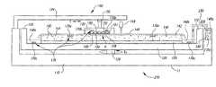
- FIG. 4is a schematic cross-sectional view of another embodiment of a polish machine 210 for polishing the substrate 150 .
- the polish machine 210has a housing 112 , a platen 120 , a substrate carrier assembly 130 , and a polishing pad 140 .
- the polish machine 210also has a reacting cell 220 preferably positioned in the housing 112 , and a feed line 230 from the cell 220 to the CMP byproducts 148 (a) on the platen 120 .
- the feed line 230is preferably movable so that it can be removed from the byproducts 148 (a) and/or the interior of the platen 120 during planarization when the platen 120 rotates.
- the CMP byproducts 148 (a)are pumped through the feed line 230 and into the cell 220 by a pump (not shown).
- a reactive agent 240is mixed with the CMP byproducts 148 (a) to detect whether material of the underlying layer 154 is present in the CMP byproducts 148 (a).
- the reactive agent 240is preferably selected to react with the material of the underlying layer 154 in a manner that indicates the quantity of the underlying layer 154 that is present in the CMP byproducts 148 (a).
- reactive agents 240may be added to the cell 220 to indicate the presence and quantity of material from the underlying layer 154 in the CMP byproducts 148 (a). Depending upon the specific reactive agent 240 , the resulting reaction may be detected by a change in temperature in the cell 220 measured by a heat sensor 170 (d), a change in color of the reacted CMP byproducts 148 (a) in the cell 220 , or other known techniques to monitor chemical reactions.
- One suitable reactive agent 240 to detect the presence of tungsten or compounds of tungsten in the CMP byproducts 148 (a)is composed of potassium chlorate (KClO 3 ) and aqua regia (HCl+HNO 3 ).
- the heat at the front of the substrateis only one characteristic of a polishing component indicative of material being removed from the planarized surface of the substrate.
- the polishing componentis the CMP byproducts
- the characteristics of the byproducts that may be indicative of the material at the front face of the substrateinclude the pH of the byproducts, the conductivity of the byproducts (especially for polishing conductive layers), the color of the byproducts, and the chemical composition of the byproducts.
- Predetermined values of any characteristic corresponding to the endpointmay be determined in a similar manner as described above with respect to the temperature of a polishing component sensitive to the heat at the front face of the substrate.
- the pH level of the byproductsmay be determined using a calomel electrode known in the art, or the chemical composition of the byproducts may be determined by infrared spectroscopy, elemental analysis, or atomic absorption processes known in the art. Accordingly, the invention is not limited except as by the appended claims.
Landscapes
- Engineering & Computer Science (AREA)
- Mechanical Engineering (AREA)
- Mechanical Treatment Of Semiconductor (AREA)
- Finish Polishing, Edge Sharpening, And Grinding By Specific Grinding Devices (AREA)
Abstract
Description
Claims (19)
Priority Applications (1)
| Application Number | Priority Date | Filing Date | Title |
|---|---|---|---|
| US10/035,828USRE39547E1 (en) | 1997-08-21 | 2001-12-28 | Method and apparatus for endpointing mechanical and chemical-mechanical polishing of substrates |
Applications Claiming Priority (2)
| Application Number | Priority Date | Filing Date | Title |
|---|---|---|---|
| US08/917,665US6007408A (en) | 1997-08-21 | 1997-08-21 | Method and apparatus for endpointing mechanical and chemical-mechanical polishing of substrates |
| US10/035,828USRE39547E1 (en) | 1997-08-21 | 2001-12-28 | Method and apparatus for endpointing mechanical and chemical-mechanical polishing of substrates |
Related Parent Applications (1)
| Application Number | Title | Priority Date | Filing Date |
|---|---|---|---|
| US08/917,665ReissueUS6007408A (en) | 1997-08-21 | 1997-08-21 | Method and apparatus for endpointing mechanical and chemical-mechanical polishing of substrates |
Publications (1)
| Publication Number | Publication Date |
|---|---|
| USRE39547E1true USRE39547E1 (en) | 2007-04-03 |
Family
ID=25439157
Family Applications (2)
| Application Number | Title | Priority Date | Filing Date |
|---|---|---|---|
| US08/917,665CeasedUS6007408A (en) | 1997-08-21 | 1997-08-21 | Method and apparatus for endpointing mechanical and chemical-mechanical polishing of substrates |
| US10/035,828Expired - LifetimeUSRE39547E1 (en) | 1997-08-21 | 2001-12-28 | Method and apparatus for endpointing mechanical and chemical-mechanical polishing of substrates |
Family Applications Before (1)
| Application Number | Title | Priority Date | Filing Date |
|---|---|---|---|
| US08/917,665CeasedUS6007408A (en) | 1997-08-21 | 1997-08-21 | Method and apparatus for endpointing mechanical and chemical-mechanical polishing of substrates |
Country Status (1)
| Country | Link |
|---|---|
| US (2) | US6007408A (en) |
Families Citing this family (48)
| Publication number | Priority date | Publication date | Assignee | Title |
|---|---|---|---|---|
| US6075606A (en) | 1996-02-16 | 2000-06-13 | Doan; Trung T. | Endpoint detector and method for measuring a change in wafer thickness in chemical-mechanical polishing of semiconductor wafers and other microelectronic substrates |
| US6180422B1 (en)* | 1998-05-06 | 2001-01-30 | International Business Machines Corporation | Endpoint detection by chemical reaction |
| US6126848A (en)* | 1998-05-06 | 2000-10-03 | International Business Machines Corporation | Indirect endpoint detection by chemical reaction and chemiluminescence |
| US20030206114A1 (en)* | 1998-08-04 | 2003-11-06 | Leping Li | Interface device for sti/bpsg EPD and real time control |
| US6352466B1 (en)* | 1998-08-31 | 2002-03-05 | Micron Technology, Inc. | Method and apparatus for wireless transfer of chemical-mechanical planarization measurements |
| US6191037B1 (en)* | 1998-09-03 | 2001-02-20 | Micron Technology, Inc. | Methods, apparatuses and substrate assembly structures for fabricating microelectronic components using mechanical and chemical-mechanical planarization processes |
| US6276996B1 (en)* | 1998-11-10 | 2001-08-21 | Micron Technology, Inc. | Copper chemical-mechanical polishing process using a fixed abrasive polishing pad and a copper layer chemical-mechanical polishing solution specifically adapted for chemical-mechanical polishing with a fixed abrasive pad |
| US20050118839A1 (en)* | 1999-04-23 | 2005-06-02 | Industrial Technology Research Institute | Chemical mechanical polish process control method using thermal imaging of polishing pad |
| US6537135B1 (en)* | 1999-12-13 | 2003-03-25 | Agere Systems Inc. | Curvilinear chemical mechanical planarization device and method |
| US6227939B1 (en)* | 2000-01-25 | 2001-05-08 | Agilent Technologies, Inc. | Temperature controlled chemical mechanical polishing method and apparatus |
| DE60143192D1 (en) | 2000-02-08 | 2010-11-18 | Sangamo Biosciences Inc | CELLS FOR THE DISCOVERY OF MEDICAMENTS |
| US6387289B1 (en) | 2000-05-04 | 2002-05-14 | Micron Technology, Inc. | Planarizing machines and methods for mechanical and/or chemical-mechanical planarization of microelectronic-device substrate assemblies |
| US6612901B1 (en) | 2000-06-07 | 2003-09-02 | Micron Technology, Inc. | Apparatus for in-situ optical endpointing of web-format planarizing machines in mechanical or chemical-mechanical planarization of microelectronic-device substrate assemblies |
| US6485354B1 (en)* | 2000-06-09 | 2002-11-26 | Strasbaugh | Polishing pad with built-in optical sensor |
| US6375540B1 (en) | 2000-06-30 | 2002-04-23 | Lam Research Corporation | End-point detection system for chemical mechanical posing applications |
| US6338668B1 (en) | 2000-08-16 | 2002-01-15 | Taiwan Semiconductor Manufacturing Company, Ltd | In-line chemical mechanical polish (CMP) planarizing method employing interpolation and extrapolation |
| US6609947B1 (en) | 2000-08-30 | 2003-08-26 | Micron Technology, Inc. | Planarizing machines and control systems for mechanical and/or chemical-mechanical planarization of micro electronic substrates |
| US6652764B1 (en) | 2000-08-31 | 2003-11-25 | Micron Technology, Inc. | Methods and apparatuses for making and using planarizing pads for mechanical and chemical-mechanical planarization of microelectronic substrates |
| US7067317B2 (en)* | 2000-12-07 | 2006-06-27 | Sangamo Biosciences, Inc. | Regulation of angiogenesis with zinc finger proteins |
| JP2004537260A (en)* | 2000-12-07 | 2004-12-16 | サンガモ バイオサイエンシーズ, インコーポレイテッド | Regulation of angiogenesis by zinc finger proteins |
| US9234187B2 (en)* | 2001-01-22 | 2016-01-12 | Sangamo Biosciences, Inc. | Modified zinc finger binding proteins |
| WO2003002301A1 (en)* | 2001-06-26 | 2003-01-09 | Lam Research Corporation | End point detection system for chemical mechanical polishing applications |
| US6562185B2 (en)* | 2001-09-18 | 2003-05-13 | Advanced Micro Devices, Inc. | Wafer based temperature sensors for characterizing chemical mechanical polishing processes |
| AUPR806801A0 (en)* | 2001-10-03 | 2001-10-25 | Davey Products Pty Ltd | Pump control system |
| US6939198B1 (en)* | 2001-12-28 | 2005-09-06 | Applied Materials, Inc. | Polishing system with in-line and in-situ metrology |
| US7262054B2 (en)* | 2002-01-22 | 2007-08-28 | Sangamo Biosciences, Inc. | Zinc finger proteins for DNA binding and gene regulation in plants |
| US7131889B1 (en) | 2002-03-04 | 2006-11-07 | Micron Technology, Inc. | Method for planarizing microelectronic workpieces |
| US20030199112A1 (en) | 2002-03-22 | 2003-10-23 | Applied Materials, Inc. | Copper wiring module control |
| US7341502B2 (en) | 2002-07-18 | 2008-03-11 | Micron Technology, Inc. | Methods and systems for planarizing workpieces, e.g., microelectronic workpieces |
| US7004817B2 (en) | 2002-08-23 | 2006-02-28 | Micron Technology, Inc. | Carrier assemblies, planarizing apparatuses including carrier assemblies, and methods for planarizing micro-device workpieces |
| US7008299B2 (en) | 2002-08-29 | 2006-03-07 | Micron Technology, Inc. | Apparatus and method for mechanical and/or chemical-mechanical planarization of micro-device workpieces |
| JP4197269B2 (en)* | 2002-09-09 | 2008-12-17 | 株式会社キッツ | Nickel elution prevention method for copper alloy piping equipment such as valves and fittings and its copper alloy piping equipment |
| US7074114B2 (en) | 2003-01-16 | 2006-07-11 | Micron Technology, Inc. | Carrier assemblies, polishing machines including carrier assemblies, and methods for polishing micro-device workpieces |
| US6872132B2 (en) | 2003-03-03 | 2005-03-29 | Micron Technology, Inc. | Systems and methods for monitoring characteristics of a polishing pad used in polishing micro-device workpieces |
| US7131891B2 (en) | 2003-04-28 | 2006-11-07 | Micron Technology, Inc. | Systems and methods for mechanical and/or chemical-mechanical polishing of microfeature workpieces |
| KR100506942B1 (en)* | 2003-09-03 | 2005-08-05 | 삼성전자주식회사 | Chemical mechanical polishing apparatus |
| US6939211B2 (en)* | 2003-10-09 | 2005-09-06 | Micron Technology, Inc. | Planarizing solutions including abrasive elements, and methods for manufacturing and using such planarizing solutions |
| US6872662B1 (en) | 2003-10-27 | 2005-03-29 | Hong Hocheng | Method for detecting the endpoint of a chemical mechanical polishing (CMP) process |
| US7086927B2 (en) | 2004-03-09 | 2006-08-08 | Micron Technology, Inc. | Methods and systems for planarizing workpieces, e.g., microelectronic workpieces |
| WO2005099771A2 (en)* | 2004-04-08 | 2005-10-27 | Sangamo Biosciences, Inc. | Methods and compositions for treating neuropathic and neurodegenerative conditions |
| US7534775B2 (en)* | 2004-04-08 | 2009-05-19 | Sangamo Biosciences, Inc. | Methods and compositions for modulating cardiac contractility |
| US20060105676A1 (en)* | 2004-11-17 | 2006-05-18 | International Business Machines Corporation | Robust Signal Processing Algorithm For End-Pointing Chemical-Mechanical Polishing Processes |
| CA2599004C (en) | 2005-02-28 | 2015-05-26 | Sangamo Biosciences, Inc. | Anti-angiogenic methods and compositions |
| US8549347B1 (en) | 2010-12-20 | 2013-10-01 | Amazon Technologies, Inc. | Techniques for network replication |
| US8230050B1 (en) | 2008-12-10 | 2012-07-24 | Amazon Technologies, Inc. | Providing access to configurable private computer networks |
| US9137209B1 (en) | 2008-12-10 | 2015-09-15 | Amazon Technologies, Inc. | Providing local secure network access to remote services |
| US9106540B2 (en) | 2009-03-30 | 2015-08-11 | Amazon Technologies, Inc. | Providing logical networking functionality for managed computer networks |
| US11282755B2 (en) | 2019-08-27 | 2022-03-22 | Applied Materials, Inc. | Asymmetry correction via oriented wafer loading |
Citations (34)
| Publication number | Priority date | Publication date | Assignee | Title |
|---|---|---|---|---|
| US4200395A (en)* | 1977-05-03 | 1980-04-29 | Massachusetts Institute Of Technology | Alignment of diffraction gratings |
| US4203799A (en)* | 1975-05-30 | 1980-05-20 | Hitachi, Ltd. | Method for monitoring thickness of epitaxial growth layer on substrate |
| US4358338A (en)* | 1980-05-16 | 1982-11-09 | Varian Associates, Inc. | End point detection method for physical etching process |
| US4367044A (en)* | 1980-12-31 | 1983-01-04 | International Business Machines Corp. | Situ rate and depth monitor for silicon etching |
| US4377028A (en)* | 1980-02-29 | 1983-03-22 | Telmec Co., Ltd. | Method for registering a mask pattern in a photo-etching apparatus for semiconductor devices |
| US4422764A (en)* | 1980-12-12 | 1983-12-27 | The University Of Rochester | Interferometer apparatus for microtopography |
| US4640002A (en)* | 1982-02-25 | 1987-02-03 | The University Of Delaware | Method and apparatus for increasing the durability and yield of thin film photovoltaic devices |
| US4660980A (en)* | 1983-12-13 | 1987-04-28 | Anritsu Electric Company Limited | Apparatus for measuring thickness of object transparent to light utilizing interferometric method |
| US4717255A (en)* | 1986-03-26 | 1988-01-05 | Hommelwerke Gmbh | Device for measuring small distances |
| US4879258A (en)* | 1988-08-31 | 1989-11-07 | Texas Instruments Incorporated | Integrated circuit planarization by mechanical polishing |
| US5036015A (en)* | 1990-09-24 | 1991-07-30 | Micron Technology, Inc. | Method of endpoint detection during chemical/mechanical planarization of semiconductor wafers |
| US5064683A (en)* | 1990-10-29 | 1991-11-12 | Motorola, Inc. | Method for polish planarizing a semiconductor substrate by using a boron nitride polish stop |
| US5069002A (en)* | 1991-04-17 | 1991-12-03 | Micron Technology, Inc. | Apparatus for endpoint detection during mechanical planarization of semiconductor wafers |
| US5081796A (en)* | 1990-08-06 | 1992-01-21 | Micron Technology, Inc. | Method and apparatus for mechanical planarization and endpoint detection of a semiconductor wafer |
| US5154021A (en)* | 1991-06-26 | 1992-10-13 | International Business Machines Corporation | Pneumatic pad conditioner |
| US5216843A (en)* | 1992-09-24 | 1993-06-08 | Intel Corporation | Polishing pad conditioning apparatus for wafer planarization process |
| US5220405A (en)* | 1991-12-20 | 1993-06-15 | International Business Machines Corporation | Interferometer for in situ measurement of thin film thickness changes |
| US5314843A (en)* | 1992-03-27 | 1994-05-24 | Micron Technology, Inc. | Integrated circuit polishing method |
| US5324381A (en)* | 1992-05-06 | 1994-06-28 | Sumitomo Electric Industries, Ltd. | Semiconductor chip mounting method and apparatus |
| US5369488A (en)* | 1991-12-10 | 1994-11-29 | Olympus Optical Co., Ltd. | High precision location measuring device wherein a position detector and an interferometer are fixed to a movable holder |
| US5399234A (en)* | 1993-09-29 | 1995-03-21 | Motorola Inc. | Acoustically regulated polishing process |
| US5413941A (en)* | 1994-01-06 | 1995-05-09 | Micron Technology, Inc. | Optical end point detection methods in semiconductor planarizing polishing processes |
| US5433651A (en)* | 1993-12-22 | 1995-07-18 | International Business Machines Corporation | In-situ endpoint detection and process monitoring method and apparatus for chemical-mechanical polishing |
| US5461007A (en)* | 1994-06-02 | 1995-10-24 | Motorola, Inc. | Process for polishing and analyzing a layer over a patterned semiconductor substrate |
| US5465154A (en)* | 1989-05-05 | 1995-11-07 | Levy; Karl B. | Optical monitoring of growth and etch rate of materials |
| US5597442A (en)* | 1995-10-16 | 1997-01-28 | Taiwan Semiconductor Manufacturing Company Ltd. | Chemical/mechanical planarization (CMP) endpoint method using measurement of polishing pad temperature |
| US5609719A (en)* | 1994-11-03 | 1997-03-11 | Texas Instruments Incorporated | Method for performing chemical mechanical polish (CMP) of a wafer |
| US5616069A (en)* | 1995-12-19 | 1997-04-01 | Micron Technology, Inc. | Directional spray pad scrubber |
| US5643050A (en)* | 1996-05-23 | 1997-07-01 | Industrial Technology Research Institute | Chemical/mechanical polish (CMP) thickness monitor |
| US5663797A (en)* | 1996-05-16 | 1997-09-02 | Micron Technology, Inc. | Method and apparatus for detecting the endpoint in chemical-mechanical polishing of semiconductor wafers |
| US5733176A (en)* | 1996-05-24 | 1998-03-31 | Micron Technology, Inc. | Polishing pad and method of use |
| US5762537A (en)* | 1993-08-25 | 1998-06-09 | Micron Technology, Inc. | System for real-time control of semiconductor wafer polishing including heater |
| US5777739A (en)* | 1996-02-16 | 1998-07-07 | Micron Technology, Inc. | Endpoint detector and method for measuring a change in wafer thickness in chemical-mechanical polishing of semiconductor wafers |
| US5855804A (en)* | 1996-12-06 | 1999-01-05 | Micron Technology, Inc. | Method and apparatus for stopping mechanical and chemical-mechanical planarization of substrates at desired endpoints |
- 1997
- 1997-08-21USUS08/917,665patent/US6007408A/ennot_activeCeased
- 2001
- 2001-12-28USUS10/035,828patent/USRE39547E1/ennot_activeExpired - Lifetime
Patent Citations (34)
| Publication number | Priority date | Publication date | Assignee | Title |
|---|---|---|---|---|
| US4203799A (en)* | 1975-05-30 | 1980-05-20 | Hitachi, Ltd. | Method for monitoring thickness of epitaxial growth layer on substrate |
| US4200395A (en)* | 1977-05-03 | 1980-04-29 | Massachusetts Institute Of Technology | Alignment of diffraction gratings |
| US4377028A (en)* | 1980-02-29 | 1983-03-22 | Telmec Co., Ltd. | Method for registering a mask pattern in a photo-etching apparatus for semiconductor devices |
| US4358338A (en)* | 1980-05-16 | 1982-11-09 | Varian Associates, Inc. | End point detection method for physical etching process |
| US4422764A (en)* | 1980-12-12 | 1983-12-27 | The University Of Rochester | Interferometer apparatus for microtopography |
| US4367044A (en)* | 1980-12-31 | 1983-01-04 | International Business Machines Corp. | Situ rate and depth monitor for silicon etching |
| US4640002A (en)* | 1982-02-25 | 1987-02-03 | The University Of Delaware | Method and apparatus for increasing the durability and yield of thin film photovoltaic devices |
| US4660980A (en)* | 1983-12-13 | 1987-04-28 | Anritsu Electric Company Limited | Apparatus for measuring thickness of object transparent to light utilizing interferometric method |
| US4717255A (en)* | 1986-03-26 | 1988-01-05 | Hommelwerke Gmbh | Device for measuring small distances |
| US4879258A (en)* | 1988-08-31 | 1989-11-07 | Texas Instruments Incorporated | Integrated circuit planarization by mechanical polishing |
| US5465154A (en)* | 1989-05-05 | 1995-11-07 | Levy; Karl B. | Optical monitoring of growth and etch rate of materials |
| US5081796A (en)* | 1990-08-06 | 1992-01-21 | Micron Technology, Inc. | Method and apparatus for mechanical planarization and endpoint detection of a semiconductor wafer |
| US5036015A (en)* | 1990-09-24 | 1991-07-30 | Micron Technology, Inc. | Method of endpoint detection during chemical/mechanical planarization of semiconductor wafers |
| US5064683A (en)* | 1990-10-29 | 1991-11-12 | Motorola, Inc. | Method for polish planarizing a semiconductor substrate by using a boron nitride polish stop |
| US5069002A (en)* | 1991-04-17 | 1991-12-03 | Micron Technology, Inc. | Apparatus for endpoint detection during mechanical planarization of semiconductor wafers |
| US5154021A (en)* | 1991-06-26 | 1992-10-13 | International Business Machines Corporation | Pneumatic pad conditioner |
| US5369488A (en)* | 1991-12-10 | 1994-11-29 | Olympus Optical Co., Ltd. | High precision location measuring device wherein a position detector and an interferometer are fixed to a movable holder |
| US5220405A (en)* | 1991-12-20 | 1993-06-15 | International Business Machines Corporation | Interferometer for in situ measurement of thin film thickness changes |
| US5314843A (en)* | 1992-03-27 | 1994-05-24 | Micron Technology, Inc. | Integrated circuit polishing method |
| US5324381A (en)* | 1992-05-06 | 1994-06-28 | Sumitomo Electric Industries, Ltd. | Semiconductor chip mounting method and apparatus |
| US5216843A (en)* | 1992-09-24 | 1993-06-08 | Intel Corporation | Polishing pad conditioning apparatus for wafer planarization process |
| US5762537A (en)* | 1993-08-25 | 1998-06-09 | Micron Technology, Inc. | System for real-time control of semiconductor wafer polishing including heater |
| US5399234A (en)* | 1993-09-29 | 1995-03-21 | Motorola Inc. | Acoustically regulated polishing process |
| US5433651A (en)* | 1993-12-22 | 1995-07-18 | International Business Machines Corporation | In-situ endpoint detection and process monitoring method and apparatus for chemical-mechanical polishing |
| US5413941A (en)* | 1994-01-06 | 1995-05-09 | Micron Technology, Inc. | Optical end point detection methods in semiconductor planarizing polishing processes |
| US5461007A (en)* | 1994-06-02 | 1995-10-24 | Motorola, Inc. | Process for polishing and analyzing a layer over a patterned semiconductor substrate |
| US5609719A (en)* | 1994-11-03 | 1997-03-11 | Texas Instruments Incorporated | Method for performing chemical mechanical polish (CMP) of a wafer |
| US5597442A (en)* | 1995-10-16 | 1997-01-28 | Taiwan Semiconductor Manufacturing Company Ltd. | Chemical/mechanical planarization (CMP) endpoint method using measurement of polishing pad temperature |
| US5616069A (en)* | 1995-12-19 | 1997-04-01 | Micron Technology, Inc. | Directional spray pad scrubber |
| US5777739A (en)* | 1996-02-16 | 1998-07-07 | Micron Technology, Inc. | Endpoint detector and method for measuring a change in wafer thickness in chemical-mechanical polishing of semiconductor wafers |
| US5663797A (en)* | 1996-05-16 | 1997-09-02 | Micron Technology, Inc. | Method and apparatus for detecting the endpoint in chemical-mechanical polishing of semiconductor wafers |
| US5643050A (en)* | 1996-05-23 | 1997-07-01 | Industrial Technology Research Institute | Chemical/mechanical polish (CMP) thickness monitor |
| US5733176A (en)* | 1996-05-24 | 1998-03-31 | Micron Technology, Inc. | Polishing pad and method of use |
| US5855804A (en)* | 1996-12-06 | 1999-01-05 | Micron Technology, Inc. | Method and apparatus for stopping mechanical and chemical-mechanical planarization of substrates at desired endpoints |
Also Published As
| Publication number | Publication date |
|---|---|
| US6007408A (en) | 1999-12-28 |
Similar Documents
| Publication | Publication Date | Title |
|---|---|---|
| USRE39547E1 (en) | Method and apparatus for endpointing mechanical and chemical-mechanical polishing of substrates | |
| US6506097B1 (en) | Optical monitoring in a two-step chemical mechanical polishing process | |
| US6869332B2 (en) | Chemical mechanical polishing of a metal layer with polishing rate monitoring | |
| US7235000B2 (en) | Methods and systems for conditioning planarizing pads used in planarizing substrates | |
| US6659842B2 (en) | Method and apparatus for optical monitoring in chemical mechanical polishing | |
| US6913511B2 (en) | Method and apparatus for detecting an end-point in chemical mechanical polishing of metal layers | |
| US6524165B1 (en) | Method and apparatus for measuring substrate layer thickness during chemical mechanical polishing | |
| US5637185A (en) | Systems for performing chemical mechanical planarization and process for conducting same | |
| EP1294534B2 (en) | IN SITU POINT DETECTION AND PROCESS MONITORING METHOD AND MECHANICAL CHEMICAL POLISHING APPARATUS | |
| US7247080B1 (en) | Feedback controlled polishing processes | |
| US6186865B1 (en) | Apparatus and method for performing end point detection on a linear planarization tool | |
| WO2001056744A9 (en) | Endpoint monitoring with polishing rate change | |
| US6258205B1 (en) | Endpoint detection method and apparatus which utilize an endpoint polishing layer of catalyst material | |
| US20020124957A1 (en) | Methods and apparatuses for monitoring and controlling mechanical or chemical-mechanical planarization of microelectronic substrate assemblies | |
| US20060113036A1 (en) | Computer integrated manufacturing control system for oxide chemical mechanical polishing | |
| US9248544B2 (en) | Endpoint detection during polishing using integrated differential intensity | |
| US6503766B1 (en) | Method and system for detecting an exposure of a material on a semiconductor wafer during chemical-mechanical polishing | |
| Stein et al. | Recent advances in endpoint and in-line monitoring techniques for chemical-mechanical polishing processes | |
| EP1618991B1 (en) | Polishing pad | |
| Hetherington et al. | In-line monitoring of chemical-mechanical polishing processes |
Legal Events
| Date | Code | Title | Description |
|---|---|---|---|
| FEPP | Fee payment procedure | Free format text:PAYOR NUMBER ASSIGNED (ORIGINAL EVENT CODE: ASPN); ENTITY STATUS OF PATENT OWNER: LARGE ENTITY | |
| FPAY | Fee payment | Year of fee payment:8 | |
| FPAY | Fee payment | Year of fee payment:12 | |
| AS | Assignment | Owner name:U.S. BANK NATIONAL ASSOCIATION, AS COLLATERAL AGENT, CALIFORNIA Free format text:SECURITY INTEREST;ASSIGNOR:MICRON TECHNOLOGY, INC.;REEL/FRAME:038669/0001 Effective date:20160426 Owner name:U.S. BANK NATIONAL ASSOCIATION, AS COLLATERAL AGEN Free format text:SECURITY INTEREST;ASSIGNOR:MICRON TECHNOLOGY, INC.;REEL/FRAME:038669/0001 Effective date:20160426 | |
| AS | Assignment | Owner name:MORGAN STANLEY SENIOR FUNDING, INC., AS COLLATERAL AGENT, MARYLAND Free format text:PATENT SECURITY AGREEMENT;ASSIGNOR:MICRON TECHNOLOGY, INC.;REEL/FRAME:038954/0001 Effective date:20160426 Owner name:MORGAN STANLEY SENIOR FUNDING, INC., AS COLLATERAL Free format text:PATENT SECURITY AGREEMENT;ASSIGNOR:MICRON TECHNOLOGY, INC.;REEL/FRAME:038954/0001 Effective date:20160426 | |
| AS | Assignment | Owner name:U.S. BANK NATIONAL ASSOCIATION, AS COLLATERAL AGENT, CALIFORNIA Free format text:CORRECTIVE ASSIGNMENT TO CORRECT THE REPLACE ERRONEOUSLY FILED PATENT #7358718 WITH THE CORRECT PATENT #7358178 PREVIOUSLY RECORDED ON REEL 038669 FRAME 0001. ASSIGNOR(S) HEREBY CONFIRMS THE SECURITY INTEREST;ASSIGNOR:MICRON TECHNOLOGY, INC.;REEL/FRAME:043079/0001 Effective date:20160426 Owner name:U.S. BANK NATIONAL ASSOCIATION, AS COLLATERAL AGEN Free format text:CORRECTIVE ASSIGNMENT TO CORRECT THE REPLACE ERRONEOUSLY FILED PATENT #7358718 WITH THE CORRECT PATENT #7358178 PREVIOUSLY RECORDED ON REEL 038669 FRAME 0001. ASSIGNOR(S) HEREBY CONFIRMS THE SECURITY INTEREST;ASSIGNOR:MICRON TECHNOLOGY, INC.;REEL/FRAME:043079/0001 Effective date:20160426 | |
| AS | Assignment | Owner name:MICRON TECHNOLOGY, INC., IDAHO Free format text:RELEASE BY SECURED PARTY;ASSIGNOR:U.S. BANK NATIONAL ASSOCIATION, AS COLLATERAL AGENT;REEL/FRAME:047243/0001 Effective date:20180629 | |
| AS | Assignment | Owner name:MICRON TECHNOLOGY, INC., IDAHO Free format text:RELEASE BY SECURED PARTY;ASSIGNOR:MORGAN STANLEY SENIOR FUNDING, INC., AS COLLATERAL AGENT;REEL/FRAME:050937/0001 Effective date:20190731 |