USRE38381E1 - Inverted board mounted electromechanical device - Google Patents
Inverted board mounted electromechanical deviceDownload PDFInfo
- Publication number
- USRE38381E1 USRE38381E1US10/023,176US2317602AUSRE38381EUS RE38381 E1USRE38381 E1US RE38381E1US 2317602 AUS2317602 AUS 2317602AUS RE38381 EUSRE38381 EUS RE38381E
- Authority
- US
- United States
- Prior art keywords
- electrical interconnection
- ground
- signal
- interconnection member
- circuit board
- Prior art date
- Legal status (The legal status is an assumption and is not a legal conclusion. Google has not performed a legal analysis and makes no representation as to the accuracy of the status listed.)
- Expired - Fee Related
Links
- 235000014676Phragmites communisNutrition0.000claimsabstractdescription151
- 239000000758substrateSubstances0.000claimsabstractdescription38
- 229910000679solderInorganic materials0.000claimsdescription8
- 239000004020conductorSubstances0.000description16
- 238000012360testing methodMethods0.000description9
- 238000009434installationMethods0.000description5
- 238000004519manufacturing processMethods0.000description5
- 239000011521glassSubstances0.000description4
- RYGMFSIKBFXOCR-UHFFFAOYSA-NCopperChemical compound[Cu]RYGMFSIKBFXOCR-UHFFFAOYSA-N0.000description3
- 238000010276constructionMethods0.000description3
- 229910052802copperInorganic materials0.000description3
- 239000010949copperSubstances0.000description3
- 239000000463materialSubstances0.000description3
- 238000000034methodMethods0.000description3
- 230000003071parasitic effectEffects0.000description3
- 230000001681protective effectEffects0.000description3
- 210000002105tongueAnatomy0.000description3
- 229910001369BrassInorganic materials0.000description2
- 230000005540biological transmissionEffects0.000description2
- 239000010951brassSubstances0.000description2
- 239000002775capsuleSubstances0.000description2
- 238000010586diagramMethods0.000description2
- 239000011261inert gasSubstances0.000description2
- 239000002184metalSubstances0.000description2
- 229910052751metalInorganic materials0.000description2
- 238000012986modificationMethods0.000description2
- 230000004048modificationEffects0.000description2
- 238000004806packaging method and processMethods0.000description2
- 230000007704transitionEffects0.000description2
- ATJFFYVFTNAWJD-UHFFFAOYSA-NTinChemical compound[Sn]ATJFFYVFTNAWJD-UHFFFAOYSA-N0.000description1
- 229910045601alloyInorganic materials0.000description1
- 239000000956alloySubstances0.000description1
- 229910052782aluminiumInorganic materials0.000description1
- XAGFODPZIPBFFR-UHFFFAOYSA-NaluminiumChemical compound[Al]XAGFODPZIPBFFR-UHFFFAOYSA-N0.000description1
- 230000015556catabolic processEffects0.000description1
- 230000000295complement effectEffects0.000description1
- 238000006731degradation reactionMethods0.000description1
- 238000012938design processMethods0.000description1
- 239000003989dielectric materialSubstances0.000description1
- 238000009413insulationMethods0.000description1
- 230000010354integrationEffects0.000description1
- 238000012423maintenanceMethods0.000description1
- 230000008054signal transmissionEffects0.000description1
- 239000002356single layerSubstances0.000description1
- 229910052718tinInorganic materials0.000description1
Images


Classifications
- H—ELECTRICITY
- H05—ELECTRIC TECHNIQUES NOT OTHERWISE PROVIDED FOR
- H05K—PRINTED CIRCUITS; CASINGS OR CONSTRUCTIONAL DETAILS OF ELECTRIC APPARATUS; MANUFACTURE OF ASSEMBLAGES OF ELECTRICAL COMPONENTS
- H05K1/00—Printed circuits
- H05K1/02—Details
- H05K1/14—Structural association of two or more printed circuits
- H05K1/141—One or more single auxiliary printed circuits mounted on a main printed circuit, e.g. modules, adapters
- H—ELECTRICITY
- H01—ELECTRIC ELEMENTS
- H01H—ELECTRIC SWITCHES; RELAYS; SELECTORS; EMERGENCY PROTECTIVE DEVICES
- H01H51/00—Electromagnetic relays
- H01H51/28—Relays having both armature and contacts within a sealed casing outside which the operating coil is located, e.g. contact carried by a magnetic leaf spring or reed
- H01H51/281—Mounting of the relay; Encapsulating; Details of connections
- H—ELECTRICITY
- H05—ELECTRIC TECHNIQUES NOT OTHERWISE PROVIDED FOR
- H05K—PRINTED CIRCUITS; CASINGS OR CONSTRUCTIONAL DETAILS OF ELECTRIC APPARATUS; MANUFACTURE OF ASSEMBLAGES OF ELECTRICAL COMPONENTS
- H05K1/00—Printed circuits
- H05K1/02—Details
- H05K1/0213—Electrical arrangements not otherwise provided for
- H05K1/0216—Reduction of cross-talk, noise or electromagnetic interference
- H05K1/0218—Reduction of cross-talk, noise or electromagnetic interference by printed shielding conductors, ground planes or power plane
- H05K1/0219—Printed shielding conductors for shielding around or between signal conductors, e.g. coplanar or coaxial printed shielding conductors
- H—ELECTRICITY
- H05—ELECTRIC TECHNIQUES NOT OTHERWISE PROVIDED FOR
- H05K—PRINTED CIRCUITS; CASINGS OR CONSTRUCTIONAL DETAILS OF ELECTRIC APPARATUS; MANUFACTURE OF ASSEMBLAGES OF ELECTRICAL COMPONENTS
- H05K1/00—Printed circuits
- H05K1/18—Printed circuits structurally associated with non-printed electric components
- H05K1/182—Printed circuits structurally associated with non-printed electric components associated with components mounted in the printed circuit board, e.g. insert mounted components [IMC]
- H—ELECTRICITY
- H05—ELECTRIC TECHNIQUES NOT OTHERWISE PROVIDED FOR
- H05K—PRINTED CIRCUITS; CASINGS OR CONSTRUCTIONAL DETAILS OF ELECTRIC APPARATUS; MANUFACTURE OF ASSEMBLAGES OF ELECTRICAL COMPONENTS
- H05K2201/00—Indexing scheme relating to printed circuits covered by H05K1/00
- H05K2201/04—Assemblies of printed circuits
- H05K2201/049—PCB for one component, e.g. for mounting onto mother PCB
- H—ELECTRICITY
- H05—ELECTRIC TECHNIQUES NOT OTHERWISE PROVIDED FOR
- H05K—PRINTED CIRCUITS; CASINGS OR CONSTRUCTIONAL DETAILS OF ELECTRIC APPARATUS; MANUFACTURE OF ASSEMBLAGES OF ELECTRICAL COMPONENTS
- H05K2201/00—Indexing scheme relating to printed circuits covered by H05K1/00
- H05K2201/09—Shape and layout
- H05K2201/09009—Substrate related
- H05K2201/09072—Hole or recess under component or special relationship between hole and component
- H—ELECTRICITY
- H05—ELECTRIC TECHNIQUES NOT OTHERWISE PROVIDED FOR
- H05K—PRINTED CIRCUITS; CASINGS OR CONSTRUCTIONAL DETAILS OF ELECTRIC APPARATUS; MANUFACTURE OF ASSEMBLAGES OF ELECTRICAL COMPONENTS
- H05K2201/00—Indexing scheme relating to printed circuits covered by H05K1/00
- H05K2201/10—Details of components or other objects attached to or integrated in a printed circuit board
- H05K2201/10007—Types of components
- H05K2201/10083—Electromechanical or electro-acoustic component, e.g. microphone
- H—ELECTRICITY
- H05—ELECTRIC TECHNIQUES NOT OTHERWISE PROVIDED FOR
- H05K—PRINTED CIRCUITS; CASINGS OR CONSTRUCTIONAL DETAILS OF ELECTRIC APPARATUS; MANUFACTURE OF ASSEMBLAGES OF ELECTRICAL COMPONENTS
- H05K2201/00—Indexing scheme relating to printed circuits covered by H05K1/00
- H05K2201/10—Details of components or other objects attached to or integrated in a printed circuit board
- H05K2201/10431—Details of mounted components
- H05K2201/10439—Position of a single component
- H05K2201/10477—Inverted
Definitions
- the present inventionrelates generally to switching devices. More specifically, the present invention relates to improved packaging and circuit integration for electromagnetic devices, such as reed switches and electromagnetic devices such as reed relays.
- Electromagnetic relayshave been known in the electronics industry for many years. Such electromagnetic relays include the reed relay which incorporates a reed switch.
- a reed switchis a magnetically activated device that typically includes two flat contact tongues which are merged in a hermetically sealed glass tube filled with a protective inert gas or vacuum. The switch is operated by an externally generated magnetic field, either from a coil or a permanent magnet. When the external magnetic field is enabled, the overlapping contact tongue ends attract each other and ultimately come into contact to close the switch. When the magnetic field is removed, the contact tongues demagnetize and spring back to return to their rest positions, thus opening the switch.
- Reed switchesactuated by a magnetic coil
- a coil of wireis wrapped about the outside of the bobbin and connected to a source of electric current. The current flowing through the coil creates the desired magnetic field to actuate the reed switch within the bobbin housing.
- a ground shield conductorcommonly made of copper or brass is disposed about the body of the reed switch.
- the ground shield conductoris commonly in a cylindrical configuration.
- the shield conductorresides between the reed switch and the bobbin housing to form a co-axial high frequency transmission system.
- This co-axial systemincludes the outer shield conductor and the switch lead signal conductor co-axially through the center of the reed switch.
- the ground shield conductoris employed to contain the signal through the switch conductor in order to maintain the desired impedance of the signal path.
- a reed switch deviceFor application at higher frequencies, a reed switch device must be ideally configured to match as closely as possible the desired impedance requirements of the circuit in which it is installed.
- a co-axial arrangementis preferred throughout the entire environment to maintain circuit integrity and the desired matched impedance.
- the body of a reed switchincludes the necessary co-axial environment.
- the signal trace on the user's circuit boardcommonly includes a “wave guide” where two ground leads reside on opposing sides of the signal lead and in the same plane or a “strip line” where a ground plane resides below the plane of the signal conductor.
- the reed switch devicemust be physically packaged and electrically interconnected to a circuit board carrying a given circuit configuration. It is common to terminate the shield and signal terminals to a lead frame architecture and enclose the entire assembly in a dielectric material like plastic for manufacturing and packaging ease. These leads may be formed in a gull-wing or “J” shape for surface mount capability.
- the signal leads or terminalsexit out of the reed switch body and into the air in order to make the electrical interconnection to the circuit board. This transition of the signal leads from plastic dielectric to air creates an undesirable discontinuity of the protective co-axial environment found within the body of the switch itself. Such discontinuity creates inaccuracy and uncertainty in the impedance of the reed switch device.
- circuit designersmust compensate for this problem by specifically designing their circuits to accommodate and anticipate the inherent problems associated with the discontinuity of the protective co-axial environment and the degradation of the rated impedance of the reed switch device.
- the circuitmay be tuned to compensate for the discontinuity by adding parasitic inductance and capacitance. This method of discontinuity compensation is not preferred because it complicates and slows the design process and can degrade the integrity of the circuit.
- the prior artuses a structure of carefully designed vias, which are expensive and difficult to manufacture, to control the impedance from the relay to the board transition.
- a reed switch devicethat includes a controlled impedance environment through the entire body of the package to the interconnection to a circuit.
- a reed switch deviceto be compact and of a low profile for installation into small spaces and for circuit board stacking.
- reed switch devicesthat are of a surface mount configuration to optimize the high frequency of the performance of the system.
- a reed switch devicethat can reduce the need to tune a circuit to compensate for an uncontrolled impedance environment.
- a reed switch devicethat has a small footprint and is of a standard shape and configuration for simplified manufacture and installation.
- the present inventionpreserves the advantages of prior art electromagnetic switch devices, such as reed relays. In addition, it provides new advantages not found in currently available switching devices and overcomes many disadvantages of such currently available devices.
- the inventionis generally directed to the novel and unique reed switch device with particular application in effectively interconnecting a reed switch device to a circuit on a circuit board in a low profile configuration.
- the reed switch package of the present inventionenables the efficient and effective interconnection to a circuit board while being in an inexpensive construction.
- a new electromechanical devicemounts to a relay substrate to form a low profile, board mountable reed relay.
- a portion of the reed relayextends through an aperture in the relay substrate.
- the substrateincludes a series of electrical contacts, such as solder balls array (BGA), land grid array (LGA), column grid array (CGA), or pin grid array (PGA), mounted to the same side of the substrate that the relay mounts to electrically connect to the main circuit card.
- BGAsolder balls array
- LGAland grid array
- CGAcolumn grid array
- PGApin grid array
- the reed relay substrateis mounted into a cut-out in the main circuit board in an inverted manner so that a portion of the reed relay not within the substrate recess sits within a cut-out in the main circuit board.
- the reed relay componentis recessed below the surface of the main circuit board resulting in an overall low profile circuit board.
- Another object of the present inventionis to provide a reed switch package that is capable of efficiently conducting high frequency signals.
- Another object of the present inventionis to provide a reed switch package that can be easily surface mounted to a main circuit board.
- FIG. 1is a perspective view of a prior art reed relay configuration
- FIG. 2is an perspective view a reed relay device in accordance with the preferred embodiment of the present invention.
- FIG. 3is an exploded perspective view a reed relay device in accordance with the preferred embodiment of the present invention shown in FIG. 2;
- FIG. 4is a bottom perspective view of the reed relay card in accordance with the present invention.
- FIG. 5is a bottom plan view of the reed relay card in accordance with the present invention.
- FIG. 6is a perspective view of a circuit board for receipt of the reed relay card in accordance with the present invention.
- FIG. 7is a perspective view the reed relay card installed in the circuit board shown in FIG. 6;
- FIG. 8is a side elevational view of the reed relay card installed in the circuit board shown in FIG. 6;
- FIG. 9is a schematic representation of a circuit commonly used with reed relays.
- FIG. 10is pictorial implementation of the circuit shown in FIG. 9 .
- FIG. 1a perspective view of a prior art reed switch configuration 10 is shown.
- a known reed switch 11includes a glass envelope 12 as well as two signal leads 14 emanating from opposing ends of the reed switch 11 and coil termination leads 15 .
- the construction of a reed switch 11is so well known in the art, the details thereof need not be discussed.
- a shield conductor 16commonly made of brass or copper, is provided in the form of a cylindrical sleeve which receives and houses the reed switch 11 .
- the reed switch 11 and shield 16are housed within the central bore 18 of a bobbin or spool 20 .
- About the bobbin 20is wound a conductive wire 22 .
- a co-axial arrangementis formed to protect the reed switch 11 device and to control the impedance of the environment and to improve the overall transmission of the signal.
- the reed switch 11 , shield conductor 16 and bobbin 20are shown in general as cylindrical in configuration. It should be understood that various other configurations, such as those oval in cross-section, may be employed and still be within the scope of the present invention.
- the free ends of the coil of wire 22 , the shield 16 and signal terminals 14 of the reed switch 11are electrically interconnected to a circuit as desired.
- the respective components of the reed switch 11 configurationare interconnected to a circuit by lead frame or other electrical interconnection (not shown).
- the lead frame or other electrical interconnectionintroduces a discontinuity of the desirable co-axial environment.
- the overall reed switch device 10must be designed to be easily accommodated within a user's circuit.
- a circuit used to operate at high frequencyis designed with a defined characteristic impedance environment.
- the goal of designing and manufacturing a reed device 10 to the specifications of a circuit customeris to match the desired impedance of the device 10 to the circuit environment as closely as possible. It is preferred that there is no discontinuity of impedance from the reed device 10 itself to a circuit board trace of the circuit that will receive the device 10 .
- the characteristic impedance, Z 1is generally a function of the outer diameter of the signal conductor 14 , the inner diameter of the shield 16 and the dielectric constant of the insulation (not shown) between the signal conductor 14 and the shield 16 .
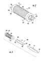
- a modified reed device 103is provided to include an outer bobbin 102 with coil 109 wrapped around it for introducing the necessary magnetic field to actuate the reed switch 111 .
- Ends of wire 109may be connected to posts, pins, or the like (not shown) connected to bobbin 102 to provide for electrical interconnection of the magnetic field current.
- Emanating from the reed switch 111are two signal leads 106 which correspond to opposing sides of the reed switch 111 .
- shield or ground tabs 108emanating from the bobbin body 102 are a pair of shield or ground tabs 108 on each side of the bobbin body 102 that are electrically interconnected to, as shown in FIG. 6, the ends of the inner shield sleeve 110 .
- FIG. 3an exploded perspective view the reed switch 111 of FIG. 2, these ground tabs 108 are extensions from the shield sleeve 110 itself on opposing sides thereof.
- the reed switch 111includes a signal conductor 106 within a glass capsule with an inert gas or vacuum surrounding it. Positioned about the glass capsule is a ground shield 110 which is preferably of a cylindrical or tubular configuration but may be of an oval cross-section to accommodate certain reed switches 111 or multiple reed switches in a multiple channel environment.
- the foregoing assemblyis housed within the bobbin 102 which includes an energizing coil 109 .
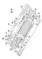
- FIG. 4a perspective view of a reed switch package 100 is shown.
- This complete reed switch package 100includes the reed switch 111 shown in FIGS. 2 and 3 affixed to the surface 120 of a relay card 122 .
- the relay card 122includes an aperture 124 which is large enough to receive at least a portion of the bobbin or main body 102 of the reed switch 111 therein to reduce the overall height of the package 100 . For example, about 1 ⁇ 3 of the volume of the bobbin 102 resides within the upper seat aperture 124 in the relay card 122 .
- the relay card 122includes a number of contact pads 126 a-f for respectively receiving the signal leads 106 and ground leads 108 of the reed switch 111 .
- three contact pads 126 a, 126 b and 126 care provided on the left side of the upper seat aperture 124 to correspond with the single signal lead 106 and two ground leads 108 on the left side of the reed switch 111 .
- the opposing contact pads 126 d, 126 e and 126 fare provided on the right side of the upper seat aperture 124 to correspond with the single signal lead 106 and two ground leads 108 on the right side of the reed switch 111 .
- Pads 126 g and 126 hare provided for termination of coil leads 115 .
- interconnection members 128such as solder balls, are also provided on the same surface 120 of the relay card 122 to electrically interface with the circuit board into which the reed switch package 100 is installed, which will be described in detail below.
- the electrical interconnection members 128may also be of other types, such as a land grid array (LGA), column grid array (CGA) or pin grid array (PGA) as well as solder bumps and solder paste dots.
- the electrical interconnection members 128are electrically connected to respective ones of the contacts pads 126 a-h to provide electrical continuity to the signal leads 106 , ground leads 108 and coil leads or ends 115 are terminated in the same fashion, although their physical location may vary widely with respect to the switch and signal topology.
- Circuit board traces 130are preferably employed to provide the electrical connection between the contact pads 126 a-h and the electrical interconnection members 128 . Any other type of electrical interconnection may be employed to replace the circuit board traces 130 .
- the signal through the reed switch 111is optimized because the co-axial configuration of the reed switch 111 is maintained to the interconnection members 128 due to the presence of circuit board traces 130 connected to the ground leads 108 which are on opposing sides of the traces 130 connected to the signal leads 106 to maintain a wave guide across the lower surface 120 of the relay card 122 to ensure a complete controlled impedance environment.
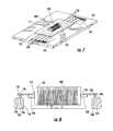
- FIG. 6illustrates a sample circuit board 132 in a accordance with the present invention where in a relief aperture 134 is provided therethrough for seating.
- a complete through-aperture 134is provided; however, a recess (not shown) in the component-mounting surface of the main circuit board 132 is also contemplated and within the scope of the present invention.
- the main circuit board 132includes an array of contact pads 136 which are complementary to the electrical interconnection members 128 on the bottom surface 120 of the relay card 122 .
- Electrical traces 138are also provided on the main circuit board 132 to electrically interconnect the reed switch package 100 into the circuit at hand.
- the reed switch package 100With the reed device 111 mounted on a relay card 122 , is installed into the aperture 134 on the component-mounting surface 140 of the main circuit board 132 in an inverted manner, such that approximately 1 ⁇ 3 of the bobbin 102 of the reed device 111 residing within the seating aperture 134 of the main circuit board 132 .
- the electrical interconnection members 128are mated to corresponding contact pads 136 on the top surface 140 of the circuit board 132 and secured in place to electrically interconnect the reed device 111 into the circuit, representationally referenced by numeral 142 on the circuit board 132 . As best seen in FIG.
- a low profile reed switch package 100is provided where the bobbin portion 102 of the reed device 111 partially resides through the relay card 122 and partially within the main circuit board 132 .
- the overall height of the reed switch package 100is greatly reduced thus allowing for a low height installation of components on the circuit board 132 to permit installation into smaller environments and to facilitate closer stacking of populated multiple circuit boards 132 together.
- the present inventionprovides a wave guide to simulate a true coaxial environment.
- This unique wave guideextends from the reed device 111 itself to the electrical interconnections 128 at the bottom of the reed switch package 100 .
- the wave guide or simulated co-axial arrangementis continuous from the reed switch 111 itself to the electrical interconnections 124 where a microstrip or wave guide is typically present on the circuit board 132 .
- Such a wave guide on the circuit board 132is provided by traces 138 connected to the ground leads.
- the shielding protection for the signal lead 106is extended and controlled from the actual body of the reed switch 111 to the actual electrical interface to the circuit board 132 .
- the impedance of the signal transmission pathis maintained substantially consistent through its entire length within package 100 and is matched to the desired overall impedance value thus obviating the need for substantial circuit tuning by the user.
- present inventionprovides either an actual or simulated co-axial environment for superior protection of the signal lead 106 of the reed switch 111 .
- This continuous co-axial protection without the use of vias through the relay substrateis not found in prior art packages.
- the integrated wave guide on the reed switch package 100enable a continuous co-axial environment to be provided from the reed switch directly down to the electrical interconnection to the circuit board 132 . In most applications, due to the frequency of the signal transmitted by the reed switch 111 , a complete continuous ground loop is not needed to provide a co-axial arrangement for signal lead protection.
- the ground conductor traces 130which are connected to ground leads 108 , are preferably spaced apart from one another a distance of 1.27 mm or 1.00 mm; however, other distances may be employed.
- Common frequencies for the reed switch 111are in the 1.0 to 8.0 GHz range. At these frequencies, the wavelengths are in the 300 mm to 40 mm range. The wavelengths are too long to sense any discontinuities of the “simulated” co-axial arrangement. Therefore, the simulated co-axial arrangement is essentially identical in effectiveness compared to a true full co-axial arrangement. As a result, this topology provides for effective shielding until the wavelength gets so small that the conductor trace spacing will be seen as discontinuous. For the trace spacing as discussed above, effective shielding can be realized with the present invention with wavelengths as low as 8 mm with a frequency of 37 GHz. Greater or fewer conductive traces 130 may be employed depending on the device within the package and the application at hand.
- the package 100 of the presentmay be easily modified to accommodate more than one reed switch 111 at a time to provide multiple channels.
- the appropriate electrical contacts 128e.g. solder ball interconnections, are employed for each reed switch 111 corresponding to a given channel.
- many different types of interconnections 128may be employed by the package 100 of the present invention. It should be understood that the package 100 of the present invention can accommodate a wide array of electronic devices that require signal lead shielding with a controlled impedance environment.
- the package 100 of the present inventionmay be employed to carry out many different types of circuit arrangements using reed switches 111 with the added unique capability of superior protection of the signal lead 106 of a reed switch 111 by simulating the co-axial environment in accordance with the present invention.
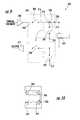
- FIG. 9illustrates a specific sample application of the package of the present invention.
- the diagram of FIG. 9illustrates a circuit 300 that is commonly employed in ATE (Automatic Testing Equipment) for the purpose of testing circuit devices, generally referenced as 313 , and the like.
- This circuit 300sets forth a three terminal device that may be “stackable” in series, end to end, depending on the application.
- a three terminal device 306 with a first reed switch 302 and a second reed switch 304is shown in FIG. 9 as generally referenced by the dotted lines.
- the first reed switch device 302provides a connection for a high frequency AC signal while the second reed switch 304 provides a connection for a DC signal or low frequency AC signal.
- a signal generator 308is connected to the first terminal 310 of the first reed switch 302 .
- a second reed switch 304is provided with a first terminal 312 and a second terminal 314 .
- a second terminal 316 of the first reed switch 302is connected to the second terminal 314 of the second reed switch 304 at node 318 .
- This node 318becomes the output terminal 326 to the device 306 .
- a second pair of reed switches 320 , 322is employed to receive the stimulus from the device under test, (DUT) 313 .
- Receiver 317receives the output from the second pair of reed switches 320 , 322 .
- FIG. 10illustrates a representational schematic of one of the pair of reed relays that carry out the circuit diagram of FIG. 9 .
- stub connectionAs a result of this long, unprotected stub connection 324 , significant parasitic capacitance C to ground will be present. This is termed a “stub capacitance” and acts to load the high frequency path, thus limiting the frequency of the circuit to a value in the range of about 5.0 GHz, for example.
- circuit 300may easily operate at frequencies in the 7 GHz range and above to accommodate the testing of high-speed devices because the high-frequency path is protected using the simulated co-axial signal protecting environment as discussed in detail above.
- the stub connectionresides inside the device, thus minimizing its length which inherently minimizes the capacitive parasitic load.
- the fact that the stub resides in the deviceallows the use of other techniques for capacitance control and compensation.
- the package of the present inventionis shown to employ solder balls in a BGA package for electric interconnection to a circuit board 132
- other types of interconnections 128may be employed such as pin grids, land grids or column grids.
- ball grid array socket arrangementmay be used to facilitate removal or replacement of the package when desired.
- the relay cardis preferably made of typical circuit board material but may be manufactured of any other material suitable for electronic device packages.
- the electrical traces 130 , 138 employed in the present inventionmay be made of known conductive materials, such as copper, aluminum, tin and other alloys known in the industry.
- the relay cardSince the reed relay package 100 is mounted on a relay card instead of being completely encapsulated into a closed package, the relay card can be made much thinner. A thin relay card results in lower cost because a thin, single layer, non-laminated construction can now be employed. Also, with a thin relay card providing the substrate for the package 100 , controlled depth routing can be eliminated and the signal path can be reduced thus providing better maintenance of the desired impedance of the signal path.
- the reed switch packagein accordance with the present invention, is preferably fully enclosed in metal or non-metallic shell or may be fully overmolded for additional protection of the device.
- the reed switch packagemay be partially enclosed with a metal or non-metallic shell, partially overmolded with plastic or partially encapsulated using other materials to provide an air-tight and/or liquid-tight seal in a low profile configuration.
Landscapes
- Physics & Mathematics (AREA)
- Electromagnetism (AREA)
- Engineering & Computer Science (AREA)
- Microelectronics & Electronic Packaging (AREA)
- Switches That Are Operated By Magnetic Or Electric Fields (AREA)
Abstract
Description
Claims (10)
Priority Applications (1)
| Application Number | Priority Date | Filing Date | Title |
|---|---|---|---|
| US10/023,176USRE38381E1 (en) | 2000-07-21 | 2002-04-23 | Inverted board mounted electromechanical device |
Applications Claiming Priority (3)
| Application Number | Priority Date | Filing Date | Title |
|---|---|---|---|
| US21981700P | 2000-07-21 | 2000-07-21 | |
| US09/833,867US6294971B1 (en) | 2000-07-21 | 2001-04-12 | Inverted board mounted electromechanical device |
| US10/023,176USRE38381E1 (en) | 2000-07-21 | 2002-04-23 | Inverted board mounted electromechanical device |
Related Parent Applications (1)
| Application Number | Title | Priority Date | Filing Date |
|---|---|---|---|
| US09/833,867ReissueUS6294971B1 (en) | 2000-07-21 | 2001-04-12 | Inverted board mounted electromechanical device |
Publications (1)
| Publication Number | Publication Date |
|---|---|
| USRE38381E1true USRE38381E1 (en) | 2004-01-13 |
Family
ID=29783125
Family Applications (1)
| Application Number | Title | Priority Date | Filing Date |
|---|---|---|---|
| US10/023,176Expired - Fee RelatedUSRE38381E1 (en) | 2000-07-21 | 2002-04-23 | Inverted board mounted electromechanical device |
Country Status (1)
| Country | Link |
|---|---|
| US (1) | USRE38381E1 (en) |
Cited By (6)
| Publication number | Priority date | Publication date | Assignee | Title |
|---|---|---|---|---|
| US20040082100A1 (en)* | 2001-11-02 | 2004-04-29 | Norihito Tsukahara | Method and apparatus for manufacturing electronic component-mounted component, and electronic component-mounted component |
| US20070090905A1 (en)* | 2004-05-19 | 2007-04-26 | Volvo Lastvagnar Ab | Magnetic switch arrangement and method for obtaining a differential magnetic switch |
| US20090256662A1 (en)* | 2008-04-15 | 2009-10-15 | Coto Technology, Inc. | Form c relay and package using same |
| US20100277883A1 (en)* | 2009-04-30 | 2010-11-04 | Yoshinari Matsuda | Downward-facing optical component module |
| US7920038B1 (en)* | 2008-05-20 | 2011-04-05 | Keithley Instruments, Inc. | Dual shielded relay |
| US20160379784A1 (en)* | 2014-03-11 | 2016-12-29 | Shenzhen Zhiyou Battery Integration Technology Co., Ltd | Reed relay |
Citations (58)
| Publication number | Priority date | Publication date | Assignee | Title |
|---|---|---|---|---|
| US2945163A (en) | 1955-01-10 | 1960-07-12 | Globe Union Inc | Component mounting for printed circuits |
| US3408602A (en) | 1967-04-12 | 1968-10-29 | Vidar Corp | Shielded switching device |
| US3480836A (en) | 1966-08-11 | 1969-11-25 | Ibm | Component mounted in a printed circuit |
| US3517273A (en) | 1968-10-25 | 1970-06-23 | Stromberg Carlson Corp | Reed relay assembly with alignment strips |
| US3575678A (en) | 1969-10-06 | 1971-04-20 | Grigsby Barton Inc | Reed switch assembly |
| US3939381A (en) | 1974-03-22 | 1976-02-17 | Mcm Industries, Inc. | Universal burn-in fixture |
| US4389627A (en) | 1980-11-19 | 1983-06-21 | Chino Works, Ltd. | Changeover switch for actuating a plurality of reed switches disposed in a circle |
| US4947235A (en) | 1989-02-21 | 1990-08-07 | Delco Electronics Corporation | Integrated circuit shield |
| US4975761A (en) | 1989-09-05 | 1990-12-04 | Advanced Micro Devices, Inc. | High performance plastic encapsulated package for integrated circuit die |
| US5043534A (en) | 1990-07-02 | 1991-08-27 | Olin Corporation | Metal electronic package having improved resistance to electromagnetic interference |
| US5175613A (en) | 1991-01-18 | 1992-12-29 | Digital Equipment Corporation | Package for EMI, ESD, thermal, and mechanical shock protection of circuit chips |
| US5239198A (en) | 1989-09-06 | 1993-08-24 | Motorola, Inc. | Overmolded semiconductor device having solder ball and edge lead connective structure |
| US5294826A (en) | 1993-04-16 | 1994-03-15 | Northern Telecom Limited | Integrated circuit package and assembly thereof for thermal and EMI management |
| US5355016A (en) | 1993-05-03 | 1994-10-11 | Motorola, Inc. | Shielded EPROM package |
| US5400949A (en) | 1991-09-19 | 1995-03-28 | Nokia Mobile Phones Ltd. | Circuit board assembly |
| US5403782A (en) | 1992-12-21 | 1995-04-04 | Sgs-Thomson Microelectronics, Inc. | Surface mountable integrated circuit package with integrated battery mount |
| US5418688A (en) | 1993-03-29 | 1995-05-23 | Motorola, Inc. | Cardlike electronic device |
| US5422433A (en) | 1993-11-15 | 1995-06-06 | Motorola, Inc. | Radio frequency isolation shield having reclosable opening |
| US5436203A (en) | 1994-07-05 | 1995-07-25 | Motorola, Inc. | Shielded liquid encapsulated semiconductor device and method for making the same |
| US5438307A (en) | 1994-08-03 | 1995-08-01 | Pen-Lin Liao | Single-pole magnetic reed relay |
| US5459287A (en) | 1994-05-18 | 1995-10-17 | Dell Usa, L.P. | Socketed printed circuit board BGA connection apparatus and associated methods |
| US5483423A (en) | 1993-11-16 | 1996-01-09 | Digital Equipment Corporation | EMI shielding for components |
| US5485037A (en) | 1993-04-12 | 1996-01-16 | Amkor Electronics, Inc. | Semiconductor device having a thermal dissipator and electromagnetic shielding |
| US5486720A (en) | 1994-05-26 | 1996-01-23 | Analog Devices, Inc. | EMF shielding of an integrated circuit package |
| US5525834A (en) | 1994-10-17 | 1996-06-11 | W. L. Gore & Associates, Inc. | Integrated circuit package |
| US5530202A (en) | 1995-01-09 | 1996-06-25 | At&T Corp. | Metallic RF or thermal shield for automatic vacuum placement |
| US5535101A (en) | 1992-11-03 | 1996-07-09 | Motorola, Inc. | Leadless integrated circuit package |
| US5541450A (en) | 1994-11-02 | 1996-07-30 | Motorola, Inc. | Low-profile ball-grid array semiconductor package |
| US5543663A (en) | 1993-12-27 | 1996-08-06 | Kabushiki Kaisha Toshiba | Semiconductor device and BGA package |
| US5557142A (en) | 1991-02-04 | 1996-09-17 | Motorola, Inc. | Shielded semiconductor device package |
| US5559306A (en) | 1994-05-17 | 1996-09-24 | Olin Corporation | Electronic package with improved electrical performance |
| US5561265A (en) | 1993-03-24 | 1996-10-01 | Northern Telecom Limited | Integrated circuit packaging |
| US5566055A (en) | 1995-03-03 | 1996-10-15 | Parker-Hannifin Corporation | Shieled enclosure for electronics |
| US5574314A (en) | 1994-07-28 | 1996-11-12 | Mitsubishi Denki Kabushiki Kaisha | Packaged semiconductor device including shielded inner walls |
| US5583378A (en) | 1994-05-16 | 1996-12-10 | Amkor Electronics, Inc. | Ball grid array integrated circuit package with thermal conductor |
| US5629835A (en) | 1994-07-19 | 1997-05-13 | Olin Corporation | Metal ball grid array package with improved thermal conductivity |
| US5633786A (en) | 1995-08-21 | 1997-05-27 | Motorola | Shield assembly and method of shielding suitable for use in a communication device |
| US5640048A (en) | 1994-07-11 | 1997-06-17 | Sun Microsystems, Inc. | Ball grid array package for a integrated circuit |
| US5650659A (en) | 1995-08-04 | 1997-07-22 | National Semiconductor Corporation | Semiconductor component package assembly including an integral RF/EMI shield |
| US5666272A (en) | 1994-11-29 | 1997-09-09 | Sgs-Thomson Microelectronics, Inc. | Detachable module/ball grid array package |
| US5668406A (en) | 1994-05-31 | 1997-09-16 | Nec Corporation | Semiconductor device having shielding structure made of electrically conductive paste |
| US5684441A (en) | 1996-02-29 | 1997-11-04 | Graeber; Roger R. | Reverse power protection circuit and relay |
| EP0805471A1 (en) | 1996-04-30 | 1997-11-05 | C.P. Clare Corporation | Electromagnetic relay and method of manufacturing such relay |
| US5694300A (en) | 1996-04-01 | 1997-12-02 | Northrop Grumman Corporation | Electromagnetically channelized microwave integrated circuit |
| US5701032A (en) | 1994-10-17 | 1997-12-23 | W. L. Gore & Associates, Inc. | Integrated circuit package |
| US5708567A (en) | 1995-11-15 | 1998-01-13 | Anam Industrial Co., Ltd. | Ball grid array semiconductor package with ring-type heat sink |
| US5777382A (en) | 1995-12-19 | 1998-07-07 | Texas Instruments Incorporated | Plastic packaging for a surface mounted integrated circuit |
| US5789815A (en) | 1996-04-23 | 1998-08-04 | Motorola, Inc. | Three dimensional semiconductor package having flexible appendages |
| US5789068A (en) | 1995-06-29 | 1998-08-04 | Fry's Metals, Inc. | Preformed solder parts coated with parylene in a thickness effective to exhibit predetermined interference colors |
| US5796170A (en) | 1996-02-15 | 1998-08-18 | Northern Telecom Limited | Ball grid array (BGA) integrated circuit packages |
| US5798567A (en) | 1997-08-21 | 1998-08-25 | Hewlett-Packard Company | Ball grid array integrated circuit package which employs a flip chip integrated circuit and decoupling capacitors |
| US5819398A (en) | 1995-07-31 | 1998-10-13 | Sgs-Thomson Microelectronics, Ltd. | Method of manufacturing a ball grid array package |
| US5831832A (en) | 1997-08-11 | 1998-11-03 | Motorola, Inc. | Molded plastic ball grid array package |
| US5838551A (en) | 1996-08-01 | 1998-11-17 | Northern Telecom Limited | Electronic package carrying an electronic component and assembly of mother board and electronic package |
| US5854512A (en) | 1996-09-20 | 1998-12-29 | Vlsi Technology, Inc. | High density leaded ball-grid array package |
| US5943216A (en) | 1997-06-03 | 1999-08-24 | Photo Opto Electronic Technologies | Apparatus for providing a two-sided, cavity, inverted-mounted component circuit board |
| US6025768A (en) | 1999-03-12 | 2000-02-15 | Kearny-National, Inc. | Electromechanical switching device package with controlled impedance environment |
| US6052045A (en) | 1999-03-12 | 2000-04-18 | Kearney-National, Inc. | Electromechanical switching device package with controlled impedance environment |
- 2002
- 2002-04-23USUS10/023,176patent/USRE38381E1/ennot_activeExpired - Fee Related
Patent Citations (58)
| Publication number | Priority date | Publication date | Assignee | Title |
|---|---|---|---|---|
| US2945163A (en) | 1955-01-10 | 1960-07-12 | Globe Union Inc | Component mounting for printed circuits |
| US3480836A (en) | 1966-08-11 | 1969-11-25 | Ibm | Component mounted in a printed circuit |
| US3408602A (en) | 1967-04-12 | 1968-10-29 | Vidar Corp | Shielded switching device |
| US3517273A (en) | 1968-10-25 | 1970-06-23 | Stromberg Carlson Corp | Reed relay assembly with alignment strips |
| US3575678A (en) | 1969-10-06 | 1971-04-20 | Grigsby Barton Inc | Reed switch assembly |
| US3939381A (en) | 1974-03-22 | 1976-02-17 | Mcm Industries, Inc. | Universal burn-in fixture |
| US4389627A (en) | 1980-11-19 | 1983-06-21 | Chino Works, Ltd. | Changeover switch for actuating a plurality of reed switches disposed in a circle |
| US4947235A (en) | 1989-02-21 | 1990-08-07 | Delco Electronics Corporation | Integrated circuit shield |
| US4975761A (en) | 1989-09-05 | 1990-12-04 | Advanced Micro Devices, Inc. | High performance plastic encapsulated package for integrated circuit die |
| US5239198A (en) | 1989-09-06 | 1993-08-24 | Motorola, Inc. | Overmolded semiconductor device having solder ball and edge lead connective structure |
| US5043534A (en) | 1990-07-02 | 1991-08-27 | Olin Corporation | Metal electronic package having improved resistance to electromagnetic interference |
| US5175613A (en) | 1991-01-18 | 1992-12-29 | Digital Equipment Corporation | Package for EMI, ESD, thermal, and mechanical shock protection of circuit chips |
| US5557142A (en) | 1991-02-04 | 1996-09-17 | Motorola, Inc. | Shielded semiconductor device package |
| US5400949A (en) | 1991-09-19 | 1995-03-28 | Nokia Mobile Phones Ltd. | Circuit board assembly |
| US5535101A (en) | 1992-11-03 | 1996-07-09 | Motorola, Inc. | Leadless integrated circuit package |
| US5403782A (en) | 1992-12-21 | 1995-04-04 | Sgs-Thomson Microelectronics, Inc. | Surface mountable integrated circuit package with integrated battery mount |
| US5561265A (en) | 1993-03-24 | 1996-10-01 | Northern Telecom Limited | Integrated circuit packaging |
| US5418688A (en) | 1993-03-29 | 1995-05-23 | Motorola, Inc. | Cardlike electronic device |
| US5485037A (en) | 1993-04-12 | 1996-01-16 | Amkor Electronics, Inc. | Semiconductor device having a thermal dissipator and electromagnetic shielding |
| US5294826A (en) | 1993-04-16 | 1994-03-15 | Northern Telecom Limited | Integrated circuit package and assembly thereof for thermal and EMI management |
| US5355016A (en) | 1993-05-03 | 1994-10-11 | Motorola, Inc. | Shielded EPROM package |
| US5422433A (en) | 1993-11-15 | 1995-06-06 | Motorola, Inc. | Radio frequency isolation shield having reclosable opening |
| US5483423A (en) | 1993-11-16 | 1996-01-09 | Digital Equipment Corporation | EMI shielding for components |
| US5543663A (en) | 1993-12-27 | 1996-08-06 | Kabushiki Kaisha Toshiba | Semiconductor device and BGA package |
| US5583378A (en) | 1994-05-16 | 1996-12-10 | Amkor Electronics, Inc. | Ball grid array integrated circuit package with thermal conductor |
| US5559306A (en) | 1994-05-17 | 1996-09-24 | Olin Corporation | Electronic package with improved electrical performance |
| US5459287A (en) | 1994-05-18 | 1995-10-17 | Dell Usa, L.P. | Socketed printed circuit board BGA connection apparatus and associated methods |
| US5486720A (en) | 1994-05-26 | 1996-01-23 | Analog Devices, Inc. | EMF shielding of an integrated circuit package |
| US5668406A (en) | 1994-05-31 | 1997-09-16 | Nec Corporation | Semiconductor device having shielding structure made of electrically conductive paste |
| US5436203A (en) | 1994-07-05 | 1995-07-25 | Motorola, Inc. | Shielded liquid encapsulated semiconductor device and method for making the same |
| US5640048A (en) | 1994-07-11 | 1997-06-17 | Sun Microsystems, Inc. | Ball grid array package for a integrated circuit |
| US5629835A (en) | 1994-07-19 | 1997-05-13 | Olin Corporation | Metal ball grid array package with improved thermal conductivity |
| US5574314A (en) | 1994-07-28 | 1996-11-12 | Mitsubishi Denki Kabushiki Kaisha | Packaged semiconductor device including shielded inner walls |
| US5438307A (en) | 1994-08-03 | 1995-08-01 | Pen-Lin Liao | Single-pole magnetic reed relay |
| US5525834A (en) | 1994-10-17 | 1996-06-11 | W. L. Gore & Associates, Inc. | Integrated circuit package |
| US5701032A (en) | 1994-10-17 | 1997-12-23 | W. L. Gore & Associates, Inc. | Integrated circuit package |
| US5541450A (en) | 1994-11-02 | 1996-07-30 | Motorola, Inc. | Low-profile ball-grid array semiconductor package |
| US5666272A (en) | 1994-11-29 | 1997-09-09 | Sgs-Thomson Microelectronics, Inc. | Detachable module/ball grid array package |
| US5530202A (en) | 1995-01-09 | 1996-06-25 | At&T Corp. | Metallic RF or thermal shield for automatic vacuum placement |
| US5566055A (en) | 1995-03-03 | 1996-10-15 | Parker-Hannifin Corporation | Shieled enclosure for electronics |
| US5789068A (en) | 1995-06-29 | 1998-08-04 | Fry's Metals, Inc. | Preformed solder parts coated with parylene in a thickness effective to exhibit predetermined interference colors |
| US5819398A (en) | 1995-07-31 | 1998-10-13 | Sgs-Thomson Microelectronics, Ltd. | Method of manufacturing a ball grid array package |
| US5650659A (en) | 1995-08-04 | 1997-07-22 | National Semiconductor Corporation | Semiconductor component package assembly including an integral RF/EMI shield |
| US5633786A (en) | 1995-08-21 | 1997-05-27 | Motorola | Shield assembly and method of shielding suitable for use in a communication device |
| US5708567A (en) | 1995-11-15 | 1998-01-13 | Anam Industrial Co., Ltd. | Ball grid array semiconductor package with ring-type heat sink |
| US5777382A (en) | 1995-12-19 | 1998-07-07 | Texas Instruments Incorporated | Plastic packaging for a surface mounted integrated circuit |
| US5796170A (en) | 1996-02-15 | 1998-08-18 | Northern Telecom Limited | Ball grid array (BGA) integrated circuit packages |
| US5684441A (en) | 1996-02-29 | 1997-11-04 | Graeber; Roger R. | Reverse power protection circuit and relay |
| US5694300A (en) | 1996-04-01 | 1997-12-02 | Northrop Grumman Corporation | Electromagnetically channelized microwave integrated circuit |
| US5789815A (en) | 1996-04-23 | 1998-08-04 | Motorola, Inc. | Three dimensional semiconductor package having flexible appendages |
| EP0805471A1 (en) | 1996-04-30 | 1997-11-05 | C.P. Clare Corporation | Electromagnetic relay and method of manufacturing such relay |
| US5838551A (en) | 1996-08-01 | 1998-11-17 | Northern Telecom Limited | Electronic package carrying an electronic component and assembly of mother board and electronic package |
| US5854512A (en) | 1996-09-20 | 1998-12-29 | Vlsi Technology, Inc. | High density leaded ball-grid array package |
| US5943216A (en) | 1997-06-03 | 1999-08-24 | Photo Opto Electronic Technologies | Apparatus for providing a two-sided, cavity, inverted-mounted component circuit board |
| US5831832A (en) | 1997-08-11 | 1998-11-03 | Motorola, Inc. | Molded plastic ball grid array package |
| US5798567A (en) | 1997-08-21 | 1998-08-25 | Hewlett-Packard Company | Ball grid array integrated circuit package which employs a flip chip integrated circuit and decoupling capacitors |
| US6025768A (en) | 1999-03-12 | 2000-02-15 | Kearny-National, Inc. | Electromechanical switching device package with controlled impedance environment |
| US6052045A (en) | 1999-03-12 | 2000-04-18 | Kearney-National, Inc. | Electromechanical switching device package with controlled impedance environment |
Cited By (13)
| Publication number | Priority date | Publication date | Assignee | Title |
|---|---|---|---|---|
| US20040082100A1 (en)* | 2001-11-02 | 2004-04-29 | Norihito Tsukahara | Method and apparatus for manufacturing electronic component-mounted component, and electronic component-mounted component |
| US7176055B2 (en)* | 2001-11-02 | 2007-02-13 | Matsushita Electric Industrial Co., Ltd. | Method and apparatus for manufacturing electronic component-mounted component, and electronic component-mounted component |
| US20070200217A1 (en)* | 2001-11-02 | 2007-08-30 | Norihito Tsukahara | Method and apparatus for manufacturing electronic component-mounted component, and electronic component-mounted component |
| US20070090905A1 (en)* | 2004-05-19 | 2007-04-26 | Volvo Lastvagnar Ab | Magnetic switch arrangement and method for obtaining a differential magnetic switch |
| US20070109084A1 (en)* | 2004-05-19 | 2007-05-17 | Van Glabeke Pierre | Magnetic switch arrangement |
| US7508288B2 (en)* | 2004-05-19 | 2009-03-24 | Volvo Lastvagnar Ab | Magnetic switch arrangement |
| US20090256662A1 (en)* | 2008-04-15 | 2009-10-15 | Coto Technology, Inc. | Form c relay and package using same |
| US8063725B2 (en) | 2008-04-15 | 2011-11-22 | Coto Technology, Inc. | Form C relay and package using same |
| US7920038B1 (en)* | 2008-05-20 | 2011-04-05 | Keithley Instruments, Inc. | Dual shielded relay |
| US20100277883A1 (en)* | 2009-04-30 | 2010-11-04 | Yoshinari Matsuda | Downward-facing optical component module |
| US8804368B2 (en) | 2009-04-30 | 2014-08-12 | Sony Corporation | Downward-facing optical component module |
| US20160379784A1 (en)* | 2014-03-11 | 2016-12-29 | Shenzhen Zhiyou Battery Integration Technology Co., Ltd | Reed relay |
| US10026575B2 (en)* | 2014-03-11 | 2018-07-17 | Shenzhen Zhiyou Battery Integration Technology Co., Ltd | Reed relay |
Similar Documents
| Publication | Publication Date | Title |
|---|---|---|
| US6294971B1 (en) | Inverted board mounted electromechanical device | |
| EP1037236B1 (en) | Electromechanical switching device package with controlled impedance environment | |
| US8063725B2 (en) | Form C relay and package using same | |
| US6052045A (en) | Electromechanical switching device package with controlled impedance environment | |
| US6683518B2 (en) | Surface mount molded relay package and method of manufacturing same | |
| USRE38381E1 (en) | Inverted board mounted electromechanical device | |
| US4644096A (en) | Surface mounting package | |
| US6954126B2 (en) | Lead-less surface mount reed relay | |
| JP4211240B2 (en) | High frequency signal switching device | |
| HK1148607A (en) | Improved form c relay and package using same | |
| HK1037059B (en) | Electromechanical switching device package with controlled impedance environment |
Legal Events
| Date | Code | Title | Description |
|---|---|---|---|
| AS | Assignment | Owner name:BANK OF AMERICA, N.A., AS ADMINISTRATIVE AGENT, NO Free format text:NOTICE OF GRANT OF SECURITY INTEREST;ASSIGNOR:KEARNEY-NATIONAL, INC.;REEL/FRAME:014734/0820 Effective date:20040526 | |
| FPAY | Fee payment | Year of fee payment:4 | |
| AS | Assignment | Owner name:COTO TECHNOLOGY, INC., RHODE ISLAND Free format text:ASSIGNMENT OF ASSIGNORS INTEREST;ASSIGNOR:KEARNEY-NATIONAL INC.;REEL/FRAME:019881/0483 Effective date:20070623 | |
| AS | Assignment | Owner name:KEARNEY-NATIONAL INC., NEW YORK Free format text:ASSIGNMENT OF ASSIGNORS INTEREST;ASSIGNOR:MARTICH, MARK E.;REEL/FRAME:020083/0339 Effective date:20000721 | |
| AS | Assignment | Owner name:BANK OF AMERICA, N.A., AS ADMINISTRATIVE AGENT, NO Free format text:NOTICE OF GRANT OF SECURITY INTEREST;ASSIGNOR:COTO TECHNOLOGY, INC.;REEL/FRAME:020092/0304 Effective date:20040526 | |
| FPAY | Fee payment | Year of fee payment:8 | |
| AS | Assignment | Owner name:KEARNEY-NATIONAL, INC., NEW YORK Free format text:TERMINATION OF SECURITY INTEREST IN PATENTS;ASSIGNOR:BANK OF AMERICA, N.A., AS ADMINISTRATIVE AGENT;REEL/FRAME:026583/0318 Effective date:20110712 Owner name:COTO TECHNOLOGY, INC., RHODE ISLAND Free format text:TERMINATION OF SECURITY INTEREST IN PATENTS;ASSIGNOR:BANK OF AMERICA, N.A., AS ADMINISTRATIVE AGENT;REEL/FRAME:026583/0060 Effective date:20110712 | |
| REMI | Maintenance fee reminder mailed | ||
| LAPS | Lapse for failure to pay maintenance fees |