USRE34615E - Video probe aligning of object to be acted upon - Google Patents
Video probe aligning of object to be acted uponDownload PDFInfo
- Publication number
- USRE34615E USRE34615EUS07/829,727US82972792AUSRE34615EUS RE34615 EUSRE34615 EUS RE34615EUS 82972792 AUS82972792 AUS 82972792AUS RE34615 EUSRE34615 EUS RE34615E
- Authority
- US
- United States
- Prior art keywords
- mirror
- video
- video probe
- probe
- pattern
- Prior art date
- Legal status (The legal status is an assumption and is not a legal conclusion. Google has not performed a legal analysis and makes no representation as to the accuracy of the status listed.)
- Expired - Lifetime
Links
Images


Classifications
- H—ELECTRICITY
- H05—ELECTRIC TECHNIQUES NOT OTHERWISE PROVIDED FOR
- H05K—PRINTED CIRCUITS; CASINGS OR CONSTRUCTIONAL DETAILS OF ELECTRIC APPARATUS; MANUFACTURE OF ASSEMBLAGES OF ELECTRICAL COMPONENTS
- H05K13/00—Apparatus or processes specially adapted for manufacturing or adjusting assemblages of electric components
- H05K13/04—Mounting of components, e.g. of leadless components
- H05K13/046—Surface mounting
- H05K13/0465—Surface mounting by soldering
- G—PHYSICS
- G03—PHOTOGRAPHY; CINEMATOGRAPHY; ANALOGOUS TECHNIQUES USING WAVES OTHER THAN OPTICAL WAVES; ELECTROGRAPHY; HOLOGRAPHY
- G03F—PHOTOMECHANICAL PRODUCTION OF TEXTURED OR PATTERNED SURFACES, e.g. FOR PRINTING, FOR PROCESSING OF SEMICONDUCTOR DEVICES; MATERIALS THEREFOR; ORIGINALS THEREFOR; APPARATUS SPECIALLY ADAPTED THEREFOR
- G03F9/00—Registration or positioning of originals, masks, frames, photographic sheets or textured or patterned surfaces, e.g. automatically
- H—ELECTRICITY
- H05—ELECTRIC TECHNIQUES NOT OTHERWISE PROVIDED FOR
- H05K—PRINTED CIRCUITS; CASINGS OR CONSTRUCTIONAL DETAILS OF ELECTRIC APPARATUS; MANUFACTURE OF ASSEMBLAGES OF ELECTRICAL COMPONENTS
- H05K3/00—Apparatus or processes for manufacturing printed circuits
- H05K3/10—Apparatus or processes for manufacturing printed circuits in which conductive material is applied to the insulating support in such a manner as to form the desired conductive pattern
- H05K3/12—Apparatus or processes for manufacturing printed circuits in which conductive material is applied to the insulating support in such a manner as to form the desired conductive pattern using thick film techniques, e.g. printing techniques to apply the conductive material or similar techniques for applying conductive paste or ink patterns
- H05K3/1216—Apparatus or processes for manufacturing printed circuits in which conductive material is applied to the insulating support in such a manner as to form the desired conductive pattern using thick film techniques, e.g. printing techniques to apply the conductive material or similar techniques for applying conductive paste or ink patterns by screen printing or stencil printing
Definitions
- the present inventionrelates in general to aligning and more particularly concerns novel apparatus and techniques for aligning an object to be acted upon at particular locations with a device that performs the specific operations on the specified points.
- a specific embodiment of the inventionfacilitates aligning circuit boards for receiving surface mounted components with a stencil for applying solder paste to a pattern on the circuit board while facilitating rapid reorientation for applying solder paste to a different pattern.
- a typical screen printeris the commercially available ASP-24 automated screen printer available from MPM Corp., 71 West Street, Medfield, Mass. 02052 incorporated herein by reference.
- This screen printerincludes a replaceable screen for printing solder paste on a footprint of pads on a surface mount circuit board.
- This systemmay also deposit other materials, such as epoxy, polymer, cermet and most other screen printable materials.
- This systemincludes a programmable controller for positioning each circuit board beneath the screen or stencil above that deposits the screen printable materials.
- Prior art screen printers with visionrequire printing solder paste on the circuit board, driving a table out beneath the cameras and the cameras look at the solder paste. The solder paste in then wiped off, the board enters beneath the stencil, and the board is printed a second time, and reciprocates back out for examination by the camera.
- a prior art screen printerincludes a camera that looks between the board and the screen, but it does not look at an image on the screen, only at the board.
- the camera on that devicedoes not reciprocate. It uses a fixed mounted camera that just looks down at the board, and it requires that the board be outside of the stencil which comes down upon it by a certain amount such that the camera does not get in the way.
- At least one, and preferably two, movable video probesare located between the acting device, such as the screen or stencil, typically above, and the object to be acted upon, such as a circuit board, typically below.
- the one or two probesfirst look at and locate a pattern, such as on the object device, such as a circuit board, store information on features in this pattern, such as x, y and ⁇ information on key features in the pattern.
- Associated data processing apparatusprocesses and stores this information.
- the one or both video probesthen rotate downward while still in the region between the object to be acted upon and the device to act, examine the other pattern such as on the acting device, such as the screen or stencil, for a matching pattern and relatively position the object and device so that the two patterns are in alignment.
- the one or both video probesthen retract, and the device, such as the stencil or screen engages the object, such as the circuit board, to deposit solder paste or other screen printable material on selected points in registration with corresponding points on the device, such as the screen or stencil.
- the inventionmay repeatedly relatively position by looking at only the object to be acted upon.
- a positionable basesupports a video probe.[.,.]. .Iadd.. .Iaddend.
- This baseis formed with at least one and preferably two slots having a generally horizontal leaning portion with a depending angled trailing portion for guiding elements that carry the video probe as it moves between the extended position at the leading end of the slots, with the video probe between object and device, and the retracted position at the trailing end of the slot, with the video probe retracted from the region between object and device.
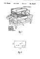
- FIG. 1is a perspective view of a fully automated screen printer with vision system according to the invention
- FIGS. 2 and 3are perspective views of the video probe assembly in retracted and extended positions, respectively;
- FIG. 4is an exploded view of the video probe and portions of the supporting assembly
- FIG. 5is an exploded view of the video probe support assembly
- FIG. 6is a diagram illustrating the relationship among target points and the center of rotation helpful in understanding principles of the invention.
- FIG. 1there is shown a perspective view of an exemplary embodiment of the invention comprising the commercially available ASP-24 fully automated screen printer available from MPM Corp. with movable video probes according to the invention.
- the apparatusincludes a base 11 for supporting a circuit board to be printed upon, left and right video probe assemblies 12 and 13, a controller 14 and video monitor assembly 15.
- the systemalso includes a positionable screen/stencil support assembly that may be moved to align the screen or stencil with the circuit board to be printed upon.
- a lower platform 16supports various packages for containing hardware used in the system.
- the base components added to the ASP-24 automated screen printerinclude the two video probe assemblies 12 and 13, a fiberoptic light source for illuminating the screen and board during pattern recognition, the trackball teaching module 14, and a vision processor unit comprising a commercially available Cognex Type 2000 with suitable software, an example of which is set forth in Appendix A.
- the inventionutilizes a user-friendly operator interface.
- Menu-driven softwaresuch as set forth in Appendix A, produces a display on video monitor 15 that prompts the operator through each phase of the four-step setup process.
- Help screensare accessible at each step, outlining in detail the instructions for performing that step.
- the systemautomatically displays the next prompt on monitor 15. Setup errors may be quickly corrected through the push-button editing feature with trackball teaching module 14.
- the operatoruses the independent trackball teaching module 14 to select a pattern on the PC board within each probe's field of view of left and right probe assemblies 12 and 13. Teaching module 14 capture these two select patterns and then recognizes and locates the matching patterns on the screen or stencil. Without further operator involvement, the system implements the program by calculating the pixel representation in x and y coordinates of significant features and angular orientation in azimuth, conveniently referred to a ⁇ geometry. The apparatus then determines an accurate "home" position for the screen/stencil in relation to the circuit board then positioned on base .Iadd.11.Iaddend..
- the offset data corresponding to the difference in x, y and ⁇ positions of the observed circuit board features and corresponding screen/stencil featuresis automatically downloaded into the screen printer stepper motor programmable indexes. These indexes activate the screen printer stepper motor assembly to reposition the screen/stencil relative to each stationary board for subsequent print cycles with screen/stencil in horizontal alignment with each circuit board below.
- This automatic positioning adjustmentaccommodates variations in board tolerances.
- the left and right video probes 12 and 13automatically move in, look at the next board in place, move out again, screen/stencil is positioned if necessary, and printing occurs without operator intervention.
- the usemay verify alignment with a post-print inspection feature.
- the operatormay choose how often to do post inspection. Then a choice may be made from three tolerance threshold menu selections for alignment error detection.
- Printed circuit boards having patterns outside these parametersproduce an error message on video monitor 15.
- This error signalmay be used to activate a diverter to reroute that board for reworking.
- the error signalmay also be used to pause automatic operation so that the operator can correct the problem before any more material is wasted.
- the operatorpresses a "video attention" button on teaching module 14. Actuating this button produces the setup menu on video monitor 15. Then the operator completes four steps, pressing a single button 14 on teaching module 14 to signal completion of each step. First, the operator clamps left and right video probe assemblies 12 and 13 in place so that each probe when in the extended position may observe two different patterns of significant features of the circuit board and corresponding screen/stencil. The operator then teaches these board patterns.
- trackball teaching module 14the operator moves joy stick 14A to define the windows within the .[.probes,.]. .Iadd.probes' .Iaddend.fields of view embracing significant features, typically a pattern of pads for receiving solder paste, and then pushes a single button on teaching module 14 to teach the pattern to the apparatus which then captures the patterns.
- the operatorpositions the probes of left and right probe assemblies 12 and 13 to view upward to learn the screen or stencil pattern above.
- the associated data processing systemautomatically locates the matching pattern on the screen or stencil, determines the pixel representation of it in x, y and ⁇ geometry; automatically downloads offset data for x, y and ⁇ for alignment purposes.
- the operatorthen rotates the video probes downward toward the circuit board, and the apparatus is now ready to print automatically.
- the video probes on left and right assemblies 12 and 13extend above the positioned circuit board, determine x, y and ⁇ differences between the positioned circuit board and the screen or stencil above and operate stepper motors to reposition, if necessary, the stencil or screen for alignment with the circuit board below.
- FIGS. 2 and 3there are shown perspective views of the video probe assemblies in extended and retracted positions, respectively.
- Each assemblyincludes a base 21 with vertical walls 22 and 23, each formed with front and rear slots 24 and 25, respectively, having horizontal leading portions 24A and 25A, respectively, and depending angled trailing portions 24B and 25B, respectively.
- a vertical bracket 26rests upon side walls 22 and 23.
- the movable probe support 27is formed with elements, such as 31 for riding in slots 24 and 25.
- the movable base 27supports 90° mirror tube 32 that provides an image to camera 33 in housing 34 and furnishes illuminating light to illuminate the screen or stencil and the circuit board.
- FIG. 2shows the video probe in the extended position between circuit board and screen or stencil.
- FIG. 3shows the video probe in the retracted position outside the region between circuit board and screen or stencil.
- Arrows 36indicate the path traveled by the probe up and forward to the extended position and rearward and down to the retracted position.
- the Volpie 90° mirror tube 32includes a mirror 32A mounted at 45° angle relative to the axis of mirror tube 32 with a Volpie intrascope approximately 12 inches long mounted inside mirror tube 32.
- a rotate clamp mechanismis shown inside broken line 42 with the parts exploded and functions to position mirror tube 32 in one of two positions 180° apart, looking up as shown for viewing the bottom of the screen or stencil, or looking down for viewing the top of the printed circuit board.
- Focus knob 43allows for focusing the image of camera 33 by observing the image on video monitor 15.
- the main probe clamp 44carries two shock absorbers 45 and 46 above the left and right arms 47 and 48, respectively.
- Main clamp 44also carries three ball-and-cone pieces, two of which 51 and 52 are visible in FIG. 4.
- FIG. 5there is shown an exploded view of a video probe support assembly with the housing cut away and the video probes omitted to better illustrate certain structural features.
- Main clamp 44supports the vision probe at the center of the camera 30 and Volpie intrascope unit 44. By supporting this assembly at the center of gravity, when the ball-and-cone pieces 51, 52 and 61 engage reference balls, there is very low energy movement to achieve precise reference position very quickly.
- a linkageallows the center of effort to be aligned along the axis of mirror tube 32 and Volpie intrascope unit 41.
- This linkageincludes a left link 62 and right link 63.
- Air cylinder 64drives the leading ends of these links with pin 65 seated in clevis 66 secured to the leading edge of air cylinder rod 64A.
- Main clamp 44is formed with vertical recesses 44A and 44B that engage the left and right arms 71 and 72, respectively. These arms accommodate four rollers, a trailing pair in openings 71A and 72A, and a leading pair in vertical slots 71B and 72B.
- Left and right side plates 22are cammed as shown.
- Left and right angle brackets 73 and 74are attached to the top leading portions of left and right side plates 22 and 23, respectively, that rollers on the link system engage. These angled brackets provided horizontal surfaces for insuring that air cylinder 64 pulls the probe itself horizontally without a vertical component of force. Rollers 75 and 76 ride on left and right angled brackets 74 and 75, respectively.
- a pair of flow controls 81 and 82mount on the trailing portion of left side plate 22 and have a needle valve which allows re-exhaust in each direction for aiding in providing smooth motion upon operating air cylinder 64 for extension and retraction free of binding or violet motion. Shock absorbers 45 and 46 also help allow smooth action when the vision probe approaches a final location against the ball and cone. Shock absorbers 45 and 46 provide damping that prevents the CCD cameras 33 from being subjected to violet movements.
- Main clamp 44clamps the vision probe firmly to the tooling bed 11 of the machine, while allowing some relative adjustment on the probe to position the mirror tube 32 between the stencil and circuit board that may vary depending on the thickness of the circuit board. Clamping screws may be loosened and two jacking set screws 94A may be adjusted to control this position.
- Balls 84A, 83A and 83Bengage ball-and-cone pieces 51, 52, and 61, respectively.
- Ball mounts 83C, 83D and 84Bare independently adjustable. When air cylinder 64 urges the probes to the extended position, ball mounts 83C, 83D and 84B are tightened so that balls 83A, 83B and 84B are exactly seated in ball-and-cone pieces 52, 61 and 51, respectively. This position is then readily repeatable.
- Left and right fiberoptic supports 85 and 86are connected to left and right links 62 and 63, respectively, and carry fibers optics (not shown) in parallel to the Volpie intrascope.
- This arrangement with fiber optics along and parallel to the Volpie intrascopeprovides back lighting. That is to say, this structure provides a very shallow light illuminating the object being viewed. The shallow angle light reduces glare, and the image of the object being viewed appears more clearly with back lighting.
- Pins 85A and 86Apivotally support left and right fiber optic supports 85 and 86 to slots 71B and 72B in left and right arms 71 and 72, respectively.
- This structural arrangementallows free vertical rotation of these supports so that when air cylinder 64 extends and retracts the assembled slide unit, it prevents significant free floating.
- the structural arrangementcontains when not actually contacting the angle brackets.
- Pins 85A and 86A in slots 71B and 72Bprovide this containment.
- Pin 65pulls left and right links 62 and 63 up and outward toward the extended end until rollers 75 and 76 engage the underside of left and right brackets 73 and 74. On retraction pin 65 moves down and toward the retracted position.
- a focus hold bar 91is secured to the top of main clamp 44 and carries a piece of felt on the bottom for engagement by focus knob 43. This holding function helps prevent focus knob 43 from rotating in the presence of repeated changes in position of the probe assembly.
- a proximity switch 92is fastened to side plate 23 for providing a signal indicating that the probe is in a safe retracted position to allow the apparatus to print on the circuit board then below the aligned screen or stencil.
- left clamp piece 93There is a left clamp piece 93, left set screw adjust bar 94 and left clamp nut plate 95 secured to the extended end of left side plate 22.
- right clamp piece 96there is a right clamp piece 96, right set screw adjust bar 97 and right clamp nut plate 98 secured to the extended end of right side plate 23.
- Set screwssuch as 94A and 97A, allow adjustment of set screw adjust bars 94 and 97.
- vision processora commercially available type.Iadd.. .Iaddend.
- Cognex unit and monitorhaving Cognex commercially available software for image searching for matching a stored image with an observed image to permit alignment of the screen or stencil with a circuit board below together with software for controlling the menu-driven functions relative to the specific screen printer application of the vision processor.
- An operatorcommunicates with the processor for aligning a particular board through a trackball teaching module 14.
- This teaching modulehas three buttons 14A, 14B and 14C and a ball 14D. Rotating or pushing the ball with fingers allows the operator to move the window within the field of view on monitor 15, and actuating the buttons allows the operator to select a menu item or move the cursor down through the menu.
- Operating button 14Cselects a help menu.
- Two vision probesare used to detect rotational movement ⁇ in addition to rectilinear movement in x and y directions.
- the light sourceis preferably a high intensity light coupled to the fiber optics. These fiber optics carry light where needed on each side of each vision probe, a total of four light sources. There is also a source of illumination above the stencil for backlighting the stencil to permit observation of features, such as holes, in the stencil for identifying the image for capturing.
- the operatoradjusts the mechanisms on the screen printer to handle the particular board size in conventional manner. That involves adjusting the tracks and board stop, and inserting the stencil needed to print on that board inside the screen printer. These mechanical steps are the same as with the ASP-24 fully automated screen printer without the vision features according to the invention.
- This main menuallows the operator to select setup, edit setup, autoprint or address a help menu.
- a menu prompt on the screeninstructs the operator to locate each vision probe over the particular object on the circuit board which the operator feels is unique and will be trained upon, such as a configuration of surface mount circuit board footprint pads.
- the apparatuswill then look for this same unique pattern on subsequent boards in an automated production run.
- the operatormanually positions a first vision probe, such as the one in left assembly 12, over the board centered over the particular unique object. The operator then clamps this vision probe assembly in place. The operator then pushes button 14A on the teaching track ball module to select the next prompt on the menu. That prompt directs alignment of the second vision probe, such as the one on right assembly 13. The operator aligns this second vision probe in substantially the same manner as the first and again presses button 14A to produce the next prompt.
- the board patternsare taught and then the apparatus .[.loos.]. .Iadd.looks .Iaddend.at the stencil. This next prompt instructs the operator to rotate the vision probes .[.throu.]. .Iadd.through .Iaddend.180° to look at the stencil.
- the operatorthen rotates mirror tubes 32 through the 180° established by the rotate clamps 42.
- the operatorthen drives the screen into position above the board with joy stick and ⁇ push button controls on the ASP-24 machine.
- the operatorpositions the overhead structure in x, y and ⁇ into a position such that the vision probes observe the pattern on the screen or stencil that matches the pattern on the circuit board previously aligned centered within the field of view of the probes.
- the menuprompts the operator to teach the pattern that is desirable after manually locating the stencil.
- the operatormay be required to make fine adjustments in the window by moving trackball 14D and changing the window size until the object is clearly defined and boxed in a square on monitor 15.
- the operatorthen depresses push-button 14B and thereby teaches the system the pattern it is looking for with the first probe.
- the operatorfollows the same procedure for the second probe.
- the operatorpushes button 14C to indicate teaching is complete.
- the screen printerthen makes a number of automatic moves to learn the geometry associated with this particular setup and this particular type board.
- the x stepper motorfirst moves the screen printer a predetermined number of steps in the x direction. This movement defines the world coordinate system for the cameras 33. Because of this feature the cameras may be placed at any angle anywhere along the front of the circuit board.
- the y stepper motorsthen move the screen printer a predetermined number of steps in the orthogonal y direction to confirm the world coordinate system. The system also recognizes the number of steps per pixel during these x-y moves. These moves enable recognition of how much the image moves for every step of the stepper drive system.
- the stepper motorsmove the screen printer through pure rotation a predetermined number of steps to determine how the object translates in x and y coordinates during a pure rotation. The printer repeats these translational and rotational movements.
- the systemhas thus recognized how the object moves in x and y and how it translates in x and y during a rotational move. This information on these moves allows the system to learn trigonometric solutions of several triangles.
- FIG. 6there is shown a diagrammatic representation of moves in x, y and ⁇ helpful in understanding the principles of the invention involved in learning the geometry of the circuit boards and stencils.
- the patternis characterized by a center of rotation 111.
- the apparatusmay learn from looking at the stencil or screen driven by the stepping motors with reference to two points, such as 112 and 113, that are some vector distance away from the center of rotation 111.
- First performing a move in the x directionfacilitates learning the world coordinate system and steps per pixel confirmed by a movement in the y direction.
- the following rotational movesinvolves taking a picture of the objects, such as 112 and 113, after an incremental move in one direction, typically counterclockwise, followed by a move from the initial position in the opposite direction by the same increment from the initial position, typically clockwise.
- the moves in the x and y directionbasically define right triangles having a hypotenuse of magnitude corresponding to the square root of the sum of the squares of the incremental displacements in the x and y directions.
- the angular displacementseffectively create two isosceles triangles from the shifts about points 112 and 113 with the center of rotation 111 being the common vertex for both isosceles triangles.
- the inventionfacilitates learning the geometry of the board by looking at only two points and making moves in x, y and ⁇ directions for each of these points.
- An operatormay select any target point that appears unique on the board such that it may be distinguished from other target points around it, choose a second target point similarly distinguishable from other surrounding targets, and teach the apparatus the geometry of the board such that when any circuit board enters the apparatus out of line with the stencil, the video probes looking at the board automatically download the proper x, y and ⁇ moves for the stencil to bring stencil and board into alignment.
- both probe assembliesindex into position after the board has been brought in, recognize the patterns that is learned on each of the probes and automatically moves the screen relative to the board to align the stencil very accurately with the board.
- the probesthen moves into the retracted position, printing occurs and the board just properly printed exits the machine.
- a new boardenters, set down against the vacuum stop, the probes move to the extended position, the apparatus recognizes the patterns, downloads to the stepper motors the proper movements to align the stencil with the circuit board, print, exits, and the process repeats.
- the operatormay edit a setup. If an operator notices that the screen printer is printing consistently off the pad in one direction or other, the operator may select edit setup from the menu and modify where the screen printer is printing by selecting a predetermined direction and distance of correction. Thereafter, the apparatus will automatically print consistently in the new location and continue to print in that location until modified again.
- a feature of the inventionis the lighting arrangement for back lighting the stencil. Stencils and screens are usually shiny or have objects on the bottom which may be confused with object features to be taught. By laying the translucent material on the stencil and providing a light behind it, back lighting occurs which prevents this problem. This arrangement disperses the light in a manner that clearly defines each hole in the stencil relative to any type of reflective background that might occur.
- the inventionhas a number of features.
- the vision probesenter between circuit board and stencil and perform the alignment as distinguished from looking at the board outside the screen printer.
Landscapes
- Engineering & Computer Science (AREA)
- Manufacturing & Machinery (AREA)
- Microelectronics & Electronic Packaging (AREA)
- Physics & Mathematics (AREA)
- General Physics & Mathematics (AREA)
- Manufacturing Of Printed Wiring (AREA)
- Image Processing (AREA)
- Length Measuring Devices By Optical Means (AREA)
- Supply And Installment Of Electrical Components (AREA)
- Electric Connection Of Electric Components To Printed Circuits (AREA)
Abstract
Description
Claims (14)
Priority Applications (1)
| Application Number | Priority Date | Filing Date | Title |
|---|---|---|---|
| US07/829,727USRE34615E (en) | 1987-11-02 | 1992-01-31 | Video probe aligning of object to be acted upon |
Applications Claiming Priority (3)
| Application Number | Priority Date | Filing Date | Title |
|---|---|---|---|
| US07/116,490US4924304A (en) | 1987-11-02 | 1987-11-02 | Video probe aligning of object to be acted upon |
| CA000596903ACA1320828C (en) | 1987-11-02 | 1989-04-17 | Aligning |
| US07/829,727USRE34615E (en) | 1987-11-02 | 1992-01-31 | Video probe aligning of object to be acted upon |
Related Parent Applications (1)
| Application Number | Title | Priority Date | Filing Date |
|---|---|---|---|
| US07/116,490ReissueUS4924304A (en) | 1987-11-02 | 1987-11-02 | Video probe aligning of object to be acted upon |
Publications (1)
| Publication Number | Publication Date |
|---|---|
| USRE34615Etrue USRE34615E (en) | 1994-05-24 |
Family
ID=25672625
Family Applications (2)
| Application Number | Title | Priority Date | Filing Date |
|---|---|---|---|
| US07/116,490CeasedUS4924304A (en) | 1987-11-02 | 1987-11-02 | Video probe aligning of object to be acted upon |
| US07/829,727Expired - LifetimeUSRE34615E (en) | 1987-11-02 | 1992-01-31 | Video probe aligning of object to be acted upon |
Family Applications Before (1)
| Application Number | Title | Priority Date | Filing Date |
|---|---|---|---|
| US07/116,490CeasedUS4924304A (en) | 1987-11-02 | 1987-11-02 | Video probe aligning of object to be acted upon |
Country Status (4)
| Country | Link |
|---|---|
| US (2) | US4924304A (en) |
| EP (1) | EP0394568B1 (en) |
| CA (1) | CA1320828C (en) |
| ES (1) | ES2058512T3 (en) |
Cited By (38)
| Publication number | Priority date | Publication date | Assignee | Title |
|---|---|---|---|---|
| US5669970A (en)* | 1995-06-02 | 1997-09-23 | Mpm Corporation | Stencil apparatus for applying solder paste |
| US5794329A (en)* | 1995-02-27 | 1998-08-18 | Mpm Corporation | Support apparatus for circuit board |
| US5883663A (en)* | 1996-12-02 | 1999-03-16 | Siwko; Robert P. | Multiple image camera for measuring the alignment of objects in different planes |
| US5943089A (en) | 1996-08-23 | 1999-08-24 | Speedline Technologies, Inc. | Method and apparatus for viewing an object and for viewing a device that acts upon the object |
| US6031242A (en) | 1998-01-23 | 2000-02-29 | Zevatech, Inc. | Semiconductor die in-flight registration and orientation method and apparatus |
| US6077022A (en) | 1997-02-18 | 2000-06-20 | Zevatech Trading Ag | Placement machine and a method to control a placement machine |
| US6129040A (en) | 1997-09-05 | 2000-10-10 | Esec Sa | Semi-conductor mounting apparatus for applying adhesive to a substrate |
| US6135339A (en) | 1998-01-26 | 2000-10-24 | Esec Sa | Ultrasonic transducer with a flange for mounting on an ultrasonic welding device, in particular on a wire bonder |
| US6157870A (en) | 1997-02-18 | 2000-12-05 | Zevatech Trading Ag | Apparatus supplying components to a placement machine with splice sensor |
| US6179938B1 (en) | 1997-10-30 | 2001-01-30 | Esec Sa | Method and apparatus for aligning the bonding head of a bonder, in particular a die bonder |
| US6185815B1 (en) | 1997-12-07 | 2001-02-13 | Esec Sa | Semiconductor mounting apparatus with a chip gripper travelling back and forth |
| WO2001035703A1 (en)* | 1999-11-08 | 2001-05-17 | Speedline Technologies, Inc. | Improvements in solder printers |
| US20030021886A1 (en)* | 2000-02-23 | 2003-01-30 | Baele Stephen James | Method of printing and printing machine |
| US6663712B2 (en) | 1997-02-21 | 2003-12-16 | Speedline Technologies, Inc. | Dual track stenciling system with solder gathering head |
| US20040060963A1 (en)* | 2002-09-30 | 2004-04-01 | Eric Ludwig | Selective wave solder system |
| US20040089413A1 (en)* | 2002-08-08 | 2004-05-13 | Michael Murphy | System and method for modifying electronic design data |
| US20040175030A1 (en)* | 1999-05-04 | 2004-09-09 | Prince David P. | Systems and methods for detecting defects in printed solder paste |
| US20040187716A1 (en)* | 2003-03-28 | 2004-09-30 | Pham-Van-Diep Gerald C. | Pressure control system for printing a viscous material |
| US20040218808A1 (en)* | 1999-05-04 | 2004-11-04 | Prince David P. | Systems and methods for detecting defects in printed solder paste |
| US20060048655A1 (en)* | 2004-02-19 | 2006-03-09 | Speedline Technologies, Inc. | Method and apparatus for performing operations within a stencil printer |
| US20060081138A1 (en)* | 2004-10-18 | 2006-04-20 | Perault Joseph A | Method and apparatus for supporting and clamping a substrate |
| US20070102477A1 (en)* | 2005-11-10 | 2007-05-10 | Speedline Technologies, Inc. | Imaging system and method for a stencil printer |
| US20070102478A1 (en)* | 2005-11-10 | 2007-05-10 | Speedline Technologies, Inc. | Optimal imaging system and method for a stencil printer |
| US7270478B2 (en) | 2002-08-13 | 2007-09-18 | International Business Machines Corporation | X-ray alignment system for fabricating electronic chips |
| US7293691B2 (en) | 2003-01-17 | 2007-11-13 | Speedline Technologies, Inc. | Electronic substrate printing |
| US20080006162A1 (en)* | 2006-07-10 | 2008-01-10 | Speedline Technologies, Inc. | Method and apparatus for clamping a substrate |
| US20080197170A1 (en)* | 2007-02-16 | 2008-08-21 | Prince David P | Single and multi-spectral illumination system and method |
| US20080250951A1 (en)* | 2007-04-13 | 2008-10-16 | Illinois Tool Works, Inc. | Method and apparatus for adjusting a substrate support |
| US20080257179A1 (en)* | 2007-04-17 | 2008-10-23 | Patsy Anthony Mattero | Multiplexed control of multi-axis machine with distributed control amplifier |
| US7458318B2 (en) | 2006-02-01 | 2008-12-02 | Speedline Technologies, Inc. | Off-axis illumination assembly and method |
| US20090169054A1 (en)* | 2007-12-26 | 2009-07-02 | Altek Corporation | Method of adjusting selected window size of image object |
| US20090255426A1 (en)* | 2008-02-14 | 2009-10-15 | Illinois Tool Works Inc. | Method and apparatus for placing substrate support components |
| US20110115899A1 (en)* | 2008-07-14 | 2011-05-19 | Panasonic Corporation | Component mount system |
| US9370925B1 (en) | 2015-03-25 | 2016-06-21 | Illinois Tool Works Inc. | Stencil printer having stencil shuttle assembly |
| US9370923B1 (en) | 2015-04-07 | 2016-06-21 | Illinois Tool Works Inc. | Lift tool assembly for stencil printer |
| US9370924B1 (en) | 2015-03-25 | 2016-06-21 | Illinois Tool Works Inc. | Dual action stencil wiper assembly for stencil printer |
| US10703089B2 (en) | 2015-04-07 | 2020-07-07 | Illinois Tool Works Inc. | Edge lock assembly for a stencil printer |
| US10723117B2 (en) | 2015-04-07 | 2020-07-28 | Illinois Tool Works Inc. | Lift tool assembly for stencil printer |
Families Citing this family (20)
| Publication number | Priority date | Publication date | Assignee | Title |
|---|---|---|---|---|
| JP2561166B2 (en)* | 1990-03-26 | 1996-12-04 | 株式会社精工舎 | Method and device for punching printed circuit board |
| US5060063A (en)* | 1990-07-30 | 1991-10-22 | Mpm Corporation | Viewing and illuminating video probe with viewing means for simultaneously viewing object and device images along viewing axis and translating them along optical axis |
| US5216804A (en)* | 1991-05-21 | 1993-06-08 | U.S. Philips Corp. | Method and device for placing a component on a printed circuit board |
| JPH10128951A (en)* | 1996-10-31 | 1998-05-19 | Sakurai Graphic Syst:Kk | Screen printing apparatus and printing position adjusting method |
| DE19728144C2 (en) | 1997-07-02 | 2001-02-01 | Ekra Eduard Kraft Gmbh | Method and device for generating test patterns |
| GB2359515B (en)* | 2000-02-23 | 2003-12-03 | Kistech Ltd | Method of printing and printing machine |
| US6569248B1 (en) | 2000-09-11 | 2003-05-27 | Allen David Hertz | Apparatus for selectively applying solder mask |
| US6626106B2 (en) | 2001-04-17 | 2003-09-30 | Speedline Technologies, Inc. | Cleaning apparatus in a stencil printer |
| KR100428510B1 (en)* | 2002-04-10 | 2004-04-29 | 삼성전자주식회사 | Apparatus and method of precise positioning control using optical system |
| US20080156207A1 (en)* | 2006-12-28 | 2008-07-03 | Dan Ellenbogen | Stencil printers and the like, optical systems therefor, and methods of printing and inspection |
| CN101229711B (en)* | 2007-01-25 | 2010-06-02 | 东莞市凯格精密机械有限公司 | Method and Mechanism of Single Optical Axis Detection in Vision Printing Machine |
| IT1398427B1 (en)* | 2009-09-03 | 2013-02-22 | Applied Materials Inc | PROCEDURE AND ALIGNMENT OF A SUBSTRATE |
| CN102001242B (en)* | 2010-10-14 | 2012-06-20 | 吴江迈为技术有限公司 | Printing deviation measuring method, printing method and printing device for solar cell plate |
| CN102092179B (en)* | 2010-12-30 | 2012-07-04 | 东莞市科隆威自动化设备有限公司 | Full-automatic solder paste printing machine |
| CN102706302B (en)* | 2011-07-04 | 2014-12-10 | 东莞市卓安精机自动化设备有限公司 | Automatic detecting device for printing steel mesh |
| US9299118B1 (en)* | 2012-04-18 | 2016-03-29 | The Boeing Company | Method and apparatus for inspecting countersinks using composite images from different light sources |
| EP3735807B1 (en)* | 2018-01-02 | 2023-09-13 | Illinois Tool Works Inc. | Edge lock assembly for a stencil printer and method and system therefor |
| US20200391530A1 (en) | 2019-06-13 | 2020-12-17 | Illinois Tool Works Inc. | Multi-functional print head for a stencil printer |
| US11247286B2 (en) | 2019-06-13 | 2022-02-15 | Illinois Tool Works Inc. | Paste dispensing transfer system and method for a stencil printer |
| US11318549B2 (en) | 2019-06-13 | 2022-05-03 | Illinois Tool Works Inc. | Solder paste bead recovery system and method |
Citations (4)
| Publication number | Priority date | Publication date | Assignee | Title |
|---|---|---|---|---|
| US4608494A (en)* | 1983-11-11 | 1986-08-26 | Hitachi, Ltd. | Component alignment apparatus |
| US4672437A (en)* | 1985-07-08 | 1987-06-09 | Honeywell Inc. | Fiber optic inspection system |
| US4686565A (en)* | 1984-05-22 | 1987-08-11 | Fujitsu Limited | Method and apparatus for visually examining an array of objects disposed in a narrow gap |
| US4737845A (en)* | 1985-10-11 | 1988-04-12 | Hitachi, Ltd. | Method of loading surface mounted device and an apparatus therefor |
- 1987
- 1987-11-02USUS07/116,490patent/US4924304A/ennot_activeCeased
- 1989
- 1989-04-17CACA000596903Apatent/CA1320828C/ennot_activeExpired - Lifetime
- 1989-04-24ESES89304037Tpatent/ES2058512T3/ennot_activeExpired - Lifetime
- 1989-04-24EPEP89304037Apatent/EP0394568B1/ennot_activeExpired - Lifetime
- 1992
- 1992-01-31USUS07/829,727patent/USRE34615E/ennot_activeExpired - Lifetime
Patent Citations (4)
| Publication number | Priority date | Publication date | Assignee | Title |
|---|---|---|---|---|
| US4608494A (en)* | 1983-11-11 | 1986-08-26 | Hitachi, Ltd. | Component alignment apparatus |
| US4686565A (en)* | 1984-05-22 | 1987-08-11 | Fujitsu Limited | Method and apparatus for visually examining an array of objects disposed in a narrow gap |
| US4672437A (en)* | 1985-07-08 | 1987-06-09 | Honeywell Inc. | Fiber optic inspection system |
| US4737845A (en)* | 1985-10-11 | 1988-04-12 | Hitachi, Ltd. | Method of loading surface mounted device and an apparatus therefor |
Cited By (66)
| Publication number | Priority date | Publication date | Assignee | Title |
|---|---|---|---|---|
| US5794329A (en)* | 1995-02-27 | 1998-08-18 | Mpm Corporation | Support apparatus for circuit board |
| US5669970A (en)* | 1995-06-02 | 1997-09-23 | Mpm Corporation | Stencil apparatus for applying solder paste |
| US5943089A (en) | 1996-08-23 | 1999-08-24 | Speedline Technologies, Inc. | Method and apparatus for viewing an object and for viewing a device that acts upon the object |
| US5883663A (en)* | 1996-12-02 | 1999-03-16 | Siwko; Robert P. | Multiple image camera for measuring the alignment of objects in different planes |
| US6077022A (en) | 1997-02-18 | 2000-06-20 | Zevatech Trading Ag | Placement machine and a method to control a placement machine |
| US6157870A (en) | 1997-02-18 | 2000-12-05 | Zevatech Trading Ag | Apparatus supplying components to a placement machine with splice sensor |
| US6663712B2 (en) | 1997-02-21 | 2003-12-16 | Speedline Technologies, Inc. | Dual track stenciling system with solder gathering head |
| US6129040A (en) | 1997-09-05 | 2000-10-10 | Esec Sa | Semi-conductor mounting apparatus for applying adhesive to a substrate |
| US6179938B1 (en) | 1997-10-30 | 2001-01-30 | Esec Sa | Method and apparatus for aligning the bonding head of a bonder, in particular a die bonder |
| US6185815B1 (en) | 1997-12-07 | 2001-02-13 | Esec Sa | Semiconductor mounting apparatus with a chip gripper travelling back and forth |
| US6031242A (en) | 1998-01-23 | 2000-02-29 | Zevatech, Inc. | Semiconductor die in-flight registration and orientation method and apparatus |
| US6135339A (en) | 1998-01-26 | 2000-10-24 | Esec Sa | Ultrasonic transducer with a flange for mounting on an ultrasonic welding device, in particular on a wire bonder |
| US20040175030A1 (en)* | 1999-05-04 | 2004-09-09 | Prince David P. | Systems and methods for detecting defects in printed solder paste |
| US7310438B2 (en) | 1999-05-04 | 2007-12-18 | Speedline Technologies, Inc. | Systems for detecting defects in printed solder paste |
| US7149344B2 (en) | 1999-05-04 | 2006-12-12 | Speedline Technologies, Inc. | Systems and methods for detecting defects in printed solder paste |
| US20060245637A1 (en)* | 1999-05-04 | 2006-11-02 | Speedline Technologies, Inc. | Systems for detecting defects in printed solder paste |
| US7072503B2 (en) | 1999-05-04 | 2006-07-04 | Speedline Technologies, Inc. | Systems and methods for detecting defects in printed solder paste |
| US20050169514A1 (en)* | 1999-05-04 | 2005-08-04 | Speedline Technologies, Inc. | Systems and methods for detecting defects in printed solder paste |
| US6891967B2 (en) | 1999-05-04 | 2005-05-10 | Speedline Technologies, Inc. | Systems and methods for detecting defects in printed solder paste |
| US20040218808A1 (en)* | 1999-05-04 | 2004-11-04 | Prince David P. | Systems and methods for detecting defects in printed solder paste |
| WO2001035703A1 (en)* | 1999-11-08 | 2001-05-17 | Speedline Technologies, Inc. | Improvements in solder printers |
| US20030021886A1 (en)* | 2000-02-23 | 2003-01-30 | Baele Stephen James | Method of printing and printing machine |
| US6938227B2 (en) | 2002-08-08 | 2005-08-30 | Fry's Metals, Inc. | System and method for modifying electronic design data |
| US20040089413A1 (en)* | 2002-08-08 | 2004-05-13 | Michael Murphy | System and method for modifying electronic design data |
| US20080043909A1 (en)* | 2002-08-13 | 2008-02-21 | International Business Machines Corporation | X-Ray Alignment System For Fabricating Electronic Chips |
| US7270478B2 (en) | 2002-08-13 | 2007-09-18 | International Business Machines Corporation | X-ray alignment system for fabricating electronic chips |
| US7213738B2 (en) | 2002-09-30 | 2007-05-08 | Speedline Technologies, Inc. | Selective wave solder system |
| US20040060963A1 (en)* | 2002-09-30 | 2004-04-01 | Eric Ludwig | Selective wave solder system |
| US7293691B2 (en) | 2003-01-17 | 2007-11-13 | Speedline Technologies, Inc. | Electronic substrate printing |
| WO2004087421A1 (en) | 2003-03-28 | 2004-10-14 | Speedline Technologies, Inc. | Pressure control system for printing a viscous material |
| US20040187716A1 (en)* | 2003-03-28 | 2004-09-30 | Pham-Van-Diep Gerald C. | Pressure control system for printing a viscous material |
| US6955120B2 (en) | 2003-03-28 | 2005-10-18 | Speedline Technologies, Inc. | Pressure control system for printing a viscous material |
| US7171898B2 (en) | 2004-02-19 | 2007-02-06 | Speedline Technologies, Inc. | Method and apparatus for performing operations within a stencil printer |
| US7013802B2 (en) | 2004-02-19 | 2006-03-21 | Speedline Technologies, Inc. | Method and apparatus for simultaneous inspection and cleaning of a stencil |
| US20070051253A1 (en)* | 2004-02-19 | 2007-03-08 | Speedline Technologies, Inc. | Method and apparatus for performing operations within a stencil printer |
| US7322288B2 (en) | 2004-02-19 | 2008-01-29 | Speedline Technologies, Inc. | Method and apparatus for performing operations within a stencil printer |
| US20060048655A1 (en)* | 2004-02-19 | 2006-03-09 | Speedline Technologies, Inc. | Method and apparatus for performing operations within a stencil printer |
| US20080066635A1 (en)* | 2004-02-19 | 2008-03-20 | Speedline Technologies, Inc. | Method and apparatus for performing operations within a stencil printer |
| US7469635B2 (en) | 2004-02-19 | 2008-12-30 | Speedline Technologies, Inc. | Method and apparatus for performing operations within a stencil printer |
| US7121199B2 (en) | 2004-10-18 | 2006-10-17 | Speedline Technologies, Inc. | Method and apparatus for supporting and clamping a substrate |
| US20060081138A1 (en)* | 2004-10-18 | 2006-04-20 | Perault Joseph A | Method and apparatus for supporting and clamping a substrate |
| US20070102477A1 (en)* | 2005-11-10 | 2007-05-10 | Speedline Technologies, Inc. | Imaging system and method for a stencil printer |
| US20070102478A1 (en)* | 2005-11-10 | 2007-05-10 | Speedline Technologies, Inc. | Optimal imaging system and method for a stencil printer |
| US7458318B2 (en) | 2006-02-01 | 2008-12-02 | Speedline Technologies, Inc. | Off-axis illumination assembly and method |
| US7549371B2 (en) | 2006-07-10 | 2009-06-23 | Speedline Technologies, Inc. | Method and apparatus for clamping a substrate |
| US20080006162A1 (en)* | 2006-07-10 | 2008-01-10 | Speedline Technologies, Inc. | Method and apparatus for clamping a substrate |
| US20080197170A1 (en)* | 2007-02-16 | 2008-08-21 | Prince David P | Single and multi-spectral illumination system and method |
| US7710611B2 (en) | 2007-02-16 | 2010-05-04 | Illinois Tool Works, Inc. | Single and multi-spectral illumination system and method |
| US20080250951A1 (en)* | 2007-04-13 | 2008-10-16 | Illinois Tool Works, Inc. | Method and apparatus for adjusting a substrate support |
| US20110120325A1 (en)* | 2007-04-13 | 2011-05-26 | Illinois Tool Works, Inc. | Method and apparatus for adjusting a substrate support |
| US7861650B2 (en) | 2007-04-13 | 2011-01-04 | Illinois Tool Works, Inc. | Method and apparatus for adjusting a substrate support |
| US8230783B2 (en) | 2007-04-13 | 2012-07-31 | Illinois Tool Works Inc. | Method and apparatus for adjusting a substrate support |
| US20080257179A1 (en)* | 2007-04-17 | 2008-10-23 | Patsy Anthony Mattero | Multiplexed control of multi-axis machine with distributed control amplifier |
| US8253355B2 (en) | 2007-04-17 | 2012-08-28 | Illinois Tool Works Inc. | Multiplexed control of multi-axis machine with distributed control amplifier |
| US7827909B2 (en) | 2007-04-17 | 2010-11-09 | Illinois Tool Works Inc. | Stencil printer with multiplexed control of multi-axis machine having distributed control motor amplifier |
| US20110023735A1 (en)* | 2007-04-17 | 2011-02-03 | Illinois Tool Works Inc. | Multiplexed control of multi-axis machine with distributed control amplifier |
| US20090169054A1 (en)* | 2007-12-26 | 2009-07-02 | Altek Corporation | Method of adjusting selected window size of image object |
| US8085983B2 (en)* | 2007-12-26 | 2011-12-27 | Altek Corporation | Method of adjusting selected window size of image object |
| US20090255426A1 (en)* | 2008-02-14 | 2009-10-15 | Illinois Tool Works Inc. | Method and apparatus for placing substrate support components |
| US20110115899A1 (en)* | 2008-07-14 | 2011-05-19 | Panasonic Corporation | Component mount system |
| US9370925B1 (en) | 2015-03-25 | 2016-06-21 | Illinois Tool Works Inc. | Stencil printer having stencil shuttle assembly |
| US9370924B1 (en) | 2015-03-25 | 2016-06-21 | Illinois Tool Works Inc. | Dual action stencil wiper assembly for stencil printer |
| US9370923B1 (en) | 2015-04-07 | 2016-06-21 | Illinois Tool Works Inc. | Lift tool assembly for stencil printer |
| US9868278B2 (en) | 2015-04-07 | 2018-01-16 | Illinois Tool Works Inc. | Lift tool assembly for stencil printer |
| US10703089B2 (en) | 2015-04-07 | 2020-07-07 | Illinois Tool Works Inc. | Edge lock assembly for a stencil printer |
| US10723117B2 (en) | 2015-04-07 | 2020-07-28 | Illinois Tool Works Inc. | Lift tool assembly for stencil printer |
Also Published As
| Publication number | Publication date |
|---|---|
| US4924304A (en) | 1990-05-08 |
| ES2058512T3 (en) | 1994-11-01 |
| CA1320828C (en) | 1993-08-03 |
| EP0394568B1 (en) | 1994-09-07 |
| EP0394568A1 (en) | 1990-10-31 |
Similar Documents
| Publication | Publication Date | Title |
|---|---|---|
| USRE34615E (en) | Video probe aligning of object to be acted upon | |
| US5471310A (en) | System for placement and mounting of fine pitch integrated circuit devices | |
| US5251266A (en) | System for placement and mounting of fine pitch integrated circuit devices using a split mirror assembly | |
| EP0730528B1 (en) | Alignment systems | |
| JP4616514B2 (en) | Electrical component mounting system and position error detection method therefor | |
| US5627913A (en) | Placement system using a split imaging system coaxially coupled to a component pickup means | |
| US20080156207A1 (en) | Stencil printers and the like, optical systems therefor, and methods of printing and inspection | |
| US4821657A (en) | Viewing apparatus for entering coordinate data in an automatic sewing machine | |
| US4232335A (en) | Numerical control tape preparation machine | |
| CN211047019U (en) | Multi-angle image acquisition system | |
| JP2002264294A (en) | Screen printing equipment and method of setting screen plate | |
| CN220785181U (en) | Calibrating device for elliptical printing machine | |
| CN116697936A (en) | Gantry type fishing rod straightness detection device and method based on machine vision | |
| JPH02301438A (en) | Device for adjusting object of video probe and method therefor | |
| JPS58213496A (en) | Component mounting equipment | |
| KR0129784B1 (en) | Apparatus for fire extinguishing utilizing spray wvisual inspection supporting system for printed circuit board ater | |
| JPS6411404B2 (en) | ||
| JP3341855B2 (en) | Work positioning stage device, method for correcting and updating control parameters in the same, and chip bonding device | |
| JP3865459B2 (en) | Semiconductor device mounting equipment | |
| JPH08201430A (en) | Prober alignment method and apparatus | |
| CN216046545U (en) | Multi-dimensional position adjusting device and optical detection equipment with same | |
| CN113624209B (en) | Module flat cable calibration equipment and calibration method | |
| JP2020136424A (en) | Component mounting machine | |
| JP3173289B2 (en) | Electronic component mounting apparatus and electronic component mounting method | |
| US3376762A (en) | Spotting projectorscope |
Legal Events
| Date | Code | Title | Description |
|---|---|---|---|
| FEPP | Fee payment procedure | Free format text:PAYOR NUMBER ASSIGNED (ORIGINAL EVENT CODE: ASPN); ENTITY STATUS OF PATENT OWNER: LARGE ENTITY | |
| REFU | Refund | Free format text:REFUND - PAYMENT OF MAINTENANCE FEE, 8TH YR, SMALL ENTITY (ORIGINAL EVENT CODE: R284); ENTITY STATUS OF PATENT OWNER: LARGE ENTITY | |
| FEPP | Fee payment procedure | Free format text:PAT HLDR NO LONGER CLAIMS SMALL ENT STAT AS SMALL BUSINESS (ORIGINAL EVENT CODE: LSM2); ENTITY STATUS OF PATENT OWNER: LARGE ENTITY | |
| FPAY | Fee payment | Year of fee payment:8 | |
| AS | Assignment | Owner name:SPEEDLINE TECHNOLOGIES, INC., MASSACHUSETTS Free format text:ASSIGNMENT OF ASSIGNORS INTEREST;ASSIGNOR:MPM CORPORATION;REEL/FRAME:009719/0352 Effective date:19981231 | |
| FPAY | Fee payment | Year of fee payment:12 | |
| SULP | Surcharge for late payment | Year of fee payment:11 | |
| AS | Assignment | Owner name:SPEEDLINE HOLDINGS I, LLC, NEW YORK Free format text:NOTICE OF GRANT OF SECURITY INTEREST IN PATENTS;ASSIGNOR:SPEEDLINE TECHNOLOGIES, INC.;REEL/FRAME:014943/0593 Effective date:20040105 | |
| AS | Assignment | Owner name:KPS SPECIAL SITUATIONS FUND II L.P., NEW YORK Free format text:ASSIGNMENT OF ASSIGNORS INTEREST;ASSIGNOR:SPEEDLINE TECHNOLOGIES, INC.;REEL/FRAME:015460/0737 Effective date:20040521 | |
| AS | Assignment | Owner name:SPEEDLINE TECHNOLOGIES, INC., MASSACHUSETTS Free format text:RELEASE BY SECURED PARTY;ASSIGNOR:SPEEDLINE HOLDINGS I, LLC;REEL/FRAME:018480/0775 Effective date:20061106 |