USD981969S1 - Elastic membrane for semiconductor wafer polishing apparatus - Google Patents
Elastic membrane for semiconductor wafer polishing apparatusDownload PDFInfo
- Publication number
- USD981969S1 USD981969S1US29/794,758US202129794758FUSD981969SUS D981969 S1USD981969 S1US D981969S1US 202129794758 FUS202129794758 FUS 202129794758FUS D981969 SUSD981969 SUS D981969S
- Authority
- US
- United States
- Prior art keywords
- semiconductor wafer
- polishing apparatus
- elastic membrane
- wafer polishing
- view
- Prior art date
- Legal status (The legal status is an assumption and is not a legal conclusion. Google has not performed a legal analysis and makes no representation as to the accuracy of the status listed.)
- Active
Links
Images


Description
Claims (1)
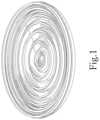
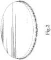
- The ornamental design for an elastic membrane for semiconductor wafer polishing apparatus, as shown and described.
Applications Claiming Priority (2)
| Application Number | Priority Date | Filing Date | Title |
|---|---|---|---|
| JP2020-027290D | 2020-12-18 | ||
| JPD2020-27290FJP1692349S (en) | 2020-12-18 | 2020-12-18 |
Publications (1)
| Publication Number | Publication Date |
|---|---|
| USD981969S1true USD981969S1 (en) | 2023-03-28 |
Family
ID=77173029
Family Applications (1)
| Application Number | Title | Priority Date | Filing Date |
|---|---|---|---|
| US29/794,758ActiveUSD981969S1 (en) | 2020-12-18 | 2021-06-15 | Elastic membrane for semiconductor wafer polishing apparatus |
Country Status (2)
| Country | Link |
|---|---|
| US (1) | USD981969S1 (en) |
| JP (1) | JP1692349S (en) |
Citations (14)
| Publication number | Priority date | Publication date | Assignee | Title |
|---|---|---|---|---|
| USD364384S (en)* | 1994-05-23 | 1995-11-21 | Fuji Electric Co., Ltd. | Semi-conductor element with terminal casing |
| US6659850B2 (en)* | 2000-03-31 | 2003-12-09 | Speedfam-Ipec Corporation | Work piece carrier with adjustable pressure zones and barriers and a method of planarizing a work piece |
| USD633452S1 (en)* | 2009-08-27 | 2011-03-01 | Ebara Corporation | Elastic membrane for semiconductor wafer polishing apparatus |
| TWD167111S (en) | 2013-05-15 | 2015-04-11 | 荏原製作所股份有限公司 | Elastic membrane for semiconductor wafer polishing apparatus |
| USD769200S1 (en)* | 2013-05-15 | 2016-10-18 | Ebara Corporation | Elastic membrane for semiconductor wafer polishing apparatus |
| USD770990S1 (en)* | 2013-05-15 | 2016-11-08 | Ebara Corporation | Elastic membrane for semiconductor wafer polishing apparatus |
| USD790041S1 (en)* | 2016-01-08 | 2017-06-20 | Asm Ip Holding B.V. | Gas dispersing plate for semiconductor manufacturing apparatus |
| USD808349S1 (en)* | 2013-05-15 | 2018-01-23 | Ebara Corporation | Elastic membrane for semiconductor wafer polishing apparatus |
| USD839224S1 (en)* | 2016-12-12 | 2019-01-29 | Ebara Corporation | Elastic membrane for semiconductor wafer polishing |
| TWD197827S (en) | 2017-12-19 | 2019-06-01 | Ebara Corp | Elastic film for semiconductor wafer polishing |
| USD859332S1 (en) | 2017-06-29 | 2019-09-10 | Ebara Corporation | Elastic membrane for semiconductor wafer polishing |
| US10537975B2 (en) | 2015-08-18 | 2020-01-21 | Ebara Corporation | Substrate adsorption method, substrate holding apparatus, substrate polishing apparatus, elastic film, substrate adsorption determination method for substrate holding apparatus, and pressure control method for substrate holding apparatus |
| USD918161S1 (en)* | 2017-12-19 | 2021-05-04 | Ebara Corporation | Elastic membrane |
| TWD215079S (en) | 2020-09-17 | 2021-11-01 | 日商荏原製作所股份有限公司 | Elastic film for semiconductor wafer polishing |
- 2020
- 2020-12-18JPJPD2020-27290Fpatent/JP1692349S/jaactiveActive
- 2021
- 2021-06-15USUS29/794,758patent/USD981969S1/enactiveActive
Patent Citations (16)
| Publication number | Priority date | Publication date | Assignee | Title |
|---|---|---|---|---|
| USD364384S (en)* | 1994-05-23 | 1995-11-21 | Fuji Electric Co., Ltd. | Semi-conductor element with terminal casing |
| US6659850B2 (en)* | 2000-03-31 | 2003-12-09 | Speedfam-Ipec Corporation | Work piece carrier with adjustable pressure zones and barriers and a method of planarizing a work piece |
| USD633452S1 (en)* | 2009-08-27 | 2011-03-01 | Ebara Corporation | Elastic membrane for semiconductor wafer polishing apparatus |
| USD813180S1 (en)* | 2013-05-15 | 2018-03-20 | Ebara Corporation | Elastic membrane for semiconductor wafer polishing apparatus |
| USD769200S1 (en)* | 2013-05-15 | 2016-10-18 | Ebara Corporation | Elastic membrane for semiconductor wafer polishing apparatus |
| USD770990S1 (en)* | 2013-05-15 | 2016-11-08 | Ebara Corporation | Elastic membrane for semiconductor wafer polishing apparatus |
| USD808349S1 (en)* | 2013-05-15 | 2018-01-23 | Ebara Corporation | Elastic membrane for semiconductor wafer polishing apparatus |
| TWD167111S (en) | 2013-05-15 | 2015-04-11 | 荏原製作所股份有限公司 | Elastic membrane for semiconductor wafer polishing apparatus |
| US10537975B2 (en) | 2015-08-18 | 2020-01-21 | Ebara Corporation | Substrate adsorption method, substrate holding apparatus, substrate polishing apparatus, elastic film, substrate adsorption determination method for substrate holding apparatus, and pressure control method for substrate holding apparatus |
| USD790041S1 (en)* | 2016-01-08 | 2017-06-20 | Asm Ip Holding B.V. | Gas dispersing plate for semiconductor manufacturing apparatus |
| USD839224S1 (en)* | 2016-12-12 | 2019-01-29 | Ebara Corporation | Elastic membrane for semiconductor wafer polishing |
| USD913977S1 (en)* | 2016-12-12 | 2021-03-23 | Ebara Corporation | Elastic membrane for semiconductor wafer polishing |
| USD859332S1 (en) | 2017-06-29 | 2019-09-10 | Ebara Corporation | Elastic membrane for semiconductor wafer polishing |
| TWD197827S (en) | 2017-12-19 | 2019-06-01 | Ebara Corp | Elastic film for semiconductor wafer polishing |
| USD918161S1 (en)* | 2017-12-19 | 2021-05-04 | Ebara Corporation | Elastic membrane |
| TWD215079S (en) | 2020-09-17 | 2021-11-01 | 日商荏原製作所股份有限公司 | Elastic film for semiconductor wafer polishing |
Also Published As
| Publication number | Publication date |
|---|---|
| JP1692349S (en) | 2021-08-10 |
Similar Documents
| Publication | Publication Date | Title |
|---|---|---|
| USD839224S1 (en) | Elastic membrane for semiconductor wafer polishing | |
| USD881133S1 (en) | Contact wafer | |
| USD948143S1 (en) | Robotic vacuum cleaner | |
| USD954371S1 (en) | Hand-held vacuum cleaner | |
| USD926401S1 (en) | Vacuum cleaner | |
| USD908990S1 (en) | Hand-held vacuum cleaner | |
| USD903611S1 (en) | Semiconductor device | |
| USD924505S1 (en) | Vacuum cleaner | |
| USD922008S1 (en) | Hand-held vacuum cleaner | |
| USD932452S1 (en) | Semiconductor device | |
| USD934821S1 (en) | Semiconductor device | |
| USD930299S1 (en) | Robot vacuum cleaner | |
| USD990079S1 (en) | Electric cleaning device | |
| USD976019S1 (en) | Ergonomic chair | |
| USD862010S1 (en) | Robotic vacuum cleaner | |
| USD928432S1 (en) | Vacuum cleaner | |
| USD928433S1 (en) | Vacuum cleaner | |
| USD928435S1 (en) | Vacuum cleaner | |
| USD924504S1 (en) | Vacuum cleaner | |
| USD934820S1 (en) | Semiconductor device | |
| USD926398S1 (en) | Robot vacuum cleaner | |
| USD922009S1 (en) | Hand-held vacuum cleaner | |
| USD859332S1 (en) | Elastic membrane for semiconductor wafer polishing | |
| USD901564S1 (en) | Gas inlet attachment for wafer processing apparatus | |
| USD938925S1 (en) | Semiconductor device |
Legal Events
| Date | Code | Title | Description |
|---|---|---|---|
| FEPP | Fee payment procedure | Free format text:ENTITY STATUS SET TO UNDISCOUNTED (ORIGINAL EVENT CODE: BIG.); ENTITY STATUS OF PATENT OWNER: LARGE ENTITY |