USD979524S1 - Confinement liner for a substrate processing chamber - Google Patents
Confinement liner for a substrate processing chamberDownload PDFInfo
- Publication number
- USD979524S1 USD979524S1US29/728,614US202029728614FUSD979524SUS D979524 S1USD979524 S1US D979524S1US 202029728614 FUS202029728614 FUS 202029728614FUS D979524 SUSD979524 SUS D979524S
- Authority
- US
- United States
- Prior art keywords
- processing chamber
- substrate processing
- confinement
- liner
- confinement liner
- Prior art date
- Legal status (The legal status is an assumption and is not a legal conclusion. Google has not performed a legal analysis and makes no representation as to the accuracy of the status listed.)
- Active
Links
Images


Description
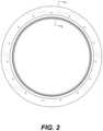
The broken lines shown in the drawings represent portions of a confinement liner for a substrate processing chamber that form no part of the claimed design.
Claims (1)
- The ornamental design for a confinement liner for a substrate processing chamber, as shown and described.
Priority Applications (6)
| Application Number | Priority Date | Filing Date | Title |
|---|---|---|---|
| US29/728,614USD979524S1 (en) | 2020-03-19 | 2020-03-19 | Confinement liner for a substrate processing chamber |
| TW109305178D01FTWD215698S (en) | 2020-03-19 | 2020-09-15 | Confinement liner for a substrate processing chamber |
| TW109305178FTWD215697S (en) | 2020-03-19 | 2020-09-15 | Confinement liner for a substrate processing chamber |
| JPD2021-5063FJP1692414S (en) | 2020-03-19 | 2020-09-19 | |
| JPD2020-20094FJP1686347S (en) | 2020-03-19 | 2020-09-19 | |
| US29/882,671USD1051867S1 (en) | 2020-03-19 | 2023-01-17 | Confinement liner for a substrate processing chamber |
Applications Claiming Priority (1)
| Application Number | Priority Date | Filing Date | Title |
|---|---|---|---|
| US29/728,614USD979524S1 (en) | 2020-03-19 | 2020-03-19 | Confinement liner for a substrate processing chamber |
Related Child Applications (1)
| Application Number | Title | Priority Date | Filing Date |
|---|---|---|---|
| US29/882,671DivisionUSD1051867S1 (en) | 2020-03-19 | 2023-01-17 | Confinement liner for a substrate processing chamber |
Publications (1)
| Publication Number | Publication Date |
|---|---|
| USD979524S1true USD979524S1 (en) | 2023-02-28 |
Family
ID=76083950
Family Applications (2)
| Application Number | Title | Priority Date | Filing Date |
|---|---|---|---|
| US29/728,614ActiveUSD979524S1 (en) | 2020-03-19 | 2020-03-19 | Confinement liner for a substrate processing chamber |
| US29/882,671ActiveUSD1051867S1 (en) | 2020-03-19 | 2023-01-17 | Confinement liner for a substrate processing chamber |
Family Applications After (1)
| Application Number | Title | Priority Date | Filing Date |
|---|---|---|---|
| US29/882,671ActiveUSD1051867S1 (en) | 2020-03-19 | 2023-01-17 | Confinement liner for a substrate processing chamber |
Country Status (3)
| Country | Link |
|---|---|
| US (2) | USD979524S1 (en) |
| JP (2) | JP1686347S (en) |
| TW (2) | TWD215697S (en) |
Cited By (8)
| Publication number | Priority date | Publication date | Assignee | Title |
|---|---|---|---|---|
| USD1034493S1 (en)* | 2022-11-25 | 2024-07-09 | Ap Systems Inc. | Chamber wall liner for a semiconductor manufacturing apparatus |
| USD1049067S1 (en)* | 2022-04-04 | 2024-10-29 | Applied Materials, Inc. | Ring for an anti-rotation process kit for a substrate processing chamber |
| USD1051867S1 (en)* | 2020-03-19 | 2024-11-19 | Applied Materials, Inc. | Confinement liner for a substrate processing chamber |
| USD1066275S1 (en) | 2022-04-04 | 2025-03-11 | Applied Materials, Inc. | Baffle for anti-rotation process kit for substrate processing chamber |
| USD1066440S1 (en)* | 2022-10-28 | 2025-03-11 | Applied Materials, Inc. | Process chamber pumping liner |
| USD1071886S1 (en)* | 2022-01-20 | 2025-04-22 | Applied Materials, Inc. | Substrate support for a substrate processing chamber |
| USD1073758S1 (en)* | 2022-10-13 | 2025-05-06 | Lam Research Corporation | Baffle for substrate processing system |
| USD1086087S1 (en)* | 2023-03-30 | 2025-07-29 | Samsung Electronics Co., Ltd. | CMP (chemical mechanical planarization) retaining ring |
Families Citing this family (3)
| Publication number | Priority date | Publication date | Assignee | Title |
|---|---|---|---|---|
| USD1071103S1 (en)* | 2022-04-11 | 2025-04-15 | Applied Materials, Inc. | Gas distribution plate |
| JP2025521046A (en) | 2022-07-08 | 2025-07-04 | トーソー エスエムディー,インク. | Dynamic Vacuum Seal System for Physical Vapor Deposition Sputtering Applications |
| TWD233706S (en) | 2023-10-27 | 2024-09-21 | 俊龍 吳 | Nozzle pad |
Citations (57)
| Publication number | Priority date | Publication date | Assignee | Title |
|---|---|---|---|---|
| US6129808A (en) | 1998-03-31 | 2000-10-10 | Lam Research Corporation | Low contamination high density plasma etch chambers and methods for making the same |
| US6156151A (en) | 1996-07-19 | 2000-12-05 | Tokyo Electron Limited | Plasma processing apparatus |
| US6224472B1 (en)* | 1999-06-24 | 2001-05-01 | Samsung Austin Semiconductor, L.P. | Retaining ring for chemical mechanical polishing |
| US6464843B1 (en) | 1998-03-31 | 2002-10-15 | Lam Research Corporation | Contamination controlling method and apparatus for a plasma processing chamber |
| US6506254B1 (en) | 2000-06-30 | 2003-01-14 | Lam Research Corporation | Semiconductor processing equipment having improved particle performance |
| US6506685B2 (en) | 1998-12-28 | 2003-01-14 | Lam Research Corporation | Perforated plasma confinement ring in plasma reactors |
| US20030092278A1 (en) | 2001-11-13 | 2003-05-15 | Fink Steven T. | Plasma baffle assembly |
| US20040075036A1 (en)* | 2002-10-04 | 2004-04-22 | Ceramic Component Technologies, Inc. | Test plate for ceramic surface mount devices and other electronic components |
| WO2004059716A1 (en) | 2002-12-20 | 2004-07-15 | Lam Research Corporation | A system and method for controlling plasma with an adjustable coupling to ground circuit |
| USD494551S1 (en)* | 2002-12-12 | 2004-08-17 | Tokyo Electron Limited | Exhaust ring for manufacturing semiconductors |
| US20060283551A1 (en)* | 2005-06-17 | 2006-12-21 | Sung-Ku Son | Confinement ring assembly of plasma processing apparatus |
| US7267741B2 (en) | 2003-11-14 | 2007-09-11 | Lam Research Corporation | Silicon carbide components of semiconductor substrate processing apparatuses treated to remove free-carbon |
| US20080110567A1 (en) | 2006-11-15 | 2008-05-15 | Miller Matthew L | Plasma confinement baffle and flow equalizer for enhanced magnetic control of plasma radial distribution |
| US7552521B2 (en) | 2004-12-08 | 2009-06-30 | Tokyo Electron Limited | Method and apparatus for improved baffle plate |
| US20090188625A1 (en) | 2008-01-28 | 2009-07-30 | Carducci James D | Etching chamber having flow equalizer and lower liner |
| US7585384B2 (en) | 2003-04-17 | 2009-09-08 | Applied Materials, Inc. | Apparatus and method to confine plasma and reduce flow resistance in a plasma reactor |
| US7802539B2 (en) | 2000-06-30 | 2010-09-28 | Lam Research Corporation | Semiconductor processing equipment having improved particle performance |
| US7837826B2 (en) | 2006-07-18 | 2010-11-23 | Lam Research Corporation | Hybrid RF capacitively and inductively coupled plasma source using multifrequency RF powers and methods of use thereof |
| US20100304571A1 (en) | 2007-12-19 | 2010-12-02 | Larson Dean J | Film adhesive for semiconductor vacuum processing apparatus |
| JP2011040461A (en) | 2009-08-07 | 2011-02-24 | Tokyo Electron Ltd | Baffle plate and plasma processing apparatus |
| US20110100553A1 (en) | 2009-08-31 | 2011-05-05 | Rajinder Dhindsa | multi-peripheral ring arrangement for performing plasma confinement |
| US20110226739A1 (en) | 2010-03-19 | 2011-09-22 | Varian Semiconductor Equipment Associates, Inc. | Process chamber liner with apertures for particle containment |
| US8298046B2 (en)* | 2009-10-21 | 2012-10-30 | SPM Technology, Inc. | Retaining rings |
| US20120273130A1 (en) | 2011-04-28 | 2012-11-01 | Lam Research Corporation | Internal Faraday Shield Having Distributed Chevron Patterns and Correlated Positioning Relative to External Inner and Outer TCP Coil |
| US8485128B2 (en) | 2010-06-30 | 2013-07-16 | Lam Research Corporation | Movable ground ring for a plasma processing chamber |
| US8517803B2 (en)* | 2009-09-16 | 2013-08-27 | SPM Technology, Inc. | Retaining ring for chemical mechanical polishing |
| US8622021B2 (en) | 2007-10-31 | 2014-01-07 | Lam Research Corporation | High lifetime consumable silicon nitride-silicon dioxide plasma processing components |
| USD699200S1 (en)* | 2011-09-30 | 2014-02-11 | Tokyo Electron Limited | Electrode member for a plasma processing apparatus |
| US20140113453A1 (en) | 2012-10-24 | 2014-04-24 | Lam Research Corporation | Tungsten carbide coated metal component of a plasma reactor chamber and method of coating |
| US20140116338A1 (en) | 2012-10-29 | 2014-05-01 | Advanced Micro-Fabrication Equipment Inc, Shanghai | Coating for performance enhancement of semiconductor apparatus |
| USD709539S1 (en)* | 2011-09-30 | 2014-07-22 | Tokyo Electron Limited | Focusing ring |
| USD709538S1 (en)* | 2011-09-30 | 2014-07-22 | Tokyo Electron Limited | Focusing ring |
| USD709536S1 (en)* | 2011-09-30 | 2014-07-22 | Tokyo Electron Limited | Focusing ring |
| USD709537S1 (en)* | 2011-09-30 | 2014-07-22 | Tokyo Electron Limited | Focusing ring |
| US8826855B2 (en) | 2010-06-30 | 2014-09-09 | Lam Research Corporation | C-shaped confinement ring for a plasma processing chamber |
| US8893702B2 (en) | 2013-02-20 | 2014-11-25 | Lam Research Corporation | Ductile mode machining methods for hard and brittle components of plasma processing apparatuses |
| USD729730S1 (en)* | 2013-06-06 | 2015-05-19 | Jon Simon Gillespie-Brown | Power charging ring |
| US9123661B2 (en) | 2013-08-07 | 2015-09-01 | Lam Research Corporation | Silicon containing confinement ring for plasma processing apparatus and method of forming thereof |
| US9184029B2 (en) | 2013-09-03 | 2015-11-10 | Lam Research Corporation | System, method and apparatus for coordinating pressure pulses and RF modulation in a small volume confined process reactor |
| US20150329955A1 (en) | 2014-05-16 | 2015-11-19 | Applied Materials, Inc. | Plasma spray coating design using phase and stress control |
| US20160002788A1 (en)* | 2013-02-21 | 2016-01-07 | Altatech Semiconductor | Chemical vapour deposition device |
| US9330927B2 (en) | 2013-08-28 | 2016-05-03 | Lam Research Corporation | System, method and apparatus for generating pressure pulses in small volume confined process reactor |
| US20160158910A1 (en)* | 2013-07-11 | 2016-06-09 | Will Be S & T Co., Ltd. | Retainer ring for chemical-mechanical polishing device |
| USD766849S1 (en)* | 2013-05-15 | 2016-09-20 | Ebara Corporation | Substrate retaining ring |
| USD770992S1 (en)* | 2015-06-12 | 2016-11-08 | Hitachi High-Technologies Corporation | Electrode cover for a plasma processing apparatus |
| US9508530B2 (en) | 2011-11-21 | 2016-11-29 | Lam Research Corporation | Plasma processing chamber with flexible symmetric RF return strap |
| CN106898534A (en) | 2015-12-21 | 2017-06-27 | 中微半导体设备(上海)有限公司 | Plasma confinement ring, plasma processing apparatus and processing method for substrate |
| USD797691S1 (en)* | 2016-04-14 | 2017-09-19 | Applied Materials, Inc. | Composite edge ring |
| US9779916B2 (en) | 2009-08-31 | 2017-10-03 | Lam Research Corporation | Radio frequency (RF) ground return arrangements |
| USD810705S1 (en)* | 2016-04-01 | 2018-02-20 | Veeco Instruments Inc. | Self-centering wafer carrier for chemical vapor deposition |
| US20180061618A1 (en) | 2016-08-26 | 2018-03-01 | Applied Materials, Inc. | Plasma screen for plasma processing chamber |
| USD840364S1 (en)* | 2017-01-31 | 2019-02-12 | Hitachi High-Technologies Corporation | Electrode cover for a plasma processing apparatus |
| TWD197827S (en) | 2017-12-19 | 2019-06-01 | Ebara Corp | Elastic film for semiconductor wafer polishing |
| USD876504S1 (en)* | 2017-04-03 | 2020-02-25 | Asm Ip Holding B.V. | Exhaust flow control ring for semiconductor deposition apparatus |
| US10672629B2 (en)* | 2016-09-28 | 2020-06-02 | Samsung Electronics Co., Ltd. | Ring assembly and chuck assembly having the same |
| USD891382S1 (en)* | 2019-02-08 | 2020-07-28 | Applied Materials, Inc. | Process shield for a substrate processing chamber |
| USD895777S1 (en)* | 2017-09-20 | 2020-09-08 | Gardner Denver Petroleum Pumps Llc | Header ring |
Family Cites Families (24)
| Publication number | Priority date | Publication date | Assignee | Title |
|---|---|---|---|---|
| US7252738B2 (en)* | 2002-09-20 | 2007-08-07 | Lam Research Corporation | Apparatus for reducing polymer deposition on a substrate and substrate support |
| USD491963S1 (en)* | 2002-11-20 | 2004-06-22 | Tokyo Electron Limited | Inner wall shield for a process chamber for manufacturing semiconductors |
| US20070113783A1 (en)* | 2005-11-19 | 2007-05-24 | Applied Materials, Inc. | Band shield for substrate processing chamber |
| CN103069542A (en)* | 2010-08-20 | 2013-04-24 | 应用材料公司 | Extended life deposition ring |
| TW201325326A (en) | 2011-10-05 | 2013-06-16 | Applied Materials Inc | Plasma processing equipment and substrate support assembly thereof |
| USD665491S1 (en)* | 2012-01-25 | 2012-08-14 | Applied Materials, Inc. | Deposition chamber cover ring |
| USD717746S1 (en)* | 2013-11-06 | 2014-11-18 | Applied Materials, Inc. | Lower chamber liner |
| USD716239S1 (en)* | 2013-11-06 | 2014-10-28 | Applied Materials, Inc. | Upper chamber liner |
| USD716240S1 (en)* | 2013-11-07 | 2014-10-28 | Applied Materials, Inc. | Lower chamber liner |
| USD711331S1 (en)* | 2013-11-07 | 2014-08-19 | Applied Materials, Inc. | Upper chamber liner |
| JP1546801S (en)* | 2015-06-12 | 2016-03-28 | ||
| CN110892502B (en)* | 2017-06-01 | 2022-10-04 | 欧瑞康表面处理解决方案股份公司普费菲孔 | Target assembly for safe and economical evaporation of brittle materials |
| JP1612684S (en)* | 2018-02-08 | 2018-09-03 | ||
| KR102040281B1 (en) | 2018-04-26 | 2019-11-04 | 주식회사 건테크 | Limited ring for semiconductor plasma etching process using CVD-SiC material |
| US11515128B2 (en) | 2018-08-28 | 2022-11-29 | Lam Research Corporation | Confinement ring with extended life |
| USD888903S1 (en)* | 2018-12-17 | 2020-06-30 | Applied Materials, Inc. | Deposition ring for physical vapor deposition chamber |
| USD933725S1 (en)* | 2019-02-08 | 2021-10-19 | Applied Materials, Inc. | Deposition ring for a substrate processing chamber |
| USD942516S1 (en)* | 2019-02-08 | 2022-02-01 | Applied Materials, Inc. | Process shield for a substrate processing chamber |
| USD979524S1 (en)* | 2020-03-19 | 2023-02-28 | Applied Materials, Inc. | Confinement liner for a substrate processing chamber |
| USD934315S1 (en)* | 2020-03-20 | 2021-10-26 | Applied Materials, Inc. | Deposition ring for a substrate processing chamber |
| USD941372S1 (en)* | 2020-03-20 | 2022-01-18 | Applied Materials, Inc. | Process shield for a substrate processing chamber |
| USD941371S1 (en)* | 2020-03-20 | 2022-01-18 | Applied Materials, Inc. | Process shield for a substrate processing chamber |
| USD933726S1 (en)* | 2020-07-31 | 2021-10-19 | Applied Materials, Inc. | Deposition ring for a semiconductor processing chamber |
| USD1034493S1 (en)* | 2022-11-25 | 2024-07-09 | Ap Systems Inc. | Chamber wall liner for a semiconductor manufacturing apparatus |
- 2020
- 2020-03-19USUS29/728,614patent/USD979524S1/enactiveActive
- 2020-09-15TWTW109305178Fpatent/TWD215697S/enunknown
- 2020-09-15TWTW109305178D01Fpatent/TWD215698S/enunknown
- 2020-09-19JPJPD2020-20094Fpatent/JP1686347S/jaactiveActive
- 2020-09-19JPJPD2021-5063Fpatent/JP1692414S/jaactiveActive
- 2023
- 2023-01-17USUS29/882,671patent/USD1051867S1/enactiveActive
Patent Citations (63)
| Publication number | Priority date | Publication date | Assignee | Title |
|---|---|---|---|---|
| US6156151A (en) | 1996-07-19 | 2000-12-05 | Tokyo Electron Limited | Plasma processing apparatus |
| US6464843B1 (en) | 1998-03-31 | 2002-10-15 | Lam Research Corporation | Contamination controlling method and apparatus for a plasma processing chamber |
| US6129808A (en) | 1998-03-31 | 2000-10-10 | Lam Research Corporation | Low contamination high density plasma etch chambers and methods for making the same |
| US6506685B2 (en) | 1998-12-28 | 2003-01-14 | Lam Research Corporation | Perforated plasma confinement ring in plasma reactors |
| US6224472B1 (en)* | 1999-06-24 | 2001-05-01 | Samsung Austin Semiconductor, L.P. | Retaining ring for chemical mechanical polishing |
| US7802539B2 (en) | 2000-06-30 | 2010-09-28 | Lam Research Corporation | Semiconductor processing equipment having improved particle performance |
| US6506254B1 (en) | 2000-06-30 | 2003-01-14 | Lam Research Corporation | Semiconductor processing equipment having improved particle performance |
| US20030092278A1 (en) | 2001-11-13 | 2003-05-15 | Fink Steven T. | Plasma baffle assembly |
| US20040075036A1 (en)* | 2002-10-04 | 2004-04-22 | Ceramic Component Technologies, Inc. | Test plate for ceramic surface mount devices and other electronic components |
| USD494551S1 (en)* | 2002-12-12 | 2004-08-17 | Tokyo Electron Limited | Exhaust ring for manufacturing semiconductors |
| WO2004059716A1 (en) | 2002-12-20 | 2004-07-15 | Lam Research Corporation | A system and method for controlling plasma with an adjustable coupling to ground circuit |
| US7585384B2 (en) | 2003-04-17 | 2009-09-08 | Applied Materials, Inc. | Apparatus and method to confine plasma and reduce flow resistance in a plasma reactor |
| US7754997B2 (en) | 2003-04-17 | 2010-07-13 | Applied Materials, Inc. | Apparatus and method to confine plasma and reduce flow resistance in a plasma |
| US7972467B2 (en) | 2003-04-17 | 2011-07-05 | Applied Materials Inc. | Apparatus and method to confine plasma and reduce flow resistance in a plasma reactor |
| US7267741B2 (en) | 2003-11-14 | 2007-09-11 | Lam Research Corporation | Silicon carbide components of semiconductor substrate processing apparatuses treated to remove free-carbon |
| US20080023029A1 (en) | 2003-11-14 | 2008-01-31 | Lam Research Corporation | Silicon carbide components of semiconductor substrate processing apparatuses treated to remove free-carbon |
| US7552521B2 (en) | 2004-12-08 | 2009-06-30 | Tokyo Electron Limited | Method and apparatus for improved baffle plate |
| US20060283551A1 (en)* | 2005-06-17 | 2006-12-21 | Sung-Ku Son | Confinement ring assembly of plasma processing apparatus |
| US7837826B2 (en) | 2006-07-18 | 2010-11-23 | Lam Research Corporation | Hybrid RF capacitively and inductively coupled plasma source using multifrequency RF powers and methods of use thereof |
| US20080110567A1 (en) | 2006-11-15 | 2008-05-15 | Miller Matthew L | Plasma confinement baffle and flow equalizer for enhanced magnetic control of plasma radial distribution |
| US8622021B2 (en) | 2007-10-31 | 2014-01-07 | Lam Research Corporation | High lifetime consumable silicon nitride-silicon dioxide plasma processing components |
| US20100304571A1 (en) | 2007-12-19 | 2010-12-02 | Larson Dean J | Film adhesive for semiconductor vacuum processing apparatus |
| US20090188625A1 (en) | 2008-01-28 | 2009-07-30 | Carducci James D | Etching chamber having flow equalizer and lower liner |
| JP2011040461A (en) | 2009-08-07 | 2011-02-24 | Tokyo Electron Ltd | Baffle plate and plasma processing apparatus |
| US20110100553A1 (en) | 2009-08-31 | 2011-05-05 | Rajinder Dhindsa | multi-peripheral ring arrangement for performing plasma confinement |
| US9779916B2 (en) | 2009-08-31 | 2017-10-03 | Lam Research Corporation | Radio frequency (RF) ground return arrangements |
| US8900398B2 (en) | 2009-08-31 | 2014-12-02 | Lam Research Corporation | Local plasma confinement and pressure control arrangement and methods thereof |
| US8517803B2 (en)* | 2009-09-16 | 2013-08-27 | SPM Technology, Inc. | Retaining ring for chemical mechanical polishing |
| US8298046B2 (en)* | 2009-10-21 | 2012-10-30 | SPM Technology, Inc. | Retaining rings |
| US20110226739A1 (en) | 2010-03-19 | 2011-09-22 | Varian Semiconductor Equipment Associates, Inc. | Process chamber liner with apertures for particle containment |
| US8485128B2 (en) | 2010-06-30 | 2013-07-16 | Lam Research Corporation | Movable ground ring for a plasma processing chamber |
| US8826855B2 (en) | 2010-06-30 | 2014-09-09 | Lam Research Corporation | C-shaped confinement ring for a plasma processing chamber |
| US20120273130A1 (en) | 2011-04-28 | 2012-11-01 | Lam Research Corporation | Internal Faraday Shield Having Distributed Chevron Patterns and Correlated Positioning Relative to External Inner and Outer TCP Coil |
| USD699200S1 (en)* | 2011-09-30 | 2014-02-11 | Tokyo Electron Limited | Electrode member for a plasma processing apparatus |
| USD709536S1 (en)* | 2011-09-30 | 2014-07-22 | Tokyo Electron Limited | Focusing ring |
| USD709537S1 (en)* | 2011-09-30 | 2014-07-22 | Tokyo Electron Limited | Focusing ring |
| USD709539S1 (en)* | 2011-09-30 | 2014-07-22 | Tokyo Electron Limited | Focusing ring |
| USD709538S1 (en)* | 2011-09-30 | 2014-07-22 | Tokyo Electron Limited | Focusing ring |
| US9508530B2 (en) | 2011-11-21 | 2016-11-29 | Lam Research Corporation | Plasma processing chamber with flexible symmetric RF return strap |
| US20140113453A1 (en) | 2012-10-24 | 2014-04-24 | Lam Research Corporation | Tungsten carbide coated metal component of a plasma reactor chamber and method of coating |
| US20140116338A1 (en) | 2012-10-29 | 2014-05-01 | Advanced Micro-Fabrication Equipment Inc, Shanghai | Coating for performance enhancement of semiconductor apparatus |
| US8893702B2 (en) | 2013-02-20 | 2014-11-25 | Lam Research Corporation | Ductile mode machining methods for hard and brittle components of plasma processing apparatuses |
| US20160002788A1 (en)* | 2013-02-21 | 2016-01-07 | Altatech Semiconductor | Chemical vapour deposition device |
| USD793976S1 (en)* | 2013-05-15 | 2017-08-08 | Ebara Corporation | Substrate retaining ring |
| USD766849S1 (en)* | 2013-05-15 | 2016-09-20 | Ebara Corporation | Substrate retaining ring |
| USD729730S1 (en)* | 2013-06-06 | 2015-05-19 | Jon Simon Gillespie-Brown | Power charging ring |
| US20160158910A1 (en)* | 2013-07-11 | 2016-06-09 | Will Be S & T Co., Ltd. | Retainer ring for chemical-mechanical polishing device |
| US9123661B2 (en) | 2013-08-07 | 2015-09-01 | Lam Research Corporation | Silicon containing confinement ring for plasma processing apparatus and method of forming thereof |
| US20150364322A1 (en) | 2013-08-07 | 2015-12-17 | Lam Research Corporation | Silicon containing confinement ring for plasma processing apparatus and method of forming thereof |
| US9330927B2 (en) | 2013-08-28 | 2016-05-03 | Lam Research Corporation | System, method and apparatus for generating pressure pulses in small volume confined process reactor |
| US9184029B2 (en) | 2013-09-03 | 2015-11-10 | Lam Research Corporation | System, method and apparatus for coordinating pressure pulses and RF modulation in a small volume confined process reactor |
| US20150329955A1 (en) | 2014-05-16 | 2015-11-19 | Applied Materials, Inc. | Plasma spray coating design using phase and stress control |
| USD770992S1 (en)* | 2015-06-12 | 2016-11-08 | Hitachi High-Technologies Corporation | Electrode cover for a plasma processing apparatus |
| CN106898534A (en) | 2015-12-21 | 2017-06-27 | 中微半导体设备(上海)有限公司 | Plasma confinement ring, plasma processing apparatus and processing method for substrate |
| USD810705S1 (en)* | 2016-04-01 | 2018-02-20 | Veeco Instruments Inc. | Self-centering wafer carrier for chemical vapor deposition |
| USD797691S1 (en)* | 2016-04-14 | 2017-09-19 | Applied Materials, Inc. | Composite edge ring |
| US20180061618A1 (en) | 2016-08-26 | 2018-03-01 | Applied Materials, Inc. | Plasma screen for plasma processing chamber |
| US10672629B2 (en)* | 2016-09-28 | 2020-06-02 | Samsung Electronics Co., Ltd. | Ring assembly and chuck assembly having the same |
| USD840364S1 (en)* | 2017-01-31 | 2019-02-12 | Hitachi High-Technologies Corporation | Electrode cover for a plasma processing apparatus |
| USD876504S1 (en)* | 2017-04-03 | 2020-02-25 | Asm Ip Holding B.V. | Exhaust flow control ring for semiconductor deposition apparatus |
| USD895777S1 (en)* | 2017-09-20 | 2020-09-08 | Gardner Denver Petroleum Pumps Llc | Header ring |
| TWD197827S (en) | 2017-12-19 | 2019-06-01 | Ebara Corp | Elastic film for semiconductor wafer polishing |
| USD891382S1 (en)* | 2019-02-08 | 2020-07-28 | Applied Materials, Inc. | Process shield for a substrate processing chamber |
Non-Patent Citations (2)
| Title |
|---|
| International Search Report for PCT/US2021/021986, dated Jun. 28, 2021. |
| Search Report for Taiwan Design Application No. 109305178, dated Mar. 30, 2021. |
Cited By (8)
| Publication number | Priority date | Publication date | Assignee | Title |
|---|---|---|---|---|
| USD1051867S1 (en)* | 2020-03-19 | 2024-11-19 | Applied Materials, Inc. | Confinement liner for a substrate processing chamber |
| USD1071886S1 (en)* | 2022-01-20 | 2025-04-22 | Applied Materials, Inc. | Substrate support for a substrate processing chamber |
| USD1049067S1 (en)* | 2022-04-04 | 2024-10-29 | Applied Materials, Inc. | Ring for an anti-rotation process kit for a substrate processing chamber |
| USD1066275S1 (en) | 2022-04-04 | 2025-03-11 | Applied Materials, Inc. | Baffle for anti-rotation process kit for substrate processing chamber |
| USD1073758S1 (en)* | 2022-10-13 | 2025-05-06 | Lam Research Corporation | Baffle for substrate processing system |
| USD1066440S1 (en)* | 2022-10-28 | 2025-03-11 | Applied Materials, Inc. | Process chamber pumping liner |
| USD1034493S1 (en)* | 2022-11-25 | 2024-07-09 | Ap Systems Inc. | Chamber wall liner for a semiconductor manufacturing apparatus |
| USD1086087S1 (en)* | 2023-03-30 | 2025-07-29 | Samsung Electronics Co., Ltd. | CMP (chemical mechanical planarization) retaining ring |
Also Published As
| Publication number | Publication date |
|---|---|
| JP1692414S (en) | 2021-08-16 |
| TWD215698S (en) | 2021-12-01 |
| USD1051867S1 (en) | 2024-11-19 |
| TWD215697S (en) | 2021-12-01 |
| JP1686347S (en) | 2021-05-31 |
Similar Documents
| Publication | Publication Date | Title |
|---|---|---|
| USD979524S1 (en) | Confinement liner for a substrate processing chamber | |
| USD1087371S1 (en) | Mask | |
| USD986190S1 (en) | Confinement plate for a substrate processing chamber | |
| USRE50390E1 (en) | Keyboard | |
| USD955083S1 (en) | Cart | |
| USD1011346S1 (en) | Keyboard | |
| USD965592S1 (en) | Keyboard | |
| USD1042924S1 (en) | Light | |
| USD960631S1 (en) | Cooking tray | |
| USD960303S1 (en) | Showerhead | |
| USD1038592S1 (en) | Shoe | |
| USD961592S1 (en) | Keyboard | |
| USD1002616S1 (en) | Keyboard | |
| USD1029985S1 (en) | Substrate | |
| USD1070325S1 (en) | Footwear | |
| USD967334S1 (en) | Showerhead | |
| USD1070821S1 (en) | Earphone | |
| USD1052865S1 (en) | Shoe | |
| USD997772S1 (en) | Jewelry | |
| USD1025064S1 (en) | Keyboard | |
| USD1052548S1 (en) | Gas diffuser | |
| USD1056793S1 (en) | Tailcap assembly | |
| USD980953S1 (en) | Faucet | |
| USD960318S1 (en) | Showerhead | |
| USD1028701S1 (en) | Nut |
Legal Events
| Date | Code | Title | Description |
|---|---|---|---|
| FEPP | Fee payment procedure | Free format text:ENTITY STATUS SET TO UNDISCOUNTED (ORIGINAL EVENT CODE: BIG.); ENTITY STATUS OF PATENT OWNER: LARGE ENTITY |