USD938925S1 - Semiconductor device - Google Patents
Semiconductor deviceDownload PDFInfo
- Publication number
- USD938925S1 USD938925S1US29/710,616US201929710616FUSD938925SUS D938925 S1USD938925 S1US D938925S1US 201929710616 FUS201929710616 FUS 201929710616FUS D938925 SUSD938925 SUS D938925S
- Authority
- US
- United States
- Prior art keywords
- semiconductor device
- view
- ornamental design
- semiconductor
- perspective
- Prior art date
- Legal status (The legal status is an assumption and is not a legal conclusion. Google has not performed a legal analysis and makes no representation as to the accuracy of the status listed.)
- Active
Links
Images


Description
Claims (1)
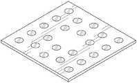
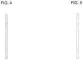
- The ornamental design for a semiconductor device, as shown and described.
Priority Applications (2)
| Application Number | Priority Date | Filing Date | Title |
|---|---|---|---|
| US29/710,616USD938925S1 (en) | 2019-10-24 | 2019-10-24 | Semiconductor device |
| US29/801,764USD937232S1 (en) | 2019-10-24 | 2021-07-30 | Semiconductor device |
Applications Claiming Priority (1)
| Application Number | Priority Date | Filing Date | Title |
|---|---|---|---|
| US29/710,616USD938925S1 (en) | 2019-10-24 | 2019-10-24 | Semiconductor device |
Related Child Applications (1)
| Application Number | Title | Priority Date | Filing Date |
|---|---|---|---|
| US29/801,764DivisionUSD937232S1 (en) | 2019-10-24 | 2021-07-30 | Semiconductor device |
Publications (1)
| Publication Number | Publication Date |
|---|---|
| USD938925S1true USD938925S1 (en) | 2021-12-21 |
Family
ID=78704014
Family Applications (2)
| Application Number | Title | Priority Date | Filing Date |
|---|---|---|---|
| US29/710,616ActiveUSD938925S1 (en) | 2019-10-24 | 2019-10-24 | Semiconductor device |
| US29/801,764ActiveUSD937232S1 (en) | 2019-10-24 | 2021-07-30 | Semiconductor device |
Family Applications After (1)
| Application Number | Title | Priority Date | Filing Date |
|---|---|---|---|
| US29/801,764ActiveUSD937232S1 (en) | 2019-10-24 | 2021-07-30 | Semiconductor device |
Country Status (1)
| Country | Link |
|---|---|
| US (2) | USD938925S1 (en) |
Cited By (5)
| Publication number | Priority date | Publication date | Assignee | Title |
|---|---|---|---|---|
| USD972933S1 (en)* | 2020-11-24 | 2022-12-20 | Panasonic Intellectual Property Management Co., Ltd. | Package cushioning |
| USD980810S1 (en)* | 2020-02-27 | 2023-03-14 | Kioxia Corporation | Integrated circuit card |
| USD986840S1 (en)* | 2020-05-13 | 2023-05-23 | Panasonic Intellectual Property Management Co., Ltd. | Semiconductor device |
| USD1054389S1 (en)* | 2022-01-05 | 2024-12-17 | Nec Corporation | Semiconductor device |
| USD1054390S1 (en)* | 2022-01-05 | 2024-12-17 | Nec Corporation | Semiconductor device |
Families Citing this family (4)
| Publication number | Priority date | Publication date | Assignee | Title |
|---|---|---|---|---|
| USD942974S1 (en)* | 2018-11-20 | 2022-02-08 | Thales Dis Ais Deutschland Gmbh | Cellular module |
| USD988300S1 (en)* | 2021-03-09 | 2023-06-06 | Thales Dis Ais Deutschland Gmbh | IoT module |
| USD988299S1 (en)* | 2021-06-18 | 2023-06-06 | Telit Cinterion Deutschland Gmbh | Cellular module |
| USD1087928S1 (en)* | 2022-08-16 | 2025-08-12 | Modus Test, Llc | Contact field for a printed circuit board |
Citations (48)
| Publication number | Priority date | Publication date | Assignee | Title |
|---|---|---|---|---|
| US273559A (en)* | 1883-03-06 | Chaeles s | ||
| US729489A (en)* | 1902-10-04 | 1903-05-26 | Mattson Rubber Company | Game-piece. |
| US1998526A (en)* | 1932-09-23 | 1935-04-23 | Schubert Philipp | Domino |
| USD318461S (en)* | 1988-04-13 | 1991-07-23 | Ibiden Co., Ltd. | Semi-conductor mounting substrate |
| USD319045S (en)* | 1988-04-13 | 1991-08-13 | Ibiden Co., Ltd. | Semi-conductor substrate with conducting pattern |
| USD319629S (en)* | 1988-04-13 | 1991-09-03 | Ibiden Co., Ltd. | Semiconductor substrate with conducting pattern |
| USD319814S (en)* | 1988-04-13 | 1991-09-10 | Ibiden Co., Ltd. | Semi-conductor substrate with conducting pattern |
| US5370398A (en)* | 1993-06-30 | 1994-12-06 | Nguyen; Thang V. | Close and open game |
| US5757082A (en)* | 1995-07-31 | 1998-05-26 | Rohm Co., Ltd. | Semiconductor chips, devices incorporating same and method of making same |
| US5858815A (en) | 1996-06-21 | 1999-01-12 | Anam Semiconductor Inc. | Semiconductor package and method for fabricating the same |
| US6307269B1 (en)* | 1997-07-11 | 2001-10-23 | Hitachi, Ltd. | Semiconductor device with chip size package |
| US6589817B1 (en) | 1996-12-03 | 2003-07-08 | Oki Electric Industry Co., Ltd. | Semiconductor device, method for manufacturing the same, and method for mounting the same |
| USD487430S1 (en)* | 2002-07-10 | 2004-03-09 | Matsushita Electric Industrial Co., Ltd. | Semiconductor memory element |
| US6836002B2 (en)* | 2000-03-09 | 2004-12-28 | Sharp Kabushiki Kaisha | Semiconductor device |
| USD598380S1 (en)* | 2008-05-09 | 2009-08-18 | Fujifilm Corporation | Conductive sheet |
| US20100326710A1 (en) | 2009-06-29 | 2010-12-30 | Guigen Zhang | Mono-Domain Hexagonal Arrays of Nanopillars and Processes For Preparing the Same |
| USD633672S1 (en) | 2010-02-10 | 2011-03-01 | The Libman Company | Pad |
| US8177993B2 (en) | 2006-11-05 | 2012-05-15 | Globalfoundries Singapore Pte Ltd | Apparatus and methods for cleaning and drying of wafers |
| US8294250B2 (en) | 2009-10-12 | 2012-10-23 | Samsung Electronics Co., Ltd. | Wiring substrate for a semiconductor chip, and semiconducotor package having the wiring substrate |
| USD687898S1 (en)* | 2012-06-11 | 2013-08-13 | Raymond Lupkas | Set of pai-gow tiles |
| USD704155S1 (en)* | 2010-08-19 | 2014-05-06 | Epistar Corporation | Wafer carrier |
| USD730304S1 (en)* | 2014-05-15 | 2015-05-26 | Kabushiki Kaisha Toshiba | Substrate for an electronic circuit |
| USD754083S1 (en)* | 2013-10-17 | 2016-04-19 | Vlt, Inc. | Electric terminal |
| USD757693S1 (en)* | 2013-09-26 | 2016-05-31 | Murata Manufacturing Co., Ltd. | Wireless transmission/reception module |
| USD764424S1 (en)* | 2014-05-15 | 2016-08-23 | Kabushiki Kaisha Toshiba | Substrate for an electronic circuit |
| USD789456S1 (en)* | 2015-02-12 | 2017-06-13 | Wenlan H. Frost | Set of square domino tiles |
| JP1581768S (en) | 2016-08-02 | 2017-07-24 | ||
| USD797066S1 (en)* | 2015-08-17 | 2017-09-12 | Cooper Technologies Company | Integrated light emitting diode (LED) light engine |
| JP1588125S (en) | 2017-04-26 | 2017-10-16 | ||
| JP1588481S (en) | 2017-04-26 | 2017-10-16 | ||
| USD821338S1 (en) | 2015-01-20 | 2018-06-26 | Modus Test Automation, Llc. | Contact fields for a printed circuit board |
| USD821337S1 (en) | 2015-01-20 | 2018-06-26 | Modus Test Automation, Llc. | Contact field for a printed circuit board |
| USD831009S1 (en) | 2015-12-11 | 2018-10-16 | Gemalto M2M Gmbh | Radio module |
| USD837171S1 (en)* | 2018-05-07 | 2019-01-01 | Adura Led Solutions Llc | Circuit board having arrangements of light-emitting diodes |
| JP1632160S (en) | 2018-09-28 | 2019-05-27 | ||
| JP1632597S (en) | 2018-09-28 | 2019-05-27 | ||
| USD850309S1 (en)* | 2017-07-27 | 2019-06-04 | Aehr Test Systems | Layout of contacts |
| USD856948S1 (en)* | 2018-05-07 | 2019-08-20 | Adura Led Solutions Llc | Circuit board having arrangements of light-emitting diodes |
| JP1641049S (en) | 2018-06-19 | 2019-09-09 | ||
| JP1641048S (en) | 2018-06-19 | 2019-09-09 | ||
| JP1640664S (en) | 2018-06-19 | 2019-09-09 | ||
| US10510626B2 (en)* | 2015-07-06 | 2019-12-17 | Infineon Technologies Ag | Method for use in manufacturing a semiconductor device die |
| USD872033S1 (en)* | 2018-09-14 | 2020-01-07 | Telit Communications S.P.A. | Connection module |
| USD872032S1 (en)* | 2018-09-14 | 2020-01-07 | Telit Communications S.P.A. | Connection module |
| USD887999S1 (en) | 2018-10-17 | 2020-06-23 | Oupiin Electronic (Kunshan) Co., Ltd | Circuit board with zigzag routes |
| USD902164S1 (en)* | 2019-01-24 | 2020-11-17 | Toshiba Memory Corporation | Integrated circuit card |
| USD904325S1 (en)* | 2019-03-20 | 2020-12-08 | Sansha Electric Manufacturing Company, Limited | Semiconductor module |
| USD927429S1 (en) | 2019-03-15 | 2021-08-10 | Modus Test, Llc | Plurality of contact fields for a printed circuit board |
- 2019
- 2019-10-24USUS29/710,616patent/USD938925S1/enactiveActive
- 2021
- 2021-07-30USUS29/801,764patent/USD937232S1/enactiveActive
Patent Citations (53)
| Publication number | Priority date | Publication date | Assignee | Title |
|---|---|---|---|---|
| US273559A (en)* | 1883-03-06 | Chaeles s | ||
| US729489A (en)* | 1902-10-04 | 1903-05-26 | Mattson Rubber Company | Game-piece. |
| US1998526A (en)* | 1932-09-23 | 1935-04-23 | Schubert Philipp | Domino |
| USD319814S (en)* | 1988-04-13 | 1991-09-10 | Ibiden Co., Ltd. | Semi-conductor substrate with conducting pattern |
| USD319045S (en)* | 1988-04-13 | 1991-08-13 | Ibiden Co., Ltd. | Semi-conductor substrate with conducting pattern |
| USD319629S (en)* | 1988-04-13 | 1991-09-03 | Ibiden Co., Ltd. | Semiconductor substrate with conducting pattern |
| USD318461S (en)* | 1988-04-13 | 1991-07-23 | Ibiden Co., Ltd. | Semi-conductor mounting substrate |
| US5370398A (en)* | 1993-06-30 | 1994-12-06 | Nguyen; Thang V. | Close and open game |
| US5757082A (en)* | 1995-07-31 | 1998-05-26 | Rohm Co., Ltd. | Semiconductor chips, devices incorporating same and method of making same |
| US5858815A (en) | 1996-06-21 | 1999-01-12 | Anam Semiconductor Inc. | Semiconductor package and method for fabricating the same |
| US6589817B1 (en) | 1996-12-03 | 2003-07-08 | Oki Electric Industry Co., Ltd. | Semiconductor device, method for manufacturing the same, and method for mounting the same |
| US6307269B1 (en)* | 1997-07-11 | 2001-10-23 | Hitachi, Ltd. | Semiconductor device with chip size package |
| US6836002B2 (en)* | 2000-03-09 | 2004-12-28 | Sharp Kabushiki Kaisha | Semiconductor device |
| USD487430S1 (en)* | 2002-07-10 | 2004-03-09 | Matsushita Electric Industrial Co., Ltd. | Semiconductor memory element |
| US8177993B2 (en) | 2006-11-05 | 2012-05-15 | Globalfoundries Singapore Pte Ltd | Apparatus and methods for cleaning and drying of wafers |
| USD598380S1 (en)* | 2008-05-09 | 2009-08-18 | Fujifilm Corporation | Conductive sheet |
| US20100326710A1 (en) | 2009-06-29 | 2010-12-30 | Guigen Zhang | Mono-Domain Hexagonal Arrays of Nanopillars and Processes For Preparing the Same |
| US8294250B2 (en) | 2009-10-12 | 2012-10-23 | Samsung Electronics Co., Ltd. | Wiring substrate for a semiconductor chip, and semiconducotor package having the wiring substrate |
| USD633672S1 (en) | 2010-02-10 | 2011-03-01 | The Libman Company | Pad |
| USD704155S1 (en)* | 2010-08-19 | 2014-05-06 | Epistar Corporation | Wafer carrier |
| USD687898S1 (en)* | 2012-06-11 | 2013-08-13 | Raymond Lupkas | Set of pai-gow tiles |
| USD757693S1 (en)* | 2013-09-26 | 2016-05-31 | Murata Manufacturing Co., Ltd. | Wireless transmission/reception module |
| USD775093S1 (en)* | 2013-10-17 | 2016-12-27 | Vlt, Inc. | Electric terminal |
| USD754083S1 (en)* | 2013-10-17 | 2016-04-19 | Vlt, Inc. | Electric terminal |
| USD778850S1 (en)* | 2014-05-15 | 2017-02-14 | Kabushiki Kaisha Toshiba | Substrate for an electronic circuit |
| USD730304S1 (en)* | 2014-05-15 | 2015-05-26 | Kabushiki Kaisha Toshiba | Substrate for an electronic circuit |
| USD764424S1 (en)* | 2014-05-15 | 2016-08-23 | Kabushiki Kaisha Toshiba | Substrate for an electronic circuit |
| USD821337S1 (en) | 2015-01-20 | 2018-06-26 | Modus Test Automation, Llc. | Contact field for a printed circuit board |
| USD821338S1 (en) | 2015-01-20 | 2018-06-26 | Modus Test Automation, Llc. | Contact fields for a printed circuit board |
| USD789456S1 (en)* | 2015-02-12 | 2017-06-13 | Wenlan H. Frost | Set of square domino tiles |
| US10510626B2 (en)* | 2015-07-06 | 2019-12-17 | Infineon Technologies Ag | Method for use in manufacturing a semiconductor device die |
| USD797066S1 (en)* | 2015-08-17 | 2017-09-12 | Cooper Technologies Company | Integrated light emitting diode (LED) light engine |
| USD904355S1 (en)* | 2015-12-11 | 2020-12-08 | Gemalto M2M Gmbh | Radio module |
| USD831009S1 (en) | 2015-12-11 | 2018-10-16 | Gemalto M2M Gmbh | Radio module |
| JP1581768S (en) | 2016-08-02 | 2017-07-24 | ||
| USD813182S1 (en)* | 2016-08-02 | 2018-03-20 | Panasonic Intellectual Property Management Co., Ltd. | Semiconductor device |
| JP1588481S (en) | 2017-04-26 | 2017-10-16 | ||
| JP1588125S (en) | 2017-04-26 | 2017-10-16 | ||
| USD850309S1 (en)* | 2017-07-27 | 2019-06-04 | Aehr Test Systems | Layout of contacts |
| USD893439S1 (en)* | 2018-05-07 | 2020-08-18 | Adura Led Solutions Llc | Circuit board having arrangements of light-emitting diodes |
| USD856948S1 (en)* | 2018-05-07 | 2019-08-20 | Adura Led Solutions Llc | Circuit board having arrangements of light-emitting diodes |
| USD837171S1 (en)* | 2018-05-07 | 2019-01-01 | Adura Led Solutions Llc | Circuit board having arrangements of light-emitting diodes |
| JP1641048S (en) | 2018-06-19 | 2019-09-09 | ||
| JP1640664S (en) | 2018-06-19 | 2019-09-09 | ||
| JP1641049S (en) | 2018-06-19 | 2019-09-09 | ||
| USD872033S1 (en)* | 2018-09-14 | 2020-01-07 | Telit Communications S.P.A. | Connection module |
| USD872032S1 (en)* | 2018-09-14 | 2020-01-07 | Telit Communications S.P.A. | Connection module |
| JP1632160S (en) | 2018-09-28 | 2019-05-27 | ||
| JP1632597S (en) | 2018-09-28 | 2019-05-27 | ||
| USD887999S1 (en) | 2018-10-17 | 2020-06-23 | Oupiin Electronic (Kunshan) Co., Ltd | Circuit board with zigzag routes |
| USD902164S1 (en)* | 2019-01-24 | 2020-11-17 | Toshiba Memory Corporation | Integrated circuit card |
| USD927429S1 (en) | 2019-03-15 | 2021-08-10 | Modus Test, Llc | Plurality of contact fields for a printed circuit board |
| USD904325S1 (en)* | 2019-03-20 | 2020-12-08 | Sansha Electric Manufacturing Company, Limited | Semiconductor module |
Non-Patent Citations (1)
| Title |
|---|
| Notice of Allowance in U.S. Appl. No. 29/801,764, dated Oct. 4, 2021, 12 pages. |
Cited By (5)
| Publication number | Priority date | Publication date | Assignee | Title |
|---|---|---|---|---|
| USD980810S1 (en)* | 2020-02-27 | 2023-03-14 | Kioxia Corporation | Integrated circuit card |
| USD986840S1 (en)* | 2020-05-13 | 2023-05-23 | Panasonic Intellectual Property Management Co., Ltd. | Semiconductor device |
| USD972933S1 (en)* | 2020-11-24 | 2022-12-20 | Panasonic Intellectual Property Management Co., Ltd. | Package cushioning |
| USD1054389S1 (en)* | 2022-01-05 | 2024-12-17 | Nec Corporation | Semiconductor device |
| USD1054390S1 (en)* | 2022-01-05 | 2024-12-17 | Nec Corporation | Semiconductor device |
Also Published As
| Publication number | Publication date |
|---|---|
| USD937232S1 (en) | 2021-11-30 |
Similar Documents
| Publication | Publication Date | Title |
|---|---|---|
| USD934821S1 (en) | Semiconductor device | |
| USD903611S1 (en) | Semiconductor device | |
| USD948482S1 (en) | Earphone | |
| USD932452S1 (en) | Semiconductor device | |
| USD907608S1 (en) | Earphone | |
| USD934202S1 (en) | Earphone | |
| USD900093S1 (en) | ARVR wearable device | |
| USD876719S1 (en) | Vape device | |
| USD881133S1 (en) | Contact wafer | |
| USD903612S1 (en) | Semiconductor module | |
| USD869618S1 (en) | Sink | |
| USD897996S1 (en) | Earphone | |
| USD937232S1 (en) | Semiconductor device | |
| USD911543S1 (en) | Massage device | |
| USD934820S1 (en) | Semiconductor device | |
| USD853147S1 (en) | Lapdesk | |
| USD902877S1 (en) | Packaged semiconductor module | |
| USD873424S1 (en) | Cover for foot | |
| USD926632S1 (en) | Intelligent device | |
| USD920264S1 (en) | Semiconductor device | |
| USD872288S1 (en) | Cover for foot | |
| USD951215S1 (en) | Semiconductor device | |
| USD917787S1 (en) | Compact case | |
| USD927469S1 (en) | Wireless access point device | |
| USD951214S1 (en) | Semiconductor device |
Legal Events
| Date | Code | Title | Description |
|---|---|---|---|
| FEPP | Fee payment procedure | Free format text:ENTITY STATUS SET TO UNDISCOUNTED (ORIGINAL EVENT CODE: BIG.); ENTITY STATUS OF PATENT OWNER: LARGE ENTITY |