USD902165S1 - Target profile for a physical vapor deposition chamber target - Google Patents
Target profile for a physical vapor deposition chamber targetDownload PDFInfo
- Publication number
- USD902165S1 USD902165S1US29/726,094US202029726094FUSD902165SUS D902165 S1USD902165 S1US D902165S1US 202029726094 FUS202029726094 FUS 202029726094FUS D902165 SUSD902165 SUS D902165S
- Authority
- US
- United States
- Prior art keywords
- target
- vapor deposition
- physical vapor
- deposition chamber
- profile
- Prior art date
- Legal status (The legal status is an assumption and is not a legal conclusion. Google has not performed a legal analysis and makes no representation as to the accuracy of the status listed.)
- Active
Links
Images


Description
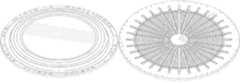
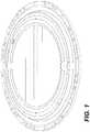
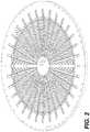
The dashed lines inFIGS. 1-9 represent unclaimed environment and form no part of the claimed design.
Claims (1)
- The ornamental design for a target profile for a physical vapor deposition chamber target, as shown and described.
Priority Applications (1)
| Application Number | Priority Date | Filing Date | Title |
|---|---|---|---|
| US29/726,094USD902165S1 (en) | 2018-03-09 | 2020-02-28 | Target profile for a physical vapor deposition chamber target |
Applications Claiming Priority (2)
| Application Number | Priority Date | Filing Date | Title |
|---|---|---|---|
| US29/639,953USD877101S1 (en) | 2018-03-09 | 2018-03-09 | Target profile for a physical vapor deposition chamber target |
| US29/726,094USD902165S1 (en) | 2018-03-09 | 2020-02-28 | Target profile for a physical vapor deposition chamber target |
Related Parent Applications (1)
| Application Number | Title | Priority Date | Filing Date |
|---|---|---|---|
| US29/639,953DivisionUSD877101S1 (en) | 2018-03-09 | 2018-03-09 | Target profile for a physical vapor deposition chamber target |
Publications (1)
| Publication Number | Publication Date |
|---|---|
| USD902165S1true USD902165S1 (en) | 2020-11-17 |
Family
ID=67769548
Family Applications (2)
| Application Number | Title | Priority Date | Filing Date |
|---|---|---|---|
| US29/639,953ActiveUSD877101S1 (en) | 2018-03-09 | 2018-03-09 | Target profile for a physical vapor deposition chamber target |
| US29/726,094ActiveUSD902165S1 (en) | 2018-03-09 | 2020-02-28 | Target profile for a physical vapor deposition chamber target |
Family Applications Before (1)
| Application Number | Title | Priority Date | Filing Date |
|---|---|---|---|
| US29/639,953ActiveUSD877101S1 (en) | 2018-03-09 | 2018-03-09 | Target profile for a physical vapor deposition chamber target |
Country Status (3)
| Country | Link |
|---|---|
| US (2) | USD877101S1 (en) |
| JP (2) | JP1651699S (en) |
| TW (2) | TWD203691S (en) |
Cited By (13)
| Publication number | Priority date | Publication date | Assignee | Title |
|---|---|---|---|---|
| USD933725S1 (en)* | 2019-02-08 | 2021-10-19 | Applied Materials, Inc. | Deposition ring for a substrate processing chamber |
| USD933726S1 (en)* | 2020-07-31 | 2021-10-19 | Applied Materials, Inc. | Deposition ring for a semiconductor processing chamber |
| USD937329S1 (en) | 2020-03-23 | 2021-11-30 | Applied Materials, Inc. | Sputter target for a physical vapor deposition chamber |
| USD940765S1 (en) | 2020-12-02 | 2022-01-11 | Applied Materials, Inc. | Target profile for a physical vapor deposition chamber target |
| USD946638S1 (en) | 2017-12-11 | 2022-03-22 | Applied Materials, Inc. | Target profile for a physical vapor deposition chamber target |
| US11581166B2 (en) | 2020-07-31 | 2023-02-14 | Applied Materials, Inc. | Low profile deposition ring for enhanced life |
| USD1007449S1 (en) | 2021-05-07 | 2023-12-12 | Applied Materials, Inc. | Target profile for a physical vapor deposition chamber target |
| USD1012051S1 (en)* | 2019-06-17 | 2024-01-23 | Tokyo Electron Limited | Electrostatic chuck for semiconductor manufacturing device |
| USD1012873S1 (en)* | 2020-09-24 | 2024-01-30 | Asm Ip Holding B.V. | Electrode for semiconductor processing apparatus |
| USD1053230S1 (en) | 2022-05-19 | 2024-12-03 | Applied Materials, Inc. | Sputter target for a physical vapor deposition chamber |
| USD1071103S1 (en)* | 2022-04-11 | 2025-04-15 | Applied Materials, Inc. | Gas distribution plate |
| USD1072774S1 (en)* | 2021-02-06 | 2025-04-29 | Applied Materials, Inc. | Target profile for a physical vapor deposition chamber target |
| USD1085029S1 (en)* | 2022-07-19 | 2025-07-22 | Applied Materials, Inc. | Gas distribution plate |
Families Citing this family (13)
| Publication number | Priority date | Publication date | Assignee | Title |
|---|---|---|---|---|
| USD851613S1 (en)* | 2017-10-05 | 2019-06-18 | Applied Materials, Inc. | Target profile for a physical vapor deposition chamber target |
| US10746511B2 (en) | 2017-11-06 | 2020-08-18 | JMA Outdoors, Inc. | Apparatus for generating a vitals target |
| USD877101S1 (en) | 2018-03-09 | 2020-03-03 | Applied Materials, Inc. | Target profile for a physical vapor deposition chamber target |
| USD917003S1 (en)* | 2018-06-06 | 2021-04-20 | JMA Outdoors, Inc. | Simulating target |
| JP1646505S (en)* | 2018-12-07 | 2019-11-25 | ||
| US12125728B2 (en) | 2019-01-21 | 2024-10-22 | Applied Materials, Inc. | Substrate carrier |
| USD904640S1 (en)* | 2019-01-21 | 2020-12-08 | Applied Materials, Inc. | Substrate carrier |
| USD942516S1 (en)* | 2019-02-08 | 2022-02-01 | Applied Materials, Inc. | Process shield for a substrate processing chamber |
| USD908645S1 (en)* | 2019-08-26 | 2021-01-26 | Applied Materials, Inc. | Sputtering target for a physical vapor deposition chamber |
| USD941371S1 (en)* | 2020-03-20 | 2022-01-18 | Applied Materials, Inc. | Process shield for a substrate processing chamber |
| USD941372S1 (en)* | 2020-03-20 | 2022-01-18 | Applied Materials, Inc. | Process shield for a substrate processing chamber |
| JP1700776S (en)* | 2021-03-04 | 2021-11-29 | Substrate placement plate for substrate processing apparatus | |
| USD1037778S1 (en) | 2022-07-19 | 2024-08-06 | Applied Materials, Inc. | Gas distribution plate |
Citations (98)
| Publication number | Priority date | Publication date | Assignee | Title |
|---|---|---|---|---|
| US5320728A (en) | 1990-03-30 | 1994-06-14 | Applied Materials, Inc. | Planar magnetron sputtering source producing improved coating thickness uniformity, step coverage and step coverage uniformity |
| USD351450S (en) | 1993-05-19 | 1994-10-11 | Riteflite Pty. Limited | Target for shooting |
| USD363464S (en) | 1992-08-27 | 1995-10-24 | Tokyo Electron Yamanashi Limited | Electrode for a semiconductor processing apparatus |
| USD376744S (en)* | 1994-08-03 | 1996-12-24 | Gerd Eisenblatter Gmbh | Support plate |
| USD381030S (en) | 1995-11-21 | 1997-07-15 | Avi Tepman | Sputtering target |
| USD411516S (en) | 1996-03-15 | 1999-06-29 | Tokyo Electron Limited | Gas diffusion plate for electrode of semiconductor wafer processing apparatus |
| USD423026S (en) | 1997-08-20 | 2000-04-18 | Tokyo Electron Limited | Quartz cover |
| US6086725A (en) | 1998-04-02 | 2000-07-11 | Applied Materials, Inc. | Target for use in magnetron sputtering of nickel for forming metallization films having consistent uniformity through life |
| US6114216A (en) | 1996-11-13 | 2000-09-05 | Applied Materials, Inc. | Methods for shallow trench isolation |
| USD446231S1 (en) | 2000-08-21 | 2001-08-07 | Komatsu Industries Corporation | Nozzle for a plasma arc torch |
| US6390905B1 (en) | 2000-03-31 | 2002-05-21 | Speedfam-Ipec Corporation | Workpiece carrier with adjustable pressure zones and barriers |
| USD487254S1 (en) | 2002-05-24 | 2004-03-02 | Nichia Corporation | Light emitting diode |
| US20040149567A1 (en) | 2002-12-16 | 2004-08-05 | Alexander Kosyachkov | Composite sputter target and phosphor deposition method |
| USD496951S1 (en) | 2003-01-30 | 2004-10-05 | Thermal Dynamics Corporation | Mechanized cap for a plasma arc torch |
| US6815352B1 (en) | 1999-11-09 | 2004-11-09 | Shin-Etsu Chemical Co., Ltd. | Silicon focus ring and method for producing the same |
| USD503729S1 (en) | 2003-10-31 | 2005-04-05 | Nordson Corporation | Nozzle for dispensing adhesives and sealants |
| US20050152089A1 (en) | 2003-12-26 | 2005-07-14 | Ngk Insulators, Ltd. | Electrostatic chuck and manufacturing method for the same, and alumina sintered member and manufacturing method for the same |
| US20050193952A1 (en) | 2004-02-13 | 2005-09-08 | Goodman Matt G. | Substrate support system for reduced autodoping and backside deposition |
| US20070076345A1 (en) | 2005-09-20 | 2007-04-05 | Bang Won B | Substrate placement determination using substrate backside pressure measurement |
| USD553104S1 (en) | 2004-04-21 | 2007-10-16 | Tokyo Electron Limited | Absorption board for an electric chuck used in semiconductor manufacture |
| USD557226S1 (en) | 2005-08-25 | 2007-12-11 | Hitachi High-Technologies Corporation | Electrode cover for a plasma processing apparatus |
| USD559066S1 (en)* | 2004-10-26 | 2008-01-08 | Jsr Corporation | Polishing pad |
| USD559994S1 (en) | 2005-03-30 | 2008-01-15 | Tokyo Electron Limited | Cover ring |
| USD559993S1 (en) | 2005-03-30 | 2008-01-15 | Tokyo Electron Limited | Cover ring |
| USD562856S1 (en) | 2006-03-30 | 2008-02-26 | Dave Hawley | Plasma gun anode |
| USD570310S1 (en) | 2006-08-01 | 2008-06-03 | Tokyo Electron Limited | Attracting plate of an electrostatic chuck for semiconductor manufacturing |
| USD571383S1 (en) | 2005-07-29 | 2008-06-17 | Tokyo Electron Limited | Top panel for microwave introduction window of a plasma processing apparatus |
| USD571831S1 (en) | 2005-07-29 | 2008-06-24 | Tokyo Electron Limited | Top panel for microwave introduction window of a plasma processing apparatus |
| USD571833S1 (en) | 2005-07-29 | 2008-06-24 | Tokyo Electron Limited | Top panel for microwave introduction window of plasma processing apparatus |
| USD572733S1 (en) | 2005-07-29 | 2008-07-08 | Tokyo Electron Limited | Top panel for microwave introduction window of a plasma processing apparatus |
| US7402098B2 (en)* | 2006-10-27 | 2008-07-22 | Novellus Systems, Inc. | Carrier head for workpiece planarization/polishing |
| US20080173541A1 (en) | 2007-01-22 | 2008-07-24 | Eal Lee | Target designs and related methods for reduced eddy currents, increased resistance and resistivity, and enhanced cooling |
| USD582949S1 (en) | 2006-12-15 | 2008-12-16 | Tokyo Electron Limited | Cover for a heater stage of a plasma processing apparatus |
| US20080308416A1 (en) | 2007-06-18 | 2008-12-18 | Applied Materials, Inc. | Sputtering target having increased life and sputtering uniformity |
| USD600660S1 (en) | 2008-03-28 | 2009-09-22 | Tokyo Electron Limited | Heat radiation fin of heat insulating cylinder for manufacturing semiconductor wafers |
| US20090260982A1 (en) | 2008-04-16 | 2009-10-22 | Applied Materials, Inc. | Wafer processing deposition shielding components |
| US20100096261A1 (en) | 2008-10-17 | 2010-04-22 | Applied Materials, Inc. | Physical vapor deposition reactor with circularly symmetric rf feed and dc feed to the sputter target |
| USD614593S1 (en) | 2008-07-21 | 2010-04-27 | Asm Genitech Korea Ltd | Substrate support for a semiconductor deposition apparatus |
| US20100108500A1 (en) | 2008-10-31 | 2010-05-06 | Applied Materials, Inc. | Encapsulated sputtering target |
| USD616390S1 (en) | 2009-03-06 | 2010-05-25 | Tokyo Electron Limited | Quartz cover for manufacturing semiconductor wafers |
| USD616389S1 (en)* | 2008-10-20 | 2010-05-25 | Ebara Corporation | Vacuum contact pad |
| US20100170786A1 (en) | 2009-01-07 | 2010-07-08 | Solar Applied Materials Technology Corp. | Refurbished sputtering target and method for making the same |
| USD633452S1 (en) | 2009-08-27 | 2011-03-01 | Ebara Corporation | Elastic membrane for semiconductor wafer polishing apparatus |
| USD649126S1 (en) | 2008-10-20 | 2011-11-22 | Ebara Corporation | Vacuum contact pad |
| US20120033340A1 (en) | 2010-08-06 | 2012-02-09 | Applied Materials, Inc. | Electrostatic chuck and methods of use thereof |
| TWD146490S (en) | 2011-01-12 | 2012-04-21 | 荏原製作所股份有限公司 | Elastic film for semiconductor wafer polishing |
| USD669509S1 (en) | 2011-10-19 | 2012-10-23 | Kjellberg Stiftung, rechtsfahige Stiftung des burge rlichen Rechts | Nozzle for torch |
| US8371904B2 (en)* | 2008-08-08 | 2013-02-12 | Globalfoundries Singapore Pte. Ltd. | Polishing with enhanced uniformity |
| US8398833B2 (en) | 2008-04-21 | 2013-03-19 | Honeywell International Inc. | Use of DC magnetron sputtering systems |
| USD678745S1 (en)* | 2011-07-07 | 2013-03-26 | Phuong Van Nguyen | Spinning insert polishing pad |
| USD683806S1 (en) | 2012-01-12 | 2013-06-04 | Surefire, Llc | Front plate for a firearm sound suppressor |
| USD687791S1 (en) | 2012-03-20 | 2013-08-13 | Veeco Instruments Inc. | Multi-keyed wafer carrier |
| USD687790S1 (en) | 2012-03-20 | 2013-08-13 | Veeco Instruments Inc. | Keyed wafer carrier |
| USD691974S1 (en) | 2011-12-22 | 2013-10-22 | Tokyo Electron Limited | Holding pad for transferring a wafer |
| US20130316628A1 (en) | 2012-05-23 | 2013-11-28 | Samsung Electronics Co., Ltd. | Flexible membranes for a polishing head |
| USD694790S1 (en) | 2011-09-20 | 2013-12-03 | Tokyo Electron Limited | Baffle plate for manufacturing semiconductor |
| USD703162S1 (en)* | 2012-10-17 | 2014-04-22 | Sumitomo Electric Industries, Ltd. | Wafer holder for stepper |
| US20140261180A1 (en) | 2013-03-15 | 2014-09-18 | Applied Materials, Inc. | Pvd target for self-centering process shield |
| USD716742S1 (en) | 2013-09-13 | 2014-11-04 | Asm Ip Holding B.V. | Substrate supporter for semiconductor deposition apparatus |
| USD724553S1 (en) | 2013-09-13 | 2015-03-17 | Asm Ip Holding B.V. | Substrate supporter for semiconductor deposition apparatus |
| USD732145S1 (en) | 2014-02-04 | 2015-06-16 | Asm Ip Holding B.V. | Shower plate |
| USD732094S1 (en) | 2012-07-20 | 2015-06-16 | Ivoclar Vivadent Ag | Firing plate for a dental furnace |
| US20150170888A1 (en) | 2013-12-18 | 2015-06-18 | Applied Materials, Inc. | Physical vapor deposition (pvd) target having low friction pads |
| USD733843S1 (en) | 2014-02-04 | 2015-07-07 | ASM IP Holding, B.V. | Shower plate |
| USD741921S1 (en)* | 2014-04-15 | 2015-10-27 | Q-Linea Ab | Positive mold for manufacturing a sample holding disc |
| USD741823S1 (en) | 2013-07-10 | 2015-10-27 | Hitachi Kokusai Electric Inc. | Vaporizer for substrate processing apparatus |
| US20150357169A1 (en) | 2013-01-04 | 2015-12-10 | Tosoh Smd, Inc. | Silicon sputtering target with enhanced surface profile and improved performance and methods of making the same |
| US20160002776A1 (en) | 2013-02-21 | 2016-01-07 | Altatech Semiconductor | Chemical vapor deposition device |
| US20160002788A1 (en) | 2013-02-21 | 2016-01-07 | Altatech Semiconductor | Chemical vapour deposition device |
| US20160035547A1 (en) | 2014-07-29 | 2016-02-04 | Applied Materials, Inc. | Magnetron assembly for physical vapor deposition chamber |
| USD750728S1 (en) | 2014-12-02 | 2016-03-01 | John K. Kremer | Laser target |
| USD767234S1 (en) | 2015-03-02 | 2016-09-20 | Entegris, Inc. | Wafer support ring |
| USD769200S1 (en) | 2013-05-15 | 2016-10-18 | Ebara Corporation | Elastic membrane for semiconductor wafer polishing apparatus |
| US9475996B2 (en) | 2012-10-17 | 2016-10-25 | Richard Max Mandle | Centrifugal fluid ring plasma reactor |
| USD770992S1 (en) | 2015-06-12 | 2016-11-08 | Hitachi High-Technologies Corporation | Electrode cover for a plasma processing apparatus |
| USD789888S1 (en)* | 2016-01-08 | 2017-06-20 | Asm Ip Holding B.V. | Electrode plate for semiconductor manufacturing apparatus |
| USD790041S1 (en) | 2016-01-08 | 2017-06-20 | Asm Ip Holding B.V. | Gas dispersing plate for semiconductor manufacturing apparatus |
| USD793572S1 (en) | 2015-06-10 | 2017-08-01 | Tokyo Electron Limited | Electrode plate for plasma processing apparatus |
| USD795208S1 (en) | 2015-08-18 | 2017-08-22 | Tokyo Electron Limited | Electrostatic chuck for semiconductor manufacturing equipment |
| USD796458S1 (en) | 2016-01-08 | 2017-09-05 | Asm Ip Holding B.V. | Gas flow control plate for semiconductor manufacturing apparatus |
| USD797067S1 (en) | 2015-04-21 | 2017-09-12 | Applied Materials, Inc. | Target profile for a physical vapor deposition chamber target |
| USD797691S1 (en) | 2016-04-14 | 2017-09-19 | Applied Materials, Inc. | Composite edge ring |
| USD798248S1 (en) | 2015-06-18 | 2017-09-26 | Applied Materials, Inc. | Target profile for a physical vapor deposition chamber target |
| CN206573738U (en) | 2017-03-16 | 2017-10-20 | 江苏亨通光导新材料有限公司 | Low loss fiber |
| USD801942S1 (en) | 2015-04-16 | 2017-11-07 | Applied Materials, Inc. | Target profile for a physical vapor deposition chamber target |
| USD808349S1 (en) | 2013-05-15 | 2018-01-23 | Ebara Corporation | Elastic membrane for semiconductor wafer polishing apparatus |
| USD810705S1 (en) | 2016-04-01 | 2018-02-20 | Veeco Instruments Inc. | Self-centering wafer carrier for chemical vapor deposition |
| USD813181S1 (en) | 2016-07-26 | 2018-03-20 | Hitachi Kokusai Electric Inc. | Cover of seal cap for reaction chamber of semiconductor |
| USD830435S1 (en) | 2015-12-28 | 2018-10-09 | Ntn Corporation | Inner ring for tapered roller bearing |
| USD830981S1 (en) | 2017-04-07 | 2018-10-16 | Asm Ip Holding B.V. | Susceptor for semiconductor substrate processing apparatus |
| USD836572S1 (en) | 2016-09-30 | 2018-12-25 | Applied Materials, Inc. | Target profile for a physical vapor deposition chamber target |
| USD839224S1 (en) | 2016-12-12 | 2019-01-29 | Ebara Corporation | Elastic membrane for semiconductor wafer polishing |
| USD846514S1 (en) | 2018-05-03 | 2019-04-23 | Kokusai Electric Corporation | Boat of substrate processing apparatus |
| USD851613S1 (en) | 2017-10-05 | 2019-06-18 | Applied Materials, Inc. | Target profile for a physical vapor deposition chamber target |
| USD860747S1 (en)* | 2017-10-16 | 2019-09-24 | William P. Russo | Tapered segment diamond blade |
| US10442056B2 (en)* | 2012-06-29 | 2019-10-15 | Ebara Corporation | Substrate holding apparatus and polishing apparatus |
| USD868124S1 (en) | 2017-12-11 | 2019-11-26 | Applied Materials, Inc. | Target profile for a physical vapor deposition chamber target |
| USD877101S1 (en) | 2018-03-09 | 2020-03-03 | Applied Materials, Inc. | Target profile for a physical vapor deposition chamber target |
- 2018
- 2018-03-09USUS29/639,953patent/USD877101S1/enactiveActive
- 2018-09-07JPJPD2019-5062Fpatent/JP1651699S/jaactiveActive
- 2018-09-07JPJPD2018-19579Fpatent/JP1640252S/jaactiveActive
- 2018-09-10TWTW108303594Fpatent/TWD203691S/enunknown
- 2018-09-10TWTW107305358Fpatent/TWD202101S/enunknown
- 2020
- 2020-02-28USUS29/726,094patent/USD902165S1/enactiveActive
Patent Citations (107)
| Publication number | Priority date | Publication date | Assignee | Title |
|---|---|---|---|---|
| US5320728A (en) | 1990-03-30 | 1994-06-14 | Applied Materials, Inc. | Planar magnetron sputtering source producing improved coating thickness uniformity, step coverage and step coverage uniformity |
| USD363464S (en) | 1992-08-27 | 1995-10-24 | Tokyo Electron Yamanashi Limited | Electrode for a semiconductor processing apparatus |
| USD351450S (en) | 1993-05-19 | 1994-10-11 | Riteflite Pty. Limited | Target for shooting |
| USD376744S (en)* | 1994-08-03 | 1996-12-24 | Gerd Eisenblatter Gmbh | Support plate |
| USD381030S (en) | 1995-11-21 | 1997-07-15 | Avi Tepman | Sputtering target |
| USD411516S (en) | 1996-03-15 | 1999-06-29 | Tokyo Electron Limited | Gas diffusion plate for electrode of semiconductor wafer processing apparatus |
| US6114216A (en) | 1996-11-13 | 2000-09-05 | Applied Materials, Inc. | Methods for shallow trench isolation |
| USD423026S (en) | 1997-08-20 | 2000-04-18 | Tokyo Electron Limited | Quartz cover |
| US6086725A (en) | 1998-04-02 | 2000-07-11 | Applied Materials, Inc. | Target for use in magnetron sputtering of nickel for forming metallization films having consistent uniformity through life |
| US6815352B1 (en) | 1999-11-09 | 2004-11-09 | Shin-Etsu Chemical Co., Ltd. | Silicon focus ring and method for producing the same |
| US6390905B1 (en) | 2000-03-31 | 2002-05-21 | Speedfam-Ipec Corporation | Workpiece carrier with adjustable pressure zones and barriers |
| US6659850B2 (en) | 2000-03-31 | 2003-12-09 | Speedfam-Ipec Corporation | Work piece carrier with adjustable pressure zones and barriers and a method of planarizing a work piece |
| USD446231S1 (en) | 2000-08-21 | 2001-08-07 | Komatsu Industries Corporation | Nozzle for a plasma arc torch |
| USD487254S1 (en) | 2002-05-24 | 2004-03-02 | Nichia Corporation | Light emitting diode |
| US20040149567A1 (en) | 2002-12-16 | 2004-08-05 | Alexander Kosyachkov | Composite sputter target and phosphor deposition method |
| USD496951S1 (en) | 2003-01-30 | 2004-10-05 | Thermal Dynamics Corporation | Mechanized cap for a plasma arc torch |
| USD503729S1 (en) | 2003-10-31 | 2005-04-05 | Nordson Corporation | Nozzle for dispensing adhesives and sealants |
| US20050152089A1 (en) | 2003-12-26 | 2005-07-14 | Ngk Insulators, Ltd. | Electrostatic chuck and manufacturing method for the same, and alumina sintered member and manufacturing method for the same |
| US20050193952A1 (en) | 2004-02-13 | 2005-09-08 | Goodman Matt G. | Substrate support system for reduced autodoping and backside deposition |
| USD553104S1 (en) | 2004-04-21 | 2007-10-16 | Tokyo Electron Limited | Absorption board for an electric chuck used in semiconductor manufacture |
| USD584591S1 (en)* | 2004-10-26 | 2009-01-13 | Jsr Corporation | Polishing pad |
| USD600989S1 (en)* | 2004-10-26 | 2009-09-29 | Jsr Corporation | Polishing pad |
| USD559066S1 (en)* | 2004-10-26 | 2008-01-08 | Jsr Corporation | Polishing pad |
| USD592029S1 (en)* | 2004-10-26 | 2009-05-12 | Jsr Corporation | Polishing pad |
| USD592030S1 (en)* | 2004-10-26 | 2009-05-12 | Jsr Corporation | Polishing pad |
| USD559994S1 (en) | 2005-03-30 | 2008-01-15 | Tokyo Electron Limited | Cover ring |
| USD559993S1 (en) | 2005-03-30 | 2008-01-15 | Tokyo Electron Limited | Cover ring |
| USD572733S1 (en) | 2005-07-29 | 2008-07-08 | Tokyo Electron Limited | Top panel for microwave introduction window of a plasma processing apparatus |
| USD571383S1 (en) | 2005-07-29 | 2008-06-17 | Tokyo Electron Limited | Top panel for microwave introduction window of a plasma processing apparatus |
| USD571833S1 (en) | 2005-07-29 | 2008-06-24 | Tokyo Electron Limited | Top panel for microwave introduction window of plasma processing apparatus |
| USD571831S1 (en) | 2005-07-29 | 2008-06-24 | Tokyo Electron Limited | Top panel for microwave introduction window of a plasma processing apparatus |
| USD557226S1 (en) | 2005-08-25 | 2007-12-11 | Hitachi High-Technologies Corporation | Electrode cover for a plasma processing apparatus |
| US20070076345A1 (en) | 2005-09-20 | 2007-04-05 | Bang Won B | Substrate placement determination using substrate backside pressure measurement |
| USD562856S1 (en) | 2006-03-30 | 2008-02-26 | Dave Hawley | Plasma gun anode |
| USD570310S1 (en) | 2006-08-01 | 2008-06-03 | Tokyo Electron Limited | Attracting plate of an electrostatic chuck for semiconductor manufacturing |
| US7402098B2 (en)* | 2006-10-27 | 2008-07-22 | Novellus Systems, Inc. | Carrier head for workpiece planarization/polishing |
| USD582949S1 (en) | 2006-12-15 | 2008-12-16 | Tokyo Electron Limited | Cover for a heater stage of a plasma processing apparatus |
| US20080173541A1 (en) | 2007-01-22 | 2008-07-24 | Eal Lee | Target designs and related methods for reduced eddy currents, increased resistance and resistivity, and enhanced cooling |
| US20080308416A1 (en) | 2007-06-18 | 2008-12-18 | Applied Materials, Inc. | Sputtering target having increased life and sputtering uniformity |
| USD600660S1 (en) | 2008-03-28 | 2009-09-22 | Tokyo Electron Limited | Heat radiation fin of heat insulating cylinder for manufacturing semiconductor wafers |
| US20090260982A1 (en) | 2008-04-16 | 2009-10-22 | Applied Materials, Inc. | Wafer processing deposition shielding components |
| US8398833B2 (en) | 2008-04-21 | 2013-03-19 | Honeywell International Inc. | Use of DC magnetron sputtering systems |
| USD614593S1 (en) | 2008-07-21 | 2010-04-27 | Asm Genitech Korea Ltd | Substrate support for a semiconductor deposition apparatus |
| US8371904B2 (en)* | 2008-08-08 | 2013-02-12 | Globalfoundries Singapore Pte. Ltd. | Polishing with enhanced uniformity |
| US20100096261A1 (en) | 2008-10-17 | 2010-04-22 | Applied Materials, Inc. | Physical vapor deposition reactor with circularly symmetric rf feed and dc feed to the sputter target |
| USD616389S1 (en)* | 2008-10-20 | 2010-05-25 | Ebara Corporation | Vacuum contact pad |
| USD649126S1 (en) | 2008-10-20 | 2011-11-22 | Ebara Corporation | Vacuum contact pad |
| US20100108500A1 (en) | 2008-10-31 | 2010-05-06 | Applied Materials, Inc. | Encapsulated sputtering target |
| US20100170786A1 (en) | 2009-01-07 | 2010-07-08 | Solar Applied Materials Technology Corp. | Refurbished sputtering target and method for making the same |
| USD616390S1 (en) | 2009-03-06 | 2010-05-25 | Tokyo Electron Limited | Quartz cover for manufacturing semiconductor wafers |
| USD633452S1 (en) | 2009-08-27 | 2011-03-01 | Ebara Corporation | Elastic membrane for semiconductor wafer polishing apparatus |
| US20120033340A1 (en) | 2010-08-06 | 2012-02-09 | Applied Materials, Inc. | Electrostatic chuck and methods of use thereof |
| TWD146490S (en) | 2011-01-12 | 2012-04-21 | 荏原製作所股份有限公司 | Elastic film for semiconductor wafer polishing |
| USD678745S1 (en)* | 2011-07-07 | 2013-03-26 | Phuong Van Nguyen | Spinning insert polishing pad |
| USD694790S1 (en) | 2011-09-20 | 2013-12-03 | Tokyo Electron Limited | Baffle plate for manufacturing semiconductor |
| USD669509S1 (en) | 2011-10-19 | 2012-10-23 | Kjellberg Stiftung, rechtsfahige Stiftung des burge rlichen Rechts | Nozzle for torch |
| USD691974S1 (en) | 2011-12-22 | 2013-10-22 | Tokyo Electron Limited | Holding pad for transferring a wafer |
| USD683806S1 (en) | 2012-01-12 | 2013-06-04 | Surefire, Llc | Front plate for a firearm sound suppressor |
| USD687791S1 (en) | 2012-03-20 | 2013-08-13 | Veeco Instruments Inc. | Multi-keyed wafer carrier |
| USD687790S1 (en) | 2012-03-20 | 2013-08-13 | Veeco Instruments Inc. | Keyed wafer carrier |
| US20130316628A1 (en) | 2012-05-23 | 2013-11-28 | Samsung Electronics Co., Ltd. | Flexible membranes for a polishing head |
| US10442056B2 (en)* | 2012-06-29 | 2019-10-15 | Ebara Corporation | Substrate holding apparatus and polishing apparatus |
| USD732094S1 (en) | 2012-07-20 | 2015-06-16 | Ivoclar Vivadent Ag | Firing plate for a dental furnace |
| USD703162S1 (en)* | 2012-10-17 | 2014-04-22 | Sumitomo Electric Industries, Ltd. | Wafer holder for stepper |
| US9475996B2 (en) | 2012-10-17 | 2016-10-25 | Richard Max Mandle | Centrifugal fluid ring plasma reactor |
| US20150357169A1 (en) | 2013-01-04 | 2015-12-10 | Tosoh Smd, Inc. | Silicon sputtering target with enhanced surface profile and improved performance and methods of making the same |
| US20160002788A1 (en) | 2013-02-21 | 2016-01-07 | Altatech Semiconductor | Chemical vapour deposition device |
| US20160002776A1 (en) | 2013-02-21 | 2016-01-07 | Altatech Semiconductor | Chemical vapor deposition device |
| US20140261180A1 (en) | 2013-03-15 | 2014-09-18 | Applied Materials, Inc. | Pvd target for self-centering process shield |
| USD769200S1 (en) | 2013-05-15 | 2016-10-18 | Ebara Corporation | Elastic membrane for semiconductor wafer polishing apparatus |
| USD808349S1 (en) | 2013-05-15 | 2018-01-23 | Ebara Corporation | Elastic membrane for semiconductor wafer polishing apparatus |
| USD741823S1 (en) | 2013-07-10 | 2015-10-27 | Hitachi Kokusai Electric Inc. | Vaporizer for substrate processing apparatus |
| USD724553S1 (en) | 2013-09-13 | 2015-03-17 | Asm Ip Holding B.V. | Substrate supporter for semiconductor deposition apparatus |
| USD716742S1 (en) | 2013-09-13 | 2014-11-04 | Asm Ip Holding B.V. | Substrate supporter for semiconductor deposition apparatus |
| US20150170888A1 (en) | 2013-12-18 | 2015-06-18 | Applied Materials, Inc. | Physical vapor deposition (pvd) target having low friction pads |
| USD733843S1 (en) | 2014-02-04 | 2015-07-07 | ASM IP Holding, B.V. | Shower plate |
| USD732145S1 (en) | 2014-02-04 | 2015-06-16 | Asm Ip Holding B.V. | Shower plate |
| USD741921S1 (en)* | 2014-04-15 | 2015-10-27 | Q-Linea Ab | Positive mold for manufacturing a sample holding disc |
| US20160035547A1 (en) | 2014-07-29 | 2016-02-04 | Applied Materials, Inc. | Magnetron assembly for physical vapor deposition chamber |
| USD750728S1 (en) | 2014-12-02 | 2016-03-01 | John K. Kremer | Laser target |
| USD767234S1 (en) | 2015-03-02 | 2016-09-20 | Entegris, Inc. | Wafer support ring |
| USD801942S1 (en) | 2015-04-16 | 2017-11-07 | Applied Materials, Inc. | Target profile for a physical vapor deposition chamber target |
| USD837755S1 (en) | 2015-04-16 | 2019-01-08 | Applied Materials, Inc. | Target profile for a physical vapor deposition chamber target |
| USD825504S1 (en) | 2015-04-21 | 2018-08-14 | Applied Materials, Inc. | Target profile for a physical vapor deposition chamber target |
| USD797067S1 (en) | 2015-04-21 | 2017-09-12 | Applied Materials, Inc. | Target profile for a physical vapor deposition chamber target |
| USD793572S1 (en) | 2015-06-10 | 2017-08-01 | Tokyo Electron Limited | Electrode plate for plasma processing apparatus |
| USD770992S1 (en) | 2015-06-12 | 2016-11-08 | Hitachi High-Technologies Corporation | Electrode cover for a plasma processing apparatus |
| USD825505S1 (en) | 2015-06-18 | 2018-08-14 | Applied Materials, Inc. | Target profile for a physical vapor deposition chamber target |
| USD798248S1 (en) | 2015-06-18 | 2017-09-26 | Applied Materials, Inc. | Target profile for a physical vapor deposition chamber target |
| USD795208S1 (en) | 2015-08-18 | 2017-08-22 | Tokyo Electron Limited | Electrostatic chuck for semiconductor manufacturing equipment |
| USD830435S1 (en) | 2015-12-28 | 2018-10-09 | Ntn Corporation | Inner ring for tapered roller bearing |
| USD796458S1 (en) | 2016-01-08 | 2017-09-05 | Asm Ip Holding B.V. | Gas flow control plate for semiconductor manufacturing apparatus |
| USD790041S1 (en) | 2016-01-08 | 2017-06-20 | Asm Ip Holding B.V. | Gas dispersing plate for semiconductor manufacturing apparatus |
| USD789888S1 (en)* | 2016-01-08 | 2017-06-20 | Asm Ip Holding B.V. | Electrode plate for semiconductor manufacturing apparatus |
| USD810705S1 (en) | 2016-04-01 | 2018-02-20 | Veeco Instruments Inc. | Self-centering wafer carrier for chemical vapor deposition |
| USD797691S1 (en) | 2016-04-14 | 2017-09-19 | Applied Materials, Inc. | Composite edge ring |
| USD813181S1 (en) | 2016-07-26 | 2018-03-20 | Hitachi Kokusai Electric Inc. | Cover of seal cap for reaction chamber of semiconductor |
| USD836572S1 (en) | 2016-09-30 | 2018-12-25 | Applied Materials, Inc. | Target profile for a physical vapor deposition chamber target |
| USD869409S1 (en) | 2016-09-30 | 2019-12-10 | Applied Materials, Inc. | Target profile for a physical vapor deposition chamber target |
| USD839224S1 (en) | 2016-12-12 | 2019-01-29 | Ebara Corporation | Elastic membrane for semiconductor wafer polishing |
| CN206573738U (en) | 2017-03-16 | 2017-10-20 | 江苏亨通光导新材料有限公司 | Low loss fiber |
| USD830981S1 (en) | 2017-04-07 | 2018-10-16 | Asm Ip Holding B.V. | Susceptor for semiconductor substrate processing apparatus |
| USD851613S1 (en) | 2017-10-05 | 2019-06-18 | Applied Materials, Inc. | Target profile for a physical vapor deposition chamber target |
| USD860747S1 (en)* | 2017-10-16 | 2019-09-24 | William P. Russo | Tapered segment diamond blade |
| USD868124S1 (en) | 2017-12-11 | 2019-11-26 | Applied Materials, Inc. | Target profile for a physical vapor deposition chamber target |
| USD877101S1 (en) | 2018-03-09 | 2020-03-03 | Applied Materials, Inc. | Target profile for a physical vapor deposition chamber target |
| USD846514S1 (en) | 2018-05-03 | 2019-04-23 | Kokusai Electric Corporation | Boat of substrate processing apparatus |
Non-Patent Citations (6)
| Title |
|---|
| Search Report for Taiwan Design Application No. 106301373 dated Jun. 20, 2017. |
| Search Report for Taiwan Design Application No. 107305358 dated Feb. 21, 2019. |
| Search Report for Taiwan Design Application No. 1077303086 dated Jul. 6, 2018. |
| Sputtering Targets for LSis, posted at JX Nippon Mining & Metals, posting date Mar. 22, 2016. Site visited Apr. 1, 2019. URL: <https://web .archive .org/web/20 160322055046/http :1/www.nmm.jx-group.co.jp/english/products/04_supa/target_adv.html> (Year: 2016). |
| Sputtering Targets, posted at Angstrom Sciences, posting date May 5, 2016. Site visited Apr. 1, 2019. URL: <https://web.archive.org/web/20160505015447/https://www.angstromsciences.com/sputtering-targets> (Year: 2016). |
| U.S. Appl. No. 29/690,617, filed May 9, 2019. |
Cited By (15)
| Publication number | Priority date | Publication date | Assignee | Title |
|---|---|---|---|---|
| USD946638S1 (en) | 2017-12-11 | 2022-03-22 | Applied Materials, Inc. | Target profile for a physical vapor deposition chamber target |
| USD933725S1 (en)* | 2019-02-08 | 2021-10-19 | Applied Materials, Inc. | Deposition ring for a substrate processing chamber |
| USD1012051S1 (en)* | 2019-06-17 | 2024-01-23 | Tokyo Electron Limited | Electrostatic chuck for semiconductor manufacturing device |
| USD970566S1 (en)* | 2020-03-23 | 2022-11-22 | Applied Materials, Inc. | Sputter target for a physical vapor deposition chamber |
| USD937329S1 (en) | 2020-03-23 | 2021-11-30 | Applied Materials, Inc. | Sputter target for a physical vapor deposition chamber |
| US11581166B2 (en) | 2020-07-31 | 2023-02-14 | Applied Materials, Inc. | Low profile deposition ring for enhanced life |
| USD933726S1 (en)* | 2020-07-31 | 2021-10-19 | Applied Materials, Inc. | Deposition ring for a semiconductor processing chamber |
| USD1012873S1 (en)* | 2020-09-24 | 2024-01-30 | Asm Ip Holding B.V. | Electrode for semiconductor processing apparatus |
| USD940765S1 (en) | 2020-12-02 | 2022-01-11 | Applied Materials, Inc. | Target profile for a physical vapor deposition chamber target |
| USD966357S1 (en)* | 2020-12-02 | 2022-10-11 | Applied Materials, Inc. | Target profile for a physical vapor deposition chamber target |
| USD1072774S1 (en)* | 2021-02-06 | 2025-04-29 | Applied Materials, Inc. | Target profile for a physical vapor deposition chamber target |
| USD1007449S1 (en) | 2021-05-07 | 2023-12-12 | Applied Materials, Inc. | Target profile for a physical vapor deposition chamber target |
| USD1071103S1 (en)* | 2022-04-11 | 2025-04-15 | Applied Materials, Inc. | Gas distribution plate |
| USD1053230S1 (en) | 2022-05-19 | 2024-12-03 | Applied Materials, Inc. | Sputter target for a physical vapor deposition chamber |
| USD1085029S1 (en)* | 2022-07-19 | 2025-07-22 | Applied Materials, Inc. | Gas distribution plate |
Also Published As
| Publication number | Publication date |
|---|---|
| USD877101S1 (en) | 2020-03-03 |
| JP1640252S (en) | 2019-09-02 |
| TWD202101S (en) | 2020-01-11 |
| JP1651699S (en) | 2020-01-27 |
| TWD203691S (en) | 2020-04-01 |
Similar Documents
| Publication | Publication Date | Title |
|---|---|---|
| USD902165S1 (en) | Target profile for a physical vapor deposition chamber target | |
| USD946638S1 (en) | Target profile for a physical vapor deposition chamber target | |
| USD851613S1 (en) | Target profile for a physical vapor deposition chamber target | |
| USD869409S1 (en) | Target profile for a physical vapor deposition chamber target | |
| USD1040304S1 (en) | Deposition ring for physical vapor deposition chamber | |
| USD888903S1 (en) | Deposition ring for physical vapor deposition chamber | |
| USD858468S1 (en) | Collimator for a physical vapor deposition chamber | |
| USD797067S1 (en) | Target profile for a physical vapor deposition chamber target | |
| USD837755S1 (en) | Target profile for a physical vapor deposition chamber target | |
| USD825505S1 (en) | Target profile for a physical vapor deposition chamber target | |
| USD859333S1 (en) | Collimator for a physical vapor deposition chamber | |
| USD908645S1 (en) | Sputtering target for a physical vapor deposition chamber | |
| USD1036935S1 (en) | Tumbler | |
| USD903275S1 (en) | Footwear | |
| USD849908S1 (en) | Oven | |
| USD1036199S1 (en) | Tumbler | |
| USD893950S1 (en) | Tumbler | |
| USD853793S1 (en) | Geometric double wall vacuum tumbler | |
| USD899176S1 (en) | Oven | |
| USD914443S1 (en) | Oven door | |
| USD867853S1 (en) | Escutcheon | |
| USD860757S1 (en) | Oven knob | |
| USD881680S1 (en) | Lock escutcheon assembly | |
| USD916409S1 (en) | Silicone scraper | |
| USD847815S1 (en) | Keyboard |
Legal Events
| Date | Code | Title | Description |
|---|---|---|---|
| FEPP | Fee payment procedure | Free format text:ENTITY STATUS SET TO UNDISCOUNTED (ORIGINAL EVENT CODE: BIG.); ENTITY STATUS OF PATENT OWNER: LARGE ENTITY |