USD839224S1 - Elastic membrane for semiconductor wafer polishing - Google Patents
Elastic membrane for semiconductor wafer polishingDownload PDFInfo
- Publication number
- USD839224S1 USD839224S1US29/606,998US201729606998FUSD839224SUS D839224 S1USD839224 S1US D839224S1US 201729606998 FUS201729606998 FUS 201729606998FUS D839224 SUSD839224 SUS D839224S
- Authority
- US
- United States
- Prior art keywords
- semiconductor wafer
- elastic membrane
- wafer polishing
- view
- polishing
- Prior art date
- Legal status (The legal status is an assumption and is not a legal conclusion. Google has not performed a legal analysis and makes no representation as to the accuracy of the status listed.)
- Active
Links
Images


Description
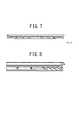
The dash-dot lines inFIG. 7 represent the boundary line of the enlarged portion view shown inFIG. 8 .
Claims (1)
- The ornamental design for an elastic membrane for semiconductor wafer polishing, as shown and described.
Priority Applications (1)
| Application Number | Priority Date | Filing Date | Title |
|---|---|---|---|
| US29/672,852USD913977S1 (en) | 2016-12-12 | 2018-12-10 | Elastic membrane for semiconductor wafer polishing |
Applications Claiming Priority (6)
| Application Number | Priority Date | Filing Date | Title |
|---|---|---|---|
| JP2016-026914 | 2016-02-16 | ||
| JP2016-026915 | 2016-02-16 | ||
| JPD2016-26913FJP1582993S (en) | 2016-12-12 | 2016-12-12 | |
| JPD2016-26915FJP1582995S (en) | 2016-12-12 | 2016-12-12 | |
| JP2016-026913 | 2016-12-12 | ||
| JPD2016-26914FJP1582994S (en) | 2016-12-12 | 2016-12-12 |
Related Child Applications (1)
| Application Number | Title | Priority Date | Filing Date |
|---|---|---|---|
| US29/672,852DivisionUSD913977S1 (en) | 2016-12-12 | 2018-12-10 | Elastic membrane for semiconductor wafer polishing |
Publications (1)
| Publication Number | Publication Date |
|---|---|
| USD839224S1true USD839224S1 (en) | 2019-01-29 |
Family
ID=65032365
Family Applications (2)
| Application Number | Title | Priority Date | Filing Date |
|---|---|---|---|
| US29/606,998ActiveUSD839224S1 (en) | 2016-12-12 | 2017-06-09 | Elastic membrane for semiconductor wafer polishing |
| US29/672,852ActiveUSD913977S1 (en) | 2016-12-12 | 2018-12-10 | Elastic membrane for semiconductor wafer polishing |
Family Applications After (1)
| Application Number | Title | Priority Date | Filing Date |
|---|---|---|---|
| US29/672,852ActiveUSD913977S1 (en) | 2016-12-12 | 2018-12-10 | Elastic membrane for semiconductor wafer polishing |
Country Status (1)
| Country | Link |
|---|---|
| US (2) | USD839224S1 (en) |
Cited By (20)
| Publication number | Priority date | Publication date | Assignee | Title |
|---|---|---|---|---|
| USD859331S1 (en)* | 2017-03-31 | 2019-09-10 | Ebara Corporation | Vacuum contact pad |
| USD859332S1 (en)* | 2017-06-29 | 2019-09-10 | Ebara Corporation | Elastic membrane for semiconductor wafer polishing |
| USD868124S1 (en)* | 2017-12-11 | 2019-11-26 | Applied Materials, Inc. | Target profile for a physical vapor deposition chamber target |
| USD869409S1 (en)* | 2016-09-30 | 2019-12-10 | Applied Materials, Inc. | Target profile for a physical vapor deposition chamber target |
| USD877101S1 (en) | 2018-03-09 | 2020-03-03 | Applied Materials, Inc. | Target profile for a physical vapor deposition chamber target |
| USD894137S1 (en) | 2017-10-05 | 2020-08-25 | Applied Materials, Inc. | Target profile for a physical vapor deposition chamber target |
| USD908645S1 (en) | 2019-08-26 | 2021-01-26 | Applied Materials, Inc. | Sputtering target for a physical vapor deposition chamber |
| USD913230S1 (en)* | 2019-04-24 | 2021-03-16 | Tokyo Electron Limited | Heater for heating semiconductor wafer |
| USD913229S1 (en)* | 2019-04-24 | 2021-03-16 | Tokyo Electron Limited | Heater for heating semiconductor wafer |
| USD913977S1 (en)* | 2016-12-12 | 2021-03-23 | Ebara Corporation | Elastic membrane for semiconductor wafer polishing |
| USD918161S1 (en)* | 2017-12-19 | 2021-05-04 | Ebara Corporation | Elastic membrane |
| USD937329S1 (en) | 2020-03-23 | 2021-11-30 | Applied Materials, Inc. | Sputter target for a physical vapor deposition chamber |
| USD940765S1 (en) | 2020-12-02 | 2022-01-11 | Applied Materials, Inc. | Target profile for a physical vapor deposition chamber target |
| USD954567S1 (en)* | 2019-06-25 | 2022-06-14 | Ebara Corporation | Measurement jig |
| USD981969S1 (en)* | 2020-12-18 | 2023-03-28 | Ebara Corporation | Elastic membrane for semiconductor wafer polishing apparatus |
| USD989012S1 (en)* | 2020-09-17 | 2023-06-13 | Ebara Corporation | Elastic membrane |
| USD1006768S1 (en)* | 2021-01-07 | 2023-12-05 | Solaero Technologies Corp. | Semiconductor wafer for mosaic solar cell fabrication |
| USD1007449S1 (en) | 2021-05-07 | 2023-12-12 | Applied Materials, Inc. | Target profile for a physical vapor deposition chamber target |
| USD1053230S1 (en) | 2022-05-19 | 2024-12-03 | Applied Materials, Inc. | Sputter target for a physical vapor deposition chamber |
| USD1072774S1 (en) | 2021-02-06 | 2025-04-29 | Applied Materials, Inc. | Target profile for a physical vapor deposition chamber target |
Families Citing this family (1)
| Publication number | Priority date | Publication date | Assignee | Title |
|---|---|---|---|---|
| USD1061489S1 (en)* | 2023-01-27 | 2025-02-11 | All.Space Networks Limited | Satellite communication terminal |
Citations (31)
| Publication number | Priority date | Publication date | Assignee | Title |
|---|---|---|---|---|
| USD363464S (en) | 1992-08-27 | 1995-10-24 | Tokyo Electron Yamanashi Limited | Electrode for a semiconductor processing apparatus |
| USD411516S (en) | 1996-03-15 | 1999-06-29 | Tokyo Electron Limited | Gas diffusion plate for electrode of semiconductor wafer processing apparatus |
| US6659850B2 (en)* | 2000-03-31 | 2003-12-09 | Speedfam-Ipec Corporation | Work piece carrier with adjustable pressure zones and barriers and a method of planarizing a work piece |
| USD546784S1 (en) | 2005-09-29 | 2007-07-17 | Tokyo Electron Limited | Attracting disc for an electrostatic chuck for semiconductor production |
| USD553104S1 (en) | 2004-04-21 | 2007-10-16 | Tokyo Electron Limited | Absorption board for an electric chuck used in semiconductor manufacture |
| USD557226S1 (en)* | 2005-08-25 | 2007-12-11 | Hitachi High-Technologies Corporation | Electrode cover for a plasma processing apparatus |
| USD559993S1 (en)* | 2005-03-30 | 2008-01-15 | Tokyo Electron Limited | Cover ring |
| USD559994S1 (en)* | 2005-03-30 | 2008-01-15 | Tokyo Electron Limited | Cover ring |
| US20090247057A1 (en)* | 2005-09-14 | 2009-10-01 | Ebara Corporation | Polishing platen and polishing apparatus |
| USD633452S1 (en)* | 2009-08-27 | 2011-03-01 | Ebara Corporation | Elastic membrane for semiconductor wafer polishing apparatus |
| USD634719S1 (en)* | 2009-08-27 | 2011-03-22 | Ebara Corporation | Elastic membrane for semiconductor wafer polishing apparatus |
| USD649126S1 (en)* | 2008-10-20 | 2011-11-22 | Ebara Corporation | Vacuum contact pad |
| US8469776B2 (en)* | 2006-11-22 | 2013-06-25 | Applied Materials, Inc. | Flexible membrane for carrier head |
| US20130316628A1 (en)* | 2012-05-23 | 2013-11-28 | Samsung Electronics Co., Ltd. | Flexible membranes for a polishing head |
| USD709538S1 (en)* | 2011-09-30 | 2014-07-22 | Tokyo Electron Limited | Focusing ring |
| USD709539S1 (en)* | 2011-09-30 | 2014-07-22 | Tokyo Electron Limited | Focusing ring |
| USD709536S1 (en)* | 2011-09-30 | 2014-07-22 | Tokyo Electron Limited | Focusing ring |
| USD711330S1 (en)* | 2010-12-28 | 2014-08-19 | Ebara Corporation | Elastic membrane for semiconductor wafer polishing |
| US20140262193A1 (en)* | 2013-03-13 | 2014-09-18 | Techest Co., Ltd. | Edge ring cooling module for semi-conductor manufacture chuck |
| US8859070B2 (en)* | 2011-11-30 | 2014-10-14 | Ebara Corporation | Elastic membrane |
| US20160002788A1 (en)* | 2013-02-21 | 2016-01-07 | Altatech Semiconductor | Chemical vapour deposition device |
| US9376752B2 (en)* | 2012-04-06 | 2016-06-28 | Applied Materials, Inc. | Edge ring for a deposition chamber |
| USD767234S1 (en)* | 2015-03-02 | 2016-09-20 | Entegris, Inc. | Wafer support ring |
| USD769200S1 (en) | 2013-05-15 | 2016-10-18 | Ebara Corporation | Elastic membrane for semiconductor wafer polishing apparatus |
| USD770992S1 (en)* | 2015-06-12 | 2016-11-08 | Hitachi High-Technologies Corporation | Electrode cover for a plasma processing apparatus |
| USD770990S1 (en) | 2013-05-15 | 2016-11-08 | Ebara Corporation | Elastic membrane for semiconductor wafer polishing apparatus |
| US20170009367A1 (en)* | 2015-07-09 | 2017-01-12 | Applied Materials, Inc. | Wafer electroplating chuck assembly |
| USD783922S1 (en)* | 2014-12-08 | 2017-04-11 | Entegris, Inc. | Wafer support ring |
| USD797067S1 (en)* | 2015-04-21 | 2017-09-12 | Applied Materials, Inc. | Target profile for a physical vapor deposition chamber target |
| USD808349S1 (en)* | 2013-05-15 | 2018-01-23 | Ebara Corporation | Elastic membrane for semiconductor wafer polishing apparatus |
| USD810705S1 (en)* | 2016-04-01 | 2018-02-20 | Veeco Instruments Inc. | Self-centering wafer carrier for chemical vapor deposition |
Family Cites Families (20)
| Publication number | Priority date | Publication date | Assignee | Title |
|---|---|---|---|---|
| US6183354B1 (en)* | 1996-11-08 | 2001-02-06 | Applied Materials, Inc. | Carrier head with a flexible membrane for a chemical mechanical polishing system |
| US20010029158A1 (en)* | 1998-07-30 | 2001-10-11 | Yoshitaka Sasaki | Polishing apparatus and polishing method, and method of manufacturing semiconductor device and method of manufacturing thin film magnetic head |
| JP3342686B2 (en)* | 1999-12-28 | 2002-11-11 | 信越半導体株式会社 | Wafer polishing method and wafer polishing apparatus |
| EP1177859B1 (en)* | 2000-07-31 | 2009-04-15 | Ebara Corporation | Substrate holding apparatus and substrate polishing apparatus |
| WO2003049168A1 (en)* | 2001-12-06 | 2003-06-12 | Ebara Corporation | Substrate holding device and polishing device |
| TWI289494B (en)* | 2002-01-22 | 2007-11-11 | Multi Planar Technologies Inc | Chemical mechanical polishing apparatus and method having a retaining ring with a contoured surface for slurry distribution |
| TWI375294B (en)* | 2003-02-10 | 2012-10-21 | Ebara Corp | Elastic membrane |
| US7001245B2 (en)* | 2003-03-07 | 2006-02-21 | Applied Materials Inc. | Substrate carrier with a textured membrane |
| US7033252B2 (en)* | 2004-03-05 | 2006-04-25 | Strasbaugh | Wafer carrier with pressurized membrane and retaining ring actuator |
| CN100467210C (en)* | 2004-03-25 | 2009-03-11 | 揖斐电株式会社 | Vacuum Chucks and Suction Plates |
| US8083571B2 (en)* | 2004-11-01 | 2011-12-27 | Ebara Corporation | Polishing apparatus |
| US7402098B2 (en)* | 2006-10-27 | 2008-07-22 | Novellus Systems, Inc. | Carrier head for workpiece planarization/polishing |
| US7699688B2 (en)* | 2006-11-22 | 2010-04-20 | Applied Materials, Inc. | Carrier ring for carrier head |
| KR101358645B1 (en)* | 2007-09-04 | 2014-02-05 | 삼성전자주식회사 | carrier apparatus for polishing wafer and chemical mechanical polishing equipment used the same |
| JP5464820B2 (en)* | 2007-10-29 | 2014-04-09 | 株式会社荏原製作所 | Polishing equipment |
| JP5552401B2 (en)* | 2010-09-08 | 2014-07-16 | 株式会社荏原製作所 | Polishing apparatus and method |
| KR101196652B1 (en)* | 2011-05-31 | 2012-11-02 | 주식회사 케이씨텍 | Membrane assembly in carrier head |
| USD839224S1 (en)* | 2016-12-12 | 2019-01-29 | Ebara Corporation | Elastic membrane for semiconductor wafer polishing |
| USD859331S1 (en)* | 2017-03-31 | 2019-09-10 | Ebara Corporation | Vacuum contact pad |
| USD859332S1 (en)* | 2017-06-29 | 2019-09-10 | Ebara Corporation | Elastic membrane for semiconductor wafer polishing |
- 2017
- 2017-06-09USUS29/606,998patent/USD839224S1/enactiveActive
- 2018
- 2018-12-10USUS29/672,852patent/USD913977S1/enactiveActive
Patent Citations (32)
| Publication number | Priority date | Publication date | Assignee | Title |
|---|---|---|---|---|
| USD363464S (en) | 1992-08-27 | 1995-10-24 | Tokyo Electron Yamanashi Limited | Electrode for a semiconductor processing apparatus |
| USD411516S (en) | 1996-03-15 | 1999-06-29 | Tokyo Electron Limited | Gas diffusion plate for electrode of semiconductor wafer processing apparatus |
| US6659850B2 (en)* | 2000-03-31 | 2003-12-09 | Speedfam-Ipec Corporation | Work piece carrier with adjustable pressure zones and barriers and a method of planarizing a work piece |
| USD553104S1 (en) | 2004-04-21 | 2007-10-16 | Tokyo Electron Limited | Absorption board for an electric chuck used in semiconductor manufacture |
| USD559993S1 (en)* | 2005-03-30 | 2008-01-15 | Tokyo Electron Limited | Cover ring |
| USD559994S1 (en)* | 2005-03-30 | 2008-01-15 | Tokyo Electron Limited | Cover ring |
| USD557226S1 (en)* | 2005-08-25 | 2007-12-11 | Hitachi High-Technologies Corporation | Electrode cover for a plasma processing apparatus |
| US20090247057A1 (en)* | 2005-09-14 | 2009-10-01 | Ebara Corporation | Polishing platen and polishing apparatus |
| USD546784S1 (en) | 2005-09-29 | 2007-07-17 | Tokyo Electron Limited | Attracting disc for an electrostatic chuck for semiconductor production |
| US8469776B2 (en)* | 2006-11-22 | 2013-06-25 | Applied Materials, Inc. | Flexible membrane for carrier head |
| USD649126S1 (en)* | 2008-10-20 | 2011-11-22 | Ebara Corporation | Vacuum contact pad |
| USD633452S1 (en)* | 2009-08-27 | 2011-03-01 | Ebara Corporation | Elastic membrane for semiconductor wafer polishing apparatus |
| USD634719S1 (en)* | 2009-08-27 | 2011-03-22 | Ebara Corporation | Elastic membrane for semiconductor wafer polishing apparatus |
| USD729753S1 (en)* | 2010-12-28 | 2015-05-19 | Ebara Corporation | Elastic membrane for semiconductor wafer polishing |
| USD711330S1 (en)* | 2010-12-28 | 2014-08-19 | Ebara Corporation | Elastic membrane for semiconductor wafer polishing |
| USD709536S1 (en)* | 2011-09-30 | 2014-07-22 | Tokyo Electron Limited | Focusing ring |
| USD709539S1 (en)* | 2011-09-30 | 2014-07-22 | Tokyo Electron Limited | Focusing ring |
| USD709538S1 (en)* | 2011-09-30 | 2014-07-22 | Tokyo Electron Limited | Focusing ring |
| US8859070B2 (en)* | 2011-11-30 | 2014-10-14 | Ebara Corporation | Elastic membrane |
| US9376752B2 (en)* | 2012-04-06 | 2016-06-28 | Applied Materials, Inc. | Edge ring for a deposition chamber |
| US20130316628A1 (en)* | 2012-05-23 | 2013-11-28 | Samsung Electronics Co., Ltd. | Flexible membranes for a polishing head |
| US20160002788A1 (en)* | 2013-02-21 | 2016-01-07 | Altatech Semiconductor | Chemical vapour deposition device |
| US20140262193A1 (en)* | 2013-03-13 | 2014-09-18 | Techest Co., Ltd. | Edge ring cooling module for semi-conductor manufacture chuck |
| USD769200S1 (en) | 2013-05-15 | 2016-10-18 | Ebara Corporation | Elastic membrane for semiconductor wafer polishing apparatus |
| USD770990S1 (en) | 2013-05-15 | 2016-11-08 | Ebara Corporation | Elastic membrane for semiconductor wafer polishing apparatus |
| USD808349S1 (en)* | 2013-05-15 | 2018-01-23 | Ebara Corporation | Elastic membrane for semiconductor wafer polishing apparatus |
| USD783922S1 (en)* | 2014-12-08 | 2017-04-11 | Entegris, Inc. | Wafer support ring |
| USD767234S1 (en)* | 2015-03-02 | 2016-09-20 | Entegris, Inc. | Wafer support ring |
| USD797067S1 (en)* | 2015-04-21 | 2017-09-12 | Applied Materials, Inc. | Target profile for a physical vapor deposition chamber target |
| USD770992S1 (en)* | 2015-06-12 | 2016-11-08 | Hitachi High-Technologies Corporation | Electrode cover for a plasma processing apparatus |
| US20170009367A1 (en)* | 2015-07-09 | 2017-01-12 | Applied Materials, Inc. | Wafer electroplating chuck assembly |
| USD810705S1 (en)* | 2016-04-01 | 2018-02-20 | Veeco Instruments Inc. | Self-centering wafer carrier for chemical vapor deposition |
Cited By (27)
| Publication number | Priority date | Publication date | Assignee | Title |
|---|---|---|---|---|
| USD869409S1 (en)* | 2016-09-30 | 2019-12-10 | Applied Materials, Inc. | Target profile for a physical vapor deposition chamber target |
| USD913977S1 (en)* | 2016-12-12 | 2021-03-23 | Ebara Corporation | Elastic membrane for semiconductor wafer polishing |
| USD859331S1 (en)* | 2017-03-31 | 2019-09-10 | Ebara Corporation | Vacuum contact pad |
| USD859332S1 (en)* | 2017-06-29 | 2019-09-10 | Ebara Corporation | Elastic membrane for semiconductor wafer polishing |
| USD894137S1 (en) | 2017-10-05 | 2020-08-25 | Applied Materials, Inc. | Target profile for a physical vapor deposition chamber target |
| USD868124S1 (en)* | 2017-12-11 | 2019-11-26 | Applied Materials, Inc. | Target profile for a physical vapor deposition chamber target |
| USD946638S1 (en) | 2017-12-11 | 2022-03-22 | Applied Materials, Inc. | Target profile for a physical vapor deposition chamber target |
| USD918161S1 (en)* | 2017-12-19 | 2021-05-04 | Ebara Corporation | Elastic membrane |
| USD877101S1 (en) | 2018-03-09 | 2020-03-03 | Applied Materials, Inc. | Target profile for a physical vapor deposition chamber target |
| USD902165S1 (en) | 2018-03-09 | 2020-11-17 | Applied Materials, Inc. | Target profile for a physical vapor deposition chamber target |
| USD913229S1 (en)* | 2019-04-24 | 2021-03-16 | Tokyo Electron Limited | Heater for heating semiconductor wafer |
| USD913230S1 (en)* | 2019-04-24 | 2021-03-16 | Tokyo Electron Limited | Heater for heating semiconductor wafer |
| USD1035468S1 (en) | 2019-06-25 | 2024-07-16 | Ebara Corporation | Measurement jig |
| USD1034248S1 (en) | 2019-06-25 | 2024-07-09 | Ebara Corporation | Measurement jig |
| USD954567S1 (en)* | 2019-06-25 | 2022-06-14 | Ebara Corporation | Measurement jig |
| USD908645S1 (en) | 2019-08-26 | 2021-01-26 | Applied Materials, Inc. | Sputtering target for a physical vapor deposition chamber |
| USD937329S1 (en) | 2020-03-23 | 2021-11-30 | Applied Materials, Inc. | Sputter target for a physical vapor deposition chamber |
| USD970566S1 (en) | 2020-03-23 | 2022-11-22 | Applied Materials, Inc. | Sputter target for a physical vapor deposition chamber |
| USD989012S1 (en)* | 2020-09-17 | 2023-06-13 | Ebara Corporation | Elastic membrane |
| USD1021832S1 (en)* | 2020-09-17 | 2024-04-09 | Ebara Corporation | Elastic membrane |
| USD966357S1 (en) | 2020-12-02 | 2022-10-11 | Applied Materials, Inc. | Target profile for a physical vapor deposition chamber target |
| USD940765S1 (en) | 2020-12-02 | 2022-01-11 | Applied Materials, Inc. | Target profile for a physical vapor deposition chamber target |
| USD981969S1 (en)* | 2020-12-18 | 2023-03-28 | Ebara Corporation | Elastic membrane for semiconductor wafer polishing apparatus |
| USD1006768S1 (en)* | 2021-01-07 | 2023-12-05 | Solaero Technologies Corp. | Semiconductor wafer for mosaic solar cell fabrication |
| USD1072774S1 (en) | 2021-02-06 | 2025-04-29 | Applied Materials, Inc. | Target profile for a physical vapor deposition chamber target |
| USD1007449S1 (en) | 2021-05-07 | 2023-12-12 | Applied Materials, Inc. | Target profile for a physical vapor deposition chamber target |
| USD1053230S1 (en) | 2022-05-19 | 2024-12-03 | Applied Materials, Inc. | Sputter target for a physical vapor deposition chamber |
Also Published As
| Publication number | Publication date |
|---|---|
| USD913977S1 (en) | 2021-03-23 |
Similar Documents
| Publication | Publication Date | Title |
|---|---|---|
| USD839224S1 (en) | Elastic membrane for semiconductor wafer polishing | |
| USD813180S1 (en) | Elastic membrane for semiconductor wafer polishing apparatus | |
| USD813182S1 (en) | Semiconductor device | |
| USD866892S1 (en) | Scouring pad | |
| USD870114S1 (en) | Adapter | |
| USD852762S1 (en) | Wafer carrier with a 14-pocket configuration | |
| USD773412S1 (en) | Semiconductor device | |
| USD773413S1 (en) | Semiconductor device | |
| USD879724S1 (en) | Contact wafer | |
| USD815385S1 (en) | Wafer support ring | |
| USD823439S1 (en) | Sink faucet | |
| USD808349S1 (en) | Elastic membrane for semiconductor wafer polishing apparatus | |
| USD859332S1 (en) | Elastic membrane for semiconductor wafer polishing | |
| USD758051S1 (en) | Silicone bib | |
| USD815443S1 (en) | Sitting module | |
| USD815379S1 (en) | Vacuum cleaner | |
| USD922545S1 (en) | Seal member for use in semiconductor production apparatus | |
| USD746417S1 (en) | Sink supported cutlery cup | |
| USD932203S1 (en) | Seating arrangement | |
| USD922547S1 (en) | Seal members for use in semiconductor production apparatuses | |
| USD833092S1 (en) | Vacuum cleaner | |
| USD812828S1 (en) | Vacuum cleaner | |
| USD784208S1 (en) | Chair | |
| USD766850S1 (en) | Wafer holder for manufacturing semiconductor | |
| USD811026S1 (en) | Vacuum cleaner |