USD770990S1 - Elastic membrane for semiconductor wafer polishing apparatus - Google Patents
Elastic membrane for semiconductor wafer polishing apparatusDownload PDFInfo
- Publication number
- USD770990S1 USD770990S1US29/489,477US201429489477FUSD770990SUS D770990 S1USD770990 S1US D770990S1US 201429489477 FUS201429489477 FUS 201429489477FUS D770990 SUSD770990 SUS D770990S
- Authority
- US
- United States
- Prior art keywords
- semiconductor wafer
- polishing apparatus
- elastic membrane
- wafer polishing
- view
- Prior art date
- Legal status (The legal status is an assumption and is not a legal conclusion. Google has not performed a legal analysis and makes no representation as to the accuracy of the status listed.)
- Active
Links
- 239000012528membraneSubstances0.000titleclaimsdescription4
- 238000005498polishingMethods0.000titleclaimsdescription4
- 239000004065semiconductorSubstances0.000titleclaimsdescription4
Images


Description
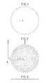
The broken lines shown in the drawings represent portions of the elastic membrane for semiconductor wafer polishing apparatus that form no part of the claimed design. The dashed-dot-dashed lines represent the boundary lines of the claimed design.
All surfaces not shown form no part of the claimed design.
Claims (1)
- The ornamental design for an elastic membrane for semiconductor wafer polishing apparatus, as shown and described.
Priority Applications (1)
| Application Number | Priority Date | Filing Date | Title |
|---|---|---|---|
| US29/489,477USD770990S1 (en) | 2013-05-15 | 2014-04-30 | Elastic membrane for semiconductor wafer polishing apparatus |
Applications Claiming Priority (24)
| Application Number | Priority Date | Filing Date | Title |
|---|---|---|---|
| JP2013-026347 | 2013-02-14 | ||
| JP2013-10674 | 2013-05-15 | ||
| JP2013-10672 | 2013-05-15 | ||
| JPD2013-10675FJP1495082S (en) | 2013-05-15 | 2013-05-15 | |
| JPD2013-10672FJP1494713S (en) | 2013-05-15 | 2013-05-15 | |
| JPD2013-10678FJP1521701S (en) | 2013-05-15 | 2013-05-15 | |
| JP2013-10676 | 2013-05-15 | ||
| JPD2013-10674FJP1495081S (en) | 2013-05-15 | 2013-05-15 | |
| JP2013-10675 | 2013-05-15 | ||
| JPD2013-10673FJP1495738S (en) | 2013-05-15 | 2013-05-15 | |
| JPD2013-10676FJP1495739S (en) | 2013-05-15 | 2013-05-15 | |
| JP2013-10673 | 2013-05-15 | ||
| JP2013-10677 | 2013-05-15 | ||
| JP2013-10678 | 2013-05-15 | ||
| JPD2013-10677FJP1521451S (en) | 2013-05-15 | 2013-05-15 | |
| JP2013026346 | 2013-11-11 | ||
| JP2013-026349 | 2013-11-11 | ||
| JP2013026347 | 2013-11-11 | ||
| JP2013026348 | 2013-11-11 | ||
| JP2013-026346 | 2013-11-11 | ||
| JP2013-026348 | 2013-11-11 | ||
| JP2013026349 | 2013-11-11 | ||
| US29/472,346USD769200S1 (en) | 2013-05-15 | 2013-11-12 | Elastic membrane for semiconductor wafer polishing apparatus |
| US29/489,477USD770990S1 (en) | 2013-05-15 | 2014-04-30 | Elastic membrane for semiconductor wafer polishing apparatus |
Related Parent Applications (1)
| Application Number | Title | Priority Date | Filing Date |
|---|---|---|---|
| US29/472,346Continuation-In-PartUSD769200S1 (en) | 2013-05-15 | 2013-11-12 | Elastic membrane for semiconductor wafer polishing apparatus |
Publications (1)
| Publication Number | Publication Date |
|---|---|
| USD770990S1true USD770990S1 (en) | 2016-11-08 |
Family
ID=57210360
Family Applications (1)
| Application Number | Title | Priority Date | Filing Date |
|---|---|---|---|
| US29/489,477ActiveUSD770990S1 (en) | 2013-05-15 | 2014-04-30 | Elastic membrane for semiconductor wafer polishing apparatus |
Country Status (1)
| Country | Link |
|---|---|
| US (1) | USD770990S1 (en) |
Cited By (5)
| Publication number | Priority date | Publication date | Assignee | Title |
|---|---|---|---|---|
| USD808349S1 (en)* | 2013-05-15 | 2018-01-23 | Ebara Corporation | Elastic membrane for semiconductor wafer polishing apparatus |
| USD813180S1 (en)* | 2013-05-15 | 2018-03-20 | Ebara Corporation | Elastic membrane for semiconductor wafer polishing apparatus |
| USD814473S1 (en)* | 2016-01-19 | 2018-04-03 | Sony Corporation | Memory card |
| USD839224S1 (en) | 2016-12-12 | 2019-01-29 | Ebara Corporation | Elastic membrane for semiconductor wafer polishing |
| USD981969S1 (en)* | 2020-12-18 | 2023-03-28 | Ebara Corporation | Elastic membrane for semiconductor wafer polishing apparatus |
Citations (26)
| Publication number | Priority date | Publication date | Assignee | Title |
|---|---|---|---|---|
| US20010029158A1 (en)* | 1998-07-30 | 2001-10-11 | Yoshitaka Sasaki | Polishing apparatus and polishing method, and method of manufacturing semiconductor device and method of manufacturing thin film magnetic head |
| US6659850B2 (en)* | 2000-03-31 | 2003-12-09 | Speedfam-Ipec Corporation | Work piece carrier with adjustable pressure zones and barriers and a method of planarizing a work piece |
| US20040175951A1 (en)* | 2003-03-07 | 2004-09-09 | Applied Materials, Inc. | Substrate carrier with a textured membrane |
| US20080070479A1 (en)* | 2004-11-01 | 2008-03-20 | Ebara Corporation | Polishing Apparatus |
| US7357699B2 (en)* | 2003-02-10 | 2008-04-15 | Ebara Corporation | Substrate holding apparatus and polishing apparatus |
| US7402098B2 (en)* | 2006-10-27 | 2008-07-22 | Novellus Systems, Inc. | Carrier head for workpiece planarization/polishing |
| US20090068934A1 (en)* | 2007-09-04 | 2009-03-12 | Samsung Electronics Co., Ltd. | Wafer polishing carrier apparatus and chemical mechanical polishing equipment using the same |
| US20090068935A1 (en)* | 2003-10-17 | 2009-03-12 | Hiroomi Torii | Polishing apparatus |
| US20090111362A1 (en)* | 2007-10-29 | 2009-04-30 | Ebara Corporation | Polishing Apparatus |
| US20090247057A1 (en)* | 2005-09-14 | 2009-10-01 | Ebara Corporation | Polishing platen and polishing apparatus |
| USD616390S1 (en)* | 2009-03-06 | 2010-05-25 | Tokyo Electron Limited | Quartz cover for manufacturing semiconductor wafers |
| CN301348233S (en) | 2009-08-27 | 2010-09-15 | 株式会社荏原制作所 | Elastic film for semiconductor wafer polishing device |
| USD633452S1 (en) | 2009-08-27 | 2011-03-01 | Ebara Corporation | Elastic membrane for semiconductor wafer polishing apparatus |
| USD634719S1 (en) | 2009-08-27 | 2011-03-22 | Ebara Corporation | Elastic membrane for semiconductor wafer polishing apparatus |
| TWD139857S (en) | 2009-08-27 | 2011-04-11 | 荏原製作所股份有限公司 | Elastic film for semiconductor wafer polishing equipment |
| USD649126S1 (en)* | 2008-10-20 | 2011-11-22 | Ebara Corporation | Vacuum contact pad |
| TWD146491S (en) | 2010-12-28 | 2012-04-21 | 荏原製作所股份有限公司 | Elastic film for semiconductor wafer polishing |
| USD684551S1 (en)* | 2011-07-07 | 2013-06-18 | Phuong Van Nguyen | Wafer polishing pad holder |
| US8469776B2 (en)* | 2006-11-22 | 2013-06-25 | Applied Materials, Inc. | Flexible membrane for carrier head |
| USD686175S1 (en)* | 2012-03-20 | 2013-07-16 | Veeco Instruments Inc. | Wafer carrier having pockets |
| USD686582S1 (en)* | 2012-03-20 | 2013-07-23 | Veeco Instruments Inc. | Wafer carrier having pockets |
| USD687791S1 (en)* | 2012-03-20 | 2013-08-13 | Veeco Instruments Inc. | Multi-keyed wafer carrier |
| USD687790S1 (en)* | 2012-03-20 | 2013-08-13 | Veeco Instruments Inc. | Keyed wafer carrier |
| US20130316628A1 (en)* | 2012-05-23 | 2013-11-28 | Samsung Electronics Co., Ltd. | Flexible membranes for a polishing head |
| USD711330S1 (en) | 2010-12-28 | 2014-08-19 | Ebara Corporation | Elastic membrane for semiconductor wafer polishing |
| US8859070B2 (en)* | 2011-11-30 | 2014-10-14 | Ebara Corporation | Elastic membrane |
- 2014
- 2014-04-30USUS29/489,477patent/USD770990S1/enactiveActive
Patent Citations (27)
| Publication number | Priority date | Publication date | Assignee | Title |
|---|---|---|---|---|
| US20010029158A1 (en)* | 1998-07-30 | 2001-10-11 | Yoshitaka Sasaki | Polishing apparatus and polishing method, and method of manufacturing semiconductor device and method of manufacturing thin film magnetic head |
| US6659850B2 (en)* | 2000-03-31 | 2003-12-09 | Speedfam-Ipec Corporation | Work piece carrier with adjustable pressure zones and barriers and a method of planarizing a work piece |
| US7357699B2 (en)* | 2003-02-10 | 2008-04-15 | Ebara Corporation | Substrate holding apparatus and polishing apparatus |
| US20040175951A1 (en)* | 2003-03-07 | 2004-09-09 | Applied Materials, Inc. | Substrate carrier with a textured membrane |
| US20090068935A1 (en)* | 2003-10-17 | 2009-03-12 | Hiroomi Torii | Polishing apparatus |
| US20080070479A1 (en)* | 2004-11-01 | 2008-03-20 | Ebara Corporation | Polishing Apparatus |
| US20090247057A1 (en)* | 2005-09-14 | 2009-10-01 | Ebara Corporation | Polishing platen and polishing apparatus |
| US7402098B2 (en)* | 2006-10-27 | 2008-07-22 | Novellus Systems, Inc. | Carrier head for workpiece planarization/polishing |
| US8469776B2 (en)* | 2006-11-22 | 2013-06-25 | Applied Materials, Inc. | Flexible membrane for carrier head |
| US20090068934A1 (en)* | 2007-09-04 | 2009-03-12 | Samsung Electronics Co., Ltd. | Wafer polishing carrier apparatus and chemical mechanical polishing equipment using the same |
| US20090111362A1 (en)* | 2007-10-29 | 2009-04-30 | Ebara Corporation | Polishing Apparatus |
| USD649126S1 (en)* | 2008-10-20 | 2011-11-22 | Ebara Corporation | Vacuum contact pad |
| USD616390S1 (en)* | 2009-03-06 | 2010-05-25 | Tokyo Electron Limited | Quartz cover for manufacturing semiconductor wafers |
| TWD139857S (en) | 2009-08-27 | 2011-04-11 | 荏原製作所股份有限公司 | Elastic film for semiconductor wafer polishing equipment |
| USD633452S1 (en) | 2009-08-27 | 2011-03-01 | Ebara Corporation | Elastic membrane for semiconductor wafer polishing apparatus |
| CN301348233S (en) | 2009-08-27 | 2010-09-15 | 株式会社荏原制作所 | Elastic film for semiconductor wafer polishing device |
| USD634719S1 (en) | 2009-08-27 | 2011-03-22 | Ebara Corporation | Elastic membrane for semiconductor wafer polishing apparatus |
| USD711330S1 (en) | 2010-12-28 | 2014-08-19 | Ebara Corporation | Elastic membrane for semiconductor wafer polishing |
| TWD146491S (en) | 2010-12-28 | 2012-04-21 | 荏原製作所股份有限公司 | Elastic film for semiconductor wafer polishing |
| USD729753S1 (en) | 2010-12-28 | 2015-05-19 | Ebara Corporation | Elastic membrane for semiconductor wafer polishing |
| USD684551S1 (en)* | 2011-07-07 | 2013-06-18 | Phuong Van Nguyen | Wafer polishing pad holder |
| US8859070B2 (en)* | 2011-11-30 | 2014-10-14 | Ebara Corporation | Elastic membrane |
| USD686582S1 (en)* | 2012-03-20 | 2013-07-23 | Veeco Instruments Inc. | Wafer carrier having pockets |
| USD687790S1 (en)* | 2012-03-20 | 2013-08-13 | Veeco Instruments Inc. | Keyed wafer carrier |
| USD687791S1 (en)* | 2012-03-20 | 2013-08-13 | Veeco Instruments Inc. | Multi-keyed wafer carrier |
| USD686175S1 (en)* | 2012-03-20 | 2013-07-16 | Veeco Instruments Inc. | Wafer carrier having pockets |
| US20130316628A1 (en)* | 2012-05-23 | 2013-11-28 | Samsung Electronics Co., Ltd. | Flexible membranes for a polishing head |
Cited By (6)
| Publication number | Priority date | Publication date | Assignee | Title |
|---|---|---|---|---|
| USD808349S1 (en)* | 2013-05-15 | 2018-01-23 | Ebara Corporation | Elastic membrane for semiconductor wafer polishing apparatus |
| USD813180S1 (en)* | 2013-05-15 | 2018-03-20 | Ebara Corporation | Elastic membrane for semiconductor wafer polishing apparatus |
| USD814473S1 (en)* | 2016-01-19 | 2018-04-03 | Sony Corporation | Memory card |
| USD839224S1 (en) | 2016-12-12 | 2019-01-29 | Ebara Corporation | Elastic membrane for semiconductor wafer polishing |
| USD913977S1 (en) | 2016-12-12 | 2021-03-23 | Ebara Corporation | Elastic membrane for semiconductor wafer polishing |
| USD981969S1 (en)* | 2020-12-18 | 2023-03-28 | Ebara Corporation | Elastic membrane for semiconductor wafer polishing apparatus |
Similar Documents
| Publication | Publication Date | Title |
|---|---|---|
| USD813180S1 (en) | Elastic membrane for semiconductor wafer polishing apparatus | |
| USD808349S1 (en) | Elastic membrane for semiconductor wafer polishing apparatus | |
| USD918895S1 (en) | Kiosk | |
| USD913977S1 (en) | Elastic membrane for semiconductor wafer polishing | |
| USD772841S1 (en) | Headphone device | |
| USD775091S1 (en) | Power semiconductor module | |
| USD776071S1 (en) | Power semiconductor module | |
| USD775593S1 (en) | Power semiconductor module | |
| USD793016S1 (en) | Brush cleaning apparatus | |
| USD717112S1 (en) | Cutlery | |
| USD769124S1 (en) | Bottle | |
| USD797472S1 (en) | Mat base | |
| USD727763S1 (en) | Breathalyzer | |
| USD815385S1 (en) | Wafer support ring | |
| USD717111S1 (en) | Cutlery | |
| USD714098S1 (en) | Glass | |
| USD774628S1 (en) | Conduit coupler | |
| USD717000S1 (en) | Hair stylizing apparatus | |
| USD715010S1 (en) | Footwear cleaning device | |
| USD759404S1 (en) | Pillow | |
| USD769832S1 (en) | Semiconductor device | |
| USD859332S1 (en) | Elastic membrane for semiconductor wafer polishing | |
| USD804828S1 (en) | Brush | |
| USD747412S1 (en) | Board | |
| USD854902S1 (en) | Polishing or grinding pad |