USD769200S1 - Elastic membrane for semiconductor wafer polishing apparatus - Google Patents
Elastic membrane for semiconductor wafer polishing apparatusDownload PDFInfo
- Publication number
- USD769200S1 USD769200S1US29/472,346US201329472346FUSD769200SUS D769200 S1USD769200 S1US D769200S1US 201329472346 FUS201329472346 FUS 201329472346FUS D769200 SUSD769200 SUS D769200S
- Authority
- US
- United States
- Prior art keywords
- semiconductor wafer
- polishing apparatus
- elastic membrane
- wafer polishing
- view
- Prior art date
- Legal status (The legal status is an assumption and is not a legal conclusion. Google has not performed a legal analysis and makes no representation as to the accuracy of the status listed.)
- Active
Links
- 239000012528membraneSubstances0.000titleclaimsdescription7
- 238000005498polishingMethods0.000titleclaimsdescription7
- 239000004065semiconductorSubstances0.000titleclaimsdescription7
Images


Description
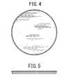
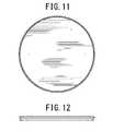
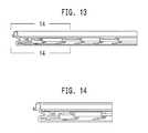
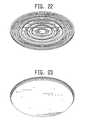
The broken lines shown in the drawings represent portions of the elastic membrane for semiconductor wafer polishing apparatus that form no part of the claimed design.
Claims (1)
- The ornamental design for an elastic membrane for semiconductor wafer polishing apparatus, as shown and described.
Priority Applications (2)
| Application Number | Priority Date | Filing Date | Title |
|---|---|---|---|
| US29/489,477USD770990S1 (en) | 2013-05-15 | 2014-04-30 | Elastic membrane for semiconductor wafer polishing apparatus |
| US29/580,339USD813180S1 (en) | 2013-05-15 | 2016-10-07 | Elastic membrane for semiconductor wafer polishing apparatus |
Applications Claiming Priority (14)
| Application Number | Priority Date | Filing Date | Title |
|---|---|---|---|
| JP2013-10677 | 2013-05-15 | ||
| JPD2013-10675FJP1495082S (en) | 2013-05-15 | 2013-05-15 | |
| JPD2013-10672FJP1494713S (en) | 2013-05-15 | 2013-05-15 | |
| JPD2013-10678FJP1521701S (en) | 2013-05-15 | 2013-05-15 | |
| JPD2013-10674FJP1495081S (en) | 2013-05-15 | 2013-05-15 | |
| JPD2013-10676FJP1495739S (en) | 2013-05-15 | 2013-05-15 | |
| JP2013-10678 | 2013-05-15 | ||
| JPD2013-10673FJP1495738S (en) | 2013-05-15 | 2013-05-15 | |
| JPD2013-10677FJP1521451S (en) | 2013-05-15 | 2013-05-15 | |
| JP2013-10672 | 2013-05-15 | ||
| JP2013-10674 | 2013-05-15 | ||
| JP2013-10673 | 2013-05-15 | ||
| JP2013-10675 | 2013-05-15 | ||
| JP2013-10676 | 2013-05-15 |
Related Child Applications (2)
| Application Number | Title | Priority Date | Filing Date |
|---|---|---|---|
| US29/489,477Continuation-In-PartUSD770990S1 (en) | 2013-05-15 | 2014-04-30 | Elastic membrane for semiconductor wafer polishing apparatus |
| US29/580,339DivisionUSD813180S1 (en) | 2013-05-15 | 2016-10-07 | Elastic membrane for semiconductor wafer polishing apparatus |
Publications (1)
| Publication Number | Publication Date |
|---|---|
| USD769200S1true USD769200S1 (en) | 2016-10-18 |
Family
ID=57120114
Family Applications (2)
| Application Number | Title | Priority Date | Filing Date |
|---|---|---|---|
| US29/472,346ActiveUSD769200S1 (en) | 2013-05-15 | 2013-11-12 | Elastic membrane for semiconductor wafer polishing apparatus |
| US29/580,339ActiveUSD813180S1 (en) | 2013-05-15 | 2016-10-07 | Elastic membrane for semiconductor wafer polishing apparatus |
Family Applications After (1)
| Application Number | Title | Priority Date | Filing Date |
|---|---|---|---|
| US29/580,339ActiveUSD813180S1 (en) | 2013-05-15 | 2016-10-07 | Elastic membrane for semiconductor wafer polishing apparatus |
Country Status (1)
| Country | Link |
|---|---|
| US (2) | USD769200S1 (en) |
Cited By (34)
| Publication number | Priority date | Publication date | Assignee | Title |
|---|---|---|---|---|
| USD797067S1 (en)* | 2015-04-21 | 2017-09-12 | Applied Materials, Inc. | Target profile for a physical vapor deposition chamber target |
| USD798248S1 (en)* | 2015-06-18 | 2017-09-26 | Applied Materials, Inc. | Target profile for a physical vapor deposition chamber target |
| USD799646S1 (en)* | 2016-08-30 | 2017-10-10 | Asm Ip Holding B.V. | Heater block |
| USD801942S1 (en)* | 2015-04-16 | 2017-11-07 | Applied Materials, Inc. | Target profile for a physical vapor deposition chamber target |
| USD808349S1 (en)* | 2013-05-15 | 2018-01-23 | Ebara Corporation | Elastic membrane for semiconductor wafer polishing apparatus |
| USD813180S1 (en)* | 2013-05-15 | 2018-03-20 | Ebara Corporation | Elastic membrane for semiconductor wafer polishing apparatus |
| USD836572S1 (en)* | 2016-09-30 | 2018-12-25 | Applied Materials, Inc. | Target profile for a physical vapor deposition chamber target |
| USD839224S1 (en) | 2016-12-12 | 2019-01-29 | Ebara Corporation | Elastic membrane for semiconductor wafer polishing |
| USD851613S1 (en) | 2017-10-05 | 2019-06-18 | Applied Materials, Inc. | Target profile for a physical vapor deposition chamber target |
| USD859332S1 (en) | 2017-06-29 | 2019-09-10 | Ebara Corporation | Elastic membrane for semiconductor wafer polishing |
| USD859331S1 (en)* | 2017-03-31 | 2019-09-10 | Ebara Corporation | Vacuum contact pad |
| USD868124S1 (en) | 2017-12-11 | 2019-11-26 | Applied Materials, Inc. | Target profile for a physical vapor deposition chamber target |
| USD877101S1 (en) | 2018-03-09 | 2020-03-03 | Applied Materials, Inc. | Target profile for a physical vapor deposition chamber target |
| USD908645S1 (en) | 2019-08-26 | 2021-01-26 | Applied Materials, Inc. | Sputtering target for a physical vapor deposition chamber |
| USD918161S1 (en)* | 2017-12-19 | 2021-05-04 | Ebara Corporation | Elastic membrane |
| USD918848S1 (en)* | 2019-07-18 | 2021-05-11 | Kokusai Electric Corporation | Retainer of ceiling heater for semiconductor fabrication apparatus |
| US11179823B2 (en) | 2016-10-28 | 2021-11-23 | Ebara Corporation | Substrate holding apparatus, elastic membrane, polishing apparatus, and method for replacing elastic membrane |
| USD937329S1 (en) | 2020-03-23 | 2021-11-30 | Applied Materials, Inc. | Sputter target for a physical vapor deposition chamber |
| USD940765S1 (en) | 2020-12-02 | 2022-01-11 | Applied Materials, Inc. | Target profile for a physical vapor deposition chamber target |
| USD947802S1 (en)* | 2020-05-20 | 2022-04-05 | Applied Materials, Inc. | Replaceable substrate carrier interfacing film |
| USD954567S1 (en)* | 2019-06-25 | 2022-06-14 | Ebara Corporation | Measurement jig |
| USD962184S1 (en)* | 2019-07-11 | 2022-08-30 | Kokusai Electric Corporation | Retainer plate of top heater for wafer processing furnace |
| USD962183S1 (en)* | 2019-07-11 | 2022-08-30 | Kokusai Electric Corporation | Retainer plate of top heater for wafer processing furnace |
| USD981969S1 (en)* | 2020-12-18 | 2023-03-28 | Ebara Corporation | Elastic membrane for semiconductor wafer polishing apparatus |
| USD989012S1 (en)* | 2020-09-17 | 2023-06-13 | Ebara Corporation | Elastic membrane |
| USD1006768S1 (en)* | 2021-01-07 | 2023-12-05 | Solaero Technologies Corp. | Semiconductor wafer for mosaic solar cell fabrication |
| USD1007449S1 (en) | 2021-05-07 | 2023-12-12 | Applied Materials, Inc. | Target profile for a physical vapor deposition chamber target |
| US11958163B2 (en) | 2016-10-28 | 2024-04-16 | Ebara Corporation | Substrate holding apparatus, elastic membrane, polishing apparatus, and method for replacing elastic membrane |
| USD1051530S1 (en)* | 2023-03-29 | 2024-11-12 | Irobot Corporation | Drip tray for use with a mobile cleaning robot |
| USD1053230S1 (en) | 2022-05-19 | 2024-12-03 | Applied Materials, Inc. | Sputter target for a physical vapor deposition chamber |
| USD1072774S1 (en) | 2021-02-06 | 2025-04-29 | Applied Materials, Inc. | Target profile for a physical vapor deposition chamber target |
| USD1091033S1 (en) | 2023-03-09 | 2025-08-26 | Irobot Corporation | Drip tray for use with a mobile cleaning robot |
| USD1090499S1 (en)* | 2024-02-27 | 2025-08-26 | Avery Dennison Retail Information Services Llc | Antenna |
| USD1092453S1 (en)* | 2024-04-22 | 2025-09-09 | Avery Dennison Retail Information Services Llc | Antenna |
Citations (26)
| Publication number | Priority date | Publication date | Assignee | Title |
|---|---|---|---|---|
| US20010029158A1 (en)* | 1998-07-30 | 2001-10-11 | Yoshitaka Sasaki | Polishing apparatus and polishing method, and method of manufacturing semiconductor device and method of manufacturing thin film magnetic head |
| US6659850B2 (en)* | 2000-03-31 | 2003-12-09 | Speedfam-Ipec Corporation | Work piece carrier with adjustable pressure zones and barriers and a method of planarizing a work piece |
| US20040175951A1 (en)* | 2003-03-07 | 2004-09-09 | Applied Materials, Inc. | Substrate carrier with a textured membrane |
| US20080070479A1 (en)* | 2004-11-01 | 2008-03-20 | Ebara Corporation | Polishing Apparatus |
| US7357699B2 (en)* | 2003-02-10 | 2008-04-15 | Ebara Corporation | Substrate holding apparatus and polishing apparatus |
| US7402098B2 (en)* | 2006-10-27 | 2008-07-22 | Novellus Systems, Inc. | Carrier head for workpiece planarization/polishing |
| US20090068934A1 (en)* | 2007-09-04 | 2009-03-12 | Samsung Electronics Co., Ltd. | Wafer polishing carrier apparatus and chemical mechanical polishing equipment using the same |
| US20090068935A1 (en)* | 2003-10-17 | 2009-03-12 | Hiroomi Torii | Polishing apparatus |
| US20090111362A1 (en)* | 2007-10-29 | 2009-04-30 | Ebara Corporation | Polishing Apparatus |
| US20090247057A1 (en)* | 2005-09-14 | 2009-10-01 | Ebara Corporation | Polishing platen and polishing apparatus |
| USD616390S1 (en)* | 2009-03-06 | 2010-05-25 | Tokyo Electron Limited | Quartz cover for manufacturing semiconductor wafers |
| CN301348233S (en) | 2009-08-27 | 2010-09-15 | 株式会社荏原制作所 | Elastic film for semiconductor wafer polishing device |
| USD633452S1 (en) | 2009-08-27 | 2011-03-01 | Ebara Corporation | Elastic membrane for semiconductor wafer polishing apparatus |
| USD634719S1 (en) | 2009-08-27 | 2011-03-22 | Ebara Corporation | Elastic membrane for semiconductor wafer polishing apparatus |
| TWD139857S (en) | 2009-08-27 | 2011-04-11 | 荏原製作所股份有限公司 | Elastic film for semiconductor wafer polishing equipment |
| USD649126S1 (en)* | 2008-10-20 | 2011-11-22 | Ebara Corporation | Vacuum contact pad |
| TWD146491S (en) | 2010-12-28 | 2012-04-21 | 荏原製作所股份有限公司 | Elastic film for semiconductor wafer polishing |
| USD684551S1 (en)* | 2011-07-07 | 2013-06-18 | Phuong Van Nguyen | Wafer polishing pad holder |
| US8469776B2 (en)* | 2006-11-22 | 2013-06-25 | Applied Materials, Inc. | Flexible membrane for carrier head |
| USD686175S1 (en)* | 2012-03-20 | 2013-07-16 | Veeco Instruments Inc. | Wafer carrier having pockets |
| USD686582S1 (en)* | 2012-03-20 | 2013-07-23 | Veeco Instruments Inc. | Wafer carrier having pockets |
| USD687791S1 (en)* | 2012-03-20 | 2013-08-13 | Veeco Instruments Inc. | Multi-keyed wafer carrier |
| USD687790S1 (en)* | 2012-03-20 | 2013-08-13 | Veeco Instruments Inc. | Keyed wafer carrier |
| US20130316628A1 (en)* | 2012-05-23 | 2013-11-28 | Samsung Electronics Co., Ltd. | Flexible membranes for a polishing head |
| USD711330S1 (en) | 2010-12-28 | 2014-08-19 | Ebara Corporation | Elastic membrane for semiconductor wafer polishing |
| US8859070B2 (en)* | 2011-11-30 | 2014-10-14 | Ebara Corporation | Elastic membrane |
Family Cites Families (10)
| Publication number | Priority date | Publication date | Assignee | Title |
|---|---|---|---|---|
| US3627338A (en)* | 1969-10-09 | 1971-12-14 | Sheldon Thompson | Vacuum chuck |
| US6402594B1 (en)* | 1999-01-18 | 2002-06-11 | Shin-Etsu Handotai Co., Ltd. | Polishing method for wafer and holding plate |
| JP3342686B2 (en)* | 1999-12-28 | 2002-11-11 | 信越半導体株式会社 | Wafer polishing method and wafer polishing apparatus |
| US20050035514A1 (en)* | 2003-08-11 | 2005-02-17 | Supercritical Systems, Inc. | Vacuum chuck apparatus and method for holding a wafer during high pressure processing |
| US7033252B2 (en)* | 2004-03-05 | 2006-04-25 | Strasbaugh | Wafer carrier with pressurized membrane and retaining ring actuator |
| CN100467210C (en)* | 2004-03-25 | 2009-03-11 | 揖斐电株式会社 | Vacuum Chucks and Suction Plates |
| USD769200S1 (en)* | 2013-05-15 | 2016-10-18 | Ebara Corporation | Elastic membrane for semiconductor wafer polishing apparatus |
| USD770990S1 (en)* | 2013-05-15 | 2016-11-08 | Ebara Corporation | Elastic membrane for semiconductor wafer polishing apparatus |
| USD797067S1 (en)* | 2015-04-21 | 2017-09-12 | Applied Materials, Inc. | Target profile for a physical vapor deposition chamber target |
| USD798248S1 (en)* | 2015-06-18 | 2017-09-26 | Applied Materials, Inc. | Target profile for a physical vapor deposition chamber target |
- 2013
- 2013-11-12USUS29/472,346patent/USD769200S1/enactiveActive
- 2016
- 2016-10-07USUS29/580,339patent/USD813180S1/enactiveActive
Patent Citations (27)
| Publication number | Priority date | Publication date | Assignee | Title |
|---|---|---|---|---|
| US20010029158A1 (en)* | 1998-07-30 | 2001-10-11 | Yoshitaka Sasaki | Polishing apparatus and polishing method, and method of manufacturing semiconductor device and method of manufacturing thin film magnetic head |
| US6659850B2 (en)* | 2000-03-31 | 2003-12-09 | Speedfam-Ipec Corporation | Work piece carrier with adjustable pressure zones and barriers and a method of planarizing a work piece |
| US7357699B2 (en)* | 2003-02-10 | 2008-04-15 | Ebara Corporation | Substrate holding apparatus and polishing apparatus |
| US20040175951A1 (en)* | 2003-03-07 | 2004-09-09 | Applied Materials, Inc. | Substrate carrier with a textured membrane |
| US20090068935A1 (en)* | 2003-10-17 | 2009-03-12 | Hiroomi Torii | Polishing apparatus |
| US20080070479A1 (en)* | 2004-11-01 | 2008-03-20 | Ebara Corporation | Polishing Apparatus |
| US20090247057A1 (en)* | 2005-09-14 | 2009-10-01 | Ebara Corporation | Polishing platen and polishing apparatus |
| US7402098B2 (en)* | 2006-10-27 | 2008-07-22 | Novellus Systems, Inc. | Carrier head for workpiece planarization/polishing |
| US8469776B2 (en)* | 2006-11-22 | 2013-06-25 | Applied Materials, Inc. | Flexible membrane for carrier head |
| US20090068934A1 (en)* | 2007-09-04 | 2009-03-12 | Samsung Electronics Co., Ltd. | Wafer polishing carrier apparatus and chemical mechanical polishing equipment using the same |
| US20090111362A1 (en)* | 2007-10-29 | 2009-04-30 | Ebara Corporation | Polishing Apparatus |
| USD649126S1 (en)* | 2008-10-20 | 2011-11-22 | Ebara Corporation | Vacuum contact pad |
| USD616390S1 (en)* | 2009-03-06 | 2010-05-25 | Tokyo Electron Limited | Quartz cover for manufacturing semiconductor wafers |
| TWD139857S (en) | 2009-08-27 | 2011-04-11 | 荏原製作所股份有限公司 | Elastic film for semiconductor wafer polishing equipment |
| USD633452S1 (en) | 2009-08-27 | 2011-03-01 | Ebara Corporation | Elastic membrane for semiconductor wafer polishing apparatus |
| CN301348233S (en) | 2009-08-27 | 2010-09-15 | 株式会社荏原制作所 | Elastic film for semiconductor wafer polishing device |
| USD634719S1 (en) | 2009-08-27 | 2011-03-22 | Ebara Corporation | Elastic membrane for semiconductor wafer polishing apparatus |
| USD711330S1 (en) | 2010-12-28 | 2014-08-19 | Ebara Corporation | Elastic membrane for semiconductor wafer polishing |
| TWD146491S (en) | 2010-12-28 | 2012-04-21 | 荏原製作所股份有限公司 | Elastic film for semiconductor wafer polishing |
| USD729753S1 (en) | 2010-12-28 | 2015-05-19 | Ebara Corporation | Elastic membrane for semiconductor wafer polishing |
| USD684551S1 (en)* | 2011-07-07 | 2013-06-18 | Phuong Van Nguyen | Wafer polishing pad holder |
| US8859070B2 (en)* | 2011-11-30 | 2014-10-14 | Ebara Corporation | Elastic membrane |
| USD686582S1 (en)* | 2012-03-20 | 2013-07-23 | Veeco Instruments Inc. | Wafer carrier having pockets |
| USD687790S1 (en)* | 2012-03-20 | 2013-08-13 | Veeco Instruments Inc. | Keyed wafer carrier |
| USD687791S1 (en)* | 2012-03-20 | 2013-08-13 | Veeco Instruments Inc. | Multi-keyed wafer carrier |
| USD686175S1 (en)* | 2012-03-20 | 2013-07-16 | Veeco Instruments Inc. | Wafer carrier having pockets |
| US20130316628A1 (en)* | 2012-05-23 | 2013-11-28 | Samsung Electronics Co., Ltd. | Flexible membranes for a polishing head |
Cited By (47)
| Publication number | Priority date | Publication date | Assignee | Title |
|---|---|---|---|---|
| USD808349S1 (en)* | 2013-05-15 | 2018-01-23 | Ebara Corporation | Elastic membrane for semiconductor wafer polishing apparatus |
| USD813180S1 (en)* | 2013-05-15 | 2018-03-20 | Ebara Corporation | Elastic membrane for semiconductor wafer polishing apparatus |
| USD837755S1 (en)* | 2015-04-16 | 2019-01-08 | Applied Materials, Inc. | Target profile for a physical vapor deposition chamber target |
| USD801942S1 (en)* | 2015-04-16 | 2017-11-07 | Applied Materials, Inc. | Target profile for a physical vapor deposition chamber target |
| USD825504S1 (en) | 2015-04-21 | 2018-08-14 | Applied Materials, Inc. | Target profile for a physical vapor deposition chamber target |
| USD797067S1 (en)* | 2015-04-21 | 2017-09-12 | Applied Materials, Inc. | Target profile for a physical vapor deposition chamber target |
| USD798248S1 (en)* | 2015-06-18 | 2017-09-26 | Applied Materials, Inc. | Target profile for a physical vapor deposition chamber target |
| USD825505S1 (en)* | 2015-06-18 | 2018-08-14 | Applied Materials, Inc. | Target profile for a physical vapor deposition chamber target |
| USD799646S1 (en)* | 2016-08-30 | 2017-10-10 | Asm Ip Holding B.V. | Heater block |
| USD836572S1 (en)* | 2016-09-30 | 2018-12-25 | Applied Materials, Inc. | Target profile for a physical vapor deposition chamber target |
| USD869409S1 (en) | 2016-09-30 | 2019-12-10 | Applied Materials, Inc. | Target profile for a physical vapor deposition chamber target |
| US11958163B2 (en) | 2016-10-28 | 2024-04-16 | Ebara Corporation | Substrate holding apparatus, elastic membrane, polishing apparatus, and method for replacing elastic membrane |
| US11179823B2 (en) | 2016-10-28 | 2021-11-23 | Ebara Corporation | Substrate holding apparatus, elastic membrane, polishing apparatus, and method for replacing elastic membrane |
| USD839224S1 (en) | 2016-12-12 | 2019-01-29 | Ebara Corporation | Elastic membrane for semiconductor wafer polishing |
| USD913977S1 (en) | 2016-12-12 | 2021-03-23 | Ebara Corporation | Elastic membrane for semiconductor wafer polishing |
| USD859331S1 (en)* | 2017-03-31 | 2019-09-10 | Ebara Corporation | Vacuum contact pad |
| USD859332S1 (en) | 2017-06-29 | 2019-09-10 | Ebara Corporation | Elastic membrane for semiconductor wafer polishing |
| USD851613S1 (en) | 2017-10-05 | 2019-06-18 | Applied Materials, Inc. | Target profile for a physical vapor deposition chamber target |
| USD894137S1 (en) | 2017-10-05 | 2020-08-25 | Applied Materials, Inc. | Target profile for a physical vapor deposition chamber target |
| USD868124S1 (en) | 2017-12-11 | 2019-11-26 | Applied Materials, Inc. | Target profile for a physical vapor deposition chamber target |
| USD946638S1 (en) | 2017-12-11 | 2022-03-22 | Applied Materials, Inc. | Target profile for a physical vapor deposition chamber target |
| USD918161S1 (en)* | 2017-12-19 | 2021-05-04 | Ebara Corporation | Elastic membrane |
| USD902165S1 (en) | 2018-03-09 | 2020-11-17 | Applied Materials, Inc. | Target profile for a physical vapor deposition chamber target |
| USD877101S1 (en) | 2018-03-09 | 2020-03-03 | Applied Materials, Inc. | Target profile for a physical vapor deposition chamber target |
| USD1035468S1 (en) | 2019-06-25 | 2024-07-16 | Ebara Corporation | Measurement jig |
| USD1034248S1 (en) | 2019-06-25 | 2024-07-09 | Ebara Corporation | Measurement jig |
| USD954567S1 (en)* | 2019-06-25 | 2022-06-14 | Ebara Corporation | Measurement jig |
| USD962184S1 (en)* | 2019-07-11 | 2022-08-30 | Kokusai Electric Corporation | Retainer plate of top heater for wafer processing furnace |
| USD962183S1 (en)* | 2019-07-11 | 2022-08-30 | Kokusai Electric Corporation | Retainer plate of top heater for wafer processing furnace |
| USD918848S1 (en)* | 2019-07-18 | 2021-05-11 | Kokusai Electric Corporation | Retainer of ceiling heater for semiconductor fabrication apparatus |
| USD908645S1 (en) | 2019-08-26 | 2021-01-26 | Applied Materials, Inc. | Sputtering target for a physical vapor deposition chamber |
| USD970566S1 (en) | 2020-03-23 | 2022-11-22 | Applied Materials, Inc. | Sputter target for a physical vapor deposition chamber |
| USD937329S1 (en) | 2020-03-23 | 2021-11-30 | Applied Materials, Inc. | Sputter target for a physical vapor deposition chamber |
| USD947802S1 (en)* | 2020-05-20 | 2022-04-05 | Applied Materials, Inc. | Replaceable substrate carrier interfacing film |
| USD1021832S1 (en)* | 2020-09-17 | 2024-04-09 | Ebara Corporation | Elastic membrane |
| USD989012S1 (en)* | 2020-09-17 | 2023-06-13 | Ebara Corporation | Elastic membrane |
| USD940765S1 (en) | 2020-12-02 | 2022-01-11 | Applied Materials, Inc. | Target profile for a physical vapor deposition chamber target |
| USD966357S1 (en) | 2020-12-02 | 2022-10-11 | Applied Materials, Inc. | Target profile for a physical vapor deposition chamber target |
| USD981969S1 (en)* | 2020-12-18 | 2023-03-28 | Ebara Corporation | Elastic membrane for semiconductor wafer polishing apparatus |
| USD1006768S1 (en)* | 2021-01-07 | 2023-12-05 | Solaero Technologies Corp. | Semiconductor wafer for mosaic solar cell fabrication |
| USD1072774S1 (en) | 2021-02-06 | 2025-04-29 | Applied Materials, Inc. | Target profile for a physical vapor deposition chamber target |
| USD1007449S1 (en) | 2021-05-07 | 2023-12-12 | Applied Materials, Inc. | Target profile for a physical vapor deposition chamber target |
| USD1053230S1 (en) | 2022-05-19 | 2024-12-03 | Applied Materials, Inc. | Sputter target for a physical vapor deposition chamber |
| USD1091033S1 (en) | 2023-03-09 | 2025-08-26 | Irobot Corporation | Drip tray for use with a mobile cleaning robot |
| USD1051530S1 (en)* | 2023-03-29 | 2024-11-12 | Irobot Corporation | Drip tray for use with a mobile cleaning robot |
| USD1090499S1 (en)* | 2024-02-27 | 2025-08-26 | Avery Dennison Retail Information Services Llc | Antenna |
| USD1092453S1 (en)* | 2024-04-22 | 2025-09-09 | Avery Dennison Retail Information Services Llc | Antenna |
Also Published As
| Publication number | Publication date |
|---|---|
| USD813180S1 (en) | 2018-03-20 |
Similar Documents
| Publication | Publication Date | Title |
|---|---|---|
| USD769200S1 (en) | Elastic membrane for semiconductor wafer polishing apparatus | |
| USD766849S1 (en) | Substrate retaining ring | |
| USD808349S1 (en) | Elastic membrane for semiconductor wafer polishing apparatus | |
| USD783922S1 (en) | Wafer support ring | |
| USD746795S1 (en) | Playback device | |
| USD797472S1 (en) | Mat base | |
| USD723450S1 (en) | Truck topper | |
| USD732402S1 (en) | Beverage can | |
| USD738158S1 (en) | Cookware vessel | |
| USD769124S1 (en) | Bottle | |
| USD815385S1 (en) | Wafer support ring | |
| USD767332S1 (en) | Impeller for mixer | |
| USD717112S1 (en) | Cutlery | |
| USD773063S1 (en) | Octagonal inflatable spa | |
| USD766820S1 (en) | Battery | |
| USD723239S1 (en) | Wafer carrier ring | |
| USD838373S1 (en) | Bandage | |
| USD717111S1 (en) | Cutlery | |
| USD714098S1 (en) | Glass | |
| USD741160S1 (en) | Fence clip | |
| USD759302S1 (en) | Vaporizer | |
| USD768788S1 (en) | Scooter with inflatable base | |
| USD859332S1 (en) | Elastic membrane for semiconductor wafer polishing | |
| USD765163S1 (en) | Circular organ | |
| USD786085S1 (en) | Bottle |