USD645486S1 - Dielectric window for plasma processing device - Google Patents
Dielectric window for plasma processing deviceDownload PDFInfo
- Publication number
- USD645486S1 USD645486S1US29/369,644US36964410FUSD645486SUS D645486 S1USD645486 S1US D645486S1US 36964410 FUS36964410 FUS 36964410FUS D645486 SUSD645486 SUS D645486S
- Authority
- US
- United States
- Prior art keywords
- processing device
- plasma processing
- dielectric window
- dielectric
- window
- Prior art date
- Legal status (The legal status is an assumption and is not a legal conclusion. Google has not performed a legal analysis and makes no representation as to the accuracy of the status listed.)
- Expired - Lifetime
Links
Images


Description
Claims (1)
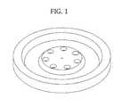
- The ornamental design for a dielectric window for a plasma processing device, as shown and described.
Applications Claiming Priority (2)
| Application Number | Priority Date | Filing Date | Title |
|---|---|---|---|
| JP2010-008109 | 2010-03-31 | ||
| JP2010008109 | 2010-03-31 |
Publications (1)
| Publication Number | Publication Date |
|---|---|
| USD645486S1true USD645486S1 (en) | 2011-09-20 |
Family
ID=44587438
Family Applications (1)
| Application Number | Title | Priority Date | Filing Date |
|---|---|---|---|
| US29/369,644Expired - LifetimeUSD645486S1 (en) | 2010-03-31 | 2010-09-10 | Dielectric window for plasma processing device |
Country Status (2)
| Country | Link |
|---|---|
| US (1) | USD645486S1 (en) |
| TW (1) | TWD142852S1 (en) |
Cited By (6)
| Publication number | Priority date | Publication date | Assignee | Title |
|---|---|---|---|---|
| USD658691S1 (en)* | 2011-03-30 | 2012-05-01 | Tokyo Electron Limited | Liner for plasma processing apparatus |
| USD658693S1 (en)* | 2011-03-30 | 2012-05-01 | Tokyo Electron Limited | Liner for plasma processing apparatus |
| USD658692S1 (en)* | 2011-03-30 | 2012-05-01 | Tokyo Electron Limited | Liner for plasma processing apparatus |
| USD826300S1 (en)* | 2016-09-30 | 2018-08-21 | Oerlikon Metco Ag, Wohlen | Rotably mounted thermal plasma burner for thermalspraying |
| USD909439S1 (en)* | 2018-11-30 | 2021-02-02 | Ferrotec (Usa) Corporation | Two-piece crucible cover |
| USD921058S1 (en)* | 2019-08-27 | 2021-06-01 | Black & Decker Inc. | Abrasive wheel |
Citations (8)
| Publication number | Priority date | Publication date | Assignee | Title |
|---|---|---|---|---|
| US4391034A (en)* | 1980-12-22 | 1983-07-05 | Ibm Corporation | Thermally compensated shadow mask |
| US20010007302A1 (en)* | 1997-05-16 | 2001-07-12 | Liubo Hong | Hybrid coil design for ionized deposition |
| US6280563B1 (en)* | 1997-12-31 | 2001-08-28 | Lam Research Corporation | Plasma device including a powered non-magnetic metal member between a plasma AC excitation source and the plasma |
| US20060110546A1 (en)* | 2002-09-30 | 2006-05-25 | Vikharev Anatoly L | High velocity method for deposing diamond films from a gaseous phase in shf discharge plasma and device for carrying out said method |
| US20080102538A1 (en)* | 2006-10-27 | 2008-05-01 | Taiwan Semiconductor Manufacturing Company, Ltd. | Apparatus and Method For Controlling Relative Particle Concentrations In A Plasma |
| US20090068934A1 (en)* | 2007-09-04 | 2009-03-12 | Samsung Electronics Co., Ltd. | Wafer polishing carrier apparatus and chemical mechanical polishing equipment using the same |
| US20090314434A1 (en)* | 2006-08-28 | 2009-12-24 | Qiaoli Song | Inductively coupled coil and inductively coupled plasma device using the same |
| US20100230273A1 (en)* | 2006-06-22 | 2010-09-16 | Shibaura Mechatronics Corporation | Film forming apparatus and film forming method |
- 2010
- 2010-09-10USUS29/369,644patent/USD645486S1/ennot_activeExpired - Lifetime
- 2010-09-29TWTW099304906Fpatent/TWD142852S1/enunknown
Patent Citations (9)
| Publication number | Priority date | Publication date | Assignee | Title |
|---|---|---|---|---|
| US4391034A (en)* | 1980-12-22 | 1983-07-05 | Ibm Corporation | Thermally compensated shadow mask |
| US20010007302A1 (en)* | 1997-05-16 | 2001-07-12 | Liubo Hong | Hybrid coil design for ionized deposition |
| US6280563B1 (en)* | 1997-12-31 | 2001-08-28 | Lam Research Corporation | Plasma device including a powered non-magnetic metal member between a plasma AC excitation source and the plasma |
| US20060110546A1 (en)* | 2002-09-30 | 2006-05-25 | Vikharev Anatoly L | High velocity method for deposing diamond films from a gaseous phase in shf discharge plasma and device for carrying out said method |
| US7694651B2 (en)* | 2002-09-30 | 2010-04-13 | Institute Of Applied Physics Ras | High velocity method for deposing diamond films from a gaseous phase in SHF discharge plasma and device for carrying out said method |
| US20100230273A1 (en)* | 2006-06-22 | 2010-09-16 | Shibaura Mechatronics Corporation | Film forming apparatus and film forming method |
| US20090314434A1 (en)* | 2006-08-28 | 2009-12-24 | Qiaoli Song | Inductively coupled coil and inductively coupled plasma device using the same |
| US20080102538A1 (en)* | 2006-10-27 | 2008-05-01 | Taiwan Semiconductor Manufacturing Company, Ltd. | Apparatus and Method For Controlling Relative Particle Concentrations In A Plasma |
| US20090068934A1 (en)* | 2007-09-04 | 2009-03-12 | Samsung Electronics Co., Ltd. | Wafer polishing carrier apparatus and chemical mechanical polishing equipment using the same |
Cited By (6)
| Publication number | Priority date | Publication date | Assignee | Title |
|---|---|---|---|---|
| USD658691S1 (en)* | 2011-03-30 | 2012-05-01 | Tokyo Electron Limited | Liner for plasma processing apparatus |
| USD658693S1 (en)* | 2011-03-30 | 2012-05-01 | Tokyo Electron Limited | Liner for plasma processing apparatus |
| USD658692S1 (en)* | 2011-03-30 | 2012-05-01 | Tokyo Electron Limited | Liner for plasma processing apparatus |
| USD826300S1 (en)* | 2016-09-30 | 2018-08-21 | Oerlikon Metco Ag, Wohlen | Rotably mounted thermal plasma burner for thermalspraying |
| USD909439S1 (en)* | 2018-11-30 | 2021-02-02 | Ferrotec (Usa) Corporation | Two-piece crucible cover |
| USD921058S1 (en)* | 2019-08-27 | 2021-06-01 | Black & Decker Inc. | Abrasive wheel |
Also Published As
| Publication number | Publication date |
|---|---|
| TWD142852S1 (en) | 2011-09-21 |
Similar Documents
| Publication | Publication Date | Title |
|---|---|---|
| USD699200S1 (en) | Electrode member for a plasma processing apparatus | |
| USD720511S1 (en) | Robot vacuum cleaner | |
| USD720510S1 (en) | Robot vacuum cleaner | |
| USD694481S1 (en) | Vacuum cleaner | |
| USD652041S1 (en) | Electronic device | |
| USD655296S1 (en) | Electronic device | |
| USD661440S1 (en) | Vacuum cleaner | |
| USD697835S1 (en) | Motor scooter or replica thereof | |
| USD661439S1 (en) | Vacuum cleaner | |
| USD658583S1 (en) | Electronic device | |
| USD687779S1 (en) | Electric receptacle | |
| USD676849S1 (en) | Electronic mouse | |
| USD746523S1 (en) | Vacuum cleaner | |
| USD660956S1 (en) | Inhaler | |
| USD655873S1 (en) | Vacuum cleaner | |
| USD654075S1 (en) | Access device | |
| USD652852S1 (en) | Field glass | |
| USD715505S1 (en) | Vacuum cleaner | |
| USD690887S1 (en) | Vacuum cleaner | |
| USD714501S1 (en) | Vacuum cleaner | |
| USD658691S1 (en) | Liner for plasma processing apparatus | |
| USD786408S1 (en) | Sensor assembly for touch-free water-control apparatus | |
| USD663629S1 (en) | Bottle | |
| USD672929S1 (en) | Vacuum cleaner | |
| USD658692S1 (en) | Liner for plasma processing apparatus |