US9990673B2 - Universal payment module systems and methods for mobile computing devices - Google Patents
Universal payment module systems and methods for mobile computing devicesDownload PDFInfo
- Publication number
- US9990673B2 US9990673B2US12/772,409US77240910AUS9990673B2US 9990673 B2US9990673 B2US 9990673B2US 77240910 AUS77240910 AUS 77240910AUS 9990673 B2US9990673 B2US 9990673B2
- Authority
- US
- United States
- Prior art keywords
- payment module
- universal
- connector
- computing devices
- payment
- Prior art date
- Legal status (The legal status is an assumption and is not a legal conclusion. Google has not performed a legal analysis and makes no representation as to the accuracy of the status listed.)
- Active, expires
Links
Images


Classifications
- G—PHYSICS
- G06—COMPUTING OR CALCULATING; COUNTING
- G06Q—INFORMATION AND COMMUNICATION TECHNOLOGY [ICT] SPECIALLY ADAPTED FOR ADMINISTRATIVE, COMMERCIAL, FINANCIAL, MANAGERIAL OR SUPERVISORY PURPOSES; SYSTEMS OR METHODS SPECIALLY ADAPTED FOR ADMINISTRATIVE, COMMERCIAL, FINANCIAL, MANAGERIAL OR SUPERVISORY PURPOSES, NOT OTHERWISE PROVIDED FOR
- G06Q40/00—Finance; Insurance; Tax strategies; Processing of corporate or income taxes
- G—PHYSICS
- G06—COMPUTING OR CALCULATING; COUNTING
- G06Q—INFORMATION AND COMMUNICATION TECHNOLOGY [ICT] SPECIALLY ADAPTED FOR ADMINISTRATIVE, COMMERCIAL, FINANCIAL, MANAGERIAL OR SUPERVISORY PURPOSES; SYSTEMS OR METHODS SPECIALLY ADAPTED FOR ADMINISTRATIVE, COMMERCIAL, FINANCIAL, MANAGERIAL OR SUPERVISORY PURPOSES, NOT OTHERWISE PROVIDED FOR
- G06Q20/00—Payment architectures, schemes or protocols
- G06Q20/08—Payment architectures
- G06Q20/10—Payment architectures specially adapted for electronic funds transfer [EFT] systems; specially adapted for home banking systems
Definitions
- the present inventionrelates generally to payment systems and methods with mobile computing devices. More particularly, the present invention relates to universal payment module systems and methods for mobile computing devices that generally include a universal payment module and an associated adapter device to couple the universal payment module to any of a plurality of mobile computing devices.
- mobile computing devicesinclude smart phones, cell phones, personal digital assistants (PDAs), and the like.
- Fixed computing devicesmay include point-of-sale (POS) devices, wall-mounted scanners, and the like. These devices typically include network connectivity such as through wireless (i.e. cellular, wireless local area network (WLAN)).
- POSpoint-of-sale
- WLANwireless local area network
- snap-on modulesfor a particular mobile device that enable the mobile device to obtain payments.
- various mobile or fixed payment applicationsmay include credit card transactions, debit card transactions, chip and PIN transactions, and the like.
- the conventional snap-on modulesare designed to fit only one style of mobile or fixed device, i.e. the form factor is dedicated to one mobile device form factor.
- payment devicesrequire special payment security mechanisms via mechanical, electrical, and software mechanisms. Thus, it is not possible to take one particular snap-on module for mobile payments and connect it to a different form factor without reengineering, testing, etc.
- payment devicesalso require payment card industry security approvals (like PCI and EMV) before they can be deployed for use. Since the physical construction and embodiment is usually considered part of the security system any changes usually require a new security review and approval, a time consuming and costly process.
- a universal payment module systemincludes a payment module including a housing and a first connector; and one or more adapters including a second connector and a third connector, wherein, for each of the one or more adapters, the second connector is configured to interface with the first connector and the third connector is configured to interface to one of a plurality of computing devices associated with the each of the one or more adapters; wherein the payment module is configured to process mobile payment transactions and to communicate between the one of the plurality of computing devices, and wherein the payment module is configured to operate with each of the plurality of computing devices via the one or more adapters.
- the one or more adapterseach may further include a fourth connector; and the universal payment module system may further include a card reading device including a fifth connector configured to interface with the fourth connector, wherein the card reading device may be configured to read any of a credit card, debit card, contactless card, ATM card, or smart card.
- the payment modulemay include a front portion and a rear portion, the front portion may include input and output interfaces.
- the rear portionmay include a card reading device, wherein the card reading device may be configured to read any of a credit card, debit card, contactless card, ATM card, or smart card.
- the payment modulemay be configured to connect to or within a housing of each of the one or more adapters, and wherein the payment module may be configured to connect to the each of the one or more adapters such that the front portion and the rear portion are accessible by a user.
- the payment modulemay be configured to connect to or within a housing of each of the one or more adapters, wherein the each of the one or more adapters is configured to connect to a computing device, and wherein the each of the one or more adapters may provide a power and data interface between the computing device and the payment module.
- the payment modulemay be tested for compliance to regulatory standards, and wherein the one or more adapters may not require compliance testing to the regulatory standards.
- each of the one or more adaptersmay include a form factor based on an associated computing device, wherein the payment module may include a single form factor thereby allowing the payment module to be utilized in conjunction with the plurality of computing devices.
- the housing of the payment modulemay include tamper resistance mechanisms.
- the tamper resistance mechanismsmay include one or more sensors disposed in the housing configured to deactivate the payment module responsive to detecting tampering of the housing.
- the payment modulemay include a processor, a data store, memory, and input and output interfaces, each of which is communicatively coupled via a local interface that is communicatively coupled to the second connector.
- the payment modulemay be configured to: receive payment information; process the payment information into a payment transaction; and communicate the payment transaction via an attached adapter to a computing device.
- the payment informationmay be received from any of a magnetic stripe reader disposed on the payment module, a magnetic stripe reader connected to the adapter, the input and output interfaces on the payment module, and a contactless connection.
- the payment informationmay be processed into encrypted data for the payment transaction, and wherein the encrypted data may be communicated to the computing device.
- the computing devicemay include a network connection, and wherein the encrypted data may be transmitted over the network connection.
- a payment devicein another exemplary embodiment, includes a processor; input/output interfaces; a data store; one or more sensors; memory; an external connector; a local interface communicatively coupling the processor, the input/output interfaces, the data store, the one or more sensors, the memory, and the external connector; and a housing including the processor, the input/output interfaces, the data store, the one or more sensors, the memory, and the external connector; wherein the housing is configured to connect to an external adapter via the external connector for operation with a device associated with the external adapter; and wherein the processor, the input/output interfaces, the data store, the one or more sensors, the memory, and the external connector collectively are configured to enable payment transaction processing.
- a mobile payment method with a deviceincludes providing a universal payment module configured to process mobile payment transactions; providing a device and an associated adapter configured to interface the universal payment module with the device; connecting the universal payment module to the adapter; connecting the adapter to the device; utilizing the universal payment module to process a payment transaction; and communicating the payment transaction over a network via the device.
- the mobile payment methodmay further include ensuring compliance of the universal payment module to regulations related to any of credit card processing and debit card processing.
- the mobile payment methodmay further include providing a plurality of mobile devices; providing a plurality of adapters for each of the plurality of mobile devices; and connecting the universal payment module to any of the plurality of adapters for use with any of the plurality of mobile devices.
- FIG. 1is a block diagram of a universal payment module illustrating various components configured for receiving and processing payments
- FIG. 2is a front view of the universal payment module
- FIG. 3is a rear view of the universal payment module
- FIG. 4is a front view of an adapter configured to connect the universal payment module to a mobile computing device
- FIG. 5is a front view of a snap-on magnetic stripe reader for connection to the adapter
- FIG. 6is a perspective view of the universal payment module connected within an exemplary adapter
- FIG. 7is a perspective view of the exemplary adapter of FIG. 6 without the universal payment module
- FIG. 8is a perspective view of the universal payment module of FIG. 6 disconnected from an adapter.
- FIG. 9is a flowchart of an exemplary method for providing and operating a universal payment module with a plurality of mobile computing devices.
- the present inventionprovides universal payment module systems and methods for mobile or fixed computing devices that include a universal payment module and an associated adapter device for coupling the universal payment module to any of a plurality of mobile computing devices or fixed computing devices, such as wall mounted price checkers.
- the present inventionutilizes a common payment module (e.g., card industry approved) which can interface multiple mobile computers with differing form factors via a snap-on sled.
- the present inventionallows the leveraging of one payment module for many mobile computers.
- the single payment moduleincludes various special payment security mechanisms via mechanical, electrical, and software mechanisms.
- the present inventionenables design, standardization, and production of one single common, payment card industry approved, universal payment module for a plurality of mobile computer devices instead of one specific payment module for each form factor of the plurality of mobile or fixed computing devices.
- the present inventionincludes a universal payment module 10 with various components configured for receiving and processing payments.
- the universal payment module 10may be a digital device that, in terms of hardware architecture, generally includes a processor 12 , input/output (I/O) interfaces 14 , a network interface 16 , a data store 18 , various sensors 20 , and memory 22 .
- I/Oinput/output
- FIG. 1depicts the universal payment module 10 in an oversimplified manner, and a practical embodiment may include additional components and suitably configured processing logic to support known or conventional operating features that are not described in detail herein.
- the components ( 12 , 14 , 16 , 18 , 20 , and 22 )are communicatively coupled via a local interface 24 and housed collectively in a housing 26 .
- the local interface 24may be, for example but not limited to, one or more buses or other wired or wireless connections, as is known in the art.
- the local interface 24may have additional elements, which are omitted for simplicity, such as controllers, buffers (caches), drivers, repeaters, and receivers, among many others, to enable communications. Further, the local interface 24 may include address, control, and/or data connections to enable appropriate communications among the aforementioned components.
- the processor 12is a hardware device for executing software instructions.
- the processor 12may be any custom made or commercially available processor, a central processing unit (CPU), an auxiliary processor among several processors associated with the universal payment module 10 , a semiconductor-based microprocessor (in the form of a microchip or chip set), or generally any device for executing software instructions.
- the processor 12is configured to execute software stored within the memory 22 , to communicate data to and from the memory 22 , and to generally control operations of the universal payment module 10 pursuant to the software instructions.
- the I/O interfaces 14may be used to receive user input from and/or for providing system output to one or more devices or components.
- User inputcan be provided via, for example, a keyboard, a keypad, a mouse, a scroll bar, buttons, bar code scanner, and the like.
- System outputcan be provided via a display device such as a liquid crystal display (LCD), touch screen, and the like.
- the I/O interfaces 14can also include, for example, a serial port, a parallel port, a small computer system interface (SCSI), an infrared (IR) interface, a radio frequency (RF) interface, and/or a universal serial bus (USB) interface.
- SCSIsmall computer system interface
- IRinfrared
- RFradio frequency
- USBuniversal serial bus
- the I/O interfaces 14may include a graphical user interface (GUI), a keypad, a magnetic strip reader, an RFID chip reader, and the like that enables a user to interact with the universal payment module 10 .
- GUIgraphical user interface
- the I/O interfaces 14may include connectors to interface data between the universal payment module 10 , an adapter, and a mobile or fixed computing device.
- the universal payment module 10may plug into the adapter which in turn snaps on to the mobile or fixed computing device.
- the network interface 16is used to enable the universal payment module 10 to communicate on a network or on the network through a corresponding mobile or fixed computing device.
- the network interface 16may include, for example, an Ethernet adapter (e.g., 10BaseT, Fast Ethernet, Gigabit Ethernet) or a wireless local area network (WLAN) adapter (e.g., 802.11a/b/g/n or proprietary wireless protocol based, including mesh network) or a cellular data network (e.g., 3G or EvDO) adapter.
- the network interface 16may include address, control, and/or data connections to enable appropriate communications on the network and/or to the corresponding mobile or fixed computing device.
- the network interface 16includes circuitry and logic to interface to the different adapters for communication of data.
- the mobile or fixed computing devicemay include another network adapter, such as a radio to enable wireless communication to an external access device or network.
- a radioto enable wireless communication to an external access device or network.
- Any number of suitable wireless data communication protocols, techniques, or methodologiescan be supported by the radio, including, without limitation: RF; IrDA (infrared); Bluetooth; ZigBee (and other variants of the IEEE 802.15 protocol); IEEE 802.11 (any variation); IEEE 802.16 (WiMAX or any other variation); Direct Sequence Spread Spectrum; Frequency Hopping Spread Spectrum; cellular/wireless/cordless telecommunication protocols; wireless home network communication protocols; paging network protocols; magnetic induction; satellite data communication protocols; wireless hospital or health care facility network protocols such as those operating in the WMTS bands; GPRS; and proprietary wireless data communication protocols such as variants of Wireless USB.
- the universal payment module 10may utilize the radio on the mobile or fixed computing device to
- the data store 18may be used to store data.
- the data store 18can include any of volatile memory elements (e.g., random access memory (RAM, such as DRAM, SRAM, SDRAM, and the like)), nonvolatile memory elements (e.g., ROM, hard drive, tape, CDROM, and the like), and combinations thereof.
- the data store 18can incorporate electronic, magnetic, optical, and/or other types of storage media.
- the memory 22may include any of volatile memory elements (e.g., random access memory (RAM, such as DRAM, SRAM, SDRAM, etc.)), nonvolatile memory elements (e.g., ROM, hard drive, tape, CDROM, etc.), and combinations thereof.
- the memory 22may incorporate electronic, magnetic, optical, and/or other types of storage media. Note that the memory 22 may have a distributed architecture, where various components are situated remotely from one another, but can be accessed by the processor 12 .
- the software in memory 22may include one or more software programs, each of which includes an ordered listing of executable instructions for implementing logical functions.
- the software in the memory system 22includes a suitable operating system (O/S) 28 and programs 30 .
- the operating system 28essentially controls the execution of other computer programs, and provides scheduling, input-output control, file and data management, memory management, and communication control and related services.
- the operating system 28 and the programs 30are configured to support payments using the universal payment module 10 including taking of payments, processing of payments, and communication of payments to/from a corresponding mobile or fixed computing device.
- the various componentsare contained or disposed within or on the housing 26 .
- the housing 26includes a specific form factor and the sensors 20 are disposed within this form factor.
- the universal payment module 10must meet certain regulatory specifications such as, for example, Payment Card Industry (PCI) specifications, Europay Mastercard Visa (EMV), INTERAC, and the like.
- PCIPayment Card Industry
- EMVEuropay Mastercard Visa
- INTERACEuropay Mastercard Visa
- the present inventionenables the universal payment module 10 with the housing 26 to operate as a single form factor, payment regulatory body approved device that can interface with multiple mobile or fixed computers via an adapter.
- the development and compliance requirements for payment devicesare lengthy and costly.
- the present inventionprovides the ability to create one module (i.e., the universal payment module 10 with the housing 26 ) to work with many mobile or fixed computers allows leveraging one product to many and avoiding additional expenses.
- Companion adapter sledsallow the adaption of the universal payment module 10 to the various mobile or fixed computers.
- the sensors 20are disposed within the housing 26 and configured to prevent users from accessing the various components within the universal payment module 10 . This is a requirement for compliance and security to ensure tamper resistance in the universal payment module 10 .
- the sensors 20are customized to the particular form factor of the housing 26 .
- the programs 28provide a user interface, payment collection, payment processing, and communications to/from the adapter and the mobile or fixed computing device.
- the programs 28 for the universal payment module 10enable various payment applications including, for example, Point of Sale (POS) applications, processing of cards with magnetic stripes, processing of cards with smart chips, processing of cards with RFID, integrated payment transaction processing, and the like.
- the programs 28 along with the various other components of the universal payment module 10provide payment security compliant with various specifications includes firewall, intrusion prevention, enforced authentication, data encryption, integrity monitoring, ability to wipe data on the universal payment module 10 if lost or stolen, and the like.
- the programs 28include algorithms to process credit card or debit card transactions remotely (POS) applications from the universal payment module 10 . This may include security and encryption to take card data and process a transaction and to send the processed transaction to a remote server or the like.
- FIGS. 2-5in various exemplary embodiments, an exemplary physical implementation of the universal payment module 10 and an associated adapter 40 is illustrated.
- FIG. 2illustrates a front view of the universal payment module 10 and
- FIG. 3illustrates a rear view of the universal payment module 10 .
- FIG. 4illustrates a front view of the adapter 40
- FIG. 5illustrates a snap-on magnetic stripe reader 42 for connection to the adapter 40 .
- the universal payment module 10is a single form factor device that may interconnect with a plurality of different mobile or fixed computing devices with varying form factors.
- the adapter 40is configured to interface the universal payment module 10 to multiple mobile or fixed computing devices, e.g.
- the adapter 40may function as a snap-on interfacing sled leveraging the universal payment module 10 to many mobile or fixed computing devices.
- the universal payment module 10is a single form factor, payment regulatory body approved device that can interface with multiple mobile or fixed computing devices.
- the development and compliance requirements for payment devices such as the universal payment module 10is lengthy and costly.
- the present inventionprovides the ability to create one module to work with many mobile or fixed computing devices leveraging one product to many and avoiding additional expenses.
- the adapter 40may come in various different form factors to allow the adaption of the universal payment module 10 to the various mobile or fixed computing devices.
- the adapter 40does not have the same development and compliance requirements and thus may be easily produced to fit a specific interface and form factor.
- the universal payment module 10includes a housing 44 that is adapted and sized to fit within an opening 46 defined in a housing 48 of the adapter 40 .
- the opening 46extends through the housing 48 allowing a front portion 50 and a rear portion 52 of the universal payment module 10 to be exposed and accessible.
- the opening 46does not extend through the housing 48 , i.e. the opening 46 is a cavity defined in the housing 48 , allowing only the front portion to be exposed and accessible.
- the opening 46is designed as such based on whether access is required to the rear portion 52 .
- the rear portion 52may include input/output interfaces such as a magnetic stripe reader 54 or the like.
- the opening 46is required to provide access to both the portions 50 , 52 .
- additional input/output interfacessuch as the magnetic stripe reader 42 may be contained in a separate housing 56 that connects to the adapter 40 .
- the universal payment module 10 , the adapter 40 , and the magnetic stripe reader 42may each include a plurality of input/output (IO) interface connectors configured to interconnect these devices 10 , 40 , 42 physically and electrically.
- the adapter 40may include three IO connectors 58 , 60 , 62 .
- the connector 58is configured to connect the adapter 40 to a corresponding mobile or fixed computing device (not shown). This connector 58 may be utilized to provide power and data between the adapter 40 and the corresponding mobile or fixed computing device.
- the connector 60is configured to connect the adapter 40 to the universal payment module 10 through a corresponding IO connector 64 on the universal payment module 10 . Similar to the connector 58 , the connector 60 may be utilized to provide power and data between the adapter 40 and the universal payment module 10 .
- the connector 62is configured to connect the adapter 40 to an external device such as a connector 66 on the magnetic stripe reader 42 . Similar to the connectors 58 , 60 , the connector 62 may be utilized to provide power and data between the adapter 40 and the external device.
- these connectorsmay be configured to provide power and data interfaces.
- the universal payment module 10is configured to perform payment processing and data encryption such that payment information exchanged over the data interfaces associated with the connectors 58 - 66 is encrypted.
- all payment operations that must be performed to be compliant to various specificationsare performed internally to the universal payment module 10 with the adapter 40 , the magnetic stripe reader 42 , etc. not requiring compliance testing and the like.
- the housing 44 for the universal payment module 10is a form factor compatible with the opening 46 in the adapter 40 .
- the housing 44is illustrated as a substantially rectangular shape forming a rectangular box with the front portion 50 , the rear portion 52 , top and bottom sides, and left and right sides.
- the front portion 50may include a display 68 , a plurality of keys 70 , and the like (e.g. a scroll bar, touch pad, etc.) that are collectively configured to enable user operation of the universal payment module 10 .
- the rear portion 52may or may not include components.
- the housing 44includes circuitry, hardware, storage, etc. associated with the functionality of the universal payment module 10 , e.g. such as described in FIG. 1 .
- the connector 64is configured to communicate to/from the various circuitry, hardware, storage, etc for operating the universal payment module 10 .
- the connector 64is illustrate on the top side of the housing 44 , and those of ordinary skill in the art will recognize the connector 64 may be placed anywhere on the housing 44 .
- the adapter 40includes the housing 48 in a form factor compatible with as associated mobile or fixed computing device.
- the present inventioncontemplates one or more different adapters 40 operating with the universal payment module 10 .
- the universal payment module 10requires stringent standardization, security, compliance, etc. while the adapter 40 does not.
- the present inventiondecouples the design of the universal payment module 10 from the design of associated mobile or fixed computing devices.
- all that is required to enable the universal payment module 10 to operate with new mobile or fixed computing devicesis an associated adapter 40 configured to interface the universal payment module 10 to the mobile or fixed computing device.
- the housings 44 , 48may be constructed of plastic or the like and collectively the housings 44 , 48 are designed to protect the universal payment module 10 from bumps, drops, etc.
- the adapter 40includes various connections, circuits, and the like internal to the housing 48 and configured to connect the various connectors 58 , 60 , 62 .
- the adapter 40includes a rectangular box shape with a bottom side 72 , a left side 74 , a right side 76 , a top side 78 , a front side 80 , and a rear side (not shown) opposing the front side 80 .
- Those of ordinary skill in the artwill recognize the present invention contemplates any shape or form factor for the housing 48 . It is expected that the particular form factor of the housing 48 will conform to that of a corresponding mobile or fixed computing device.
- the opening 46is shaped to conform to the form factor of the universal payment module 10 .
- the top side 78includes the connector 58 for connecting the adapter 40 to the mobile or fixed computing device.
- the top side 78includes a cavity defined by three sides 84 , 86 , 88 .
- the cavityis configured to engage the mobile or fixed computing device in a snap-on configuration, i.e. the cavity receives a portion of the mobile or fixed computing device and provides physical support between the mobile or fixed computing device and the adapter 40 .
- the sides 84 , 86 , 88may include snaps, grooves, notches, etc. configured to engage corresponding structures on the mobile or fixed computing device to provide the snap-on configuration.
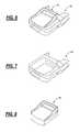
- FIGS. 6, 7, and 8in various exemplary embodiments, perspective views illustrate an exemplary implementation of the universal payment module 10 and the adapter 40 .
- FIG. 6is a perspective view of the universal payment module 10 connected within an exemplary adapter 40
- FIG. 7is a perspective view of the exemplary adapter 40 of FIG. 6 without the universal payment module
- FIG. 8is a perspective view of the universal payment module 10 of FIG. 6 disconnected from the adapter 40 .
- the adapter 40includes a specific form factor
- the universal payment module 10is configured to plug into the adapter 40 thereby enabling operation with any mobile or fixed device configured to snap on or connect to the adapter 40 .
- a flowchartillustrates an exemplary method 90 for providing and operating a universal payment module with a plurality of mobile or fixed computing devices.
- the present inventionenables the use of a single form factor universal payment module configured to process payments.
- the method 900describes both a design/production process and a operational process for the universal payment module.
- the present inventionstreamlines design, testing, and production of payment modules as only one universal payment module is required for multiple mobile or fixed devices. This reduces development, testing, and compliance time and effort. Further, this reduces manufacturing and inventory efforts as well.
- the universal payment modulefurther provides an advantage of reducing the number of components an enterprise or the like needs to provide payments, i.e.
- the adapter and the universal payment moduleenable the universal payment module to work across different vendor's platforms.
- a universal payment moduleis designed and provided (step 91 ).
- the UPMis configured to provide payment transactions, i.e. POS, including credit card processing, debit card processing, ATM card processing, smart card processing, contactless device processing, and the like.
- the UPMis designed and tested for compliance to various standards and regulations associated with these mobile payment transactions. For example, debit card payments must comply with PCI regulations.
- the present inventionallows a payment device vendor to only have to submit to testing and compliance for one single device, i.e. the universal payment module. Further, the UPM is then manufactured and provided to end users or the like.
- an adapterFor each of a plurality of mobile or fixed devices intending on using the UPM, an adapter is designed and provided with the adapter configured to receive the UPM (step 92 ).
- the adapterincludes a form factor and associated connectors for each of the different plurality of mobile or fixed devices. That is, the UPM is designed for all mobile or fixed devices as one unit, and each mobile or fixed device has an associated adapter that is configured to receive the UPM and interface the UPM to the mobile or fixed device. Specifically, the adapter interfaces power and data connections from the UPM to the mobile or fixed device.
- the adapterdoes not perform payment transaction processing, so it does not require the rigorous testing and compliance requirements of the UPM. Rather, the adapter is configured to interface with already processed transaction data that may be encrypted.
- the method 90may operate these devices by connecting the UPM to the adapter and connecting the adapter to the mobile or fixed device (step 93 ).
- the UPMis configured to snap into or equivalent into, on, etc. the adapter for a physical connection, a data connection, and a power connection.
- the adapteris configured to snap on or equivalent to the mobile or fixed device for a physical connection, a data connection, and a power connection.
- the UPMmay process payments including sending secure, encrypted data between the UPM and the mobile or fixed device via the adapter (step 94 ).
- the UPMis configured to operate as a payment device as described herein, and the UPM is in communication with the mobile or fixed device.
- the mobile or fixed devicemay be configured to send the secure, encrypted data to a network, such as a cellular network, a wireless local area network (WLAN), a wide area network (WAN), a private network, the Internet, or the like (step 95 ).
- WLANwireless local area network
- WANwide area network
- a private networksuch as a cellular network
- the Internetsuch as a cellular network, a wireless local area network (WLAN), a wide area network (WAN), a private network, the Internet, or the like.
Landscapes
- Business, Economics & Management (AREA)
- Accounting & Taxation (AREA)
- Finance (AREA)
- Engineering & Computer Science (AREA)
- Physics & Mathematics (AREA)
- Economics (AREA)
- Strategic Management (AREA)
- Development Economics (AREA)
- General Business, Economics & Management (AREA)
- General Physics & Mathematics (AREA)
- Theoretical Computer Science (AREA)
- Marketing (AREA)
- Technology Law (AREA)
- Cash Registers Or Receiving Machines (AREA)
Abstract
Description
Claims (13)
Priority Applications (1)
| Application Number | Priority Date | Filing Date | Title |
|---|---|---|---|
| US12/772,409US9990673B2 (en) | 2010-05-03 | 2010-05-03 | Universal payment module systems and methods for mobile computing devices |
Applications Claiming Priority (1)
| Application Number | Priority Date | Filing Date | Title |
|---|---|---|---|
| US12/772,409US9990673B2 (en) | 2010-05-03 | 2010-05-03 | Universal payment module systems and methods for mobile computing devices |
Publications (2)
| Publication Number | Publication Date |
|---|---|
| US20110270741A1 US20110270741A1 (en) | 2011-11-03 |
| US9990673B2true US9990673B2 (en) | 2018-06-05 |
Family
ID=44859064
Family Applications (1)
| Application Number | Title | Priority Date | Filing Date |
|---|---|---|---|
| US12/772,409Active2033-03-05US9990673B2 (en) | 2010-05-03 | 2010-05-03 | Universal payment module systems and methods for mobile computing devices |
Country Status (1)
| Country | Link |
|---|---|
| US (1) | US9990673B2 (en) |
Families Citing this family (4)
| Publication number | Priority date | Publication date | Assignee | Title |
|---|---|---|---|---|
| AU2012396880B2 (en) | 2012-12-12 | 2017-04-13 | Paypal, Inc. | Dual card reader for mobile device |
| FR3020163B1 (en)* | 2014-04-18 | 2016-05-06 | Compagnie Ind Et Financiere Dingenierie Ingenico | METHOD OF DEACTIVATING A PAYMENT MODULE, COMPUTER PROGRAM PRODUCT, STORAGE MEDIUM AND PAYMENT MODULE THEREOF |
| CN107071213A (en)* | 2014-07-25 | 2017-08-18 | 苏州鱼得水电气科技有限公司 | The adjustable scanner of multifunction wall hanging |
| US9542339B1 (en)* | 2015-01-10 | 2017-01-10 | Koamtac, Inc. | Mobile device sled with novel port usage and standing configuration for ready pairing between a mobile device and associated peripheral devices |
Citations (55)
| Publication number | Priority date | Publication date | Assignee | Title |
|---|---|---|---|---|
| USD339807S (en)* | 1991-07-05 | 1993-09-28 | Nokia Mobile Phones Ltd. | Card reader for a mobile phone |
| US5496992A (en) | 1994-06-21 | 1996-03-05 | Lxe, Inc. | Dual trigger multiplexed data entry terminal |
| US5627355A (en)* | 1994-07-13 | 1997-05-06 | Rahman; Sam | Transaction device, equipment and method for protecting account numbers and their associated personal identification numbers |
| US5669069A (en)* | 1994-04-19 | 1997-09-16 | Nokia Mobile Phones Limited | Card reading configuration in a mobile phone |
| US5999624A (en)* | 1994-06-30 | 1999-12-07 | Compaq Computer Corporation | Remote financial transaction system |
| US6006987A (en)* | 1996-12-20 | 1999-12-28 | Siemens Aktiengesellschaft | Removable card carrier assembly |
| US6026166A (en)* | 1997-10-20 | 2000-02-15 | Cryptoworx Corporation | Digitally certifying a user identity and a computer system in combination |
| JP2002117370A (en) | 2001-10-01 | 2002-04-19 | Fujitsu Ltd | Optical reading device |
| US20020116245A1 (en)* | 2000-12-21 | 2002-08-22 | Hinkle Burl Shannon | Method and system for prioritizing debt collections |
| US20020194068A1 (en)* | 2001-02-26 | 2002-12-19 | Fred Bishop | System and method for securing data through a PDA portal |
| US20030137416A1 (en)* | 2000-06-01 | 2003-07-24 | Shuzhen Fu | Point of sale (POS) terminal security system |
| US20030222152A1 (en)* | 2002-05-28 | 2003-12-04 | Boley George E.S. | Pre-paid debit & credit card |
| US6726070B2 (en) | 2002-05-20 | 2004-04-27 | Robert Lautner | Ergonomic input-device holder |
| US20040104268A1 (en)* | 2002-07-30 | 2004-06-03 | Bailey Kenneth Stephen | Plug in credit card reader module for wireless cellular phone verifications |
| US6754069B2 (en) | 2001-02-07 | 2004-06-22 | Matsushita Electric Industrial Co., Ltd. | Portable terminal wearable on forearm |
| US20040120101A1 (en)* | 2002-12-20 | 2004-06-24 | Lipman Electronic Engineering Ltd. | Anti-tampering enclosure for electronic circuitry |
| JP2006502471A (en) | 2002-08-15 | 2006-01-19 | カイバー テクノロジーズ コーポレイション | Portable data input device with separable host PDA |
| US20060049243A1 (en)* | 2002-06-10 | 2006-03-09 | Ken Sakamura | Ic card, terminal device, and data communications method |
| US20060049256A1 (en)* | 2004-09-07 | 2006-03-09 | Clay Von Mueller | Transparently securing data for transmission on financial networks |
| US7016709B2 (en)* | 2004-03-12 | 2006-03-21 | Sbc Knowledge Ventures, L.P. | Universal mobile phone adapter method and system for vehicles |
| US7051002B2 (en)* | 2002-06-12 | 2006-05-23 | Cardinalcommerce Corporation | Universal merchant platform for payment authentication |
| US20060197753A1 (en) | 2005-03-04 | 2006-09-07 | Hotelling Steven P | Multi-functional hand-held device |
| US20060264110A1 (en)* | 2000-07-06 | 2006-11-23 | Onspec Electronic, Inc. | Smartconnect universal flash media card adapters |
| US7147162B2 (en) | 2003-01-09 | 2006-12-12 | Hand Held Products, Inc. | Housing for an optical reader |
| US20070131774A1 (en) | 2005-12-09 | 2007-06-14 | Shoplogix Inc. | System and method for verifying identity during data entry with a barcode scanner |
| US20080105747A1 (en) | 2006-11-03 | 2008-05-08 | Orlassino Mark P | System and method for selecting a portion of an image |
| US7395241B1 (en)* | 2000-01-19 | 2008-07-01 | Intuit Inc. | Consumer-directed financial transfers using automated clearinghouse networks |
| US20080257966A1 (en)* | 2007-04-20 | 2008-10-23 | Chris Britt | Packaging for a portable consumer device |
| US7464867B1 (en)* | 2001-03-26 | 2008-12-16 | Usa Technologies, Inc. | Cashless vending system with tethered payment interface |
| US20090068982A1 (en)* | 2007-09-10 | 2009-03-12 | Microsoft Corporation | Mobile wallet and digital payment |
| US7609406B2 (en) | 2002-08-16 | 2009-10-27 | Avery Dennison Retail Information Services, Llc | Hand held portable printer with RFID read write capability |
| US20090266899A1 (en) | 2008-04-25 | 2009-10-29 | Toshiba Tec Kabushiki Kaisha | Code scanner |
| JP2009282761A (en) | 2008-05-22 | 2009-12-03 | Denso Wave Inc | Optical information reading device |
| US20100148066A1 (en) | 2008-12-12 | 2010-06-17 | Testo Ag | Thermal imaging camera for taking thermographic images |
| US7746511B2 (en) | 2004-04-23 | 2010-06-29 | Symbol Technologies, Inc. | Scan head rotation at different optimum angles |
| US20100196075A1 (en)* | 2009-02-02 | 2010-08-05 | Xerox Corporation | Method and system for transmitting proof of payment for "pay-as-you-go" multi-function devices |
| US7819322B2 (en)* | 2006-06-19 | 2010-10-26 | Visa U.S.A. Inc. | Portable consumer device verification system |
| US20100280909A1 (en)* | 2009-04-29 | 2010-11-04 | Microsoft Corporation | Provider-driven payment adapter plug-in to payment gateway |
| US7853525B2 (en)* | 2003-07-15 | 2010-12-14 | Microsoft Corporation | Electronic draft capture |
| US20110180600A1 (en) | 2010-01-26 | 2011-07-28 | Toshiba Tec Kabushiki Kaisha | Information processing apparatus, commodity information processing system, information processing method, and commodity information processing method |
| US20110198395A1 (en)* | 2010-02-16 | 2011-08-18 | Mike Chen | Handheld mobile credit card reader |
| US20110249104A1 (en) | 2010-04-07 | 2011-10-13 | SDX-Interactive, Inc. | Peripheral for a Handheld Communication Device |
| US20110279279A1 (en)* | 2008-01-22 | 2011-11-17 | Verifone, Inc. | Secure point of sale terminal |
| US8121942B2 (en)* | 2007-06-25 | 2012-02-21 | Visa U.S.A. Inc. | Systems and methods for secure and transparent cardless transactions |
| US8151345B1 (en)* | 2007-01-25 | 2012-04-03 | Yeager C Douglas | Self-authorizing devices |
| US8260719B2 (en)* | 2000-12-01 | 2012-09-04 | Carrott Richard F | Transactional security over a network |
| US8260723B2 (en)* | 2000-12-01 | 2012-09-04 | Carrott Richard F | Transactional security over a network |
| US8261977B2 (en)* | 2009-03-27 | 2012-09-11 | Mastercard International Incorporated | Methods and systems for using an interface and protocol extensions to perform a financial transaction |
| US8281998B2 (en)* | 2009-02-10 | 2012-10-09 | 4361423 Canada Inc. | Apparatus and method for commercial transactions using a communication device |
| US8314817B2 (en) | 2007-06-29 | 2012-11-20 | Microsoft Corporation | Manipulation of graphical objects |
| US8533118B2 (en)* | 2008-11-06 | 2013-09-10 | Visa International Service Association | Online challenge-response |
| US8571937B2 (en)* | 2010-10-20 | 2013-10-29 | Playspan Inc. | Dynamic payment optimization apparatuses, methods and systems |
| US8577803B2 (en)* | 2011-06-03 | 2013-11-05 | Visa International Service Association | Virtual wallet card selection apparatuses, methods and systems |
| US8825516B2 (en) | 2007-09-07 | 2014-09-02 | Yottamark, Inc. | Methods for correlating first mile and last mile product data |
| US9314472B2 (en) | 2012-10-17 | 2016-04-19 | Brigham Young University | Treatment and prevention of mastitis |
- 2010
- 2010-05-03USUS12/772,409patent/US9990673B2/enactiveActive
Patent Citations (64)
| Publication number | Priority date | Publication date | Assignee | Title |
|---|---|---|---|---|
| USD339807S (en)* | 1991-07-05 | 1993-09-28 | Nokia Mobile Phones Ltd. | Card reader for a mobile phone |
| US5669069A (en)* | 1994-04-19 | 1997-09-16 | Nokia Mobile Phones Limited | Card reading configuration in a mobile phone |
| US5496992A (en) | 1994-06-21 | 1996-03-05 | Lxe, Inc. | Dual trigger multiplexed data entry terminal |
| US5999624A (en)* | 1994-06-30 | 1999-12-07 | Compaq Computer Corporation | Remote financial transaction system |
| US5627355A (en)* | 1994-07-13 | 1997-05-06 | Rahman; Sam | Transaction device, equipment and method for protecting account numbers and their associated personal identification numbers |
| US6006987A (en)* | 1996-12-20 | 1999-12-28 | Siemens Aktiengesellschaft | Removable card carrier assembly |
| US6026166A (en)* | 1997-10-20 | 2000-02-15 | Cryptoworx Corporation | Digitally certifying a user identity and a computer system in combination |
| US7395241B1 (en)* | 2000-01-19 | 2008-07-01 | Intuit Inc. | Consumer-directed financial transfers using automated clearinghouse networks |
| US20030137416A1 (en)* | 2000-06-01 | 2003-07-24 | Shuzhen Fu | Point of sale (POS) terminal security system |
| US6917299B2 (en)* | 2000-06-01 | 2005-07-12 | Hewlett-Packard Development Company, L.P. | Point of sale (POS) terminal security system |
| US20060264110A1 (en)* | 2000-07-06 | 2006-11-23 | Onspec Electronic, Inc. | Smartconnect universal flash media card adapters |
| US8260723B2 (en)* | 2000-12-01 | 2012-09-04 | Carrott Richard F | Transactional security over a network |
| US8463713B2 (en)* | 2000-12-01 | 2013-06-11 | Richard F. Carrott | Transactional security over a network |
| US8260719B2 (en)* | 2000-12-01 | 2012-09-04 | Carrott Richard F | Transactional security over a network |
| US20020116245A1 (en)* | 2000-12-21 | 2002-08-22 | Hinkle Burl Shannon | Method and system for prioritizing debt collections |
| US6754069B2 (en) | 2001-02-07 | 2004-06-22 | Matsushita Electric Industrial Co., Ltd. | Portable terminal wearable on forearm |
| US20020194068A1 (en)* | 2001-02-26 | 2002-12-19 | Fred Bishop | System and method for securing data through a PDA portal |
| US7464867B1 (en)* | 2001-03-26 | 2008-12-16 | Usa Technologies, Inc. | Cashless vending system with tethered payment interface |
| JP2002117370A (en) | 2001-10-01 | 2002-04-19 | Fujitsu Ltd | Optical reading device |
| US6726070B2 (en) | 2002-05-20 | 2004-04-27 | Robert Lautner | Ergonomic input-device holder |
| US20030222152A1 (en)* | 2002-05-28 | 2003-12-04 | Boley George E.S. | Pre-paid debit & credit card |
| US20060049243A1 (en)* | 2002-06-10 | 2006-03-09 | Ken Sakamura | Ic card, terminal device, and data communications method |
| US7357329B2 (en)* | 2002-06-10 | 2008-04-15 | Ken Sakamura | IC card, terminal device, and data communication method |
| US7051002B2 (en)* | 2002-06-12 | 2006-05-23 | Cardinalcommerce Corporation | Universal merchant platform for payment authentication |
| US20040104268A1 (en)* | 2002-07-30 | 2004-06-03 | Bailey Kenneth Stephen | Plug in credit card reader module for wireless cellular phone verifications |
| JP2006502471A (en) | 2002-08-15 | 2006-01-19 | カイバー テクノロジーズ コーポレイション | Portable data input device with separable host PDA |
| US7609406B2 (en) | 2002-08-16 | 2009-10-27 | Avery Dennison Retail Information Services, Llc | Hand held portable printer with RFID read write capability |
| US20040120101A1 (en)* | 2002-12-20 | 2004-06-24 | Lipman Electronic Engineering Ltd. | Anti-tampering enclosure for electronic circuitry |
| US7147162B2 (en) | 2003-01-09 | 2006-12-12 | Hand Held Products, Inc. | Housing for an optical reader |
| US7853525B2 (en)* | 2003-07-15 | 2010-12-14 | Microsoft Corporation | Electronic draft capture |
| US7016709B2 (en)* | 2004-03-12 | 2006-03-21 | Sbc Knowledge Ventures, L.P. | Universal mobile phone adapter method and system for vehicles |
| US7746511B2 (en) | 2004-04-23 | 2010-06-29 | Symbol Technologies, Inc. | Scan head rotation at different optimum angles |
| US20060049256A1 (en)* | 2004-09-07 | 2006-03-09 | Clay Von Mueller | Transparently securing data for transmission on financial networks |
| US20060197753A1 (en) | 2005-03-04 | 2006-09-07 | Hotelling Steven P | Multi-functional hand-held device |
| US20070131774A1 (en) | 2005-12-09 | 2007-06-14 | Shoplogix Inc. | System and method for verifying identity during data entry with a barcode scanner |
| US7819322B2 (en)* | 2006-06-19 | 2010-10-26 | Visa U.S.A. Inc. | Portable consumer device verification system |
| US8489506B2 (en)* | 2006-06-19 | 2013-07-16 | Visa U.S.A. Inc. | Portable consumer device verification system |
| US8494968B2 (en)* | 2006-06-19 | 2013-07-23 | Visa U.S.A. Inc. | Terminal data encryption |
| US20080105747A1 (en) | 2006-11-03 | 2008-05-08 | Orlassino Mark P | System and method for selecting a portion of an image |
| US8151345B1 (en)* | 2007-01-25 | 2012-04-03 | Yeager C Douglas | Self-authorizing devices |
| US20080257966A1 (en)* | 2007-04-20 | 2008-10-23 | Chris Britt | Packaging for a portable consumer device |
| US8606700B2 (en)* | 2007-06-25 | 2013-12-10 | Visa U.S.A., Inc. | Systems and methods for secure and transparent cardless transactions |
| US8589291B2 (en)* | 2007-06-25 | 2013-11-19 | Visa U.S.A. Inc. | System and method utilizing device information |
| US8121942B2 (en)* | 2007-06-25 | 2012-02-21 | Visa U.S.A. Inc. | Systems and methods for secure and transparent cardless transactions |
| US8121956B2 (en)* | 2007-06-25 | 2012-02-21 | Visa U.S.A. Inc. | Cardless challenge systems and methods |
| US8314817B2 (en) | 2007-06-29 | 2012-11-20 | Microsoft Corporation | Manipulation of graphical objects |
| US8825516B2 (en) | 2007-09-07 | 2014-09-02 | Yottamark, Inc. | Methods for correlating first mile and last mile product data |
| US20090068982A1 (en)* | 2007-09-10 | 2009-03-12 | Microsoft Corporation | Mobile wallet and digital payment |
| US20110279279A1 (en)* | 2008-01-22 | 2011-11-17 | Verifone, Inc. | Secure point of sale terminal |
| US20090266899A1 (en) | 2008-04-25 | 2009-10-29 | Toshiba Tec Kabushiki Kaisha | Code scanner |
| JP2009282761A (en) | 2008-05-22 | 2009-12-03 | Denso Wave Inc | Optical information reading device |
| US8533118B2 (en)* | 2008-11-06 | 2013-09-10 | Visa International Service Association | Online challenge-response |
| US20100148066A1 (en) | 2008-12-12 | 2010-06-17 | Testo Ag | Thermal imaging camera for taking thermographic images |
| US20100196075A1 (en)* | 2009-02-02 | 2010-08-05 | Xerox Corporation | Method and system for transmitting proof of payment for "pay-as-you-go" multi-function devices |
| US8281998B2 (en)* | 2009-02-10 | 2012-10-09 | 4361423 Canada Inc. | Apparatus and method for commercial transactions using a communication device |
| US8286875B2 (en)* | 2009-02-10 | 2012-10-16 | 4361423 Canada Inc. | Apparatus and method for commercial transactions using a communication device |
| US8261977B2 (en)* | 2009-03-27 | 2012-09-11 | Mastercard International Incorporated | Methods and systems for using an interface and protocol extensions to perform a financial transaction |
| US20100280909A1 (en)* | 2009-04-29 | 2010-11-04 | Microsoft Corporation | Provider-driven payment adapter plug-in to payment gateway |
| US20110180600A1 (en) | 2010-01-26 | 2011-07-28 | Toshiba Tec Kabushiki Kaisha | Information processing apparatus, commodity information processing system, information processing method, and commodity information processing method |
| US20110198395A1 (en)* | 2010-02-16 | 2011-08-18 | Mike Chen | Handheld mobile credit card reader |
| US20110249104A1 (en) | 2010-04-07 | 2011-10-13 | SDX-Interactive, Inc. | Peripheral for a Handheld Communication Device |
| US8571937B2 (en)* | 2010-10-20 | 2013-10-29 | Playspan Inc. | Dynamic payment optimization apparatuses, methods and systems |
| US8577803B2 (en)* | 2011-06-03 | 2013-11-05 | Visa International Service Association | Virtual wallet card selection apparatuses, methods and systems |
| US9314472B2 (en) | 2012-10-17 | 2016-04-19 | Brigham Young University | Treatment and prevention of mastitis |
Also Published As
| Publication number | Publication date |
|---|---|
| US20110270741A1 (en) | 2011-11-03 |
Similar Documents
| Publication | Publication Date | Title |
|---|---|---|
| US9195983B2 (en) | System and method for a secure cardholder load and storage device | |
| KR101941624B1 (en) | Detachable electronic payment device | |
| US20140279565A1 (en) | System for secure automotive in-vehicle wireless payments | |
| US11797966B2 (en) | Tamper resistant device | |
| CN103562972A (en) | Handheld self-provisioning PIN PED communicator | |
| JP2016509295A (en) | A method for performing secure payment transactions and protecting cardholder data in a mobile device that allows the mobile device to function as a secure payment terminal | |
| EP3349162A1 (en) | Hybrid mobile payment architecture and mobile pos module thereof | |
| US20210141946A1 (en) | System, device and method for protecting information of a payment transaction using tamper-resistant portable stick computer device | |
| US9990673B2 (en) | Universal payment module systems and methods for mobile computing devices | |
| WO2013116817A1 (en) | System and method for a secure cardholder load and storage device | |
| US8898076B2 (en) | Systems and methods for integrated, secure point-of-sale transactions having an adjustable base station | |
| CN204576569U (en) | Safety digital storage card embedded with intelligent chip and mobile card reading terminal | |
| US20240005319A1 (en) | Method for secure payment, secure payment terminal, and non-transitory computer readable storage medium | |
| CN108038962B (en) | All-purpose card-based remote electricity selling system adopting ARM9 processor and working method | |
| TWI556179B (en) | Dual mode card reader and card-reading method thereof | |
| KR100706946B1 (en) | Dual Interface Rf Chip and Dual Interface Method Using the Same | |
| Sahana et al. | Design of secure SMART card reader and Wi-Fi interface for Point of Sale terminal | |
| KR101070295B1 (en) | Devices | |
| KR101070299B1 (en) | Method for Processing Information | |
| US20240169334A1 (en) | Apparatus, system, and method for a security operations management module for a payment terminal | |
| KR20170000409U (en) | System link type pos terminal using certified cat terminal | |
| EP1486907A1 (en) | Method and system for multiplexing smart card electric connections | |
| KR20080069568A (en) | IC Chip | |
| CN105373816B (en) | Dual-mode card reader and card reading method thereof | |
| KR101124309B1 (en) | System for Approving the RFID Information Corresponded to Purchased Commodities |
Legal Events
| Date | Code | Title | Description |
|---|---|---|---|
| AS | Assignment | Owner name:SYMBOL TECHNOLOGIES, INC., ILLINOIS Free format text:ASSIGNMENT OF ASSIGNORS INTEREST;ASSIGNORS:KAYSER, CHRIS;CLERVO, CHRIS;WEISSMAN, JEFF;REEL/FRAME:024327/0793 Effective date:20100503 | |
| AS | Assignment | Owner name:SYMBOL TECHNOLOGIES, INC., NEW YORK Free format text:CORRECTIVE ASSIGNMENT TO CORRECT THE ADDRESS OF SYMBOL TECHNOLOGIES, INC. AND SPELLING OF LAST NAME OF INVENTOR 2 SHOULD BE CIERVO PREVIOUSLY RECORDED ON REEL 024327 FRAME 0793. ASSIGNOR(S) HEREBY CONFIRMS THE ADDRESS CORRECTION AND SPELLING OF INVENTOR CIERVO'S NAME TO SYMBOL TECHNOLOGIES, INC.;ASSIGNORS:KAYSER, CHRIS;CIERVO, CHRIS;WEISSMAN, JEFF;REEL/FRAME:026932/0843 Effective date:20100503 | |
| AS | Assignment | Owner name:MORGAN STANLEY SENIOR FUNDING, INC. AS THE COLLATERAL AGENT, MARYLAND Free format text:SECURITY AGREEMENT;ASSIGNORS:ZIH CORP.;LASER BAND, LLC;ZEBRA ENTERPRISE SOLUTIONS CORP.;AND OTHERS;REEL/FRAME:034114/0270 Effective date:20141027 Owner name:MORGAN STANLEY SENIOR FUNDING, INC. AS THE COLLATE Free format text:SECURITY AGREEMENT;ASSIGNORS:ZIH CORP.;LASER BAND, LLC;ZEBRA ENTERPRISE SOLUTIONS CORP.;AND OTHERS;REEL/FRAME:034114/0270 Effective date:20141027 | |
| AS | Assignment | Owner name:SYMBOL TECHNOLOGIES, LLC, NEW YORK Free format text:CHANGE OF NAME;ASSIGNOR:SYMBOL TECHNOLOGIES, INC.;REEL/FRAME:036083/0640 Effective date:20150410 | |
| AS | Assignment | Owner name:SYMBOL TECHNOLOGIES, INC., NEW YORK Free format text:RELEASE BY SECURED PARTY;ASSIGNOR:MORGAN STANLEY SENIOR FUNDING, INC.;REEL/FRAME:036371/0738 Effective date:20150721 | |
| STCF | Information on status: patent grant | Free format text:PATENTED CASE | |
| MAFP | Maintenance fee payment | Free format text:PAYMENT OF MAINTENANCE FEE, 4TH YEAR, LARGE ENTITY (ORIGINAL EVENT CODE: M1551); ENTITY STATUS OF PATENT OWNER: LARGE ENTITY Year of fee payment:4 |