US9988720B2 - Charge transfer roller for use in an additive deposition system and process - Google Patents
Charge transfer roller for use in an additive deposition system and processDownload PDFInfo
- Publication number
- US9988720B2 US9988720B2US15/292,906US201615292906AUS9988720B2US 9988720 B2US9988720 B2US 9988720B2US 201615292906 AUS201615292906 AUS 201615292906AUS 9988720 B2US9988720 B2US 9988720B2
- Authority
- US
- United States
- Prior art keywords
- transfer roller
- substrate
- charge transfer
- charge
- selectively
- Prior art date
- Legal status (The legal status is an assumption and is not a legal conclusion. Google has not performed a legal analysis and makes no representation as to the accuracy of the status listed.)
- Active
Links
Images


Classifications
- G—PHYSICS
- G03—PHOTOGRAPHY; CINEMATOGRAPHY; ANALOGOUS TECHNIQUES USING WAVES OTHER THAN OPTICAL WAVES; ELECTROGRAPHY; HOLOGRAPHY
- G03G—ELECTROGRAPHY; ELECTROPHOTOGRAPHY; MAGNETOGRAPHY
- G03G15/00—Apparatus for electrographic processes using a charge pattern
- G03G15/14—Apparatus for electrographic processes using a charge pattern for transferring a pattern to a second base
- G03G15/16—Apparatus for electrographic processes using a charge pattern for transferring a pattern to a second base of a toner pattern, e.g. a powder pattern, e.g. magnetic transfer
- G03G15/1625—Apparatus for electrographic processes using a charge pattern for transferring a pattern to a second base of a toner pattern, e.g. a powder pattern, e.g. magnetic transfer on a base other than paper
- C—CHEMISTRY; METALLURGY
- C23—COATING METALLIC MATERIAL; COATING MATERIAL WITH METALLIC MATERIAL; CHEMICAL SURFACE TREATMENT; DIFFUSION TREATMENT OF METALLIC MATERIAL; COATING BY VACUUM EVAPORATION, BY SPUTTERING, BY ION IMPLANTATION OR BY CHEMICAL VAPOUR DEPOSITION, IN GENERAL; INHIBITING CORROSION OF METALLIC MATERIAL OR INCRUSTATION IN GENERAL
- C23C—COATING METALLIC MATERIAL; COATING MATERIAL WITH METALLIC MATERIAL; SURFACE TREATMENT OF METALLIC MATERIAL BY DIFFUSION INTO THE SURFACE, BY CHEMICAL CONVERSION OR SUBSTITUTION; COATING BY VACUUM EVAPORATION, BY SPUTTERING, BY ION IMPLANTATION OR BY CHEMICAL VAPOUR DEPOSITION, IN GENERAL
- C23C16/00—Chemical coating by decomposition of gaseous compounds, without leaving reaction products of surface material in the coating, i.e. chemical vapour deposition [CVD] processes
- C23C16/44—Chemical coating by decomposition of gaseous compounds, without leaving reaction products of surface material in the coating, i.e. chemical vapour deposition [CVD] processes characterised by the method of coating
- C23C16/50—Chemical coating by decomposition of gaseous compounds, without leaving reaction products of surface material in the coating, i.e. chemical vapour deposition [CVD] processes characterised by the method of coating using electric discharges
- G—PHYSICS
- G03—PHOTOGRAPHY; CINEMATOGRAPHY; ANALOGOUS TECHNIQUES USING WAVES OTHER THAN OPTICAL WAVES; ELECTROGRAPHY; HOLOGRAPHY
- G03G—ELECTROGRAPHY; ELECTROPHOTOGRAPHY; MAGNETOGRAPHY
- G03G15/00—Apparatus for electrographic processes using a charge pattern
- G03G15/14—Apparatus for electrographic processes using a charge pattern for transferring a pattern to a second base
- G03G15/18—Apparatus for electrographic processes using a charge pattern for transferring a pattern to a second base of a charge pattern
- G—PHYSICS
- G03—PHOTOGRAPHY; CINEMATOGRAPHY; ANALOGOUS TECHNIQUES USING WAVES OTHER THAN OPTICAL WAVES; ELECTROGRAPHY; HOLOGRAPHY
- G03G—ELECTROGRAPHY; ELECTROPHOTOGRAPHY; MAGNETOGRAPHY
- G03G15/00—Apparatus for electrographic processes using a charge pattern
- G03G15/22—Apparatus for electrographic processes using a charge pattern involving the combination of more than one step according to groups G03G13/02 - G03G13/20
- G03G15/221—Machines other than electrographic copiers, e.g. electrophotographic cameras, electrostatic typewriters
- G03G15/224—Machines for forming tactile or three dimensional images by electrographic means, e.g. braille, 3d printing
Definitions
- the presently disclosed embodimentsare directed to a charge transfer roller for use in an electrostatic charge based additive deposition process.
- Custom manufacturing of partsis a growing industry and has wide ranging applications.
- injection molding machines and other machining techniqueswere used to create models of objects or to create the objects themselves. More specifically, heated materials like glass, metals, thermoplastics, and other polymers are injected into an injection mold specifically formed in the shape of the desired object. The material is allowed to cool in the mold and take on the shape of the mold to form the object. Injection molds are expensive and time-consuming to create and changes to the shape of the object are difficult to accommodate without further increasing the time and expense of creating the object.
- CNCcomputer numerical control
- the manufacturing industrywould benefit from a manufacturing process that realizes the advantages of digital, additive manufacturing with a broad set of thermoplastic materials and feature resolution to be capable of manufacturing objects with the complexity and structural integrity obtained using more traditional manufacturing techniques.
- a charge transfer rollerfor use in an additive deposition process.
- the charge transfer rollerconfigured to be selectively charged by a charging device, the charge transfer roller transferring the selective charging to a substrate for a selective additive deposition process.
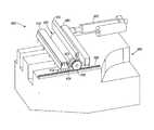
- FIG. 1is an example additive deposition system including a selective charging system having a charge transfer roller.
- FIG. 2is an example selective charging system including a charge transfer roller for use in an additive deposition system.
- FIG. 3is a top view of an example selective charging system including a charge transfer roller for use in an additive deposition system.
- FIGS. 4A-4Care an example additive deposition system including a selective charging system having a charge transfer roller.
- Embodiments and arrangements disclosed hereininclude a charge transfer roller for use in an electrostatic charge based additive deposition process.
- the electrostatic charge based additive deposition processuses electrostatically charged additive material that is deposited onto a substrate that has been selectively charged.
- the additive materialis deposited onto the selectively charged substrate based on the selective electrostatic charging of the substrate.
- the charge transfer rollercan be selectively charged and in-turn apply that selective charging to the substrate to selectively charge the substrate as desired.
- the use of the charge transfer rollercan increase the resolution of the selective charging and reduces charge blooming effects in thick substrates.
- FIG. 1is an example additive deposition system 100 that utilizes electrostatic charge based selective deposition.
- a selective charging system 120selectively charges the substrate 140 in a desired or preselected pattern.
- the pattern of chargingcan be a positive, i.e. additive material is deposited onto the selectively charged areas created by the selective charging system 120 , or the pattern of charging can be a negative, i.e. the additive material is repelled from the selectively charged areas created by the selective charging system 120 and deposited in the areas that were not affected or charged by the selective charging system 120 .
- Selectively charged substrate 144is then exposed to the additive material for selective deposition.
- An additive material system 130prepares and charges additive material for selected deposition onto the selectively charged portions 144 of the substrate 140 , a positive additive deposition process.
- the prepared and charged additive materialis deposited in non-selectively charged portions the substrate 140 . That is, the additive material is deposited on the substrate 140 about or around the selectively charged portions 144 .
- the process of selectively charging the substrate in a pattern and depositing additive material onto the substrate 140 based on the selective chargingcan be repeated to build-up a matrix of additive material, layer-by-layer.
- the selective charging system 120includes a charge transfer roller 126 that applies the selective charging to the substrate 140 and a charging device 122 that applies the desired selective charging to the charge transfer roller 126 .
- the charging device 122selectively charges the charge transfer roller 126 a portion at a time. As the charge transfer roller 126 is rotated, the charging device 122 selectively charges the charge transfer roller 126 one portion at a time.
- the selectively charged portions of the charge transfer roller 126contact or come in proximity to the substrate 140 , selectively applying or altering the surface charge of the substrate 140 based on the selectively charged portions of the charge transfer roller 126 .
- the selectively charged substrate 144is then exposed to the additive material for deposition of the additive material onto the selectively charged substrate 144 based on the selective charging imparted onto the substrate 140 by the selectively charged portions of the charge transfer roller 126 .
- the charging device 122 of the selective charging system 120can be an ionographic printhead 124 .
- the ionographic printheadgenerates and modulates a stream of ions towards the charge transfer roller 126 to form a selectively charged portion of the charge transfer roller 126 .
- the ionographic printhead 124can be translated along the axis of the charge transfer roller 126 during the selective charging process.
- the ionographic printhead 124can have a length similar or greater than the length of the charger transfer roller 126 , which selectively charges a portion of the charge transfer roller 126 across the length of the charge transfer roller 126 .
- the charging device 122can include an optical source 123 that selectively charges a charge transfer roller 126 having an outer covering of electrophotographic material. Light from the optical source 123 strikes the electrophotographic material of the charge transfer roller 126 and induces or modifies a charge locally in the material. Modulating the light emitted from the optical source 123 allows for the selective charging of the charge transfer roller 126 .
- the optical source 123can span the entire length of the charge transfer roller 126 or can be translated across the length of the charge transfer roller 126 to perform the selective charging.
- Additive materialis deposited onto the substrate 140 based on the selectively charged portions 144 of the substrate 140 . The additive material is processed, or handled, by the additive material system 130 in preparation for selective deposition onto the substrate 140 .
- the additive material system 130includes an additive material preparation device 132 and an additive material charging device 134 .
- the additive material preparation device 132prepares additive material of a desirable size, such as a droplet or powder form.
- the additive material preparation device 132can include an excluder or other means of size selection of the additive material packages to prevent additive material having a size outside of desired parameters from being processed further. Once prepared, the additive material is charged in preparation for deposition onto the substrate 140 based on the selective charged portions 144 of the substrate 140 .
- the additive material preparation device 132can be a filament extension atomizer (FEA).
- FFAfilament extension atomizer
- the filament extension atomizerstretches filaments of an additive material in a fluid state. The break-up of the stretched fluid filaments produces droplets of additive material that can then be charged for selective deposition onto the substrate 140 .
- the prepared additive materialcan be charged by the additive material charging device 134 .
- the additive material charging device 134imparts an electrostatic charge or potential in or on the prepared additive material.
- the imparted chargecan be similar or opposite a charge of the selectively charged portions 144 of the substrate 140 . If the charge of the additive material is similar to that of the selectively charged portions 144 of the substrate 140 , a negative process of additive deposition occurs in which the additive material is deposited, due to the electrostatic repulsion, onto the substrate 140 in the portions other than the selectively charged portions 144 .
- the negative deposition processis due to the repulsion caused by the similar charges of the additive material and the selectively charged portions 144 of the substrate 140 . If the charge of the additive material is opposite that of the selectively charged portions 144 , a positive process of additive deposition occurs in which the additive material is deposited, due to electrostatic attraction, onto the selectively charged portions 144 of the substrate 140 . The positive deposition process is due to the attraction caused by the oppositely charged additive material and the selectively charged portions 144 of the substrate 140 .
- a substrate pre-charge system 110can be included in the additive deposition system 100 .
- the substrate pre-charge system 110can uniformly charge the substrate 140 to a desired charge, having a polarity and, optionally, a magnitude, using a blanket charger 112 .
- the substrate pre-charge systemcan include a charge neutralizer 114 to neutralize the charge of the substrate 140 .
- the substrate pre-charge system 110can use the charge neutralizer 114 to effectively “blank” or remove any existing charges from the surface of the substrate 140 and from any previously deposited layers of additive material.
- the blanket charger 112can then uniformly the charge the surface of the substrate and any exposed layers of previously deposited additive material.
- the blanket charger 112creates a uniform charge across a top, exposed, layer of substrate 140 and previously deposited additive material.
- the uniformly charged or charge neutral substrate 142is then selectively charged by the selective charging system 120 .
- the additive deposition system 100can include a substrate handling system 150 that translates the substrate beneath the substrate pre-charge system 110 , the selective charging system 120 and/or the additive material system 130 .
- the substrate handling system 150can translate the substrate 140 in a vertical direction in preparation for the ensuing layers.
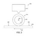
- FIG. 2shows an example selective charging system 200 , including an ionographic printhead 210 and a charge transfer roller 220 .
- the ionographic printhead 210generates a stream of ions and directs them onto the charge transfer roller 220 , which selectively charges a portion of the charge transfer roller 220 in a desired or selected pattern.
- the charge transfer roller 220then contacts the substrate 230 , which causes the substrate to become selectively charged based on the selective charging on the charge transfer roller 220 at the point of contact with the substrate 230 .
- the ionographic printhead 210generates and modulates a flow of ions that are directed onto a dielectric layer 222 of the charge transfer roller 220 .
- the modulation of ions from the ionographic printhead 210 onto the dielectric layer 222 of the charge transfer roller 220selectively charges a portion of the charge transfer roller 220 .
- the ions from the ionographic printhead 210are accelerated onto the dielectric layer 222 of the charge transfer roller 220 by the ground plane or back electrode 224 about which the dielectric layer 222 is disposed.
- the ground plane 224further assists with the retention of charge on the dielectric layer 222 .
- Ions from the ionographic printhead 210can induce, modify or neutralize charge in the dielectric layer 222 of the charge transfer roller 220 .
- the selective flow of ions from the ionographic printheadcan induce or impart selective electrostatic charging of the dielectric layer 222 .
- the dielectric layer 222can be uniformly charged prior to the ionographic printhead 210 .
- the selective flow of ions from the ionographic printhead 210can then selectively modify or neutralize portions of the uniformly charged dialectic layer 222 .
- the dielectric layer 222can be relatively thin, which increases the retention of a desired magnitude of charge on the dielectric layer 222 to selectively charge the charge transfer roller 220 .
- the degree of control over the selective placement of charge onto the dielectric layer 222 and the magnitude of the selectively placed chargeincreases the available resolution for the additive deposition process.
- the reduction of charge blooming, charge leakage or migration, in the dielectric layer 222allows a high degree of precision in charge location and magnitude which increases the available resolution for an additive deposition process.
- the combination of a relatively thin dielectric layer 222 and control over the ground plane or back electrode 224allows for a high resolution, selective additive deposition process to be achieved through control over charge placement and magnitude.
- Controlling the magnitude of the charge to be transferred by the charge transfer roller 220 onto the substrate 230allows control over the amount of additive material that is deposited in that particular location.
- more or less additive materialis electrostatically attracted to and agglomerate in that location based on the charge of the additive material.
- the charge transfer roller 220is rotated 226 while the substrate 230 is translated 236 such that the relative velocity is substantially zero at a point of contact between the charge transfer roller 220 and the substrate 230 .
- the selective charge of the dielectric layer 222alters the charging of the substrate 230 , which selectively charges or neutralizes a portion of the substrate 230 based on the selective charging imparted onto the charge transfer roller 220 by the ionographic printhead 210 .
- the selectively charged substrate 234can then be exposed to charged additive material to perform the additive deposition process onto the substrate 230 based on the selectively charged portions 234 .
- the substrate 230can undergo a pre-charging process to pre-charge the substrate 232 before being selectively neutralized by the selective charging system 200 .
- the pre-charging processcan include neutralizing the surface charges of the substrate 230 and/or charging the substrate 230 with a uniform charge across the surface.
- the surface of the substrate 230 and the substrate 230are understood to be the exposed upper surface of the substrate and/or any previously deposited layers of additive material.
- a mechanical system to maintain charge transfer roller 220 contact with the substrate 230can be included in the selective charging system 200 .
- the charge transfer roller 220can be weighted, internally or externally, to increase its mass and reduce the likelihood the charge transfer roller 220 loses contact with the surface of the substrate 230 .
- a spring or system of springscan be used to retain the charge transfer roller 220 against the surface of the substrate 230 .
- an active systemcan be used to maintain contact between the charge transfer roller 220 and the surface of the substrate 230 .
- the active systemcan further adjust the amount of pressure exerted by the charge transfer roller 220 on the surface of the substrate 230 , which allows a desired or required contact pressure between the charge transfer roller 220 and substrate 230 to be achieved.
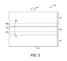
- FIG. 3is a top view of an example selective charging system 300 that includes a charge transfer roller 320 .
- a substrate 310is translated 316 beneath a rotating 323 charge transfer roller 320 .
- the charge transfer roller 320is selectively charged by a charging device 324 .
- the selectively charged portion 314 of the substratecan then be exposed to electrostatically charged additive material to selectively deposit additive material onto the substrate 310 based on the selectively charged portion 314 .
- the charging device 324can span the entire length of the charge transfer roller 320 , as shown in FIG. 3 , or can span a length greater than or less than the length of the charge transfer roller 320 .
- the charge transfer roller 320can be interchanged from the selective charging system 300 to match the width of the substrate, as necessary or desired.
- the charging device 324is an ionographic printhead that generates and modulates a stream of ions to selectively charge the charge transfer roller 320 .
- the selectively charged portion 322 A of the charge transfer roller 320is rotated 323 to contact the substrate 310 and selectively charge a portion 314 of the substrate 310 .
- the now neutralized portion 322 B of the charge transfer roller 320is then rotated 323 to be selectively charged 322 A again by the ionographic printhead 324 .
- the portion 322 B of the rollercan be uniformly charged or neutralized prior to selective charging by the ionographic printhead 324 .
- the substrate 310can be pre-charged 312 to a neutral or uniformly charged state. This can assist in the selective charging process by creating a uniformly charged substrate 310 that can then be charge altered in a more precise and measured manner by minimizing the degree the substrate 310 can affect the magnitude of the applied selective charging. Further, the pre-charging of the substrate can remove or override any residual electrostatic charges that remain in the substrate 310 or previously deposited additive material. Pre-charging can assist in increasing or maintaining the achievable resolution of the selective additive deposition process.
- FIGS. 4A-4Care an example additive deposition system 400 including a selective charging system having a charge transfer roller 420 .
- Additive materialis selectively deposited onto the substrate 460 through the additive deposition system 400 based on charging of the substrate 460 surface and the charging of the additive material.
- a blanket charger, such as a scorotron, 410uniformly charges the surface of the substrate 460 .
- the scorotron 410emits ions 412 , uniformly charging the surface of the substrate 460 with a charge in preparation for a selective charging process.
- the charge transfer roller 420is selectively charged by an ionographic printhead 430 .
- the ionographic print head 430emits a stream of ions directed towards the charge transfer roller 420 to selectively charge the roller 420 in a desired pattern.
- the charge transfer roller 420includes a conductive core 424 surrounded by a layer of dielectric material 422 .
- the conductive core 424 and the layer of dielectric material 422retain the selective charging created by the ionographic printhead 430 on the surface of the charge transfer roller 420 .
- the stored charges on the dielectric layer 422contact the uniformly charged substrate 460 surface, selectively altering the surface charges of the substrate 460 based on the selective charging of the charge transfer roller 420 .
- Additive materialis then deposited onto the selectively charged substrate 460 surface based on the selective charging of the substrate 460 surface and a charge of the additive material.
- the additive materialis passed through an additive material depositor 440 that channels or directs charged additive material proximate the surface of the substrate 460 .
- Additive materialcan be attracted and deposited onto oppositely charged portions of the surface of the substrate 460 .
- the amount of additive material depositedis based on the charge of the additive material and the charge of the selectively charged portions of the substrate 460 , as the additive material can be attracted onto the selectively charged surface of the substrate 460 until the selective charge is substantially neutralized.
- the assembly of the scorotron 410 , charge transfer roller 420 , ionographic printhead 430 and additive material depositor 440are translated across the substrate 460 surface by a linear actuator 450 that extends and retracts moving the assembly.
- the charge transfer roller 420can include a charge transfer roller drive gear 426 that engages a charge transfer roller drive track 428 on the surface of the substrate 460 .
- the engagement of the drive gear 426 and drive track 428rotates and indexes the charge transfer roller 420 as the linear actuator 450 extends and retracts.
- the linear actuator 450translates the assembly, the linear motion of the assembly causes the rotation of the drive gear 426 , rotating the charge transfer roller 420 .
- the selective charging stored on the dielectric layer 422selectively alters the uniformly charged surface of the substrate 460 .
- the areas of the build platform that are not filled in with deposited material 460can be filled in with a support material in order to ensure the entire area is filled with a material.
- the use of a charge transfer rollerallows for a high resolution additive deposition process.
- the charge transfer rollerallows a greater degree of precision in charge placement and charge magnitude, allowing for greater control over the additive deposition process as a whole.
Landscapes
- Chemical & Material Sciences (AREA)
- Physics & Mathematics (AREA)
- Engineering & Computer Science (AREA)
- General Physics & Mathematics (AREA)
- Materials Engineering (AREA)
- Chemical Kinetics & Catalysis (AREA)
- General Chemical & Material Sciences (AREA)
- Mechanical Engineering (AREA)
- Metallurgy (AREA)
- Organic Chemistry (AREA)
- Plasma & Fusion (AREA)
- Manufacturing & Machinery (AREA)
- Printers Or Recording Devices Using Electromagnetic And Radiation Means (AREA)
Abstract
Description
Claims (7)
Priority Applications (1)
| Application Number | Priority Date | Filing Date | Title |
|---|---|---|---|
| US15/292,906US9988720B2 (en) | 2016-10-13 | 2016-10-13 | Charge transfer roller for use in an additive deposition system and process |
Applications Claiming Priority (1)
| Application Number | Priority Date | Filing Date | Title |
|---|---|---|---|
| US15/292,906US9988720B2 (en) | 2016-10-13 | 2016-10-13 | Charge transfer roller for use in an additive deposition system and process |
Publications (2)
| Publication Number | Publication Date |
|---|---|
| US20180105937A1 US20180105937A1 (en) | 2018-04-19 |
| US9988720B2true US9988720B2 (en) | 2018-06-05 |
Family
ID=61903734
Family Applications (1)
| Application Number | Title | Priority Date | Filing Date |
|---|---|---|---|
| US15/292,906ActiveUS9988720B2 (en) | 2016-10-13 | 2016-10-13 | Charge transfer roller for use in an additive deposition system and process |
Country Status (1)
| Country | Link |
|---|---|
| US (1) | US9988720B2 (en) |
Cited By (1)
| Publication number | Priority date | Publication date | Assignee | Title |
|---|---|---|---|---|
| US11167375B2 (en) | 2018-08-10 | 2021-11-09 | The Research Foundation For The State University Of New York | Additive manufacturing processes and additively manufactured products |
Families Citing this family (1)
| Publication number | Priority date | Publication date | Assignee | Title |
|---|---|---|---|---|
| US20220380928A1 (en)* | 2021-05-29 | 2022-12-01 | Nissan North America, Inc. | Method and system of powder coating a vehicle component |
Citations (40)
| Publication number | Priority date | Publication date | Assignee | Title |
|---|---|---|---|---|
| US2291046A (en) | 1942-07-28 | Arrangement for burning liquid fuel | ||
| US3554815A (en) | 1963-04-30 | 1971-01-12 | Du Pont | Thin,flexible thermoelectric device |
| US3626833A (en) | 1969-06-09 | 1971-12-14 | Addressograph Multigraph | Liquid developing apparatus |
| US3649829A (en) | 1970-10-06 | 1972-03-14 | Atomic Energy Commission | Laminar flow cell |
| US3702258A (en) | 1969-03-05 | 1972-11-07 | Eastman Kodak Co | Web treatment method |
| US3717875A (en) | 1971-05-04 | 1973-02-20 | Little Inc A | Method and apparatus for directing the flow of liquid droplets in a stream and instruments incorporating the same |
| US3873025A (en) | 1974-05-06 | 1975-03-25 | Stora Kopparbergs Bergslags Ab | Method and apparatus for atomizing a liquid medium and for spraying the atomized liquid medium in a predetermined direction |
| US3926114A (en) | 1967-06-30 | 1975-12-16 | Walter E S Matuschke | Rotary lithographic printing press with ink and dampening fluid separator |
| US4034670A (en) | 1975-03-24 | 1977-07-12 | Rockwell International Corporation | Dampening device for lithographic printing press |
| US4222059A (en) | 1978-12-18 | 1980-09-09 | Xerox Corporation | Ink jet multiple field electrostatic lens |
| US4384296A (en) | 1981-04-24 | 1983-05-17 | Xerox Corporation | Linear ink jet deflection method and apparatus |
| US5003327A (en)* | 1989-11-15 | 1991-03-26 | Delphax Systems | Printer autocontrast control |
| US5270086A (en) | 1989-09-25 | 1993-12-14 | Schneider (Usa) Inc. | Multilayer extrusion of angioplasty balloons |
| US5307119A (en)* | 1992-12-31 | 1994-04-26 | Xerox Corporation | Method and apparatus for monitoring and controlling a toner image formation process |
| US5314119A (en) | 1992-04-20 | 1994-05-24 | Latanick Equipment, Inc. | Method and apparatus for applying thin coatings of fluid droplets |
| US5402214A (en)* | 1994-02-23 | 1995-03-28 | Xerox Corporation | Toner concentration sensing system for an electrophotographic printer |
| US6382524B1 (en) | 1999-11-26 | 2002-05-07 | Diversey Lever, Inc. | Applicator for applying a fluid to a surface and method of applying a fluid to a surface |
| US20020053320A1 (en) | 1998-12-15 | 2002-05-09 | Gregg M. Duthaler | Method for printing of transistor arrays on plastic substrates |
| US6576861B2 (en) | 2000-07-25 | 2003-06-10 | The Research Foundation Of State University Of New York | Method and apparatus for fine feature spray deposition |
| US6622335B1 (en) | 2000-03-29 | 2003-09-23 | Lam Research Corporation | Drip manifold for uniform chemical delivery |
| US20050000231A1 (en) | 2003-07-02 | 2005-01-06 | Ju-Yeon Lee | Wearable cooler using thermoelectric module |
| US6934142B2 (en) | 2001-02-23 | 2005-08-23 | Robert Bosch Gmbh | Device and method for charge removal from dielectric surfaces |
| US20060035033A1 (en) | 2004-08-10 | 2006-02-16 | Konica Minolta Photo Imaging, Inc. | Spray coating method, spray coating device and inkjet recording sheet |
| US7083830B2 (en) | 2003-10-02 | 2006-08-01 | E. I. Dupont De Nemours And Company | Electrostatically-assisted high-speed rotary application process for the production of special effect base coat/clear coat two-layer coatings |
| US20090014046A1 (en) | 2007-07-12 | 2009-01-15 | Industrial Technology Research Institute | Flexible thermoelectric device and manufacturing method thereof |
| US20100154856A1 (en) | 2007-03-13 | 2010-06-24 | Sumitomo Chemical Company, Limited | Substrate for Thermoelectric Conversion Module, and Thermoelectric Conversion Module |
| US20110017431A1 (en) | 2009-03-06 | 2011-01-27 | Y.C. Lee | Flexible thermal ground plane and manufacturing the same |
| US20110150036A1 (en) | 2009-12-21 | 2011-06-23 | Electronics And Telecommunications Research Institute | Flexible thermoelectric generator, wireless sensor node including the same and method of manufacturing the same |
| US20110154558A1 (en) | 2008-06-02 | 2011-06-30 | Nederlandse Organisatie Voor Toegepast- Natuurwetenschappelijk Onderzoek Tno | Method for Manufacturing a Thermoelectric Generator, a Wearable Thermoelectric Generator and a Garment Comprising the Same |
| EP2227834B1 (en) | 2007-12-28 | 2011-08-03 | Basf Se | Extrusion process for producing improved thermoelectric materials |
| US8132744B2 (en) | 2004-12-13 | 2012-03-13 | Optomec, Inc. | Miniature aerosol jet and aerosol jet array |
| US20120227778A1 (en) | 2011-03-11 | 2012-09-13 | Imec | Thermoelectric Textile |
| US8272579B2 (en) | 2007-08-30 | 2012-09-25 | Optomec, Inc. | Mechanically integrated and closely coupled print head and mist source |
| US20130087180A1 (en) | 2011-10-10 | 2013-04-11 | Perpetua Power Source Technologies, Inc. | Wearable thermoelectric generator system |
| US8511251B2 (en) | 2009-08-24 | 2013-08-20 | Fujitsu Limited | Film deposition device and method thereof |
| US8552299B2 (en) | 2008-03-05 | 2013-10-08 | The Board Of Trustees Of The University Of Illinois | Stretchable and foldable electronic devices |
| US8720370B2 (en) | 2011-04-07 | 2014-05-13 | Dynamic Micro System Semiconductor Equipment GmbH | Methods and apparatuses for roll-on coating |
| US20140146116A1 (en) | 2012-11-29 | 2014-05-29 | Palo Alto Research Center Incorporated | Pulsating heat pipe spreader for ink jet printer |
| US8742246B2 (en) | 2011-04-22 | 2014-06-03 | Panasonic Corporation | Thermoelectric conversion module and method of manufacturing thereof |
| US9021948B2 (en) | 2011-04-27 | 2015-05-05 | Xerox Corporation | Environmental control subsystem for a variable data lithographic apparatus |
- 2016
- 2016-10-13USUS15/292,906patent/US9988720B2/enactiveActive
Patent Citations (40)
| Publication number | Priority date | Publication date | Assignee | Title |
|---|---|---|---|---|
| US2291046A (en) | 1942-07-28 | Arrangement for burning liquid fuel | ||
| US3554815A (en) | 1963-04-30 | 1971-01-12 | Du Pont | Thin,flexible thermoelectric device |
| US3926114A (en) | 1967-06-30 | 1975-12-16 | Walter E S Matuschke | Rotary lithographic printing press with ink and dampening fluid separator |
| US3702258A (en) | 1969-03-05 | 1972-11-07 | Eastman Kodak Co | Web treatment method |
| US3626833A (en) | 1969-06-09 | 1971-12-14 | Addressograph Multigraph | Liquid developing apparatus |
| US3649829A (en) | 1970-10-06 | 1972-03-14 | Atomic Energy Commission | Laminar flow cell |
| US3717875A (en) | 1971-05-04 | 1973-02-20 | Little Inc A | Method and apparatus for directing the flow of liquid droplets in a stream and instruments incorporating the same |
| US3873025A (en) | 1974-05-06 | 1975-03-25 | Stora Kopparbergs Bergslags Ab | Method and apparatus for atomizing a liquid medium and for spraying the atomized liquid medium in a predetermined direction |
| US4034670A (en) | 1975-03-24 | 1977-07-12 | Rockwell International Corporation | Dampening device for lithographic printing press |
| US4222059A (en) | 1978-12-18 | 1980-09-09 | Xerox Corporation | Ink jet multiple field electrostatic lens |
| US4384296A (en) | 1981-04-24 | 1983-05-17 | Xerox Corporation | Linear ink jet deflection method and apparatus |
| US5270086A (en) | 1989-09-25 | 1993-12-14 | Schneider (Usa) Inc. | Multilayer extrusion of angioplasty balloons |
| US5003327A (en)* | 1989-11-15 | 1991-03-26 | Delphax Systems | Printer autocontrast control |
| US5314119A (en) | 1992-04-20 | 1994-05-24 | Latanick Equipment, Inc. | Method and apparatus for applying thin coatings of fluid droplets |
| US5307119A (en)* | 1992-12-31 | 1994-04-26 | Xerox Corporation | Method and apparatus for monitoring and controlling a toner image formation process |
| US5402214A (en)* | 1994-02-23 | 1995-03-28 | Xerox Corporation | Toner concentration sensing system for an electrophotographic printer |
| US20020053320A1 (en) | 1998-12-15 | 2002-05-09 | Gregg M. Duthaler | Method for printing of transistor arrays on plastic substrates |
| US6382524B1 (en) | 1999-11-26 | 2002-05-07 | Diversey Lever, Inc. | Applicator for applying a fluid to a surface and method of applying a fluid to a surface |
| US6622335B1 (en) | 2000-03-29 | 2003-09-23 | Lam Research Corporation | Drip manifold for uniform chemical delivery |
| US6576861B2 (en) | 2000-07-25 | 2003-06-10 | The Research Foundation Of State University Of New York | Method and apparatus for fine feature spray deposition |
| US6934142B2 (en) | 2001-02-23 | 2005-08-23 | Robert Bosch Gmbh | Device and method for charge removal from dielectric surfaces |
| US20050000231A1 (en) | 2003-07-02 | 2005-01-06 | Ju-Yeon Lee | Wearable cooler using thermoelectric module |
| US7083830B2 (en) | 2003-10-02 | 2006-08-01 | E. I. Dupont De Nemours And Company | Electrostatically-assisted high-speed rotary application process for the production of special effect base coat/clear coat two-layer coatings |
| US20060035033A1 (en) | 2004-08-10 | 2006-02-16 | Konica Minolta Photo Imaging, Inc. | Spray coating method, spray coating device and inkjet recording sheet |
| US8132744B2 (en) | 2004-12-13 | 2012-03-13 | Optomec, Inc. | Miniature aerosol jet and aerosol jet array |
| US20100154856A1 (en) | 2007-03-13 | 2010-06-24 | Sumitomo Chemical Company, Limited | Substrate for Thermoelectric Conversion Module, and Thermoelectric Conversion Module |
| US20090014046A1 (en) | 2007-07-12 | 2009-01-15 | Industrial Technology Research Institute | Flexible thermoelectric device and manufacturing method thereof |
| US8272579B2 (en) | 2007-08-30 | 2012-09-25 | Optomec, Inc. | Mechanically integrated and closely coupled print head and mist source |
| EP2227834B1 (en) | 2007-12-28 | 2011-08-03 | Basf Se | Extrusion process for producing improved thermoelectric materials |
| US8552299B2 (en) | 2008-03-05 | 2013-10-08 | The Board Of Trustees Of The University Of Illinois | Stretchable and foldable electronic devices |
| US20110154558A1 (en) | 2008-06-02 | 2011-06-30 | Nederlandse Organisatie Voor Toegepast- Natuurwetenschappelijk Onderzoek Tno | Method for Manufacturing a Thermoelectric Generator, a Wearable Thermoelectric Generator and a Garment Comprising the Same |
| US20110017431A1 (en) | 2009-03-06 | 2011-01-27 | Y.C. Lee | Flexible thermal ground plane and manufacturing the same |
| US8511251B2 (en) | 2009-08-24 | 2013-08-20 | Fujitsu Limited | Film deposition device and method thereof |
| US20110150036A1 (en) | 2009-12-21 | 2011-06-23 | Electronics And Telecommunications Research Institute | Flexible thermoelectric generator, wireless sensor node including the same and method of manufacturing the same |
| US20120227778A1 (en) | 2011-03-11 | 2012-09-13 | Imec | Thermoelectric Textile |
| US8720370B2 (en) | 2011-04-07 | 2014-05-13 | Dynamic Micro System Semiconductor Equipment GmbH | Methods and apparatuses for roll-on coating |
| US8742246B2 (en) | 2011-04-22 | 2014-06-03 | Panasonic Corporation | Thermoelectric conversion module and method of manufacturing thereof |
| US9021948B2 (en) | 2011-04-27 | 2015-05-05 | Xerox Corporation | Environmental control subsystem for a variable data lithographic apparatus |
| US20130087180A1 (en) | 2011-10-10 | 2013-04-11 | Perpetua Power Source Technologies, Inc. | Wearable thermoelectric generator system |
| US20140146116A1 (en) | 2012-11-29 | 2014-05-29 | Palo Alto Research Center Incorporated | Pulsating heat pipe spreader for ink jet printer |
Non-Patent Citations (34)
| Title |
|---|
| "Ortho-Planar Spring", BYI Mechanical Engineering Website, URL: http://compliantmechanisms.byu.edu/content/ortho-planar-spring, retrieved from the Internet on Dec. 23, 2014. |
| Arens, E., "Partial- and whole-body thermal sensation and comfort-Part I: Uniform environmental conditions," Journal of Thermal Biology, vol. 31, Issues 1-2, Jan. 2006, pp. 53-59. |
| Arens, E., "Partial- and whole-body thermal sensation and comfort-Part II: Non-uniform environmental conditions," Journal of Thermal Biology, vol. 31, Issues 1-2, Jan. 2006, pp. 60-66. |
| Arens, E., "Partial- and whole-body thermal sensation and comfort—Part I: Uniform environmental conditions," Journal of Thermal Biology, vol. 31, Issues 1-2, Jan. 2006, pp. 53-59. |
| Arens, E., "Partial- and whole-body thermal sensation and comfort—Part II: Non-uniform environmental conditions," Journal of Thermal Biology, vol. 31, Issues 1-2, Jan. 2006, pp. 60-66. |
| Bailey, Adrian G.: "The Science and technology of electrostatic powder spraying, transport and coating", Journal of Electrostatics, vol. 45, 1998, pp. 85-120. |
| Bhat, Pradeep R, "Formation of beads-on-a-string structures during break-up of viscoelastic filaments," Aug. 2010, vol. 6:625-631, Nature Physics, 7 pages. |
| Bullis, Kevin, "Expandable Silicon", MIT Technology Review, Dec. 14, 2007, URL: http://www.technologyreview.com/news/409198/expandable-silicon/, retrieved from the Internet on Dec. 23, 2014. |
| C. Huizenga, H. Zhang, E. Arens, D. Wang: "Skin and core temperature response to partial- and whole-body heating and cooling," Journal of Thermal Biology, vol. 29, Issues 7-8, Oct.-Dec. 2004, pp. 549-558. |
| Chapter 15, "Ink Jet Printing", 14 pages, found at http://www.lintech.org/comp-per/15INK.pdf. |
| Chen, A.,"Dispenser-printed planar thick-film thermoelectric energy generators," J. Micromech. Microeng., 21(10), 2011. |
| Crowe, Clayton et al.: "Multiphase Flows With Droplets and Particles", CRC Press, LLC, 1998. |
| Domnick, et al.: "The Simulation of Electrostatic Spray Painting Process with High-Speed Rotary Bell Atomizers. Part II: External Charging", Part. Part. Syst. Charact. vol. 23, 2006, pp. 408-416, URL: http://www.ppsc-journal.com. |
| Francioso, L., "Flexible thermoelectric generator for ambient assisted living wearable biometric sensors", Journal of Power Sources, vol. 196, Issue 6, Mar. 15, 2011, pp. 3239-3243. |
| Hewitt, A.B., "Multilayered Carbon Nanotube/Polymer Composite Based Thermoelectric Fabrics," Nano Letters, 12(3), pp. 1307-1310, 2012. |
| http://www.cvs.com/shop/product-detail/CVS-Cold-Pain-Relief-Pack-Reusable?skuld=324111, retrieved on Dec. 19, 2014. |
| http://www.glaciertek.com/, retrieved on Dec. 19, 2014. |
| http://www.stacoolvest.com/, retrieved on Dec. 19, 2014. |
| http://www.steelevest.com/, retrieved on Dec. 19, 2014. |
| http://www.veskimo.com/, retrieved on Dec. 19, 2014. |
| Kelly, Ryan T, et al..: "The ion funnel: theory, implementations, and applications", Mass Spectrometry Reviews,vol. 29, 2010, pp. 294-312. |
| L. Francioso, C. De Pascali, A. Taurino, P. Siciliano, A. De Risi: "Wearable and flexible thermoelectric generator with enhanced package," In Proc. SPIE 8763, Smart Sensors, Actuators, and MEMS VI, 876306, May 2013. |
| Le, Hue P., "Progress and Trends in Ink-jet Printing Technology," Jan./Feb. 1998, vol. 42:49-62, Journal of Imaging Science and Technology, 16 pages, found at: http://www.imaging.org/ist/resources/tutorials/inkjet.cfm. |
| Marple, A. and Liu, Y.H.: "Characteristics of Laminar Jet Impactors", Environmental Science & Technology, vol. 8, No. 7, Jul. 1974, pp. 648-654. |
| Matheson, Rob, "Cool Invention Wins First Place at MADMEC", MIT News Office, Oct. 17, 2013, 3 pages, retrieved from the Internet: http://newsoffice.mit.edu/2013/madmec-design-competition-1017, retrieved on Dec. 19, 2014. |
| McClure, Max, "Stanford Researchers' Cooling Glove Better than Steroids-and Helps Solve Physiological Mystery Too", Stanford Report, Aug. 29, 2012, 3 pages, retrieved from the Internet: http://news.stanford.edu/news/2012/august/cooling-glove-research-082912.html, retrieved on Dec. 19, 2014. |
| McClure, Max, "Stanford Researchers' Cooling Glove Better than Steroids—and Helps Solve Physiological Mystery Too", Stanford Report, Aug. 29, 2012, 3 pages, retrieved from the Internet: http://news.stanford.edu/news/2012/august/cooling-glove-research-082912.html, retrieved on Dec. 19, 2014. |
| Oliveira, Monica S., "Iterated Stretching, Extensional Rheology and Formation of Beads-on-a-String Structures in Polymer Solutions," Jan. 20, 2006, Special Issue of JNNFM on Extensional Flow, MIT, Cambridge, MA, 36 pages. |
| Owen, M., "Misting of non-Newtonian Liquids in Forward Roll Coating," Jul. 13, 2011, Journal of Non-Newtonian Fluid Mechanics, vol. 166:1123-1128, 6 pages. |
| S.-J. Kim, J.-H. Wea and B.-J. Cho: "A wearable thermoelectric generator fabricated on a glass fabric," Energy Environmental Science, 2014. |
| Shi, X.D., "A Cascade of Structure in a Drop Falling from a Faucet," Jul. 8, 2004, vol. 265:219-222, Science, 4 pages. |
| Sholin, V. et al.: "High Work Function Materials for Source/Drain Contacts in Printed Polymer Thin Transistors," Applied Physics Letters, vol. 92, 2008. |
| Vanhemert, Kyle, "MIT Wristband Could Make AC Obsolete", Wired.com, Oct. 30, 2013, retrieved from the Internet: http://www.wired.com/2013/10/an-ingenious-wristband-that-keeps-your-body-at-theperfect-temperature-no-ac-required/, retrieved on Dec. 19, 2014. |
| Zhou, Li, et al: "Highly Conductive, Flexible, Polyurethane-Based Adhesives for Flexible and Printed Electronics," Advanced Functional Materials, vol. 23, p. 1459-1465, wileyonlinelibrary.com. |
Cited By (3)
| Publication number | Priority date | Publication date | Assignee | Title |
|---|---|---|---|---|
| US11167375B2 (en) | 2018-08-10 | 2021-11-09 | The Research Foundation For The State University Of New York | Additive manufacturing processes and additively manufactured products |
| US11426818B2 (en) | 2018-08-10 | 2022-08-30 | The Research Foundation for the State University | Additive manufacturing processes and additively manufactured products |
| US12122120B2 (en) | 2018-08-10 | 2024-10-22 | The Research Foundation For The State University Of New York | Additive manufacturing processes and additively manufactured products |
Also Published As
| Publication number | Publication date |
|---|---|
| US20180105937A1 (en) | 2018-04-19 |
Similar Documents
| Publication | Publication Date | Title |
|---|---|---|
| EP3196002B1 (en) | Additive deposition system | |
| US8968625B2 (en) | Process for building three-dimensional objects | |
| RU2641578C2 (en) | Application head in additive manufacturing | |
| EP3196003B1 (en) | Additive deposition method | |
| US10220471B2 (en) | Spatter reduction laser scanning strategy in selective laser melting | |
| RU2602895C1 (en) | Method for producing a structures body and device for producing thereof | |
| US20160368055A1 (en) | Selective depositing of powder in additive manufacturing | |
| JP2019501798A (en) | Method for producing silicone elastomer articles with enhanced print quality | |
| CN109843591B (en) | Methods of forming 3D objects | |
| US9988720B2 (en) | Charge transfer roller for use in an additive deposition system and process | |
| US11413813B2 (en) | Electrostatic polymer aerosol deposition and fusing of solid particles for three-dimensional printing | |
| US10807273B2 (en) | High temperature additive manufacturing print head | |
| DE102014010412A1 (en) | Method and arrangement for the additive production of components | |
| Kumar et al. | Investigation of an electrophotography based rapid prototyping technology | |
| US11825610B2 (en) | Process for the manufacturing of printed conductive tracks on an object and 3D printed electronics | |
| JP6878364B2 (en) | Movable wall for additional powder floor | |
| US20190134912A1 (en) | Setting printing distances |
Legal Events
| Date | Code | Title | Description |
|---|---|---|---|
| AS | Assignment | Owner name:PALO ALTO RESEARCH CENTER INCORPORATED, CALIFORNIA Free format text:ASSIGNMENT OF ASSIGNORS INTEREST;ASSIGNOR:JOHNSON, DAVID MATHEW;REEL/FRAME:040009/0038 Effective date:20161013 | |
| STCF | Information on status: patent grant | Free format text:PATENTED CASE | |
| MAFP | Maintenance fee payment | Free format text:PAYMENT OF MAINTENANCE FEE, 4TH YEAR, LARGE ENTITY (ORIGINAL EVENT CODE: M1551); ENTITY STATUS OF PATENT OWNER: LARGE ENTITY Year of fee payment:4 | |
| AS | Assignment | Owner name:XEROX CORPORATION, CONNECTICUT Free format text:ASSIGNMENT OF ASSIGNORS INTEREST;ASSIGNOR:PALO ALTO RESEARCH CENTER INCORPORATED;REEL/FRAME:064038/0001 Effective date:20230416 | |
| AS | Assignment | Owner name:CITIBANK, N.A., AS COLLATERAL AGENT, NEW YORK Free format text:SECURITY INTEREST;ASSIGNOR:XEROX CORPORATION;REEL/FRAME:064760/0389 Effective date:20230621 | |
| AS | Assignment | Owner name:XEROX CORPORATION, CONNECTICUT Free format text:CORRECTIVE ASSIGNMENT TO CORRECT THE REMOVAL OF US PATENTS 9356603, 10026651, 10626048 AND INCLUSION OF US PATENT 7167871 PREVIOUSLY RECORDED ON REEL 064038 FRAME 0001. ASSIGNOR(S) HEREBY CONFIRMS THE ASSIGNMENT;ASSIGNOR:PALO ALTO RESEARCH CENTER INCORPORATED;REEL/FRAME:064161/0001 Effective date:20230416 | |
| AS | Assignment | Owner name:JEFFERIES FINANCE LLC, AS COLLATERAL AGENT, NEW YORK Free format text:SECURITY INTEREST;ASSIGNOR:XEROX CORPORATION;REEL/FRAME:065628/0019 Effective date:20231117 | |
| AS | Assignment | Owner name:XEROX CORPORATION, CONNECTICUT Free format text:TERMINATION AND RELEASE OF SECURITY INTEREST IN PATENTS RECORDED AT RF 064760/0389;ASSIGNOR:CITIBANK, N.A., AS COLLATERAL AGENT;REEL/FRAME:068261/0001 Effective date:20240206 Owner name:CITIBANK, N.A., AS COLLATERAL AGENT, NEW YORK Free format text:SECURITY INTEREST;ASSIGNOR:XEROX CORPORATION;REEL/FRAME:066741/0001 Effective date:20240206 | |
| AS | Assignment | Owner name:U.S. BANK TRUST COMPANY, NATIONAL ASSOCIATION, AS COLLATERAL AGENT, CONNECTICUT Free format text:FIRST LIEN NOTES PATENT SECURITY AGREEMENT;ASSIGNOR:XEROX CORPORATION;REEL/FRAME:070824/0001 Effective date:20250411 | |
| AS | Assignment | Owner name:U.S. BANK TRUST COMPANY, NATIONAL ASSOCIATION, AS COLLATERAL AGENT, CONNECTICUT Free format text:SECOND LIEN NOTES PATENT SECURITY AGREEMENT;ASSIGNOR:XEROX CORPORATION;REEL/FRAME:071785/0550 Effective date:20250701 |