US9978310B2 - Pixel circuits for amoled displays - Google Patents
Pixel circuits for amoled displaysDownload PDFInfo
- Publication number
- US9978310B2 US9978310B2US14/363,379US201314363379AUS9978310B2US 9978310 B2US9978310 B2US 9978310B2US 201314363379 AUS201314363379 AUS 201314363379AUS 9978310 B2US9978310 B2US 9978310B2
- Authority
- US
- United States
- Prior art keywords
- voltage
- drive transistor
- current
- transistor
- emitting device
- Prior art date
- Legal status (The legal status is an assumption and is not a legal conclusion. Google has not performed a legal analysis and makes no representation as to the accuracy of the status listed.)
- Active, expires
Links
Images


Classifications
- G—PHYSICS
- G09—EDUCATION; CRYPTOGRAPHY; DISPLAY; ADVERTISING; SEALS
- G09G—ARRANGEMENTS OR CIRCUITS FOR CONTROL OF INDICATING DEVICES USING STATIC MEANS TO PRESENT VARIABLE INFORMATION
- G09G3/00—Control arrangements or circuits, of interest only in connection with visual indicators other than cathode-ray tubes
- G09G3/20—Control arrangements or circuits, of interest only in connection with visual indicators other than cathode-ray tubes for presentation of an assembly of a number of characters, e.g. a page, by composing the assembly by combination of individual elements arranged in a matrix no fixed position being assigned to or needed to be assigned to the individual characters or partial characters
- G09G3/22—Control arrangements or circuits, of interest only in connection with visual indicators other than cathode-ray tubes for presentation of an assembly of a number of characters, e.g. a page, by composing the assembly by combination of individual elements arranged in a matrix no fixed position being assigned to or needed to be assigned to the individual characters or partial characters using controlled light sources
- G09G3/30—Control arrangements or circuits, of interest only in connection with visual indicators other than cathode-ray tubes for presentation of an assembly of a number of characters, e.g. a page, by composing the assembly by combination of individual elements arranged in a matrix no fixed position being assigned to or needed to be assigned to the individual characters or partial characters using controlled light sources using electroluminescent panels
- G09G3/32—Control arrangements or circuits, of interest only in connection with visual indicators other than cathode-ray tubes for presentation of an assembly of a number of characters, e.g. a page, by composing the assembly by combination of individual elements arranged in a matrix no fixed position being assigned to or needed to be assigned to the individual characters or partial characters using controlled light sources using electroluminescent panels semiconductive, e.g. using light-emitting diodes [LED]
- G09G3/3208—Control arrangements or circuits, of interest only in connection with visual indicators other than cathode-ray tubes for presentation of an assembly of a number of characters, e.g. a page, by composing the assembly by combination of individual elements arranged in a matrix no fixed position being assigned to or needed to be assigned to the individual characters or partial characters using controlled light sources using electroluminescent panels semiconductive, e.g. using light-emitting diodes [LED] organic, e.g. using organic light-emitting diodes [OLED]
- G09G3/3225—Control arrangements or circuits, of interest only in connection with visual indicators other than cathode-ray tubes for presentation of an assembly of a number of characters, e.g. a page, by composing the assembly by combination of individual elements arranged in a matrix no fixed position being assigned to or needed to be assigned to the individual characters or partial characters using controlled light sources using electroluminescent panels semiconductive, e.g. using light-emitting diodes [LED] organic, e.g. using organic light-emitting diodes [OLED] using an active matrix
- G09G3/3258—Control arrangements or circuits, of interest only in connection with visual indicators other than cathode-ray tubes for presentation of an assembly of a number of characters, e.g. a page, by composing the assembly by combination of individual elements arranged in a matrix no fixed position being assigned to or needed to be assigned to the individual characters or partial characters using controlled light sources using electroluminescent panels semiconductive, e.g. using light-emitting diodes [LED] organic, e.g. using organic light-emitting diodes [OLED] using an active matrix with pixel circuitry controlling the voltage across the light-emitting element
- G—PHYSICS
- G09—EDUCATION; CRYPTOGRAPHY; DISPLAY; ADVERTISING; SEALS
- G09G—ARRANGEMENTS OR CIRCUITS FOR CONTROL OF INDICATING DEVICES USING STATIC MEANS TO PRESENT VARIABLE INFORMATION
- G09G3/00—Control arrangements or circuits, of interest only in connection with visual indicators other than cathode-ray tubes
- G09G3/20—Control arrangements or circuits, of interest only in connection with visual indicators other than cathode-ray tubes for presentation of an assembly of a number of characters, e.g. a page, by composing the assembly by combination of individual elements arranged in a matrix no fixed position being assigned to or needed to be assigned to the individual characters or partial characters
- G09G3/22—Control arrangements or circuits, of interest only in connection with visual indicators other than cathode-ray tubes for presentation of an assembly of a number of characters, e.g. a page, by composing the assembly by combination of individual elements arranged in a matrix no fixed position being assigned to or needed to be assigned to the individual characters or partial characters using controlled light sources
- G09G3/30—Control arrangements or circuits, of interest only in connection with visual indicators other than cathode-ray tubes for presentation of an assembly of a number of characters, e.g. a page, by composing the assembly by combination of individual elements arranged in a matrix no fixed position being assigned to or needed to be assigned to the individual characters or partial characters using controlled light sources using electroluminescent panels
- G09G3/32—Control arrangements or circuits, of interest only in connection with visual indicators other than cathode-ray tubes for presentation of an assembly of a number of characters, e.g. a page, by composing the assembly by combination of individual elements arranged in a matrix no fixed position being assigned to or needed to be assigned to the individual characters or partial characters using controlled light sources using electroluminescent panels semiconductive, e.g. using light-emitting diodes [LED]
- G09G3/3208—Control arrangements or circuits, of interest only in connection with visual indicators other than cathode-ray tubes for presentation of an assembly of a number of characters, e.g. a page, by composing the assembly by combination of individual elements arranged in a matrix no fixed position being assigned to or needed to be assigned to the individual characters or partial characters using controlled light sources using electroluminescent panels semiconductive, e.g. using light-emitting diodes [LED] organic, e.g. using organic light-emitting diodes [OLED]
- G09G3/3225—Control arrangements or circuits, of interest only in connection with visual indicators other than cathode-ray tubes for presentation of an assembly of a number of characters, e.g. a page, by composing the assembly by combination of individual elements arranged in a matrix no fixed position being assigned to or needed to be assigned to the individual characters or partial characters using controlled light sources using electroluminescent panels semiconductive, e.g. using light-emitting diodes [LED] organic, e.g. using organic light-emitting diodes [OLED] using an active matrix
- G09G3/3233—Control arrangements or circuits, of interest only in connection with visual indicators other than cathode-ray tubes for presentation of an assembly of a number of characters, e.g. a page, by composing the assembly by combination of individual elements arranged in a matrix no fixed position being assigned to or needed to be assigned to the individual characters or partial characters using controlled light sources using electroluminescent panels semiconductive, e.g. using light-emitting diodes [LED] organic, e.g. using organic light-emitting diodes [OLED] using an active matrix with pixel circuitry controlling the current through the light-emitting element
- G—PHYSICS
- G09—EDUCATION; CRYPTOGRAPHY; DISPLAY; ADVERTISING; SEALS
- G09G—ARRANGEMENTS OR CIRCUITS FOR CONTROL OF INDICATING DEVICES USING STATIC MEANS TO PRESENT VARIABLE INFORMATION
- G09G3/00—Control arrangements or circuits, of interest only in connection with visual indicators other than cathode-ray tubes
- G09G3/006—Electronic inspection or testing of displays and display drivers, e.g. of LED or LCD displays
- G—PHYSICS
- G09—EDUCATION; CRYPTOGRAPHY; DISPLAY; ADVERTISING; SEALS
- G09G—ARRANGEMENTS OR CIRCUITS FOR CONTROL OF INDICATING DEVICES USING STATIC MEANS TO PRESENT VARIABLE INFORMATION
- G09G3/00—Control arrangements or circuits, of interest only in connection with visual indicators other than cathode-ray tubes
- G09G3/20—Control arrangements or circuits, of interest only in connection with visual indicators other than cathode-ray tubes for presentation of an assembly of a number of characters, e.g. a page, by composing the assembly by combination of individual elements arranged in a matrix no fixed position being assigned to or needed to be assigned to the individual characters or partial characters
- G09G3/22—Control arrangements or circuits, of interest only in connection with visual indicators other than cathode-ray tubes for presentation of an assembly of a number of characters, e.g. a page, by composing the assembly by combination of individual elements arranged in a matrix no fixed position being assigned to or needed to be assigned to the individual characters or partial characters using controlled light sources
- G09G3/30—Control arrangements or circuits, of interest only in connection with visual indicators other than cathode-ray tubes for presentation of an assembly of a number of characters, e.g. a page, by composing the assembly by combination of individual elements arranged in a matrix no fixed position being assigned to or needed to be assigned to the individual characters or partial characters using controlled light sources using electroluminescent panels
- G09G3/32—Control arrangements or circuits, of interest only in connection with visual indicators other than cathode-ray tubes for presentation of an assembly of a number of characters, e.g. a page, by composing the assembly by combination of individual elements arranged in a matrix no fixed position being assigned to or needed to be assigned to the individual characters or partial characters using controlled light sources using electroluminescent panels semiconductive, e.g. using light-emitting diodes [LED]
- G09G3/3208—Control arrangements or circuits, of interest only in connection with visual indicators other than cathode-ray tubes for presentation of an assembly of a number of characters, e.g. a page, by composing the assembly by combination of individual elements arranged in a matrix no fixed position being assigned to or needed to be assigned to the individual characters or partial characters using controlled light sources using electroluminescent panels semiconductive, e.g. using light-emitting diodes [LED] organic, e.g. using organic light-emitting diodes [OLED]
- G09G3/3275—Details of drivers for data electrodes
- G09G3/3291—Details of drivers for data electrodes in which the data driver supplies a variable data voltage for setting the current through, or the voltage across, the light-emitting elements
- G—PHYSICS
- G09—EDUCATION; CRYPTOGRAPHY; DISPLAY; ADVERTISING; SEALS
- G09G—ARRANGEMENTS OR CIRCUITS FOR CONTROL OF INDICATING DEVICES USING STATIC MEANS TO PRESENT VARIABLE INFORMATION
- G09G2300/00—Aspects of the constitution of display devices
- G09G2300/04—Structural and physical details of display devices
- G09G2300/0404—Matrix technologies
- G09G2300/0408—Integration of the drivers onto the display substrate
- G—PHYSICS
- G09—EDUCATION; CRYPTOGRAPHY; DISPLAY; ADVERTISING; SEALS
- G09G—ARRANGEMENTS OR CIRCUITS FOR CONTROL OF INDICATING DEVICES USING STATIC MEANS TO PRESENT VARIABLE INFORMATION
- G09G2300/00—Aspects of the constitution of display devices
- G09G2300/08—Active matrix structure, i.e. with use of active elements, inclusive of non-linear two terminal elements, in the pixels together with light emitting or modulating elements
- G09G2300/0809—Several active elements per pixel in active matrix panels
- G09G2300/0819—Several active elements per pixel in active matrix panels used for counteracting undesired variations, e.g. feedback or autozeroing
- G—PHYSICS
- G09—EDUCATION; CRYPTOGRAPHY; DISPLAY; ADVERTISING; SEALS
- G09G—ARRANGEMENTS OR CIRCUITS FOR CONTROL OF INDICATING DEVICES USING STATIC MEANS TO PRESENT VARIABLE INFORMATION
- G09G2300/00—Aspects of the constitution of display devices
- G09G2300/08—Active matrix structure, i.e. with use of active elements, inclusive of non-linear two terminal elements, in the pixels together with light emitting or modulating elements
- G09G2300/0809—Several active elements per pixel in active matrix panels
- G09G2300/0842—Several active elements per pixel in active matrix panels forming a memory circuit, e.g. a dynamic memory with one capacitor
- G09G2300/0861—Several active elements per pixel in active matrix panels forming a memory circuit, e.g. a dynamic memory with one capacitor with additional control of the display period without amending the charge stored in a pixel memory, e.g. by means of additional select electrodes
- G—PHYSICS
- G09—EDUCATION; CRYPTOGRAPHY; DISPLAY; ADVERTISING; SEALS
- G09G—ARRANGEMENTS OR CIRCUITS FOR CONTROL OF INDICATING DEVICES USING STATIC MEANS TO PRESENT VARIABLE INFORMATION
- G09G2320/00—Control of display operating conditions
- G09G2320/02—Improving the quality of display appearance
- G09G2320/029—Improving the quality of display appearance by monitoring one or more pixels in the display panel, e.g. by monitoring a fixed reference pixel
- G09G2320/0295—Improving the quality of display appearance by monitoring one or more pixels in the display panel, e.g. by monitoring a fixed reference pixel by monitoring each display pixel
- G—PHYSICS
- G09—EDUCATION; CRYPTOGRAPHY; DISPLAY; ADVERTISING; SEALS
- G09G—ARRANGEMENTS OR CIRCUITS FOR CONTROL OF INDICATING DEVICES USING STATIC MEANS TO PRESENT VARIABLE INFORMATION
- G09G2320/00—Control of display operating conditions
- G09G2320/06—Adjustment of display parameters
- G09G2320/0693—Calibration of display systems
- G—PHYSICS
- G09—EDUCATION; CRYPTOGRAPHY; DISPLAY; ADVERTISING; SEALS
- G09G—ARRANGEMENTS OR CIRCUITS FOR CONTROL OF INDICATING DEVICES USING STATIC MEANS TO PRESENT VARIABLE INFORMATION
- G09G2330/00—Aspects of power supply; Aspects of display protection and defect management
- G09G2330/10—Dealing with defective pixels
Definitions
- the present disclosuregenerally relates to circuits for use in displays, and methods of driving, calibrating, and programming displays, particularly displays such as active matrix organic light emitting diode displays.
- Displayscan be created from an array of light emitting devices each controlled by individual circuits (i.e., pixel circuits) having transistors for selectively controlling the circuits to be programmed with display information and to emit light according to the display information.
- Thin film transistors (“TFTs”) fabricated on a substratecan be incorporated into such displays. TFTs tend to demonstrate non-uniform behavior across display panels and over time as the displays age. Compensation techniques can be applied to such displays to achieve image uniformity across the displays and to account for degradation in the displays as the displays age.
- Some schemes for providing compensation to displays to account for variations across the display panel and over timeutilize monitoring systems to measure time dependent parameters associated with the aging (i.e., degradation) of the pixel circuits. The measured information can then be used to inform subsequent programming of the pixel circuits so as to ensure that any measured degradation is accounted for by adjustments made to the programming.
- Such monitored pixel circuitsmay require the use of additional transistors and/or lines to selectively couple the pixel circuits to the monitoring systems and provide for reading out information. The incorporation of additional transistors and/or lines may undesirably decrease pixel-pitch (i.e., “pixel density”).
- a system for controlling an array of pixels in a displayin which each pixel includes a pixel circuit that comprises a light-emitting device; a drive transistor for driving current through the light emitting device according to a driving voltage across the drive transistor during an emission cycle, the drive transistor having a gate, a source and a drain; a storage capacitor coupled to the gate of the drive transistor for controlling the driving voltage; a reference voltage source coupled to a first switching transistor that controls the coupling of the reference voltage source to the storage capacitor; a programming voltage source coupled to a second switching transistor that controls the coupling of the programming voltage to the gate of the drive transistor, so that the storage capacitor stores a voltage equal to the difference between the reference voltage and the programming voltage; and a controller configured to (1) supply a programming voltage that is a calibrated voltage for a known target current, (2) read the actual current passing through the drive transistor to a monitor line, (3) turn off the light emitting device while modifying the calibrated voltage to make the current supplied through the drive transistor substantially the same as the target current
- each pixelincludes a pixel circuit that comprises a light-emitting device; a drive transistor for driving current through the light emitting device according to a driving voltage across the drive transistor during an emission cycle, the drive transistor having a gate, a source and a drain; a storage capacitor coupled to the gate of the drive transistor for controlling the driving voltage; a reference voltage source coupled to a first switching transistor that controls the coupling of the reference voltage source to the storage capacitor; a programming voltage source coupled to a second switching transistor that controls the coupling of the programming voltage to the gate of the drive transistor, so that the storage capacitor stores a voltage equal to the difference between the reference voltage and the programming voltage; and a controller configured to (1) supply a programming voltage that is a predetermined fixed voltage, (2) supply a current from an external source to the light emitting device, and (3) read the voltage at the node between the drive transistor and the light emitting device.
- a systemfor controlling an array of pixels in a display in which each pixel includes a pixel circuit that comprises a light-emitting device; a drive transistor for driving current through the light emitting device according to a driving voltage across the drive transistor during an emission cycle, the drive transistor having a gate, a source and a drain; a storage capacitor coupled to the gate of the drive transistor for controlling the driving voltage; a reference voltage source coupled to a first switching transistor that controls the coupling of the reference voltage source to the storage capacitor; a programming voltage source coupled to a second switching transistor that controls the coupling of the programming voltage to the gate of the drive transistor, so that the storage capacitor stores a voltage equal to the difference between the reference voltage and the programming voltage; and a controller configured to (1) supply a programming voltage that is an off voltage so that the drive transistor does not provide any current to the light emitting device, (2) supply a current from an external source to a node between the drive transistor and the light emitting device, the external source having a pre-calibrated voltage
- each pixelincludes a pixel circuit that comprises a light-emitting device; a drive transistor for driving current through the light emitting device according to a driving voltage across the drive transistor during an emission cycle, the drive transistor having a gate, a source and a drain; a storage capacitor coupled to the gate of the drive transistor for controlling the driving voltage; a reference voltage source coupled to a first switching transistor that controls the coupling of the reference voltage source to the storage capacitor; a programming voltage source coupled to a second switching transistor that controls the coupling of the programming voltage to the gate of the drive transistor, so that the storage capacitor stores a voltage equal to the difference between the reference voltage and the programming voltage; and a controller configured to (1) supply a current from an external source to the light emitting device, and (2) read the voltage at the node between the drive transistor and the light emitting device as the gate voltage of the drive transistor for the corresponding current.
- a still further embodimentprovides a system for controlling an array of pixels in a display in which each pixel includes a pixel circuit that comprises a light-emitting device; a drive transistor for driving current through the light emitting device according to a driving voltage across the drive transistor during an emission cycle, the drive transistor having a gate, a source and a drain; a storage capacitor coupled to the gate of the drive transistor for controlling the driving voltage; a supply voltage source coupled to a first switching transistor that controls the coupling of the supply voltage source to the storage capacitor and the drive transistor; a programming voltage source coupled to a second switching transistor that controls the coupling of the programming voltage to the gate of the drive transistor, so that the storage capacitor stores a voltage equal to the difference between the reference voltage and the programming voltage; a monitor line coupled to a third switching transistor that controls the coupling of the monitor line to a node between the light emitting device and the drive transistor; and a controller that (1) controls the programming voltage source to produce a voltage that is a calibrated voltage corresponding to a known target current through the drive
- each pixelincludes a pixel circuit that comprises a light-emitting device; a drive transistor for driving current through the light emitting device according to a driving voltage across the drive transistor during an emission cycle, the drive transistor having a gate, a source and a drain; a storage capacitor coupled to the gate of the drive transistor for controlling the driving voltage; a supply voltage source coupled to a first switching transistor that controls the coupling of the supply voltage source to the storage capacitor and the drive transistor; a programming voltage source coupled to a second switching transistor that controls the coupling of the programming voltage to the gate of the drive transistor, so that the storage capacitor stores a voltage equal to the difference between the reference voltage and the programming voltage; a monitor line coupled to a third switching transistor that controls the coupling of the monitor line to a node between the light emitting device and the drive transistor; and a controller that (1) controls the programming voltage source to produce an off voltage that prevents the drive transistor from passing current to the light emitting device, (2) controls the monitor line
- FIG. 1illustrates an exemplary configuration of a system for driving an OLED display while monitoring the degradation of the individual pixels and providing compensation therefor.
- FIG. 2Ais a circuit diagram of an exemplary pixel circuit configuration.
- FIG. 2Bis a timing diagram of first exemplary operation cycles for the pixel shown in FIG. 2A .
- FIG. 2Cis a timing diagram of second exemplary operation cycles for the pixel shown in FIG. 2A .
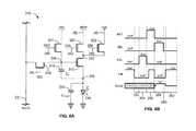
- FIG. 3Ais a circuit diagram of an exemplary pixel circuit configuration.
- FIG. 3Bis a timing diagram of first exemplary operation cycles for the pixel shown in FIG. 3A .
- FIG. 3Cis a timing diagram of second exemplary operation cycles for the pixel shown in FIG. 3A .
- FIG. 4Ais a circuit diagram of an exemplary pixel circuit configuration.
- FIG. 4Bis a circuit diagram of a modified configuration for two identical pixel circuits in a display.
- FIG. 5Ais a circuit diagram of an exemplary pixel circuit configuration.
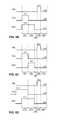
- FIG. 5Bis a timing diagram of first exemplary operation cycles for the pixel illustrated in FIG. 5A .
- FIG. 5Cis a timing diagram of second exemplary operation cycles for the pixel illustrated in FIG. 5A .
- FIG. 5Dis a timing diagram of third exemplary operation cycles for the pixel illustrated in FIG. 5A .
- FIG. 5Eis a timing diagram of fourth exemplary operation cycles for the pixel illustrated in FIG. 5A .
- FIG. 5Fis a timing diagram of fifth exemplary operation cycles for the pixel illustrated in FIG. 5A .
- FIG. 6Ais a circuit diagram of an exemplary pixel circuit configuration.
- FIG. 6Bis a timing diagram of exemplary operation cycles for the pixel illustrated in FIG. 6A .
- FIG. 7Ais a circuit diagram of an exemplary pixel circuit configuration.
- FIG. 7Bis a timing diagram of exemplary operation cycles for the pixel illustrated in FIG. 7A .
- FIG. 8Ais a circuit diagram of an exemplary pixel circuit configuration.
- FIG. 8Bis a timing diagram of exemplary operation cycles for the pixel illustrated in FIG. 8A .
- FIG. 9Ais a circuit diagram of an exemplary pixel circuit configuration.
- FIG. 9Bis a timing diagram of first exemplary operation cycles for the pixel illustrated in FIG. 9A .
- FIG. 9Cis a timing diagram of second exemplary operation cycles for the pixel illustrated in FIG. 9A .
- FIG. 10Ais a circuit diagram of an exemplary pixel circuit configuration.
- FIG. 10Bis a timing diagram of exemplary operation cycles for the pixel illustrated in FIG. 10A in a programming cycle.
- FIG. 10Cis a timing diagram of exemplary operation cycles for the pixel illustrated in FIG. 10A in a TFT read cycle.
- FIG. 10Dis a timing diagram of exemplary operation cycles for the pixel illustrated in FIG. 10A in am OLED read cycle.
- FIG. 11Ais a circuit diagram of a pixel circuit with IR drop compensation.
- FIG. 11Bis a timing diagram for an IR drop compensation operation of the circuit of FIG. 11A .
- FIG. 11Cis a timing diagram for reading out a parameter of the drive transistor in the circuit of FIG. 11A .
- FIG. 11Dis a timing diagram for reading out a parameter of the light emitting device in the circuit of FIG. 11A .
- FIG. 12Ais a circuit diagram of a pixel circuit with charge-based compensation.
- FIG. 12Bis a timing diagram for a charge-based compensation operation of the circuit of FIG. 12A .
- FIG. 12Cis a timing diagram for a direct readout of a parameter of the light emitting device in the circuit of FIG. 12A .
- FIG. 12Dis a timing diagram for an indirect readout of a parameter of the light emitting device in the circuit of FIG. 12A .
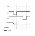
- FIG. 12Eis a timing diagram for a direct readout of a parameter of the drive transistor in the circuit of FIG. 12A .
- FIG. 13is a circuit diagram of a biased pixel circuit.
- FIG. 14Ais a diagram of a pixel circuit and an electrode connected to a signal line.
- FIG. 14Bis a diagram of a pixel circuit and an expanded electrode replacing the signal line shown in FIG. 14A .
- FIG. 15is a circuit diagram of a pad arrangement for use in the probing of a display panel.
- FIG. 16is a circuit diagram of a pixel circuit for use in backplane testing.
- FIG. 17is a circuit diagram of a pixel circuit for a full display test.
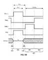
- FIG. 1is a diagram of an exemplary display system 50 .
- the display system 50includes an address driver 8 , a data driver 4 , a controller 2 , a memory storage 6 , and display panel 20 .
- the display panel 20includes an array of pixels 10 arranged in rows and columns. Each of the pixels 10 are individually programmable to emit light with individually programmable luminance values.
- the controller 2receives digital data indicative of information to be displayed on the display panel 20 .
- the controller 2sends signals 32 to the data driver 4 and scheduling signals 34 to the address driver 8 to drive the pixels 10 in the display panel 20 to display the information indicated.
- the plurality of pixels 10 associated with the display panel 20thus comprise a display array (“display screen”) adapted to dynamically display information according to the input digital data received by the controller 2 .
- the display screencan display, for example, video information from a stream of video data received by the controller 2 .
- the supply voltage 14can provide a constant power voltage or can be an adjustable voltage supply that is controlled by signals from the controller 2 .
- the display system 50can also incorporate features from a current source or sink (not shown) to provide biasing currents to the pixels 10 in the display panel 20 to thereby decrease programming time for the pixels 10 .
- the display system 50 in FIG. 1is illustrated with only four pixels 10 in the display panel 20 . It is understood that the display system 50 can be implemented with a display screen that includes an array of similar pixels, such as the pixels 10 , and that the display screen is not limited to a particular number of rows and columns of pixels. For example, the display system 50 can be implemented with a display screen with a number of rows and columns of pixels commonly available in displays for mobile devices, monitor-based devices, and/or projection-devices.
- the pixel 10is operated by a driving circuit (“pixel circuit”) that generally includes a drive transistor and a light emitting device.
- pixel circuitmay refer to the pixel circuit.
- the light emitting devicecan optionally be an organic light emitting diode, but implementations of the present disclosure apply to pixel circuits having other electroluminescence devices, including current-driven light emitting devices.
- the drive transistor in the pixel 10can optionally be an n-type or p-type amorphous silicon thin-film transistor, but implementations of the present disclosure are not limited to pixel circuits having a particular polarity of transistor or only to pixel circuits having thin-film transistors.
- the pixel circuit 10can also include a storage capacitor for storing programming information and allowing the pixel circuit 10 to drive the light emitting device after being addressed.
- the display panel 20can be an active matrix display array.
- the pixel 10 illustrated as the top-left pixel in the display panel 20is coupled to a select line 24 j , a supply line 26 j , a data line 22 i , and a monitor line 28 i .
- the supply voltage 14can also provide a second supply line to the pixel 10 .
- each pixelcan be coupled to a first supply line charged with Vdd and a second supply line coupled with Vss, and the pixel circuits 10 can be situated between the first and second supply lines to facilitate driving current between the two supply lines during an emission phase of the pixel circuit.
- the top-left pixel 10 in the display panel 20can correspond a pixel in the display panel in a “jth” row and “ith” column of the display panel 20 .
- the top-right pixel 10 in the display panel 20represents a “jth” row and “mth” column; the bottom-left pixel 10 represents an “nth” row and “ith” column; and the bottom-right pixel 10 represents an “nth” row and “ith” column.
- Each of the pixels 10is coupled to appropriate select lines (e.g., the select lines 24 j and 24 n ), supply lines (e.g., the supply lines 26 j and 26 n ), data lines (e.g., the data lines 22 i and 22 m ), and monitor lines (e.g., the monitor lines 28 i and 28 m ). It is noted that aspects of the present disclosure apply to pixels having additional connections, such as connections to additional select lines, and to pixels having fewer connections, such as pixels lacking a connection to a monitoring line.
- select linese.g., the select lines 24 j and 24 n
- supply linese.g., the supply lines 26 j and 26 n
- data linese.g., the data lines 22 i and 22 m
- monitor linese.g., the monitor lines 28 i and 28 m
- the select line 24 jis provided by the address driver 8 , and can be utilized to enable, for example, a programming operation of the pixel 10 by activating a switch or transistor to allow the data line 22 i to program the pixel 10 .
- the data line 22 iconveys programming information from the data driver 4 to the pixel 10 .
- the data line 22 ican be utilized to apply a programming voltage or a programming current to the pixel 10 in order to program the pixel 10 to emit a desired amount of luminance.
- the programming voltage (or programming current) supplied by the data driver 4 via the data line 22 iis a voltage (or current) appropriate to cause the pixel 10 to emit light with a desired amount of luminance according to the digital data received by the controller 2 .
- the programming voltage (or programming current)can be applied to the pixel 10 during a programming operation of the pixel 10 so as to charge a storage device within the pixel 10 , such as a storage capacitor, thereby enabling the pixel 10 to emit light with the desired amount of luminance during an emission operation following the programming operation.
- the storage device in the pixel 10can be charged during a programming operation to apply a voltage to one or more of a gate or a source terminal of the drive transistor during the emission operation, thereby causing the drive transistor to convey the driving current through the light emitting device according to the voltage stored on the storage device.
- the driving current that is conveyed through the light emitting device by the drive transistor during the emission operation of the pixel 10is a current that is supplied by the first supply line 26 j and is drained to a second supply line (not shown).
- the first supply line 22 j and the second supply lineare coupled to the voltage supply 14 .
- the first supply line 26 jcan provide a positive supply voltage (e.g., the voltage commonly referred to in circuit design as “Vdd”) and the second supply line can provide a negative supply voltage (e.g., the voltage commonly referred to in circuit design as “Vss”). Implementations of the present disclosure can be realized where one or the other of the supply lines (e.g., the supply line 26 j ) are fixed at a ground voltage or at another reference voltage.
- the display system 50also includes a monitoring system 12 .
- the monitor line 28 iconnects the pixel 10 to the monitoring system 12 .
- the monitoring system 12can be integrated with the data driver 4 , or can be a separate stand-alone system.
- the monitoring system 12can optionally be implemented by monitoring the current and/or voltage of the data line 22 i during a monitoring operation of the pixel 10 , and the monitor line 28 i can be entirely omitted.
- the display system 50can be implemented without the monitoring system 12 or the monitor line 28 i .
- the monitor line 28 iallows the monitoring system 12 to measure a current or voltage associated with the pixel 10 and thereby extract information indicative of a degradation of the pixel 10 .
- the monitoring system 12can extract, via the monitor line 28 i , a current flowing through the drive transistor within the pixel 10 and thereby determine, based on the measured current and based on the voltages applied to the drive transistor during the measurement, a threshold voltage of the drive transistor or a shift thereof.
- the monitoring system 12can also extract an operating voltage of the light emitting device (e.g., a voltage drop across the light emitting device while the light emitting device is operating to emit light). The monitoring system 12 can then communicate the signals 32 to the controller 2 and/or the memory 6 to allow the display system 50 to store the extracted degradation information in the memory 6 . During subsequent programming and/or emission operations of the pixel 10 , the degradation information is retrieved from the memory 6 by the controller 2 via the memory signals 36 , and the controller 2 then compensates for the extracted degradation information in subsequent programming and/or emission operations of the pixel 10 .
- an operating voltage of the light emitting devicee.g., a voltage drop across the light emitting device while the light emitting device is operating to emit light.
- the monitoring system 12can then communicate the signals 32 to the controller 2 and/or the memory 6 to allow the display system 50 to store the extracted degradation information in the memory 6 .
- the degradation informationis retrieved from the memory 6 by the controller 2 via the memory signals 36 , and the controller 2 then compensate
- the programming information conveyed to the pixel 10 via the data line 22 ican be appropriately adjusted during a subsequent programming operation of the pixel 10 such that the pixel 10 emits light with a desired amount of luminance that is independent of the degradation of the pixel 10 .
- an increase in the threshold voltage of the drive transistor within the pixel 10can be compensated for by appropriately increasing the programming voltage applied to the pixel 10 .
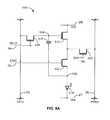
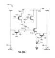
- FIG. 2Ais a circuit diagram of an exemplary driving circuit for a pixel 110 .
- the driving circuit shown in FIG. 2Ais utilized to calibrate, program, and drive the pixel 110 and includes a drive transistor 112 for conveying a driving current through an organic light emitting diode (“OLED”) 114 .
- OLEDorganic light emitting diode
- the OLED 114emits light according to the current passing through the OLED 114 , and can be replaced by any current-driven light emitting device.
- the OLED 114has an inherent capacitance 12 .
- the pixel 110can be utilized in the display panel 20 of the display system 50 described in connection with FIG. 1 .
- the driving circuit for the pixel 110also includes a storage capacitor 116 and a switching transistor 118 .
- the pixel 110is coupled to a reference voltage line 144 , a select line 24 i , a voltage supply line 26 i , and a data line 22 j .
- the drive transistor 112draws a current from the voltage supply line 26 i according to a gate-source voltage (Vgs) across the gate and source terminals of the drive transistor 112 .
- Vgsgate-source voltage
- the storage capacitor 116is coupled across the gate and source terminals of the drive transistor 112 .
- the storage capacitor 116has a first terminal 116 g , which is referred to for convenience as a gate-side terminal 116 g , and a second terminal 116 s , which is referred to for convenience as a source-side terminal 116 s .
- the gate-side terminal 116 g of the storage capacitor 116is electrically coupled to the gate terminal of the drive transistor 112 .
- the source-side terminal 116 s of the storage capacitor 116is electrically coupled to the source terminal of the drive transistor 112 .
- the gate-source voltage Vgs of the drive transistor 112is also the voltage charged on the storage capacitor 116 .
- the storage capacitor 116can thereby maintain a driving voltage across the drive transistor 112 during an emission phase of the pixel 110 .
- the drain terminal of the drive transistor 112is electrically coupled to the voltage supply line 26 i through an emission transistor 160 , and to the reference voltage line 144 through a calibration transistor 142 .
- the source terminal of the drive transistor 112is electrically coupled to an anode terminal of the OLED 114 .
- a cathode terminal of the OLED 114can be connected to ground or can optionally be connected to a second voltage supply line, such as a supply line Vss (not shown). Thus, the OLED 114 is connected in series with the current path of the drive transistor 112 .
- the OLED 114emits light according to the magnitude of the current passing through the OLED 114 , once a voltage drop across the anode and cathode terminals of the OLED achieves an operating voltage (V OLED ) of the OLED 114 . That is, when the difference between the voltage on the anode terminal and the voltage on the cathode terminal is greater than the operating voltage V OLED , the OLED 114 turns on and emits light. When the anode to cathode voltage is less than V OLED , current does not pass through the OLED 114 .
- the switching transistor 118is operated according to a select line 24 i (e.g., when the voltage SEL on the select line 24 i is at a high level, the switching transistor 118 is turned on, and when the voltage SEL is at a low level, the switching transistor is turned off). When turned on, the switching transistor 118 electrically couples the gate terminal of the drive transistor (and the gate-side terminal 116 g of the storage capacitor 116 ) to the data line 22 j.
- the drain terminal of the drive transistor 112is coupled to the VDD line 26 i via an emission transistor 122 , and to a Vref line 144 via a calibration transistor 142 .
- the emission transistor 122is controlled by the voltage on an EM line 140 connected to the gate of the transistor 122
- the calibration transistor 142is controlled by the voltage on a CAL line 140 connected to the gate of the transistor 142 .
- the reference voltage line 144can be maintained at a ground voltage or another fixed reference voltage (Vref) and can optionally be adjusted during a programming phase of the pixel 110 to provide compensation for degradation of the pixel 110 .
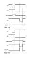
- FIG. 2Bis a schematic timing diagram of exemplary operation cycles for the pixel 110 shown in FIG. 2A .
- the pixel 110can be operated in a calibration cycle t CAL having two phases 154 and 158 separated by an interval 156 , a program cycle 160 , and a driving cycle 164 .
- both the SEL line and the CAL linesare high, so the corresponding transistors 118 and 142 are turned on.
- the calibration transistor 142applies the voltage Vref, which has a level that turns the OLED 114 off, to the node 132 between the source of the emission transistor 122 and the drain of the drive transistor 112 .
- the switching transistor 118applies the voltage Vdata, which is at a biasing voltage level Vb, to the gate of the drive transistor 112 to allow the voltage Vref to be transferred from the node 132 to the node 130 between the source of the drive transistor 112 and the anode of the OLED 114 .
- the voltage on the CAL linegoes low at the end of the first phase 154 , while the voltage on the SEL line remains high to keep the drive transistor 112 turned on.
- the voltage on the EM line 140goes high to turn on the emission transistor 122 , which causes the voltage at the node 130 to increase. If the phase 158 is long enough, the voltage at the node 130 reaches a value (Vb ⁇ Vt), where Vt is the threshold voltage of the drive transistor 112 . If the phase 158 is not long enough to allow that value to be reached, the voltage at the node 130 is a function of Vt and the mobility of the drive transistor 112 . This is the voltage stored in the capacitor 116 .
- the voltage at the node 130is applied to the anode terminal of the OLED 114 , but the value of that voltage is chosen such that the voltage applied across the anode and cathode terminals of the OLED 114 is less than the operating voltage V OLED of the OLED 114 , so that the OLED 114 does not draw current.
- the current flowing through the drive transistor 112 during the calibration phase 158does not pass through the OLED 114 .
- the voltages on both lines EM and CALare low, so both the emission transistor 122 and the calibration transistor 142 are off.
- the SEL lineremains high to turn on the switching transistor 116 , and the data line 22 j is set to a programming voltage Vp, thereby charging the node 134 , and thus the gate of the drive transistor 112 , to Vp.
- the node 130 between the OLED and the source of the drive transistor 112holds the voltage created during the calibration cycle, since the OLED capacitance is large.
- the voltage charged on the storage capacitor 116is the difference between Vp and the voltage created during the calibration cycle. Because the emission transistor 122 is off during the programming cycle, the charge on the capacitor 116 cannot be affected by changes in the voltage level on the Vdd line 26 i.
- the voltage on the EM linegoes high, thereby turning on the emission transistor 122 , while both the switching transistor 118 and the and the calibration transistor 142 remain off.
- Turning on the emission transistor 122causes the drive transistor 112 to draw a driving current from the VDD supply line 26 i , according to the driving voltage on the storage capacitor 116 .
- the OLED 114is turned on, and the voltage at the anode of the OLED adjusts to the operating voltage V OLED . Since the voltage stored in the storage capacitor 116 is a function of the threshold voltage Vt and the mobility of the drive transistor 112 , the current passing through the OLED 114 remains stable.
- the SEL line 24 iis low during the driving cycle, so the switching transistor 118 remains turned off.
- the storage capacitor 116maintains the driving voltage, and the drive transistor 112 draws a driving current from the voltage supply line 26 i according to the value of the driving voltage on the capacitor 116 .
- the driving currentis conveyed through the OLED 114 , which emits a desired amount of light according to the amount of current passed through the OLED 114 .
- the storage capacitor 116maintains the driving voltage by self-adjusting the voltage of the source terminal and/or gate terminal of the drive transistor 112 so as to account for variations on one or the other.
- the storage capacitor 116adjusts the voltage on the gate terminal of the drive transistor 112 to maintain the driving voltage across the gate and source terminals of the drive transistor.
- FIG. 2Cis a modified timing diagram in which the voltage on the data line 22 j is used to charge the node 130 to Vref during a longer first phase 174 of the calibration cycle t CAL .
- the driving circuit illustrated in FIG. 2Ais illustrated with n-type transistors, which can be thin-film transistors and can be formed from amorphous silicon
- the driving circuit illustrated in FIG. 2A and the operating cycles illustrated in FIG. 2Bcan be extended to a complementary circuit having one or more p-type transistors and having transistors other than thin film transistors.
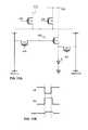
- FIG. 3Ais a modified version of the driving circuit of FIG. 2A using p-type transistors, with the storage capacitor 116 connected between the gate and source terminals of the drive transistor 112 .
- the emission transistor 122disconnects the pixel 110 in FIG. 3A from the VDD line during the programming cycle 154 , to avoid any effect of VDD variations on the pixel current.
- the calibration transistor 142is turned on by the CAL line 120 during the programming cycle 154 , which applies the voltage Vref to the node 132 on one side of the capacitor 116 , while the switching transistor 118 is turned on by the SEL line to apply the programming voltage Vp to the node 134 on the opposite side of the capacitor.
- the voltage stored in the storage capacitor 116 during programming in FIG. 3Awill be (Vp ⁇ Vref). Since there is small current flowing in the Vref line, the voltage is stable.
- the VDD lineis connected to the pixel, but it has no effect on the voltage stored in the capacitor 116 since the switching transistor 118 is off during the driving cycle.
- FIG. 3Cis a timing diagram illustrating how TFT transistor and OLED readouts are obtained in the circuit of FIG. 3A .
- the voltage Vcal on the DATA line 22 j during the programming cycle 154should be a voltage related to the desired current.
- the voltage Vcalis sufficiently low to force the drive transistor 112 to act as a switch, and the voltage Vb on the Vref line 144 and node 132 is related to the OLED voltage.
- the TFT and OLED readoutscan be obtained from the DATA line 120 and the node 132 , respectively, during different cycles.
- Each row of pixelshas its own VDD, VSS, EM and SEL lines that are shared by all the pixels in that row.
- the calibration transistor 142 of each pixelhas its gate connected to the SEL line of the previous row (SEL[i ⁇ 1]). This is an efficient arrangement when external compensation is provided for the OLED efficiency as the display ages, while in-pixel compensation is used for other parameters such as V OLED , temperature-induced degradation, IR drop (e.g., in the VDD lines), hysteresis, etc.
- FIG. 4Bis a circuit diagram showing how the two pixels shown in FIG. 4A can be simplified by sharing common calibration and emission transistors 120 and 140 and common Vref 2 /MON and VDD lines. It can be seen that the number of transistors required is significantly reduced.
- FIG. 5Ais a circuit diagram of an exemplary driving circuit for a pixel 210 that includes a monitor line 28 j coupled to the node 230 by a calibration transistor 226 controlled by a CAL line 242 , for reading the current values of operating parameters such as the drive current and the OLED voltage.
- the circuit of FIG. 5Aalso includes a reset transistor 228 for controlling the application of a reset voltage Vrst to the gate of the drive transistor 212 .
- the drive transistor 212 , the switching transistor 218 and the OLED 214are the same as described above in the circuit of FIG. 2A .
- FIG. 5Bis a schematic timing diagram of exemplary operation cycles for the pixel 210 shown in FIG. 5A .
- the RST and CAL linesgo high at the same time, thereby turning on both the transistors 228 and 226 for the cycle 252 , so that a voltage is applied to the monitor line 28 j .
- the drive transistor 212is on, and the OLED 214 is off.
- the RST linestays high while the CAL line goes low to turn off the transistor 226 , so that the drive transistor 212 charges the node 230 until the drive transistor 212 is turned off, e.g., by the RST line going low at the end of the cycle 254 .
- the gate-source voltage Vgs of the drive transistor 212is the Vt of that transistor. If desired, the timing can be selected so that the drive transistor 212 does not turn off during the cycle 254 , but rather charges the node 230 slightly. This charge voltage is a function of the mobility, Vt and other parameters of the transistor 212 and thus can compensate for all these parameters.
- the SEL line 24 igoes high to turn on the switching transistor 218 . This connects the gate of the drive transistor 212 to the DATA line, which charges the the gate of transistor 212 to Vp.
- the gate-source voltage Vgs of the transistor 212is then Vp+Vt, and thus the current through that transistor is independent of the threshold voltage Vt:
- FIG. 5Eillustrates a timing diagram that permits the measuring of the OLED voltage and/or current through the monitor line 28 j while the RST line is high to turn on the transistor 228 , during the cycle 282 , while the drive transistor 212 is off.
- FIG. 5Fillustrates a timing diagram that offers functionality similar to that of FIG. 5E .
- each pixel in a given row ncan use the reset signal from the previous row n ⁇ 1 (RST[n ⁇ 1]) as the calibration signal CAL[n] in the current row n, thereby reducing the number of signals required.
- FIG. 6Ais a circuit diagram of an exemplary driving circuit for a pixel 310 that includes a calibration transistor 320 between the drain of the drive transistor 312 and a MON/Vref 2 line 28 j for controlling the application of a voltage Vref 2 to the node 332 , which is the drain of the drive transistor 312 .
- the circuit in FIG. 6Aalso includes an emission transistor 322 between the drain of the drive transistor 312 and a VDD line 26 i , for controlling the application of the voltage Vdd to the node 332 .
- the drive transistor 312 , the switching transistor 318 , the reset transistor 321 and the OLED 214are the same as described above in the circuit of FIG. 5A .
- FIG. 6Bis a schematic timing diagram of exemplary operation cycles for the pixel 310 shown in FIG. 6A .
- the EM linegoes low to turn off the emission transistor 322 so that the voltage Vdd is not applied to the drain of the drive transistor 312 .
- the emission transistorremains off during the second cycle 354 , when the CAL line goes high to turn on the calibration transistor 320 , which connects the MON/Vref 2 line 28 j to the node 332 . This charges the node 332 to a voltage that is smaller that the ON voltage of the OLED.
- the CAL linegoes low to turn off the calibration transistor 320 .
- the RST and EM linesgo low to turn off the transistors 321 and 322 , and then the SEL line goes high to turn on the switching transistor 318 to supply a programming voltage Vp to the gate of the drive transistor 312 .
- the node 330 at the source terminal of the drive transistor 312remains substantially the same because the capacitance C OLED of the OLED 314 is large.
- the gate-source voltage of the transistor 312is a function of the mobility, Vt and other parameters of the drive transistor 312 and thus can compensate for all these parameters.
- FIG. 7Ais a circuit diagram of another exemplary driving circuit that modifies the gate-source voltage Vgs of the drive transistor 412 of a pixel 410 to compensate for variations in drive transistor parameters due to process variations, aging and/or temperature variations.
- This circuitincludes a monitor line 28 j coupled to the node 430 by a read transistor 422 controlled by a RD line 420 , for reading the current values of operating parameters such as drive current and Voled.
- the drive transistor 412 , the switching transistor 418 and the OLED 414are the same as described above in the circuit of FIG. 2A .
- FIG. 7Bis a schematic timing diagram of exemplary operation cycles for the pixel 410 shown in FIG. 7A .
- the SEL and RD linesboth go high to (1) turn on a switching transistor 418 to charge the gate of the drive transistor 412 to a programming voltage Vp from the data line 22 j , and (2) turn on a read transistor 422 to charge the source of the transistor 412 (node 430 ) to a voltage Vref from a monitor line 28 j .
- the RD linegoes low to turn off the read transistor 422 so that the node 430 is charged back through the transistor 412 , which remains on because the SEL line remains high.
- the gate-source voltage of the transistor 312is a function of the mobility, Vt and other parameters of the transistor 212 and thus can compensate for all these parameters.
- FIG. 8Ais a circuit diagram of an exemplary driving circuit for a pixel 510 which adds an emission transistor 522 to the pixel circuit of FIG. 7A , between the source side of the storage capacitor 522 and the source of the drive transistor 512 .
- the drive transistor 512 , the switching transistor 518 , the read transistor 520 , and the OLED 414are the same as described above in the circuit of FIG. 7A .
- FIG. 8Bis a schematic timing diagram of exemplary operation cycles for the pixel 510 shown in FIG. 8A .
- the EM lineis low to turn off the emission transistor 522 during the entire programming cycle 554 , to produce a black frame.
- the emission transistoris also off during the entire measurement cycle controlled by the RD line 540 , to avoid unwanted effects from the OLED 514 .
- the pixel 510can be programmed with no in-pixel compensation, as illustrated in FIG. 8B , or can be programmed in a manner similar to that described above for the circuit of FIG. 2A .
- FIG. 9Ais a circuit diagram of an exemplary driving circuit for a pixel 610 which is the same as the circuit of FIG. 8A except that the single emission transistor is replaced with a pair of emission transistors 622 a and 622 b connected in parallel and controlled by two different EM lines EMa and EMb.
- the two emission transistorscan be used alternately to manage the aging of the emission transistors, as illustrated in the two timing diagrams in FIGS. 9B and 9C .
- the EMa lineis high and the EMAb line is low during the first phase of a driving cycle 660 , and then the EMa line is low and the EMAb line is high during the second phase of that same driving cycle.
- the EMa lineis high and the EMAb line is low during a first driving cycle 672
- the EMa lineis low and the EMAb line is high during a second driving cycle 676 .
- FIG. 10Ais a circuit diagram of an exemplary driving circuit for a pixel 710 which is similar to the circuit of FIG. 3A described above, except that the circuit in FIG. 10A adds a monitor line 28 j , the EM line controls both the Vref transistor 742 and the emission transistor 722 , and the drive transistor 712 and the emission transistor 722 have separate connections to the VDD line.
- the drive transistor 12 , the switching transistor 18 , the storage capacitor 716 , and the OLED 414are the same as described above in the circuit of FIG. 3A .
- the EM line 740goes high and remains high during the programming cycle to turn off the p-type emission transistor 722 .
- Thisdisconnects the source side of the storage capacitor 716 from the VDD line 26 i to protect the pixel 710 from fluctuations in the VDD voltage during the programming cycle, thereby avoiding any effect of VDD variations on the pixel current.
- the high EM linealso turns on the n-type reference transistor 742 to connect the source side of the storage capacitor 716 to the Vrst line 744 , so the capacitor terminal B is charged to Vrst.
- the gate voltage of the drive transistor 712is high, so the drive transistor 712 is off.
- the voltage on the gate side of the capacitor 716is controlled by the WR line 745 connected to the gate of the switching transistor 718 and, as shown in the timing diagram, the WR line 745 goes low during a portion of the programming cycle to turn on the p-type transistor 718 , thereby applying the programming voltage Vp to the gate of the drive transistor 712 and the gate side of the storage capacitor 716 .
- the transistor 722turns on to connect the capacitor terminal B to the VDD line. This causes the gate voltage of the drive transistor 712 to go to Vdd ⁇ Vp, and the drive transistor turns on.
- the charge on the capacitoris Vrst ⁇ Vdd ⁇ Vp. Since the capacitor 716 is connected to the VDD line during the driving cycle, any fluctuations in Vdd will not affect the pixel current.
- FIG. 10Cis a timing diagram for a TFT read operation, which takes place during an interval when both the RD and EM lines are low and the WR line is high, so the emission transistor 722 is on and the switching transistor 718 is off.
- the monitor line 28 jis connected to the source of the drive transistor 712 during the interval when the RD line 746 is low to turn on the read transistor 726 , which overlaps the interval when current if flowing through the drive transistor to the OLED 714 , so that a reading of that current flowing through the drive transistor 712 can be taken via the monitor line 28 j.
- FIG. 10Dis a timing diagram for an OLED read operation, which takes place during an interval when the RD line 746 is low and both the EM and WR lines are high, so the emission transistor 722 and the switching transistor 718 are both off.
- the monitor line 28 jis connected to the source of the drive transistor 712 during the interval when the RD line is low to turn on the read transistor 726 , so that a reading of the voltage on the anode of the OLED 714 can be taken via the monitor line 28 j.
- FIG. 11Ais a schematic circuit diagram of a pixel circuit with IR drop compensation.
- the voltages Vmonitor and Vdataare shown being supplied on two separate lines, but both these voltages can be supplied on the same line in this circuit, since Vmonitor has no role during the programming and Vdata has no role during the measurement cycle.
- the two transistors Ta and Tbcan be shared between rows and columns for supplying the voltages Vref and Vdd, and the control signal EM can be shared between columns.
- the control signal WRturns on transistors T 2 and Ta to supply the programming data Vp and the reference voltage Vref to opposite sides of the storage capacitor Cs, while the control signal EM turns off the transistor Tb.
- the voltage stored in CSis Vref ⁇ Vp.
- the signal EMturns on the transistor Tb, and the signal WR turns off transistors T 2 and Ta.
- the gate-source voltage ofbecomes Vref ⁇ Vp and independent of Vdd.
- FIG. 11Cis a timing diagram for obtaining a direct readout of parameters of the transistor T 1 in the circuit of FIG. 11A .
- the control signal WRturns on the transistor T 2 and the pixel is programmed with a calibrated voltage Vdata for a known target current.
- the control signal RDturns on the transistor T 3 , and the pixel current is read through the transistor T 3 and the line Vmonitor.
- the voltage on the Vmonitor lineis low enough during the second cycle to prevent the OLED from turning on.
- the calibrated voltageis then modified until the pixel current becomes the same as the target current.
- the final modified calibrated voltageis then used as a point in TFT current-voltage characteristics to extract the corresponding current through the transistor T 1 .
- a currentcan be supplied through the Vmonitor line and the transistor T 3 while the transistors T 2 and Ta are turned on, and Vdata is set to a fixed voltage. At this point the voltage created on the line Vmonitor is the gate voltage of the transistor T 1 for the corresponding current.
- FIG. 11Dis a timing diagram for obtaining a direct readout of the OLED voltage in the circuit of FIG. 11A .
- the control signal WRturns on the transistor T 2 , and the pixel is programmed with an off voltage so that the drive transistor T 1 does not provide any current.
- the control signal RDturns on the transistor T 3 so the OLED current can be read through the Vmonitor line.
- the Vmonitor voltageis pre-calibrated based for a known target current.
- the Vmonitor voltageis then modified until the OLED current becomes the same as the target current. Then the modified Vmonitor voltage is used as a point in the OLED current-voltage characteristics to extract a parameter of the OLED, such as its turn-on voltage.
- the control signal EMcan keep the transistor Tb turned off all the way to the end of the readout cycle, while the control signal WR keeps the transistor Ta turned on. In this case, the remaining pixel operations for reading the OLED parameter are the same as described above for FIG. 11C .
- a currentcan be supplied to the OLED through the Vmonitor line so that the voltage on the Vmonitor line is the gate voltage of the drive transistor T 1 for the corresponding current.
- FIG. 12Ais a schematic circuit diagram of a pixel circuit with charge-based compensation. The voltages Vmonitor and Vdata are shown being supplied on the lines
- Vmonitor and Vdatacan be Vdata as well, in which case Vdata can be a fixed voltage Vref.
- the two transistors Ta and Tbcan be shared between adjacent rows for supplying the voltages Vref and Vdd, and Vmonitor can be shared between adjacent columns.
- the timing diagram in FIG. 12Bdepicts normal operation of the circuit of FIG. 12A .
- the control signal WRturns on the respective transistors Ta and T 2 to apply the programming voltage Vp from the Vdata line to the capacitor Cs, and the control signal RD turns on the transistor T 3 to apply the voltage Vref through the Vmonitor line and transistor T 3 to the node between the drive transistor T 1 and the OLED.
- Vrefis generally low enough to prevent the OLED from turning on.
- the control signal RDturns off the transistor T 3 before the control signal WR turns off the transistors Ta and T 2 .
- the drive transistor T 1starts to charge the OLED and so compensates for part of the variation of the transistor T 1 parameter, since the charge generated will be a function of the T 1 parameter.
- the compensationis independent of the IR drop since the source of the drive transistor T 1 is disconnected from Vdd during the programming cycle.
- the timing diagram in FIG. 12Cdepicts a direct readout of a parameter of the drive transistor T 1 in the circuit of FIG. 12A .
- the circuitis programmed with a calibrated voltage for a known target current.
- the control signal RDturns on the transistor T 3 to read the pixel current through the Vmonitor line.
- the Vmonitor voltageis low enough during the second cycle to prevent the OLED from turning on.
- the calibrated voltageis varied until the pixel current becomes the same as the target current.
- the final value of the calibrated voltageis used as a point in the current-voltage characteristics of the drive transistor T 1 to extract a parameter of that transistor.
- a currentcan be supplied to the OLED through the Vmonitor line, while the control signal WR turns on the transistor T 2 and Vdata is set to a fixed voltage, so that the voltage on the Vmonitor line is the gate voltage of the drive transistor T 1 for the corresponding current.
- the timing diagram in FIG. 12Ddepicts a direct readout of a parameter of the OLED in the circuit of FIG. 12A .
- the circuitis programmed with an off voltage so that the drive transistor T 1 does not provide any current.
- the control signal RDturns on the transistor T 3 , and the OLED current is read through the Vmonitor line.
- the Vmonitor voltage during second cycleis pre-calibrated, based for a known target current. Then the Vmonitor voltage is varied until the OLED current becomes the same as the target current. The final value of the Vmonitor voltage is then used as a point in the current-voltage characteristics of the OLED to extracts a parameter of the OLED.
- the timing diagram in FIG. 12Edepicts an indirect readout of a parameter of the OLED in the circuit of FIG. 12A .
- the pixel currentis read out in a manner similar to that described above for the timing diagram of FIG. 12C .
- the control signal RDturns off the transistor T 3 , and thus the gate voltage of the drive transistor T 1 is set to the OLED voltage.
- the calibrated voltageneeds to account for the effect of the OLED voltage and the parameter of the drive transistor T 1 to make the pixel current equal to the target current.
- This calibrated voltage and the voltage extracted by the direct T 1 readoutcan be used to extract the OLED voltage. For example, subtracting the calibrated voltage extracted from this process with the calibrated voltage extracted from TFT direct readout will result to the effect of OLED if the two target currents are the same.
- FIG. 13is a schematic circuit diagram of a biased pixel circuit with charge-based compensation.
- the two transistors Ta and Tbcan be shared between adjacent rows and columns for supplying the voltages Vdd and Vref 1
- the two transistors Tc and Tdcan be shared between adjacent rows for supplying the voltages Vdata and Vref 2
- the Vmonitor linecan be shared between adjacent columns.
- the control signal WRturns on the transistors Ta, Tc and T 2
- the control signal RDturns on the transistor T 3
- the control signal EMturns off the transistor Tb and Td.
- the voltage Vref 2can be Vdata.
- the Vmonitor lineis connected to a reference current
- the Vdata lineis connected to a programming voltage from the source driver.
- the gate of the drive transistor T 1is charged to a bias voltage related to the reference current from the Vmonitor line, and the voltage stored in the capacitor Cs is a function of the programming voltage Vp and the bias voltage.
- the control signals WR and Rdturn off the transistors Ta, Tc, T 2 and T 3
- EMturns on the transistor Tb.
- the gate-source voltage of the transistor T 1is a function of the voltage Vp and the bias voltage. Since the bias voltage is a function of parameters of the transistor T 1 , the bias voltage becomes insensitive to variations in the transistor T 1 . In the same operation, the voltages Vref 1 and Vdata can be swapped, and the capacitor Cs can be directly connected to Vdd or Vref, so there is no need for the transistors Tc and Td.
- the Vmonitor lineis connected to a reference voltage.
- the control signal WRturns on the transistors Ta, Tc and T 2
- the control signal RDturns on the transistor T 3 .
- Vdatais connected to Vp.
- the control signal RDturns off the transistor T 3 , and so the drain voltage of the transistor T 1 (the anode voltage of the OLED), starts to increase and develops a voltage VB.
- This change in voltageis a function of the parameters of the transistor T 1 .
- the control signals WR and RDturn off the transistors Ta, Tc, T 2 and T 3 .
- the source gate-voltage of the transistor T 1becomes a function of the voltages Vp and VB.
- the voltages Vdata and Vref 1can be swapped, and Cs can be connected directly to Vdd or a reference voltage, so there is no need for the transistors Td and Tc.
- the pixelis programmed with one of the aforementioned operations using a calibrated voltage.
- the current of the drive transistor T 1is then measured or compared with a reference current.
- the calibrated voltagecan be adjusted until the current through the drive transistor is substantially equal to a reference current.
- the calibrated voltageis then used to extract the desired parameter of the drive transistor.
- the pixelFor a direct readout of the OLED voltage, the pixel is programmed with black using one of the operations described above. Then a calibrated voltage is supplied to the Vmonitor line, and the current supplied to the OLED is measured or compared with a reference current. The calibrated voltage can be adjusted until the OLED current is substantially equal to a reference current. The calibrated voltage can then be used to extract the OLED parameters.
- the pixel currentis read out in a manner similar to the operation described above for the direct readout of parameters of the drive transistor T 1 .
- the only differenceis that during the programming, the control signal RD turns off the transistor T 3 , and thus the gate voltage of the drive transistor T 1 is set to the OLED voltage.
- the calibrated voltageneeds to account for the effect of the OLED voltage and the drive transistor parameter to make the pixel current equal to the target current.
- This calibrated voltage and the voltage extracted from the direct readout of the T 1 parametercan be used to extract the OLED voltage. For example, subtracting the calibrated voltage extracted from this process from the calibrated voltage extracted from the direct readout of the drive transistor corresponds to the effect of the OLED if the two target currents are the same.
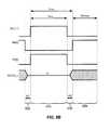
- FIG. 14Aillustrates a pixel circuit with a signal line connected to an OLED and the pixel circuit
- FIG. 14Billustrates the pixel circuit with an electrode ITO patterned as a signal line.
- the same system used to compensate the pixel circuitscan be used to analyze an entire display panel during different stages of fabrication, e.g., after backplane fabrication, after OLED fabrication, and after full assembly. At each stage the information provided by the analysis can be used to identify the defects and repair them with different techniques such as laser repair. To be able to measure the panel, there must be either a direct path to each pixel to measure the pixel current, or a partial electrode pattern may be used for the measurement path, as depicted in FIG. 14B . In the latter case, the electrode is patterned to contact the vertical lines first, and after the measurement is finished, the balance of the electrode is completed.
- FIG. 15illustrates a typical arrangement for a panel and its signals during a panel test, including a pad arrangement for probing the panel. Every other signal is connected to one pad through a multiplexer having a default stage that sets the signal to a default value. Every signal can be selected through the multiplexer to either program the panel or to measure a current, voltage and/or charge from the individual pixel circuits.
- FIG. 16illustrates a pixel circuit for use in testing.
- the followingare some of the factory tests that can be carried out to identify defects in the pixel circuits.
- a similar conceptcan be applied to different pixel circuits, although the following tests are defined for the pixel circuit shown in FIG. 16 .
- FIG. 17illustrates a pixel circuit for use in testing a full display.
- the followingare some of the factory tests that can be carried out to identify defects in the display. A similar concept can be applied to different circuits, although the following tests are defined for the circuit shown in FIG. 17 .
Landscapes
- Engineering & Computer Science (AREA)
- Physics & Mathematics (AREA)
- Computer Hardware Design (AREA)
- General Physics & Mathematics (AREA)
- Theoretical Computer Science (AREA)
- Control Of Indicators Other Than Cathode Ray Tubes (AREA)
- Control Of El Displays (AREA)
- Electroluminescent Light Sources (AREA)
Abstract
Description
This application is a U.S. National Stage of International Application No. PCT/IB2013/060755, filed Dec. 9, 2013, which claims the benefit of U.S. Provisional Application No. 61/815,698, filed Apr. 24, 2013 and U.S. patent application Ser. No. 13/710,872, filed Dec. 11, 2012, all of which are incorporated herein by reference in their entireties.
The present disclosure generally relates to circuits for use in displays, and methods of driving, calibrating, and programming displays, particularly displays such as active matrix organic light emitting diode displays.
Displays can be created from an array of light emitting devices each controlled by individual circuits (i.e., pixel circuits) having transistors for selectively controlling the circuits to be programmed with display information and to emit light according to the display information. Thin film transistors (“TFTs”) fabricated on a substrate can be incorporated into such displays. TFTs tend to demonstrate non-uniform behavior across display panels and over time as the displays age. Compensation techniques can be applied to such displays to achieve image uniformity across the displays and to account for degradation in the displays as the displays age.
Some schemes for providing compensation to displays to account for variations across the display panel and over time utilize monitoring systems to measure time dependent parameters associated with the aging (i.e., degradation) of the pixel circuits. The measured information can then be used to inform subsequent programming of the pixel circuits so as to ensure that any measured degradation is accounted for by adjustments made to the programming. Such monitored pixel circuits may require the use of additional transistors and/or lines to selectively couple the pixel circuits to the monitoring systems and provide for reading out information. The incorporation of additional transistors and/or lines may undesirably decrease pixel-pitch (i.e., “pixel density”).
In accordance with one embodiment, a system for controlling an array of pixels in a display in which each pixel includes a pixel circuit that comprises a light-emitting device; a drive transistor for driving current through the light emitting device according to a driving voltage across the drive transistor during an emission cycle, the drive transistor having a gate, a source and a drain; a storage capacitor coupled to the gate of the drive transistor for controlling the driving voltage; a reference voltage source coupled to a first switching transistor that controls the coupling of the reference voltage source to the storage capacitor; a programming voltage source coupled to a second switching transistor that controls the coupling of the programming voltage to the gate of the drive transistor, so that the storage capacitor stores a voltage equal to the difference between the reference voltage and the programming voltage; and a controller configured to (1) supply a programming voltage that is a calibrated voltage for a known target current, (2) read the actual current passing through the drive transistor to a monitor line, (3) turn off the light emitting device while modifying the calibrated voltage to make the current supplied through the drive transistor substantially the same as the target current, (4) modify the calibrated voltage to make the current supplied through the drive transistor substantially the same as the target current, and (5) determine a current corresponding to the modified calibrated voltage based on predetermined current-voltage characteristics of the drive transistor.
Another embodiment provides a system for controlling an array of pixels in a display in which each pixel includes a pixel circuit that comprises a light-emitting device; a drive transistor for driving current through the light emitting device according to a driving voltage across the drive transistor during an emission cycle, the drive transistor having a gate, a source and a drain; a storage capacitor coupled to the gate of the drive transistor for controlling the driving voltage; a reference voltage source coupled to a first switching transistor that controls the coupling of the reference voltage source to the storage capacitor; a programming voltage source coupled to a second switching transistor that controls the coupling of the programming voltage to the gate of the drive transistor, so that the storage capacitor stores a voltage equal to the difference between the reference voltage and the programming voltage; and a controller configured to (1) supply a programming voltage that is a predetermined fixed voltage, (2) supply a current from an external source to the light emitting device, and (3) read the voltage at the node between the drive transistor and the light emitting device.
In a further embodiment, a system is provided for controlling an array of pixels in a display in which each pixel includes a pixel circuit that comprises a light-emitting device; a drive transistor for driving current through the light emitting device according to a driving voltage across the drive transistor during an emission cycle, the drive transistor having a gate, a source and a drain; a storage capacitor coupled to the gate of the drive transistor for controlling the driving voltage; a reference voltage source coupled to a first switching transistor that controls the coupling of the reference voltage source to the storage capacitor; a programming voltage source coupled to a second switching transistor that controls the coupling of the programming voltage to the gate of the drive transistor, so that the storage capacitor stores a voltage equal to the difference between the reference voltage and the programming voltage; and a controller configured to (1) supply a programming voltage that is an off voltage so that the drive transistor does not provide any current to the light emitting device, (2) supply a current from an external source to a node between the drive transistor and the light emitting device, the external source having a pre-calibrated voltage based on a known target current, (3) modify the pre-calibrated voltage to make the current substantially the same as the target current, (4) read the current corresponding to the modified calibrated voltage, and (5) determine a current corresponding to the modified calibrated voltage based on predetermined current-voltage characteristics of the OLED.
Yet another embodiment provides a system for controlling an array of pixels in a display in which each pixel includes a pixel circuit that comprises a light-emitting device; a drive transistor for driving current through the light emitting device according to a driving voltage across the drive transistor during an emission cycle, the drive transistor having a gate, a source and a drain; a storage capacitor coupled to the gate of the drive transistor for controlling the driving voltage; a reference voltage source coupled to a first switching transistor that controls the coupling of the reference voltage source to the storage capacitor; a programming voltage source coupled to a second switching transistor that controls the coupling of the programming voltage to the gate of the drive transistor, so that the storage capacitor stores a voltage equal to the difference between the reference voltage and the programming voltage; and a controller configured to (1) supply a current from an external source to the light emitting device, and (2) read the voltage at the node between the drive transistor and the light emitting device as the gate voltage of the drive transistor for the corresponding current.
A still further embodiment provides a system for controlling an array of pixels in a display in which each pixel includes a pixel circuit that comprises a light-emitting device; a drive transistor for driving current through the light emitting device according to a driving voltage across the drive transistor during an emission cycle, the drive transistor having a gate, a source and a drain; a storage capacitor coupled to the gate of the drive transistor for controlling the driving voltage; a supply voltage source coupled to a first switching transistor that controls the coupling of the supply voltage source to the storage capacitor and the drive transistor; a programming voltage source coupled to a second switching transistor that controls the coupling of the programming voltage to the gate of the drive transistor, so that the storage capacitor stores a voltage equal to the difference between the reference voltage and the programming voltage; a monitor line coupled to a third switching transistor that controls the coupling of the monitor line to a node between the light emitting device and the drive transistor; and a controller that (1) controls the programming voltage source to produce a voltage that is a calibrated voltage corresponding to a known target current through the drive transistor, (2) controls the monitor line to read a current through the monitor line, with a monitoring voltage low enough to prevent the light emitting device from turning on, (3) controls the programming voltage source to modify the calibrated voltage until the current through the drive transistor is substantially the same as the target current, and (4) identifies a current corresponding to the modified calibrated voltage in predetermined current-voltage characteristics of the drive transistor, the identified current corresponding to the current threshold voltage of the drive transistor.
Another embodiment provides a system for controlling an array of pixels in a display in which each pixel includes a pixel circuit that comprises a light-emitting device; a drive transistor for driving current through the light emitting device according to a driving voltage across the drive transistor during an emission cycle, the drive transistor having a gate, a source and a drain; a storage capacitor coupled to the gate of the drive transistor for controlling the driving voltage; a supply voltage source coupled to a first switching transistor that controls the coupling of the supply voltage source to the storage capacitor and the drive transistor; a programming voltage source coupled to a second switching transistor that controls the coupling of the programming voltage to the gate of the drive transistor, so that the storage capacitor stores a voltage equal to the difference between the reference voltage and the programming voltage; a monitor line coupled to a third switching transistor that controls the coupling of the monitor line to a node between the light emitting device and the drive transistor; and a controller that (1) controls the programming voltage source to produce an off voltage that prevents the drive transistor from passing current to the light emitting device, (2) controls the monitor line to supply a pre-calibrated voltage from the monitor line to a node between the drive transistor and the light emitting device, the pre-calibrated voltage causing current to flow through the node to the light emitting device, the pre-calibrated voltage corresponding to a predetermined target current through the drive transistor, (3) modifies the pre-calibrated voltage until the current flowing through the node to the light emitting device is substantially the same as the target current, and (4) identifies a current corresponding to the modified pre-calibrated voltage in predetermined current-voltage characteristics of the drive transistor, the identified current corresponding to the voltage of the light emitting device.
The foregoing and additional aspects and embodiments of the present invention will be apparent to those of ordinary skill in the art in view of the detailed description of various embodiments and/or aspects, which is made with reference to the drawings, a brief description of which is provided next.
The foregoing and other advantages of the invention will become apparent upon reading the following detailed description and upon reference to the drawings.
While the invention is susceptible to various modifications and alternative forms, specific embodiments have been shown by way of example in the drawings and will be described in detail herein. It should be understood, however, that the invention is not intended to be limited to the particular forms disclosed. Rather, the invention is to cover all modifications, equivalents, and alternatives falling within the spirit and scope of the invention as defined by the appended claims.
For illustrative purposes, thedisplay system 50 inFIG. 1 is illustrated with only fourpixels 10 in thedisplay panel 20. It is understood that thedisplay system 50 can be implemented with a display screen that includes an array of similar pixels, such as thepixels 10, and that the display screen is not limited to a particular number of rows and columns of pixels. For example, thedisplay system 50 can be implemented with a display screen with a number of rows and columns of pixels commonly available in displays for mobile devices, monitor-based devices, and/or projection-devices.
Thepixel 10 is operated by a driving circuit (“pixel circuit”) that generally includes a drive transistor and a light emitting device. Hereinafter thepixel 10 may refer to the pixel circuit. The light emitting device can optionally be an organic light emitting diode, but implementations of the present disclosure apply to pixel circuits having other electroluminescence devices, including current-driven light emitting devices. The drive transistor in thepixel 10 can optionally be an n-type or p-type amorphous silicon thin-film transistor, but implementations of the present disclosure are not limited to pixel circuits having a particular polarity of transistor or only to pixel circuits having thin-film transistors. Thepixel circuit 10 can also include a storage capacitor for storing programming information and allowing thepixel circuit 10 to drive the light emitting device after being addressed. Thus, thedisplay panel 20 can be an active matrix display array.
As illustrated inFIG. 1 , thepixel 10 illustrated as the top-left pixel in thedisplay panel 20 is coupled to aselect line 24j, a supply line26j, a data line22i, and a monitor line28i. In an implementation, thesupply voltage 14 can also provide a second supply line to thepixel 10. For example, each pixel can be coupled to a first supply line charged with Vdd and a second supply line coupled with Vss, and thepixel circuits 10 can be situated between the first and second supply lines to facilitate driving current between the two supply lines during an emission phase of the pixel circuit. The top-leftpixel 10 in thedisplay panel 20 can correspond a pixel in the display panel in a “jth” row and “ith” column of thedisplay panel 20. Similarly, the top-right pixel 10 in thedisplay panel 20 represents a “jth” row and “mth” column; the bottom-leftpixel 10 represents an “nth” row and “ith” column; and the bottom-right pixel 10 represents an “nth” row and “ith” column. Each of thepixels 10 is coupled to appropriate select lines (e.g., theselect lines supply lines 26jand26n), data lines (e.g., the data lines22iand22m), and monitor lines (e.g., themonitor lines 28iand28m). It is noted that aspects of the present disclosure apply to pixels having additional connections, such as connections to additional select lines, and to pixels having fewer connections, such as pixels lacking a connection to a monitoring line.
With reference to the top-leftpixel 10 shown in thedisplay panel 20, theselect line 24jis provided by theaddress driver 8, and can be utilized to enable, for example, a programming operation of thepixel 10 by activating a switch or transistor to allow the data line22ito program thepixel 10. The data line22iconveys programming information from thedata driver 4 to thepixel 10. For example, the data line22ican be utilized to apply a programming voltage or a programming current to thepixel 10 in order to program thepixel 10 to emit a desired amount of luminance. The programming voltage (or programming current) supplied by thedata driver 4 via the data line22iis a voltage (or current) appropriate to cause thepixel 10 to emit light with a desired amount of luminance according to the digital data received by thecontroller 2. The programming voltage (or programming current) can be applied to thepixel 10 during a programming operation of thepixel 10 so as to charge a storage device within thepixel 10, such as a storage capacitor, thereby enabling thepixel 10 to emit light with the desired amount of luminance during an emission operation following the programming operation. For example, the storage device in thepixel 10 can be charged during a programming operation to apply a voltage to one or more of a gate or a source terminal of the drive transistor during the emission operation, thereby causing the drive transistor to convey the driving current through the light emitting device according to the voltage stored on the storage device.
Generally, in thepixel 10, the driving current that is conveyed through the light emitting device by the drive transistor during the emission operation of thepixel 10 is a current that is supplied by the first supply line26jand is drained to a second supply line (not shown). Thefirst supply line 22jand the second supply line are coupled to thevoltage supply 14. The first supply line26jcan provide a positive supply voltage (e.g., the voltage commonly referred to in circuit design as “Vdd”) and the second supply line can provide a negative supply voltage (e.g., the voltage commonly referred to in circuit design as “Vss”). Implementations of the present disclosure can be realized where one or the other of the supply lines (e.g., the supply line26j) are fixed at a ground voltage or at another reference voltage.
Thedisplay system 50 also includes amonitoring system 12. With reference again to the topleft pixel 10 in thedisplay panel 20, the monitor line28iconnects thepixel 10 to themonitoring system 12. Themonitoring system 12 can be integrated with thedata driver 4, or can be a separate stand-alone system. In particular, themonitoring system 12 can optionally be implemented by monitoring the current and/or voltage of the data line22iduring a monitoring operation of thepixel 10, and the monitor line28ican be entirely omitted. Additionally, thedisplay system 50 can be implemented without themonitoring system 12 or the monitor line28i. The monitor line28iallows themonitoring system 12 to measure a current or voltage associated with thepixel 10 and thereby extract information indicative of a degradation of thepixel 10. For example, themonitoring system 12 can extract, via the monitor line28i, a current flowing through the drive transistor within thepixel 10 and thereby determine, based on the measured current and based on the voltages applied to the drive transistor during the measurement, a threshold voltage of the drive transistor or a shift thereof.
Themonitoring system 12 can also extract an operating voltage of the light emitting device (e.g., a voltage drop across the light emitting device while the light emitting device is operating to emit light). Themonitoring system 12 can then communicate thesignals 32 to thecontroller 2 and/or thememory 6 to allow thedisplay system 50 to store the extracted degradation information in thememory 6. During subsequent programming and/or emission operations of thepixel 10, the degradation information is retrieved from thememory 6 by thecontroller 2 via the memory signals36, and thecontroller 2 then compensates for the extracted degradation information in subsequent programming and/or emission operations of thepixel 10. For example, once the degradation information is extracted, the programming information conveyed to thepixel 10 via the data line22ican be appropriately adjusted during a subsequent programming operation of thepixel 10 such that thepixel 10 emits light with a desired amount of luminance that is independent of the degradation of thepixel 10. In an example, an increase in the threshold voltage of the drive transistor within thepixel 10 can be compensated for by appropriately increasing the programming voltage applied to thepixel 10.
The driving circuit for thepixel 110 also includes astorage capacitor 116 and a switchingtransistor 118. Thepixel 110 is coupled to areference voltage line 144, aselect line 24i, avoltage supply line 26i, and adata line 22j. Thedrive transistor 112 draws a current from thevoltage supply line 26iaccording to a gate-source voltage (Vgs) across the gate and source terminals of thedrive transistor 112. For example, in a saturation mode of thedrive transistor 112, the current passing through the drive transistor can be given by Ids=β(Vgs−Vt)2, where β is a parameter that depends on device characteristics of thedrive transistor 112, Ids is the current from the drain terminal of thedrive transistor 112 to the source terminal of thedrive transistor 112, and Vt is the threshold voltage of thedrive transistor 112.
In thepixel 110, thestorage capacitor 116 is coupled across the gate and source terminals of thedrive transistor 112. Thestorage capacitor 116 has a first terminal116g, which is referred to for convenience as a gate-side terminal116g, and a second terminal116s, which is referred to for convenience as a source-side terminal116s. The gate-side terminal116gof thestorage capacitor 116 is electrically coupled to the gate terminal of thedrive transistor 112. The source-side terminal116sof thestorage capacitor 116 is electrically coupled to the source terminal of thedrive transistor 112. Thus, the gate-source voltage Vgs of thedrive transistor 112 is also the voltage charged on thestorage capacitor 116. As will be explained further below, thestorage capacitor 116 can thereby maintain a driving voltage across thedrive transistor 112 during an emission phase of thepixel 110.
The drain terminal of thedrive transistor 112 is electrically coupled to thevoltage supply line 26ithrough anemission transistor 160, and to thereference voltage line 144 through acalibration transistor 142. The source terminal of thedrive transistor 112 is electrically coupled to an anode terminal of theOLED 114. A cathode terminal of theOLED 114 can be connected to ground or can optionally be connected to a second voltage supply line, such as a supply line Vss (not shown). Thus, theOLED 114 is connected in series with the current path of thedrive transistor 112. TheOLED 114 emits light according to the magnitude of the current passing through theOLED 114, once a voltage drop across the anode and cathode terminals of the OLED achieves an operating voltage (VOLED) of theOLED 114. That is, when the difference between the voltage on the anode terminal and the voltage on the cathode terminal is greater than the operating voltage VOLED, theOLED 114 turns on and emits light. When the anode to cathode voltage is less than VOLED, current does not pass through theOLED 114.
The switchingtransistor 118 is operated according to aselect line 24i(e.g., when the voltage SEL on theselect line 24iis at a high level, the switchingtransistor 118 is turned on, and when the voltage SEL is at a low level, the switching transistor is turned off). When turned on, the switchingtransistor 118 electrically couples the gate terminal of the drive transistor (and the gate-side terminal116gof the storage capacitor116) to thedata line 22j.
The drain terminal of thedrive transistor 112 is coupled to theVDD line 26ivia anemission transistor 122, and to aVref line 144 via acalibration transistor 142. Theemission transistor 122 is controlled by the voltage on anEM line 140 connected to the gate of thetransistor 122, and thecalibration transistor 142 is controlled by the voltage on aCAL line 140 connected to the gate of thetransistor 142. As will be described further below in connection withFIG. 2B , thereference voltage line 144 can be maintained at a ground voltage or another fixed reference voltage (Vref) and can optionally be adjusted during a programming phase of thepixel 110 to provide compensation for degradation of thepixel 110.
During thesecond phase 158 of the calibration cycle tCAL, the voltage on theEM line 140 goes high to turn on theemission transistor 122, which causes the voltage at thenode 130 to increase. If thephase 158 is long enough, the voltage at thenode 130 reaches a value (Vb−Vt), where Vt is the threshold voltage of thedrive transistor 112. If thephase 158 is not long enough to allow that value to be reached, the voltage at thenode 130 is a function of Vt and the mobility of thedrive transistor 112. This is the voltage stored in thecapacitor 116.
The voltage at thenode 130 is applied to the anode terminal of theOLED 114, but the value of that voltage is chosen such that the voltage applied across the anode and cathode terminals of theOLED 114 is less than the operating voltage VOLEDof theOLED 114, so that theOLED 114 does not draw current. Thus, the current flowing through thedrive transistor 112 during thecalibration phase 158 does not pass through theOLED 114.
During theprogramming cycle 160, the voltages on both lines EM and CAL are low, so both theemission transistor 122 and thecalibration transistor 142 are off. The SEL line remains high to turn on the switchingtransistor 116, and thedata line 22jis set to a programming voltage Vp, thereby charging thenode 134, and thus the gate of thedrive transistor 112, to Vp. Thenode 130 between the OLED and the source of thedrive transistor 112 holds the voltage created during the calibration cycle, since the OLED capacitance is large. The voltage charged on thestorage capacitor 116 is the difference between Vp and the voltage created during the calibration cycle. Because theemission transistor 122 is off during the programming cycle, the charge on thecapacitor 116 cannot be affected by changes in the voltage level on theVdd line 26i.
During thedriving cycle 164, the voltage on the EM line goes high, thereby turning on theemission transistor 122, while both the switchingtransistor 118 and the and thecalibration transistor 142 remain off. Turning on theemission transistor 122 causes thedrive transistor 112 to draw a driving current from theVDD supply line 26i, according to the driving voltage on thestorage capacitor 116. TheOLED 114 is turned on, and the voltage at the anode of the OLED adjusts to the operating voltage VOLED. Since the voltage stored in thestorage capacitor 116 is a function of the threshold voltage Vt and the mobility of thedrive transistor 112, the current passing through theOLED 114 remains stable.
TheSEL line 24iis low during the driving cycle, so the switchingtransistor 118 remains turned off. Thestorage capacitor 116 maintains the driving voltage, and thedrive transistor 112 draws a driving current from thevoltage supply line 26iaccording to the value of the driving voltage on thecapacitor 116. The driving current is conveyed through theOLED 114, which emits a desired amount of light according to the amount of current passed through theOLED 114. Thestorage capacitor 116 maintains the driving voltage by self-adjusting the voltage of the source terminal and/or gate terminal of thedrive transistor 112 so as to account for variations on one or the other. For example, if the voltage on the source-side terminal of thecapacitor 116 changes during the drivingcycle 164 due to, for example, the anode terminal of theOLED 114 settling at the operating voltage VOLED, thestorage capacitor 116 adjusts the voltage on the gate terminal of thedrive transistor 112 to maintain the driving voltage across the gate and source terminals of the drive transistor.
While the driving circuit illustrated inFIG. 2A is illustrated with n-type transistors, which can be thin-film transistors and can be formed from amorphous silicon, the driving circuit illustrated inFIG. 2A and the operating cycles illustrated inFIG. 2B can be extended to a complementary circuit having one or more p-type transistors and having transistors other than thin film transistors.
During theprogramming cycle 258, theSEL line 24igoes high to turn on the switchingtransistor 218. This connects the gate of thedrive transistor 212 to the DATA line, which charges the the gate oftransistor 212 to Vp. The gate-source voltage Vgs of thetransistor 212 is then Vp+Vt, and thus the current through that transistor is independent of the threshold voltage Vt:
The timing diagrams inFIGS. 5C and 5D as described above for the timing diagram ofFIG. 5B , but with symmetric signals for CAL and RST so they can be shared, e.g., CAL[n] can be used as RST[n−1].
At the beginning of thenext cycle 358 shown inFIG. 6B , the RST and EM lines go low to turn off thetransistors transistor 318 to supply a programming voltage Vp to the gate of thedrive transistor 312. Thenode 330 at the source terminal of thedrive transistor 312 remains substantially the same because the capacitance COLEDof theOLED 314 is large. Thus, the gate-source voltage of thetransistor 312 is a function of the mobility, Vt and other parameters of thedrive transistor 312 and thus can compensate for all these parameters.
As can be seen in the timing diagram inFIG. 10B , theEM line 740 goes high and remains high during the programming cycle to turn off the p-type emission transistor 722. This disconnects the source side of thestorage capacitor 716 from theVDD line 26ito protect thepixel 710 from fluctuations in the VDD voltage during the programming cycle, thereby avoiding any effect of VDD variations on the pixel current. The high EM line also turns on the n-type reference transistor 742 to connect the source side of thestorage capacitor 716 to theVrst line 744, so the capacitor terminal B is charged to Vrst. The gate voltage of thedrive transistor 712 is high, so thedrive transistor 712 is off. The voltage on the gate side of thecapacitor 716 is controlled by theWR line 745 connected to the gate of the switchingtransistor 718 and, as shown in the timing diagram, theWR line 745 goes low during a portion of the programming cycle to turn on the p-type transistor 718, thereby applying the programming voltage Vp to the gate of thedrive transistor 712 and the gate side of thestorage capacitor 716.
When theEM line 740 goes low at the end of the programming cycle, thetransistor 722 turns on to connect the capacitor terminal B to the VDD line. This causes the gate voltage of thedrive transistor 712 to go to Vdd−Vp, and the drive transistor turns on. The charge on the capacitor is Vrst−Vdd−Vp. Since thecapacitor 716 is connected to the VDD line during the driving cycle, any fluctuations in Vdd will not affect the pixel current.
As depicted by the timing diagram inFIG. 11B , during normal operation of the circuit ofFIG. 11A , the control signal WR turns on transistors T2 and Ta to supply the programming data Vp and the reference voltage Vref to opposite sides of the storage capacitor Cs, while the control signal EM turns off the transistor Tb. Thus the voltage stored in CS is Vref−Vp. During the driving cycle, the signal EM turns on the transistor Tb, and the signal WR turns off transistors T2 and Ta. Thus, the gate-source voltage of becomes Vref−Vp and independent of Vdd.
The control signal EM can keep the transistor Tb turned off all the way to the end of the readout cycle, while the control signal WR keeps the transistor Ta turned on. In this case, the remaining pixel operations for reading the OLED parameter are the same as described above forFIG. 11C .
Alternatively, a current can be supplied to the OLED through the Vmonitor line so that the voltage on the Vmonitor line is the gate voltage of the drive transistor T1 for the corresponding current.
Vmonitor and Vdata, but Vmonitor can be Vdata as well, in which case Vdata can be a fixed voltage Vref. The two transistors Ta and Tb can be shared between adjacent rows for supplying the voltages Vref and Vdd, and Vmonitor can be shared between adjacent columns.
The timing diagram inFIG. 12B depicts normal operation of the circuit ofFIG. 12A . The control signal WR turns on the respective transistors Ta and T2 to apply the programming voltage Vp from the Vdata line to the capacitor Cs, and the control signal RD turns on the transistor T3 to apply the voltage Vref through the Vmonitor line and transistor T3 to the node between the drive transistor T1 and the OLED. Vref is generally low enough to prevent the OLED from turning on. As depicted in the timing diagram inFIG. 12B , the control signal RD turns off the transistor T3 before the control signal WR turns off the transistors Ta and T2. During this gap time, the drive transistor T1 starts to charge the OLED and so compensates for part of the variation of the transistor T1 parameter, since the charge generated will be a function of the T1 parameter. The compensation is independent of the IR drop since the source of the drive transistor T1 is disconnected from Vdd during the programming cycle.
The timing diagram inFIG. 12C depicts a direct readout of a parameter of the drive transistor T1 in the circuit ofFIG. 12A . In the first cycle, the circuit is programmed with a calibrated voltage for a known target current. During the second cycle, the control signal RD turns on the transistor T3 to read the pixel current through the Vmonitor line. The Vmonitor voltage is low enough during the second cycle to prevent the OLED from turning on. Next, the calibrated voltage is varied until the pixel current becomes the same as the target current. The final value of the calibrated voltage is used as a point in the current-voltage characteristics of the drive transistor T1 to extract a parameter of that transistor. Alternatively, a current can be supplied to the OLED through the Vmonitor line, while the control signal WR turns on the transistor T2 and Vdata is set to a fixed voltage, so that the voltage on the Vmonitor line is the gate voltage of the drive transistor T1 for the corresponding current.
The timing diagram inFIG. 12D depicts a direct readout of a parameter of the OLED in the circuit ofFIG. 12A . In the first cycle, the circuit is programmed with an off voltage so that the drive transistor T1 does not provide any current. During the second cycle, the control signal RD turns on the transistor T3, and the OLED current is read through the Vmonitor line. The Vmonitor voltage during second cycle is pre-calibrated, based for a known target current. Then the Vmonitor voltage is varied until the OLED current becomes the same as the target current. The final value of the Vmonitor voltage is then used as a point in the current-voltage characteristics of the OLED to extracts a parameter of the OLED. One can extend the EM off all the way to the end of the readout cycle and keep the WR active. In this case, the remaining pixel operations for reading OLED will be the same as previous steps. One can also apply a current to the OLED through Vmonitor. At this point the created voltage on Vmonitor is the TFT gate voltage for the corresponding current.
The timing diagram inFIG. 12E depicts an indirect readout of a parameter of the OLED in the circuit ofFIG. 12A . Here the pixel current is read out in a manner similar to that described above for the timing diagram ofFIG. 12C . The only difference is that during the programming, the control signal RD turns off the transistor T3, and thus the gate voltage of the drive transistor T1 is set to the OLED voltage. Thus, the calibrated voltage needs to account for the effect of the OLED voltage and the parameter of the drive transistor T1 to make the pixel current equal to the target current. This calibrated voltage and the voltage extracted by the direct T1 readout can be used to extract the OLED voltage. For example, subtracting the calibrated voltage extracted from this process with the calibrated voltage extracted from TFT direct readout will result to the effect of OLED if the two target currents are the same.
In normal operation of the circuit ofFIG. 13 , the control signal WR turns on the transistors Ta, Tc and T2, the control signal RD turns on the transistor T3, and the control signal EM turns off the transistor Tb and Td. The voltage Vref2 can be Vdata. The Vmonitor line is connected to a reference current, and the Vdata line is connected to a programming voltage from the source driver. The gate of the drive transistor T1 is charged to a bias voltage related to the reference current from the Vmonitor line, and the voltage stored in the capacitor Cs is a function of the programming voltage Vp and the bias voltage. After programming, the control signals WR and Rd turn off the transistors Ta, Tc, T2 and T3, and EM turns on the transistor Tb. Thus, the gate-source voltage of the transistor T1 is a function of the voltage Vp and the bias voltage. Since the bias voltage is a function of parameters of the transistor T1, the bias voltage becomes insensitive to variations in the transistor T1. In the same operation, the voltages Vref1 and Vdata can be swapped, and the capacitor Cs can be directly connected to Vdd or Vref, so there is no need for the transistors Tc and Td.
In another operating mode, the Vmonitor line is connected to a reference voltage. During the first cycle in this operation, the control signal WR turns on the transistors Ta, Tc and T2, the control signal RD turns on the transistor T3. Vdata is connected to Vp. During the second cycle of this operation, the control signal RD turns off the transistor T3, and so the drain voltage of the transistor T1 (the anode voltage of the OLED), starts to increase and develops a voltage VB. This change in voltage is a function of the parameters of the transistor T1. During the driving cycle, the control signals WR and RD turn off the transistors Ta, Tc, T2 and T3. Thus, the source gate-voltage of the transistor T1 becomes a function of the voltages Vp and VB. In this mode of operation, the voltages Vdata and Vref1 can be swapped, and Cs can be connected directly to Vdd or a reference voltage, so there is no need for the transistors Td and Tc.
For a direct readout of a parameter of the drive transistor T1, the pixel is programmed with one of the aforementioned operations using a calibrated voltage. The current of the drive transistor T1 is then measured or compared with a reference current. In this case, the calibrated voltage can be adjusted until the current through the drive transistor is substantially equal to a reference current. The calibrated voltage is then used to extract the desired parameter of the drive transistor.
For a direct readout of the OLED voltage, the pixel is programmed with black using one of the operations described above. Then a calibrated voltage is supplied to the Vmonitor line, and the current supplied to the OLED is measured or compared with a reference current. The calibrated voltage can be adjusted until the OLED current is substantially equal to a reference current. The calibrated voltage can then be used to extract the OLED parameters.
For an indirect readout of the OLED voltage, the pixel current is read out in a manner similar to the operation described above for the direct readout of parameters of the drive transistor T1. The only difference is that during the programming, the control signal RD turns off the transistor T3, and thus the gate voltage of the drive transistor T1 is set to the OLED voltage. The calibrated voltage needs to account for the effect of the OLED voltage and the drive transistor parameter to make the pixel current equal to the target current. This calibrated voltage and the voltage extracted from the direct readout of the T1 parameter can be used to extract the OLED voltage. For example, subtracting the calibrated voltage extracted from this process from the calibrated voltage extracted from the direct readout of the drive transistor corresponds to the effect of the OLED if the two target currents are the same.
The same system used to compensate the pixel circuits can be used to analyze an entire display panel during different stages of fabrication, e.g., after backplane fabrication, after OLED fabrication, and after full assembly. At each stage the information provided by the analysis can be used to identify the defects and repair them with different techniques such as laser repair. To be able to measure the panel, there must be either a direct path to each pixel to measure the pixel current, or a partial electrode pattern may be used for the measurement path, as depicted inFIG. 14B . In the latter case, the electrode is patterned to contact the vertical lines first, and after the measurement is finished, the balance of the electrode is completed.
Test #1:
- WR is high (Data=high and Data=low and Vdd=high).
| Idata | Idata | ||
| Idata | NA | T1: short |
| ∥ B: stock at high | ||
| (if data current is high, B is | ||
| stock at high) | ||
| Idata | T1: open | T1: OK |
| ∥ T3: open | && T2: ? | |
| && T3: OK | ||
- Here, Ith_lowis the lowest acceptable current allowed for Data=low, and Ith_highis the highest acceptable current for Data=high.
Test #2:
- Static: WR is high (Data=high and Data=low).
- Dynamic: WR goes high and after programming it goes to low (Data=low to high and Data=high to low).
| Istatic | Istatic | ||
| Idyn | ? | T2: OK |
| Idyn | T2: open | T2: short |
- Ith_high_dynis the highest acceptable current for data high with dynamic programming.
- Ith_high_lowis the highest acceptable current for data high with static programming.
- One can also use the following pattern:
- Static: WR is high (Data=low and Data=high).
- Dynamic: WR goes high and after programming it goes to low (Data=high to low).
Test 3:
- Measuring T1 and OLED current through monitor.
- Condition 1: T1 is OK from the backplane test.
| Ioled> Ioled | Ioled< Ioled | Ioled is OK | ||
| Itft> Itft | x | x | x |
| Itft< Itft | OLED: short | OLED: open | OLED: open |
| ∥ T3: open | |||
| Itft is OK | x | OLED: open | OLED: ok |
- Itft_highis the highest possible current for TFT current for a specific data value.
- Itft_highis the lowest possible current for TFT current for a specific data value.
- Ioled_highis the highest possible current for OLED current for a specific OLED voltage.
- Ioled_lowis the lowest possible current for OLED current for a specific OLED voltage.
Test 4:
- Measuring T1 and OLED current through monitor
- Condition 2: T1 is open from the backplane test
| Ioled> Ioled | Ioled< Ioled | Ioled is OK | ||
| Itft> Itft | X | X | X |
| Itft< Itft | OLED: short | OLED: open | OLED: open |
| ∥ T3: open | |||
| Itft is OK | x | x | x |
Test 5:
- Measuring T1 and OLED current through monitor
- Condition 3: T1 is short from the backplane test
| Ioled> Ioled | Ioled< Ioled | Ioled is OK | ||
| Itft> Itft high | X | X | X |
| Itft< Itft | OLED: short | OLED: open | OLED: open |
| ∥ T3: open | |||
| Itft is OK | x | x | x |
To compensate for defects that are darker than the sounding pixels, one can use surrounding pixels to provide the extra brightness required for the video/images. There are different methods to provide this extra brightness, as follows:
- 1. Using all immediate surrounding pixels and divide the extra brightness between each of them. The challenge with this method is that in most of the cases, the portion of assigned to each pixel will not be generated by that pixel accurately. Since the error generated by each surrounding pixel will be added to the total error, the error will be very large reducing the effectiveness of the correction.
- 2. Using on pixel (or two) of the surrounding pixels generate the extra brightness required by defective pixel. In this case, one can switch the position of the active pixels in compensation so that minimize the localized artifact.
During the lifetime of the display, some soft defects can create stock on (always bright) pixels which tends to be very annoying for the user. The real-time measurement of the panel can identify the newly generated stock on pixel. One can use extra voltage through monitor line and kill the OLED to turn it to dark pixel. Also, using the compensation method describe in the above, it can reduce the visual effect of the dark pixels.
While particular embodiments and applications of the present invention have been illustrated and described, it is to be understood that the invention is not limited to the precise construction and compositions disclosed herein and that various modifications, changes, and variations can be apparent from the foregoing descriptions without departing from the spirit and scope of the invention as defined in the appended claims.
Claims (6)
1. A system for controlling an array of pixels in a display in which each pixel includes a pixel circuit that comprises
a light-emitting device,
a drive transistor for driving current through the light emitting device according to a driving voltage across the drive transistor during an emission cycle, said drive transistor having a gate, a source and a drain,
a storage capacitor coupled to the gate of said drive transistor for controlling said driving voltage,
a reference voltage source coupled to a first switching transistor that controls the coupling of said reference voltage source to said storage capacitor,
a programming voltage source coupled to a second switching transistor that controls the coupling of said programming voltage to the gate of said drive transistor, so that said storage capacitor stores a voltage equal to the difference between said reference voltage and said programming voltage, and
a controller configured to
supply a programming voltage that is a calibrated voltage for a known target current,
read the actual current passing through the drive transistor to a monitor line,
turn off the light emitting device while modifying said calibrated voltage to make the current supplied through the drive transistor substantially the same as said target current,
modify said calibrated voltage to make the current supplied through the drive transistor substantially the same as said target current, and
determine a current corresponding to said modified calibrated voltage based on predetermined current-voltage characteristics of said drive transistor.
2. A system for controlling an array of pixels in a display in which each pixel includes a pixel circuit that comprises
a light-emitting device,
a drive transistor for driving current through the light emitting device according to a driving voltage across the drive transistor during an emission cycle, said drive transistor having a gate, a source and a drain,
a storage capacitor coupled to the gate of said drive transistor for controlling said driving voltage,
a reference voltage source coupled to a first switching transistor that controls the coupling of said reference voltage source to said storage capacitor,
a programming voltage source coupled to a second switching transistor that controls the coupling of said programming voltage to the gate of said drive transistor, so that said storage capacitor stores a voltage equal to the difference between said reference voltage and said programming voltage, and
a controller configured to
supply a programming voltage that is a predetermined fixed voltage,
supply a current from an external source to said light emitting device, and
read the voltage at said node between said drive transistor and said light emitting device.
3. A system for controlling an array of pixels in a display in which each pixel includes a pixel circuit that comprises
a light-emitting device,
a drive transistor for driving current through the light emitting device according to a driving voltage across the drive transistor during an emission cycle, said drive transistor having a gate, a source and a drain,
a storage capacitor coupled to the gate of said drive transistor for controlling said driving voltage,
a reference voltage source coupled to a first switching transistor that controls the coupling of said reference voltage source to said storage capacitor,
a programming voltage source coupled to a second switching transistor that controls the coupling of said programming voltage to the gate of said drive transistor, so that said storage capacitor stores a voltage equal to the difference between said reference voltage and said programming voltage, and
a controller configured to
supply a programming voltage that is an off voltage so that said drive transistor does not provide any current to said light emitting device,
supply a current from an external source to a node between said drive transistor and said light emitting device, said external source having a pre-calibrated voltage based on a known target current,
modify said pre-calibrated voltage to make said current substantially the same as said target current,
read the current corresponding to the modified calibrated voltage, and
determine a current corresponding to said modified calibrated voltage based on predetermined current-voltage characteristics of said OLED.
4. A system for controlling an array of pixels in a display in which each pixel includes a pixel circuit that comprises
a light-emitting device,
a drive transistor for driving current through the light emitting device according to a driving voltage across the drive transistor during an emission cycle, said drive transistor having a gate, a source and a drain,
a storage capacitor coupled to the gate of said drive transistor for controlling said driving voltage,
a reference voltage source coupled to a first switching transistor that controls the coupling of said reference voltage source to said storage capacitor,
a programming voltage source coupled to a second switching transistor that controls the coupling of said programming voltage to the gate of said drive transistor, so that said storage capacitor stores a voltage equal to the difference between said reference voltage and said programming voltage, and
a controller configured to
supply a current from an external source to said light emitting device, and
read the voltage at said node between said drive transistor and said light emitting device as the gate voltage of the drive transistor for the corresponding current.
5. A system for controlling an array of pixels in a display in which each pixel includes a pixel circuit that comprises
a light-emitting device,
a drive transistor for driving current through the light emitting device according to a driving voltage across the drive transistor during an emission cycle, said drive transistor having a gate, a source and a drain,
a storage capacitor coupled to the gate of said drive transistor for controlling said driving voltage,
a supply voltage source coupled to a first switching transistor that controls the coupling of said supply voltage source to said storage capacitor and said drive transistor,
a programming voltage source coupled to a second switching transistor that controls the coupling of said programming voltage to the gate of said drive transistor, so that said storage capacitor stores a voltage equal to the difference between said reference voltage and said programming voltage,
a monitor line coupled to a third switching transistor that controls the coupling of said monitor line to a node between said light emitting device and said drive transistor, and
a controller that
controls said programming voltage source to produce a voltage that is a calibrated voltage corresponding to a known target current through the drive transistor,
controls said monitor line to read a current through the monitor line, with a monitoring voltage low enough to prevent said light emitting device from turning on,
controls said programming voltage source to modify the calibrated voltage until the current through the drive transistor is substantially the same as said target current, and
identifies a current corresponding to the modified calibrated voltage in predetermined current-voltage characteristics of the drive transistor, said identified current corresponding to the current threshold voltage of the drive transistor.
6. A system for controlling an array of pixels in a display in which each pixel includes a pixel circuit that comprises
a light-emitting device,
a drive transistor for driving current through the light emitting device according to a driving voltage across the drive transistor during an emission cycle, said drive transistor having a gate, a source and a drain,
a storage capacitor coupled to the gate of said drive transistor for controlling said driving voltage,
a supply voltage source coupled to a first switching transistor that controls the coupling of said supply voltage source to said storage capacitor and said drive transistor,
a programming voltage source coupled to a second switching transistor that controls the coupling of said programming voltage to the gate of said drive transistor, so that said storage
capacitor stores a voltage equal to the difference between said reference voltage and said programming voltage,
a monitor line coupled to a third switching transistor that controls the coupling of said monitor line to a node between said light emitting device and said drive transistor, and
a controller that
controls said programming voltage source to produce an off voltage that prevents the drive transistor from passing current to the light emitting device,
controls said monitor line to supply a pre-calibrated voltage from the monitor line to a node between the drive transistor and the light emitting device, the pre-calibrated voltage causing current to flow through said node to said light emitting device, the pre-calibrated voltage corresponding to a predetermined target current through the drive transistor,
modifies the pre-calibrated voltage until the current flowing through said node to said light emitting device is substantially the same as said target current, and
identifies a current corresponding to the modified pre-calibrated voltage in predetermined current-voltage characteristics of the drive transistor, said identified current corresponding to the voltage of the light emitting device.
Priority Applications (3)
| Application Number | Priority Date | Filing Date | Title |
|---|---|---|---|
| US14/363,379US9978310B2 (en) | 2012-12-11 | 2013-12-09 | Pixel circuits for amoled displays |
| US14/298,333US9336717B2 (en) | 2012-12-11 | 2014-06-06 | Pixel circuits for AMOLED displays |
| US15/958,143US11030955B2 (en) | 2012-12-11 | 2018-04-20 | Pixel circuits for AMOLED displays |
Applications Claiming Priority (4)
| Application Number | Priority Date | Filing Date | Title |
|---|---|---|---|
| US13/710,872US9786223B2 (en) | 2012-12-11 | 2012-12-11 | Pixel circuits for AMOLED displays |
| US201361815698P | 2013-04-24 | 2013-04-24 | |
| PCT/IB2013/060755WO2014091394A1 (en) | 2012-12-11 | 2013-12-09 | Pixel circuits for amoled displays |
| US14/363,379US9978310B2 (en) | 2012-12-11 | 2013-12-09 | Pixel circuits for amoled displays |
Related Parent Applications (3)
| Application Number | Title | Priority Date | Filing Date |
|---|---|---|---|
| US13/710,872Continuation-In-PartUS9786223B2 (en) | 2012-12-11 | 2012-12-11 | Pixel circuits for AMOLED displays |
| US13/710,872ContinuationUS9786223B2 (en) | 2012-12-11 | 2012-12-11 | Pixel circuits for AMOLED displays |
| PCT/IB2013/060755A-371-Of-InternationalWO2014091394A1 (en) | 2012-12-11 | 2013-12-09 | Pixel circuits for amoled displays |
Related Child Applications (2)
| Application Number | Title | Priority Date | Filing Date |
|---|---|---|---|
| US14/298,333Continuation-In-PartUS9336717B2 (en) | 2012-12-11 | 2014-06-06 | Pixel circuits for AMOLED displays |
| US15/958,143ContinuationUS11030955B2 (en) | 2012-12-11 | 2018-04-20 | Pixel circuits for AMOLED displays |
Publications (2)
| Publication Number | Publication Date |
|---|---|
| US20150294622A1 US20150294622A1 (en) | 2015-10-15 |
| US9978310B2true US9978310B2 (en) | 2018-05-22 |
Family
ID=50880459
Family Applications (6)
| Application Number | Title | Priority Date | Filing Date |
|---|---|---|---|
| US13/710,872Active2035-05-24US9786223B2 (en) | 2012-12-11 | 2012-12-11 | Pixel circuits for AMOLED displays |
| US14/363,379Active2033-01-07US9978310B2 (en) | 2012-12-11 | 2013-12-09 | Pixel circuits for amoled displays |
| US15/703,357ActiveUS10140925B2 (en) | 2012-12-11 | 2017-09-13 | Pixel circuits for AMOLED displays |
| US15/958,143Expired - Fee RelatedUS11030955B2 (en) | 2012-12-11 | 2018-04-20 | Pixel circuits for AMOLED displays |
| US16/177,353ActiveUS10446083B2 (en) | 2012-12-11 | 2018-10-31 | Pixel circuits for AMOLED displays |
| US16/562,499Expired - Fee RelatedUS10885849B2 (en) | 2012-12-11 | 2019-09-06 | Pixel circuits for AMOLED displays |
Family Applications Before (1)
| Application Number | Title | Priority Date | Filing Date |
|---|---|---|---|
| US13/710,872Active2035-05-24US9786223B2 (en) | 2012-12-11 | 2012-12-11 | Pixel circuits for AMOLED displays |
Family Applications After (4)
| Application Number | Title | Priority Date | Filing Date |
|---|---|---|---|
| US15/703,357ActiveUS10140925B2 (en) | 2012-12-11 | 2017-09-13 | Pixel circuits for AMOLED displays |
| US15/958,143Expired - Fee RelatedUS11030955B2 (en) | 2012-12-11 | 2018-04-20 | Pixel circuits for AMOLED displays |
| US16/177,353ActiveUS10446083B2 (en) | 2012-12-11 | 2018-10-31 | Pixel circuits for AMOLED displays |
| US16/562,499Expired - Fee RelatedUS10885849B2 (en) | 2012-12-11 | 2019-09-06 | Pixel circuits for AMOLED displays |
Country Status (4)
| Country | Link |
|---|---|
| US (6) | US9786223B2 (en) |
| CN (2) | CN107452342B (en) |
| DE (1) | DE112013005918B4 (en) |
| WO (1) | WO2014091394A1 (en) |
Cited By (2)
| Publication number | Priority date | Publication date | Assignee | Title |
|---|---|---|---|---|
| US20180261159A1 (en)* | 2012-12-11 | 2018-09-13 | Ignis Innovation Inc. | Pixel circuits for amoled displays |
| US10198996B2 (en)* | 2016-10-31 | 2019-02-05 | Lg Display Co., Ltd. | Organic light emitting diode display device and method for driving the same |
Families Citing this family (47)
| Publication number | Priority date | Publication date | Assignee | Title |
|---|---|---|---|---|
| CA2894717A1 (en)* | 2015-06-19 | 2016-12-19 | Ignis Innovation Inc. | Optoelectronic device characterization in array with shared sense line |
| DE102015210399A1 (en)* | 2014-06-06 | 2015-12-24 | Ignis Innovation Inc. | Pixel circuits for Amoled displays |
| JP2016001266A (en)* | 2014-06-12 | 2016-01-07 | 三星ディスプレイ株式會社Samsung Display Co.,Ltd. | Display circuit and display device |
| KR102218642B1 (en)* | 2014-11-27 | 2021-02-23 | 삼성디스플레이 주식회사 | Display device and method of driving a display device |
| CN104575377A (en)* | 2014-12-22 | 2015-04-29 | 昆山国显光电有限公司 | Pixel circuit and driving method thereof as well as active matrix organic light emitting display |
| CN107533825B (en)* | 2015-04-02 | 2020-05-01 | 夏普株式会社 | display device |
| CN105448244B (en)* | 2016-01-04 | 2018-04-06 | 京东方科技集团股份有限公司 | pixel compensation circuit and AMOLED display device |
| CN115458571A (en) | 2016-01-21 | 2022-12-09 | 苹果公司 | Power and data routing structure for organic light emitting diode display |
| US10297191B2 (en) | 2016-01-29 | 2019-05-21 | Samsung Display Co., Ltd. | Dynamic net power control for OLED and local dimming LCD displays |
| CN105741743B (en)* | 2016-05-11 | 2019-01-04 | 京东方科技集团股份有限公司 | Pixel-driving circuit, dot structure and image element driving method |
| KR102664308B1 (en)* | 2016-08-31 | 2024-05-09 | 엘지디스플레이 주식회사 | Organic Light Emitting Display Device and Driving Method thereof |
| EP3319075B1 (en)* | 2016-11-03 | 2023-03-22 | IMEC vzw | Power supply line voltage drop compensation for active matrix displays |
| KR102573916B1 (en)* | 2016-11-29 | 2023-09-05 | 엘지디스플레이 주식회사 | Organic Light Emitting Display and Driving Method thereof |
| KR102617966B1 (en)* | 2016-12-28 | 2023-12-28 | 엘지디스플레이 주식회사 | Electroluminescent Display Device and Driving Method thereof |
| CN107045855A (en)* | 2017-04-06 | 2017-08-15 | 安徽熙泰智能科技有限公司 | A kind of AMOLED drive circuits and its display device |
| WO2018187092A1 (en) | 2017-04-07 | 2018-10-11 | Apple Inc. | Device and method for panel conditioning |
| US11380260B2 (en)* | 2017-04-07 | 2022-07-05 | Apple Inc. | Device and method for panel conditioning |
| WO2019023962A1 (en)* | 2017-08-02 | 2019-02-07 | Boe Technology Group Co., Ltd. | Pixel ciruit, active matrix organic light emitting diode display panel, display apparatus, and method of compensating threshold voltage of driving transistor |
| KR102472310B1 (en)* | 2017-09-27 | 2022-11-30 | 삼성디스플레이 주식회사 | Organic light emitting display device and mehthod for driving the same |
| CN107657919B (en) | 2017-10-10 | 2019-11-26 | 深圳市华星光电半导体显示技术有限公司 | AMOLED display device and its driving method |
| CN117037711A (en)* | 2017-11-22 | 2023-11-10 | 伊格尼斯创新公司 | Display system and method |
| CN110364115B (en)* | 2018-04-11 | 2022-04-15 | 伊格尼斯创新公司 | Display system with controllable connection |
| TWI669700B (en)* | 2018-07-26 | 2019-08-21 | 友達光電股份有限公司 | Pixel circuit and display panel |
| US11557251B2 (en)* | 2018-09-28 | 2023-01-17 | Sharp Kabushiki Kaisha | Display device and drive method therefor |
| CN109166526B (en)* | 2018-10-19 | 2021-04-06 | 京东方科技集团股份有限公司 | Temperature compensation method and device and display device |
| CN110226195A (en)* | 2018-11-22 | 2019-09-10 | 京东方科技集团股份有限公司 | Display driver circuit, display device and display methods for the multirow pixel in single-row |
| CN109243374A (en)* | 2018-11-29 | 2019-01-18 | 昆山国显光电有限公司 | The voltage-drop compensation system and method for display panel internal electric source |
| EP3916711B1 (en)* | 2019-01-25 | 2023-11-29 | Boe Technology Group Co., Ltd. | Pixel driving circuit and driving method thereof, and display panel |
| CN109493806B (en)* | 2019-01-28 | 2019-08-23 | 苹果公司 | Electronic device including a display with oxide transistor threshold voltage compensation |
| CN110088825A (en)* | 2019-03-13 | 2019-08-02 | 京东方科技集团股份有限公司 | Pixel circuit, its driving method and display equipment |
| US11341878B2 (en)* | 2019-03-21 | 2022-05-24 | Samsung Display Co., Ltd. | Display panel and method of testing display panel |
| US12136394B2 (en)* | 2019-04-19 | 2024-11-05 | Apple Inc. | Systems and methods for external off-time pixel sensing |
| US11107410B2 (en)* | 2019-08-15 | 2021-08-31 | Hefei Boe Joint Technology Co., Ltd. | Pixel circuit and method of controlling the same, display panel and display device |
| CN110544456B (en)* | 2019-09-05 | 2021-01-01 | 合肥京东方卓印科技有限公司 | Display panel, driving method thereof and display device |
| JP7321049B2 (en)* | 2019-10-11 | 2023-08-04 | キヤノン株式会社 | Light-emitting devices, display devices, photoelectric conversion devices, electronic devices, lighting devices, and moving bodies |
| CN110992884B (en)* | 2019-12-24 | 2021-07-09 | 武汉天马微电子有限公司 | Display panel, display device and detection compensation method of display panel |
| CN111044874B (en)* | 2019-12-31 | 2022-05-24 | 武汉天马微电子有限公司 | Display module, detection method and electronic equipment |
| DE102020000278A1 (en) | 2020-01-20 | 2021-07-22 | Marquardt Gmbh | Control and / or display device |
| CN111261112B (en)* | 2020-03-20 | 2021-05-14 | 合肥京东方卓印科技有限公司 | Pixel driving circuit, display panel, display device and pixel driving method |
| US11138924B1 (en)* | 2020-07-03 | 2021-10-05 | Innolux Corporation | Driving circuit for driving a light emitting unit |
| CN111754940B (en)* | 2020-07-28 | 2021-10-26 | 武汉天马微电子有限公司 | Pixel driving circuit, driving method thereof and display device |
| TWI775226B (en)* | 2020-11-30 | 2022-08-21 | 錼創顯示科技股份有限公司 | Micro light-emitting diode display device |
| TWI795902B (en)* | 2021-09-07 | 2023-03-11 | 友達光電股份有限公司 | Control circuit, display panel and pixel circuit driving method |
| CN114023262B (en)* | 2021-11-25 | 2023-12-29 | 武汉华星光电半导体显示技术有限公司 | Pixel driving circuit and display panel |
| CN114639333B (en)* | 2022-03-22 | 2025-09-16 | 上海天马微电子有限公司 | Circuit structure, driving method and display device |
| WO2023240465A1 (en) | 2022-06-14 | 2023-12-21 | 京东方科技集团股份有限公司 | Display panel and display device |
| TWI848463B (en)* | 2022-12-08 | 2024-07-11 | 友達光電股份有限公司 | Biomedical detection panel |
Citations (406)
| Publication number | Priority date | Publication date | Assignee | Title |
|---|---|---|---|---|
| US3506851A (en) | 1966-12-14 | 1970-04-14 | North American Rockwell | Field effect transistor driver using capacitor feedback |
| US3750987A (en) | 1970-08-10 | 1973-08-07 | K Gobel | Bearing for supporting roof components above roof ceilings |
| US3774055A (en) | 1972-01-24 | 1973-11-20 | Nat Semiconductor Corp | Clocked bootstrap inverter circuit |
| US4090096A (en) | 1976-03-31 | 1978-05-16 | Nippon Electric Co., Ltd. | Timing signal generator circuit |
| US4354162A (en) | 1981-02-09 | 1982-10-12 | National Semiconductor Corporation | Wide dynamic range control amplifier with offset correction |
| US4996523A (en) | 1988-10-20 | 1991-02-26 | Eastman Kodak Company | Electroluminescent storage display with improved intensity driver circuits |
| CA1294034C (en) | 1985-01-09 | 1992-01-07 | Hiromu Hosokawa | Color uniformity compensation apparatus for cathode ray tubes |
| EP0478186A2 (en) | 1990-09-25 | 1992-04-01 | THORN EMI plc | Display device |
| US5134387A (en) | 1989-11-06 | 1992-07-28 | Texas Digital Systems, Inc. | Multicolor display system |
| US5153420A (en) | 1990-11-28 | 1992-10-06 | Xerox Corporation | Timing independent pixel-scale light sensing apparatus |
| US5170158A (en) | 1989-06-30 | 1992-12-08 | Kabushiki Kaisha Toshiba | Display apparatus |
| US5204661A (en) | 1990-12-13 | 1993-04-20 | Xerox Corporation | Input/output pixel circuit and array of such circuits |
| US5266515A (en) | 1992-03-02 | 1993-11-30 | Motorola, Inc. | Fabricating dual gate thin film transistors |
| US5408267A (en) | 1993-07-06 | 1995-04-18 | The 3Do Company | Method and apparatus for gamma correction by mapping, transforming and demapping |
| US5498880A (en) | 1995-01-12 | 1996-03-12 | E. I. Du Pont De Nemours And Company | Image capture panel using a solid state device |
| US5572444A (en) | 1992-08-19 | 1996-11-05 | Mtl Systems, Inc. | Method and apparatus for automatic performance evaluation of electronic display devices |
| US5589847A (en) | 1991-09-23 | 1996-12-31 | Xerox Corporation | Switched capacitor analog circuits using polysilicon thin film technology |
| JPH0990405A (en) | 1995-09-21 | 1997-04-04 | Sharp Corp | Thin film transistor |
| US5619033A (en) | 1995-06-07 | 1997-04-08 | Xerox Corporation | Layered solid state photodiode sensor array |
| US5648276A (en) | 1993-05-27 | 1997-07-15 | Sony Corporation | Method and apparatus for fabricating a thin film semiconductor device |
| US5670973A (en) | 1993-04-05 | 1997-09-23 | Cirrus Logic, Inc. | Method and apparatus for compensating crosstalk in liquid crystal displays |
| US5691783A (en) | 1993-06-30 | 1997-11-25 | Sharp Kabushiki Kaisha | Liquid crystal display device and method for driving the same |
| US5701505A (en) | 1992-09-14 | 1997-12-23 | Fuji Xerox Co., Ltd. | Image data parallel processing apparatus |
| US5714968A (en) | 1994-08-09 | 1998-02-03 | Nec Corporation | Current-dependent light-emitting element drive circuit for use in active matrix display device |
| WO1998011554A1 (en) | 1996-09-16 | 1998-03-19 | Atmel Corporation | Clock feedthrough reduction system for switched current memory cells |
| US5745660A (en) | 1995-04-26 | 1998-04-28 | Polaroid Corporation | Image rendering system and method for generating stochastic threshold arrays for use therewith |
| US5744824A (en) | 1994-06-15 | 1998-04-28 | Sharp Kabushiki Kaisha | Semiconductor device method for producing the same and liquid crystal display including the same |
| US5748160A (en) | 1995-08-21 | 1998-05-05 | Mororola, Inc. | Active driven LED matrices |
| US5758129A (en) | 1993-07-21 | 1998-05-26 | Pgm Systems, Inc. | Data display apparatus |
| CA2249592A1 (en) | 1997-01-28 | 1998-07-30 | Casio Computer Co., Ltd. | Active matrix electroluminescent display device and a driving method thereof |
| JPH10254410A (en) | 1997-03-12 | 1998-09-25 | Pioneer Electron Corp | Organic electroluminescent display device, and driving method therefor |
| US5835376A (en) | 1995-10-27 | 1998-11-10 | Total Technology, Inc. | Fully automated vehicle dispatching, monitoring and billing |
| US5870071A (en) | 1995-09-07 | 1999-02-09 | Frontec Incorporated | LCD gate line drive circuit |
| US5874803A (en) | 1997-09-09 | 1999-02-23 | The Trustees Of Princeton University | Light emitting device with stack of OLEDS and phosphor downconverter |
| US5880582A (en) | 1996-09-04 | 1999-03-09 | Sumitomo Electric Industries, Ltd. | Current mirror circuit and reference voltage generating and light emitting element driving circuits using the same |
| CA2303302A1 (en) | 1997-09-15 | 1999-03-25 | Silicon Image, Inc. | High density column drivers for an active matrix display |
| US5903248A (en) | 1997-04-11 | 1999-05-11 | Spatialight, Inc. | Active matrix display having pixel driving circuits with integrated charge pumps |
| US5917280A (en) | 1997-02-03 | 1999-06-29 | The Trustees Of Princeton University | Stacked organic light emitting devices |
| JPH11231805A (en) | 1998-02-10 | 1999-08-27 | Sanyo Electric Co Ltd | Display device |
| US5949398A (en) | 1996-04-12 | 1999-09-07 | Thomson Multimedia S.A. | Select line driver for a display matrix with toggling backplane |
| US5952789A (en) | 1997-04-14 | 1999-09-14 | Sarnoff Corporation | Active matrix organic light emitting diode (amoled) display pixel structure and data load/illuminate circuit therefor |
| CA2368386A1 (en) | 1998-03-19 | 1999-09-23 | Charles J. Holloman | Analog driver for led or similar display element |
| US6023259A (en) | 1997-07-11 | 2000-02-08 | Fed Corporation | OLED active matrix using a single transistor current mode pixel design |
| CA2242720C (en) | 1998-07-09 | 2000-05-16 | Ibm Canada Limited-Ibm Canada Limitee | Programmable led driver |
| US6069365A (en) | 1997-11-25 | 2000-05-30 | Alan Y. Chow | Optical processor based imaging system |
| CA2354018A1 (en) | 1998-12-14 | 2000-06-22 | Alan Richard | Portable microdisplay system |
| US6091203A (en) | 1998-03-31 | 2000-07-18 | Nec Corporation | Image display device with element driving device for matrix drive of multiple active elements |
| EP1028471A2 (en) | 1999-02-09 | 2000-08-16 | SANYO ELECTRIC Co., Ltd. | Electroluminescence display device |
| AU729652B2 (en) | 1997-06-03 | 2001-02-08 | Tii Industries, Inc. | Residential protection service center |
| WO2001027910A1 (en) | 1999-10-12 | 2001-04-19 | Koninklijke Philips Electronics N.V. | Led display device |
| US6229508B1 (en) | 1997-09-29 | 2001-05-08 | Sarnoff Corporation | Active matrix light emitting diode pixel structure and concomitant method |
| US6229506B1 (en) | 1997-04-23 | 2001-05-08 | Sarnoff Corporation | Active matrix light emitting diode pixel structure and concomitant method |
| US20010002703A1 (en) | 1999-11-30 | 2001-06-07 | Jun Koyama | Electric device |
| US6246180B1 (en) | 1999-01-29 | 2001-06-12 | Nec Corporation | Organic el display device having an improved image quality |
| US6252248B1 (en) | 1998-06-08 | 2001-06-26 | Sanyo Electric Co., Ltd. | Thin film transistor and display |
| US20010009283A1 (en) | 2000-01-26 | 2001-07-26 | Tatsuya Arao | Semiconductor device and method of manufacturing the semiconductor device |
| US6268841B1 (en) | 1998-01-09 | 2001-07-31 | Sharp Kabushiki Kaisha | Data line driver for a matrix display and a matrix display |
| EP1130565A1 (en) | 1999-07-14 | 2001-09-05 | Sony Corporation | Current drive circuit and display comprising the same, pixel circuit, and drive method |
| US20010026257A1 (en) | 2000-03-27 | 2001-10-04 | Hajime Kimura | Electro-optical device |
| US20010030323A1 (en) | 2000-03-29 | 2001-10-18 | Sony Corporation | Thin film semiconductor apparatus and method for driving the same |
| US6307322B1 (en) | 1999-12-28 | 2001-10-23 | Sarnoff Corporation | Thin-film transistor circuitry with reduced sensitivity to variance in transistor threshold voltage |
| US6310962B1 (en) | 1997-08-20 | 2001-10-30 | Samsung Electronics Co., Ltd. | MPEG2 moving picture encoding/decoding system |
| US20010035863A1 (en) | 2000-04-26 | 2001-11-01 | Hajime Kimura | Electronic device and driving method thereof |
| US20010040541A1 (en) | 1997-09-08 | 2001-11-15 | Kiyoshi Yoneda | Semiconductor device having laser-annealed semiconductor device, display device and liquid crystal display device |
| US20010043173A1 (en) | 1997-09-04 | 2001-11-22 | Ronald Roy Troutman | Field sequential gray in active matrix led display using complementary transistor pixel circuits |
| US6323631B1 (en) | 2001-01-18 | 2001-11-27 | Sunplus Technology Co., Ltd. | Constant current driver with auto-clamped pre-charge function |
| US20010045929A1 (en) | 2000-01-21 | 2001-11-29 | Prache Olivier F. | Gray scale pixel driver for electronic display and method of operation therefor |
| US20010052940A1 (en) | 2000-02-01 | 2001-12-20 | Yoshio Hagihara | Solid-state image-sensing device |
| US6333729B1 (en) | 1997-07-10 | 2001-12-25 | Lg Electronics Inc. | Liquid crystal display |
| US20020000576A1 (en) | 2000-06-22 | 2002-01-03 | Kazutaka Inukai | Display device |
| US20020011799A1 (en) | 2000-04-06 | 2002-01-31 | Semiconductor Energy Laboratory Co., Ltd. | Electronic device and driving method |
| US20020011796A1 (en) | 2000-05-08 | 2002-01-31 | Semiconductor Energy Laboratory Co., Ltd. | Light-emitting device, and electric device using the same |
| US20020012057A1 (en) | 2000-05-26 | 2002-01-31 | Hajime Kimura | MOS sensor and drive method thereof |
| US20020030190A1 (en) | 1998-12-03 | 2002-03-14 | Hisashi Ohtani | Electro-optical device and semiconductor circuit |
| EP1194013A1 (en) | 2000-09-29 | 2002-04-03 | Eastman Kodak Company | A flat-panel display with luminance feedback |
| US20020047565A1 (en) | 2000-07-28 | 2002-04-25 | Wintest Corporation | Apparatus and method for evaluating organic EL display |
| US20020052086A1 (en) | 2000-10-31 | 2002-05-02 | Mitsubishi Denki Kabushiki Kaisha | Semiconductor device and method of manufacturing same |
| US6384804B1 (en) | 1998-11-25 | 2002-05-07 | Lucent Techonologies Inc. | Display comprising organic smart pixels |
| US6388653B1 (en) | 1998-03-03 | 2002-05-14 | Hitachi, Ltd. | Liquid crystal display device with influences of offset voltages reduced |
| US6392617B1 (en) | 1999-10-27 | 2002-05-21 | Agilent Technologies, Inc. | Active matrix light emitting diode display |
| US6396469B1 (en) | 1997-09-12 | 2002-05-28 | International Business Machines Corporation | Method of displaying an image on liquid crystal display and a liquid crystal display |
| US20020080108A1 (en) | 2000-12-26 | 2002-06-27 | Hannstar Display Corp. | Gate lines driving circuit and driving method |
| US6414661B1 (en) | 2000-02-22 | 2002-07-02 | Sarnoff Corporation | Method and apparatus for calibrating display devices and automatically compensating for loss in their efficiency over time |
| US20020084463A1 (en) | 2001-01-04 | 2002-07-04 | International Business Machines Corporation | Low-power organic light emitting diode pixel circuit |
| US6417825B1 (en) | 1998-09-29 | 2002-07-09 | Sarnoff Corporation | Analog active matrix emissive display |
| US20020101172A1 (en) | 2001-01-02 | 2002-08-01 | Bu Lin-Kai | Oled active driving system with current feedback |
| CA2436451A1 (en) | 2001-02-05 | 2002-08-15 | International Business Machines Corporation | Liquid crystal display device |
| US20020117722A1 (en) | 1999-05-12 | 2002-08-29 | Kenichi Osada | Semiconductor integrated circuit device |
| CA2507276A1 (en) | 2001-02-16 | 2002-08-29 | Ignis Innovation Inc. | Pixel current driver for organic light emitting diode displays |
| WO2002067327A2 (en) | 2001-02-16 | 2002-08-29 | Ignis Innovation Inc. | Pixel current driver for organic light emitting diode displays |
| JP2002278513A (en) | 2001-03-19 | 2002-09-27 | Sharp Corp | Electro-optical device |
| US20020140712A1 (en) | 2001-03-30 | 2002-10-03 | Takayuki Ouchi | Image display apparatus |
| US6473065B1 (en) | 1998-11-16 | 2002-10-29 | Nongqiang Fan | Methods of improving display uniformity of organic light emitting displays by calibrating individual pixel |
| US20020158823A1 (en) | 1997-10-31 | 2002-10-31 | Matthew Zavracky | Portable microdisplay system |
| US20020158666A1 (en) | 2001-04-27 | 2002-10-31 | Munehiro Azami | Semiconductor device |
| US20020158587A1 (en) | 2001-02-15 | 2002-10-31 | Naoaki Komiya | Organic EL pixel circuit |
| US20020181275A1 (en) | 2001-04-27 | 2002-12-05 | International Business Machines Corporation | Data register and access method thereof |
| US20020186214A1 (en) | 2001-06-05 | 2002-12-12 | Eastman Kodak Company | Method for saving power in an organic electroluminescent display using white light emitting elements |
| US20020190971A1 (en) | 2001-04-27 | 2002-12-19 | Kabushiki Kaisha Toshiba | Display apparatus, digital-to-analog conversion circuit and digital-to-analog conversion method |
| US20020195967A1 (en) | 2001-06-22 | 2002-12-26 | Kim Sung Ki | Electro-luminescence panel |
| US20020195968A1 (en) | 2001-06-22 | 2002-12-26 | International Business Machines Corporation | Oled current drive pixel circuit |
| US20020196213A1 (en) | 2001-06-21 | 2002-12-26 | Hajime Akimoto | Image display |
| US6501466B1 (en) | 1999-11-18 | 2002-12-31 | Sony Corporation | Active matrix type display apparatus and drive circuit thereof |
| US6501098B2 (en) | 1998-11-25 | 2002-12-31 | Semiconductor Energy Laboratory Co, Ltd. | Semiconductor device |
| US20030001828A1 (en) | 2001-05-31 | 2003-01-02 | Mitsuru Asano | Active matrix type display apparatus, active matrix type organic electroluminescence display apparatus, and driving methods thereof |
| US20030001858A1 (en) | 2001-01-18 | 2003-01-02 | Thomas Jack | Creation of a mosaic image by tile-for-pixel substitution |
| US20030016190A1 (en) | 2001-03-21 | 2003-01-23 | Canon Kabushiki Kaisha | Drive circuit to be used in active matrix type light-emitting element array |
| US20030020413A1 (en) | 2001-07-27 | 2003-01-30 | Masanobu Oomura | Active matrix display |
| US20030030603A1 (en) | 2001-08-09 | 2003-02-13 | Nec Corporation | Drive circuit for display device |
| US6522315B2 (en) | 1997-02-17 | 2003-02-18 | Seiko Epson Corporation | Display apparatus |
| JP2003076331A (en) | 2001-08-31 | 2003-03-14 | Seiko Epson Corp | Display device and electronic equipment |
| US6535185B2 (en) | 2000-03-06 | 2003-03-18 | Lg Electronics Inc. | Active driving circuit for display panel |
| US6542138B1 (en) | 1999-09-11 | 2003-04-01 | Koninklijke Philips Electronics N.V. | Active matrix electroluminescent display device |
| US20030062524A1 (en) | 2001-08-29 | 2003-04-03 | Hajime Kimura | Light emitting device, method of driving a light emitting device, element substrate, and electronic equipment |
| US20030062844A1 (en) | 2001-09-10 | 2003-04-03 | Seiko Epson Corporation | Unit circuit, electronic circuit, electronic apparatus, electro-optic apparatus, driving method, and electronic equipment |
| JP2003099000A (en) | 2001-09-25 | 2003-04-04 | Matsushita Electric Ind Co Ltd | Driving method, driving circuit, and display device for current-driven display panel |
| US20030076048A1 (en) | 2001-10-23 | 2003-04-24 | Rutherford James C. | Organic electroluminescent display device driving method and apparatus |
| WO2003034389A2 (en) | 2001-10-19 | 2003-04-24 | Clare Micronix Integrated Systems, Inc. | System and method for providing pulse amplitude modulation for oled display drivers |
| US6559839B1 (en) | 1999-09-28 | 2003-05-06 | Mitsubishi Denki Kabushiki Kaisha | Image display apparatus and method using output enable signals to display interlaced images |
| US20030090481A1 (en) | 2001-11-13 | 2003-05-15 | Hajime Kimura | Display device and method for driving the same |
| US20030090445A1 (en) | 2001-11-14 | 2003-05-15 | Industrial Technology Research Institute | Current driver for active matrix organic light emitting diode |
| US20030090447A1 (en) | 2001-09-21 | 2003-05-15 | Hajime Kimura | Display device and driving method thereof |
| US20030095087A1 (en) | 2001-11-20 | 2003-05-22 | International Business Machines Corporation | Data voltage current drive amoled pixel circuit |
| US20030098829A1 (en) | 2001-11-28 | 2003-05-29 | Shang-Li Chen | Active matrix led pixel driving circuit |
| US20030107560A1 (en) | 2001-01-15 | 2003-06-12 | Akira Yumoto | Active-matrix display, active-matrix organic electroluminescent display, and methods of driving them |
| US20030107561A1 (en) | 2001-10-17 | 2003-06-12 | Katsuhide Uchino | Display apparatus |
| US6580408B1 (en) | 1999-06-03 | 2003-06-17 | Lg. Philips Lcd Co., Ltd. | Electro-luminescent display including a current mirror |
| US20030111966A1 (en) | 2001-12-19 | 2003-06-19 | Yoshiro Mikami | Image display apparatus |
| US20030112208A1 (en) | 2001-03-21 | 2003-06-19 | Masashi Okabe | Self-luminous display |
| US20030112205A1 (en) | 2001-12-18 | 2003-06-19 | Sanyo Electric Co., Ltd. | Display apparatus with function for initializing luminance data of optical element |
| JP2003173165A (en) | 2001-09-29 | 2003-06-20 | Toshiba Corp | Display device |
| US6583398B2 (en) | 1999-12-14 | 2003-06-24 | Koninklijke Philips Electronics N.V. | Image sensor |
| EP1321922A2 (en) | 2001-12-13 | 2003-06-25 | Seiko Epson Corporation | Pixel circuit for light emitting element |
| US20030117348A1 (en) | 2001-12-20 | 2003-06-26 | Koninklijke Philips Electronics N.V. | Active matrix electroluminescent display device |
| US20030122474A1 (en) | 2002-01-03 | 2003-07-03 | Lee Tae Hoon | Color cathode ray tube |
| JP2003186439A (en) | 2001-12-21 | 2003-07-04 | Matsushita Electric Ind Co Ltd | EL display device, driving method thereof, and information display device |
| JP2003195809A (en) | 2001-12-28 | 2003-07-09 | Matsushita Electric Ind Co Ltd | EL display device, driving method thereof, and information display device |
| US20030128199A1 (en) | 2001-10-30 | 2003-07-10 | Semiconductor Energy Laboratory Co., Ltd. | Signal line drive circuit and light emitting device and driving method therefor |
| WO2003063124A1 (en) | 2002-01-17 | 2003-07-31 | Nec Corporation | Semiconductor device incorporating matrix type current load driving circuits, and driving method thereof |
| EP1335430A1 (en) | 2002-02-12 | 2003-08-13 | Eastman Kodak Company | A flat-panel light emitting pixel with luminance feedback |
| US20030156104A1 (en) | 2002-02-14 | 2003-08-21 | Seiko Epson Corporation | Display driver circuit, display panel, display device, and display drive method |
| AU764896B2 (en) | 1996-08-30 | 2003-09-04 | Canon Kabushiki Kaisha | Mounting method for a combination solar battery and roof unit |
| US20030169247A1 (en) | 2002-03-07 | 2003-09-11 | Kazuyoshi Kawabe | Display device having improved drive circuit and method of driving same |
| US20030169241A1 (en) | 2001-10-19 | 2003-09-11 | Lechevalier Robert E. | Method and system for ramp control of precharge voltage |
| WO2003075256A1 (en) | 2002-03-05 | 2003-09-12 | Nec Corporation | Image display and its control method |
| US20030174152A1 (en) | 2002-02-04 | 2003-09-18 | Yukihiro Noguchi | Display apparatus with function which makes gradiation control easier |
| JP2003271095A (en) | 2002-03-14 | 2003-09-25 | Nec Corp | Driving circuit for current control element and image display device |
| US20030185438A1 (en) | 1997-09-16 | 2003-10-02 | Olympus Optical Co., Ltd. | Color image processing apparatus |
| US20030189535A1 (en) | 2002-04-04 | 2003-10-09 | Shoichiro Matsumoto | Semiconductor device and display apparatus |
| US20030197663A1 (en) | 2001-12-27 | 2003-10-23 | Lee Han Sang | Electroluminescent display panel and method for operating the same |
| US6639244B1 (en) | 1999-01-11 | 2003-10-28 | Semiconductor Energy Laboratory Co., Ltd. | Semiconductor device and method of fabricating the same |
| JP2003308046A (en) | 2002-02-18 | 2003-10-31 | Sanyo Electric Co Ltd | Display device |
| US20030214465A1 (en) | 2002-05-17 | 2003-11-20 | Semiconductor Energy Laboratory Co., Ltd. | Display apparatus and driving method thereof |
| US20030227262A1 (en) | 2002-06-11 | 2003-12-11 | Samsung Sdi Co., Ltd. | Light emitting display, light emitting display panel, and driving method thereof |
| US20030230980A1 (en) | 2002-06-18 | 2003-12-18 | Forrest Stephen R | Very low voltage, high efficiency phosphorescent oled in a p-i-n structure |
| US20030230141A1 (en) | 2002-06-18 | 2003-12-18 | Gilmour Daniel A. | Optical fuel level sensor |
| TW569173B (en) | 2002-08-05 | 2004-01-01 | Etoms Electronics Corp | Driver for controlling display cycle of OLED and its method |
| WO2004003877A2 (en) | 2002-06-27 | 2004-01-08 | Casio Computer Co., Ltd. | Current drive apparatus and drive method thereof, and electroluminescent display apparatus using the circuit |
| US20040004589A1 (en) | 2002-07-04 | 2004-01-08 | Li-Wei Shih | Driving circuit of display |
| EP1381019A1 (en) | 2002-07-10 | 2004-01-14 | Pioneer Corporation | Automatic luminance adjustment device and method |
| CA2463653A1 (en) | 2002-07-09 | 2004-01-15 | Casio Computer Co., Ltd. | Driving device, display apparatus using the same, and driving method therefor |
| US6680580B1 (en) | 2002-09-16 | 2004-01-20 | Au Optronics Corporation | Driving circuit and method for light emitting device |
| US6686699B2 (en) | 2001-05-30 | 2004-02-03 | Sony Corporation | Active matrix type display apparatus, active matrix type organic electroluminescence display apparatus, and driving methods thereof |
| US6690000B1 (en) | 1998-12-02 | 2004-02-10 | Nec Corporation | Image sensor |
| US6694248B2 (en) | 1995-10-27 | 2004-02-17 | Total Technology Inc. | Fully automated vehicle dispatching, monitoring and billing |
| WO2004015668A1 (en) | 2002-08-06 | 2004-02-19 | Koninklijke Philips Electronics N.V. | Electroluminescent display device to display low brightness uniformly |
| US6697057B2 (en) | 2000-10-27 | 2004-02-24 | Semiconductor Energy Laboratory Co., Ltd. | Display device and method of driving the same |
| US20040041750A1 (en) | 2001-08-29 | 2004-03-04 | Katsumi Abe | Current load device and method for driving the same |
| CA2498136A1 (en) | 2002-09-09 | 2004-03-18 | Matthew Stevenson | Organic electronic device having improved homogeneity |
| US20040066357A1 (en) | 2002-09-02 | 2004-04-08 | Canon Kabushiki Kaisha | Drive circuit, display apparatus, and information display apparatus |
| US20040070557A1 (en) | 2002-10-11 | 2004-04-15 | Mitsuru Asano | Active-matrix display device and method of driving the same |
| US20040070558A1 (en) | 2000-05-24 | 2004-04-15 | Eastman Kodak Company | OLED display with aging compensation |
| US6724151B2 (en) | 2001-11-06 | 2004-04-20 | Lg. Philips Lcd Co., Ltd. | Apparatus and method of driving electro luminescence panel |
| WO2004034364A1 (en) | 2002-10-08 | 2004-04-22 | Koninklijke Philips Electronics N.V. | Electroluminescent display devices |
| US20040090186A1 (en) | 2002-11-08 | 2004-05-13 | Tohoku Pioneer Corporation | Drive methods and drive devices for active type light emitting display panel |
| US20040095338A1 (en) | 2002-08-30 | 2004-05-20 | Seiko Epson Corporation | Electronic circuit, method of driving electronic circuit, electro-optical device, method of driving electro-optical device, and electronic apparatus |
| EP1429312A2 (en) | 2002-12-12 | 2004-06-16 | Seiko Epson Corporation | Electro-optical device, method of driving electro optical device, and electronic apparatus |
| US6753834B2 (en) | 2001-03-30 | 2004-06-22 | Hitachi, Ltd. | Display device and driving method thereof |
| US6753655B2 (en) | 2002-09-19 | 2004-06-22 | Industrial Technology Research Institute | Pixel structure for an active matrix OLED |
| US6756741B2 (en) | 2002-07-12 | 2004-06-29 | Au Optronics Corp. | Driving circuit for unit pixel of organic light emitting displays |
| US6756958B2 (en) | 2000-11-30 | 2004-06-29 | Hitachi, Ltd. | Liquid crystal display device |
| US20040130516A1 (en) | 2001-02-16 | 2004-07-08 | Arokia Nathan | Organic light emitting diode display having shield electrodes |
| US20040135749A1 (en) | 2003-01-14 | 2004-07-15 | Eastman Kodak Company | Compensating for aging in OLED devices |
| EP1439520A2 (en) | 2003-01-20 | 2004-07-21 | SANYO ELECTRIC Co., Ltd. | Display device of active matrix drive type |
| US20040145547A1 (en) | 2003-01-21 | 2004-07-29 | Oh Choon-Yul | Luminescent display, and driving method and pixel circuit thereof, and display device |
| US20040155841A1 (en) | 2002-11-27 | 2004-08-12 | Seiko Epson Corporation | Electro-optical device, method of driving electro-optical device, and electronic apparatus |
| US6781567B2 (en) | 2000-09-29 | 2004-08-24 | Seiko Epson Corporation | Driving method for electro-optical device, electro-optical device, and electronic apparatus |
| US20040171619A1 (en) | 2001-07-26 | 2004-09-02 | Jozsef Barkoczy | Novel 2h-pyridazine-3-one derivatives, pharmaceutical compositions containing the same and a process for the preparation of the active ingredient |
| US6788231B1 (en) | 2003-02-21 | 2004-09-07 | Toppoly Optoelectronics Corporation | Data driver |
| US20040174349A1 (en) | 2003-03-04 | 2004-09-09 | Libsch Frank Robert | Driving circuits for displays |
| US20040174354A1 (en) | 2003-02-24 | 2004-09-09 | Shinya Ono | Display apparatus controlling brightness of current-controlled light emitting element |
| GB2399935A (en) | 2003-03-24 | 2004-09-29 | Hitachi Ltd | Display apparatus |
| US20040189627A1 (en) | 2003-03-05 | 2004-09-30 | Casio Computer Co., Ltd. | Display device and method for driving display device |
| EP1465143A2 (en) | 2003-04-01 | 2004-10-06 | Samsung SDI Co., Ltd. | Light emitting display, display panel, and driving method thereof |
| EP1473689A2 (en) | 2003-04-30 | 2004-11-03 | Samsung SDI Co., Ltd. | Pixel circuit, display panel, image display device and driving method thereof |
| CA2522396A1 (en) | 2003-04-25 | 2004-11-11 | Visioneered Image Systems, Inc. | Led illumination source/display with individual led brightness monitoring capability and calibration method |
| US20040227697A1 (en) | 2003-05-14 | 2004-11-18 | Canon Kabushiki Kaisha | Signal processing apparatus, signal processing method, correction value generation apparatus, correction value generation method, and display apparatus manufacturing method |
| US20040239696A1 (en) | 2003-05-27 | 2004-12-02 | Mitsubishi Denki Kabushiki Kaisha | Image display device supplied with digital signal and image display method |
| US6828950B2 (en) | 2000-08-10 | 2004-12-07 | Semiconductor Energy Laboratory Co., Ltd. | Display device and method of driving the same |
| US20040252085A1 (en) | 2003-05-16 | 2004-12-16 | Semiconductor Energy Laboratory Co., Ltd. | Display device |
| US20040252089A1 (en) | 2003-05-16 | 2004-12-16 | Shinya Ono | Image display apparatus controlling brightness of current-controlled light emitting element |
| US20040251844A1 (en) | 2003-05-28 | 2004-12-16 | Mitsubishi Denki Kabushiki Kaisha | Display device with light emitting elements |
| US20040256617A1 (en) | 2002-08-26 | 2004-12-23 | Hiroyasu Yamada | Display device and display device driving method |
| US20040257355A1 (en) | 2003-06-18 | 2004-12-23 | Nuelight Corporation | Method and apparatus for controlling an active matrix display |
| US20040257353A1 (en)* | 2003-05-19 | 2004-12-23 | Seiko Epson Corporation | Electro-optical device and driving device thereof |
| JP2005004147A (en) | 2003-04-16 | 2005-01-06 | Okamoto Isao | Sticker and its manufacturing method, photography holder |
| US20050007357A1 (en) | 2003-05-19 | 2005-01-13 | Sony Corporation | Pixel circuit, display device, and driving method of pixel circuit |
| CA2438363A1 (en) | 2003-08-28 | 2005-02-28 | Ignis Innovation Inc. | A pixel circuit for amoled displays |
| CN1588521A (en) | 2004-09-08 | 2005-03-02 | 友达光电股份有限公司 | Organic light emitting display and its display unit |
| US20050052379A1 (en) | 2003-08-19 | 2005-03-10 | Waterman John Karl | Display driver architecture for a liquid crystal display and method therefore |
| WO2005022498A2 (en) | 2003-09-02 | 2005-03-10 | Koninklijke Philips Electronics N.V. | Active matrix display devices |
| US20050057459A1 (en) | 2003-08-29 | 2005-03-17 | Seiko Epson Corporation | Electro-optical device, method of driving the same, and electronic apparatus |
| EP1517290A2 (en) | 2003-08-29 | 2005-03-23 | Seiko Epson Corporation | Driving circuit for electroluminescent display device and its related method of operation |
| CA2443206A1 (en) | 2003-09-23 | 2005-03-23 | Ignis Innovation Inc. | Amoled display backplanes - pixel driver circuits, array architecture, and external compensation |
| CN1601594A (en) | 2003-09-22 | 2005-03-30 | 统宝光电股份有限公司 | Active matrix organic light emitting diode pixel driving circuit and driving method thereof |
| US20050067970A1 (en) | 2003-09-26 | 2005-03-31 | International Business Machines Corporation | Active-matrix light emitting display and method for obtaining threshold voltage compensation for same |
| US20050067971A1 (en) | 2003-09-29 | 2005-03-31 | Michael Gillis Kane | Pixel circuit for an active matrix organic light-emitting diode display |
| US6876346B2 (en) | 2000-09-29 | 2005-04-05 | Sanyo Electric Co., Ltd. | Thin film transistor for supplying power to element to be driven |
| EP1521203A2 (en) | 2003-10-02 | 2005-04-06 | Alps Electric Co., Ltd. | Capacitance detector circuit, capacitance detector method and fingerprint sensor using the same |
| US20050110420A1 (en) | 2003-11-25 | 2005-05-26 | Eastman Kodak Company | OLED display with aging compensation |
| US20050110727A1 (en) | 2003-11-26 | 2005-05-26 | Dong-Yong Shin | Demultiplexing device and display device using the same |
| US6900485B2 (en) | 2003-04-30 | 2005-05-31 | Hynix Semiconductor Inc. | Unit pixel in CMOS image sensor with enhanced reset efficiency |
| US6903734B2 (en) | 2000-12-22 | 2005-06-07 | Lg.Philips Lcd Co., Ltd. | Discharging apparatus for liquid crystal display |
| US20050123193A1 (en) | 2003-12-05 | 2005-06-09 | Nokia Corporation | Image adjustment with tone rendering curve |
| WO2005055185A1 (en) | 2003-11-25 | 2005-06-16 | Eastman Kodak Company | Aceing compensation in an oled display |
| US6911960B1 (en) | 1998-11-30 | 2005-06-28 | Sanyo Electric Co., Ltd. | Active-type electroluminescent display |
| US6911964B2 (en) | 2002-11-07 | 2005-06-28 | Duke University | Frame buffer pixel circuit for liquid crystal display |
| US20050140610A1 (en) | 2002-03-14 | 2005-06-30 | Smith Euan C. | Display driver circuits |
| US20050140600A1 (en) | 2003-11-27 | 2005-06-30 | Yang-Wan Kim | Light emitting display, display panel, and driving method thereof |
| US6914448B2 (en) | 2002-03-15 | 2005-07-05 | Sanyo Electric Co., Ltd. | Transistor circuit |
| US20050156831A1 (en) | 2002-04-23 | 2005-07-21 | Semiconductor Energy Laboratory Co., Ltd. | Light emitting device and production system of the same |
| WO2005069267A1 (en) | 2004-01-07 | 2005-07-28 | Koninklijke Philips Electronics N.V. | Threshold voltage compensation method for electroluminescent display devices |
| US20050168416A1 (en) | 2004-01-30 | 2005-08-04 | Nec Electronics Corporation | Display apparatus, and driving circuit for the same |
| US6937220B2 (en) | 2001-09-25 | 2005-08-30 | Sharp Kabushiki Kaisha | Active matrix display panel and image display device adapting same |
| JP2005258326A (en) | 2004-03-15 | 2005-09-22 | Toshiba Matsushita Display Technology Co Ltd | Active matrix type display device and driving method therefor |
| US20050212787A1 (en) | 2004-03-24 | 2005-09-29 | Sanyo Electric Co., Ltd. | Display apparatus that controls luminance irregularity and gradation irregularity, and method for controlling said display apparatus |
| US20050243037A1 (en) | 2004-04-29 | 2005-11-03 | Ki-Myeong Eom | Light-emitting display |
| US20050248515A1 (en) | 2004-04-28 | 2005-11-10 | Naugler W E Jr | Stabilized active matrix emissive display |
| US20050258867A1 (en) | 2004-05-21 | 2005-11-24 | Seiko Epson Corporation | Electronic circuit, electro-optical device, electronic device and electronic apparatus |
| US6970149B2 (en) | 2002-09-14 | 2005-11-29 | Electronics And Telecommunications Research Institute | Active matrix organic light emitting diode display panel circuit |
| US6975332B2 (en) | 2004-03-08 | 2005-12-13 | Adobe Systems Incorporated | Selecting a transfer function for a display device |
| WO2005122121A1 (en) | 2004-06-05 | 2005-12-22 | Koninklijke Philips Electronics N.V. | Active matrix display devices |
| CA2472671A1 (en) | 2004-06-29 | 2005-12-29 | Ignis Innovation Inc. | Voltage-programming scheme for current-driven amoled displays |
| US20050285822A1 (en) | 2004-06-29 | 2005-12-29 | Damoder Reddy | High-performance emissive display device for computers, information appliances, and entertainment systems |
| US20050285825A1 (en) | 2004-06-29 | 2005-12-29 | Ki-Myeong Eom | Light emitting display and driving method thereof |
| CA2567076A1 (en) | 2004-06-29 | 2006-01-05 | Ignis Innovation Inc. | Voltage-programming scheme for current-driven amoled displays |
| US20060012311A1 (en) | 2004-07-12 | 2006-01-19 | Sanyo Electric Co., Ltd. | Organic electroluminescent display device |
| CA2523841A1 (en) | 2004-11-16 | 2006-01-29 | Ignis Innovation Inc. | System and driving method for active matrix light emitting device display |
| US20060022305A1 (en) | 2004-07-30 | 2006-02-02 | Atsuhiro Yamashita | Active-matrix-driven display device |
| US20060038750A1 (en) | 2004-06-02 | 2006-02-23 | Matsushita Electric Industrial Co., Ltd. | Driving apparatus of plasma display panel and plasma display |
| US20060038762A1 (en) | 2004-08-21 | 2006-02-23 | Chen-Jean Chou | Light emitting device display circuit and drive method thereof |
| US20060038758A1 (en) | 2002-06-18 | 2006-02-23 | Routley Paul R | Display driver circuits |
| US20060066533A1 (en) | 2004-09-27 | 2006-03-30 | Toshihiro Sato | Display device and the driving method of the same |
| US7027015B2 (en) | 2001-08-31 | 2006-04-11 | Intel Corporation | Compensating organic light emitting device displays for color variations |
| US20060077194A1 (en) | 2004-10-08 | 2006-04-13 | Jeong Jin T | Pixel circuit and light emitting display comprising the same |
| US20060077134A1 (en) | 2003-01-24 | 2006-04-13 | Koninklijke Philips Electronics N.V. | Active matrix display devices |
| US20060077077A1 (en) | 2004-10-08 | 2006-04-13 | Oh-Kyong Kwon | Data driving apparatus in a current driving type display device |
| US7034793B2 (en) | 2001-05-23 | 2006-04-25 | Au Optronics Corporation | Liquid crystal display device |
| US20060092185A1 (en) | 2004-10-19 | 2006-05-04 | Seiko Epson Corporation | Electro-optical device, method of driving the same, and electronic apparatus |
| US20060114196A1 (en) | 2004-12-01 | 2006-06-01 | Samsung Sdi Co., Ltd. | Organic electroluminescence display and method of operating the same |
| US7061451B2 (en) | 2001-02-21 | 2006-06-13 | Semiconductor Energy Laboratory Co., Ltd, | Light emitting device and electronic device |
| US20060125740A1 (en) | 2004-12-13 | 2006-06-15 | Casio Computer Co., Ltd. | Light emission drive circuit and its drive control method and display unit and its display drive method |
| US20060125408A1 (en) | 2004-11-16 | 2006-06-15 | Arokia Nathan | System and driving method for active matrix light emitting device display |
| WO2006063448A1 (en) | 2004-12-15 | 2006-06-22 | Ignis Innovation Inc. | Method and system for programming, calibrating and driving a light emitting device display |
| US20060139253A1 (en) | 2004-12-24 | 2006-06-29 | Choi Sang M | Pixel and light emitting display |
| US20060145964A1 (en) | 2005-01-05 | 2006-07-06 | Sung-Chon Park | Display device and driving method thereof |
| CA2495726A1 (en) | 2005-01-28 | 2006-07-28 | Ignis Innovation Inc. | Locally referenced voltage programmed pixel for amoled displays |
| DE202006007613U1 (en) | 2006-05-11 | 2006-08-17 | Beck, Manfred | Photovoltaic system for production of electrical energy, has thermal fuse provided in connecting lines between photovoltaic unit and hand-over point, where fuse has preset marginal temperature corresponding to fire temperature |
| US20060191178A1 (en) | 2003-07-08 | 2006-08-31 | Koninklijke Philips Electronics N.V. | Display device |
| US20060208971A1 (en) | 2003-05-02 | 2006-09-21 | Deane Steven C | Active matrix oled display device with threshold voltage drift compensation |
| US20060209012A1 (en) | 2005-02-23 | 2006-09-21 | Pixtronix, Incorporated | Devices having MEMS displays |
| US7113864B2 (en) | 1995-10-27 | 2006-09-26 | Total Technology, Inc. | Fully automated vehicle dispatching, monitoring and billing |
| US7112820B2 (en) | 2003-06-20 | 2006-09-26 | Au Optronics Corp. | Stacked capacitor having parallel interdigitized structure for use in thin film transistor liquid crystal display |
| US20060214888A1 (en) | 2004-09-20 | 2006-09-28 | Oliver Schneider | Method and circuit arrangement for the ageing compensation of an organic light-emitting diode and circuit arrangement |
| US20060221009A1 (en) | 2005-04-05 | 2006-10-05 | Koichi Miwa | Drive circuit for electroluminescent device |
| US20060227082A1 (en) | 2005-04-06 | 2006-10-12 | Renesas Technology Corp. | Semiconductor intergrated circuit for display driving and electronic device having light emitting display |
| US7122835B1 (en) | 1999-04-07 | 2006-10-17 | Semiconductor Energy Laboratory Co., Ltd. | Electrooptical device and a method of manufacturing the same |
| US20060232522A1 (en) | 2005-04-14 | 2006-10-19 | Roy Philippe L | Active-matrix display, the emitters of which are supplied by voltage-controlled current generators |
| US20060244697A1 (en) | 2005-04-28 | 2006-11-02 | Lee Jae S | Light emitting display device and method of driving the same |
| US20060244391A1 (en) | 2005-05-02 | 2006-11-02 | Semiconductor Energy Laboratory Co., Ltd. | Display device, and driving method and electronic apparatus of the display device |
| US20060261841A1 (en) | 2004-08-20 | 2006-11-23 | Koninklijke Philips Electronics N.V. | Data signal driver for light emitting display |
| CA2557713A1 (en) | 2005-09-13 | 2006-11-26 | Ignis Innovation Inc. | Compensation technique for luminance degradation in electro-luminance devices |
| WO2006128069A2 (en) | 2005-05-25 | 2006-11-30 | Nuelight Corporation | Digital drive architecture for flat panel displays |
| US20060279478A1 (en) | 2005-06-09 | 2006-12-14 | Seiko Epson Corporation | Light-emitting device, driving method thereof, and electronic apparatus |
| US20060290614A1 (en) | 2005-06-08 | 2006-12-28 | Arokia Nathan | Method and system for driving a light emitting device display |
| US20070001945A1 (en) | 2005-07-04 | 2007-01-04 | Semiconductor Energy Laboratory Co., Ltd. | Display device and driving method thereof |
| US20070008251A1 (en) | 2005-07-07 | 2007-01-11 | Makoto Kohno | Method of correcting nonuniformity of pixels in an oled |
| US20070008297A1 (en) | 2005-04-20 | 2007-01-11 | Bassetti Chester F | Method and apparatus for image based power control of drive circuitry of a display pixel |
| US7164417B2 (en) | 2001-03-26 | 2007-01-16 | Eastman Kodak Company | Dynamic controller for active-matrix displays |
| US20070035707A1 (en) | 2005-06-20 | 2007-02-15 | Digital Display Innovations, Llc | Field sequential light source modulation for a digital display system |
| US20070035489A1 (en) | 2005-08-08 | 2007-02-15 | Samsung Sdi Co., Ltd. | Flat panel display device and control method of the same |
| US20070040782A1 (en) | 2005-08-16 | 2007-02-22 | Samsung Electronics Co., Ltd. | Method for driving liquid crystal display having multi-channel single-amplifier structure |
| US20070040773A1 (en) | 2005-08-18 | 2007-02-22 | Samsung Electronics Co., Ltd. | Data driver circuits for a display in which a data current is generated responsive to the selection of a subset of a plurality of reference currents based on a gamma signal and methods of operating the same |
| US20070057873A1 (en) | 2003-05-23 | 2007-03-15 | Sony Corporation | Pixel circuit, display unit, and pixel circuit drive method |
| US20070057874A1 (en) | 2003-07-03 | 2007-03-15 | Thomson Licensing S.A. | Display device and control circuit for a light modulator |
| US20070075957A1 (en) | 2005-10-04 | 2007-04-05 | Yi-Cheng Chen | Flat panel display, image correction circuit and method of the same |
| US20070085801A1 (en) | 2005-10-18 | 2007-04-19 | Samsung Electronics Co., Ltd. | Flat panel display and method of driving the same |
| US20070109232A1 (en) | 2005-10-13 | 2007-05-17 | Teturo Yamamoto | Method for driving display and display |
| US20070128583A1 (en) | 2005-04-15 | 2007-06-07 | Seiko Epson Corporation | Electronic circuit, method of driving the same, electro-optical device, and electronic apparatus |
| WO2007079572A1 (en) | 2006-01-09 | 2007-07-19 | Ignis Innovation Inc. | Method and system for driving an active matrix display circuit |
| US20070164941A1 (en) | 2006-01-16 | 2007-07-19 | Kyong-Tae Park | Display device with enhanced brightness and driving method thereof |
| CA2526782C (en) | 2004-12-15 | 2007-08-21 | Ignis Innovation Inc. | Method and system for programming, calibrating and driving a light emitting device display |
| US7262753B2 (en) | 2003-08-07 | 2007-08-28 | Barco N.V. | Method and system for measuring and controlling an OLED display element for improved lifetime and light output |
| US7274363B2 (en) | 2001-12-28 | 2007-09-25 | Pioneer Corporation | Panel display driving device and driving method |
| US20070236440A1 (en) | 2006-04-06 | 2007-10-11 | Emagin Corporation | OLED active matrix cell designed for optimal uniformity |
| US20070241999A1 (en) | 2006-04-14 | 2007-10-18 | Toppoly Optoelectronics Corp. | Systems for displaying images involving reduced mura |
| US20070242008A1 (en) | 2006-04-17 | 2007-10-18 | William Cummings | Mode indicator for interferometric modulator displays |
| CA2651893A1 (en) | 2006-05-16 | 2007-11-22 | Steve Amo | Large scale flexible led video display and control system therefor |
| US7310092B2 (en) | 2002-04-24 | 2007-12-18 | Seiko Epson Corporation | Electronic apparatus, electronic system, and driving method for electronic apparatus |
| US7315295B2 (en) | 2000-09-29 | 2008-01-01 | Seiko Epson Corporation | Driving method for electro-optical device, electro-optical device, and electronic apparatus |
| US20080001544A1 (en) | 2002-12-11 | 2008-01-03 | Hitachi Displays, Ltd. | Organic Light-Emitting Display Device |
| US7317434B2 (en) | 2004-12-03 | 2008-01-08 | Dupont Displays, Inc. | Circuits including switches for electronic devices and methods of using the electronic devices |
| US7333077B2 (en) | 2002-11-27 | 2008-02-19 | Semiconductor Energy Laboratory Co., Ltd. | Display device and electronic device |
| US20080043044A1 (en) | 2006-06-23 | 2008-02-21 | Samsung Electronics Co., Ltd. | Method and circuit of selectively generating gray-scale voltage |
| US20080048951A1 (en) | 2006-04-13 | 2008-02-28 | Naugler Walter E Jr | Method and apparatus for managing and uniformly maintaining pixel circuitry in a flat panel display |
| US20080055134A1 (en) | 2006-08-31 | 2008-03-06 | Kongning Li | Reduced component digital to analog decoder and method |
| US20080062106A1 (en) | 2006-09-12 | 2008-03-13 | Industrial Technology Research Institute | System for increasing circuit reliability and method thereof |
| US20080074360A1 (en) | 2006-09-22 | 2008-03-27 | Au Optronics Corp. | Organic light emitting diode display and related pixel circuit |
| US20080094426A1 (en) | 2004-10-25 | 2008-04-24 | Barco N.V. | Backlight Modulation For Display |
| WO2008057369A1 (en) | 2006-11-09 | 2008-05-15 | Eastman Kodak Company | Data driver and display device |
| US20080111766A1 (en) | 2006-11-13 | 2008-05-15 | Sony Corporation | Display device, method for driving the same, and electronic apparatus |
| US20080122819A1 (en) | 2006-11-28 | 2008-05-29 | Gyu Hyeong Cho | Data driving circuit and organic light emitting display comprising the same |
| US20080129906A1 (en) | 2006-12-01 | 2008-06-05 | Ching-Yao Lin | Liquid crystal display system capable of improving display quality and method for driving the same |
| US20080198103A1 (en) | 2007-02-20 | 2008-08-21 | Sony Corporation | Display device and driving method thereof |
| US20080219232A1 (en) | 2002-08-22 | 2008-09-11 | Michael Heubel | Lan based wireless communications system |
| US20080231625A1 (en) | 2007-03-22 | 2008-09-25 | Sony Corporation | Display apparatus and drive method thereof and electronic device |
| US20080231641A1 (en) | 2005-09-01 | 2008-09-25 | Toshihiko Miyashita | Display Device, and Circuit and Method for Driving Same |
| US20080265786A1 (en) | 1999-06-23 | 2008-10-30 | Semiconductor Energy Laboratory Co., Ltd. | EL display device and electronic device |
| US20080290805A1 (en) | 2002-06-07 | 2008-11-27 | Casio Computer Co., Ltd. | Display device and its driving method |
| US7466166B2 (en) | 2004-04-20 | 2008-12-16 | Panasonic Corporation | Current driver |
| US20090009459A1 (en) | 2006-02-22 | 2009-01-08 | Toshihiko Miyashita | Display Device and Method for Driving Same |
| US20090015532A1 (en) | 2007-07-12 | 2009-01-15 | Renesas Technology Corp. | Display device and driving circuit thereof |
| US7495501B2 (en) | 2005-12-27 | 2009-02-24 | Semiconductor Energy Laboratory Co., Ltd. | Charge pump circuit and semiconductor device having the same |
| US20090058789A1 (en) | 2007-08-27 | 2009-03-05 | Jinq Kaih Technology Co., Ltd. | Digital play system, LCD display module and display control method |
| US7502000B2 (en) | 2004-02-12 | 2009-03-10 | Canon Kabushiki Kaisha | Drive circuit and image forming apparatus using the same |
| CN101395653A (en) | 2006-01-09 | 2009-03-25 | 伊格尼斯创新有限公司 | Method and system for driving an active matrix display circuit |
| US7515124B2 (en) | 2004-05-24 | 2009-04-07 | Rohm Co., Ltd. | Organic EL drive circuit and organic EL display device using the same organic EL drive circuit |
| WO2009059028A2 (en) | 2007-11-02 | 2009-05-07 | Tigo Energy, Inc., | Apparatuses and methods to reduce safety risks associated with photovoltaic systems |
| US7535449B2 (en) | 2003-02-12 | 2009-05-19 | Seiko Epson Corporation | Method of driving electro-optical device and electronic apparatus |
| US20090146926A1 (en) | 2007-12-05 | 2009-06-11 | Si-Duk Sung | Driving apparatus and driving method for an organic light emitting device |
| US20090153448A1 (en) | 2007-12-13 | 2009-06-18 | Sony Corporation | Self-luminous display device and driving method of the same |
| US20090153459A9 (en) | 2004-12-03 | 2009-06-18 | Seoul National University Industry Foundation | Picture element structure of current programming method type active matrix organic emitting diode display and driving method of data line |
| US20090174628A1 (en) | 2008-01-04 | 2009-07-09 | Tpo Display Corp. | OLED display, information device, and method for displaying an image in OLED display |
| US7569849B2 (en) | 2001-02-16 | 2009-08-04 | Ignis Innovation Inc. | Pixel driver circuit and pixel circuit having the pixel driver circuit |
| US20090201230A1 (en) | 2006-06-30 | 2009-08-13 | Cambridge Display Technology Limited | Active Matrix Organic Electro-Optic Devices |
| US20090201281A1 (en) | 2005-09-12 | 2009-08-13 | Cambridge Display Technology Limited | Active Matrix Display Drive Control Systems |
| US20090206764A1 (en) | 2006-05-18 | 2009-08-20 | Thomson Licensing | Driver for Controlling a Light Emitting Element, in Particular an Organic Light Emitting Diode |
| US20090225011A1 (en) | 2008-03-10 | 2009-09-10 | Sang-Moo Choi | Pixel and organic light emitting display using the same |
| US20090244046A1 (en) | 2008-03-26 | 2009-10-01 | Fujifilm Corporation | Pixel circuit, display apparatus, and pixel circuit drive control method |
| CA2672590A1 (en) | 2008-07-29 | 2009-10-07 | Ignis Innovation Inc. | Method and system for driving light emitting display |
| US20090251486A1 (en) | 2005-08-10 | 2009-10-08 | Seiko Epson Corporation | Image display apparatus and image adjusting method |
| US7604718B2 (en) | 2003-02-19 | 2009-10-20 | Bioarray Solutions Ltd. | Dynamically configurable electrode formed of pixels |
| WO2009127065A1 (en) | 2008-04-18 | 2009-10-22 | Ignis Innovation Inc. | System and driving method for light emitting device display |
| US7609239B2 (en) | 2006-03-16 | 2009-10-27 | Princeton Technology Corporation | Display control system of a display panel and control method thereof |
| US20090278777A1 (en) | 2008-05-08 | 2009-11-12 | Chunghwa Picture Tubes, Ltd. | Pixel circuit and driving method thereof |
| US7619594B2 (en) | 2005-05-23 | 2009-11-17 | Au Optronics Corp. | Display unit, array display and display panel utilizing the same and control method thereof |
| GB2460018A (en) | 2008-05-07 | 2009-11-18 | Cambridge Display Tech Ltd | Active Matrix Displays |
| US20090289964A1 (en) | 1999-06-15 | 2009-11-26 | Sharp Kabushiki Kaisha | Liquid crystal display method and liquid crystal display device improving motion picture display grade |
| US20090295423A1 (en) | 2008-05-29 | 2009-12-03 | Levey Charles I | Compensation scheme for multi-color electroluminescent display |
| US7639211B2 (en) | 2005-07-21 | 2009-12-29 | Seiko Epson Corporation | Electronic circuit, electronic device, method of driving electronic device, electro-optical device, and electronic apparatus |
| US20100026725A1 (en) | 2006-08-31 | 2010-02-04 | Cambridge Display Technology Limited | Display Drive Systems |
| US20100039451A1 (en) | 2008-08-12 | 2010-02-18 | Lg Display Co., Ltd. | Liquid crystal display and driving method thereof |
| US20100045646A1 (en) | 2007-03-08 | 2010-02-25 | Noritaka Kishi | Display device and its driving method |
| US7683899B2 (en) | 2000-10-12 | 2010-03-23 | Hitachi, Ltd. | Liquid crystal display device having an improved lighting device |
| US7688289B2 (en) | 2004-03-29 | 2010-03-30 | Rohm Co., Ltd. | Organic EL driver circuit and organic EL display device |
| US20100079419A1 (en) | 2008-09-30 | 2010-04-01 | Makoto Shibusawa | Active matrix display |
| US20100134475A1 (en) | 2008-11-28 | 2010-06-03 | Casio Computer Co., Ltd. | Pixel driving device, light emitting device, and property parameter acquisition method in a pixel driving device |
| US20100141564A1 (en) | 2008-12-05 | 2010-06-10 | Sang-Moo Choi | Pixel and organic light emitting display device using the same |
| WO2010066030A1 (en) | 2008-12-09 | 2010-06-17 | Ignis Innovation Inc. | Low power circuit and driving method for emissive displays |
| US20100225634A1 (en) | 2009-03-04 | 2010-09-09 | Levey Charles I | Electroluminescent display compensated drive signal |
| US20100251295A1 (en) | 2009-03-31 | 2010-09-30 | At&T Intellectual Property I, L.P. | System and Method to Create a Media Content Summary Based on Viewer Annotations |
| US7808008B2 (en) | 2007-06-29 | 2010-10-05 | Semiconductor Energy Laboratory Co., Ltd. | Display device and driving method thereof |
| WO2010120733A1 (en) | 2009-04-13 | 2010-10-21 | Global Oled Technology Llc | Display device using capacitor coupled light emission control transitors |
| US20100269889A1 (en) | 2009-04-27 | 2010-10-28 | MHLEED Inc. | Photoelectric Solar Panel Electrical Safety System Permitting Access for Fire Suppression |
| US20100277400A1 (en) | 2009-05-01 | 2010-11-04 | Leadis Technology, Inc. | Correction of aging in amoled display |
| US20100315319A1 (en) | 2009-06-12 | 2010-12-16 | Cok Ronald S | Display with pixel arrangement |
| US20100315449A1 (en) | 2009-06-16 | 2010-12-16 | Ignis Innovation Inc. | Compensation technique for color shift in displays |
| US20110050741A1 (en) | 2009-09-02 | 2011-03-03 | Jin-Tae Jeong | Organic light emitting display device and driving method thereof |
| US7903127B2 (en) | 2004-10-08 | 2011-03-08 | Samsung Mobile Display Co., Ltd. | Digital/analog converter, display device using the same, and display panel and driving method thereof |
| US20110063197A1 (en) | 2009-09-14 | 2011-03-17 | Bo-Yong Chung | Pixel circuit and organic light emitting display apparatus including the same |
| US20110069089A1 (en) | 2009-09-23 | 2011-03-24 | Microsoft Corporation | Power management for organic light-emitting diode (oled) displays |
| US20110074762A1 (en) | 2009-09-30 | 2011-03-31 | Casio Computer Co., Ltd. | Light-emitting apparatus and drive control method thereof as well as electronic device |
| US20110084993A1 (en) | 2008-03-19 | 2011-04-14 | Global Oled Technology Llc | Oled display panel with pwm control |
| US20110109350A1 (en) | 2009-11-12 | 2011-05-12 | Ignis Innovation Inc. | Stable Current Source for System Integration to Display Substrate |
| US7944414B2 (en) | 2004-05-28 | 2011-05-17 | Casio Computer Co., Ltd. | Display drive apparatus in which display pixels in a plurality of specific rows are set in a selected state with periods at least overlapping each other, and gradation current is supplied to the display pixels during the selected state, and display apparatus |
| US7978170B2 (en) | 2005-12-08 | 2011-07-12 | Lg Display Co., Ltd. | Driving apparatus of backlight and method of driving backlight using the same |
| US20110169805A1 (en) | 2010-01-12 | 2011-07-14 | Seiko Epson Corporation | Electric optical apparatus, driving method thereof and electronic device |
| US7989392B2 (en) | 2000-09-13 | 2011-08-02 | Monsanto Technology, Llc | Herbicidal compositions containing glyphosate bipyridilium |
| US20110191042A1 (en) | 2010-02-04 | 2011-08-04 | Ignis Innovation Inc. | System and methods for extracting correlation curves for an organic light emitting device |
| US20110205221A1 (en) | 2010-02-19 | 2011-08-25 | Chih-Lung Lin | Display and compensation circuit therefor |
| US8063852B2 (en) | 2004-10-13 | 2011-11-22 | Samsung Mobile Display Co., Ltd. | Light emitting display and light emitting display panel |
| US8102343B2 (en) | 2007-03-30 | 2012-01-24 | Seiko Epson Corporation | Liquid crystal device, driving circuit for liquid crystal device, method of driving liquid crystal device, and electronic apparatus |
| US20120026146A1 (en) | 2010-08-02 | 2012-02-02 | Samsung Mobile Display Co., Ltd. | Pixel and organic light emitting display device using the same |
| US8159007B2 (en) | 2002-08-12 | 2012-04-17 | Aptina Imaging Corporation | Providing current to compensate for spurious current while receiving signals through a line |
| US8242979B2 (en) | 2002-12-27 | 2012-08-14 | Semiconductor Energy Laboratory Co., Ltd. | Display device |
| US20120299978A1 (en) | 2011-05-27 | 2012-11-29 | Ignis Innovation Inc. | Systems and methods for aging compensation in amoled displays |
| US20120299976A1 (en) | 2011-05-26 | 2012-11-29 | Chimei Innolux Corporation | Display device and control method thereof |
| US20140267215A1 (en) | 2013-03-15 | 2014-09-18 | Ignis Innovation Inc. | Amoled displays with multiple readout circuits |
| US8872739B2 (en) | 2006-04-05 | 2014-10-28 | Semiconductor Energy Laboratory Co., Ltd. | Semiconductor device, display device, and electronic device |
| US9466240B2 (en) | 2011-05-26 | 2016-10-11 | Ignis Innovation Inc. | Adaptive feedback system for compensating for aging pixel areas with enhanced estimation speed |
| US9659527B2 (en) | 2013-03-08 | 2017-05-23 | Ignis Innovation Inc. | Pixel circuits for AMOLED displays |
| US9685114B2 (en) | 2012-12-11 | 2017-06-20 | Ignis Innovation Inc. | Pixel circuits for AMOLED displays |
| US9697771B2 (en) | 2013-03-08 | 2017-07-04 | Ignis Innovation Inc. | Pixel circuits for AMOLED displays |
| US9721505B2 (en) | 2013-03-08 | 2017-08-01 | Ignis Innovation Inc. | Pixel circuits for AMOLED displays |
| US9741292B2 (en) | 2004-12-07 | 2017-08-22 | Ignis Innovation Inc. | Method and system for programming and driving active matrix light emitting device pixel having a controllable supply voltage |
| US9747834B2 (en) | 2012-05-11 | 2017-08-29 | Ignis Innovation Inc. | Pixel circuits including feedback capacitors and reset capacitors, and display systems therefore |
Family Cites Families (266)
| Publication number | Priority date | Publication date | Assignee | Title |
|---|---|---|---|---|
| AU153946B2 (en) | 1952-01-08 | 1953-11-03 | Maatschappij Voor Kolenbewerking Stamicarbon N. V | Multi hydrocyclone or multi vortex chamber and method of treating a suspension therein |
| US4160934A (en) | 1977-08-11 | 1979-07-10 | Bell Telephone Laboratories, Incorporated | Current control circuit for light emitting diode |
| JPS60218626A (en) | 1984-04-13 | 1985-11-01 | Sharp Corp | Color llquid crystal display device |
| JPH01272298A (en) | 1988-04-25 | 1989-10-31 | Yamaha Corp | Driving device |
| DE68925434T2 (en) | 1988-04-25 | 1996-11-14 | Yamaha Corp | Electroacoustic drive circuit |
| US5198803A (en) | 1990-06-06 | 1993-03-30 | Opto Tech Corporation | Large scale movie display system with multiple gray levels |
| JP3039791B2 (en) | 1990-06-08 | 2000-05-08 | 富士通株式会社 | DA converter |
| EP0462333B1 (en) | 1990-06-11 | 1994-08-31 | International Business Machines Corporation | Display system |
| JPH04158570A (en) | 1990-10-22 | 1992-06-01 | Seiko Epson Corp | Structure of semiconductor device and manufacture thereof |
| US5280280A (en) | 1991-05-24 | 1994-01-18 | Robert Hotto | DC integrating display driver employing pixel status memories |
| US5489918A (en) | 1991-06-14 | 1996-02-06 | Rockwell International Corporation | Method and apparatus for dynamically and adjustably generating active matrix liquid crystal display gray level voltages |
| JPH06314977A (en) | 1993-04-28 | 1994-11-08 | Nec Ic Microcomput Syst Ltd | Current output type d/a converter circuit |
| US5557342A (en) | 1993-07-06 | 1996-09-17 | Hitachi, Ltd. | Video display apparatus for displaying a plurality of video signals having different scanning frequencies and a multi-screen display system using the video display apparatus |
| JPH0830231A (en) | 1994-07-18 | 1996-02-02 | Toshiba Corp | LED dot matrix display and dimming method thereof |
| US6476798B1 (en) | 1994-08-22 | 2002-11-05 | International Game Technology | Reduced noise touch screen apparatus and method |
| JPH08340243A (en) | 1995-06-14 | 1996-12-24 | Canon Inc | Bias circuit |
| US5945972A (en) | 1995-11-30 | 1999-08-31 | Kabushiki Kaisha Toshiba | Display device |
| JPH09179525A (en) | 1995-12-26 | 1997-07-11 | Pioneer Electron Corp | Method and device for driving capacitive light emitting element |
| US5923794A (en) | 1996-02-06 | 1999-07-13 | Polaroid Corporation | Current-mediated active-pixel image sensing device with current reset |
| US6271825B1 (en) | 1996-04-23 | 2001-08-07 | Rainbow Displays, Inc. | Correction methods for brightness in electronic display |
| US5723950A (en) | 1996-06-10 | 1998-03-03 | Motorola | Pre-charge driver for light emitting devices and method |
| US5952991A (en) | 1996-11-14 | 1999-09-14 | Kabushiki Kaisha Toshiba | Liquid crystal display |
| US6261009B1 (en) | 1996-11-27 | 2001-07-17 | Zih Corporation | Thermal printer |
| US6518962B2 (en) | 1997-03-12 | 2003-02-11 | Seiko Epson Corporation | Pixel circuit display apparatus and electronic apparatus equipped with current driving type light-emitting device |
| JP4251377B2 (en) | 1997-04-23 | 2009-04-08 | 宇東科技股▲ふん▼有限公司 | Active matrix light emitting diode pixel structure and method |
| US5815303A (en) | 1997-06-26 | 1998-09-29 | Xerox Corporation | Fault tolerant projective display having redundant light modulators |
| US6738035B1 (en) | 1997-09-22 | 2004-05-18 | Nongqiang Fan | Active matrix LCD based on diode switches and methods of improving display uniformity of same |
| JP3755277B2 (en) | 1998-01-09 | 2006-03-15 | セイコーエプソン株式会社 | Electro-optical device drive circuit, electro-optical device, and electronic apparatus |
| US6445369B1 (en) | 1998-02-20 | 2002-09-03 | The University Of Hong Kong | Light emitting diode dot matrix display system with audio output |
| US6259424B1 (en) | 1998-03-04 | 2001-07-10 | Victor Company Of Japan, Ltd. | Display matrix substrate, production method of the same and display matrix circuit |
| FR2775821B1 (en) | 1998-03-05 | 2000-05-26 | Jean Claude Decaux | LIGHT DISPLAY PANEL |
| JP2931975B1 (en) | 1998-05-25 | 1999-08-09 | アジアエレクトロニクス株式会社 | TFT array inspection method and device |
| GB9812742D0 (en) | 1998-06-12 | 1998-08-12 | Philips Electronics Nv | Active matrix electroluminescent display devices |
| JP2000075854A (en) | 1998-06-18 | 2000-03-14 | Matsushita Electric Ind Co Ltd | Image processing device and display device using the same |
| JP2953465B1 (en) | 1998-08-14 | 1999-09-27 | 日本電気株式会社 | Constant current drive circuit |
| EP0984492A3 (en) | 1998-08-31 | 2000-05-17 | Sel Semiconductor Energy Laboratory Co., Ltd. | Semiconductor device comprising organic resin and process for producing semiconductor device |
| JP2000081607A (en) | 1998-09-04 | 2000-03-21 | Denso Corp | Matrix type liquid crystal display device |
| US7012600B2 (en) | 1999-04-30 | 2006-03-14 | E Ink Corporation | Methods for driving bistable electro-optic displays, and apparatus for use therein |
| US6690344B1 (en) | 1999-05-14 | 2004-02-10 | Ngk Insulators, Ltd. | Method and apparatus for driving device and display |
| JP4092857B2 (en) | 1999-06-17 | 2008-05-28 | ソニー株式会社 | Image display device |
| US6437106B1 (en) | 1999-06-24 | 2002-08-20 | Abbott Laboratories | Process for preparing 6-o-substituted erythromycin derivatives |
| US7379039B2 (en) | 1999-07-14 | 2008-05-27 | Sony Corporation | Current drive circuit and display device using same pixel circuit, and drive method |
| GB9923261D0 (en) | 1999-10-02 | 1999-12-08 | Koninkl Philips Electronics Nv | Active matrix electroluminescent display device |
| WO2001026085A1 (en) | 1999-10-04 | 2001-04-12 | Matsushita Electric Industrial Co., Ltd. | Method of driving display panel, and display panel luminance correction device and display panel driving device |
| JP2001134217A (en) | 1999-11-09 | 2001-05-18 | Tdk Corp | Driving device for organic el element |
| TW573165B (en) | 1999-12-24 | 2004-01-21 | Sanyo Electric Co | Display device |
| JP2001195014A (en) | 2000-01-14 | 2001-07-19 | Tdk Corp | Driving device for organic el element |
| JP4907753B2 (en) | 2000-01-17 | 2012-04-04 | エーユー オプトロニクス コーポレイション | Liquid crystal display |
| TW493153B (en) | 2000-05-22 | 2002-07-01 | Koninkl Philips Electronics Nv | Display device |
| TW461002B (en) | 2000-06-05 | 2001-10-21 | Ind Tech Res Inst | Testing apparatus and testing method for organic light emitting diode array |
| US6738034B2 (en) | 2000-06-27 | 2004-05-18 | Hitachi, Ltd. | Picture image display device and method of driving the same |
| JP3877049B2 (en) | 2000-06-27 | 2007-02-07 | 株式会社日立製作所 | Image display apparatus and driving method thereof |
| JP2002032058A (en) | 2000-07-18 | 2002-01-31 | Nec Corp | Display device |
| JP2002049325A (en) | 2000-07-31 | 2002-02-15 | Seiko Instruments Inc | Illuminator for correcting display color temperature and flat panel display |
| US6304039B1 (en) | 2000-08-08 | 2001-10-16 | E-Lite Technologies, Inc. | Power supply for illuminating an electro-luminescent panel |
| JP3485175B2 (en) | 2000-08-10 | 2004-01-13 | 日本電気株式会社 | Electroluminescent display |
| TW507192B (en) | 2000-09-18 | 2002-10-21 | Sanyo Electric Co | Display device |
| JP3838063B2 (en) | 2000-09-29 | 2006-10-25 | セイコーエプソン株式会社 | Driving method of organic electroluminescence device |
| US6320325B1 (en) | 2000-11-06 | 2001-11-20 | Eastman Kodak Company | Emissive display with luminance feedback from a representative pixel |
| US7127380B1 (en) | 2000-11-07 | 2006-10-24 | Alliant Techsystems Inc. | System for performing coupled finite analysis |
| JP2002215063A (en) | 2001-01-19 | 2002-07-31 | Sony Corp | Active matrix display |
| TW569016B (en) | 2001-01-29 | 2004-01-01 | Semiconductor Energy Lab | Light emitting device |
| TWI248319B (en) | 2001-02-08 | 2006-01-21 | Semiconductor Energy Lab | Light emitting device and electronic equipment using the same |
| JP4212815B2 (en) | 2001-02-21 | 2009-01-21 | 株式会社半導体エネルギー研究所 | Light emitting device |
| US6753654B2 (en) | 2001-02-21 | 2004-06-22 | Semiconductor Energy Laboratory Co., Ltd. | Light emitting device and electronic appliance |
| US7352786B2 (en) | 2001-03-05 | 2008-04-01 | Fuji Xerox Co., Ltd. | Apparatus for driving light emitting element and system for driving light emitting element |
| US6594606B2 (en) | 2001-05-09 | 2003-07-15 | Clare Micronix Integrated Systems, Inc. | Matrix element voltage sensing for precharge |
| US6943761B2 (en) | 2001-05-09 | 2005-09-13 | Clare Micronix Integrated Systems, Inc. | System for providing pulse amplitude modulation for OLED display drivers |
| US6777249B2 (en) | 2001-06-01 | 2004-08-17 | Semiconductor Energy Laboratory Co., Ltd. | Method of repairing a light-emitting device, and method of manufacturing a light-emitting device |
| US6956547B2 (en) | 2001-06-30 | 2005-10-18 | Lg.Philips Lcd Co., Ltd. | Driving circuit and method of driving an organic electroluminescence device |
| WO2003023752A1 (en) | 2001-09-07 | 2003-03-20 | Matsushita Electric Industrial Co., Ltd. | El display, el display driving circuit and image display |
| TWI221268B (en) | 2001-09-07 | 2004-09-21 | Semiconductor Energy Lab | Light emitting device and method of driving the same |
| US6525683B1 (en) | 2001-09-19 | 2003-02-25 | Intel Corporation | Nonlinearly converting a signal to compensate for non-uniformities and degradations in a display |
| EP1450341A4 (en) | 2001-09-25 | 2009-04-01 | Panasonic Corp | ELECTROLUMINESCENT SCREEN AND ELECTROLUMINESCENT DISPLAY DEVICE COMPRISING THE SAME |
| SG120889A1 (en) | 2001-09-28 | 2006-04-26 | Semiconductor Energy Lab | A light emitting device and electronic apparatus using the same |
| JP4067803B2 (en) | 2001-10-11 | 2008-03-26 | シャープ株式会社 | Light emitting diode driving circuit and optical transmission device using the same |
| US20030071821A1 (en) | 2001-10-11 | 2003-04-17 | Sundahl Robert C. | Luminance compensation for emissive displays |
| WO2003034384A2 (en) | 2001-10-19 | 2003-04-24 | Clare Micronix Integrated Systems, Inc. | Method and system for precharging oled/pled displays with a precharge latency |
| US20040070565A1 (en) | 2001-12-05 | 2004-04-15 | Nayar Shree K | Method and apparatus for displaying images |
| JP4009097B2 (en) | 2001-12-07 | 2007-11-14 | 日立電線株式会社 | LIGHT EMITTING DEVICE, ITS MANUFACTURING METHOD, AND LEAD FRAME USED FOR MANUFACTURING LIGHT EMITTING DEVICE |
| JP2003255901A (en) | 2001-12-28 | 2003-09-10 | Sanyo Electric Co Ltd | Organic el display luminance control method and luminance control circuit |
| US6947022B2 (en) | 2002-02-11 | 2005-09-20 | National Semiconductor Corporation | Display line drivers and method for signal propagation delay compensation |
| KR20040091704A (en) | 2002-03-13 | 2004-10-28 | 코닌클리케 필립스 일렉트로닉스 엔.브이. | Two sided display device |
| JP3995505B2 (en) | 2002-03-25 | 2007-10-24 | 三洋電機株式会社 | Display method and display device |
| JP4266682B2 (en) | 2002-03-29 | 2009-05-20 | セイコーエプソン株式会社 | Electronic device, driving method of electronic device, electro-optical device, and electronic apparatus |
| US6806497B2 (en) | 2002-03-29 | 2004-10-19 | Seiko Epson Corporation | Electronic device, method for driving the electronic device, electro-optical device, and electronic equipment |
| JP2003317944A (en) | 2002-04-26 | 2003-11-07 | Seiko Epson Corp | Electro-optical devices and electronic equipment |
| US6909243B2 (en) | 2002-05-17 | 2005-06-21 | Semiconductor Energy Laboratory Co., Ltd. | Light-emitting device and method of driving the same |
| US7474285B2 (en) | 2002-05-17 | 2009-01-06 | Semiconductor Energy Laboratory Co., Ltd. | Display apparatus and driving method thereof |
| JP3527726B2 (en) | 2002-05-21 | 2004-05-17 | ウインテスト株式会社 | Inspection method and inspection device for active matrix substrate |
| JP2004070293A (en) | 2002-06-12 | 2004-03-04 | Seiko Epson Corp | Electronic device, method of driving electronic device, and electronic apparatus |
| TW582006B (en) | 2002-06-14 | 2004-04-01 | Chunghwa Picture Tubes Ltd | Brightness correction apparatus and method for plasma display |
| GB2389952A (en) | 2002-06-18 | 2003-12-24 | Cambridge Display Tech Ltd | Driver circuits for electroluminescent displays with reduced power consumption |
| US20040150594A1 (en) | 2002-07-25 | 2004-08-05 | Semiconductor Energy Laboratory Co., Ltd. | Display device and drive method therefor |
| JP3829778B2 (en) | 2002-08-07 | 2006-10-04 | セイコーエプソン株式会社 | Electronic circuit, electro-optical device, and electronic apparatus |
| GB0219771D0 (en) | 2002-08-24 | 2002-10-02 | Koninkl Philips Electronics Nv | Manufacture of electronic devices comprising thin-film circuit elements |
| TW558699B (en) | 2002-08-28 | 2003-10-21 | Au Optronics Corp | Driving circuit and method for light emitting device |
| JP2005539252A (en) | 2002-09-16 | 2005-12-22 | コーニンクレッカ フィリップス エレクトロニクス エヌ ヴィ | Display device |
| JP4230746B2 (en) | 2002-09-30 | 2009-02-25 | パイオニア株式会社 | Display device and display panel driving method |
| JP4032922B2 (en) | 2002-10-28 | 2008-01-16 | 三菱電機株式会社 | Display device and display panel |
| DE10250827B3 (en) | 2002-10-31 | 2004-07-15 | OCé PRINTING SYSTEMS GMBH | Imaging optimization control device for electrographic process providing temperature compensation for photosensitive layer and exposure light source |
| KR100476368B1 (en) | 2002-11-05 | 2005-03-17 | 엘지.필립스 엘시디 주식회사 | Data driving apparatus and method of organic electro-luminescence display panel |
| CN1711479B (en) | 2002-11-06 | 2010-05-26 | 统宝光电股份有限公司 | Method and device for inspecting LED matrix display |
| US6687266B1 (en) | 2002-11-08 | 2004-02-03 | Universal Display Corporation | Organic light emitting materials and devices |
| US20040095297A1 (en) | 2002-11-20 | 2004-05-20 | International Business Machines Corporation | Nonlinear voltage controlled current source with feedback circuit |
| JP2006507524A (en) | 2002-11-21 | 2006-03-02 | コーニンクレッカ フィリップス エレクトロニクス エヌ ヴィ | Method for improving display output uniformity |
| US7075242B2 (en) | 2002-12-16 | 2006-07-11 | Eastman Kodak Company | Color OLED display system having improved performance |
| TWI228941B (en) | 2002-12-27 | 2005-03-01 | Au Optronics Corp | Active matrix organic light emitting diode display and fabricating method thereof |
| JP4865986B2 (en) | 2003-01-10 | 2012-02-01 | グローバル・オーエルイーディー・テクノロジー・リミテッド・ライアビリティ・カンパニー | Organic EL display device |
| US7184054B2 (en) | 2003-01-21 | 2007-02-27 | Hewlett-Packard Development Company, L.P. | Correction of a projected image based on a reflected image |
| JP4287820B2 (en) | 2003-02-13 | 2009-07-01 | 富士フイルム株式会社 | Display device and manufacturing method thereof |
| JP4378087B2 (en) | 2003-02-19 | 2009-12-02 | 奇美電子股▲ふん▼有限公司 | Image display device |
| US20040160516A1 (en) | 2003-02-19 | 2004-08-19 | Ford Eric Harlen | Light beam display employing polygon scan optics with parallel scan lines |
| TWI224300B (en) | 2003-03-07 | 2004-11-21 | Au Optronics Corp | Data driver and related method used in a display device for saving space |
| TWI228696B (en) | 2003-03-21 | 2005-03-01 | Ind Tech Res Inst | Pixel circuit for active matrix OLED and driving method |
| JP4158570B2 (en) | 2003-03-25 | 2008-10-01 | カシオ計算機株式会社 | Display drive device, display device, and drive control method thereof |
| KR100903099B1 (en) | 2003-04-15 | 2009-06-16 | 삼성모바일디스플레이주식회사 | Method and device for driving an electroluminescent display panel that efficiently performs booting |
| US6771028B1 (en) | 2003-04-30 | 2004-08-03 | Eastman Kodak Company | Drive circuitry for four-color organic light-emitting device |
| EP1624435A1 (en) | 2003-05-07 | 2006-02-08 | Toshiba Matsushita Display Technology Co., Ltd. | El display and its driving method |
| WO2004105381A1 (en) | 2003-05-15 | 2004-12-02 | Zih Corp. | Conversion between color gamuts associated with different image processing device |
| JP3760411B2 (en) | 2003-05-21 | 2006-03-29 | インターナショナル・ビジネス・マシーンズ・コーポレーション | Active matrix panel inspection apparatus, inspection method, and active matrix OLED panel manufacturing method |
| JP2004348044A (en) | 2003-05-26 | 2004-12-09 | Seiko Epson Corp | Display device, display method, and method of manufacturing display device |
| JP4036142B2 (en) | 2003-05-28 | 2008-01-23 | セイコーエプソン株式会社 | Electro-optical device, driving method of electro-optical device, and electronic apparatus |
| JP2005024690A (en) | 2003-06-30 | 2005-01-27 | Fujitsu Hitachi Plasma Display Ltd | Display unit and driving method of display |
| US6846876B1 (en) | 2003-07-16 | 2005-01-25 | Adherent Laboratories, Inc. | Low odor, light color, disposable article construction adhesive |
| GB2404274B (en) | 2003-07-24 | 2007-07-04 | Pelikon Ltd | Control of electroluminescent displays |
| JP4579528B2 (en) | 2003-07-28 | 2010-11-10 | キヤノン株式会社 | Image forming apparatus |
| TWI223092B (en) | 2003-07-29 | 2004-11-01 | Primtest System Technologies | Testing apparatus and method for thin film transistor display array |
| JP2005057217A (en) | 2003-08-07 | 2005-03-03 | Renesas Technology Corp | Semiconductor integrated circuit device |
| GB0320212D0 (en) | 2003-08-29 | 2003-10-01 | Koninkl Philips Electronics Nv | Light emitting display devices |
| JP2005084260A (en) | 2003-09-05 | 2005-03-31 | Agilent Technol Inc | Display panel conversion data determination method and measuring apparatus |
| US20050057484A1 (en) | 2003-09-15 | 2005-03-17 | Diefenbaugh Paul S. | Automatic image luminance control with backlight adjustment |
| US8537081B2 (en) | 2003-09-17 | 2013-09-17 | Hitachi Displays, Ltd. | Display apparatus and display control method |
| WO2005029456A1 (en) | 2003-09-23 | 2005-03-31 | Ignis Innovation Inc. | Circuit and method for driving an array of light emitting pixels |
| US7633470B2 (en) | 2003-09-29 | 2009-12-15 | Michael Gillis Kane | Driver circuit, as for an OLED display |
| JP4443179B2 (en) | 2003-09-29 | 2010-03-31 | 三洋電機株式会社 | Organic EL panel |
| TWI254898B (en) | 2003-10-02 | 2006-05-11 | Pioneer Corp | Display apparatus with active matrix display panel and method for driving same |
| JP2005128089A (en) | 2003-10-21 | 2005-05-19 | Tohoku Pioneer Corp | Luminescent display device |
| US8264431B2 (en) | 2003-10-23 | 2012-09-11 | Massachusetts Institute Of Technology | LED array with photodetector |
| US7057359B2 (en) | 2003-10-28 | 2006-06-06 | Au Optronics Corporation | Method and apparatus for controlling driving current of illumination source in a display system |
| JP4589614B2 (en) | 2003-10-28 | 2010-12-01 | 株式会社 日立ディスプレイズ | Image display device |
| US6937215B2 (en) | 2003-11-03 | 2005-08-30 | Wintek Corporation | Pixel driving circuit of an organic light emitting diode display panel |
| CN1910901B (en) | 2003-11-04 | 2013-11-20 | 皇家飞利浦电子股份有限公司 | Smart clipper for mobile displays |
| DE10353036B4 (en) | 2003-11-13 | 2021-11-25 | Pictiva Displays International Limited | Full color organic display with color filter technology and matched white emitter material and uses for it |
| US7379042B2 (en) | 2003-11-21 | 2008-05-27 | Au Optronics Corporation | Method for displaying images on electroluminescence devices with stressed pixels |
| JP4036184B2 (en) | 2003-11-28 | 2008-01-23 | セイコーエプソン株式会社 | Display device and driving method of display device |
| KR100580554B1 (en) | 2003-12-30 | 2006-05-16 | 엘지.필립스 엘시디 주식회사 | Electro-luminescence display and its driving method |
| US7339560B2 (en) | 2004-02-12 | 2008-03-04 | Au Optronics Corporation | OLED pixel |
| KR100560479B1 (en) | 2004-03-10 | 2006-03-13 | 삼성에스디아이 주식회사 | Light emitting display device, display panel and driving method thereof |
| US7301543B2 (en) | 2004-04-09 | 2007-11-27 | Clairvoyante, Inc. | Systems and methods for selecting a white point for image displays |
| EP1587049A1 (en) | 2004-04-15 | 2005-10-19 | Barco N.V. | Method and device for improving conformance of a display panel to a display standard in the whole display area and for different viewing angles |
| EP1591992A1 (en) | 2004-04-27 | 2005-11-02 | Thomson Licensing, S.A. | Method for grayscale rendition in an AM-OLED |
| US7737937B2 (en) | 2004-05-14 | 2010-06-15 | Koninklijke Philips Electronics N.V. | Scanning backlight for a matrix display |
| US7173590B2 (en) | 2004-06-02 | 2007-02-06 | Sony Corporation | Pixel circuit, active matrix apparatus and display apparatus |
| KR20050115346A (en) | 2004-06-02 | 2005-12-07 | 삼성전자주식회사 | Display device and driving method thereof |
| JP2005345992A (en) | 2004-06-07 | 2005-12-15 | Chi Mei Electronics Corp | Display device |
| US6989636B2 (en) | 2004-06-16 | 2006-01-24 | Eastman Kodak Company | Method and apparatus for uniformity and brightness correction in an OLED display |
| US7317433B2 (en) | 2004-07-16 | 2008-01-08 | E.I. Du Pont De Nemours And Company | Circuit for driving an electronic component and method of operating an electronic device having the circuit |
| JP2006047510A (en) | 2004-08-02 | 2006-02-16 | Oki Electric Ind Co Ltd | Display panel driving circuit and driving method |
| KR101087417B1 (en) | 2004-08-13 | 2011-11-25 | 엘지디스플레이 주식회사 | Driving circuit of organic light emitting display |
| US7589707B2 (en) | 2004-09-24 | 2009-09-15 | Chen-Jean Chou | Active matrix light emitting device display pixel circuit and drive method |
| KR100670137B1 (en) | 2004-10-08 | 2007-01-16 | 삼성에스디아이 주식회사 | Digital / analog converter, display device using same, display panel and driving method thereof |
| US20060077135A1 (en) | 2004-10-08 | 2006-04-13 | Eastman Kodak Company | Method for compensating an OLED device for aging |
| TWI248321B (en) | 2004-10-18 | 2006-01-21 | Chi Mei Optoelectronics Corp | Active organic electroluminescence display panel module and driving module thereof |
| KR100741967B1 (en) | 2004-11-08 | 2007-07-23 | 삼성에스디아이 주식회사 | Flat Panel Display |
| KR100700004B1 (en) | 2004-11-10 | 2007-03-26 | 삼성에스디아이 주식회사 | Double-sided light emitting organic electroluminescent device and manufacturing method thereof |
| KR100688798B1 (en) | 2004-11-17 | 2007-03-02 | 삼성에스디아이 주식회사 | Light-emitting display device and driving method thereof |
| KR100602352B1 (en) | 2004-11-22 | 2006-07-18 | 삼성에스디아이 주식회사 | Pixel and light emitting display device using same |
| US7116058B2 (en) | 2004-11-30 | 2006-10-03 | Wintek Corporation | Method of improving the stability of active matrix OLED displays driven by amorphous silicon thin-film transistors |
| CA2490861A1 (en) | 2004-12-01 | 2006-06-01 | Ignis Innovation Inc. | Fuzzy control for stable amoled displays |
| CA2504571A1 (en) | 2005-04-12 | 2006-10-12 | Ignis Innovation Inc. | A fast method for compensation of non-uniformities in oled displays |
| WO2006066250A1 (en) | 2004-12-15 | 2006-06-22 | Nuelight Corporation | A system for controlling emissive pixels with feedback signals |
| US8576217B2 (en) | 2011-05-20 | 2013-11-05 | Ignis Innovation Inc. | System and methods for extraction of threshold and mobility parameters in AMOLED displays |
| CA2496642A1 (en) | 2005-02-10 | 2006-08-10 | Ignis Innovation Inc. | Fast settling time driving method for organic light-emitting diode (oled) displays based on current programming |
| JP2008532084A (en)* | 2005-03-02 | 2008-08-14 | コーニンクレッカ フィリップス エレクトロニクス エヌ ヴィ | Active matrix display device and driving method thereof |
| WO2006098148A1 (en) | 2005-03-15 | 2006-09-21 | Sharp Kabushiki Kaisha | Display, liquid crystal monitor, liquid crystal television receiver and display method |
| US20080158115A1 (en) | 2005-04-04 | 2008-07-03 | Koninklijke Philips Electronics, N.V. | Led Display System |
| US7088051B1 (en) | 2005-04-08 | 2006-08-08 | Eastman Kodak Company | OLED display with control |
| CA2541531C (en) | 2005-04-12 | 2008-02-19 | Ignis Innovation Inc. | Method and system for compensation of non-uniformities in light emitting device displays |
| JP4752315B2 (en)* | 2005-04-19 | 2011-08-17 | セイコーエプソン株式会社 | Electronic circuit, driving method thereof, electro-optical device, and electronic apparatus |
| US7932883B2 (en) | 2005-04-21 | 2011-04-26 | Koninklijke Philips Electronics N.V. | Sub-pixel mapping |
| JP2008541185A (en)* | 2005-05-19 | 2008-11-20 | コーニンクレッカ フィリップス エレクトロニクス エヌ ヴィ | Electroluminescent display device |
| JP2006330312A (en) | 2005-05-26 | 2006-12-07 | Hitachi Ltd | Image display device |
| US20060284895A1 (en) | 2005-06-15 | 2006-12-21 | Marcu Gabriel G | Dynamic gamma correction |
| JP4996065B2 (en) | 2005-06-15 | 2012-08-08 | グローバル・オーエルイーディー・テクノロジー・リミテッド・ライアビリティ・カンパニー | Method for manufacturing organic EL display device and organic EL display device |
| KR101157979B1 (en) | 2005-06-20 | 2012-06-25 | 엘지디스플레이 주식회사 | Driving Circuit for Organic Light Emitting Diode and Organic Light Emitting Diode Display Using The Same |
| US7649513B2 (en) | 2005-06-25 | 2010-01-19 | Lg Display Co., Ltd | Organic light emitting diode display |
| GB0513384D0 (en) | 2005-06-30 | 2005-08-03 | Dry Ice Ltd | Cooling receptacle |
| KR101169053B1 (en) | 2005-06-30 | 2012-07-26 | 엘지디스플레이 주식회사 | Organic Light Emitting Diode Display |
| CA2510855A1 (en) | 2005-07-06 | 2007-01-06 | Ignis Innovation Inc. | Fast driving method for amoled displays |
| CA2550102C (en) | 2005-07-06 | 2008-04-29 | Ignis Innovation Inc. | Method and system for driving a pixel circuit in an active matrix display |
| JP2007065015A (en) | 2005-08-29 | 2007-03-15 | Seiko Epson Corp | LIGHT EMITTING CONTROL DEVICE, LIGHT EMITTING DEVICE AND ITS CONTROL METHOD |
| KR101298969B1 (en) | 2005-09-15 | 2013-08-23 | 가부시키가이샤 한도오따이 에네루기 켄큐쇼 | Semiconductor device and driving method thereof |
| KR101333025B1 (en) | 2005-09-29 | 2013-11-26 | 코닌클리케 필립스 엔.브이. | A method of compensating an aging process of an illumination device |
| JP4923505B2 (en) | 2005-10-07 | 2012-04-25 | ソニー株式会社 | Pixel circuit and display device |
| EP1784055A3 (en) | 2005-10-17 | 2009-08-05 | Semiconductor Energy Laboratory Co., Ltd. | Lighting system |
| US20070097041A1 (en) | 2005-10-28 | 2007-05-03 | Samsung Electronics Co., Ltd | Display device and driving method thereof |
| US20080055209A1 (en) | 2006-08-30 | 2008-03-06 | Eastman Kodak Company | Method and apparatus for uniformity and brightness correction in an amoled display |
| US7510454B2 (en) | 2006-01-19 | 2009-03-31 | Eastman Kodak Company | OLED device with improved power consumption |
| TWI450247B (en) | 2006-02-10 | 2014-08-21 | Ignis Innovation Inc | Method and system for pixel circuit displays |
| US7690837B2 (en) | 2006-03-07 | 2010-04-06 | The Boeing Company | Method of analysis of effects of cargo fire on primary aircraft structure temperatures |
| JP4211800B2 (en) | 2006-04-19 | 2009-01-21 | セイコーエプソン株式会社 | Electro-optical device, driving method of electro-optical device, and electronic apparatus |
| JP5037858B2 (en) | 2006-05-16 | 2012-10-03 | グローバル・オーエルイーディー・テクノロジー・リミテッド・ライアビリティ・カンパニー | Display device |
| JP2007317384A (en) | 2006-05-23 | 2007-12-06 | Canon Inc | Organic EL display device, manufacturing method thereof, repair method and repair device |
| US7696965B2 (en) | 2006-06-16 | 2010-04-13 | Global Oled Technology Llc | Method and apparatus for compensating aging of OLED display |
| US20070290958A1 (en) | 2006-06-16 | 2007-12-20 | Eastman Kodak Company | Method and apparatus for averaged luminance and uniformity correction in an amoled display |
| KR101245218B1 (en) | 2006-06-22 | 2013-03-19 | 엘지디스플레이 주식회사 | Organic light emitting diode display |
| US20080001525A1 (en) | 2006-06-30 | 2008-01-03 | Au Optronics Corporation | Arrangements of color pixels for full color OLED |
| EP1879169A1 (en) | 2006-07-14 | 2008-01-16 | Barco N.V. | Aging compensation for display boards comprising light emitting elements |
| EP1879172A1 (en) | 2006-07-14 | 2008-01-16 | Barco NV | Aging compensation for display boards comprising light emitting elements |
| JP4935979B2 (en) | 2006-08-10 | 2012-05-23 | カシオ計算機株式会社 | Display device and driving method thereof, display driving device and driving method thereof |
| CA2556961A1 (en) | 2006-08-15 | 2008-02-15 | Ignis Innovation Inc. | Oled compensation technique based on oled capacitance |
| JP2008046377A (en) | 2006-08-17 | 2008-02-28 | Sony Corp | Display device |
| JP4836718B2 (en) | 2006-09-04 | 2011-12-14 | オンセミコンダクター・トレーディング・リミテッド | Defect inspection method and defect inspection apparatus for electroluminescence display device, and method for manufacturing electroluminescence display device using them |
| JP4222426B2 (en) | 2006-09-26 | 2009-02-12 | カシオ計算機株式会社 | Display driving device and driving method thereof, and display device and driving method thereof |
| US8021615B2 (en) | 2006-10-06 | 2011-09-20 | Ric Investments, Llc | Sensor that compensates for deterioration of a luminescable medium |
| JP4984815B2 (en) | 2006-10-19 | 2012-07-25 | セイコーエプソン株式会社 | Manufacturing method of electro-optical device |
| JP2008102404A (en) | 2006-10-20 | 2008-05-01 | Hitachi Displays Ltd | Display device |
| JP5240538B2 (en)* | 2006-11-15 | 2013-07-17 | カシオ計算機株式会社 | Display driving device and driving method thereof, and display device and driving method thereof |
| TWI364839B (en) | 2006-11-17 | 2012-05-21 | Au Optronics Corp | Pixel structure of active matrix organic light emitting display and fabrication method thereof |
| KR100824854B1 (en) | 2006-12-21 | 2008-04-23 | 삼성에스디아이 주식회사 | Organic electroluminescent display |
| US20080158648A1 (en) | 2006-12-29 | 2008-07-03 | Cummings William J | Peripheral switches for MEMS display test |
| US7355574B1 (en) | 2007-01-24 | 2008-04-08 | Eastman Kodak Company | OLED display with aging and efficiency compensation |
| US7847764B2 (en) | 2007-03-15 | 2010-12-07 | Global Oled Technology Llc | LED device compensation method |
| JP2008262176A (en) | 2007-03-16 | 2008-10-30 | Hitachi Displays Ltd | Organic EL display device |
| US8077123B2 (en) | 2007-03-20 | 2011-12-13 | Leadis Technology, Inc. | Emission control in aged active matrix OLED display using voltage ratio or current ratio with temperature compensation |
| KR100858615B1 (en) | 2007-03-22 | 2008-09-17 | 삼성에스디아이 주식회사 | Organic light emitting display device and driving method thereof |
| US20090109142A1 (en) | 2007-03-29 | 2009-04-30 | Toshiba Matsushita Display Technology Co., Ltd. | El display device |
| JP2008299019A (en) | 2007-05-30 | 2008-12-11 | Sony Corp | Cathode potential controller, self light emission display device, electronic equipment and cathode potential control method |
| KR101453970B1 (en) | 2007-09-04 | 2014-10-21 | 삼성디스플레이 주식회사 | Organic light emitting display and method for driving thereof |
| US8531202B2 (en) | 2007-10-11 | 2013-09-10 | Veraconnex, Llc | Probe card test apparatus and method |
| CA2610148A1 (en) | 2007-10-29 | 2009-04-29 | Ignis Innovation Inc. | High aperture ratio pixel layout for amoled display |
| JP5115180B2 (en) | 2007-12-21 | 2013-01-09 | ソニー株式会社 | Self-luminous display device and driving method thereof |
| KR100902245B1 (en) | 2008-01-18 | 2009-06-11 | 삼성모바일디스플레이주식회사 | Organic light emitting display device and driving method thereof |
| US20090195483A1 (en) | 2008-02-06 | 2009-08-06 | Leadis Technology, Inc. | Using standard current curves to correct non-uniformity in active matrix emissive displays |
| KR100939211B1 (en) | 2008-02-22 | 2010-01-28 | 엘지디스플레이 주식회사 | Organic light emitting diode display and its driving method |
| KR101448004B1 (en) | 2008-04-22 | 2014-10-07 | 삼성디스플레이 주식회사 | Organic light emitting display |
| JP2009294635A (en)* | 2008-05-08 | 2009-12-17 | Sony Corp | Display device, method for driving display device thereof, and electronic equipment |
| TWI370310B (en) | 2008-07-16 | 2012-08-11 | Au Optronics Corp | Array substrate and display panel thereof |
| GB2462646B (en) | 2008-08-15 | 2011-05-11 | Cambridge Display Tech Ltd | Active matrix displays |
| JP5107824B2 (en) | 2008-08-18 | 2012-12-26 | 富士フイルム株式会社 | Display device and drive control method thereof |
| EP2159783A1 (en) | 2008-09-01 | 2010-03-03 | Barco N.V. | Method and system for compensating ageing effects in light emitting diode display devices |
| US8289344B2 (en) | 2008-09-11 | 2012-10-16 | Apple Inc. | Methods and apparatus for color uniformity |
| KR101542398B1 (en) | 2008-12-19 | 2015-08-13 | 삼성디스플레이 주식회사 | Organic emitting device and method of manufacturing thereof |
| KR101289653B1 (en) | 2008-12-26 | 2013-07-25 | 엘지디스플레이 주식회사 | Liquid Crystal Display |
| US9280943B2 (en) | 2009-02-13 | 2016-03-08 | Barco, N.V. | Devices and methods for reducing artefacts in display devices by the use of overdrive |
| US8217928B2 (en) | 2009-03-03 | 2012-07-10 | Global Oled Technology Llc | Electroluminescent subpixel compensated drive signal |
| US9361727B2 (en) | 2009-03-06 | 2016-06-07 | The University Of North Carolina At Chapel Hill | Methods, systems, and computer readable media for generating autostereo three-dimensional views of a scene for a plurality of viewpoints using a pseudo-random hole barrier |
| KR101575750B1 (en) | 2009-06-03 | 2015-12-09 | 삼성디스플레이 주식회사 | Thin film transistor display panel and manufacturing method thereof |
| KR101015339B1 (en) | 2009-06-05 | 2011-02-16 | 삼성모바일디스플레이주식회사 | Pixel and organic light emitting display device using same |
| CA2688870A1 (en) | 2009-11-30 | 2011-05-30 | Ignis Innovation Inc. | Methode and techniques for improving display uniformity |
| JP5493634B2 (en) | 2009-09-18 | 2014-05-14 | ソニー株式会社 | Display device |
| US8339386B2 (en) | 2009-09-29 | 2012-12-25 | Global Oled Technology Llc | Electroluminescent device aging compensation with reference subpixels |
| CA2686174A1 (en) | 2009-12-01 | 2011-06-01 | Ignis Innovation Inc | High reslution pixel architecture |
| US8803417B2 (en) | 2009-12-01 | 2014-08-12 | Ignis Innovation Inc. | High resolution pixel architecture |
| US9049410B2 (en) | 2009-12-23 | 2015-06-02 | Samsung Display Co., Ltd. | Color correction to compensate for displays' luminance and chrominance transfer characteristics |
| CA2696778A1 (en) | 2010-03-17 | 2011-09-17 | Ignis Innovation Inc. | Lifetime, uniformity, parameter extraction methods |
| KR101697342B1 (en) | 2010-05-04 | 2017-01-17 | 삼성전자 주식회사 | Method and apparatus for performing calibration in touch sensing system and touch sensing system applying the same |
| JP5189147B2 (en) | 2010-09-02 | 2013-04-24 | 奇美電子股▲ふん▼有限公司 | Display device and electronic apparatus having the same |
| TWI480655B (en) | 2011-04-14 | 2015-04-11 | Au Optronics Corp | Display panel and testing method thereof |
| US9881587B2 (en) | 2011-05-28 | 2018-01-30 | Ignis Innovation Inc. | Systems and methods for operating pixels in a display to mitigate image flicker |
| CN102222468A (en)* | 2011-06-23 | 2011-10-19 | 华南理工大学 | Alternating-current pixel driving circuit and method for active organic light-emitting diode (OLED) display |
| KR101272367B1 (en) | 2011-11-25 | 2013-06-07 | 박재열 | Calibration System of Image Display Device Using Transfer Functions And Calibration Method Thereof |
| CA2773699A1 (en) | 2012-04-10 | 2013-10-10 | Ignis Innovation Inc | External calibration system for amoled displays |
| US11089247B2 (en) | 2012-05-31 | 2021-08-10 | Apple Inc. | Systems and method for reducing fixed pattern noise in image data |
| TWM485337U (en) | 2014-05-29 | 2014-09-01 | Jin-Yu Guo | Bellows coupling device |
- 2012
- 2012-12-11USUS13/710,872patent/US9786223B2/enactiveActive
- 2013
- 2013-12-09CNCN201710839485.7Apatent/CN107452342B/enactiveActive
- 2013-12-09WOPCT/IB2013/060755patent/WO2014091394A1/enactiveApplication Filing
- 2013-12-09CNCN201380068756.3Apatent/CN104885145B/enactiveActive
- 2013-12-09DEDE112013005918.5Tpatent/DE112013005918B4/enactiveActive
- 2013-12-09USUS14/363,379patent/US9978310B2/enactiveActive
- 2017
- 2017-09-13USUS15/703,357patent/US10140925B2/enactiveActive
- 2018
- 2018-04-20USUS15/958,143patent/US11030955B2/ennot_activeExpired - Fee Related
- 2018-10-31USUS16/177,353patent/US10446083B2/enactiveActive
- 2019
- 2019-09-06USUS16/562,499patent/US10885849B2/ennot_activeExpired - Fee Related
Patent Citations (498)
| Publication number | Priority date | Publication date | Assignee | Title |
|---|---|---|---|---|
| US3506851A (en) | 1966-12-14 | 1970-04-14 | North American Rockwell | Field effect transistor driver using capacitor feedback |
| US3750987A (en) | 1970-08-10 | 1973-08-07 | K Gobel | Bearing for supporting roof components above roof ceilings |
| US3774055A (en) | 1972-01-24 | 1973-11-20 | Nat Semiconductor Corp | Clocked bootstrap inverter circuit |
| US4090096A (en) | 1976-03-31 | 1978-05-16 | Nippon Electric Co., Ltd. | Timing signal generator circuit |
| US4354162A (en) | 1981-02-09 | 1982-10-12 | National Semiconductor Corporation | Wide dynamic range control amplifier with offset correction |
| CA1294034C (en) | 1985-01-09 | 1992-01-07 | Hiromu Hosokawa | Color uniformity compensation apparatus for cathode ray tubes |
| US4996523A (en) | 1988-10-20 | 1991-02-26 | Eastman Kodak Company | Electroluminescent storage display with improved intensity driver circuits |
| US5170158A (en) | 1989-06-30 | 1992-12-08 | Kabushiki Kaisha Toshiba | Display apparatus |
| US5278542A (en) | 1989-11-06 | 1994-01-11 | Texas Digital Systems, Inc. | Multicolor display system |
| US5134387A (en) | 1989-11-06 | 1992-07-28 | Texas Digital Systems, Inc. | Multicolor display system |
| EP0478186A2 (en) | 1990-09-25 | 1992-04-01 | THORN EMI plc | Display device |
| US5153420A (en) | 1990-11-28 | 1992-10-06 | Xerox Corporation | Timing independent pixel-scale light sensing apparatus |
| US5204661A (en) | 1990-12-13 | 1993-04-20 | Xerox Corporation | Input/output pixel circuit and array of such circuits |
| US5589847A (en) | 1991-09-23 | 1996-12-31 | Xerox Corporation | Switched capacitor analog circuits using polysilicon thin film technology |
| US5266515A (en) | 1992-03-02 | 1993-11-30 | Motorola, Inc. | Fabricating dual gate thin film transistors |
| US5572444A (en) | 1992-08-19 | 1996-11-05 | Mtl Systems, Inc. | Method and apparatus for automatic performance evaluation of electronic display devices |
| US5701505A (en) | 1992-09-14 | 1997-12-23 | Fuji Xerox Co., Ltd. | Image data parallel processing apparatus |
| US5670973A (en) | 1993-04-05 | 1997-09-23 | Cirrus Logic, Inc. | Method and apparatus for compensating crosstalk in liquid crystal displays |
| US5648276A (en) | 1993-05-27 | 1997-07-15 | Sony Corporation | Method and apparatus for fabricating a thin film semiconductor device |
| US5691783A (en) | 1993-06-30 | 1997-11-25 | Sharp Kabushiki Kaisha | Liquid crystal display device and method for driving the same |
| US5408267A (en) | 1993-07-06 | 1995-04-18 | The 3Do Company | Method and apparatus for gamma correction by mapping, transforming and demapping |
| US5758129A (en) | 1993-07-21 | 1998-05-26 | Pgm Systems, Inc. | Data display apparatus |
| US5744824A (en) | 1994-06-15 | 1998-04-28 | Sharp Kabushiki Kaisha | Semiconductor device method for producing the same and liquid crystal display including the same |
| US5714968A (en) | 1994-08-09 | 1998-02-03 | Nec Corporation | Current-dependent light-emitting element drive circuit for use in active matrix display device |
| US5498880A (en) | 1995-01-12 | 1996-03-12 | E. I. Du Pont De Nemours And Company | Image capture panel using a solid state device |
| US5745660A (en) | 1995-04-26 | 1998-04-28 | Polaroid Corporation | Image rendering system and method for generating stochastic threshold arrays for use therewith |
| US5619033A (en) | 1995-06-07 | 1997-04-08 | Xerox Corporation | Layered solid state photodiode sensor array |
| US5748160A (en) | 1995-08-21 | 1998-05-05 | Mororola, Inc. | Active driven LED matrices |
| US5870071A (en) | 1995-09-07 | 1999-02-09 | Frontec Incorporated | LCD gate line drive circuit |
| JPH0990405A (en) | 1995-09-21 | 1997-04-04 | Sharp Corp | Thin film transistor |
| US6694248B2 (en) | 1995-10-27 | 2004-02-17 | Total Technology Inc. | Fully automated vehicle dispatching, monitoring and billing |
| US20080228562A1 (en) | 1995-10-27 | 2008-09-18 | Total Technology Inc. | Fully Automated Vehicle Dispatching, Monitoring and Billing |
| US5835376A (en) | 1995-10-27 | 1998-11-10 | Total Technology, Inc. | Fully automated vehicle dispatching, monitoring and billing |
| US7343243B2 (en) | 1995-10-27 | 2008-03-11 | Total Technology, Inc. | Fully automated vehicle dispatching, monitoring and billing |
| US6430496B1 (en) | 1995-10-27 | 2002-08-06 | Trak Software, Inc. | Fully automated vehicle dispatching, monitoring and billing |
| US7113864B2 (en) | 1995-10-27 | 2006-09-26 | Total Technology, Inc. | Fully automated vehicle dispatching, monitoring and billing |
| US5949398A (en) | 1996-04-12 | 1999-09-07 | Thomson Multimedia S.A. | Select line driver for a display matrix with toggling backplane |
| AU764896B2 (en) | 1996-08-30 | 2003-09-04 | Canon Kabushiki Kaisha | Mounting method for a combination solar battery and roof unit |
| US5880582A (en) | 1996-09-04 | 1999-03-09 | Sumitomo Electric Industries, Ltd. | Current mirror circuit and reference voltage generating and light emitting element driving circuits using the same |
| WO1998011554A1 (en) | 1996-09-16 | 1998-03-19 | Atmel Corporation | Clock feedthrough reduction system for switched current memory cells |
| CA2249592A1 (en) | 1997-01-28 | 1998-07-30 | Casio Computer Co., Ltd. | Active matrix electroluminescent display device and a driving method thereof |
| US5990629A (en) | 1997-01-28 | 1999-11-23 | Casio Computer Co., Ltd. | Electroluminescent display device and a driving method thereof |
| US5917280A (en) | 1997-02-03 | 1999-06-29 | The Trustees Of Princeton University | Stacked organic light emitting devices |
| US6522315B2 (en) | 1997-02-17 | 2003-02-18 | Seiko Epson Corporation | Display apparatus |
| JPH10254410A (en) | 1997-03-12 | 1998-09-25 | Pioneer Electron Corp | Organic electroluminescent display device, and driving method therefor |
| US5903248A (en) | 1997-04-11 | 1999-05-11 | Spatialight, Inc. | Active matrix display having pixel driving circuits with integrated charge pumps |
| US5952789A (en) | 1997-04-14 | 1999-09-14 | Sarnoff Corporation | Active matrix organic light emitting diode (amoled) display pixel structure and data load/illuminate circuit therefor |
| US6229506B1 (en) | 1997-04-23 | 2001-05-08 | Sarnoff Corporation | Active matrix light emitting diode pixel structure and concomitant method |
| AU729652B2 (en) | 1997-06-03 | 2001-02-08 | Tii Industries, Inc. | Residential protection service center |
| US6333729B1 (en) | 1997-07-10 | 2001-12-25 | Lg Electronics Inc. | Liquid crystal display |
| US6023259A (en) | 1997-07-11 | 2000-02-08 | Fed Corporation | OLED active matrix using a single transistor current mode pixel design |
| US6310962B1 (en) | 1997-08-20 | 2001-10-30 | Samsung Electronics Co., Ltd. | MPEG2 moving picture encoding/decoding system |
| US20010043173A1 (en) | 1997-09-04 | 2001-11-22 | Ronald Roy Troutman | Field sequential gray in active matrix led display using complementary transistor pixel circuits |
| US20010040541A1 (en) | 1997-09-08 | 2001-11-15 | Kiyoshi Yoneda | Semiconductor device having laser-annealed semiconductor device, display device and liquid crystal display device |
| US5874803A (en) | 1997-09-09 | 1999-02-23 | The Trustees Of Princeton University | Light emitting device with stack of OLEDS and phosphor downconverter |
| US6396469B1 (en) | 1997-09-12 | 2002-05-28 | International Business Machines Corporation | Method of displaying an image on liquid crystal display and a liquid crystal display |
| CA2303302A1 (en) | 1997-09-15 | 1999-03-25 | Silicon Image, Inc. | High density column drivers for an active matrix display |
| US6100868A (en) | 1997-09-15 | 2000-08-08 | Silicon Image, Inc. | High density column drivers for an active matrix display |
| US20030185438A1 (en) | 1997-09-16 | 2003-10-02 | Olympus Optical Co., Ltd. | Color image processing apparatus |
| US6229508B1 (en) | 1997-09-29 | 2001-05-08 | Sarnoff Corporation | Active matrix light emitting diode pixel structure and concomitant method |
| US6618030B2 (en) | 1997-09-29 | 2003-09-09 | Sarnoff Corporation | Active matrix light emitting diode pixel structure and concomitant method |
| US20010024186A1 (en) | 1997-09-29 | 2001-09-27 | Sarnoff Corporation | Active matrix light emitting diode pixel structure and concomitant method |
| US20020158823A1 (en) | 1997-10-31 | 2002-10-31 | Matthew Zavracky | Portable microdisplay system |
| US6069365A (en) | 1997-11-25 | 2000-05-30 | Alan Y. Chow | Optical processor based imaging system |
| US6268841B1 (en) | 1998-01-09 | 2001-07-31 | Sharp Kabushiki Kaisha | Data line driver for a matrix display and a matrix display |
| JPH11231805A (en) | 1998-02-10 | 1999-08-27 | Sanyo Electric Co Ltd | Display device |
| US6388653B1 (en) | 1998-03-03 | 2002-05-14 | Hitachi, Ltd. | Liquid crystal display device with influences of offset voltages reduced |
| US20020171613A1 (en) | 1998-03-03 | 2002-11-21 | Mitsuru Goto | Liquid crystal display device with influences of offset voltages reduced |
| US6097360A (en) | 1998-03-19 | 2000-08-01 | Holloman; Charles J | Analog driver for LED or similar display element |
| CA2368386A1 (en) | 1998-03-19 | 1999-09-23 | Charles J. Holloman | Analog driver for led or similar display element |
| US6288696B1 (en) | 1998-03-19 | 2001-09-11 | Charles J Holloman | Analog driver for led or similar display element |
| WO1999048079A1 (en) | 1998-03-19 | 1999-09-23 | Holloman Charles J | Analog driver for led or similar display element |
| US6091203A (en) | 1998-03-31 | 2000-07-18 | Nec Corporation | Image display device with element driving device for matrix drive of multiple active elements |
| US6252248B1 (en) | 1998-06-08 | 2001-06-26 | Sanyo Electric Co., Ltd. | Thin film transistor and display |
| US6144222A (en) | 1998-07-09 | 2000-11-07 | International Business Machines Corporation | Programmable LED driver |
| CA2242720C (en) | 1998-07-09 | 2000-05-16 | Ibm Canada Limited-Ibm Canada Limitee | Programmable led driver |
| US6417825B1 (en) | 1998-09-29 | 2002-07-09 | Sarnoff Corporation | Analog active matrix emissive display |
| US6473065B1 (en) | 1998-11-16 | 2002-10-29 | Nongqiang Fan | Methods of improving display uniformity of organic light emitting displays by calibrating individual pixel |
| US6501098B2 (en) | 1998-11-25 | 2002-12-31 | Semiconductor Energy Laboratory Co, Ltd. | Semiconductor device |
| US6384804B1 (en) | 1998-11-25 | 2002-05-07 | Lucent Techonologies Inc. | Display comprising organic smart pixels |
| US6911960B1 (en) | 1998-11-30 | 2005-06-28 | Sanyo Electric Co., Ltd. | Active-type electroluminescent display |
| US6690000B1 (en) | 1998-12-02 | 2004-02-10 | Nec Corporation | Image sensor |
| US20020030190A1 (en) | 1998-12-03 | 2002-03-14 | Hisashi Ohtani | Electro-optical device and semiconductor circuit |
| CA2354018A1 (en) | 1998-12-14 | 2000-06-22 | Alan Richard | Portable microdisplay system |
| US6639244B1 (en) | 1999-01-11 | 2003-10-28 | Semiconductor Energy Laboratory Co., Ltd. | Semiconductor device and method of fabricating the same |
| US6246180B1 (en) | 1999-01-29 | 2001-06-12 | Nec Corporation | Organic el display device having an improved image quality |
| US6940214B1 (en) | 1999-02-09 | 2005-09-06 | Sanyo Electric Co., Ltd. | Electroluminescence display device |
| EP1028471A2 (en) | 1999-02-09 | 2000-08-16 | SANYO ELECTRIC Co., Ltd. | Electroluminescence display device |
| US7122835B1 (en) | 1999-04-07 | 2006-10-17 | Semiconductor Energy Laboratory Co., Ltd. | Electrooptical device and a method of manufacturing the same |
| US20020117722A1 (en) | 1999-05-12 | 2002-08-29 | Kenichi Osada | Semiconductor integrated circuit device |
| US6580408B1 (en) | 1999-06-03 | 2003-06-17 | Lg. Philips Lcd Co., Ltd. | Electro-luminescent display including a current mirror |
| US20090289964A1 (en) | 1999-06-15 | 2009-11-26 | Sharp Kabushiki Kaisha | Liquid crystal display method and liquid crystal display device improving motion picture display grade |
| US20080265786A1 (en) | 1999-06-23 | 2008-10-30 | Semiconductor Energy Laboratory Co., Ltd. | EL display device and electronic device |
| US6859193B1 (en) | 1999-07-14 | 2005-02-22 | Sony Corporation | Current drive circuit and display device using the same, pixel circuit, and drive method |
| EP1130565A1 (en) | 1999-07-14 | 2001-09-05 | Sony Corporation | Current drive circuit and display comprising the same, pixel circuit, and drive method |
| US6542138B1 (en) | 1999-09-11 | 2003-04-01 | Koninklijke Philips Electronics N.V. | Active matrix electroluminescent display device |
| US20030122747A1 (en) | 1999-09-11 | 2003-07-03 | Koninklijke Philips Electronics N.V. | Active matrix electroluminescent display device |
| US6693610B2 (en) | 1999-09-11 | 2004-02-17 | Koninklijke Philips Electronics N.V. | Active matrix electroluminescent display device |
| US6559839B1 (en) | 1999-09-28 | 2003-05-06 | Mitsubishi Denki Kabushiki Kaisha | Image display apparatus and method using output enable signals to display interlaced images |
| WO2001027910A1 (en) | 1999-10-12 | 2001-04-19 | Koninklijke Philips Electronics N.V. | Led display device |
| US6392617B1 (en) | 1999-10-27 | 2002-05-21 | Agilent Technologies, Inc. | Active matrix light emitting diode display |
| US6501466B1 (en) | 1999-11-18 | 2002-12-31 | Sony Corporation | Active matrix type display apparatus and drive circuit thereof |
| US20010002703A1 (en) | 1999-11-30 | 2001-06-07 | Jun Koyama | Electric device |
| US6583398B2 (en) | 1999-12-14 | 2003-06-24 | Koninklijke Philips Electronics N.V. | Image sensor |
| US6307322B1 (en) | 1999-12-28 | 2001-10-23 | Sarnoff Corporation | Thin-film transistor circuitry with reduced sensitivity to variance in transistor threshold voltage |
| US20010045929A1 (en) | 2000-01-21 | 2001-11-29 | Prache Olivier F. | Gray scale pixel driver for electronic display and method of operation therefor |
| US20010009283A1 (en) | 2000-01-26 | 2001-07-26 | Tatsuya Arao | Semiconductor device and method of manufacturing the semiconductor device |
| US20010052940A1 (en) | 2000-02-01 | 2001-12-20 | Yoshio Hagihara | Solid-state image-sensing device |
| US6414661B1 (en) | 2000-02-22 | 2002-07-02 | Sarnoff Corporation | Method and apparatus for calibrating display devices and automatically compensating for loss in their efficiency over time |
| US6535185B2 (en) | 2000-03-06 | 2003-03-18 | Lg Electronics Inc. | Active driving circuit for display panel |
| US20010026257A1 (en) | 2000-03-27 | 2001-10-04 | Hajime Kimura | Electro-optical device |
| US6475845B2 (en) | 2000-03-27 | 2002-11-05 | Semiconductor Energy Laboratory Co., Ltd. | Electro-optical device |
| US20010030323A1 (en) | 2000-03-29 | 2001-10-18 | Sony Corporation | Thin film semiconductor apparatus and method for driving the same |
| US20020011799A1 (en) | 2000-04-06 | 2002-01-31 | Semiconductor Energy Laboratory Co., Ltd. | Electronic device and driving method |
| US20010035863A1 (en) | 2000-04-26 | 2001-11-01 | Hajime Kimura | Electronic device and driving method thereof |
| US20020011796A1 (en) | 2000-05-08 | 2002-01-31 | Semiconductor Energy Laboratory Co., Ltd. | Light-emitting device, and electric device using the same |
| US7321348B2 (en) | 2000-05-24 | 2008-01-22 | Eastman Kodak Company | OLED display with aging compensation |
| US20040070558A1 (en) | 2000-05-24 | 2004-04-15 | Eastman Kodak Company | OLED display with aging compensation |
| US20020012057A1 (en) | 2000-05-26 | 2002-01-31 | Hajime Kimura | MOS sensor and drive method thereof |
| US20020000576A1 (en) | 2000-06-22 | 2002-01-03 | Kazutaka Inukai | Display device |
| US20020047565A1 (en) | 2000-07-28 | 2002-04-25 | Wintest Corporation | Apparatus and method for evaluating organic EL display |
| US6828950B2 (en) | 2000-08-10 | 2004-12-07 | Semiconductor Energy Laboratory Co., Ltd. | Display device and method of driving the same |
| US7989392B2 (en) | 2000-09-13 | 2011-08-02 | Monsanto Technology, Llc | Herbicidal compositions containing glyphosate bipyridilium |
| US7315295B2 (en) | 2000-09-29 | 2008-01-01 | Seiko Epson Corporation | Driving method for electro-optical device, electro-optical device, and electronic apparatus |
| US6781567B2 (en) | 2000-09-29 | 2004-08-24 | Seiko Epson Corporation | Driving method for electro-optical device, electro-optical device, and electronic apparatus |
| EP1194013A1 (en) | 2000-09-29 | 2002-04-03 | Eastman Kodak Company | A flat-panel display with luminance feedback |
| US20040032382A1 (en) | 2000-09-29 | 2004-02-19 | Cok Ronald S. | Flat-panel display with luminance feedback |
| US6876346B2 (en) | 2000-09-29 | 2005-04-05 | Sanyo Electric Co., Ltd. | Thin film transistor for supplying power to element to be driven |
| US7683899B2 (en) | 2000-10-12 | 2010-03-23 | Hitachi, Ltd. | Liquid crystal display device having an improved lighting device |
| US6697057B2 (en) | 2000-10-27 | 2004-02-24 | Semiconductor Energy Laboratory Co., Ltd. | Display device and method of driving the same |
| US20020052086A1 (en) | 2000-10-31 | 2002-05-02 | Mitsubishi Denki Kabushiki Kaisha | Semiconductor device and method of manufacturing same |
| US6756958B2 (en) | 2000-11-30 | 2004-06-29 | Hitachi, Ltd. | Liquid crystal display device |
| US6903734B2 (en) | 2000-12-22 | 2005-06-07 | Lg.Philips Lcd Co., Ltd. | Discharging apparatus for liquid crystal display |
| US20020080108A1 (en) | 2000-12-26 | 2002-06-27 | Hannstar Display Corp. | Gate lines driving circuit and driving method |
| US20020101172A1 (en) | 2001-01-02 | 2002-08-01 | Bu Lin-Kai | Oled active driving system with current feedback |
| US6433488B1 (en) | 2001-01-02 | 2002-08-13 | Chi Mei Optoelectronics Corp. | OLED active driving system with current feedback |
| US20030179626A1 (en) | 2001-01-04 | 2003-09-25 | International Business Machines Corporation | Low-power organic light emitting diode pixel circuit |
| US20020084463A1 (en) | 2001-01-04 | 2002-07-04 | International Business Machines Corporation | Low-power organic light emitting diode pixel circuit |
| CA2432530A1 (en) | 2001-01-04 | 2002-07-11 | International Business Machines Corporation | Low-power organic light emitting diode pixel circuit |
| US20030107560A1 (en) | 2001-01-15 | 2003-06-12 | Akira Yumoto | Active-matrix display, active-matrix organic electroluminescent display, and methods of driving them |
| US7612745B2 (en) | 2001-01-15 | 2009-11-03 | Sony Corporation | Active matrix type display device, active matrix type organic electroluminescent display device, and methods of driving such display devices |
| US20030001858A1 (en) | 2001-01-18 | 2003-01-02 | Thomas Jack | Creation of a mosaic image by tile-for-pixel substitution |
| US6323631B1 (en) | 2001-01-18 | 2001-11-27 | Sunplus Technology Co., Ltd. | Constant current driver with auto-clamped pre-charge function |
| CA2436451A1 (en) | 2001-02-05 | 2002-08-15 | International Business Machines Corporation | Liquid crystal display device |
| US6924602B2 (en) | 2001-02-15 | 2005-08-02 | Sanyo Electric Co., Ltd. | Organic EL pixel circuit |
| US20020158587A1 (en) | 2001-02-15 | 2002-10-31 | Naoaki Komiya | Organic EL pixel circuit |
| US7248236B2 (en) | 2001-02-16 | 2007-07-24 | Ignis Innovation Inc. | Organic light emitting diode display having shield electrodes |
| US7414600B2 (en) | 2001-02-16 | 2008-08-19 | Ignis Innovation Inc. | Pixel current driver for organic light emitting diode displays |
| US20040130516A1 (en) | 2001-02-16 | 2004-07-08 | Arokia Nathan | Organic light emitting diode display having shield electrodes |
| WO2002067327A2 (en) | 2001-02-16 | 2002-08-29 | Ignis Innovation Inc. | Pixel current driver for organic light emitting diode displays |
| US7569849B2 (en) | 2001-02-16 | 2009-08-04 | Ignis Innovation Inc. | Pixel driver circuit and pixel circuit having the pixel driver circuit |
| US20040129933A1 (en) | 2001-02-16 | 2004-07-08 | Arokia Nathan | Pixel current driver for organic light emitting diode displays |
| CA2507276A1 (en) | 2001-02-16 | 2002-08-29 | Ignis Innovation Inc. | Pixel current driver for organic light emitting diode displays |
| US7061451B2 (en) | 2001-02-21 | 2006-06-13 | Semiconductor Energy Laboratory Co., Ltd, | Light emitting device and electronic device |
| JP2002278513A (en) | 2001-03-19 | 2002-09-27 | Sharp Corp | Electro-optical device |
| US6777888B2 (en) | 2001-03-21 | 2004-08-17 | Canon Kabushiki Kaisha | Drive circuit to be used in active matrix type light-emitting element array |
| US20030016190A1 (en) | 2001-03-21 | 2003-01-23 | Canon Kabushiki Kaisha | Drive circuit to be used in active matrix type light-emitting element array |
| US20030112208A1 (en) | 2001-03-21 | 2003-06-19 | Masashi Okabe | Self-luminous display |
| US7164417B2 (en) | 2001-03-26 | 2007-01-16 | Eastman Kodak Company | Dynamic controller for active-matrix displays |
| US20020140712A1 (en) | 2001-03-30 | 2002-10-03 | Takayuki Ouchi | Image display apparatus |
| US6753834B2 (en) | 2001-03-30 | 2004-06-22 | Hitachi, Ltd. | Display device and driving method thereof |
| US20020190971A1 (en) | 2001-04-27 | 2002-12-19 | Kabushiki Kaisha Toshiba | Display apparatus, digital-to-analog conversion circuit and digital-to-analog conversion method |
| US6975142B2 (en) | 2001-04-27 | 2005-12-13 | Semiconductor Energy Laboratory Co., Ltd. | Semiconductor device |
| US20020181275A1 (en) | 2001-04-27 | 2002-12-05 | International Business Machines Corporation | Data register and access method thereof |
| US20020158666A1 (en) | 2001-04-27 | 2002-10-31 | Munehiro Azami | Semiconductor device |
| US7034793B2 (en) | 2001-05-23 | 2006-04-25 | Au Optronics Corporation | Liquid crystal display device |
| US6686699B2 (en) | 2001-05-30 | 2004-02-03 | Sony Corporation | Active matrix type display apparatus, active matrix type organic electroluminescence display apparatus, and driving methods thereof |
| US20030001828A1 (en) | 2001-05-31 | 2003-01-02 | Mitsuru Asano | Active matrix type display apparatus, active matrix type organic electroluminescence display apparatus, and driving methods thereof |
| US20020186214A1 (en) | 2001-06-05 | 2002-12-12 | Eastman Kodak Company | Method for saving power in an organic electroluminescent display using white light emitting elements |
| US20020196213A1 (en) | 2001-06-21 | 2002-12-26 | Hajime Akimoto | Image display |
| US20020195967A1 (en) | 2001-06-22 | 2002-12-26 | Kim Sung Ki | Electro-luminescence panel |
| US6734636B2 (en) | 2001-06-22 | 2004-05-11 | International Business Machines Corporation | OLED current drive pixel circuit |
| US20020195968A1 (en) | 2001-06-22 | 2002-12-26 | International Business Machines Corporation | Oled current drive pixel circuit |
| US20040171619A1 (en) | 2001-07-26 | 2004-09-02 | Jozsef Barkoczy | Novel 2h-pyridazine-3-one derivatives, pharmaceutical compositions containing the same and a process for the preparation of the active ingredient |
| US20030020413A1 (en) | 2001-07-27 | 2003-01-30 | Masanobu Oomura | Active matrix display |
| US20030030603A1 (en) | 2001-08-09 | 2003-02-13 | Nec Corporation | Drive circuit for display device |
| US6809706B2 (en) | 2001-08-09 | 2004-10-26 | Nec Corporation | Drive circuit for display device |
| US20030062524A1 (en) | 2001-08-29 | 2003-04-03 | Hajime Kimura | Light emitting device, method of driving a light emitting device, element substrate, and electronic equipment |
| US20040041750A1 (en) | 2001-08-29 | 2004-03-04 | Katsumi Abe | Current load device and method for driving the same |
| JP2003076331A (en) | 2001-08-31 | 2003-03-14 | Seiko Epson Corp | Display device and electronic equipment |
| US7027015B2 (en) | 2001-08-31 | 2006-04-11 | Intel Corporation | Compensating organic light emitting device displays for color variations |
| US7760162B2 (en) | 2001-09-10 | 2010-07-20 | Seiko Epson Corporation | Unit circuit, electronic circuit, electronic apparatus, electro-optic apparatus, driving method, and electronic equipment which can compensate for variations in characteristics of transistors to drive current-type driven elements |
| US6858991B2 (en) | 2001-09-10 | 2005-02-22 | Seiko Epson Corporation | Unit circuit, electronic circuit, electronic apparatus, electro-optic apparatus, driving method, and electronic equipment |
| US20030062844A1 (en) | 2001-09-10 | 2003-04-03 | Seiko Epson Corporation | Unit circuit, electronic circuit, electronic apparatus, electro-optic apparatus, driving method, and electronic equipment |
| JP2004054188A (en) | 2001-09-10 | 2004-02-19 | Seiko Epson Corp | Unit circuit, electronic circuit, electronic device, electro-optical device, driving method, and electronic device |
| US7859520B2 (en) | 2001-09-21 | 2010-12-28 | Semiconductor Energy Laboratory Co., Ltd. | Display device and driving method thereof |
| US20030090447A1 (en) | 2001-09-21 | 2003-05-15 | Hajime Kimura | Display device and driving method thereof |
| JP2003099000A (en) | 2001-09-25 | 2003-04-04 | Matsushita Electric Ind Co Ltd | Driving method, driving circuit, and display device for current-driven display panel |
| US6937220B2 (en) | 2001-09-25 | 2005-08-30 | Sharp Kabushiki Kaisha | Active matrix display panel and image display device adapting same |
| JP2003173165A (en) | 2001-09-29 | 2003-06-20 | Toshiba Corp | Display device |
| US20030107561A1 (en) | 2001-10-17 | 2003-06-12 | Katsuhide Uchino | Display apparatus |
| WO2003034389A2 (en) | 2001-10-19 | 2003-04-24 | Clare Micronix Integrated Systems, Inc. | System and method for providing pulse amplitude modulation for oled display drivers |
| US20030169241A1 (en) | 2001-10-19 | 2003-09-11 | Lechevalier Robert E. | Method and system for ramp control of precharge voltage |
| US20030076048A1 (en) | 2001-10-23 | 2003-04-24 | Rutherford James C. | Organic electroluminescent display device driving method and apparatus |
| US20030128199A1 (en) | 2001-10-30 | 2003-07-10 | Semiconductor Energy Laboratory Co., Ltd. | Signal line drive circuit and light emitting device and driving method therefor |
| US6724151B2 (en) | 2001-11-06 | 2004-04-20 | Lg. Philips Lcd Co., Ltd. | Apparatus and method of driving electro luminescence panel |
| US20030090481A1 (en) | 2001-11-13 | 2003-05-15 | Hajime Kimura | Display device and method for driving the same |
| US20030090445A1 (en) | 2001-11-14 | 2003-05-15 | Industrial Technology Research Institute | Current driver for active matrix organic light emitting diode |
| US20030095087A1 (en) | 2001-11-20 | 2003-05-22 | International Business Machines Corporation | Data voltage current drive amoled pixel circuit |
| US7071932B2 (en) | 2001-11-20 | 2006-07-04 | Toppoly Optoelectronics Corporation | Data voltage current drive amoled pixel circuit |
| US20030098829A1 (en) | 2001-11-28 | 2003-05-29 | Shang-Li Chen | Active matrix led pixel driving circuit |
| EP1321922A2 (en) | 2001-12-13 | 2003-06-25 | Seiko Epson Corporation | Pixel circuit for light emitting element |
| US20030112205A1 (en) | 2001-12-18 | 2003-06-19 | Sanyo Electric Co., Ltd. | Display apparatus with function for initializing luminance data of optical element |
| US20030111966A1 (en) | 2001-12-19 | 2003-06-19 | Yoshiro Mikami | Image display apparatus |
| US20030117348A1 (en) | 2001-12-20 | 2003-06-26 | Koninklijke Philips Electronics N.V. | Active matrix electroluminescent display device |
| US7129914B2 (en) | 2001-12-20 | 2006-10-31 | Koninklijke Philips Electronics N. V. | Active matrix electroluminescent display device |
| JP2003186439A (en) | 2001-12-21 | 2003-07-04 | Matsushita Electric Ind Co Ltd | EL display device, driving method thereof, and information display device |
| US20030197663A1 (en) | 2001-12-27 | 2003-10-23 | Lee Han Sang | Electroluminescent display panel and method for operating the same |
| JP2003195809A (en) | 2001-12-28 | 2003-07-09 | Matsushita Electric Ind Co Ltd | EL display device, driving method thereof, and information display device |
| US7274363B2 (en) | 2001-12-28 | 2007-09-25 | Pioneer Corporation | Panel display driving device and driving method |
| US20030122474A1 (en) | 2002-01-03 | 2003-07-03 | Lee Tae Hoon | Color cathode ray tube |
| US20050145891A1 (en) | 2002-01-17 | 2005-07-07 | Nec Corporation | Semiconductor device provided with matrix type current load driving circuits, and driving method thereof |
| WO2003063124A1 (en) | 2002-01-17 | 2003-07-31 | Nec Corporation | Semiconductor device incorporating matrix type current load driving circuits, and driving method thereof |
| US20030174152A1 (en) | 2002-02-04 | 2003-09-18 | Yukihiro Noguchi | Display apparatus with function which makes gradiation control easier |
| US20030151569A1 (en) | 2002-02-12 | 2003-08-14 | Eastman Kodak Company | Flat-panel light emitting pixel with luminance feedback |
| EP1335430A1 (en) | 2002-02-12 | 2003-08-13 | Eastman Kodak Company | A flat-panel light emitting pixel with luminance feedback |
| US20030156104A1 (en) | 2002-02-14 | 2003-08-21 | Seiko Epson Corporation | Display driver circuit, display panel, display device, and display drive method |
| JP2003308046A (en) | 2002-02-18 | 2003-10-31 | Sanyo Electric Co Ltd | Display device |
| US20050206590A1 (en) | 2002-03-05 | 2005-09-22 | Nec Corporation | Image display and Its control method |
| WO2003075256A1 (en) | 2002-03-05 | 2003-09-12 | Nec Corporation | Image display and its control method |
| US20030169247A1 (en) | 2002-03-07 | 2003-09-11 | Kazuyoshi Kawabe | Display device having improved drive circuit and method of driving same |
| US20050219188A1 (en) | 2002-03-07 | 2005-10-06 | Kazuyoshi Kawabe | Display device having improved drive circuit and method of driving same |
| JP2003271095A (en) | 2002-03-14 | 2003-09-25 | Nec Corp | Driving circuit for current control element and image display device |
| US20050140610A1 (en) | 2002-03-14 | 2005-06-30 | Smith Euan C. | Display driver circuits |
| US6914448B2 (en) | 2002-03-15 | 2005-07-05 | Sanyo Electric Co., Ltd. | Transistor circuit |
| US20030189535A1 (en) | 2002-04-04 | 2003-10-09 | Shoichiro Matsumoto | Semiconductor device and display apparatus |
| US6954194B2 (en) | 2002-04-04 | 2005-10-11 | Sanyo Electric Co., Ltd. | Semiconductor device and display apparatus |
| US20050156831A1 (en) | 2002-04-23 | 2005-07-21 | Semiconductor Energy Laboratory Co., Ltd. | Light emitting device and production system of the same |
| US7310092B2 (en) | 2002-04-24 | 2007-12-18 | Seiko Epson Corporation | Electronic apparatus, electronic system, and driving method for electronic apparatus |
| US20030214465A1 (en) | 2002-05-17 | 2003-11-20 | Semiconductor Energy Laboratory Co., Ltd. | Display apparatus and driving method thereof |
| US20080290805A1 (en) | 2002-06-07 | 2008-11-27 | Casio Computer Co., Ltd. | Display device and its driving method |
| US20030227262A1 (en) | 2002-06-11 | 2003-12-11 | Samsung Sdi Co., Ltd. | Light emitting display, light emitting display panel, and driving method thereof |
| US20030230141A1 (en) | 2002-06-18 | 2003-12-18 | Gilmour Daniel A. | Optical fuel level sensor |
| US20030230980A1 (en) | 2002-06-18 | 2003-12-18 | Forrest Stephen R | Very low voltage, high efficiency phosphorescent oled in a p-i-n structure |
| US20060038758A1 (en) | 2002-06-18 | 2006-02-23 | Routley Paul R | Display driver circuits |
| US20040263437A1 (en) | 2002-06-27 | 2004-12-30 | Casio Computer Co., Ltd. | Current drive circuit and drive method thereof, and electroluminescent display apparatus using the circuit |
| WO2004003877A2 (en) | 2002-06-27 | 2004-01-08 | Casio Computer Co., Ltd. | Current drive apparatus and drive method thereof, and electroluminescent display apparatus using the circuit |
| US20040004589A1 (en) | 2002-07-04 | 2004-01-08 | Li-Wei Shih | Driving circuit of display |
| US20040196275A1 (en) | 2002-07-09 | 2004-10-07 | Casio Computer Co., Ltd. | Driving device, display apparatus using the same, and driving method therefor |
| CA2463653A1 (en) | 2002-07-09 | 2004-01-15 | Casio Computer Co., Ltd. | Driving device, display apparatus using the same, and driving method therefor |
| EP1381019A1 (en) | 2002-07-10 | 2004-01-14 | Pioneer Corporation | Automatic luminance adjustment device and method |
| US6756741B2 (en) | 2002-07-12 | 2004-06-29 | Au Optronics Corp. | Driving circuit for unit pixel of organic light emitting displays |
| TW569173B (en) | 2002-08-05 | 2004-01-01 | Etoms Electronics Corp | Driver for controlling display cycle of OLED and its method |
| WO2004015668A1 (en) | 2002-08-06 | 2004-02-19 | Koninklijke Philips Electronics N.V. | Electroluminescent display device to display low brightness uniformly |
| US8159007B2 (en) | 2002-08-12 | 2012-04-17 | Aptina Imaging Corporation | Providing current to compensate for spurious current while receiving signals through a line |
| US20080219232A1 (en) | 2002-08-22 | 2008-09-11 | Michael Heubel | Lan based wireless communications system |
| US20040256617A1 (en) | 2002-08-26 | 2004-12-23 | Hiroyasu Yamada | Display device and display device driving method |
| US20040095338A1 (en) | 2002-08-30 | 2004-05-20 | Seiko Epson Corporation | Electronic circuit, method of driving electronic circuit, electro-optical device, method of driving electro-optical device, and electronic apparatus |
| US20040066357A1 (en) | 2002-09-02 | 2004-04-08 | Canon Kabushiki Kaisha | Drive circuit, display apparatus, and information display apparatus |
| CA2498136A1 (en) | 2002-09-09 | 2004-03-18 | Matthew Stevenson | Organic electronic device having improved homogeneity |
| US20040183759A1 (en) | 2002-09-09 | 2004-09-23 | Matthew Stevenson | Organic electronic device having improved homogeneity |
| US6970149B2 (en) | 2002-09-14 | 2005-11-29 | Electronics And Telecommunications Research Institute | Active matrix organic light emitting diode display panel circuit |
| US6680580B1 (en) | 2002-09-16 | 2004-01-20 | Au Optronics Corporation | Driving circuit and method for light emitting device |
| US6753655B2 (en) | 2002-09-19 | 2004-06-22 | Industrial Technology Research Institute | Pixel structure for an active matrix OLED |
| US7554512B2 (en) | 2002-10-08 | 2009-06-30 | Tpo Displays Corp. | Electroluminescent display devices |
| WO2004034364A1 (en) | 2002-10-08 | 2004-04-22 | Koninklijke Philips Electronics N.V. | Electroluminescent display devices |
| US20040070557A1 (en) | 2002-10-11 | 2004-04-15 | Mitsuru Asano | Active-matrix display device and method of driving the same |
| US7057588B2 (en) | 2002-10-11 | 2006-06-06 | Sony Corporation | Active-matrix display device and method of driving the same |
| US6911964B2 (en) | 2002-11-07 | 2005-06-28 | Duke University | Frame buffer pixel circuit for liquid crystal display |
| US20040090186A1 (en) | 2002-11-08 | 2004-05-13 | Tohoku Pioneer Corporation | Drive methods and drive devices for active type light emitting display panel |
| US7333077B2 (en) | 2002-11-27 | 2008-02-19 | Semiconductor Energy Laboratory Co., Ltd. | Display device and electronic device |
| US20040155841A1 (en) | 2002-11-27 | 2004-08-12 | Seiko Epson Corporation | Electro-optical device, method of driving electro-optical device, and electronic apparatus |
| US20080001544A1 (en) | 2002-12-11 | 2008-01-03 | Hitachi Displays, Ltd. | Organic Light-Emitting Display Device |
| US20040150595A1 (en) | 2002-12-12 | 2004-08-05 | Seiko Epson Corporation | Electro-optical device, method of driving electro-optical device, and electronic apparatus |
| EP1429312A2 (en) | 2002-12-12 | 2004-06-16 | Seiko Epson Corporation | Electro-optical device, method of driving electro optical device, and electronic apparatus |
| US8242979B2 (en) | 2002-12-27 | 2012-08-14 | Semiconductor Energy Laboratory Co., Ltd. | Display device |
| US20040135749A1 (en) | 2003-01-14 | 2004-07-15 | Eastman Kodak Company | Compensating for aging in OLED devices |
| EP1439520A2 (en) | 2003-01-20 | 2004-07-21 | SANYO ELECTRIC Co., Ltd. | Display device of active matrix drive type |
| US20040145547A1 (en) | 2003-01-21 | 2004-07-29 | Oh Choon-Yul | Luminescent display, and driving method and pixel circuit thereof, and display device |
| JP2004226960A (en) | 2003-01-21 | 2004-08-12 | Samsung Sdi Co Ltd | Light emitting display device, driving method thereof, and pixel circuit |
| US20060077134A1 (en) | 2003-01-24 | 2006-04-13 | Koninklijke Philips Electronics N.V. | Active matrix display devices |
| US7535449B2 (en) | 2003-02-12 | 2009-05-19 | Seiko Epson Corporation | Method of driving electro-optical device and electronic apparatus |
| US7604718B2 (en) | 2003-02-19 | 2009-10-20 | Bioarray Solutions Ltd. | Dynamically configurable electrode formed of pixels |
| US6788231B1 (en) | 2003-02-21 | 2004-09-07 | Toppoly Optoelectronics Corporation | Data driver |
| US20040174354A1 (en) | 2003-02-24 | 2004-09-09 | Shinya Ono | Display apparatus controlling brightness of current-controlled light emitting element |
| US20040174349A1 (en) | 2003-03-04 | 2004-09-09 | Libsch Frank Robert | Driving circuits for displays |
| US20040189627A1 (en) | 2003-03-05 | 2004-09-30 | Casio Computer Co., Ltd. | Display device and method for driving display device |
| GB2399935A (en) | 2003-03-24 | 2004-09-29 | Hitachi Ltd | Display apparatus |
| US6919871B2 (en) | 2003-04-01 | 2005-07-19 | Samsung Sdi Co., Ltd. | Light emitting display, display panel, and driving method thereof |
| EP1465143A2 (en) | 2003-04-01 | 2004-10-06 | Samsung SDI Co., Ltd. | Light emitting display, display panel, and driving method thereof |
| JP2005004147A (en) | 2003-04-16 | 2005-01-06 | Okamoto Isao | Sticker and its manufacturing method, photography holder |
| CA2522396A1 (en) | 2003-04-25 | 2004-11-11 | Visioneered Image Systems, Inc. | Led illumination source/display with individual led brightness monitoring capability and calibration method |
| US6900485B2 (en) | 2003-04-30 | 2005-05-31 | Hynix Semiconductor Inc. | Unit pixel in CMOS image sensor with enhanced reset efficiency |
| EP1473689A2 (en) | 2003-04-30 | 2004-11-03 | Samsung SDI Co., Ltd. | Pixel circuit, display panel, image display device and driving method thereof |
| US20060208971A1 (en) | 2003-05-02 | 2006-09-21 | Deane Steven C | Active matrix oled display device with threshold voltage drift compensation |
| US20040227697A1 (en) | 2003-05-14 | 2004-11-18 | Canon Kabushiki Kaisha | Signal processing apparatus, signal processing method, correction value generation apparatus, correction value generation method, and display apparatus manufacturing method |
| TWI239501B (en) | 2003-05-16 | 2005-09-11 | Chi Mei Optoelectronics Corp | Image display device |
| US7259737B2 (en) | 2003-05-16 | 2007-08-21 | Shinya Ono | Image display apparatus controlling brightness of current-controlled light emitting element |
| US20040252085A1 (en) | 2003-05-16 | 2004-12-16 | Semiconductor Energy Laboratory Co., Ltd. | Display device |
| US20040252089A1 (en) | 2003-05-16 | 2004-12-16 | Shinya Ono | Image display apparatus controlling brightness of current-controlled light emitting element |
| US20050007357A1 (en) | 2003-05-19 | 2005-01-13 | Sony Corporation | Pixel circuit, display device, and driving method of pixel circuit |
| US20040257353A1 (en)* | 2003-05-19 | 2004-12-23 | Seiko Epson Corporation | Electro-optical device and driving device thereof |
| US20070057873A1 (en) | 2003-05-23 | 2007-03-15 | Sony Corporation | Pixel circuit, display unit, and pixel circuit drive method |
| US20040239696A1 (en) | 2003-05-27 | 2004-12-02 | Mitsubishi Denki Kabushiki Kaisha | Image display device supplied with digital signal and image display method |
| US20040251844A1 (en) | 2003-05-28 | 2004-12-16 | Mitsubishi Denki Kabushiki Kaisha | Display device with light emitting elements |
| US20040257355A1 (en) | 2003-06-18 | 2004-12-23 | Nuelight Corporation | Method and apparatus for controlling an active matrix display |
| US7106285B2 (en) | 2003-06-18 | 2006-09-12 | Nuelight Corporation | Method and apparatus for controlling an active matrix display |
| US7112820B2 (en) | 2003-06-20 | 2006-09-26 | Au Optronics Corp. | Stacked capacitor having parallel interdigitized structure for use in thin film transistor liquid crystal display |
| US20070057874A1 (en) | 2003-07-03 | 2007-03-15 | Thomson Licensing S.A. | Display device and control circuit for a light modulator |
| US20060191178A1 (en) | 2003-07-08 | 2006-08-31 | Koninklijke Philips Electronics N.V. | Display device |
| US7262753B2 (en) | 2003-08-07 | 2007-08-28 | Barco N.V. | Method and system for measuring and controlling an OLED display element for improved lifetime and light output |
| US20050052379A1 (en) | 2003-08-19 | 2005-03-10 | Waterman John Karl | Display driver architecture for a liquid crystal display and method therefore |
| CA2438363A1 (en) | 2003-08-28 | 2005-02-28 | Ignis Innovation Inc. | A pixel circuit for amoled displays |
| EP1517290A2 (en) | 2003-08-29 | 2005-03-23 | Seiko Epson Corporation | Driving circuit for electroluminescent display device and its related method of operation |
| JP2005099715A (en) | 2003-08-29 | 2005-04-14 | Seiko Epson Corp | Electronic circuit driving method, electronic circuit, electronic device, electro-optical device, electronic apparatus, and electronic device driving method |
| US20050057459A1 (en) | 2003-08-29 | 2005-03-17 | Seiko Epson Corporation | Electro-optical device, method of driving the same, and electronic apparatus |
| US20050083270A1 (en) | 2003-08-29 | 2005-04-21 | Seiko Epson Corporation | Electronic circuit, method of driving the same, electronic device, electro-optical device, electronic apparatus, and method of driving the electronic device |
| WO2005022498A2 (en) | 2003-09-02 | 2005-03-10 | Koninklijke Philips Electronics N.V. | Active matrix display devices |
| CN1601594A (en) | 2003-09-22 | 2005-03-30 | 统宝光电股份有限公司 | Active matrix organic light emitting diode pixel driving circuit and driving method thereof |
| US20070182671A1 (en) | 2003-09-23 | 2007-08-09 | Arokia Nathan | Pixel driver circuit |
| CA2519097A1 (en) | 2003-09-23 | 2005-03-31 | Ignis Innovation Inc. | Pixel driver circuit |
| US9472138B2 (en) | 2003-09-23 | 2016-10-18 | Ignis Innovation Inc. | Pixel driver circuit with load-balance in current mirror circuit |
| CA2443206A1 (en) | 2003-09-23 | 2005-03-23 | Ignis Innovation Inc. | Amoled display backplanes - pixel driver circuits, array architecture, and external compensation |
| US20070080908A1 (en) | 2003-09-23 | 2007-04-12 | Arokia Nathan | Circuit and method for driving an array of light emitting pixels |
| US20050067970A1 (en) | 2003-09-26 | 2005-03-31 | International Business Machines Corporation | Active-matrix light emitting display and method for obtaining threshold voltage compensation for same |
| US7038392B2 (en) | 2003-09-26 | 2006-05-02 | International Business Machines Corporation | Active-matrix light emitting display and method for obtaining threshold voltage compensation for same |
| US20050067971A1 (en) | 2003-09-29 | 2005-03-31 | Michael Gillis Kane | Pixel circuit for an active matrix organic light-emitting diode display |
| EP1521203A2 (en) | 2003-10-02 | 2005-04-06 | Alps Electric Co., Ltd. | Capacitance detector circuit, capacitance detector method and fingerprint sensor using the same |
| US20050110420A1 (en) | 2003-11-25 | 2005-05-26 | Eastman Kodak Company | OLED display with aging compensation |
| WO2005055185A1 (en) | 2003-11-25 | 2005-06-16 | Eastman Kodak Company | Aceing compensation in an oled display |
| CN1886774A (en) | 2003-11-25 | 2006-12-27 | 伊斯曼柯达公司 | OLED display with aging compensation |
| US7224332B2 (en) | 2003-11-25 | 2007-05-29 | Eastman Kodak Company | Method of aging compensation in an OLED display |
| TW200526065A (en) | 2003-11-25 | 2005-08-01 | Eastman Kodak Co | An OLED display with aging compensation |
| WO2005055186A1 (en) | 2003-11-25 | 2005-06-16 | Eastman Kodak Company | An oled display with aging compensation |
| US6995519B2 (en) | 2003-11-25 | 2006-02-07 | Eastman Kodak Company | OLED display with aging compensation |
| US20050110727A1 (en) | 2003-11-26 | 2005-05-26 | Dong-Yong Shin | Demultiplexing device and display device using the same |
| US20050140600A1 (en) | 2003-11-27 | 2005-06-30 | Yang-Wan Kim | Light emitting display, display panel, and driving method thereof |
| US20050123193A1 (en) | 2003-12-05 | 2005-06-09 | Nokia Corporation | Image adjustment with tone rendering curve |
| WO2005069267A1 (en) | 2004-01-07 | 2005-07-28 | Koninklijke Philips Electronics N.V. | Threshold voltage compensation method for electroluminescent display devices |
| US20070001939A1 (en) | 2004-01-30 | 2007-01-04 | Nec Electronics Corporation | Display apparatus, and driving circuit for the same |
| US7595776B2 (en) | 2004-01-30 | 2009-09-29 | Nec Electronics Corporation | Display apparatus, and driving circuit for the same |
| US20050168416A1 (en) | 2004-01-30 | 2005-08-04 | Nec Electronics Corporation | Display apparatus, and driving circuit for the same |
| US7502000B2 (en) | 2004-02-12 | 2009-03-10 | Canon Kabushiki Kaisha | Drive circuit and image forming apparatus using the same |
| US6975332B2 (en) | 2004-03-08 | 2005-12-13 | Adobe Systems Incorporated | Selecting a transfer function for a display device |
| JP2005258326A (en) | 2004-03-15 | 2005-09-22 | Toshiba Matsushita Display Technology Co Ltd | Active matrix type display device and driving method therefor |
| US20050212787A1 (en) | 2004-03-24 | 2005-09-29 | Sanyo Electric Co., Ltd. | Display apparatus that controls luminance irregularity and gradation irregularity, and method for controlling said display apparatus |
| US7688289B2 (en) | 2004-03-29 | 2010-03-30 | Rohm Co., Ltd. | Organic EL driver circuit and organic EL display device |
| US7466166B2 (en) | 2004-04-20 | 2008-12-16 | Panasonic Corporation | Current driver |
| US20050248515A1 (en) | 2004-04-28 | 2005-11-10 | Naugler W E Jr | Stabilized active matrix emissive display |
| US20050243037A1 (en) | 2004-04-29 | 2005-11-03 | Ki-Myeong Eom | Light-emitting display |
| US20050258867A1 (en) | 2004-05-21 | 2005-11-24 | Seiko Epson Corporation | Electronic circuit, electro-optical device, electronic device and electronic apparatus |
| JP2005338819A (en) | 2004-05-21 | 2005-12-08 | Seiko Epson Corp | Electronic circuit, electro-optical device, electronic device, and electronic apparatus |
| US7515124B2 (en) | 2004-05-24 | 2009-04-07 | Rohm Co., Ltd. | Organic EL drive circuit and organic EL display device using the same organic EL drive circuit |
| US7944414B2 (en) | 2004-05-28 | 2011-05-17 | Casio Computer Co., Ltd. | Display drive apparatus in which display pixels in a plurality of specific rows are set in a selected state with periods at least overlapping each other, and gradation current is supplied to the display pixels during the selected state, and display apparatus |
| US20060038750A1 (en) | 2004-06-02 | 2006-02-23 | Matsushita Electric Industrial Co., Ltd. | Driving apparatus of plasma display panel and plasma display |
| US20070236430A1 (en) | 2004-06-05 | 2007-10-11 | Koninklijke Philips Electronics, N.V. | Active Matrix Display Devices |
| WO2005122121A1 (en) | 2004-06-05 | 2005-12-22 | Koninklijke Philips Electronics N.V. | Active matrix display devices |
| US20050285822A1 (en) | 2004-06-29 | 2005-12-29 | Damoder Reddy | High-performance emissive display device for computers, information appliances, and entertainment systems |
| US20050285825A1 (en) | 2004-06-29 | 2005-12-29 | Ki-Myeong Eom | Light emitting display and driving method thereof |
| CA2567076A1 (en) | 2004-06-29 | 2006-01-05 | Ignis Innovation Inc. | Voltage-programming scheme for current-driven amoled displays |
| CA2472671A1 (en) | 2004-06-29 | 2005-12-29 | Ignis Innovation Inc. | Voltage-programming scheme for current-driven amoled displays |
| US20060012311A1 (en) | 2004-07-12 | 2006-01-19 | Sanyo Electric Co., Ltd. | Organic electroluminescent display device |
| US20060022305A1 (en) | 2004-07-30 | 2006-02-02 | Atsuhiro Yamashita | Active-matrix-driven display device |
| US20060261841A1 (en) | 2004-08-20 | 2006-11-23 | Koninklijke Philips Electronics N.V. | Data signal driver for light emitting display |
| US20060038762A1 (en) | 2004-08-21 | 2006-02-23 | Chen-Jean Chou | Light emitting device display circuit and drive method thereof |
| CN1588521A (en) | 2004-09-08 | 2005-03-02 | 友达光电股份有限公司 | Organic light emitting display and its display unit |
| US20060214888A1 (en) | 2004-09-20 | 2006-09-28 | Oliver Schneider | Method and circuit arrangement for the ageing compensation of an organic light-emitting diode and circuit arrangement |
| US20060066533A1 (en) | 2004-09-27 | 2006-03-30 | Toshihiro Sato | Display device and the driving method of the same |
| US20060077077A1 (en) | 2004-10-08 | 2006-04-13 | Oh-Kyong Kwon | Data driving apparatus in a current driving type display device |
| US7903127B2 (en) | 2004-10-08 | 2011-03-08 | Samsung Mobile Display Co., Ltd. | Digital/analog converter, display device using the same, and display panel and driving method thereof |
| US7327357B2 (en) | 2004-10-08 | 2008-02-05 | Samsung Sdi Co., Ltd. | Pixel circuit and light emitting display comprising the same |
| US20060077194A1 (en) | 2004-10-08 | 2006-04-13 | Jeong Jin T | Pixel circuit and light emitting display comprising the same |
| US8063852B2 (en) | 2004-10-13 | 2011-11-22 | Samsung Mobile Display Co., Ltd. | Light emitting display and light emitting display panel |
| US20060092185A1 (en) | 2004-10-19 | 2006-05-04 | Seiko Epson Corporation | Electro-optical device, method of driving the same, and electronic apparatus |
| US20080094426A1 (en) | 2004-10-25 | 2008-04-24 | Barco N.V. | Backlight Modulation For Display |
| CA2523841A1 (en) | 2004-11-16 | 2006-01-29 | Ignis Innovation Inc. | System and driving method for active matrix light emitting device display |
| US20060125408A1 (en) | 2004-11-16 | 2006-06-15 | Arokia Nathan | System and driving method for active matrix light emitting device display |
| US7889159B2 (en) | 2004-11-16 | 2011-02-15 | Ignis Innovation Inc. | System and driving method for active matrix light emitting device display |
| US8319712B2 (en) | 2004-11-16 | 2012-11-27 | Ignis Innovation Inc. | System and driving method for active matrix light emitting device display |
| US20060114196A1 (en) | 2004-12-01 | 2006-06-01 | Samsung Sdi Co., Ltd. | Organic electroluminescence display and method of operating the same |
| US20090153459A9 (en) | 2004-12-03 | 2009-06-18 | Seoul National University Industry Foundation | Picture element structure of current programming method type active matrix organic emitting diode display and driving method of data line |
| US7317434B2 (en) | 2004-12-03 | 2008-01-08 | Dupont Displays, Inc. | Circuits including switches for electronic devices and methods of using the electronic devices |
| US9741292B2 (en) | 2004-12-07 | 2017-08-22 | Ignis Innovation Inc. | Method and system for programming and driving active matrix light emitting device pixel having a controllable supply voltage |
| US20060125740A1 (en) | 2004-12-13 | 2006-06-15 | Casio Computer Co., Ltd. | Light emission drive circuit and its drive control method and display unit and its display drive method |
| US20060158402A1 (en) | 2004-12-15 | 2006-07-20 | Arokia Nathan | Method and system for programming, calibrating and driving a light emitting device display |
| US7619597B2 (en) | 2004-12-15 | 2009-11-17 | Ignis Innovation Inc. | Method and system for programming, calibrating and driving a light emitting device display |
| WO2006063448A1 (en) | 2004-12-15 | 2006-06-22 | Ignis Innovation Inc. | Method and system for programming, calibrating and driving a light emitting device display |
| US20100033469A1 (en) | 2004-12-15 | 2010-02-11 | Ignis Innovation Inc. | Method and system for programming, calibrating and driving a light emitting device display |
| CA2526782C (en) | 2004-12-15 | 2007-08-21 | Ignis Innovation Inc. | Method and system for programming, calibrating and driving a light emitting device display |
| US20060139253A1 (en) | 2004-12-24 | 2006-06-29 | Choi Sang M | Pixel and light emitting display |
| US20060145964A1 (en) | 2005-01-05 | 2006-07-06 | Sung-Chon Park | Display device and driving method thereof |
| CA2495726A1 (en) | 2005-01-28 | 2006-07-28 | Ignis Innovation Inc. | Locally referenced voltage programmed pixel for amoled displays |
| US20060209012A1 (en) | 2005-02-23 | 2006-09-21 | Pixtronix, Incorporated | Devices having MEMS displays |
| US20060221009A1 (en) | 2005-04-05 | 2006-10-05 | Koichi Miwa | Drive circuit for electroluminescent device |
| US7995008B2 (en) | 2005-04-05 | 2011-08-09 | Global Oled Technology Llc | Drive circuit for electroluminescent device |
| US20060227082A1 (en) | 2005-04-06 | 2006-10-12 | Renesas Technology Corp. | Semiconductor intergrated circuit for display driving and electronic device having light emitting display |
| US20060232522A1 (en) | 2005-04-14 | 2006-10-19 | Roy Philippe L | Active-matrix display, the emitters of which are supplied by voltage-controlled current generators |
| US20070128583A1 (en) | 2005-04-15 | 2007-06-07 | Seiko Epson Corporation | Electronic circuit, method of driving the same, electro-optical device, and electronic apparatus |
| US20070008297A1 (en) | 2005-04-20 | 2007-01-11 | Bassetti Chester F | Method and apparatus for image based power control of drive circuitry of a display pixel |
| US20060244697A1 (en) | 2005-04-28 | 2006-11-02 | Lee Jae S | Light emitting display device and method of driving the same |
| US20060244391A1 (en) | 2005-05-02 | 2006-11-02 | Semiconductor Energy Laboratory Co., Ltd. | Display device, and driving method and electronic apparatus of the display device |
| US7619594B2 (en) | 2005-05-23 | 2009-11-17 | Au Optronics Corp. | Display unit, array display and display panel utilizing the same and control method thereof |
| WO2006128069A2 (en) | 2005-05-25 | 2006-11-30 | Nuelight Corporation | Digital drive architecture for flat panel displays |
| US20060290614A1 (en) | 2005-06-08 | 2006-12-28 | Arokia Nathan | Method and system for driving a light emitting device display |
| US20060279478A1 (en) | 2005-06-09 | 2006-12-14 | Seiko Epson Corporation | Light-emitting device, driving method thereof, and electronic apparatus |
| US20070035707A1 (en) | 2005-06-20 | 2007-02-15 | Digital Display Innovations, Llc | Field sequential light source modulation for a digital display system |
| US20070001945A1 (en) | 2005-07-04 | 2007-01-04 | Semiconductor Energy Laboratory Co., Ltd. | Display device and driving method thereof |
| US20070008251A1 (en) | 2005-07-07 | 2007-01-11 | Makoto Kohno | Method of correcting nonuniformity of pixels in an oled |
| US7639211B2 (en) | 2005-07-21 | 2009-12-29 | Seiko Epson Corporation | Electronic circuit, electronic device, method of driving electronic device, electro-optical device, and electronic apparatus |
| US8144081B2 (en) | 2005-07-21 | 2012-03-27 | Seiko Epson Corporation | Electronic circuit, electronic device, method of driving electronic device, electro-optical device, and electronic apparatus |
| US20070035489A1 (en) | 2005-08-08 | 2007-02-15 | Samsung Sdi Co., Ltd. | Flat panel display device and control method of the same |
| US20090251486A1 (en) | 2005-08-10 | 2009-10-08 | Seiko Epson Corporation | Image display apparatus and image adjusting method |
| US20070040782A1 (en) | 2005-08-16 | 2007-02-22 | Samsung Electronics Co., Ltd. | Method for driving liquid crystal display having multi-channel single-amplifier structure |
| US20070040773A1 (en) | 2005-08-18 | 2007-02-22 | Samsung Electronics Co., Ltd. | Data driver circuits for a display in which a data current is generated responsive to the selection of a subset of a plurality of reference currents based on a gamma signal and methods of operating the same |
| US20080231641A1 (en) | 2005-09-01 | 2008-09-25 | Toshihiko Miyashita | Display Device, and Circuit and Method for Driving Same |
| US20090201281A1 (en) | 2005-09-12 | 2009-08-13 | Cambridge Display Technology Limited | Active Matrix Display Drive Control Systems |
| CA2557713A1 (en) | 2005-09-13 | 2006-11-26 | Ignis Innovation Inc. | Compensation technique for luminance degradation in electro-luminance devices |
| US20070063932A1 (en) | 2005-09-13 | 2007-03-22 | Arokia Nathan | Compensation technique for luminance degradation in electro-luminance devices |
| US20070075957A1 (en) | 2005-10-04 | 2007-04-05 | Yi-Cheng Chen | Flat panel display, image correction circuit and method of the same |
| US20070109232A1 (en) | 2005-10-13 | 2007-05-17 | Teturo Yamamoto | Method for driving display and display |
| US20070085801A1 (en) | 2005-10-18 | 2007-04-19 | Samsung Electronics Co., Ltd. | Flat panel display and method of driving the same |
| US7978170B2 (en) | 2005-12-08 | 2011-07-12 | Lg Display Co., Ltd. | Driving apparatus of backlight and method of driving backlight using the same |
| US7495501B2 (en) | 2005-12-27 | 2009-02-24 | Semiconductor Energy Laboratory Co., Ltd. | Charge pump circuit and semiconductor device having the same |
| US8564513B2 (en) | 2006-01-09 | 2013-10-22 | Ignis Innovation, Inc. | Method and system for driving an active matrix display circuit |
| CN101395653A (en) | 2006-01-09 | 2009-03-25 | 伊格尼斯创新有限公司 | Method and system for driving an active matrix display circuit |
| US20080088549A1 (en) | 2006-01-09 | 2008-04-17 | Arokia Nathan | Method and system for driving an active matrix display circuit |
| WO2007079572A1 (en) | 2006-01-09 | 2007-07-19 | Ignis Innovation Inc. | Method and system for driving an active matrix display circuit |
| US20120169793A1 (en) | 2006-01-09 | 2012-07-05 | Ignis Innovation Inc. | Method and system for driving an active matrix display |
| US8253665B2 (en) | 2006-01-09 | 2012-08-28 | Ignis Innovation Inc. | Method and system for driving an active matrix display circuit |
| US20070164941A1 (en) | 2006-01-16 | 2007-07-19 | Kyong-Tae Park | Display device with enhanced brightness and driving method thereof |
| US20090009459A1 (en) | 2006-02-22 | 2009-01-08 | Toshihiko Miyashita | Display Device and Method for Driving Same |
| US7609239B2 (en) | 2006-03-16 | 2009-10-27 | Princeton Technology Corporation | Display control system of a display panel and control method thereof |
| US8872739B2 (en) | 2006-04-05 | 2014-10-28 | Semiconductor Energy Laboratory Co., Ltd. | Semiconductor device, display device, and electronic device |
| US20070236440A1 (en) | 2006-04-06 | 2007-10-11 | Emagin Corporation | OLED active matrix cell designed for optimal uniformity |
| US20080048951A1 (en) | 2006-04-13 | 2008-02-28 | Naugler Walter E Jr | Method and apparatus for managing and uniformly maintaining pixel circuitry in a flat panel display |
| US20070241999A1 (en) | 2006-04-14 | 2007-10-18 | Toppoly Optoelectronics Corp. | Systems for displaying images involving reduced mura |
| US20070242008A1 (en) | 2006-04-17 | 2007-10-18 | William Cummings | Mode indicator for interferometric modulator displays |
| DE202006007613U1 (en) | 2006-05-11 | 2006-08-17 | Beck, Manfred | Photovoltaic system for production of electrical energy, has thermal fuse provided in connecting lines between photovoltaic unit and hand-over point, where fuse has preset marginal temperature corresponding to fire temperature |
| US20090121988A1 (en) | 2006-05-16 | 2009-05-14 | Steve Amo | Large scale flexible led video display and control system therefor |
| CA2651893A1 (en) | 2006-05-16 | 2007-11-22 | Steve Amo | Large scale flexible led video display and control system therefor |
| US20090206764A1 (en) | 2006-05-18 | 2009-08-20 | Thomson Licensing | Driver for Controlling a Light Emitting Element, in Particular an Organic Light Emitting Diode |
| US7920116B2 (en) | 2006-06-23 | 2011-04-05 | Samsung Electronics Co., Ltd. | Method and circuit of selectively generating gray-scale voltage |
| US20080043044A1 (en) | 2006-06-23 | 2008-02-21 | Samsung Electronics Co., Ltd. | Method and circuit of selectively generating gray-scale voltage |
| US20090201230A1 (en) | 2006-06-30 | 2009-08-13 | Cambridge Display Technology Limited | Active Matrix Organic Electro-Optic Devices |
| US20100026725A1 (en) | 2006-08-31 | 2010-02-04 | Cambridge Display Technology Limited | Display Drive Systems |
| US20080055134A1 (en) | 2006-08-31 | 2008-03-06 | Kongning Li | Reduced component digital to analog decoder and method |
| US20080062106A1 (en) | 2006-09-12 | 2008-03-13 | Industrial Technology Research Institute | System for increasing circuit reliability and method thereof |
| US20080074360A1 (en) | 2006-09-22 | 2008-03-27 | Au Optronics Corp. | Organic light emitting diode display and related pixel circuit |
| WO2008057369A1 (en) | 2006-11-09 | 2008-05-15 | Eastman Kodak Company | Data driver and display device |
| US20080111766A1 (en) | 2006-11-13 | 2008-05-15 | Sony Corporation | Display device, method for driving the same, and electronic apparatus |
| US20080122819A1 (en) | 2006-11-28 | 2008-05-29 | Gyu Hyeong Cho | Data driving circuit and organic light emitting display comprising the same |
| US20080129906A1 (en) | 2006-12-01 | 2008-06-05 | Ching-Yao Lin | Liquid crystal display system capable of improving display quality and method for driving the same |
| US20080198103A1 (en) | 2007-02-20 | 2008-08-21 | Sony Corporation | Display device and driving method thereof |
| US20100045646A1 (en) | 2007-03-08 | 2010-02-25 | Noritaka Kishi | Display device and its driving method |
| US20080231625A1 (en) | 2007-03-22 | 2008-09-25 | Sony Corporation | Display apparatus and drive method thereof and electronic device |
| US8102343B2 (en) | 2007-03-30 | 2012-01-24 | Seiko Epson Corporation | Liquid crystal device, driving circuit for liquid crystal device, method of driving liquid crystal device, and electronic apparatus |
| US7808008B2 (en) | 2007-06-29 | 2010-10-05 | Semiconductor Energy Laboratory Co., Ltd. | Display device and driving method thereof |
| US20090015532A1 (en) | 2007-07-12 | 2009-01-15 | Renesas Technology Corp. | Display device and driving circuit thereof |
| US20090058789A1 (en) | 2007-08-27 | 2009-03-05 | Jinq Kaih Technology Co., Ltd. | Digital play system, LCD display module and display control method |
| WO2009059028A2 (en) | 2007-11-02 | 2009-05-07 | Tigo Energy, Inc., | Apparatuses and methods to reduce safety risks associated with photovoltaic systems |
| US20090146926A1 (en) | 2007-12-05 | 2009-06-11 | Si-Duk Sung | Driving apparatus and driving method for an organic light emitting device |
| US20090153448A1 (en) | 2007-12-13 | 2009-06-18 | Sony Corporation | Self-luminous display device and driving method of the same |
| US20090174628A1 (en) | 2008-01-04 | 2009-07-09 | Tpo Display Corp. | OLED display, information device, and method for displaying an image in OLED display |
| US20090225011A1 (en) | 2008-03-10 | 2009-09-10 | Sang-Moo Choi | Pixel and organic light emitting display using the same |
| US20110084993A1 (en) | 2008-03-19 | 2011-04-14 | Global Oled Technology Llc | Oled display panel with pwm control |
| US20090244046A1 (en) | 2008-03-26 | 2009-10-01 | Fujifilm Corporation | Pixel circuit, display apparatus, and pixel circuit drive control method |
| US20100039458A1 (en)* | 2008-04-18 | 2010-02-18 | Ignis Innovation Inc. | System and driving method for light emitting device display |
| WO2009127065A1 (en) | 2008-04-18 | 2009-10-22 | Ignis Innovation Inc. | System and driving method for light emitting device display |
| GB2460018A (en) | 2008-05-07 | 2009-11-18 | Cambridge Display Tech Ltd | Active Matrix Displays |
| US20090278777A1 (en) | 2008-05-08 | 2009-11-12 | Chunghwa Picture Tubes, Ltd. | Pixel circuit and driving method thereof |
| US20090295423A1 (en) | 2008-05-29 | 2009-12-03 | Levey Charles I | Compensation scheme for multi-color electroluminescent display |
| US20100039453A1 (en) | 2008-07-29 | 2010-02-18 | Ignis Innovation Inc. | Method and system for driving light emitting display |
| USRE46561E1 (en) | 2008-07-29 | 2017-09-26 | Ignis Innovation Inc. | Method and system for driving light emitting display |
| CA2672590A1 (en) | 2008-07-29 | 2009-10-07 | Ignis Innovation Inc. | Method and system for driving light emitting display |
| US20100039451A1 (en) | 2008-08-12 | 2010-02-18 | Lg Display Co., Ltd. | Liquid crystal display and driving method thereof |
| US20100079419A1 (en) | 2008-09-30 | 2010-04-01 | Makoto Shibusawa | Active matrix display |
| US20100134475A1 (en) | 2008-11-28 | 2010-06-03 | Casio Computer Co., Ltd. | Pixel driving device, light emitting device, and property parameter acquisition method in a pixel driving device |
| US20100141564A1 (en) | 2008-12-05 | 2010-06-10 | Sang-Moo Choi | Pixel and organic light emitting display device using the same |
| US20100207920A1 (en) | 2008-12-09 | 2010-08-19 | Ignis Innovation Inc. | Low power circuit and driving method for emissive displays |
| WO2010066030A1 (en) | 2008-12-09 | 2010-06-17 | Ignis Innovation Inc. | Low power circuit and driving method for emissive displays |
| US20100225634A1 (en) | 2009-03-04 | 2010-09-09 | Levey Charles I | Electroluminescent display compensated drive signal |
| US20100251295A1 (en) | 2009-03-31 | 2010-09-30 | At&T Intellectual Property I, L.P. | System and Method to Create a Media Content Summary Based on Viewer Annotations |
| WO2010120733A1 (en) | 2009-04-13 | 2010-10-21 | Global Oled Technology Llc | Display device using capacitor coupled light emission control transitors |
| US20100269889A1 (en) | 2009-04-27 | 2010-10-28 | MHLEED Inc. | Photoelectric Solar Panel Electrical Safety System Permitting Access for Fire Suppression |
| US20100277400A1 (en) | 2009-05-01 | 2010-11-04 | Leadis Technology, Inc. | Correction of aging in amoled display |
| US20100315319A1 (en) | 2009-06-12 | 2010-12-16 | Cok Ronald S | Display with pixel arrangement |
| US20100315449A1 (en) | 2009-06-16 | 2010-12-16 | Ignis Innovation Inc. | Compensation technique for color shift in displays |
| US20110050741A1 (en) | 2009-09-02 | 2011-03-03 | Jin-Tae Jeong | Organic light emitting display device and driving method thereof |
| US20110063197A1 (en) | 2009-09-14 | 2011-03-17 | Bo-Yong Chung | Pixel circuit and organic light emitting display apparatus including the same |
| US20110069089A1 (en) | 2009-09-23 | 2011-03-24 | Microsoft Corporation | Power management for organic light-emitting diode (oled) displays |
| US20110074762A1 (en) | 2009-09-30 | 2011-03-31 | Casio Computer Co., Ltd. | Light-emitting apparatus and drive control method thereof as well as electronic device |
| US8283967B2 (en) | 2009-11-12 | 2012-10-09 | Ignis Innovation Inc. | Stable current source for system integration to display substrate |
| US20110109350A1 (en) | 2009-11-12 | 2011-05-12 | Ignis Innovation Inc. | Stable Current Source for System Integration to Display Substrate |
| US20110169805A1 (en) | 2010-01-12 | 2011-07-14 | Seiko Epson Corporation | Electric optical apparatus, driving method thereof and electronic device |
| US9430958B2 (en) | 2010-02-04 | 2016-08-30 | Ignis Innovation Inc. | System and methods for extracting correlation curves for an organic light emitting device |
| US20110191042A1 (en) | 2010-02-04 | 2011-08-04 | Ignis Innovation Inc. | System and methods for extracting correlation curves for an organic light emitting device |
| US20110205221A1 (en) | 2010-02-19 | 2011-08-25 | Chih-Lung Lin | Display and compensation circuit therefor |
| US20120026146A1 (en) | 2010-08-02 | 2012-02-02 | Samsung Mobile Display Co., Ltd. | Pixel and organic light emitting display device using the same |
| US9466240B2 (en) | 2011-05-26 | 2016-10-11 | Ignis Innovation Inc. | Adaptive feedback system for compensating for aging pixel areas with enhanced estimation speed |
| US20120299976A1 (en) | 2011-05-26 | 2012-11-29 | Chimei Innolux Corporation | Display device and control method thereof |
| CN103562989A (en) | 2011-05-27 | 2014-02-05 | 伊格尼斯创新公司 | Systems and methods for burn-in compensation for AMOLED displays |
| US20120299978A1 (en) | 2011-05-27 | 2012-11-29 | Ignis Innovation Inc. | Systems and methods for aging compensation in amoled displays |
| US9747834B2 (en) | 2012-05-11 | 2017-08-29 | Ignis Innovation Inc. | Pixel circuits including feedback capacitors and reset capacitors, and display systems therefore |
| US9685114B2 (en) | 2012-12-11 | 2017-06-20 | Ignis Innovation Inc. | Pixel circuits for AMOLED displays |
| US9659527B2 (en) | 2013-03-08 | 2017-05-23 | Ignis Innovation Inc. | Pixel circuits for AMOLED displays |
| US9697771B2 (en) | 2013-03-08 | 2017-07-04 | Ignis Innovation Inc. | Pixel circuits for AMOLED displays |
| US9721505B2 (en) | 2013-03-08 | 2017-08-01 | Ignis Innovation Inc. | Pixel circuits for AMOLED displays |
| US20140267215A1 (en) | 2013-03-15 | 2014-09-18 | Ignis Innovation Inc. | Amoled displays with multiple readout circuits |
Non-Patent Citations (97)
| Title |
|---|
| Ahnood et al.: "Effect of threshold voltage instability on field effect mobility in thin film transistors deduced from constant current measurements"; dated Aug. 2009. |
| Alexander et al.: "Pixel circuits and drive schemes for glass and elastic AMOLED displays"; dated Jul. 2005 (9 pages). |
| Alexander et al.: "Unique Electrical Measurement Technology for Compensation Inspection and Process Diagnostics of AMOLED HDTV"; dated May 2010 (4 pages). |
| Ashtiani et al.: "AMOLED Pixel Circuit With Electronic Compensation of Luminance Degradation"; dated Mar. 2007 (4 pages). |
| Chaji et al.: "A Current-Mode Comparator for Digital Calibration of Amorphous Silicon AMOLED Displays"; dated Jul. 2008 (5 pages). |
| Chaji et al.: "A fast settling current driver based on the CCII for AMOLED displays"; dated Dec. 2009 (6 pages). |
| Chaji et al.: "A Low-Cost Stable Amorphous Silicon AMOLED Display with Full V˜T- and V˜O˜L˜E˜D Shift Compensation"; dated May 2007 (4 pages). |
| Chaji et al.: "A low-power driving scheme for a-Si:H active-matrix organic light-emitting diode displays"; dated Jun. 2005 (4 pages). |
| Chaji et al.: "A low-power high-performance digital circuit for deep submicron technologies"; dated Jun. 2005 (4 pages). |
| Chaji et al.: "A novel a-Si:H AMOLED pixel circuit based on short-term stress stability of a-Si:H TFTs"; dated Oct. 2005 (3 pages). |
| Chaji et al.: "A Novel Driving Scheme and Pixel Circuit for AMOLED Displays"; dated Jun. 2006 (4 pages). |
| Chaji et al.: "A novel driving scheme for high-resolution large-area a-Si:H AMOLED displays"; dated Aug. 2005 (4 pages). |
| Chaji et al.: "A Stable Voltage-Programmed Pixel Circuit for a-Si:H AMOLED Displays"; dated Dec. 2006 (12 pages). |
| Chaji et al.: "A Sub-μA fast-settling current-programmed pixel circuit for AMOLED displays"; dated Sep. 2007. |
| Chaji et al.: "An Enhanced and Simplified Optical Feedback Pixel Circuit for AMOLED Displays"; dated Oct. 2006. |
| Chaji et al.: "Compensation technique for DC and transient instability of thin film transistor circuits for large-area devices"; dated Aug. 2008. |
| Chaji et al.: "Driving scheme for stable operation of 2-TFT a-Si AMOLED pixel"; dated Apr. 2005 (2 pages). |
| Chaji et al.: "Dynamic-effect compensating technique for stable a-Si:H AMOLED displays"; dated Aug. 2005 (4 pages). |
| Chaji et al.: "Electrical Compensation of OLED Luminance Degradation"; dated Dec. 2007 (3 pages). |
| Chaji et al.: "eUTDSP: a design study of a new VLIW-based DSP architecture"; dated May 2003 (4 pages). |
| Chaji et al.: "Fast and Offset-Leakage Insensitive Current-Mode Line Driver for Active Matrix Displays and Sensors"; dated Feb. 2009 (8 pages). |
| Chaji et al.: "High Speed Low Power Adder Design With a New Logic Style: Pseudo Dynamic Logic (SDL)"; dated Oct. 2001 (4 pages). |
| Chaji et al.: "High-precision fast current source for large-area current-programmed a-Si flat panels"; dated Sep. 2006 (4 pages). |
| Chaji et al.: "Low-Cost AMOLED Television with IGNIS Compensating Technology"; dated May 2008 (4 pages). |
| Chaji et al.: "Low-Cost Stable a-Si:H AMOLED Display for Portable Applications"; dated Jun. 2006 (4 pages). |
| Chaji et al.: "Low-Power Low-Cost Voltage-Programmed a-Si:H AMOLED Display"; dated Jun. 2008 (5 pages). |
| Chaji et al.: "Merged phototransistor pixel with enhanced near infrared response and flicker noise reduction for biomolecular imaging"; dated Nov. 2008 (3 pages). |
| Chaji et al.: "Parallel Addressing Scheme for Voltage-Programmed Active-Matrix OLED Displays"; dated May 2007 (6 pages). |
| Chaji et al.: "Pseudo dynamic logic (SDL): a high-speed and low-power dynamic logic family"; dated 2002 (4 pages). |
| Chaji et al.: "Stable a-Si:H circuits based on short-term stress stability of amorphous silicon thin film transistors"; dated May 2006 (4 pages). |
| Chaji et al.: "Stable Pixel Circuit for Small-Area High-Resolution a-Si:H AMOLED Displays"; dated Oct. 2008 (6 pages). |
| Chaji et al.: "Stable RGBW AMOLED display with OLED degradation compensation using electrical feedback"; dated Feb. 2010 (2 pages). |
| Chaji et al.: "Thin-Film Transistor Integration for Biomedical Imaging and AMOLED Displays"; dated May 2008 (177 pages). |
| Chapter 3: Color Spaces "Keith Jack: "Video Demystified:"A Handbook for the Digital Engineer" 2001 Referex ORD-0000-00-00 USA EP040425529 ISBN: 1-878707-56-6 pp. 32-33. |
| Chapter 8: Alternative Flat Panel Display 1-25 Technologies; Willem den Boer: "Active Matrix Liquid Crystal Display: Fundamentals and Applications" 2005 Referex ORD-0000-00-00 U.K.; XP040426102 ISBN: 0-7506-7813-5 pp. 206-209 p. 208. |
| European Partial Search Report Application No. 12 15 6251.6 European Patent Office dated May 30, 2012 (7 pages). |
| European Patent Office Communication Application No. 05 82 1114 dated Jan. 11, 2013 (9 pages). |
| European Patent Office Communication with Supplemental European Search Report for EP Application No. 07 70 1644.2 dated Aug. 18, 2009 (12 pages). |
| European Search Report Application No. 10 83 4294.0-1903 dated Apr. 8, 2013 (9 pages). |
| European Search Report Application No. EP 05 80 7905 dated Apr. 2, 2009 (5 pages). |
| European Search Report Application No. EP 05 82 1114 dated Mar. 27 2009 (2 pages). |
| European Search Report Application No. EP 07 70 1644 dated Aug. 5 2009. |
| European Search Report Application No. EP 10 17 5764 dated Oct. 18, 2010 (2 pages). |
| European Search Report Application No. EP 10 82 9593.2 European Patent Office dated May 17, 2013 (7 pages). |
| European Search Report Application No. EP 12 15 6251.6 European Patent Office dated Oct. 12, 2012 (18 pages). |
| European Search Report Application No. EP. 11 175 225.9 dated Nov. 4 2011 (9 pages). |
| European Supplementary Search Report Application No. EP 09 80 2309 dated May 8, 2011 (14 pages). |
| European Supplementary Search Report Application No. EP 09 83 1339.8 dated Mar. 26, 2012 (11 pages). |
| Extended European Search Report Application No. EP 06 75 2777.0 dated Dec. 6 2010 (21 pages). |
| Extended European Search Report Application No. EP 09 73 2338.0 dated May 24, 2011 (8 pages). |
| Extended European Search Report Application No. EP 11 17 5223, 4 dated Nov. 8, 2011 (8 pages). |
| Extended European Search Report Application No. EP 12 17 4465.0 European Patent Office dated Sep. 7 2012 (9 pages). |
| Extended European Search Report Application No. EP 15173106.4 dated Oct. 15, 2013 (8 pages). |
| Fan et al. "LTPS_TFT Pixel Circuit Compensation for TFT Threshold Voltage Shift and IR-Drop on the Power Line for Amolded Displays" 5 pages copyright 2012. |
| Goh et al. "A New a-Si:H Thin-Film Transistor Pixel Circuit for Active-Matrix Organic Light-Emitting Diodes" IEEE Electron Device Letters vol. 24 No. 9 Sep. 2003 pp. 583-585. |
| International Search Report Application No. PCT/CA2005/001844 dated Mar. 28, 2006 (2 pages). |
| International Search Report Application No. PCT/CA2006/000941 dated Oct. 3, 2006 (2 pages). |
| International Search Report Application No. PCT/CA2007/000013 dated May 7, 2007. |
| International Search Report Application No. PCT/CA2009/001049 dated Dec. 7, 2009 (4 pages). |
| International Search Report Application No. PCT/CA2009/001769 dated Apr. 8, 2010. |
| International Search Report Application No. PCT/IB2010/002898 Canadian Intellectual Property Office dated Jul. 28, 2009 (5 pages). |
| International Search Report Application No. PCT/IB2010/055481 dated Apr. 7, 2011 (3 pages). |
| International Search Report Application No. PCT/IB2011/051103 dated Jul. 8, 2011 3 pages. |
| International Search Report Application No. PCT/IB2012/052651 5 pages dated Sep. 11, 2012. |
| International Search Report Application No. PCT/IB2013/059074, dated Dec. 18, 2013 (5 pages). |
| International Search Report Application No. PCT/IB2017/050170, dated May 5, 2017 (3 pages). |
| International Searching Authority Written Opinion Application No. PCT/CA2009/001769 dated Apr. 8, 2010 (8 pages). |
| International Searching Authority Written Opinion Application No. PCT/IB2010/002898 Canadian Intellectual Property Office dated Mar. 30, 2011 (8 pages). |
| International Searching Authority Written Opinion Application No. PCT/IB2010/055481 dated Apr. 7, 2011 (6 pages). |
| International Searching Authority Written Opinion Application No. PCT/IB2011/051103 dated Jul. 8, 2011 6 pages. |
| International Searching Authority Written Opinion Application No. PCT/IB2012/052651 6 pages dated Sep. 11, 2012. |
| International Searching Authority Written Opinion Application No. PCT/IB2013/059074, dated Dec. 18, 2013 (8 pages). |
| International Searching Authority Written Opinion Application No. PCT/IB2017/050170, dated May 5, 2017 (4 pages). |
| Jafarabadiashtiani et al.: "A New Driving Method for a-Si AMOLED Displays Based on Voltage Feedback"; dated May 2005 (4 pages). |
| Lee et al.: "Ambipolar Thin-Film Transistors Fabricated by PECVD Nanocrystalline Silicon"; dated May 2006 (6 pages). |
| Ma e y et al: "Organic Light-Emitting Diode/Thin Film Transistor Integration for foldable Displays" Conference record of the 1997 International display research conference and international workshops on LCD technology and emissive technology. Toronto Sep. 15-19, 1997 (6 pages). |
| Matsueda y et al.: "35.1: 2.5-in. AMOLED with Integrated 6-bit Gamma Compensated Digital Data Driver"; dated May 2004 (4 pages). |
| Nathan et al. "Amorphous Silicon Thin Film Transistor Circuit Integration for Organic LED Displays on Glass and Plastic" IEEE Journal of Solid-State Circuits vol. 39 No. 9 Sep. 2004 pp. 1477-1486. |
| Nathan et al.: "Backplane Requirements for Active Matrix Organic Light Emitting Diode Displays"; dated Sep. 2006 (16 pages). |
| Nathan et al.: "Call for papers second international workshop on compact thin-film transistor (TFT) modeling for circuit simulation"; dated Sep. 2009 (1 page). |
| Nathan et al.: "Driving schemes for a-Si and LTPS AMOLED displays"; dated Dec. 2005 (11 pages). |
| Nathan et al.: "Invited Paper: a -Si for AMOLED—Meeting the Performance and Cost Demands of Display Applications (Cell Phone to HDTV)"; dated Jun. 2006 (4 pages). |
| Nathan et al.: "Thin film imaging technology on glass and plastic"; dated Oct. 31-Nov. 2, 2000 (4 pages). |
| Ono et al. "Shared Pixel Compensation Circuit for AM-OLED Displays" Proceedings of the 9th Asian Symposium on Information Display (ASID) pp. 462-465 New Delhi dated Oct. 8-12, 2006 (4 pages). |
| Philipp: "Charge transfer sensing" Sensor Review vol. 19 No. 2 Dec. 31, 1999 (Dec. 31, 1999) 10 pages. |
| Rafati et al.: "Comparison of a 17 b multiplier in Dual-rail domino and in Dual-rail D L (D L) logic styles"; dated 2002 (4 pages). |
| Safavaian et al.: "Three-TFT image sensor for real-time digital X-ray imaging"; dated Feb. 2, 2006 (2 pages). |
| Safavian et al.: "3-TFT active pixel sensor with correlated double sampling readout circuit for real-time medical x-ray imaging"; dated Jun. 2006 (4 pages). |
| Safavian et al.: "A novel current scaling active pixel sensor with correlated double sampling readout circuit for real time medical x-ray imaging"; dated May 2007 (7 pages). |
| Safavian et al.: "A novel hybrid active-passive pixel with correlated double sampling CMOS readout circuit for medical x-ray imaging"; dated May 2008 (4 pages). |
| Safavian et al.: "Self-compensated a-Si:H detector with current-mode readout circuit for digital X-ray fluoroscopy"; dated Aug. 2005 (4 pages). |
| Safavian et al.: "TFT active image sensor with current-mode readout circuit for digital x-ray fluoroscopy [5969D-82]"; dated Sep. 2005 (9 pages). |
| Smith, Lindsay I., "A tutorial on Principal Components Analysis," dated Feb. 26, 2001 (27 pages). |
| Stewart M. et al. "Polysilicon TFT technology for active matrix OLED displays" IEEE transactions on electron devices vol. 48 No. 5 May 2001 (7 pages). |
| Vygranenko et al.: "Stability of indium-oxide thin-film transistors by reactive ion beam assisted deposition"; dated Feb. 2009. |
| Wang et al.: "Indium oxides by reactive ion beam assisted evaporation: From material study to device application," dated Mar. 2009 (6 pages). |
| Yi He et al. "Current-Source a-Si:H Thin Film Transistor Circuit for Active-Matrix Organic Light-Emitting Displays" IEEE Electron Device Letters vol. 21 No. 12 Dec. 2000 pp. 590-592. |
Cited By (8)
| Publication number | Priority date | Publication date | Assignee | Title |
|---|---|---|---|---|
| US20180261159A1 (en)* | 2012-12-11 | 2018-09-13 | Ignis Innovation Inc. | Pixel circuits for amoled displays |
| US10311790B2 (en)* | 2012-12-11 | 2019-06-04 | Ignis Innovation Inc. | Pixel circuits for amoled displays |
| US10467963B2 (en)* | 2012-12-11 | 2019-11-05 | Ignis Innovation Inc. | Pixel circuits for AMOLED displays |
| US20200027396A1 (en)* | 2012-12-11 | 2020-01-23 | Ignis Innovation Inc. | Pixel circuits for amoled displays |
| US10810940B2 (en)* | 2012-12-11 | 2020-10-20 | Ignis Innovation Inc. | Pixel circuits for AMOLED displays |
| US11074863B2 (en)* | 2012-12-11 | 2021-07-27 | Ignis Innovation Inc. | Pixel circuits for AMOLED displays |
| US11475839B2 (en)* | 2012-12-11 | 2022-10-18 | Ignis Innovation Inc. | Pixel circuits for AMOLED displays |
| US10198996B2 (en)* | 2016-10-31 | 2019-02-05 | Lg Display Co., Ltd. | Organic light emitting diode display device and method for driving the same |
Also Published As
| Publication number | Publication date |
|---|---|
| DE112013005918B4 (en) | 2022-06-02 |
| US20180005583A1 (en) | 2018-01-04 |
| US20150294622A1 (en) | 2015-10-15 |
| US20140160093A1 (en) | 2014-06-12 |
| US10446083B2 (en) | 2019-10-15 |
| CN107452342A (en) | 2017-12-08 |
| WO2014091394A1 (en) | 2014-06-19 |
| US20190073958A1 (en) | 2019-03-07 |
| CN104885145A (en) | 2015-09-02 |
| US10140925B2 (en) | 2018-11-27 |
| DE112013005918T5 (en) | 2015-09-17 |
| CN104885145B (en) | 2017-08-15 |
| US11030955B2 (en) | 2021-06-08 |
| CN107452342B (en) | 2020-08-11 |
| US20180240407A1 (en) | 2018-08-23 |
| US9786223B2 (en) | 2017-10-10 |
| US10885849B2 (en) | 2021-01-05 |
| US20190392763A1 (en) | 2019-12-26 |
Similar Documents
| Publication | Publication Date | Title |
|---|---|---|
| US11475839B2 (en) | Pixel circuits for AMOLED displays | |
| US11030955B2 (en) | Pixel circuits for AMOLED displays | |
| US20230018709A1 (en) | Pixel circuits for amoled displays | |
| US20220277692A1 (en) | Pixel circuits for amoled displays | |
| US10650742B2 (en) | Pixel circuits for amoled displays | |
| US9934725B2 (en) | Pixel circuits for AMOLED displays | |
| US10515585B2 (en) | Pixel circuits for AMOLED displays |
Legal Events
| Date | Code | Title | Description |
|---|---|---|---|
| AS | Assignment | Owner name:IGNIS INNOVATION INC., CANADA Free format text:ASSIGNMENT OF ASSIGNORS INTEREST;ASSIGNOR:CHAJI, GHOLAMREZA;REEL/FRAME:033046/0374 Effective date:20121210 | |
| FEPP | Fee payment procedure | Free format text:ENTITY STATUS SET TO UNDISCOUNTED (ORIGINAL EVENT CODE: BIG.) | |
| STCF | Information on status: patent grant | Free format text:PATENTED CASE | |
| MAFP | Maintenance fee payment | Free format text:PAYMENT OF MAINTENANCE FEE, 4TH YEAR, LARGE ENTITY (ORIGINAL EVENT CODE: M1551); ENTITY STATUS OF PATENT OWNER: LARGE ENTITY Year of fee payment:4 | |
| AS | Assignment | Owner name:IGNIS INNOVATION INC., VIRGIN ISLANDS, BRITISH Free format text:ASSIGNMENT OF ASSIGNORS INTEREST;ASSIGNOR:IGNIS INNOVATION INC.;REEL/FRAME:063706/0406 Effective date:20230331 |