US9971541B2 - Apparatuses and methods for data movement - Google Patents
Apparatuses and methods for data movementDownload PDFInfo
- Publication number
- US9971541B2 US9971541B2US15/045,750US201615045750AUS9971541B2US 9971541 B2US9971541 B2US 9971541B2US 201615045750 AUS201615045750 AUS 201615045750AUS 9971541 B2US9971541 B2US 9971541B2
- Authority
- US
- United States
- Prior art keywords
- subarray
- data
- controller
- subarrays
- coupled
- Prior art date
- Legal status (The legal status is an assumption and is not a legal conclusion. Google has not performed a legal analysis and makes no representation as to the accuracy of the status listed.)
- Active, expires
Links
Images


Classifications
- G—PHYSICS
- G06—COMPUTING OR CALCULATING; COUNTING
- G06F—ELECTRIC DIGITAL DATA PROCESSING
- G06F3/00—Input arrangements for transferring data to be processed into a form capable of being handled by the computer; Output arrangements for transferring data from processing unit to output unit, e.g. interface arrangements
- G06F3/06—Digital input from, or digital output to, record carriers, e.g. RAID, emulated record carriers or networked record carriers
- G06F3/0601—Interfaces specially adapted for storage systems
- G06F3/0628—Interfaces specially adapted for storage systems making use of a particular technique
- G06F3/0646—Horizontal data movement in storage systems, i.e. moving data in between storage devices or systems
- G06F3/0647—Migration mechanisms
- G—PHYSICS
- G06—COMPUTING OR CALCULATING; COUNTING
- G06F—ELECTRIC DIGITAL DATA PROCESSING
- G06F3/00—Input arrangements for transferring data to be processed into a form capable of being handled by the computer; Output arrangements for transferring data from processing unit to output unit, e.g. interface arrangements
- G06F3/06—Digital input from, or digital output to, record carriers, e.g. RAID, emulated record carriers or networked record carriers
- G06F3/0601—Interfaces specially adapted for storage systems
- G06F3/0602—Interfaces specially adapted for storage systems specifically adapted to achieve a particular effect
- G06F3/061—Improving I/O performance
- G—PHYSICS
- G06—COMPUTING OR CALCULATING; COUNTING
- G06F—ELECTRIC DIGITAL DATA PROCESSING
- G06F3/00—Input arrangements for transferring data to be processed into a form capable of being handled by the computer; Output arrangements for transferring data from processing unit to output unit, e.g. interface arrangements
- G06F3/06—Digital input from, or digital output to, record carriers, e.g. RAID, emulated record carriers or networked record carriers
- G06F3/0601—Interfaces specially adapted for storage systems
- G06F3/0602—Interfaces specially adapted for storage systems specifically adapted to achieve a particular effect
- G06F3/0625—Power saving in storage systems
- G—PHYSICS
- G06—COMPUTING OR CALCULATING; COUNTING
- G06F—ELECTRIC DIGITAL DATA PROCESSING
- G06F3/00—Input arrangements for transferring data to be processed into a form capable of being handled by the computer; Output arrangements for transferring data from processing unit to output unit, e.g. interface arrangements
- G06F3/06—Digital input from, or digital output to, record carriers, e.g. RAID, emulated record carriers or networked record carriers
- G06F3/0601—Interfaces specially adapted for storage systems
- G06F3/0668—Interfaces specially adapted for storage systems adopting a particular infrastructure
- G06F3/0671—In-line storage system
- G06F3/0683—Plurality of storage devices
- G06F3/0685—Hybrid storage combining heterogeneous device types, e.g. hierarchical storage, hybrid arrays
- G—PHYSICS
- G11—INFORMATION STORAGE
- G11C—STATIC STORES
- G11C11/00—Digital stores characterised by the use of particular electric or magnetic storage elements; Storage elements therefor
- G11C11/21—Digital stores characterised by the use of particular electric or magnetic storage elements; Storage elements therefor using electric elements
- G11C11/34—Digital stores characterised by the use of particular electric or magnetic storage elements; Storage elements therefor using electric elements using semiconductor devices
- G11C11/40—Digital stores characterised by the use of particular electric or magnetic storage elements; Storage elements therefor using electric elements using semiconductor devices using transistors
- G11C11/401—Digital stores characterised by the use of particular electric or magnetic storage elements; Storage elements therefor using electric elements using semiconductor devices using transistors forming cells needing refreshing or charge regeneration, i.e. dynamic cells
- G11C11/4063—Auxiliary circuits, e.g. for addressing, decoding, driving, writing, sensing or timing
- G11C11/407—Auxiliary circuits, e.g. for addressing, decoding, driving, writing, sensing or timing for memory cells of the field-effect type
- G11C11/4076—Timing circuits
- G—PHYSICS
- G11—INFORMATION STORAGE
- G11C—STATIC STORES
- G11C11/00—Digital stores characterised by the use of particular electric or magnetic storage elements; Storage elements therefor
- G11C11/21—Digital stores characterised by the use of particular electric or magnetic storage elements; Storage elements therefor using electric elements
- G11C11/34—Digital stores characterised by the use of particular electric or magnetic storage elements; Storage elements therefor using electric elements using semiconductor devices
- G11C11/40—Digital stores characterised by the use of particular electric or magnetic storage elements; Storage elements therefor using electric elements using semiconductor devices using transistors
- G11C11/401—Digital stores characterised by the use of particular electric or magnetic storage elements; Storage elements therefor using electric elements using semiconductor devices using transistors forming cells needing refreshing or charge regeneration, i.e. dynamic cells
- G11C11/4063—Auxiliary circuits, e.g. for addressing, decoding, driving, writing, sensing or timing
- G11C11/407—Auxiliary circuits, e.g. for addressing, decoding, driving, writing, sensing or timing for memory cells of the field-effect type
- G11C11/409—Read-write [R-W] circuits
- G11C11/4091—Sense or sense/refresh amplifiers, or associated sense circuitry, e.g. for coupled bit-line precharging, equalising or isolating
- G—PHYSICS
- G11—INFORMATION STORAGE
- G11C—STATIC STORES
- G11C11/00—Digital stores characterised by the use of particular electric or magnetic storage elements; Storage elements therefor
- G11C11/21—Digital stores characterised by the use of particular electric or magnetic storage elements; Storage elements therefor using electric elements
- G11C11/34—Digital stores characterised by the use of particular electric or magnetic storage elements; Storage elements therefor using electric elements using semiconductor devices
- G11C11/40—Digital stores characterised by the use of particular electric or magnetic storage elements; Storage elements therefor using electric elements using semiconductor devices using transistors
- G11C11/401—Digital stores characterised by the use of particular electric or magnetic storage elements; Storage elements therefor using electric elements using semiconductor devices using transistors forming cells needing refreshing or charge regeneration, i.e. dynamic cells
- G11C11/4063—Auxiliary circuits, e.g. for addressing, decoding, driving, writing, sensing or timing
- G11C11/407—Auxiliary circuits, e.g. for addressing, decoding, driving, writing, sensing or timing for memory cells of the field-effect type
- G11C11/409—Read-write [R-W] circuits
- G11C11/4097—Bit-line organisation, e.g. bit-line layout, folded bit lines
- G—PHYSICS
- G11—INFORMATION STORAGE
- G11C—STATIC STORES
- G11C7/00—Arrangements for writing information into, or reading information out from, a digital store
- G11C7/10—Input/output [I/O] data interface arrangements, e.g. I/O data control circuits, I/O data buffers
- G11C7/1006—Data managing, e.g. manipulating data before writing or reading out, data bus switches or control circuits therefor
- G—PHYSICS
- G11—INFORMATION STORAGE
- G11C—STATIC STORES
- G11C7/00—Arrangements for writing information into, or reading information out from, a digital store
- G11C7/10—Input/output [I/O] data interface arrangements, e.g. I/O data control circuits, I/O data buffers
- G11C7/1072—Input/output [I/O] data interface arrangements, e.g. I/O data control circuits, I/O data buffers for memories with random access ports synchronised on clock signal pulse trains, e.g. synchronous memories, self timed memories
- G—PHYSICS
- G11—INFORMATION STORAGE
- G11C—STATIC STORES
- G11C2207/00—Indexing scheme relating to arrangements for writing information into, or reading information out from, a digital store
- G11C2207/22—Control and timing of internal memory operations
- G11C2207/2236—Copy
- G—PHYSICS
- G11—INFORMATION STORAGE
- G11C—STATIC STORES
- G11C2207/00—Indexing scheme relating to arrangements for writing information into, or reading information out from, a digital store
- G11C2207/22—Control and timing of internal memory operations
- G11C2207/2245—Memory devices with an internal cache buffer
Definitions
- Memory devicesare typically provided as internal, semiconductor, integrated circuits in computers or other electronic systems. There are many different types of memory including volatile and non-volatile memory. Volatile memory can require power to maintain its data (e.g., host data, error data, etc.) and includes random access memory (RAM), dynamic random access memory (DRAM), static random access memory (SRAM), synchronous dynamic random access memory (SDRAM), and thyristor random access memory (TRAM), among others.
- RAMrandom access memory
- DRAMdynamic random access memory
- SRAMstatic random access memory
- SDRAMsynchronous dynamic random access memory
- TAMthyristor random access memory
- Non-volatile memorycan provide persistent data by retaining stored data when not powered and can include NAND flash memory, NOR flash memory, and resistance variable memory such as phase change random access memory (PCRAM), resistive random access memory (RRAM), and magnetoresistive random access memory (MRAM), such as spin torque transfer random access memory (STT RAM), among others.
- PCRAMphase change random access memory
- RRAMresistive random access memory
- MRAMmagnetoresistive random access memory
- STT RAMspin torque transfer random access memory
- a processorcan comprise a number of functional units such as arithmetic logic unit (ALU) circuitry, floating point unit (FPU) circuitry, and a combinatorial logic block, for example, which can be used to execute instructions by performing operations, such as AND, OR, NOT, NAND, NOR, and XOR, and invert (e.g., inversion) operations on data (e.g., one or more operands).
- ALUarithmetic logic unit
- FPUfloating point unit
- combinatorial logic blockfor example, which can be used to execute instructions by performing operations, such as AND, OR, NOT, NAND, NOR, and XOR, and invert (e.g., inversion) operations on data (e.g., one or more operands).
- ALUarithmetic logic unit
- FPUfloating point unit
- combinatorial logic blockfor example, which can be used to execute instructions by performing operations, such as AND, OR, NOT, NAND, NOR, and XOR, and invert (
- a number of components in an electronic systemmay be involved in providing instructions to the functional unit circuitry for execution.
- the instructionsmay be executed, for instance, by a processing resource such as a controller and host processor.
- Datae.g., the operands on which the instructions will be executed
- the instructions and datamay be retrieved from the memory array and sequenced and buffered before the functional unit circuitry begins to execute instructions on the data.
- intermediate results of the instructions and datamay also be sequenced and buffered.
- FIG. 1Ais a block diagram of an apparatus in the form of a computing system including a memory device in accordance with a number of embodiments of the present disclosure.
- FIG. 1Bis a block diagram of a bank section of a memory device in accordance with a number of embodiments of the present disclosure.
- FIG. 1Cis a block diagram of a bank of a memory device in accordance with a number of embodiments of the present disclosure.
- FIG. 3is a schematic diagram illustrating circuitry for data movement to a memory device in accordance with a number of embodiments of the present disclosure.
- FIGS. 4A and 4Brepresent another schematic diagram illustrating circuitry for data movement to a memory device in accordance with a number of embodiments of the present disclosure.
- the apparatusincludes a memory device configured to include a plurality of subarrays of memory cells and sensing circuitry coupled to the plurality of subarrays (e.g., via a plurality of columns of the memory cells).
- the sensing circuitryincludes a sense amplifier and a compute component (e.g., coupled to each of the plurality of columns).
- the memory deviceincludes a plurality of subarray controllers.
- Each subarray controller of the plurality of subarray controllersis coupled to a respective subarray of the plurality of subarrays and is configured to direct performance of an operation (e.g., a single operation) with respect to data stored in the respective subarray of the plurality of subarrays.
- an operatione.g., a single operation
- the data on which the operation is performedcan be stored in a subset of or all of the memory cells in the respective subarray of the plurality of subarrays.
- the memory deviceis configured to move a data value corresponding to a result of an operation with respect to data stored in a first subarray of the plurality of subarrays to a memory cell in a second subarray of the plurality of subarrays. For example, a first operation can be performed with respect to data stored in the first subarray and a second operation can be performed with respect to data moved to the second subarray, where the second operation can be different than the first operation.
- a host system and a controllermay perform the address resolution on entire, or portions of, blocks of program instructions (e.g., PIM command instructions) and data and direct (e.g., control) allocation, storage, and/or flow of data and commands into allocated locations (e.g., subarrays and portions of subarrays) within a destination (e.g., target) bank.
- PIM command instructionse.g., PIM command instructions
- Writing data and executing commandse.g., performing a sequence of operations, as described herein
- DRAM-style PIM deviceis discussed with regard to examples presented herein, embodiments are not limited to a PIM DRAM implementation.
- a bit-parallel single instruction multiple data (SIMD) functionalitycan be modified to operate as a systolic array with an ability to perform multiple instruction multiple data (MIMD) operations.
- SIMDsingle instruction multiple data
- MIMDmultiple instruction multiple data
- implantation of such an architectural modificationmay yield around a 64-fold increase in performance (e.g., by performing the operation in around 1/64th of the time) for some applications of the PIM device.
- the architecturecan use a subarray controller (e.g., a sequencer, a state machine, a microcontroller, a sub-processor, ALU circuitry, or some other type of controller) to execute a set of instructions to perform an operation (e.g., a single operation) on data (e.g., one or more operands).
- an operationcan be, for example, a Boolean operation, such as AND, OR, NOT, NOT, NAND, NOR, and XOR, and/or other operations (e.g., invert, shift, arithmetic, statistics, among many other possible operations).
- functional unit circuitrymay be used to perform the arithmetic operations, such as addition, subtraction, multiplication, and division on operands, via a number of logical operations.
- Each subarray controllermay be coupled to a respective subarray to stage and control the processing performed on data stored in that subarray (e.g., which may be just a subset of all the data stored in that subarray).
- each memory cell in each subarraycan be involved in performance of a single operation (also referred to as an “atomic operation”) that can be the same as (e.g., identical to) the operation performed on data stored in the other memory cells in the same subarray. This can provide processing and/or power consumption benefits.
- the streaming interfacemay be a shared I/O line, as described herein, (also referred to as a data flow pipeline) between the memory cells.
- a data flow pipelinecan allow a single operation to be performed with respect to data stored in one subarray, with a data value corresponding to the result of that operation being moved (e.g., transferred, transported, and/or fed) by the data flow pipeline (e.g., via a shared I/O line) into a selected row of another (e.g., adjacent) subarray.
- the memory devicemay be configured to perform a next single operation on data stored in the other subarray that, in various embodiments, may be a same or a different operation. This process can be repeated until the sequence of instructions is completed to yield an intended result.
- a bank of a memory devicecan have 64 subarrays.
- the bankmight have 64 subarray controllers.
- Each subarray controllercan be configured to perform a uniquely defined operation.
- the memory devicecan be configured to move the result of its one operation to a particular row of another subarray. Different operations may be performed on data stored in each subarray based upon the instructions executed by their respective subarray controllers. Because operational cycles may include operations that take longer to perform than one clock cycle of the computing device, an operational cycle may, in some embodiments, last more than one clock cycle.
- a second batch of data valuescan be input to the first subarray and can be referred to as the second batch until output as completely processed data values, and so on.
- systolicis intended to mean data that is input to flow through a network of hard-wired processor nodes (e.g., memory cells in subarrays, as described herein) to combine, process, merge, and/or sort the data into a derived end result.
- processor nodese.g., memory cells in subarrays, as described herein
- Each nodecan independently compute a partial result, store the partial result within itself, and move (e.g., transfer and/or copy) the partial result downstream for further processing of the partial result until computation and output of the derived end result.
- Systolic arraysmay be referred to as MIMD architectures.
- a second batch of unprocessed datacan be input into the first subarray, followed by a third batch when the second batch has been moved (e.g., transferred and/or copied) to the second subarray and the first batch has been moved (e.g., transferred and/or copied) to a third subarray, and so on.
- Latencyis intended to mean a period of time between input of a first batch of unprocessed data to a first subarray for performance of a first operation and output of the first batch as completely processed data. For example, when a sequence of 64 instructions has been executed and the processed data has been output after the 64th operational cycle (e.g., after performing a 64th operation in the sequence of 64 operations), the latency of output from the sequence of 64 subarrays has expired. As such, because additional batches of data can be input after every operational cycle, every operational cycle of the memory device following the latency can output a completely processed batch of data or, in some embodiments described herein, more than one completely processed batch of data.
- Such applicationsmay involve input of a lengthy and/or continuous stream of data for data processing.
- Such applicationscan, for example, include signal processing, image processing, speech recognition, packet inspection, comma separated value (CSV) parsing, matrix multiplication, and neural nets, among other applications, that may operate on a lengthy and/or continuous stream of data.
- this unprocessed datamay be input into a figurative top of an array that is configured as a stack of subarrays and the data processed by execution of a sequence of instructions in consecutive subarrays, and the result may be output at the bottom of the stack of subarrays.
- the apparatuses and methods for data movement described hereininclude a number of changes to operation of a controller of, for example, a PIM DRAM implementation.
- the controllercan coordinate assignment of instructions for separate operations of a sequence of operations to each subarray controller, as described herein, such that each subarray controller performs a separate operation with respect to data stored in each of the subarrays. For example, for a stack of 64 subarrays, 64 independent operations can be performed to complete the sequence of operations.
- a PIM DRAM memory devicemay effectively make use of its massive parallelization and computational power.
- a PIM DRAM memory devicemay extend its computation and execution capabilities in order to substantially simultaneously perform multiple, independent, and/or unique operations in a sequence of operations while outputting the processed data values in parallel from one operation to the next.
- 64 independent operationscan be performed to effectively increase the performance (e.g., speed, rate, and/or efficiency) of data movement in a PIM array by 64-fold.
- FIG. 1Ais a block diagram of an apparatus in the form of a computing system 100 including a memory device 120 in accordance with a number of embodiments of the present disclosure.
- a memory device 120 , controller 140 , channel controller 143 , memory array 130 , sensing circuitry 150 , including sensing amplifiers and compute components, and peripheral sense amplifier and logic 170might each also be separately considered an “apparatus.”
- datamay be transferred from the array and sensing circuitry (e.g., via a bus comprising input/output (I/O) lines) to a processing resource such as a processor, microprocessor, and compute engine, which may comprise ALU circuitry and other functional unit circuitry configured to perform the appropriate operations.
- a processing resourcesuch as a processor, microprocessor, and compute engine, which may comprise ALU circuitry and other functional unit circuitry configured to perform the appropriate operations.
- transferring data from a memory array and sensing circuitry to such processing resource(s)may involve significant power consumption.
- a sense linewhich may be referred to herein as a digit line or data line
- I/O linese.g., local and global I/O lines
- the circuitry of the processing resource(s)may not conform to pitch rules associated with a memory array.
- the cells of a memory arraymay have a 4F 2 or 6F 2 cell size, where “F” is a feature size corresponding to the cells.
- the devicese.g., logic gates
- ALU circuitry of previous PIM systemsmay not be capable of being formed on pitch with the memory cells, which can affect chip size and memory density, for example.
- program instructionse.g., PIM commands
- a memory device having PIM capabilitiescan distribute implementation of the PIM commands and data over multiple sensing circuitries that can implement operations and can move and store the PIM commands and data within the memory array (e.g., without having to transfer such back and forth over an A/C and data bus between a host and the memory device).
- data for a memory device having PIM capabilitiescan be accessed and used in less time and using less power.
- a time and power advantagecan be realized by increasing the speed, rate, and/or efficiency of data being moved around and stored in a computing system in order to process requested memory array operations (e.g., reads, writes, logical operations, etc.).
- the system 100 illustrated in FIG. 1Acan include a host 110 coupled (e.g., connected) to memory device 120 , which includes the memory array 130 .
- Host 110can be a host system such as a personal laptop computer, a desktop computer, a tablet computer, a digital camera, a smart phone, or a memory card reader, among various other types of hosts.
- Host 110can include a system motherboard and backplane and can include a number of processing resources (e.g., one or more processors, microprocessors, or some other type of controlling circuitry).
- the system 100can include separate integrated circuits or both the host 110 and the memory device 120 can be on the same integrated circuit.
- the system 100can be, for instance, a server system and a high performance computing (HPC) system and a portion thereof.
- HPChigh performance computing
- FIG. 1Aillustrates a system having a Von Neumann architecture
- embodiments of the present disclosurecan be implemented in non-Von Neumann architectures, which may not include one or more components (e.g., CPU, ALU, etc.) often associated with a Von Neumann architecture.
- the memory array 130can be a DRAM array, SRAM array, STT RAM array, PCRAM array, TRAM array, RRAM array, NAND flash array, and NOR flash array, for instance.
- the memory array 130can include memory cells arranged in rows coupled by access lines (which may be referred to herein as word lines or select lines) and columns coupled by sense lines (which may be referred to herein as data lines or digit lines).
- access lineswhich may be referred to herein as word lines or select lines
- sense lineswhich may be referred to herein as data lines or digit lines.
- memory device 120may include a number of memory arrays 130 (e.g., a number of banks of DRAM cells, NAND flash cells, etc.) in addition to a number subarrays, as described herein.
- the channel controller 143can include a logic component 160 to allocate a plurality of locations (e.g., controllers for subarrays) in the arrays of each respective bank to store bank commands, application instructions (e.g., as sequences of operations), and arguments (PIM commands) for the various banks associated with operation of each of a plurality of memory devices (e.g., 120 - 0 , 120 - 1 , . . . , 120 -N).
- the channel controller 143can dispatch commands (e.g., PIM commands) to the plurality of memory devices 120 - 1 , . . . , 120 -N to store those program instructions within a given bank of a memory device.
- Address signalsare received through address circuitry 142 and decoded by a row decoder 146 and a column decoder 152 to access the memory array 130 .
- Datacan be sensed (read) from memory array 130 by sensing voltage and current changes on sense lines (digit lines) using a number of sense amplifiers, as described herein, of the sensing circuitry 150 .
- a sense amplifiercan read and latch a page (e.g., a row) of data from the memory array 130 .
- Additional compute componentsas described herein, can be coupled to the sense amplifiers and can be used in combination with the sense amplifiers to sense, store (e.g., cache and buffer), perform compute functions (e.g., operations), and/or move data.
- the I/O circuitry 144can be used for bi-directional data communication with host 110 over the data bus 156 (e.g., a 64 bit wide data bus).
- the write circuitry 148can be used to write data to the memory array 130 .
- Controller 140can decode signals (e.g., commands) provided by control bus 154 from the host 110 . These signals can include chip enable signals, write enable signals, and address latch signals that can be used to control operations performed on the memory array 130 , including data sense, data store, data move, data write, and data erase operations, among other operations.
- the controller 140can be responsible for executing instructions from the host 110 and accessing the memory array 130 .
- the controller 140can be a state machine, a sequencer, or some other type of controller.
- the controller 140can control shifting data (e.g., right or left) in a row of an array (e.g., memory array 130 ).
- the sensing circuitry 150can include a number of sense amplifiers and a number of compute components, which may serve as an accumulator and can be used to perform operations as directed by the subarray controller of each subarray (e.g., on data associated with complementary sense lines).
- the sensing circuitry 150can be used to perform operations using data stored in memory array 130 as inputs and participate in movement of the data for writing, logic, and storage operations to a different location in the memory array 130 without transferring the data via a sense line address access (e.g., without firing a column decode signal).
- various compute functionscan be performed using, and within, sensing circuitry 150 rather than (or in association with) being performed by processing resources external to the sensing circuitry 150 (e.g., by a processor associated with host 110 and other processing circuitry, such as ALU circuitry, located on device 120 , such as on controller 140 or elsewhere).
- data associated with an operandwould be read from memory via sensing circuitry and provided to external ALU circuitry via I/O lines (e.g., via local I/O lines and global I/O lines).
- the external ALU circuitrycould include a number of registers and would perform compute functions using the operands, and the result would be transferred back to the array via the I/O lines.
- the sensing circuitry 150is configured to perform operations on data stored in memory array 130 and store the result back to the memory array 130 without enabling a local I/O line and global I/O line coupled to the sensing circuitry 150 .
- the sensing circuitry 150can be formed on pitch with the memory cells of the array. Additional peripheral sense amplifiers and/or logic 170 (e.g., the subarray controllers that each store instructions for performance of an operation) can be coupled to the sensing circuitry 150 .
- the sensing circuitry 150 and the peripheral sense amplifier and logic 170can cooperate in performing operations, according to some embodiments described herein.
- circuitry external to memory array 130 and sensing circuitry 150is not needed to perform compute functions as the sensing circuitry 150 can perform the appropriate operations in order to perform such compute functions by execution of a set (e.g., a sequence) of instructions without the use of an external processing resource. Therefore, the sensing circuitry 150 may be used to complement or to replace, at least to some extent, such an external processing resource (or at least lessen the bandwidth consumption of such an external processing resource).
- the sensing circuitry 150may be used to perform operations (e.g., to execute the set of instructions) in addition to operations performed by an external processing resource (e.g., host 110 ). For instance, either of the host 110 and the sensing circuitry 150 may be limited to performing only certain operations and a certain number of operations.
- Enabling a local I/O line and global I/O linecan include enabling (e.g., activating, turning on) a transistor having a gate coupled to a decode signal (e.g., a column decode signal) and a source/drain coupled to the I/O line.
- a decode signale.g., a column decode signal
- embodimentsare not limited to not enabling a local I/O line and global I/O line.
- the sensing circuitry 150can be used to perform operations without enabling column decode lines of the array.
- the local I/O line(s) and global I/O line(s)may be enabled in order to transfer a result to a suitable location other than back to the memory array 130 (e.g., to an external register).
- Each column 122can be configured to be coupled to sensing circuitry 150 , as described in connection with FIG. 1A and elsewhere herein.
- each column in a subarraycan be coupled individually to a sense amplifier and/or compute component that contribute to a sensing component stripe for that subarray.
- the bank architecturecan include sensing component stripe 0 , sensing component stripe 1 , . . . , sensing component stripe N ⁇ 1 that each have sensing circuitry 150 with sense amplifiers and compute components that can, in various embodiments, be used as registers, caches, etc., and for computations, data buffering, etc.
- the sensing component stripescan, in some embodiments, be coupled to each column 122 in the respective subarrays 125 - 0 , 125 - 1 , . . . , 125 -N ⁇ 1.
- the compute component within the sensing circuitry 150 coupled to the memory array 130can complement a cache 171 associated with the controller 140 .
- Each of the of the subarrays 125 - 0 , 125 - 1 , . . . 125 -N ⁇ 1can include a plurality of rows 119 shown vertically as Y (e.g., each subarray may include 512 rows in an example DRAM bank).
- Example embodimentsare not limited to the example horizontal and vertical orientation of columns and rows described herein or the example numbers thereof.
- the bank architecturecan be associated with controller 140 .
- the controller 140 shown in FIG. 1Bcan, in various examples, represent at least a portion of the functionality embodied by and contained in the controller 140 shown in FIG. 1A .
- the controller 140can direct (e.g., control) input of commands and data 141 to the bank architecture and output from the bank architecture (e.g., to the host 110 ) along with control of data movement (e.g., systolic data movement) in the bank architecture, as described herein.
- the bank architecturecan include a data bus 156 (e.g., a 64 bit wide data bus) to DRAM DQs, which can correspond to the data bus 156 described in connection with FIG. 1A .
- FIG. 1Cis a block diagram of a bank 121 of a memory device 120 in accordance with a number of embodiments of the present disclosure.
- bank 121can represent an example bank to a memory device (e.g., bank 0 , bank 1 , . . . , bank M ⁇ 1).
- a bank architecturecan include an address/control (A/C) path 153 (e.g., a bus) coupled to a controller 140 .
- A/Caddress/control
- the controller 140 shown in FIG. 1Ccan, in various examples, represent at least a portion of the functionality embodied by and contained in the controller 140 shown in FIGS. 1A and 1B .
- a bank 121can include a plurality of bank sections (e.g., bank section 123 ). As further shown in FIG. 1C , a bank section 123 can be subdivided into a plurality of subarrays (e.g., subarray 0 , subarray 1 , . . . , subarray N ⁇ 1 shown at 125 - 0 , 125 - 1 , . . . , 125 -N ⁇ 1) respectively separated by sensing component stripes 124 - 0 , 124 - 1 , . . . , 124 -N ⁇ 1, as shown in FIG. 1B .
- the sensing component stripescan include sensing circuitry 150 and/or can be coupled to logic circuitry 170 , as shown in FIG. 1A and described further with regard to subarray controllers in connection with FIG. 1C through FIG. 5 .
- an architecture of a bank 121 and each section 123 of the bankcan include a plurality of shared I/O lines 155 (e.g., data path, bus) configured to couple to the plurality of subarrays 125 - 0 , 125 - 1 , . . . , 125 -N ⁇ 1 of memory cells of the bank section 123 and a plurality of banks (not shown).
- the plurality of shared I/O lines 155can be selectably coupled between subarrays, rows, and particular columns of memory cells via the sensing component stripes represented by 124 - 0 , 124 - 1 , . . . , 124 -N ⁇ 1 shown in FIG. 1B .
- the plurality of shared I/O lines 155can be utilized to increase a speed, rate, and/or efficiency of data movement in a PIM array (e.g., between subarrays). In at least one embodiment, using the plurality of shared I/O lines 155 provides an improved data path by providing at least a thousand bit width. In one embodiment, 2048 shared I/O lines are coupled to 16,384 columns to provide a 2048 bit width. The illustrated plurality of shared I/O lines 155 can be formed on pitch with the memory cells of the array.
- a shared I/O linecan be used to refer to “a plurality of shared I/O lines”, unless the context clearly dictates otherwise.
- shared I/O linesis an abbreviation of “plurality of shared I/O lines”.
- Controller 140can control movement of the data values upon which the operation has been performed to particular memory cells in subarray 1 ( 125 - 1 ), for example.
- Data valuescan, as described herein, be moved (e.g., transferred and/or transported) from a coupled sensing component stripe to a coupled shared I/O line.
- an OR operationmay be performed as a second operation in the sequence, etc.
- the data values upon which the OR operation has been performedcan be moved (e.g., transferred and/or copied) from sensing component stripe 1 ( 124 - 1 ) to particular memory cells in subarray 2 ( 125 - 2 ) in which a NOR operation may be performed as a third operation in the sequence.
- the data valuescan reach a last subarray in the sequence for final processing of the data values.
- a XOR operationcan been performed as the final processing of the data values, which then can be moved (e.g., transferred and/or copied) from sensing component stripe N ⁇ 1 ( 124 -N ⁇ 1) for output 141 to, in some embodiments, a cache 571 - 2 associated with the controller 540 (e.g., as shown in FIG. 5 ).
- a number of subarray controllers and/or sets of instructions for operationscan correspond to the number of subarrays.
- a sequence of instructionscan be executed to perform 64 operations by 64 separate subarray controllers, each individual subarray controller being coupled to a different subarray.
- embodimentsare not so limited.
- any number of individual subarray controllers at any position in the bank sectioncan be configured not to store instructions for an operation.
- a bank sectionmay have 64 subarrays, but a sequence of instructions may be executed to perform fewer operations, which can be stored in less than the 64 subarray controllers, such that some of the subarray controllers can be programmed to perform no operations.
- the subarray controllers programmed to perform no operationscan be positioned between subarray controllers that are programmed to perform operations (e.g., as a spacer).
- the operation performed by the subarray controller of each subarraycan be performed substantially simultaneously upon data stored in each selected memory cell of the at least two different subarrays.
- Implementations of PIM DRAM architecturemay perform processing at the sense amplifier and compute component level. Implementations of PIM DRAM architecture may allow only a finite number of memory cells to be connected to each sense amplifier (e.g., around 512 memory cells in some embodiments).
- a sensing component stripe 124may include, for example, from around 8,000 to around 16,000 sense amplifiers.
- a sensing component stripe 124may be configured to couple to an array of, for example, 512 rows and around 16,000 columns.
- a sensing component stripecan be used as a building block to construct the larger memory.
- theremay be, for example, 32, 64, or 128 sensing component stripes, which correspond to 32, 64, or 128 subarrays, as described herein.
- 512 rows times 128 sensing component stripeswould yield around 66,000 rows intersected by around 16,000 columns to form around a 1 gigabit DRAM.
- a sensing component stripecan contain as many as 16,000 sense amplifiers, which corresponds to around 16,000 columns or around 16,000 data values (e.g., bits) of data to be stored (e.g., cached) from each row.
- a DRAM DQ data bus(e.g., as shown at 156 in FIGS. 1A and 1B ) may be configured as a 64 bit part.
- shared I/O lines 155are described herein. For example, with 2048 shared I/O lines configured as a 2048 bit wide shared I/O line 155 , movement of data from a full row, as just described, would take 8 cycles, a 32 times increase in the speed, rate, and/or efficiency of data movement.
- utilization of the structures and processes described hereinmy save time for data movement (e.g., by not having to read data out of one bank, bank section, and subarray thereof, storing the data, and then writing the data in another location) and by reducing the number of cycles for data movement.
- FIG. 2is a schematic diagram illustrating sensing circuitry 250 in accordance with a number of embodiments of the present disclosure.
- the sensing circuitry 250can correspond to sensing circuitry 150 shown in FIG. 1A .
- a memory cellcan include a storage element (e.g., capacitor) and an access device (e.g., transistor).
- a first memory cellcan include transistor 202 - 1 and capacitor 203 - 1
- a second memory cellcan include transistor 202 - 2 and capacitor 203 - 2 , etc.
- the memory array 230is a DRAM array of 1T1C (one transistor one capacitor) memory cells, although other embodiments of configurations can be used (e.g., 2T2C with two transistors and two capacitors per memory cell).
- the memory cellsmay be destructive read memory cells (e.g., reading the data stored in the cell destroys the data such that the data originally stored in the cell is refreshed after being read).
- the memory array 230is configured to couple to sensing circuitry 250 in accordance with a number of embodiments of the present disclosure.
- the sensing circuitry 250comprises a sense amplifier 206 and a compute component 231 corresponding to respective columns of memory cells (e.g., coupled to respective pairs of complementary digit lines).
- the sense amplifier 206can be coupled to the pair of complementary digit lines 205 - 1 and 205 - 2 .
- the compute component 231can be coupled to the sense amplifier 206 via pass gates 207 - 1 and 207 - 2 .
- the gates of the pass gates 207 - 1 and 207 - 2can be coupled to operation selection logic 213 .
- the operation selection logic 213can be configured to include pass gate logic for controlling pass gates that couple the pair of complementary digit lines un-transposed between the sense amplifier 206 and the compute component 231 and swap gate logic for controlling swap gates that couple the pair of complementary digit lines transposed between the sense amplifier 206 and the compute component 231 .
- the operation selection logic 213can also be coupled to the pair of complementary digit lines 205 - 1 and 205 - 2 .
- the operation selection logic 213can be configured to control continuity of pass gates 207 - 1 and 207 - 2 based on a selected operation.
- the sense amplifier 206can be operated to determine a data value (e.g., logic state) stored in a selected memory cell.
- the sense amplifier 206can comprise a cross coupled latch, which can be referred to herein as a primary latch.
- the circuitry corresponding to sense amplifier 206comprises a latch 215 including four transistors coupled to a pair of complementary digit lines D 205 - 1 and (D) — 205 - 2 .
- embodimentsare not limited to this example.
- the latch 215can be a cross coupled latch, e.g., gates of a pair of transistors, such as n-channel transistors (e.g., NMOS transistors) 227 - 1 and 227 - 2 are cross coupled with the gates of another pair of transistors, such as p-channel transistors (e.g., PMOS transistors) 229 - 1 and 229 - 2 ).
- the cross coupled latch 215comprising transistors 227 - 1 , 227 - 2 , 229 - 1 , and 229 - 2 can be referred to as a primary latch.
- the voltage on one of the digit lines 205 - 1 (D) or 205 - 2 (D) —will be slightly greater than the voltage on the other one of digit lines 205 - 1 (D) or 205 - 2 (D)_.
- An ACT signal and an RNL* signalcan be driven low to enable (e.g., fire) the sense amplifier 206 .
- the digit lines 205 - 1 (D) or 205 - 2 (D) — having the lower voltagewill turn on one of the PMOS transistor 229 - 1 or 229 - 2 to a greater extent than the other of PMOS transistor 229 - 1 or 229 - 2 , thereby driving high the digit line 205 - 1 (D) or 205 - 2 (D) — having the higher voltage to a greater extent than the other digit line 205 - 1 (D) or 205 - 2 (D) — is driven high.
- the digit line 205 - 1 (D) or 205 - 2 (D) — having the higher voltagewill turn on one of the NMOS transistor 227 - 1 or 227 - 2 to a greater extent than the other of the NMOS transistor 227 - 1 or 227 - 2 , thereby driving low the digit line 205 - 1 (D) or 205 - 2 (D) — having the lower voltage to a greater extent than the other digit line 205 - 1 (D) or 205 - 2 (D) — is driven low.
- the digit line 205 - 1 (D) or 205 - 2 (D) — having the slightly greater voltageis driven to the voltage of the supply voltage Vcc through a source transistor, and the other digit line 205 - 1 (D) or 205 - 2 (D) — is driven to the voltage of the reference voltage (e.g., ground) through a sink transistor.
- the reference voltagee.g., ground
- the cross coupled NMOS transistors 227 - 1 and 227 - 2 and PMOS transistors 229 - 1 and 229 - 2serve as a sense amplifier pair, which amplify the differential voltage on the digit lines 205 - 1 (D) and 205 - 2 (D) — and operate to latch a data value sensed from the selected memory cell.
- the cross coupled latch of sense amplifier 206may be referred to as a primary latch 215 .
- Embodimentsare not limited to the sense amplifier 206 configuration illustrated in FIG. 2 .
- the sense amplifier 206can be a current-mode sense amplifier and a single-ended sense amplifier (e.g., sense amplifier coupled to one digit line).
- embodiments of the present disclosureare not limited to a folded digit line architecture such as that shown in FIG. 2 .
- a number of embodimentscan enable an increased (e.g., faster) processing capability as compared to previous approaches.
- the sense amplifier 206can further include equilibration circuitry 214 , which can be configured to equilibrate the digit lines 205 - 1 (D) and 205 - 2 (D)_.
- the equilibration circuitry 214comprises a transistor 224 coupled between digit lines 205 - 1 (D) and 205 - 2 (D)_.
- the equilibration circuitry 214also comprises transistors 225 - 1 and 225 - 2 each having a first source/drain region coupled to an equilibration voltage (e.g., V DD /2), where V DD is a supply voltage associated with the array.
- V DDequilibration voltage
- a second source/drain region of transistor 225 - 1can be coupled digit line 205 - 1 (D), and a second source/drain region of transistor 225 - 2 can be coupled digit line 205 - 2 (D)_.
- Gates of transistors 224 , 225 - 1 , and 225 - 2can be coupled together, and to an equilibration (EQ) control signal line 226 .
- activating EQenables (e.g., activates) the transistors 224 , 225 - 1 , and 225 - 2 , which effectively shorts digit lines 205 - 1 (D) and 205 - 2 (D) — together and to the equilibration voltage (e.g., V CC /2).
- the equilibration voltagee.g., V CC /2).
- FIG. 2shows sense amplifier 206 comprising the equilibration circuitry 214
- the equilibration circuitry 214may be implemented discretely from the sense amplifier 206 , implemented in a different configuration than that shown in FIG. 2 , or not implemented at all.
- the sensing circuitry 250e.g., sense amplifier 206 and compute component 231
- the sensing circuitry 250can be operated to perform a selected operation and initially store the result in one of the sense amplifier 206 or the compute component 231 without transferring data from the sensing circuitry via a local or global I/O line (e.g., without performing a sense line address access via activation of a column decode signal, for instance).
- Boolean operationse.g., Boolean logical functions involving data values
- Boolean logical functions involving data valuesare used in many higher level applications. Consequently, speed and power efficiencies that can be realized with improved performance of the operations may provide improved speed and/or power efficiencies for these applications.
- the compute component 231can also comprise a latch, which can be referred to herein as a secondary latch 264 .
- the secondary latch 264can be configured and operated in a manner similar to that described above with respect to the primary latch 215 , with the exception that the pair of cross coupled p-channel transistors (e.g., PMOS transistors) included in the secondary latch can have their respective sources coupled to a supply voltage (e.g., V DD ), and the pair of cross coupled n-channel transistors (e.g., NMOS transistors) of the secondary latch can have their respective sources selectively coupled to a reference voltage (e.g., ground), such that the secondary latch is continuously enabled.
- the configuration of the compute component 231is not limited to that shown in FIG. 2 , and various other embodiments are feasible.
- connection circuitry 232 - 1 and 232 - 2to be coupled at 217 - 1 and 217 - 2 , respectively, of the primary latch 215 , embodiments are not so limited.
- connection circuitry 232 - 1 and 232 - 2can, for example, be coupled to the secondary latch 264 for movement of the sensed and/or stored data values, among other possible locations for coupling connection circuitry 232 - 1 and 232 - 2 .
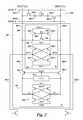
- FIG. 3is a schematic diagram illustrating circuitry for data movement in a memory device in accordance with a number of embodiments of the present disclosure.
- FIG. 3shows eight sense amplifiers (e.g., sense amplifiers 0 , 1 , . . . , 7 shown at 306 - 0 , 306 - 1 , . . . , 306 - 7 , respectively) each coupled to a respective pair of complementary sense lines (e.g., digit lines 305 - 1 and 305 - 2 ).
- FIG. 3also shows eight compute components (e.g., compute components 0 , 1 , . . . , 7 shown at 331 - 0 , 331 - 1 , . . .
- the pass gatescan be connected as shown in FIG. 2 and can be controlled by an operation selection signal, Pass.
- an output of the selection logiccan be coupled to the gates of the pass gates and digit lines 307 - 1 and 307 - 2 .
- Corresponding pairs of the sense amplifiers and compute componentscan contribute to formation of the sensing circuitry indicated at 350 - 0 , 350 - 1 , . . . , 350 - 7 .
- Data values present on the pair of complementary digit lines 305 - 1 and 305 - 2can be loaded into the compute component 331 - 0 as described in connection with FIG. 2 .
- data values on the pair of complementary digit lines 305 - 1 and 305 - 2can be passed from the sense amplifiers to the compute component (e.g., 306 - 0 to 331 - 0 ).
- the data values on the pair of complementary digit lines 305 - 1 and 305 - 2can be the data value stored in the sense amplifier 306 - 0 when the sense amplifier is fired.
- the sense amplifiers 306 - 0 , 306 - 1 , . . . , 306 - 7 in FIG. 3can each correspond to sense amplifier 206 shown in FIG. 2 .
- the compute components 331 - 0 , 331 - 1 , . . . , 331 - 7 shown in FIG. 3can each correspond to compute component 231 shown in FIG. 2 .
- a combination of one sense amplifier with one compute componentcan contribute to the sensing circuitry (e.g., 350 - 0 , 350 - 1 , . . . , 350 - 7 ) of a portion of a DRAM memory subarray 325 configured to couple to a shared I/O line 355 , as described herein.
- the paired combinations of the sense amplifiers 306 - 0 , 306 - 1 , . . . , 306 - 7 and the compute components 331 - 0 , 331 - 1 , . . . , 331 - 7 , shown in FIG. 3can be included in a sensing component stripe, as shown at 124 in FIG. 1B and at 424 in FIGS. 4A and 4B .
- FIG. 3The configurations of embodiments illustrated in FIG. 3 are shown for purposes of clarity and are not limited to these configurations.
- the configuration illustrated in FIG. 3 for the sense amplifiers 306 - 0 , 306 - 1 , . . . , 306 - 7 in combination with the compute components 331 - 0 , 331 - 1 , . . . , 331 - 7 and the shared I/O line 355is not limited to half the combination of the sense amplifiers 306 - 0 , 306 - 1 , . . . , 306 - 7 with the compute components 331 - 0 , 331 - 1 , . . .
- the sensing circuitrybeing formed above the columns 322 of memory cells (not shown) and half being formed below the columns 322 of memory cells.
- the number of such combinations of the sense amplifiers with the compute components forming the sensing circuitry configured to couple to a shared I/O linelimited to eight.
- the configuration of the shared I/O line 355is not limited to being split into two for separately coupling each of the two sets of complementary digit lines 305 - 1 and 305 - 2 , nor is the positioning of the shared I/O line 355 limited to being in the middle of the combination of the sense amplifiers and the compute components forming the sensing circuitry (e.g., rather than being at either end of the combination of the sense amplifiers and the compute components).
- the circuitry illustrated in FIG. 3also shows column select circuitry 358 - 1 and 358 - 2 that is configured to implement data movement operations with respect to particular columns 322 of a subarray 325 , the complementary digit lines 305 - 1 and 305 - 2 associated therewith, and the shared I/O line 355 (e.g., as directed by the controller 140 shown in FIGS. 1A-1C ).
- column select circuitry 358 - 1has select lines 0 , 2 , 4 , and 6 that are configured to couple with corresponding columns, such as column 0 , column 2 , column 4 , and column 6 .
- Column select circuitry 358 - 2has select lines 1 , 3 , 5 , and 7 that are configured to couple with corresponding columns, such as column 1 , column 3 , column 5 , and column 7 .
- the column select circuitry 358 illustrated in connection with FIG. 3can, in various examples, represent at least a portion of the functionality embodied by and contained in the multiplexers 460 illustrated in connection with FIGS. 4A and 4B .
- Controller 140can be coupled to column select circuitry 358 to control select lines (e.g., select line 0 ) to access data values stored in the sense amplifiers, compute components and/or present on the pair of complementary digit lines (e.g., 305 - 1 and 305 - 2 when selection transistors 359 - 1 and 359 - 2 are activated via signals from column select line 0 ).
- select linese.g., select line 0
- select linese.g., select line 0
- the pair of complementary digit linese.g., 305 - 1 and 305 - 2 when selection transistors 359 - 1 and 359 - 2 are activated via signals from column select line 0 .
- Activating the selection transistors 359 - 1 and 359 - 2enables coupling of sense amplifier 306 - 0 , compute component 331 - 0 , and/or complementary digit lines 305 - 1 and 305 - 2 of column 0 ( 322 - 0 ) to move data values on digit line 0 and digit line 0 * to shared I/O line 355 .
- the moved data valuesmay be data values from a particular row 319 stored (cached) in sense amplifier 306 - 0 and/or compute component 331 - 0 .
- Data values from each of columns 0 through 7can similarly be selected by controller 140 activating the appropriate selection transistors.
- selection transistors 359 - 1 and 359 - 2activating the selection transistors (e.g., selection transistors 359 - 1 and 359 - 2 ) enables a particular sense amplifier and/or compute component (e.g., 306 - 0 and/or 331 - 0 ) to be coupled with a shared I/O line 355 such that the sensed (stored) data values can be moved to (e.g., placed on and/or transferred to) the shared I/O line 355 .
- one column at a timeis selected (e.g., column 322 - 0 ) to be coupled to a particular shared I/O line 355 to move (e.g., transfer and/or copy) the sensed data values.
- the shared I/O line 355is illustrated as a shared, differential I/O line pair (e.g., shared I/O line and shared I/O line*).
- selection of column 0 ( 322 - 0 )could yield two data values (e.g., two bits with values of 0 and/or 1) from a row (e.g., row 319 ) and/or as stored in the sense amplifier and/or compute component associated with complementary digit lines 305 - 1 and 305 - 2 .
- These data valuescould be moved (e.g., transferred, transported, and/or fed) in parallel to each of the shared, differential I/O pair (e.g., shared I/O and shared I/O*) of the shared differential I/O line 355 .
- a memory devicee.g., 120 in FIG. 1A
- a hoste.g., 110
- a data buse.g., 156
- a control buse.g., 154
- a bank in the memory devicee.g., 123 in FIG. 1B
- can include a plurality of subarrayse.g., 125 - 0 , 125 - 1 , . . . , 125 -N ⁇ 1 in FIGS. 1B and 1C ) of memory cells and sensing circuitry (e.g., 150 in FIG.
- the sensing circuitrycan include a sense amplifier and a compute component (e.g., 206 and 231 , respectively, in FIG. 2 ) coupled to each of the columns.
- the bankcan include a plurality of subarray controllers (e.g., 170 - 0 , 170 - 1 , . . . , 170 -N ⁇ 1 in FIG. 1C ).
- Each subarray controllercan be coupled to a respective subarray of the plurality of subarrays (e.g., 125 - 0 , 125 - 1 , . . . , 125 -N ⁇ 1 in FIGS. 1B and 1C ) and each subarray controller can be configured to direct performance of an operation with respect to data stored in the respective subarray of the plurality of subarrays.
- the subarray controllerscan be individually coupled to each of the plurality of subarrays to direct execution of an operation (e.g., a single operation) upon data stored in a plurality of (e.g., a selected subset of or all) memory cells in each of the plurality of subarrays.
- an operatione.g., a single operation
- the memory devicecan, in various embodiments, be configured to move a data value corresponding to a result of an operation with respect to data stored in a first subarray of the plurality of subarrays to a memory cell in a second subarray of the plurality of subarrays.
- the sensing circuitry 150can be configured to couple to the plurality of subarrays (e.g., via the shared I/O lines 355 , column select circuitry 358 , and/or the multiplexers 460 described herein) to move a data value upon which a first operation has been performed in a first subarray to a memory cell in a second subarray for performance of a second operation.
- the first operation performed with respect to the first subarray and the second operation performed with respect to the second subarraycan be a sequence (e.g., part of the sequence) of a plurality of operations with instructions executed by the plurality of subarray controllers individually coupled to each of the plurality of subarrays.
- a first set of instructionswhen executed, can direct performance of the first operation on data stored in the first subarray that, in some embodiments, can be different from the second operation performed on data stored in the second subarray as directed by execution of a second set of instructions.
- the sensing circuitrycan be configured to couple to the plurality of subarrays to implement parallel movement of data values stored in the first subarray, upon which a first operation has been performed, to a plurality of memory cells in the second subarray.
- the memory devicecan include a shared I/O line (e.g., 155 in FIG. 1C ) configured to be coupled to the sensing circuitry of each of the plurality of subarrays to selectably implement movement of the data value stored in the first subarray, upon which the first operation has been performed, to the memory cell in the second subarray.
- the memory devicecan include a plurality of shared I/O lines (e.g., 355 in FIGS. 3 and 455-1, 455-2 , . . . , 455 -M in FIGS.
- the memory devicecan include a sensing component stripe (e.g., 124 in FIG. 1B and 424 in FIGS. 4A and 4B ) configured to include a number of a plurality of sense amplifiers and compute components (e.g., 306 - 0 , 306 - 1 , . . . , 306 - 7 and 331 - 0 , 331 - 1 , . . . , 331 - 7 , respectively, as shown in FIG.
- a sensing component stripee.g., 124 in FIG. 1B and 424 in FIGS. 4A and 4B
- compute componentse.g., 306 - 0 , 306 - 1 , . . . , 306 - 7 and 331 - 0 , 331 - 1 , . . . , 331 - 7 , respectively, as shown in FIG.
- the column select circuitrycan be configured to selectably sense data in a particular column of memory cells of a subarray by being selectably coupled to a plurality of (e.g., eight) sense amplifiers and compute components.
- a number of a plurality of sensing component stripes (e.g., 124 - 0 , . . . , 124 -N in FIGS. 1B and 1C ) in the bank of the memory devicecan correspond to a number of the plurality of subarrays (e.g., 125 - 0 , 125 - 1 , . . . , 125 -N ⁇ 1 in FIGS. 1B and 1C ) in the bank.
- a sensing component stripecan include a number of sense amplifiers and compute components configured to move (e.g., transfer and/or transport) an amount of data sensed from a row of the first subarray in parallel to a plurality of shared I/O lines. In some embodiments, the amount of data can correspond to at least a thousand bit width of the plurality of shared I/O lines.
- the array of memory cellscan include an implementation of DRAM memory cells where the controller is configured, in response to a command, to move data from the source location to the destination location via a shared I/O line.
- the source locationcan be in a first bank and the destination location can be in a second bank in the memory device and/or the source location can be in a first subarray of one bank in the memory device and the destination location can be in a second subarray of the same bank.
- the first subarray and the second subarraycan be in the same section of the bank or the subarrays can be in different sections of the bank.
- the apparatuscan be configured to move data from a source location, including a particular row (e.g., 319 in FIG. 3 ) and column address associated with a first number of sense amplifiers and compute components (e.g., 406 - 0 and 431 - 0 , respectively) in subarray 0 ( 425 - 0 ) to a shared I/O line (e.g., 455 - 1 ).
- a source locationincluding a particular row (e.g., 319 in FIG. 3 ) and column address associated with a first number of sense amplifiers and compute components (e.g., 406 - 0 and 431 - 0 , respectively) in subarray 0 ( 425 - 0 ) to a shared I/O line (e.g., 455 - 1 ).
- the apparatuscan be configured to move the data to a destination location, including a particular row and column address associated with a second number of sense amplifier and compute component (e.g., 406 - 0 and 431 - 0 , respectively, in subarray N ⁇ 1 ( 425 -N ⁇ 1) using the shared I/O line (e.g., 455 - 1 ).
- each shared I/O linee.g., 455 - 1
- 2048 shared I/O linese.g., complementary pairs of shared I/O lines
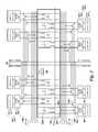
- FIGS. 4A and 4Brepresent another schematic diagram illustrating circuitry for data movement in a memory device in accordance with a number of embodiments of the present disclosure.
- a bank section of a DRAM memory devicecan include a plurality of subarrays, which are indicated in FIGS. 4A and 4B at 425 - 0 as subarray 0 and at 425 -N ⁇ 1 as subarray N ⁇ 1.
- FIGS. 4A and 4Bwhich are to be considered as horizontally connected, illustrate that each subarray (e.g., subarray 425 - 0 ) partly shown in FIG. 4A and partly shown in FIG. 4B ) can have a number of associated sense amplifiers 406 - 0 , 406 - 1 , . . . , 406 -X ⁇ 1 and compute components 431 - 0 , 431 - 1 , . . . , 431 -X ⁇ 1.
- each subarray, 425 - 0 , . . . , 425 -N ⁇ 1can have one or more associated sensing component stripes (e.g., 124 - 0 , . .
- each subarray, 425 - 0 , . . . , 425 -N ⁇ 1,can be split into portions 462 - 1 (shown in FIG. 4A ), 462 - 2 , . . . , 462 -M (shown in FIG. 4B ).
- 462 -Mmay be defined by coupling a selectable number (e.g., 2, 4, 8, 16, etc.) of the sense amplifiers and compute components (e.g., sensing circuitry 150 ), along with the corresponding columns (e.g., 422 - 0 , 422 - 1 , . . . , 422 - 7 ) among columns 422 - 0 , . . . , 422 -X ⁇ 1, to a given shared I/O line (e.g., 455 -M).
- Corresponding pairs of the sense amplifiers and compute componentscan contribute to formation of the sensing circuitry indicated at 450 - 0 , 450 - 1 , . . . , 450 -X ⁇ 1 in FIGS. 4A and 4B .
- the particular number of the sense amplifiers and compute components, along with the corresponding columns, that can be selectably coupled to a shared I/O line 455can be eight.
- the number of portions 462 - 1 , 462 - 2 , . . . , 462 -M of the subarraycan be the same as the number of shared I/O lines 455 - 1 , 455 , 2 , . . . , 455 -M that can be coupled to the subarray.
- the subarrayscan be arranged according to various DRAM architectures for coupling shared I/O lines 455 - 1 , 455 , 2 , . . . , 455 -M between subarrays 425 - 0 , 425 - 1 , . . . , 425 -N ⁇ 1.
- portion 462 - 1 of subarray 0 ( 425 - 0 ) in FIG. 4Acan correspond to the portion of the subarray illustrated in FIG. 3 .
- sense amplifier 0406 - 0
- compute component 0431 - 0
- a columncan be configured to include a pair of complementary digit lines referred to as digit line 0 and digit line 0 *.
- alternative embodimentscan include a single digit line 405 - 0 (sense line) for a single column of memory cells. Embodiments are not so limited.
- FIGS. 4A and 4Bcan selectably sense data in a particular column of memory cells of a subarray by being selectably coupled to at least one of the sense amplifier and compute component coupled to a respective sense line of the particular column.
- a sensing component stripecan, in various embodiments, extend from one end of a subarray to an opposite end of the subarray.
- sensing component stripe 0424 - 0
- sensing component stripe 0424 - 0
- the configuration illustrated in FIGS. 4A and 4B for the sense amplifiers 406 - 0 , 406 - 1 , . . . , 406 -X ⁇ 1 in combination with the compute components 431 - 0 , 431 - 1 , . . . , 431 -X ⁇ 1 and shared I/O line 0 ( 455 - 1 ) through shared I/O line M ⁇ 1 ( 455 -M)is not limited to half the combination of the sense amplifiers with the compute components of the sensing circuitry ( 450 ) being formed above the columns of memory cells and half being formed below the columns of memory cells 422 - 0 , 422 - 1 , . . .
- a sensing component stripe 424 for a particular subarray 425can be formed with any number of the sense amplifiers and compute components of the sensing component stripe being formed above and below the columns of memory cells. Accordingly, in some embodiments as illustrated in FIGS. 1B and 1C , all of the sense amplifiers and compute components of the sensing circuitry and corresponding sensing component stripes can be formed above or below the columns of memory cells.
- each subarraycan have column select circuitry (e.g., 358 ) that is configured to implement data movement operations on particular columns 422 of a subarray, such as subarray 0 ( 425 - 0 ), and the complementary digit lines thereof, coupling stored data values from the sense amplifiers 406 and/or compute components 431 to given shared I/O lines 455 - 1 , . . . , 455 -M (e.g., complementary shared I/O lines 355 in FIG. 3 ).
- column select circuitrye.g., 358
- the controller 140can direct that data values of memory cells in a particular row (e.g., row 319 ) of subarray 0 ( 425 - 0 ) be sensed and moved to a same or different numbered row of subarrays 425 - 1 , 425 - 2 , . . . , 425 -N ⁇ 1 in a same or different numbered column.
- the data valuescan be moved from a portion of a first subarray to a different portion of a second subarray (e.g., not necessarily from portion 462 - 1 of subarray 0 to portion 462 - 1 of subarray N ⁇ 1).
- data valuesmay be moved from a column in portion 462 - 1 to a column in portion 462 -M using shifting techniques.
- the column select circuitry(e.g., 358 in FIG. 3 ) can direct movement (e.g., sequential movement) of each of the eight columns (e.g., digit/digit*) in the portion of the subarray (e.g., portion 462 - 1 of subarray 425 - 0 ) for a particular row such that the sense amplifiers and compute components of the sensing component stripe (e.g., 424 - 0 ) for that portion can store (cache) and move all data values to the shared I/O line in a particular order (e.g., in an order in which the columns were sensed).
- complementary digit lines, digit/digit*, and complementary shared I/O lines 355for each of eight columns, there can be 16 data values (e.g., bits) sequenced to the shared I/O line from one portion of the subarray such that one data value (e.g., bit) is moved (e.g., transferred, transported, and/or fed) to each of the complementary shared I/O lines at a time from each of the sense amplifiers and compute components.
- data valuese.g., bits
- subarray portion 462 - 1 of each of subarrays 425 - 0 , 425 - 1 , . . . , 425 -N ⁇ 1each configured to couple to a different shared I/O line (e.g., 455 - 1 through 455 -M)
- data valuese.g., bits
- the plurality of shared I/O linesmight be, for example, at least a thousand bits wide (e.g., 2048 bits wide), such as to increase the speed, rate, and/or efficiency of data movement in a DRAM implementation (e.g., relative to a 64 bit wide data path).
- each subarraye.g., subarray 425 - 0
- one or more multiplexers 460 - 1 and 460 - 2can be coupled to the sense amplifiers and compute components of each portion 462 - 1 , 462 - 2 , . . . , 462 -M of the sensing component stripe 424 - 0 for the subarray.
- the multiplexers 460 illustrated in connection with FIGS. 4A and 4Bcan, in various embodiments, be inclusive of at least the functionality embodied by and contained in the column select circuitry 358 illustrated in connection with FIG. 3 .
- the multiplexers 460 - 1 and 460 - 2can be configured to access, select, receive, coordinate, combine, and move (e.g., transfer and/or transport) the data values (e.g., bits) stored (cached) by the number of selected sense amplifiers and compute components in a portion (e.g., portion 462 - 1 ) of the subarray to the shared I/O line (e.g., shared I/O line 455 - 1 ).
- a shared I/O lineas described herein, can be configured to couple a source location and a destination location between pairs of bank section subarrays for improved data movement.
- a controllere.g., 140
- a bank of a memory devicee.g., 121
- a bank sectioncan, in various embodiments, include a plurality of subarrays of memory cells in the bank section (e.g., subarrays 125 - 0 through 125 -N ⁇ 1 and 425 - 0 through 425 -N ⁇ 1).
- the bank sectioncan, in various embodiments, further include sensing circuitry (e.g., 150 ) coupled to the plurality of subarrays via a plurality of columns (e.g., 322 - 0 , 422 - 0 , and 422 - 1 ) of the memory cells.
- the sensing circuitrycan include a sense amplifier and a compute component (e.g., 206 and 231 , respectively, in FIG. 2 and at corresponding reference numbers in FIGS. 3, 4A and 4B ) coupled to each of the columns and configured to implement the command to move the data.
- the bank sectioncan, in various embodiments, further include a shared I/O line (e.g., 155 , 355 , 455 - 1 , and 455 -M) to couple the source location and the destination location to move the data.
- the controllercan be configured to direct the plurality of subarrays and to the sensing circuitry to perform a data write operation on the moved data to the destination location in the bank section (e.g., a selected memory cell in a particular row and/or column of a different selected subarray).
- the apparatuscan include a sensing component stripe (e.g., 124 and 424 ) including a number of sense amplifiers and compute components that corresponds to a number of columns of the memory cells (e.g., where each column of memory cells is configured to couple to a sense amplifier and a compute component).
- the number of sensing component stripes in the bank sectione.g., 424 - 0 through 424 -N ⁇ 1
- the number of sensing component stripes in the bank sectioncan correspond to a number of subarrays in the bank section (e.g., 425 - 0 through 425 -N ⁇ 1).
- the number of sense amplifiers and compute componentscan be selectably (e.g., sequentially) coupled to the shared I/O line (e.g., as shown by column select circuitry at 358 - 1 , 358 - 2 , 359 - 1 , and 359 - 2 in FIG. 3 ).
- the column select circuitrycan be configured to selectably couple a shared I/O line to, for example, one or more of eight sense amplifiers and compute components in the source location (e.g., as shown in subarray 325 in FIG. 3 and subarray portions 462 - 1 through 462 -M in FIGS. 4A and 4B ). As such, the eight sense amplifiers and compute components in the source location can be sequentially coupled to the shared I/O line.
- a number of shared I/O lines formed in the arraycan correspond to a division of a number of columns in the array by the eight sense amplifiers and compute components that can be selectably coupled to each of the shared I/O lines.
- the apparatuscan, in various embodiments, include a number of multiplexers (e.g., as shown at 460 - 1 and 460 - 2 in portions 462 - 1 through 462 -M of various subarrays in FIGS. 4A and 4B ).
- the apparatuscan include a plurality of sense amplifiers and compute components and a multiplexer to select a sense amplifier and a compute component to couple to the shared I/O line.
- the multiplexerscan be formed between the sense amplifiers and compute components and the shared I/O line to access, select, receive, coordinate, combine, and move (e.g., transfer and/or transport) selected data to the coupled shared I/O line.
- an array of memory cellscan include a column of memory cells having a pair of complementary sense (digit) lines (e.g., 305 - 1 and 305 - 2 in FIG. 3 ).
- the sensing circuitrycan, in some embodiments, include a sense amplifier (e.g., 306 - 0 ) selectably coupled to each of the pair of complementary sense (digit) lines and a compute component (e.g., 331 - 0 ) coupled to the sense amplifier via pass gates (e.g., 307 - 1 and 307 - 2 ).
- a source sensing component stripe(e.g., 124 and 424 ) can include a number of sense amplifiers and compute components that can be selected and configured to move (e.g., transfer and/or transport) data values (e.g., a number of bits) sensed from a row of the source location in parallel to a plurality of shared I/O lines.
- movee.g., transfer and/or transport
- data valuese.g., a number of bits
- the data values stored in memory cells of selected columns of a row of the subarraycan be sensed by and stored (cached) in the sense amplifiers and compute components of the sensing component stripe until a number of data values (e.g., the number of bits) reaches the number of data values stored in the row and/or a threshold (e.g., the number of sense amplifiers and compute components in the sensing component stripe) and then move (e.g., transfer and/or transport) the data values via the plurality of shared I/O lines.
- the threshold amount of datacan correspond to the at least a thousand bit width of the plurality of shared I/O lines.
- the source sensing component stripecan include a number of sense amplifiers and compute components that can be selected and configured to store data values (e.g., bits) sensed from a row of the source location when an amount of sensed data values (e.g., the number of data bits) exceeds the at least a thousand bit width of the plurality of shared I/O lines.
- the source sensing component stripecan be configured to move (e.g., transfer and/or transport) the data values sensed from the row of the source location when coupled to the plurality of shared I/O lines as a plurality of subsets.
- the amount of at least a first subset of the data valuescan correspond to the at least a thousand bit width of the plurality of shared I/O lines.
- the controllercan, as described herein, be configured to move the data values from a selected row and a selected sense line in the source location to a selected row and a selected sense line in the destination location via the shared I/O line.
- the data valuescan be moved in response to commands by the controller 140 and/or a particular subarray controller 170 - 0 , 170 - 1 , . . . , 170 -N ⁇ 1 coupled to a particular subarray 125 - 0 , 125 - 1 , . . . , 125 -N ⁇ 1, and/or a particular sensing component stripe 125 - 0 , 125 - 1 , . . .
- a selected row and a selected sense line in the source location (e.g., a first subarray) input to the controllercan be different from a selected row and a selected sense line in the destination location (e.g., a second subarray).
- a location of the data in memory cells of the selected row and the selected sense line in a source subarraycan be different from a location of the data moved to memory cells of a selected row and the selected source line in a destination subarray.
- the source locationmay be a particular row and digit lines of portion 462 - 1 of subarray 0 ( 425 - 0 ) in FIG. 4A and the destination may be a different row and digit lines of portion 462 -M in subarray N ⁇ 1 ( 425 -N ⁇ 1) in FIG. 4B .
- a destination sensing component stripe(e.g., 124 and 424 ) can be the same as a source sensing component stripe.
- a plurality of sense amplifiers and/or compute componentscan be selected and configured (e.g., depending on the command from the controller and/or subarray controllers 170 - 0 , 170 - 1 , . . . , 170 -N ⁇ 1) to selectably move (e.g., transfer and/or transport) sensed data to the coupled shared I/O line and selectably receive the data from one of a plurality of coupled shared I/O lines (e.g., to be moved to the destination location).
- movee.g., transfer and/or transport
- Selection of sense amplifiers and compute components in the destination sensing component stripecan be performed using the column select circuitry (e.g., 358 - 1 , 358 - 2 , 359 - 1 , and 359 - 2 in FIG. 3 ) and/or the multiplexers described herein (e.g., 460 - 1 and 460 - 2 in FIGS. 4A and 4B ).
- the column select circuitrye.g., 358 - 1 , 358 - 2 , 359 - 1 , and 359 - 2 in FIG. 3
- the multiplexers described hereine.g., 460 - 1 and 460 - 2 in FIGS. 4A and 4B .
- the controllercan, according to some embodiments, be configured to write an amount of data (e.g., a number of data bits) selectably received by the plurality of selected sense amplifiers and/or compute components in the destination sensing component stripe to a selected row and a selected sense line of the destination location in the destination subarray.
- the amount of data to writecorresponds to the at least a thousand bit width of a plurality of shared I/O lines.
- the destination sensing component stripecan, according to some embodiments, include a plurality of selected sense amplifiers and compute components configured to store received data values (e.g., bits) when an amount of received data values (e.g., the number of data bits) exceeds the at least a thousand bit width of the plurality of shared I/O lines.
- the controllercan, according to some embodiments, be configured to write the stored data values (e.g., the number of data bits) to a selected row and a plurality of selected sense lines in the destination location as a plurality of subsets.
- the amount of data values of at least a first subset of the written datacan correspond to the at least a thousand bit width of the plurality of shared I/O lines.
- the controllercan be configured to write the stored data values (e.g., the number of data bits) to the selected row and the selected sense line in the destination location as a single set (e.g., not as subsets of data values).
- a controllere.g., 140
- a banke.g., 121
- a memory devicee.g., 120
- a bank in the memory devicecan include a plurality of subarrays (e.g., 125 - 0 , 125 - 1 , . . . , 125 -N ⁇ 1 as shown in FIGS. 1B and 1C and 425-0, 425-1 , . . . , 425 -N ⁇ 1 as shown in FIGS.
- a plurality of subarray controllerse.g., 170 - 0 , 170 - 1 , . . . , 170 -N ⁇ 1 in FIG. 1C ) individually coupled to each of the plurality of subarrays to direct performance of an operation (e.g., a single operation) upon data stored in a plurality (e.g., a selected subset or all) of the memory cells by the sensing circuitry in each of the plurality of subarrays.
- an operatione.g., a single operation
- the bankalso can include sensing circuitry (e.g., 150 in FIG. 1A and 250 in FIG. 2 ) on pitch with the plurality of subarrays and coupled to the plurality of subarrays (e.g., via a plurality of sense lines 205 - 1 and 205 - 2 in FIGS. 2, 305-1 and 305-2 and at corresponding reference numbers in FIGS. 3, 4A and 4B ).
- the sensing circuitrycan include a sense amplifier and a compute component (e.g., 206 and 231 , respectively, in FIG. 2 and at corresponding reference numbers in FIGS. 3, 4A and 4B ) coupled to a sense line.
- the controller 140can be configured to provide a respective set of instructions to each of the plurality of subarray controllers (e.g., 170 - 0 , 170 - 1 , . . . , 170 -N ⁇ 1).
- the controllercan be configured to couple to the plurality of subarray controllers to input a respective set of instructions to be executed by each of the plurality of subarray controllers to direct performance of a respective operation by the sensing circuitry.
- the plurality of subarrays of memory cellscan be subarrays of DRAM cells.
- the controllercan be configured to systolically move the data values between sequential subarrays in the bank of memory cells, in response to a command, using a DRAM protocol and DRAM logical and electrical interfaces, as described herein.
- a hoste.g., 110 in FIG. 1A
- a first cache(e.g., 171 - 1 in FIG. 1C ) can be associated with the controller.
- the first cachecan be configured to receive data from the host and signal to the controller 140 that the data is received to initiate performance of a stored sequence of a plurality of operations.
- the controllercan be configured to determine, based upon input of the data (e.g., analysis of the type and/or content of the unprocessed data in the cache), which of a plurality of sequences of operations performed by the subarray controllers coupled to the plurality of subarrays is appropriate for processing of the data.
- the controllercan be configured to provide (e.g., input) the data to a particular subarray based upon a particular subarray controller coupled to the particular subarray performing a first operation in the appropriate stored contiguous sequence of operations.
- the particular subarraycan be coupled to a particular subarray controller configured to execute a first set of instructions to direct performance of a first operation in the appropriate stored contiguous sequence of operations upon data stored in the plurality of memory cells.
- connection circuitrye.g., 232 - 1 and 232 - 2 in FIG. 2
- connection circuitrycan be configured to connect sensing circuitry coupled to a particular column in a first subarray to a number of rows in a corresponding column in a second (e.g., adjacent) subarray.
- the connection circuitrycan be configured to move (e.g., transfer and/or transport) a data value (e.g., from a selected row and the particular column) to a selected row and the corresponding column in the second subarray (e.g., the data value can be copied to a selected memory cell therein) for performance of a next operation in a sequence of operations.
- the movement of the data valuecan be directed by the subarray controller of the first subarray executing a set of instructions when the data value is stored in the sensing circuitry and the controller can select a particular row and/or a particular memory cell intersected by the corresponding column in the second subarray to receive the data value by movement (e.g., transfer and/or transport) of the data value.
- movemente.g., transfer and/or transport
- the controller(e.g., 140 ) can be coupled to the bank of the memory device to execute a command for movement of data from a start location to an end location in the bank.
- the plurality of subarray controllers(e.g., 170 - 0 , 170 - 1 , . . . , 170 -N ⁇ 1 in FIG. 1C ) can be configured to couple to the controller to receive a respective set of instructions by each of the plurality of subarray controllers to direct performance of the operation with respect to data stored in each of the plurality of subarrays.
- the plurality of subarray controllerscan be configured to couple to the controller to receive input of a set of instructions into each of the plurality of subarray controllers to, when executed, direct performance of the operation on data of each respective subarray of the plurality of subarrays (e.g., 125 - 0 , 125 - 1 , . . . , 125 -N ⁇ 1 in FIGS. 1B and 1C and at corresponding reference numbers in FIGS. 4A and 4B ).
- a set of instructionsinto each of the plurality of subarray controllers to, when executed, direct performance of the operation on data of each respective subarray of the plurality of subarrays (e.g., 125 - 0 , 125 - 1 , . . . , 125 -N ⁇ 1 in FIGS. 1B and 1C and at corresponding reference numbers in FIGS. 4A and 4B ).
- the plurality of subarrayscan include a plurality of sets of instructions to execute performance of different sequences of operations stored by the subarray controllers for a plurality of contiguous subsets of the subarrays (e.g., configured for processing of different data content).
- the controllercan be configured to provide (e.g., input) data to a particular subarray based upon a particular subarray controller coupled to the particular subarray being configured to execute a first set of instructions for an appropriate contiguous sequence of operations.
- the particular subarray controller coupled to the particular subarraycan be the start location in the bank for performance of the appropriate stored contiguous sequence of operations (e.g., based upon the analysis of the type and/or content of the unprocessed data in the cache).
- the particular subarray that is the start locationcan, in various embodiments, have at least one contiguous sequence of operations for a plurality of subarrays stored between the start location and a beginning of a first subarray in the bank.
- the start location determined to be appropriate for the unprocessed data by the controllermay be subarray 125 - 3 in FIG. 1C with the three subarrays 125 - 0 , 125 - 1 , and 125 - 2 being the first subarrays in the bank.
- completed performance of a contiguous sequence of a number of operationscan be configured to yield an output at the end location in the subarrays of the bank, where a particular subarray at the end location has at least one subarray between the end location and an end of a last subarray in the bank.
- the end location at which the number of operations is completed to yield the outputmay be subarray 125 - 3 in FIG. 1C with subarray 125 -N ⁇ 1 being the last subarray in the bank.
- the stored contiguous sequence of operations determined to be appropriate as the start location for input of the unprocessed datacan have a plurality of subarrays between the start location and the beginning of the first subarray and an end location that has at least one subarray between the end location and the end of the last subarray.
- the stored contiguous sequence of operations determined to be appropriate, and into which the unprocessed data is inputcan be in the middle of a stack of subarrays, as described herein.
- a second cache(e.g., 571 - 2 in FIG. 5 ) can be associated with the controller.
- the second cachecan be configured to receive output of completed performance of a sequence of operations from the plurality of subarrays.
- the second cachecan be configured to signal to the controller (e.g., 540 in FIG. 5 ) to initiate another iteration of performance of the sequence of operations by input of new received data to selected memory cells in a subarray (e.g., in particular columns and/or rows of the subarray) at the start location after the latency has expired. Prior to expiry of the latency, new received data also can be input For example, as described in connection with FIG.
- a second batch of unprocessed datacan be input into a first subarray 525 - 0 to be processed by performance of an AND operation after a first batch of unprocessed data has been processed therein and moved (e.g., transferred and/or copied) as a first set of data values for processing by a second subarray 525 - 1 to produce a second set of data values.
- a commandcan be received from the controller to move data from the source location to the destination location (e.g., of a DRAM array of the memory cells).
- the datacan be moved from the source location to the destination location (e.g., of the DRAM array) using the sense amplifiers and compute components via the plurality of shared I/O lines.
- 2048 shared I/O linescan be configured as a 2048 bit wide shared I/O line.
- a number of cycles for moving the data from a first row in the source location to a second row in the destination locationcan be determined by dividing a number of columns in the array intersected by a row of memory cells in the array by the 2048 bit width of the plurality of shared I/O lines.
- an arraye.g., a bank, a bank section, and a subarray thereof
- an arraycan have 16,384 columns, which can correspond to 16,384 data values in a row, which when divided by the 2048 bit width of the plurality of shared I/O lines intersecting the row can yield eight cycles, each separate cycle being at substantially the same point in time (e.g., in parallel) for movement of all the data in the row.
- a bandwidth for moving the data from a first row in the source location to a second row in the destination locationcan be determined by dividing the number of columns in the array intersected by the row of memory cells in the array by the 2048 bit width of the plurality of shared I/O lines and multiplying the result by a clock rate of the controller.
- determining a number of data values in a row of the arraycan be based upon the plurality of sense (digit) lines in the array.
- a source location in a first subarray of memory cellscan be configured to couple via a plurality of shared I/O lines to a destination location in a second subarray of memory cells, where the plurality of shared I/O lines can be configured as at least a thousand bit wide shared I/O line.
- a first sensing component stripe (e.g., 424 - 0 ) for the first subarray (e.g., 425 - 0 ) and second sensing component stripe (e.g., 424 -N ⁇ 1) for second subarray (e.g., 425 -N ⁇ 1)can be configured to include a sense amplifier and a compute component (e.g., 406 - 0 and 431 - 0 , respectively) coupled to each corresponding column of memory cells in the first and second subarrays (e.g., 422 - 0 through 422 -X ⁇ 1).
- a controllercan be configured to couple to the memory cells of the first and second subarrays and the first and second sensing component stripes (e.g., via the column select circuitry 358 - 1 , 358 - 2 , 359 - 1 , and 359 - 2 ).
- the datacan be moved from the source location in the first subarray via the plurality of shared I/O lines to the destination location in the second subarray using the first sensing component stripe for the first subarray and the second sensing component stripe for the second subarray.
- the first amplifier stripe for the first subarray and the second sensing component stripe for the second subarraycan, accordingly to various embodiment, be configured to couple to the plurality of shared I/O lines (e.g., via the column select circuitry 358 - 1 , 358 - 2 , 359 - 1 , and 359 - 2 in FIG. 3 and/or the multiplexers 460 - 1 and 460 - 2 in FIGS. 4A and 4B ).
- the source location in the first subarray and the destination location in the second subarraycan be in a single bank section of a memory device (e.g., as shown in FIGS. 1B and 1C and FIGS. 4A and 4B ).
- the source location in the first subarray and the destination location in the second subarraycan be in separate banks and bank sections of the memory device coupled to a plurality of shared I/O lines.
- the methodcan include moving the data (e.g., in parallel) from the first sensing component stripe for the first subarray via the plurality of shared I/O lines to the second sensing component stripe for the second subarray.
- a sensing component stripe(e.g., all sensing component stripes 424 - 0 through 424 -N ⁇ 1) can be configured in each of a plurality of subarrays (e.g., subarrays 425 - 0 through 425 -N ⁇ 1) to couple to the plurality of shared I/O lines (e.g., shared I/O line 455 - 1 ).
- only one of eight columns of complementary sense lines at a time in the first subarraycan be coupled to one of the plurality of shared I/O lines using the first sensing component stripe (e.g., sensing component stripe 424 - 0 ) and only one of eight columns of complementary sense lines at a time in the second subarray can be coupled to one of the plurality of shared I/O lines using the second sensing component stripe (e.g., sensing component stripes 424 -N ⁇ 1).
- the first sensing component stripee.g., sensing component stripe 424 - 0
- the second sensing component stripee.g., sensing component stripes 424 -N ⁇ 1
- the datacan be moved from a number of sense amplifiers and compute components of the first sensing component stripe via the plurality of shared I/O lines to a corresponding number of sense amplifiers and compute components of the second sensing component stripe.
- the data sensed from each sense amplifier and/or compute component of the source locationcan be moved to a corresponding sense amplifier and/or compute component in the destination location.
- the datacan be moved in parallel from the first sensing component stripe to the second sensing component stripe via the plurality of shared I/O lines.
- the first sensing component stripecan store (e.g., cache) the sensed data and the second sensing component stripe can store (e.g., cache) the moved data.
- the controller and/or subarray controllerscan select (e.g., open via an appropriate select line) a second row of memory cells, which corresponds to the destination location, for the second sensing component stripe (e.g., via the column select circuitry 358 - 1 , 358 - 2 , 359 - 1 , and 359 - 2 and/or the multiplexers 460 - 1 and 460 - 2 ).
- the controller and/or subarray controllerscan then direct writing the data moved to the second sensing component stripe to the destination location in the second row of memory cells.
- a shared I/O linecan be used as a data path (e.g., data flow pipeline) to move data in the memory cell array between various locations (e.g., subarrays) in the array.
- the shared I/O linecan be shared between all sensing component stripes.
- one sensing component stripe or one pair of sensing component stripese.g., coupling a source location and a destination location
- the shared I/O lineis used to accomplish moving the data from one sensing component stripe to the other sensing component stripe.
- a rowcan be selected (e.g., opened by the controller and/or subarray controller via an appropriate select line) for the first sensing component stripe and the data values of the memory cells in the row can be sensed.
- the first sensing component stripecan be coupled to the shared I/O line, along with coupling the second sensing component stripe to the same shared I/O line.
- the second sensing component stripecan still be in a pre-charge state (e.g., ready to accept data).
- the second sensing component stripecan fire (e.g., latch) to store the data into respective sense amplifiers and compute components.
- a row coupled to the second sensing component stripecan be opened (e.g., after latching the data) and the data that resides in the sense amplifiers and compute components can be written into the destination location of that row.
- FIG. 5illustrates a timing diagram 533 associated with performing a number of data movement operations using circuitry in accordance with a number of embodiments of the present disclosure.
- the timing diagram 533 schematically illustrated in FIG. 5is shown as an example of a sequence of operations associated with systolic movement of data, as described herein (e.g., sequential movement of data between adjacent subarrays 525 - 0 , 525 - 1 , 525 - 2 , 525 - 3 , and 525 - 4 ).
- a time scalee.g., time points 1 , 2 , 3 , 4 , and 5
- arbitrary lengthe.g., operational cycle and/or clock cycle
- the functions described belowcan be performed substantially simultaneously in the subarrays executing the sequence of instructions (e.g., taking into account that a continuous length of a shared I/O line moves one data value (e.g., bit) at a time).
- a continuous length of a shared I/O linemoves one data value (e.g., bit) at a time).
- input of data, processing of the data with operations, and moving the data to a next subarray, etc.can occur substantially simultaneously with the corresponding functions in a second subarray, a third subarray, and so on until the corresponding functions are performed in the last subarray of the sequence of instructions stored in the subarray controllers.
- the sequence of instructions to be stored in and/or executed by the subarray controllerse.g., subarray controllers corresponding to 170 - 0 , 170 - 1 , . . . , 170 -N ⁇ 1 described in connection with FIG. 1C ) and performed as a sequence of operations is shown in FIG. 5 to be five different operations by way of example. However, embodiments of the present disclosure are not limited to a sequence of five operations, all the operations being different, and/or any or all of the operations being the particular operations shown in FIG. 5 .
- the first data values stored in some or all of the memory cells thereofcan be processed by performance of an AND operation by a first subarray controller (e.g., subarray controller 170 - 0 described in connection with FIG. 1C ) to produce a first set of data values.
- a first subarray controllere.g., subarray controller 170 - 0 described in connection with FIG. 1C
- the first set of data valuescan be moved (e.g., transferred and/or copied) from a first sensing component stripe (e.g., sensing component stripe 124 - 0 described in connection with FIG.
- the first set of data values stored in some or all of the memory cells in subarray 525 - 1can be further processed by performance of an OR operation by a second subarray controller (e.g., subarray controller 170 - 2 described in connection with FIG. 1C ).
- a second subarray controllere.g., subarray controller 170 - 2 described in connection with FIG. 1C .
- the first set of data valuescan be moved (e.g., transferred and/or copied) from a second sensing component stripe (e.g., sensing component stripe 124 - 1 described in connection with FIG.
- a second batch of unprocessed datacan be input into some or all of the memory cells of the first subarray 525 - 0 to be processed by performance of the AND operation to produce a second set of data values.
- the second set of data valuescan be moved (e.g., transferred and/or copied) from the first sensing component stripe (e.g., sensing component stripe 124 - 0 described in connection with FIG. 1C ) by being moved (e.g., transferred and/or transported) via a plurality of shared I/O lines for input to selected memory cells (e.g., some or all of the memory cells) of the second subarray 525 - 1 .
- selected memory cellse.g., some or all of the memory cells
- the first set of data values stored in some or all of the memory cells in subarray 525 - 2can be further processed by performance of a NOR operation by a third subarray controller (e.g., subarray controller 170 - 2 described in connection with FIG. 1C ).
- a third subarray controllere.g., subarray controller 170 - 2 described in connection with FIG. 1C .
- the second batch of data valuescan be input to selected memory cells of the second subarray 525 - 1 to be processed by performance of the OR operation.
- the second set of data valuescan be moved (e.g., transferred and/or copied) from the second sensing component stripe (e.g., sensing component stripe 124 - 1 ) by being moved (e.g., transferred and/or transported) via the plurality of shared I/O lines for input to selected memory cells of the third subarray 525 - 2 .
- the systolic data movement operation just describedcan continue through performance of a last operation of an operational cycle (e.g., an XOR operation) at time point 5 .
- an operational cyclee.g., an XOR operation
- a completely processed batch of datacan be output at each time point thereafter until the last batch of unprocessed data input to the first subarray 525 - 0 has been completely processed.
- the completely processed data values of each batchcan be output (e.g., as shown at 141 and described in connection with FIG. 1B ) to, in some embodiments, a cache 571 - 2 associated with the controller 540 .
- the controller 540 shown in FIG. 5can, in various examples, represent at least a portion of the functionality embodied by and contained in the controller 140 shown in FIGS. 1A-1C .
- the controller 540can be configured to output each batch of the completely processed data values from the cache 571 - 2 to the host 110 via, for example, an HSI out-of-band bus 157 (e.g., as described in connection with FIG. 1A ).
- the first set of instructionscan be stored in the first subarray controller, where the first subarray controller is coupled to the first subarray
- the second set of instructionscan be stored in the second subarray controller, where the second subarray controller is coupled to the second subarray.
- the first and second sets of instructionscan be accessed by (e.g., without being stored by) the first subarray controller and the second subarray controller, respectively, from, for example, the controller 140 to be executed for performance of particular operations.
- the methodcan include the controller directing performance of the first operation with respect to data stored in the first subarray by execution of the first set of instructions and directing performance of the second operation with respect to data stored in the second subarray by execution of the second set of instructions.
- the methodcan include coupling the first sense amplifier stripe (e.g., 124 - 0 ) for the first subarray (e.g., 125 - 0 ) via a shared I/O line (e.g., 455 - 1 , 455 - 2 , . . . , 455 -M) to the selected row (e.g., 319 ) of memory cells in the second subarray (e.g., 125 - 1 ).
- a shared I/O linee.g., 455 - 1 , 455 - 2 , . . . , 455 -M
- the data valuescan be moved (e.g., transferred and/or transported) from the particular row in the first subarray, upon which the first operation has been performed, via the shared I/O line to the selected row of memory cells in the second subarray using the coupled first sense amplifier stripe.
- the data values from the particular row in the first subarraycan be processed by performance of the first operation as directed by execution of instructions by the first subarray controller for the first subarray and the data values can be processed (e.g., systolically processed) by performance of the second operation in the selected row of the second subarray as directed by execution of instructions by a second subarray controller for the second subarray.
- the methodcan, in various embodiments, include coupling only one of a plurality of (e.g., eight) columns (e.g., columns of complementary sense lines 305 - 1 and 305 - 2 ) at a time in the first subarray to each one of the plurality of shared I/O lines using the first sensing component stripe.
- a plurality of (e.g., eight) columnse.g., columns of complementary sense lines 305 - 1 and 305 - 2
- the methodcan include the controller selecting a first row of memory cells in the first subarray for the first sensing component stripe to sense data stored therein, coupling the plurality of shared I/O lines to the first sensing component stripe, coupling the selected row of memory cells in the second subarray to the plurality of shared I/O lines, and moving the data in parallel from the first sensing component stripe to the selected row of memory cells in the second subarray via the plurality of shared I/O lines.
- the first sensing component stripecan store (e.g., cache) the data values upon which the first operation has been performed and the moved data values can be stored (e.g., cached and/or saved) in the selected row of memory cells in the second subarray.
- the methodcan include performing substantially simultaneously each operation of a sequence of operations by execution of a first set of instructions by a first subarray controller coupled to the first subarray and by execution of a second set of instructions by the second subarray controller coupled to the second subarray.
- the sequence of operationscan be performed (e.g., substantially simultaneously performing at least two operations) after data is present for processing in the particular row in the first subarray and the selected row of memory cells in the second subarray.
- performance of the first operation by execution of instructions by the first subarray controllercan be configured to be an operation that is different than a second operation performed by execution of instructions by the second subarray controller.
- the first and second subarray controllerscan be configured to perform the same operation.
- sensing circuitrysense amplifiers
- compute componentssensing component stripes
- subarray controllersshared I/O lines
- column select circuitrymultiplexers, timing sequences, etc.
- embodiments of the present disclosureare not limited to those combinations explicitly recited herein.
- Other combinations and configurations of the sensing circuitry, sense amplifiers, compute components, sensing component stripes, subarray controllers, shared I/O lines, column select circuitry, multiplexers, timing sequences, etc., disclosed hereinare expressly included within the scope of this disclosure.
Landscapes
- Engineering & Computer Science (AREA)
- Theoretical Computer Science (AREA)
- Microelectronics & Electronic Packaging (AREA)
- Computer Hardware Design (AREA)
- Human Computer Interaction (AREA)
- Physics & Mathematics (AREA)
- General Engineering & Computer Science (AREA)
- General Physics & Mathematics (AREA)
- Dram (AREA)
Abstract
Description
Claims (31)
Priority Applications (8)
| Application Number | Priority Date | Filing Date | Title |
|---|---|---|---|
| US15/045,750US9971541B2 (en) | 2016-02-17 | 2016-02-17 | Apparatuses and methods for data movement |
| CN201780011785.4ACN108701473B (en) | 2016-02-17 | 2017-02-13 | Apparatus and method for data movement |
| PCT/US2017/017613WO2017142826A1 (en) | 2016-02-17 | 2017-02-13 | Apparatuses and methods for data movement |
| US15/978,750US10353618B2 (en) | 2016-02-17 | 2018-05-14 | Apparatuses and methods for data movement |
| US16/506,664US11010085B2 (en) | 2016-02-17 | 2019-07-09 | Apparatuses and methods for data movement |
| US17/321,807US11614878B2 (en) | 2016-02-17 | 2021-05-17 | Apparatuses and methods for data movement |
| US18/125,625US12019895B2 (en) | 2016-02-17 | 2023-03-23 | Apparatuses and methods for data movement |
| US18/751,917US20240345756A1 (en) | 2016-02-17 | 2024-06-24 | Apparatuses and methods for data movement |
Applications Claiming Priority (1)
| Application Number | Priority Date | Filing Date | Title |
|---|---|---|---|
| US15/045,750US9971541B2 (en) | 2016-02-17 | 2016-02-17 | Apparatuses and methods for data movement |
Related Child Applications (1)
| Application Number | Title | Priority Date | Filing Date |
|---|---|---|---|
| US15/978,750ContinuationUS10353618B2 (en) | 2016-02-17 | 2018-05-14 | Apparatuses and methods for data movement |
Publications (2)
| Publication Number | Publication Date |
|---|---|
| US20170235515A1 US20170235515A1 (en) | 2017-08-17 |
| US9971541B2true US9971541B2 (en) | 2018-05-15 |
Family
ID=59561503
Family Applications (6)
| Application Number | Title | Priority Date | Filing Date |
|---|---|---|---|
| US15/045,750Active2036-04-13US9971541B2 (en) | 2016-02-17 | 2016-02-17 | Apparatuses and methods for data movement |
| US15/978,750ActiveUS10353618B2 (en) | 2016-02-17 | 2018-05-14 | Apparatuses and methods for data movement |
| US16/506,664ActiveUS11010085B2 (en) | 2016-02-17 | 2019-07-09 | Apparatuses and methods for data movement |
| US17/321,807Active2036-03-11US11614878B2 (en) | 2016-02-17 | 2021-05-17 | Apparatuses and methods for data movement |
| US18/125,625ActiveUS12019895B2 (en) | 2016-02-17 | 2023-03-23 | Apparatuses and methods for data movement |
| US18/751,917PendingUS20240345756A1 (en) | 2016-02-17 | 2024-06-24 | Apparatuses and methods for data movement |
Family Applications After (5)
| Application Number | Title | Priority Date | Filing Date |
|---|---|---|---|
| US15/978,750ActiveUS10353618B2 (en) | 2016-02-17 | 2018-05-14 | Apparatuses and methods for data movement |
| US16/506,664ActiveUS11010085B2 (en) | 2016-02-17 | 2019-07-09 | Apparatuses and methods for data movement |
| US17/321,807Active2036-03-11US11614878B2 (en) | 2016-02-17 | 2021-05-17 | Apparatuses and methods for data movement |
| US18/125,625ActiveUS12019895B2 (en) | 2016-02-17 | 2023-03-23 | Apparatuses and methods for data movement |
| US18/751,917PendingUS20240345756A1 (en) | 2016-02-17 | 2024-06-24 | Apparatuses and methods for data movement |
Country Status (3)
| Country | Link |
|---|---|
| US (6) | US9971541B2 (en) |
| CN (1) | CN108701473B (en) |
| WO (1) | WO2017142826A1 (en) |
Cited By (8)
| Publication number | Priority date | Publication date | Assignee | Title |
|---|---|---|---|---|
| US20180308529A1 (en)* | 2016-10-06 | 2018-10-25 | Micron Technology, Inc. | Shifting data in sensing circuitry |
| US10353618B2 (en)* | 2016-02-17 | 2019-07-16 | Micron Technology, Inc. | Apparatuses and methods for data movement |
| US11094371B2 (en) | 2019-03-11 | 2021-08-17 | Samsung Electronics Co., Ltd. | Memory device for processing operation and method of operating the same |
| US11301399B2 (en) | 2019-11-22 | 2022-04-12 | Samsung Electronics Co., Ltd. | Memory device including processing circuit, and electronic device including system on chip and memory device |
| US12040013B2 (en) | 2021-08-11 | 2024-07-16 | Stmicroelectronics International N.V. | Static random access memory supporting a single clock cycle read-modify-write operation |
| US12046324B2 (en) | 2021-08-11 | 2024-07-23 | Stmicroelectronics International N.V. | Modular memory architecture with gated sub-array operation dependent on stored data content |
| US12210754B2 (en) | 2021-10-28 | 2025-01-28 | Stmicroelectronics International N.V. | Modular memory architecture with more significant bit sub-array word line activation in single-cycle read-modify-write operation dependent on less significant bit sub-array data content |
| US12340099B2 (en) | 2021-08-11 | 2025-06-24 | Stmicroelectronics International N.V. | Static random access memory supporting a single clock cycle read-modify-write operation with a modulated word line assertion |
Families Citing this family (49)
| Publication number | Priority date | Publication date | Assignee | Title |
|---|---|---|---|---|
| US9997232B2 (en)* | 2016-03-10 | 2018-06-12 | Micron Technology, Inc. | Processing in memory (PIM) capable memory device having sensing circuitry performing logic operations |
| CN207637499U (en) | 2016-11-08 | 2018-07-20 | 美光科技公司 | The equipment for being used to form the computation module above memory cell array |
| US10534553B2 (en) | 2017-08-30 | 2020-01-14 | Micron Technology, Inc. | Memory array accessibility |
| US10416927B2 (en) | 2017-08-31 | 2019-09-17 | Micron Technology, Inc. | Processing in memory |
| US10741239B2 (en) | 2017-08-31 | 2020-08-11 | Micron Technology, Inc. | Processing in memory device including a row address strobe manager |
| US10346092B2 (en) | 2017-08-31 | 2019-07-09 | Micron Technology, Inc. | Apparatuses and methods for in-memory operations using timing circuitry |
| US10409739B2 (en) | 2017-10-24 | 2019-09-10 | Micron Technology, Inc. | Command selection policy |
| KR102586173B1 (en) | 2017-10-31 | 2023-10-10 | 삼성전자주식회사 | Processor and control methods thererof |
| US10522210B2 (en)* | 2017-12-14 | 2019-12-31 | Micron Technology, Inc. | Apparatuses and methods for subarray addressing |
| US10332586B1 (en) | 2017-12-19 | 2019-06-25 | Micron Technology, Inc. | Apparatuses and methods for subrow addressing |
| US10614875B2 (en) | 2018-01-30 | 2020-04-07 | Micron Technology, Inc. | Logical operations using memory cells |
| US11194477B2 (en) | 2018-01-31 | 2021-12-07 | Micron Technology, Inc. | Determination of a match between data values stored by three or more arrays |
| US10437557B2 (en) | 2018-01-31 | 2019-10-08 | Micron Technology, Inc. | Determination of a match between data values stored by several arrays |
| CN108388537B (en)* | 2018-03-06 | 2020-06-16 | 上海熠知电子科技有限公司 | A convolutional neural network acceleration device and method |
| US10725696B2 (en) | 2018-04-12 | 2020-07-28 | Micron Technology, Inc. | Command selection policy with read priority |
| US10440341B1 (en) | 2018-06-07 | 2019-10-08 | Micron Technology, Inc. | Image processor formed in an array of memory cells |
| US10831693B1 (en) | 2018-09-27 | 2020-11-10 | Amazon Technologies, Inc. | Multicast master |
| US10613977B1 (en)* | 2018-09-27 | 2020-04-07 | Amazon Technologies, Inc. | Target port with distributed transactions |
| US11175915B2 (en) | 2018-10-10 | 2021-11-16 | Micron Technology, Inc. | Vector registers implemented in memory |
| US10769071B2 (en) | 2018-10-10 | 2020-09-08 | Micron Technology, Inc. | Coherent memory access |
| US10483978B1 (en) | 2018-10-16 | 2019-11-19 | Micron Technology, Inc. | Memory device processing |
| US11184446B2 (en) | 2018-12-05 | 2021-11-23 | Micron Technology, Inc. | Methods and apparatus for incentivizing participation in fog networks |
| US12118056B2 (en) | 2019-05-03 | 2024-10-15 | Micron Technology, Inc. | Methods and apparatus for performing matrix transformations within a memory array |
| US10867655B1 (en) | 2019-07-08 | 2020-12-15 | Micron Technology, Inc. | Methods and apparatus for dynamically adjusting performance of partitioned memory |
| US11152039B2 (en) | 2019-07-11 | 2021-10-19 | Micron Technology, Inc. | Input/output line sharing for memory arrays |
| US11360768B2 (en) | 2019-08-14 | 2022-06-14 | Micron Technolgy, Inc. | Bit string operations in memory |
| US11842169B1 (en) | 2019-09-25 | 2023-12-12 | Amazon Technologies, Inc. | Systolic multiply delayed accumulate processor architecture |
| US12379933B2 (en) | 2019-10-25 | 2025-08-05 | Samsung Electronics Co., Ltd. | Ultra pipelined accelerator for machine learning inference |
| US11769043B2 (en) | 2019-10-25 | 2023-09-26 | Samsung Electronics Co., Ltd. | Batch size pipelined PIM accelerator for vision inference on multiple images |
| US11449577B2 (en) | 2019-11-20 | 2022-09-20 | Micron Technology, Inc. | Methods and apparatus for performing video processing matrix operations within a memory array |
| US11816446B2 (en) | 2019-11-27 | 2023-11-14 | Amazon Technologies, Inc. | Systolic array component combining multiple integer and floating-point data types |
| US11741350B2 (en) | 2019-11-27 | 2023-08-29 | Amazon Technologies, Inc. | Efficient utilization of processing element array |
| US11467806B2 (en) | 2019-11-27 | 2022-10-11 | Amazon Technologies, Inc. | Systolic array including fused multiply accumulate with efficient prenormalization and extended dynamic range |
| US11853385B2 (en) | 2019-12-05 | 2023-12-26 | Micron Technology, Inc. | Methods and apparatus for performing diversity matrix operations within a memory array |
| US11551072B2 (en) | 2020-02-04 | 2023-01-10 | Macronix International Co., Ltd. | Spiking neural networks circuit and operation method thereof |
| US11081149B1 (en)* | 2020-03-31 | 2021-08-03 | Winbond Electronics Corp. | Memory device for artificial intelligence operation |
| US12066985B2 (en) | 2020-05-01 | 2024-08-20 | EMC IP Holding Company LLC | Token-based offload data transfer with synchronous replication |
| US11586547B2 (en)* | 2020-05-26 | 2023-02-21 | Micron Technology, Inc. | Instruction caching scheme for memory devices |
| US11262949B2 (en)* | 2020-05-28 | 2022-03-01 | Advanced Micro Devices, Inc. | Command throughput in PIM-enabled memory using available data bus bandwidth |
| US11308027B1 (en) | 2020-06-29 | 2022-04-19 | Amazon Technologies, Inc. | Multiple accumulate busses in a systolic array |
| US11113233B1 (en)* | 2020-06-29 | 2021-09-07 | Amazon Technologies, Inc. | Multiple busses in a grouped systolic array |
| US11232062B1 (en) | 2020-06-29 | 2022-01-25 | Amazon Technologies, Inc. | Parallelism within a systolic array using multiple accumulate busses |
| US11422773B1 (en) | 2020-06-29 | 2022-08-23 | Amazon Technologies, Inc. | Multiple busses within a systolic array processing element |
| US11227641B1 (en) | 2020-07-21 | 2022-01-18 | Micron Technology, Inc. | Arithmetic operations in memory |
| US11152056B1 (en)* | 2020-09-14 | 2021-10-19 | Micron Technology, Inc. | Integrated assemblies |
| CN115836347A (en)* | 2020-10-23 | 2023-03-21 | 华为技术有限公司 | A kind of memory and data migration method |
| US11996137B2 (en)* | 2021-05-21 | 2024-05-28 | Taiwan Semiconductor Manufacturing Company, Ltd. | Compute in memory (CIM) memory array |
| US12423058B2 (en) | 2021-06-30 | 2025-09-23 | Amazon Technologies, Inc. | Systolic array with input reduction to multiple reduced inputs |
| US11880682B2 (en) | 2021-06-30 | 2024-01-23 | Amazon Technologies, Inc. | Systolic array with efficient input reduction and extended array performance |
Citations (286)
| Publication number | Priority date | Publication date | Assignee | Title |
|---|---|---|---|---|
| US4380046A (en) | 1979-05-21 | 1983-04-12 | Nasa | Massively parallel processor computer |
| US4435793A (en) | 1979-07-26 | 1984-03-06 | Tokyo Shibaura Denki Kabushiki Kaisha | Semiconductor memory device with dummy word line/sense amplifier activation |
| US4435792A (en) | 1982-06-30 | 1984-03-06 | Sun Microsystems, Inc. | Raster memory manipulation apparatus |
| EP0214718A2 (en) | 1985-07-22 | 1987-03-18 | Alliant Computer Systems Corporation | Digital computer |
| US4727474A (en) | 1983-02-18 | 1988-02-23 | Loral Corporation | Staging memory for massively parallel processor |
| US4843264A (en) | 1987-11-25 | 1989-06-27 | Visic, Inc. | Dynamic sense amplifier for CMOS static RAM |
| US4958378A (en) | 1989-04-26 | 1990-09-18 | Sun Microsystems, Inc. | Method and apparatus for detecting changes in raster data |
| US4977542A (en) | 1988-08-30 | 1990-12-11 | Mitsubishi Denki Kabushiki Kaisha | Dynamic semiconductor memory device of a twisted bit line system having improved reliability of readout |
| US5023838A (en) | 1988-12-02 | 1991-06-11 | Ncr Corporation | Random access memory device with integral logic capability |
| US5034636A (en) | 1990-06-04 | 1991-07-23 | Motorola, Inc. | Sense amplifier with an integral logic function |
| US5201039A (en) | 1987-09-30 | 1993-04-06 | Mitsubishi Denki Kabushiki Kaisha | Multiple address-space data processor with addressable register and context switching |
| US5210850A (en) | 1990-06-15 | 1993-05-11 | Compaq Computer Corporation | Memory address space determination using programmable limit registers with single-ended comparators |
| US5253308A (en) | 1989-06-21 | 1993-10-12 | Amber Engineering, Inc. | Massively parallel digital image data processor using pixel-mapped input/output and relative indexed addressing |
| US5276643A (en) | 1988-08-11 | 1994-01-04 | Siemens Aktiengesellschaft | Integrated semiconductor circuit |
| US5325519A (en) | 1991-10-18 | 1994-06-28 | Texas Microsystems, Inc. | Fault tolerant computer with archival rollback capabilities |
| US5367488A (en) | 1992-03-18 | 1994-11-22 | Goldstar Electron Co., Ltd. | DRAM having bidirectional global bit lines |
| US5379257A (en) | 1990-11-16 | 1995-01-03 | Mitsubishi Denki Kabushiki Kaisha | Semiconductor integrated circuit device having a memory and an operational unit integrated therein |
| US5386379A (en) | 1992-01-03 | 1995-01-31 | France Telecom, Establissement Autonome De Droit Public | Memory cell for associative memory |
| US5398213A (en) | 1992-10-08 | 1995-03-14 | Samsung Electronics Co., Ltd. | Access time speed-up circuit for a semiconductor memory device |
| US5440482A (en) | 1993-03-25 | 1995-08-08 | Taligent, Inc. | Forward and reverse Boyer-Moore string searching of multilingual text having a defined collation order |
| US5446690A (en) | 1993-08-10 | 1995-08-29 | Hitachi, Ltd. | Semiconductor nonvolatile memory device |
| US5473576A (en) | 1993-07-27 | 1995-12-05 | Nec Corporation | Dynamic random access memory device with low-power consumption column selector |
| US5481500A (en) | 1994-07-22 | 1996-01-02 | International Business Machines Corporation | Precharged bit decoder and sense amplifier with integrated latch usable in pipelined memories |
| US5485373A (en) | 1993-03-25 | 1996-01-16 | Taligent, Inc. | Language-sensitive text searching system with modified Boyer-Moore process |
| JPH0831168A (en) | 1994-07-13 | 1996-02-02 | Hitachi Ltd | Semiconductor memory device |
| US5506811A (en) | 1993-04-20 | 1996-04-09 | Micron Technology Inc. | Dynamic memory with isolated digit lines |
| US5615404A (en) | 1994-10-31 | 1997-03-25 | Intel Corporation | System having independently addressable bus interfaces coupled to serially connected multi-ported signal distributors generating and maintaining frame based polling schedule favoring isochronous peripherals |
| US5638317A (en) | 1990-08-22 | 1997-06-10 | Texas Instruments Incorporated | Hierarchical DRAM array with grouped I/O lines and high speed sensing circuit |
| US5638128A (en) | 1994-11-08 | 1997-06-10 | General Instrument Corporation Of Delaware | Pixel interpolation filters for video decompression processor |
| US5654936A (en) | 1995-05-25 | 1997-08-05 | Samsung Electronics Co., Ltd. | Control circuit and method for controlling a data line switching circuit in a semiconductor memory device |
| US5678021A (en) | 1992-08-25 | 1997-10-14 | Texas Instruments Incorporated | Apparatus and method for a memory unit with a processor integrated therein |
| US5724366A (en) | 1995-05-16 | 1998-03-03 | Mitsubishi Denki Kabushiki Kaisha | Semiconductor memory device |
| US5724291A (en) | 1995-11-30 | 1998-03-03 | Nec Corporation | Semiconductor memory device with reduced chip area |
| US5748551A (en)* | 1995-12-29 | 1998-05-05 | Micron Technology, Inc. | Memory device with multiple internal banks and staggered command execution |
| US5751987A (en) | 1990-03-16 | 1998-05-12 | Texas Instruments Incorporated | Distributed processing memory chip with embedded logic having both data memory and broadcast memory |
| US5787458A (en) | 1995-08-31 | 1998-07-28 | Nec Corporation | Content addressable memory of a simple construction capable of retrieving a variable word length data |
| US5854636A (en) | 1994-04-11 | 1998-12-29 | Hitachi, Ltd. | Semiconductor IC with a plurality of processing circuits which receive parallel data via a parallel data transfer circuit |
| US5867429A (en) | 1997-11-19 | 1999-02-02 | Sandisk Corporation | High density non-volatile flash memory without adverse effects of electric field coupling between adjacent floating gates |
| US5870504A (en) | 1996-02-29 | 1999-02-09 | International Business Machines Corporation | High speed outline smoothing method and apparatus including the operation of shifting bits of the current, preceding, and succeeding lines left and right |
| US5915084A (en) | 1996-09-30 | 1999-06-22 | Advanced Micro Devices, Inc. | Scannable sense amplifier circuit |
| US5935263A (en) | 1997-07-01 | 1999-08-10 | Micron Technology, Inc. | Method and apparatus for memory array compressed data testing |
| US5986942A (en) | 1998-01-20 | 1999-11-16 | Nec Corporation | Semiconductor memory device |
| US5991785A (en) | 1997-11-13 | 1999-11-23 | Lucent Technologies Inc. | Determining an extremum value and its index in an array using a dual-accumulation processor |
| US5991209A (en) | 1997-04-11 | 1999-11-23 | Raytheon Company | Split sense amplifier and staging buffer for wide memory architecture |
| US6005799A (en) | 1998-08-06 | 1999-12-21 | Silicon Aquarius | Methods and circuits for single-memory dynamic cell multivalue data storage |
| US6009020A (en) | 1998-03-13 | 1999-12-28 | Nec Corporation | Semiconductor memory device having dynamic data amplifier circuit capable of reducing power dissipation |
| US6092186A (en) | 1996-05-07 | 2000-07-18 | Lucent Technologies Inc. | Apparatus and method for aborting un-needed instruction fetches in a digital microprocessor device |
| US6122211A (en) | 1993-04-20 | 2000-09-19 | Micron Technology, Inc. | Fast, low power, write scheme for memory circuits using pulsed off isolation device |
| US6125071A (en) | 1998-04-22 | 2000-09-26 | Kabushiki Kaisha Toshiba | Semiconductor memory device with high data read rate |
| US6134164A (en) | 1999-04-22 | 2000-10-17 | International Business Machines Corp. | Sensing circuit for a memory cell array |
| US6147514A (en) | 1997-12-11 | 2000-11-14 | Kabushiki Kaisha Toshiba | Sense amplifier circuit |
| US6151244A (en) | 1998-03-17 | 2000-11-21 | Mitsubishi Denki Kabushiki Kaisha | Dynamic semiconductor memory device |
| US6157578A (en) | 1999-07-15 | 2000-12-05 | Stmicroelectronics, Inc. | Method and apparatus for accessing a memory device |
| US6163862A (en) | 1997-12-01 | 2000-12-19 | International Business Machines Corporation | On-chip test circuit for evaluating an on-chip signal using an external test signal |
| US6166942A (en) | 1998-08-21 | 2000-12-26 | Micron Technology, Inc. | Embedded DRAM architecture with local data drivers and programmable number of data read and data write lines |
| US6172918B1 (en) | 1998-12-08 | 2001-01-09 | Mitsubishi Denki Kabushiki Kaisha | Semiconductor memory device allowing high-speed operation of internal data buses |
| US6175514B1 (en) | 1999-01-15 | 2001-01-16 | Fast-Chip, Inc. | Content addressable memory device |
| US6175535B1 (en) | 2000-01-24 | 2001-01-16 | International Business Machines Corporation | Cycle control circuit for extending a cycle period of a dynamic memory device subarray |
| US6181698B1 (en) | 1997-07-09 | 2001-01-30 | Yoichi Hariguchi | Network routing table using content addressable memory |
| US6208544B1 (en) | 1999-09-09 | 2001-03-27 | Harris Corporation | Content addressable memory cell providing simultaneous read and compare capability |
| US6226215B1 (en) | 1998-12-30 | 2001-05-01 | Hyundai Electronics Industries Co., Ltd. | Semiconductor memory device having reduced data access time and improve speed |
| US20010007112A1 (en) | 1997-07-02 | 2001-07-05 | Porterfield A. Kent | System for implementing a graphic address remapping table as a virtual register file in system memory |
| US20010008492A1 (en) | 2000-01-18 | 2001-07-19 | Fujitsu Limited | Semiconductor memory and method for controlling the same |
| US20010010057A1 (en) | 1997-06-24 | 2001-07-26 | Matsushita Electronics Corporation | Semiconductor integrated circuit, computer system, data processor and data processing method |
| WO2001065359A2 (en) | 2000-02-29 | 2001-09-07 | Peter Petrov | Method and apparatus for building a memory image |
| US6301153B1 (en) | 1997-04-30 | 2001-10-09 | Kabushiki Kaisha Toshiba | Nonvolatile semiconductor memory device |
| US6301164B1 (en) | 2000-08-25 | 2001-10-09 | Micron Technology, Inc. | Antifuse method to repair columns in a prefetched output memory architecture |
| US20010028584A1 (en) | 2000-03-28 | 2001-10-11 | Kabushiki Kaisha Toshiba | Semiconductor memory device having replacing defective columns with redundant columns |
| US6304477B1 (en) | 2001-01-31 | 2001-10-16 | Motorola, Inc. | Content addressable magnetic random access memory |
| US20010043089A1 (en) | 1999-05-26 | 2001-11-22 | Leonard Forbes | Dram sense amplifier for low voltages |
| US20010053105A1 (en)* | 1990-10-18 | 2001-12-20 | Elliott Duncan G. | Method and apparatus for an energy efficient operation of multiple processors in a memory |
| US6389507B1 (en) | 1999-01-15 | 2002-05-14 | Gigabus, Inc. | Memory device search system and method |
| US20020059355A1 (en) | 1995-08-31 | 2002-05-16 | Intel Corporation | Method and apparatus for performing multiply-add operations on packed data |
| US6418498B1 (en) | 1999-12-30 | 2002-07-09 | Intel Corporation | Integrated system management memory for system management interrupt handler independent of BIOS and operating system |
| US6466499B1 (en) | 2000-07-11 | 2002-10-15 | Micron Technology, Inc. | DRAM sense amplifier having pre-charged transistor body nodes |
| US6510098B1 (en) | 1997-05-28 | 2003-01-21 | Cirrus Logic, Inc. | Method and apparatus for transferring data in a dual port memory |
| US6563754B1 (en) | 2001-02-08 | 2003-05-13 | Integrated Device Technology, Inc. | DRAM circuit with separate refresh memory |
| US6578058B1 (en) | 1999-10-06 | 2003-06-10 | Agilent Technologies, Inc. | System and method for comparing values from target systems |
| US20030167426A1 (en) | 2001-12-20 | 2003-09-04 | Richard Slobodnik | Method and apparatus for memory self testing |
| US20030222879A1 (en) | 2002-04-09 | 2003-12-04 | University Of Rochester | Multiplier-based processor-in-memory architectures for image and graphics processing |
| US20040073773A1 (en) | 2002-02-06 | 2004-04-15 | Victor Demjanenko | Vector processor architecture and methods performed therein |
| US20040073592A1 (en) | 2002-06-10 | 2004-04-15 | International Business Machines Corporation | Sense-amp based adder with source follower evaluation tree |
| US6731542B1 (en) | 2002-12-05 | 2004-05-04 | Advanced Micro Devices, Inc. | Circuit for accurate memory read operations |
| US20040085840A1 (en) | 2001-08-29 | 2004-05-06 | Micron Technology, Inc. | High voltage low power sensing device for flash memory |
| US20040095826A1 (en) | 2002-11-19 | 2004-05-20 | Frederick Perner | System and method for sensing memory cells of an array of memory cells |
| US6754746B1 (en) | 1994-07-05 | 2004-06-22 | Monolithic System Technology, Inc. | Memory array with read/write methods |
| US6768679B1 (en) | 2003-02-10 | 2004-07-27 | Advanced Micro Devices, Inc. | Selection circuit for accurate memory read operations |
| US20040154002A1 (en) | 2003-02-04 | 2004-08-05 | Ball Michael S. | System & method of linking separately compiled simulations |
| US20040205289A1 (en) | 2003-04-11 | 2004-10-14 | Sujaya Srinivasan | Reclaiming blocks in a block-alterable memory |
| US6807614B2 (en) | 2001-07-19 | 2004-10-19 | Shine C. Chung | Method and apparatus for using smart memories in computing |
| US6816422B2 (en) | 2002-05-13 | 2004-11-09 | Renesas Technology Corp. | Semiconductor memory device having multi-bit testing function |
| US6819612B1 (en) | 2003-03-13 | 2004-11-16 | Advanced Micro Devices, Inc. | Apparatus and method for a sense amplifier circuit that samples and holds a reference voltage |
| US20040240251A1 (en) | 2003-05-27 | 2004-12-02 | Rohm Co., Ltd. | Memory device with function to perform operation, and method of performing operation and storage |
| US20050015557A1 (en) | 2002-12-27 | 2005-01-20 | Chih-Hung Wang | Nonvolatile memory unit with specific cache |
| US20050078514A1 (en) | 2003-09-30 | 2005-04-14 | Scheuerlein Roy E. | Multiple twin cell non-volatile memory array and logic block structure and method therefor |
| US20050097417A1 (en) | 2003-11-04 | 2005-05-05 | Agrawal Ghasi R. | Novel bisr mode to test the redundant elements and regular functional memory to avoid test escapes |
| US6894549B2 (en) | 2001-02-21 | 2005-05-17 | Ramtron International Corporation | Ferroelectric non-volatile logic elements |
| US6943579B1 (en) | 2002-12-20 | 2005-09-13 | Altera Corporation | Variable fixed multipliers using memory blocks |
| US6948056B1 (en) | 2000-09-28 | 2005-09-20 | Intel Corporation | Maintaining even and odd array pointers to extreme values by searching and comparing multiple elements concurrently where a pointer is adjusted after processing to account for a number of pipeline stages |
| US6950898B2 (en) | 2000-08-31 | 2005-09-27 | Micron Technology, Inc. | Data amplifier having reduced data lines and/or higher data rates |
| US6950771B1 (en) | 2003-12-09 | 2005-09-27 | Xilinx, Inc. | Correlation of electrical test data with physical defect data |
| US6956770B2 (en) | 2003-09-17 | 2005-10-18 | Sandisk Corporation | Non-volatile memory and method with bit line compensation dependent on neighboring operating modes |
| US6961272B2 (en) | 2002-02-15 | 2005-11-01 | Micron Technology, Inc. | Physically alternating sense amplifier activation |
| US6965648B1 (en) | 2000-05-04 | 2005-11-15 | Sun Microsystems, Inc. | Source synchronous link integrity validation |
| US6985394B2 (en) | 2002-12-05 | 2006-01-10 | Samsung Electronics Co., Ltd | Integrated circuit devices including input/output line pairs and precharge circuits and related memory devices |
| US6987693B2 (en) | 2002-09-24 | 2006-01-17 | Sandisk Corporation | Non-volatile memory and method with reduced neighboring field errors |
| US20060047937A1 (en) | 2004-08-30 | 2006-03-02 | Ati Technologies Inc. | SIMD processor and addressing method |
| US7020017B2 (en) | 2004-04-06 | 2006-03-28 | Sandisk Corporation | Variable programming of non-volatile memory |
| US20060069849A1 (en) | 2004-09-30 | 2006-03-30 | Rudelic John C | Methods and apparatus to update information in a memory |
| US7028170B2 (en) | 2000-03-08 | 2006-04-11 | Sun Microsystems, Inc. | Processing architecture having a compare capability |
| US7045834B2 (en) | 1997-08-22 | 2006-05-16 | Micron Technology, Inc. | Memory cell arrays |
| US7054178B1 (en) | 2002-09-06 | 2006-05-30 | Etron Technology, Inc. | Datapath architecture for high area efficiency |
| US7061817B2 (en) | 2004-06-30 | 2006-06-13 | Micron Technology, Inc. | Data path having grounded precharge operation and test compression capability |
| US20060146623A1 (en) | 2000-02-04 | 2006-07-06 | Renesas Technology Corp. | Semiconductor device |
| US20060149804A1 (en) | 2004-11-30 | 2006-07-06 | International Business Machines Corporation | Multiply-sum dot product instruction with mask and splat |
| US7079407B1 (en) | 2002-10-18 | 2006-07-18 | Netlogic Microsystems, Inc. | Content addressable memory (CAM) device including match line sensing |
| US20060181917A1 (en) | 2005-01-28 | 2006-08-17 | Kang Hee-Bok | Semiconductor memory device for low voltage |
| US7114014B2 (en) | 2003-06-27 | 2006-09-26 | Sun Microsystems, Inc. | Method and system for data movement in data storage systems employing parcel-based data mapping |
| US20060215432A1 (en) | 2005-03-28 | 2006-09-28 | Wickeraad John A | TCAM BIST with redundancy |
| US20060225072A1 (en) | 2004-05-18 | 2006-10-05 | Oracle International Corporation | Packaging multiple groups of read-only files of an application's components into multiple shared libraries |
| US20060291282A1 (en) | 2004-05-07 | 2006-12-28 | Zhizheng Liu | Flash memory cell and methods for programming and erasing |
| US7173857B2 (en) | 2002-05-23 | 2007-02-06 | Renesas Technology Corp. | Nonvolatile semiconductor memory device capable of uniformly inputting/outputting data |
| US7187585B2 (en) | 2005-04-05 | 2007-03-06 | Sandisk Corporation | Read operation for non-volatile storage that includes compensation for coupling |
| US7196928B2 (en) | 2005-04-05 | 2007-03-27 | Sandisk Corporation | Compensating for coupling during read operations of non-volatile memory |
| US20070118721A1 (en)* | 2001-03-02 | 2007-05-24 | Mtekvision Co., Ltd. | Apparatus for controlling access in a data processor |
| US20070171747A1 (en) | 2006-01-23 | 2007-07-26 | Freescale Semiconductor, Inc. | Memory and method for sensing data in a memory using complementary sensing scheme |
| US20070180006A1 (en) | 2006-01-31 | 2007-08-02 | Renesas Technology Corp. | Parallel operational processing device |
| US20070180184A1 (en) | 2005-12-13 | 2007-08-02 | Mototada Sakashita | Semiconductor device and control method therefor |
| US7260565B2 (en) | 2000-03-09 | 2007-08-21 | Broadcom Corporation | Method and apparatus for high speed table search |
| US7260672B2 (en) | 2001-09-07 | 2007-08-21 | Intel Corporation | Using data stored in a destructive-read memory |
| US20070195602A1 (en) | 2004-12-23 | 2007-08-23 | Yupin Fong | Reducing floating gate to floating gate coupling effect |
| US20070285131A1 (en) | 2006-04-28 | 2007-12-13 | Young-Soo Sohn | Sense amplifier circuit and sense amplifier-based flip-flop having the same |
| US20070285979A1 (en) | 2004-03-10 | 2007-12-13 | Altera Corporation | Dynamic ram storage techniques |
| US20070291532A1 (en) | 2004-02-23 | 2007-12-20 | Renesas Technology Corp. | Semiconductor integrated circuit device and magnetic memory device capable of maintaining data integrity |
| US20080025073A1 (en) | 2006-07-14 | 2008-01-31 | Igor Arsovski | Self-Referenced Match-Line Sense Amplifier For Content Addressable Memories |
| US20080037333A1 (en) | 2006-04-17 | 2008-02-14 | Kyoung Ho Kim | Memory device with separate read and write gate voltage controls |
| US20080052711A1 (en) | 1998-09-09 | 2008-02-28 | Microsoft Corporation | Highly componentized system architecture with loadable virtual memory manager |
| US7372715B2 (en) | 2006-06-14 | 2008-05-13 | Micron Technology, Inc. | Architecture and method for NAND flash memory |
| US20080137388A1 (en) | 2006-12-08 | 2008-06-12 | Krishnan Rengarajan S | Novel match mismatch emulation scheme for an addressed location in a cam |
| US20080165601A1 (en) | 2007-01-05 | 2008-07-10 | International Business Machines Corporation | eDRAM HIERARCHICAL DIFFERENTIAL SENSE AMP |
| US7400532B2 (en) | 2006-02-16 | 2008-07-15 | Micron Technology, Inc. | Programming method to reduce gate coupling interference for non-volatile memory |
| US20080178053A1 (en) | 2004-01-29 | 2008-07-24 | Gorman Kevin W | Hybrid built-in self test (bist) architecture for embedded memory arrays and an associated method |
| US7406494B2 (en) | 2002-05-14 | 2008-07-29 | Texas Instruments Incorporated | Method of generating a cycle-efficient bit-reverse index array for a wireless communication system |
| US20080215937A1 (en) | 2004-01-29 | 2008-09-04 | International Business Machines Corporation | Remote bist for high speed test and redundancy calculation |
| US7447720B2 (en) | 2003-04-23 | 2008-11-04 | Micron Technology, Inc. | Method for finding global extrema of a set of bytes distributed across an array of parallel processing elements |
| US7454451B2 (en) | 2003-04-23 | 2008-11-18 | Micron Technology, Inc. | Method for finding local extrema of a set of values for a parallel processing element |
| US7457181B2 (en) | 2005-11-17 | 2008-11-25 | Samsung Electronics Co., Ltd. | Memory device and method of operating the same |
| EP2026209A2 (en) | 2007-08-14 | 2009-02-18 | Dell Products, L.P. | System and method for using a memory mapping function to map memory defects |
| US20090067218A1 (en) | 2007-09-06 | 2009-03-12 | Philippe Graber | Sense amplifier circuitry for integrated circuit having memory cell array, and method of operating same |
| US7535769B2 (en) | 2005-06-20 | 2009-05-19 | Sandisk Corporation | Time-dependent compensation currents in non-volatile memory read operations |
| US7546438B2 (en) | 2001-07-19 | 2009-06-09 | Chung Shine C | Algorithm mapping, specialized instructions and architecture features for smart memory computing |
| US20090154238A1 (en) | 2007-07-25 | 2009-06-18 | Micron Technology, Inc. | Programming multilevel cell memory arrays |
| US20090154273A1 (en) | 2007-12-17 | 2009-06-18 | Stmicroelectronics Sa | Memory including a performance test circuit |
| US7562198B2 (en) | 2004-06-09 | 2009-07-14 | Renesas Technology Corp. | Semiconductor device and semiconductor signal processing apparatus |
| US7574466B2 (en) | 2003-04-23 | 2009-08-11 | Micron Technology, Inc. | Method for finding global extrema of a set of shorts distributed across an array of parallel processing elements |
| US20090254697A1 (en) | 2008-04-02 | 2009-10-08 | Zikbit Ltd. | Memory with embedded associative section for computations |
| US7602647B2 (en) | 2006-07-20 | 2009-10-13 | Sandisk Corporation | System that compensates for coupling based on sensing a neighbor using coupling |
| JP2009259193A (en) | 2008-02-20 | 2009-11-05 | Renesas Technology Corp | Semiconductor signal processor |
| US7663928B2 (en) | 2007-10-09 | 2010-02-16 | Ememory Technology Inc. | Sense amplifier circuit having current mirror architecture |
| US20100067296A1 (en) | 2006-07-20 | 2010-03-18 | Yan Li | Compensating for coupling during programming |
| US7685365B2 (en) | 2004-09-30 | 2010-03-23 | Intel Corporation | Transactional memory execution utilizing virtual memory |
| US7692466B2 (en) | 2006-08-18 | 2010-04-06 | Ati Technologies Ulc | Sense amplifier based flip-flop |
| US20100091582A1 (en) | 2008-10-09 | 2010-04-15 | Micron Technology, Inc. | Architecture and method for memory programming |
| US7752417B2 (en) | 2006-06-05 | 2010-07-06 | Oracle America, Inc. | Dynamic selection of memory virtualization techniques |
| US20100172190A1 (en) | 2007-09-18 | 2010-07-08 | Zikbit, Inc. | Processor Arrays Made of Standard Memory Cells |
| WO2010079451A1 (en) | 2009-01-08 | 2010-07-15 | Zikbit Ltd. | Memory with smaller, faster, and/or less complex storage cells |
| US20100210076A1 (en) | 2003-04-29 | 2010-08-19 | Infineon Technologies Ag | Memory circuit arrangement and method for the production thereof |
| US20100226183A1 (en) | 2007-03-07 | 2010-09-09 | Mosaid Technologies Incorporated | Partial block erase architecture for flash memory |
| US7796453B2 (en) | 2007-06-29 | 2010-09-14 | Elpida Memory, Inc. | Semiconductor device |
| US7805587B1 (en) | 2006-11-01 | 2010-09-28 | Nvidia Corporation | Memory addressing controlled by PTE fields |
| US7808854B2 (en) | 2008-02-19 | 2010-10-05 | Kabushiki Kaisha Toshiba | Systems and methods for data transfers between memory cells |
| US7827372B2 (en) | 2003-09-04 | 2010-11-02 | Nxp B.V. | Intergrated circuit and a method of cache remapping |
| KR20100134235A (en) | 2009-06-15 | 2010-12-23 | 삼성전자주식회사 | Semiconductor memory device |
| US20100332895A1 (en) | 2009-06-30 | 2010-12-30 | Gurkirat Billing | Non-volatile memory to store memory remap information |
| US7869273B2 (en) | 2007-09-04 | 2011-01-11 | Sandisk Corporation | Reducing the impact of interference during programming |
| US7898864B2 (en) | 2009-06-24 | 2011-03-01 | Sandisk Corporation | Read operation for memory with compensation for coupling based on write-erase cycles |
| US20110051523A1 (en) | 2009-09-02 | 2011-03-03 | Micron Technology, Inc. | Small unit internal verify read in a memory device |
| US20110063919A1 (en) | 2009-09-14 | 2011-03-17 | Micron Technology, Inc. | Memory kink checking |
| US7924628B2 (en) | 2007-11-14 | 2011-04-12 | Spansion Israel Ltd | Operation of a non-volatile memory array |
| US20110093662A1 (en)* | 2009-10-21 | 2011-04-21 | Micron Technology, Inc. | Memory having internal processors and data communication methods in memory |
| US7937535B2 (en) | 2007-02-22 | 2011-05-03 | Arm Limited | Managing cache coherency in a data processing apparatus |
| US20110103151A1 (en) | 2009-11-03 | 2011-05-05 | Samsung Electronics Co., Ltd. | Methods of Programming Semiconductor Memory Devices |
| US20110119467A1 (en) | 2009-11-13 | 2011-05-19 | Nec Laboratories America, Inc. | Massively parallel, smart memory based accelerator |
| US20110122695A1 (en) | 2009-11-24 | 2011-05-26 | Yan Li | Programming memory with bit line floating to reduce channel-to-floating gate coupling |
| US7957206B2 (en) | 2008-04-04 | 2011-06-07 | Micron Technology, Inc. | Read circuitry for an integrated circuit having memory cells and/or a memory cell array, and method of operating same |
| US20110140741A1 (en) | 1999-10-19 | 2011-06-16 | Zerbe Jared L | Integrating receiver with precharge circuitry |
| US7979667B2 (en) | 2007-12-10 | 2011-07-12 | Spansion Llc | Memory array search engine |
| CN102141905A (en) | 2010-01-29 | 2011-08-03 | 上海芯豪微电子有限公司 | Processor system structure |
| US7996749B2 (en) | 2007-07-03 | 2011-08-09 | Altera Corporation | Signal loss detector for high-speed serial interface of a programmable logic device |
| US20110219260A1 (en) | 2007-01-22 | 2011-09-08 | Micron Technology, Inc. | Defective memory block remapping method and system, and memory device and processor-based system using same |
| US8042082B2 (en) | 2007-09-12 | 2011-10-18 | Neal Solomon | Three dimensional memory in a system on a chip |
| US8045391B2 (en) | 2007-06-07 | 2011-10-25 | Sandisk Technologies Inc. | Non-volatile memory and method with improved sensing having bit-line lockout control |
| US20110267883A1 (en) | 2010-05-03 | 2011-11-03 | Peter Wung Lee | Dram-like nvm memory array and sense amplifier design for high temperature and high endurance operation |
| US8059438B2 (en) | 2009-08-28 | 2011-11-15 | International Business Machines Corporation | Content addressable memory array programmed to perform logic operations |
| US20110317496A1 (en) | 2010-06-23 | 2011-12-29 | International Business Machines Corporation | Jam latch for latching memory array output data |
| US20120005397A1 (en) | 2010-07-02 | 2012-01-05 | Hynix Semiconductor Inc. | Sense amplifier and semiconductor apparatus including the same |
| US8095825B2 (en) | 2006-01-16 | 2012-01-10 | Renesas Electronics Corporation | Error correction method with instruction level rollback |
| US20120017039A1 (en) | 2010-07-16 | 2012-01-19 | Plx Technology, Inc. | Caching using virtual memory |
| US20120023281A1 (en) | 1993-09-17 | 2012-01-26 | Shumpei Kawasaki | Single-chip microcomputer |
| US8117462B2 (en) | 2000-08-21 | 2012-02-14 | United States Postal Service | Delivery point validation system |
| US8164942B2 (en) | 2010-02-01 | 2012-04-24 | International Business Machines Corporation | High performance eDRAM sense amplifier |
| US20120120705A1 (en) | 2010-11-11 | 2012-05-17 | Elpida Memory, Inc. | Semiconductor device having bit lines and local i/o lines |
| US20120134226A1 (en) | 2010-11-29 | 2012-05-31 | Chow Daniel C | Sense amplifier and sense amplifier latch having common control |
| US20120135225A1 (en) | 2009-08-18 | 2012-05-31 | Andre Colas | Multi-layer Transdermal Patch |
| US20120134216A1 (en) | 2006-06-26 | 2012-05-31 | Micron Technology, Inc. | Integrated circuit having memory array including ecc and column redundancy, and method of operating same |
| US20120140540A1 (en) | 2009-07-16 | 2012-06-07 | Agam Oren | Charge sharing in a tcam array |
| US8213248B2 (en) | 2009-03-06 | 2012-07-03 | Samsung Electronics Co., Ltd. | Semiconductor memory device having improved local input/output line precharge scheme |
| US8223568B2 (en) | 2008-12-19 | 2012-07-17 | Samsung Electronics Co., Ltd. | Semiconductor memory device adopting improved local input/output line precharging scheme |
| US20120182798A1 (en) | 2000-03-08 | 2012-07-19 | Kabushiki Kaisha Toshiba | Non-Volatile Semiconductor Memory |
| US20120198310A1 (en) | 2010-09-28 | 2012-08-02 | Texas Instruments Incorporated | Configurable source based/requestor based error detection and correction for soft errors in multi-level cache memory to minimize cpu interrupt service routines |
| US20120195146A1 (en) | 2011-02-01 | 2012-08-02 | Jun In-Woo | Local sense amplifier circuit and semiconductor memory device including the same |
| US8238173B2 (en) | 2009-07-16 | 2012-08-07 | Zikbit Ltd | Using storage cells to perform computation |
| US20120246380A1 (en) | 2009-10-21 | 2012-09-27 | Avidan Akerib | Neighborhood operations for parallel processing |
| US8279683B2 (en) | 2004-07-15 | 2012-10-02 | Micron Technology, Inc. | Digit line comparison circuits |
| US20120265964A1 (en) | 2011-02-22 | 2012-10-18 | Renesas Electronics Corporation | Data processing device and data processing method thereof |
| US20120281486A1 (en) | 2008-08-18 | 2012-11-08 | Elpida Memory, Inc | Semiconductor memory device and method with auxiliary i/o line assist circuit and functionality |
| US8310884B2 (en) | 2009-08-06 | 2012-11-13 | Kabushiki Kaisha Toshiba | Semiconductor memory device |
| US20120303627A1 (en) | 2011-05-23 | 2012-11-29 | Kimberly Keeton | Responding to a query in a data processing system |
| US8332367B2 (en) | 2010-10-20 | 2012-12-11 | International Business Machines Corporation | Parallel data redundancy removal |
| US8339824B2 (en) | 2008-07-02 | 2012-12-25 | Cooke Laurence H | Nearest neighbor serial content addressable memory |
| US8339883B2 (en) | 2009-11-18 | 2012-12-25 | Samsung Electronics Co., Ltd. | Semiconductor memory device |
| US8347154B2 (en) | 2010-09-21 | 2013-01-01 | International Business Machines Corporation | Use of hashing function to distinguish random and repeat errors in a memory system |
| US8351292B2 (en) | 2010-01-15 | 2013-01-08 | Elpida Memory, Inc. | Semiconductor device and data processing system |
| US8356144B2 (en) | 2005-02-10 | 2013-01-15 | Richard Hessel | Vector processor system |
| US20130061006A1 (en) | 2011-09-01 | 2013-03-07 | Elpida Memory, Inc. | Data mask encoding in data bit inversion scheme |
| US8417921B2 (en) | 2008-08-15 | 2013-04-09 | Apple Inc. | Running-min and running-max instructions for processing vectors using a base value from a key element of an input vector |
| US20130107623A1 (en) | 2011-11-01 | 2013-05-02 | Micron Technology, Inc. | Memory cell sensing |
| WO2013062596A1 (en) | 2011-10-28 | 2013-05-02 | Hewlett-Packard Development Company, L.P. | Row shifting shiftable memory |
| US20130117541A1 (en) | 2011-11-04 | 2013-05-09 | Jack Hilaire Choquette | Speculative execution and rollback |
| KR20130049421A (en) | 2011-11-04 | 2013-05-14 | 에스케이하이닉스 주식회사 | Semiconductor memory apparatus and test circuit therefor |
| US20130124783A1 (en) | 2011-11-14 | 2013-05-16 | Samsung Electronics Co., Ltd. | Method of operating nonvolatile memory devices storing randomized data generated by copyback operation |
| US20130132702A1 (en) | 2011-11-22 | 2013-05-23 | Mips Technologies, Inc. | Processor with Kernel Mode Access to User Space Virtual Addresses |
| US20130138646A1 (en) | 2010-04-27 | 2013-05-30 | Emin Gun Sirer | System and methods for mapping and searching objects in multidimensional space |
| WO2013081588A1 (en) | 2011-11-30 | 2013-06-06 | Intel Corporation | Instruction and logic to provide vector horizontal compare functionality |
| US8462532B1 (en) | 2010-08-31 | 2013-06-11 | Netlogic Microsystems, Inc. | Fast quaternary content addressable memory cell |
| US8473669B2 (en) | 2009-12-07 | 2013-06-25 | Sandisk Technologies Inc. | Method and system for concurrent background and foreground operations in a non-volatile memory array |
| WO2013095592A1 (en) | 2011-12-22 | 2013-06-27 | Intel Corporation | Apparatus and method for vector compute and accumulate |
| US20130163362A1 (en) | 2011-12-22 | 2013-06-27 | SK Hynix Inc. | Precharge circuit and non-volatile memory device |
| US20130173888A1 (en) | 1998-08-24 | 2013-07-04 | Microunity Systems Engineering, Inc. | Processor for Executing Wide Operand Operations Using a Control Register and a Results Register |
| US8484276B2 (en) | 2009-03-18 | 2013-07-09 | International Business Machines Corporation | Processing array data on SIMD multi-core processor architectures |
| US8495438B2 (en) | 2007-12-28 | 2013-07-23 | Texas Instruments Incorporated | Technique for memory imprint reliability improvement |
| US8503250B2 (en) | 2000-07-07 | 2013-08-06 | Mosaid Technologies Incorporated | High speed DRAM architecture with uniform access latency |
| US20130205114A1 (en) | 2006-12-06 | 2013-08-08 | Fusion-Io | Object-based memory storage |
| US20130219112A1 (en) | 2007-10-19 | 2013-08-22 | Virident Systems Inc. | Managing memory systems containing components with asymmetric characteristics |
| US20130227361A1 (en) | 2009-06-30 | 2013-08-29 | Micro Technology, Inc. | Hardwired remapped memory |
| US8526239B2 (en) | 2010-04-29 | 2013-09-03 | Hynix Semiconductor Inc. | Semiconductor memory device and method of operating the same |
| US8533245B1 (en) | 2010-03-03 | 2013-09-10 | Altera Corporation | Multipliers with a reduced number of memory blocks |
| US8555037B2 (en) | 2008-08-15 | 2013-10-08 | Apple Inc. | Processing vectors using wrapping minima and maxima instructions in the macroscalar architecture |
| US20130283122A1 (en) | 2009-10-15 | 2013-10-24 | Apple Inc. | Error Correction Coding Over Multiple Memory Pages |
| US20130286705A1 (en) | 2012-04-26 | 2013-10-31 | David B. Grover | Low power content addressable memory hitline precharge and sensing circuit |
| US8599613B2 (en) | 2011-03-29 | 2013-12-03 | Kabushiki Kaisha Toshiba | Nonvolatile semiconductor memory |
| US20130326154A1 (en) | 2012-05-31 | 2013-12-05 | Samsung Electronics Co., Ltd. | Cache system optimized for cache miss detection |
| US8605015B2 (en) | 2009-12-23 | 2013-12-10 | Syndiant, Inc. | Spatial light modulator with masking-comparators |
| US20130332707A1 (en) | 2012-06-07 | 2013-12-12 | Intel Corporation | Speed up big-number multiplication using single instruction multiple data (simd) architectures |
| US8625376B2 (en) | 2010-11-02 | 2014-01-07 | Hynix Semiconductor Inc. | Semiconductor memory device and method of operation the same |
| US8650232B2 (en) | 2009-10-26 | 2014-02-11 | Via Technologies, Inc. | System and method for determination of a horizontal minimum of digital values |
| US20140185395A1 (en) | 2013-01-03 | 2014-07-03 | Seong-young Seo | Methods of copying a page in a memory device and methods of managing pages in a memory system |
| US20140215185A1 (en) | 2013-01-29 | 2014-07-31 | Atmel Norway | Fetching instructions of a loop routine |
| US20140250279A1 (en) | 2013-03-04 | 2014-09-04 | Micron Technology, Inc. | Apparatuses and methods for performing logical operations using sensing circuitry |
| US20140344934A1 (en) | 2013-05-17 | 2014-11-20 | Hewlett-Packard Development Company, L.P. | Bloom filter with memory element |
| US20150012717A1 (en) | 2013-07-03 | 2015-01-08 | Micron Technology, Inc. | Memory controlled data movement and timing |
| US20150029798A1 (en) | 2013-07-26 | 2015-01-29 | Micron Technology, Inc. | Apparatuses and methods for performing compare operations using sensing circuitry |
| US20150042380A1 (en) | 2013-08-08 | 2015-02-12 | Micron Technology, Inc. | Apparatuses and methods for performing logical operations using sensing circuitry |
| US20150063052A1 (en) | 2013-08-30 | 2015-03-05 | Micron Technology, Inc. | Independently addressable memory array address spaces |
| US20150078108A1 (en) | 2013-09-19 | 2015-03-19 | Micron Technology, Inc. | Data shifting via a number of isolation devices |
| US20150085589A1 (en) | 2013-09-26 | 2015-03-26 | Shih-Lien Lu | Data movement in memory devices |
| US9015390B2 (en) | 2003-04-25 | 2015-04-21 | Micron Technology, Inc. | Active memory data compression system and method |
| US20150120987A1 (en) | 2013-10-31 | 2015-04-30 | Micron Technology, Inc. | Apparatuses and methods for identifying an extremum value stored in an array of memory cells |
| US20150134713A1 (en) | 2013-11-08 | 2015-05-14 | Micron Technology, Inc. | Divsion operations for memory |
| US20150270015A1 (en) | 2014-03-19 | 2015-09-24 | Micron Technology, Inc. | Memory mapping |
| US20150279466A1 (en) | 2014-03-31 | 2015-10-01 | Micron Technology, Inc. | Apparatuses and methods for comparing data patterns in memory |
| US9165023B2 (en) | 2011-01-31 | 2015-10-20 | Freescale Semiconductor, Inc. | Integrated circuit device and method for determining an index of an extreme value within an array of values |
| US20150325272A1 (en) | 2014-05-08 | 2015-11-12 | Richard C. Murphy | In-memory lightweight coherency |
| US20150324290A1 (en) | 2014-05-08 | 2015-11-12 | John Leidel | Hybrid memory cube system interconnect directory-based cache coherence methodology |
| US20150357047A1 (en) | 2014-06-05 | 2015-12-10 | Micron Technology, Inc. | Comparison operations in memory |
| US20150357022A1 (en) | 2014-06-05 | 2015-12-10 | Micron Technology, Inc. | Performing logical operations using sensing circuitry |
| US20150357024A1 (en) | 2014-06-05 | 2015-12-10 | Micron Technology, Inc. | Apparatuses and methods for performing logical operations using sensing circuitry |
| US20150357023A1 (en) | 2014-06-05 | 2015-12-10 | Micron Technology, Inc. | Performing logical operations using sensing circuitry |
| US20150357008A1 (en) | 2014-06-05 | 2015-12-10 | Micron Technology, Inc. | Apparatuses and methods for performing logical operations using sensing circuitry |
| US20150357021A1 (en) | 2014-06-05 | 2015-12-10 | Micron Technology, Inc. | Performing logical operations using sensing circuitry |
| US20150356022A1 (en) | 2014-06-05 | 2015-12-10 | Micron Technology, Inc. | Virtual address table |
| US20150357007A1 (en) | 2014-06-05 | 2015-12-10 | Micron Technology, Inc. | Apparatuses and methods for parity determination using sensing circuitry |
| US20150356009A1 (en) | 2014-06-05 | 2015-12-10 | Micron Technology, Inc. | Data storage layout |
| US20150357019A1 (en) | 2014-06-05 | 2015-12-10 | Micron Technology, Inc. | Comparison operations in memory |
| US20150357020A1 (en) | 2014-06-05 | 2015-12-10 | Micron Technology, Inc. | Apparatuses and methods for performing an exclusive or operation using sensing circuitry |
| US20160306567A1 (en)* | 2015-04-14 | 2016-10-20 | Seung-Soo Yang | Method for operating semiconductor device and semiconductor system |
Family Cites Families (5)
| Publication number | Priority date | Publication date | Assignee | Title |
|---|---|---|---|---|
| US7283417B2 (en)* | 2005-02-09 | 2007-10-16 | International Business Machines Corporation | Write control circuitry and method for a memory array configured with multiple memory subarrays |
| US8085605B2 (en)* | 2007-08-29 | 2011-12-27 | Marvell World Trade Ltd. | Sequence detection for flash memory with inter-cell interference |
| US8793438B2 (en)* | 2009-10-15 | 2014-07-29 | Netronome Systems, Incorporated | Atomic compare and write memory |
| US9423970B2 (en)* | 2013-12-30 | 2016-08-23 | Sandisk Technologies Llc | Method and system for predicting block failure in a non-volatile memory |
| US9971541B2 (en)* | 2016-02-17 | 2018-05-15 | Micron Technology, Inc. | Apparatuses and methods for data movement |
- 2016
- 2016-02-17USUS15/045,750patent/US9971541B2/enactiveActive
- 2017
- 2017-02-13CNCN201780011785.4Apatent/CN108701473B/enactiveActive
- 2017-02-13WOPCT/US2017/017613patent/WO2017142826A1/ennot_activeCeased
- 2018
- 2018-05-14USUS15/978,750patent/US10353618B2/enactiveActive
- 2019
- 2019-07-09USUS16/506,664patent/US11010085B2/enactiveActive
- 2021
- 2021-05-17USUS17/321,807patent/US11614878B2/enactiveActive
- 2023
- 2023-03-23USUS18/125,625patent/US12019895B2/enactiveActive
- 2024
- 2024-06-24USUS18/751,917patent/US20240345756A1/enactivePending
Patent Citations (298)
| Publication number | Priority date | Publication date | Assignee | Title |
|---|---|---|---|---|
| US4380046A (en) | 1979-05-21 | 1983-04-12 | Nasa | Massively parallel processor computer |
| US4435793A (en) | 1979-07-26 | 1984-03-06 | Tokyo Shibaura Denki Kabushiki Kaisha | Semiconductor memory device with dummy word line/sense amplifier activation |
| US4435792A (en) | 1982-06-30 | 1984-03-06 | Sun Microsystems, Inc. | Raster memory manipulation apparatus |
| US4727474A (en) | 1983-02-18 | 1988-02-23 | Loral Corporation | Staging memory for massively parallel processor |
| EP0214718A2 (en) | 1985-07-22 | 1987-03-18 | Alliant Computer Systems Corporation | Digital computer |
| US5201039A (en) | 1987-09-30 | 1993-04-06 | Mitsubishi Denki Kabushiki Kaisha | Multiple address-space data processor with addressable register and context switching |
| US4843264A (en) | 1987-11-25 | 1989-06-27 | Visic, Inc. | Dynamic sense amplifier for CMOS static RAM |
| US5276643A (en) | 1988-08-11 | 1994-01-04 | Siemens Aktiengesellschaft | Integrated semiconductor circuit |
| US4977542A (en) | 1988-08-30 | 1990-12-11 | Mitsubishi Denki Kabushiki Kaisha | Dynamic semiconductor memory device of a twisted bit line system having improved reliability of readout |
| US5023838A (en) | 1988-12-02 | 1991-06-11 | Ncr Corporation | Random access memory device with integral logic capability |
| US4958378A (en) | 1989-04-26 | 1990-09-18 | Sun Microsystems, Inc. | Method and apparatus for detecting changes in raster data |
| US5253308A (en) | 1989-06-21 | 1993-10-12 | Amber Engineering, Inc. | Massively parallel digital image data processor using pixel-mapped input/output and relative indexed addressing |
| US5751987A (en) | 1990-03-16 | 1998-05-12 | Texas Instruments Incorporated | Distributed processing memory chip with embedded logic having both data memory and broadcast memory |
| US5034636A (en) | 1990-06-04 | 1991-07-23 | Motorola, Inc. | Sense amplifier with an integral logic function |
| US5210850A (en) | 1990-06-15 | 1993-05-11 | Compaq Computer Corporation | Memory address space determination using programmable limit registers with single-ended comparators |
| US5638317A (en) | 1990-08-22 | 1997-06-10 | Texas Instruments Incorporated | Hierarchical DRAM array with grouped I/O lines and high speed sensing circuit |
| US20010053105A1 (en)* | 1990-10-18 | 2001-12-20 | Elliott Duncan G. | Method and apparatus for an energy efficient operation of multiple processors in a memory |
| US5379257A (en) | 1990-11-16 | 1995-01-03 | Mitsubishi Denki Kabushiki Kaisha | Semiconductor integrated circuit device having a memory and an operational unit integrated therein |
| US5325519A (en) | 1991-10-18 | 1994-06-28 | Texas Microsystems, Inc. | Fault tolerant computer with archival rollback capabilities |
| US5386379A (en) | 1992-01-03 | 1995-01-31 | France Telecom, Establissement Autonome De Droit Public | Memory cell for associative memory |
| US5367488A (en) | 1992-03-18 | 1994-11-22 | Goldstar Electron Co., Ltd. | DRAM having bidirectional global bit lines |
| US5678021A (en) | 1992-08-25 | 1997-10-14 | Texas Instruments Incorporated | Apparatus and method for a memory unit with a processor integrated therein |
| US5398213A (en) | 1992-10-08 | 1995-03-14 | Samsung Electronics Co., Ltd. | Access time speed-up circuit for a semiconductor memory device |
| US5440482A (en) | 1993-03-25 | 1995-08-08 | Taligent, Inc. | Forward and reverse Boyer-Moore string searching of multilingual text having a defined collation order |
| US5485373A (en) | 1993-03-25 | 1996-01-16 | Taligent, Inc. | Language-sensitive text searching system with modified Boyer-Moore process |
| US6122211A (en) | 1993-04-20 | 2000-09-19 | Micron Technology, Inc. | Fast, low power, write scheme for memory circuits using pulsed off isolation device |
| US5506811A (en) | 1993-04-20 | 1996-04-09 | Micron Technology Inc. | Dynamic memory with isolated digit lines |
| US5473576A (en) | 1993-07-27 | 1995-12-05 | Nec Corporation | Dynamic random access memory device with low-power consumption column selector |
| US5446690A (en) | 1993-08-10 | 1995-08-29 | Hitachi, Ltd. | Semiconductor nonvolatile memory device |
| US20120023281A1 (en) | 1993-09-17 | 2012-01-26 | Shumpei Kawasaki | Single-chip microcomputer |
| US5854636A (en) | 1994-04-11 | 1998-12-29 | Hitachi, Ltd. | Semiconductor IC with a plurality of processing circuits which receive parallel data via a parallel data transfer circuit |
| US6754746B1 (en) | 1994-07-05 | 2004-06-22 | Monolithic System Technology, Inc. | Memory array with read/write methods |
| JPH0831168A (en) | 1994-07-13 | 1996-02-02 | Hitachi Ltd | Semiconductor memory device |
| US5481500A (en) | 1994-07-22 | 1996-01-02 | International Business Machines Corporation | Precharged bit decoder and sense amplifier with integrated latch usable in pipelined memories |
| US5615404A (en) | 1994-10-31 | 1997-03-25 | Intel Corporation | System having independently addressable bus interfaces coupled to serially connected multi-ported signal distributors generating and maintaining frame based polling schedule favoring isochronous peripherals |
| US5638128A (en) | 1994-11-08 | 1997-06-10 | General Instrument Corporation Of Delaware | Pixel interpolation filters for video decompression processor |
| US5724366A (en) | 1995-05-16 | 1998-03-03 | Mitsubishi Denki Kabushiki Kaisha | Semiconductor memory device |
| US5654936A (en) | 1995-05-25 | 1997-08-05 | Samsung Electronics Co., Ltd. | Control circuit and method for controlling a data line switching circuit in a semiconductor memory device |
| US5787458A (en) | 1995-08-31 | 1998-07-28 | Nec Corporation | Content addressable memory of a simple construction capable of retrieving a variable word length data |
| US20020059355A1 (en) | 1995-08-31 | 2002-05-16 | Intel Corporation | Method and apparatus for performing multiply-add operations on packed data |
| KR100211482B1 (en) | 1995-11-30 | 1999-08-02 | 가네꼬 히사시 | Semiconductor memory device with reduced chip area |
| US5724291A (en) | 1995-11-30 | 1998-03-03 | Nec Corporation | Semiconductor memory device with reduced chip area |
| US5748551A (en)* | 1995-12-29 | 1998-05-05 | Micron Technology, Inc. | Memory device with multiple internal banks and staggered command execution |
| US5870504A (en) | 1996-02-29 | 1999-02-09 | International Business Machines Corporation | High speed outline smoothing method and apparatus including the operation of shifting bits of the current, preceding, and succeeding lines left and right |
| US6092186A (en) | 1996-05-07 | 2000-07-18 | Lucent Technologies Inc. | Apparatus and method for aborting un-needed instruction fetches in a digital microprocessor device |
| US5915084A (en) | 1996-09-30 | 1999-06-22 | Advanced Micro Devices, Inc. | Scannable sense amplifier circuit |
| US5991209A (en) | 1997-04-11 | 1999-11-23 | Raytheon Company | Split sense amplifier and staging buffer for wide memory architecture |
| US6301153B1 (en) | 1997-04-30 | 2001-10-09 | Kabushiki Kaisha Toshiba | Nonvolatile semiconductor memory device |
| US6510098B1 (en) | 1997-05-28 | 2003-01-21 | Cirrus Logic, Inc. | Method and apparatus for transferring data in a dual port memory |
| US20010010057A1 (en) | 1997-06-24 | 2001-07-26 | Matsushita Electronics Corporation | Semiconductor integrated circuit, computer system, data processor and data processing method |
| US5935263A (en) | 1997-07-01 | 1999-08-10 | Micron Technology, Inc. | Method and apparatus for memory array compressed data testing |
| US20010007112A1 (en) | 1997-07-02 | 2001-07-05 | Porterfield A. Kent | System for implementing a graphic address remapping table as a virtual register file in system memory |
| US6181698B1 (en) | 1997-07-09 | 2001-01-30 | Yoichi Hariguchi | Network routing table using content addressable memory |
| US7045834B2 (en) | 1997-08-22 | 2006-05-16 | Micron Technology, Inc. | Memory cell arrays |
| US5991785A (en) | 1997-11-13 | 1999-11-23 | Lucent Technologies Inc. | Determining an extremum value and its index in an array using a dual-accumulation processor |
| US5867429A (en) | 1997-11-19 | 1999-02-02 | Sandisk Corporation | High density non-volatile flash memory without adverse effects of electric field coupling between adjacent floating gates |
| US6163862A (en) | 1997-12-01 | 2000-12-19 | International Business Machines Corporation | On-chip test circuit for evaluating an on-chip signal using an external test signal |
| US6147514A (en) | 1997-12-11 | 2000-11-14 | Kabushiki Kaisha Toshiba | Sense amplifier circuit |
| US5986942A (en) | 1998-01-20 | 1999-11-16 | Nec Corporation | Semiconductor memory device |
| US6009020A (en) | 1998-03-13 | 1999-12-28 | Nec Corporation | Semiconductor memory device having dynamic data amplifier circuit capable of reducing power dissipation |
| US6151244A (en) | 1998-03-17 | 2000-11-21 | Mitsubishi Denki Kabushiki Kaisha | Dynamic semiconductor memory device |
| US6125071A (en) | 1998-04-22 | 2000-09-26 | Kabushiki Kaisha Toshiba | Semiconductor memory device with high data read rate |
| US6005799A (en) | 1998-08-06 | 1999-12-21 | Silicon Aquarius | Methods and circuits for single-memory dynamic cell multivalue data storage |
| US6166942A (en) | 1998-08-21 | 2000-12-26 | Micron Technology, Inc. | Embedded DRAM architecture with local data drivers and programmable number of data read and data write lines |
| US20130173888A1 (en) | 1998-08-24 | 2013-07-04 | Microunity Systems Engineering, Inc. | Processor for Executing Wide Operand Operations Using a Control Register and a Results Register |
| US20080052711A1 (en) | 1998-09-09 | 2008-02-28 | Microsoft Corporation | Highly componentized system architecture with loadable virtual memory manager |
| US6172918B1 (en) | 1998-12-08 | 2001-01-09 | Mitsubishi Denki Kabushiki Kaisha | Semiconductor memory device allowing high-speed operation of internal data buses |
| US6226215B1 (en) | 1998-12-30 | 2001-05-01 | Hyundai Electronics Industries Co., Ltd. | Semiconductor memory device having reduced data access time and improve speed |
| US6175514B1 (en) | 1999-01-15 | 2001-01-16 | Fast-Chip, Inc. | Content addressable memory device |
| US6389507B1 (en) | 1999-01-15 | 2002-05-14 | Gigabus, Inc. | Memory device search system and method |
| US6134164A (en) | 1999-04-22 | 2000-10-17 | International Business Machines Corp. | Sensing circuit for a memory cell array |
| US20010043089A1 (en) | 1999-05-26 | 2001-11-22 | Leonard Forbes | Dram sense amplifier for low voltages |
| US6157578A (en) | 1999-07-15 | 2000-12-05 | Stmicroelectronics, Inc. | Method and apparatus for accessing a memory device |
| US6208544B1 (en) | 1999-09-09 | 2001-03-27 | Harris Corporation | Content addressable memory cell providing simultaneous read and compare capability |
| US6578058B1 (en) | 1999-10-06 | 2003-06-10 | Agilent Technologies, Inc. | System and method for comparing values from target systems |
| US20110140741A1 (en) | 1999-10-19 | 2011-06-16 | Zerbe Jared L | Integrating receiver with precharge circuitry |
| US6418498B1 (en) | 1999-12-30 | 2002-07-09 | Intel Corporation | Integrated system management memory for system management interrupt handler independent of BIOS and operating system |
| US20010008492A1 (en) | 2000-01-18 | 2001-07-19 | Fujitsu Limited | Semiconductor memory and method for controlling the same |
| US6175535B1 (en) | 2000-01-24 | 2001-01-16 | International Business Machines Corporation | Cycle control circuit for extending a cycle period of a dynamic memory device subarray |
| US20060146623A1 (en) | 2000-02-04 | 2006-07-06 | Renesas Technology Corp. | Semiconductor device |
| WO2001065359A2 (en) | 2000-02-29 | 2001-09-07 | Peter Petrov | Method and apparatus for building a memory image |
| US7028170B2 (en) | 2000-03-08 | 2006-04-11 | Sun Microsystems, Inc. | Processing architecture having a compare capability |
| US20120182798A1 (en) | 2000-03-08 | 2012-07-19 | Kabushiki Kaisha Toshiba | Non-Volatile Semiconductor Memory |
| US7260565B2 (en) | 2000-03-09 | 2007-08-21 | Broadcom Corporation | Method and apparatus for high speed table search |
| US20010028584A1 (en) | 2000-03-28 | 2001-10-11 | Kabushiki Kaisha Toshiba | Semiconductor memory device having replacing defective columns with redundant columns |
| US6965648B1 (en) | 2000-05-04 | 2005-11-15 | Sun Microsystems, Inc. | Source synchronous link integrity validation |
| US8503250B2 (en) | 2000-07-07 | 2013-08-06 | Mosaid Technologies Incorporated | High speed DRAM architecture with uniform access latency |
| US6466499B1 (en) | 2000-07-11 | 2002-10-15 | Micron Technology, Inc. | DRAM sense amplifier having pre-charged transistor body nodes |
| US8117462B2 (en) | 2000-08-21 | 2012-02-14 | United States Postal Service | Delivery point validation system |
| US6301164B1 (en) | 2000-08-25 | 2001-10-09 | Micron Technology, Inc. | Antifuse method to repair columns in a prefetched output memory architecture |
| US6950898B2 (en) | 2000-08-31 | 2005-09-27 | Micron Technology, Inc. | Data amplifier having reduced data lines and/or higher data rates |
| US6948056B1 (en) | 2000-09-28 | 2005-09-20 | Intel Corporation | Maintaining even and odd array pointers to extreme values by searching and comparing multiple elements concurrently where a pointer is adjusted after processing to account for a number of pipeline stages |
| US6304477B1 (en) | 2001-01-31 | 2001-10-16 | Motorola, Inc. | Content addressable magnetic random access memory |
| US6563754B1 (en) | 2001-02-08 | 2003-05-13 | Integrated Device Technology, Inc. | DRAM circuit with separate refresh memory |
| US6894549B2 (en) | 2001-02-21 | 2005-05-17 | Ramtron International Corporation | Ferroelectric non-volatile logic elements |
| US20070118721A1 (en)* | 2001-03-02 | 2007-05-24 | Mtekvision Co., Ltd. | Apparatus for controlling access in a data processor |
| US6807614B2 (en) | 2001-07-19 | 2004-10-19 | Shine C. Chung | Method and apparatus for using smart memories in computing |
| US7546438B2 (en) | 2001-07-19 | 2009-06-09 | Chung Shine C | Algorithm mapping, specialized instructions and architecture features for smart memory computing |
| US20040085840A1 (en) | 2001-08-29 | 2004-05-06 | Micron Technology, Inc. | High voltage low power sensing device for flash memory |
| US7260672B2 (en) | 2001-09-07 | 2007-08-21 | Intel Corporation | Using data stored in a destructive-read memory |
| US20030167426A1 (en) | 2001-12-20 | 2003-09-04 | Richard Slobodnik | Method and apparatus for memory self testing |
| US20040073773A1 (en) | 2002-02-06 | 2004-04-15 | Victor Demjanenko | Vector processor architecture and methods performed therein |
| US6961272B2 (en) | 2002-02-15 | 2005-11-01 | Micron Technology, Inc. | Physically alternating sense amplifier activation |
| US20030222879A1 (en) | 2002-04-09 | 2003-12-04 | University Of Rochester | Multiplier-based processor-in-memory architectures for image and graphics processing |
| US6816422B2 (en) | 2002-05-13 | 2004-11-09 | Renesas Technology Corp. | Semiconductor memory device having multi-bit testing function |
| US7406494B2 (en) | 2002-05-14 | 2008-07-29 | Texas Instruments Incorporated | Method of generating a cycle-efficient bit-reverse index array for a wireless communication system |
| US7173857B2 (en) | 2002-05-23 | 2007-02-06 | Renesas Technology Corp. | Nonvolatile semiconductor memory device capable of uniformly inputting/outputting data |
| US20040073592A1 (en) | 2002-06-10 | 2004-04-15 | International Business Machines Corporation | Sense-amp based adder with source follower evaluation tree |
| US7054178B1 (en) | 2002-09-06 | 2006-05-30 | Etron Technology, Inc. | Datapath architecture for high area efficiency |
| US6987693B2 (en) | 2002-09-24 | 2006-01-17 | Sandisk Corporation | Non-volatile memory and method with reduced neighboring field errors |
| US7079407B1 (en) | 2002-10-18 | 2006-07-18 | Netlogic Microsystems, Inc. | Content addressable memory (CAM) device including match line sensing |
| US20040095826A1 (en) | 2002-11-19 | 2004-05-20 | Frederick Perner | System and method for sensing memory cells of an array of memory cells |
| US6731542B1 (en) | 2002-12-05 | 2004-05-04 | Advanced Micro Devices, Inc. | Circuit for accurate memory read operations |
| US6985394B2 (en) | 2002-12-05 | 2006-01-10 | Samsung Electronics Co., Ltd | Integrated circuit devices including input/output line pairs and precharge circuits and related memory devices |
| US6943579B1 (en) | 2002-12-20 | 2005-09-13 | Altera Corporation | Variable fixed multipliers using memory blocks |
| US20050015557A1 (en) | 2002-12-27 | 2005-01-20 | Chih-Hung Wang | Nonvolatile memory unit with specific cache |
| US20040154002A1 (en) | 2003-02-04 | 2004-08-05 | Ball Michael S. | System & method of linking separately compiled simulations |
| US6768679B1 (en) | 2003-02-10 | 2004-07-27 | Advanced Micro Devices, Inc. | Selection circuit for accurate memory read operations |
| US6819612B1 (en) | 2003-03-13 | 2004-11-16 | Advanced Micro Devices, Inc. | Apparatus and method for a sense amplifier circuit that samples and holds a reference voltage |
| US20040205289A1 (en) | 2003-04-11 | 2004-10-14 | Sujaya Srinivasan | Reclaiming blocks in a block-alterable memory |
| US7447720B2 (en) | 2003-04-23 | 2008-11-04 | Micron Technology, Inc. | Method for finding global extrema of a set of bytes distributed across an array of parallel processing elements |
| US7454451B2 (en) | 2003-04-23 | 2008-11-18 | Micron Technology, Inc. | Method for finding local extrema of a set of values for a parallel processing element |
| US7574466B2 (en) | 2003-04-23 | 2009-08-11 | Micron Technology, Inc. | Method for finding global extrema of a set of shorts distributed across an array of parallel processing elements |
| US9015390B2 (en) | 2003-04-25 | 2015-04-21 | Micron Technology, Inc. | Active memory data compression system and method |
| US20100210076A1 (en) | 2003-04-29 | 2010-08-19 | Infineon Technologies Ag | Memory circuit arrangement and method for the production thereof |
| US20040240251A1 (en) | 2003-05-27 | 2004-12-02 | Rohm Co., Ltd. | Memory device with function to perform operation, and method of performing operation and storage |
| US7114014B2 (en) | 2003-06-27 | 2006-09-26 | Sun Microsystems, Inc. | Method and system for data movement in data storage systems employing parcel-based data mapping |
| US7827372B2 (en) | 2003-09-04 | 2010-11-02 | Nxp B.V. | Intergrated circuit and a method of cache remapping |
| US6956770B2 (en) | 2003-09-17 | 2005-10-18 | Sandisk Corporation | Non-volatile memory and method with bit line compensation dependent on neighboring operating modes |
| US20050078514A1 (en) | 2003-09-30 | 2005-04-14 | Scheuerlein Roy E. | Multiple twin cell non-volatile memory array and logic block structure and method therefor |
| US20050097417A1 (en) | 2003-11-04 | 2005-05-05 | Agrawal Ghasi R. | Novel bisr mode to test the redundant elements and regular functional memory to avoid test escapes |
| US6950771B1 (en) | 2003-12-09 | 2005-09-27 | Xilinx, Inc. | Correlation of electrical test data with physical defect data |
| US20080178053A1 (en) | 2004-01-29 | 2008-07-24 | Gorman Kevin W | Hybrid built-in self test (bist) architecture for embedded memory arrays and an associated method |
| US20080215937A1 (en) | 2004-01-29 | 2008-09-04 | International Business Machines Corporation | Remote bist for high speed test and redundancy calculation |
| US20070291532A1 (en) | 2004-02-23 | 2007-12-20 | Renesas Technology Corp. | Semiconductor integrated circuit device and magnetic memory device capable of maintaining data integrity |
| US20070285979A1 (en) | 2004-03-10 | 2007-12-13 | Altera Corporation | Dynamic ram storage techniques |
| US7020017B2 (en) | 2004-04-06 | 2006-03-28 | Sandisk Corporation | Variable programming of non-volatile memory |
| US20060291282A1 (en) | 2004-05-07 | 2006-12-28 | Zhizheng Liu | Flash memory cell and methods for programming and erasing |
| US20060225072A1 (en) | 2004-05-18 | 2006-10-05 | Oracle International Corporation | Packaging multiple groups of read-only files of an application's components into multiple shared libraries |
| US7791962B2 (en) | 2004-06-09 | 2010-09-07 | Renesas Technology Corp. | Semiconductor device and semiconductor signal processing apparatus |
| US20100308858A1 (en) | 2004-06-09 | 2010-12-09 | Renesas Technology Corp. | Semiconductor device and semiconductor signal processing apparatus |
| US7562198B2 (en) | 2004-06-09 | 2009-07-14 | Renesas Technology Corp. | Semiconductor device and semiconductor signal processing apparatus |
| US7061817B2 (en) | 2004-06-30 | 2006-06-13 | Micron Technology, Inc. | Data path having grounded precharge operation and test compression capability |
| US8279683B2 (en) | 2004-07-15 | 2012-10-02 | Micron Technology, Inc. | Digit line comparison circuits |
| US20130003467A1 (en) | 2004-07-15 | 2013-01-03 | Micron Technology, Inc. | Digit line comparison circuits |
| US20060047937A1 (en) | 2004-08-30 | 2006-03-02 | Ati Technologies Inc. | SIMD processor and addressing method |
| US20060069849A1 (en) | 2004-09-30 | 2006-03-30 | Rudelic John C | Methods and apparatus to update information in a memory |
| US7685365B2 (en) | 2004-09-30 | 2010-03-23 | Intel Corporation | Transactional memory execution utilizing virtual memory |
| US20060149804A1 (en) | 2004-11-30 | 2006-07-06 | International Business Machines Corporation | Multiply-sum dot product instruction with mask and splat |
| US20070195602A1 (en) | 2004-12-23 | 2007-08-23 | Yupin Fong | Reducing floating gate to floating gate coupling effect |
| US20060181917A1 (en) | 2005-01-28 | 2006-08-17 | Kang Hee-Bok | Semiconductor memory device for low voltage |
| US8356144B2 (en) | 2005-02-10 | 2013-01-15 | Richard Hessel | Vector processor system |
| US20060215432A1 (en) | 2005-03-28 | 2006-09-28 | Wickeraad John A | TCAM BIST with redundancy |
| US7187585B2 (en) | 2005-04-05 | 2007-03-06 | Sandisk Corporation | Read operation for non-volatile storage that includes compensation for coupling |
| US7196928B2 (en) | 2005-04-05 | 2007-03-27 | Sandisk Corporation | Compensating for coupling during read operations of non-volatile memory |
| US20070103986A1 (en) | 2005-04-05 | 2007-05-10 | Jian Chen | Compensating for coupling during read operations of non-volatile memory |
| US7535769B2 (en) | 2005-06-20 | 2009-05-19 | Sandisk Corporation | Time-dependent compensation currents in non-volatile memory read operations |
| US7457181B2 (en) | 2005-11-17 | 2008-11-25 | Samsung Electronics Co., Ltd. | Memory device and method of operating the same |
| US20070180184A1 (en) | 2005-12-13 | 2007-08-02 | Mototada Sakashita | Semiconductor device and control method therefor |
| US8095825B2 (en) | 2006-01-16 | 2012-01-10 | Renesas Electronics Corporation | Error correction method with instruction level rollback |
| US20070171747A1 (en) | 2006-01-23 | 2007-07-26 | Freescale Semiconductor, Inc. | Memory and method for sensing data in a memory using complementary sensing scheme |
| US20070180006A1 (en) | 2006-01-31 | 2007-08-02 | Renesas Technology Corp. | Parallel operational processing device |
| US7400532B2 (en) | 2006-02-16 | 2008-07-15 | Micron Technology, Inc. | Programming method to reduce gate coupling interference for non-volatile memory |
| US20080037333A1 (en) | 2006-04-17 | 2008-02-14 | Kyoung Ho Kim | Memory device with separate read and write gate voltage controls |
| US20070285131A1 (en) | 2006-04-28 | 2007-12-13 | Young-Soo Sohn | Sense amplifier circuit and sense amplifier-based flip-flop having the same |
| US7752417B2 (en) | 2006-06-05 | 2010-07-06 | Oracle America, Inc. | Dynamic selection of memory virtualization techniques |
| US7372715B2 (en) | 2006-06-14 | 2008-05-13 | Micron Technology, Inc. | Architecture and method for NAND flash memory |
| US20120134216A1 (en) | 2006-06-26 | 2012-05-31 | Micron Technology, Inc. | Integrated circuit having memory array including ecc and column redundancy, and method of operating same |
| US20080025073A1 (en) | 2006-07-14 | 2008-01-31 | Igor Arsovski | Self-Referenced Match-Line Sense Amplifier For Content Addressable Memories |
| US7602647B2 (en) | 2006-07-20 | 2009-10-13 | Sandisk Corporation | System that compensates for coupling based on sensing a neighbor using coupling |
| US20100067296A1 (en) | 2006-07-20 | 2010-03-18 | Yan Li | Compensating for coupling during programming |
| US7692466B2 (en) | 2006-08-18 | 2010-04-06 | Ati Technologies Ulc | Sense amplifier based flip-flop |
| US7805587B1 (en) | 2006-11-01 | 2010-09-28 | Nvidia Corporation | Memory addressing controlled by PTE fields |
| US20130205114A1 (en) | 2006-12-06 | 2013-08-08 | Fusion-Io | Object-based memory storage |
| US20080137388A1 (en) | 2006-12-08 | 2008-06-12 | Krishnan Rengarajan S | Novel match mismatch emulation scheme for an addressed location in a cam |
| US20080165601A1 (en) | 2007-01-05 | 2008-07-10 | International Business Machines Corporation | eDRAM HIERARCHICAL DIFFERENTIAL SENSE AMP |
| US20110219260A1 (en) | 2007-01-22 | 2011-09-08 | Micron Technology, Inc. | Defective memory block remapping method and system, and memory device and processor-based system using same |
| US7937535B2 (en) | 2007-02-22 | 2011-05-03 | Arm Limited | Managing cache coherency in a data processing apparatus |
| US20100226183A1 (en) | 2007-03-07 | 2010-09-09 | Mosaid Technologies Incorporated | Partial block erase architecture for flash memory |
| US8045391B2 (en) | 2007-06-07 | 2011-10-25 | Sandisk Technologies Inc. | Non-volatile memory and method with improved sensing having bit-line lockout control |
| US7796453B2 (en) | 2007-06-29 | 2010-09-14 | Elpida Memory, Inc. | Semiconductor device |
| US7996749B2 (en) | 2007-07-03 | 2011-08-09 | Altera Corporation | Signal loss detector for high-speed serial interface of a programmable logic device |
| US20090154238A1 (en) | 2007-07-25 | 2009-06-18 | Micron Technology, Inc. | Programming multilevel cell memory arrays |
| EP2026209A2 (en) | 2007-08-14 | 2009-02-18 | Dell Products, L.P. | System and method for using a memory mapping function to map memory defects |
| US7869273B2 (en) | 2007-09-04 | 2011-01-11 | Sandisk Corporation | Reducing the impact of interference during programming |
| US20090067218A1 (en) | 2007-09-06 | 2009-03-12 | Philippe Graber | Sense amplifier circuitry for integrated circuit having memory cell array, and method of operating same |
| US8042082B2 (en) | 2007-09-12 | 2011-10-18 | Neal Solomon | Three dimensional memory in a system on a chip |
| US20100172190A1 (en) | 2007-09-18 | 2010-07-08 | Zikbit, Inc. | Processor Arrays Made of Standard Memory Cells |
| US7663928B2 (en) | 2007-10-09 | 2010-02-16 | Ememory Technology Inc. | Sense amplifier circuit having current mirror architecture |
| US20130219112A1 (en) | 2007-10-19 | 2013-08-22 | Virident Systems Inc. | Managing memory systems containing components with asymmetric characteristics |
| US7924628B2 (en) | 2007-11-14 | 2011-04-12 | Spansion Israel Ltd | Operation of a non-volatile memory array |
| US7979667B2 (en) | 2007-12-10 | 2011-07-12 | Spansion Llc | Memory array search engine |
| US20090154273A1 (en) | 2007-12-17 | 2009-06-18 | Stmicroelectronics Sa | Memory including a performance test circuit |
| US8495438B2 (en) | 2007-12-28 | 2013-07-23 | Texas Instruments Incorporated | Technique for memory imprint reliability improvement |
| US7808854B2 (en) | 2008-02-19 | 2010-10-05 | Kabushiki Kaisha Toshiba | Systems and methods for data transfers between memory cells |
| JP2009259193A (en) | 2008-02-20 | 2009-11-05 | Renesas Technology Corp | Semiconductor signal processor |
| US8274841B2 (en) | 2008-02-20 | 2012-09-25 | Renesas Electronics Corporation | Semiconductor signal processing device |
| US20090254697A1 (en) | 2008-04-02 | 2009-10-08 | Zikbit Ltd. | Memory with embedded associative section for computations |
| US7957206B2 (en) | 2008-04-04 | 2011-06-07 | Micron Technology, Inc. | Read circuitry for an integrated circuit having memory cells and/or a memory cell array, and method of operating same |
| US8339824B2 (en) | 2008-07-02 | 2012-12-25 | Cooke Laurence H | Nearest neighbor serial content addressable memory |
| US8417921B2 (en) | 2008-08-15 | 2013-04-09 | Apple Inc. | Running-min and running-max instructions for processing vectors using a base value from a key element of an input vector |
| US8555037B2 (en) | 2008-08-15 | 2013-10-08 | Apple Inc. | Processing vectors using wrapping minima and maxima instructions in the macroscalar architecture |
| US20120281486A1 (en) | 2008-08-18 | 2012-11-08 | Elpida Memory, Inc | Semiconductor memory device and method with auxiliary i/o line assist circuit and functionality |
| US20100091582A1 (en) | 2008-10-09 | 2010-04-15 | Micron Technology, Inc. | Architecture and method for memory programming |
| US8223568B2 (en) | 2008-12-19 | 2012-07-17 | Samsung Electronics Co., Ltd. | Semiconductor memory device adopting improved local input/output line precharging scheme |
| WO2010079451A1 (en) | 2009-01-08 | 2010-07-15 | Zikbit Ltd. | Memory with smaller, faster, and/or less complex storage cells |
| US8213248B2 (en) | 2009-03-06 | 2012-07-03 | Samsung Electronics Co., Ltd. | Semiconductor memory device having improved local input/output line precharge scheme |
| US8484276B2 (en) | 2009-03-18 | 2013-07-09 | International Business Machines Corporation | Processing array data on SIMD multi-core processor architectures |
| KR20100134235A (en) | 2009-06-15 | 2010-12-23 | 삼성전자주식회사 | Semiconductor memory device |
| US8208328B2 (en) | 2009-06-15 | 2012-06-26 | Samsung Electronics Co., Ltd. | Semiconductor memory device |
| US7898864B2 (en) | 2009-06-24 | 2011-03-01 | Sandisk Corporation | Read operation for memory with compensation for coupling based on write-erase cycles |
| US20100332895A1 (en) | 2009-06-30 | 2010-12-30 | Gurkirat Billing | Non-volatile memory to store memory remap information |
| US20130227361A1 (en) | 2009-06-30 | 2013-08-29 | Micro Technology, Inc. | Hardwired remapped memory |
| US20120140540A1 (en) | 2009-07-16 | 2012-06-07 | Agam Oren | Charge sharing in a tcam array |
| US8238173B2 (en) | 2009-07-16 | 2012-08-07 | Zikbit Ltd | Using storage cells to perform computation |
| US8310884B2 (en) | 2009-08-06 | 2012-11-13 | Kabushiki Kaisha Toshiba | Semiconductor memory device |
| US20120135225A1 (en) | 2009-08-18 | 2012-05-31 | Andre Colas | Multi-layer Transdermal Patch |
| US8059438B2 (en) | 2009-08-28 | 2011-11-15 | International Business Machines Corporation | Content addressable memory array programmed to perform logic operations |
| US20110051523A1 (en) | 2009-09-02 | 2011-03-03 | Micron Technology, Inc. | Small unit internal verify read in a memory device |
| US20110063919A1 (en) | 2009-09-14 | 2011-03-17 | Micron Technology, Inc. | Memory kink checking |
| US20130283122A1 (en) | 2009-10-15 | 2013-10-24 | Apple Inc. | Error Correction Coding Over Multiple Memory Pages |
| US20110093662A1 (en)* | 2009-10-21 | 2011-04-21 | Micron Technology, Inc. | Memory having internal processors and data communication methods in memory |
| US20120246380A1 (en) | 2009-10-21 | 2012-09-27 | Avidan Akerib | Neighborhood operations for parallel processing |
| US8650232B2 (en) | 2009-10-26 | 2014-02-11 | Via Technologies, Inc. | System and method for determination of a horizontal minimum of digital values |
| US20110103151A1 (en) | 2009-11-03 | 2011-05-05 | Samsung Electronics Co., Ltd. | Methods of Programming Semiconductor Memory Devices |
| US20110119467A1 (en) | 2009-11-13 | 2011-05-19 | Nec Laboratories America, Inc. | Massively parallel, smart memory based accelerator |
| US8339883B2 (en) | 2009-11-18 | 2012-12-25 | Samsung Electronics Co., Ltd. | Semiconductor memory device |
| US20110122695A1 (en) | 2009-11-24 | 2011-05-26 | Yan Li | Programming memory with bit line floating to reduce channel-to-floating gate coupling |
| US8473669B2 (en) | 2009-12-07 | 2013-06-25 | Sandisk Technologies Inc. | Method and system for concurrent background and foreground operations in a non-volatile memory array |
| US8605015B2 (en) | 2009-12-23 | 2013-12-10 | Syndiant, Inc. | Spatial light modulator with masking-comparators |
| US8351292B2 (en) | 2010-01-15 | 2013-01-08 | Elpida Memory, Inc. | Semiconductor device and data processing system |
| CN102141905A (en) | 2010-01-29 | 2011-08-03 | 上海芯豪微电子有限公司 | Processor system structure |
| US9047193B2 (en) | 2010-01-29 | 2015-06-02 | Shanghai Xin Hao Micro Electronics Co. Ltd. | Processor-cache system and method |
| US8164942B2 (en) | 2010-02-01 | 2012-04-24 | International Business Machines Corporation | High performance eDRAM sense amplifier |
| US8533245B1 (en) | 2010-03-03 | 2013-09-10 | Altera Corporation | Multipliers with a reduced number of memory blocks |
| US20130138646A1 (en) | 2010-04-27 | 2013-05-30 | Emin Gun Sirer | System and methods for mapping and searching objects in multidimensional space |
| US8526239B2 (en) | 2010-04-29 | 2013-09-03 | Hynix Semiconductor Inc. | Semiconductor memory device and method of operating the same |
| US20110267883A1 (en) | 2010-05-03 | 2011-11-03 | Peter Wung Lee | Dram-like nvm memory array and sense amplifier design for high temperature and high endurance operation |
| US20110317496A1 (en) | 2010-06-23 | 2011-12-29 | International Business Machines Corporation | Jam latch for latching memory array output data |
| US20120005397A1 (en) | 2010-07-02 | 2012-01-05 | Hynix Semiconductor Inc. | Sense amplifier and semiconductor apparatus including the same |
| US20120017039A1 (en) | 2010-07-16 | 2012-01-19 | Plx Technology, Inc. | Caching using virtual memory |
| US8462532B1 (en) | 2010-08-31 | 2013-06-11 | Netlogic Microsystems, Inc. | Fast quaternary content addressable memory cell |
| US8347154B2 (en) | 2010-09-21 | 2013-01-01 | International Business Machines Corporation | Use of hashing function to distinguish random and repeat errors in a memory system |
| US20120198310A1 (en) | 2010-09-28 | 2012-08-02 | Texas Instruments Incorporated | Configurable source based/requestor based error detection and correction for soft errors in multi-level cache memory to minimize cpu interrupt service routines |
| US8332367B2 (en) | 2010-10-20 | 2012-12-11 | International Business Machines Corporation | Parallel data redundancy removal |
| US8625376B2 (en) | 2010-11-02 | 2014-01-07 | Hynix Semiconductor Inc. | Semiconductor memory device and method of operation the same |
| US20120120705A1 (en) | 2010-11-11 | 2012-05-17 | Elpida Memory, Inc. | Semiconductor device having bit lines and local i/o lines |
| US20120134226A1 (en) | 2010-11-29 | 2012-05-31 | Chow Daniel C | Sense amplifier and sense amplifier latch having common control |
| US9165023B2 (en) | 2011-01-31 | 2015-10-20 | Freescale Semiconductor, Inc. | Integrated circuit device and method for determining an index of an extreme value within an array of values |
| US8644101B2 (en) | 2011-02-01 | 2014-02-04 | Samsung Electronics Co., Ltd. | Local sense amplifier circuit and semiconductor memory device including the same |
| US20120195146A1 (en) | 2011-02-01 | 2012-08-02 | Jun In-Woo | Local sense amplifier circuit and semiconductor memory device including the same |
| US20120265964A1 (en) | 2011-02-22 | 2012-10-18 | Renesas Electronics Corporation | Data processing device and data processing method thereof |
| US8599613B2 (en) | 2011-03-29 | 2013-12-03 | Kabushiki Kaisha Toshiba | Nonvolatile semiconductor memory |
| US20120303627A1 (en) | 2011-05-23 | 2012-11-29 | Kimberly Keeton | Responding to a query in a data processing system |
| US20130061006A1 (en) | 2011-09-01 | 2013-03-07 | Elpida Memory, Inc. | Data mask encoding in data bit inversion scheme |
| WO2013062596A1 (en) | 2011-10-28 | 2013-05-02 | Hewlett-Packard Development Company, L.P. | Row shifting shiftable memory |
| US20130107623A1 (en) | 2011-11-01 | 2013-05-02 | Micron Technology, Inc. | Memory cell sensing |
| KR20130049421A (en) | 2011-11-04 | 2013-05-14 | 에스케이하이닉스 주식회사 | Semiconductor memory apparatus and test circuit therefor |
| US20130117541A1 (en) | 2011-11-04 | 2013-05-09 | Jack Hilaire Choquette | Speculative execution and rollback |
| US8873272B2 (en) | 2011-11-04 | 2014-10-28 | SK Hynix Inc. | Semiconductor memory apparatus and test circuit therefor |
| US20130124783A1 (en) | 2011-11-14 | 2013-05-16 | Samsung Electronics Co., Ltd. | Method of operating nonvolatile memory devices storing randomized data generated by copyback operation |
| US20130132702A1 (en) | 2011-11-22 | 2013-05-23 | Mips Technologies, Inc. | Processor with Kernel Mode Access to User Space Virtual Addresses |
| WO2013081588A1 (en) | 2011-11-30 | 2013-06-06 | Intel Corporation | Instruction and logic to provide vector horizontal compare functionality |
| WO2013095592A1 (en) | 2011-12-22 | 2013-06-27 | Intel Corporation | Apparatus and method for vector compute and accumulate |
| US20130163362A1 (en) | 2011-12-22 | 2013-06-27 | SK Hynix Inc. | Precharge circuit and non-volatile memory device |
| US20130286705A1 (en) | 2012-04-26 | 2013-10-31 | David B. Grover | Low power content addressable memory hitline precharge and sensing circuit |
| US20130326154A1 (en) | 2012-05-31 | 2013-12-05 | Samsung Electronics Co., Ltd. | Cache system optimized for cache miss detection |
| US20130332707A1 (en) | 2012-06-07 | 2013-12-12 | Intel Corporation | Speed up big-number multiplication using single instruction multiple data (simd) architectures |
| US20140185395A1 (en) | 2013-01-03 | 2014-07-03 | Seong-young Seo | Methods of copying a page in a memory device and methods of managing pages in a memory system |
| US20140215185A1 (en) | 2013-01-29 | 2014-07-31 | Atmel Norway | Fetching instructions of a loop routine |
| US20140250279A1 (en) | 2013-03-04 | 2014-09-04 | Micron Technology, Inc. | Apparatuses and methods for performing logical operations using sensing circuitry |
| US20140344934A1 (en) | 2013-05-17 | 2014-11-20 | Hewlett-Packard Development Company, L.P. | Bloom filter with memory element |
| US20150012717A1 (en) | 2013-07-03 | 2015-01-08 | Micron Technology, Inc. | Memory controlled data movement and timing |
| US20150029798A1 (en) | 2013-07-26 | 2015-01-29 | Micron Technology, Inc. | Apparatuses and methods for performing compare operations using sensing circuitry |
| US8964496B2 (en) | 2013-07-26 | 2015-02-24 | Micron Technology, Inc. | Apparatuses and methods for performing compare operations using sensing circuitry |
| US20150042380A1 (en) | 2013-08-08 | 2015-02-12 | Micron Technology, Inc. | Apparatuses and methods for performing logical operations using sensing circuitry |
| US8971124B1 (en) | 2013-08-08 | 2015-03-03 | Micron Technology, Inc. | Apparatuses and methods for performing logical operations using sensing circuitry |
| US20150063052A1 (en) | 2013-08-30 | 2015-03-05 | Micron Technology, Inc. | Independently addressable memory array address spaces |
| US20150078108A1 (en) | 2013-09-19 | 2015-03-19 | Micron Technology, Inc. | Data shifting via a number of isolation devices |
| US20150085589A1 (en) | 2013-09-26 | 2015-03-26 | Shih-Lien Lu | Data movement in memory devices |
| US20150120987A1 (en) | 2013-10-31 | 2015-04-30 | Micron Technology, Inc. | Apparatuses and methods for identifying an extremum value stored in an array of memory cells |
| US20150134713A1 (en) | 2013-11-08 | 2015-05-14 | Micron Technology, Inc. | Divsion operations for memory |
| US20150270015A1 (en) | 2014-03-19 | 2015-09-24 | Micron Technology, Inc. | Memory mapping |
| US20150279466A1 (en) | 2014-03-31 | 2015-10-01 | Micron Technology, Inc. | Apparatuses and methods for comparing data patterns in memory |
| US20150325272A1 (en) | 2014-05-08 | 2015-11-12 | Richard C. Murphy | In-memory lightweight coherency |
| US20150324290A1 (en) | 2014-05-08 | 2015-11-12 | John Leidel | Hybrid memory cube system interconnect directory-based cache coherence methodology |
| US20150357024A1 (en) | 2014-06-05 | 2015-12-10 | Micron Technology, Inc. | Apparatuses and methods for performing logical operations using sensing circuitry |
| US20150357022A1 (en) | 2014-06-05 | 2015-12-10 | Micron Technology, Inc. | Performing logical operations using sensing circuitry |
| US20150357047A1 (en) | 2014-06-05 | 2015-12-10 | Micron Technology, Inc. | Comparison operations in memory |
| US20150357023A1 (en) | 2014-06-05 | 2015-12-10 | Micron Technology, Inc. | Performing logical operations using sensing circuitry |
| US20150357008A1 (en) | 2014-06-05 | 2015-12-10 | Micron Technology, Inc. | Apparatuses and methods for performing logical operations using sensing circuitry |
| US20150357021A1 (en) | 2014-06-05 | 2015-12-10 | Micron Technology, Inc. | Performing logical operations using sensing circuitry |
| US20150356022A1 (en) | 2014-06-05 | 2015-12-10 | Micron Technology, Inc. | Virtual address table |
| US20150357007A1 (en) | 2014-06-05 | 2015-12-10 | Micron Technology, Inc. | Apparatuses and methods for parity determination using sensing circuitry |
| US20150356009A1 (en) | 2014-06-05 | 2015-12-10 | Micron Technology, Inc. | Data storage layout |
| US20150357019A1 (en) | 2014-06-05 | 2015-12-10 | Micron Technology, Inc. | Comparison operations in memory |
| US20150357020A1 (en) | 2014-06-05 | 2015-12-10 | Micron Technology, Inc. | Apparatuses and methods for performing an exclusive or operation using sensing circuitry |
| US20160306567A1 (en)* | 2015-04-14 | 2016-10-20 | Seung-Soo Yang | Method for operating semiconductor device and semiconductor system |
Non-Patent Citations (22)
| Title |
|---|
| "4.9.3 MINLOC and MAXLOC", Jun. 12, 1995, (5pgs.), Message Passing Interface Forum 1.1, retrieved from http://www.mpi-forum.org/docs/mpi-1.1/mpi-11-html/node79.html. |
| Abidi, et al., "Processing-In-Memory Technology for Knowledge Discovery Algorithms," Jun. 25, 2006, (10 pgs.), Proceeding of the Second International Workshop on Data Management on New Hardware, retrieved from: http://www.cs.cmu.edu/˜damon2006/pdf/adibi06inmemory.pdf. |
| Adibi, et al., "Processing-In-Memory Technology for Knowledge Discovery Algorithms," Jun. 25, 2006, (10 pgs.), Proceeding of the Second International Workshop on Data Management on New Hardware, retrieved from: http://www.cs.cmu.edu/˜damon2006/pdf/adibi06inmemory.pdf. |
| Boyd et al., "On the General Applicability of Instruction-Set Randomization", Jul.-Sep. 2010, (14 pgs.), vol. 7, Issue 3, IEEE Transactions on Dependable and Secure Computing. |
| Debnath, Biplob, Bloomflash: Bloom Filter on Flash-Based Storage, 2011 31st Annual Conference on Distributed Computing Systems, Jun. 20-24, 2011, 10 pgs. |
| Derby, et al., "A High-Performance Embedded DSP Core with Novel SIMD Features", Apr. 6-10, 2003, (4 pgs), vol. 2, pp. 301-304, 2003 IEEE International Conference on Accoustics, Speech, and Signal Processing. |
| Draper, et al., "The Architecture of the DIVA Processing-In-Memory Chip," Jun. 22-26, 2002, (12 pgs.), ICS '02, retrieved from: http://www.isi.edu/˜draper/papers/ics02.pdf. |
| Duncan G. Elliot, "Computational RAM: Implementing Processors in Memory", Jan.-Mar. 1999.* |
| Dybdahl, et al., "Destructive-Read in Embedded DRAM, Impact on Power Consumption," Apr. 2006, (10 pgs.), vol. 2, Issue 2, Journal of Embedded Computing-Issues in embedded single-chip multicore architectures. |
| Elliot, et al., "Computational RAM: Implementing Processors in Memory", Jan.-Mar. 1999, (10 pgs.), vol. 16, Issue 1, IEEE Design and Test of Computers Magazine. |
| International Search Report and Written Opinion for PCT Application No. PCT/US2013/043702, dated Sep. 26, 2013, (11 pgs.). |
| International Search Report and Written Opinion for related PCT Application No. PCT/US2017/017613, dated May 31, 2017, 16 pages. |
| Kogge, et al., "Processing In Memory: Chips to Petaflops," May 23, 1997, (8 pgs.), retrieved from: http://www.cs.ucf.edu/courses/cda5106/summer02/papers/kogge97PIM.pdf. |
| Nisha Singh, "Difference between Single and Multiprocessor Systems", Jan. 4, 2015.* |
| Pagiamtzis, et al., "Content-Addressable Memory (CAM) Circuits and Architectures: A Tutorial and Survey", Mar. 2006, (16 pgs.), vol. 41, No. 3, IEEE Journal of Solid-State Circuits. |
| Pagiamtzis, Kostas, "Content-Addressable Memory Introduction", Jun. 25, 2007, (6 pgs.), retrieved from: http://www.pagiamtzis.com/cam/camintro. |
| Stojmenovic, "Multiplicative Circulant Networks Topological Properties and Communication Algorithms", (25 pgs.), Discrete Applied Mathematics 77 (1997) 281-305. |
| U.S. Appl. No. 13/449,082, entitled, "Methods and Apparatus for Pattern Matching," filed Apr. 17, 2012, (37 pgs.). |
| U.S. Appl. No. 13/743,686, entitled, "Weighted Search and Compare in a Memory Device," filed Jan. 17, 2013, (25 pgs.). |
| U.S. Appl. No. 13/774,553, entitled, "Neural Network in a Memory Device," filed Feb. 22, 2013, (63 pgs.). |
| U.S. Appl. No. 13/774,636, entitled, "Memory As a Programmable Logic Device," filed Feb. 22, 2013, (30 pgs.). |
| U.S. Appl. No. 13/796,189, entitled, "Performing Complex Arithmetic Functions in a Memory Device," filed Mar. 12, 2013, (23 pgs.). |
Cited By (15)
| Publication number | Priority date | Publication date | Assignee | Title |
|---|---|---|---|---|
| US12019895B2 (en) | 2016-02-17 | 2024-06-25 | Lodestar Licensing Group Llc | Apparatuses and methods for data movement |
| US10353618B2 (en)* | 2016-02-17 | 2019-07-16 | Micron Technology, Inc. | Apparatuses and methods for data movement |
| US11010085B2 (en)* | 2016-02-17 | 2021-05-18 | Micron Technology, Inc. | Apparatuses and methods for data movement |
| US11614878B2 (en)* | 2016-02-17 | 2023-03-28 | Micron Technology, Inc. | Apparatuses and methods for data movement |
| US20210278988A1 (en)* | 2016-02-17 | 2021-09-09 | Micron Technology, Inc. | Apparatuses and methods for data movement |
| US20180308529A1 (en)* | 2016-10-06 | 2018-10-25 | Micron Technology, Inc. | Shifting data in sensing circuitry |
| US10242721B2 (en)* | 2016-10-06 | 2019-03-26 | Micron Technology, Inc. | Shifting data in sensing circuitry |
| US11094371B2 (en) | 2019-03-11 | 2021-08-17 | Samsung Electronics Co., Ltd. | Memory device for processing operation and method of operating the same |
| US11301399B2 (en) | 2019-11-22 | 2022-04-12 | Samsung Electronics Co., Ltd. | Memory device including processing circuit, and electronic device including system on chip and memory device |
| US11860803B2 (en) | 2019-11-22 | 2024-01-02 | Samsung Electronics Co., Ltd. | Memory device including processing circuit, and electronic device including system on chip and memory device |
| US12399847B2 (en) | 2019-11-22 | 2025-08-26 | Samsung Electronics Co., Ltd. | Memory device including processing circuit, and electronic device including system on chip and memory device |
| US12040013B2 (en) | 2021-08-11 | 2024-07-16 | Stmicroelectronics International N.V. | Static random access memory supporting a single clock cycle read-modify-write operation |
| US12046324B2 (en) | 2021-08-11 | 2024-07-23 | Stmicroelectronics International N.V. | Modular memory architecture with gated sub-array operation dependent on stored data content |
| US12340099B2 (en) | 2021-08-11 | 2025-06-24 | Stmicroelectronics International N.V. | Static random access memory supporting a single clock cycle read-modify-write operation with a modulated word line assertion |
| US12210754B2 (en) | 2021-10-28 | 2025-01-28 | Stmicroelectronics International N.V. | Modular memory architecture with more significant bit sub-array word line activation in single-cycle read-modify-write operation dependent on less significant bit sub-array data content |
Also Published As
| Publication number | Publication date |
|---|---|
| CN108701473B (en) | 2022-05-17 |
| US20180267738A1 (en) | 2018-09-20 |
| US20240345756A1 (en) | 2024-10-17 |
| WO2017142826A1 (en) | 2017-08-24 |
| US12019895B2 (en) | 2024-06-25 |
| US10353618B2 (en) | 2019-07-16 |
| US20190332310A1 (en) | 2019-10-31 |
| US11614878B2 (en) | 2023-03-28 |
| CN108701473A (en) | 2018-10-23 |
| US20230236752A1 (en) | 2023-07-27 |
| US20170235515A1 (en) | 2017-08-17 |
| US11010085B2 (en) | 2021-05-18 |
| US20210278988A1 (en) | 2021-09-09 |
Similar Documents
| Publication | Publication Date | Title |
|---|---|---|
| US12019895B2 (en) | Apparatuses and methods for data movement | |
| US11614877B2 (en) | Apparatuses and methods for data movement | |
| US11693783B2 (en) | Apparatuses and methods for cache operations | |
| US11513713B2 (en) | Apparatuses and methods for partitioned parallel data movement | |
| US10915249B2 (en) | Apparatuses and methods for in-memory operations | |
| US10482948B2 (en) | Apparatuses and methods for data movement | |
| US9940990B1 (en) | Data shift apparatuses and methods | |
| US11410717B2 (en) | Apparatuses and methods for in-memory operations | |
| US10185674B2 (en) | Apparatus and methods for in data path compute operations |
Legal Events
| Date | Code | Title | Description |
|---|---|---|---|
| AS | Assignment | Owner name:MICRON TECHNOLOGY, INC., IDAHO Free format text:ASSIGNMENT OF ASSIGNORS INTEREST;ASSIGNORS:LEA, PERRY V.;HUSH, GLEN E.;SIGNING DATES FROM 20160211 TO 20160217;REEL/FRAME:037754/0427 | |
| AS | Assignment | Owner name:U.S. BANK NATIONAL ASSOCIATION, AS COLLATERAL AGENT, CALIFORNIA Free format text:SECURITY INTEREST;ASSIGNOR:MICRON TECHNOLOGY, INC.;REEL/FRAME:038669/0001 Effective date:20160426 Owner name:U.S. BANK NATIONAL ASSOCIATION, AS COLLATERAL AGEN Free format text:SECURITY INTEREST;ASSIGNOR:MICRON TECHNOLOGY, INC.;REEL/FRAME:038669/0001 Effective date:20160426 | |
| AS | Assignment | Owner name:MORGAN STANLEY SENIOR FUNDING, INC., AS COLLATERAL AGENT, MARYLAND Free format text:PATENT SECURITY AGREEMENT;ASSIGNOR:MICRON TECHNOLOGY, INC.;REEL/FRAME:038954/0001 Effective date:20160426 Owner name:MORGAN STANLEY SENIOR FUNDING, INC., AS COLLATERAL Free format text:PATENT SECURITY AGREEMENT;ASSIGNOR:MICRON TECHNOLOGY, INC.;REEL/FRAME:038954/0001 Effective date:20160426 | |
| AS | Assignment | Owner name:U.S. BANK NATIONAL ASSOCIATION, AS COLLATERAL AGENT, CALIFORNIA Free format text:CORRECTIVE ASSIGNMENT TO CORRECT THE REPLACE ERRONEOUSLY FILED PATENT #7358718 WITH THE CORRECT PATENT #7358178 PREVIOUSLY RECORDED ON REEL 038669 FRAME 0001. ASSIGNOR(S) HEREBY CONFIRMS THE SECURITY INTEREST;ASSIGNOR:MICRON TECHNOLOGY, INC.;REEL/FRAME:043079/0001 Effective date:20160426 Owner name:U.S. BANK NATIONAL ASSOCIATION, AS COLLATERAL AGEN Free format text:CORRECTIVE ASSIGNMENT TO CORRECT THE REPLACE ERRONEOUSLY FILED PATENT #7358718 WITH THE CORRECT PATENT #7358178 PREVIOUSLY RECORDED ON REEL 038669 FRAME 0001. ASSIGNOR(S) HEREBY CONFIRMS THE SECURITY INTEREST;ASSIGNOR:MICRON TECHNOLOGY, INC.;REEL/FRAME:043079/0001 Effective date:20160426 | |
| STCF | Information on status: patent grant | Free format text:PATENTED CASE | |
| AS | Assignment | Owner name:JPMORGAN CHASE BANK, N.A., AS COLLATERAL AGENT, ILLINOIS Free format text:SECURITY INTEREST;ASSIGNORS:MICRON TECHNOLOGY, INC.;MICRON SEMICONDUCTOR PRODUCTS, INC.;REEL/FRAME:047540/0001 Effective date:20180703 Owner name:JPMORGAN CHASE BANK, N.A., AS COLLATERAL AGENT, IL Free format text:SECURITY INTEREST;ASSIGNORS:MICRON TECHNOLOGY, INC.;MICRON SEMICONDUCTOR PRODUCTS, INC.;REEL/FRAME:047540/0001 Effective date:20180703 | |
| AS | Assignment | Owner name:MICRON TECHNOLOGY, INC., IDAHO Free format text:RELEASE BY SECURED PARTY;ASSIGNOR:U.S. BANK NATIONAL ASSOCIATION, AS COLLATERAL AGENT;REEL/FRAME:047243/0001 Effective date:20180629 | |
| AS | Assignment | Owner name:MICRON TECHNOLOGY, INC., IDAHO Free format text:RELEASE BY SECURED PARTY;ASSIGNOR:MORGAN STANLEY SENIOR FUNDING, INC., AS COLLATERAL AGENT;REEL/FRAME:050937/0001 Effective date:20190731 | |
| AS | Assignment | Owner name:MICRON SEMICONDUCTOR PRODUCTS, INC., IDAHO Free format text:RELEASE BY SECURED PARTY;ASSIGNOR:JPMORGAN CHASE BANK, N.A., AS COLLATERAL AGENT;REEL/FRAME:051028/0001 Effective date:20190731 Owner name:MICRON TECHNOLOGY, INC., IDAHO Free format text:RELEASE BY SECURED PARTY;ASSIGNOR:JPMORGAN CHASE BANK, N.A., AS COLLATERAL AGENT;REEL/FRAME:051028/0001 Effective date:20190731 | |
| MAFP | Maintenance fee payment | Free format text:PAYMENT OF MAINTENANCE FEE, 4TH YEAR, LARGE ENTITY (ORIGINAL EVENT CODE: M1551); ENTITY STATUS OF PATENT OWNER: LARGE ENTITY Year of fee payment:4 | |
| AS | Assignment | Owner name:LODESTAR LICENSING GROUP LLC, ILLINOIS Free format text:ASSIGNMENT OF ASSIGNORS INTEREST;ASSIGNOR:MICRON TECHNOLOGY, INC.;REEL/FRAME:066197/0585 Effective date:20230323 |