US9964515B2 - Integrated sensor arrays for biological and chemical analysis - Google Patents
Integrated sensor arrays for biological and chemical analysisDownload PDFInfo
- Publication number
- US9964515B2 US9964515B2US14/862,930US201514862930AUS9964515B2US 9964515 B2US9964515 B2US 9964515B2US 201514862930 AUS201514862930 AUS 201514862930AUS 9964515 B2US9964515 B2US 9964515B2
- Authority
- US
- United States
- Prior art keywords
- array
- sample
- sensor
- circuit
- isfet
- Prior art date
- Legal status (The legal status is an assumption and is not a legal conclusion. Google has not performed a legal analysis and makes no representation as to the accuracy of the status listed.)
- Active
Links
Images


Classifications
- G—PHYSICS
- G01—MEASURING; TESTING
- G01N—INVESTIGATING OR ANALYSING MATERIALS BY DETERMINING THEIR CHEMICAL OR PHYSICAL PROPERTIES
- G01N27/00—Investigating or analysing materials by the use of electric, electrochemical, or magnetic means
- G01N27/26—Investigating or analysing materials by the use of electric, electrochemical, or magnetic means by investigating electrochemical variables; by using electrolysis or electrophoresis
- G01N27/403—Cells and electrode assemblies
- G01N27/414—Ion-sensitive or chemical field-effect transistors, i.e. ISFETS or CHEMFETS
- G01N27/4145—Ion-sensitive or chemical field-effect transistors, i.e. ISFETS or CHEMFETS specially adapted for biomolecules, e.g. gate electrode with immobilised receptors
- C—CHEMISTRY; METALLURGY
- C12—BIOCHEMISTRY; BEER; SPIRITS; WINE; VINEGAR; MICROBIOLOGY; ENZYMOLOGY; MUTATION OR GENETIC ENGINEERING
- C12Q—MEASURING OR TESTING PROCESSES INVOLVING ENZYMES, NUCLEIC ACIDS OR MICROORGANISMS; COMPOSITIONS OR TEST PAPERS THEREFOR; PROCESSES OF PREPARING SUCH COMPOSITIONS; CONDITION-RESPONSIVE CONTROL IN MICROBIOLOGICAL OR ENZYMOLOGICAL PROCESSES
- C12Q1/00—Measuring or testing processes involving enzymes, nucleic acids or microorganisms; Compositions therefor; Processes of preparing such compositions
- C12Q1/68—Measuring or testing processes involving enzymes, nucleic acids or microorganisms; Compositions therefor; Processes of preparing such compositions involving nucleic acids
- C12Q1/6869—Methods for sequencing
- C12Q1/6874—Methods for sequencing involving nucleic acid arrays, e.g. sequencing by hybridisation
- G—PHYSICS
- G01—MEASURING; TESTING
- G01N—INVESTIGATING OR ANALYSING MATERIALS BY DETERMINING THEIR CHEMICAL OR PHYSICAL PROPERTIES
- G01N27/00—Investigating or analysing materials by the use of electric, electrochemical, or magnetic means
- G01N27/26—Investigating or analysing materials by the use of electric, electrochemical, or magnetic means by investigating electrochemical variables; by using electrolysis or electrophoresis
- G01N27/403—Cells and electrode assemblies
- G01N27/414—Ion-sensitive or chemical field-effect transistors, i.e. ISFETS or CHEMFETS
- G01N27/4148—Integrated circuits therefor, e.g. fabricated by CMOS processing
- H01L21/82—
- H—ELECTRICITY
- H10—SEMICONDUCTOR DEVICES; ELECTRIC SOLID-STATE DEVICES NOT OTHERWISE PROVIDED FOR
- H10D—INORGANIC ELECTRIC SEMICONDUCTOR DEVICES
- H10D84/00—Integrated devices formed in or on semiconductor substrates that comprise only semiconducting layers, e.g. on Si wafers or on GaAs-on-Si wafers
- H10D84/01—Manufacture or treatment
- C—CHEMISTRY; METALLURGY
- C12—BIOCHEMISTRY; BEER; SPIRITS; WINE; VINEGAR; MICROBIOLOGY; ENZYMOLOGY; MUTATION OR GENETIC ENGINEERING
- C12Q—MEASURING OR TESTING PROCESSES INVOLVING ENZYMES, NUCLEIC ACIDS OR MICROORGANISMS; COMPOSITIONS OR TEST PAPERS THEREFOR; PROCESSES OF PREPARING SUCH COMPOSITIONS; CONDITION-RESPONSIVE CONTROL IN MICROBIOLOGICAL OR ENZYMOLOGICAL PROCESSES
- C12Q2565/00—Nucleic acid analysis characterised by mode or means of detection
- C12Q2565/60—Detection means characterised by use of a special device
- C12Q2565/607—Detection means characterised by use of a special device being a sensor, e.g. electrode
Definitions
- the present disclosureis directed generally to semiconductor chips for making chemical measurements, and more particularly, to single chip ISFET arrays (and arrays of single chip ISFET arrays) for monitoring one or more analytes.
- chemFETsion-sensitive field effect transistors
- ISFETsion-sensitive field effect transistors
- Such challengesinclude making large-scale arrays with sensor elements having uniform performance characteristics from sensor to sensor within the array, and making sensor elements with footprints on the order of microns which are capable of generating signals detectable against a background of many noise sources from both the sensor array itself and a fluidics system that conveys reactants or analyte-containing samples to the array
- the former challengeis exacerbated by the accumulation of trapped charge in or adjacent to such components, which is a common side product of semiconductor fabrication technologies.
- aspects of the inventionrelate in part to large arrays of chemFETs or more specifically ISFETs for monitoring reactions, including for example nucleic acid (e.g., DNA) sequencing reactions, based on monitoring analytes present, generated or used during a reaction.
- arrays including large arrays of chemFETsmay be employed to detect and measure static and/or dynamic amounts or concentrations of a variety of analytes (e.g., hydrogen ions, other ions, non-ionic molecules or compounds, etc.) in a variety of chemical and/or biological processes (e.g., biological or chemical reactions, cell or tissue cultures or monitoring, neural activity, nucleic acid sequencing, etc.) in which valuable information may be obtained based on such analyte measurements.
- analytese.g., hydrogen ions, other ions, non-ionic molecules or compounds, etc.
- chemical and/or biological processese.g., biological or chemical reactions, cell or tissue cultures or monitoring, neural activity, nucleic acid sequencing, etc.
- Such arraysmay be employed in methods that detect analytes and/or methods that monitor biological or chemical processes via changes in charge at the surfaces of sensors in the arrays, either by direct accumulation of charged products or by indirect generation or capture of charged species related to the concentration or presence of an analyte of interest.
- the present inventionis exemplified in a number of implementations and applications, some of which are summarized below.
- the inventionis directed to an apparatus comprising a chemical field effect transistor array in a circuit-supporting substrate, such transistor array having disposed on its surface an array of sample-retaining regions capable of retaining a chemical or biological sample from a sample fluid, wherein such transistor array has a pitch of 10 ⁇ m or less and each sample retaining region is positioned on at least one chemical field effect transistor which is configured to generate at least one output signal related to a characteristic of a chemical or biological sample in such sample-retaining region.
- the characteristic of said chemical or biological sampleis a concentration or an amount of a charged species and wherein each of said chemical field effect transistors is an ion-sensitive field effect transistor having a floating gate with a dielectric layer on a surface thereof, the dielectric layer contacting said sample fluid and being capable of accumulating charge in proportion to a concentration of the charged species in said sample fluid.
- such charged speciesis a hydrogen ion such that the sensors measure changes in pH of the sample fluid in or adjacent to the sample-retaining region thereof.
- the dielectric layerhas a thickness selected to maximize capacitance thereacross, consistent with other requirements. Such thickness may be selected in the range of from 1 to 1000 nanometers (nm), or in a range of from 10 to 500 nm, or in a range of from 20 to 100 nm.
- the inventionis directed to an integrated sensor array that comprises a plurality of sensors formed in a circuit-supporting substrate, each sensor comprising a chemical field effect transistor, the sensors being in a planar array of greater than 256 sensors at a density greater than 100 sensors per mm 2 , each sensor of the array being configured to provide at least one output signal related to a concentration or presence of a chemical or biological sample proximate thereto, such output signal being substantially the same for each sensor of the array in response to the same concentration or presence of the same chemical or biological sample.
- the integrated sensor arrayfurther includes a plurality of sample-retaining regions in said circuit-supporting substrate, each sample-retaining region on (or alternatively below or beside) and operationally associated with at least one of said sensors.
- sample retaining regionsare each microwells configured to hold a sample within a volume of sample fluid.
- sensors of the integrated sensor arraydetect or measure a concentration of a charged species and each of the sensors is an ion-sensitive field effect transistor having a floating gate with a dielectric layer on a surface thereof, the dielectric layer contacting a sample fluid containing said chemical or biological sample and being capable of accumulating charge in proportion to a concentration of the charged species in the sample fluid adjacent thereto.
- the dielectric layerhas a thickness selected to maximize capacitance thereacross, consistent with other requirements.
- the inventionis directed to a single chip chemical assay device that comprises: (a) a sensor array formed in a circuit supporting substrate, each sensor of the array comprising a chemical field-effect transistor and being configured to provide at least one output signal related to a concentration or presence of a chemical or biological sample proximate thereto, such output signal being substantially the same for each sensor of the array in response to the same concentration or presence of the same chemical or biological sample; (b) a plurality of sample retaining regions in the circuit supporting substrate, each sample-retaining region disposed on at least one sensors; and (c) control circuitry in the circuit supporting substrate coupled to the sensor array to receive samples of the output signals from said chemical field effect transistors at a rate of at least one frame per second.
- the inventionis directed to a single chip nucleic acid assay device that comprises: (a) a sensor array formed in a circuit supporting substrate, each sensor of the array comprising a chemical field-effect transistor and being configured to provide at least one output signal related to a concentration or presence of a chemical or biological sample proximate thereto, such output signal being substantially the same for each sensor of the array in response to the same concentration or presence of the same chemical or biological sample; (b) a plurality of sample retaining regions in the circuit supporting substrate, each sample-retaining region disposed on at least one sensors; (c) supports, including solid supports such as particulate solid supports, disposed on the sample-retaining regions, each support having a concatemerized template attached thereto; and (d) control circuitry in the circuit supporting substrate coupled to the sensor array to receive samples of the output signals from said chemical field effect transistors at a rate of at least one frame per second.
- Supportsmay include beads, including beads having solid or porous cores and/or solid or porous surfaces, microspheres, microparticles, gel microdroplets and other separable particulate supports for attaching DNA templates, particularly as clonal populations.
- Such supportsmay be on the order of microns or nanometers, depending on the application.
- the beadsmay be microbeads or they may be nanobeads.
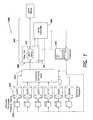
- FIG. 1generally illustrates a nucleic acid processing system comprising a large scale chemFET array, according to one inventive embodiment of the present disclosure.
- FIG. 2illustrates one column of an chemFET array similar to that shown in FIG. 1 , according to one inventive embodiment of the present disclosure.
- FIG. 3shows a composite cross-sectional view of multiple neighboring pixels illustrating a layer-by-layer view of pixel fabrication according to another inventive embodiment of the present disclosure.
- FIGS. 4A-4Lare top views of patterns corresponding layers of material laid down in the fabrication of sensors shown in FIG. 3 .
- FIG. 5A-5Billustrates process steps for fabricating an array with thin dielectric layers on sensor floating gates, and a dielectric layer comprising a charge-sensitive layer and an adhesion layer.
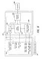
- FIG. 6is a block diagram of an embodiment of the electronic components of one embodiment of the invention.
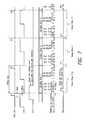
- FIG. 7is an exemplary timing diagram for components shown in FIG. 6 .
- FIG. 8Ais a high-level, partially block, partially circuit diagram showing a basic passive sensor pixel in which the voltage changes on the ISFET source and drain inject noise into the analyte, causing errors in the sensed values.
- FIG. 8Bis a high-level partially block, partially circuit diagram showing a basic passive sensor pixel in which the voltage changes on the ISFET drain are eliminated by tying it to ground, the pixel output is obtained via a column buffer, and CDS is employed on the output of the column buffer to reduce correlated noise.
- FIG. 8Cis a high-level partially block, partially circuit diagram showing a two transistor passive sensor pixel in which the voltage changes on the ISFET drain and source are substantially eliminated, the pixel output is obtained via a buffer, and CDS is employed on the output of the column buffer to reduce correlated noise.
- FIG. 9is a cross-sectional view of a flow cell.
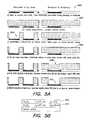
- FIGS. 10A and Bare graphs showing a trace from an ISFET device (A) and a nucleotide readout (B) from a sequencing reaction of a 23-mer synthetic oligonucleotide.
- FIGS. 11A and Bare graphs showing a trace from an ISFET device (A) and a nucleotide readout (B) from a sequencing reaction of a 25-mer PCR product.
- microelectronics portion of the apparatus and arrayis implemented in CMOS technology for purposes of illustration. It should be appreciated, however, that the disclosure is not intended to be limiting in this respect, as other semiconductor-based technologies may be utilized to implement various aspects of the microelectronics portion of the systems discussed herein.
- sample fluidmeans a fluid which is used to deliver sample or reagents to a sample-retaining region or to remove products or reactants from sample-retaining regions, such as a wash fluid of a multi-step reaction. Sample fluids may remain the same or may change in the course of an analytical process, or processes, taking place on an array.
- Analytical processes detected or monitored by arrays of the inventioninclude chemical and/or biological processes (e.g., chemical reactions, cell cultures, neural activity, nucleic acid sequencing reactions, etc.) occurring in proximity to the array.
- chemFETs contemplated by various embodiments discussed in greater detail belowinclude, but are not limited to, ion-sensitive field effect transistors (ISFETs) and enzyme-sensitive field effect transistors (EnFETs).
- ISFETsion-sensitive field effect transistors
- EnFETsenzyme-sensitive field effect transistors
- one or more microfluidic structuresis/are fabricated above the chemFET sensor array to provide for retention, containment and/or confinement of a biological or chemical reaction in which an analyte of interest may be captured, produced, or consumed, as the case may be.
- microfluidic structure(s)may be configured as one or more wells (or microwells, or reaction chambers, or reaction wells as the terms are used interchangeably herein) disposed above one or more sensors of the array, such that the one or more sensors over which a given well is disposed detect and measure analyte presence, level, and/or concentration in the given well.
- a chemFET arraymay be configured for sensitivity to any one or more of a variety of analytes.
- one or more chemFETs of an arraymay be particularly configured for sensitivity to one or more analytes, and in other embodiments different chemFETs of a given array may be configured for sensitivity to different analytes.
- one or more sensors (pixels) of the arraymay include a first type of chemFET configured to be sensitive to a first analyte, and one or more other sensors of the array may include a second type of chemFET configured to be sensitive to a second analyte different from the first analyte.
- the first and second analytesmay be related to each other.
- the first and second analytesmay be byproducts of the same biological or chemical reaction/process and therefore they may be detected concurrently to confirm the occurrence of a reaction (or lack thereof).
- redundancyis preferable in some analyte detection methods.
- more than two different types of chemFETsmay be employed in any given array to detect and/or measure different types of analytes, and optionally to monitor biological or chemical processes such as binding events.
- a given sensor arraymay be “homogeneous” and thereby consist of chemFETs of substantially similar or identical type that detect and/or measure the same analyte (e.g., pH or other ion concentration), or a sensor array may be “heterogeneous” and include chemFETs of different types to detect and/or measure different analytes.
- the sensors in an arraymay be configured to detect and/or measure a single type (or class) of analyte even though the species of that type (or class) detected and/or measured may be different between sensors.
- all the sensors in an arraymay be configured to detect and/or measure nucleic acids, but each sensor detects and/or measures a different nucleic acid.
- an arrayis a planar arrangement of elements such as sensors or wells.
- the arraymay be one or two dimensional.
- a one dimensional arrayis an array having one column (or row) of elements in the first dimension and a plurality of columns (or rows) in the second dimension.
- An example of a one dimensional arrayis a 1 ⁇ 5 array.
- a two dimensional arrayis an array having a plurality of columns (or rows) in both the first and the second dimensions. The number of columns (or rows) in the first and second dimensions may or may not be the same.
- An example of a two dimensional arrayis a 5 ⁇ 10 array.
- one embodimentis directed to an apparatus, comprising an array of CMOS-fabricated sensors, each sensor comprising one chemically-sensitive field effect transistor (chemFET) and occupying an area on a surface of the array of 10 ⁇ m 2 or less, 9 ⁇ m 2 or less, 8 ⁇ m 2 or less, 7 ⁇ m 2 or less, 6 ⁇ m 2 or less, 5 ⁇ m 2 or less, 4 ⁇ m 2 or less 3 ⁇ m 2 or less, or 2 ⁇ m 2 or less.
- chemFETchemically-sensitive field effect transistor
- Chemical or biological phenomena measured by the sensorsmay result in electrical signals, usually current or voltage level changes, having a wide variety of durations and amplitudes.
- such signalsmay have a duration in the range of a few milliseconds, e.g. 10 msec, to many seconds, e.g. 10-20 sec.
- the signalmay be substantially repeated over an interval of minute, hours, or days.
- the signalmay have superimposed various types of noise, including flicker noise from the array itself, and thermal noise, particularly from the sample fluid.
- the control circuitry of the apparatusis configured to sample each signal from each sensor in the array for a complete frame of data. Such sampling may be for a short duration, e.g. 1-100 ⁇ sec, or the like, so that complete frames of data may be readout in the frame per second values listed above.
- arrays of the inventionhave been fabricated in a manner that reduces the effects of trapped charge, which includes lack of stability and uniformity of sensor-to-sensor responses to the same or similar sensing conditions by sensor in the same array.
- such responsesmay be measured by exposing sensors of an array to predefined changes in pH.
- responses of at least 95 percent of the sensors in an arrayare substantially linear over a range of from 7 to 9 pH and has a voltage output signal with a sensitivity of at least 40 m V/pH unit.
- at least 98 percent of sensor of an arrayhave such performance.
- a sensor arraycomprising a plurality of electronic sensors arranged in a plurality of rows and a plurality of columns.
- Each sensorcomprises one chemically-sensitive field effect transistor (chemFET) configured to provide at least one and in some instances at least two output signals representing a presence and/or a concentration of an analyte proximate to a surface of the array.
- chemFETchemically-sensitive field effect transistor
- the arrayfurther comprises column circuitry configured to provide a constant drain current and a constant drain-to-source voltage to respective chemFETs in the column, the column circuitry including two operational amplifiers and a diode-connected FET arranged in a Kelvin bridge configuration with the respective chemFETs to provide the constant drain-to-source voltage.
- the apparatus and devices of the inventioncan be used to detect and/or monitor interactions between various entities. These interactions include biological and chemical reactions and may involve enzymatic reactions and/or non-enzymatic interactions such as but not limited to binding events. As an example, the invention contemplates monitoring enzymatic reactions in which substrates and/or reagents are consumed and/or reaction intermediates, byproducts and/or products are generated.
- An example of a reaction that can be monitored according to the inventionis a nucleic acid synthesis method such as one that provides information regarding nucleic acid sequence. This reaction will be discussed in greater detail herein.
- Apparatus of the inventioncan vary widely depending on the analyte being detected, whether assay reactions with auxiliary reagents are required, and whether sequential or cyclical reactions are required.
- apparatus of the inventioncomprises a sensor array and an array of sample-retaining regions on a surface thereof for retaining biological or chemical analytes delivered to the surface by a sample fluid.
- sample-retaining regionsare integral with the sensor array and may have a wide variety of formats.
- apparatus of the inventionmay comprise sample carriers, such as beads, particles, gel microdroplets, or other supports, structures or substances which hold analytes of interest and which may be delivered to sample-retaining regions by a sample fluid.
- sample carriersmay include binding moieties or reactive groups to permit attachment to sample-retaining regions.
- sample fluid and samples or analytesmay be delivered to retaining regions of a sensor array in several ways.
- samplemay be delivered by emersion, pipetting, pouring, or by other direct methods.
- sensor arraysare employed in sequential or cyclical reactions, such as in DNA sequencing, sample fluidic, including nucleic acid templates, reagents, wash solutions, and the like, may be delivered by a fluidic system under computer control.
- embodiments of the inventionmay further include a flow cell integrated with the sample-retaining regions and sensor array.
- a flow cell of an apparatus of the inventioncomprises an inlet, an outlet, and an interior space, which when the flow cell is in communication with, for example sealingly bonded to, the arrays of sample retaining regions and sensors forms a chamber that is closed except for the inlet and outlet.
- the deviceis manufactured such that the flow cell and one or both the arrays are integral to each other. In other embodiments, the flow cell is sealingly bonded to the arrays.
- the apparatus of the inventionincludes a reference electrode in fluid contact with the sample fluid so that during operation an electrical potential difference is established between the reference electrode and the sensors of the array.
- FIG. 1An exemplary apparatus is shown in FIG. 1 which is adapted for nucleic acid sequencing.
- the chemFET sensors of the arrayare described for purposes of illustration as ISFETs configured for sensitivity to static and/or dynamic ion concentration, including but not limited to hydrogen ion concentration.
- ISFETsconfigured for sensitivity to static and/or dynamic ion concentration, including but not limited to hydrogen ion concentration.
- the present disclosureis not limited in this respect, and that in any of the embodiments discussed herein in which ISFETs are employed as an illustrative example, other types of chemFETs may be similarly employed in alternative embodiments, as discussed in further detail below.
- various aspects and embodiments of the inventionmay employ ISFETs as sensors yet detect one or more ionic species that are not hydrogen ions.
- the system 1000includes a semiconductor/microfluidics hybrid structure 300 comprising an ISFET sensor array 100 and a microfluidics flow cell 200 .
- the flow cell 200may comprise a number of wells (not shown in FIG. 1 ) disposed above corresponding sensors of the ISFET array 100 .
- the flow cell 200is configured to facilitate the sequencing of one or more identical template nucleic acids disposed in the flow cell via the controlled and ordered introduction to the flow cell of a number of sequencing reagents 272 (e.g., dATP, dCTP, dGTP, dTTP (generically referred to herein as dNTP), divalent cations such as but not limited to Mg 2+ , wash solutions, and the like).
- sequencing reagents 272e.g., dATP, dCTP, dGTP, dTTP (generically referred to herein as dNTP), divalent cations such as but not limited to Mg 2+ , wash solutions, and the like.
- the flow cell 200may not contain any wells, and diffusion properties of the reagents may be exploited to limit cross-talk between respective sensors of the ISFET array 100 , or nucleic acids may be immobilized on the surfaces of sensors of the ISFET array 100 .
- the ISFET sensor array 100monitors ionic species, and in particular, changes in the levels/amounts and/or concentration of ionic species, including hydrogen ions.
- the speciesare those that result from a nucleic acid synthesis or sequencing reaction.
- the ISFET arraymay be controlled so as to acquire data (e.g., output signals of respective ISFETs of the array) relating to analyte detection and/or measurements, and collected data may be processed by the computer 260 to yield meaningful information associated with the processing (including sequencing) of the template nucleic acid.
- datae.g., output signals of respective ISFETs of the array
- collected datamay be processed by the computer 260 to yield meaningful information associated with the processing (including sequencing) of the template nucleic acid.
- the array 100is implemented as an integrated circuit designed and fabricated using standard CMOS processes (e.g., 0.35 micrometer process, 0.18 micrometer process), comprising all the sensors and electronics needed to monitor/measure one or more analytes and/or reactions.
- CMOS processese.g. 0.35 micrometer process, 0.18 micrometer process
- one or more reference electrodes 76 to be employed in connection with the ISFET array 100may be placed in the flow cell 200 (e.g., disposed in “unused” wells of the flow cell) or otherwise exposed to a reference (e.g., one or more of the sequencing reagents 172 ) to establish a baseline against which changes in analyte concentration proximate to respective ISFETs of the array 100 are compared.
- a referencee.g., one or more of the sequencing reagents 172
- the reference electrode(s) 76may be electrically coupled to the array 100 , the array controller 250 or directly to the computer 260 to facilitate analyte measurements based on voltage signals obtained from the array 100 ; in some implementations, the reference electrode(s) may be coupled to an electric ground or other predetermined potential, or the reference electrode voltage may be measured with respect to ground, to establish an electric reference for ISFET output signal measurements, as discussed further below.
- a chemFET arraymay be configured for sensitivity to any one or more of a variety of analytes.
- one or more chemFETs of an arraymay be particularly configured for sensitivity to one or more analytes and/or one or more binding events, and in other embodiments different chemFETs of a given array may be configured for sensitivity to different analytes.
- one or more sensors (pixels) of the arraymay include a first type of chemFET configured to be sensitive to a first analyte, and one or more other sensors of the array may include a second type of chemFET configured to be sensitive to a second analyte different from the first analyte.
- both a first and a second analytemay indicate a particular reaction such as for example nucleotide incorporation in a sequencing-by-synthesis method.
- more than two different types of chemFETsmay be employed in any given array to detect and/or measure different types of analytes and/or other reactions.
- a given sensor arraymay be “homogeneous” and include chemFETs of substantially similar or identical types to detect and/or measure a same type of analyte (e.g., hydrogen ions), or a sensor array may be “heterogeneous” and include chemFETs of different types to detect and/or measure different analytes.
- analytee.g., hydrogen ions
- one or more array controllers 250may be employed to operate the ISFET array 100 (e.g., selecting/enabling respective pixels of the array to obtain output signals representing analyte measurements).
- one or more components constituting one or more array controllersmay be implemented together with pixel elements of the arrays themselves, on the same integrated circuit (IC) chip as the array but in a different portion of the IC chip, or off-chip.
- ICintegrated circuit
- analog-to-digital conversion of ISFET output signalsmay be performed by circuitry implemented on the same integrated circuit chip as the ISFET array, but located outside of the sensor array region (locating the analog to digital conversion circuitry outside of the sensor array region allows for smaller pitch and hence a larger number of sensors, as well as reduced noise).
- analog-to-digital conversioncan be 4-bit, 8-bit, 12-bit, 16-bit or other bit resolutions depending on the signal dynamic range required.
- datamay be removed from the array in serial or parallel or some combination thereof.
- On-chip controllersor sense amplifiers
- the chip controllers or signal amplifiersmay be replicated as necessary according to the demands of the application.
- the arraymay, but need not be, uniform. For instance, if signal processing or some other constraint requires instead of one large array multiple smaller arrays, each with its own sense amplifiers or controller logic, that is quite feasible.
- chemFET array 100e.g., ISFET
- ISFETchemFET array 100
- chemFET arraysaccording to various inventive embodiments of the present disclosure that may be employed in a variety of applications.
- chemFET arrays according to the present disclosureare discussed below using the particular example of an ISFET array, but other types of chemFETs may be employed in alternative embodiments.
- chemFET arraysare discussed in the context of nucleic acid sequencing applications, however, the invention is not so limited and rather contemplates a variety of applications for the chemFET arrays described herein.
- each chemFET of an arraycomprises a floating gate structure, and a source and a drain having a first semiconductor type and fabricated in a region having a second semiconductor type, wherein there is no electrical conductor that electrically connects the region having the second semiconductor type to either the source or the drain.
- Each sensorconsists of three field effect transistors (FETs) including the chemFET, and each sensor includes a plurality of electrical conductors electrically connected to the three FETs.
- the three FETsare arranged such that the plurality of electrical conductors includes no more than four conductors traversing an area occupied by each sensor and interconnecting multiple sensors of the array. All of the FETs in each sensor are of a same channel type and implemented in a single semiconductor region of an array substrate.
- a collection of chemFET output signals from all chemFETs of the arrayconstitutes a frame of data.
- the apparatusfurther comprises control circuitry coupled to the array and configured to generate at least one array output signal to provide multiple frames of data from the array at a frame rate of at least 20 frames per second.
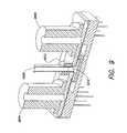
- FIG. 3shows a composite cross-sectional view of neighboring pixels illustrating a layer-by-layer view of the pixel fabrication and relative positions of floating gates and microwells. Three adjacent pixels are shown in cross-section. All of the FET components of the pixel 1051 are fabricated asp-channel FETs in the single n-type well 154 . Additionally, in the composite cross-sectional view of FIG. 3 the highly doped p-type region 159 is also visible corresponding to the shared drain (D) of the MOSFETs Q 2 and Q 3 . For purposes of illustration, the polysilicon gate 166 of the MOSFET Q 3 also is visible in FIG. 3 .
- the topmost metal layer 304corresponds to the ISFETs sensitive area 178 , above which is disposed an analyte-sensitive passivation layer 172 .
- the topmost metal layer 304together with the ISFET polysilicon gate 164 and the intervening conductors 306 , 308 , 312 , 316 , 320 , 326 and 338 , form the ISFETs floating gate structure 170 .
- an electrical connection to the ISFETs drainis provided by the conductors 340 , 328 , and 318 , coupled to the line 116 1 which is formed in the Metal 2 layer rather than the Metal 3 layer.
- the lines 112 1 and 114 1also are shown in FIG. 3 as formed in the Metal 2 layer rather than the Metal 3 layer. The configuration of these lines, as well as the line 118 1 , may be further appreciated from the respective images of FIGS. 4A through 4L ; in particular, it may be observed in FIG.
- a six-metal-layer fabrication processmay be employed, in which the signal lines are fabricated using the Metal 1 and Metal 2 layers, the topmost metal layer of the floating gate structure is formed in the Metal 6 layer, and jumpers to the topmost metal layer are formed in the Metal 3 , Metal 4 and Metal 5 layers, respectively (with associated vias between the metal layers).
- a dimension “f” of the topmost metal layer 304may be reduced so as to reduce cross-capacitance between neighboring pixels.
- the well 725may be fabricated so as to have a tapered shape, such that a dimension “g” at the top of the well is smaller than the pixel pitch “e” but yet larger than a dimension “f” at the bottom of the well.
- the topmost metal layer 304also may be designed with the dimension “f” rather than the dimension “g” so as to provide for additional space between the top metal layers of neighboring pixels.
- the dimension “f”may be on the order of 6 micrometers (as opposed to 7 micrometers, as discussed above), and for pixels having a dimension “e” on the order of 5 micrometers the dimension “f” may be on the order of 3.5 micrometers.
- Detection of hydrogen ions, and other analytes as determined by the inventioncan be carried out using a passivation layer made of silicon nitride (Si 3 N 4 ), silicon oxynitride (Si 2 N 2 0), silicon oxide (Si0 2 ), aluminum oxide (Al 2 0 3 ), tantalum pentoxide (Ta 2 0 5 ), tin oxide or stannic oxide (Sn0 2 ), and the like.
- the path from the analyte to the ISFET gatemay be modeled as a series connection of three capacitances: (1) the capacitance attributable to the above-described charge double layer at the analyte-dielectric layer interface (labeled C DL ), (2) the capacitance due to the floating gate dielectric layer (C FGD ), and (3) the gate oxide capacitance (C ox ).
- C DLthe capacitance attributable to the above-described charge double layer at the analyte-dielectric layer interface
- C FGDthe capacitance due to the floating gate dielectric layer
- C oxthe gate oxide capacitance
- the layeras a floating gate dielectric layer in order to avoid any suggestion that the material composition of the layer is necessarily related to the so-called passivation material(s) often used in CMOS processing (e.g., PECVD silicon nitride) to coat and protect circuit elements.)
- the series capacitance stringextends between the liquid analyte in the wells and the ISFET gate.
- C FGDC ox
- C FGDC ox
- C FGD⁇ ⁇ ⁇ ⁇ ⁇ ⁇ ⁇ ⁇ ⁇ ⁇ ⁇ ⁇ ⁇ ⁇ ⁇ ⁇ ⁇ ⁇ ⁇ ⁇ ⁇ ⁇ ⁇ ⁇ ⁇ ⁇ ⁇ ⁇ ⁇ ⁇ ⁇ ⁇ ⁇ ⁇ ⁇ ⁇ ⁇ ⁇ ⁇ ⁇ ⁇ ⁇ ⁇ ⁇ ⁇ ⁇ ⁇ ⁇ ⁇ ⁇ ⁇ ⁇ ⁇ ⁇ ⁇ ⁇ ⁇ ⁇ ⁇ ⁇ ⁇ ⁇ ⁇ ⁇ ⁇ ⁇ ⁇ ⁇ ⁇ ⁇ ⁇ ⁇ ⁇ ⁇ ⁇ ⁇ ⁇ ⁇ ⁇ ⁇ ⁇ ⁇ ⁇ ⁇ ⁇ ⁇ ⁇ ⁇ ⁇ ⁇ ⁇ ⁇ ⁇ ⁇ ⁇ ⁇ ⁇ ⁇ ⁇ ⁇ ⁇ ⁇ ⁇ ⁇ ⁇ ⁇ ⁇ ⁇ ⁇ ⁇ ⁇ ⁇ ⁇ ⁇ ⁇ ⁇
- One candidate for the floating gate dielectric layer materialis the passivation material used by standard CMOS foundry processes.
- the standard (typically, PECVD nitride or, to be more precise, silicon nitride over silicon oxynitride) passivation layeris relatively thick when formed (e.g., about 1.3 ⁇ m), and typical passivation materials have a limited dielectric constant.
- a first improvementcan be achieved by thinning the passivation layer after formation. This can be accomplished by etching back the CMOS passivation layer, such as by using an over-etch step during microwell formation, to etch into and consume much of the nitride passivation layer, leaving a thinner layer, such as a layer only about 200-600 Angstroms thick.
- a first approachis referred to as the “partial etch” technique; it involves etching away the silicon nitride layer plus approximately half of the silicon oxynitride layer before depositing the thin-film metal oxide sensing layer.
- the second approachreferred to as the “etch-to-metal” technique, involves etching away all of the silicon nitride and silicon oxynitride layers before depositing the thin-film metal oxide sensing layer.
- An alternativeis to simply deposit a thinner layer of dielectric (passivation) material in the first place, such as the indicated 200-600 Angstroms instead of the 1.3 ⁇ m of the conventional CMOS passivation process.
- Materials useful for the floating gate dielectric layerare metal oxides such as tantalum oxide, tungsten oxide, aluminum oxide, and hafnium oxide, though other materials of dielectric constant greater than that of the usual silicon nitride passivation material may be substituted, provided that such material is, or can be rendered, sensitive to the ion of interest.
- the etch-to-metal approachis preferred, with the CMOS process' passivation oxide on the floating gate being etched completely away prior to depositing the floating gate dielectric material layer.
- FIGS. 5A and 5Bshow steps using readily available fabrication techniques for generating a dielectric layer for high capacitive coupling to array sensor plates. Process steps additionally provide electrical access to bondpad structures for off-chip communication. Initially wafer ( 500 ) from a semiconductor manufacturer is treated to apply material layer ( 502 ) from which microwells are formed (in this example, TEOS), after which microwells are formed by etching to the metal of the sensor plate ( 504 ). Dielectric layer ( 506 ) is added, for example, by atomic layer deposition. In one embodiment, as illustrated in FIG.
- dielectric layer ( 506 )comprises a charge-sensitive layer ( 512 ) and an adhesion layer ( 514 ).
- a charge-sensitive layer512
- an adhesion layer514
- dielectric layer ( 506 )comprises a charge-sensitive layer ( 512 ) and an adhesion layer ( 514 ).
- Tantalum oxide and aluminumare exemplary charge-sensitive and adhesion layers of dielectric layer ( 506 ).
- other materials from which dielectric layer ( 506 ) may be formedinclude Ta 2 O 5 5, Al 2 0 3 , HfO 2 or W0 3 . In particular, such materials result in a larger signal in response to pH changes in a sample fluid.
- Iridium oxidemay also be used, e.g. as described in D. O. Wipf et al., “Microscopic Measurement of pH with Iridium Oxide Microelectrodes,” Anal. Chem. 2000, 72, 4921-4927, and Y. J. Kim et al., “Configuration for Micro pH Sensor,” Electronics Letters, Vol. 39, No. 21 (Oct. 16, 2003).
- FIG. 6illustrates a block diagram of the sensor array 100 coupled to an array controller 250 , according to one inventive embodiment of the present disclosure.
- the array controller 250may be fabricated as a “stand alone” controller, or as one or more computer compatible “cards” forming part of a computer 260 In one aspect, the functions of the array controller 250 may be controlled by the computer 260 through an interface block 252 (e.g., serial interface, via USB port or PCI bus, Ethernet connection, etc.). In one embodiment, all or a portion of the array controller 250 is fabricated as one or more printed circuit boards, and the array 100 is configured to plug into one of the printed circuit boards, similar to a conventional IC chip (e.g., the array 100 is configured as an ASIC that plugs into a chip socket, such as a zero-insertion-force or “ZIF” socket, of a printed circuit board).
- a conventional IC chipe.g., the array 100 is configured as an ASIC that plugs into a chip socket, such as a zero-insertion-force or “ZIF” socket, of a printed circuit board.
- an array 100 configured as an ASICmay include one or more pins/terminal connections dedicated to providing an identification code that may be accessed/read by the array controller 250 and/or passed on to the computer 260 .
- an identification codemay represent various attributes of the array 100 (e.g., size, number of pixels, number of output signals, various operating parameters such as supply and/or bias voltages, etc.) and may be processed to determine corresponding operating modes, parameters and or signals provided by the array controller 250 to ensure appropriate operation with any of a number of different types of arrays 100 .
- an array 100 configured as an ASICmay be provided with three pins dedicated to an identification code, and during the manufacturing process the ASIC may be encoded to provide one of three possible voltage states at each of these three pins (i.e., a tri-state pin coding scheme) to be read by the array controller 250 , thereby providing for unique array identification codes.
- all or portions of the array controller 250may be implemented as a field programmable gate array (FPGA) configured to perform various array controller functions described in further detail below.
- FPGAfield programmable gate array
- the array controller 250provides various supply voltages and bias voltages to the array 100 , as well as various signals relating to row and column selection, sampling of pixel outputs and data acquisition.
- the array controller 250reads one or more analog output signals (e.g., V out1 and V out2 ) including multiplexed respective pixel voltage signals from the array 100 and then digitizes these respective pixel signals to provide measurement data to the computer 260 , which in turn may store and/or process the data.
- the array controller 250also may be configured to perform or facilitate various array calibration and diagnostic functions.
- Array controller 250generally provides to the array 100 the analog supply voltage and ground (VDDA, VSSA), the digital supply voltage and ground (VDDD, VSSD), and the buffer output supply voltage and ground (VDDO, VSSO).
- VDDA, VSSAanalog supply voltage and ground
- VDDD, VSSDdigital supply voltage and ground
- VDDO, VSSObuffer output supply voltage and ground
- each of the supply voltages VDDA, VDDD and VDDOis approximately 3.3 Volts.
- the supply voltages VDDA, VDDD and VDDOmay be as low as approximately 1.8 Volts.
- each of these power supply voltagesis provided to the array 100 via separate conducting paths to facilitate noise isolation.
- these supply voltagesmay originate from respective power supplies/regulators, or one or more of these supply voltages may originate from a common source in a power supply 258 of the array controller 250 .
- the power supply 258also may provide the various bias voltages required for array operation (e.g., VB 1 , VB 2 , VB 3 , VB 4 , VBO 0 , V BODY ) and the reference voltage VREF used for array diagnostics and calibration.
- the power supply 258includes one or more digital-to-analog converters (DACs) that may be controlled by the computer 260 to allow any or all of the bias voltages, reference voltage, and supply voltages to be changed under software control (i.e., programmable bias settings).
- DACsdigital-to-analog converters
- a power supply 258 responsive to computer controlmay facilitate adjustment of one or more of the supply voltages (e.g., switching between 3.3 Volts and 1.8 Volts depending on chip type as represented by an identification code), and or adjustment of one or more of the bias voltages VB 1 and VB 2 for pixel drain current, VB 3 for column bus drive, VB 4 for column amplifier bandwidth, and VBO 0 for column output buffer current drive.
- one or more bias voltagesmay be adjusted to optimize settling times of signals from enabled pixels.
- the common body voltage V BODY for all ISFETs of the arraymay be grounded during an optional post-fabrication UV irradiation treatment to reduce trapped charge, and then coupled to a higher voltage (e.g., VDDA) during diagnostic analysis, calibration, and normal operation of the array for measurement/data acquisition.
- VDDAa higher voltage
- the reference voltage VREFmay be varied to facilitate a variety of diagnostic and calibration functions.
- the reference electrode 76which is typically employed in connection with an analyte solution to be measured by the array 100 may be coupled to the power supply 258 to provide a reference potential for the pixel output voltages.
- the reference electrode 76may be coupled to a supply ground (e.g., the analog ground VSSA) to provide a reference for the pixel output voltages.
- the reference electrode voltagemay be set by placing a solution/sample of interest having a known pH level in proximity to the sensor array 100 and adjusting the reference electrode voltage until the array output signals V out1 and V out2 provide pixel voltages at a desired reference level, from which subsequent changes in pixel voltages reflect local changes in pH with respect to the known reference pH level.
- a voltage associated with the reference electrode 76need not necessarily be identical to the reference voltage VREF discussed above (which may be employed for a variety of array diagnostic and calibration functions), although in some implementations the reference voltage VREF provided by the power supply 258 may be used to set the voltage of the reference electrode 76 .
- the array controller 250 of FIG. 6may include one or more preamplifiers 253 to further buffer one or more output signals (e.g., V out1 and V out2 ) from the sensor array and provide selectable gain.
- the array controller 250may include one preamplifier for each output signal (e.g., two preamplifiers for two analog output signals).
- the preamplifiersmay be configured to accept input voltages from 0.0 to 1.8 Volts or 0.0 to 3.3 Volts, may have programmable/computer selectable gains (e.g., 1, 2, 5, 10 and 20) and low noise outputs (e.g., ⁇ 10 n V/sqrtHz), and may provide low pass filtering (e.g., bandwidths of 5 MHz and 25 MHz).
- programmable/computer selectable gainse.g., 1, 2, 5, 10 and 20
- low noise outputse.g., ⁇ 10 n V/sqrtHz
- filtering capacitorsmay be employed in proximity to the chip socket (e.g., the underside of a ZIF socket) to facilitate noise reduction.
- the preamplifiersmay have a programmable/computer selectable offset for input and/or output voltage signals to set a nominal level for either to a desired range.
- the array controller 250 of FIG. 6also comprises one or more analog-to-digital converters 254 (ADCs) to convert the sensor array output signals V out1 and V out2 to digital outputs (e.g., 1 O-bit or 12-bit) so as to provide data to the computer 260 .
- ADCanalog-to-digital converters 254
- one ADCmay be employed for each analog output of the sensor array, and each ADC may be coupled to the output of a corresponding preamplifier (if preamplifiers are employed in a given implementation).
- the ADC(s)may have a computer-selectable input range (e.g., 50 mV, 200 mV, 500 mV, IV) to facilitate compatibility with different ranges of array output signals and/or preamplifier parameters.
- the bandwidth of the ADC(s)may be greater than 60 MHz, and the data acquisition/conversion rate greater than 25 MHz (e.g., as high as 100 MHz or greater).
- ADC acquisition timing and array row and column selectionmay be controlled by a timing generator 256 .
- the timing generatorprovides the digital vertical data and clock signals (DV, CV) to control row selection, the digital horizontal data and clock signals (DH, CH) to control column selection, and the column sample and hold signal COL SH to sample respective pixel voltages for an enabled row.
- the timing generator 256also provides a sampling clock signal CS to the ADC(s) 254 so as to appropriately sample and digitize consecutive pixel values in the data stream of a given array analog output signal (e.g., V out1 and V out2 ), as discussed further below in connection with FIG. 7 .
- the timing generator 256may be implemented by a microprocessor executing code and configured as a multichannel digital pattern generator to provide appropriately timed control signals.
- the timing generator 256may be implemented as a field-programmable gate array (FPGA).
- FIG. 7illustrates an exemplary timing diagram for various array control signals, as provided by the timing generator 256 , to acquire pixel data from the sensor array 100 .
- a “frame”is defined as a data set that includes a value (e.g., pixel output signal or voltage V s ) for each pixel in the array
- a “frame rate”is defined as the rate at which successive frames may be acquired from the array.
- the frame ratecorresponds essentially to a “pixel sampling rate” for each pixel of the array, as data from any given pixel is obtained at the frame rate.
- an exemplary frame rate of 20 frames/secis chosen to illustrate operation of the array (i.e., row and column selection and signal acquisition); however, it should be appreciated that arrays and array controllers according to the present disclosure are not limited in this respect, as different frame rates, including lower frame rates (e.g., 1 to 10 frames/second) or higher frame rates (e.g., 25, 30, 40, 50, 60, 70 to 100 frames/sec., etc.), with arrays having the same or higher numbers of pixels, are possible.
- a data setmay be acquired that includes many frames over several seconds to conduct an experiment on a given analyte or analytes. Several such experiments may be performed in succession, in some cases with pauses in between to allow for data transfer/processing and/or washing of the sensor array ASIC and reagent preparation for a subsequent experiment.
- a hydrogen ion signalmay have a full-width at half-maximum (FWHM) on the order of approximately 1 second to approximately 2.5 seconds, depending on the number of nucleotide incorporation events.
- FWHMfull-width at half-maximum
- a frame rate (or pixel sampling rate) of 20 Hzis sufficient to reliably resolve the signals in a given pixel's output signal.
- the frame rates given in this exampleare provided primarily for purposes of illustration, and different frame rates may be involved in other implementations.
- the array controller 250controls the array 100 to enable rows successively, one at a time. For example, a first row of pixels is enabled via the row select signal RowSel 1 . The enabled pixels are allowed to settle for some time period, after which the COL SH signal is asserted briefly to close the sample/hold switch in each column and store on the column's sample/hold capacitor C sh the voltage value output by the first pixel in the column. This voltage is then available as the column output voltage V COLj applied to one of the two (odd and even column) array output drivers. The COL SH signal is then de-asserted, thereby opening the sample/hold switches in each column and decoupling the column output buffer 111 j from the column amplifiers 107 A and 107 B.
- the second row of pixelsis enabled via the row select signal RowSel 2 .
- the column select signalsare generated two at a time (one odd and one even; odd column select signals are applied in succession to the odd output driver, even column select signals are applied in succession to the even output driver) to read the column output voltages associated with the first row.
- RowSel 2the row select signal
- the column select signalsare generated two at a time (one odd and one even; odd column select signals are applied in succession to the odd output driver, even column select signals are applied in succession to the even output driver) to read the column output voltages associated with the first row.
- FIG. 7illustrates the timing details of the foregoing process for an exemplary frame rate of 20 frames/sec.
- each rowmust be read out in approximately 98 microseconds, as indicated by the vertical delineations in FIG. 7 .
- the vertical clock signal CVhas a period of 98 microseconds (i.e., a clock frequency of over 10 kHz), with a new row being enabled on a trailing edge (negative transition) of the CV signal.
- the left side of FIG. 7reflects the beginning of a new frame cycle, at which point the vertical data signal DV is asserted before a first trailing edge of the CV signal and de-asserted before the next trailing edge of the CV signal.
- the COL SH signalis asserted for 2 microseconds, leaving approximately 50 nanoseconds before the trailing edge of the CV signal.
- the first occurrence of the COL SH signalis actually sampling the pixel values of row 512 of the 512 ⁇ 512 array.
- the first rowis enabled and allowed to settle (for approximately 96 microseconds) until the second occurrence of the COL SH signal.
- the pixel values of row 512are read out via the column select signals. Because two column select signals are generated simultaneously to read 512 columns, the horizontal clock signal CH must generate 256 cycles within this period, each trailing edge of the CH signal generating one odd and one even column select signal. As shown in FIG.
- the first trailing edge of the CH signal in a given rowis timed to occur two microseconds after the selection of the row (after deactivation of the COL SH signal) to allow for settling of the voltage values stored on the sample/hold capacitors C sh and provided by the column output buffers.
- the time period between the first trailing edge of the CH signal and a trailing edge (i.e., deactivation) of the COL SH signalmay be significantly less than two microseconds, and in some cases as small as just over 50 nanoseconds.
- the horizontal data signal DHis asserted before the first trailing edge of the CH signal and de-asserted before the next trailing edge of the CH signal.
- the last two columnsare selected before the occurrence of the COL SH signal which, as discussed above, occurs approximately two microseconds before the next row is enabled.
- columnsare read, two at a time, within a time period of approximately 94 microseconds (i.e., 98 microseconds per row, minus two microseconds at the beginning and end of each row). This results in a data rate for each of the array output signals V out1 and V out2 of approximately 2.7 MHz.
- Noise coupled into the sample fluid by the sensors in every column of the arraymay be present in the output signals of a sensor.
- the drain terminal voltage shared between all of the ISFETs in a columnmoves up or down (as a necessary requirement of the source-and-drain follower). This changes the gate-to-drain capacitances of all of the unselected ISFETs in the column. In turn, this change in capacitance couples from the gate of every unselected ISFET into the fluid, ultimately manifesting itself as noise in the fluid (i.e., an incorrect charge, one not due to the chemical reaction being monitored). That is, any change in the shared drain terminal voltage can be regarded as injecting noise into the fluid by each and every unselected ISFET in the column.
- the shared drain terminal voltage of the unselected ISFETscan be kept constant when selecting a row in the array, this mechanism of coupling noise into the fluid can be reduced or even effectively eliminated.
- the source terminal voltage of all of the unselected ISFETs in the columnalso changes. In turn, that changes the gate-to-source capacitance of all of these ISFETs in the column. This change in capacitance couples from the gate of every unselected ISFET into the fluid, again ultimately manifesting itself as noise in the fluid. That is, any change in the source terminal voltage of an unselected ISFET in the column can be regarded as an injection of noise into the fluid.
- this mechanism of coupling noise into the fluid viacan be reduced or even effectively eliminated.
- a column buffermay be used with some passive pixel designs to alleviate the ISFET drain problem but not the ISFET source problem.
- a column buffermost likely is preferable to the above-illustrated source-and-drain follower.
- the illustrated three-transistor passive pixels employing a source-and-drain follower arrangementthere are essentially two sense nodes, the ISFET source and drain terminals, By connecting the pixel to a column buffer and grounding the drain terminal of the ISFET, there will be only one sense node: the ISFET source terminal. So the drain problem is eliminated.
- the above-described readout circuitwhich comprises both sample-and-hold and multiplexer blocks, also has a gain that is less than the ideal value of unity. Furthermore, the sample and -hold block contributes a significant percentage of the overall chip noise, perhaps more than 25%. From switched-capacitor theory, the sample-and-hold “kT/C” noise is inversely proportional to capacitance. Hence, by choosing a larger capacitor, the sample-and-hold noise can be reduced. Another approach to reducing noise is to employ Correlated Double Sampling (CDS), where a second sample-and-hold and difference circuit is used to cancel out correlated noise. This approach is discussed at greater length, below.
- CDSCorrelated Double Sampling
- Correlated Double Samplingis a known technique for measuring electrical values such as voltages or currents that allows for removal of an undesired offset.
- the output of the sensoris measured twice: once in a known condition and once in an unknown condition.
- the value measured from the known conditionis then subtracted from the unknown condition to generate a value with a known relation to the physical quantity being measured.
- the challenge hereis how to be efficient in implementing CDS and how to address both correlated noise and the minimization of noise injection into the analyte fluid.
- the basic passive sensor pixel 77 A 1is a three transistor arrangement of an ISFET 77 A 2 and a pair of row select transistors, 77 A 3 and 77 A 4 connected to the ISFET source.
- Transistor 77 A 3is connected in turn to a current source or sink 77 A 5 .
- a readoutis obtained via transistor 77 A 4 which is connected to the input of sense amplifier 77 A 6 .
- a diode-connected transistor 77 A 7 in series with another amplifier, 77 A 8connects in a feedback loop from the output of the sense amplifier to the drain of the ISFET.
- the sense amplifier outputis captured by a sample-and-hold circuit 77 A 9 , which feeds an output amplifier 77 A 10 .
- the first changeis to alter the signals on the ISFET.
- the feedback loop to the drain of the ISFETis eliminated and the drain is connected to a stable voltage, such as ground.
- a column buffer 778is connected to the emitter of transistor.
- the second changeis to include a circuit to perform CDS on the output of the column buffer.
- CDSrequires a first, reference value. This is obtained by connecting the input of column buffer 7781 to a reference voltage via switch 7782 , during a first, or reference phase of a clock, indicated as the “SH” phase.
- a combined CDS and sample-and-hold circuitthen double samples the output of the column buffer, obtaining a reference sample and a sensed value, performs a subtraction, and supplies a resulting noise-reduced output value, since the same correlated noise appears in the reference sample and in the sensor output.
- the operation of the CDS and sample-and-hold circuitis straightforward.
- the circuitoperates on a two-phase clock, the first phase being the SH phase and the second phase being the SHb phase.
- the phaseswill be symmetrical and thus inverted values of each other.
- the reference sampleis obtained in the SH phase and places a charge (and thus a voltage) on capacitor Cin, which is subtracted from the output of the column buffer when the clock phase changes.
- FIG. 8CAn alternative embodiment, still with a passive sensor pixel, is shown in FIG. 8C .
- the sensor pixel in this embodimentis a two-transistor circuit comprising ISFET whose drain is connected to a fixed supply voltage, VSSA. There is no transistor comparable to 77 A 4 , and the pixel output is taken from the emitter of transistor 77 A 3 , instead.
- the CDS and sample-and-hold circuithas been simplified slightly, by the elimination of a feedback loop, but it serves the same function, in conjunction with the charge (voltage) stored on capacitor Cb 1 , of subtracting a reference value on capacitor Cin from the signal supplied by the sensor pixel.
- each microwellbeing small enough preferably to receive only one DNA-loaded bead, in connection with which an underlying pixel in the array will provide a corresponding output signal.
- microwell arrayinvolves three stages of fabrication and preparation, each of which is discussed separately: (1) creating the array of microwells to result in a chip having a coat comprising a microwell array layer; (2) mounting of the coated chip to a fluidic interface; and in the case of DNA sequencing, (3) loading DNA-loaded bead or beads into the wells. It will be understood, of course, that in other applications, beads may be unnecessary or beads having different characteristics may be employed.
- the systems described hereincan include an array of microfluidic reaction chambers integrated with a semiconductor comprising an array of chemFETs.
- the inventionencompasses such an array.
- the reaction chambersmay, for example, be formed in a glass, dielectric, photodefineable or etchable material.
- the glass materialmay be silicon dioxide.
- chemFET sensorsoverlayed with an array of reaction chambers wherein the bottom of a reaction chamber is in contact with (or capacitively coupled to) a chemFET sensor.
- each reaction chamber bottomis in contact with a chemFET sensor, and preferably with a separate chemFET sensor.
- less than all reaction chamber bottomsare in contact with a chemFET sensor.
- each sensor in the arrayis in contact with a reaction chamber. In other embodiments, less than all sensors are in contact with a reaction chamber.
- the sensor (and/or reaction chamber) arraymay be comprised of 2, 3, 4, 5, 6, 7, 8, 9, 10, 15, 20, 30, 40, 50, 60, 60, 80, 90, 100, 200, 300, 400, 500, 1000, 10 4 , 10 5 , 10 6 , 10 7 , 10 8 , or more chemFET sensors (and/or reaction chambers).
- an array that comprises, as an example, 256 sensors or reaction chamberswill contain 256 or more (i.e., at least 256) sensors or reaction chambers.
- aspects and embodiments described herein that “comprise” elements and/or stepsalso fully support and embrace aspects and embodiments that “consist of” or “consist essentially of” such elements and/or steps.
- Various aspects and embodiments of the inventioninvolve sensors (and/or reaction chambers) within an array that are spaced apart from each other at a center-to-center distance or spacing (or “pitch”, as the terms are used interchangeably herein) that is in the range of 1-50 microns, 1-40 microns, 1-30 microns, 1-20 microns, 1-10 microns, or 5-10 microns, including equal to or less than about 9 microns, or equal to or less than about 5.1 microns, or 1-5 microns including equal to or less than about 2.8 microns.
- the center-to-center distance between adjacent reaction chambers in a reaction chamber arraymay be about 1-9 microns, or about 2-9 microns, or about 1 microns, about 2 microns, about 3 microns, about 4 microns, about 5 microns, about 6 microns, about 7 microns, about 8 microns, or about 9 microns.
- the reaction chamberhas a volume of equal to or less than about 1 picoliter (pL), including less than 0.5 pL, less than 0.1 pL, less than 0.05 pL, less than 0.01 pL, less than 0.005 pL.
- the reaction chambersmay have a square cross section, for example, at their base or bottom. Examples include an 8 ⁇ m by 8 ⁇ m cross section, a 4 ⁇ m by 4 ⁇ m cross section, or a 1.5 ⁇ m by 1.5 ⁇ m cross section. Alternatively, they may have a rectangular cross section, for example, at their base or bottom. Examples include an 8 ⁇ m by 12 ⁇ m cross section, a 4 ⁇ m by 6 ⁇ m cross section, or a 1.5 ⁇ m by 2.25 ⁇ m cross section.
- the inventionencompasses a system comprising at least one two-dimensional array of reaction chambers, wherein each reaction chamber is coupled to a chemically-sensitive field effect transistor (“chemFET”) and each reaction chamber is no greater than 10 ⁇ m 3 (i.e., 1 pL) in volume.
- chemFETchemically-sensitive field effect transistor
- each reaction chamberis no greater than 0.34 pL, and more preferably no greater than 0.096 pL or even 0.012 pL in volume.
- a reaction chambercan optionally be 2 2 , 3 2 , 4 2 , 5 2 , 6 2 , 7 2 , 8 2 , 9 2 , or 10 2 square microns in cross-sectional area at the top.
- the arrayhas at least 10 2 , 10 3 , 10 4 , 10 5 , 10 6 , 10 7 , 10 8 , 10 9 , or more reaction chambers.
- the reaction chambersmay be capacitively coupled to the chemFETs, and preferably are capacitively coupled to the chemFETs.
- Such systemsmay be used for high-throughput sequencing of nucleic acids.
- the reaction chamber array(or equivalently, microwell array) comprises 10 2 , 10 3 , 10 4 , 10 5 , 10 6 , 10 7 microwells or reaction chambers.
- individual reaction chambers in the reaction chamber arrayare in contact with or capacitively coupled to at least one chemFET.
- a reaction chamber of an arrayis in contact with or capacitively coupled to one chemFET or one ISFET.
- the chemFET arraymay optionally comprise 10 2 , 10 3 , 10 4 , 10 5 , 10 6 , 10 7 chemFETs.
- the chemFET or ISFET arraysmay comprise 256 or more chemFETs or ISFETs.
- the chemFETs or ISFETs of such arraysmay have a center-to-center spacing (between adjacent chemFETs or ISFETs) of 1-10 microns.
- the center-to-center spacingis about 9 microns, about 8 microns, about 7 microns, about 6 microns, about 5 microns, about 4 microns, about 3 microns, about 2 microns or about 1 micron.
- the center-to-center spacingis about 5.1 microns or about 2.8 microns.
- the beadis in a reaction chamber, and optionally the only bead in the reaction chamber.
- the reaction chamberis in contact with or capacitively coupled to an ISFET.
- the ISFETis in an ISFET array
- the beadhas a diameter of less than 6 microns, less than 3 microns, or about 1 micron.
- the beadmay have a diameter of about 1 micron up to about 7 microns, or about 1 micron up to about 3 microns.
- the reaction chambershave a center-to-center distance of about 1 micron to about 10 microns.
- the reaction chamber arraycomprises 10 2 , 10 3 , 10 4 , 10 5 , 10 6 or 10 7 reaction chambers.
- a dielectric layer on a gate of an ISFETis part of the ISFET. It is recognized that the charge in the reaction chamber builds up on one side of the dielectric and forms one plate of a capacitor and which has as its second plate the floating gate metal layer; thus, a reaction chamber is referred to as being capacitively coupled to the ISFET.
- the ISFETis in an ISFET array.
- the ISFET arraymay comprise 10 2 , 10 3 , 10 4 , 10 5 , 10 6 , 10 7 ISFETS.
- the template nucleic acidis in a reaction chamber in contact with or capacitively coupled to the ISFET.
- the reaction chamberis in a reaction chamber array.
- the reaction chamber arraycomprises 10 2 , 10 3 , 10 4 , 10 5 , 10 6 or 10 7 reaction chambers.
- the microwellsmay vary in size between arrays.
- the size of these microwellsmay be described in terms of a width (or diameter) to height ratio. In some embodiments, this ratio is 1:1 to 2:1.5.
- the bead to well sizee.g., the bead diameter to well width, diameter, or height
- the microwell sizemay be described in terms of cross section.
- the cross sectionmay refer to a “slice” parallel to the depth (or height) of the well, or it may be a slice perpendicular to the depth (or height) of the well.
- the microwellsmay be square in cross-section, but they are not so limited.
- the dimensions at the bottom of a microwelli.e., in a cross section that is perpendicular to the depth of the well) may be 1.5 ⁇ m by 1.5 ⁇ m, or it may be 1.5 ⁇ m by 2 ⁇ m.
- Suitable diametersinclude but are not limited to at or about 100 ⁇ m, 95 ⁇ m, 90 ⁇ m, 85 ⁇ m, 80 ⁇ m, 75 ⁇ m, 70 ⁇ m, 65 ⁇ m, 60 ⁇ m, 55 ⁇ m, 50 ⁇ m, 45 ⁇ m, 40 J ⁇ tm, 35 ⁇ m, 30 ⁇ m, 25 ⁇ m, 20 ⁇ m, 15 ⁇ m, 10 J ⁇ tm, 9 ⁇ m, 8 ⁇ m, 7 ⁇ m, 6 J ⁇ tm, 5 J ⁇ tm, 4 ⁇ m, 3 ⁇ m, 2 ⁇ m, I ⁇ m or less.
- the diametersmay be at or about 44 J ⁇ tm, 32 J ⁇ tm, 8 ⁇ m, 4 ⁇ m, or 1.5 ⁇ m.
- Suitable heightsinclude but are not limited to at or about 100 ⁇ m, 95 ⁇ m, 90 ⁇ m, 85 ⁇ m, 80 ⁇ m, 75 J ⁇ tm, 70 ⁇ m, 65 ⁇ m, 60 ⁇ m, 55 ⁇ m, 50 ⁇ m, 45 ⁇ m, 40 ⁇ m, 35 ⁇ m, 30 ⁇ m, 25 ⁇ m, 20 ⁇ m, 15 ⁇ m, 10 ⁇ m, 9 ⁇ m, 8 ⁇ m, 7 ⁇ m, 6 ⁇ m, 5 ⁇ m, 4 ⁇ m, 3 ⁇ m, 2 ⁇ m, 1 ⁇ m or less.
- the heightsmay be at or about 55 ⁇ m, 48 ⁇ m, 32 ⁇ m, 12 ⁇ m, 8 ⁇ m, 6 ⁇ m, 4 ⁇ m, 2.25 ⁇ m, 1.5 ⁇ m, or less.
- the reaction well dimensionsmay be (diameter in ⁇ m by height in ⁇ m) 44 by 55, 32 by 32, 32 by 48, 8 by 8, 8 by 12, 4 by 4, 4 by 6, 1.5 by 1.5, or 1.5 by 2.25.
- the reaction well volumemay range (between arrays, and preferably not within a single array) based on the well dimensions. This volume may be at or about 100 picoliter (pL), 90, 80, 70, 60, 50, 40, 30, 20, 10, or fewer pL. In important embodiments, the well volume is less than 1 pL, including equal to or less than 0.5 pL, equal to or less than 0.1 pL, equal to or less than 0.05 pL, equal to or less than 0.01 pL, equal to or less than 0.005 pL, or equal to or less than 0.001 pL.
- the volumemay be 0.001 to 0.9 pL, 0.001 to 0.5 pL, 0.001 to 0.1 pL, 0.001 to 0.05 pL, or 0.005 to 0.05 pL.
- the well volumeis 75 pL, 34 pL, 23 pL, 0.54 pL, 0.36 pL, 0.07 pL, 0.045 pL, 0.0024 pL, or 0.004 pL.
- each reaction chamberis no greater than about 0.39 pL in volume and about 49 ⁇ m 2 surface aperture, and more preferably has an aperture no greater than about 16 ⁇ m 2 and volume no greater than about 0.064 pL.
- chemFETs and more particularly ISFETsmay be used to detect analytes and/or charge.
- An ISFETas discussed above, is a particular type of chemFET that is configured for ion detection such as hydrogen ion (or proton) detection.
- Other types of chemFETs contemplated by the present disclosureinclude enzyme FETs (EnFETs) which employ enzymes to detect analytes.
- chemical sensitivitybroadly encompasses sensitivity to any molecule of interest, including without limitation organic, inorganic, naturally occurring, non-naturally occurring, chemical and biological compounds, such as ions, small molecules, polymers such as nucleic acids, proteins, peptides, polysaccharides, and the like.
- the microwell structureis applied to the die. That is, the microwell structure can be formed right on the die or it may be formed separately and then mounted onto the die, either approach being acceptable.
- various processesmay be used. For example, the entire die may be spin-coated with, for example, a negative photoresist such as Microchem's SU-8 2015 or a positive resist/polyimide such as HD Microsystems HD8820, to the desired height of the microwells.
- Unreacted resisti.e., resist in areas which are not exposed, due to the mask blocking the light from reaching the resist and preventing cross-linking
- a suitable solventi.e., developer
- PMEApropyleneglycolmethylethylacetate
- microwell layer(s)Among the various organic materials which may be used in some embodiments to form the microwell layer(s) are the above-mentioned SU-8 type of negative-acting photoresist, a conventional positive-acting photoresist and a positive-acting photodefineable polyimide. Each has its virtues and its drawbacks, well known to those familiar with the photolithographic art.
- Contact lithographyhas its limitations and it may not be the production method of choice to produce the highest densities of wells—i.e., it may impose a higher than desired minimum pitch limit in the lateral directions.
- Other techniquessuch as a deep UV step-and-repeat process, are capable of providing higher resolution lithography and can be used to produce small pitches and possibly smaller well diameters.
- desired specificationse.g., numbers of sensors and wells per chip
- different techniquesmay prove optimal.
- pragmatic factorssuch as the fabrication processes available to a manufacturer, may motivate the use of a specific fabrication method. While novel methods are discussed, various aspects of the invention are limited to use of these novel methods.
- a “drill-focusing” techniquemay be employed, whereby several sequential step-and-repeat exposures are done at different focal depths to compensate for the limited depth of focus (DOF) of high-resolution steppers when patterning thick resist layers.
- DOEdepth of focus
- This techniquedepends on the stepper NA and DOF as well as the contrast properties of the resist material.
- microwellscan be fabricated by any high aspect ratio photo-definable or etchable thin-film process, that can provide requisite thickness (e.g., about 4-10 ⁇ m).
- materials believed to be suitableare photosensitive polymers, deposited silicon dioxide, nonphotosensitive polymer which can be etched using, for example, plasma etching processes, etc.
- TEOS and silane nitrous oxide (SILOX)appear suitable.
- the final structuresare similar but the various materials present differing surface compositions that may cause the target biology or chemistry to react differently.
- etch stop layerWhen the microwell layer is formed, it may be necessary to provide an etch stop layer so that the etching process does not proceed further than desired. For example, there may be an underlying layer to be preserved, such as a low-K dielectric.
- the etch stop materialshould be selected according to the application. SiC and SiN materials may be suitable, but that is not meant to indicate that other materials may not be employed, instead. These etch-stop materials can also serve to enhance the surface chemistry which drives the ISFET sensor sensitivity, by choosing the etch-stop material to have an appropriate point of zero charge (PZC).
- PZCpoint of zero charge
- Various metal oxidesmay be suitable addition to silicon dioxide and silicon nitride.
- Ta20smay be preferred as an etch stop over Al 2 O 3 because the PZC of Al 2 O 3 is right at the pH being used (i.e., about 8.8) and, hence, right at the point of zero charge.
- Ta 2 O 5has a higher sensitivity to pH (i.e., m V/pH), another important factor in the sensor performance. Optimizing these parameters may require judicious selection of passivation surface materials.
- a post-microwell fabrication metal oxide deposition techniquemay allow placement of appropriate PZC metal oxide films at the bottom of the high aspect ratio microwells.
- Electron-beam depositions ofof (a) reactively sputtered tantalum oxide, (b) nonreactive stoichiometric tantalum oxide, (c) tungsten oxide, or (d) Vanadium oxide may prove to have superior “down-in-well” coverage due to the superior directionality of the deposition process.
- the arraytypically comprises at least 100 microfluidic wells, each of which is coupled to one or more chemFET sensors.
- the wellsare formed in at least one of a glass (e.g., SiO 2 ), a polymeric material, a photodefinable material or a reactively ion etchable thin film material.
- the wellshave a width to height ratio less than about 1:1.
- the sensoris a field effect transistor, and more preferably a chemFET.
- the chemFETmay optionally be coupled to a PPi receptor.
- each of the chemFETsoccupies an area of the array that is 10 2 microns or less.
- the inventionencompasses a sequencing device comprising a semiconductor wafer device coupled to a dielectric layer such as a glass (e.g., SiO 2 ), polymeric, photodefinable or reactive ion etchable material in which reaction chambers are formed.
- a dielectric layersuch as a glass (e.g., SiO 2 ), polymeric, photodefinable or reactive ion etchable material in which reaction chambers are formed.
- the glass, dielectric, polymeric, photodefinable or reactive ion etchable materialis integrated with the semiconductor wafer layer.
- the glass, polymeric, photodefinable or reactive ion etchable layeris non-crystalline.
- the glassmay be SiO 2 .
- the devicecan optionally further comprise a fluid delivery module of a suitable material such as a polymeric material, preferably an injection moldable material. More preferably, the polymeric layer is polycarbonate.
- the inventionencompasses a method for manufacturing a sequencing device comprising: using photolithography, generating wells in a glass, dielectric, photodefinable or reactively ion etchable material on top of an array of transistors.
- CMOScomplementary metal-oxide-semiconductor
- the CMOS top metallization layer forming the floating gates of the ISFET arrayusually is coated with a passivation layer that is about 1.3 ⁇ m thick.
- Microwells 1.3 ⁇ m deepcan be formed by etching away the passivation material. For example, microwells having a 1:1 aspect ratio may be formed, 1.3 ⁇ m deep and 1.3 ⁇ m across at their tops. Modeling indicates that as the well size is reduced, in fact, the DNA concentration, and hence the SNR, increases. So, other factors being equal, such small wells may prove desirable.
- a complete system for using the sensor arraywill include suitable fluid sources, valving and a controller for operating the valving to low reagents and washes over the microarray or sensor array, depending on the application. These elements are readily assembled from off-the-shelf components, with and the controller may readily be programmed to perform a desired experiment.
- the process of using the assembly of an array of sensors on a chip combined with an array of microwells to sequence the DNA in a sampleis referred to as an “experiment.”
- Executing an experimentrequires loading the wells with the DNA-bound beads and the flowing of several different fluid solutions (i.e., reagents and washes) across the wells.
- a fluid delivery systeme.g., valves, conduits, pressure source(s), etc.
- a fluidic interfaceis needed which flows the various solutions across the wells in a controlled even flow with acceptably small dead volumes and small cross contamination between sequential solutions.
- the fluidic interface to the chip(sometimes referred to as a “flow cell”) would cause the fluid to reach all microwells at the same time.
- designswill be discussed, meeting these criteria in differing ways and degrees.
- designsmay be categorized by the way the reference electrode is integrated into the arrangement. Depending on the design, the reference electrode may be integrated into the flow cell (e.g., form part of the ceiling of the flow chamber) or be in the flow path (typically to the outlet or downstream side of the flow path, after the sensor array).
- a glass slide 3422e.g., Erie Microarray Cat #C22-5128-M20 from Erie Scientific Company, Portsmouth, N.H., cut in thirds, each to be of size about 25 mm ⁇ 25 mm).
- flow chamber 3420may comprise various structures for promoting a substantially laminar flow across the microwell array.
- a series of microfluidic channels fanning out from the inlet pipe to the edge of the flow chambermay be patterned by contact lithography using positive photoresists such as SU-8 photoresist from MicroChem Corp. of Newton, Mass.
- positive photoresistssuch as SU-8 photoresist from MicroChem Corp. of Newton, Mass.
- the chip 3412will in turn be mounted to a carrier 3430 , for packaging and connection to connector pins 3432 .
- Achieving a uniform flow front and eliminating problematic flow path areasis desirable for a number of reasons.
- One reasonis that very fast transition of fluid interfaces within the system's flow cell is desired for many applications, particularly gene sequencing.
- an incoming fluidmust completely displace the previous fluid in a short period of time.
- Uneven fluid velocities and diffusion within the flow cell, as well as problematic flow paths,can compete with this requirement.
- Simple flow through a conduit of rectangular cross sectioncan exhibit considerable disparity of fluid velocity from regions near the center of the flow volume to those adjacent the sidewalls, one sidewall being the top surface of the microwell layer and the fluid in the wells. Such disparity leads to spatially and temporally large concentration gradients between the two traveling fluids.
- bubblesare likely to be trapped or created in stagnant areas like sharp corners interior the flow cell.
- the surface energyhydrophilic vs. hydrophobic
- Avoidance of surface contamination during processing and use of a surface treatment to create a more hydrophilic surfaceshould be considered if the as-molded surface is too hydrophobic.
- the physical arrangement of the flow chamberis probably the factor which most influences the degree of uniformity achievable for the flow front.
- the flow cellmay be fabricated of many different materials. Injection molded polycarbonate appears to be quite suitable.
- a conductive metale.g., gold
- an adhesion layere.g., chrome
- Appropriate low-temperature thin-film deposition techniquespreferably are employed in the deposition of the metal reference electrode due to the materials (e.g., polycarbonate) and large step coverage topography at the bottom-side of the fluidic cell (i.e., the frame surround of ISFET array).
- One possible approachwould be to use electron-beam evaporation in a planetary system.
- conductive epoxye.g., Epo-Tek H20E or similar
- the ISFET flow cellis ready for operation with the reference potential being applied to the assigned pin of the package.
- the inventionencompasses an apparatus for detection of pH comprising a laminar fluid flow system.
- the apparatusis used for sequencing a plurality of nucleic acid templates present in an array.
- the apparatustypically includes a fluidics assembly comprising a member comprising one or more apertures for non-mechanically directing a fluid to flow to an array of at least 100K (100 thousand), 500K (500 thousand), or 1M (1 million) microfluidic reaction chambers such that the fluid reaches all of the microfluidic reaction chambers at the same time or substantially the same time.
- the fluid flowis parallel to the sensor surface.
- the assemblyhas a Reynolds number of less than 1000, 500, 200, 100, 50, 20, or 10.
- the memberfurther comprises a first aperture for directing fluid towards the sensor array and a second aperture for directing fluid away from the sensor array.
- the inventionencompasses a method for directing a fluid to a sensor array comprising: providing a fluidics assembly comprising an aperture fluidly coupling a fluid source to the sensor array; and non-mechanically directing a fluid to the sensor array.
- non-mechanicallyit is meant that the fluid is moved under pressure from a gaseous pressure source, as opposed to a mechanical pump.
- the inventionencompasses an array of wells, each of which is coupled to a lid having an inlet port and an outlet port and a fluid delivery system for delivering and removing fluid from said inlet and outlet ports non-mechanically.
- the inventionencompasses a method for sequencing a biological polymer such as a nucleic acid utilizing the above-described apparatus, comprising: directing a fluid comprising a monomer to an array of reaction chambers wherein the fluid has a fluid flow Reynolds number of at most 2000, 1000, 200, 100, 50, or 20.
- the methodmay optionally further comprise detecting a pH or a change in pH from each said reaction chamber. This is typically detected by ion diffusion to the sensor surface.
- Apparatus of the inventionmay be adapted to detecting hydrogen ions released by nucleotide incorporation, which detection process is disclosed as a DNA sequencing method in Rothberg et al., U.S. patent publications 2009/0026082 and 2009/0127589. It is important in these and various other aspects to detect as many released hydrogen ions as possible in order to achieve as high a signal (and/or a signal to noise ratio) as possible.
- Strategies for increasing the number of released protons that are ultimately detected by the chemFET surfaceinclude without limitation limiting interaction of released protons with reactive groups in the well, choosing a material from which to manufacture the well in the first instance that is relatively inert to protons, preventing released protons from exiting the well prior to detection at the chemFET, and increasing the copy number of templates per well (in order to amplify the signal from each nucleotide incorporation), among others.
- the inventionprovides arrays and devices with reduced buffering capacity for monitoring and/or measuring hydrogen ion changes (or pH changes) more accurately.
- the inventionprovides apparatus and devices for monitoring pH changes in polymerase extension reactions in an environment with no or limited buffering capacity.
- a reduced buffering environmentinclude environments that lack pH buffering components in the sample fluid and/or reaction mixtures; environments in which surfaces of array components in contact with sample fluid and/or reaction mixtures have little or no buffering capacity; and environments in which pH changes on the order of 0.01, 0.05, 0.1, 0.2, 0.3, 0.4, 0.5, 0.6. 0.7, 0.8, 0.9, or 1.0 pH units are detectable for example via a chemFET and more particularly an ISFET as described herein.
- the buffering inhibitormay also be a phospholipid.
- the phospholipidsmay be naturally occurring or non-naturally occurring phospholipids.
- Examples of phospholipids to be used as buffering inhibitorsinclude but are not limited to phosphatidylcholine, hosphatidylethanolamine, phosphatidylglycerol, and phosphatidylserine.
- phospholipidsmay be coated on the chemFET surface (or reaction chamber surface). Such coating may be covalent or noncovalent.
- the phospholipidsexist in solution.
- a solution having no or low buffering capacity (or activity)is one in which changes in hydrogen ion concentration on the order of at least about +/ ⁇ 0.005 pH units, at least about +/ ⁇ 0.01, at least about +/ ⁇ 0.015, at least about +/ ⁇ 0.02, at least about +/ ⁇ 0.03, at least about +/ ⁇ 0.04, at least about +/ ⁇ 0.05, at least about +/ ⁇ 0.10, at least about +/ ⁇ 0.15, at least about +/ ⁇ 0.20, at least about +/ ⁇ 0.25, at least about +/ ⁇ 0.30, at least about +/ ⁇ 0.35, at least about +/ ⁇ 0.45, at least about +/ ⁇ 0.50, or more are detectable (e.g., using the chemFET sensors described herein).
- the pH change per nucleotide incorporationis on the order of about 0.005. In some embodiments, the pH change per nucleotide incorporation is a decrease in pH. Reaction solutions that have no or low buffering capacity may contain no or very low concentrations of buffer, or may use weak buffers.
- Copy numbercan be increased for example by using templates that are concatemers (i.e., nucleic acids comprising multiple, tandemly arranged, copies of the nucleic acid to be sequenced), by increasing the number of nucleic acids on or in beads up to and including saturating such beads, and by attaching templates or primers to beads or to the sensor surface in ways that reduce steric hindrance and/or ensure template attachment (e.g., by covalently attaching templates), among other things.
- templates that are concatemersi.e., nucleic acids comprising multiple, tandemly arranged, copies of the nucleic acid to be sequenced
- attaching templates or primersto beads or to the sensor surface in ways that reduce steric hindrance and/or ensure template attachment (e.g., by covalently attaching templates), among other things.
- Concatemer templatesmay be immobilized on or in beads or on other solid supports such as the sensor surface, although in some embodiments concatemers templates may be present in a reaction chamber without immobilization.
- the templatesor complexes comprising templates and primers
- the chemFET surfacemay be covalently or non-covalently attached to the chemFET surface and their sequencing may involve detection of released hydrogen ions and/or addition of negative charge to the chemFET surface upon a nucleotide incorporation event.
- the latter detection schememay be performed in a buffered environment or solution (i.e., any changes in pH will not be detected by the chemFET and thus such changes will not interfere with detection of negative charge addition to the chemFET surface).
- RCA or CCR amplification methodsgenerate concatemers of template nucleic acids that comprise tens, hundreds, thousands or more tandemly arranged copies of the template. Such concatemers may still be referred to herein as template nucleic acids, although they may contain multiple copies of starting template nucleic acids. In some embodiments, they may also be preferred to as amplified template nucleic acids. Alternatively, they may be referred to herein as comprising multiple copies of target nucleic acid fragment. Concatemers may contain 2, 3, 4, 5, 6, 7, 8, 9, 10, 20, 30, 40, 50, 60, 70, 80, 90, 100, 500, 1000, or more copies of the starting nucleic acid.
- Concatemers generated using these or other methodscan be used in the sequencing-by-synthesis methods described herein.
- the concatemersmay be generated in vitro apart from the array and then placed into reaction chambers of the array or they may be generated in the reaction chambers.
- One or more inside walls of the reaction chambermay be treated to enhance attachment and retention of the concatemers, although this is not required.
- nucleotide incorporation at least in the context of a sequencing-by-synthesis reactionmay be detected by a change in charge at the chemFET surface, as an alternative to or in addition to the detection of released hydrogen ions as discussed herein.
- the concatemersare deposited onto a chemFET surface and/or into a reaction chamber, sequencing-by-synthesis can occur through detection of released hydrogen ions as discussed herein.
- the inventionembraces the use of other approaches for generating concatemerized templates.
- One such approachis a PCR described by Stemmer et al. in U.S. Pat. No. 5,834,252, and the description of this approach is incorporated by reference herein.
- Important aspects of the inventioncontemplate sequencing a plurality of different template nucleic acids simultaneously. This may be accomplished using the sensor arrays described herein.
- the sensor arraysare overlayed (and/or integral with) an array of microwells (or reaction chambers or wells, as those terms are used interchangeably herein), with the proviso that there be at least one sensor per microwell.
- Present in a plurality of microwellsis a population of identical copies of a template nucleic acid. There is no requirement that any two microwells carry identical template nucleic acids, although in some instances such templates may share overlapping sequence.
- each microwellcomprises a plurality of identical copies of a template nucleic acid, and the templates between microwells may be different.
- the inventioncontemplates a sequencing apparatus for sequencing unlabeled nucleic acid acids, optionally using unlabeled nucleotides, without optical detection and comprising an array of at least 100 reaction chambers.
- the arraycomprises 10 3 , 10 4 , 10 5 , 10 6 , 10 7 or more reaction chambers.
- the pitch(or center-to-center distance between adjacent reaction chambers) is on the order of about 1-10 microns, including 1-9 microns, 1-8 microns, 1-7 microns, 1-6 microns, 1-5 microns, 1-4 microns, 1-3 microns, or 1-2 microns.
- the nucleic acid loaded beadsof which there may be tens, hundreds, thousands, or more, first enter the flow cell and then individual beads enter individual wells.
- the beadsmay enter the wells passively or otherwise.
- the beadsmay enter the wells through gravity without any applied external force.
- the beadsmay enter the wells through an applied external force including but not limited to a magnetic force or a centrifugal force.
- an external forceif an external force is applied, it is applied in a direction that is parallel to the well height/depth rather than transverse to the well height/depth, with the aim being to “capture” as many beads as possible.
- the wellsare not agitated, as for example may occur through an applied external force that is perpendicular to the well height/depth. Moreover, once the wells are so loaded, they are not subjected to any other force that could dislodge the beads from the wells.
- the Examplesprovide a brief description of an exemplary bead loading protocol in the context of magnetic beads. It is to be understood that a similar approach could be used to load other bead types.
- the protocolhas been demonstrated to reduce the likelihood and incidence of trapped air in the wells of the flow chamber, uniformly distribute nucleic acid loaded beads in the totality of wells of the flow chamber, and avoid the presence and/or accumulation of excess beads in the flow chamber.
- each well in the flow chambercontain only one nucleic acid loaded bead. This is because the presence of two beads per well will yield unusable sequencing information derived from two different template nucleic acids.
- a dNTPwill be ligated to (or “incorporated into” as used herein) the 3′ of the newly synthesized strand (or the 3′ end of the sequencing primer in the case of the first incorporated dNTP) if its complementary nucleotide is present at that same location on the template nucleic acid. Incorporation of the introduced dNTP (and concomitant release of PPi) therefore indicates the identity of the corresponding nucleotide in the template nucleic acid. If no dNTP has been incorporated, no hydrogens are released and no signal is detected at the ChemFET surface. One can therefore conclude that the complementary nucleotide was not present in the template at that location.
- the chemFETwill detect a signal.
- the signal intensity and/or area under the curveis a function of the number of nucleotides incorporated (for example, as may occur in a homopolymer stretch in the template. The result is that no sequence information is lost through the sequencing of a homopolymer stretch (e.g., poly A, poly T, poly C, or poly G) in the template.
- Streptavidin-coated 2.8 micron beads carrying biotinylated synthetic template to which sequencing primers and T4 DNA polymerase are boundwere subjected to three sequential flows of each of the four nucleotides.
- Each nucleotide cycleconsisted of flows of dATP, dCTP, dGTP and dTTP, each interspersed with a wash flow of buffer only. Flows from the first cycle are shown in blue, flows from the second cycle in red, and the third cycle in yellow. As shown in FIG. 10A , signal generated for both of the two dATP flows were very similar.
- FIG. 10Asignal generated for both of the two dATP flows were very similar.
- FIG. 10Bshows that the first (blue) trace of dCTP is higher than the dCTP flows from subsequent cycles, corresponding to the flow in which the polymerase should incorporate a single nucleotide per template molecule.
- FIG. 10Cshows that the first (blue) trace of dGTP is approximately 6 counts higher (peak-to-peak) than the dGTP flows from subsequent cycles, corresponding to the flow in which the polymerase should incorporate a string of 10 nucleotides per template molecule.
- FIG. 10Dshows that the first (blue) trace of dTTP is also approximately 6 counts higher (peak-to-peak) than the dTTP flows from subsequent cycles, corresponding to the flow in which the polymerase should incorporate 10 nucleotides per template molecule.
- Sequencehas been obtained from a 23-mer synthetic oligonucleotide and a 25-mer PCR product oligonucleotide.
- the oligonucleotideswere attached to beads which were then loaded into individual wells on a chip having 1.55 million sensors in a 1348 ⁇ 1152 array having a 5.1 micron pitch (38400 sensors per mm 2 ).
- About 1 million copies of the synthetic oligonucleotidewere loaded per bead, and about 300000 to 600000 copies of the PCR product were loaded per bead.
- a cycle of 4 nucleotides through and over the arraywas 2 minutes long. Nucleotides were used at a concentration of 50 micromolar each. Polymerase was the only enzyme used in the process. Data were collected at 32 frames per second.
- FIG. 11Adepicts the raw data measured directly from an ISFET for the synthetic oligonucleotide.
- One millivoltis equivalent to 68 counts.
- the dataare sampled at each sensor on the chip (1550200 sensors on a 314 chip) many times per second.
- the Figureis color-coded for each nucleotide flow. With each nucleotide flow, several seconds of imaging occur.
- the graphdepicts the concatenation of those individual measurements taken during each flow.
- the Y axisis in raw counts, and the X axis is in seconds. Superimposed just above the X axis are the expected incorporations at each flow.
- FIG. 11 Bdepicts the integrated value for each nucleotide flow, normalized to the template being sequenced.
- the integrated valueis taken from the raw trace measurements shown in FIG. 11 A, and the integral bounds have been chosen to maximize signal to noise ratio.
- the resultshave been normalized to the signal per base incorporation, and graphed per nucleotide flow.
- the Y axisis incorporation count
- the X axisis nucleotide flow number, alternating through TACG.
Landscapes
- Life Sciences & Earth Sciences (AREA)
- Chemical & Material Sciences (AREA)
- Health & Medical Sciences (AREA)
- Engineering & Computer Science (AREA)
- Proteomics, Peptides & Aminoacids (AREA)
- Organic Chemistry (AREA)
- Molecular Biology (AREA)
- Physics & Mathematics (AREA)
- Analytical Chemistry (AREA)
- General Health & Medical Sciences (AREA)
- Biochemistry (AREA)
- Immunology (AREA)
- Zoology (AREA)
- Wood Science & Technology (AREA)
- Microelectronics & Electronic Packaging (AREA)
- Pathology (AREA)
- Chemical Kinetics & Catalysis (AREA)
- General Physics & Mathematics (AREA)
- Electrochemistry (AREA)
- Genetics & Genomics (AREA)
- Biotechnology (AREA)
- Bioinformatics & Cheminformatics (AREA)
- General Engineering & Computer Science (AREA)
- Microbiology (AREA)
- Biophysics (AREA)
- Spectroscopy & Molecular Physics (AREA)
- Computer Hardware Design (AREA)
- Apparatus Associated With Microorganisms And Enzymes (AREA)
- Investigating Or Analyzing Materials By The Use Of Electric Means (AREA)
Abstract
Description
This application in continuation of U.S. patent application Ser. No. 14/599,948 filed Jan. 19, 2015, which is a continuation of U.S. patent application Ser. No. 13/125,133 filed Jul. 1, 2011 which is a 371 filing of International Application No. PCT/US2009/005745 filed Oct. 22, 2009 which claims priority under 35 U.S.C. § 119(e) to U.S. Provisional Applications 61/196,953, 61/198,222, 61/205,626, filed Oct. 22, 2008, Nov. 4, 2008 and Jan. 22, 2009, respectively, and under 35 U.S.C. § 120 to U.S. Non-Provisional application Ser. Nos. 12/474,897 and 12/475,311, both filed May 29, 2009, the entire contents of all of which are incorporated by reference herein.
The present disclosure is directed generally to semiconductor chips for making chemical measurements, and more particularly, to single chip ISFET arrays (and arrays of single chip ISFET arrays) for monitoring one or more analytes.
Rapid and accurate measurement of biological and chemical analytes is important in many fields, ranging from diagnostics, to industrial process control, to environmental monitoring, to scientific research. Chemically sensitive, and in particular, ion-sensitive field effect transistors (“chemFETs” and “ISFETs” respectively) have been used for such measurements for many years, e.g. Bergveld, Sensors and Actuators, 88: 1-20 (2003); Yuqing et al., Biotechnology Advances, 21: 527-534 (2003); and the like. More recently, attempts have been made to fabricate arrays of such sensors using integrated circuit technologies to obtain spatially distributed and multi-analyte measurements using a single device, e.g., Yeow et al., Sensors and Actuators B 44: 434-440 (1997); Martinoia et al., Biosensors & Bioelectronics, 16: 1043-1050 (2001); Milgrew et al., Sensors and Actuators B 103: 37-42 (2004); Milgrew et al., Sensors and Actuators B, 111-112: 347-353 (2005); Hizawa et al., Sensors and Actuators B, 117: 509-515 (2006); Heer et al., Biosensors and Bioelectronics, 22: 2546-2553 (2007); and the like. Such efforts face several difficult technical challenges, particularly when ISFET sensor arrays have scales in excess of thousands of sensor elements and densities in excess of many hundreds of sensor elements per mm2Such challenges include making large-scale arrays with sensor elements having uniform performance characteristics from sensor to sensor within the array, and making sensor elements with footprints on the order of microns which are capable of generating signals detectable against a background of many noise sources from both the sensor array itself and a fluidics system that conveys reactants or analyte-containing samples to the array, For ISFET arrays comprising sensor elements with charge-sensitive components, such as floating gates, the former challenge is exacerbated by the accumulation of trapped charge in or adjacent to such components, which is a common side product of semiconductor fabrication technologies. The latter challenge is exacerbated by the requirement that analytes of interest directly or indirectly generate a charged species that accumulates at or on a charge-sensitive component of the ISFET sensor. In very dense arrays, diffusion, reactivity of the analyte or its surrogate, cross-contamination from adjacent sensors, as well as electrical noise in the sample fluid can all adversely affect measurements. The availability of large-scale ISFET array that overcome these challenges would be highly useful in the above fields, particularly where ever highly parallel multiplex chemical measurements are required, such as in the large scale genetic analysis of genomes.
Aspects of the invention relate in part to large arrays of chemFETs or more specifically ISFETs for monitoring reactions, including for example nucleic acid (e.g., DNA) sequencing reactions, based on monitoring analytes present, generated or used during a reaction. More generally, arrays including large arrays of chemFETs may be employed to detect and measure static and/or dynamic amounts or concentrations of a variety of analytes (e.g., hydrogen ions, other ions, non-ionic molecules or compounds, etc.) in a variety of chemical and/or biological processes (e.g., biological or chemical reactions, cell or tissue cultures or monitoring, neural activity, nucleic acid sequencing, etc.) in which valuable information may be obtained based on such analyte measurements. Such arrays may be employed in methods that detect analytes and/or methods that monitor biological or chemical processes via changes in charge at the surfaces of sensors in the arrays, either by direct accumulation of charged products or by indirect generation or capture of charged species related to the concentration or presence of an analyte of interest. The present invention is exemplified in a number of implementations and applications, some of which are summarized below.
In one aspect the invention is directed to an apparatus comprising a chemical field effect transistor array in a circuit-supporting substrate, such transistor array having disposed on its surface an array of sample-retaining regions capable of retaining a chemical or biological sample from a sample fluid, wherein such transistor array has a pitch of 10 μm or less and each sample retaining region is positioned on at least one chemical field effect transistor which is configured to generate at least one output signal related to a characteristic of a chemical or biological sample in such sample-retaining region. In one embodiment, the characteristic of said chemical or biological sample is a concentration or an amount of a charged species and wherein each of said chemical field effect transistors is an ion-sensitive field effect transistor having a floating gate with a dielectric layer on a surface thereof, the dielectric layer contacting said sample fluid and being capable of accumulating charge in proportion to a concentration of the charged species in said sample fluid. In one embodiment, such charged species is a hydrogen ion such that the sensors measure changes in pH of the sample fluid in or adjacent to the sample-retaining region thereof. In an aspect of such embodiment, the dielectric layer has a thickness selected to maximize capacitance thereacross, consistent with other requirements. Such thickness may be selected in the range of from 1 to 1000 nanometers (nm), or in a range of from 10 to 500 nm, or in a range of from 20 to 100 nm.
In another aspect, the invention is directed to an integrated sensor array that comprises a plurality of sensors formed in a circuit-supporting substrate, each sensor comprising a chemical field effect transistor, the sensors being in a planar array of greater than 256 sensors at a density greater than 100 sensors per mm2, each sensor of the array being configured to provide at least one output signal related to a concentration or presence of a chemical or biological sample proximate thereto, such output signal being substantially the same for each sensor of the array in response to the same concentration or presence of the same chemical or biological sample. In one embodiment of this aspect, the integrated sensor array further includes a plurality of sample-retaining regions in said circuit-supporting substrate, each sample-retaining region on (or alternatively below or beside) and operationally associated with at least one of said sensors. In another embodiment, such sample retaining regions are each microwells configured to hold a sample within a volume of sample fluid. In another embodiment, sensors of the integrated sensor array detect or measure a concentration of a charged species and each of the sensors is an ion-sensitive field effect transistor having a floating gate with a dielectric layer on a surface thereof, the dielectric layer contacting a sample fluid containing said chemical or biological sample and being capable of accumulating charge in proportion to a concentration of the charged species in the sample fluid adjacent thereto. The dielectric layer has a thickness selected to maximize capacitance thereacross, consistent with other requirements.
In a further aspect, the invention is directed to a single chip chemical assay device that comprises: (a) a sensor array formed in a circuit supporting substrate, each sensor of the array comprising a chemical field-effect transistor and being configured to provide at least one output signal related to a concentration or presence of a chemical or biological sample proximate thereto, such output signal being substantially the same for each sensor of the array in response to the same concentration or presence of the same chemical or biological sample; (b) a plurality of sample retaining regions in the circuit supporting substrate, each sample-retaining region disposed on at least one sensors; and (c) control circuitry in the circuit supporting substrate coupled to the sensor array to receive samples of the output signals from said chemical field effect transistors at a rate of at least one frame per second.
In still another aspect the invention is directed to a single chip nucleic acid assay device that comprises: (a) a sensor array formed in a circuit supporting substrate, each sensor of the array comprising a chemical field-effect transistor and being configured to provide at least one output signal related to a concentration or presence of a chemical or biological sample proximate thereto, such output signal being substantially the same for each sensor of the array in response to the same concentration or presence of the same chemical or biological sample; (b) a plurality of sample retaining regions in the circuit supporting substrate, each sample-retaining region disposed on at least one sensors; (c) supports, including solid supports such as particulate solid supports, disposed on the sample-retaining regions, each support having a concatemerized template attached thereto; and (d) control circuitry in the circuit supporting substrate coupled to the sensor array to receive samples of the output signals from said chemical field effect transistors at a rate of at least one frame per second. Supports may include beads, including beads having solid or porous cores and/or solid or porous surfaces, microspheres, microparticles, gel microdroplets and other separable particulate supports for attaching DNA templates, particularly as clonal populations. Such supports may be on the order of microns or nanometers, depending on the application. For example, the beads may be microbeads or they may be nanobeads.
These above-characterized aspects, as well as other aspects, of the present invention are exemplified in a number of illustrated implementations and applications, some of which are shown in the figures and characterized in the claims section that follows. However, the above summary is not intended to describe each illustrated embodiment or every implementation of the present invention.
In the drawings, like reference characters generally refer to the same parts throughout the different views. Also, the drawings are not necessarily to scale, emphasis instead being placed upon generally illustrating the various concepts discussed herein.
While the invention is amenable to various modifications and alternative forms, specifics thereof have been shown by way of example in the drawings and will be described in detail. It should be understood, however, that the intention is not to limit the invention to the particular embodiments described. On the contrary, the intention is to cover all modifications, equivalents, and alternatives falling within the spirit and scope of the invention. For example, the microelectronics portion of the apparatus and array is implemented in CMOS technology for purposes of illustration. It should be appreciated, however, that the disclosure is not intended to be limiting in this respect, as other semiconductor-based technologies may be utilized to implement various aspects of the microelectronics portion of the systems discussed herein. Guidance for making arrays of the invention is found in many available references and treatises on integrated circuit design and manufacturing and micromachining, including, but not limited to, Allen et al., CMOS Analog Circuit Design (Oxford University Press, 2″d Edition, 2002); Levinson, Principles of Lithography, Second Edition (SPIE Press, 2005); Doering and Nishi, Editors, Handbook of Semiconductor Manufacturing Technology, Second Edition (CRC Press, 2007); Baker, CMOS Circuit Design, Layout, and Simulation (IEEE Press, Wiley-Interscience, 2008); Veendrick, Deep-Submicron CMOS ICs (Kluwer-Deventer, 1998); Cao, Nanostructures & Nanomaterials (Imperial College Press, 2004); and the like, which relevant parts are hereby incorporated by reference.
In one aspect the invention is directed to integrated sensor arrays (e.g., a two-dimensional array) of chemically-sensitive field effect transistors (chemFETs), where the individual chemFET sensor elements or “pixels” of the array are configured to detect analyte presence (or absence), analyte levels (or amounts), and/or analyte concentration in a sample fluid. “Sample fluid” means a fluid which is used to deliver sample or reagents to a sample-retaining region or to remove products or reactants from sample-retaining regions, such as a wash fluid of a multi-step reaction. Sample fluids may remain the same or may change in the course of an analytical process, or processes, taking place on an array. Analytical processes detected or monitored by arrays of the invention include chemical and/or biological processes (e.g., chemical reactions, cell cultures, neural activity, nucleic acid sequencing reactions, etc.) occurring in proximity to the array. Examples of chemFETs contemplated by various embodiments discussed in greater detail below include, but are not limited to, ion-sensitive field effect transistors (ISFETs) and enzyme-sensitive field effect transistors (EnFETs). In one exemplary implementation, one or more microfluidic structures is/are fabricated above the chemFET sensor array to provide for retention, containment and/or confinement of a biological or chemical reaction in which an analyte of interest may be captured, produced, or consumed, as the case may be. Such structures define regions on an array referred to herein as “sample-retaining regions.” For example, in one implementation, the microfluidic structure(s) may be configured as one or more wells (or microwells, or reaction chambers, or reaction wells as the terms are used interchangeably herein) disposed above one or more sensors of the array, such that the one or more sensors over which a given well is disposed detect and measure analyte presence, level, and/or concentration in the given well. Preferably, there is a 1:1 ratio of wells and sensors.
A chemFET array according to various inventive embodiments of the present disclosure may be configured for sensitivity to any one or more of a variety of analytes. In one embodiment, one or more chemFETs of an array may be particularly configured for sensitivity to one or more analytes, and in other embodiments different chemFETs of a given array may be configured for sensitivity to different analytes. For example, in one embodiment, one or more sensors (pixels) of the array may include a first type of chemFET configured to be sensitive to a first analyte, and one or more other sensors of the array may include a second type of chemFET configured to be sensitive to a second analyte different from the first analyte. In one embodiment, the first and second analytes may be related to each other. As an example, the first and second analytes may be byproducts of the same biological or chemical reaction/process and therefore they may be detected concurrently to confirm the occurrence of a reaction (or lack thereof). Such redundancy is preferable in some analyte detection methods. Of course, it should be appreciated that more than two different types of chemFETs may be employed in any given array to detect and/or measure different types of analytes, and optionally to monitor biological or chemical processes such as binding events. In general, it should be appreciated in any of the embodiments of sensor arrays discussed herein that a given sensor array may be “homogeneous” and thereby consist of chemFETs of substantially similar or identical type that detect and/or measure the same analyte (e.g., pH or other ion concentration), or a sensor array may be “heterogeneous” and include chemFETs of different types to detect and/or measure different analytes. In another embodiment, the sensors in an array may be configured to detect and/or measure a single type (or class) of analyte even though the species of that type (or class) detected and/or measured may be different between sensors. As an example, all the sensors in an array may be configured to detect and/or measure nucleic acids, but each sensor detects and/or measures a different nucleic acid.
As used herein, an array is a planar arrangement of elements such as sensors or wells. The array may be one or two dimensional. A one dimensional array is an array having one column (or row) of elements in the first dimension and a plurality of columns (or rows) in the second dimension. An example of a one dimensional array is a 1×5 array. A two dimensional array is an array having a plurality of columns (or rows) in both the first and the second dimensions. The number of columns (or rows) in the first and second dimensions may or may not be the same. An example of a two dimensional array is a 5×10 array.
Accordingly, one embodiment is directed to an apparatus, comprising an array of CMOS-fabricated sensors, each sensor comprising one chemically-sensitive field effect transistor (chemFET) and occupying an area on a surface of the array of 10 μm2or less, 9 μm2or less, 8 μm2or less, 7 μm2or less, 6 μm2or less, 5 μm2or less, 4 μm2or less 3 μm2or less, or 2 μm2or less. Another embodiment of the invention is directed to an apparatus comprising a planar array of CMOS-fabricated sensors in a density of at least 100 sensors/mm2, or at least 250 sensors/mm2, or at least 1000 sensors/mm2, or at least 5000 sensors/mm2, or at least 10000 sensors/mm2.
Another embodiment is directed to an apparatus, comprising an array of CMOS fabricated sensors, each sensor comprising one chemically-sensitive field effect transistor (chemFET). The array of CMOS-fabricated sensors includes more than 256 sensors, and a collection of chemFET output signals from all chemFETs of the array constitutes a frame of data. The apparatus further comprises control circuitry coupled to the array and configured to generate at least one array output signal to provide multiple frames of data from the array at a frame rate of at least 1 frame per second. In one aspect, the frame rate may be at least 10 frames per second. In another aspect, the frame rate may be at least 20 frames per second. In yet other aspects, the frame rate may be at least 30, 40, 50, 70 or up to 100 frames per second. Chemical or biological phenomena measured by the sensors may result in electrical signals, usually current or voltage level changes, having a wide variety of durations and amplitudes. In some embodiments, such signals may have a duration in the range of a few milliseconds, e.g. 10 msec, to many seconds, e.g. 10-20 sec. For cyclical or sequential processes monitored by arrays, such signals may be substantially repeated over an interval of minute, hours, or days. Moreover, the signal may have superimposed various types of noise, including flicker noise from the array itself, and thermal noise, particularly from the sample fluid. The control circuitry of the apparatus is configured to sample each signal from each sensor in the array for a complete frame of data. Such sampling may be for a short duration, e.g. 1-100 μsec, or the like, so that complete frames of data may be readout in the frame per second values listed above.
As explained more fully below, arrays of the invention have been fabricated in a manner that reduces the effects of trapped charge, which includes lack of stability and uniformity of sensor-to-sensor responses to the same or similar sensing conditions by sensor in the same array. In one embodiment, such responses may be measured by exposing sensors of an array to predefined changes in pH. In one embodiment, responses of at least 95 percent of the sensors in an array are substantially linear over a range of from 7 to 9 pH and has a voltage output signal with a sensitivity of at least 40 m V/pH unit. In another embodiment, at least 98 percent of sensor of an array have such performance. “Substantially linear” means that measured pH values over such pH range has a coefficient of variation of deviation from linearity of at least 10 percent, or at least 5 percent, or at least 2 percent. In another embodiment, at least 95 percent of sensors of such arrays each have a response time to a change of pH of less than 200 msec.
Another embodiment is directed to a sensor array, comprising a plurality of electronic sensors arranged in a plurality of rows and a plurality of columns. Each sensor comprises one chemically-sensitive field effect transistor (chemFET) configured to provide at least one and in some instances at least two output signals representing a presence and/or a concentration of an analyte proximate to a surface of the array. For each column of the plurality of columns, the array further comprises column circuitry configured to provide a constant drain current and a constant drain-to-source voltage to respective chemFETs in the column, the column circuitry including two operational amplifiers and a diode-connected FET arranged in a Kelvin bridge configuration with the respective chemFETs to provide the constant drain-to-source voltage.
Another embodiment is directed to a sensor array, comprising a plurality of electronic sensors arranged in a plurality of rows and a plurality of columns. Each sensor comprises one chemically-sensitive field effect transistor (chemFET) configured to provide at least one output signal and in some instances at least two output signals representing a concentration of ions in a solution proximate to a surface of the array. The array further comprises at least one row select shift register to enable respective rows of the plurality of rows, and at least one column select shift register to acquire chemFET output signals from respective columns of the plurality of columns.
The apparatus and devices of the invention can be used to detect and/or monitor interactions between various entities. These interactions include biological and chemical reactions and may involve enzymatic reactions and/or non-enzymatic interactions such as but not limited to binding events. As an example, the invention contemplates monitoring enzymatic reactions in which substrates and/or reagents are consumed and/or reaction intermediates, byproducts and/or products are generated. An example of a reaction that can be monitored according to the invention is a nucleic acid synthesis method such as one that provides information regarding nucleic acid sequence. This reaction will be discussed in greater detail herein.
Apparatus of the invention can vary widely depending on the analyte being detected, whether assay reactions with auxiliary reagents are required, and whether sequential or cyclical reactions are required. In one aspect, apparatus of the invention comprises a sensor array and an array of sample-retaining regions on a surface thereof for retaining biological or chemical analytes delivered to the surface by a sample fluid. In one embodiment, sample-retaining regions are integral with the sensor array and may have a wide variety of formats. Such regions may be defined by chemically reactive group on the surface of the sensor array, by binding compounds attached to the surface of the sensor array which are specific for predetermined analytes, by regions of hydrophobicity or hydrophilicity, or by spatial features such as microwells, cavities, weirs, dams, reservoirs, or the like. In additional embodiments, apparatus of the invention may comprise sample carriers, such as beads, particles, gel microdroplets, or other supports, structures or substances which hold analytes of interest and which may be delivered to sample-retaining regions by a sample fluid. Such sample carriers may include binding moieties or reactive groups to permit attachment to sample-retaining regions. Such attachment may be specific wherein such binding moieties or reactive groups form linkages with only complementary binding compounds or functionalities, or the attachment may be random where a sample carrier has a substantially equal likelihood of being retained in any sample-retaining region of an array. As described more fully below, in one embodiment, sample-retaining regions are arrays of microwells that each have walls and an interior for physically retaining sample, analyte and/or one or more sample carriers.
As is exemplified below, sample fluid and samples or analytes may be delivered to retaining regions of a sensor array in several ways. Where sensor arrays are employed as one-use sample characterization devices, such as with process, environmental or cellular monitoring, sample may be delivered by emersion, pipetting, pouring, or by other direct methods. Where sensor arrays are employed in sequential or cyclical reactions, such as in DNA sequencing, sample fluidic, including nucleic acid templates, reagents, wash solutions, and the like, may be delivered by a fluidic system under computer control. For such latter applications, embodiments of the invention may further include a flow cell integrated with the sample-retaining regions and sensor array. As described more fully below, in one embodiment, such flow cell delivers sample fluids (including assay reactants, buffers, and the like) to sample-retaining regions under controlled conditions, which may include laminar flow, constant flow rate at each sample-retaining region, controlled temperature, minimization of bubbles or other flow disruptions, and the like. In one aspect, a flow cell of an apparatus of the invention comprises an inlet, an outlet, and an interior space, which when the flow cell is in communication with, for example sealingly bonded to, the arrays of sample retaining regions and sensors forms a chamber that is closed except for the inlet and outlet. In some embodiments, the device is manufactured such that the flow cell and one or both the arrays are integral to each other. In other embodiments, the flow cell is sealingly bonded to the arrays. Either embodiment will prevent fluid leakage, which, among other possible hazards, would introduce electrical noise into the sample fluid. In one aspect, the apparatus of the invention includes a reference electrode in fluid contact with the sample fluid so that during operation an electrical potential difference is established between the reference electrode and the sensors of the array.
An exemplary apparatus is shown inFIG. 1 which is adapted for nucleic acid sequencing. In the discussion that follows, the chemFET sensors of the array are described for purposes of illustration as ISFETs configured for sensitivity to static and/or dynamic ion concentration, including but not limited to hydrogen ion concentration. However, it should be appreciated that the present disclosure is not limited in this respect, and that in any of the embodiments discussed herein in which ISFETs are employed as an illustrative example, other types of chemFETs may be similarly employed in alternative embodiments, as discussed in further detail below. Similarly it should be appreciated that various aspects and embodiments of the invention may employ ISFETs as sensors yet detect one or more ionic species that are not hydrogen ions.
Thesystem 1000 includes a semiconductor/microfluidics hybrid structure 300 comprising anISFET sensor array 100 and amicrofluidics flow cell 200. In one aspect, theflow cell 200 may comprise a number of wells (not shown inFIG. 1 ) disposed above corresponding sensors of theISFET array 100. In another aspect, theflow cell 200 is configured to facilitate the sequencing of one or more identical template nucleic acids disposed in the flow cell via the controlled and ordered introduction to the flow cell of a number of sequencing reagents272 (e.g., dATP, dCTP, dGTP, dTTP (generically referred to herein as dNTP), divalent cations such as but not limited to Mg2+, wash solutions, and the like).
As illustrated inFIG. 1 , the introduction of the sequencing reagents to theflow cell 200 may be accomplished via one ormore valves 270 and one ormore pumps 274 that are controlled by acomputer 260. A number of techniques may be used to admit (i.e., introduce) the various processing materials (i.e., solutions, samples, reaction reagents, wash solutions, and the like) into the wells of such a flow cell. As illustrated inFIG. 1 , reagents including dNTP may be admitted to the flow cell (e.g., via the computer controlledvalve 270 and pumps274) from which they diffuse into the wells, or reagents may be added to the flow cell by other means such as an ink jet. In yet another example, theflow cell 200 may not contain any wells, and diffusion properties of the reagents may be exploited to limit cross-talk between respective sensors of theISFET array 100, or nucleic acids may be immobilized on the surfaces of sensors of theISFET array 100.
Theflow cell 200 in the system ofFIG. 1 may be configured in a variety of manners to provide one or more analytes (or one or more reaction solutions) in proximity to theISFET array 100. For example, a template nucleic acid may be directly attached or applied in suitable proximity to one or more pixels of thesensor array 100, or in or on a support material (e.g., one or more “beads”) located above the sensor array but within the reaction chambers, or on the sensor surface itself. Processing reagents (e.g., enzymes such as polymerases) can also be placed on the sensors directly, or on one or more solid supports (e.g., they may be bound to the capture beads or to other beads) in proximity to the sensors, or they may be in solution and free-flowing. It is to be understood that the device may be used without wells or beads.
In thesystem 1000 ofFIG. 1 , according to one embodiment theISFET sensor array 100 monitors ionic species, and in particular, changes in the levels/amounts and/or concentration of ionic species, including hydrogen ions. In important embodiments, the species are those that result from a nucleic acid synthesis or sequencing reaction.
Via an array controller250 (also under operation of the computer260), the ISFET array may be controlled so as to acquire data (e.g., output signals of respective ISFETs of the array) relating to analyte detection and/or measurements, and collected data may be processed by thecomputer 260 to yield meaningful information associated with the processing (including sequencing) of the template nucleic acid.
With respect to theISFET array 100 of thesystem 1000 shown inFIG. 1 , in one embodiment thearray 100 is implemented as an integrated circuit designed and fabricated using standard CMOS processes (e.g., 0.35 micrometer process, 0.18 micrometer process), comprising all the sensors and electronics needed to monitor/measure one or more analytes and/or reactions. With reference again toFIG. 1 , one ormore reference electrodes 76 to be employed in connection with theISFET array 100 may be placed in the flow cell200 (e.g., disposed in “unused” wells of the flow cell) or otherwise exposed to a reference (e.g., one or more of the sequencing reagents172) to establish a baseline against which changes in analyte concentration proximate to respective ISFETs of thearray 100 are compared. The reference electrode(s)76 may be electrically coupled to thearray 100, thearray controller 250 or directly to thecomputer 260 to facilitate analyte measurements based on voltage signals obtained from thearray 100; in some implementations, the reference electrode(s) may be coupled to an electric ground or other predetermined potential, or the reference electrode voltage may be measured with respect to ground, to establish an electric reference for ISFET output signal measurements, as discussed further below.
More generally, a chemFET array according to various embodiments of the present disclosure may be configured for sensitivity to any one or more of a variety of analytes. In one embodiment, one or more chemFETs of an array may be particularly configured for sensitivity to one or more analytes and/or one or more binding events, and in other embodiments different chemFETs of a given array may be configured for sensitivity to different analytes. For example, in one embodiment, one or more sensors (pixels) of the array may include a first type of chemFET configured to be sensitive to a first analyte, and one or more other sensors of the array may include a second type of chemFET configured to be sensitive to a second analyte different from the first analyte. In one exemplary implementation, both a first and a second analyte may indicate a particular reaction such as for example nucleotide incorporation in a sequencing-by-synthesis method. Of course, it should be appreciated that more than two different types of chemFETs may be employed in any given array to detect and/or measure different types of analytes and/or other reactions. In general, it should be appreciated in any of the embodiments of sensor arrays discussed herein that a given sensor array may be “homogeneous” and include chemFETs of substantially similar or identical types to detect and/or measure a same type of analyte (e.g., hydrogen ions), or a sensor array may be “heterogeneous” and include chemFETs of different types to detect and/or measure different analytes.
In other aspects of the system shown inFIG. 1 , one ormore array controllers 250 may be employed to operate the ISFET array100 (e.g., selecting/enabling respective pixels of the array to obtain output signals representing analyte measurements). In various implementations, one or more components constituting one or more array controllers may be implemented together with pixel elements of the arrays themselves, on the same integrated circuit (IC) chip as the array but in a different portion of the IC chip, or off-chip. In connection with array control, analog-to-digital conversion of ISFET output signals may be performed by circuitry implemented on the same integrated circuit chip as the ISFET array, but located outside of the sensor array region (locating the analog to digital conversion circuitry outside of the sensor array region allows for smaller pitch and hence a larger number of sensors, as well as reduced noise). In various exemplary implementations discussed further below, analog-to-digital conversion can be 4-bit, 8-bit, 12-bit, 16-bit or other bit resolutions depending on the signal dynamic range required.
In general, data may be removed from the array in serial or parallel or some combination thereof. On-chip controllers (or sense amplifiers) can control the entire chip or some portion of the chip. Thus, the chip controllers or signal amplifiers may be replicated as necessary according to the demands of the application. The array may, but need not be, uniform. For instance, if signal processing or some other constraint requires instead of one large array multiple smaller arrays, each with its own sense amplifiers or controller logic, that is quite feasible.
Having provided a general overview of the role of a chemFET (e.g., ISFET)array 100 in anexemplary system 1000 for measuring one or more analytes, following below are more detailed descriptions of exemplary chemFET arrays according to various inventive embodiments of the present disclosure that may be employed in a variety of applications. Again, for purposes of illustration, chemFET arrays according to the present disclosure are discussed below using the particular example of an ISFET array, but other types of chemFETs may be employed in alternative embodiments. Also, again, for purposes of illustration, chemFET arrays are discussed in the context of nucleic acid sequencing applications, however, the invention is not so limited and rather contemplates a variety of applications for the chemFET arrays described herein.
Methods of sensor layout design and array fabrication are described in Rothberg et al., U.S. patent publications 2009/0026082 and 2009/0127589. In particular, techniques are disclosed for reducing or eliminating trapped charged during; accordingly, these references are incorporated by reference. In one aspect, the sensor design and signal readout circuitry may be employed in the present invention. For example, in one embodiment shown inFIG. 2 , each chemFET of an array comprises a floating gate structure, and a source and a drain having a first semiconductor type and fabricated in a region having a second semiconductor type, wherein there is no electrical conductor that electrically connects the region having the second semiconductor type to either the source or the drain. Each sensor consists of three field effect transistors (FETs) including the chemFET, and each sensor includes a plurality of electrical conductors electrically connected to the three FETs. The three FETs are arranged such that the plurality of electrical conductors includes no more than four conductors traversing an area occupied by each sensor and interconnecting multiple sensors of the array. All of the FETs in each sensor are of a same channel type and implemented in a single semiconductor region of an array substrate. A collection of chemFET output signals from all chemFETs of the array constitutes a frame of data. The apparatus further comprises control circuitry coupled to the array and configured to generate at least one array output signal to provide multiple frames of data from the array at a frame rate of at least 20 frames per second.
As an example of the integration of microwell and sensor arrays,FIG. 3 shows a composite cross-sectional view of neighboring pixels illustrating a layer-by-layer view of the pixel fabrication and relative positions of floating gates and microwells. Three adjacent pixels are shown in cross-section. All of the FET components of thepixel 1051 are fabricated asp-channel FETs in the single n-type well 154. Additionally, in the composite cross-sectional view ofFIG. 3 the highly doped p-type region 159 is also visible corresponding to the shared drain (D) of the MOSFETs Q2 and Q3. For purposes of illustration, thepolysilicon gate 166 of the MOSFET Q3 also is visible inFIG. 3 . However, for simplicity, the respective sources of the MOSFETs Q2 and Q3 shown inFIG. 2 , as well as the gate of Q2, are not visible inFIG. 3 , as they lie along the same axis (i.e., perpendicular to the plane of the figure) as the shared drain. Thetopmost metal layer 304 corresponds to the ISFETssensitive area 178, above which is disposed an analyte-sensitive passivation layer 172. Thetopmost metal layer 304, together with theISFET polysilicon gate 164 and the interveningconductors gate structure 170. However, an electrical connection to the ISFETs drain is provided by theconductors line 1161which is formed in the Metal2 layer rather than the Metal3 layer. Additionally, the lines1121and1141also are shown inFIG. 3 as formed in the Metal2 layer rather than the Metal3 layer. The configuration of these lines, as well as the line1181, may be further appreciated from the respective images ofFIGS. 4A through 4L ; in particular, it may be observed inFIG. 4F that the line1181, together with themetal conductor 322, is formed in theMetal 1 layer, and it may be observed that thelines 1121,1141and1161are formed in the Metal2 layer, leaving only thejumper 308 of the floatinggate structure 170 in the Metal3 layer shown inFIG. 4J .
Accordingly, by consolidating thesignal lines 1121,1141,1161, and1181, to the Metal1 and Metal2 layers and thereby increasing the distance between these signal lines and thetopmost layer 304 of the floatinggate structure 170 in the Metal4 layer, parasitic capacitances in the ISFET may be at least partially mitigated. It should be appreciated that this general concept (e.g., including one or more intervening metal layers between signal lines and topmost layer of the floating gate structure) may be implemented in other fabrication processes involving greater numbers of metal layers. For example, distance between pixel signal lines and the topmost metal layer may be increased by adding additional metal layers (more than four total metal layers) in which only jumpers to the topmost metal layer are formed in the additional metal layers. In particular, a six-metal-layer fabrication process may be employed, in which the signal lines are fabricated using theMetal 1 and Metal2 layers, the topmost metal layer of the floating gate structure is formed in the Metal6 layer, and jumpers to the topmost metal layer are formed in the Metal3, Metal4 andMetal 5 layers, respectively (with associated vias between the metal layers).
In yet another aspect relating to reduced capacitance, a dimension “f” of the topmost metal layer304 (and thus the ISFET sensitive area178) may be reduced so as to reduce cross-capacitance between neighboring pixels. As may be observed inFIG. 4 (and as discussed further below in connection with other embodiments directed to well fabrication above an ISFET array), the well725 may be fabricated so as to have a tapered shape, such that a dimension “g” at the top of the well is smaller than the pixel pitch “e” but yet larger than a dimension “f” at the bottom of the well. Based on such tapering, thetopmost metal layer 304 also may be designed with the dimension “f” rather than the dimension “g” so as to provide for additional space between the top metal layers of neighboring pixels. In some illustrative non-limiting implementations, for pixels having a dimension “e” on the order of 9 micrometers the dimension “f” may be on the order of 6 micrometers (as opposed to 7 micrometers, as discussed above), and for pixels having a dimension “e” on the order of 5 micrometers the dimension “f” may be on the order of 3.5 micrometers.
Detection of hydrogen ions, and other analytes as determined by the invention, can be carried out using a passivation layer made of silicon nitride (Si3N4), silicon oxynitride (Si2N20), silicon oxide (Si02), aluminum oxide (Al203), tantalum pentoxide (Ta205), tin oxide or stannic oxide (Sn02), and the like.
When a dielectric layer is added over the floating gate structure of the ISFET sensor arrangement, the path from the analyte to the ISFET gate may be modeled as a series connection of three capacitances: (1) the capacitance attributable to the above-described charge double layer at the analyte-dielectric layer interface (labeled CDL), (2) the capacitance due to the floating gate dielectric layer (CFGD), and (3) the gate oxide capacitance (Cox). (Note that in the text above, the floating gate dielectric layer is sometimes referred to as a “passivation” layer. Here, we refer more specifically to the layer as a floating gate dielectric layer in order to avoid any suggestion that the material composition of the layer is necessarily related to the so-called passivation material(s) often used in CMOS processing (e.g., PECVD silicon nitride) to coat and protect circuit elements.) The series capacitance string extends between the liquid analyte in the wells and the ISFET gate.
It is well known that capacitances in series form a capacitive voltage divider. Consequently, only a fraction of the signal voltage, Vs, generated by or in the analyte, is applied to the gate oxide as the voltage VGthat drives the ISFET. If we define the gate gain as VG/VS, one would ideally like to have unity gain—i.e., no signal loss across any of the three capacitances. The value of CDLis a function of material properties and is typically on the order of about 10-40 μF/cm2. The gate oxide capacitance is typically a very small value by comparison. Thus, by making CFGDmuch greater than the series combination of Coxand CDL(for short, CFGD>>Cox), the gate gain can be made to approach unity as closely as is practical.
To achieve the relationship CFGD>>Cox, one can minimize Cox, maximize CFGD, or both. Maximization of CFGDcan be achieved by using a thin layer of high dielectric constant material, or by increasing the area of the floating gate metallization. The capacitance CFGDis essentially formed by a parallel plate capacitor having the floating gate dielectric layer as its dielectric. Consequently, for a given plate (i.e., floating gate metallization) area, the parameters principally available for increasing the value of CFGDare (1) the thickness of the dielectric layer and (2) the selection of the dielectric material and, hence, its dielectric constant. The capacitance of the floating gate dielectric layer varies directly with its dielectric constant and inversely with its thickness. Thus, a thin, high-dielectric-constant layer would be preferred, to satisfy the objective of obtaining maximum gate gain.
One candidate for the floating gate dielectric layer material is the passivation material used by standard CMOS foundry processes. The standard (typically, PECVD nitride or, to be more precise, silicon nitride over silicon oxynitride) passivation layer is relatively thick when formed (e.g., about 1.3 μm), and typical passivation materials have a limited dielectric constant. A first improvement can be achieved by thinning the passivation layer after formation. This can be accomplished by etching back the CMOS passivation layer, such as by using an over-etch step during microwell formation, to etch into and consume much of the nitride passivation layer, leaving a thinner layer, such as a layer only about 200-600 Angstroms thick.
Two approaches have been used for etching a standard CMOS passivation layer of silicon nitride deposited over silicon oxynitride. A first approach is referred to as the “partial etch” technique; it involves etching away the silicon nitride layer plus approximately half of the silicon oxynitride layer before depositing the thin-film metal oxide sensing layer. The second approach referred to as the “etch-to-metal” technique, involves etching away all of the silicon nitride and silicon oxynitride layers before depositing the thin-film metal oxide sensing layer. With an ALD Ta2O5thin-film sensing layer deposited over a “partial etch,” ISFET gains from about 0.37 to about 0.43 have been obtained empirically, with sensor sensitivities of about 15.02-17.08 mV/pH.
An alternative is to simply deposit a thinner layer of dielectric (passivation) material in the first place, such as the indicated 200-600 Angstroms instead of the 1.3 μm of the conventional CMOS passivation process. Materials useful for the floating gate dielectric layer are metal oxides such as tantalum oxide, tungsten oxide, aluminum oxide, and hafnium oxide, though other materials of dielectric constant greater than that of the usual silicon nitride passivation material may be substituted, provided that such material is, or can be rendered, sensitive to the ion of interest. The etch-to-metal approach is preferred, with the CMOS process' passivation oxide on the floating gate being etched completely away prior to depositing the floating gate dielectric material layer. That dielectric layer may be applied directly on the metal extended ISFET floating gate electrode. This will help maximize the value of the capacitance CFGD.FIGS. 5A and 5B show steps using readily available fabrication techniques for generating a dielectric layer for high capacitive coupling to array sensor plates. Process steps additionally provide electrical access to bondpad structures for off-chip communication. Initially wafer (500) from a semiconductor manufacturer is treated to apply material layer (502) from which microwells are formed (in this example, TEOS), after which microwells are formed by etching to the metal of the sensor plate (504). Dielectric layer (506) is added, for example, by atomic layer deposition. In one embodiment, as illustrated inFIG. 5B , dielectric layer (506) comprises a charge-sensitive layer (512) and an adhesion layer (514). Using alternative techniques and materials either single or multiple-component dielectric layers may be formed. Tantalum oxide and aluminum are exemplary charge-sensitive and adhesion layers of dielectric layer (506). As mentioned above, other materials from which dielectric layer (506) may be formed include Ta2O55,Al 203, HfO2or W03. In particular, such materials result in a larger signal in response to pH changes in a sample fluid.
Iridium oxide may also be used, e.g. as described in D. O. Wipf et al., “Microscopic Measurement of pH with Iridium Oxide Microelectrodes,” Anal. Chem. 2000, 72, 4921-4927, and Y. J. Kim et al., “Configuration for Micro pH Sensor,” Electronics Letters, Vol. 39, No. 21 (Oct. 16, 2003).
A wide variety of on-chip architectures and circuit designs may be used for acquiring and processing output signals generated by sensors in arrays of the invention. Several approaches are disclosed in Rothberg et al., U.S. patent publications 2009/0026082 and 2009/0127589, which may be used with arrays of the present invention. For example,FIG. 6 illustrates a block diagram of thesensor array 100 coupled to anarray controller 250, according to one inventive embodiment of the present disclosure. In various exemplary implementations, thearray controller 250 may be fabricated as a “stand alone” controller, or as one or more computer compatible “cards” forming part of acomputer 260 In one aspect, the functions of thearray controller 250 may be controlled by thecomputer 260 through an interface block252 (e.g., serial interface, via USB port or PCI bus, Ethernet connection, etc.). In one embodiment, all or a portion of thearray controller 250 is fabricated as one or more printed circuit boards, and thearray 100 is configured to plug into one of the printed circuit boards, similar to a conventional IC chip (e.g., thearray 100 is configured as an ASIC that plugs into a chip socket, such as a zero-insertion-force or “ZIF” socket, of a printed circuit board). In one aspect of such an embodiment, anarray 100 configured as an ASIC may include one or more pins/terminal connections dedicated to providing an identification code that may be accessed/read by thearray controller 250 and/or passed on to thecomputer 260. Such an identification code may represent various attributes of the array100 (e.g., size, number of pixels, number of output signals, various operating parameters such as supply and/or bias voltages, etc.) and may be processed to determine corresponding operating modes, parameters and or signals provided by thearray controller 250 to ensure appropriate operation with any of a number of different types ofarrays 100. In one exemplary implementation, anarray 100 configured as an ASIC may be provided with three pins dedicated to an identification code, and during the manufacturing process the ASIC may be encoded to provide one of three possible voltage states at each of these three pins (i.e., a tri-state pin coding scheme) to be read by thearray controller 250, thereby providing for unique array identification codes. In another aspect of this embodiment, all or portions of thearray controller 250 may be implemented as a field programmable gate array (FPGA) configured to perform various array controller functions described in further detail below.
Generally, thearray controller 250 provides various supply voltages and bias voltages to thearray 100, as well as various signals relating to row and column selection, sampling of pixel outputs and data acquisition. In particular, thearray controller 250 reads one or more analog output signals (e.g., Vout1and Vout2) including multiplexed respective pixel voltage signals from thearray 100 and then digitizes these respective pixel signals to provide measurement data to thecomputer 260, which in turn may store and/or process the data. In some implementations, thearray controller 250 also may be configured to perform or facilitate various array calibration and diagnostic functions.Array controller 250 generally provides to thearray 100 the analog supply voltage and ground (VDDA, VSSA), the digital supply voltage and ground (VDDD, VSSD), and the buffer output supply voltage and ground (VDDO, VSSO). In one exemplary implementation, each of the supply voltages VDDA, VDDD and VDDO is approximately 3.3 Volts. In another implementation, the supply voltages VDDA, VDDD and VDDO may be as low as approximately 1.8 Volts. As discussed above, in one aspect each of these power supply voltages is provided to thearray 100 via separate conducting paths to facilitate noise isolation. In another aspect, these supply voltages may originate from respective power supplies/regulators, or one or more of these supply voltages may originate from a common source in apower supply 258 of thearray controller 250. Thepower supply 258 also may provide the various bias voltages required for array operation (e.g., VB1, VB2, VB3, VB4, VBO0, VBODY) and the reference voltage VREF used for array diagnostics and calibration.
In another aspect, thepower supply 258 includes one or more digital-to-analog converters (DACs) that may be controlled by thecomputer 260 to allow any or all of the bias voltages, reference voltage, and supply voltages to be changed under software control (i.e., programmable bias settings). For example, apower supply 258 responsive to computer control (e.g., via software execution) may facilitate adjustment of one or more of the supply voltages (e.g., switching between 3.3 Volts and 1.8 Volts depending on chip type as represented by an identification code), and or adjustment of one or more of the bias voltages VB1 and VB2 for pixel drain current, VB3 for column bus drive, VB4 for column amplifier bandwidth, and VBO0 for column output buffer current drive. In some aspects, one or more bias voltages may be adjusted to optimize settling times of signals from enabled pixels. Additionally, the common body voltage VBODYfor all ISFETs of the array may be grounded during an optional post-fabrication UV irradiation treatment to reduce trapped charge, and then coupled to a higher voltage (e.g., VDDA) during diagnostic analysis, calibration, and normal operation of the array for measurement/data acquisition. Likewise, the reference voltage VREF may be varied to facilitate a variety of diagnostic and calibration functions.
As shown inFIG. 6 , thereference electrode 76 which is typically employed in connection with an analyte solution to be measured by thearray 100 may be coupled to thepower supply 258 to provide a reference potential for the pixel output voltages. For example, in one implementation thereference electrode 76 may be coupled to a supply ground (e.g., the analog ground VSSA) to provide a reference for the pixel output voltages. In other exemplary implementations, the reference electrode voltage may be set by placing a solution/sample of interest having a known pH level in proximity to thesensor array 100 and adjusting the reference electrode voltage until the array output signals Vout1and Vout2provide pixel voltages at a desired reference level, from which subsequent changes in pixel voltages reflect local changes in pH with respect to the known reference pH level. In general, it should be appreciated that a voltage associated with thereference electrode 76 need not necessarily be identical to the reference voltage VREF discussed above (which may be employed for a variety of array diagnostic and calibration functions), although in some implementations the reference voltage VREF provided by thepower supply 258 may be used to set the voltage of thereference electrode 76.
Regarding data acquisition from thearray 100, in one embodiment thearray controller 250 ofFIG. 6 may include one ormore preamplifiers 253 to further buffer one or more output signals (e.g., Vout1and Vout2) from the sensor array and provide selectable gain. In one aspect, thearray controller 250 may include one preamplifier for each output signal (e.g., two preamplifiers for two analog output signals). In other aspects, the preamplifiers may be configured to accept input voltages from 0.0 to 1.8 Volts or 0.0 to 3.3 Volts, may have programmable/computer selectable gains (e.g., 1, 2, 5, 10 and 20) and low noise outputs (e.g., <10 n V/sqrtHz), and may provide low pass filtering (e.g., bandwidths of 5 MHz and 25 MHz). With respect to noise reduction and increasing signal-to-noise ratio, in one implementation in which thearray 100 is configured as an ASIC placed in a chip socket of a printed circuit board containing all or a portion of thearray controller 250, filtering capacitors may be employed in proximity to the chip socket (e.g., the underside of a ZIF socket) to facilitate noise reduction. In yet another aspect, the preamplifiers may have a programmable/computer selectable offset for input and/or output voltage signals to set a nominal level for either to a desired range.
Thearray controller 250 ofFIG. 6 also comprises one or more analog-to-digital converters254 (ADCs) to convert the sensor array output signals Vout1and Vout2to digital outputs (e.g., 1 O-bit or 12-bit) so as to provide data to thecomputer 260. In one aspect, one ADC may be employed for each analog output of the sensor array, and each ADC may be coupled to the output of a corresponding preamplifier (if preamplifiers are employed in a given implementation). In another aspect, the ADC(s) may have a computer-selectable input range (e.g., 50 mV, 200 mV, 500 mV, IV) to facilitate compatibility with different ranges of array output signals and/or preamplifier parameters. In yet other aspects, the bandwidth of the ADC(s) may be greater than 60 MHz, and the data acquisition/conversion rate greater than 25 MHz (e.g., as high as 100 MHz or greater).
In the embodiment ofFIG. 6 , ADC acquisition timing and array row and column selection may be controlled by atiming generator 256. In particular, the timing generator provides the digital vertical data and clock signals (DV, CV) to control row selection, the digital horizontal data and clock signals (DH, CH) to control column selection, and the column sample and hold signal COL SH to sample respective pixel voltages for an enabled row. Thetiming generator 256 also provides a sampling clock signal CS to the ADC(s)254 so as to appropriately sample and digitize consecutive pixel values in the data stream of a given array analog output signal (e.g., Vout1and Vout2), as discussed further below in connection withFIG. 7 . In some implementations, thetiming generator 256 may be implemented by a microprocessor executing code and configured as a multichannel digital pattern generator to provide appropriately timed control signals. In one exemplary implementation, thetiming generator 256 may be implemented as a field-programmable gate array (FPGA).
In the example ofFIG. 7 , an exemplary frame rate of 20 frames/sec is chosen to illustrate operation of the array (i.e., row and column selection and signal acquisition); however, it should be appreciated that arrays and array controllers according to the present disclosure are not limited in this respect, as different frame rates, including lower frame rates (e.g., 1 to 10 frames/second) or higher frame rates (e.g., 25, 30, 40, 50, 60, 70 to 100 frames/sec., etc.), with arrays having the same or higher numbers of pixels, are possible. In some exemplary applications, a data set may be acquired that includes many frames over several seconds to conduct an experiment on a given analyte or analytes. Several such experiments may be performed in succession, in some cases with pauses in between to allow for data transfer/processing and/or washing of the sensor array ASIC and reagent preparation for a subsequent experiment.
For example, with respect to the method for detecting nucleotide incorporation, appropriate frame rates may be chosen to sufficiently sample the JSFET's output signal. In some exemplary implementations, a hydrogen ion signal may have a full-width at half-maximum (FWHM) on the order of approximately 1 second to approximately 2.5 seconds, depending on the number of nucleotide incorporation events. Given these exemplary values, a frame rate (or pixel sampling rate) of 20 Hz is sufficient to reliably resolve the signals in a given pixel's output signal. Again, the frame rates given in this example are provided primarily for purposes of illustration, and different frame rates may be involved in other implementations.
In one implementation, thearray controller 250 controls thearray 100 to enable rows successively, one at a time. For example, a first row of pixels is enabled via the row select signalRowSel1 . The enabled pixels are allowed to settle for some time period, after which the COL SH signal is asserted briefly to close the sample/hold switch in each column and store on the column's sample/hold capacitor Cshthe voltage value output by the first pixel in the column. This voltage is then available as the column output voltage VCOLjapplied to one of the two (odd and even column) array output drivers. The COL SH signal is then de-asserted, thereby opening the sample/hold switches in each column and decoupling the column output buffer111jfrom thecolumn amplifiers RowSel2 . During the time period in which the second row of pixels is allowed to settle, the column select signals are generated two at a time (one odd and one even; odd column select signals are applied in succession to the odd output driver, even column select signals are applied in succession to the even output driver) to read the column output voltages associated with the first row. Thus, while a given row in the array is enabled and settling, the previous row is being read out, two columns at a time. By staggering row selection and sampling/readout (e.g., via different vertical and horizontal clock signals and column sample/hold), and by reading multiple columns at a time for a given row, a frame of data may be acquired from the array in a significantly streamlined manner.
InFIG. 7 , the first occurrence of the COL SH signal is actually sampling the pixel values ofrow 512 of the 512×512 array. Thus, upon the first trailing edge of the CV signal, the first row is enabled and allowed to settle (for approximately 96 microseconds) until the second occurrence of the COL SH signal. During this settling time for the first row, the pixel values ofrow 512 are read out via the column select signals. Because two column select signals are generated simultaneously to read 512 columns, the horizontal clock signal CH must generate 256 cycles within this period, each trailing edge of the CH signal generating one odd and one even column select signal. As shown inFIG. 7 , the first trailing edge of the CH signal in a given row is timed to occur two microseconds after the selection of the row (after deactivation of the COL SH signal) to allow for settling of the voltage values stored on the sample/hold capacitors Cshand provided by the column output buffers. It should be appreciated however that, in other implementations, the time period between the first trailing edge of the CH signal and a trailing edge (i.e., deactivation) of the COL SH signal may be significantly less than two microseconds, and in some cases as small as just over 50 nanoseconds. Also for each row, the horizontal data signal DH is asserted before the first trailing edge of the CH signal and de-asserted before the next trailing edge of the CH signal. The last two columns are selected before the occurrence of the COL SH signal which, as discussed above, occurs approximately two microseconds before the next row is enabled. Thus, in the above example, columns are read, two at a time, within a time period of approximately 94 microseconds (i.e., 98 microseconds per row, minus two microseconds at the beginning and end of each row). This results in a data rate for each of the array output signals Vout1and Vout2of approximately 2.7 MHz.
Noise coupled into the sample fluid by the sensors in every column of the array may be present in the output signals of a sensor. When a row is selected in the array, the drain terminal voltage shared between all of the ISFETs in a column moves up or down (as a necessary requirement of the source-and-drain follower). This changes the gate-to-drain capacitances of all of the unselected ISFETs in the column. In turn, this change in capacitance couples from the gate of every unselected ISFET into the fluid, ultimately manifesting itself as noise in the fluid (i.e., an incorrect charge, one not due to the chemical reaction being monitored). That is, any change in the shared drain terminal voltage can be regarded as injecting noise into the fluid by each and every unselected ISFET in the column. Hence, if the shared drain terminal voltage of the unselected ISFETs can be kept constant when selecting a row in the array, this mechanism of coupling noise into the fluid can be reduced or even effectively eliminated. When a row is selected in the array, the source terminal voltage of all of the unselected ISFETs in the column also changes. In turn, that changes the gate-to-source capacitance of all of these ISFETs in the column. This change in capacitance couples from the gate of every unselected ISFET into the fluid, again ultimately manifesting itself as noise in the fluid. That is, any change in the source terminal voltage of an unselected ISFET in the column can be regarded as an injection of noise into the fluid. Hence, if the source terminal voltage of the unselected ISFETs can be kept when selecting a row in the array, this mechanism of coupling noise into the fluid via can be reduced or even effectively eliminated.
A column buffer may be used with some passive pixel designs to alleviate the ISFET drain problem but not the ISFET source problem. Thus, a column buffer most likely is preferable to the above-illustrated source-and-drain follower. With the illustrated three-transistor passive pixels employing a source-and-drain follower arrangement, there are essentially two sense nodes, the ISFET source and drain terminals, By connecting the pixel to a column buffer and grounding the drain terminal of the ISFET, there will be only one sense node: the ISFET source terminal. So the drain problem is eliminated.
The above-described readout circuit, which comprises both sample-and-hold and multiplexer blocks, also has a gain that is less than the ideal value of unity. Furthermore, the sample and -hold block contributes a significant percentage of the overall chip noise, perhaps more than 25%. From switched-capacitor theory, the sample-and-hold “kT/C” noise is inversely proportional to capacitance. Hence, by choosing a larger capacitor, the sample-and-hold noise can be reduced. Another approach to reducing noise is to employ Correlated Double Sampling (CDS), where a second sample-and-hold and difference circuit is used to cancel out correlated noise. This approach is discussed at greater length, below.
Correlated Double Sampling (CDS) is a known technique for measuring electrical values such as voltages or currents that allows for removal of an undesired offset. The output of the sensor is measured twice: once in a known condition and once in an unknown condition. The value measured from the known condition is then subtracted from the unknown condition to generate a value with a known relation to the physical quantity being measured. The challenge here is how to be efficient in implementing CDS and how to address both correlated noise and the minimization of noise injection into the analyte fluid.
A starting point is the sensor pixel and its readout configuration as expressed in earlier parts of this application. Referring toFIG. 8A , the basic passive sensor pixel77A 1 is a three transistor arrangement of an ISFET77 A2 and a pair of row select transistors,77 A3 and77 A4 connected to the ISFET source. Transistor77 A3 is connected in turn to a current source or sink77 A5. A readout is obtained via transistor77 A4 which is connected to the input of sense amplifier77 A6. A diode-connected transistor77 A7 in series with another amplifier,77 A8, connects in a feedback loop from the output of the sense amplifier to the drain of the ISFET. The sense amplifier output is captured by a sample-and-hold circuit77A9, which feeds an output amplifier77A10.
As discussed above, the voltage changes on the ISFET source and drain inject noise into the analyte, causing errors in the sensed values. Two constructive modifications can reduce the noise level appreciably, as shown inFIG. 8B .
The first change is to alter the signals on the ISFET. The feedback loop to the drain of the ISFET is eliminated and the drain is connected to a stable voltage, such as ground. A column buffer778 is connected to the emitter of transistor.
The second change is to include a circuit to perform CDS on the output of the column buffer. As mentioned above, CDS requires a first, reference value. This is obtained by connecting the input of column buffer7781 to a reference voltage via switch7782, during a first, or reference phase of a clock, indicated as the “SH” phase. A combined CDS and sample-and-hold circuit then double samples the output of the column buffer, obtaining a reference sample and a sensed value, performs a subtraction, and supplies a resulting noise-reduced output value, since the same correlated noise appears in the reference sample and in the sensor output.
The operation of the CDS and sample-and-hold circuit is straightforward. The circuit operates on a two-phase clock, the first phase being the SH phase and the second phase being the SHb phase. Typically, the phases will be symmetrical and thus inverted values of each other. The reference sample is obtained in the SH phase and places a charge (and thus a voltage) on capacitor Cin, which is subtracted from the output of the column buffer when the clock phase changes.
An alternative embodiment, still with a passive sensor pixel, is shown inFIG. 8C . The sensor pixel in this embodiment is a two-transistor circuit comprising ISFET whose drain is connected to a fixed supply voltage, VSSA. There is no transistor comparable to77 A4, and the pixel output is taken from the emitter of transistor77 A3, instead. The CDS and sample-and-hold circuit has been simplified slightly, by the elimination of a feedback loop, but it serves the same function, in conjunction with the charge (voltage) stored on capacitor Cb1, of subtracting a reference value on capacitor Cin from the signal supplied by the sensor pixel.
As discussed elsewhere, for many uses, such as in DNA sequencing, it is desirable to provide over the array of semiconductor sensors a corresponding array of microwells, each microwell being small enough preferably to receive only one DNA-loaded bead, in connection with which an underlying pixel in the array will provide a corresponding output signal.
The use of such a microwell array involves three stages of fabrication and preparation, each of which is discussed separately: (1) creating the array of microwells to result in a chip having a coat comprising a microwell array layer; (2) mounting of the coated chip to a fluidic interface; and in the case of DNA sequencing, (3) loading DNA-loaded bead or beads into the wells. It will be understood, of course, that in other applications, beads may be unnecessary or beads having different characteristics may be employed.
The systems described herein can include an array of microfluidic reaction chambers integrated with a semiconductor comprising an array of chemFETs. In some embodiments, the invention encompasses such an array. The reaction chambers may, for example, be formed in a glass, dielectric, photodefineable or etchable material. The glass material may be silicon dioxide.
Various aspects or embodiments of the invention involve an apparatus comprising an array of chemFET sensors overlayed with an array of reaction chambers wherein the bottom of a reaction chamber is in contact with (or capacitively coupled to) a chemFET sensor. In some embodiments, each reaction chamber bottom is in contact with a chemFET sensor, and preferably with a separate chemFET sensor. In some embodiments, less than all reaction chamber bottoms are in contact with a chemFET sensor. In some embodiments, each sensor in the array is in contact with a reaction chamber. In other embodiments, less than all sensors are in contact with a reaction chamber. The sensor (and/or reaction chamber) array may be comprised of 2, 3, 4, 5, 6, 7, 8, 9, 10, 15, 20, 30, 40, 50, 60, 60, 80, 90, 100, 200, 300, 400, 500, 1000, 104, 105, 106, 107, 108, or more chemFET sensors (and/or reaction chambers). As used herein, it is intended that an array that comprises, as an example, 256 sensors or reaction chambers will contain 256 or more (i.e., at least 256) sensors or reaction chambers. It is further intended that aspects and embodiments described herein that “comprise” elements and/or steps also fully support and embrace aspects and embodiments that “consist of” or “consist essentially of” such elements and/or steps.
Various aspects and embodiments of the invention involve sensors (and/or reaction chambers) within an array that are spaced apart from each other at a center-to-center distance or spacing (or “pitch”, as the terms are used interchangeably herein) that is in the range of 1-50 microns, 1-40 microns, 1-30 microns, 1-20 microns, 1-10 microns, or 5-10 microns, including equal to or less than about 9 microns, or equal to or less than about 5.1 microns, or 1-5 microns including equal to or less than about 2.8 microns. The center-to-center distance between adjacent reaction chambers in a reaction chamber array may be about 1-9 microns, or about 2-9 microns, or about 1 microns, about 2 microns, about 3 microns, about 4 microns, about 5 microns, about 6 microns, about 7 microns, about 8 microns, or about 9 microns.
In some embodiments, the reaction chamber has a volume of equal to or less than about 1 picoliter (pL), including less than 0.5 pL, less than 0.1 pL, less than 0.05 pL, less than 0.01 pL, less than 0.005 pL.
The reaction chambers may have a square cross section, for example, at their base or bottom. Examples include an 8 μm by 8 μm cross section, a 4 μm by 4 μm cross section, or a 1.5 μm by 1.5 μm cross section. Alternatively, they may have a rectangular cross section, for example, at their base or bottom. Examples include an 8 μm by 12 μm cross section, a 4 μm by 6 μm cross section, or a 1.5 μm by 2.25 μm cross section.
In another exemplary implementation, the invention encompasses a system comprising at least one two-dimensional array of reaction chambers, wherein each reaction chamber is coupled to a chemically-sensitive field effect transistor (“chemFET”) and each reaction chamber is no greater than 10 μm3(i.e., 1 pL) in volume. Preferably, each reaction chamber is no greater than 0.34 pL, and more preferably no greater than 0.096 pL or even 0.012 pL in volume. A reaction chamber can optionally be 22, 32, 42, 52, 62, 72, 82, 92, or 102square microns in cross-sectional area at the top. Preferably, the array has at least 102, 103, 104, 105, 106, 107, 108, 109, or more reaction chambers. The reaction chambers may be capacitively coupled to the chemFETs, and preferably are capacitively coupled to the chemFETs. Such systems may be used for high-throughput sequencing of nucleic acids.
In some embodiments, the reaction chamber array (or equivalently, microwell array) comprises 102, 103, 104, 105, 106, 107microwells or reaction chambers. In some embodiments, individual reaction chambers in the reaction chamber array are in contact with or capacitively coupled to at least one chemFET. In one embodiment, a reaction chamber of an array is in contact with or capacitively coupled to one chemFET or one ISFET. In some embodiments, the chemFET array may optionally comprise 102, 103, 104, 105, 106, 107chemFETs.
In these and in other aspects and embodiments, the chemFET or ISFET arrays may comprise 256 or more chemFETs or ISFETs. The chemFETs or ISFETs of such arrays may have a center-to-center spacing (between adjacent chemFETs or ISFETs) of 1-10 microns. In some embodiments, the center-to-center spacing is about 9 microns, about 8 microns, about 7 microns, about 6 microns, about 5 microns, about 4 microns, about 3 microns, about 2 microns or about 1 micron. In particular embodiments, the center-to-center spacing is about 5.1 microns or about 2.8 microns.
In some embodiments, the bead is in a reaction chamber, and optionally the only bead in the reaction chamber. In some embodiments, the reaction chamber is in contact with or capacitively coupled to an ISFET. In some embodiments, the ISFET is in an ISFET array In some embodiments, the bead has a diameter of less than 6 microns, less than 3 microns, or about 1 micron. The bead may have a diameter of about 1 micron up to about 7 microns, or about 1 micron up to about 3 microns.
In some embodiments, the reaction chambers have a center-to-center distance of about 1 micron to about 10 microns. In some embodiments, the reaction chamber array comprises 102, 103, 104, 105, 106or 107reaction chambers.
In accordance with the invention, a dielectric layer on a gate of an ISFET is part of the ISFET. It is recognized that the charge in the reaction chamber builds up on one side of the dielectric and forms one plate of a capacitor and which has as its second plate the floating gate metal layer; thus, a reaction chamber is referred to as being capacitively coupled to the ISFET.
In some embodiments, the ISFET is in an ISFET array. The ISFET array may comprise 102, 103, 104, 105, 106, 107ISFETS.
In some embodiments, the template nucleic acid is in a reaction chamber in contact with or capacitively coupled to the ISFET. In some embodiments, the reaction chamber is in a reaction chamber array. In some embodiments, the reaction chamber array comprises 102, 103, 104, 105, 106or 107reaction chambers.
The microwells may vary in size between arrays. The size of these microwells may be described in terms of a width (or diameter) to height ratio. In some embodiments, this ratio is 1:1 to 2:1.5. The bead to well size (e.g., the bead diameter to well width, diameter, or height) is preferably in the range of 0.6-0.8.
The microwell size may be described in terms of cross section. The cross section may refer to a “slice” parallel to the depth (or height) of the well, or it may be a slice perpendicular to the depth (or height) of the well. The microwells may be square in cross-section, but they are not so limited. The dimensions at the bottom of a microwell (i.e., in a cross section that is perpendicular to the depth of the well) may be 1.5 μm by 1.5 μm, or it may be 1.5 μm by 2 μm. Suitable diameters include but are not limited to at or about 100 μm, 95 μm, 90 μm, 85 μm, 80 μm, 75 μm, 70 μm, 65 μm, 60 μm, 55 μm, 50 μm, 45 μm, 40 J·tm, 35 μm, 30 μm, 25 μm, 20 μm, 15 μm, 10 J·tm, 9 μm, 8 μm, 7 μm, 6 J·tm, 5 J·tm, 4 μm, 3 μm, 2 μm, I μm or less. In some particular embodiments, the diameters may be at or about 44 J·tm, 32 J·tm, 8 μm, 4 μm, or 1.5 μm. Suitable heights include but are not limited to at or about 100 μm, 95 μm, 90 μm, 85 μm, 80 μm, 75 J·tm, 70 μm, 65 μm, 60 μm, 55 μm, 50 μm, 45 μm, 40 μm, 35 μm, 30 μm, 25 μm, 20 μm, 15 μm, 10 μm, 9 μm, 8 μm, 7 μm, 6 μm, 5 μm, 4 μm, 3 μm, 2 μm, 1 μm or less. In some particular embodiments, the heights may be at or about 55 μm, 48 μm, 32 μm, 12 μm, 8 μm, 6 μm, 4 μm, 2.25 μm, 1.5 μm, or less. Various embodiments of the invention contemplate the combination of any of these diameters with any of these heights. In still other embodiments, the reaction well dimensions may be (diameter in μm by height in μm) 44 by 55, 32 by 32, 32 by 48, 8 by 8, 8 by 12, 4 by 4, 4 by 6, 1.5 by 1.5, or 1.5 by 2.25.
The reaction well volume may range (between arrays, and preferably not within a single array) based on the well dimensions. This volume may be at or about 100 picoliter (pL), 90, 80, 70, 60, 50, 40, 30, 20, 10, or fewer pL. In important embodiments, the well volume is less than 1 pL, including equal to or less than 0.5 pL, equal to or less than 0.1 pL, equal to or less than 0.05 pL, equal to or less than 0.01 pL, equal to or less than 0.005 pL, or equal to or less than 0.001 pL. The volume may be 0.001 to 0.9 pL, 0.001 to 0.5 pL, 0.001 to 0.1 pL, 0.001 to 0.05 pL, or 0.005 to 0.05 pL. In particular embodiments, the well volume is 75 pL, 34 pL, 23 pL, 0.54 pL, 0.36 pL, 0.07 pL, 0.045 pL, 0.0024 pL, or 0.004 pL. In some embodiments, each reaction chamber is no greater than about 0.39 pL in volume and about 49 μm2surface aperture, and more preferably has an aperture no greater than about 16 μm2and volume no greater than about 0.064 pL.
Thus, it is to be understood that various aspects and embodiments of the invention relate generally to large scale FET arrays for measuring one or more analytes or for measuring charge bound to the chemFET surface. It will be appreciated that chemFETs and more particularly ISFETs may be used to detect analytes and/or charge. An ISFET, as discussed above, is a particular type of chemFET that is configured for ion detection such as hydrogen ion (or proton) detection. Other types of chemFETs contemplated by the present disclosure include enzyme FETs (EnFETs) which employ enzymes to detect analytes. It should be appreciated, however, that the present disclosure is not limited to ISFETs and EnFETs, but more generally relates to any FET that is configured for some type of chemical sensitivity. As used herein, chemical sensitivity broadly encompasses sensitivity to any molecule of interest, including without limitation organic, inorganic, naturally occurring, non-naturally occurring, chemical and biological compounds, such as ions, small molecules, polymers such as nucleic acids, proteins, peptides, polysaccharides, and the like.
In some embodiments, the invention encompasses a sequencing apparatus comprising a dielectric layer overlying a chemFET, the dielectric layer having a recess laterally centered atop the chemFET. Preferably, the dielectric layer is formed of silicon dioxide.
After the semiconductor structures, as shown, are formed, the microwell structure is applied to the die. That is, the microwell structure can be formed right on the die or it may be formed separately and then mounted onto the die, either approach being acceptable. To form the microwell structure on the die, various processes may be used. For example, the entire die may be spin-coated with, for example, a negative photoresist such as Microchem's SU-8 2015 or a positive resist/polyimide such as HD Microsystems HD8820, to the desired height of the microwells. The desired height of the wells (e.g., about 4-12 μm in the example of one pixel per well, though not so limited as a general matter) in the photoresist layer(s) can be achieved by spinning the appropriate resist at predetermined rates (which can be found by reference to the literature and manufacturer specifications, or empirically), in one or more layers. (Well height typically may be selected in correspondence with the lateral dimension of the sensor pixel, preferably for a nominal 1:1-1.5:1 aspect ratio, height:width or diameter. Based on signal-to-noise considerations, there is a relationship between dimensions and the required data sampling rates to achieve a desired level of performance. Thus there are a number of factors that will go into selecting optimum parameters for a given application.) Alternatively, multiple layers of different photoresists may be applied or another form of dielectric material may be deposited. Various types of chemical vapor deposition may also be used to build up a layer of materials suitable for microwell formation therein.
Once the photoresist layer (the singular form “layer” is used to encompass multiple layers in the aggregate, as well) is in place, the individual wells (typically mapped to have either one or four ISFET sensors per well) may be generated by placing a mask (e.g., of chromium) over the resist-coated die and exposing the resist to cross-linking (typically UV) radiation. All resist exposed to the radiation (i.e., where the mask does not block the radiation) becomes cross-linked and as a result will form a permanent plastic layer bonded to the surface of the chip (die). Unreacted resist (i.e., resist in areas which are not exposed, due to the mask blocking the light from reaching the resist and preventing cross-linking) is removed by washing the chip in a suitable solvent (i.e., developer) such as propyleneglycolmethylethylacetate (PGMEA) or other appropriate solvent. The resultant structure defines the walls of the microwell array.
For example, contact lithography of various resolutions and with various etchants and developers may be employed. Both organic and inorganic materials may be used for the layer(s) in which the microwells are formed. The layer(s) may be etched on a chip having a dielectric layer over the pixel structures in the sensor array, such as a passivation layer, or the layer(s) may be formed separately and then applied over the sensor array. The specific choice or processes will depend on factors such as array size, well size, the fabrication facility that is available, acceptable costs, and the like.
Among the various organic materials which may be used in some embodiments to form the microwell layer(s) are the above-mentioned SU-8 type of negative-acting photoresist, a conventional positive-acting photoresist and a positive-acting photodefineable polyimide. Each has its virtues and its drawbacks, well known to those familiar with the photolithographic art.
Naturally, in a production environment, modifications will be appropriate.
Contact lithography has its limitations and it may not be the production method of choice to produce the highest densities of wells—i.e., it may impose a higher than desired minimum pitch limit in the lateral directions. Other techniques, such as a deep UV step-and-repeat process, are capable of providing higher resolution lithography and can be used to produce small pitches and possibly smaller well diameters. Of course, for different desired specifications (e.g., numbers of sensors and wells per chip), different techniques may prove optimal. And pragmatic factors, such as the fabrication processes available to a manufacturer, may motivate the use of a specific fabrication method. While novel methods are discussed, various aspects of the invention are limited to use of these novel methods.
Preferably the CMOS wafer with the ISFET array will be planarized after the final metallization process. A chemical mechanical dielectric planarization prior to the silicon nitride passivation is suitable. This will allow subsequent lithographic steps to be done on very flat surfaces which are free of back-end CMOS topography.
By utilizing deep-UV step-and-repeat lithography systems, it is possible to resolve small features with superior resolution, registration, and repeatability. However, the high resolution and large numerical aperture (NA) of these systems precludes their having a large depth of focus. As such, it may be necessary, when using such a fabrication system, to use thinner photodefinable spin-on layers (i.e., resists on the order of 1-2 μm rather than the thicker layers used in contact lithography) to pattern transfer and then etch microwell features to underlying layer or layers. High resolution lithography can then be used to pattern the microwell features and conventional Si02etch chemistries can be used—one each for the bondpad areas and then the microwell areas having selective etch stops; the etch stops then can be on aluminum bondpads and silicon nitride passivation (or the like), respectively. Alternatively, other suitable substitute pattern transfer and etch processes can be employed to render microwells of inorganic materials.
Another approach is to form the microwell structure in an organic material. For example, a dual-resist “soft-mask” process may be employed, whereby a thin high-resolution deep UV resist is used on top of a thicker organic material (e.g., cured polyimide or opposite-acting resist). The top resist layer is patterned. The pattern can be transferred using an oxygen plasma reactive ion etch process. This process sequence is sometimes referred to as the “portable conformable mask” (PCM) technique. See B. J. Lin et al., “Practicing the Novolac deep-UV portable conformable masking technique”, Journal of Vacuum Science and Technology 19, No. 4, 1313-1319 (1981); and A. Cooper et al., “Optimization of a photosensitive spin-on dielectric process for copper inductor coil and interconnect protection in RF SoC devices.
Alternatively a “drill-focusing” technique may be employed, whereby several sequential step-and-repeat exposures are done at different focal depths to compensate for the limited depth of focus (DOF) of high-resolution steppers when patterning thick resist layers. This technique depends on the stepper NA and DOF as well as the contrast properties of the resist material.
Thus, microwells can be fabricated by any high aspect ratio photo-definable or etchable thin-film process, that can provide requisite thickness (e.g., about 4-10 μm). Among the materials believed to be suitable are photosensitive polymers, deposited silicon dioxide, nonphotosensitive polymer which can be etched using, for example, plasma etching processes, etc. In the silicon dioxide family, TEOS and silane nitrous oxide (SILOX) appear suitable. The final structures are similar but the various materials present differing surface compositions that may cause the target biology or chemistry to react differently.
When the microwell layer is formed, it may be necessary to provide an etch stop layer so that the etching process does not proceed further than desired. For example, there may be an underlying layer to be preserved, such as a low-K dielectric. The etch stop material should be selected according to the application. SiC and SiN materials may be suitable, but that is not meant to indicate that other materials may not be employed, instead. These etch-stop materials can also serve to enhance the surface chemistry which drives the ISFET sensor sensitivity, by choosing the etch-stop material to have an appropriate point of zero charge (PZC). Various metal oxides may be suitable addition to silicon dioxide and silicon nitride.
The PZCs for various metal oxides may be found in various texts, such as “Metal Oxides—Chemistry and Applications” by J. Fierro. We have learned that Ta20s may be preferred as an etch stop over Al2O3because the PZC of Al2O3is right at the pH being used (i.e., about 8.8) and, hence, right at the point of zero charge. In addition Ta2O5has a higher sensitivity to pH (i.e., m V/pH), another important factor in the sensor performance. Optimizing these parameters may require judicious selection of passivation surface materials.
Using thin metal oxide materials for this purpose (i.e., as an etch stop layer) is difficult due to the fact of their being so thinly deposited (typically 200-SOOA). A post-microwell fabrication metal oxide deposition technique may allow placement of appropriate PZC metal oxide films at the bottom of the high aspect ratio microwells.
Electron-beam depositions of (a) reactively sputtered tantalum oxide, (b) nonreactive stoichiometric tantalum oxide, (c) tungsten oxide, or (d) Vanadium oxide may prove to have superior “down-in-well” coverage due to the superior directionality of the deposition process.
The array typically comprises at least 100 microfluidic wells, each of which is coupled to one or more chemFET sensors. Preferably, the wells are formed in at least one of a glass (e.g., SiO2), a polymeric material, a photodefinable material or a reactively ion etchable thin film material. Preferably, the wells have a width to height ratio less than about 1:1. Preferably the sensor is a field effect transistor, and more preferably a chemFET. The chemFET may optionally be coupled to a PPi receptor. Preferably, each of the chemFETs occupies an area of the array that is 102microns or less.
In some embodiments, the invention encompasses a sequencing device comprising a semiconductor wafer device coupled to a dielectric layer such as a glass (e.g., SiO2), polymeric, photodefinable or reactive ion etchable material in which reaction chambers are formed. Typically, the glass, dielectric, polymeric, photodefinable or reactive ion etchable material is integrated with the semiconductor wafer layer. In some instances, the glass, polymeric, photodefinable or reactive ion etchable layer is non-crystalline. In some instances, the glass may be SiO2. The device can optionally further comprise a fluid delivery module of a suitable material such as a polymeric material, preferably an injection moldable material. More preferably, the polymeric layer is polycarbonate.
In some embodiments, the invention encompasses a method for manufacturing a sequencing device comprising: using photolithography, generating wells in a glass, dielectric, photodefinable or reactively ion etchable material on top of an array of transistors.
Yet another alternative when a CMOS or similar fabrication process is used for array fabrication is to form the microwells directly using the CMOS materials. That is, the CMOS top metallization layer forming the floating gates of the ISFET array usually is coated with a passivation layer that is about 1.3 μm thick. Microwells 1.3 μm deep can be formed by etching away the passivation material. For example, microwells having a 1:1 aspect ratio may be formed, 1.3 μm deep and 1.3 μm across at their tops. Modeling indicates that as the well size is reduced, in fact, the DNA concentration, and hence the SNR, increases. So, other factors being equal, such small wells may prove desirable.
A complete system for using the sensor array will include suitable fluid sources, valving and a controller for operating the valving to low reagents and washes over the microarray or sensor array, depending on the application. These elements are readily assembled from off-the-shelf components, with and the controller may readily be programmed to perform a desired experiment.
It should be understood that the readout at the chemFET may be current or voltage (and change thereof) and that any particular reference to either readout is intended for simplicity and not to the exclusion of the other readout. Therefore any reference in the following text to either current or voltage detection at the chemFET should be understood to contemplate and apply equally to the other readout as well. In important embodiments, the readout reflects a rapid, transient change in concentration of an analyte. The concentration of more than one analyte may be detected at different times. In some instances, such measurements are to be contrasted with methods that focus on steady state concentration measurements.
The process of using the assembly of an array of sensors on a chip combined with an array of microwells to sequence the DNA in a sample is referred to as an “experiment.” Executing an experiment requires loading the wells with the DNA-bound beads and the flowing of several different fluid solutions (i.e., reagents and washes) across the wells. A fluid delivery system (e.g., valves, conduits, pressure source(s), etc.) coupled with a fluidic interface is needed which flows the various solutions across the wells in a controlled even flow with acceptably small dead volumes and small cross contamination between sequential solutions. Ideally, the fluidic interface to the chip (sometimes referred to as a “flow cell”) would cause the fluid to reach all microwells at the same time. To maximize array speed, it is necessary that the array outputs be available at as close to the same time as possible. The ideal clearly is not possible, but it is desirable to minimize the differentials, or skews, of the arrival times of an introduced fluid, at the various wells, in order to maximize the overall speed of acquisition of all the signals from the array.
Flow cell designs of many configurations are possible; thus the system and methods presented herein are not dependent on use of a specific flow cell configuration. It is desirable, though, that a suitable flow cell substantially conform to the following set of objectives:
- have connections suitable for interconnecting with a fluidics delivery system—e.g., via appropriately-sized tubing;
- have appropriate head space above wells;
- minimize dead volumes encountered by fluids;
- minimize small spaces in contact with liquid but not quickly swept clean by flow of a wash fluid through the flow cell (to minimize cross contamination);
- be configured to achieve uniform transit time of the flow over the array;
- generate or propagate minimal bubbles in the flow over the wells;
- be adaptable to placement of a removable reference electrode inside or as close to the flow chamber as possible;
- facilitate easy loading of beads;
- be manufacturable at acceptable cost; and
- be easily assembled and attached to the chip package.
Satisfaction of these criteria so far as possible will contribute to system performance positively. For example, minimization of bubbles is important so that signals from the array truly indicate the reaction in a well rather than being spurious noise.
Each of several example designs will be discussed, meeting these criteria in differing ways and degrees. In each instance, one typically may choose to implement the design in one of two ways: either by attaching the flow cell to a frame and gluing the frame (or otherwise attaching it) to the chip or by integrating the frame into the flow cell structure and attaching this unified assembly to the chip. Further, designs may be categorized by the way the reference electrode is integrated into the arrangement. Depending on the design, the reference electrode may be integrated into the flow cell (e.g., form part of the ceiling of the flow chamber) or be in the flow path (typically to the outlet or downstream side of the flow path, after the sensor array).
An example of a suitable experiment apparatus3410 incorporating such a fluidic interface is shown inFIG. 9 , the manufacture and construction of which will be discussed in greater detail below. The apparatus comprises a semiconductor chip3412 (indicated generally, though hidden) on or in which the arrays of wells and sensors are formed, and a fluidics assembly3414 on top of the chip and delivering the sample to the chip for reading. The fluidics assembly includes a portion3416 for introducing fluid containing the sample, a portion3418 for allowing the fluid to be piped out, and a flow chamber portion3420 for allowing the fluid to flow from inlet to outlet and along the way interact with the material in the wells. Those three portions are unified by an interface comprising a glass slide3422 (e.g., Erie Microarray Cat #C22-5128-M20 from Erie Scientific Company, Portsmouth, N.H., cut in thirds, each to be of size about 25 mm×25 mm).
Mounted on the top face of the glass slide are two fittings,3424 and3426, such as nanoport fittings Part# N-333 from Upchurch Scientific of Oak Harbor, Wash. One port (e.g.,3424) serves as an inlet delivering liquids from the pumpinglvalving system described below but not shown here. The second port (e.g.,3426) is the outlet which pipes the liquids to waste. Each port connects to a conduit3428,3432 such as flexible tubing of appropriate inner diameter. The nanoports are mounted such that the tubing can penetrate corresponding holes in the glass slide. The tube apertures should be flush with the bottom surface of the slide.
On the bottom of the glass slide, flow chamber3420 may comprise various structures for promoting a substantially laminar flow across the microwell array. For example, a series of microfluidic channels fanning out from the inlet pipe to the edge of the flow chamber may be patterned by contact lithography using positive photoresists such as SU-8 photoresist from MicroChem Corp. of Newton, Mass. Other structures will be discussed below.
The chip3412 will in turn be mounted to a carrier3430, for packaging and connection to connector pins3432.
Achieving a uniform flow front and eliminating problematic flow path areas is desirable for a number of reasons. One reason is that very fast transition of fluid interfaces within the system's flow cell is desired for many applications, particularly gene sequencing. In other words, an incoming fluid must completely displace the previous fluid in a short period of time. Uneven fluid velocities and diffusion within the flow cell, as well as problematic flow paths, can compete with this requirement. Simple flow through a conduit of rectangular cross section can exhibit considerable disparity of fluid velocity from regions near the center of the flow volume to those adjacent the sidewalls, one sidewall being the top surface of the microwell layer and the fluid in the wells. Such disparity leads to spatially and temporally large concentration gradients between the two traveling fluids. Further, bubbles are likely to be trapped or created in stagnant areas like sharp corners interior the flow cell. (The surface energy (hydrophilic vs. hydrophobic) can significantly affect bubble retention. Avoidance of surface contamination during processing and use of a surface treatment to create a more hydrophilic surface should be considered if the as-molded surface is too hydrophobic.) Of course, the physical arrangement of the flow chamber is probably the factor which most influences the degree of uniformity achievable for the flow front.
In all cases, attention should be given to assuring a thorough washing of the entire flow chamber, along with the microwells, between reagent cycles. Flow disturbances may exacerbate the challenge of fully cleaning out the flow chamber.
Flow disturbances may also induce or multiply bubbles in the fluid. A bubble may prevent the fluid from reaching a microwell, or delay its introduction to the microwell, introducing error into the microwell reading or making the output from that microwell useless in the processing of outputs from the array. Thus, care should be taken in selecting configurations and dimensions for the flow disruptor elements to manage these potential adverse factors. For example, a tradeoff may be made between the heights of the disruptor elements and the velocity profile change that is desired.
The flow cell, as stated elsewhere, may be fabricated of many different materials. Injection molded polycarbonate appears to be quite suitable. A conductive metal (e.g., gold) may be deposited using an adhesion layer (e.g., chrome) to the underside of the flow cell roof (the ceiling of the flow chamber). Appropriate low-temperature thin-film deposition techniques preferably are employed in the deposition of the metal reference electrode due to the materials (e.g., polycarbonate) and large step coverage topography at the bottom-side of the fluidic cell (i.e., the frame surround of ISFET array). One possible approach would be to use electron-beam evaporation in a planetary system.
Once assembly is complete—conductive epoxy (e.g., Epo-Tek H20E or similar) may be dispensed on the seal ring with the flow cell aligned, placed, pressed and cured—the ISFET flow cell is ready for operation with the reference potential being applied to the assigned pin of the package.
In some embodiments, the invention encompasses an apparatus for detection of pH comprising a laminar fluid flow system. Preferably, the apparatus is used for sequencing a plurality of nucleic acid templates present in an array.
The apparatus typically includes a fluidics assembly comprising a member comprising one or more apertures for non-mechanically directing a fluid to flow to an array of at least 100K (100 thousand), 500K (500 thousand), or 1M (1 million) microfluidic reaction chambers such that the fluid reaches all of the microfluidic reaction chambers at the same time or substantially the same time. Typically, the fluid flow is parallel to the sensor surface. Typically, the assembly has a Reynolds number of less than 1000, 500, 200, 100, 50, 20, or 10. Preferably, the member further comprises a first aperture for directing fluid towards the sensor array and a second aperture for directing fluid away from the sensor array.
In some embodiments, the invention encompasses a method for directing a fluid to a sensor array comprising: providing a fluidics assembly comprising an aperture fluidly coupling a fluid source to the sensor array; and non-mechanically directing a fluid to the sensor array. By “non-mechanically” it is meant that the fluid is moved under pressure from a gaseous pressure source, as opposed to a mechanical pump.
In some embodiments, the invention encompasses an array of wells, each of which is coupled to a lid having an inlet port and an outlet port and a fluid delivery system for delivering and removing fluid from said inlet and outlet ports non-mechanically.
In some embodiments, the invention encompasses a method for sequencing a biological polymer such as a nucleic acid utilizing the above-described apparatus, comprising: directing a fluid comprising a monomer to an array of reaction chambers wherein the fluid has a fluid flow Reynolds number of at most 2000, 1000, 200, 100, 50, or 20. The method may optionally further comprise detecting a pH or a change in pH from each said reaction chamber. This is typically detected by ion diffusion to the sensor surface. There are various other ways of providing a fluidics assembly for delivering an appropriate fluid flow across the microwell and sensor array assembly, and the forgoing examples are thus not intended to be exhaustive.
Apparatus of the invention may be adapted to detecting hydrogen ions released by nucleotide incorporation, which detection process is disclosed as a DNA sequencing method in Rothberg et al., U.S. patent publications 2009/0026082 and 2009/0127589. It is important in these and various other aspects to detect as many released hydrogen ions as possible in order to achieve as high a signal (and/or a signal to noise ratio) as possible. Strategies for increasing the number of released protons that are ultimately detected by the chemFET surface include without limitation limiting interaction of released protons with reactive groups in the well, choosing a material from which to manufacture the well in the first instance that is relatively inert to protons, preventing released protons from exiting the well prior to detection at the chemFET, and increasing the copy number of templates per well (in order to amplify the signal from each nucleotide incorporation), among others.
In one aspect, the invention provides arrays and devices with reduced buffering capacity for monitoring and/or measuring hydrogen ion changes (or pH changes) more accurately. As an example, the invention provides apparatus and devices for monitoring pH changes in polymerase extension reactions in an environment with no or limited buffering capacity. Examples of a reduced buffering environment include environments that lack pH buffering components in the sample fluid and/or reaction mixtures; environments in which surfaces of array components in contact with sample fluid and/or reaction mixtures have little or no buffering capacity; and environments in which pH changes on the order of 0.01, 0.05, 0.1, 0.2, 0.3, 0.4, 0.5, 0.6. 0.7, 0.8, 0.9, or 1.0 pH units are detectable for example via a chemFET and more particularly an ISFET as described herein.
The buffering inhibitor may also be a phospholipid. The phospholipids may be naturally occurring or non-naturally occurring phospholipids. Examples of phospholipids to be used as buffering inhibitors include but are not limited to phosphatidylcholine, hosphatidylethanolamine, phosphatidylglycerol, and phosphatidylserine. In some embodiments, phospholipids may be coated on the chemFET surface (or reaction chamber surface). Such coating may be covalent or noncovalent. In other embodiments, the phospholipids exist in solution.
Some instances of the invention employ an environment, including a reaction solution, that is minimally buffered, if at all. Buffering can be contributed by the components of the solution or by the solid supports in contact with such solution. A solution having no or low buffering capacity (or activity) is one in which changes in hydrogen ion concentration on the order of at least about +/−0.005 pH units, at least about +/−0.01, at least about +/−0.015, at least about +/−0.02, at least about +/−0.03, at least about +/−0.04, at least about +/−0.05, at least about +/−0.10, at least about +/−0.15, at least about +/−0.20, at least about +/−0.25, at least about +/−0.30, at least about +/−0.35, at least about +/−0.45, at least about +/−0.50, or more are detectable (e.g., using the chemFET sensors described herein). In some embodiments, the pH change per nucleotide incorporation is on the order of about 0.005. In some embodiments, the pH change per nucleotide incorporation is a decrease in pH. Reaction solutions that have no or low buffering capacity may contain no or very low concentrations of buffer, or may use weak buffers.
Increasing the number of templates or primers (i.e., copy number) results in a greater number of nucleotide incorporations per sensor and/or per reaction chamber, thereby leading to a higher signal and thus signal to noise ratio. Copy number can be increased for example by using templates that are concatemers (i.e., nucleic acids comprising multiple, tandemly arranged, copies of the nucleic acid to be sequenced), by increasing the number of nucleic acids on or in beads up to and including saturating such beads, and by attaching templates or primers to beads or to the sensor surface in ways that reduce steric hindrance and/or ensure template attachment (e.g., by covalently attaching templates), among other things. Concatemer templates may be immobilized on or in beads or on other solid supports such as the sensor surface, although in some embodiments concatemers templates may be present in a reaction chamber without immobilization. For example, the templates (or complexes comprising templates and primers) may be covalently or non-covalently attached to the chemFET surface and their sequencing may involve detection of released hydrogen ions and/or addition of negative charge to the chemFET surface upon a nucleotide incorporation event. The latter detection scheme may be performed in a buffered environment or solution (i.e., any changes in pH will not be detected by the chemFET and thus such changes will not interfere with detection of negative charge addition to the chemFET surface).
RCA or CCR amplification methods generate concatemers of template nucleic acids that comprise tens, hundreds, thousands or more tandemly arranged copies of the template. Such concatemers may still be referred to herein as template nucleic acids, although they may contain multiple copies of starting template nucleic acids. In some embodiments, they may also be preferred to as amplified template nucleic acids. Alternatively, they may be referred to herein as comprising multiple copies of target nucleic acid fragment. Concatemers may contain 2, 3, 4, 5, 6, 7, 8, 9, 10, 20, 30, 40, 50, 60, 70, 80, 90, 100, 500, 1000, or more copies of the starting nucleic acid. They may contain 10-102, 102-103, 103-104, 103-105, or more copies of the starting nucleic acid. Concatemers generated using these or other methods (such as for example DNA nanoballs) can be used in the sequencing-by-synthesis methods described herein. The concatemers may be generated in vitro apart from the array and then placed into reaction chambers of the array or they may be generated in the reaction chambers. One or more inside walls of the reaction chamber may be treated to enhance attachment and retention of the concatemers, although this is not required. In some embodiments of the invention, if the concatemers are attached to an inside wall of the reaction chamber, such as the chemFET surface, then nucleotide incorporation at least in the context of a sequencing-by-synthesis reaction may be detected by a change in charge at the chemFET surface, as an alternative to or in addition to the detection of released hydrogen ions as discussed herein. If the concatemers are deposited onto a chemFET surface and/or into a reaction chamber, sequencing-by-synthesis can occur through detection of released hydrogen ions as discussed herein. The invention embraces the use of other approaches for generating concatemerized templates. One such approach is a PCR described by Stemmer et al. in U.S. Pat. No. 5,834,252, and the description of this approach is incorporated by reference herein.
Important aspects of the invention contemplate sequencing a plurality of different template nucleic acids simultaneously. This may be accomplished using the sensor arrays described herein. In one embodiment, the sensor arrays are overlayed (and/or integral with) an array of microwells (or reaction chambers or wells, as those terms are used interchangeably herein), with the proviso that there be at least one sensor per microwell. Present in a plurality of microwells is a population of identical copies of a template nucleic acid. There is no requirement that any two microwells carry identical template nucleic acids, although in some instances such templates may share overlapping sequence. Thus, each microwell comprises a plurality of identical copies of a template nucleic acid, and the templates between microwells may be different.
It is to be understood therefore that the invention contemplates a sequencing apparatus for sequencing unlabeled nucleic acid acids, optionally using unlabeled nucleotides, without optical detection and comprising an array of at least 100 reaction chambers. In some embodiments, the array comprises 103, 104, 105, 106, 107or more reaction chambers. The pitch (or center-to-center distance between adjacent reaction chambers) is on the order of about 1-10 microns, including 1-9 microns, 1-8 microns, 1-7 microns, 1-6 microns, 1-5 microns, 1-4 microns, 1-3 microns, or 1-2 microns.
In various aspects and embodiments of the invention, the nucleic acid loaded beads, of which there may be tens, hundreds, thousands, or more, first enter the flow cell and then individual beads enter individual wells. The beads may enter the wells passively or otherwise. For example, the beads may enter the wells through gravity without any applied external force. The beads may enter the wells through an applied external force including but not limited to a magnetic force or a centrifugal force. In some embodiments, if an external force is applied, it is applied in a direction that is parallel to the well height/depth rather than transverse to the well height/depth, with the aim being to “capture” as many beads as possible. Preferably, the wells (or well arrays) are not agitated, as for example may occur through an applied external force that is perpendicular to the well height/depth. Moreover, once the wells are so loaded, they are not subjected to any other force that could dislodge the beads from the wells.
The Examples provide a brief description of an exemplary bead loading protocol in the context of magnetic beads. It is to be understood that a similar approach could be used to load other bead types. The protocol has been demonstrated to reduce the likelihood and incidence of trapped air in the wells of the flow chamber, uniformly distribute nucleic acid loaded beads in the totality of wells of the flow chamber, and avoid the presence and/or accumulation of excess beads in the flow chamber.
In various instances, the invention contemplates that each well in the flow chamber contain only one nucleic acid loaded bead. This is because the presence of two beads per well will yield unusable sequencing information derived from two different template nucleic acids.
As part of the sequencing reaction, a dNTP will be ligated to (or “incorporated into” as used herein) the 3′ of the newly synthesized strand (or the 3′ end of the sequencing primer in the case of the first incorporated dNTP) if its complementary nucleotide is present at that same location on the template nucleic acid. Incorporation of the introduced dNTP (and concomitant release of PPi) therefore indicates the identity of the corresponding nucleotide in the template nucleic acid. If no dNTP has been incorporated, no hydrogens are released and no signal is detected at the ChemFET surface. One can therefore conclude that the complementary nucleotide was not present in the template at that location. If the introduced dNTP has been incorporated into the newly synthesized strand, then the chemFET will detect a signal. The signal intensity and/or area under the curve is a function of the number of nucleotides incorporated (for example, as may occur in a homopolymer stretch in the template. The result is that no sequence information is lost through the sequencing of a homopolymer stretch (e.g., poly A, poly T, poly C, or poly G) in the template.
Streptavidin-coated 2.8 micron beads carrying biotinylated synthetic template to which sequencing primers and T4 DNA polymerase are bound were subjected to three sequential flows of each of the four nucleotides. Each nucleotide cycle consisted of flows of dATP, dCTP, dGTP and dTTP, each interspersed with a wash flow of buffer only. Flows from the first cycle are shown in blue, flows from the second cycle in red, and the third cycle in yellow. As shown inFIG. 10A , signal generated for both of the two dATP flows were very similar.FIG. 10B shows that the first (blue) trace of dCTP is higher than the dCTP flows from subsequent cycles, corresponding to the flow in which the polymerase should incorporate a single nucleotide per template molecule.FIG. 10C shows that the first (blue) trace of dGTP is approximately 6 counts higher (peak-to-peak) than the dGTP flows from subsequent cycles, corresponding to the flow in which the polymerase should incorporate a string of 10 nucleotides per template molecule.FIG. 10D shows that the first (blue) trace of dTTP is also approximately 6 counts higher (peak-to-peak) than the dTTP flows from subsequent cycles, corresponding to the flow in which the polymerase should incorporate 10 nucleotides per template molecule.
Sequence has been obtained from a 23-mer synthetic oligonucleotide and a 25-mer PCR product oligonucleotide. The oligonucleotides were attached to beads which were then loaded into individual wells on a chip having 1.55 million sensors in a 1348×1152 array having a 5.1 micron pitch (38400 sensors per mm2). About 1 million copies of the synthetic oligonucleotide were loaded per bead, and about 300000 to 600000 copies of the PCR product were loaded per bead. A cycle of 4 nucleotides through and over the array was 2 minutes long. Nucleotides were used at a concentration of 50 micromolar each. Polymerase was the only enzyme used in the process. Data were collected at 32 frames per second.
Claims (11)
1. An apparatus comprising:
a chemical field effect transistor array in a circuit-supporting substrate, such transistor array having disposed on its surface an array of sample-retaining regions capable of retaining a chemical or biological sample from a sample fluid, wherein such transistor array has a pitch of 10 μm or less and each sample-retaining region is positioned on at least one chemical field effect transistor which is configured to generate at least one output signal related to a characteristic of a chemical or biological sample in such sample-retaining region, the at least one chemical field effect transistor generating the at least one output signal at a circuit node at a first time interval, a first switch between the chemical field effect transistor and the circuit node to couple a terminal of the chemical field effect transistor to the circuit node in response to a select signal;
a reference circuit including a second switch directly connected to the circuit node for coupling a reference signal to the circuit node in response to a timing signal during a second time interval; and
a sampling circuit producing an output signal as a function of a first sample obtained during the first time interval and a second sample obtained during the second time interval.
2. The apparatus ofclaim 1 , wherein the output signal indicates a characteristic of a reaction involving the biological sample.
3. The apparatus ofclaim 2 , wherein the characteristic of the reaction is a concentration of a charged species in a sample fluid.
4. The apparatus ofclaim 3 , wherein the chemically-sensitive field effect transistor has a floating gate with a dielectric layer on a surface thereof.
5. The apparatus ofclaim 4 , wherein the dielectric layer comprises a metal oxide.
6. The apparatus ofclaim 5 , wherein the metal oxide is selected from the group consisting of aluminum oxide, tantalum oxide, silicon nitride, silicon oxynitride, tantalum pentoxide, tin oxide, and stannic oxide.
7. The apparatus ofclaim 1 , wherein the output signal is based on a difference between the first and the second samples.
8. The apparatus ofclaim 1 , wherein the sampling circuit includes a sample and hold capacitor, and a difference circuit that stores a difference between the first sample and the second sample on the sample and hold capacitor.
9. The apparatus ofclaim 1 , wherein the sampling circuit includes an amplifier having an input coupled to the circuit node and an output coupled by a switch to a sample and hold capacitor, and a feedback circuit between the input and output of the amplifier.
10. The apparatus ofclaim 9 , wherein the feedback circuit provides a first feedback path between the input and output of the amplifier during the first time interval, and provides a second feedback path between the input and output of the amplifier during the second time interval.
11. The apparatus ofclaim 10 , wherein: the first feedback path includes a first switch; and the second feedback path includes a feedback capacitor in series with a second switch.
Priority Applications (3)
| Application Number | Priority Date | Filing Date | Title |
|---|---|---|---|
| US14/862,930US9964515B2 (en) | 2008-10-22 | 2015-09-23 | Integrated sensor arrays for biological and chemical analysis |
| US15/051,084US20160168635A1 (en) | 2008-10-22 | 2016-02-23 | Integrated sensor arrays for biological and chemical analysis |
| US15/971,857US11137369B2 (en) | 2008-10-22 | 2018-05-04 | Integrated sensor arrays for biological and chemical analysis |
Applications Claiming Priority (7)
| Application Number | Priority Date | Filing Date | Title |
|---|---|---|---|
| US19695308P | 2008-10-22 | 2008-10-22 | |
| US19822208P | 2008-11-04 | 2008-11-04 | |
| US20562609P | 2009-01-22 | 2009-01-22 | |
| PCT/US2009/005745WO2010047804A1 (en) | 2008-10-22 | 2009-10-22 | Integrated sensor arrays for biological and chemical analysis |
| US201113125133A | 2011-07-01 | 2011-07-01 | |
| US14/599,948US20150197797A1 (en) | 2008-10-22 | 2015-01-19 | Integrated sensor arrays for biological and chemical analysis |
| US14/862,930US9964515B2 (en) | 2008-10-22 | 2015-09-23 | Integrated sensor arrays for biological and chemical analysis |
Related Parent Applications (1)
| Application Number | Title | Priority Date | Filing Date |
|---|---|---|---|
| US14/599,948ContinuationUS20150197797A1 (en) | 2008-10-22 | 2015-01-19 | Integrated sensor arrays for biological and chemical analysis |
Related Child Applications (2)
| Application Number | Title | Priority Date | Filing Date |
|---|---|---|---|
| US15/051,084ContinuationUS20160168635A1 (en) | 2008-10-22 | 2016-02-23 | Integrated sensor arrays for biological and chemical analysis |
| US15/971,857ContinuationUS11137369B2 (en) | 2008-10-22 | 2018-05-04 | Integrated sensor arrays for biological and chemical analysis |
Publications (2)
| Publication Number | Publication Date |
|---|---|
| US20160010149A1 US20160010149A1 (en) | 2016-01-14 |
| US9964515B2true US9964515B2 (en) | 2018-05-08 |
Family
ID=42223357
Family Applications (17)
| Application Number | Title | Priority Date | Filing Date |
|---|---|---|---|
| US12/474,897AbandonedUS20100137143A1 (en) | 2008-10-22 | 2009-05-29 | Methods and apparatus for measuring analytes |
| US13/125,133Active2030-02-22US8936763B2 (en) | 2008-10-22 | 2009-10-22 | Integrated sensor arrays for biological and chemical analysis |
| US13/027,500AbandonedUS20110281737A1 (en) | 2008-10-22 | 2011-02-15 | Method and Apparatus for Rapid Nucleic Acid Sequencing |
| US13/027,459AbandonedUS20110275522A1 (en) | 2008-10-22 | 2011-02-15 | Method and Apparatus for Rapid Nucleic Acid Sequencing |
| US13/027,420AbandonedUS20110281741A1 (en) | 2008-10-22 | 2011-02-15 | Method and Apparatus for Rapid Nucleic Acid Sequencing |
| US13/612,742AbandonedUS20130217004A1 (en) | 2008-10-22 | 2012-09-12 | Methods and apparatus for measuring analytes |
| US13/797,871AbandonedUS20130210182A1 (en) | 2008-10-22 | 2013-03-12 | Methods and apparatus for measuring analytes |
| US13/797,865Active2032-11-14US9944981B2 (en) | 2008-10-22 | 2013-03-12 | Methods and apparatus for measuring analytes |
| US14/599,948AbandonedUS20150197797A1 (en) | 2008-10-22 | 2015-01-19 | Integrated sensor arrays for biological and chemical analysis |
| US14/569,372AbandonedUS20150160154A1 (en) | 2008-10-22 | 2015-01-21 | Integrated sensor arrays for biological and chemical analysis |
| US14/862,930ActiveUS9964515B2 (en) | 2008-10-22 | 2015-09-23 | Integrated sensor arrays for biological and chemical analysis |
| US14/863,718AbandonedUS20160011145A1 (en) | 2008-10-22 | 2015-09-24 | Integrated sensor arrays for biological and chemical analysis |
| US15/051,084AbandonedUS20160168635A1 (en) | 2008-10-22 | 2016-02-23 | Integrated sensor arrays for biological and chemical analysis |
| US15/971,857Active2029-06-25US11137369B2 (en) | 2008-10-22 | 2018-05-04 | Integrated sensor arrays for biological and chemical analysis |
| US16/101,337Active2030-01-11US11448613B2 (en) | 2008-10-22 | 2018-08-10 | ChemFET sensor array including overlying array of wells |
| US17/823,696ActiveUS11874250B2 (en) | 2008-10-22 | 2022-08-31 | Integrated sensor arrays for biological and chemical analysis |
| US18/536,131ActiveUS12146853B2 (en) | 2008-10-22 | 2023-12-11 | Methods and apparatus including array of reaction chambers over array of chemFET sensors for measuring analytes |
Family Applications Before (10)
| Application Number | Title | Priority Date | Filing Date |
|---|---|---|---|
| US12/474,897AbandonedUS20100137143A1 (en) | 2008-10-22 | 2009-05-29 | Methods and apparatus for measuring analytes |
| US13/125,133Active2030-02-22US8936763B2 (en) | 2008-10-22 | 2009-10-22 | Integrated sensor arrays for biological and chemical analysis |
| US13/027,500AbandonedUS20110281737A1 (en) | 2008-10-22 | 2011-02-15 | Method and Apparatus for Rapid Nucleic Acid Sequencing |
| US13/027,459AbandonedUS20110275522A1 (en) | 2008-10-22 | 2011-02-15 | Method and Apparatus for Rapid Nucleic Acid Sequencing |
| US13/027,420AbandonedUS20110281741A1 (en) | 2008-10-22 | 2011-02-15 | Method and Apparatus for Rapid Nucleic Acid Sequencing |
| US13/612,742AbandonedUS20130217004A1 (en) | 2008-10-22 | 2012-09-12 | Methods and apparatus for measuring analytes |
| US13/797,871AbandonedUS20130210182A1 (en) | 2008-10-22 | 2013-03-12 | Methods and apparatus for measuring analytes |
| US13/797,865Active2032-11-14US9944981B2 (en) | 2008-10-22 | 2013-03-12 | Methods and apparatus for measuring analytes |
| US14/599,948AbandonedUS20150197797A1 (en) | 2008-10-22 | 2015-01-19 | Integrated sensor arrays for biological and chemical analysis |
| US14/569,372AbandonedUS20150160154A1 (en) | 2008-10-22 | 2015-01-21 | Integrated sensor arrays for biological and chemical analysis |
Family Applications After (6)
| Application Number | Title | Priority Date | Filing Date |
|---|---|---|---|
| US14/863,718AbandonedUS20160011145A1 (en) | 2008-10-22 | 2015-09-24 | Integrated sensor arrays for biological and chemical analysis |
| US15/051,084AbandonedUS20160168635A1 (en) | 2008-10-22 | 2016-02-23 | Integrated sensor arrays for biological and chemical analysis |
| US15/971,857Active2029-06-25US11137369B2 (en) | 2008-10-22 | 2018-05-04 | Integrated sensor arrays for biological and chemical analysis |
| US16/101,337Active2030-01-11US11448613B2 (en) | 2008-10-22 | 2018-08-10 | ChemFET sensor array including overlying array of wells |
| US17/823,696ActiveUS11874250B2 (en) | 2008-10-22 | 2022-08-31 | Integrated sensor arrays for biological and chemical analysis |
| US18/536,131ActiveUS12146853B2 (en) | 2008-10-22 | 2023-12-11 | Methods and apparatus including array of reaction chambers over array of chemFET sensors for measuring analytes |
Country Status (1)
| Country | Link |
|---|---|
| US (17) | US20100137143A1 (en) |
Cited By (3)
| Publication number | Priority date | Publication date | Assignee | Title |
|---|---|---|---|---|
| US11137369B2 (en) | 2008-10-22 | 2021-10-05 | Life Technologies Corporation | Integrated sensor arrays for biological and chemical analysis |
| US11293895B2 (en) | 2018-06-13 | 2022-04-05 | The Hong Kong University Of Science And Technology | Gas sensitive field effect transistors |
| TWI803903B (en)* | 2019-02-13 | 2023-06-01 | 大陸商上海耕岩智能科技有限公司 | Signal conversion circuit and signal readout circuit structure |
Families Citing this family (1026)
| Publication number | Priority date | Publication date | Assignee | Title |
|---|---|---|---|---|
| GB9923644D0 (en)* | 1999-10-06 | 1999-12-08 | Medical Biosystems Ltd | DNA sequencing |
| US20100022414A1 (en) | 2008-07-18 | 2010-01-28 | Raindance Technologies, Inc. | Droplet Libraries |
| US20060078893A1 (en) | 2004-10-12 | 2006-04-13 | Medical Research Council | Compartmentalised combinatorial chemistry by microfluidic control |
| GB0307403D0 (en) | 2003-03-31 | 2003-05-07 | Medical Res Council | Selection by compartmentalised screening |
| GB0307428D0 (en) | 2003-03-31 | 2003-05-07 | Medical Res Council | Compartmentalised combinatorial chemistry |
| US20050221339A1 (en) | 2004-03-31 | 2005-10-06 | Medical Research Council Harvard University | Compartmentalised screening by microfluidic control |
| US20060030036A1 (en) | 2004-05-28 | 2006-02-09 | Victor Joseph | Chips for multiplex analyses |
| US7968287B2 (en) | 2004-10-08 | 2011-06-28 | Medical Research Council Harvard University | In vitro evolution in microfluidic systems |
| US20100137163A1 (en) | 2006-01-11 | 2010-06-03 | Link Darren R | Microfluidic Devices and Methods of Use in The Formation and Control of Nanoreactors |
| KR20080096567A (en) | 2006-02-03 | 2008-10-30 | 마이크로칩 바이오테크놀로지스, 인크. | Microfluidic devices |
| US10522240B2 (en) | 2006-05-03 | 2019-12-31 | Population Bio, Inc. | Evaluating genetic disorders |
| US7702468B2 (en) | 2006-05-03 | 2010-04-20 | Population Diagnostics, Inc. | Evaluating genetic disorders |
| ATE540750T1 (en) | 2006-05-11 | 2012-01-15 | Raindance Technologies Inc | MICROFLUIDIC DEVICE AND METHOD |
| US9562837B2 (en) | 2006-05-11 | 2017-02-07 | Raindance Technologies, Inc. | Systems for handling microfludic droplets |
| EP3536396B1 (en) | 2006-08-07 | 2022-03-30 | The President and Fellows of Harvard College | Fluorocarbon emulsion stabilizing surfactants |
| CA2672315A1 (en) | 2006-12-14 | 2008-06-26 | Ion Torrent Systems Incorporated | Methods and apparatus for measuring analytes using large scale fet arrays |
| US11339430B2 (en) | 2007-07-10 | 2022-05-24 | Life Technologies Corporation | Methods and apparatus for measuring analytes using large scale FET arrays |
| US8262900B2 (en) | 2006-12-14 | 2012-09-11 | Life Technologies Corporation | Methods and apparatus for measuring analytes using large scale FET arrays |
| US8349167B2 (en) | 2006-12-14 | 2013-01-08 | Life Technologies Corporation | Methods and apparatus for detecting molecular interactions using FET arrays |
| WO2008097559A2 (en) | 2007-02-06 | 2008-08-14 | Brandeis University | Manipulation of fluids and reactions in microfluidic systems |
| WO2008130623A1 (en) | 2007-04-19 | 2008-10-30 | Brandeis University | Manipulation of fluids, fluid components and reactions in microfluidic systems |
| CN102203282B (en) | 2008-06-25 | 2014-04-30 | 生命技术公司 | Methods and apparatus for measuring analytes using large scale FET arrays |
| US12038438B2 (en) | 2008-07-18 | 2024-07-16 | Bio-Rad Laboratories, Inc. | Enzyme quantification |
| WO2010028288A2 (en) | 2008-09-05 | 2010-03-11 | Aueon, Inc. | Methods for stratifying and annotating cancer drug treatment options |
| US8383345B2 (en) | 2008-09-12 | 2013-02-26 | University Of Washington | Sequence tag directed subassembly of short sequencing reads into long sequencing reads |
| US8945912B2 (en) | 2008-09-29 | 2015-02-03 | The Board Of Trustees Of The University Of Illinois | DNA sequencing and amplification systems using nanoscale field effect sensor arrays |
| WO2013154750A1 (en) | 2012-04-10 | 2013-10-17 | The Trustees Of Columbia Unversity In The City Of New York | Systems and methods for biological ion channel interfaces |
| US11951474B2 (en) | 2008-10-22 | 2024-04-09 | Life Technologies Corporation | Fluidics systems for sequential delivery of reagents |
| US8546128B2 (en) | 2008-10-22 | 2013-10-01 | Life Technologies Corporation | Fluidics system for sequential delivery of reagents |
| US20100301398A1 (en) | 2009-05-29 | 2010-12-02 | Ion Torrent Systems Incorporated | Methods and apparatus for measuring analytes |
| US8748103B2 (en) | 2008-11-07 | 2014-06-10 | Sequenta, Inc. | Monitoring health and disease status using clonotype profiles |
| US9506119B2 (en) | 2008-11-07 | 2016-11-29 | Adaptive Biotechnologies Corp. | Method of sequence determination using sequence tags |
| US8628927B2 (en) | 2008-11-07 | 2014-01-14 | Sequenta, Inc. | Monitoring health and disease status using clonotype profiles |
| US9394567B2 (en) | 2008-11-07 | 2016-07-19 | Adaptive Biotechnologies Corporation | Detection and quantification of sample contamination in immune repertoire analysis |
| US9528160B2 (en) | 2008-11-07 | 2016-12-27 | Adaptive Biotechnolgies Corp. | Rare clonotypes and uses thereof |
| GB2467704B (en) | 2008-11-07 | 2011-08-24 | Mlc Dx Inc | A method for determining a profile of recombined DNA sequences in T-cells and/or B-cells |
| US9365901B2 (en) | 2008-11-07 | 2016-06-14 | Adaptive Biotechnologies Corp. | Monitoring immunoglobulin heavy chain evolution in B-cell acute lymphoblastic leukemia |
| PL2387627T3 (en) | 2009-01-15 | 2016-10-31 | Adaptive immunity profiling and methods for generation of monoclonal antibodies | |
| EP3415235A1 (en) | 2009-03-23 | 2018-12-19 | Raindance Technologies Inc. | Manipulation of microfluidic droplets |
| US8395191B2 (en) | 2009-10-12 | 2013-03-12 | Monolithic 3D Inc. | Semiconductor device and structure |
| US8427200B2 (en) | 2009-04-14 | 2013-04-23 | Monolithic 3D Inc. | 3D semiconductor device |
| US9711407B2 (en)* | 2009-04-14 | 2017-07-18 | Monolithic 3D Inc. | Method of manufacturing a three dimensional integrated circuit by transfer of a mono-crystalline layer |
| US8669778B1 (en) | 2009-04-14 | 2014-03-11 | Monolithic 3D Inc. | Method for design and manufacturing of a 3D semiconductor device |
| US9577642B2 (en) | 2009-04-14 | 2017-02-21 | Monolithic 3D Inc. | Method to form a 3D semiconductor device |
| US8754533B2 (en) | 2009-04-14 | 2014-06-17 | Monolithic 3D Inc. | Monolithic three-dimensional semiconductor device and structure |
| US8362482B2 (en) | 2009-04-14 | 2013-01-29 | Monolithic 3D Inc. | Semiconductor device and structure |
| US20110199116A1 (en)* | 2010-02-16 | 2011-08-18 | NuPGA Corporation | Method for fabrication of a semiconductor device and structure |
| US8058137B1 (en) | 2009-04-14 | 2011-11-15 | Monolithic 3D Inc. | Method for fabrication of a semiconductor device and structure |
| US9509313B2 (en) | 2009-04-14 | 2016-11-29 | Monolithic 3D Inc. | 3D semiconductor device |
| EP2425240A4 (en) | 2009-04-30 | 2012-12-12 | Good Start Genetics Inc | Methods and compositions for evaluating genetic markers |
| US12129514B2 (en) | 2009-04-30 | 2024-10-29 | Molecular Loop Biosolutions, Llc | Methods and compositions for evaluating genetic markers |
| US20120261274A1 (en) | 2009-05-29 | 2012-10-18 | Life Technologies Corporation | Methods and apparatus for measuring analytes |
| US8673627B2 (en) | 2009-05-29 | 2014-03-18 | Life Technologies Corporation | Apparatus and methods for performing electrochemical reactions |
| US8776573B2 (en) | 2009-05-29 | 2014-07-15 | Life Technologies Corporation | Methods and apparatus for measuring analytes |
| US8574835B2 (en) | 2009-05-29 | 2013-11-05 | Life Technologies Corporation | Scaffolded nucleic acid polymer particles and methods of making and using |
| RU2539032C2 (en) | 2009-06-25 | 2015-01-10 | Фред Хатчинсон Кансэр Рисёч Сентер | Method for measuring artificial immunity |
| US9523701B2 (en) | 2009-07-29 | 2016-12-20 | Dynex Technologies, Inc. | Sample plate systems and methods |
| GB0913258D0 (en)* | 2009-07-29 | 2009-09-02 | Dynex Technologies Inc | Reagent dispenser |
| WO2011042564A1 (en) | 2009-10-09 | 2011-04-14 | Universite De Strasbourg | Labelled silica-based nanomaterial with enhanced properties and uses thereof |
| US10157909B2 (en) | 2009-10-12 | 2018-12-18 | Monolithic 3D Inc. | 3D semiconductor device and structure |
| US11984445B2 (en) | 2009-10-12 | 2024-05-14 | Monolithic 3D Inc. | 3D semiconductor devices and structures with metal layers |
| US8450804B2 (en) | 2011-03-06 | 2013-05-28 | Monolithic 3D Inc. | Semiconductor device and structure for heat removal |
| US8476145B2 (en) | 2010-10-13 | 2013-07-02 | Monolithic 3D Inc. | Method of fabricating a semiconductor device and structure |
| US11374118B2 (en) | 2009-10-12 | 2022-06-28 | Monolithic 3D Inc. | Method to form a 3D integrated circuit |
| US10354995B2 (en) | 2009-10-12 | 2019-07-16 | Monolithic 3D Inc. | Semiconductor memory device and structure |
| US11018133B2 (en) | 2009-10-12 | 2021-05-25 | Monolithic 3D Inc. | 3D integrated circuit |
| US10910364B2 (en) | 2009-10-12 | 2021-02-02 | Monolitaic 3D Inc. | 3D semiconductor device |
| US9099424B1 (en) | 2012-08-10 | 2015-08-04 | Monolithic 3D Inc. | Semiconductor system, device and structure with heat removal |
| US10043781B2 (en) | 2009-10-12 | 2018-08-07 | Monolithic 3D Inc. | 3D semiconductor device and structure |
| US8536023B2 (en) | 2010-11-22 | 2013-09-17 | Monolithic 3D Inc. | Method of manufacturing a semiconductor device and structure |
| US8581349B1 (en) | 2011-05-02 | 2013-11-12 | Monolithic 3D Inc. | 3D memory semiconductor device and structure |
| US8742476B1 (en) | 2012-11-27 | 2014-06-03 | Monolithic 3D Inc. | Semiconductor device and structure |
| US10366970B2 (en) | 2009-10-12 | 2019-07-30 | Monolithic 3D Inc. | 3D semiconductor device and structure |
| US8148728B2 (en) | 2009-10-12 | 2012-04-03 | Monolithic 3D, Inc. | Method for fabrication of a semiconductor device and structure |
| US12027518B1 (en) | 2009-10-12 | 2024-07-02 | Monolithic 3D Inc. | 3D semiconductor devices and structures with metal layers |
| US10388863B2 (en) | 2009-10-12 | 2019-08-20 | Monolithic 3D Inc. | 3D memory device and structure |
| EP2517025B1 (en) | 2009-12-23 | 2019-11-27 | Bio-Rad Laboratories, Inc. | Methods for reducing the exchange of molecules between droplets |
| US9399797B2 (en) | 2010-02-12 | 2016-07-26 | Raindance Technologies, Inc. | Digital analyte analysis |
| US9366632B2 (en) | 2010-02-12 | 2016-06-14 | Raindance Technologies, Inc. | Digital analyte analysis |
| CA2789425C (en) | 2010-02-12 | 2020-04-28 | Raindance Technologies, Inc. | Digital analyte analysis with polymerase error correction |
| US10351905B2 (en) | 2010-02-12 | 2019-07-16 | Bio-Rad Laboratories, Inc. | Digital analyte analysis |
| US8541819B1 (en) | 2010-12-09 | 2013-09-24 | Monolithic 3D Inc. | Semiconductor device and structure |
| US8492886B2 (en) | 2010-02-16 | 2013-07-23 | Monolithic 3D Inc | 3D integrated circuit with logic |
| US8026521B1 (en) | 2010-10-11 | 2011-09-27 | Monolithic 3D Inc. | Semiconductor device and structure |
| US8461035B1 (en) | 2010-09-30 | 2013-06-11 | Monolithic 3D Inc. | Method for fabrication of a semiconductor device and structure |
| WO2011106634A2 (en) | 2010-02-26 | 2011-09-01 | Life Technologies Corporation | Modified proteins and methods of making and using same |
| US10787701B2 (en) | 2010-04-05 | 2020-09-29 | Prognosys Biosciences, Inc. | Spatially encoded biological assays |
| HUE026666T2 (en) | 2010-04-05 | 2016-07-28 | Prognosys Biosciences Inc | Spatially encoded biological assays |
| US20190300945A1 (en) | 2010-04-05 | 2019-10-03 | Prognosys Biosciences, Inc. | Spatially Encoded Biological Assays |
| US9476812B2 (en) | 2010-04-21 | 2016-10-25 | Dna Electronics, Inc. | Methods for isolating a target analyte from a heterogeneous sample |
| US8841104B2 (en) | 2010-04-21 | 2014-09-23 | Nanomr, Inc. | Methods for isolating a target analyte from a heterogeneous sample |
| US20110262989A1 (en) | 2010-04-21 | 2011-10-27 | Nanomr, Inc. | Isolating a target analyte from a body fluid |
| CN103097888B (en) | 2010-05-06 | 2016-03-09 | 赛昆塔有限责任公司 | Monitoring health and disease states using clonotype profiles |
| AU2011226792A1 (en) | 2010-06-11 | 2012-01-12 | Life Technologies Corporation | Alternative nucleotide flows in sequencing-by-synthesis methods |
| JP2013540259A (en)* | 2010-06-30 | 2013-10-31 | ライフ テクノロジーズ コーポレーション | Array column integrator |
| TWI539172B (en) | 2010-06-30 | 2016-06-21 | 生命技術公司 | Methods and apparatus for testing isfet arrays |
| WO2012003363A1 (en) | 2010-06-30 | 2012-01-05 | Life Technologies Corporation | Ion-sensing charge-accumulation circuits and methods |
| US11307166B2 (en) | 2010-07-01 | 2022-04-19 | Life Technologies Corporation | Column ADC |
| EP2589065B1 (en)* | 2010-07-03 | 2015-08-19 | Life Technologies Corporation | Chemically sensitive sensor with lightly doped drains |
| US9953925B2 (en) | 2011-06-28 | 2018-04-24 | Monolithic 3D Inc. | Semiconductor system and device |
| US10217667B2 (en) | 2011-06-28 | 2019-02-26 | Monolithic 3D Inc. | 3D semiconductor device, fabrication method and system |
| US8901613B2 (en) | 2011-03-06 | 2014-12-02 | Monolithic 3D Inc. | Semiconductor device and structure for heat removal |
| US9219005B2 (en) | 2011-06-28 | 2015-12-22 | Monolithic 3D Inc. | Semiconductor system and device |
| US8642416B2 (en) | 2010-07-30 | 2014-02-04 | Monolithic 3D Inc. | Method of forming three dimensional integrated circuit devices using layer transfer technique |
| CN103392182B (en) | 2010-08-02 | 2017-07-04 | 众有生物有限公司 | System and method for finding pathogenic mutation in genetic disease |
| CA2805814C (en) | 2010-08-06 | 2016-04-26 | Dna Electronics Ltd. | Method and apparatus for sensing a property of a fluid |
| US8987841B2 (en)* | 2010-08-09 | 2015-03-24 | Omnivision Technologies, Inc. | Backside stimulated sensor with background current manipulation |
| US8519490B2 (en)* | 2010-08-09 | 2013-08-27 | Omnivision Technologies, Inc. | Backside stimulated sensor with background current manipulation |
| US20120045368A1 (en) | 2010-08-18 | 2012-02-23 | Life Technologies Corporation | Chemical Coating of Microwell for Electrochemical Detection Device |
| EP2606154B1 (en) | 2010-08-20 | 2019-09-25 | Integenx Inc. | Integrated analysis system |
| US9309569B2 (en) | 2010-08-26 | 2016-04-12 | Intelligent Bio-Systems, Inc. | Methods and compositions for sequencing nucleic acid using charge |
| WO2012036679A1 (en) | 2010-09-15 | 2012-03-22 | Life Technologies Corporation | Methods and apparatus for measuring analytes |
| AU2011305445B2 (en)* | 2010-09-24 | 2017-03-16 | The Board Of Trustees Of The Leland Stanford Junior University | Direct capture, amplification and sequencing of target DNA using immobilized primers |
| US8796036B2 (en) | 2010-09-24 | 2014-08-05 | Life Technologies Corporation | Method and system for delta double sampling |
| US20120077691A1 (en) | 2010-09-24 | 2012-03-29 | Full Spectrum Genetics, Inc. | Method of analyzing binding interactions |
| WO2012042399A1 (en) | 2010-09-30 | 2012-04-05 | Nxp B.V. | Biosensor device and method |
| EP2622103B2 (en) | 2010-09-30 | 2022-11-16 | Bio-Rad Laboratories, Inc. | Sandwich assays in droplets |
| US9399217B2 (en) | 2010-10-04 | 2016-07-26 | Genapsys, Inc. | Chamber free nanoreactor system |
| US9184099B2 (en) | 2010-10-04 | 2015-11-10 | The Board Of Trustees Of The Leland Stanford Junior University | Biosensor devices, systems and methods therefor |
| WO2012047889A2 (en) | 2010-10-04 | 2012-04-12 | Genapsys Inc. | Systems and methods for automated reusable parallel biological reactions |
| US12362219B2 (en) | 2010-11-18 | 2025-07-15 | Monolithic 3D Inc. | 3D semiconductor memory device and structure |
| US11482440B2 (en) | 2010-12-16 | 2022-10-25 | Monolithic 3D Inc. | 3D semiconductor device and structure with a built-in test circuit for repairing faulty circuits |
| US10497713B2 (en) | 2010-11-18 | 2019-12-03 | Monolithic 3D Inc. | 3D semiconductor memory device and structure |
| US8273610B2 (en) | 2010-11-18 | 2012-09-25 | Monolithic 3D Inc. | Method of constructing a semiconductor device and structure |
| US8163581B1 (en) | 2010-10-13 | 2012-04-24 | Monolith IC 3D | Semiconductor and optoelectronic devices |
| GB2484339B (en) | 2010-10-08 | 2016-12-21 | Dnae Group Holdings Ltd | Electrostatic discharge protection |
| GB2544683B (en)* | 2010-10-08 | 2017-09-27 | Dnae Group Holdings Ltd | Electrostatic discharge protection |
| US11158674B2 (en) | 2010-10-11 | 2021-10-26 | Monolithic 3D Inc. | Method to produce a 3D semiconductor device and structure |
| US11018191B1 (en) | 2010-10-11 | 2021-05-25 | Monolithic 3D Inc. | 3D semiconductor device and structure |
| US10290682B2 (en) | 2010-10-11 | 2019-05-14 | Monolithic 3D Inc. | 3D IC semiconductor device and structure with stacked memory |
| US10896931B1 (en) | 2010-10-11 | 2021-01-19 | Monolithic 3D Inc. | 3D semiconductor device and structure |
| US11227897B2 (en) | 2010-10-11 | 2022-01-18 | Monolithic 3D Inc. | Method for producing a 3D semiconductor memory device and structure |
| US11600667B1 (en) | 2010-10-11 | 2023-03-07 | Monolithic 3D Inc. | Method to produce 3D semiconductor devices and structures with memory |
| US11315980B1 (en) | 2010-10-11 | 2022-04-26 | Monolithic 3D Inc. | 3D semiconductor device and structure with transistors |
| US8114757B1 (en) | 2010-10-11 | 2012-02-14 | Monolithic 3D Inc. | Semiconductor device and structure |
| US11469271B2 (en) | 2010-10-11 | 2022-10-11 | Monolithic 3D Inc. | Method to produce 3D semiconductor devices and structures with memory |
| US11257867B1 (en) | 2010-10-11 | 2022-02-22 | Monolithic 3D Inc. | 3D semiconductor device and structure with oxide bonds |
| US11024673B1 (en) | 2010-10-11 | 2021-06-01 | Monolithic 3D Inc. | 3D semiconductor device and structure |
| US11605663B2 (en) | 2010-10-13 | 2023-03-14 | Monolithic 3D Inc. | Multilevel semiconductor device and structure with image sensors and wafer bonding |
| US11437368B2 (en) | 2010-10-13 | 2022-09-06 | Monolithic 3D Inc. | Multilevel semiconductor device and structure with oxide bonding |
| US11984438B2 (en) | 2010-10-13 | 2024-05-14 | Monolithic 3D Inc. | Multilevel semiconductor device and structure with oxide bonding |
| US11327227B2 (en) | 2010-10-13 | 2022-05-10 | Monolithic 3D Inc. | Multilevel semiconductor device and structure with electromagnetic modulators |
| US10978501B1 (en) | 2010-10-13 | 2021-04-13 | Monolithic 3D Inc. | Multilevel semiconductor device and structure with waveguides |
| US11694922B2 (en) | 2010-10-13 | 2023-07-04 | Monolithic 3D Inc. | Multilevel semiconductor device and structure with oxide bonding |
| US12094892B2 (en) | 2010-10-13 | 2024-09-17 | Monolithic 3D Inc. | 3D micro display device and structure |
| US11164898B2 (en) | 2010-10-13 | 2021-11-02 | Monolithic 3D Inc. | Multilevel semiconductor device and structure |
| US11133344B2 (en) | 2010-10-13 | 2021-09-28 | Monolithic 3D Inc. | Multilevel semiconductor device and structure with image sensors |
| US10679977B2 (en) | 2010-10-13 | 2020-06-09 | Monolithic 3D Inc. | 3D microdisplay device and structure |
| US11043523B1 (en) | 2010-10-13 | 2021-06-22 | Monolithic 3D Inc. | Multilevel semiconductor device and structure with image sensors |
| US11929372B2 (en) | 2010-10-13 | 2024-03-12 | Monolithic 3D Inc. | Multilevel semiconductor device and structure with image sensors and wafer bonding |
| US10943934B2 (en) | 2010-10-13 | 2021-03-09 | Monolithic 3D Inc. | Multilevel semiconductor device and structure |
| US12080743B2 (en) | 2010-10-13 | 2024-09-03 | Monolithic 3D Inc. | Multilevel semiconductor device and structure with image sensors and wafer bonding |
| US10833108B2 (en) | 2010-10-13 | 2020-11-10 | Monolithic 3D Inc. | 3D microdisplay device and structure |
| US12360310B2 (en) | 2010-10-13 | 2025-07-15 | Monolithic 3D Inc. | Multilevel semiconductor device and structure with oxide bonding |
| US9197804B1 (en) | 2011-10-14 | 2015-11-24 | Monolithic 3D Inc. | Semiconductor and optoelectronic devices |
| US11855114B2 (en) | 2010-10-13 | 2023-12-26 | Monolithic 3D Inc. | Multilevel semiconductor device and structure with image sensors and wafer bonding |
| US11063071B1 (en) | 2010-10-13 | 2021-07-13 | Monolithic 3D Inc. | Multilevel semiconductor device and structure with waveguides |
| US10998374B1 (en) | 2010-10-13 | 2021-05-04 | Monolithic 3D Inc. | Multilevel semiconductor device and structure |
| US11855100B2 (en) | 2010-10-13 | 2023-12-26 | Monolithic 3D Inc. | Multilevel semiconductor device and structure with oxide bonding |
| US11163112B2 (en) | 2010-10-13 | 2021-11-02 | Monolithic 3D Inc. | Multilevel semiconductor device and structure with electromagnetic modulators |
| US11869915B2 (en) | 2010-10-13 | 2024-01-09 | Monolithic 3D Inc. | Multilevel semiconductor device and structure with image sensors and wafer bonding |
| US11404466B2 (en) | 2010-10-13 | 2022-08-02 | Monolithic 3D Inc. | Multilevel semiconductor device and structure with image sensors |
| US8666678B2 (en) | 2010-10-27 | 2014-03-04 | Life Technologies Corporation | Predictive model for use in sequencing-by-synthesis |
| US10273540B2 (en) | 2010-10-27 | 2019-04-30 | Life Technologies Corporation | Methods and apparatuses for estimating parameters in a predictive model for use in sequencing-by-synthesis |
| GB201018224D0 (en)* | 2010-10-28 | 2010-12-15 | Dna Electronics | Chemical sensing device |
| US9074251B2 (en) | 2011-02-10 | 2015-07-07 | Illumina, Inc. | Linking sequence reads using paired code tags |
| US11521888B2 (en) | 2010-11-18 | 2022-12-06 | Monolithic 3D Inc. | 3D semiconductor device and structure with high-k metal gate transistors |
| US11804396B2 (en) | 2010-11-18 | 2023-10-31 | Monolithic 3D Inc. | Methods for producing a 3D semiconductor device and structure with memory cells and multiple metal layers |
| US11735462B2 (en) | 2010-11-18 | 2023-08-22 | Monolithic 3D Inc. | 3D semiconductor device and structure with single-crystal layers |
| US11784082B2 (en) | 2010-11-18 | 2023-10-10 | Monolithic 3D Inc. | 3D semiconductor device and structure with bonding |
| US12144190B2 (en) | 2010-11-18 | 2024-11-12 | Monolithic 3D Inc. | 3D semiconductor device and structure with bonding and memory cells preliminary class |
| US11443971B2 (en) | 2010-11-18 | 2022-09-13 | Monolithic 3D Inc. | 3D semiconductor device and structure with memory |
| US11094576B1 (en) | 2010-11-18 | 2021-08-17 | Monolithic 3D Inc. | Methods for producing a 3D semiconductor memory device and structure |
| US11923230B1 (en) | 2010-11-18 | 2024-03-05 | Monolithic 3D Inc. | 3D semiconductor device and structure with bonding |
| US11121021B2 (en) | 2010-11-18 | 2021-09-14 | Monolithic 3D Inc. | 3D semiconductor device and structure |
| US12033884B2 (en) | 2010-11-18 | 2024-07-09 | Monolithic 3D Inc. | Methods for producing a 3D semiconductor device and structure with memory cells and multiple metal layers |
| US11508605B2 (en) | 2010-11-18 | 2022-11-22 | Monolithic 3D Inc. | 3D semiconductor memory device and structure |
| US11355380B2 (en) | 2010-11-18 | 2022-06-07 | Monolithic 3D Inc. | Methods for producing 3D semiconductor memory device and structure utilizing alignment marks |
| US12154817B1 (en) | 2010-11-18 | 2024-11-26 | Monolithic 3D Inc. | Methods for producing a 3D semiconductor memory device and structure |
| US12136562B2 (en) | 2010-11-18 | 2024-11-05 | Monolithic 3D Inc. | 3D semiconductor device and structure with single-crystal layers |
| US11018042B1 (en) | 2010-11-18 | 2021-05-25 | Monolithic 3D Inc. | 3D semiconductor memory device and structure |
| US11107721B2 (en) | 2010-11-18 | 2021-08-31 | Monolithic 3D Inc. | 3D semiconductor device and structure with NAND logic |
| US11569117B2 (en) | 2010-11-18 | 2023-01-31 | Monolithic 3D Inc. | 3D semiconductor device and structure with single-crystal layers |
| US11482439B2 (en) | 2010-11-18 | 2022-10-25 | Monolithic 3D Inc. | Methods for producing a 3D semiconductor memory device comprising charge trap junction-less transistors |
| US11355381B2 (en) | 2010-11-18 | 2022-06-07 | Monolithic 3D Inc. | 3D semiconductor memory device and structure |
| US11211279B2 (en) | 2010-11-18 | 2021-12-28 | Monolithic 3D Inc. | Method for processing a 3D integrated circuit and structure |
| US12068187B2 (en) | 2010-11-18 | 2024-08-20 | Monolithic 3D Inc. | 3D semiconductor device and structure with bonding and DRAM memory cells |
| US11004719B1 (en) | 2010-11-18 | 2021-05-11 | Monolithic 3D Inc. | Methods for producing a 3D semiconductor memory device and structure |
| US11495484B2 (en) | 2010-11-18 | 2022-11-08 | Monolithic 3D Inc. | 3D semiconductor devices and structures with at least two single-crystal layers |
| US11164770B1 (en) | 2010-11-18 | 2021-11-02 | Monolithic 3D Inc. | Method for producing a 3D semiconductor memory device and structure |
| US11615977B2 (en) | 2010-11-18 | 2023-03-28 | Monolithic 3D Inc. | 3D semiconductor memory device and structure |
| US11854857B1 (en) | 2010-11-18 | 2023-12-26 | Monolithic 3D Inc. | Methods for producing a 3D semiconductor device and structure with memory cells and multiple metal layers |
| US11901210B2 (en) | 2010-11-18 | 2024-02-13 | Monolithic 3D Inc. | 3D semiconductor device and structure with memory |
| US12100611B2 (en) | 2010-11-18 | 2024-09-24 | Monolithic 3D Inc. | Methods for producing a 3D semiconductor device and structure with memory cells and multiple metal layers |
| US11610802B2 (en) | 2010-11-18 | 2023-03-21 | Monolithic 3D Inc. | Method for producing a 3D semiconductor device and structure with single crystal transistors and metal gate electrodes |
| US11862503B2 (en) | 2010-11-18 | 2024-01-02 | Monolithic 3D Inc. | Method for producing a 3D semiconductor device and structure with memory cells and multiple metal layers |
| US12243765B2 (en) | 2010-11-18 | 2025-03-04 | Monolithic 3D Inc. | 3D semiconductor device and structure with metal layers and memory cells |
| US11482438B2 (en) | 2010-11-18 | 2022-10-25 | Monolithic 3D Inc. | Methods for producing a 3D semiconductor memory device and structure |
| US12272586B2 (en) | 2010-11-18 | 2025-04-08 | Monolithic 3D Inc. | 3D semiconductor memory device and structure with memory and metal layers |
| US11031275B2 (en) | 2010-11-18 | 2021-06-08 | Monolithic 3D Inc. | 3D semiconductor device and structure with memory |
| US12125737B1 (en) | 2010-11-18 | 2024-10-22 | Monolithic 3D Inc. | 3D semiconductor device and structure with metal layers and memory cells |
| WO2013082164A1 (en) | 2011-11-28 | 2013-06-06 | Life Technologies Corporation | Enhanced ligation reactions |
| US9163281B2 (en) | 2010-12-23 | 2015-10-20 | Good Start Genetics, Inc. | Methods for maintaining the integrity and identification of a nucleic acid template in a multiplex sequencing reaction |
| WO2012118555A1 (en) | 2010-12-29 | 2012-09-07 | Life Technologies Corporation | Time-warped background signal for sequencing-by-synthesis operations |
| WO2012092515A2 (en) | 2010-12-30 | 2012-07-05 | Life Technologies Corporation | Methods, systems, and computer readable media for nucleic acid sequencing |
| EP2658999B1 (en) | 2010-12-30 | 2019-03-13 | Life Technologies Corporation | Models for analyzing data from sequencing-by-synthesis operations |
| US20130060482A1 (en) | 2010-12-30 | 2013-03-07 | Life Technologies Corporation | Methods, systems, and computer readable media for making base calls in nucleic acid sequencing |
| CN103620403B (en) | 2011-01-11 | 2016-08-10 | 纽约市哥伦比亚大学理事会 | Systems and methods for monitoring single molecules using nanotubes |
| US9269982B2 (en) | 2011-01-13 | 2016-02-23 | Imergy Power Systems, Inc. | Flow cell stack |
| WO2012100194A1 (en) | 2011-01-20 | 2012-07-26 | Ibis Biosciences, Inc. | Microfluidic transducer |
| CN103443338B (en) | 2011-02-02 | 2017-09-22 | 华盛顿大学商业化中心 | Massively parallel continguity mapping |
| WO2012109615A1 (en) | 2011-02-10 | 2012-08-16 | Life Technologies Corporation | Purification systems and methods |
| WO2012109600A2 (en) | 2011-02-11 | 2012-08-16 | Raindance Technologies, Inc. | Methods for forming mixed droplets |
| EP2675819B1 (en) | 2011-02-18 | 2020-04-08 | Bio-Rad Laboratories, Inc. | Compositions and methods for molecular labeling |
| CN103380369B (en) | 2011-02-23 | 2016-12-28 | 纽约市哥伦比亚大学理事会 | Nano-pore is used to carry out the system and method for Single Molecule Detection |
| US8975670B2 (en) | 2011-03-06 | 2015-03-10 | Monolithic 3D Inc. | Semiconductor device and structure for heat removal |
| WO2012138926A1 (en) | 2011-04-08 | 2012-10-11 | Life Technologies Corporation | Methods and kits for breaking emulsions |
| EP2694675B1 (en) | 2011-04-08 | 2018-01-24 | Life Technologies Corporation | Phase-protecting reagent flow orderings for use in sequencing-by-synthesis |
| GB201106254D0 (en) | 2011-04-13 | 2011-05-25 | Frisen Jonas | Method and product |
| EP2699903B1 (en) | 2011-04-20 | 2018-07-18 | Life Technologies Corporation | Methods, compositions and systems for sample deposition |
| EP3395957B1 (en) | 2011-04-25 | 2020-08-12 | Bio-Rad Laboratories, Inc. | Methods and compositions for nucleic acid analysis |
| EP2702170B1 (en) | 2011-04-28 | 2015-12-16 | Life Technologies Corporation | Methods and compositions for multiplex pcr |
| KR101263327B1 (en)* | 2011-05-06 | 2013-05-16 | 광주과학기술원 | Film member, film target for laser-driven ion acceleration and manufacturing methods thereof |
| US8585973B2 (en) | 2011-05-27 | 2013-11-19 | The Board Of Trustees Of The Leland Stanford Junior University | Nano-sensor array |
| EP3260557A1 (en) | 2011-05-27 | 2017-12-27 | Life Technologies Corporation | Methods for manipulating biomolecules |
| US9926596B2 (en) | 2011-05-27 | 2018-03-27 | Genapsys, Inc. | Systems and methods for genetic and biological analysis |
| US8841071B2 (en) | 2011-06-02 | 2014-09-23 | Raindance Technologies, Inc. | Sample multiplexing |
| EP2714970B1 (en) | 2011-06-02 | 2017-04-19 | Raindance Technologies, Inc. | Enzyme quantification |
| EP2718465B1 (en) | 2011-06-09 | 2022-04-13 | Illumina, Inc. | Method of making an analyte array |
| TWI596340B (en)* | 2011-06-17 | 2017-08-21 | 長庚大學 | Surface treatment method by using the nh3 plasma treatment to modify the sensing thin-film |
| US10388568B2 (en) | 2011-06-28 | 2019-08-20 | Monolithic 3D Inc. | 3D semiconductor device and system |
| US9139874B2 (en) | 2011-07-07 | 2015-09-22 | Life Technologies Corporation | Bi-directional sequencing compositions and methods |
| EP2729580B1 (en) | 2011-07-08 | 2015-09-16 | Keygene N.V. | Sequence based genotyping based on oligonucleotide ligation assays |
| WO2013010062A2 (en) | 2011-07-14 | 2013-01-17 | Life Technologies Corporation | Nucleic acid complexity reduction |
| US8658430B2 (en) | 2011-07-20 | 2014-02-25 | Raindance Technologies, Inc. | Manipulating droplet size |
| US9670538B2 (en) | 2011-08-05 | 2017-06-06 | Ibis Biosciences, Inc. | Nucleic acid sequencing by electrochemical detection |
| WO2013023176A2 (en) | 2011-08-10 | 2013-02-14 | Life Technologies Corporation | Polymerase compositions, methods of making and using same |
| WO2013023220A2 (en) | 2011-08-11 | 2013-02-14 | Life Technologies Corporation | Systems and methods for nucleic acid-based identification |
| EP2745108B1 (en) | 2011-08-18 | 2019-06-26 | Life Technologies Corporation | Methods, systems, and computer readable media for making base calls in nucleic acid sequencing |
| US10704164B2 (en) | 2011-08-31 | 2020-07-07 | Life Technologies Corporation | Methods, systems, computer readable media, and kits for sample identification |
| US20150087537A1 (en) | 2011-08-31 | 2015-03-26 | Life Technologies Corporation | Methods, Systems, Computer Readable Media, and Kits for Sample Identification |
| DE102011112145B4 (en)* | 2011-09-01 | 2015-05-07 | Fraunhofer-Gesellschaft zur Förderung der angewandten Forschung e.V. | Cell culture vessel with integrated sensors |
| US10385475B2 (en) | 2011-09-12 | 2019-08-20 | Adaptive Biotechnologies Corp. | Random array sequencing of low-complexity libraries |
| US20130158378A1 (en)* | 2011-09-22 | 2013-06-20 | The Ohio State University | Ionic barrier for floating gate in vivo biosensors |
| LT2768607T (en) | 2011-09-26 | 2021-12-27 | Thermo Fisher Scientific Geneart Gmbh | MULTI-CELLULAR PLATE FOR HIGH-EFFICIENCY, LOW-VOLUME NUCLEIC ACID SYNTHESIS |
| US10378051B2 (en) | 2011-09-29 | 2019-08-13 | Illumina Cambridge Limited | Continuous extension and deblocking in reactions for nucleic acids synthesis and sequencing |
| WO2013049463A2 (en)* | 2011-09-30 | 2013-04-04 | Stc.Unm | Double gate ion sensitive field effect transistor |
| US8687399B2 (en) | 2011-10-02 | 2014-04-01 | Monolithic 3D Inc. | Semiconductor device and structure |
| WO2013055553A1 (en) | 2011-10-03 | 2013-04-18 | Life Technologies Corporation | Electric field directed loading of microwell array |
| JP2015527870A (en) | 2011-10-03 | 2015-09-24 | セルマティックス, インコーポレイテッド | Method and device for assessing the risk of presumed births developing a condition |
| WO2013052837A1 (en) | 2011-10-05 | 2013-04-11 | Life Technologies Corporation | Signal correction for multiplexer cross-talk in chemical sensor arrays |
| WO2013052825A1 (en) | 2011-10-05 | 2013-04-11 | Life Technologies Corporation | Bypass for r-c filter in chemical sensor arrays |
| US10221454B2 (en) | 2011-10-10 | 2019-03-05 | The Hospital For Sick Children | Methods and compositions for screening and treating developmental disorders |
| WO2013058907A1 (en) | 2011-10-17 | 2013-04-25 | Good Start Genetics, Inc. | Analysis methods |
| US9029173B2 (en) | 2011-10-18 | 2015-05-12 | Monolithic 3D Inc. | Method for fabrication of a semiconductor device and structure |
| WO2013059746A1 (en) | 2011-10-19 | 2013-04-25 | Nugen Technologies, Inc. | Compositions and methods for directional nucleic acid amplification and sequencing |
| HK1201565A1 (en) | 2011-10-21 | 2015-09-04 | Adaptive Biotechnologies Corporation | Quantification of adaptive immune cell genomes in a complex mixture of cells |
| US10865440B2 (en) | 2011-10-21 | 2020-12-15 | IntegenX, Inc. | Sample preparation, processing and analysis systems |
| US20150136604A1 (en) | 2011-10-21 | 2015-05-21 | Integenx Inc. | Sample preparation, processing and analysis systems |
| US8975668B2 (en) | 2011-10-28 | 2015-03-10 | Intevac, Inc. | Backside-thinned image sensor using Al2 O3 surface passivation |
| CA2856163C (en) | 2011-10-28 | 2019-05-07 | Illumina, Inc. | Microarray fabrication system and method |
| WO2013067451A2 (en) | 2011-11-04 | 2013-05-10 | Population Diagnostics Inc. | Methods and compositions for diagnosing, prognosing, and treating neurological conditions |
| EP2776165A2 (en) | 2011-11-07 | 2014-09-17 | Illumina, Inc. | Integrated sequencing apparatuses and methods of use |
| EP2785860B1 (en) | 2011-11-29 | 2015-06-03 | Life Technologies Corporation | Methods and compositions for multiplex pcr |
| WO2013081864A1 (en) | 2011-11-29 | 2013-06-06 | Life Technologies Corporation | Methods and compositions for multiplex pcr |
| US9970984B2 (en) | 2011-12-01 | 2018-05-15 | Life Technologies Corporation | Method and apparatus for identifying defects in a chemical sensor array |
| US10093975B2 (en) | 2011-12-01 | 2018-10-09 | Genapsys, Inc. | Systems and methods for high efficiency electronic sequencing and detection |
| DK2788499T3 (en) | 2011-12-09 | 2016-03-21 | Illumina Inc | Enhanced root for polymer tags |
| CA2858070C (en) | 2011-12-09 | 2018-07-10 | Adaptive Biotechnologies Corporation | Diagnosis of lymphoid malignancies and minimal residual disease detection |
| US9499865B2 (en) | 2011-12-13 | 2016-11-22 | Adaptive Biotechnologies Corp. | Detection and measurement of tissue-infiltrating lymphocytes |
| WO2013096819A2 (en) | 2011-12-22 | 2013-06-27 | Ibis Biosciences, Inc. | Macromolecule positioning by electrical potential |
| WO2013096799A1 (en) | 2011-12-22 | 2013-06-27 | Ibis Biosciences, Inc. | Systems and methods for isolating nucleic acids from cellular samples |
| WO2013096838A2 (en) | 2011-12-22 | 2013-06-27 | Ibis Biosciences, Inc. | Systems and methods for isolating nucleic acids |
| WO2013102091A1 (en) | 2011-12-28 | 2013-07-04 | Ibis Biosciences, Inc. | Nucleic acid ligation systems and methods |
| WO2013102081A2 (en) | 2011-12-29 | 2013-07-04 | Ibis Biosciences, Inc. | Macromolecule delivery to nanowells |
| AU2013208757A1 (en) | 2012-01-09 | 2014-07-24 | Oslo Universitetssykehus Hf | Methods and biomarkers for analysis of colorectal cancer |
| CN104334739A (en) | 2012-01-13 | 2015-02-04 | Data生物有限公司 | Genotyping by Next Generation Sequencing |
| US9194840B2 (en) | 2012-01-19 | 2015-11-24 | Life Technologies Corporation | Sensor arrays and methods for making same |
| US8747748B2 (en) | 2012-01-19 | 2014-06-10 | Life Technologies Corporation | Chemical sensor with conductive cup-shaped sensor surface |
| US8821798B2 (en)* | 2012-01-19 | 2014-09-02 | Life Technologies Corporation | Titanium nitride as sensing layer for microwell structure |
| WO2013112541A2 (en) | 2012-01-23 | 2013-08-01 | The Ohio State University | Devices and methods for the rapid and accurate detection of analytes |
| SG11201404243WA (en) | 2012-01-26 | 2014-08-28 | Nugen Technologies Inc | Compositions and methods for targeted nucleic acid sequence enrichment and high efficiency library generation |
| US9864846B2 (en) | 2012-01-31 | 2018-01-09 | Life Technologies Corporation | Methods and computer program products for compression of sequencing data |
| US9515676B2 (en) | 2012-01-31 | 2016-12-06 | Life Technologies Corporation | Methods and computer program products for compression of sequencing data |
| DK2812452T3 (en) | 2012-02-09 | 2020-06-29 | Population Bio Inc | METHODS AND COMPOSITIONS FOR SCREENING AND TREATING DEVELOPMENT DISORDERS |
| CN108103147B (en) | 2012-02-09 | 2021-06-01 | 生命技术公司 | Conjugated polymer particles and methods of making the same |
| US9243085B2 (en) | 2012-02-09 | 2016-01-26 | Life Technologies Corporation | Hydrophilic polymeric particles and methods for making and using same |
| EP2823303A4 (en) | 2012-02-10 | 2015-09-30 | Raindance Technologies Inc | MOLECULAR DIAGNOSTIC SCREEN TYPE ASSAY |
| EP2814959B1 (en) | 2012-02-17 | 2018-01-17 | Fred Hutchinson Cancer Research Center | Compositions and methods for accurately identifying mutations |
| US20130217023A1 (en)* | 2012-02-22 | 2013-08-22 | 454 Life Sciences Corporation | System And Method For Generation And Use Of Compact Clonally Amplified Products |
| WO2013126902A1 (en)* | 2012-02-24 | 2013-08-29 | Cambrian Genomics, Inc. | Method and apparatus for light based recovery of sequence verified dna |
| WO2013134162A2 (en) | 2012-03-05 | 2013-09-12 | Sequenta, Inc. | Determining paired immune receptor chains from frequency matched subunits |
| US9000557B2 (en) | 2012-03-17 | 2015-04-07 | Zvi Or-Bach | Semiconductor device and structure |
| GB2500715A (en)* | 2012-03-30 | 2013-10-02 | Gene Onyx Ltd | Single nucleotide polymorphism detection using an ISFET array |
| EP2834370B1 (en) | 2012-04-03 | 2019-01-02 | The Regents Of The University Of Michigan | Biomarker associated with irritable bowel syndrome and crohn's disease |
| US8209130B1 (en) | 2012-04-04 | 2012-06-26 | Good Start Genetics, Inc. | Sequence assembly |
| US8812422B2 (en) | 2012-04-09 | 2014-08-19 | Good Start Genetics, Inc. | Variant database |
| US11476181B1 (en) | 2012-04-09 | 2022-10-18 | Monolithic 3D Inc. | 3D semiconductor device and structure with metal layers |
| US11410912B2 (en) | 2012-04-09 | 2022-08-09 | Monolithic 3D Inc. | 3D semiconductor device with vias and isolation layers |
| US11616004B1 (en) | 2012-04-09 | 2023-03-28 | Monolithic 3D Inc. | 3D semiconductor device and structure with metal layers and a connective path |
| US11088050B2 (en) | 2012-04-09 | 2021-08-10 | Monolithic 3D Inc. | 3D semiconductor device with isolation layers |
| US8557632B1 (en) | 2012-04-09 | 2013-10-15 | Monolithic 3D Inc. | Method for fabrication of a semiconductor device and structure |
| US11164811B2 (en) | 2012-04-09 | 2021-11-02 | Monolithic 3D Inc. | 3D semiconductor device with isolation layers and oxide-to-oxide bonding |
| US11594473B2 (en) | 2012-04-09 | 2023-02-28 | Monolithic 3D Inc. | 3D semiconductor device and structure with metal layers and a connective path |
| US11735501B1 (en) | 2012-04-09 | 2023-08-22 | Monolithic 3D Inc. | 3D semiconductor device and structure with metal layers and a connective path |
| US10600888B2 (en) | 2012-04-09 | 2020-03-24 | Monolithic 3D Inc. | 3D semiconductor device |
| US11694944B1 (en) | 2012-04-09 | 2023-07-04 | Monolithic 3D Inc. | 3D semiconductor device and structure with metal layers and a connective path |
| US20130268207A1 (en) | 2012-04-09 | 2013-10-10 | Life Technologies Corporation | Systems and methods for identifying somatic mutations |
| US11881443B2 (en) | 2012-04-09 | 2024-01-23 | Monolithic 3D Inc. | 3D semiconductor device and structure with metal layers and a connective path |
| US20130274148A1 (en) | 2012-04-11 | 2013-10-17 | Illumina, Inc. | Portable genetic detection and analysis system and method |
| US9444880B2 (en) | 2012-04-11 | 2016-09-13 | Illumina, Inc. | Cloud computing environment for biological data |
| US10227635B2 (en) | 2012-04-16 | 2019-03-12 | Molecular Loop Biosolutions, Llc | Capture reactions |
| EP3095879B1 (en) | 2012-04-19 | 2018-09-19 | Life Technologies Corporation | Nucleic acid amplification |
| SG10201802883UA (en) | 2012-04-19 | 2018-05-30 | Life Technologies Corp | Nucleic acid amplification |
| WO2013158280A1 (en) | 2012-04-20 | 2013-10-24 | The Trustees Of Columbia University In The City Of New York | Systems and methods for single-molecule nucleic-acid assay platforms |
| WO2013166302A1 (en) | 2012-05-02 | 2013-11-07 | Ibis Biosciences, Inc. | Nucleic acid sequencing systems and methods |
| WO2013166303A1 (en) | 2012-05-02 | 2013-11-07 | Ibis Biosciences, Inc. | Dna sequencing |
| EP2844773B1 (en) | 2012-05-04 | 2017-08-16 | Boreal Genomics Corp. | Biomarker analysis using scodaphoresis |
| KR101621643B1 (en) | 2012-05-08 | 2016-05-16 | 어댑티브 바이오테크놀로지스 코포레이션 | Compositions and method for measuring and calibrating amplification bias in multiplexed pcr reactions |
| US9646132B2 (en) | 2012-05-11 | 2017-05-09 | Life Technologies Corporation | Models for analyzing data from sequencing-by-synthesis operations |
| WO2013176767A1 (en)* | 2012-05-25 | 2013-11-28 | The University Of North Carolina At Chapel Hill | Microfluidic devices, solid supports for reagents and related methods |
| US8786331B2 (en) | 2012-05-29 | 2014-07-22 | Life Technologies Corporation | System for reducing noise in a chemical sensor array |
| US9012022B2 (en) | 2012-06-08 | 2015-04-21 | Illumina, Inc. | Polymer coatings |
| US8895249B2 (en) | 2012-06-15 | 2014-11-25 | Illumina, Inc. | Kinetic exclusion amplification of nucleic acid libraries |
| EP2861787B1 (en) | 2012-06-18 | 2017-09-20 | Nugen Technologies, Inc. | Compositions and methods for negative selection of non-desired nucleic acid sequences |
| EP2677306B1 (en) | 2012-06-19 | 2017-11-29 | Nxp B.V. | Integrated circuit with ion sensitive sensor and manufacturing method |
| EP2677307B1 (en)* | 2012-06-21 | 2016-05-11 | Nxp B.V. | Integrated circuit with sensors and manufacturing method |
| WO2014005076A2 (en) | 2012-06-29 | 2014-01-03 | The Regents Of The University Of Michigan | Methods and biomarkers for detection of kidney disorders |
| US20150011396A1 (en) | 2012-07-09 | 2015-01-08 | Benjamin G. Schroeder | Methods for creating directional bisulfite-converted nucleic acid libraries for next generation sequencing |
| EP3388533A1 (en) | 2012-07-13 | 2018-10-17 | Life Technologies Corporation | Human identification using a panel of snps |
| GB201212775D0 (en) | 2012-07-18 | 2012-08-29 | Dna Electronics Ltd | Sensing apparatus and method |
| US9091647B2 (en)* | 2012-09-08 | 2015-07-28 | Taiwan Semiconductor Manufacturing Company, Ltd. | Direct sensing bioFETs and methods of manufacture |
| EP2895620B1 (en) | 2012-09-11 | 2017-08-02 | Life Technologies Corporation | Nucleic acid amplification |
| WO2014043143A1 (en) | 2012-09-11 | 2014-03-20 | Life Technologies Corporation | Nucleic acid amplification |
| US9976180B2 (en) | 2012-09-14 | 2018-05-22 | Population Bio, Inc. | Methods for detecting a genetic variation in subjects with parkinsonism |
| WO2014043298A1 (en) | 2012-09-14 | 2014-03-20 | Life Technologies Corporation | Systems and methods for identifying sequence variation associated with genetic diseases |
| US9343497B2 (en)* | 2012-09-20 | 2016-05-17 | Semiconductor Components Industries, Llc | Imagers with stacked integrated circuit dies |
| WO2014052855A1 (en) | 2012-09-27 | 2014-04-03 | Population Diagnostics, Inc. | Methods and compositions for screening and treating developmental disorders |
| CA2886647A1 (en) | 2012-10-01 | 2014-04-10 | Adaptive Biotechnologies Corporation | Immunocompetence assessment by adaptive immune receptor diversity and clonality characterization |
| US10329608B2 (en) | 2012-10-10 | 2019-06-25 | Life Technologies Corporation | Methods, systems, and computer readable media for repeat sequencing |
| EP3252174B1 (en) | 2012-10-15 | 2020-07-01 | Life Technologies Corporation | Compositions, methods, systems and kits for target nucleic acid enrichment |
| WO2014062835A1 (en) | 2012-10-16 | 2014-04-24 | Abbott Molecular Inc. | Methods and apparatus to sequence a nucleic acid |
| WO2014060483A1 (en) | 2012-10-17 | 2014-04-24 | Spatial Transcriptomics Ab | Methods and product for optimising localised or spatial detection of gene expression in a tissue sample |
| US10162800B2 (en) | 2012-10-17 | 2018-12-25 | Celmatix Inc. | Systems and methods for determining the probability of a pregnancy at a selected point in time |
| US9177098B2 (en) | 2012-10-17 | 2015-11-03 | Celmatix Inc. | Systems and methods for determining the probability of a pregnancy at a selected point in time |
| US9181583B2 (en) | 2012-10-23 | 2015-11-10 | Illumina, Inc. | HLA typing using selective amplification and sequencing |
| US9116139B2 (en) | 2012-11-05 | 2015-08-25 | Illumina, Inc. | Sequence scheduling and sample distribution techniques |
| WO2014074611A1 (en) | 2012-11-07 | 2014-05-15 | Good Start Genetics, Inc. | Methods and systems for identifying contamination in samples |
| US8686428B1 (en) | 2012-11-16 | 2014-04-01 | Monolithic 3D Inc. | Semiconductor device and structure |
| US8574929B1 (en) | 2012-11-16 | 2013-11-05 | Monolithic 3D Inc. | Method to form a 3D semiconductor device and structure |
| US9836577B2 (en) | 2012-12-14 | 2017-12-05 | Celmatix, Inc. | Methods and devices for assessing risk of female infertility |
| US10000557B2 (en) | 2012-12-19 | 2018-06-19 | Dnae Group Holdings Limited | Methods for raising antibodies |
| US9551704B2 (en) | 2012-12-19 | 2017-01-24 | Dna Electronics, Inc. | Target detection |
| US9995742B2 (en) | 2012-12-19 | 2018-06-12 | Dnae Group Holdings Limited | Sample entry |
| US9434940B2 (en) | 2012-12-19 | 2016-09-06 | Dna Electronics, Inc. | Methods for universal target capture |
| US9599610B2 (en) | 2012-12-19 | 2017-03-21 | Dnae Group Holdings Limited | Target capture system |
| US9804069B2 (en) | 2012-12-19 | 2017-10-31 | Dnae Group Holdings Limited | Methods for degrading nucleic acid |
| US11916045B2 (en) | 2012-12-22 | 2024-02-27 | Monolithic 3D Inc. | 3D semiconductor device and structure with metal layers |
| US11217565B2 (en) | 2012-12-22 | 2022-01-04 | Monolithic 3D Inc. | Method to form a 3D semiconductor device and structure |
| US11961827B1 (en) | 2012-12-22 | 2024-04-16 | Monolithic 3D Inc. | 3D semiconductor device and structure with metal layers |
| US11784169B2 (en) | 2012-12-22 | 2023-10-10 | Monolithic 3D Inc. | 3D semiconductor device and structure with metal layers |
| US11063024B1 (en) | 2012-12-22 | 2021-07-13 | Monlithic 3D Inc. | Method to form a 3D semiconductor device and structure |
| US11967583B2 (en) | 2012-12-22 | 2024-04-23 | Monolithic 3D Inc. | 3D semiconductor device and structure with metal layers |
| US11018116B2 (en) | 2012-12-22 | 2021-05-25 | Monolithic 3D Inc. | Method to form a 3D semiconductor device and structure |
| US8674470B1 (en) | 2012-12-22 | 2014-03-18 | Monolithic 3D Inc. | Semiconductor device and structure |
| US11309292B2 (en) | 2012-12-22 | 2022-04-19 | Monolithic 3D Inc. | 3D semiconductor device and structure with metal layers |
| US12051674B2 (en) | 2012-12-22 | 2024-07-30 | Monolithic 3D Inc. | 3D semiconductor device and structure with metal layers |
| US11087995B1 (en) | 2012-12-29 | 2021-08-10 | Monolithic 3D Inc. | 3D semiconductor device and structure |
| US11177140B2 (en) | 2012-12-29 | 2021-11-16 | Monolithic 3D Inc. | 3D semiconductor device and structure |
| US11430668B2 (en) | 2012-12-29 | 2022-08-30 | Monolithic 3D Inc. | 3D semiconductor device and structure with bonding |
| US10115663B2 (en) | 2012-12-29 | 2018-10-30 | Monolithic 3D Inc. | 3D semiconductor device and structure |
| US10600657B2 (en) | 2012-12-29 | 2020-03-24 | Monolithic 3D Inc | 3D semiconductor device and structure |
| US9871034B1 (en) | 2012-12-29 | 2018-01-16 | Monolithic 3D Inc. | Semiconductor device and structure |
| US9385058B1 (en) | 2012-12-29 | 2016-07-05 | Monolithic 3D Inc. | Semiconductor device and structure |
| US11430667B2 (en) | 2012-12-29 | 2022-08-30 | Monolithic 3D Inc. | 3D semiconductor device and structure with bonding |
| US12249538B2 (en) | 2012-12-29 | 2025-03-11 | Monolithic 3D Inc. | 3D semiconductor device and structure including power distribution grids |
| US11004694B1 (en) | 2012-12-29 | 2021-05-11 | Monolithic 3D Inc. | 3D semiconductor device and structure |
| US10903089B1 (en) | 2012-12-29 | 2021-01-26 | Monolithic 3D Inc. | 3D semiconductor device and structure |
| US10651054B2 (en) | 2012-12-29 | 2020-05-12 | Monolithic 3D Inc. | 3D semiconductor device and structure |
| US10892169B2 (en) | 2012-12-29 | 2021-01-12 | Monolithic 3D Inc. | 3D semiconductor device and structure |
| US9080968B2 (en) | 2013-01-04 | 2015-07-14 | Life Technologies Corporation | Methods and systems for point of use removal of sacrificial material |
| US9841398B2 (en) | 2013-01-08 | 2017-12-12 | Life Technologies Corporation | Methods for manufacturing well structures for low-noise chemical sensors |
| US9683230B2 (en) | 2013-01-09 | 2017-06-20 | Illumina Cambridge Limited | Sample preparation on a solid support |
| US9679104B2 (en) | 2013-01-17 | 2017-06-13 | Edico Genome, Corp. | Bioinformatics systems, apparatuses, and methods executed on an integrated circuit processing platform |
| US10691775B2 (en) | 2013-01-17 | 2020-06-23 | Edico Genome, Corp. | Bioinformatics systems, apparatuses, and methods executed on an integrated circuit processing platform |
| CN104884948B (en)* | 2013-01-17 | 2018-01-09 | 株式会社日立高新技术 | Biomolecule measurement apparatus |
| EP4414990A3 (en) | 2013-01-17 | 2024-11-06 | Personalis, Inc. | Methods and systems for genetic analysis |
| US10068054B2 (en) | 2013-01-17 | 2018-09-04 | Edico Genome, Corp. | Bioinformatics systems, apparatuses, and methods executed on an integrated circuit processing platform |
| US9792405B2 (en) | 2013-01-17 | 2017-10-17 | Edico Genome, Corp. | Bioinformatics systems, apparatuses, and methods executed on an integrated circuit processing platform |
| US10847251B2 (en) | 2013-01-17 | 2020-11-24 | Illumina, Inc. | Genomic infrastructure for on-site or cloud-based DNA and RNA processing and analysis |
| US9805407B2 (en) | 2013-01-25 | 2017-10-31 | Illumina, Inc. | Methods and systems for using a cloud computing environment to configure and sell a biological sample preparation cartridge and share related data |
| US8962366B2 (en) | 2013-01-28 | 2015-02-24 | Life Technologies Corporation | Self-aligned well structures for low-noise chemical sensors |
| US9512422B2 (en) | 2013-02-26 | 2016-12-06 | Illumina, Inc. | Gel patterned surfaces |
| WO2014138119A2 (en) | 2013-03-04 | 2014-09-12 | Fry Laboratories, LLC | Method and kit for characterizing microorganisms |
| WO2014138153A1 (en) | 2013-03-06 | 2014-09-12 | Life Technologies Corporation | Systems and methods for determining copy number variation |
| US11935949B1 (en) | 2013-03-11 | 2024-03-19 | Monolithic 3D Inc. | 3D semiconductor device and structure with metal layers and memory cells |
| US10325651B2 (en) | 2013-03-11 | 2019-06-18 | Monolithic 3D Inc. | 3D semiconductor device with stacked memory |
| US8902663B1 (en) | 2013-03-11 | 2014-12-02 | Monolithic 3D Inc. | Method of maintaining a memory state |
| US12094965B2 (en) | 2013-03-11 | 2024-09-17 | Monolithic 3D Inc. | 3D semiconductor device and structure with metal layers and memory cells |
| US11869965B2 (en) | 2013-03-11 | 2024-01-09 | Monolithic 3D Inc. | 3D semiconductor device and structure with metal layers and memory cells |
| US11923374B2 (en) | 2013-03-12 | 2024-03-05 | Monolithic 3D Inc. | 3D semiconductor device and structure with metal layers |
| US11398569B2 (en) | 2013-03-12 | 2022-07-26 | Monolithic 3D Inc. | 3D semiconductor device and structure |
| CN105408908A (en) | 2013-03-12 | 2016-03-16 | 生命科技股份有限公司 | Methods and systems for local sequence alignment |
| US10840239B2 (en) | 2014-08-26 | 2020-11-17 | Monolithic 3D Inc. | 3D semiconductor device and structure |
| US12100646B2 (en) | 2013-03-12 | 2024-09-24 | Monolithic 3D Inc. | 3D semiconductor device and structure with metal layers |
| US11088130B2 (en) | 2014-01-28 | 2021-08-10 | Monolithic 3D Inc. | 3D semiconductor device and structure |
| US8994404B1 (en) | 2013-03-12 | 2015-03-31 | Monolithic 3D Inc. | Semiconductor device and structure |
| US8963216B2 (en) | 2013-03-13 | 2015-02-24 | Life Technologies Corporation | Chemical sensor with sidewall spacer sensor surface |
| US8841217B1 (en) | 2013-03-13 | 2014-09-23 | Life Technologies Corporation | Chemical sensor with protruded sensor surface |
| US20160023208A1 (en) | 2013-03-13 | 2016-01-28 | Illumina, Inc. | Multilayer fluidic devices and methods for their fabrication |
| EP2970951B1 (en) | 2013-03-13 | 2019-02-20 | Illumina, Inc. | Methods for nucleic acid sequencing |
| CN116622812A (en) | 2013-03-14 | 2023-08-22 | 生命技术公司 | Matrix array and method for producing the same |
| EP2971070B2 (en) | 2013-03-14 | 2021-03-03 | Illumina, Inc. | Modified polymerases for improved incorporation of nucleotide analogues |
| WO2014152937A1 (en) | 2013-03-14 | 2014-09-25 | Ibis Biosciences, Inc. | Nucleic acid control panels |
| EP2971171A4 (en) | 2013-03-14 | 2016-11-02 | Abbott Molecular Inc | Multiplex methylation-specific amplification systems and methods |
| US10563240B2 (en) | 2013-03-14 | 2020-02-18 | Life Technologies Corporation | High efficiency, small volume nucleic acid synthesis |
| US8778609B1 (en) | 2013-03-14 | 2014-07-15 | Good Start Genetics, Inc. | Methods for analyzing nucleic acids |
| US20140296080A1 (en) | 2013-03-14 | 2014-10-02 | Life Technologies Corporation | Methods, Systems, and Computer Readable Media for Evaluating Variant Likelihood |
| US20140274732A1 (en)* | 2013-03-15 | 2014-09-18 | Pacific Biosciences Of California, Inc. | Methods and compositions for nucleic acid sequencing using electronic sensing elements |
| US9340835B2 (en) | 2013-03-15 | 2016-05-17 | Boreal Genomics Corp. | Method for separating homoduplexed and heteroduplexed nucleic acids |
| EP2972279B1 (en) | 2013-03-15 | 2021-10-06 | Life Technologies Corporation | Chemical sensors with consistent sensor surface areas |
| US9116117B2 (en) | 2013-03-15 | 2015-08-25 | Life Technologies Corporation | Chemical sensor with sidewall sensor surface |
| US10224279B2 (en) | 2013-03-15 | 2019-03-05 | Monolithic 3D Inc. | Semiconductor device and structure |
| JP6671274B2 (en) | 2013-03-15 | 2020-03-25 | ライフ テクノロジーズ コーポレーション | Chemical device with thin conductive element |
| EP2970356B1 (en) | 2013-03-15 | 2018-05-30 | Illumina Cambridge Limited | Modified nucleosides or nucleotides |
| US20160153029A1 (en) | 2013-03-15 | 2016-06-02 | Ibis Biosciences, Inc. | Dna sequences to assess contamination in dna sequencing |
| US20140274738A1 (en) | 2013-03-15 | 2014-09-18 | Nugen Technologies, Inc. | Sequential sequencing |
| US9117749B1 (en) | 2013-03-15 | 2015-08-25 | Monolithic 3D Inc. | Semiconductor device and structure |
| US9835585B2 (en) | 2013-03-15 | 2017-12-05 | Life Technologies Corporation | Chemical sensor with protruded sensor surface |
| US9809852B2 (en) | 2013-03-15 | 2017-11-07 | Genapsys, Inc. | Systems and methods for biological analysis |
| EP2972280B1 (en) | 2013-03-15 | 2021-09-29 | Life Technologies Corporation | Chemical sensor with consistent sensor surface areas |
| WO2014151511A2 (en) | 2013-03-15 | 2014-09-25 | Abbott Molecular Inc. | Systems and methods for detection of genomic copy number changes |
| US9509719B2 (en) | 2013-04-02 | 2016-11-29 | Avigilon Analytics Corporation | Self-provisioning access control |
| US11270055B1 (en) | 2013-04-15 | 2022-03-08 | Monolithic 3D Inc. | Automation for monolithic 3D devices |
| US11030371B2 (en) | 2013-04-15 | 2021-06-08 | Monolithic 3D Inc. | Automation for monolithic 3D devices |
| US9021414B1 (en) | 2013-04-15 | 2015-04-28 | Monolithic 3D Inc. | Automation for monolithic 3D devices |
| US11487928B2 (en) | 2013-04-15 | 2022-11-01 | Monolithic 3D Inc. | Automation for monolithic 3D devices |
| US11720736B2 (en) | 2013-04-15 | 2023-08-08 | Monolithic 3D Inc. | Automation methods for 3D integrated circuits and devices |
| US11341309B1 (en) | 2013-04-15 | 2022-05-24 | Monolithic 3D Inc. | Automation for monolithic 3D devices |
| US11574109B1 (en) | 2013-04-15 | 2023-02-07 | Monolithic 3D Inc | Automation methods for 3D integrated circuits and devices |
| DE112014002066T5 (en)* | 2013-04-21 | 2015-12-31 | Kerstan Hoobler Eric | Ion-sensitive device and manufacturing method |
| JP5447716B1 (en) | 2013-04-30 | 2014-03-19 | 国立大学法人 東京大学 | Biosensor and molecular identification member |
| US20140336063A1 (en)* | 2013-05-09 | 2014-11-13 | Life Technologies Corporation | Windowed Sequencing |
| EP3005200A2 (en) | 2013-06-03 | 2016-04-13 | Good Start Genetics, Inc. | Methods and systems for storing sequence read data |
| US10458942B2 (en) | 2013-06-10 | 2019-10-29 | Life Technologies Corporation | Chemical sensor array having multiple sensors per well |
| CN105849275B (en) | 2013-06-25 | 2020-03-17 | 普罗格诺西斯生物科学公司 | Method and system for detecting spatial distribution of biological targets in a sample |
| IL273519B2 (en) | 2013-07-01 | 2023-04-01 | Illumina Inc | Catalyst-free surface functionalization and polymer grafting |
| US9708657B2 (en) | 2013-07-01 | 2017-07-18 | Adaptive Biotechnologies Corp. | Method for generating clonotype profiles using sequence tags |
| US9193999B2 (en) | 2013-07-03 | 2015-11-24 | Illumina, Inc. | Sequencing by orthogonal synthesis |
| US9926597B2 (en) | 2013-07-26 | 2018-03-27 | Life Technologies Corporation | Control nucleic acid sequences for use in sequencing-by-synthesis and methods for designing the same |
| JP5565783B1 (en)* | 2013-08-08 | 2014-08-06 | 国立大学法人 東京大学 | Biosensor |
| CA2921620C (en) | 2013-08-19 | 2021-01-19 | Abbott Molecular Inc. | Next-generation sequencing libraries |
| US9898575B2 (en) | 2013-08-21 | 2018-02-20 | Seven Bridges Genomics Inc. | Methods and systems for aligning sequences |
| US9116866B2 (en) | 2013-08-21 | 2015-08-25 | Seven Bridges Genomics Inc. | Methods and systems for detecting sequence variants |
| US10508311B2 (en) | 2013-08-26 | 2019-12-17 | The Translational Genomics Research Institute | Single molecule-overlapping read analysis for minor variant mutation detection in pathogen samples |
| EP3965111B8 (en) | 2013-08-30 | 2025-06-11 | Personalis, Inc. | Methods for genomic analysis |
| AU2014312043A1 (en) | 2013-08-30 | 2016-02-25 | Illumina France | Manipulation of droplets on hydrophilic or variegated-hydrophilic surfaces |
| ES2938585T3 (en) | 2013-09-30 | 2023-04-12 | Life Technologies Corp | Polymerase compositions, methods of production and use of these |
| CA2925335C (en) | 2013-09-30 | 2023-03-28 | Seven Bridges Genomics Inc. | Methods and systems for detecting sequence variants |
| WO2015051275A1 (en) | 2013-10-03 | 2015-04-09 | Personalis, Inc. | Methods for analyzing genotypes |
| US11901041B2 (en) | 2013-10-04 | 2024-02-13 | Bio-Rad Laboratories, Inc. | Digital analysis of nucleic acid modification |
| CN105683980B (en) | 2013-10-04 | 2018-08-24 | 生命科技股份有限公司 | The method and system of effect model stage by stage is established in using the sequencing for terminating chemical substance |
| EP3875601A1 (en) | 2013-10-17 | 2021-09-08 | Illumina, Inc. | Methods and compositions for preparing nucleic acid libraries |
| US10851414B2 (en) | 2013-10-18 | 2020-12-01 | Good Start Genetics, Inc. | Methods for determining carrier status |
| WO2015057565A1 (en) | 2013-10-18 | 2015-04-23 | Good Start Genetics, Inc. | Methods for assessing a genomic region of a subject |
| CA2927752A1 (en) | 2013-10-18 | 2015-04-23 | The Regents Of The University Of Michigan | Systems and methods for determining a treatment course of action |
| JP2016533182A (en) | 2013-10-18 | 2016-10-27 | セブン ブリッジズ ジェノミクス インコーポレイテッド | Methods and systems for identifying disease-induced mutations |
| US10832797B2 (en) | 2013-10-18 | 2020-11-10 | Seven Bridges Genomics Inc. | Method and system for quantifying sequence alignment |
| US10078724B2 (en) | 2013-10-18 | 2018-09-18 | Seven Bridges Genomics Inc. | Methods and systems for genotyping genetic samples |
| US11049587B2 (en) | 2013-10-18 | 2021-06-29 | Seven Bridges Genomics Inc. | Methods and systems for aligning sequences in the presence of repeating elements |
| US9063914B2 (en) | 2013-10-21 | 2015-06-23 | Seven Bridges Genomics Inc. | Systems and methods for transcriptome analysis |
| CN106132555B (en) | 2013-11-11 | 2019-07-26 | 生命科技股份有限公司 | Rotor assembly and method of use |
| US9546399B2 (en) | 2013-11-13 | 2017-01-17 | Nugen Technologies, Inc. | Compositions and methods for identification of a duplicate sequencing read |
| US10191071B2 (en) | 2013-11-18 | 2019-01-29 | IntegenX, Inc. | Cartridges and instruments for sample analysis |
| WO2015077632A1 (en) | 2013-11-21 | 2015-05-28 | Avails Medical, Inc. | Electrical biosensor for detecting a substance in a bodily fluid, and method and system for same |
| US10801070B2 (en) | 2013-11-25 | 2020-10-13 | The Broad Institute, Inc. | Compositions and methods for diagnosing, evaluating and treating cancer |
| WO2015085147A1 (en) | 2013-12-05 | 2015-06-11 | The Broad Institute Inc. | Polymorphic gene typing and somatic change detection using sequencing data |
| CA2931533C (en) | 2013-12-09 | 2023-08-08 | Illumina, Inc. | Methods and compositions for targeted nucleic acid sequencing |
| US9476853B2 (en) | 2013-12-10 | 2016-10-25 | Life Technologies Corporation | System and method for forming microwells |
| EP3080300B1 (en) | 2013-12-11 | 2020-09-02 | Genapsys Inc. | Systems and methods for biological analysis and computation |
| US9944977B2 (en) | 2013-12-12 | 2018-04-17 | Raindance Technologies, Inc. | Distinguishing rare variations in a nucleic acid sequence from a sample |
| US10768181B2 (en) | 2013-12-17 | 2020-09-08 | The Brigham And Women's Hospital, Inc. | Detection of an antibody against a pathogen |
| EP3082853A2 (en) | 2013-12-20 | 2016-10-26 | The Broad Institute, Inc. | Combination therapy with neoantigen vaccine |
| DK3083994T3 (en) | 2013-12-20 | 2021-09-13 | Illumina Inc | Preservation of genomic connectivity information in fragmented genomic DNA samples |
| EP3090063B1 (en) | 2013-12-31 | 2019-11-06 | Bio-Rad Laboratories, Inc. | Method for detection of latent retrovirus |
| US10867693B2 (en) | 2014-01-10 | 2020-12-15 | Seven Bridges Genomics Inc. | Systems and methods for use of known alleles in read mapping |
| BR112016016546B1 (en) | 2014-01-16 | 2022-09-06 | Illumina, Inc | AMPLICON PREPARATION METHOD AND METHODS FOR DETERMINING THE PRESENCE OF A CANCER-ASSOCIATED GENE AND A TRUE NUCLEIC ACID SEQUENCE VARIANT |
| WO2015107430A2 (en) | 2014-01-16 | 2015-07-23 | Oslo Universitetssykehus Hf | Methods and biomarkers for detection and prognosis of cervical cancer |
| US9677132B2 (en) | 2014-01-16 | 2017-06-13 | Illumina, Inc. | Polynucleotide modification on solid support |
| US10297586B2 (en) | 2015-03-09 | 2019-05-21 | Monolithic 3D Inc. | Methods for processing a 3D semiconductor device |
| US11031394B1 (en) | 2014-01-28 | 2021-06-08 | Monolithic 3D Inc. | 3D semiconductor device and structure |
| US12094829B2 (en) | 2014-01-28 | 2024-09-17 | Monolithic 3D Inc. | 3D semiconductor device and structure |
| US11107808B1 (en) | 2014-01-28 | 2021-08-31 | Monolithic 3D Inc. | 3D semiconductor device and structure |
| CN106103713B (en) | 2014-02-03 | 2021-05-28 | 赛默飞世尔科技波罗的海封闭股份公司 | Methods for Controlled DNA Fragmentation |
| US9817944B2 (en) | 2014-02-11 | 2017-11-14 | Seven Bridges Genomics Inc. | Systems and methods for analyzing sequence data |
| CN106462337B (en) | 2014-02-13 | 2019-11-01 | Illumina公司 | Comprehensive Consumer Genomic Services |
| BR122022007092B8 (en) | 2014-02-18 | 2023-01-31 | Illumina Inc | METHOD TO BUILD A DNA PROFILE, METHOD TO BUILD A NUCLEIC ACID LIBRARY, NUCLEIC ACID LIBRARY, PLURALITY OF PRIMERS AND KIT |
| US9697327B2 (en) | 2014-02-24 | 2017-07-04 | Edico Genome Corporation | Dynamic genome reference generation for improved NGS accuracy and reproducibility |
| WO2015131107A1 (en) | 2014-02-28 | 2015-09-03 | Nugen Technologies, Inc. | Reduced representation bisulfite sequencing with diversity adaptors |
| AU2015227054A1 (en) | 2014-03-05 | 2016-09-22 | Adaptive Biotechnologies Corporation | Methods using randomer-containing synthetic molecules |
| WO2015138648A1 (en) | 2014-03-11 | 2015-09-17 | Illumina, Inc. | Disposable, integrated microfluidic cartridge and methods of making and using same |
| EP3123148B1 (en)* | 2014-03-31 | 2020-05-27 | Redshift Systems Corporation | Fluid analyzer with modulation for liquids and gases |
| US10066265B2 (en) | 2014-04-01 | 2018-09-04 | Adaptive Biotechnologies Corp. | Determining antigen-specific t-cells |
| US11390921B2 (en) | 2014-04-01 | 2022-07-19 | Adaptive Biotechnologies Corporation | Determining WT-1 specific T cells and WT-1 specific T cell receptors (TCRs) |
| ES2777529T3 (en) | 2014-04-17 | 2020-08-05 | Adaptive Biotechnologies Corp | Quantification of adaptive immune cell genomes in a complex mixture of cells |
| EP3556864B1 (en) | 2014-04-18 | 2020-12-09 | Genapsys, Inc. | Methods and systems for nucleic acid amplification |
| WO2015175530A1 (en) | 2014-05-12 | 2015-11-19 | Gore Athurva | Methods for detecting aneuploidy |
| WO2015175691A1 (en) | 2014-05-13 | 2015-11-19 | Life Technologies Corporation | Systems and methods for validation of sequencing results |
| CN106795554A (en)* | 2014-05-19 | 2017-05-31 | 哥伦比亚大学董事会 | Ion sensor DNA and RNA sequencing by synthesis using nucleotide reversible terminators |
| WO2015179098A1 (en) | 2014-05-21 | 2015-11-26 | Integenx Inc. | Fluidic cartridge with valve mechanism |
| RU2682546C2 (en) | 2014-05-27 | 2019-03-19 | Иллумина, Инк. | Systems and methods of biochemical analysis including main device and removable cartridge |
| WO2015187832A1 (en) | 2014-06-04 | 2015-12-10 | Life Technologies Corporation | Methods, systems, and computer-readable media for compression of sequencing data |
| US20150355129A1 (en)* | 2014-06-05 | 2015-12-10 | Avails Medical, Inc. | Systems and methods for detecting substances in bodily fluids |
| US20150353989A1 (en) | 2014-06-09 | 2015-12-10 | Illumina Cambridge Limited | Sample preparation for nucleic acid amplification |
| AU2015273232B2 (en) | 2014-06-13 | 2021-09-16 | Illumina Cambridge Limited | Methods and compositions for preparing sequencing libraries |
| US20150361481A1 (en) | 2014-06-13 | 2015-12-17 | Life Technologies Corporation | Multiplex nucleic acid amplification |
| US10829814B2 (en) | 2014-06-19 | 2020-11-10 | Illumina, Inc. | Methods and compositions for single cell genomics |
| WO2015200541A1 (en) | 2014-06-24 | 2015-12-30 | Bio-Rad Laboratories, Inc. | Digital pcr barcoding |
| US10017759B2 (en) | 2014-06-26 | 2018-07-10 | Illumina, Inc. | Library preparation of tagged nucleic acid |
| US9765309B2 (en) | 2014-06-27 | 2017-09-19 | Illumina, Inc. | Modified polymerases for improved incorporation of nucleotide analogues |
| ES2753573T3 (en) | 2014-06-27 | 2020-04-13 | Abbott Lab | Compositions and methods for detecting human pegivirus 2 (HPGV-2) |
| SG11201610910QA (en) | 2014-06-30 | 2017-01-27 | Illumina Inc | Methods and compositions using one-sided transposition |
| WO2016010856A1 (en) | 2014-07-15 | 2016-01-21 | Qiagen Sciences, Llc | Semi-random barcodes for nucleic acid analysis |
| AU2015289464A1 (en) | 2014-07-17 | 2017-02-02 | Celmatix Inc. | Methods and systems for assessing infertility and related pathologies |
| AU2015294354B2 (en) | 2014-07-21 | 2021-10-28 | Illumina, Inc. | Polynucleotide enrichment using CRISPR-Cas systems |
| JP6596066B2 (en) | 2014-07-24 | 2019-10-23 | アボツト・モレキユラー・インコーポレイテツド | Compositions and methods for detection and analysis of Mycobacterium tuberculosis |
| GB201414098D0 (en) | 2014-08-08 | 2014-09-24 | Illumina Cambridge Ltd | Modified nucleotide linkers |
| US20160048608A1 (en) | 2014-08-15 | 2016-02-18 | Good Start Genetics, Inc. | Systems and methods for genetic analysis |
| CN107076739B (en) | 2014-08-21 | 2018-12-25 | 伊卢米纳剑桥有限公司 | Reversible surface functionalization |
| CA2996445A1 (en) | 2014-09-05 | 2016-03-10 | Eli Hatchwell | Methods and compositions for inhibiting and treating neurological conditions |
| WO2016040446A1 (en) | 2014-09-10 | 2016-03-17 | Good Start Genetics, Inc. | Methods for selectively suppressing non-target sequences |
| WO2016040602A1 (en) | 2014-09-11 | 2016-03-17 | Epicentre Technologies Corporation | Reduced representation bisulfite sequencing using uracil n-glycosylase (ung) and endonuclease iv |
| EP4246138A3 (en) | 2014-09-15 | 2024-01-24 | Life Technologies Corporation | Apparatus and method for fluid potential artifact correction in reagent delivery systems comprising a sensor array |
| HK1243454A1 (en) | 2014-09-17 | 2018-07-13 | Hologic, Inc. | Method of partial lysis and assay |
| US9873100B2 (en) | 2014-09-17 | 2018-01-23 | Taiwan Semiconductor Manufacturing Company, Ltd. | Integrated circuit having temperature-sensing device |
| WO2016048829A1 (en) | 2014-09-24 | 2016-03-31 | Good Start Genetics, Inc. | Process control for increased robustness of genetic assays |
| US9677057B2 (en) | 2014-09-30 | 2017-06-13 | Illumina, Inc. | Modified polymerases for improved incorporation of nucleotide analogues |
| US10487357B2 (en) | 2014-10-03 | 2019-11-26 | Life Technologies Corporation | Methods of nucleic acid analysis using terminator nucleotides |
| US10544455B2 (en) | 2014-10-03 | 2020-01-28 | Life Technologies Corporation | Sequencing methods, compositions and systems using terminator nucleotides |
| WO2016153999A1 (en) | 2015-03-25 | 2016-09-29 | Life Technologies Corporation | Modified nucleotides and uses thereof |
| US9576679B2 (en)* | 2014-10-09 | 2017-02-21 | Silicon Laboratories Inc. | Multi-stage sample and hold circuit |
| EP3204882B1 (en) | 2014-10-10 | 2025-01-01 | Life Technologies Corporation | Methods, systems, and computer-readable media for calculating corrected amplicon coverages |
| US10676787B2 (en) | 2014-10-13 | 2020-06-09 | Life Technologies Corporation | Methods, systems, and computer-readable media for accelerated base calling |
| WO2016060910A1 (en) | 2014-10-14 | 2016-04-21 | Seven Bridges Genomics Inc. | Systems and methods for smart tools in sequence pipelines |
| US9897791B2 (en) | 2014-10-16 | 2018-02-20 | Illumina, Inc. | Optical scanning systems for in situ genetic analysis |
| US11873480B2 (en) | 2014-10-17 | 2024-01-16 | Illumina Cambridge Limited | Contiguity preserving transposition |
| EP3835429A1 (en) | 2014-10-17 | 2021-06-16 | Good Start Genetics, Inc. | Pre-implantation genetic screening and aneuploidy detection |
| WO2016065073A1 (en) | 2014-10-22 | 2016-04-28 | Integenx Inc. | Systems and methods for sample preparation, processing and analysis |
| CA2966201A1 (en) | 2014-10-29 | 2016-05-06 | Adaptive Biotechnologies Corp. | Highly-multiplexed simultaneous detection of nucleic acids encoding paired adaptive immune receptor heterodimers from many samples |
| EP4026913A1 (en) | 2014-10-30 | 2022-07-13 | Personalis, Inc. | Methods for using mosaicism in nucleic acids sampled distal to their origin |
| AU2015340767B2 (en) | 2014-10-31 | 2020-01-30 | Illumina Cambridge Limited | Novel polymers and DNA copolymer coatings |
| US10000799B2 (en) | 2014-11-04 | 2018-06-19 | Boreal Genomics, Inc. | Methods of sequencing with linked fragments |
| GB201419731D0 (en) | 2014-11-05 | 2014-12-17 | Illumina Cambridge Ltd | Sequencing from multiple primers to increase data rate and density |
| WO2016073237A1 (en) | 2014-11-05 | 2016-05-12 | Illumina Cambridge Limited | Reducing dna damage during sample preparation and sequencing using siderophore chelators |
| KR102590448B1 (en) | 2014-11-11 | 2023-10-17 | 일루미나 케임브리지 리미티드 | Methods and arrays for producing and sequencing monoclonal clusters of nucleic acid |
| ES2706531T3 (en) | 2014-11-11 | 2019-03-29 | Illumina Inc | Amplification of polynucleotides using CRISPR-Cas systems |
| US10246701B2 (en) | 2014-11-14 | 2019-04-02 | Adaptive Biotechnologies Corp. | Multiplexed digital quantitation of rearranged lymphoid receptors in a complex mixture |
| US9885352B2 (en) | 2014-11-25 | 2018-02-06 | Genia Technologies, Inc. | Selectable valve of a delivery system |
| EP3498866A1 (en) | 2014-11-25 | 2019-06-19 | Adaptive Biotechnologies Corp. | Characterization of adaptive immune response to vaccination or infection using immune repertoire sequencing |
| EP3227461A1 (en) | 2014-12-05 | 2017-10-11 | Amyris, Inc. | High-throughput sequencing of polynucleotides |
| CN115927293A (en) | 2014-12-09 | 2023-04-07 | 生命技术公司 | Efficient small volume nucleic acid synthesis |
| CN107223161B (en) | 2014-12-15 | 2022-03-22 | 亿明达股份有限公司 | Compositions and methods for single molecule placement on a substrate |
| EP3234115B1 (en) | 2014-12-16 | 2020-07-22 | Life Technologies Corporation | Polymerase compositions and methods of making and using same |
| CA2971589C (en) | 2014-12-18 | 2021-09-28 | Edico Genome Corporation | Chemically-sensitive field effect transistor |
| US9618474B2 (en) | 2014-12-18 | 2017-04-11 | Edico Genome, Inc. | Graphene FET devices, systems, and methods of using the same for sequencing nucleic acids |
| EP3234198B1 (en) | 2014-12-18 | 2024-04-03 | Life Technologies Corporation | Calibration panels and methods for designing the same |
| KR102593647B1 (en) | 2014-12-18 | 2023-10-26 | 라이프 테크놀로지스 코포레이션 | High data rate integrated circuit with transmitter configuration |
| US9857328B2 (en) | 2014-12-18 | 2018-01-02 | Agilome, Inc. | Chemically-sensitive field effect transistors, systems and methods for manufacturing and using the same |
| US10077472B2 (en) | 2014-12-18 | 2018-09-18 | Life Technologies Corporation | High data rate integrated circuit with power management |
| US9859394B2 (en) | 2014-12-18 | 2018-01-02 | Agilome, Inc. | Graphene FET devices, systems, and methods of using the same for sequencing nucleic acids |
| US10020300B2 (en) | 2014-12-18 | 2018-07-10 | Agilome, Inc. | Graphene FET devices, systems, and methods of using the same for sequencing nucleic acids |
| US10006910B2 (en) | 2014-12-18 | 2018-06-26 | Agilome, Inc. | Chemically-sensitive field effect transistors, systems, and methods for manufacturing and using the same |
| CN107407656B (en) | 2014-12-18 | 2020-04-07 | 生命科技公司 | Method and apparatus for measuring analytes using large scale FET arrays |
| EP3234193B1 (en) | 2014-12-19 | 2020-07-15 | Massachusetts Institute of Technology | Molecular biomarkers for cancer immunotherapy |
| EP3234130B1 (en) | 2014-12-19 | 2020-11-25 | The Broad Institute, Inc. | Methods for profiling the t-cell- receptor repertoire |
| EP3271480B8 (en) | 2015-01-06 | 2022-09-28 | Molecular Loop Biosciences, Inc. | Screening for structural variants |
| EP3247804B1 (en) | 2015-01-23 | 2020-08-05 | Qiagen Sciences, LLC | High multiplex pcr with molecular barcoding |
| US10208339B2 (en) | 2015-02-19 | 2019-02-19 | Takara Bio Usa, Inc. | Systems and methods for whole genome amplification |
| EP3259602B9 (en) | 2015-02-20 | 2021-05-19 | Takara Bio USA, Inc. | Method for rapid accurate dispensing, visualization and analysis of single cells |
| DE102015001998B3 (en)* | 2015-02-20 | 2016-02-04 | Friz Biochem Gesellschaft Für Bioanalytik Mbh | Microfluidic cartridge for the detection of biomolecules |
| EP3591074B1 (en) | 2015-02-24 | 2024-10-23 | Adaptive Biotechnologies Corp. | Methods for diagnosing infectious disease and determining hla status using immune repertoire sequencing |
| US10192026B2 (en) | 2015-03-05 | 2019-01-29 | Seven Bridges Genomics Inc. | Systems and methods for genomic pattern analysis |
| JP2018513508A (en) | 2015-03-16 | 2018-05-24 | パーソナル ジノーム ダイアグノスティクス, インコーポレイテッド | Systems and methods for analyzing nucleic acids |
| EP3271073B1 (en) | 2015-03-20 | 2019-06-12 | Illumina, Inc. | Fluidics cartridge for use in the vertical or substantially vertical position |
| WO2016154154A2 (en) | 2015-03-23 | 2016-09-29 | Edico Genome Corporation | Method and system for genomic visualization |
| EP3783109B1 (en) | 2015-03-31 | 2024-05-29 | Illumina Cambridge Limited | Surface concatamerization of templates |
| US11041202B2 (en) | 2015-04-01 | 2021-06-22 | Adaptive Biotechnologies Corporation | Method of identifying human compatible T cell receptors specific for an antigenic target |
| CA2982146A1 (en) | 2015-04-10 | 2016-10-13 | Spatial Transcriptomics Ab | Spatially distinguished, multiplex nucleic acid analysis of biological specimens |
| US12050196B2 (en) | 2015-04-13 | 2024-07-30 | Life Technologies Corporation | Apparatuses, methods, systems, and computer-readable media for fluid potential artifact correction in reagent delivery systems |
| US11056468B1 (en) | 2015-04-19 | 2021-07-06 | Monolithic 3D Inc. | 3D semiconductor device and structure |
| US10825779B2 (en) | 2015-04-19 | 2020-11-03 | Monolithic 3D Inc. | 3D semiconductor device and structure |
| US11011507B1 (en) | 2015-04-19 | 2021-05-18 | Monolithic 3D Inc. | 3D semiconductor device and structure |
| US10381328B2 (en) | 2015-04-19 | 2019-08-13 | Monolithic 3D Inc. | Semiconductor device and structure |
| KR102333255B1 (en) | 2015-05-11 | 2021-12-01 | 일루미나, 인코포레이티드 | Platform for discovery and analysis of therapeutic agents |
| CN114540475B (en) | 2015-05-14 | 2025-07-29 | 生命科技公司 | Barcode sequences and related systems and methods |
| WO2016187508A2 (en) | 2015-05-20 | 2016-11-24 | The Broad Institute Inc. | Shared neoantigens |
| US10275567B2 (en) | 2015-05-22 | 2019-04-30 | Seven Bridges Genomics Inc. | Systems and methods for haplotyping |
| US10640809B2 (en) | 2015-05-29 | 2020-05-05 | Epicentre Technologies Corporation | Methods of analyzing nucleic acids |
| US10590464B2 (en) | 2015-05-29 | 2020-03-17 | Illumina Cambridge Limited | Enhanced utilization of surface primers in clusters |
| JP6698708B2 (en) | 2015-06-09 | 2020-05-27 | ライフ テクノロジーズ コーポレーション | Methods, systems, compositions, kits, devices, and computer-readable media for molecular tagging |
| US10144968B2 (en) | 2015-07-02 | 2018-12-04 | Life Technologies Corporation | Conjugation of carboxyl functional hydrophilic beads |
| ES2877205T3 (en) | 2015-07-06 | 2021-11-16 | Illumina Cambridge Ltd | Sample preparation for nucleic acid amplification |
| EP3320115B1 (en) | 2015-07-06 | 2020-09-02 | Life Technologies Corporation | Substrates and methods useful in sequencing |
| US10808282B2 (en) | 2015-07-07 | 2020-10-20 | Illumina, Inc. | Selective surface patterning via nanoimprinting |
| CA2992565A1 (en) | 2015-07-14 | 2017-01-19 | Abbott Molecular Inc. | Compositions and methods for identifying drug resistant tuberculosis |
| CN108350452B (en) | 2015-07-14 | 2022-07-19 | 雅培分子公司 | Purification of nucleic acids using copper-titanium oxides |
| ES2945607T3 (en) | 2015-07-17 | 2023-07-04 | Illumina Inc | Polymer sheets for sequencing applications |
| CN108025304B (en) | 2015-07-22 | 2022-01-21 | 北卡罗来纳-查佩尔山大学 | Fluidic devices containing bead well geometries with spatially separated bead retention and signal detection segments and related methods |
| US10618301B2 (en)* | 2015-07-24 | 2020-04-14 | Hewlett-Packard Development Company, L.P. | Semiconductor device including capacitive sensor and ion-sensitive transistor for determining level and ion-concentration of fluid |
| CN108138225B (en) | 2015-07-27 | 2022-10-14 | 亿明达股份有限公司 | Spatial localization of nucleic acid sequence information |
| CN107771223B (en) | 2015-07-30 | 2022-03-22 | 亿明达股份有限公司 | Orthogonal deblocking of nucleotides |
| EP3332032B1 (en)* | 2015-08-06 | 2023-12-27 | Pacific Biosciences Of California, Inc. | Integrated circuits for selectively addressing sparsely arranged electronic measurement devices |
| US11512348B2 (en) | 2015-08-14 | 2022-11-29 | Illumina, Inc. | Systems and methods using magnetically-responsive sensors for determining a genetic characteristic |
| US11956952B2 (en) | 2015-08-23 | 2024-04-09 | Monolithic 3D Inc. | Semiconductor memory device and structure |
| US10793895B2 (en) | 2015-08-24 | 2020-10-06 | Seven Bridges Genomics Inc. | Systems and methods for epigenetic analysis |
| WO2017035393A1 (en) | 2015-08-25 | 2017-03-02 | eSense, LLC | Devices, systems and methods for detecting viable microorganisms in a fluid sample |
| US10584380B2 (en) | 2015-09-01 | 2020-03-10 | Seven Bridges Genomics Inc. | Systems and methods for mitochondrial analysis |
| US10724110B2 (en) | 2015-09-01 | 2020-07-28 | Seven Bridges Genomics Inc. | Systems and methods for analyzing viral nucleic acids |
| EP3344389B1 (en) | 2015-09-02 | 2020-06-10 | Illumina Cambridge Limited | Method of fixing defects in a hydrophobic surface of a droplet actuator |
| US10647981B1 (en) | 2015-09-08 | 2020-05-12 | Bio-Rad Laboratories, Inc. | Nucleic acid library generation methods and compositions |
| US12100658B2 (en) | 2015-09-21 | 2024-09-24 | Monolithic 3D Inc. | Method to produce a 3D multilayer semiconductor device and structure |
| US12178055B2 (en) | 2015-09-21 | 2024-12-24 | Monolithic 3D Inc. | 3D semiconductor memory devices and structures |
| US11937422B2 (en) | 2015-11-07 | 2024-03-19 | Monolithic 3D Inc. | Semiconductor memory device and structure |
| CN108401468A (en) | 2015-09-21 | 2018-08-14 | 莫诺利特斯3D有限公司 | 3D semiconductor devices and structures |
| US12250830B2 (en) | 2015-09-21 | 2025-03-11 | Monolithic 3D Inc. | 3D semiconductor memory devices and structures |
| US11978731B2 (en) | 2015-09-21 | 2024-05-07 | Monolithic 3D Inc. | Method to produce a multi-level semiconductor memory device and structure |
| US11114427B2 (en) | 2015-11-07 | 2021-09-07 | Monolithic 3D Inc. | 3D semiconductor processor and memory device and structure |
| US10126262B2 (en) | 2015-09-24 | 2018-11-13 | Genia Technologies, Inc. | Differential output of analog memories storing nanopore measurement samples |
| US10344268B2 (en) | 2015-10-01 | 2019-07-09 | Life Technologies Corporation | Polymerase compositions and kits, and methods of using and making the same |
| US10522225B1 (en) | 2015-10-02 | 2019-12-31 | Monolithic 3D Inc. | Semiconductor device with non-volatile memory |
| US10577643B2 (en) | 2015-10-07 | 2020-03-03 | Illumina, Inc. | Off-target capture reduction in sequencing techniques |
| EP4446431A3 (en) | 2015-10-16 | 2025-01-15 | Qiagen Sciences, LLC | Methods and kits for highly multiplex single primer extension |
| US11347704B2 (en) | 2015-10-16 | 2022-05-31 | Seven Bridges Genomics Inc. | Biological graph or sequence serialization |
| US11991884B1 (en) | 2015-10-24 | 2024-05-21 | Monolithic 3D Inc. | 3D semiconductor device and structure with logic and memory |
| US11296115B1 (en) | 2015-10-24 | 2022-04-05 | Monolithic 3D Inc. | 3D semiconductor device and structure |
| US12016181B2 (en) | 2015-10-24 | 2024-06-18 | Monolithic 3D Inc. | 3D semiconductor device and structure with logic and memory |
| US12035531B2 (en) | 2015-10-24 | 2024-07-09 | Monolithic 3D Inc. | 3D semiconductor device and structure with logic and memory |
| US11114464B2 (en) | 2015-10-24 | 2021-09-07 | Monolithic 3D Inc. | 3D semiconductor device and structure |
| US12219769B2 (en) | 2015-10-24 | 2025-02-04 | Monolithic 3D Inc. | 3D semiconductor device and structure with logic and memory |
| US12120880B1 (en) | 2015-10-24 | 2024-10-15 | Monolithic 3D Inc. | 3D semiconductor device and structure with logic and memory |
| US10418369B2 (en) | 2015-10-24 | 2019-09-17 | Monolithic 3D Inc. | Multi-level semiconductor memory device and structure |
| US10847540B2 (en) | 2015-10-24 | 2020-11-24 | Monolithic 3D Inc. | 3D semiconductor memory device and structure |
| US9988678B2 (en) | 2015-10-26 | 2018-06-05 | International Business Machines Corporation | DNA sequencing detection field effect transistor |
| US9541521B1 (en)* | 2015-10-30 | 2017-01-10 | Nxp Usa, Inc. | Enhanced sensitivity ion sensing devices |
| IL290309B2 (en) | 2015-11-06 | 2024-04-01 | Ventana Med Syst Inc | Representative diagnostics |
| CA3007840C (en) | 2015-12-07 | 2020-09-15 | Zymergen Inc. | Microbial strain improvement by a htp genomic engineering platform |
| US11208649B2 (en) | 2015-12-07 | 2021-12-28 | Zymergen Inc. | HTP genomic engineering platform |
| US9988624B2 (en) | 2015-12-07 | 2018-06-05 | Zymergen Inc. | Microbial strain improvement by a HTP genomic engineering platform |
| CA3007635A1 (en) | 2015-12-07 | 2017-06-15 | Zymergen Inc. | Promoters from corynebacterium glutamicum |
| EP3390657B1 (en) | 2015-12-17 | 2020-09-16 | Illumina, Inc. | Distinguishing methylation levels in complex biological samples |
| US20170199960A1 (en) | 2016-01-07 | 2017-07-13 | Seven Bridges Genomics Inc. | Systems and methods for adaptive local alignment for graph genomes |
| US10730030B2 (en) | 2016-01-08 | 2020-08-04 | Bio-Rad Laboratories, Inc. | Multiple beads per droplet resolution |
| US10068183B1 (en) | 2017-02-23 | 2018-09-04 | Edico Genome, Corp. | Bioinformatics systems, apparatuses, and methods executed on a quantum processing platform |
| US20170270245A1 (en) | 2016-01-11 | 2017-09-21 | Edico Genome, Corp. | Bioinformatics systems, apparatuses, and methods for performing secondary and/or tertiary processing |
| US10364468B2 (en) | 2016-01-13 | 2019-07-30 | Seven Bridges Genomics Inc. | Systems and methods for analyzing circulating tumor DNA |
| US10460829B2 (en) | 2016-01-26 | 2019-10-29 | Seven Bridges Genomics Inc. | Systems and methods for encoding genetic variation for a population |
| EP3848457B1 (en) | 2016-02-08 | 2025-08-13 | Rgene, Inc. | Multiple ligase compositions, systems, and methods |
| US10262102B2 (en) | 2016-02-24 | 2019-04-16 | Seven Bridges Genomics Inc. | Systems and methods for genotyping with graph reference |
| US10438662B2 (en) | 2016-02-29 | 2019-10-08 | Iridia, Inc. | Methods, compositions, and devices for information storage |
| US10859562B2 (en) | 2016-02-29 | 2020-12-08 | Iridia, Inc. | Methods, compositions, and devices for information storage |
| US10640822B2 (en) | 2016-02-29 | 2020-05-05 | Iridia, Inc. | Systems and methods for writing, reading, and controlling data stored in a polymer |
| WO2017160788A2 (en) | 2016-03-14 | 2017-09-21 | RGENE, Inc. | HYPER-THERMOSTABLE LYSINE-MUTANT ssDNA/RNA LIGASES |
| WO2017165289A1 (en) | 2016-03-25 | 2017-09-28 | Qiagen Sciences, Llc | Primers with self-complementary sequences for multiple displacement amplification |
| US10961573B2 (en) | 2016-03-28 | 2021-03-30 | Boreal Genomics, Inc. | Linked duplex target capture |
| WO2017168331A1 (en) | 2016-03-28 | 2017-10-05 | Boreal Genomics, Inc. | Linked duplex fragment sequencing |
| US11326206B2 (en) | 2016-04-07 | 2022-05-10 | Pacific Biosciences Of California, Inc. | Methods of quantifying target nucleic acids and identifying sequence variants |
| US11162945B2 (en) | 2016-04-11 | 2021-11-02 | Board Of Regents, The University Of Texas System | Methods and compositions for detecting single T cell receptor affinity and sequence |
| US10619205B2 (en) | 2016-05-06 | 2020-04-14 | Life Technologies Corporation | Combinatorial barcode sequences, and related systems and methods |
| WO2017196676A1 (en) | 2016-05-10 | 2017-11-16 | Life Technologies Corporation | Metal chelation post incorporation detection methods |
| EP3656873A3 (en) | 2016-05-11 | 2020-07-29 | Illumina, Inc. | Polynucleotide enrichment and amplification using argonaute systems |
| US10811539B2 (en) | 2016-05-16 | 2020-10-20 | Nanomedical Diagnostics, Inc. | Graphene FET devices, systems, and methods of using the same for sequencing nucleic acids |
| ES2929367T3 (en) | 2016-05-18 | 2022-11-28 | Hoffmann La Roche | Quantitative ultrafast PCR amplification using an electrowet based device |
| US11299783B2 (en) | 2016-05-27 | 2022-04-12 | Personalis, Inc. | Methods and systems for genetic analysis |
| WO2017209839A1 (en) | 2016-05-31 | 2017-12-07 | Avails Medical, Inc. | Detecting viable infectious agents in a fluid sample and susceptibility of infectious agents to anti-infectives |
| CN109564218B (en)* | 2016-06-10 | 2022-08-19 | 昆士兰大学 | Detecting analytes |
| CN109415727A (en) | 2016-06-13 | 2019-03-01 | 格里尔公司 | The cell-free nucleic acid of mutation is enriched with for the method for cancer detection |
| EP3478845A4 (en) | 2016-06-30 | 2019-07-31 | Zymergen, Inc. | METHODS OF PRODUCING A GLUCOSE PERMEASE BANK AND USES THEREOF |
| EP3478833A4 (en) | 2016-06-30 | 2019-10-02 | Zymergen, Inc. | METHODS OF GENERATING A BACTERIAL HEMOGLOBIN LIBRARY AND USES THEREOF |
| US10082481B2 (en)* | 2016-07-07 | 2018-09-25 | Sharp Life Science (Eu) Limited | Bio-sensor pixel circuit with amplification |
| WO2018013509A1 (en) | 2016-07-11 | 2018-01-18 | Arizona Board Of Regents On Behalf Of The University Of Arizona | Compositions and methods for diagnosing and treating arrhythmias |
| US10676734B2 (en) | 2016-07-12 | 2020-06-09 | Life Technologies Corporation | Compositions and methods for detecting nucleic acid regions |
| WO2018013598A1 (en) | 2016-07-12 | 2018-01-18 | Qiagen Sciences, Llc | Single end duplex dna sequencing |
| WO2018017884A1 (en) | 2016-07-20 | 2018-01-25 | Genapsys, Inc. | Systems and methods for nucleic acid sequencing |
| US11460405B2 (en) | 2016-07-21 | 2022-10-04 | Takara Bio Usa, Inc. | Multi-Z imaging and dispensing with multi-well devices |
| ES2873723T3 (en) | 2016-07-22 | 2021-11-03 | Univ Oregon Health & Science | Single cell whole genome collections and combinatorial indexing methods to prepare them |
| US11543417B2 (en) | 2016-08-29 | 2023-01-03 | Oslo Universitetssykehus Hf | ChIP-seq assays |
| US11250931B2 (en) | 2016-09-01 | 2022-02-15 | Seven Bridges Genomics Inc. | Systems and methods for detecting recombination |
| US10428325B1 (en) | 2016-09-21 | 2019-10-01 | Adaptive Biotechnologies Corporation | Identification of antigen-specific B cell receptors |
| CA3037917C (en) | 2016-09-22 | 2024-05-28 | Illumina, Inc. | Somatic copy number variation detection |
| US10487358B2 (en) | 2016-09-23 | 2019-11-26 | Grail, Inc. | Methods of preparing and analyzing cell-free nucleic acid sequencing libraries |
| WO2018064311A2 (en) | 2016-09-28 | 2018-04-05 | Life Technologies Corporation | Methods and systems for reducing phasing errors when sequencing nucleic acids using termination chemistry |
| ES2937782T3 (en) | 2016-10-03 | 2023-03-31 | Illumina Inc | Fluorescent detection of amines and hydrazines and methods of testing the same |
| US10876986B2 (en)* | 2016-10-05 | 2020-12-29 | Hewlett-Packard Development Company, L.P. | Insulated sensors |
| US11251149B2 (en) | 2016-10-10 | 2022-02-15 | Monolithic 3D Inc. | 3D memory device and structure |
| US11711928B2 (en) | 2016-10-10 | 2023-07-25 | Monolithic 3D Inc. | 3D memory devices and structures with control circuits |
| US11812620B2 (en) | 2016-10-10 | 2023-11-07 | Monolithic 3D Inc. | 3D DRAM memory devices and structures with control circuits |
| US11869591B2 (en) | 2016-10-10 | 2024-01-09 | Monolithic 3D Inc. | 3D memory devices and structures with control circuits |
| US11329059B1 (en) | 2016-10-10 | 2022-05-10 | Monolithic 3D Inc. | 3D memory devices and structures with thinned single crystal substrates |
| US12225704B2 (en) | 2016-10-10 | 2025-02-11 | Monolithic 3D Inc. | 3D memory devices and structures with memory arrays and metal layers |
| US11930648B1 (en) | 2016-10-10 | 2024-03-12 | Monolithic 3D Inc. | 3D memory devices and structures with metal layers |
| WO2018071522A1 (en) | 2016-10-11 | 2018-04-19 | Life Technologies Corporation | Rapid amplification of nucleic acids |
| WO2018077845A1 (en)* | 2016-10-26 | 2018-05-03 | F. Hoffmann-La Roche Ag | Multi-chip packaging of integrated circuits and flow cells for nanopore sequencing |
| CN109906276A (en) | 2016-11-07 | 2019-06-18 | 格里尔公司 | For detecting the recognition methods of somatic mutation feature in early-stage cancer |
| GB201619458D0 (en) | 2016-11-17 | 2017-01-04 | Spatial Transcriptomics Ab | Method for spatial tagging and analysing nucleic acids in a biological specimen |
| CN108172627B (en)* | 2016-12-07 | 2020-11-06 | 清华大学 | A kind of thin film transistor and preparation method thereof |
| CA3048420A1 (en) | 2016-12-09 | 2018-06-14 | Boreal Genomics, Inc. | Linked ligation |
| US20180163201A1 (en) | 2016-12-12 | 2018-06-14 | Grail, Inc. | Methods for tagging and amplifying rna template molecules for preparing sequencing libraries |
| WO2018111234A1 (en) | 2016-12-13 | 2018-06-21 | Avails Medical, Inc. | DEVICES, SYSTEMS AND METHODS TO DETECT THE PRESENCE OF ß-LACTAM ANTIBIOTIC HYDROLYZING BACTERIA IN A SAMPLE |
| CN110139932B (en) | 2016-12-19 | 2024-05-17 | 生物辐射实验室股份有限公司 | Droplet-spiked DNA with contiguity preservation |
| US10982351B2 (en) | 2016-12-23 | 2021-04-20 | Grail, Inc. | Methods for high efficiency library preparation using double-stranded adapters |
| AU2018205472B2 (en) | 2017-01-04 | 2022-12-15 | Bgi Shenzhen | Nucleic acid sequencing using affinity reagents |
| GB201704754D0 (en) | 2017-01-05 | 2017-05-10 | Illumina Inc | Kinetic exclusion amplification of nucleic acid libraries |
| KR102385560B1 (en) | 2017-01-06 | 2022-04-11 | 일루미나, 인코포레이티드 | Paging Correction |
| WO2018136416A1 (en) | 2017-01-17 | 2018-07-26 | Illumina, Inc. | Oncogenic splice variant determination |
| CA3050241C (en) | 2017-01-20 | 2022-11-29 | Omniome, Inc. | Allele-specific capture of nucleic acids |
| CA3050852C (en) | 2017-01-20 | 2021-03-09 | Omniome, Inc. | Genotyping by polymerase binding |
| EP3574116A1 (en) | 2017-01-24 | 2019-12-04 | The Broad Institute, Inc. | Compositions and methods for detecting a mutant variant of a polynucleotide |
| EP3574525B1 (en)* | 2017-01-26 | 2023-08-09 | HRL Laboratories, LLC | A scalable, stackable, and beol-process compatible integrated neuron circuit |
| US10240205B2 (en) | 2017-02-03 | 2019-03-26 | Population Bio, Inc. | Methods for assessing risk of developing a viral disease using a genetic test |
| WO2018152162A1 (en) | 2017-02-15 | 2018-08-23 | Omniome, Inc. | Distinguishing sequences by detecting polymerase dissociation |
| SG11201810639RA (en) | 2017-02-21 | 2018-12-28 | Illumina Inc | Tagmentation using immobilized transposomes with linkers |
| EP3601593B1 (en) | 2017-03-24 | 2021-12-22 | Bio-Rad Laboratories, Inc. | Universal hairpin primers |
| CN110446791B (en) | 2017-03-24 | 2024-04-16 | 生命技术公司 | Polynucleotide adaptors and methods of use thereof |
| WO2018183918A1 (en) | 2017-03-30 | 2018-10-04 | Grail, Inc. | Enhanced ligation in sequencing library preparation |
| US11118222B2 (en) | 2017-03-31 | 2021-09-14 | Grail, Inc. | Higher target capture efficiency using probe extension |
| US11584958B2 (en) | 2017-03-31 | 2023-02-21 | Grail, Llc | Library preparation and use thereof for sequencing based error correction and/or variant identification |
| EP3607087A4 (en) | 2017-04-04 | 2020-12-30 | Omniome, Inc. | FLUIDIC DEVICE AND PROCEDURE FOR CHEMICAL AND BIOLOGICAL REACTIONS |
| SG11201909914RA (en) | 2017-04-23 | 2019-11-28 | Illumina Cambridge Ltd | Compositions and methods for improving sample identification in indexed nucleic acid libraries |
| EP3625351A1 (en) | 2017-05-19 | 2020-03-25 | Zymergen Inc. | Genomic engineering of biosynthetic pathways leading to increased nadph |
| WO2018222800A2 (en)* | 2017-05-31 | 2018-12-06 | Centrillion Technologies, Inc. | Oligonucleotide probe array with electronic detection system |
| KR20200014836A (en) | 2017-06-06 | 2020-02-11 | 지머젠 인코포레이티드 | High Throughput Transposon Mutagenesis |
| CA3061984A1 (en) | 2017-06-06 | 2018-12-13 | Zymergen Inc. | A htp genomic engineering platform for improving fungal strains |
| CN110945125A (en) | 2017-06-06 | 2020-03-31 | 齐默尔根公司 | HTP genetic engineering modification platform for improving escherichia coli |
| KR102741381B1 (en) | 2017-06-06 | 2024-12-11 | 지머젠 인코포레이티드 | A high-throughput (HTP) genome engineering platform for improving Saccharopolyspora spinosa |
| DK3635136T3 (en) | 2017-06-07 | 2022-01-10 | Univ Oregon Health & Science | SINGLE CELL WEEKEND LIBRARIES FOR METHYLATION SEQUENCE |
| EP4414704A3 (en) | 2017-06-08 | 2024-10-30 | The Brigham and Women's Hospital, Inc. | Methods and compositions for identifying epitopes |
| GB2578038B (en) | 2017-06-16 | 2022-11-23 | Life Technologies Corp | Control nucleic acids, and compositions, kits, and uses thereof |
| CN110770356B (en) | 2017-06-20 | 2024-06-07 | 生物辐射实验室股份有限公司 | MDA using bead oligonucleotides |
| WO2018236631A1 (en) | 2017-06-20 | 2018-12-27 | Illumina, Inc. | METHODS AND COMPOSITIONS FOR RESOLVING INEFFICIENCY IN AMPLIFICATION REACTIONS |
| US20180368744A1 (en)* | 2017-06-26 | 2018-12-27 | International Business Machines Corporation | Urine catheter ph sensor |
| WO2019005296A1 (en) | 2017-06-27 | 2019-01-03 | Avails Medical, Inc. | Apparatus, systems, and methods for determining susceptibility of microorganisms to anti-infectives |
| CN110785813A (en) | 2017-07-31 | 2020-02-11 | 伊鲁米那股份有限公司 | Sequencing system with multi-path biological sample aggregation |
| EP4488382A3 (en) | 2017-08-01 | 2025-01-22 | Illumina, Inc. | Hydrogel beads for nucleotide sequencing |
| FI3662083T3 (en) | 2017-08-01 | 2024-11-20 | Illumina Inc | Spatial indexing of genetic material and library preparation using hydrogel beads and flow cells |
| JP2021500531A (en) | 2017-08-15 | 2021-01-07 | オムニオム インコーポレイテッドOmniome, Inc. | Scanning equipment and methods useful for detecting chemical and biological specimens |
| WO2019055819A1 (en) | 2017-09-14 | 2019-03-21 | Grail, Inc. | Methods for preparing a sequencing library from single-stranded dna |
| CN111344403B (en) | 2017-09-15 | 2025-05-06 | 利兰斯坦福初级大学董事会 | Multiplexed generation and barcoding of genetically engineered cells |
| WO2019060628A1 (en) | 2017-09-21 | 2019-03-28 | Genapsys, Inc. | Systems and methods for nucleic acid sequencing |
| EP3688191B1 (en) | 2017-09-28 | 2022-03-02 | Grail, LLC | Enrichment of short nucleic acid fragments in sequencing library preparation |
| WO2019070739A1 (en) | 2017-10-03 | 2019-04-11 | Avails Medical, Inc. | Apparatus, systems, and methods for determining the concentration of microorganisms and the susceptibility of microorganisms to anti-infectives based on redox reactions |
| US11598780B2 (en) | 2017-10-06 | 2023-03-07 | The University Of Chicago | Engineering lymphocytes with specific alpha and beta chains on their t-cell receptor |
| US11099202B2 (en) | 2017-10-20 | 2021-08-24 | Tecan Genomics, Inc. | Reagent delivery system |
| CN111386363A (en)* | 2017-10-30 | 2020-07-07 | 康宁股份有限公司 | Nucleic acid immobilization article and method therefor |
| WO2019089959A1 (en) | 2017-11-02 | 2019-05-09 | Bio-Rad Laboratories, Inc. | Transposase-based genomic analysis |
| WO2019090251A2 (en) | 2017-11-06 | 2019-05-09 | Illumina, Inc. | Nucleic acid indexing techniques |
| WO2019092269A1 (en) | 2017-11-13 | 2019-05-16 | F. Hoffmann-La Roche Ag | Devices for sample analysis using epitachophoresis |
| KR102667912B1 (en) | 2017-11-16 | 2024-05-21 | 일루미나, 인코포레이티드 | Systems and methods for determining microsatellite instability |
| US11254980B1 (en) | 2017-11-29 | 2022-02-22 | Adaptive Biotechnologies Corporation | Methods of profiling targeted polynucleotides while mitigating sequencing depth requirements |
| AU2018375785A1 (en) | 2017-11-30 | 2019-12-12 | Illumina, Inc. | Validation methods and systems for sequence variant calls |
| EP3717663B1 (en) | 2017-12-01 | 2023-08-23 | Life Technologies Corporation | Methods, systems, and computer-readable media for detection of internal tandem duplication in the flt3 gene |
| CN111712709B (en) | 2017-12-05 | 2023-11-10 | 阿威尔斯医疗公司 | Preparation of output samples containing defined concentrations of infectious agents for downstream testing |
| WO2019118925A1 (en) | 2017-12-15 | 2019-06-20 | Grail, Inc. | Methods for enriching for duplex reads in sequencing and error correction |
| US20190237161A1 (en) | 2017-12-22 | 2019-08-01 | Grail, Inc. | Error removal using improved library preparation methods |
| AU2018395430B2 (en) | 2017-12-29 | 2024-05-23 | Nautilus Subsidiary, Inc. | Decoding approaches for protein identification |
| US20190237163A1 (en) | 2018-01-12 | 2019-08-01 | Life Technologies Corporation | Methods for flow space quality score prediction by neural networks |
| EP4324962A3 (en) | 2018-01-31 | 2024-05-08 | Bio-Rad Laboratories, Inc. | Methods and compositions for deconvoluting partition barcodes |
| EP4083225A1 (en) | 2018-02-13 | 2022-11-02 | Illumina, Inc. | Dna sequencing using hydrogel beads |
| AU2019231688B2 (en) | 2018-03-09 | 2022-03-31 | Illumina Cambridge Limited | Generalized stochastic super-resolution sequencing |
| KR20200132870A (en) | 2018-03-20 | 2020-11-25 | 지머젠 인코포레이티드 | HTP platform for genetic manipulation of Chinese hamster ovary cells |
| CN110832086A (en) | 2018-04-02 | 2020-02-21 | 伊鲁米那股份有限公司 | Compositions and methods for making controls for sequence-based genetic testing |
| US11512002B2 (en) | 2018-04-18 | 2022-11-29 | University Of Virginia Patent Foundation | Silica materials and methods of making thereof |
| CA3097583A1 (en) | 2018-04-19 | 2019-10-24 | Omniome, Inc. | Improving accuracy of base calls in nucleic acid sequencing methods |
| KR20240052875A (en) | 2018-04-20 | 2024-04-23 | 일루미나, 인코포레이티드 | Methods of encapsulating single cells, the encapsulated cells and uses thereof |
| US12235273B2 (en) | 2018-05-04 | 2025-02-25 | Abbott Laboratories | HBV diagnostic, prognostic, and therapeutic methods and products |
| CA3206377A1 (en) | 2018-05-17 | 2019-11-21 | Illumina, Inc. | High-throughput single-cell sequencing with reduced amplification bias |
| CN112154190A (en) | 2018-05-18 | 2020-12-29 | 北卡罗来纳-查佩尔山大学 | Composition, device and method for improving surface properties of a substrate |
| CN112334867A (en) | 2018-05-24 | 2021-02-05 | 纽约州立大学研究基金会 | Capacitive sensor |
| US11814750B2 (en) | 2018-05-31 | 2023-11-14 | Personalis, Inc. | Compositions, methods and systems for processing or analyzing multi-species nucleic acid samples |
| US10801064B2 (en) | 2018-05-31 | 2020-10-13 | Personalis, Inc. | Compositions, methods and systems for processing or analyzing multi-species nucleic acid samples |
| KR102393414B1 (en) | 2018-06-04 | 2022-05-02 | 일루미나, 인코포레이티드 | High-throughput, high-volume single-cell transcriptome libraries and methods of making and using same |
| US11374124B2 (en)* | 2018-06-28 | 2022-06-28 | Texas Instruments Incorporated | Protection of drain extended transistor field oxide |
| AU2019316556C9 (en) | 2018-08-08 | 2025-04-10 | Pml Screening, Llc | Methods for assessing the risk of developing progressive multifocal leukoencephalopathy caused by john cunningham virus by genetic testing |
| WO2020037078A1 (en) | 2018-08-14 | 2020-02-20 | Sensor-Kinesis Corporation | Chelator-coated field effect transistor and devices and methods using same |
| EP4249651B1 (en) | 2018-08-20 | 2025-01-29 | Bio-Rad Laboratories, Inc. | Nucleotide sequence generation by barcode bead-colocalization in partitions |
| WO2020039261A1 (en) | 2018-08-23 | 2020-02-27 | Boreal Genomics, Inc. | Linked target capture and ligation |
| US20210332425A1 (en) | 2018-08-28 | 2021-10-28 | Rajiv Bharadwaj | Increasing spatial array resolution |
| US20210324457A1 (en)* | 2018-08-28 | 2021-10-21 | Eswar Prasad Ramachandran Iyer | Methods for Generating Spatially Barcoded Arrays |
| US11519033B2 (en) | 2018-08-28 | 2022-12-06 | 10X Genomics, Inc. | Method for transposase-mediated spatial tagging and analyzing genomic DNA in a biological sample |
| US20210317524A1 (en) | 2018-08-28 | 2021-10-14 | 10X Genomics, Inc. | Resolving spatial arrays |
| WO2020056298A1 (en) | 2018-09-13 | 2020-03-19 | Assembly Biosciences, Inc. | Methods and compositions for treating gastrointestinal and inflammatory disorders |
| EP3850350A1 (en) | 2018-09-13 | 2021-07-21 | Life Technologies Corporation | Cell analysis using chemfet sensor array-based systems |
| WO2020060811A1 (en) | 2018-09-17 | 2020-03-26 | Omniome, Inc. | Engineered polymerases for improved sequencing |
| ES3037403T3 (en) | 2018-09-21 | 2025-10-01 | Teralytic Holdings Inc | Extensible, multimodal sensor fusion platform for remote, proximal soil sensing |
| JP2022502028A (en) | 2018-09-25 | 2022-01-11 | キアゲン サイエンシーズ, エルエルシー | Elimination of unwanted RNA species |
| EP3864403A1 (en) | 2018-10-12 | 2021-08-18 | F. Hoffmann-La Roche AG | Detection methods for epitachophoresis workflow automation |
| KR20250134701A (en) | 2018-10-26 | 2025-09-11 | 일루미나, 인코포레이티드 | Modulating polymer beads for dna processing |
| WO2020092830A1 (en) | 2018-10-31 | 2020-05-07 | Illumina, Inc. | Polymerases, compositions, and methods of use |
| US10768173B1 (en) | 2019-09-06 | 2020-09-08 | Element Biosciences, Inc. | Multivalent binding composition for nucleic acid analysis |
| US12139764B2 (en) | 2018-11-14 | 2024-11-12 | Arizona Board Of Regents On Behalf Of The University Of Arizona | Systems and methods for characterizing and treating breast cancer |
| US10876148B2 (en) | 2018-11-14 | 2020-12-29 | Element Biosciences, Inc. | De novo surface preparation and uses thereof |
| US10704094B1 (en) | 2018-11-14 | 2020-07-07 | Element Biosciences, Inc. | Multipart reagents having increased avidity for polymerase binding |
| US11680261B2 (en) | 2018-11-15 | 2023-06-20 | Grail, Inc. | Needle-based devices and methods for in vivo diagnostics of disease conditions |
| EP4293126B1 (en) | 2018-11-30 | 2025-05-14 | Illumina, Inc. | Analysis of multiple analytes using a single assay |
| WO2020117650A1 (en) | 2018-12-03 | 2020-06-11 | Avails Medical, Inc. | Apparatus, systems, and methods for quantifying infectious agents |
| CN113166805B (en) | 2018-12-04 | 2024-07-16 | 加利福尼亚太平洋生物科学股份有限公司 | Mixed-phase fluids for nucleic acid sequencing and other analytical assays |
| SG11202012762WA (en) | 2018-12-05 | 2021-01-28 | Illumina Cambridge Ltd | Methods and compositions for cluster generation by bridge amplification |
| SG11202012559SA (en) | 2018-12-05 | 2021-01-28 | Illumina Inc | Polymerases, compositions, and methods of use |
| WO2020123319A2 (en) | 2018-12-10 | 2020-06-18 | 10X Genomics, Inc. | Methods of using master / copy arrays for spatial detection |
| GB201820341D0 (en) | 2018-12-13 | 2019-01-30 | 10X Genomics Inc | Method for transposase-mediated spatial tagging and analysing genomic DNA in a biological specimen |
| GB201820300D0 (en) | 2018-12-13 | 2019-01-30 | 10X Genomics Inc | Method for spatial tagging and analysing genomic DNA in a biological specimen |
| EP3671209B1 (en) | 2018-12-17 | 2021-12-15 | IMEC vzw | Assay with digital readout |
| CN113286883A (en) | 2018-12-18 | 2021-08-20 | 格里尔公司 | Methods for detecting disease using RNA analysis |
| AU2019411272B2 (en) | 2018-12-18 | 2025-08-14 | Illumina Cambridge Limited | Methods and compositions for paired end sequencing using a single surface primer |
| AU2019402925B2 (en) | 2018-12-19 | 2025-09-25 | Illumina, Inc. | Methods for improving polynucleotide cluster clonality priority |
| US11041199B2 (en) | 2018-12-20 | 2021-06-22 | Omniome, Inc. | Temperature control for analysis of nucleic acids and other analytes |
| US11293061B2 (en) | 2018-12-26 | 2022-04-05 | Illumina Cambridge Limited | Sequencing methods using nucleotides with 3′ AOM blocking group |
| EP3674702A1 (en)* | 2018-12-27 | 2020-07-01 | Imec VZW | Method for sequencing a polynucleotide using a biofet |
| WO2020141464A1 (en) | 2019-01-03 | 2020-07-09 | Boreal Genomics, Inc. | Linked target capture |
| US20220081714A1 (en) | 2019-01-04 | 2022-03-17 | Northwestern University | Storing temporal data into dna |
| US11926867B2 (en) | 2019-01-06 | 2024-03-12 | 10X Genomics, Inc. | Generating capture probes for spatial analysis |
| US11649485B2 (en) | 2019-01-06 | 2023-05-16 | 10X Genomics, Inc. | Generating capture probes for spatial analysis |
| CN111477530B (en) | 2019-01-24 | 2023-05-05 | 卡尔蔡司MultiSEM有限责任公司 | Method for imaging 3D samples using a multi-beam particle microscope |
| US11499189B2 (en) | 2019-02-14 | 2022-11-15 | Pacific Biosciences Of California, Inc. | Mitigating adverse impacts of detection systems on nucleic acids and other biological analytes |
| EP3927467A4 (en) | 2019-02-20 | 2022-12-14 | Pacific Biosciences of California, Inc. | Scanning apparatus and methods for detecting chemical and biological analytes |
| CN114174531A (en) | 2019-02-28 | 2022-03-11 | 10X基因组学有限公司 | Profiling of biological analytes with spatially barcoded oligonucleotide arrays |
| CN113302300A (en) | 2019-03-01 | 2021-08-24 | 伊路敏纳公司 | High throughput single cell nuclei and single cell libraries and methods of making and using the same |
| EP3938538A1 (en) | 2019-03-15 | 2022-01-19 | 10X Genomics, Inc. | Methods for using spatial arrays for single cell sequencing |
| EP3887542A1 (en) | 2019-03-22 | 2021-10-06 | 10X Genomics, Inc. | Three-dimensional spatial analysis |
| US11296106B2 (en) | 2019-04-08 | 2022-04-05 | Monolithic 3D Inc. | 3D memory semiconductor devices and structures |
| US10892016B1 (en) | 2019-04-08 | 2021-01-12 | Monolithic 3D Inc. | 3D memory semiconductor devices and structures |
| US11018156B2 (en) | 2019-04-08 | 2021-05-25 | Monolithic 3D Inc. | 3D memory semiconductor devices and structures |
| US11158652B1 (en) | 2019-04-08 | 2021-10-26 | Monolithic 3D Inc. | 3D memory semiconductor devices and structures |
| US11763864B2 (en) | 2019-04-08 | 2023-09-19 | Monolithic 3D Inc. | 3D memory semiconductor devices and structures with bit-line pillars |
| US10788446B1 (en) | 2019-04-09 | 2020-09-29 | International Business Machines Corporation | Ion-sensitive field-effect transistor with micro-pillar well to enhance sensitivity |
| EP3956897A1 (en) | 2019-04-18 | 2022-02-23 | Life Technologies Corporation | Methods for context based compression of genomic data for immuno-oncology biomarkers |
| US20220325268A1 (en) | 2019-05-14 | 2022-10-13 | Roche Sequencing Solutions, Inc | Devices and methods for sample analysis |
| US11828709B2 (en) | 2019-05-17 | 2023-11-28 | GeneSense Technology Inc. | Analytical system for molecule detection and sensing |
| EP3976820A1 (en) | 2019-05-30 | 2022-04-06 | 10X Genomics, Inc. | Methods of detecting spatial heterogeneity of a biological sample |
| US11644406B2 (en) | 2019-06-11 | 2023-05-09 | Pacific Biosciences Of California, Inc. | Calibrated focus sensing |
| US20200407711A1 (en)* | 2019-06-28 | 2020-12-31 | Advanced Molecular Diagnostics, LLC | Systems and methods for scoring results of identification processes used to identify a biological sequence |
| MX2021007774A (en) | 2019-07-12 | 2021-08-05 | Illumina Cambridge Ltd | Nucleic acid library preparation using electrophoresis. |
| CN113260711B (en) | 2019-07-12 | 2025-04-11 | Illumina剑桥有限公司 | Compositions and methods for preparing nucleic acid sequencing libraries using CRISPR/CAS9 immobilized on a solid support |
| US10656368B1 (en) | 2019-07-24 | 2020-05-19 | Omniome, Inc. | Method and system for biological imaging using a wide field objective lens |
| AU2020325026A1 (en) | 2019-08-05 | 2022-03-17 | Mission Bio, Inc. | Method and apparatus for single-cell analysis for determining a cell trajectory |
| CN112039481B (en)* | 2019-08-09 | 2024-03-19 | 中芯集成电路(宁波)有限公司 | Bulk acoustic wave resonator and method of manufacturing the same |
| CN114728026A (en) | 2019-08-28 | 2022-07-08 | 未知君有限责任公司 | Compositions comprising bacterial species and methods related thereto |
| EP4265628A3 (en) | 2019-09-10 | 2024-01-03 | Pacific Biosciences of California, Inc. | Reversible modification of nucleotides |
| US11807909B1 (en) | 2019-09-12 | 2023-11-07 | Zymo Research Corporation | Methods for species-level resolution of microorganisms |
| US11111507B2 (en) | 2019-09-23 | 2021-09-07 | Zymergen Inc. | Method for counterselection in microorganisms |
| US11287422B2 (en) | 2019-09-23 | 2022-03-29 | Element Biosciences, Inc. | Multivalent binding composition for nucleic acid analysis |
| EP4038546B1 (en) | 2019-10-01 | 2024-08-21 | 10X Genomics, Inc. | Systems and methods for identifying morphological patterns in tissue samples |
| US10756693B1 (en) | 2019-10-08 | 2020-08-25 | Nanya Technology Corporation | Integrated circuit device |
| EP4045683B1 (en) | 2019-10-18 | 2025-02-19 | Pacific Biosciences of California, Inc. | Methods for capping nucleic acids |
| SG11202110571YA (en) | 2019-10-25 | 2021-10-28 | Illumina Cambridge Ltd | Methods for generating, and sequencing from, asymmetric adaptors on the ends of polynucleotide templates comprising hairpin loops |
| JP7470787B2 (en) | 2019-11-05 | 2024-04-18 | パーソナリス,インコーポレイティド | Estimation of tumor purity from a single sample |
| WO2021091611A1 (en) | 2019-11-08 | 2021-05-14 | 10X Genomics, Inc. | Spatially-tagged analyte capture agents for analyte multiplexing |
| WO2021092431A1 (en) | 2019-11-08 | 2021-05-14 | Omniome, Inc. | Engineered polymerases for improved sequencing by binding |
| TWI720686B (en)* | 2019-11-12 | 2021-03-01 | 國立中興大學 | Sensing device with correction function |
| WO2021102003A1 (en) | 2019-11-18 | 2021-05-27 | 10X Genomics, Inc. | Systems and methods for tissue classification |
| EP4062373B1 (en) | 2019-11-21 | 2025-01-22 | 10X Genomics, Inc. | Spatial analysis of analytes |
| CA3158891A1 (en) | 2019-11-22 | 2021-05-27 | Neil Ira WEISENFELD | Systems and methods for spatial analysis of analytes using fiducial alignment |
| DE202019106694U1 (en) | 2019-12-02 | 2020-03-19 | Omniome, Inc. | System for sequencing nucleic acids in fluid foam |
| CA3131632A1 (en) | 2019-12-04 | 2021-06-10 | Tong Liu | Preparation of dna sequencing libraries for detection of dna pathogens in plasma |
| MX2021011847A (en) | 2019-12-19 | 2021-11-17 | Illumina Inc | High-throughput single-cell libraries and methods of making and of using. |
| WO2021152586A1 (en) | 2020-01-30 | 2021-08-05 | Yeda Research And Development Co. Ltd. | Methods of analyzing microbiome, immunoglobulin profile and physiological state |
| US12110541B2 (en) | 2020-02-03 | 2024-10-08 | 10X Genomics, Inc. | Methods for preparing high-resolution spatial arrays |
| US12059674B2 (en) | 2020-02-03 | 2024-08-13 | Tecan Genomics, Inc. | Reagent storage system |
| US12110548B2 (en) | 2020-02-03 | 2024-10-08 | 10X Genomics, Inc. | Bi-directional in situ analysis |
| CN115243792A (en) | 2020-02-04 | 2022-10-25 | 加利福尼亚太平洋生物科学股份有限公司 | Flow cell and methods of making and using the same |
| US12112833B2 (en) | 2020-02-04 | 2024-10-08 | 10X Genomics, Inc. | Systems and methods for index hopping filtering |
| US11086048B1 (en) | 2020-02-07 | 2021-08-10 | HyperLight Corporation | Lithium niobate devices fabricated using deep ultraviolet radiation |
| US11899293B2 (en)* | 2020-02-07 | 2024-02-13 | HyperLight Corporation | Electro optical devices fabricated using deep ultraviolet radiation |
| IL294909A (en) | 2020-02-13 | 2022-09-01 | Zymergen Inc | A metagenomic library and natural product discovery platform |
| US12421558B2 (en) | 2020-02-13 | 2025-09-23 | 10X Genomics, Inc. | Systems and methods for joint interactive visualization of gene expression and DNA chromatin accessibility |
| CA3168202A1 (en) | 2020-02-21 | 2021-08-26 | Felice Alessio BAVA | Methods and compositions for integrated in situ spatial assay |
| EP4114966B1 (en) | 2020-03-03 | 2025-02-26 | Pacific Biosciences Of California, Inc. | Methods and compositions for sequencing double stranded nucleic acids |
| WO2021185320A1 (en) | 2020-03-18 | 2021-09-23 | Mgi Tech Co., Ltd. | Restoring phase in massively parallel sequencing |
| EP3991211A4 (en) | 2020-03-20 | 2022-07-20 | GeneSense Technology Inc. | HIGH-THROUGHPUT ANALYSIS SYSTEM FOR THE DETERMINATION AND DETECTION OF MOLECULES |
| AU2021240092A1 (en) | 2020-03-20 | 2022-10-27 | Mission Bio, Inc. | Single cell workflow for whole genome amplification |
| WO2021214766A1 (en) | 2020-04-21 | 2021-10-28 | Yeda Research And Development Co. Ltd. | Methods of diagnosing viral infections and vaccines thereto |
| US20230203592A1 (en) | 2020-05-05 | 2023-06-29 | Akershus Universitetssykehus Hf | Compositions and methods for characterizing bowel cancer |
| WO2021226523A2 (en) | 2020-05-08 | 2021-11-11 | Illumina, Inc. | Genome sequencing and detection techniques |
| CN115916967A (en) | 2020-05-12 | 2023-04-04 | 伊鲁米纳公司 | Production of nucleic acids having modified bases using recombinant terminal deoxynucleotidyl transferases |
| US12031177B1 (en) | 2020-06-04 | 2024-07-09 | 10X Genomics, Inc. | Methods of enhancing spatial resolution of transcripts |
| US20230193356A1 (en) | 2020-06-08 | 2023-06-22 | The Broad Institute, Inc. | Single cell combinatorial indexing from amplified nucleic acids |
| WO2021252617A1 (en) | 2020-06-09 | 2021-12-16 | Illumina, Inc. | Methods for increasing yield of sequencing libraries |
| WO2021252800A1 (en) | 2020-06-11 | 2021-12-16 | Nautilus Biotechnology, Inc. | Methods and systems for computational decoding of biological, chemical, and physical entities |
| AU2021295081A1 (en) | 2020-06-22 | 2022-12-08 | Illumina Cambridge Limited | Nucleosides and nucleotides with 3' acetal blocking group |
| US12009177B2 (en)* | 2020-06-29 | 2024-06-11 | Taiwan Semiconductor Manufacturing Company, Ltd. | Detection using semiconductor detector |
| CN116568797A (en) | 2020-06-30 | 2023-08-08 | 普莱克斯姆公司 | Fluid device and method |
| US12168801B1 (en) | 2020-07-02 | 2024-12-17 | 10X Genomics, Inc. | Hybrid/capture probe designs for full-length cDNA |
| AU2021306281A1 (en) | 2020-07-08 | 2023-01-05 | Illumina, Inc. | Beads as transposome carriers |
| EP4185301A4 (en) | 2020-07-24 | 2025-05-07 | The Regents Of The University Of Michigan | Compositions and methods for the detection and treatment of high-grade subtypes of cervical cancer |
| MX2023000872A (en) | 2020-08-06 | 2023-02-22 | Illumina Inc | Preparation of rna and dna sequencing libraries using bead-linked transposomes. |
| US11837302B1 (en) | 2020-08-07 | 2023-12-05 | Iridia, Inc. | Systems and methods for writing and reading data stored in a polymer using nano-channels |
| AU2021329302A1 (en) | 2020-08-18 | 2023-02-16 | Illumina Cambridge Limited | Sequence-specific targeted transposition and selection and sorting of nucleic acids |
| ES3004943T3 (en) | 2020-09-11 | 2025-03-13 | Illumina Cambridge Ltd | Methods of enriching a target sequence from a sequencing library using hairpin adaptors |
| AU2021378290A1 (en) | 2020-11-11 | 2023-06-29 | Nautilus Subsidiary, Inc. | Affinity reagents having enhanced binding and detection characteristics |
| US12181460B2 (en) | 2020-11-30 | 2024-12-31 | Gentroma, Inc. | Semiconductor nanosensing device with multilayer graphene sheet for sequencing or sensing nucleic acids |
| JP2023552015A (en) | 2020-12-02 | 2023-12-14 | イルミナ ソフトウェア, インコーポレイテッド | Systems and methods for detecting genetic mutations |
| AU2022209365A1 (en) | 2021-01-21 | 2023-07-20 | Nautilus Subsidiary, Inc. | Systems and methods for biomolecule preparation |
| CA3208854A1 (en) | 2021-02-04 | 2022-08-11 | Illumina, Inc. | Long indexed-linked read generation on transposome bound beads |
| US20240043915A1 (en) | 2021-02-13 | 2024-02-08 | The General Hospital Corporation | Methods and compositions for in situ macromolecule detection and uses thereof |
| US11505796B2 (en) | 2021-03-11 | 2022-11-22 | Nautilus Biotechnology, Inc. | Systems and methods for biomolecule retention |
| EP4308723B1 (en) | 2021-03-15 | 2025-04-23 | F. Hoffmann-La Roche AG | Targeted next-generation sequencing via anchored primer extension |
| CN117222747A (en) | 2021-03-22 | 2023-12-12 | 伊鲁米纳剑桥有限公司 | Methods for improving clonality of nucleic acid clusters |
| IL307195A (en) | 2021-03-29 | 2023-11-01 | Illumina Inc | Improved methods of library preparation |
| AU2022246569A1 (en) | 2021-03-29 | 2023-09-14 | Illumina, Inc. | Compositions and methods for assessing dna damage in a library and normalizing amplicon size bias |
| CA3211172A1 (en) | 2021-03-31 | 2022-10-06 | Illumina, Inc. | Methods of preparing directional tagmentation sequencing libraries using transposon-based technology with unique molecular identifiers for error correction |
| IL307159A (en) | 2021-03-31 | 2023-11-01 | Illumina Cambridge Ltd | Nucleic acid library sequencing techniques with adapter dimer detection |
| US20220319641A1 (en) | 2021-04-02 | 2022-10-06 | Illumina, Inc. | Machine-learning model for detecting a bubble within a nucleotide-sample slide for sequencing |
| JP2024516637A (en) | 2021-04-26 | 2024-04-16 | ザ ブリガム アンド ウィメンズ ホスピタル インコーポレイテッド | Compositions and methods for characterizing alterations in polynucleotide sequences |
| KR20240004473A (en) | 2021-04-29 | 2024-01-11 | 일루미나, 인코포레이티드 | Amplification techniques for nucleic acid characterization |
| AU2022277632A1 (en) | 2021-05-20 | 2023-11-09 | Illumina Cambridge Limited | Compositions and methods for sequencing by synthesis |
| CA3220708A1 (en) | 2021-05-28 | 2022-12-01 | Niall Anthony Gormley | Oligo-modified nucleotide analogues for nucleic acid preparation |
| IL309308A (en) | 2021-06-29 | 2024-02-01 | Illumina Inc | Signal-to-noise-ratio metric for determining nucleotide-base calls and base-call quality |
| US20220415443A1 (en) | 2021-06-29 | 2022-12-29 | Illumina, Inc. | Machine-learning model for generating confidence classifications for genomic coordinates |
| GB202110485D0 (en) | 2021-07-21 | 2021-09-01 | Dnae Diagnostics Ltd | Compositions, kits and methods for sequencing target polynucleotides |
| EP4373965A1 (en) | 2021-07-21 | 2024-05-29 | DNAe Diagnostics Limited | Method and system comprising a cartridge for sequencing target polynucleotides |
| GB202110479D0 (en) | 2021-07-21 | 2021-09-01 | Dnae Diagnostics Ltd | Compositions, kits and methods for sequencing target polynucleotides |
| US11824133B2 (en)* | 2021-07-22 | 2023-11-21 | Taiwan Semiconductor Manufacturing Company, Ltd. | Detection using semiconductor detector |
| US20230021577A1 (en) | 2021-07-23 | 2023-01-26 | Illumina Software, Inc. | Machine-learning model for recalibrating nucleotide-base calls |
| US12077789B2 (en) | 2021-08-14 | 2024-09-03 | Illumina, Inc. | Polymerases, compositions, and methods of use |
| US20230070896A1 (en) | 2021-09-09 | 2023-03-09 | Nautilus Biotechnology, Inc. | Characterization and localization of protein modifications |
| CN117561573A (en) | 2021-09-17 | 2024-02-13 | 因美纳有限公司 | Automatic identification of the source of faults in nucleotide sequencing from base interpretation error patterns |
| JP2024535664A (en) | 2021-09-21 | 2024-10-02 | イルミナ インコーポレイテッド | A graph reference genome and base calling approach using imputed haplotypes |
| AU2022352593A1 (en) | 2021-09-22 | 2024-02-15 | Nautilus Subsidiary, Inc. | Methods and systems for determining polypeptide interactions |
| EP4413580A4 (en) | 2021-10-05 | 2025-08-13 | Personalis Inc | PERSONALIZED TESTS FOR PERSONALIZED CANCER MONITORING |
| EP4416731A1 (en) | 2021-10-11 | 2024-08-21 | Nautilus Subsidiary, Inc. | Highly multiplexable analysis of proteins and proteomes |
| US20250034623A1 (en) | 2021-10-25 | 2025-01-30 | Singular Genomics Systems, Inc. | Manipulating and detecting biological samples |
| EP4174189A1 (en) | 2021-10-28 | 2023-05-03 | Volker, Leen | Enzyme directed biomolecule labeling |
| US20230149883A1 (en) | 2021-11-03 | 2023-05-18 | Nautilus Biotechnology, Inc. | Systems and methods for surface structuring |
| US20230343415A1 (en) | 2021-12-02 | 2023-10-26 | Illumina Software, Inc. | Generating cluster-specific-signal corrections for determining nucleotide-base calls |
| US20230215515A1 (en) | 2021-12-23 | 2023-07-06 | Illumina Software, Inc. | Facilitating secure execution of external workflows for genomic sequencing diagnostics |
| WO2023122363A1 (en) | 2021-12-23 | 2023-06-29 | Illumina Software, Inc. | Dynamic graphical status summaries for nucelotide sequencing |
| US20230207050A1 (en) | 2021-12-28 | 2023-06-29 | Illumina Software, Inc. | Machine learning model for recalibrating nucleotide base calls corresponding to target variants |
| JP2025504332A (en) | 2021-12-29 | 2025-02-12 | イルミナ インコーポレイテッド | Automated Variant Analysis Model Version Switching for Genomic Analysis Applications |
| US20230212667A1 (en) | 2021-12-29 | 2023-07-06 | Illumina Cambridge Limited | Methods of nucleic acid sequencing using surface-bound primers |
| BE1030246B1 (en) | 2022-02-04 | 2023-09-04 | Leen Volker | POLYMER ASSISTED BIOMOLECULE ANALYSIS |
| AU2023225949A1 (en) | 2022-02-25 | 2024-01-18 | Illumina, Inc. | Machine-learning models for detecting and adjusting values for nucleotide methylation levels |
| US20230410944A1 (en) | 2022-02-25 | 2023-12-21 | Illumina, Inc. | Calibration sequences for nucelotide sequencing |
| CN118715566A (en) | 2022-03-08 | 2024-09-27 | 因美纳有限公司 | Multi-channel software accelerates genome read mapping engine |
| US12092578B2 (en) | 2022-03-29 | 2024-09-17 | Nautilus Subsidiary, Inc. | Integrated arrays for single-analyte processes |
| WO2023196572A1 (en) | 2022-04-07 | 2023-10-12 | Illumina Singapore Pte. Ltd. | Altered cytidine deaminases and methods of use |
| CA3224264A1 (en) | 2022-04-08 | 2023-10-12 | Illumina, Inc. | Aptamer dynamic range compression and detection techniques |
| US20230360732A1 (en) | 2022-04-25 | 2023-11-09 | Nautilus Subsidiary, Inc. | Systems and methods for assessing and improving the quality of multiplex molecular assays |
| US20230340571A1 (en) | 2022-04-26 | 2023-10-26 | Illumina, Inc. | Machine-learning models for selecting oligonucleotide probes for array technologies |
| WO2023220627A1 (en) | 2022-05-10 | 2023-11-16 | Illumina Software, Inc. | Adaptive neural network for nucelotide sequencing |
| EP4526443A1 (en) | 2022-05-18 | 2025-03-26 | Illumina, Inc. | Preparation of size-controlled nucleic acid fragments |
| EP4544077A1 (en) | 2022-06-21 | 2025-04-30 | Nautilus Subsidiary, Inc. | Method for detecting analytes at sites of optically non-resolvable distances |
| EP4544558A1 (en) | 2022-06-24 | 2025-04-30 | Illumina, Inc. | Improving split-read alignment by intelligently identifying and scoring candidate split groups |
| CN119422199A (en) | 2022-06-27 | 2025-02-11 | 因美纳有限公司 | Accelerator for genotype imputation models |
| WO2024006705A1 (en) | 2022-06-27 | 2024-01-04 | Illumina Software, Inc. | Improved human leukocyte antigen (hla) genotyping |
| IL317959A (en) | 2022-06-27 | 2025-02-01 | Illumina Inc | Generating and implementing a structural variation graph genome |
| WO2024015962A1 (en) | 2022-07-15 | 2024-01-18 | Pacific Biosciences Of California, Inc. | Blocked asymmetric hairpin adaptors |
| WO2024026356A1 (en) | 2022-07-26 | 2024-02-01 | Illumina, Inc. | Rapid single-cell multiomics processing using an executable file |
| WO2024039516A1 (en) | 2022-08-19 | 2024-02-22 | Illumina, Inc. | Third dna base pair site-specific dna detection |
| US20240094215A1 (en) | 2022-09-15 | 2024-03-21 | Nautilus Subsidiary, Inc. | Characterizing accessibility of macromolecule structures |
| WO2024073599A1 (en) | 2022-09-29 | 2024-04-04 | Nautilus Subsidiary, Inc. | Preparation of array surfaces for single-analyte processes |
| CN118974830A (en) | 2022-09-29 | 2024-11-15 | 因美纳有限公司 | Target variant reference set for imputing target variants |
| US20240141427A1 (en) | 2022-09-30 | 2024-05-02 | Illumina, Inc. | Polymerases, compositions, and methods of use |
| US20240120027A1 (en) | 2022-09-30 | 2024-04-11 | Illumina, Inc. | Machine-learning model for refining structural variant calls |
| WO2024073043A1 (en) | 2022-09-30 | 2024-04-04 | Illumina, Inc. | Methods of using cpg binding proteins in mapping modified cytosine nucleotides |
| EP4594481A1 (en) | 2022-09-30 | 2025-08-06 | Illumina, Inc. | Helicase-cytidine deaminase complexes and methods of use |
| EP4594482A1 (en) | 2022-09-30 | 2025-08-06 | Illumina, Inc. | Cytidine deaminases and methods of use in mapping modified cytosine nucleotides |
| KR20250081825A (en) | 2022-10-05 | 2025-06-05 | 일루미나, 인코포레이티드 | Integrating variant calling in multi-sequencing pipelines leveraging machine learning architectures |
| US20240127906A1 (en) | 2022-10-11 | 2024-04-18 | Illumina, Inc. | Detecting and correcting methylation values from methylation sequencing assays |
| GB202215624D0 (en) | 2022-10-21 | 2022-12-07 | Dnae Diagnostics Ltd | Clonal amplification |
| WO2024118791A1 (en) | 2022-11-30 | 2024-06-06 | Illumina, Inc. | Accurately predicting variants from methylation sequencing data |
| WO2024118903A1 (en) | 2022-11-30 | 2024-06-06 | Illumina, Inc. | Chemoenzymatic correction of false positive uracil transformations |
| US20240192202A1 (en) | 2022-12-09 | 2024-06-13 | Nautilus Subsidiary, Inc. | Fluidic media for single-analtye arrays |
| WO2024129672A1 (en) | 2022-12-12 | 2024-06-20 | The Broad Institute, Inc. | Trafficked rnas for assessment of cell-cell connectivity and neuroanatomy |
| WO2024129969A1 (en) | 2022-12-14 | 2024-06-20 | Illumina, Inc. | Systems and methods for capture and enrichment of clustered beads on flow cell substrates |
| WO2024130000A1 (en) | 2022-12-15 | 2024-06-20 | Nautilus Subsidiary, Inc. | Inhibition of photon phenomena on single molecule arrays |
| WO2024137774A1 (en) | 2022-12-22 | 2024-06-27 | Illumina, Inc. | Palladium catalyst compositions and methods for sequencing by synthesis |
| CN119095983A (en) | 2022-12-22 | 2024-12-06 | 伊路米纳有限公司 | Transition metal catalyst compositions and methods for sequencing by synthesis |
| CN120418451A (en) | 2023-01-06 | 2025-08-01 | Dna斯克瑞普特公司 | Method for obtaining correctly assembled nucleic acids |
| AU2023421715A1 (en) | 2023-01-06 | 2024-09-26 | Illumina, Inc. | Reducing uracils by polymerase |
| WO2024149763A1 (en)* | 2023-01-09 | 2024-07-18 | Imperial College Innovations Limited | Graphene transistor |
| WO2024167954A1 (en) | 2023-02-06 | 2024-08-15 | Illumina, Inc. | Determining and removing inter-cluster light interference |
| AU2024228388A1 (en) | 2023-02-27 | 2025-10-02 | Adaptive Biotechnologies Corp. | Therapeutic t cell receptors targeting kras g12d |
| WO2024191806A1 (en) | 2023-03-10 | 2024-09-19 | Illumina, Inc. | Aptamer detection techniques |
| US20240344116A1 (en) | 2023-03-24 | 2024-10-17 | Nautilus Subsidiary, Inc. | Transfer of nanoparticles to array surfaces |
| US20240327909A1 (en) | 2023-03-30 | 2024-10-03 | Illumina, Inc. | Compositions and methods for nucleic acid sequencing |
| WO2024206848A1 (en) | 2023-03-30 | 2024-10-03 | Illumina, Inc. | Tandem repeat genotyping |
| WO2024206413A1 (en) | 2023-03-30 | 2024-10-03 | Illumina, Inc. | Ai-driven signal enhancement of low-resolution images |
| WO2024211082A1 (en)* | 2023-04-03 | 2024-10-10 | Martin Huber | Method and system for optically based immunoassays |
| IL317962A (en) | 2023-05-03 | 2025-02-01 | Illumina Inc | Machine learning model for recalibrating genotype calls from existing sequencing data files |
| WO2024243237A1 (en) | 2023-05-24 | 2024-11-28 | Nautilus Subsidiary, Inc. | Systems and methods for machine vision |
| WO2024249200A1 (en) | 2023-05-26 | 2024-12-05 | Illumina, Inc. | Methods for preserving methylation status during clustering |
| US20240404624A1 (en) | 2023-05-31 | 2024-12-05 | Illumina, Inc. | Structural variant alignment and variant calling by utilizing a structural-variant reference genome |
| WO2024249466A1 (en) | 2023-05-31 | 2024-12-05 | Illumina, Inc. | False positive reduction by translesion polymerase repair |
| US20240401129A1 (en) | 2023-05-31 | 2024-12-05 | Illumina, Inc. | Methods for double-stranded sequencing by synthesis |
| WO2024249973A2 (en) | 2023-06-02 | 2024-12-05 | Illumina, Inc. | Linking human genes to clinical phenotypes using graph neural networks |
| WO2025006565A1 (en) | 2023-06-27 | 2025-01-02 | Illumina, Inc. | Variant calling with methylation-level estimation |
| WO2025006874A1 (en) | 2023-06-30 | 2025-01-02 | Illumina, Inc. | Machine-learning model for recalibrating genotype calls corresponding to germline variants and somatic mosaic variants |
| US20250066841A1 (en) | 2023-08-24 | 2025-02-27 | Nautilus Subsidiary, Inc. | Compositions and methods for detecting binding interactions under equilibrium or non-equilibrium conditions |
| WO2025049720A2 (en) | 2023-08-31 | 2025-03-06 | Illumina, Inc. | Aptamer dynamic range compression and detection techniques |
| WO2025049331A2 (en) | 2023-08-31 | 2025-03-06 | Illumina, Inc. | Aptamer detection techniques |
| WO2025054389A1 (en) | 2023-09-07 | 2025-03-13 | Illumina, Inc. | Identification of methylated cytosine using landmarks |
| WO2025072800A2 (en) | 2023-09-28 | 2025-04-03 | Illumina, Inc. | Altered cytidine deaminases and methods of use |
| WO2025072870A1 (en) | 2023-09-29 | 2025-04-03 | Illumina, Inc. | Tracking and modifying cluster location on nucleotide-sample slides in real time |
| US20250111899A1 (en) | 2023-09-29 | 2025-04-03 | Illumina, Inc. | Predicting insert lengths using primary analysis metrics |
| WO2025081064A2 (en) | 2023-10-11 | 2025-04-17 | Illumina, Inc. | Thermophilic deaminase and methods for identifying modified cytosine |
| WO2025090883A1 (en) | 2023-10-27 | 2025-05-01 | Illumina, Inc. | Detecting variants in nucleotide sequences based on haplotype diversity |
| WO2025117738A1 (en) | 2023-11-28 | 2025-06-05 | Illumina, Inc. | Methods of improving unique molecular index ligation efficiency |
| WO2025129074A2 (en) | 2023-12-14 | 2025-06-19 | Illumina, Inc. | Indexing techniques for tagmented dna libraries |
| US20250201342A1 (en) | 2023-12-15 | 2025-06-19 | Illumina, Inc. | Minimal residual disease (mrd) models for determining likelihoods or probabilities of a subject comprising cancer |
| WO2025136998A1 (en) | 2023-12-18 | 2025-06-26 | Illumina, Inc. | Using machine learning models for detecting minimum residual disease (mrd) in a subject |
| WO2025137222A1 (en) | 2023-12-19 | 2025-06-26 | Illumina, Inc. | Methylation detection assay |
| WO2025137166A1 (en) | 2023-12-20 | 2025-06-26 | Nautilus Subsidiary, Inc. | Fluidic devices for single-analyte assays |
| US20250210137A1 (en) | 2023-12-20 | 2025-06-26 | Illumina, Inc. | Directly determining signal-to-noise-ratio metrics for accelerated convergence in determining nucleotide-base calls and base-call quality |
| US20250210141A1 (en) | 2023-12-21 | 2025-06-26 | Illumina, Inc. | Enhanced mapping and alignment of nucleotide reads utilizing an improved haplotype data structure with allele-variant differences |
| US20250215493A1 (en) | 2023-12-28 | 2025-07-03 | Illumina, Inc. | Nucleotides with enzymatically cleavable 3'-o-glycoside blocking groups for sequencing |
| WO2025160089A1 (en) | 2024-01-26 | 2025-07-31 | Illumina, Inc. | Custom multigenome reference construction for improved sequencing analysis of genomic samples |
| WO2025174774A1 (en) | 2024-02-12 | 2025-08-21 | Illumina, Inc. | Determining offline corrections for sequence specific errors caused by low complexity nucleotide sequences |
| WO2025174708A1 (en) | 2024-02-13 | 2025-08-21 | Illumina, Inc. | Design and method for cross-sequencing platform compatibility of flow cells |
| WO2025178951A1 (en) | 2024-02-22 | 2025-08-28 | Illumina, Inc. | Techniques for dynamic range compression grouping in analyte assays |
| WO2025184234A1 (en) | 2024-02-28 | 2025-09-04 | Illumina, Inc. | A personalized haplotype database for improved mapping and alignment of nucleotide reads and improved genotype calling |
| WO2025184226A1 (en) | 2024-02-28 | 2025-09-04 | Illumina, Inc. | Nucleotides with terminal phosphate capping |
| WO2025188906A1 (en) | 2024-03-08 | 2025-09-12 | Illumina, Inc. | Modified adenosine nucleotides |
| WO2025189105A1 (en) | 2024-03-08 | 2025-09-12 | Illumina, Inc. | Size thresholding of dna fragments |
| WO2025193747A1 (en) | 2024-03-12 | 2025-09-18 | Illumina, Inc. | Machine-learning models for ordering and expediting sequencing tasks or corresponding nucleotide-sample slides |
| WO2025199236A1 (en) | 2024-03-22 | 2025-09-25 | Nautilus Subsidiary, Inc. | Plasmonic particle systems for single-analyte assays |
| WO2025207535A1 (en) | 2024-03-26 | 2025-10-02 | Illumina, Inc. | Photo-switchable surfaces |
| WO2025207886A1 (en) | 2024-03-28 | 2025-10-02 | Illumina, Inc. | Kits and methods for on-flow cell library preparation and methylation detection |
Citations (458)
| Publication number | Priority date | Publication date | Assignee | Title |
|---|---|---|---|---|
| US4086642A (en) | 1975-01-16 | 1978-04-25 | Hitachi, Ltd. | Protective circuit and device for metal-oxide-semiconductor field effect transistor and method for fabricating the device |
| JPS5870155A (en) | 1981-07-24 | 1983-04-26 | フオンダシヨン・スイス・プ−ル・ラ・レシエルシユ・アン・ミクロテクニク | Semiconductor device responding to ion |
| US4411741A (en) | 1982-01-12 | 1983-10-25 | University Of Utah | Apparatus and method for measuring the concentration of components in fluids |
| US4438354A (en) | 1981-08-14 | 1984-03-20 | American Microsystems, Incorporated | Monolithic programmable gain-integrator stage |
| US4437969A (en) | 1981-04-09 | 1984-03-20 | Corning Glass Works | Offset-gate chemical-sensitive field-effect transistors (OG-CHEMFETS) with electrolytically-programmable selectivity |
| US4444644A (en) | 1981-02-17 | 1984-04-24 | Sumitomo Electric Industries, Ltd. | PH Electrode |
| US4490678A (en) | 1981-05-15 | 1984-12-25 | Licentia Patent-Verwaltungs-G.M.B.H. | Method of and an apparatus for measuring ion concentrations in solutions |
| US4641084A (en) | 1983-12-15 | 1987-02-03 | Olympus Optical Co., Ltd. | Ion concentration measuring apparatus |
| US4660063A (en) | 1985-03-18 | 1987-04-21 | General Electric Company | Immersion type ISFET |
| EP0223618A2 (en) | 1985-07-18 | 1987-05-27 | New York Medical College | Automatable process for nucleotide sequencing |
| US4691167A (en) | 1983-08-24 | 1987-09-01 | Sentron V.O.F. | Apparatus for determining the activity of an ion (pIon) in a liquid |
| JPS62237349A (en) | 1986-04-08 | 1987-10-17 | Nec Corp | Instrument for measuring distribution of hydrogen ion concentration |
| US4701253A (en) | 1983-11-03 | 1987-10-20 | Sentron V.O.F. | ISFET-based measuring device and method for correcting drift |
| US4722830A (en) | 1986-05-05 | 1988-02-02 | General Electric Company | Automated multiple stream analysis system |
| US4743954A (en) | 1985-06-07 | 1988-05-10 | University Of Utah | Integrated circuit for a chemical-selective sensor with voltage output |
| US4764797A (en) | 1985-09-14 | 1988-08-16 | Thorn Emi Plc | Chemical-sensitive semiconductor device |
| US4777019A (en) | 1985-04-12 | 1988-10-11 | Thomas Dandekar | Biosensor |
| US4822566A (en) | 1985-11-19 | 1989-04-18 | The Johns Hopkins University | Optimized capacitive sensor for chemical analysis and measurement |
| US4864229A (en) | 1986-05-03 | 1989-09-05 | Integrated Ionics, Inc. | Method and apparatus for testing chemical and ionic sensors |
| WO1989009283A1 (en) | 1988-03-25 | 1989-10-05 | Edward David Hyman | Pyrophosphate-based method and apparatus for sequencing nucleic acids |
| US4874499A (en) | 1988-05-23 | 1989-10-17 | Massachusetts Institute Of Technology | Electrochemical microsensors and method of making such sensors |
| US4893088A (en) | 1988-11-16 | 1990-01-09 | Harris Corporation | Transimpedance focal plane processor |
| US4927736A (en) | 1987-07-21 | 1990-05-22 | Hoechst Celanese Corporation | Hydroxy polyimides and high temperature positive photoresists therefrom |
| WO1990005910A1 (en) | 1988-11-14 | 1990-05-31 | I Stat Corp | Wholly microfabricated biosensors and process for the manufacture and use thereof |
| JPH02250331A (en) | 1989-03-24 | 1990-10-08 | Hitachi Ltd | Semiconductor device and its manufacture |
| JPH02310931A (en) | 1989-05-25 | 1990-12-26 | Mitsubishi Electric Corp | Semiconductor device and its manufacturing method |
| US5009766A (en) | 1988-02-08 | 1991-04-23 | I-Stat Corporation | Metal oxide electrodes |
| US5038192A (en) | 1989-04-28 | 1991-08-06 | International Business Machines Corporation | Gate array cell having FETs of different and optimized sizes |
| US5110441A (en) | 1989-12-14 | 1992-05-05 | Monsanto Company | Solid state ph sensor |
| US5113870A (en) | 1987-05-01 | 1992-05-19 | Rossenfeld Joel P | Method and apparatus for the analysis, display and classification of event related potentials by interpretation of P3 responses |
| US5118607A (en) | 1989-10-23 | 1992-06-02 | Hawaii Biotechnology Group, Inc. | Non-aqueous solvent specific binding protein assays |
| US5126759A (en) | 1990-06-26 | 1992-06-30 | Eastman Kodak Company | Non-impact printer with token bit control of data and current regulation signals |
| US5138251A (en) | 1989-10-04 | 1992-08-11 | Olympus Optical Co., Ltd. | Fet sensor apparatus of flow-cell adaptive type and method of manufacturing the same |
| US5140393A (en) | 1985-10-08 | 1992-08-18 | Sharp Kabushiki Kaisha | Sensor device |
| US5142236A (en) | 1989-10-16 | 1992-08-25 | Marelli Autronica Spa | Switched-capacitor circuit having a full-wave-rectifying and integrating function |
| US5151759A (en) | 1989-03-02 | 1992-09-29 | Thunderbird Technologies, Inc. | Fermi threshold silicon-on-insulator field effect transistor |
| US5151587A (en) | 1990-01-10 | 1992-09-29 | Seiko Instruments Inc. | Image sensor having an array of operative and dummy bipolar transistors and pairs of pixel selecting switches connected thereto |
| US5164319A (en) | 1985-08-22 | 1992-11-17 | Molecular Devices Corporation | Multiple chemically modulated capacitance determination |
| JPH0580115A (en) | 1991-09-19 | 1993-04-02 | Fujitsu Ltd | Nonvolatile random access memory device and method of detecting floating gate voltage level in nonvolatile random access memory device |
| US5202576A (en) | 1990-08-29 | 1993-04-13 | Texas Instruments Incorporated | Asymmetrical non-volatile memory cell, arrays and methods for fabricating same |
| US5284566A (en) | 1993-01-04 | 1994-02-08 | Bacharach, Inc. | Electrochemical gas sensor with wraparound reference electrode |
| DE4232532A1 (en) | 1992-09-29 | 1994-04-28 | Ct Fuer Intelligente Sensorik | Ion-sensitive field effect transistor mfr. for higher reliability - involves electrostatic protection by diodes within well and substrate of CMOS structure in conjunction with pseudo-reference electrode |
| US5317407A (en) | 1991-03-11 | 1994-05-31 | General Electric Company | Fixed-pattern noise correction circuitry for solid-state imager |
| US5319226A (en) | 1991-09-06 | 1994-06-07 | Dong Jin Kim | Method of fabricating an ion sensitive field effect transistor with a Ta2 O5 hydrogen ion sensing membrane |
| US5407854A (en) | 1994-01-19 | 1995-04-18 | General Signal Corporation | ESD protection of ISFET sensors |
| US5436149A (en) | 1993-02-19 | 1995-07-25 | Barnes; Wayne M. | Thermostable DNA polymerase with enhanced thermostability and enhanced length and efficiency of primer extension |
| US5439839A (en) | 1994-07-13 | 1995-08-08 | Winbond Electronics Corporation | Self-aligned source/drain MOS process |
| DE4430811C1 (en) | 1994-08-30 | 1995-09-07 | Fraunhofer Ges Forschung | Ion-sensitive FET prodn., useful for mfg. integrated liq. sensor circuit |
| US5466348A (en) | 1991-10-21 | 1995-11-14 | Holm-Kennedy; James W. | Methods and devices for enhanced biochemical sensing |
| US5475337A (en) | 1992-07-24 | 1995-12-12 | Nec Corporation | Switched capacitor amplifier circuit |
| US5490971A (en) | 1994-10-25 | 1996-02-13 | Sippican, Inc. | Chemical detector |
| DE19512117A1 (en) | 1995-04-04 | 1996-10-10 | Itt Ind Gmbh Deutsche | Measuring device |
| US5583462A (en) | 1993-04-26 | 1996-12-10 | Unifet Incorporated | Method and apparatus for multiplexing devices having long thermal time constants |
| US5587894A (en) | 1994-03-28 | 1996-12-24 | Matsushita Electric Works, Ltd. | Power source device |
| US5593838A (en) | 1994-11-10 | 1997-01-14 | David Sarnoff Research Center, Inc. | Partitioned microelectronic device array |
| US5600451A (en) | 1993-08-12 | 1997-02-04 | Sony Corporation | Charge transfer device and output circuit thereof |
| US5627403A (en) | 1993-05-31 | 1997-05-06 | Sgs-Thomson Microelectronics S.R.L. | Adhesion between dielectric layers in an integrated circuit |
| US5631704A (en) | 1994-10-14 | 1997-05-20 | Lucent Technologies, Inc. | Active pixel sensor and imaging system having differential mode |
| US5637469A (en) | 1992-05-01 | 1997-06-10 | Trustees Of The University Of Pennsylvania | Methods and apparatus for the detection of an analyte utilizing mesoscale flow systems |
| US5646558A (en) | 1995-09-27 | 1997-07-08 | Intel Corporation | Plurality of distinct multiplexers that operate as a single multiplexer |
| US5702964A (en) | 1995-10-17 | 1997-12-30 | Lg Semicon, Co., Ltd. | Method for forming a semiconductor device having a floating gate |
| JPH1078827A (en) | 1996-09-02 | 1998-03-24 | Yokogawa Electric Corp | IC start circuit |
| WO1998013523A1 (en) | 1996-09-27 | 1998-04-02 | Pyrosequencing Ab | Method of sequencing dna |
| US5793230A (en) | 1997-02-26 | 1998-08-11 | Sandia Corporation | Sensor readout detector circuit |
| WO1998046797A1 (en) | 1997-04-16 | 1998-10-22 | Immunological Associates Of Denver | Nucleic acid archiving |
| US5846708A (en) | 1991-11-19 | 1998-12-08 | Massachusetts Institiute Of Technology | Optical and electrical methods and apparatus for molecule detection |
| US5894284A (en) | 1996-12-02 | 1999-04-13 | Motorola, Inc. | Common-mode output sensing circuit |
| US5907765A (en) | 1995-06-30 | 1999-05-25 | Motorola, Inc. | Method for forming a semiconductor sensor device |
| US5912560A (en) | 1997-02-25 | 1999-06-15 | Waferscale Integration Inc. | Charge pump circuit for voltage boosting in integrated semiconductor circuits |
| US5911873A (en) | 1997-05-02 | 1999-06-15 | Rosemount Analytical Inc. | Apparatus and method for operating an ISFET at multiple drain currents and gate-source voltages allowing for diagnostics and control of isopotential points |
| US5922591A (en) | 1995-06-29 | 1999-07-13 | Affymetrix, Inc. | Integrated nucleic acid diagnostic device |
| US5923421A (en) | 1997-07-24 | 1999-07-13 | Lockheed Martin Energy Research Corporation | Chemical detection using calorimetric spectroscopy |
| US5944970A (en) | 1997-04-29 | 1999-08-31 | Honeywell Inc. | Solid state electrochemical sensors |
| US5958703A (en) | 1996-12-03 | 1999-09-28 | Glaxo Group Limited | Use of modified tethers in screening compound libraries |
| US5965452A (en) | 1996-07-09 | 1999-10-12 | Nanogen, Inc. | Multiplexed active biologic array |
| US6002299A (en) | 1997-06-10 | 1999-12-14 | Cirrus Logic, Inc. | High-order multipath operational amplifier with dynamic offset reduction, controlled saturation current limiting, and current feedback for enhanced conditional stability |
| US6021172A (en) | 1994-01-28 | 2000-02-01 | California Institute Of Technology | Active pixel sensor having intra-pixel charge transfer with analog-to-digital converter |
| JP2000055874A (en) | 1998-08-03 | 2000-02-25 | Horiba Ltd | Isfet array |
| US6107032A (en) | 1996-12-20 | 2000-08-22 | Roche Diagnostics Gmbh | Method for the direct, exponential amplification and sequencing of DNA molecules and its application |
| US6191444B1 (en) | 1998-09-03 | 2001-02-20 | Micron Technology, Inc. | Mini flash process and circuit |
| US6195585B1 (en) | 1998-06-26 | 2001-02-27 | Advanced Bionics Corporation | Remote monitoring of implantable cochlear stimulator |
| WO2001020039A2 (en) | 1999-09-16 | 2001-03-22 | Curagen Corporation | Method of sequencing a nucleic acid |
| WO2001042498A1 (en) | 1999-12-10 | 2001-06-14 | Toyo Boseki Kabushiki Kaisha | Method of detecting nucleotide polymorphism |
| US6255678B1 (en) | 1997-05-29 | 2001-07-03 | Horiba, Ltd. | Apparatus for measuring physical and chemical phenomena |
| WO2001047804A1 (en) | 1999-12-28 | 2001-07-05 | Merck Patent Gmbh | Method for producing high-purity sulphuric acid |
| US20010007418A1 (en) | 1999-12-14 | 2001-07-12 | Matsushita Electric Industrial Co., Ltd. | Common mode bias generator |
| US6275061B1 (en) | 1998-09-25 | 2001-08-14 | Kabushiki Kaisha Toshiba | Testing method for a substrate of active matrix display panel |
| US6294133B1 (en) | 1998-01-14 | 2001-09-25 | Horiba, Ltd. | Multiple detecting apparatus for physical phenomenon and/or chemical phenomenon |
| US20010024790A1 (en) | 2000-03-17 | 2001-09-27 | Hitachi, Ltd. | DNA base sequencing system |
| WO2001081896A1 (en) | 2000-04-24 | 2001-11-01 | Eagle Research & Development, Llc | An ultra-fast nucleic acid sequencing device and a method for making and using the same |
| US6327410B1 (en) | 1997-03-14 | 2001-12-04 | The Trustees Of Tufts College | Target analyte sensors utilizing Microspheres |
| US20020001801A1 (en) | 2000-02-16 | 2002-01-03 | Jian-Bing Fan | Parallel genotyping of multiple patient samples |
| US20020012937A1 (en) | 2000-06-23 | 2002-01-31 | Tender Leonard M. | Microelectronic device and method for label-free detection and quantification of biological and chemical molecules |
| US20020012930A1 (en) | 1999-09-16 | 2002-01-31 | Rothberg Jonathan M. | Method of sequencing a nucleic acid |
| US6353324B1 (en) | 1998-11-06 | 2002-03-05 | Bridge Semiconductor Corporation | Electronic circuit |
| US6355431B1 (en) | 1999-04-20 | 2002-03-12 | Illumina, Inc. | Detection of nucleic acid amplification reactions using bead arrays |
| US6361671B1 (en) | 1999-01-11 | 2002-03-26 | The Regents Of The University Of California | Microfabricated capillary electrophoresis chip and method for simultaneously detecting multiple redox labels |
| US20020042388A1 (en) | 2001-05-01 | 2002-04-11 | Cooper Mark J. | Lyophilizable and enhanced compacted nucleic acids |
| US20020042059A1 (en) | 1997-03-05 | 2002-04-11 | The Regents Of The University Of Michigan | Compositions and methods for analysis of nucleic acids |
| US6372291B1 (en) | 1999-12-23 | 2002-04-16 | Applied Materials, Inc. | In situ deposition and integration of silicon nitride in a high density plasma reactor |
| US6376256B1 (en) | 1996-08-21 | 2002-04-23 | Smithkline Beecham Corporation | Rapid process for arraying and synthesizing bead-based combinatorial libraries |
| US20020050611A1 (en) | 1999-02-22 | 2002-05-02 | Yissum Research Development Company Of The Hebrew University Of Jerusalem | Hybrid electrical device with biological components |
| US6384684B1 (en) | 1999-11-13 | 2002-05-07 | U.S. Philips Corporation | Amplifier |
| US6403957B1 (en) | 1989-06-07 | 2002-06-11 | Affymetrix, Inc. | Nucleic acid reading and analysis system |
| US6406848B1 (en) | 1997-05-23 | 2002-06-18 | Lynx Therapeutics, Inc. | Planar arrays of microparticle-bound polynucleotides |
| US20020081714A1 (en) | 2000-05-05 | 2002-06-27 | Maneesh Jain | Devices and methods to form a randomly ordered array of magnetic beads and uses thereof |
| US6413792B1 (en) | 2000-04-24 | 2002-07-02 | Eagle Research Development, Llc | Ultra-fast nucleic acid sequencing device and a method for making and using the same |
| US20020086318A1 (en) | 2000-11-17 | 2002-07-04 | Manalis Scott R. | Direct DNA sequencing with a transcription protein and a nanometer scale electrometer |
| US20020085136A1 (en) | 2000-12-29 | 2002-07-04 | Hong-Man Moon | Array substrate for IPS mode liquid crystal display device |
| US20020094533A1 (en) | 2000-10-10 | 2002-07-18 | Hess Robert A. | Apparatus for assay, synthesis and storage, and methods of manufacture, use, and manipulation thereof |
| US6429027B1 (en) | 1998-12-28 | 2002-08-06 | Illumina, Inc. | Composite arrays utilizing microspheres |
| JP2002221510A (en) | 2001-01-26 | 2002-08-09 | Japan Science & Technology Corp | Storage type chemical / physical phenomenon detection device |
| US6433386B1 (en) | 1997-10-20 | 2002-08-13 | Samsung Electronics Co., Ltd. | Sense FET having a selectable sense current ratio and method of manufacturing the same |
| US6432360B1 (en) | 1997-10-10 | 2002-08-13 | President And Fellows Of Harvard College | Replica amplification of nucleic acid arrays |
| US20020117694A1 (en)* | 2000-12-22 | 2002-08-29 | Seiko Epson Corporation | Sensor cell |
| JP2002272463A (en) | 2001-03-22 | 2002-09-24 | Olympus Optical Co Ltd | Method for judging form of monobasic polymorphism |
| EP1243925A2 (en) | 2001-03-21 | 2002-09-25 | Olympus Optical Co., Ltd. | Biochemical examination method |
| US6459398B1 (en) | 1999-07-20 | 2002-10-01 | D.S.P.C. Technologies Ltd. | Pulse modulated digital to analog converter (DAC) |
| US6465178B2 (en) | 1997-09-30 | 2002-10-15 | Surmodics, Inc. | Target molecule attachment to surfaces |
| US20020150909A1 (en) | 1999-02-09 | 2002-10-17 | Stuelpnagel John R. | Automated information processing in randomly ordered arrays |
| WO2002086162A1 (en) | 2001-04-23 | 2002-10-31 | Samsung Electronics Co., Ltd. | Molecular detection chip including mosfet, molecular detection device employing the chip, and molecular detection method using the device |
| US6475728B1 (en) | 1997-06-11 | 2002-11-05 | Ecole Centrale De Lyon | Method for identifying and/or analyzing biological substances, present in a conductive liquid, device and affinity sensor used for implementing said method |
| US20020168678A1 (en) | 2000-06-07 | 2002-11-14 | Li-Cor, Inc. | Flowcell system for nucleic acid sequencing |
| US6485944B1 (en) | 1997-10-10 | 2002-11-26 | President And Fellows Of Harvard College | Replica amplification of nucleic acid arrays |
| US6490220B1 (en) | 2001-08-13 | 2002-12-03 | Micron Technology, Inc. | Method for reliably shutting off oscillator pulses to a charge-pump |
| US6499499B2 (en) | 2001-04-20 | 2002-12-31 | Nanostream, Inc. | Flow control in multi-stream microfluidic devices |
| US6511803B1 (en) | 1997-10-10 | 2003-01-28 | President And Fellows Of Harvard College | Replica amplification of nucleic acid arrays |
| US20030020334A1 (en) | 2001-07-19 | 2003-01-30 | Nisshinbo Industries, Inc. | Capacitor unit with electric double layer capacitors, control method and control apparatus for the same, and accumulator system for motor vehicles |
| US6518146B1 (en) | 2002-01-09 | 2003-02-11 | Motorola, Inc. | Semiconductor device structure and method for forming |
| US6518024B2 (en) | 1999-12-13 | 2003-02-11 | Motorola, Inc. | Electrochemical detection of single base extension |
| US20030032052A1 (en) | 1999-08-02 | 2003-02-13 | Molecular Dynamics, Inc. | Methods and apparatus for template capture and normalization for submicroliter reaction |
| US20030044833A1 (en) | 2001-09-06 | 2003-03-06 | Randox Laboratories Ltd. | Biomolecule array |
| US20030044799A1 (en) | 2001-08-31 | 2003-03-06 | Matson Robert S. | Analysis using a distributed sample |
| US6535824B1 (en) | 1998-12-11 | 2003-03-18 | Symyx Technologies, Inc. | Sensor array-based system and method for rapid materials characterization |
| US20030054396A1 (en) | 2001-09-07 | 2003-03-20 | Weiner Michael P. | Enzymatic light amplification |
| US6537881B1 (en) | 2000-10-16 | 2003-03-25 | Advanced Micro Devices, Inc. | Process for fabricating a non-volatile memory device |
| US6538593B2 (en) | 1997-10-30 | 2003-03-25 | The Board Of Trustees Of The Leland Stanford Junior University | Method and apparatus for converting a low dynamic range analog signal to a large dynamic range floating-point digital representation |
| US20030064366A1 (en) | 2000-07-07 | 2003-04-03 | Susan Hardin | Real-time sequence determination |
| US6545620B2 (en) | 2000-02-14 | 2003-04-08 | Koninklijke Philips Electronics N.V. | Current-to-voltage converter with controllable gain, and signal processing circuit comprising such a converter |
| US6571189B2 (en) | 2001-05-14 | 2003-05-27 | Hewlett-Packard Company | System and method for scanner calibration |
| US20030108867A1 (en) | 1999-04-20 | 2003-06-12 | Chee Mark S | Nucleic acid sequencing using microsphere arrays |
| US20030119020A1 (en) | 2001-07-17 | 2003-06-26 | Stevens Priscilla Wilkins | Solid-phase reactions |
| US20030124572A1 (en) | 2001-07-30 | 2003-07-03 | Favor Of Meso Scale Technologies, Llc. | Assay electrode having immobilized lipid/protein layers, methods of making the same and methods of using the same for luminescence test measurements |
| US20030124599A1 (en) | 2001-11-14 | 2003-07-03 | Shiping Chen | Biochemical analysis system with combinatorial chemistry applications |
| US20030141928A1 (en) | 2002-01-26 | 2003-07-31 | Samsung Electronics Co., Ltd. | Power amplifier clipping circuit for minimizing output distortion |
| US20030141929A1 (en) | 2002-01-31 | 2003-07-31 | Intel Corporation | Differential amplifier offset adjustment |
| US6602702B1 (en) | 1999-07-16 | 2003-08-05 | The University Of Texas System | Detection system based on an analyte reactive particle |
| US20030148301A1 (en) | 1999-12-10 | 2003-08-07 | Toshiya Aono | Method of detecting nucleotide polymorphism |
| US6605428B2 (en) | 1996-12-20 | 2003-08-12 | Roche Diagnostics Gmbh | Method for the direct, exponential amplification and sequencing of DNA molecules and its application |
| US20030152929A1 (en) | 2002-02-11 | 2003-08-14 | Matsushita Electric Industrial Co., Ltd. | Method and apparatus for detecting DNA hybridization |
| US20030152994A1 (en) | 1996-04-03 | 2003-08-14 | Applera Corporation | Device and method for multiple analyte detection |
| US20030155942A1 (en) | 2000-03-30 | 2003-08-21 | Roland Thewes | Sensor array and method for detecting the condition of a transistor in a sensor array |
| US6613513B1 (en) | 1999-02-23 | 2003-09-02 | Caliper Technologies Corp. | Sequencing by incorporation |
| WO2003073088A2 (en) | 2001-03-09 | 2003-09-04 | Christofer Toumazou | Apparatus and method for the detection of localised fluctuactions of ionic charge by ion sensitive field effect transistors during a chemical reaction |
| US6618083B1 (en) | 1997-12-31 | 2003-09-09 | Texas Instruments Incorporated | Mismatch-independent reset sensing for CMOS area array sensors |
| US20030175990A1 (en) | 2002-03-14 | 2003-09-18 | Hayenga Jon W. | Microfluidic channel network device |
| US6624637B1 (en) | 1998-12-16 | 2003-09-23 | Endress + Hauser Conducta Gesellschaft für Mess - und Regeltechnik mbH + Co. | Device for measuring the concentrations in a measuring liquid |
| US6627154B1 (en) | 1998-04-09 | 2003-09-30 | Cyrano Sciences Inc. | Electronic techniques for analyte detection |
| JP2003279532A (en) | 2002-03-22 | 2003-10-02 | Horiba Ltd | Chemical concentration sensor and method for measuring the same |
| US20030186262A1 (en) | 2000-03-01 | 2003-10-02 | Fabrice Cailloux | Novel dna chips |
| US20030211502A1 (en) | 2000-04-24 | 2003-11-13 | Sauer Jon R. | Ultra-fast nucleic acid sequencing device and a method for making and using the same |
| JP2003322633A (en) | 2002-05-01 | 2003-11-14 | Seiko Epson Corp | Sensor cell, biosensor, and manufacturing method thereof |
| US20030215791A1 (en) | 2002-05-20 | 2003-11-20 | Applied Spectral Imaging Ltd. | Method of and system for multiplexed analysis by spectral imaging |
| US20030215857A1 (en) | 1996-12-20 | 2003-11-20 | Roche Diagnostics Gmbh | Method for the direct, exponential amplification and sequencing of DNA molecules and its application |
| US6654505B2 (en) | 1994-10-13 | 2003-11-25 | Lynx Therapeutics, Inc. | System and apparatus for sequential processing of analytes |
| US20030224419A1 (en) | 1997-05-23 | 2003-12-04 | Lynx Therapeutics, Inc. | Data analysis and display system for ligation-based DNA sequencing |
| EP1371974A1 (en) | 2001-02-14 | 2003-12-17 | Akihiko Tanioka | Apparatus for detecting interaction between biopolymer and ligand and method thereof |
| US20030231531A1 (en) | 2002-03-19 | 2003-12-18 | Baxter Gregory T. | Electronic gain cell based charge sensor |
| US6671341B1 (en) | 1999-09-17 | 2003-12-30 | Agere Systems, Inc. | Glitch-free phase switching synthesizer |
| US20040002470A1 (en) | 2000-04-13 | 2004-01-01 | Tim Keith | Novel human gene relating to respiratory diseases, obesity, and inflammatory bowel disease |
| US20040012998A1 (en) | 2002-06-19 | 2004-01-22 | Sandisk Corporation | Deep wordline trench to shield cross coupling between adjacent cells for scaled NAND |
| US6682899B2 (en) | 1996-12-12 | 2004-01-27 | Prolume, Ltd. | Apparatus and method for detecting and identifying infectious agents |
| US6686638B2 (en) | 2000-12-23 | 2004-02-03 | Robert Bosch Gmbh | Micromechanical component including function components suspended movably above a substrate |
| US20040023253A1 (en) | 2001-06-11 | 2004-02-05 | Sandeep Kunwar | Device structure for closely spaced electrodes |
| US20040038420A1 (en) | 2002-08-20 | 2004-02-26 | Nanogen, Inc. | Programmable multiplexed active biologic array |
| WO2004017068A1 (en) | 2002-08-12 | 2004-02-26 | Hitachi High-Technologies Corporation | Method of detecting nucleic acid by using dna microarrays and nucleic acid detection apparatus |
| US6700814B1 (en) | 2002-10-30 | 2004-03-02 | Motorola, Inc. | Sense amplifier bias circuit for a memory having at least two distinct resistance states |
| US20040079636A1 (en) | 2002-10-25 | 2004-04-29 | Chin Hsia | Biomedical ion sensitive semiconductor sensor and sensor array |
| WO2004040291A1 (en) | 2002-10-29 | 2004-05-13 | Cornell Research Foundation, Inc. | Chemical-sensitive floating gate field effect transistor |
| US20040106211A1 (en) | 2000-02-18 | 2004-06-03 | Trustees Of Tufts College | Intelligent electro-optical sensor array and method for analyte detection |
| WO2004048962A1 (en) | 2002-11-28 | 2004-06-10 | Christian Schneider | Integrated electronic circuit comprising field effect sensors for detecting biomolecules |
| US20040121354A1 (en) | 2002-09-06 | 2004-06-24 | Hitachi Ltd. | System and method for detecting biological and chemical material |
| EP1432818A1 (en) | 2001-08-31 | 2004-06-30 | Xtrana, Inc. | Nucleic acid archiving |
| US20040130377A1 (en) | 2002-11-26 | 2004-07-08 | Akira Takeda | Switched capacitor amplifier circuit and electronic device |
| US20040136866A1 (en) | 2002-06-27 | 2004-07-15 | Nanosys, Inc. | Planar nanowire based sensor elements, devices, systems and methods for using and making same |
| US20040146849A1 (en) | 2002-01-24 | 2004-07-29 | Mingxian Huang | Biochips including ion transport detecting structures and methods of use |
| KR100442838B1 (en) | 2001-12-11 | 2004-08-02 | 삼성전자주식회사 | Method for detecting immobilization of probes and method for detecting binding degree between the probes and target samples |
| US6795006B1 (en) | 2003-07-18 | 2004-09-21 | Zarlink Semiconductor Ab | Integrator reset mechanism |
| WO2004081234A2 (en) | 2003-03-10 | 2004-09-23 | Casio Computer Co., Ltd. | Dna analyzing apparatus, dna sensor, and analyzing method |
| US20040185591A1 (en) | 2003-03-19 | 2004-09-23 | Hsiung Stephen S.K. | Method for fabricating a titanium nitride sensing membrane on an EGFET |
| US20040185484A1 (en) | 2003-01-29 | 2004-09-23 | Costa Gina L. | Method for preparing single-stranded DNA libraries |
| JP2004271384A (en) | 2003-03-10 | 2004-09-30 | Casio Comput Co Ltd | DNA analyzer and analysis method |
| US20040197803A1 (en) | 2002-12-06 | 2004-10-07 | Hidenobu Yaku | Method, primer and kit for determining base type |
| KR100455283B1 (en) | 2001-04-23 | 2004-11-08 | 삼성전자주식회사 | Molecular detection chip including MOSFET fabricated in the sidewall of molecular flux channel, molecular detection apparatus having the same, fabrication method for the same, and method for molecular detection using the molecular detection apparatus |
| US20040235216A1 (en) | 2000-08-28 | 2004-11-25 | Rhodes Howard E. | Multi-trench region for accumulation of photo-generated charge in a CMOS imager |
| JP2004343441A (en) | 2003-05-15 | 2004-12-02 | Denso Corp | Light receiving circuit and distance measuring unit |
| US6828100B1 (en) | 1999-01-22 | 2004-12-07 | Biotage Ab | Method of DNA sequencing |
| US20040248161A1 (en) | 1999-09-16 | 2004-12-09 | Rothberg Jonathan M. | Method of sequencing a nucleic acid |
| US20050009022A1 (en) | 2001-07-06 | 2005-01-13 | Weiner Michael P. | Method for isolation of independent, parallel chemical micro-reactions using a porous filter |
| US20050006234A1 (en) | 2003-02-13 | 2005-01-13 | Arjang Hassibi | Semiconductor electrochemical bio-sensor array |
| US20050017190A1 (en) | 2001-10-16 | 2005-01-27 | Infineon Technologies Ag | Biosensor circuit and sensor array consisting of a plurality of said biosensor circuits and biosensor array |
| US20050032075A1 (en) | 2002-10-01 | 2005-02-10 | Hidenobu Yaku | Method of detecting primer extension reaction, method of discriminating base type, device for discriminating base type, device for detecting pyrophosphate, method of detecting nucleic acid and tip for introducing sample solution |
| US20050032076A1 (en) | 1998-05-01 | 2005-02-10 | Arizona Board Of Regents | Method of determining the nucleotide sequence of oligonucleotides and dna molecules |
| US20050031490A1 (en) | 2001-03-09 | 2005-02-10 | Walter Gumbrecht | Module for an analysis device, applicator as an exchange part of the analysis device and analysis device associated therewith |
| CN1582334A (en) | 2001-12-19 | 2005-02-16 | 株式会社日立高新技术 | Potentionmetric DNA microarray, Process for producing same and method of analyzig nucleuic acid |
| WO2005015156A2 (en) | 2003-08-04 | 2005-02-17 | Idaho Research Foundation, Inc. | Molecular detector |
| CN1585896A (en) | 2001-11-16 | 2005-02-23 | 株式会社Bio-X | FET type sensor, method for detecting ion concentration using same, and method for detecting base sequence |
| US20050042627A1 (en) | 2002-01-25 | 2005-02-24 | Raj Chakrabarti | Methods and compositions for polynucleotide amplification |
| WO2005022142A1 (en) | 2003-08-29 | 2005-03-10 | National Institute For Materials Science | Biomolecule detecting element and method for analyzing nucleic acid using the same |
| TW200510714A (en) | 2003-09-03 | 2005-03-16 | Univ Chung Yuan Christian | Method for manufacturing an array pH sensor and its readout circuit |
| US20050058990A1 (en) | 2001-03-24 | 2005-03-17 | Antonio Guia | Biochip devices for ion transport measurement, methods of manufacture, and methods of use |
| US6878255B1 (en) | 1999-11-05 | 2005-04-12 | Arrowhead Center, Inc. | Microfluidic devices with thick-film electrochemical detection |
| US6888194B2 (en) | 2002-02-27 | 2005-05-03 | Nec Electronics Corporation | Nonvolatile semiconductor memory device, manufacturing method thereof, and operating method thereof |
| US20050093645A1 (en) | 2003-09-24 | 2005-05-05 | Toru Watanabe | Impedance circuit, and filter circuit, amplifier circuit, semiconductor integrated circuit, electronic component, and wireless communications device using the same |
| US20050093072A1 (en) | 2003-11-04 | 2005-05-05 | International Business Machines Corporation | Method of assessing potential for charging damage in soi designs and structures for eliminating potential for damage |
| WO2005043160A2 (en) | 2003-10-31 | 2005-05-12 | University Of Hawaii | Ultrasensitive biochemical sensing platform |
| US20050106587A1 (en) | 2001-12-21 | 2005-05-19 | Micronas Gmbh | Method for determining of nucleic acid analytes |
| JP2005515475A (en) | 2002-01-21 | 2005-05-26 | サントル ナショナル ドゥ ラ ルシェルシュ シアンティフィク | Detection of molecular probes immobilized in the reactive zone of the sensor |
| WO2005047878A1 (en) | 2003-11-11 | 2005-05-26 | Endress+Hauser Conducta Gesellschaft Für Mess- Und Regeltechnik Mbh + Co. Kg | Sensor arrangement provided with several potentiometric sensors |
| US6906524B2 (en) | 2003-05-09 | 2005-06-14 | Chung-Yuan Christian University | Electronic circuit for ion sensor |
| WO2005054431A2 (en) | 2003-12-01 | 2005-06-16 | 454 Corporation | Method for isolation of independent, parallel chemical micro-reactions using a porous filter |
| US20050142033A1 (en) | 2003-11-04 | 2005-06-30 | Meso Scale Technologies, Llc. | Modular assay plates, reader systems and methods for test measurements |
| WO2005062049A2 (en) | 2003-12-22 | 2005-07-07 | Interuniversitair Microelektronica Centrum (Imec) | The use of microelectronic structures for patterned deposition of molecules onto surfaces |
| US20050151181A1 (en) | 2004-01-09 | 2005-07-14 | International Business Machines Corporation | Nitrided sti liner oxide for reduced corner device impact on vertical device performance |
| US6919211B1 (en) | 1989-06-07 | 2005-07-19 | Affymetrix, Inc. | Polypeptide arrays |
| US20050156207A1 (en) | 2004-01-21 | 2005-07-21 | Yoshiaki Yazawa | Examination apparatus for biological sample and chemical sample |
| US20050156584A1 (en) | 2004-01-21 | 2005-07-21 | Rosemount Analytical Inc. | Ion sensitive field effect transistor (ISFET) sensor with improved gate configuration |
| US20050181440A1 (en) | 1999-04-20 | 2005-08-18 | Illumina, Inc. | Nucleic acid sequencing using microsphere arrays |
| JP2005218310A (en) | 2004-02-03 | 2005-08-18 | National Institute For Materials Science | Gene detection field effect device and gene polymorphism analysis method using the same |
| US20050189960A1 (en) | 2004-02-26 | 2005-09-01 | Agilent Technologies, Inc. | Method for testing a thin film transistor array |
| US6939451B2 (en) | 2000-09-19 | 2005-09-06 | Aclara Biosciences, Inc. | Microfluidic chip having integrated electrodes |
| US20050202582A1 (en) | 2002-07-31 | 2005-09-15 | Infineon Technologies Ag | Sensor arrangement with improved spatial and temporal resolution |
| WO2005084367A2 (en) | 2004-03-03 | 2005-09-15 | The Trustees Of Columbia University In The City Of New York | Photocleavable fluorescent nucleotides for dna sequencing on chip constructed by site-specific coupling chemistry |
| US20050206548A1 (en) | 2004-02-23 | 2005-09-22 | Yoshinori Muramatsu | Method and apparatus for AD conversion, semiconductor device for detecting distribution of physical quantity, and electronic apparatus |
| US20050212016A1 (en) | 2004-03-23 | 2005-09-29 | Fujitsu Limited | On-chip integrated detector for analyzing fluids |
| WO2005090961A1 (en) | 2004-03-24 | 2005-09-29 | Japan Science And Technology Agency | Measuring method in which biomolecule configuration and information are detected using is-fet and system therefor |
| US20050221473A1 (en) | 2004-03-30 | 2005-10-06 | Intel Corporation | Sensor array integrated circuits |
| US20050230245A1 (en) | 2004-04-16 | 2005-10-20 | Technion Research & Development Foundation Ltd. | Ion concentration sensor |
| US20050230271A1 (en)* | 2004-01-12 | 2005-10-20 | Kalle Levon | Floating gate field effect transistors for chemical and/or biological sensing |
| US20050233318A1 (en) | 1998-06-24 | 2005-10-20 | Chee Mark S | Decoding of array sensors with microspheres |
| US20050239132A1 (en) | 2002-11-05 | 2005-10-27 | Holger Klapproth | Method and device for determining a concentration of ligands in an analysed sample |
| US6969488B2 (en) | 1998-05-22 | 2005-11-29 | Solexa, Inc. | System and apparatus for sequential processing of analytes |
| US20050266456A1 (en) | 2004-04-30 | 2005-12-01 | Li-Cor, Inc. | Field-switch sequencing |
| US20050282224A1 (en) | 1999-07-28 | 2005-12-22 | Serono Genetics Institute S.A. | Method for carrying out a biochemical protocol in continuous flow in a microreactor |
| US20050285155A1 (en) | 2004-06-28 | 2005-12-29 | Nitronex Corporation | Semiconductor device-based sensors and methods associated with the same |
| US20060000772A1 (en) | 2002-11-29 | 2006-01-05 | Toru Sano | Separation apparatus and separation method |
| WO2006005967A1 (en) | 2004-07-13 | 2006-01-19 | Dna Electronics Limited | Signal processing circuit comprising ion sensitive field effect transistor and method of monitoring a property of a fluid |
| US20060035400A1 (en) | 2004-08-10 | 2006-02-16 | Industrial Technology Research Institute | Apparatus of ion sensitive thin film transistor and method of manufacturing of the same |
| US20060040297A1 (en) | 2003-01-29 | 2006-02-23 | Leamon John H | Methods of amplifying and sequencing nucleic acids |
| WO2006022370A1 (en) | 2004-08-27 | 2006-03-02 | National Institute For Materials Science | Method of analyzing dna sequence using field-effect device, and base sequence analyzer |
| US7008550B2 (en) | 2003-09-25 | 2006-03-07 | Hitachi Global Storage Technologies Netherlands B.V. | Method for forming a read transducer by ion milling and chemical mechanical polishing to eliminate nonuniformity near the MR sensor |
| US20060057025A1 (en) | 2002-10-14 | 2006-03-16 | Bjorn-Oliver Eversmann | Sensor arrangement and method for operating a sensor arrangement |
| US20060057604A1 (en) | 2004-03-15 | 2006-03-16 | Thinkfar Nanotechnology Corporation | Method for electrically detecting oligo-nucleotides with nano-particles |
| DE102004044299A1 (en) | 2004-09-10 | 2006-03-30 | Forschungszentrum Jülich GmbH | Apparatus and method for detecting charged macromolecules |
| US7022288B1 (en) | 2002-11-13 | 2006-04-04 | The United States Of America As Represented By The Secretary Of The Navy | Chemical detection sensor system |
| JP2006138846A (en) | 2004-10-14 | 2006-06-01 | Toshiba Corp | Nucleic acid detection sensor, nucleic acid detection chip and nucleic acid detection apparatus |
| WO2006056226A1 (en) | 2004-11-26 | 2006-06-01 | Micronas Gmbh | Electric component |
| EP1669749A1 (en) | 2004-12-10 | 2006-06-14 | Horiba, Ltd. | FET based method and apparatus for measuring physical or chemical phenomena |
| US20060154399A1 (en) | 2000-04-24 | 2006-07-13 | Sauer Jon R | Ultra-fast nucleic acid sequencing device and a method for making and using the same |
| US20060166203A1 (en) | 2002-09-27 | 2006-07-27 | Nigel Tooke | New sequencing method for sequencing rna molecules |
| US7085502B2 (en) | 2002-07-30 | 2006-08-01 | Amplification Technologies, Inc. | High sensitivity, high resolution detection of signals |
| US7084641B2 (en) | 2001-07-10 | 2006-08-01 | Infineon Technologies Ag | Measuring cell and measuring field comprising measuring cells of this type, use of a measuring and use of a measuring field |
| US20060182664A1 (en) | 2005-02-14 | 2006-08-17 | Peck Bill J | Flow cell devices, systems and methods of using the same |
| US7097973B1 (en) | 1999-06-14 | 2006-08-29 | Alpha Mos | Method for monitoring molecular species within a medium |
| US20060199493A1 (en) | 2005-02-04 | 2006-09-07 | Hartmann Richard Jr | Vent assembly |
| US20060197118A1 (en) | 2003-09-19 | 2006-09-07 | Piero Migliorato | Detection of molecular interactions using a field effect transistor |
| US20060199193A1 (en) | 2005-03-04 | 2006-09-07 | Tae-Woong Koo | Sensor arrays and nucleic acid sequencing applications |
| US7106089B2 (en) | 2003-05-21 | 2006-09-12 | International Business Machines Corporation | Inspection device and inspection method for active matrix panel, and manufacturing method for active matrix organic light emitting diode panel |
| US20060205061A1 (en) | 2004-11-24 | 2006-09-14 | California Institute Of Technology | Biosensors based upon actuated desorption |
| US20060216812A1 (en) | 2004-03-18 | 2006-09-28 | Jun Okada | Nucleic acid detection cassette and nucleic acid detection device |
| US20060219558A1 (en) | 2005-04-05 | 2006-10-05 | Hafeman Dean G | Improved Methods and Devices for Concentration and Fractionation of Analytes for Chemical Analysis including Matrix-Assisted Laser Desorption/Ionization (MALDI) Mass Spectrometry (MS) |
| US20060228721A1 (en) | 2005-04-12 | 2006-10-12 | Leamon John H | Methods for determining sequence variants using ultra-deep sequencing |
| JP2006284225A (en) | 2005-03-31 | 2006-10-19 | Horiba Ltd | Potential measuring method and measuring instrument |
| US20060246497A1 (en) | 2005-04-27 | 2006-11-02 | Jung-Tang Huang | Ultra-rapid DNA sequencing method with nano-transistors array based devices |
| US20060269927A1 (en) | 2005-05-25 | 2006-11-30 | Lieber Charles M | Nanoscale sensors |
| US20060289726A1 (en) | 2005-06-13 | 2006-12-28 | Christian Paulus | Circuit arrangement |
| WO2007002204A2 (en) | 2005-06-21 | 2007-01-04 | The Trustees Of Columbia University In The City Of New York | Pyrosequencing methods and related compostions |
| US7173445B2 (en) | 2001-08-27 | 2007-02-06 | Oht Inc. | Sensor for inspection instrument and inspection instrument |
| US7190026B2 (en) | 2004-08-23 | 2007-03-13 | Enpirion, Inc. | Integrated circuit employable with a power converter |
| US20070059741A1 (en) | 2005-09-15 | 2007-03-15 | Hitachi, Ltd. | Deoxyribonucleic acid measuring apparatus and method of measuring deoxyribonucleic acid |
| US7193453B2 (en) | 2005-06-29 | 2007-03-20 | Leadtrend Technology Corp. | Dual loop voltage regulation circuit of power supply chip |
| US7192745B2 (en) | 2001-03-02 | 2007-03-20 | Roche Molecular Systems, Inc. | Method for the determination of a nucleic acid using a control |
| US20070069291A1 (en) | 2005-07-11 | 2007-03-29 | Stuber Michael A | Method and apparatus improving gate oxide reliability by controlling accumulated charge |
| US20070087401A1 (en) | 2003-10-17 | 2007-04-19 | Andy Neilson | Analysis of metabolic activity in cells using extracellular flux rate measurements |
| US20070096164A1 (en)* | 2005-10-31 | 2007-05-03 | Peters Kevin F | Sensing system |
| US20070099173A1 (en) | 2003-06-10 | 2007-05-03 | Yissum Research Development Company Of The Hebrew University Of Jerusalem | Electronic device for communication with living cells |
| US20070099208A1 (en) | 2005-06-15 | 2007-05-03 | Radoje Drmanac | Single molecule arrays for genetic and chemical analysis |
| US20070095663A1 (en) | 2005-11-01 | 2007-05-03 | National Yunlin University Of Science And Technology | Preparation of a PH sensor, the prepared PH sensor, system comprising the same and measurement using the system |
| US20070117099A1 (en) | 2005-11-18 | 2007-05-24 | Mei Technologies, Inc. | Process and apparatus for combinatorial synthesis |
| US7223540B2 (en) | 2000-10-20 | 2007-05-29 | The Board Of Trustees Of The Leland Stanford Junior University | Transient electrical signal based methods and devices for characterizing molecular interaction and/or motion in a sample |
| US20070138132A1 (en) | 2003-06-12 | 2007-06-21 | Barth Phillip W | Nanopore with resonant tunneling electrodes |
| US7239188B1 (en) | 2005-11-01 | 2007-07-03 | Integrated Device Technology, Inc. | Locked-loop integrated circuits having speed tracking circuits therein |
| US7238323B2 (en) | 1997-04-04 | 2007-07-03 | Caliper Life Sciences, Inc. | Microfluidic sequencing systems |
| US7265929B2 (en) | 2005-06-14 | 2007-09-04 | Matsushita Electric Industrial Co., Ltd. | Method of controlling an actuator, and disk apparatus using the same method |
| US7264934B2 (en) | 2004-06-10 | 2007-09-04 | Ge Healthcare Bio-Sciences Corp. | Rapid parallel nucleic acid analysis |
| US20070212681A1 (en) | 2004-08-30 | 2007-09-13 | Benjamin Shapiro | Cell canaries for biochemical pathogen detection |
| JP2007243003A (en) | 2006-03-10 | 2007-09-20 | Oki Electric Ind Co Ltd | Manufacturing method of semiconductor device |
| US20070217963A1 (en) | 2005-09-29 | 2007-09-20 | Elizarov Arkadij M | Microfluidic chip capable of synthesizing radioactively labeled molecules on a scale suitable for human imaging with positron emission tomography |
| US7276749B2 (en) | 2002-02-05 | 2007-10-02 | E-Phocus, Inc. | Image sensor with microcrystalline germanium photodiode layer |
| US20070233477A1 (en) | 2006-03-30 | 2007-10-04 | Infima Ltd. | Lossless Data Compression Using Adaptive Context Modeling |
| US20070250274A1 (en) | 2006-02-06 | 2007-10-25 | Visigen Biotechnologies, Inc. | Method for analyzing dynamic detectable events at the single molecule level |
| US20070247170A1 (en) | 2004-06-09 | 2007-10-25 | Massimo Barbaro | Field-Effect Device for the Detection of Small Quantities of Electric Charge, Such as Those Generated in Bio-Molecular Process, Bound in the Vicinity of the Surface |
| US20070252176A1 (en) | 2006-04-26 | 2007-11-01 | Samsung Electronics Co., Ltd., | Field effect transistor for detecting ionic material and method of detecting ionic material using the same |
| US7291496B2 (en) | 2003-05-22 | 2007-11-06 | University Of Hawaii | Ultrasensitive biochemical sensor |
| US20070262363A1 (en) | 2003-02-28 | 2007-11-15 | Board Of Regents, University Of Texas System | Low temperature fabrication of discrete silicon-containing substrates and devices |
| US7298475B2 (en) | 2002-08-22 | 2007-11-20 | The Secretary Of State For Defence | Method and apparatus for stand-off chemical detection |
| US7297518B2 (en) | 2001-03-12 | 2007-11-20 | California Institute Of Technology | Methods and apparatus for analyzing polynucleotide sequences by asynchronous base extension |
| US7303875B1 (en) | 2002-10-10 | 2007-12-04 | Nanosys, Inc. | Nano-chem-FET based biosensors |
| US20070278111A1 (en) | 2004-09-30 | 2007-12-06 | Salah Boussaad | Redox potential mediated, heterogeneous, carbon nanotube biosensing |
| US20070278488A1 (en) | 2006-06-01 | 2007-12-06 | Epson Imaging Devices Corporation | Electro-optical device and electronic apparatus |
| EP1870703A1 (en) | 2005-03-11 | 2007-12-26 | National University Corporation Toyohashi University of Technology | Cumulative chemical/physical phenomenon detecting apparatus |
| US20080003142A1 (en) | 2006-05-11 | 2008-01-03 | Link Darren R | Microfluidic devices |
| US7317484B2 (en) | 2003-02-26 | 2008-01-08 | Digital Imaging Systems Gmbh | CMOS APS readout scheme that combines reset drain current and the source follower output |
| US20080012007A1 (en) | 2004-04-01 | 2008-01-17 | Nanyang Technological University | Addressable Transistor Chip For Conducting Assays |
| WO2008007716A1 (en) | 2006-07-13 | 2008-01-17 | National University Corporation Nagoya University | Material detection device |
| US20080035494A1 (en) | 2006-03-17 | 2008-02-14 | Gomez Romel D R | Apparatus for microarray binding sensors having biological probe materials using carbon nanotube transistors |
| US20080047836A1 (en) | 2002-12-05 | 2008-02-28 | David Strand | Configurable Microfluidic Substrate Assembly |
| US20080063566A1 (en) | 2004-09-03 | 2008-03-13 | Mitsubishi Chemical Corporation | Sensor Unit and Reaction Field Cell Unit and Analyzer |
| US20080077607A1 (en) | 2004-11-08 | 2008-03-27 | Seirad Inc. | Methods and Systems for Compressing and Comparing Genomic Data |
| US20080085219A1 (en) | 2006-10-05 | 2008-04-10 | Beebe David J | Microfluidic platform and method |
| US7359058B2 (en) | 2004-11-18 | 2008-04-15 | Morgan Research Corporation | Miniature fourier transform spectrophotometer |
| US20080096216A1 (en) | 1999-06-28 | 2008-04-24 | California Institute Of Technology | Methods and apparatuses for analyzing polynucleotide sequences |
| US20080094074A1 (en) | 2006-09-27 | 2008-04-24 | Myongseob Kim | Transistor with floating gate and electret |
| US7363717B2 (en) | 2004-04-13 | 2008-04-29 | Gyrodata, Incorporated | System and method for using rotation sensors within a borehole |
| US20080111161A1 (en) | 2006-11-09 | 2008-05-15 | Fraunhofer-Gesellschaft Zur Forderung Der Angewandten Forschung E.V. | Protective structure for semiconductor sensors |
| WO2008058282A2 (en) | 2006-11-09 | 2008-05-15 | Complete Genomics, Inc. | Methods and compositions for large-scale analysis of nucleic acids using dna deletions |
| US20080115361A1 (en) | 2000-03-02 | 2008-05-22 | Microchips, Inc. | Method for Making Reservoir-Based Sensor Device |
| US20080121946A1 (en) | 2006-08-31 | 2008-05-29 | Youn Doo Hyeb | Method of forming sensor for detecting gases and biochemical materials, integrated circuit having the sensor, and method of manufacturing the integrated circuit |
| US7381936B2 (en) | 2004-10-29 | 2008-06-03 | Ess Technology, Inc. | Self-calibrating anti-blooming circuit for CMOS image sensor having a spillover protection performance in response to a spillover condition |
| US20080136933A1 (en) | 2006-12-11 | 2008-06-12 | Digital Imaging Systems Gmbh | Apparatus for controlling operation of a multiple photosensor pixel image sensor |
| US20080145910A1 (en) | 2006-12-19 | 2008-06-19 | Sigma Aldrich Company | Stabilized compositions of thermostable dna polymerase and anionic or zwitterionic detergent |
| WO2008076406A2 (en) | 2006-12-14 | 2008-06-26 | Ion Torrent Systems Incorporated | Methods and apparatus for measuring analytes using large scale fet arrays |
| US20080164917A1 (en) | 2007-01-10 | 2008-07-10 | Floyd Brian A | Circuits and methods for implementing sub-integer-n frequency dividers using phase rotators |
| US20080176271A1 (en) | 2000-05-15 | 2008-07-24 | Silver James H | Sensors for detecting substances indicative of stroke, ischemia, infection or inflammation |
| US20080178692A1 (en) | 2007-01-29 | 2008-07-31 | Searete Llc, A Limited Liability Corporation Of The State Of Delaware | Fluidic methods |
| US20080197022A1 (en) | 2007-02-20 | 2008-08-21 | Denso Corporation | Gas sensor control apparatus designed to ensure accuracy of measurement in gas sensor |
| US20080204048A1 (en) | 2002-12-03 | 2008-08-28 | James Stasiak | Free-standing nanowire sensor and method for detecting an analyte in a fluid |
| US20080205559A1 (en) | 2007-02-28 | 2008-08-28 | Seiko Epson Corporation | Template pulse generating circuit, communication device, and communication method |
| US7419636B2 (en) | 2000-10-17 | 2008-09-02 | Nomadics, Inc. | Vapor sensing instruments for ultra trace chemical detection |
| US20080210931A1 (en) | 2004-08-10 | 2008-09-04 | Nugent Truong | Methods for forming an undercut region and electronic devices incorporating the same |
| WO2008107014A1 (en) | 2007-03-02 | 2008-09-12 | Dna Electronics Ltd | Qpcr using solid-state ph sensing |
| US7425431B2 (en) | 2004-02-27 | 2008-09-16 | President And Fellows Of Harvard College | Polony fluorescent in situ sequencing beads |
| JP2008215974A (en) | 2007-03-02 | 2008-09-18 | Citizen Holdings Co Ltd | Field effect transistor type ion sensor |
| US20080230386A1 (en) | 2006-04-18 | 2008-09-25 | Vijay Srinivasan | Sample Processing Droplet Actuator, System and Method |
| EP1975246A1 (en) | 2007-03-29 | 2008-10-01 | Micronas Holding GmbH | Label free sequencing on a solid surface using a field effect transistor |
| US7466258B1 (en) | 2005-10-07 | 2008-12-16 | Cornell Research Foundation, Inc. | Asynchronous analog-to-digital converter and method |
| US7465512B2 (en) | 2003-10-03 | 2008-12-16 | Rolls-Royce Plc | Solid oxide fuel cell stack |
| US7470352B2 (en) | 2001-10-16 | 2008-12-30 | Infineon Technologies Ag | Sensor arrangement |
| WO2009012112A1 (en) | 2007-07-13 | 2009-01-22 | The Board Of Trustees Of The Leland Stanford Junior University | Method and apparatus using electric field for improved biological assays |
| US7482677B2 (en) | 2005-01-25 | 2009-01-27 | Samsung Electronics Co., Ltd. | Dielectric structures having high dielectric constants, and non-volatile semiconductor memory devices having the dielectric structures |
| US20090026082A1 (en) | 2006-12-14 | 2009-01-29 | Ion Torrent Systems Incorporated | Methods and apparatus for measuring analytes using large scale FET arrays |
| US20090030117A1 (en) | 2003-08-08 | 2009-01-29 | Boston Scientific Scimed, Inc. | Porous polymeric particle comprising polyvinyl alcohol and having interior to surface porosity-gradient |
| WO2009014155A1 (en) | 2007-07-25 | 2009-01-29 | Semiconductor Energy Laboratory Co., Ltd. | Photoelectric conversion device and electronic device having the same |
| US20090033370A1 (en) | 2007-08-03 | 2009-02-05 | Tower Semiconductor Ltd. | Comparator with low supplies current spike and input offset cancellation |
| US7499513B1 (en) | 2004-12-23 | 2009-03-03 | Xilinx, Inc. | Method and apparatus for providing frequency synthesis and phase alignment in an integrated circuit |
| US20090062132A1 (en) | 2007-08-29 | 2009-03-05 | Borner Scott R | Alternative nucleic acid sequencing methods |
| US20090075283A1 (en) | 2007-07-27 | 2009-03-19 | Wyeth | Vectors and Methods for Cloning Gene Clusters or Portions Thereof |
| WO2009041917A1 (en) | 2007-09-28 | 2009-04-02 | Agency For Science, Technology And Research | Method of electrically detecting a nucleic acid molecule |
| US7515124B2 (en) | 2004-05-24 | 2009-04-07 | Rohm Co., Ltd. | Organic EL drive circuit and organic EL display device using the same organic EL drive circuit |
| US20090121258A1 (en) | 2007-11-13 | 2009-05-14 | International Business Machines Corporation | Field effect transistor containing a wide band gap semiconductor material in a drain |
| US20090120905A1 (en) | 2002-11-01 | 2009-05-14 | Georgia Tech Research Corporation | Sacrificial Compositions And Methods Of Fabricating A Structure Using Sacrificial Compositions |
| US20090127689A1 (en) | 2005-08-26 | 2009-05-21 | Micron Technology, Inc. | Microelectronic device packages, stacked microelectronic device packages, and methods for manufacturing microelectronic devices |
| US20090140763A1 (en) | 2007-12-03 | 2009-06-04 | Yeo-Hwang Kim | Method of measuring on-resistance in backside drain wafer |
| US20090149607A1 (en) | 2005-05-06 | 2009-06-11 | Khalku Karim | Synthetic receptor |
| US20090156425A1 (en) | 1997-03-14 | 2009-06-18 | Walt David R | Methods for detecting target analytes and enzymatic reactions |
| WO2009074926A1 (en) | 2007-12-13 | 2009-06-18 | Nxp B.V. | A biosensor device and a method of sequencing biological particles |
| WO2009081890A1 (en) | 2007-12-20 | 2009-07-02 | National University Corporation Toyohashi University Of Technology | Combined detector |
| US20090194416A1 (en) | 2008-01-31 | 2009-08-06 | Chung Yuan Christian University | Potentiometric biosensor for detection of creatinine and forming method thereof |
| US20090201032A1 (en) | 2005-12-19 | 2009-08-13 | Alison Burdett | Sensor circuits |
| DE102008012899A1 (en) | 2008-03-06 | 2009-09-10 | Robert Bosch Gmbh | Method for operating a gas sensor |
| US7595883B1 (en) | 2002-09-16 | 2009-09-29 | The Board Of Trustees Of The Leland Stanford Junior University | Biological analysis arrangement and approach therefor |
| US7605650B2 (en) | 2005-08-19 | 2009-10-20 | Micron Technology, Inc. | Switched capacitor amplifier with higher gain and improved closed-loop gain accuracy |
| US7608810B2 (en) | 2005-07-22 | 2009-10-27 | Rohm Co., Ltd. | Semiconductor device, module, and electronic device including a conversion circuit having a second switch rendered conductive together with a first switch |
| US7609303B1 (en) | 2004-10-12 | 2009-10-27 | Melexis Tessenderlo Nv | Low noise active pixel image sensor using a modified reset value |
| US7612817B2 (en) | 2001-11-06 | 2009-11-03 | Hiok Nam Tay | CMOS image sensor with noise cancellation |
| US20090273386A1 (en) | 2008-05-01 | 2009-11-05 | Custom One Design, Inc | Apparatus for current-to-voltage integration for current-to-digital converter |
| TW200946904A (en) | 2008-05-08 | 2009-11-16 | Univ Nat Yunlin Sci & Tech | Method for forming an extended gate field effect transistor (EGFET) based sensor and the sensor formed thereby |
| WO2009158006A2 (en) | 2008-06-26 | 2009-12-30 | Ion Torrent Systems Incorporated | Methods and apparatus for detecting molecular interactions using fet arrays |
| GB2461127A (en) | 2008-06-25 | 2009-12-30 | Ion Torrent Systems Inc | A chemFET with PPi receptor |
| WO2010008480A2 (en) | 2008-06-25 | 2010-01-21 | Ion Torrent Systems Incorporated | Methods and apparatus for measuring analytes using large scale fet arrays |
| US20100026814A1 (en) | 2006-06-30 | 2010-02-04 | Sony Corporation | Solid-state image pick-up device, data transmission method, and image pickup apparatus |
| US20100039146A1 (en) | 2008-08-13 | 2010-02-18 | Sung Bae Park | High-Speed Multiplexer and Semiconductor Device Including the Same |
| US7667501B2 (en) | 2008-03-19 | 2010-02-23 | Texas Instruments Incorporated | Correlated double sampling technique |
| US20100052765A1 (en) | 2008-09-03 | 2010-03-04 | Nec Electronics Corporation | Semiconductor integrated circuit and method of leveling switching noise thereof |
| CN101676714A (en) | 2008-09-16 | 2010-03-24 | 中研应用感测科技股份有限公司 | integrated ion sensor |
| WO2010047804A1 (en) | 2008-10-22 | 2010-04-29 | Ion Torrent Systems Incorporated | Integrated sensor arrays for biological and chemical analysis |
| US20100105373A1 (en) | 2008-10-28 | 2010-04-29 | Qualcomm Incorporated | Location Information For Control of Mode/Technology |
| US20100137143A1 (en) | 2008-10-22 | 2010-06-03 | Ion Torrent Systems Incorporated | Methods and apparatus for measuring analytes |
| US20100133547A1 (en) | 2005-08-08 | 2010-06-03 | Mike Kunze | Semiconductor Sensor |
| US7733401B2 (en) | 2004-08-06 | 2010-06-08 | Canon Kabushiki Kaisha | Image capturing apparatus |
| US20100156454A1 (en) | 2008-12-24 | 2010-06-24 | Agere Systems, Inc. | Hot-Electron Injection Testing of Transistors on a Wafer |
| US20100176463A1 (en) | 2007-07-19 | 2010-07-15 | Renesas Technology Corp. | Semiconductor device and manufacturing method of the same |
| US20100244106A1 (en) | 2009-03-27 | 2010-09-30 | National Semiconductor Corporation | Fabrication and structure of asymmetric field-effect transistors using L-shaped spacers |
| US20100282617A1 (en) | 2006-12-14 | 2010-11-11 | Ion Torrent Systems Incorporated | Methods and apparatus for detecting molecular interactions using fet arrays |
| US20100300895A1 (en) | 2009-05-29 | 2010-12-02 | Ion Torrent Systems, Inc. | Apparatus and methods for performing electrochemical reactions |
| US20100301398A1 (en) | 2009-05-29 | 2010-12-02 | Ion Torrent Systems Incorporated | Methods and apparatus for measuring analytes |
| WO2010138186A1 (en) | 2009-05-29 | 2010-12-02 | Ion Torrent Systems Incorporated | Fluidics system for sequential delivery of reagents |
| US7859029B2 (en) | 2006-01-09 | 2010-12-28 | Samsung Electronics Co., Ltd. | FET-based sensor for detecting ionic material, ionic material detecting device using the FET-based sensor, and method of detecting ionic material using the FET-based sensor |
| US7885490B2 (en) | 2008-03-10 | 2011-02-08 | Octrolix Bv | Optical chemical detector and method |
| US20110037121A1 (en) | 2009-08-16 | 2011-02-17 | Tung-Hsing Lee | Input/output electrostatic discharge device with reduced junction breakdown voltage |
| US20110062972A1 (en) | 2009-09-11 | 2011-03-17 | Agency For Science, Technology And Research | Method of determining a sensitivity of a biosensor arrangement, and biosensor sensitivity determining system |
| US7923240B2 (en) | 2006-03-31 | 2011-04-12 | Intel Corporation | Photo-activated field effect transistor for bioanalyte detection |
| US7932034B2 (en) | 2006-12-20 | 2011-04-26 | The Board Of Trustees Of The Leland Stanford Junior University | Heat and pH measurement for sequencing of DNA |
| US20110114827A1 (en) | 2009-08-18 | 2011-05-19 | Panasonic Corporation | Voltage generator circuit, digital-to-analog converter, ramp generator circuit, analog-to-digital converter, image sensor system, and method for generating voltage |
| US7955995B2 (en) | 2006-05-26 | 2011-06-07 | Semiconductor Energy Laboratory Co., Ltd. | Nonvolatile semiconductor memory device and manufacturing method thereof, semiconductor device and manufacturing method thereof, and manufacturing method of insulating film |
| US20110165557A1 (en) | 2008-09-10 | 2011-07-07 | Electronics And Telecommunications Research Institute | Apparatus and method for detecting biomolecules |
| US20110169056A1 (en) | 2010-01-11 | 2011-07-14 | National Chip Implementation Center National Applied Research Laboratories. | Hydrogen ion-sensitive field effect transistor and manufacturing method thereof |
| US20110181253A1 (en) | 2010-01-27 | 2011-07-28 | Intersil Americas Inc. | System and method for high precision current sensing |
| US20110262903A1 (en) | 2010-02-26 | 2011-10-27 | Life Technologies Corporation | Modified Proteins and Methods of Making and Using Same |
| US8067731B2 (en) | 2008-03-08 | 2011-11-29 | Scott Technologies, Inc. | Chemical detection method and system |
| US8072188B2 (en) | 2008-03-19 | 2011-12-06 | Sansha Electric Manufacturing Co., Ltd. | Power supply device for charge/discharge device, and charge/discharge device |
| US20110299337A1 (en) | 2010-06-04 | 2011-12-08 | Freescale Semiconductor, Inc. | Methods and apparatus for an isfet |
| US20120001237A1 (en) | 2010-06-30 | 2012-01-05 | Life Technologies Corporation | Two-transistor pixel array |
| WO2012003363A1 (en) | 2010-06-30 | 2012-01-05 | Life Technologies Corporation | Ion-sensing charge-accumulation circuits and methods |
| US20120001646A1 (en) | 2010-06-30 | 2012-01-05 | Life Technologies Corporation | Methods and apparatus for testing isfet arrays |
| WO2012006222A1 (en) | 2010-07-03 | 2012-01-12 | Life Technologies Corporation | Chemically sensitive sensor with lightly doped drains |
| US20120012900A1 (en) | 2010-07-14 | 2012-01-19 | Macronix International Co., Ltd. | Semiconductor bio-sensors and methods of manufacturing the same |
| US20120045368A1 (en) | 2010-08-18 | 2012-02-23 | Life Technologies Corporation | Chemical Coating of Microwell for Electrochemical Detection Device |
| US8124936B1 (en) | 2007-12-13 | 2012-02-28 | The United States Of America As Represented By The Secretary Of The Army | Stand-off chemical detector |
| US20120060587A1 (en) | 2010-09-13 | 2012-03-15 | Babcock Jeffrey A | Gas Detector that Utilizes an Electric Field to Assist in the Collection and Removal of Gas Molecules |
| WO2012046137A1 (en) | 2010-10-08 | 2012-04-12 | Dna Electronics Ltd. | Isfet device |
| US20120143531A1 (en) | 2010-01-07 | 2012-06-07 | Life Technologies Corporation | Fluidics interface systems and methods |
| US8199859B2 (en) | 1999-10-19 | 2012-06-12 | Rambus Inc. | Integrating receiver with precharge circuitry |
| US20120154018A1 (en) | 2010-12-20 | 2012-06-21 | Samsung Electro-Mechanics Co., Ltd. | High frequency semiconductor switch |
| US20120161207A1 (en) | 2009-11-23 | 2012-06-28 | Homyk Andrew P | Chemical sensing and/or measuring devices and methods |
| US20120173159A1 (en) | 2010-12-30 | 2012-07-05 | Life Technologies Corporation | Methods, systems, and computer readable media for nucleic acid sequencing |
| US8231831B2 (en) | 2006-10-06 | 2012-07-31 | Sharp Laboratories Of America, Inc. | Micro-pixelated fluid-assay structure |
| US8248356B2 (en) | 2008-10-24 | 2012-08-21 | Au Optronics Corp. | Driving circuit for detecting line short defects |
| US20120249192A1 (en) | 2011-03-28 | 2012-10-04 | Renesas Electronics Corporation | Clock generation circuit, processor system using same, and clock frequency control method |
| US20120261274A1 (en) | 2009-05-29 | 2012-10-18 | Life Technologies Corporation | Methods and apparatus for measuring analytes |
| WO2012152308A1 (en) | 2011-05-06 | 2012-11-15 | X-Fab Semiconductor Foundries Ag | Ion sensitive field effect transistor |
| US8343856B2 (en) | 2005-12-02 | 2013-01-01 | International Rectifier Corporation | Method for forming gallium nitride devices with conductive regions |
| US20130056353A1 (en) | 2011-09-07 | 2013-03-07 | Technion Research And Development Foundation Ltd. | Ion sensitive detector |
| US20130105868A1 (en) | 2011-10-31 | 2013-05-02 | Taiwan Semiconductor Manufacturing Company, Ltd., ("Tsmc") | Cmos compatible biofet |
| US8449824B2 (en) | 2002-09-09 | 2013-05-28 | Yizhong Sun | Sensor instrument system including method for detecting analytes in fluids |
| US20130135018A1 (en) | 2011-11-30 | 2013-05-30 | Taiwan Semiconductor Manufacturing Company, Ltd. | Phase-locked loops that share a loop filter |
| US8552771B1 (en) | 2012-05-29 | 2013-10-08 | Life Technologies Corporation | System for reducing noise in a chemical sensor array |
| US20130281307A1 (en) | 2010-12-17 | 2013-10-24 | Life Technologies Corporation | Nucleic acid amplification |
| US20130341734A1 (en) | 2012-06-21 | 2013-12-26 | Nxp B.V. | Integrated circuit with sensors and manufacturing method |
| US20140080717A1 (en) | 2010-12-17 | 2014-03-20 | Life Technologies Corporation | Nucleic acid amplification |
| US8728844B1 (en) | 2012-12-05 | 2014-05-20 | Taiwan Semiconductor Manufacturing Company, Ltd. | Backside CMOS compatible bioFET with no plasma induced damage |
| US8747748B2 (en) | 2012-01-19 | 2014-06-10 | Life Technologies Corporation | Chemical sensor with conductive cup-shaped sensor surface |
| US8796036B2 (en) | 2010-09-24 | 2014-08-05 | Life Technologies Corporation | Method and system for delta double sampling |
| US20140234981A1 (en) | 2011-09-30 | 2014-08-21 | Stc.Unm | Double gate ion sensitive field effect transistor |
| US20140235452A1 (en) | 2010-09-15 | 2014-08-21 | Life Technologies Corporation | Methods and apparatus for measuring analytes |
| US8821798B2 (en) | 2012-01-19 | 2014-09-02 | Life Technologies Corporation | Titanium nitride as sensing layer for microwell structure |
| US8841217B1 (en) | 2013-03-13 | 2014-09-23 | Life Technologies Corporation | Chemical sensor with protruded sensor surface |
| US8847637B1 (en) | 2012-05-24 | 2014-09-30 | Massachusetts Institute Of Technology | Time-interleaved multi-modulus frequency divider |
| US20140308752A1 (en) | 2013-04-10 | 2014-10-16 | Taiwan Semiconductor Manufacturing Company, Ltd. | Biosensing well array by self-alignment and selective etching |
| US8945912B2 (en) | 2008-09-29 | 2015-02-03 | The Board Of Trustees Of The University Of Illinois | DNA sequencing and amplification systems using nanoscale field effect sensor arrays |
| US8962366B2 (en) | 2013-01-28 | 2015-02-24 | Life Technologies Corporation | Self-aligned well structures for low-noise chemical sensors |
| US8963216B2 (en) | 2013-03-13 | 2015-02-24 | Life Technologies Corporation | Chemical sensor with sidewall spacer sensor surface |
| JP2015506557A (en) | 2012-01-09 | 2015-03-02 | プランゼー エスエー | X-ray rotating anode having a grinding structure that is at least partially radially oriented |
| US20150097214A1 (en) | 2013-10-09 | 2015-04-09 | Taiwan Semiconductor Manufacturing Company Limited | Structures, apparatuses and methods for fabricating sensors in multi-layer structures |
| US9023674B2 (en) | 2013-09-20 | 2015-05-05 | Taiwan Semiconductor Manufacturing Company, Ltd. | Biosensing well array with protective layer |
| US9201041B2 (en) | 2013-06-14 | 2015-12-01 | Globalfoundries Inc | Extended gate sensor for pH sensing |
| US20160178568A1 (en) | 2014-12-17 | 2016-06-23 | Taiwan Semiconductor Manufacturing Co., Ltd. | Integrated biosensor |
| US9389199B2 (en) | 2013-03-14 | 2016-07-12 | Taiwan Semiconductor Manufacturing Company, Ltd. | Backside sensing bioFET with enhanced performance |
Family Cites Families (65)
| Publication number | Priority date | Publication date | Assignee | Title |
|---|---|---|---|---|
| US3531258A (en) | 1967-11-16 | 1970-09-29 | Us Health Education & Welfare | Apparatus for the automated synthesis of peptides |
| DE2413703C3 (en) | 1974-03-21 | 1979-01-04 | Max-Planck-Gesellschaft Zur Foerderung Der Wissenschaften E.V., 3400 Goettingen | Valve arrangement for the supply of liquid or gaseous substances to a processing vessel |
| US5132418A (en) | 1980-02-29 | 1992-07-21 | University Patents, Inc. | Process for preparing polynucleotides |
| JPS5870155U (en) | 1981-11-06 | 1983-05-12 | ヤマハ株式会社 | Electronic equipment storage furniture |
| US4558845A (en) | 1982-09-22 | 1985-12-17 | Hunkapiller Michael W | Zero dead volume valve |
| US5082788A (en) | 1986-08-27 | 1992-01-21 | Porton Instruments, Inc. | Method of sequencing peptides and proteins using a valve block assembly |
| JPS6364406A (en) | 1986-09-04 | 1988-03-22 | Tamura Seisakusho Co Ltd | Variable frequency chopping system insulating amplifier |
| US5084911A (en) | 1989-01-10 | 1992-01-28 | Eastman Kodak Company | X-ray phototimer |
| US6054034A (en) | 1990-02-28 | 2000-04-25 | Aclara Biosciences, Inc. | Acrylic microchannels and their use in electrophoretic applications |
| US5126022A (en) | 1990-02-28 | 1992-06-30 | Soane Tecnologies, Inc. | Method and device for moving molecules by the application of a plurality of electrical fields |
| US5587128A (en) | 1992-05-01 | 1996-12-24 | The Trustees Of The University Of Pennsylvania | Mesoscale polynucleotide amplification devices |
| US5498392A (en) | 1992-05-01 | 1996-03-12 | Trustees Of The University Of Pennsylvania | Mesoscale polynucleotide amplification device and method |
| US5313984A (en) | 1992-09-24 | 1994-05-24 | Santa Barbara Research Center | Multi-fluid, variable sequence, zero dead volume valve and system |
| JPH06138846A (en) | 1992-10-29 | 1994-05-20 | Hitachi Ltd | Liquid crystal half-tone display system |
| JPH07169861A (en) | 1993-12-14 | 1995-07-04 | Nec Corp | Nonvolatile semiconductor memory device |
| AU1911795A (en) | 1994-02-09 | 1995-08-29 | Abbott Laboratories | Diagnostic flow cell device |
| US6001229A (en) | 1994-08-01 | 1999-12-14 | Lockheed Martin Energy Systems, Inc. | Apparatus and method for performing microfluidic manipulations for chemical analysis |
| US5830645A (en) | 1994-12-09 | 1998-11-03 | The Regents Of The University Of California | Comparative fluorescence hybridization to nucleic acid arrays |
| US6001299A (en) | 1995-02-21 | 1999-12-14 | Japan Vilene Company, Ltd. | Process and apparatus for manufacturing an electret article |
| US5895274A (en) | 1996-01-22 | 1999-04-20 | Micron Technology, Inc. | High-pressure anneal process for integrated circuits |
| JP3565983B2 (en) | 1996-04-12 | 2004-09-15 | 株式会社半導体エネルギー研究所 | Method for manufacturing semiconductor device |
| DE19621996C2 (en)* | 1996-05-31 | 1998-04-09 | Siemens Ag | Method for producing a combination of a pressure sensor and an electrochemical sensor |
| US6074827A (en) | 1996-07-30 | 2000-06-13 | Aclara Biosciences, Inc. | Microfluidic method for nucleic acid purification and processing |
| US7220550B2 (en) | 1997-05-14 | 2007-05-22 | Keensense, Inc. | Molecular wire injection sensors |
| JP2001520377A (en) | 1997-10-15 | 2001-10-30 | アクレイラ バイオサイエンシズ,インコーポレイティド | Laminated micro structural device and method of manufacturing laminated micro structural device |
| US7090975B2 (en)* | 1998-03-13 | 2006-08-15 | Promega Corporation | Pyrophosphorolysis and incorporation of nucleotide method for nucleic acid detection |
| US7875440B2 (en) | 1998-05-01 | 2011-01-25 | Arizona Board Of Regents | Method of determining the nucleotide sequence of oligonucleotides and DNA molecules |
| JP3813818B2 (en)* | 1998-05-01 | 2006-08-23 | アリゾナ ボード オブ リージェンツ | Method for determining the nucleotide sequence of oligonucleotides and DNA molecules |
| US6787111B2 (en) | 1998-07-02 | 2004-09-07 | Amersham Biosciences (Sv) Corp. | Apparatus and method for filling and cleaning channels and inlet ports in microchips used for biological analysis |
| US6232075B1 (en) | 1998-12-14 | 2001-05-15 | Li-Cor, Inc. | Heterogeneous assay for pyrophosphate detection |
| US20020124663A1 (en) | 1999-04-07 | 2002-09-12 | Yoshitomo Tokumoto | Rotational angle detecting device, torque detecting device and steering apparatus |
| US6399952B1 (en) | 1999-05-12 | 2002-06-04 | Aclara Biosciences, Inc. | Multiplexed fluorescent detection in microfluidic devices |
| ATE417127T1 (en) | 1999-07-26 | 2008-12-15 | Clinical Micro Sensors Inc | NUKELIC ACID SEQUENCE DETERMINATION USING ELECTRONIC DETECTION |
| CA2430888C (en) | 2000-12-11 | 2013-10-22 | President And Fellows Of Harvard College | Nanosensors |
| US6958216B2 (en) | 2001-01-10 | 2005-10-25 | The Trustees Of Boston College | DNA-bridged carbon nanotube arrays |
| US8114591B2 (en) | 2001-03-09 | 2012-02-14 | Dna Electronics Ltd. | Sensing apparatus and method |
| AU2002307152A1 (en) | 2001-04-06 | 2002-10-21 | California Institute Of Technology | Nucleic acid amplification utilizing microfluidic devices |
| US7504364B2 (en)* | 2002-03-01 | 2009-03-17 | Receptors Llc | Methods of making arrays and artificial receptors |
| US6828685B2 (en)* | 2002-06-14 | 2004-12-07 | Hewlett-Packard Development Company, L.P. | Memory device having a semiconducting polymer film |
| US7092757B2 (en) | 2002-07-12 | 2006-08-15 | Cardiac Pacemakers, Inc. | Minute ventilation sensor with dynamically adjusted excitation current |
| EP1685380A2 (en) | 2003-09-18 | 2006-08-02 | Parallele Bioscience, Inc. | System and methods for enhancing signal-to-noise ratios of microarray-based measurements |
| US20050095602A1 (en) | 2003-11-04 | 2005-05-05 | West Jason A. | Microfluidic integrated microarrays for biological detection |
| WO2005047474A2 (en) | 2003-11-10 | 2005-05-26 | Geneohm Sciences, Inc. | Nucleic acid detection method having increased sensitivity |
| US7169560B2 (en) | 2003-11-12 | 2007-01-30 | Helicos Biosciences Corporation | Short cycle methods for sequencing polynucleotides |
| US7279588B2 (en) | 2003-12-02 | 2007-10-09 | Seoul National University Foundation | Dinuclear metal complex and pyrophosphate assay using the same |
| ES2432040T3 (en)* | 2004-01-28 | 2013-11-29 | 454 Life Sciences Corporation | Nucleic acid amplification with continuous flow emulsion |
| TWI256840B (en) | 2004-03-16 | 2006-06-11 | Samsung Electronics Co Ltd | Method and circuit for performing correlated double sub-sampling (CDSS) of pixels in an active pixel sensor (APS) array |
| US20060024711A1 (en)* | 2004-07-02 | 2006-02-02 | Helicos Biosciences Corporation | Methods for nucleic acid amplification and sequence determination |
| JP3874772B2 (en) | 2004-07-21 | 2007-01-31 | 株式会社日立製作所 | Biologically related substance measuring apparatus and measuring method |
| US7534097B2 (en)* | 2004-10-15 | 2009-05-19 | Nanyang Technological University | Method and apparatus for controlling multi-fluid flow in a micro channel |
| WO2007008246A2 (en)* | 2004-11-12 | 2007-01-18 | The Board Of Trustees Of The Leland Stanford Junior University | Charge perturbation detection system for dna and other molecules |
| US7476504B2 (en) | 2005-01-31 | 2009-01-13 | Pacific Biosciences Of California, Inc. | Use of reversible extension terminator in nucleic acid sequencing |
| US20090030293A1 (en) | 2005-02-11 | 2009-01-29 | The University Court Of The University Of Glasgow | Sensing device, apparatus and system, and method for operating the same |
| US7794584B2 (en) | 2005-10-12 | 2010-09-14 | The Research Foundation Of State University Of New York | pH-change sensor and method |
| US7335526B2 (en) | 2005-10-31 | 2008-02-26 | Hewlett-Packard Development Company, L.P. | Sensing system |
| US7538827B2 (en) | 2005-11-17 | 2009-05-26 | Chunghwa Picture Tubes, Ltd. | Pixel structure |
| CA2652971A1 (en) | 2006-05-23 | 2007-11-29 | Thomson Licensing | Image sensor circuit |
| JP2008091556A (en) | 2006-09-29 | 2008-04-17 | Toshiba Corp | Semiconductor device |
| US20080302672A1 (en) | 2007-06-05 | 2008-12-11 | General Electric Company | Systems and methods for sensing |
| US7821806B2 (en) | 2008-06-18 | 2010-10-26 | Nscore Inc. | Nonvolatile semiconductor memory circuit utilizing a MIS transistor as a memory cell |
| AU2009269433A1 (en) | 2008-07-10 | 2010-01-14 | J-Oil Mills, Inc. | Taste-improving agent for foods and drinks |
| US8776573B2 (en) | 2009-05-29 | 2014-07-15 | Life Technologies Corporation | Methods and apparatus for measuring analytes |
| AT508322B1 (en) | 2009-06-05 | 2012-04-15 | Boehler Schmiedetechnik Gmbh & Co Kg | METHOD FOR THE HOT FORMING OF A WORKPIECE |
| US8383896B2 (en) | 2010-07-28 | 2013-02-26 | Monsanto Technology Llc | Soybean variety A1023758 |
| WO2014077783A1 (en) | 2012-11-15 | 2014-05-22 | Nanyang Technological University | Image capture device and image capture system |
- 2009
- 2009-05-29USUS12/474,897patent/US20100137143A1/ennot_activeAbandoned
- 2009-10-22USUS13/125,133patent/US8936763B2/enactiveActive
- 2011
- 2011-02-15USUS13/027,500patent/US20110281737A1/ennot_activeAbandoned
- 2011-02-15USUS13/027,459patent/US20110275522A1/ennot_activeAbandoned
- 2011-02-15USUS13/027,420patent/US20110281741A1/ennot_activeAbandoned
- 2012
- 2012-09-12USUS13/612,742patent/US20130217004A1/ennot_activeAbandoned
- 2013
- 2013-03-12USUS13/797,871patent/US20130210182A1/ennot_activeAbandoned
- 2013-03-12USUS13/797,865patent/US9944981B2/enactiveActive
- 2015
- 2015-01-19USUS14/599,948patent/US20150197797A1/ennot_activeAbandoned
- 2015-01-21USUS14/569,372patent/US20150160154A1/ennot_activeAbandoned
- 2015-09-23USUS14/862,930patent/US9964515B2/enactiveActive
- 2015-09-24USUS14/863,718patent/US20160011145A1/ennot_activeAbandoned
- 2016
- 2016-02-23USUS15/051,084patent/US20160168635A1/ennot_activeAbandoned
- 2018
- 2018-05-04USUS15/971,857patent/US11137369B2/enactiveActive
- 2018-08-10USUS16/101,337patent/US11448613B2/enactiveActive
- 2022
- 2022-08-31USUS17/823,696patent/US11874250B2/enactiveActive
- 2023
- 2023-12-11USUS18/536,131patent/US12146853B2/enactiveActive
Patent Citations (692)
| Publication number | Priority date | Publication date | Assignee | Title |
|---|---|---|---|---|
| US4086642A (en) | 1975-01-16 | 1978-04-25 | Hitachi, Ltd. | Protective circuit and device for metal-oxide-semiconductor field effect transistor and method for fabricating the device |
| US4444644A (en) | 1981-02-17 | 1984-04-24 | Sumitomo Electric Industries, Ltd. | PH Electrode |
| US4437969A (en) | 1981-04-09 | 1984-03-20 | Corning Glass Works | Offset-gate chemical-sensitive field-effect transistors (OG-CHEMFETS) with electrolytically-programmable selectivity |
| US4490678A (en) | 1981-05-15 | 1984-12-25 | Licentia Patent-Verwaltungs-G.M.B.H. | Method of and an apparatus for measuring ion concentrations in solutions |
| JPS5870155A (en) | 1981-07-24 | 1983-04-26 | フオンダシヨン・スイス・プ−ル・ラ・レシエルシユ・アン・ミクロテクニク | Semiconductor device responding to ion |
| US4438354A (en) | 1981-08-14 | 1984-03-20 | American Microsystems, Incorporated | Monolithic programmable gain-integrator stage |
| US4411741A (en) | 1982-01-12 | 1983-10-25 | University Of Utah | Apparatus and method for measuring the concentration of components in fluids |
| US4691167A (en) | 1983-08-24 | 1987-09-01 | Sentron V.O.F. | Apparatus for determining the activity of an ion (pIon) in a liquid |
| US4701253A (en) | 1983-11-03 | 1987-10-20 | Sentron V.O.F. | ISFET-based measuring device and method for correcting drift |
| US4641084A (en) | 1983-12-15 | 1987-02-03 | Olympus Optical Co., Ltd. | Ion concentration measuring apparatus |
| US4660063A (en) | 1985-03-18 | 1987-04-21 | General Electric Company | Immersion type ISFET |
| US4777019A (en) | 1985-04-12 | 1988-10-11 | Thomas Dandekar | Biosensor |
| US4743954A (en) | 1985-06-07 | 1988-05-10 | University Of Utah | Integrated circuit for a chemical-selective sensor with voltage output |
| US4863849A (en) | 1985-07-18 | 1989-09-05 | New York Medical College | Automatable process for sequencing nucleotide |
| EP0223618A2 (en) | 1985-07-18 | 1987-05-27 | New York Medical College | Automatable process for nucleotide sequencing |
| US5164319A (en) | 1985-08-22 | 1992-11-17 | Molecular Devices Corporation | Multiple chemically modulated capacitance determination |
| US4764797A (en) | 1985-09-14 | 1988-08-16 | Thorn Emi Plc | Chemical-sensitive semiconductor device |
| US5140393A (en) | 1985-10-08 | 1992-08-18 | Sharp Kabushiki Kaisha | Sensor device |
| US4822566A (en) | 1985-11-19 | 1989-04-18 | The Johns Hopkins University | Optimized capacitive sensor for chemical analysis and measurement |
| JPS62237349A (en) | 1986-04-08 | 1987-10-17 | Nec Corp | Instrument for measuring distribution of hydrogen ion concentration |
| US4864229A (en) | 1986-05-03 | 1989-09-05 | Integrated Ionics, Inc. | Method and apparatus for testing chemical and ionic sensors |
| US4722830A (en) | 1986-05-05 | 1988-02-02 | General Electric Company | Automated multiple stream analysis system |
| US5113870A (en) | 1987-05-01 | 1992-05-19 | Rossenfeld Joel P | Method and apparatus for the analysis, display and classification of event related potentials by interpretation of P3 responses |
| US4927736A (en) | 1987-07-21 | 1990-05-22 | Hoechst Celanese Corporation | Hydroxy polyimides and high temperature positive photoresists therefrom |
| US5009766A (en) | 1988-02-08 | 1991-04-23 | I-Stat Corporation | Metal oxide electrodes |
| WO1989009283A1 (en) | 1988-03-25 | 1989-10-05 | Edward David Hyman | Pyrophosphate-based method and apparatus for sequencing nucleic acids |
| US4971903A (en) | 1988-03-25 | 1990-11-20 | Edward Hyman | Pyrophosphate-based method and apparatus for sequencing nucleic acids |
| US4874499A (en) | 1988-05-23 | 1989-10-17 | Massachusetts Institute Of Technology | Electrochemical microsensors and method of making such sensors |
| US5554339A (en) | 1988-11-14 | 1996-09-10 | I-Stat Corporation | Process for the manufacture of wholly microfabricated biosensors |
| WO1990005910A1 (en) | 1988-11-14 | 1990-05-31 | I Stat Corp | Wholly microfabricated biosensors and process for the manufacture and use thereof |
| US4893088A (en) | 1988-11-16 | 1990-01-09 | Harris Corporation | Transimpedance focal plane processor |
| US5151759A (en) | 1989-03-02 | 1992-09-29 | Thunderbird Technologies, Inc. | Fermi threshold silicon-on-insulator field effect transistor |
| JPH02250331A (en) | 1989-03-24 | 1990-10-08 | Hitachi Ltd | Semiconductor device and its manufacture |
| US5038192A (en) | 1989-04-28 | 1991-08-06 | International Business Machines Corporation | Gate array cell having FETs of different and optimized sizes |
| JPH02310931A (en) | 1989-05-25 | 1990-12-26 | Mitsubishi Electric Corp | Semiconductor device and its manufacturing method |
| US6919211B1 (en) | 1989-06-07 | 2005-07-19 | Affymetrix, Inc. | Polypeptide arrays |
| US6403957B1 (en) | 1989-06-07 | 2002-06-11 | Affymetrix, Inc. | Nucleic acid reading and analysis system |
| US5138251A (en) | 1989-10-04 | 1992-08-11 | Olympus Optical Co., Ltd. | Fet sensor apparatus of flow-cell adaptive type and method of manufacturing the same |
| US5142236A (en) | 1989-10-16 | 1992-08-25 | Marelli Autronica Spa | Switched-capacitor circuit having a full-wave-rectifying and integrating function |
| US5118607A (en) | 1989-10-23 | 1992-06-02 | Hawaii Biotechnology Group, Inc. | Non-aqueous solvent specific binding protein assays |
| US5110441A (en) | 1989-12-14 | 1992-05-05 | Monsanto Company | Solid state ph sensor |
| US5151587A (en) | 1990-01-10 | 1992-09-29 | Seiko Instruments Inc. | Image sensor having an array of operative and dummy bipolar transistors and pairs of pixel selecting switches connected thereto |
| US5126759A (en) | 1990-06-26 | 1992-06-30 | Eastman Kodak Company | Non-impact printer with token bit control of data and current regulation signals |
| US5202576A (en) | 1990-08-29 | 1993-04-13 | Texas Instruments Incorporated | Asymmetrical non-volatile memory cell, arrays and methods for fabricating same |
| US5317407A (en) | 1991-03-11 | 1994-05-31 | General Electric Company | Fixed-pattern noise correction circuitry for solid-state imager |
| US5319226A (en) | 1991-09-06 | 1994-06-07 | Dong Jin Kim | Method of fabricating an ion sensitive field effect transistor with a Ta2 O5 hydrogen ion sensing membrane |
| JPH0580115A (en) | 1991-09-19 | 1993-04-02 | Fujitsu Ltd | Nonvolatile random access memory device and method of detecting floating gate voltage level in nonvolatile random access memory device |
| US5466348A (en) | 1991-10-21 | 1995-11-14 | Holm-Kennedy; James W. | Methods and devices for enhanced biochemical sensing |
| US5846708A (en) | 1991-11-19 | 1998-12-08 | Massachusetts Institiute Of Technology | Optical and electrical methods and apparatus for molecule detection |
| US5637469A (en) | 1992-05-01 | 1997-06-10 | Trustees Of The University Of Pennsylvania | Methods and apparatus for the detection of an analyte utilizing mesoscale flow systems |
| US5475337A (en) | 1992-07-24 | 1995-12-12 | Nec Corporation | Switched capacitor amplifier circuit |
| DE4232532A1 (en) | 1992-09-29 | 1994-04-28 | Ct Fuer Intelligente Sensorik | Ion-sensitive field effect transistor mfr. for higher reliability - involves electrostatic protection by diodes within well and substrate of CMOS structure in conjunction with pseudo-reference electrode |
| US5284566A (en) | 1993-01-04 | 1994-02-08 | Bacharach, Inc. | Electrochemical gas sensor with wraparound reference electrode |
| US5436149A (en) | 1993-02-19 | 1995-07-25 | Barnes; Wayne M. | Thermostable DNA polymerase with enhanced thermostability and enhanced length and efficiency of primer extension |
| US5583462A (en) | 1993-04-26 | 1996-12-10 | Unifet Incorporated | Method and apparatus for multiplexing devices having long thermal time constants |
| US5627403A (en) | 1993-05-31 | 1997-05-06 | Sgs-Thomson Microelectronics S.R.L. | Adhesion between dielectric layers in an integrated circuit |
| US5600451A (en) | 1993-08-12 | 1997-02-04 | Sony Corporation | Charge transfer device and output circuit thereof |
| US5407854A (en) | 1994-01-19 | 1995-04-18 | General Signal Corporation | ESD protection of ISFET sensors |
| US6021172A (en) | 1994-01-28 | 2000-02-01 | California Institute Of Technology | Active pixel sensor having intra-pixel charge transfer with analog-to-digital converter |
| US5587894A (en) | 1994-03-28 | 1996-12-24 | Matsushita Electric Works, Ltd. | Power source device |
| US5439839A (en) | 1994-07-13 | 1995-08-08 | Winbond Electronics Corporation | Self-aligned source/drain MOS process |
| DE4430811C1 (en) | 1994-08-30 | 1995-09-07 | Fraunhofer Ges Forschung | Ion-sensitive FET prodn., useful for mfg. integrated liq. sensor circuit |
| US6654505B2 (en) | 1994-10-13 | 2003-11-25 | Lynx Therapeutics, Inc. | System and apparatus for sequential processing of analytes |
| US5631704A (en) | 1994-10-14 | 1997-05-20 | Lucent Technologies, Inc. | Active pixel sensor and imaging system having differential mode |
| US5490971A (en) | 1994-10-25 | 1996-02-13 | Sippican, Inc. | Chemical detector |
| US5593838A (en) | 1994-11-10 | 1997-01-14 | David Sarnoff Research Center, Inc. | Partitioned microelectronic device array |
| US6280586B1 (en) | 1995-04-04 | 2001-08-28 | Micronas Gmbh | Measuring device using biological cells or chemical biologically active substances contained in an analyte |
| DE19512117A1 (en) | 1995-04-04 | 1996-10-10 | Itt Ind Gmbh Deutsche | Measuring device |
| US5922591A (en) | 1995-06-29 | 1999-07-13 | Affymetrix, Inc. | Integrated nucleic acid diagnostic device |
| US5907765A (en) | 1995-06-30 | 1999-05-25 | Motorola, Inc. | Method for forming a semiconductor sensor device |
| US5646558A (en) | 1995-09-27 | 1997-07-08 | Intel Corporation | Plurality of distinct multiplexers that operate as a single multiplexer |
| US5702964A (en) | 1995-10-17 | 1997-12-30 | Lg Semicon, Co., Ltd. | Method for forming a semiconductor device having a floating gate |
| US20030152994A1 (en) | 1996-04-03 | 2003-08-14 | Applera Corporation | Device and method for multiple analyte detection |
| US6682936B2 (en) | 1996-07-09 | 2004-01-27 | Nanogen, Inc. | Addressable biologic electrode array |
| US20020131899A1 (en) | 1996-07-09 | 2002-09-19 | Nanogen, Inc. | Biologic electrode array with integrated optical detector |
| US5965452A (en) | 1996-07-09 | 1999-10-12 | Nanogen, Inc. | Multiplexed active biologic array |
| US20020029971A1 (en) | 1996-07-09 | 2002-03-14 | Nanogen, Inc. | Multiplexed active biologic array |
| US6376256B1 (en) | 1996-08-21 | 2002-04-23 | Smithkline Beecham Corporation | Rapid process for arraying and synthesizing bead-based combinatorial libraries |
| JPH1078827A (en) | 1996-09-02 | 1998-03-24 | Yokogawa Electric Corp | IC start circuit |
| US6210891B1 (en) | 1996-09-27 | 2001-04-03 | Pyrosequencing Ab | Method of sequencing DNA |
| WO1998013523A1 (en) | 1996-09-27 | 1998-04-02 | Pyrosequencing Ab | Method of sequencing dna |
| US5894284A (en) | 1996-12-02 | 1999-04-13 | Motorola, Inc. | Common-mode output sensing circuit |
| US5958703A (en) | 1996-12-03 | 1999-09-28 | Glaxo Group Limited | Use of modified tethers in screening compound libraries |
| US6682899B2 (en) | 1996-12-12 | 2004-01-27 | Prolume, Ltd. | Apparatus and method for detecting and identifying infectious agents |
| US6605428B2 (en) | 1996-12-20 | 2003-08-12 | Roche Diagnostics Gmbh | Method for the direct, exponential amplification and sequencing of DNA molecules and its application |
| US6107032A (en) | 1996-12-20 | 2000-08-22 | Roche Diagnostics Gmbh | Method for the direct, exponential amplification and sequencing of DNA molecules and its application |
| US20030215857A1 (en) | 1996-12-20 | 2003-11-20 | Roche Diagnostics Gmbh | Method for the direct, exponential amplification and sequencing of DNA molecules and its application |
| US5912560A (en) | 1997-02-25 | 1999-06-15 | Waferscale Integration Inc. | Charge pump circuit for voltage boosting in integrated semiconductor circuits |
| US5793230A (en) | 1997-02-26 | 1998-08-11 | Sandia Corporation | Sensor readout detector circuit |
| US20020042059A1 (en) | 1997-03-05 | 2002-04-11 | The Regents Of The University Of Michigan | Compositions and methods for analysis of nucleic acids |
| US6762022B2 (en) | 1997-03-05 | 2004-07-13 | The Regents Of The University Of Michigan | Compositions and methods for analysis of nucleic acids |
| US20090156425A1 (en) | 1997-03-14 | 2009-06-18 | Walt David R | Methods for detecting target analytes and enzymatic reactions |
| US6327410B1 (en) | 1997-03-14 | 2001-12-04 | The Trustees Of Tufts College | Target analyte sensors utilizing Microspheres |
| US20090170728A1 (en) | 1997-03-14 | 2009-07-02 | Walt David R | Methods for detecting target analytes and enzymatic reactions |
| US6859570B2 (en) | 1997-03-14 | 2005-02-22 | Trustees Of Tufts College, Tufts University | Target analyte sensors utilizing microspheres |
| US7238323B2 (en) | 1997-04-04 | 2007-07-03 | Caliper Life Sciences, Inc. | Microfluidic sequencing systems |
| WO1998046797A1 (en) | 1997-04-16 | 1998-10-22 | Immunological Associates Of Denver | Nucleic acid archiving |
| US7087387B2 (en) | 1997-04-16 | 2006-08-08 | Applera Corporation | Nucleic acid archiving |
| US5944970A (en) | 1997-04-29 | 1999-08-31 | Honeywell Inc. | Solid state electrochemical sensors |
| US5911873A (en) | 1997-05-02 | 1999-06-15 | Rosemount Analytical Inc. | Apparatus and method for operating an ISFET at multiple drain currents and gate-source voltages allowing for diagnostics and control of isopotential points |
| US20030224419A1 (en) | 1997-05-23 | 2003-12-04 | Lynx Therapeutics, Inc. | Data analysis and display system for ligation-based DNA sequencing |
| US6806052B2 (en) | 1997-05-23 | 2004-10-19 | Lynx Therapeutics, Inc. | Planar arrays of microparticle-bound polynucleotides |
| US6406848B1 (en) | 1997-05-23 | 2002-06-18 | Lynx Therapeutics, Inc. | Planar arrays of microparticle-bound polynucleotides |
| US7282370B2 (en) | 1997-05-23 | 2007-10-16 | Solexa, Inc. | System and apparatus for sequential processing of analytes |
| US8361713B2 (en) | 1997-05-23 | 2013-01-29 | Illumina, Inc. | System and apparatus for sequential processing of analytes |
| US6831994B2 (en) | 1997-05-23 | 2004-12-14 | Lynx Therapeutics, Inc. | System and apparatus for sequential processing of analytes |
| US6255678B1 (en) | 1997-05-29 | 2001-07-03 | Horiba, Ltd. | Apparatus for measuring physical and chemical phenomena |
| US6002299A (en) | 1997-06-10 | 1999-12-14 | Cirrus Logic, Inc. | High-order multipath operational amplifier with dynamic offset reduction, controlled saturation current limiting, and current feedback for enhanced conditional stability |
| US6475728B1 (en) | 1997-06-11 | 2002-11-05 | Ecole Centrale De Lyon | Method for identifying and/or analyzing biological substances, present in a conductive liquid, device and affinity sensor used for implementing said method |
| US5923421A (en) | 1997-07-24 | 1999-07-13 | Lockheed Martin Energy Research Corporation | Chemical detection using calorimetric spectroscopy |
| US6465178B2 (en) | 1997-09-30 | 2002-10-15 | Surmodics, Inc. | Target molecule attachment to surfaces |
| US6485944B1 (en) | 1997-10-10 | 2002-11-26 | President And Fellows Of Harvard College | Replica amplification of nucleic acid arrays |
| US7785790B1 (en) | 1997-10-10 | 2010-08-31 | President And Fellows Of Harvard College | Replica amplification of nucleic acid arrays |
| US6511803B1 (en) | 1997-10-10 | 2003-01-28 | President And Fellows Of Harvard College | Replica amplification of nucleic acid arrays |
| US6432360B1 (en) | 1997-10-10 | 2002-08-13 | President And Fellows Of Harvard College | Replica amplification of nucleic acid arrays |
| US6433386B1 (en) | 1997-10-20 | 2002-08-13 | Samsung Electronics Co., Ltd. | Sense FET having a selectable sense current ratio and method of manufacturing the same |
| US6538593B2 (en) | 1997-10-30 | 2003-03-25 | The Board Of Trustees Of The Leland Stanford Junior University | Method and apparatus for converting a low dynamic range analog signal to a large dynamic range floating-point digital representation |
| US6618083B1 (en) | 1997-12-31 | 2003-09-09 | Texas Instruments Incorporated | Mismatch-independent reset sensing for CMOS area array sensors |
| US6294133B1 (en) | 1998-01-14 | 2001-09-25 | Horiba, Ltd. | Multiple detecting apparatus for physical phenomenon and/or chemical phenomenon |
| US6627154B1 (en) | 1998-04-09 | 2003-09-30 | Cyrano Sciences Inc. | Electronic techniques for analyte detection |
| US20050032076A1 (en) | 1998-05-01 | 2005-02-10 | Arizona Board Of Regents | Method of determining the nucleotide sequence of oligonucleotides and dna molecules |
| US6969488B2 (en) | 1998-05-22 | 2005-11-29 | Solexa, Inc. | System and apparatus for sequential processing of analytes |
| US7060431B2 (en) | 1998-06-24 | 2006-06-13 | Illumina, Inc. | Method of making and decoding of array sensors with microspheres |
| US20050233318A1 (en) | 1998-06-24 | 2005-10-20 | Chee Mark S | Decoding of array sensors with microspheres |
| US7455971B2 (en) | 1998-06-24 | 2008-11-25 | Illumina, Inc. | Multiplex decoding of array sensors with microspheres |
| US7226734B2 (en) | 1998-06-24 | 2007-06-05 | Illumina, Inc. | Multiplex decoding of array sensors with microspheres |
| US20070231824A1 (en) | 1998-06-24 | 2007-10-04 | Illumina, Inc. | Multiplex decoding of array sensors with microspheres |
| US7033754B2 (en) | 1998-06-24 | 2006-04-25 | Illumina, Inc. | Decoding of array sensors with microspheres |
| US20060073513A1 (en) | 1998-06-24 | 2006-04-06 | Chee Mark S | Multiplex decoding of array sensors with microspheres |
| US6195585B1 (en) | 1998-06-26 | 2001-02-27 | Advanced Bionics Corporation | Remote monitoring of implantable cochlear stimulator |
| JP2000055874A (en) | 1998-08-03 | 2000-02-25 | Horiba Ltd | Isfet array |
| US6191444B1 (en) | 1998-09-03 | 2001-02-20 | Micron Technology, Inc. | Mini flash process and circuit |
| US6275061B1 (en) | 1998-09-25 | 2001-08-14 | Kabushiki Kaisha Toshiba | Testing method for a substrate of active matrix display panel |
| US6353324B1 (en) | 1998-11-06 | 2002-03-05 | Bridge Semiconductor Corporation | Electronic circuit |
| US6535824B1 (en) | 1998-12-11 | 2003-03-18 | Symyx Technologies, Inc. | Sensor array-based system and method for rapid materials characterization |
| US6624637B1 (en) | 1998-12-16 | 2003-09-23 | Endress + Hauser Conducta Gesellschaft für Mess - und Regeltechnik mbH + Co. | Device for measuring the concentrations in a measuring liquid |
| US6998274B2 (en) | 1998-12-28 | 2006-02-14 | Illumina, Inc. | Composite arrays utilizing microspheres |
| US6429027B1 (en) | 1998-12-28 | 2002-08-06 | Illumina, Inc. | Composite arrays utilizing microspheres |
| US6361671B1 (en) | 1999-01-11 | 2002-03-26 | The Regents Of The University Of California | Microfabricated capillary electrophoresis chip and method for simultaneously detecting multiple redox labels |
| US6828100B1 (en) | 1999-01-22 | 2004-12-07 | Biotage Ab | Method of DNA sequencing |
| US20020150909A1 (en) | 1999-02-09 | 2002-10-17 | Stuelpnagel John R. | Automated information processing in randomly ordered arrays |
| US6703660B2 (en) | 1999-02-22 | 2004-03-09 | Yissum Research Development Company Of The Hebrew University Of Jerusalem | Hybrid electrical device with biological components |
| US20020050611A1 (en) | 1999-02-22 | 2002-05-02 | Yissum Research Development Company Of The Hebrew University Of Jerusalem | Hybrid electrical device with biological components |
| US7105300B2 (en) | 1999-02-23 | 2006-09-12 | Caliper Life Sciences, Inc. | Sequencing by incorporation |
| US6613513B1 (en) | 1999-02-23 | 2003-09-02 | Caliper Technologies Corp. | Sequencing by incorporation |
| US20050181440A1 (en) | 1999-04-20 | 2005-08-18 | Illumina, Inc. | Nucleic acid sequencing using microsphere arrays |
| US20050191698A1 (en) | 1999-04-20 | 2005-09-01 | Illumina, Inc. | Nucleic acid sequencing using microsphere arrays |
| US20030108867A1 (en) | 1999-04-20 | 2003-06-12 | Chee Mark S | Nucleic acid sequencing using microsphere arrays |
| US6355431B1 (en) | 1999-04-20 | 2002-03-12 | Illumina, Inc. | Detection of nucleic acid amplification reactions using bead arrays |
| US7097973B1 (en) | 1999-06-14 | 2006-08-29 | Alpha Mos | Method for monitoring molecular species within a medium |
| US20080096216A1 (en) | 1999-06-28 | 2008-04-24 | California Institute Of Technology | Methods and apparatuses for analyzing polynucleotide sequences |
| US6602702B1 (en) | 1999-07-16 | 2003-08-05 | The University Of Texas System | Detection system based on an analyte reactive particle |
| US6459398B1 (en) | 1999-07-20 | 2002-10-01 | D.S.P.C. Technologies Ltd. | Pulse modulated digital to analog converter (DAC) |
| US20050282224A1 (en) | 1999-07-28 | 2005-12-22 | Serono Genetics Institute S.A. | Method for carrying out a biochemical protocol in continuous flow in a microreactor |
| US20030032052A1 (en) | 1999-08-02 | 2003-02-13 | Molecular Dynamics, Inc. | Methods and apparatus for template capture and normalization for submicroliter reaction |
| US20030148344A1 (en) | 1999-09-16 | 2003-08-07 | Rothberg Jonathan M. | Method of sequencing a nucleic acid |
| US7264929B2 (en) | 1999-09-16 | 2007-09-04 | 454 Life Sciences Corporation | Method of sequencing a nucleic acid |
| US7335762B2 (en) | 1999-09-16 | 2008-02-26 | 454 Life Sciences Corporation | Apparatus and method for sequencing a nucleic acid |
| US20020012930A1 (en) | 1999-09-16 | 2002-01-31 | Rothberg Jonathan M. | Method of sequencing a nucleic acid |
| US7211390B2 (en) | 1999-09-16 | 2007-05-01 | 454 Life Sciences Corporation | Method of sequencing a nucleic acid |
| US6274320B1 (en) | 1999-09-16 | 2001-08-14 | Curagen Corporation | Method of sequencing a nucleic acid |
| US20070092872A1 (en) | 1999-09-16 | 2007-04-26 | Rothberg Jonathan M | Apparatus and method for sequencing a nucleic acid |
| WO2001020039A2 (en) | 1999-09-16 | 2001-03-22 | Curagen Corporation | Method of sequencing a nucleic acid |
| US7244559B2 (en) | 1999-09-16 | 2007-07-17 | 454 Life Sciences Corporation | Method of sequencing a nucleic acid |
| US20020012933A1 (en) | 1999-09-16 | 2002-01-31 | Curagen Corporation | Method of sequencing a nucleic acid |
| US20030100102A1 (en) | 1999-09-16 | 2003-05-29 | Rothberg Jonathan M. | Apparatus and method for sequencing a nucleic acid |
| US20040248161A1 (en) | 1999-09-16 | 2004-12-09 | Rothberg Jonathan M. | Method of sequencing a nucleic acid |
| US6671341B1 (en) | 1999-09-17 | 2003-12-30 | Agere Systems, Inc. | Glitch-free phase switching synthesizer |
| US8199859B2 (en) | 1999-10-19 | 2012-06-12 | Rambus Inc. | Integrating receiver with precharge circuitry |
| US6878255B1 (en) | 1999-11-05 | 2005-04-12 | Arrowhead Center, Inc. | Microfluidic devices with thick-film electrochemical detection |
| US6384684B1 (en) | 1999-11-13 | 2002-05-07 | U.S. Philips Corporation | Amplifier |
| US20030148301A1 (en) | 1999-12-10 | 2003-08-07 | Toshiya Aono | Method of detecting nucleotide polymorphism |
| WO2001042498A1 (en) | 1999-12-10 | 2001-06-14 | Toyo Boseki Kabushiki Kaisha | Method of detecting nucleotide polymorphism |
| US6518024B2 (en) | 1999-12-13 | 2003-02-11 | Motorola, Inc. | Electrochemical detection of single base extension |
| US20010007418A1 (en) | 1999-12-14 | 2001-07-12 | Matsushita Electric Industrial Co., Ltd. | Common mode bias generator |
| US6372291B1 (en) | 1999-12-23 | 2002-04-16 | Applied Materials, Inc. | In situ deposition and integration of silicon nitride in a high density plasma reactor |
| WO2001047804A1 (en) | 1999-12-28 | 2001-07-05 | Merck Patent Gmbh | Method for producing high-purity sulphuric acid |
| US6545620B2 (en) | 2000-02-14 | 2003-04-08 | Koninklijke Philips Electronics N.V. | Current-to-voltage converter with controllable gain, and signal processing circuit comprising such a converter |
| US20020001801A1 (en) | 2000-02-16 | 2002-01-03 | Jian-Bing Fan | Parallel genotyping of multiple patient samples |
| US7285384B2 (en) | 2000-02-16 | 2007-10-23 | Illuminia, Inc. | Parallel genotyping of multiple patient samples |
| US20040106211A1 (en) | 2000-02-18 | 2004-06-03 | Trustees Of Tufts College | Intelligent electro-optical sensor array and method for analyte detection |
| US20030186262A1 (en) | 2000-03-01 | 2003-10-02 | Fabrice Cailloux | Novel dna chips |
| US7614135B2 (en) | 2000-03-02 | 2009-11-10 | Microchips, Inc. | Method for making reservoir-based sensor device |
| US20080115361A1 (en) | 2000-03-02 | 2008-05-22 | Microchips, Inc. | Method for Making Reservoir-Based Sensor Device |
| US20010024790A1 (en) | 2000-03-17 | 2001-09-27 | Hitachi, Ltd. | DNA base sequencing system |
| US6841128B2 (en) | 2000-03-17 | 2005-01-11 | Hitachi, Ltd. | DNA base sequencing system |
| US20030155942A1 (en) | 2000-03-30 | 2003-08-21 | Roland Thewes | Sensor array and method for detecting the condition of a transistor in a sensor array |
| JP2004510125A (en) | 2000-03-30 | 2004-04-02 | インフィネオン テクノロジーズ アクチェンゲゼルシャフト | Sensor array and method for detecting the state of a transistor in a sensor array |
| US20040002470A1 (en) | 2000-04-13 | 2004-01-01 | Tim Keith | Novel human gene relating to respiratory diseases, obesity, and inflammatory bowel disease |
| US20030211502A1 (en) | 2000-04-24 | 2003-11-13 | Sauer Jon R. | Ultra-fast nucleic acid sequencing device and a method for making and using the same |
| WO2001081896A1 (en) | 2000-04-24 | 2001-11-01 | Eagle Research & Development, Llc | An ultra-fast nucleic acid sequencing device and a method for making and using the same |
| US20060154399A1 (en) | 2000-04-24 | 2006-07-13 | Sauer Jon R | Ultra-fast nucleic acid sequencing device and a method for making and using the same |
| US6413792B1 (en) | 2000-04-24 | 2002-07-02 | Eagle Research Development, Llc | Ultra-fast nucleic acid sequencing device and a method for making and using the same |
| US20020081714A1 (en) | 2000-05-05 | 2002-06-27 | Maneesh Jain | Devices and methods to form a randomly ordered array of magnetic beads and uses thereof |
| US8133698B2 (en) | 2000-05-15 | 2012-03-13 | Silver James H | Sensors for detecting substances indicative of stroke, ischemia, infection or inflammation |
| US20080176271A1 (en) | 2000-05-15 | 2008-07-24 | Silver James H | Sensors for detecting substances indicative of stroke, ischemia, infection or inflammation |
| US20020168678A1 (en) | 2000-06-07 | 2002-11-14 | Li-Cor, Inc. | Flowcell system for nucleic acid sequencing |
| US6482639B2 (en) | 2000-06-23 | 2002-11-19 | The United States Of America As Represented By The Secretary Of The Navy | Microelectronic device and method for label-free detection and quantification of biological and chemical molecules |
| US20020012937A1 (en) | 2000-06-23 | 2002-01-31 | Tender Leonard M. | Microelectronic device and method for label-free detection and quantification of biological and chemical molecules |
| US20070172865A1 (en) | 2000-07-07 | 2007-07-26 | Susan Hardin | Sequence determination in confined regions |
| US20030064366A1 (en) | 2000-07-07 | 2003-04-03 | Susan Hardin | Real-time sequence determination |
| US7091059B2 (en) | 2000-08-28 | 2006-08-15 | Micron Technology, Inc. | Method of forming a photosensor comprising a plurality of trenches |
| US20040235216A1 (en) | 2000-08-28 | 2004-11-25 | Rhodes Howard E. | Multi-trench region for accumulation of photo-generated charge in a CMOS imager |
| US6939451B2 (en) | 2000-09-19 | 2005-09-06 | Aclara Biosciences, Inc. | Microfluidic chip having integrated electrodes |
| US6716629B2 (en) | 2000-10-10 | 2004-04-06 | Biotrove, Inc. | Apparatus for assay, synthesis and storage, and methods of manufacture, use, and manipulation thereof |
| US20020094533A1 (en) | 2000-10-10 | 2002-07-18 | Hess Robert A. | Apparatus for assay, synthesis and storage, and methods of manufacture, use, and manipulation thereof |
| US6537881B1 (en) | 2000-10-16 | 2003-03-25 | Advanced Micro Devices, Inc. | Process for fabricating a non-volatile memory device |
| US7419636B2 (en) | 2000-10-17 | 2008-09-02 | Nomadics, Inc. | Vapor sensing instruments for ultra trace chemical detection |
| US7223540B2 (en) | 2000-10-20 | 2007-05-29 | The Board Of Trustees Of The Leland Stanford Junior University | Transient electrical signal based methods and devices for characterizing molecular interaction and/or motion in a sample |
| US20020086318A1 (en) | 2000-11-17 | 2002-07-04 | Manalis Scott R. | Direct DNA sequencing with a transcription protein and a nanometer scale electrometer |
| US6770472B2 (en) | 2000-11-17 | 2004-08-03 | The Board Of Trustees Of The Leland Stanford Junior University | Direct DNA sequencing with a transcription protein and a nanometer scale electrometer |
| US20020117694A1 (en)* | 2000-12-22 | 2002-08-29 | Seiko Epson Corporation | Sensor cell |
| US6686638B2 (en) | 2000-12-23 | 2004-02-03 | Robert Bosch Gmbh | Micromechanical component including function components suspended movably above a substrate |
| US20020085136A1 (en) | 2000-12-29 | 2002-07-04 | Hong-Man Moon | Array substrate for IPS mode liquid crystal display device |
| JP2002221510A (en) | 2001-01-26 | 2002-08-09 | Japan Science & Technology Corp | Storage type chemical / physical phenomenon detection device |
| EP1371974A1 (en) | 2001-02-14 | 2003-12-17 | Akihiko Tanioka | Apparatus for detecting interaction between biopolymer and ligand and method thereof |
| US7192745B2 (en) | 2001-03-02 | 2007-03-20 | Roche Molecular Systems, Inc. | Method for the determination of a nucleic acid using a control |
| US20040134798A1 (en) | 2001-03-09 | 2004-07-15 | Christofer Toumazou | Sensing apparatus and method |
| US20050031490A1 (en) | 2001-03-09 | 2005-02-10 | Walter Gumbrecht | Module for an analysis device, applicator as an exchange part of the analysis device and analysis device associated therewith |
| WO2003073088A2 (en) | 2001-03-09 | 2003-09-04 | Christofer Toumazou | Apparatus and method for the detection of localised fluctuactions of ionic charge by ion sensitive field effect transistors during a chemical reaction |
| JP2005518541A (en) | 2001-03-09 | 2005-06-23 | クリストファー トマゾウ, | Detection apparatus and detection method |
| US7297518B2 (en) | 2001-03-12 | 2007-11-20 | California Institute Of Technology | Methods and apparatus for analyzing polynucleotide sequences by asynchronous base extension |
| EP1243925A2 (en) | 2001-03-21 | 2002-09-25 | Olympus Optical Co., Ltd. | Biochemical examination method |
| WO2002077287A1 (en) | 2001-03-21 | 2002-10-03 | Curagen Corporation | Apparatus and method for sequencing a nucleic acid |
| US20030068629A1 (en) | 2001-03-21 | 2003-04-10 | Rothberg Jonathan M. | Apparatus and method for sequencing a nucleic acid |
| JP2002272463A (en) | 2001-03-22 | 2002-09-24 | Olympus Optical Co Ltd | Method for judging form of monobasic polymorphism |
| US20050058990A1 (en) | 2001-03-24 | 2005-03-17 | Antonio Guia | Biochip devices for ion transport measurement, methods of manufacture, and methods of use |
| US6499499B2 (en) | 2001-04-20 | 2002-12-31 | Nanostream, Inc. | Flow control in multi-stream microfluidic devices |
| US20030102510A1 (en) | 2001-04-23 | 2003-06-05 | Lim Geun-Bae | Molecular detection chip including mosfet , molecular detection device employing the chip, and molecular detection method using the device |
| KR100455283B1 (en) | 2001-04-23 | 2004-11-08 | 삼성전자주식회사 | Molecular detection chip including MOSFET fabricated in the sidewall of molecular flux channel, molecular detection apparatus having the same, fabrication method for the same, and method for molecular detection using the molecular detection apparatus |
| US7235389B2 (en) | 2001-04-23 | 2007-06-26 | Samsung Electronics Co., Ltd. | Molecular detection device and chip including MOSFET |
| WO2002086162A1 (en) | 2001-04-23 | 2002-10-31 | Samsung Electronics Co., Ltd. | Molecular detection chip including mosfet, molecular detection device employing the chip, and molecular detection method using the device |
| US20020042388A1 (en) | 2001-05-01 | 2002-04-11 | Cooper Mark J. | Lyophilizable and enhanced compacted nucleic acids |
| US6571189B2 (en) | 2001-05-14 | 2003-05-27 | Hewlett-Packard Company | System and method for scanner calibration |
| US20040023253A1 (en) | 2001-06-11 | 2004-02-05 | Sandeep Kunwar | Device structure for closely spaced electrodes |
| US20050009022A1 (en) | 2001-07-06 | 2005-01-13 | Weiner Michael P. | Method for isolation of independent, parallel chemical micro-reactions using a porous filter |
| US7084641B2 (en) | 2001-07-10 | 2006-08-01 | Infineon Technologies Ag | Measuring cell and measuring field comprising measuring cells of this type, use of a measuring and use of a measuring field |
| US20030119020A1 (en) | 2001-07-17 | 2003-06-26 | Stevens Priscilla Wilkins | Solid-phase reactions |
| US20030020334A1 (en) | 2001-07-19 | 2003-01-30 | Nisshinbo Industries, Inc. | Capacitor unit with electric double layer capacitors, control method and control apparatus for the same, and accumulator system for motor vehicles |
| US20030124572A1 (en) | 2001-07-30 | 2003-07-03 | Favor Of Meso Scale Technologies, Llc. | Assay electrode having immobilized lipid/protein layers, methods of making the same and methods of using the same for luminescence test measurements |
| US6490220B1 (en) | 2001-08-13 | 2002-12-03 | Micron Technology, Inc. | Method for reliably shutting off oscillator pulses to a charge-pump |
| US7173445B2 (en) | 2001-08-27 | 2007-02-06 | Oht Inc. | Sensor for inspection instrument and inspection instrument |
| EP1432818A1 (en) | 2001-08-31 | 2004-06-30 | Xtrana, Inc. | Nucleic acid archiving |
| US6929944B2 (en) | 2001-08-31 | 2005-08-16 | Beckman Coulter, Inc. | Analysis using a distributed sample |
| US20030044799A1 (en) | 2001-08-31 | 2003-03-06 | Matson Robert S. | Analysis using a distributed sample |
| US20030044833A1 (en) | 2001-09-06 | 2003-03-06 | Randox Laboratories Ltd. | Biomolecule array |
| US20030054396A1 (en) | 2001-09-07 | 2003-03-20 | Weiner Michael P. | Enzymatic light amplification |
| US7019305B2 (en) | 2001-10-16 | 2006-03-28 | Infineon Technologies Ag | Biosensor circuit and sensor array consisting of a plurality of said biosensor circuits and biosensor array |
| US20050017190A1 (en) | 2001-10-16 | 2005-01-27 | Infineon Technologies Ag | Biosensor circuit and sensor array consisting of a plurality of said biosensor circuits and biosensor array |
| US7470352B2 (en) | 2001-10-16 | 2008-12-30 | Infineon Technologies Ag | Sensor arrangement |
| US7612817B2 (en) | 2001-11-06 | 2009-11-03 | Hiok Nam Tay | CMOS image sensor with noise cancellation |
| US20030124599A1 (en) | 2001-11-14 | 2003-07-03 | Shiping Chen | Biochemical analysis system with combinatorial chemistry applications |
| CN1585896A (en) | 2001-11-16 | 2005-02-23 | 株式会社Bio-X | FET type sensor, method for detecting ion concentration using same, and method for detecting base sequence |
| US7049645B2 (en) | 2001-11-16 | 2006-05-23 | Bio-X Inc. | FET type sensor, ion density detecting method comprising this sensor, and base sequence detecting method |
| US20050062093A1 (en) | 2001-11-16 | 2005-03-24 | Kazuaki Sawada | Fet type sensor, ion density detecting method comprising this sensor, and base sequence detecting method |
| KR100442838B1 (en) | 2001-12-11 | 2004-08-02 | 삼성전자주식회사 | Method for detecting immobilization of probes and method for detecting binding degree between the probes and target samples |
| CN1582334A (en) | 2001-12-19 | 2005-02-16 | 株式会社日立高新技术 | Potentionmetric DNA microarray, Process for producing same and method of analyzig nucleuic acid |
| US20050106587A1 (en) | 2001-12-21 | 2005-05-19 | Micronas Gmbh | Method for determining of nucleic acid analytes |
| US6518146B1 (en) | 2002-01-09 | 2003-02-11 | Motorola, Inc. | Semiconductor device structure and method for forming |
| JP2005515475A (en) | 2002-01-21 | 2005-05-26 | サントル ナショナル ドゥ ラ ルシェルシュ シアンティフィク | Detection of molecular probes immobilized in the reactive zone of the sensor |
| US20040146849A1 (en) | 2002-01-24 | 2004-07-29 | Mingxian Huang | Biochips including ion transport detecting structures and methods of use |
| US20050042627A1 (en) | 2002-01-25 | 2005-02-24 | Raj Chakrabarti | Methods and compositions for polynucleotide amplification |
| US20030141928A1 (en) | 2002-01-26 | 2003-07-31 | Samsung Electronics Co., Ltd. | Power amplifier clipping circuit for minimizing output distortion |
| US20030141929A1 (en) | 2002-01-31 | 2003-07-31 | Intel Corporation | Differential amplifier offset adjustment |
| US7276749B2 (en) | 2002-02-05 | 2007-10-02 | E-Phocus, Inc. | Image sensor with microcrystalline germanium photodiode layer |
| US6926865B2 (en) | 2002-02-11 | 2005-08-09 | Matsushita Electric Industrial Co., Ltd. | Method and apparatus for detecting DNA hybridization |
| US20030152929A1 (en) | 2002-02-11 | 2003-08-14 | Matsushita Electric Industrial Co., Ltd. | Method and apparatus for detecting DNA hybridization |
| US6888194B2 (en) | 2002-02-27 | 2005-05-03 | Nec Electronics Corporation | Nonvolatile semiconductor memory device, manufacturing method thereof, and operating method thereof |
| US20030175990A1 (en) | 2002-03-14 | 2003-09-18 | Hayenga Jon W. | Microfluidic channel network device |
| US20030231531A1 (en) | 2002-03-19 | 2003-12-18 | Baxter Gregory T. | Electronic gain cell based charge sensor |
| US6953958B2 (en) | 2002-03-19 | 2005-10-11 | Cornell Research Foundation, Inc. | Electronic gain cell based charge sensor |
| JP2003279532A (en) | 2002-03-22 | 2003-10-02 | Horiba Ltd | Chemical concentration sensor and method for measuring the same |
| JP2003322633A (en) | 2002-05-01 | 2003-11-14 | Seiko Epson Corp | Sensor cell, biosensor, and manufacturing method thereof |
| US20030215791A1 (en) | 2002-05-20 | 2003-11-20 | Applied Spectral Imaging Ltd. | Method of and system for multiplexed analysis by spectral imaging |
| US6898121B2 (en) | 2002-06-19 | 2005-05-24 | Sandisk Corporation | Deep wordline trench to shield cross coupling between adjacent cells for scaled NAND |
| US20040012998A1 (en) | 2002-06-19 | 2004-01-22 | Sandisk Corporation | Deep wordline trench to shield cross coupling between adjacent cells for scaled NAND |
| US20040136866A1 (en) | 2002-06-27 | 2004-07-15 | Nanosys, Inc. | Planar nanowire based sensor elements, devices, systems and methods for using and making same |
| US7085502B2 (en) | 2002-07-30 | 2006-08-01 | Amplification Technologies, Inc. | High sensitivity, high resolution detection of signals |
| US20050202582A1 (en) | 2002-07-31 | 2005-09-15 | Infineon Technologies Ag | Sensor arrangement with improved spatial and temporal resolution |
| EP1542009A1 (en) | 2002-08-12 | 2005-06-15 | Hitachi High-Technologies Corporation | Method of detecting nucleic acid by using dna microarrays and nucleic acid detection apparatus |
| CN1703623A (en) | 2002-08-12 | 2005-11-30 | 株式会社日立高新技术 | Nucleic acid detection method and nucleic acid detection device using DNA microarray |
| WO2004017068A1 (en) | 2002-08-12 | 2004-02-26 | Hitachi High-Technologies Corporation | Method of detecting nucleic acid by using dna microarrays and nucleic acid detection apparatus |
| US7267751B2 (en) | 2002-08-20 | 2007-09-11 | Nanogen, Inc. | Programmable multiplexed active biologic array |
| US20040038420A1 (en) | 2002-08-20 | 2004-02-26 | Nanogen, Inc. | Programmable multiplexed active biologic array |
| US7298475B2 (en) | 2002-08-22 | 2007-11-20 | The Secretary Of State For Defence | Method and apparatus for stand-off chemical detection |
| US20040121354A1 (en) | 2002-09-06 | 2004-06-24 | Hitachi Ltd. | System and method for detecting biological and chemical material |
| US8449824B2 (en) | 2002-09-09 | 2013-05-28 | Yizhong Sun | Sensor instrument system including method for detecting analytes in fluids |
| US7595883B1 (en) | 2002-09-16 | 2009-09-29 | The Board Of Trustees Of The Leland Stanford Junior University | Biological analysis arrangement and approach therefor |
| US20060166203A1 (en) | 2002-09-27 | 2006-07-27 | Nigel Tooke | New sequencing method for sequencing rna molecules |
| US20050032075A1 (en) | 2002-10-01 | 2005-02-10 | Hidenobu Yaku | Method of detecting primer extension reaction, method of discriminating base type, device for discriminating base type, device for detecting pyrophosphate, method of detecting nucleic acid and tip for introducing sample solution |
| US7303875B1 (en) | 2002-10-10 | 2007-12-04 | Nanosys, Inc. | Nano-chem-FET based biosensors |
| US20060057025A1 (en) | 2002-10-14 | 2006-03-16 | Bjorn-Oliver Eversmann | Sensor arrangement and method for operating a sensor arrangement |
| US20040079636A1 (en) | 2002-10-25 | 2004-04-29 | Chin Hsia | Biomedical ion sensitive semiconductor sensor and sensor array |
| WO2004040291A1 (en) | 2002-10-29 | 2004-05-13 | Cornell Research Foundation, Inc. | Chemical-sensitive floating gate field effect transistor |
| US6700814B1 (en) | 2002-10-30 | 2004-03-02 | Motorola, Inc. | Sense amplifier bias circuit for a memory having at least two distinct resistance states |
| US20090120905A1 (en) | 2002-11-01 | 2009-05-14 | Georgia Tech Research Corporation | Sacrificial Compositions And Methods Of Fabricating A Structure Using Sacrificial Compositions |
| US20050239132A1 (en) | 2002-11-05 | 2005-10-27 | Holger Klapproth | Method and device for determining a concentration of ligands in an analysed sample |
| US7022288B1 (en) | 2002-11-13 | 2006-04-04 | The United States Of America As Represented By The Secretary Of The Navy | Chemical detection sensor system |
| US20040130377A1 (en) | 2002-11-26 | 2004-07-08 | Akira Takeda | Switched capacitor amplifier circuit and electronic device |
| WO2004048962A1 (en) | 2002-11-28 | 2004-06-10 | Christian Schneider | Integrated electronic circuit comprising field effect sensors for detecting biomolecules |
| US20060000772A1 (en) | 2002-11-29 | 2006-01-05 | Toru Sano | Separation apparatus and separation method |
| US20080204048A1 (en) | 2002-12-03 | 2008-08-28 | James Stasiak | Free-standing nanowire sensor and method for detecting an analyte in a fluid |
| US20080047836A1 (en) | 2002-12-05 | 2008-02-28 | David Strand | Configurable Microfluidic Substrate Assembly |
| US20040197803A1 (en) | 2002-12-06 | 2004-10-07 | Hidenobu Yaku | Method, primer and kit for determining base type |
| US20090048124A1 (en) | 2003-01-29 | 2009-02-19 | Leamon John H | Methods of amplifying and sequencing nucleic acids |
| US7842457B2 (en) | 2003-01-29 | 2010-11-30 | 454 Life Sciences Corporation | Bead emulsion nucleic acid amplification |
| US20040185484A1 (en) | 2003-01-29 | 2004-09-23 | Costa Gina L. | Method for preparing single-stranded DNA libraries |
| US20060134633A1 (en) | 2003-01-29 | 2006-06-22 | Yi-Ju Chen | Double ended sequencing |
| US7575865B2 (en) | 2003-01-29 | 2009-08-18 | 454 Life Sciences Corporation | Methods of amplifying and sequencing nucleic acids |
| US7323305B2 (en) | 2003-01-29 | 2008-01-29 | 454 Life Sciences Corporation | Methods of amplifying and sequencing nucleic acids |
| US20060040297A1 (en) | 2003-01-29 | 2006-02-23 | Leamon John H | Methods of amplifying and sequencing nucleic acids |
| US20080132693A1 (en) | 2003-01-29 | 2008-06-05 | Jan Berka | Bead emulsion nucleic acid amplification |
| US20050079510A1 (en) | 2003-01-29 | 2005-04-14 | Jan Berka | Bead emulsion nucleic acid amplification |
| US8012690B2 (en) | 2003-01-29 | 2011-09-06 | 454 Life Sciences Corporation | Bead emulsion nucleic acid amplification |
| US7244567B2 (en) | 2003-01-29 | 2007-07-17 | 454 Life Sciences Corporation | Double ended sequencing |
| US20050006234A1 (en) | 2003-02-13 | 2005-01-13 | Arjang Hassibi | Semiconductor electrochemical bio-sensor array |
| US7317484B2 (en) | 2003-02-26 | 2008-01-08 | Digital Imaging Systems Gmbh | CMOS APS readout scheme that combines reset drain current and the source follower output |
| US20070262363A1 (en) | 2003-02-28 | 2007-11-15 | Board Of Regents, University Of Texas System | Low temperature fabrication of discrete silicon-containing substrates and devices |
| US7824900B2 (en) | 2003-03-10 | 2010-11-02 | Casio Computer Co., Ltd. | DNA analyzing apparatus, DNA sensor, and analyzing method |
| JP2004271384A (en) | 2003-03-10 | 2004-09-30 | Casio Comput Co Ltd | DNA analyzer and analysis method |
| WO2004081234A2 (en) | 2003-03-10 | 2004-09-23 | Casio Computer Co., Ltd. | Dna analyzing apparatus, dna sensor, and analyzing method |
| US20040185591A1 (en) | 2003-03-19 | 2004-09-23 | Hsiung Stephen S.K. | Method for fabricating a titanium nitride sensing membrane on an EGFET |
| US6906524B2 (en) | 2003-05-09 | 2005-06-14 | Chung-Yuan Christian University | Electronic circuit for ion sensor |
| JP2004343441A (en) | 2003-05-15 | 2004-12-02 | Denso Corp | Light receiving circuit and distance measuring unit |
| US7106089B2 (en) | 2003-05-21 | 2006-09-12 | International Business Machines Corporation | Inspection device and inspection method for active matrix panel, and manufacturing method for active matrix organic light emitting diode panel |
| US7291496B2 (en) | 2003-05-22 | 2007-11-06 | University Of Hawaii | Ultrasensitive biochemical sensor |
| US20070099173A1 (en) | 2003-06-10 | 2007-05-03 | Yissum Research Development Company Of The Hebrew University Of Jerusalem | Electronic device for communication with living cells |
| US20070138132A1 (en) | 2003-06-12 | 2007-06-21 | Barth Phillip W | Nanopore with resonant tunneling electrodes |
| US6795006B1 (en) | 2003-07-18 | 2004-09-21 | Zarlink Semiconductor Ab | Integrator reset mechanism |
| WO2005015156A2 (en) | 2003-08-04 | 2005-02-17 | Idaho Research Foundation, Inc. | Molecular detector |
| US7842377B2 (en) | 2003-08-08 | 2010-11-30 | Boston Scientific Scimed, Inc. | Porous polymeric particle comprising polyvinyl alcohol and having interior to surface porosity-gradient |
| US20090030117A1 (en) | 2003-08-08 | 2009-01-29 | Boston Scientific Scimed, Inc. | Porous polymeric particle comprising polyvinyl alcohol and having interior to surface porosity-gradient |
| JP2005077210A (en) | 2003-08-29 | 2005-03-24 | National Institute For Materials Science | Biomolecule detection element and nucleic acid analysis method using the same |
| CN1826525A (en) | 2003-08-29 | 2006-08-30 | 独立行政法人物质·材料研究机构 | Biomolecular detection element and method for analyzing nucleic acid using it |
| WO2005022142A1 (en) | 2003-08-29 | 2005-03-10 | National Institute For Materials Science | Biomolecule detecting element and method for analyzing nucleic acid using the same |
| US20060141474A1 (en) | 2003-08-29 | 2006-06-29 | Yuji Miyahara | Biomolecule detecting element and method for analyzing nucleic acid using the same |
| TW200510714A (en) | 2003-09-03 | 2005-03-16 | Univ Chung Yuan Christian | Method for manufacturing an array pH sensor and its readout circuit |
| US20060197118A1 (en) | 2003-09-19 | 2006-09-07 | Piero Migliorato | Detection of molecular interactions using a field effect transistor |
| US20050093645A1 (en) | 2003-09-24 | 2005-05-05 | Toru Watanabe | Impedance circuit, and filter circuit, amplifier circuit, semiconductor integrated circuit, electronic component, and wireless communications device using the same |
| US7008550B2 (en) | 2003-09-25 | 2006-03-07 | Hitachi Global Storage Technologies Netherlands B.V. | Method for forming a read transducer by ion milling and chemical mechanical polishing to eliminate nonuniformity near the MR sensor |
| US7465512B2 (en) | 2003-10-03 | 2008-12-16 | Rolls-Royce Plc | Solid oxide fuel cell stack |
| US20070087401A1 (en) | 2003-10-17 | 2007-04-19 | Andy Neilson | Analysis of metabolic activity in cells using extracellular flux rate measurements |
| US7317216B2 (en) | 2003-10-31 | 2008-01-08 | University Of Hawaii | Ultrasensitive biochemical sensing platform |
| WO2005043160A2 (en) | 2003-10-31 | 2005-05-12 | University Of Hawaii | Ultrasensitive biochemical sensing platform |
| US7981362B2 (en) | 2003-11-04 | 2011-07-19 | Meso Scale Technologies, Llc | Modular assay plates, reader systems and methods for test measurements |
| US20050142033A1 (en) | 2003-11-04 | 2005-06-30 | Meso Scale Technologies, Llc. | Modular assay plates, reader systems and methods for test measurements |
| US20050093072A1 (en) | 2003-11-04 | 2005-05-05 | International Business Machines Corporation | Method of assessing potential for charging damage in soi designs and structures for eliminating potential for damage |
| US7067886B2 (en) | 2003-11-04 | 2006-06-27 | International Business Machines Corporation | Method of assessing potential for charging damage in SOI designs and structures for eliminating potential for damage |
| US7394263B2 (en) | 2003-11-11 | 2008-07-01 | Endress + Hauser Conducta Gesellschaft Fur Mess-U. Regeltechnik Mbh +Co. Kg | Sensor arrangement with a plurality of potentiometric sensors |
| WO2005047878A1 (en) | 2003-11-11 | 2005-05-26 | Endress+Hauser Conducta Gesellschaft Für Mess- Und Regeltechnik Mbh + Co. Kg | Sensor arrangement provided with several potentiometric sensors |
| WO2005054431A2 (en) | 2003-12-01 | 2005-06-16 | 454 Corporation | Method for isolation of independent, parallel chemical micro-reactions using a porous filter |
| WO2005062049A2 (en) | 2003-12-22 | 2005-07-07 | Interuniversitair Microelektronica Centrum (Imec) | The use of microelectronic structures for patterned deposition of molecules onto surfaces |
| US20050151181A1 (en) | 2004-01-09 | 2005-07-14 | International Business Machines Corporation | Nitrided sti liner oxide for reduced corner device impact on vertical device performance |
| US7462512B2 (en) | 2004-01-12 | 2008-12-09 | Polytechnic University | Floating gate field effect transistors for chemical and/or biological sensing |
| US20050230271A1 (en)* | 2004-01-12 | 2005-10-20 | Kalle Levon | Floating gate field effect transistors for chemical and/or biological sensing |
| US7888708B2 (en) | 2004-01-21 | 2011-02-15 | Hitachi, Ltd. | Examination apparatus for biological sample and chemical sample |
| JP2005207797A (en) | 2004-01-21 | 2005-08-04 | Hitachi Ltd | Biological and chemical sample inspection equipment |
| EP1557884A2 (en) | 2004-01-21 | 2005-07-27 | Hitachi, Ltd. | Examination apparatus for biological sample and chemical sample |
| US20050156207A1 (en) | 2004-01-21 | 2005-07-21 | Yoshiaki Yazawa | Examination apparatus for biological sample and chemical sample |
| US20050156584A1 (en) | 2004-01-21 | 2005-07-21 | Rosemount Analytical Inc. | Ion sensitive field effect transistor (ISFET) sensor with improved gate configuration |
| JP2005218310A (en) | 2004-02-03 | 2005-08-18 | National Institute For Materials Science | Gene detection field effect device and gene polymorphism analysis method using the same |
| US20050206548A1 (en) | 2004-02-23 | 2005-09-22 | Yoshinori Muramatsu | Method and apparatus for AD conversion, semiconductor device for detecting distribution of physical quantity, and electronic apparatus |
| US20050189960A1 (en) | 2004-02-26 | 2005-09-01 | Agilent Technologies, Inc. | Method for testing a thin film transistor array |
| US7425431B2 (en) | 2004-02-27 | 2008-09-16 | President And Fellows Of Harvard College | Polony fluorescent in situ sequencing beads |
| WO2005084367A2 (en) | 2004-03-03 | 2005-09-15 | The Trustees Of Columbia University In The City Of New York | Photocleavable fluorescent nucleotides for dna sequencing on chip constructed by site-specific coupling chemistry |
| US20060057604A1 (en) | 2004-03-15 | 2006-03-16 | Thinkfar Nanotechnology Corporation | Method for electrically detecting oligo-nucleotides with nano-particles |
| US7482153B2 (en) | 2004-03-18 | 2009-01-27 | Kabushiki Kaisha Toshiba | Nucleic acid detection cassette and nucleic acid detection device |
| US20060216812A1 (en) | 2004-03-18 | 2006-09-28 | Jun Okada | Nucleic acid detection cassette and nucleic acid detection device |
| US20050212016A1 (en) | 2004-03-23 | 2005-09-29 | Fujitsu Limited | On-chip integrated detector for analyzing fluids |
| WO2005090961A1 (en) | 2004-03-24 | 2005-09-29 | Japan Science And Technology Agency | Measuring method in which biomolecule configuration and information are detected using is-fet and system therefor |
| US20050221473A1 (en) | 2004-03-30 | 2005-10-06 | Intel Corporation | Sensor array integrated circuits |
| US8138496B2 (en) | 2004-04-01 | 2012-03-20 | Nanyang Technological University | Addressable transistor chip for conducting assays |
| US20080012007A1 (en) | 2004-04-01 | 2008-01-17 | Nanyang Technological University | Addressable Transistor Chip For Conducting Assays |
| US7363717B2 (en) | 2004-04-13 | 2008-04-29 | Gyrodata, Incorporated | System and method for using rotation sensors within a borehole |
| US20050230245A1 (en) | 2004-04-16 | 2005-10-20 | Technion Research & Development Foundation Ltd. | Ion concentration sensor |
| US7462452B2 (en) | 2004-04-30 | 2008-12-09 | Pacific Biosciences Of California, Inc. | Field-switch sequencing |
| US20050266456A1 (en) | 2004-04-30 | 2005-12-01 | Li-Cor, Inc. | Field-switch sequencing |
| US7515124B2 (en) | 2004-05-24 | 2009-04-07 | Rohm Co., Ltd. | Organic EL drive circuit and organic EL display device using the same organic EL drive circuit |
| US20070247170A1 (en) | 2004-06-09 | 2007-10-25 | Massimo Barbaro | Field-Effect Device for the Detection of Small Quantities of Electric Charge, Such as Those Generated in Bio-Molecular Process, Bound in the Vicinity of the Surface |
| US7264934B2 (en) | 2004-06-10 | 2007-09-04 | Ge Healthcare Bio-Sciences Corp. | Rapid parallel nucleic acid analysis |
| US20080185616A1 (en) | 2004-06-28 | 2008-08-07 | Nitronex Corporation | Semiconductor device-based sensors and methods associated with the same |
| US20050285155A1 (en) | 2004-06-28 | 2005-12-29 | Nitronex Corporation | Semiconductor device-based sensors and methods associated with the same |
| US7361946B2 (en) | 2004-06-28 | 2008-04-22 | Nitronex Corporation | Semiconductor device-based sensors |
| WO2006005967A1 (en) | 2004-07-13 | 2006-01-19 | Dna Electronics Limited | Signal processing circuit comprising ion sensitive field effect transistor and method of monitoring a property of a fluid |
| US20080265985A1 (en) | 2004-07-13 | 2008-10-30 | Dna Electronics Ltd. | Signal Processing Circuit Comprising Ion Sensitive Field Effect Transistor and Method of Monitoring a Property of a Fluid |
| US7733401B2 (en) | 2004-08-06 | 2010-06-08 | Canon Kabushiki Kaisha | Image capturing apparatus |
| US20080210931A1 (en) | 2004-08-10 | 2008-09-04 | Nugent Truong | Methods for forming an undercut region and electronic devices incorporating the same |
| US20060035400A1 (en) | 2004-08-10 | 2006-02-16 | Industrial Technology Research Institute | Apparatus of ion sensitive thin film transistor and method of manufacturing of the same |
| US7190026B2 (en) | 2004-08-23 | 2007-03-13 | Enpirion, Inc. | Integrated circuit employable with a power converter |
| WO2006022370A1 (en) | 2004-08-27 | 2006-03-02 | National Institute For Materials Science | Method of analyzing dna sequence using field-effect device, and base sequence analyzer |
| US20070212681A1 (en) | 2004-08-30 | 2007-09-13 | Benjamin Shapiro | Cell canaries for biochemical pathogen detection |
| US20080063566A1 (en) | 2004-09-03 | 2008-03-13 | Mitsubishi Chemical Corporation | Sensor Unit and Reaction Field Cell Unit and Analyzer |
| DE102004044299A1 (en) | 2004-09-10 | 2006-03-30 | Forschungszentrum Jülich GmbH | Apparatus and method for detecting charged macromolecules |
| US20070278111A1 (en) | 2004-09-30 | 2007-12-06 | Salah Boussaad | Redox potential mediated, heterogeneous, carbon nanotube biosensing |
| US7609303B1 (en) | 2004-10-12 | 2009-10-27 | Melexis Tessenderlo Nv | Low noise active pixel image sensor using a modified reset value |
| JP2006138846A (en) | 2004-10-14 | 2006-06-01 | Toshiba Corp | Nucleic acid detection sensor, nucleic acid detection chip and nucleic acid detection apparatus |
| US7381936B2 (en) | 2004-10-29 | 2008-06-03 | Ess Technology, Inc. | Self-calibrating anti-blooming circuit for CMOS image sensor having a spillover protection performance in response to a spillover condition |
| US8340914B2 (en) | 2004-11-08 | 2012-12-25 | Gatewood Joe M | Methods and systems for compressing and comparing genomic data |
| US20080077607A1 (en) | 2004-11-08 | 2008-03-27 | Seirad Inc. | Methods and Systems for Compressing and Comparing Genomic Data |
| US7359058B2 (en) | 2004-11-18 | 2008-04-15 | Morgan Research Corporation | Miniature fourier transform spectrophotometer |
| US20060205061A1 (en) | 2004-11-24 | 2006-09-14 | California Institute Of Technology | Biosensors based upon actuated desorption |
| WO2006056226A1 (en) | 2004-11-26 | 2006-06-01 | Micronas Gmbh | Electric component |
| EP1669749A1 (en) | 2004-12-10 | 2006-06-14 | Horiba, Ltd. | FET based method and apparatus for measuring physical or chemical phenomena |
| US7499513B1 (en) | 2004-12-23 | 2009-03-03 | Xilinx, Inc. | Method and apparatus for providing frequency synthesis and phase alignment in an integrated circuit |
| US20090079414A1 (en) | 2005-01-11 | 2009-03-26 | Kalle Levon | Using floating gate field effect transistors for chemical and/or biological sensing |
| US7482677B2 (en) | 2005-01-25 | 2009-01-27 | Samsung Electronics Co., Ltd. | Dielectric structures having high dielectric constants, and non-volatile semiconductor memory devices having the dielectric structures |
| US20060199493A1 (en) | 2005-02-04 | 2006-09-07 | Hartmann Richard Jr | Vent assembly |
| US20060182664A1 (en) | 2005-02-14 | 2006-08-17 | Peck Bill J | Flow cell devices, systems and methods of using the same |
| US20060199193A1 (en) | 2005-03-04 | 2006-09-07 | Tae-Woong Koo | Sensor arrays and nucleic acid sequencing applications |
| EP1870703A1 (en) | 2005-03-11 | 2007-12-26 | National University Corporation Toyohashi University of Technology | Cumulative chemical/physical phenomenon detecting apparatus |
| JP2006284225A (en) | 2005-03-31 | 2006-10-19 | Horiba Ltd | Potential measuring method and measuring instrument |
| US20060219558A1 (en) | 2005-04-05 | 2006-10-05 | Hafeman Dean G | Improved Methods and Devices for Concentration and Fractionation of Analytes for Chemical Analysis including Matrix-Assisted Laser Desorption/Ionization (MALDI) Mass Spectrometry (MS) |
| US20060228721A1 (en) | 2005-04-12 | 2006-10-12 | Leamon John H | Methods for determining sequence variants using ultra-deep sequencing |
| US20060246497A1 (en) | 2005-04-27 | 2006-11-02 | Jung-Tang Huang | Ultra-rapid DNA sequencing method with nano-transistors array based devices |
| US20090149607A1 (en) | 2005-05-06 | 2009-06-11 | Khalku Karim | Synthetic receptor |
| US20060269927A1 (en) | 2005-05-25 | 2006-11-30 | Lieber Charles M | Nanoscale sensors |
| US20060289726A1 (en) | 2005-06-13 | 2006-12-28 | Christian Paulus | Circuit arrangement |
| US7265929B2 (en) | 2005-06-14 | 2007-09-04 | Matsushita Electric Industrial Co., Ltd. | Method of controlling an actuator, and disk apparatus using the same method |
| US20070099208A1 (en) | 2005-06-15 | 2007-05-03 | Radoje Drmanac | Single molecule arrays for genetic and chemical analysis |
| US8445194B2 (en) | 2005-06-15 | 2013-05-21 | Callida Genomics, Inc. | Single molecule arrays for genetic and chemical analysis |
| WO2007002204A2 (en) | 2005-06-21 | 2007-01-04 | The Trustees Of Columbia University In The City Of New York | Pyrosequencing methods and related compostions |
| US7193453B2 (en) | 2005-06-29 | 2007-03-20 | Leadtrend Technology Corp. | Dual loop voltage regulation circuit of power supply chip |
| US20070069291A1 (en) | 2005-07-11 | 2007-03-29 | Stuber Michael A | Method and apparatus improving gate oxide reliability by controlling accumulated charge |
| US7608810B2 (en) | 2005-07-22 | 2009-10-27 | Rohm Co., Ltd. | Semiconductor device, module, and electronic device including a conversion circuit having a second switch rendered conductive together with a first switch |
| WO2007086935A2 (en) | 2005-08-01 | 2007-08-02 | 454 Life Sciences Corporation | Methods of amplifying and sequencing nucleic acids |
| US20100133547A1 (en) | 2005-08-08 | 2010-06-03 | Mike Kunze | Semiconductor Sensor |
| US7605650B2 (en) | 2005-08-19 | 2009-10-20 | Micron Technology, Inc. | Switched capacitor amplifier with higher gain and improved closed-loop gain accuracy |
| US20090127689A1 (en) | 2005-08-26 | 2009-05-21 | Micron Technology, Inc. | Microelectronic device packages, stacked microelectronic device packages, and methods for manufacturing microelectronic devices |
| US20070059741A1 (en) | 2005-09-15 | 2007-03-15 | Hitachi, Ltd. | Deoxyribonucleic acid measuring apparatus and method of measuring deoxyribonucleic acid |
| US20070217963A1 (en) | 2005-09-29 | 2007-09-20 | Elizarov Arkadij M | Microfluidic chip capable of synthesizing radioactively labeled molecules on a scale suitable for human imaging with positron emission tomography |
| US7466258B1 (en) | 2005-10-07 | 2008-12-16 | Cornell Research Foundation, Inc. | Asynchronous analog-to-digital converter and method |
| US20070096164A1 (en)* | 2005-10-31 | 2007-05-03 | Peters Kevin F | Sensing system |
| US20070095663A1 (en) | 2005-11-01 | 2007-05-03 | National Yunlin University Of Science And Technology | Preparation of a PH sensor, the prepared PH sensor, system comprising the same and measurement using the system |
| US7239188B1 (en) | 2005-11-01 | 2007-07-03 | Integrated Device Technology, Inc. | Locked-loop integrated circuits having speed tracking circuits therein |
| US20070117099A1 (en) | 2005-11-18 | 2007-05-24 | Mei Technologies, Inc. | Process and apparatus for combinatorial synthesis |
| US7576037B2 (en) | 2005-11-18 | 2009-08-18 | Mei Technologies, Inc. | Process and apparatus for combinatorial synthesis |
| US8343856B2 (en) | 2005-12-02 | 2013-01-01 | International Rectifier Corporation | Method for forming gallium nitride devices with conductive regions |
| US20090201032A1 (en) | 2005-12-19 | 2009-08-13 | Alison Burdett | Sensor circuits |
| US8232813B2 (en) | 2005-12-19 | 2012-07-31 | Toumaz Technology Limited | Sensor circuits |
| US7859029B2 (en) | 2006-01-09 | 2010-12-28 | Samsung Electronics Co., Ltd. | FET-based sensor for detecting ionic material, ionic material detecting device using the FET-based sensor, and method of detecting ionic material using the FET-based sensor |
| US20070250274A1 (en) | 2006-02-06 | 2007-10-25 | Visigen Biotechnologies, Inc. | Method for analyzing dynamic detectable events at the single molecule level |
| JP2007243003A (en) | 2006-03-10 | 2007-09-20 | Oki Electric Ind Co Ltd | Manufacturing method of semiconductor device |
| US8017938B2 (en) | 2006-03-17 | 2011-09-13 | The United States Of America As Represented By The Department Of Health And Human Services | Apparatus for microarray binding sensors having biological probe materials using carbon nanotube transistors |
| US20080035494A1 (en) | 2006-03-17 | 2008-02-14 | Gomez Romel D R | Apparatus for microarray binding sensors having biological probe materials using carbon nanotube transistors |
| US20070233477A1 (en) | 2006-03-30 | 2007-10-04 | Infima Ltd. | Lossless Data Compression Using Adaptive Context Modeling |
| US7923240B2 (en) | 2006-03-31 | 2011-04-12 | Intel Corporation | Photo-activated field effect transistor for bioanalyte detection |
| US20080230386A1 (en) | 2006-04-18 | 2008-09-25 | Vijay Srinivasan | Sample Processing Droplet Actuator, System and Method |
| US8035175B2 (en) | 2006-04-26 | 2011-10-11 | Samsung Electronics Co., Ltd. | Field effect transistor for detecting ionic material and method of detecting ionic material using the same |
| US20070252176A1 (en) | 2006-04-26 | 2007-11-01 | Samsung Electronics Co., Ltd., | Field effect transistor for detecting ionic material and method of detecting ionic material using the same |
| US20080003142A1 (en) | 2006-05-11 | 2008-01-03 | Link Darren R | Microfluidic devices |
| US20080014589A1 (en) | 2006-05-11 | 2008-01-17 | Link Darren R | Microfluidic devices and methods of use thereof |
| US7955995B2 (en) | 2006-05-26 | 2011-06-07 | Semiconductor Energy Laboratory Co., Ltd. | Nonvolatile semiconductor memory device and manufacturing method thereof, semiconductor device and manufacturing method thereof, and manufacturing method of insulating film |
| US20070278488A1 (en) | 2006-06-01 | 2007-12-06 | Epson Imaging Devices Corporation | Electro-optical device and electronic apparatus |
| US20100026814A1 (en) | 2006-06-30 | 2010-02-04 | Sony Corporation | Solid-state image pick-up device, data transmission method, and image pickup apparatus |
| WO2008007716A1 (en) | 2006-07-13 | 2008-01-17 | National University Corporation Nagoya University | Material detection device |
| US20100007326A1 (en) | 2006-07-13 | 2010-01-14 | Kazuo Nakazato | Material Detector |
| US20080121946A1 (en) | 2006-08-31 | 2008-05-29 | Youn Doo Hyeb | Method of forming sensor for detecting gases and biochemical materials, integrated circuit having the sensor, and method of manufacturing the integrated circuit |
| US20080094074A1 (en) | 2006-09-27 | 2008-04-24 | Myongseob Kim | Transistor with floating gate and electret |
| US7960776B2 (en) | 2006-09-27 | 2011-06-14 | Cornell Research Foundation, Inc. | Transistor with floating gate and electret |
| US20080085219A1 (en) | 2006-10-05 | 2008-04-10 | Beebe David J | Microfluidic platform and method |
| US8231831B2 (en) | 2006-10-06 | 2012-07-31 | Sharp Laboratories Of America, Inc. | Micro-pixelated fluid-assay structure |
| US20080111161A1 (en) | 2006-11-09 | 2008-05-15 | Fraunhofer-Gesellschaft Zur Forderung Der Angewandten Forschung E.V. | Protective structure for semiconductor sensors |
| WO2008058282A2 (en) | 2006-11-09 | 2008-05-15 | Complete Genomics, Inc. | Methods and compositions for large-scale analysis of nucleic acids using dna deletions |
| US20080136933A1 (en) | 2006-12-11 | 2008-06-12 | Digital Imaging Systems Gmbh | Apparatus for controlling operation of a multiple photosensor pixel image sensor |
| US20120295795A1 (en) | 2006-12-14 | 2012-11-22 | Life Technologies Corporation | Methods for operating chemically-sensitive sample and hold sensors |
| US8492800B2 (en) | 2006-12-14 | 2013-07-23 | Life Technologies Corporation | Chemically sensitive sensors with sample and hold capacitors |
| US8269261B2 (en) | 2006-12-14 | 2012-09-18 | Life Technologies Corporation | Methods and apparatus for measuring analytes using large scale FET arrays |
| US8293082B2 (en) | 2006-12-14 | 2012-10-23 | Life Technologies Corporation | Methods and apparatus for measuring analytes using large scale FET arrays |
| US8264014B2 (en) | 2006-12-14 | 2012-09-11 | Life Technologies Corporation | Methods and apparatus for measuring analytes using large scale FET arrays |
| US8262900B2 (en) | 2006-12-14 | 2012-09-11 | Life Technologies Corporation | Methods and apparatus for measuring analytes using large scale FET arrays |
| US8306757B2 (en) | 2006-12-14 | 2012-11-06 | Life Technologies Corporation | Methods and apparatus for measuring analytes using large scale FET arrays |
| US20120280286A1 (en) | 2006-12-14 | 2012-11-08 | Life Technologies Corporation | Chemically-sensitive sample and hold sensors |
| CN101669026A (en) | 2006-12-14 | 2010-03-10 | 离子流系统有限公司 | Utilize the method and apparatus of large-scale F ET array measurement analyte |
| US20120279859A1 (en) | 2006-12-14 | 2012-11-08 | Life Technologies Corporation | Chemically-sensitive array with active and reference sensors |
| US20120280285A1 (en) | 2006-12-14 | 2012-11-08 | Life Technologies Corporation | Chemically sensitive sensors with feedback circuits |
| US8764969B2 (en) | 2006-12-14 | 2014-07-01 | Life Technologies Corporation | Methods for operating chemically sensitive sensors with sample and hold capacitors |
| JP2010513869A (en) | 2006-12-14 | 2010-04-30 | イオン トーレント システムズ インコーポレーテッド | Method and apparatus for analyte measurement using large-scale FET arrays |
| US8766328B2 (en) | 2006-12-14 | 2014-07-01 | Life Technologies Corporation | Chemically-sensitive sample and hold sensors |
| US20120283146A1 (en) | 2006-12-14 | 2012-11-08 | Life Technologies Corporation | Chemically-sensitive sensor array calibration circuitry |
| US20120286333A1 (en) | 2006-12-14 | 2012-11-15 | Life Technologies Corporation | Low noise chemically-sensitive field effect transistors |
| US8742472B2 (en) | 2006-12-14 | 2014-06-03 | Life Technologies Corporation | Chemically sensitive sensors with sample and hold capacitors |
| US20120288853A1 (en) | 2006-12-14 | 2012-11-15 | Life Technologies Corporation | Methods for operating chemically sensitive sensors with sample and hold capacitors |
| US20100188073A1 (en) | 2006-12-14 | 2010-07-29 | Ion Torrent Systems Incorporated | Methods and apparatus for measuring analytes using large scale fet arrays |
| US20100197507A1 (en) | 2006-12-14 | 2010-08-05 | Ion Torrent Systems Incorporated | Methods and apparatus for measuring analytes using large scale fet arrays |
| US20120286771A1 (en) | 2006-12-14 | 2012-11-15 | Life Technologies Corporation | Methods for calibrating an array of chemically-sensitive sensors |
| US8685230B2 (en) | 2006-12-14 | 2014-04-01 | Life Technologies Corporation | Methods and apparatus for high-speed operation of a chemically-sensitive sensor array |
| US20120289413A1 (en) | 2006-12-14 | 2012-11-15 | Life Technologies Corporation | Methods for operating an array of chemically-sensitive sensors |
| GB2457851A (en) | 2006-12-14 | 2009-09-02 | Ion Torrent Systems Inc | Methods and apparatus for measuring analytes using large scale fet arrays |
| US20100282617A1 (en) | 2006-12-14 | 2010-11-11 | Ion Torrent Systems Incorporated | Methods and apparatus for detecting molecular interactions using fet arrays |
| US20120135870A1 (en) | 2006-12-14 | 2012-05-31 | Life Technologies Corporation | Methods and Apparatus for Measuring Analytes Using Large Scale FET Arrays |
| US20120288976A1 (en) | 2006-12-14 | 2012-11-15 | Life Technologies Corporation | Methods for manufacturing low noise chemically-sensitive field effect transistors |
| US8658017B2 (en) | 2006-12-14 | 2014-02-25 | Life Technologies Corporation | Methods for operating an array of chemically-sensitive sensors |
| US20120129703A1 (en) | 2006-12-14 | 2012-05-24 | Life Technologies Corporation | Methods and Apparatus for Measuring Analytes Using Large Scale FET Arrays |
| US8575664B2 (en) | 2006-12-14 | 2013-11-05 | Life Technologies Corporation | Chemically-sensitive sensor array calibration circuitry |
| US8558288B2 (en) | 2006-12-14 | 2013-10-15 | Life Technologies Corporation | Methods and apparatus for measuring analytes using large scale FET arrays |
| US8535513B2 (en) | 2006-12-14 | 2013-09-17 | Life Technologies Corporation | Methods and apparatus for measuring analytes using large scale FET arrays |
| US20120129728A1 (en) | 2006-12-14 | 2012-05-24 | Life Technologies Corporation | Methods and Apparatus for Measuring Analytes Using Large Scale FET Arrays |
| US20120129732A1 (en) | 2006-12-14 | 2012-05-24 | Life Technologies Corporation | Methods and Apparatus for Measuring Analytes Using Large Scale FET Arrays |
| US20120286332A1 (en) | 2006-12-14 | 2012-11-15 | Life Technologies Corporation | Chemically sensitive sensors with sample and hold capacitors |
| US8530941B2 (en) | 2006-12-14 | 2013-09-10 | Life Technologies Corporation | Methods and apparatus for measuring analytes using large scale FET arrays |
| US8313639B2 (en) | 2006-12-14 | 2012-11-20 | Life Technologies Corporation | Methods and apparatus for measuring analytes using large scale FET arrays |
| US20090127589A1 (en) | 2006-12-14 | 2009-05-21 | Ion Torrent Systems Incorporated | Methods and apparatus for measuring analytes using large scale FET arrays |
| US8313625B2 (en) | 2006-12-14 | 2012-11-20 | Life Technologies Corporation | Methods and apparatus for measuring analytes using large scale FET arrays |
| US20090026082A1 (en) | 2006-12-14 | 2009-01-29 | Ion Torrent Systems Incorporated | Methods and apparatus for measuring analytes using large scale FET arrays |
| US8519448B2 (en) | 2006-12-14 | 2013-08-27 | Life Technologies Corporation | Chemically-sensitive array with active and reference sensors |
| US7948015B2 (en) | 2006-12-14 | 2011-05-24 | Life Technologies Corporation | Methods and apparatus for measuring analytes using large scale FET arrays |
| US20120055811A1 (en) | 2006-12-14 | 2012-03-08 | Life Technologies Corporation | Methods and Apparatus for Measuring Analytes Using Large Scale FET Arrays |
| US20120055813A1 (en) | 2006-12-14 | 2012-03-08 | Life Technologies Corporation | Methods and Apparatus for Measuring Analytes Using Large Scale FET Arrays |
| US20120045844A1 (en) | 2006-12-14 | 2012-02-23 | Life Technologies Corporation | Methods and apparatus for measuring analytes using large scale fet arrays |
| US20130217587A1 (en) | 2006-12-14 | 2013-08-22 | Life Technologies Corporation | High density sensor array without wells |
| US20120293158A1 (en) | 2006-12-14 | 2012-11-22 | Life Technologies Corporation | Methods and apparatus for high-speed operation of a chemically-sensitive sensor array |
| US20130210641A1 (en) | 2006-12-14 | 2013-08-15 | Life Technologies Corporation | Methods and apparatus for measuring analytes using large scale fet arrays |
| US20120037961A1 (en) | 2006-12-14 | 2012-02-16 | Life Technologies Corporation | Methods and Apparatus for Measuring Analytes Using Large Scale FET Arrays |
| US20120040844A1 (en) | 2006-12-14 | 2012-02-16 | Life Technologies Corporation | Methods and Apparatus for Measuring Analytes Using Large Scale FET Arrays |
| US20120034607A1 (en) | 2006-12-14 | 2012-02-09 | Life Technologies Corporation | Methods and apparatus for measuring analytes using large scale fet arrays |
| US20110230375A1 (en) | 2006-12-14 | 2011-09-22 | Life Technologies Corporation | Methods and apparatus for measuring analytes using large scale fet arrays |
| US8317999B2 (en) | 2006-12-14 | 2012-11-27 | Life Technologies Corporation | Methods and apparatus for measuring analytes using large scale FET arrays |
| US20120322054A1 (en) | 2006-12-14 | 2012-12-20 | Life Technologies Corporation | Methods and Apparatus for Measuring Analytes Using Large Scale FET Arrays |
| US8349167B2 (en) | 2006-12-14 | 2013-01-08 | Life Technologies Corporation | Methods and apparatus for detecting molecular interactions using FET arrays |
| US20130017959A1 (en) | 2006-12-14 | 2013-01-17 | Life Technologies Corporation | Methods and apparatus for measuring analytes using large scale fet arrays |
| US20110247933A1 (en) | 2006-12-14 | 2011-10-13 | Life Technologies Corporation | Methods and apparatus for measuring analytes using large scale fet arrays |
| US8502278B2 (en) | 2006-12-14 | 2013-08-06 | Life Technologies Corporation | Chemically-sensitive sample and hold sensors |
| US20130015506A1 (en) | 2006-12-14 | 2013-01-17 | Life Technologies Corporation | Methods and apparatus for measuring analytes using large scale fet arrays |
| US8496802B2 (en) | 2006-12-14 | 2013-07-30 | Life Technologies Corporation | Methods for operating chemically-sensitive sample and hold sensors |
| US20130015505A1 (en) | 2006-12-14 | 2013-01-17 | Life Technologies Corporation | Methods and apparatus for measuring analytes using large scale fet arrays |
| US8415716B2 (en) | 2006-12-14 | 2013-04-09 | Life Technologies Corporation | Chemically sensitive sensors with feedback circuits |
| US8426899B2 (en) | 2006-12-14 | 2013-04-23 | Life Technologies Corporation | Methods and apparatus for measuring analytes using large scale FET arrays |
| US20110287945A1 (en) | 2006-12-14 | 2011-11-24 | Life Technologies Corporation | Methods and Apparatus for Measuring Analytes Using Large Scale FET Arrays |
| US8426898B2 (en) | 2006-12-14 | 2013-04-23 | Life Technologies Corporation | Methods and apparatus for measuring analytes using large scale FET arrays |
| US8435395B2 (en) | 2006-12-14 | 2013-05-07 | Life Technologies Corporation | Methods and apparatus for measuring analytes using large scale FET arrays |
| US8450781B2 (en) | 2006-12-14 | 2013-05-28 | Life Technologies Corporation | Methods and apparatus for measuring analytes using large scale FET arrays |
| WO2008076406A2 (en) | 2006-12-14 | 2008-06-26 | Ion Torrent Systems Incorporated | Methods and apparatus for measuring analytes using large scale fet arrays |
| US8445945B2 (en) | 2006-12-14 | 2013-05-21 | Life Technologies Corporation | Low noise chemically-sensitive field effect transistors |
| US8441044B2 (en) | 2006-12-14 | 2013-05-14 | Life Technologies Corporation | Methods for manufacturing low noise chemically-sensitive field effect transistors |
| US20080145910A1 (en) | 2006-12-19 | 2008-06-19 | Sigma Aldrich Company | Stabilized compositions of thermostable dna polymerase and anionic or zwitterionic detergent |
| US7932034B2 (en) | 2006-12-20 | 2011-04-26 | The Board Of Trustees Of The Leland Stanford Junior University | Heat and pH measurement for sequencing of DNA |
| US20080164917A1 (en) | 2007-01-10 | 2008-07-10 | Floyd Brian A | Circuits and methods for implementing sub-integer-n frequency dividers using phase rotators |
| US20080178692A1 (en) | 2007-01-29 | 2008-07-31 | Searete Llc, A Limited Liability Corporation Of The State Of Delaware | Fluidic methods |
| US20080197022A1 (en) | 2007-02-20 | 2008-08-21 | Denso Corporation | Gas sensor control apparatus designed to ensure accuracy of measurement in gas sensor |
| US20080205559A1 (en) | 2007-02-28 | 2008-08-28 | Seiko Epson Corporation | Template pulse generating circuit, communication device, and communication method |
| WO2008107014A1 (en) | 2007-03-02 | 2008-09-12 | Dna Electronics Ltd | Qpcr using solid-state ph sensing |
| JP2008215974A (en) | 2007-03-02 | 2008-09-18 | Citizen Holdings Co Ltd | Field effect transistor type ion sensor |
| EP1975246A1 (en) | 2007-03-29 | 2008-10-01 | Micronas Holding GmbH | Label free sequencing on a solid surface using a field effect transistor |
| WO2009012112A1 (en) | 2007-07-13 | 2009-01-22 | The Board Of Trustees Of The Leland Stanford Junior University | Method and apparatus using electric field for improved biological assays |
| US20100176463A1 (en) | 2007-07-19 | 2010-07-15 | Renesas Technology Corp. | Semiconductor device and manufacturing method of the same |
| WO2009014155A1 (en) | 2007-07-25 | 2009-01-29 | Semiconductor Energy Laboratory Co., Ltd. | Photoelectric conversion device and electronic device having the same |
| US8154480B2 (en) | 2007-07-25 | 2012-04-10 | Semiconductor Energy Laboratory Co., Ltd. | Photoelectric conversion device and electronic device having the same |
| US20090075283A1 (en) | 2007-07-27 | 2009-03-19 | Wyeth | Vectors and Methods for Cloning Gene Clusters or Portions Thereof |
| US20090033370A1 (en) | 2007-08-03 | 2009-02-05 | Tower Semiconductor Ltd. | Comparator with low supplies current spike and input offset cancellation |
| US7609093B2 (en) | 2007-08-03 | 2009-10-27 | Tower Semiconductor Ltd. | Comparator with low supply current spike and input offset cancellation |
| US20090062132A1 (en) | 2007-08-29 | 2009-03-05 | Borner Scott R | Alternative nucleic acid sequencing methods |
| WO2009041917A1 (en) | 2007-09-28 | 2009-04-02 | Agency For Science, Technology And Research | Method of electrically detecting a nucleic acid molecule |
| US20090121258A1 (en) | 2007-11-13 | 2009-05-14 | International Business Machines Corporation | Field effect transistor containing a wide band gap semiconductor material in a drain |
| US20090140763A1 (en) | 2007-12-03 | 2009-06-04 | Yeo-Hwang Kim | Method of measuring on-resistance in backside drain wafer |
| US8124936B1 (en) | 2007-12-13 | 2012-02-28 | The United States Of America As Represented By The Secretary Of The Army | Stand-off chemical detector |
| WO2009074926A1 (en) | 2007-12-13 | 2009-06-18 | Nxp B.V. | A biosensor device and a method of sequencing biological particles |
| US20100273166A1 (en) | 2007-12-13 | 2010-10-28 | Nxp B.V. | biosensor device and method of sequencing biological particles |
| US20110236263A1 (en) | 2007-12-20 | 2011-09-29 | National University Corporation Toyohashi University Of Technology | Combined Detector |
| WO2009081890A1 (en) | 2007-12-20 | 2009-07-02 | National University Corporation Toyohashi University Of Technology | Combined detector |
| US20090194416A1 (en) | 2008-01-31 | 2009-08-06 | Chung Yuan Christian University | Potentiometric biosensor for detection of creatinine and forming method thereof |
| DE102008012899A1 (en) | 2008-03-06 | 2009-09-10 | Robert Bosch Gmbh | Method for operating a gas sensor |
| US8067731B2 (en) | 2008-03-08 | 2011-11-29 | Scott Technologies, Inc. | Chemical detection method and system |
| US7885490B2 (en) | 2008-03-10 | 2011-02-08 | Octrolix Bv | Optical chemical detector and method |
| US8072188B2 (en) | 2008-03-19 | 2011-12-06 | Sansha Electric Manufacturing Co., Ltd. | Power supply device for charge/discharge device, and charge/discharge device |
| US7667501B2 (en) | 2008-03-19 | 2010-02-23 | Texas Instruments Incorporated | Correlated double sampling technique |
| US20090273386A1 (en) | 2008-05-01 | 2009-11-05 | Custom One Design, Inc | Apparatus for current-to-voltage integration for current-to-digital converter |
| TW200946904A (en) | 2008-05-08 | 2009-11-16 | Univ Nat Yunlin Sci & Tech | Method for forming an extended gate field effect transistor (EGFET) based sensor and the sensor formed thereby |
| CN102203282A (en) | 2008-06-25 | 2011-09-28 | 生命技术公司 | Methods and apparatus for measuring analytes using large scale fet arrays |
| US8524057B2 (en) | 2008-06-25 | 2013-09-03 | Life Technologies Corporation | Methods and apparatus for measuring analytes using large scale FET arrays |
| EP2307577A2 (en) | 2008-06-25 | 2011-04-13 | Life Technologies Corporation | Methods and apparatus for measuring analytes using large scale fet arrays |
| US20110217697A1 (en) | 2008-06-25 | 2011-09-08 | Life Technologies Corporation | Methods and apparatus for measuring analytes using large scale fet arrays |
| WO2010008480A2 (en) | 2008-06-25 | 2010-01-21 | Ion Torrent Systems Incorporated | Methods and apparatus for measuring analytes using large scale fet arrays |
| JP2011525810A (en) | 2008-06-25 | 2011-09-29 | ライフ テクノロジーズ コーポレーション | Method and apparatus for measuring analytes using large-scale FET arrays |
| GB2461127A (en) | 2008-06-25 | 2009-12-30 | Ion Torrent Systems Inc | A chemFET with PPi receptor |
| US8470164B2 (en) | 2008-06-25 | 2013-06-25 | Life Technologies Corporation | Methods and apparatus for measuring analytes using large scale FET arrays |
| US20130324421A1 (en) | 2008-06-25 | 2013-12-05 | Life Technologies Corporation | Methods and apparatus for measuring analytes using large scale fet arrays |
| US20120247977A1 (en) | 2008-06-25 | 2012-10-04 | Life Technologies Corporation | Methods and apparatus for measuring analytes using large scale fet arrays |
| WO2009158006A2 (en) | 2008-06-26 | 2009-12-30 | Ion Torrent Systems Incorporated | Methods and apparatus for detecting molecular interactions using fet arrays |
| US20100039146A1 (en) | 2008-08-13 | 2010-02-18 | Sung Bae Park | High-Speed Multiplexer and Semiconductor Device Including the Same |
| US20100052765A1 (en) | 2008-09-03 | 2010-03-04 | Nec Electronics Corporation | Semiconductor integrated circuit and method of leveling switching noise thereof |
| US20110165557A1 (en) | 2008-09-10 | 2011-07-07 | Electronics And Telecommunications Research Institute | Apparatus and method for detecting biomolecules |
| CN101676714A (en) | 2008-09-16 | 2010-03-24 | 中研应用感测科技股份有限公司 | integrated ion sensor |
| US8945912B2 (en) | 2008-09-29 | 2015-02-03 | The Board Of Trustees Of The University Of Illinois | DNA sequencing and amplification systems using nanoscale field effect sensor arrays |
| US20110263463A1 (en) | 2008-10-22 | 2011-10-27 | Life Technologies Corporation | Integrated sensor arrays for biological and chemical analysis |
| US20110281737A1 (en) | 2008-10-22 | 2011-11-17 | Life Technologies Corporation | Method and Apparatus for Rapid Nucleic Acid Sequencing |
| WO2010047804A1 (en) | 2008-10-22 | 2010-04-29 | Ion Torrent Systems Incorporated | Integrated sensor arrays for biological and chemical analysis |
| US8936763B2 (en) | 2008-10-22 | 2015-01-20 | Life Technologies Corporation | Integrated sensor arrays for biological and chemical analysis |
| JP2012506557A (en) | 2008-10-22 | 2012-03-15 | ライフ テクノロジーズ コーポレーション | Integrated sensor arrays for biological and chemical analysis |
| US20100137143A1 (en) | 2008-10-22 | 2010-06-03 | Ion Torrent Systems Incorporated | Methods and apparatus for measuring analytes |
| CN102301228A (en) | 2008-10-22 | 2011-12-28 | 生命技术公司 | Integrated Sensor Arrays for Biological and Chemical Analysis |
| US20110281741A1 (en) | 2008-10-22 | 2011-11-17 | Life Technologies Corporation | Method and Apparatus for Rapid Nucleic Acid Sequencing |
| US20130217004A1 (en) | 2008-10-22 | 2013-08-22 | Life Technologies Corporation | Methods and apparatus for measuring analytes |
| US20130210128A1 (en) | 2008-10-22 | 2013-08-15 | Life Technologies Corporation | Methods and apparatus for measuring analytes |
| US20130210182A1 (en) | 2008-10-22 | 2013-08-15 | Life Technologies Corporation | Methods and apparatus for measuring analytes |
| US20110275522A1 (en) | 2008-10-22 | 2011-11-10 | Life Technologies Corporation | Method and Apparatus for Rapid Nucleic Acid Sequencing |
| US8248356B2 (en) | 2008-10-24 | 2012-08-21 | Au Optronics Corp. | Driving circuit for detecting line short defects |
| US20100105373A1 (en) | 2008-10-28 | 2010-04-29 | Qualcomm Incorporated | Location Information For Control of Mode/Technology |
| US20100156454A1 (en) | 2008-12-24 | 2010-06-24 | Agere Systems, Inc. | Hot-Electron Injection Testing of Transistors on a Wafer |
| US20100244106A1 (en) | 2009-03-27 | 2010-09-30 | National Semiconductor Corporation | Fabrication and structure of asymmetric field-effect transistors using L-shaped spacers |
| US20130001653A1 (en) | 2009-05-29 | 2013-01-03 | Life Technologies Corporation | Chemically-sensitive field effect transistor based pixel array with protection diodes |
| US20100301398A1 (en) | 2009-05-29 | 2010-12-02 | Ion Torrent Systems Incorporated | Methods and apparatus for measuring analytes |
| US20120261274A1 (en) | 2009-05-29 | 2012-10-18 | Life Technologies Corporation | Methods and apparatus for measuring analytes |
| US8263336B2 (en) | 2009-05-29 | 2012-09-11 | Life Technologies Corporation | Methods and apparatus for measuring analytes |
| US8766327B2 (en) | 2009-05-29 | 2014-07-01 | Life Technologies Corporation | Active chemically-sensitive sensors with in-sensor current sources |
| US8742469B2 (en) | 2009-05-29 | 2014-06-03 | Life Technologies Corporation | Active chemically-sensitive sensors with correlated double sampling |
| US20120013392A1 (en) | 2009-05-29 | 2012-01-19 | Life Technologies Corporation | Methods and apparatus for measuring analytes |
| US20120329043A1 (en) | 2009-05-29 | 2012-12-27 | Life Technologies Corporation | Active chemically-sensitive sensors with source follower amplifier |
| US20120329044A1 (en) | 2009-05-29 | 2012-12-27 | Life Technologies Corporation | Active chemically-sensitive sensors with correlated double sampling |
| US20120326213A1 (en) | 2009-05-29 | 2012-12-27 | Life Technologies Corporation | Microwell structures for chemically-sensitive sensor arrays |
| US20120329192A1 (en) | 2009-05-29 | 2012-12-27 | Life Technologies Corporation | Methods for manufacturing microwell structures of chemically-sensitive sensor arrays |
| US20120326767A1 (en) | 2009-05-29 | 2012-12-27 | Life Technologies Corporation | Active chemically-sensitive sensors |
| US8673627B2 (en) | 2009-05-29 | 2014-03-18 | Life Technologies Corporation | Apparatus and methods for performing electrochemical reactions |
| US20100300895A1 (en) | 2009-05-29 | 2010-12-02 | Ion Torrent Systems, Inc. | Apparatus and methods for performing electrochemical reactions |
| US20130004949A1 (en) | 2009-05-29 | 2013-01-03 | Life Technologies Corporation | Methods and apparatus for high speed operation of a chemically-sensitive sensor array |
| CN102484267A (en) | 2009-05-29 | 2012-05-30 | 生命技术公司 | Apparatus and methods for performing electrochemical reactions |
| US20130009214A1 (en) | 2009-05-29 | 2013-01-10 | Life Technologies Corporation | Microwell structures for chemically-sensitive sensor arrays |
| US8592154B2 (en) | 2009-05-29 | 2013-11-26 | Life Technologies Corporation | Methods and apparatus for high speed operation of a chemically-sensitive sensor array |
| WO2010138182A2 (en) | 2009-05-29 | 2010-12-02 | Ion Torrent Systems Incorporated | Methods and apparatus for measuring analytes |
| WO2010138188A1 (en) | 2009-05-29 | 2010-12-02 | Ion Torrent Systems Incorporated | Apparatus and methods for performing electrochemical reactions |
| WO2010138186A1 (en) | 2009-05-29 | 2010-12-02 | Ion Torrent Systems Incorporated | Fluidics system for sequential delivery of reagents |
| US20110248320A1 (en) | 2009-05-29 | 2011-10-13 | Life Technologies Corporation | Methods and apparatus for measuring analytes |
| US20110037121A1 (en) | 2009-08-16 | 2011-02-17 | Tung-Hsing Lee | Input/output electrostatic discharge device with reduced junction breakdown voltage |
| US20110114827A1 (en) | 2009-08-18 | 2011-05-19 | Panasonic Corporation | Voltage generator circuit, digital-to-analog converter, ramp generator circuit, analog-to-digital converter, image sensor system, and method for generating voltage |
| US20110062972A1 (en) | 2009-09-11 | 2011-03-17 | Agency For Science, Technology And Research | Method of determining a sensitivity of a biosensor arrangement, and biosensor sensitivity determining system |
| US20120161207A1 (en) | 2009-11-23 | 2012-06-28 | Homyk Andrew P | Chemical sensing and/or measuring devices and methods |
| US20120143531A1 (en) | 2010-01-07 | 2012-06-07 | Life Technologies Corporation | Fluidics interface systems and methods |
| US20110169056A1 (en) | 2010-01-11 | 2011-07-14 | National Chip Implementation Center National Applied Research Laboratories. | Hydrogen ion-sensitive field effect transistor and manufacturing method thereof |
| US20110181253A1 (en) | 2010-01-27 | 2011-07-28 | Intersil Americas Inc. | System and method for high precision current sensing |
| US20110262903A1 (en) | 2010-02-26 | 2011-10-27 | Life Technologies Corporation | Modified Proteins and Methods of Making and Using Same |
| US20110299337A1 (en) | 2010-06-04 | 2011-12-08 | Freescale Semiconductor, Inc. | Methods and apparatus for an isfet |
| US8421437B2 (en) | 2010-06-30 | 2013-04-16 | Life Technologies Corporation | Array column integrator |
| US20120228136A1 (en) | 2010-06-30 | 2012-09-13 | Life Technologies Corporation | Array Column Integrator |
| US20120001237A1 (en) | 2010-06-30 | 2012-01-05 | Life Technologies Corporation | Two-transistor pixel array |
| US9164070B2 (en) | 2010-06-30 | 2015-10-20 | Life Technologies Corporation | Column adc |
| US20120001236A1 (en) | 2010-06-30 | 2012-01-05 | Life Technologies Corporation | One-transistor pixel array with cascoded column circuit |
| US8487790B2 (en) | 2010-06-30 | 2013-07-16 | Life Technologies Corporation | Chemical detection circuit including a serializer circuit |
| US8983783B2 (en) | 2010-06-30 | 2015-03-17 | Life Technologies Corporation | Chemical detection device having multiple flow channels |
| WO2012003363A1 (en) | 2010-06-30 | 2012-01-05 | Life Technologies Corporation | Ion-sensing charge-accumulation circuits and methods |
| US20120056248A1 (en) | 2010-06-30 | 2012-03-08 | Life Technologies Corporation | One-transistor pixel array |
| US20120001646A1 (en) | 2010-06-30 | 2012-01-05 | Life Technologies Corporation | Methods and apparatus for testing isfet arrays |
| US20120000274A1 (en) | 2010-06-30 | 2012-01-05 | Life Technologies Corporation | Ion-sensing charge-accumulation circuits and methods |
| WO2012003359A1 (en) | 2010-06-30 | 2012-01-05 | Life Technologies Corporation | Methods and apparatus for testing isfet arrays |
| US8731847B2 (en) | 2010-06-30 | 2014-05-20 | Life Technologies Corporation | Array configuration and readout scheme |
| US8217433B1 (en) | 2010-06-30 | 2012-07-10 | Life Technologies Corporation | One-transistor pixel array |
| WO2012003368A2 (en) | 2010-06-30 | 2012-01-05 | Life Technologies Corporation | Transistor circuits for detection and measurement of chemical reactions and compounds |
| US8247849B2 (en) | 2010-06-30 | 2012-08-21 | Life Technologies Corporation | Two-transistor pixel array |
| US20120001615A1 (en) | 2010-06-30 | 2012-01-05 | Life Technologies Corporation | Array column integrator |
| US20120022795A1 (en) | 2010-06-30 | 2012-01-26 | Life Technologies Corporation | Array configuration and readout scheme |
| US20120001056A1 (en) | 2010-06-30 | 2012-01-05 | Life Technologies Corporation | Ccd-based multi-transistor active pixel sensor array |
| WO2012003380A2 (en) | 2010-06-30 | 2012-01-05 | Life Technologies Corporation | Array column integrator |
| US20120001779A1 (en) | 2010-06-30 | 2012-01-05 | Life Technologies Corporation | Serializer circuit |
| US8653567B2 (en) | 2010-07-03 | 2014-02-18 | Life Technologies Corporation | Chemically sensitive sensor with lightly doped drains |
| WO2012006222A1 (en) | 2010-07-03 | 2012-01-12 | Life Technologies Corporation | Chemically sensitive sensor with lightly doped drains |
| US20120012900A1 (en) | 2010-07-14 | 2012-01-19 | Macronix International Co., Ltd. | Semiconductor bio-sensors and methods of manufacturing the same |
| US8357547B2 (en) | 2010-07-14 | 2013-01-22 | Macronix International Co., Ltd. | Semiconductor bio-sensors and methods of manufacturing the same |
| US8227877B2 (en) | 2010-07-14 | 2012-07-24 | Macronix International Co., Ltd. | Semiconductor bio-sensors and methods of manufacturing the same |
| US20120045368A1 (en) | 2010-08-18 | 2012-02-23 | Life Technologies Corporation | Chemical Coating of Microwell for Electrochemical Detection Device |
| US20120060587A1 (en) | 2010-09-13 | 2012-03-15 | Babcock Jeffrey A | Gas Detector that Utilizes an Electric Field to Assist in the Collection and Removal of Gas Molecules |
| US20140235452A1 (en) | 2010-09-15 | 2014-08-21 | Life Technologies Corporation | Methods and apparatus for measuring analytes |
| US20140235463A1 (en) | 2010-09-15 | 2014-08-21 | Life Technologies Corporation | Methods and apparatus for measuring analytes |
| US8796036B2 (en) | 2010-09-24 | 2014-08-05 | Life Technologies Corporation | Method and system for delta double sampling |
| US8912005B1 (en) | 2010-09-24 | 2014-12-16 | Life Technologies Corporation | Method and system for delta double sampling |
| WO2012046137A1 (en) | 2010-10-08 | 2012-04-12 | Dna Electronics Ltd. | Isfet device |
| US20140148345A1 (en) | 2010-12-17 | 2014-05-29 | Life Technologies Corporation | Nucleic acid amplification |
| US20140080717A1 (en) | 2010-12-17 | 2014-03-20 | Life Technologies Corporation | Nucleic acid amplification |
| US20130281307A1 (en) | 2010-12-17 | 2013-10-24 | Life Technologies Corporation | Nucleic acid amplification |
| US20120154018A1 (en) | 2010-12-20 | 2012-06-21 | Samsung Electro-Mechanics Co., Ltd. | High frequency semiconductor switch |
| US20120173159A1 (en) | 2010-12-30 | 2012-07-05 | Life Technologies Corporation | Methods, systems, and computer readable media for nucleic acid sequencing |
| US20120249192A1 (en) | 2011-03-28 | 2012-10-04 | Renesas Electronics Corporation | Clock generation circuit, processor system using same, and clock frequency control method |
| WO2012152308A1 (en) | 2011-05-06 | 2012-11-15 | X-Fab Semiconductor Foundries Ag | Ion sensitive field effect transistor |
| US20130056353A1 (en) | 2011-09-07 | 2013-03-07 | Technion Research And Development Foundation Ltd. | Ion sensitive detector |
| US20140234981A1 (en) | 2011-09-30 | 2014-08-21 | Stc.Unm | Double gate ion sensitive field effect transistor |
| US20130105868A1 (en) | 2011-10-31 | 2013-05-02 | Taiwan Semiconductor Manufacturing Company, Ltd., ("Tsmc") | Cmos compatible biofet |
| US20130135018A1 (en) | 2011-11-30 | 2013-05-30 | Taiwan Semiconductor Manufacturing Company, Ltd. | Phase-locked loops that share a loop filter |
| JP2015506557A (en) | 2012-01-09 | 2015-03-02 | プランゼー エスエー | X-ray rotating anode having a grinding structure that is at least partially radially oriented |
| US8747748B2 (en) | 2012-01-19 | 2014-06-10 | Life Technologies Corporation | Chemical sensor with conductive cup-shaped sensor surface |
| US8821798B2 (en) | 2012-01-19 | 2014-09-02 | Life Technologies Corporation | Titanium nitride as sensing layer for microwell structure |
| US8847637B1 (en) | 2012-05-24 | 2014-09-30 | Massachusetts Institute Of Technology | Time-interleaved multi-modulus frequency divider |
| US9270264B2 (en) | 2012-05-29 | 2016-02-23 | Life Technologies Corporation | System for reducing noise in a chemical sensor array |
| US8786331B2 (en) | 2012-05-29 | 2014-07-22 | Life Technologies Corporation | System for reducing noise in a chemical sensor array |
| US8552771B1 (en) | 2012-05-29 | 2013-10-08 | Life Technologies Corporation | System for reducing noise in a chemical sensor array |
| US20130341734A1 (en) | 2012-06-21 | 2013-12-26 | Nxp B.V. | Integrated circuit with sensors and manufacturing method |
| US8728844B1 (en) | 2012-12-05 | 2014-05-20 | Taiwan Semiconductor Manufacturing Company, Ltd. | Backside CMOS compatible bioFET with no plasma induced damage |
| US8962366B2 (en) | 2013-01-28 | 2015-02-24 | Life Technologies Corporation | Self-aligned well structures for low-noise chemical sensors |
| US8963216B2 (en) | 2013-03-13 | 2015-02-24 | Life Technologies Corporation | Chemical sensor with sidewall spacer sensor surface |
| US8841217B1 (en) | 2013-03-13 | 2014-09-23 | Life Technologies Corporation | Chemical sensor with protruded sensor surface |
| US9389199B2 (en) | 2013-03-14 | 2016-07-12 | Taiwan Semiconductor Manufacturing Company, Ltd. | Backside sensing bioFET with enhanced performance |
| US20140308752A1 (en) | 2013-04-10 | 2014-10-16 | Taiwan Semiconductor Manufacturing Company, Ltd. | Biosensing well array by self-alignment and selective etching |
| US9201041B2 (en) | 2013-06-14 | 2015-12-01 | Globalfoundries Inc | Extended gate sensor for pH sensing |
| US9023674B2 (en) | 2013-09-20 | 2015-05-05 | Taiwan Semiconductor Manufacturing Company, Ltd. | Biosensing well array with protective layer |
| US20150097214A1 (en) | 2013-10-09 | 2015-04-09 | Taiwan Semiconductor Manufacturing Company Limited | Structures, apparatuses and methods for fabricating sensors in multi-layer structures |
| US20160178568A1 (en) | 2014-12-17 | 2016-06-23 | Taiwan Semiconductor Manufacturing Co., Ltd. | Integrated biosensor |
Non-Patent Citations (285)
| Title |
|---|
| "0V5640 Datasheet Product Specification", 1/4″ color CMOS QSXGA (5 megapixel) image sensor with OmniBSI technology, May 1, 2011, p. 1, line 9 and pp. 2-7, paragraph 1. |
| [No Author Listed], "ISFET Wikipedia article", Wikipedia, Last modified Nov. 7, 2006. |
| Ahmadian, et al., "Single-nucleotide polymorphism analysis by pyrosequencing", Anal. Biochem, vol. 280, 2000, 103-110. |
| Akiyama, T et al., "Ion-Sensitive Field-Effect Transistors with Inorganic Gate Oxide for pH Sensing", IEE Transactions on Electron Devices, vol. ED-20(12), 1982, pp. 1936-1941. |
| AU2011226767, , "Search Information Statement", Oct. 26, 2011, pp. 1-3. |
| Bandiera, L. et al., "A fully electronic sensor for the measurement of cDNA hybridization kinetics", Biosens Bioelectron, vol. 22, 2007, pp. 2108-2114. |
| Barbaro, M et al., "A CMOS, Fully Integrated Sensor for Electronic Detection of DNA Hybridization", IEEE Electron Device Letters, vol. 27(7), 2006, pp. 595-597. |
| Barbaro, M. et al., "A Charge-Modulated FET for Detection of Biomolecular Processes: Conception, Modeling, and Simulation", IEEE Transactions on Electron Devices, vol. 53(1), 2006, pp. 158-166. |
| Barbaro, M. et al., "Fully electronic DNA hybridization detection by a standard CMOS biochip", Sensors and Actuators B Chemical, vol. 118, 2006, 41-46. |
| Bashford, G. et al., "Automated bead-trapping apparatus and control system for single-molecule DNA sequencing", Optics Express, vol. 16(5), Mar. 3, 2008, pp. 3445-3455. |
| Baumann, W. et al., "Microelectronic sensor system for microphysiological application on living cells", Sensors Actuators B, vol. 55, 1999, pp. 77-89. |
| Bausells, J. et al., "Ion-sensitive field-effect transistors fabricated in a commercial CMOS technology", Sensors and Actuators B Chemical, vol. 57, 1999, pp. 56-62. |
| Bergveld, "ISFET, Theory and Practice", IEEE Sensor Conference, Toronto, Oct. 2003, 2003, pp. 1-26. |
| Bergveld, "Thirty years of ISFETOLOGY What happened in the past 30 years and what may happen in the next 30 years", Sensors and Actuators B, vol. 88, 2003, pp. 1-20. |
| Besselink, et al., "ISFET Affinity Sensor", Methods in Biotechnology, vol. 7: Affinity Biosensors: Techniques and Protocols, 1998, pp. 173-185. |
| Bobrov, P. et al., "Chemical sensitivity of an ISFET with Ta2O5 membrane in strong acid and alkaline solutions", Sensors and Actuators B, vol. 3, 1991, pp. 75-81. |
| Bockelmann, U. et al., "Detecting DNA by field effect transistor arrays", Proceedings of the 2006 IFIP International Conference on Very Large Scale Integration, 2006, 164-168. |
| Bousse, L. et al., "A process for the combined fabrication of ion sensors and CMOS circuits", IEEE Electron Device Letters, vol. 9(1), 1988, pp. 44-46. |
| Bousse, L. et al., "Zeta potential measurements of Ta2O5 and SiO2 thin films", J. Colloid Interface Sci., vol. 147(1), 1991, pp. 22-32. |
| Chan, Wai P. et al., "An Integrated ISFETs Instrumentation System in Standard CMOS Technology", IEEE Journal of Solid-State Circuits, vol. 45, No. 9, Sep. 2010, pp. 1923-1934. |
| Chen, Y. et al., "Nanoscale field effect transistor for biomolecular signal amplification", App. Phys Letter, vol. 91, 2007, pp. 243511-1-243511-3. |
| Chen, Y. et al., "Silicon-based nanoelectronic field-effect pH sensor with local gate control",App Phys Letter, vol. 89, 2006, pp. 223512-1-223512-3. |
| Chin, Yuan-Lung et al., "Titanium Nitride Membrane Application to Extended Gate Field Effect Transistor pH Sensor Using VLSI Technology", Jpn. J. Appl. Phys. vol. 40, Part 1, No. 11, Nov. 2001, pp. 6311-6315. |
| Chou, J. et al., "Letter to the Editor on Simulation of Ta205 gate ISFET temperature characteristics", Sensors and Actuators B, vol. 80, 2001, pp. 290-291. |
| Chou, J. et al., "Simulation of Ta2O5 gate ISFET temperature characteristics", Sensor and Actuators B, vol. 71, Letter to the Editor, 2000, pp. 73-76. |
| Chung, et al., "ISFET interface circuit embedded with noise rejection capability", Electronics Letters, vol. 40, No. 18, Oct. 2004, 1115-1116 |
| Chung, W-Y et al., "ISFET performance enhancement by using the improved circuit techniques", Sensors and Actuators B, vol. 113, 2006, pp. 555-562. |
| Chung, W-Y et al., "New ISFET interface circuit design with temperature compensation", Microelectronics Journal, vol. 37(10), Oct. 1, 2006, pp. 1105-1114. |
| Chung, W-Y et al., "Temperature compensation electronics for ISFET readout applications", Biomedical Circuits and Systems, IEEE International Workshop Singapore, Dec. 1, 2004, pp. 305-308. |
| Dazhong, Z. et al., "Research of CMOS Biosensor IC for Extracellular Electrophysiological Signal Recording and pH value Measuring", Solid-State and Integrated-Circuit Technology, 9th International Conference, NJ USA, Oct. 20, 2008, pp. 2557-2560. |
| Dorf, Richard C. , "The Electrical Engineering Handbook", University of California, Davis, CRC Press, 2 edition, Chapter 3-Linear Circuit Analysis, Jun. 25, 2004, pp. 3-1 to 3-66. |
| Dorf, Richard C. , "The Electrical Engineering Handbook", University of California, Davis, CRC Press, 2 edition, Chapter 3—Linear Circuit Analysis, Jun. 25, 2004, pp. 3-1 to 3-66. |
| Eastman Kodak Company, Image Sensor Solutions-Full-Frame CCD Image Sensor Performance Specification, www.physics.csbsju.edu/370/photometry/manuals/kaf-1001e.pdf, Feb. 19, 2001. |
| Eijkel, J. , Potentiometric detection and characterization of adsorbed protein using stimulus-response measurement techniques, Thesis, Sep. 3, 1955, pp. 1-147; 160-192. |
| Eijkel, J. et al., "Measuring Donnan-related phenomena using a solid-state ion sensor and a concentration-step method", J. Membrane Sci., vol. 127, 1997, pp. 203-221. |
| Eltoukhy, H et al., "A 0.18um CMOS 10-6 lux Bioluminescence Detection System-on-Chip", ISSCC 2004/Session12/Biomicrosystems/12.3, 2004, pp. 1-3. |
| Eltoukhy, H. et al., "A. 0.18-um CMOS Bioluminescence Detection Lab-on-Chip", IEEE J Solid-State Circuits, vol. 41(3), 2006, pp. 651-662 |
| EP09798251.6, "Extend European Search Report", Aug. 27, 2013, 6 pages. |
| EP09822323.3, "European Extended Search Report", May 27, 2015, 8 pages. |
| EP10780930, "European Search Report", mailed Jun. 15, 2015, 3 pages. |
| EP10857377, "European Search Report", mailed Jun. 26, 2015, 3 pages. |
| EP11801437.2, "European Extended Search Report", Jul. 25, 2013, 10 pages. |
| EP11801437.2, "LT00349EP Examination Notification", Feb. 12, 2015, 8 pages. |
| EP11801439.8, "Extended Search Report", Mar. 7, 2014, 9 pages. |
| EP11804218.3, "European Extended Search Report", Jul. 11, 2013, 3 pages. |
| EP11827128.7, "European Search Report", Aug. 1, 2013, 5 pages. |
| EP13161312.7, "Extend European Search Report", Oct. 15, 2013, 8 pages. |
| EP13163995.7, "EP Search Report mailed Jul. 9, 2014". |
| EP13163995.7, "Extend European Search Report", Aug. 20, 2013, 6 pages. |
| EP13164768.7, "European Search Report", Aug. 20, 2013, 6 pages. |
| EP13174555.6, "EP Extended Search Report", Dec. 12, 2013, 8 pages. |
| EP13174555.6, "EP Search Report", Nov. 21, 2013, 5 pages. |
| EP13177039.8, "EP Search Report", Nov. 21, 2013, 9 pages. |
| EP13177590.0, "EP Search Report", Nov. 20, 2013, 5 pages. |
| EP13177590.0, "European Examination Notification", Sep. 8, 2014, 9 pages. |
| EP14152861.2, "EP Search Report", Jul. 7, 2014, 5 pages. |
| EP17167536.6, European Search Report, dated Nov. 7, 2017, 1-13. |
| EP7867780.4, "Examination Report mailed Jul. 3, 2012". |
| Eriksson, J. et al., "Pyrosequencing technology at elevated temperature", Electrophoresis, vol. 25, 2004, pp. 20-27. |
| Esfandyarpour, H. et al., "Gate-controlled microfluidic chamber with magnetic bead for DNA sequencing-by-synthesis technology", Proc 5th Intl Conf Nanochannels, Microchannels, Minnichannels, Puebla, Mexico (Jun. 18-20, 2007), Jun. 18, 2007, pp. 1-5. |
| European Search Report for European Application No. EP10780935 mailed Jun. 9, 2015, 5 pages. |
| European Search Report for European Application No. EP15170247.9 dated Nov. 10, 2015, 4 pages. |
| Eversmann, B. et al., "A 128×128 CMOS Biosensor Array for Extracellular Recording of Neural Activity", IEEE J. Solid-State Circ., vol. 38(12), Dec. 12, 2003, pp. 2306-2317. |
| Faramarzpour, N. et al., "CMOS-Based Active Pixel for Low-Light Level Detection: Analysis and Measurements", IEEE Trans Electron Devices, vol. 54(12), Dec. 2007, pp. 3229-3237. |
| Finn, A et al., "Towards an Optimization of FET-Based Bio-Sensors", European Cells and Materials, vol. 4, Sup 2, 2002, pp. 21-23. |
| Fraden, J. , "Handbook of Modern Sensors-Physics, Designs, and Applications . . .", 17.3.2 CHEMFET Sensors, 1996, pp. 499-501. |
| Fraden, J. , "Handbook of Modern Sensors—Physics, Designs, and Applications . . .", 17.3.2 CHEMFET Sensors, 1996, pp. 499-501. |
| Fritz, J. et al., "Electronic detection of DNA by its intrinsic molecular charge", PNAS, vol. 99, No. 22, Oct. 2002, 14142-14146. |
| Gardner, J.W. et al., "Enhancing electronic nose performance by sensor selection using a new integer-based genetic algorithm approach", Science Direct, Sensors and Actuators B, vol. 106, 2005, pp. 114-121. |
| GB0811656.8, "Search and Examination Report", mailed Mar. 12, 2010. |
| GB0811656.8, "Search Report", mailed Sep. 21, 2009. |
| GB0811657.6, "Examination Report", mailed Jun. 30, 2010. |
| GB0811657.6, "Search Report under Section 17", mailed Oct. 26, 2009. |
| Gracia, I. et al., "Test Structures for ISFET Chemical Sensors", Proc IEEE 1992 Intl Conf Microelec Test Struct, vol. 5, 1992, pp. 156-159. |
| Hammond, et al., "Performance and system-on-chip integration of an unmodified CMOS ISFET", Science Direct, Sensors and Actuators vol. 111-112, 2005, pp. 254-258. |
| Hammond, P. et al., "A System-on-Chip Digital pH Meter for Use in a Wireless Diagnostic Capsule", IEEE Transactons on Biomedical Engineering, vol. 52(4), 2005, pp. 687-694. |
| Hammond, P. et al., "Design of a Single-Chip pH Sensor Using a Conventional 0.6-μm CMOS Process", IEEE Sensors Journal, vol. 4(6), 2004, 706-712. |
| Hammond, P. et al., "Encapsulation of a liquid-sensing microchip using SU-8 photoresist", MicoElectronic Engineering, vol. 73-74, 2004, pp. 893-897. |
| Hammond, S. et al., "Genomic sequencing and analysis of a Chinese Hamster ovary cell line using Illumina sequencing technology", BMC Genomics, vol. 12:67, 2011, pp. 1-8. |
| Han, Y , "Label-free detection of biomolecules by a field-effect transistor microarray biosensor with bio-functionalized gate surfaces", Masters Dissertation, 2006, pp. 1-63. |
| Hanshaw, R. et al., "An indicator displacement system for fluorescent detection of phosphate oxyanions under physiological conditions", Science Direct, Tetrahedron Letters, vol. 45, Nov. 15, 2004, pp. 8721-8724. |
| Hara, H. et al., "Dynamic response of a Ta205-gate pH-sensitive field-effect transistor", Sensors Actuators B, vol. 32, 1996, pp. 115-119. |
| Hermon, Z. et al., "Miniaturized bio-electronic hybrid for chemical sensing applications", Tech Connect News, Apr. 22, 2008, pp. 1. |
| Hideshima, S. et al., "Detection of tumor marker in blood serum using antibody-modified field effect transistor with optimized BSA blocking", Sensors and Actuations B: Chemical, vol. 161, 2012, pp. 146-150. |
| Hijikata, et al., "Identification of a Single Nucleotide Polymorphism in the MXA Gene Promoter (T/T at nt -88) Correlated with the Response of Hepatitis C Patients to Interferon", Intervirology, vol. 43, 2000, 124-127. |
| Hizawa, et al., "Sensing Characteristics of Charge Transfer Type pH Sensor by Accumulative Operation", IEEE Sensors. EXCO, Daegu, Korea, Oct. 22-25, 2006, pp. 144-147. |
| Hizawa, T et al., "Fabrication of a two-dimensional pH image sensor using a charge transfer technique", Sensors and Actuators B Chemical, vol. 117, 2006, 509-515. |
| Hizawa, T. et al., "32×32 pH Image Sensors for Real Time Observation of Biochemical Phenomena", Transducers & Eurosensors '07, 14th Intl. Conf. on Solid-State, Actuators and Microsystems, Lyon, France, Jun. 10-14, 2007, 2007, pp. 1311-1312. |
| Ingebrandt, Sven et al., "Label-free detection of DNA using field-effect transistors", Phys. stat. sol. (a) 203, No. 14, 2006, pp. 3399-3411. |
| International Preliminary Report on Patentability for International Application No. PCT/US2014/020887 mailed Sep. 15, 2015, 8 pages. |
| International Preliminary Report on Patentability for International Application No. PCT/US2014/040923 dated Dec. 15, 2015, 8 pages. |
| Izuru, Shinmura, "Kojien", published by Owanami, Fourth Edition, 1991, p. 2683. |
| Jakobson, C. et al., "Low frequency noise and drift in Ion Senstive Field Effect Transistors", Sensors Actuators B, vol. 68, 2000, pp. 134-139. |
| Ji, H. et al., "A CMOS contact imager for locating individual cells", ISCAS, 2006, pp. 3357-3360. |
| Ji, H. et al., "Contact Imaging: Simulation and Experiment", IEEE Trans Circuits Systems-I: Regular Papers, vol. 54(8), 2007, pp. 1698-1710. |
| Ji, H. et al., "Contact Imaging: Simulation and Experiment", IEEE Trans Circuits Systems—I: Regular Papers, vol. 54(8), 2007, pp. 1698-1710. |
| JP2017-030653, Office Action, dated Feb. 15, 2018, 1-4. |
| Kim, D. et al., "An FET-type charger sensor for highly sensitive detection of DNA sequence", Biosens Bioelectron, vol. 20(1), 2004, pp. 69-74. |
| Klein, M. , "Time effects of ion-sensitive field-effect transistors", Sens Act B, vol. 17, 1989, pp. 203-208. |
| Koch, S et al., "Protein detection with a novel ISFET-based zeta potential analyzer", Biosensors & Bioelectronics, vol. 14, 1999, pp. 413-421. |
| Krause, M. et al., "Extended gate electrode arrays for extracellular signal recordings", Sensors and Actuators B, vol. 70, 2000, pp. 101-107. |
| Kruise, J. et al., "Detection of protein concentrations using a pH-step titration method", Sensors Actuators B, vol. 44, 1997, pp. 297-303. |
| Leamon, J. et al., "A Massively Parallel PicoTiterPlate Based Platform for Discrete Picoliter-Scale Polymerase Chain Reactions", Electrophoresis, vol. 24, 2003, pp. 3769-3777. |
| Leamon, J. et al., "Cramming More Sequencing Reactions onto Microreactor Chips", Chemical Reviews, vol. 107, 2007, pp. 3367-3376. |
| Lee, C-S et al., "Ion-sensitive Field-Effect Transistor for Biological Sensing", Sensors, vol. 9, 2009, pp. 7111-7131. |
| Lee, S. et al., "An Enhanced Glucose Biosensor Using Charge Transfer Techniques", Biosensors and Bioelectronics, vol. 24, 2008, pp. 650-656. |
| Li, et al., "Sequence-Specific Label-Free DNA Sensors Based on Silico Nanowires", Nano Letters,, vol. 4, No. 2, 2004, 245-247. |
| Ligler, Frances S. et al., "Array biosensor for detection of toxins", Anal. Bioanal Chem vol. 377, 2003, pp. 469-477. |
| Lin, B.J. et al., "Practicing the Novolac deep-UV portable conformable masking technique", Journal of Vacuum Science and Technology, Vo. 19, No. 4, 1981, 1313-1319. |
| Liu, Yan et al., "An ISFET based sensing array with sensor offset compensation and pH sensitivity enhancement", Proc. of 2010 IEEE Int. Symp. on Circuits and Systems (ISCAS), ISBN:978-1-4244-5308-5, Jun. 2, 2010, pp. 2283-2286. |
| Lohrengel, M. et al., "A new microcell or microreactor for material surface investigations at large current densities", Electrochimica Acta, vol. 49, 2004, pp. 2863-2870. |
| Lui, A. et al., "A Test Chip for ISFET/CMNOS Technology Development", Proc. of the 1996 IEEE Intl. Conf. on Microelectronic Test Structures, vol. 9, 1996, pp. 123-128. |
| Maki, W et al., "Nanowire-transistor based ultra-sensitive DNA methylation detection", Biosensors & Bioelectronics, 23, 2008, pp. 780-787. |
| Margulies, et al., "Genome sequencing in microfabricated high-density picolitre reactors", Nature, vol. 437 (15), Jul. 31, 2005, 376-380. |
| Marshall, et al., "DNA chips: an array of possibilities", Nature Biotechnology, vol. 16, 1998, 27-31. |
| Martinoia, S. et al., "A behavioral macromodel of the ISFET in SPICE", Sensors Actuators B, vol. 62, 2000, pp. 182-189. |
| Martinoia, S. et al., "Development of ISFET Array-Based Microsystems for Bioelectrochemical measurements of cell populations", Biosensors & Bioelectronics, vol. 16, 2001, pp. 1043-1050. |
| Matsuo, J. et al., "Charge Transfer Type pH Sensor with Super High Sensitivity", the 14th international conference on solid-state sensors actuators and microsystems, France, Jun. 10-14, 2007, pp. 1881-1884. |
| Matula, Richard A., "Electrical Resistivity of Copper, Gold, Palladium, and Silver", Journal of Physical and Chemical Reference Data, vol. 8.4, 1979, pp. 1147-1298. |
| Medoro, G. et al., "A Lab-on-a-Chip for Cell Detection and Manipulation", IEEE Sensors J, vol. 3(3), 2003, pp. 317-325. |
| Meyburg, et al., "N-Channel field-effect transistors with floating gates for extracellular recordings", Biosens Bioelectron, vol. 21(7), 2006, pp. 1037-1044. |
| Milgrew, et al., "The fabrication of scalable multi-sensor arrays using standard CMOS technology", 2003 IEEE Custom Integrated Circuits Conference, 2003, pp. 513-516. |
| Milgrew, M. et al., "A 16×16 CMOS proton camera array for direct extracellular imaging of hydrogen-ion activity", IEEE Intl Solid-State Circuits Conf, Session 32:24, 2008, pp. 590-591; 638. |
| Milgrew, M. et al., "A large transistor based sensor array chip for direct extracellular imaging", Sensors and Actuators B Chemical, vol. 111-112, 2005, 347-353. |
| Milgrew, M. et al., "Matching the transconductance characteristics of CMOS ESFET arrays by removing trapped charge", IEEE Trans Electron Devices, vol. 55(4), 2008, pp. 1074-1079. |
| Milgrew, M. et al., "Microsensor Array Technology for Direct Extracellular Imaging", Apr. 5, 2006, pp. 1-23. |
| Milgrew, M. et al., "The development of scalable sensor arrays using standard CMOS technology", Sensors and Actuators B, vol. 103, 2004, 37-42. |
| Milgrew, M.J. et al., "The development of scalable sensor arrays using standard CMOS technology", ScienceDirect, Sensors and Actuators, vol. 103, 2004, pp. 37-42. |
| Milgrew, Mark J. et al., "A Proton Camera Array Technology for Direct Extracellular Ion Imaging", IEEE International Symposium on Industrial Electronics, 2008, 2051-2055. |
| Miyahara, Y. et al., "Biochip Using Micromachining Technology", J. Institute of Electrostatics, Japan, vol. 27, No. 6, 2003, 268-272. |
| Miyahara, Y. et al., "Direct Transduction of Primer Extension into Electrical Signal Using Genetic Field Effect Transistor", Micro Total Analysis Systems 2004, vol. 1, 2004, pp. 303-305. |
| Miyahara, Y. et al., "Potentiometric Detection of DNA Molecules Using Field Effect Transistor", The Japan Society of Applied Physics, No. 3 (Translation included), 2003, 1180, 30A-S2. |
| Morgenshtein, Arkadiy et al., "Wheatstone-Bridge readout interface for ISFET/REFET applications", Sensors and Actuators B: Chemical, vol. 98, No. 1, Mar. 2004, pp. 18-27. |
| Moriizumi, Toyosaka, "Biosensors", Oyo Buturi (monthly publication of the Japan Society and Applied Physics), vol. 54, No. 2, Feb. 10, 1985, pp. 98-114. |
| Naidu, M. S. et al., "Introduction to Electrical Engineering", Chapter 1-Fundamental Concepts of Electricity, McGraw Hill Education (India) Private Limited, 1995, pp. 1-10. |
| Naidu, M. S. et al., "Introduction to Electrical Engineering", Chapter 1—Fundamental Concepts of Electricity, McGraw Hill Education (India) Private Limited, 1995, pp. 1-10. |
| Nakazato, Kazuo, "An Integrated ISFET Sensor Array", Sensors, vol. 9, No. 11, 2009, pp. 8831-8851. |
| Nakazato, Kazuro et al., "28p-Y-7 ISFET sensor array integrated circuits based on standard CMOS process", The 55th annual meeting of the Japan Society of Applied Physics, book of Abstracts, ISBN:978-4-903968-44-5, Mar. 27, 2008, p. 70. |
| Neaman, Donald A. , "Electronic Circuit Analysis and Design", McGraw Hill Higher Education, 2nd edition, Chapter 6-Basic FET Amplifiers, (reference will be uploaded in 2 parts due to size) part 1 of 2, Dec. 1, 2000, pp. 313-345. |
| Neaman, Donald A. , "Electronic Circuit Analysis and Design", McGraw Hill Higher Education, 2nd edition, Chapter 6-Basic FET Amplifiers, (reference will be uploaded in 2 parts due to size) part 2 of 2, Dec. 1, 2000, pp. 346-381. |
| Neaman, Donald A. , "Electronic Circuit Analysis and Design", McGraw Hill Higher Education, 2nd edition, Chapter 6—Basic FET Amplifiers, (reference will be uploaded in 2 parts due to size) part 1 of 2, Dec. 1, 2000, pp. 313-345. |
| Neaman, Donald A. , "Electronic Circuit Analysis and Design", McGraw Hill Higher Education, 2nd edition, Chapter 6—Basic FET Amplifiers, (reference will be uploaded in 2 parts due to size) part 2 of 2, Dec. 1, 2000, pp. 346-381. |
| Nishiguchi, K. et al., "Si nanowire ion-sensitive field-effect transistors with a shared floating gate", Applied Physics Letters vol. 94, 2009, pp. 163106-1 to 163106-3. |
| Nyren, P. et al., "Enzymatic Method for Continuous Monitoring of Inorganic Pyrophosphate Synthesis", Analytical Biochemistry, vol. 151, 1985, pp. 504-509. |
| Oelbner, W. et al., "Encapsulation of ESFET sensor chips", Sensors Actuators B, vol. 105, 2005, pp. 104-117. |
| Oelbner, W. et al., "Investigation of the dynamic response behaviour of ISFET pH sensors by means of laser Doppler velocimetry (LDV)", Sensors Actuators B, vol. 26-27, 1995, pp. 345-348. |
| Offenhausser, A. et al., "Field-Effect transistor array for monitoring electrical activity from mammalian neurons in culture", Biosensors & Bioelectronics, vol. 12(8), 1997, pp. 819-826. |
| Ohno, Y. et al., "Electrolyte-Gated Graphene Field-Effect Transistors for Detecting pH and Protein Adsorption", Nano Letters, vol. 9(9), Jul. 28, 2009, pp. 3318-3322. |
| Palan, B. et al., "New ISFET sensor interface circuit for biomedical applications", Sensors and Actuators B: Chemical: International Journal Devoted to Research and Development of Physical and Chemical Transducers, Elsevier S.A. Ch., vol. 57, No. 1-3, 1999, pp. 63-68. |
| Park, K-Y et al., "ISFET glucose sensor system with fast recovery characteristics by employing electrolysis", Sensors and Actuators B: Chemical, vol. 83 (1-3), Mar. 15, 2002, pp. 90-97. |
| Patolsky, F. et al., "Nanowire-Based Biosensors", Analyt Chem 1, vol. 78(13), 2006, pp. 4261-4269. |
| PCT/JP2005/001987, "International Search Report", Apr. 5, 2005. |
| PCT/JP2005/015522, "International Preliminary Report on Patentability", mailed Mar. 19, 2007. |
| PCT/JP2005/015522, "International Search Report", (includes English translation), mailed Sep. 27, 2005. |
| PCT/US/2009/05745, "International Preliminary Report on Patentability", mailed Apr. 26, 2011. |
| PCT/US/2009/05745, "International Search Report", mailed Dec. 11, 2009. |
| PCT/US/2009/05745, "Written Opinion", mailed Dec. 11, 2009. |
| PCT/US2007/025721, "Declaration of Non-Establishment of International Search Report", mailed Jul. 15, 2008. |
| PCT/US2007/025721, "International Preliminary Report on Patentability", mailed Jun. 16, 2009. |
| PCT/US2007/025721, "Written Opinion", mailed Jun. 16, 2009. |
| PCT/US2009/003766, "International Preliminary Report on Patentability", mailed Jan. 5, 2011. |
| PCT/US2009/003766, "International Search Report", mailed Apr. 8, 2010. |
| PCT/US2009/003766, "Written Opinion", mailed Apr. 8, 2010. |
| PCT/US2009/003797, "International Search Report", mailed Mar. 12, 2010. |
| PCT/US2009/003797, "Written Opinion", mailed Mar. 12, 2010. |
| PCT/US2010/001543, "International Preliminary Report on Patentability", mailed Nov. 29, 2011, pp. 1-8. |
| PCT/US2010/001543, "International Search Report and Written Opinion", Oct. 13, 2010, pp. 1-12. |
| PCT/US2010/001553, "International Preliminary Report on Patentability", mailed Dec. 8, 2011, pp. 1-10. |
| PCT/US2010/001553, "International Search Report", mailed Jul. 28, 2010, pp. 1-2. |
| PCT/US2010/001553, "Written Opinion", mailed Jul. 14, 2010, pp. 1-6. |
| PCT/US2010/048835, "International Preliminary Report on Patentability", mailed Mar. 19, 2013, 7 pages. |
| PCT/US2010/48835, "International Search Report and Written Opinion", mailed Dec. 16, 2010, pp. 1-12. |
| PCT/US2011/042655, "International Search Report", mailed Oct. 21, 2011, 2011, pp. 1-2. |
| PCT/US2011/042660, "International Search Report", mailed Nov. 2, 2011. |
| PCT/US2011/042665, "International Search Report", mailed Nov. 2, 2011. |
| PCT/US2011/042668, "International Preliminary Report on Patentability", mailed Mar. 26, 2013, 11 pages. |
| PCT/US2011/042668, "International Search Report", mailed Oct. 28, 2011. |
| PCT/US2011/042669, "International Search Report", mailed Jan. 9, 2012, pp. 1-5. |
| PCT/US2011/042669, "Written Opinion", mailed Jan. 9, 2012, pp. 1-5. |
| PCT/US2011/042683, "International Preliminary Report on Patentability", mailed Jun. 4, 2013, 5 pages. |
| PCT/US2011/042683, "International Search Report", mailed Feb. 16, 2012. |
| PCT/US2011/042683, "Written Opinion", mailed Feb. 16, 2012. |
| PCT/US2012/058996, "International Search Report and Written Opinion", mailed Jan. 22, 2013, pp. 1-11. |
| PCT/US2012/071471, "International Preliminary Report on Patentability", Jun. 24, 2014, 8 pages. |
| PCT/US2012/071471, "International Search Report of the International Searching Authority and Written Opinion", mailed Apr. 24, 2013, 14 pages. |
| PCT/US2012/071482, "International Preliminary Amendment", Jun. 24, 2014, 7 pages. |
| PCT/US2012/071482, "International Search Report of the International Searching Authority and Written Opinion", May 23, 2013, 11 pages. |
| PCT/US2013/022129, "International Preliminary Report on Patentability", Jul. 22, 2014, 11 pages. |
| PCT/US2013/022129, "International Search Report of the International Searching Authority and Written Opinion", Aug. 9, 2013, 18 pages. |
| PCT/US2013/022140, "International Preliminary Report on Patentability", Jul. 22, 2014, 9 pages. |
| PCT/US2013/022140, "International Search Report of the International Searching Authority and Written Opinion", mailed May 2, 2013, 15 pages. |
| PCT/US2014/020887, "International Search Report and Written Opinion", May 30, 2014, 12 pages. |
| PCT/US2014/020892, "International Search Report and Written Opinion mailed Jun. 3, 2014". |
| PCT/US2014/020892, International Search Report and Written Opinion mailed Jun. 3, 2014. |
| PCT/US2014/040923, "International Search Report and Written Opinion", Sep. 1, 2014, 14 pages. |
| PCT/US2015/066052, "International Search Report and Written Opinion of the International Searching Authority" dated Apr. 7, 2016, 19 pages. |
| PCT/US2015/066052, International Preliminary Reporrt on Patentability. dated Jun. 29, 2017, 1-16. |
| Poghossian, A. et al., "Functional testing and characterization of ISFETs on wafer level by means of a micro-droplet cell", Sensors, vol. 6, 2006, pp. 397-404. |
| Pollack, J. et al., "Genome-wide analysis of DNA copy-numbe changes using cDNA microarrays", Nature Genetics, Nature America Inc., vol. 23, Sep. 1999, pp. 41-46. |
| Pourmand, N et al., "Direct electrical detection of DNA synthesis", PNAS, vol. 103(17), 2006, pp. 6466-6470. |
| Pouthas, F. et al., "Spatially resolved electronic detection of biopolymers", Phys Rev, vol. 70, 2004, pp. 031906-1-031906-8 |
| Premanode, B. et al., "A composite ISFED readout circuit employing current feedback", Sensors Actuators B, vol. 127, 2007, pp. 486-490. |
| Premanode, B. et al., "A novel, low power biosensor for real time monitoring of creatine and urea in peritoneal dialysis", Sensors Actuators B, vol. 120, 2007, pp. 732-735. |
| Premanode, B. et al., "Drift Reduction in Ion-Sensitive FETs using correlated double sampling", Electronics Letters, vol. 43, No. 16, Aug. 2, 2007, 857 (2 pages). |
| Premanode, et al., "Ultra-low power precision ISFET readout using global current feedback", Electronic Letters, vol. 42, No. 22, Oct. 2006, 1264-1265. |
| Purushothaman, S. et al., "Protons and single nucleotide polymorphism detection: A simple use for the Ion Sensitive Field Effect Transistor", Sensors and Actuators B Chemical, vol. 114(2), 2006, pp. 964-968. |
| Purushothaman, S. et al., "Towards Fast Solid State DNA Sequencing", IEEE ISCAS 2002 Proceedings, Circuits and Systems, vol. 4, 2002, pp. IV-169-IV-172. |
| Rodriguez-Villegas, E. , "Solution to trapped charge in FGMOS transistors", Electronics Letters, vol. 39(19), 2003. |
| Ronaghi, M. et al., "A Sequencing Method Based on Real-Time Pyrophosphate", Science, vol. 281, 1998, 363-365. |
| Rothberg, J. et al., "An integrated semiconductor device enabling non-optical genome sequencing", Nature, vol. 475, No. 7356, Jul. 21, 2011, pp. 348-352. |
| Rowe, Chris A. et al., "An Array Immunosensor for Simultaneous Detection of Clinical Analytes", Anal. Chem. vol. 71, 1999, pp. 433-439. |
| Sakata, et al., "Potentiometric Detection of DNA Using Genetic Transistor", Denki Gakkai Kenkyukai Shiryo Chemical Sensor Kenkyukai, CHS-03-51-55, 2003, 1-5. |
| Sakata, T. et al., "Cell-based field effect devices fo cell adhesion analysis", Intl. Conf. on Microtechnologies in Medicine and Biology, May 9-12, 2006, Okinawa, Japan, 2006, pp. 177-179. |
| Sakata, T. et al., "Detection of DNA recognition events using multi-well field effect transistor", Biosensors and Bioelectronics vol. 21, 2005, pp. 827-832. |
| Sakata, T. et al., "Detection sensitivity of genetic field effect transistor combined with charged nanoparticle-DNA conjugate", Proc. of 2006 Intl. Conf. on Microtechnologies in Medicine and Biology, May 9-12, 2005, Okinawa, Japan, 2006, pp. 97-100. |
| Sakata, T. et al., "Direct detection of single nucleotide polymorphism using genetic field effect transistor", Digest of Papers Microprocesses and Nanotechnology 2004, Osaka, Japan, 2004 International Microprocesses and Nanotechnology Conference, 2004, pp. 226-227. |
| Sakata, T. et al., "Direct Detection of Single-Base Extension Reaction Using Genetic Field Effect Transistor", Proc. of 3rd Ann. Intl. IEEE EMBS Special Topic Conf. on Microtechnologies in Medicine and Biology, Kahuku, Oahu, HI, May 12-15, 2005, 2005, pp. 219-222. |
| Sakata, T. et al., "Direct transduction of allele-specific primer extension into electrical signal using genetic field effect transistor", Biosensors and Bioelectronics, vol. 22, 2007, pp. 1311-1316. |
| Sakata, T. et al., "DNA Analysis Chip Based on Field-Effedt Transistors", Japanese Journal of Applied Physics, vol. 44(4B), 2005, pp. 2854-2859. |
| Sakata, T. et al., "DNA Sequencing Based on Intrinsic Molecular Charges", Angewandte Chemie International Edition 2006, vol. 118, 2006, 2283-2286. |
| Sakata, T. et al., "DNA Sequencing Based on Intrinsic Molecular Charges", Angewandte Chemie International Edition 2006, vol. 45, 2006, pp. 2225-2228. |
| Sakata, T. et al., "DNA Sequencing Using Genetic Field Effect Transistor", 13th Intl. Conf. on Solid-State Sensors, Actuators and Microsystems, Jun. 5-9, 2005, Seoul, Korea, 2005, pp. 1676-1679. |
| Sakata, T. et al., "Immobilization of oligonucleotide probes on Si3N4 surface and its application to genetic field effect transistor", Materials Science and Engineering: C, vol. 24, 2004, pp. 827-832. |
| Sakata, T. et al., "Potential Behavior of Biochemically Modified Gold Electrode for Extended-Gate Field-Effect Transistor", Japanese Journal of Applied Physics, vol. 44(4B), 2005, pp. 2860-2863. |
| Sakata, T. et al., "Potential Response of Genetic Field Effect Transistor to Charged Nanoparticle-DNA Conjugate", Digest of Papers Microprocesses and Nanotechnology 2005, Tokyo, Japan, 2005 Intl Microprocesses and Nanotech Conference, Hotel Bellclassic, 2005, pp. 42-43. |
| Sakata, T. et al., "Potentiometric Detection of Allele Specific Oligonucleotide Hybridization Using Genetic Field Effect Transistor", Micro Total Analysis Systems 2004, 8th Intl. Conf. on Miniaturized Systems for Chemistry and Life Sciences, Sep. 26-30, 2004, Malmo, Sweden, 2004, pp. 300-302. |
| Sakata, T. et al., "Potentiometric Detection of DNA Molecules Hybridization Using Gene Field Effect Transistor and Intercalator", Materials Research Society Symposium Proceedings, vol. 782, Micro- and Nanosystems, Dec. 1-3, 2003, Boston, Massachusetts, 2004, pp. 393-398. |
| Sakata, T. et al., "Potentiometric Detection of Single Nucleotide Polymorphism by Using a Genetic Field-effect transistor", ChemBioChem, vol. 6, 2005, pp. 703-710. |
| Sakurai, T. et al., "Real-Time Monitoring of DNA Polymerase Reactions by a Micro ISFET pH Sensor", Anal Chem, vol. 64(17), 1992, pp. 1996-1997. |
| Salama, K. , "CMOS luminescence detection lab-on-chip: modeling, design, and characterization", Thesis, Presented at Stanford University, 2005, pp. ii-78. |
| Salama, K. , "Modeling and simulation of luminescence detection platforms", Biosensors & Bioelectronics, 2004, pp. 1377-1386 |
| Sawada, K. et al., "A novel fused sensor for photo- and ion-sensing", Sensors Actuators B, vol. 106, 2005, pp. 614-618. |
| Sawada, K. et al., "Highly sensitive ion sensors using charge transfer technique", Sensors Actuators B, vol. 98, 2004, pp. 69-72. |
| Schasfoort, R. et al., "A new approach to immunoFET operation", Biosensors & Bioelectronics, vol. 5, 1990, pp. 103-124. |
| Schasfoort, R. et al., "Field-effect flow control for microfabricated fluidic networks", Science, vol. 286(5441), 1999, pp. 942-945. |
| Schoning, M. et al., "Bio FEDs (Field-Effect Devices): State-of-the-Art and New Directions", Electroanalysis, vol. 18(19-20), 2006, pp. 1893-1900. |
| Schroder, Dieter K., "6. Oxide and Interface Trapped Charges, Oxide Thickness", Semiconductor Material and Device Characterization, John Wiley & Sons, ISBN: 978-0-471-73906-7, Feb. 17, 2006, pp. 319-387. |
| Seong-Jin, K. et al., "Label-Free CMOS DNA Quantification With On-Chip Noise Reduction Schemes", Solid-State Sensors, Actuators and Microsystems Conference, IEEE, Jun. 10, 2013, pp. 947-950. |
| SG200903992-6, , "Search and Examination Report (Favourable) Mailed Jan. 20, 2011", 12. |
| Shah, N. , "Microfabrication of a parellel-array DNA pyrosequencing chip", NNIN REU Research Accomplishments, 2005, pp. 130-131. |
| Shepherd, L. et al., "A biochemical translinear principle with weak inversion ISFETs", IEEE Trans Circuits Syst-I, vol. 52(12), Dec. 2005, pp. 2614-2619. |
| Shepherd, L. et al., "A novel voltage-clamped CMOS ISFET sensor interface", IEEE, 2007, pp. 3331-3334. |
| Shepherd, L. et al., "Towards direct biochemical analysis with weak inversion ISFETS", Intl Workshop on Biomedical . . . , 2004, S1.5-5-S1.5-8. |
| Shepherd, L. et al., "Weak inversion ISFETs for ultra-low power biochemical sensing and real-time analysis", Sensors Actuators B, vol. 107, 2005, pp. 468-473. |
| Shepherd, L. et al., "A biochemical translinear principle with weak inversion ISFETs", IEEE Trans Circuits Syst—I, vol. 52(12), Dec. 2005, pp. 2614-2619. |
| Shi, Y. et al., "Radical Capillary Array Electrophoresis Microplace and Scanner for High-Performance Nucleic Acid Analysis", Anal. Chem., vol. 71(23), 1999, 5354-5361. |
| Simonian, A. L. et al., "FET based biosensors for the direct detection of organophosphate neurotoxins", Electroanalysis, vol. 16(22), 2004, pp. 1896-1906. |
| Souteyrand, E. et al., "Direct detection of the hybridization of synthetic homo-oligomer DNA sequences by field effect", J Phys Chem B, vol. 101(15), 1997, pp. 2980-2985. |
| Starodub, N. et al., "Immunosensor for the determination of the herbicide simazine based on an ion-selective field-effect transistor", Analytica Chimica Acta, vol. 424, 2000, pp. 37-43. |
| Supplementary European Search Report for European Application No. EP10780935 mailed Sep. 30, 2015, 6 pages. |
| Takenaka, et al., "DNA Sensing on a DNA Probe-Modified Electrode Using Ferrocenylnaphthalene Dimide as the Electrochemically Active Ligand", Anal. Chem., vol. 72, No. 6, 2000, 1334-1341. |
| Temes, G.C. et al., "A Tutorial Discussion of the Oversampling Method for A/D and D/A Conversion", 1990 IEEE International Symposium on Circuits and Systems, vol. 2 of 4, 1990, 5 pages. |
| Thewes, R. et al., "CMOS-based Biosencor Arrays", Proceedings of the Design, Automation and Test in Europe Conference and Exhibition, 2005, 2 pages. |
| Tokuda, T. et al., "A CMOS image sensor with optical and potential dual imaging function for on-chip bioscientific applications", Sensors and Actuators A, vol. 125, No. 2, 2006, 273-280. |
| Tomaszewski, D. et al., "Electrical characterization of ISFETs", J Telecomm Info Technol, Mar. 2007, pp. 55-60. |
| Toumazou, C. et al., "Using transistors to linearase biochemistry", Electronics Letters, vol. 43(2), Jan. 18, 2007, 3 pages. |
| Truman, P. , "Monitoring liquid transport and chemical composition in lab on . . .", Lab on a Chip, vol. 6, 2006, pp. 1220-1228. |
| Uslu, F. et al., "Labelfree fully electronic nucleic acid detection system based on a field-effect transistor device", Biosens & Bioelectron, vol. 19(12), 2004, pp. 1723-1731. |
| Van Der Schoot, Bart et al., "The Use of a Multi-ISFET Sensor Fabricated in a Single Substrate", Letter to the Editors, Sensors and Actuators, vol. 12, 1987, pp. 463-468. |
| Van Der Wouden, E. et al., "Directional flow induced by synchronized longitudinal and zeta-potential controlling AC-electrical fields", Lab Chip, vol. 6(10), 2006, pp. 1300-1305. |
| Van Hal, R.E.G. et al., "A general model to describe the electrostatic potential at electrolyte oxide interfaces", Advances in Colloid and Interface Science, vol. 69, 1996, pp. 31-62. |
| Van Kerkhof, , "The Development of an ISFET-based Heparin Sensor", Thesis, 1994. |
| Van Kerkhof, J et al., "ISFET based heparin sensor with a monolayer of protamine as affinity ligand", Biosensors & Bioelectronics, vol. 10(3), 1995, pp. 269-282. |
| Van Kerkhof, J. et al., "ISFET Responses on a stepwise change in electrolyte concentration at constant pH", Sensors Actuators B: Chemical, vol. 18-19, 1994, pp. 56-59. |
| Van Kerkof, , "The Development of an ISFET based heparin sensor using the ion-step measuring method", Biosensors and Bioelectronics, vol. 9, Nos. 9-10, 1993, 463-472. |
| Vardalas, John , "Twists and Turns in the Development of the Transistor", IEEE-USA Today's Engineer Online, May 2003, 6 pages. |
| Voigt, H. et al., "Diamond-like carbon-gate pH-ISFET", Sensors and Actuators B., vol. 44, 1997, pp. 441-445. |
| Wagner, T et al., "'All-in-one' solid-state device based on a light-addressable potentiometric sensor platform", Sensors and Actuators B, vol. 117, 2006, pp. 472-479. |
| Wagner, T et al., "‘All-in-one’ solid-state device based on a light-addressable potentiometric sensor platform", Sensors and Actuators B, vol. 117, 2006, pp. 472-479. |
| Wang, W. et al., "Label-free detection of small-molecule-protein interactions by using nanowire nanosensors", Proc. of the Natl. Acad. of Sciences (PNAS), vol. 102(9), 2005, pp. 3208-3212. |
| Wen-Yaw, Chung A. et al., "New ISFET interface circuit design with temperature Compensation" CiteSeerx-URL: http://citeseerx.ist.psu.edu/viewdoc/download?doi=10.1.1.95.2321&rep=rep1&type=pdf, 2006, 1 Microelectronics Journal 37(10):1105-1114, Sep. 2006. |
| Wen-Yaw, Chung A. et al., "New ISFET interface circuit design with temperature Compensation" CiteSeerx—URL: http://citeseerx.ist.psu.edu/viewdoc/download?doi=10.1.1.95.2321&rep=rep1&type=pdf, 2006, 1 Microelectronics Journal 37(10):1105-1114, Sep. 2006. |
| Wilhelm, D. et al., "pH Sensor Based on Differential Measurements on One pH-FET Chip", Sensors and Actuators B, vol. 4, 1991, pp. 145-149. |
| Woias, P , "Modelling and short time response of ISFET sensors", Sensors and Actuators B, vol. 24-25, 1995, pp. 211-217. |
| Woias, P. et al., "Slow pH response effects of silicon nitride ISFET sensors", Sensors and Actuators B, vol. 48, 1998, pp. 501-504. |
| Wood, et al., "Base composition-independent hybridization in tetramethylammonium chloride: a method for oligonucleotide screening of highly complex gene libraries", Proceedings of the National Academy of Sciences, vol. 82, 1985, 1585-1588. |
| Wu, P. et al., "DNA and protein microarray printing on silicon nitride waveguide surfaces", Biosensens Bioelectron, vol. 21(7), 2006, pp. 1252-1263. |
| Xu, J-J et al., "Analytical Aspects of FET-Based Biosensors", Frontiers in Bioscience, vol. 10, 2005, pp. 420-430. |
| Yeow, T.C.W. et al., "A very large integrated pH-ISFET sensor array chip compatible with standard CMOS processes", Sensor and Actuators B, vol. 44, 1997, 434-440. |
| Yoshida, Shoji et al., "Development of a Wide Range pH Sensor based on Electrolyte-Insulator-Semiconductor Structure with Corrosion-Resistant Al2O3-Ta2O5 and Al2O3-ZrO2", Journal of the Electrochemical Society vol. 151(3), 2004, pp. H53-H58. |
| Yoshida, Shoji et al., "Development of a Wide Range pH Sensor based on Electrolyte-Insulator-Semiconductor Structure with Corrosion-Resistant Al2O3—Ta2O5 and Al2O3—ZrO2", Journal of the Electrochemical Society vol. 151(3), 2004, pp. H53-H58. |
| Yuqing, M. et al., "Ion sensitive field effect trnasducer-based biosensors", Biotechnology Advances, vol. 21, 2003, pp. 527-534. |
| Zhang, X. et al., "32-Channel Full Customized CMOS Biosensor Chip for Extracellular neural Signal Recording", Proc. of the 2nd Intl. IEEE EMBs Conf. on Neural Engineering, Arlington, Virginia, 2005, pp. v-viii. |
| Zhao, B. et al., "Floating-Gate Ion Sensitive Field-Effect Transistor for Chemical and Biological Sensing", MRS Proceedings, vol. 828, 2005, pp. 349-354. |
| Zhou, et al., "Quantitative detection of single nucleotide polymorphisms for a pooled sample by a bioluminometric assay coupled with modified primer extension reactions (BAMPER)", Nuc. Acids Res., vol. 29(19), e93, 2001, 1-11. |
Cited By (3)
| Publication number | Priority date | Publication date | Assignee | Title |
|---|---|---|---|---|
| US11137369B2 (en) | 2008-10-22 | 2021-10-05 | Life Technologies Corporation | Integrated sensor arrays for biological and chemical analysis |
| US11293895B2 (en) | 2018-06-13 | 2022-04-05 | The Hong Kong University Of Science And Technology | Gas sensitive field effect transistors |
| TWI803903B (en)* | 2019-02-13 | 2023-06-01 | 大陸商上海耕岩智能科技有限公司 | Signal conversion circuit and signal readout circuit structure |
Also Published As
| Publication number | Publication date |
|---|---|
| US11874250B2 (en) | 2024-01-16 |
| US9944981B2 (en) | 2018-04-17 |
| US11137369B2 (en) | 2021-10-05 |
| US20190079047A1 (en) | 2019-03-14 |
| US20110263463A1 (en) | 2011-10-27 |
| US20240201126A1 (en) | 2024-06-20 |
| US11448613B2 (en) | 2022-09-20 |
| US20110281741A1 (en) | 2011-11-17 |
| US20230152271A1 (en) | 2023-05-18 |
| US8936763B2 (en) | 2015-01-20 |
| US20110275522A1 (en) | 2011-11-10 |
| US20150197797A1 (en) | 2015-07-16 |
| US20190011396A1 (en) | 2019-01-10 |
| US20130210182A1 (en) | 2013-08-15 |
| US20150160154A1 (en) | 2015-06-11 |
| US20160168635A1 (en) | 2016-06-16 |
| US20100137143A1 (en) | 2010-06-03 |
| US20160011145A1 (en) | 2016-01-14 |
| US12146853B2 (en) | 2024-11-19 |
| US20130217004A1 (en) | 2013-08-22 |
| US20130210128A1 (en) | 2013-08-15 |
| US20110281737A1 (en) | 2011-11-17 |
| US20160010149A1 (en) | 2016-01-14 |
Similar Documents
| Publication | Publication Date | Title |
|---|---|---|
| US11137369B2 (en) | Integrated sensor arrays for biological and chemical analysis | |
| JP7080923B2 (en) | Integrated sensor array for biological and chemical analysis | |
| US12050195B2 (en) | Methods and apparatus for measuring analytes using chemfet arrays | |
| US12038405B2 (en) | Methods and apparatus for measuring analytes | |
| US11768171B2 (en) | Methods and apparatus for measuring analytes | |
| US11530444B2 (en) | Methods and apparatus for measuring analytes using large scale FET arrays | |
| US10415079B2 (en) | Methods and apparatus for detecting molecular interactions using FET arrays |
Legal Events
| Date | Code | Title | Description |
|---|---|---|---|
| AS | Assignment | Owner name:LIFE TECHNOLOGIES CORPORATION, CALIFORNIA Free format text:ASSIGNMENT OF ASSIGNORS INTEREST;ASSIGNORS:ROTHBERG, JONATHAN;BUSTILLO, JAMES;MILGREW, MARK;AND OTHERS;SIGNING DATES FROM 20110609 TO 20110913;REEL/FRAME:036637/0770 | |
| STCF | Information on status: patent grant | Free format text:PATENTED CASE | |
| MAFP | Maintenance fee payment | Free format text:PAYMENT OF MAINTENANCE FEE, 4TH YEAR, LARGE ENTITY (ORIGINAL EVENT CODE: M1551); ENTITY STATUS OF PATENT OWNER: LARGE ENTITY Year of fee payment:4 |