US9963782B2 - Semiconductor manufacturing apparatus - Google Patents
Semiconductor manufacturing apparatusDownload PDFInfo
- Publication number
- US9963782B2 US9963782B2US14/621,167US201514621167AUS9963782B2US 9963782 B2US9963782 B2US 9963782B2US 201514621167 AUS201514621167 AUS 201514621167AUS 9963782 B2US9963782 B2US 9963782B2
- Authority
- US
- United States
- Prior art keywords
- extent
- slit
- semiconductor manufacturing
- manufacturing apparatus
- exhaust duct
- Prior art date
- Legal status (The legal status is an assumption and is not a legal conclusion. Google has not performed a legal analysis and makes no representation as to the accuracy of the status listed.)
- Active, expires
Links
Images


Classifications
- H—ELECTRICITY
- H01—ELECTRIC ELEMENTS
- H01L—SEMICONDUCTOR DEVICES NOT COVERED BY CLASS H10
- H01L21/00—Processes or apparatus adapted for the manufacture or treatment of semiconductor or solid state devices or of parts thereof
- H01L21/67—Apparatus specially adapted for handling semiconductor or electric solid state devices during manufacture or treatment thereof; Apparatus specially adapted for handling wafers during manufacture or treatment of semiconductor or electric solid state devices or components ; Apparatus not specifically provided for elsewhere
- H01L21/67005—Apparatus not specifically provided for elsewhere
- H01L21/67011—Apparatus for manufacture or treatment
- C—CHEMISTRY; METALLURGY
- C23—COATING METALLIC MATERIAL; COATING MATERIAL WITH METALLIC MATERIAL; CHEMICAL SURFACE TREATMENT; DIFFUSION TREATMENT OF METALLIC MATERIAL; COATING BY VACUUM EVAPORATION, BY SPUTTERING, BY ION IMPLANTATION OR BY CHEMICAL VAPOUR DEPOSITION, IN GENERAL; INHIBITING CORROSION OF METALLIC MATERIAL OR INCRUSTATION IN GENERAL
- C23C—COATING METALLIC MATERIAL; COATING MATERIAL WITH METALLIC MATERIAL; SURFACE TREATMENT OF METALLIC MATERIAL BY DIFFUSION INTO THE SURFACE, BY CHEMICAL CONVERSION OR SUBSTITUTION; COATING BY VACUUM EVAPORATION, BY SPUTTERING, BY ION IMPLANTATION OR BY CHEMICAL VAPOUR DEPOSITION, IN GENERAL
- C23C16/00—Chemical coating by decomposition of gaseous compounds, without leaving reaction products of surface material in the coating, i.e. chemical vapour deposition [CVD] processes
- C23C16/44—Chemical coating by decomposition of gaseous compounds, without leaving reaction products of surface material in the coating, i.e. chemical vapour deposition [CVD] processes characterised by the method of coating
- C23C16/4412—Details relating to the exhausts, e.g. pumps, filters, scrubbers, particle traps
- C—CHEMISTRY; METALLURGY
- C23—COATING METALLIC MATERIAL; COATING MATERIAL WITH METALLIC MATERIAL; CHEMICAL SURFACE TREATMENT; DIFFUSION TREATMENT OF METALLIC MATERIAL; COATING BY VACUUM EVAPORATION, BY SPUTTERING, BY ION IMPLANTATION OR BY CHEMICAL VAPOUR DEPOSITION, IN GENERAL; INHIBITING CORROSION OF METALLIC MATERIAL OR INCRUSTATION IN GENERAL
- C23C—COATING METALLIC MATERIAL; COATING MATERIAL WITH METALLIC MATERIAL; SURFACE TREATMENT OF METALLIC MATERIAL BY DIFFUSION INTO THE SURFACE, BY CHEMICAL CONVERSION OR SUBSTITUTION; COATING BY VACUUM EVAPORATION, BY SPUTTERING, BY ION IMPLANTATION OR BY CHEMICAL VAPOUR DEPOSITION, IN GENERAL
- C23C16/00—Chemical coating by decomposition of gaseous compounds, without leaving reaction products of surface material in the coating, i.e. chemical vapour deposition [CVD] processes
- C23C16/44—Chemical coating by decomposition of gaseous compounds, without leaving reaction products of surface material in the coating, i.e. chemical vapour deposition [CVD] processes characterised by the method of coating
- C23C16/54—Apparatus specially adapted for continuous coating
- H—ELECTRICITY
- H01—ELECTRIC ELEMENTS
- H01J—ELECTRIC DISCHARGE TUBES OR DISCHARGE LAMPS
- H01J37/00—Discharge tubes with provision for introducing objects or material to be exposed to the discharge, e.g. for the purpose of examination or processing thereof
- H01J37/32—Gas-filled discharge tubes
- H01J37/32009—Arrangements for generation of plasma specially adapted for examination or treatment of objects, e.g. plasma sources
- H01J37/32082—Radio frequency generated discharge
- H01J37/32091—Radio frequency generated discharge the radio frequency energy being capacitively coupled to the plasma
- H—ELECTRICITY
- H01—ELECTRIC ELEMENTS
- H01J—ELECTRIC DISCHARGE TUBES OR DISCHARGE LAMPS
- H01J37/00—Discharge tubes with provision for introducing objects or material to be exposed to the discharge, e.g. for the purpose of examination or processing thereof
- H01J37/32—Gas-filled discharge tubes
- H01J37/32431—Constructional details of the reactor
- H01J37/3244—Gas supply means
- H—ELECTRICITY
- H01—ELECTRIC ELEMENTS
- H01J—ELECTRIC DISCHARGE TUBES OR DISCHARGE LAMPS
- H01J37/00—Discharge tubes with provision for introducing objects or material to be exposed to the discharge, e.g. for the purpose of examination or processing thereof
- H01J37/32—Gas-filled discharge tubes
- H01J37/32431—Constructional details of the reactor
- H01J37/32798—Further details of plasma apparatus not provided for in groups H01J37/3244 - H01J37/32788; special provisions for cleaning or maintenance of the apparatus
- H01J37/32816—Pressure
- H01J37/32834—Exhausting
- H—ELECTRICITY
- H01—ELECTRIC ELEMENTS
- H01L—SEMICONDUCTOR DEVICES NOT COVERED BY CLASS H10
- H01L21/00—Processes or apparatus adapted for the manufacture or treatment of semiconductor or solid state devices or of parts thereof
- H01L21/67—Apparatus specially adapted for handling semiconductor or electric solid state devices during manufacture or treatment thereof; Apparatus specially adapted for handling wafers during manufacture or treatment of semiconductor or electric solid state devices or components ; Apparatus not specifically provided for elsewhere
- H01L21/67005—Apparatus not specifically provided for elsewhere
- H01L21/67011—Apparatus for manufacture or treatment
- H01L21/67017—Apparatus for fluid treatment
- H01L21/67063—Apparatus for fluid treatment for etching
- H01L21/67069—Apparatus for fluid treatment for etching for drying etching
Definitions
- the present inventionrelates to a semiconductor manufacturing apparatus that subjects a substrate to gas-based processing.
- U.S. Pat. No. 6,921,556B2discloses an exhaust duct through which a gas spent for film forming is discharged to the outside.
- an exhaust ductis provided so as to surround a stage.
- a gas supplied onto the stageis radially diffused and taken in the exhaust duct.
- the gas supplied onto the stageenters the exhaust duct radially and uniformly. In other words, for uniformly performing processing on a substrate on the stage with no location dependence, it is desirable that the gas flow rate at the edge of the stage is uniform.
- the gas flow rateis increased in some location on the stage edge and is reduced in another location on the stage edge.
- the gas flow rate at the stage edgeis not uniform.
- the seriousness of this problemis increased particularly when the pressure in the chamber is reduced to about 200 Pa while the amount of exhaust in the chamber is comparatively large.
- the present inventionhas been achieved to solve the above-described problem, and an object of the present invention is to provide a semiconductor manufacturing apparatus capable of improving the uniformity of the gas flow rate at the stage edge.
- a semiconductor manufacturing apparatusincludes a stage, and an exhaust duct having an annular passage surrounding a processing space over the stage, an annular slit through which a gas supplied to the processing space is led into the annular passage, and an exhaust port through which the gas in the annular passage is discharged to the outside, wherein the opening-area percentage of the slit is increased with increase in distance from the exhaust port.
- FIG. 1is a sectional view of a semiconductor manufacturing apparatus according to a first embodiment
- FIG. 2is an enlarged view of the exhaust duct and other components
- FIG. 3is a plan view of the exhaust duct
- FIG. 4is a perspective view of a portion of the exhaust duct
- FIG. 5is a perspective view of a portion of an exhaust duct of the semiconductor manufacturing apparatus according to the second embodiment
- FIG. 6is a plan view of the lower part
- FIG. 7is a perspective view of a portion of the exhaust duct of the semiconductor manufacturing apparatus according to the third embodiment.
- FIG. 8shows simulation results
- FIG. 9is a perspective view of a portion of the exhaust duct according to the fourth embodiment.
- FIG. 10is a perspective view of a portion of the exhaust duct according to the fifth embodiment.
- FIG. 1is a sectional view of a semiconductor manufacturing apparatus 10 according to a first embodiment of the present invention.
- the semiconductor manufacturing apparatus 10is constructed as a film forming apparatus with which plasma enhanced atomic layer deposition (PEALD) for example is performed on a substrate.
- the semiconductor manufacturing apparatus 10comprises a chamber (reactor chamber) 12 .
- An RF electrode 14 to which RF power is appliedis provided in the chamber 12 .
- Holes 14 aare formed in the RF electrode 14 .
- a stage 16is provided in the chamber 12 so as to be opposed to the RF electrode 14 .
- the stage 16is a susceptor supported on a slide shaft 18 .
- the RF electrode 14 and the stage 16form a parallel flat plate structure.
- a gas supply part 22is connected to the RF electrode 14 , with an insulating part 20 interposed therebetween.
- the gas supply part 22is a part through which a material gas is supplied to a space between the RF electrode 14 and the stage 16 .
- processing space 17In a space over the stage 16 , processing such as film forming is performed on a substrate placed on the stage 16 . This space is therefore referred to as processing space 17 .
- An exhaust duct 30is provided between the RF electrode 14 and the chamber 12 .
- the exhaust duct 30is formed of ceramic for example.
- An O-ring 32suitably compressed is provided between the exhaust duct 30 and the RF electrode 14 .
- An O-ring 34suitably compressed is provided between the exhaust duct 30 and the chamber 12 .
- An O-ring 36suitably compressed is provided between the exhaust duct 30 and a gas exhaust part 40 .
- the exhaust duct 30is formed so as to be annular as viewed in plan and surround the stage 16 .
- an annular passage 30 b surrounding the processing space 17 over the stage 16is provided.
- an annular slit 30 a through which a gas supplied into the processing space 17 is led into the annular passage 30 b and an exhaust port 30 c through which the gas in the annular passage 30 b is discharged to the outsideare formed.
- the exhaust port 30 cconnects to the gas exhaust part 40 provided on a side surface of the chamber 12 .
- the gas exhaust part 40is provided for the purpose of discharging the material gas used for film forming.
- a valve 42 and a vacuum pump 44are connected to the gas exhaust part 40 .
- the pressure in the chamber 12can be freely controlled by adjusting the amount of exhaust with the valve 42 and the vacuum pump 44 .
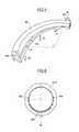
- FIG. 2is an enlarged view of the exhaust duct 30 and other components.
- the exhaust ducthas an upper part 30 ⁇ and a lower part 30 ⁇ .
- Zrepresents the extent of the slit 30 a in the vertical direction.
- the facility with which the gas enters the annular passage 30 b from the processing space 17can be adjusted by adjusting the extent Z of the slit 30 a . If the extent Z of the slit 30 a is large, the material gas can easily flow into the annular passage 30 b . If the extent Z of the slit 30 a is small, the facility with which the material gas flows into the annular passage 30 b is reduced.
- FIG. 3is a plan view of the exhaust duct 30 .
- the extent Z of the slit 30 a in the vertical directionis increased stepwise with increase in distance from the exhaust port 30 c . More specifically, the extent of the slit in the vertical direction in a region from the exhaust port 30 c to a position reached by an advance in the circumferential direction by 1 ⁇ 8 of the entire circumference of the exhaust duct 30 (referred to as first region 30 A) is a first extension Z 1 . That is, the extent of the slit in the vertical direction on the 1 ⁇ 4 circular arc centered on the exhaust port 30 c is Z 1 . Z 1 is, for example, 1.4 mm.
- the extent of the slit 30 a in the vertical direction in a region from the position reached by the advance in the circumferential direction by 1 ⁇ 8 of the entire circumference of the exhaust duct 30 from the exhaust port 30 c to a position reached by a further advance in the circumferential direction by 1 ⁇ 8 of the entire circumference of the exhaust duct 30is a second extension Z 2 . That is, the two 1 ⁇ 8 circular arcs between which the first region 30 A is defined are the second region 30 B.
- Z 2is, for example, 1.5 mm.
- the extent of the slit 30 a in the vertical direction in the portion (referred to as third region 30 C) other than the portion formed with the first extent Z 1 (first region 30 A) and the portion formed with the second extent Z 2 (second region 30 B)is a third extent Z 3 . That is, the 1 ⁇ 2 circular arc at the farthermost position from the exhaust port 30 c is the third region 30 C.
- Z 3is, for example, 1.55 mm.
- FIG. 4is a perspective view of a portion of the exhaust duct 30 .
- the extent Z 1 of the slit 30 a in the vertical directionis 1.4 mm.
- the extent Z 2 of the slit 30 a in the vertical directionis 1.5 mm.
- the extent Z 3 of the slit 30 a in the vertical directionis 1.55 mm.
- a material gasis supplied into the processing space 17 through the holes 14 a in the RF electrode 14 shown in FIG. 1 .
- Plasma of the material gasis produced by the electric field between the RF electrode 14 and the stage 16 between which electric power is applied, thereby performing plasma film forming on a substrate on the stage 16 .
- the material gas used for film formingspreads radially as viewed in plan and enters the annular passage 30 b via the slit 30 a of the exhaust duct 30 .
- the gas in the annular passage 30 bis discharged from the exhaust port 30 c to the outside.
- the extent in the vertical direction of the slit 30 a of the exhaust duct 30is increased with increase in distance from the exhaust port 30 c .
- the gas flow rate at a portion of the stage edge closer to the exhaust port 30 Cis suppressed and the gas flow rate at a portion of the stage edge farther from the exhaust port 30 c is increased.
- the uniformity of the gas flow rate at the stage edgecan therefore be improved.
- variations in the effects of film forming in the substrate surface areacan be reduced by making the exhaust conductance at the stage edge generally uniform.
- the semiconductor manufacturing apparatus 10 according to the first embodiment of the present inventioncan be variously modified.
- the first extent Z 1is set smaller than the second extent Z 2
- the second extent Z 2is set smaller than the third extent Z 3 , thereby improving the uniformity of the gas flow rate at the stage edge.
- the actual size values Z 1 , Z 2 and Z 3can be variously changed as desired.
- the semiconductor manufacturing apparatus 10is characterized by the shape of the exhaust duct 30 .
- the present inventioncan therefore be applied to various semiconductor manufacturing apparatuses with exhaust ducts. More specifically, the exhaust duct of the present invention can be utilized in semiconductor manufacturing apparatuses such as etchers as well as film forming apparatuses.
- FIG. 5is a perspective view of a portion of an exhaust duct 50 of the semiconductor manufacturing apparatus according to the second embodiment of the present invention.
- the extent Z of the slit 30 a in the vertical directionis increased steplessly with increase in distance from the exhaust port 30 c . Accordingly, the extent Z of the slit 30 a in the vertical direction is minimized in its portion at which the exhaust port 30 c is formed, and is maximized in its portion farthermost from the exhaust port 30 c.
- the gas flow rateis higher at a position P 1 in the slit 30 a reached by an advance in the circumferential direction by 1 ⁇ 4 of the entire circumference of the exhaust duct 30 from the exhaust port 30 c than at any other position.
- the effect of improving the uniformity of the gas flow rate at the stage edgeis therefore limited.
- the slit 30 a in the vertical directionis nonlinearly and steplessly with increase in distance from the exhaust port 30 c in order to suppress the extent of the slit 30 a in the vertical direction at the position P 1 .
- the rate of increase in the extent of the slit 30 a in the vertical direction from the location where the exhaust port 30 c exists to the position P 1is set smaller than the rate of increase in the extent of the slit 30 a in the vertical direction in the farther location.
- the slit shape in such a casecan be realized by changing the extent of the slit 30 a in the vertical direction according to a quadratic function. Needless to say, the degree of the function determining the change may be increased.
- the extent Z of the slit 30 a in the vertical directionis changed through the entire exhaust duct 30 in annular form.
- the arrangementmay be such that the extent Z is changed in a portion from the position at which the exhaust port 30 c exits to a predetermined position and is made constant in the other portion.
- FIG. 6is a plan view of the lower part 30 ⁇ of the exhaust duct of the semiconductor manufacturing apparatus according to the third embodiment of the present invention. In this exhaust duct, portions of the slit are blocked with a plurality of obstacles.
- FIG. 6illustrates the lower part 30 ⁇ and a plurality of obstacles. As the plurality of obstacles, three obstacles 50 a , eleven obstacles 50 b and three obstacles 50 c are provided. The obstacles 50 b are formed near the exhaust port 30 c . The obstacles 50 a and the obstacles 50 c are provided at positions between which the obstacles 50 b are located.
- Each of the three obstacles 50 a and the three obstacles 50 cis an obstacle of a comparatively small width.
- the eleven obstaclesare each an obstacle of a width about twice that of the obstacles 50 a and 50 c .
- the obstacles 50 bare provided at a density twice the density at which the obstacles 50 a and 50 c are provided. Consequently, the plurality of obstacles block portions of the slit in such a manner that the slit opening-area percentage is increased with increase in distance from the exhaust port 30 c.
- FIG. 7is a perspective view of a portion of the exhaust duct of the semiconductor manufacturing apparatus according to the third embodiment of the present invention.
- the extent Z of the slit 30 a in the vertical directionis 1.55 mm and fixed at this value.
- the width of the obstacles 50 ais 1.5 mm.
- the extent of the obstacles 50 a in the longitudinal direction(the direction from the processing space toward the annular passage 30 b ) is 8 mm.
- the obstacles 50 care identical in shape to the obstacles 50 a.
- the width of the obstacles 50 bis 3 mm.
- the extent of the obstacles 50 b in the longitudinal directionis 8 mm.
- the extent of the plurality of obstacles in the vertical directionis equal to the extent of the slit 30 a in the vertical direction, which is 1.55 mm. Accordingly, the upper ends and the lower ends of the plurality of obstacles are connected to the exhaust duct 30 .
- the plurality of obstaclesmay be parts provided separately from the exhaust duct 30 or may be formed integrally with the exhaust duct 30 .
- the density and the width of the plurality of obstaclesare set higher and larger in a location closer to the exhaust port 30 c than in a location farther from the exhaust port 30 c , thereby making the opening-area percentage of the slit 30 a substantially equal to that of the slit 30 a in the first embodiment.
- the uniformity of the gas flow rate at the stage edgecan thus be improved.
- FIG. 8shows simulation results showing the relationship between the slit shape of the exhaust duct and non-uniformity (NU) of the gas flow rate at the stage edge.
- NUnon-uniformity
- Non-uniformity (NU) of the gas flow rate at the stage edgecan be expressed by ((Vmax ⁇ Vmin)/Vave) ⁇ 100 where Vmax is the maximum of the gas flow rate at the stage edge; Vmin is the minimum of the gas flow rate at the stage edge; and Vave is the average of the gas flow rate at the stage edge.
- “Traditional Exhaust Duct”designates an exhaust duct in which the extent of the slit in the vertical direction is uniform. A concrete value of the extent of the slit in the vertical direction is 1.5 mm
- “ED with Slope”designates the exhaust duct according to the second embodiment ( FIG. 5 ).
- “ED with Various Gap Heights”designates the exhaust duct according to the first embodiment ( FIGS. 3 and 4 ).
- “ED with Obstacles”designates the exhaust duct according to the third embodiment ( FIGS. 6 and 7 ).
- non-uniformityIn the case of “Traditional Exhaust Duct”, non-uniformity (NU) is as high as 16.3%. In the case of “ED with Slope”, non-uniformity is slightly improved in comparison with that in the case of “Traditional Exhaust Duct”. In the case of “ED with Various Gap Heights”, a markedly improved value of non-uniformity as low as 3.7% is exhibited. Also in the case of “ED with Obstacles”, a markedly improved value of non-uniformity as low as 3.2% is exhibited.
- the plurality of obstacles according to the third embodiment of the present inventionare provided for the purpose of adjusting the opening-area percentage of slit 30 a . Therefore, the width and density of the obstacles may be appropriately changed.
- FIG. 9is a perspective view of a portion of the exhaust duct according to the fourth embodiment.
- a plurality of obstaclesobstacles 60 a of a smaller width and obstacles 60 b of a larger width are provided.
- the plurality of obstaclesare joined to the exhaust duct 30 only at their upper ends.
- the opening-area percentage of slit 30 acan be adjusted by adjusting the gaps between the lower ends of the plurality of obstacles and the exhaust duct 30 .
- FIG. 10is a perspective view of a portion of the exhaust duct according to the fifth embodiment.
- a plurality of obstaclesobstacles 70 a of a smaller width and obstacles 70 b of a larger width are provided.
- the plurality of obstaclesare joined to the exhaust duct 30 only at their lower ends.
- the opening-area percentage of slit 30 acan be adjusted by adjusting the gaps between the upper ends of the plurality of obstacles and the exhaust duct 30 .
- Each of the slits 30 a of the semiconductor manufacturing apparatuses of the present invention described abovecan be changed in shape appropriately as long as the opening-area percentage of the slit 30 a is increased with increase in distance from the exhaust port.
- a combination of some of the features of the semiconductor manufacturing apparatuses according to the embodimentscan be appropriately made.
- the opening-area percentage of a slit of the exhaust ductis increased with increase in distance from the exhaust port.
- the uniformity of the gas flow rate at the stage edgecan thereby be improved.
Landscapes
- Chemical & Material Sciences (AREA)
- Engineering & Computer Science (AREA)
- Physics & Mathematics (AREA)
- Plasma & Fusion (AREA)
- Analytical Chemistry (AREA)
- Materials Engineering (AREA)
- Metallurgy (AREA)
- Organic Chemistry (AREA)
- Mechanical Engineering (AREA)
- Chemical Kinetics & Catalysis (AREA)
- General Chemical & Material Sciences (AREA)
- General Physics & Mathematics (AREA)
- Condensed Matter Physics & Semiconductors (AREA)
- Manufacturing & Machinery (AREA)
- Computer Hardware Design (AREA)
- Microelectronics & Electronic Packaging (AREA)
- Power Engineering (AREA)
- Drying Of Semiconductors (AREA)
- Chemical Vapour Deposition (AREA)
Abstract
Description
Field of the Invention
The present invention relates to a semiconductor manufacturing apparatus that subjects a substrate to gas-based processing.
Background Art
U.S. Pat. No. 6,921,556B2 discloses an exhaust duct through which a gas spent for film forming is discharged to the outside.
For example, on a film forming apparatus or an etcher, an exhaust duct is provided so as to surround a stage. A gas supplied onto the stage is radially diffused and taken in the exhaust duct. Preferably, the gas supplied onto the stage enters the exhaust duct radially and uniformly. In other words, for uniformly performing processing on a substrate on the stage with no location dependence, it is desirable that the gas flow rate at the edge of the stage is uniform.
However, the gas flow rate is increased in some location on the stage edge and is reduced in another location on the stage edge. Thus, there is a problem of the gas flow rate at the stage edge being not uniform. The seriousness of this problem is increased particularly when the pressure in the chamber is reduced to about 200 Pa while the amount of exhaust in the chamber is comparatively large.
The present invention has been achieved to solve the above-described problem, and an object of the present invention is to provide a semiconductor manufacturing apparatus capable of improving the uniformity of the gas flow rate at the stage edge.
The features and advantages of the present invention may be summarized as follows.
According to one aspect of the present invention, a semiconductor manufacturing apparatus includes a stage, and an exhaust duct having an annular passage surrounding a processing space over the stage, an annular slit through which a gas supplied to the processing space is led into the annular passage, and an exhaust port through which the gas in the annular passage is discharged to the outside, wherein the opening-area percentage of the slit is increased with increase in distance from the exhaust port.
Other and further objects, features and advantages of the invention will appear more fully from the following description.
A semiconductor manufacturing apparatus according to an embodiment of the present invention will be described with reference to the drawings. Components identical or corresponding to each other are indicated by the same reference characters and repeated description of them is omitted in some cases.
Astage 16 is provided in thechamber 12 so as to be opposed to theRF electrode 14. Thestage 16 is a susceptor supported on aslide shaft 18. TheRF electrode 14 and thestage 16 form a parallel flat plate structure.
Agas supply part 22 is connected to theRF electrode 14, with aninsulating part 20 interposed therebetween. Thegas supply part 22 is a part through which a material gas is supplied to a space between theRF electrode 14 and thestage 16. In a space over thestage 16, processing such as film forming is performed on a substrate placed on thestage 16. This space is therefore referred to asprocessing space 17.
Anexhaust duct 30 is provided between theRF electrode 14 and thechamber 12. Theexhaust duct 30 is formed of ceramic for example. An O-ring 32 suitably compressed is provided between theexhaust duct 30 and theRF electrode 14. An O-ring 34 suitably compressed is provided between theexhaust duct 30 and thechamber 12. An O-ring 36 suitably compressed is provided between theexhaust duct 30 and agas exhaust part 40.
Theexhaust duct 30 is formed so as to be annular as viewed in plan and surround thestage 16. With theexhaust duct 30, anannular passage 30bsurrounding theprocessing space 17 over thestage 16 is provided. In theexhaust duct 30, anannular slit 30athrough which a gas supplied into theprocessing space 17 is led into theannular passage 30band anexhaust port 30cthrough which the gas in theannular passage 30bis discharged to the outside are formed.
Theexhaust port 30cconnects to thegas exhaust part 40 provided on a side surface of thechamber 12. Thegas exhaust part 40 is provided for the purpose of discharging the material gas used for film forming. Avalve 42 and avacuum pump 44 are connected to thegas exhaust part 40. The pressure in thechamber 12 can be freely controlled by adjusting the amount of exhaust with thevalve 42 and thevacuum pump 44.
The extent of theslit 30ain the vertical direction in a region from the position reached by the advance in the circumferential direction by ⅛ of the entire circumference of theexhaust duct 30 from theexhaust port 30cto a position reached by a further advance in the circumferential direction by ⅛ of the entire circumference of the exhaust duct30 (referred to assecond region 30B) is a second extension Z2. That is, the two ⅛ circular arcs between which thefirst region 30A is defined are thesecond region 30B. Z2 is, for example, 1.5 mm.
The extent of theslit 30ain the vertical direction in the portion (referred to asthird region 30C) other than the portion formed with the first extent Z1 (first region 30A) and the portion formed with the second extent Z2 (second region 30B) is a third extent Z3. That is, the ½ circular arc at the farthermost position from theexhaust port 30cis thethird region 30C. Z3 is, for example, 1.55 mm.
The operation of thesemiconductor manufacturing apparatus 10 according to the first embodiment will now be described. A material gas is supplied into theprocessing space 17 through theholes 14ain theRF electrode 14 shown inFIG. 1 . Plasma of the material gas is produced by the electric field between theRF electrode 14 and thestage 16 between which electric power is applied, thereby performing plasma film forming on a substrate on thestage 16. The material gas used for film forming spreads radially as viewed in plan and enters theannular passage 30bvia theslit 30aof theexhaust duct 30. The gas in theannular passage 30bis discharged from theexhaust port 30cto the outside.
In the case where the extent in the vertical direction of theslit 30ain annular form is uniform, a larger amount of gas flows through a portion of theslit 30acloser to theexhaust port 30cwhile a smaller amount of gas flows through a portion farther from theexhaust port 30c. Non-uniformity of the gas flow rate at the edge of the stage16 (stage edge) thus occurs. More specifically, the gas flow rate is increased at a portion of the stage edge closer to theexhaust port 30cwhile the gas flow rate is reduced at a portion farther from theexhaust port 30c.
In the first embodiment of the present invention, the extent in the vertical direction of theslit 30aof theexhaust duct 30 is increased with increase in distance from theexhaust port 30c. With theslit 30athus formed, the gas flow rate at a portion of the stage edge closer to theexhaust port 30C is suppressed and the gas flow rate at a portion of the stage edge farther from theexhaust port 30cis increased. The uniformity of the gas flow rate at the stage edge can therefore be improved. Thus, variations in the effects of film forming in the substrate surface area can be reduced by making the exhaust conductance at the stage edge generally uniform.
Thesemiconductor manufacturing apparatus 10 according to the first embodiment of the present invention can be variously modified. In thesemiconductor manufacturing apparatus 10, the first extent Z1 is set smaller than the second extent Z2, and the second extent Z2 is set smaller than the third extent Z3, thereby improving the uniformity of the gas flow rate at the stage edge. The actual size values Z1, Z2 and Z3 can be variously changed as desired.
While the extent of theslit 30ain the vertical direction is changed in three steps (Z1, Z2, Z3), the number of steps is not limited to three as long as the extent is changed in two or more steps. Thesemiconductor manufacturing apparatus 10 is characterized by the shape of theexhaust duct 30. The present invention can therefore be applied to various semiconductor manufacturing apparatuses with exhaust ducts. More specifically, the exhaust duct of the present invention can be utilized in semiconductor manufacturing apparatuses such as etchers as well as film forming apparatuses.
These modifications can be applied as desired to semiconductor manufacturing apparatuses according to embodiments described below. Each of the semiconductor manufacturing apparatuses according to the embodiments described below has a number of commonalities with the first embodiments and will therefore be described mainly with respect to points of difference from the first embodiment.
With this slit shape, the flow of gas from a position in the processing space close to theexhaust port 30cto theannular passage 30bis suppressed and the flow of gas from a position in the processing space remote from theexhaust port 30cis promoted, thus improving the uniformity of the gas flow rate at the stage edge.
In the meantime, in theexhaust duct 50 according to the second embodiment, the gas flow rate is higher at a position P1 in theslit 30areached by an advance in the circumferential direction by ¼ of the entire circumference of theexhaust duct 30 from theexhaust port 30cthan at any other position. The effect of improving the uniformity of the gas flow rate at the stage edge is therefore limited.
It is preferable to increase the extent of theslit 30ain the vertical direction nonlinearly and steplessly with increase in distance from theexhaust port 30cin order to suppress the extent of theslit 30ain the vertical direction at the position P1. For example, the rate of increase in the extent of theslit 30ain the vertical direction from the location where theexhaust port 30cexists to the position P1 is set smaller than the rate of increase in the extent of theslit 30ain the vertical direction in the farther location. The slit shape in such a case can be realized by changing the extent of theslit 30ain the vertical direction according to a quadratic function. Needless to say, the degree of the function determining the change may be increased.
In the second embodiment of the present invention, the extent Z of theslit 30ain the vertical direction is changed through theentire exhaust duct 30 in annular form. However, the arrangement may be such that the extent Z is changed in a portion from the position at which theexhaust port 30cexits to a predetermined position and is made constant in the other portion.
Each of the threeobstacles 50aand the threeobstacles 50cis an obstacle of a comparatively small width. The eleven obstacles are each an obstacle of a width about twice that of theobstacles obstacles 50bare provided at a density twice the density at which theobstacles exhaust port 30c.
The width of theobstacles 50bis 3 mm. The extent of theobstacles 50bin the longitudinal direction (the direction from the processing space toward theannular passage 30b) is 8 mm.
The extent of the plurality of obstacles in the vertical direction is equal to the extent of theslit 30ain the vertical direction, which is 1.55 mm. Accordingly, the upper ends and the lower ends of the plurality of obstacles are connected to theexhaust duct 30. The plurality of obstacles may be parts provided separately from theexhaust duct 30 or may be formed integrally with theexhaust duct 30.
As shown inFIG. 6 , the density and the width of the plurality of obstacles are set higher and larger in a location closer to theexhaust port 30cthan in a location farther from theexhaust port 30c, thereby making the opening-area percentage of theslit 30asubstantially equal to that of theslit 30ain the first embodiment. The uniformity of the gas flow rate at the stage edge can thus be improved.
“Traditional Exhaust Duct” designates an exhaust duct in which the extent of the slit in the vertical direction is uniform. A concrete value of the extent of the slit in the vertical direction is 1.5 mm “ED with Slope” designates the exhaust duct according to the second embodiment (FIG. 5 ). “ED with Various Gap Heights” designates the exhaust duct according to the first embodiment (FIGS. 3 and 4 ). “ED with Obstacles” designates the exhaust duct according to the third embodiment (FIGS. 6 and 7 ).
In the case of “Traditional Exhaust Duct”, non-uniformity (NU) is as high as 16.3%. In the case of “ED with Slope”, non-uniformity is slightly improved in comparison with that in the case of “Traditional Exhaust Duct”. In the case of “ED with Various Gap Heights”, a markedly improved value of non-uniformity as low as 3.7% is exhibited. Also in the case of “ED with Obstacles”, a markedly improved value of non-uniformity as low as 3.2% is exhibited.
The plurality of obstacles according to the third embodiment of the present invention are provided for the purpose of adjusting the opening-area percentage ofslit 30a. Therefore, the width and density of the obstacles may be appropriately changed.
The semiconductor manufacturing apparatus according to the fourth embodiment will be described mainly with respect to points of difference from the semiconductor manufacturing apparatus according to the third embodiment.FIG. 9 is a perspective view of a portion of the exhaust duct according to the fourth embodiment. A plurality of obstacles:obstacles 60aof a smaller width andobstacles 60bof a larger width are provided. The plurality of obstacles are joined to theexhaust duct 30 only at their upper ends. The opening-area percentage ofslit 30acan be adjusted by adjusting the gaps between the lower ends of the plurality of obstacles and theexhaust duct 30.
The semiconductor manufacturing apparatus according to the fifth embodiment will be described mainly with respect to points of difference from the semiconductor manufacturing apparatus according to the third embodiment.FIG. 10 is a perspective view of a portion of the exhaust duct according to the fifth embodiment. A plurality of obstacles:obstacles 70aof a smaller width andobstacles 70bof a larger width are provided. The plurality of obstacles are joined to theexhaust duct 30 only at their lower ends. The opening-area percentage ofslit 30acan be adjusted by adjusting the gaps between the upper ends of the plurality of obstacles and theexhaust duct 30.
Each of theslits 30aof the semiconductor manufacturing apparatuses of the present invention described above can be changed in shape appropriately as long as the opening-area percentage of theslit 30ais increased with increase in distance from the exhaust port. A combination of some of the features of the semiconductor manufacturing apparatuses according to the embodiments can be appropriately made.
According to the present invention, the opening-area percentage of a slit of the exhaust duct is increased with increase in distance from the exhaust port. The uniformity of the gas flow rate at the stage edge can thereby be improved.
Obviously many modifications and variations of the present invention are possible in the light of the above teachings. It is therefore to be understood that within the scope of the appended claims the invention may be practiced otherwise than as specifically described.
Claims (12)
1. A semiconductor manufacturing apparatus comprising:
a stage; and
an exhaust duct having an annular passage surrounding a processing space, the processing space being over the stage, an annular slit through which a gas supplied to the processing space is led into the annular passage, and an exhaust port through which the gas in the annular passage is discharged to the outside, wherein
the opening-area percentage of the slit is increased with increase in distance from the exhaust port,
the stage is separated from the exhaust duct, and
the rate of increase in the extent of the slit in the vertical direction from the location where the exhaust port exists to a predetermined position is set smaller than the rate of increase in the extent of the slit in the vertical direction in a farther location.
2. The semiconductor manufacturing apparatus according toclaim 1 , wherein the extent of the slit in the vertical direction is increased stepwise with increase in distance from the exhaust port.
3. The semiconductor manufacturing apparatus according toclaim 2 , wherein the extent of the slit in the vertical direction is:
a first extent in a region from the exhaust port to a position reached by an advance in the circumferential direction by ⅛ of the entire circumference of the exhaust duct;
a second extent in a region from the position reached by the advance in the circumferential direction by ⅛ of the entire circumference of the exhaust duct from the exhaust port to a position reached by a further advance in the circumferential direction by ⅛ of the entire circumference of the exhaust duct; and
a third extent in a portion other than the portion formed with the first extent and the portion formed with the second extent, and
wherein the first extent is smaller than the second extent, and the second extent is smaller than the third extent.
4. The semiconductor manufacturing apparatus according toclaim 1 , wherein the extent of the slit in the vertical direction is steplessly increased with increase in distance from the exhaust port.
5. The semiconductor manufacturing apparatus according toclaim 1 , wherein the extent of the slit in the vertical direction is nonlinearly and steplessly increased with increase in distance from the exhaust port.
6. The semiconductor manufacturing apparatus according toclaim 1 , comprising a plurality of obstacles with which portions of the slit are blocked so that the opening-area percentage of the slit is increased with increase in distance from the exhaust port.
7. The semiconductor manufacturing apparatus according toclaim 6 , wherein the density and the width of the plurality of obstacles are set higher and larger in a location closer to the exhaust port than in a location farther from the exhaust port.
8. The semiconductor manufacturing apparatus according toclaim 6 , wherein the extent of the plurality of obstacles in the vertical direction is equal to the extent of the slit in the vertical direction.
9. The semiconductor manufacturing apparatus according toclaim 6 , wherein the plurality of obstacles are joined to the exhaust duct only at their upper ends.
10. The semiconductor manufacturing apparatus according toclaim 6 , wherein the plurality of obstacles are joined to the exhaust duct only at their lower ends.
11. The semiconductor manufacturing apparatus according toclaim 6 , wherein the plurality of obstacles are formed integrally with the exhaust duct.
12. The semiconductor manufacturing apparatus according toclaim 1 , wherein the exhaust duct is formed of ceramic.
Priority Applications (5)
| Application Number | Priority Date | Filing Date | Title |
|---|---|---|---|
| US14/621,167US9963782B2 (en) | 2015-02-12 | 2015-02-12 | Semiconductor manufacturing apparatus |
| JP2015224473AJP2016149526A (en) | 2015-02-12 | 2015-11-17 | Semiconductor manufacturing apparatus |
| KR1020150164882AKR102423789B1 (en) | 2015-02-12 | 2015-11-24 | Semiconductor manufacturing apparatus |
| CN201510824352.3ACN105895553A (en) | 2015-02-12 | 2015-11-24 | Semiconductor Manufacturing Apparatus |
| TW104139868ATWI657478B (en) | 2015-02-12 | 2015-11-30 | Semiconductor manufacturing apparatus |
Applications Claiming Priority (1)
| Application Number | Priority Date | Filing Date | Title |
|---|---|---|---|
| US14/621,167US9963782B2 (en) | 2015-02-12 | 2015-02-12 | Semiconductor manufacturing apparatus |
Publications (2)
| Publication Number | Publication Date |
|---|---|
| US20160237559A1 US20160237559A1 (en) | 2016-08-18 |
| US9963782B2true US9963782B2 (en) | 2018-05-08 |
Family
ID=56620855
Family Applications (1)
| Application Number | Title | Priority Date | Filing Date |
|---|---|---|---|
| US14/621,167Active2036-04-25US9963782B2 (en) | 2015-02-12 | 2015-02-12 | Semiconductor manufacturing apparatus |
Country Status (5)
| Country | Link |
|---|---|
| US (1) | US9963782B2 (en) |
| JP (1) | JP2016149526A (en) |
| KR (1) | KR102423789B1 (en) |
| CN (1) | CN105895553A (en) |
| TW (1) | TWI657478B (en) |
Cited By (5)
| Publication number | Priority date | Publication date | Assignee | Title |
|---|---|---|---|---|
| US10358721B2 (en)* | 2015-10-22 | 2019-07-23 | Asm Ip Holding B.V. | Semiconductor manufacturing system including deposition apparatus |
| US11078568B2 (en)* | 2019-01-08 | 2021-08-03 | Applied Materials, Inc. | Pumping apparatus and method for substrate processing chambers |
| US11276585B2 (en)* | 2018-01-30 | 2022-03-15 | Samsung Electronics Co., Ltd. | Asymmetrical sealing and gas flow control device |
| US11447866B2 (en)* | 2020-06-17 | 2022-09-20 | Applied Materials, Inc. | High temperature chemical vapor deposition lid |
| US20230063007A1 (en)* | 2020-02-10 | 2023-03-02 | Lam Research Corporation | Tunability of edge plasma density for tilt control |
Families Citing this family (240)
| Publication number | Priority date | Publication date | Assignee | Title |
|---|---|---|---|---|
| US20130023129A1 (en) | 2011-07-20 | 2013-01-24 | Asm America, Inc. | Pressure transmitter for a semiconductor processing environment |
| US20160376700A1 (en) | 2013-02-01 | 2016-12-29 | Asm Ip Holding B.V. | System for treatment of deposition reactor |
| CN105164309B (en)* | 2013-05-01 | 2019-04-12 | 应用材料公司 | Injection and Vent Design for Controlling Epitaxy Chamber Flow |
| US10941490B2 (en) | 2014-10-07 | 2021-03-09 | Asm Ip Holding B.V. | Multiple temperature range susceptor, assembly, reactor and system including the susceptor, and methods of using the same |
| US9963782B2 (en)* | 2015-02-12 | 2018-05-08 | Asm Ip Holding B.V. | Semiconductor manufacturing apparatus |
| US10276355B2 (en) | 2015-03-12 | 2019-04-30 | Asm Ip Holding B.V. | Multi-zone reactor, system including the reactor, and method of using the same |
| US11139308B2 (en) | 2015-12-29 | 2021-10-05 | Asm Ip Holding B.V. | Atomic layer deposition of III-V compounds to form V-NAND devices |
| US10529554B2 (en) | 2016-02-19 | 2020-01-07 | Asm Ip Holding B.V. | Method for forming silicon nitride film selectively on sidewalls or flat surfaces of trenches |
| US10343920B2 (en) | 2016-03-18 | 2019-07-09 | Asm Ip Holding B.V. | Aligned carbon nanotubes |
| US11453943B2 (en) | 2016-05-25 | 2022-09-27 | Asm Ip Holding B.V. | Method for forming carbon-containing silicon/metal oxide or nitride film by ALD using silicon precursor and hydrocarbon precursor |
| US10612137B2 (en) | 2016-07-08 | 2020-04-07 | Asm Ip Holdings B.V. | Organic reactants for atomic layer deposition |
| US9859151B1 (en) | 2016-07-08 | 2018-01-02 | Asm Ip Holding B.V. | Selective film deposition method to form air gaps |
| US9812320B1 (en) | 2016-07-28 | 2017-11-07 | Asm Ip Holding B.V. | Method and apparatus for filling a gap |
| US9887082B1 (en) | 2016-07-28 | 2018-02-06 | Asm Ip Holding B.V. | Method and apparatus for filling a gap |
| JP6794184B2 (en)* | 2016-08-31 | 2020-12-02 | 株式会社日本製鋼所 | Plasma atomic layer deposition equipment |
| US11532757B2 (en) | 2016-10-27 | 2022-12-20 | Asm Ip Holding B.V. | Deposition of charge trapping layers |
| US10714350B2 (en) | 2016-11-01 | 2020-07-14 | ASM IP Holdings, B.V. | Methods for forming a transition metal niobium nitride film on a substrate by atomic layer deposition and related semiconductor device structures |
| KR102546317B1 (en) | 2016-11-15 | 2023-06-21 | 에이에스엠 아이피 홀딩 비.브이. | Gas supply unit and substrate processing apparatus including the same |
| US11447861B2 (en) | 2016-12-15 | 2022-09-20 | Asm Ip Holding B.V. | Sequential infiltration synthesis apparatus and a method of forming a patterned structure |
| US11581186B2 (en) | 2016-12-15 | 2023-02-14 | Asm Ip Holding B.V. | Sequential infiltration synthesis apparatus |
| US11390950B2 (en) | 2017-01-10 | 2022-07-19 | Asm Ip Holding B.V. | Reactor system and method to reduce residue buildup during a film deposition process |
| US10468261B2 (en) | 2017-02-15 | 2019-11-05 | Asm Ip Holding B.V. | Methods for forming a metallic film on a substrate by cyclical deposition and related semiconductor device structures |
| US10770286B2 (en) | 2017-05-08 | 2020-09-08 | Asm Ip Holdings B.V. | Methods for selectively forming a silicon nitride film on a substrate and related semiconductor device structures |
| US12040200B2 (en) | 2017-06-20 | 2024-07-16 | Asm Ip Holding B.V. | Semiconductor processing apparatus and methods for calibrating a semiconductor processing apparatus |
| US11306395B2 (en) | 2017-06-28 | 2022-04-19 | Asm Ip Holding B.V. | Methods for depositing a transition metal nitride film on a substrate by atomic layer deposition and related deposition apparatus |
| KR20190009245A (en) | 2017-07-18 | 2019-01-28 | 에이에스엠 아이피 홀딩 비.브이. | Methods for forming a semiconductor device structure and related semiconductor device structures |
| US11374112B2 (en) | 2017-07-19 | 2022-06-28 | Asm Ip Holding B.V. | Method for depositing a group IV semiconductor and related semiconductor device structures |
| US10590535B2 (en) | 2017-07-26 | 2020-03-17 | Asm Ip Holdings B.V. | Chemical treatment, deposition and/or infiltration apparatus and method for using the same |
| TWI815813B (en) | 2017-08-04 | 2023-09-21 | 荷蘭商Asm智慧財產控股公司 | Showerhead assembly for distributing a gas within a reaction chamber |
| US10692741B2 (en) | 2017-08-08 | 2020-06-23 | Asm Ip Holdings B.V. | Radiation shield |
| US10770336B2 (en) | 2017-08-08 | 2020-09-08 | Asm Ip Holding B.V. | Substrate lift mechanism and reactor including same |
| US11769682B2 (en) | 2017-08-09 | 2023-09-26 | Asm Ip Holding B.V. | Storage apparatus for storing cassettes for substrates and processing apparatus equipped therewith |
| US11830730B2 (en) | 2017-08-29 | 2023-11-28 | Asm Ip Holding B.V. | Layer forming method and apparatus |
| US11295980B2 (en) | 2017-08-30 | 2022-04-05 | Asm Ip Holding B.V. | Methods for depositing a molybdenum metal film over a dielectric surface of a substrate by a cyclical deposition process and related semiconductor device structures |
| US10658205B2 (en) | 2017-09-28 | 2020-05-19 | Asm Ip Holdings B.V. | Chemical dispensing apparatus and methods for dispensing a chemical to a reaction chamber |
| US10403504B2 (en) | 2017-10-05 | 2019-09-03 | Asm Ip Holding B.V. | Method for selectively depositing a metallic film on a substrate |
| JP2019075517A (en)* | 2017-10-19 | 2019-05-16 | 東京エレクトロン株式会社 | Processing device and member having diffusion path |
| US10923344B2 (en) | 2017-10-30 | 2021-02-16 | Asm Ip Holding B.V. | Methods for forming a semiconductor structure and related semiconductor structures |
| WO2019103613A1 (en) | 2017-11-27 | 2019-05-31 | Asm Ip Holding B.V. | A storage device for storing wafer cassettes for use with a batch furnace |
| CN111344522B (en) | 2017-11-27 | 2022-04-12 | 阿斯莫Ip控股公司 | Including clean mini-environment device |
| US10872771B2 (en) | 2018-01-16 | 2020-12-22 | Asm Ip Holding B. V. | Method for depositing a material film on a substrate within a reaction chamber by a cyclical deposition process and related device structures |
| KR102695659B1 (en) | 2018-01-19 | 2024-08-14 | 에이에스엠 아이피 홀딩 비.브이. | Method for depositing a gap filling layer by plasma assisted deposition |
| TWI799494B (en) | 2018-01-19 | 2023-04-21 | 荷蘭商Asm 智慧財產控股公司 | Deposition method |
| US11081345B2 (en) | 2018-02-06 | 2021-08-03 | Asm Ip Holding B.V. | Method of post-deposition treatment for silicon oxide film |
| US10896820B2 (en) | 2018-02-14 | 2021-01-19 | Asm Ip Holding B.V. | Method for depositing a ruthenium-containing film on a substrate by a cyclical deposition process |
| WO2019158960A1 (en) | 2018-02-14 | 2019-08-22 | Asm Ip Holding B.V. | A method for depositing a ruthenium-containing film on a substrate by a cyclical deposition process |
| US10731249B2 (en) | 2018-02-15 | 2020-08-04 | Asm Ip Holding B.V. | Method of forming a transition metal containing film on a substrate by a cyclical deposition process, a method for supplying a transition metal halide compound to a reaction chamber, and related vapor deposition apparatus |
| KR102636427B1 (en) | 2018-02-20 | 2024-02-13 | 에이에스엠 아이피 홀딩 비.브이. | Substrate processing method and apparatus |
| US10975470B2 (en) | 2018-02-23 | 2021-04-13 | Asm Ip Holding B.V. | Apparatus for detecting or monitoring for a chemical precursor in a high temperature environment |
| US11473195B2 (en) | 2018-03-01 | 2022-10-18 | Asm Ip Holding B.V. | Semiconductor processing apparatus and a method for processing a substrate |
| KR102646467B1 (en) | 2018-03-27 | 2024-03-11 | 에이에스엠 아이피 홀딩 비.브이. | Method of forming an electrode on a substrate and a semiconductor device structure including an electrode |
| KR102600229B1 (en) | 2018-04-09 | 2023-11-10 | 에이에스엠 아이피 홀딩 비.브이. | Substrate supporting device, substrate processing apparatus including the same and substrate processing method |
| US11462387B2 (en)* | 2018-04-17 | 2022-10-04 | Asm Ip Holding B.V. | Substrate processing apparatus and substrate processing method |
| US12025484B2 (en) | 2018-05-08 | 2024-07-02 | Asm Ip Holding B.V. | Thin film forming method |
| US12272527B2 (en) | 2018-05-09 | 2025-04-08 | Asm Ip Holding B.V. | Apparatus for use with hydrogen radicals and method of using same |
| US11434569B2 (en)* | 2018-05-25 | 2022-09-06 | Applied Materials, Inc. | Ground path systems for providing a shorter and symmetrical ground path |
| KR102596988B1 (en) | 2018-05-28 | 2023-10-31 | 에이에스엠 아이피 홀딩 비.브이. | Method of processing a substrate and a device manufactured by the same |
| US11718913B2 (en) | 2018-06-04 | 2023-08-08 | Asm Ip Holding B.V. | Gas distribution system and reactor system including same |
| US10797133B2 (en) | 2018-06-21 | 2020-10-06 | Asm Ip Holding B.V. | Method for depositing a phosphorus doped silicon arsenide film and related semiconductor device structures |
| KR102568797B1 (en) | 2018-06-21 | 2023-08-21 | 에이에스엠 아이피 홀딩 비.브이. | Substrate processing system |
| KR102854019B1 (en) | 2018-06-27 | 2025-09-02 | 에이에스엠 아이피 홀딩 비.브이. | Periodic deposition method for forming a metal-containing material and films and structures comprising the metal-containing material |
| TWI873894B (en) | 2018-06-27 | 2025-02-21 | 荷蘭商Asm Ip私人控股有限公司 | Cyclic deposition methods for forming metal-containing material and films and structures including the metal-containing material |
| US10755922B2 (en) | 2018-07-03 | 2020-08-25 | Asm Ip Holding B.V. | Method for depositing silicon-free carbon-containing film as gap-fill layer by pulse plasma-assisted deposition |
| US10388513B1 (en) | 2018-07-03 | 2019-08-20 | Asm Ip Holding B.V. | Method for depositing silicon-free carbon-containing film as gap-fill layer by pulse plasma-assisted deposition |
| US11430674B2 (en) | 2018-08-22 | 2022-08-30 | Asm Ip Holding B.V. | Sensor array, apparatus for dispensing a vapor phase reactant to a reaction chamber and related methods |
| US11024523B2 (en) | 2018-09-11 | 2021-06-01 | Asm Ip Holding B.V. | Substrate processing apparatus and method |
| KR102707956B1 (en) | 2018-09-11 | 2024-09-19 | 에이에스엠 아이피 홀딩 비.브이. | Method for deposition of a thin film |
| CN110970344B (en) | 2018-10-01 | 2024-10-25 | Asmip控股有限公司 | Substrate holding apparatus, system comprising the same and method of using the same |
| KR102592699B1 (en) | 2018-10-08 | 2023-10-23 | 에이에스엠 아이피 홀딩 비.브이. | Substrate support unit and apparatuses for depositing thin film and processing the substrate including the same |
| KR102546322B1 (en) | 2018-10-19 | 2023-06-21 | 에이에스엠 아이피 홀딩 비.브이. | Substrate processing apparatus and substrate processing method |
| US12378665B2 (en) | 2018-10-26 | 2025-08-05 | Asm Ip Holding B.V. | High temperature coatings for a preclean and etch apparatus and related methods |
| US11087997B2 (en) | 2018-10-31 | 2021-08-10 | Asm Ip Holding B.V. | Substrate processing apparatus for processing substrates |
| KR102748291B1 (en) | 2018-11-02 | 2024-12-31 | 에이에스엠 아이피 홀딩 비.브이. | Substrate support unit and substrate processing apparatus including the same |
| US11572620B2 (en) | 2018-11-06 | 2023-02-07 | Asm Ip Holding B.V. | Methods for selectively depositing an amorphous silicon film on a substrate |
| US10818758B2 (en) | 2018-11-16 | 2020-10-27 | Asm Ip Holding B.V. | Methods for forming a metal silicate film on a substrate in a reaction chamber and related semiconductor device structures |
| US12040199B2 (en) | 2018-11-28 | 2024-07-16 | Asm Ip Holding B.V. | Substrate processing apparatus for processing substrates |
| KR102636428B1 (en) | 2018-12-04 | 2024-02-13 | 에이에스엠 아이피 홀딩 비.브이. | A method for cleaning a substrate processing apparatus |
| US11158513B2 (en) | 2018-12-13 | 2021-10-26 | Asm Ip Holding B.V. | Methods for forming a rhenium-containing film on a substrate by a cyclical deposition process and related semiconductor device structures |
| TWI874340B (en) | 2018-12-14 | 2025-03-01 | 荷蘭商Asm Ip私人控股有限公司 | Method of forming device structure, structure formed by the method and system for performing the method |
| TWI866480B (en) | 2019-01-17 | 2024-12-11 | 荷蘭商Asm Ip 私人控股有限公司 | Methods of forming a transition metal containing film on a substrate by a cyclical deposition process |
| KR102727227B1 (en)* | 2019-01-22 | 2024-11-07 | 에이에스엠 아이피 홀딩 비.브이. | Semiconductor processing device |
| TWI838458B (en) | 2019-02-20 | 2024-04-11 | 荷蘭商Asm Ip私人控股有限公司 | Apparatus and methods for plug fill deposition in 3-d nand applications |
| TWI845607B (en) | 2019-02-20 | 2024-06-21 | 荷蘭商Asm Ip私人控股有限公司 | Cyclical deposition method and apparatus for filling a recess formed within a substrate surface |
| TWI873122B (en) | 2019-02-20 | 2025-02-21 | 荷蘭商Asm Ip私人控股有限公司 | Method of filling a recess formed within a surface of a substrate, semiconductor structure formed according to the method, and semiconductor processing apparatus |
| TWI842826B (en) | 2019-02-22 | 2024-05-21 | 荷蘭商Asm Ip私人控股有限公司 | Substrate processing apparatus and method for processing substrate |
| KR102858005B1 (en) | 2019-03-08 | 2025-09-09 | 에이에스엠 아이피 홀딩 비.브이. | Method for Selective Deposition of Silicon Nitride Layer and Structure Including Selectively-Deposited Silicon Nitride Layer |
| US11742198B2 (en) | 2019-03-08 | 2023-08-29 | Asm Ip Holding B.V. | Structure including SiOCN layer and method of forming same |
| JP7502039B2 (en)* | 2019-03-28 | 2024-06-18 | エーエスエム・アイピー・ホールディング・ベー・フェー | Substrate Processing Equipment |
| JP2020167398A (en) | 2019-03-28 | 2020-10-08 | エーエスエム・アイピー・ホールディング・ベー・フェー | Door openers and substrate processing equipment provided with door openers |
| KR102809999B1 (en) | 2019-04-01 | 2025-05-19 | 에이에스엠 아이피 홀딩 비.브이. | Method of manufacturing semiconductor device |
| KR20200123380A (en) | 2019-04-19 | 2020-10-29 | 에이에스엠 아이피 홀딩 비.브이. | Layer forming method and apparatus |
| KR20200125453A (en) | 2019-04-24 | 2020-11-04 | 에이에스엠 아이피 홀딩 비.브이. | Gas-phase reactor system and method of using same |
| KR20200130121A (en) | 2019-05-07 | 2020-11-18 | 에이에스엠 아이피 홀딩 비.브이. | Chemical source vessel with dip tube |
| KR20200130652A (en) | 2019-05-10 | 2020-11-19 | 에이에스엠 아이피 홀딩 비.브이. | Method of depositing material onto a surface and structure formed according to the method |
| JP7612342B2 (en) | 2019-05-16 | 2025-01-14 | エーエスエム・アイピー・ホールディング・ベー・フェー | Wafer boat handling apparatus, vertical batch furnace and method |
| JP7598201B2 (en) | 2019-05-16 | 2024-12-11 | エーエスエム・アイピー・ホールディング・ベー・フェー | Wafer boat handling apparatus, vertical batch furnace and method |
| USD975665S1 (en) | 2019-05-17 | 2023-01-17 | Asm Ip Holding B.V. | Susceptor shaft |
| USD947913S1 (en) | 2019-05-17 | 2022-04-05 | Asm Ip Holding B.V. | Susceptor shaft |
| KR20200141002A (en) | 2019-06-06 | 2020-12-17 | 에이에스엠 아이피 홀딩 비.브이. | Method of using a gas-phase reactor system including analyzing exhausted gas |
| KR20200141931A (en) | 2019-06-10 | 2020-12-21 | 에이에스엠 아이피 홀딩 비.브이. | Method for cleaning quartz epitaxial chambers |
| KR20200143254A (en) | 2019-06-11 | 2020-12-23 | 에이에스엠 아이피 홀딩 비.브이. | Method of forming an electronic structure using an reforming gas, system for performing the method, and structure formed using the method |
| KR20210005515A (en) | 2019-07-03 | 2021-01-14 | 에이에스엠 아이피 홀딩 비.브이. | Temperature control assembly for substrate processing apparatus and method of using same |
| JP7499079B2 (en) | 2019-07-09 | 2024-06-13 | エーエスエム・アイピー・ホールディング・ベー・フェー | Plasma device using coaxial waveguide and substrate processing method |
| CN112216646A (en) | 2019-07-10 | 2021-01-12 | Asm Ip私人控股有限公司 | Substrate supporting assembly and substrate processing device comprising same |
| KR20210010307A (en) | 2019-07-16 | 2021-01-27 | 에이에스엠 아이피 홀딩 비.브이. | Substrate processing apparatus |
| KR102860110B1 (en) | 2019-07-17 | 2025-09-16 | 에이에스엠 아이피 홀딩 비.브이. | Methods of forming silicon germanium structures |
| KR20210010816A (en) | 2019-07-17 | 2021-01-28 | 에이에스엠 아이피 홀딩 비.브이. | Radical assist ignition plasma system and method |
| US11643724B2 (en) | 2019-07-18 | 2023-05-09 | Asm Ip Holding B.V. | Method of forming structures using a neutral beam |
| KR20210010817A (en) | 2019-07-19 | 2021-01-28 | 에이에스엠 아이피 홀딩 비.브이. | Method of Forming Topology-Controlled Amorphous Carbon Polymer Film |
| TWI851767B (en) | 2019-07-29 | 2024-08-11 | 荷蘭商Asm Ip私人控股有限公司 | Methods for selective deposition utilizing n-type dopants and/or alternative dopants to achieve high dopant incorporation |
| US12169361B2 (en) | 2019-07-30 | 2024-12-17 | Asm Ip Holding B.V. | Substrate processing apparatus and method |
| CN112309899A (en)* | 2019-07-30 | 2021-02-02 | Asm Ip私人控股有限公司 | Substrate processing apparatus |
| CN112309900A (en) | 2019-07-30 | 2021-02-02 | Asm Ip私人控股有限公司 | Substrate processing apparatus |
| US11587814B2 (en) | 2019-07-31 | 2023-02-21 | Asm Ip Holding B.V. | Vertical batch furnace assembly |
| US11587815B2 (en) | 2019-07-31 | 2023-02-21 | Asm Ip Holding B.V. | Vertical batch furnace assembly |
| US11227782B2 (en) | 2019-07-31 | 2022-01-18 | Asm Ip Holding B.V. | Vertical batch furnace assembly |
| CN112323048B (en) | 2019-08-05 | 2024-02-09 | Asm Ip私人控股有限公司 | Liquid level sensor for chemical source container |
| CN112342526A (en) | 2019-08-09 | 2021-02-09 | Asm Ip私人控股有限公司 | Heater assembly including cooling device and method of using same |
| USD965524S1 (en) | 2019-08-19 | 2022-10-04 | Asm Ip Holding B.V. | Susceptor support |
| USD965044S1 (en) | 2019-08-19 | 2022-09-27 | Asm Ip Holding B.V. | Susceptor shaft |
| JP2021031769A (en) | 2019-08-21 | 2021-03-01 | エーエスエム アイピー ホールディング ビー.ブイ. | Production apparatus of mixed gas of film deposition raw material and film deposition apparatus |
| USD979506S1 (en) | 2019-08-22 | 2023-02-28 | Asm Ip Holding B.V. | Insulator |
| KR20210024423A (en) | 2019-08-22 | 2021-03-05 | 에이에스엠 아이피 홀딩 비.브이. | Method for forming a structure with a hole |
| KR20210024420A (en) | 2019-08-23 | 2021-03-05 | 에이에스엠 아이피 홀딩 비.브이. | Method for depositing silicon oxide film having improved quality by peald using bis(diethylamino)silane |
| US11286558B2 (en) | 2019-08-23 | 2022-03-29 | Asm Ip Holding B.V. | Methods for depositing a molybdenum nitride film on a surface of a substrate by a cyclical deposition process and related semiconductor device structures including a molybdenum nitride film |
| KR102806450B1 (en) | 2019-09-04 | 2025-05-12 | 에이에스엠 아이피 홀딩 비.브이. | Methods for selective deposition using a sacrificial capping layer |
| KR102733104B1 (en) | 2019-09-05 | 2024-11-22 | 에이에스엠 아이피 홀딩 비.브이. | Substrate processing apparatus |
| US11562901B2 (en) | 2019-09-25 | 2023-01-24 | Asm Ip Holding B.V. | Substrate processing method |
| CN112593212B (en) | 2019-10-02 | 2023-12-22 | Asm Ip私人控股有限公司 | Method for forming topologically selective silicon oxide film by cyclic plasma enhanced deposition process |
| TWI846953B (en) | 2019-10-08 | 2024-07-01 | 荷蘭商Asm Ip私人控股有限公司 | Substrate processing device |
| TW202128273A (en) | 2019-10-08 | 2021-08-01 | 荷蘭商Asm Ip私人控股有限公司 | Gas injection system, reactor system, and method of depositing material on surface of substratewithin reaction chamber |
| KR20210042810A (en) | 2019-10-08 | 2021-04-20 | 에이에스엠 아이피 홀딩 비.브이. | Reactor system including a gas distribution assembly for use with activated species and method of using same |
| TWI846966B (en) | 2019-10-10 | 2024-07-01 | 荷蘭商Asm Ip私人控股有限公司 | Method of forming a photoresist underlayer and structure including same |
| US12009241B2 (en) | 2019-10-14 | 2024-06-11 | Asm Ip Holding B.V. | Vertical batch furnace assembly with detector to detect cassette |
| TWI834919B (en) | 2019-10-16 | 2024-03-11 | 荷蘭商Asm Ip私人控股有限公司 | Method of topology-selective film formation of silicon oxide |
| US11637014B2 (en) | 2019-10-17 | 2023-04-25 | Asm Ip Holding B.V. | Methods for selective deposition of doped semiconductor material |
| KR102845724B1 (en) | 2019-10-21 | 2025-08-13 | 에이에스엠 아이피 홀딩 비.브이. | Apparatus and methods for selectively etching films |
| KR20210050453A (en) | 2019-10-25 | 2021-05-07 | 에이에스엠 아이피 홀딩 비.브이. | Methods for filling a gap feature on a substrate surface and related semiconductor structures |
| US11646205B2 (en) | 2019-10-29 | 2023-05-09 | Asm Ip Holding B.V. | Methods of selectively forming n-type doped material on a surface, systems for selectively forming n-type doped material, and structures formed using same |
| US11236424B2 (en)* | 2019-11-01 | 2022-02-01 | Applied Materials, Inc. | Process kit for improving edge film thickness uniformity on a substrate |
| KR20210054983A (en) | 2019-11-05 | 2021-05-14 | 에이에스엠 아이피 홀딩 비.브이. | Structures with doped semiconductor layers and methods and systems for forming same |
| US11501968B2 (en) | 2019-11-15 | 2022-11-15 | Asm Ip Holding B.V. | Method for providing a semiconductor device with silicon filled gaps |
| KR102861314B1 (en) | 2019-11-20 | 2025-09-17 | 에이에스엠 아이피 홀딩 비.브이. | Method of depositing carbon-containing material on a surface of a substrate, structure formed using the method, and system for forming the structure |
| US11450529B2 (en) | 2019-11-26 | 2022-09-20 | Asm Ip Holding B.V. | Methods for selectively forming a target film on a substrate comprising a first dielectric surface and a second metallic surface |
| CN112951697B (en) | 2019-11-26 | 2025-07-29 | Asmip私人控股有限公司 | Substrate processing apparatus |
| CN120432376A (en) | 2019-11-29 | 2025-08-05 | Asm Ip私人控股有限公司 | Substrate processing apparatus |
| CN112885692B (en) | 2019-11-29 | 2025-08-15 | Asmip私人控股有限公司 | Substrate processing apparatus |
| JP7527928B2 (en) | 2019-12-02 | 2024-08-05 | エーエスエム・アイピー・ホールディング・ベー・フェー | Substrate processing apparatus and substrate processing method |
| KR20210070898A (en) | 2019-12-04 | 2021-06-15 | 에이에스엠 아이피 홀딩 비.브이. | Substrate processing apparatus |
| KR20210078405A (en) | 2019-12-17 | 2021-06-28 | 에이에스엠 아이피 홀딩 비.브이. | Method of forming vanadium nitride layer and structure including the vanadium nitride layer |
| KR20210080214A (en) | 2019-12-19 | 2021-06-30 | 에이에스엠 아이피 홀딩 비.브이. | Methods for filling a gap feature on a substrate and related semiconductor structures |
| JP7636892B2 (en) | 2020-01-06 | 2025-02-27 | エーエスエム・アイピー・ホールディング・ベー・フェー | Channeled Lift Pins |
| JP7730637B2 (en) | 2020-01-06 | 2025-08-28 | エーエスエム・アイピー・ホールディング・ベー・フェー | Gas delivery assembly, components thereof, and reactor system including same |
| US11993847B2 (en) | 2020-01-08 | 2024-05-28 | Asm Ip Holding B.V. | Injector |
| KR20210093163A (en) | 2020-01-16 | 2021-07-27 | 에이에스엠 아이피 홀딩 비.브이. | Method of forming high aspect ratio features |
| KR102675856B1 (en) | 2020-01-20 | 2024-06-17 | 에이에스엠 아이피 홀딩 비.브이. | Method of forming thin film and method of modifying surface of thin film |
| TWI889744B (en) | 2020-01-29 | 2025-07-11 | 荷蘭商Asm Ip私人控股有限公司 | Contaminant trap system, and baffle plate stack |
| TW202513845A (en) | 2020-02-03 | 2025-04-01 | 荷蘭商Asm Ip私人控股有限公司 | Semiconductor structures and methods for forming the same |
| KR20210100010A (en) | 2020-02-04 | 2021-08-13 | 에이에스엠 아이피 홀딩 비.브이. | Method and apparatus for transmittance measurements of large articles |
| US11776846B2 (en) | 2020-02-07 | 2023-10-03 | Asm Ip Holding B.V. | Methods for depositing gap filling fluids and related systems and devices |
| TW202146691A (en) | 2020-02-13 | 2021-12-16 | 荷蘭商Asm Ip私人控股有限公司 | Gas distribution assembly, shower plate assembly, and method of adjusting conductance of gas to reaction chamber |
| KR20210103956A (en) | 2020-02-13 | 2021-08-24 | 에이에스엠 아이피 홀딩 비.브이. | Substrate processing apparatus including light receiving device and calibration method of light receiving device |
| TWI855223B (en) | 2020-02-17 | 2024-09-11 | 荷蘭商Asm Ip私人控股有限公司 | Method for growing phosphorous-doped silicon layer |
| CN113410160A (en) | 2020-02-28 | 2021-09-17 | Asm Ip私人控股有限公司 | System specially used for cleaning parts |
| KR20210113043A (en) | 2020-03-04 | 2021-09-15 | 에이에스엠 아이피 홀딩 비.브이. | Alignment fixture for a reactor system |
| KR20210116240A (en) | 2020-03-11 | 2021-09-27 | 에이에스엠 아이피 홀딩 비.브이. | Substrate handling device with adjustable joints |
| US11876356B2 (en) | 2020-03-11 | 2024-01-16 | Asm Ip Holding B.V. | Lockout tagout assembly and system and method of using same |
| KR102775390B1 (en) | 2020-03-12 | 2025-02-28 | 에이에스엠 아이피 홀딩 비.브이. | Method for Fabricating Layer Structure Having Target Topological Profile |
| US12173404B2 (en) | 2020-03-17 | 2024-12-24 | Asm Ip Holding B.V. | Method of depositing epitaxial material, structure formed using the method, and system for performing the method |
| KR102755229B1 (en) | 2020-04-02 | 2025-01-14 | 에이에스엠 아이피 홀딩 비.브이. | Thin film forming method |
| TWI887376B (en) | 2020-04-03 | 2025-06-21 | 荷蘭商Asm Ip私人控股有限公司 | Method for manufacturing semiconductor device |
| TWI888525B (en) | 2020-04-08 | 2025-07-01 | 荷蘭商Asm Ip私人控股有限公司 | Apparatus and methods for selectively etching silcon oxide films |
| KR20210127620A (en) | 2020-04-13 | 2021-10-22 | 에이에스엠 아이피 홀딩 비.브이. | method of forming a nitrogen-containing carbon film and system for performing the method |
| US11821078B2 (en) | 2020-04-15 | 2023-11-21 | Asm Ip Holding B.V. | Method for forming precoat film and method for forming silicon-containing film |
| KR20210128343A (en) | 2020-04-15 | 2021-10-26 | 에이에스엠 아이피 홀딩 비.브이. | Method of forming chromium nitride layer and structure including the chromium nitride layer |
| US11996289B2 (en) | 2020-04-16 | 2024-05-28 | Asm Ip Holding B.V. | Methods of forming structures including silicon germanium and silicon layers, devices formed using the methods, and systems for performing the methods |
| KR20210130646A (en) | 2020-04-21 | 2021-11-01 | 에이에스엠 아이피 홀딩 비.브이. | Method for processing a substrate |
| KR20210132612A (en) | 2020-04-24 | 2021-11-04 | 에이에스엠 아이피 홀딩 비.브이. | Methods and apparatus for stabilizing vanadium compounds |
| KR20210132600A (en) | 2020-04-24 | 2021-11-04 | 에이에스엠 아이피 홀딩 비.브이. | Methods and systems for depositing a layer comprising vanadium, nitrogen, and a further element |
| TW202208671A (en) | 2020-04-24 | 2022-03-01 | 荷蘭商Asm Ip私人控股有限公司 | Methods of forming structures including vanadium boride and vanadium phosphide layers |
| CN113555279A (en) | 2020-04-24 | 2021-10-26 | Asm Ip私人控股有限公司 | Methods of forming vanadium nitride-containing layers and structures comprising the same |
| KR102866804B1 (en) | 2020-04-24 | 2025-09-30 | 에이에스엠 아이피 홀딩 비.브이. | Vertical batch furnace assembly comprising a cooling gas supply |
| KR102783898B1 (en) | 2020-04-29 | 2025-03-18 | 에이에스엠 아이피 홀딩 비.브이. | Solid source precursor vessel |
| KR20210134869A (en) | 2020-05-01 | 2021-11-11 | 에이에스엠 아이피 홀딩 비.브이. | Fast FOUP swapping with a FOUP handler |
| JP7726664B2 (en) | 2020-05-04 | 2025-08-20 | エーエスエム・アイピー・ホールディング・ベー・フェー | Substrate processing system for processing a substrate |
| KR20210137395A (en) | 2020-05-07 | 2021-11-17 | 에이에스엠 아이피 홀딩 비.브이. | Apparatus and methods for performing an in-situ etch of reaction chambers with fluorine-based radicals |
| KR102788543B1 (en) | 2020-05-13 | 2025-03-27 | 에이에스엠 아이피 홀딩 비.브이. | Laser alignment fixture for a reactor system |
| TW202146699A (en) | 2020-05-15 | 2021-12-16 | 荷蘭商Asm Ip私人控股有限公司 | Method of forming a silicon germanium layer, semiconductor structure, semiconductor device, method of forming a deposition layer, and deposition system |
| KR20210143653A (en) | 2020-05-19 | 2021-11-29 | 에이에스엠 아이피 홀딩 비.브이. | Substrate processing apparatus |
| KR102795476B1 (en) | 2020-05-21 | 2025-04-11 | 에이에스엠 아이피 홀딩 비.브이. | Structures including multiple carbon layers and methods of forming and using same |
| KR20210145079A (en) | 2020-05-21 | 2021-12-01 | 에이에스엠 아이피 홀딩 비.브이. | Flange and apparatus for processing substrates |
| TWI873343B (en) | 2020-05-22 | 2025-02-21 | 荷蘭商Asm Ip私人控股有限公司 | Reaction system for forming thin film on substrate |
| KR20210146802A (en) | 2020-05-26 | 2021-12-06 | 에이에스엠 아이피 홀딩 비.브이. | Method for depositing boron and gallium containing silicon germanium layers |
| TWI876048B (en)* | 2020-05-29 | 2025-03-11 | 荷蘭商Asm Ip私人控股有限公司 | Substrate processing device |
| TW202212620A (en) | 2020-06-02 | 2022-04-01 | 荷蘭商Asm Ip私人控股有限公司 | Apparatus for processing substrate, method of forming film, and method of controlling apparatus for processing substrate |
| TW202208659A (en) | 2020-06-16 | 2022-03-01 | 荷蘭商Asm Ip私人控股有限公司 | Method for depositing boron containing silicon germanium layers |
| TW202218133A (en) | 2020-06-24 | 2022-05-01 | 荷蘭商Asm Ip私人控股有限公司 | Method for forming a layer provided with silicon |
| TWI873359B (en) | 2020-06-30 | 2025-02-21 | 荷蘭商Asm Ip私人控股有限公司 | Substrate processing method |
| TW202202649A (en) | 2020-07-08 | 2022-01-16 | 荷蘭商Asm Ip私人控股有限公司 | Substrate processing method |
| KR20220010438A (en) | 2020-07-17 | 2022-01-25 | 에이에스엠 아이피 홀딩 비.브이. | Structures and methods for use in photolithography |
| US12068144B2 (en)* | 2020-07-19 | 2024-08-20 | Applied Materials, Inc. | Multi-stage pumping liner |
| TWI878570B (en) | 2020-07-20 | 2025-04-01 | 荷蘭商Asm Ip私人控股有限公司 | Method and system for depositing molybdenum layers |
| KR20220011092A (en) | 2020-07-20 | 2022-01-27 | 에이에스엠 아이피 홀딩 비.브이. | Method and system for forming structures including transition metal layers |
| US12322591B2 (en) | 2020-07-27 | 2025-06-03 | Asm Ip Holding B.V. | Thin film deposition process |
| KR20220021863A (en) | 2020-08-14 | 2022-02-22 | 에이에스엠 아이피 홀딩 비.브이. | Method for processing a substrate |
| US12040177B2 (en) | 2020-08-18 | 2024-07-16 | Asm Ip Holding B.V. | Methods for forming a laminate film by cyclical plasma-enhanced deposition processes |
| TW202228863A (en) | 2020-08-25 | 2022-08-01 | 荷蘭商Asm Ip私人控股有限公司 | Method for cleaning a substrate, method for selectively depositing, and reaction system |
| US11725280B2 (en) | 2020-08-26 | 2023-08-15 | Asm Ip Holding B.V. | Method for forming metal silicon oxide and metal silicon oxynitride layers |
| TW202229601A (en) | 2020-08-27 | 2022-08-01 | 荷蘭商Asm Ip私人控股有限公司 | Method of forming patterned structures, method of manipulating mechanical property, device structure, and substrate processing system |
| USD990534S1 (en) | 2020-09-11 | 2023-06-27 | Asm Ip Holding B.V. | Weighted lift pin |
| KR20220036866A (en) | 2020-09-16 | 2022-03-23 | 에이에스엠 아이피 홀딩 비.브이. | Silicon oxide deposition method |
| USD1012873S1 (en) | 2020-09-24 | 2024-01-30 | Asm Ip Holding B.V. | Electrode for semiconductor processing apparatus |
| TWI889903B (en) | 2020-09-25 | 2025-07-11 | 荷蘭商Asm Ip私人控股有限公司 | Semiconductor processing method |
| US12009224B2 (en) | 2020-09-29 | 2024-06-11 | Asm Ip Holding B.V. | Apparatus and method for etching metal nitrides |
| KR20220045900A (en) | 2020-10-06 | 2022-04-13 | 에이에스엠 아이피 홀딩 비.브이. | Deposition method and an apparatus for depositing a silicon-containing material |
| CN114293174A (en) | 2020-10-07 | 2022-04-08 | Asm Ip私人控股有限公司 | Gas supply unit and substrate processing apparatus including the same |
| TW202229613A (en) | 2020-10-14 | 2022-08-01 | 荷蘭商Asm Ip私人控股有限公司 | Method of depositing material on stepped structure |
| TW202232565A (en) | 2020-10-15 | 2022-08-16 | 荷蘭商Asm Ip私人控股有限公司 | Method of manufacturing semiconductor device, and substrate treatment apparatus using ether-cat |
| TW202217037A (en) | 2020-10-22 | 2022-05-01 | 荷蘭商Asm Ip私人控股有限公司 | Method of depositing vanadium metal, structure, device and a deposition assembly |
| TW202223136A (en) | 2020-10-28 | 2022-06-16 | 荷蘭商Asm Ip私人控股有限公司 | Method for forming layer on substrate, and semiconductor processing system |
| TW202229620A (en) | 2020-11-12 | 2022-08-01 | 特文特大學 | Deposition system, method for controlling reaction condition, method for depositing |
| TW202229795A (en) | 2020-11-23 | 2022-08-01 | 荷蘭商Asm Ip私人控股有限公司 | A substrate processing apparatus with an injector |
| TW202235649A (en) | 2020-11-24 | 2022-09-16 | 荷蘭商Asm Ip私人控股有限公司 | Methods for filling a gap and related systems and devices |
| TW202235675A (en) | 2020-11-30 | 2022-09-16 | 荷蘭商Asm Ip私人控股有限公司 | Injector, and substrate processing apparatus |
| US12255053B2 (en) | 2020-12-10 | 2025-03-18 | Asm Ip Holding B.V. | Methods and systems for depositing a layer |
| TW202233884A (en) | 2020-12-14 | 2022-09-01 | 荷蘭商Asm Ip私人控股有限公司 | Method of forming structures for threshold voltage control |
| US11946137B2 (en) | 2020-12-16 | 2024-04-02 | Asm Ip Holding B.V. | Runout and wobble measurement fixtures |
| TW202232639A (en) | 2020-12-18 | 2022-08-16 | 荷蘭商Asm Ip私人控股有限公司 | Wafer processing apparatus with a rotatable table |
| TW202231903A (en) | 2020-12-22 | 2022-08-16 | 荷蘭商Asm Ip私人控股有限公司 | Transition metal deposition method, transition metal layer, and deposition assembly for depositing transition metal on substrate |
| TW202242184A (en) | 2020-12-22 | 2022-11-01 | 荷蘭商Asm Ip私人控股有限公司 | Precursor capsule, precursor vessel, vapor deposition assembly, and method of loading solid precursor into precursor vessel |
| TW202226899A (en) | 2020-12-22 | 2022-07-01 | 荷蘭商Asm Ip私人控股有限公司 | Plasma treatment device having matching box |
| CN114686849B (en)* | 2020-12-31 | 2023-12-01 | 拓荆科技股份有限公司 | Apparatus and method for manufacturing semiconductor thin film |
| USD980813S1 (en) | 2021-05-11 | 2023-03-14 | Asm Ip Holding B.V. | Gas flow control plate for substrate processing apparatus |
| USD981973S1 (en) | 2021-05-11 | 2023-03-28 | Asm Ip Holding B.V. | Reactor wall for substrate processing apparatus |
| USD980814S1 (en) | 2021-05-11 | 2023-03-14 | Asm Ip Holding B.V. | Gas distributor for substrate processing apparatus |
| USD1023959S1 (en) | 2021-05-11 | 2024-04-23 | Asm Ip Holding B.V. | Electrode for substrate processing apparatus |
| USD990441S1 (en) | 2021-09-07 | 2023-06-27 | Asm Ip Holding B.V. | Gas flow control plate |
| USD1060598S1 (en) | 2021-12-03 | 2025-02-04 | Asm Ip Holding B.V. | Split showerhead cover |
| JP2023118553A (en)* | 2022-02-15 | 2023-08-25 | 東京エレクトロン株式会社 | Plasma processing device |
| TW202400822A (en)* | 2022-05-13 | 2024-01-01 | 荷蘭商Asm Ip私人控股有限公司 | Film forming apparatus |
Citations (54)
| Publication number | Priority date | Publication date | Assignee | Title |
|---|---|---|---|---|
| US4282267A (en)* | 1979-09-20 | 1981-08-04 | Western Electric Co., Inc. | Methods and apparatus for generating plasmas |
| US5891350A (en)* | 1994-12-15 | 1999-04-06 | Applied Materials, Inc. | Adjusting DC bias voltage in plasma chambers |
| US6261408B1 (en)* | 2000-02-16 | 2001-07-17 | Applied Materials, Inc. | Method and apparatus for semiconductor processing chamber pressure control |
| US6402847B1 (en)* | 1998-11-27 | 2002-06-11 | Kabushiki Kaisha Toshiba | Dry processing apparatus and dry processing method |
| US6446572B1 (en)* | 2000-08-18 | 2002-09-10 | Tokyo Electron Limited | Embedded plasma source for plasma density improvement |
| US6531069B1 (en)* | 2000-06-22 | 2003-03-11 | International Business Machines Corporation | Reactive Ion Etching chamber design for flip chip interconnections |
| US20030094135A1 (en)* | 1999-12-24 | 2003-05-22 | Taro Komiya | Baffle plate, apparatus for producing the same, method of producing the same, and gas processing apparatus containing baffle plate |
| US20040071874A1 (en)* | 2002-04-12 | 2004-04-15 | Asm Japan K.K. | Apparatus and method for single-wafer-processing type CVD |
| US6777352B2 (en)* | 2002-02-11 | 2004-08-17 | Applied Materials, Inc. | Variable flow deposition apparatus and method in semiconductor substrate processing |
| US6806211B2 (en)* | 2000-08-11 | 2004-10-19 | Tokyo Electron Limited | Device and method for processing substrate |
| US20050208217A1 (en)* | 2003-10-09 | 2005-09-22 | Asm Japan K.K. | Apparatus and method for forming thin film using upstream and downstream exhaust mechanisms |
| US6972055B2 (en)* | 2003-03-28 | 2005-12-06 | Finens Corporation | Continuous flow deposition system |
| US7020981B2 (en)* | 2003-10-29 | 2006-04-04 | Asm America, Inc | Reaction system for growing a thin film |
| US20060213438A1 (en)* | 2005-03-28 | 2006-09-28 | Tokyo Electron Limited | Plasma enhanced atomic layer deposition system |
| US7153542B2 (en)* | 2002-08-06 | 2006-12-26 | Tegal Corporation | Assembly line processing method |
| US7273526B2 (en)* | 2004-04-15 | 2007-09-25 | Asm Japan K.K. | Thin-film deposition apparatus |
| US20070221130A1 (en)* | 2004-05-27 | 2007-09-27 | Tokyo Electron Limited | Substrate Processing Apparatus |
| US20070259110A1 (en)* | 2006-05-05 | 2007-11-08 | Applied Materials, Inc. | Plasma, uv and ion/neutral assisted ald or cvd in a batch tool |
| US20080069966A1 (en)* | 1999-12-10 | 2008-03-20 | Tokyo Electron Limited | Processing apparatus with a chamber having therein a high-corrosion-resistant sprayed film |
| US20080152803A1 (en)* | 2005-02-17 | 2008-06-26 | Franck Lamouroux | Method For the Densification of Thin Porous Substrates By Means of Vapour Phase Chemical Infiltration and Device For Loading Such Substrates |
| US20080318417A1 (en)* | 2006-09-01 | 2008-12-25 | Asm Japan K.K. | Method of forming ruthenium film for metal wiring structure |
| US20090165713A1 (en)* | 2007-12-26 | 2009-07-02 | Samsung Electro-Mechanics Co, Ltd. | Chemical vapor deposition apparatus |
| US20090260569A1 (en)* | 2008-04-18 | 2009-10-22 | Samsung Electro-Mechanics Co., Ltd. | Chemical vapor deposition apparatus |
| US7749326B2 (en)* | 2008-05-22 | 2010-07-06 | Samsung Led Co., Ltd. | Chemical vapor deposition apparatus |
| US20100279008A1 (en)* | 2007-09-12 | 2010-11-04 | Tokyo Electron Limited | Film deposition apparatus and film deposition method |
| US20110162580A1 (en)* | 2006-01-19 | 2011-07-07 | Asm America, Inc. | High temperature ald inlet manifold |
| US8026159B2 (en)* | 2007-08-30 | 2011-09-27 | Hitachi Kokusai Electric Inc. | Method of manufacturing semiconductor device and substrate processing apparatus |
| US8075728B2 (en)* | 2008-02-28 | 2011-12-13 | Applied Materials, Inc. | Gas flow equalizer plate suitable for use in a substrate process chamber |
| US8118938B2 (en)* | 2008-04-07 | 2012-02-21 | Applied Materials, Inc. | Lower liner with integrated flow equalizer and improved conductance |
| US8257499B2 (en)* | 2007-02-13 | 2012-09-04 | Nuflare Technology, Inc. | Vapor phase deposition apparatus and vapor phase deposition method |
| US8282768B1 (en)* | 2005-04-26 | 2012-10-09 | Novellus Systems, Inc. | Purging of porogen from UV cure chamber |
| US8617347B2 (en)* | 2009-08-06 | 2013-12-31 | Applied Materials, Inc. | Vacuum processing chambers incorporating a moveable flow equalizer |
| US8627783B2 (en)* | 2008-12-19 | 2014-01-14 | Lam Research Corporation | Combined wafer area pressure control and plasma confinement assembly |
| US8632634B2 (en)* | 2008-07-24 | 2014-01-21 | Nuflare Technology, Inc. | Coating apparatus and coating method |
| US8677590B2 (en)* | 2008-12-19 | 2014-03-25 | Lam Research Corporation | Plasma confinement structures in plasma processing systems and methods thereof |
| US20140331933A1 (en)* | 2012-02-03 | 2014-11-13 | Eugene Technology Co., Ltd. | Apparatus for processing apparatus having side pumping type |
| US20150110959A1 (en)* | 2013-10-18 | 2015-04-23 | Tokyo Electron Limited | Film forming method and film forming apparatus |
| US9017481B1 (en)* | 2011-10-28 | 2015-04-28 | Asm America, Inc. | Process feed management for semiconductor substrate processing |
| US9028648B1 (en)* | 2014-03-26 | 2015-05-12 | Hitachi Kokusai Electric Inc. | Substrate processing apparatus, method of manufacturing semiconductor device and non-transitory computer-readable recording medium |
| US20160083837A1 (en)* | 2013-04-30 | 2016-03-24 | Tokyo Electron Limited | Film Formation Device |
| US20160104602A1 (en)* | 2014-10-10 | 2016-04-14 | Kabushiki Kaisha Toshiba | Semiconductor manufacturing apparatus, semiconductor manufacturing method, and flow rate adjusting mechanism |
| US20160153088A1 (en)* | 2014-12-02 | 2016-06-02 | Asm Ip Holding B.V. | Film forming apparatus |
| US20160194756A1 (en)* | 2015-01-02 | 2016-07-07 | Samsung Electronics Co., Ltd. | Semiconductor processing apparatus having gas spray unit |
| US20160237559A1 (en)* | 2015-02-12 | 2016-08-18 | Asm Ip Holding B.V. | Semiconductor manufacturing apparatus |
| US20160289831A1 (en)* | 2014-01-03 | 2016-10-06 | Eugene Technology Co., Ltd. | Substrate processing apparatus and substrate processing method |
| US20160319425A1 (en)* | 2015-04-30 | 2016-11-03 | Advanced Micro-Fabrication Equipment Inc. Shanghai | Chemical vapor deposition apparatus and its cleaning method |
| US9487863B2 (en)* | 2015-02-06 | 2016-11-08 | Hitachi Kokusai Electric Inc. | Substrate processing apparatus |
| US20160355928A1 (en)* | 2012-11-15 | 2016-12-08 | Tokyo Electron Limited | Film Forming Apparatus |
| US9567669B2 (en)* | 2014-12-04 | 2017-02-14 | Samsung Electronics Co., Ltd. | Chemical vapor deposition apparatus and method of manufacturing light-emitting diode device using the same |
| US20170051402A1 (en)* | 2015-08-17 | 2017-02-23 | Asm Ip Holding B.V. | Susceptor and substrate processing apparatus |
| US9673092B2 (en)* | 2014-03-06 | 2017-06-06 | Asm Ip Holding B.V. | Film forming apparatus, and method of manufacturing semiconductor device |
| US9732421B2 (en)* | 2014-08-27 | 2017-08-15 | Hitachi Kokusai Electric Inc. | Substrate processing apparatus |
| US9758870B2 (en)* | 2012-12-18 | 2017-09-12 | Eugene Technology Co., Ltd. | Substrate treatment apparatus, and method for controlling temperature of heater |
| US9779918B2 (en)* | 2013-12-26 | 2017-10-03 | Psk Inc. | Substrate treating apparatus and method |
Family Cites Families (11)
| Publication number | Priority date | Publication date | Assignee | Title |
|---|---|---|---|---|
| JPH0334061U (en)* | 1989-08-09 | 1991-04-03 | ||
| JPH0636409B2 (en)* | 1989-12-28 | 1994-05-11 | 大日本スクリーン製造株式会社 | Light irradiation type vapor phase treatment equipment |
| JP2927211B2 (en)* | 1995-06-21 | 1999-07-28 | 国際電気株式会社 | Wafer processing equipment |
| JPH1055968A (en)* | 1996-08-08 | 1998-02-24 | Nippon Asm Kk | Semiconductor treating device |
| JPH11158632A (en)* | 1997-07-22 | 1999-06-15 | Ebara Corp | Thin film vapor phase growth apparatus |
| JP2000223429A (en)* | 1998-11-27 | 2000-08-11 | Toshiba Corp | Film forming apparatus, film forming method and cleaning method |
| JP2003188162A (en)* | 2002-11-01 | 2003-07-04 | Sharp Corp | Plasma processing equipment |
| JP2009088298A (en)* | 2007-09-29 | 2009-04-23 | Tokyo Electron Ltd | Plasma treatment apparatus and plasma treatment method |
| JP5086192B2 (en)* | 2008-07-01 | 2012-11-28 | 東京エレクトロン株式会社 | Plasma processing equipment |
| JP5803714B2 (en)* | 2012-02-09 | 2015-11-04 | 東京エレクトロン株式会社 | Deposition equipment |
| JP6085106B2 (en)* | 2012-06-26 | 2017-02-22 | 東京エレクトロン株式会社 | Plasma processing apparatus and plasma processing method |
- 2015
- 2015-02-12USUS14/621,167patent/US9963782B2/enactiveActive
- 2015-11-17JPJP2015224473Apatent/JP2016149526A/enactivePending
- 2015-11-24KRKR1020150164882Apatent/KR102423789B1/enactiveActive
- 2015-11-24CNCN201510824352.3Apatent/CN105895553A/enactivePending
- 2015-11-30TWTW104139868Apatent/TWI657478B/enactive
Patent Citations (71)
| Publication number | Priority date | Publication date | Assignee | Title |
|---|---|---|---|---|
| US4282267A (en)* | 1979-09-20 | 1981-08-04 | Western Electric Co., Inc. | Methods and apparatus for generating plasmas |
| US5891350A (en)* | 1994-12-15 | 1999-04-06 | Applied Materials, Inc. | Adjusting DC bias voltage in plasma chambers |
| US6221782B1 (en)* | 1994-12-15 | 2001-04-24 | Applied Materials, Inc. | Adjusting DC bias voltage in plasma chamber |
| US6513452B2 (en)* | 1994-12-15 | 2003-02-04 | Applied Materials Inc. | Adjusting DC bias voltage in plasma chamber |
| US6402847B1 (en)* | 1998-11-27 | 2002-06-11 | Kabushiki Kaisha Toshiba | Dry processing apparatus and dry processing method |
| US20080069966A1 (en)* | 1999-12-10 | 2008-03-20 | Tokyo Electron Limited | Processing apparatus with a chamber having therein a high-corrosion-resistant sprayed film |
| US20030094135A1 (en)* | 1999-12-24 | 2003-05-22 | Taro Komiya | Baffle plate, apparatus for producing the same, method of producing the same, and gas processing apparatus containing baffle plate |
| US7648610B2 (en)* | 1999-12-24 | 2010-01-19 | Tokyo Electron Limited | Baffle plate, apparatus for producing the same, method of producing the same, and gas processing apparatus containing baffle plate |
| US6261408B1 (en)* | 2000-02-16 | 2001-07-17 | Applied Materials, Inc. | Method and apparatus for semiconductor processing chamber pressure control |
| US6531069B1 (en)* | 2000-06-22 | 2003-03-11 | International Business Machines Corporation | Reactive Ion Etching chamber design for flip chip interconnections |
| US6806211B2 (en)* | 2000-08-11 | 2004-10-19 | Tokyo Electron Limited | Device and method for processing substrate |
| US6446572B1 (en)* | 2000-08-18 | 2002-09-10 | Tokyo Electron Limited | Embedded plasma source for plasma density improvement |
| US6777352B2 (en)* | 2002-02-11 | 2004-08-17 | Applied Materials, Inc. | Variable flow deposition apparatus and method in semiconductor substrate processing |
| US6921556B2 (en)* | 2002-04-12 | 2005-07-26 | Asm Japan K.K. | Method of film deposition using single-wafer-processing type CVD |
| US20050098111A1 (en)* | 2002-04-12 | 2005-05-12 | Asm Japan K.K. | Apparatus for single-wafer-processing type CVD |
| US20040071874A1 (en)* | 2002-04-12 | 2004-04-15 | Asm Japan K.K. | Apparatus and method for single-wafer-processing type CVD |
| US7153542B2 (en)* | 2002-08-06 | 2006-12-26 | Tegal Corporation | Assembly line processing method |
| US6972055B2 (en)* | 2003-03-28 | 2005-12-06 | Finens Corporation | Continuous flow deposition system |
| US20050208217A1 (en)* | 2003-10-09 | 2005-09-22 | Asm Japan K.K. | Apparatus and method for forming thin film using upstream and downstream exhaust mechanisms |
| US7408225B2 (en)* | 2003-10-09 | 2008-08-05 | Asm Japan K.K. | Apparatus and method for forming thin film using upstream and downstream exhaust mechanisms |
| US7020981B2 (en)* | 2003-10-29 | 2006-04-04 | Asm America, Inc | Reaction system for growing a thin film |
| US7273526B2 (en)* | 2004-04-15 | 2007-09-25 | Asm Japan K.K. | Thin-film deposition apparatus |
| US20070221130A1 (en)* | 2004-05-27 | 2007-09-27 | Tokyo Electron Limited | Substrate Processing Apparatus |
| US20080152803A1 (en)* | 2005-02-17 | 2008-06-26 | Franck Lamouroux | Method For the Densification of Thin Porous Substrates By Means of Vapour Phase Chemical Infiltration and Device For Loading Such Substrates |
| US8163088B2 (en)* | 2005-02-17 | 2012-04-24 | Snecma Propulsion Solide | Method of densifying thin porous substrates by chemical vapor infiltration, and a loading device for such substrates |
| US20060213438A1 (en)* | 2005-03-28 | 2006-09-28 | Tokyo Electron Limited | Plasma enhanced atomic layer deposition system |
| US20160284574A1 (en)* | 2005-04-26 | 2016-09-29 | Novellus Systems, Inc. | Purging of porogen from uv cure chamber |
| US9384959B2 (en)* | 2005-04-26 | 2016-07-05 | Novellus Systems, Inc. | Purging of porogen from UV cure chamber |
| US8282768B1 (en)* | 2005-04-26 | 2012-10-09 | Novellus Systems, Inc. | Purging of porogen from UV cure chamber |
| US8518210B2 (en)* | 2005-04-26 | 2013-08-27 | Novellus Systems, Inc. | Purging of porogen from UV cure chamber |
| US8734663B2 (en)* | 2005-04-26 | 2014-05-27 | Novellus Systems, Inc. | Purging of porogen from UV cure chamber |
| US8372201B2 (en)* | 2006-01-19 | 2013-02-12 | Asm America, Inc. | High temperature ALD inlet manifold |
| US20110162580A1 (en)* | 2006-01-19 | 2011-07-07 | Asm America, Inc. | High temperature ald inlet manifold |
| US20070259110A1 (en)* | 2006-05-05 | 2007-11-08 | Applied Materials, Inc. | Plasma, uv and ion/neutral assisted ald or cvd in a batch tool |
| US20080318417A1 (en)* | 2006-09-01 | 2008-12-25 | Asm Japan K.K. | Method of forming ruthenium film for metal wiring structure |
| US8257499B2 (en)* | 2007-02-13 | 2012-09-04 | Nuflare Technology, Inc. | Vapor phase deposition apparatus and vapor phase deposition method |
| US8026159B2 (en)* | 2007-08-30 | 2011-09-27 | Hitachi Kokusai Electric Inc. | Method of manufacturing semiconductor device and substrate processing apparatus |
| US20100279008A1 (en)* | 2007-09-12 | 2010-11-04 | Tokyo Electron Limited | Film deposition apparatus and film deposition method |
| US8506713B2 (en)* | 2007-09-12 | 2013-08-13 | Tokyo Electron Limited | Film deposition apparatus and film deposition method |
| US20090165713A1 (en)* | 2007-12-26 | 2009-07-02 | Samsung Electro-Mechanics Co, Ltd. | Chemical vapor deposition apparatus |
| US8298338B2 (en)* | 2007-12-26 | 2012-10-30 | Samsung Electronics Co., Ltd. | Chemical vapor deposition apparatus |
| US8075728B2 (en)* | 2008-02-28 | 2011-12-13 | Applied Materials, Inc. | Gas flow equalizer plate suitable for use in a substrate process chamber |
| US8118938B2 (en)* | 2008-04-07 | 2012-02-21 | Applied Materials, Inc. | Lower liner with integrated flow equalizer and improved conductance |
| US8440019B2 (en)* | 2008-04-07 | 2013-05-14 | Applied Materials, Inc. | Lower liner with integrated flow equalizer and improved conductance |
| US8277561B2 (en)* | 2008-04-18 | 2012-10-02 | Samsung Electronics Co., Ltd. | Chemical vapor deposition apparatus |
| US20090260569A1 (en)* | 2008-04-18 | 2009-10-22 | Samsung Electro-Mechanics Co., Ltd. | Chemical vapor deposition apparatus |
| US7749326B2 (en)* | 2008-05-22 | 2010-07-06 | Samsung Led Co., Ltd. | Chemical vapor deposition apparatus |
| US8632634B2 (en)* | 2008-07-24 | 2014-01-21 | Nuflare Technology, Inc. | Coating apparatus and coating method |
| US8627783B2 (en)* | 2008-12-19 | 2014-01-14 | Lam Research Corporation | Combined wafer area pressure control and plasma confinement assembly |
| US8677590B2 (en)* | 2008-12-19 | 2014-03-25 | Lam Research Corporation | Plasma confinement structures in plasma processing systems and methods thereof |
| US8617347B2 (en)* | 2009-08-06 | 2013-12-31 | Applied Materials, Inc. | Vacuum processing chambers incorporating a moveable flow equalizer |
| US9017481B1 (en)* | 2011-10-28 | 2015-04-28 | Asm America, Inc. | Process feed management for semiconductor substrate processing |
| US20140331933A1 (en)* | 2012-02-03 | 2014-11-13 | Eugene Technology Co., Ltd. | Apparatus for processing apparatus having side pumping type |
| US20160355928A1 (en)* | 2012-11-15 | 2016-12-08 | Tokyo Electron Limited | Film Forming Apparatus |
| US9758870B2 (en)* | 2012-12-18 | 2017-09-12 | Eugene Technology Co., Ltd. | Substrate treatment apparatus, and method for controlling temperature of heater |
| US20160083837A1 (en)* | 2013-04-30 | 2016-03-24 | Tokyo Electron Limited | Film Formation Device |
| US20150110959A1 (en)* | 2013-10-18 | 2015-04-23 | Tokyo Electron Limited | Film forming method and film forming apparatus |
| US9779918B2 (en)* | 2013-12-26 | 2017-10-03 | Psk Inc. | Substrate treating apparatus and method |
| US20160289831A1 (en)* | 2014-01-03 | 2016-10-06 | Eugene Technology Co., Ltd. | Substrate processing apparatus and substrate processing method |
| US9673092B2 (en)* | 2014-03-06 | 2017-06-06 | Asm Ip Holding B.V. | Film forming apparatus, and method of manufacturing semiconductor device |
| US9028648B1 (en)* | 2014-03-26 | 2015-05-12 | Hitachi Kokusai Electric Inc. | Substrate processing apparatus, method of manufacturing semiconductor device and non-transitory computer-readable recording medium |
| US9732421B2 (en)* | 2014-08-27 | 2017-08-15 | Hitachi Kokusai Electric Inc. | Substrate processing apparatus |
| US20160104602A1 (en)* | 2014-10-10 | 2016-04-14 | Kabushiki Kaisha Toshiba | Semiconductor manufacturing apparatus, semiconductor manufacturing method, and flow rate adjusting mechanism |
| US9885112B2 (en)* | 2014-12-02 | 2018-02-06 | Asm Ip Holdings B.V. | Film forming apparatus |
| US20160153088A1 (en)* | 2014-12-02 | 2016-06-02 | Asm Ip Holding B.V. | Film forming apparatus |
| US9567669B2 (en)* | 2014-12-04 | 2017-02-14 | Samsung Electronics Co., Ltd. | Chemical vapor deposition apparatus and method of manufacturing light-emitting diode device using the same |
| US20160194756A1 (en)* | 2015-01-02 | 2016-07-07 | Samsung Electronics Co., Ltd. | Semiconductor processing apparatus having gas spray unit |
| US9487863B2 (en)* | 2015-02-06 | 2016-11-08 | Hitachi Kokusai Electric Inc. | Substrate processing apparatus |
| US20160237559A1 (en)* | 2015-02-12 | 2016-08-18 | Asm Ip Holding B.V. | Semiconductor manufacturing apparatus |
| US20160319425A1 (en)* | 2015-04-30 | 2016-11-03 | Advanced Micro-Fabrication Equipment Inc. Shanghai | Chemical vapor deposition apparatus and its cleaning method |
| US20170051402A1 (en)* | 2015-08-17 | 2017-02-23 | Asm Ip Holding B.V. | Susceptor and substrate processing apparatus |
Cited By (9)
| Publication number | Priority date | Publication date | Assignee | Title |
|---|---|---|---|---|
| US10358721B2 (en)* | 2015-10-22 | 2019-07-23 | Asm Ip Holding B.V. | Semiconductor manufacturing system including deposition apparatus |
| US11276585B2 (en)* | 2018-01-30 | 2022-03-15 | Samsung Electronics Co., Ltd. | Asymmetrical sealing and gas flow control device |
| US20220102168A1 (en)* | 2018-01-30 | 2022-03-31 | Samsung Electronics Co., Ltd. | Asymmetrical sealing and gas flow control device |
| US12094730B2 (en)* | 2018-01-30 | 2024-09-17 | Samsung Electronics Co., Ltd. | Asymmetrical sealing and gas flow control device |
| US11078568B2 (en)* | 2019-01-08 | 2021-08-03 | Applied Materials, Inc. | Pumping apparatus and method for substrate processing chambers |
| US20230063007A1 (en)* | 2020-02-10 | 2023-03-02 | Lam Research Corporation | Tunability of edge plasma density for tilt control |
| US11447866B2 (en)* | 2020-06-17 | 2022-09-20 | Applied Materials, Inc. | High temperature chemical vapor deposition lid |
| US20220389585A1 (en)* | 2020-06-17 | 2022-12-08 | Applied Materials, Inc. | High Temperature Chemical Vapor Deposition Lid |
| US11732358B2 (en)* | 2020-06-17 | 2023-08-22 | Applied Materials, Inc. | High temperature chemical vapor deposition lid |
Also Published As
| Publication number | Publication date |
|---|---|
| KR20160099459A (en) | 2016-08-22 |
| KR102423789B1 (en) | 2022-07-21 |
| CN105895553A (en) | 2016-08-24 |
| TW201640555A (en) | 2016-11-16 |
| JP2016149526A (en) | 2016-08-18 |
| TWI657478B (en) | 2019-04-21 |
| US20160237559A1 (en) | 2016-08-18 |
Similar Documents
| Publication | Publication Date | Title |
|---|---|---|
| US9963782B2 (en) | Semiconductor manufacturing apparatus | |
| KR102370610B1 (en) | Substrate support with more uniform edge purge | |
| KR102385122B1 (en) | Substrate processing apparatus and method of processing substrate | |
| KR102390323B1 (en) | Plasma Screens for Plasma Processing Chambers | |
| TWI538566B (en) | Methods and apparatus for dual confinement and ultra-high pressure in an adjustable gap plasma chamber | |
| US8118938B2 (en) | Lower liner with integrated flow equalizer and improved conductance | |
| KR101522835B1 (en) | Gas flow equalizer plate suitable for use in a substrate process chamber | |
| US20090236447A1 (en) | Method and apparatus for controlling gas injection in process chamber | |
| TW201624607A (en) | Substrate support with multiple heating zones | |
| US12110590B2 (en) | Faceplate having a curved surface | |
| US11767590B2 (en) | ALD cycle time reduction using process chamber lid with tunable pumping | |
| TW201539521A (en) | Edge hump reduction faceplate by plasma modulation | |
| KR20140049456A (en) | Plasma treatment apparatus | |
| CN112714949B (en) | Multi-station chamber lid with accurate temperature and flow control | |
| US8951384B2 (en) | Electron beam plasma source with segmented beam dump for uniform plasma generation | |
| JPH10321608A (en) | Dry etching equipment | |
| CN105336640B (en) | A kind of reaction chamber and consersion unit | |
| CN110484895A (en) | Chamber combination and reaction chamber | |
| TWI777288B (en) | Plasma processing equipment and its gas baffle structure, plasma processing method | |
| KR20180065927A (en) | Gas supply and exhaust structure | |
| US12054826B2 (en) | ALD cycle time reduction using process chamber lid with tunable pumping | |
| WO2025075895A1 (en) | Smart faceplate/showerhead using shape memory alloy |
Legal Events
| Date | Code | Title | Description |
|---|---|---|---|
| AS | Assignment | Owner name:ASM IP HOLDING B.V., NETHERLANDS Free format text:ASSIGNMENT OF ASSIGNORS INTEREST;ASSIGNOR:TSUJI, NAOTO;REEL/FRAME:034953/0635 Effective date:20150205 | |
| STCF | Information on status: patent grant | Free format text:PATENTED CASE | |
| MAFP | Maintenance fee payment | Free format text:PAYMENT OF MAINTENANCE FEE, 4TH YEAR, LARGE ENTITY (ORIGINAL EVENT CODE: M1551); ENTITY STATUS OF PATENT OWNER: LARGE ENTITY Year of fee payment:4 |