US9960145B2 - Flip chip module with enhanced properties - Google Patents
Flip chip module with enhanced propertiesDownload PDFInfo
- Publication number
- US9960145B2 US9960145B2US15/229,780US201615229780AUS9960145B2US 9960145 B2US9960145 B2US 9960145B2US 201615229780 AUS201615229780 AUS 201615229780AUS 9960145 B2US9960145 B2US 9960145B2
- Authority
- US
- United States
- Prior art keywords
- flip chip
- mold compound
- die
- chip die
- top surface
- Prior art date
- Legal status (The legal status is an assumption and is not a legal conclusion. Google has not performed a legal analysis and makes no representation as to the accuracy of the status listed.)
- Active
Links
- 150000001875compoundsChemical class0.000claimsabstractdescription90
- 239000000758substrateSubstances0.000claimsabstractdescription38
- 238000000034methodMethods0.000claimsdescription39
- 238000005530etchingMethods0.000claimsdescription20
- 239000004065semiconductorSubstances0.000claimsdescription15
- 229920001187thermosetting polymerPolymers0.000claimsdescription12
- 229920001169thermoplasticPolymers0.000claimsdescription10
- 239000003822epoxy resinSubstances0.000claimsdescription6
- 229920000647polyepoxidePolymers0.000claimsdescription6
- 230000035699permeabilityEffects0.000claimsdescription5
- 229910052581Si3N4Inorganic materials0.000claimsdescription4
- 239000000945fillerSubstances0.000claimsdescription4
- HQVNEWCFYHHQES-UHFFFAOYSA-Nsilicon nitrideChemical groupN12[Si]34N5[Si]62N3[Si]51N64HQVNEWCFYHHQES-UHFFFAOYSA-N0.000claimsdescription4
- LNEPOXFFQSENCJ-UHFFFAOYSA-NhaloperidolChemical compoundC1CC(O)(C=2C=CC(Cl)=CC=2)CCN1CCCC(=O)C1=CC=C(F)C=C1LNEPOXFFQSENCJ-UHFFFAOYSA-N0.000claimsdescription3
- 230000000704physical effectEffects0.000claimsdescription3
- 230000000295complement effectEffects0.000claimsdescription2
- 229910044991metal oxideInorganic materials0.000claimsdescription2
- 150000004706metal oxidesChemical class0.000claimsdescription2
- 239000011858nanopowderSubstances0.000claimsdescription2
- 238000007788rougheningMethods0.000claimsdescription2
- 239000004416thermosoftening plasticSubstances0.000claimsdescription2
- 229910000859α-FeInorganic materials0.000claimsdescription2
- 239000002482conductive additiveSubstances0.000claims1
- HUWSZNZAROKDRZ-RRLWZMAJSA-N(3r,4r)-3-azaniumyl-5-[[(2s,3r)-1-[(2s)-2,3-dicarboxypyrrolidin-1-yl]-3-methyl-1-oxopentan-2-yl]amino]-5-oxo-4-sulfanylpentane-1-sulfonateChemical compoundOS(=O)(=O)CC[C@@H](N)[C@@H](S)C(=O)N[C@@H]([C@H](C)CC)C(=O)N1CCC(C(O)=O)[C@H]1C(O)=OHUWSZNZAROKDRZ-RRLWZMAJSA-N0.000description27
- UDQTXCHQKHIQMH-KYGLGHNPSA-N(3ar,5s,6s,7r,7ar)-5-(difluoromethyl)-2-(ethylamino)-5,6,7,7a-tetrahydro-3ah-pyrano[3,2-d][1,3]thiazole-6,7-diolChemical compoundS1C(NCC)=N[C@H]2[C@@H]1O[C@H](C(F)F)[C@@H](O)[C@@H]2OUDQTXCHQKHIQMH-KYGLGHNPSA-N0.000description22
- 229940125936compound 42Drugs0.000description22
- KWYUFKZDYYNOTN-UHFFFAOYSA-MPotassium hydroxideChemical compound[OH-].[K+]KWYUFKZDYYNOTN-UHFFFAOYSA-M0.000description19
- 230000008569processEffects0.000description19
- HEMHJVSKTPXQMS-UHFFFAOYSA-MSodium hydroxideChemical compound[OH-].[Na+]HEMHJVSKTPXQMS-UHFFFAOYSA-M0.000description18
- 239000000463materialSubstances0.000description15
- YJLIKUSWRSEPSM-WGQQHEPDSA-N(2r,3r,4s,5r)-2-[6-amino-8-[(4-phenylphenyl)methylamino]purin-9-yl]-5-(hydroxymethyl)oxolane-3,4-diolChemical compoundC=1C=C(C=2C=CC=CC=2)C=CC=1CNC1=NC=2C(N)=NC=NC=2N1[C@@H]1O[C@H](CO)[C@@H](O)[C@H]1OYJLIKUSWRSEPSM-WGQQHEPDSA-N0.000description14
- 239000000126substanceSubstances0.000description13
- 239000000654additiveSubstances0.000description12
- 239000011253protective coatingSubstances0.000description12
- WZZBNLYBHUDSHF-DHLKQENFSA-N1-[(3s,4s)-4-[8-(2-chloro-4-pyrimidin-2-yloxyphenyl)-7-fluoro-2-methylimidazo[4,5-c]quinolin-1-yl]-3-fluoropiperidin-1-yl]-2-hydroxyethanoneChemical compoundCC1=NC2=CN=C3C=C(F)C(C=4C(=CC(OC=5N=CC=CN=5)=CC=4)Cl)=CC3=C2N1[C@H]1CCN(C(=O)CO)C[C@@H]1FWZZBNLYBHUDSHF-DHLKQENFSA-N0.000description10
- YSUIQYOGTINQIN-UZFYAQMZSA-N2-amino-9-[(1S,6R,8R,9S,10R,15R,17R,18R)-8-(6-aminopurin-9-yl)-9,18-difluoro-3,12-dihydroxy-3,12-bis(sulfanylidene)-2,4,7,11,13,16-hexaoxa-3lambda5,12lambda5-diphosphatricyclo[13.2.1.06,10]octadecan-17-yl]-1H-purin-6-oneChemical compoundNC1=NC2=C(N=CN2[C@@H]2O[C@@H]3COP(S)(=O)O[C@@H]4[C@@H](COP(S)(=O)O[C@@H]2[C@@H]3F)O[C@H]([C@H]4F)N2C=NC3=C2N=CN=C3N)C(=O)N1YSUIQYOGTINQIN-UZFYAQMZSA-N0.000description8
- VYPSYNLAJGMNEJ-UHFFFAOYSA-NSilicium dioxideChemical compoundO=[Si]=OVYPSYNLAJGMNEJ-UHFFFAOYSA-N0.000description6
- OIPILFWXSMYKGL-UHFFFAOYSA-NacetylcholineChemical compoundCC(=O)OCC[N+](C)(C)COIPILFWXSMYKGL-UHFFFAOYSA-N0.000description6
- 229960004373acetylcholineDrugs0.000description6
- 229910000679solderInorganic materials0.000description6
- 238000010586diagramMethods0.000description5
- 239000002861polymer materialSubstances0.000description5
- 230000008901benefitEffects0.000description4
- ZUOUZKKEUPVFJK-UHFFFAOYSA-NdiphenylChemical compoundC1=CC=CC=C1C1=CC=CC=C1ZUOUZKKEUPVFJK-UHFFFAOYSA-N0.000description4
- 238000005538encapsulationMethods0.000description4
- 238000005429filling processMethods0.000description4
- 238000000227grindingMethods0.000description4
- 230000017525heat dissipationEffects0.000description4
- 238000000465mouldingMethods0.000description4
- 230000004888barrier functionEffects0.000description3
- 230000015556catabolic processEffects0.000description3
- 239000000377silicon dioxideSubstances0.000description3
- 239000004593EpoxySubstances0.000description2
- 229920000106Liquid crystal polymerPolymers0.000description2
- PGTXKIZLOWULDJ-UHFFFAOYSA-N[Mg].[Zn]Chemical compound[Mg].[Zn]PGTXKIZLOWULDJ-UHFFFAOYSA-N0.000description2
- 230000000996additive effectEffects0.000description2
- 235000010290biphenylNutrition0.000description2
- 239000004305biphenylSubstances0.000description2
- 239000003990capacitorSubstances0.000description2
- 238000003486chemical etchingMethods0.000description2
- 238000000748compression mouldingMethods0.000description2
- 230000001066destructive effectEffects0.000description2
- 239000012776electronic materialSubstances0.000description2
- 238000005516engineering processMethods0.000description2
- 230000009477glass transitionEffects0.000description2
- 239000007788liquidSubstances0.000description2
- 238000010297mechanical methods and processMethods0.000description2
- 230000005226mechanical processes and functionsEffects0.000description2
- 238000012986modificationMethods0.000description2
- 230000004048modificationEffects0.000description2
- QELJHCBNGDEXLD-UHFFFAOYSA-Nnickel zincChemical compound[Ni].[Zn]QELJHCBNGDEXLD-UHFFFAOYSA-N0.000description2
- 238000012858packaging processMethods0.000description2
- 239000000843powderSubstances0.000description2
- 238000012545processingMethods0.000description2
- 238000001721transfer mouldingMethods0.000description2
- JBRZTFJDHDCESZ-UHFFFAOYSA-NAsGaChemical compound[As]#[Ga]JBRZTFJDHDCESZ-UHFFFAOYSA-N0.000description1
- OKTJSMMVPCPJKN-UHFFFAOYSA-NCarbonChemical compound[C]OKTJSMMVPCPJKN-UHFFFAOYSA-N0.000description1
- 229910002601GaNInorganic materials0.000description1
- 229910001218Gallium arsenideInorganic materials0.000description1
- JMASRVWKEDWRBT-UHFFFAOYSA-NGallium nitrideChemical compound[Ga]#NJMASRVWKEDWRBT-UHFFFAOYSA-N0.000description1
- PWHULOQIROXLJO-UHFFFAOYSA-NManganeseChemical compound[Mn]PWHULOQIROXLJO-UHFFFAOYSA-N0.000description1
- 229910000577Silicon-germaniumInorganic materials0.000description1
- LEVVHYCKPQWKOP-UHFFFAOYSA-N[Si].[Ge]Chemical compound[Si].[Ge]LEVVHYCKPQWKOP-UHFFFAOYSA-N0.000description1
- 230000009471actionEffects0.000description1
- 230000003213activating effectEffects0.000description1
- 229910052799carbonInorganic materials0.000description1
- 239000000919ceramicSubstances0.000description1
- 238000004891communicationMethods0.000description1
- 238000007599dischargingMethods0.000description1
- 230000008030eliminationEffects0.000description1
- 238000003379elimination reactionMethods0.000description1
- 239000012530fluidSubstances0.000description1
- 230000020169heat generationEffects0.000description1
- 238000010438heat treatmentMethods0.000description1
- 230000002427irreversible effectEffects0.000description1
- 229910052748manganeseInorganic materials0.000description1
- 239000011572manganeseSubstances0.000description1
- 238000004519manufacturing processMethods0.000description1
- 239000000203mixtureSubstances0.000description1
- 238000004806packaging method and processMethods0.000description1
- 239000002245particleSubstances0.000description1
- 238000000059patterningMethods0.000description1
- 229920000642polymerPolymers0.000description1
- 229910052710siliconInorganic materials0.000description1
- 239000010703siliconSubstances0.000description1
- 235000012239silicon dioxideNutrition0.000description1
- 239000007921spraySubstances0.000description1
- XLYOFNOQVPJJNP-UHFFFAOYSA-NwaterSubstancesOXLYOFNOQVPJJNP-UHFFFAOYSA-N0.000description1
- 238000007704wet chemistry methodMethods0.000description1
Images


Classifications
- H—ELECTRICITY
- H01—ELECTRIC ELEMENTS
- H01L—SEMICONDUCTOR DEVICES NOT COVERED BY CLASS H10
- H01L24/00—Arrangements for connecting or disconnecting semiconductor or solid-state bodies; Methods or apparatus related thereto
- H01L24/93—Batch processes
- H01L24/95—Batch processes at chip-level, i.e. with connecting carried out on a plurality of singulated devices, i.e. on diced chips
- H01L24/97—Batch processes at chip-level, i.e. with connecting carried out on a plurality of singulated devices, i.e. on diced chips the devices being connected to a common substrate, e.g. interposer, said common substrate being separable into individual assemblies after connecting
- H—ELECTRICITY
- H01—ELECTRIC ELEMENTS
- H01L—SEMICONDUCTOR DEVICES NOT COVERED BY CLASS H10
- H01L23/00—Details of semiconductor or other solid state devices
- H01L23/28—Encapsulations, e.g. encapsulating layers, coatings, e.g. for protection
- H01L23/31—Encapsulations, e.g. encapsulating layers, coatings, e.g. for protection characterised by the arrangement or shape
- H01L23/3107—Encapsulations, e.g. encapsulating layers, coatings, e.g. for protection characterised by the arrangement or shape the device being completely enclosed
- H01L23/3135—Double encapsulation or coating and encapsulation
- H—ELECTRICITY
- H01—ELECTRIC ELEMENTS
- H01L—SEMICONDUCTOR DEVICES NOT COVERED BY CLASS H10
- H01L23/00—Details of semiconductor or other solid state devices
- H01L23/34—Arrangements for cooling, heating, ventilating or temperature compensation ; Temperature sensing arrangements
- H01L23/36—Selection of materials, or shaping, to facilitate cooling or heating, e.g. heatsinks
- H01L23/373—Cooling facilitated by selection of materials for the device or materials for thermal expansion adaptation, e.g. carbon
- H01L23/3737—Organic materials with or without a thermoconductive filler
- H—ELECTRICITY
- H01—ELECTRIC ELEMENTS
- H01L—SEMICONDUCTOR DEVICES NOT COVERED BY CLASS H10
- H01L23/00—Details of semiconductor or other solid state devices
- H01L23/34—Arrangements for cooling, heating, ventilating or temperature compensation ; Temperature sensing arrangements
- H01L23/42—Fillings or auxiliary members in containers or encapsulations selected or arranged to facilitate heating or cooling
- H01L23/433—Auxiliary members in containers characterised by their shape, e.g. pistons
- H01L23/4334—Auxiliary members in encapsulations
- H—ELECTRICITY
- H01—ELECTRIC ELEMENTS
- H01L—SEMICONDUCTOR DEVICES NOT COVERED BY CLASS H10
- H01L21/00—Processes or apparatus adapted for the manufacture or treatment of semiconductor or solid state devices or of parts thereof
- H01L21/02—Manufacture or treatment of semiconductor devices or of parts thereof
- H01L21/04—Manufacture or treatment of semiconductor devices or of parts thereof the devices having potential barriers, e.g. a PN junction, depletion layer or carrier concentration layer
- H01L21/50—Assembly of semiconductor devices using processes or apparatus not provided for in a single one of the groups H01L21/18 - H01L21/326 or H10D48/04 - H10D48/07 e.g. sealing of a cap to a base of a container
- H01L21/56—Encapsulations, e.g. encapsulation layers, coatings
- H01L21/561—Batch processing
- H—ELECTRICITY
- H01—ELECTRIC ELEMENTS
- H01L—SEMICONDUCTOR DEVICES NOT COVERED BY CLASS H10
- H01L2224/00—Indexing scheme for arrangements for connecting or disconnecting semiconductor or solid-state bodies and methods related thereto as covered by H01L24/00
- H01L2224/01—Means for bonding being attached to, or being formed on, the surface to be connected, e.g. chip-to-package, die-attach, "first-level" interconnects; Manufacturing methods related thereto
- H01L2224/02—Bonding areas; Manufacturing methods related thereto
- H01L2224/04—Structure, shape, material or disposition of the bonding areas prior to the connecting process
- H01L2224/0401—Bonding areas specifically adapted for bump connectors, e.g. under bump metallisation [UBM]
- H—ELECTRICITY
- H01—ELECTRIC ELEMENTS
- H01L—SEMICONDUCTOR DEVICES NOT COVERED BY CLASS H10
- H01L2224/00—Indexing scheme for arrangements for connecting or disconnecting semiconductor or solid-state bodies and methods related thereto as covered by H01L24/00
- H01L2224/01—Means for bonding being attached to, or being formed on, the surface to be connected, e.g. chip-to-package, die-attach, "first-level" interconnects; Manufacturing methods related thereto
- H01L2224/02—Bonding areas; Manufacturing methods related thereto
- H01L2224/04—Structure, shape, material or disposition of the bonding areas prior to the connecting process
- H01L2224/05—Structure, shape, material or disposition of the bonding areas prior to the connecting process of an individual bonding area
- H01L2224/0554—External layer
- H01L2224/0556—Disposition
- H01L2224/05568—Disposition the whole external layer protruding from the surface
- H—ELECTRICITY
- H01—ELECTRIC ELEMENTS
- H01L—SEMICONDUCTOR DEVICES NOT COVERED BY CLASS H10
- H01L2224/00—Indexing scheme for arrangements for connecting or disconnecting semiconductor or solid-state bodies and methods related thereto as covered by H01L24/00
- H01L2224/01—Means for bonding being attached to, or being formed on, the surface to be connected, e.g. chip-to-package, die-attach, "first-level" interconnects; Manufacturing methods related thereto
- H01L2224/10—Bump connectors; Manufacturing methods related thereto
- H01L2224/15—Structure, shape, material or disposition of the bump connectors after the connecting process
- H01L2224/16—Structure, shape, material or disposition of the bump connectors after the connecting process of an individual bump connector
- H01L2224/161—Disposition
- H01L2224/16151—Disposition the bump connector connecting between a semiconductor or solid-state body and an item not being a semiconductor or solid-state body, e.g. chip-to-substrate, chip-to-passive
- H01L2224/16221—Disposition the bump connector connecting between a semiconductor or solid-state body and an item not being a semiconductor or solid-state body, e.g. chip-to-substrate, chip-to-passive the body and the item being stacked
- H01L2224/16225—Disposition the bump connector connecting between a semiconductor or solid-state body and an item not being a semiconductor or solid-state body, e.g. chip-to-substrate, chip-to-passive the body and the item being stacked the item being non-metallic, e.g. insulating substrate with or without metallisation
- H01L2224/16227—Disposition the bump connector connecting between a semiconductor or solid-state body and an item not being a semiconductor or solid-state body, e.g. chip-to-substrate, chip-to-passive the body and the item being stacked the item being non-metallic, e.g. insulating substrate with or without metallisation the bump connector connecting to a bond pad of the item
- H—ELECTRICITY
- H01—ELECTRIC ELEMENTS
- H01L—SEMICONDUCTOR DEVICES NOT COVERED BY CLASS H10
- H01L2224/00—Indexing scheme for arrangements for connecting or disconnecting semiconductor or solid-state bodies and methods related thereto as covered by H01L24/00
- H01L2224/01—Means for bonding being attached to, or being formed on, the surface to be connected, e.g. chip-to-package, die-attach, "first-level" interconnects; Manufacturing methods related thereto
- H01L2224/10—Bump connectors; Manufacturing methods related thereto
- H01L2224/15—Structure, shape, material or disposition of the bump connectors after the connecting process
- H01L2224/16—Structure, shape, material or disposition of the bump connectors after the connecting process of an individual bump connector
- H01L2224/161—Disposition
- H01L2224/16151—Disposition the bump connector connecting between a semiconductor or solid-state body and an item not being a semiconductor or solid-state body, e.g. chip-to-substrate, chip-to-passive
- H01L2224/16221—Disposition the bump connector connecting between a semiconductor or solid-state body and an item not being a semiconductor or solid-state body, e.g. chip-to-substrate, chip-to-passive the body and the item being stacked
- H01L2224/16225—Disposition the bump connector connecting between a semiconductor or solid-state body and an item not being a semiconductor or solid-state body, e.g. chip-to-substrate, chip-to-passive the body and the item being stacked the item being non-metallic, e.g. insulating substrate with or without metallisation
- H01L2224/16238—Disposition the bump connector connecting between a semiconductor or solid-state body and an item not being a semiconductor or solid-state body, e.g. chip-to-substrate, chip-to-passive the body and the item being stacked the item being non-metallic, e.g. insulating substrate with or without metallisation the bump connector connecting to a bonding area protruding from the surface of the item
- H—ELECTRICITY
- H01—ELECTRIC ELEMENTS
- H01L—SEMICONDUCTOR DEVICES NOT COVERED BY CLASS H10
- H01L2224/00—Indexing scheme for arrangements for connecting or disconnecting semiconductor or solid-state bodies and methods related thereto as covered by H01L24/00
- H01L2224/01—Means for bonding being attached to, or being formed on, the surface to be connected, e.g. chip-to-package, die-attach, "first-level" interconnects; Manufacturing methods related thereto
- H01L2224/10—Bump connectors; Manufacturing methods related thereto
- H01L2224/15—Structure, shape, material or disposition of the bump connectors after the connecting process
- H01L2224/16—Structure, shape, material or disposition of the bump connectors after the connecting process of an individual bump connector
- H01L2224/161—Disposition
- H01L2224/16151—Disposition the bump connector connecting between a semiconductor or solid-state body and an item not being a semiconductor or solid-state body, e.g. chip-to-substrate, chip-to-passive
- H01L2224/16221—Disposition the bump connector connecting between a semiconductor or solid-state body and an item not being a semiconductor or solid-state body, e.g. chip-to-substrate, chip-to-passive the body and the item being stacked
- H01L2224/16245—Disposition the bump connector connecting between a semiconductor or solid-state body and an item not being a semiconductor or solid-state body, e.g. chip-to-substrate, chip-to-passive the body and the item being stacked the item being metallic
- H01L2224/16258—Disposition the bump connector connecting between a semiconductor or solid-state body and an item not being a semiconductor or solid-state body, e.g. chip-to-substrate, chip-to-passive the body and the item being stacked the item being metallic the bump connector connecting to a bonding area protruding from the surface of the item
- H—ELECTRICITY
- H01—ELECTRIC ELEMENTS
- H01L—SEMICONDUCTOR DEVICES NOT COVERED BY CLASS H10
- H01L2224/00—Indexing scheme for arrangements for connecting or disconnecting semiconductor or solid-state bodies and methods related thereto as covered by H01L24/00
- H01L2224/01—Means for bonding being attached to, or being formed on, the surface to be connected, e.g. chip-to-package, die-attach, "first-level" interconnects; Manufacturing methods related thereto
- H01L2224/26—Layer connectors, e.g. plate connectors, solder or adhesive layers; Manufacturing methods related thereto
- H01L2224/31—Structure, shape, material or disposition of the layer connectors after the connecting process
- H01L2224/32—Structure, shape, material or disposition of the layer connectors after the connecting process of an individual layer connector
- H01L2224/321—Disposition
- H01L2224/32151—Disposition the layer connector connecting between a semiconductor or solid-state body and an item not being a semiconductor or solid-state body, e.g. chip-to-substrate, chip-to-passive
- H01L2224/32221—Disposition the layer connector connecting between a semiconductor or solid-state body and an item not being a semiconductor or solid-state body, e.g. chip-to-substrate, chip-to-passive the body and the item being stacked
- H01L2224/32225—Disposition the layer connector connecting between a semiconductor or solid-state body and an item not being a semiconductor or solid-state body, e.g. chip-to-substrate, chip-to-passive the body and the item being stacked the item being non-metallic, e.g. insulating substrate with or without metallisation
- H—ELECTRICITY
- H01—ELECTRIC ELEMENTS
- H01L—SEMICONDUCTOR DEVICES NOT COVERED BY CLASS H10
- H01L2224/00—Indexing scheme for arrangements for connecting or disconnecting semiconductor or solid-state bodies and methods related thereto as covered by H01L24/00
- H01L2224/01—Means for bonding being attached to, or being formed on, the surface to be connected, e.g. chip-to-package, die-attach, "first-level" interconnects; Manufacturing methods related thereto
- H01L2224/26—Layer connectors, e.g. plate connectors, solder or adhesive layers; Manufacturing methods related thereto
- H01L2224/31—Structure, shape, material or disposition of the layer connectors after the connecting process
- H01L2224/32—Structure, shape, material or disposition of the layer connectors after the connecting process of an individual layer connector
- H01L2224/321—Disposition
- H01L2224/32151—Disposition the layer connector connecting between a semiconductor or solid-state body and an item not being a semiconductor or solid-state body, e.g. chip-to-substrate, chip-to-passive
- H01L2224/32221—Disposition the layer connector connecting between a semiconductor or solid-state body and an item not being a semiconductor or solid-state body, e.g. chip-to-substrate, chip-to-passive the body and the item being stacked
- H01L2224/32245—Disposition the layer connector connecting between a semiconductor or solid-state body and an item not being a semiconductor or solid-state body, e.g. chip-to-substrate, chip-to-passive the body and the item being stacked the item being metallic
- H—ELECTRICITY
- H01—ELECTRIC ELEMENTS
- H01L—SEMICONDUCTOR DEVICES NOT COVERED BY CLASS H10
- H01L2224/00—Indexing scheme for arrangements for connecting or disconnecting semiconductor or solid-state bodies and methods related thereto as covered by H01L24/00
- H01L2224/73—Means for bonding being of different types provided for in two or more of groups H01L2224/10, H01L2224/18, H01L2224/26, H01L2224/34, H01L2224/42, H01L2224/50, H01L2224/63, H01L2224/71
- H01L2224/732—Location after the connecting process
- H01L2224/73201—Location after the connecting process on the same surface
- H01L2224/73203—Bump and layer connectors
- H01L2224/73204—Bump and layer connectors the bump connector being embedded into the layer connector
- H—ELECTRICITY
- H01—ELECTRIC ELEMENTS
- H01L—SEMICONDUCTOR DEVICES NOT COVERED BY CLASS H10
- H01L2224/00—Indexing scheme for arrangements for connecting or disconnecting semiconductor or solid-state bodies and methods related thereto as covered by H01L24/00
- H01L2224/73—Means for bonding being of different types provided for in two or more of groups H01L2224/10, H01L2224/18, H01L2224/26, H01L2224/34, H01L2224/42, H01L2224/50, H01L2224/63, H01L2224/71
- H01L2224/732—Location after the connecting process
- H01L2224/73251—Location after the connecting process on different surfaces
- H01L2224/73253—Bump and layer connectors
- H—ELECTRICITY
- H01—ELECTRIC ELEMENTS
- H01L—SEMICONDUCTOR DEVICES NOT COVERED BY CLASS H10
- H01L2224/00—Indexing scheme for arrangements for connecting or disconnecting semiconductor or solid-state bodies and methods related thereto as covered by H01L24/00
- H01L2224/80—Methods for connecting semiconductor or other solid state bodies using means for bonding being attached to, or being formed on, the surface to be connected
- H01L2224/81—Methods for connecting semiconductor or other solid state bodies using means for bonding being attached to, or being formed on, the surface to be connected using a bump connector
- H—ELECTRICITY
- H01—ELECTRIC ELEMENTS
- H01L—SEMICONDUCTOR DEVICES NOT COVERED BY CLASS H10
- H01L2224/00—Indexing scheme for arrangements for connecting or disconnecting semiconductor or solid-state bodies and methods related thereto as covered by H01L24/00
- H01L2224/80—Methods for connecting semiconductor or other solid state bodies using means for bonding being attached to, or being formed on, the surface to be connected
- H01L2224/83—Methods for connecting semiconductor or other solid state bodies using means for bonding being attached to, or being formed on, the surface to be connected using a layer connector
- H—ELECTRICITY
- H01—ELECTRIC ELEMENTS
- H01L—SEMICONDUCTOR DEVICES NOT COVERED BY CLASS H10
- H01L2224/00—Indexing scheme for arrangements for connecting or disconnecting semiconductor or solid-state bodies and methods related thereto as covered by H01L24/00
- H01L2224/91—Methods for connecting semiconductor or solid state bodies including different methods provided for in two or more of groups H01L2224/80 - H01L2224/90
- H01L2224/92—Specific sequence of method steps
- H01L2224/921—Connecting a surface with connectors of different types
- H01L2224/9212—Sequential connecting processes
- H01L2224/92122—Sequential connecting processes the first connecting process involving a bump connector
- H01L2224/92125—Sequential connecting processes the first connecting process involving a bump connector the second connecting process involving a layer connector
- H—ELECTRICITY
- H01—ELECTRIC ELEMENTS
- H01L—SEMICONDUCTOR DEVICES NOT COVERED BY CLASS H10
- H01L2224/00—Indexing scheme for arrangements for connecting or disconnecting semiconductor or solid-state bodies and methods related thereto as covered by H01L24/00
- H01L2224/93—Batch processes
- H01L2224/95—Batch processes at chip-level, i.e. with connecting carried out on a plurality of singulated devices, i.e. on diced chips
- H01L2224/97—Batch processes at chip-level, i.e. with connecting carried out on a plurality of singulated devices, i.e. on diced chips the devices being connected to a common substrate, e.g. interposer, said common substrate being separable into individual assemblies after connecting
- H—ELECTRICITY
- H01—ELECTRIC ELEMENTS
- H01L—SEMICONDUCTOR DEVICES NOT COVERED BY CLASS H10
- H01L24/00—Arrangements for connecting or disconnecting semiconductor or solid-state bodies; Methods or apparatus related thereto
- H01L24/01—Means for bonding being attached to, or being formed on, the surface to be connected, e.g. chip-to-package, die-attach, "first-level" interconnects; Manufacturing methods related thereto
- H01L24/02—Bonding areas ; Manufacturing methods related thereto
- H01L24/04—Structure, shape, material or disposition of the bonding areas prior to the connecting process
- H01L24/05—Structure, shape, material or disposition of the bonding areas prior to the connecting process of an individual bonding area
- H—ELECTRICITY
- H01—ELECTRIC ELEMENTS
- H01L—SEMICONDUCTOR DEVICES NOT COVERED BY CLASS H10
- H01L24/00—Arrangements for connecting or disconnecting semiconductor or solid-state bodies; Methods or apparatus related thereto
- H01L24/01—Means for bonding being attached to, or being formed on, the surface to be connected, e.g. chip-to-package, die-attach, "first-level" interconnects; Manufacturing methods related thereto
- H01L24/10—Bump connectors ; Manufacturing methods related thereto
- H01L24/15—Structure, shape, material or disposition of the bump connectors after the connecting process
- H01L24/16—Structure, shape, material or disposition of the bump connectors after the connecting process of an individual bump connector
- H—ELECTRICITY
- H01—ELECTRIC ELEMENTS
- H01L—SEMICONDUCTOR DEVICES NOT COVERED BY CLASS H10
- H01L24/00—Arrangements for connecting or disconnecting semiconductor or solid-state bodies; Methods or apparatus related thereto
- H01L24/73—Means for bonding being of different types provided for in two or more of groups H01L24/10, H01L24/18, H01L24/26, H01L24/34, H01L24/42, H01L24/50, H01L24/63, H01L24/71
- H—ELECTRICITY
- H01—ELECTRIC ELEMENTS
- H01L—SEMICONDUCTOR DEVICES NOT COVERED BY CLASS H10
- H01L24/00—Arrangements for connecting or disconnecting semiconductor or solid-state bodies; Methods or apparatus related thereto
- H01L24/91—Methods for connecting semiconductor or solid state bodies including different methods provided for in two or more of groups H01L24/80 - H01L24/90
- H01L24/92—Specific sequence of method steps
- H—ELECTRICITY
- H01—ELECTRIC ELEMENTS
- H01L—SEMICONDUCTOR DEVICES NOT COVERED BY CLASS H10
- H01L25/00—Assemblies consisting of a plurality of semiconductor or other solid state devices
- H01L25/03—Assemblies consisting of a plurality of semiconductor or other solid state devices all the devices being of a type provided for in a single subclass of subclasses H10B, H10F, H10H, H10K or H10N, e.g. assemblies of rectifier diodes
- H01L25/04—Assemblies consisting of a plurality of semiconductor or other solid state devices all the devices being of a type provided for in a single subclass of subclasses H10B, H10F, H10H, H10K or H10N, e.g. assemblies of rectifier diodes the devices not having separate containers
- H01L25/065—Assemblies consisting of a plurality of semiconductor or other solid state devices all the devices being of a type provided for in a single subclass of subclasses H10B, H10F, H10H, H10K or H10N, e.g. assemblies of rectifier diodes the devices not having separate containers the devices being of a type provided for in group H10D89/00
- H01L25/0655—Assemblies consisting of a plurality of semiconductor or other solid state devices all the devices being of a type provided for in a single subclass of subclasses H10B, H10F, H10H, H10K or H10N, e.g. assemblies of rectifier diodes the devices not having separate containers the devices being of a type provided for in group H10D89/00 the devices being arranged next to each other
- H—ELECTRICITY
- H01—ELECTRIC ELEMENTS
- H01L—SEMICONDUCTOR DEVICES NOT COVERED BY CLASS H10
- H01L25/00—Assemblies consisting of a plurality of semiconductor or other solid state devices
- H01L25/16—Assemblies consisting of a plurality of semiconductor or other solid state devices the devices being of types provided for in two or more different subclasses of H10B, H10D, H10F, H10H, H10K or H10N, e.g. forming hybrid circuits
- H—ELECTRICITY
- H01—ELECTRIC ELEMENTS
- H01L—SEMICONDUCTOR DEVICES NOT COVERED BY CLASS H10
- H01L25/00—Assemblies consisting of a plurality of semiconductor or other solid state devices
- H01L25/50—Multistep manufacturing processes of assemblies consisting of devices, the devices being individual devices of subclass H10D or integrated devices of class H10
- H—ELECTRICITY
- H01—ELECTRIC ELEMENTS
- H01L—SEMICONDUCTOR DEVICES NOT COVERED BY CLASS H10
- H01L2924/00—Indexing scheme for arrangements or methods for connecting or disconnecting semiconductor or solid-state bodies as covered by H01L24/00
- H01L2924/10—Details of semiconductor or other solid state devices to be connected
- H01L2924/102—Material of the semiconductor or solid state bodies
- H01L2924/1025—Semiconducting materials
- H01L2924/1026—Compound semiconductors
- H01L2924/1027—IV
- H01L2924/10271—Silicon-germanium [SiGe]
- H—ELECTRICITY
- H01—ELECTRIC ELEMENTS
- H01L—SEMICONDUCTOR DEVICES NOT COVERED BY CLASS H10
- H01L2924/00—Indexing scheme for arrangements or methods for connecting or disconnecting semiconductor or solid-state bodies as covered by H01L24/00
- H01L2924/10—Details of semiconductor or other solid state devices to be connected
- H01L2924/102—Material of the semiconductor or solid state bodies
- H01L2924/1025—Semiconducting materials
- H01L2924/1026—Compound semiconductors
- H01L2924/1032—III-V
- H01L2924/10329—Gallium arsenide [GaAs]
- H—ELECTRICITY
- H01—ELECTRIC ELEMENTS
- H01L—SEMICONDUCTOR DEVICES NOT COVERED BY CLASS H10
- H01L2924/00—Indexing scheme for arrangements or methods for connecting or disconnecting semiconductor or solid-state bodies as covered by H01L24/00
- H01L2924/10—Details of semiconductor or other solid state devices to be connected
- H01L2924/102—Material of the semiconductor or solid state bodies
- H01L2924/1025—Semiconducting materials
- H01L2924/1026—Compound semiconductors
- H01L2924/1032—III-V
- H01L2924/1033—Gallium nitride [GaN]
- H—ELECTRICITY
- H01—ELECTRIC ELEMENTS
- H01L—SEMICONDUCTOR DEVICES NOT COVERED BY CLASS H10
- H01L2924/00—Indexing scheme for arrangements or methods for connecting or disconnecting semiconductor or solid-state bodies as covered by H01L24/00
- H01L2924/10—Details of semiconductor or other solid state devices to be connected
- H01L2924/146—Mixed devices
- H01L2924/1461—MEMS
- H—ELECTRICITY
- H01—ELECTRIC ELEMENTS
- H01L—SEMICONDUCTOR DEVICES NOT COVERED BY CLASS H10
- H01L2924/00—Indexing scheme for arrangements or methods for connecting or disconnecting semiconductor or solid-state bodies as covered by H01L24/00
- H01L2924/15—Details of package parts other than the semiconductor or other solid state devices to be connected
- H01L2924/151—Die mounting substrate
- H01L2924/153—Connection portion
- H01L2924/1531—Connection portion the connection portion being formed only on the surface of the substrate opposite to the die mounting surface
- H01L2924/15311—Connection portion the connection portion being formed only on the surface of the substrate opposite to the die mounting surface being a ball array, e.g. BGA
- H—ELECTRICITY
- H01—ELECTRIC ELEMENTS
- H01L—SEMICONDUCTOR DEVICES NOT COVERED BY CLASS H10
- H01L2924/00—Indexing scheme for arrangements or methods for connecting or disconnecting semiconductor or solid-state bodies as covered by H01L24/00
- H01L2924/15—Details of package parts other than the semiconductor or other solid state devices to be connected
- H01L2924/151—Die mounting substrate
- H01L2924/153—Connection portion
- H01L2924/1531—Connection portion the connection portion being formed only on the surface of the substrate opposite to the die mounting surface
- H01L2924/15313—Connection portion the connection portion being formed only on the surface of the substrate opposite to the die mounting surface being a land array, e.g. LGA
- H—ELECTRICITY
- H01—ELECTRIC ELEMENTS
- H01L—SEMICONDUCTOR DEVICES NOT COVERED BY CLASS H10
- H01L2924/00—Indexing scheme for arrangements or methods for connecting or disconnecting semiconductor or solid-state bodies as covered by H01L24/00
- H01L2924/15—Details of package parts other than the semiconductor or other solid state devices to be connected
- H01L2924/181—Encapsulation
- H01L2924/1815—Shape
- H01L2924/1816—Exposing the passive side of the semiconductor or solid-state body
- H01L2924/18161—Exposing the passive side of the semiconductor or solid-state body of a flip chip
- H—ELECTRICITY
- H01—ELECTRIC ELEMENTS
- H01L—SEMICONDUCTOR DEVICES NOT COVERED BY CLASS H10
- H01L2924/00—Indexing scheme for arrangements or methods for connecting or disconnecting semiconductor or solid-state bodies as covered by H01L24/00
- H01L2924/19—Details of hybrid assemblies other than the semiconductor or other solid state devices to be connected
- H01L2924/1901—Structure
- H01L2924/19011—Structure including integrated passive components
- H—ELECTRICITY
- H01—ELECTRIC ELEMENTS
- H01L—SEMICONDUCTOR DEVICES NOT COVERED BY CLASS H10
- H01L2924/00—Indexing scheme for arrangements or methods for connecting or disconnecting semiconductor or solid-state bodies as covered by H01L24/00
- H01L2924/19—Details of hybrid assemblies other than the semiconductor or other solid state devices to be connected
- H01L2924/1901—Structure
- H01L2924/1904—Component type
- H01L2924/19041—Component type being a capacitor
- H—ELECTRICITY
- H01—ELECTRIC ELEMENTS
- H01L—SEMICONDUCTOR DEVICES NOT COVERED BY CLASS H10
- H01L2924/00—Indexing scheme for arrangements or methods for connecting or disconnecting semiconductor or solid-state bodies as covered by H01L24/00
- H01L2924/19—Details of hybrid assemblies other than the semiconductor or other solid state devices to be connected
- H01L2924/1901—Structure
- H01L2924/1904—Component type
- H01L2924/19042—Component type being an inductor
- H—ELECTRICITY
- H01—ELECTRIC ELEMENTS
- H01L—SEMICONDUCTOR DEVICES NOT COVERED BY CLASS H10
- H01L2924/00—Indexing scheme for arrangements or methods for connecting or disconnecting semiconductor or solid-state bodies as covered by H01L24/00
- H01L2924/19—Details of hybrid assemblies other than the semiconductor or other solid state devices to be connected
- H01L2924/1901—Structure
- H01L2924/1904—Component type
- H01L2924/19043—Component type being a resistor
- H—ELECTRICITY
- H01—ELECTRIC ELEMENTS
- H01L—SEMICONDUCTOR DEVICES NOT COVERED BY CLASS H10
- H01L2924/00—Indexing scheme for arrangements or methods for connecting or disconnecting semiconductor or solid-state bodies as covered by H01L24/00
- H01L2924/19—Details of hybrid assemblies other than the semiconductor or other solid state devices to be connected
- H01L2924/191—Disposition
- H01L2924/19101—Disposition of discrete passive components
- H01L2924/19105—Disposition of discrete passive components in a side-by-side arrangement on a common die mounting substrate
Definitions
- the present disclosurerelates to a packaging process, and more particularly to a packaging process to enhance thermal performance of encapsulated flip chip dies.
- Flip chip assembly technologyis widely utilized in semiconductor packaging due to its preferable solder interconnection between flip chip dies and laminate, which eliminates the space needed for wire bonding and die surface area of a package and essentially reduces the overall size of the package.
- the elimination of wire connections and implementation of a shorter electrical path from the flip chip die to the laminatereduces undesired inductance and capacitance.
- mold compoundsformulated from epoxy resins containing silica particulates, are used to encapsulate and underfill flip chip dies to protect the dies against damage from the outside environment.
- Some of the mold compoundscan be used as a barrier withstanding chemistries such as potassium hydroxide (KOH), sodium hydroxide (NaOH), and acetylcholine (ACH) without breakdown; while some of the mold compounds having good thermal conductive features can be used for heat dissipation of dies.
- KOHpotassium hydroxide
- NaOHsodium hydroxide
- ACHacetylcholine
- a flip chip module having at least one flip chip dieincludes a carrier having a top surface with a first mold compound residing on the top surface.
- a first mold compoundis disposed on the top surface of the carrier.
- a first thinned flip chip dieresides over a first portion of the first mold compound with interconnects extending through the first portion to the top surface wherein the first portion of the mold compound fills a region between the first flip chip die and the top surface.
- a second mold compoundresides over the substrate in contact with the first mold compound and provides a first recess over the first flip chip die wherein the first recess extends to a first die surface of the first flip chip die.
- a third mold compoundresides in the first recess and covers an exposed surface of the flip chip die.
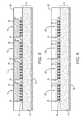
- FIG. 1provides a flow diagram that illustrates an exemplary etching and filling process according to one embodiment of the present disclosure.
- FIGS. 2 through 8illustrate the steps associated with the etching and filling process provided in FIG. 1 .
- FIG. 9illustrates an exemplary application of the present disclosure.
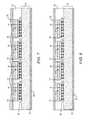
- FIG. 10Ais a first section of a flow diagram that illustrates additional process steps that include a first mold compound used as an underfill and a second mold compound used as an encapsulate combined with a selective etching step that removes the substrates of selected flip chip dies.
- FIG. 10Bis a second section for the flow diagram of FIG. 10A , which illustrates disposing a dielectric layer and applying a third mold compound to fill cavities left by etching substrates of selected flip chip dies.
- FIG. 11is a cross-section view of a flip chip module fabricated using the process provided in FIG. 10A and FIG. 10B .
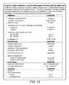
- FIG. 12is a specification table that lists thermal, mechanical, electrical, and physical specifications for an exemplary polymer material that is usable as a mold compound that is in accordance with the present disclosure.
- thermoset polymers and thermoplastic polymersare disclosed as mold compounds in this disclosure.
- Thermoset polymerscross-link together to form an irreversible chemical bond.
- thermoset polymerscannot be melted and re-molded after curing.
- a benefit of thermoset polymersis that they provide relatively high levels of dimensional stability in comparison to thermoplastic polymers. Dimensional stability is desirable for encapsulating interconnections between a flip chip die and a carrier.
- thermoplastic polymerssoften when heated and become more fluid when heated past a plasticization temperature. Once cooled below the plasticization temperature, thermoplastic polymers can be reheated to be re-molded as no chemical bonding takes place like that of thermoset polymers.
- a benefit of thermoplastic polymersis chemical resistance.
- additivessuch as carbon particles and other fillers are usable to provide thermoset polymers with various physical properties. Such fillers are readily mixed with thermoplastic polymers because there are no chemical bonds to interfere with.
- thermoset polymerscan also accommodate some additives and fillers with particular care being taken with regard to ratios and types of additives in comparison to thermoplastic polymers.
- a thinned flip chip diealso referred to as an etched flip chip die
- a flip chip die with an intact semiconductor substrateis one that has not undergone a substrate removal process.
- some etching of a semiconductor substrate to provide via holes and patterningcan occur and the semiconductor substrate would still be considered an intact semiconductor substrate as long as 95% of an original substrate remains after etching.
- FIG. 1provides a flow diagram that illustrates an exemplary etching and filling process according to one embodiment of the present disclosure.
- FIGS. 2-8illustrate the steps associated with the etching and filling process provided in FIG. 1 .
- various types of materialsmay be used for the substrate, the following examples incorporate silicon as the preferred material.
- a plurality of flip chip dies 10are attached on a top surface of a carrier 12 as depicted in FIG. 2 (Step 100 ).
- the carrier of the described embodimentis formed from a laminate, but may also be formed from a wafer level fan out (WLFO) carrier, a lead frame, a ceramic carrier, or the like.
- WLFOwafer level fan out
- each flip chip die 10includes a substrate 14 with approximately 150-500 ⁇ m thickness, a device layer 16 with approximately 4-7 ⁇ m thickness, layer contacts 18 located on a bottom surface of the device layer 16 , and solder interconnections 20 provided on each of the layer contacts 18 .
- the device layer 16may be formed from silicon dioxide, gallium arsenide, gallium nitride, silicon germanium, and the like and includes various devices, such as diodes, transistors, mechanical switches, resonators, and the like.
- the carrier 12includes a carrier body 22 , carrier contacts 24 on a top surface of the carrier 12 and input/output (I/O) pads (not shown) on a bottom surface of the carrier 12 .
- the I/O pads on the bottom surface of the carrier 12may be formed by a ball grid array (BGA) or land grid array (LGA) method and selectively connect to the carrier contacts 24 through any number of vias (not shown).
- BGAball grid array
- LGAland grid array
- the solder interconnections 20 of the flip chip dies 10are used to electrically and physically connect to the carrier contacts 24 of the carrier 12 .
- the backside of the substrate 14 of the plurality of flip chip dies 10will generally be the tallest component after the attaching process.
- the height between the device layer 16 and the carrier body 22often varies from 15-200 ⁇ m.
- a first mold compound 26is then applied over the top surface of the carrier 12 such that the flip chip dies 10 are encapsulated by the first mold compound 26 as illustrated in FIG. 3 (Step 102 ).
- the first mold compound 26may be applied by various procedures, such as sheet molding, overmolding, compression molding, transfer molding, dam fill encapsulation and screen print encapsulation.
- the first mold compound 26is an organic epoxy resin system or the like, such as Hitachi Chemical Electronic Materials GE-100LFC, which can be used as an etchant barrier to protect the flip chip dies 10 against etching chemistries such as KOH, NaOH and ACH.
- a curing process(Step 104 ) is then used to harden the first mold compound.
- a process for etching away substantially the entire substrate 14 of each encapsulated flip chip die 10is provided according to one embodiment of the present disclosure.
- the processbegins by forming a protective coating 28 over the bottom surface of the carrier 12 , as shown in FIG. 4 (Step 106 ).
- the purpose of the protective coating 28is to prevent potential damage to the I/O pads (not shown) on the bottom surface of the carrier 12 in subsequent processing steps.
- the protective coating 28may be a chemical resistant tape or liquid protective coating, which can withstand etching chemistries such as KOH, NaOH and ACH without breakdown.
- a rigid carriercan be sealed on the bottom surface of the carrier 12 as a protective coating 28 to prevent the I/O pads (not shown) on the bottom surface of the carrier 12 from contacting the destructive etchant materials in later etching processes.
- the next process stepis to thin the first mold compound 26 down to expose the back side of the flip chip dies 10 , wherein the only exposed component of the flip chip dies 10 will be the substrate 14 , as shown in FIG. 5 (Step 108 ).
- the thinning proceduremay be done with a mechanical process.
- An alternative process stepwould be to leave the back side of the flip chip dies 10 always exposed during the molding process with the first mold compound 26 .
- a wet/dry etchant chemistrywhich may be KOH, ACH, NaOH or the like, is used to etch away substantially the entire substrate 14 of each flip chip die 10 to provide an etched flip chip die 10 E that has an exposed surface at the bottom of a cavity, as shown in FIG. 6 (Step 110 ).
- etching away substantially the entire substrate 14refers to removal of at least 95% of the entire substrate 14 , and perhaps a portion of the device layer 16 .
- the substrate 14is etched away completely and the device layer 16 is exposed at the bottom of the cavity of each etched flip chip die 10 E.
- a process for filling the remaining cavity of each etched flip chip die 10 Eis provided according to one embodiment of the present disclosure.
- a second mold compound 30is applied to substantially fill the remaining cavity of each etched flip chip die 10 E, as illustrated in FIG. 7 (Step 112 ).
- the second mold compound 30may be applied by various procedures, such as sheet molding, overmolding, compression molding, transfer molding, dam fill encapsulation, and screen print encapsulation.
- the second mold compound 30is a high thermal conductivity mold compound.
- a high thermal conductivity mold compoundCompared to the normal mold compound having 1 Watts per meter Kelvin (W/m ⁇ K) thermal conductivity, a high thermal conductivity mold compound has 2.5 W/m ⁇ K ⁇ 10 W/m ⁇ K or greater thermal conductivity, such as Hitachi Chemical Electronic Materials GE-506HT.
- the second mold compound 30directly contacts the exposed surface of each etched flip chip die 10 E at the bottom of each cavity. If the substrate 14 is removed completely in the etching step (Step 110 ), the second mold compound 30 directly contacts the device layer 16 .
- the second mold compound 30directly contacts the thin layer of substrate 14 .
- the first mold compound 26could be formed from the same material as the second mold compound 30 .
- the first mold compound 26does not have a thermal conductivity requirement in higher performing embodiments.
- a curing process(Step 114 ) is then provided to harden the second mold compound.
- the normal curing temperatureis 175° F. and could be higher or lower depending on which material is used as the second mold compound 30 .
- the top surface of the second mold compound 30is then planarized to ensure each encapsulated etched flip chip die 10 E has a flat top surface as shown in FIG. 8 (Step 116 ).
- a package grinding processmay be used for planarization.
- the protective coating 28 applied over the bottom surface of the carrier 12is removed as illustrated in FIG. 9 (Step 118 ).
- the productcould be marked, singulated and tested as a module (Step 120 ).
- FIG. 10A and FIG. 10Bmake up a flow diagram that illustrates process steps for fabricating an additional embodiment of the present disclosure.
- FIG. 11is a cross-section view of the additional embodiment that is a flip chip module 32 , which is fabricated using the process provided in FIG. 10A and FIG. 10B .
- a plurality of flip chip dies 10are attached onto a top surface of the carrier 12 (Step 200 ).
- Step 200a plurality of flip chip dies 10 are attached onto a top surface of the carrier 12 (Step 200 ).
- the leftmost flip chip die 10includes an integrated passive device (IPD) 34
- the middle flip chip die 10includes a microelectromechanical systems (MEMS) device 36
- the rightmost flip chip die 10includes a complementary metal oxide semiconductor (CMOS) controller 38 .
- the IPD 34typically comprises passive components such as integrated inductors, capacitors, and resistors.
- the MEMS device 36is typically an RF switch that is controlled by the CMOS controller 38 .
- the solder interconnections 20 of the flip chip dies 10are used to electrically and physically connect to the carrier contacts 24 of the carrier 12 . It is to be understood that the MEMS device 36 comprises mechanical parts that move within a cavity under a lid.
- a MEMS RF switch version of MEMS device 36includes a cantilever having a first end attached to an anchor and a second end situated over a conductive pad.
- An actuator plate beneath the cantileveris charged to attract the second end of the cantilever to make contact with the conductive pad to provide a low resistance electrical path between the anchor and the conductive pad.
- charging the actuator platecloses the MEMS RF switch.
- Discharging the actuator plateallows the second end of the cantilever to spring away from the conductive pad, thereby opening the MEMS RF switch and providing nearly infinite resistance to electrical current flow.
- Other types of MEMS devicessuch as MEMS capacitors are also envisioned as MEMS device 36 . Such MEMS devices are well known to those skilled in the art, and are within the scope of this disclosure.
- a first mold compound 40is applied to portions of the top surface of the carrier 12 substantially near each of the plurality of flip chip dies 10 to fill space between the plurality of flip chip dies 10 and the top surface of the carrier 12 (Step 202 ).
- the first mold compound 40is an epoxy resin that has an uncured viscosity of no more than 360 m ⁇ Pas when measured with a cone and plate viscometer. This relatively low viscosity in comparison to encapsulating epoxy resins allows the first mold compound 40 to wick between and around the solder interconnections 20 by capillary action.
- the first mold compound 40is known in industry as a capillary underfill designed to cure in about eight minutes at 130° C. and about five minutes at 150° C.
- the first mold compoundhas a glass transition temperature of 113° C. with a coefficient of thermal expansion of 55 parts per million per ° C. (ppm/° C.) below the glass transition temperature of 113° C.
- An exemplary material for the first mold compound 40is made by Henkel and is marketed under the product number UF3808.
- the first mold compound 40includes an additive powder to increase magnetic permeability.
- Suitable additive powdersinclude fully sintered nickel zinc (Ni—Zn) ferrite, magnesium zinc (Mg—Zn), and manganese (Mn—Zn) nanopowders having magnetic saturations between 45 and 80 electromagnetic units per gram (emu/g).
- the first mold compound 40is either actively or passively cured (Step 204 ). Actively curing the first mold compound 40 is accomplished by exposing the first mold compound 40 to energy such as heat energy, light energy, or chemical energy, depending on the material making up the first mold compound 40 . Examples of adding energy to cure the first mold compound 40 include heating the first mold compound 40 to a predetermined elevated temperature such as 175° F., exposing the first mold compound 40 to ultraviolet (UV) light, or exposing the first mold compound 40 to an activating chemical vapor or spray. Passively curing the first mold compound 40 would allow the first mold compound 40 to cure over time without intervention.
- the first mold compound 40can include additives that enhance thermal properties such as thermal conductivity, electrical properties such as permittivity, and/or magnetic properties such as permeability.
- a second mold compound 42is applied over the top surface of the carrier 12 to encapsulate the plurality of flip chip dies 10 (Step 206 ).
- the second mold compound 42is then passively and/or actively cured (Step 208 ). Actively curing the second mold compound 42 is accomplished by exposing the second mold compound 42 to energy such as heat energy, light energy, or chemical energy depending on the material making up the second mold compound 42 . Passively curing the second mold compound 42 would allow the second mold compound 42 to cure over time without intervention.
- the second mold compound 42can include additives that enhance thermal properties such as thermal conductivity, electrical properties such as permittivity, and/or magnetic properties such as permeability.
- the second mold compound 42does not necessarily include the same additives or the same amount of additives that may be present in the first mold compound 40 . Moreover, the second mold compound 42 does not need to be the same material as the first mold compound 40 . Therefore, the second mold compound 42 may or may not be cured the same way as the first mold compound 40 .
- An exemplary material making up the second mold compound 42is a biphenyl thermoset epoxy manufactured by Hitachi and marketed under the product number GE100-LFCS. In at least one embodiment, the second mold compound 42 and the first mold compound 40 are one in the same. For example, in at least one embodiment, the biphenyl thermoset epoxy would make up both the first mold compound 40 and the second mold compound 42 .
- the processcontinues by forming the protective coating 28 (as shown in FIGS. 4 through 8 ) over the bottom surface of the carrier 12 (Step 210 ).
- the purpose of the protective coating 28is to prevent potential damage to the I/O pads (not shown) on the bottom surface of the carrier 12 in subsequent processing steps.
- the protective coating 28may be a chemical resistant tape or liquid protective coating, which can withstand etching chemistries such as KOH, NaOH, and ACH without breakdown.
- a rigid carriercan be sealed on the bottom surface of the carrier 12 as a protective coating 28 to prevent the I/O pads (not shown) on the bottom surface of the carrier 12 from contacting the destructive etchant materials in later etching processes.
- the next process stepis to thin the first mold compound 40 down to expose the back side of select ones of the plurality of flip chip dies 10 , wherein the only exposed component of the flip chip dies 10 will be the substrate 14 (Step 212 ).
- the substrate 14 of the rightmost one of the flip chip dies 10 having the CMOS controller 38is not exposed because it is lower in height than either of the other ones of the plurality of flip chip dies 10 depicted in FIG. 11 .
- the leftmost one and the middle one of the plurality of the flip chip dies 10are desired to have the substrate 14 removed.
- the thinning proceduremay be done with a mechanical process.
- An alternative process stepwould be to leave the back side of the desired ones of the plurality of flip chip dies 10 always exposed during the molding process that applies the second mold compound 42 .
- Each of the substrates 14 exposed in the previous stepare then etched to provide etched dies 10 E that each have an exposed surface at an etch stop layer 44 that is disposed over each of the IPD 34 and the MEMS device 36 (Step 214 ).
- an etchantreaches the etch stop layer 44 , the etch process inherently stops due to the chemical composition of the etch stop layer 44 .
- the etch stop layer 44is typically a dielectric layer such as a buried oxide (BOX) layer. The etch stop layer 44 is not needed and therefore not disposed over the CMOS controller 38 .
- Step 216An exemplary way to achieve the roughening produced in this step is to employ a wet chemistry etchant such as potassium hydroxide and water (KOH:H 2 O), which causes surface silica spheres that are typically present in the second mold compound 42 to dissolve leaving a pitted surface.
- a wet chemistry etchantsuch as potassium hydroxide and water (KOH:H 2 O)
- KOH:H 2 Opotassium hydroxide and water
- a dielectric layer 46is disposed over both the second mold compound 42 and the exposed surface at the etch stop layer 44 at the bottom of a cavity left by etching the substrate 14 of each of the etched flip chip dies 10 E (Step 218 ).
- the dielectric layer 46provides a moisture barrier that is not provided by the etch stop layer 44 .
- An exemplary material making up etch stop layer 44is silicon nitride SiN.
- the dielectric layer 46can be between 200 ⁇ to 5000 ⁇ thick and is typically between 1000 ⁇ and 2000 ⁇ thick.
- the processcontinues by applying a third mold compound 48 to substantially fill each cavity and directly contact the exposed surface of each of the etched ones of the plurality of flip chip dies 10 (Step 220 ).
- the exposed surfaceis the exposed surface of the dielectric layer 46 .
- the third mold compound 48can be disposed over the entirety of the dielectric layer 46 .
- the third mold compound 48is then passively and/or actively cured (Step 222 ). Actively curing the third mold compound 48 is accomplished by exposing the third mold compound 48 to energy such as heat energy, light energy, or chemical energy depending on the material making up the third mold compound 48 . Passively curing the third mold compound 48 would allow the third mold compound 48 to cure over time without intervention.
- the third mold compound 48can include additives that enhance thermal properties such as thermal conductivity, electrical properties such as permittivity, and/or magnetic properties such as permeability.
- the third mold compound 48does not necessarily include the same additives or the same amount of additives that may be present in either the first mold compound 40 or the second mold compound 42 .
- the third mold compound 48does not need to be the same material as either the first mold compound 40 or the second mold compound 42 . Therefore, the third mold compound 48 may or may not be cured the same way as either the first mold compound 40 or the second mold compound 42 .
- a top surface of the third mold compound 48is planarized to ensure that each encapsulated etched flip chip die 10 E has a flat top surface as shown in FIG. 11 (Step 224 ).
- a package grinding processmay be used for planarization.
- the protective coating 28 applied over the bottom surface of the carrier 12is removed as illustrated in FIG. 9 (Step 226 ).
- the flip chip module 32is marked, singulated and tested (Step 228 ).
- FIG. 12is a specification table that lists thermal, mechanical, electrical, and physical specifications for an exemplary polymer material that is usable as a mold compound that is in accordance with the present disclosure.
- this exemplary polymer materialis a thermoplastic that is usable as the third mold compound.
- the second mold compound and the third mold compoundare one in the same and comprise this exemplary polymer material.
- the exemplary polymer material specified in the specification table of FIG. 12is made by Cool Polymers® and is sold under the label “CoolPoly® D5506 Thermally Conductive Liquid Crystalline Polymer (LCP).” It is to be understood that the specification table of FIG. 12 only provides exemplary specifications and that a variety of mechanical and physical properties are available within the scope of the present disclosure. Moreover, the quantitative values for the thermal and electrical properties provided in the table of FIG. 12 only represent exemplary values that are within the range of thermal and electrical properties already discussed in the above disclosure.
Landscapes
- Engineering & Computer Science (AREA)
- Microelectronics & Electronic Packaging (AREA)
- Power Engineering (AREA)
- Computer Hardware Design (AREA)
- Physics & Mathematics (AREA)
- Condensed Matter Physics & Semiconductors (AREA)
- General Physics & Mathematics (AREA)
- Chemical & Material Sciences (AREA)
- Materials Engineering (AREA)
- Manufacturing & Machinery (AREA)
- Encapsulation Of And Coatings For Semiconductor Or Solid State Devices (AREA)
- Structures Or Materials For Encapsulating Or Coating Semiconductor Devices Or Solid State Devices (AREA)
Abstract
Description
This application claims priority to U.S. provisional patent applications No. 62/202,207, filed Aug. 7, 2016, and No. 62/202,967, filed Aug. 10, 2015.
This application is a continuation-in-part of and claims priority to U.S. patent application Ser. No. 14/959,129, filed Dec. 4, 2015, now U.S. Pat. No. 9,613,831, entitled “ENCAPSULATED DIES WITH ENHANCED THERMAL PERFORMANCE,” which claims priority to U.S. provisional patent application No. 62/138,177, filed Mar. 25, 2015.
All of the applications listed above are hereby incorporated herein by reference in their entireties.
The present disclosure relates to a packaging process, and more particularly to a packaging process to enhance thermal performance of encapsulated flip chip dies.
With the current popularity of portable communication devices and developed semiconductor fabrication technology, high speed and high performance transistors are more densely integrated on semiconductor dies. Consequently, the amount of heat generated by the semiconductor dies will increase significantly due to the large number of transistors integrated on the semiconductor dies, the large amount of power passing through the transistors, and the high operation speed of the transistors. Accordingly, it is desirable to package the semiconductor dies in a configuration for better heat dissipation.
Flip chip assembly technology is widely utilized in semiconductor packaging due to its preferable solder interconnection between flip chip dies and laminate, which eliminates the space needed for wire bonding and die surface area of a package and essentially reduces the overall size of the package. In addition, the elimination of wire connections and implementation of a shorter electrical path from the flip chip die to the laminate reduces undesired inductance and capacitance.
In flip chip assembly, mold compounds, formulated from epoxy resins containing silica particulates, are used to encapsulate and underfill flip chip dies to protect the dies against damage from the outside environment. Some of the mold compounds can be used as a barrier withstanding chemistries such as potassium hydroxide (KOH), sodium hydroxide (NaOH), and acetylcholine (ACH) without breakdown; while some of the mold compounds having good thermal conductive features can be used for heat dissipation of dies.
To accommodate the increased heat generation of high performance dies and to utilize the advantages of flip chip assembly, it is therefore an object of the present disclosure to provide a method to package flip chip dies in a configuration for better heat dissipation. In addition, there is also a need to enhance the thermal performance of encapsulated flip chip dies without increasing the package size.
A flip chip module having at least one flip chip die is disclosed. The flip chip module includes a carrier having a top surface with a first mold compound residing on the top surface. A first mold compound is disposed on the top surface of the carrier. A first thinned flip chip die resides over a first portion of the first mold compound with interconnects extending through the first portion to the top surface wherein the first portion of the mold compound fills a region between the first flip chip die and the top surface. A second mold compound resides over the substrate in contact with the first mold compound and provides a first recess over the first flip chip die wherein the first recess extends to a first die surface of the first flip chip die. A third mold compound resides in the first recess and covers an exposed surface of the flip chip die.
Those skilled in the art will appreciate the scope of the disclosure and realize additional aspects thereof after reading the following detailed description in association with the accompanying drawings.
The accompanying drawings incorporated in and forming a part of this specification illustrate several aspects of the disclosure, and together with the description serve to explain the principles of the disclosure.
The embodiments set forth below represent the necessary information to enable those skilled in the art to practice the disclosure and illustrate the best mode of practicing the disclosure. Upon reading the following description in light of the accompanying drawings, those skilled in the art will understand the concepts of the disclosure and will recognize applications of these concepts not particularly addressed herein. It should be understood that these concepts and applications fall within the scope of the disclosure and the accompanying claims.
It will be understood that, although the terms first, second, etc. may be used herein to describe various elements, these elements should not be limited by these terms. These terms are only used to distinguish one element from another. For example, a first element could be termed a second element, and, similarly, a second element could be termed a first element, without departing from the scope of the present disclosure. As used herein, the term “and/or” includes any and all combinations of one or more of the associated listed items.
It will be understood that when an element such as a layer, region, or substrate is referred to as being “on” or extending “onto” another element, it can be directly on or extend directly onto the other element or intervening elements may also be present. In contrast, when an element is referred to as being “directly on” or extending “directly onto” another element, there are no intervening elements present. Likewise, it will be understood that when an element such as a layer, region, or substrate is referred to as being “over” or extending “over” another element, it can be directly over or extend directly over the other element or intervening elements may also be present. In contrast, when an element is referred to as being “directly over” or extending “directly over” another element, there are no intervening elements present. It will also be understood that when an element is referred to as being “connected” or “coupled” to another element, it can be directly connected or coupled to the other element or intervening elements may be present. In contrast, when an element is referred to as being “directly connected” or “directly coupled” to another element, there are no intervening elements present.
Relative terms such as “below” or “above” or “upper” or “lower” or “horizontal” or “vertical” may be used herein to describe a relationship of one element, layer, or region to another element, layer, or region as illustrated in the Figures. It will be understood that these terms and those discussed above are intended to encompass different orientations of the device in addition to the orientation depicted in the Figures.
The terminology used herein is for the purpose of describing particular embodiments only and is not intended to be limiting of the disclosure. As used herein, the singular forms “a,” “an,” and “the” are intended to include the plural forms as well, unless the context clearly indicates otherwise. It will be further understood that the terms “comprises,” “comprising,” “includes,” and/or “including” when used herein specify the presence of stated features, integers, steps, operations, elements, and/or components, but do not preclude the presence or addition of one or more other features, integers, steps, operations, elements, components, and/or groups thereof.
Unless otherwise defined, all terms (including technical and scientific terms) used herein have the same meaning as commonly understood by one of ordinary skill in the art to which this disclosure belongs. It will be further understood that terms used herein should be interpreted as having a meaning that is consistent with their meaning in the context of this specification and the relevant art and will not be interpreted in an idealized or overly formal sense unless expressly so defined herein.
Both thermoset polymers and thermoplastic polymers are disclosed as mold compounds in this disclosure. Thermoset polymers cross-link together to form an irreversible chemical bond. As such, thermoset polymers cannot be melted and re-molded after curing. A benefit of thermoset polymers is that they provide relatively high levels of dimensional stability in comparison to thermoplastic polymers. Dimensional stability is desirable for encapsulating interconnections between a flip chip die and a carrier.
In contrast, thermoplastic polymers soften when heated and become more fluid when heated past a plasticization temperature. Once cooled below the plasticization temperature, thermoplastic polymers can be reheated to be re-molded as no chemical bonding takes place like that of thermoset polymers. A benefit of thermoplastic polymers is chemical resistance. Another benefit is that additives such as carbon particles and other fillers are usable to provide thermoset polymers with various physical properties. Such fillers are readily mixed with thermoplastic polymers because there are no chemical bonds to interfere with. However, it is to be understood that thermoset polymers can also accommodate some additives and fillers with particular care being taken with regard to ratios and types of additives in comparison to thermoplastic polymers.
For the purpose of this disclosure a thinned flip chip die, also referred to as an etched flip chip die, is one with at least 95% of a semiconductor substrate removed by chemical etching, mechanical grinding, or a combination of chemical etching and mechanical grinding, or peeling. In contrast, a flip chip die with an intact semiconductor substrate is one that has not undergone a substrate removal process. However, it is to be understood that some etching of a semiconductor substrate to provide via holes and patterning can occur and the semiconductor substrate would still be considered an intact semiconductor substrate as long as 95% of an original substrate remains after etching.
The present disclosure relates to a method to enhance the thermal performance of encapsulated flip chip dies.FIG. 1 provides a flow diagram that illustrates an exemplary etching and filling process according to one embodiment of the present disclosure.FIGS. 2-8 illustrate the steps associated with the etching and filling process provided inFIG. 1 . Although various types of materials may be used for the substrate, the following examples incorporate silicon as the preferred material. Initially, a plurality of flip chip dies10 are attached on a top surface of acarrier 12 as depicted inFIG. 2 (Step100). The carrier of the described embodiment is formed from a laminate, but may also be formed from a wafer level fan out (WLFO) carrier, a lead frame, a ceramic carrier, or the like. For the purpose of this illustration, each flip chip die10 includes asubstrate 14 with approximately 150-500 μm thickness, adevice layer 16 with approximately 4-7 μm thickness,layer contacts 18 located on a bottom surface of thedevice layer 16, andsolder interconnections 20 provided on each of thelayer contacts 18. Thedevice layer 16 may be formed from silicon dioxide, gallium arsenide, gallium nitride, silicon germanium, and the like and includes various devices, such as diodes, transistors, mechanical switches, resonators, and the like. Thecarrier 12 includes acarrier body 22,carrier contacts 24 on a top surface of thecarrier 12 and input/output (I/O) pads (not shown) on a bottom surface of thecarrier 12. The I/O pads on the bottom surface of thecarrier 12 may be formed by a ball grid array (BGA) or land grid array (LGA) method and selectively connect to thecarrier contacts 24 through any number of vias (not shown). Thesolder interconnections 20 of the flip chip dies10 are used to electrically and physically connect to thecarrier contacts 24 of thecarrier 12. As such, the backside of thesubstrate 14 of the plurality of flip chip dies10 will generally be the tallest component after the attaching process. The height between thedevice layer 16 and thecarrier body 22 often varies from 15-200 μm.
Afirst mold compound 26 is then applied over the top surface of thecarrier 12 such that the flip chip dies10 are encapsulated by thefirst mold compound 26 as illustrated inFIG. 3 (Step102). Thefirst mold compound 26 may be applied by various procedures, such as sheet molding, overmolding, compression molding, transfer molding, dam fill encapsulation and screen print encapsulation. Thefirst mold compound 26 is an organic epoxy resin system or the like, such as Hitachi Chemical Electronic Materials GE-100LFC, which can be used as an etchant barrier to protect the flip chip dies10 against etching chemistries such as KOH, NaOH and ACH. A curing process (Step104) is then used to harden the first mold compound.
With reference toFIGS. 4 through 6 , a process for etching away substantially theentire substrate 14 of each encapsulated flip chip die10 is provided according to one embodiment of the present disclosure. The process begins by forming aprotective coating 28 over the bottom surface of thecarrier 12, as shown inFIG. 4 (Step106). The purpose of theprotective coating 28 is to prevent potential damage to the I/O pads (not shown) on the bottom surface of thecarrier 12 in subsequent processing steps. Theprotective coating 28 may be a chemical resistant tape or liquid protective coating, which can withstand etching chemistries such as KOH, NaOH and ACH without breakdown. Alternatively, a rigid carrier can be sealed on the bottom surface of thecarrier 12 as aprotective coating 28 to prevent the I/O pads (not shown) on the bottom surface of thecarrier 12 from contacting the destructive etchant materials in later etching processes.
The next process step is to thin thefirst mold compound 26 down to expose the back side of the flip chip dies10, wherein the only exposed component of the flip chip dies10 will be thesubstrate 14, as shown inFIG. 5 (Step108). The thinning procedure may be done with a mechanical process. An alternative process step would be to leave the back side of the flip chip dies10 always exposed during the molding process with thefirst mold compound 26.
Next, a wet/dry etchant chemistry, which may be KOH, ACH, NaOH or the like, is used to etch away substantially theentire substrate 14 of each flip chip die10 to provide an etched flip chip die10E that has an exposed surface at the bottom of a cavity, as shown inFIG. 6 (Step110). Herein, etching away substantially theentire substrate 14 refers to removal of at least 95% of theentire substrate 14, and perhaps a portion of thedevice layer 16. As such, in some applications, there is a thin layer of thesubstrate 14 left at the bottom of the cavity of each etched flip chip die10E, which covers thedevice layer 16, to protect the devices located on thedevice layer 16. For other cases, thesubstrate 14 is etched away completely and thedevice layer 16 is exposed at the bottom of the cavity of each etched flip chip die10E.
With reference toFIGS. 7 through 8 , a process for filling the remaining cavity of each etched flip chip die10E is provided according to one embodiment of the present disclosure. After the etching step is done, asecond mold compound 30 is applied to substantially fill the remaining cavity of each etched flip chip die10E, as illustrated inFIG. 7 (Step112). Thesecond mold compound 30 may be applied by various procedures, such as sheet molding, overmolding, compression molding, transfer molding, dam fill encapsulation, and screen print encapsulation. Thesecond mold compound 30 is a high thermal conductivity mold compound. Compared to the normal mold compound having 1 Watts per meter Kelvin (W/m·K) thermal conductivity, a high thermal conductivity mold compound has 2.5 W/m·K˜10 W/m·K or greater thermal conductivity, such as Hitachi Chemical Electronic Materials GE-506HT. The higher the thermal conductivity, the better the heat dissipation performance of the encapsulated etched flip chip dies10E. Additionally, thesecond mold compound 30 directly contacts the exposed surface of each etched flip chip die10E at the bottom of each cavity. If thesubstrate 14 is removed completely in the etching step (Step110), thesecond mold compound 30 directly contacts thedevice layer 16. If there is a thin layer ofsubstrate 14 left in the etching step (Step110), thesecond mold compound 30 directly contacts the thin layer ofsubstrate 14. Notably, thefirst mold compound 26 could be formed from the same material as thesecond mold compound 30. However, unlike thesecond mold compound 30, thefirst mold compound 26 does not have a thermal conductivity requirement in higher performing embodiments. A curing process (Step114) is then provided to harden the second mold compound. The normal curing temperature is 175° F. and could be higher or lower depending on which material is used as thesecond mold compound 30.
The top surface of thesecond mold compound 30 is then planarized to ensure each encapsulated etched flip chip die10E has a flat top surface as shown inFIG. 8 (Step116). A package grinding process may be used for planarization. Next, theprotective coating 28 applied over the bottom surface of thecarrier 12 is removed as illustrated inFIG. 9 (Step118). Lastly, the product could be marked, singulated and tested as a module (Step120).
Next, afirst mold compound 40 is applied to portions of the top surface of thecarrier 12 substantially near each of the plurality of flip chip dies10 to fill space between the plurality of flip chip dies10 and the top surface of the carrier12 (Step202). Thefirst mold compound 40 is an epoxy resin that has an uncured viscosity of no more than 360 m·Pas when measured with a cone and plate viscometer. This relatively low viscosity in comparison to encapsulating epoxy resins allows thefirst mold compound 40 to wick between and around thesolder interconnections 20 by capillary action. As such, thefirst mold compound 40 is known in industry as a capillary underfill designed to cure in about eight minutes at 130° C. and about five minutes at 150° C. to minimize stress on thesolder interconnections 20. In one embodiment, the first mold compound has a glass transition temperature of 113° C. with a coefficient of thermal expansion of 55 parts per million per ° C. (ppm/° C.) below the glass transition temperature of 113° C. An exemplary material for thefirst mold compound 40 is made by Henkel and is marketed under the product number UF3808.
In one embodiment, thefirst mold compound 40 includes an additive powder to increase magnetic permeability. Suitable additive powders include fully sintered nickel zinc (Ni—Zn) ferrite, magnesium zinc (Mg—Zn), and manganese (Mn—Zn) nanopowders having magnetic saturations between 45 and 80 electromagnetic units per gram (emu/g).
Thefirst mold compound 40 is either actively or passively cured (Step204). Actively curing thefirst mold compound 40 is accomplished by exposing thefirst mold compound 40 to energy such as heat energy, light energy, or chemical energy, depending on the material making up thefirst mold compound 40. Examples of adding energy to cure thefirst mold compound 40 include heating thefirst mold compound 40 to a predetermined elevated temperature such as 175° F., exposing thefirst mold compound 40 to ultraviolet (UV) light, or exposing thefirst mold compound 40 to an activating chemical vapor or spray. Passively curing thefirst mold compound 40 would allow thefirst mold compound 40 to cure over time without intervention. Thefirst mold compound 40 can include additives that enhance thermal properties such as thermal conductivity, electrical properties such as permittivity, and/or magnetic properties such as permeability.
Once thefirst mold compound 40 is cured, asecond mold compound 42 is applied over the top surface of thecarrier 12 to encapsulate the plurality of flip chip dies10 (Step206). Thesecond mold compound 42 is then passively and/or actively cured (Step208). Actively curing thesecond mold compound 42 is accomplished by exposing thesecond mold compound 42 to energy such as heat energy, light energy, or chemical energy depending on the material making up thesecond mold compound 42. Passively curing thesecond mold compound 42 would allow thesecond mold compound 42 to cure over time without intervention. Thesecond mold compound 42 can include additives that enhance thermal properties such as thermal conductivity, electrical properties such as permittivity, and/or magnetic properties such as permeability. However, it is to be understood that thesecond mold compound 42 does not necessarily include the same additives or the same amount of additives that may be present in thefirst mold compound 40. Moreover, thesecond mold compound 42 does not need to be the same material as thefirst mold compound 40. Therefore, thesecond mold compound 42 may or may not be cured the same way as thefirst mold compound 40. An exemplary material making up thesecond mold compound 42 is a biphenyl thermoset epoxy manufactured by Hitachi and marketed under the product number GE100-LFCS. In at least one embodiment, thesecond mold compound 42 and thefirst mold compound 40 are one in the same. For example, in at least one embodiment, the biphenyl thermoset epoxy would make up both thefirst mold compound 40 and thesecond mold compound 42.
The process continues by forming the protective coating28 (as shown inFIGS. 4 through 8 ) over the bottom surface of the carrier12 (Step210). The purpose of theprotective coating 28 is to prevent potential damage to the I/O pads (not shown) on the bottom surface of thecarrier 12 in subsequent processing steps. Theprotective coating 28 may be a chemical resistant tape or liquid protective coating, which can withstand etching chemistries such as KOH, NaOH, and ACH without breakdown. Alternatively, a rigid carrier can be sealed on the bottom surface of thecarrier 12 as aprotective coating 28 to prevent the I/O pads (not shown) on the bottom surface of thecarrier 12 from contacting the destructive etchant materials in later etching processes.
The next process step is to thin thefirst mold compound 40 down to expose the back side of select ones of the plurality of flip chip dies10, wherein the only exposed component of the flip chip dies10 will be the substrate14 (Step212). As depicted inFIG. 11 , thesubstrate 14 of the rightmost one of the flip chip dies10 having theCMOS controller 38, is not exposed because it is lower in height than either of the other ones of the plurality of flip chip dies10 depicted inFIG. 11 . In this exemplary embodiment, the leftmost one and the middle one of the plurality of the flip chip dies10 are desired to have thesubstrate 14 removed. The thinning procedure may be done with a mechanical process. An alternative process step would be to leave the back side of the desired ones of the plurality of flip chip dies10 always exposed during the molding process that applies thesecond mold compound 42.
Each of thesubstrates 14 exposed in the previous step are then etched to provide etched dies10E that each have an exposed surface at anetch stop layer 44 that is disposed over each of theIPD 34 and the MEMS device36 (Step214). Once an etchant reaches theetch stop layer 44, the etch process inherently stops due to the chemical composition of theetch stop layer 44. Theetch stop layer 44 is typically a dielectric layer such as a buried oxide (BOX) layer. Theetch stop layer 44 is not needed and therefore not disposed over theCMOS controller 38.
Turning now toFIG. 10B while keepingFIG. 11 in view, the process continues by using an etchant to roughen the surface of the second mold compound42 (Step216). An exemplary way to achieve the roughening produced in this step is to employ a wet chemistry etchant such as potassium hydroxide and water (KOH:H2O), which causes surface silica spheres that are typically present in thesecond mold compound 42 to dissolve leaving a pitted surface. The now pitted surface of thesecond mold compound 42 provides a substantial enhancement in adhesion of a subsequently applied or disposed material.
Next, adielectric layer 46 is disposed over both thesecond mold compound 42 and the exposed surface at theetch stop layer 44 at the bottom of a cavity left by etching thesubstrate 14 of each of the etched flip chip dies10E (Step218). Thedielectric layer 46 provides a moisture barrier that is not provided by theetch stop layer 44. An exemplary material making upetch stop layer 44 is silicon nitride SiN. Thedielectric layer 46 can be between 200 Å to 5000 Å thick and is typically between 1000 Å and 2000 Å thick.
The process continues by applying athird mold compound 48 to substantially fill each cavity and directly contact the exposed surface of each of the etched ones of the plurality of flip chip dies10 (Step220). In this exemplary embodiment, the exposed surface is the exposed surface of thedielectric layer 46. Also, as shown in the exemplary embodiment ofFIG. 11 , thethird mold compound 48 can be disposed over the entirety of thedielectric layer 46.
Thethird mold compound 48 is then passively and/or actively cured (Step222). Actively curing thethird mold compound 48 is accomplished by exposing thethird mold compound 48 to energy such as heat energy, light energy, or chemical energy depending on the material making up thethird mold compound 48. Passively curing thethird mold compound 48 would allow thethird mold compound 48 to cure over time without intervention. Thethird mold compound 48 can include additives that enhance thermal properties such as thermal conductivity, electrical properties such as permittivity, and/or magnetic properties such as permeability. However, it is to be understood that thethird mold compound 48 does not necessarily include the same additives or the same amount of additives that may be present in either thefirst mold compound 40 or thesecond mold compound 42. Moreover, thethird mold compound 48 does not need to be the same material as either thefirst mold compound 40 or thesecond mold compound 42. Therefore, thethird mold compound 48 may or may not be cured the same way as either thefirst mold compound 40 or thesecond mold compound 42.
Once thethird mold compound 48 is cured, a top surface of thethird mold compound 48 is planarized to ensure that each encapsulated etched flip chip die10E has a flat top surface as shown inFIG. 11 (Step224). A package grinding process may be used for planarization. Next, theprotective coating 28 applied over the bottom surface of thecarrier 12 is removed as illustrated inFIG. 9 (Step226). Lastly, theflip chip module 32 is marked, singulated and tested (Step228).
The exemplary polymer material specified in the specification table ofFIG. 12 is made by Cool Polymers® and is sold under the label “CoolPoly® D5506 Thermally Conductive Liquid Crystalline Polymer (LCP).” It is to be understood that the specification table ofFIG. 12 only provides exemplary specifications and that a variety of mechanical and physical properties are available within the scope of the present disclosure. Moreover, the quantitative values for the thermal and electrical properties provided in the table ofFIG. 12 only represent exemplary values that are within the range of thermal and electrical properties already discussed in the above disclosure.
Those skilled in the art will recognize improvements and modifications to the embodiments of the present disclosure. All such improvements and modifications are considered within the scope of the concepts disclosed herein and the claims that follow.
Claims (25)
1. A flip chip module comprising:
a carrier having a top surface;
a first mold compound residing on the top surface;
a first thinned flip chip die residing over a first portion of the first mold compound and having a first set of interconnects extending through the first portion of the first mold compound to the top surface wherein the first portion of the first mold compound fills a region between the first thinned flip chip die and the top surface;
a second mold compound residing over the carrier and in contact with the first mold compound and providing a first recess over the first thinned flip chip die wherein the first recess extends to a first die surface of the first thinned flip chip die; and
a third mold compound residing in the first recess and covering a first exposed surface of the first thinned flip chip die, wherein the first thinned flip chip die comprises a first layer with no substrate over the first layer such that the first die surface of the first thinned flip chip die in contact with the third mold compound is a top surface of the first layer.
2. The flip chip module ofclaim 1 further comprising a second thinned flip chip die residing over a second portion of the first mold compound and having a second set of interconnects extending through the second portion to the top surface wherein:
the second portion of the first mold compound fills a region between the second thinned flip chip die and the top surface;
the second mold compound provides a second recess over the second thinned flip chip die such that the second recess extends to a second exposed surface of the second thinned flip chip die; and
the third mold compound resides in the second recess and covers the second exposed surface of the second thinned flip chip die.
3. The flip chip module ofclaim 2 wherein the first thinned flip chip die provides a microelectromechanical systems (MEMS) component and the second thinned flip chip die does not provide a MEMS component.
4. The flip chip module ofclaim 2 wherein the first thinned flip chip die provides an integrated passive device (IPD) and the second thinned flip chip die does not provide an IPD.
5. The flip chip module ofclaim 1 further comprising an intact flip chip die having an intact semiconductor substrate, the intact flip chip die residing over a second portion of the first mold compound and having a second set of interconnects extending through the first portion to the top surface wherein:
the second portion of the first mold compound fills a region between the intact flip chip die and the top surface;
the second mold compound covers the intact semiconductor substrate of the intact flip chip die; and
the third mold compound covers an exposed surface of the second mold compound.
6. The flip chip module ofclaim 5 wherein the first thinned flip chip die is a MEMS device and the intact flip chip die is a complementary metal oxide semiconductor (CMOS) controller.
7. The flip chip module ofclaim 1 wherein the first mold compound, and the second mold compound, and the third mold compound are not the same with each having different physical properties.
8. The flip chip module ofclaim 7 wherein the first mold compound includes a ferrite nanopowder to provide magnetic permeability, the second mold compound includes a filler to provide mechanical strength, and the third mold compound includes a thermally conductive additive to provide thermal conductance through the third mold compound.
9. The flip chip module ofclaim 1 wherein the first mold compound and the second mold compound are both thermoset polymers with the second mold compound being harder than the first mold compound.
10. The flip chip module ofclaim 1 wherein the second mold compound is a thermoset polymer and the third mold compound is a thermoplastic polymer.
11. The flip chip module ofclaim 1 wherein the first mold compound and the second mold compound are the same.
12. The flip chip module ofclaim 1 wherein the second mold compound and the third mold compound are the same.
13. The flip chip module ofclaim 1 wherein the second mold compound has an etched surface to promote adhesion with the third mold compound.
14. The flip chip module ofclaim 1 wherein the first exposed surface is the surface of an etch stop layer comprising buried oxide (BOX).
15. The flip chip module ofclaim 1 further including a dielectric layer disposed over a top surface of the second mold compound and the first die surface of the first thinned flip chip die.
16. The flip chip module ofclaim 15 wherein the dielectric layer is a silicon nitride (SiN) layer.
17. The flip chip module ofclaim 1 wherein the third mold compound has a thermal conductivity greater than 2.5 W/m·K and an electrical resistivity greater than 103Ohm-cm.
18. A method for fabricating a flip chip module comprising:
providing a carrier having a top surface;
attaching a flip chip die to the top surface of the carrier by way of interconnects that extend from the flip chip die to the top surface of the carrier;
filling space between the flip chip die and the top surface of the carrier with a first mold compound;
applying a second mold compound onto the top surface of the carrier to encapsulate the flip chip die;
thinning the second mold compound to expose a substrate of the flip chip die;
etching the substrate of the flip chip die such that none of the substrate remains to provide a thinned flip chip die having an exposed surface at the bottom of a cavity; and
applying a third mold compound to substantially fill the cavity of the thinned flip chip die.
19. The method for fabricating the flip chip module ofclaim 18 further including disposing a dielectric layer over the exposed surface at the bottom of the cavity before applying the third mold compound.
20. The method for fabricating the flip chip module ofclaim 19 wherein the exposed surface at the bottom of the cavity is a surface of an etch stop layer made of BOX and the dielectric layer is made of SiN.
21. The method for fabricating the flip chip module ofclaim 18 further including roughening a top surface of the second mold compound before applying the third mold compound.
22. The method for fabricating the flip chip module ofclaim 18 wherein the first mold compound is an epoxy resin that has an uncured viscosity of no more than 360 mPa·s when measured with a cone and plate viscometer.
23. The method for fabricating the flip chip module ofclaim 18 wherein the first mold compound and the second mold compound are both epoxy resins with the second mold compound being harder than the first.
24. The method for fabricating the flip chip module ofclaim 18 wherein the second mold compound is a thermoset polymer and the third mold compound is a thermoplastic with a thermal conductivity greater than 2.5 W/m·K and an electrical resistivity greater than 103Ohm-cm.
25. A flip chip module comprising:
a carrier having a top surface;
a first mold compound residing on the top surface;
a first thinned flip chip die residing over a first portion of the first mold compound and having a first set of interconnects extending through the first portion of the first mold compound to the top surface wherein the first portion of the first mold compound fills a region between the first thinned flip chip die and the top surface;
a second mold compound residing over the carrier and in contact with the first mold compound and extending to a first die surface of the first thinned flip chip die; and
a third mold compound covering a first exposed surface of the first thinned flip chip die, wherein the first thinned flip chip die comprises a first layer with no substrate over the first layer, such that the first die surface of the first thinned flip chip die in contact with the third mold compound is a top surface of the first layer.
Priority Applications (1)
| Application Number | Priority Date | Filing Date | Title |
|---|---|---|---|
| US15/229,780US9960145B2 (en) | 2015-03-25 | 2016-08-05 | Flip chip module with enhanced properties |
Applications Claiming Priority (5)
| Application Number | Priority Date | Filing Date | Title |
|---|---|---|---|
| US201562138177P | 2015-03-25 | 2015-03-25 | |
| US201562202207P | 2015-08-07 | 2015-08-07 | |
| US201562202967P | 2015-08-10 | 2015-08-10 | |
| US14/959,129US9613831B2 (en) | 2015-03-25 | 2015-12-04 | Encapsulated dies with enhanced thermal performance |
| US15/229,780US9960145B2 (en) | 2015-03-25 | 2016-08-05 | Flip chip module with enhanced properties |
Related Parent Applications (1)
| Application Number | Title | Priority Date | Filing Date |
|---|---|---|---|
| US14/959,129Continuation-In-PartUS9613831B2 (en) | 2015-03-25 | 2015-12-04 | Encapsulated dies with enhanced thermal performance |
Publications (2)
| Publication Number | Publication Date |
|---|---|
| US20160343592A1 US20160343592A1 (en) | 2016-11-24 |
| US9960145B2true US9960145B2 (en) | 2018-05-01 |
Family
ID=57325653
Family Applications (1)
| Application Number | Title | Priority Date | Filing Date |
|---|---|---|---|
| US15/229,780ActiveUS9960145B2 (en) | 2015-03-25 | 2016-08-05 | Flip chip module with enhanced properties |
Country Status (1)
| Country | Link |
|---|---|
| US (1) | US9960145B2 (en) |
Cited By (10)
| Publication number | Priority date | Publication date | Assignee | Title |
|---|---|---|---|---|
| US10510694B2 (en)* | 2018-04-18 | 2019-12-17 | Analog Devices, Inc. | Radio frequency communication systems |
| US10658324B2 (en)* | 2015-10-09 | 2020-05-19 | Mitsubishi Electric Corporation | Semiconductor device |
| US10756025B2 (en)* | 2016-10-24 | 2020-08-25 | Advanced Semiconductor Engineering, Inc. | Semiconductor package device and method of manufacturing the same |
| US20210082869A1 (en)* | 2018-09-04 | 2021-03-18 | Ningbo Semiconductor International Corporation | Wafer-level package structure |
| US20210378106A1 (en)* | 2020-05-29 | 2021-12-02 | Google Llc | Methods And Heat Distribution Devices For Thermal Management Of Chip Assemblies |
| US11302609B2 (en) | 2020-08-31 | 2022-04-12 | Nxp Usa, Inc. | Radio frequency power dies having flip-chip architectures and power amplifier modules containing the same |
| US11387169B2 (en) | 2020-08-04 | 2022-07-12 | Nxp Usa, Inc. | Transistor with I/O ports in an active area of the transistor |
| US11502026B2 (en) | 2020-10-12 | 2022-11-15 | Nxp Usa, Inc. | Transistor with flip-chip topology and power amplifier containing same |
| US11587852B2 (en) | 2020-10-12 | 2023-02-21 | Nxp Usa, Inc. | Power amplifier modules with flip-chip and non-flip-chip power transistor dies |
| US11948855B1 (en) | 2019-09-27 | 2024-04-02 | Rockwell Collins, Inc. | Integrated circuit (IC) package with cantilever multi-chip module (MCM) heat spreader |
Families Citing this family (44)
| Publication number | Priority date | Publication date | Assignee | Title |
|---|---|---|---|---|
| US9812350B2 (en) | 2013-03-06 | 2017-11-07 | Qorvo Us, Inc. | Method of manufacture for a silicon-on-plastic semiconductor device with interfacial adhesion layer |
| US10085352B2 (en)* | 2014-10-01 | 2018-09-25 | Qorvo Us, Inc. | Method for manufacturing an integrated circuit package |
| US9530709B2 (en) | 2014-11-03 | 2016-12-27 | Qorvo Us, Inc. | Methods of manufacturing a printed circuit module having a semiconductor device with a protective layer in place of a low-resistivity handle layer |
| US20160343604A1 (en) | 2015-05-22 | 2016-11-24 | Rf Micro Devices, Inc. | Substrate structure with embedded layer for post-processing silicon handle elimination |
| US10090262B2 (en)* | 2016-05-09 | 2018-10-02 | Qorvo Us, Inc. | Microelectronics package with inductive element and magnetically enhanced mold compound component |
| US10784149B2 (en) | 2016-05-20 | 2020-09-22 | Qorvo Us, Inc. | Air-cavity module with enhanced device isolation |
| US10773952B2 (en) | 2016-05-20 | 2020-09-15 | Qorvo Us, Inc. | Wafer-level package with enhanced performance |
| US10103080B2 (en) | 2016-06-10 | 2018-10-16 | Qorvo Us, Inc. | Thermally enhanced semiconductor package with thermal additive and process for making the same |
| US10186499B2 (en)* | 2016-06-30 | 2019-01-22 | Intel IP Corporation | Integrated circuit package assemblies including a chip recess |
| US10079196B2 (en) | 2016-07-18 | 2018-09-18 | Qorvo Us, Inc. | Thermally enhanced semiconductor package having field effect transistors with back-gate feature |
| EP3497717A1 (en)* | 2016-08-12 | 2019-06-19 | Qorvo Us, Inc. | Wafer-level package with enhanced performance |
| JP7035014B2 (en) | 2016-08-12 | 2022-03-14 | コーボ ユーエス,インコーポレイティド | Wafer level package with enhanced performance |
| WO2018031999A1 (en) | 2016-08-12 | 2018-02-15 | Qorvo Us, Inc. | Wafer-level package with enhanced performance |
| US10109502B2 (en) | 2016-09-12 | 2018-10-23 | Qorvo Us, Inc. | Semiconductor package with reduced parasitic coupling effects and process for making the same |
| US10090339B2 (en) | 2016-10-21 | 2018-10-02 | Qorvo Us, Inc. | Radio frequency (RF) switch |
| US10749518B2 (en) | 2016-11-18 | 2020-08-18 | Qorvo Us, Inc. | Stacked field-effect transistor switch |
| US10068831B2 (en) | 2016-12-09 | 2018-09-04 | Qorvo Us, Inc. | Thermally enhanced semiconductor package and process for making the same |
| US10755992B2 (en) | 2017-07-06 | 2020-08-25 | Qorvo Us, Inc. | Wafer-level packaging for enhanced performance |
| US10366972B2 (en) | 2017-09-05 | 2019-07-30 | Qorvo Us, Inc. | Microelectronics package with self-aligned stacked-die assembly |
| US10784233B2 (en) | 2017-09-05 | 2020-09-22 | Qorvo Us, Inc. | Microelectronics package with self-aligned stacked-die assembly |
| US10957672B2 (en)* | 2017-11-13 | 2021-03-23 | Taiwan Semiconductor Manufacturing Company, Ltd. | Package structure and method of manufacturing the same |
| US11152363B2 (en) | 2018-03-28 | 2021-10-19 | Qorvo Us, Inc. | Bulk CMOS devices with enhanced performance and methods of forming the same utilizing bulk CMOS process |
| WO2019195428A1 (en) | 2018-04-04 | 2019-10-10 | Qorvo Us, Inc. | Gallium-nitride-based module with enhanced electrical performance and process for making the same |
| US12046505B2 (en)* | 2018-04-20 | 2024-07-23 | Qorvo Us, Inc. | RF devices with enhanced performance and methods of forming the same utilizing localized SOI formation |
| US10804246B2 (en) | 2018-06-11 | 2020-10-13 | Qorvo Us, Inc. | Microelectronics package with vertically stacked dies |
| EP3818558A1 (en)* | 2018-07-02 | 2021-05-12 | Qorvo US, Inc. | Rf semiconductor device and manufacturing method thereof |
| US11355358B2 (en)* | 2018-09-24 | 2022-06-07 | Applied Materials, Inc. | Methods of thinning silicon on epoxy mold compound for radio frequency (RF) applications |
| US11069590B2 (en) | 2018-10-10 | 2021-07-20 | Qorvo Us, Inc. | Wafer-level fan-out package with enhanced performance |
| US10964554B2 (en) | 2018-10-10 | 2021-03-30 | Qorvo Us, Inc. | Wafer-level fan-out package with enhanced performance |
| US11646242B2 (en) | 2018-11-29 | 2023-05-09 | Qorvo Us, Inc. | Thermally enhanced semiconductor package with at least one heat extractor and process for making the same |
| EP3915134A1 (en) | 2019-01-23 | 2021-12-01 | Qorvo US, Inc. | Rf semiconductor device and manufacturing method thereof |
| US11387157B2 (en) | 2019-01-23 | 2022-07-12 | Qorvo Us, Inc. | RF devices with enhanced performance and methods of forming the same |
| US12046570B2 (en) | 2019-01-23 | 2024-07-23 | Qorvo Us, Inc. | RF devices with enhanced performance and methods of forming the same |
| US12057374B2 (en) | 2019-01-23 | 2024-08-06 | Qorvo Us, Inc. | RF devices with enhanced performance and methods of forming the same |
| US12125825B2 (en) | 2019-01-23 | 2024-10-22 | Qorvo Us, Inc. | RF devices with enhanced performance and methods of forming the same |
| US12046483B2 (en) | 2019-01-23 | 2024-07-23 | Qorvo Us, Inc. | RF devices with enhanced performance and methods of forming the same |
| US10930456B2 (en)* | 2019-03-15 | 2021-02-23 | Qorvo Us, Inc. | Microelectromechanical systems switch die |
| US12074086B2 (en) | 2019-11-01 | 2024-08-27 | Qorvo Us, Inc. | RF devices with nanotube particles for enhanced performance and methods of forming the same |
| US11495578B2 (en)* | 2019-11-15 | 2022-11-08 | Samsung Electronics Co., Ltd. | Semiconductor package and PoP type package |
| US11646289B2 (en) | 2019-12-02 | 2023-05-09 | Qorvo Us, Inc. | RF devices with enhanced performance and methods of forming the same |
| US11923238B2 (en) | 2019-12-12 | 2024-03-05 | Qorvo Us, Inc. | Method of forming RF devices with enhanced performance including attaching a wafer to a support carrier by a bonding technique without any polymer adhesive |
| US12129168B2 (en) | 2019-12-23 | 2024-10-29 | Qorvo Us, Inc. | Microelectronics package with vertically stacked MEMS device and controller device |
| TWI772816B (en)* | 2020-06-04 | 2022-08-01 | 矽品精密工業股份有限公司 | Electronic package and manufacturing method thereof |
| WO2022186857A1 (en) | 2021-03-05 | 2022-09-09 | Qorvo Us, Inc. | Selective etching process for si-ge and doped epitaxial silicon |
Citations (140)
| Publication number | Priority date | Publication date | Assignee | Title |
|---|---|---|---|---|
| US4093562A (en) | 1976-02-20 | 1978-06-06 | Matsushita Electric Industrial Co., Ltd. | Polymeric compositions for manufacture of secondary electron multiplier tubes and method for manufacture thereof |
| US4366202A (en) | 1981-06-19 | 1982-12-28 | Kimberly-Clark Corporation | Ceramic/organic web |
| US5061663A (en) | 1986-09-04 | 1991-10-29 | E. I. Du Pont De Nemours And Company | AlN and AlN-containing composites |
| US5069626A (en) | 1987-07-01 | 1991-12-03 | Western Digital Corporation | Plated plastic castellated interconnect for electrical components |
| US5391257A (en) | 1993-12-10 | 1995-02-21 | Rockwell International Corporation | Method of transferring a thin film to an alternate substrate |
| US5459368A (en) | 1993-08-06 | 1995-10-17 | Matsushita Electric Industrial Co., Ltd. | Surface acoustic wave device mounted module |
| US5646432A (en) | 1992-05-14 | 1997-07-08 | Seiko Instruments Inc. | Semiconductor thin film formed on a supporting substrate |
| US5648013A (en) | 1992-12-24 | 1997-07-15 | Canon Kabushiki Kaisha | Plastic additive, plastic composition containing the additive and plastic molding containing the additive |
| US5699027A (en) | 1995-03-28 | 1997-12-16 | Matsushita Electric Industrial Co., Ltd. | Surface acoustic wave devices having a guard layer |
| US5709960A (en) | 1996-06-21 | 1998-01-20 | Motorola, Inc. | Mold compound |
| US5831369A (en) | 1994-05-02 | 1998-11-03 | Siemens Matsushita Components Gmbh & Co. Kg | Encapsulation for electronic components and method for producing the encapsulation |
| US5920142A (en) | 1996-03-08 | 1999-07-06 | Matsushita Electric Industrial Co., Ltd. | Electronic part and a method of production thereof |
| US6072557A (en) | 1998-07-31 | 2000-06-06 | Sharp Kabushiki Kaisha | Color liquid crystal display apparatus and method for producing the same |
| US6154372A (en) | 1993-09-02 | 2000-11-28 | Siemens Aktiengesellschaft | Multichip module for surface mounting on printed circuit boards |
| US6235554B1 (en) | 1995-11-27 | 2001-05-22 | Micron Technology, Inc. | Method for fabricating stackable chip scale semiconductor package |
| US6236061B1 (en) | 1999-01-08 | 2001-05-22 | Lakshaman Mahinda Walpita | Semiconductor crystallization on composite polymer substrates |
| US20010004131A1 (en) | 1999-12-17 | 2001-06-21 | Tobita Masayuki | Adhesion method and electronic component |
| US6268654B1 (en) | 1997-04-18 | 2001-07-31 | Ankor Technology, Inc. | Integrated circuit package having adhesive bead supporting planar lid above planar substrate |
| US6426559B1 (en) | 2000-06-29 | 2002-07-30 | National Semiconductor Corporation | Miniature 3D multi-chip module |
| US20020185675A1 (en) | 2001-06-06 | 2002-12-12 | International Business Machines Corporation | SOI device with reduced junction capacitance |
| US6578458B1 (en) | 1996-11-12 | 2003-06-17 | Micron Technology, Inc. | Method for sawing wafers employing multiple indexing techniques for multiple die dimensions |
| US20040164367A1 (en) | 2003-02-21 | 2004-08-26 | Jae-Yeong Park | Duplexer filter having film bulk acoustic resonator and semiconductor package thereof |
| US20040166642A1 (en) | 2003-02-20 | 2004-08-26 | Hao-Yu Chen | Semiconductor nano-rod devices |
| US20040219765A1 (en) | 2002-12-31 | 2004-11-04 | Rafael Reif | Method of forming a multi-layer semiconductor structure incorporating a processing handle member |
| US20050037595A1 (en) | 2003-08-11 | 2005-02-17 | Sumitomo Electric Industries, Ltd | Method of recovering and reproducing substrates and method of producing semiconductor wafers |
| US6864156B1 (en) | 2003-04-04 | 2005-03-08 | Xilinx, Inc. | Semiconductor wafer with well contacts on back side |
| US20050079686A1 (en) | 2002-02-19 | 2005-04-14 | Infineon Technologies Ag | Method for producing a cover, method for producing a packaged device |
| US6943429B1 (en) | 2001-03-08 | 2005-09-13 | Amkor Technology, Inc. | Wafer having alignment marks extending from a first to a second surface of the wafer |
| US20050212419A1 (en) | 2004-03-23 | 2005-09-29 | Eastman Kodak Company | Encapsulating oled devices |
| JP2006005025A (en) | 2004-06-15 | 2006-01-05 | Sharp Corp | Manufacturing method of semiconductor wafer provided with lid and manufacturing method of semiconductor device |
| US6992400B2 (en) | 2004-01-30 | 2006-01-31 | Nokia Corporation | Encapsulated electronics device with improved heat dissipation |
| US7042072B1 (en) | 2002-08-02 | 2006-05-09 | Amkor Technology, Inc. | Semiconductor package and method of manufacturing the same which reduces warpage |
| US7049692B2 (en) | 2003-03-11 | 2006-05-23 | Fujitsu Limited | Stacked semiconductor device |
| US20060108585A1 (en) | 2004-11-22 | 2006-05-25 | Au Optronics Corp. | Thin film transistors and fabrication methods thereof |
| US7109635B1 (en) | 2003-06-11 | 2006-09-19 | Sawtek, Inc. | Wafer level packaging of materials with different coefficients of thermal expansion |
| US20060261446A1 (en) | 2005-05-19 | 2006-11-23 | Micron Technology, Inc. | Backside method and system for fabricating semiconductor components with conductive interconnects |
| US20070020807A1 (en) | 2004-11-09 | 2007-01-25 | Geefay Frank S | Protective structures and methods of fabricating protective structures over wafers |
| US7183172B2 (en) | 2002-05-22 | 2007-02-27 | Samsung Electronics Co., Ltd. | Method of forming silicon-on-insulator (SOI) semiconductor substrate and SOI semiconductor substrate formed thereby |
| US20070069393A1 (en) | 2003-07-24 | 2007-03-29 | Toshiyuki Asahi | Wiring board embedded with spherical semiconductor element |
| US20070075317A1 (en) | 2005-09-30 | 2007-04-05 | Seiko Epson Corporation | Semiconductor device and semiconductor device manufacturing method |
| US20070121326A1 (en) | 2005-11-29 | 2007-05-31 | Gelcore, Llc | LED lighting assemblies with thermal overmolding |
| WO2007074651A1 (en) | 2005-12-26 | 2007-07-05 | Sharp Kabushiki Kaisha | Solid state imaging element module fabrication method |
| US20070190747A1 (en) | 2006-01-23 | 2007-08-16 | Tessera Technologies Hungary Kft. | Wafer level packaging to lidded chips |
| JP2007227439A (en) | 2006-02-21 | 2007-09-06 | Denso Corp | Method and apparatus of manufacturing semiconductor device |
| US20070252481A1 (en) | 2005-06-16 | 2007-11-01 | Murata Manufacturing Co., Ltd. | Piezoelectric device and method for producing same |
| US20070276092A1 (en) | 2003-12-25 | 2007-11-29 | Jsr Corporation | Thermoplastic Elastomer Composition, Method for Producing Same and Formed Article |
| US20080050852A1 (en) | 2006-08-23 | 2008-02-28 | Tae-Hyung Hwang | Manufacturing of flexible display device panel |
| US20080164528A1 (en) | 2007-01-10 | 2008-07-10 | International Business Machines Corporation | Self-aligned metal-semiconductor alloy and metallization for sub-lithographic source and drain contacts |
| JP2008235490A (en) | 2007-03-19 | 2008-10-02 | Sumitomo Bakelite Co Ltd | Hollow structure and manufacturing method therefor |
| US20080272497A1 (en) | 2007-05-04 | 2008-11-06 | Micron Technology, Inc. | Methods of forming conductive vias through substrates, and structures and assemblies resulting therefrom |
| JP2008279567A (en) | 2007-05-11 | 2008-11-20 | Denso Corp | Manufacturing method of semi-conductor apparatus |
| US20080315372A1 (en) | 2007-06-20 | 2008-12-25 | Stats Chippac, Ltd. | Wafer Level Integration Package |
| US20090010056A1 (en) | 2002-11-20 | 2009-01-08 | The Regents Of The University Of California | Method and apparatus for capacitorless double-gate storage |
| US20090008714A1 (en) | 2007-07-06 | 2009-01-08 | Hee-Il Chae | Semiconductor devices and methods of forming the same |
| US20090014856A1 (en) | 2007-07-10 | 2009-01-15 | International Business Machine Corporation | Microbump seal |
| JP2009026880A (en) | 2007-07-18 | 2009-02-05 | Denso Corp | Method of manufacturing semiconductor apparatus |
| US20090179266A1 (en) | 2008-01-11 | 2009-07-16 | International Business Machines Corporation | Device structures for a metal-oxide-semiconductor field effect transistor and methods of fabricating such device structures |
| JP2009530823A (en) | 2006-03-17 | 2009-08-27 | マイクロケム コーポレイション | MEMS device packaging |
| US7596849B1 (en) | 2003-06-11 | 2009-10-06 | Triquint Semiconductor, Inc. | Method of assembling a wafer-level package filter |
| US7619347B1 (en) | 2005-05-24 | 2009-11-17 | Rf Micro Devices, Inc. | Layer acoustic wave device and method of making the same |
| US20100012354A1 (en) | 2008-07-14 | 2010-01-21 | Logan Brook Hedin | Thermally conductive polymer based printed circuit board |
| US20100029045A1 (en) | 2008-08-01 | 2010-02-04 | Freescale Semiconductor, Inc. | Packaging an integrated circuit die with backside metallization |
| US20100045145A1 (en) | 2008-08-19 | 2010-02-25 | Nihon Dempa Kogyo Co., Ltd. | Piezoelectric component and manufacturing method thereof |
| US20100081232A1 (en) | 2007-05-10 | 2010-04-01 | International Business Machines Corporation | Layer transfer process and functionally enhanced integrated circuits produced thereby |
| US20100081237A1 (en) | 2008-09-30 | 2010-04-01 | Avago Technologies Fiber Ip (Singapore) Pte. Ltd. | Integrated Circuit Assemblies and Methods for Encapsulating a Semiconductor Device |
| US20100109122A1 (en) | 2008-11-05 | 2010-05-06 | Stmicroelectronics Inc. | Method to reduce metal fuse thickness without extra mask |
| US7714535B2 (en) | 2006-07-28 | 2010-05-11 | Semiconductor Energy Laboratory Co., Ltd. | Power storage device |
| US20100173436A1 (en) | 2009-01-05 | 2010-07-08 | Dalsa Semiconductor Inc. | Method of making biomems devices |
| US20100200919A1 (en) | 2009-02-06 | 2010-08-12 | Sony Corporation | Semiconductor device |
| US20110003433A1 (en) | 2009-07-01 | 2011-01-06 | Shinko Electric Industries Co., Ltd. | Manufacturing method of semiconductor device |
| US7868419B1 (en) | 2007-10-18 | 2011-01-11 | Rf Micro Devices, Inc. | Linearity improvements of semiconductor substrate based radio frequency devices |
| US20110026232A1 (en) | 2009-07-30 | 2011-02-03 | Megica Corporation | System-in packages |
| US20110036400A1 (en) | 2009-08-17 | 2011-02-17 | First Solar, Inc. | Barrier layer |
| US20110062549A1 (en) | 2009-09-11 | 2011-03-17 | Stats Chippac, Ltd. | Semiconductor Device and Method of Forming Integrated Passive Device |
| US20110068433A1 (en) | 2009-09-24 | 2011-03-24 | Qualcomm Incorporated | Forming radio frequency integrated circuits |
| US20110102002A1 (en) | 2008-04-09 | 2011-05-05 | Riehl Bill L | Electrode and sensor having carbon nanostructures |
| US7960218B2 (en) | 2006-09-08 | 2011-06-14 | Wisconsin Alumni Research Foundation | Method for fabricating high-speed thin-film transistors |
| US20110171792A1 (en) | 2010-01-08 | 2011-07-14 | International Business Machines Corporation | Back-gated fully depleted soi transistor |
| US20120003813A1 (en) | 2010-06-30 | 2012-01-05 | Ta Ko Chuang | Oxygen plasma conversion process for preparing a surface for bonding |
| US20120068276A1 (en) | 2010-09-21 | 2012-03-22 | Taiwan Semiconductor Manufacturing Company, Ltd. | Microstructure with an enhanced anchor |
| US20120094418A1 (en) | 2010-10-18 | 2012-04-19 | Triquint Semiconductor, Inc. | Wafer Level Package and Manufacturing Method Using Photodefinable Polymer for Enclosing Acoustic Devices |
| US20120104495A1 (en) | 2010-10-27 | 2012-05-03 | Institute of Microelectronics, Chinese Academy of Sciences | Semiconductor structure and method for manufacturing the same |
| US20120119346A1 (en)* | 2010-11-17 | 2012-05-17 | Yunhyeok Im | Semiconductor package and method of forming the same |
| US20120153393A1 (en) | 2010-12-17 | 2012-06-21 | Institute of Microelectronics, Chinese Academy of Sciences | Transistor, Semiconductor Device Comprising the Transistor and Method for Manufacturing the Same |
| US20120168863A1 (en) | 2010-12-31 | 2012-07-05 | Institute of Microelectronics, Chinese Academy of Sciences | Semiconductor Structure and Method for Manufacturing the Same |
| US20120256260A1 (en) | 2011-04-08 | 2012-10-11 | International Business Machines Corporation | Dual-depth self-aligned isolation structure for a back gate electrode |
| US20120292700A1 (en) | 2011-05-16 | 2012-11-22 | International Business Machines Corporation | Extremely Thin Semiconductor-On-Insulator (ETSOI) FET With A Back Gate and Reduced Parasitic Capacitance And Method of Forming The Same |
| US20120299105A1 (en) | 2011-05-24 | 2012-11-29 | International Business Machines Corporation | ETSOI CMOS with Back Gates |
| US20130001665A1 (en) | 2011-06-23 | 2013-01-03 | Huilong Zhu | Mosfet and method for manufacturing the same |
| US20130015429A1 (en) | 2011-07-12 | 2013-01-17 | The Regents Of The University Of California | All graphene flash memory device |
| US20130049205A1 (en) | 2011-08-25 | 2013-02-28 | Intel Mobile Communications GmbH | Semiconductor Device and Method of Manufacturing a Semiconductor Device Including Grinding Steps |
| US8420447B2 (en) | 2011-03-23 | 2013-04-16 | Stats Chippac Ltd. | Integrated circuit packaging system with flipchip leadframe and method of manufacture thereof |
| US20130099315A1 (en) | 2011-09-16 | 2013-04-25 | Huilong Zhu | Mosfet and method for manufacturing the same |
| US20130147009A1 (en) | 2011-12-08 | 2013-06-13 | SK Hynix Inc. | Semiconductor device and method for manufacturing the same |
| US20130196483A1 (en) | 2012-01-26 | 2013-08-01 | International Business Machines Corporation | Soi structures including a buried boron nitride dielectric |
| US20130200456A1 (en) | 2011-09-07 | 2013-08-08 | Huilong Zhu | Semiconductor Substrate, Integrated Circuit Having the Semiconductor Substrate, and Methods of Manufacturing the Same |
| US20130280826A1 (en) | 2010-02-16 | 2013-10-24 | Deca Technologies Inc. | Adaptive patterning for panelized packaging |
| US20130299871A1 (en) | 2012-05-14 | 2013-11-14 | Anton Mauder | Lateral transistor on polymer |
| US8643148B2 (en) | 2011-11-30 | 2014-02-04 | Taiwan Semiconductor Manufacturing Company, Ltd. | Chip-on-Wafer structures and methods for forming the same |
| US20140035129A1 (en) | 2009-07-15 | 2014-02-06 | Io Semiconductor, Inc. | Thin integrated circuit chip-on-board assembly and method of making |
| US8664044B2 (en) | 2011-11-02 | 2014-03-04 | Stmicroelectronics Pte Ltd. | Method of fabricating land grid array semiconductor package |
| US20140134803A1 (en) | 2012-11-15 | 2014-05-15 | Michael G. Kelly | Method And System For A Semiconductor Device Package With A Die-To-Die First Bond |
| CN103811474A (en) | 2012-11-07 | 2014-05-21 | 索尼公司 | Semiconductor device, method of manufacturing semiconductor device, and antenna switch module |
| US20140168014A1 (en) | 2012-12-13 | 2014-06-19 | Taiwan Semiconductor Manufacturing Company, Ltd. | Antenna Apparatus and Method |
| US20140197530A1 (en) | 2013-01-11 | 2014-07-17 | Intel Mobile Communications GmbH | Semiconductor device with chip having low-k-layers |
| US8791532B2 (en) | 2009-11-18 | 2014-07-29 | Sensirion Ag | Sensor mounted in flip-chip technology on a substrate |
| US20140210314A1 (en) | 2007-08-31 | 2014-07-31 | Rf Micro Devices, Inc. | Mems vibrating structure using an orientation dependent single-crystal piezoelectric thin film layer |
| US8802495B2 (en)* | 2012-08-03 | 2014-08-12 | Samsung Electronics Co., Ltd. | Semiconductor packages, methods of manufacturing the same, and semiconductor package structures including the same |
| US8816407B2 (en) | 2012-02-28 | 2014-08-26 | Samsung Electronics Co., Ltd. | Semiconductor package |
| US20140252566A1 (en) | 2013-03-06 | 2014-09-11 | Rf Micro Devices, Inc. | Silicon-on-dual plastic (sodp) technology and methods of manufacturing the same |
| US20140252567A1 (en) | 2013-03-06 | 2014-09-11 | Rf Micro Devices, Inc. | Patterned silicon-on-plastic (sop) technology and methods of manufacturing the same |
| US20140264813A1 (en) | 2013-03-13 | 2014-09-18 | Taiwan Semiconductor Manufacturing Company, Ltd. | Semiconductor Device Package and Method |
| US20140264818A1 (en) | 2013-03-15 | 2014-09-18 | Randall D. Lowe, JR. | Polymer thermal interface material having enhanced thermal conductivity |
| US20140306324A1 (en) | 2013-03-06 | 2014-10-16 | Rf Micro Devices, Inc. | Semiconductor device with a polymer substrate and methods of manufacturing the same |
| US20140327150A1 (en) | 2012-08-03 | 2014-11-06 | Deok-Young Jung | Semiconductor packages, methods of manufacturing the same, and semiconductor package structures including the same |
| US20140327003A1 (en) | 2013-05-03 | 2014-11-06 | Infineon Technologies Ag | Removable indicator structure in electronic chips of a common substrate for process adjustment |
| US20140346573A1 (en) | 2013-05-23 | 2014-11-27 | International Business Machines Corporation | Semiconductor device including embedded crystalline back-gate bias planes, related design structure and method of fabrication |
| US8906755B1 (en) | 2013-07-24 | 2014-12-09 | International Business Machines Corporation | Active matrix using hybrid integrated circuit and bipolar transistor |
| US8921990B2 (en) | 2012-12-18 | 2014-12-30 | Samsung Electronics Co., Ltd. | Semiconductor package |
| US8927968B2 (en) | 2012-12-18 | 2015-01-06 | International Business Machines Corporation | Accurate control of distance between suspended semiconductor nanowires and substrate surface |
| US8963321B2 (en) | 2011-09-12 | 2015-02-24 | Infineon Technologies Ag | Semiconductor device including cladded base plate |
| US20150115416A1 (en) | 2013-10-31 | 2015-04-30 | Rf Micro Devices, Inc. | Silicon-on-plastic semiconductor device and method of making the same |
| US20150130045A1 (en) | 2013-11-08 | 2015-05-14 | Taiwan Semiconductor Manufacturing Company, Ltd | Thermally conductive structure for heat dissipation in semiconductor packages |
| US20150235993A1 (en) | 2014-02-14 | 2015-08-20 | Taiwan Semiconductor Manufacturing Company, Ltd. | Thermal Performance Structure for Semiconductor Packages and Method of Forming Same |
| US20150235990A1 (en) | 2014-02-14 | 2015-08-20 | Taiwan Semiconductor Manufacturing Company, Ltd. | Substrate design for semiconductor packages and method of forming same |
| US20150243881A1 (en) | 2013-10-15 | 2015-08-27 | Robert L. Sankman | Magnetic shielded integrated circuit package |
| US20150255368A1 (en) | 2013-03-06 | 2015-09-10 | Rf Micro Devices, Inc. | Silicon-on-plastic semiconductor device with interfacial adhesion layer |
| US20150279789A1 (en) | 2014-03-28 | 2015-10-01 | Ravindranath V. Mahajan | Electromagnetic interference shield for semiconductor chip packages |
| US9165793B1 (en) | 2014-05-02 | 2015-10-20 | Invensas Corporation | Making electrical components in handle wafers of integrated circuit packages |
| US20150311132A1 (en) | 2014-04-28 | 2015-10-29 | Taiwan Semiconductor Manufacturing Company, Ltd. | Scribe line structure and method of forming same |
| US20150364344A1 (en) | 2014-06-13 | 2015-12-17 | Taiwan Semiconductor Manufacturing Company, Ltd. | Integrated Circuit Packages and Methods of Forming Same |
| US20150380523A1 (en) | 2014-06-30 | 2015-12-31 | International Business Machines Corporation | Thin-film ambipolar logic |
| US20160002510A1 (en) | 2013-03-22 | 2016-01-07 | Henkel IP & Holding GmbH | Diene/dienophile couples and thermosetting resin compositions having reworkability |
| EP2996143A1 (en) | 2014-09-12 | 2016-03-16 | RF Micro Devices, Inc. | Printed circuit module having semiconductor device with a polymer substrate and methods of manufacturing the same |
| US20160093580A1 (en) | 2011-12-30 | 2016-03-31 | Deca Technologies Inc. | Semiconductor device and method comprising redistribution layers |
| US20160155706A1 (en) | 2014-11-28 | 2016-06-02 | Mitsubishi Electric Corporation | Semiconductor module and power converter |
| US9368429B2 (en) | 2011-10-25 | 2016-06-14 | Intel Corporation | Interposer for hermetic sealing of sensor chips and for their integration with integrated circuit chips |
| US9461001B1 (en) | 2015-07-22 | 2016-10-04 | Advanced Semiconductor Engineering, Inc. | Semiconductor device package integrated with coil for wireless charging and electromagnetic interference shielding, and method of manufacturing the same |
| US20170190572A1 (en) | 2015-12-31 | 2017-07-06 | Taiwan Semiconductor Manufacturing Company, Ltd. | Integrated Circuit Package and Method of Forming Same |
| US9859254B1 (en) | 2016-06-30 | 2018-01-02 | Taiwan Semiconductor Manufacturing Company Ltd. | Semiconductor structure and a manufacturing method thereof |
- 2016
- 2016-08-05USUS15/229,780patent/US9960145B2/enactiveActive
Patent Citations (157)
| Publication number | Priority date | Publication date | Assignee | Title |
|---|---|---|---|---|
| US4093562A (en) | 1976-02-20 | 1978-06-06 | Matsushita Electric Industrial Co., Ltd. | Polymeric compositions for manufacture of secondary electron multiplier tubes and method for manufacture thereof |
| US4366202A (en) | 1981-06-19 | 1982-12-28 | Kimberly-Clark Corporation | Ceramic/organic web |
| US5061663A (en) | 1986-09-04 | 1991-10-29 | E. I. Du Pont De Nemours And Company | AlN and AlN-containing composites |
| US5069626A (en) | 1987-07-01 | 1991-12-03 | Western Digital Corporation | Plated plastic castellated interconnect for electrical components |
| US5646432A (en) | 1992-05-14 | 1997-07-08 | Seiko Instruments Inc. | Semiconductor thin film formed on a supporting substrate |
| US5648013A (en) | 1992-12-24 | 1997-07-15 | Canon Kabushiki Kaisha | Plastic additive, plastic composition containing the additive and plastic molding containing the additive |
| US5459368A (en) | 1993-08-06 | 1995-10-17 | Matsushita Electric Industrial Co., Ltd. | Surface acoustic wave device mounted module |
| US6154372A (en) | 1993-09-02 | 2000-11-28 | Siemens Aktiengesellschaft | Multichip module for surface mounting on printed circuit boards |
| US5391257A (en) | 1993-12-10 | 1995-02-21 | Rockwell International Corporation | Method of transferring a thin film to an alternate substrate |
| US6446316B1 (en) | 1994-05-02 | 2002-09-10 | Siemens Matsushita Components Gmbh & Co. Kg | Method for producing an encapsulation for a SAW component operating with surface acoustic waves |
| US5831369A (en) | 1994-05-02 | 1998-11-03 | Siemens Matsushita Components Gmbh & Co. Kg | Encapsulation for electronic components and method for producing the encapsulation |
| US5699027A (en) | 1995-03-28 | 1997-12-16 | Matsushita Electric Industrial Co., Ltd. | Surface acoustic wave devices having a guard layer |
| US6235554B1 (en) | 1995-11-27 | 2001-05-22 | Micron Technology, Inc. | Method for fabricating stackable chip scale semiconductor package |
| US5920142A (en) | 1996-03-08 | 1999-07-06 | Matsushita Electric Industrial Co., Ltd. | Electronic part and a method of production thereof |
| US5709960A (en) | 1996-06-21 | 1998-01-20 | Motorola, Inc. | Mold compound |
| US6578458B1 (en) | 1996-11-12 | 2003-06-17 | Micron Technology, Inc. | Method for sawing wafers employing multiple indexing techniques for multiple die dimensions |
| US6268654B1 (en) | 1997-04-18 | 2001-07-31 | Ankor Technology, Inc. | Integrated circuit package having adhesive bead supporting planar lid above planar substrate |
| US6072557A (en) | 1998-07-31 | 2000-06-06 | Sharp Kabushiki Kaisha | Color liquid crystal display apparatus and method for producing the same |
| US6236061B1 (en) | 1999-01-08 | 2001-05-22 | Lakshaman Mahinda Walpita | Semiconductor crystallization on composite polymer substrates |
| US6649012B2 (en) | 1999-12-17 | 2003-11-18 | Polymatech Co., Ltd. | Adhesion method and electronic component |
| US20010004131A1 (en) | 1999-12-17 | 2001-06-21 | Tobita Masayuki | Adhesion method and electronic component |
| US6426559B1 (en) | 2000-06-29 | 2002-07-30 | National Semiconductor Corporation | Miniature 3D multi-chip module |
| US6943429B1 (en) | 2001-03-08 | 2005-09-13 | Amkor Technology, Inc. | Wafer having alignment marks extending from a first to a second surface of the wafer |
| US20020185675A1 (en) | 2001-06-06 | 2002-12-12 | International Business Machines Corporation | SOI device with reduced junction capacitance |
| US7288435B2 (en) | 2002-02-19 | 2007-10-30 | Infineon Technologies Ag | Method for producing a cover, method for producing a packaged device |
| US20050079686A1 (en) | 2002-02-19 | 2005-04-14 | Infineon Technologies Ag | Method for producing a cover, method for producing a packaged device |
| US7183172B2 (en) | 2002-05-22 | 2007-02-27 | Samsung Electronics Co., Ltd. | Method of forming silicon-on-insulator (SOI) semiconductor substrate and SOI semiconductor substrate formed thereby |
| US7042072B1 (en) | 2002-08-02 | 2006-05-09 | Amkor Technology, Inc. | Semiconductor package and method of manufacturing the same which reduces warpage |
| US20090010056A1 (en) | 2002-11-20 | 2009-01-08 | The Regents Of The University Of California | Method and apparatus for capacitorless double-gate storage |
| US20040219765A1 (en) | 2002-12-31 | 2004-11-04 | Rafael Reif | Method of forming a multi-layer semiconductor structure incorporating a processing handle member |
| US7307003B2 (en) | 2002-12-31 | 2007-12-11 | Massachusetts Institute Of Technology | Method of forming a multi-layer semiconductor structure incorporating a processing handle member |
| US20040166642A1 (en) | 2003-02-20 | 2004-08-26 | Hao-Yu Chen | Semiconductor nano-rod devices |
| US20040164367A1 (en) | 2003-02-21 | 2004-08-26 | Jae-Yeong Park | Duplexer filter having film bulk acoustic resonator and semiconductor package thereof |
| US7049692B2 (en) | 2003-03-11 | 2006-05-23 | Fujitsu Limited | Stacked semiconductor device |
| US6864156B1 (en) | 2003-04-04 | 2005-03-08 | Xilinx, Inc. | Semiconductor wafer with well contacts on back side |
| US7596849B1 (en) | 2003-06-11 | 2009-10-06 | Triquint Semiconductor, Inc. | Method of assembling a wafer-level package filter |
| US7109635B1 (en) | 2003-06-11 | 2006-09-19 | Sawtek, Inc. | Wafer level packaging of materials with different coefficients of thermal expansion |
| US7635636B2 (en) | 2003-06-11 | 2009-12-22 | Triquint Semiconductor, Inc. | Wafer level packaging of materials with different coefficients of thermal expansion |
| US20070069393A1 (en) | 2003-07-24 | 2007-03-29 | Toshiyuki Asahi | Wiring board embedded with spherical semiconductor element |
| US20050037595A1 (en) | 2003-08-11 | 2005-02-17 | Sumitomo Electric Industries, Ltd | Method of recovering and reproducing substrates and method of producing semiconductor wafers |
| US20070276092A1 (en) | 2003-12-25 | 2007-11-29 | Jsr Corporation | Thermoplastic Elastomer Composition, Method for Producing Same and Formed Article |
| US6992400B2 (en) | 2004-01-30 | 2006-01-31 | Nokia Corporation | Encapsulated electronics device with improved heat dissipation |
| US20050212419A1 (en) | 2004-03-23 | 2005-09-29 | Eastman Kodak Company | Encapsulating oled devices |
| JP2006005025A (en) | 2004-06-15 | 2006-01-05 | Sharp Corp | Manufacturing method of semiconductor wafer provided with lid and manufacturing method of semiconductor device |
| US20070020807A1 (en) | 2004-11-09 | 2007-01-25 | Geefay Frank S | Protective structures and methods of fabricating protective structures over wafers |
| US20060108585A1 (en) | 2004-11-22 | 2006-05-25 | Au Optronics Corp. | Thin film transistors and fabrication methods thereof |
| US7393770B2 (en) | 2005-05-19 | 2008-07-01 | Micron Technology, Inc. | Backside method for fabricating semiconductor components with conductive interconnects |
| US20060261446A1 (en) | 2005-05-19 | 2006-11-23 | Micron Technology, Inc. | Backside method and system for fabricating semiconductor components with conductive interconnects |
| US7619347B1 (en) | 2005-05-24 | 2009-11-17 | Rf Micro Devices, Inc. | Layer acoustic wave device and method of making the same |
| US7427824B2 (en) | 2005-06-16 | 2008-09-23 | Murata Manufacturing Co., Ltd. | Piezoelectric device and method for producing same |
| US20070252481A1 (en) | 2005-06-16 | 2007-11-01 | Murata Manufacturing Co., Ltd. | Piezoelectric device and method for producing same |
| US20070075317A1 (en) | 2005-09-30 | 2007-04-05 | Seiko Epson Corporation | Semiconductor device and semiconductor device manufacturing method |
| US20070121326A1 (en) | 2005-11-29 | 2007-05-31 | Gelcore, Llc | LED lighting assemblies with thermal overmolding |
| US20130155681A1 (en) | 2005-11-29 | 2013-06-20 | Ge Lighting Solutions Llc | Led lighting assemblies with thermal overmolding |
| WO2007074651A1 (en) | 2005-12-26 | 2007-07-05 | Sharp Kabushiki Kaisha | Solid state imaging element module fabrication method |
| US20070190747A1 (en) | 2006-01-23 | 2007-08-16 | Tessera Technologies Hungary Kft. | Wafer level packaging to lidded chips |
| JP2007227439A (en) | 2006-02-21 | 2007-09-06 | Denso Corp | Method and apparatus of manufacturing semiconductor device |
| JP2009530823A (en) | 2006-03-17 | 2009-08-27 | マイクロケム コーポレイション | MEMS device packaging |
| US7714535B2 (en) | 2006-07-28 | 2010-05-11 | Semiconductor Energy Laboratory Co., Ltd. | Power storage device |
| US20080050852A1 (en) | 2006-08-23 | 2008-02-28 | Tae-Hyung Hwang | Manufacturing of flexible display device panel |
| US7960218B2 (en) | 2006-09-08 | 2011-06-14 | Wisconsin Alumni Research Foundation | Method for fabricating high-speed thin-film transistors |
| US20080164528A1 (en) | 2007-01-10 | 2008-07-10 | International Business Machines Corporation | Self-aligned metal-semiconductor alloy and metallization for sub-lithographic source and drain contacts |
| JP2008235490A (en) | 2007-03-19 | 2008-10-02 | Sumitomo Bakelite Co Ltd | Hollow structure and manufacturing method therefor |
| US8183151B2 (en) | 2007-05-04 | 2012-05-22 | Micron Technology, Inc. | Methods of forming conductive vias through substrates, and structures and assemblies resulting therefrom |
| US20080272497A1 (en) | 2007-05-04 | 2008-11-06 | Micron Technology, Inc. | Methods of forming conductive vias through substrates, and structures and assemblies resulting therefrom |
| US20100081232A1 (en) | 2007-05-10 | 2010-04-01 | International Business Machines Corporation | Layer transfer process and functionally enhanced integrated circuits produced thereby |
| US7855101B2 (en) | 2007-05-10 | 2010-12-21 | International Business Machines Corporation | Layer transfer process and functionally enhanced integrated circuits produced thereby |
| JP2008279567A (en) | 2007-05-11 | 2008-11-20 | Denso Corp | Manufacturing method of semi-conductor apparatus |
| US20090261460A1 (en) | 2007-06-20 | 2009-10-22 | Stats Chippac, Ltd. | Wafer Level Integration Package |
| US20080315372A1 (en) | 2007-06-20 | 2008-12-25 | Stats Chippac, Ltd. | Wafer Level Integration Package |
| US20090008714A1 (en) | 2007-07-06 | 2009-01-08 | Hee-Il Chae | Semiconductor devices and methods of forming the same |
| US20090014856A1 (en) | 2007-07-10 | 2009-01-15 | International Business Machine Corporation | Microbump seal |
| JP2009026880A (en) | 2007-07-18 | 2009-02-05 | Denso Corp | Method of manufacturing semiconductor apparatus |
| US20140210314A1 (en) | 2007-08-31 | 2014-07-31 | Rf Micro Devices, Inc. | Mems vibrating structure using an orientation dependent single-crystal piezoelectric thin film layer |
| US7868419B1 (en) | 2007-10-18 | 2011-01-11 | Rf Micro Devices, Inc. | Linearity improvements of semiconductor substrate based radio frequency devices |
| US7790543B2 (en) | 2008-01-11 | 2010-09-07 | International Business Machines Corporation | Device structures for a metal-oxide-semiconductor field effect transistor and methods of fabricating such device structures |
| US20090179266A1 (en) | 2008-01-11 | 2009-07-16 | International Business Machines Corporation | Device structures for a metal-oxide-semiconductor field effect transistor and methods of fabricating such device structures |
| US20110102002A1 (en) | 2008-04-09 | 2011-05-05 | Riehl Bill L | Electrode and sensor having carbon nanostructures |
| US20100012354A1 (en) | 2008-07-14 | 2010-01-21 | Logan Brook Hedin | Thermally conductive polymer based printed circuit board |
| US20100029045A1 (en) | 2008-08-01 | 2010-02-04 | Freescale Semiconductor, Inc. | Packaging an integrated circuit die with backside metallization |
| US20100045145A1 (en) | 2008-08-19 | 2010-02-25 | Nihon Dempa Kogyo Co., Ltd. | Piezoelectric component and manufacturing method thereof |
| US20100081237A1 (en) | 2008-09-30 | 2010-04-01 | Avago Technologies Fiber Ip (Singapore) Pte. Ltd. | Integrated Circuit Assemblies and Methods for Encapsulating a Semiconductor Device |
| US20100109122A1 (en) | 2008-11-05 | 2010-05-06 | Stmicroelectronics Inc. | Method to reduce metal fuse thickness without extra mask |
| US20100173436A1 (en) | 2009-01-05 | 2010-07-08 | Dalsa Semiconductor Inc. | Method of making biomems devices |
| US20100200919A1 (en) | 2009-02-06 | 2010-08-12 | Sony Corporation | Semiconductor device |
| US20110003433A1 (en) | 2009-07-01 | 2011-01-06 | Shinko Electric Industries Co., Ltd. | Manufacturing method of semiconductor device |
| US20140035129A1 (en) | 2009-07-15 | 2014-02-06 | Io Semiconductor, Inc. | Thin integrated circuit chip-on-board assembly and method of making |
| US20110026232A1 (en) | 2009-07-30 | 2011-02-03 | Megica Corporation | System-in packages |
| US8503186B2 (en) | 2009-07-30 | 2013-08-06 | Megica Corporation | System-in packages |
| US20110036400A1 (en) | 2009-08-17 | 2011-02-17 | First Solar, Inc. | Barrier layer |
| US20110062549A1 (en) | 2009-09-11 | 2011-03-17 | Stats Chippac, Ltd. | Semiconductor Device and Method of Forming Integrated Passive Device |
| US20110068433A1 (en) | 2009-09-24 | 2011-03-24 | Qualcomm Incorporated | Forming radio frequency integrated circuits |
| US8791532B2 (en) | 2009-11-18 | 2014-07-29 | Sensirion Ag | Sensor mounted in flip-chip technology on a substrate |
| US20110171792A1 (en) | 2010-01-08 | 2011-07-14 | International Business Machines Corporation | Back-gated fully depleted soi transistor |
| US20130280826A1 (en) | 2010-02-16 | 2013-10-24 | Deca Technologies Inc. | Adaptive patterning for panelized packaging |
| US20120003813A1 (en) | 2010-06-30 | 2012-01-05 | Ta Ko Chuang | Oxygen plasma conversion process for preparing a surface for bonding |
| US20120068276A1 (en) | 2010-09-21 | 2012-03-22 | Taiwan Semiconductor Manufacturing Company, Ltd. | Microstructure with an enhanced anchor |
| US20120094418A1 (en) | 2010-10-18 | 2012-04-19 | Triquint Semiconductor, Inc. | Wafer Level Package and Manufacturing Method Using Photodefinable Polymer for Enclosing Acoustic Devices |
| US20120104495A1 (en) | 2010-10-27 | 2012-05-03 | Institute of Microelectronics, Chinese Academy of Sciences | Semiconductor structure and method for manufacturing the same |
| US20120119346A1 (en)* | 2010-11-17 | 2012-05-17 | Yunhyeok Im | Semiconductor package and method of forming the same |
| US20120153393A1 (en) | 2010-12-17 | 2012-06-21 | Institute of Microelectronics, Chinese Academy of Sciences | Transistor, Semiconductor Device Comprising the Transistor and Method for Manufacturing the Same |
| US20120168863A1 (en) | 2010-12-31 | 2012-07-05 | Institute of Microelectronics, Chinese Academy of Sciences | Semiconductor Structure and Method for Manufacturing the Same |
| US8420447B2 (en) | 2011-03-23 | 2013-04-16 | Stats Chippac Ltd. | Integrated circuit packaging system with flipchip leadframe and method of manufacture thereof |
| US20120256260A1 (en) | 2011-04-08 | 2012-10-11 | International Business Machines Corporation | Dual-depth self-aligned isolation structure for a back gate electrode |
| US20120292700A1 (en) | 2011-05-16 | 2012-11-22 | International Business Machines Corporation | Extremely Thin Semiconductor-On-Insulator (ETSOI) FET With A Back Gate and Reduced Parasitic Capacitance And Method of Forming The Same |
| US20120299105A1 (en) | 2011-05-24 | 2012-11-29 | International Business Machines Corporation | ETSOI CMOS with Back Gates |
| US20130001665A1 (en) | 2011-06-23 | 2013-01-03 | Huilong Zhu | Mosfet and method for manufacturing the same |
| US8772853B2 (en) | 2011-07-12 | 2014-07-08 | The Regents Of The University Of California | All graphene flash memory device |
| US20130015429A1 (en) | 2011-07-12 | 2013-01-17 | The Regents Of The University Of California | All graphene flash memory device |
| US20130049205A1 (en) | 2011-08-25 | 2013-02-28 | Intel Mobile Communications GmbH | Semiconductor Device and Method of Manufacturing a Semiconductor Device Including Grinding Steps |
| US20150262844A1 (en) | 2011-08-25 | 2015-09-17 | Intel Mobile Communications GmbH | Semiconductor device and method of manufacturing a semiconductor device including grinding sets |
| US20130200456A1 (en) | 2011-09-07 | 2013-08-08 | Huilong Zhu | Semiconductor Substrate, Integrated Circuit Having the Semiconductor Substrate, and Methods of Manufacturing the Same |
| US8963321B2 (en) | 2011-09-12 | 2015-02-24 | Infineon Technologies Ag | Semiconductor device including cladded base plate |
| US20130099315A1 (en) | 2011-09-16 | 2013-04-25 | Huilong Zhu | Mosfet and method for manufacturing the same |
| US9368429B2 (en) | 2011-10-25 | 2016-06-14 | Intel Corporation | Interposer for hermetic sealing of sensor chips and for their integration with integrated circuit chips |
| US8664044B2 (en) | 2011-11-02 | 2014-03-04 | Stmicroelectronics Pte Ltd. | Method of fabricating land grid array semiconductor package |
| US8643148B2 (en) | 2011-11-30 | 2014-02-04 | Taiwan Semiconductor Manufacturing Company, Ltd. | Chip-on-Wafer structures and methods for forming the same |
| US20130147009A1 (en) | 2011-12-08 | 2013-06-13 | SK Hynix Inc. | Semiconductor device and method for manufacturing the same |
| US20160093580A1 (en) | 2011-12-30 | 2016-03-31 | Deca Technologies Inc. | Semiconductor device and method comprising redistribution layers |
| US20130196483A1 (en) | 2012-01-26 | 2013-08-01 | International Business Machines Corporation | Soi structures including a buried boron nitride dielectric |
| US8816407B2 (en) | 2012-02-28 | 2014-08-26 | Samsung Electronics Co., Ltd. | Semiconductor package |
| US20130299871A1 (en) | 2012-05-14 | 2013-11-14 | Anton Mauder | Lateral transistor on polymer |
| US8835978B2 (en) | 2012-05-14 | 2014-09-16 | Infineon Technologies Ag | Lateral transistor on polymer |
| US8802495B2 (en)* | 2012-08-03 | 2014-08-12 | Samsung Electronics Co., Ltd. | Semiconductor packages, methods of manufacturing the same, and semiconductor package structures including the same |
| US20140327150A1 (en) | 2012-08-03 | 2014-11-06 | Deok-Young Jung | Semiconductor packages, methods of manufacturing the same, and semiconductor package structures including the same |
| CN103811474A (en) | 2012-11-07 | 2014-05-21 | 索尼公司 | Semiconductor device, method of manufacturing semiconductor device, and antenna switch module |
| US20140134803A1 (en) | 2012-11-15 | 2014-05-15 | Michael G. Kelly | Method And System For A Semiconductor Device Package With A Die-To-Die First Bond |
| US20140168014A1 (en) | 2012-12-13 | 2014-06-19 | Taiwan Semiconductor Manufacturing Company, Ltd. | Antenna Apparatus and Method |
| US8921990B2 (en) | 2012-12-18 | 2014-12-30 | Samsung Electronics Co., Ltd. | Semiconductor package |
| US8927968B2 (en) | 2012-12-18 | 2015-01-06 | International Business Machines Corporation | Accurate control of distance between suspended semiconductor nanowires and substrate surface |
| US20140197530A1 (en) | 2013-01-11 | 2014-07-17 | Intel Mobile Communications GmbH | Semiconductor device with chip having low-k-layers |
| US20140252566A1 (en) | 2013-03-06 | 2014-09-11 | Rf Micro Devices, Inc. | Silicon-on-dual plastic (sodp) technology and methods of manufacturing the same |
| US20150255368A1 (en) | 2013-03-06 | 2015-09-10 | Rf Micro Devices, Inc. | Silicon-on-plastic semiconductor device with interfacial adhesion layer |
| US20140252567A1 (en) | 2013-03-06 | 2014-09-11 | Rf Micro Devices, Inc. | Patterned silicon-on-plastic (sop) technology and methods of manufacturing the same |
| US20140306324A1 (en) | 2013-03-06 | 2014-10-16 | Rf Micro Devices, Inc. | Semiconductor device with a polymer substrate and methods of manufacturing the same |
| US20140264813A1 (en) | 2013-03-13 | 2014-09-18 | Taiwan Semiconductor Manufacturing Company, Ltd. | Semiconductor Device Package and Method |
| US20140264818A1 (en) | 2013-03-15 | 2014-09-18 | Randall D. Lowe, JR. | Polymer thermal interface material having enhanced thermal conductivity |
| US20160002510A1 (en) | 2013-03-22 | 2016-01-07 | Henkel IP & Holding GmbH | Diene/dienophile couples and thermosetting resin compositions having reworkability |
| US20140327003A1 (en) | 2013-05-03 | 2014-11-06 | Infineon Technologies Ag | Removable indicator structure in electronic chips of a common substrate for process adjustment |
| US20140346573A1 (en) | 2013-05-23 | 2014-11-27 | International Business Machines Corporation | Semiconductor device including embedded crystalline back-gate bias planes, related design structure and method of fabrication |
| US8906755B1 (en) | 2013-07-24 | 2014-12-09 | International Business Machines Corporation | Active matrix using hybrid integrated circuit and bipolar transistor |
| US20150243881A1 (en) | 2013-10-15 | 2015-08-27 | Robert L. Sankman | Magnetic shielded integrated circuit package |
| US20150115416A1 (en) | 2013-10-31 | 2015-04-30 | Rf Micro Devices, Inc. | Silicon-on-plastic semiconductor device and method of making the same |
| US20150130045A1 (en) | 2013-11-08 | 2015-05-14 | Taiwan Semiconductor Manufacturing Company, Ltd | Thermally conductive structure for heat dissipation in semiconductor packages |
| US20150235993A1 (en) | 2014-02-14 | 2015-08-20 | Taiwan Semiconductor Manufacturing Company, Ltd. | Thermal Performance Structure for Semiconductor Packages and Method of Forming Same |
| US20150235990A1 (en) | 2014-02-14 | 2015-08-20 | Taiwan Semiconductor Manufacturing Company, Ltd. | Substrate design for semiconductor packages and method of forming same |
| US20150279789A1 (en) | 2014-03-28 | 2015-10-01 | Ravindranath V. Mahajan | Electromagnetic interference shield for semiconductor chip packages |
| US20150311132A1 (en) | 2014-04-28 | 2015-10-29 | Taiwan Semiconductor Manufacturing Company, Ltd. | Scribe line structure and method of forming same |
| US9165793B1 (en) | 2014-05-02 | 2015-10-20 | Invensas Corporation | Making electrical components in handle wafers of integrated circuit packages |
| US20150364344A1 (en) | 2014-06-13 | 2015-12-17 | Taiwan Semiconductor Manufacturing Company, Ltd. | Integrated Circuit Packages and Methods of Forming Same |
| US20150380523A1 (en) | 2014-06-30 | 2015-12-31 | International Business Machines Corporation | Thin-film ambipolar logic |
| EP2996143A1 (en) | 2014-09-12 | 2016-03-16 | RF Micro Devices, Inc. | Printed circuit module having semiconductor device with a polymer substrate and methods of manufacturing the same |
| US20160079137A1 (en) | 2014-09-12 | 2016-03-17 | Rf Micro Devices, Inc. | Printed circuit module having semiconductor device with a polymer substrate and methods of manufacturing the same |
| US20160155706A1 (en) | 2014-11-28 | 2016-06-02 | Mitsubishi Electric Corporation | Semiconductor module and power converter |
| US9461001B1 (en) | 2015-07-22 | 2016-10-04 | Advanced Semiconductor Engineering, Inc. | Semiconductor device package integrated with coil for wireless charging and electromagnetic interference shielding, and method of manufacturing the same |
| US20170190572A1 (en) | 2015-12-31 | 2017-07-06 | Taiwan Semiconductor Manufacturing Company, Ltd. | Integrated Circuit Package and Method of Forming Same |
| US9859254B1 (en) | 2016-06-30 | 2018-01-02 | Taiwan Semiconductor Manufacturing Company Ltd. | Semiconductor structure and a manufacturing method thereof |
Non-Patent Citations (138)
| Title |
|---|
| Advisory Action and Applicant-Initiated Interview Summary for U.S. Appl. No. 15/262,457, dated Feb. 28, 2018, 5 pages. |
| Advisory Action for U.S. Appl. No. 13/852,648, dated Mar. 7, 2014, 4 pages. |
| Advisory Action for U.S. Appl. No. 14/315,765, dated Jul. 22, 2015, 3 pages. |
| Advisory Action for U.S. Appl. No. 14/885,202, dated Nov. 29, 2016, 3 pages. |
| Advisory Action for U.S. Appl. No. 15/173,037, dated Jul. 20, 2017, 3 pages. |
| Ali, K. Ben et al., "RE SOI CMOS Technology on Commercial Trap-Rich High Resistivity SOI Wafer," 2012 IEEE International SOI Conference (SOI), Oct. 1-4, 2012, Napa, California, IEEE, 2 pages. |
| Anderson, D.R., "Thermal Conductivity of Polymers," Sandia Corporation, Mar. 8, 1966, pp. 677-690. |
| Applicant-Initiated Interview Summary for U.S. Appl. No. 13/852,648, dated Jan. 27, 2014, 4 pages. |
| Author Polymers, Unknown, "CoolPoly Thermally Conductive Plastics for Substrates and Electronic Packaging," Cool Inc., 2005, 1 page. |
| Author Unknown, "96% Alumina, thick-film, as fired," MatWeb, Date Unknown, date accessed Apr. 6, 2016, 2 pages, http://www.matweb.com/search/DataSheetaspx?MatGUID=3996a734395a4870a9739076918c4297&ckck=1. |
| Author Unknown, "CoolPoly D5108 Thermally Conductive Polyphenylene Sulfide (PPS)," Cool Polymers, Inc., Aug. 8, 2007, 2 pages. |
| Author Unknown, "CoolPoly D5506 Thermally Conductive Liquid Crystalline Polymer (LCP)," Cool Polymers, Inc., Dec. 12, 2013, 2 pages. |
| Author Unknown, "CoolPoly D-Series-Thermally Conductive Dielectric Plastics," Cool Polymers, Retrieved Jun. 24, 2013, http://coolpolymers.com/dseries.asp, 1 page. |
| Author Unknown, "CoolPoly E2 Thermally Conductive Liquid Crystalline Polymer (LCP)," Cool Polymers, Inc., 2007, http://www.coolpolymers.com/Files/DS/Datasheet_e2.pdf, 1 page. |
| Author Unknown, "CoolPoly E3605 Thermally Conductive Polyamide 4,6 (PA 4,6)," Cool Polymers, Inc., Aug. 4, 2007, 1 page, http://www.coolpolymers.com/Files/DS/Datasheet_e3605.pdf. |
| Author Unknown, "CoolPoly E5101 Thermally Conductive Polyphenylene Sulfide (PPS)," Cool Polymers, Inc., Aug. 27, 2007, 1 page, http://www.coolpolymers.com/Files/DS/Datasheet_e5101.pdf. |
| Author Unknown, "CoolPoly E5107 Thermally Conductive Polyphenylene Sulfide (PPS)," Cool Polymers, Inc., Aug. 8, 2007, 1 page, http://coolpolymers.com/Files/DS/Datasheet_e5107.pdf. |
| Author Unknown, "CoolPoly Selection Tool," Cool Polymers, Inc., 2006, 1 page, http://www.coolpolymers.com/select.asp?Application=Substrates+%26+Electcronic_Packaging. |
| Author Unknown, "CoolPoly Thermally Conductive Plastics for Dielectric Heat Plates," Cool Polymers, Inc. 2006, 2 pages, http://www.coolpolymers.com/heatplate.asp. |
| Author Unknown, "Electrical Properties of Plastic Materials," Professional Plastics, Oct. 28, 2011, http://www.professionalplastics.com/professionalplastics/ElectricalPropertiesofPlastics.pdf, accessed Dec. 18, 2014, 4 pages. |
| Author Unknown, "Fully Sintered Ferrite Powders," Powder Processing and Technology, LLC, Date Unknown, 1 page. |
| Author Unknown, "Heat Transfer," Cool Polymers, Inc., 2006, http://www.coolpolymers.com/heattrans.html, 2 pages. |
| Author Unknown, "Hysol UF3808," Henkel Corporation, Technical Data Sheet, May 2013, 2 pages. |
| Author Unknown, "Plastics that Conduct Heat," Plastics Technology Online, Jun. 2001, Retrieved Jun. 24, 2013, http://www.ptonline.com/articles/plastics-that-conduct-heat, 4 pages. |
| Author Unknown, "PolyOne Therma-Tech™ LC-5000C TC LCP," MatWeb, Date Unknown, date accessed Apr. 6, 2016, 2 pages, http://www.matweb.com/search/datasheeftext.aspx?matguid=89754e8bb26148d083c5ebb05a0cbff1. |
| Author Unknown, "Sapphire Substrate," from CRC Handbook of Chemistry and Physics, Date Unknown, 1 page. |
| Author Unknown, "Thermal Properties of Plastic Materials," Professional Plastics, Aug. 21, 2010, http://www.professionalplastics.com/professionalplastics/ThermalPropertiesofPlasticMaterials.pdf, accessed Dec. 18, 2014, 4 pages. |
| Author Unknown, "Thermal Properties of Solids," PowerPoint Presentation, No Date, 28 slides, http://www.phys.huji.ac.il/Phys_Hug/Lectures/77602/PHONONS_2_thermal.pdf. |
| Author Unknown, "Thermal Resistance & Thermal Conductance," C-Therm Technologies Ltd., accessed Sep. 19, 2013, 4 pages, http://www.ctherm.com/products/tci_thermal_conductivity/helpful_links_tools/thermal_resistance_thermal_conductance/. |
| Author Unknown, "CoolPoly D-Series—Thermally Conductive Dielectric Plastics," Cool Polymers, Retrieved Jun. 24, 2013, http://coolpolymers.com/dseries.asp, 1 page. |
| Beck, D., et al., "CMOS on FZ-High Resistivity Substrate for Monolithic Integration of SiGe-RF-Circuitry and Readout Electronics," IEEE Transactions on Electron Devices, vol. 44, No. 7, Jul. 1997, pp. 1091-1101. |
| Bernheim et al., "Chapter 9: Lamination," Tools and Manufacturing Engineers Handbook (book), Apr. 1, 1996, Society of Manufacturing Engineers, p. 9-1. |
| Botula, A., et al., "A Thin-Film SOI 180nm CMOS RF Switch Technology," IEEE Topical Meeting on Silicon Monolithic Integrated Circuits in RF Systems, (SiRF '09), Jan. 2009, pp. 1-4. |
| Carroll, M., et al., "High-Resistivity SOI CMOS Cellular Antenna Switches," Annual IEEE Compound Semiconductor Integrated Circuit Symposium, (CISC 2009), Oct. 2009, pp. 1-4. |
| Colinge, J.P., et al., "A Low-Voltage, Low-Power Microwave SOI MOSFET," Proceedings of 1996 IEEE International SOI Conference, Oct. 1996, pp. 128-129. |
| Corrected Notice of Allowability for U.S. Appl. No. 14/261,029, dated Nov. 17, 2015, 5 pages. |
| Corrected Notice of Allowability for U.S. Appl. No. 14/851,652, dated Oct. 20, 2017, 5 pages. |
| Corrected Notice of Allowability for U.S. Appl. No. 15/287,273, dated Jul. 21, 2017, 5 pages. |
| Corrected Notice of Allowance for U.S. Appl. No. 14/851,652, dated Jul. 24, 2017, 6 pages. |
| Corrected Notice of Allowance for U.S. Appl. No. 14/851,652, dated Sep. 6, 2017, 5 pages. |
| Costa, J. et al., "Silicon RFCMOS SOI Technology with Above-IC MEMS Integration for Front End Wireless Applications," Bipolar/BiCMOS Circuits and Technology Meeting, 2008, BCTM 2008, IEEE, pp. 204-207. |
| Costa, J., "RFCMOS SOI Technology for 4G Reconfigurable RF Solutions," Session WEC1-2, Proceedings of the 2013 IEEE International Microwave Symposium, 4 pages. |
| Esfeh, Babak Kazemi et al., "RF Non-Linearities from Si-Based Substrates," 2014 International Workshop on Integrated Nonlinear Microwave and Millimetre-wave Circuits (INMMiC), Apr. 2-4, 2014, IEEE, 3 pages. |
| Extended European Search Report for European Patent Application No. 15184861.1, dated Jan. 25, 2016, 6 pages. |
| Fillion R. et al., "Development of a Plastic Encapsulated Multichip Technology for High Volume, Low Cost Commercial Electronics," Electronic Components and Technology Conference, vol. 1, May 1994, IEEE, 5 pages. |
| Final Office Action for U.S. Appl. No. 13/852,648, dated Jul. 20, 2016, 14 pages. |
| Final Office Action for U.S. Appl. No. 13/852,648, dated Nov. 26, 2013, 21 pages. |
| Final Office Action for U.S. Appl. No. 13/852,648, dated Oct. 22, 2015, 20 pages. |
| Final Office Action for U.S. Appl. No. 14/260,909, dated Aug. 12, 2015, 18 pages. |
| Final Office Action for U.S. Appl. No. 14/315,765, dated May 11, 2015, 17 pages. |
| Final Office Action for U.S. Appl. No. 14/715,830, dated Sep. 6, 2016, 13 pages. |
| Final Office Action for U.S. Appl. No. 14/885,202, dated Sep. 27, 2016, 7 pages. |
| Final Office Action for U.S. Appl. No. 15/173,037, dated May 2, 2017, 13 pages. |
| Final Office Action for U.S. Appl. No. 15/262,457, dated Dec. 19, 2017, 12 pages. |
| Final Rejection for Japanese Patent Application No. 2011-229152, dated Oct. 25, 2013, 2 pages. |
| Finne, R. M. et al., "A Water-Amine-Complexing Agent System for Etching Silicon," Journal of the Electrochemical Society, vol. 114, No. 9, Sep. 1967, pp. 965-970. |
| Gamble, H. S. et al., "Low-Loss CPW Lines on Surface Stabilized High-Resistivity Silicon," IEEE Microwave and Guided Wave Letters, vol. 9, No. 10, Oct. 1999, pp. 395-397. |
| Henawy, Mahmoud Al et al., "New Thermoplastic Polymer Substrate for Microstrip Antennas at 60 GHz," German Microwave Conference, Mar. 15-17, 2010, Berlin, Germany, IEEE, pp. 5-8. |
| Huang, Xingyi, et al., "A Review of Dielectric Polymer Composites with High Thermal Conductivity," IEEE Electrical Insulation Magazine, vol. 27, No. 4, Jul./Aug. 2011, pp. 8-16. |
| International Preliminary Report on Patentability for PCT/US2016/045809, dated Feb. 22, 2018, 8 pages. |
| International Search Report and Written Opinion for PCT/US2016/045809, dated Oct. 7, 2016, 11 pages. |
| International Search Report and Written Opinion for PCT/US2017/046744, dated Nov. 27, 2017, 17 pages. |
| International Search Report and Written Opinion for PCT/US2017/046758, dated Nov. 16, 2017, 19 pages. |
| International Search Report and Written Opinion for PCT/US2017/046779, dated Nov. 29, 2017, 17 pages. |
| Joshi, V. et al., "MEMS Solutions in RF Applications," 2013 IEEE SOI-3D-Subthreshold Microelectronics Technology Unified Conference (S3S), Oct. 2013, IEEE, 2 pages. |
| Jung, Boo Yang, et al., "Study of FCMBGA with Low CTE Core Substrate," 2009 Electronic Components and Technology Conference, May 2009, pp. 301-304. |
| Kerr, D.C., et al., "Identification of RF Harmonic Distortion on Si Substrates and Its Reduction Using a Trap-Rich Layer," IEEE Topical Meeting on Silicon Monolithic Integrated Circuits in RF Systems, (SiRF 2008), Jan. 2008, pp. 151-154. |
| Lederer, D., et al., "New Substrate Passivation Method Dedicated to HR SOI Wafer Fabrication with Increased Substrate Resistivity," IEEE Electron Device Letters, vol. 26, No. 11, Nov. 2005, pp. 805-807. |
| Lederer, Dimitri et al., "Substrate loss mechanisms for microstrip and CPW transmission lines on lossy silicon wafers," Solid-State Electronics, vol. 47, No. 11, Nov. 2003, pp. 1927-1936. |
| Lee, Kwang Hong et al., "Integration of III-V materials and Si-CMOS through double layer transfer process," Japanese Journal of Applied Physics, vol. 54, Jan. 2015, pp. 030209-1 to 030209-5. |
| Lee, Tzung-Yin, et al., "Modeling of SOI FET for RF Switch Applications," IEEE Radio Frequency Integrated Circuits Symposium, May 23-25, 2010, Anaheim, CA, IEEE, pp. 479-482. |
| Lu, J.Q., et al., "Evaluation Procedures for Wafer Bonding and Thinning of Interconnect Test Structures for 3D ICs," Proceedings of the IEEE 2003 International Interconnect Technology Conference, Jun. 2-4, 2003, pp. 74-76. |
| Mamunya, YE.P., et al., "Electrical and Thermal Conductivity of Polymers Filled with Metal Powders," European Polymer Journal, vol. 38, 2002, pp. 1887-1897. |
| Mansour, Raafat R., "RF MEMS-CMOS Device Integration," IEEE Microwave Magazine, vol. 14, No. 1, Jan. 2013, pp. 39-56. |
| Mazuré, C. et al., "Advanced SOI Substrate Manufacturing," 2004 IEEE International Conference on Integrated Circuit Design and Technology, 2004, IEEE, pp. 105-111. |
| Micak, R. et al., "Photo-Assisted Electrochemical Machining of Micromechanical Structures," Proceedings of Micro Electro Mechanical Systems, Feb. 7-10, 1993, Fort Lauderdale, FL, IEEE, pp. 225-229. |
| Morris, Art, "Monolithic Integration of RF-MEMS within CMOS," 2015 International Symposium on VLSI Technology, Systems and Application (VLSI-TSA), Apr. 27-29, 2015, IEEE, 2 pages. |
| Niklaus, F., et al., "Adhesive Wafer Bonding," Journal of Applied Physics, vol. 99, No. 3, Mar. 11, 2001 (2006), 28 pages. |
| Non-Final Office Action for U.S. Appl. No. 12/906,689, dated May 27, 2011, 13 pages. |
| Non-Final Office Action for U.S. Appl. No. 12/906,689, dated Nov. 4, 2011, 20 pages. |
| Non-Final Office Action for U.S. Appl. No. 13/852,648, dated Feb. 19, 2016, 12 pages. |
| Non-Final Office Action for U.S. Appl. No. 13/852,648, dated Jul. 18, 2013, 20 pages. |
| Non-Final Office Action for U.S. Appl. No. 13/852,648, dated Jun. 24, 2015, 20 pages. |
| Non-Final Office Action for U.S. Appl. No. 14/260,909, dated Mar. 20, 2015, 20 pages. |
| Non-Final Office Action for U.S. Appl. No. 14/261,029, dated Dec. 5, 2014, 15 pages. |
| Non-Final Office Action for U.S. Appl. No. 14/315,765, dated Jan. 2, 2015, 6 pages. |
| Non-Final Office Action for U.S. Appl. No. 14/529,870, dated Feb. 12, 2016, 14 pages. |
| Non-Final Office Action for U.S. Appl. No. 14/715,830, dated Apr. 13, 2016, 16 pages. |
| Non-Final Office Action for U.S. Appl. No. 14/851,652, dated Oct. 7, 2016, 10 pages. |
| Non-Final Office Action for U.S. Appl. No. 14/885,202, dated Apr. 14, 2016, 5 pages. |
| Non-Final Office Action for U.S. Appl. No. 15/085,185, dated Feb. 15, 2017, 10 pages. |
| Non-Final Office Action for U.S. Appl. No. 15/085,185, dated Jun. 6, 2017, 5 pages. |
| Non-Final Office Action for U.S. Appl. No. 15/173,037, dated Jan. 10, 2017, 8 pages. |
| Non-Final Office Action for U.S. Appl. No. 15/262,457, dated Aug. 7, 2017, 10 pages. |
| Non-Final Office Action for U.S. Appl. No. 15/293,947, dated Apr. 7, 2017, 12 pages. |
| Non-Final Office Action for U.S. Appl. No. 15/353,346, dated May 23, 2017, 15 pages. |
| Non-Final Office Action for U.S. Appl. No. 15/387,855, dated Jan. 16, 2018, 7 pages. |
| Non-Final Office Action for U.S. Appl. No. 15/491,064, dated Jan. 2, 2018, 9 pages. |
| Non-Final Office Action for U.S. Appl. No. 15/616,109, dated Oct. 23, 2017, 16 pages. |
| Non-Final Office Action for U.S. Appl. No. 15/652,826, dated Nov. 3, 2017, 5 pages. |
| Non-Final Office Action for U.S. Appl. No. 15/652,867, dated Oct. 10, 2017, 5 pages. |
| Non-Final Office Action for U.S. Appl. No. 15/676,621, dated Mar. 26, 2018, 16 pages. |
| Non-Final Office Action for U.S. Appl. No. 15/795,915, dated Feb. 23, 2018, 6 pages. |
| Notice of Allowance for U.S. Appl. No. 13/852,648, dated Jan. 22, 2015, 8 pages. |
| Notice of Allowance for U.S. Appl. No. 13/852,648, dated Jun. 16, 2014, 9 pages. |
| Notice of Allowance for U.S. Appl. No. 13/852,648, dated Sep. 26, 2014, 8 pages. |
| Notice of Allowance for U.S. Appl. No. 14/261,029, dated Apr. 27, 2015, 10 pages. |
| Notice of Allowance for U.S. Appl. No. 14/529,870, dated Jul. 15, 2016, 8 pages. |
| Notice of Allowance for U.S. Appl. No. 14/715,830, dated Feb. 10, 2017, 8 pages. |
| Notice of Allowance for U.S. Appl. No. 14/715,830, dated Mar. 2, 2017, 8 pages. |
| Notice of Allowance for U.S. Appl. No. 14/851,652, dated Apr. 11, 2017, 9 pages. |
| Notice of Allowance for U.S. Appl. No. 14/872,910, dated Nov. 17, 2017, 11 pages. |
| Notice of Allowance for U.S. Appl. No. 14/885,202, dated Jan. 27, 2017, 7 pages. |
| Notice of Allowance for U.S. Appl. No. 14/885,202, dated Jul. 24, 2017, 8 pages. |
| Notice of Allowance for U.S. Appl. No. 14/885,243, dated Aug. 31, 2016, 8 pages. |
| Notice of Allowance for U.S. Appl. No. 14/959,129, dated Oct. 11, 2016, 8 pages. |
| Notice of Allowance for U.S. Appl. No. 15/173,037, dated Aug. 9, 2017, 7 pages. |
| Notice of Allowance for U.S. Appl. No. 15/287,202, dated Aug. 25, 2017, 11 pages. |
| Notice of Allowance for U.S. Appl. No. 15/287,273, dated Jun. 30, 2017, 8 pages. |
| Notice of Allowance for U.S. Appl. No. 15/293,947, dated Aug. 14, 2017, 7 pages. |
| Notice of Allowance for U.S. Appl. No. 15/353,346, dated Sep. 25, 2017, 9 pages. |
| Notice of Allowance for U.S. Appl. No. 15/408,560, dated Sep. 25, 2017, 8 pages. |
| Notice of Allowance for U.S. Appl. No. 15/498,040, dated Feb. 20, 2018, 8 pages. |
| Notice of Allowance for U.S. Appl. No. 15/648,082, dated Nov. 29, 2017, 8 pages. |
| Office Action for Japanese Patent Application No. 2011-229152, dated May 10, 2013, 7 pages. |
| Office Action of the Intellectual Property Office for Taiwanese Patent Application No. 104130224, dated Jun. 15, 2016, 9 pages. |
| Parthasarathy, S., et al., "RE SOI Switch FET Design and Modeling Tradeoffs for GSM Applications," 2010 23rd International Conference on VLSI Design, (VLSID '10), Jan. 2010, pp. 194-199. |
| Raskin, J.P., et al., "Coupling Effects in High-Resistivity SIMOX Substrates for VHF and Microwave Applications," Proceedings of 1995 IEEE International SOI Conference, Oct. 1995, pp. 62-63. |
| Raskin, Jean-Pierre et al., "Substrate Crosstalk Reduction Using SOI Technology," IEEE Transactions on Electron Devices, vol. 44, No. 12, Dec. 1997, pp. 2252-2261. |
| Rong, B., et al., "Surface-Passivated High-Resistivity Silicon Substrates for RFICs," IEEE Electron Device Letters, vol. 25, No. 4, Apr. 2004, pp. 176-178. |
| Search Report for Japanese Patent Application No. 2011-229152, dated Feb. 22, 2013, 58 pages. |
| Supplemental Notice of Allowability and Applicant-Initiated Interview Summary for U.S. Appl. No. 15/287,273, dated Oct. 18, 2017, 6 pages. |
| Supplemental Notice of Allowability for U.S. Appl. No. 15/287,273, dated Feb. 23, 2018, 5 pages. |
| Supplemental Notice of Allowability for U.S. Appl. No. 15/287,273, dated Jan. 17, 2018, 5 pages. |
| Supplemental Notice of Allowability for U.S. Appl. No. 15/287,273, dated Nov. 2, 2017, 5 pages. |
| Supplemental Notice of Allowability for U.S. Appl. No. 15/287,273, dated Sep. 7, 2017, 5 pages. |
| Tombak, A., et al., "High-Efficiency Cellular Power Amplifiers Based on a Modified LDMOS Process on Bulk Silicon and Silicon-on-Insulator Substrates with Integrated Power Management Circuitry," IEEE Transactions on Microwave Theory and Techniques, vol. 60, No. 6, Jun. 2012, pp. 1862-1869. |
| Yamanaka, A., et al., "Thermal Conductivity of High-Strength Polyetheylene Fiber and Applications for Cryogenic Use," International Scholarly Research Network, ISRN Materials Science, vol. 2011, Article ID 718761, May 25, 2011, 10 pages. |
Cited By (15)
| Publication number | Priority date | Publication date | Assignee | Title |
|---|---|---|---|---|
| US10658324B2 (en)* | 2015-10-09 | 2020-05-19 | Mitsubishi Electric Corporation | Semiconductor device |
| US10756025B2 (en)* | 2016-10-24 | 2020-08-25 | Advanced Semiconductor Engineering, Inc. | Semiconductor package device and method of manufacturing the same |
| US10510694B2 (en)* | 2018-04-18 | 2019-12-17 | Analog Devices, Inc. | Radio frequency communication systems |
| US20210082869A1 (en)* | 2018-09-04 | 2021-03-18 | Ningbo Semiconductor International Corporation | Wafer-level package structure |
| US11562980B2 (en)* | 2018-09-04 | 2023-01-24 | Ningbo Semiconductor International Corporation | Wafer-level package structure |
| US11948855B1 (en) | 2019-09-27 | 2024-04-02 | Rockwell Collins, Inc. | Integrated circuit (IC) package with cantilever multi-chip module (MCM) heat spreader |
| US20210378106A1 (en)* | 2020-05-29 | 2021-12-02 | Google Llc | Methods And Heat Distribution Devices For Thermal Management Of Chip Assemblies |
| US12278160B2 (en) | 2020-05-29 | 2025-04-15 | Google Llc | Methods and heat distribution devices for thermal management of chip assemblies |
| US12243802B2 (en) | 2020-05-29 | 2025-03-04 | Google Llc | Methods and heat distribution devices for thermal management of chip assemblies |
| US11990386B2 (en)* | 2020-05-29 | 2024-05-21 | Google Llc | Methods and heat distribution devices for thermal management of chip assemblies |
| US11600548B2 (en) | 2020-05-29 | 2023-03-07 | Google Llc | Methods and heat distribution devices for thermal management of chip assemblies |
| US11387169B2 (en) | 2020-08-04 | 2022-07-12 | Nxp Usa, Inc. | Transistor with I/O ports in an active area of the transistor |
| US11302609B2 (en) | 2020-08-31 | 2022-04-12 | Nxp Usa, Inc. | Radio frequency power dies having flip-chip architectures and power amplifier modules containing the same |
| US11587852B2 (en) | 2020-10-12 | 2023-02-21 | Nxp Usa, Inc. | Power amplifier modules with flip-chip and non-flip-chip power transistor dies |
| US11502026B2 (en) | 2020-10-12 | 2022-11-15 | Nxp Usa, Inc. | Transistor with flip-chip topology and power amplifier containing same |
Also Published As
| Publication number | Publication date |
|---|---|
| US20160343592A1 (en) | 2016-11-24 |
Similar Documents
| Publication | Publication Date | Title |
|---|---|---|
| US9960145B2 (en) | Flip chip module with enhanced properties | |
| US10262915B2 (en) | Thermally enhanced semiconductor package with thermal additive and process for making the same | |
| US10882740B2 (en) | Wafer-level package with enhanced performance and manufacturing method thereof | |
| US10020206B2 (en) | Encapsulated dies with enhanced thermal performance | |
| US10804179B2 (en) | Wafer-level package with enhanced performance | |
| US20210296199A1 (en) | Thermally enhanced semiconductor package with at least one heat extractor and process for making the same | |
| US10090262B2 (en) | Microelectronics package with inductive element and magnetically enhanced mold compound component | |
| US10964554B2 (en) | Wafer-level fan-out package with enhanced performance | |
| US10486963B2 (en) | Wafer-level package with enhanced performance | |
| US20200115220A1 (en) | Wafer-level fan-out package with enhanced performance | |
| US20090072382A1 (en) | Microelectronic package and method of forming same | |
| EP3332419B1 (en) | Flip chip module with enhanced properties | |
| JP2018523317A5 (en) | ||
| HK1250419B (en) | Flip chip module with enhanced properties | |
| CN115274466A (en) | A fan-out packaging method for enhanced heat dissipation |
Legal Events
| Date | Code | Title | Description |
|---|---|---|---|
| AS | Assignment | Owner name:QORVO US, INC., NORTH CAROLINA Free format text:ASSIGNMENT OF ASSIGNORS INTEREST;ASSIGNORS:COSTA, JULIO C.;MORRIS, THOMAS SCOTT;HAMMOND, JONATHAN HALE;AND OTHERS;SIGNING DATES FROM 20161123 TO 20161202;REEL/FRAME:040729/0712 | |
| STCF | Information on status: patent grant | Free format text:PATENTED CASE | |
| MAFP | Maintenance fee payment | Free format text:PAYMENT OF MAINTENANCE FEE, 4TH YEAR, LARGE ENTITY (ORIGINAL EVENT CODE: M1551); ENTITY STATUS OF PATENT OWNER: LARGE ENTITY Year of fee payment:4 |