US9958990B2 - Authenticating with active stylus - Google Patents
Authenticating with active stylusDownload PDFInfo
- Publication number
- US9958990B2 US9958990B2US13/556,799US201213556799AUS9958990B2US 9958990 B2US9958990 B2US 9958990B2US 201213556799 AUS201213556799 AUS 201213556799AUS 9958990 B2US9958990 B2US 9958990B2
- Authority
- US
- United States
- Prior art keywords
- stylus
- data
- touch
- active stylus
- access
- Prior art date
- Legal status (The legal status is an assumption and is not a legal conclusion. Google has not performed a legal analysis and makes no representation as to the accuracy of the status listed.)
- Active
Links
Images


Classifications
- G—PHYSICS
- G06—COMPUTING OR CALCULATING; COUNTING
- G06F—ELECTRIC DIGITAL DATA PROCESSING
- G06F3/00—Input arrangements for transferring data to be processed into a form capable of being handled by the computer; Output arrangements for transferring data from processing unit to output unit, e.g. interface arrangements
- G06F3/01—Input arrangements or combined input and output arrangements for interaction between user and computer
- G06F3/03—Arrangements for converting the position or the displacement of a member into a coded form
- G06F3/041—Digitisers, e.g. for touch screens or touch pads, characterised by the transducing means
- G06F3/044—Digitisers, e.g. for touch screens or touch pads, characterised by the transducing means by capacitive means
- G—PHYSICS
- G06—COMPUTING OR CALCULATING; COUNTING
- G06F—ELECTRIC DIGITAL DATA PROCESSING
- G06F21/00—Security arrangements for protecting computers, components thereof, programs or data against unauthorised activity
- G06F21/30—Authentication, i.e. establishing the identity or authorisation of security principals
- G06F21/31—User authentication
- G06F21/32—User authentication using biometric data, e.g. fingerprints, iris scans or voiceprints
- G—PHYSICS
- G06—COMPUTING OR CALCULATING; COUNTING
- G06F—ELECTRIC DIGITAL DATA PROCESSING
- G06F3/00—Input arrangements for transferring data to be processed into a form capable of being handled by the computer; Output arrangements for transferring data from processing unit to output unit, e.g. interface arrangements
- G06F3/01—Input arrangements or combined input and output arrangements for interaction between user and computer
- G06F3/03—Arrangements for converting the position or the displacement of a member into a coded form
- G06F3/033—Pointing devices displaced or positioned by the user, e.g. mice, trackballs, pens or joysticks; Accessories therefor
- G06F3/0354—Pointing devices displaced or positioned by the user, e.g. mice, trackballs, pens or joysticks; Accessories therefor with detection of 2D relative movements between the device, or an operating part thereof, and a plane or surface, e.g. 2D mice, trackballs, pens or pucks
- G06F3/03545—Pens or stylus
- G—PHYSICS
- G06—COMPUTING OR CALCULATING; COUNTING
- G06F—ELECTRIC DIGITAL DATA PROCESSING
- G06F3/00—Input arrangements for transferring data to be processed into a form capable of being handled by the computer; Output arrangements for transferring data from processing unit to output unit, e.g. interface arrangements
- G06F3/01—Input arrangements or combined input and output arrangements for interaction between user and computer
- G06F3/03—Arrangements for converting the position or the displacement of a member into a coded form
- G06F3/041—Digitisers, e.g. for touch screens or touch pads, characterised by the transducing means
- G06F3/044—Digitisers, e.g. for touch screens or touch pads, characterised by the transducing means by capacitive means
- G06F3/0441—Digitisers, e.g. for touch screens or touch pads, characterised by the transducing means by capacitive means using active external devices, e.g. active pens, for receiving changes in electrical potential transmitted by the digitiser, e.g. tablet driving signals
- G—PHYSICS
- G06—COMPUTING OR CALCULATING; COUNTING
- G06F—ELECTRIC DIGITAL DATA PROCESSING
- G06F3/00—Input arrangements for transferring data to be processed into a form capable of being handled by the computer; Output arrangements for transferring data from processing unit to output unit, e.g. interface arrangements
- G06F3/01—Input arrangements or combined input and output arrangements for interaction between user and computer
- G06F3/03—Arrangements for converting the position or the displacement of a member into a coded form
- G06F3/041—Digitisers, e.g. for touch screens or touch pads, characterised by the transducing means
- G06F3/044—Digitisers, e.g. for touch screens or touch pads, characterised by the transducing means by capacitive means
- G06F3/0442—Digitisers, e.g. for touch screens or touch pads, characterised by the transducing means by capacitive means using active external devices, e.g. active pens, for transmitting changes in electrical potential to be received by the digitiser
- G—PHYSICS
- G06—COMPUTING OR CALCULATING; COUNTING
- G06F—ELECTRIC DIGITAL DATA PROCESSING
- G06F3/00—Input arrangements for transferring data to be processed into a form capable of being handled by the computer; Output arrangements for transferring data from processing unit to output unit, e.g. interface arrangements
- G06F3/01—Input arrangements or combined input and output arrangements for interaction between user and computer
- G06F3/03—Arrangements for converting the position or the displacement of a member into a coded form
- G06F3/041—Digitisers, e.g. for touch screens or touch pads, characterised by the transducing means
- G06F3/044—Digitisers, e.g. for touch screens or touch pads, characterised by the transducing means by capacitive means
- G06F3/0443—Digitisers, e.g. for touch screens or touch pads, characterised by the transducing means by capacitive means using a single layer of sensing electrodes
- G—PHYSICS
- G06—COMPUTING OR CALCULATING; COUNTING
- G06F—ELECTRIC DIGITAL DATA PROCESSING
- G06F3/00—Input arrangements for transferring data to be processed into a form capable of being handled by the computer; Output arrangements for transferring data from processing unit to output unit, e.g. interface arrangements
- G06F3/01—Input arrangements or combined input and output arrangements for interaction between user and computer
- G06F3/03—Arrangements for converting the position or the displacement of a member into a coded form
- G06F3/041—Digitisers, e.g. for touch screens or touch pads, characterised by the transducing means
- G06F3/044—Digitisers, e.g. for touch screens or touch pads, characterised by the transducing means by capacitive means
- G06F3/0445—Digitisers, e.g. for touch screens or touch pads, characterised by the transducing means by capacitive means using two or more layers of sensing electrodes, e.g. using two layers of electrodes separated by a dielectric layer
- G—PHYSICS
- G06—COMPUTING OR CALCULATING; COUNTING
- G06F—ELECTRIC DIGITAL DATA PROCESSING
- G06F3/00—Input arrangements for transferring data to be processed into a form capable of being handled by the computer; Output arrangements for transferring data from processing unit to output unit, e.g. interface arrangements
- G06F3/01—Input arrangements or combined input and output arrangements for interaction between user and computer
- G06F3/03—Arrangements for converting the position or the displacement of a member into a coded form
- G06F3/041—Digitisers, e.g. for touch screens or touch pads, characterised by the transducing means
- G06F3/044—Digitisers, e.g. for touch screens or touch pads, characterised by the transducing means by capacitive means
- G06F3/0446—Digitisers, e.g. for touch screens or touch pads, characterised by the transducing means by capacitive means using a grid-like structure of electrodes in at least two directions, e.g. using row and column electrodes
Definitions
- This disclosuregenerally relates to touch-sensitive technology.
- a touch sensormay detect the presence and location of a touch or the proximity of an object (such as a user's finger or a stylus) within a touch-sensitive area of the touch sensor overlaid on a display screen, for example.
- the touch sensormay enable a user to interact directly with what is displayed on the screen, rather than indirectly with a mouse or touch pad.
- a touch sensormay be attached to or provided as part of a desktop computer, laptop computer, tablet computer, personal digital assistant (PDA), smartphone, satellite navigation device, portable media player, portable game console, kiosk computer, point-of-sale device, or other suitable device.
- a control panel on a household or other appliancemay include a touch sensor.
- touch sensorssuch as, for example, resistive touch screens, surface acoustic wave touch screens, and capacitive touch screens.
- reference to a touch sensormay encompass a touch screen, and vice versa, where appropriate.
- a touch-sensor controllermay process the change in capacitance to determine its position on the touch screen.
- FIG. 1illustrates an example touch sensor with an example touch-sensor controller.
- FIG. 2illustrates an example active stylus exterior.
- FIG. 3illustrates an example active stylus interior.
- FIG. 4illustrates an example active stylus with touch sensor device.
- FIG. 5illustrates an example active stylus capable of executing gestures.
- FIGS. 6A and 6Billustrate example embodiments of providing electromagnetic input directly to a touch-sensitive device by executing gestures with an active stylus.
- FIG. 7illustrates an example touch-sensitive device receiving electromagnetic input directly from a gesture and also receiving electromagnetic input relating to the same or another gesture from a component of a touch-sensor system.
- FIG. 1illustrates an example touch sensor 10 with an example touch-sensor controller 12 .
- Touch sensor 10 and touch-sensor controller 12may detect the presence and location of a touch or the proximity of an object within a touch-sensitive area of touch sensor 10 .
- reference to a touch sensormay encompass both the touch sensor and its touch-sensor controller, where appropriate.
- reference to a touch-sensor controllermay encompass both the touch-sensor controller and its touch sensor, where appropriate.
- Touch sensor 10may include one or more touch-sensitive areas, where appropriate.
- Touch sensor 10may include an array of drive and sense electrodes (or an array of electrodes of a single type) disposed on one or more substrates, which may be made of a dielectric material.
- reference to a touch sensormay encompass both the electrodes of the touch sensor and the substrate(s) that they are disposed on, where appropriate.
- reference to a touch sensormay encompass the electrodes of the touch sensor, but not the substrate(s) that they are disposed on.
- An electrodemay be an area of conductive material forming a shape, such as for example a disc, square, rectangle, thin line, other suitable shape, or suitable combination of these.
- One or more cuts in one or more layers of conductive materialmay (at least in part) create the shape of an electrode, and the area of the shape may (at least in part) be bounded by those cuts.
- the conductive material of an electrodemay occupy approximately 100% of the area of its shape.
- an electrodemay be made of indium tin oxide (ITO) and the ITO of the electrode may occupy approximately 100% of the area of its shape (sometimes referred to as a 100% fill), where appropriate.
- ITOindium tin oxide
- the conductive material of an electrodemay occupy substantially less than 100% of the area of its shape.
- an electrodemay be made of fine lines of metal or other conductive material (FLM), such as for example copper, silver, or a copper- or silver-based material, and the fine lines of conductive material may occupy approximately 5% of the area of its shape in a hatched, mesh, or other suitable pattern.
- FLMconductive material
- reference to FLMencompasses such material, where appropriate.
- the shapes of the electrodes (or other elements) of a touch sensormay constitute in whole or in part one or more macro-features of the touch sensor.
- One or more characteristics of the implementation of those shapesmay constitute in whole or in part one or more micro-features of the touch sensor.
- One or more macro-features of a touch sensormay determine one or more characteristics of its functionality, and one or more micro-features of the touch sensor may determine one or more optical features of the touch sensor, such as transmittance, refraction, or reflection.
- a mechanical stackmay contain the substrate (or multiple substrates) and the conductive material forming the drive or sense electrodes of touch sensor 10 .
- the mechanical stackmay include a first layer of optically clear adhesive (OCA) beneath a cover panel.
- OCAoptically clear adhesive
- the cover panelmay be clear and made of a resilient material suitable for repeated touching, such as for example glass, polycarbonate, or poly(methyl methacrylate) (PMMA).
- PMMApoly(methyl methacrylate)
- This disclosurecontemplates any suitable cover panel made of any suitable material.
- the first layer of OCAmay be disposed between the cover panel and the substrate with the conductive material forming the drive or sense electrodes.
- the mechanical stackmay also include a second layer of OCA and a dielectric layer (which may be made of PET or another suitable material, similar to the substrate with the conductive material forming the drive or sense electrodes).
- a thin coating of a dielectric materialmay be applied instead of the second layer of OCA and the dielectric layer.
- the second layer of OCAmay be disposed between the substrate with the conductive material making up the drive or sense electrodes and the dielectric layer, and the dielectric layer may be disposed between the second layer of OCA and an air gap to a display of a device including touch sensor 10 and touch-sensor controller 12 .
- the cover panelmay have a thickness of approximately 1 mm; the first layer of OCA may have a thickness of approximately 0.05 mm; the substrate with the conductive material forming the drive or sense electrodes may have a thickness of approximately 0.05 mm; the second layer of OCA may have a thickness of approximately 0.05 mm; and the dielectric layer may have a thickness of approximately 0.05 mm.
- this disclosuredescribes a particular mechanical stack with a particular number of particular layers made of particular materials and having particular thicknesses, this disclosure contemplates any suitable mechanical stack with any suitable number of any suitable layers made of any suitable materials and having any suitable thicknesses.
- a layer of adhesive or dielectricmay replace the dielectric layer, second layer of OCA, and air gap described above, with there being no air gap to the display.
- One or more portions of the substrate of touch sensor 10may be made of polyethylene terephthalate (PET) or another suitable material. This disclosure contemplates any suitable substrate with any suitable portions made of any suitable material.
- the drive or sense electrodes in touch sensor 10may be made of ITO in whole or in part.
- the drive or sense electrodes in touch sensor 10may be made of fine lines of metal or other conductive material.
- one or more portions of the conductive materialmay be copper or copper-based and have a thickness of approximately 5 ⁇ m or less and a width of approximately 10 ⁇ m or less.
- one or more portions of the conductive materialmay be silver or silver-based and similarly have a thickness of approximately 5 ⁇ m or less and a width of approximately 10 ⁇ m or less. This disclosure contemplates any suitable electrodes made of any suitable material.
- Touch sensor 10may implement a capacitive form of touch sensing.
- touch sensor 10may include an array of drive and sense electrodes forming an array of capacitive nodes.
- a drive electrode and a sense electrodemay form a capacitive node.
- the drive and sense electrodes forming the capacitive nodemay come near each other, but not make electrical contact with each other. Instead, the drive and sense electrodes may be capacitively coupled to each other across a space between them.
- a pulsed or alternating voltage applied to the drive electrode(by touch-sensor controller 12 ) may induce a charge on the sense electrode, and the amount of charge induced may be susceptible to external influence (such as a touch or the proximity of an object).
- touch-sensor controller 12may measure the change in capacitance. By measuring changes in capacitance throughout the array, touch-sensor controller 12 may determine the position of the touch or proximity within the touch-sensitive area(s) of touch sensor 10 .
- touch sensor 10may include an array of electrodes of a single type that may each form a capacitive node.
- controller 12may measure the change in capacitance, for example, as a change in the amount of charge needed to raise the voltage at the capacitive node by a pre-determined amount.
- controller 12may determine the position of the touch or proximity within the touch-sensitive area(s) of touch sensor 10 .
- This disclosurecontemplates any suitable form of capacitive touch sensing, where appropriate.
- one or more drive electrodesmay together form a drive line running horizontally or vertically or in any suitable orientation.
- one or more sense electrodesmay together form a sense line running horizontally or vertically or in any suitable orientation.
- drive linesmay run substantially perpendicular to sense lines.
- reference to a drive linemay encompass one or more drive electrodes making up the drive line, and vice versa, where appropriate.
- reference to a sense linemay encompass one or more sense electrodes making up the sense line, and vice versa, where appropriate.
- Touch sensor 10may have drive and sense electrodes disposed in a pattern on one side of a single substrate. In such a configuration, a pair of drive and sense electrodes capacitively coupled to each other across a space between them may form a capacitive node. For a self-capacitance implementation, electrodes of only a single type may be disposed in a pattern on a single substrate. In addition or as an alternative to having drive and sense electrodes disposed in a pattern on one side of a single substrate, touch sensor 10 may have drive electrodes disposed in a pattern on one side of a substrate and sense electrodes disposed in a pattern on another side of the substrate.
- touch sensor 10may have drive electrodes disposed in a pattern on one side of one substrate and sense electrodes disposed in a pattern on one side of another substrate.
- an intersection of a drive electrode and a sense electrodemay form a capacitive node.
- Such an intersectionmay be a location where the drive electrode and the sense electrode “cross” or come nearest each other in their respective planes.
- the drive and sense electrodesdo not make electrical contact with each other—instead they are capacitively coupled to each other across a dielectric at the intersection.
- this disclosuredescribes particular configurations of particular electrodes forming particular nodes, this disclosure contemplates any suitable configuration of any suitable electrodes forming any suitable nodes. Moreover, this disclosure contemplates any suitable electrodes disposed on any suitable number of any suitable substrates in any suitable patterns.
- a change in capacitance at a capacitive node of touch sensor 10may indicate a touch or proximity input at the position of the capacitive node.
- Touch-sensor controller 12may detect and process the change in capacitance to determine the presence and location of the touch or proximity input. Touch-sensor controller 12 may then communicate information about the touch or proximity input to one or more other components (such one or more central processing units (CPUs)) of a device that includes touch sensor 10 and touch-sensor controller 12 , which may respond to the touch or proximity input by initiating a function of the device (or an application running on the device).
- CPUscentral processing units
- Touch-sensor controller 12may be one or more integrated circuits (ICs), such as for example general-purpose microprocessors, microcontrollers, programmable logic devices (PLDs) or programmable logic arrays (PLAs), application-specific ICs (ASICs).
- touch-sensor controller 12comprises analog circuitry, digital logic, and digital non-volatile memory.
- touch-sensor controller 12is disposed on a flexible printed circuit (FPC) bonded to the substrate of touch sensor 10 , as described below.
- the FPCmay be active or passive, where appropriate.
- multiple touch-sensor controllers 12are disposed on the FPC.
- Touch-sensor controller 12may include a processor unit, a drive unit, a sense unit, and a storage unit.
- the drive unitmay supply drive signals to the drive electrodes of touch sensor 10 .
- the sense unitmay sense charge at the capacitive nodes of touch sensor 10 and provide measurement signals to the processor unit representing capacitances at the capacitive nodes.
- the processor unitmay control the supply of drive signals to the drive electrodes by the drive unit and process measurement signals from the sense unit to detect and process the presence and location of a touch or proximity input within the touch-sensitive area(s) of touch sensor 10 .
- the processor unitmay also track changes in the position of a touch or proximity input within the touch-sensitive area(s) of touch sensor 10 .
- the storage unitmay store programming for execution by the processor unit, including programming for controlling the drive unit to supply drive signals to the drive electrodes, programming for processing measurement signals from the sense unit, and other suitable programming, where appropriate.
- Tracks 14 of conductive material disposed on the substrate of touch sensor 10may couple the drive or sense electrodes of touch sensor 10 to connection pads 16 , also disposed on the substrate of touch sensor 10 . As described below, connection pads 16 facilitate coupling of tracks 14 to touch-sensor controller 12 . Tracks 14 may extend into or around (e.g. at the edges of) the touch-sensitive area(s) of touch sensor 10 . Particular tracks 14 may provide drive connections for coupling touch-sensor controller 12 to drive electrodes of touch sensor 10 , through which the drive unit of touch-sensor controller 12 may supply drive signals to the drive electrodes.
- Tracks 14may provide sense connections for coupling touch-sensor controller 12 to sense electrodes of touch sensor 10 , through which the sense unit of touch-sensor controller 12 may sense charge at the capacitive nodes of touch sensor 10 .
- Tracks 14may be made of fine lines of metal or other conductive material.
- the conductive material of tracks 14may be copper or copper-based and have a width of approximately 100 ⁇ m or less.
- the conductive material of tracks 14may be silver or silver-based and have a width of approximately 100 ⁇ m or less.
- tracks 14may be made of ITO in whole or in part in addition or as an alternative to fine lines of metal or other conductive material.
- touch sensor 10may include one or more ground lines terminating at a ground connector (which may be a connection pad 16 ) at an edge of the substrate of touch sensor 10 (similar to tracks 14 ).
- Connection pads 16may be located along one or more edges of the substrate, outside the touch-sensitive area(s) of touch sensor 10 .
- touch-sensor controller 12may be on an FPC.
- Connection pads 16may be made of the same material as tracks 14 and may be bonded to the FPC using an anisotropic conductive film (ACF).
- ACFanisotropic conductive film
- Connection 18may include conductive lines on the FPC coupling touch-sensor controller 12 to connection pads 16 , in turn coupling touch-sensor controller 12 to tracks 14 and to the drive or sense electrodes of touch sensor 10 .
- connection pads 16may be connected to an electro-mechanical connector (such as a zero insertion force wire-to-board connector); in this embodiment, connection 18 may not need to include an FPC.
- This disclosurecontemplates any suitable connection 18 between touch-sensor controller 12 and touch sensor 10 .
- FIG. 2illustrates an example exterior of an example active stylus 20 .
- Active stylus 20may include one or more components, such as buttons 30 or sliders 32 and 34 integrated with an outer body 22 . These external components may provide for interaction between active stylus 20 and a user or between a device and a user. As an example and not by way of limitation, interactions may include communication between active stylus 20 and a device, enabling or altering functionality of active stylus 20 or a device, or providing feedback to or accepting input from one or more users.
- the devicemay by any suitable device, such as, for example and without limitation, a desktop computer, laptop computer, tablet computer, personal digital assistant (PDA), smartphone, satellite navigation device, portable media player, portable game console, kiosk computer, point-of-sale device, or other suitable device.
- PDApersonal digital assistant
- Active stylus 20may have any suitable dimensions with outer body 22 made of any suitable material or combination of materials, such as, for example and without limitation, plastic or metal.
- exterior components (e.g. 30 or 32 ) of active stylus 20may interact with internal components or programming of active stylus 20 or may initiate one or more interactions with one or more devices or other active styluses 20 .
- buttons 30 or sliders 32 and 34may be mechanical or capacitive and may function as a roller, trackball, or wheel.
- one or more sliders 32 or 34may function as a vertical slider 34 aligned along a longitudinal axis, while one or more wheel sliders 32 may be aligned along the circumference of active stylus 20 .
- capacitive sliders 32 and 34 or buttons 30may be implemented using one or more touch-sensitive areas.
- Touch-sensitive areasmay have any suitable shape, dimensions, location, or be made from any suitable material.
- sliders 32 and 34 or buttons 30may be implemented using areas of flexible mesh formed using lines of conductive material.
- sliders 32 and 34 or buttons 30may be implemented using a FPC.
- Active stylus 20may have one or more components configured to provide feedback to or accepting feedback from a user, such as, for example and without limitation, tactile, visual, or audio feedback.
- Active stylus 20may include one or more ridges or grooves 24 on its outer body 22 . Ridges or grooves 24 may have any suitable dimensions, have any suitable spacing between ridges or grooves, or be located at any suitable area on outer body 22 of active stylus 20 . As an example and not by way of limitation, ridges 24 may enhance a user's grip on outer body 22 of active stylus 20 or provide tactile feedback to or accept tactile input from a user.
- Active stylus 20may include one or more audio components 38 capable of transmitting and receiving audio signals.
- audio component 38may contain a microphone capable of recording or transmitting one or more users' voices. As another example, audio component 38 may provide an auditory indication of a power status of active stylus 20 .
- Active stylus 20may include one or more visual feedback components 36 , such as a light-emitting diode (LED) indicator. As an example and not by way of limitation, visual feedback component 36 may indicate a power status of active stylus 20 to the user.
- LEDlight-emitting diode
- modified surface areas 40may form one or more components on outer body 22 of active stylus 20 .
- Properties of modified surface areas 40may be different than properties of the remaining surface of outer body 22 .
- modified surface area 40may be modified to have a different texture, temperature, or electromagnetic characteristic relative to the surface properties of the remainder of outer body 22 .
- Modified surface area 40may be capable of dynamically altering its properties, for example by using haptic interfaces or rendering techniques.
- a usermay interact with modified surface area 40 to provide any suitable functionally. For example and not by way of limitation, dragging a finger across modified surface area 40 may initiate an interaction, such as data transfer, between active stylus 20 and a device.
- active stylus 20may be configured to communicate data between active stylus 20 and the device.
- active stylus 20may include one or more tips 26 or nibs.
- Tip 26may include one or more electrodes configured to communicate data between active stylus 20 and one or more devices or other active styluses.
- Tip 26may be made of any suitable material, such as a conductive material, and have any suitable dimensions, such as, for example, a diameter of 1 mm or less at its terminal end.
- Active stylus 20may include one or more ports 28 located at any suitable location on outer body 22 of active stylus 20 . Port 28 may be configured to transfer signals or information between active stylus 20 and one or more devices or power sources.
- Port 28may transfer signals or information by any suitable technology, such as, for example, by universal serial bus (USB) or Ethernet connections.
- USBuniversal serial bus
- this disclosuredescribes and illustrates a particular configuration of particular components with particular locations, dimensions, composition and functionality, this disclosure contemplates any suitable configuration of suitable components with any suitable locations, dimensions, composition, and functionality with respect to active stylus 20 .
- FIG. 3illustrates an example internal components of example active stylus 20 .
- Active stylus 20may include one or more internal components, such as a controller 50 , sensors 42 , memory 44 , or power source 48 .
- one or more internal componentsmay be configured to provide for interaction between active stylus 20 and a user or between a device and a user.
- one or more internal componentsin conjunction with one or more external components described above, may be configured to provide interaction between active stylus 20 and a user or between a device and a user.
- interactionsmay include communication between active stylus 20 and a device, enabling or altering functionality of active stylus 20 or a device, or providing feedback to or accepting input from one or more users.
- Controller 50may be a microcontroller or any other type of processor suitable for controlling the operation of active stylus 20 .
- Controller 50may be one or more ICs—such as, for example, general-purpose microprocessors, microcontrollers, PLDs, PLAs, or ASICs.
- Controller 50may include a processor unit, a drive unit, a sense unit, and a storage unit.
- the drive unitmay supply signals to electrodes of tip 26 through center shaft 41 .
- the drive unitmay also supply signals to control or drive sensors 42 or one or more external components of active stylus 20 .
- the sense unitmay sense signals received by electrodes of tip 26 through center shaft 41 and provide measurement signals to the processor unit representing input from a device.
- the sense unitmay also sense signals generated by sensors 42 or one or more external components and provide measurement signals to the processor unit representing input from a user.
- the processor unitmay control the supply of signals to the electrodes of tip 26 and process measurement signals from the sense unit to detect and process input from the device.
- the processor unitmay also process measurement signals from sensors 42 or one or more external components.
- the storage unitmay store programming for execution by the processor unit, including programming for controlling the drive unit to supply signals to the electrodes of tip 26 , programming for processing measurement signals from the sense unit corresponding to input from the device, programming for processing measurement signals from sensors 42 or external components to initiate a pre-determined function or gesture to be performed by active stylus 20 or the device, and other suitable programming, where appropriate.
- programming executed by controller 50may electronically filter signals received from the sense unit.
- active stylus 20may include one or more sensors 42 , such as touch sensors, gyroscopes, accelerometers, contact sensors, or any other type of sensor that detect or measure data about the environment in which active stylus 20 operates. Sensors 42 may detect and measure one or more characteristic of active stylus 20 , such as acceleration or movement, orientation, contact, pressure on outer body 22 , force on tip 26 , vibration, or any other suitable characteristic of active stylus 20 . As an example and not by way of limitation, sensors 42 may be implemented mechanically, electronically, or capcitively. As described above, data detected or measured by sensors 42 communicated to controller 50 may initiate a pre-determined function or gesture to be performed by active stylus 20 or the device.
- sensors 42such as touch sensors, gyroscopes, accelerometers, contact sensors, or any other type of sensor that detect or measure data about the environment in which active stylus 20 operates. Sensors 42 may detect and measure one or more characteristic of active stylus 20 , such as acceleration or movement, orientation, contact, pressure on outer body 22
- data detected or received by sensors 42may be stored in memory 44 .
- Memory 44may be any form of memory suitable for storing data in active stylus 20 .
- controller 50may access data stored in memory 44 .
- memory 44may store programming for execution by the processor unit of controller 50 .
- data measured by sensors 42may be processed by controller 50 and stored in memory 44 .
- Power source 48may be any type of stored-energy source, including electrical or chemical-energy sources, suitable for powering the operation of active stylus 20 .
- power source 48may be charged by energy from a user or device.
- power source 48may be a rechargeable battery that may be charged by motion induced on active stylus 20 .
- power source 48 of active stylus 20may provide power to or receive power from the device.
- powermay be inductively transferred between power source 48 and a power source of the device.
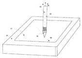
- FIG. 4illustrates an example active stylus 20 with an example device 52 .
- Device 52may have a display (not shown) and a touch sensor with a touch-sensitive area 54 .
- Device 52 displaymay be a liquid crystal display (LCD), a LED display, a LED-backlight LCD, or other suitable display and may be visible though a cover panel and substrate (and the drive and sense electrodes of the touch sensor disposed on it) of device 52 .
- LCDliquid crystal display
- LED displayLED-backlight LCD
- FIG. 4illustrates an example active stylus 20 with an example device 52 .
- Device 52may have a display (not shown) and a touch sensor with a touch-sensitive area 54 .
- Device 52 displaymay be a liquid crystal display (LCD), a LED display, a LED-backlight LCD, or other suitable display and may be visible though a cover panel and substrate (and the drive and sense electrodes of the touch sensor disposed on it) of device 52 .
- Device 52 electronicsmay provide the functionality of device 52 .
- device 52 electronicsmay include circuitry or other electronics for wireless communication to or from device 52 , execute programming on device 52 , generating graphical or other user interfaces (UIs) for device 52 display to display to a user, managing power to device 52 from a battery or other power source, taking still pictures, recording video, other suitable functionality, or any suitable combination of these.
- UIsuser interfaces
- this disclosuredescribes particular device electronics providing particular functionality of a particular device, this disclosure contemplates any suitable device electronics providing any suitable functionality of any suitable device.
- active stylus 20 and device 52may be synchronized prior to communication of data between active stylus 20 and device 52 .
- active stylus 20may be synchronized to device through a pre-determined bit sequence transmitted by the touch sensor of device 52 .
- active stylus 20may be synchronized to device by processing the drive signal transmitted by drive electrodes of the touch sensor of device 52 .
- Active stylus 20may interact or communicate with device 52 when active stylus 20 is brought in contact with or in proximity to touch-sensitive area 54 of the touch sensor of device 52 .
- interaction between active stylus 20 and device 52may be capacitive or inductive.
- measurement signals from the sensors of active stylus 20may initiate, provide for, or terminate interactions between active stylus 20 and one or more devices 52 or one or more users, as described above. Interaction between active stylus 20 and device 52 may occur when active stylus 20 is contacting or in proximity to device 52 .
- a usermay perform a gesture or sequence of gestures, such as shaking or inverting active stylus 20 , whilst active stylus 20 is hovering above touch-sensitive area 54 of device 52 .
- Active stylusmay interact with device 52 based on the gesture performed with active stylus 20 to initiate a pre-determined function, such as authenticating a user associated with active stylus 20 or device 52 .
- this disclosuredescribes particular movements providing particular types of interactions between active stylus 20 and device 52 , this disclosure contemplates any suitable movement influencing any suitable interaction in any suitable way.
- FIG. 5illustrates an example active stylus capable of executing gestures.
- a gesturemay involve a movement, such as translation in any suitable direction or rotation about any suitable axis, or any suitable combination of translations and rotations.
- active stylus 20rotates 58 about axis 60 , 62 , or 64 .
- active stylus 20moves translationally in any direction, such as along axis 60 , 62 , or 64 .
- Gesturesmay be a manipulation of active stylus 20 .
- tapping active stylus 20 or sliding an object across active stylus 20constitutes a gesture or part of a gesture.
- a portion of active stylus 20may be textured so that sliding one body may be a recorded as a different gesture than sliding a different body.
- a portion of active stylus 20may have ridges, and sliding a finger across these ridges may be recorded as a different gesture than sliding a fingernail across the same ridges. While this disclosure provides specific examples of motion with or on an active stylus constituting a gesture or part of a gesture, this disclosure contemplates any suitable motion with or on an active stylus constituting any suitable gesture or part of a gesture.
- a gesturemay provide input, such as electromagnetic input, to or be electronically recorded by components in active stylus 20 . More specifically, in some implementations, a specific gesture may be translated into a specific electromagnetic input, and different gestures may be respectively translated into different electromagnetic inputs.
- electromagnetic inputmay be provided by one or more sensors 42 placed at any suitable locations in or on active stylus 20 .
- sensors 42one or more accelerometers sense translation, motion, and vibration of active stylus 20 .
- one or more gyroscopessense rotation of active stylus 20 .
- one or more force sensorssense force from one or more locations on active stylus 20 , such as the tip or along a portion of the body.
- one or more magnetometerssense the orientation of active stylus 20 in a magnetic field. Changes in orientation sensed by the magnetometer specify the motion of active stylus 20 .
- a global positioning systemGPS
- sensorssense the location, and changes of location, of active stylus 20 relative to the Earth. These sensors produce electromagnetic signals based on the motion, force, orientation, or location sensed.
- electromagnetic input or signalsmay take any suitable form, such as an electric field, magnetic field, electromagnetic radiation, static configuration of electric charge, or electric current. While this disclosure describes specific examples of particular embodiments of gestures providing electromagnetic input to an active stylus, this disclosure contemplates any suitable method of providing any suitable input to an active stylus by any suitable gesture or combination of gestures.
- Gestures executed with or on active stylus 20may provide electromagnetic input to a touch sensor system or associated components, such as a touch-sensitive device.
- electromagnetic signals produced by the components of active stylus 20 based on the motion of active stylus 20results in active stylus 20 providing electromagnetic input to a touch-sensitive device.
- active stylus 20includes a transmitter capable of transmitting electromagnetic signals, such as radio waves, to a touch-sensitive device.
- active stylus 20may transmit data in, for example, electromagnetic form to a touch-sensitive device through a direct connection, such as a universal serial bus cable.
- gesturesprovide electromagnetic input directly to a touch sensor system.
- FIGS. 6A and 6Billustrate example embodiments of providing electromagnetic input directly to a touch-sensitive device by executing gestures with an active stylus.
- active stylus 20is hovering over touch-sensitive display 54 of a touch-sensitive device 52 , and tip 26 of active stylus 20 is separated from the touch-sensitive display by a distance D 1 .
- D 1may be approximately 10 millimeters.
- Electronics in touch-sensitive device 52such as drive and sense lines, sense the location of tip 26 relative to touch-sensitive display 54 , including the distance D 1 separating tip 26 from touch-sensitive display 54 .
- tip 26outputs voltage signals that induce charge on the sense lines in the proximity of tip 26 , and the induced charge depends on the distance D 1 . Motion of tip 26 in any direction is thus detected directly by the electronics of touch-sensitive device 52 .
- active stylus 20may be oriented at any suitable angle with respect to touch-sensitive display 52 .
- FIG. 6Billustrates the body of active stylus 20 contacting touch-sensitive display 54 and tip 26 separated from touch-sensitive display 54 by a distance D 2 .
- touch-sensitive device 52may receive electromagnetic input directly from a gesture and also receive electromagnetic input relating to the same or another gesture from a component of a touch-sensor system, as illustrated in FIG. 7 .
- tip 26 of active stylus 20is in contact with touch-sensitive display 54 of touch-sensitive device 52 .
- Motion of tip 26is directly recorded by electronics, such as drive or sense lines, in touch-sensitive device 20 .
- motion of active stylus 20 relative to tip 26such as rotation 58 about axis 66 or axis 68 passing through tip 26 , is recorded by one or more sensors in active stylus 20 .
- the sensorsconvert the recorded motion into electromagnetic signals in active stylus 20 .
- Active stylus 20outputs electromagnetic signals to touch-sensitive device 52 based on the electromagnetic signals produced within the active stylus as a result of the recorded motion.
- Gestures executed on or by an active stylusmay result in a variety of functionality.
- gesturesalter the functionality of, or produce functionality in, a touch sensor system or its associated components, such as an active stylus or a touch-sensitive device.
- the functionality associated with one or more gesturesmay depend on the orientation of an active stylus. As an example, shaking an active stylus in a vertical position results in different functionality than shaking an active stylus in a horizontal position.
- the functionality associated with one or more gesturesmay depend on the location of an active stylus. As an example, rotating an active stylus near a touch-sensitive device results in different functionality than rotating the active stylus when no touch-sensitive device is near.
- the functionality associated with one or more gesturesmay depend on the user associated with an active stylus or touch-sensitive device. As an example, the functionality associated with a gesture is set by a user. In particular embodiments, the functionality associated with one or more gestures may depend on data stored on an active stylus. As an example, shaking an active stylus that has encrypted data results in a different function than shaking an active stylus that has unsecured data. In particular embodiments, the functionality associated with one or more gestures may depend on the sequence of gestures. As an example, inverting an active stylus after shaking the active stylus results in a different functionality than shaking an active stylus after inverting the active stylus.
- an active stylusmay have a tip on each end, and gestures performed with one tip near a touch-sensitive device may result in different functionality than a gesture with both tips near the touch-sensitive device.
- laying the active stylus flat on the touch-sensitive display so that both tips are hovering near the displayprovides different functionality than hovering one tip near the display.
- one or more gesturesmay affect the functionality of an active stylus.
- an active stylus that creates output on a touch-sensitive display when used with the tip proximal to the displaymay erase output on a touch-sensitive display when used with the end opposite the tip proximal to the display.
- one or more gesturesmay alter the power settings of a touch sensor system and its associated components. As an example, shaking an active stylus transitions the active stylus or associated components from one power mode, such as “off” to another power mode, such as “on”.
- one or more gesturesmay interact with output on a touch-sensitive display. As an example, encircling a group of icons with an active stylus selects the icons.
- Pressing the tip of the active stylus into the touch-sensitive displaypicks up the icons, and pressing the tip a second time onto the display drops the icons.
- sweeping the active stylus or tip of the active stylus across the touch-sensitive displayscrolls around output on a touch-sensitive display or material related to the output.
- pressing the tip of an active stylus into an icon displayed on a touch-sensitive display and sweeping or flicking the tip of the active stylusdeletes the icon.
- sweeping the tip of an active stylus over particular output, such as textselects the text.
- pressing the tip of an active stylus into a touch-sensitive display while gesturing with the active stylusalters the typeface of characters being written on the display.
- one or more gesturesmay access specific command or menus associated with output displayed on a touch-sensitive display.
- selecting output of a touch-sensitive display and shaking the active stylusmay display a set of commands or menus associated with the output selected or displayed.
- one or more gesturesmay combine with other functionality to perform a specific function.
- shaking an active stylus while pressing a buttonmay initiate data transfer between the active stylus and a touch-sensitive device.
- separating either stylus with a finger or two or more fingers over output on a touch-sensitive displaymay zoom in on the output, and an active stylus may gesture, such as writing on the display, to interact with the zoomed-in output.
- performing a user's pre-defined gesturemay unlock the touch-sensitive display of a touch-sensitive device. While this disclosure provides specific examples of particular embodiments of the functionality associated with one or more specific gestures, this disclosure contemplates any suitable functionality associated with any suitable gestures.
- a touch sensor system or its associated componentsmay authenticate one or more users to an active stylus or device, an active stylus to a user or a device, or a device to an active stylus or a user. While particular embodiments described below may reference one type of authentication (e.g. a user to a stylus), this disclosure contemplates that each example is applicable to each type of authentication, where appropriate.
- Authenticationmay enable access to and manipulation of data on or associated with the touch sensor system or its associated components. As an example, successfully authenticating a user to an active stylus allows the user to view, download, edit, delete, or transfer data on the active stylus.
- any user of an active stylusmay authenticate the active stylus to a touch-sensitive device for basic functionality, such as accessing information on the internet.
- a subset of usersare allowed to access certain types of data, such as administrative or security settings on the active stylus or touch-sensitive device.
- itmay require additional or a higher level of authentication in order for a user to be able to access administrative or security settings on the active stylus or touch-sensitive device.
- any usermay be able to read particular data on an active stylus or touch-sensitive device, while only certain users are able to read and write data to the active stylus or touch-sensitive device.
- a graphical user interface associated with a touch sensor systemallows a user to view and edit data on the touch sensor system.
- authenticating a user to an active stylus or an active stylus to a touch-sensitive deviceallows the user to run an application where the user can view the data on the active stylus and the touch-sensitive device and transfer data between the active stylus and the touch-sensitive device. While this disclosure provides specific examples of particular embodiments of types of authentication and the rights or levels of access granted by authentication, this disclosure contemplates any suitable types of authentication granting any suitable rights or levels of access.
- one or more gesturesmay authenticate one or more users to an active stylus, one or more users to a touch-sensitive device, or one or more active styluses to a touch-sensitive device. Authentication may involve unlocking a touch-sensitive display, unlocking data associated with a touch-sensitive device or active stylus, enabling functionality associated with components of an active stylus, or providing access to menus or functionality associated with data on a touch-sensitive device or active stylus.
- a three-dimensional gesture with the active stylusprovides a user access to administrative or security settings on a touch-sensitive device or active stylus.
- performing a gesturedisplays the data on an active stylus or touch-sensitive device. The user may select and transfer data between the two devices after authentication has been accomplished.
- gesturesmay be combined with pressure or force applied to the active stylus.
- squeezing the active stylus at particular locations at specific times before, during, or after a gestureis necessary to achieve authentication.
- an active stylushas one or more components capable of determining the location of the active stylus. The location determined may affect the success of an authenticating gesture.
- an active stylushas a global positioning (GPS) device. If the GPS device recognizes that the active stylus is in a certain location, such as a user's bank or office, the active stylus allows authentication associated with those locations. Authentication associated with those locations is not allowed when the active stylus is not determined to be in those locations.
- GPSglobal positioning
- a usermay set, pre-program, or determine the gestures and pressure necessary for authentication.
- a userperforms a suitable combination of gestures and pressure that they want to authenticate the user to the active stylus. Only the replication of substantially the same set of gestures and/or pressure that the user chose to perform authentication, will in fact achieve authentication.
- an active stylusmay have a tip on each end, and each tip may be used in an authentication gesture. As an example, sweeping the active stylus across a touch-sensitive display with both tips near the display may provide for different authentication than sweeping one tip near the display. While this disclosure provides specific examples of particular embodiments of gestures, pressure, and components used to perform particular types of authentication, this disclosure contemplates any suitable gestures, force, and components performing any suitable authentication associated with an active stylus.
- authenticationmay be accomplished by methods other than gestures. These methods may be combined with gestures to accomplish authentication.
- an active stylus or a touch-sensitive devicehas one or more fingerprint readers that detect the fingerprint of a user and compares the fingerprint to those stored in a database that are known to provide authentication.
- the fingerprint readermay be comprised of capacitive materials.
- an active stylus and a touch-sensitive devicemay have one or more radio frequency identification (RFID) systems.
- RFID systemsidentify and communicate with each other over a secured connection, such as those requiring a 128-bit hex key, and identification provides for authentication of a particular active stylus to a particular touch-sensitive device.
- an active stylus or touch-sensitive devicemay have one or more near-field communication (NFC) systems associated with the active stylus and touch-sensitive device. Communication using the one or more NFC systems enables authentication of the active stylus to the touch-sensitive device or a user to the active stylus or touch-sensitive device.
- NFCnear-field communication
- this disclosureprovides specific examples of particular methods of authenticating users, active styluses, or touch-sensitive devices associated with a touch sensor system, this disclosure contemplates any suitable methods of authenticating users, active styluses, or touch-sensitive devices associated with a touch sensor system.
- an authentication processmay authenticate a user to an active stylus or an active stylus to a touch-sensitive device.
- the authenticationmay be accomplished by accessing first data representing a recently occurred authentication event involving the stylus or the device, accessing second data representing a pre-defined authentication event, and comparing the first data with the second data to authenticate a user to the stylus or the device.
- a recently occurred authentication eventmay include any authentication technique or structure described above, or any suitable combination thereof.
- a combination of one or more characteristics in connection with the active stylusmay be used for the authentication. These characteristics may include, for example, one or more gestures made using the active stylus, a pressure applied to the active stylus, a location of the active stylus, or a RFID key.
- a predetermined combination of characteristicsis specified for a specific authentication (e.g., to authenticate a user to an active stylus).
- a specific authenticatione.g., to authenticate a user to an active stylus.
- the userneeds to provide a combination of characteristics using the active stylus that is the same as or similar to the predetermined combination of characteristics specified for this specific authentication.
- a computer-readable non-transitory storage medium or mediamay include one or more semiconductor-based or other integrated circuits (ICs) (such, as for example, field-programmable gate arrays (FPGAs) or application-specific ICs (ASICs)), hard disk drives (HDDs), hybrid hard drives (HHDs), optical discs, optical disc drives (ODDs), magneto-optical discs, magneto-optical drives, floppy diskettes, floppy disk drives (FDDs), magnetic tapes, solid-state drives (SSDs), RAM-drives, SECURE DIGITAL cards or drives, any other suitable computer-readable non-transitory storage medium or media, or any suitable combination of two or more of these, where appropriate.
- ICssemiconductor-based or other integrated circuits
- HDDshard disk drives
- HHDshybrid hard drives
- ODDsoptical disc drives
- magneto-optical discsmagneto-optical drives
- FDDsfloppy diskettes
- FDDsfloppy disk drives
- an apparatus or system or a component of an apparatus or systembeing adapted to, arranged to, capable of, configured to, enabled to, operable to, or operative to perform a particular function encompasses that apparatus, system, component, whether or not it or that particular function is activated, turned on, or unlocked, as long as that apparatus, system, or component is so adapted, arranged, capable, configured, enabled, operable, or operative.
Landscapes
- Engineering & Computer Science (AREA)
- Theoretical Computer Science (AREA)
- General Engineering & Computer Science (AREA)
- Physics & Mathematics (AREA)
- General Physics & Mathematics (AREA)
- Human Computer Interaction (AREA)
- Computer Security & Cryptography (AREA)
- Computer Hardware Design (AREA)
- Software Systems (AREA)
- User Interface Of Digital Computer (AREA)
- Position Input By Displaying (AREA)
Abstract
Description
Claims (20)
Priority Applications (1)
| Application Number | Priority Date | Filing Date | Title |
|---|---|---|---|
| US13/556,799US9958990B2 (en) | 2011-10-28 | 2012-07-24 | Authenticating with active stylus |
Applications Claiming Priority (2)
| Application Number | Priority Date | Filing Date | Title |
|---|---|---|---|
| US201161553114P | 2011-10-28 | 2011-10-28 | |
| US13/556,799US9958990B2 (en) | 2011-10-28 | 2012-07-24 | Authenticating with active stylus |
Publications (2)
| Publication Number | Publication Date |
|---|---|
| US20130106800A1 US20130106800A1 (en) | 2013-05-02 |
| US9958990B2true US9958990B2 (en) | 2018-05-01 |
Family
ID=48171896
Family Applications (4)
| Application Number | Title | Priority Date | Filing Date |
|---|---|---|---|
| US13/556,799ActiveUS9958990B2 (en) | 2011-10-28 | 2012-07-24 | Authenticating with active stylus |
| US13/556,766ActiveUS9965107B2 (en) | 2011-10-28 | 2012-07-24 | Authenticating with active stylus |
| US13/556,951AbandonedUS20130106741A1 (en) | 2011-10-28 | 2012-07-24 | Active Stylus with Tactile Input and Output |
| US13/645,101AbandonedUS20130106777A1 (en) | 2011-10-28 | 2012-10-04 | Determining Hover Distance of an Active Stylus |
Family Applications After (3)
| Application Number | Title | Priority Date | Filing Date |
|---|---|---|---|
| US13/556,766ActiveUS9965107B2 (en) | 2011-10-28 | 2012-07-24 | Authenticating with active stylus |
| US13/556,951AbandonedUS20130106741A1 (en) | 2011-10-28 | 2012-07-24 | Active Stylus with Tactile Input and Output |
| US13/645,101AbandonedUS20130106777A1 (en) | 2011-10-28 | 2012-10-04 | Determining Hover Distance of an Active Stylus |
Country Status (1)
| Country | Link |
|---|---|
| US (4) | US9958990B2 (en) |
Cited By (2)
| Publication number | Priority date | Publication date | Assignee | Title |
|---|---|---|---|---|
| US11341219B2 (en) | 2018-08-06 | 2022-05-24 | Samsung Electronics Co., Ltd | Apparatus for unlocking electronic device by using stylus pen and method thereof |
| US20240295935A1 (en)* | 2023-03-05 | 2024-09-05 | Novatek Microelectronics Corp. | Stylus, touch device, and touch processing circuit |
Families Citing this family (52)
| Publication number | Priority date | Publication date | Assignee | Title |
|---|---|---|---|---|
| KR101862123B1 (en)* | 2011-08-31 | 2018-05-30 | 삼성전자 주식회사 | Input device and method on terminal equipment having a touch module |
| US9164598B2 (en) | 2011-10-28 | 2015-10-20 | Atmel Corporation | Active stylus with surface-modification materials |
| US8866767B2 (en) | 2011-10-28 | 2014-10-21 | Atmel Corporation | Active stylus with high voltage |
| US9164603B2 (en) | 2011-10-28 | 2015-10-20 | Atmel Corporation | Executing gestures with active stylus |
| US9606641B2 (en) | 2015-03-09 | 2017-03-28 | Atmel Corporation | Adaptive transmit voltage in active stylus |
| US9116558B2 (en) | 2011-10-28 | 2015-08-25 | Atmel Corporation | Executing gestures with active stylus |
| CN102736752A (en)* | 2012-06-08 | 2012-10-17 | 中兴通讯股份有限公司 | Hand writing pen, mobile terminal and information processing method |
| FR2992441B1 (en)* | 2012-06-22 | 2017-12-08 | Compagnie Ind Et Financiere Dingenierie Ingenico | STYLET OF DATA ENTRY. |
| US9075438B2 (en)* | 2012-07-18 | 2015-07-07 | Htc Corporation | Systems and related methods involving stylus tactile feel |
| KR102008374B1 (en)* | 2012-08-03 | 2019-10-23 | 삼성전자주식회사 | Input device for portable terminal |
| US9921626B2 (en)* | 2012-09-28 | 2018-03-20 | Atmel Corporation | Stylus communication with near-field coupling |
| US9335872B2 (en)* | 2012-10-01 | 2016-05-10 | Stmicroelectronics Asia Pacific Pte Ltd | Hybrid stylus for use in touch screen applications |
| CN103838490B (en)* | 2012-11-20 | 2018-01-23 | 联想(北京)有限公司 | The method and a kind of electronic equipment of a kind of information processing |
| US9342162B2 (en)* | 2013-01-29 | 2016-05-17 | Lg Electronics Inc. | Mobile terminal and controlling method thereof |
| US9946365B2 (en) | 2013-03-11 | 2018-04-17 | Barnes & Noble College Booksellers, Llc | Stylus-based pressure-sensitive area for UI control of computing device |
| US9785259B2 (en)* | 2013-03-11 | 2017-10-10 | Barnes & Noble College Booksellers, Llc | Stylus-based slider functionality for UI control of computing device |
| US9766723B2 (en)* | 2013-03-11 | 2017-09-19 | Barnes & Noble College Booksellers, Llc | Stylus sensitive device with hover over stylus control functionality |
| US9626008B2 (en)* | 2013-03-11 | 2017-04-18 | Barnes & Noble College Booksellers, Llc | Stylus-based remote wipe of lost device |
| US20140253462A1 (en)* | 2013-03-11 | 2014-09-11 | Barnesandnoble.Com Llc | Sync system for storing/restoring stylus customizations |
| US9261985B2 (en) | 2013-03-11 | 2016-02-16 | Barnes & Noble College Booksellers, Llc | Stylus-based touch-sensitive area for UI control of computing device |
| US9304609B2 (en)* | 2013-03-12 | 2016-04-05 | Lenovo (Singapore) Pte. Ltd. | Suspending tablet computer by stylus detection |
| JP5666641B2 (en)* | 2013-03-13 | 2015-02-12 | パナソニック インテレクチュアル プロパティ コーポレーション オブアメリカPanasonic Intellectual Property Corporation of America | Information terminal |
| KR102096824B1 (en)* | 2013-06-24 | 2020-04-06 | 삼성전자주식회사 | Apparatus and method for providing a security environment |
| DE102013214020A1 (en)* | 2013-07-17 | 2015-02-19 | Stabilo International Gmbh | Digital pen |
| EP3025434A4 (en)* | 2013-07-24 | 2017-02-22 | FiftyThree, Inc. | Apparatuses, methods and systems for authenticating a wireless connection |
| US10073578B2 (en) | 2013-08-13 | 2018-09-11 | Samsung Electronics Company, Ltd | Electromagnetic interference signal detection |
| US10141929B2 (en) | 2013-08-13 | 2018-11-27 | Samsung Electronics Company, Ltd. | Processing electromagnetic interference signal using machine learning |
| US10042446B2 (en) | 2013-08-13 | 2018-08-07 | Samsung Electronics Company, Ltd. | Interaction modes for object-device interactions |
| US10101869B2 (en) | 2013-08-13 | 2018-10-16 | Samsung Electronics Company, Ltd. | Identifying device associated with touch event |
| US10042504B2 (en) | 2013-08-13 | 2018-08-07 | Samsung Electronics Company, Ltd. | Interaction sensing |
| CN104375722B (en)* | 2013-08-16 | 2018-04-27 | 联想(北京)有限公司 | A kind of input method and electronic equipment |
| GB2520069A (en)* | 2013-11-08 | 2015-05-13 | Univ Newcastle | Identifying a user applying a touch or proximity input |
| GB2522247A (en)* | 2014-01-20 | 2015-07-22 | Promethean Ltd | Touch device detection |
| GB2522249A (en)* | 2014-01-20 | 2015-07-22 | Promethean Ltd | Active pointing device detection |
| US9355236B1 (en)* | 2014-04-03 | 2016-05-31 | Fuji Xerox Co., Ltd. | System and method for biometric user authentication using 3D in-air hand gestures |
| US9310899B2 (en) | 2014-04-28 | 2016-04-12 | Htc Corporation | Stylus having head being rigid body and electronic device using the same |
| US9927927B2 (en)* | 2014-05-05 | 2018-03-27 | Atmel Corporation | Implementing a virtual controller outside an area of a touch sensor |
| US9727161B2 (en) | 2014-06-12 | 2017-08-08 | Microsoft Technology Licensing, Llc | Sensor correlation for pen and touch-sensitive computing device interaction |
| US9870083B2 (en) | 2014-06-12 | 2018-01-16 | Microsoft Technology Licensing, Llc | Multi-device multi-user sensor correlation for pen and computing device interaction |
| US9600177B2 (en)* | 2014-07-17 | 2017-03-21 | Google Technology Holdings LLC | Electronic device with gesture display control and corresponding methods |
| US10042439B2 (en) | 2014-12-11 | 2018-08-07 | Microsft Technology Licensing, LLC | Interactive stylus and display device |
| US9898100B2 (en)* | 2015-06-04 | 2018-02-20 | Microsoft Technology Licensing, Llc | Authenticating stylus device |
| US9983744B2 (en)* | 2015-07-07 | 2018-05-29 | Pressure Profile Corp. | Capacitive tactile sensor with nested matrix electrodes |
| EP3347854A4 (en)* | 2015-09-10 | 2019-04-24 | Oath Inc. | User identification through an external device on a per touch basis on touch sensitive devices |
| US9891773B2 (en) | 2015-12-17 | 2018-02-13 | Synaptics Incorporated | Detecting hover distance with a capacitive sensor |
| US10452830B2 (en)* | 2016-02-02 | 2019-10-22 | Microsoft Technology Licensing, Llc | Authenticating users via data stored on stylus devices |
| US10025403B2 (en) | 2016-07-25 | 2018-07-17 | Microsoft Technology Licensing, Llc | Stylus communication channels |
| US10416777B2 (en) | 2016-08-16 | 2019-09-17 | Microsoft Technology Licensing, Llc | Device manipulation using hover |
| JP7087364B2 (en)* | 2017-12-04 | 2022-06-21 | 富士フイルムビジネスイノベーション株式会社 | Information processing equipment, information processing systems and programs |
| EP3640775B1 (en)* | 2018-09-05 | 2022-02-23 | Shenzhen Goodix Technology Co., Ltd. | Touch sensing method, touch chip, electronic device, and touch system |
| CN111090351B (en)* | 2018-10-24 | 2023-08-18 | 义隆电子股份有限公司 | Touch system, input device thereof and signal transmission method thereof |
| US10649551B1 (en)* | 2018-12-27 | 2020-05-12 | Pixart Imaging Inc. | Pen mouse with an inclining compensation function |
Citations (67)
| Publication number | Priority date | Publication date | Assignee | Title |
|---|---|---|---|---|
| US4695680A (en) | 1986-06-27 | 1987-09-22 | Scriptel Corporation | Stylus for position responsive apparatus having electrographic application |
| US5007085A (en)* | 1988-10-28 | 1991-04-09 | International Business Machines Corporation | Remotely sensed personal stylus |
| US5349139A (en)* | 1992-10-30 | 1994-09-20 | International Business Machines | Architecture for communication of remote devices to a digitizing display |
| US5453762A (en)* | 1993-01-20 | 1995-09-26 | Hitachi, Ltd. | Systems for processing information and identifying individual |
| US5478976A (en)* | 1992-08-31 | 1995-12-26 | Canon Kabushiki Kaisha | Information processing method and apparatus |
| US5557076A (en)* | 1993-11-12 | 1996-09-17 | Mikron Gesellschaft Fur | Cordless position detection apparatus |
| US5699084A (en)* | 1994-06-29 | 1997-12-16 | Wacom Co., Ltd. | Computer system |
| US5883338A (en)* | 1994-12-16 | 1999-03-16 | Hyundai Electronics America, Inc. | Telementry by digitizer stylus |
| US5973677A (en) | 1997-01-07 | 1999-10-26 | Telxon Corporation | Rechargeable, untethered electronic stylus for computer with interactive display screen |
| US6195446B1 (en)* | 1994-12-16 | 2001-02-27 | Hyundai Electronics America | Digitizer stylus with memory for storing handwriting data |
| US6249276B1 (en)* | 1997-01-22 | 2001-06-19 | Mitsubishi Denki Kabushiki Kaisha | Pen-inputted personal information terminal device |
| US20020190947A1 (en) | 2000-04-05 | 2002-12-19 | Feinstein David Y. | View navigation and magnification of a hand-held device with a display |
| US6728881B1 (en)* | 1999-10-01 | 2004-04-27 | The United States Of America As Represented By The Secretary Of The Army | Fingerprint and signature identification and authorization card and pen |
| US20040134690A1 (en)* | 2002-12-30 | 2004-07-15 | Pitney Bowes Inc. | System and method for authenticating a mailpiece sender |
| US20040140965A1 (en) | 2002-10-31 | 2004-07-22 | Microsoft Corporation | Universal computing device |
| US20050063570A1 (en)* | 2003-08-22 | 2005-03-24 | Dynasig Corporation | Method and apparatus for capturing and authenticating biometric information from a writing instrument |
| US20060023922A1 (en)* | 2001-05-25 | 2006-02-02 | Black Gerald R | Identity authentication device |
| US20060215886A1 (en)* | 2000-01-24 | 2006-09-28 | Black Gerald R | Method for identity verification |
| US20060267966A1 (en) | 2005-05-24 | 2006-11-30 | Microsoft Corporation | Hover widgets: using the tracking state to extend capabilities of pen-operated devices |
| US20070057763A1 (en)* | 2005-09-12 | 2007-03-15 | Imation Corp. | Wireless handheld device with local biometric authentication |
| US20080143693A1 (en) | 2000-05-24 | 2008-06-19 | Immersion Corporation | Haptic stylus utilizing an electroactive polymer |
| US7426643B2 (en)* | 2004-06-22 | 2008-09-16 | Hewlett-Packard Development Company, L.P. | Input device feature |
| US7425643B1 (en) | 2004-01-26 | 2008-09-16 | University Of Washington | Electron acceptors for nonlinear optical chromophores |
| US20080238885A1 (en) | 2007-03-29 | 2008-10-02 | N-Trig Ltd. | System and method for multiple object detection on a digitizer system |
| US20080309621A1 (en) | 2007-06-15 | 2008-12-18 | Aggarwal Akhil | Proximity based stylus and display screen, and device incorporating same |
| US20090095540A1 (en) | 2007-10-11 | 2009-04-16 | N-Trig Ltd. | Method for palm touch identification in multi-touch digitizing systems |
| US20090115725A1 (en) | 2007-11-05 | 2009-05-07 | Eldad Shemesh | Input device and method of operation thereof |
| US20090127005A1 (en) | 2007-11-14 | 2009-05-21 | N-Trig Ltd. | System and method for detection with a digitizer sensor |
| US20090153152A1 (en) | 2007-12-14 | 2009-06-18 | Cypress Semiconductor Corporation | Compensation circuit for a tx-rx capacitive sensor |
| US20090153525A1 (en) | 2007-12-12 | 2009-06-18 | Mitac International Corp. | Touch pen with erasure function |
| US20090184939A1 (en) | 2008-01-23 | 2009-07-23 | N-Trig Ltd. | Graphical object manipulation with a touch sensitive screen |
| US20090219250A1 (en) | 2008-02-29 | 2009-09-03 | Ure Michael J | Interface with and communication between mobile electronic devices |
| US20090251434A1 (en) | 2008-04-03 | 2009-10-08 | N-Tring Ltd. | Multi-touch and single touch detection |
| US7612767B1 (en) | 2005-08-24 | 2009-11-03 | Griffin Technology, Inc. | Trackpad pen for use with computer touchpad |
| US20090315854A1 (en) | 2008-06-18 | 2009-12-24 | Epson Imaging Devices Corporation | Capacitance type input device and display device with input function |
| US20100006350A1 (en) | 2008-07-11 | 2010-01-14 | Elias John G | Stylus Adapted For Low Resolution Touch Sensor Panels |
| US7663607B2 (en) | 2004-05-06 | 2010-02-16 | Apple Inc. | Multipoint touchscreen |
| US20100079414A1 (en) | 2008-09-30 | 2010-04-01 | Andrew Rodney Ferlitsch | Apparatus, systems, and methods for authentication on a publicly accessed shared interactive digital surface |
| US20100139992A1 (en)* | 2008-12-10 | 2010-06-10 | International Business Machines Corporation | User-authenticating, digital data recording pen |
| US20100155153A1 (en) | 2008-12-22 | 2010-06-24 | N-Trig Ltd. | Digitizer, stylus and method of synchronization therewith |
| US20100194547A1 (en) | 2009-01-30 | 2010-08-05 | Scott Michael Terrell | Tactile feedback apparatus and method |
| US20100292945A1 (en) | 2009-05-13 | 2010-11-18 | Joseph Kurth Reynolds | Capacitive sensor device |
| US20100308962A1 (en)* | 2009-06-04 | 2010-12-09 | Foxconn Communication Technology Corp. | Method and electronic device capable of user identification |
| US20100315384A1 (en) | 2009-06-12 | 2010-12-16 | Kirk Hargreaves | Untethered active pen and a method for communicating with a capacitive sensing device using the untethered active pen |
| US20110007029A1 (en) | 2009-07-08 | 2011-01-13 | Ben-David Amichai | System and method for multi-touch interactions with a touch sensitive screen |
| US7875814B2 (en) | 2005-07-21 | 2011-01-25 | Tpo Displays Corp. | Electromagnetic digitizer sensor array structure |
| US20110071394A1 (en) | 2009-09-23 | 2011-03-24 | Fedinec James J | Central venous catheter kit with line gripping and needle localizing devices |
| US7920129B2 (en) | 2007-01-03 | 2011-04-05 | Apple Inc. | Double-sided touch-sensitive panel with shield and drive combined layer |
| US8031094B2 (en) | 2009-09-11 | 2011-10-04 | Apple Inc. | Touch controller with improved analog front end |
| US8031174B2 (en) | 2007-01-03 | 2011-10-04 | Apple Inc. | Multi-touch surface stackup arrangement |
| US8040326B2 (en) | 2007-06-13 | 2011-10-18 | Apple Inc. | Integrated in-plane switching display and touch sensor |
| US8049732B2 (en) | 2007-01-03 | 2011-11-01 | Apple Inc. | Front-end signal compensation |
| US20120068964A1 (en) | 2010-09-22 | 2012-03-22 | Cypress Semiconductor Corporation | Capacitive stylus for a touch screen |
| US8179381B2 (en) | 2008-02-28 | 2012-05-15 | 3M Innovative Properties Company | Touch screen sensor |
| US20120127110A1 (en) | 2010-11-19 | 2012-05-24 | Apple Inc. | Optical stylus |
| US20120192250A1 (en)* | 2010-07-06 | 2012-07-26 | Alkhalaf Rakan | Device, System, And Method For Registering And Authenticating Handwritten Signatures And Archiving Handwritten Information |
| US20120243151A1 (en) | 2011-03-21 | 2012-09-27 | Stephen Brian Lynch | Electronic Devices With Convex Displays |
| US20120242592A1 (en) | 2011-03-21 | 2012-09-27 | Rothkopf Fletcher R | Electronic devices with flexible displays |
| US20120242603A1 (en) | 2011-03-21 | 2012-09-27 | N-Trig Ltd. | System and method for authentication with a computer stylus |
| US20120243719A1 (en) | 2011-03-21 | 2012-09-27 | Franklin Jeremy C | Display-Based Speaker Structures for Electronic Devices |
| US20120242588A1 (en) | 2011-03-21 | 2012-09-27 | Myers Scott A | Electronic devices with concave displays |
| WO2012129247A2 (en) | 2011-03-21 | 2012-09-27 | Apple Inc. | Electronic devices with flexible displays |
| US20120331546A1 (en)* | 2011-06-22 | 2012-12-27 | Falkenburg David R | Intelligent stylus |
| US20120327041A1 (en) | 2011-06-22 | 2012-12-27 | Harley Jonah A | Active stylus |
| US20130076612A1 (en) | 2011-09-26 | 2013-03-28 | Apple Inc. | Electronic device with wrap around display |
| US20130106724A1 (en) | 2011-10-28 | 2013-05-02 | Atmel Corporation | Executing Gestures With Active Stylus |
| US8638320B2 (en) | 2011-06-22 | 2014-01-28 | Apple Inc. | Stylus orientation detection |
Family Cites Families (13)
| Publication number | Priority date | Publication date | Assignee | Title |
|---|---|---|---|---|
| US5581274A (en)* | 1991-04-05 | 1996-12-03 | Sharp Kabushiki Kaisha | Display-integrated type tablet device |
| US6970583B2 (en)* | 2000-05-25 | 2005-11-29 | Black Gerald R | Identity authentication device |
| US20060001657A1 (en)* | 2004-07-02 | 2006-01-05 | Logitech Europe S.A. | Scrolling device |
| US7382357B2 (en)* | 2005-04-25 | 2008-06-03 | Avago Technologies Ecbu Ip Pte Ltd | User interface incorporating emulated hard keys |
| US8405618B2 (en)* | 2006-03-24 | 2013-03-26 | Northwestern University | Haptic device with indirect haptic feedback |
| WO2008007372A2 (en)* | 2006-07-12 | 2008-01-17 | N-Trig Ltd. | Hover and touch detection for a digitizer |
| US8432365B2 (en)* | 2007-08-30 | 2013-04-30 | Lg Electronics Inc. | Apparatus and method for providing feedback for three-dimensional touchscreen |
| WO2010073329A1 (en)* | 2008-12-25 | 2010-07-01 | 富士通株式会社 | Computer program, input device, and input method |
| US8446392B2 (en)* | 2009-11-16 | 2013-05-21 | Smart Technologies Ulc | Method for determining the location of a pointer in a pointer input region, and interactive input system executing the method |
| US20110115751A1 (en)* | 2009-11-19 | 2011-05-19 | Sony Ericsson Mobile Communications Ab | Hand-held input device, system comprising the input device and an electronic device and method for controlling the same |
| KR101073309B1 (en)* | 2009-11-24 | 2011-10-12 | 삼성모바일디스플레이주식회사 | touch screen system and driving method thereof |
| JP5636678B2 (en)* | 2010-01-19 | 2014-12-10 | ソニー株式会社 | Display control apparatus, display control method, and display control program |
| US20120268414A1 (en)* | 2011-04-25 | 2012-10-25 | Motorola Mobility, Inc. | Method and apparatus for exchanging data with a user computer device |
- 2012
- 2012-07-24USUS13/556,799patent/US9958990B2/enactiveActive
- 2012-07-24USUS13/556,766patent/US9965107B2/enactiveActive
- 2012-07-24USUS13/556,951patent/US20130106741A1/ennot_activeAbandoned
- 2012-10-04USUS13/645,101patent/US20130106777A1/ennot_activeAbandoned
Patent Citations (69)
| Publication number | Priority date | Publication date | Assignee | Title |
|---|---|---|---|---|
| US4695680A (en) | 1986-06-27 | 1987-09-22 | Scriptel Corporation | Stylus for position responsive apparatus having electrographic application |
| US5007085A (en)* | 1988-10-28 | 1991-04-09 | International Business Machines Corporation | Remotely sensed personal stylus |
| US5478976A (en)* | 1992-08-31 | 1995-12-26 | Canon Kabushiki Kaisha | Information processing method and apparatus |
| US5349139A (en)* | 1992-10-30 | 1994-09-20 | International Business Machines | Architecture for communication of remote devices to a digitizing display |
| US5453762A (en)* | 1993-01-20 | 1995-09-26 | Hitachi, Ltd. | Systems for processing information and identifying individual |
| US5612720A (en)* | 1993-01-20 | 1997-03-18 | Hitachi Ltd. | Systems for processing information and identifying individual |
| US5557076A (en)* | 1993-11-12 | 1996-09-17 | Mikron Gesellschaft Fur | Cordless position detection apparatus |
| US5699084A (en)* | 1994-06-29 | 1997-12-16 | Wacom Co., Ltd. | Computer system |
| US5883338A (en)* | 1994-12-16 | 1999-03-16 | Hyundai Electronics America, Inc. | Telementry by digitizer stylus |
| US6195446B1 (en)* | 1994-12-16 | 2001-02-27 | Hyundai Electronics America | Digitizer stylus with memory for storing handwriting data |
| US6556694B2 (en)* | 1994-12-16 | 2003-04-29 | Hyundai Electronics America | Digitizer stylus containing handwriting data |
| US5973677A (en) | 1997-01-07 | 1999-10-26 | Telxon Corporation | Rechargeable, untethered electronic stylus for computer with interactive display screen |
| US6249276B1 (en)* | 1997-01-22 | 2001-06-19 | Mitsubishi Denki Kabushiki Kaisha | Pen-inputted personal information terminal device |
| US6728881B1 (en)* | 1999-10-01 | 2004-04-27 | The United States Of America As Represented By The Secretary Of The Army | Fingerprint and signature identification and authorization card and pen |
| US20060215886A1 (en)* | 2000-01-24 | 2006-09-28 | Black Gerald R | Method for identity verification |
| US20020190947A1 (en) | 2000-04-05 | 2002-12-19 | Feinstein David Y. | View navigation and magnification of a hand-held device with a display |
| US20080143693A1 (en) | 2000-05-24 | 2008-06-19 | Immersion Corporation | Haptic stylus utilizing an electroactive polymer |
| US20060023922A1 (en)* | 2001-05-25 | 2006-02-02 | Black Gerald R | Identity authentication device |
| US20040140965A1 (en) | 2002-10-31 | 2004-07-22 | Microsoft Corporation | Universal computing device |
| US20040134690A1 (en)* | 2002-12-30 | 2004-07-15 | Pitney Bowes Inc. | System and method for authenticating a mailpiece sender |
| US20050063570A1 (en)* | 2003-08-22 | 2005-03-24 | Dynasig Corporation | Method and apparatus for capturing and authenticating biometric information from a writing instrument |
| US7425643B1 (en) | 2004-01-26 | 2008-09-16 | University Of Washington | Electron acceptors for nonlinear optical chromophores |
| US7663607B2 (en) | 2004-05-06 | 2010-02-16 | Apple Inc. | Multipoint touchscreen |
| US7426643B2 (en)* | 2004-06-22 | 2008-09-16 | Hewlett-Packard Development Company, L.P. | Input device feature |
| US20060267966A1 (en) | 2005-05-24 | 2006-11-30 | Microsoft Corporation | Hover widgets: using the tracking state to extend capabilities of pen-operated devices |
| US7875814B2 (en) | 2005-07-21 | 2011-01-25 | Tpo Displays Corp. | Electromagnetic digitizer sensor array structure |
| US7612767B1 (en) | 2005-08-24 | 2009-11-03 | Griffin Technology, Inc. | Trackpad pen for use with computer touchpad |
| US20070057763A1 (en)* | 2005-09-12 | 2007-03-15 | Imation Corp. | Wireless handheld device with local biometric authentication |
| US8031174B2 (en) | 2007-01-03 | 2011-10-04 | Apple Inc. | Multi-touch surface stackup arrangement |
| US7920129B2 (en) | 2007-01-03 | 2011-04-05 | Apple Inc. | Double-sided touch-sensitive panel with shield and drive combined layer |
| US8049732B2 (en) | 2007-01-03 | 2011-11-01 | Apple Inc. | Front-end signal compensation |
| US20080238885A1 (en) | 2007-03-29 | 2008-10-02 | N-Trig Ltd. | System and method for multiple object detection on a digitizer system |
| US8040326B2 (en) | 2007-06-13 | 2011-10-18 | Apple Inc. | Integrated in-plane switching display and touch sensor |
| US20080309621A1 (en) | 2007-06-15 | 2008-12-18 | Aggarwal Akhil | Proximity based stylus and display screen, and device incorporating same |
| US20090095540A1 (en) | 2007-10-11 | 2009-04-16 | N-Trig Ltd. | Method for palm touch identification in multi-touch digitizing systems |
| US20090115725A1 (en) | 2007-11-05 | 2009-05-07 | Eldad Shemesh | Input device and method of operation thereof |
| US20090127005A1 (en) | 2007-11-14 | 2009-05-21 | N-Trig Ltd. | System and method for detection with a digitizer sensor |
| US20090153525A1 (en) | 2007-12-12 | 2009-06-18 | Mitac International Corp. | Touch pen with erasure function |
| US20090153152A1 (en) | 2007-12-14 | 2009-06-18 | Cypress Semiconductor Corporation | Compensation circuit for a tx-rx capacitive sensor |
| US20090184939A1 (en) | 2008-01-23 | 2009-07-23 | N-Trig Ltd. | Graphical object manipulation with a touch sensitive screen |
| US8179381B2 (en) | 2008-02-28 | 2012-05-15 | 3M Innovative Properties Company | Touch screen sensor |
| US20090219250A1 (en) | 2008-02-29 | 2009-09-03 | Ure Michael J | Interface with and communication between mobile electronic devices |
| US20090251434A1 (en) | 2008-04-03 | 2009-10-08 | N-Tring Ltd. | Multi-touch and single touch detection |
| US20090315854A1 (en) | 2008-06-18 | 2009-12-24 | Epson Imaging Devices Corporation | Capacitance type input device and display device with input function |
| US20100006350A1 (en) | 2008-07-11 | 2010-01-14 | Elias John G | Stylus Adapted For Low Resolution Touch Sensor Panels |
| US20100079414A1 (en) | 2008-09-30 | 2010-04-01 | Andrew Rodney Ferlitsch | Apparatus, systems, and methods for authentication on a publicly accessed shared interactive digital surface |
| US20100139992A1 (en)* | 2008-12-10 | 2010-06-10 | International Business Machines Corporation | User-authenticating, digital data recording pen |
| US20100155153A1 (en) | 2008-12-22 | 2010-06-24 | N-Trig Ltd. | Digitizer, stylus and method of synchronization therewith |
| US20100194547A1 (en) | 2009-01-30 | 2010-08-05 | Scott Michael Terrell | Tactile feedback apparatus and method |
| US20100292945A1 (en) | 2009-05-13 | 2010-11-18 | Joseph Kurth Reynolds | Capacitive sensor device |
| US20100308962A1 (en)* | 2009-06-04 | 2010-12-09 | Foxconn Communication Technology Corp. | Method and electronic device capable of user identification |
| US20100315384A1 (en) | 2009-06-12 | 2010-12-16 | Kirk Hargreaves | Untethered active pen and a method for communicating with a capacitive sensing device using the untethered active pen |
| US20110007029A1 (en) | 2009-07-08 | 2011-01-13 | Ben-David Amichai | System and method for multi-touch interactions with a touch sensitive screen |
| US8031094B2 (en) | 2009-09-11 | 2011-10-04 | Apple Inc. | Touch controller with improved analog front end |
| US20110071394A1 (en) | 2009-09-23 | 2011-03-24 | Fedinec James J | Central venous catheter kit with line gripping and needle localizing devices |
| US20120192250A1 (en)* | 2010-07-06 | 2012-07-26 | Alkhalaf Rakan | Device, System, And Method For Registering And Authenticating Handwritten Signatures And Archiving Handwritten Information |
| US20120068964A1 (en) | 2010-09-22 | 2012-03-22 | Cypress Semiconductor Corporation | Capacitive stylus for a touch screen |
| US20120127110A1 (en) | 2010-11-19 | 2012-05-24 | Apple Inc. | Optical stylus |
| US20120242592A1 (en) | 2011-03-21 | 2012-09-27 | Rothkopf Fletcher R | Electronic devices with flexible displays |
| US20120243151A1 (en) | 2011-03-21 | 2012-09-27 | Stephen Brian Lynch | Electronic Devices With Convex Displays |
| US20120242603A1 (en) | 2011-03-21 | 2012-09-27 | N-Trig Ltd. | System and method for authentication with a computer stylus |
| US20120243719A1 (en) | 2011-03-21 | 2012-09-27 | Franklin Jeremy C | Display-Based Speaker Structures for Electronic Devices |
| US20120242588A1 (en) | 2011-03-21 | 2012-09-27 | Myers Scott A | Electronic devices with concave displays |
| WO2012129247A2 (en) | 2011-03-21 | 2012-09-27 | Apple Inc. | Electronic devices with flexible displays |
| US20120331546A1 (en)* | 2011-06-22 | 2012-12-27 | Falkenburg David R | Intelligent stylus |
| US20120327041A1 (en) | 2011-06-22 | 2012-12-27 | Harley Jonah A | Active stylus |
| US8638320B2 (en) | 2011-06-22 | 2014-01-28 | Apple Inc. | Stylus orientation detection |
| US20130076612A1 (en) | 2011-09-26 | 2013-03-28 | Apple Inc. | Electronic device with wrap around display |
| US20130106724A1 (en) | 2011-10-28 | 2013-05-02 | Atmel Corporation | Executing Gestures With Active Stylus |
Non-Patent Citations (21)
| Title |
|---|
| Final Office Action for U.S. Appl. No. 13/363,190, dated Aug. 1, 2014. |
| Final Office Action for U.S. Appl. No. 13/419,087, dated Aug. 22, 2014. |
| Final Office Action for U.S. Appl. No. 13/556,766, dated Aug. 26, 2013. |
| Final Office Action for U.S. Appl. No. 13/556,766, dated Feb. 3, 2015. |
| Kyung, Ki-Uk et al., "wUbi-Pen : Windows Graphical User Interface Interacting with Haptic Feedback Stylus," SIGGRAPH., Los Angeles, California, Aug. 2008. |
| Lee, Johnny C. et al., "Haptic Pen: A Tactile Feedback Stylus for Touch Screens," UIST'04, vol. 6, Issue 2, Santa Fe, New Mexico, Oct. 2004. |
| Non-Final Office Action for U.S. Appl. No. 13/363,190, dated Feb. 6, 2015. |
| Non-Final Office Action for U.S. Appl. No. 13/363,190, dated Jan. 31, 2014. |
| Non-Final Office Action for U.S. Appl. No. 13/419,087, dated Apr. 25, 2014. |
| Non-Final Office Action for U.S. Appl. No. 13/419,087, dated Dec. 31, 2014. |
| Non-Final Office Action for U.S. Appl. No. 13/556,766, dated Aug. 8, 2014. |
| Office Action for U.S. Appl. No. 13/419,087, dated May 16, 2012. |
| Office Action for U.S. Appl. No. 13/419,087, dated Sep. 4, 2012. |
| Office Action for U.S. Appl. No. 13/556,766, dated Jan. 30, 2013. |
| Song, Hyunyoung et al., "Grips and Gestures on a Multi-Touch Pen," CHI 2011, Session: Flexible Grips & Gestures, Vancouver, BC, Canada, May 2011. |
| Tan, Eng Chong et al., "Application of Capacitive Coupling to the Design of an Absolute-Coordinate Pointing Device," IEEE Transactions on Instrumentation and Measurement, vol. 54, No. 5, Oct. 2005. |
| U.S. Appl. No. 13/419,087, filed Mar. 13, 2012, Yilmaz. |
| U.S. Appl. No. 13/556,766, filed Jul. 24, 2012, Yilmaz. |
| U.S. Appl. No. 61/454,894, filed Mar. 21, 2011, Rothkopf. |
| U.S. Appl. No. 61/454,936, filed Mar. 21, 2011, Myers. |
| U.S. Appl. No. 61/454,950, filed Mar. 21, 2011, Lynch |
Cited By (3)
| Publication number | Priority date | Publication date | Assignee | Title |
|---|---|---|---|---|
| US11341219B2 (en) | 2018-08-06 | 2022-05-24 | Samsung Electronics Co., Ltd | Apparatus for unlocking electronic device by using stylus pen and method thereof |
| US20240295935A1 (en)* | 2023-03-05 | 2024-09-05 | Novatek Microelectronics Corp. | Stylus, touch device, and touch processing circuit |
| US12422945B2 (en)* | 2023-03-05 | 2025-09-23 | Novatek Microelectronics Corp. | Stylus, touch device, and touch processing circuit |
Also Published As
| Publication number | Publication date |
|---|---|
| US20130106799A1 (en) | 2013-05-02 |
| US20130106777A1 (en) | 2013-05-02 |
| US9965107B2 (en) | 2018-05-08 |
| US20130106800A1 (en) | 2013-05-02 |
| US20130106741A1 (en) | 2013-05-02 |
Similar Documents
| Publication | Publication Date | Title |
|---|---|---|
| US12236020B2 (en) | Executing gestures with active stylus | |
| US9958990B2 (en) | Authenticating with active stylus | |
| US11079821B2 (en) | Stylus communication with near-field coupling | |
| US12111984B2 (en) | Multi-electrode active stylus tip | |
| US11327583B2 (en) | Touch-sensitive system with motion filtering | |
| US9389701B2 (en) | Data transfer from active stylus | |
| US9880645B2 (en) | Executing gestures with active stylus | |
| US9389707B2 (en) | Active stylus with configurable touch sensor | |
| US9354728B2 (en) | Active stylus with capacitive buttons and sliders | |
| US9690431B2 (en) | Locking active stylus and touch-sensor device | |
| US10725563B2 (en) | Data transfer from active stylus to configure a device or application | |
| US9891723B2 (en) | Active stylus with surface-modification materials | |
| US20130106912A1 (en) | Combination Touch-Sensor Input | |
| US20130106771A1 (en) | Active-Stylus Nib with Rolling-Ball Tip |
Legal Events
| Date | Code | Title | Description |
|---|---|---|---|
| AS | Assignment | Owner name:ATMEL CORPORATION, CALIFORNIA Free format text:ASSIGNMENT OF ASSIGNORS INTEREST;ASSIGNORS:YILMAZ, ESAT;BAKKEN, VEMUND KVAL;SUNDARA-RAJAN, KISHORE;SIGNING DATES FROM 20120720 TO 20120723;REEL/FRAME:028627/0277 | |
| AS | Assignment | Owner name:MORGAN STANLEY SENIOR FUNDING, INC. AS ADMINISTRAT Free format text:PATENT SECURITY AGREEMENT;ASSIGNOR:ATMEL CORPORATION;REEL/FRAME:031912/0173 Effective date:20131206 Owner name:MORGAN STANLEY SENIOR FUNDING, INC. AS ADMINISTRATIVE AGENT, NEW YORK Free format text:PATENT SECURITY AGREEMENT;ASSIGNOR:ATMEL CORPORATION;REEL/FRAME:031912/0173 Effective date:20131206 | |
| AS | Assignment | Owner name:ATMEL CORPORATION, CALIFORNIA Free format text:TERMINATION AND RELEASE OF SECURITY INTEREST IN PATENT COLLATERAL;ASSIGNOR:MORGAN STANLEY SENIOR FUNDING, INC.;REEL/FRAME:038376/0001 Effective date:20160404 | |
| AS | Assignment | Owner name:JPMORGAN CHASE BANK, N.A., AS ADMINISTRATIVE AGENT, ILLINOIS Free format text:SECURITY INTEREST;ASSIGNOR:ATMEL CORPORATION;REEL/FRAME:041715/0747 Effective date:20170208 Owner name:JPMORGAN CHASE BANK, N.A., AS ADMINISTRATIVE AGENT Free format text:SECURITY INTEREST;ASSIGNOR:ATMEL CORPORATION;REEL/FRAME:041715/0747 Effective date:20170208 | |
| STCF | Information on status: patent grant | Free format text:PATENTED CASE | |
| AS | Assignment | Owner name:JPMORGAN CHASE BANK, N.A., AS ADMINISTRATIVE AGENT, ILLINOIS Free format text:SECURITY INTEREST;ASSIGNORS:MICROCHIP TECHNOLOGY INCORPORATED;SILICON STORAGE TECHNOLOGY, INC.;ATMEL CORPORATION;AND OTHERS;REEL/FRAME:046426/0001 Effective date:20180529 Owner name:JPMORGAN CHASE BANK, N.A., AS ADMINISTRATIVE AGENT Free format text:SECURITY INTEREST;ASSIGNORS:MICROCHIP TECHNOLOGY INCORPORATED;SILICON STORAGE TECHNOLOGY, INC.;ATMEL CORPORATION;AND OTHERS;REEL/FRAME:046426/0001 Effective date:20180529 | |
| AS | Assignment | Owner name:WELLS FARGO BANK, NATIONAL ASSOCIATION, AS NOTES COLLATERAL AGENT, CALIFORNIA Free format text:SECURITY INTEREST;ASSIGNORS:MICROCHIP TECHNOLOGY INCORPORATED;SILICON STORAGE TECHNOLOGY, INC.;ATMEL CORPORATION;AND OTHERS;REEL/FRAME:047103/0206 Effective date:20180914 Owner name:WELLS FARGO BANK, NATIONAL ASSOCIATION, AS NOTES C Free format text:SECURITY INTEREST;ASSIGNORS:MICROCHIP TECHNOLOGY INCORPORATED;SILICON STORAGE TECHNOLOGY, INC.;ATMEL CORPORATION;AND OTHERS;REEL/FRAME:047103/0206 Effective date:20180914 | |
| AS | Assignment | Owner name:ATMEL CORPORATION, ARIZONA Free format text:RELEASE OF SECURITY INTEREST IN CERTAIN PATENT RIGHTS;ASSIGNOR:JPMORGAN CHASE BANK, N.A., AS ADMINISTRATIVE AGENT;REEL/FRAME:047158/0958 Effective date:20180927 Owner name:MICROSEMI CORPORATION, ARIZONA Free format text:RELEASE OF SECURITY INTEREST IN CERTAIN PATENT RIGHTS;ASSIGNOR:JPMORGAN CHASE BANK, N.A., AS ADMINISTRATIVE AGENT;REEL/FRAME:047158/0958 Effective date:20180927 Owner name:SILICON STORAGE TECHNOLOGY, INC., ARIZONA Free format text:RELEASE OF SECURITY INTEREST IN CERTAIN PATENT RIGHTS;ASSIGNOR:JPMORGAN CHASE BANK, N.A., AS ADMINISTRATIVE AGENT;REEL/FRAME:047158/0958 Effective date:20180927 Owner name:MICROCHIP TECHNOLOGY INCORPORATED, ARIZONA Free format text:RELEASE OF SECURITY INTEREST IN CERTAIN PATENT RIGHTS;ASSIGNOR:JPMORGAN CHASE BANK, N.A., AS ADMINISTRATIVE AGENT;REEL/FRAME:047158/0958 Effective date:20180927 Owner name:MICROSEMI STORAGE SOLUTIONS, INC., ARIZONA Free format text:RELEASE OF SECURITY INTEREST IN CERTAIN PATENT RIGHTS;ASSIGNOR:JPMORGAN CHASE BANK, N.A., AS ADMINISTRATIVE AGENT;REEL/FRAME:047158/0958 Effective date:20180927 Owner name:MICROSEMI CORPORATION, ARIZONA Free format text:RELEASE OF SECURITY INTEREST IN CERTAIN PATENT RIGHTS;ASSIGNOR:WELLS FARGO BANK, NATIONAL ASSOCIATION, AS NOTES COLLATERAL AGENT;REEL/FRAME:047159/0792 Effective date:20180927 Owner name:SILICON STORAGE TECHNOLOGY, INC., ARIZONA Free format text:RELEASE OF SECURITY INTEREST IN CERTAIN PATENT RIGHTS;ASSIGNOR:WELLS FARGO BANK, NATIONAL ASSOCIATION, AS NOTES COLLATERAL AGENT;REEL/FRAME:047159/0792 Effective date:20180927 Owner name:ATMEL CORPORATION, ARIZONA Free format text:RELEASE OF SECURITY INTEREST IN CERTAIN PATENT RIGHTS;ASSIGNOR:WELLS FARGO BANK, NATIONAL ASSOCIATION, AS NOTES COLLATERAL AGENT;REEL/FRAME:047159/0792 Effective date:20180927 Owner name:MICROCHIP TECHNOLOGY INCORPORATED, ARIZONA Free format text:RELEASE OF SECURITY INTEREST IN CERTAIN PATENT RIGHTS;ASSIGNOR:WELLS FARGO BANK, NATIONAL ASSOCIATION, AS NOTES COLLATERAL AGENT;REEL/FRAME:047159/0792 Effective date:20180927 Owner name:MICROSEMI STORAGE SOLUTIONS, INC., ARIZONA Free format text:RELEASE OF SECURITY INTEREST IN CERTAIN PATENT RIGHTS;ASSIGNOR:WELLS FARGO BANK, NATIONAL ASSOCIATION, AS NOTES COLLATERAL AGENT;REEL/FRAME:047159/0792 Effective date:20180927 | |
| AS | Assignment | Owner name:WACOM CO., LTD., JAPAN Free format text:ASSIGNMENT OF ASSIGNORS INTEREST;ASSIGNOR:ATMEL CORPORATION;REEL/FRAME:047640/0227 Effective date:20180925 | |
| MAFP | Maintenance fee payment | Free format text:PAYMENT OF MAINTENANCE FEE, 4TH YEAR, LARGE ENTITY (ORIGINAL EVENT CODE: M1551); ENTITY STATUS OF PATENT OWNER: LARGE ENTITY Year of fee payment:4 | |
| AS | Assignment | Owner name:MICROSEMI STORAGE SOLUTIONS, INC., ARIZONA Free format text:RELEASE BY SECURED PARTY;ASSIGNOR:JPMORGAN CHASE BANK, N.A., AS ADMINISTRATIVE AGENT;REEL/FRAME:059333/0222 Effective date:20220218 Owner name:MICROSEMI CORPORATION, ARIZONA Free format text:RELEASE BY SECURED PARTY;ASSIGNOR:JPMORGAN CHASE BANK, N.A., AS ADMINISTRATIVE AGENT;REEL/FRAME:059333/0222 Effective date:20220218 Owner name:ATMEL CORPORATION, ARIZONA Free format text:RELEASE BY SECURED PARTY;ASSIGNOR:JPMORGAN CHASE BANK, N.A., AS ADMINISTRATIVE AGENT;REEL/FRAME:059333/0222 Effective date:20220218 Owner name:SILICON STORAGE TECHNOLOGY, INC., ARIZONA Free format text:RELEASE BY SECURED PARTY;ASSIGNOR:JPMORGAN CHASE BANK, N.A., AS ADMINISTRATIVE AGENT;REEL/FRAME:059333/0222 Effective date:20220218 Owner name:MICROCHIP TECHNOLOGY INCORPORATED, ARIZONA Free format text:RELEASE BY SECURED PARTY;ASSIGNOR:JPMORGAN CHASE BANK, N.A., AS ADMINISTRATIVE AGENT;REEL/FRAME:059333/0222 Effective date:20220218 | |
| AS | Assignment | Owner name:ATMEL CORPORATION, ARIZONA Free format text:RELEASE BY SECURED PARTY;ASSIGNOR:JPMORGAN CHASE BANK, N.A., AS ADMINISTRATIVE AGENT;REEL/FRAME:059262/0105 Effective date:20220218 | |
| AS | Assignment | Owner name:MICROSEMI STORAGE SOLUTIONS, INC., ARIZONA Free format text:RELEASE BY SECURED PARTY;ASSIGNOR:WELLS FARGO BANK, NATIONAL ASSOCIATION, AS NOTES COLLATERAL AGENT;REEL/FRAME:059358/0001 Effective date:20220228 Owner name:MICROSEMI CORPORATION, ARIZONA Free format text:RELEASE BY SECURED PARTY;ASSIGNOR:WELLS FARGO BANK, NATIONAL ASSOCIATION, AS NOTES COLLATERAL AGENT;REEL/FRAME:059358/0001 Effective date:20220228 Owner name:ATMEL CORPORATION, ARIZONA Free format text:RELEASE BY SECURED PARTY;ASSIGNOR:WELLS FARGO BANK, NATIONAL ASSOCIATION, AS NOTES COLLATERAL AGENT;REEL/FRAME:059358/0001 Effective date:20220228 Owner name:SILICON STORAGE TECHNOLOGY, INC., ARIZONA Free format text:RELEASE BY SECURED PARTY;ASSIGNOR:WELLS FARGO BANK, NATIONAL ASSOCIATION, AS NOTES COLLATERAL AGENT;REEL/FRAME:059358/0001 Effective date:20220228 Owner name:MICROCHIP TECHNOLOGY INCORPORATED, ARIZONA Free format text:RELEASE BY SECURED PARTY;ASSIGNOR:WELLS FARGO BANK, NATIONAL ASSOCIATION, AS NOTES COLLATERAL AGENT;REEL/FRAME:059358/0001 Effective date:20220228 |