US9958786B2 - Cleanup method for optics in immersion lithography using object on wafer holder in place of wafer - Google Patents
Cleanup method for optics in immersion lithography using object on wafer holder in place of waferDownload PDFInfo
- Publication number
- US9958786B2 US9958786B2US14/161,072US201414161072AUS9958786B2US 9958786 B2US9958786 B2US 9958786B2US 201414161072 AUS201414161072 AUS 201414161072AUS 9958786 B2US9958786 B2US 9958786B2
- Authority
- US
- United States
- Prior art keywords
- liquid
- wafer
- during
- holder
- immersion lithography
- Prior art date
- Legal status (The legal status is an assumption and is not a legal conclusion. Google has not performed a legal analysis and makes no representation as to the accuracy of the status listed.)
- Expired - Fee Related
Links
Images


Classifications
- H—ELECTRICITY
- H01—ELECTRIC ELEMENTS
- H01L—SEMICONDUCTOR DEVICES NOT COVERED BY CLASS H10
- H01L21/00—Processes or apparatus adapted for the manufacture or treatment of semiconductor or solid state devices or of parts thereof
- H01L21/02—Manufacture or treatment of semiconductor devices or of parts thereof
- H01L21/027—Making masks on semiconductor bodies for further photolithographic processing not provided for in group H01L21/18 or H01L21/34
- H01L21/0271—Making masks on semiconductor bodies for further photolithographic processing not provided for in group H01L21/18 or H01L21/34 comprising organic layers
- H01L21/0273—Making masks on semiconductor bodies for further photolithographic processing not provided for in group H01L21/18 or H01L21/34 comprising organic layers characterised by the treatment of photoresist layers
- H01L21/0274—Photolithographic processes
- G—PHYSICS
- G03—PHOTOGRAPHY; CINEMATOGRAPHY; ANALOGOUS TECHNIQUES USING WAVES OTHER THAN OPTICAL WAVES; ELECTROGRAPHY; HOLOGRAPHY
- G03F—PHOTOMECHANICAL PRODUCTION OF TEXTURED OR PATTERNED SURFACES, e.g. FOR PRINTING, FOR PROCESSING OF SEMICONDUCTOR DEVICES; MATERIALS THEREFOR; ORIGINALS THEREFOR; APPARATUS SPECIALLY ADAPTED THEREFOR
- G03F7/00—Photomechanical, e.g. photolithographic, production of textured or patterned surfaces, e.g. printing surfaces; Materials therefor, e.g. comprising photoresists; Apparatus specially adapted therefor
- G03F7/70—Microphotolithographic exposure; Apparatus therefor
- G03F7/70216—Mask projection systems
- G03F7/70341—Details of immersion lithography aspects, e.g. exposure media or control of immersion liquid supply
- B—PERFORMING OPERATIONS; TRANSPORTING
- B08—CLEANING
- B08B—CLEANING IN GENERAL; PREVENTION OF FOULING IN GENERAL
- B08B3/00—Cleaning by methods involving the use or presence of liquid or steam
- B08B3/04—Cleaning involving contact with liquid
- B—PERFORMING OPERATIONS; TRANSPORTING
- B08—CLEANING
- B08B—CLEANING IN GENERAL; PREVENTION OF FOULING IN GENERAL
- B08B3/00—Cleaning by methods involving the use or presence of liquid or steam
- B08B3/04—Cleaning involving contact with liquid
- B08B3/10—Cleaning involving contact with liquid with additional treatment of the liquid or of the object being cleaned, e.g. by heat, by electricity or by vibration
- B08B3/12—Cleaning involving contact with liquid with additional treatment of the liquid or of the object being cleaned, e.g. by heat, by electricity or by vibration by sonic or ultrasonic vibrations
- G—PHYSICS
- G03—PHOTOGRAPHY; CINEMATOGRAPHY; ANALOGOUS TECHNIQUES USING WAVES OTHER THAN OPTICAL WAVES; ELECTROGRAPHY; HOLOGRAPHY
- G03F—PHOTOMECHANICAL PRODUCTION OF TEXTURED OR PATTERNED SURFACES, e.g. FOR PRINTING, FOR PROCESSING OF SEMICONDUCTOR DEVICES; MATERIALS THEREFOR; ORIGINALS THEREFOR; APPARATUS SPECIALLY ADAPTED THEREFOR
- G03F7/00—Photomechanical, e.g. photolithographic, production of textured or patterned surfaces, e.g. printing surfaces; Materials therefor, e.g. comprising photoresists; Apparatus specially adapted therefor
- G03F7/20—Exposure; Apparatus therefor
- G03F7/2041—Exposure; Apparatus therefor in the presence of a fluid, e.g. immersion; using fluid cooling means
- G—PHYSICS
- G03—PHOTOGRAPHY; CINEMATOGRAPHY; ANALOGOUS TECHNIQUES USING WAVES OTHER THAN OPTICAL WAVES; ELECTROGRAPHY; HOLOGRAPHY
- G03F—PHOTOMECHANICAL PRODUCTION OF TEXTURED OR PATTERNED SURFACES, e.g. FOR PRINTING, FOR PROCESSING OF SEMICONDUCTOR DEVICES; MATERIALS THEREFOR; ORIGINALS THEREFOR; APPARATUS SPECIALLY ADAPTED THEREFOR
- G03F7/00—Photomechanical, e.g. photolithographic, production of textured or patterned surfaces, e.g. printing surfaces; Materials therefor, e.g. comprising photoresists; Apparatus specially adapted therefor
- G03F7/70—Microphotolithographic exposure; Apparatus therefor
- G03F7/708—Construction of apparatus, e.g. environment aspects, hygiene aspects or materials
- G03F7/70858—Environment aspects, e.g. pressure of beam-path gas, temperature
- G03F7/70883—Environment aspects, e.g. pressure of beam-path gas, temperature of optical system
- G03F7/70891—Temperature
- G—PHYSICS
- G03—PHOTOGRAPHY; CINEMATOGRAPHY; ANALOGOUS TECHNIQUES USING WAVES OTHER THAN OPTICAL WAVES; ELECTROGRAPHY; HOLOGRAPHY
- G03F—PHOTOMECHANICAL PRODUCTION OF TEXTURED OR PATTERNED SURFACES, e.g. FOR PRINTING, FOR PROCESSING OF SEMICONDUCTOR DEVICES; MATERIALS THEREFOR; ORIGINALS THEREFOR; APPARATUS SPECIALLY ADAPTED THEREFOR
- G03F7/00—Photomechanical, e.g. photolithographic, production of textured or patterned surfaces, e.g. printing surfaces; Materials therefor, e.g. comprising photoresists; Apparatus specially adapted therefor
- G03F7/70—Microphotolithographic exposure; Apparatus therefor
- G03F7/708—Construction of apparatus, e.g. environment aspects, hygiene aspects or materials
- G03F7/70908—Hygiene, e.g. preventing apparatus pollution, mitigating effect of pollution or removing pollutants from apparatus
- G03F7/70916—Pollution mitigation, i.e. mitigating effect of contamination or debris, e.g. foil traps
- G—PHYSICS
- G03—PHOTOGRAPHY; CINEMATOGRAPHY; ANALOGOUS TECHNIQUES USING WAVES OTHER THAN OPTICAL WAVES; ELECTROGRAPHY; HOLOGRAPHY
- G03F—PHOTOMECHANICAL PRODUCTION OF TEXTURED OR PATTERNED SURFACES, e.g. FOR PRINTING, FOR PROCESSING OF SEMICONDUCTOR DEVICES; MATERIALS THEREFOR; ORIGINALS THEREFOR; APPARATUS SPECIALLY ADAPTED THEREFOR
- G03F7/00—Photomechanical, e.g. photolithographic, production of textured or patterned surfaces, e.g. printing surfaces; Materials therefor, e.g. comprising photoresists; Apparatus specially adapted therefor
- G03F7/70—Microphotolithographic exposure; Apparatus therefor
- G03F7/708—Construction of apparatus, e.g. environment aspects, hygiene aspects or materials
- G03F7/70908—Hygiene, e.g. preventing apparatus pollution, mitigating effect of pollution or removing pollutants from apparatus
- G03F7/70925—Cleaning, i.e. actively freeing apparatus from pollutants, e.g. using plasma cleaning
Definitions
- This inventionrelates to an immersion lithography system and more particularly to methods, as well as systems, for cleaning up the optical element that contacts and absorbs water in the process of immersion lithography.
- Immersion lithography systemssuch as disclosed in W099/49504, which is herein incorporated by reference for describing the general background of the technology as well as some general considerations related thereto, are adapted to supply a liquid into the space between a workpiece such as a wafer and the last-stage optical element of an optical system for projecting the image of a reticle onto the workpiece.
- the liquidthus supplied improves the performance of the optical system and the quality of the exposure.
- the liquid to be suppliedmay be water for light with wavelength of 193 nm although different liquids may be necessary for light with other wavelengths. Because the last-stage optical element of the optical system is exposed to the liquid, there is a possibility that some of the liquid may be absorbed. This possibility is particularly high if the last-stage optical element of the optical system is a lens because calcium fluoride is a common lens material for lithography systems while it is a hygroscopic material that is capable of absorbing water from the surrounding environment.
- the absorbed watermay cause several problems. First, it may degrade the image projected by the lens by changing the refractive properties of the lens or by causing the lens to swell to thereby change the geometry of the lens. Second, it may cause long-term degradation of the lens due to chemical effects.
- Immersion lithography apparatus of this inventionmay include a reticle stage arranged to retain a reticle, a working stage arranged to retain a workpiece, an optical system including an illumination source and an optical element opposite the workpiece for projecting an image pattern of the reticle onto the workpiece by radiation from the illumination source while defining a gap between the optical element and the workpiece, and a fluid-supplying device for providing an immersion liquid between and contacting both the optical element and the workpiece during an immersion lithography process.
- the apparatusalso includes a cleaning device to clean the optical element.
- cleaningwill be used throughout this disclosure to mean both removing immersion liquid that has been absorbed into the optical element and removing dirt, debris, salts and the like from the optical element.
- the cleaning devicemay use a cleaning liquid having affinity to the immersion liquid to be contacted with the optical element. If the immersion liquid is water, ethanol may serve as the cleaning liquid.
- the cleaning devicemay include a heat-generating device for heating the optical element and/or a vacuum device for generating a vacuum condition on the optical element.
- Ultrasonic vibrationsmay be used for removing the absorbed liquid.
- An ultrasonic vibratorsuch as a piezoelectric transducer may be attached to the housing for the optical element or placed opposite the optical element such that the vibrations may be transmitted to the optical element through a liquid maintained in the gap.
- cavitating bubblesmay be used for the removal of the absorbed liquid.
- a pad with finsmay be used to generate cavitating bubbles in a liquid maintained in the gap between the pad and the optical element.
- the nozzles through which the immersion liquid is supplied into the gap between the workpiece and the optical elementmay be used to alternately supply a cleaning liquid by providing a flow route-switching device such as a switch valve.
- the cleaning procedurebecomes significantly easier and faster because there is no need to detach the optical element to be cleaned and the cleaning process improves the useful lifetime of the optical element.
- FIG. 1is a schematic cross-sectional view of an immersion lithography apparatus to which methods and systems of this invention may be applied;
- FIG. 2is a process flow diagram illustrating an exemplary process by which semiconductor devices are fabricated using the apparatus shown in FIG. 1 according to the invention
- FIG. 3is a flowchart of the wafer processing step shown in FIG. 2 in the case of fabricating semiconductor devices according to the invention
- FIG. 4is a schematic drawing showing a side view of a portion of the immersion lithography apparatus of FIG. 1 ;
- FIG. 5is a schematic side view of a portion of another immersion lithography apparatus having an ultrasonic transducer attached so as to serve as its cleaning device;
- FIG. 6is a schematic side view of a portion of another immersion lithography apparatus having a piezoelectric cleaning device below its optical system;
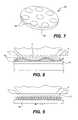
- FIG. 7is a schematic diagonal view of an example of a piezoelectric device
- FIG. 8is a schematic side view of a portion of another immersion lithography apparatus having two mutually attached piezoelectric planar members as the cleaning device;
- FIG. 9is a schematic side view of a portion of another immersion lithography apparatus having a bubble-generating pad as the cleaning device.
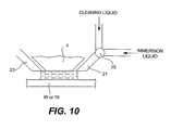
- FIG. 10is a schematic side view of a portion of another immersion lithography apparatus having a switching device incorporated in the fluid-supplying device.
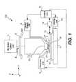
- FIG. 1shows an immersion lithography apparatus 100 to which cleaning methods and systems of this invention may be applied.
- the immersion lithography apparatus 100comprises an illuminator optical unit 1 including a light source such as an excimer laser unit, an optical integrator (or homogenizer) and a lens and serving to emit pulsed ultraviolet light IL with wavelength 248 nm to be made incident to a pattern on a reticle R.
- the pattern on the reticle Ris projected onto a wafer W coated with a photoresist at a specified magnification (such as 1 ⁇ 4 or 1 ⁇ 5) through a telecentric light projection unit PL.
- the pulsed light ILmay alternatively be ArF excimer laser light with wavelength 193 nm, F 2 laser light with wavelength 157 nm or the i-line of a mercury lamp with wavelength 365 nm.
- the coordinate system with X-, Y- and Z-axes as shown in FIG. 1is referenced to explain the directions in describing the structure and functions of the lithography apparatus 100 .
- the light projection unit PLis illustrated in FIG. 1 only by way of its last-stage optical element (such as a lens) 4 disposed opposite to the wafer W and a cylindrical housing 3 containing the rest of its components.
- the reticle Ris supported on a reticle stage RST incorporating a mechanism for moving the reticle R in the X-direction, the Y-direction and the rotary direction around the Z-axis.
- the two-dimensional position and orientation of the reticle R on the reticle stage RSTare detected by a laser interferometer (not shown) in real time and the positioning of the reticle R is affected by a main control unit 14 on the basis of the detection thus made.
- the wafer Wis held by a wafer holder (not shown) on a Z-stage 9 for controlling the focusing position (along the Z-axis) and the tilting angle of the wafer W.
- the Z-stage 9is affixed to an XY-stage 10 adapted to move in the XY-plane substantially parallel to the image-forming surface of the light projection unit PL.
- the XY-stage 10is set on a base 11 .
- the Z-stage 9serves to match the wafer surface with the image surface of the light projection unit PL by adjusting the focusing position (along the Z-axis) and the tilting angle of the wafer W by the auto-focusing and auto-leveling method
- the XY-stage 10serves to adjust the position of the wafer Win the X-direction and the Y-direction.
- the two-dimensional position and orientation of the Z-stage 9(and hence also of the wafer W) are monitored in real time by another laser interferometer 13 with reference to a mobile mirror 12 affixed to the Z-stage 9 .
- Control data based on the results of this monitoringare transmitted from the main control unit 14 to a stage-driving unit 15 adapted to control the motions of the Z-stage 9 and the XY-stage 10 according to the received control data.
- the projection lightis made to sequentially move from one to another of different exposure positions on the wafer W according to the pattern on the reticle R in a step-and-repeat routine or in a step-and-scan routine.
- the lithography apparatus 100 described with reference to FIG. 1is an immersion lithography apparatus and is hence adapted to have a liquid (or the “immersion liquid”) 7 of a specified kind such as water filling the space (the “gap”) between the surface of the wafer W and the lower surface of the last-stage optical element 4 of the light projection unit PL at least while the pattern image of the reticle R is being projected onto the wafer W.
- a liquid (or the “immersion liquid”) 7 of a specified kindsuch as water filling the space (the “gap”) between the surface of the wafer W and the lower surface of the last-stage optical element 4 of the light projection unit PL at least while the pattern image of the reticle R is being projected onto the wafer W.
- the last-stage optical element 4 of the light projection unit PLmay be detachably affixed to the cylindrical housing 3 and is designed such that the liquid 7 will contact only the last-stage optical element 4 and not the cylindrical housing 3 because the housing 3 typically comprises a metallic material and is likely to become corroded.
- the liquid 7is supplied from a liquid supply unit 5 that may comprise a tank, a pressure pump and a temperature regulator (not individually shown) to the space above the wafer W under a temperature-regulated condition and is collected by a liquid recovery unit 6 .
- the temperature of the liquid 7is regulated to be approximately the same as the temperature inside the chamber in which the lithography apparatus 100 itself is disposed.
- Numeral 21indicates supply nozzles through which the liquid 7 is supplied from the supply unit 5 .
- Numeral 23indicates recovery nozzles through which the liquid 7 is collected into the recovery unit 6 .
- the cleaning methods and devices of the inventionare applicable to immersion lithography apparatus of many different kinds.
- the numbers and arrangements of the supply and recovery nozzles 21 and 23 around the light projection unit PLmay be designed in a variety of ways for establishing a smooth flow and quick recovery of the immersion liquid 7 .
- a method embodying this invention of removing the portion of the liquid 7 such as water absorbed by the last-stage optical element 4 made of a hygroscopic material, as well as dirt, debris, etc.,is explained next with reference to FIGS. 1 and 4 .
- the liquid 7is removed from underneath the light projection unit PL and a cleaning device 30 is brought into contact with the last-stage optical element 4 as shown in FIG. 4 .
- the cleaning device 30may be placed on the Z-stage 9 or the aforementioned wafer holder thereon, as shown in FIG. 4 , in place of the wafer W.
- the cleaning device 30may be a container containing a liquid (“cleaning liquid”) having a strong affinity to the immersion liquid 7 that is absorbed by the optical element 4 .
- the immersion liquid 7is water
- the cleaning device 30may contain ethanol because ethanol has a strong affinity to water. Any cleaning liquid may be used provided it has a sufficiently strong affinity to the liquid to be removed and does not damage the optical element 4 or its coating.
- the bottom surface of the optical element 4is soaked in the cleaning liquid for a period of time sufficiently long to reduce the level of the absorbed immersion liquid. The cleaning device 30 is removed thereafter and the optical element 4 is ready to be exposed to the liquid 7 again.
- the cleaning device 30may contain a heat-generating device and/or a vacuum device (not separately shown).
- the combination of heat and vacuum on the surface of the optical element 4causes the absorbed liquid to undergo a phase change into vapor, or to evaporate from the surface.
- the reduction in liquid density on the surface of the optical element 4draws the liquid 7 that is absorbed more deeply in the element 4 to the surface of the optical element 4 .
- FIG. 5shows a third example in which use is made of an ultrasonic transducer (or ultrasonic vibrator) 32 attached to the housing 3 of the light projection unit PL.
- the ultrasonic transducer 32(such as a piezoelectric transducer) is activated, pressure waves are generated and propagated, serving to clean the surface of the optical element 4 .
- the gap adjacent to the optical element 4is filled with the immersion liquid 7 .
- the supply and recovery nozzlescan continue to supply and collect the immersion liquid 7 , or the supply and recovery nozzles can stop supplying and collecting the immersion liquid 7 .
- the optical element 4can face a surface of wafer W, a surface of the Z-stage 9 , or a surface of another assembly.
- FIG. 6is a fourth example using a vibratory tool 34 placed below the optical element 4 to be cleaned.
- the tool 34may be shaped like the wafer W with thickness more or less equal to that of the wafer W, or about 0.5-1 mm, and may be made entirely of a piezoelectric material such that its thickness will fluctuate when activated.
- the tool 34is placed below the optical element 4 , like the wafer W as shown in FIG. 1 , and the gap between the optical element 4 and the tool 34 is filled with the liquid 7 , pressure waves are generated in the immersion liquid 7 to clean the optical element.
- the gap adjacent to the optical element 4is filled with the immersion liquid 7 .
- the supply and recovery nozzlescan continue to supply and collect the immersion liquid, or the supply and recovery nozzles can stop supplying and collecting the immersion liquid 7 .
- the vibrator tool 34may be a ultrasonic transducer attached to the wafer holder on a Z-stage 9 , or another assembly.
- FIG. 7shows another tool 36 , structured alternatively, having a plurality of piezoelectric transducers 38 supported by a planar supporting member 39 .
- FIG. 8shows still another example of a cleaning device having two planar members 40 of a piezoelectric material attached in a face-to-face relationship and adapted to oscillate parallel to each other and out of phase by 180° with respect to each other.
- these members 40attached to each other, will vibrate in the transverse directions, as shown in FIG. 8 in a very exaggerated manner.
- the vibrationhas node points at constant intervals where the members 40 are not displaced.
- the members 40are supported at these node points on a supporting member 41 .
- voltagesare applied to these members 40 so as to cause the vibrations in the mode described above, ultrasonic pressure waves are thereby generated and propagated through the liquid 7 , and the optical element 4 is cleaned, as desired.
- FIG. 9shows still another example of a cleaning device that cleans the optical element 4 by creating cavitating bubbles.
- Cavitating bubbles trapped and energized by ultrasoundare high-temperature, high-pressure microreactors and intense energy released by the implosive compression of the bubbles is believed to rip molecules apart.
- the example shown in FIG. 9is characterized as comprising a pad 43 with fins protruding upward and rapidly moved horizontally as shown by an arrow below the optical element 4 with a bubble-generating liquid 17 filling the gap in between (structure for moving the pad 43 not being shown). As the pad 43 is thus moved, the fins serve to stir the liquid 17 and to generate cavitating bubbles that in turn serve to clean the optical element.
- FIG. 10shows a different approach to the problem of cleaning the last-stage optical element 4 by applying a cleaning liquid on its bottom surface by using the same source nozzles 21 used for supplying the immersion liquid 7 .
- a switch valve 25is inserted between the supply nozzle 21 and the liquid unit 5 such that the immersion liquid 7 and the cleaning liquid can be supplied selectively through the supply nozzle 21 .
- cleaning methods and systems according to this inventionare applicable to immersion lithography apparatus of different kinds and types, for example, having different numbers of source nozzles.
- a switch valve as described aboveneed not necessarily be provided to each of the source nozzles but may be provided to a group of the source nozzles.
- the wafer W itself or a pad 18 of a suitable kindmay be placed below the optical element 4 to provide a suitable gap in between when the cleaning liquid is thus supplied through the supply nozzles 21 .
- This embodiment of the inventionis advantageous because the same nozzles already present for supplying the immersion liquid can be utilized for the cleaning process.
- the pad 43 with fins shown in FIG. 9may be used instead of the pad 18 of FIG. 10 .
- the examples described aboveare not intended to limit the scope of the invention, and many modifications and variations are possible within the scope of this invention.
- a polishing pad similar to one used in chemical mechanical polishingmay be used for this purpose.
- the cleanup procedure shown in FIGS. 4-10may be carried out with ultraviolet light.
- the lightmay irradiate the optical element 4 .
- the lightmay be normal exposure light from the illuminator optical unit 1 or some other light of an appropriate wavelength for the purpose of the cleanup.
- the ultraviolet light for the purpose of the cleanupmay be used without the cleanup procedure shown in FIGS. 4-10 , and may be used under a condition in which the gap adjacent to the optical element 4 is filled with the immersion liquid 7 from the liquid supply unit 5 . All such modifications and variations that may be apparent to a person skilled in the art are intended to be within the scope of this invention.
- any of the above described cleaning methods for removing immersion fluid absorbed by the last-stage optical elementalso may be used to remove salts, deposits, dirt and debris that may have accumulated.
- the term cleaningtherefore refers to both of these phenomena.
- FIG. 2is referenced next to describe a process for fabricating a semiconductor device by using an immersion lithography apparatus incorporating a cleaning device embodying this invention.
- step 301the device's function and performance characteristics are designed.
- step 302a mask (reticle) having a pattern is designed according to the previous designing step, and in a parallel step 303 , a wafer is made from a silicon material.
- the mask pattern designed in step 302is exposed onto the wafer from step 303 in step 304 by a photolithography system such as the systems described above.
- step 305the semiconductor device is assembled (including the dicing process, bonding process and packaging process), then finally the device is inspected in step 306 .
- FIG. 3illustrates a detailed flowchart example of the above-mentioned step 304 in the case of fabricating semiconductor devices.
- step 311oxidation step
- step 312CVD step
- step 313electrode formation step
- step 314ion implantation step
- ionsare implanted in the wafer.
- the aforementioned steps 311 - 314form the preprocessing steps for wafers during wafer processing, and selection is made at each step according to processing requirements.
- step 315photoresist formation step
- step 316exposure step
- step 317developing step
- step 318etching step
- steps other than residual photoresistexposed material surface
- step 319photoresist removal step
Landscapes
- Health & Medical Sciences (AREA)
- Physics & Mathematics (AREA)
- Epidemiology (AREA)
- Public Health (AREA)
- General Physics & Mathematics (AREA)
- Engineering & Computer Science (AREA)
- Life Sciences & Earth Sciences (AREA)
- Atmospheric Sciences (AREA)
- Environmental & Geological Engineering (AREA)
- Plasma & Fusion (AREA)
- Toxicology (AREA)
- Condensed Matter Physics & Semiconductors (AREA)
- Manufacturing & Machinery (AREA)
- Computer Hardware Design (AREA)
- Microelectronics & Electronic Packaging (AREA)
- Power Engineering (AREA)
- Exposure And Positioning Against Photoresist Photosensitive Materials (AREA)
- Exposure Of Semiconductors, Excluding Electron Or Ion Beam Exposure (AREA)
- Crystals, And After-Treatments Of Crystals (AREA)
- Container, Conveyance, Adherence, Positioning, Of Wafer (AREA)
- Cleaning In General (AREA)
- Cleaning By Liquid Or Steam (AREA)
Abstract
Description
This is a divisional of U.S. patent application Ser. No. 12/003,038 filed Dec. 19, 2007 (now U.S. Pat. No. 8,670,103), which in turn is a continuation of U.S. patent application Ser. No. 11/703,802 filed Feb. 8, 2007 (now abandoned), which is a division of U.S. patent application Ser. No. 11/237,651 filed Sep. 29, 2005 (now U.S. Pat. No. 7,522,259), which is a continuation of International Application No. PCT/US2004/010309 filed Apr. 2, 2004, which claims the benefit of U.S. Provisional Patent Application No. 60/462,556 filed Apr. 11, 2003 and U.S. Provisional Patent Application No. 60/482,913 filed Jun. 27, 2003. The disclosures of each of these applications are hereby incorporated by reference herein in their entirety.
This invention relates to an immersion lithography system and more particularly to methods, as well as systems, for cleaning up the optical element that contacts and absorbs water in the process of immersion lithography.
Immersion lithography systems, such as disclosed in W099/49504, which is herein incorporated by reference for describing the general background of the technology as well as some general considerations related thereto, are adapted to supply a liquid into the space between a workpiece such as a wafer and the last-stage optical element of an optical system for projecting the image of a reticle onto the workpiece. The liquid thus supplied improves the performance of the optical system and the quality of the exposure.
The liquid to be supplied may be water for light with wavelength of 193 nm although different liquids may be necessary for light with other wavelengths. Because the last-stage optical element of the optical system is exposed to the liquid, there is a possibility that some of the liquid may be absorbed. This possibility is particularly high if the last-stage optical element of the optical system is a lens because calcium fluoride is a common lens material for lithography systems while it is a hygroscopic material that is capable of absorbing water from the surrounding environment.
The absorbed water may cause several problems. First, it may degrade the image projected by the lens by changing the refractive properties of the lens or by causing the lens to swell to thereby change the geometry of the lens. Second, it may cause long-term degradation of the lens due to chemical effects.
Conventional air-immersion exposure lithography systems require the optical elements to be made detachable for maintenance work such as when they are cleaned. It is a cumbersome and time-consuming operation, however, to remove an optical element and to reset it after it is cleaned or to exchange an optical element for a new one.
It is therefore an object of this invention to provide systems and methods for periodically removing the water from the lens such that the amount of absorbed water will not reach a critical level and the degradation of the image and the long-term damage to the lens can be prevented.
It is another object of the invention to provide systems and methods for making the maintenance of the optical element of an immersion lithography apparatus easier and thereby improve the useful lifetime of the optical element.
Immersion lithography apparatus of this invention may include a reticle stage arranged to retain a reticle, a working stage arranged to retain a workpiece, an optical system including an illumination source and an optical element opposite the workpiece for projecting an image pattern of the reticle onto the workpiece by radiation from the illumination source while defining a gap between the optical element and the workpiece, and a fluid-supplying device for providing an immersion liquid between and contacting both the optical element and the workpiece during an immersion lithography process. The apparatus also includes a cleaning device to clean the optical element. The term “cleaning” will be used throughout this disclosure to mean both removing immersion liquid that has been absorbed into the optical element and removing dirt, debris, salts and the like from the optical element.
Many different kinds of cleaning devices may be used within the scope of this invention. For example, the cleaning device may use a cleaning liquid having affinity to the immersion liquid to be contacted with the optical element. If the immersion liquid is water, ethanol may serve as the cleaning liquid. As another example, the cleaning device may include a heat-generating device for heating the optical element and/or a vacuum device for generating a vacuum condition on the optical element.
Ultrasonic vibrations may be used for removing the absorbed liquid. An ultrasonic vibrator such as a piezoelectric transducer may be attached to the housing for the optical element or placed opposite the optical element such that the vibrations may be transmitted to the optical element through a liquid maintained in the gap.
Alternatively, cavitating bubbles may be used for the removal of the absorbed liquid. A pad with fins may be used to generate cavitating bubbles in a liquid maintained in the gap between the pad and the optical element.
According to another embodiment of the invention, the nozzles through which the immersion liquid is supplied into the gap between the workpiece and the optical element may be used to alternately supply a cleaning liquid by providing a flow route-switching device such as a switch valve.
With a system and method of this invention, the cleaning procedure becomes significantly easier and faster because there is no need to detach the optical element to be cleaned and the cleaning process improves the useful lifetime of the optical element.
The invention will be described in conjunction with the following drawings of exemplary embodiments in which like reference numerals designate like elements, and in which:
As shown inFIG. 1 , theimmersion lithography apparatus 100 comprises an illuminatoroptical unit 1 including a light source such as an excimer laser unit, an optical integrator (or homogenizer) and a lens and serving to emit pulsed ultraviolet light IL with wavelength 248 nm to be made incident to a pattern on a reticle R. The pattern on the reticle R is projected onto a wafer W coated with a photoresist at a specified magnification (such as ¼ or ⅕) through a telecentric light projection unit PL. The pulsed light IL may alternatively be ArF excimer laser light with wavelength 193 nm, F2laser light with wavelength 157 nm or the i-line of a mercury lamp with wavelength 365 nm. In what follows, the coordinate system with X-, Y- and Z-axes as shown inFIG. 1 is referenced to explain the directions in describing the structure and functions of thelithography apparatus 100. For the convenience of disclosure and description, the light projection unit PL is illustrated inFIG. 1 only by way of its last-stage optical element (such as a lens)4 disposed opposite to the wafer W and acylindrical housing 3 containing the rest of its components.
The reticle R is supported on a reticle stage RST incorporating a mechanism for moving the reticle R in the X-direction, the Y-direction and the rotary direction around the Z-axis. The two-dimensional position and orientation of the reticle R on the reticle stage RST are detected by a laser interferometer (not shown) in real time and the positioning of the reticle R is affected by amain control unit 14 on the basis of the detection thus made.
The wafer W is held by a wafer holder (not shown) on a Z-stage 9 for controlling the focusing position (along the Z-axis) and the tilting angle of the wafer W. The Z-stage 9 is affixed to an XY-stage 10 adapted to move in the XY-plane substantially parallel to the image-forming surface of the light projection unit PL. The XY-stage 10 is set on abase 11. Thus, the Z-stage 9 serves to match the wafer surface with the image surface of the light projection unit PL by adjusting the focusing position (along the Z-axis) and the tilting angle of the wafer W by the auto-focusing and auto-leveling method, and the XY-stage 10 serves to adjust the position of the wafer Win the X-direction and the Y-direction.
The two-dimensional position and orientation of the Z-stage9 (and hence also of the wafer W) are monitored in real time by anotherlaser interferometer 13 with reference to amobile mirror 12 affixed to the Z-stage 9. Control data based on the results of this monitoring are transmitted from themain control unit 14 to a stage-driving unit 15 adapted to control the motions of the Z-stage 9 and the XY-stage 10 according to the received control data. At the time of an exposure, the projection light is made to sequentially move from one to another of different exposure positions on the wafer W according to the pattern on the reticle R in a step-and-repeat routine or in a step-and-scan routine.
Thelithography apparatus 100 described with reference toFIG. 1 is an immersion lithography apparatus and is hence adapted to have a liquid (or the “immersion liquid”)7 of a specified kind such as water filling the space (the “gap”) between the surface of the wafer W and the lower surface of the last-stageoptical element 4 of the light projection unit PL at least while the pattern image of the reticle R is being projected onto the wafer W.
The last-stageoptical element 4 of the light projection unit PL may be detachably affixed to thecylindrical housing 3 and is designed such that theliquid 7 will contact only the last-stageoptical element 4 and not thecylindrical housing 3 because thehousing 3 typically comprises a metallic material and is likely to become corroded.
Theliquid 7 is supplied from aliquid supply unit 5 that may comprise a tank, a pressure pump and a temperature regulator (not individually shown) to the space above the wafer W under a temperature-regulated condition and is collected by aliquid recovery unit 6. The temperature of theliquid 7 is regulated to be approximately the same as the temperature inside the chamber in which thelithography apparatus 100 itself is disposed.Numeral 21 indicates supply nozzles through which theliquid 7 is supplied from thesupply unit 5.Numeral 23 indicates recovery nozzles through which theliquid 7 is collected into therecovery unit 6. The structure described above with reference toFIG. 1 is not intended to limit the scope of the immersion lithography apparatus to which the cleaning methods and devices of the invention are applicable. In other words, the cleaning methods and devices of the invention are applicable to immersion lithography apparatus of many different kinds. In particular, the numbers and arrangements of the supply andrecovery nozzles immersion liquid 7.
A method embodying this invention of removing the portion of the liquid7 such as water absorbed by the last-stageoptical element 4 made of a hygroscopic material, as well as dirt, debris, etc., is explained next with reference toFIGS. 1 and 4 . After the wafer W is exposed with light from the illuminatoroptical unit 1 through the light projection unit PL in the presence of the liquid7 as shown inFIG. 1 , theliquid 7 is removed from underneath the light projection unit PL and acleaning device 30 is brought into contact with the last-stageoptical element 4 as shown inFIG. 4 . In the case of a portable kind, as shown inFIG. 4 , thecleaning device 30 may be placed on the Z-stage 9 or the aforementioned wafer holder thereon, as shown inFIG. 4 , in place of the wafer W.
Different types and kinds of cleaningdevices 30 can be used for the purpose of this invention. As a first example, thecleaning device 30 may be a container containing a liquid (“cleaning liquid”) having a strong affinity to theimmersion liquid 7 that is absorbed by theoptical element 4. If theimmersion liquid 7 is water, thecleaning device 30 may contain ethanol because ethanol has a strong affinity to water. Any cleaning liquid may be used provided it has a sufficiently strong affinity to the liquid to be removed and does not damage theoptical element 4 or its coating. The bottom surface of theoptical element 4 is soaked in the cleaning liquid for a period of time sufficiently long to reduce the level of the absorbed immersion liquid. Thecleaning device 30 is removed thereafter and theoptical element 4 is ready to be exposed to theliquid 7 again.
As another example, thecleaning device 30 may contain a heat-generating device and/or a vacuum device (not separately shown). The combination of heat and vacuum on the surface of theoptical element 4 causes the absorbed liquid to undergo a phase change into vapor, or to evaporate from the surface. The reduction in liquid density on the surface of theoptical element 4 draws theliquid 7 that is absorbed more deeply in theelement 4 to the surface of theoptical element 4.
During the cleaning operation inFIG. 5 , the gap adjacent to theoptical element 4 is filled with theimmersion liquid 7. In this case, the supply and recovery nozzles can continue to supply and collect theimmersion liquid 7, or the supply and recovery nozzles can stop supplying and collecting theimmersion liquid 7. Also during the cleaning operation, theoptical element 4 can face a surface of wafer W, a surface of the Z-stage 9, or a surface of another assembly.
During the cleaning operation ofFIG. 6 , the gap adjacent to theoptical element 4 is filled with theimmersion liquid 7. In this case, the supply and recovery nozzles can continue to supply and collect the immersion liquid, or the supply and recovery nozzles can stop supplying and collecting theimmersion liquid 7. In another example, thevibrator tool 34 may be a ultrasonic transducer attached to the wafer holder on a Z-stage 9, or another assembly.
It is again noted that the cleaning methods and systems according to this invention are applicable to immersion lithography apparatus of different kinds and types, for example, having different numbers of source nozzles. A switch valve as described above need not necessarily be provided to each of the source nozzles but may be provided to a group of the source nozzles.
The wafer W itself or apad 18 of a suitable kind may be placed below theoptical element 4 to provide a suitable gap in between when the cleaning liquid is thus supplied through thesupply nozzles 21. This embodiment of the invention is advantageous because the same nozzles already present for supplying the immersion liquid can be utilized for the cleaning process.
Although various methods have been separately described above, they may be used in combinations, although that is not separately illustrated in the drawings. For example, thepad 43 with fins shown inFIG. 9 may be used instead of thepad 18 ofFIG. 10 . In other words, the examples described above are not intended to limit the scope of the invention, and many modifications and variations are possible within the scope of this invention. For example, a polishing pad similar to one used in chemical mechanical polishing may be used for this purpose. The cleanup procedure shown inFIGS. 4-10 may be carried out with ultraviolet light. The light may irradiate theoptical element 4. The light may be normal exposure light from the illuminatoroptical unit 1 or some other light of an appropriate wavelength for the purpose of the cleanup. In another example, the ultraviolet light for the purpose of the cleanup may be used without the cleanup procedure shown inFIGS. 4-10 , and may be used under a condition in which the gap adjacent to theoptical element 4 is filled with theimmersion liquid 7 from theliquid supply unit 5. All such modifications and variations that may be apparent to a person skilled in the art are intended to be within the scope of this invention.
Any of the above described cleaning methods for removing immersion fluid absorbed by the last-stage optical element also may be used to remove salts, deposits, dirt and debris that may have accumulated. The term cleaning therefore refers to both of these phenomena.
At each stage of wafer processing, when the above-mentioned preprocessing steps have been completed, the following post-processing steps are implemented. During post-processing, initially, in step315 (photoresist formation step), photoresist is applied to a wafer. Next, in step316 (exposure step), the above-mentioned exposure device is used to transfer the circuit pattern of a mask (reticle) onto a wafer. Then, in step317 (developing step), the exposed wafer is developed, and in step318 (etching step), parts other than residual photoresist (exposed material surface) are removed by etching. In step319 (photoresist removal step), unnecessary photoresist remaining after etching is removed. Multiple circuit patterns are formed by repetition of these preprocessing and post-processing steps.
While a lithography system of this invention has been described in terms of several preferred embodiments, there are alterations, permutations, and various substitute equivalents which fall within the scope of this invention. There are many alternative ways of implementing the methods and apparatus of the invention.
Claims (35)
1. A method used in an immersion lithography apparatus, the method comprising:
placing an object for a cleanup process on a holder of a movable stage of the immersion lithography apparatus in which a wafer is held on the holder of the stage and is exposed via immersion liquid between a projection system and the wafer during a liquid immersion lithography process; and
supplying, for use in the cleanup process, a cleaning liquid via a supply port from above the stage holding the object on the holder,
wherein:
during the liquid immersion lithography process, the wafer held on the holder is exposed through the immersion liquid that is different from the cleaning liquid,
during the cleanup process, the object is held on the holder in place of the wafer,
the supply port is arranged adjacent to the projection system of the immersion lithography apparatus,
the supply port supplies the cleaning liquid for use in the cleanup process and also supplies the immersion liquid during the liquid immersion lithography process, and
the object held on the holder for the cleanup process is not the wafer that was held on the holder during the liquid immersion lithography process.
2. The method according toclaim 1 , wherein the stage is movable below a member to be cleaned during the cleanup process.
3. The method according toclaim 2 , wherein a device pattern image is projected onto the wafer by the projection system during the liquid immersion lithography process, and wherein the member to be cleaned includes an optical element of the projection system.
4. The method according toclaim 1 , wherein during the cleanup process, the cleaning liquid is supplied from the supply port in a state in which the stage is under the supply port.
5. The method according toclaim 4 , wherein during the cleanup process, the cleaning liquid is supplied onto the object held on the holder of the stage.
6. The method according toclaim 5 , wherein:
a device pattern image is projected onto the wafer by the projection system during the liquid immersion lithography process, and
the supplied cleaning liquid is retained in a space between the projection system and the object held on the holder during the cleanup process.
7. The method according toclaim 1 , wherein the object includes a cleaning device.
8. The method according toclaim 1 , wherein the object is shaped like the wafer.
9. The method according toclaim 1 , wherein the object has a thickness substantially equal to a thickness of the wafer.
10. The method according toclaim 1 , wherein the object has a thickness of about 0.5-1 mm.
11. The method according toclaim 1 , wherein the wafer has a coated photoresist, and during the cleanup process, the object has no photoresist and is held on the holder.
12. The method according toclaim 1 , wherein:
a device pattern image is projected onto the wafer through the immersion liquid during the liquid immersion lithography process, and
the cleaning liquid is supplied from the supply port during the cleanup process, after removing the immersion liquid.
13. The method according toclaim 1 , wherein the cleanup process is performed after the wafer is exposed.
14. The method according toclaim 1 , wherein the supply of the cleaning liquid from the supply port and collection of the supplied cleaning liquid continue during the cleanup process.
15. The method according toclaim 1 , wherein the supply of the cleaning liquid from the supply port and collection of the supplied cleaning liquid are stopped during the cleanup process.
16. The method according toclaim 1 , wherein the cleanup process is carried out with exposure light used for exposing the wafer.
17. The method according toclaim 1 , wherein ultrasonic vibrations are generated by an ultrasonic vibrator in the cleanup process.
18. An immersion lithography apparatus comprising:
a projection system;
a movable stage having a holder configured to hold a wafer during exposure of the wafer in a liquid immersion lithography process, the holder being configured to hold an object in place of the wafer during a cleanup process; and
a liquid supply system having a supply port disposed above the stage and configured to supply, for use in the cleanup process, a cleaning liquid via the supply port from above the stage holding the object on the holder, the cleaning liquid being different from an immersion liquid,
wherein:
during the liquid immersion lithography process, the wafer held on the holder is exposed through the immersion liquid between the projection system and the wafer,
during the cleanup process, the immersion lithography apparatus holds the object on the holder in place of the wafer, and utilizes the cleaning liquid supplied via the supply port from above the stage holding the object on the holder,
the supply port is arranged adjacent to the projection system of the immersion lithography apparatus,
the supply port supplies the cleaning liquid for use in the cleanup process and also supplies the immersion liquid during the liquid immersion lithography process and
the object held on the holder for the cleanup process is not the wafer that was held on the holder during the liquid immersion lithography process.
19. The apparatus according toclaim 18 , wherein the stage is movable below a member to be cleaned during the cleanup process.
20. The apparatus according toclaim 19 , wherein a device pattern image is projected onto the wafer by the projection system during the liquid immersion lithography process, and wherein the member to be cleaned includes an optical element of the projection system.
21. The apparatus according toclaim 18 , wherein during the cleanup process, the liquid supply system supplies the cleaning liquid from the supply port in a state in which the stage is under the supply port.
22. The apparatus according toclaim 21 , wherein during the cleanup process, the liquid supply system supplies the cleaning liquid onto the object held on the holder of the stage.
23. The apparatus according toclaim 22 , wherein:
the projection system is configured to project a device pattern image onto the wafer during the liquid immersion lithography process, and
the supplied cleaning liquid is retained in a space between the projection system and the object held on the holder during the cleanup process.
24. The apparatus according toclaim 18 , wherein the object includes a cleaning device.
25. The apparatus according toclaim 18 , wherein the object is shaped like the wafer.
26. The apparatus according toclaim 18 , wherein the object has a thickness substantially equal to a thickness of the wafer.
27. The apparatus according toclaim 18 , wherein the object has a thickness of about 0.5-1 mm.
28. The apparatus according toclaim 18 , wherein the wafer has a coated photoresist, and during the cleanup process, the immersion lithography apparatus holds the object, which has no photoresist, on the holder.
29. The apparatus according toclaim 18 , wherein:
a device pattern image is projected onto the wafer through the immersion liquid during the liquid immersion lithography process, and
the liquid supply system supplies the cleaning liquid from the supply port during the cleanup process, after removing the immersion liquid.
30. The apparatus according toclaim 18 , wherein the apparatus performs the cleanup process after the wafer is exposed.
31. The apparatus according toclaim 18 , wherein the supply of the cleaning liquid from the supply port and collection of the supplied cleaning liquid continue during the cleanup process.
32. The apparatus according toclaim 18 , wherein the supply of the cleaning liquid from the supply port and collection of the supplied cleaning liquid are stopped during the cleanup process.
33. The apparatus according toclaim 18 , wherein the cleanup process is carried out with exposure light used for exposing the wafer.
34. The apparatus according toclaim 18 , wherein ultrasonic vibrations are generated by an ultrasonic vibrator in the cleanup process.
35. An immersion lithography apparatus comprising:
a projection system;
a movable stage having a holder configured to hold a wafer during exposure of the wafer in a liquid immersion lithography process;
an object configured to be held by the holder in place of the wafer during a cleanup process; and
a liquid supply system having a supply port disposed above the stage and configured to supply, during the cleanup process, a cleaning liquid via the supply port from above the stage holding the object on the holder, the cleaning liquid being different from an immersion liquid,
wherein:
during the liquid immersion lithography process, the wafer held on the holder is exposed through the immersion liquid between the projection system and the wafer,
during the cleanup process, the immersion lithography apparatus holds the object on the holder in place of the wafer, and supplies the cleaning liquid via the supply port from above the stage holding the object on the holder,
the supply port is arranged adjacent to the projection system of the immersion lithography apparatus,
the supply port supplies the cleaning liquid for use in the cleanup process and also supplies the immersion liquid during the liquid immersion lithography process, and
the object held on the holder for the cleanup process is not the wafer that was held on the holder during the liquid immersion lithography process.
Priority Applications (2)
| Application Number | Priority Date | Filing Date | Title |
|---|---|---|---|
| US14/161,072US9958786B2 (en) | 2003-04-11 | 2014-01-22 | Cleanup method for optics in immersion lithography using object on wafer holder in place of wafer |
| US15/921,121US20180203366A1 (en) | 2003-04-11 | 2018-03-14 | Cleanup method for optics in immersion lithography |
Applications Claiming Priority (7)
| Application Number | Priority Date | Filing Date | Title |
|---|---|---|---|
| US46255603P | 2003-04-11 | 2003-04-11 | |
| US48291303P | 2003-06-27 | 2003-06-27 | |
| PCT/US2004/010309WO2004093130A2 (en) | 2003-04-11 | 2004-04-02 | Cleanup method for optics in immersion lithography |
| US11/237,651US7522259B2 (en) | 2003-04-11 | 2005-09-29 | Cleanup method for optics in immersion lithography |
| US11/703,802US20070171390A1 (en) | 2003-04-11 | 2007-02-08 | Cleanup method for optics in immersion lithography |
| US12/003,038US8670103B2 (en) | 2003-04-11 | 2007-12-19 | Cleanup method for optics in immersion lithography using bubbles |
| US14/161,072US9958786B2 (en) | 2003-04-11 | 2014-01-22 | Cleanup method for optics in immersion lithography using object on wafer holder in place of wafer |
Related Parent Applications (1)
| Application Number | Title | Priority Date | Filing Date |
|---|---|---|---|
| US12/003,038DivisionUS8670103B2 (en) | 2003-04-11 | 2007-12-19 | Cleanup method for optics in immersion lithography using bubbles |
Related Child Applications (1)
| Application Number | Title | Priority Date | Filing Date |
|---|---|---|---|
| US15/921,121DivisionUS20180203366A1 (en) | 2003-04-11 | 2018-03-14 | Cleanup method for optics in immersion lithography |
Publications (2)
| Publication Number | Publication Date |
|---|---|
| US20140132939A1 US20140132939A1 (en) | 2014-05-15 |
| US9958786B2true US9958786B2 (en) | 2018-05-01 |
Family
ID=33303091
Family Applications (10)
| Application Number | Title | Priority Date | Filing Date |
|---|---|---|---|
| US11/237,651Expired - Fee RelatedUS7522259B2 (en) | 2003-04-11 | 2005-09-29 | Cleanup method for optics in immersion lithography |
| US11/703,802AbandonedUS20070171390A1 (en) | 2003-04-11 | 2007-02-08 | Cleanup method for optics in immersion lithography |
| US11/704,241Expired - Fee RelatedUS8085381B2 (en) | 2003-04-11 | 2007-02-09 | Cleanup method for optics in immersion lithography using sonic device |
| US11/812,924AbandonedUS20070247601A1 (en) | 2003-04-11 | 2007-06-22 | Cleanup method for optics in immersion lithography |
| US12/003,038Expired - Fee RelatedUS8670103B2 (en) | 2003-04-11 | 2007-12-19 | Cleanup method for optics in immersion lithography using bubbles |
| US12/379,171Expired - Fee RelatedUS8269946B2 (en) | 2003-04-11 | 2009-02-13 | Cleanup method for optics in immersion lithography supplying cleaning liquid at different times than immersion liquid |
| US12/382,078Expired - Fee RelatedUS8493545B2 (en) | 2003-04-11 | 2009-03-09 | Cleanup method for optics in immersion lithography supplying cleaning liquid onto a surface of object below optical element, liquid supply port and liquid recovery port |
| US12/382,162Expired - Fee RelatedUS8670104B2 (en) | 2003-04-11 | 2009-03-10 | Cleanup method for optics in immersion lithography with cleaning liquid opposed by a surface of object |
| US14/161,072Expired - Fee RelatedUS9958786B2 (en) | 2003-04-11 | 2014-01-22 | Cleanup method for optics in immersion lithography using object on wafer holder in place of wafer |
| US15/921,121AbandonedUS20180203366A1 (en) | 2003-04-11 | 2018-03-14 | Cleanup method for optics in immersion lithography |
Family Applications Before (8)
| Application Number | Title | Priority Date | Filing Date |
|---|---|---|---|
| US11/237,651Expired - Fee RelatedUS7522259B2 (en) | 2003-04-11 | 2005-09-29 | Cleanup method for optics in immersion lithography |
| US11/703,802AbandonedUS20070171390A1 (en) | 2003-04-11 | 2007-02-08 | Cleanup method for optics in immersion lithography |
| US11/704,241Expired - Fee RelatedUS8085381B2 (en) | 2003-04-11 | 2007-02-09 | Cleanup method for optics in immersion lithography using sonic device |
| US11/812,924AbandonedUS20070247601A1 (en) | 2003-04-11 | 2007-06-22 | Cleanup method for optics in immersion lithography |
| US12/003,038Expired - Fee RelatedUS8670103B2 (en) | 2003-04-11 | 2007-12-19 | Cleanup method for optics in immersion lithography using bubbles |
| US12/379,171Expired - Fee RelatedUS8269946B2 (en) | 2003-04-11 | 2009-02-13 | Cleanup method for optics in immersion lithography supplying cleaning liquid at different times than immersion liquid |
| US12/382,078Expired - Fee RelatedUS8493545B2 (en) | 2003-04-11 | 2009-03-09 | Cleanup method for optics in immersion lithography supplying cleaning liquid onto a surface of object below optical element, liquid supply port and liquid recovery port |
| US12/382,162Expired - Fee RelatedUS8670104B2 (en) | 2003-04-11 | 2009-03-10 | Cleanup method for optics in immersion lithography with cleaning liquid opposed by a surface of object |
Family Applications After (1)
| Application Number | Title | Priority Date | Filing Date |
|---|---|---|---|
| US15/921,121AbandonedUS20180203366A1 (en) | 2003-04-11 | 2018-03-14 | Cleanup method for optics in immersion lithography |
Country Status (9)
| Country | Link |
|---|---|
| US (10) | US7522259B2 (en) |
| EP (6) | EP2172809B1 (en) |
| JP (10) | JP4837556B2 (en) |
| KR (11) | KR101324818B1 (en) |
| CN (4) | CN101825847B (en) |
| AT (1) | ATE449982T1 (en) |
| DE (1) | DE602004024295D1 (en) |
| SG (5) | SG2014015135A (en) |
| WO (1) | WO2004093130A2 (en) |
Cited By (1)
| Publication number | Priority date | Publication date | Assignee | Title |
|---|---|---|---|---|
| US20180203366A1 (en)* | 2003-04-11 | 2018-07-19 | Nikon Corporation | Cleanup method for optics in immersion lithography |
Families Citing this family (226)
| Publication number | Priority date | Publication date | Assignee | Title |
|---|---|---|---|---|
| US9482966B2 (en) | 2002-11-12 | 2016-11-01 | Asml Netherlands B.V. | Lithographic apparatus and device manufacturing method |
| DE60335595D1 (en) | 2002-11-12 | 2011-02-17 | Asml Netherlands Bv | Immersion lithographic apparatus and method of making a device |
| US7372541B2 (en) | 2002-11-12 | 2008-05-13 | Asml Netherlands B.V. | Lithographic apparatus and device manufacturing method |
| KR100585476B1 (en) | 2002-11-12 | 2006-06-07 | 에이에스엠엘 네델란즈 비.브이. | Lithographic Apparatus and Device Manufacturing Method |
| CN100568101C (en) | 2002-11-12 | 2009-12-09 | Asml荷兰有限公司 | Photolithography apparatus and device manufacturing method |
| US10503084B2 (en) | 2002-11-12 | 2019-12-10 | Asml Netherlands B.V. | Lithographic apparatus and device manufacturing method |
| EP1420299B1 (en)* | 2002-11-12 | 2011-01-05 | ASML Netherlands B.V. | Immersion lithographic apparatus and device manufacturing method |
| KR20120127755A (en) | 2002-12-10 | 2012-11-23 | 가부시키가이샤 니콘 | Exposure apparatus and method for manufacturing device |
| KR101101737B1 (en) | 2002-12-10 | 2012-01-05 | 가부시키가이샤 니콘 | Exposure apparatus, exposure method and method for manufacturing device |
| US7242455B2 (en) | 2002-12-10 | 2007-07-10 | Nikon Corporation | Exposure apparatus and method for producing device |
| EP1571694A4 (en) | 2002-12-10 | 2008-10-15 | Nikon Corp | Exposure apparatus and method for manufacturing device |
| JP4352874B2 (en) | 2002-12-10 | 2009-10-28 | 株式会社ニコン | Exposure apparatus and device manufacturing method |
| US7948604B2 (en) | 2002-12-10 | 2011-05-24 | Nikon Corporation | Exposure apparatus and method for producing device |
| WO2004053955A1 (en) | 2002-12-10 | 2004-06-24 | Nikon Corporation | Exposure system and device producing method |
| DE10261775A1 (en) | 2002-12-20 | 2004-07-01 | Carl Zeiss Smt Ag | Device for the optical measurement of an imaging system |
| EP2466623B1 (en) | 2003-02-26 | 2015-04-22 | Nikon Corporation | Exposure apparatus, exposure method, and method for producing device |
| KR20050110033A (en) | 2003-03-25 | 2005-11-22 | 가부시키가이샤 니콘 | Exposure system and device production method |
| EP1612850B1 (en) | 2003-04-07 | 2009-03-25 | Nikon Corporation | Exposure apparatus and method for manufacturing a device |
| WO2004093159A2 (en) | 2003-04-09 | 2004-10-28 | Nikon Corporation | Immersion lithography fluid control system |
| EP2950147B1 (en) | 2003-04-10 | 2017-04-26 | Nikon Corporation | Environmental system including vaccum scavenge for an immersion lithography apparatus |
| EP3352010A1 (en) | 2003-04-10 | 2018-07-25 | Nikon Corporation | Run-off path to collect liquid for an immersion lithography apparatus |
| EP3062152B1 (en) | 2003-04-10 | 2017-12-20 | Nikon Corporation | Environmental system including vaccum scavenge for an immersion lithography apparatus |
| KR101225884B1 (en) | 2003-04-11 | 2013-01-28 | 가부시키가이샤 니콘 | Apparatus and method for maintaining immersion fluid in the gap under the projection lens during wafer exchange in an immersion lithography machine |
| JP4582089B2 (en) | 2003-04-11 | 2010-11-17 | 株式会社ニコン | Liquid jet recovery system for immersion lithography |
| SG194246A1 (en) | 2003-04-17 | 2013-11-29 | Nikon Corp | Optical arrangement of autofocus elements for use with immersion lithography |
| TWI295414B (en) | 2003-05-13 | 2008-04-01 | Asml Netherlands Bv | Lithographic apparatus and device manufacturing method |
| KR20060009356A (en) | 2003-05-15 | 2006-01-31 | 가부시키가이샤 니콘 | Exposure apparatus and device manufacturing method |
| TWI421906B (en) | 2003-05-23 | 2014-01-01 | 尼康股份有限公司 | An exposure method, an exposure apparatus, and an element manufacturing method |
| TW201806001A (en)* | 2003-05-23 | 2018-02-16 | 尼康股份有限公司 | Exposure device and device manufacturing method |
| KR101548832B1 (en) | 2003-05-28 | 2015-09-01 | 가부시키가이샤 니콘 | Exposure method, exposure device, and device manufacturing method |
| US7213963B2 (en) | 2003-06-09 | 2007-05-08 | Asml Netherlands B.V. | Lithographic apparatus and device manufacturing method |
| US7317504B2 (en) | 2004-04-08 | 2008-01-08 | Asml Netherlands B.V. | Lithographic apparatus and device manufacturing method |
| EP2261741A3 (en) | 2003-06-11 | 2011-05-25 | ASML Netherlands B.V. | Lithographic apparatus and device manufacturing method |
| KR101242815B1 (en) | 2003-06-13 | 2013-03-12 | 가부시키가이샤 니콘 | Exposure method, substrate stage, exposure apparatus and method for manufacturing device |
| TW201721717A (en) | 2003-06-19 | 2017-06-16 | 尼康股份有限公司 | Exposure apparatus, exposure method, and device manufacturing method |
| US6867844B2 (en) | 2003-06-19 | 2005-03-15 | Asml Holding N.V. | Immersion photolithography system and method using microchannel nozzles |
| US6809794B1 (en) | 2003-06-27 | 2004-10-26 | Asml Holding N.V. | Immersion photolithography system and method using inverted wafer-projection optics interface |
| EP1491956B1 (en) | 2003-06-27 | 2006-09-06 | ASML Netherlands B.V. | Lithographic apparatus and device manufacturing method |
| KR20060027832A (en) | 2003-07-01 | 2006-03-28 | 가부시키가이샤 니콘 | Method of Using Isotopically Specified Fluids as Optical Elements |
| EP3179309A1 (en) | 2003-07-08 | 2017-06-14 | Nikon Corporation | Wafer table for immersion lithography |
| WO2005006418A1 (en) | 2003-07-09 | 2005-01-20 | Nikon Corporation | Exposure apparatus and method for manufacturing device |
| EP1643543B1 (en) | 2003-07-09 | 2010-11-24 | Nikon Corporation | Exposure apparatus and method for manufacturing device |
| WO2005006415A1 (en) | 2003-07-09 | 2005-01-20 | Nikon Corporation | Exposure apparatus and method for manufacturing device |
| WO2005010960A1 (en) | 2003-07-25 | 2005-02-03 | Nikon Corporation | Inspection method and inspection device for projection optical system, and production method for projection optical system |
| US7175968B2 (en) | 2003-07-28 | 2007-02-13 | Asml Netherlands B.V. | Lithographic apparatus, device manufacturing method and a substrate |
| EP1503244A1 (en) | 2003-07-28 | 2005-02-02 | ASML Netherlands B.V. | Lithographic projection apparatus and device manufacturing method |
| KR101641011B1 (en) | 2003-07-28 | 2016-07-19 | 가부시키가이샤 니콘 | Exposure apparatus, device producing method, and exposure apparatus controlling method |
| US7326522B2 (en) | 2004-02-11 | 2008-02-05 | Asml Netherlands B.V. | Device manufacturing method and a substrate |
| US7779781B2 (en) | 2003-07-31 | 2010-08-24 | Asml Netherlands B.V. | Lithographic apparatus and device manufacturing method |
| US7370659B2 (en)* | 2003-08-06 | 2008-05-13 | Micron Technology, Inc. | Photolithographic stepper and/or scanner machines including cleaning devices and methods of cleaning photolithographic stepper and/or scanner machines |
| TWI245163B (en)* | 2003-08-29 | 2005-12-11 | Asml Netherlands Bv | Lithographic apparatus and device manufacturing method |
| KR101380989B1 (en) | 2003-08-29 | 2014-04-04 | 가부시키가이샤 니콘 | Exposure apparatus and device producing method |
| TWI263859B (en) | 2003-08-29 | 2006-10-11 | Asml Netherlands Bv | Lithographic apparatus and device manufacturing method |
| EP3223053A1 (en) | 2003-09-03 | 2017-09-27 | Nikon Corporation | Apparatus and method for providing fluid for immersion lithography |
| JP4444920B2 (en) | 2003-09-19 | 2010-03-31 | 株式会社ニコン | Exposure apparatus and device manufacturing method |
| JP4438747B2 (en) | 2003-09-26 | 2010-03-24 | 株式会社ニコン | Projection exposure apparatus, projection exposure apparatus cleaning method, maintenance method, and device manufacturing method |
| EP2837969B1 (en) | 2003-09-29 | 2016-04-20 | Nikon Corporation | Exposure apparatus, exposure method, and method for producing device |
| KR20060126949A (en) | 2003-10-08 | 2006-12-11 | 가부시키가이샤 니콘 | Substrate conveyance apparatus and substrate conveyance method, exposure apparatus, exposure method, and device manufacturing method |
| JP2005136364A (en) | 2003-10-08 | 2005-05-26 | Zao Nikon Co Ltd | Substrate transport apparatus, exposure apparatus, and device manufacturing method |
| KR101203028B1 (en) | 2003-10-08 | 2012-11-21 | 가부시키가이샤 자오 니콘 | Substrate carrying apparatus, substrate carrying method, exposure apparatus, exposure method, and method for producing device |
| TWI553701B (en) | 2003-10-09 | 2016-10-11 | 尼康股份有限公司 | Exposure apparatus and exposure method, component manufacturing method |
| US7352433B2 (en) | 2003-10-28 | 2008-04-01 | Asml Netherlands B.V. | Lithographic apparatus and device manufacturing method |
| US7411653B2 (en) | 2003-10-28 | 2008-08-12 | Asml Netherlands B.V. | Lithographic apparatus |
| EP1531362A3 (en)* | 2003-11-13 | 2007-07-25 | Matsushita Electric Industrial Co., Ltd. | Semiconductor manufacturing apparatus and pattern formation method |
| US7528929B2 (en) | 2003-11-14 | 2009-05-05 | Asml Netherlands B.V. | Lithographic apparatus and device manufacturing method |
| KR101394764B1 (en) | 2003-12-03 | 2014-05-27 | 가부시키가이샤 니콘 | Exposure apparatus, exposure method, device producing method, and optical component |
| JP4720506B2 (en) | 2003-12-15 | 2011-07-13 | 株式会社ニコン | Stage apparatus, exposure apparatus, and exposure method |
| JP4308638B2 (en) | 2003-12-17 | 2009-08-05 | パナソニック株式会社 | Pattern formation method |
| US7394521B2 (en) | 2003-12-23 | 2008-07-01 | Asml Netherlands B.V. | Lithographic apparatus and device manufacturing method |
| JP4371822B2 (en)* | 2004-01-06 | 2009-11-25 | キヤノン株式会社 | Exposure equipment |
| DE602005019689D1 (en) | 2004-01-20 | 2010-04-15 | Zeiss Carl Smt Ag | EXPOSURE DEVICE AND MEASURING DEVICE FOR A PROJECTION SECTOR |
| US7589822B2 (en) | 2004-02-02 | 2009-09-15 | Nikon Corporation | Stage drive method and stage unit, exposure apparatus, and device manufacturing method |
| WO2005076321A1 (en) | 2004-02-03 | 2005-08-18 | Nikon Corporation | Exposure apparatus and method of producing device |
| US7050146B2 (en) | 2004-02-09 | 2006-05-23 | Asml Netherlands B.V. | Lithographic apparatus and device manufacturing method |
| KR101166007B1 (en)* | 2004-02-10 | 2012-07-17 | 가부시키가이샤 니콘 | Aligner, device manufacturing method, maintenance method and aligning method |
| US20050205108A1 (en)* | 2004-03-16 | 2005-09-22 | Taiwan Semiconductor Manufacturing Co., Ltd. | Method and system for immersion lithography lens cleaning |
| KR101851511B1 (en) | 2004-03-25 | 2018-04-23 | 가부시키가이샤 니콘 | Exposure apparatus and method for manufacturing device |
| US7034917B2 (en) | 2004-04-01 | 2006-04-25 | Asml Netherlands B.V. | Lithographic apparatus, device manufacturing method and device manufactured thereby |
| US7898642B2 (en) | 2004-04-14 | 2011-03-01 | Asml Netherlands B.V. | Lithographic apparatus and device manufacturing method |
| US8054448B2 (en) | 2004-05-04 | 2011-11-08 | Nikon Corporation | Apparatus and method for providing fluid for immersion lithography |
| US7616383B2 (en) | 2004-05-18 | 2009-11-10 | Asml Netherlands B.V. | Lithographic apparatus and device manufacturing method |
| CN100594430C (en) | 2004-06-04 | 2010-03-17 | 卡尔蔡司Smt股份公司 | System for measuring image quality of optical imaging system |
| EP3203498A1 (en)* | 2004-06-09 | 2017-08-09 | Nikon Corporation | Exposure apparatus and device manufacturing method |
| JP4677833B2 (en)* | 2004-06-21 | 2011-04-27 | 株式会社ニコン | EXPOSURE APPARATUS, METHOD FOR CLEANING ITS MEMBER, EXPOSURE APPARATUS MAINTENANCE METHOD, MAINTENANCE EQUIPMENT AND DEVICE MANUFACTURING METHOD |
| US8698998B2 (en) | 2004-06-21 | 2014-04-15 | Nikon Corporation | Exposure apparatus, method for cleaning member thereof, maintenance method for exposure apparatus, maintenance device, and method for producing device |
| WO2005124833A1 (en)* | 2004-06-21 | 2005-12-29 | Nikon Corporation | Exposure device, exposure device member cleaning method, exposure device maintenance method, maintenance device, and device manufacturing method |
| US20060001851A1 (en) | 2004-07-01 | 2006-01-05 | Grant Robert B | Immersion photolithography system |
| US7463330B2 (en) | 2004-07-07 | 2008-12-09 | Asml Netherlands B.V. | Lithographic apparatus and device manufacturing method |
| JP4894515B2 (en) | 2004-07-12 | 2012-03-14 | 株式会社ニコン | Exposure apparatus, device manufacturing method, and liquid detection method |
| JP2006032750A (en)* | 2004-07-20 | 2006-02-02 | Canon Inc | Immersion projection exposure apparatus and device manufacturing method |
| US7224427B2 (en) | 2004-08-03 | 2007-05-29 | Taiwan Semiconductor Manufacturing Company, Ltd. | Megasonic immersion lithography exposure apparatus and method |
| KR20070048164A (en) | 2004-08-18 | 2007-05-08 | 가부시키가이샤 니콘 | Exposure apparatus and device manufacturing method |
| US7701550B2 (en) | 2004-08-19 | 2010-04-20 | Asml Netherlands B.V. | Lithographic apparatus and device manufacturing method |
| JP4772306B2 (en) | 2004-09-06 | 2011-09-14 | 株式会社東芝 | Immersion optical device and cleaning method |
| US7385670B2 (en)* | 2004-10-05 | 2008-06-10 | Asml Netherlands B.V. | Lithographic apparatus, cleaning system and cleaning method for in situ removing contamination from a component in a lithographic apparatus |
| CN101044594B (en) | 2004-10-26 | 2010-05-12 | 株式会社尼康 | Substrate processing method, exposure apparatus, and device manufacturing method |
| US7414699B2 (en)* | 2004-11-12 | 2008-08-19 | Asml Netherlands B.V. | Lithographic apparatus and device manufacturing method |
| US7411657B2 (en) | 2004-11-17 | 2008-08-12 | Asml Netherlands B.V. | Lithographic apparatus and device manufacturing method |
| KR101166008B1 (en)* | 2004-11-19 | 2012-07-18 | 가부시키가이샤 니콘 | Maintenance method, exposure method, exposure apparatus, and device producing method |
| US7732123B2 (en)* | 2004-11-23 | 2010-06-08 | Taiwan Semiconductor Manufacturing Company, Ltd. | Immersion photolithography with megasonic rinse |
| US7446850B2 (en) | 2004-12-03 | 2008-11-04 | Asml Netherlands B.V. | Lithographic apparatus and device manufacturing method |
| JP4784513B2 (en) | 2004-12-06 | 2011-10-05 | 株式会社ニコン | Maintenance method, maintenance equipment, exposure apparatus, and device manufacturing method |
| US7196770B2 (en) | 2004-12-07 | 2007-03-27 | Asml Netherlands B.V. | Prewetting of substrate before immersion exposure |
| US7397533B2 (en) | 2004-12-07 | 2008-07-08 | Asml Netherlands B.V. | Lithographic apparatus and device manufacturing method |
| US7365827B2 (en) | 2004-12-08 | 2008-04-29 | Asml Netherlands B.V. | Lithographic apparatus and device manufacturing method |
| US7352440B2 (en) | 2004-12-10 | 2008-04-01 | Asml Netherlands B.V. | Substrate placement in immersion lithography |
| US7403261B2 (en) | 2004-12-15 | 2008-07-22 | Asml Netherlands B.V. | Lithographic apparatus and device manufacturing method |
| US7880860B2 (en)* | 2004-12-20 | 2011-02-01 | Asml Netherlands B.V. | Lithographic apparatus and device manufacturing method |
| US7528931B2 (en) | 2004-12-20 | 2009-05-05 | Asml Netherlands B.V. | Lithographic apparatus and device manufacturing method |
| US7491661B2 (en) | 2004-12-28 | 2009-02-17 | Asml Netherlands B.V. | Device manufacturing method, top coat material and substrate |
| US7405805B2 (en) | 2004-12-28 | 2008-07-29 | Asml Netherlands B.V. | Lithographic apparatus and device manufacturing method |
| US7450217B2 (en) | 2005-01-12 | 2008-11-11 | Asml Netherlands B.V. | Exposure apparatus, coatings for exposure apparatus, lithographic apparatus, device manufacturing method, and device manufactured thereby |
| DE602006012746D1 (en) | 2005-01-14 | 2010-04-22 | Asml Netherlands Bv | Lithographic apparatus and manufacturing method |
| KR101513840B1 (en) | 2005-01-31 | 2015-04-20 | 가부시키가이샤 니콘 | Exposure apparatus and method for manufacturing device |
| US8692973B2 (en) | 2005-01-31 | 2014-04-08 | Nikon Corporation | Exposure apparatus and method for producing device |
| CN102360170B (en) | 2005-02-10 | 2014-03-12 | Asml荷兰有限公司 | Immersion liquid, exposure apparatus, and exposure process |
| US7378025B2 (en) | 2005-02-22 | 2008-05-27 | Asml Netherlands B.V. | Fluid filtration method, fluid filtered thereby, lithographic apparatus and device manufacturing method |
| US7224431B2 (en) | 2005-02-22 | 2007-05-29 | Asml Netherlands B.V. | Lithographic apparatus and device manufacturing method |
| US8018573B2 (en) | 2005-02-22 | 2011-09-13 | Asml Netherlands B.V. | Lithographic apparatus and device manufacturing method |
| US7282701B2 (en) | 2005-02-28 | 2007-10-16 | Asml Netherlands B.V. | Sensor for use in a lithographic apparatus |
| US7428038B2 (en) | 2005-02-28 | 2008-09-23 | Asml Netherlands B.V. | Lithographic apparatus, device manufacturing method and apparatus for de-gassing a liquid |
| US7324185B2 (en) | 2005-03-04 | 2008-01-29 | Asml Netherlands B.V. | Lithographic apparatus and device manufacturing method |
| JP4072543B2 (en) | 2005-03-18 | 2008-04-09 | キヤノン株式会社 | Immersion exposure apparatus and device manufacturing method |
| US7330238B2 (en) | 2005-03-28 | 2008-02-12 | Asml Netherlands, B.V. | Lithographic apparatus, immersion projection apparatus and device manufacturing method |
| US7411654B2 (en) | 2005-04-05 | 2008-08-12 | Asml Netherlands B.V. | Lithographic apparatus and device manufacturing method |
| USRE43576E1 (en) | 2005-04-08 | 2012-08-14 | Asml Netherlands B.V. | Dual stage lithographic apparatus and device manufacturing method |
| US7291850B2 (en) | 2005-04-08 | 2007-11-06 | Asml Netherlands B.V. | Lithographic apparatus and device manufacturing method |
| US20060232753A1 (en) | 2005-04-19 | 2006-10-19 | Asml Holding N.V. | Liquid immersion lithography system with tilted liquid flow |
| US8248577B2 (en) | 2005-05-03 | 2012-08-21 | Asml Netherlands B.V. | Lithographic apparatus and device manufacturing method |
| US7433016B2 (en) | 2005-05-03 | 2008-10-07 | Asml Netherlands B.V. | Lithographic apparatus and device manufacturing method |
| US7317507B2 (en) | 2005-05-03 | 2008-01-08 | Asml Netherlands B.V. | Lithographic apparatus and device manufacturing method |
| US20060250588A1 (en)* | 2005-05-03 | 2006-11-09 | Stefan Brandl | Immersion exposure tool cleaning system and method |
| US7652746B2 (en) | 2005-06-21 | 2010-01-26 | Asml Netherlands B.V. | Lithographic apparatus and device manufacturing method |
| KR20080018158A (en)* | 2005-06-21 | 2008-02-27 | 가부시키가이샤 니콘 | Exposure apparatus and exposure method, maintenance method and device manufacturing method |
| US7468779B2 (en) | 2005-06-28 | 2008-12-23 | Asml Netherlands B.V. | Lithographic apparatus and device manufacturing method |
| US7834974B2 (en) | 2005-06-28 | 2010-11-16 | Asml Netherlands B.V. | Lithographic apparatus and device manufacturing method |
| US7474379B2 (en) | 2005-06-28 | 2009-01-06 | Asml Netherlands B.V. | Lithographic apparatus and device manufacturing method |
| KR20080026082A (en) | 2005-06-30 | 2008-03-24 | 가부시키가이샤 니콘 | Exposure apparatus and method, maintenance method of exposure apparatus, and device manufacturing method |
| US7262422B2 (en)* | 2005-07-01 | 2007-08-28 | Spansion Llc | Use of supercritical fluid to dry wafer and clean lens in immersion lithography |
| US7583358B2 (en)* | 2005-07-25 | 2009-09-01 | Micron Technology, Inc. | Systems and methods for retrieving residual liquid during immersion lens photolithography |
| US8054445B2 (en) | 2005-08-16 | 2011-11-08 | Asml Netherlands B.V. | Lithographic apparatus and device manufacturing method |
| US7456928B2 (en)* | 2005-08-29 | 2008-11-25 | Micron Technology, Inc. | Systems and methods for controlling ambient pressure during processing of microfeature workpieces, including during immersion lithography |
| US7411658B2 (en) | 2005-10-06 | 2008-08-12 | Asml Netherlands B.V. | Lithographic apparatus and device manufacturing method |
| US7986395B2 (en)* | 2005-10-24 | 2011-07-26 | Taiwan Semiconductor Manufacturing Company, Ltd. | Immersion lithography apparatus and methods |
| JP2007123775A (en)* | 2005-10-31 | 2007-05-17 | Tokyo Ohka Kogyo Co Ltd | Cleaning liquid and cleaning method |
| JP5036996B2 (en)* | 2005-10-31 | 2012-09-26 | 東京応化工業株式会社 | Cleaning liquid and cleaning method |
| US7864292B2 (en) | 2005-11-16 | 2011-01-04 | Asml Netherlands B.V. | Lithographic apparatus and device manufacturing method |
| US7804577B2 (en) | 2005-11-16 | 2010-09-28 | Asml Netherlands B.V. | Lithographic apparatus |
| JP2007142217A (en)* | 2005-11-18 | 2007-06-07 | Taiwan Semiconductor Manufacturing Co Ltd | Immersion lithography exposure apparatus and its method |
| FR2893725B1 (en)* | 2005-11-21 | 2009-05-29 | Taiwan Semiconductor Mfg | DEVICE AND METHOD FOR EXPOSING MEGASONIC IMMERSION LITHOGRAPHY |
| TWI413155B (en) | 2005-11-22 | 2013-10-21 | Tokyo Ohka Kogyo Co Ltd | Cleaning liquid for photolithography and method of cleaning exposure equipment using the same |
| US7633073B2 (en) | 2005-11-23 | 2009-12-15 | Asml Netherlands B.V. | Lithographic apparatus and device manufacturing method |
| JP2007150102A (en)* | 2005-11-29 | 2007-06-14 | Fujitsu Ltd | Exposure apparatus and optical element cleaning method |
| US7773195B2 (en) | 2005-11-29 | 2010-08-10 | Asml Holding N.V. | System and method to increase surface tension and contact angle in immersion lithography |
| US8125610B2 (en)* | 2005-12-02 | 2012-02-28 | ASML Metherlands B.V. | Method for preventing or reducing contamination of an immersion type projection apparatus and an immersion type lithographic apparatus |
| US7420194B2 (en) | 2005-12-27 | 2008-09-02 | Asml Netherlands B.V. | Lithographic apparatus and substrate edge seal |
| US7649611B2 (en) | 2005-12-30 | 2010-01-19 | Asml Netherlands B.V. | Lithographic apparatus and device manufacturing method |
| US8472004B2 (en)* | 2006-01-18 | 2013-06-25 | Micron Technology, Inc. | Immersion photolithography scanner |
| US8045134B2 (en) | 2006-03-13 | 2011-10-25 | Asml Netherlands B.V. | Lithographic apparatus, control system and device manufacturing method |
| WO2007105645A1 (en)* | 2006-03-13 | 2007-09-20 | Nikon Corporation | Exposure apparatus, maintenance method, exposure method and device manufacturing method |
| US7709813B2 (en) | 2006-04-03 | 2010-05-04 | Nikon Corporation | Incidence surfaces and optical windows that are solvophobic to immersion liquids |
| US9477158B2 (en) | 2006-04-14 | 2016-10-25 | Asml Netherlands B.V. | Lithographic apparatus and device manufacturing method |
| DE102006021797A1 (en) | 2006-05-09 | 2007-11-15 | Carl Zeiss Smt Ag | Optical imaging device with thermal damping |
| TW200805000A (en) | 2006-05-18 | 2008-01-16 | Nikon Corp | Exposure method and apparatus, maintenance method and device manufacturing method |
| US7969548B2 (en)* | 2006-05-22 | 2011-06-28 | Asml Netherlands B.V. | Lithographic apparatus and lithographic apparatus cleaning method |
| EP2034515A4 (en)* | 2006-05-23 | 2012-01-18 | Nikon Corp | Maintenance method, exposure method and apparatus, and device manufacturing method |
| US20070280526A1 (en)* | 2006-05-30 | 2007-12-06 | Irfan Malik | Determining Information about Defects or Binning Defects Detected on a Wafer after an Immersion Lithography Process is Performed on the Wafer |
| US8564759B2 (en) | 2006-06-29 | 2013-10-22 | Taiwan Semiconductor Manufacturing Company, Ltd. | Apparatus and method for immersion lithography |
| KR101523388B1 (en)* | 2006-08-30 | 2015-05-27 | 가부시키가이샤 니콘 | Exposure apparatus, device manufacturing method, cleaning method and member for cleaning |
| WO2008029884A1 (en)* | 2006-09-08 | 2008-03-13 | Nikon Corporation | Cleaning member, cleaning method and device manufacturing method |
| DE102006050835A1 (en)* | 2006-10-27 | 2008-05-08 | Carl Zeiss Smt Ag | Method and device for exchanging object parts |
| US8045135B2 (en) | 2006-11-22 | 2011-10-25 | Asml Netherlands B.V. | Lithographic apparatus with a fluid combining unit and related device manufacturing method |
| US8634053B2 (en) | 2006-12-07 | 2014-01-21 | Asml Netherlands B.V. | Lithographic apparatus and device manufacturing method |
| US9632425B2 (en) | 2006-12-07 | 2017-04-25 | Asml Holding N.V. | Lithographic apparatus, a dryer and a method of removing liquid from a surface |
| JP5099476B2 (en)* | 2006-12-28 | 2012-12-19 | 株式会社ニコン | Cleaning apparatus and cleaning system, pattern forming apparatus, cleaning method and exposure method, and device manufacturing method |
| US8817226B2 (en)* | 2007-02-15 | 2014-08-26 | Asml Holding N.V. | Systems and methods for insitu lens cleaning using ozone in immersion lithography |
| US8654305B2 (en)* | 2007-02-15 | 2014-02-18 | Asml Holding N.V. | Systems and methods for insitu lens cleaning in immersion lithography |
| US8237911B2 (en) | 2007-03-15 | 2012-08-07 | Nikon Corporation | Apparatus and methods for keeping immersion fluid adjacent to an optical assembly during wafer exchange in an immersion lithography machine |
| US7841352B2 (en)* | 2007-05-04 | 2010-11-30 | Asml Netherlands B.V. | Cleaning device, a lithographic apparatus and a lithographic apparatus cleaning method |
| US8011377B2 (en) | 2007-05-04 | 2011-09-06 | Asml Netherlands B.V. | Cleaning device and a lithographic apparatus cleaning method |
| US7866330B2 (en) | 2007-05-04 | 2011-01-11 | Asml Netherlands B.V. | Cleaning device, a lithographic apparatus and a lithographic apparatus cleaning method |
| US8947629B2 (en) | 2007-05-04 | 2015-02-03 | Asml Netherlands B.V. | Cleaning device, a lithographic apparatus and a lithographic apparatus cleaning method |
| JP2009033111A (en)* | 2007-05-28 | 2009-02-12 | Nikon Corp | Exposure apparatus, device manufacturing method, cleaning apparatus, cleaning method, and exposure method |
| JP5018249B2 (en)* | 2007-06-04 | 2012-09-05 | 株式会社ニコン | Cleaning device, cleaning method, exposure apparatus, and device manufacturing method |
| US20090014030A1 (en)* | 2007-07-09 | 2009-01-15 | Asml Netherlands B.V. | Substrates and methods of using those substrates |
| US20090025753A1 (en)* | 2007-07-24 | 2009-01-29 | Asml Netherlands B.V. | Lithographic Apparatus And Contamination Removal Or Prevention Method |
| US7916269B2 (en)* | 2007-07-24 | 2011-03-29 | Asml Netherlands B.V. | Lithographic apparatus and contamination removal or prevention method |
| NL1035942A1 (en)* | 2007-09-27 | 2009-03-30 | Asml Netherlands Bv | Lithographic Apparatus and Method of Cleaning a Lithographic Apparatus. |
| SG151198A1 (en)* | 2007-09-27 | 2009-04-30 | Asml Netherlands Bv | Methods relating to immersion lithography and an immersion lithographic apparatus |
| JP5017232B2 (en)* | 2007-10-31 | 2012-09-05 | エーエスエムエル ネザーランズ ビー.ブイ. | Cleaning apparatus and immersion lithography apparatus |
| NL1036273A1 (en)* | 2007-12-18 | 2009-06-19 | Asml Netherlands Bv | Lithographic apparatus and method of cleaning a surface or an immersion lithographic apparatus. |
| NL1036306A1 (en) | 2007-12-20 | 2009-06-23 | Asml Netherlands Bv | Lithographic apparatus and in-line cleaning apparatus. |
| US8451425B2 (en) | 2007-12-28 | 2013-05-28 | Nikon Corporation | Exposure apparatus, exposure method, cleaning apparatus, and device manufacturing method |
| US8339572B2 (en) | 2008-01-25 | 2012-12-25 | Asml Netherlands B.V. | Lithographic apparatus and device manufacturing method |
| US20100039628A1 (en)* | 2008-03-19 | 2010-02-18 | Nikon Corporation | Cleaning tool, cleaning method, and device fabricating method |
| US8654306B2 (en)* | 2008-04-14 | 2014-02-18 | Nikon Corporation | Exposure apparatus, cleaning method, and device fabricating method |
| NL1036709A1 (en) | 2008-04-24 | 2009-10-27 | Asml Netherlands Bv | Lithographic apparatus and a method of operating the apparatus. |
| US9176393B2 (en) | 2008-05-28 | 2015-11-03 | Asml Netherlands B.V. | Lithographic apparatus and a method of operating the apparatus |
| US20100045949A1 (en)* | 2008-08-11 | 2010-02-25 | Nikon Corporation | Exposure apparatus, maintaining method and device fabricating method |
| NL2003363A (en) | 2008-09-10 | 2010-03-15 | Asml Netherlands Bv | Lithographic apparatus, method of manufacturing an article for a lithographic apparatus and device manufacturing method. |
| NL2003421A (en)* | 2008-10-21 | 2010-04-22 | Asml Netherlands Bv | Lithographic apparatus and a method of removing contamination. |
| US8477284B2 (en)* | 2008-10-22 | 2013-07-02 | Nikon Corporation | Apparatus and method to control vacuum at porous material using multiple porous materials |
| EP2391700A4 (en) | 2009-01-28 | 2016-08-31 | Entegris Inc | Lithographic tool in situ clean formulations |
| TW201102765A (en)* | 2009-07-01 | 2011-01-16 | Nikon Corp | Grinding device, grinding method, exposure device and production method of a device |
| NL2005207A (en) | 2009-09-28 | 2011-03-29 | Asml Netherlands Bv | Heat pipe, lithographic apparatus and device manufacturing method. |
| NL2005610A (en) | 2009-12-02 | 2011-06-06 | Asml Netherlands Bv | Lithographic apparatus and surface cleaning method. |
| US20110134400A1 (en)* | 2009-12-04 | 2011-06-09 | Nikon Corporation | Exposure apparatus, liquid immersion member, and device manufacturing method |
| MX2012007581A (en)* | 2009-12-28 | 2012-07-30 | Pioneer Hi Bred Int | Sorghum fertility restorer genotypes and methods of marker-assisted selection. |
| US20110201888A1 (en)* | 2010-02-18 | 2011-08-18 | Verner Sarah N | Medical Devices and Methods |
| US20120062858A1 (en)* | 2010-04-02 | 2012-03-15 | Nikon Corporation | Cleaning method, device manufacturing method, exposure apparatus, and device manufacturing system |
| EP2381310B1 (en) | 2010-04-22 | 2015-05-06 | ASML Netherlands BV | Fluid handling structure and lithographic apparatus |
| US20120188521A1 (en) | 2010-12-27 | 2012-07-26 | Nikon Corporation | Cleaning method, liquid immersion member, immersion exposure apparatus, device fabricating method, program and storage medium |
| WO2013086217A1 (en) | 2011-12-06 | 2013-06-13 | Masco Corporation Of Indiana | Ozone distribution in a faucet |
| DE102013100473A1 (en)* | 2013-01-17 | 2014-07-17 | Seho Systemtechnik Gmbh | Method and device for cleaning a soldering nozzle |
| JP2015185813A (en)* | 2014-03-26 | 2015-10-22 | 株式会社Screenホールディングス | Substrate cleaning method and substrate cleaning device |
| US9776218B2 (en)* | 2015-08-06 | 2017-10-03 | Asml Netherlands B.V. | Controlled fluid flow for cleaning an optical element |
| US10018113B2 (en)* | 2015-11-11 | 2018-07-10 | General Electric Company | Ultrasonic cleaning system and method |
| CN115093008B (en) | 2015-12-21 | 2024-05-14 | 德尔塔阀门公司 | Fluid delivery system including a sterilizing device |
| CN107442518B (en)* | 2016-05-31 | 2019-12-24 | 上海微电子装备(集团)股份有限公司 | An automatic cleaning device and method for a photolithography machine workpiece table |
| US10962471B1 (en)* | 2018-07-09 | 2021-03-30 | Fazal Fazlin | Point of care system for quantifying components of blood |
| JP6650539B1 (en) | 2019-01-18 | 2020-02-19 | エヌ・ティ・ティ・アドバンステクノロジ株式会社 | Cleaning tool for optical connector |
| CN111167803A (en)* | 2019-12-14 | 2020-05-19 | 上海航翼高新技术发展研究院有限公司 | Laser wet cleaning method and device |
| CN113070273A (en)* | 2020-01-03 | 2021-07-06 | 中国科学院上海硅酸盐研究所 | Surface treatment method for improving laser damage threshold of calcium fluoride crystal optical element |
| CN114518696B (en) | 2020-11-20 | 2025-01-10 | 长鑫存储技术有限公司 | Cleaning system, exposure machine and cleaning method |
| CN112563166B (en)* | 2020-12-01 | 2024-07-16 | 中国计量大学 | Vacuum defoaming device |
| CN119668046B (en)* | 2024-12-19 | 2025-09-26 | 苏州励索精密装备科技有限公司 | Immersion head detection device and method for immersion lithography machine |
Citations (280)
| Publication number | Priority date | Publication date | Assignee | Title |
|---|---|---|---|---|
| US3139101A (en) | 1962-07-23 | 1964-06-30 | Gen Motors Corp | Sonic surface cleaner |
| US3648587A (en) | 1967-10-20 | 1972-03-14 | Eastman Kodak Co | Focus control for optical instruments |
| EP0023231A1 (en) | 1979-07-27 | 1981-02-04 | Tabarelli, Werner, Dr. | Optical lithographic method and apparatus for copying a pattern onto a semiconductor wafer |
| JPS57117238A (en) | 1981-01-14 | 1982-07-21 | Nippon Kogaku Kk <Nikon> | Exposing and baking device for manufacturing integrated circuit with illuminometer |
| US4346164A (en) | 1980-10-06 | 1982-08-24 | Werner Tabarelli | Photolithographic method for the manufacture of integrated circuits |
| JPS57153433A (en) | 1981-03-18 | 1982-09-22 | Hitachi Ltd | Manufacturing device for semiconductor |
| JPS58202448A (en) | 1982-05-21 | 1983-11-25 | Hitachi Ltd | exposure equipment |
| JPS5919912A (en) | 1982-07-26 | 1984-02-01 | Hitachi Ltd | Immersion distance holding device |
| US4509852A (en) | 1980-10-06 | 1985-04-09 | Werner Tabarelli | Apparatus for the photolithographic manufacture of integrated circuit elements |
| DD221563A1 (en) | 1983-09-14 | 1985-04-24 | Mikroelektronik Zt Forsch Tech | IMMERSIONS OBJECTIVE FOR THE STEP-BY-STEP PROJECTION IMAGING OF A MASK STRUCTURE |
| DD224448A1 (en) | 1984-03-01 | 1985-07-03 | Zeiss Jena Veb Carl | DEVICE FOR PHOTOLITHOGRAPHIC STRUCTURAL TRANSMISSION |
| JPS6265326A (en) | 1985-09-18 | 1987-03-24 | Hitachi Ltd | Exposure device |
| JPS62183522A (en) | 1986-02-07 | 1987-08-11 | Nippon Kogaku Kk <Nikon> | Projection and exposure apparatus |
| JPS6373628A (en) | 1986-09-17 | 1988-04-04 | Dainippon Screen Mfg Co Ltd | Method for washing and drying treatments |
| JPS63157419A (en) | 1986-12-22 | 1988-06-30 | Toshiba Corp | Fine pattern transfer apparatus |
| US4825453A (en) | 1984-10-19 | 1989-04-25 | Hitachi, Ltd. | X-ray exposure apparatus |
| JPH0465603A (en) | 1990-07-05 | 1992-03-02 | Nikon Corp | Alignment method, exposure device, and position detection method and device |
| JPH04305915A (en) | 1991-04-02 | 1992-10-28 | Nikon Corp | Adhesion type exposure device |
| JPH04305917A (en) | 1991-04-02 | 1992-10-28 | Nikon Corp | Close-contact exposure equipment |
| JPH0562877A (en) | 1991-09-02 | 1993-03-12 | Yasuko Shinohara | Optical system for lsi manufacturing contraction projection aligner by light |
| JPH05100182A (en) | 1991-10-11 | 1993-04-23 | Nikon Corp | Laser trap dust collector and dust collecting method |
| JPH05304072A (en) | 1992-04-08 | 1993-11-16 | Nec Corp | Manufacture of semiconductor device |
| JPH0653120A (en) | 1992-07-27 | 1994-02-25 | Nikon Corp | Lighting optics |
| JPH06124873A (en) | 1992-10-09 | 1994-05-06 | Canon Inc | Immersion projection exposure system |
| JPH06168866A (en) | 1992-11-27 | 1994-06-14 | Canon Inc | Immersion projection exposure system |
| JPH06181157A (en) | 1992-12-15 | 1994-06-28 | Nikon Corp | Low dust generation device |
| JPH06188169A (en) | 1992-08-24 | 1994-07-08 | Canon Inc | Imaging method, exposure apparatus using the method, and device manufacturing method using the method |
| US5368649A (en) | 1992-06-19 | 1994-11-29 | T.H.I. System Corporation | Washing and drying method |
| JPH07132262A (en) | 1992-12-21 | 1995-05-23 | Tokyo Electron Ltd | Liquid treating device of immersion type |
| JPH07176468A (en) | 1993-02-26 | 1995-07-14 | Nikon Corp | Projection exposure method |
| JPH07220990A (en) | 1994-01-28 | 1995-08-18 | Hitachi Ltd | Pattern forming method and exposure apparatus thereof |
| JPH0837149A (en) | 1994-05-18 | 1996-02-06 | Nikon Corp | Projection exposure device |
| JPH08115868A (en) | 1994-10-18 | 1996-05-07 | Nikon Corp | Cleaning device for exposure equipment |
| US5528118A (en) | 1994-04-01 | 1996-06-18 | Nikon Precision, Inc. | Guideless stage with isolated reaction stage |
| JPH08195375A (en) | 1995-01-17 | 1996-07-30 | Sony Corp | Spin-drying method and spin-dryer |
| JPH08316125A (en) | 1995-05-19 | 1996-11-29 | Hitachi Ltd | Projection exposure method and exposure apparatus |
| JPH08330224A (en) | 1995-04-04 | 1996-12-13 | Nikon Corp | Stage mechanism and operating method thereof |
| US5623853A (en) | 1994-10-19 | 1997-04-29 | Nikon Precision Inc. | Precision motion stage with single guide beam and follower stage |
| US5715039A (en) | 1995-05-19 | 1998-02-03 | Hitachi, Ltd. | Projection exposure apparatus and method which uses multiple diffraction gratings in order to produce a solid state device with fine patterns |
| EP0834773A2 (en) | 1996-10-07 | 1998-04-08 | Nikon Corporation | Focusing and tilting adjustment system for lithography aligner, manufacturing apparatus or inspection apparatus |
| JPH10109073A (en) | 1996-10-04 | 1998-04-28 | Puretetsuku:Kk | High-frequency washing device |
| JPH10116760A (en) | 1996-10-08 | 1998-05-06 | Nikon Corp | Exposure device and substrate holding device |
| WO1998024115A1 (en) | 1996-11-28 | 1998-06-04 | Nikon Corporation | Aligner and method for exposure |
| JPH10163099A (en) | 1996-11-28 | 1998-06-19 | Nikon Corp | Exposure method and exposure apparatus |
| US5774575A (en) | 1995-01-12 | 1998-06-30 | Canon Kabushiki Kaisha | Inspection apparatus, and exposure apparatus and device manufacturing method using the inspection apparatus |
| WO1998028665A1 (en) | 1996-12-24 | 1998-07-02 | Koninklijke Philips Electronics N.V. | Two-dimensionally balanced positioning device with two object holders, and lithographic device provided with such a positioning device |
| JPH10214783A (en) | 1996-11-28 | 1998-08-11 | Nikon Corp | Projection exposure apparatus and projection exposure method |
| US5798838A (en) | 1996-02-28 | 1998-08-25 | Nikon Corporation | Projection exposure apparatus having function of detecting intensity distribution of spatial image, and method of detecting the same |
| JPH10255319A (en) | 1997-03-12 | 1998-09-25 | Hitachi Maxell Ltd | Master exposure apparatus and method |
| US5815246A (en) | 1996-12-24 | 1998-09-29 | U.S. Philips Corporation | Two-dimensionally balanced positioning device, and lithographic device provided with such a positioning device |
| EP0874283A2 (en) | 1997-04-23 | 1998-10-28 | Nikon Corporation | Optical exposure apparatus and photo-cleaning method |
| JPH10303114A (en) | 1997-04-23 | 1998-11-13 | Nikon Corp | Immersion type exposure equipment |
| JPH10340846A (en) | 1997-06-10 | 1998-12-22 | Nikon Corp | Aligner, its manufacture, exposing method and device manufacturing method |
| WO1998058079A1 (en) | 1997-06-18 | 1998-12-23 | Krull Ulrich J | Nucleic acid biosensor diagnostics |
| WO1998059364A1 (en) | 1997-06-25 | 1998-12-30 | Nikon Corporation | Projection aligner, method of manufacturing the aligner, method of exposure using the aligner, and method of manufacturing circuit devices by using the aligner |
| JPH11135400A (en) | 1997-10-31 | 1999-05-21 | Nikon Corp | Exposure equipment |
| WO1999027568A1 (en) | 1997-11-21 | 1999-06-03 | Nikon Corporation | Projection aligner and projection exposure method |
| JPH11162831A (en) | 1997-11-21 | 1999-06-18 | Nikon Corp | Projection exposure apparatus and projection exposure method |
| JPH11166990A (en) | 1997-12-04 | 1999-06-22 | Nikon Corp | Stage apparatus, exposure apparatus, and scanning exposure apparatus |
| US5913981A (en) | 1998-03-05 | 1999-06-22 | Micron Technology, Inc. | Method of rinsing and drying semiconductor wafers in a chamber with a moveable side wall |
| WO1999032940A1 (en) | 1997-12-22 | 1999-07-01 | Asm Lithography B.V. | Repetitively projecting a mask pattern using a time-saving height measurement |
| JPH11176727A (en) | 1997-12-11 | 1999-07-02 | Nikon Corp | Projection exposure equipment |
| JPH11191525A (en) | 1997-12-26 | 1999-07-13 | Nikon Corp | Projection exposure equipment |
| JPH11238680A (en) | 1998-02-20 | 1999-08-31 | Nikon Corp | Illuminance meter for exposure apparatus, lithography system, calibration method of illuminometer, and method of manufacturing micro device |
| US5958143A (en) | 1998-04-28 | 1999-09-28 | The Regents Of The University Of California | Cleaning process for EUV optical substrates |
| WO1999049504A1 (en) | 1998-03-26 | 1999-09-30 | Nikon Corporation | Projection exposure method and system |
| JPH11283903A (en) | 1998-03-30 | 1999-10-15 | Nikon Corp | Projection optical system inspection apparatus and projection exposure apparatus having the same |
| US5980647A (en) | 1997-07-15 | 1999-11-09 | International Business Machines Corporation | Metal removal cleaning process and apparatus |
| US6008500A (en) | 1995-04-04 | 1999-12-28 | Nikon Corporation | Exposure apparatus having dynamically isolated reaction frame |
| JP2000058436A (en) | 1998-08-11 | 2000-02-25 | Nikon Corp | Projection exposure apparatus and exposure method |
| US6033478A (en) | 1996-11-05 | 2000-03-07 | Applied Materials, Inc. | Wafer support with improved temperature control |
| JP2000091207A (en) | 1998-09-14 | 2000-03-31 | Nikon Corp | Projection exposure apparatus and cleaning method of projection optical system |
| JP2000097616A (en) | 1998-09-22 | 2000-04-07 | Nikon Corp | Interferometer |
| JP2000354835A (en) | 1999-06-15 | 2000-12-26 | Toshiba Corp | Ultrasonic cleaning method and apparatus |
| JP2001013677A (en) | 1999-06-28 | 2001-01-19 | Shin Etsu Chem Co Ltd | How to clean pellicle storage containers |
| US6178974B1 (en) | 1997-07-22 | 2001-01-30 | Tdk Corporation | Cleaning apparatus and method |
| WO2001035168A1 (en) | 1999-11-10 | 2001-05-17 | Massachusetts Institute Of Technology | Interference lithography utilizing phase-locked scanning beams |
| US6262796B1 (en) | 1997-03-10 | 2001-07-17 | Asm Lithography B.V. | Positioning device having two object holders |
| US6268904B1 (en) | 1997-04-23 | 2001-07-31 | Nikon Corporation | Optical exposure apparatus and photo-cleaning method |
| US20010015021A1 (en) | 2000-02-14 | 2001-08-23 | Hitachi Electronics Engineering Co., Ltd. | Method and apparatus for drying substrate plates |
| US20010019399A1 (en) | 1995-09-12 | 2001-09-06 | Nikon Corporation | Exposure apparatus |
| JP2001284304A (en) | 2000-03-31 | 2001-10-12 | Hitachi Ltd | Manufacturing method of semiconductor parts |
| JP2001291855A (en) | 2000-04-08 | 2001-10-19 | Takashi Miura | Solid-state image pickup element |
| US6307620B1 (en) | 1999-04-27 | 2001-10-23 | Canon Kabushiki Kaisha | Substrate holding apparatus, substrate transfer system, exposure apparatus, coating apparatus, method for making a device, and method for cleaning a substrate holding section |
| US20010043320A1 (en) | 1997-09-30 | 2001-11-22 | Hideo Kato | Illuminator, exposure apparatus, and method for fabricating device using the same |
| JP2002014005A (en) | 2000-04-25 | 2002-01-18 | Nikon Corp | Aerial image measurement method, imaging characteristic measurement method, aerial image measurement device, and exposure device |
| US20020041377A1 (en) | 2000-04-25 | 2002-04-11 | Nikon Corporation | Aerial image measurement method and unit, optical properties measurement method and unit, adjustment method of projection optical system, exposure method and apparatus, making method of exposure apparatus, and device manufacturing method |
| CN1344590A (en) | 2000-06-29 | 2002-04-17 | 株式会社D.M.S | Multi-functional cleaning module and cleaning apparatus using the module |
| JP2002166217A (en) | 2000-09-25 | 2002-06-11 | Tokyo Electron Ltd | Substrate treatment apparatus |
| WO2002063664A1 (en) | 2001-02-06 | 2002-08-15 | Nikon Corporation | Exposure system and exposure method, and device production method |
| US20020109824A1 (en) | 2000-12-22 | 2002-08-15 | Nikon Corporation | Exposure apparatus and exposure method |
| US6459672B1 (en) | 1999-09-28 | 2002-10-01 | Sony Corporation | Optical head and optical disc device |
| US6459472B1 (en) | 1998-05-15 | 2002-10-01 | Asml Netherlands B.V. | Lithographic device |
| US6466365B1 (en) | 2000-04-07 | 2002-10-15 | Corning Incorporated | Film coated optical lithography elements and method of making |
| US20020163629A1 (en) | 2001-05-07 | 2002-11-07 | Michael Switkes | Methods and apparatus employing an index matching medium |
| WO2002093232A2 (en) | 2001-05-11 | 2002-11-21 | Evotec Oai Ag | Device for examining chemical and/or biological samples |
| JP2002336804A (en) | 2001-05-15 | 2002-11-26 | Nikon Corp | Optical component cleaning method and exposure apparatus |
| US20030030916A1 (en) | 2000-12-11 | 2003-02-13 | Nikon Corporation | Projection optical system and exposure apparatus having the projection optical system |
| US20030066975A1 (en) | 2001-10-09 | 2003-04-10 | Nikon Corporation | Systems and methods for reducing contaminants in a charged-particle-beam microlithography system |
| EP1329773A2 (en) | 2002-01-18 | 2003-07-23 | ASML Netherlands B.V. | Lithographic apparatus, apparatus cleaning method, and device manufacturing method |
| WO2003077036A1 (en) | 2002-03-08 | 2003-09-18 | Carl Zeiss Smt Ag | High-aperture projection lens |
| US20030200996A1 (en) | 2002-04-30 | 2003-10-30 | Hiatt William Mark | Method and system for cleaning a wafer chuck |
| TW564466B (en) | 2000-09-25 | 2003-12-01 | Tokyo Electron Ltd | Substrate processing apparatus |
| US20040000627A1 (en) | 2002-06-28 | 2004-01-01 | Carl Zeiss Semiconductor Manufacturing Technologies Ag | Method for focus detection and an imaging system with a focus-detection system |
| US20040004757A1 (en) | 2002-05-03 | 2004-01-08 | Carl Zeiss Smt Ag | Very-high aperture projection objective |
| JP2004007417A (en) | 2003-02-10 | 2004-01-08 | Fujitsu Ltd | Information provision system |
| US20040021061A1 (en) | 2002-07-30 | 2004-02-05 | Frederik Bijkerk | Photodiode, charged-coupled device and method for the production |
| WO2004019128A2 (en) | 2002-08-23 | 2004-03-04 | Nikon Corporation | Projection optical system and method for photolithography and exposure apparatus and method using same |
| US20040041377A1 (en) | 2002-08-30 | 2004-03-04 | Honda Giken Kogyo Kabushiki Kaisha | Side airbag system |
| JP2004071855A (en) | 2002-08-07 | 2004-03-04 | Tokyo Electron Ltd | Method and device for substrate processing |
| US6721674B2 (en) | 2000-03-13 | 2004-04-13 | Andras Borzsonyi | Method and apparatus for in-situ calibration of quantity measurement of a fluid flowing in a channel |
| US20040075895A1 (en) | 2002-10-22 | 2004-04-22 | Taiwan Semiconductor Manufacturing Co., Ltd. | Apparatus for method for immersion lithography |
| EP1420298A2 (en) | 2002-11-12 | 2004-05-19 | ASML Netherlands B.V. | Immersion lithographic apparatus and device manufacturing method |
| EP1420299A2 (en) | 2002-11-12 | 2004-05-19 | ASML Netherlands B.V. | Immersion lithographic apparatus and device manufacturing method |
| CN1501175A (en) | 2002-11-12 | 2004-06-02 | Asml荷兰有限公司 | Photolithography apparatus and device manufacturing method |
| US20040109237A1 (en) | 2002-12-09 | 2004-06-10 | Carl Zeiss Smt Ag | Projection objective, especially for microlithography, and method for adjusting a projection objective |
| EP1429188A2 (en) | 2002-11-12 | 2004-06-16 | ASML Netherlands B.V. | Lithographic apparatus and device manufacturing method |
| US20040114117A1 (en) | 2002-11-18 | 2004-06-17 | Asml Netherlands B.V. | Lithographic apparatus and device manufacturing method |
| WO2004051717A1 (en) | 2002-12-03 | 2004-06-17 | Nikon Corporation | Illumination optical system, exposure system, and exposure method |
| WO2004053953A1 (en) | 2002-12-10 | 2004-06-24 | Nikon Corporation | Exposure apparatus and method for manufacturing device |
| WO2004053958A1 (en) | 2002-12-10 | 2004-06-24 | Nikon Corporation | Exposure apparatus and method for manufacturing device |
| US20040118184A1 (en) | 2002-12-19 | 2004-06-24 | Asml Holding N.V. | Liquid flow proximity sensor for use in immersion lithography |
| US20040120051A1 (en) | 2002-03-01 | 2004-06-24 | Carl Zeiss Smt Ag | Refractive projection objective with a waist |
| WO2004053952A1 (en) | 2002-12-10 | 2004-06-24 | Nikon Corporation | Exposure apparatus and method for manufacturing device |
| US20040119954A1 (en) | 2002-12-10 | 2004-06-24 | Miyoko Kawashima | Exposure apparatus and method |
| WO2004053955A1 (en) | 2002-12-10 | 2004-06-24 | Nikon Corporation | Exposure system and device producing method |
| US20040125351A1 (en) | 2002-12-30 | 2004-07-01 | Krautschik Christof Gabriel | Immersion lithography |
| WO2004055803A1 (en) | 2002-12-13 | 2004-07-01 | Koninklijke Philips Electronics N.V. | Liquid removal in a method and device for irradiating spots on a layer |
| WO2004057590A1 (en) | 2002-12-19 | 2004-07-08 | Koninklijke Philips Electronics N.V. | Method and device for irradiating spots on a layer |
| WO2004057589A1 (en) | 2002-12-19 | 2004-07-08 | Koninklijke Philips Electronics N.V. | Method and device for irradiating spots on a layer |
| US20040136494A1 (en) | 2002-11-12 | 2004-07-15 | Asml Netherlands B.V. | Lithographic apparatus and device manufacturing method |
| US6778257B2 (en) | 2001-07-24 | 2004-08-17 | Asml Netherlands B.V. | Imaging apparatus |
| US20040165159A1 (en) | 2002-11-12 | 2004-08-26 | Asml Netherlands B.V. | Lithographic apparatus and device manufacturing method |
| US20040169834A1 (en) | 2002-11-18 | 2004-09-02 | Infineon Technologies Ag | Optical device for use with a lithography method |
| US20040169924A1 (en) | 2003-02-27 | 2004-09-02 | Asml Netherlands, B.V. | Stationary and dynamic radial transverse electric polarizer for high numerical aperture systems |
| WO2004077154A2 (en) | 2003-02-21 | 2004-09-10 | Asml Holding N.V. | Lithographic printing with polarized light |
| US20040180299A1 (en) | 2003-03-11 | 2004-09-16 | Rolland Jason P. | Immersion lithography methods using carbon dioxide |
| US6801301B2 (en) | 2001-10-12 | 2004-10-05 | Canon Kabushiki Kaisha | Exposure apparatus |
| WO2004090633A2 (en) | 2003-04-10 | 2004-10-21 | Nikon Corporation | An electro-osmotic element for an immersion lithography apparatus |
| US20040207824A1 (en) | 2002-11-12 | 2004-10-21 | Asml Netherlands B.V. | Lithographic apparatus and device manufacturing method |
| WO2004090577A2 (en) | 2003-04-11 | 2004-10-21 | Nikon Corporation | Maintaining immersion fluid under a lithographic projection lens |
| WO2004090634A2 (en) | 2003-04-10 | 2004-10-21 | Nikon Corporation | Environmental system including vaccum scavange for an immersion lithography apparatus |
| WO2004092833A2 (en) | 2003-04-10 | 2004-10-28 | Nikon Corporation | Environmental system including a transport region for an immersion lithography apparatus |
| WO2004092830A2 (en) | 2003-04-11 | 2004-10-28 | Nikon Corporation | Liquid jet and recovery system for immersion lithography |
| WO2004093130A2 (en) | 2003-04-11 | 2004-10-28 | Nikon Corporation | Cleanup method for optics in immersion lithography |
| WO2004093159A2 (en) | 2003-04-09 | 2004-10-28 | Nikon Corporation | Immersion lithography fluid control system |
| US20040211920A1 (en) | 2002-11-12 | 2004-10-28 | Asml Netherlands B.V. | Lithographic apparatus and device manufacturing method |
| WO2004093160A2 (en) | 2003-04-10 | 2004-10-28 | Nikon Corporation | Run-off path to collect liquid for an immersion lithography apparatus |
| WO2004095135A2 (en) | 2003-04-17 | 2004-11-04 | Nikon Corporation | Optical arrangement of autofocus elements for use with immersion lithography |
| US20040224265A1 (en) | 2003-05-09 | 2004-11-11 | Matsushita Electric Industrial Co., Ltd | Pattern formation method and exposure system |
| US20040224525A1 (en) | 2003-05-09 | 2004-11-11 | Matsushita Electric Industrial Co., Ltd. | Pattern formation method |
| US20040227923A1 (en) | 2003-02-27 | 2004-11-18 | Flagello Donis George | Stationary and dynamic radial transverse electric polarizer for high numerical aperture systems |
| US20040233405A1 (en) | 2003-05-23 | 2004-11-25 | Takashi Kato | Projection optical system, exposure apparatus, and device manufacturing method |
| US20040238005A1 (en) | 2003-05-29 | 2004-12-02 | Kazuhisa Takayama | Method of judging end of cleaning treatment and device for the cleaning treatment |
| WO2004105107A1 (en) | 2003-05-23 | 2004-12-02 | Nikon Corporation | Exposure device and device manufacturing method |
| WO2004107417A1 (en) | 2003-05-28 | 2004-12-09 | Nikon Corporation | Exposure method, exposure device, and device manufacturing method |
| EP1486827A2 (en) | 2003-06-11 | 2004-12-15 | ASML Netherlands B.V. | Lithographic apparatus and device manufacturing method |
| US20040253548A1 (en) | 2003-06-12 | 2004-12-16 | Matsushita Electric Industrial Co., Ltd. | Pattern formation method |
| US20040253547A1 (en) | 2003-06-12 | 2004-12-16 | Matsushita Electric Industrial Co., Ltd. | Pattern formation method |
| US20040259040A1 (en) | 2003-06-23 | 2004-12-23 | Matsushita Electric Industrial Co., Ltd. | Pattern formation method |
| US20040257544A1 (en) | 2003-06-19 | 2004-12-23 | Asml Holding N.V. | Immersion photolithography system and method using microchannel nozzles |
| US20040259008A1 (en) | 2003-06-23 | 2004-12-23 | Matsushita Electric Industrial Co., Ltd. | Pattern formation method |
| US20040263808A1 (en) | 2003-06-27 | 2004-12-30 | Asml Holding N.V. | Immersion photolithography system and method using inverted wafer-projection optics interface |
| US20050002009A1 (en) | 1994-04-01 | 2005-01-06 | Nikon Corporation | Positioning device having dynamically isolated frame, and lithographic device provided with such a positioning device |
| WO2005001432A2 (en) | 2003-03-24 | 2005-01-06 | Massachusetts Institute Of Technology | Optical fluids, and systems and methods of making and using the same |
| US20050007569A1 (en) | 2003-05-13 | 2005-01-13 | Asml Netherlands B.V. | Lithographic apparatus and device manufacturing method |
| WO2005003864A2 (en) | 2003-06-24 | 2005-01-13 | Lam Research Corporation | Apparatus and method for providing a confined liquid for immersion lithography |
| US6844206B1 (en) | 2003-08-21 | 2005-01-18 | Advanced Micro Devices, Llp | Refractive index system monitor and control for immersion lithography |
| WO2005006026A2 (en) | 2003-07-01 | 2005-01-20 | Nikon Corporation | Using isotopically specified fluids as optical elements |
| WO2005006417A1 (en) | 2003-07-09 | 2005-01-20 | Nikon Corporation | Exposure apparatus and method for manufacturing device |
| WO2005008339A2 (en) | 2003-07-21 | 2005-01-27 | Asml Netherlands B.V. | Lithographic projection apparatus, purge gas supply system and gas purging method |
| US20050018208A1 (en) | 2003-07-25 | 2005-01-27 | Levinson Harry J. | Method and apparatus for monitoring and controlling imaging in immersion lithography systems |
| US20050025108A1 (en) | 2001-11-15 | 2005-02-03 | Markus Dillinger | Method for the transmission of information in a cellular radio communication system with radio sectors |
| US6853794B2 (en) | 2002-07-02 | 2005-02-08 | Lightel Technologies Inc. | Apparatus for cleaning optical fiber connectors and fiber optic parts |
| US20050028314A1 (en) | 2003-08-06 | 2005-02-10 | Hickman Craig A. | Photolithographic stepper and/or scanner machines including cleaning devices and methods of cleaning photolithographic stepper and/or scanner machines |
| US20050030506A1 (en) | 2002-03-08 | 2005-02-10 | Carl Zeiss Smt Ag | Projection exposure method and projection exposure system |
| WO2005015283A1 (en) | 2003-08-12 | 2005-02-17 | Carl Zeiss Smt Ag | Projection objectives including a plurality of curved mirrors with lenses ahead of the last but one mirror |
| US20050036183A1 (en) | 2003-08-11 | 2005-02-17 | Yee-Chia Yeo | Immersion fluid for immersion Lithography, and method of performing immersion lithography |
| US20050036184A1 (en) | 2003-08-11 | 2005-02-17 | Yee-Chia Yeo | Lithography apparatus for manufacture of integrated circuits |
| US20050037269A1 (en) | 2003-08-11 | 2005-02-17 | Levinson Harry J. | Method and apparatus for monitoring and controlling imaging in immersion lithography systems |
| US20050036121A1 (en) | 2002-11-12 | 2005-02-17 | Asml Netherlands B.V. | Lithographic apparatus and device manufacturing method |
| US20050042554A1 (en) | 2003-07-28 | 2005-02-24 | Asml Netherlands B.V. | Lithographic apparatus, device manufacturing method and a substrate |
| US20050046934A1 (en) | 2003-08-29 | 2005-03-03 | Tokyo Electron Limited | Method and system for drying a substrate |
| US20050048223A1 (en) | 2003-09-02 | 2005-03-03 | Pawloski Adam R. | Method and apparatus for elimination of bubbles in immersion medium in immersion lithography systems |
| WO2005022615A1 (en) | 2003-08-29 | 2005-03-10 | Nikon Corporation | Liquid recovery apparatus, exposure apparatus, exposure method, and device production method |
| JP2005072404A (en) | 2003-08-27 | 2005-03-17 | Sony Corp | Aligner and manufacturing method of semiconductor device |
| WO2005024517A2 (en) | 2003-09-03 | 2005-03-17 | Nikon Corporation | Apparatus and method for providing fluid for immersion lithography |
| JP2005079584A (en) | 2003-08-29 | 2005-03-24 | Asml Netherlands Bv | Lithographic apparatus and device manufacturing method |
| JP2005079222A (en) | 2003-08-29 | 2005-03-24 | Nikon Corp | Immersion projection exposure apparatus equipped with an optical component cleaning mechanism and immersion optical component cleaning method |
| US20050068639A1 (en) | 2003-09-26 | 2005-03-31 | Fortis Systems Inc. | Contact printing using a magnified mask image |
| WO2005031820A1 (en) | 2003-09-26 | 2005-04-07 | Nikon Corporation | Projection exposure apparatus, cleaning and maintenance methods of projection exposure apparatus, and method of producing device |
| US20050073670A1 (en) | 2003-10-03 | 2005-04-07 | Micronic Laser Systems Ab | Method and device for immersion lithography |
| EP1522894A2 (en) | 2003-10-06 | 2005-04-13 | Matsushita Electric Industrial Co., Ltd. | Semiconductor fabrication apparatus and pattern formation method using the same |
| JP2005101487A (en) | 2002-12-10 | 2005-04-14 | Nikon Corp | Exposure apparatus, device manufacturing method, and exposure system |
| EP1524558A1 (en) | 2003-10-15 | 2005-04-20 | ASML Netherlands B.V. | Lithographic apparatus and device manufacturing method |
| US20050084794A1 (en) | 2003-10-16 | 2005-04-21 | Meagley Robert P. | Methods and compositions for providing photoresist with improved properties for contacting liquids |
| US20050094116A1 (en) | 2003-08-29 | 2005-05-05 | Asml Netherlands B.V. | Gradient immersion lithography |
| US20050100745A1 (en) | 2003-11-06 | 2005-05-12 | Taiwan Semiconductor Manufacturing Company, Ltd. | Anti-corrosion layer on objective lens for liquid immersion lithography applications |
| US20050110973A1 (en) | 2003-11-24 | 2005-05-26 | Asml Netherlands B.V. | Lithographic apparatus and device manufacturing method |
| US20050111108A1 (en) | 2002-03-01 | 2005-05-26 | Carl Zeiss Smt Ag | Very-high aperture projection objective |
| WO2005050324A2 (en) | 2003-11-05 | 2005-06-02 | Dsm Ip Assets B.V. | A method and apparatus for producing microchips |
| US20050117224A1 (en) | 1999-12-29 | 2005-06-02 | Carl Zeiss Smt Ag | Catadioptric projection objective with geometric beam splitting |
| US20050122497A1 (en) | 2003-12-03 | 2005-06-09 | Lyons Christopher F. | Immersion lithographic process using a conforming immersion medium |
| WO2005054953A2 (en) | 2003-11-24 | 2005-06-16 | Carl-Zeiss Smt Ag | Holding device for an optical element in an objective |
| US20050134815A1 (en) | 2003-12-23 | 2005-06-23 | Asml Netherlands B.V. | Lithographic apparatus and device manufacturing method |
| US20050132914A1 (en) | 2003-12-23 | 2005-06-23 | Asml Netherlands B.V. | Lithographic apparatus, alignment apparatus, device manufacturing method, and a method of converting an apparatus |
| WO2005059654A1 (en) | 2003-12-15 | 2005-06-30 | Carl Zeiss Smt Ag | Objective as a microlithography projection objective with at least one liquid lens |
| WO2005059617A2 (en) | 2003-12-15 | 2005-06-30 | Carl Zeiss Smt Ag | Projection objective having a high aperture and a planar end surface |
| WO2005059618A2 (en) | 2003-12-19 | 2005-06-30 | Carl Zeiss Smt Ag | Microlithography projection objective with crystal lens |
| US20050147920A1 (en) | 2003-12-30 | 2005-07-07 | Chia-Hui Lin | Method and system for immersion lithography |
| US20050146694A1 (en) | 2004-01-07 | 2005-07-07 | Toshinobu Tokita | Exposure apparatus and device manufacturing method |
| US20050145803A1 (en) | 2003-12-31 | 2005-07-07 | International Business Machines Corporation | Moving lens for immersion optical lithography |
| US20050146695A1 (en) | 2004-01-06 | 2005-07-07 | Eigo Kawakami | Exposure apparatus and device manufacturing method |
| JP2005183693A (en) | 2003-12-19 | 2005-07-07 | Canon Inc | Exposure equipment |
| WO2005064400A2 (en) | 2003-12-24 | 2005-07-14 | Asml Netherlands B.V. | Chuck system, lithographic apparatus using the same and device manufacturing method |
| US20050153424A1 (en) | 2004-01-08 | 2005-07-14 | Derek Coon | Fluid barrier with transparent areas for immersion lithography |
| US20050158673A1 (en) | 2004-01-21 | 2005-07-21 | International Business Machines Corporation | Liquid-filled balloons for immersion lithography |
| US20050164502A1 (en) | 2004-01-22 | 2005-07-28 | Hai Deng | Immersion liquids for immersion lithography |
| WO2005069055A2 (en) | 2004-01-14 | 2005-07-28 | Carl Zeiss Smt Ag | Catadioptric projection objective |
| WO2005069081A2 (en) | 2004-01-16 | 2005-07-28 | Carl Zeiss Smt Ag | Polarization-modulating optical element |
| WO2005069078A1 (en) | 2004-01-19 | 2005-07-28 | Carl Zeiss Smt Ag | Microlithographic projection exposure apparatus with immersion projection lens |
| WO2005071491A2 (en) | 2004-01-20 | 2005-08-04 | Carl Zeiss Smt Ag | Exposure apparatus and measuring device for a projection lens |
| US20050175940A1 (en) | 2004-02-11 | 2005-08-11 | Asml Netherlands B.V. | Device manufacturing method and a substrate |
| US20050174549A1 (en) | 2004-02-09 | 2005-08-11 | Asml Netherlands B.V. | Lithographic apparatus and device manufacturing method |
| WO2005076323A1 (en) | 2004-02-10 | 2005-08-18 | Nikon Corporation | Aligner, device manufacturing method, maintenance method and aligning method |
| WO2005074606A2 (en) | 2004-02-03 | 2005-08-18 | Rochester Institute Of Technology | Method of photolithography using a fluid and a system thereof |
| WO2005076084A1 (en) | 2004-02-09 | 2005-08-18 | Carl Zeiss Smt Ag | Projection objective for a microlithographic projection exposure apparatus |
| US20050185269A1 (en) | 2003-12-19 | 2005-08-25 | Carl Zeiss Smt Ag | Catadioptric projection objective with geometric beam splitting |
| WO2005081067A1 (en) | 2004-02-13 | 2005-09-01 | Carl Zeiss Smt Ag | Projection objective for a microlithographic projection exposure apparatus |
| US20050190455A1 (en) | 1999-12-29 | 2005-09-01 | Carl Zeiss Smt Ag | Refractive projection objective for immersion lithography |
| WO2005081030A1 (en) | 2004-02-18 | 2005-09-01 | Corning Incorporated | Catadioptric imaging system for high numerical aperture imaging with deep ultraviolet light |
| US20050205108A1 (en) | 2004-03-16 | 2005-09-22 | Taiwan Semiconductor Manufacturing Co., Ltd. | Method and system for immersion lithography lens cleaning |
| US20050213061A1 (en) | 2004-03-25 | 2005-09-29 | International Business Machines Corporation | System and apparatus for photolithography |
| US20050213072A1 (en) | 2004-03-29 | 2005-09-29 | Intel Corporation | Lithography using controlled polarization |
| US20050219499A1 (en) | 2004-04-01 | 2005-10-06 | Asml Netherlands B.V. | Lithographic apparatus and device manufacturing method |
| US20050217137A1 (en) | 2002-09-30 | 2005-10-06 | Lam Research Corp. | Concentric proximity processing head |
| US20050219481A1 (en) | 2004-04-02 | 2005-10-06 | Asml Netherlands B.V. | Lithographic apparatus and device manufacturing method |
| US20050217703A1 (en) | 2002-09-30 | 2005-10-06 | Lam Research Corp. | Apparatus and method for utilizing a meniscus in substrate processing |
| US20050219482A1 (en) | 2004-04-01 | 2005-10-06 | Asml Netherlands B.V. | Lithographic apparatus, device manufacturing method and device manufactured thereby |
| US20050217135A1 (en) | 2002-09-30 | 2005-10-06 | Lam Research Corp. | Phobic barrier meniscus separation and containment |
| JP2005277363A (en) | 2003-05-23 | 2005-10-06 | Nikon Corp | Exposure apparatus and device manufacturing method |
| US20050225737A1 (en) | 2003-12-19 | 2005-10-13 | Carl Zeiss Smt Ag | Projection objective for immersion lithography |
| US20050231694A1 (en) | 2004-04-14 | 2005-10-20 | Asml Netherlands B.V. | Lithographic apparatus and device manufacturing method |
| US20050231813A1 (en) | 2002-03-01 | 2005-10-20 | Carl Zeiss Smt Ag | Refractive projection objective |
| WO2005098504A1 (en) | 2004-04-08 | 2005-10-20 | Carl Zeiss Smt Ag | Imaging system with mirror group |
| US20050237501A1 (en) | 2004-04-22 | 2005-10-27 | International Business Machines Corporation | Wafer cell for immersion lithography |
| US20050245005A1 (en) | 2004-04-29 | 2005-11-03 | Benson Peter A | Wafer edge ring structures and methods of formation |
| US20050243292A1 (en) | 2004-05-03 | 2005-11-03 | Asml Netherlands B.V. | Lithographic apparatus and device manufacturing method |
| WO2005106589A1 (en) | 2004-05-04 | 2005-11-10 | Carl Zeiss Smt Ag | Microlithographic projection exposure apparatus and immersion liquid therefore |
| US20050253090A1 (en) | 2004-05-12 | 2005-11-17 | Taiwan Semiconductor Manufacturing Co., Ltd. | Apparatus and method for immersion lithography |
| WO2005111722A2 (en) | 2004-05-04 | 2005-11-24 | Nikon Corporation | Apparatus and method for providing fluid for immersion lithography |
| WO2005111689A2 (en) | 2004-05-17 | 2005-11-24 | Carl Zeiss Smt Ag | Catadioptric projection objective with intermediate images |
| US20050259232A1 (en) | 2004-05-18 | 2005-11-24 | Asml Netherlands B.V. | Lithographic apparatus and device manufacturing method |
| US20050259233A1 (en) | 2004-05-21 | 2005-11-24 | Asml Netherlands B.V. | Lithographic apparatus and device manufacturing method |
| WO2005119368A2 (en) | 2004-06-04 | 2005-12-15 | Carl Zeiss Smt Ag | System for measuring the image quality of an optical imaging system |
| EP1624481A1 (en) | 2003-05-15 | 2006-02-08 | Nikon Corporation | Exposure apparatus and method for manufacturing device |
| US20060028626A1 (en) | 2004-08-03 | 2006-02-09 | Taiwan Semiconductor Manufacturing Co., Ltd. | Megasonic immersion lithography exposure apparatus and method |
| EP1628161A2 (en) | 2004-08-13 | 2006-02-22 | ASML Netherlands B.V. | Lithographic apparatus and device manufacturing method |
| EP1632991A1 (en) | 2003-05-23 | 2006-03-08 | Nikon Corporation | Exposure method, exposure device, and device manufacturing method |
| US20060119816A1 (en) | 2004-12-07 | 2006-06-08 | Asml Netherlands B.V. | Sensor shield |
| US20060119813A1 (en) | 2004-12-03 | 2006-06-08 | Asml Netherlands B.V. | Lithographic apparatus and device manufacturing method |
| US7061573B2 (en) | 2000-04-14 | 2006-06-13 | Canon Kabushiki Kaisha | Contamination prevention in optical system |
| EP1670039A1 (en) | 2003-08-29 | 2006-06-14 | Nikon Corporation | Exposure apparatus and device producing method |
| WO2006062065A1 (en) | 2004-12-06 | 2006-06-15 | Nikon Corporation | Maintenance method, maintenance apparatus, exposure apparatus and device manufacturing method |
| US20060132731A1 (en) | 2004-12-20 | 2006-06-22 | Asml Netherlands B.V. | Lithographic apparatus and device manufacturing method |
| US20060132737A1 (en) | 2003-07-28 | 2006-06-22 | Nikon Corporation | Exposure apparatus, method for producing device, and method for controlling exposure apparatus |
| US20060152696A1 (en) | 2005-01-12 | 2006-07-13 | Asml Netherlands B.V. | Exposure apparatus, coatings for exposure apparatus, lithographic apparatus, device manufacturing method, and device manufactured thereby |
| JP2006190997A (en) | 2004-12-09 | 2006-07-20 | Nikon Corp | Exposure apparatus, exposure method, and device manufacturing method |
| EP1699073A1 (en) | 2003-12-15 | 2006-09-06 | Nikon Corporation | Stage system, exposure apparatus and exposure method |
| EP1703548A1 (en) | 2004-01-05 | 2006-09-20 | Nikon Corporation | Exposure apparatus, exposure method, and device producing method |
| EP1727188A1 (en) | 2004-02-20 | 2006-11-29 | Nikon Corporation | Exposure apparatus, supply method and recovery method, exposure method, and device producing method |
| US7145671B2 (en) | 2001-08-16 | 2006-12-05 | Hewlett-Packard Development Company, L.P. | Image forming devices, methods of operating an image forming device, a method of providing consumable information, and a method of operating a printer |
| US7145641B2 (en) | 2003-12-31 | 2006-12-05 | Asml Netherlands, B.V. | Lithographic apparatus, device manufacturing method, and device manufactured thereby |
| US20070127001A1 (en) | 2005-12-02 | 2007-06-07 | Asml Netherlands B.V. | Method for preventing or reducing contamination of an immersion type projection apparatus and an immersion type lithographic apparatus |
| US7262422B2 (en) | 2005-07-01 | 2007-08-28 | Spansion Llc | Use of supercritical fluid to dry wafer and clean lens in immersion lithography |
| US20070242247A1 (en) | 2004-06-09 | 2007-10-18 | Kenichi Shiraishi | Exposure apparatus and device manufacturing method |
| US7317504B2 (en) | 2004-04-08 | 2008-01-08 | Asml Netherlands B.V. | Lithographic apparatus and device manufacturing method |
| US7365513B1 (en) | 1994-04-01 | 2008-04-29 | Nikon Corporation | Positioning device having dynamically isolated frame, and lithographic device provided with such a positioning device |
| US7463330B2 (en) | 2004-07-07 | 2008-12-09 | Asml Netherlands B.V. | Lithographic apparatus and device manufacturing method |
| US20090027636A1 (en) | 2007-07-24 | 2009-01-29 | Asml Netherlands B.V. | Lithographic Apparatus, Reflective Member And A Method of Irradiating The Underside Of A Liquid Supply System |
Family Cites Families (15)
| Publication number | Priority date | Publication date | Assignee | Title |
|---|---|---|---|---|
| JPH0345522U (en)* | 1989-09-08 | 1991-04-26 | ||
| DE19806284C2 (en)* | 1998-02-16 | 2000-02-24 | Inventa Ag | Thermosetting coating compositions, process for their preparation and their use |
| WO2001027978A1 (en)* | 1999-10-07 | 2001-04-19 | Nikon Corporation | Substrate, stage device, method of driving stage, exposure system and exposure method |
| US6446365B1 (en) | 2000-09-15 | 2002-09-10 | Vermeer Manufacturing Company | Nozzle mount for soft excavation |
| JP3884371B2 (en) | 2002-11-26 | 2007-02-21 | 株式会社東芝 | Reticle, exposure monitoring method, exposure method, and semiconductor device manufacturing method |
| WO2004081999A1 (en)* | 2003-03-12 | 2004-09-23 | Nikon Corporation | Optical device, exposure apparatus and method for manufacturing device |
| GB0306176D0 (en)* | 2003-03-18 | 2003-04-23 | Imp College Innovations Ltd | Tubing |
| FR2857292B1 (en)* | 2003-07-11 | 2007-04-20 | Oreal | CONTAINER COMPRISING A COATING PART AND METHOD FOR MANUFACTURING THE SAME |
| US7153406B2 (en)* | 2003-07-15 | 2006-12-26 | E. I. Du Pont De Nemours And Company | Cathodic electrodeposition coating compositions and process for using same |
| EP1524588A1 (en) | 2003-10-15 | 2005-04-20 | Sony Ericsson Mobile Communications AB | User input device for a portable electronic device |
| US7921303B2 (en)* | 2005-11-18 | 2011-04-05 | Qualcomm Incorporated | Mobile security system and method |
| US7446859B2 (en) | 2006-01-27 | 2008-11-04 | International Business Machines Corporation | Apparatus and method for reducing contamination in immersion lithography |
| JP5304072B2 (en) | 2007-07-18 | 2013-10-02 | ヤマハ株式会社 | Haptic control device, keyboard instrument, haptic control method and program |
| US8033602B2 (en)* | 2007-07-20 | 2011-10-11 | Honda Motor Co., Ltd. | Vehicle seat |
| NL2004305A (en)* | 2009-03-13 | 2010-09-14 | Asml Netherlands Bv | Substrate table, immersion lithographic apparatus and device manufacturing method. |
- 2004
- 2004-04-02CNCN201010113560XApatent/CN101825847B/ennot_activeExpired - Fee Related
- 2004-04-02KRKR1020117018576Apatent/KR101324818B1/ennot_activeExpired - Fee Related
- 2004-04-02EPEP09176912.5Apatent/EP2172809B1/ennot_activeExpired - Lifetime
- 2004-04-02SGSG2014015135Apatent/SG2014015135A/enunknown
- 2004-04-02KRKR1020137013978Apatent/KR101525335B1/ennot_activeExpired - Fee Related
- 2004-04-02KRKR1020117024887Apatent/KR101508810B1/ennot_activeExpired - Fee Related
- 2004-04-02KRKR1020197001257Apatent/KR20190007532A/ennot_activeCeased
- 2004-04-02EPEP09176913Apatent/EP2166413A1/ennot_activeWithdrawn
- 2004-04-02WOPCT/US2004/010309patent/WO2004093130A2/enactiveApplication Filing
- 2004-04-02KRKR1020147005470Apatent/KR101597475B1/ennot_activeExpired - Fee Related
- 2004-04-02KRKR1020177002557Apatent/KR20170016014A/ennot_activeCeased
- 2004-04-02CNCN201310419409.2Apatent/CN103558736B/ennot_activeExpired - Fee Related
- 2004-04-02KRKR1020127025016Apatent/KR101318542B1/ennot_activeExpired - Fee Related
- 2004-04-02EPEP09176909.1Apatent/EP2161619B8/ennot_activeExpired - Lifetime
- 2004-04-02DEDE602004024295Tpatent/DE602004024295D1/ennot_activeExpired - Fee Related
- 2004-04-02KRKR1020127014420Apatent/KR101289959B1/ennot_activeExpired - Fee Related
- 2004-04-02EPEP09176911.7Apatent/EP2161621B1/ennot_activeExpired - Lifetime
- 2004-04-02SGSG10201803122UApatent/SG10201803122UA/enunknown
- 2004-04-02SGSG2009027129Apatent/SG189557A1/enunknown
- 2004-04-02SGSG2013077797Apatent/SG2013077797A/enunknown
- 2004-04-02EPEP04759103Apatent/EP1614001B1/ennot_activeExpired - Lifetime
- 2004-04-02KRKR1020157002109Apatent/KR101753496B1/ennot_activeExpired - Fee Related
- 2004-04-02CNCN201610820643.XApatent/CN106444292A/enactivePending
- 2004-04-02JPJP2006509667Apatent/JP4837556B2/ennot_activeExpired - Fee Related
- 2004-04-02ATAT04759103Tpatent/ATE449982T1/ennot_activeIP Right Cessation
- 2004-04-02CNCN2004800096916Apatent/CN1867865B/ennot_activeExpired - Fee Related
- 2004-04-02KRKR1020117022193Apatent/KR101508809B1/ennot_activeExpired - Fee Related
- 2004-04-02EPEP09176910Apatent/EP2161620A1/ennot_activeWithdrawn
- 2004-04-02SGSG2009027137Apatent/SG185136A1/enunknown
- 2005
- 2005-09-29USUS11/237,651patent/US7522259B2/ennot_activeExpired - Fee Related
- 2005-10-11KRKR1020057019365Apatent/KR101342824B1/ennot_activeExpired - Fee Related
- 2007
- 2007-02-08USUS11/703,802patent/US20070171390A1/ennot_activeAbandoned
- 2007-02-09USUS11/704,241patent/US8085381B2/ennot_activeExpired - Fee Related
- 2007-06-22USUS11/812,924patent/US20070247601A1/ennot_activeAbandoned
- 2007-12-19USUS12/003,038patent/US8670103B2/ennot_activeExpired - Fee Related
- 2009
- 2009-02-13USUS12/379,171patent/US8269946B2/ennot_activeExpired - Fee Related
- 2009-03-09USUS12/382,078patent/US8493545B2/ennot_activeExpired - Fee Related
- 2009-03-10USUS12/382,162patent/US8670104B2/ennot_activeExpired - Fee Related
- 2010
- 2010-01-25JPJP2010013488Apatent/JP4983933B2/ennot_activeExpired - Fee Related
- 2011
- 2011-04-26JPJP2011098570Apatent/JP5582087B2/ennot_activeExpired - Fee Related
- 2012
- 2012-03-30JPJP2012083162Apatent/JP5648650B2/ennot_activeExpired - Fee Related
- 2013
- 2013-08-14JPJP2013168656Apatent/JP5799991B2/ennot_activeExpired - Fee Related
- 2014
- 2014-01-22USUS14/161,072patent/US9958786B2/ennot_activeExpired - Fee Related
- 2014-08-28JPJP2014173449Apatent/JP6020528B2/ennot_activeExpired - Fee Related
- 2015
- 2015-10-19JPJP2015205420Apatent/JP6135737B2/ennot_activeExpired - Fee Related
- 2016
- 2016-10-13JPJP2016201391Apatent/JP6319393B2/ennot_activeExpired - Lifetime
- 2017
- 2017-10-11JPJP2017197311Apatent/JP2018025818A/enactivePending
- 2018
- 2018-03-14USUS15/921,121patent/US20180203366A1/ennot_activeAbandoned
- 2018-12-05JPJP2018228345Apatent/JP2019045873A/ennot_activeWithdrawn
Patent Citations (479)
| Publication number | Priority date | Publication date | Assignee | Title |
|---|---|---|---|---|
| US3139101A (en) | 1962-07-23 | 1964-06-30 | Gen Motors Corp | Sonic surface cleaner |
| US3648587A (en) | 1967-10-20 | 1972-03-14 | Eastman Kodak Co | Focus control for optical instruments |
| EP0023231A1 (en) | 1979-07-27 | 1981-02-04 | Tabarelli, Werner, Dr. | Optical lithographic method and apparatus for copying a pattern onto a semiconductor wafer |
| US4346164A (en) | 1980-10-06 | 1982-08-24 | Werner Tabarelli | Photolithographic method for the manufacture of integrated circuits |
| US4509852A (en) | 1980-10-06 | 1985-04-09 | Werner Tabarelli | Apparatus for the photolithographic manufacture of integrated circuit elements |
| US4465368A (en) | 1981-01-14 | 1984-08-14 | Nippon Kogaku K.K. | Exposure apparatus for production of integrated circuit |
| JPS57117238A (en) | 1981-01-14 | 1982-07-21 | Nippon Kogaku Kk <Nikon> | Exposing and baking device for manufacturing integrated circuit with illuminometer |
| USRE32795E (en) | 1981-01-14 | 1988-12-06 | Nikon Corporation | Exposure apparatus for production of integrated circuit |
| US4480910A (en) | 1981-03-18 | 1984-11-06 | Hitachi, Ltd. | Pattern forming apparatus |
| JPS57153433A (en) | 1981-03-18 | 1982-09-22 | Hitachi Ltd | Manufacturing device for semiconductor |
| JPS58202448A (en) | 1982-05-21 | 1983-11-25 | Hitachi Ltd | exposure equipment |
| JPS5919912A (en) | 1982-07-26 | 1984-02-01 | Hitachi Ltd | Immersion distance holding device |
| DD221563A1 (en) | 1983-09-14 | 1985-04-24 | Mikroelektronik Zt Forsch Tech | IMMERSIONS OBJECTIVE FOR THE STEP-BY-STEP PROJECTION IMAGING OF A MASK STRUCTURE |
| DD224448A1 (en) | 1984-03-01 | 1985-07-03 | Zeiss Jena Veb Carl | DEVICE FOR PHOTOLITHOGRAPHIC STRUCTURAL TRANSMISSION |
| US4825453A (en) | 1984-10-19 | 1989-04-25 | Hitachi, Ltd. | X-ray exposure apparatus |
| JPS6265326A (en) | 1985-09-18 | 1987-03-24 | Hitachi Ltd | Exposure device |
| US4780747A (en) | 1986-02-07 | 1988-10-25 | Nippon Kogaku K.K. | Projection exposure apparatus |
| JPS62183522A (en) | 1986-02-07 | 1987-08-11 | Nippon Kogaku Kk <Nikon> | Projection and exposure apparatus |
| JPS6373628A (en) | 1986-09-17 | 1988-04-04 | Dainippon Screen Mfg Co Ltd | Method for washing and drying treatments |
| JPS63157419A (en) | 1986-12-22 | 1988-06-30 | Toshiba Corp | Fine pattern transfer apparatus |
| US5995234A (en) | 1990-07-05 | 1999-11-30 | Nikon Corporation | Method and apparatus for the alignment of a substrate |
| JPH0465603A (en) | 1990-07-05 | 1992-03-02 | Nikon Corp | Alignment method, exposure device, and position detection method and device |
| US5493403A (en) | 1990-07-05 | 1996-02-20 | Nikon Corporation | Method and apparatus for the alignment of a substrate |
| US5657129A (en) | 1990-07-05 | 1997-08-12 | Nikon Corporation | Method and apparatus for the alignment of a substrate |
| JPH04305915A (en) | 1991-04-02 | 1992-10-28 | Nikon Corp | Adhesion type exposure device |
| JPH04305917A (en) | 1991-04-02 | 1992-10-28 | Nikon Corp | Close-contact exposure equipment |
| JPH0562877A (en) | 1991-09-02 | 1993-03-12 | Yasuko Shinohara | Optical system for lsi manufacturing contraction projection aligner by light |
| JPH05100182A (en) | 1991-10-11 | 1993-04-23 | Nikon Corp | Laser trap dust collector and dust collecting method |
| JPH05304072A (en) | 1992-04-08 | 1993-11-16 | Nec Corp | Manufacture of semiconductor device |
| US5368649A (en) | 1992-06-19 | 1994-11-29 | T.H.I. System Corporation | Washing and drying method |
| JPH0653120A (en) | 1992-07-27 | 1994-02-25 | Nikon Corp | Lighting optics |
| JPH06188169A (en) | 1992-08-24 | 1994-07-08 | Canon Inc | Imaging method, exposure apparatus using the method, and device manufacturing method using the method |
| JPH06124873A (en) | 1992-10-09 | 1994-05-06 | Canon Inc | Immersion projection exposure system |
| JPH06168866A (en) | 1992-11-27 | 1994-06-14 | Canon Inc | Immersion projection exposure system |
| EP0605103A1 (en) | 1992-11-27 | 1994-07-06 | Canon Kabushiki Kaisha | Projection apparatus for immersed exposure |
| US5610683A (en) | 1992-11-27 | 1997-03-11 | Canon Kabushiki Kaisha | Immersion type projection exposure apparatus |
| JPH06181157A (en) | 1992-12-15 | 1994-06-28 | Nikon Corp | Low dust generation device |
| JPH07132262A (en) | 1992-12-21 | 1995-05-23 | Tokyo Electron Ltd | Liquid treating device of immersion type |
| US5646413A (en) | 1993-02-26 | 1997-07-08 | Nikon Corporation | Exposure apparatus and method which synchronously moves the mask and the substrate to measure displacement |
| JPH07176468A (en) | 1993-02-26 | 1995-07-14 | Nikon Corp | Projection exposure method |
| US5844247A (en) | 1993-02-26 | 1998-12-01 | Nikon Corporation | Exposure apparatus and method which synchronously moves the mask and the substrate to measure displacement |
| US6279881B1 (en) | 1993-02-26 | 2001-08-28 | Nikon Corporation | Method and apparatus which exposes a second object with a pattern formed on a first object and which performs statistical calculation based on position information of marks on the first object |
| US6051843A (en) | 1993-02-26 | 2000-04-18 | Nikon Corporation | Exposure apparatus and method which synchronously moves the mask and the substrate to measure displacement |
| US6498352B1 (en) | 1993-02-26 | 2002-12-24 | Nikon Corporation | Method of exposing and apparatus therefor |
| JPH07220990A (en) | 1994-01-28 | 1995-08-18 | Hitachi Ltd | Pattern forming method and exposure apparatus thereof |
| US6271640B1 (en) | 1994-04-01 | 2001-08-07 | Nikon Corporation | Exposure apparatus having reaction frame |
| US5528118A (en) | 1994-04-01 | 1996-06-18 | Nikon Precision, Inc. | Guideless stage with isolated reaction stage |
| US7365513B1 (en) | 1994-04-01 | 2008-04-29 | Nikon Corporation | Positioning device having dynamically isolated frame, and lithographic device provided with such a positioning device |
| JPH08166475A (en) | 1994-04-01 | 1996-06-25 | Nikon Corp | Positioning device, alignment device, and positioning method |
| US5982128A (en) | 1994-04-01 | 1999-11-09 | Nikon Corporation | Lithography apparatus with movable stage and mechanical isolation of stage drive |
| US5744924A (en) | 1994-04-01 | 1998-04-28 | Nikon Corporation | Guideless stage with isolated reaction frame |
| US6049186A (en) | 1994-04-01 | 2000-04-11 | Nikon Corporation | Method for making and operating an exposure apparatus having a reaction frame |
| US5942871A (en) | 1994-04-01 | 1999-08-24 | Nikon Corporation | Double flexure support for stage drive coil |
| US20080180053A1 (en) | 1994-04-01 | 2008-07-31 | Nikon Corporation | Positioning device having dynamically isolated frame, and lithographic device provided with such a positioning device |
| US6841965B2 (en) | 1994-04-01 | 2005-01-11 | Nikon Corporation | Guideless stage with isolated reaction stage |
| US6281654B1 (en) | 1994-04-01 | 2001-08-28 | Nikon Corporation | Method for making apparatus with dynamic support structure isolation and exposure method |
| US20010030522A1 (en) | 1994-04-01 | 2001-10-18 | Nikon Corporation | Guideless stage with isolated reaction stage |
| US6989647B1 (en) | 1994-04-01 | 2006-01-24 | Nikon Corporation | Positioning device having dynamically isolated frame, and lithographic device provided with such a positioning device |
| US20050002009A1 (en) | 1994-04-01 | 2005-01-06 | Nikon Corporation | Positioning device having dynamically isolated frame, and lithographic device provided with such a positioning device |
| US6927840B2 (en) | 1994-04-01 | 2005-08-09 | Nikon Corporation | Positioning device having dynamically isolated frame, and lithographic device provided with such a positioning device |
| US6327025B1 (en) | 1994-05-18 | 2001-12-04 | Nikon Corporation | Projection exposure apparatus for transferring mask pattern onto photosensitive substrate |
| US6195154B1 (en) | 1994-05-18 | 2001-02-27 | Nikon Corporation | Projection exposure apparatus for transferring mask pattern onto photosensitive substrate |
| JPH0837149A (en) | 1994-05-18 | 1996-02-06 | Nikon Corp | Projection exposure device |
| JPH08115868A (en) | 1994-10-18 | 1996-05-07 | Nikon Corp | Cleaning device for exposure equipment |
| US5623853A (en) | 1994-10-19 | 1997-04-29 | Nikon Precision Inc. | Precision motion stage with single guide beam and follower stage |
| US5774575A (en) | 1995-01-12 | 1998-06-30 | Canon Kabushiki Kaisha | Inspection apparatus, and exposure apparatus and device manufacturing method using the inspection apparatus |
| JPH08195375A (en) | 1995-01-17 | 1996-07-30 | Sony Corp | Spin-drying method and spin-dryer |
| US20040095085A1 (en) | 1995-04-04 | 2004-05-20 | Nikon Corporation | Window frame-guided stage mechanism |
| US6683433B2 (en) | 1995-04-04 | 2004-01-27 | Nikon Corporation | Exposure apparatus and method utilizing isolated reaction frame |
| US6087797A (en) | 1995-04-04 | 2000-07-11 | Nikon Corporation | Exposure method, and method of making exposure apparatus having dynamically isolated reaction frame |
| US5874820A (en) | 1995-04-04 | 1999-02-23 | Nikon Corporation | Window frame-guided stage mechanism |
| US6188195B1 (en) | 1995-04-04 | 2001-02-13 | Nikon Corporation | Exposure method, and method of making exposure apparatus having dynamically isolated support structure |
| US6150787A (en) | 1995-04-04 | 2000-11-21 | Nikon Corporation | Exposure apparatus having dynamically isolated reaction frame |
| US20010019250A1 (en) | 1995-04-04 | 2001-09-06 | Nikon Corporation | Exposure apparatus and method utilizing isolated reaction frame |
| JPH08330224A (en) | 1995-04-04 | 1996-12-13 | Nikon Corp | Stage mechanism and operating method thereof |
| US6747732B1 (en) | 1995-04-04 | 2004-06-08 | Nikon Corporation | Method of making exposure apparatus with dynamically isolated reaction frame |
| US6246202B1 (en) | 1995-04-04 | 2001-06-12 | Nikon Corporation | Method of making exposure apparatus with dynamically isolated reaction frame |
| US20020017889A1 (en) | 1995-04-04 | 2002-02-14 | Nikon Corporation | Exposure apparatus and method utilizing isolated reaction frame |
| US6175404B1 (en) | 1995-04-04 | 2001-01-16 | Nikon Corporation | Exposure apparatus having dynamically isolated reaction frame |
| US6020710A (en) | 1995-04-04 | 2000-02-01 | Nikon Corporation | Exposure method, and method of making exposure apparatus having dynamically isolated reaction frame |
| US6008500A (en) | 1995-04-04 | 1999-12-28 | Nikon Corporation | Exposure apparatus having dynamically isolated reaction frame |
| US6316901B2 (en) | 1995-04-04 | 2001-11-13 | Nikon Corporation | Exposure apparatus and method utilizing isolated reaction frame |
| US6151105A (en) | 1995-04-04 | 2000-11-21 | Nikon Corporation | Exposure apparatus having dynamically isolated support structure |
| US5715039A (en) | 1995-05-19 | 1998-02-03 | Hitachi, Ltd. | Projection exposure apparatus and method which uses multiple diffraction gratings in order to produce a solid state device with fine patterns |
| JPH08316125A (en) | 1995-05-19 | 1996-11-29 | Hitachi Ltd | Projection exposure method and exposure apparatus |
| US20010019399A1 (en) | 1995-09-12 | 2001-09-06 | Nikon Corporation | Exposure apparatus |
| US5798838A (en) | 1996-02-28 | 1998-08-25 | Nikon Corporation | Projection exposure apparatus having function of detecting intensity distribution of spatial image, and method of detecting the same |
| JPH10109073A (en) | 1996-10-04 | 1998-04-28 | Puretetsuku:Kk | High-frequency washing device |
| EP0834773A2 (en) | 1996-10-07 | 1998-04-08 | Nikon Corporation | Focusing and tilting adjustment system for lithography aligner, manufacturing apparatus or inspection apparatus |
| JPH10154659A (en) | 1996-10-07 | 1998-06-09 | Nikon Corp | Focus and tilt adjustment system for lithography aligner, manufacturing equipment or inspection equipment |
| US5825043A (en) | 1996-10-07 | 1998-10-20 | Nikon Precision Inc. | Focusing and tilting adjustment system for lithography aligner, manufacturing apparatus or inspection apparatus |
| US6191429B1 (en) | 1996-10-07 | 2001-02-20 | Nikon Precision Inc. | Projection exposure apparatus and method with workpiece area detection |
| JPH10116760A (en) | 1996-10-08 | 1998-05-06 | Nikon Corp | Exposure device and substrate holding device |
| US6033478A (en) | 1996-11-05 | 2000-03-07 | Applied Materials, Inc. | Wafer support with improved temperature control |
| WO1998024115A1 (en) | 1996-11-28 | 1998-06-04 | Nikon Corporation | Aligner and method for exposure |
| US20070109515A1 (en) | 1996-11-28 | 2007-05-17 | Nikon Corporation | Exposure apparatus and an exposure method |
| JPH10163099A (en) | 1996-11-28 | 1998-06-19 | Nikon Corp | Exposure method and exposure apparatus |
| US6400441B1 (en) | 1996-11-28 | 2002-06-04 | Nikon Corporation | Projection exposure apparatus and method |
| JPH10214783A (en) | 1996-11-28 | 1998-08-11 | Nikon Corp | Projection exposure apparatus and projection exposure method |
| US6549269B1 (en) | 1996-11-28 | 2003-04-15 | Nikon Corporation | Exposure apparatus and an exposure method |
| US6590634B1 (en) | 1996-11-28 | 2003-07-08 | Nikon Corporation | Exposure apparatus and method |
| US20040032575A1 (en) | 1996-11-28 | 2004-02-19 | Nikon Corporation | Exposure apparatus and an exposure method |
| US7177008B2 (en) | 1996-11-28 | 2007-02-13 | Nikon Corporation | Exposure apparatus and method |
| US6341007B1 (en) | 1996-11-28 | 2002-01-22 | Nikon Corporation | Exposure apparatus and method |
| US7256869B2 (en) | 1996-11-28 | 2007-08-14 | Nikon Corporation | Exposure apparatus and an exposure method |
| US6798491B2 (en) | 1996-11-28 | 2004-09-28 | Nikon Corporation | Exposure apparatus and an exposure method |
| US20040233407A1 (en) | 1996-11-28 | 2004-11-25 | Nikon Corporation | Exposure apparatus and method |
| US5815246A (en) | 1996-12-24 | 1998-09-29 | U.S. Philips Corporation | Two-dimensionally balanced positioning device, and lithographic device provided with such a positioning device |
| US5969441A (en) | 1996-12-24 | 1999-10-19 | Asm Lithography Bv | Two-dimensionally balanced positioning device with two object holders, and lithographic device provided with such a positioning device |
| WO1998028665A1 (en) | 1996-12-24 | 1998-07-02 | Koninklijke Philips Electronics N.V. | Two-dimensionally balanced positioning device with two object holders, and lithographic device provided with such a positioning device |
| JP2000505958A (en) | 1996-12-24 | 2000-05-16 | コーニンクレッカ フィリップス エレクトロニクス エヌ ヴィ | Two-dimensional balance positioning device having two article holders and lithographic device having this positioning device |
| US6262796B1 (en) | 1997-03-10 | 2001-07-17 | Asm Lithography B.V. | Positioning device having two object holders |
| USRE40043E1 (en) | 1997-03-10 | 2008-02-05 | Asml Netherlands B.V. | Positioning device having two object holders |
| JPH10255319A (en) | 1997-03-12 | 1998-09-25 | Hitachi Maxell Ltd | Master exposure apparatus and method |
| EP0874283A2 (en) | 1997-04-23 | 1998-10-28 | Nikon Corporation | Optical exposure apparatus and photo-cleaning method |
| US6268904B1 (en) | 1997-04-23 | 2001-07-31 | Nikon Corporation | Optical exposure apparatus and photo-cleaning method |
| JPH10303114A (en) | 1997-04-23 | 1998-11-13 | Nikon Corp | Immersion type exposure equipment |
| JPH10340846A (en) | 1997-06-10 | 1998-12-22 | Nikon Corp | Aligner, its manufacture, exposing method and device manufacturing method |
| US20030157538A1 (en) | 1997-06-18 | 2003-08-21 | Krull Ulrich J. | Nucleic acid biosensor diagnostics |
| WO1998058079A1 (en) | 1997-06-18 | 1998-12-23 | Krull Ulrich J | Nucleic acid biosensor diagnostics |
| JPH1116816A (en) | 1997-06-25 | 1999-01-22 | Nikon Corp | Projection exposure apparatus, exposure method using the apparatus, and method for manufacturing circuit device using the apparatus |
| US20020061469A1 (en) | 1997-06-25 | 2002-05-23 | Nikon Corporation | Projection apparatus, method of manufacturing the apparatus,method of exposure using the apparatus, and method of manufacturing circuit devices by using the apparatus |
| WO1998059364A1 (en) | 1997-06-25 | 1998-12-30 | Nikon Corporation | Projection aligner, method of manufacturing the aligner, method of exposure using the aligner, and method of manufacturing circuit devices by using the aligner |
| US5980647A (en) | 1997-07-15 | 1999-11-09 | International Business Machines Corporation | Metal removal cleaning process and apparatus |
| US6178974B1 (en) | 1997-07-22 | 2001-01-30 | Tdk Corporation | Cleaning apparatus and method |
| US20010043320A1 (en) | 1997-09-30 | 2001-11-22 | Hideo Kato | Illuminator, exposure apparatus, and method for fabricating device using the same |
| JPH11135400A (en) | 1997-10-31 | 1999-05-21 | Nikon Corp | Exposure equipment |
| US20050094115A1 (en) | 1997-11-21 | 2005-05-05 | Nikon Corporation | Projection exposure apparatus and method |
| US20030011763A1 (en) | 1997-11-21 | 2003-01-16 | Nikon Corporation | Projection exposure apparatus and method |
| US7061575B2 (en) | 1997-11-21 | 2006-06-13 | Nikon Corporation | Projection exposure apparatus and method |
| JPH11162831A (en) | 1997-11-21 | 1999-06-18 | Nikon Corp | Projection exposure apparatus and projection exposure method |
| WO1999027568A1 (en) | 1997-11-21 | 1999-06-03 | Nikon Corporation | Projection aligner and projection exposure method |
| US6496257B1 (en) | 1997-11-21 | 2002-12-17 | Nikon Corporation | Projection exposure apparatus and method |
| JPH11166990A (en) | 1997-12-04 | 1999-06-22 | Nikon Corp | Stage apparatus, exposure apparatus, and scanning exposure apparatus |
| JPH11176727A (en) | 1997-12-11 | 1999-07-02 | Nikon Corp | Projection exposure equipment |
| WO1999032940A1 (en) | 1997-12-22 | 1999-07-01 | Asm Lithography B.V. | Repetitively projecting a mask pattern using a time-saving height measurement |
| US6208407B1 (en) | 1997-12-22 | 2001-03-27 | Asm Lithography B.V. | Method and apparatus for repetitively projecting a mask pattern on a substrate, using a time-saving height measurement |
| JPH11191525A (en) | 1997-12-26 | 1999-07-13 | Nikon Corp | Projection exposure equipment |
| JPH11238680A (en) | 1998-02-20 | 1999-08-31 | Nikon Corp | Illuminance meter for exposure apparatus, lithography system, calibration method of illuminometer, and method of manufacturing micro device |
| US5913981A (en) | 1998-03-05 | 1999-06-22 | Micron Technology, Inc. | Method of rinsing and drying semiconductor wafers in a chamber with a moveable side wall |
| WO1999049504A1 (en) | 1998-03-26 | 1999-09-30 | Nikon Corporation | Projection exposure method and system |
| JPH11283903A (en) | 1998-03-30 | 1999-10-15 | Nikon Corp | Projection optical system inspection apparatus and projection exposure apparatus having the same |
| US5958143A (en) | 1998-04-28 | 1999-09-28 | The Regents Of The University Of California | Cleaning process for EUV optical substrates |
| US6459472B1 (en) | 1998-05-15 | 2002-10-01 | Asml Netherlands B.V. | Lithographic device |
| JP2000058436A (en) | 1998-08-11 | 2000-02-25 | Nikon Corp | Projection exposure apparatus and exposure method |
| JP2000091207A (en) | 1998-09-14 | 2000-03-31 | Nikon Corp | Projection exposure apparatus and cleaning method of projection optical system |
| JP2000097616A (en) | 1998-09-22 | 2000-04-07 | Nikon Corp | Interferometer |
| US6307620B1 (en) | 1999-04-27 | 2001-10-23 | Canon Kabushiki Kaisha | Substrate holding apparatus, substrate transfer system, exposure apparatus, coating apparatus, method for making a device, and method for cleaning a substrate holding section |
| JP2000354835A (en) | 1999-06-15 | 2000-12-26 | Toshiba Corp | Ultrasonic cleaning method and apparatus |
| JP2001013677A (en) | 1999-06-28 | 2001-01-19 | Shin Etsu Chem Co Ltd | How to clean pellicle storage containers |
| US6459672B1 (en) | 1999-09-28 | 2002-10-01 | Sony Corporation | Optical head and optical disc device |
| WO2001035168A1 (en) | 1999-11-10 | 2001-05-17 | Massachusetts Institute Of Technology | Interference lithography utilizing phase-locked scanning beams |
| US20050117224A1 (en) | 1999-12-29 | 2005-06-02 | Carl Zeiss Smt Ag | Catadioptric projection objective with geometric beam splitting |
| US20050190455A1 (en) | 1999-12-29 | 2005-09-01 | Carl Zeiss Smt Ag | Refractive projection objective for immersion lithography |
| US20010015021A1 (en) | 2000-02-14 | 2001-08-23 | Hitachi Electronics Engineering Co., Ltd. | Method and apparatus for drying substrate plates |
| US6721674B2 (en) | 2000-03-13 | 2004-04-13 | Andras Borzsonyi | Method and apparatus for in-situ calibration of quantity measurement of a fluid flowing in a channel |
| JP2001284304A (en) | 2000-03-31 | 2001-10-12 | Hitachi Ltd | Manufacturing method of semiconductor parts |
| US6466365B1 (en) | 2000-04-07 | 2002-10-15 | Corning Incorporated | Film coated optical lithography elements and method of making |
| JP2001291855A (en) | 2000-04-08 | 2001-10-19 | Takashi Miura | Solid-state image pickup element |
| US7061573B2 (en) | 2000-04-14 | 2006-06-13 | Canon Kabushiki Kaisha | Contamination prevention in optical system |
| US20020041377A1 (en) | 2000-04-25 | 2002-04-11 | Nikon Corporation | Aerial image measurement method and unit, optical properties measurement method and unit, adjustment method of projection optical system, exposure method and apparatus, making method of exposure apparatus, and device manufacturing method |
| JP2002014005A (en) | 2000-04-25 | 2002-01-18 | Nikon Corp | Aerial image measurement method, imaging characteristic measurement method, aerial image measurement device, and exposure device |
| CN1344590A (en) | 2000-06-29 | 2002-04-17 | 株式会社D.M.S | Multi-functional cleaning module and cleaning apparatus using the module |
| US6564421B2 (en) | 2000-06-29 | 2003-05-20 | Yong Seok Park | Multi functional cleaning module of manufacturing apparatus for flat panel display and cleaning apparatus using the same |
| TW564466B (en) | 2000-09-25 | 2003-12-01 | Tokyo Electron Ltd | Substrate processing apparatus |
| JP2002166217A (en) | 2000-09-25 | 2002-06-11 | Tokyo Electron Ltd | Substrate treatment apparatus |
| US20030030916A1 (en) | 2000-12-11 | 2003-02-13 | Nikon Corporation | Projection optical system and exposure apparatus having the projection optical system |
| US6710850B2 (en) | 2000-12-22 | 2004-03-23 | Nikon Corporation | Exposure apparatus and exposure method |
| US20020109824A1 (en) | 2000-12-22 | 2002-08-15 | Nikon Corporation | Exposure apparatus and exposure method |
| US20040090606A1 (en) | 2001-02-06 | 2004-05-13 | Nikon Corporation | Exposure apparatus, exposure method, and device manufacturing method |
| US6914665B2 (en) | 2001-02-06 | 2005-07-05 | Nikon Corporation | Exposure apparatus, exposure method, and device manufacturing method |
| WO2002063664A1 (en) | 2001-02-06 | 2002-08-15 | Nikon Corporation | Exposure system and exposure method, and device production method |
| WO2002091078A1 (en) | 2001-05-07 | 2002-11-14 | Massachusetts Institute Of Technology | Methods and apparatus employing an index matching medium |
| US20020163629A1 (en) | 2001-05-07 | 2002-11-07 | Michael Switkes | Methods and apparatus employing an index matching medium |
| WO2002093232A2 (en) | 2001-05-11 | 2002-11-21 | Evotec Oai Ag | Device for examining chemical and/or biological samples |
| US20040263961A1 (en) | 2001-05-11 | 2004-12-30 | Stefan Hummel | Device for examining chemical and/or biological samples |
| US7304793B2 (en) | 2001-05-11 | 2007-12-04 | Evotec Oai Ag | Apparatus for examination of chemical and/or biological samples |
| JP2002336804A (en) | 2001-05-15 | 2002-11-26 | Nikon Corp | Optical component cleaning method and exposure apparatus |
| US6778257B2 (en) | 2001-07-24 | 2004-08-17 | Asml Netherlands B.V. | Imaging apparatus |
| US7145671B2 (en) | 2001-08-16 | 2006-12-05 | Hewlett-Packard Development Company, L.P. | Image forming devices, methods of operating an image forming device, a method of providing consumable information, and a method of operating a printer |
| US20030066975A1 (en) | 2001-10-09 | 2003-04-10 | Nikon Corporation | Systems and methods for reducing contaminants in a charged-particle-beam microlithography system |
| US6801301B2 (en) | 2001-10-12 | 2004-10-05 | Canon Kabushiki Kaisha | Exposure apparatus |
| US20050025108A1 (en) | 2001-11-15 | 2005-02-03 | Markus Dillinger | Method for the transmission of information in a cellular radio communication system with radio sectors |
| EP1329773A2 (en) | 2002-01-18 | 2003-07-23 | ASML Netherlands B.V. | Lithographic apparatus, apparatus cleaning method, and device manufacturing method |
| US20040120051A1 (en) | 2002-03-01 | 2004-06-24 | Carl Zeiss Smt Ag | Refractive projection objective with a waist |
| US20050231813A1 (en) | 2002-03-01 | 2005-10-20 | Carl Zeiss Smt Ag | Refractive projection objective |
| US7154676B2 (en) | 2002-03-01 | 2006-12-26 | Carl Zeiss Smt A.G. | Very-high aperture projection objective |
| US20070019301A1 (en) | 2002-03-01 | 2007-01-25 | Carl Zeiss Smt Ag | Very-high aperture projection objective |
| US7339743B2 (en) | 2002-03-01 | 2008-03-04 | Carl Zeiss Smt Ag | Very-high aperture projection objective |
| US7190527B2 (en) | 2002-03-01 | 2007-03-13 | Carl Zeiss Smt Ag | Refractive projection objective |
| US7382540B2 (en) | 2002-03-01 | 2008-06-03 | Carl Zeiss Smt Ag | Refractive projection objective |
| US20050111108A1 (en) | 2002-03-01 | 2005-05-26 | Carl Zeiss Smt Ag | Very-high aperture projection objective |
| US6891683B2 (en) | 2002-03-01 | 2005-05-10 | Carl Zeiss Smt Ag | Refractive projection objective with a waist |
| US20070247722A1 (en) | 2002-03-01 | 2007-10-25 | Carl Zeiss Smt Ag | Refractive projection objective |
| US20030174408A1 (en) | 2002-03-08 | 2003-09-18 | Carl Zeiss Smt Ag | Refractive projection objective for immersion lithography |
| US20070188880A1 (en) | 2002-03-08 | 2007-08-16 | Carl Zeiss Smt Ag | Very high-aperture projection objective |
| WO2003077036A1 (en) | 2002-03-08 | 2003-09-18 | Carl Zeiss Smt Ag | High-aperture projection lens |
| US20050231814A1 (en) | 2002-03-08 | 2005-10-20 | Carl Zeiss Smt Ag | Refractive projection objective for immersion lithography |
| US20050030506A1 (en) | 2002-03-08 | 2005-02-10 | Carl Zeiss Smt Ag | Projection exposure method and projection exposure system |
| US20050141098A1 (en) | 2002-03-08 | 2005-06-30 | Carl Zeiss Smt Ag | Very high-aperture projection objective |
| WO2003077037A1 (en) | 2002-03-08 | 2003-09-18 | Carl Zeiss Smt Ag | Refractive projection objective for immersion lithography |
| US6891596B2 (en) | 2002-03-08 | 2005-05-10 | Carl Zeiss Smt Ag | Refractive projection objective for immersion lithography |
| US7203008B2 (en) | 2002-03-08 | 2007-04-10 | Carl Zeiss Smt Ag | Very high-aperture projection objective |
| US7092069B2 (en) | 2002-03-08 | 2006-08-15 | Carl Zeiss Smt Ag | Projection exposure method and projection exposure system |
| US7495840B2 (en) | 2002-03-08 | 2009-02-24 | Karl-Heinz Schuster | Very high-aperture projection objective |
| US7312847B2 (en) | 2002-03-08 | 2007-12-25 | Carl Zeiss Smt Ag | Refractive projection objective for immersion lithography |
| US20030200996A1 (en) | 2002-04-30 | 2003-10-30 | Hiatt William Mark | Method and system for cleaning a wafer chuck |
| US20040004757A1 (en) | 2002-05-03 | 2004-01-08 | Carl Zeiss Smt Ag | Very-high aperture projection objective |
| US6878916B2 (en) | 2002-06-28 | 2005-04-12 | Carl Zeiss Smt Ag | Method for focus detection for optically detecting deviation of the image plane of a projection lens from the upper surface of a substrate, and an imaging system with a focus-detection system |
| US20050178944A1 (en) | 2002-06-28 | 2005-08-18 | Carl Zeiss Smt Ag | Method for optically detecting deviations of an image plane of an imaging system from the surface of a substrate |
| US7442908B2 (en) | 2002-06-28 | 2008-10-28 | Carl Zeiss Smt Ag | Method for optically detecting deviations of an image plane of an imaging system from the surface of a substrate |
| US20040000627A1 (en) | 2002-06-28 | 2004-01-01 | Carl Zeiss Semiconductor Manufacturing Technologies Ag | Method for focus detection and an imaging system with a focus-detection system |
| US6853794B2 (en) | 2002-07-02 | 2005-02-08 | Lightel Technologies Inc. | Apparatus for cleaning optical fiber connectors and fiber optic parts |
| US20040021061A1 (en) | 2002-07-30 | 2004-02-05 | Frederik Bijkerk | Photodiode, charged-coupled device and method for the production |
| JP2004071855A (en) | 2002-08-07 | 2004-03-04 | Tokyo Electron Ltd | Method and device for substrate processing |
| WO2004019128A2 (en) | 2002-08-23 | 2004-03-04 | Nikon Corporation | Projection optical system and method for photolithography and exposure apparatus and method using same |
| US20040041377A1 (en) | 2002-08-30 | 2004-03-04 | Honda Giken Kogyo Kabushiki Kaisha | Side airbag system |
| US20050217703A1 (en) | 2002-09-30 | 2005-10-06 | Lam Research Corp. | Apparatus and method for utilizing a meniscus in substrate processing |
| US20050217137A1 (en) | 2002-09-30 | 2005-10-06 | Lam Research Corp. | Concentric proximity processing head |
| US20050217135A1 (en) | 2002-09-30 | 2005-10-06 | Lam Research Corp. | Phobic barrier meniscus separation and containment |
| US20040075895A1 (en) | 2002-10-22 | 2004-04-22 | Taiwan Semiconductor Manufacturing Co., Ltd. | Apparatus for method for immersion lithography |
| US6788477B2 (en) | 2002-10-22 | 2004-09-07 | Taiwan Semiconductor Manufacturing Co., Ltd. | Apparatus for method for immersion lithography |
| EP1420299A2 (en) | 2002-11-12 | 2004-05-19 | ASML Netherlands B.V. | Immersion lithographic apparatus and device manufacturing method |
| US7075616B2 (en) | 2002-11-12 | 2006-07-11 | Asml Netherlands B.V. | Lithographic apparatus and device manufacturing method |
| EP1420298A2 (en) | 2002-11-12 | 2004-05-19 | ASML Netherlands B.V. | Immersion lithographic apparatus and device manufacturing method |
| CN1501175A (en) | 2002-11-12 | 2004-06-02 | Asml荷兰有限公司 | Photolithography apparatus and device manufacturing method |
| US20040211920A1 (en) | 2002-11-12 | 2004-10-28 | Asml Netherlands B.V. | Lithographic apparatus and device manufacturing method |
| EP1429188A2 (en) | 2002-11-12 | 2004-06-16 | ASML Netherlands B.V. | Lithographic apparatus and device manufacturing method |
| US6952253B2 (en) | 2002-11-12 | 2005-10-04 | Asml Netherlands B.V. | Lithographic apparatus and device manufacturing method |
| US20040207824A1 (en) | 2002-11-12 | 2004-10-21 | Asml Netherlands B.V. | Lithographic apparatus and device manufacturing method |
| US20040165159A1 (en) | 2002-11-12 | 2004-08-26 | Asml Netherlands B.V. | Lithographic apparatus and device manufacturing method |
| US20050036121A1 (en) | 2002-11-12 | 2005-02-17 | Asml Netherlands B.V. | Lithographic apparatus and device manufacturing method |
| US7199858B2 (en) | 2002-11-12 | 2007-04-03 | Asml Netherlands B.V. | Lithographic apparatus and device manufacturing method |
| US20040136494A1 (en) | 2002-11-12 | 2004-07-15 | Asml Netherlands B.V. | Lithographic apparatus and device manufacturing method |
| US20040160582A1 (en) | 2002-11-12 | 2004-08-19 | Asml Netherlands B.V. | Lithographic apparatus and device manufacturing method |
| US20040169834A1 (en) | 2002-11-18 | 2004-09-02 | Infineon Technologies Ag | Optical device for use with a lithography method |
| US20040114117A1 (en) | 2002-11-18 | 2004-06-17 | Asml Netherlands B.V. | Lithographic apparatus and device manufacturing method |
| WO2004051717A1 (en) | 2002-12-03 | 2004-06-17 | Nikon Corporation | Illumination optical system, exposure system, and exposure method |
| US20040109237A1 (en) | 2002-12-09 | 2004-06-10 | Carl Zeiss Smt Ag | Projection objective, especially for microlithography, and method for adjusting a projection objective |
| US20060126043A1 (en) | 2002-12-10 | 2006-06-15 | Nikon Corporation | Exposure apparatus and method for producing device |
| US7379158B2 (en) | 2002-12-10 | 2008-05-27 | Nikon Corporation | Exposure apparatus and method for producing device |
| US7589821B2 (en) | 2002-12-10 | 2009-09-15 | Nikon Corporation | Exposure apparatus and device manufacturing method |
| US20070115447A1 (en) | 2002-12-10 | 2007-05-24 | Nikon Corporation | Exposure apparatus and device manufacturing method |
| US20070115448A1 (en) | 2002-12-10 | 2007-05-24 | Nikon Corporation | Exposure apparatus and device manufacturing method |
| US20050259234A1 (en) | 2002-12-10 | 2005-11-24 | Nikon Corporation | Exposure apparatus and device manufacturing method |
| US20090180089A1 (en) | 2002-12-10 | 2009-07-16 | Nikon Corporation | Exposure apparatus and method for producing device |
| US20050225735A1 (en) | 2002-12-10 | 2005-10-13 | Nikon Corporation | Exposure apparatus and method for producing device |
| US20050264774A1 (en) | 2002-12-10 | 2005-12-01 | Nikon Corporation | Exposure apparatus and method for producing device |
| US20050219488A1 (en) | 2002-12-10 | 2005-10-06 | Nikon Corporation | Exposure apparatus and method for producing device |
| US7505111B2 (en) | 2002-12-10 | 2009-03-17 | Nikon Corporation | Exposure apparatus and device manufacturing method |
| EP1571694A1 (en) | 2002-12-10 | 2005-09-07 | Nikon Corporation | Exposure apparatus and method for manufacturing device |
| EP1571695A1 (en) | 2002-12-10 | 2005-09-07 | Nikon Corporation | Exposure apparatus and method for manufacturing device |
| US20090015807A1 (en) | 2002-12-10 | 2009-01-15 | Nikon Corporation | Exposure apparatus and device manufacturing method |
| EP1571699A1 (en) | 2002-12-10 | 2005-09-07 | Nikon Corporation | Exposure apparatus and method for manufacturing device |
| EP1571697A1 (en) | 2002-12-10 | 2005-09-07 | Nikon Corporation | Exposure system and device producing method |
| US7460207B2 (en) | 2002-12-10 | 2008-12-02 | Nikon Corporation | Exposure apparatus and method for producing device |
| US7446851B2 (en) | 2002-12-10 | 2008-11-04 | Nikon Corporation | Exposure apparatus and device manufacturing method |
| US20070171391A1 (en) | 2002-12-10 | 2007-07-26 | Nikon Corporation | Exposure apparatus and method for producing device |
| US7436486B2 (en) | 2002-12-10 | 2008-10-14 | Nikon Corporation | Exposure apparatus and device manufacturing method |
| US7436487B2 (en) | 2002-12-10 | 2008-10-14 | Nikon Corporation | Exposure apparatus and method for producing device |
| US20060119820A1 (en) | 2002-12-10 | 2006-06-08 | Nikon Corporation | Exposure apparatus and device manufacturing method |
| WO2004053953A1 (en) | 2002-12-10 | 2004-06-24 | Nikon Corporation | Exposure apparatus and method for manufacturing device |
| WO2004053958A1 (en) | 2002-12-10 | 2004-06-24 | Nikon Corporation | Exposure apparatus and method for manufacturing device |
| US20060126044A1 (en) | 2002-12-10 | 2006-06-15 | Nikon Corporation | Exposure apparatus and method for producing device |
| US20080151203A1 (en) | 2002-12-10 | 2008-06-26 | Nikon Corporation | Exposure apparatus and device manufacturing method |
| US20070258064A1 (en) | 2002-12-10 | 2007-11-08 | Nikon Corporation | Exposure apparatus and device manufacturing method |
| US7589820B2 (en) | 2002-12-10 | 2009-09-15 | Nikon Corporation | Exposure apparatus and method for producing device |
| US20070263196A1 (en) | 2002-12-10 | 2007-11-15 | Nikon Corporation | Exposure apparatus and device manufacturing method |
| US20060132738A1 (en) | 2002-12-10 | 2006-06-22 | Nikon Corporation | Exposure apparatus and device manufacturing method |
| US20060154183A1 (en) | 2002-12-10 | 2006-07-13 | Nikon Corporation | Exposure apparatus and method for producing device |
| US20060164615A1 (en) | 2002-12-10 | 2006-07-27 | Nikon Corporation | Exposure apparatus and device manufacturing method |
| WO2004053952A1 (en) | 2002-12-10 | 2004-06-24 | Nikon Corporation | Exposure apparatus and method for manufacturing device |
| JP2005101487A (en) | 2002-12-10 | 2005-04-14 | Nikon Corp | Exposure apparatus, device manufacturing method, and exposure system |
| US20060238730A1 (en) | 2002-12-10 | 2006-10-26 | Nikon Corporation | Exposure apparatus and method for producing device |
| US20040119954A1 (en) | 2002-12-10 | 2004-06-24 | Miyoko Kawashima | Exposure apparatus and method |
| WO2004053955A1 (en) | 2002-12-10 | 2004-06-24 | Nikon Corporation | Exposure system and device producing method |
| US7639343B2 (en) | 2002-12-10 | 2009-12-29 | Nikon Corporation | Exposure apparatus and device manufacturing method |
| WO2004055803A1 (en) | 2002-12-13 | 2004-07-01 | Koninklijke Philips Electronics N.V. | Liquid removal in a method and device for irradiating spots on a layer |
| US20040118184A1 (en) | 2002-12-19 | 2004-06-24 | Asml Holding N.V. | Liquid flow proximity sensor for use in immersion lithography |
| WO2004057589A1 (en) | 2002-12-19 | 2004-07-08 | Koninklijke Philips Electronics N.V. | Method and device for irradiating spots on a layer |
| WO2004057590A1 (en) | 2002-12-19 | 2004-07-08 | Koninklijke Philips Electronics N.V. | Method and device for irradiating spots on a layer |
| US6781670B2 (en) | 2002-12-30 | 2004-08-24 | Intel Corporation | Immersion lithography |
| US20040125351A1 (en) | 2002-12-30 | 2004-07-01 | Krautschik Christof Gabriel | Immersion lithography |
| JP2004007417A (en) | 2003-02-10 | 2004-01-08 | Fujitsu Ltd | Information provision system |
| US20040180294A1 (en) | 2003-02-21 | 2004-09-16 | Asml Holding N.V. | Lithographic printing with polarized light |
| WO2004077154A2 (en) | 2003-02-21 | 2004-09-10 | Asml Holding N.V. | Lithographic printing with polarized light |
| US20040169924A1 (en) | 2003-02-27 | 2004-09-02 | Asml Netherlands, B.V. | Stationary and dynamic radial transverse electric polarizer for high numerical aperture systems |
| US20040227923A1 (en) | 2003-02-27 | 2004-11-18 | Flagello Donis George | Stationary and dynamic radial transverse electric polarizer for high numerical aperture systems |
| US20040180299A1 (en) | 2003-03-11 | 2004-09-16 | Rolland Jason P. | Immersion lithography methods using carbon dioxide |
| WO2004081666A1 (en) | 2003-03-11 | 2004-09-23 | University Of North Carolina At Chapel Hill | Immersion lithography methods using carbon dioxide |
| US7029832B2 (en) | 2003-03-11 | 2006-04-18 | Samsung Electronics Co., Ltd. | Immersion lithography methods using carbon dioxide |
| WO2005001432A2 (en) | 2003-03-24 | 2005-01-06 | Massachusetts Institute Of Technology | Optical fluids, and systems and methods of making and using the same |
| WO2004093159A2 (en) | 2003-04-09 | 2004-10-28 | Nikon Corporation | Immersion lithography fluid control system |
| US20060023182A1 (en) | 2003-04-10 | 2006-02-02 | Nikon Corporation | Environmental system including a transport region for an immersion lithography apparatus |
| WO2004093160A2 (en) | 2003-04-10 | 2004-10-28 | Nikon Corporation | Run-off path to collect liquid for an immersion lithography apparatus |
| WO2004092833A2 (en) | 2003-04-10 | 2004-10-28 | Nikon Corporation | Environmental system including a transport region for an immersion lithography apparatus |
| WO2004090634A2 (en) | 2003-04-10 | 2004-10-21 | Nikon Corporation | Environmental system including vaccum scavange for an immersion lithography apparatus |
| WO2004090633A2 (en) | 2003-04-10 | 2004-10-21 | Nikon Corporation | An electro-osmotic element for an immersion lithography apparatus |
| CN1867865A (en) | 2003-04-11 | 2006-11-22 | 株式会社尼康 | Cleaning method for immersion lithography optical system |
| US20060023185A1 (en) | 2003-04-11 | 2006-02-02 | Nikon Corporation | Cleanup method for optics in immersion lithography |
| US7522259B2 (en) | 2003-04-11 | 2009-04-21 | Nikon Corporation | Cleanup method for optics in immersion lithography |
| US20070247601A1 (en) | 2003-04-11 | 2007-10-25 | Nikon Corporation | Cleanup method for optics in immersion lithography |
| WO2004090577A2 (en) | 2003-04-11 | 2004-10-21 | Nikon Corporation | Maintaining immersion fluid under a lithographic projection lens |
| WO2004093130A2 (en) | 2003-04-11 | 2004-10-28 | Nikon Corporation | Cleanup method for optics in immersion lithography |
| WO2004092830A2 (en) | 2003-04-11 | 2004-10-28 | Nikon Corporation | Liquid jet and recovery system for immersion lithography |
| US20070171390A1 (en) | 2003-04-11 | 2007-07-26 | Nikon Corporation | Cleanup method for optics in immersion lithography |
| WO2004095135A2 (en) | 2003-04-17 | 2004-11-04 | Nikon Corporation | Optical arrangement of autofocus elements for use with immersion lithography |
| US20040224265A1 (en) | 2003-05-09 | 2004-11-11 | Matsushita Electric Industrial Co., Ltd | Pattern formation method and exposure system |
| US20040224525A1 (en) | 2003-05-09 | 2004-11-11 | Matsushita Electric Industrial Co., Ltd. | Pattern formation method |
| US20050007569A1 (en) | 2003-05-13 | 2005-01-13 | Asml Netherlands B.V. | Lithographic apparatus and device manufacturing method |
| EP1624481A1 (en) | 2003-05-15 | 2006-02-08 | Nikon Corporation | Exposure apparatus and method for manufacturing device |
| US20080030696A1 (en) | 2003-05-23 | 2008-02-07 | Nikon Corporation | Exposure apparatus and method for producing device |
| US20040233405A1 (en) | 2003-05-23 | 2004-11-25 | Takashi Kato | Projection optical system, exposure apparatus, and device manufacturing method |
| JP2005277363A (en) | 2003-05-23 | 2005-10-06 | Nikon Corp | Exposure apparatus and device manufacturing method |
| US20070064210A1 (en) | 2003-05-23 | 2007-03-22 | Nikon Corporation | Exposure apparatus and method for producing device |
| US20080225250A1 (en) | 2003-05-23 | 2008-09-18 | Nikon Corporation | Exposure apparatus and method for producing device |
| US20080225249A1 (en) | 2003-05-23 | 2008-09-18 | Nikon Corporation | Exposure apparatus and method for producing device |
| US20080231825A1 (en) | 2003-05-23 | 2008-09-25 | Nikon Corporation | Exposure Apparatus and method for producing device |
| US20070247600A1 (en) | 2003-05-23 | 2007-10-25 | Nikon Corporation | Exposure apparatus and method for producing device |
| US20070132968A1 (en) | 2003-05-23 | 2007-06-14 | Nikon Corporation | Exposure apparatus and method for producing device |
| US7388649B2 (en) | 2003-05-23 | 2008-06-17 | Nikon Corporation | Exposure apparatus and method for producing device |
| WO2004105107A1 (en) | 2003-05-23 | 2004-12-02 | Nikon Corporation | Exposure device and device manufacturing method |
| EP1628329A1 (en) | 2003-05-23 | 2006-02-22 | Nikon Corporation | Exposure device and device manufacturing method |
| US20060077367A1 (en) | 2003-05-23 | 2006-04-13 | Nikon Corporation | Exposure apparatus and method for producing device |
| EP1632991A1 (en) | 2003-05-23 | 2006-03-08 | Nikon Corporation | Exposure method, exposure device, and device manufacturing method |
| US20080030695A1 (en) | 2003-05-23 | 2008-02-07 | Nikon Corporation | Exposure apparatus and method for producing device |
| US20060082744A1 (en) | 2003-05-28 | 2006-04-20 | Nikon Corporation | Exposure method, exposure apparatus, and method for producing device |
| US7483117B2 (en) | 2003-05-28 | 2009-01-27 | Nikon Corporation | Exposure method, exposure apparatus, and method for producing device |
| US20080309896A1 (en) | 2003-05-28 | 2008-12-18 | Nikon Corporation | Exposure method, exposure apparatus, and method for producing device |
| EP1628330A1 (en) | 2003-05-28 | 2006-02-22 | Nikon Corporation | Exposure method, exposure device, and device manufacturing method |
| WO2004107417A1 (en) | 2003-05-28 | 2004-12-09 | Nikon Corporation | Exposure method, exposure device, and device manufacturing method |
| US20060098179A1 (en) | 2003-05-28 | 2006-05-11 | Nikon Corporation | Exposure method, exposure apparatus, and method for producing device |
| US20090104568A1 (en) | 2003-05-28 | 2009-04-23 | Nikon Corporation | Exposure method, exposure apparatus, and method for producing device |
| US20040238005A1 (en) | 2003-05-29 | 2004-12-02 | Kazuhisa Takayama | Method of judging end of cleaning treatment and device for the cleaning treatment |
| US20050024609A1 (en) | 2003-06-11 | 2005-02-03 | Asml Netherlands B.V. | Lithographic apparatus and device manufacturing method |
| EP1486827A2 (en) | 2003-06-11 | 2004-12-15 | ASML Netherlands B.V. | Lithographic apparatus and device manufacturing method |
| JP2005005713A (en) | 2003-06-11 | 2005-01-06 | Asml Netherlands Bv | Lithography apparatus and method of manufacturing device |
| US20040253548A1 (en) | 2003-06-12 | 2004-12-16 | Matsushita Electric Industrial Co., Ltd. | Pattern formation method |
| US20040253547A1 (en) | 2003-06-12 | 2004-12-16 | Matsushita Electric Industrial Co., Ltd. | Pattern formation method |
| US20040257544A1 (en) | 2003-06-19 | 2004-12-23 | Asml Holding N.V. | Immersion photolithography system and method using microchannel nozzles |
| US20040259040A1 (en) | 2003-06-23 | 2004-12-23 | Matsushita Electric Industrial Co., Ltd. | Pattern formation method |
| US20040259008A1 (en) | 2003-06-23 | 2004-12-23 | Matsushita Electric Industrial Co., Ltd. | Pattern formation method |
| WO2005003864A2 (en) | 2003-06-24 | 2005-01-13 | Lam Research Corporation | Apparatus and method for providing a confined liquid for immersion lithography |
| US20040263808A1 (en) | 2003-06-27 | 2004-12-30 | Asml Holding N.V. | Immersion photolithography system and method using inverted wafer-projection optics interface |
| WO2005006026A2 (en) | 2003-07-01 | 2005-01-20 | Nikon Corporation | Using isotopically specified fluids as optical elements |
| WO2005006417A1 (en) | 2003-07-09 | 2005-01-20 | Nikon Corporation | Exposure apparatus and method for manufacturing device |
| US7433019B2 (en) | 2003-07-09 | 2008-10-07 | Nikon Corporation | Exposure apparatus and device manufacturing method |
| US20090002660A1 (en) | 2003-07-09 | 2009-01-01 | Nikon Corporation | Exposure apparatus and device manufacturing method |
| US20060209278A1 (en) | 2003-07-09 | 2006-09-21 | Nikon Corporation | Exposure apparatus and device manufacturing method |
| WO2005008339A2 (en) | 2003-07-21 | 2005-01-27 | Asml Netherlands B.V. | Lithographic projection apparatus, purge gas supply system and gas purging method |
| US20050018208A1 (en) | 2003-07-25 | 2005-01-27 | Levinson Harry J. | Method and apparatus for monitoring and controlling imaging in immersion lithography systems |
| WO2005013008A2 (en) | 2003-07-25 | 2005-02-10 | Advanced Micro Devices, Inc. | Method for monitoring and controlling imaging in immersion lithography systems |
| TW201403667A (en) | 2003-07-28 | 2014-01-16 | 尼康股份有限公司 | Exposure device and device manufacturing method, and controlling method of its exposure device |
| US20060132737A1 (en) | 2003-07-28 | 2006-06-22 | Nikon Corporation | Exposure apparatus, method for producing device, and method for controlling exposure apparatus |
| US20050042554A1 (en) | 2003-07-28 | 2005-02-24 | Asml Netherlands B.V. | Lithographic apparatus, device manufacturing method and a substrate |
| US20050028314A1 (en) | 2003-08-06 | 2005-02-10 | Hickman Craig A. | Photolithographic stepper and/or scanner machines including cleaning devices and methods of cleaning photolithographic stepper and/or scanner machines |
| US20050036184A1 (en) | 2003-08-11 | 2005-02-17 | Yee-Chia Yeo | Lithography apparatus for manufacture of integrated circuits |
| US20050036183A1 (en) | 2003-08-11 | 2005-02-17 | Yee-Chia Yeo | Immersion fluid for immersion Lithography, and method of performing immersion lithography |
| WO2005017625A2 (en) | 2003-08-11 | 2005-02-24 | Advanced Micro Devices, Inc. | Method and apparatus for monitoring and controlling imaging in immersion lithography systems |
| US20050037269A1 (en) | 2003-08-11 | 2005-02-17 | Levinson Harry J. | Method and apparatus for monitoring and controlling imaging in immersion lithography systems |
| US20050036213A1 (en) | 2003-08-12 | 2005-02-17 | Hans-Jurgen Mann | Projection objectives including a plurality of mirrors with lenses ahead of mirror M3 |
| WO2005015283A1 (en) | 2003-08-12 | 2005-02-17 | Carl Zeiss Smt Ag | Projection objectives including a plurality of curved mirrors with lenses ahead of the last but one mirror |
| WO2005019935A2 (en) | 2003-08-21 | 2005-03-03 | Advanced Micro Devices, Inc. | Refractive index system monitor and control for immersion lithography |
| US6844206B1 (en) | 2003-08-21 | 2005-01-18 | Advanced Micro Devices, Llp | Refractive index system monitor and control for immersion lithography |
| JP2005072404A (en) | 2003-08-27 | 2005-03-17 | Sony Corp | Aligner and manufacturing method of semiconductor device |
| WO2005024325A2 (en) | 2003-08-29 | 2005-03-17 | Tokyo Electron Limited | Method and system for drying a substrate |
| US20090128793A1 (en) | 2003-08-29 | 2009-05-21 | Nikon Corporation | Liquid recovery apparatus, exposure apparatus, exposure method, and device manufacturing method |
| US20050078286A1 (en) | 2003-08-29 | 2005-04-14 | Asml Netherlands B.V. | Lithographic apparatus and device manufacturing method |
| JP2005079222A (en) | 2003-08-29 | 2005-03-24 | Nikon Corp | Immersion projection exposure apparatus equipped with an optical component cleaning mechanism and immersion optical component cleaning method |
| US20050094116A1 (en) | 2003-08-29 | 2005-05-05 | Asml Netherlands B.V. | Gradient immersion lithography |
| EP1670039A1 (en) | 2003-08-29 | 2006-06-14 | Nikon Corporation | Exposure apparatus and device producing method |
| WO2005022615A1 (en) | 2003-08-29 | 2005-03-10 | Nikon Corporation | Liquid recovery apparatus, exposure apparatus, exposure method, and device production method |
| US20050046934A1 (en) | 2003-08-29 | 2005-03-03 | Tokyo Electron Limited | Method and system for drying a substrate |
| US7070915B2 (en) | 2003-08-29 | 2006-07-04 | Tokyo Electron Limited | Method and system for drying a substrate |
| US20050243293A1 (en) | 2003-08-29 | 2005-11-03 | Nikon Corporation | Liquid recovery apparatus, exposure apparatus, exposure method, and device manufacturing method |
| US20070076183A1 (en) | 2003-08-29 | 2007-04-05 | Nikon Corporation | Liquid recovery apparatus, exposure apparatus, exposure method, and device manufacturing method |
| US20060139594A1 (en) | 2003-08-29 | 2006-06-29 | Nikon Corporation | Exposure apparatus and device fabricating method |
| JP2005079584A (en) | 2003-08-29 | 2005-03-24 | Asml Netherlands Bv | Lithographic apparatus and device manufacturing method |
| WO2005022266A2 (en) | 2003-09-02 | 2005-03-10 | Advanced Micro Devices, Inc. | Immersion medium bubble elimination in immersion lithography |
| US20050048223A1 (en) | 2003-09-02 | 2005-03-03 | Pawloski Adam R. | Method and apparatus for elimination of bubbles in immersion medium in immersion lithography systems |
| WO2005024517A2 (en) | 2003-09-03 | 2005-03-17 | Nikon Corporation | Apparatus and method for providing fluid for immersion lithography |
| US20050068639A1 (en) | 2003-09-26 | 2005-03-31 | Fortis Systems Inc. | Contact printing using a magnified mask image |
| EP1667211A1 (en) | 2003-09-26 | 2006-06-07 | Nikon Corporation | Projection exposure apparatus, cleaning and maintenance methods of projection exposure apparatus, and method of producing device |
| WO2005031820A1 (en) | 2003-09-26 | 2005-04-07 | Nikon Corporation | Projection exposure apparatus, cleaning and maintenance methods of projection exposure apparatus, and method of producing device |
| US20060232757A1 (en) | 2003-09-26 | 2006-10-19 | Nikon Corporation | Projection exposure apparatus, cleaning and maintenance methods of a projection exposure apparatus, and device manufacturing method |
| US20050073670A1 (en) | 2003-10-03 | 2005-04-07 | Micronic Laser Systems Ab | Method and device for immersion lithography |
| WO2005034174A2 (en) | 2003-10-03 | 2005-04-14 | Micronic Laser Systems Ab | Method and device for immersion lithography |
| EP1522894A2 (en) | 2003-10-06 | 2005-04-13 | Matsushita Electric Industrial Co., Ltd. | Semiconductor fabrication apparatus and pattern formation method using the same |
| US20090021707A1 (en) | 2003-10-15 | 2009-01-22 | Asml Netherlands B.V. | Lithographic apparatus and device manufacturing method |
| EP1524558A1 (en) | 2003-10-15 | 2005-04-20 | ASML Netherlands B.V. | Lithographic apparatus and device manufacturing method |
| US7433015B2 (en) | 2003-10-15 | 2008-10-07 | Asml Netherlands B.V. | Lithographic apparatus and device manufacturing method |
| JP2005136404A (en) | 2003-10-15 | 2005-05-26 | Asml Netherlands Bv | Lithography apparatus and device manufacturing method |
| US20050179877A1 (en) | 2003-10-15 | 2005-08-18 | Asml Netherlands B.V. | Lithographic apparatus and device manufacturing method |
| US20050084794A1 (en) | 2003-10-16 | 2005-04-21 | Meagley Robert P. | Methods and compositions for providing photoresist with improved properties for contacting liquids |
| WO2005050324A2 (en) | 2003-11-05 | 2005-06-02 | Dsm Ip Assets B.V. | A method and apparatus for producing microchips |
| US20050100745A1 (en) | 2003-11-06 | 2005-05-12 | Taiwan Semiconductor Manufacturing Company, Ltd. | Anti-corrosion layer on objective lens for liquid immersion lithography applications |
| WO2005054953A2 (en) | 2003-11-24 | 2005-06-16 | Carl-Zeiss Smt Ag | Holding device for an optical element in an objective |
| WO2005054955A2 (en) | 2003-11-24 | 2005-06-16 | Asml Netherlands B.V. | Lithographic apparatus and device manufacturing method |
| US20050110973A1 (en) | 2003-11-24 | 2005-05-26 | Asml Netherlands B.V. | Lithographic apparatus and device manufacturing method |
| US20050122497A1 (en) | 2003-12-03 | 2005-06-09 | Lyons Christopher F. | Immersion lithographic process using a conforming immersion medium |
| WO2005062128A2 (en) | 2003-12-03 | 2005-07-07 | Advanced Micro Devices, Inc. | Immersion lithographic process using a conforming immersion medium |
| WO2005059654A1 (en) | 2003-12-15 | 2005-06-30 | Carl Zeiss Smt Ag | Objective as a microlithography projection objective with at least one liquid lens |
| WO2005059617A2 (en) | 2003-12-15 | 2005-06-30 | Carl Zeiss Smt Ag | Projection objective having a high aperture and a planar end surface |
| EP1699073A1 (en) | 2003-12-15 | 2006-09-06 | Nikon Corporation | Stage system, exposure apparatus and exposure method |
| JP2005183693A (en) | 2003-12-19 | 2005-07-07 | Canon Inc | Exposure equipment |
| US20050185269A1 (en) | 2003-12-19 | 2005-08-25 | Carl Zeiss Smt Ag | Catadioptric projection objective with geometric beam splitting |
| US20060050257A1 (en) | 2003-12-19 | 2006-03-09 | Tokuyuki Honda | Exposure apparatus and device manufacturing method |
| WO2005059618A2 (en) | 2003-12-19 | 2005-06-30 | Carl Zeiss Smt Ag | Microlithography projection objective with crystal lens |
| US20050225737A1 (en) | 2003-12-19 | 2005-10-13 | Carl Zeiss Smt Ag | Projection objective for immersion lithography |
| WO2005059645A2 (en) | 2003-12-19 | 2005-06-30 | Carl Zeiss Smt Ag | Microlithography projection objective with crystal elements |
| US20050132914A1 (en) | 2003-12-23 | 2005-06-23 | Asml Netherlands B.V. | Lithographic apparatus, alignment apparatus, device manufacturing method, and a method of converting an apparatus |
| WO2005064405A2 (en) | 2003-12-23 | 2005-07-14 | Asml Netherlands B.V. | Lithographic apparatus and device manufacturing method |
| US20050134815A1 (en) | 2003-12-23 | 2005-06-23 | Asml Netherlands B.V. | Lithographic apparatus and device manufacturing method |
| WO2005064400A2 (en) | 2003-12-24 | 2005-07-14 | Asml Netherlands B.V. | Chuck system, lithographic apparatus using the same and device manufacturing method |
| US20050147920A1 (en) | 2003-12-30 | 2005-07-07 | Chia-Hui Lin | Method and system for immersion lithography |
| US20050145803A1 (en) | 2003-12-31 | 2005-07-07 | International Business Machines Corporation | Moving lens for immersion optical lithography |
| US7145641B2 (en) | 2003-12-31 | 2006-12-05 | Asml Netherlands, B.V. | Lithographic apparatus, device manufacturing method, and device manufactured thereby |
| US8064044B2 (en) | 2004-01-05 | 2011-11-22 | Nikon Corporation | Exposure apparatus, exposure method, and device producing method |
| EP1703548A1 (en) | 2004-01-05 | 2006-09-20 | Nikon Corporation | Exposure apparatus, exposure method, and device producing method |
| US20070146663A1 (en) | 2004-01-05 | 2007-06-28 | Nikon Corporation | Exposure apparatus, exposure method, and device producing method |
| US20050146695A1 (en) | 2004-01-06 | 2005-07-07 | Eigo Kawakami | Exposure apparatus and device manufacturing method |
| US20050146694A1 (en) | 2004-01-07 | 2005-07-07 | Toshinobu Tokita | Exposure apparatus and device manufacturing method |
| US20050153424A1 (en) | 2004-01-08 | 2005-07-14 | Derek Coon | Fluid barrier with transparent areas for immersion lithography |
| US20050190435A1 (en) | 2004-01-14 | 2005-09-01 | Carl Zeiss Smt Ag | Catadioptric projection objective |
| WO2005069055A2 (en) | 2004-01-14 | 2005-07-28 | Carl Zeiss Smt Ag | Catadioptric projection objective |
| WO2005069081A2 (en) | 2004-01-16 | 2005-07-28 | Carl Zeiss Smt Ag | Polarization-modulating optical element |
| WO2005069078A1 (en) | 2004-01-19 | 2005-07-28 | Carl Zeiss Smt Ag | Microlithographic projection exposure apparatus with immersion projection lens |
| WO2005071491A2 (en) | 2004-01-20 | 2005-08-04 | Carl Zeiss Smt Ag | Exposure apparatus and measuring device for a projection lens |
| US20050158673A1 (en) | 2004-01-21 | 2005-07-21 | International Business Machines Corporation | Liquid-filled balloons for immersion lithography |
| US20050164502A1 (en) | 2004-01-22 | 2005-07-28 | Hai Deng | Immersion liquids for immersion lithography |
| WO2005074606A2 (en) | 2004-02-03 | 2005-08-18 | Rochester Institute Of Technology | Method of photolithography using a fluid and a system thereof |
| US20050270505A1 (en) | 2004-02-03 | 2005-12-08 | Smith Bruce W | Method of photolithography using a fluid and a system thereof |
| WO2005076084A1 (en) | 2004-02-09 | 2005-08-18 | Carl Zeiss Smt Ag | Projection objective for a microlithographic projection exposure apparatus |
| US20050174549A1 (en) | 2004-02-09 | 2005-08-11 | Asml Netherlands B.V. | Lithographic apparatus and device manufacturing method |
| WO2005076323A1 (en) | 2004-02-10 | 2005-08-18 | Nikon Corporation | Aligner, device manufacturing method, maintenance method and aligning method |
| US20070159610A1 (en) | 2004-02-10 | 2007-07-12 | Nikon Corporation | Exposure apparatus, device manufacturing method, maintenance method, and exposure method |
| US20050175940A1 (en) | 2004-02-11 | 2005-08-11 | Asml Netherlands B.V. | Device manufacturing method and a substrate |
| WO2005081067A1 (en) | 2004-02-13 | 2005-09-01 | Carl Zeiss Smt Ag | Projection objective for a microlithographic projection exposure apparatus |
| WO2005081030A1 (en) | 2004-02-18 | 2005-09-01 | Corning Incorporated | Catadioptric imaging system for high numerical aperture imaging with deep ultraviolet light |
| EP1727188A1 (en) | 2004-02-20 | 2006-11-29 | Nikon Corporation | Exposure apparatus, supply method and recovery method, exposure method, and device producing method |
| US20050205108A1 (en) | 2004-03-16 | 2005-09-22 | Taiwan Semiconductor Manufacturing Co., Ltd. | Method and system for immersion lithography lens cleaning |
| US20050213061A1 (en) | 2004-03-25 | 2005-09-29 | International Business Machines Corporation | System and apparatus for photolithography |
| US20050213072A1 (en) | 2004-03-29 | 2005-09-29 | Intel Corporation | Lithography using controlled polarization |
| US20050219499A1 (en) | 2004-04-01 | 2005-10-06 | Asml Netherlands B.V. | Lithographic apparatus and device manufacturing method |
| US20050219482A1 (en) | 2004-04-01 | 2005-10-06 | Asml Netherlands B.V. | Lithographic apparatus, device manufacturing method and device manufactured thereby |
| US20050219481A1 (en) | 2004-04-02 | 2005-10-06 | Asml Netherlands B.V. | Lithographic apparatus and device manufacturing method |
| WO2005098505A1 (en) | 2004-04-08 | 2005-10-20 | Carl Zeiss Smt Ag | Catadioptric projection objective with mirror group |
| US7317504B2 (en) | 2004-04-08 | 2008-01-08 | Asml Netherlands B.V. | Lithographic apparatus and device manufacturing method |
| WO2005098506A1 (en) | 2004-04-08 | 2005-10-20 | Carl Zeiss Smt Ag | Catadioptric projection objective |
| WO2005098504A1 (en) | 2004-04-08 | 2005-10-20 | Carl Zeiss Smt Ag | Imaging system with mirror group |
| US20050231694A1 (en) | 2004-04-14 | 2005-10-20 | Asml Netherlands B.V. | Lithographic apparatus and device manufacturing method |
| US20050237501A1 (en) | 2004-04-22 | 2005-10-27 | International Business Machines Corporation | Wafer cell for immersion lithography |
| US20050245005A1 (en) | 2004-04-29 | 2005-11-03 | Benson Peter A | Wafer edge ring structures and methods of formation |
| US20050243292A1 (en) | 2004-05-03 | 2005-11-03 | Asml Netherlands B.V. | Lithographic apparatus and device manufacturing method |
| WO2005106589A1 (en) | 2004-05-04 | 2005-11-10 | Carl Zeiss Smt Ag | Microlithographic projection exposure apparatus and immersion liquid therefore |
| WO2005111722A2 (en) | 2004-05-04 | 2005-11-24 | Nikon Corporation | Apparatus and method for providing fluid for immersion lithography |
| US20050253090A1 (en) | 2004-05-12 | 2005-11-17 | Taiwan Semiconductor Manufacturing Co., Ltd. | Apparatus and method for immersion lithography |
| WO2005111689A2 (en) | 2004-05-17 | 2005-11-24 | Carl Zeiss Smt Ag | Catadioptric projection objective with intermediate images |
| US20050259232A1 (en) | 2004-05-18 | 2005-11-24 | Asml Netherlands B.V. | Lithographic apparatus and device manufacturing method |
| US20050259233A1 (en) | 2004-05-21 | 2005-11-24 | Asml Netherlands B.V. | Lithographic apparatus and device manufacturing method |
| WO2005119368A2 (en) | 2004-06-04 | 2005-12-15 | Carl Zeiss Smt Ag | System for measuring the image quality of an optical imaging system |
| US20070242247A1 (en) | 2004-06-09 | 2007-10-18 | Kenichi Shiraishi | Exposure apparatus and device manufacturing method |
| US7463330B2 (en) | 2004-07-07 | 2008-12-09 | Asml Netherlands B.V. | Lithographic apparatus and device manufacturing method |
| US20060028626A1 (en) | 2004-08-03 | 2006-02-09 | Taiwan Semiconductor Manufacturing Co., Ltd. | Megasonic immersion lithography exposure apparatus and method |
| US20060028628A1 (en) | 2004-08-03 | 2006-02-09 | Taiwan Semiconductor Manufacturing Co., Ltd. | Lens cleaning module |
| US7224427B2 (en) | 2004-08-03 | 2007-05-29 | Taiwan Semiconductor Manufacturing Company, Ltd. | Megasonic immersion lithography exposure apparatus and method |
| EP1628161A2 (en) | 2004-08-13 | 2006-02-22 | ASML Netherlands B.V. | Lithographic apparatus and device manufacturing method |
| US20060119813A1 (en) | 2004-12-03 | 2006-06-08 | Asml Netherlands B.V. | Lithographic apparatus and device manufacturing method |
| US20080018867A1 (en) | 2004-12-06 | 2008-01-24 | Nikon Corporation | Maintenance Method, Maintenance Device, Exposure Apparatus, and Device Manufacturing Method |
| WO2006062065A1 (en) | 2004-12-06 | 2006-06-15 | Nikon Corporation | Maintenance method, maintenance apparatus, exposure apparatus and device manufacturing method |
| EP1821337A1 (en) | 2004-12-06 | 2007-08-22 | Nikon Corporation | Maintenance method, maintenance apparatus, exposure apparatus and device manufacturing method |
| US20060119816A1 (en) | 2004-12-07 | 2006-06-08 | Asml Netherlands B.V. | Sensor shield |
| JP2006190997A (en) | 2004-12-09 | 2006-07-20 | Nikon Corp | Exposure apparatus, exposure method, and device manufacturing method |
| US20070252960A1 (en) | 2004-12-09 | 2007-11-01 | Nikon Corporation | Exposure Apparatus, Exposure Method, and Device Producing Method |
| US20060132731A1 (en) | 2004-12-20 | 2006-06-22 | Asml Netherlands B.V. | Lithographic apparatus and device manufacturing method |
| US20060152696A1 (en) | 2005-01-12 | 2006-07-13 | Asml Netherlands B.V. | Exposure apparatus, coatings for exposure apparatus, lithographic apparatus, device manufacturing method, and device manufactured thereby |
| US7262422B2 (en) | 2005-07-01 | 2007-08-28 | Spansion Llc | Use of supercritical fluid to dry wafer and clean lens in immersion lithography |
| US20070127001A1 (en) | 2005-12-02 | 2007-06-07 | Asml Netherlands B.V. | Method for preventing or reducing contamination of an immersion type projection apparatus and an immersion type lithographic apparatus |
| US20090027636A1 (en) | 2007-07-24 | 2009-01-29 | Asml Netherlands B.V. | Lithographic Apparatus, Reflective Member And A Method of Irradiating The Underside Of A Liquid Supply System |
Non-Patent Citations (218)
| Title |
|---|
| Apr. 1, 2008 Office Action in U.S. Appl. No. 11/570,219. |
| Apr. 10, 2008 Office Action in U.S. Appl. No. 11/812,924. |
| Apr. 16, 2007 Search Report in European Application No. EP 04 75 9103.7. |
| Apr. 20, 2011 Office Action in Chinese Patent Application No. 201010127802.0, with translation. |
| Apr. 20, 2012 Summons to Attend Oral Proceedings issued in European Application No. 09176909.1. |
| Apr. 25, 2013 Office Action issued in U.S. Appl. No. 12/134,950. |
| Apr. 4, 2007 Supplementary European Search Report in European Application No. 04 75 9103. |
| Apr. 4, 2008 Office Action in U.S. Appl. No. 11/767,441. |
| Apr. 8, 2010 Notice of Allowance in U.S. Appl. No. 11/767,425. |
| Aug. 10, 2010 Office Action in Japanese Application No. 2004-151714, with translation. |
| Aug. 10, 2010 Office Action in Japanese Application No. 2006-274330, with translation. |
| Aug. 10, 2010 Office Action in Japanese Application No. 2008-164527, with translation. |
| Aug. 12, 2009 Office Action in U.S. Appl. No. 11/822,964. |
| Aug. 13, 2009 European Search Report in European Application No. 04734624.2. |
| Aug. 15, 2007 Office Action in U.S. Appl. No. 11/015,767. |
| Aug. 16, 2012 Office Action issued in U.S. Appl. No. 11/570,219. |
| Aug. 16, 2012 Office Action issued in U.S. Appl. No. 11/767,441. |
| Aug. 20, 2012 Office Action issued in European Application No. 04 734 624.2. |
| Aug. 20, 2012 Office Action issued in Korean Application No. 2012-7014420 (with English translation). |
| Aug. 21, 2007 European Office Action in European Application No. 04 759 103.7. |
| Aug. 21, 2014 Office Action issued in Taiwanese Patent Application No. 100136676 (with translation). |
| Aug. 22, 2008 Office Action in Chinese Application No. 200480009691.6 and English Translation. |
| Aug. 27, 2010 Office Action in U.S. Appl. No. 12/379,171. |
| Aug. 27, 2010 Office Action in U.S. Appl. No. 12/382,078. |
| Aug. 27, 2010 Office Action issued in U.S. Appl. No. 12/003,038. |
| Aug. 3, 2010 Office Action in Japanese Application No. 2006-274332, with translation. |
| Aug. 3, 2010 Office Action in Japanese Application No. 2006-514514, with translation. |
| Aug. 3, 2010 Office Action in U.S. Appl. No. 12/153,357. |
| Aug. 31, 2017 Office Action issued in Chinese Application No. 201610820643.X. |
| Aug. 6, 2009 Supplementary European Search Report in European Application No. 04 73 4624. |
| Aug. 8, 2012 Office Action issued in U.S. Appl. No. 12/134,950. |
| Dec. 10, 2009 Office Action in U.S. Appl. No. 11/015,767. |
| Dec. 10, 2009 Office Action in U.S. Appl. No. 11/630,110. |
| Dec. 12, 2009 Office Action in U.S. Appl. No. 11/015,767. |
| Dec. 13, 2011 Office Action issued in JP Application No. 2004-151714 (with English translation). |
| Dec. 14, 2010 Office Action in Japanese Application No. 2006-514514, with translation. |
| Dec. 2, 2015 Office Action issued in Taiwanese Patent Application No. 102131792. |
| Dec. 23, 2008 Office Action in U.S. Appl. No. 12/153,354. |
| Dec. 3, 2012 Search Report issued in EP Application No. 12155100.6. |
| Dec. 5, 2007 Office Action in U.S. Appl. No. 11/822,964. |
| Dec. 5, 2008 European Result of Consultation in European Application No. 04 759 103.7. |
| Dec. 5, 2012 Search Report issued in EP Application No. 12155114.7. |
| Dec. 9, 2008 Notice of Allowance in U.S. Appl. No. 11/237,651. |
| Emerging Lithographic Technologies VI, Proceedings of SPIE, vol. 4688 (2002), "Semiconductor Foundry, Lithography, and Partners", B.J. Lin, pp. 11-24. |
| Feb. 14, 2008 Notice of Allowance in U.S. Appl. No. 11/284,187. |
| Feb. 14, 2011 Office Action in Korean Application No. 2005-7022146, with translation. |
| Feb. 14, 2012 Office Action issued in U.S. Appl. No. 11/808,230. |
| Feb. 19, 2010 Notice of Allowance in U.S. Appl. No. 11/808,231. |
| Feb. 23, 2010 European Search Report in European Application No. 09176913.3. |
| Feb. 23, 2016 Office Action issued in Japanese Patent Application No. 2014-173449. |
| Feb. 24, 2016 Office Action issued in Korean Patent Application No. 10-2015-7002109. |
| Feb. 27, 2007 Office Action in U.S. Appl. No. 11/015,767. |
| Feb. 27, 2013 Office Action issued in Taiwanese Patent Application No. 094118981 (with translation). |
| Feb. 3, 2010 Office Action in European Application No. EP 04 734 624.2. |
| Feb. 4, 2010 European Search Report in European Application No. 09176909.1. |
| Feb. 4, 2010 European Search Report in European Application No. 09176910.9. |
| Feb. 8, 2010 European Search Report in European Application No. 09176911.7. |
| Feb. 8, 2011 Office Action in Japanese Application No. 2006-274330, with translation. |
| Feb. 9, 2007 Office Action in U.S. Appl. No. 11/237,651. |
| Feb. 9, 2011 Office Action in Chinese Patent Application No. 201010127815.8, with translation. |
| Feb. 9, 2011 Office Action in Korean Application No. 2005-7019365, with translation. |
| Hancock. "Enhance Your Cleaning Process with Ultrasonics." pfonline.com/articles/040003.html. Published Jan. 21, 2001. |
| J. Microlith., Microfab., Microsyst., vol. 1 No. 3, Oct. 2002, Society of Photo-Optical Instrumentation Engineers, "Resolution enhancement of 157 nm lithography by liquid immersion", M. Switkes et al., pp. 1-4. |
| Jan. 13, 2010 Office Action in U.S. Appl. No. 11/808,230. |
| Jan. 14, 2010 Office Action in U.S. Appl. No. 11/704,340. |
| Jan. 15, 2010 Office Action in U.S. Appl. No. 12/382,162. |
| Jan. 20, 2011 Office Action in Chinese Application No. 201010113560.X, with translation. |
| Jan. 21, 2009 Austrian Examination Report in Singapore Application No. 200506413-4. |
| Jan. 22, 2018 Office Action issued in Korean Application No. 10-2017-7002557. |
| Jan. 23, 2015 Office Action issued in U.S. Appl. No. 13/950,338. |
| Jan. 30, 2008 Office Action in U.S. Appl. No. 11/767,425. |
| Jan. 30, 2018 Office Action issued in U.S. Appl. No. 15/585,664. |
| Jan. 5, 2012 Office Action issued in U.S. Appl. No. 11/767,441. |
| Jan. 6, 2012 Office Action issued in U.S. Appl. No. 11/570,219. |
| Jan. 6, 2012 Office Action issued in U.S. Appl. No. 12/134,950. |
| Jan. 6, 2015 Office Action issued in Japanese Application No. 2013-168656. |
| Jan. 8, 2010 Office Action issued in U.S. Appl. No. 12/003,038. |
| Jan. 9, 2009 European Result of Consultation in European Application No. 04 759 103.7. |
| Jan. 9, 2009 European Rule 71(3) Allowance in European Application No. 04 759 103.7. |
| Jul. 10, 2009 Chinese Office Action in Chinese Application No. 2005800183590, with translation. |
| Jul. 10, 2009 Office Action in Chinese Application No. 200480009691.6 and English Translation. |
| Jul. 12, 2007 Office Action in U.S. Appl. No. 11/704,241. |
| Jul. 12, 2010 Notice of Allowance in U.S. Appl. No. 11/767,425. |
| Jul. 15, 2009 Office Action in U.S. Appl. No. 11/767,425. |
| Jul. 15, 2015 Search Report issued in European Application No. 12155100.6. |
| Jul. 17, 2012 Office Action issued in Japanese Application No. 2010-026918 (with English translation). |
| Jul. 17, 2012 Office Action issued in Japanese Application No. 2011-089258 (with English translation). |
| Jul. 17, 2012 Office Action issued in Japanese Application No. 2011-089259 (with English translation). |
| Jul. 17, 2012 Office Action issued in Japanese Application No. 2011-089260 (with English translation). |
| Jul. 17, 2012 Office Action issued in Japanese Application No. 2011-089261 (with English translation). |
| Jul. 17, 2014 Office Action issued in European Patent Application No. 04734624.2. |
| Jul. 17, 2014 Office Action issued in U.S. Appl. No. 13/950,338. |
| Jul. 2, 2008 Office Action in U.S. Appl. No. 11/237,651. |
| Jul. 2, 2015 Office Action issued in U.S. Appl. No. 13/950,338. |
| Jul. 21, 2011 Office Action issued in EP Application No. 09176909.1. |
| Jul. 21, 2011 Office Action issued in EP Application No. 09176910.9. |
| Jul. 21, 2011 Office Action issued in EP Application No. 09176911.7. |
| Jul. 21, 2011 Office Action issued in EP Application No. 09176912.5. |
| Jul. 26, 2011 Office Action issued in EP Application No. 09176913.3. |
| Jul. 29, 2016 Office Action issued in U.S. Appl. No. 13/950,338. |
| Jul. 4, 2008 Chinese Office Action in Chinese Application No. 2005800183590, with translation. |
| Jul. 6, 2017 Extended Search Report issued in European Patent Application No. 16204702.1. |
| Jul. 8, 2009 Office Action in U.S. Appl. No. 11/704,241. |
| Jul. 8, 2011 Office Action issued in Korean Application No. 2007-7000539 (with English translation). |
| Jun. 10, 2011 Office Action in U.S. Appl. No. 11/570,219. |
| Jun. 10, 2011 Office Action in U.S. Appl. No. 11/767,441. |
| Jun. 11, 2008 European Summos to Attend Oral Proceedings in European Application No. 04 759 103.7. |
| Jun. 13, 2016 Office Action issued in Singaporean Patent Application No. 2013077797. |
| Jun. 14, 2016 Office Action issued in Japanese Patent Application No. 2015-205420. |
| Jun. 15, 2010 Notice of Allowance in U.S. Appl. No. 11/808,231. |
| Jun. 21, 2010 Office Action in U.S. Appl. No. 11/603,078. |
| Jun. 24, 2009 Office Action in U.S. Appl. No. 11/570,219. |
| Jun. 25, 2009 Office Action in U.S. Appl. No. 11/767,441. |
| Jun. 26, 2012 Office Action issued in U.S. Appl. No. 12/003,038. |
| Jun. 28, 2012 Office Action issued in U.S. Appl. No. 12/382,162. |
| Jun. 29, 2007 Office Action in U.S. Appl. No. 11/703,802. |
| Jun. 29, 2009 Office Action in U.S. Appl. No. 11/015,767. |
| Jun. 29, 2012 Office Action issued in U.S. Appl. No. 12/382,078. |
| Jun. 3, 2014 Office Action issued in Japanese Patent Application No. 2013-168656 (with translation). |
| Jun. 4, 2009 Office Action in U.S. Appl. No. 12/153,357. |
| Jun. 5, 2012 Office Action issued in Japanese Patent Application No. 2004-151714 (with translation). |
| Jun. 6, 2011 Office Action in U.S. Appl. No. 12/134,950. |
| Jun. 9, 2009 Supplementary European Search Report in European Application No. 05749073.2. |
| M. Switkes, R.R. Kunz, R.F. Sinta, M. Rothschild, P.M. Gallagher-Wetmore, V.J. Krukonis and K. Williams, Immersion Liquids for Lithography in the Deep Ultraviolet, Optical Microlithography XVI, vol. 5040, pp. 690-699. |
| Mar. 17, 2008 Office Action in U.S. Appl. No. 11/015,767. |
| Mar. 17, 2008 Office Action in U.S. Appl. No. 11/704,241. |
| Mar. 17, 2010 Office Action in U.S. Appl. No. 11/704,241. |
| Mar. 18, 2013 Office Action issued in U.S. Appl. No. 12/382,162. |
| Mar. 19, 2008 Austrian Invitation to Respond to Written Opinion in Singapore Application No. 200506413-4. |
| Mar. 19, 2013 Office Action issued in Japanese Patent Application No. 2010-026918 (with translation). |
| Mar. 19, 2013 Office Action issued in Japanese Patent Application No. 2011-089259 (with translation). |
| Mar. 19, 2013 Office Action issued in U.S. Appl. No. 12/003,038. |
| Mar. 2, 2010 Japanese Office Action in Japanese Application No. 2006-509667, with translation. |
| Mar. 2, 2010 Office Action in U.S. Appl. No. 11/767,441. |
| Mar. 2, 2010 Office Action in U.S. Appl. No. 12/134,950. |
| Mar. 22, 2016 Office Action issued in Korean Patent Application No. 2015-7010305. |
| Mar. 23, 2010 Office Action in U.S. Appl. No. 11/630,110. |
| Mar. 24, 2011 Notice of Allowance in U.S. Appl. No. 12/153,357. |
| Mar. 25, 2011 Office Action in U.S. Appl. No. 12/379,171. |
| Mar. 25, 2011 Office Action in U.S. Appl. No. 12/382,078. |
| Mar. 25, 2011 Office Action in U.S. Appl. No. 12/382,162. |
| Mar. 25, 2011 Office Action issued in U.S. Appl. No. 12/003,038. |
| Mar. 3, 2010 Office Action in U.S. Appl. No. 11/570,219. |
| Mar. 30, 2009 Office Action in U.S. Appl. No. 11/704,241. |
| Mar. 30, 2012 Office Action issued in Korean Application No. 2005-7022146 (with English translation). |
| Mar. 4, 2014 Office Action issued in Korean Patent Application No. 2011-7024887 (with translation). |
| Mar. 7, 2012 Office Action issued in Chinese Application No. 201010127815.8 (with English translation). |
| Mar. 8, 2010 European Search Report in European Application No. 09176912.5. |
| Mar. 9, 2009 Office Action in U.S. Appl. No. 11/015,767. |
| Mar. 9, 2010 Japanese Office Action in Japanese Application No. 2004-151714, with translation. |
| Mar. 9, 2010 Japanese Office Action in Japanese Application No. 2006-274330, with translation. |
| May 13, 2009 Office Action in U.S. Appl. No. 11/704,340. |
| May 18, 2011 Office Action in U.S. Appl. No. 11/603,078. |
| May 21, 2013 Office Action issued in Taiwanese Patent Application No. 098124949 (with translation). |
| May 28, 2013 Office Action issued in Korean Patent Application No. 2011-7024887 (with translation). |
| May 29, 2009 Notice of Allowance in U.S. Appl. No. 11/808,231. |
| May 31, 2007 Office Action in U.S. Appl. No. 11/284,187. |
| Nikon Corporation, 3rd 157 nm symposium, Sep. 4, 2002, "Nikon F2 Exposure Tool", Soichi Owa et al., 25 pages (slides 1-25). |
| Nikon Corporation, Immersion Lithography Workshop, Dec. 11, 2002, 24 pages (slides 1-24). |
| Nikon Corporation, Immersion Workshop, Jan. 27, 2004, "Update on 193 nm immersion exposure tool", S. Owa et al., 38 pages (slides 1-38). |
| Nikon Corporation, Litho Forum, Jan. 28, 2004, "Update on 193 nm immersion exposure tool", S. Owa et al., 51 pages (slides 1-51). |
| Nikon Corporation, NGL Workshop, Jul. 10, 2003, :Potential performance and feasibility of immersion lithography, Soichi Owa et al., 33 pages, slides 1-33. |
| Nov. 12, 2013 Office Action issued in Japanese Patent Application No. 2012-083162 (with translation). |
| Nov. 14, 2008 Office Action in U.S. Appl. No. 11/812,924. |
| Nov. 16, 2007 Office Action in U.S. Appl. No. 11/237,651. |
| Nov. 17, 2008 Office Action in U.S. Appl. No. 11/570,219. |
| Nov. 19, 2013 Office Action issued in Japanese Patent Application No. 2011-098570 (with translation). |
| Nov. 20, 2008 Office Action in U.S. Appl. No. 11/767,441. |
| Nov. 20, 2009 Chinese Notice of Allowance in Chinese Application No. 200480009691.6, with translation. |
| Nov. 21, 2008 European Result of Consultation in European Application No. 04 759 103.7. |
| Nov. 23, 2012 Office Action issued in CN Application No. 201010127802.0 (with English translation). |
| Nov. 24, 2009 Japanese Office Action in Japanese Application No. 2006-509667, with translation. |
| Nov. 27, 2012 Office Action issued in KR Application No. 2012-7025016 (with English translation). |
| Nov. 29, 2010 Notice of Allowance in U.S. Appl. No. 11/704,241. |
| Nov. 4, 2008 Office Action in U.S. Appl. No. 11/015,767. |
| Nov. 4, 2010 Office Action in U.S. Appl. No. 11/570,219. |
| Nov. 4, 2010 Office Action in U.S. Appl. No. 11/767,441. |
| Nov. 5, 2010 Notice of Allowance in U.S. Appl. No. 11/808,231. |
| Nov. 7, 2008 Office Action in U.S. Appl. No. 11/822,964. |
| Nov. 9, 2010 Office Action in Taiwanese Application No. 093114406, with translation. |
| Oct. 10, 2007 Office Action in U.S. Appl. No. 11/237,651. |
| Oct. 11, 2012 Search Report issued in EP Application No. 12155098.2. |
| Oct. 12, 2012 Office Action issued in SG Application No. 200902712.9. |
| Oct. 14, 2005 International Search Report in Application No. PCT/JP2005/011305. |
| Oct. 14, 2015 Office Action issued in Taiwanese Patent Application No. 102131788. |
| Oct. 19, 2009 Office Action in U.S. Appl. No. 11/603,078. |
| Oct. 21, 2009 Notice of Allowance in U.S. Appl. No. 11/808,231. |
| Oct. 21, 2009 Office Action in U.S. Appl. No. 12/153,354. |
| Oct. 21, 2010 Office Action in U.S. Appl. No. 12/153,234. |
| Oct. 23, 2012 Search Report issued in EP Application No. 12155099.0. |
| Oct. 24, 2011 Office Action issued in U.S. Appl. No. 12/003,038. |
| Oct. 24, 2011 Office Action issued in U.S. Appl. No. 12/379,171. |
| Oct. 24, 2011 Office Action issued in U.S. Appl. No. 12/382,162. |
| Oct. 25, 2011 Office Action issued in U.S. Appl. No. 12/382,078. |
| Oct. 25, 2012 Office Action issued in EP Application No. 05749073.2. |
| Oct. 26, 2016 Office Action issued in Korean Patent Application No. 10-2015-7026199. |
| Oct. 27, 2015 Office Action issued in Chinese Application No. 201310419409.2. |
| Oct. 28, 2010 Office Action in U.S. Appl. No. 12/134,950. |
| Oct. 28, 2016 Office Action issued in Korean Patent Application No. 10-2015-7002109. |
| Oct. 30, 2012 Office Action issued in KR Application No. 2011-7019047 (with English translation). |
| Oct. 30, 2013 Notice of Allowance issued in U.S. Appl. No. 12/003,038. |
| Oct. 31, 2008 Office Action in U.S. Appl. No. 11/767,425. |
| Oct. 31, 2012 Office Action issued in KR Application No. 2011-7018576 (with English translation). |
| Oct. 8, 2008 Office Action in U.S. Appl. No. 11/808,231. |
| Office Action issued in U.S. Appl. No. 11/808,230 dated Sep. 23, 2010. |
| Optical Microlithography XV, Proceedings of SPIE, vol. 4691 (2002), "Resolution Enhancement of 157 nm Lithography by Liquid Immersion", M. Switkes et al., pp. 459-465. |
| Optical Microlithography XVI, Proceedings of SPIE vol. 5040 (2003), "Immersion lithography; its potential performance and issues", Soichi Owa et al., pp. 724-733. |
| Sep. 1, 2010 Office Action in U.S. Appl. No. 12/382,162. |
| Sep. 14, 2004 International Search Report and Written Opinion in Application No. PCT/JP2004/007417. |
| Sep. 16, 2005 International Search Report and Written Opinion in Application No. PCT/US04/10309. |
| Sep. 17, 2008 Office Action in U.S. Appl. No. 11/704,241. |
| Sep. 20, 2005 International Search Report and Written Opinion in Application No. PCT/JP2005/010412, with translation. |
| Sep. 25, 2012 Minutes of the Oral Proceedings issued in EP Application No. 09176909.1. |
| Sep. 28, 2012 Office Action issued in TW Application No. 098124949 (with English translation). |
| Sep. 5, 2012 Search Report issued in European Application No. 12155096.6. |
| Sep. 6, 2012 Search Report issued in European Application No. 12155095.8. |
| Sep. 6, 2012 Search Report issued in European Application No. 12155097.4. |
| U.S. Appl. No. 12/656,456, filed Jan. 29, 2010. |
Cited By (1)
| Publication number | Priority date | Publication date | Assignee | Title |
|---|---|---|---|---|
| US20180203366A1 (en)* | 2003-04-11 | 2018-07-19 | Nikon Corporation | Cleanup method for optics in immersion lithography |
Also Published As
Similar Documents
| Publication | Publication Date | Title |
|---|---|---|
| US9958786B2 (en) | Cleanup method for optics in immersion lithography using object on wafer holder in place of wafer | |
| HK1087531B (en) | Cleanup method for optics in immersion lithography | |
| HK1140834A (en) | Cleanup method for optics in an immersion lithography apparatus, and corresponding immersion lithography apparatus | |
| HK1142964B (en) | Cleanup method and immersion lithography apparatus | |
| HK1142963A (en) | Cleanup method for optics in immersion lithography | |
| HK1141595A (en) | Cleanup method for optics in immersion lithography | |
| HK1140834B (en) | Cleanup method for optics in an immersion lithography apparatus, and corresponding immersion lithography apparatus | |
| HK1141594A (en) | Cleanup method for optics in immersion lithography | |
| HK1233333A1 (en) | Immersion lithography apparatus, cleanup method thereof, device manufacturing method and liquid immersion lithography apparatus | |
| HK1195135B (en) | Cleanup method for optics in immersion lithography | |
| HK1195135A (en) | Cleanup method for optics in immersion lithography | |
| HK1145547B (en) | Cleanup method for optics in immersion lithography |
Legal Events
| Date | Code | Title | Description |
|---|---|---|---|
| STCF | Information on status: patent grant | Free format text:PATENTED CASE | |
| FEPP | Fee payment procedure | Free format text:MAINTENANCE FEE REMINDER MAILED (ORIGINAL EVENT CODE: REM.); ENTITY STATUS OF PATENT OWNER: LARGE ENTITY | |
| LAPS | Lapse for failure to pay maintenance fees | Free format text:PATENT EXPIRED FOR FAILURE TO PAY MAINTENANCE FEES (ORIGINAL EVENT CODE: EXP.); ENTITY STATUS OF PATENT OWNER: LARGE ENTITY | |
| STCH | Information on status: patent discontinuation | Free format text:PATENT EXPIRED DUE TO NONPAYMENT OF MAINTENANCE FEES UNDER 37 CFR 1.362 | |
| FP | Lapsed due to failure to pay maintenance fee | Effective date:20220501 |