US9957608B2 - Composite shielding - Google Patents
Composite shieldingDownload PDFInfo
- Publication number
- US9957608B2 US9957608B2US13/371,642US201213371642AUS9957608B2US 9957608 B2US9957608 B2US 9957608B2US 201213371642 AUS201213371642 AUS 201213371642AUS 9957608 B2US9957608 B2US 9957608B2
- Authority
- US
- United States
- Prior art keywords
- shield
- annular
- assembly
- stainless steel
- chamber
- Prior art date
- Legal status (The legal status is an assumption and is not a legal conclusion. Google has not performed a legal analysis and makes no representation as to the accuracy of the status listed.)
- Active
Links
Images


Classifications
- C—CHEMISTRY; METALLURGY
- C23—COATING METALLIC MATERIAL; COATING MATERIAL WITH METALLIC MATERIAL; CHEMICAL SURFACE TREATMENT; DIFFUSION TREATMENT OF METALLIC MATERIAL; COATING BY VACUUM EVAPORATION, BY SPUTTERING, BY ION IMPLANTATION OR BY CHEMICAL VAPOUR DEPOSITION, IN GENERAL; INHIBITING CORROSION OF METALLIC MATERIAL OR INCRUSTATION IN GENERAL
- C23C—COATING METALLIC MATERIAL; COATING MATERIAL WITH METALLIC MATERIAL; SURFACE TREATMENT OF METALLIC MATERIAL BY DIFFUSION INTO THE SURFACE, BY CHEMICAL CONVERSION OR SUBSTITUTION; COATING BY VACUUM EVAPORATION, BY SPUTTERING, BY ION IMPLANTATION OR BY CHEMICAL VAPOUR DEPOSITION, IN GENERAL
- C23C14/00—Coating by vacuum evaporation, by sputtering or by ion implantation of the coating forming material
- C23C14/22—Coating by vacuum evaporation, by sputtering or by ion implantation of the coating forming material characterised by the process of coating
- C23C14/56—Apparatus specially adapted for continuous coating; Arrangements for maintaining the vacuum, e.g. vacuum locks
- C23C14/564—Means for minimising impurities in the coating chamber such as dust, moisture, residual gases
- H—ELECTRICITY
- H01—ELECTRIC ELEMENTS
- H01J—ELECTRIC DISCHARGE TUBES OR DISCHARGE LAMPS
- H01J37/00—Discharge tubes with provision for introducing objects or material to be exposed to the discharge, e.g. for the purpose of examination or processing thereof
- H01J37/32—Gas-filled discharge tubes
- H01J37/34—Gas-filled discharge tubes operating with cathodic sputtering
- H01J37/3411—Constructional aspects of the reactor
Definitions
- Shielding designis an important factor in the reliable operation of PVD tools.
- the shieldinghas to contain deposited material, to avoid deposition on the chamber walls for example, retain this material for as long as possible, ideally a full target life without release of particles, be simple to replace, be low cost and have no adverse effect on the film coating on the wafer.
- stainless steel shieldingis used in PVD systems as robust, relatively complex assemblies can be constructed which can be simple to install in the process chamber and are relatively cost effective as they can be cleaned and re-used.
- the inventionseeks to provide a practical solution for high power deposition process by using a composite shielding assembly.
- the shielding assemblyuses both stainless steel and aluminium components which when installed in the system behave as a single assembly. In the regions where the heat load is high aluminium is used. This enables prolonged high power operation while maintaining excellent process performance.
- the aluminium partmay be disposed of while the stainless steel assembly is cleaned and re-used.
- the inventionconsists in a composite shield assembly for use in deposition apparatus defining a workpiece location the assembly, including:
- a second shield elementfor extending around and carrying the first element wherein the thermal conductivity of the first element is greater than that of the second element and the elements are arranged for intimate thermal contact.
- a shield elementis a bulk structure and not merely a coating.
- the first elementmay be aluminium or an alloy thereof and the second element stainless steel.
- the first elementmay be a press or friction fit in the second.
- the inventionalso includes a deposition chamber including a workpiece location and an assembly as defined above.
- the second elementmay mount the first on a wall of the chamber.
- the first elementmay lie circumjacent the workpiece location to constitute a shadow shield.
- the second elementmay form a shield for part of the chamber.
- FIG. 1is a vertical section through one half of a part of a Physical Vapour Deposition (PVD) chamber;
- PVDPhysical Vapour Deposition
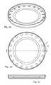
- FIG. 2( a )is a perspective view of an aluminium element of the shield assembly
- FIG. 2( b )is a view from above of that assembly
- FIG. 2( c )is a cross section of the line A-A in FIG. 2( b ) ;
- FIG. 3is a graph of thickness uniformity as a function of target life.
- FIG. 4is a graph indicating deposition thicknesses with respect to the wafer edge.
- FIG. 1shows the composite assembly 10 in a PVD process chamber 11 .
- An Al shield element 13is placed above the wafer 16 , at a wafer location, in the region where the heat flux is typically at a maximum for the shielding.
- the shield element 13acts as a shadow shield.
- the Al shield element 13is held there by a stainless steel shield element 14 to form the assembly 10 .
- the stainless steel shield element 14extends along the wall 15 of the chamber 11 and beneath the Al shield element 13 . Parts need to be a very tight fit (press fit (spec +0.1 to +0.3 mm) as indicated in FIG.
- the coupling between the Al and stainless steel of the shield elements 13 and 14needs to be intimate (as the shielding heats up the Al shield element 13 expands into the stainless steel shield element 14 and provides an even better thermal contact).
- Contact between the outer stainless steel shielding and the inner wall of process chamberneeds to be achieved for optimum dissipation of the heat generated during the deposition cycle. Note if the complete shielding was solely made from Al this would be a serious problem as it would tend to weld, for example friction weld, to the process chamber wall and be very difficult to remove during maintenance.
- the Al shield element 13has a number of openings 17 to enable efficient pumping of the chamber.
- FIG. 3shows the excellent uniformity performance of the shielding over ⁇ 1100 kWhrs of high power 3 ⁇ m, 40 kW Al(Cu) deposition.
- the Al shield 13can be replaced while the stainless steel exterior shielding can be cleaned and re-used.
Landscapes
- Chemical & Material Sciences (AREA)
- Engineering & Computer Science (AREA)
- Physics & Mathematics (AREA)
- Plasma & Fusion (AREA)
- Analytical Chemistry (AREA)
- Chemical Kinetics & Catalysis (AREA)
- Materials Engineering (AREA)
- Mechanical Engineering (AREA)
- Metallurgy (AREA)
- Organic Chemistry (AREA)
- Physical Vapour Deposition (AREA)
- Shielding Devices Or Components To Electric Or Magnetic Fields (AREA)
Abstract
Description
Claims (20)
Priority Applications (1)
| Application Number | Priority Date | Filing Date | Title |
|---|---|---|---|
| US13/371,642US9957608B2 (en) | 2011-02-11 | 2012-02-13 | Composite shielding |
Applications Claiming Priority (4)
| Application Number | Priority Date | Filing Date | Title |
|---|---|---|---|
| GBGB1102447.8AGB201102447D0 (en) | 2011-02-11 | 2011-02-11 | Composite shielding |
| GB1102447.8 | 2011-02-11 | ||
| US201161443781P | 2011-02-17 | 2011-02-17 | |
| US13/371,642US9957608B2 (en) | 2011-02-11 | 2012-02-13 | Composite shielding |
Publications (2)
| Publication Number | Publication Date |
|---|---|
| US20130042812A1 US20130042812A1 (en) | 2013-02-21 |
| US9957608B2true US9957608B2 (en) | 2018-05-01 |
Family
ID=43859299
Family Applications (1)
| Application Number | Title | Priority Date | Filing Date |
|---|---|---|---|
| US13/371,642ActiveUS9957608B2 (en) | 2011-02-11 | 2012-02-13 | Composite shielding |
Country Status (2)
| Country | Link |
|---|---|
| US (1) | US9957608B2 (en) |
| GB (1) | GB201102447D0 (en) |
Citations (20)
| Publication number | Priority date | Publication date | Assignee | Title |
|---|---|---|---|---|
| US5202008A (en) | 1990-03-02 | 1993-04-13 | Applied Materials, Inc. | Method for preparing a shield to reduce particles in a physical vapor deposition chamber |
| EP0853331A2 (en) | 1997-01-08 | 1998-07-15 | Applied Materials, Inc. | Back sputtering shield |
| US5942042A (en)* | 1997-05-23 | 1999-08-24 | Applied Materials, Inc. | Apparatus for improved power coupling through a workpiece in a semiconductor wafer processing system |
| US6231674B1 (en) | 1994-02-23 | 2001-05-15 | Applied Materials, Inc. | Wafer edge deposition elimination |
| US6562715B1 (en)* | 2000-08-09 | 2003-05-13 | Applied Materials, Inc. | Barrier layer structure for copper metallization and method of forming the structure |
| JP2003247058A (en) | 2002-02-20 | 2003-09-05 | Seiko Epson Corp | Deposition jig and thin film forming equipment |
| JP2003247057A (en) | 2002-02-20 | 2003-09-05 | Seiko Epson Corp | Deposition jig and thin film forming equipment |
| JP2003247059A (en) | 2002-02-20 | 2003-09-05 | Seiko Epson Corp | Anti-stick jig, thin film forming apparatus, and method of cleaning anti-stick jig |
| US20030185965A1 (en)* | 2002-03-27 | 2003-10-02 | Applied Materials, Inc. | Evaluation of chamber components having textured coatings |
| JP2004315948A (en) | 2003-04-21 | 2004-11-11 | Nikko Materials Co Ltd | Contamination prevention device for thin film deposition system |
| US20050089699A1 (en) | 2003-10-22 | 2005-04-28 | Applied Materials, Inc. | Cleaning and refurbishing chamber components having metal coatings |
| US20070158188A1 (en) | 2004-06-15 | 2007-07-12 | Ivanov Eugene Y | Metal foam shield for sputter reactor |
| US20070283884A1 (en)* | 2006-05-30 | 2007-12-13 | Applied Materials, Inc. | Ring assembly for substrate processing chamber |
| US20080178801A1 (en)* | 2007-01-29 | 2008-07-31 | Applied Materials, Inc. | Process kit for substrate processing chamber |
| US20080230371A1 (en)* | 2007-03-22 | 2008-09-25 | Tokyo Electron Limited | Method and apparatus for extending chamber component life in a substrate processing system |
| JP2008291299A (en) | 2007-05-23 | 2008-12-04 | Texas Instr Japan Ltd | Metal film peeling prevention structure in metal film forming apparatus and semiconductor device manufacturing method using the structure |
| US20090260982A1 (en)* | 2008-04-16 | 2009-10-22 | Applied Materials, Inc. | Wafer processing deposition shielding components |
| US20100218785A1 (en)* | 2009-02-27 | 2010-09-02 | Applied Materials, Inc. | In situ plasma clean for removal of residue from pedestal surface without breaking vacuum |
| US20100270143A1 (en)* | 2008-01-15 | 2010-10-28 | Ulvac, Inc. | Substrate stage, sputtering apparatus provided with same, and film forming method |
| US20110186426A1 (en)* | 2010-01-29 | 2011-08-04 | Applied Materials, Inc. | Adjustable process spacing, centering, and improved gas conductance |
- 2011
- 2011-02-11GBGBGB1102447.8Apatent/GB201102447D0/ennot_activeCeased
- 2012
- 2012-02-13USUS13/371,642patent/US9957608B2/enactiveActive
Patent Citations (22)
| Publication number | Priority date | Publication date | Assignee | Title |
|---|---|---|---|---|
| US5202008A (en) | 1990-03-02 | 1993-04-13 | Applied Materials, Inc. | Method for preparing a shield to reduce particles in a physical vapor deposition chamber |
| US6231674B1 (en) | 1994-02-23 | 2001-05-15 | Applied Materials, Inc. | Wafer edge deposition elimination |
| EP0853331A2 (en) | 1997-01-08 | 1998-07-15 | Applied Materials, Inc. | Back sputtering shield |
| US5942042A (en)* | 1997-05-23 | 1999-08-24 | Applied Materials, Inc. | Apparatus for improved power coupling through a workpiece in a semiconductor wafer processing system |
| US6562715B1 (en)* | 2000-08-09 | 2003-05-13 | Applied Materials, Inc. | Barrier layer structure for copper metallization and method of forming the structure |
| JP2003247058A (en) | 2002-02-20 | 2003-09-05 | Seiko Epson Corp | Deposition jig and thin film forming equipment |
| JP2003247057A (en) | 2002-02-20 | 2003-09-05 | Seiko Epson Corp | Deposition jig and thin film forming equipment |
| JP2003247059A (en) | 2002-02-20 | 2003-09-05 | Seiko Epson Corp | Anti-stick jig, thin film forming apparatus, and method of cleaning anti-stick jig |
| US20030185965A1 (en)* | 2002-03-27 | 2003-10-02 | Applied Materials, Inc. | Evaluation of chamber components having textured coatings |
| JP2004315948A (en) | 2003-04-21 | 2004-11-11 | Nikko Materials Co Ltd | Contamination prevention device for thin film deposition system |
| US20050089699A1 (en) | 2003-10-22 | 2005-04-28 | Applied Materials, Inc. | Cleaning and refurbishing chamber components having metal coatings |
| US20070158188A1 (en) | 2004-06-15 | 2007-07-12 | Ivanov Eugene Y | Metal foam shield for sputter reactor |
| US20070283884A1 (en)* | 2006-05-30 | 2007-12-13 | Applied Materials, Inc. | Ring assembly for substrate processing chamber |
| US20080178801A1 (en)* | 2007-01-29 | 2008-07-31 | Applied Materials, Inc. | Process kit for substrate processing chamber |
| EP1953798A2 (en) | 2007-01-29 | 2008-08-06 | Applied Materials, Inc. | Process kit for substrate processing chamber |
| US20080230371A1 (en)* | 2007-03-22 | 2008-09-25 | Tokyo Electron Limited | Method and apparatus for extending chamber component life in a substrate processing system |
| JP2008291299A (en) | 2007-05-23 | 2008-12-04 | Texas Instr Japan Ltd | Metal film peeling prevention structure in metal film forming apparatus and semiconductor device manufacturing method using the structure |
| US20080305634A1 (en) | 2007-05-23 | 2008-12-11 | Texas Instruments Incorporated | Metal Film Separation Prevention Structure in Metal Film Forming Device, and Semiconductor Device Manufacturing Method Using Said Structure |
| US20100270143A1 (en)* | 2008-01-15 | 2010-10-28 | Ulvac, Inc. | Substrate stage, sputtering apparatus provided with same, and film forming method |
| US20090260982A1 (en)* | 2008-04-16 | 2009-10-22 | Applied Materials, Inc. | Wafer processing deposition shielding components |
| US20100218785A1 (en)* | 2009-02-27 | 2010-09-02 | Applied Materials, Inc. | In situ plasma clean for removal of residue from pedestal surface without breaking vacuum |
| US20110186426A1 (en)* | 2010-01-29 | 2011-08-04 | Applied Materials, Inc. | Adjustable process spacing, centering, and improved gas conductance |
Non-Patent Citations (3)
| Title |
|---|
| European Search Report for EP 12 15 2912 dated Jul. 2, 2012. |
| Great Britain Search Report for GB1102747.1 dated Jul. 15, 2011. |
| Japanese Office Action in Corresponding Japanese Application No. 2012-027506 dated Sep. 29, 2015. |
Also Published As
| Publication number | Publication date |
|---|---|
| US20130042812A1 (en) | 2013-02-21 |
| GB201102447D0 (en) | 2011-03-30 |
Similar Documents
| Publication | Publication Date | Title |
|---|---|---|
| US8580092B2 (en) | Adjustable process spacing, centering, and improved gas conductance | |
| US8911601B2 (en) | Deposition ring and electrostatic chuck for physical vapor deposition chamber | |
| US8968537B2 (en) | PVD sputtering target with a protected backing plate | |
| RU2665059C2 (en) | Spraying target having the increased energy compatibility | |
| CN105874565A (en) | Physical Vapor Deposition (PVD) Targets with Low Friction Pads | |
| JP2011520034A (en) | RF physical vapor deposition processing kit | |
| TWI606546B (en) | Electrostatic chuck apparatus | |
| US10435783B2 (en) | Target assembly | |
| US10435784B2 (en) | Thermally optimized rings | |
| US9957608B2 (en) | Composite shielding | |
| US20160168687A1 (en) | Particle reduction in a deposition chamber using thermal expansion coefficient compatible coating | |
| CN112789366B (en) | Vacuum processing apparatus | |
| EP2487275B1 (en) | Composite shielding | |
| CN108538744B (en) | Chuck device and semiconductor processing equipment | |
| JP6588418B2 (en) | Process for producing a film forming apparatus and a film forming material using the same and cooling panel, | |
| JP2008081763A (en) | Target assembly unit and sputtering apparatus | |
| KR101930788B1 (en) | Cooling unit of substrate processing chamber | |
| US8143590B2 (en) | Ion source apparatus | |
| BR112019025350B1 (en) | TARGET SET FOR SAFE AND ECONOMIC EVAPORATION OF BRITTLE MATERIALS | |
| BR112019025350A2 (en) | TARGET SET FOR SAFE AND ECONOMIC EVAPORATION OF BREAKING MATERIALS | |
| JP2013185212A (en) | Backing plate and method for using the same, and sputtering device |
Legal Events
| Date | Code | Title | Description |
|---|---|---|---|
| AS | Assignment | Owner name:SAMSUNG ELECTRONICS CO., LTD., KOREA, REPUBLIC OF Free format text:ASSIGNMENT OF ASSIGNORS INTEREST;ASSIGNOR:WIDDICKS, CLIVE LUCA;REEL/FRAME:027779/0930 Effective date:20120208 | |
| AS | Assignment | Owner name:SPTS TECHNOLOGIES LIMITED, UNITED KINGDOM Free format text:CORRECTIVE ASSIGNMENT TO CORRECT THE ASSIGNMENT TO ADD THE SECOND INVENTOR AND CORRECT THE NAME AND ADDRESS OF THE ASSIGNEE PREVIOUSLY RECORDED ON REEL 027779 FRAME 0930. ASSIGNOR(S) HEREBY CONFIRMS THE SECOND ASSIGNOR IS MONCRIEFF, IAN AND THE ASSIGNEE IS SPTS TECHNOLOGIES LIMITED.;ASSIGNORS:WIDDICKS, CLIVE LUCA;MONCRIEFF, IAN;REEL/FRAME:028583/0195 Effective date:20120208 | |
| AS | Assignment | Owner name:JPMORGAN CHASE BANK, N.A., AS ADMINISTRATIVE AGENT, ILLINOIS Free format text:SECURITY INTEREST;ASSIGNOR:SPTS TECHNOLOGIES LIMITED;REEL/FRAME:035364/0295 Effective date:20150401 Owner name:JPMORGAN CHASE BANK, N.A., AS ADMINISTRATIVE AGENT Free format text:SECURITY INTEREST;ASSIGNOR:SPTS TECHNOLOGIES LIMITED;REEL/FRAME:035364/0295 Effective date:20150401 | |
| AS | Assignment | Owner name:SPTS TECHNOLOGIES LIMITED, UNITED KINGDOM Free format text:RELEASE BY SECURED PARTY;ASSIGNOR:JPMORGAN CHASE BANK, N.A.;REEL/FRAME:039257/0026 Effective date:20160623 | |
| STCF | Information on status: patent grant | Free format text:PATENTED CASE | |
| MAFP | Maintenance fee payment | Free format text:PAYMENT OF MAINTENANCE FEE, 4TH YEAR, LARGE ENTITY (ORIGINAL EVENT CODE: M1551); ENTITY STATUS OF PATENT OWNER: LARGE ENTITY Year of fee payment:4 |