US9953941B2 - Conductive barrier direct hybrid bonding - Google Patents
Conductive barrier direct hybrid bondingDownload PDFInfo
- Publication number
- US9953941B2 US9953941B2US14/835,379US201514835379AUS9953941B2US 9953941 B2US9953941 B2US 9953941B2US 201514835379 AUS201514835379 AUS 201514835379AUS 9953941 B2US9953941 B2US 9953941B2
- Authority
- US
- United States
- Prior art keywords
- conductive barrier
- barrier material
- contact structures
- metallic contact
- conductive
- Prior art date
- Legal status (The legal status is an assumption and is not a legal conclusion. Google has not performed a legal analysis and makes no representation as to the accuracy of the status listed.)
- Active
Links
Images


Classifications
- H—ELECTRICITY
- H01—ELECTRIC ELEMENTS
- H01L—SEMICONDUCTOR DEVICES NOT COVERED BY CLASS H10
- H01L24/00—Arrangements for connecting or disconnecting semiconductor or solid-state bodies; Methods or apparatus related thereto
- H01L24/01—Means for bonding being attached to, or being formed on, the surface to be connected, e.g. chip-to-package, die-attach, "first-level" interconnects; Manufacturing methods related thereto
- H01L24/26—Layer connectors, e.g. plate connectors, solder or adhesive layers; Manufacturing methods related thereto
- H—ELECTRICITY
- H01—ELECTRIC ELEMENTS
- H01L—SEMICONDUCTOR DEVICES NOT COVERED BY CLASS H10
- H01L24/00—Arrangements for connecting or disconnecting semiconductor or solid-state bodies; Methods or apparatus related thereto
- H01L24/01—Means for bonding being attached to, or being formed on, the surface to be connected, e.g. chip-to-package, die-attach, "first-level" interconnects; Manufacturing methods related thereto
- H01L24/02—Bonding areas ; Manufacturing methods related thereto
- H01L24/07—Structure, shape, material or disposition of the bonding areas after the connecting process
- H01L24/09—Structure, shape, material or disposition of the bonding areas after the connecting process of a plurality of bonding areas
- H—ELECTRICITY
- H01—ELECTRIC ELEMENTS
- H01L—SEMICONDUCTOR DEVICES NOT COVERED BY CLASS H10
- H01L21/00—Processes or apparatus adapted for the manufacture or treatment of semiconductor or solid state devices or of parts thereof
- H01L21/02—Manufacture or treatment of semiconductor devices or of parts thereof
- H01L21/04—Manufacture or treatment of semiconductor devices or of parts thereof the devices having potential barriers, e.g. a PN junction, depletion layer or carrier concentration layer
- H01L21/18—Manufacture or treatment of semiconductor devices or of parts thereof the devices having potential barriers, e.g. a PN junction, depletion layer or carrier concentration layer the devices having semiconductor bodies comprising elements of Group IV of the Periodic Table or AIIIBV compounds with or without impurities, e.g. doping materials
- H01L21/185—Joining of semiconductor bodies for junction formation
- H01L21/187—Joining of semiconductor bodies for junction formation by direct bonding
- H—ELECTRICITY
- H01—ELECTRIC ELEMENTS
- H01L—SEMICONDUCTOR DEVICES NOT COVERED BY CLASS H10
- H01L21/00—Processes or apparatus adapted for the manufacture or treatment of semiconductor or solid state devices or of parts thereof
- H01L21/02—Manufacture or treatment of semiconductor devices or of parts thereof
- H01L21/04—Manufacture or treatment of semiconductor devices or of parts thereof the devices having potential barriers, e.g. a PN junction, depletion layer or carrier concentration layer
- H01L21/18—Manufacture or treatment of semiconductor devices or of parts thereof the devices having potential barriers, e.g. a PN junction, depletion layer or carrier concentration layer the devices having semiconductor bodies comprising elements of Group IV of the Periodic Table or AIIIBV compounds with or without impurities, e.g. doping materials
- H01L21/20—Deposition of semiconductor materials on a substrate, e.g. epitaxial growth solid phase epitaxy
- H01L21/2003—Deposition of semiconductor materials on a substrate, e.g. epitaxial growth solid phase epitaxy characterised by the substrate
- H01L21/2007—Bonding of semiconductor wafers to insulating substrates or to semiconducting substrates using an intermediate insulating layer
- H—ELECTRICITY
- H01—ELECTRIC ELEMENTS
- H01L—SEMICONDUCTOR DEVICES NOT COVERED BY CLASS H10
- H01L21/00—Processes or apparatus adapted for the manufacture or treatment of semiconductor or solid state devices or of parts thereof
- H01L21/02—Manufacture or treatment of semiconductor devices or of parts thereof
- H01L21/04—Manufacture or treatment of semiconductor devices or of parts thereof the devices having potential barriers, e.g. a PN junction, depletion layer or carrier concentration layer
- H01L21/50—Assembly of semiconductor devices using processes or apparatus not provided for in a single one of the groups H01L21/18 - H01L21/326 or H10D48/04 - H10D48/07 e.g. sealing of a cap to a base of a container
- H01L21/52—Mounting semiconductor bodies in containers
- H—ELECTRICITY
- H01—ELECTRIC ELEMENTS
- H01L—SEMICONDUCTOR DEVICES NOT COVERED BY CLASS H10
- H01L24/00—Arrangements for connecting or disconnecting semiconductor or solid-state bodies; Methods or apparatus related thereto
- H01L24/01—Means for bonding being attached to, or being formed on, the surface to be connected, e.g. chip-to-package, die-attach, "first-level" interconnects; Manufacturing methods related thereto
- H01L24/02—Bonding areas ; Manufacturing methods related thereto
- H01L24/03—Manufacturing methods
- H—ELECTRICITY
- H01—ELECTRIC ELEMENTS
- H01L—SEMICONDUCTOR DEVICES NOT COVERED BY CLASS H10
- H01L24/00—Arrangements for connecting or disconnecting semiconductor or solid-state bodies; Methods or apparatus related thereto
- H01L24/01—Means for bonding being attached to, or being formed on, the surface to be connected, e.g. chip-to-package, die-attach, "first-level" interconnects; Manufacturing methods related thereto
- H01L24/02—Bonding areas ; Manufacturing methods related thereto
- H01L24/04—Structure, shape, material or disposition of the bonding areas prior to the connecting process
- H01L24/05—Structure, shape, material or disposition of the bonding areas prior to the connecting process of an individual bonding area
- H—ELECTRICITY
- H01—ELECTRIC ELEMENTS
- H01L—SEMICONDUCTOR DEVICES NOT COVERED BY CLASS H10
- H01L24/00—Arrangements for connecting or disconnecting semiconductor or solid-state bodies; Methods or apparatus related thereto
- H01L24/01—Means for bonding being attached to, or being formed on, the surface to be connected, e.g. chip-to-package, die-attach, "first-level" interconnects; Manufacturing methods related thereto
- H01L24/02—Bonding areas ; Manufacturing methods related thereto
- H01L24/07—Structure, shape, material or disposition of the bonding areas after the connecting process
- H01L24/08—Structure, shape, material or disposition of the bonding areas after the connecting process of an individual bonding area
- H—ELECTRICITY
- H01—ELECTRIC ELEMENTS
- H01L—SEMICONDUCTOR DEVICES NOT COVERED BY CLASS H10
- H01L24/00—Arrangements for connecting or disconnecting semiconductor or solid-state bodies; Methods or apparatus related thereto
- H01L24/01—Means for bonding being attached to, or being formed on, the surface to be connected, e.g. chip-to-package, die-attach, "first-level" interconnects; Manufacturing methods related thereto
- H01L24/26—Layer connectors, e.g. plate connectors, solder or adhesive layers; Manufacturing methods related thereto
- H01L24/27—Manufacturing methods
- H—ELECTRICITY
- H01—ELECTRIC ELEMENTS
- H01L—SEMICONDUCTOR DEVICES NOT COVERED BY CLASS H10
- H01L24/00—Arrangements for connecting or disconnecting semiconductor or solid-state bodies; Methods or apparatus related thereto
- H01L24/01—Means for bonding being attached to, or being formed on, the surface to be connected, e.g. chip-to-package, die-attach, "first-level" interconnects; Manufacturing methods related thereto
- H01L24/26—Layer connectors, e.g. plate connectors, solder or adhesive layers; Manufacturing methods related thereto
- H01L24/28—Structure, shape, material or disposition of the layer connectors prior to the connecting process
- H—ELECTRICITY
- H01—ELECTRIC ELEMENTS
- H01L—SEMICONDUCTOR DEVICES NOT COVERED BY CLASS H10
- H01L24/00—Arrangements for connecting or disconnecting semiconductor or solid-state bodies; Methods or apparatus related thereto
- H01L24/80—Methods for connecting semiconductor or other solid state bodies using means for bonding being attached to, or being formed on, the surface to be connected
- H01L24/83—Methods for connecting semiconductor or other solid state bodies using means for bonding being attached to, or being formed on, the surface to be connected using a layer connector
- H—ELECTRICITY
- H01—ELECTRIC ELEMENTS
- H01L—SEMICONDUCTOR DEVICES NOT COVERED BY CLASS H10
- H01L24/00—Arrangements for connecting or disconnecting semiconductor or solid-state bodies; Methods or apparatus related thereto
- H01L24/80—Methods for connecting semiconductor or other solid state bodies using means for bonding being attached to, or being formed on, the surface to be connected
- H01L24/89—Methods for connecting semiconductor or other solid state bodies using means for bonding being attached to, or being formed on, the surface to be connected using at least one connector not provided for in any of the groups H01L24/81 - H01L24/86
- H—ELECTRICITY
- H01—ELECTRIC ELEMENTS
- H01L—SEMICONDUCTOR DEVICES NOT COVERED BY CLASS H10
- H01L25/00—Assemblies consisting of a plurality of semiconductor or other solid state devices
- H01L25/03—Assemblies consisting of a plurality of semiconductor or other solid state devices all the devices being of a type provided for in a single subclass of subclasses H10B, H10D, H10F, H10H, H10K or H10N, e.g. assemblies of rectifier diodes
- H01L25/04—Assemblies consisting of a plurality of semiconductor or other solid state devices all the devices being of a type provided for in a single subclass of subclasses H10B, H10D, H10F, H10H, H10K or H10N, e.g. assemblies of rectifier diodes the devices not having separate containers
- H01L25/065—Assemblies consisting of a plurality of semiconductor or other solid state devices all the devices being of a type provided for in a single subclass of subclasses H10B, H10D, H10F, H10H, H10K or H10N, e.g. assemblies of rectifier diodes the devices not having separate containers the devices being of a type provided for in group H10D89/00
- H01L25/0657—Stacked arrangements of devices
- H—ELECTRICITY
- H01—ELECTRIC ELEMENTS
- H01L—SEMICONDUCTOR DEVICES NOT COVERED BY CLASS H10
- H01L25/00—Assemblies consisting of a plurality of semiconductor or other solid state devices
- H01L25/50—Multistep manufacturing processes of assemblies consisting of devices, the devices being individual devices of subclass H10D or integrated devices of class H10
- H—ELECTRICITY
- H01—ELECTRIC ELEMENTS
- H01L—SEMICONDUCTOR DEVICES NOT COVERED BY CLASS H10
- H01L2224/00—Indexing scheme for arrangements for connecting or disconnecting semiconductor or solid-state bodies and methods related thereto as covered by H01L24/00
- H01L2224/01—Means for bonding being attached to, or being formed on, the surface to be connected, e.g. chip-to-package, die-attach, "first-level" interconnects; Manufacturing methods related thereto
- H01L2224/02—Bonding areas; Manufacturing methods related thereto
- H01L2224/03—Manufacturing methods
- H01L2224/034—Manufacturing methods by blanket deposition of the material of the bonding area
- H01L2224/03444—Manufacturing methods by blanket deposition of the material of the bonding area in gaseous form
- H01L2224/0345—Physical vapour deposition [PVD], e.g. evaporation, or sputtering
- H—ELECTRICITY
- H01—ELECTRIC ELEMENTS
- H01L—SEMICONDUCTOR DEVICES NOT COVERED BY CLASS H10
- H01L2224/00—Indexing scheme for arrangements for connecting or disconnecting semiconductor or solid-state bodies and methods related thereto as covered by H01L24/00
- H01L2224/01—Means for bonding being attached to, or being formed on, the surface to be connected, e.g. chip-to-package, die-attach, "first-level" interconnects; Manufacturing methods related thereto
- H01L2224/02—Bonding areas; Manufacturing methods related thereto
- H01L2224/03—Manufacturing methods
- H01L2224/034—Manufacturing methods by blanket deposition of the material of the bonding area
- H01L2224/03444—Manufacturing methods by blanket deposition of the material of the bonding area in gaseous form
- H01L2224/03452—Chemical vapour deposition [CVD], e.g. laser CVD
- H—ELECTRICITY
- H01—ELECTRIC ELEMENTS
- H01L—SEMICONDUCTOR DEVICES NOT COVERED BY CLASS H10
- H01L2224/00—Indexing scheme for arrangements for connecting or disconnecting semiconductor or solid-state bodies and methods related thereto as covered by H01L24/00
- H01L2224/01—Means for bonding being attached to, or being formed on, the surface to be connected, e.g. chip-to-package, die-attach, "first-level" interconnects; Manufacturing methods related thereto
- H01L2224/02—Bonding areas; Manufacturing methods related thereto
- H01L2224/03—Manufacturing methods
- H01L2224/034—Manufacturing methods by blanket deposition of the material of the bonding area
- H01L2224/0346—Plating
- H01L2224/03462—Electroplating
- H—ELECTRICITY
- H01—ELECTRIC ELEMENTS
- H01L—SEMICONDUCTOR DEVICES NOT COVERED BY CLASS H10
- H01L2224/00—Indexing scheme for arrangements for connecting or disconnecting semiconductor or solid-state bodies and methods related thereto as covered by H01L24/00
- H01L2224/01—Means for bonding being attached to, or being formed on, the surface to be connected, e.g. chip-to-package, die-attach, "first-level" interconnects; Manufacturing methods related thereto
- H01L2224/02—Bonding areas; Manufacturing methods related thereto
- H01L2224/03—Manufacturing methods
- H01L2224/036—Manufacturing methods by patterning a pre-deposited material
- H01L2224/0361—Physical or chemical etching
- H01L2224/03616—Chemical mechanical polishing [CMP]
- H—ELECTRICITY
- H01—ELECTRIC ELEMENTS
- H01L—SEMICONDUCTOR DEVICES NOT COVERED BY CLASS H10
- H01L2224/00—Indexing scheme for arrangements for connecting or disconnecting semiconductor or solid-state bodies and methods related thereto as covered by H01L24/00
- H01L2224/01—Means for bonding being attached to, or being formed on, the surface to be connected, e.g. chip-to-package, die-attach, "first-level" interconnects; Manufacturing methods related thereto
- H01L2224/02—Bonding areas; Manufacturing methods related thereto
- H01L2224/03—Manufacturing methods
- H01L2224/038—Post-treatment of the bonding area
- H01L2224/0382—Applying permanent coating, e.g. in-situ coating
- H01L2224/03825—Plating, e.g. electroplating, electroless plating
- H—ELECTRICITY
- H01—ELECTRIC ELEMENTS
- H01L—SEMICONDUCTOR DEVICES NOT COVERED BY CLASS H10
- H01L2224/00—Indexing scheme for arrangements for connecting or disconnecting semiconductor or solid-state bodies and methods related thereto as covered by H01L24/00
- H01L2224/01—Means for bonding being attached to, or being formed on, the surface to be connected, e.g. chip-to-package, die-attach, "first-level" interconnects; Manufacturing methods related thereto
- H01L2224/02—Bonding areas; Manufacturing methods related thereto
- H01L2224/04—Structure, shape, material or disposition of the bonding areas prior to the connecting process
- H01L2224/05—Structure, shape, material or disposition of the bonding areas prior to the connecting process of an individual bonding area
- H01L2224/05001—Internal layers
- H01L2224/05005—Structure
- H01L2224/05007—Structure comprising a core and a coating
- H—ELECTRICITY
- H01—ELECTRIC ELEMENTS
- H01L—SEMICONDUCTOR DEVICES NOT COVERED BY CLASS H10
- H01L2224/00—Indexing scheme for arrangements for connecting or disconnecting semiconductor or solid-state bodies and methods related thereto as covered by H01L24/00
- H01L2224/01—Means for bonding being attached to, or being formed on, the surface to be connected, e.g. chip-to-package, die-attach, "first-level" interconnects; Manufacturing methods related thereto
- H01L2224/02—Bonding areas; Manufacturing methods related thereto
- H01L2224/04—Structure, shape, material or disposition of the bonding areas prior to the connecting process
- H01L2224/05—Structure, shape, material or disposition of the bonding areas prior to the connecting process of an individual bonding area
- H01L2224/05001—Internal layers
- H01L2224/0502—Disposition
- H01L2224/05026—Disposition the internal layer being disposed in a recess of the surface
- H—ELECTRICITY
- H01—ELECTRIC ELEMENTS
- H01L—SEMICONDUCTOR DEVICES NOT COVERED BY CLASS H10
- H01L2224/00—Indexing scheme for arrangements for connecting or disconnecting semiconductor or solid-state bodies and methods related thereto as covered by H01L24/00
- H01L2224/01—Means for bonding being attached to, or being formed on, the surface to be connected, e.g. chip-to-package, die-attach, "first-level" interconnects; Manufacturing methods related thereto
- H01L2224/02—Bonding areas; Manufacturing methods related thereto
- H01L2224/04—Structure, shape, material or disposition of the bonding areas prior to the connecting process
- H01L2224/05—Structure, shape, material or disposition of the bonding areas prior to the connecting process of an individual bonding area
- H01L2224/05001—Internal layers
- H01L2224/05075—Plural internal layers
- H01L2224/05078—Plural internal layers being disposed next to each other, e.g. side-to-side arrangements
- H—ELECTRICITY
- H01—ELECTRIC ELEMENTS
- H01L—SEMICONDUCTOR DEVICES NOT COVERED BY CLASS H10
- H01L2224/00—Indexing scheme for arrangements for connecting or disconnecting semiconductor or solid-state bodies and methods related thereto as covered by H01L24/00
- H01L2224/01—Means for bonding being attached to, or being formed on, the surface to be connected, e.g. chip-to-package, die-attach, "first-level" interconnects; Manufacturing methods related thereto
- H01L2224/02—Bonding areas; Manufacturing methods related thereto
- H01L2224/04—Structure, shape, material or disposition of the bonding areas prior to the connecting process
- H01L2224/05—Structure, shape, material or disposition of the bonding areas prior to the connecting process of an individual bonding area
- H01L2224/05001—Internal layers
- H01L2224/05075—Plural internal layers
- H01L2224/0508—Plural internal layers being stacked
- H01L2224/05082—Two-layer arrangements
- H—ELECTRICITY
- H01—ELECTRIC ELEMENTS
- H01L—SEMICONDUCTOR DEVICES NOT COVERED BY CLASS H10
- H01L2224/00—Indexing scheme for arrangements for connecting or disconnecting semiconductor or solid-state bodies and methods related thereto as covered by H01L24/00
- H01L2224/01—Means for bonding being attached to, or being formed on, the surface to be connected, e.g. chip-to-package, die-attach, "first-level" interconnects; Manufacturing methods related thereto
- H01L2224/02—Bonding areas; Manufacturing methods related thereto
- H01L2224/04—Structure, shape, material or disposition of the bonding areas prior to the connecting process
- H01L2224/05—Structure, shape, material or disposition of the bonding areas prior to the connecting process of an individual bonding area
- H01L2224/05001—Internal layers
- H01L2224/05099—Material
- H01L2224/051—Material with a principal constituent of the material being a metal or a metalloid, e.g. boron [B], silicon [Si], germanium [Ge], arsenic [As], antimony [Sb], tellurium [Te] and polonium [Po], and alloys thereof
- H01L2224/05117—Material with a principal constituent of the material being a metal or a metalloid, e.g. boron [B], silicon [Si], germanium [Ge], arsenic [As], antimony [Sb], tellurium [Te] and polonium [Po], and alloys thereof the principal constituent melting at a temperature of greater than or equal to 400°C and less than 950°C
- H01L2224/05124—Aluminium [Al] as principal constituent
- H—ELECTRICITY
- H01—ELECTRIC ELEMENTS
- H01L—SEMICONDUCTOR DEVICES NOT COVERED BY CLASS H10
- H01L2224/00—Indexing scheme for arrangements for connecting or disconnecting semiconductor or solid-state bodies and methods related thereto as covered by H01L24/00
- H01L2224/01—Means for bonding being attached to, or being formed on, the surface to be connected, e.g. chip-to-package, die-attach, "first-level" interconnects; Manufacturing methods related thereto
- H01L2224/02—Bonding areas; Manufacturing methods related thereto
- H01L2224/04—Structure, shape, material or disposition of the bonding areas prior to the connecting process
- H01L2224/05—Structure, shape, material or disposition of the bonding areas prior to the connecting process of an individual bonding area
- H01L2224/05001—Internal layers
- H01L2224/05099—Material
- H01L2224/051—Material with a principal constituent of the material being a metal or a metalloid, e.g. boron [B], silicon [Si], germanium [Ge], arsenic [As], antimony [Sb], tellurium [Te] and polonium [Po], and alloys thereof
- H01L2224/05138—Material with a principal constituent of the material being a metal or a metalloid, e.g. boron [B], silicon [Si], germanium [Ge], arsenic [As], antimony [Sb], tellurium [Te] and polonium [Po], and alloys thereof the principal constituent melting at a temperature of greater than or equal to 950°C and less than 1550°C
- H01L2224/05147—Copper [Cu] as principal constituent
- H—ELECTRICITY
- H01—ELECTRIC ELEMENTS
- H01L—SEMICONDUCTOR DEVICES NOT COVERED BY CLASS H10
- H01L2224/00—Indexing scheme for arrangements for connecting or disconnecting semiconductor or solid-state bodies and methods related thereto as covered by H01L24/00
- H01L2224/01—Means for bonding being attached to, or being formed on, the surface to be connected, e.g. chip-to-package, die-attach, "first-level" interconnects; Manufacturing methods related thereto
- H01L2224/02—Bonding areas; Manufacturing methods related thereto
- H01L2224/04—Structure, shape, material or disposition of the bonding areas prior to the connecting process
- H01L2224/05—Structure, shape, material or disposition of the bonding areas prior to the connecting process of an individual bonding area
- H01L2224/0554—External layer
- H01L2224/05541—Structure
- H01L2224/05547—Structure comprising a core and a coating
- H—ELECTRICITY
- H01—ELECTRIC ELEMENTS
- H01L—SEMICONDUCTOR DEVICES NOT COVERED BY CLASS H10
- H01L2224/00—Indexing scheme for arrangements for connecting or disconnecting semiconductor or solid-state bodies and methods related thereto as covered by H01L24/00
- H01L2224/01—Means for bonding being attached to, or being formed on, the surface to be connected, e.g. chip-to-package, die-attach, "first-level" interconnects; Manufacturing methods related thereto
- H01L2224/02—Bonding areas; Manufacturing methods related thereto
- H01L2224/04—Structure, shape, material or disposition of the bonding areas prior to the connecting process
- H01L2224/05—Structure, shape, material or disposition of the bonding areas prior to the connecting process of an individual bonding area
- H01L2224/0554—External layer
- H01L2224/0556—Disposition
- H01L2224/05561—On the entire surface of the internal layer
- H—ELECTRICITY
- H01—ELECTRIC ELEMENTS
- H01L—SEMICONDUCTOR DEVICES NOT COVERED BY CLASS H10
- H01L2224/00—Indexing scheme for arrangements for connecting or disconnecting semiconductor or solid-state bodies and methods related thereto as covered by H01L24/00
- H01L2224/01—Means for bonding being attached to, or being formed on, the surface to be connected, e.g. chip-to-package, die-attach, "first-level" interconnects; Manufacturing methods related thereto
- H01L2224/02—Bonding areas; Manufacturing methods related thereto
- H01L2224/04—Structure, shape, material or disposition of the bonding areas prior to the connecting process
- H01L2224/05—Structure, shape, material or disposition of the bonding areas prior to the connecting process of an individual bonding area
- H01L2224/0554—External layer
- H01L2224/0556—Disposition
- H01L2224/05562—On the entire exposed surface of the internal layer
- H—ELECTRICITY
- H01—ELECTRIC ELEMENTS
- H01L—SEMICONDUCTOR DEVICES NOT COVERED BY CLASS H10
- H01L2224/00—Indexing scheme for arrangements for connecting or disconnecting semiconductor or solid-state bodies and methods related thereto as covered by H01L24/00
- H01L2224/01—Means for bonding being attached to, or being formed on, the surface to be connected, e.g. chip-to-package, die-attach, "first-level" interconnects; Manufacturing methods related thereto
- H01L2224/02—Bonding areas; Manufacturing methods related thereto
- H01L2224/04—Structure, shape, material or disposition of the bonding areas prior to the connecting process
- H01L2224/05—Structure, shape, material or disposition of the bonding areas prior to the connecting process of an individual bonding area
- H01L2224/0554—External layer
- H01L2224/0556—Disposition
- H01L2224/0557—Disposition the external layer being disposed on a via connection of the semiconductor or solid-state body
- H—ELECTRICITY
- H01—ELECTRIC ELEMENTS
- H01L—SEMICONDUCTOR DEVICES NOT COVERED BY CLASS H10
- H01L2224/00—Indexing scheme for arrangements for connecting or disconnecting semiconductor or solid-state bodies and methods related thereto as covered by H01L24/00
- H01L2224/01—Means for bonding being attached to, or being formed on, the surface to be connected, e.g. chip-to-package, die-attach, "first-level" interconnects; Manufacturing methods related thereto
- H01L2224/02—Bonding areas; Manufacturing methods related thereto
- H01L2224/04—Structure, shape, material or disposition of the bonding areas prior to the connecting process
- H01L2224/05—Structure, shape, material or disposition of the bonding areas prior to the connecting process of an individual bonding area
- H01L2224/0554—External layer
- H01L2224/0556—Disposition
- H01L2224/05571—Disposition the external layer being disposed in a recess of the surface
- H—ELECTRICITY
- H01—ELECTRIC ELEMENTS
- H01L—SEMICONDUCTOR DEVICES NOT COVERED BY CLASS H10
- H01L2224/00—Indexing scheme for arrangements for connecting or disconnecting semiconductor or solid-state bodies and methods related thereto as covered by H01L24/00
- H01L2224/01—Means for bonding being attached to, or being formed on, the surface to be connected, e.g. chip-to-package, die-attach, "first-level" interconnects; Manufacturing methods related thereto
- H01L2224/02—Bonding areas; Manufacturing methods related thereto
- H01L2224/04—Structure, shape, material or disposition of the bonding areas prior to the connecting process
- H01L2224/05—Structure, shape, material or disposition of the bonding areas prior to the connecting process of an individual bonding area
- H01L2224/0554—External layer
- H01L2224/05573—Single external layer
- H—ELECTRICITY
- H01—ELECTRIC ELEMENTS
- H01L—SEMICONDUCTOR DEVICES NOT COVERED BY CLASS H10
- H01L2224/00—Indexing scheme for arrangements for connecting or disconnecting semiconductor or solid-state bodies and methods related thereto as covered by H01L24/00
- H01L2224/01—Means for bonding being attached to, or being formed on, the surface to be connected, e.g. chip-to-package, die-attach, "first-level" interconnects; Manufacturing methods related thereto
- H01L2224/02—Bonding areas; Manufacturing methods related thereto
- H01L2224/04—Structure, shape, material or disposition of the bonding areas prior to the connecting process
- H01L2224/05—Structure, shape, material or disposition of the bonding areas prior to the connecting process of an individual bonding area
- H01L2224/0554—External layer
- H01L2224/05599—Material
- H01L2224/056—Material with a principal constituent of the material being a metal or a metalloid, e.g. boron [B], silicon [Si], germanium [Ge], arsenic [As], antimony [Sb], tellurium [Te] and polonium [Po], and alloys thereof
- H01L2224/05638—Material with a principal constituent of the material being a metal or a metalloid, e.g. boron [B], silicon [Si], germanium [Ge], arsenic [As], antimony [Sb], tellurium [Te] and polonium [Po], and alloys thereof the principal constituent melting at a temperature of greater than or equal to 950°C and less than 1550°C
- H01L2224/05655—Nickel [Ni] as principal constituent
- H—ELECTRICITY
- H01—ELECTRIC ELEMENTS
- H01L—SEMICONDUCTOR DEVICES NOT COVERED BY CLASS H10
- H01L2224/00—Indexing scheme for arrangements for connecting or disconnecting semiconductor or solid-state bodies and methods related thereto as covered by H01L24/00
- H01L2224/01—Means for bonding being attached to, or being formed on, the surface to be connected, e.g. chip-to-package, die-attach, "first-level" interconnects; Manufacturing methods related thereto
- H01L2224/02—Bonding areas; Manufacturing methods related thereto
- H01L2224/04—Structure, shape, material or disposition of the bonding areas prior to the connecting process
- H01L2224/05—Structure, shape, material or disposition of the bonding areas prior to the connecting process of an individual bonding area
- H01L2224/0554—External layer
- H01L2224/05599—Material
- H01L2224/056—Material with a principal constituent of the material being a metal or a metalloid, e.g. boron [B], silicon [Si], germanium [Ge], arsenic [As], antimony [Sb], tellurium [Te] and polonium [Po], and alloys thereof
- H01L2224/05638—Material with a principal constituent of the material being a metal or a metalloid, e.g. boron [B], silicon [Si], germanium [Ge], arsenic [As], antimony [Sb], tellurium [Te] and polonium [Po], and alloys thereof the principal constituent melting at a temperature of greater than or equal to 950°C and less than 1550°C
- H01L2224/05657—Cobalt [Co] as principal constituent
- H—ELECTRICITY
- H01—ELECTRIC ELEMENTS
- H01L—SEMICONDUCTOR DEVICES NOT COVERED BY CLASS H10
- H01L2224/00—Indexing scheme for arrangements for connecting or disconnecting semiconductor or solid-state bodies and methods related thereto as covered by H01L24/00
- H01L2224/01—Means for bonding being attached to, or being formed on, the surface to be connected, e.g. chip-to-package, die-attach, "first-level" interconnects; Manufacturing methods related thereto
- H01L2224/02—Bonding areas; Manufacturing methods related thereto
- H01L2224/04—Structure, shape, material or disposition of the bonding areas prior to the connecting process
- H01L2224/05—Structure, shape, material or disposition of the bonding areas prior to the connecting process of an individual bonding area
- H01L2224/0554—External layer
- H01L2224/05599—Material
- H01L2224/056—Material with a principal constituent of the material being a metal or a metalloid, e.g. boron [B], silicon [Si], germanium [Ge], arsenic [As], antimony [Sb], tellurium [Te] and polonium [Po], and alloys thereof
- H01L2224/05663—Material with a principal constituent of the material being a metal or a metalloid, e.g. boron [B], silicon [Si], germanium [Ge], arsenic [As], antimony [Sb], tellurium [Te] and polonium [Po], and alloys thereof the principal constituent melting at a temperature of greater than 1550°C
- H01L2224/05666—Titanium [Ti] as principal constituent
- H—ELECTRICITY
- H01—ELECTRIC ELEMENTS
- H01L—SEMICONDUCTOR DEVICES NOT COVERED BY CLASS H10
- H01L2224/00—Indexing scheme for arrangements for connecting or disconnecting semiconductor or solid-state bodies and methods related thereto as covered by H01L24/00
- H01L2224/01—Means for bonding being attached to, or being formed on, the surface to be connected, e.g. chip-to-package, die-attach, "first-level" interconnects; Manufacturing methods related thereto
- H01L2224/02—Bonding areas; Manufacturing methods related thereto
- H01L2224/04—Structure, shape, material or disposition of the bonding areas prior to the connecting process
- H01L2224/05—Structure, shape, material or disposition of the bonding areas prior to the connecting process of an individual bonding area
- H01L2224/0554—External layer
- H01L2224/05599—Material
- H01L2224/056—Material with a principal constituent of the material being a metal or a metalloid, e.g. boron [B], silicon [Si], germanium [Ge], arsenic [As], antimony [Sb], tellurium [Te] and polonium [Po], and alloys thereof
- H01L2224/05663—Material with a principal constituent of the material being a metal or a metalloid, e.g. boron [B], silicon [Si], germanium [Ge], arsenic [As], antimony [Sb], tellurium [Te] and polonium [Po], and alloys thereof the principal constituent melting at a temperature of greater than 1550°C
- H01L2224/05676—Ruthenium [Ru] as principal constituent
- H—ELECTRICITY
- H01—ELECTRIC ELEMENTS
- H01L—SEMICONDUCTOR DEVICES NOT COVERED BY CLASS H10
- H01L2224/00—Indexing scheme for arrangements for connecting or disconnecting semiconductor or solid-state bodies and methods related thereto as covered by H01L24/00
- H01L2224/01—Means for bonding being attached to, or being formed on, the surface to be connected, e.g. chip-to-package, die-attach, "first-level" interconnects; Manufacturing methods related thereto
- H01L2224/02—Bonding areas; Manufacturing methods related thereto
- H01L2224/04—Structure, shape, material or disposition of the bonding areas prior to the connecting process
- H01L2224/05—Structure, shape, material or disposition of the bonding areas prior to the connecting process of an individual bonding area
- H01L2224/0554—External layer
- H01L2224/05599—Material
- H01L2224/056—Material with a principal constituent of the material being a metal or a metalloid, e.g. boron [B], silicon [Si], germanium [Ge], arsenic [As], antimony [Sb], tellurium [Te] and polonium [Po], and alloys thereof
- H01L2224/05663—Material with a principal constituent of the material being a metal or a metalloid, e.g. boron [B], silicon [Si], germanium [Ge], arsenic [As], antimony [Sb], tellurium [Te] and polonium [Po], and alloys thereof the principal constituent melting at a temperature of greater than 1550°C
- H01L2224/05681—Tantalum [Ta] as principal constituent
- H—ELECTRICITY
- H01—ELECTRIC ELEMENTS
- H01L—SEMICONDUCTOR DEVICES NOT COVERED BY CLASS H10
- H01L2224/00—Indexing scheme for arrangements for connecting or disconnecting semiconductor or solid-state bodies and methods related thereto as covered by H01L24/00
- H01L2224/01—Means for bonding being attached to, or being formed on, the surface to be connected, e.g. chip-to-package, die-attach, "first-level" interconnects; Manufacturing methods related thereto
- H01L2224/02—Bonding areas; Manufacturing methods related thereto
- H01L2224/04—Structure, shape, material or disposition of the bonding areas prior to the connecting process
- H01L2224/05—Structure, shape, material or disposition of the bonding areas prior to the connecting process of an individual bonding area
- H01L2224/0554—External layer
- H01L2224/05599—Material
- H01L2224/056—Material with a principal constituent of the material being a metal or a metalloid, e.g. boron [B], silicon [Si], germanium [Ge], arsenic [As], antimony [Sb], tellurium [Te] and polonium [Po], and alloys thereof
- H01L2224/05663—Material with a principal constituent of the material being a metal or a metalloid, e.g. boron [B], silicon [Si], germanium [Ge], arsenic [As], antimony [Sb], tellurium [Te] and polonium [Po], and alloys thereof the principal constituent melting at a temperature of greater than 1550°C
- H01L2224/05684—Tungsten [W] as principal constituent
- H—ELECTRICITY
- H01—ELECTRIC ELEMENTS
- H01L—SEMICONDUCTOR DEVICES NOT COVERED BY CLASS H10
- H01L2224/00—Indexing scheme for arrangements for connecting or disconnecting semiconductor or solid-state bodies and methods related thereto as covered by H01L24/00
- H01L2224/01—Means for bonding being attached to, or being formed on, the surface to be connected, e.g. chip-to-package, die-attach, "first-level" interconnects; Manufacturing methods related thereto
- H01L2224/02—Bonding areas; Manufacturing methods related thereto
- H01L2224/04—Structure, shape, material or disposition of the bonding areas prior to the connecting process
- H01L2224/05—Structure, shape, material or disposition of the bonding areas prior to the connecting process of an individual bonding area
- H01L2224/0554—External layer
- H01L2224/05599—Material
- H01L2224/05686—Material with a principal constituent of the material being a non metallic, non metalloid inorganic material
- H—ELECTRICITY
- H01—ELECTRIC ELEMENTS
- H01L—SEMICONDUCTOR DEVICES NOT COVERED BY CLASS H10
- H01L2224/00—Indexing scheme for arrangements for connecting or disconnecting semiconductor or solid-state bodies and methods related thereto as covered by H01L24/00
- H01L2224/01—Means for bonding being attached to, or being formed on, the surface to be connected, e.g. chip-to-package, die-attach, "first-level" interconnects; Manufacturing methods related thereto
- H01L2224/02—Bonding areas; Manufacturing methods related thereto
- H01L2224/04—Structure, shape, material or disposition of the bonding areas prior to the connecting process
- H01L2224/06—Structure, shape, material or disposition of the bonding areas prior to the connecting process of a plurality of bonding areas
- H01L2224/0601—Structure
- H01L2224/0603—Bonding areas having different sizes, e.g. different heights or widths
- H—ELECTRICITY
- H01—ELECTRIC ELEMENTS
- H01L—SEMICONDUCTOR DEVICES NOT COVERED BY CLASS H10
- H01L2224/00—Indexing scheme for arrangements for connecting or disconnecting semiconductor or solid-state bodies and methods related thereto as covered by H01L24/00
- H01L2224/01—Means for bonding being attached to, or being formed on, the surface to be connected, e.g. chip-to-package, die-attach, "first-level" interconnects; Manufacturing methods related thereto
- H01L2224/02—Bonding areas; Manufacturing methods related thereto
- H01L2224/07—Structure, shape, material or disposition of the bonding areas after the connecting process
- H01L2224/08—Structure, shape, material or disposition of the bonding areas after the connecting process of an individual bonding area
- H01L2224/081—Disposition
- H01L2224/08112—Disposition the bonding area being at least partially embedded in the surface of the body
- H—ELECTRICITY
- H01—ELECTRIC ELEMENTS
- H01L—SEMICONDUCTOR DEVICES NOT COVERED BY CLASS H10
- H01L2224/00—Indexing scheme for arrangements for connecting or disconnecting semiconductor or solid-state bodies and methods related thereto as covered by H01L24/00
- H01L2224/01—Means for bonding being attached to, or being formed on, the surface to be connected, e.g. chip-to-package, die-attach, "first-level" interconnects; Manufacturing methods related thereto
- H01L2224/02—Bonding areas; Manufacturing methods related thereto
- H01L2224/07—Structure, shape, material or disposition of the bonding areas after the connecting process
- H01L2224/08—Structure, shape, material or disposition of the bonding areas after the connecting process of an individual bonding area
- H01L2224/081—Disposition
- H01L2224/0812—Disposition the bonding area connecting directly to another bonding area, i.e. connectorless bonding, e.g. bumpless bonding
- H01L2224/08121—Disposition the bonding area connecting directly to another bonding area, i.e. connectorless bonding, e.g. bumpless bonding the connected bonding areas being not aligned with respect to each other
- H—ELECTRICITY
- H01—ELECTRIC ELEMENTS
- H01L—SEMICONDUCTOR DEVICES NOT COVERED BY CLASS H10
- H01L2224/00—Indexing scheme for arrangements for connecting or disconnecting semiconductor or solid-state bodies and methods related thereto as covered by H01L24/00
- H01L2224/01—Means for bonding being attached to, or being formed on, the surface to be connected, e.g. chip-to-package, die-attach, "first-level" interconnects; Manufacturing methods related thereto
- H01L2224/02—Bonding areas; Manufacturing methods related thereto
- H01L2224/07—Structure, shape, material or disposition of the bonding areas after the connecting process
- H01L2224/08—Structure, shape, material or disposition of the bonding areas after the connecting process of an individual bonding area
- H01L2224/081—Disposition
- H01L2224/0812—Disposition the bonding area connecting directly to another bonding area, i.e. connectorless bonding, e.g. bumpless bonding
- H01L2224/08123—Disposition the bonding area connecting directly to another bonding area, i.e. connectorless bonding, e.g. bumpless bonding the bonding area connecting directly to at least two bonding areas
- H—ELECTRICITY
- H01—ELECTRIC ELEMENTS
- H01L—SEMICONDUCTOR DEVICES NOT COVERED BY CLASS H10
- H01L2224/00—Indexing scheme for arrangements for connecting or disconnecting semiconductor or solid-state bodies and methods related thereto as covered by H01L24/00
- H01L2224/01—Means for bonding being attached to, or being formed on, the surface to be connected, e.g. chip-to-package, die-attach, "first-level" interconnects; Manufacturing methods related thereto
- H01L2224/02—Bonding areas; Manufacturing methods related thereto
- H01L2224/07—Structure, shape, material or disposition of the bonding areas after the connecting process
- H01L2224/08—Structure, shape, material or disposition of the bonding areas after the connecting process of an individual bonding area
- H01L2224/081—Disposition
- H01L2224/0812—Disposition the bonding area connecting directly to another bonding area, i.e. connectorless bonding, e.g. bumpless bonding
- H01L2224/08135—Disposition the bonding area connecting directly to another bonding area, i.e. connectorless bonding, e.g. bumpless bonding the bonding area connecting between different semiconductor or solid-state bodies, i.e. chip-to-chip
- H01L2224/08137—Disposition the bonding area connecting directly to another bonding area, i.e. connectorless bonding, e.g. bumpless bonding the bonding area connecting between different semiconductor or solid-state bodies, i.e. chip-to-chip the bodies being arranged next to each other, e.g. on a common substrate
- H—ELECTRICITY
- H01—ELECTRIC ELEMENTS
- H01L—SEMICONDUCTOR DEVICES NOT COVERED BY CLASS H10
- H01L2224/00—Indexing scheme for arrangements for connecting or disconnecting semiconductor or solid-state bodies and methods related thereto as covered by H01L24/00
- H01L2224/01—Means for bonding being attached to, or being formed on, the surface to be connected, e.g. chip-to-package, die-attach, "first-level" interconnects; Manufacturing methods related thereto
- H01L2224/02—Bonding areas; Manufacturing methods related thereto
- H01L2224/07—Structure, shape, material or disposition of the bonding areas after the connecting process
- H01L2224/08—Structure, shape, material or disposition of the bonding areas after the connecting process of an individual bonding area
- H01L2224/081—Disposition
- H01L2224/0812—Disposition the bonding area connecting directly to another bonding area, i.e. connectorless bonding, e.g. bumpless bonding
- H01L2224/08135—Disposition the bonding area connecting directly to another bonding area, i.e. connectorless bonding, e.g. bumpless bonding the bonding area connecting between different semiconductor or solid-state bodies, i.e. chip-to-chip
- H01L2224/08145—Disposition the bonding area connecting directly to another bonding area, i.e. connectorless bonding, e.g. bumpless bonding the bonding area connecting between different semiconductor or solid-state bodies, i.e. chip-to-chip the bodies being stacked
- H01L2224/08147—Disposition the bonding area connecting directly to another bonding area, i.e. connectorless bonding, e.g. bumpless bonding the bonding area connecting between different semiconductor or solid-state bodies, i.e. chip-to-chip the bodies being stacked the bonding area connecting to a bonding area disposed in a recess of the surface of the body
- H—ELECTRICITY
- H01—ELECTRIC ELEMENTS
- H01L—SEMICONDUCTOR DEVICES NOT COVERED BY CLASS H10
- H01L2224/00—Indexing scheme for arrangements for connecting or disconnecting semiconductor or solid-state bodies and methods related thereto as covered by H01L24/00
- H01L2224/01—Means for bonding being attached to, or being formed on, the surface to be connected, e.g. chip-to-package, die-attach, "first-level" interconnects; Manufacturing methods related thereto
- H01L2224/26—Layer connectors, e.g. plate connectors, solder or adhesive layers; Manufacturing methods related thereto
- H01L2224/27—Manufacturing methods
- H—ELECTRICITY
- H01—ELECTRIC ELEMENTS
- H01L—SEMICONDUCTOR DEVICES NOT COVERED BY CLASS H10
- H01L2224/00—Indexing scheme for arrangements for connecting or disconnecting semiconductor or solid-state bodies and methods related thereto as covered by H01L24/00
- H01L2224/01—Means for bonding being attached to, or being formed on, the surface to be connected, e.g. chip-to-package, die-attach, "first-level" interconnects; Manufacturing methods related thereto
- H01L2224/26—Layer connectors, e.g. plate connectors, solder or adhesive layers; Manufacturing methods related thereto
- H01L2224/28—Structure, shape, material or disposition of the layer connectors prior to the connecting process
- H01L2224/29—Structure, shape, material or disposition of the layer connectors prior to the connecting process of an individual layer connector
- H01L2224/29001—Core members of the layer connector
- H01L2224/29099—Material
- H01L2224/29198—Material with a principal constituent of the material being a combination of two or more materials in the form of a matrix with a filler, i.e. being a hybrid material, e.g. segmented structures, foams
- H01L2224/29199—Material of the matrix
- H01L2224/29286—Material of the matrix with a principal constituent of the material being a non metallic, non metalloid inorganic material
- H01L2224/29287—Ceramics, e.g. crystalline carbides, nitrides or oxides
- H—ELECTRICITY
- H01—ELECTRIC ELEMENTS
- H01L—SEMICONDUCTOR DEVICES NOT COVERED BY CLASS H10
- H01L2224/00—Indexing scheme for arrangements for connecting or disconnecting semiconductor or solid-state bodies and methods related thereto as covered by H01L24/00
- H01L2224/01—Means for bonding being attached to, or being formed on, the surface to be connected, e.g. chip-to-package, die-attach, "first-level" interconnects; Manufacturing methods related thereto
- H01L2224/26—Layer connectors, e.g. plate connectors, solder or adhesive layers; Manufacturing methods related thereto
- H01L2224/28—Structure, shape, material or disposition of the layer connectors prior to the connecting process
- H01L2224/29—Structure, shape, material or disposition of the layer connectors prior to the connecting process of an individual layer connector
- H01L2224/29001—Core members of the layer connector
- H01L2224/29099—Material
- H01L2224/29198—Material with a principal constituent of the material being a combination of two or more materials in the form of a matrix with a filler, i.e. being a hybrid material, e.g. segmented structures, foams
- H01L2224/29298—Fillers
- H01L2224/29299—Base material
- H01L2224/293—Base material with a principal constituent of the material being a metal or a metalloid, e.g. boron [B], silicon [Si], germanium [Ge], arsenic [As], antimony [Sb], tellurium [Te] and polonium [Po], and alloys thereof
- H—ELECTRICITY
- H01—ELECTRIC ELEMENTS
- H01L—SEMICONDUCTOR DEVICES NOT COVERED BY CLASS H10
- H01L2224/00—Indexing scheme for arrangements for connecting or disconnecting semiconductor or solid-state bodies and methods related thereto as covered by H01L24/00
- H01L2224/01—Means for bonding being attached to, or being formed on, the surface to be connected, e.g. chip-to-package, die-attach, "first-level" interconnects; Manufacturing methods related thereto
- H01L2224/26—Layer connectors, e.g. plate connectors, solder or adhesive layers; Manufacturing methods related thereto
- H01L2224/28—Structure, shape, material or disposition of the layer connectors prior to the connecting process
- H01L2224/30—Structure, shape, material or disposition of the layer connectors prior to the connecting process of a plurality of layer connectors
- H01L2224/3001—Structure
- H—ELECTRICITY
- H01—ELECTRIC ELEMENTS
- H01L—SEMICONDUCTOR DEVICES NOT COVERED BY CLASS H10
- H01L2224/00—Indexing scheme for arrangements for connecting or disconnecting semiconductor or solid-state bodies and methods related thereto as covered by H01L24/00
- H01L2224/01—Means for bonding being attached to, or being formed on, the surface to be connected, e.g. chip-to-package, die-attach, "first-level" interconnects; Manufacturing methods related thereto
- H01L2224/26—Layer connectors, e.g. plate connectors, solder or adhesive layers; Manufacturing methods related thereto
- H01L2224/28—Structure, shape, material or disposition of the layer connectors prior to the connecting process
- H01L2224/30—Structure, shape, material or disposition of the layer connectors prior to the connecting process of a plurality of layer connectors
- H01L2224/3005—Shape
- H—ELECTRICITY
- H01—ELECTRIC ELEMENTS
- H01L—SEMICONDUCTOR DEVICES NOT COVERED BY CLASS H10
- H01L2224/00—Indexing scheme for arrangements for connecting or disconnecting semiconductor or solid-state bodies and methods related thereto as covered by H01L24/00
- H01L2224/01—Means for bonding being attached to, or being formed on, the surface to be connected, e.g. chip-to-package, die-attach, "first-level" interconnects; Manufacturing methods related thereto
- H01L2224/26—Layer connectors, e.g. plate connectors, solder or adhesive layers; Manufacturing methods related thereto
- H01L2224/28—Structure, shape, material or disposition of the layer connectors prior to the connecting process
- H01L2224/30—Structure, shape, material or disposition of the layer connectors prior to the connecting process of a plurality of layer connectors
- H01L2224/305—Material
- H01L2224/30505—Layer connectors having different materials
- H—ELECTRICITY
- H01—ELECTRIC ELEMENTS
- H01L—SEMICONDUCTOR DEVICES NOT COVERED BY CLASS H10
- H01L2224/00—Indexing scheme for arrangements for connecting or disconnecting semiconductor or solid-state bodies and methods related thereto as covered by H01L24/00
- H01L2224/80—Methods for connecting semiconductor or other solid state bodies using means for bonding being attached to, or being formed on, the surface to be connected
- H01L2224/80001—Methods for connecting semiconductor or other solid state bodies using means for bonding being attached to, or being formed on, the surface to be connected by connecting a bonding area directly to another bonding area, i.e. connectorless bonding, e.g. bumpless bonding
- H01L2224/80009—Pre-treatment of the bonding area
- H01L2224/8001—Cleaning the bonding area, e.g. oxide removal step, desmearing
- H01L2224/80011—Chemical cleaning, e.g. etching, flux
- H—ELECTRICITY
- H01—ELECTRIC ELEMENTS
- H01L—SEMICONDUCTOR DEVICES NOT COVERED BY CLASS H10
- H01L2224/00—Indexing scheme for arrangements for connecting or disconnecting semiconductor or solid-state bodies and methods related thereto as covered by H01L24/00
- H01L2224/80—Methods for connecting semiconductor or other solid state bodies using means for bonding being attached to, or being formed on, the surface to be connected
- H01L2224/80001—Methods for connecting semiconductor or other solid state bodies using means for bonding being attached to, or being formed on, the surface to be connected by connecting a bonding area directly to another bonding area, i.e. connectorless bonding, e.g. bumpless bonding
- H01L2224/80009—Pre-treatment of the bonding area
- H01L2224/8003—Reshaping the bonding area in the bonding apparatus, e.g. flattening the bonding area
- H01L2224/80031—Reshaping the bonding area in the bonding apparatus, e.g. flattening the bonding area by chemical means, e.g. etching, anodisation
- H—ELECTRICITY
- H01—ELECTRIC ELEMENTS
- H01L—SEMICONDUCTOR DEVICES NOT COVERED BY CLASS H10
- H01L2224/00—Indexing scheme for arrangements for connecting or disconnecting semiconductor or solid-state bodies and methods related thereto as covered by H01L24/00
- H01L2224/80—Methods for connecting semiconductor or other solid state bodies using means for bonding being attached to, or being formed on, the surface to be connected
- H01L2224/80001—Methods for connecting semiconductor or other solid state bodies using means for bonding being attached to, or being formed on, the surface to be connected by connecting a bonding area directly to another bonding area, i.e. connectorless bonding, e.g. bumpless bonding
- H01L2224/80009—Pre-treatment of the bonding area
- H01L2224/8003—Reshaping the bonding area in the bonding apparatus, e.g. flattening the bonding area
- H01L2224/80035—Reshaping the bonding area in the bonding apparatus, e.g. flattening the bonding area by heating means
- H—ELECTRICITY
- H01—ELECTRIC ELEMENTS
- H01L—SEMICONDUCTOR DEVICES NOT COVERED BY CLASS H10
- H01L2224/00—Indexing scheme for arrangements for connecting or disconnecting semiconductor or solid-state bodies and methods related thereto as covered by H01L24/00
- H01L2224/80—Methods for connecting semiconductor or other solid state bodies using means for bonding being attached to, or being formed on, the surface to be connected
- H01L2224/80001—Methods for connecting semiconductor or other solid state bodies using means for bonding being attached to, or being formed on, the surface to be connected by connecting a bonding area directly to another bonding area, i.e. connectorless bonding, e.g. bumpless bonding
- H01L2224/80009—Pre-treatment of the bonding area
- H01L2224/8003—Reshaping the bonding area in the bonding apparatus, e.g. flattening the bonding area
- H01L2224/80047—Reshaping the bonding area in the bonding apparatus, e.g. flattening the bonding area by mechanical means, e.g. severing, pressing, stamping
- H—ELECTRICITY
- H01—ELECTRIC ELEMENTS
- H01L—SEMICONDUCTOR DEVICES NOT COVERED BY CLASS H10
- H01L2224/00—Indexing scheme for arrangements for connecting or disconnecting semiconductor or solid-state bodies and methods related thereto as covered by H01L24/00
- H01L2224/80—Methods for connecting semiconductor or other solid state bodies using means for bonding being attached to, or being formed on, the surface to be connected
- H01L2224/80001—Methods for connecting semiconductor or other solid state bodies using means for bonding being attached to, or being formed on, the surface to be connected by connecting a bonding area directly to another bonding area, i.e. connectorless bonding, e.g. bumpless bonding
- H01L2224/80053—Bonding environment
- H01L2224/80054—Composition of the atmosphere
- H01L2224/80075—Composition of the atmosphere being inert
- H—ELECTRICITY
- H01—ELECTRIC ELEMENTS
- H01L—SEMICONDUCTOR DEVICES NOT COVERED BY CLASS H10
- H01L2224/00—Indexing scheme for arrangements for connecting or disconnecting semiconductor or solid-state bodies and methods related thereto as covered by H01L24/00
- H01L2224/80—Methods for connecting semiconductor or other solid state bodies using means for bonding being attached to, or being formed on, the surface to be connected
- H01L2224/80001—Methods for connecting semiconductor or other solid state bodies using means for bonding being attached to, or being formed on, the surface to be connected by connecting a bonding area directly to another bonding area, i.e. connectorless bonding, e.g. bumpless bonding
- H01L2224/80053—Bonding environment
- H01L2224/80095—Temperature settings
- H01L2224/80096—Transient conditions
- H01L2224/80097—Heating
- H—ELECTRICITY
- H01—ELECTRIC ELEMENTS
- H01L—SEMICONDUCTOR DEVICES NOT COVERED BY CLASS H10
- H01L2224/00—Indexing scheme for arrangements for connecting or disconnecting semiconductor or solid-state bodies and methods related thereto as covered by H01L24/00
- H01L2224/80—Methods for connecting semiconductor or other solid state bodies using means for bonding being attached to, or being formed on, the surface to be connected
- H01L2224/80001—Methods for connecting semiconductor or other solid state bodies using means for bonding being attached to, or being formed on, the surface to be connected by connecting a bonding area directly to another bonding area, i.e. connectorless bonding, e.g. bumpless bonding
- H01L2224/80053—Bonding environment
- H01L2224/80095—Temperature settings
- H01L2224/80099—Ambient temperature
- H—ELECTRICITY
- H01—ELECTRIC ELEMENTS
- H01L—SEMICONDUCTOR DEVICES NOT COVERED BY CLASS H10
- H01L2224/00—Indexing scheme for arrangements for connecting or disconnecting semiconductor or solid-state bodies and methods related thereto as covered by H01L24/00
- H01L2224/80—Methods for connecting semiconductor or other solid state bodies using means for bonding being attached to, or being formed on, the surface to be connected
- H01L2224/80001—Methods for connecting semiconductor or other solid state bodies using means for bonding being attached to, or being formed on, the surface to be connected by connecting a bonding area directly to another bonding area, i.e. connectorless bonding, e.g. bumpless bonding
- H01L2224/8019—Arrangement of the bonding areas prior to mounting
- H01L2224/80194—Lateral distribution of the bonding areas
- H—ELECTRICITY
- H01—ELECTRIC ELEMENTS
- H01L—SEMICONDUCTOR DEVICES NOT COVERED BY CLASS H10
- H01L2224/00—Indexing scheme for arrangements for connecting or disconnecting semiconductor or solid-state bodies and methods related thereto as covered by H01L24/00
- H01L2224/80—Methods for connecting semiconductor or other solid state bodies using means for bonding being attached to, or being formed on, the surface to be connected
- H01L2224/80001—Methods for connecting semiconductor or other solid state bodies using means for bonding being attached to, or being formed on, the surface to be connected by connecting a bonding area directly to another bonding area, i.e. connectorless bonding, e.g. bumpless bonding
- H01L2224/8034—Bonding interfaces of the bonding area
- H—ELECTRICITY
- H01—ELECTRIC ELEMENTS
- H01L—SEMICONDUCTOR DEVICES NOT COVERED BY CLASS H10
- H01L2224/00—Indexing scheme for arrangements for connecting or disconnecting semiconductor or solid-state bodies and methods related thereto as covered by H01L24/00
- H01L2224/80—Methods for connecting semiconductor or other solid state bodies using means for bonding being attached to, or being formed on, the surface to be connected
- H01L2224/80001—Methods for connecting semiconductor or other solid state bodies using means for bonding being attached to, or being formed on, the surface to be connected by connecting a bonding area directly to another bonding area, i.e. connectorless bonding, e.g. bumpless bonding
- H01L2224/808—Bonding techniques
- H01L2224/80894—Direct bonding, i.e. joining surfaces by means of intermolecular attracting interactions at their interfaces, e.g. covalent bonds, van der Waals forces
- H01L2224/80895—Direct bonding, i.e. joining surfaces by means of intermolecular attracting interactions at their interfaces, e.g. covalent bonds, van der Waals forces between electrically conductive surfaces, e.g. copper-copper direct bonding, surface activated bonding
- H—ELECTRICITY
- H01—ELECTRIC ELEMENTS
- H01L—SEMICONDUCTOR DEVICES NOT COVERED BY CLASS H10
- H01L2224/00—Indexing scheme for arrangements for connecting or disconnecting semiconductor or solid-state bodies and methods related thereto as covered by H01L24/00
- H01L2224/80—Methods for connecting semiconductor or other solid state bodies using means for bonding being attached to, or being formed on, the surface to be connected
- H01L2224/80001—Methods for connecting semiconductor or other solid state bodies using means for bonding being attached to, or being formed on, the surface to be connected by connecting a bonding area directly to another bonding area, i.e. connectorless bonding, e.g. bumpless bonding
- H01L2224/808—Bonding techniques
- H01L2224/80894—Direct bonding, i.e. joining surfaces by means of intermolecular attracting interactions at their interfaces, e.g. covalent bonds, van der Waals forces
- H01L2224/80896—Direct bonding, i.e. joining surfaces by means of intermolecular attracting interactions at their interfaces, e.g. covalent bonds, van der Waals forces between electrically insulating surfaces, e.g. oxide or nitride layers
- H—ELECTRICITY
- H01—ELECTRIC ELEMENTS
- H01L—SEMICONDUCTOR DEVICES NOT COVERED BY CLASS H10
- H01L2224/00—Indexing scheme for arrangements for connecting or disconnecting semiconductor or solid-state bodies and methods related thereto as covered by H01L24/00
- H01L2224/80—Methods for connecting semiconductor or other solid state bodies using means for bonding being attached to, or being formed on, the surface to be connected
- H01L2224/80001—Methods for connecting semiconductor or other solid state bodies using means for bonding being attached to, or being formed on, the surface to be connected by connecting a bonding area directly to another bonding area, i.e. connectorless bonding, e.g. bumpless bonding
- H01L2224/80909—Post-treatment of the bonding area
- H01L2224/8093—Reshaping
- H01L2224/80935—Reshaping by heating means, e.g. reflowing
- H—ELECTRICITY
- H01—ELECTRIC ELEMENTS
- H01L—SEMICONDUCTOR DEVICES NOT COVERED BY CLASS H10
- H01L2224/00—Indexing scheme for arrangements for connecting or disconnecting semiconductor or solid-state bodies and methods related thereto as covered by H01L24/00
- H01L2224/80—Methods for connecting semiconductor or other solid state bodies using means for bonding being attached to, or being formed on, the surface to be connected
- H01L2224/80001—Methods for connecting semiconductor or other solid state bodies using means for bonding being attached to, or being formed on, the surface to be connected by connecting a bonding area directly to another bonding area, i.e. connectorless bonding, e.g. bumpless bonding
- H01L2224/80986—Specific sequence of steps, e.g. repetition of manufacturing steps, time sequence
- H—ELECTRICITY
- H01—ELECTRIC ELEMENTS
- H01L—SEMICONDUCTOR DEVICES NOT COVERED BY CLASS H10
- H01L2224/00—Indexing scheme for arrangements for connecting or disconnecting semiconductor or solid-state bodies and methods related thereto as covered by H01L24/00
- H01L2224/80—Methods for connecting semiconductor or other solid state bodies using means for bonding being attached to, or being formed on, the surface to be connected
- H01L2224/83—Methods for connecting semiconductor or other solid state bodies using means for bonding being attached to, or being formed on, the surface to be connected using a layer connector
- H01L2224/83009—Pre-treatment of the layer connector or the bonding area
- H01L2224/8303—Reshaping the layer connector in the bonding apparatus, e.g. flattening the layer connector
- H—ELECTRICITY
- H01—ELECTRIC ELEMENTS
- H01L—SEMICONDUCTOR DEVICES NOT COVERED BY CLASS H10
- H01L2224/00—Indexing scheme for arrangements for connecting or disconnecting semiconductor or solid-state bodies and methods related thereto as covered by H01L24/00
- H01L2224/80—Methods for connecting semiconductor or other solid state bodies using means for bonding being attached to, or being formed on, the surface to be connected
- H01L2224/83—Methods for connecting semiconductor or other solid state bodies using means for bonding being attached to, or being formed on, the surface to be connected using a layer connector
- H01L2224/832—Applying energy for connecting
- H01L2224/83201—Compression bonding
- H01L2224/83203—Thermocompression bonding, e.g. diffusion bonding, pressure joining, thermocompression welding or solid-state welding
- H—ELECTRICITY
- H01—ELECTRIC ELEMENTS
- H01L—SEMICONDUCTOR DEVICES NOT COVERED BY CLASS H10
- H01L2225/00—Details relating to assemblies covered by the group H01L25/00 but not provided for in its subgroups
- H01L2225/03—All the devices being of a type provided for in the same main group of the same subclass of class H10, e.g. assemblies of rectifier diodes
- H01L2225/04—All the devices being of a type provided for in the same main group of the same subclass of class H10, e.g. assemblies of rectifier diodes the devices not having separate containers
- H01L2225/065—All the devices being of a type provided for in the same main group of the same subclass of class H10
- H01L2225/06503—Stacked arrangements of devices
- H01L2225/06513—Bump or bump-like direct electrical connections between devices, e.g. flip-chip connection, solder bumps
Definitions
- the present inventionrelates to the field of direct bonding, more specifically hybrid direct bonding, preferably at room or low temperature, and more particularly to the bonding of semiconductor materials, devices, or circuits to be utilized in stacked semiconductor device and integrated circuit fabrication and even more particularly to the fabrication of value-added parts in consumer and business products including image sensors in mobile phones, RF front ends in cell phones, 3D memory in high performance graphics products, and 3D memory in servers.
- stackingcan be done with electrical interconnections between layers in the stack formed either as part of the stacking process or after the stacking process.
- An example of electrical interconnections formed after the stacking processis the use of through silicon via (TSV) etching and filling through one layer in the stack and into an adjacent layer in the stack to make electrical interconnections between layers in the stack.
- TSVthrough silicon via
- Examples of these three dimensional (3D) electrical interconnections formed as part of the stacking processinclude solder bumps and copper pillar, either with or without underfill, hybrid bonding and direct hybrid bonding.
- Direct hybrid bondingalso referred to as Direct Bond Interconnect (DBI®)
- DIB®Direct Bond Interconnect
- the metal and dielectric surface components used for a direct hybrid bondcan be comprised of a variety of combinations of metals and dielectrics in a variety of patterns formed with a variety of fabrication techniques.
- metalsinclude copper, nickel, tungsten, and aluminum. See for example; P. Enquist, “High Density Direct Bond Interconnect (DBITM) Technology for Three Dimensional Integrated Circuit Applications”, Mater. Res. Soc. Symp. Proc. Vol. 970, 2007, p. 13-24; P. Gueguen, et. al., “3D Vertical Interconnects by Copper Direct Bonding,” Mater. Res. Soc. Symp. Proc. Vol. 1112, 2009, p. 81; P.
- DBITMHigh Density Direct Bond Interconnect
- Non-limiting examples of dielectricsinclude silicon oxide, silicon nitride, silicon oxynitride, and silicon carbon nitride. See for example P. Enquist, “3D Technology Platform—Advanced Direct Bond Technology”, C. S. Tan, K.-N. Chen, and S. J. Koester (Editors), “3D Integration for VLSI Systems,” Pan Stanford, ISBN 978-981-4303-81-1, 2011 and J. A. Ruan, S. K. Ajmera, C. Jin, A. J. Reddy, T. S. Kim, “Semiconductor device having improved adhesion and reduced blistering between etch stop layer and dielectric layer”, U.S. Pat. No.
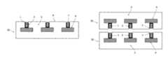
- Non-limiting examples of a variety of patternsinclude arrays of vias or arrays of metal lines and spaces, for example as found in via and routing layers in CMOS back-end-of-line (BEOL) interconnect fabrication.
- 3D electrical interconnectionsmay be formed by alignment and bonding of metal vias to metal vias, metal vias to metal lines, or metal lines to metal lines.
- fabrication techniques to build a surface suitable for a hybrid bondare industry standard single and dual damascene processes adjusted to satisfy a suitable topography specification, if necessary.
- CMOS BEOL fabrication processesThere are basically two types of CMOS BEOL fabrication processes. One is typically referred to as an aluminum (Al) BEOL and the other is referred to as a copper (Cu) BEOL.
- Al BEOL processAl with a suitable conductive barrier layer is typically used as the routing layer and tungsten (W), with a suitable conductive barrier layer is used for a via layer to electrically interconnect between two adjacent Al routing layers.
- Wtungsten
- the Al routing layeris typically dry etched and subsequently planarized with a dielectric deposition followed by chemo-mechanical polishing (CMP).
- CMPchemo-mechanical polishing
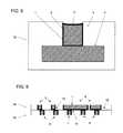
- the W via layeris typically formed with a single damascene process comprised of dielectric deposition, via patterning and etching to the previous routing layer, via filling with conductive barrier layer physical vapor deposition and W chemical vapor deposition, and CMP of W and conductive barrier layer to isolate W vias, or plugs, within the dielectric matrix.
- a Cu BEOL processCu with a suitable conductive barrier layer is typically used as the routing and via layer.
- the Cu routing and via layersare typically formed with a dual damascene process comprised of dielectric deposition, via patterning and etching partially through the dielectric layer, followed by routing patterning that overlaps the via patterning and simultaneous continued etching of the via(s) to the previous routing layer where the routing overlaps the partially etched vias and etching of a trench for routing that connects to the previous routing layer with the via.
- An alternate dual damascene processis comprised of dielectric deposition, routing patterning and etching partially through the dielectric layer that stops short of the previous routing layer, via patterning and etching to the previous routing layer where the via is within the partially etched routing and the etching completes the via etch to the previous routing layer.
- Either doubly etched surfaceis then filled with a conductive barrier layer, for example by physical vapor deposition, followed by Cu filling, for example by electroplating or physical vapor deposition and electroplating, and finally CMP of the Cu and conductive barrier layer to isolate Cu routing within the dielectric matrix.
- a conductive barrier layerfor example by physical vapor deposition
- Cu fillingfor example by electroplating or physical vapor deposition and electroplating
- CMP of the Cu and conductive barrier layerto isolate Cu routing within the dielectric matrix.
- a Cu BEOL processis an example of such a preferable capability due to the Cu damascene process which has been an industry standard for a number of years and the capability of Cu direct hybrid bond technology to leverage this infrastructure. It has been relatively more challenging to leverage an Al BEOL industry standard process because the two primary metals in this process, W and Al, are more challenging materials to develop either a W or Al direct hybrid bond technology due to a combination of factors including high yield strength, coefficient of thermal expansion (CTE), native oxide, and hillock formation.
- CTEcoefficient of thermal expansion
- An embodiment of the inventionis directed to a method of forming a direct hybrid bond surface including forming a first plurality of metallic contact structures in an upper surface of a first substrate, where a top surface of said structures is below said upper surface; forming a first layer of conductive barrier material over said upper surface and said plurality of metallic contact structures; and removing said first layer of conductive barrier material from said upper surface.
- FIG. 1is a schematic depiction of a cross-section of the near surface region of a single or dual damascene process formed conductive layers, with filled vias and/or routing with a conductive barrier between filled vias and/or routing and surrounding dielectric;
- FIG. 2is a schematic depiction of the cross-section in FIG. 1 after removal of the conductive layers from the surface of a surrounding dielectric;
- FIG. 3is a schematic depiction of the cross-section in FIG. 2 after forming a conductive barrier material layer
- FIG. 4is a schematic depiction of the cross-section in FIG. 3 after removal of the conductive barrier layer material layer from the surface of the surrounding dielectric;
- FIG. 5is a schematic depiction of two hybrid direct bond surfaces being bonded
- FIG. 6is a schematic depiction of two hybrid direct bond surfaces after contacting the respective dielectric layers
- FIG. 7is a schematic depiction of two hybrid direct bond surfaces directly bonded
- FIG. 8is a schematic depiction of curvature of the upper surface of the conductive barrier material as a result of dishing
- FIG. 9is a schematic depiction of a pair of substrates, according to the present invention, with misalignment of similar via structures with conductive barriers and alignment of vias with conductive barriers to routing structures with conductive barriers;
- FIG. 10is a schematic depiction of a cross-section of the near surface region of a surface comprised of a patterned metal layer planarized with surrounding dielectric with planarization exposing patterned metal layer, without a conductive barrier layer laterally between metal layer and surrounding dielectric;
- FIG. 11is a schematic depiction of the cross-section in FIG. 10 with the conductive portion of the exposed surface of the patterned metal layer capped with conductive barrier metal according to the present invention
- FIG. 12is a schematic depiction of a pair of contacted substrates, according to the present invention, with an example of alignment of routing structures without conductive barriers to routing structures without conductive barriers laterally between metal layer and surrounding dielectric;
- FIG. 13is a schematic depiction of another embodiment of the invention having a through silicon via structure
- FIG. 14is a schematic depiction of the structure of FIG. 13 with a second conductive barrier material layer.
- FIG. 15is a schematic depiction of another embodiment of the invention having a through silicon via structure with a dielectric layer on the sidewall.
- FIG. 1showing a cross-section of a surface of a substrate 30 in a process for direct hybrid bonding according to the invention comprised of conductor 1 , conductive barrier 2 , dielectric 3 , and metal structure 4 .
- Metal structures 4are formed in dielectric 3 .
- Metal structures 4are located within dielectric 3 and can be a contact, pad, line, or other metal interconnect structure. Openings are formed in dielectric 3 over metal structures 4 followed by formation of barrier 2 and conductor 1 .
- the sizes and thicknesses of the conductor 1 , conductive barrier 2 and metal structure 4are not to scale but are drawn to illustrate the invention. While the openings and metal structures are shown to be the same size and shape, they can differ in size and shape depending upon design or need.
- a wide variety of metals for conductor 1are possible including but not limited to Cu, and W which are common in Cu and Al BEOL foundries, respectively.
- Cucan be deposited by physical vapor deposition (PVD) or electroplating (EP) and W can be deposited by chemical vapor deposition (CVD).
- PVDphysical vapor deposition
- EPelectroplating
- CVDchemical vapor deposition
- a wide variety of conductive barriers for conductive barrier material 2are also possible which are common in Cu and Al BEOL foundries.
- Conductive barriers in Cu BEOL processesinclude tantalum (Ta), titanium nitride (TiN), tantalum nitride (TaN), tungsten nitride (WN), ruthenium oxide (RuO 2 ), tantalum silicon nitride (TaSiN), titanium silicon nitride (TiSiN), tungsten boron nitride (TBN), cobalt tungsten boride (CoWB), cobalt tungsten phosphide or combinations thereof, for example Ti/TiN and Ta/TaN, which can be deposited by a variety of techniques including PVD, CVD, and metal organic CVD (MOCVD).
- PVD techniquesinclude DC magnetron sputtering, collimated sputtering, and ionized metal plasma (IMP).
- Conductive barriers in Al BEOL processesinclude Ti/TiN. Other materials are also possible as barriers, for example nickel (Ni).
- a wide variety of dielectricsare also possible including but not limited to silicon oxide, silicon nitride, and silicon carbide nitride which are common in Cu and Al BEOL foundries.
- a common method to create the surface described by the cross-section in FIG. 1is with the damascene process described above.
- FIG. 1The upper surface of FIG. 1 is subjected to CMP to remove the portion of conductor 1 and conductive barrier 2 on top of dielectric 3 .
- FIG. 2illustrates the structure after CMP.
- the relative heights of conductor 1 and conductive barrier 2 relative to dielectric 3can be controlled by the CMP portion of the damascene process.
- An example of variation of relative height across the bond surface of the conductive layers below dielectric 3 for a surface most suitable for direct hybrid bondingis one to ten nanometers below the dielectric 3 , although smaller and larger variations are also possible. This recess is typically referred to as dishing. The resulting surface is referred to as a hybrid bond surface without a conductive barrier 2 .
- a typical amount of dishing compatible with hybrid bondingis 0 to 20 nm, referred to as standard dishing.
- Standard dishingis increased by an amount that is comparable to the thickness of a subsequent conductive barrier 6 shown in FIG. 3 formed on top of this increased dishing forming openings 5 shown in FIG. 2 resulting in a dishing that is comparable to the standard dishing and compatible with that desired for a direct hybrid bond.
- An example of an increase in standard dishingis 5-20 nm, resulting in a total dishing t 1 of about 5-40 nm.
- This increase in standard dishingcan be formed in a variety of ways, for example by increasing the CMP used to create the standard dishing until the desired increased dishing is achieved.
- This increase in CMPcan be accomplished with an increase in CMP time, the amount of which can be determined by routine calibration and can be a function of CMP pad, slurry, downforce, carrier and table rotation, and pattern of conductor and dielectric on the hybrid surface.
- a layer of conductive barrier metal 6is formed over the structure on surface 31 shown in FIG. 2 .
- Barrier 6can be the same or a different material than conductive barrier 2 .
- Formation of barrier 6 on top of the conductor 1 after increased dishingcan be formed in a number of ways, for example by a damascene process including deposition of the conductive barrier over the entire surface followed by CMP to remove the conductive barrier from the higher dielectric surface without removing a significant amount or all of the conductive barrier material of layer 6 from within the recess.
- the barrier formationmay also be formed with a selective process, for example electro-less nickel electroplating.
- the resulting structurehas conductive barrier 7 in each of the openings 5 on top of conductor 1 and conductive barrier 2 .
- This resulting dishingis preferably compatible with that required for a direct hybrid bond, i.e. the surface of conductive barrier 7 is less than 20 nm, and preferably 1-10 nm, below the surface of dielectric 3 .
- the cross-section of the resulting surface shown schematically in FIG. 4is referred to as a hybrid bond surface with a conductive barrier 7 .
- the thickness of the layer 6can be less than the amount of dishing of conductor 1 /barrier 2 , as shown in FIG. 3 , or can be the same as or thicker than this amount of dishing. In the former case, only a portion or none of the layer 6 is removed from the recess. In the case of the layer 6 being the same or thicker than the amount of recess, layer 6 is removed from within the recess by the CMP. Layer 6 is removed in all cases so that the resulting dishing is less than 20 nm, preferably 1-10 nm, in forming barrier 7 .
- Each hybrid bond surface of substrate 30can contain devices and/or integrated circuits (not shown) such that these devices and/or integrated circuits can be connected to each other after completion of the hybrid bond.
- the devices and circuitscan contain metal structures 4 or can be connected to metal structures 4 through further unillustrated interconnect structures.
- Two hybrid bond surfaces of substrates 30 and 32 each having with a conductive barrier 7 with cross-section schematic such as shown in FIG. 4can now be direct hybrid bonded to each other as shown in the cross-sections of FIGS. 5 and 6 to form direct hybrid bond 12 .
- Substrates 30 and 32are aligned ( FIG. 5 ) and placed into direct contact such that the dielectric layers 3 in substrates 30 and 32 contact each other ( FIG. 6 ).
- the alignment and contactingcan be performed at room temperature in either room ambient or under vacuum.
- the figures schematicallyshow a gap between the barriers 7 of substrates 30 and 32 , there may be partial or significant contact between barriers 7 following the alignment and contacting. While a one-to-one connection arrangement is shown in FIG. 6 , other arrangements are possible such as plural metal structures in one substrate are bonded to a single metal structure in another substrate.
- the dielectric surfaces of substrates 30 and 32are preferably prepared as described in application Ser. Nos. 09/505,283, 10/359,608 and 11/201,321. Briefly, the surfaces may be etched, polished, activated and/or terminated with a desired bonding species to promote and enhance chemical bonding between dielectric 3 on substrates 30 and 32 . Smooth surfaces of dielectric 3 with a roughness of 0.1 to 3 nm rms are produced which are activated and/or terminated through wet or dry processes.
- the dielectric 3 of the substrate surfacesbegan to form a bond at a contact point or points, and the attractive bonding force between the wafers increases as the chemically bonded area increases.
- This contactcan include barriers 7 or not include barriers 7 . If the contact includes barriers 7 , the pressure generated by the chemical substrate-to-substrate bonding in dielectric 3 results in a force by which contacting areas of the barriers 7 are strongly joined, and the chemical bonding between the dielectric 3 in substrates 30 and 32 produces electrical connection between metal pads on the two different wafers.
- barriers 7 against each other resulting from the bond between the dielectric 3 of substrates 30 and 32may not be adequate to achieve an electrical connection with a preferably low resistance due to, for example, a native oxide or other contamination, for example, hydrocarbons.
- An improved bond or preferably lower resistance electrical connectionmay be achieved by removing the native oxide on barrier 7 .
- dilute hydrofluoric acidmay be used to clean the surface or the surfaces of substrates 30 and 32 may be exposed to an inert ambient, for example nitrogen or argon, after removing the native oxide until bonding is conducted.
- the internal pressurealso may not be sufficient to contact enough of the surfaces of barriers 7 to each other.
- an improved bond or preferably lower resistance electrical connection between barriers 7can be achieved by heating.
- Examples of heatinginclude temperatures in the range of 100-400° C. for times between 10 minutes and 2 hours depending upon the materials used for the contact structures 4 , barrier 6 and conductor 1 .
- Time and temperature optimization for a given combination of materialsis possible. For example, shorter heating times may be possible with higher temperatures and lower temperatures may be possible with longer heating times.
- the extent to which heating time can be minimized and/or heating temperature can be minimizedwill depend on the specific structure and materials combination and can be determined with common process optimization practices. For example, if barrier 7 is nickel, a temperature of 300° C.
- Temperature increasecan result in a preferably low resistance electrical connection by reduction of the native oxide or other contamination or by increasing the internal pressure between barriers 7 due to thermal expansion of conductor 1 and barrier 7 .
- Material 4 and other materials below material 4may also increase the thermal expansion of the structure underneath barrier 7 and correspondingly increase pressure between opposed barriers 7 .
- material 4is aluminum with associated CTE and Young's modulus
- a higher pressuremay be generated compared to an alternate material 4 with a lower CTE and/or Young's modulus.
- Heatingmay also increase interdiffusion between barriers 7 to produce in a preferable lower-resistance electrical connection.
- heatingcan be used to result in contact between barriers 7 due to a higher CTE of barrier 7 than dielectric 3 .
- the amount of heating or temperature risedepends on the separation between barriers 7 , the thickness, CTE, and Young's modulus of barriers 7 and conductor 1 and metal structure 4 as these parameters affect the pressure between opposed barriers 7 for a given temperature rise. For example, minimizing the separation between barriers 7 , for example less than 10 nm, may reduce the heating compared to a separation of 20 nm.
- the height or thickness of barrier 7 and/or conductor 1will increase pressure as the thermal expansion of barrier 7 and conductor 1 will increase with thickness.
- the typical increase of expansion of barrier 7 and conductor 1is proportional to thickness.
- conductor 1 with higher Young's modulusis expected to generate higher pressure than an alternate conductor 1 with lower Young's modulus as the higher Young's modulus material is less likely to yield when generating pressure.
- a barrier 7 with lower Young's modulusmay not require as much heating as it may facilitate forming a connection by yielding at a lower pressure. Following heating, the thermal expansion of conductor 1 and barrier 7 thus result in intimately contacted low-resistance connections, as shown in FIG. 7 if barriers 7 are not in intimate contact when the surfaces of substrates 30 and 32 are initially contacted.
- barrier 7is preferably thick enough to accommodate coverage of the roughness of conductor 1 but not too thick to complicate fabrication. Typical thickness ranges can be 5-20 nm.
- the relative thickness of the barrier at the middle and edge of the curvaturecan be thicker or thinner depending on the curvature of formation of surface of contact 1 prior to barrier 7 deposition on conductor 1 and curvature of formation of barrier 7 , for example due to different characteristics of a CMP process used to form surface of contact 1 and CMP process used to form surface of barrier 7 .
- the center of the barrier 7is recess less than 20 nm and preferably 1-10 nm below the surface of dielectric 3 .
- FIG. 9illustrates the upper portion of two substrates 34 and 35 with hybrid bond surfaces.
- Hybrid bond surfaces with a conductive barriercan comprise via components 8 that are connected to underlying trace components (not shown) or trace components 9 that are connected to underlying via components (not shown).
- trace components 9that are connected to underlying via components (not shown).
- This misalignmentcan also result in contact of conductive barrier 7 on one hybrid bond surface with dielectric surface 6 on another surface and the contact of an entire surface of conductive barrier 7 from one surface with a portion of a surface of a conductive barrier 7 on the other hybrid bond surface as shown by 11 in FIG. 9 .
- the surface of dielectric 3 on either first or second hybrid bond surfaceis in contact with either conductive barrier 7 on the other hybrid bond surface and conductive barrier 7 on either first or second hybrid bond surface is in contact with either conductive barrier 7 or the surface of dielectric 3 on the other hybrid bond surface according to the present invention.
- the conductive barrier 7 on top of conductor 1thus prevents contact between conductor 2 and dielectric 3 notwithstanding misalignment.
- This feature of the subject inventioncan improve reliability of the direct hybrid bond, for example when Cu is used as conductor 1 with Cu single or dual damascene direct hybrid bond surfaces built in a Cu BEOL for applications where there is a concern, for example, of Cu diffusion into dielectric 3 if Cu was in direct contact with dielectric 3 .
- the featuremay also facilitate the formation of an electrical connection across the bond interface for some structures, for example where conductor 1 is a W plug single damascene direct hybrid bond surfaces built in an Al BEOL when making electrical connections between conductor 1 on opposing surfaces is more challenging than making electrical connections between conductive barriers 7 on top of conductors 1 on opposing surfaces.
- the amount of dishing shown in FIG. 2can affect the thermal budget of a subsequent direct hybrid bond using these surfaces with recessed conductive portions.
- the dielectric portionsmay be in direct contact and all or some of the recessed conductive portions may not be in direct contact due to the recess.
- Heating of these direct hybrid bonded surfaces with recessed conductive portionscan result in expansion of the recessed conductive portions so that they are brought into direct contact at a temperature above that at which the direct hybrid bond surfaces were brought into contact and generate significant pressure to facilitate electrical connection between opposed recessed conductive portions and even higher temperatures. These higher temperatures can facilitate the formation of electrical interconnections between opposed recessed conductive portions and completion of the direct hybrid bond.
- the temperatures required to bring the recessed portions into direct contact and to generate significant pressure to facilitate electrical connection between opposed recessed conductive portionsis a combination of the conductive material, residual or native oxide on the conductive material, yield strength of the conductive material and dishing or recess of the conductive material. For example, less dishing can result in a lower thermal budget required to complete the hybrid bond after initially directly bonding opposed dielectric surfaces at low or room temperature due to less conductor 1 and conductive barrier 7 expansion required to form a metallic bond between opposed conductive barrier 7 surfaces.
- the thermal budgetcan also be influenced by materials that are underneath the conductor. For example, conductors 1 with higher CTE (i.e., above 15 ppm/° C.) underneath conductor 1 , for example metal structure 4 as shown in FIG.
- conductors 1 and/or metal structures 4may have a lower thermal budget to form hybrid bond electrical connections than conductors 1 and/or metal structures 4 with a lower CTE.
- metals with high CTE above 15 ppm/° C.include Cu and Al which are conductors common in Al and Cu BEOL processes.
- a conductive portion 13 surrounded by a dielectric portion 14comprises a direct hybrid bond surface 15 in substrate 36 as shown in FIG. 10 .
- An example of conductive portion 13is aluminum and an example of dielectric portion 14 is an inter-layer dielectric, examples of which are silicon oxide and other dielectrics used in Al BEOL, which are examples of typical materials used in Al BEOL.
- the metal portion 13may include via and/or routing patterns connected to underlying layers of interconnect.
- the dielectric portion 14may be contiguous, for example if the conductive portion is comprised only of vias, or may not be contiguous, for example if the conductive portion is separated by routing patterns.
- direct hybrid bond surface 15preferably has a dished conductive portion within a direct hybrid bonding specification.
- This surfacecan be formed by a combination of an Al metallization, dielectric deposition, and CMP planarization to form the surface with cross-section shown in FIG. 10 .
- the Al metallizationmay include a conductive barrier on top, for example Ti. If there is a conductive barrier and it is removed by the CMP planarization, the surface will have a cross-section shown in FIG. 10 .
- the conductive barrieris sufficiently thick that it is not entirely removed by the CMP planarization, and there is suitable dishing t 2 , for example 0-20 nm of the conductive barrier portion of the hybrid bond surface for hybrid bonding, then this surface, e.g, as shown in FIG. 11 , can be suitable for direct hybrid bonding without additional conductive barrier deposition and CMP.
- the dishing t 2 described in FIG. 10is increased by an amount that is comparable to the thickness of a subsequent conductive barrier 16 that is formed on top of this increased dishing resulting in a dishing that is comparable to that in FIG. 10 and compatible with that required for a direct hybrid bond ( FIG. 10 ).
- This increase in thicknessis in the range of about 5-20 nm.
- This increase in standard dishingcan be formed in a variety of ways, for example by increasing the amount of CMP from that used to be compatible with that required for a direct hybrid bond.
- Formation of the barrier on top of the increased dishingcan be formed in a number of ways, for example by a damascene process including deposition of the conductive barrier over the entire surface (similar to FIG.
- the thickness of the formed barriercan be comparable to, greater than, or less than the increased dishing thickness, for example less than about 40 nm.
- the final barrier thickness and the dishingcan then be controlled by CMP after formation of the barrier.
- this resulting dishingis preferably compatible with that required for a direct hybrid bond.
- a cross-section of the resulting surfaceis shown schematically in FIG. 11 illustrating substrate 37 and is referred to as a hybrid bond surface 18 with a conductive barrier 16 not in contact with an underlying conductive barrier.
- the barrier formationmay also be formed with a selective process, for example electro-less nickel electroplating.
- Hybrid bond surfaces of substrates 38 and 39 with a conductive barrier 16 formed as shown in the cross-section schematic of FIG. 11can now be direct hybrid bonded to each other as shown in the cross-section of FIG. 12 to form direct hybrid bond with conductive barrier 16 without an underlying conductive barrier.
- Each hybrid bond surfaceis a surface of a substrate and each substrate can contain devices and/or integrated circuits such that these devices and/or integrated circuits can be connected to each other after completion of the hybrid bond.
- Hybrid bond surfaces with a conductive barriercan comprise via components that are connected to underlying trace components (not shown) or trace components 19 that are connected to underlying via components (not shown).
- misalignmentAfter bonding, there is typically some amount of misalignment between respective hybrid bond surfaces with a conductive barrier.
- This misalignmentcan result in contact of conductive barrier 16 on a first hybrid bond surface with a dielectric surface 17 on a second hybrid bond surface in substrate 36 and contact of a dielectric surface 17 on a first hybrid bond surface with a conductive barrier 16 on a second hybrid bond surface as shown by 20 in FIG. 12 .
- This misalignmentcan also result in contact of conductive barrier 16 on one hybrid bond surface with dielectric surface 17 on another surface and the contact of an surface of conductive barrier 16 from one surface with a portion of a surface of a conductive barrier 16 on the other hybrid bond surface as shown by 21 in FIG. 12 .
- dielectric surface 17 on either first or second hybrid bond surfaceis in contact with either conductive bather 16 on the other hybrid bond surface and conductive barrier 16 on either first or second hybrid bond surface is in contact with either conductive barrier 16 or dielectric surface 17 on the other hybrid bond surface according to the present invention.
- This featurecan facilitate the formation of an electrical connection across the bond interface for some structures, for example where conductor 13 is an Al routing surface built in an Al BEOL, when making electrical connections between conductor 13 on opposing surfaces is more challenging than making electrical connections between conductive barriers 16 on top of conductors 13 on opposing surfaces.
- the amount of dishing shown in FIG. 11can affect the thermal budget of a subsequent direct hybrid bond using these surfaces. For example, less dishing can result in a lower thermal budget required to complete the hybrid bond after initially directly bonding opposed dielectric surfaces at low or room temperature due to less conductor 13 expansion required to form a metallic bond between opposed conductive barrier 16 surfaces.
- a hybrid surfaceincludes a conductive through silicon via (TSV) structures 23 and 35 as shown in FIGS. 13-15 .
- TSVconductive through silicon via
- Each figureshows two different structures, with ( 23 ) and without ( 25 ) a conductive barrier material layer 26 , for convenience of illustration, formed in a manner similar to FIGS. 1-4 above.
- the TSVsextend through substrate 40 to contact metal conductor 4 in substrate 41 .
- the conductive material of TSV 23 and 25can be comprised of a metal like Cu or W or a non-metal like polysilicon.
- the conductive materialcan be adjacent to an insulating material 24 as shown in FIG. 13 or, as shown in FIG. 14 including substrate 42 , may have a barrier layer 27 interposed between the conductive material and insulating material.
- TSV 23 and 25may have an insulating barrier 28 interposed between the conductive material and a semiconductor substrate 43 as shown in FIG. 15 .
- the TSVmay be recessed with increased dishing as described in the first and second embodiments and a conductive barrier 26 formed within this increased dishing as described in the first and second embodiments to form a hybrid bond surface with dishing suitable for direct hybrid bonding.
- These types of surfacesmay be direct hybrid bonded to each other resulting in, for example a so-called back-to-back direct hybrid bond if the TSV surface is exposed through the back of a CMOS structure.
- hybrid bond surfacesit is also possible to use one of these hybrid bond surfaces to form a direct hybrid bond to the hybrid bond surface formed on the front of a CMOS structure, for example on top of a Cu BEOL or Al BEOL, to form a so-called front-to-back direct hybrid bond.
- BEOL via fill metalcan be fully encapsulated with a conductive barrier.
- the present inventionallows hybrid bond fabrication to utilize dielectrics and conductive barrier materials for the direct hybrid bonding.
- the process window for a direct hybrid bond process leveraging materials and/or processes currently qualified in CMOS BEOL foundriescan be improved.
- the present inventionalso allows for lowering the adoption barrier for manufacturers to qualify direct hybrid bond technology, produces a direct hybrid bond surface using a combination of insulating dielectric and conductive barrier materials that are used in CMOS BEOLs, can provide a method and structure for a direct hybrid bond surface that suppresses hillock formation, and can reduce thermal budgets in direct hybrid bonding.
- Applications of the present inventioninclude but are not limited to vertical integration of processed integrated circuits for 3-D SOC, micro-pad packaging, low-cost and high-performance replacement of flip chip bonding, wafer scale packaging, thermal management and unique device structures such as metal base devices.
- Applicationsfurther include but are not limited to integrated circuits like backside-illuminated image sensors, RF front ends, micro-electrical mechanical structures (MEMS) including but not limited to pico-projectors and gyros, 3D stacked memory including but not limited to hybrid memory cube, high bandwidth memory, and DIRAM, 2.5D including but not limited to FPGA tiling on interposers and the products these circuits are used in including but not limited to cell phones and other mobile devices, laptop's, and servers.
- MEMSmicro-electrical mechanical structures
- 3D stacked memoryincluding but not limited to hybrid memory cube, high bandwidth memory, and DIRAM
- 2.5Dincluding but not limited to FPGA tiling on interposers and the products these circuits are used in including but not limited to cell phones and other
Landscapes
- Engineering & Computer Science (AREA)
- Microelectronics & Electronic Packaging (AREA)
- Power Engineering (AREA)
- Computer Hardware Design (AREA)
- Manufacturing & Machinery (AREA)
- Physics & Mathematics (AREA)
- Condensed Matter Physics & Semiconductors (AREA)
- General Physics & Mathematics (AREA)
- Internal Circuitry In Semiconductor Integrated Circuit Devices (AREA)
- Pressure Welding/Diffusion-Bonding (AREA)
- Wire Bonding (AREA)
Abstract
Description
Claims (15)
Priority Applications (13)
| Application Number | Priority Date | Filing Date | Title |
|---|---|---|---|
| US14/835,379US9953941B2 (en) | 2015-08-25 | 2015-08-25 | Conductive barrier direct hybrid bonding |
| TW105126081ATWI702659B (en) | 2015-08-25 | 2016-08-16 | Conductive barrier direct hybrid bonding |
| CN202210544308.7ACN114944376A (en) | 2015-08-25 | 2016-08-25 | Conductive barrier direct hybrid bonding |
| CN201680048737.8ACN108140559B (en) | 2015-08-25 | 2016-08-25 | Conductive barrier direct hybrid bonding |
| JP2018529502AJP6743149B2 (en) | 2015-08-25 | 2016-08-25 | Direct hybrid bonding of conductive barrier |
| KR1020227019392AKR102659849B1 (en) | 2015-08-25 | 2016-08-25 | Conductive barrier direct hybrid bonding |
| EP16840097.6AEP3341956A4 (en) | 2015-08-25 | 2016-08-25 | DIRECT HYBRID CONNECTION WITH CONDUCTIVE BARRIER |
| KR1020187007638AKR102408487B1 (en) | 2015-08-25 | 2016-08-25 | Conductive barrier direct hybrid junction |
| PCT/US2016/048609WO2017035321A1 (en) | 2015-08-25 | 2016-08-25 | Conductive barrier direct hybrid bonding |
| US15/947,461US10262963B2 (en) | 2015-08-25 | 2018-04-06 | Conductive barrier direct hybrid bonding |
| US16/383,455US11264345B2 (en) | 2015-08-25 | 2019-04-12 | Conductive barrier direct hybrid bonding |
| US17/677,161US11830838B2 (en) | 2015-08-25 | 2022-02-22 | Conductive barrier direct hybrid bonding |
| US18/517,681US12381168B2 (en) | 2015-08-25 | 2023-11-22 | Conductive barrier direct hybrid bonding |
Applications Claiming Priority (1)
| Application Number | Priority Date | Filing Date | Title |
|---|---|---|---|
| US14/835,379US9953941B2 (en) | 2015-08-25 | 2015-08-25 | Conductive barrier direct hybrid bonding |
Related Child Applications (1)
| Application Number | Title | Priority Date | Filing Date |
|---|---|---|---|
| US15/947,461DivisionUS10262963B2 (en) | 2015-08-25 | 2018-04-06 | Conductive barrier direct hybrid bonding |
Publications (2)
| Publication Number | Publication Date |
|---|---|
| US20170062366A1 US20170062366A1 (en) | 2017-03-02 |
| US9953941B2true US9953941B2 (en) | 2018-04-24 |
Family
ID=58100993
Family Applications (5)
| Application Number | Title | Priority Date | Filing Date |
|---|---|---|---|
| US14/835,379ActiveUS9953941B2 (en) | 2015-08-25 | 2015-08-25 | Conductive barrier direct hybrid bonding |
| US15/947,461ActiveUS10262963B2 (en) | 2015-08-25 | 2018-04-06 | Conductive barrier direct hybrid bonding |
| US16/383,455ActiveUS11264345B2 (en) | 2015-08-25 | 2019-04-12 | Conductive barrier direct hybrid bonding |
| US17/677,161ActiveUS11830838B2 (en) | 2015-08-25 | 2022-02-22 | Conductive barrier direct hybrid bonding |
| US18/517,681ActiveUS12381168B2 (en) | 2015-08-25 | 2023-11-22 | Conductive barrier direct hybrid bonding |
Family Applications After (4)
| Application Number | Title | Priority Date | Filing Date |
|---|---|---|---|
| US15/947,461ActiveUS10262963B2 (en) | 2015-08-25 | 2018-04-06 | Conductive barrier direct hybrid bonding |
| US16/383,455ActiveUS11264345B2 (en) | 2015-08-25 | 2019-04-12 | Conductive barrier direct hybrid bonding |
| US17/677,161ActiveUS11830838B2 (en) | 2015-08-25 | 2022-02-22 | Conductive barrier direct hybrid bonding |
| US18/517,681ActiveUS12381168B2 (en) | 2015-08-25 | 2023-11-22 | Conductive barrier direct hybrid bonding |
Country Status (7)
| Country | Link |
|---|---|
| US (5) | US9953941B2 (en) |
| EP (1) | EP3341956A4 (en) |
| JP (1) | JP6743149B2 (en) |
| KR (2) | KR102408487B1 (en) |
| CN (2) | CN108140559B (en) |
| TW (1) | TWI702659B (en) |
| WO (1) | WO2017035321A1 (en) |
Cited By (106)
| Publication number | Priority date | Publication date | Assignee | Title |
|---|---|---|---|---|
| US10262963B2 (en) | 2015-08-25 | 2019-04-16 | Invensas Bonding Technologies, Inc. | Conductive barrier direct hybrid bonding |
| US10508030B2 (en) | 2017-03-21 | 2019-12-17 | Invensas Bonding Technologies, Inc. | Seal for microelectronic assembly |
| US10515913B2 (en) | 2017-03-17 | 2019-12-24 | Invensas Bonding Technologies, Inc. | Multi-metal contact structure |
| US10515925B2 (en) | 2017-04-21 | 2019-12-24 | Invensas Bonding Technologies, Inc. | Die processing |
| US10529634B2 (en) | 2017-05-11 | 2020-01-07 | Invensas Bonding Technologies, Inc. | Probe methodology for ultrafine pitch interconnects |
| US20200075533A1 (en)* | 2018-08-29 | 2020-03-05 | Invensas Bonding Technologies, Inc. | Bond enhancement in microelectronics by trapping contaminants and arresting cracks during direct-bonding processes |
| US10658313B2 (en) | 2017-12-11 | 2020-05-19 | Invensas Bonding Technologies, Inc. | Selective recess |
| US10727219B2 (en) | 2018-02-15 | 2020-07-28 | Invensas Bonding Technologies, Inc. | Techniques for processing devices |
| US10777533B2 (en) | 2012-08-30 | 2020-09-15 | Invensas Bonding Technologies, Inc. | Heterogeneous device |
| US10784191B2 (en) | 2017-03-31 | 2020-09-22 | Invensas Bonding Technologies, Inc. | Interface structures and methods for forming same |
| US10790262B2 (en) | 2018-04-11 | 2020-09-29 | Invensas Bonding Technologies, Inc. | Low temperature bonded structures |
| US10796936B2 (en) | 2016-12-22 | 2020-10-06 | Invensas Bonding Technologies, Inc. | Die tray with channels |
| US10840205B2 (en) | 2017-09-24 | 2020-11-17 | Invensas Bonding Technologies, Inc. | Chemical mechanical polishing for hybrid bonding |
| WO2020251779A1 (en) | 2019-06-12 | 2020-12-17 | Invensas Bonding Technologies, Inc. | Sealed bonded structures and methods for forming the same |
| US10879210B2 (en) | 2017-02-09 | 2020-12-29 | Invensas Bonding Technologies, Inc. | Bonded structures |
| US10879226B2 (en) | 2016-05-19 | 2020-12-29 | Invensas Bonding Technologies, Inc. | Stacked dies and methods for forming bonded structures |
| US10879207B2 (en) | 2016-12-21 | 2020-12-29 | Invensas Bonding Technologies, Inc. | Bonded structures |
| US10879212B2 (en) | 2017-05-11 | 2020-12-29 | Invensas Bonding Technologies, Inc. | Processed stacked dies |
| US10896902B2 (en) | 2016-01-13 | 2021-01-19 | Invensas Bonding Technologies, Inc. | Systems and methods for efficient transfer of semiconductor elements |
| US10923408B2 (en) | 2017-12-22 | 2021-02-16 | Invensas Bonding Technologies, Inc. | Cavity packages |
| US10964664B2 (en) | 2018-04-20 | 2021-03-30 | Invensas Bonding Technologies, Inc. | DBI to Si bonding for simplified handle wafer |
| US10998265B2 (en) | 2016-09-30 | 2021-05-04 | Invensas Bonding Technologies, Inc. | Interface structures and methods for forming same |
| US10998292B2 (en) | 2018-06-13 | 2021-05-04 | Invensas Bonding Technologies, Inc. | Offset pads over TSV |
| US11004757B2 (en) | 2018-05-14 | 2021-05-11 | Invensas Bonding Technologies, Inc. | Bonded structures |
| US11011494B2 (en) | 2018-08-31 | 2021-05-18 | Invensas Bonding Technologies, Inc. | Layer structures for making direct metal-to-metal bonds at low temperatures in microelectronics |
| US11011503B2 (en) | 2017-12-15 | 2021-05-18 | Invensas Bonding Technologies, Inc. | Direct-bonded optoelectronic interconnect for high-density integrated photonics |
| US11031285B2 (en) | 2017-10-06 | 2021-06-08 | Invensas Bonding Technologies, Inc. | Diffusion barrier collar for interconnects |
| US11056390B2 (en) | 2015-06-24 | 2021-07-06 | Invensas Corporation | Structures and methods for reliable packages |
| US11056348B2 (en) | 2018-04-05 | 2021-07-06 | Invensas Bonding Technologies, Inc. | Bonding surfaces for microelectronics |
| US11145626B2 (en) | 2018-10-24 | 2021-10-12 | Samsung Electronics Co., Ltd. | Semiconductor package |
| US11152317B2 (en) | 2018-09-20 | 2021-10-19 | Samsung Electronics Co., Ltd. | Semiconductor device including interconnection structure including copper and tin and semiconductor package including the same |
| US11158573B2 (en) | 2018-10-22 | 2021-10-26 | Invensas Bonding Technologies, Inc. | Interconnect structures |
| US11158606B2 (en) | 2018-07-06 | 2021-10-26 | Invensas Bonding Technologies, Inc. | Molded direct bonded and interconnected stack |
| US11171117B2 (en) | 2018-06-12 | 2021-11-09 | Invensas Bonding Technologies, Inc. | Interlayer connection of stacked microelectronic components |
| US11169326B2 (en) | 2018-02-26 | 2021-11-09 | Invensas Bonding Technologies, Inc. | Integrated optical waveguides, direct-bonded waveguide interface joints, optical routing and interconnects |
| US11195748B2 (en) | 2017-09-27 | 2021-12-07 | Invensas Corporation | Interconnect structures and methods for forming same |
| US11205625B2 (en) | 2019-04-12 | 2021-12-21 | Invensas Bonding Technologies, Inc. | Wafer-level bonding of obstructive elements |
| US11205600B2 (en) | 2014-03-12 | 2021-12-21 | Invensas Corporation | Integrated circuits protected by substrates with cavities, and methods of manufacture |
| US11244920B2 (en) | 2018-12-18 | 2022-02-08 | Invensas Bonding Technologies, Inc. | Method and structures for low temperature device bonding |
| US11244916B2 (en) | 2018-04-11 | 2022-02-08 | Invensas Bonding Technologies, Inc. | Low temperature bonded structures |
| US11256004B2 (en) | 2018-03-20 | 2022-02-22 | Invensas Bonding Technologies, Inc. | Direct-bonded lamination for improved image clarity in optical devices |
| US20220068890A1 (en)* | 2016-10-07 | 2022-03-03 | Xcelsis Corporation | 3d processor |
| US11270963B2 (en)* | 2020-01-14 | 2022-03-08 | Sandisk Technologies Llc | Bonding pads including interfacial electromigration barrier layers and methods of making the same |
| WO2022051103A1 (en) | 2020-09-04 | 2022-03-10 | Invensas Bonding Technologies, Inc. | Bonded structure with interconnect structure |
| WO2022051104A1 (en) | 2020-09-04 | 2022-03-10 | Invensas Bonding Technologies, Inc. | Bonded structure with interconnect structure |
| US11276676B2 (en) | 2018-05-15 | 2022-03-15 | Invensas Bonding Technologies, Inc. | Stacked devices and methods of fabrication |
| US11282801B2 (en)* | 2010-03-31 | 2022-03-22 | Ev Group E. Thallner Gmbh | Method for permanent connection of two metal surfaces |
| US11289372B2 (en) | 2005-08-11 | 2022-03-29 | Invensas Bonding Technologies, Inc. | 3D IC method and device |
| US11296053B2 (en) | 2019-06-26 | 2022-04-05 | Invensas Bonding Technologies, Inc. | Direct bonded stack structures for increased reliability and improved yield in microelectronics |
| US11305372B2 (en)* | 2013-10-03 | 2022-04-19 | Commissariat A L'energie Atomique Et Aux Energies Alternatives | Method of assembly by direct bonding between two elements, each element comprising portions of metal and dielectric materials |
| US20220148963A1 (en)* | 2019-06-13 | 2022-05-12 | Nanya Technology Corporation | Method of forming integrated circuit device with bonding structure |
| US11348801B2 (en) | 2016-12-28 | 2022-05-31 | Invensas Bonding Technologies, Inc. | Processing stacked substrates |
| US11355404B2 (en) | 2019-04-22 | 2022-06-07 | Invensas Bonding Technologies, Inc. | Mitigating surface damage of probe pads in preparation for direct bonding of a substrate |
| US11367652B2 (en) | 2016-12-28 | 2022-06-21 | Invensas Bonding Technologies, Inc. | Microelectronic assembly from processed substrate |
| US11373963B2 (en) | 2019-04-12 | 2022-06-28 | Invensas Bonding Technologies, Inc. | Protective elements for bonded structures |
| US11380597B2 (en) | 2017-12-22 | 2022-07-05 | Invensas Bonding Technologies, Inc. | Bonded structures |
| US11385278B2 (en)* | 2019-05-23 | 2022-07-12 | Invensas Bonding Technologies, Inc. | Security circuitry for bonded structures |
| US11387214B2 (en) | 2017-06-15 | 2022-07-12 | Invensas Llc | Multi-chip modules formed using wafer-level processing of a reconstituted wafer |
| US11393779B2 (en) | 2018-06-13 | 2022-07-19 | Invensas Bonding Technologies, Inc. | Large metal pads over TSV |
| US11462419B2 (en) | 2018-07-06 | 2022-10-04 | Invensas Bonding Technologies, Inc. | Microelectronic assemblies |
| US11476213B2 (en) | 2019-01-14 | 2022-10-18 | Invensas Bonding Technologies, Inc. | Bonded structures without intervening adhesive |
| US11515291B2 (en) | 2018-08-28 | 2022-11-29 | Adeia Semiconductor Inc. | Integrated voltage regulator and passive components |
| US11538781B2 (en) | 2020-06-30 | 2022-12-27 | Adeia Semiconductor Bonding Technologies Inc. | Integrated device packages including bonded structures |
| US11605614B2 (en) | 2016-02-29 | 2023-03-14 | Invensas Llc | Correction die for wafer/die stack |
| US11610846B2 (en) | 2019-04-12 | 2023-03-21 | Adeia Semiconductor Bonding Technologies Inc. | Protective elements for bonded structures including an obstructive element |
| US11621246B2 (en) | 2019-03-29 | 2023-04-04 | Adeia Semiconductor Technologies Llc | Diffused bitline replacement in stacked wafer memory |
| US11626363B2 (en) | 2016-12-29 | 2023-04-11 | Adeia Semiconductor Bonding Technologies Inc. | Bonded structures with integrated passive component |
| US11658139B2 (en) | 2020-07-29 | 2023-05-23 | Samsung Electronics Co., Ltd. | Semiconductor package for improving bonding reliability |
| US11664357B2 (en) | 2018-07-03 | 2023-05-30 | Adeia Semiconductor Bonding Technologies Inc. | Techniques for joining dissimilar materials in microelectronics |
| US11710718B2 (en) | 2015-07-10 | 2023-07-25 | Adeia Semiconductor Technologies Llc | Structures and methods for low temperature bonding using nanoparticles |
| US11715730B2 (en) | 2017-03-16 | 2023-08-01 | Adeia Semiconductor Technologies Llc | Direct-bonded LED arrays including optical elements configured to transmit optical signals from LED elements |
| US11721653B2 (en) | 2019-12-23 | 2023-08-08 | Adeia Semiconductor Bonding Technologies Inc. | Circuitry for electrical redundancy in bonded structures |
| US11735523B2 (en) | 2020-05-19 | 2023-08-22 | Adeia Semiconductor Bonding Technologies Inc. | Laterally unconfined structure |
| US11742314B2 (en) | 2020-03-31 | 2023-08-29 | Adeia Semiconductor Bonding Technologies Inc. | Reliable hybrid bonded apparatus |
| US11762200B2 (en) | 2019-12-17 | 2023-09-19 | Adeia Semiconductor Bonding Technologies Inc. | Bonded optical devices |
| US11760059B2 (en) | 2003-05-19 | 2023-09-19 | Adeia Semiconductor Bonding Technologies Inc. | Method of room temperature covalent bonding |
| TWI817137B (en)* | 2020-06-12 | 2023-10-01 | 美商豪威科技股份有限公司 | Metal routing in image sensor using hybrid bonding |
| US11790219B2 (en) | 2017-08-03 | 2023-10-17 | Adeia Semiconductor Inc. | Three dimensional circuit implementing machine trained network |
| US11798908B2 (en) | 2020-08-14 | 2023-10-24 | Samsung Electronics Co., Ltd. | Trilayer bonding bump structure for semiconductor package |
| US20230377938A1 (en)* | 2020-12-10 | 2023-11-23 | Wuhan Xinxin Semiconductor Manufacturing Co., Ltd. | Chip bonding method |
| US11842894B2 (en) | 2019-12-23 | 2023-12-12 | Adeia Semiconductor Bonding Technologies Inc. | Electrical redundancy for bonded structures |
| US11862604B2 (en) | 2018-06-22 | 2024-01-02 | Adeia Semiconductor Inc. | Systems and methods for releveled bump planes for chiplets |
| US11862602B2 (en) | 2019-11-07 | 2024-01-02 | Adeia Semiconductor Technologies Llc | Scalable architecture for reduced cycles across SOC |
| US11876076B2 (en) | 2019-12-20 | 2024-01-16 | Adeia Semiconductor Technologies Llc | Apparatus for non-volatile random access memory stacks |
| US11881454B2 (en) | 2016-10-07 | 2024-01-23 | Adeia Semiconductor Inc. | Stacked IC structure with orthogonal interconnect layers |
| US11901281B2 (en) | 2019-03-11 | 2024-02-13 | Adeia Semiconductor Bonding Technologies Inc. | Bonded structures with integrated passive component |
| US11908739B2 (en) | 2017-06-05 | 2024-02-20 | Adeia Semiconductor Technologies Llc | Flat metal features for microelectronics applications |
| US11929347B2 (en) | 2020-10-20 | 2024-03-12 | Adeia Semiconductor Technologies Llc | Mixed exposure for large die |
| US20240088020A1 (en)* | 2019-06-13 | 2024-03-14 | Nanya Technology Corporation | Method of manufacturing integrated circuit device with bonding structure |
| US11935907B2 (en) | 2014-12-11 | 2024-03-19 | Adeia Semiconductor Technologies Llc | Image sensor device |
| US11961820B2 (en)* | 2018-02-15 | 2024-04-16 | Osram Oled Gmbh | Method for producing a connection between component parts, and component made of component parts |
| US11973056B2 (en) | 2016-10-27 | 2024-04-30 | Adeia Semiconductor Technologies Llc | Methods for low temperature bonding using nanoparticles |
| US11973045B2 (en) | 2021-07-01 | 2024-04-30 | Changxin Memory Technologies, Inc. | Semiconductor structure and method for forming same |
| US12009338B2 (en) | 2020-03-19 | 2024-06-11 | Adeia Semiconductor Bonding Technologies Inc. | Dimension compensation control for directly bonded structures |
| US12074092B2 (en) | 2018-05-30 | 2024-08-27 | Adeia Semiconductor Inc. | Hard IP blocks with physically bidirectional passageways |
| US12080672B2 (en) | 2019-09-26 | 2024-09-03 | Adeia Semiconductor Bonding Technologies Inc. | Direct gang bonding methods including directly bonding first element to second element to form bonded structure without adhesive |
| US12113054B2 (en) | 2019-10-21 | 2024-10-08 | Adeia Semiconductor Technologies Llc | Non-volatile dynamic random access memory |
| US12142528B2 (en) | 2016-10-07 | 2024-11-12 | Adeia Semiconductor Inc. | 3D chip with shared clock distribution network |
| US12191267B2 (en) | 2019-03-01 | 2025-01-07 | Adeia Semiconductor Technologies, LLC | Nanowire bonding interconnect for fine-pitch microelectronics |
| US12211809B2 (en) | 2020-12-30 | 2025-01-28 | Adeia Semiconductor Bonding Technologies Inc. | Structure with conductive feature and method of forming same |
| US12272730B2 (en) | 2018-03-29 | 2025-04-08 | Adeia Semiconductor Inc. | Transistor level interconnection methodologies utilizing 3D interconnects |
| US12300634B2 (en) | 2021-08-02 | 2025-05-13 | Adeia Semiconductor Bonding Technologies Inc. | Protective semiconductor elements for bonded structures |
| US12341083B2 (en) | 2023-02-08 | 2025-06-24 | Adeia Semiconductor Bonding Technologies Inc. | Electronic device cooling structures bonded to semiconductor elements |
| US12381128B2 (en) | 2020-12-28 | 2025-08-05 | Adeia Semiconductor Bonding Technologies Inc. | Structures with through-substrate vias and methods for forming the same |
| US12406959B2 (en) | 2018-07-26 | 2025-09-02 | Adeia Semiconductor Bonding Technologies Inc. | Post CMP processing for hybrid bonding |
| US12424584B2 (en) | 2020-10-29 | 2025-09-23 | Adeia Semiconductor Bonding Technologies Inc. | Direct bonding methods and structures |
Families Citing this family (95)
| Publication number | Priority date | Publication date | Assignee | Title |
|---|---|---|---|---|
| US6984571B1 (en) | 1999-10-01 | 2006-01-10 | Ziptronix, Inc. | Three dimensional device integration method and integrated device |
| US6902987B1 (en) | 2000-02-16 | 2005-06-07 | Ziptronix, Inc. | Method for low temperature bonding and bonded structure |
| US6962835B2 (en) | 2003-02-07 | 2005-11-08 | Ziptronix, Inc. | Method for room temperature metal direct bonding |
| US9455182B2 (en) | 2014-08-22 | 2016-09-27 | International Business Machines Corporation | Interconnect structure with capping layer and barrier layer |
| US10811388B2 (en) | 2015-09-28 | 2020-10-20 | Invensas Corporation | Capacitive coupling in a direct-bonded interface for microelectronic devices |
| US10032751B2 (en) | 2015-09-28 | 2018-07-24 | Invensas Corporation | Ultrathin layer for forming a capacitive interface between joined integrated circuit components |
| US9852988B2 (en) | 2015-12-18 | 2017-12-26 | Invensas Bonding Technologies, Inc. | Increased contact alignment tolerance for direct bonding |
| US10580757B2 (en)* | 2016-10-07 | 2020-03-03 | Xcelsis Corporation | Face-to-face mounted IC dies with orthogonal top interconnect layers |
| CN108288616B (en) | 2016-12-14 | 2023-04-07 | 成真股份有限公司 | Chip package |
| US10276909B2 (en) | 2016-12-30 | 2019-04-30 | Invensas Bonding Technologies, Inc. | Structure comprising at least a first element bonded to a carrier having a closed metallic channel waveguide formed therein |
| US20180233479A1 (en) | 2017-02-16 | 2018-08-16 | Nanya Technology Corporation | Semiconductor apparatus and method for preparing the same |
| IT201700053902A1 (en) | 2017-05-18 | 2018-11-18 | Lfoundry Srl | HYBRID BONDING METHOD FOR WAFER WITH SEMICONDUCTOR AND ITS INTEGRATED THREE-DIMENSIONAL DEVICE |
| US10447274B2 (en) | 2017-07-11 | 2019-10-15 | iCometrue Company Ltd. | Logic drive based on standard commodity FPGA IC chips using non-volatile memory cells |
| US10957679B2 (en) | 2017-08-08 | 2021-03-23 | iCometrue Company Ltd. | Logic drive based on standardized commodity programmable logic semiconductor IC chips |
| US10630296B2 (en) | 2017-09-12 | 2020-04-21 | iCometrue Company Ltd. | Logic drive with brain-like elasticity and integrality based on standard commodity FPGA IC chips using non-volatile memory cells |
| JP2019054153A (en)* | 2017-09-15 | 2019-04-04 | 東芝メモリ株式会社 | Semiconductor device manufacturing method |
| US12021072B2 (en) | 2018-01-23 | 2024-06-25 | Lumiense Photonics Inc. | Method of manufacturing of advanced three-dimensional semiconductor structures and structures produced therefrom |
| US10608642B2 (en) | 2018-02-01 | 2020-03-31 | iCometrue Company Ltd. | Logic drive using standard commodity programmable logic IC chips comprising non-volatile radom access memory cells |
| JP6952629B2 (en)* | 2018-03-20 | 2021-10-20 | 株式会社東芝 | Semiconductor device |
| KR102075764B1 (en)* | 2018-03-28 | 2020-02-10 | 한국과학기술원 | Heterogeneously integrated photonic circuit and method for manufacturing the circuit |
| US12062700B2 (en) | 2018-04-04 | 2024-08-13 | Qorvo Us, Inc. | Gallium-nitride-based module with enhanced electrical performance and process for making the same |
| US12046505B2 (en) | 2018-04-20 | 2024-07-23 | Qorvo Us, Inc. | RF devices with enhanced performance and methods of forming the same utilizing localized SOI formation |
| CN108520858A (en)* | 2018-06-07 | 2018-09-11 | 长江存储科技有限责任公司 | Metal connection structure and method for forming the same |
| CN118213279A (en) | 2018-07-02 | 2024-06-18 | Qorvo美国公司 | RF semiconductor device and method for manufacturing the same |
| US11211333B2 (en)* | 2018-07-16 | 2021-12-28 | Taiwan Semiconductor Manufacturing Co., Ltd. | Through silicon via optimization for three-dimensional integrated circuits |
| US10700094B2 (en)* | 2018-08-08 | 2020-06-30 | Xcelsis Corporation | Device disaggregation for improved performance |
| US11309334B2 (en) | 2018-09-11 | 2022-04-19 | iCometrue Company Ltd. | Logic drive using standard commodity programmable logic IC chips comprising non-volatile random access memory cells |
| US10937762B2 (en) | 2018-10-04 | 2021-03-02 | iCometrue Company Ltd. | Logic drive based on multichip package using interconnection bridge |
| WO2020071103A1 (en)* | 2018-10-05 | 2020-04-09 | ソニーセミコンダクタソリューションズ株式会社 | Semiconductor device, method of manufacturing same, and image-capture element |
| US11309278B2 (en)* | 2018-10-29 | 2022-04-19 | Applied Materials, Inc. | Methods for bonding substrates |
| US11616046B2 (en) | 2018-11-02 | 2023-03-28 | iCometrue Company Ltd. | Logic drive based on chip scale package comprising standardized commodity programmable logic IC chip and memory IC chip |
| US11211334B2 (en) | 2018-11-18 | 2021-12-28 | iCometrue Company Ltd. | Logic drive based on chip scale package comprising standardized commodity programmable logic IC chip and memory IC chip |
| US11646242B2 (en) | 2018-11-29 | 2023-05-09 | Qorvo Us, Inc. | Thermally enhanced semiconductor package with at least one heat extractor and process for making the same |
| WO2020107452A1 (en)* | 2018-11-30 | 2020-06-04 | Yangtze Memory Technologies Co., Ltd. | Bonded memory device and fabrication methods thereof |
| US12272713B2 (en)* | 2018-12-04 | 2025-04-08 | Sony Semiconductor Solutions Corporation | Semiconductor apparatus and electronic equipment |
| JP7243015B2 (en)* | 2018-12-04 | 2023-03-22 | 日清紡マイクロデバイス株式会社 | Electronic components and bonding structures for electronic components |
| CN119208304A (en)* | 2018-12-06 | 2024-12-27 | 伊文萨思公司 | Capacitive coupling in interfaces for direct bonding of microelectronic devices |
| US12125825B2 (en) | 2019-01-23 | 2024-10-22 | Qorvo Us, Inc. | RF devices with enhanced performance and methods of forming the same |
| KR20250027591A (en) | 2019-01-23 | 2025-02-26 | 코르보 유에스, 인크. | Rf semiconductor device and manufacturing method thereof |
| US12046570B2 (en) | 2019-01-23 | 2024-07-23 | Qorvo Us, Inc. | RF devices with enhanced performance and methods of forming the same |
| US12046483B2 (en) | 2019-01-23 | 2024-07-23 | Qorvo Us, Inc. | RF devices with enhanced performance and methods of forming the same |
| US11387157B2 (en) | 2019-01-23 | 2022-07-12 | Qorvo Us, Inc. | RF devices with enhanced performance and methods of forming the same |
| US12057374B2 (en) | 2019-01-23 | 2024-08-06 | Qorvo Us, Inc. | RF devices with enhanced performance and methods of forming the same |
| CN113348555B (en)* | 2019-03-18 | 2023-08-18 | 铠侠股份有限公司 | Semiconductor device and manufacturing method thereof |
| US11227838B2 (en) | 2019-07-02 | 2022-01-18 | iCometrue Company Ltd. | Logic drive based on multichip package comprising standard commodity FPGA IC chip with cooperating or supporting circuits |
| TWI686518B (en) | 2019-07-19 | 2020-03-01 | 國立交通大學 | Electrical connecting structure having nano-twins copper and method of forming the same |
| US11393780B2 (en) | 2019-07-26 | 2022-07-19 | Sandisk Technologies Llc | Bonded assembly containing oxidation barriers, hybrid bonding, or air gap, and methods of forming the same |
| US11139272B2 (en)* | 2019-07-26 | 2021-10-05 | Sandisk Technologies Llc | Bonded assembly containing oxidation barriers and/or adhesion enhancers and methods of forming the same |
| US11515273B2 (en) | 2019-07-26 | 2022-11-29 | Sandisk Technologies Llc | Bonded assembly containing oxidation barriers, hybrid bonding, or air gap, and methods of forming the same |
| US11887930B2 (en) | 2019-08-05 | 2024-01-30 | iCometrue Company Ltd. | Vertical interconnect elevator based on through silicon vias |
| US11443981B2 (en)* | 2019-08-16 | 2022-09-13 | Taiwan Semiconductor Manufacturing Company, Ltd. | Bonding method of package components and bonding apparatus |
| KR20210024893A (en) | 2019-08-26 | 2021-03-08 | 삼성전자주식회사 | Method of manufacturing semiconductor device |
| KR102780353B1 (en)* | 2019-08-26 | 2025-03-12 | 삼성전자주식회사 | Semiconductor device and method of manufacturing the same |
| US12074086B2 (en) | 2019-11-01 | 2024-08-27 | Qorvo Us, Inc. | RF devices with nanotube particles for enhanced performance and methods of forming the same |
| WO2021087720A1 (en) | 2019-11-05 | 2021-05-14 | Yangtze Memory Technologies Co., Ltd. | Semiconductor devices having adjoined via structures formed by bonding and methods for forming the same |
| US11094653B2 (en) | 2019-11-13 | 2021-08-17 | Sandisk Technologies Llc | Bonded assembly containing a dielectric bonding pattern definition layer and methods of forming the same |
| GB2589329B (en)* | 2019-11-26 | 2022-02-09 | Plessey Semiconductors Ltd | Substrate bonding |
| US11646289B2 (en) | 2019-12-02 | 2023-05-09 | Qorvo Us, Inc. | RF devices with enhanced performance and methods of forming the same |
| US11923238B2 (en) | 2019-12-12 | 2024-03-05 | Qorvo Us, Inc. | Method of forming RF devices with enhanced performance including attaching a wafer to a support carrier by a bonding technique without any polymer adhesive |
| US12129168B2 (en) | 2019-12-23 | 2024-10-29 | Qorvo Us, Inc. | Microelectronics package with vertically stacked MEMS device and controller device |
| CN111244123A (en)* | 2020-02-03 | 2020-06-05 | 长江存储科技有限责任公司 | Semiconductor structure and method of making the same |
| US12148687B2 (en) | 2020-02-25 | 2024-11-19 | Tokyo Electron Limited | Split substrate interposer with integrated passive device |
| JP2021150574A (en)* | 2020-03-23 | 2021-09-27 | キオクシア株式会社 | Semiconductor device |
| CN111463114B (en)* | 2020-04-17 | 2021-08-06 | 武汉新芯集成电路制造有限公司 | Semiconductor device, method for forming the same, and chip |
| WO2022000385A1 (en)* | 2020-07-01 | 2022-01-06 | 重庆康佳光电技术研究院有限公司 | Manufacturing method for display panel, display panel and display device |
| US11430753B2 (en) | 2020-07-08 | 2022-08-30 | Raytheon Company | Iterative formation of damascene interconnects |
| CN113380640B (en)* | 2020-08-17 | 2024-07-02 | 长江存储科技有限责任公司 | Semiconductor packaging structure and manufacturing method thereof |
| US11164822B1 (en)* | 2020-09-28 | 2021-11-02 | United Microelectronics Corp. | Structure of semiconductor device and method for bonding two substrates |
| US11837623B2 (en) | 2020-10-12 | 2023-12-05 | Raytheon Company | Integrated circuit having vertical routing to bond pads |
| EP3993021A1 (en)* | 2020-11-03 | 2022-05-04 | Infineon Technologies AG | Method of manufacturing a bonded substrate stack |
| KR20220060612A (en)* | 2020-11-04 | 2022-05-12 | 삼성전자주식회사 | Semiconductor devices and data storage systems including the same |
| KR20220060620A (en) | 2020-11-04 | 2022-05-12 | 삼성전자주식회사 | Semiconductor devices and electronic system including the same |
| US11424215B2 (en)* | 2020-11-10 | 2022-08-23 | Sandisk Technologies Llc | Bonded assembly formed by hybrid wafer bonding using selectively deposited metal liners |
| US11710756B2 (en) | 2020-11-19 | 2023-07-25 | Raytheon Company | Integrating optical elements with electro-optical sensors via direct-bond hybridization |
| WO2022125722A1 (en)* | 2020-12-11 | 2022-06-16 | Qorvo Us, Inc. | Microelectronics package with vertically stacked wafer slices and process for making the same |
| US11527501B1 (en)* | 2020-12-15 | 2022-12-13 | Intel Corporation | Sacrificial redistribution layer in microelectronic assemblies having direct bonding |
| WO2022172349A1 (en)* | 2021-02-10 | 2022-08-18 | キヤノンアネルバ株式会社 | Chemical bonding method and packaged electronic component |
| WO2022186857A1 (en) | 2021-03-05 | 2022-09-09 | Qorvo Us, Inc. | Selective etching process for si-ge and doped epitaxial silicon |
| CN113035729B (en)* | 2021-03-10 | 2023-04-07 | 联合微电子中心有限责任公司 | Hybrid bonding method and substrate for bonding |
| CN113299601A (en)* | 2021-05-21 | 2021-08-24 | 浙江集迈科微电子有限公司 | Wafer-level welding process for multilayer adapter plate |
| US12176278B2 (en) | 2021-05-30 | 2024-12-24 | iCometrue Company Ltd. | 3D chip package based on vertical-through-via connector |
| CN115513046A (en) | 2021-06-23 | 2022-12-23 | 联华电子股份有限公司 | Semiconductor device with a plurality of semiconductor chips |
| US11817420B2 (en)* | 2021-07-19 | 2023-11-14 | Micron Technology, Inc. | Systems and methods for direct bonding in semiconductor die manufacturing |
| US12268012B2 (en) | 2021-09-24 | 2025-04-01 | iCometrue Company Ltd. | Multi-output look-up table (LUT) for use in coarse-grained field-programmable-gate-array (FPGA) integrated-circuit (IC) chip |
| JP2024539325A (en)* | 2021-10-28 | 2024-10-28 | アデイア セミコンダクター ボンディング テクノロジーズ インコーポレイテッド | Diffusion barrier and method for forming the same - Patents.com |
| WO2023162264A1 (en)* | 2022-02-28 | 2023-08-31 | 株式会社レゾナック | Method for producing semiconductor device, and semiconductor device |
| WO2023195322A1 (en)* | 2022-04-06 | 2023-10-12 | Hdマイクロシステムズ株式会社 | Method for manufacturing semiconductor device, hybrid bonding insulating film forming material, and semiconductor device |
| TWI872344B (en)* | 2022-06-21 | 2025-02-11 | 聯華電子股份有限公司 | Manufacturing method of semiconductor structure |
| TW202437367A (en)* | 2022-11-22 | 2024-09-16 | 美商應用材料股份有限公司 | Method for collective dishing of singulated dies |
| US20240222315A1 (en)* | 2022-12-29 | 2024-07-04 | Adeia Semiconductor Bonding Technologies Inc. | Directly bonded metal structures having aluminum features and methods of preparing same |
| US20240332227A1 (en)* | 2023-03-31 | 2024-10-03 | Adeia Semiconductor Bonding Technologies Inc | Semiconductor element with bonding layer having low-k dielectric material |
| US20240387419A1 (en)* | 2023-05-18 | 2024-11-21 | Adeia Semiconductor Bonding Technologies Inc. | Direct hybrid bond pad having tapered sidewall |
| US20250112127A1 (en)* | 2023-09-28 | 2025-04-03 | Intel Corporation | Ic assemblies with metal passivation at bond interfaces |
| WO2025178884A1 (en)* | 2024-02-23 | 2025-08-28 | Tokyo Electron Limited | Method for die-to-die hybrid bonding using an advanced distribution model |
| US20250286002A1 (en)* | 2024-03-08 | 2025-09-11 | Applied Materials, Inc. | Aluminum Oxide Crystallization Barrier for Hybrid Bonding |
Citations (112)
| Publication number | Priority date | Publication date | Assignee | Title |
|---|---|---|---|---|
| US4612083A (en) | 1984-07-20 | 1986-09-16 | Nec Corporation | Process of fabricating three-dimensional semiconductor device |
| US4818728A (en) | 1986-12-03 | 1989-04-04 | Sharp Kabushiki Kaisha | Method of making a hybrid semiconductor device |
| US4904328A (en) | 1987-09-08 | 1990-02-27 | Gencorp Inc. | Bonding of FRP parts |
| US4939568A (en) | 1986-03-20 | 1990-07-03 | Fujitsu Limited | Three-dimensional integrated circuit and manufacturing method thereof |
| US4998665A (en) | 1988-09-07 | 1991-03-12 | Nec Corporation | Bonding structure of substrates and method for bonding substrates |
| EP0465227A2 (en) | 1990-07-02 | 1992-01-08 | Kabushiki Kaisha Toshiba | Composite integrated circuit device |
| US5087585A (en) | 1989-07-11 | 1992-02-11 | Nec Corporation | Method of stacking semiconductor substrates for fabrication of three-dimensional integrated circuit |
| US5322593A (en) | 1991-11-21 | 1994-06-21 | Nec Corporation | Method for manufacturing polyimide multilayer wiring substrate |
| JPH06260594A (en) | 1993-02-11 | 1994-09-16 | Siemens Ag | Preparation of three-dimensional circuit device |
| JPH0766093A (en) | 1993-08-23 | 1995-03-10 | Sumitomo Sitix Corp | Method and device for bonding semiconductor wafers |
| US5442235A (en)* | 1993-12-23 | 1995-08-15 | Motorola Inc. | Semiconductor device having an improved metal interconnect structure |
| US5489804A (en) | 1989-08-28 | 1996-02-06 | Lsi Logic Corporation | Flexible preformed planar structures for interposing between a chip and a substrate |
| US5501003A (en) | 1993-12-15 | 1996-03-26 | Bel Fuse Inc. | Method of assembling electronic packages for surface mount applications |
| US5504376A (en) | 1991-09-10 | 1996-04-02 | Mitsubishi Denki Kabushiki Kaisha | Stacked-type semiconductor device |
| US5516727A (en) | 1993-04-19 | 1996-05-14 | International Business Machines Corporation | Method for encapsulating light emitting diodes |
| US5563084A (en) | 1994-09-22 | 1996-10-08 | Fraunhofer-Gesellschaft zur F orderung der angewandten Forschung e.V. | Method of making a three-dimensional integrated circuit |
| US5610431A (en) | 1995-05-12 | 1997-03-11 | The Charles Stark Draper Laboratory, Inc. | Covers for micromechanical sensors and other semiconductor devices |
| US5734199A (en) | 1995-12-18 | 1998-03-31 | Matsushita Electric Industrial Co., Ltd. | Semiconductor device having improved test electrodes |
| US5753536A (en) | 1994-08-29 | 1998-05-19 | Matsushita Electric Industrial Co., Ltd. | Semiconductor device and associated fabrication method |
| JPH10242383A (en)* | 1997-02-24 | 1998-09-11 | Sanyo Electric Co Ltd | Semiconductor device |
| US5821692A (en) | 1996-11-26 | 1998-10-13 | Motorola, Inc. | Organic electroluminescent device hermetic encapsulation package |
| US5866942A (en) | 1995-04-28 | 1999-02-02 | Nec Corporation | Metal base package for a semiconductor device |
| US5985739A (en) | 1994-09-19 | 1999-11-16 | Fraunhofer-Gesellschaft Zur Forderung Der Angewandten Forschung E.V. | Semiconductor structures having advantageous high-frequency characteristics and processes for producing such semiconductor structures |
| US5998808A (en) | 1997-06-27 | 1999-12-07 | Sony Corporation | Three-dimensional integrated circuit device and its manufacturing method |
| US6008126A (en) | 1992-04-08 | 1999-12-28 | Elm Technology Corporation | Membrane dielectric isolation IC fabrication |
| JP2000100679A (en) | 1998-09-22 | 2000-04-07 | Canon Inc | Micro-region solid-state bonding method between substrates by thinning and device structure |
| US6071761A (en) | 1997-03-18 | 2000-06-06 | Jacobs; Richard L. | Method for encapsulated integrated circuits |
| US6080640A (en) | 1997-07-11 | 2000-06-27 | Advanced Micro Devices, Inc. | Metal attachment method and structure for attaching substrates at low temperatures |
| JP2000260934A (en) | 1999-03-05 | 2000-09-22 | Seiko Epson Corp | Method for manufacturing semiconductor device |
| JP2000299379A (en) | 1999-04-13 | 2000-10-24 | Tadatomo Suga | Semiconductor device and manufacturing method thereof |
| JP2000311982A (en) | 1999-04-26 | 2000-11-07 | Toshiba Corp | Semiconductor device, semiconductor module, and manufacturing method thereof |
| US6147000A (en)* | 1998-08-11 | 2000-11-14 | Advanced Micro Devices, Inc. | Method for forming low dielectric passivation of copper interconnects |
| US6183592B1 (en) | 1996-11-08 | 2001-02-06 | Mark F. Sylvester | Method for minimizing warp in the production of electronic assemblies |
| JP2001102479A (en) | 1999-09-27 | 2001-04-13 | Toshiba Corp | Semiconductor integrated circuit device and method of manufacturing the same |
| US6218203B1 (en) | 1999-06-28 | 2001-04-17 | Advantest Corp. | Method of producing a contact structure |
| US6232150B1 (en) | 1998-12-03 | 2001-05-15 | The Regents Of The University Of Michigan | Process for making microstructures and microstructures made thereby |
| US6259160B1 (en)* | 1999-04-21 | 2001-07-10 | Advanced Micro Devices, Inc. | Apparatus and method of encapsulated copper (Cu) Interconnect formation |
| US6258625B1 (en) | 1999-05-18 | 2001-07-10 | International Business Machines Corporation | Method of interconnecting electronic components using a plurality of conductive studs |
| US6265775B1 (en) | 1997-01-24 | 2001-07-24 | Micron Technology, Inc. | Flip chip technique for chip assembly |
| WO2001061743A1 (en) | 2000-02-16 | 2001-08-23 | Ziptronix, Inc. | Method for low temperature bonding and bonded structure |
| US6297072B1 (en) | 1998-04-17 | 2001-10-02 | Interuniversitair Micro-Elktronica Centrum (Imec Vzw) | Method of fabrication of a microstructure having an internal cavity |
| US6316786B1 (en) | 1998-08-29 | 2001-11-13 | International Business Machines Corporation | Organic opto-electronic devices |
| JP2001326326A (en) | 2000-05-16 | 2001-11-22 | Seiko Epson Corp | Semiconductor device and manufacturing method thereof |
| US6322600B1 (en) | 1997-04-23 | 2001-11-27 | Advanced Technology Materials, Inc. | Planarization compositions and methods for removing interlayer dielectric films |
| US6333206B1 (en) | 1996-12-24 | 2001-12-25 | Nitto Denko Corporation | Process for the production of semiconductor device |
| US20020000328A1 (en) | 2000-06-22 | 2002-01-03 | Kabushiki Kaisha Toshiba | Printed wiring board and manufacturing method thereof |
| US20020003307A1 (en) | 2000-07-05 | 2002-01-10 | Tadatomo Suga | Semiconductor device and method for fabricating the device |
| TW476145B (en) | 1999-06-28 | 2002-02-11 | Hyundai Electronics Ind | Chip scale stack package and method of fabricating the same |
| US6348709B1 (en)* | 1999-03-15 | 2002-02-19 | Micron Technology, Inc. | Electrical contact for high dielectric constant capacitors and method for fabricating the same |
| US20020025665A1 (en)* | 2000-08-29 | 2002-02-28 | Werner Juengling | Method of forming a metal to polysilicon contact in oxygen environment |
| US6359235B1 (en) | 1999-07-30 | 2002-03-19 | Kyocera Corporation | Electrical device mounting wiring board and method of producing the same |
| US6374770B1 (en) | 1995-10-26 | 2002-04-23 | Applied Materials, Inc. | Apparatus for improving film stability of halogen-doped silicon oxide films |
| US20020094661A1 (en) | 1999-10-01 | 2002-07-18 | Ziptronix | Three dimensional device intergration method and intergrated device |
| US20020113241A1 (en) | 2000-07-24 | 2002-08-22 | Tdk Corporation | Light emitting device |
| JP2002353416A (en) | 2001-05-25 | 2002-12-06 | Sony Corp | Semiconductor storage device and method of manufacturing the same |
| US6515343B1 (en) | 1998-11-19 | 2003-02-04 | Quicklogic Corporation | Metal-to-metal antifuse with non-conductive diffusion barrier |
| US6528894B1 (en) | 1996-09-20 | 2003-03-04 | Micron Technology, Inc. | Use of nitrides for flip-chip encapsulation |
| US6552436B2 (en) | 2000-12-08 | 2003-04-22 | Motorola, Inc. | Semiconductor device having a ball grid array and method therefor |
| US6555917B1 (en) | 2001-10-09 | 2003-04-29 | Amkor Technology, Inc. | Semiconductor package having stacked semiconductor chips and method of making the same |
| US20030092220A1 (en) | 2000-06-08 | 2003-05-15 | Salman Akram | Stereolithographic methods of fabricating semiconductor devices having protective layers thereon through which contact pads are exposed |
| US20030109083A1 (en) | 2000-08-23 | 2003-06-12 | Ahmad Syed Sajid | Interconnecting substrates for electrical coupling of microelectronic components |
| US6579744B1 (en) | 1998-02-27 | 2003-06-17 | Micron Technology, Inc. | Electrical interconnections, methods of conducting electricity, and methods of reducing horizontal conductivity within an anisotropic conductive adhesive |
| US6583515B1 (en) | 1999-09-03 | 2003-06-24 | Texas Instruments Incorporated | Ball grid array package for enhanced stress tolerance |
| WO2003054954A2 (en) | 2001-12-19 | 2003-07-03 | Intel Corporation | Electrical/optical integration scheme using direct copper bonding |
| US20030129796A1 (en) | 2001-06-29 | 2003-07-10 | Rainer Bruchhaus | Method for fabricating a semiconductor memory device |
| US6600224B1 (en) | 2000-10-31 | 2003-07-29 | International Business Machines Corporation | Thin film attachment to laminate using a dendritic interconnection |
| US20030157748A1 (en) | 2002-02-20 | 2003-08-21 | Kim Sarah E. | Process of vertically stacking multiple wafers supporting different active integrated circuit (IC) devices |
| US6624003B1 (en) | 2002-02-06 | 2003-09-23 | Teravicta Technologies, Inc. | Integrated MEMS device and package |
| US6627814B1 (en) | 2002-03-22 | 2003-09-30 | David H. Stark | Hermetically sealed micro-device package with window |
| US6642081B1 (en) | 2002-04-11 | 2003-11-04 | Robert Patti | Interlocking conductor method for bonding wafers to produce stacked integrated circuits |
| US6656826B2 (en) | 2000-09-27 | 2003-12-02 | Kabushiki Kaisha Toshiba | Semiconductor device with fuse to be blown with energy beam and method of manufacturing the semiconductor device |
| US6660564B2 (en) | 2002-01-25 | 2003-12-09 | Sony Corporation | Wafer-level through-wafer packaging process for MEMS and MEMS package produced thereby |
| US6667225B2 (en) | 2001-12-17 | 2003-12-23 | Intel Corporation | Wafer-bonding using solder and method of making the same |
| US6720212B2 (en) | 2002-03-14 | 2004-04-13 | Infineon Technologies Ag | Method of eliminating back-end rerouting in ball grid array packaging |
| JP2004200547A (en) | 2002-12-20 | 2004-07-15 | Seiko Epson Corp | Semiconductor chip, semiconductor wafer, semiconductor device and manufacturing method thereof, circuit board, and electronic equipment |
| US20040157407A1 (en) | 2003-02-07 | 2004-08-12 | Ziptronix | Room temperature metal direct bonding |
| US20040217483A1 (en) | 2003-04-30 | 2004-11-04 | Infineon Technologies Ag | Semiconductor device and method for fabricating the semiconductor device |
| US20040262772A1 (en) | 2003-06-30 | 2004-12-30 | Shriram Ramanathan | Methods for bonding wafers using a metal interlayer |
| US6847527B2 (en) | 2001-08-24 | 2005-01-25 | 3M Innovative Properties Company | Interconnect module with reduced power distribution impedance |
| US6867073B1 (en) | 2003-10-21 | 2005-03-15 | Ziptronix, Inc. | Single mask via method and device |
| JP2005086089A (en) | 2003-09-10 | 2005-03-31 | Seiko Epson Corp | Manufacturing method of three-dimensional device |
| JP2005093486A (en) | 2003-09-12 | 2005-04-07 | Seiko Epson Corp | Semiconductor device manufacturing method and semiconductor device |
| US6887769B2 (en) | 2002-02-06 | 2005-05-03 | Intel Corporation | Dielectric recess for wafer-to-wafer and die-to-die metal bonding and method of fabricating the same |
| US6909194B2 (en) | 1999-08-27 | 2005-06-21 | Micron Technology, Inc. | Electronic assembly having semiconductor component with polymer support member and method of fabrication |
| US6960492B1 (en) | 2003-01-30 | 2005-11-01 | Kabushiki Kaisha Toshiba | Semiconductor device having multilayer wiring and manufacturing method therefor |
| US20060024950A1 (en)* | 2004-08-02 | 2006-02-02 | Suk-Hun Choi | Methods of forming metal contact structures and methods of fabricating phase-change memory devices using the same |
| US7109063B2 (en) | 2003-02-12 | 2006-09-19 | Micron Technology, Inc. | Semiconductor substrate for build-up packages |
| US20070212870A1 (en) | 2006-03-13 | 2007-09-13 | International Business Machines Corporation | Interconnect structure with a barrier-redundancy feature |
| US7354798B2 (en) | 2002-12-20 | 2008-04-08 | International Business Machines Corporation | Three-dimensional device fabrication method |
| US20080122092A1 (en)* | 2006-11-29 | 2008-05-29 | Ji Ho Hong | Semiconductor Device and Method of Manufacturing the Same |
| US7485968B2 (en) | 2005-08-11 | 2009-02-03 | Ziptronix, Inc. | 3D IC method and device |
| US7485962B2 (en) | 2002-12-10 | 2009-02-03 | Fujitsu Limited | Semiconductor device, wiring substrate forming method, and substrate processing apparatus |
| US20090197408A1 (en)* | 2008-01-31 | 2009-08-06 | Matthias Lehr | Increasing electromigration resistance in an interconnect structure of a semiconductor device by forming an alloy |
| US20090200668A1 (en)* | 2008-02-07 | 2009-08-13 | International Business Machines Corporation | Interconnect structure with high leakage resistance |
| US20110074040A1 (en)* | 2009-09-29 | 2011-03-31 | Manfred Frank | Semiconductor Device And Method For Making Same |
| US8183127B2 (en) | 2006-07-10 | 2012-05-22 | Tezzaron Semiconductor, Inc. | Method for bonding wafers to produce stacked integrated circuits |
| US8241961B2 (en) | 2008-12-09 | 2012-08-14 | Young Hae KIM | Method for manufacturing hetero-bonded wafer |
| US20120211894A1 (en)* | 2011-02-23 | 2012-08-23 | Sony Corporation | Joining electrode, method of manufacturing the same, semiconductor device, and method of manufacturing the same |
| US8314007B2 (en) | 2009-12-23 | 2012-11-20 | Soitec | Process for fabricating a heterostructure with minimized stress |
| US8357931B2 (en) | 2004-02-27 | 2013-01-22 | Nvidia Corporation | Flip chip semiconductor die internal signal access system and method |
| US20130020704A1 (en) | 2011-07-18 | 2013-01-24 | S.O.I.Tec Silicon On Insulator Technologies | Bonding surfaces for direct bonding of semiconductor structures |
| JP2013033786A (en) | 2011-08-01 | 2013-02-14 | Sony Corp | Semiconductor device and semiconductor device manufacturing method |
| US8476146B2 (en) | 2010-12-03 | 2013-07-02 | Taiwan Semiconductor Manufacturing Company, Ltd. | Reducing wafer distortion through a low CTE layer |
| US20130221527A1 (en)* | 2012-02-24 | 2013-08-29 | International Business Machines Corporation | Metallic capped interconnect structure with high electromigration resistance and low resistivity |
| US20130320556A1 (en) | 2012-06-05 | 2013-12-05 | Taiwan Semiconductor Manufacturing Company, Ltd. | Three Dimensional Integrated Circuit Structures and Hybrid Bonding Methods for Semiconductor Wafers |
| US20140264948A1 (en) | 2013-03-15 | 2014-09-18 | Taiwan Semiconductor Manufacturing Company, Ltd. | Air Trench in Packages Incorporating Hybrid Bonding |
| US8841002B2 (en) | 2003-05-19 | 2014-09-23 | Ziptronix, Inc. | Method of room temperature covalent bonding |
| US8916448B2 (en) | 2013-01-09 | 2014-12-23 | International Business Machines Corporation | Metal to metal bonding for stacked (3D) integrated circuits |
| US20150108644A1 (en) | 2013-10-17 | 2015-04-23 | Taiwan Semiconductor Manufacturing Company, Ltd. | 3D Integrated Circuit and Methods of Forming the Same |
| US20150206823A1 (en)* | 2014-01-17 | 2015-07-23 | Taiwan Semiconductor Manufacturing Company, Ltd. | Robust Through-Silicon-Via Structure |
| US9184125B2 (en) | 2012-08-30 | 2015-11-10 | Ziptronix, Inc. | Heterogeneous annealing method and device |
| US9496239B1 (en) | 2015-12-11 | 2016-11-15 | International Business Machines Corporation | Nitride-enriched oxide-to-oxide 3D wafer bonding |
Family Cites Families (313)
| Publication number | Priority date | Publication date | Assignee | Title |
|---|---|---|---|---|
| JPS63274248A (en) | 1987-04-30 | 1988-11-11 | Mitsubishi Electric Corp | Diagnosis method for transmission error detection unit |
| US4784970A (en) | 1987-11-18 | 1988-11-15 | Grumman Aerospace Corporation | Process for making a double wafer moated signal processor |
| JP2729413B2 (en) | 1991-02-14 | 1998-03-18 | 三菱電機株式会社 | Semiconductor device |
| JP2910334B2 (en) | 1991-07-22 | 1999-06-23 | 富士電機株式会社 | Joining method |
| US5236118A (en) | 1992-05-12 | 1993-08-17 | The Regents Of The University Of California | Aligned wafer bonding |
| JPH0682753B2 (en) | 1992-09-28 | 1994-10-19 | 株式会社東芝 | Method for manufacturing semiconductor device |
| US5503704A (en) | 1993-01-06 | 1996-04-02 | The Regents Of The University Of California | Nitrogen based low temperature direct bonding |
| EP0651449B1 (en) | 1993-11-01 | 2002-02-13 | Matsushita Electric Industrial Co., Ltd. | Electronic component and method for producing the same |
| US5413952A (en) | 1994-02-02 | 1995-05-09 | Motorola, Inc. | Direct wafer bonded structure method of making |
| JP3294934B2 (en) | 1994-03-11 | 2002-06-24 | キヤノン株式会社 | Method for manufacturing semiconductor substrate and semiconductor substrate |
| JPH07283382A (en) | 1994-04-12 | 1995-10-27 | Sony Corp | Method of pasting silicon substrates |
| JPH08125121A (en) | 1994-08-29 | 1996-05-17 | Matsushita Electric Ind Co Ltd | Semiconductor device and manufacturing method thereof |
| JP3171366B2 (en) | 1994-09-05 | 2001-05-28 | 三菱マテリアル株式会社 | Silicon semiconductor wafer and method for manufacturing the same |
| JPH08186235A (en) | 1994-12-16 | 1996-07-16 | Texas Instr Inc <Ti> | Manufacture of semiconductor device |
| JP3490198B2 (en) | 1995-10-25 | 2004-01-26 | 松下電器産業株式会社 | Semiconductor device and manufacturing method thereof |
| JP3383811B2 (en) | 1996-10-28 | 2003-03-10 | 松下電器産業株式会社 | Semiconductor chip module and method of manufacturing the same |
| US6054363A (en) | 1996-11-15 | 2000-04-25 | Canon Kabushiki Kaisha | Method of manufacturing semiconductor article |
| US6809421B1 (en) | 1996-12-02 | 2004-10-26 | Kabushiki Kaisha Toshiba | Multichip semiconductor device, chip therefor and method of formation thereof |
| JPH10223636A (en) | 1997-02-12 | 1998-08-21 | Nec Yamagata Ltd | Manufacture of semiconductor integrated circuit device |
| US5915167A (en) | 1997-04-04 | 1999-06-22 | Elm Technology Corporation | Three dimensional structure memory |
| WO1999027579A1 (en) | 1997-11-26 | 1999-06-03 | Applied Materials, Inc. | Damage-free sculptured coating deposition |
| JPH11186120A (en) | 1997-12-24 | 1999-07-09 | Canon Inc | Adhesion bonding between substrates of the same or different materials |
| JP2000150810A (en) | 1998-11-17 | 2000-05-30 | Toshiba Microelectronics Corp | Semiconductor device and manufacturing method thereof |
| JP3293792B2 (en) | 1999-01-12 | 2002-06-17 | 日本電気株式会社 | Semiconductor device and manufacturing method thereof |
| US6593645B2 (en) | 1999-09-24 | 2003-07-15 | United Microelectronics Corp. | Three-dimensional system-on-chip structure |
| JP3659101B2 (en) | 1999-12-13 | 2005-06-15 | 富士ゼロックス株式会社 | Nitride semiconductor device and manufacturing method thereof |
| EP1130654A1 (en) | 2000-03-01 | 2001-09-05 | Infineon Technologies AG | Integrated device including a metal- insulator-metal capacitor |
| US6373137B1 (en)* | 2000-03-21 | 2002-04-16 | Micron Technology, Inc. | Copper interconnect for an integrated circuit and methods for its fabrication |
| JP2002009248A (en) | 2000-06-26 | 2002-01-11 | Oki Electric Ind Co Ltd | Capacitor and manufacturing method thereof |
| US6376353B1 (en)* | 2000-07-03 | 2002-04-23 | Chartered Semiconductor Manufacturing Ltd. | Aluminum and copper bimetallic bond pad scheme for copper damascene interconnects |
| US6423640B1 (en) | 2000-08-09 | 2002-07-23 | Taiwan Semiconductor Manufacturing Co., Ltd. | Headless CMP process for oxide planarization |
| US7084507B2 (en) | 2001-05-02 | 2006-08-01 | Fujitsu Limited | Integrated circuit device and method of producing the same |
| JP3705159B2 (en) | 2001-06-11 | 2005-10-12 | 株式会社デンソー | Manufacturing method of semiconductor device |
| JP2003023071A (en) | 2001-07-05 | 2003-01-24 | Sony Corp | Semiconductor device manufacturing method and semiconductor device |
| US6661085B2 (en) | 2002-02-06 | 2003-12-09 | Intel Corporation | Barrier structure against corrosion and contamination in three-dimensional (3-D) wafer-to-wafer vertical stack |
| US6713402B2 (en) | 2002-05-31 | 2004-03-30 | Texas Instruments Incorporated | Methods for polymer removal following etch-stop layer etch |
| CN1248304C (en) | 2002-06-13 | 2006-03-29 | 松下电器产业株式会社 | Method for forming wiring structure |
| TWI229435B (en) | 2002-06-18 | 2005-03-11 | Sanyo Electric Co | Manufacture of semiconductor device |
| US7105980B2 (en) | 2002-07-03 | 2006-09-12 | Sawtek, Inc. | Saw filter device and method employing normal temperature bonding for producing desirable filter production and performance characteristics |
| JP2004133384A (en) | 2002-08-14 | 2004-04-30 | Sony Corp | Resist removing agent composition and method for manufacturing semiconductor device |
| JP4083502B2 (en) | 2002-08-19 | 2008-04-30 | 株式会社フジミインコーポレーテッド | Polishing method and polishing composition used therefor |
| US7023093B2 (en) | 2002-10-24 | 2006-04-04 | International Business Machines Corporation | Very low effective dielectric constant interconnect Structures and methods for fabricating the same |
| KR100598245B1 (en) | 2002-12-30 | 2006-07-07 | 동부일렉트로닉스 주식회사 | How to Form Semiconductor Metal Wiring |
| US20040126993A1 (en) | 2002-12-30 | 2004-07-01 | Chan Kevin K. | Low temperature fusion bonding with high surface energy using a wet chemical treatment |
| JP4173374B2 (en) | 2003-01-08 | 2008-10-29 | 株式会社ルネサステクノロジ | Manufacturing method of semiconductor device |
| JP4082236B2 (en) | 2003-02-21 | 2008-04-30 | ソニー株式会社 | Semiconductor device and manufacturing method thereof |
| US7617279B2 (en) | 2003-02-27 | 2009-11-10 | Fujifilm Corporation | Image-printing system using peer-to-peer network |
| JP4001115B2 (en) | 2003-02-28 | 2007-10-31 | セイコーエプソン株式会社 | Semiconductor device and manufacturing method thereof |
| US6908027B2 (en) | 2003-03-31 | 2005-06-21 | Intel Corporation | Complete device layer transfer without edge exclusion via direct wafer bonding and constrained bond-strengthening process |
| JP4130158B2 (en) | 2003-06-09 | 2008-08-06 | 三洋電機株式会社 | Semiconductor device manufacturing method, semiconductor device |
| US20040245636A1 (en) | 2003-06-06 | 2004-12-09 | International Business Machines Corporation | Full removal of dual damascene metal level |
| TWI275168B (en) | 2003-06-06 | 2007-03-01 | Sanyo Electric Co | Semiconductor device and method for making the same |
| TWI229930B (en) | 2003-06-09 | 2005-03-21 | Advanced Semiconductor Eng | Chip structure |
| JP2005029183A (en) | 2003-07-09 | 2005-02-03 | Sumitomo Bakelite Co Ltd | Embossed carrier tape for storing electronic component |
| JP2005135988A (en) | 2003-10-28 | 2005-05-26 | Toshiba Corp | Manufacturing method of semiconductor device |
| US7193323B2 (en) | 2003-11-18 | 2007-03-20 | International Business Machines Corporation | Electroplated CoWP composite structures as copper barrier layers |
| US6936918B2 (en) | 2003-12-15 | 2005-08-30 | Analog Devices, Inc. | MEMS device with conductive path through substrate |
| US20050170609A1 (en) | 2003-12-15 | 2005-08-04 | Alie Susan A. | Conductive bond for through-wafer interconnect |
| DE102004001853B3 (en) | 2004-01-13 | 2005-07-21 | Infineon Technologies Ag | Fabrication of connection contacts of semiconductors for future nanotechnologies including deposition of contact layer on masking layer during later back polishing stage |
| JP4897201B2 (en) | 2004-05-31 | 2012-03-14 | ルネサスエレクトロニクス株式会社 | Semiconductor device |
| JP4376715B2 (en) | 2004-07-16 | 2009-12-02 | 三洋電機株式会社 | Manufacturing method of semiconductor device |
| US20060057945A1 (en) | 2004-09-16 | 2006-03-16 | Chia-Lin Hsu | Chemical mechanical polishing process |
| US20060076634A1 (en) | 2004-09-27 | 2006-04-13 | Lauren Palmateer | Method and system for packaging MEMS devices with incorporated getter |
| KR100580212B1 (en) | 2004-12-20 | 2006-05-16 | 삼성전자주식회사 | Paper feeder and image forming apparatus having same |
| GB0505680D0 (en) | 2005-03-22 | 2005-04-27 | Cambridge Display Tech Ltd | Apparatus and method for increased device lifetime in an organic electro-luminescent device |
| US7193423B1 (en) | 2005-12-12 | 2007-03-20 | International Business Machines Corporation | Wafer-to-wafer alignments |
| TWI299552B (en) | 2006-03-24 | 2008-08-01 | Advanced Semiconductor Eng | Package structure |
| US7972683B2 (en) | 2006-03-28 | 2011-07-05 | Innovative Micro Technology | Wafer bonding material with embedded conductive particles |
| JP2007283382A (en) | 2006-04-19 | 2007-11-01 | Mitsubishi Heavy Ind Ltd | Core for casting, core for precision casting, and precision cast product manufactured using the same core for precision casting |
| JP4453678B2 (en) | 2006-05-01 | 2010-04-21 | ソニー株式会社 | Data processing method and data processing system |
| DE102006035864B4 (en) | 2006-08-01 | 2014-03-27 | Qimonda Ag | Method for producing an electrical feedthrough |
| US7964496B2 (en) | 2006-11-21 | 2011-06-21 | Taiwan Semiconductor Manufacturing Company, Ltd. | Schemes for forming barrier layers for copper in interconnect structures |
| JP5204408B2 (en) | 2007-01-30 | 2013-06-05 | 株式会社ソニー・コンピュータエンタテインメント | CHARACTER INPUT DEVICE, ITS CONTROL METHOD, PROGRAM, AND INFORMATION STORAGE MEDIUM |
| US7803693B2 (en) | 2007-02-15 | 2010-09-28 | John Trezza | Bowed wafer hybridization compensation |
| KR100850212B1 (en)* | 2007-04-20 | 2008-08-04 | 삼성전자주식회사 | Manufacturing Method of Semiconductor Device to Obtain Uniform Electroless Plating Thickness |
| WO2009017835A2 (en) | 2007-07-31 | 2009-02-05 | Tessera, Inc. | Semiconductor packaging process using through silicon vias |
| KR101387701B1 (en) | 2007-08-01 | 2014-04-23 | 삼성전자주식회사 | Semiconductor packages and methods for manufacturing the same |
| JP2009120979A (en) | 2007-11-13 | 2009-06-04 | Satoshi Tsuchiya | Return-sewing assistant tool for bead loom |
| JP2008125121A (en) | 2008-01-15 | 2008-05-29 | Sumitomo Bakelite Co Ltd | Method for manufacturing printing base material for decorative plate |
| US8017873B2 (en) | 2008-03-03 | 2011-09-13 | Himax Technologies Limited | Built-in method of thermal dissipation layer for driver IC substrate and structure thereof |
| US8349635B1 (en) | 2008-05-20 | 2013-01-08 | Silicon Laboratories Inc. | Encapsulated MEMS device and method to form the same |
| US9893004B2 (en) | 2011-07-27 | 2018-02-13 | Broadpak Corporation | Semiconductor interposer integration |
| US8130527B2 (en) | 2008-09-11 | 2012-03-06 | Micron Technology, Inc. | Stacked device identification assignment |
| US7872332B2 (en) | 2008-09-11 | 2011-01-18 | Micron Technology, Inc. | Interconnect structures for stacked dies, including penetrating structures for through-silicon vias, and associated systems and methods |
| US7825024B2 (en) | 2008-11-25 | 2010-11-02 | Taiwan Semiconductor Manufacturing Company, Ltd. | Method of forming through-silicon vias |
| JP2010135404A (en) | 2008-12-02 | 2010-06-17 | Mitsui Chemicals Inc | Organic transistor |
| JP2010223636A (en) | 2009-03-19 | 2010-10-07 | Olympus Corp | Optical encoder |
| US8476165B2 (en) | 2009-04-01 | 2013-07-02 | Tokyo Electron Limited | Method for thinning a bonding wafer |
| JP2010242383A (en) | 2009-04-07 | 2010-10-28 | Bunka Shutter Co Ltd | Opening and closing body device |
| US8482132B2 (en)* | 2009-10-08 | 2013-07-09 | International Business Machines Corporation | Pad bonding employing a self-aligned plated liner for adhesion enhancement |
| US8258619B2 (en) | 2009-11-12 | 2012-09-04 | International Business Machines Corporation | Integrated circuit die stacks with translationally compatible vias |
| EP2544225A4 (en)* | 2010-03-01 | 2018-07-25 | Osaka University | Semiconductor device and bonding material for semiconductor device |
| JP2011186120A (en) | 2010-03-08 | 2011-09-22 | Konica Minolta Business Technologies Inc | Organic photoreceptor, image forming apparatus and process cartridge |
| JP5517800B2 (en)* | 2010-07-09 | 2014-06-11 | キヤノン株式会社 | Member for solid-state imaging device and method for manufacturing solid-state imaging device |
| FR2963158B1 (en) | 2010-07-21 | 2013-05-17 | Commissariat Energie Atomique | DIRECT COLLAGE ASSEMBLY METHOD BETWEEN TWO ELEMENTS COMPRISING COPPER PORTIONS AND DIELECTRIC MATERIALS |
| CN102024782B (en) | 2010-10-12 | 2012-07-25 | 北京大学 | Three-dimensional vertical interconnecting structure and manufacturing method thereof |
| FR2966283B1 (en) | 2010-10-14 | 2012-11-30 | Soi Tec Silicon On Insulator Tech Sa | METHOD FOR PRODUCING A COLLAGE STRUCTURE |
| US8377798B2 (en) | 2010-11-10 | 2013-02-19 | Taiwan Semiconductor Manufacturing Co., Ltd | Method and structure for wafer to wafer bonding in semiconductor packaging |
| US8778773B2 (en)* | 2010-12-16 | 2014-07-15 | Soitec | Methods for directly bonding together semiconductor structures, and bonded semiconductor structures formed using such methods |
| WO2012090292A1 (en)* | 2010-12-28 | 2012-07-05 | 富士通セミコンダクター株式会社 | Semiconductor device production method |
| US8620164B2 (en) | 2011-01-20 | 2013-12-31 | Intel Corporation | Hybrid III-V silicon laser formed by direct bonding |
| US8988299B2 (en) | 2011-02-17 | 2015-03-24 | International Business Machines Corporation | Integrated antenna for RFIC package applications |
| US8501537B2 (en) | 2011-03-31 | 2013-08-06 | Soitec | Methods for bonding semiconductor structures involving annealing processes, and bonded semiconductor structures formed using such methods |
| US8716105B2 (en) | 2011-03-31 | 2014-05-06 | Soitec | Methods for bonding semiconductor structures involving annealing processes, and bonded semiconductor structures and intermediate structures formed using such methods |
| EP2717300B1 (en) | 2011-05-24 | 2020-03-18 | Sony Corporation | Semiconductor device |
| US8896125B2 (en) | 2011-07-05 | 2014-11-25 | Sony Corporation | Semiconductor device, fabrication method for a semiconductor device and electronic apparatus |
| US8441131B2 (en) | 2011-09-12 | 2013-05-14 | Globalfoundries Inc. | Strain-compensating fill patterns for controlling semiconductor chip package interactions |
| FR2986904A1 (en)* | 2012-02-14 | 2013-08-16 | St Microelectronics Crolles 2 | SYSTEM FOR ASSEMBLING CHIPS |
| CN103377911B (en) | 2012-04-16 | 2016-09-21 | 中国科学院微电子研究所 | Method for Improving Uniformity of Chemical Mechanical Planarization Process |
| TWI498975B (en)* | 2012-04-26 | 2015-09-01 | Asian Pacific Microsystems Inc | Package structure and bonding method of substrates |
| US9214435B2 (en) | 2012-05-21 | 2015-12-15 | Globalfoundries Inc. | Via structure for three-dimensional circuit integration |
| US9142517B2 (en) | 2012-06-05 | 2015-09-22 | Taiwan Semiconductor Manufacturing Company, Ltd. | Hybrid bonding mechanisms for semiconductor wafers |
| US8772946B2 (en)* | 2012-06-08 | 2014-07-08 | Invensas Corporation | Reduced stress TSV and interposer structures |
| TWI540710B (en) | 2012-06-22 | 2016-07-01 | Sony Corp | A semiconductor device, a method for manufacturing a semiconductor device, and an electronic device |
| DE102012224310A1 (en) | 2012-12-21 | 2014-06-26 | Tesa Se | Gettermaterial containing adhesive tape |
| US20140175655A1 (en) | 2012-12-22 | 2014-06-26 | Industrial Technology Research Institute | Chip bonding structure and manufacturing method thereof |
| TWI483378B (en) | 2013-01-04 | 2015-05-01 | Tsai Yu Huang | Three dimensional stacked structure for chips |
| TWI518991B (en) | 2013-02-08 | 2016-01-21 | Sj Antenna Design | Integrated antenna and integrated circuit components of the shielding module |
| US8946784B2 (en) | 2013-02-18 | 2015-02-03 | Taiwan Semiconductor Manufacturing Company, Ltd. | Method and apparatus for image sensor packaging |
| US9105485B2 (en) | 2013-03-08 | 2015-08-11 | Taiwan Semiconductor Manufacturing Company, Ltd. | Bonding structures and methods of forming the same |
| US8802538B1 (en) | 2013-03-15 | 2014-08-12 | Taiwan Semiconductor Manufacturing Company, Ltd. | Methods for hybrid wafer bonding |
| US9064937B2 (en)* | 2013-05-30 | 2015-06-23 | International Business Machines Corporation | Substrate bonding with diffusion barrier structures |
| US10490741B2 (en) | 2013-06-05 | 2019-11-26 | SK Hynix Inc. | Electronic device and method for fabricating the same |
| US9929050B2 (en) | 2013-07-16 | 2018-03-27 | Taiwan Semiconductor Manufacturing Company, Ltd. | Mechanisms for forming three-dimensional integrated circuit (3DIC) stacking structure |
| US9723716B2 (en) | 2013-09-27 | 2017-08-01 | Infineon Technologies Ag | Contact pad structure, an electronic component, and a method for manufacturing a contact pad structure |
| US9159610B2 (en)* | 2013-10-23 | 2015-10-13 | Globalfoundires, Inc. | Hybrid manganese and manganese nitride barriers for back-end-of-line metallization and methods for fabricating the same |
| JP2015115446A (en) | 2013-12-11 | 2015-06-22 | 株式会社東芝 | Manufacturing method of semiconductor device |
| US9437572B2 (en) | 2013-12-18 | 2016-09-06 | Taiwan Semiconductor Manufacturing Company, Ltd. | Conductive pad structure for hybrid bonding and methods of forming same |
| US20150262902A1 (en) | 2014-03-12 | 2015-09-17 | Invensas Corporation | Integrated circuits protected by substrates with cavities, and methods of manufacture |
| US9230941B2 (en) | 2014-03-28 | 2016-01-05 | Taiwan Semiconductor Manufacturing Company, Ltd. | Bonding structure for stacked semiconductor devices |
| US9299736B2 (en) | 2014-03-28 | 2016-03-29 | Taiwan Semiconductor Manufacturing Company, Ltd. | Hybrid bonding with uniform pattern density |
| US9543257B2 (en) | 2014-05-29 | 2017-01-10 | Taiwan Semiconductor Manufacturing Company, Ltd. | 3DIC interconnect devices and methods of forming same |
| US9472458B2 (en) | 2014-06-04 | 2016-10-18 | Semiconductor Components Industries, Llc | Method of reducing residual contamination in singulated semiconductor die |
| KR102275705B1 (en) | 2014-07-11 | 2021-07-09 | 삼성전자주식회사 | Wafer-to-wafer bonding structure |
| US9455182B2 (en) | 2014-08-22 | 2016-09-27 | International Business Machines Corporation | Interconnect structure with capping layer and barrier layer |
| US9536848B2 (en) | 2014-10-16 | 2017-01-03 | Globalfoundries Inc. | Bond pad structure for low temperature flip chip bonding |
| US9394161B2 (en) | 2014-11-14 | 2016-07-19 | Taiwan Semiconductor Manufacturing Co., Ltd. | MEMS and CMOS integration with low-temperature bonding |
| US11069734B2 (en) | 2014-12-11 | 2021-07-20 | Invensas Corporation | Image sensor device |
| US9741620B2 (en) | 2015-06-24 | 2017-08-22 | Invensas Corporation | Structures and methods for reliable packages |
| EP3113216B1 (en) | 2015-07-01 | 2021-05-19 | IMEC vzw | A method for bonding and interconnecting integrated circuit devices |
| US9656852B2 (en) | 2015-07-06 | 2017-05-23 | Taiwan Semiconductor Manufacturing Company Ltd. | CMOS-MEMS device structure, bonding mesa structure and associated method |
| US10886250B2 (en) | 2015-07-10 | 2021-01-05 | Invensas Corporation | Structures and methods for low temperature bonding using nanoparticles |
| US10075657B2 (en) | 2015-07-21 | 2018-09-11 | Fermi Research Alliance, Llc | Edgeless large area camera system |
| US9728521B2 (en) | 2015-07-23 | 2017-08-08 | Taiwan Semiconductor Manufacturing Co., Ltd. | Hybrid bond using a copper alloy for yield improvement |
| KR102379165B1 (en) | 2015-08-17 | 2022-03-25 | 삼성전자주식회사 | Integrated circuit device having through silicon via structure and method of manufacturing the same |
| US9559081B1 (en) | 2015-08-21 | 2017-01-31 | Apple Inc. | Independent 3D stacking |
| US9953941B2 (en) | 2015-08-25 | 2018-04-24 | Invensas Bonding Technologies, Inc. | Conductive barrier direct hybrid bonding |
| US9852988B2 (en) | 2015-12-18 | 2017-12-26 | Invensas Bonding Technologies, Inc. | Increased contact alignment tolerance for direct bonding |
| US9881882B2 (en) | 2016-01-06 | 2018-01-30 | Mediatek Inc. | Semiconductor package with three-dimensional antenna |
| US9923011B2 (en) | 2016-01-12 | 2018-03-20 | Taiwan Semiconductor Manufacturing Co., Ltd. | Semiconductor device structure with stacked semiconductor dies |
| US10446532B2 (en) | 2016-01-13 | 2019-10-15 | Invensas Bonding Technologies, Inc. | Systems and methods for efficient transfer of semiconductor elements |
| US10636767B2 (en) | 2016-02-29 | 2020-04-28 | Invensas Corporation | Correction die for wafer/die stack |
| US10026716B2 (en) | 2016-04-15 | 2018-07-17 | Taiwan Semiconductor Manufacturing Company, Ltd. | 3DIC formation with dies bonded to formed RDLs |
| CN107305861B (en) | 2016-04-25 | 2019-09-03 | 晟碟信息科技(上海)有限公司 | Semiconductor device and manufacturing method thereof |
| US10204893B2 (en) | 2016-05-19 | 2019-02-12 | Invensas Bonding Technologies, Inc. | Stacked dies and methods for forming bonded structures |
| KR102505856B1 (en) | 2016-06-09 | 2023-03-03 | 삼성전자 주식회사 | wafer-to-wafer bonding structure |
| US10229877B2 (en) | 2016-06-22 | 2019-03-12 | Nanya Technology Corporation | Semiconductor chip and multi-chip package using thereof |
| US9941241B2 (en) | 2016-06-30 | 2018-04-10 | International Business Machines Corporation | Method for wafer-wafer bonding |
| US9892961B1 (en) | 2016-08-09 | 2018-02-13 | International Business Machines Corporation | Air gap spacer formation for nano-scale semiconductor devices |
| EP3293757B1 (en) | 2016-09-07 | 2019-04-17 | IMEC vzw | A method for bonding and interconnecting integrated circuit devices |
| US10446487B2 (en) | 2016-09-30 | 2019-10-15 | Invensas Bonding Technologies, Inc. | Interface structures and methods for forming same |
| US10580735B2 (en) | 2016-10-07 | 2020-03-03 | Xcelsis Corporation | Stacked IC structure with system level wiring on multiple sides of the IC die |
| US11176450B2 (en) | 2017-08-03 | 2021-11-16 | Xcelsis Corporation | Three dimensional circuit implementing machine trained network |
| US10672663B2 (en) | 2016-10-07 | 2020-06-02 | Xcelsis Corporation | 3D chip sharing power circuit |
| US10163750B2 (en) | 2016-12-05 | 2018-12-25 | Taiwan Semiconductor Manufacturing Company, Ltd. | Package structure for heat dissipation |
| US10453832B2 (en) | 2016-12-15 | 2019-10-22 | Taiwan Semiconductor Manufacturing Co., Ltd. | Seal ring structures and methods of forming same |
| US10002844B1 (en) | 2016-12-21 | 2018-06-19 | Invensas Bonding Technologies, Inc. | Bonded structures |
| CN117878055A (en) | 2016-12-28 | 2024-04-12 | 艾德亚半导体接合科技有限公司 | Stacking substrate processing |
| US20180182665A1 (en) | 2016-12-28 | 2018-06-28 | Invensas Bonding Technologies, Inc. | Processed Substrate |
| US20180190583A1 (en) | 2016-12-29 | 2018-07-05 | Invensas Bonding Technologies, Inc. | Bonded structures with integrated passive component |
| TWI837879B (en) | 2016-12-29 | 2024-04-01 | 美商艾德亞半導體接合科技有限公司 | Bonded structures with integrated passive component |
| US10276909B2 (en) | 2016-12-30 | 2019-04-30 | Invensas Bonding Technologies, Inc. | Structure comprising at least a first element bonded to a carrier having a closed metallic channel waveguide formed therein |
| US10431614B2 (en) | 2017-02-01 | 2019-10-01 | Semiconductor Components Industries, Llc | Edge seals for semiconductor packages |
| EP3580166A4 (en) | 2017-02-09 | 2020-09-02 | Invensas Bonding Technologies, Inc. | Bonded structures |
| WO2018169968A1 (en) | 2017-03-16 | 2018-09-20 | Invensas Corporation | Direct-bonded led arrays and applications |
| US10515913B2 (en) | 2017-03-17 | 2019-12-24 | Invensas Bonding Technologies, Inc. | Multi-metal contact structure |
| US10508030B2 (en) | 2017-03-21 | 2019-12-17 | Invensas Bonding Technologies, Inc. | Seal for microelectronic assembly |
| JP6640780B2 (en) | 2017-03-22 | 2020-02-05 | キオクシア株式会社 | Semiconductor device manufacturing method and semiconductor device |
| US10784191B2 (en) | 2017-03-31 | 2020-09-22 | Invensas Bonding Technologies, Inc. | Interface structures and methods for forming same |
| US10269756B2 (en) | 2017-04-21 | 2019-04-23 | Invensas Bonding Technologies, Inc. | Die processing |
| US10580823B2 (en) | 2017-05-03 | 2020-03-03 | United Microelectronics Corp. | Wafer level packaging method |
| US10879212B2 (en) | 2017-05-11 | 2020-12-29 | Invensas Bonding Technologies, Inc. | Processed stacked dies |
| US10446441B2 (en) | 2017-06-05 | 2019-10-15 | Invensas Corporation | Flat metal features for microelectronics applications |
| US10217720B2 (en) | 2017-06-15 | 2019-02-26 | Invensas Corporation | Multi-chip modules formed using wafer-level processing of a reconstitute wafer |
| US10840205B2 (en) | 2017-09-24 | 2020-11-17 | Invensas Bonding Technologies, Inc. | Chemical mechanical polishing for hybrid bonding |
| US11195748B2 (en) | 2017-09-27 | 2021-12-07 | Invensas Corporation | Interconnect structures and methods for forming same |
| US11031285B2 (en) | 2017-10-06 | 2021-06-08 | Invensas Bonding Technologies, Inc. | Diffusion barrier collar for interconnects |
| US11251157B2 (en) | 2017-11-01 | 2022-02-15 | Taiwan Semiconductor Manufacturing Company, Ltd. | Die stack structure with hybrid bonding structure and method of fabricating the same and package |
| CN107748879A (en) | 2017-11-16 | 2018-03-02 | 百度在线网络技术(北京)有限公司 | For obtaining the method and device of face information |
| US11011503B2 (en) | 2017-12-15 | 2021-05-18 | Invensas Bonding Technologies, Inc. | Direct-bonded optoelectronic interconnect for high-density integrated photonics |
| US10923408B2 (en) | 2017-12-22 | 2021-02-16 | Invensas Bonding Technologies, Inc. | Cavity packages |
| US11380597B2 (en) | 2017-12-22 | 2022-07-05 | Invensas Bonding Technologies, Inc. | Bonded structures |
| US11127738B2 (en) | 2018-02-09 | 2021-09-21 | Xcelsis Corporation | Back biasing of FD-SOI circuit blocks |
| US10727219B2 (en) | 2018-02-15 | 2020-07-28 | Invensas Bonding Technologies, Inc. | Techniques for processing devices |
| US11169326B2 (en) | 2018-02-26 | 2021-11-09 | Invensas Bonding Technologies, Inc. | Integrated optical waveguides, direct-bonded waveguide interface joints, optical routing and interconnects |
| US11256004B2 (en) | 2018-03-20 | 2022-02-22 | Invensas Bonding Technologies, Inc. | Direct-bonded lamination for improved image clarity in optical devices |
| US10991804B2 (en) | 2018-03-29 | 2021-04-27 | Xcelsis Corporation | Transistor level interconnection methodologies utilizing 3D interconnects |
| US11056348B2 (en) | 2018-04-05 | 2021-07-06 | Invensas Bonding Technologies, Inc. | Bonding surfaces for microelectronics |
| US10790262B2 (en) | 2018-04-11 | 2020-09-29 | Invensas Bonding Technologies, Inc. | Low temperature bonded structures |
| US10964664B2 (en) | 2018-04-20 | 2021-03-30 | Invensas Bonding Technologies, Inc. | DBI to Si bonding for simplified handle wafer |
| US11398258B2 (en) | 2018-04-30 | 2022-07-26 | Invensas Llc | Multi-die module with low power operation |
| US10403577B1 (en) | 2018-05-03 | 2019-09-03 | Invensas Corporation | Dielets on flexible and stretchable packaging for microelectronics |
| US11004757B2 (en) | 2018-05-14 | 2021-05-11 | Invensas Bonding Technologies, Inc. | Bonded structures |
| US11276676B2 (en) | 2018-05-15 | 2022-03-15 | Invensas Bonding Technologies, Inc. | Stacked devices and methods of fabrication |
| US10923413B2 (en) | 2018-05-30 | 2021-02-16 | Xcelsis Corporation | Hard IP blocks with physically bidirectional passageways |
| US11171117B2 (en) | 2018-06-12 | 2021-11-09 | Invensas Bonding Technologies, Inc. | Interlayer connection of stacked microelectronic components |
| KR20210009426A (en) | 2018-06-13 | 2021-01-26 | 인벤사스 본딩 테크놀로지스 인코포레이티드 | TV as a pad |
| US11393779B2 (en) | 2018-06-13 | 2022-07-19 | Invensas Bonding Technologies, Inc. | Large metal pads over TSV |
| US10910344B2 (en) | 2018-06-22 | 2021-02-02 | Xcelsis Corporation | Systems and methods for releveled bump planes for chiplets |
| WO2020010056A1 (en) | 2018-07-03 | 2020-01-09 | Invensas Bonding Technologies, Inc. | Techniques for joining dissimilar materials in microelectronics |
| US11462419B2 (en) | 2018-07-06 | 2022-10-04 | Invensas Bonding Technologies, Inc. | Microelectronic assemblies |
| US11158606B2 (en) | 2018-07-06 | 2021-10-26 | Invensas Bonding Technologies, Inc. | Molded direct bonded and interconnected stack |
| US12406959B2 (en) | 2018-07-26 | 2025-09-02 | Adeia Semiconductor Bonding Technologies Inc. | Post CMP processing for hybrid bonding |
| US11515291B2 (en) | 2018-08-28 | 2022-11-29 | Adeia Semiconductor Inc. | Integrated voltage regulator and passive components |
| US20200075533A1 (en) | 2018-08-29 | 2020-03-05 | Invensas Bonding Technologies, Inc. | Bond enhancement in microelectronics by trapping contaminants and arresting cracks during direct-bonding processes |
| US11011494B2 (en) | 2018-08-31 | 2021-05-18 | Invensas Bonding Technologies, Inc. | Layer structures for making direct metal-to-metal bonds at low temperatures in microelectronics |
| US11158573B2 (en) | 2018-10-22 | 2021-10-26 | Invensas Bonding Technologies, Inc. | Interconnect structures |
| US11244920B2 (en) | 2018-12-18 | 2022-02-08 | Invensas Bonding Technologies, Inc. | Method and structures for low temperature device bonding |
| CN113330557A (en) | 2019-01-14 | 2021-08-31 | 伊文萨思粘合技术公司 | Bonding structure |
| US11387202B2 (en) | 2019-03-01 | 2022-07-12 | Invensas Llc | Nanowire bonding interconnect for fine-pitch microelectronics |
| US11901281B2 (en) | 2019-03-11 | 2024-02-13 | Adeia Semiconductor Bonding Technologies Inc. | Bonded structures with integrated passive component |
| US10854578B2 (en) | 2019-03-29 | 2020-12-01 | Invensas Corporation | Diffused bitline replacement in stacked wafer memory |
| US11373963B2 (en) | 2019-04-12 | 2022-06-28 | Invensas Bonding Technologies, Inc. | Protective elements for bonded structures |
| US11610846B2 (en) | 2019-04-12 | 2023-03-21 | Adeia Semiconductor Bonding Technologies Inc. | Protective elements for bonded structures including an obstructive element |
| US11205625B2 (en) | 2019-04-12 | 2021-12-21 | Invensas Bonding Technologies, Inc. | Wafer-level bonding of obstructive elements |
| US11355404B2 (en) | 2019-04-22 | 2022-06-07 | Invensas Bonding Technologies, Inc. | Mitigating surface damage of probe pads in preparation for direct bonding of a substrate |
| US11385278B2 (en) | 2019-05-23 | 2022-07-12 | Invensas Bonding Technologies, Inc. | Security circuitry for bonded structures |
| US12374641B2 (en) | 2019-06-12 | 2025-07-29 | Adeia Semiconductor Bonding Technologies Inc. | Sealed bonded structures and methods for forming the same |
| US11296053B2 (en) | 2019-06-26 | 2022-04-05 | Invensas Bonding Technologies, Inc. | Direct bonded stack structures for increased reliability and improved yield in microelectronics |
| US12080672B2 (en) | 2019-09-26 | 2024-09-03 | Adeia Semiconductor Bonding Technologies Inc. | Direct gang bonding methods including directly bonding first element to second element to form bonded structure without adhesive |
| US12113054B2 (en) | 2019-10-21 | 2024-10-08 | Adeia Semiconductor Technologies Llc | Non-volatile dynamic random access memory |
| US11862602B2 (en) | 2019-11-07 | 2024-01-02 | Adeia Semiconductor Technologies Llc | Scalable architecture for reduced cycles across SOC |
| US11762200B2 (en) | 2019-12-17 | 2023-09-19 | Adeia Semiconductor Bonding Technologies Inc. | Bonded optical devices |
| US11876076B2 (en) | 2019-12-20 | 2024-01-16 | Adeia Semiconductor Technologies Llc | Apparatus for non-volatile random access memory stacks |
| US11721653B2 (en) | 2019-12-23 | 2023-08-08 | Adeia Semiconductor Bonding Technologies Inc. | Circuitry for electrical redundancy in bonded structures |
| CN115088068A (en) | 2019-12-23 | 2022-09-20 | 伊文萨思粘合技术公司 | Electrical redundancy for bonded structures |
| US20210242152A1 (en) | 2020-02-05 | 2021-08-05 | Invensas Bonding Technologies, Inc. | Selective alteration of interconnect pads for direct bonding |
| WO2021188846A1 (en) | 2020-03-19 | 2021-09-23 | Invensas Bonding Technologies, Inc. | Dimension compensation control for directly bonded structures |
| US11742314B2 (en) | 2020-03-31 | 2023-08-29 | Adeia Semiconductor Bonding Technologies Inc. | Reliable hybrid bonded apparatus |
| WO2021236361A1 (en) | 2020-05-19 | 2021-11-25 | Invensas Bonding Technologies, Inc. | Laterally unconfined structure |
| US11631647B2 (en) | 2020-06-30 | 2023-04-18 | Adeia Semiconductor Bonding Technologies Inc. | Integrated device packages with integrated device die and dummy element |
| US11764177B2 (en) | 2020-09-04 | 2023-09-19 | Adeia Semiconductor Bonding Technologies Inc. | Bonded structure with interconnect structure |
| US11728273B2 (en) | 2020-09-04 | 2023-08-15 | Adeia Semiconductor Bonding Technologies Inc. | Bonded structure with interconnect structure |
| US11264357B1 (en) | 2020-10-20 | 2022-03-01 | Invensas Corporation | Mixed exposure for large die |
| KR20230097121A (en) | 2020-10-29 | 2023-06-30 | 아데이아 세미컨덕터 본딩 테크놀로지스 인코포레이티드 | Direct bonding method and structure |
| TW202236439A (en) | 2020-10-29 | 2022-09-16 | 美商英帆薩斯邦德科技有限公司 | Direct bonding methods and structures |
| KR20230125309A (en) | 2020-12-28 | 2023-08-29 | 아데이아 세미컨덕터 본딩 테크놀로지스 인코포레이티드 | Structures having through-substrate vias and methods for forming the same |
| JP2024501017A (en) | 2020-12-28 | 2024-01-10 | アデイア セミコンダクター ボンディング テクノロジーズ インコーポレイテッド | Structure with through-substrate via and method for forming the same |
| JP2024501559A (en) | 2020-12-30 | 2024-01-12 | アデイア セミコンダクター ボンディング テクノロジーズ インコーポレイテッド | Structures with conductive features and methods of forming the same |
| US20220208723A1 (en) | 2020-12-30 | 2022-06-30 | Invensas Bonding Technologies, Inc. | Directly bonded structures |
| KR20230153446A (en) | 2021-03-03 | 2023-11-06 | 아데이아 세미컨덕터 본딩 테크놀로지스 인코포레이티드 | Contact structure for direct coupling |
| WO2022212596A1 (en) | 2021-03-31 | 2022-10-06 | Invensas Bonding Technologies, Inc. | Direct bonding methods and structures |
| WO2022212594A1 (en) | 2021-03-31 | 2022-10-06 | Invensas Bonding Technologies, Inc. | Direct bonding and debonding of carrier |
| JP2024515032A (en) | 2021-03-31 | 2024-04-04 | アデイア セミコンダクター ボンディング テクノロジーズ インコーポレイテッド | Direct bonding and peeling of carriers |
| EP4364194A4 (en) | 2021-06-30 | 2025-05-28 | Adeia Semiconductor Bonding Technologies Inc. | ELEMENT WITH ROUTING STRUCTURE IN THE LINK LAYER |
| KR20240036032A (en) | 2021-07-16 | 2024-03-19 | 아데이아 세미컨덕터 본딩 테크놀로지스 인코포레이티드 | Optically blocking protective elements in bonded structures |
| KR20240036698A (en) | 2021-08-02 | 2024-03-20 | 아데이아 세미컨덕터 본딩 테크놀로지스 인코포레이티드 | Protective semiconductor elements for combined structures |
| CN118302858A (en) | 2021-09-01 | 2024-07-05 | 美商艾德亚半导体科技有限责任公司 | Stacked structure with interposer |
| US20230067677A1 (en) | 2021-09-01 | 2023-03-02 | Invensas Bonding Technologies, Inc. | Sequences and equipment for direct bonding |
| EP4402717A1 (en) | 2021-09-14 | 2024-07-24 | Adeia Semiconductor Bonding Technologies Inc. | Method of bonding thin substrates |
| KR20240059637A (en) | 2021-09-24 | 2024-05-07 | 아데이아 세미컨덕터 본딩 테크놀로지스 인코포레이티드 | Combination structure with active interposer |
| JP2024538179A (en) | 2021-10-18 | 2024-10-18 | アデイア セミコンダクター テクノロジーズ リミテッド ライアビリティ カンパニー | Reducing parasitic capacitance in coupling structures |
| EP4420165A4 (en) | 2021-10-19 | 2025-08-13 | Adeia Semiconductor Bonding Technologies Inc | Stacked inductors in multi-chip stacking |
| WO2023070033A1 (en) | 2021-10-22 | 2023-04-27 | Adeia Semiconductor Technologies Llc | Radio frequency device packages |
| CN118355491A (en) | 2021-10-25 | 2024-07-16 | 美商艾德亚半导体接合科技有限公司 | Power Distribution in Stacked Electronics |
| US20230125395A1 (en) | 2021-10-27 | 2023-04-27 | Adeia Semiconductor Bonding Technologies Inc. | Stacked structures with capacitive coupling connections |
| US20230140107A1 (en) | 2021-10-28 | 2023-05-04 | Adeia Semiconductor Bonding Technologies Inc. | Direct bonding methods and structures |
| JP2024539325A (en) | 2021-10-28 | 2024-10-28 | アデイア セミコンダクター ボンディング テクノロジーズ インコーポレイテッド | Diffusion barrier and method for forming the same - Patents.com |
| US20230142680A1 (en) | 2021-10-28 | 2023-05-11 | Adeia Semiconductor Bonding Technologies Inc. | Stacked electronic devices |
| KR20240094026A (en) | 2021-11-05 | 2024-06-24 | 아데이아 세미컨덕터 본딩 테크놀로지스 인코포레이티드 | Multi-channel device stacking |
| CN118476024A (en) | 2021-11-17 | 2024-08-09 | 美商艾德亚半导体接合科技有限公司 | Thermal bypass for stacked die |
| WO2023091485A1 (en) | 2021-11-18 | 2023-05-25 | Adeia Semiconductor Bonding Technologies Inc. | Fluid cooling for die stacks |
| KR20240122826A (en) | 2021-12-13 | 2024-08-13 | 아데이아 세미컨덕터 본딩 테크놀로지스 인코포레이티드 | Interconnected structure |
| US20230187264A1 (en) | 2021-12-13 | 2023-06-15 | Adeia Semiconductor Technologies Llc | Methods for bonding semiconductor elements |
| KR20240118874A (en) | 2021-12-17 | 2024-08-05 | 아데이아 세미컨덕터 본딩 테크놀로지스 인코포레이티드 | Structures with conductive features for direct bonding and methods of forming the same |
| US20230197559A1 (en) | 2021-12-20 | 2023-06-22 | Adeia Semiconductor Bonding Technologies Inc. | Thermoelectric cooling for die packages |
| KR20240127407A (en) | 2021-12-20 | 2024-08-22 | 아데이아 세미컨덕터 본딩 테크놀로지스 인코포레이티드 | Direct bonding and debonding of elements |
| CN118614163A (en) | 2021-12-20 | 2024-09-06 | 美商艾德亚半导体接合科技有限公司 | Thermoelectric Cooling in Microelectronics |
| EP4454006A1 (en) | 2021-12-22 | 2024-10-30 | Adeia Semiconductor Bonding Technologies Inc. | Low stress direct hybrid bonding |
| US20240213191A1 (en) | 2021-12-23 | 2024-06-27 | Adeia Semiconductor Bonding Technologies Inc. | Controlled grain growth for bonding and bonded structure with controlled grain growth |
| KR20240128928A (en) | 2021-12-23 | 2024-08-27 | 아데이아 세미컨덕터 본딩 테크놀로지스 인코포레이티드 | Device and method for die bonding control |
| JP2024545467A (en) | 2021-12-23 | 2024-12-06 | アデイア セミコンダクター ボンディング テクノロジーズ インコーポレイテッド | Joint structure with interconnect assembly |
| EP4454008A1 (en) | 2021-12-23 | 2024-10-30 | Adeia Semiconductor Bonding Technologies Inc. | Direct bonding on package substrates |
| EP4457860A1 (en) | 2021-12-27 | 2024-11-06 | Adeia Semiconductor Bonding Technologies Inc. | Directly bonded frame wafers |
| KR20240144961A (en) | 2022-01-31 | 2024-10-04 | 아데이아 세미컨덕터 본딩 테크놀로지스 인코포레이티드 | Heat dissipation systems for electronic devices |
| WO2023164564A1 (en) | 2022-02-24 | 2023-08-31 | Adeia Semiconductor Bonding Technologies Inc. | Bonded structures |
| EP4494184A1 (en) | 2022-03-16 | 2025-01-22 | Adeia Semiconductor Bonding Technologies Inc. | Expansion control for bonding |
| CN119096348A (en) | 2022-04-25 | 2024-12-06 | 美商艾德亚半导体接合科技有限公司 | Expansion control structure for direct bonding and method of forming the same |
| US20230360950A1 (en) | 2022-05-05 | 2023-11-09 | Adeia Semiconductor Bonding Technologies Inc. | Gang-flipping of dies prior to bonding |
| CN119110988A (en) | 2022-05-05 | 2024-12-10 | 美商艾德亚半导体接合科技有限公司 | Low temperature direct bonding |
| US20230369136A1 (en) | 2022-05-13 | 2023-11-16 | Adeia Semiconductor Bonding Technologies Inc. | Bonding surface validation on dicing tape |
| US20230375613A1 (en) | 2022-05-23 | 2023-11-23 | Adeia Semiconductor Bonding Technologies Inc. | Testing elements for bonded structures |
| US20240038702A1 (en) | 2022-07-27 | 2024-02-01 | Adeia Semiconductor Bonding Technologies Inc. | High-performance hybrid bonded interconnect systems |
| US20240055407A1 (en) | 2022-08-11 | 2024-02-15 | Adeia Semiconductor Bonding Technologies Inc. | Bonded debugging elements for integrated circuits and methods for debugging integrated circuits using same |
| WO2024054799A1 (en) | 2022-09-07 | 2024-03-14 | Adeia Semiconductor Bonding Technologies Inc. | Rapid thermal processing for direct bonding |
| US20240105674A1 (en) | 2022-09-07 | 2024-03-28 | Adeia Semiconductor Bonding Technologies Inc. | Bonded structure and method of forming same |
| US20240170411A1 (en) | 2022-11-18 | 2024-05-23 | Adeia Semiconductor Bonding Technologies Inc. | Scribe lane reinforcement |
| US20240186248A1 (en) | 2022-12-01 | 2024-06-06 | Adeia Semiconductor Bonding Technologies Inc. | Backside power delivery network |
| KR20250114543A (en) | 2022-12-01 | 2025-07-29 | 아데이아 세미컨덕터 본딩 테크놀로지스 인코포레이티드 | Direct-bonded structure with frame structure |
| US20240186269A1 (en) | 2022-12-02 | 2024-06-06 | Adeia Semiconductor Bonding Technologies Inc. | Bonded structure with security die |
| US20240213210A1 (en) | 2022-12-23 | 2024-06-27 | Adeia Semiconductor Bonding Technologies Inc. | System and method for using acoustic waves to counteract deformations during bonding |
| US20240222319A1 (en) | 2022-12-28 | 2024-07-04 | Adeia Semiconductor Bonding Technologies Inc. | Debonding repair devices |
| CN120604335A (en) | 2022-12-28 | 2025-09-05 | 美商艾德亚半导体接合科技有限公司 | Semiconductor component having a bonding layer with functional and non-functional conductive pads |
| US20240217210A1 (en) | 2022-12-29 | 2024-07-04 | Adeia Semiconductor Bonding Technologies Inc. | Directly bonded metal structures having aluminum features and methods of preparing same |
| US20240222315A1 (en) | 2022-12-29 | 2024-07-04 | Adeia Semiconductor Bonding Technologies Inc. | Directly bonded metal structures having aluminum features and methods of preparing same |
| US12341083B2 (en) | 2023-02-08 | 2025-06-24 | Adeia Semiconductor Bonding Technologies Inc. | Electronic device cooling structures bonded to semiconductor elements |
| WO2024182545A1 (en) | 2023-03-01 | 2024-09-06 | Adeia Semiconductor Bonding Technologies Inc. | Multichannel memory with serdes |
| US20240304593A1 (en) | 2023-03-06 | 2024-09-12 | Adeia Semiconductor Bonding Technologies Inc. | Direct bonding methods and structures |
| US20240312951A1 (en) | 2023-03-14 | 2024-09-19 | Adeia Semiconductor Bonding Technologies Inc. | System and method for bonding transparent conductor substrates |
| US20240332184A1 (en) | 2023-03-31 | 2024-10-03 | Adeia Semiconductor Bonding Technologies, Inc. | Direct bonding on buried power rails |
| US20240332231A1 (en) | 2023-03-31 | 2024-10-03 | Adeia Semiconductor Bonding Technologies Inc. | Direct hybrid bonding in topographic packages |
| US20240332267A1 (en) | 2023-03-31 | 2024-10-03 | Adeia Semiconductor Bonding Technologies, Inc. | Interposer for backside power delivery network |
| US20240332227A1 (en) | 2023-03-31 | 2024-10-03 | Adeia Semiconductor Bonding Technologies Inc | Semiconductor element with bonding layer having low-k dielectric material |
- 2015
- 2015-08-25USUS14/835,379patent/US9953941B2/enactiveActive
- 2016
- 2016-08-16TWTW105126081Apatent/TWI702659B/enactive
- 2016-08-25CNCN201680048737.8Apatent/CN108140559B/enactiveActive
- 2016-08-25WOPCT/US2016/048609patent/WO2017035321A1/ennot_activeCeased
- 2016-08-25KRKR1020187007638Apatent/KR102408487B1/enactiveActive
- 2016-08-25EPEP16840097.6Apatent/EP3341956A4/enactivePending
- 2016-08-25CNCN202210544308.7Apatent/CN114944376A/enactivePending
- 2016-08-25JPJP2018529502Apatent/JP6743149B2/enactiveActive
- 2016-08-25KRKR1020227019392Apatent/KR102659849B1/enactiveActive
- 2018
- 2018-04-06USUS15/947,461patent/US10262963B2/enactiveActive
- 2019
- 2019-04-12USUS16/383,455patent/US11264345B2/enactiveActive
- 2022
- 2022-02-22USUS17/677,161patent/US11830838B2/enactiveActive
- 2023
- 2023-11-22USUS18/517,681patent/US12381168B2/enactiveActive
Patent Citations (126)
| Publication number | Priority date | Publication date | Assignee | Title |
|---|---|---|---|---|
| US4612083A (en) | 1984-07-20 | 1986-09-16 | Nec Corporation | Process of fabricating three-dimensional semiconductor device |
| US4939568A (en) | 1986-03-20 | 1990-07-03 | Fujitsu Limited | Three-dimensional integrated circuit and manufacturing method thereof |
| US4818728A (en) | 1986-12-03 | 1989-04-04 | Sharp Kabushiki Kaisha | Method of making a hybrid semiconductor device |
| US4904328A (en) | 1987-09-08 | 1990-02-27 | Gencorp Inc. | Bonding of FRP parts |
| US4998665A (en) | 1988-09-07 | 1991-03-12 | Nec Corporation | Bonding structure of substrates and method for bonding substrates |
| US5087585A (en) | 1989-07-11 | 1992-02-11 | Nec Corporation | Method of stacking semiconductor substrates for fabrication of three-dimensional integrated circuit |
| US5489804A (en) | 1989-08-28 | 1996-02-06 | Lsi Logic Corporation | Flexible preformed planar structures for interposing between a chip and a substrate |
| EP0465227A2 (en) | 1990-07-02 | 1992-01-08 | Kabushiki Kaisha Toshiba | Composite integrated circuit device |
| US5504376A (en) | 1991-09-10 | 1996-04-02 | Mitsubishi Denki Kabushiki Kaisha | Stacked-type semiconductor device |
| US5322593A (en) | 1991-11-21 | 1994-06-21 | Nec Corporation | Method for manufacturing polyimide multilayer wiring substrate |
| US6008126A (en) | 1992-04-08 | 1999-12-28 | Elm Technology Corporation | Membrane dielectric isolation IC fabrication |
| US5419806A (en) | 1993-02-11 | 1995-05-30 | Siemens Aktiengesellschaft | Method for manufacturing a three-dimensional circuit apparatus |
| JPH06260594A (en) | 1993-02-11 | 1994-09-16 | Siemens Ag | Preparation of three-dimensional circuit device |
| US5516727A (en) | 1993-04-19 | 1996-05-14 | International Business Machines Corporation | Method for encapsulating light emitting diodes |
| JPH0766093A (en) | 1993-08-23 | 1995-03-10 | Sumitomo Sitix Corp | Method and device for bonding semiconductor wafers |
| US5501003A (en) | 1993-12-15 | 1996-03-26 | Bel Fuse Inc. | Method of assembling electronic packages for surface mount applications |
| US5442235A (en)* | 1993-12-23 | 1995-08-15 | Motorola Inc. | Semiconductor device having an improved metal interconnect structure |
| US5753536A (en) | 1994-08-29 | 1998-05-19 | Matsushita Electric Industrial Co., Ltd. | Semiconductor device and associated fabrication method |
| US5985739A (en) | 1994-09-19 | 1999-11-16 | Fraunhofer-Gesellschaft Zur Forderung Der Angewandten Forschung E.V. | Semiconductor structures having advantageous high-frequency characteristics and processes for producing such semiconductor structures |
| US5563084A (en) | 1994-09-22 | 1996-10-08 | Fraunhofer-Gesellschaft zur F orderung der angewandten Forschung e.V. | Method of making a three-dimensional integrated circuit |
| US5866942A (en) | 1995-04-28 | 1999-02-02 | Nec Corporation | Metal base package for a semiconductor device |
| US5610431A (en) | 1995-05-12 | 1997-03-11 | The Charles Stark Draper Laboratory, Inc. | Covers for micromechanical sensors and other semiconductor devices |
| US6374770B1 (en) | 1995-10-26 | 2002-04-23 | Applied Materials, Inc. | Apparatus for improving film stability of halogen-doped silicon oxide films |
| US5734199A (en) | 1995-12-18 | 1998-03-31 | Matsushita Electric Industrial Co., Ltd. | Semiconductor device having improved test electrodes |
| US6528894B1 (en) | 1996-09-20 | 2003-03-04 | Micron Technology, Inc. | Use of nitrides for flip-chip encapsulation |
| US6183592B1 (en) | 1996-11-08 | 2001-02-06 | Mark F. Sylvester | Method for minimizing warp in the production of electronic assemblies |
| US5821692A (en) | 1996-11-26 | 1998-10-13 | Motorola, Inc. | Organic electroluminescent device hermetic encapsulation package |
| US6333206B1 (en) | 1996-12-24 | 2001-12-25 | Nitto Denko Corporation | Process for the production of semiconductor device |
| US6265775B1 (en) | 1997-01-24 | 2001-07-24 | Micron Technology, Inc. | Flip chip technique for chip assembly |
| JPH10242383A (en)* | 1997-02-24 | 1998-09-11 | Sanyo Electric Co Ltd | Semiconductor device |
| US6071761A (en) | 1997-03-18 | 2000-06-06 | Jacobs; Richard L. | Method for encapsulated integrated circuits |
| US6322600B1 (en) | 1997-04-23 | 2001-11-27 | Advanced Technology Materials, Inc. | Planarization compositions and methods for removing interlayer dielectric films |
| US5998808A (en) | 1997-06-27 | 1999-12-07 | Sony Corporation | Three-dimensional integrated circuit device and its manufacturing method |
| US6080640A (en) | 1997-07-11 | 2000-06-27 | Advanced Micro Devices, Inc. | Metal attachment method and structure for attaching substrates at low temperatures |
| US6579744B1 (en) | 1998-02-27 | 2003-06-17 | Micron Technology, Inc. | Electrical interconnections, methods of conducting electricity, and methods of reducing horizontal conductivity within an anisotropic conductive adhesive |
| US6297072B1 (en) | 1998-04-17 | 2001-10-02 | Interuniversitair Micro-Elktronica Centrum (Imec Vzw) | Method of fabrication of a microstructure having an internal cavity |
| US6147000A (en)* | 1998-08-11 | 2000-11-14 | Advanced Micro Devices, Inc. | Method for forming low dielectric passivation of copper interconnects |
| US6316786B1 (en) | 1998-08-29 | 2001-11-13 | International Business Machines Corporation | Organic opto-electronic devices |
| JP2000100679A (en) | 1998-09-22 | 2000-04-07 | Canon Inc | Micro-region solid-state bonding method between substrates by thinning and device structure |
| US6515343B1 (en) | 1998-11-19 | 2003-02-04 | Quicklogic Corporation | Metal-to-metal antifuse with non-conductive diffusion barrier |
| US6232150B1 (en) | 1998-12-03 | 2001-05-15 | The Regents Of The University Of Michigan | Process for making microstructures and microstructures made thereby |
| JP2000260934A (en) | 1999-03-05 | 2000-09-22 | Seiko Epson Corp | Method for manufacturing semiconductor device |
| US6348709B1 (en)* | 1999-03-15 | 2002-02-19 | Micron Technology, Inc. | Electrical contact for high dielectric constant capacitors and method for fabricating the same |
| US20020074670A1 (en) | 1999-04-13 | 2002-06-20 | Tadatomo Suga | Method for manufacturing an interconnect structure for stacked semiconductor device |
| JP2000299379A (en) | 1999-04-13 | 2000-10-24 | Tadatomo Suga | Semiconductor device and manufacturing method thereof |
| US6465892B1 (en) | 1999-04-13 | 2002-10-15 | Oki Electric Industry Co., Ltd. | Interconnect structure for stacked semiconductor device |
| US6259160B1 (en)* | 1999-04-21 | 2001-07-10 | Advanced Micro Devices, Inc. | Apparatus and method of encapsulated copper (Cu) Interconnect formation |
| JP2000311982A (en) | 1999-04-26 | 2000-11-07 | Toshiba Corp | Semiconductor device, semiconductor module, and manufacturing method thereof |
| US6258625B1 (en) | 1999-05-18 | 2001-07-10 | International Business Machines Corporation | Method of interconnecting electronic components using a plurality of conductive studs |
| US6218203B1 (en) | 1999-06-28 | 2001-04-17 | Advantest Corp. | Method of producing a contact structure |
| US6589813B1 (en) | 1999-06-28 | 2003-07-08 | Hyundai Electronics Industries Co., Ltd. | Chip size stack package and method of fabricating the same |
| US6828686B2 (en) | 1999-06-28 | 2004-12-07 | Hyundai Electronics Industries Co., Ltd. | Chip size stack package and method of fabricating the same |
| TW476145B (en) | 1999-06-28 | 2002-02-11 | Hyundai Electronics Ind | Chip scale stack package and method of fabricating the same |
| US6359235B1 (en) | 1999-07-30 | 2002-03-19 | Kyocera Corporation | Electrical device mounting wiring board and method of producing the same |
| US6909194B2 (en) | 1999-08-27 | 2005-06-21 | Micron Technology, Inc. | Electronic assembly having semiconductor component with polymer support member and method of fabrication |
| US6583515B1 (en) | 1999-09-03 | 2003-06-24 | Texas Instruments Incorporated | Ball grid array package for enhanced stress tolerance |
| JP2001102479A (en) | 1999-09-27 | 2001-04-13 | Toshiba Corp | Semiconductor integrated circuit device and method of manufacturing the same |
| US20020094661A1 (en) | 1999-10-01 | 2002-07-18 | Ziptronix | Three dimensional device intergration method and intergrated device |
| US20020173120A1 (en) | 1999-10-01 | 2002-11-21 | Ziptronix | Three dimensional device integration method and integrated device |
| US7126212B2 (en) | 1999-10-01 | 2006-10-24 | Ziptronix, Inc. | Three dimensional device integration method and integrated device |
| US6902987B1 (en) | 2000-02-16 | 2005-06-07 | Ziptronix, Inc. | Method for low temperature bonding and bonded structure |
| WO2001061743A1 (en) | 2000-02-16 | 2001-08-23 | Ziptronix, Inc. | Method for low temperature bonding and bonded structure |
| JP2001326326A (en) | 2000-05-16 | 2001-11-22 | Seiko Epson Corp | Semiconductor device and manufacturing method thereof |
| US20030092220A1 (en) | 2000-06-08 | 2003-05-15 | Salman Akram | Stereolithographic methods of fabricating semiconductor devices having protective layers thereon through which contact pads are exposed |
| US20020000328A1 (en) | 2000-06-22 | 2002-01-03 | Kabushiki Kaisha Toshiba | Printed wiring board and manufacturing method thereof |
| US20020003307A1 (en) | 2000-07-05 | 2002-01-10 | Tadatomo Suga | Semiconductor device and method for fabricating the device |
| US7078811B2 (en) | 2000-07-05 | 2006-07-18 | Tadatomo Suga | Semiconductor device and method for fabricating the device |
| JP2002026123A (en) | 2000-07-05 | 2002-01-25 | Tadatomo Suga | Semiconductor device and method of manufacturing the same |
| US20020113241A1 (en) | 2000-07-24 | 2002-08-22 | Tdk Corporation | Light emitting device |
| US20030109083A1 (en) | 2000-08-23 | 2003-06-12 | Ahmad Syed Sajid | Interconnecting substrates for electrical coupling of microelectronic components |
| US20020025665A1 (en)* | 2000-08-29 | 2002-02-28 | Werner Juengling | Method of forming a metal to polysilicon contact in oxygen environment |
| US6656826B2 (en) | 2000-09-27 | 2003-12-02 | Kabushiki Kaisha Toshiba | Semiconductor device with fuse to be blown with energy beam and method of manufacturing the semiconductor device |
| US6600224B1 (en) | 2000-10-31 | 2003-07-29 | International Business Machines Corporation | Thin film attachment to laminate using a dendritic interconnection |
| US6552436B2 (en) | 2000-12-08 | 2003-04-22 | Motorola, Inc. | Semiconductor device having a ball grid array and method therefor |
| JP2002353416A (en) | 2001-05-25 | 2002-12-06 | Sony Corp | Semiconductor storage device and method of manufacturing the same |
| US20030129796A1 (en) | 2001-06-29 | 2003-07-10 | Rainer Bruchhaus | Method for fabricating a semiconductor memory device |
| US6847527B2 (en) | 2001-08-24 | 2005-01-25 | 3M Innovative Properties Company | Interconnect module with reduced power distribution impedance |
| US6555917B1 (en) | 2001-10-09 | 2003-04-29 | Amkor Technology, Inc. | Semiconductor package having stacked semiconductor chips and method of making the same |
| US6667225B2 (en) | 2001-12-17 | 2003-12-23 | Intel Corporation | Wafer-bonding using solder and method of making the same |
| WO2003054954A2 (en) | 2001-12-19 | 2003-07-03 | Intel Corporation | Electrical/optical integration scheme using direct copper bonding |
| US6660564B2 (en) | 2002-01-25 | 2003-12-09 | Sony Corporation | Wafer-level through-wafer packaging process for MEMS and MEMS package produced thereby |
| US6624003B1 (en) | 2002-02-06 | 2003-09-23 | Teravicta Technologies, Inc. | Integrated MEMS device and package |
| US6887769B2 (en) | 2002-02-06 | 2005-05-03 | Intel Corporation | Dielectric recess for wafer-to-wafer and die-to-die metal bonding and method of fabricating the same |
| US20030157748A1 (en) | 2002-02-20 | 2003-08-21 | Kim Sarah E. | Process of vertically stacking multiple wafers supporting different active integrated circuit (IC) devices |
| US6720212B2 (en) | 2002-03-14 | 2004-04-13 | Infineon Technologies Ag | Method of eliminating back-end rerouting in ball grid array packaging |
| US6627814B1 (en) | 2002-03-22 | 2003-09-30 | David H. Stark | Hermetically sealed micro-device package with window |
| US6642081B1 (en) | 2002-04-11 | 2003-11-04 | Robert Patti | Interlocking conductor method for bonding wafers to produce stacked integrated circuits |
| US7485962B2 (en) | 2002-12-10 | 2009-02-03 | Fujitsu Limited | Semiconductor device, wiring substrate forming method, and substrate processing apparatus |
| JP2004200547A (en) | 2002-12-20 | 2004-07-15 | Seiko Epson Corp | Semiconductor chip, semiconductor wafer, semiconductor device and manufacturing method thereof, circuit board, and electronic equipment |
| US7354798B2 (en) | 2002-12-20 | 2008-04-08 | International Business Machines Corporation | Three-dimensional device fabrication method |
| US6960492B1 (en) | 2003-01-30 | 2005-11-01 | Kabushiki Kaisha Toshiba | Semiconductor device having multilayer wiring and manufacturing method therefor |
| US6962835B2 (en) | 2003-02-07 | 2005-11-08 | Ziptronix, Inc. | Method for room temperature metal direct bonding |
| US20040157407A1 (en) | 2003-02-07 | 2004-08-12 | Ziptronix | Room temperature metal direct bonding |
| US7109063B2 (en) | 2003-02-12 | 2006-09-19 | Micron Technology, Inc. | Semiconductor substrate for build-up packages |
| US20040217483A1 (en) | 2003-04-30 | 2004-11-04 | Infineon Technologies Ag | Semiconductor device and method for fabricating the semiconductor device |
| US7247948B2 (en) | 2003-04-30 | 2007-07-24 | Infineon Technologies Ag | Semiconductor device and method for fabricating the semiconductor device |
| US8841002B2 (en) | 2003-05-19 | 2014-09-23 | Ziptronix, Inc. | Method of room temperature covalent bonding |
| US20040262772A1 (en) | 2003-06-30 | 2004-12-30 | Shriram Ramanathan | Methods for bonding wafers using a metal interlayer |
| JP2005086089A (en) | 2003-09-10 | 2005-03-31 | Seiko Epson Corp | Manufacturing method of three-dimensional device |
| JP2005093486A (en) | 2003-09-12 | 2005-04-07 | Seiko Epson Corp | Semiconductor device manufacturing method and semiconductor device |
| US20050181542A1 (en) | 2003-10-21 | 2005-08-18 | Ziptronix, Inc. | Single mask via method and device |
| WO2005043584A2 (en) | 2003-10-21 | 2005-05-12 | Ziptronix, Inc. | Single mask via method and device |
| US6867073B1 (en) | 2003-10-21 | 2005-03-15 | Ziptronix, Inc. | Single mask via method and device |
| US8357931B2 (en) | 2004-02-27 | 2013-01-22 | Nvidia Corporation | Flip chip semiconductor die internal signal access system and method |
| US20060024950A1 (en)* | 2004-08-02 | 2006-02-02 | Suk-Hun Choi | Methods of forming metal contact structures and methods of fabricating phase-change memory devices using the same |
| US7485968B2 (en) | 2005-08-11 | 2009-02-03 | Ziptronix, Inc. | 3D IC method and device |
| US20070212870A1 (en) | 2006-03-13 | 2007-09-13 | International Business Machines Corporation | Interconnect structure with a barrier-redundancy feature |
| US8183127B2 (en) | 2006-07-10 | 2012-05-22 | Tezzaron Semiconductor, Inc. | Method for bonding wafers to produce stacked integrated circuits |
| US20080122092A1 (en)* | 2006-11-29 | 2008-05-29 | Ji Ho Hong | Semiconductor Device and Method of Manufacturing the Same |
| US20090197408A1 (en)* | 2008-01-31 | 2009-08-06 | Matthias Lehr | Increasing electromigration resistance in an interconnect structure of a semiconductor device by forming an alloy |
| US20090200668A1 (en)* | 2008-02-07 | 2009-08-13 | International Business Machines Corporation | Interconnect structure with high leakage resistance |
| US8241961B2 (en) | 2008-12-09 | 2012-08-14 | Young Hae KIM | Method for manufacturing hetero-bonded wafer |
| US20110074040A1 (en)* | 2009-09-29 | 2011-03-31 | Manfred Frank | Semiconductor Device And Method For Making Same |
| US8314007B2 (en) | 2009-12-23 | 2012-11-20 | Soitec | Process for fabricating a heterostructure with minimized stress |
| US8476146B2 (en) | 2010-12-03 | 2013-07-02 | Taiwan Semiconductor Manufacturing Company, Ltd. | Reducing wafer distortion through a low CTE layer |
| US20120211894A1 (en)* | 2011-02-23 | 2012-08-23 | Sony Corporation | Joining electrode, method of manufacturing the same, semiconductor device, and method of manufacturing the same |
| US20130020704A1 (en) | 2011-07-18 | 2013-01-24 | S.O.I.Tec Silicon On Insulator Technologies | Bonding surfaces for direct bonding of semiconductor structures |
| JP2013033786A (en) | 2011-08-01 | 2013-02-14 | Sony Corp | Semiconductor device and semiconductor device manufacturing method |
| US20130221527A1 (en)* | 2012-02-24 | 2013-08-29 | International Business Machines Corporation | Metallic capped interconnect structure with high electromigration resistance and low resistivity |
| US20130320556A1 (en) | 2012-06-05 | 2013-12-05 | Taiwan Semiconductor Manufacturing Company, Ltd. | Three Dimensional Integrated Circuit Structures and Hybrid Bonding Methods for Semiconductor Wafers |
| US9184125B2 (en) | 2012-08-30 | 2015-11-10 | Ziptronix, Inc. | Heterogeneous annealing method and device |
| US8916448B2 (en) | 2013-01-09 | 2014-12-23 | International Business Machines Corporation | Metal to metal bonding for stacked (3D) integrated circuits |
| US20140264948A1 (en) | 2013-03-15 | 2014-09-18 | Taiwan Semiconductor Manufacturing Company, Ltd. | Air Trench in Packages Incorporating Hybrid Bonding |
| US20150108644A1 (en) | 2013-10-17 | 2015-04-23 | Taiwan Semiconductor Manufacturing Company, Ltd. | 3D Integrated Circuit and Methods of Forming the Same |
| US20150206823A1 (en)* | 2014-01-17 | 2015-07-23 | Taiwan Semiconductor Manufacturing Company, Ltd. | Robust Through-Silicon-Via Structure |
| US9496239B1 (en) | 2015-12-11 | 2016-11-15 | International Business Machines Corporation | Nitride-enriched oxide-to-oxide 3D wafer bonding |
Non-Patent Citations (97)
| Title |
|---|
| Amirfeiz et al., "Formation of silicon structures by plasma-activated wafer bonding," Journal of the Electrochemical Society, 2000, vol. 147, No. 7, pp. 2693-2698. |
| Appeal Decision of Rejection dated Apr. 12, 2016 in Japanese Patent Application No. 2008-526104, in 14 pages. |
| Aspar et al., "The smart-cut process: Status and developments," Proc. Electrochem. Soc., vol. 99-53, pp. 48 (1999). |
| Canadian Office Action dated Aug. 1, 2013 in Canadian Patent Application No. 2,618,191, 4 pages. |
| Canadian Office Action, dated May 16, 2012 for Canadian Patent Application No. 2,515,375, with international preliminary report, 2 pages. |
| Ceramic Microstructures: Control at the Atomic Level, Recent Progress in Surface Activated Bonding, 1998, pp. 385-389. |
| Chung et al., "Room temperature GaAseu + Si and InPeu + Si wafer direct bonding by the surface activate bonding method," Nuclear Instruments and Methods in Physics Research Section B: Beam Interactions with Materials and Atoms, Jan. 2, 1997, vol. 121, Issues 1-4, pp. 203-206. |
| Chung et al., "Wafer direct bonding of compound semiconductors and silicon at room temperature by the surface activated bonding method," Applied Surface Science, Jun. 2, 1997, vols. 117-118, pp. 808-812. |
| Decision—Request for Trail Granted, Inter Partes Review, U.S. Pat. No. 7,485,968, Case IPR2013-00381, dated Dec. 18, 2013, in 27 pages. |
| Declaration of Richard A. Blanchard in Support of Petition for inter partes review of U.S. Pat. No. 7,485,968, dated Jun. 13, 2013, pp. 1-18. |
| European Office Action dated Oct. 11, 2011 in European Patent Application No. 06789507.8, in 8 pages. |
| European Search Report dated Sep. 5, 2011 in European Patent Application No. 06789507.8, in 5 pages. |
| Fan et al., "Copper water bonding," Electrochem. Solid-State Lett., U.S.A., The Electrochemical Society, Aug. 6, 1999, vol. 2, No. 10, pp. 534-536. |
| Farrens et al., "Chemical free room temperature wafer to wafer direct bonding," J. Electrochem. Soc., The Electrochemical Society, Inc., Nov. 1995, vol. 142, No. 11. pp. 3949-3955. |
| Farrens et al., "Chemical free wafer bonding of silicon to glass and sapphire," Electrochemical Society Proceedings vol. 95-7, 1995, pp. 72-77. |
| Final Written Decision, Inter PartesReview, U.S. Pat. No. 7,485,968, Case IPR2013-00381, dated Feb. 27, 2014, in 3 pages. |
| Gösele et al., "Semiconductor Wafer Bonding: A flexible approach to materials combinations in microelectronics; micromechanics and optoelectronics," IEEE, 1997, pp. 23-32. |
| Gösele et al., "Silicon layer transfer by wafer bonding," Proceedings of the Second International Symposium on Semiconductor Wafer Bonding: Science, Technology and Applications, The Electrochemical Society Proceedings, vol. 93-29 (1993), pp. 395-409. |
| Gösele et al., Proc. The Second Intl. Symposium on Semiconductor Wafer Bonding, The Electrochemical Soc. Proc., vol. 93-29, p. 395 (1993). |
| Handbook of Thin Film Technology, Maissel and Glang, 1983 Reissue, pp. 12-24. |
| Hayashi, Y. et al., "Fabrication of three-dimensional IC using cumulatively bonded IC (CUBIC) technology," VSLI Tech. Dog., 1990, pp. 95-96. |
| Hizukuri, M. et al., "Dynamic strain and chip damage during ultrasonic flip chip bonding," Jpn. J. Appl. Phys. 40, 2001, pp. 3044-3048. |
| Hosoda et al., "Effect of the surface treatment on the room-temperature bonding of Al to Si and SiO2," Journal of Materials Science, Jan. 1, 1998, vol. 33, Issue 1, pp. 253-258. |
| Hosoda et al., "Room temperature GaAs—Si and InP—Si wafer direct bonding by the surface activated bonding method," Nuclear Inst. and Methods in Physics Research B, 1997, vol. 121, Nos. 1-4, pp. 203-206. |
| Howlader et al., "A novel method for bonding of ionic wafers," Electronics Components and Technology Conference, 2006, IEEE, pp. 7-pp. |
| Howlader et al., "Bonding of p-Si/n-InP wafers through surface activated bonding method at room temperature," Indium Phosphide and Related Materials, 2001, IEEE International Conference On, pp. 272-275. |
| Howlader et al., "Characterization of the bonding strength and interface current of p-Si/ n-InP wafers bonded by surface activated bonding method at room temperature," Journal of Applied Physics, Mar. 1, 2002, vol. 91, No. 5, pp. 3062-3066. |
| Howlader et al., "Investigation of the bonding strength and interface current of p-SionGaAs wafers bonded by surface activated bonding at room temperature," J. Vac. Sci. Technol. B 19, Nov./Dec. 2001, pp. 2114-2118. |
| Iida, A. et al., "The study of initial mechanism for Al—Au solid phase diffusion flip-chip bonding," Jpn. J. Appl. Phys. 40, 1997, pp. 3044-3661. |
| International Preliminary Report on Patentability dated Mar. 8, 2018, PCT Application No. PCT/US2016/048609, 12 pages. |
| International Search Report and Written Opinion dated Nov. 29, 2016 in PCT Application No. PCT/US2016/048609, 15 pages. |
| Itoh et al., "Characteristics of fritting contacts utilized for micromachined wafer probe cards," 2000 American Institute of Physics, AIP Review of Scientific Instruments, vol. 71, 2000, pp. 2224. |
| Itoh et al., "Characteristics of low force contact process for MEMS probe cards," Sensors and Actuators A: Physical, Apr. 1, 2002, vols. 97-98, pp. 462-467. |
| Itoh et al., "Development of MEMS IC probe card utilizing fritting contact," Initiatives of Precision Engineering at the Beginning of a Millennium: 10th International Conference on Precision Engineering (ICPE) Jul. 18-20, 2001, Yokohama, Japan, 2002, Book Part 1, pp. 314-318. |
| Itoh et al., "Room temperature vacuum sealing using surface activated bonding method," The 12th International Conference on Solid State Sensors, Actuators and Microsystems, Boston, Jun. 8-12, 2003, 2003 IEEE, pp. 1828-1831. |
| Japanese Office Action dated Aug. 4, 2015 issued in Japanese Patent Application No. 2008-526104 (with English translation). |
| Japanese Office Action dated Feb. 2, 2016 in Japanese Patent Application No. 2013-246782 (English translation), in 2 pages. |
| Japanese Office Action dated Sep. 29, 2015 in Japanese Patent Application No. 2012-246660 (English translation), in 3 pages. |
| Kim et al., "Low temperature direct Cu—Cu bonding with low energy ion activation method," Electronic Materials and Packaging, 2001, IEEE, pp. 193-195. |
| Kim et al., "Room temperature Cu—Cu direct bonding using surface activated bonding method," J. Vac. Sci. Technol., 2003 American Vacuum Society, Mar./Apr. 2003, vol. 21, No. 2, pp. 449-453. |
| Kim et al., "Wafer-scale activated bonding of Cu—CU, Cu—Si, and Cu—SiO2 at low temperature," Proceedings—Electrochemical Society, 2003, vol. 19, pp. 239-247. |
| Kunio, Takemitsu, "Three dimensional IC technology, using cubic method," Journal of the JWS, Japan Welding Society, Apr. 5, 1994, vol. 63, No. 3, pp. 185-189. |
| Li, Y.A. et al., "Low temperature copper to copper direct bonding," Jpn. Appl. Phys. 37, 1998, pp. L1068-L1069. |
| Matsuzawa et al., "Room-temperature interconnection of electroplated Au microbump by means of surface activated bonding method," Electornic Components and Technology Confererence, 2001, 51st Proceedings, IEEE, pp. 384-387. |
| Monsma et al., "Development of the spin-valve transistor," IEEE Tran. Magnet., vol. 33, No. 5, Sep. 1997, pp. 3495-3499. |
| Onodera et al., "The effect of prebonding heat treatment on the separability of Au wire from Ag-plated Cu alloy substrate," Electronics Packaging Manufacturing, IEEE Transactions, Jan. 2002, vol. 25, Issue 1, pp. 5-12. |
| Petition for Inter Partes Review of U.S. Pat. No. 7,485,968, IPR 2013-00381, filed Jun. 21, 2013, pp. 1-49. |
| Reiche et al., "The effect of a plasma pretreatment on the Si/Si bonding behaviouir," Electrochemical Society Proceedings, 1998, vol. 97-36, pp. 437-444. |
| Roberds et al., "Low temperature , in situ, plasma activated wafer bonding," Electrochecmical Society Proceedings, 1997, vol. 97-36, pp. 598-606. |
| Schmidt, Martin A., Wafer-To-Wafer Bonding for Microstructure Formation, Proceedings of the IEEE, vol. 86, No. 8, 1998, pp. 1575-1586. |
| Shigetou et al., "Cu—Cu direct bonding for bump-less interconnect," Research Center for Advanced Science and Technolog., University of Tokyo, Optoelectronic Packaging and Solder Bumps, (2002), pp. 628-639. |
| Shigetou et al., "Room temperature bonding of ultra-fine pitch and low-profiled Cu electrodes for bump-less interconnect," 2003 Electronic Components and Technology Conference, pp. 848-852. |
| Shigetou et al., "Room-temperature direct bonding of CMP-Cu film for bumpless interconnection," Electronic Components and Technology Confererence, 51st Proceedings, 2001, IEEE, pp. 755-760. |
| Shigetou et al., "Room-temperature direct bonding of CMP-Cu for bumpless interconnection," Research Center for Advanced Science and Technology, University of Tokyo, 2001 Electronic Components and Technology Conference, pp. 1-6. |
| Shimatsu, T. et al., "Metal bonding during sputter film deposition," J. Vac. Sci. Technol. A 16(4), 1998, pp. 2125-2131. |
| Shingo et al., "Design and fabrication of an electrostatically actuated MEMS probe card," Tranducers, Solid-State Sensors, Actuators and Microsystems, 12th International Conference, Jun. 8-12, 2003, vol. 2, pp. 1522-1525. |
| Suga et al., "A new approach to Cu—Cu direct bump bonding," IEMT/IMC Symposium, 1997, Joint International Electronic Manufacturing Symposium and the International Microelectronics Conference, Apr. 16-18, 1997, IEEE, pp. 146-151. |
| Suga et al., "A new bumping process using lead-free solder paste," Electronics Packaging Manufacturing, IEEE Transactions on (vol. 25, Issue 4), IEEE, Oct. 2002, pp. 253-256. |
| Suga et al., "A new wafer-bonder of ultra-high precision using surface activated bonding (SAB) concept," Electronic Components and Technology Conference, 2001, IEEE, pp. 1013-1018. |
| Suga et al., "Bump-less interconnect for next generation system packaging," Electronic Components and Technology Conference, 2001, IEEE, pp. 1003-1008. |
| Suga et al., "Surface activated bonding for new flip chip and bumpless interconnect systems," Electronic Components and Technology Conference, 2002, IEEE, pp. 105-111. |
| Suga et al., "Surface activated bonding—an approach to joining at room temperature," Ceramic Transactions: Structural Ceramics Joining II, The American Ceramic Society, 1993, pp. 323-331. |
| Suga, "UHV room temperature joining by the surface activated bonding method," Advances in science and technology, Techna, Faenza, Italie, 1999, pp. C1079-C1089. |
| Suga, T., "Feasibility of surface activated bonding for ultra-fine pitch interconnection—A new concept of bump-less direct bonding for system level packaging," The University of Tokyo, Research Center for Science and Technology, 2000 Electronic Components and Technology Conference, 2000 IEEE, pp. 702-705. |
| Suga, T., "Room-temperature bonding on metals and ceramics," Proceedings of the Second International Symposium on Semiconductor Wafer Bonding: Science, Technology and Applications, The Electrochemical Society Proceedings, vol. 93-29 (1993), pp. 71-80. |
| Taiwanese Office Action dated Dec. 11, 2015 in Taiwanese Patent Application No. 095129638 (with English translation). |
| Taiwanese Office Action dated Jan. 25, 2018 in Taiwanese Patent Application No. 105126081 (with English translation), 20 pages. |
| Takagi et al, "Wafer-scale room-temperature bonding between silicon and ceramic wafers by means of argon-beam surface activation," Micro Electro Mechanical Systems, 2001, MEMS 2001, The 14th IEEE International Conference, Jan. 25, 2001, IEEE, pp. 60-63. |
| Takagi et al., "Effect of surface roughness on room-temperature wafer bonding by Ar beam surface activation," Japanese Journal of Applied Physics, 1998, vol. 37, Part 1, No. 1, pp. 4197. |
| Takagi et al., "Low temperature direct bonding of silicon and silicon dioxide by the surface activation method," Solid State Sensors and Actuators, 1997, Transducers '97 Chicago, 1997 International Conference, vol. 1, pp. 657-660. |
| Takagi et al., "Room temperature silicon wafer direct bonding in vaccum by Ar beam irradiation," Micro Electro Mehcanical Systems, MEMS '97 Proceedings, 1997, pp. 191-196. |
| Takagi et al., "Room-temperature bonding of lithium niobate and silicon wafers by argon-beam surface activation," Appl. Phys. Lett., 1999. vol. 74, pp. 2387. |
| Takagi et al., "Room-temperature wafer bonding of Si to LiNbO3, LiTaO3 and Gd3Ga5O12 by Ar-beam surface activation," Journal of Micromechanics and Microengineering, 2001, vol. 11, No. 4, pp. 348. |
| Takagi et al., "Room-temperature wafer bonding of silicon and lithium niobate by means of arbon-beam surface activation," Integrated Ferroelectrics: An International Journal, 2002, vol. 50, Issue 1, pp. 53-59. |
| Takagi et al., "Surface activated bonding silicon wafers at room temperature," Appl. Phys. Lett. 68, 2222 (1996). |
| Takagi et al., "Wafer-scale spontaneous bonding of silicon wafers by argon-beam surface activation at room temperature," Sensors and Actuators A: Physical, Jun. 15, 2003, vol. 105, Issue 1, pp. 98-102. |
| Tong et al., "Low temperature wafer direct bonding," Journal of Microelectromechanical Systems, IEEE Service Center, Piscataway, NJ, vol. 3, No. 1, Mar. 1, 1994, pp. 29-35, XP-000885425, ISSN 1057-7157. |
| Tong et al., "Low temperature wafer direct bonding," Journal of Microelectomechanical systems, Mar. 1994, vol. 3, No. 1, pp. 29-35. |
| TONG Q.-Y., ET AL.: "LOW TEMPERATURE WAFER DIRECT BONDING.", JOURNAL OF MICROELECTROMECHANICAL SYSTEMS., IEEE SERVICE CENTER, US, vol. 03., no. 01., 1 March 1994 (1994-03-01), US, pages 29 - 36., XP000885425, ISSN: 1057-7157, DOI: 10.1109/84.285720 |
| Topol et al., "Enabling technologies for wafer-level bonding of 3D MEMS and integrated circuit structures," 2004 Electronics Components and Technology Conference, 2004 IEEE, pp. 931-938. |
| Tsau et al., "Fabrication process and plasticity of gold-gold thermocompression bonds," Mater. Soc. Symp. Proc. 605, 171 (1999). |
| Tsau, C.H. et al., "Characterization of low temperature wafer-level gold-gold thermocompression bonds," Mater. Soc. Symp. Proc. 605, 1999, pp. 171-176. |
| U.S. Appl. No. 14/835,379, filed Aug. 25, 2015, Enquist. |
| U.S. Appl. No. 15/159,649, filed May 19, 2016, Uzoh et al. |
| U.S. Appl. No. 15/379,942, filed Dec. 15, 2016, Enquist et al. |
| U.S. Appl. No. 15/387,385, filed Dec. 21, 2016, Wang et al. |
| U.S. Appl. No. 15/389,157, filed Dec. 22, 2016, Uzoh et al. |
| U.S. Appl. No. 15/395,197, filed Dec. 30, 2016, Huang et al. |
| U.S. Appl. No. 15/426,942, filed Feb. 7, 2017, DeLaCruz et al. |
| Wang et al., "Reliability and microstructure of Au—Al and Au—Cu direct bonding fabricated by the Surface Activated Bonding," Electronic Components and Technology Conference, 2002, IEEE, pp. 915-919. |
| Wang et al., "Reliability of Au bump—Cu direct interconnections fabricated by means of surface activated bonding method," Microelectronics Reliability, May 2003, vol. 43, Issue 5, pp. 751-756. |
| Warner, K. et al., "Low-temperature oxide-bonded three-dimensional integrated circuits," IEEE International SOI Conference, Oct. 2012, pp. 123-125. |
| Weldon et al., "Physics and chemistry of silicon wafer bonding investigated by infrared absorption spectroscopy," Journal of Vacuum Science & Technology B, Jul./Aug. 1996, vol. 14, No. 4, pp. 3095-3106. |
| Wikipedia, "Chemical bond," URL https://en.wikipedia.org/wiki/Chemical_bond, originally accessed on Mar. 31, 2010, 8 pages. |
| Wikipedia, "Van der Waals force," URL https://en.wikipedia.org/wiki/Van_der_Waals_force, originally accessed on Mar. 31, 2010; 7 pages. |
| Xu et al., "New Au—Al interconnect technology and its reliability by surface activated bonding," Electronic Packaging Technology Proceedings, Oct. 28-30, 2003, Shanghai, China, pp. 479-483. |
| Yablonovitch, E. et al., "Van der Waals bonding of GaAs on Pd leads to a permanent, solid-phase-topotaxial metallurgical bond," Appl. Phys. Lett. 59, 1991, pp. 3159-3161. |
Cited By (224)
| Publication number | Priority date | Publication date | Assignee | Title |
|---|---|---|---|---|
| US11760059B2 (en) | 2003-05-19 | 2023-09-19 | Adeia Semiconductor Bonding Technologies Inc. | Method of room temperature covalent bonding |
| US11289372B2 (en) | 2005-08-11 | 2022-03-29 | Invensas Bonding Technologies, Inc. | 3D IC method and device |
| US11515202B2 (en) | 2005-08-11 | 2022-11-29 | Adeia Semiconductor Bonding Technologies Inc. | 3D IC method and device |
| US12107057B2 (en) | 2010-03-31 | 2024-10-01 | Ev Group E. Thallner Gmbh | Method for permanent connection of two metal surfaces |
| US11282801B2 (en)* | 2010-03-31 | 2022-03-22 | Ev Group E. Thallner Gmbh | Method for permanent connection of two metal surfaces |
| US12199069B2 (en) | 2012-08-30 | 2025-01-14 | Adeia Semiconductor Bonding Technologies Inc. | Heterogeneous annealing method and device |
| US10777533B2 (en) | 2012-08-30 | 2020-09-15 | Invensas Bonding Technologies, Inc. | Heterogeneous device |
| US11631586B2 (en) | 2012-08-30 | 2023-04-18 | Adeia Semiconductor Bonding Technologies Inc. | Heterogeneous annealing method |
| US11305372B2 (en)* | 2013-10-03 | 2022-04-19 | Commissariat A L'energie Atomique Et Aux Energies Alternatives | Method of assembly by direct bonding between two elements, each element comprising portions of metal and dielectric materials |
| US11205600B2 (en) | 2014-03-12 | 2021-12-21 | Invensas Corporation | Integrated circuits protected by substrates with cavities, and methods of manufacture |
| US11935907B2 (en) | 2014-12-11 | 2024-03-19 | Adeia Semiconductor Technologies Llc | Image sensor device |
| US12324268B2 (en) | 2014-12-11 | 2025-06-03 | Adeia Semiconductor Technologies Llc | Image sensor device |
| US11056390B2 (en) | 2015-06-24 | 2021-07-06 | Invensas Corporation | Structures and methods for reliable packages |
| US11710718B2 (en) | 2015-07-10 | 2023-07-25 | Adeia Semiconductor Technologies Llc | Structures and methods for low temperature bonding using nanoparticles |
| US12381168B2 (en) | 2015-08-25 | 2025-08-05 | Adeia Semiconductor Bonding Technologies Inc. | Conductive barrier direct hybrid bonding |
| US11830838B2 (en) | 2015-08-25 | 2023-11-28 | Adeia Semiconductor Bonding Technologies Inc. | Conductive barrier direct hybrid bonding |
| US11264345B2 (en) | 2015-08-25 | 2022-03-01 | Invensas Bonding Technologies, Inc. | Conductive barrier direct hybrid bonding |
| US10262963B2 (en) | 2015-08-25 | 2019-04-16 | Invensas Bonding Technologies, Inc. | Conductive barrier direct hybrid bonding |
| US10896902B2 (en) | 2016-01-13 | 2021-01-19 | Invensas Bonding Technologies, Inc. | Systems and methods for efficient transfer of semiconductor elements |
| US12237306B2 (en) | 2016-02-29 | 2025-02-25 | Adeia Semiconductor Technologies Llc | Correction die for wafer/die stack |
| US11605614B2 (en) | 2016-02-29 | 2023-03-14 | Invensas Llc | Correction die for wafer/die stack |
| US11837596B2 (en) | 2016-05-19 | 2023-12-05 | Adeia Semiconductor Bonding Technologies Inc. | Stacked dies and methods for forming bonded structures |
| US10879226B2 (en) | 2016-05-19 | 2020-12-29 | Invensas Bonding Technologies, Inc. | Stacked dies and methods for forming bonded structures |
| US11658173B2 (en) | 2016-05-19 | 2023-05-23 | Adeia Semiconductor Bonding Technologies Inc. | Stacked dies and methods for forming bonded structures |
| US12266650B2 (en) | 2016-05-19 | 2025-04-01 | Adeia Semiconductor Bonding Technologies Inc. | Stacked dies and methods for forming bonded structures |
| US12113056B2 (en) | 2016-05-19 | 2024-10-08 | Adeia Semiconductor Bonding Technologies Inc. | Stacked dies and methods for forming bonded structures |
| US10998265B2 (en) | 2016-09-30 | 2021-05-04 | Invensas Bonding Technologies, Inc. | Interface structures and methods for forming same |
| US11881454B2 (en) | 2016-10-07 | 2024-01-23 | Adeia Semiconductor Inc. | Stacked IC structure with orthogonal interconnect layers |
| US12401010B2 (en)* | 2016-10-07 | 2025-08-26 | Adeia Semiconductor Inc. | 3D processor having stacked integrated circuit die |
| US20220068890A1 (en)* | 2016-10-07 | 2022-03-03 | Xcelsis Corporation | 3d processor |
| US12142528B2 (en) | 2016-10-07 | 2024-11-12 | Adeia Semiconductor Inc. | 3D chip with shared clock distribution network |
| US12218059B2 (en) | 2016-10-07 | 2025-02-04 | Adeia Semiconductor Inc. | Stacked IC structure with orthogonal interconnect layers |
| US11973056B2 (en) | 2016-10-27 | 2024-04-30 | Adeia Semiconductor Technologies Llc | Methods for low temperature bonding using nanoparticles |
| US12027487B2 (en) | 2016-10-27 | 2024-07-02 | Adeia Semiconductor Technologies Llc | Structures for low temperature bonding using nanoparticles |
| US12100684B2 (en) | 2016-12-21 | 2024-09-24 | Adeia Semiconductor Bonding Technologies Inc. | Bonded structures |
| US10879207B2 (en) | 2016-12-21 | 2020-12-29 | Invensas Bonding Technologies, Inc. | Bonded structures |
| US11670615B2 (en) | 2016-12-21 | 2023-06-06 | Adeia Semiconductor Bonding Technologies Inc. | Bonded structures |
| US10796936B2 (en) | 2016-12-22 | 2020-10-06 | Invensas Bonding Technologies, Inc. | Die tray with channels |
| US12051621B2 (en) | 2016-12-28 | 2024-07-30 | Adeia Semiconductor Bonding Technologies Inc. | Microelectronic assembly from processed substrate |
| US11367652B2 (en) | 2016-12-28 | 2022-06-21 | Invensas Bonding Technologies, Inc. | Microelectronic assembly from processed substrate |
| US11348801B2 (en) | 2016-12-28 | 2022-05-31 | Invensas Bonding Technologies, Inc. | Processing stacked substrates |
| US12374556B2 (en) | 2016-12-28 | 2025-07-29 | Adeia Semiconductor Bonding Technologies Inc. | Processing stacked substrates |
| US12057383B2 (en) | 2016-12-29 | 2024-08-06 | Adeia Semiconductor Bonding Technologies Inc. | Bonded structures with integrated passive component |
| US11626363B2 (en) | 2016-12-29 | 2023-04-11 | Adeia Semiconductor Bonding Technologies Inc. | Bonded structures with integrated passive component |
| US10879210B2 (en) | 2017-02-09 | 2020-12-29 | Invensas Bonding Technologies, Inc. | Bonded structures |
| US11715730B2 (en) | 2017-03-16 | 2023-08-01 | Adeia Semiconductor Technologies Llc | Direct-bonded LED arrays including optical elements configured to transmit optical signals from LED elements |
| US12199082B2 (en) | 2017-03-16 | 2025-01-14 | Adeia Semiconductor Technologies Llc | Method of direct-bonded optoelectronic devices |
| US12166024B2 (en) | 2017-03-16 | 2024-12-10 | Adeia Semiconductor Technologies Llc | Direct-bonded LED arrays drivers |
| US10515913B2 (en) | 2017-03-17 | 2019-12-24 | Invensas Bonding Technologies, Inc. | Multi-metal contact structure |
| US11894326B2 (en) | 2017-03-17 | 2024-02-06 | Adeia Semiconductor Bonding Technologies Inc. | Multi-metal contact structure |
| US11088099B2 (en) | 2017-03-17 | 2021-08-10 | Invensas Bonding Technologies, Inc. | Multi-metal contact structure in microelectronic component |
| US11257727B2 (en) | 2017-03-21 | 2022-02-22 | Invensas Bonding Technologies, Inc. | Seal for microelectronic assembly |
| US10508030B2 (en) | 2017-03-21 | 2019-12-17 | Invensas Bonding Technologies, Inc. | Seal for microelectronic assembly |
| US12322667B2 (en) | 2017-03-21 | 2025-06-03 | Adeia Semiconductor Bonding Technologies Inc. | Seal for microelectronic assembly |
| US11417576B2 (en) | 2017-03-21 | 2022-08-16 | Invensas Bonding Technologies, Inc. | Seal for microelectronic assembly |
| US12381119B2 (en) | 2017-03-21 | 2025-08-05 | Adeia Semiconductor Bonding Technologies Inc. | Seal for microelectronic assembly |
| US10784191B2 (en) | 2017-03-31 | 2020-09-22 | Invensas Bonding Technologies, Inc. | Interface structures and methods for forming same |
| US10985133B2 (en) | 2017-04-21 | 2021-04-20 | Invensas Bonding Technologies, Inc. | Die processing |
| US11742315B2 (en) | 2017-04-21 | 2023-08-29 | Adeia Semiconductor Bonding Technologies Inc. | Die processing |
| US10714449B2 (en) | 2017-04-21 | 2020-07-14 | Invensas Bonding Technologies, Inc. | Die processing |
| US12431460B2 (en) | 2017-04-21 | 2025-09-30 | Adeia Semiconductor Bonding Technologies Inc. | Die processing |
| US10515925B2 (en) | 2017-04-21 | 2019-12-24 | Invensas Bonding Technologies, Inc. | Die processing |
| US11652083B2 (en) | 2017-05-11 | 2023-05-16 | Adeia Semiconductor Bonding Technologies Inc. | Processed stacked dies |
| US10879212B2 (en) | 2017-05-11 | 2020-12-29 | Invensas Bonding Technologies, Inc. | Processed stacked dies |
| US10529634B2 (en) | 2017-05-11 | 2020-01-07 | Invensas Bonding Technologies, Inc. | Probe methodology for ultrafine pitch interconnects |
| US10748824B2 (en) | 2017-05-11 | 2020-08-18 | Invensas Bonding Technologies, Inc. | Probe methodology for ultrafine pitch interconnects |
| US12068278B2 (en) | 2017-05-11 | 2024-08-20 | Adeia Semiconductor Bonding Technologies Inc. | Processed stacked dies |
| US11908739B2 (en) | 2017-06-05 | 2024-02-20 | Adeia Semiconductor Technologies Llc | Flat metal features for microelectronics applications |
| US12374656B2 (en) | 2017-06-15 | 2025-07-29 | Adeia Semiconductor Bonding Technologies Inc. | Multi-chip modules formed using wafer-level processing of a reconstituted wafer |
| US11387214B2 (en) | 2017-06-15 | 2022-07-12 | Invensas Llc | Multi-chip modules formed using wafer-level processing of a reconstituted wafer |
| US11790219B2 (en) | 2017-08-03 | 2023-10-17 | Adeia Semiconductor Inc. | Three dimensional circuit implementing machine trained network |
| US12248869B2 (en) | 2017-08-03 | 2025-03-11 | Adeia Semiconductor Inc. | Three dimensional circuit implementing machine trained network |
| US11552041B2 (en) | 2017-09-24 | 2023-01-10 | Adeia Semiconductor Bonding Technologies Inc. | Chemical mechanical polishing for hybrid bonding |
| US12381173B2 (en) | 2017-09-24 | 2025-08-05 | Adeia Semiconductor Bonding Technologies Inc. | Direct hybrid bonding of substrates having microelectronic components with different profiles and/or pitches at the bonding interface |
| US10840205B2 (en) | 2017-09-24 | 2020-11-17 | Invensas Bonding Technologies, Inc. | Chemical mechanical polishing for hybrid bonding |
| US11195748B2 (en) | 2017-09-27 | 2021-12-07 | Invensas Corporation | Interconnect structures and methods for forming same |
| US12198981B2 (en) | 2017-10-06 | 2025-01-14 | Adeia Semiconductor Bonding Technologies Inc. | Diffusion barrier collar for interconnects |
| US11694925B2 (en) | 2017-10-06 | 2023-07-04 | Adeia Semiconductor Bonding Technologies Inc. | Diffusion barrier collar for interconnects |
| US12322650B2 (en) | 2017-10-06 | 2025-06-03 | Adeia Semiconductor Bonding Technologies Inc. | Diffusion barrier for interconnects |
| US11031285B2 (en) | 2017-10-06 | 2021-06-08 | Invensas Bonding Technologies, Inc. | Diffusion barrier collar for interconnects |
| US10658313B2 (en) | 2017-12-11 | 2020-05-19 | Invensas Bonding Technologies, Inc. | Selective recess |
| US11011503B2 (en) | 2017-12-15 | 2021-05-18 | Invensas Bonding Technologies, Inc. | Direct-bonded optoelectronic interconnect for high-density integrated photonics |
| US11600542B2 (en) | 2017-12-22 | 2023-03-07 | Adeia Semiconductor Bonding Technologies Inc. | Cavity packages |
| US11380597B2 (en) | 2017-12-22 | 2022-07-05 | Invensas Bonding Technologies, Inc. | Bonded structures |
| US10923408B2 (en) | 2017-12-22 | 2021-02-16 | Invensas Bonding Technologies, Inc. | Cavity packages |
| US11948847B2 (en) | 2017-12-22 | 2024-04-02 | Adeia Semiconductor Bonding Technologies Inc. | Bonded structures |
| US12406975B2 (en) | 2018-02-15 | 2025-09-02 | Adeia Semiconductor Bonding Technologies Inc. | Techniques for processing devices |
| US11855064B2 (en) | 2018-02-15 | 2023-12-26 | Adeia Semiconductor Bonding Technologies Inc. | Techniques for processing devices |
| US11961820B2 (en)* | 2018-02-15 | 2024-04-16 | Osram Oled Gmbh | Method for producing a connection between component parts, and component made of component parts |
| US11037919B2 (en) | 2018-02-15 | 2021-06-15 | Invensas Bonding Technologies, Inc. | Techniques for processing devices |
| US10727219B2 (en) | 2018-02-15 | 2020-07-28 | Invensas Bonding Technologies, Inc. | Techniques for processing devices |
| US12271032B2 (en) | 2018-02-26 | 2025-04-08 | Adeia Semiconductor Bonding Technologies Inc. | Integrated optical waveguides, direct-bonded waveguide interface joints, optical routing and interconnects |
| US11169326B2 (en) | 2018-02-26 | 2021-11-09 | Invensas Bonding Technologies, Inc. | Integrated optical waveguides, direct-bonded waveguide interface joints, optical routing and interconnects |
| US11860415B2 (en) | 2018-02-26 | 2024-01-02 | Adeia Semiconductor Bonding Technologies Inc. | Integrated optical waveguides, direct-bonded waveguide interface joints, optical routing and interconnects |
| US12270970B2 (en) | 2018-03-20 | 2025-04-08 | Adeia Semiconductor Bonding Technologies Inc. | Direct-bonded lamination for improved image clarity in optical devices |
| US11256004B2 (en) | 2018-03-20 | 2022-02-22 | Invensas Bonding Technologies, Inc. | Direct-bonded lamination for improved image clarity in optical devices |
| US12272730B2 (en) | 2018-03-29 | 2025-04-08 | Adeia Semiconductor Inc. | Transistor level interconnection methodologies utilizing 3D interconnects |
| US11056348B2 (en) | 2018-04-05 | 2021-07-06 | Invensas Bonding Technologies, Inc. | Bonding surfaces for microelectronics |
| US11804377B2 (en) | 2018-04-05 | 2023-10-31 | Adeia Semiconductor Bonding Technologies, Inc. | Method for preparing a surface for direct-bonding |
| US12341018B2 (en) | 2018-04-05 | 2025-06-24 | Adeia Semiconductor Bonding Technologies Inc. | Method for preparing a surface for direct-bonding |
| US20230268307A1 (en)* | 2018-04-11 | 2023-08-24 | Adeia Semiconductor Bonding Technologies Inc. | Low temperature bonded structures |
| US10790262B2 (en) | 2018-04-11 | 2020-09-29 | Invensas Bonding Technologies, Inc. | Low temperature bonded structures |
| US11244916B2 (en) | 2018-04-11 | 2022-02-08 | Invensas Bonding Technologies, Inc. | Low temperature bonded structures |
| US12132020B2 (en) | 2018-04-11 | 2024-10-29 | Adeia Semiconductor Bonding Technologies Inc. | Low temperature bonded structures |
| US12046571B2 (en)* | 2018-04-11 | 2024-07-23 | Adeia Semiconductor Bonding Technologies Inc. | Low temperature bonded structures |
| US12100676B2 (en) | 2018-04-11 | 2024-09-24 | Adeia Semiconductor Bonding Technologies Inc. | Low temperature bonded structures |
| US11515279B2 (en) | 2018-04-11 | 2022-11-29 | Adeia Semiconductor Bonding Technologies Inc. | Low temperature bonded structures |
| US10964664B2 (en) | 2018-04-20 | 2021-03-30 | Invensas Bonding Technologies, Inc. | DBI to Si bonding for simplified handle wafer |
| US11791307B2 (en) | 2018-04-20 | 2023-10-17 | Adeia Semiconductor Bonding Technologies Inc. | DBI to SI bonding for simplified handle wafer |
| US12438122B2 (en) | 2018-04-20 | 2025-10-07 | Adeia Semiconductor Bonding Technologies Inc. | DBI to Si bonding for simplified handle wafer |
| US12300662B2 (en) | 2018-04-20 | 2025-05-13 | Adeia Semiconductor Bonding Technologies Inc. | DBI to SI bonding for simplified handle wafer |
| US11955393B2 (en) | 2018-05-14 | 2024-04-09 | Adeia Semiconductor Bonding Technologies Inc. | Structures for bonding elements including conductive interface features |
| US11004757B2 (en) | 2018-05-14 | 2021-05-11 | Invensas Bonding Technologies, Inc. | Bonded structures |
| US11916054B2 (en) | 2018-05-15 | 2024-02-27 | Adeia Semiconductor Bonding Technologies Inc. | Stacked devices and methods of fabrication |
| US12401011B2 (en) | 2018-05-15 | 2025-08-26 | Adeia Semiconductor Bonding Technologies Inc. | Stacked devices and methods of fabrication |
| US11276676B2 (en) | 2018-05-15 | 2022-03-15 | Invensas Bonding Technologies, Inc. | Stacked devices and methods of fabrication |
| US12347820B2 (en) | 2018-05-15 | 2025-07-01 | Adeia Semiconductor Bonding Technologies Inc. | Stacked devices and methods of fabrication |
| US12074092B2 (en) | 2018-05-30 | 2024-08-27 | Adeia Semiconductor Inc. | Hard IP blocks with physically bidirectional passageways |
| US11171117B2 (en) | 2018-06-12 | 2021-11-09 | Invensas Bonding Technologies, Inc. | Interlayer connection of stacked microelectronic components |
| US11728313B2 (en) | 2018-06-13 | 2023-08-15 | Adeia Semiconductor Bonding Technologies Inc. | Offset pads over TSV |
| US11955445B2 (en) | 2018-06-13 | 2024-04-09 | Adeia Semiconductor Bonding Technologies Inc. | Metal pads over TSV |
| US12243851B2 (en) | 2018-06-13 | 2025-03-04 | Adeia Semiconductor Bonding Technologies Inc. | Offset pads over TSV |
| US10998292B2 (en) | 2018-06-13 | 2021-05-04 | Invensas Bonding Technologies, Inc. | Offset pads over TSV |
| US11749645B2 (en) | 2018-06-13 | 2023-09-05 | Adeia Semiconductor Bonding Technologies Inc. | TSV as pad |
| US12205926B2 (en) | 2018-06-13 | 2025-01-21 | Adeia Semiconductor Bonding Technologies Inc. | TSV as pad |
| US11393779B2 (en) | 2018-06-13 | 2022-07-19 | Invensas Bonding Technologies, Inc. | Large metal pads over TSV |
| US11862604B2 (en) | 2018-06-22 | 2024-01-02 | Adeia Semiconductor Inc. | Systems and methods for releveled bump planes for chiplets |
| US11664357B2 (en) | 2018-07-03 | 2023-05-30 | Adeia Semiconductor Bonding Technologies Inc. | Techniques for joining dissimilar materials in microelectronics |
| US11158606B2 (en) | 2018-07-06 | 2021-10-26 | Invensas Bonding Technologies, Inc. | Molded direct bonded and interconnected stack |
| US11462419B2 (en) | 2018-07-06 | 2022-10-04 | Invensas Bonding Technologies, Inc. | Microelectronic assemblies |
| US12046482B2 (en) | 2018-07-06 | 2024-07-23 | Adeia Semiconductor Bonding Technologies, Inc. | Microelectronic assemblies |
| US12341025B2 (en) | 2018-07-06 | 2025-06-24 | Adeia Semiconductor Bonding Technologies Inc. | Microelectronic assemblies |
| US11837582B2 (en) | 2018-07-06 | 2023-12-05 | Adeia Semiconductor Bonding Technologies Inc. | Molded direct bonded and interconnected stack |
| US12266640B2 (en) | 2018-07-06 | 2025-04-01 | Adeia Semiconductor Bonding Technologies Inc. | Molded direct bonded and interconnected stack |
| US11764189B2 (en) | 2018-07-06 | 2023-09-19 | Adeia Semiconductor Bonding Technologies Inc. | Molded direct bonded and interconnected stack |
| US12406959B2 (en) | 2018-07-26 | 2025-09-02 | Adeia Semiconductor Bonding Technologies Inc. | Post CMP processing for hybrid bonding |
| US11894345B2 (en) | 2018-08-28 | 2024-02-06 | Adeia Semiconductor Inc. | Integrated voltage regulator and passive components |
| US12278215B2 (en) | 2018-08-28 | 2025-04-15 | Adeia Semiconductor Inc. | Integrated voltage regulator and passive components |
| US11515291B2 (en) | 2018-08-28 | 2022-11-29 | Adeia Semiconductor Inc. | Integrated voltage regulator and passive components |
| US11296044B2 (en) | 2018-08-29 | 2022-04-05 | Invensas Bonding Technologies, Inc. | Bond enhancement structure in microelectronics for trapping contaminants during direct-bonding processes |
| US11967575B2 (en) | 2018-08-29 | 2024-04-23 | Adeia Semiconductor Bonding Technologies Inc. | Bond enhancement structure in microelectronics for trapping contaminants during direct-bonding processes |
| US20200075533A1 (en)* | 2018-08-29 | 2020-03-05 | Invensas Bonding Technologies, Inc. | Bond enhancement in microelectronics by trapping contaminants and arresting cracks during direct-bonding processes |
| US11011494B2 (en) | 2018-08-31 | 2021-05-18 | Invensas Bonding Technologies, Inc. | Layer structures for making direct metal-to-metal bonds at low temperatures in microelectronics |
| US12136605B2 (en)* | 2018-08-31 | 2024-11-05 | Adeia Semiconductor Bonding Technologies Inc. | Layer structures for making direct metal-to-metal bonds at low temperatures in microelectronics and method for forming the same |
| US20220005784A1 (en)* | 2018-08-31 | 2022-01-06 | Invensas Bonding Technologies, Inc. | Layer structures for making direct metal-to-metal bonds at low temperatures in microelectronics |
| US12136602B2 (en) | 2018-09-20 | 2024-11-05 | Samsung Electronics Co., Ltd. | Method of fabricating a semiconductor device |
| US11152317B2 (en) | 2018-09-20 | 2021-10-19 | Samsung Electronics Co., Ltd. | Semiconductor device including interconnection structure including copper and tin and semiconductor package including the same |
| US12125784B2 (en)* | 2018-10-22 | 2024-10-22 | Adeia Semiconductor Bonding Technologies Inc. | Interconnect structures |
| US11756880B2 (en) | 2018-10-22 | 2023-09-12 | Adeia Semiconductor Bonding Technologies Inc. | Interconnect structures |
| US20240047344A1 (en)* | 2018-10-22 | 2024-02-08 | Adeia Semiconductor Bonding Technologies Inc. | Interconnect structures |
| US11158573B2 (en) | 2018-10-22 | 2021-10-26 | Invensas Bonding Technologies, Inc. | Interconnect structures |
| US11887968B2 (en) | 2018-10-24 | 2024-01-30 | Samsung Electronics Co., Ltd. | Method of manufacturing a semiconductor package |
| US11145626B2 (en) | 2018-10-24 | 2021-10-12 | Samsung Electronics Co., Ltd. | Semiconductor package |
| US12154880B2 (en) | 2018-12-18 | 2024-11-26 | Adeia Semiconductor Bonding Technologies Inc. | Method and structures for low temperature device bonding |
| US11244920B2 (en) | 2018-12-18 | 2022-02-08 | Invensas Bonding Technologies, Inc. | Method and structures for low temperature device bonding |
| US11476213B2 (en) | 2019-01-14 | 2022-10-18 | Invensas Bonding Technologies, Inc. | Bonded structures without intervening adhesive |
| US11817409B2 (en) | 2019-01-14 | 2023-11-14 | Adeia Semiconductor Bonding Technologies Inc. | Directly bonded structures without intervening adhesive and methods for forming the same |
| US12191267B2 (en) | 2019-03-01 | 2025-01-07 | Adeia Semiconductor Technologies, LLC | Nanowire bonding interconnect for fine-pitch microelectronics |
| US11901281B2 (en) | 2019-03-11 | 2024-02-13 | Adeia Semiconductor Bonding Technologies Inc. | Bonded structures with integrated passive component |
| US11621246B2 (en) | 2019-03-29 | 2023-04-04 | Adeia Semiconductor Technologies Llc | Diffused bitline replacement in stacked wafer memory |
| US12170268B2 (en) | 2019-03-29 | 2024-12-17 | Adeia Semiconductor Technologies Llc | Embedded metal lines |
| US11978724B2 (en) | 2019-03-29 | 2024-05-07 | Adeia Semiconductor Technologies Llc | Diffused bitline replacement in memory |
| US11373963B2 (en) | 2019-04-12 | 2022-06-28 | Invensas Bonding Technologies, Inc. | Protective elements for bonded structures |
| US11205625B2 (en) | 2019-04-12 | 2021-12-21 | Invensas Bonding Technologies, Inc. | Wafer-level bonding of obstructive elements |
| US11610846B2 (en) | 2019-04-12 | 2023-03-21 | Adeia Semiconductor Bonding Technologies Inc. | Protective elements for bonded structures including an obstructive element |
| US11728287B2 (en) | 2019-04-12 | 2023-08-15 | Adeia Semiconductor Bonding Technologies Inc. | Wafer-level bonding of obstructive elements |
| US11848284B2 (en) | 2019-04-12 | 2023-12-19 | Adeia Semiconductor Bonding Technologies Inc. | Protective elements for bonded structures |
| US12176303B2 (en) | 2019-04-12 | 2024-12-24 | Adeia Semiconductor Bonding Technologies Inc. | Wafer-level bonding of obstructive elements |
| US11355404B2 (en) | 2019-04-22 | 2022-06-07 | Invensas Bonding Technologies, Inc. | Mitigating surface damage of probe pads in preparation for direct bonding of a substrate |
| US11978681B2 (en) | 2019-04-22 | 2024-05-07 | Adeia Semiconductor Bonding Technologies Inc. | Mitigating surface damage of probe pads in preparation for direct bonding of a substrate |
| US12417950B2 (en) | 2019-04-22 | 2025-09-16 | Adeia Semiconductor Bonding Technologies Inc. | Mitigating surface damage of probe pads in preparation for direct bonding of a substrate |
| US12174246B2 (en) | 2019-05-23 | 2024-12-24 | Adeia Semiconductor Bonding Technologies Inc. | Security circuitry for bonded structures |
| US11385278B2 (en)* | 2019-05-23 | 2022-07-12 | Invensas Bonding Technologies, Inc. | Security circuitry for bonded structures |
| WO2020251779A1 (en) | 2019-06-12 | 2020-12-17 | Invensas Bonding Technologies, Inc. | Sealed bonded structures and methods for forming the same |
| US12374641B2 (en) | 2019-06-12 | 2025-07-29 | Adeia Semiconductor Bonding Technologies Inc. | Sealed bonded structures and methods for forming the same |
| US11764148B2 (en)* | 2019-06-13 | 2023-09-19 | Nanya Technology Corporation | Method of forming integrated circuit device with bonding structure |
| US20240088020A1 (en)* | 2019-06-13 | 2024-03-14 | Nanya Technology Corporation | Method of manufacturing integrated circuit device with bonding structure |
| US20220148963A1 (en)* | 2019-06-13 | 2022-05-12 | Nanya Technology Corporation | Method of forming integrated circuit device with bonding structure |
| US12159831B2 (en)* | 2019-06-13 | 2024-12-03 | Nanya Technology Corporation | Method of manufacturing integrated circuit device with bonding structure |
| US12272677B2 (en) | 2019-06-26 | 2025-04-08 | Adeia Semiconductor Bonding Technologies Inc. | Direct bonded stack structures for increased reliability and improved yield in microelectronics |
| US11296053B2 (en) | 2019-06-26 | 2022-04-05 | Invensas Bonding Technologies, Inc. | Direct bonded stack structures for increased reliability and improved yield in microelectronics |
| US11955463B2 (en) | 2019-06-26 | 2024-04-09 | Adeia Semiconductor Bonding Technologies Inc. | Direct bonded stack structures for increased reliability and improved yield in microelectronics |
| US12080672B2 (en) | 2019-09-26 | 2024-09-03 | Adeia Semiconductor Bonding Technologies Inc. | Direct gang bonding methods including directly bonding first element to second element to form bonded structure without adhesive |
| US12113054B2 (en) | 2019-10-21 | 2024-10-08 | Adeia Semiconductor Technologies Llc | Non-volatile dynamic random access memory |
| US11862602B2 (en) | 2019-11-07 | 2024-01-02 | Adeia Semiconductor Technologies Llc | Scalable architecture for reduced cycles across SOC |
| US12255176B2 (en) | 2019-11-07 | 2025-03-18 | Adeia Semiconductor Technologies Llc | Scalable architecture for reduced cycles across SOC |
| US12153222B2 (en) | 2019-12-17 | 2024-11-26 | Adeia Semiconductor Bonding Technologies Inc. | Bonded optical devices |
| US11762200B2 (en) | 2019-12-17 | 2023-09-19 | Adeia Semiconductor Bonding Technologies Inc. | Bonded optical devices |
| US12288771B2 (en) | 2019-12-20 | 2025-04-29 | Adeia Semiconductor Technologies Llc | Apparatus for non-volatile random access memory stacks |
| US11876076B2 (en) | 2019-12-20 | 2024-01-16 | Adeia Semiconductor Technologies Llc | Apparatus for non-volatile random access memory stacks |
| US12431449B2 (en) | 2019-12-23 | 2025-09-30 | Adeia Semiconductor Bonding Technologies Inc. | Circuitry for electrical redundancy in bonded structures |
| US11842894B2 (en) | 2019-12-23 | 2023-12-12 | Adeia Semiconductor Bonding Technologies Inc. | Electrical redundancy for bonded structures |
| US12218107B2 (en) | 2019-12-23 | 2025-02-04 | Adeia Semiconductor Bonding Technologies Inc. | Electrical redundancy for bonded structures |
| US11721653B2 (en) | 2019-12-23 | 2023-08-08 | Adeia Semiconductor Bonding Technologies Inc. | Circuitry for electrical redundancy in bonded structures |
| US12046583B2 (en) | 2019-12-23 | 2024-07-23 | Adeia Semiconductor Bonding Technologies Inc. | Electrical redundancy for bonded structures |
| US12308332B2 (en) | 2019-12-23 | 2025-05-20 | Adeia Semiconductor Bonding Technologies Inc. | Circuitry for electrical redundancy in bonded structures |
| US11270963B2 (en)* | 2020-01-14 | 2022-03-08 | Sandisk Technologies Llc | Bonding pads including interfacial electromigration barrier layers and methods of making the same |
| US12009338B2 (en) | 2020-03-19 | 2024-06-11 | Adeia Semiconductor Bonding Technologies Inc. | Dimension compensation control for directly bonded structures |
| US12341125B2 (en) | 2020-03-19 | 2025-06-24 | Adeia Semiconductor Bonding Technologies Inc. | Dimension compensation control for directly bonded structures |
| US12300661B2 (en) | 2020-03-31 | 2025-05-13 | Adeia Semiconductor Bonding Technologies Inc. | Reliable hybrid bonded apparatus |
| US11742314B2 (en) | 2020-03-31 | 2023-08-29 | Adeia Semiconductor Bonding Technologies Inc. | Reliable hybrid bonded apparatus |
| US11735523B2 (en) | 2020-05-19 | 2023-08-22 | Adeia Semiconductor Bonding Technologies Inc. | Laterally unconfined structure |
| US12033943B2 (en) | 2020-05-19 | 2024-07-09 | Adeia Semiconductor Bonding Technologies Inc. | Laterally unconfined structure |
| TWI817137B (en)* | 2020-06-12 | 2023-10-01 | 美商豪威科技股份有限公司 | Metal routing in image sensor using hybrid bonding |
| US11631647B2 (en) | 2020-06-30 | 2023-04-18 | Adeia Semiconductor Bonding Technologies Inc. | Integrated device packages with integrated device die and dummy element |
| US12046569B2 (en) | 2020-06-30 | 2024-07-23 | Adeia Semiconductor Bonding Technologies Inc. | Integrated device packages with integrated device die and dummy element |
| US11538781B2 (en) | 2020-06-30 | 2022-12-27 | Adeia Semiconductor Bonding Technologies Inc. | Integrated device packages including bonded structures |
| US11658139B2 (en) | 2020-07-29 | 2023-05-23 | Samsung Electronics Co., Ltd. | Semiconductor package for improving bonding reliability |
| US11798908B2 (en) | 2020-08-14 | 2023-10-24 | Samsung Electronics Co., Ltd. | Trilayer bonding bump structure for semiconductor package |
| US12272665B2 (en) | 2020-08-14 | 2025-04-08 | Samsung Electronics Co., Ltd. | Semiconductor package and method of manufacturing the semiconductor package |
| US11764177B2 (en) | 2020-09-04 | 2023-09-19 | Adeia Semiconductor Bonding Technologies Inc. | Bonded structure with interconnect structure |
| US12176294B2 (en) | 2020-09-04 | 2024-12-24 | Adeia Semiconductor Bonding Technologies, Inc. | Bonded structure with interconnect structure |
| US11728273B2 (en) | 2020-09-04 | 2023-08-15 | Adeia Semiconductor Bonding Technologies Inc. | Bonded structure with interconnect structure |
| WO2022051104A1 (en) | 2020-09-04 | 2022-03-10 | Invensas Bonding Technologies, Inc. | Bonded structure with interconnect structure |
| WO2022051103A1 (en) | 2020-09-04 | 2022-03-10 | Invensas Bonding Technologies, Inc. | Bonded structure with interconnect structure |
| US12322718B2 (en) | 2020-09-04 | 2025-06-03 | Adeia Semiconductor Bonding Technologies Inc. | Bonded structure with interconnect structure |
| US11929347B2 (en) | 2020-10-20 | 2024-03-12 | Adeia Semiconductor Technologies Llc | Mixed exposure for large die |
| US12424584B2 (en) | 2020-10-29 | 2025-09-23 | Adeia Semiconductor Bonding Technologies Inc. | Direct bonding methods and structures |
| US20230377938A1 (en)* | 2020-12-10 | 2023-11-23 | Wuhan Xinxin Semiconductor Manufacturing Co., Ltd. | Chip bonding method |
| US12381128B2 (en) | 2020-12-28 | 2025-08-05 | Adeia Semiconductor Bonding Technologies Inc. | Structures with through-substrate vias and methods for forming the same |
| US12211809B2 (en) | 2020-12-30 | 2025-01-28 | Adeia Semiconductor Bonding Technologies Inc. | Structure with conductive feature and method of forming same |
| US11973045B2 (en) | 2021-07-01 | 2024-04-30 | Changxin Memory Technologies, Inc. | Semiconductor structure and method for forming same |
| US12300634B2 (en) | 2021-08-02 | 2025-05-13 | Adeia Semiconductor Bonding Technologies Inc. | Protective semiconductor elements for bonded structures |
| US12341083B2 (en) | 2023-02-08 | 2025-06-24 | Adeia Semiconductor Bonding Technologies Inc. | Electronic device cooling structures bonded to semiconductor elements |
Also Published As
| Publication number | Publication date |
|---|---|
| US20180226371A1 (en) | 2018-08-09 |
| WO2017035321A1 (en) | 2017-03-02 |
| KR20220083859A (en) | 2022-06-20 |
| TW201715620A (en) | 2017-05-01 |
| US20240243085A1 (en) | 2024-07-18 |
| CN108140559B (en) | 2022-05-24 |
| KR20180034671A (en) | 2018-04-04 |
| TWI702659B (en) | 2020-08-21 |
| US12381168B2 (en) | 2025-08-05 |
| US10262963B2 (en) | 2019-04-16 |
| CN108140559A (en) | 2018-06-08 |
| EP3341956A1 (en) | 2018-07-04 |
| KR102659849B1 (en) | 2024-04-22 |
| JP6743149B2 (en) | 2020-08-19 |
| US11830838B2 (en) | 2023-11-28 |
| US20190237419A1 (en) | 2019-08-01 |
| CN114944376A (en) | 2022-08-26 |
| US11264345B2 (en) | 2022-03-01 |
| US20170062366A1 (en) | 2017-03-02 |
| US20220254746A1 (en) | 2022-08-11 |
| JP2018528622A (en) | 2018-09-27 |
| EP3341956A4 (en) | 2019-03-06 |
| KR102408487B1 (en) | 2022-06-13 |
Similar Documents
| Publication | Publication Date | Title |
|---|---|---|
| US11830838B2 (en) | Conductive barrier direct hybrid bonding | |
| US20240355784A1 (en) | Hybrid bonding technology for stacking integrated circuits | |
| US20230207530A1 (en) | Stacked Semiconductor Structure and Method | |
| US9240349B2 (en) | Interconnect structures for substrate | |
| TWI524492B (en) | 3-d integration using multi stage vias | |
| JP5345077B2 (en) | Through-silicon via with low-k dielectric liner | |
| US9312225B2 (en) | Bump structure for stacked dies | |
| US8709936B2 (en) | Method and structure of forming backside through silicon via connections | |
| CN102856299B (en) | Interconnection barrier structure and method | |
| JP2014517547A (en) | Integrated circuit structure, integrated circuit, and method of forming a robust TSV structure | |
| CN102237338A (en) | Through-substrate vias with improved connections | |
| US9312208B2 (en) | Through silicon via structure | |
| CN101789390A (en) | Method for manufacturing silicon through hole and silicon through hole structure | |
| TW201907499A (en) | Hybrid metallization interconnect |
Legal Events
| Date | Code | Title | Description |
|---|---|---|---|
| AS | Assignment | Owner name:ZIPTRONIX, INC., NORTH CAROLINA Free format text:ASSIGNMENT OF ASSIGNORS INTEREST;ASSIGNOR:ENQUIST, PAUL M.;REEL/FRAME:036760/0590 Effective date:20151007 | |
| AS | Assignment | Owner name:ZIPTRONIX, INC., NORTH CAROLINA Free format text:ASSIGNMENT OF ASSIGNORS INTEREST;ASSIGNOR:ENQUIST, PAUL M.;REEL/FRAME:037130/0840 Effective date:20150714 | |
| AS | Assignment | Owner name:INVENSAS BONDING TECHNOLOGIES, INC., CALIFORNIA Free format text:CHANGE OF NAME;ASSIGNOR:ZIPTRONIX , INC.;REEL/FRAME:043029/0657 Effective date:20170526 | |
| STCF | Information on status: patent grant | Free format text:PATENTED CASE | |
| AS | Assignment | Owner name:BANK OF AMERICA, N.A., NORTH CAROLINA Free format text:SECURITY INTEREST;ASSIGNORS:ROVI SOLUTIONS CORPORATION;ROVI TECHNOLOGIES CORPORATION;ROVI GUIDES, INC.;AND OTHERS;REEL/FRAME:053468/0001 Effective date:20200601 | |
| MAFP | Maintenance fee payment | Free format text:PAYMENT OF MAINTENANCE FEE, 4TH YEAR, LARGE ENTITY (ORIGINAL EVENT CODE: M1551); ENTITY STATUS OF PATENT OWNER: LARGE ENTITY Year of fee payment:4 |