US9953885B2 - STI shape near fin bottom of Si fin in bulk FinFET - Google Patents
STI shape near fin bottom of Si fin in bulk FinFETDownload PDFInfo
- Publication number
- US9953885B2 US9953885B2US12/843,693US84369310AUS9953885B2US 9953885 B2US9953885 B2US 9953885B2US 84369310 AUS84369310 AUS 84369310AUS 9953885 B2US9953885 B2US 9953885B2
- Authority
- US
- United States
- Prior art keywords
- region
- top surface
- sti
- silicon fin
- semiconductor strip
- Prior art date
- Legal status (The legal status is an assumption and is not a legal conclusion. Google has not performed a legal analysis and makes no representation as to the accuracy of the status listed.)
- Active, expires
Links
Images


Classifications
- H—ELECTRICITY
- H10—SEMICONDUCTOR DEVICES; ELECTRIC SOLID-STATE DEVICES NOT OTHERWISE PROVIDED FOR
- H10D—INORGANIC ELECTRIC SEMICONDUCTOR DEVICES
- H10D86/00—Integrated devices formed in or on insulating or conducting substrates, e.g. formed in silicon-on-insulator [SOI] substrates or on stainless steel or glass substrates
- H10D86/01—Manufacture or treatment
- H10D86/011—Manufacture or treatment comprising FinFETs
- H01L21/845—
- H—ELECTRICITY
- H01—ELECTRIC ELEMENTS
- H01L—SEMICONDUCTOR DEVICES NOT COVERED BY CLASS H10
- H01L21/00—Processes or apparatus adapted for the manufacture or treatment of semiconductor or solid state devices or of parts thereof
- H01L21/70—Manufacture or treatment of devices consisting of a plurality of solid state components formed in or on a common substrate or of parts thereof; Manufacture of integrated circuit devices or of parts thereof
- H01L21/71—Manufacture of specific parts of devices defined in group H01L21/70
- H01L21/76—Making of isolation regions between components
- H01L21/762—Dielectric regions, e.g. EPIC dielectric isolation, LOCOS; Trench refilling techniques, SOI technology, use of channel stoppers
- H01L21/76224—Dielectric regions, e.g. EPIC dielectric isolation, LOCOS; Trench refilling techniques, SOI technology, use of channel stoppers using trench refilling with dielectric materials
- H01L21/823431—
- H01L29/66795—
- H—ELECTRICITY
- H10—SEMICONDUCTOR DEVICES; ELECTRIC SOLID-STATE DEVICES NOT OTHERWISE PROVIDED FOR
- H10D—INORGANIC ELECTRIC SEMICONDUCTOR DEVICES
- H10D30/00—Field-effect transistors [FET]
- H10D30/01—Manufacture or treatment
- H10D30/021—Manufacture or treatment of FETs having insulated gates [IGFET]
- H10D30/024—Manufacture or treatment of FETs having insulated gates [IGFET] of fin field-effect transistors [FinFET]
- H—ELECTRICITY
- H10—SEMICONDUCTOR DEVICES; ELECTRIC SOLID-STATE DEVICES NOT OTHERWISE PROVIDED FOR
- H10D—INORGANIC ELECTRIC SEMICONDUCTOR DEVICES
- H10D84/00—Integrated devices formed in or on semiconductor substrates that comprise only semiconducting layers, e.g. on Si wafers or on GaAs-on-Si wafers
- H10D84/01—Manufacture or treatment
- H10D84/0123—Integrating together multiple components covered by H10D12/00 or H10D30/00, e.g. integrating multiple IGBTs
- H10D84/0126—Integrating together multiple components covered by H10D12/00 or H10D30/00, e.g. integrating multiple IGBTs the components including insulated gates, e.g. IGFETs
- H10D84/0158—Integrating together multiple components covered by H10D12/00 or H10D30/00, e.g. integrating multiple IGBTs the components including insulated gates, e.g. IGFETs the components including FinFETs
- H—ELECTRICITY
- H10—SEMICONDUCTOR DEVICES; ELECTRIC SOLID-STATE DEVICES NOT OTHERWISE PROVIDED FOR
- H10D—INORGANIC ELECTRIC SEMICONDUCTOR DEVICES
- H10D84/00—Integrated devices formed in or on semiconductor substrates that comprise only semiconducting layers, e.g. on Si wafers or on GaAs-on-Si wafers
- H10D84/01—Manufacture or treatment
- H10D84/02—Manufacture or treatment characterised by using material-based technologies
- H10D84/03—Manufacture or treatment characterised by using material-based technologies using Group IV technology, e.g. silicon technology or silicon-carbide [SiC] technology
- H10D84/038—Manufacture or treatment characterised by using material-based technologies using Group IV technology, e.g. silicon technology or silicon-carbide [SiC] technology using silicon technology, e.g. SiGe
Definitions
- This applicationrelates generally to integrated circuits, and more particularly to structures and manufacturing methods of and semiconductor fins and Fin field effect transistors (FinFETs).
- FinFETsFin field effect transistors
- FIG. 1illustrate a cross-sectional view of a conventional FinFET, wherein the cross-sectional view is made crossing the fins rather than the source and drain regions.
- Fins 100are formed as vertical silicon fins extending above substrate 102 , and are used to form source and drain regions (not shown) and channel regions therebetween.
- Shallow trench isolation (STI) regions 120are formed to define fins 100 .
- Gate 108is formed over fins 100 .
- Gate dielectric 106is formed to separate fins 100 from gate 108 .
- a wet etchis used to recess the top surfaces of STI regions 120 to form fins 100 . It is observed that with the wet etching, the center portions of the surfaces of STI regions 120 are lower than the portions of surfaces close to fins 100 .
- the top surfaces of STI regions 120are referred to as having a smiling profile.
- parasitic capacitance(shown as capacitors 110 ) is generated between gate 108 and semiconductor strips 122 , wherein STI regions 120 act as the insulator of parasitic capacitor 110 .
- the parasitic capacitanceadversely affects the performance of the respective integrated circuit, and needs to be reduced.
- a method of forming an integrated circuit structureincludes providing a semiconductor substrate including a top surface; forming a first insulation region and a second insulation region in the semiconductor substrate; and recessing the first insulation region and the second insulation region. Top surfaces of remaining portions of the first insulation region and the second insulation region are flat surfaces or divot surfaces. A portion of the semiconductor substrate between and adjoining removed portions of the first insulation region and the second insulation region forms a fin.
- FIG. 1illustrates a cross-sectional view of a conventional FinFET
- FIGS. 2 through 8Care cross-sectional views of intermediate stages in the manufacturing of a FinFET in accordance with an embodiment
- FIGS. 9A through 9Care structures used for performing simulations.
- STIshallow trench isolation
- FinFETfin field-effect transistor
- semiconductor substrate 20is provided.
- semiconductor substrate 20includes silicon.
- Other commonly used materialssuch as carbon, germanium, gallium, arsenic, nitrogen, indium, and/or phosphorus, and the like, may also be included in semiconductor substrate 20 .
- Semiconductor substrate 20may be a bulk substrate or a semiconductor-on-insulator (SOI) substrate.
- Pad layer 22 and mask layer 24may be formed on semiconductor substrate 20 .
- Pad layer 22may be a thin film comprising silicon oxide formed, for example, using a thermal oxidation process.
- Pad layer 22may act as an adhesion layer between semiconductor substrate 20 and mask layer 24 .
- Pad layer 22may also act as an etch stop layer for etching mask layer 24 .
- mask layer 24is formed of silicon nitride, for example, using low-pressure chemical vapor deposition (LPCVD).
- LPCVDlow-pressure chemical vapor deposition
- mask layer 24is formed by thermal nitridation of silicon, plasma enhanced chemical vapor deposition (PECVD), or plasma anodic nitridation.
- PECVDplasma enhanced chemical vapor deposition
- Mask layer 24is used as a hard mask during subsequent photolithography processes.
- Photo resist 26is formed on mask layer 24 and is then patterned, forming openings 28 in photo resist 26 .
- mask layer 24 and pad layer 22are etched through openings 28 , exposing underlying semiconductor substrate 20 .
- the exposed semiconductor substrate 20is then etched, forming trenches 32 .
- the portions of semiconductor substrate 20 between trenches 32form semiconductor strips 42 .
- Trenches 32may be strips (in the top view) parallel to each other, and closely located from each other. For example, the spacing S between trenches 32 may be smaller than about 30 nm.
- Photo resist 26is then removed.
- a cleaningmay be performed to remove a native oxide of semiconductor substrate 20 .
- the cleaningmay be performed using diluted hydrofluoric (HF) acid.
- Depth D of trenches 32may be between about 2100 ⁇ and about 2500 ⁇ , while width W is between about 300 ⁇ and about 1500 ⁇ .
- the aspect ratio (D/W) of trenches 32is greater than about 7.0.
- the aspect ratiomay even be greater than about 8.0, although they may also be lower than about 7.0, or between 7.0 and 8.0.
- One skilled in the artwill realize, however, that the dimensions and values recited throughout the descriptions are merely examples, and may be changed to suit different scales of integrated circuits.
- Liner oxide 34is then formed in trenches 32 , as is shown in FIG. 4 .
- liner oxide 34may be a thermal oxide having a thickness between about 20 ⁇ to about 500 ⁇ .
- liner oxide 34may be formed using in-situ steam generation (ISSG).
- ISSGin-situ steam generation
- liner oxide 34may be formed using a deposition technique that can form conformal oxide layers, such as selective area chemical vapor deposition (SACVD) and the like. The formation of liner oxide 34 rounds the corners of trenches 32 , which reduces the electrical fields, and hence improves the performance of the resulting integrated circuit.
- SACVDselective area chemical vapor deposition
- Dielectric material 36may include silicon oxide, and hence is referred to as oxide 36 , although other dielectric materials, such as SiN, SiC, or the like, may also be used.
- oxide 36is formed using a high aspect-ratio process (HARP), wherein process gases may include tetraethylorthosilicate (TEOS) and O 3 (ozone).
- HTPhigh aspect-ratio process
- process gasesmay include tetraethylorthosilicate (TEOS) and O 3 (ozone).
- a chemical mechanical polishis then performed, followed by the removal of mask layer 24 and pad layer 22 .
- the resulting structureis shown in FIG. 6 .
- the remaining portions of oxide 36 and liner oxide 34 in trenches 32are referred to as shallow trench isolation (STI) regions 40 hereinafter.
- STIshallow trench isolation
- Mask layer 24if formed of silicon nitride, may be removed by a wet process using hot H 3 PO 4 , while pad layer 22 may be removed using diluted HF acid, if formed of silicon oxide.
- the removal of mask layer 24 and pad layer 22may be performed after the recessing of STI regions 40 , which recessing step is shown in FIGS. 7A through 7C .
- FIG. 6may be used to form fins of a FinFET.
- STI regions 40are recessed by an etching step, resulting in recess 52 .
- the portions of semiconductor strips 42 protruding over the top surfaces of the remaining STI regions 40thus become fins 60 .
- Height H′ of fins 60may be between 15 nm and about 50 nm, although it may also be greater or smaller.
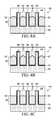
- the top surfaces of STI regions 40 in FIGS. 7A, 7B, and 7Chave different profiles.
- the STI regions 40 in FIGS. 7A and 7Bare referred to as having divot profiles. Accordingly, the respective STI regions 40 in FIGS. 7A and 7B are referred to as divot STI regions.
- the space between neighboring fins 60have middle lines 61 , and the portions of the top surfaces of STI regions 40 close to middle lines 61 are higher than the portions of the top surfaces close to fins 60 .
- the centers of the top surfaces of the divot STI regions 40may be the highest, and from middle lines 61 to respective fins 60 , the top surfaces of STI regions 40 are gradually, and may be continuously, lowered.
- the highest point and the lowest point of the top surface of an STI region 40have a height different ⁇ H greater than about 5 nm, or even greater than about 20 nm.
- the gradual decrease in the height of the top surfaces of STI regions 40may continue all the way from middle line 61 to the adjoining fin 60 , as shown in FIG. 7A .
- the top surfaces of STI regions 40may rise slightly where they join fins 60 , as shown in FIG. 7B .
- the highest points of the top surfaces of STI regions 40are still close to middle lines 61 .
- FIG. 7Cillustrates an alternative embodiment, wherein the top surfaces of STI regions 40 are substantially flat. Accordingly, the respective STI regions 40 are referred to as flat STI regions.
- a dry etchmay be performed.
- the etchis performed using a Siconi (also referred to as SiCoNi) process, in which the process gases include NH 3 , HF, and the like.
- the flow rate of NH3is about 10 sccm and about 1000 sccm
- the flow rate of HFis about 100 sccm and about 500 sccm.
- HF and NH 3react with silicon oxide in STI regions 40 to form (NH 4 ) 2 SiF 6 , which accumulates on STI regions 40 to block further HF/NH 3 from reaching silicon oxide. Accordingly, the etching rate is reduced, the lateral etching is strengthened, and flat STI regions 40 or divot STI regions 40 may be formed.
- FIGS. 8A, 8B, and 8Cillustrate the FinFETs formed from the structures shown in FIGS. 7A, 7B, and 7C , respectively.
- gate dielectric 62is formed to cover the top surfaces and sidewalls of fins 60 .
- Gate dielectric 62may be formed by a thermal oxidation, and hence may include thermal silicon oxide.
- gate dielectric 62is formed on the top surfaces of fins 60 , but not on the main parts of top surfaces of STI regions 40 .
- Gate dielectric 62may be formed by a deposition, and may be formed of high-k materials.
- gate dielectric 62is formed on the top surfaces of fins 60 and the top surfaces of STI regions 40 (the portions shown with dotted lines). The portions of gate dielectric 62 directly over the top surfaces of STI regions 40 will thus also have a divot profile.
- Gate electrode 64is then formed on gate dielectric 62 .
- gate electrode 64covers more than one fin 60 , so that the resulting FinFET 66 comprises more than one fin 60 .
- each of fins 60may be used to form one FinFET.
- the remaining components of the FinFET, including source and drain regions and source and drain silicides (not shown),are then formed. The formation processes of these components are known in the art, and hence are not repeated herein.
- FIGS. 9A, 9B, and 9Care the structures on which simulations are performed, and comprise divot STI regions 240 , flat STI regions 240 , and smiling STI regions 240 , respectively.
- the structures in FIGS. 9A, 9B, and 9Chave the same fin height H fin .
- gate electrode 264may be divided into a portion 264 _ 1 that is close to fin 260 and portions 264 _ 2 that are spaced apart from fin 260 by portion 264 _ 1 .
- Gate portion 264 _ 1contributes to the controlling of the channel in fin 260 .
- Gate portions 264 _ 2not only do not contribute to the controlling of the channel, but also adversely contribute to the parasitic gate capacitance, wherein capacitor 270 symbolizes a portion of the parasitic gate capacitance. Accordingly, with the divot or flat STI regions, the sizes of gate portions 264 _ 2 are reduced. Further, the effective thickness of the capacitor insulator of capacitor 270 is increased. As a result, the gate parasitic capacitance is reduced.
- the embodimentshave several advantageous features. By forming flat STI regions or divot STI regions underlying gate electrodes of FinFETs, the parasitic gate capacitance of the FinFETs may be reduced, and the speed of the respective FinFETs may be increased.
Landscapes
- Engineering & Computer Science (AREA)
- Physics & Mathematics (AREA)
- Condensed Matter Physics & Semiconductors (AREA)
- General Physics & Mathematics (AREA)
- Manufacturing & Machinery (AREA)
- Computer Hardware Design (AREA)
- Microelectronics & Electronic Packaging (AREA)
- Power Engineering (AREA)
- Insulated Gate Type Field-Effect Transistor (AREA)
- Element Separation (AREA)
- Thin Film Transistor (AREA)
- Metal-Oxide And Bipolar Metal-Oxide Semiconductor Integrated Circuits (AREA)
Abstract
Description
This application claims the benefit of U.S. Provisional Application No. 61/255,365 filed on Oct. 27, 2009, entitled “STI Shape Near Fin Bottom of Si Fin in Bulk FinFET,” which application is hereby incorporated herein by reference.
This application relates to the following U.S. patent application: Application Ser. No. 61/160,635, filed Mar. 16, 2009, and entitled “Hybrid STI Gap-Filling Approach,” which application is hereby incorporated herein by reference.
This application relates generally to integrated circuits, and more particularly to structures and manufacturing methods of and semiconductor fins and Fin field effect transistors (FinFETs).
With the increasing down-scaling of integrated circuits and increasingly demanding requirements to the speed of integrated circuits, transistors need to have higher drive currents with increasingly smaller dimensions. Fin field-effect transistors (FinFET) were thus developed.FIG. 1 illustrate a cross-sectional view of a conventional FinFET, wherein the cross-sectional view is made crossing the fins rather than the source and drain regions. Fins100 are formed as vertical silicon fins extending abovesubstrate 102, and are used to form source and drain regions (not shown) and channel regions therebetween. Shallow trench isolation (STI)regions 120 are formed to define fins100. Gate108 is formed overfins 100. Gate dielectric106 is formed to separatefins 100 fromgate 108.
In the formation ofSTI regions 120, a wet etch is used to recess the top surfaces ofSTI regions 120 to formfins 100. It is observed that with the wet etching, the center portions of the surfaces ofSTI regions 120 are lower than the portions of surfaces close tofins 100. The top surfaces ofSTI regions 120 are referred to as having a smiling profile.
It is realized that the parasitic capacitance (shown as capacitors110) is generated betweengate 108 andsemiconductor strips 122, whereinSTI regions 120 act as the insulator ofparasitic capacitor 110. The parasitic capacitance adversely affects the performance of the respective integrated circuit, and needs to be reduced.
In accordance with one aspect of the embodiment, a method of forming an integrated circuit structure includes providing a semiconductor substrate including a top surface; forming a first insulation region and a second insulation region in the semiconductor substrate; and recessing the first insulation region and the second insulation region. Top surfaces of remaining portions of the first insulation region and the second insulation region are flat surfaces or divot surfaces. A portion of the semiconductor substrate between and adjoining removed portions of the first insulation region and the second insulation region forms a fin.
Other embodiments are also disclosed.
For a more complete understanding of the embodiments, and the advantages thereof, reference is now made to the following descriptions taken in conjunction with the accompanying drawings, in which:
The making and using of the embodiments of the disclosure are discussed in detail below. It should be appreciated, however, that the embodiments provide many applicable inventive concepts that can be embodied in a wide variety of specific contexts. The specific embodiments discussed are merely illustrative of specific ways to make and use the embodiments, and do not limit the scope of the disclosure.
A novel method for forming shallow trench isolation (STI) regions and a fin field-effect transistor (FinFET) is provided. The intermediate stages in the manufacturing of an embodiment are illustrated. The variations of the embodiment are discussed. Throughout the various views and illustrative embodiments, like reference numbers are used to designate like elements.
Referring toFIG. 2 ,semiconductor substrate 20 is provided. In an embodiment,semiconductor substrate 20 includes silicon. Other commonly used materials, such as carbon, germanium, gallium, arsenic, nitrogen, indium, and/or phosphorus, and the like, may also be included insemiconductor substrate 20.Semiconductor substrate 20 may be a bulk substrate or a semiconductor-on-insulator (SOI) substrate.
Referring toFIG. 3 ,mask layer 24 andpad layer 22 are etched throughopenings 28, exposingunderlying semiconductor substrate 20. The exposedsemiconductor substrate 20 is then etched, formingtrenches 32. The portions ofsemiconductor substrate 20 betweentrenches 32form semiconductor strips 42.Trenches 32 may be strips (in the top view) parallel to each other, and closely located from each other. For example, the spacing S betweentrenches 32 may be smaller than about 30 nm.Photo resist 26 is then removed. Next, a cleaning may be performed to remove a native oxide ofsemiconductor substrate 20. The cleaning may be performed using diluted hydrofluoric (HF) acid.
Depth D oftrenches 32 may be between about 2100 Å and about 2500 Å, while width W is between about 300 Å and about 1500 Å. In an exemplary embodiment, the aspect ratio (D/W) oftrenches 32 is greater than about 7.0. In other exemplary embodiments, the aspect ratio may even be greater than about 8.0, although they may also be lower than about 7.0, or between 7.0 and 8.0. One skilled in the art will realize, however, that the dimensions and values recited throughout the descriptions are merely examples, and may be changed to suit different scales of integrated circuits.
Referring toFIG. 5 ,trenches 32 are filled withdielectric material 36.Dielectric material 36 may include silicon oxide, and hence is referred to asoxide 36, although other dielectric materials, such as SiN, SiC, or the like, may also be used. In an embodiment,oxide 36 is formed using a high aspect-ratio process (HARP), wherein process gases may include tetraethylorthosilicate (TEOS) and O3(ozone).
A chemical mechanical polish is then performed, followed by the removal ofmask layer 24 andpad layer 22. The resulting structure is shown inFIG. 6 . The remaining portions ofoxide 36 andliner oxide 34 intrenches 32 are referred to as shallow trench isolation (STI)regions 40 hereinafter.Mask layer 24, if formed of silicon nitride, may be removed by a wet process using hot H3PO4, whilepad layer 22 may be removed using diluted HF acid, if formed of silicon oxide. In alternative embodiments, the removal ofmask layer 24 andpad layer 22 may be performed after the recessing ofSTI regions 40, which recessing step is shown inFIGS. 7A through 7C .
Next, the structure shown inFIG. 6 may be used to form fins of a FinFET. As shown inFIGS. 7A, 7B, and 7C ,STI regions 40 are recessed by an etching step, resulting inrecess 52. The portions of semiconductor strips42 protruding over the top surfaces of the remainingSTI regions 40 thus becomefins 60. Height H′ offins 60 may be between 15 nm and about 50 nm, although it may also be greater or smaller.
The top surfaces ofSTI regions 40 inFIGS. 7A, 7B, and 7C have different profiles. TheSTI regions 40 inFIGS. 7A and 7B are referred to as having divot profiles. Accordingly, therespective STI regions 40 inFIGS. 7A and 7B are referred to as divot STI regions. It is observed that the space between neighboringfins 60 havemiddle lines 61, and the portions of the top surfaces ofSTI regions 40 close tomiddle lines 61 are higher than the portions of the top surfaces close tofins 60. In other words, the centers of the top surfaces of thedivot STI regions 40 may be the highest, and frommiddle lines 61 torespective fins 60, the top surfaces ofSTI regions 40 are gradually, and may be continuously, lowered. In an embodiment, as shown inFIG. 7A , the highest point and the lowest point of the top surface of anSTI region 40 have a height different ΔH greater than about 5 nm, or even greater than about 20 nm. The gradual decrease in the height of the top surfaces ofSTI regions 40 may continue all the way frommiddle line 61 to the adjoiningfin 60, as shown inFIG. 7A . Alternatively, the top surfaces ofSTI regions 40 may rise slightly where they joinfins 60, as shown inFIG. 7B . However, the highest points of the top surfaces ofSTI regions 40 are still close tomiddle lines 61.FIG. 7C illustrates an alternative embodiment, wherein the top surfaces ofSTI regions 40 are substantially flat. Accordingly, therespective STI regions 40 are referred to as flat STI regions.
In order to formSTI regions 40 having the profiles as shown inFIGS. 7A, 7B, and 7C , a dry etch may be performed. In an embodiment, the etch is performed using a Siconi (also referred to as SiCoNi) process, in which the process gases include NH3, HF, and the like. In an embodiment, the flow rate of NH3 is about 10 sccm and about 1000 sccm, and the flow rate of HF is about 100 sccm and about 500 sccm. HF and NH3react with silicon oxide inSTI regions 40 to form (NH4)2SiF6, which accumulates onSTI regions 40 to block further HF/NH3from reaching silicon oxide. Accordingly, the etching rate is reduced, the lateral etching is strengthened, andflat STI regions 40 ordivot STI regions 40 may be formed.
Simulations were performed to study the effects of the profiles ofSTI regions 240.FIGS. 9A, 9B, and 9C are the structures on which simulations are performed, and comprisedivot STI regions 240,flat STI regions 240, and smilingSTI regions 240, respectively. The structures inFIGS. 9A, 9B, and 9C have the same fin height Hfin. The simulation results revealed that the parasitic gate capacitance inFIG. 9A is the smallest, and the parasitic gate capacitance inFIG. 9C is the greatest. With the smallest parasitic gate capacitance, the FinFET inFIG. 9A may have an improved speed over the FinFET shown inFIGS. 9B and 9C . Similarly, the FinFET inFIG. 9B may have an improved speed over the FinFET shown inFIG. 9C . A possible explanation is that (referring toFIG. 9A )gate electrode 264 may be divided into a portion264_1 that is close tofin 260 and portions264_2 that are spaced apart fromfin 260 by portion264_1. Gate portion264_1 contributes to the controlling of the channel infin 260. Gate portions264_2, however, not only do not contribute to the controlling of the channel, but also adversely contribute to the parasitic gate capacitance, whereincapacitor 270 symbolizes a portion of the parasitic gate capacitance. Accordingly, with the divot or flat STI regions, the sizes of gate portions264_2 are reduced. Further, the effective thickness of the capacitor insulator ofcapacitor 270 is increased. As a result, the gate parasitic capacitance is reduced.
The embodiments have several advantageous features. By forming flat STI regions or divot STI regions underlying gate electrodes of FinFETs, the parasitic gate capacitance of the FinFETs may be reduced, and the speed of the respective FinFETs may be increased.
Although the embodiments and their advantages have been described in detail, it should be understood that various changes, substitutions and alterations can be made herein without departing from the spirit and scope of the embodiments as defined by the appended claims. Moreover, the scope of the present application is not intended to be limited to the particular embodiments of the process, machine, manufacture, and composition of matter, means, methods and steps described in the specification. As one of ordinary skill in the art will readily appreciate from the disclosure, processes, machines, manufacture, compositions of matter, means, methods, or steps, presently existing or later to be developed, that perform substantially the same function or achieve substantially the same result as the corresponding embodiments described herein may be utilized according to the disclosure. Accordingly, the appended claims are intended to include within their scope such processes, machines, manufacture, compositions of matter, means, methods, or steps. In addition, each claim constitutes a separate embodiment, and the combination of various claims and embodiments are within the scope of the disclosure.
Claims (20)
1. A method of forming an integrated circuit structure, the method comprising:
forming a plurality of shallow-trench isolation (STI) regions in a silicon substrate, wherein an entire portion of the silicon substrate disposed above bottommost surfaces of the plurality of STI regions comprises a semiconductor material;
removing top portions of the plurality of STI regions using HF and NH3as process gases to form a first silicon fin and a second silicon fin, wherein the first silicon fin and the second silicon fin are horizontally between, and above, remaining lower portions of the plurality of STI regions, and wherein one of the plurality of STI regions (an intermediate STI region) is between and contacting the first silicon fin and the second silicon fin and has a divot top surface, with the highest point of a top surface of the intermediate STI region being close to a middle line between the first silicon fin and the second silicon fin, and lower than top surfaces of the first and the second silicon fins, wherein the intermediate STI region comprises:
a liner contacting the first silicon fin and the second silicon fin; and
a dielectric region, wherein the liner contacts sidewalls and a bottom of the dielectric region, wherein the highest point of the top surface of the intermediate STI region is the highest point of both the liner and the dielectric region, and wherein the top surface of the intermediate STI region comprises:
a first region extending from the highest point of the top surface of the intermediate STI region toward a first sidewall of the first silicon fin, wherein magnitudes of slopes of the first region increase as the first region extends from the highest point of the top surface of the intermediate STI region toward the first sidewall of the first silicon fin;
a second region extending from the first sidewall of the first silicon fin toward the highest point of the top surface of the intermediate STI region, wherein the second region comprises a top surface of a vertical portion of the liner, and wherein the top surface of the vertical portion of the liner rises slightly as the top surface of the vertical portion of the liner extends toward the first sidewall of the first silicon fin; and
a third region interposed between the first region and the second region, wherein magnitudes of slopes of the third region decrease as the third region extends from the first region toward the second region, and wherein a first direction pointing from the highest point of the top surface of the intermediate STI region toward the first sidewall of the first silicon fin is perpendicular to a current flow direction through the first silicon fin; and
after removing the top portions of the plurality of STI regions, forming a FinFET comprising:
forming a gate dielectric on top surfaces and sidewalls of the first silicon fin and the second silicon fin, wherein the gate dielectric extends between the first sidewall of the first silicon fin and a second sidewall of the second silicon fin; and
forming a gate electrode on the gate dielectric, wherein the gate electrode extends from directly over the first silicon fin to directly over the second silicon fin.
2. The method ofclaim 1 , wherein the plurality of STI regions comprises silicon oxide.
3. The method ofclaim 1 , wherein a lowest point of the top surface of the intermediate STI region is close to, and is not, a joint point of the top surface of the intermediate STI region and the first sidewall of the first silicon fin.
4. The method ofclaim 1 , wherein the highest point and a lowest point of the top surface of the intermediate STI region have a height difference greater than about 5 nm.
5. The method ofclaim 1 , wherein the intermediate STI region is formed by steps comprising:
forming the liner contacting the first silicon fin and the second silicon fin; and
filling the dielectric region over a bottom portion of the liner, wherein the gate dielectric contacts the top surface of the vertical portion of the liner.
6. The method ofclaim 5 , wherein the forming the liner comprises a thermal oxidation, and the filling the dielectric region comprises a reaction using tetrathylorthosilicate (TEOS) and ozone as process gases.
7. The method ofclaim 1 , wherein the second region and the third region are portions of a concave region of the top surface of the intermediate STI region.
8. The method ofclaim 1 , wherein the first silicon fin and the second silicon fin have heights between about 15 nm and about 50 nm.
9. A method comprising:
etching a semiconductor substrate to form a trench extending into the semiconductor substrate, wherein remaining portions of the semiconductor substrate form a first semiconductor strip and a second semiconductor strip on opposite sides of the trench and wherein entireties of the first semiconductor strip and the second semiconductor strip comprise a semiconductor material;
forming a liner oxide extending to a bottom of the trench and on sidewalls of the first semiconductor strip and the second semiconductor strip;
filling a dielectric material into the trench and over the liner oxide;
planarizing the dielectric material, wherein the dielectric material and a remaining portion of the liner oxide in combination form a shallow-trench isolation (STI) region;
etching the STI region using HF and NH3as process gases, wherein a remaining portion of the STI region has a top surface having:
a convex region including a highest point of the top surface substantially at a middle line between the first semiconductor strip and the second semiconductor strip; and
a first concave region including a lowest point of the top surface close to a vertical interface between the dielectric material and a vertical portion of the liner oxide, wherein the first concave region is interposed between the vertical interface and the convex region along a first direction pointing from the highest point to the vertical interface, wherein a top surface of the vertical portion of the liner oxide rises slightly from the vertical interface toward the first semiconductor strip along the first direction, and wherein the first direction is perpendicular to a current flow direction through the first semiconductor strip; and
after etching the STI region, forming a FinFET comprising:
forming a gate dielectric on the sidewalls of the first semiconductor strip and the second semiconductor strip, the gate dielectric extending over the bottom of the trench and directly contacting the top surface of the STI region; and
forming a gate electrode over the gate dielectric, the gate electrode extending above top surfaces of the first semiconductor strip and the second semiconductor strip.
10. The method ofclaim 9 , wherein the forming the STI region comprises forming a silicon oxide region.
11. The method ofclaim 9 , wherein at the lowest point, the top surface is substantially flat.
12. The method ofclaim 9 , wherein the highest point and the lowest point have a height difference greater than about 5 nm.
13. The method ofclaim 9 , wherein the highest point of the top surface of the STI region is the highest point of both the liner oxide and the dielectric material.
14. The method ofclaim 9 , wherein the top surface of the STI region further has a second concave region, the convex region being interposed between the first concave region and the second concave region along the first direction.
15. The method ofclaim 9 , wherein the gate dielectric completely covers the top surface of the STI region.
16. A method comprising:
etching a semiconductor substrate to form a trench extending into the semiconductor substrate, wherein remaining portions of the semiconductor substrate form a first semiconductor strip and a second semiconductor strip on opposite sides of the trench, wherein entireties of the first semiconductor strip and the second semiconductor strip comprise a semiconductor material;
forming a liner oxide extending to a bottom of the trench and on sidewalls of the first semiconductor strip and the second semiconductor strip;
filling a dielectric material into the trench and over the liner oxide;
planarizing the dielectric material, wherein the dielectric material and a remaining portion of the liner oxide in combination form a shallow-trench isolation (STI) region;
etching the STI region using HF and NH3as process gases, wherein a remaining portion of the STI region has a top surface having a highest point, and the highest point is substantially at a middle line between the first semiconductor strip and the second semiconductor strip, and wherein the top surface comprises:
a first region including the highest point, the first region having a first curvature; and
a second region having a second curvature, the second curvature and the first curvature having opposite signs, wherein the second region is interposed between the first semiconductor strip and the first region along a first direction pointing from the highest point to the first semiconductor strip, and wherein the first direction is perpendicular to a current flow direction through the first semiconductor strip; and
after etching the STI region, forming a FinFET comprising:
forming a gate dielectric on sidewalls of the trench, the gate dielectric extending over the bottom of the trench and completely covering the top surface of the STI region; and
forming a gate electrode over the gate dielectric.
17. The method ofclaim 16 , wherein the top surface of the STI region comprises an edge portion, with the edge portion being a top surface of a vertical portion of the liner oxide, and portions of the edge portion farther away from the dielectric material are increasingly lower than portions of the edge portion closer to the dielectric material.
18. The method ofclaim 16 , wherein the filling the dielectric material comprises a reaction using tetrathylorthosilicate (TEOS) and ozone as process gases.
19. The method ofclaim 16 , wherein a top surface of the gate electrode is over a top surface of the first semiconductor strip and a top surface of the second semiconductor strip.
20. The method ofclaim 16 , wherein the gate dielectric directly contacts the top surface of the STI region.
Priority Applications (5)
| Application Number | Priority Date | Filing Date | Title |
|---|---|---|---|
| US12/843,693US9953885B2 (en) | 2009-10-27 | 2010-07-26 | STI shape near fin bottom of Si fin in bulk FinFET |
| TW099133830ATWI436410B (en) | 2009-10-27 | 2010-10-05 | Method of forming an integrated circuit structure |
| CN201010518038XACN102054741B (en) | 2009-10-27 | 2010-10-20 | Method of forming integrated circuit structure |
| JP2010240535AJP5632255B2 (en) | 2009-10-27 | 2010-10-27 | STI shape near bottom of Si fin in bulk FinFET |
| JP2014126541AJP5836437B2 (en) | 2009-10-27 | 2014-06-19 | Method for forming an integrated circuit structure |
Applications Claiming Priority (2)
| Application Number | Priority Date | Filing Date | Title |
|---|---|---|---|
| US25536509P | 2009-10-27 | 2009-10-27 | |
| US12/843,693US9953885B2 (en) | 2009-10-27 | 2010-07-26 | STI shape near fin bottom of Si fin in bulk FinFET |
Publications (2)
| Publication Number | Publication Date |
|---|---|
| US20110097889A1 US20110097889A1 (en) | 2011-04-28 |
| US9953885B2true US9953885B2 (en) | 2018-04-24 |
Family
ID=43898800
Family Applications (1)
| Application Number | Title | Priority Date | Filing Date |
|---|---|---|---|
| US12/843,693Active2031-03-17US9953885B2 (en) | 2009-10-27 | 2010-07-26 | STI shape near fin bottom of Si fin in bulk FinFET |
Country Status (4)
| Country | Link |
|---|---|
| US (1) | US9953885B2 (en) |
| JP (2) | JP5632255B2 (en) |
| CN (1) | CN102054741B (en) |
| TW (1) | TWI436410B (en) |
Cited By (8)
| Publication number | Priority date | Publication date | Assignee | Title |
|---|---|---|---|---|
| US20180350991A1 (en)* | 2017-03-17 | 2018-12-06 | International Business Machines Corporation | Wrapped source/drain contacts with enhanced area |
| US10355110B2 (en)* | 2016-08-02 | 2019-07-16 | Taiwan Semiconductor Manufacturing Company, Ltd. | FinFET and method of forming same |
| US20190252519A1 (en)* | 2011-11-04 | 2019-08-15 | Taiwan Semiconductor Manufacturing Company, Ltd. | 3D Capacitor and Method of Manufacturing Same |
| US11276755B2 (en) | 2016-06-17 | 2022-03-15 | Intel Corporation | Field effect transistors with gate electrode self-aligned to semiconductor fin |
| US11342441B2 (en) | 2012-07-17 | 2022-05-24 | Unm Rainforest Innovations | Method of forming a seed area and growing a heteroepitaxial layer on the seed area |
| US11476338B2 (en) | 2015-09-11 | 2022-10-18 | Intel Corporation | Aluminum indium phosphide subfin germanium channel transistors |
| US11482606B2 (en) | 2020-07-29 | 2022-10-25 | Samsung Electronics Co., Ltd. | Semiconductor devices |
| US11670676B2 (en) | 2020-12-24 | 2023-06-06 | Samsung Electronics Co., Ltd. | Integrated circuit devices |
Families Citing this family (75)
| Publication number | Priority date | Publication date | Assignee | Title |
|---|---|---|---|---|
| US20090127648A1 (en)* | 2007-11-15 | 2009-05-21 | Neng-Kuo Chen | Hybrid Gap-fill Approach for STI Formation |
| JP2010199161A (en)* | 2009-02-23 | 2010-09-09 | Renesas Electronics Corp | Semiconductor integrated circuit device and method of manufacturing the same |
| KR101700213B1 (en)* | 2011-12-21 | 2017-01-26 | 인텔 코포레이션 | Methods for forming fins for metal oxide semiconductor device structures |
| US9117877B2 (en)* | 2012-01-16 | 2015-08-25 | Globalfoundries Inc. | Methods of forming a dielectric cap layer on a metal gate structure |
| CN103219366B (en)* | 2012-01-20 | 2017-09-05 | 联华电子股份有限公司 | Fin-shaped field effect transistor structure and manufacturing method thereof |
| CN103295900B (en)* | 2012-03-02 | 2016-08-10 | 中芯国际集成电路制造(上海)有限公司 | Form fin and the method for fin formula field effect transistor |
| CN102646599B (en) | 2012-04-09 | 2014-11-26 | 北京大学 | Preparation method of FinFET (Fin Field Effect Transistor) in large-scale integration circuit |
| US8470714B1 (en) | 2012-05-22 | 2013-06-25 | United Microelectronics Corp. | Method of forming fin structures in integrated circuits |
| US8883570B2 (en) | 2012-07-03 | 2014-11-11 | Taiwan Semiconductor Manufacturing Company, Ltd. | Multi-gate FETs and methods for forming the same |
| US9263585B2 (en) | 2012-10-30 | 2016-02-16 | Globalfoundries Inc. | Methods of forming enhanced mobility channel regions on 3D semiconductor devices, and devices comprising same |
| US8987823B2 (en) | 2012-11-07 | 2015-03-24 | International Business Machines Corporation | Method and structure for forming a localized SOI finFET |
| US8766363B2 (en)* | 2012-11-07 | 2014-07-01 | International Business Machines Corporation | Method and structure for forming a localized SOI finFET |
| KR102013842B1 (en)* | 2013-02-08 | 2019-08-26 | 삼성전자주식회사 | Method of manufacturing semiconductor device |
| US9564353B2 (en)* | 2013-02-08 | 2017-02-07 | Taiwan Semiconductor Manufacturing Company, Ltd. | FinFETs with reduced parasitic capacitance and methods of forming the same |
| KR102003276B1 (en)* | 2013-02-14 | 2019-07-24 | 삼성전자 주식회사 | Method for fabricating semiconductor device |
| US8895446B2 (en)* | 2013-02-18 | 2014-11-25 | Taiwan Semiconductor Manufacturing Company, Ltd. | Fin deformation modulation |
| US8987791B2 (en)* | 2013-02-27 | 2015-03-24 | Taiwan Semiconductor Manufacturing Company, Ltd. | FinFETs and methods for forming the same |
| US9362386B2 (en) | 2013-02-27 | 2016-06-07 | Taiwan Semiconductor Manufacturing Company, Ltd. | FETs and methods for forming the same |
| US8829606B1 (en)* | 2013-03-13 | 2014-09-09 | Taiwan Semiconductor Manufacturing Company, Ltd. | Ditches near semiconductor fins and methods for forming the same |
| US9312344B2 (en)* | 2013-03-13 | 2016-04-12 | Taiwan Semiconductor Manufacturing Company, Ltd. | Methods for forming semiconductor materials in STI trenches |
| US8975125B2 (en) | 2013-03-14 | 2015-03-10 | International Business Machines Corporation | Formation of bulk SiGe fin with dielectric isolation by anodization |
| TWI587375B (en)* | 2013-03-27 | 2017-06-11 | 聯華電子股份有限公司 | Method of forming fin structure |
| KR102030329B1 (en)* | 2013-05-30 | 2019-11-08 | 삼성전자 주식회사 | Semiconductor device and method for fabricating the same |
| US20140374807A1 (en)* | 2013-06-19 | 2014-12-25 | International Business Machines Corporation | METHOD OF DEVICE ISOLATION IN CLADDING Si THROUGH IN SITU DOPING |
| US9287262B2 (en) | 2013-10-10 | 2016-03-15 | Taiwan Semiconductor Manufacturing Company, Ltd. | Passivated and faceted for fin field effect transistor |
| CN104576383B (en)* | 2013-10-14 | 2017-09-12 | 中国科学院微电子研究所 | FinFET structure and manufacturing method thereof |
| US9214377B2 (en)* | 2013-10-31 | 2015-12-15 | Applied Materials, Inc. | Methods for silicon recess structures in a substrate by utilizing a doping layer |
| US9159833B2 (en)* | 2013-11-26 | 2015-10-13 | Taiwan Semiconductor Manufacturing Company, Ltd. | Fin structure of semiconductor device |
| US9406547B2 (en)* | 2013-12-24 | 2016-08-02 | Intel Corporation | Techniques for trench isolation using flowable dielectric materials |
| US9142676B2 (en) | 2013-12-30 | 2015-09-22 | Taiwan Semiconductor Manufacturing Company, Ltd. | Semiconductor liner of semiconductor device |
| US20150206759A1 (en) | 2014-01-21 | 2015-07-23 | United Microelectronics Corp. | Semiconductor structure and manufacturing method thereof |
| CN104810389A (en)* | 2014-01-23 | 2015-07-29 | 联华电子股份有限公司 | Semiconductor structure and manufacturing method thereof |
| CN103871897A (en)* | 2014-02-21 | 2014-06-18 | 上海华力微电子有限公司 | Chemical mechanical grinding method applied to FinFET (fin field-effect transistor) structure |
| US9178067B1 (en)* | 2014-04-25 | 2015-11-03 | Taiwan Semiconductor Manufacturing Company, Ltd. | Structure and method for FinFET device |
| EP2947693B1 (en) | 2014-05-22 | 2022-07-13 | IMEC vzw | Method of Producing a III-V Fin Structure |
| US9520296B2 (en) | 2014-06-12 | 2016-12-13 | Taiwan Semiconductor Manufacturing Company Limited | Semiconductor device having a low divot of alignment between a substrate and an isolation thereof and method of forming the same |
| CN105225955A (en)* | 2014-06-20 | 2016-01-06 | 中芯国际集成电路制造(上海)有限公司 | The manufacture method, semiconductor device and preparation method thereof of fin and sti structure |
| TWI615976B (en)* | 2014-07-07 | 2018-02-21 | 聯華電子股份有限公司 | Fin field effect transistor and manufacturing method thereof |
| US9613954B2 (en)* | 2014-07-08 | 2017-04-04 | International Business Machines Corporation | Selective removal of semiconductor fins |
| CN104409353A (en)* | 2014-11-26 | 2015-03-11 | 上海华力微电子有限公司 | Preparing method of embedded silicon carbide |
| US9659766B2 (en) | 2014-12-19 | 2017-05-23 | Taiwan Semiconductor Manufacturing Co., Ltd. | Method for forming semiconductor structure with etched fin structure |
| US9379182B1 (en) | 2015-02-03 | 2016-06-28 | United Microelectronics Corp. | Method for forming nanowire and semiconductor device formed with the nanowire |
| KR102269415B1 (en)* | 2015-03-16 | 2021-06-24 | 삼성전자주식회사 | Semiconductor device |
| KR102393321B1 (en)* | 2015-06-25 | 2022-04-29 | 삼성전자주식회사 | Semiconductor device and method for fabricating the same |
| CN106409748B (en)* | 2015-08-03 | 2020-11-17 | 联华电子股份有限公司 | Semiconductor element and manufacturing method thereof |
| US9905467B2 (en)* | 2015-09-04 | 2018-02-27 | Taiwan Semiconductor Manufacturing Company, Ltd. | Semiconductor device and manufacturing method thereof |
| KR102437295B1 (en) | 2015-11-09 | 2022-08-30 | 삼성전자주식회사 | Method for manufacturing Semiconductor device |
| US9786505B2 (en)* | 2015-12-30 | 2017-10-10 | Taiwan Semiconductor Manufacturing Co., Ltd. | FinFET device using dummy fins for smooth profiling |
| US9728397B1 (en)* | 2016-05-10 | 2017-08-08 | United Microelectronics Corp. | Semiconductor device having the insulating layers cover a bottom portion of the fin shaped structure |
| CN107452792A (en)* | 2016-06-01 | 2017-12-08 | 中芯国际集成电路制造(上海)有限公司 | Semiconductor device and its manufacture method |
| JP6688698B2 (en)* | 2016-07-08 | 2020-04-28 | ルネサスエレクトロニクス株式会社 | Semiconductor device and manufacturing method thereof |
| US9882051B1 (en)* | 2016-09-15 | 2018-01-30 | Qualcomm Incorporated | Fin field effect transistors (FETs) (FinFETs) employing dielectric material layers to apply stress to channel regions |
| US9773893B1 (en) | 2016-09-26 | 2017-09-26 | International Business Machines Corporation | Forming a sacrificial liner for dual channel devices |
| CN107958871B (en)* | 2016-10-17 | 2020-10-30 | 中芯国际集成电路制造(上海)有限公司 | Semiconductor device and method for manufacturing the same |
| US9917210B1 (en) | 2016-10-20 | 2018-03-13 | International Business Machines Corporation | FinFET transistor gate and epitaxy formation |
| US9960275B1 (en) | 2016-10-28 | 2018-05-01 | Applied Materials, Inc. | Method of fabricating air-gap spacer for N7/N5 finFET and beyond |
| US9812363B1 (en)* | 2016-11-29 | 2017-11-07 | Taiwan Semiconductor Manufacturing Company, Ltd. | FinFET device and method of forming same |
| US10510615B2 (en)* | 2016-11-29 | 2019-12-17 | Taiwan Semiconductor Manufacturing Company, Ltd. | FinFET devices and methods of forming the same |
| US11270995B2 (en)* | 2017-03-05 | 2022-03-08 | Intel Corporation | Isolation in integrated circuit devices |
| US10497577B2 (en) | 2017-08-31 | 2019-12-03 | Taiwan Semiconductor Manufacturing Company, Ltd. | Fin field-effect transistor device and method |
| US10211107B1 (en) | 2017-09-10 | 2019-02-19 | United Microelectronics Corp. | Method of fabricating fins including removing dummy fins after fluorocarbon flush step and oxygen clean step |
| KR102487548B1 (en)* | 2017-09-28 | 2023-01-11 | 삼성전자주식회사 | Integrated circuit device |
| US10468501B2 (en)* | 2017-09-29 | 2019-11-05 | Taiwan Semiconductor Manufacturing Company, Ltd. | Gap-filling germanium through selective bottom-up growth |
| CN109786380B (en) | 2017-11-10 | 2020-11-10 | 联华电子股份有限公司 | Method for fabricating epitaxial contact structure of semiconductor memory device |
| US10276449B1 (en)* | 2017-11-24 | 2019-04-30 | Taiwan Semiconductor Manufacturing Co., Ltd. | Method for forming fin field effect transistor (FinFET) device structure |
| US10832965B2 (en)* | 2018-01-11 | 2020-11-10 | Globalfoundries Inc. | Fin reveal forming STI regions having convex shape between fins |
| US11121238B2 (en)* | 2018-11-29 | 2021-09-14 | Taiwan Semiconductor Manufacturing Co., Ltd. | Semiconductor device and manufacturing method thereof |
| CN111799329B (en) | 2019-04-08 | 2024-11-29 | 三星电子株式会社 | Semiconductor device with a semiconductor layer having a plurality of semiconductor layers |
| US11043596B2 (en)* | 2019-06-25 | 2021-06-22 | United Microelectronics Corp. | Semiconductor device and fabrication method thereof |
| US10910276B1 (en) | 2019-10-01 | 2021-02-02 | Globalfoundries Inc. | STI structure with liner along lower portion of longitudinal sides of active region, and related FET and method |
| TWI707385B (en)* | 2019-10-15 | 2020-10-11 | 力晶積成電子製造股份有限公司 | Method of manufacturing semiconductor structure |
| CN111584638B (en)* | 2020-06-01 | 2022-05-06 | 福建省晋华集成电路有限公司 | Semiconductor structure |
| US20220416046A1 (en)* | 2021-06-24 | 2022-12-29 | Taiwan Semiconductor Manufacturing Co., Ltd. | Semiconductor Device With Leakage Current Suppression And Method Of Forming The Same |
| CN113642277B (en)* | 2021-08-10 | 2024-12-27 | 中国科学院上海微系统与信息技术研究所 | Gate Parasitic Capacitance Modeling Method |
| KR20240012824A (en)* | 2022-07-21 | 2024-01-30 | 삼성전자주식회사 | Semiconductor device and method for manufacturing the same |
Citations (50)
| Publication number | Priority date | Publication date | Assignee | Title |
|---|---|---|---|---|
| US5763315A (en) | 1997-01-28 | 1998-06-09 | International Business Machines Corporation | Shallow trench isolation with oxide-nitride/oxynitride liner |
| US6159801A (en)* | 1999-04-26 | 2000-12-12 | Taiwan Semiconductor Manufacturing Company | Method to increase coupling ratio of source to floating gate in split-gate flash |
| US6268629B1 (en)* | 1998-12-07 | 2001-07-31 | Kabushiki Kaisha Toshiba | Field effect transistor with reduced narrow channel effect |
| US6352897B1 (en)* | 1999-06-09 | 2002-03-05 | United Microelectronics Corp. | Method of improving edge recess problem of shallow trench isolation |
| JP2002118255A (en) | 2000-07-31 | 2002-04-19 | Toshiba Corp | Semiconductor device and manufacturing method thereof |
| US6399985B2 (en)* | 2000-07-13 | 2002-06-04 | Mitsubishi Denki Kabushiki Kaisha | Semiconductor device |
| US20020072198A1 (en)* | 2000-12-08 | 2002-06-13 | Ahn Dong-Ho | Method of forming a trench type isolation layer |
| US6465866B2 (en)* | 1999-10-12 | 2002-10-15 | Samsung Electronics Co., Ltd. | Trench isolation regions having trench liners with recessed ends |
| US6479369B1 (en)* | 1999-11-08 | 2002-11-12 | Nec Corporation | Shallow trench isolation (STI) and method of forming the same |
| US20030013271A1 (en) | 2001-07-13 | 2003-01-16 | Infineon Technologies North America Corp. | Method for high aspect ratio gap fill using sequential hdp-cvd |
| US6541351B1 (en) | 2001-11-20 | 2003-04-01 | International Business Machines Corporation | Method for limiting divot formation in post shallow trench isolation processes |
| US20030143852A1 (en) | 2002-01-25 | 2003-07-31 | Nanya Technology Corporation | Method of forming a high aspect ratio shallow trench isolation |
| US20030143817A1 (en) | 2002-01-28 | 2003-07-31 | Ho Tzu En | Method of forming shallow trench isolation |
| US6706571B1 (en) | 2002-10-22 | 2004-03-16 | Advanced Micro Devices, Inc. | Method for forming multiple structures in a semiconductor device |
| US20040126990A1 (en) | 2002-12-26 | 2004-07-01 | Fujitsu Limited | Semiconductor device having STI without divot its manufacture |
| US20040144749A1 (en) | 2002-12-11 | 2004-07-29 | Hong-Gun Kim | Methods of filling gaps by deposition on materials having different deposition rates |
| US6858478B2 (en) | 2002-08-23 | 2005-02-22 | Intel Corporation | Tri-gate devices and methods of fabrication |
| US6867086B1 (en) | 2003-03-13 | 2005-03-15 | Novellus Systems, Inc. | Multi-step deposition and etch back gap fill process |
| US6893937B1 (en)* | 2001-08-21 | 2005-05-17 | Lsi Logic Corporation | Method for preventing borderless contact to well leakage |
| US20050153490A1 (en) | 2003-12-16 | 2005-07-14 | Jae-Man Yoon | Method of forming fin field effect transistor |
| US6949447B2 (en)* | 2003-04-23 | 2005-09-27 | Hynix Semiconductor Inc. | Method for fabricating isolation layer in semiconductor device |
| US7033945B2 (en)* | 2004-06-01 | 2006-04-25 | Applied Materials | Gap filling with a composite layer |
| US7190050B2 (en) | 2005-07-01 | 2007-03-13 | Synopsys, Inc. | Integrated circuit on corrugated substrate |
| US20070122953A1 (en) | 2005-07-01 | 2007-05-31 | Synopsys, Inc. | Enhanced Segmented Channel MOS Transistor with High-Permittivity Dielectric Isolation Material |
| US20070122954A1 (en) | 2005-07-01 | 2007-05-31 | Synopsys, Inc. | Sequential Selective Epitaxial Growth |
| US20070120156A1 (en) | 2005-07-01 | 2007-05-31 | Synopsys, Inc. | Enhanced Segmented Channel MOS Transistor with Multi Layer Regions |
| US20070128782A1 (en) | 2005-07-01 | 2007-06-07 | Synopsys, Inc. | Enhanced Segmented Channel MOS Transistor with Narrowed Base Regions |
| US20070134884A1 (en) | 2005-12-14 | 2007-06-14 | Samsung Electronics Co., Ltd. | Isolation method of defining active fins, method of fabricating semiconductor device using the same and semiconductor device fabricated thereby |
| US7247887B2 (en) | 2005-07-01 | 2007-07-24 | Synopsys, Inc. | Segmented channel MOS transistor |
| US7265008B2 (en) | 2005-07-01 | 2007-09-04 | Synopsys, Inc. | Method of IC production using corrugated substrate |
| US7276757B2 (en)* | 2004-02-19 | 2007-10-02 | Kabushiki Kaisha Toshiba | Semiconductor device with shallow trench isolation and method of fabricating the same |
| US7358145B2 (en) | 2006-06-15 | 2008-04-15 | Macronix International Co., Ltd. | Method of fabricating shallow trench isolation structure |
| US7358142B2 (en)* | 2004-02-02 | 2008-04-15 | Samsung Electronics Co., Ltd. | Method for forming a FinFET by a damascene process |
| US20080217702A1 (en) | 2006-08-04 | 2008-09-11 | Kabushiki Kaisha Toshiba | Semiconductor device and method of fabricating isolation region |
| US20080296632A1 (en) | 2007-05-30 | 2008-12-04 | Synopsys, Inc. | Stress-Enhanced Performance Of A FinFet Using Surface/Channel Orientations And Strained Capping Layers |
| US20080315267A1 (en) | 2007-06-21 | 2008-12-25 | Roland Hampp | Device Performance Improvement Using FlowFill as Material for Isolation Structures |
| JP2009004769A (en) | 2007-06-01 | 2009-01-08 | Applied Materials Inc | Double frequency using spacer mask |
| JP2009032955A (en) | 2007-07-27 | 2009-02-12 | Toshiba Corp | Semiconductor device and method for manufacturing the same |
| US7535061B2 (en) | 2003-06-30 | 2009-05-19 | Samsung Electronics Co., Ltd. | Fin-field effect transistors (Fin-FETs) having protection layers |
| US20090127648A1 (en) | 2007-11-15 | 2009-05-21 | Neng-Kuo Chen | Hybrid Gap-fill Approach for STI Formation |
| US20090170321A1 (en)* | 2007-12-28 | 2009-07-02 | Hynix Semiconductor Inc. | Method of Forming Isolation Layer of Semiconductor Memory Device |
| US7588985B2 (en) | 2006-09-29 | 2009-09-15 | Hynix Semiconductor Inc. | Method for fabricating fin transistor |
| US20090250769A1 (en) | 2007-04-27 | 2009-10-08 | Chen-Hua Yu | Semiconductor Device Having Multiple Fin Heights |
| US7674685B2 (en) | 2006-07-12 | 2010-03-09 | Samsung Electronics Co, Ltd. | Semiconductor device isolation structures and methods of fabricating such structures |
| US20100078757A1 (en) | 2008-09-29 | 2010-04-01 | Hynix Semiconductor Inc. | Semiconductor device having recess gate and isolation structure and method for fabricating the same |
| US20100099236A1 (en)* | 2008-10-16 | 2010-04-22 | Applied Materials, Inc. | Gapfill improvement with low etch rate dielectric liners |
| US20100129982A1 (en)* | 2008-11-24 | 2010-05-27 | Applied Materials, Inc. | Integration sequences with top surface profile modification |
| US20100190345A1 (en)* | 2009-01-26 | 2010-07-29 | Neng-Kuo Chen | Selective Etch-Back Process for Semiconductor Devices |
| US20100230757A1 (en) | 2009-03-16 | 2010-09-16 | Taiwan Semiconductor Manufacturing Company, Ltd. | Hybrid STI Gap-Filling Approach |
| US8058179B1 (en)* | 2008-12-23 | 2011-11-15 | Novellus Systems, Inc. | Atomic layer removal process with higher etch amount |
Family Cites Families (3)
| Publication number | Priority date | Publication date | Assignee | Title |
|---|---|---|---|---|
| US7402856B2 (en)* | 2005-12-09 | 2008-07-22 | Intel Corporation | Non-planar microelectronic device having isolation element to mitigate fringe effects and method to fabricate same |
| KR100739656B1 (en)* | 2006-06-08 | 2007-07-13 | 삼성전자주식회사 | Manufacturing Method of Semiconductor Device |
| US7846849B2 (en)* | 2007-06-01 | 2010-12-07 | Applied Materials, Inc. | Frequency tripling using spacer mask having interposed regions |
- 2010
- 2010-07-26USUS12/843,693patent/US9953885B2/enactiveActive
- 2010-10-05TWTW099133830Apatent/TWI436410B/enactive
- 2010-10-20CNCN201010518038XApatent/CN102054741B/enactiveActive
- 2010-10-27JPJP2010240535Apatent/JP5632255B2/enactiveActive
- 2014
- 2014-06-19JPJP2014126541Apatent/JP5836437B2/enactiveActive
Patent Citations (60)
| Publication number | Priority date | Publication date | Assignee | Title |
|---|---|---|---|---|
| US5763315A (en) | 1997-01-28 | 1998-06-09 | International Business Machines Corporation | Shallow trench isolation with oxide-nitride/oxynitride liner |
| US6268629B1 (en)* | 1998-12-07 | 2001-07-31 | Kabushiki Kaisha Toshiba | Field effect transistor with reduced narrow channel effect |
| US6159801A (en)* | 1999-04-26 | 2000-12-12 | Taiwan Semiconductor Manufacturing Company | Method to increase coupling ratio of source to floating gate in split-gate flash |
| US6352897B1 (en)* | 1999-06-09 | 2002-03-05 | United Microelectronics Corp. | Method of improving edge recess problem of shallow trench isolation |
| US6465866B2 (en)* | 1999-10-12 | 2002-10-15 | Samsung Electronics Co., Ltd. | Trench isolation regions having trench liners with recessed ends |
| US6479369B1 (en)* | 1999-11-08 | 2002-11-12 | Nec Corporation | Shallow trench isolation (STI) and method of forming the same |
| US6399985B2 (en)* | 2000-07-13 | 2002-06-04 | Mitsubishi Denki Kabushiki Kaisha | Semiconductor device |
| JP2002118255A (en) | 2000-07-31 | 2002-04-19 | Toshiba Corp | Semiconductor device and manufacturing method thereof |
| US20020072198A1 (en)* | 2000-12-08 | 2002-06-13 | Ahn Dong-Ho | Method of forming a trench type isolation layer |
| US20030013271A1 (en) | 2001-07-13 | 2003-01-16 | Infineon Technologies North America Corp. | Method for high aspect ratio gap fill using sequential hdp-cvd |
| US6893937B1 (en)* | 2001-08-21 | 2005-05-17 | Lsi Logic Corporation | Method for preventing borderless contact to well leakage |
| JP2005510080A (en) | 2001-11-20 | 2005-04-14 | インターナショナル・ビジネス・マシーンズ・コーポレーション | Method for limiting divot formation after shallow trench isolation (STI) process |
| US6541351B1 (en) | 2001-11-20 | 2003-04-01 | International Business Machines Corporation | Method for limiting divot formation in post shallow trench isolation processes |
| US20030143852A1 (en) | 2002-01-25 | 2003-07-31 | Nanya Technology Corporation | Method of forming a high aspect ratio shallow trench isolation |
| US20030143817A1 (en) | 2002-01-28 | 2003-07-31 | Ho Tzu En | Method of forming shallow trench isolation |
| US6858478B2 (en) | 2002-08-23 | 2005-02-22 | Intel Corporation | Tri-gate devices and methods of fabrication |
| US6706571B1 (en) | 2002-10-22 | 2004-03-16 | Advanced Micro Devices, Inc. | Method for forming multiple structures in a semiconductor device |
| US20040144749A1 (en) | 2002-12-11 | 2004-07-29 | Hong-Gun Kim | Methods of filling gaps by deposition on materials having different deposition rates |
| US20040126990A1 (en) | 2002-12-26 | 2004-07-01 | Fujitsu Limited | Semiconductor device having STI without divot its manufacture |
| US6867086B1 (en) | 2003-03-13 | 2005-03-15 | Novellus Systems, Inc. | Multi-step deposition and etch back gap fill process |
| US6949447B2 (en)* | 2003-04-23 | 2005-09-27 | Hynix Semiconductor Inc. | Method for fabricating isolation layer in semiconductor device |
| US7535061B2 (en) | 2003-06-30 | 2009-05-19 | Samsung Electronics Co., Ltd. | Fin-field effect transistors (Fin-FETs) having protection layers |
| US20050153490A1 (en) | 2003-12-16 | 2005-07-14 | Jae-Man Yoon | Method of forming fin field effect transistor |
| US7358142B2 (en)* | 2004-02-02 | 2008-04-15 | Samsung Electronics Co., Ltd. | Method for forming a FinFET by a damascene process |
| US7276757B2 (en)* | 2004-02-19 | 2007-10-02 | Kabushiki Kaisha Toshiba | Semiconductor device with shallow trench isolation and method of fabricating the same |
| US7033945B2 (en)* | 2004-06-01 | 2006-04-25 | Applied Materials | Gap filling with a composite layer |
| US7265008B2 (en) | 2005-07-01 | 2007-09-04 | Synopsys, Inc. | Method of IC production using corrugated substrate |
| US20080290470A1 (en) | 2005-07-01 | 2008-11-27 | Synopsys, Inc. | Integrated Circuit On Corrugated Substrate |
| US20070132053A1 (en) | 2005-07-01 | 2007-06-14 | Synopsys Inc. | Integrated Circuit On Corrugated Substrate |
| US7508031B2 (en) | 2005-07-01 | 2009-03-24 | Synopsys, Inc. | Enhanced segmented channel MOS transistor with narrowed base regions |
| US7247887B2 (en) | 2005-07-01 | 2007-07-24 | Synopsys, Inc. | Segmented channel MOS transistor |
| US20070120156A1 (en) | 2005-07-01 | 2007-05-31 | Synopsys, Inc. | Enhanced Segmented Channel MOS Transistor with Multi Layer Regions |
| US20070122954A1 (en) | 2005-07-01 | 2007-05-31 | Synopsys, Inc. | Sequential Selective Epitaxial Growth |
| US7190050B2 (en) | 2005-07-01 | 2007-03-13 | Synopsys, Inc. | Integrated circuit on corrugated substrate |
| US20070122953A1 (en) | 2005-07-01 | 2007-05-31 | Synopsys, Inc. | Enhanced Segmented Channel MOS Transistor with High-Permittivity Dielectric Isolation Material |
| US20070128782A1 (en) | 2005-07-01 | 2007-06-07 | Synopsys, Inc. | Enhanced Segmented Channel MOS Transistor with Narrowed Base Regions |
| US7528465B2 (en) | 2005-07-01 | 2009-05-05 | Synopsys, Inc. | Integrated circuit on corrugated substrate |
| US20090181477A1 (en) | 2005-07-01 | 2009-07-16 | Synopsys, Inc. | Integrated Circuit On Corrugated Substrate |
| US7605449B2 (en) | 2005-07-01 | 2009-10-20 | Synopsys, Inc. | Enhanced segmented channel MOS transistor with high-permittivity dielectric isolation material |
| US20070134884A1 (en) | 2005-12-14 | 2007-06-14 | Samsung Electronics Co., Ltd. | Isolation method of defining active fins, method of fabricating semiconductor device using the same and semiconductor device fabricated thereby |
| US7358145B2 (en) | 2006-06-15 | 2008-04-15 | Macronix International Co., Ltd. | Method of fabricating shallow trench isolation structure |
| US7674685B2 (en) | 2006-07-12 | 2010-03-09 | Samsung Electronics Co, Ltd. | Semiconductor device isolation structures and methods of fabricating such structures |
| US20080217702A1 (en) | 2006-08-04 | 2008-09-11 | Kabushiki Kaisha Toshiba | Semiconductor device and method of fabricating isolation region |
| US7588985B2 (en) | 2006-09-29 | 2009-09-15 | Hynix Semiconductor Inc. | Method for fabricating fin transistor |
| US7843000B2 (en)* | 2007-04-27 | 2010-11-30 | Taiwan Semiconductor Manufacturing Company, Ltd. | Semiconductor device having multiple fin heights |
| US20090250769A1 (en) | 2007-04-27 | 2009-10-08 | Chen-Hua Yu | Semiconductor Device Having Multiple Fin Heights |
| US20080296632A1 (en) | 2007-05-30 | 2008-12-04 | Synopsys, Inc. | Stress-Enhanced Performance Of A FinFet Using Surface/Channel Orientations And Strained Capping Layers |
| JP2009004769A (en) | 2007-06-01 | 2009-01-08 | Applied Materials Inc | Double frequency using spacer mask |
| US20110008969A1 (en) | 2007-06-01 | 2011-01-13 | Bencher Christopher D | Frequency doubling using spacer mask |
| US20080315267A1 (en) | 2007-06-21 | 2008-12-25 | Roland Hampp | Device Performance Improvement Using FlowFill as Material for Isolation Structures |
| JP2009032955A (en) | 2007-07-27 | 2009-02-12 | Toshiba Corp | Semiconductor device and method for manufacturing the same |
| US7915693B2 (en) | 2007-07-27 | 2011-03-29 | Kabushiki Kaisha Toshiba | Semiconductor device with fin and silicide structure |
| US20090127648A1 (en) | 2007-11-15 | 2009-05-21 | Neng-Kuo Chen | Hybrid Gap-fill Approach for STI Formation |
| US20090170321A1 (en)* | 2007-12-28 | 2009-07-02 | Hynix Semiconductor Inc. | Method of Forming Isolation Layer of Semiconductor Memory Device |
| US20100078757A1 (en) | 2008-09-29 | 2010-04-01 | Hynix Semiconductor Inc. | Semiconductor device having recess gate and isolation structure and method for fabricating the same |
| US20100099236A1 (en)* | 2008-10-16 | 2010-04-22 | Applied Materials, Inc. | Gapfill improvement with low etch rate dielectric liners |
| US20100129982A1 (en)* | 2008-11-24 | 2010-05-27 | Applied Materials, Inc. | Integration sequences with top surface profile modification |
| US8058179B1 (en)* | 2008-12-23 | 2011-11-15 | Novellus Systems, Inc. | Atomic layer removal process with higher etch amount |
| US20100190345A1 (en)* | 2009-01-26 | 2010-07-29 | Neng-Kuo Chen | Selective Etch-Back Process for Semiconductor Devices |
| US20100230757A1 (en) | 2009-03-16 | 2010-09-16 | Taiwan Semiconductor Manufacturing Company, Ltd. | Hybrid STI Gap-Filling Approach |
Cited By (24)
| Publication number | Priority date | Publication date | Assignee | Title |
|---|---|---|---|---|
| US20210359107A1 (en)* | 2011-11-04 | 2021-11-18 | Taiwan Semiconductor Manufacturing Company, Ltd. | 3D Capacitor and Method of Manufacturing Same |
| US12040379B2 (en) | 2011-11-04 | 2024-07-16 | Taiwan Semiconductor Manufacturing Company, Ltd. | 3D capacitor and method of manufacturing same |
| US20190252519A1 (en)* | 2011-11-04 | 2019-08-15 | Taiwan Semiconductor Manufacturing Company, Ltd. | 3D Capacitor and Method of Manufacturing Same |
| US11837646B2 (en)* | 2011-11-04 | 2023-12-05 | Taiwan Semiconductor Manufacturing Company, Ltd. | 3D capacitor and method of manufacturing same |
| US11075278B2 (en)* | 2011-11-04 | 2021-07-27 | Taiwan Semiconductor Manufacturing Company, Ltd. | 3D capacitor based on fin structure having low-resistance surface and method of manufacturing same |
| US11374106B2 (en) | 2012-07-17 | 2022-06-28 | Unm Rainforest Innovations | Method of making heteroepitaxial structures and device formed by the method |
| US11349011B2 (en) | 2012-07-17 | 2022-05-31 | Unm Rainforest Innovations | Method of making heteroepitaxial structures and device formed by the method |
| US11456370B2 (en) | 2012-07-17 | 2022-09-27 | Unm Rainforest Innovations | Semiconductor product comprising a heteroepitaxial layer grown on a seed area of a nanostructured pedestal |
| US11342441B2 (en) | 2012-07-17 | 2022-05-24 | Unm Rainforest Innovations | Method of forming a seed area and growing a heteroepitaxial layer on the seed area |
| US11342438B1 (en) | 2012-07-17 | 2022-05-24 | Unm Rainforest Innovations | Device with heteroepitaxial structure made using a growth mask |
| US11342442B2 (en) | 2012-07-17 | 2022-05-24 | Unm Rainforest Innovations | Semiconductor product comprising a heteroepitaxial layer grown on a seed area of a nanostructured pedestal |
| US11476338B2 (en) | 2015-09-11 | 2022-10-18 | Intel Corporation | Aluminum indium phosphide subfin germanium channel transistors |
| US11276755B2 (en) | 2016-06-17 | 2022-03-15 | Intel Corporation | Field effect transistors with gate electrode self-aligned to semiconductor fin |
| US11996447B2 (en) | 2016-06-17 | 2024-05-28 | Intel Corporation | Field effect transistors with gate electrode self-aligned to semiconductor fin |
| US11251289B2 (en)* | 2016-08-02 | 2022-02-15 | Taiwan Semiconductor Manufacturing Company, Ltd. | FinFET device comprising plurality of dummy protruding features |
| US10355110B2 (en)* | 2016-08-02 | 2019-07-16 | Taiwan Semiconductor Manufacturing Company, Ltd. | FinFET and method of forming same |
| US12176424B2 (en) | 2016-08-02 | 2024-12-24 | Taiwan Semiconductor Manufacturing Company, Ltd. | FinFET device comprising plurality of dummy protruding features |
| US20180350991A1 (en)* | 2017-03-17 | 2018-12-06 | International Business Machines Corporation | Wrapped source/drain contacts with enhanced area |
| US10693007B2 (en)* | 2017-03-17 | 2020-06-23 | Elpis Technologies Inc. | Wrapped contacts with enhanced area |
| US11482606B2 (en) | 2020-07-29 | 2022-10-25 | Samsung Electronics Co., Ltd. | Semiconductor devices |
| US11769813B2 (en) | 2020-07-29 | 2023-09-26 | Samsung Electronics Co., Ltd. | Semiconductor devices |
| US12183800B2 (en) | 2020-07-29 | 2024-12-31 | Samsung Electronics Co., Ltd. | Semiconductor devices |
| US11670676B2 (en) | 2020-12-24 | 2023-06-06 | Samsung Electronics Co., Ltd. | Integrated circuit devices |
| US12107122B2 (en) | 2020-12-24 | 2024-10-01 | Samsung Electronics Co., Ltd. | Integrated circuit devices |
Also Published As
| Publication number | Publication date |
|---|---|
| JP2011097057A (en) | 2011-05-12 |
| TWI436410B (en) | 2014-05-01 |
| TW201118933A (en) | 2011-06-01 |
| JP5836437B2 (en) | 2015-12-24 |
| JP5632255B2 (en) | 2014-11-26 |
| JP2014199942A (en) | 2014-10-23 |
| CN102054741B (en) | 2013-11-06 |
| CN102054741A (en) | 2011-05-11 |
| US20110097889A1 (en) | 2011-04-28 |
Similar Documents
| Publication | Publication Date | Title |
|---|---|---|
| US9953885B2 (en) | STI shape near fin bottom of Si fin in bulk FinFET | |
| US8846466B2 (en) | Forming inter-device STI regions and intra-device STI regions using different dielectric materials | |
| US10103141B2 (en) | Fin deformation modulation | |
| US8723271B2 (en) | Voids in STI regions for forming bulk FinFETs | |
| US9564353B2 (en) | FinFETs with reduced parasitic capacitance and methods of forming the same | |
| US9640441B2 (en) | Voids in STI regions for forming bulk FinFETs | |
| US8470714B1 (en) | Method of forming fin structures in integrated circuits | |
| US9698055B2 (en) | Semiconductor fin structures and methods for forming the same | |
| US9006079B2 (en) | Methods for forming semiconductor fins with reduced widths | |
| KR101163909B1 (en) | Sti shape near fin bottom of si fin in bulk finfet |
Legal Events
| Date | Code | Title | Description |
|---|---|---|---|
| AS | Assignment | Owner name:TAIWAN SEMICONDUCTOR MANUFACTURING COMPANY, LTD., Free format text:ASSIGNMENT OF ASSIGNORS INTEREST;ASSIGNORS:YUAN, FENG;LEE, TSUNG-LIN;CHEN, HUNG-MING;AND OTHERS;REEL/FRAME:024742/0543 Effective date:20091218 | |
| STCF | Information on status: patent grant | Free format text:PATENTED CASE | |
| MAFP | Maintenance fee payment | Free format text:PAYMENT OF MAINTENANCE FEE, 4TH YEAR, LARGE ENTITY (ORIGINAL EVENT CODE: M1551); ENTITY STATUS OF PATENT OWNER: LARGE ENTITY Year of fee payment:4 |