US9944554B2 - Perforated mother sheet for partial edge chemical strengthening and method therefor - Google Patents
Perforated mother sheet for partial edge chemical strengthening and method thereforDownload PDFInfo
- Publication number
- US9944554B2 US9944554B2US13/233,978US201113233978AUS9944554B2US 9944554 B2US9944554 B2US 9944554B2US 201113233978 AUS201113233978 AUS 201113233978AUS 9944554 B2US9944554 B2US 9944554B2
- Authority
- US
- United States
- Prior art keywords
- mother sheet
- voids
- edges
- sheet
- mother
- Prior art date
- Legal status (The legal status is an assumption and is not a legal conclusion. Google has not performed a legal analysis and makes no representation as to the accuracy of the status listed.)
- Active, expires
Links
Images


Classifications
- C—CHEMISTRY; METALLURGY
- C03—GLASS; MINERAL OR SLAG WOOL
- C03C—CHEMICAL COMPOSITION OF GLASSES, GLAZES OR VITREOUS ENAMELS; SURFACE TREATMENT OF GLASS; SURFACE TREATMENT OF FIBRES OR FILAMENTS MADE FROM GLASS, MINERALS OR SLAGS; JOINING GLASS TO GLASS OR OTHER MATERIALS
- C03C21/00—Treatment of glass, not in the form of fibres or filaments, by diffusing ions or metals in the surface
- C03C21/001—Treatment of glass, not in the form of fibres or filaments, by diffusing ions or metals in the surface in liquid phase, e.g. molten salts, solutions
- C03C21/002—Treatment of glass, not in the form of fibres or filaments, by diffusing ions or metals in the surface in liquid phase, e.g. molten salts, solutions to perform ion-exchange between alkali ions
- C—CHEMISTRY; METALLURGY
- C03—GLASS; MINERAL OR SLAG WOOL
- C03C—CHEMICAL COMPOSITION OF GLASSES, GLAZES OR VITREOUS ENAMELS; SURFACE TREATMENT OF GLASS; SURFACE TREATMENT OF FIBRES OR FILAMENTS MADE FROM GLASS, MINERALS OR SLAGS; JOINING GLASS TO GLASS OR OTHER MATERIALS
- C03C17/00—Surface treatment of glass, not in the form of fibres or filaments, by coating
- C03C17/001—General methods for coating; Devices therefor
- C03C17/002—General methods for coating; Devices therefor for flat glass, e.g. float glass
- Y—GENERAL TAGGING OF NEW TECHNOLOGICAL DEVELOPMENTS; GENERAL TAGGING OF CROSS-SECTIONAL TECHNOLOGIES SPANNING OVER SEVERAL SECTIONS OF THE IPC; TECHNICAL SUBJECTS COVERED BY FORMER USPC CROSS-REFERENCE ART COLLECTIONS [XRACs] AND DIGESTS
- Y10—TECHNICAL SUBJECTS COVERED BY FORMER USPC
- Y10T—TECHNICAL SUBJECTS COVERED BY FORMER US CLASSIFICATION
- Y10T29/00—Metal working
- Y10T29/49—Method of mechanical manufacture
- Y10T29/49002—Electrical device making
- Y10T29/49117—Conductor or circuit manufacturing
- Y10T29/49124—On flat or curved insulated base, e.g., printed circuit, etc.
Definitions
- Thisrelates generally to the chemical strengthening of substrates, and more particularly, to the formation of voids in substrates to allow chemical strengthening of substrate edges.
- Touch sensor panelscan be fabricated as one or more thin films deposited and patterned into conductive traces upon one or both sides of a chemically strengthened sheet of glass.
- standard thin film processing equipmentdoes not allow for thin film deposition on custom-sized or shaped sheets of glass. Instead, thin film deposition occurs on large, rectangular sheets of glass (called mother sheets) which are subsequently separated and shaped into a plurality of individual glass sheets. The individual sheets are typically used in separate electronic devices.
- Thisrelates to chemically strengthening the edges of glass sheets adapted to have thin films deposited on at least one surface. Thin films can be deposited and patterned upon discrete regions of a chemically strengthened sheet of glass. This sheet of glass is called a mother sheet. The mother sheet can be cut (i.e., singulated) into separate sheets, where each singulated sheet can be adapted to service a separate electronic component or device.
- voidscan be formed in a mother sheet.
- the edges of these voidsmay correspond to a portion of the new edges that would normally be created during separation and free shaping.
- the mother sheetcan then be immersed in a chemical strengthener.
- the edges of the voidscan be chemically strengthened in addition to the front and back sides of the mother sheet. After thin film processing and separation, each of the resulting individual sheets has been chemically strengthened on both sides and on a portion of its edges.
- FIG. 1Aillustrates an exemplary void-forming process according to embodiments of the disclosure.
- FIG. 1Billustrates an exemplary mother sheet after a strengthening process has occurred according to embodiments of the disclosure.
- FIG. 1Cillustrates an exemplary mother sheet after thin film deposition according to embodiments of the disclosure.
- FIG. 1Dillustrates a separation process according to embodiments of the disclosure.
- FIG. 2is a high-level flow diagram illustrating an exemplary method of strengthening a substrate according to embodiments of the disclosure.
- FIG. 3Aillustrates an exemplary mother sheet after edges of the voids have been strengthened according to embodiments of the disclosure.
- FIG. 3Billustrates an exemplary mother sheet after separation according to embodiments of the disclosure.
- FIG. 4illustrates an exemplary mother sheet with voids that have been filled with plug material according to embodiments of the disclosure.
- FIG. 5illustrates an exemplary computing system including a touch sensor panel situated on a glass substrate that has been strengthened according to embodiments of the disclosure.
- FIG. 6Aillustrates an exemplary mobile telephone having a touch sensor panel situated on a glass substrate that has been strengthened according to embodiments of the disclosure.
- FIG. 6Billustrates an exemplary digital media player having a touch sensor panel situated on a glass substrate that has been strengthened according to embodiments of the disclosure.
- FIG. 6Cillustrates an exemplary personal computer having a touch sensor panel (trackpad) and/or display situated on a glass substrate that has been strengthened according to embodiments of the disclosure.
- Various embodimentsrelate to chemically strengthening the edges of glass sheets adapted to have thin films deposited on at least one surface. Thin films can be deposited and patterned upon discrete regions of a chemically strengthened sheet of glass. This sheet of glass is called a mother sheet. The mother sheet can be cut (i.e., singulated) into separate sheets, where each singulated sheet can be adapted to service a separate electronic component or device.
- voidscan be formed in a mother sheet.
- the edges of these voidsmay correspond to a portion of the new edges that would normally be created during separation and free shaping.
- the mother sheetcan then be immersed in a chemical strengthener.
- the edges of the voidscan be chemically strengthened in addition to the front and back sides of the mother sheet. After thin film processing and separation, each of the resulting individual sheets has been chemically strengthened on both sides and on a portion of its edges.
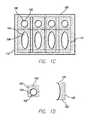
- FIGS. 1A-1Dillustrate an exemplary method of strengthening glass according to embodiments of the disclosure. Each figure in the sequence depicts a portion of the described method.
- FIG. 1Aillustrates an exemplary void-forming process according to embodiments of the disclosure.
- a mother sheet 100can be adapted to have portions removed to form one or more voids.
- the mother sheetis often a large, rectangular sheet of glass, but may be any size or shape according to various embodiments.
- One or more voids 102 and 104can then be formed in discrete regions of the mother sheet 100 . Note that even though FIG. 1A depicts eight voids formed in the mother sheet 100 , any number of voids can be formed according to various embodiments. Additionally, the voids can be situated in any position along the mother sheet 100 .
- any number of means or mechanismscan be used in order to form the voids 102 and 104 in mother sheet 100 .
- the voidscan be formed as circles or ovals (e.g., as depicted by the edges of voids 102 and 104 ).
- the voidsmay be formed using any pattern or geometry according to embodiments. This includes rectangles, trapezoids, and shapes including both curved and straight edges.
- FIG. 1Billustrates an exemplary mother sheet 100 after a strengthening process has occurred according to embodiments of the disclosure.
- the entire mother sheet 100can be strengthened by applying a global treatment to the mother sheet.
- At least a portion of mother sheet 100can be immersed in one or more chemical substances and treated at a certain temperature.
- the chemical substancecan comprise potassium nitrate (KNO 3 ) applied to the sheets at approximately 350° C.
- the strengthening processcan include applying a localized treatment to unstrengthened edges of the voids 102 and 104 .
- a localized treatmentto unstrengthened edges of the voids 102 and 104 .
- application of the localized treatment to the unstrengthened edges of the voids 102 and 104can result in a mother glass 100 with strengthened surfaces on all sides and edges.
- the substances used to strengthen the unstrengthened edges of the voids 102 and 104may be the same or may be different than the substances used to strengthen the mother sheet 100 according to some embodiments.
- the localized treatmentmay include, without limitation, one or more of the following: edge polishes (e.g., via cerium oxide or other similar compounds), acid polishes, chemical etches (e.g., via hydrogen fluoride or hydrogen chloride), localized heat treatment (e.g., bringing the glass to its glass transition temperature in the range of 500° C.-620° C.) and/or chemical treatments.
- the chemical treatmentcan include filling flaws in the surface of the mother sheet 100 with an adhesive or other similar substance.
- potassium nitrate (KNO 3 )can be applied to the unstrengthened regions at 350° C.
- FIG. 1Cillustrates an exemplary mother sheet 100 after thin film deposition according to embodiments of the disclosure.
- One or more thin films 112can be deposited upon regions of the mother sheet 100 and patterned. Note that any number of thin films 112 may be deposited on the mother sheet 100 according to various embodiments. Additionally, the thin films 112 can be situated in any position along both axes of the surface of the mother sheet 100 .
- the thin films 112is indium tin oxide (ITO).
- ITOindium tin oxide
- other materialscan be utilized in addition to, or instead of, ITO. These materials include, without limitation, amorphous silicon, copper indium diselenide, cadmium telluride, and film crystalline silicon.
- the thin films 112can be protected by one or more passivation layers (organic and/or inorganic). Passivation layers are compositions formed over conductive material and other layers which protect those materials from corrosion and other environmental effects. Various types of passivation can be employed according to embodiments. These include, without limitation, passivation layers comprising silicon dioxide (SiO 2 ) and/or silicon nitride (SiNx).
- FIG. 1Dillustrates a separation process according to embodiments of the disclosure.
- the mother sheet 100has been separated into individual sheets 120 and 122 .
- FIG. 1Ddepicts two sheets being formed from the mother sheet 100
- any number of individual sheetsmay be formed from the mother sheet.
- the individual sheetscan be further shaped (e.g., cut into a specific geometry) upon separation from the mother sheet 100 .
- any number of means or mechanismscan be used in order to accomplish separation from the mother sheet 100 . This includes, without limitation, etching, laser scribing, mechanical scribing, and/or grinding and polishing.
- the strengthened edges 106 and 108 of the voidscan form a portion of the edges of the individual sheets 120 and 122 .
- a voidcan be intact after separation and form an inner edge of an individual sheet.
- void 102remains intact after separation and forms inner edge 106 in the individual sheet 120 .
- a portion of the edge of the voidcan form an edge of an individual sheet.
- void 104falls along a path of separation, and a portion of strengthened edge 108 forms the edge 124 of individual sheet 122 .
- one or more unstrengthened edges 126 and 128can be formed along the paths of separation.
- the unstrengthened edgescan adjoin one or more surfaces that have already been chemically strengthened (for example, by a strengthening process applied to the mother sheet 100 and the strengthened edges 106 and 124 .)
- the unstrengthened edges 106 and 124can be part of a larger set of unstrengthened regions.
- FIG. 2is a high-level flow diagram illustrating an exemplary method of strengthening a substrate according to embodiments of the disclosure.
- one or more voidscan be formed in a mother sheet. Many methods may be used to form voids according to various embodiments. This includes, without limitation, etching, laser scribing, mechanical scribing, and/or grinding and polishing.
- the mother sheetcan then be chemically strengthened.
- this chemical strengthening processcan include immersing the sandwich into a chemical substance at specific temperature settings (e.g., potassium nitrate (KNO 3 ) at 350° C.).
- the chemical strengthening processcan include subjecting the mother sheet to an edge polishing procedure, a chemical etch or acid polish procedure, or a localized heat or chemical treatment.
- one or more thin filmscan be deposited on the mother sheet.
- at least one of the thin filmsis ITO.
- other materialsare utilized, including amorphous silicon, copper indium diselenide, cadmium telluride, and film crystalline silicon.
- the mother sheetcan be separated and/or shaped into multiple smaller sheets.
- methods used to accomplish separation and shapingmay include etching, laser scribing, mechanical scribing, and/or grinding and polishing.
- voidsmay be formed with curved edges.
- Techniquessuch as laser scribing may not be available to form curved edges, and other techniques, such as etching, may be more susceptible to forming micro-cracks in the edges, which can weaken the durability of the glass and make curved edges more likely to break. As a result, in some embodiments it may be important to ensure that the curved edges are chemically strengthened.
- FIGS. 3A and 3Billustrate another exemplary method of strengthening glass according to embodiments of the disclosure.
- FIG. 3Aillustrates an exemplary mother sheet after voids have been formed and the edges of the voids have been strengthened according to embodiments of the disclosure.
- FIG. 3Billustrates an exemplary mother sheet after separation according to embodiments of the disclosure.
- the voidscan be arranged so that after separation, a high proportion of the perimeter of each individual sheet has been chemically strengthened.
- void 302can be arranged so that edge 304 corresponds to the entire length of edge 306 on individual sheet 308 after separation. Because the entire length of edge 306 can be formed from void edge 304 , the entire length of edge 306 can be chemically strengthened.
- void 310can be arranged so that edge 312 corresponds with a substantial portion of edge 314 on individual sheet 308 after separation.
- the individual sheets 308 before separation, identified as areas 308 in FIG. 3Amay be referred to herein as pre-singulated sheets 308 .
- voids 302 , 316 , and 310can also form tabs 318 and 320 which keep the panel from being separated from mothersheet 300 .
- the tabs 318 and 320can be positioned along the path of separation 322 .
- Unstrengthened edge portions 324 and 326can be formed where individual panel 308 was separated from tabs 318 and 320 . Decreasing the width of tabs 318 and 320 can decrease the length of unstrengthened edge portions 324 and 326 . Accordingly, the strengthened perimeter of individual sheet 308 can be maximized by minimizing the width of tabs 318 and 320 .
- the tabsmay be used to run conductive traces to thin films patterned on the mother sheet. These traces may be used in testing prior to separation, and so the tabs must be wide enough to accommodate the conductive traces.
- the laser scribing processmay require that its target have a minimum width for the scribing to be effective. Accordingly, if laser scribing is used to separate the individual sheets from the mother sheet, the tabs must be at least that minimum width for the separation to be successful.
- thin film processingcan require rigidity and durability in the mother sheet, and tabs that are too narrow might compromise the rigidity and durability of the mother sheet during thin film processing.
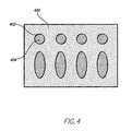
- plug materialmay be used to fill voids, which can enhance the rigidity and durability of the mother sheet during thin film processing.
- FIG. 4illustrates an exemplary mother sheet with voids that have been filled with plug material according to embodiments of the disclosure. Void 402 can be formed in mother sheet 400 and filled with plug material 404 . Mother sheet 400 can then be subjected to thin film processing, and plug material 404 can subsequently be removed.
- the plug materialcan be applied to the voids through a coating process or a flat process such as a squeegee.
- solvent strippingcan be used after application to smooth out the material. The material can then be heated to evaporate the solvent from inside the material.
- the plug materialcan be made of organic material, silicon dioxide, or metals.
- the materialcan be resistant to the acidity of the chemicals used in thin film processing, and the material can withstand the high temperature at which thin film processing occurs.
- the materialcan be easily removable when the processing is complete.
- a materialsuch as silicon dioxide (SiO 2 ) is resilient to acidity and heat and can be easily removed with a solvent.
- FIG. 5illustrates exemplary computing system 500 that can include a touch sensor panel 524 situated on a glass substrate that has been strengthened by one or more of the embodiments described above.
- Computing system 500can include one or more panel processors 502 and peripherals 504 , and panel subsystem 506 .
- Peripherals 504can include, but are not limited to, random access memory (RAM)or other types of memory or storage, watchdog timers and the like.
- Panel subsystem 506can include, but is not limited to, one or more sense channels 508 , channel scan logic 510 and driver logic 514 .
- Channel scan logic 510can access RAM 512 , autonomously read data from the sense channels and provide control for the sense channels.
- channel scan logic 510can control driver logic 514 to generate stimulation signals 516 at various frequencies and phases that can be selectively applied to drive lines of touch sensor panel 524 .
- panel subsystem 506 , panel processor 502 and peripherals 504can be integrated into a single application specific integrated circuit (ASIC).
- ASICapplication specific integrated circuit
- Touch sensor panel 524can include a capacitive sensing medium having a plurality of drive lines and a plurality of sense lines, although other sensing media can also be used. Each intersection of drive and sense lines can represent a capacitive sensing node and can be viewed as picture element (pixel) 526 , which can be particularly useful when touch sensor panel 524 is viewed as capturing an “image” of touch. (In other words, after panel subsystem 506 has determined whether a touch event has been detected at each touch sensor in the touch sensor panel, the pattern of touch sensors in the multi-touch panel at which a touch event occurred can be viewed as an “image” of touch (e.g. a pattern of fingers touching the panel).) Each sense line of touch sensor panel 524 can drive sense channel 508 (also referred to herein as an event detection and demodulation circuit) in panel subsystem 506 .
- sense channel 508also referred to herein as an event detection and demodulation circuit
- Computing system 500can also include host processor 528 for receiving outputs from panel processor 502 and performing actions based on the outputs that can include, but are not limited to, moving an object such as a cursor or pointer, scrolling or panning, adjusting control settings, opening a file or document, viewing a menu, making a selection, executing instructions, operating a peripheral device coupled to the host device, answering a telephone call, placing a telephone call, terminating a telephone call, changing the volume or audio settings, storing information related to telephone communications such as addresses, frequently dialed numbers, received calls, missed calls, logging onto a computer or a computer network, permitting authorized individuals access to restricted areas of the computer or computer network, loading a user profile associated with a user's preferred arrangement of the computer desktop, permitting access to web content, launching a particular program, encrypting or decoding a message, and/or the like.
- host processor 528for receiving outputs from panel processor 502 and performing actions based on the outputs that can include, but are not limited to, moving an
- Host processor 528can also perform additional functions that may not be related to panel processing, and can be coupled to program storage 532 and display device 530 such as an LCD display for providing a UI to a user of the device.
- Display device 530 together with touch sensor panel 524when located partially or entirely under the touch sensor panel, can form touch screen 518 .
- FIG. 6Aillustrates exemplary mobile telephone 636 that can include touch sensor panel 624 and display device 630 , the touch sensor panel formed upon a glass substrate that has been strengthened according to various embodiments.
- FIG. 6Billustrates exemplary digital media player 640 that can include touch sensor panel 624 and display device 630 , the touch sensor panel formed upon a glass substrate that has been strengthened according to various embodiments.
- FIG. 6Cillustrates exemplary personal computer 644 that can include touch sensor panel (trackpad) 624 and display 630 , the touch sensor panel and/or display of the personal computer (in embodiments where the display is part of a touch screen) including a glass substrate that has been strengthened according to embodiments.
- the mobile telephone, media player and personal computer of FIGS. 6A, 6B and 6Ccan achieve improved overall durability by utilizing the strengthened glass substrate according to various embodiments.
Landscapes
- Chemical & Material Sciences (AREA)
- Life Sciences & Earth Sciences (AREA)
- Engineering & Computer Science (AREA)
- Chemical Kinetics & Catalysis (AREA)
- General Chemical & Material Sciences (AREA)
- Geochemistry & Mineralogy (AREA)
- Materials Engineering (AREA)
- Organic Chemistry (AREA)
- Re-Forming, After-Treatment, Cutting And Transporting Of Glass Products (AREA)
- Surface Treatment Of Glass (AREA)
Abstract
Description
This relates generally to the chemical strengthening of substrates, and more particularly, to the formation of voids in substrates to allow chemical strengthening of substrate edges.
Touch sensor panels can be fabricated as one or more thin films deposited and patterned into conductive traces upon one or both sides of a chemically strengthened sheet of glass. However, standard thin film processing equipment does not allow for thin film deposition on custom-sized or shaped sheets of glass. Instead, thin film deposition occurs on large, rectangular sheets of glass (called mother sheets) which are subsequently separated and shaped into a plurality of individual glass sheets. The individual sheets are typically used in separate electronic devices.
When the mother sheet is separated into individual sheets, however, a new set of edges is formed along each path of separation. Because the new set of edges has not been chemically treated, the individual sheets are susceptible to cracking.
Techniques for chemically strengthening glass require immersion of the sheet into a chemical treatment for a certain period of time and at a certain temperature. In many cases, chemically strengthening the edges is infeasible since the exposed film would be damaged by the chemicals and/or the temperature required for the treatment.
This relates to chemically strengthening the edges of glass sheets adapted to have thin films deposited on at least one surface. Thin films can be deposited and patterned upon discrete regions of a chemically strengthened sheet of glass. This sheet of glass is called a mother sheet. The mother sheet can be cut (i.e., singulated) into separate sheets, where each singulated sheet can be adapted to service a separate electronic component or device.
When the mother sheet is separated into individual sheets, a new set of edges are formed at the path of separation. Additional new edges can be formed after separation during free shaping of curved edges on the individual sheets. These new edges on the individual sheets have not been chemically strengthened and therefore can be sensitive to forces exerted upon them. While applying a chemical strengthener to the edges of the sheets may protect the sheets from cracking, this process can damage exposed regions of the thin film. Moreover, because standard thin film equipment lacks the capability to apply thin film processes to glass in different and/or smaller sizes than a mother sheet, in many cases, the thin film deposition process must precede the separation process.
Various embodiments address these concerns by forming a portion of the new edges of the individual sheets prior to the initial chemical strengthening of the mother sheet. This can be done without separating the mother sheet into individual sheets. As a result, processing with standard thin film equipment can still be possible. In one embodiment, voids can be formed in a mother sheet. The edges of these voids may correspond to a portion of the new edges that would normally be created during separation and free shaping. The mother sheet can then be immersed in a chemical strengthener. The edges of the voids can be chemically strengthened in addition to the front and back sides of the mother sheet. After thin film processing and separation, each of the resulting individual sheets has been chemically strengthened on both sides and on a portion of its edges.
In the following description of various embodiments, reference is made to the accompanying drawings which form a part hereof, and in which it is shown by way of illustration specific embodiments which can be practiced. It is to be understood that other embodiments can be used and structural changes can be made without departing from the scope of the various embodiments.
Various embodiments relate to chemically strengthening the edges of glass sheets adapted to have thin films deposited on at least one surface. Thin films can be deposited and patterned upon discrete regions of a chemically strengthened sheet of glass. This sheet of glass is called a mother sheet. The mother sheet can be cut (i.e., singulated) into separate sheets, where each singulated sheet can be adapted to service a separate electronic component or device.
When the mother sheet is separated into individual sheets, a new set of edges are formed at the path of separation. Additional new edges can be formed after separation during free shaping of curved edges on the individual sheets. These new edges on the individual sheets have not been chemically strengthened and therefore can be sensitive to forces exerted upon them. While applying a chemical strengthener to the edges of the sheets may protect the sheets from cracking, this process can damage exposed regions of the thin film. Moreover, because standard thin film equipment lacks the capability to apply thin film processes to glass in different and/or smaller sizes than a mother sheet, in many cases, the thin film deposition process must precede the separation process.
Various embodiments address these concerns by forming a portion of the new edges of the individual sheets prior to the initial chemical strengthening of the mother sheet. This can be done without separating the mother sheet into individual sheets. As a result, processing with standard thin film equipment can still be possible. In one embodiment, voids can be formed in a mother sheet. The edges of these voids may correspond to a portion of the new edges that would normally be created during separation and free shaping. The mother sheet can then be immersed in a chemical strengthener. The edges of the voids can be chemically strengthened in addition to the front and back sides of the mother sheet. After thin film processing and separation, each of the resulting individual sheets has been chemically strengthened on both sides and on a portion of its edges.
Although embodiments may be described and illustrated herein in terms of touch sensor panels, it should be understood that embodiments are not so limited, but can be additionally applicable to any circuit or communication path formed on a glass substrate or other substrate prone to weakness at an unstrengthened edge.
One ormore voids mother sheet 100. Note that even thoughFIG. 1A depicts eight voids formed in themother sheet 100, any number of voids can be formed according to various embodiments. Additionally, the voids can be situated in any position along themother sheet 100.
Any number of means or mechanisms can be used in order to form thevoids mother sheet 100. This includes, without limitation, etching, laser scribing, mechanical scribing, and/or grinding and polishing. In some embodiments, the voids can be formed as circles or ovals (e.g., as depicted by the edges ofvoids 102 and104). However, the voids may be formed using any pattern or geometry according to embodiments. This includes rectangles, trapezoids, and shapes including both curved and straight edges.
In other embodiments, the strengthening process can include applying a localized treatment to unstrengthened edges of thevoids mother glass 100 has already been chemically strengthened (for example, by prior immersion in chemical strengthener), application of the localized treatment to the unstrengthened edges of thevoids mother glass 100 with strengthened surfaces on all sides and edges. The substances used to strengthen the unstrengthened edges of thevoids mother sheet 100 according to some embodiments.
Additionally, the localized treatment may include, without limitation, one or more of the following: edge polishes (e.g., via cerium oxide or other similar compounds), acid polishes, chemical etches (e.g., via hydrogen fluoride or hydrogen chloride), localized heat treatment (e.g., bringing the glass to its glass transition temperature in the range of 500° C.-620° C.) and/or chemical treatments. In many embodiments, the chemical treatment can include filling flaws in the surface of themother sheet 100 with an adhesive or other similar substance. In one embodiment, for example, potassium nitrate (KNO3) can be applied to the unstrengthened regions at 350° C.
In some embodiments, at least one of thethin films 112 is indium tin oxide (ITO). In some embodiments, other materials can be utilized in addition to, or instead of, ITO. These materials include, without limitation, amorphous silicon, copper indium diselenide, cadmium telluride, and film crystalline silicon. Optionally, thethin films 112 can be protected by one or more passivation layers (organic and/or inorganic). Passivation layers are compositions formed over conductive material and other layers which protect those materials from corrosion and other environmental effects. Various types of passivation can be employed according to embodiments. These include, without limitation, passivation layers comprising silicon dioxide (SiO2) and/or silicon nitride (SiNx).
Additionally, any number of means or mechanisms can be used in order to accomplish separation from themother sheet 100. This includes, without limitation, etching, laser scribing, mechanical scribing, and/or grinding and polishing.
Once the individual sheets have been separated, the strengthenededges individual sheets inner edge 106 in theindividual sheet 120. Additionally, where a void falls along the path of separation, a portion of the edge of the void can form an edge of an individual sheet. For example, void104 falls along a path of separation, and a portion of strengthenededge 108 forms theedge 124 ofindividual sheet 122.
Additionally, one or moreunstrengthened edges FIG. 1D , the unstrengthened edges can adjoin one or more surfaces that have already been chemically strengthened (for example, by a strengthening process applied to themother sheet 100 and the strengthenededges unstrengthened edges
Atblock 204, the mother sheet can then be chemically strengthened. In some embodiments, this chemical strengthening process can include immersing the sandwich into a chemical substance at specific temperature settings (e.g., potassium nitrate (KNO3) at 350° C.). In other embodiments, the chemical strengthening process can include subjecting the mother sheet to an edge polishing procedure, a chemical etch or acid polish procedure, or a localized heat or chemical treatment.
Atblock 206, one or more thin films can be deposited on the mother sheet. In various embodiments, at least one of the thin films is ITO. In some embodiments, other materials are utilized, including amorphous silicon, copper indium diselenide, cadmium telluride, and film crystalline silicon.
Atblock 208, the mother sheet can be separated and/or shaped into multiple smaller sheets. In some embodiments, methods used to accomplish separation and shaping may include etching, laser scribing, mechanical scribing, and/or grinding and polishing.
According to embodiments such as those illustrated inFIG. 1 , voids may be formed with curved edges. Techniques such as laser scribing may not be available to form curved edges, and other techniques, such as etching, may be more susceptible to forming micro-cracks in the edges, which can weaken the durability of the glass and make curved edges more likely to break. As a result, in some embodiments it may be important to ensure that the curved edges are chemically strengthened.
In other embodiments, it may be important to maximize the strengthened perimeter of an individual sheet, rather than focusing on curved edges.FIGS. 3A and 3B illustrate another exemplary method of strengthening glass according to embodiments of the disclosure.
In some embodiments, the voids can be arranged so that after separation, a high proportion of the perimeter of each individual sheet has been chemically strengthened. For example, void302 can be arranged so thatedge 304 corresponds to the entire length ofedge 306 onindividual sheet 308 after separation. Because the entire length ofedge 306 can be formed fromvoid edge 304, the entire length ofedge 306 can be chemically strengthened. Additionally, void310 can be arranged so thatedge 312 corresponds with a substantial portion ofedge 314 onindividual sheet 308 after separation. Theindividual sheets 308 before separation, identified asareas 308 inFIG. 3A , may be referred to herein aspre-singulated sheets 308.
The formation ofvoids tabs mothersheet 300. Thetabs separation 322.Unstrengthened edge portions individual panel 308 was separated fromtabs tabs unstrengthened edge portions individual sheet 308 can be maximized by minimizing the width oftabs
However, narrowing the tabs can have negative consequences. For example, the tabs may be used to run conductive traces to thin films patterned on the mother sheet. These traces may be used in testing prior to separation, and so the tabs must be wide enough to accommodate the conductive traces. Additionally, the laser scribing process may require that its target have a minimum width for the scribing to be effective. Accordingly, if laser scribing is used to separate the individual sheets from the mother sheet, the tabs must be at least that minimum width for the separation to be successful. Finally, thin film processing can require rigidity and durability in the mother sheet, and tabs that are too narrow might compromise the rigidity and durability of the mother sheet during thin film processing.
According to some embodiments, plug material may be used to fill voids, which can enhance the rigidity and durability of the mother sheet during thin film processing.FIG. 4 illustrates an exemplary mother sheet with voids that have been filled with plug material according to embodiments of the disclosure. Void402 can be formed inmother sheet 400 and filled withplug material 404.Mother sheet 400 can then be subjected to thin film processing, and plugmaterial 404 can subsequently be removed.
In some embodiments, the plug material can be applied to the voids through a coating process or a flat process such as a squeegee. In some embodiments, solvent stripping can be used after application to smooth out the material. The material can then be heated to evaporate the solvent from inside the material.
Any number of materials can be used to fill in the voids. For example, the plug material can be made of organic material, silicon dioxide, or metals. In some embodiments, the material can be resistant to the acidity of the chemicals used in thin film processing, and the material can withstand the high temperature at which thin film processing occurs. In some embodiments, the material can be easily removable when the processing is complete. For example, a material such as silicon dioxide (SiO2) is resilient to acidity and heat and can be easily removed with a solvent.
Although embodiments have been fully described with reference to the accompanying drawings, it is to be noted that various changes and modifications will become apparent to those skilled in the art. Such changes and modifications are to be understood as being included within the scope of the various embodiments as defined by the appended claims.
Claims (22)
1. A method comprising:
forming one or more voids passing through a mother sheet of glass from a first surface of the mother sheet to a second surface of the mother sheet opposite the first surface;
processing the mother sheet to strengthen one or more edges of the one or more voids in the mother sheet, the processing of the mother sheet to strengthen the one or more edges includes at least chemically strengthening of the one or more edges using ion exchange; and
separating the mother sheet to form a plurality of individual sheets,
wherein at least one of the one or more voids are formed along an entire length of at least one edge of one or more of the plurality of individual sheets, and
wherein at least a portion of each of the individual sheets is a component for a touch sensor.
2. The method ofclaim 1 , further comprising: processing the mother sheet after strengthening the one or more edges of the one or more voids in the mother sheet to form conductive traces on the mother sheet.
3. The method ofclaim 1 , further comprising filling the one or more voids with a plug material.
4. The method ofclaim 1 , wherein forming the one or more voids in the mother sheet includes shaping and locating the one or more voids to form the one or more edges.
5. The method ofclaim 1 , wherein forming the one or more voids in the mother sheet includes shaping and locating the one or more voids to create one or more tabs connecting the mother sheet to a plurality of pre-singulated sheets, the tabs configured for minimizing unstrengthened edges of the plurality of pre-singulated sheets after separation from the mother sheet, and
wherein separating the mother sheet to form the plurality of individual sheets includes separating the plurality of pre-singulated sheets from the mother sheet at the one or more tabs to form the plurality of individual sheets.
6. The method ofclaim 5 , further comprising configuring a width of the tabs to minimally accommodate a plurality of conductive traces for testing the pre-singulated sheets prior to separation from the mother sheet.
7. The method ofclaim 2 , further comprising filling the one or more voids with a plug material prior to forming the conductive traces on the mother sheet.
8. The method ofclaim 1 , wherein strengthening the one or more edges of the one or more voids in the mother sheet comprises applying a global strengthening treatment to the mother sheet.
9. The method ofclaim 1 , wherein the processing the mother sheet to strengthen the one or more edges of the one or more voids in the mother sheet comprises applying a localized strengthening treatment to the mother sheet.
10. The method ofclaim 9 , wherein the localized strengthening treatment includes applying an edge polish to the one or more edges of the one or more voids.
11. The method ofclaim 9 , wherein the localized strengthening treatment includes applying a chemical etch to the one or more edges of the one or more voids.
12. The method ofclaim 9 , wherein the localized strengthening treatment includes applying an acid polish to the one or more edges of the one or more voids.
13. The method ofclaim 8 , wherein the global strengthening treatment includes immersing the mother sheet into a chemical strengthener.
14. The method ofclaim 1 , wherein separating the mother sheet to form the plurality of individual sheets includes separating along a path of separation that intersects at least one of the one or more voids.
15. A method comprising:
forming one or more voids in a mother sheet of glass;
processing the mother sheet using ion exchange to strengthen one or more edges of the one or more voids in the mother sheet;
filling the one or more voids with a plug material;
processing the mother sheet to form conductive traces on the mother sheet;
removing the plug material from the one or more voids; and
subsequent to removing the plug material, separating the mother sheet to form a plurality of individual sheets, wherein at least one entire edge length of at least one of the plurality of individual sheets forms an edge of at least one of the one or more voids;
wherein at least a portion of a perimeter of each of the plurality of individual sheets is chemically strengthened.
16. The method ofclaim 15 , wherein forming the one or more voids in the mother sheet includes shaping and locating the one or more voids to form the one or more edges.
17. The method ofclaim 15 , wherein strengthening the one or more edges of the one or more voids in the mother sheet further comprises applying a localized strengthening treatment to the mother sheet.
18. The method ofclaim 17 , wherein the localized strengthening treatment includes applying an edge polish to the one or more edges of the one or more voids.
19. The method ofclaim 17 , wherein the localized strengthening treatment includes applying a chemical etch to the one or more edges of the one or more voids.
20. The method ofclaim 15 , wherein separating the mother sheet to form the plurality of individual sheets includes separating along a path of separation that intersects at least one of the one or more voids.
21. A method comprising:
forming one or more voids passing through a mother sheet of glass;
processing the mother sheet to strengthen one or more edges of the one or more voids in the mother sheet, the processing of the mother sheet to strengthen the one or more edges includes at least chemically strengthening of the one or more edges using ion exchange; and
separating the mother sheet to form a plurality of individual sheets, after processing the mother sheet,
wherein at least one side of the one or more voids are formed along an entire length of at least one side of at least one of the plurality of individual sheets,
wherein at least a substantial portion of a perimeter of at least one of the plurality of individual sheets is strengthened.
22. The method ofclaim 21 , wherein the method comprises: after chemical strengthening the one or more edges and before the separating, processing the mother sheet to form conductive traces on the mother sheet.
Priority Applications (6)
| Application Number | Priority Date | Filing Date | Title |
|---|---|---|---|
| US13/233,978US9944554B2 (en) | 2011-09-15 | 2011-09-15 | Perforated mother sheet for partial edge chemical strengthening and method therefor |
| KR1020147006648AKR101592797B1 (en) | 2011-09-15 | 2012-09-14 | Perforated mother sheet for partial edge chemical strengthening |
| JP2014530901AJP5986209B2 (en) | 2011-09-15 | 2012-09-14 | Perforated mother sheet for partial edge chemical strengthening |
| PCT/US2012/055613WO2013040484A1 (en) | 2011-09-15 | 2012-09-14 | Perforated mother sheet for partial edge chemical strengthening |
| CN201280044473.0ACN103857640B (en) | 2011-09-15 | 2012-09-14 | For the chemical enhanced punching motherboard of part edge |
| EP12770355.1AEP2755928B1 (en) | 2011-09-15 | 2012-09-14 | Perforated mother sheet for partial edge chemical strengthening |
Applications Claiming Priority (1)
| Application Number | Priority Date | Filing Date | Title |
|---|---|---|---|
| US13/233,978US9944554B2 (en) | 2011-09-15 | 2011-09-15 | Perforated mother sheet for partial edge chemical strengthening and method therefor |
Publications (2)
| Publication Number | Publication Date |
|---|---|
| US20130068505A1 US20130068505A1 (en) | 2013-03-21 |
| US9944554B2true US9944554B2 (en) | 2018-04-17 |
Family
ID=47010743
Family Applications (1)
| Application Number | Title | Priority Date | Filing Date |
|---|---|---|---|
| US13/233,978Active2033-01-13US9944554B2 (en) | 2011-09-15 | 2011-09-15 | Perforated mother sheet for partial edge chemical strengthening and method therefor |
Country Status (6)
| Country | Link |
|---|---|
| US (1) | US9944554B2 (en) |
| EP (1) | EP2755928B1 (en) |
| JP (1) | JP5986209B2 (en) |
| KR (1) | KR101592797B1 (en) |
| CN (1) | CN103857640B (en) |
| WO (1) | WO2013040484A1 (en) |
Families Citing this family (10)
| Publication number | Priority date | Publication date | Assignee | Title |
|---|---|---|---|---|
| JP5649592B2 (en)* | 2011-02-17 | 2015-01-07 | Hoya株式会社 | Manufacturing method of glass substrate of cover glass for portable electronic device, glass substrate of cover glass for portable electronic device, and portable electronic device |
| WO2015018425A1 (en) | 2013-08-07 | 2015-02-12 | Trumpf Laser- Und Systemtechnik Gmbh | Method for processing a plate-like workpiece having a transparent, glass, glass-like, ceramic, and/or crystalline layer, severing device for such a workpiece, and product from such a workpiece |
| KR101702969B1 (en)* | 2014-12-04 | 2017-02-07 | 주식회사 한국개발공영 | Cutting Method for Strengthened Glass |
| TWI699340B (en)* | 2015-04-21 | 2020-07-21 | 美商康寧公司 | Edge and corner-strengthened articles and methods for making same |
| CN107922259B (en)* | 2015-09-04 | 2021-05-07 | Agc株式会社 | Method for producing glass plate, method for producing glass article, and apparatus for producing glass article |
| JP6812977B2 (en) | 2015-09-04 | 2021-01-13 | Agc株式会社 | Manufacturing method of glass tube, manufacturing method of glass article, manufacturing device of glass tube, glass article, and glass article |
| EP3433065A1 (en)* | 2016-03-24 | 2019-01-30 | Corning Incorporated | Laminated glass article with aperture formed therein and methods for forming the same |
| JP6996508B2 (en)* | 2016-09-01 | 2022-01-17 | Agc株式会社 | Manufacturing method of glass articles and glass articles |
| JP6531878B2 (en) | 2017-02-21 | 2019-06-19 | Agc株式会社 | Glass plate and method of manufacturing glass plate |
| CN110291051B (en) | 2017-02-21 | 2022-04-29 | Agc株式会社 | Glass plate and method for manufacturing glass plate |
Citations (332)
| Publication number | Priority date | Publication date | Assignee | Title |
|---|---|---|---|---|
| US2643020A (en) | 1946-03-04 | 1953-06-23 | Corning Glass Works | Soft glass and composite article |
| US3415637A (en) | 1967-06-14 | 1968-12-10 | Saint Gobain Corp | Strengthening glass sheets by ion exchange |
| US3441398A (en) | 1964-08-10 | 1969-04-29 | Ppg Industries Inc | Method of removing ion from salt bath by ion exchange regeneration |
| DE1496586A1 (en) | 1962-12-19 | 1969-06-04 | Philips Nv | Process for the production of glass objects with high mechanical strength |
| US3467508A (en) | 1965-07-09 | 1969-09-16 | Pilkington Brothers Ltd | Float glass surface modification process |
| US3498773A (en) | 1966-02-23 | 1970-03-03 | Owens Illinois Inc | Method of strengthening glass by ion exchange |
| AT283630B (en) | 1967-04-28 | 1970-08-10 | Glaverbel | Method and device for the production of bent and toughened glass sheets |
| US3558415A (en) | 1969-01-13 | 1971-01-26 | Ppg Industries Inc | Glass window having a compressively stressed outer glass sheet |
| US3607172A (en) | 1968-11-01 | 1971-09-21 | Brockway Glass Co Inc | Tripotassium phosphate treatment for strengthening glass |
| US3619240A (en) | 1967-04-25 | 1971-11-09 | Glaverbel | Mechanically strengthening articles made of vitreous or ceramic materials |
| US3626723A (en) | 1967-04-28 | 1971-12-14 | Glaverbel | Production of chemically strengthened curved glass bodies |
| DE1771268A1 (en) | 1967-04-28 | 1971-12-23 | Glaverbel | Method and device for bending glass |
| US3652244A (en) | 1967-04-27 | 1972-03-28 | Glaverbel | Chemical treatments for modifying physical properties of various materials |
| JPS486925B1 (en) | 1966-08-31 | 1973-03-01 | ||
| US3753840A (en) | 1970-01-19 | 1973-08-21 | Glaverbel | Fabrication of curved glass sheets |
| GB1346747A (en) | 1971-07-28 | 1974-02-13 | Saint Gobain | Method for strengthening glass by ion exchange |
| US3798013A (en) | 1971-04-26 | 1974-03-19 | Nippon Sheet Glass Co Ltd | Double ion exchange method for strengthening glass articles |
| US3843472A (en) | 1971-05-21 | 1974-10-22 | Glaverbel | Method of strengthening an edge of a glass article and article with strengthened edge |
| US3857689A (en) | 1971-12-28 | 1974-12-31 | Nippon Selfoc Co Ltd | Ion exchange process for manufacturing integrated optical circuits |
| US3926605A (en) | 1974-06-27 | 1975-12-16 | Ppg Industries Inc | Method and apparatus for forming a ribbon of glass on a molten metal bath |
| US3951707A (en) | 1973-04-02 | 1976-04-20 | Kulite Semiconductor Products, Inc. | Method for fabricating glass-backed transducers and glass-backed structures |
| JPS5231757A (en) | 1975-09-05 | 1977-03-10 | Hitachi Ltd | Manufacturing method of liquid crystal display element |
| US4015045A (en) | 1974-01-09 | 1977-03-29 | Ppg Industries, Inc. | Chemical strengthening of glass |
| US4052184A (en) | 1976-03-23 | 1977-10-04 | Corning Glass Works | Contouring glass seal edge |
| US4119760A (en) | 1975-08-15 | 1978-10-10 | Ppg Industries, Inc. | Chemical strengthening of glass |
| US4148082A (en) | 1976-09-13 | 1979-04-03 | Sony Corporation | Tracking control apparatus |
| US4156755A (en) | 1978-04-19 | 1979-05-29 | Ppg Industries, Inc. | Lithium containing ion exchange strengthened glass |
| US4165228A (en) | 1977-05-26 | 1979-08-21 | Agency Of Industrial Science And Technology | Process and apparatus for heat treating edge of plate glass |
| JPS5531944A (en) | 1978-08-29 | 1980-03-06 | Toshiba Corp | Surface stress measuring unit for wind cooled tempered glass |
| JPS5567529A (en) | 1978-11-10 | 1980-05-21 | Asahi Glass Co Ltd | Glass article strengthening method |
| US4212919A (en) | 1979-06-28 | 1980-07-15 | Corning Glass Works | Strengthened polychromatic glasses |
| JPS5595645A (en) | 1979-01-17 | 1980-07-21 | Seiko Instr & Electronics Ltd | Tempering treatment method for inorganic glass |
| US4218230A (en) | 1978-08-04 | 1980-08-19 | Brockway Glass Company, Inc. | Method of glass strengthening by ion exchange |
| JPS55136979A (en) | 1979-04-13 | 1980-10-25 | Seiko Instr & Electronics Ltd | Digital watch with curved surface |
| JPS55144450A (en) | 1979-04-23 | 1980-11-11 | Seiko Instr & Electronics Ltd | Reinforcing treatment of inorganic glass for watch |
| US4346601A (en) | 1980-08-18 | 1982-08-31 | The Post Office | Testing glass fibres |
| US4353649A (en) | 1979-07-06 | 1982-10-12 | Tokyo Shibaura Denki Kabushiki Kaisha | Apparatus for surface stress measurement of glass coating and transparent plastic product |
| DE3212612A1 (en) | 1982-04-05 | 1983-10-13 | Schott Glaswerke, 6500 Mainz | Chemically curable watch glass of high Knoop hardness |
| US4425810A (en) | 1981-11-05 | 1984-01-17 | Chevron Research Company | Apparatus for physical properties measurements at high temperatures and pressures |
| JPS5913638A (en) | 1982-07-08 | 1984-01-24 | Matsushita Electronics Corp | Method and apparatus for manufacturing box-shaped cover glass |
| JPS5937451A (en) | 1982-05-27 | 1984-02-29 | イ−ドウエス | Method and device for automatically inspecting vessel |
| US4537820A (en) | 1983-11-01 | 1985-08-27 | Union Carbide Corporation | Insulation board and process of making |
| JPS6197147A (en) | 1984-10-16 | 1986-05-15 | Seiko Epson Corp | high strength glass |
| US4646722A (en) | 1984-12-10 | 1987-03-03 | Opielab, Inc. | Protective endoscope sheath and method of installing same |
| JPS6360129A (en) | 1986-08-28 | 1988-03-16 | Central Glass Co Ltd | Method for chemically tempering glass |
| US4733973A (en) | 1986-05-12 | 1988-03-29 | American Glass Research, Inc. | Method and apparatus for testing glassware |
| JPS63222234A (en) | 1987-03-11 | 1988-09-16 | Mitsubishi Heavy Ind Ltd | Strain/stress measuring film |
| US4842629A (en) | 1986-12-01 | 1989-06-27 | Siemens Aktiengesellschaft | Method for producing buried regions of raised refractive index in a glass member by ion exchange |
| US4844724A (en) | 1984-11-29 | 1989-07-04 | Hoya Corporation | Method of adjusting refractive index distribution lenses |
| US4846868A (en) | 1986-09-05 | 1989-07-11 | Central Glass Company, Limited | Chemically strengthened glass article and method of producing same |
| US4849002A (en) | 1987-10-27 | 1989-07-18 | Kigre, Inc. | Ion-exchangeable germanate method for strengthened germanate glass articles |
| US4872896A (en) | 1988-05-27 | 1989-10-10 | Alfred University | Process for strengthening glass |
| US4911743A (en) | 1986-05-29 | 1990-03-27 | Hughes Aircraft Company | Glass structure strengthening by etching |
| US4937129A (en) | 1988-01-06 | 1990-06-26 | Semiconductor Energy Laboratory Co., Ltd. | Thin film pattern structure formed on a glass substrate |
| US4957364A (en) | 1989-04-18 | 1990-09-18 | Hughes Aircraft Company | Helical bend proof testing of optical fibers |
| US4959548A (en) | 1989-05-02 | 1990-09-25 | The United States Of America As Represented By The United States Department Of Energy | Neutron apparatus for measuring strain in composites |
| US4983197A (en) | 1988-08-09 | 1991-01-08 | Froning Edilbert A K | Method for producing waveguides in a glass substrate by ion exchange |
| US4986130A (en) | 1989-10-19 | 1991-01-22 | Engelhaupt Darell E | Apparatus and method for monitoring stress as a coating is applied |
| US5041173A (en) | 1985-03-25 | 1991-08-20 | Kabushiki Kaisha Toshiba | Lapping tools |
| US5104435A (en) | 1985-03-05 | 1992-04-14 | Nippon Sheet Glass Co., Ltd. | Method of making a plate microlens |
| US5129934A (en) | 1990-12-24 | 1992-07-14 | Ford Motor Company | Method and apparatus for bending glass sheets |
| US5157746A (en) | 1990-06-08 | 1992-10-20 | Brother Kogyo Kabushiki Kaisha | Optical waveguide array including two-dimensional lens and its manufacturing method |
| US5160523A (en) | 1990-07-10 | 1992-11-03 | Oy Nokia Ab | Method of producing optical waveguides by an ion exchange technique on a glass substrate |
| JPH0532431A (en) | 1991-05-20 | 1993-02-09 | Hoya Corp | Glass for chemical reinforcement |
| JPH05249422A (en) | 1992-03-06 | 1993-09-28 | Casio Comput Co Ltd | Liquid crystal display device manufacturing method |
| US5254149A (en) | 1992-04-06 | 1993-10-19 | Ford Motor Company | Process for determining the quality of temper of a glass sheet using a laser beam |
| US5269888A (en) | 1990-04-19 | 1993-12-14 | Cselt - Centro Studi E Laboratori Telecomunicazioni S.P.A. | Method of fabricating integrated optical devices by means of field-assisted ion exchange |
| US5281303A (en) | 1991-09-27 | 1994-01-25 | Corning Incorporated | Process for manufacturing integrated optical components using silicon mask |
| JPH0666696A (en) | 1991-07-19 | 1994-03-11 | Nec Corp | Strength evaluating method |
| JPH06242260A (en) | 1993-02-12 | 1994-09-02 | Kyocera Corp | Cover glass for watches |
| US5369267A (en) | 1993-05-18 | 1994-11-29 | Intevac, Inc. | Microchannel image intensifier tube with novel sealing feature |
| JPH0750144A (en) | 1993-08-04 | 1995-02-21 | Nec Kagoshima Ltd | Fluorescent character display tube |
| US5411563A (en) | 1993-06-25 | 1995-05-02 | Industrial Technology Research Institute | Strengthening of multilayer ceramic/glass articles |
| US5437193A (en) | 1994-03-22 | 1995-08-01 | The United States Of America As Represented By The United States Department Of Energy | Method and apparatus for testing microfilaments |
| US5445871A (en) | 1990-10-30 | 1995-08-29 | Kansai Paint Co., Ltd. | Surface-modified plastic plate |
| US5483261A (en) | 1992-02-14 | 1996-01-09 | Itu Research, Inc. | Graphical input controller and method with rear screen image detection |
| US5488204A (en) | 1992-06-08 | 1996-01-30 | Synaptics, Incorporated | Paintbrush stylus for capacitive touch sensor pad |
| US5525138A (en) | 1994-05-26 | 1996-06-11 | Ford Motor Company | Determination of tensile membrane stress and compressive layer thickness in tempered glass using a CO2 laser beam |
| JPH0973072A (en) | 1995-03-01 | 1997-03-18 | Canon Inc | Display device |
| US5625154A (en) | 1993-12-24 | 1997-04-29 | Ngk Ceramics Europe S.A. | Method and apparatus for testing ceramic specimens by simultaneous application of mechanical and thermal stresses |
| JPH09507206A (en) | 1994-10-13 | 1997-07-22 | サン−ゴバン ビトラージュ ソシエテ アノニム | Tempered glass base material |
| US5654057A (en) | 1994-12-28 | 1997-08-05 | Hoya Corporation | Sheet glass flattening method, method of manufacturing glass substrate for an information recording disk using flattened glass, method of manufacturing a magnetic recording disk using glass substrate, and magnetic recording medium |
| JPH09312245A (en) | 1996-05-21 | 1997-12-02 | Hoya Corp | Thin-film-deposited substrate and manufacture thereof |
| US5733622A (en) | 1995-06-07 | 1998-03-31 | International Business Machines Corporation | Edge strengthened substrate of a data storage disk and method for fabricating same |
| US5766493A (en) | 1995-07-06 | 1998-06-16 | Lg Electronics Inc. | Method of fabricating a liquid crystal display substrate |
| US5816225A (en) | 1996-05-14 | 1998-10-06 | I.A.T. Technologies Limited | Device for the treatment of engine and heating fuels obtained from mineral oil or from plants |
| US5825352A (en) | 1996-01-04 | 1998-10-20 | Logitech, Inc. | Multiple fingers contact sensing method for emulating mouse buttons and mouse operations on a touch sensor pad |
| US5826601A (en) | 1995-03-30 | 1998-10-27 | Dainippon Screen Mfg., Co. | Treating liquid replacing method, substrate treating method and substrate treating apparatus |
| US5835079A (en) | 1996-06-13 | 1998-11-10 | International Business Machines Corporation | Virtual pointing device for touchscreens |
| US5880411A (en) | 1992-06-08 | 1999-03-09 | Synaptics, Incorporated | Object position detector with edge motion feature and gesture recognition |
| US5930047A (en) | 1995-04-21 | 1999-07-27 | Xelux Holding Ag | Anti-glare device |
| US5953094A (en) | 1997-04-04 | 1999-09-14 | Sanyo Electric Co., Ltd. | Liquid crystal display device |
| JPH11281501A (en) | 1998-03-30 | 1999-10-15 | Orihara Seisakusho:Kk | Surface stress measuring device |
| US5985014A (en) | 1996-10-01 | 1999-11-16 | Minolta Co., Ltd. | Ink for ink-jet recording containing specified glycol derivatives |
| JP2000086261A (en) | 1998-09-14 | 2000-03-28 | Nippon Electric Glass Co Ltd | Glass substrate, flat-panel display device using the same glass substrate and heat treatment of the same glass substrate |
| US6050870A (en) | 1994-12-09 | 2000-04-18 | Seiko Instruments, Inc. | Display device and method of manufacturing the same |
| JP2000163031A (en) | 1998-11-25 | 2000-06-16 | Seiko Epson Corp | Portable information devices and information storage media |
| WO2000047529A1 (en) | 1999-02-12 | 2000-08-17 | The Pennsylvania State University | Strengthening, crack arrest and multiple cracking in brittle materials using residual stresses |
| US6114039A (en) | 1996-02-07 | 2000-09-05 | Saint Gobain Vitrage | Process for treating glass substrates |
| US6120908A (en) | 1997-09-08 | 2000-09-19 | Elf Atochem North America, Inc. | Strengthening flat glass by edge coating |
| EP1038663A2 (en) | 1999-03-26 | 2000-09-27 | Agfa-Gevaert N.V. | Method of making an electronic module comprising a glass laminate |
| CN1277090A (en) | 1999-06-14 | 2000-12-20 | 康宁股份有限公司 | Method for finishing glass plate edge |
| US6166915A (en) | 1996-01-11 | 2000-12-26 | Micron Technology, Inc. | Electronic circuits and circuit boards |
| US6188391B1 (en) | 1998-07-09 | 2001-02-13 | Synaptics, Inc. | Two-layer capacitive touchpad and method of making same |
| FR2797627A1 (en) | 1999-08-19 | 2001-02-23 | Stein Heurtey | Improved annealing unit for flat glass has single cooling air manifold at junction of pre-annealing and annealing zones and at junction of annealing and post annealing zones |
| JP2001083887A (en) | 1999-09-10 | 2001-03-30 | Nec Eng Ltd | Mounting structure of liquid crystal display device |
| FR2801302A1 (en) | 1999-11-22 | 2001-05-25 | Saint Gobain Vitrage | Treatment of glass substrates used for production of display screens involves ion-exchange and thermal processing |
| US6245313B1 (en) | 1998-05-19 | 2001-06-12 | Toshiba Machine Co., Ltd. | Process for manufacturing a product of glassy carbon |
| US6287674B1 (en) | 1997-10-24 | 2001-09-11 | Agfa-Gevaert | Laminate comprising a thin borosilicate glass substrate as a constituting layer |
| US6307590B1 (en) | 1997-01-30 | 2001-10-23 | Fuji Photo Film Co., Ltd. | Cooled CCD camera |
| US6310610B1 (en) | 1997-12-04 | 2001-10-30 | Nortel Networks Limited | Intelligent touch display |
| CN1322339A (en) | 1999-09-27 | 2001-11-14 | 时至准钟表股份有限公司 | Method for driving color liquid crystal display panel and method for control of display of time piece |
| US6323846B1 (en) | 1998-01-26 | 2001-11-27 | University Of Delaware | Method and apparatus for integrating manual input |
| US6327011B2 (en) | 1997-10-20 | 2001-12-04 | Lg Electronics, Inc. | Liquid crystal display device having thin glass substrate on which protective layer formed and method of making the same |
| JP2002003895A (en) | 2000-06-26 | 2002-01-09 | Lion Hygiene Kk | Solid detergent and its manufacturing method |
| US6350664B1 (en) | 1999-09-02 | 2002-02-26 | Matsushita Electric Industrial Co., Ltd. | Semiconductor device and method of manufacturing the same |
| US6393180B1 (en) | 1997-10-07 | 2002-05-21 | Jds Fitel Inc. | Providing a refractive index change in an ion diffused material |
| WO2002042838A1 (en) | 2000-11-27 | 2002-05-30 | Seamless Display Limited | Visual display screen arrangement |
| JP2002160932A (en) | 2000-11-17 | 2002-06-04 | Sony Corp | Method of producing glass substrate, glass substrate, and electronic device having the glass plate |
| US20020105793A1 (en) | 2000-12-12 | 2002-08-08 | Masaharu Oda | Surface lighting device |
| US6437867B2 (en) | 1996-12-04 | 2002-08-20 | The Research Foundation Of The City University Of New York | Performing selected optical measurements with optical coherence domain reflectometry |
| CN1369449A (en) | 2002-03-26 | 2002-09-18 | 中国建筑材料科学研究院 | Process for over-all strengthening of glass |
| US20020155302A1 (en) | 2001-04-19 | 2002-10-24 | Smith Novis W. | Method for preparing laminated safety glass |
| US20020157199A1 (en) | 2000-05-19 | 2002-10-31 | International Business Machines Corporation | Lanthanide oxide dissolution from glass surface |
| JP2002338283A (en) | 2001-05-21 | 2002-11-27 | Nippon Sheet Glass Co Ltd | Glass substrate manufacturing method and glass substrate manufactured by the manufacturing method |
| JP2002342033A (en) | 2001-05-21 | 2002-11-29 | Sony Corp | Non-contact type user input device |
| JP2003502257A (en) | 1999-06-15 | 2003-01-21 | ホヤ・コリア・カンパニー・リミテッド | Cover glass for flat panel display device and manufacturing method thereof |
| US20030024274A1 (en) | 2001-08-06 | 2003-02-06 | Cho Doo Hee | Method of manufacturing a planar waveguide using ion exchange method |
| US6521862B1 (en) | 2001-10-09 | 2003-02-18 | International Business Machines Corporation | Apparatus and method for improving chamfer quality of disk edge surfaces with laser treatment |
| US20030057183A1 (en) | 2001-09-21 | 2003-03-27 | Cho Gyu Sn | Method of fabricating thin liquid crystal display device |
| US20030077453A1 (en) | 2001-10-18 | 2003-04-24 | Hitoshi Oaku | Display device substrate and display device formed therewith |
| JP2003146705A (en) | 2001-11-09 | 2003-05-21 | Nippon Sheet Glass Co Ltd | Method for chemically strengthened glass substrate for information recording medium |
| US6621542B1 (en) | 1999-10-29 | 2003-09-16 | Seiko Epson Corporation | Electro-optic panel, device, and apparatus having a mark on a planarized layer on an irregular surface |
| US20030234771A1 (en) | 2002-06-21 | 2003-12-25 | Mulligan Roger C. | Capacitive touch sensor architecture with unique sensor bar addressing |
| US6690387B2 (en) | 2001-12-28 | 2004-02-10 | Koninklijke Philips Electronics N.V. | Touch-screen image scrolling system and method |
| WO2004014109A1 (en) | 2002-07-31 | 2004-02-12 | Nippon Sheet Glass Co., Ltd. | Sealing plate for electroluminecense element and mother glass substrate for taking a large number of sealing plates |
| JP2004094256A (en) | 2002-09-03 | 2004-03-25 | Samsung Electronics Co Ltd | Flat panel display |
| US6718612B2 (en) | 1999-08-04 | 2004-04-13 | Asahi Glass Company, Ltd. | Method for manufacturing a magnetic disk comprising a glass substrate using a protective layer over a glass workpiece |
| US20040119701A1 (en) | 2002-12-19 | 2004-06-24 | Mulligan Roger C. | Lattice touch-sensing system |
| US20040137828A1 (en) | 2002-07-17 | 2004-07-15 | Hoya Corporation | Glass substrate for a mask blank, method of producing a glass substrate for a mask blank, mask blank, method of producing the mask blank, transfer mask, and method of producing a transfer mask |
| WO2004061806A1 (en) | 2002-12-27 | 2004-07-22 | Semiconductor Energy Laboratory Co., Ltd. | Display and electronic device |
| US20040142118A1 (en) | 2003-01-10 | 2004-07-22 | Nec Corporation | Flexible electronic device and production method of the same |
| US20040163414A1 (en) | 2003-02-20 | 2004-08-26 | Hoya Corporation | Method of processing a glass substrate for a magnetic disk and method of manufacturing the glass substrate |
| JP2004259402A (en) | 2003-02-27 | 2004-09-16 | Hoya Corp | Manufacturing method of glass substrate for magnetic disk and manufacturing method of magnetic disk |
| JP2004339019A (en) | 2003-05-16 | 2004-12-02 | Asahi Glass Co Ltd | Tempered glass member and vacuum envelope for display using the same |
| DE10322350A1 (en) | 2003-05-17 | 2004-12-09 | Schott Ag | Production of optical device comprises coating first region of substrate with coating having first layer with exchange atoms, removing substrate material from second region, and exchanging substrate ions with exchange ions |
| WO2004106253A1 (en) | 2003-05-28 | 2004-12-09 | Central Glass Company, Limited | Chemically reinforced glass and method for production thereof |
| US20050105071A1 (en) | 2003-06-03 | 2005-05-19 | Fusao Ishii | Methods for patterning substrates having arbitrary and unexpected dimensional changes |
| JP2005140901A (en) | 2003-11-05 | 2005-06-02 | Nippon Sheet Glass Co Ltd | Filter glass substrate and its manufacturing method |
| JP2005156766A (en) | 2003-11-25 | 2005-06-16 | Nec Corp | Display system and electronic apparatus using same |
| JP2005165249A (en) | 2003-11-10 | 2005-06-23 | Olympus Corp | Antireflection film, optical lens equipped therewith and optical lens unit |
| US20050135724A1 (en) | 2003-12-19 | 2005-06-23 | Henry Helvajian | Integrated glass ceramic systems |
| US20050174525A1 (en) | 2004-01-06 | 2005-08-11 | International Business Machines Corporation | Liquid crystal display device, liquid crystal cell, transparent substrate, and method of manufacturing liquid crystal cell |
| US6936741B2 (en) | 2003-06-30 | 2005-08-30 | Bayer Materialscience Ag | Process for working up the waste water obtained in the preparation of dinitrotoluene |
| US20050193772A1 (en) | 2004-03-05 | 2005-09-08 | Davidson Ronald A. | Closed cassette and method for heat treating glass sheets |
| US6955971B2 (en) | 2002-11-12 | 2005-10-18 | S.O.I.Tec Silicon On Insulator Technologies S.A. | Semiconductor structure and methods for fabricating same |
| EP1592073A1 (en) | 2004-04-30 | 2005-11-02 | Kabushiki Kaisha Toyota Jidoshokki | Method for thinning substrates of EL devices |
| EP1593658A1 (en) | 2004-05-07 | 2005-11-09 | Schott AG | Chemically and thermally pre-stressable lithium aluminosilicate float glass of high temperature resistance |
| US20050259438A1 (en) | 2003-02-21 | 2005-11-24 | Minebea Co., Ltd. | Spread illuminating apparatus with light conductive plate having polygonal configuration |
| US20050285991A1 (en) | 2004-06-28 | 2005-12-29 | Kabushiki Kaisha Toshiba | Liquid crystal display device protection structure for electronic equipment |
| KR20060005920A (en) | 2004-07-14 | 2006-01-18 | 삼성코닝 주식회사 | Manufacturing Method of Glass Panel |
| US20060026521A1 (en) | 2004-07-30 | 2006-02-02 | Apple Computer, Inc. | Gestures for touch sensitive input devices |
| US6996324B2 (en) | 2001-09-19 | 2006-02-07 | Matsushita Electric Industrial Co., Ltd. | Optical waveguide and method for fabricating the same |
| US7012700B2 (en) | 2002-06-17 | 2006-03-14 | Zygo Corporation | Interferometric optical systems having simultaneously scanned optical path length and focus |
| US20060055936A1 (en) | 2004-09-10 | 2006-03-16 | The General Hospital Corporation | System and method for optical coherence imaging |
| US7013709B2 (en) | 2002-01-31 | 2006-03-21 | Symyx Technologies, Inc. | High throughput preparation and analysis of plastically shaped material samples |
| US7015894B2 (en) | 2001-09-28 | 2006-03-21 | Ricoh Company, Ltd. | Information input and output system, method, storage medium, and carrier wave |
| US20060063351A1 (en) | 2004-09-10 | 2006-03-23 | Versatilis Llc | Method of making a microelectronic and/or optoelectronic circuitry sheet |
| US20060070694A1 (en) | 2000-05-03 | 2006-04-06 | Saint-Gobain Glass France | Laminated glazing material |
| US20060097991A1 (en) | 2004-05-06 | 2006-05-11 | Apple Computer, Inc. | Multipoint touchscreen |
| US7070837B2 (en) | 2001-08-08 | 2006-07-04 | Mark Ross | Screen protector |
| US20060197753A1 (en) | 2005-03-04 | 2006-09-07 | Hotelling Steven P | Multi-functional hand-held device |
| US20060227331A1 (en) | 2005-04-06 | 2006-10-12 | Frank Vollmer | Method and apparatus for measuring and monitoring optical properties based on a ring-resonator |
| US20060238695A1 (en) | 2005-04-26 | 2006-10-26 | Sharp Kabushiki Kaisha | Display device and method for manufacturing the same |
| US20060250559A1 (en) | 2003-07-03 | 2006-11-09 | Bocko Peter L | Glass product for use in ultra-thin glass display applications |
| US20060268528A1 (en) | 2004-07-02 | 2006-11-30 | Apple Computer, Inc. | Handheld computing device |
| US20060292822A1 (en) | 2005-06-27 | 2006-12-28 | Ya-Hong Xie | Method for producing dislocation-free strained crystalline films |
| US20060294420A1 (en) | 2005-06-28 | 2006-12-28 | Schneider Janet L | Isolating and storing configuration data for disaster recovery |
| US20070003796A1 (en) | 2005-06-03 | 2007-01-04 | Hoya Corporation | Method for manufacturing magnetic disk glass substrate and method for manufacturing magnetic disk |
| US20070013822A1 (en) | 2005-07-15 | 2007-01-18 | Toshiba Matsushita Display Technology Co., Ltd | Display device and method of manufacturing the same |
| US7166531B1 (en)* | 2005-01-31 | 2007-01-23 | Novellus Systems, Inc. | VLSI fabrication processes for introducing pores into dielectric materials |
| US20070029519A1 (en) | 2001-08-24 | 2007-02-08 | Hirohisa Kikuyama | Surface treating solution for fine processing of glass base plate having a plurality of components |
| US20070030436A1 (en) | 2005-08-05 | 2007-02-08 | Seiko Epson Corporation | Liquid crystal device, electro-optical device, projector, and micro-device |
| US20070039353A1 (en) | 2003-09-29 | 2007-02-22 | Naohiro Kamiya | Chemical strengthening treatment method of magnetic disk glass substrate |
| US20070046200A1 (en) | 2005-08-31 | 2007-03-01 | Chung-Lin Fu | Plasma display panel and manufacturing method of barrier ribs thereof |
| US20070063876A1 (en) | 2005-08-24 | 2007-03-22 | Wong Alex K | Multiple sensing element touch sensor |
| JP2007099557A (en) | 2005-10-04 | 2007-04-19 | Nippon Electric Glass Co Ltd | Tempered glass article and method for producing the same |
| US20070089827A1 (en) | 2004-06-01 | 2007-04-26 | Asahi Glass Co., Ltd. | Method for producing an optical element |
| US20070122542A1 (en) | 2003-07-03 | 2007-05-31 | Donnelly Corporation | Method of manufacturing a touch screen |
| US20070132737A1 (en) | 2005-12-09 | 2007-06-14 | Mulligan Roger C | Systems and methods for determining touch location |
| WO2007089054A1 (en) | 2006-01-31 | 2007-08-09 | Optron-Tec Co., Ltd. | Protective glass complex and method of manufacturing the same |
| US20070196578A1 (en) | 2006-10-10 | 2007-08-23 | Michael Karp | Method and system for coating |
| US20070236618A1 (en) | 2006-03-31 | 2007-10-11 | 3M Innovative Properties Company | Touch Screen Having Reduced Visibility Transparent Conductor Pattern |
| JP2008001590A (en) | 2006-05-25 | 2008-01-10 | Nippon Electric Glass Co Ltd | Tempered glass and method for producing the same |
| JP2008007360A (en) | 2006-06-28 | 2008-01-17 | Optrex Corp | Mother glass substrate, glass substrate and method for manufacturing the glass substrate |
| US20080020919A1 (en) | 2006-05-25 | 2008-01-24 | Nippon Electric Glass Co., Ltd. | Tempered glass and process for producing the same |
| US20080026260A1 (en) | 2006-07-03 | 2008-01-31 | Hideki Kawai | Method for fabricating a glass substrate, magnetic disk, and method for fabricating the same |
| JP2008066126A (en) | 2006-09-07 | 2008-03-21 | Pentax Corp | Sealing member and organic electroluminescence element |
| JP2008063166A (en) | 2006-09-05 | 2008-03-21 | Casio Comput Co Ltd | Method for reducing deformation of workpiece, method for machining workpiece, and method for manufacturing reactor |
| US20080074028A1 (en) | 2002-09-03 | 2008-03-27 | Helmars Ozolins | Bezel-less electronic display |
| WO2008044694A1 (en) | 2006-10-10 | 2008-04-17 | Nippon Electric Glass Co., Ltd. | Reinforced glass substrate |
| US20080094716A1 (en) | 2004-09-10 | 2008-04-24 | Toshihiko Ushiro | Transmission-Type Display Panel and Method of Manufacturing the Same |
| US20080135175A1 (en) | 2005-08-09 | 2008-06-12 | Asahi Glass Company, Limited | Thin plate glass laminate and process for producing display device using thin plate glass laminate |
| CN101206314A (en) | 2006-12-19 | 2008-06-25 | 蔡孟廷 | Touch panel display device, touch panel unit manufacturing method, and glass grinder for manufacturing touch panel unit |
| US20080158181A1 (en) | 2007-01-03 | 2008-07-03 | Apple Computer, Inc. | Double-sided touch sensitive panel and flex circuit bonding |
| US20080165139A1 (en) | 2007-01-05 | 2008-07-10 | Apple Inc. | Touch screen stack-up processing |
| JP2008192194A (en) | 2007-01-31 | 2008-08-21 | Hoya Corp | Manufacturing method of glass substrate for magnetic disk, manufacturing method of magnetic disk, magnetic disk and manufacturing system of glass substrate for magnetic disk |
| JP2008195602A (en) | 2007-01-16 | 2008-08-28 | Nippon Electric Glass Co Ltd | Method for manufacturing tempered glass substrate and tempered glass substrate |
| US20080202167A1 (en) | 2007-02-23 | 2008-08-28 | Nicholas Dominic Cavallaro | Thermal edge finishing |
| CN101267509A (en) | 2008-04-28 | 2008-09-17 | 刘圣平 | A bluetooth TV receiving device and its method |
| JP2008216938A (en) | 2007-03-08 | 2008-09-18 | Epson Imaging Devices Corp | Electrooptical device, electronic equipment, and manufacturing method of electrooptical device |
| US20080230177A1 (en) | 2007-03-19 | 2008-09-25 | White Electronic Designs Corp. | Enhanced liquid crystal display system and methods |
| US20080243321A1 (en) | 2005-02-11 | 2008-10-02 | Econtrols, Inc. | Event sensor |
| US20080261057A1 (en) | 2007-04-20 | 2008-10-23 | White Electronic Designs Corp. | Bezelless display system |
| US20080264176A1 (en) | 2007-04-30 | 2008-10-30 | Snecma | Method of making an alumina deposit on a substrate covered in sic |
| US20080286548A1 (en) | 2007-05-18 | 2008-11-20 | Adam James Ellison | Down-drawable, chemically strengthened glass for cover plate |
| US7461564B2 (en) | 2006-10-04 | 2008-12-09 | Corning Incorporated | Method and apparatus for proof testing a sheet of brittle material |
| JP2008306149A (en) | 2007-07-24 | 2008-12-18 | Hoya Candeo Optronics株式会社 | Wafer support glass |
| WO2009003029A2 (en) | 2007-06-25 | 2008-12-31 | Brewer Science Inc. | High-temperature spin-on temporary bonding compositions |
| EP2025556A2 (en) | 2007-08-07 | 2009-02-18 | Murakami Corporation | Image pickup device-equipped rear view mirror |
| US20090046240A1 (en) | 2007-08-16 | 2009-02-19 | Brian Bolton | Methods and Systems for Strengthening LCD Modules |
| US20090067141A1 (en) | 2007-09-04 | 2009-03-12 | Apple Inc. | Assembly of a handheld electronic device |
| EP2036867A1 (en) | 2006-06-08 | 2009-03-18 | Hoya Corporation | Glass for use as substrate for information recording medium, substrate for information recording medium, information recording medium, and their production methods |
| US20090091551A1 (en) | 2007-10-04 | 2009-04-09 | Apple Inc. | Single-layer touch-sensitive display |
| US20090096937A1 (en) | 2007-08-16 | 2009-04-16 | Bauer Frederick T | Vehicle Rearview Assembly Including a Display for Displaying Video Captured by a Camera and User Instructions |
| US20090153729A1 (en) | 2007-12-17 | 2009-06-18 | Jari Hiltunen | Reflowable Camera Module With Integrated Flash |
| CN101465892A (en) | 2007-12-19 | 2009-06-24 | 深圳富泰宏精密工业有限公司 | Pick-up head protective cover structure |
| WO2009078406A1 (en) | 2007-12-18 | 2009-06-25 | Hoya Corporation | Cover glass for portable terminal, method for manufacturing cover glass for portable terminal, and portable terminal apparatus |
| US20090162703A1 (en) | 2006-10-16 | 2009-06-25 | Konica Minolta | Glass Substrate for Information Recording Medium, and Method of Manufacturing Glass Substrate for Magnetic Recording Medium and Information Recording Medium |
| US7558054B1 (en) | 2008-01-03 | 2009-07-07 | Apple Inc. | Display window securing system |
| US20090197048A1 (en) | 2008-02-05 | 2009-08-06 | Jaymin Amin | Damage resistant glass article for use as a cover plate in electronic devices |
| US20090202808A1 (en) | 2008-02-08 | 2009-08-13 | Gregory Scott Glaesemann | Damage resistant chemically-toughened protective cover glass |
| WO2009102326A1 (en) | 2008-02-13 | 2009-08-20 | Hewlett-Packard Development Company, L.P. | Reinforced display devices |
| CN101523275A (en) | 2006-10-17 | 2009-09-02 | 精工电子有限公司 | Display device |
| US20090220761A1 (en) | 2008-02-29 | 2009-09-03 | Matthew John Dejneka | Ion exchanged, fast cooled glasses |
| JP2009230341A (en) | 2008-03-21 | 2009-10-08 | Epson Imaging Devices Corp | Input device, electro-optical device, and electronic appliance |
| JP2009234856A (en) | 2008-03-27 | 2009-10-15 | Hoya Corp | Glass base material and method for manufacturing the same |
| US20090257189A1 (en) | 2008-04-11 | 2009-10-15 | Wang Erik L | Portable electronic device housing structures |
| WO2009125133A2 (en) | 2008-03-27 | 2009-10-15 | Saint-Gobain Glass France | Method of manufacturing flat optical elements, and elements obtained |
| US7626807B2 (en) | 2007-01-17 | 2009-12-01 | Askey Computer Corp. | Display device capable of protecting a display panel |
| US20090324899A1 (en) | 2008-06-30 | 2009-12-31 | Feinstein Casey J | Full perimeter chemical strengthening of substrates |
| US20090324939A1 (en) | 2008-06-27 | 2009-12-31 | Feinstein Casey J | Method for Fabricating Thin Sheets of Glass |
| WO2010005578A1 (en) | 2008-07-11 | 2010-01-14 | Corning Incorporated | Glass with compressive surface for consumer applications |
| WO2010014163A1 (en) | 2008-07-29 | 2010-02-04 | Corning Incorporated | Dual stage ion exchange for chemical strengthening of glass |
| US20100024484A1 (en) | 2007-01-31 | 2010-02-04 | Hoya Corporation | Method of manufacturing glass substrate for magnetic disk and system for manufacturing glass substrate for magnetic disk |
| US20100035038A1 (en) | 2008-08-08 | 2010-02-11 | Barefoot Kristen L | Strengthened glass articles and methods of making |
| TW201007521A (en) | 2008-08-12 | 2010-02-16 | Cando Corp | Cover lens with touch-sensing function and method for fabricating the same |
| WO2010019829A1 (en) | 2008-08-13 | 2010-02-18 | Robert Stancel | Impact resistant thin-glass solar modules |
| US20100053632A1 (en) | 2004-11-12 | 2010-03-04 | Medeikon Corporation | Single Trace Multi-Channel Low Coherence Interferometric Sensor |
| US20100062284A1 (en) | 2006-12-04 | 2010-03-11 | Toru Watanabe | Method of manufacturing glass substrate for recording medium, glass substrate for recording medium, recording medium and holding jig |
| JP2010060908A (en) | 2008-09-04 | 2010-03-18 | Panasonic Corp | Video display device |
| JP2010064943A (en) | 2008-09-12 | 2010-03-25 | Olympus Corp | Method for producing glass substrate and apparatus for reinforcing glass substrate |
| US20100119846A1 (en) | 2007-03-02 | 2010-05-13 | Masahiro Sawada | Reinforced plate glass and method for manufacturing the same |
| JP2010116276A (en) | 2008-11-11 | 2010-05-27 | Nippon Electric Glass Co Ltd | Tempered glass substrate and producing method of the same |
| US20100137031A1 (en) | 2008-12-01 | 2010-06-03 | Research In Motion Limited | Portable electronic device and method of controlling same |
| EP2196870A1 (en) | 2007-09-26 | 2010-06-16 | Citizen Holdings Co., Ltd. | Cover glass for watch |
| US20100154992A1 (en) | 2008-12-22 | 2010-06-24 | Feinstein Casey J | Layer-Specific Energy Distribution Delamination |
| US20100167059A1 (en) | 2008-12-26 | 2010-07-01 | Kazuaki Hashimoto | Glass substrate and method for manufacturing the same |
| US20100171920A1 (en) | 2007-06-22 | 2010-07-08 | Tomohiro Nishiyama | Display device and method for producing the same |
| WO2010080988A2 (en) | 2009-01-09 | 2010-07-15 | Apple Inc. | A method for fabricating thin touch sensor panels |
| US20100179044A1 (en) | 2007-09-03 | 2010-07-15 | Saint- Gobain Glass France | Glass substrate with refractive index gradient and manufacturing process of same |
| US20100206008A1 (en) | 2009-02-19 | 2010-08-19 | Harvey Daniel R | Method of separating strengthened glass |
| US20100216514A1 (en) | 2009-02-25 | 2010-08-26 | Embarq Holdings Company, Llc | Multi-directional display communication devices, systems, and methods |
| US20100215862A1 (en) | 2009-02-26 | 2010-08-26 | Sinue Gomez | Method for forming an opal glass |
| JP2010195600A (en) | 2009-02-23 | 2010-09-09 | Nishiyama Stainless Chemical Kk | Methods for manufacturing glass substrate for electronic device and electronic device |
| US20100224767A1 (en) | 2009-03-04 | 2010-09-09 | Tdk Corporation | Photodetector, method for manufacturing the same, and photodetection system |
| WO2010101961A2 (en) | 2009-03-02 | 2010-09-10 | Apple Inc. | Techniques for strengthening glass covers for portable electronic devices |
| US20100265188A1 (en) | 2009-04-20 | 2010-10-21 | Shih Chang Chang | Touch actuated sensor configuration integrated with an oled structure |
| JP2010237493A (en) | 2009-03-31 | 2010-10-21 | Toshiba Mobile Display Co Ltd | Liquid crystal display |
| US20100279067A1 (en) | 2009-04-30 | 2010-11-04 | Robert Sabia | Glass sheet having enhanced edge strength |
| US20100285275A1 (en) | 2009-05-06 | 2010-11-11 | Adra Smith Baca | Fingerprint-resistant glass substrates |
| US20100315570A1 (en) | 2009-06-11 | 2010-12-16 | Mathew Dinesh C | Portable computer display structures |
| US20100321305A1 (en) | 2009-06-18 | 2010-12-23 | Shih Chang Chang | Driving an oled display structure integrated with a touch sensor configuration |
| US7872644B2 (en) | 2005-12-01 | 2011-01-18 | Lg Display Co., Ltd. | Aging pad and flat panel display device having the same |
| WO2011008433A1 (en) | 2009-07-15 | 2011-01-20 | Apple Inc. | Display modules |
| US20110019354A1 (en) | 2009-03-02 | 2011-01-27 | Christopher Prest | Techniques for Strengthening Glass Covers for Portable Electronic Devices |
| JP2011032140A (en) | 2009-08-05 | 2011-02-17 | Hoya Corp | Method for producing ion exchange treatment glass, method for producing chemically strengthened glass and ion exchange treatment apparatus |
| JP2011032124A (en) | 2009-07-31 | 2011-02-17 | Bridgestone Plant Engineering Co Ltd | Processing apparatus for thin sheet glass |
| US20110056244A1 (en) | 2009-09-10 | 2011-03-10 | Applied Vacuum Coating Technologies Co., Ltd. | Method of strengthening glass plate |
| US20110063550A1 (en) | 2009-09-11 | 2011-03-17 | Gettemy Shawn R | Electronic device display structures with alignment features |
| US20110067447A1 (en) | 2010-08-18 | 2011-03-24 | Stephen Paul Zadesky | Enhanced Strengthening of Glass |
| KR20110030919A (en) | 2009-09-18 | 2011-03-24 | 엘지전자 주식회사 | Handheld terminal |
| US20110072856A1 (en) | 2009-09-30 | 2011-03-31 | Andrew Davidson | Pre-Processing Techniques to Produce Complex Edges Using a Glass Slumping Process |
| WO2011041484A1 (en) | 2009-09-30 | 2011-04-07 | Apple Inc. | Techniques for strengthening glass covers for portable electronic devices |
| US20110102346A1 (en) | 2009-10-30 | 2011-05-05 | Orsley Timothy J | Methods and apparatus for providing touch sensitive displays |
| US20110134050A1 (en) | 2009-12-07 | 2011-06-09 | Harley Jonah A | Fabrication of touch sensor panel using laser ablation |
| US20110140286A1 (en)* | 2006-10-20 | 2011-06-16 | Shinko Electric Industries Co., Ltd. | Multilayer wiring substrate mounted with electronic component and method for manufacturing the same |
| US20110159321A1 (en) | 2009-12-29 | 2011-06-30 | Hoya Corporation | Glass substrate for magnetic disk and manufacturing method thereof |
| US20110164372A1 (en) | 2010-01-06 | 2011-07-07 | Apple Inc. | Display module |
| CN102131357A (en) | 2010-02-02 | 2011-07-20 | 苹果公司 | Hand-held device shell |
| US20110182084A1 (en) | 2008-09-29 | 2011-07-28 | Andrew Michael Tomlinson | Light guide device |
| US20110186345A1 (en) | 2010-02-02 | 2011-08-04 | David Pakula | Offset Control for Assemblying an Electronic Device Housing |
| US20110188846A1 (en) | 2008-04-25 | 2011-08-04 | Osram Opto Semiconductors Gmbh | Illumination Unit |
| JP2011158799A (en) | 2010-02-03 | 2011-08-18 | Sony Corp | Electro-optical device and electronic device |
| US8013834B2 (en) | 2005-08-04 | 2011-09-06 | Lg Electronics Inc. | Display apparatus and mobile communication terminal having the same |
| US20110248152A1 (en) | 2010-04-13 | 2011-10-13 | Silicon Laboratories, Inc. | Apparatus and Circuit with a Multi-Directional Arrangement of Optical Elements |
| US20110255000A1 (en) | 2010-04-19 | 2011-10-20 | Trent Weber | Camera alignment and mounting structures |
| US20110255250A1 (en) | 2010-04-19 | 2011-10-20 | Richard Hung Minh Dinh | Printed circuit board components for electronic devices |
| US20110267833A1 (en) | 2008-10-27 | 2011-11-03 | Saint-Gobain Glass France | Light-emitting diode module for a vehicle, and productions |
| US20110279383A1 (en) | 2010-05-14 | 2011-11-17 | Wilson Stephen S | Touch Screen Shield |
| JP2011231009A (en) | 2011-08-12 | 2011-11-17 | Hoya Corp | Glass substrate of cover glass for portable equipment |
| US20110300908A1 (en) | 2010-06-04 | 2011-12-08 | Silvio Grespan | Thin Glass for Touch Panel Sensors and Methods Therefor |
| US20120018323A1 (en) | 2010-07-20 | 2012-01-26 | Otter Products, Llc | Flash Isolation for Device Covers |
| WO2012015960A2 (en) | 2010-07-30 | 2012-02-02 | Apple Inc. | Electronic device having selectively strengthened cover glass |
| US8110268B2 (en) | 2006-11-03 | 2012-02-07 | Skinit, Inc. | Adhesive cover for consumer devices |
| US8111248B2 (en) | 2008-09-12 | 2012-02-07 | Lg Display Co., Ltd. | Liquid crystal display device and method of manufacturing thereof |
| WO2012027220A2 (en) | 2010-08-26 | 2012-03-01 | Corning Incorporated | Glass interposer panels and methods for making the same |
| US20120099113A1 (en) | 2008-11-05 | 2012-04-26 | The General Hospital Corporation | System and method for providing full jones matrix-based analysis to determine non-depolarizing polarization parameters using optical frequency domain imaging |
| US20120105400A1 (en) | 2010-10-29 | 2012-05-03 | Mathew Dinesh C | Camera lens structures and display structures for electronic devices |
| US20120118628A1 (en) | 2010-11-11 | 2012-05-17 | David Pakula | Insert Molding Around Glass Members for Portable Electronic Devices |
| US20120135195A1 (en) | 2010-11-30 | 2012-05-31 | Gregory Scott Glaesemann | Methods for separating glass articles from strengthened glass substrate sheets |
| US20120136259A1 (en) | 2006-06-05 | 2012-05-31 | Volcano Corporation | Polarization-sensitive spectral interferometry |
| US20120151760A1 (en) | 2010-12-15 | 2012-06-21 | Sony Ericsson Mobile Communications Ab | Non-planar display glass for mobile device |
| US20120188743A1 (en) | 2010-05-14 | 2012-07-26 | Wilson Stephen S | Touch screen shield |
| US20120196071A1 (en)* | 2011-02-01 | 2012-08-02 | Cornejo Ivan A | Strengthened glass substrate sheets and methods for fabricating glass panels from glass substrate sheets |
| TW201235744A (en) | 2010-11-22 | 2012-09-01 | 3M Innovative Properties Co | Electronic display including an obscuring layer and method of making same |
| US20120227399A1 (en) | 2011-03-11 | 2012-09-13 | International Engine Intellectual Property Company, Llc | In-flow air injection housing |
| US20120236526A1 (en) | 2011-03-16 | 2012-09-20 | Weber Douglas J | Strengthening variable thickness glass |
| US20120236477A1 (en) | 2011-03-16 | 2012-09-20 | Weber Douglas J | Electronic device having selectively strengthened glass |
| US20120281381A1 (en) | 2011-05-04 | 2012-11-08 | Sanford Emery A | Housing for Portable Electronic Device with Reduced Border Region |
| US8312743B2 (en) | 2005-05-18 | 2012-11-20 | City University Of Hong Kong | Method for fabricating buried ion-exchanged waveguides using field-assisted annealing |
| US20120328843A1 (en) | 2011-06-24 | 2012-12-27 | Cleary Thomas M | Light-weight hybrid glass laminates |
| US8393175B2 (en)* | 2010-08-26 | 2013-03-12 | Corning Incorporated | Methods for extracting strengthened glass substrates from glass sheets |
| CN202799425U (en) | 2011-05-04 | 2013-03-13 | 苹果公司 | Portable electronic device |
| US20130071601A1 (en) | 2011-09-16 | 2013-03-21 | Amazon Technologies, Inc. | Cover glass for electronic devices |
| US20130083506A1 (en) | 2011-09-29 | 2013-04-04 | Derek W. Wright | Multi-layer transparent structures for electronic device housings |
| WO2013106242A2 (en) | 2012-01-10 | 2013-07-18 | Apple Inc. | Integrated camera window |
| US20130182259A1 (en) | 2009-12-01 | 2013-07-18 | Mark Brezinski | System and method for calibrated spectral domain optical coherence tomography and low coherence interferometry |
| US20130213565A1 (en) | 2009-04-28 | 2013-08-22 | Cheil Industries Inc. | Flexible substrate for display panel and manufacturing method thereof |
| EP2635540A1 (en) | 2010-11-04 | 2013-09-11 | Apple Inc. | Enhanced strengthening of glass |
| US8824140B2 (en) | 2010-09-17 | 2014-09-02 | Apple Inc. | Glass enclosure |
| JP6066696B2 (en) | 2012-12-03 | 2017-01-25 | 三菱電機株式会社 | Scroll fluid machinery |
Family Cites Families (2)
| Publication number | Priority date | Publication date | Assignee | Title |
|---|---|---|---|---|
| CN201570009U (en)* | 2009-09-27 | 2010-09-01 | 深圳市豪威薄膜技术有限公司 | Resistive touch screen and touch screen mobile terminal |
| CN102167509A (en)* | 2010-02-26 | 2011-08-31 | 肖特玻璃科技(苏州)有限公司 | Chemical toughened glass capable of carrying out subsequent cutting |
- 2011
- 2011-09-15USUS13/233,978patent/US9944554B2/enactiveActive
- 2012
- 2012-09-14JPJP2014530901Apatent/JP5986209B2/ennot_activeExpired - Fee Related
- 2012-09-14KRKR1020147006648Apatent/KR101592797B1/ennot_activeExpired - Fee Related
- 2012-09-14WOPCT/US2012/055613patent/WO2013040484A1/enactiveApplication Filing
- 2012-09-14CNCN201280044473.0Apatent/CN103857640B/ennot_activeExpired - Fee Related
- 2012-09-14EPEP12770355.1Apatent/EP2755928B1/ennot_activeNot-in-force
Patent Citations (374)
| Publication number | Priority date | Publication date | Assignee | Title |
|---|---|---|---|---|
| US2643020A (en) | 1946-03-04 | 1953-06-23 | Corning Glass Works | Soft glass and composite article |
| DE1496586A1 (en) | 1962-12-19 | 1969-06-04 | Philips Nv | Process for the production of glass objects with high mechanical strength |
| US3441398A (en) | 1964-08-10 | 1969-04-29 | Ppg Industries Inc | Method of removing ion from salt bath by ion exchange regeneration |
| US3467508A (en) | 1965-07-09 | 1969-09-16 | Pilkington Brothers Ltd | Float glass surface modification process |
| US3498773A (en) | 1966-02-23 | 1970-03-03 | Owens Illinois Inc | Method of strengthening glass by ion exchange |
| JPS486925B1 (en) | 1966-08-31 | 1973-03-01 | ||
| US3619240A (en) | 1967-04-25 | 1971-11-09 | Glaverbel | Mechanically strengthening articles made of vitreous or ceramic materials |
| US3652244A (en) | 1967-04-27 | 1972-03-28 | Glaverbel | Chemical treatments for modifying physical properties of various materials |
| AT283630B (en) | 1967-04-28 | 1970-08-10 | Glaverbel | Method and device for the production of bent and toughened glass sheets |
| US3626723A (en) | 1967-04-28 | 1971-12-14 | Glaverbel | Production of chemically strengthened curved glass bodies |
| DE1771268A1 (en) | 1967-04-28 | 1971-12-23 | Glaverbel | Method and device for bending glass |
| US3415637A (en) | 1967-06-14 | 1968-12-10 | Saint Gobain Corp | Strengthening glass sheets by ion exchange |
| US3607172A (en) | 1968-11-01 | 1971-09-21 | Brockway Glass Co Inc | Tripotassium phosphate treatment for strengthening glass |
| US3558415A (en) | 1969-01-13 | 1971-01-26 | Ppg Industries Inc | Glass window having a compressively stressed outer glass sheet |
| US3753840A (en) | 1970-01-19 | 1973-08-21 | Glaverbel | Fabrication of curved glass sheets |
| US3798013A (en) | 1971-04-26 | 1974-03-19 | Nippon Sheet Glass Co Ltd | Double ion exchange method for strengthening glass articles |
| US3843472A (en) | 1971-05-21 | 1974-10-22 | Glaverbel | Method of strengthening an edge of a glass article and article with strengthened edge |
| GB1346747A (en) | 1971-07-28 | 1974-02-13 | Saint Gobain | Method for strengthening glass by ion exchange |
| US3857689A (en) | 1971-12-28 | 1974-12-31 | Nippon Selfoc Co Ltd | Ion exchange process for manufacturing integrated optical circuits |
| US3951707A (en) | 1973-04-02 | 1976-04-20 | Kulite Semiconductor Products, Inc. | Method for fabricating glass-backed transducers and glass-backed structures |
| US4015045A (en) | 1974-01-09 | 1977-03-29 | Ppg Industries, Inc. | Chemical strengthening of glass |
| US3926605A (en) | 1974-06-27 | 1975-12-16 | Ppg Industries Inc | Method and apparatus for forming a ribbon of glass on a molten metal bath |
| US4119760A (en) | 1975-08-15 | 1978-10-10 | Ppg Industries, Inc. | Chemical strengthening of glass |
| JPS5231757A (en) | 1975-09-05 | 1977-03-10 | Hitachi Ltd | Manufacturing method of liquid crystal display element |
| US4052184A (en) | 1976-03-23 | 1977-10-04 | Corning Glass Works | Contouring glass seal edge |
| US4148082A (en) | 1976-09-13 | 1979-04-03 | Sony Corporation | Tracking control apparatus |
| US4165228A (en) | 1977-05-26 | 1979-08-21 | Agency Of Industrial Science And Technology | Process and apparatus for heat treating edge of plate glass |
| US4156755A (en) | 1978-04-19 | 1979-05-29 | Ppg Industries, Inc. | Lithium containing ion exchange strengthened glass |
| US4218230A (en) | 1978-08-04 | 1980-08-19 | Brockway Glass Company, Inc. | Method of glass strengthening by ion exchange |
| JPS5531944A (en) | 1978-08-29 | 1980-03-06 | Toshiba Corp | Surface stress measuring unit for wind cooled tempered glass |
| JPS5567529A (en) | 1978-11-10 | 1980-05-21 | Asahi Glass Co Ltd | Glass article strengthening method |
| JPS5595645A (en) | 1979-01-17 | 1980-07-21 | Seiko Instr & Electronics Ltd | Tempering treatment method for inorganic glass |
| JPS55136979A (en) | 1979-04-13 | 1980-10-25 | Seiko Instr & Electronics Ltd | Digital watch with curved surface |
| JPS55144450A (en) | 1979-04-23 | 1980-11-11 | Seiko Instr & Electronics Ltd | Reinforcing treatment of inorganic glass for watch |
| US4212919A (en) | 1979-06-28 | 1980-07-15 | Corning Glass Works | Strengthened polychromatic glasses |
| US4353649A (en) | 1979-07-06 | 1982-10-12 | Tokyo Shibaura Denki Kabushiki Kaisha | Apparatus for surface stress measurement of glass coating and transparent plastic product |
| US4346601A (en) | 1980-08-18 | 1982-08-31 | The Post Office | Testing glass fibres |
| US4425810A (en) | 1981-11-05 | 1984-01-17 | Chevron Research Company | Apparatus for physical properties measurements at high temperatures and pressures |
| DE3212612A1 (en) | 1982-04-05 | 1983-10-13 | Schott Glaswerke, 6500 Mainz | Chemically curable watch glass of high Knoop hardness |
| JPS5937451A (en) | 1982-05-27 | 1984-02-29 | イ−ドウエス | Method and device for automatically inspecting vessel |
| JPS5913638A (en) | 1982-07-08 | 1984-01-24 | Matsushita Electronics Corp | Method and apparatus for manufacturing box-shaped cover glass |
| US4537820A (en) | 1983-11-01 | 1985-08-27 | Union Carbide Corporation | Insulation board and process of making |
| JPS6197147A (en) | 1984-10-16 | 1986-05-15 | Seiko Epson Corp | high strength glass |
| US4844724A (en) | 1984-11-29 | 1989-07-04 | Hoya Corporation | Method of adjusting refractive index distribution lenses |
| US4646722A (en) | 1984-12-10 | 1987-03-03 | Opielab, Inc. | Protective endoscope sheath and method of installing same |
| US5104435A (en) | 1985-03-05 | 1992-04-14 | Nippon Sheet Glass Co., Ltd. | Method of making a plate microlens |
| US5041173A (en) | 1985-03-25 | 1991-08-20 | Kabushiki Kaisha Toshiba | Lapping tools |
| US4733973A (en) | 1986-05-12 | 1988-03-29 | American Glass Research, Inc. | Method and apparatus for testing glassware |
| US4911743A (en) | 1986-05-29 | 1990-03-27 | Hughes Aircraft Company | Glass structure strengthening by etching |
| JPS6360129A (en) | 1986-08-28 | 1988-03-16 | Central Glass Co Ltd | Method for chemically tempering glass |
| US4846868A (en) | 1986-09-05 | 1989-07-11 | Central Glass Company, Limited | Chemically strengthened glass article and method of producing same |
| US4842629A (en) | 1986-12-01 | 1989-06-27 | Siemens Aktiengesellschaft | Method for producing buried regions of raised refractive index in a glass member by ion exchange |
| JPS63222234A (en) | 1987-03-11 | 1988-09-16 | Mitsubishi Heavy Ind Ltd | Strain/stress measuring film |
| US4849002A (en) | 1987-10-27 | 1989-07-18 | Kigre, Inc. | Ion-exchangeable germanate method for strengthened germanate glass articles |
| US4937129A (en) | 1988-01-06 | 1990-06-26 | Semiconductor Energy Laboratory Co., Ltd. | Thin film pattern structure formed on a glass substrate |
| US4872896A (en) | 1988-05-27 | 1989-10-10 | Alfred University | Process for strengthening glass |
| US4983197A (en) | 1988-08-09 | 1991-01-08 | Froning Edilbert A K | Method for producing waveguides in a glass substrate by ion exchange |
| US4957364A (en) | 1989-04-18 | 1990-09-18 | Hughes Aircraft Company | Helical bend proof testing of optical fibers |
| US4959548A (en) | 1989-05-02 | 1990-09-25 | The United States Of America As Represented By The United States Department Of Energy | Neutron apparatus for measuring strain in composites |
| US4986130A (en) | 1989-10-19 | 1991-01-22 | Engelhaupt Darell E | Apparatus and method for monitoring stress as a coating is applied |
| US5269888A (en) | 1990-04-19 | 1993-12-14 | Cselt - Centro Studi E Laboratori Telecomunicazioni S.P.A. | Method of fabricating integrated optical devices by means of field-assisted ion exchange |
| US5157746A (en) | 1990-06-08 | 1992-10-20 | Brother Kogyo Kabushiki Kaisha | Optical waveguide array including two-dimensional lens and its manufacturing method |
| US5160523A (en) | 1990-07-10 | 1992-11-03 | Oy Nokia Ab | Method of producing optical waveguides by an ion exchange technique on a glass substrate |
| US5445871A (en) | 1990-10-30 | 1995-08-29 | Kansai Paint Co., Ltd. | Surface-modified plastic plate |
| US5129934A (en) | 1990-12-24 | 1992-07-14 | Ford Motor Company | Method and apparatus for bending glass sheets |
| JPH0532431A (en) | 1991-05-20 | 1993-02-09 | Hoya Corp | Glass for chemical reinforcement |
| JPH0666696A (en) | 1991-07-19 | 1994-03-11 | Nec Corp | Strength evaluating method |
| US5281303A (en) | 1991-09-27 | 1994-01-25 | Corning Incorporated | Process for manufacturing integrated optical components using silicon mask |
| US5483261A (en) | 1992-02-14 | 1996-01-09 | Itu Research, Inc. | Graphical input controller and method with rear screen image detection |
| JPH05249422A (en) | 1992-03-06 | 1993-09-28 | Casio Comput Co Ltd | Liquid crystal display device manufacturing method |
| US5254149A (en) | 1992-04-06 | 1993-10-19 | Ford Motor Company | Process for determining the quality of temper of a glass sheet using a laser beam |
| US5488204A (en) | 1992-06-08 | 1996-01-30 | Synaptics, Incorporated | Paintbrush stylus for capacitive touch sensor pad |
| US5880411A (en) | 1992-06-08 | 1999-03-09 | Synaptics, Incorporated | Object position detector with edge motion feature and gesture recognition |
| JPH06242260A (en) | 1993-02-12 | 1994-09-02 | Kyocera Corp | Cover glass for watches |
| US5369267A (en) | 1993-05-18 | 1994-11-29 | Intevac, Inc. | Microchannel image intensifier tube with novel sealing feature |
| US5411563A (en) | 1993-06-25 | 1995-05-02 | Industrial Technology Research Institute | Strengthening of multilayer ceramic/glass articles |
| JPH0750144A (en) | 1993-08-04 | 1995-02-21 | Nec Kagoshima Ltd | Fluorescent character display tube |
| US5625154A (en) | 1993-12-24 | 1997-04-29 | Ngk Ceramics Europe S.A. | Method and apparatus for testing ceramic specimens by simultaneous application of mechanical and thermal stresses |
| US5437193A (en) | 1994-03-22 | 1995-08-01 | The United States Of America As Represented By The United States Department Of Energy | Method and apparatus for testing microfilaments |
| US5525138A (en) | 1994-05-26 | 1996-06-11 | Ford Motor Company | Determination of tensile membrane stress and compressive layer thickness in tempered glass using a CO2 laser beam |
| US5780371A (en) | 1994-10-13 | 1998-07-14 | Saint-Gobain Vitrage S.A. | Reinforced glass substrate |
| JPH09507206A (en) | 1994-10-13 | 1997-07-22 | サン−ゴバン ビトラージュ ソシエテ アノニム | Tempered glass base material |
| US6050870A (en) | 1994-12-09 | 2000-04-18 | Seiko Instruments, Inc. | Display device and method of manufacturing the same |
| US5725625A (en) | 1994-12-28 | 1998-03-10 | Hoya Corporation | Method of manufacturing a magnetic recording disk using glass substrate |
| US5654057A (en) | 1994-12-28 | 1997-08-05 | Hoya Corporation | Sheet glass flattening method, method of manufacturing glass substrate for an information recording disk using flattened glass, method of manufacturing a magnetic recording disk using glass substrate, and magnetic recording medium |
| JPH0973072A (en) | 1995-03-01 | 1997-03-18 | Canon Inc | Display device |
| US5826601A (en) | 1995-03-30 | 1998-10-27 | Dainippon Screen Mfg., Co. | Treating liquid replacing method, substrate treating method and substrate treating apparatus |
| US5930047A (en) | 1995-04-21 | 1999-07-27 | Xelux Holding Ag | Anti-glare device |
| US5733622A (en) | 1995-06-07 | 1998-03-31 | International Business Machines Corporation | Edge strengthened substrate of a data storage disk and method for fabricating same |
| US5766493A (en) | 1995-07-06 | 1998-06-16 | Lg Electronics Inc. | Method of fabricating a liquid crystal display substrate |
| US5825352A (en) | 1996-01-04 | 1998-10-20 | Logitech, Inc. | Multiple fingers contact sensing method for emulating mouse buttons and mouse operations on a touch sensor pad |
| US6166915A (en) | 1996-01-11 | 2000-12-26 | Micron Technology, Inc. | Electronic circuits and circuit boards |
| US6114039A (en) | 1996-02-07 | 2000-09-05 | Saint Gobain Vitrage | Process for treating glass substrates |
| US5816225A (en) | 1996-05-14 | 1998-10-06 | I.A.T. Technologies Limited | Device for the treatment of engine and heating fuels obtained from mineral oil or from plants |
| JPH09312245A (en) | 1996-05-21 | 1997-12-02 | Hoya Corp | Thin-film-deposited substrate and manufacture thereof |
| US5835079A (en) | 1996-06-13 | 1998-11-10 | International Business Machines Corporation | Virtual pointing device for touchscreens |
| US5985014A (en) | 1996-10-01 | 1999-11-16 | Minolta Co., Ltd. | Ink for ink-jet recording containing specified glycol derivatives |
| US6437867B2 (en) | 1996-12-04 | 2002-08-20 | The Research Foundation Of The City University Of New York | Performing selected optical measurements with optical coherence domain reflectometry |
| US6307590B1 (en) | 1997-01-30 | 2001-10-23 | Fuji Photo Film Co., Ltd. | Cooled CCD camera |
| US5953094A (en) | 1997-04-04 | 1999-09-14 | Sanyo Electric Co., Ltd. | Liquid crystal display device |
| US6120908A (en) | 1997-09-08 | 2000-09-19 | Elf Atochem North America, Inc. | Strengthening flat glass by edge coating |
| US6393180B1 (en) | 1997-10-07 | 2002-05-21 | Jds Fitel Inc. | Providing a refractive index change in an ion diffused material |
| US6327011B2 (en) | 1997-10-20 | 2001-12-04 | Lg Electronics, Inc. | Liquid crystal display device having thin glass substrate on which protective layer formed and method of making the same |
| US6287674B1 (en) | 1997-10-24 | 2001-09-11 | Agfa-Gevaert | Laminate comprising a thin borosilicate glass substrate as a constituting layer |
| US6310610B1 (en) | 1997-12-04 | 2001-10-30 | Nortel Networks Limited | Intelligent touch display |
| US6323846B1 (en) | 1998-01-26 | 2001-11-27 | University Of Delaware | Method and apparatus for integrating manual input |
| JPH11281501A (en) | 1998-03-30 | 1999-10-15 | Orihara Seisakusho:Kk | Surface stress measuring device |
| US6245313B1 (en) | 1998-05-19 | 2001-06-12 | Toshiba Machine Co., Ltd. | Process for manufacturing a product of glassy carbon |
| US6188391B1 (en) | 1998-07-09 | 2001-02-13 | Synaptics, Inc. | Two-layer capacitive touchpad and method of making same |
| JP2000086261A (en) | 1998-09-14 | 2000-03-28 | Nippon Electric Glass Co Ltd | Glass substrate, flat-panel display device using the same glass substrate and heat treatment of the same glass substrate |
| JP2000163031A (en) | 1998-11-25 | 2000-06-16 | Seiko Epson Corp | Portable information devices and information storage media |
| WO2000047529A1 (en) | 1999-02-12 | 2000-08-17 | The Pennsylvania State University | Strengthening, crack arrest and multiple cracking in brittle materials using residual stresses |
| US6516634B1 (en) | 1999-02-12 | 2003-02-11 | The Penn State Research Foundation | Strengthening, crack arrest and multiple cracking in brittle materials using residual stresses |
| EP1038663A2 (en) | 1999-03-26 | 2000-09-27 | Agfa-Gevaert N.V. | Method of making an electronic module comprising a glass laminate |
| US20020035853A1 (en) | 1999-06-14 | 2002-03-28 | Corning Incorporated | Method for finishing edges of glass sheets |
| US6325704B1 (en) | 1999-06-14 | 2001-12-04 | Corning Incorporated | Method for finishing edges of glass sheets |
| CN1277090A (en) | 1999-06-14 | 2000-12-20 | 康宁股份有限公司 | Method for finishing glass plate edge |
| JP2003502257A (en) | 1999-06-15 | 2003-01-21 | ホヤ・コリア・カンパニー・リミテッド | Cover glass for flat panel display device and manufacturing method thereof |
| US6718612B2 (en) | 1999-08-04 | 2004-04-13 | Asahi Glass Company, Ltd. | Method for manufacturing a magnetic disk comprising a glass substrate using a protective layer over a glass workpiece |
| EP1206422B1 (en) | 1999-08-19 | 2002-11-06 | Stein Heurtey | Improved flat glass annealing lehrs |
| US6772610B1 (en) | 1999-08-19 | 2004-08-10 | Stein Heurtey | Flat glass annealing lehrs |
| FR2797627A1 (en) | 1999-08-19 | 2001-02-23 | Stein Heurtey | Improved annealing unit for flat glass has single cooling air manifold at junction of pre-annealing and annealing zones and at junction of annealing and post annealing zones |
| US6350664B1 (en) | 1999-09-02 | 2002-02-26 | Matsushita Electric Industrial Co., Ltd. | Semiconductor device and method of manufacturing the same |
| JP2001083887A (en) | 1999-09-10 | 2001-03-30 | Nec Eng Ltd | Mounting structure of liquid crystal display device |
| CN1322339A (en) | 1999-09-27 | 2001-11-14 | 时至准钟表股份有限公司 | Method for driving color liquid crystal display panel and method for control of display of time piece |
| US6429840B1 (en) | 1999-09-27 | 2002-08-06 | Citizen Watch Co., Ltd. | Method of driving color liquid crystal display panel and method of controlling display of timepiece |
| US6621542B1 (en) | 1999-10-29 | 2003-09-16 | Seiko Epson Corporation | Electro-optic panel, device, and apparatus having a mark on a planarized layer on an irregular surface |
| FR2801302A1 (en) | 1999-11-22 | 2001-05-25 | Saint Gobain Vitrage | Treatment of glass substrates used for production of display screens involves ion-exchange and thermal processing |
| US6810688B1 (en) | 1999-11-22 | 2004-11-02 | Saint-Gobain Glass France | Method for treating glass substrates and glass substrates for the producing of display screens |
| US20060070694A1 (en) | 2000-05-03 | 2006-04-06 | Saint-Gobain Glass France | Laminated glazing material |
| US20020157199A1 (en) | 2000-05-19 | 2002-10-31 | International Business Machines Corporation | Lanthanide oxide dissolution from glass surface |
| JP2002003895A (en) | 2000-06-26 | 2002-01-09 | Lion Hygiene Kk | Solid detergent and its manufacturing method |
| JP2002160932A (en) | 2000-11-17 | 2002-06-04 | Sony Corp | Method of producing glass substrate, glass substrate, and electronic device having the glass plate |
| WO2002042838A1 (en) | 2000-11-27 | 2002-05-30 | Seamless Display Limited | Visual display screen arrangement |
| US20040051944A1 (en) | 2000-11-27 | 2004-03-18 | Stark Bernard Harry | Visual display screen arrangement |
| US20020105793A1 (en) | 2000-12-12 | 2002-08-08 | Masaharu Oda | Surface lighting device |
| US20020155302A1 (en) | 2001-04-19 | 2002-10-24 | Smith Novis W. | Method for preparing laminated safety glass |
| JP2002338283A (en) | 2001-05-21 | 2002-11-27 | Nippon Sheet Glass Co Ltd | Glass substrate manufacturing method and glass substrate manufactured by the manufacturing method |
| JP2002342033A (en) | 2001-05-21 | 2002-11-29 | Sony Corp | Non-contact type user input device |
| US20030024274A1 (en) | 2001-08-06 | 2003-02-06 | Cho Doo Hee | Method of manufacturing a planar waveguide using ion exchange method |
| US6769274B2 (en) | 2001-08-06 | 2004-08-03 | Electronics And Telecommunications Research Institute | Method of manufacturing a planar waveguide using ion exchange method |
| US7070837B2 (en) | 2001-08-08 | 2006-07-04 | Mark Ross | Screen protector |
| US20070029519A1 (en) | 2001-08-24 | 2007-02-08 | Hirohisa Kikuyama | Surface treating solution for fine processing of glass base plate having a plurality of components |
| US6996324B2 (en) | 2001-09-19 | 2006-02-07 | Matsushita Electric Industrial Co., Ltd. | Optical waveguide and method for fabricating the same |
| US20030057183A1 (en) | 2001-09-21 | 2003-03-27 | Cho Gyu Sn | Method of fabricating thin liquid crystal display device |
| US7015894B2 (en) | 2001-09-28 | 2006-03-21 | Ricoh Company, Ltd. | Information input and output system, method, storage medium, and carrier wave |
| US6521862B1 (en) | 2001-10-09 | 2003-02-18 | International Business Machines Corporation | Apparatus and method for improving chamfer quality of disk edge surfaces with laser treatment |
| US20030077453A1 (en) | 2001-10-18 | 2003-04-24 | Hitoshi Oaku | Display device substrate and display device formed therewith |
| JP2003146705A (en) | 2001-11-09 | 2003-05-21 | Nippon Sheet Glass Co Ltd | Method for chemically strengthened glass substrate for information recording medium |
| US6690387B2 (en) | 2001-12-28 | 2004-02-10 | Koninklijke Philips Electronics N.V. | Touch-screen image scrolling system and method |
| US7184064B2 (en) | 2001-12-28 | 2007-02-27 | Koninklijke Philips Electronics N.V. | Touch-screen image scrolling system and method |
| US7013709B2 (en) | 2002-01-31 | 2006-03-21 | Symyx Technologies, Inc. | High throughput preparation and analysis of plastically shaped material samples |
| CN1369449A (en) | 2002-03-26 | 2002-09-18 | 中国建筑材料科学研究院 | Process for over-all strengthening of glass |
| US7012700B2 (en) | 2002-06-17 | 2006-03-14 | Zygo Corporation | Interferometric optical systems having simultaneously scanned optical path length and focus |
| US20030234771A1 (en) | 2002-06-21 | 2003-12-25 | Mulligan Roger C. | Capacitive touch sensor architecture with unique sensor bar addressing |
| US20040137828A1 (en) | 2002-07-17 | 2004-07-15 | Hoya Corporation | Glass substrate for a mask blank, method of producing a glass substrate for a mask blank, mask blank, method of producing the mask blank, transfer mask, and method of producing a transfer mask |
| WO2004014109A1 (en) | 2002-07-31 | 2004-02-12 | Nippon Sheet Glass Co., Ltd. | Sealing plate for electroluminecense element and mother glass substrate for taking a large number of sealing plates |
| JP2004094256A (en) | 2002-09-03 | 2004-03-25 | Samsung Electronics Co Ltd | Flat panel display |
| US20080074028A1 (en) | 2002-09-03 | 2008-03-27 | Helmars Ozolins | Bezel-less electronic display |
| US6955971B2 (en) | 2002-11-12 | 2005-10-18 | S.O.I.Tec Silicon On Insulator Technologies S.A. | Semiconductor structure and methods for fabricating same |
| US20040119701A1 (en) | 2002-12-19 | 2004-06-24 | Mulligan Roger C. | Lattice touch-sensing system |
| WO2004061806A1 (en) | 2002-12-27 | 2004-07-22 | Semiconductor Energy Laboratory Co., Ltd. | Display and electronic device |
| US20040142118A1 (en) | 2003-01-10 | 2004-07-22 | Nec Corporation | Flexible electronic device and production method of the same |
| CN101025502A (en) | 2003-01-10 | 2007-08-29 | 日本电气株式会社 | Production method of flexible electronic device |
| US20040163414A1 (en) | 2003-02-20 | 2004-08-26 | Hoya Corporation | Method of processing a glass substrate for a magnetic disk and method of manufacturing the glass substrate |
| US20050259438A1 (en) | 2003-02-21 | 2005-11-24 | Minebea Co., Ltd. | Spread illuminating apparatus with light conductive plate having polygonal configuration |
| JP2004259402A (en) | 2003-02-27 | 2004-09-16 | Hoya Corp | Manufacturing method of glass substrate for magnetic disk and manufacturing method of magnetic disk |
| JP2004339019A (en) | 2003-05-16 | 2004-12-02 | Asahi Glass Co Ltd | Tempered glass member and vacuum envelope for display using the same |
| US20050058423A1 (en) | 2003-05-17 | 2005-03-17 | Schott Glas | Optical device, and process for producing it |
| DE10322350A1 (en) | 2003-05-17 | 2004-12-09 | Schott Ag | Production of optical device comprises coating first region of substrate with coating having first layer with exchange atoms, removing substrate material from second region, and exchanging substrate ions with exchange ions |
| WO2004106253A1 (en) | 2003-05-28 | 2004-12-09 | Central Glass Company, Limited | Chemically reinforced glass and method for production thereof |
| US20050105071A1 (en) | 2003-06-03 | 2005-05-19 | Fusao Ishii | Methods for patterning substrates having arbitrary and unexpected dimensional changes |
| US6936741B2 (en) | 2003-06-30 | 2005-08-30 | Bayer Materialscience Ag | Process for working up the waste water obtained in the preparation of dinitrotoluene |
| US20070122542A1 (en) | 2003-07-03 | 2007-05-31 | Donnelly Corporation | Method of manufacturing a touch screen |
| US20060250559A1 (en) | 2003-07-03 | 2006-11-09 | Bocko Peter L | Glass product for use in ultra-thin glass display applications |
| US20070039353A1 (en) | 2003-09-29 | 2007-02-22 | Naohiro Kamiya | Chemical strengthening treatment method of magnetic disk glass substrate |
| JP2005140901A (en) | 2003-11-05 | 2005-06-02 | Nippon Sheet Glass Co Ltd | Filter glass substrate and its manufacturing method |
| JP2005165249A (en) | 2003-11-10 | 2005-06-23 | Olympus Corp | Antireflection film, optical lens equipped therewith and optical lens unit |
| JP2005156766A (en) | 2003-11-25 | 2005-06-16 | Nec Corp | Display system and electronic apparatus using same |
| US20050135724A1 (en) | 2003-12-19 | 2005-06-23 | Henry Helvajian | Integrated glass ceramic systems |
| US20050174525A1 (en) | 2004-01-06 | 2005-08-11 | International Business Machines Corporation | Liquid crystal display device, liquid crystal cell, transparent substrate, and method of manufacturing liquid crystal cell |
| US20050193772A1 (en) | 2004-03-05 | 2005-09-08 | Davidson Ronald A. | Closed cassette and method for heat treating glass sheets |
| CN1694589A (en) | 2004-04-30 | 2005-11-09 | 株式会社丰田自动织机 | Method for thinning substrate of EL device |
| EP1592073A1 (en) | 2004-04-30 | 2005-11-02 | Kabushiki Kaisha Toyota Jidoshokki | Method for thinning substrates of EL devices |
| US20050245165A1 (en) | 2004-04-30 | 2005-11-03 | Masayuki Harada | Method for thinning substrate of EL device |
| US20060097991A1 (en) | 2004-05-06 | 2006-05-11 | Apple Computer, Inc. | Multipoint touchscreen |
| US7663607B2 (en) | 2004-05-06 | 2010-02-16 | Apple Inc. | Multipoint touchscreen |
| EP1593658A1 (en) | 2004-05-07 | 2005-11-09 | Schott AG | Chemically and thermally pre-stressable lithium aluminosilicate float glass of high temperature resistance |
| US20070089827A1 (en) | 2004-06-01 | 2007-04-26 | Asahi Glass Co., Ltd. | Method for producing an optical element |
| US20050285991A1 (en) | 2004-06-28 | 2005-12-29 | Kabushiki Kaisha Toshiba | Liquid crystal display device protection structure for electronic equipment |
| US20060268528A1 (en) | 2004-07-02 | 2006-11-30 | Apple Computer, Inc. | Handheld computing device |
| KR20060005920A (en) | 2004-07-14 | 2006-01-18 | 삼성코닝 주식회사 | Manufacturing Method of Glass Panel |
| US20060026521A1 (en) | 2004-07-30 | 2006-02-02 | Apple Computer, Inc. | Gestures for touch sensitive input devices |
| US20060055936A1 (en) | 2004-09-10 | 2006-03-16 | The General Hospital Corporation | System and method for optical coherence imaging |
| US20080094716A1 (en) | 2004-09-10 | 2008-04-24 | Toshihiko Ushiro | Transmission-Type Display Panel and Method of Manufacturing the Same |
| US20060063351A1 (en) | 2004-09-10 | 2006-03-23 | Versatilis Llc | Method of making a microelectronic and/or optoelectronic circuitry sheet |
| US20100053632A1 (en) | 2004-11-12 | 2010-03-04 | Medeikon Corporation | Single Trace Multi-Channel Low Coherence Interferometric Sensor |
| US7166531B1 (en)* | 2005-01-31 | 2007-01-23 | Novellus Systems, Inc. | VLSI fabrication processes for introducing pores into dielectric materials |
| US20080243321A1 (en) | 2005-02-11 | 2008-10-02 | Econtrols, Inc. | Event sensor |
| US20060197753A1 (en) | 2005-03-04 | 2006-09-07 | Hotelling Steven P | Multi-functional hand-held device |
| US20060227331A1 (en) | 2005-04-06 | 2006-10-12 | Frank Vollmer | Method and apparatus for measuring and monitoring optical properties based on a ring-resonator |
| US20060238695A1 (en) | 2005-04-26 | 2006-10-26 | Sharp Kabushiki Kaisha | Display device and method for manufacturing the same |
| US8312743B2 (en) | 2005-05-18 | 2012-11-20 | City University Of Hong Kong | Method for fabricating buried ion-exchanged waveguides using field-assisted annealing |
| US20070003796A1 (en) | 2005-06-03 | 2007-01-04 | Hoya Corporation | Method for manufacturing magnetic disk glass substrate and method for manufacturing magnetic disk |
| US20060292822A1 (en) | 2005-06-27 | 2006-12-28 | Ya-Hong Xie | Method for producing dislocation-free strained crystalline films |
| US20060294420A1 (en) | 2005-06-28 | 2006-12-28 | Schneider Janet L | Isolating and storing configuration data for disaster recovery |
| US20070013822A1 (en) | 2005-07-15 | 2007-01-18 | Toshiba Matsushita Display Technology Co., Ltd | Display device and method of manufacturing the same |
| US8013834B2 (en) | 2005-08-04 | 2011-09-06 | Lg Electronics Inc. | Display apparatus and mobile communication terminal having the same |
| US20070030436A1 (en) | 2005-08-05 | 2007-02-08 | Seiko Epson Corporation | Liquid crystal device, electro-optical device, projector, and micro-device |
| US20080135175A1 (en) | 2005-08-09 | 2008-06-12 | Asahi Glass Company, Limited | Thin plate glass laminate and process for producing display device using thin plate glass laminate |
| US20070063876A1 (en) | 2005-08-24 | 2007-03-22 | Wong Alex K | Multiple sensing element touch sensor |
| US20070046200A1 (en) | 2005-08-31 | 2007-03-01 | Chung-Lin Fu | Plasma display panel and manufacturing method of barrier ribs thereof |
| JP2007099557A (en) | 2005-10-04 | 2007-04-19 | Nippon Electric Glass Co Ltd | Tempered glass article and method for producing the same |
| US7872644B2 (en) | 2005-12-01 | 2011-01-18 | Lg Display Co., Ltd. | Aging pad and flat panel display device having the same |
| US20070132737A1 (en) | 2005-12-09 | 2007-06-14 | Mulligan Roger C | Systems and methods for determining touch location |
| WO2007089054A1 (en) | 2006-01-31 | 2007-08-09 | Optron-Tec Co., Ltd. | Protective glass complex and method of manufacturing the same |
| US20070236618A1 (en) | 2006-03-31 | 2007-10-11 | 3M Innovative Properties Company | Touch Screen Having Reduced Visibility Transparent Conductor Pattern |
| US20080020919A1 (en) | 2006-05-25 | 2008-01-24 | Nippon Electric Glass Co., Ltd. | Tempered glass and process for producing the same |
| JP2008001590A (en) | 2006-05-25 | 2008-01-10 | Nippon Electric Glass Co Ltd | Tempered glass and method for producing the same |
| US20120136259A1 (en) | 2006-06-05 | 2012-05-31 | Volcano Corporation | Polarization-sensitive spectral interferometry |
| EP2036867A1 (en) | 2006-06-08 | 2009-03-18 | Hoya Corporation | Glass for use as substrate for information recording medium, substrate for information recording medium, information recording medium, and their production methods |
| JP2008007360A (en) | 2006-06-28 | 2008-01-17 | Optrex Corp | Mother glass substrate, glass substrate and method for manufacturing the glass substrate |
| US20080026260A1 (en) | 2006-07-03 | 2008-01-31 | Hideki Kawai | Method for fabricating a glass substrate, magnetic disk, and method for fabricating the same |
| JP2008063166A (en) | 2006-09-05 | 2008-03-21 | Casio Comput Co Ltd | Method for reducing deformation of workpiece, method for machining workpiece, and method for manufacturing reactor |
| JP2008066126A (en) | 2006-09-07 | 2008-03-21 | Pentax Corp | Sealing member and organic electroluminescence element |
| US7461564B2 (en) | 2006-10-04 | 2008-12-09 | Corning Incorporated | Method and apparatus for proof testing a sheet of brittle material |
| US20070196578A1 (en) | 2006-10-10 | 2007-08-23 | Michael Karp | Method and system for coating |
| WO2008044694A1 (en) | 2006-10-10 | 2008-04-17 | Nippon Electric Glass Co., Ltd. | Reinforced glass substrate |
| EP2075237A1 (en) | 2006-10-10 | 2009-07-01 | Nippon Electric Glass Co., Ltd. | Reinforced glass substrate |
| US20090162703A1 (en) | 2006-10-16 | 2009-06-25 | Konica Minolta | Glass Substrate for Information Recording Medium, and Method of Manufacturing Glass Substrate for Magnetic Recording Medium and Information Recording Medium |
| CN101523275A (en) | 2006-10-17 | 2009-09-02 | 精工电子有限公司 | Display device |
| US20100296027A1 (en) | 2006-10-17 | 2010-11-25 | Tsutomu Matsuhira | Display device |
| US20110140286A1 (en)* | 2006-10-20 | 2011-06-16 | Shinko Electric Industries Co., Ltd. | Multilayer wiring substrate mounted with electronic component and method for manufacturing the same |
| US8110268B2 (en) | 2006-11-03 | 2012-02-07 | Skinit, Inc. | Adhesive cover for consumer devices |
| US20100062284A1 (en) | 2006-12-04 | 2010-03-11 | Toru Watanabe | Method of manufacturing glass substrate for recording medium, glass substrate for recording medium, recording medium and holding jig |
| CN101206314A (en) | 2006-12-19 | 2008-06-25 | 蔡孟廷 | Touch panel display device, touch panel unit manufacturing method, and glass grinder for manufacturing touch panel unit |
| US20080158181A1 (en) | 2007-01-03 | 2008-07-03 | Apple Computer, Inc. | Double-sided touch sensitive panel and flex circuit bonding |
| US20080165139A1 (en) | 2007-01-05 | 2008-07-10 | Apple Inc. | Touch screen stack-up processing |
| JP2008195602A (en) | 2007-01-16 | 2008-08-28 | Nippon Electric Glass Co Ltd | Method for manufacturing tempered glass substrate and tempered glass substrate |
| US7626807B2 (en) | 2007-01-17 | 2009-12-01 | Askey Computer Corp. | Display device capable of protecting a display panel |
| JP2008192194A (en) | 2007-01-31 | 2008-08-21 | Hoya Corp | Manufacturing method of glass substrate for magnetic disk, manufacturing method of magnetic disk, magnetic disk and manufacturing system of glass substrate for magnetic disk |
| US20100024484A1 (en) | 2007-01-31 | 2010-02-04 | Hoya Corporation | Method of manufacturing glass substrate for magnetic disk and system for manufacturing glass substrate for magnetic disk |
| US20080202167A1 (en) | 2007-02-23 | 2008-08-28 | Nicholas Dominic Cavallaro | Thermal edge finishing |
| US20100119846A1 (en) | 2007-03-02 | 2010-05-13 | Masahiro Sawada | Reinforced plate glass and method for manufacturing the same |
| JP2008216938A (en) | 2007-03-08 | 2008-09-18 | Epson Imaging Devices Corp | Electrooptical device, electronic equipment, and manufacturing method of electrooptical device |
| US20080230177A1 (en) | 2007-03-19 | 2008-09-25 | White Electronic Designs Corp. | Enhanced liquid crystal display system and methods |
| US20080261057A1 (en) | 2007-04-20 | 2008-10-23 | White Electronic Designs Corp. | Bezelless display system |
| US20080264176A1 (en) | 2007-04-30 | 2008-10-30 | Snecma | Method of making an alumina deposit on a substrate covered in sic |
| WO2008143999A1 (en) | 2007-05-18 | 2008-11-27 | Corning Incorporated | Down-drawable, chemically strengthened glass for cover plate |
| KR20100019526A (en) | 2007-05-18 | 2010-02-18 | 코닝 인코포레이티드 | Down-drawable, chemically strengthened glass for cover plate |
| US20080286548A1 (en) | 2007-05-18 | 2008-11-20 | Adam James Ellison | Down-drawable, chemically strengthened glass for cover plate |
| US20100171920A1 (en) | 2007-06-22 | 2010-07-08 | Tomohiro Nishiyama | Display device and method for producing the same |
| WO2009003029A2 (en) | 2007-06-25 | 2008-12-31 | Brewer Science Inc. | High-temperature spin-on temporary bonding compositions |
| JP2008306149A (en) | 2007-07-24 | 2008-12-18 | Hoya Candeo Optronics株式会社 | Wafer support glass |
| EP2025556A2 (en) | 2007-08-07 | 2009-02-18 | Murakami Corporation | Image pickup device-equipped rear view mirror |
| US20090096937A1 (en) | 2007-08-16 | 2009-04-16 | Bauer Frederick T | Vehicle Rearview Assembly Including a Display for Displaying Video Captured by a Camera and User Instructions |
| US20090046240A1 (en) | 2007-08-16 | 2009-02-19 | Brian Bolton | Methods and Systems for Strengthening LCD Modules |
| US20100179044A1 (en) | 2007-09-03 | 2010-07-15 | Saint- Gobain Glass France | Glass substrate with refractive index gradient and manufacturing process of same |
| US20090067141A1 (en) | 2007-09-04 | 2009-03-12 | Apple Inc. | Assembly of a handheld electronic device |
| EP2196870A1 (en) | 2007-09-26 | 2010-06-16 | Citizen Holdings Co., Ltd. | Cover glass for watch |
| US20090091551A1 (en) | 2007-10-04 | 2009-04-09 | Apple Inc. | Single-layer touch-sensitive display |
| US20090153729A1 (en) | 2007-12-17 | 2009-06-18 | Jari Hiltunen | Reflowable Camera Module With Integrated Flash |
| EP2233447A1 (en) | 2007-12-18 | 2010-09-29 | Hoya Corporation | Cover glass for portable terminal, method for manufacturing cover glass for portable terminal, and portable terminal apparatus |
| JP2009167086A (en) | 2007-12-18 | 2009-07-30 | Hoya Corp | Cover glass for portable terminal, its manufacturing method, and portable terminal apparatus |
| US20110003619A1 (en) | 2007-12-18 | 2011-01-06 | Hoya Corporation | Cover glass for mobile terminals, manufacturing method of the same and mobile terminal device |
| WO2009078406A1 (en) | 2007-12-18 | 2009-06-25 | Hoya Corporation | Cover glass for portable terminal, method for manufacturing cover glass for portable terminal, and portable terminal apparatus |
| CN101465892A (en) | 2007-12-19 | 2009-06-24 | 深圳富泰宏精密工业有限公司 | Pick-up head protective cover structure |
| US7558054B1 (en) | 2008-01-03 | 2009-07-07 | Apple Inc. | Display window securing system |
| US20090197048A1 (en) | 2008-02-05 | 2009-08-06 | Jaymin Amin | Damage resistant glass article for use as a cover plate in electronic devices |
| WO2009099615A1 (en) | 2008-02-05 | 2009-08-13 | Corning Incorporated | Damage resistant glass article for use as a cover plate in electronic devices |
| US20090202808A1 (en) | 2008-02-08 | 2009-08-13 | Gregory Scott Glaesemann | Damage resistant chemically-toughened protective cover glass |
| WO2009102326A1 (en) | 2008-02-13 | 2009-08-20 | Hewlett-Packard Development Company, L.P. | Reinforced display devices |
| US20090220761A1 (en) | 2008-02-29 | 2009-09-03 | Matthew John Dejneka | Ion exchanged, fast cooled glasses |
| JP2009230341A (en) | 2008-03-21 | 2009-10-08 | Epson Imaging Devices Corp | Input device, electro-optical device, and electronic appliance |
| JP2009234856A (en) | 2008-03-27 | 2009-10-15 | Hoya Corp | Glass base material and method for manufacturing the same |
| WO2009125133A2 (en) | 2008-03-27 | 2009-10-15 | Saint-Gobain Glass France | Method of manufacturing flat optical elements, and elements obtained |
| US20110199687A1 (en) | 2008-03-27 | 2011-08-18 | Saint-Gobain Glass France | Process for the manufacture of flat optical elements and elements thus obtained |
| US20090257189A1 (en) | 2008-04-11 | 2009-10-15 | Wang Erik L | Portable electronic device housing structures |
| US20110188846A1 (en) | 2008-04-25 | 2011-08-04 | Osram Opto Semiconductors Gmbh | Illumination Unit |
| CN101267509A (en) | 2008-04-28 | 2008-09-17 | 刘圣平 | A bluetooth TV receiving device and its method |
| US20090324939A1 (en) | 2008-06-27 | 2009-12-31 | Feinstein Casey J | Method for Fabricating Thin Sheets of Glass |
| US8673163B2 (en) | 2008-06-27 | 2014-03-18 | Apple Inc. | Method for fabricating thin sheets of glass |
| US7810355B2 (en) | 2008-06-30 | 2010-10-12 | Apple Inc. | Full perimeter chemical strengthening of substrates |
| US20090324899A1 (en) | 2008-06-30 | 2009-12-31 | Feinstein Casey J | Full perimeter chemical strengthening of substrates |
| US20100009154A1 (en) | 2008-07-11 | 2010-01-14 | Douglas Clippinger Allan | Glass with compressive surface for consumer applications |
| WO2010005578A1 (en) | 2008-07-11 | 2010-01-14 | Corning Incorporated | Glass with compressive surface for consumer applications |
| JP2011527661A (en) | 2008-07-11 | 2011-11-04 | コーニング インコーポレイテッド | Glass with compression surface for consumer use |
| WO2010014163A1 (en) | 2008-07-29 | 2010-02-04 | Corning Incorporated | Dual stage ion exchange for chemical strengthening of glass |
| US20100028607A1 (en) | 2008-07-29 | 2010-02-04 | Christopher Morton Lee | Dual stage ion exchange for chemical strengthening of glass |
| US20120202040A1 (en) | 2008-08-08 | 2012-08-09 | Barefoot Kristen L | Strengthened glass articles and methods of making |
| US20100035038A1 (en) | 2008-08-08 | 2010-02-11 | Barefoot Kristen L | Strengthened glass articles and methods of making |
| TW201007521A (en) | 2008-08-12 | 2010-02-16 | Cando Corp | Cover lens with touch-sensing function and method for fabricating the same |
| WO2010019829A1 (en) | 2008-08-13 | 2010-02-18 | Robert Stancel | Impact resistant thin-glass solar modules |
| JP2010060908A (en) | 2008-09-04 | 2010-03-18 | Panasonic Corp | Video display device |
| JP2010064943A (en) | 2008-09-12 | 2010-03-25 | Olympus Corp | Method for producing glass substrate and apparatus for reinforcing glass substrate |
| US8111248B2 (en) | 2008-09-12 | 2012-02-07 | Lg Display Co., Ltd. | Liquid crystal display device and method of manufacturing thereof |
| US20110182084A1 (en) | 2008-09-29 | 2011-07-28 | Andrew Michael Tomlinson | Light guide device |
| US20110267833A1 (en) | 2008-10-27 | 2011-11-03 | Saint-Gobain Glass France | Light-emitting diode module for a vehicle, and productions |
| US20120099113A1 (en) | 2008-11-05 | 2012-04-26 | The General Hospital Corporation | System and method for providing full jones matrix-based analysis to determine non-depolarizing polarization parameters using optical frequency domain imaging |
| JP2010116276A (en) | 2008-11-11 | 2010-05-27 | Nippon Electric Glass Co Ltd | Tempered glass substrate and producing method of the same |
| US20100137031A1 (en) | 2008-12-01 | 2010-06-03 | Research In Motion Limited | Portable electronic device and method of controlling same |
| US20100154992A1 (en) | 2008-12-22 | 2010-06-24 | Feinstein Casey J | Layer-Specific Energy Distribution Delamination |
| US20100167059A1 (en) | 2008-12-26 | 2010-07-01 | Kazuaki Hashimoto | Glass substrate and method for manufacturing the same |
| WO2010080988A2 (en) | 2009-01-09 | 2010-07-15 | Apple Inc. | A method for fabricating thin touch sensor panels |
| US7918019B2 (en) | 2009-01-09 | 2011-04-05 | Apple Inc. | Method for fabricating thin touch sensor panels |
| US20110030209A1 (en) | 2009-01-09 | 2011-02-10 | Shih Chang Chang | Method for fabricating thin touch sensor panels |
| US20100206008A1 (en) | 2009-02-19 | 2010-08-19 | Harvey Daniel R | Method of separating strengthened glass |
| JP2010195600A (en) | 2009-02-23 | 2010-09-09 | Nishiyama Stainless Chemical Kk | Methods for manufacturing glass substrate for electronic device and electronic device |
| US20100216514A1 (en) | 2009-02-25 | 2010-08-26 | Embarq Holdings Company, Llc | Multi-directional display communication devices, systems, and methods |
| US20100215862A1 (en) | 2009-02-26 | 2010-08-26 | Sinue Gomez | Method for forming an opal glass |
| WO2010101961A2 (en) | 2009-03-02 | 2010-09-10 | Apple Inc. | Techniques for strengthening glass covers for portable electronic devices |
| US20110019354A1 (en) | 2009-03-02 | 2011-01-27 | Christopher Prest | Techniques for Strengthening Glass Covers for Portable Electronic Devices |
| US20110019123A1 (en) | 2009-03-02 | 2011-01-27 | Christopher Prest | Techniques for Strengthening Glass Covers for Portable Electronic Devices |
| US20100224767A1 (en) | 2009-03-04 | 2010-09-09 | Tdk Corporation | Photodetector, method for manufacturing the same, and photodetection system |
| JP2010237493A (en) | 2009-03-31 | 2010-10-21 | Toshiba Mobile Display Co Ltd | Liquid crystal display |
| US20100265188A1 (en) | 2009-04-20 | 2010-10-21 | Shih Chang Chang | Touch actuated sensor configuration integrated with an oled structure |
| US20130213565A1 (en) | 2009-04-28 | 2013-08-22 | Cheil Industries Inc. | Flexible substrate for display panel and manufacturing method thereof |
| US20100279067A1 (en) | 2009-04-30 | 2010-11-04 | Robert Sabia | Glass sheet having enhanced edge strength |
| US20100285275A1 (en) | 2009-05-06 | 2010-11-11 | Adra Smith Baca | Fingerprint-resistant glass substrates |
| US20100315570A1 (en) | 2009-06-11 | 2010-12-16 | Mathew Dinesh C | Portable computer display structures |
| US20100321305A1 (en) | 2009-06-18 | 2010-12-23 | Shih Chang Chang | Driving an oled display structure integrated with a touch sensor configuration |
| WO2011008433A1 (en) | 2009-07-15 | 2011-01-20 | Apple Inc. | Display modules |
| US20110012873A1 (en) | 2009-07-15 | 2011-01-20 | Prest Christopher D | Display modules |
| JP2011032124A (en) | 2009-07-31 | 2011-02-17 | Bridgestone Plant Engineering Co Ltd | Processing apparatus for thin sheet glass |
| JP2011032140A (en) | 2009-08-05 | 2011-02-17 | Hoya Corp | Method for producing ion exchange treatment glass, method for producing chemically strengthened glass and ion exchange treatment apparatus |
| US20110056244A1 (en) | 2009-09-10 | 2011-03-10 | Applied Vacuum Coating Technologies Co., Ltd. | Method of strengthening glass plate |
| US20110063550A1 (en) | 2009-09-11 | 2011-03-17 | Gettemy Shawn R | Electronic device display structures with alignment features |
| KR20110030919A (en) | 2009-09-18 | 2011-03-24 | 엘지전자 주식회사 | Handheld terminal |
| EP2483216A1 (en) | 2009-09-30 | 2012-08-08 | Apple Inc. | Techniques for strengthening glass covers for portable electronic devices |
| WO2011041484A1 (en) | 2009-09-30 | 2011-04-07 | Apple Inc. | Techniques for strengthening glass covers for portable electronic devices |
| US20110072856A1 (en) | 2009-09-30 | 2011-03-31 | Andrew Davidson | Pre-Processing Techniques to Produce Complex Edges Using a Glass Slumping Process |
| US20110102346A1 (en) | 2009-10-30 | 2011-05-05 | Orsley Timothy J | Methods and apparatus for providing touch sensitive displays |
| US20130182259A1 (en) | 2009-12-01 | 2013-07-18 | Mark Brezinski | System and method for calibrated spectral domain optical coherence tomography and low coherence interferometry |
| US20110134050A1 (en) | 2009-12-07 | 2011-06-09 | Harley Jonah A | Fabrication of touch sensor panel using laser ablation |
| US20110159321A1 (en) | 2009-12-29 | 2011-06-30 | Hoya Corporation | Glass substrate for magnetic disk and manufacturing method thereof |
| US20110164372A1 (en) | 2010-01-06 | 2011-07-07 | Apple Inc. | Display module |
| US8551283B2 (en) | 2010-02-02 | 2013-10-08 | Apple Inc. | Offset control for assembling an electronic device housing |
| CN102131357A (en) | 2010-02-02 | 2011-07-20 | 苹果公司 | Hand-held device shell |
| US20110186345A1 (en) | 2010-02-02 | 2011-08-04 | David Pakula | Offset Control for Assemblying an Electronic Device Housing |
| JP2011158799A (en) | 2010-02-03 | 2011-08-18 | Sony Corp | Electro-optical device and electronic device |
| US20110248152A1 (en) | 2010-04-13 | 2011-10-13 | Silicon Laboratories, Inc. | Apparatus and Circuit with a Multi-Directional Arrangement of Optical Elements |
| US20110255000A1 (en) | 2010-04-19 | 2011-10-20 | Trent Weber | Camera alignment and mounting structures |
| US20110255250A1 (en) | 2010-04-19 | 2011-10-20 | Richard Hung Minh Dinh | Printed circuit board components for electronic devices |
| US20110279383A1 (en) | 2010-05-14 | 2011-11-17 | Wilson Stephen S | Touch Screen Shield |
| US20120188743A1 (en) | 2010-05-14 | 2012-07-26 | Wilson Stephen S | Touch screen shield |
| US20110300908A1 (en) | 2010-06-04 | 2011-12-08 | Silvio Grespan | Thin Glass for Touch Panel Sensors and Methods Therefor |
| US20120018323A1 (en) | 2010-07-20 | 2012-01-26 | Otter Products, Llc | Flash Isolation for Device Covers |
| WO2012015960A2 (en) | 2010-07-30 | 2012-02-02 | Apple Inc. | Electronic device having selectively strengthened cover glass |
| US20110067447A1 (en) | 2010-08-18 | 2011-03-24 | Stephen Paul Zadesky | Enhanced Strengthening of Glass |
| WO2012027220A2 (en) | 2010-08-26 | 2012-03-01 | Corning Incorporated | Glass interposer panels and methods for making the same |
| US8393175B2 (en)* | 2010-08-26 | 2013-03-12 | Corning Incorporated | Methods for extracting strengthened glass substrates from glass sheets |
| JP2013537723A (en) | 2010-08-26 | 2013-10-03 | コーニング インコーポレイテッド | Glass interposer panel and method of manufacturing the same |
| US8824140B2 (en) | 2010-09-17 | 2014-09-02 | Apple Inc. | Glass enclosure |
| US20120105400A1 (en) | 2010-10-29 | 2012-05-03 | Mathew Dinesh C | Camera lens structures and display structures for electronic devices |
| EP2635540A1 (en) | 2010-11-04 | 2013-09-11 | Apple Inc. | Enhanced strengthening of glass |
| US20120118628A1 (en) | 2010-11-11 | 2012-05-17 | David Pakula | Insert Molding Around Glass Members for Portable Electronic Devices |
| TW201235744A (en) | 2010-11-22 | 2012-09-01 | 3M Innovative Properties Co | Electronic display including an obscuring layer and method of making same |
| US20120135195A1 (en) | 2010-11-30 | 2012-05-31 | Gregory Scott Glaesemann | Methods for separating glass articles from strengthened glass substrate sheets |
| US20120151760A1 (en) | 2010-12-15 | 2012-06-21 | Sony Ericsson Mobile Communications Ab | Non-planar display glass for mobile device |
| WO2012106280A1 (en) | 2011-02-01 | 2012-08-09 | Corning Incorporated | Strengthened glass substrate sheets and methods for fabricating glass panels from glass substrate sheets |
| US20120196071A1 (en)* | 2011-02-01 | 2012-08-02 | Cornejo Ivan A | Strengthened glass substrate sheets and methods for fabricating glass panels from glass substrate sheets |
| US20120227399A1 (en) | 2011-03-11 | 2012-09-13 | International Engine Intellectual Property Company, Llc | In-flow air injection housing |
| US20120236477A1 (en) | 2011-03-16 | 2012-09-20 | Weber Douglas J | Electronic device having selectively strengthened glass |
| US20120236526A1 (en) | 2011-03-16 | 2012-09-20 | Weber Douglas J | Strengthening variable thickness glass |
| US20120281381A1 (en) | 2011-05-04 | 2012-11-08 | Sanford Emery A | Housing for Portable Electronic Device with Reduced Border Region |
| CN202799425U (en) | 2011-05-04 | 2013-03-13 | 苹果公司 | Portable electronic device |
| US20120328843A1 (en) | 2011-06-24 | 2012-12-27 | Cleary Thomas M | Light-weight hybrid glass laminates |
| JP2011231009A (en) | 2011-08-12 | 2011-11-17 | Hoya Corp | Glass substrate of cover glass for portable equipment |
| US20130071601A1 (en) | 2011-09-16 | 2013-03-21 | Amazon Technologies, Inc. | Cover glass for electronic devices |
| US20130083506A1 (en) | 2011-09-29 | 2013-04-04 | Derek W. Wright | Multi-layer transparent structures for electronic device housings |
| WO2013106242A2 (en) | 2012-01-10 | 2013-07-18 | Apple Inc. | Integrated camera window |
| US8684613B2 (en) | 2012-01-10 | 2014-04-01 | Apple Inc. | Integrated camera window |
| US20140176779A1 (en) | 2012-01-10 | 2014-06-26 | Apple Inc. | Integrated camera window |
| JP6066696B2 (en) | 2012-12-03 | 2017-01-25 | 三菱電機株式会社 | Scroll fluid machinery |
Non-Patent Citations (27)
| Title |
|---|
| "iPhone 4", Wikipedia, Jan. 4, 2012, 17 pgs. |
| "Toward Making Smart Phone Touch-Screens More Glare and Smudge Resistant", e! Science News, http://eciencenews.com/articles/2009/08/19toward.making.smart.phone.touch.screens.more.glare.and.smudge.resistant, Aug. 19, 2009, 1 pg. |
| Aben "Laboratory of Photoelasticity", Institute of Cybernetics at TTU, www.ioc.ee/res/photo.html, Oct. 5, 2000. |
| Arun K. Varshneya, Chemical Strengthening of Glass: Lessons Learned and Yet to be Learned, International Journal of Applied Glass Science, 2010, 1, 2, pp. 131-142. |
| Chemically Strengthened Glass, Wikipedia, Apr. 19, 2009, http://en/wikipedia.org/w/index.php?title=Chemically_strengthened_glass&oldid=284794988. |
| First Office Action for Chinese Patent Application No. 201280044473.0, dated Jul. 2, 2015. |
| Forooghian et al., Investigative Ophthalmology & Visual Science; Oct. 2008, vol. 49, No. 10. |
| International Search Report and Written Opinion for International Patent Application No. PCT/US2012/055613, dated Dec. 20, 2012. |
| Japanese Patent Publication No. 2002-160932 (Jun. 4, 2002).* |
| Karlsson et al., "The Technology of Chemical Glass Strengthening—a review", Apr. 2010, Glass Technology, European Journal of Glass Science and Technology A., vol. 51, No. 2, pp. 41-54. |
| Kingery et al., "Introduction to Ceramics" 2nd Ed. John Wiley & Sons, 1976, pp. 792 and 833-844. |
| Lee et al., "A Multi-Touch Three Dimensional Touch-Sensitive Tablet", Proceedings of CHI: ACM Conference on Human Factors in Computing Systems, Apr. 1985, pp. 21-25. |
| Lee, S.K. et al. (Apr. 1985). "A Multi-Touch Three Dimensional Touch-Sensitive Tablet," Proceedings of CHI: ACM Conference on Human Factors in Computing Systems, pp. 21-25. |
| Mehrl et al., "Designer's Noticebook: Proximity Detection IR LED and Optical Crosstalk", http://ams.com/eng/content/view/download/145137, Aug. 1, 2011, 5 pages. |
| Notice of Preliminary Rejection for Korean Patent Application No. 10-2014-7006648, dated May 19, 2015. |
| Office Action for Chinese Patent Application No. 201280044473.03 dated Feb. 16, 2016. |
| Office Action for EP Patent Application No. 12770355.1, dated Jan. 15, 2016. |
| Office Action for Japanese Patent Application 2014-530901, dated Jun. 5, 2015. |
| Office Action for Japanese Patent Application No. 2014-530901, dated Feb. 29, 2016. |
| Ohkuma, "Development of a Manufacturing Process of a Thin, Lightweight LCD Cell", Department of Cell Process Development, IBM, Japan, Section 13.4. |
| Rubine, "Combining Gestures and Direct Manipulation", CHI'92, May 1992, pp. 659-660. |
| Rubine, "The Automatic Recognition of Gestures", CMU-CS-91-202, Submitted in Partial Fulfillment of the Requirements of the Degree of Doctor of Philosophy in Computer Science at Carnegie Mellon University, Dec. 1991, 285 pages. |
| Rubine, D.H. (Dec. 1991). "The Automatic Recognition of Gestures," CMU-CS-91-202, Submitted in Partial Fulfillment of the Requirements for the Degree of Doctor of Philosophy in Computer Science at Carnegie Mellon University, 285 pages. |
| Rubine, D.H. (May 1992). "Combining Gestures and Direct Manipulation," CHI ' 92, pp. 659-660. |
| Westerman, "Hand Tracking, Finger Identification and Chrodic Manipulation of a Multi-Touch Surface", A Dissertation Submitted to the Faculty of the University of Delaware in Partial Fulfillment of the Requirements for the degree of Doctor of Philosophy in Electrical Engineering, Spring 1999, 364 pages. |
| Westerman, W. (Spring 1999). "Hand Tracking, Finger Identification, and Chordic Manipulation on a Multi-Touch Surface," A Dissertation Submitted to the Faculty of the University of Delaware in Partial Fulfillment of the Requirements for the Degree of Doctor of Philosophy in Electrical Engineering, 364 pages. |
| Wikipedia: "Iphone 4", www.wikipedia.org, retrieved Oct. 31, 2011, 15 pgs. |
Also Published As
| Publication number | Publication date |
|---|---|
| EP2755928B1 (en) | 2017-04-26 |
| KR101592797B1 (en) | 2016-02-05 |
| EP2755928A1 (en) | 2014-07-23 |
| WO2013040484A1 (en) | 2013-03-21 |
| JP5986209B2 (en) | 2016-09-06 |
| CN103857640B (en) | 2017-06-30 |
| US20130068505A1 (en) | 2013-03-21 |
| CN103857640A (en) | 2014-06-11 |
| JP2014531391A (en) | 2014-11-27 |
| KR20140049061A (en) | 2014-04-24 |
Similar Documents
| Publication | Publication Date | Title |
|---|---|---|
| US9944554B2 (en) | Perforated mother sheet for partial edge chemical strengthening and method therefor | |
| US7810355B2 (en) | Full perimeter chemical strengthening of substrates | |
| US9615448B2 (en) | Method for fabricating thin sheets of glass | |
| US9063605B2 (en) | Thin glass processing using a carrier | |
| TWI418462B (en) | Method for transferring thin film to substrate | |
| CN102318054B (en) | Method for manufacturing thin touch sensor panel | |
| US8368661B2 (en) | Method for fabricating touch sensor panels | |
| US8970504B2 (en) | Reliability metal traces | |
| CN102346593B (en) | Method for fabricating touch sensor panels | |
| WO2011005887A2 (en) | Patterning of thin film conductive and passivation layers | |
| US8475872B2 (en) | Patterning of thin film layers | |
| WO2013071838A1 (en) | Color film substrate, tft array substrate, manufacturing method thereof and liquid crystal display panel | |
| US9207528B2 (en) | Thin sheet glass processing | |
| CN106066731A (en) | A kind of touch-control display panel and preparation method thereof, touch control display apparatus | |
| CN102314270A (en) | Monolithic capacitive touch panel structure | |
| US9553108B2 (en) | Array substrate, method of manufacturing the same and display device | |
| HK1141102A (en) | Method for transferring thin film to substrate | |
| HK1166180B (en) | A method for fabricating thin touch sensor panels |
Legal Events
| Date | Code | Title | Description |
|---|---|---|---|
| AS | Assignment | Owner name:APPLE, INC., CALIFORNIA Free format text:ASSIGNMENT OF ASSIGNORS INTEREST;ASSIGNORS:HONG, SEUNG JAE;FEINSTEIN, CASEY J.;HUANG, LILI;AND OTHERS;SIGNING DATES FROM 20110909 TO 20110914;REEL/FRAME:027022/0526 | |
| STCF | Information on status: patent grant | Free format text:PATENTED CASE | |
| MAFP | Maintenance fee payment | Free format text:PAYMENT OF MAINTENANCE FEE, 4TH YEAR, LARGE ENTITY (ORIGINAL EVENT CODE: M1551); ENTITY STATUS OF PATENT OWNER: LARGE ENTITY Year of fee payment:4 |