US9935370B2 - Multiband radio frequency (RF) energy harvesting with scalable antenna - Google Patents
Multiband radio frequency (RF) energy harvesting with scalable antennaDownload PDFInfo
- Publication number
- US9935370B2 US9935370B2US14/582,033US201414582033AUS9935370B2US 9935370 B2US9935370 B2US 9935370B2US 201414582033 AUS201414582033 AUS 201414582033AUS 9935370 B2US9935370 B2US 9935370B2
- Authority
- US
- United States
- Prior art keywords
- antenna
- segment
- antenna segment
- energy harvesting
- primary
- Prior art date
- Legal status (The legal status is an assumption and is not a legal conclusion. Google has not performed a legal analysis and makes no representation as to the accuracy of the status listed.)
- Active, expires
Links
Images


Classifications
- H—ELECTRICITY
- H01—ELECTRIC ELEMENTS
- H01Q—ANTENNAS, i.e. RADIO AERIALS
- H01Q5/00—Arrangements for simultaneous operation of antennas on two or more different wavebands, e.g. dual-band or multi-band arrangements
- H01Q5/20—Arrangements for simultaneous operation of antennas on two or more different wavebands, e.g. dual-band or multi-band arrangements characterised by the operating wavebands
- H01Q5/25—Ultra-wideband [UWB] systems, e.g. multiple resonance systems; Pulse systems
- H—ELECTRICITY
- H01—ELECTRIC ELEMENTS
- H01Q—ANTENNAS, i.e. RADIO AERIALS
- H01Q1/00—Details of, or arrangements associated with, antennas
- H01Q1/12—Supports; Mounting means
- H01Q1/22—Supports; Mounting means by structural association with other equipment or articles
- H01Q1/24—Supports; Mounting means by structural association with other equipment or articles with receiving set
- H01Q1/248—Supports; Mounting means by structural association with other equipment or articles with receiving set provided with an AC/DC converting device, e.g. rectennas
- H—ELECTRICITY
- H01—ELECTRIC ELEMENTS
- H01Q—ANTENNAS, i.e. RADIO AERIALS
- H01Q9/00—Electrically-short antennas having dimensions not more than twice the operating wavelength and consisting of conductive active radiating elements
- H01Q9/04—Resonant antennas
- H01Q9/16—Resonant antennas with feed intermediate between the extremities of the antenna, e.g. centre-fed dipole
- H01Q9/26—Resonant antennas with feed intermediate between the extremities of the antenna, e.g. centre-fed dipole with folded element or elements, the folded parts being spaced apart a small fraction of operating wavelength
- H—ELECTRICITY
- H02—GENERATION; CONVERSION OR DISTRIBUTION OF ELECTRIC POWER
- H02J—CIRCUIT ARRANGEMENTS OR SYSTEMS FOR SUPPLYING OR DISTRIBUTING ELECTRIC POWER; SYSTEMS FOR STORING ELECTRIC ENERGY
- H02J50/00—Circuit arrangements or systems for wireless supply or distribution of electric power
- H02J50/001—Energy harvesting or scavenging
- H—ELECTRICITY
- H02—GENERATION; CONVERSION OR DISTRIBUTION OF ELECTRIC POWER
- H02J—CIRCUIT ARRANGEMENTS OR SYSTEMS FOR SUPPLYING OR DISTRIBUTING ELECTRIC POWER; SYSTEMS FOR STORING ELECTRIC ENERGY
- H02J50/00—Circuit arrangements or systems for wireless supply or distribution of electric power
- H02J50/20—Circuit arrangements or systems for wireless supply or distribution of electric power using microwaves or radio frequency waves
- H02J50/27—Circuit arrangements or systems for wireless supply or distribution of electric power using microwaves or radio frequency waves characterised by the type of receiving antennas, e.g. rectennas
Definitions
- This inventionrelates to multiband radio frequency (RF) energy harvesting, and more particularly to a low-cost, scalable RF energy harvesting device.
- RFradio frequency
- a rectennais a special type of antenna that is used to convert radio wave energy into direct current electricity. Rectennas are used in wireless power transmission systems that transmit power by radio waves.
- a typical rectenna elementconsists of a dipole antenna with a diode connected across the dipole elements. The diode rectifies the alternating current (AC) induced in the antenna by the radio waves to produce direct current (DC) power, which is then used to power a load connected across the diode.
- ACalternating current
- DCdirect current
- Schottky diodesare usually used because they have the lowest voltage drop and highest speed and therefore have the lowest power losses due to conduction and switching. Large rectennas consist of an array of many such dipole elements.
- What is neededis a low-cost, high-conversion-efficiency and electrically-small RF rectenna that is capable of reliably harvesting ambient RF energy.
- an RF energy harvesting devicecapable of harvesting multiband RF signal energy having low energy levels (i.e., tens of mW and below) including an antenna that can be scaled to accommodate different RF frequencies, thereby facilitating energy generation for remote devices (e.g., sensors) using a wide range of RF signal sources.
- the present inventionis directed to space-efficient RF energy harvesting devices (rectennas) that utilize novel metamaterial resonator antennas that are electrically-small and are capable of near-perfect RF energy absorption.
- the metamaterial resonator antennaincludes one or more metal structures that are conformally fixedly disposed on a substrate (e.g., formed by printing a conductive (e.g., silver) ink or depositing/etching a metal layer) in a manner that facilitates low-cost fabrication using printed electronics techniques.
- the at least one metal structure forming the metamaterial resonator antennaincludes two primary antenna segments and at least one secondary antenna segment that are disposed in a spaced-apart (parallel) folded arrangement and connected by two linking segments such that the overall antenna structure resonates at RF frequencies that are within an associated bandwidth range, and are configured such that captured RF signals generated at the two antenna end points are 180° out-of-phase from each other.
- Metamaterial resonator antennassuch as those described herein can be tailored to have high impedance and exhibit near-perfect absorption.
- the rectifying circuitis coupled to the antenna end points, and includes circuit elements (one or more diodes, capacitors, inductors and/or resistors) that are configured to combine positive voltage pulses from the two captured RF signals to generate a usable output voltage.
- the metamaterial resonator antenna arrangementfacilitates nesting a smaller antenna within open spaces of a larger antenna, thereby facilitating capturing a wide range of RF frequencies without significantly changing the device's footprint (size), and thereby providing a highly scalable platform that facilitates remotely powering widely dispersed IC devices (e.g., sensors, processors, etc.) using either pre-existing RF signals (e.g., from ambient Wi-Fi signals) or dedicated charging RF sources.
- the metamaterial resonator antenna arrangementis formed on a substrate and can be configured for different RF frequencies
- the present inventionfacilitates the low-cost production of RF energy harvesting device using inexpensive flexible plastic substrates and cost-effective printed electronics techniques, thereby minimizing overall manufacturing costs while maximizing the RF frequency band that can be converted into usable energy.
- the rectifying circuitincludes conductive structures that are conformally disposed on the substrate surface (i.e., generated during the same ink-jet printing run) with the antenna in order to further minimize manufacturing costs.
- the rectifying circuitutilizes a conventional voltage doubler circuit (e.g., a Greinacher circuit) to combine the two captured RF signals in order to generate a usable output voltage.
- the rectifying circuitutilizes two dissimilar Zero Bias Schottky diodes and a capacitor that are configured to combine the two captured RF signals in a way that generates an output voltage with minimal energy loss.
- the metamaterial resonator antennais implemented using a novel two-part dipole antenna arrangement made up of two bilaterally symmetrical metal elements.
- each metal elementincludes one of the primary antenna segments, one of the linking segment, and a secondary antenna segment portion that extending from the linking segment to a distal end point located adjacent to one of the antenna end point.
- the primary antenna segment and the secondary antenna segment portionare concentrically arranged (i.e., such that they are separated by a uniform gap spacing), which produces the desired captured RF signal characteristics.
- the primary and secondary segment portionsare formed by straight (linear) wire segments that are connected at one or more 90° angles (corners), wherein “tuning” the antenna to resonate at a targeted RF frequency involves increasing the length of one or more of the straight segments, or utilizing two or three interconnected segments. With this arrangement, the antenna can be “tuned” to capture a wide range of RF frequencies without substantially increasing the antenna footprint.
- the primary and secondary segment portionsare formed by concentric curved (e.g., semi-circular) wire segments that are connected by a linking segment.
- the linking segmentis implemented using a step-shaped wire that allows the primary and secondary segments to have identical lengths.
- the metamaterial resonator antennais implemented using a novel “racetrack-type” configuration formed by a single contiguous metal structure having a shape similar to an oblong rectangle with rounded ends, where portions of the rounded end “curves” extends into the interior “infield” regions.
- the primary antenna segmentsare collinear and extend in opposite directions (e.g., downward and upward) from the antenna end points, a single secondary antenna segment is disposed parallel to and spaced from the primary segments, and a pair of “open circle” linking segments 123 H- 31 / 32 are used to connect the primary and secondary segments, thereby forming a racetrack-shaped structure including curved end segments extending from each of the “open circle” linking segments into the “infield” portion of the racetrack.
- This arrangementwas found to capture RF signals over a substantially higher range than the two-part antenna design (described above), and is further “tunable” by way of changing the gap separating adjacent curved end points, or by adding one or more additional “racetracks” to the antenna structure.
- the present inventionis further directed to systems in which multiple RF energy harvesting devices including metamaterial resonator antennas and associated rectifying circuits are interconnected to generate a combined output voltage.
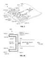
- FIG. 1is a top side perspective view showing an RF energy harvesting device according to an embodiment of the present invention
- FIG. 2is a top side perspective view showing an RF energy harvesting device including first two-part antenna configuration according to a specific embodiment of the present invention
- FIG. 3Ais a simplified diagram showing an RF energy harvesting device including the two-part antenna of FIG. 2 ;
- FIG. 3Bis a simplified diagram showing an RF energy harvesting system including three RF energy harvesting devices of FIG. 3A in a nested arrangement;
- FIGS. 4A, 4B and 4Care simplified diagrams showing two-part antenna configurations according to alternative specific embodiments of the present invention.
- FIG. 5is a simplified diagram showing an RF energy harvesting system utilizing two-part antennas according to another specific embodiment of the present invention.
- FIGS. 6A and 6Bare simplified diagrams showing curved two-part antenna configurations according to alternative specific embodiments of the present invention.
- FIG. 7is a top plan view showing a “racetrack-type” metamaterial resonator antenna according to another specific embodiment of the present invention.
- FIG. 8is a simplified diagram showing an RF energy harvesting device including the “racetrack-type” antenna of FIG. 7 ;
- FIG. 9is a simplified diagram showing an RF energy harvesting system utilizing “racetrack-type” antennas according to another specific embodiment of the present invention.
- FIGS. 10A and 10Bare top plan views showing two-loop and three-loop “racetrack” antennas, respectively, according to alternative embodiments of the present invention.
- the present inventionrelates to an improvement in RF energy harvesting.
- the following descriptionis presented to enable one of ordinary skill in the art to make and use the invention as provided in the context of a particular application and its requirements.
- the terms “coupled” and “connected”, which are utilized herein,are defined as follows.
- the term “connected”is used to describe a direct connection between two circuit elements, for example, by way of a metal line formed in accordance with normal integrated circuit fabrication techniques.
- the term “coupled”is used to describe either a direct connection or an indirect connection between two circuit elements.
- two coupled elementsmay be directly connected by way of a metal line, or indirectly connected by way of an intervening circuit element (e.g., a capacitor, resistor, inductor, or by way of the source/drain terminals of a transistor).
- an intervening circuit elemente.g., a capacitor, resistor, inductor, or by way of the source/drain terminals of a transistor.
- FIG. 1is a top side perspective view showing an RF energy harvesting device 100 according to a generalized embodiment of the present invention.
- RF energy harvesting device 100utilizes a novel metamaterial resonator antenna 120 and a rectifying circuit 130 .
- Metamaterial resonator antenna 120includes at least one metal structure 123 that is conformally fixedly disposed on a substrate 101 (e.g., formed by printing a conductive (e.g., silver) ink or depositing/etching a metal layer) in a manner that facilitates low-cost fabrication using printed electronics techniques.
- Metal structure 123includes two primary antenna segments 123 - 1 and 123 - 2 and at least one secondary antenna segment 123 - 2 that are disposed in a spaced-apart (parallel) folded arrangement and connected by two linking segments 123 - 31 and 123 - 32 .
- first primary antenna segment 123 - 11extends from a first antenna end point 121 to a first midpoint 123 - 11 A
- second primary antenna segment 123 - 12extends from a second antenna end point 122 to a second midpoint 123 - 21 A
- Secondary antenna segment 123 - 2is disposed parallel to and spaced from the first and second primary antenna segments by a uniform gap distance S, with secondary antenna segment 123 - 2 having a first end disposed at a third midpoint 123 - 12 A and an opposing second end disposed at a fourth midpoint 123 - 22 A.
- First linking segment 123 - 31is connected between first and third midpoints 123 - 11 A and 123 - 12 A, and second linking segment 123 - 32 connected between second and fourth midpoints 123 - 21 A and 123 - 22 A, with these linking segments being substantially shorter than primary and secondary segments.
- Each of these segmentsconsists of an elongated metal line structure having a thickness T (e.g., 8 microns) and a line width LW (e.g., 2.5 mm).
- the overall antenna structureis tailored to resonate at RF frequencies that are within an associated target bandwidth range, and are configured such that captured RF signals V 121 and V 122 generated at antenna end points 121 and 122 are 180° out-of-phase from each other.
- Metamaterial resonator antenna 120is electrically-small and, when combined with certain rectifying circuits, facilitates near-perfect RF energy absorption.
- An advantage of metamaterial resonator antennas formed in accordance with the present invention, such as those described below,can be tailored to have high impedance and exhibit near-perfect absorption.
- the rectifying circuit 130is coupled to the antenna end points 121 / 122 , and includes circuit elements (one or more diodes, capacitors, inductors and/or resistors) that are configured to combine positive voltage pulses from the two captured RF signals V 121 &V 122 to generate a usable output voltage V OUT .
- circuit elementsone or more diodes, capacitors, inductors and/or resistors
- the metamaterial resonator antenna arrangementfacilitates nesting a smaller antenna within open spaces of a larger antenna, thereby facilitating capturing a wide range of RF frequencies without significantly changing the device's footprint (size), and thereby providing a highly scalable platform that facilitates remotely powering widely dispersed IC devices (e.g., sensors, processors, etc.) using either pre-existing RF signals (e.g., from ambient Wi-Fi signals) or dedicated charging RF sources.
- IC devicese.g., sensors, processors, etc.
- the metamaterial resonator antenna arrangementis formed on a substrate and can be configured for different RF frequencies
- the present inventionfacilitates the low-cost production of RF energy harvesting device using inexpensive flexible plastic substrates and cost-effective printed electronics techniques, thereby minimizing overall manufacturing costs while maximizing the RF frequency band that can be converted into usable energy.
- rectifying circuit 130includes conductive structures 133 - 1 to 133 - 4 that are conformally disposed on the substrate surface 102 (i.e., generated during the same ink-jet printing run as that used to form antenna 120 ) in order to further minimize manufacturing costs.
- rectifying circuit 130utilizes two dissimilar Zero Bias Schottky diodes D 1 and D 2 and a capacitor C 1 that are configured to combine the two captured RF signals V 121 and V 122 in a way that generates an output voltage V OUT with minimal energy loss.
- first diode D 1is coupled by way of conductive structure 133 - 1 between first antenna end point 121 and a first node N 1 (which in this case is implemented by conductive structure 133 - 3 .
- a first terminal of capacitor C 1is coupled to second antenna end point 122 by way of conductive structure 133 - 2 , and a second terminal is connected to conductive structure 133 - 3 (node N 1 ).
- Second diode D 2is connected between first node N 1 and a second node N 2 , which is implemented by conductive structure 133 - 4 .
- a second capacitor C 2is coupled between first antenna end point 121 and node N 2 , and in one embodiment conductive structure 133 - 1 is coupled to a ground or other voltage source.
- diode D 1is implemented using a (first) Zero Bias Schottky diode having a very low forward voltage (e.g., 120 mV or less), a peak inverse voltage of 1.0 V or less, and a reverse current resistance of 5 k ⁇ .
- Diode D 2is implemented using a (second) Zero Bias Schottky diode having a forward voltage of 150 mV or less (i.e., equal to or higher than that of diode D 1 ), and a peak inverse voltage of at least 2.0 V (i.e., higher than that of diode D 1 ), and a reverse current resistance of at least 10 k ⁇ (i.e., higher than that of diode D 1 ).
- Capacitors C 1 and C 2are either discrete (e.g., surface mounted) capacitor structures, or a fabricated capacitor structures (e.g., using printed electronics), and have a value determined in accordance with the characteristics (current and voltage) of DC output voltage V OUT , and in a practical embodiment have a common capacitance value of 10 pF.
- a first intermediate voltage generated at first node N 1comprises a sum of positive voltage pulses of first RF signal V 121 , which are passed through first diode D 1 , and second AC signal V 122 , which is passed through first capacitor C 1 .
- a second intermediate voltageis generated at second node N 2 in accordance with positive voltage pulses that are passed from the first node N 1 through the second diode D 2 .
- the resulting RF energy harvesting devicesexhibit high energy conversion efficiencies than when conventional rectifying circuits are utilized.
- RF energy harvesting devicesincluding the metamaterial resonator antennas of the present invention and conventional rectifying circuits (e.g., using a voltage doubler circuit, such as a Greinacher circuit, to combine the two captured RF signals) may be beneficially utilized to generate a usable output voltage.
- FIG. 2is a top side perspective view showing an RF energy harvesting device 100 A including an open C-shaped two-part antenna 120 A formed by metal structures that are conformally disposed on upper surface 102 A of flexible plastic substrate 101 A.
- Antenna 120 Arepresents a first example of a two-part dipole antenna arrangement made up of two bilaterally symmetrical metal elements 123 A- 1 and 123 A- 2 .
- Metal element 123 A- 1includes a first primary antenna segment 123 A- 11 extending from first antenna end point 121 A, a first linking segment 123 A- 13 attached to the end of primary antenna segment 123 A- 11 , and a first secondary antenna segment 123 A- 12 extending from linking segment 123 A- 13 to a first distal end point 123 A- 13 A disposed adjacent to first antenna end point 121 A.
- first primary antenna segment 123 A- 11 and first secondary antenna segment 123 A- 12are concentrically arranged such that a uniform gap spacing GS separates first primary antenna segment 123 A- 11 and first secondary antenna segment 123 A- 12 along their entire length.
- second metal element 123 A- 2includes a second primary antenna segment 123 A- 21 extending from second antenna end point 122 A, a second linking segment 123 A- 23 , and a second secondary antenna segment 123 A- 22 extending from second linking segment 123 A- 23 to a second distal end point 123 A- 23 A disposed adjacent to second antenna end point 122 A, where second primary antenna segment 123 A- 21 and second secondary antenna segment 123 A- 22 are also concentrically arranged and separated by gap spacing GS along their entire length.
- Metal elements 123 A- 1 and 123 A- 2collectively form an open C-shaped pattern surrounding central region 127 on three sides.
- FIG. 3Ais a simplified diagram showing RF energy harvesting device 100 A of FIG. 2 , where device 100 A shows open C-shaped two-part antenna 120 A using simple line structures in order to simplify the description of other embodiments set forth below. That is, FIG. 3A shows in simplified form antenna 120 A coupled to a generalized rectifying circuit 130 A, where primary antenna segments 123 A- 11 and 123 A- 21 , secondary segments 123 A- 12 and 123 A- 22 , and linking segments 123 A- 13 and 123 A- 23 are indicated by solid black lines. As further illustrated in FIG. 3A , each of primary antenna segments 123 A- 11 and 123 A- 21 and secondary segments 123 A- 12 and 123 A- 22 comprises at least two linear segments connected by a corner portion. For example, referring to the upper portion of FIG. 3A , second primary antenna segment 123 A- 21 includes two linear segments 123 A- 211 and 123 A- 212 connected by a corner (90° angle) portion 123 A- 21 A.
- FIG. 3Bis a simplified diagram showing an RF energy harvesting system 200 A including three RF energy harvesting devices 100 A- 1 , 100 A- 2 and 100 A- 3 configured in a nested arrangement that illustrates an advantage of the open C-shaped configuration of antenna 120 A (described above).
- devices 100 A- 1 , 100 A- 2 and 100 A- 3respectively include three open C-shaped antennas 120 A- 1 , 120 A- 2 and 120 A- 3 , each coupled to an associated rectifying circuit 130 A- 1 , 130 A- 2 and 130 A- 3 facilitate generate an combined system output voltage V OUT-SYS utilizing, for example, a parallel configuration similar to that described below with reference to FIG. 5 .
- FIG. 5As illustrated in FIG.
- an advantage to forming metamaterial resonant antennas using the open C-shaped configuration described aboveis that multiple antennas of different sized can be concentrically “nested”, which facilitates capturing RF energy over a wide range of RF frequencies without increasing the overall device/system footprint. That is, because antennas 120 A- 1 , 120 A- 2 and 120 A- 3 have different sizes, each has a different inductance and hence resonates at a different RF frequency. By nesting antennas 120 A- 2 and 120 A- 3 inside the footprint of antenna 120 A- 1 , system 200 A facilitates capturing energy over a wider range of RF frequencies than would be possible using antenna 120 A- 1 alone, without increasing the substrate area required for antenna 120 A.
- FIGS. 4A, 4B and 4Care simplified diagrams showing three additional two-part dipole antenna configurations that illustrate other approaches (i.e., in addition to increasing antenna size, as illustrated in FIG. 3 B) for tailoring antenna inductance according to alternative specific embodiments of the present invention.
- the primary antenna segments and secondary antenna segmentsinclude three interconnected linear sections that collectively form a C-shaped pattern, where dimensions of the three linear sections are changed to illustrate how metamaterial resonator antennas are tailored to achieve difference inductance values, whereby the antennas are altered to resonate at (and thereby collect energy from) different RF frequencies.
- the primary antenna segments and secondary antenna segmentsinclude three interconnected linear sections that collectively form a C-shaped pattern, where dimensions of the three linear sections are changed to illustrate how metamaterial resonator antennas are tailored to achieve difference inductance values, whereby the antennas are altered to resonate at (and thereby collect energy from) different RF frequencies.
- antenna 120 Bincludes primary segments 123 B- 11 and 123 B- 21 and secondary segments 123 B- 12 and 123 B- 22 that are connected by linking sections 123 B- 13 and 123 B- 23 in a manner similar to that described above with reference to antenna 120 A ( FIG. 2 ). Assuming the overall length L and width X 1 of antenna 120 B is the same as that of antenna 120 A ( FIG. 2 ), FIG. 4A illustrates that the inductance of antenna 120 B can be tailored to achieve different inductances with little or minimal change to the overall antenna footprint by adding a third (vertical) section to each of the primary and secondary antenna segments.
- second primary antenna segment 123 B- 21includes three interconnected linear sections 123 B- 211 , 123 B- 212 and 123 B- 213 that form a C-shaped pattern, where vertical antenna section 123 B- 213 increases the length of primary antenna segment 123 B- 21 by length Y 1 without increasing the overall footprint of antenna 120 B.
- FIG. 4Bindicates that further tailoring is achieved by further lengthening these third (vertical) sections.
- Antenna 120 Cincludes three-section primary segments 123 C- 11 and 123 C- 21 and secondary segments 123 C- 12 and 123 C- 22 that are connected by linking sections 123 C- 13 and 123 C- 23 in a manner similar to that of antenna 120 B ( FIG.
- second primary antenna segment 123 C- 21includes three interconnected linear sections 123 C- 211 , 123 C- 212 and 123 C- 213 , where vertical antenna section 123 C- 213 has a length Y 2 that increases the inductance of antenna 120 C over that of antenna 120 B without increasing the overall footprint of antenna 120 C.
- FIG. 4Cillustrates antenna 120 D, which achieves even higher inductance by way of lengthening the horizontal sections of primary segments 123 D- 11 and 123 D- 21 and secondary segments 123 D- 12 and 123 D- 22 to width X 2 .
- second primary antenna segment 123 D- 21includes three interconnected linear sections 123 D- 211 , 123 D- 212 and 123 D- 213 , where horizontal antenna section 123 D- 212 has a width X 2 that increases the inductance of antenna 120 D over that of antenna 120 C without significantly increasing the overall footprint of antenna 120 C.
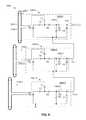
- FIG. 5is a simplified circuit diagram showing a RF energy harvesting system 200 E including RF energy harvesting devices 100 E- 1 , 100 E- 2 and 100 E- 3 that are connected in parallel between common ground sources and common system output nodes to maximize the current level of the system output voltage V OUT-SYS .
- devices 100 E- 1 , 100 E- 2 and 100 E- 3respectively include similar rectifying circuits 130 E- 1 , 130 E- 2 and 130 E- 3 that are optimized to provide their respective output voltages V OUT1 to V OUT3 in a manner that facilitates combination.
- Each rectifying circuit 130 E- 1 , 130 E- 2 and 130 E- 3includes diodes D 1 and D 2 and capacitors C 1 configured as described above with reference to FIG. 1 .
- rectifying circuits 130 E- 1 , 130 E- 2 and 130 E- 3are similar in that they respectively include output control circuits 135 E- 1 , 135 E- 2 and 135 E- 3 configured to convert the intermediate voltage generated at node N 2 into DC output voltages V OUT1 to V OUT3 .
- output control circuits 135 E- 1 , 135 E- 2 and 135 E- 3include a (second) capacitor C 2 that has essentially the same capacitance as capacitors C 1 , a third diode D 3 and a storage capacitor C 4 that are configured to store DC output voltages V OUT1 to V OUT3 for combination at system output node V OUT-SYS .
- diode D 3is connected between nodes N 2 and N 3 (which serves as an output node for rectifying circuit 130 E- 1 ), a first terminal of storage capacitor C 4 is connected to node N 3 , and a resistor R 2 connected between a second terminal of storage capacitor C 4 and first antenna end point 121 A (e.g., to the applied ground potential).
- diode D 3is implemented using the same diode element as that utilized to implement diode D 2 (e.g., a HSMS2850 Surface Mount Zero Bias Schottky Detector Diode manufactured by Agilent Technologies of Santa Clara, Calif., USA).
- Capacitor C 3is implemented using a capacitive element sized in accordance with the characteristics (current and voltage) of DC output voltage V OUT , and the size and characteristics of the system voltage present on system output node V OUT-SYS .
- capacitor C 3has a capacitance of 100 pF
- resistor R 2has a nominal resistive value of 1 ⁇ .
- Output control circuit 135 E- 2 and 135 E- 3are configured identically to output control circuit 135 E- 1 .
- each device 100 E- 1 , 100 E- 2 and 100 E- 3includes a different two-part dipole metamaterial resonator antenna 120 A, 120 B and 120 C, whereby devices 100 E- 1 , 100 E- 2 and 100 E- 3 are configured to convert RF energy having different frequencies into output voltages V OUT1 , V OUT2 and V OUT3 .
- Two-part dipole metamaterial resonator antenna 120 A, 120 B and 120 Care described in detail above. Because antennas 120 A, 120 B and 120 C have different configurations (sizes), each generates an output voltage dependent on the availability of sufficient RF energy at the frequencies to which each antenna resonates.
- System 200 Eis therefore configured to generate output current over a much broader RF frequency range than would be possible using a single antenna by utilizing three different antenna arrangements.
- FIGS. 6A and 6Bare simplified diagrams showing two curved two-part metamaterial resonator antennas 120 F and 120 G according to additional alternative specific embodiments of the present invention. Similar to the straight-section embodiments described above, each antenna 120 F and 120 G includes two bilaterally symmetrical metal elements 123 F- 1 and 123 F- 2 and 123 G- 1 and 123 G- 2 , each including concentric, continuously-curved (e.g., substantially semi-circular) primary and secondary segments wire segments that are connected by a short linking segment.
- concentric, continuously-curvede.g., substantially semi-circular
- metal element 123 F- 1 of antenna 120 Fincludes a curved primary segment 123 F- 11 extending from antenna end point 121 F to a (first) midpoint 123 A- 11 A, a straight linking segment 123 F- 13 extending from midpoint 123 F- 11 A to midpoint 123 F- 12 A, and a curved secondary antenna segment 123 F- 12 extending from the second midpoint 123 F- 12 A to a distal end point 124 F- 13 A.
- Curved primary segment 123 F- 11 and curved secondary antenna segment 123 F- 12are concentrically arranged such that they are separated along their entire length by a uniform gap spacing GS.
- metal element 123 F- 2includes a curved primary segment 123 F- 21 extending from antenna end point 121 F to straight linking segment 123 F- 23 , and a curved secondary antenna segment 123 F- 22 extending from linking segment 123 F- 23 to a distal end point 124 F- 23 A, where curved primary segment 123 F- 21 and curved secondary antenna segment 123 F- 22 are concentrically arranged.
- metal element 123 G- 1 of antenna 120 Galso includes a curved primary segment 123 G- 11 extending from antenna end point 121 G to a midpoint 123 A- 11 A, a straight linking segment 123 G- 13 extending from midpoint 123 G- 11 A to midpoint 123 G- 12 A, and a curved secondary antenna segment 123 G- 12 extending from the second midpoint 123 G- 12 A to a distal end point 124 G- 13 A, with curved primary segment 123 G- 11 and curved secondary antenna segment 123 G- 12 being concentrically arranged, and metal element 123 G- 2 includes a curved primary segment 123 G- 21 extending from antenna end point 122 G to straight linking segment 123 G- 23 , and a curved secondary antenna segment 123 G- 22 extending from linking segment 123 G- 23 to a distal end point 124 G- 23 A, where curved primary segment 123 G- 21 and curved secondary antenna segment 123 G- 22 are concentrically
- Antenna 120 Gdiffers from antenna 120 F in that, where linking segments 123 F- 13 and 123 F- 23 of antenna 120 F are implemented by straight (linear shaped) wire structures, linking segments 123 G- 13 and 123 G- 23 of antenna 120 G comprise two-segment step-shaped wire structures arranged such that the length primary antenna segments 123 G- 11 and 123 G- 21 is equal to the lengths of first secondary antenna segments 123 G- 12 and 123 G- 22 , which facilitates improved antenna performance.
- FIG. 7is a top plan view showing a “racetrack-type” metamaterial resonator antenna 120 H according to another specific embodiment of the present invention.
- antenna 120 Hhas a single-piece (integral, contiguous) metal element 123 H including (first and second) primary antenna segments 123 H- 11 and 123 H- 12 disposed on a first side of the “racetrack”, a secondary antenna segment 123 H- 2 disposed on the second side of the “racetrack”, and two open-circle linking segments 12 H- 31 and 123 H- 32 forming the two “curves” of the “racetrack”.
- Primary antenna segments 123 H- 11 and 123 H- 12are linear metal structures that are collinearly arranged and separated by a gap GW defined between the first and second antenna end points 121 H and 122 H. That is, referring to FIG. 7 , primary antenna segment 123 H- 11 extends straight downward from end point 121 H to a first midpoint 123 H- 11 A, and primary antenna segment 123 H- 21 extends upward from end point 122 H to a second midpoint 123 H- 21 A.
- Secondary antenna segment 123 H- 2is a continuous metal structure disposed parallel to and spaced at a distance S from primary antenna segments 123 H- 11 and 123 - 12 , and extends substantially the entire length L between third and fourth midpoints 123 H- 12 A and 123 H- 22 A.
- Linking segment 123 H- 31includes a semi-circular section 123 H- 311 connected between a lower end of primary antenna segment 123 H- 11 and a lower end of secondary antenna segment 123 H- 2 (i.e., between midpoints 123 H- 11 A and 123 H- 12 A), and (first and second) curved end sections 123 H- 312 and 123 H- 313 extending from semi-circular section 123 H- 311 into space 127 (i.e., into a region between primary antenna segment 123 H- 11 and secondary antenna segment 123 H- 2 ).
- Linking segment 123 H- 32includes a semi-circular section 123 H- 321 connected between upper ends of second primary antenna segment 123 H- 12 and secondary antenna segment 123 H- 2 (i.e., between midpoints 123 H- 21 A and 123 H- 22 A), and (third and fourth) curved end sections 123 H- 322 and 123 H- 323 extending from semi-circular section 123 H- 321 into space 127 .
- the resulting “racetrack-type” antenna configurationresonates at an associated bandwidth range such that captured RF signals generated on antenna end points 121 H and 122 H are 180° out-of-phase from each other.
- antenna 120 HThis “racetrack-type” antenna configuration was found to capture RF signals over a substantially higher frequency range than the two-part dipole antenna configurations described above. Similar to the two-part configurations, the impedance of antenna 120 H is tunable by way of increasing or decreasing the antenna footprint (size). In addition, the “racetrack-type” antenna configuration facilitates further “tunability” without changing the overall footprint by way of changing the gaps separating the curved end sections (e.g., the distance separating end sections 123 H- 322 and 123 H- 323 ), or by adding one or more additional “racetrack loops” to the antenna structure, as described in additional detail below.
- a “racetrack-type” antennawas formed by the present inventors using silver ink (10 ⁇ /cm) disposed on a PET substrate (250 ⁇ m thick) with segments having a thickness of 8 ⁇ m and line widths LW of 2.5 mm, where racetrack structure included a straight-section length L of 120 mm and linking segments having an inner radius r of 6.45 mm (i.e., having an overall antenna length of approximately 5.8 inches), with the curved end segments formed using an opening angle ⁇ of 60°, and with a gap width GW of 2.5 mm.
- the resulting structurewas found to resonate with peak efficiency at 914 MHz, and exhibited less than 10% loss in accepted power in the range of approximately 825 MHz to 1050 MHz.
- FIG. 8is a simplified diagram showing an RF energy harvesting device 100 H including “racetrack-type” metamaterial resonator antenna 120 H of FIG. 7 .
- rectifying circuit 130 Hincludes two discrete inductors L 1 H and L 2 H that are needed to facilitate proper transmission of captured RF signals to the other elements of rectifying circuit 130 H.
- inductor L 1 His coupled between first antenna end point 121 H and diode D 1
- inductor L 2 His coupled between antenna end point 122 H and capacitor C 1 .
- inductors L 1 H and L 2 Hhave the same (common) inductance value, and form a balanced circuit with antenna 120 H and the elements of rectifying circuit 130 H (i.e., capacitor C 1 , diodes D 1 and D 2 , and output control circuit 135 H, which may be implemented using any of the configurations described in copending application Ser. No. 14/582,002 entitled “RECTIFYING CIRCUIT FOR MULTIBAND RADIO FREQUENCY (RF) ENERGY HARVESTING”, which is incorporated herein by reference in its entirety.
- FIG. 9is a simplified diagram showing an RF energy harvesting system 200 H made up of three devices 100 H- 1 , 100 H- 2 , and 100 H- 3 respectively including “racetrack-type” metamaterial resonator antennas 120 H- 1 to 120 H- 3 , where the output terminals of devices 100 H- 1 , 100 H- 2 , and 100 H- 3 are connected in series such that the second antenna end point of at least one RF energy harvesting device is connected to the output node of an adjacent RF energy harvesting device.
- each energy harvesting device 100 H- 1 to 100 H- 3includes a substantially identical “racetrack” antenna configuration.
- device 100 H- 1includes “racetrack” antenna 120 H- 1 configured as described above to resonate at RF frequencies within an associated bandwidth range.
- Device 100 H- 2includes antenna 120 H- 2 and device 100 H- 3 includes antenna 120 H- 3 , where antennas 120 H- 2 and 120 H- 3 are substantially identical in configuration with antenna 120 H- 1 (i.e., such that all three antennas resonate at the same RF frequency, and such that all three antennas generate substantially the same amount of energy).
- Each energy harvesting device 100 H- 1 to 100 H- 3also includes a substantially identical rectifying circuit.
- device 100 H- 1includes rectifying circuit 130 H- 1 including a first diode D 1 coupled between antenna end point 121 H- 1 and a first node N 1 , a first capacitor C 1 coupled between end point 122 H- 1 and node N 1 , and a second diode D 2 connected between node N 1 and a second node N 2 .
- Rectifying circuit 130 H- 1also includes an output control circuit 135 H- 1 coupled to node N 2 that is configured (i.e., by way of third diode D 3 , second capacitor C 2 that has the same capacitance as capacitor C 1 , and storage capacitor C 4 ) to convert the intermediate voltage generated on node N 2 into DC output voltage V OUT1 .
- energy harvesting devices 100 H- 2 and 100 H- 3respectively include rectifying circuits 130 H- 2 and 130 H- 3 having diodes D 1 and D 2 and capacitor C 1 , and output control circuits 135 H- 2 and 135 H- 3 including diodes D 3 and capacitors C 2 and C 4 ) that generate respective DC output voltages V OUT2 and V OUT3 .
- RF energy harvesting devices 100 H- 1 to 100 H- 3are connected such that DC output voltages V OUT1 , V OUT2 and V OUT3 are combined such that system output voltage V OUT-SYS is maximized.
- first antenna end point 121 H- 2 of RF energy harvesting device 100 H- 2is connected to the output node of RF energy harvesting device 100 H- 3 (i.e., such that the ground plane of device 100 H- 2 is DC output voltage V OUT3 ), whereby a voltage level of DC output voltage V OUT2 generated at the output node of device 100 H- 2 is “boosted” by DC output voltage V OUT3 .
- antenna end point 121 H- 1 of RF energy harvesting device 100 H- 1is connected to the output node of RF energy harvesting device 100 H- 3 , whereby a voltage level of DC output voltage V OUT3 generated at the output node of device 100 H- 1 is “boosted” by DC output voltages V OUT2 and V OUT3 .
- V OUT-SYSthe voltage level of system output voltage V OUT-SYS is maximized by the series arrangement.
- racetrack-type antenna configurationmay also be used in a nested-device arrangement similar to that shown and described above with reference to FIG. 3B .
- FIGS. 10A and 10Bare top plan views respectively showing a two-loop “racetrack-type” metamaterial resonator antenna 120 J and a three-loop “racetrack” “racetrack-type” metamaterial resonator antenna according to alternative embodiments of the present invention.
- a racetrack antennaby altering the length and radius diameters of the “racetrack” shape, and by changing the gap distance between the curved end portions (as described above)
- it is also possible to tailor the antenna's impedance by way of adding one or more additional “loop” structuresi.e., such that the single integral metal antenna structure includes two or more “loops” as described below).
- antenna 120 Jincludes a first “loop” structure surrounding region 127 - 1 formed by primary antenna segments 123 J- 11 and 123 J- 12 respectively extending from end points 121 J and 122 J, a (first) secondary antenna segment 123 J- 21 , and (first and second) circular linking segments 123 J- 31 and 123 J- 32 , which are configured in the manner described above with reference to FIG. 7 .
- antenna 120 Jincludes a second “loop” structure surrounding region 127 - 2 formed by first secondary antenna segment 123 J- 21 , a second secondary antenna segment 123 J- 22 disposed parallel to primary antenna segments 123 J- 11 and 123 J- 12 and to first secondary antenna segment 123 J- 21 (i.e., such that first secondary antenna segment 123 J- 21 is between primary antenna segments 123 J- 11 and 123 J- 12 and second secondary antenna segment 123 J- 22 ), a (third) linking segment 123 J- 33 including a third semi-circular section 123 J- 331 connected between the first lower end of the first secondary antenna segment 123 J- 21 and a first lower end of the second secondary antenna segment 123 J- 22 , and (fifth and sixth) curved end sections 123 J- 332 and 123 J- 333 extending from third semi-circular section 123 J- 331 into region 127 - 2 , and a (fourth) linking segment 123 J- 34 including a fourth semi-circular section 123
- antenna 120 Kincludes a first “loop” structure formed by primary antenna segments 123 J- 11 and 123 J- 12 extending from end points 121 K and 122 K, respectively, a (first) secondary antenna segment 123 J- 21 , and (first and second) circular linking segments 123 J- 31 and 123 J- 32 , and a second “loop” structure formed by (first) secondary antenna segment 123 J- 21 , a (second) secondary antenna segment 123 J- 22 , and (third and fourth) circular linking segments 123 J- 33 and 123 J- 34 .
- antenna 120 Jincludes a third “loop” structure formed by (second) secondary antenna segment 123 J- 22 , a (third) secondary antenna segment 123 J- 23 , a (fifth) linking segment 123 J- 35 connecting lower ends of second antenna segments 123 J- 22 and 123 J- 23 , and a (sixth) linking segment 123 J- 36 connecting upper ends of second antenna segments 123 J- 22 and 123 J- 23 .
- the addition of the third “loop” structurefurther increases the overall inductance of antenna 120 K over that of antenna 120 J ( FIG. 10A ).
- the antenna and rectifying circuitmay be fabricated using normal printed circuit board methods on either rigid or flexible substrate.
- the devices systemsmay be formed by machining or sintering.
Landscapes
- Engineering & Computer Science (AREA)
- Computer Networks & Wireless Communication (AREA)
- Power Engineering (AREA)
- Variable-Direction Aerials And Aerial Arrays (AREA)
- Details Of Aerials (AREA)
Abstract
Description
Claims (22)
Priority Applications (5)
| Application Number | Priority Date | Filing Date | Title |
|---|---|---|---|
| US14/582,033US9935370B2 (en) | 2014-12-23 | 2014-12-23 | Multiband radio frequency (RF) energy harvesting with scalable antenna |
| EP17156106.1AEP3196978B1 (en) | 2014-12-23 | 2015-12-14 | Multiband radio frequency (rf) energy harvesting with scalable antenna |
| EP15199968.7AEP3046181B1 (en) | 2014-12-23 | 2015-12-14 | Multiband radio frequency (rf) energy harvesting with scalable antenna |
| JP2015243088AJP6586361B2 (en) | 2014-12-23 | 2015-12-14 | Multiband radio frequency (RF) energy harvesting using adaptive antennas |
| KR1020150179607AKR102333942B1 (en) | 2014-12-23 | 2015-12-15 | Multiband radio frequency (rf) energy harvesting with scalable antenna |
Applications Claiming Priority (1)
| Application Number | Priority Date | Filing Date | Title |
|---|---|---|---|
| US14/582,033US9935370B2 (en) | 2014-12-23 | 2014-12-23 | Multiband radio frequency (RF) energy harvesting with scalable antenna |
Publications (2)
| Publication Number | Publication Date |
|---|---|
| US20160181868A1 US20160181868A1 (en) | 2016-06-23 |
| US9935370B2true US9935370B2 (en) | 2018-04-03 |
Family
ID=54849869
Family Applications (1)
| Application Number | Title | Priority Date | Filing Date |
|---|---|---|---|
| US14/582,033Active2035-11-13US9935370B2 (en) | 2014-12-23 | 2014-12-23 | Multiband radio frequency (RF) energy harvesting with scalable antenna |
Country Status (4)
| Country | Link |
|---|---|
| US (1) | US9935370B2 (en) |
| EP (2) | EP3196978B1 (en) |
| JP (1) | JP6586361B2 (en) |
| KR (1) | KR102333942B1 (en) |
Cited By (1)
| Publication number | Priority date | Publication date | Assignee | Title |
|---|---|---|---|---|
| US11024970B2 (en)* | 2017-08-07 | 2021-06-01 | Agency For Science, Technology And Research | Circularly polarized antenna for radio frequency energy harvesting |
Families Citing this family (26)
| Publication number | Priority date | Publication date | Assignee | Title |
|---|---|---|---|---|
| CN106688105B (en) | 2014-06-20 | 2018-12-04 | 帕特里克·K·布拉迪 | System for converting electromagnetic radiation into electrical energy using metamaterials |
| US10797537B2 (en)* | 2016-03-15 | 2020-10-06 | Northeastern University | Distributed wireless charging system and method |
| GB2553093B (en)* | 2016-08-17 | 2019-05-15 | Drayson Tech Europe Ltd | RF energy harvesting dual loop antenna with gaps and bridges |
| US20180076376A1 (en)* | 2016-09-14 | 2018-03-15 | Patrick K. Brady | Structures, system and method for converting electromagnetic radiation to electrical energy using metamaterials, rectennas and compensation structures |
| US11112869B2 (en) | 2017-01-27 | 2021-09-07 | Northwestern University | Epidermal virtual reality devices |
| US10218073B2 (en)* | 2017-04-05 | 2019-02-26 | Lyten, Inc. | Antenna with frequency-selective elements |
| GB2561913B (en)* | 2017-04-28 | 2020-09-30 | Drayson Tech Europe Ltd | Method and apparatus |
| CN107887695B (en)* | 2017-09-27 | 2019-12-20 | 西安空间无线电技术研究所 | Rectifying antenna with guide signal transmitting function |
| SG11202006088XA (en)* | 2018-01-04 | 2020-07-29 | Lyten Inc | Resonant gas sensor |
| JP2019193171A (en)* | 2018-04-27 | 2019-10-31 | ソニーセミコンダクタソリューションズ株式会社 | Array antenna, solid-state imaging apparatus and electronic apparatus |
| US11038380B2 (en) | 2018-05-10 | 2021-06-15 | National University Of Singapore | Split-ring resonator with integrated magnetic tunnel junction for highly sensitive and efficient energy harvesting |
| EP3834124A4 (en) | 2018-08-09 | 2022-05-04 | Lyten, Inc. | ELECTROMAGNETIC CONDITION DETECTION DEVICES |
| US10707582B2 (en) | 2018-09-28 | 2020-07-07 | Qualcomm Incorporated | Wide-band dipole antenna |
| US11271434B2 (en)* | 2018-12-28 | 2022-03-08 | Mitsubishi Electric Corporation | Rectenna device |
| CN112583296B (en)* | 2019-09-27 | 2022-04-26 | 中国科学院物理研究所 | A kind of environmental electromagnetic field energy harvesting device and preparation method thereof |
| US11271325B2 (en) | 2020-01-28 | 2022-03-08 | Northrop Grumman Systems Corporation | Antenna having damage and fault tolerability |
| FR3107791B1 (en)* | 2020-03-02 | 2023-03-24 | Radiall Sa | Wireless and contactless electrical energy transfer assembly comprising an improved system for regulating the energy transferred. |
| CN111916903B (en)* | 2020-06-29 | 2022-07-05 | 四川大学 | Double-channel communication rectification multifunctional antenna based on asymmetric coupler |
| US11063475B1 (en)* | 2020-06-30 | 2021-07-13 | The Florida International University Board Of Trustees | Power transfer and harvesting system having anchor-shaped antennas |
| JP7703307B2 (en)* | 2020-09-29 | 2025-07-07 | キヤノン株式会社 | Detectors and Imaging Devices |
| JP2024012724A (en)* | 2020-11-24 | 2024-01-31 | エイターリンク株式会社 | Wireless power supply mask device |
| WO2022168376A1 (en)* | 2021-02-02 | 2022-08-11 | 株式会社村田製作所 | Wireless power transmission system |
| CN113013632B (en)* | 2021-03-11 | 2022-02-08 | 北京邮电大学 | Harmonic suppression super-surface energy collector |
| WO2023106004A1 (en)* | 2021-12-10 | 2023-06-15 | ソニーセミコンダクタソリューションズ株式会社 | Rectifier circuit and power generation device |
| AU2023286508B2 (en)* | 2022-06-22 | 2024-07-04 | Checkpoint Systems, Inc. | Rfid label for attachment to metallic items |
| CN120500798A (en)* | 2023-01-04 | 2025-08-15 | 鲍尔卡斯特公司 | Method and apparatus for dynamic RF power splitting by manipulating DC output properties |
Citations (49)
| Publication number | Priority date | Publication date | Assignee | Title |
|---|---|---|---|---|
| US3929594A (en) | 1973-05-18 | 1975-12-30 | Fromson H A | Electroplated anodized aluminum articles |
| US4065364A (en) | 1976-01-21 | 1977-12-27 | Fromson H A | Process for anodizing aluminum |
| US4315873A (en) | 1977-11-21 | 1982-02-16 | Hudson Products Corporation | Cooling equipment |
| US4779000A (en) | 1983-08-26 | 1988-10-18 | Atomic Energy Of Canada Limited | Detector/dosimeter for gamma and microwave radiation |
| US5043739A (en) | 1990-01-30 | 1991-08-27 | The United States Of America As Represented By The United States Department Of Energy | High frequency rectenna |
| US5712166A (en) | 1993-12-10 | 1998-01-27 | British Nuclear Fuels, Plc | Method and material for the detection of ionizing radiation |
| US5905263A (en) | 1996-11-26 | 1999-05-18 | Mitsubishi Denki Kabushiki Kaisha | Depth dose measuring device |
| WO2001043228A1 (en) | 1999-12-07 | 2001-06-14 | Robert Bosch Gmbh | Leaky wave antenna |
| US20020180639A1 (en) | 2001-02-15 | 2002-12-05 | Rickett Bryan Stephen | Beam steering in sub-arrayed antennae |
| US20040207486A1 (en) | 2003-04-21 | 2004-10-21 | York Robert A. | Tunable bridge circuit |
| US20040238751A1 (en) | 2003-05-30 | 2004-12-02 | Penn David G. | Coincident neutron detector for providing energy and directional information |
| US7002517B2 (en) | 2003-06-20 | 2006-02-21 | Anritsu Company | Fixed-frequency beam-steerable leaky-wave microstrip antenna |
| US20060234505A1 (en) | 2003-12-18 | 2006-10-19 | Nippon Oil Corporation | Method for manufacturing nano-array electrode and photoelectric conversion device using same |
| WO2007015281A2 (en) | 2005-08-03 | 2007-02-08 | Frigel Firenze S.P.A. | A convector for cooling of a fluid circulating in a pipe |
| US20080049228A1 (en) | 2006-08-28 | 2008-02-28 | Novaspectra, Inc. | Fabry-perot interferometer array |
| US20080143192A1 (en) | 2006-12-14 | 2008-06-19 | Sample Alanson P | Dynamic radio frequency power harvesting |
| US20090067208A1 (en) | 2007-09-11 | 2009-03-12 | Donald Corey Martin | Method and apparatus for providing power |
| US20090152954A1 (en) | 2007-07-17 | 2009-06-18 | Triet Tu Le | RF energy harvesting circuit |
| US20090207000A1 (en) | 2006-01-05 | 2009-08-20 | University Of Pittsburgh - Of The Commonwealth System Of Higher Education | Multiple Antenna Energy Harvesting |
| US20090220802A1 (en) | 2006-02-21 | 2009-09-03 | Von Ardenne Anlagentechnik Gmbh | Highly reflective layer system, method for producing the layer system and device for carrying out the method |
| US20090284351A1 (en) | 2007-07-30 | 2009-11-19 | Bae System Information And Electronic Systems Integration Inc. | Dispersive antenna for rfid tags |
| US20110242863A1 (en) | 2010-03-31 | 2011-10-06 | Kookmin University Industry Academy Cooperation Foundation | Patch antenna and rectenna using the same |
| US20110303850A1 (en) | 2008-07-11 | 2011-12-15 | Universite Louis Pasteur De Strasbourg | Novel discriminating molecule family for neutron and gamma radiation |
| US20110309686A1 (en)* | 2010-06-17 | 2011-12-22 | SCARF Technologies | Generating dc electric power from ambient electromagnetic radiation |
| US20120133547A1 (en) | 2010-11-29 | 2012-05-31 | Freescale Semiconductor, Inc. | Automotive Radar System and Method for Using Same |
| CN102778144A (en) | 2012-08-16 | 2012-11-14 | 上海廷亚冷却系统有限公司 | Jet type evaporation cooler with low water outlet temperature |
| US20120314541A1 (en) | 2011-06-07 | 2012-12-13 | Nippon Soken, Inc. | Object detection apparatus |
| WO2013039926A1 (en) | 2011-09-12 | 2013-03-21 | Bluelagoon Technologies Ltd. | Method and apparatus for a delayed and prolonged air cooling condensation system |
| US20130076570A1 (en)* | 2011-09-26 | 2013-03-28 | Samsung Electro-Mechanics Co., Ltd. | Rf module |
| US20130187830A1 (en)* | 2011-06-02 | 2013-07-25 | Brigham Young University | Planar array feed for satellite communications |
| CN103312042A (en) | 2013-06-13 | 2013-09-18 | 中傲智能科技(苏州)有限公司 | RF (radio frequency) energy collector |
| US8621245B2 (en) | 2005-06-08 | 2013-12-31 | Powercast Corporation | Powering devices using RF energy harvesting |
| US8680945B1 (en) | 2010-02-17 | 2014-03-25 | Lockheed Martin Corporation | Metamaterial enabled compact wideband tunable phase shifters |
| US20140131023A1 (en) | 2012-11-15 | 2014-05-15 | The Board Of Trustees Of The Leland Stanford Junior University | Structures for radiative cooling |
| US20140266946A1 (en) | 2013-03-15 | 2014-09-18 | Searete Llc | Surface scattering antenna improvements |
| US20140300520A1 (en) | 2011-04-07 | 2014-10-09 | Polyvalor, Limited Partnership | Full-space scanning end-switched crlh leaky-wave antenna |
| US20140355381A1 (en) | 2012-07-16 | 2014-12-04 | Cornell University | Computation devices and artificial neurons based on nanoelectromechanical systems |
| WO2015038203A1 (en) | 2013-09-11 | 2015-03-19 | Purdue Research Foundation | Refractory plasmonic metamaterial absorber and emitter for energy harvesting |
| US20150214927A1 (en) | 2005-10-24 | 2015-07-30 | Powercast Corporation | Method and apparatus for high efficiency rectification for various loads |
| US20150229028A1 (en) | 2010-10-15 | 2015-08-13 | Searete Llc | Surface scattering antennas |
| US20150276489A1 (en) | 2012-11-27 | 2015-10-01 | The University Court Of The University Of Glasgow | Terahertz radiation detector, focal plane array incorporating terahertz detector, multispectral metamaterial absorber, and combined optical filter and terahertz absorber |
| US20150318618A1 (en) | 2014-05-02 | 2015-11-05 | Searete Llc | Surface scattering antennas with lumped elements |
| US20150372389A1 (en) | 2014-06-20 | 2015-12-24 | Searete Llc, A Limited Liability Corporation Of The State Of Delaware | Modulation patterns for surface scattering antennas |
| US20150380973A1 (en) | 2014-06-30 | 2015-12-31 | Landis+Gyr Innovations, Inc. | RF Energy Harvesting by a Network Node |
| US20160145214A1 (en) | 2013-03-18 | 2016-05-26 | Centre National De La Recherche Scientifique (C.N.R.S) | New Family of Discriminating Molecules for Neutron and Gamma Rays and Ionic Liquids |
| US20160181867A1 (en)* | 2014-12-23 | 2016-06-23 | Palo Alto Research Center Incorporated | Rectifying Circuit For Multiband Radio Frequency (RF) Energy Harvesting |
| US20160254844A1 (en)* | 2015-02-27 | 2016-09-01 | Jonathan J. Hull | Intelligent network sensor system |
| US20160336198A1 (en)* | 2015-05-12 | 2016-11-17 | Smartrac Technology Gmbh | Barrier Configurations and Processes in Layer Structures |
| US20160359378A1 (en)* | 2014-02-14 | 2016-12-08 | Institut Mines Telecom | Device for converting radiofrequency energy into dc current (rectifier antenna) and corresponding sensor |
Family Cites Families (6)
| Publication number | Priority date | Publication date | Assignee | Title |
|---|---|---|---|---|
| US7292200B2 (en)* | 2004-09-23 | 2007-11-06 | Mobile Mark, Inc. | Parasitically coupled folded dipole multi-band antenna |
| KR100667307B1 (en)* | 2005-01-11 | 2007-01-12 | 삼성전자주식회사 | Apparatus and method for biocombination detection using RF wireless energy transmission |
| US20090140946A1 (en)* | 2007-10-31 | 2009-06-04 | Ziolkowski Richard W | Efficient metamaterial-inspired electrically-small antenna |
| KR100979515B1 (en)* | 2008-04-03 | 2010-09-02 | (주) 파루 | RF Printing Rectifier Using Roll-to-Roll Printing |
| EP2178162A1 (en)* | 2008-10-20 | 2010-04-21 | Sibeam, Inc. | A planar antenna |
| WO2011005012A2 (en)* | 2009-07-06 | 2011-01-13 | 삼성전자주식회사 | Wireless power transmission system and resonator for the system |
- 2014
- 2014-12-23USUS14/582,033patent/US9935370B2/enactiveActive
- 2015
- 2015-12-14EPEP17156106.1Apatent/EP3196978B1/enactiveActive
- 2015-12-14JPJP2015243088Apatent/JP6586361B2/ennot_activeExpired - Fee Related
- 2015-12-14EPEP15199968.7Apatent/EP3046181B1/enactiveActive
- 2015-12-15KRKR1020150179607Apatent/KR102333942B1/ennot_activeExpired - Fee Related
Patent Citations (50)
| Publication number | Priority date | Publication date | Assignee | Title |
|---|---|---|---|---|
| US3929594A (en) | 1973-05-18 | 1975-12-30 | Fromson H A | Electroplated anodized aluminum articles |
| US4065364A (en) | 1976-01-21 | 1977-12-27 | Fromson H A | Process for anodizing aluminum |
| US4315873A (en) | 1977-11-21 | 1982-02-16 | Hudson Products Corporation | Cooling equipment |
| US4779000A (en) | 1983-08-26 | 1988-10-18 | Atomic Energy Of Canada Limited | Detector/dosimeter for gamma and microwave radiation |
| US5043739A (en) | 1990-01-30 | 1991-08-27 | The United States Of America As Represented By The United States Department Of Energy | High frequency rectenna |
| US5712166A (en) | 1993-12-10 | 1998-01-27 | British Nuclear Fuels, Plc | Method and material for the detection of ionizing radiation |
| US5905263A (en) | 1996-11-26 | 1999-05-18 | Mitsubishi Denki Kabushiki Kaisha | Depth dose measuring device |
| WO2001043228A1 (en) | 1999-12-07 | 2001-06-14 | Robert Bosch Gmbh | Leaky wave antenna |
| US20020180639A1 (en) | 2001-02-15 | 2002-12-05 | Rickett Bryan Stephen | Beam steering in sub-arrayed antennae |
| US20040207486A1 (en) | 2003-04-21 | 2004-10-21 | York Robert A. | Tunable bridge circuit |
| US20040238751A1 (en) | 2003-05-30 | 2004-12-02 | Penn David G. | Coincident neutron detector for providing energy and directional information |
| US7002517B2 (en) | 2003-06-20 | 2006-02-21 | Anritsu Company | Fixed-frequency beam-steerable leaky-wave microstrip antenna |
| US20060234505A1 (en) | 2003-12-18 | 2006-10-19 | Nippon Oil Corporation | Method for manufacturing nano-array electrode and photoelectric conversion device using same |
| US8621245B2 (en) | 2005-06-08 | 2013-12-31 | Powercast Corporation | Powering devices using RF energy harvesting |
| US20150236551A1 (en) | 2005-06-08 | 2015-08-20 | Powercast Corporation | Powering devices using rf energy harvesting |
| WO2007015281A2 (en) | 2005-08-03 | 2007-02-08 | Frigel Firenze S.P.A. | A convector for cooling of a fluid circulating in a pipe |
| US20150214927A1 (en) | 2005-10-24 | 2015-07-30 | Powercast Corporation | Method and apparatus for high efficiency rectification for various loads |
| US20090207000A1 (en) | 2006-01-05 | 2009-08-20 | University Of Pittsburgh - Of The Commonwealth System Of Higher Education | Multiple Antenna Energy Harvesting |
| US20090220802A1 (en) | 2006-02-21 | 2009-09-03 | Von Ardenne Anlagentechnik Gmbh | Highly reflective layer system, method for producing the layer system and device for carrying out the method |
| US20080049228A1 (en) | 2006-08-28 | 2008-02-28 | Novaspectra, Inc. | Fabry-perot interferometer array |
| US20080143192A1 (en) | 2006-12-14 | 2008-06-19 | Sample Alanson P | Dynamic radio frequency power harvesting |
| US20090152954A1 (en) | 2007-07-17 | 2009-06-18 | Triet Tu Le | RF energy harvesting circuit |
| US20090284351A1 (en) | 2007-07-30 | 2009-11-19 | Bae System Information And Electronic Systems Integration Inc. | Dispersive antenna for rfid tags |
| US20090067208A1 (en) | 2007-09-11 | 2009-03-12 | Donald Corey Martin | Method and apparatus for providing power |
| US20110303850A1 (en) | 2008-07-11 | 2011-12-15 | Universite Louis Pasteur De Strasbourg | Novel discriminating molecule family for neutron and gamma radiation |
| US8680945B1 (en) | 2010-02-17 | 2014-03-25 | Lockheed Martin Corporation | Metamaterial enabled compact wideband tunable phase shifters |
| US20110242863A1 (en) | 2010-03-31 | 2011-10-06 | Kookmin University Industry Academy Cooperation Foundation | Patch antenna and rectenna using the same |
| US20110309686A1 (en)* | 2010-06-17 | 2011-12-22 | SCARF Technologies | Generating dc electric power from ambient electromagnetic radiation |
| US20150229028A1 (en) | 2010-10-15 | 2015-08-13 | Searete Llc | Surface scattering antennas |
| US20120133547A1 (en) | 2010-11-29 | 2012-05-31 | Freescale Semiconductor, Inc. | Automotive Radar System and Method for Using Same |
| US20140300520A1 (en) | 2011-04-07 | 2014-10-09 | Polyvalor, Limited Partnership | Full-space scanning end-switched crlh leaky-wave antenna |
| US20130187830A1 (en)* | 2011-06-02 | 2013-07-25 | Brigham Young University | Planar array feed for satellite communications |
| US20120314541A1 (en) | 2011-06-07 | 2012-12-13 | Nippon Soken, Inc. | Object detection apparatus |
| WO2013039926A1 (en) | 2011-09-12 | 2013-03-21 | Bluelagoon Technologies Ltd. | Method and apparatus for a delayed and prolonged air cooling condensation system |
| US20130076570A1 (en)* | 2011-09-26 | 2013-03-28 | Samsung Electro-Mechanics Co., Ltd. | Rf module |
| US20140355381A1 (en) | 2012-07-16 | 2014-12-04 | Cornell University | Computation devices and artificial neurons based on nanoelectromechanical systems |
| CN102778144A (en) | 2012-08-16 | 2012-11-14 | 上海廷亚冷却系统有限公司 | Jet type evaporation cooler with low water outlet temperature |
| US20140131023A1 (en) | 2012-11-15 | 2014-05-15 | The Board Of Trustees Of The Leland Stanford Junior University | Structures for radiative cooling |
| US20150276489A1 (en) | 2012-11-27 | 2015-10-01 | The University Court Of The University Of Glasgow | Terahertz radiation detector, focal plane array incorporating terahertz detector, multispectral metamaterial absorber, and combined optical filter and terahertz absorber |
| US20140266946A1 (en) | 2013-03-15 | 2014-09-18 | Searete Llc | Surface scattering antenna improvements |
| US20160145214A1 (en) | 2013-03-18 | 2016-05-26 | Centre National De La Recherche Scientifique (C.N.R.S) | New Family of Discriminating Molecules for Neutron and Gamma Rays and Ionic Liquids |
| CN103312042A (en) | 2013-06-13 | 2013-09-18 | 中傲智能科技(苏州)有限公司 | RF (radio frequency) energy collector |
| WO2015038203A1 (en) | 2013-09-11 | 2015-03-19 | Purdue Research Foundation | Refractory plasmonic metamaterial absorber and emitter for energy harvesting |
| US20160359378A1 (en)* | 2014-02-14 | 2016-12-08 | Institut Mines Telecom | Device for converting radiofrequency energy into dc current (rectifier antenna) and corresponding sensor |
| US20150318618A1 (en) | 2014-05-02 | 2015-11-05 | Searete Llc | Surface scattering antennas with lumped elements |
| US20150372389A1 (en) | 2014-06-20 | 2015-12-24 | Searete Llc, A Limited Liability Corporation Of The State Of Delaware | Modulation patterns for surface scattering antennas |
| US20150380973A1 (en) | 2014-06-30 | 2015-12-31 | Landis+Gyr Innovations, Inc. | RF Energy Harvesting by a Network Node |
| US20160181867A1 (en)* | 2014-12-23 | 2016-06-23 | Palo Alto Research Center Incorporated | Rectifying Circuit For Multiband Radio Frequency (RF) Energy Harvesting |
| US20160254844A1 (en)* | 2015-02-27 | 2016-09-01 | Jonathan J. Hull | Intelligent network sensor system |
| US20160336198A1 (en)* | 2015-05-12 | 2016-11-17 | Smartrac Technology Gmbh | Barrier Configurations and Processes in Layer Structures |
Non-Patent Citations (11)
| Title |
|---|
| Aoyama, Takahiko et al. "Energy response of a full-energy-absorption neutron spectrometer using boron-loaded liquid scintillator BC-523", Nuclear Instruments and Methods in Physics Research A 333 (1993) 492-501, 10 pages. |
| Flaska, Marek et al., "Digital pulse shape analysis for the capture-gated liquid scintillator BC-523A", Nuclear Instruments and Methods in Physics Research A 599 (2009) 221-225, 5 pages. |
| Juan Li et al., "Facile Method for Modulating the Profiles and Periods of Self-Ordered Three-Dimensional Alumina Taper-Nanopores," ACS Appl. Mater. Interfaces 2012, 4, 5678-5683. |
| Juan Li et al., "Tailoring Hexagonally Packed Metal Hollow-Nanocones and Taper-Nanotubes by Template-Induced Preferential Electrodeposition," ACS Appl. Mater. Interfaces 2013, 5, 10376-10380. |
| Mascarenhas, Nicholas, et al., "Directional Neutron Detectors for Use with 14 MeV Neutrons", Sandia Report, SAND2005-6255, printed Oct. 2005, 32 pages. |
| Mirenda, Martin, et al., "Ionic liquids as solvents for liquid scintillation technology, Cerenkov counting with 1-Butyl-3-Methylimidazolium Chloride", Radiation Physics and Chemistry 98 (2014) 98-102, 5 pages. |
| Noh et al., Highly Self-Assembled Nanotubular Aluminum Oxide by Hard Anodization, (Jan. 29, 2011), J. Mater. Res., vol. 26, Issue 2, pp. 186-193. |
| Pratap et al., "Plasmonic Properties of Gold-Coated Nanoporous Anodic Alumina With Linearly Organized Pores," Pramana—J. Phys. (Dec. 2014), vol. 83, No. 6, pp. 1025-1033. |
| Swiderski, L., et al., "Further Study of Boron-10 Loaded Liquid Scintillators for Detection of Fast and Thermal Neutrons", IEEE Transactions on Nuclear Science, vol. 57, No. 1, Feb. 2010, 6 pages. |
| Vanier, Peter E., et al., "Calibration and Testing of a Large-Area Fast-Neutron Directional Detector", Brookhaven National Laboratory, BNL-79632-2007-CP, 8 pages. |
| Vanier, Peter E., et al., "Directional detection of fission-spectrum neutrons", 1-4244-1302-8/07, 2007 IEEE, 5 pages. |
Cited By (1)
| Publication number | Priority date | Publication date | Assignee | Title |
|---|---|---|---|---|
| US11024970B2 (en)* | 2017-08-07 | 2021-06-01 | Agency For Science, Technology And Research | Circularly polarized antenna for radio frequency energy harvesting |
Also Published As
| Publication number | Publication date |
|---|---|
| EP3046181A3 (en) | 2016-11-09 |
| KR102333942B1 (en) | 2021-12-02 |
| US20160181868A1 (en) | 2016-06-23 |
| EP3196978A1 (en) | 2017-07-26 |
| JP2016119666A (en) | 2016-06-30 |
| EP3196978B1 (en) | 2018-10-03 |
| KR20160076978A (en) | 2016-07-01 |
| JP6586361B2 (en) | 2019-10-02 |
| EP3046181B1 (en) | 2018-07-04 |
| EP3046181A2 (en) | 2016-07-20 |
Similar Documents
| Publication | Publication Date | Title |
|---|---|---|
| US9935370B2 (en) | Multiband radio frequency (RF) energy harvesting with scalable antenna | |
| US9871298B2 (en) | Rectifying circuit for multiband radio frequency (RF) energy harvesting | |
| US9966801B2 (en) | RF energy harvester | |
| US6856291B2 (en) | Energy harvesting circuits and associated methods | |
| JP2016119836A5 (en) | ||
| CN107611617B (en) | An Electrically Tuned Rectenna Based on Substrate Integrated Waveguide | |
| CN100559654C (en) | Energy harvesting circuit and associated method | |
| Rahul et al. | Triple Band Monopole Antenna for RFID, Energy Harvesting and Data Communication | |
| Kokate | RF Energy Harvester | |
| HK1216360B (en) | Rf energy harvester | |
| JP2005348204A (en) | Antenna | |
| WO2010001337A2 (en) | Quad antenna |
Legal Events
| Date | Code | Title | Description |
|---|---|---|---|
| AS | Assignment | Owner name:PALO ALTO RESEARCH CENTER INCORPORATED, CALIFORNIA Free format text:ASSIGNMENT OF ASSIGNORS INTEREST;ASSIGNORS:CASSE, BERNARD D.;DANIEL, GEORGE;VOLKEL, ARMIN R.;AND OTHERS;SIGNING DATES FROM 20141223 TO 20150117;REEL/FRAME:034764/0727 | |
| STCF | Information on status: patent grant | Free format text:PATENTED CASE | |
| MAFP | Maintenance fee payment | Free format text:PAYMENT OF MAINTENANCE FEE, 4TH YEAR, LARGE ENTITY (ORIGINAL EVENT CODE: M1551); ENTITY STATUS OF PATENT OWNER: LARGE ENTITY Year of fee payment:4 | |
| AS | Assignment | Owner name:XEROX CORPORATION, CONNECTICUT Free format text:ASSIGNMENT OF ASSIGNORS INTEREST;ASSIGNOR:PALO ALTO RESEARCH CENTER INCORPORATED;REEL/FRAME:064038/0001 Effective date:20230416 | |
| AS | Assignment | Owner name:CITIBANK, N.A., AS COLLATERAL AGENT, NEW YORK Free format text:SECURITY INTEREST;ASSIGNOR:XEROX CORPORATION;REEL/FRAME:064760/0389 Effective date:20230621 | |
| AS | Assignment | Owner name:XEROX CORPORATION, CONNECTICUT Free format text:CORRECTIVE ASSIGNMENT TO CORRECT THE REMOVAL OF US PATENTS 9356603, 10026651, 10626048 AND INCLUSION OF US PATENT 7167871 PREVIOUSLY RECORDED ON REEL 064038 FRAME 0001. ASSIGNOR(S) HEREBY CONFIRMS THE ASSIGNMENT;ASSIGNOR:PALO ALTO RESEARCH CENTER INCORPORATED;REEL/FRAME:064161/0001 Effective date:20230416 | |
| AS | Assignment | Owner name:JEFFERIES FINANCE LLC, AS COLLATERAL AGENT, NEW YORK Free format text:SECURITY INTEREST;ASSIGNOR:XEROX CORPORATION;REEL/FRAME:065628/0019 Effective date:20231117 | |
| AS | Assignment | Owner name:XEROX CORPORATION, CONNECTICUT Free format text:TERMINATION AND RELEASE OF SECURITY INTEREST IN PATENTS RECORDED AT RF 064760/0389;ASSIGNOR:CITIBANK, N.A., AS COLLATERAL AGENT;REEL/FRAME:068261/0001 Effective date:20240206 Owner name:CITIBANK, N.A., AS COLLATERAL AGENT, NEW YORK Free format text:SECURITY INTEREST;ASSIGNOR:XEROX CORPORATION;REEL/FRAME:066741/0001 Effective date:20240206 | |
| AS | Assignment | Owner name:U.S. BANK TRUST COMPANY, NATIONAL ASSOCIATION, AS COLLATERAL AGENT, CONNECTICUT Free format text:FIRST LIEN NOTES PATENT SECURITY AGREEMENT;ASSIGNOR:XEROX CORPORATION;REEL/FRAME:070824/0001 Effective date:20250411 | |
| AS | Assignment | Owner name:U.S. BANK TRUST COMPANY, NATIONAL ASSOCIATION, AS COLLATERAL AGENT, CONNECTICUT Free format text:SECOND LIEN NOTES PATENT SECURITY AGREEMENT;ASSIGNOR:XEROX CORPORATION;REEL/FRAME:071785/0550 Effective date:20250701 | |
| MAFP | Maintenance fee payment | Free format text:PAYMENT OF MAINTENANCE FEE, 8TH YEAR, LARGE ENTITY (ORIGINAL EVENT CODE: M1552); ENTITY STATUS OF PATENT OWNER: LARGE ENTITY Year of fee payment:8 |