US9933684B2 - Transparent waveguide display providing upper and lower fields of view having a specific light output aperture configuration - Google Patents
Transparent waveguide display providing upper and lower fields of view having a specific light output aperture configurationDownload PDFInfo
- Publication number
- US9933684B2 US9933684B2US14/044,676US201314044676AUS9933684B2US 9933684 B2US9933684 B2US 9933684B2US 201314044676 AUS201314044676 AUS 201314044676AUS 9933684 B2US9933684 B2US 9933684B2
- Authority
- US
- United States
- Prior art keywords
- grating
- waveguide
- optical
- light
- optical waveguide
- Prior art date
- Legal status (The legal status is an assumption and is not a legal conclusion. Google has not performed a legal analysis and makes no representation as to the accuracy of the status listed.)
- Active
Links
Images


Classifications
- G—PHYSICS
- G02—OPTICS
- G02F—OPTICAL DEVICES OR ARRANGEMENTS FOR THE CONTROL OF LIGHT BY MODIFICATION OF THE OPTICAL PROPERTIES OF THE MEDIA OF THE ELEMENTS INVOLVED THEREIN; NON-LINEAR OPTICS; FREQUENCY-CHANGING OF LIGHT; OPTICAL LOGIC ELEMENTS; OPTICAL ANALOGUE/DIGITAL CONVERTERS
- G02F1/00—Devices or arrangements for the control of the intensity, colour, phase, polarisation or direction of light arriving from an independent light source, e.g. switching, gating or modulating; Non-linear optics
- G02F1/29—Devices or arrangements for the control of the intensity, colour, phase, polarisation or direction of light arriving from an independent light source, e.g. switching, gating or modulating; Non-linear optics for the control of the position or the direction of light beams, i.e. deflection
- G—PHYSICS
- G02—OPTICS
- G02B—OPTICAL ELEMENTS, SYSTEMS OR APPARATUS
- G02B27/00—Optical systems or apparatus not provided for by any of the groups G02B1/00 - G02B26/00, G02B30/00
- G02B27/01—Head-up displays
- G02B27/017—Head mounted
- G02B27/0172—Head mounted characterised by optical features
- G—PHYSICS
- G02—OPTICS
- G02B—OPTICAL ELEMENTS, SYSTEMS OR APPARATUS
- G02B27/00—Optical systems or apparatus not provided for by any of the groups G02B1/00 - G02B26/00, G02B30/00
- G02B27/42—Diffraction optics, i.e. systems including a diffractive element being designed for providing a diffractive effect
- G02B27/4272—Diffraction optics, i.e. systems including a diffractive element being designed for providing a diffractive effect having plural diffractive elements positioned sequentially along the optical path
- G—PHYSICS
- G02—OPTICS
- G02B—OPTICAL ELEMENTS, SYSTEMS OR APPARATUS
- G02B5/00—Optical elements other than lenses
- G02B5/18—Diffraction gratings
- G02B5/1814—Diffraction gratings structurally combined with one or more further optical elements, e.g. lenses, mirrors, prisms or other diffraction gratings
- G—PHYSICS
- G02—OPTICS
- G02B—OPTICAL ELEMENTS, SYSTEMS OR APPARATUS
- G02B27/00—Optical systems or apparatus not provided for by any of the groups G02B1/00 - G02B26/00, G02B30/00
- G02B27/01—Head-up displays
- G02B27/0101—Head-up displays characterised by optical features
- G02B2027/0118—Head-up displays characterised by optical features comprising devices for improving the contrast of the display / brillance control visibility
- G—PHYSICS
- G02—OPTICS
- G02B—OPTICAL ELEMENTS, SYSTEMS OR APPARATUS
- G02B6/00—Light guides; Structural details of arrangements comprising light guides and other optical elements, e.g. couplings
- G02B6/0001—Light guides; Structural details of arrangements comprising light guides and other optical elements, e.g. couplings specially adapted for lighting devices or systems
- G02B6/0011—Light guides; Structural details of arrangements comprising light guides and other optical elements, e.g. couplings specially adapted for lighting devices or systems the light guides being planar or of plate-like form
- G02B6/0013—Means for improving the coupling-in of light from the light source into the light guide
- G—PHYSICS
- G03—PHOTOGRAPHY; CINEMATOGRAPHY; ANALOGOUS TECHNIQUES USING WAVES OTHER THAN OPTICAL WAVES; ELECTROGRAPHY; HOLOGRAPHY
- G03H—HOLOGRAPHIC PROCESSES OR APPARATUS
- G03H2260/00—Recording materials or recording processes
- G03H2260/30—Details of photosensitive recording material not otherwise provided for
- G03H2260/34—Non uniform thickness
Definitions
- HMDsHelmet Mounted Displays
- HUDsHead Up Displays
- HDDsHead Down Displays
- One important factor in each caseis that the display should be highly transparent and the displayed image content should be clearly visible when superimposed over a bright background scene. The display should provide full color with an enhanced color gamut for optimal data visibility and impact—although monochrome will suffice in many applications.
- Helmet Mounted Displaysis that the display should be easy to attach to standard helmets or replicas thereof designed for training.
- the eye relief and pupilshould be big enough to avoid image loss during head movement even for demanding military and sports activities.
- the image generatorshould be compact, solid state and have low power consumption.
- the ergonomic demandsare equally challenging and aesthetic considerations make yet further demands on the form factor of the display, which ideally should be capable of being hidden within a dashboard when not in use.
- the inventorsnote the growing demand for HUDs in airliners and small aircraft. Car manufactures are also looking to provide HUDs and HDDs in their future models.
- the systems described hereinmay be applicable to a helmet mounted head worn display for use in Augmented Immersive Team Training (AITT), essentially a live simulated training system for observer training that augments or replaces indirect fires and aircraft sorties needed to certify or sustain observer skills.
- AITTAugmented Immersive Team Training
- Such a systemshould also be unobtrusive; that is, compact, light-weight, and comfortable, where comfort comes from having a generous exit pupil and eye motion box/exit pupil (>15 mm), adequate eye relief ( ⁇ 25 mm), ergonomic center of mass, focus at infinity, and compatibility with protective head gear.
- Current and future conventional refractive opticscannot satisfy this suite of demands.
- Other important discriminatorsinclude: full color capability, field of view, pixel resolution, see-throughness (transparency), luminance, dynamic grayscale and power consumption levels. Even after years of highly competitive development, head-mounted displays based on refractive optics exhibit limited fields of view and are not adequately compact, light-weight, or comfortable.
- the maximum range of internal anglesis ⁇ 50 degrees. This translates into a range of angles exiting the waveguide (i.e., angles in air) smaller than 40 degrees and generally less, when other design factors are taken into account.
- SGOSubstrate Guided Optics
- the lure of a compact, light-weight HMD based on waveguide opticscontinues to inspire interest.
- One way to create a much larger field of viewis to parse it into a set of smaller fields of view (each compatible with the optical limitations of the waveguide) and to time sequentially display them rapidly enough that the eye perceives them as a unified wide-angle display.
- One way to do thisis with holographic elements that can be sequentially switched on and off very rapidly such as a Switchable Bragg Grating (SBG).
- SBGSwitchable Bragg Grating
- SBGSwitchable Bragg Grating
- SBG devicesare fabricated by first placing a thin film of a mixture of photopolymerizable monomers and liquid crystal material between parallel glass plates or substrates. Techniques for making and filling glass cells are well known in the liquid crystal display industry. One or both glass substrates support electrodes, typically transparent indium tin oxide films, for applying an electric field across the PDLC layer. Other types of transparent conductive coating may also be used. A volume phase grating is then recorded by illuminating the liquid material with two mutually coherent laser beams, which interfere to form the desired grating structure.
- the monomerspolymerize and the holographic polymer-dispersed liquid crystals (HPDLC) mixture undergoes a phase separation, creating regions densely populated by liquid crystal micro-droplets, interspersed with regions of clear polymer.
- the alternating liquid crystal-rich and liquid crystal-depleted regionsform the fringe planes of the grating.
- the resulting volume phase gratingcan exhibit very high diffraction efficiency, which may be controlled by the magnitude of the electric field applied across the PDLC layer.
- the natural orientation of the LC dropletsis changed causing the refractive index modulation of the fringes to reduce and the hologram diffraction efficiency to drop to very low levels.
- the diffraction efficiency of the devicecan be adjusted, by means of the applied voltage, over a continuous range from near 100% efficiency with no voltage applied to almost zero efficiency with a sufficiently high voltage applied.
- SBGsmay be used to provide transmission or reflection gratings for free space applications.
- SBGsmay be implemented as waveguide devices in which the HPDLC forms either the waveguide core or an evanescently coupled layer in proximity to the waveguide.
- the parallel glass plates used to form the HPDLC cellprovide a total internal reflection (TIR) light guiding structure.
- TIRtotal internal reflection
- Lightis “coupled” out of the SBG when the switchable grating diffracts the light at an angle beyond the TIR condition.
- SGOsare currently of interest in a range of display and sensor applications. Although much of the earlier work on HPDLC has been directed at reflection holograms, transmission devices are proving to be much more versatile as optical system building blocks.
- the HPDLC used in SBGscomprise liquid crystal (LC), monomers, photoinitiator dyes, and coinitiators.
- LCliquid crystal
- monomersmonomers
- photoinitiator dyesand coinitiators.
- coinitiatorsThe mixture frequently includes a surfactant.
- the patent and scientific literaturecontains many examples of material systems and processes that may be used to fabricate SBGs. Two fundamental patents are: U.S. Pat. No. 5,942,157 by Sutherland, and U.S. Pat. No. 5,751,452 by Tanaka et al. Both filings describe monomer and liquid crystal material combinations suitable for fabricating SBG devices.
- transmission SBGsOne of the known attributes of transmission SBGs is that the LC molecules tend to align normal to the grating fringe planes.
- the effect of the LC molecule alignmentis that transmission SBGs efficiently diffract P polarized light (i.e., light with the polarization vector in the plane of incidence), but have nearly zero diffraction efficiency for S polarized light (i.e., light with the polarization vector normal to the plane of incidence.
- Transmission SBGsmay not be used at near-grazing incidence as the diffraction efficiency of any grating for P polarization falls to zero when the included angle between the incident and reflected light is small.
- a glass light guide in airwill propagate light by total internal reflection if the internal incidence angle is greater than about 42 degrees.
- the inventionmay be implemented using transmission SBGs if the internal incidence angles are in the range of 42 to about 70 degrees, in which case the light extracted from the light guide by the gratings will be predominantly p-polarized.
- SBGsdiffract when no voltage is applied and are switching into their optically passive state when a voltage is applied at other times.
- SBGscan be designed to operate in reverse mode such that they diffract when a voltage is applied and remain optically passive at all other times. Methods for fabricating reverse mode SBGs are disclosed in U.S. Provisional Patent Application No. 61/573,066, with filing date 24 Aug.
- SBG grating devicestypically have angular bandwidths in air of approximately ⁇ 5° (subject to material properties, index modulation beam geometry and thickness). The inventors have found that larger angles can be achieved in practice by using thinner SBGs, typically smaller than 3 microns. The increased bandwidth resulting from thinner SBGs will result in lower peak diffraction efficiency.
- RGB SBGsmultiplexed SBGs
- the illuminationis provided from opposite ends of the light guide as R and B/G illumination, compromising the color gamut somewhat.
- multiplexed gratingsraise issues of fabrication complexity and cross talk.
- 61/687,436comprises two elements: firstly, a multilayer waveguide device comprises layers of tessellated SBG arrays referred to as the DigiLens and, secondly, an optical system for providing input image data from one or more microdisplays referred to as an Input Image Node (IIN) which, in addition to the microdisplays, contains laser illumination modules, collimation and relay optics waveguide links and grating devices.
- IINInput Image Node
- the DigiLensprovides the eyepiece while the IIN provides a compact image generation module that will typically be located above or to the side of the DigiLens according to the ergonomic constraints of the application.
- the Inventorshave recognized and appreciated the advantages of a display and more particularly to a transparent display that combines Substrate Guided Optics (SGO) and Switchable Bragg Gratings (SBGs).
- SGOSubstrate Guided Optics
- SBGsSwitchable Bragg Gratings
- an apparatus for displaying an imagecomprising: a first optical substrate comprising at least one waveguide layer configured to propagate light in a first direction, wherein the at least one waveguide layer of the first optical substrate comprises at least one grating lamina configured to extract the light from the first substrate along the first direction; and a second optical substrate comprising at least one waveguide layer configured to propagate the light in a second direction, wherein the at least one waveguide layer of the second optical substrate comprises at least one grating lamina configured to extract light from the second substrate along the second direction.
- the at least one grating lamina of at least one of the first and second optical substratesmay comprise an SBG in a passive mode.
- the at least one waveguide of at least one of the first and second optical substratescomprises a plurality of grating laminas, at least two of the plurality having the same surface grating frequency.
- the at least one grating lamina of at least one of the first and second optical substratescomprises non-switching Bragg grating recorded in a HPDLC material in at least one of forward and reverse modes. While the grating lamina may be an SBG in some instances, it need not be. Other types of suitable materials may also be used.
- the first and second optical substratescomprise an SBG in a passive mode.
- At least one of the first and second optical substratescomprises a plurality of waveguide layers, and each of the pluralities of waveguide layers is configured to propagate at least one of red, green, blue, blue/green mixed light, and one of a multiplicity of sub Field of Views (FOVs).
- at least one of the first and second optical substratescomprises a plurality of waveguide layers, and when the plurality comprises three waveguide layers, the three waveguide layers are configured to propagate red, green, and blue light.
- the pluralitycomprises two waveguide layers, the three waveguide layers are configured to propagate red light and mixed blue and green light.
- the at least one waveguide layer of the at least one of the first and second optical substratescomprises holograms with superimposed different color prescriptions.
- the at least one waveguide layer in at least one of the first and second optical substratesis lossy.
- the at least one grating lamina of at least one of the first and second optical substrateshas a thickness that is less than about 3 microns.
- the thicknessmay be less than about 2.5 microns, 2 microns, 1.5 microns, 1.2 microns, 1 micron, 0.5 micron, or even smaller.
- the at least one grating lamina of at least one of the first and second optical substrateshas a varying thickness along the respective direction of light propagation.
- the apparatus described hereinis a part of a device, wherein the device is a part of at least one of HMD, HUD, and HDD.
- an apparatus for displaying an imagecomprising: an input image node for providing image modulated light; a first optical substrate comprising at least one waveguide layer configured to propagate the modulated light in a first direction, wherein the at least one waveguide layer of the first optical substrate comprises at least one grating lamina configured to extract the modulated light from the first substrate along the first direction; a second optical substrate comprising at least one waveguide layer configured to propagate the modulated light in a second direction, wherein the at least one waveguide layer of the second optical substrate comprises at least one grating lamina configured to extract the modulated light from the second substrate along the second direction.
- the at least one grating lamina of the first optical substratemay be configured to couple the modulated light into the first substrate.
- the at least one grating lamina of the second optical substratemay be configured to couple the modulated light extracted from the first substrate into the second substrate.
- the at least one grating lamina of at least one of the first and second optical substratesmay have a k-vector that varies along the respective direction of light propagation.
- the input image nodecomprises at least one of microdisplay, laser, and collimating optics.
- a microdisplaymay be any type of microdisplay commonly used, including, for example, an emissive microdisplay.
- An emissive microdisplaymay be an OLED, a QPI, and the like.
- the at least one grating lamina of at least one of the first and second optical substrateshas a varying thickness.
- the thicknessmay increase in a direction that is at least one of (i) parallel to a direction of the light propagation and (ii) orthogonal to the light propagation.
- the thicknessmay increase and then decrease (or vice versa) along the aforedescribed direction.
- the geometryis not limited.
- the at least one grating lamina of at least one of the first and second optical substratescomprises an SBG that is in a switching mode or in a passive mode.
- the at least one grating lamina in at least one of the first and second substratescomprises multiplex gratings of at least two different monochromatic prescriptions.
- the apparatuscomprises multiple grating laminas having the same surface grating frequency but different k-vectors, wherein the multiple grating laminas are configured to divide the input image field of view into multiple angular intervals.
- At least one of the first and second optical substratesis curved in at least one orthogonal plane.
- the light extracted from the first and second optical substratesprovides uniform illumination in any field of view direction.
- a method of displaying an imagecomprising: coupling a modulated light from an input image into a first optical substrate; extracting the light from the first substrate; and coupling the extracted light from the first substrate into the second substrate.
- the first optical substratemay comprise at least one waveguide layer configured to propagate light in a first direction, wherein the at least one waveguide layer of the first optical substrate comprises at least one grating lamina configured to extract light from the first substrate along the first direction.
- the second optical substratemay comprise at least one waveguide layer configured to propagate light in a second direction, wherein the at least one waveguide layer of the second optical substrate comprises at least one grating lamina configured to extract light from the second substrate along the second direction.
- the at least one grating lamina of at least one of the first and second optical substratesmay comprise an SBG in a passive mode.
- the methodfurther comprises sampling the input image into a plurality of angular intervals, each of the plurality of angular intervals having an effective exit pupil that is a fraction of the size of the full pupil.
- this surprisinglyprovides an advantage that the thickness of the first waveguide can be much smaller in comparison to pre-existing devices. Accordingly, the size and placement of the input gratings may be advantageously affected.
- the methodfurther comprising improving the displaying of the image by modifying at least one of the following of the at least one grating lamina of at least one of the first and second optical substrates: grating thickness, refractive index modulation, k-vector roll profile, surface grating period, and hologram-substrate index difference.
- an apparatus for displaying an imagecomprising: an input image node for providing image modulated light; first and second optical waveguiding substrates; a first optical means for coupling image modulated light into said first substrate; and a second optical means for coupling light extracted from the first substrate into the second substrate.
- the first optical substratecomprises at least one waveguiding layer that propagates light in a first direction. Each waveguiding layer contains at least one grating lamina operative to extract light from the first substrate, the light extraction taking place along the first direction.
- the second optical substratecomprises at least one waveguiding layer. Each waveguiding layer propagates light in a second direction. Each waveguiding layer contains at least one grating lamina operative to extract light for display from the second substrate, the light extraction taking place along the second direction.
- the first optical substrateselectively samples portions of the image modulated light, each portion being characterized by either angular field or spatial field.
- FIG. 1Ais a schematic illustration of the optical geometry of a Bragg grating in the tangential plane.
- FIG. 1Bis a schematic illustration of the optical geometry of a Bragg grating in the sagittal plane.
- FIG. 2Ais a schematic side elevation view showing a first operational state in one embodiment.
- FIG. 2Bis a schematic side elevation view showing a second operational state in one embodiment.
- FIG. 2Cis a schematic front elevation view of one embodiment.
- FIG. 3is a schematic three dimensional view of the components of one embodiment.
- FIG. 4is a schematic side elevation view of the components of one embodiment.
- FIG. 5is a flow chart representing the formation of an image in one embodiment.
- FIG. 6is a schematic side elevation view of one embodiment.
- FIG. 7is a schematic side elevation view of one embodiment.
- FIG. 8is a schematic side elevation view of one embodiment.
- FIG. 9is a chart showing the diffraction efficiency characteristics of one embodiment.
- FIG. 10is a schematic cross sectional view of a horizontal beam expander in one embodiment.
- FIG. 11is a table provide diffraction efficiency characteristic of SBGs used in one embodiment.
- FIG. 12Ais a schematic three dimensional view showing a first operational state of one embodiment.
- FIG. 12Bis a schematic three dimensional view showing a second operational state of one embodiment.
- FIG. 13Ais a schematic three dimensional view showing a third operational state of one embodiment.
- FIG. 13Bis a schematic three dimensional view showing a fourth operational state of one embodiment.
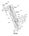
- FIG. 14Ais an artist's impression of a first aspect of a HMD implement of the invention.
- FIG. 14Bis an artist's impression of a second aspect of a HMD implement of the invention.
- FIG. 14Cis an artist's impression of a third aspect of a HMD implement of the invention.
- FIG. 15is a schematic cross section view of a wedged profile waveguide grating used in one embodiment.
- FIG. 16is a schematic side elevation view of one embodiment.
- FIG. 17is chart shown diffraction efficiency versus angle characteristics of one embodiment.
- FIG. 18is a schematic side elevation view of one embodiment.
- FIG. 19Ais a schematic side elevation view showing a first operational state of one embodiment.
- FIG. 19Bis a schematic side elevation view showing a second operational state of one embodiment.
- FIG. 20Ais a schematic side elevation view showing a first operational state of an input image node in one embodiment.
- FIG. 20Bis a schematic side elevation view showing a second operational state of an input image node in one embodiment.
- FIG. 21is a schematic plan view of a HBE containing slanted grating stripes.
- FIG. 22is a schematic three dimensional view of one embodiment using a HBE containing slanted grating stripes.
- FIG. 23Ais a schematic side elevation view showing a first operational state of a HUD provided by one embodiment.
- FIG. 23Bis a schematic side elevation view showing a second operational state of a HUD provided by one embodiment.
- FIG. 24is a schematic side elevation view of a HUD provided by one embodiment.
- FIG. 25is a schematic side elevation view of a HUD provided by one embodiment.
- FIG. 26is a schematic illustration of a prior art collimated image display.
- FIG. 27is a schematic side elevation view of a HUD according to the principles of the invention.
- FIG. 28is a schematic side elevation view of a holographic mirror.
- FIG. 29is a schematic side elevation view of a HUD provided by one embodiment.
- FIG. 30is a schematic side elevation view of a HUD provided by one embodiment.
- FIG. 31is a schematic side elevation view of a HUD provided by one embodiment.
- FIG. 32Ais a three dimension view of a color display provided by one embodiment.
- FIG. 32Bis a chart showing the spectral characteristics of a light source used in a color display provided by one embodiment.
- FIG. 32Cis a table showing the spectral characteristics of a light source used in a color display provided by one embodiment.
- FIG. 33is a cross sectional view of a HUD integrated in a windscreen in one embodiments of the invention.
- FIG. 34is a cross sectional view of a HUD integrated in a windscreen in one embodiments of the invention.
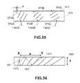
- FIG. 35is a three dimensional view of a display provided by one embodiment.
- FIG. 36is a three dimensional view of a display provided by one embodiment.
- FIG. 37is a schematic side elevation view of a color display provided by one embodiment.
- FIG. 38is a schematic three dimensional view of a color display provided by one embodiment.
- FIG. 39Ais a schematic side elevation view of one embodiment.
- FIG. 39Bis a schematic front elevation view of one embodiment.
- FIG. 40is a cross sectional view of a HUD integrated in a windscreen in one embodiment.
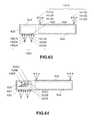
- FIG. 41is a flow chart illustrating image formation in a HUD in one embodiment.
- FIG. 42Ais a chart show a first diffraction efficiency versus angle characteristic of a multiplexed DigiLens in one embodiment.
- FIG. 42Bis a chart show a second diffraction efficiency versus angle characteristic of a multiplexed DigiLens in one embodiment.
- FIG. 43is a schematic three dimensional view of a color multiplexed display in one embodiment.
- FIG. 44is a schematic side elevation view of a DigiLens used in a color multiplexed display in one embodiment.
- FIG. 45is a three dimensional illustration of an embodiment of a display in one embodiment in which there are provided three HBE waveguides and three DigiLens waveguides.
- FIG. 46is a schematic side elevation view showing the formation of a projected stop by the IIN.
- FIG. 47is a schematic plan view illustrating the coupling of light from the IIN into the HBE waveguide.
- FIG. 48shows a detail of the HBE waveguide of FIG. 47 .
- the image input endillustrating the interaction of the beam with the gratings.
- FIG. 49is a schematic cross-sectional view of a four layer HBE in one embodiment.
- FIG. 50is a table showing the gratings used in the embodiment of FIG. 49 .
- FIG. 51is a chart showing overlapping DE versus angle profiles in the embodiment of FIG. 49 .
- FIG. 52is a three dimensional view of a wedge SBG grating in one embodiment.
- FIG. 53Ais a schematic illustration of a first operational state of the HBE in one embodiment.
- FIG. 53Bis a schematic illustration of a second operational state of the HBE in one embodiment.
- FIG. 53Cis a schematic illustration of a third operational state of the HBE in one embodiment.
- FIGS. 54A-54Billustrate projection schemes in one embodiment that do not result in a projected pupil of the type discussed earlier in the description; the pupil may be formed inside the projection lens ( FIG. 54A ) or before the projection lens using the aperture 562 ( FIG. 54B ).
- FIG. 55shows a schematic illustration of the use of rolled k-vector gratings to maximize the peak DE of in-couple light in one embodiment.
- FIG. 56shows a schematic illustration showing the propagation of a typical ray through a waveguide section 580 containing rolled k-vector gratings in one embodiment.
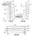
- FIG. 57shows a plan view showing the HBE 590 and the VBE 591 in one embodiment.
- FIG. 58shows a schematic side elevation view of the HBE and the VBE in one embodiment.
- FIG. 59shows an unfolded view of the HBE showing the beam propagation inside the waveguide in one embodiment.
- FIG. 60illustrates an apparatus for fabricating the HBE using a contact copying process in one embodiment.
- FIGS. 62A-62Cillustrate the generation of the conic section from a cone of tip 620 and base 621 ; the cone is shown in side view in FIG. 62A and in-front view in FIG. 62B ; a view of the cut out optics projected from the base along the cut line is shown in FIG. 62C .
- FIG. 63shows the basic architecture of a waveguide in one embodiment.
- FIG. 64is an illustration of a waveguide in which the input gratings 635 A- 635 C are stacked. Each grating has a unique k-vector 636 A- 636 C in one embodiment.
- FIG. 65shows that the input gratings are disposed adjacent to each other along the waveguide propagation direction in one embodiment.
- FIG. 66illustrates that the principles illustrated in FIGS. 64-65 may also be applied in the output grating in one embodiment.
- FIG. 67shows a flow chart describing a process of one embodiment.
- FIG. 68shows a ray trace of a monochromatic version of the design in one embodiment.
- FIG. 69shows the approximate dimensions of the IIN of FIG. 63 in one embodiment.
- FIG. 70provides unfolded views of the optical layout of FIG. 64 in one embodiment.
- FIGS. 71A and 71Billustrate the formation of a projected stop inside the HBE in one embodiment using a simplified thin lens representation of the microdisplay projection optics.
- FIG. 72illustrates one embodiment, in which the HBE that comprises a coupling grating at its input end and alternating SBG stripes of two different prescription, is inclined at 45 degrees.
- FIG. 73illustrates beam propagation from the IIN through a single layer of the DigiLens showing the four changes in direction that occur along the path to the exit pupil in one embodiment.
- FIG. 74shows plan view of the near eye geometry of the proposed helmet mounted display in one embodiment.
- FIG. 75shows side view of the near eye geometry of the proposed helmet mounted display in one embodiment.
- FIG. 76shows front view of the near eye geometry of the proposed helmet mounted display in one embodiment.
- FIG. 77shows the relationship of the DigiLens® aperture to the FOV, eye relief and eye box in one embodiment.
- FIG. 78shows partial binocular overlap in one embodiment.
- FIG. 79shows partial binocular overlap in another embodiment.
- FIG. 80shows a transparent waveguide display in one embodiment.
- the present inventionis made possible by two fundamental properties of SBGs that have not been exploited to date firstly the relatively wide angular bandwidth of Bragg gratings in the plane orthogonal to the plane of diffraction and secondly the wide angular bandwidths resulting from making SBGs very thin.
- the constraints of limiting the size of FOV tiles to around 10° ⁇ 10°does not apply in this instance, thereby leading to the tessellation approach discussed above. Fewer bigger tiles may now be used as a result.
- the needed FOVmay be divided into two tiles with one DigiLens for each. Other numbers of tiles may also be possible. With respect to the optical design this new approach may minimize, if not eliminate entirely, the problem of illumination ripple.
- a passive SBGis no different from a switching SDBG in terms of its HPDLC formulation and recording process. The only difference is that no electrodes are needed.
- the diffracting properties of an SBGare normally specified in the tangential plane.
- the tangential planeis the plane containing the incident and diffracted ray vectors and the grating vector. Following geometrical optical theory the plane orthogonal to the tangential plane is referred to as the sagittal plane.
- FIG. 1illustrates the basic geometrical optics of a transmission SBG 90 containing slanted fringes such as 91 with grating vectors K aligned normal to the fringes.
- the a multiplicity of input and output rayswill satisfy the Bragg condition provided the angles between the incident rays and the k-vector diffracted rays and the K-vector satisfy the Bragg equation.
- reasonably high diffractionwill be obtain for off-Bragg angles having a small angular or wavelength deviation from the on-Bragg ray directions).
- these off-Bragg raysare illustrated by the ray cones 902 , 903 surrounding the on-Bragg (lying in the in-plane of the drawing) rays 900 , 901 .
- the locus of the on-Bragg ray-fringe interceptsis the circle 904 .
- rays 905 , 906will also be on-Bragg. From consideration of the geometry of FIG. 1A it should be apartment that the Bragg diffraction angular bandwidth in the tangential plane is limited by the projections of the cones 902 , 903 onto the tangential plane. However, turning to FIG.
- ABSeffective angular bandwidth
- the sagittal bandwidthis mainly limited by the TIR angle constraints set by the waveguide.
- angular bandwidth of Bragg gratingstypically around 4 ⁇ the tangential bandwidth
- current horizontal FOV targetsmay be achieved for most display applications.
- the bandwidthis only limited only by TIR angle range that can be sustained in the waveguide.
- SBG gratingsprovide very wide angular bandwidths.
- An experimental SBG waveguide made using a low index modulation SBG Reactive Monomer Liquid Crystal Mix (RMLCM) formulationhas been shown to have a FWHM bandwidth of 21° with a 1 micron thick SBG layer.
- RLCMReactive Monomer Liquid Crystal Mix
- gratingswhich should generally be understood to mean a Bragg grating and desirably a SBG.
- SBGswill be operated in their normal switching mode as described above. However, in some cases SBGs will be used in a passive (e.g., completely passive) mode that is they will not be switchable.
- a non switching SBGis superior to a conventional passive hologram for the reason that the LC component of the HPDLC entangles much higher refractive index modulations than can be achieved in conventional holographic photopolymers.
- the displaywill use a mixture of switching and non switching SBGs.
- the DigiLens output gratingswill always be passive (non-switching), however. In one particular class of embodiments the displays will use all passive SBGs.
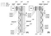
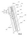
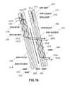
- the DigiLens®which provides a thin highly transparent eye piece (or HUD combiner) comprises two waveguides 101 , 102 for projecting the upper and lower halves of the field of view into the eye box (not shown).
- the waveguideseach comprise non switchable SBG layers sandwiched between transparent substrates.
- Each waveguidehas a switchable input grating and a non switching (passive) output grating labelled as DIGI-I1, DIGI-O1 and DIGI-I2, DIGI-O2 which are also indicated by the numerals 107 , 109 and 108 , 110 respectively.
- the waveguidesare separated by a Half Wave Film (HWF) 106 .
- HWFHalf Wave Film
- An input image node (IIN) 103which will be discussed later contains the microdisplay, laser module, beam expansion, collimation and relay optics. Schematic side elevation views are provided in FIGS. 2A-2B and a front elevation in FIG. 2C .
- FIGS. 2A-2Bindicate the ray paths from the IIN through the DigiLens layers for the two switched states of the display. In the first state the grating DIGI-I1 is active and diffracts incident P-polarised light 1000 from the IIN 103 into the TIR path 1001 .
- the TIR lightis diffracted out of the waveguide along its light as indicated by 1002 .
- the output gratingis lossy, that is the diffraction efficiency is significantly less than unity such that a portion of the guide light gets diffracted out at each beam-grating interaction.
- the remaining lightcontinues to undergo repeated TIR and diffraction until all of the light has been extracted from the waveguide.
- Uniform illumination across the output apertureis achieved by careful optimisation of diffraction efficiency (which depends on the refractive index modulation, grating thickness and other parameters). In general low diffraction efficiency is needed at the end of the waveguide nearest the IIN and the highest efficiency at the extreme end. Note that due to lossy extraction more peak energy (at 0°) is coupled into the DigiLens than at higher angles.
- lossy gratingis employed in some embodiments, the phrase encompasses “lossy waveguide. Not to be bound by any theory, but this is because the “lossy” may be due to a combination not the grating efficiency and waveguiding action that may result in the uniform loss along the waveguide.
- the diffracted light 1002has its polarisation rotated through 90 degrees (becoming S-polarised) by the HWF and therefore passes the second waveguide 102 without deviation since SBGs have relative low DE for S-polarised light.
- one DigiLens® layeremits S-polarized light while the other emits P-polarised light.
- each SBG layeris P-diffracting.
- the Horizontal Beam Expanderindicated by the labels HBE1, HBE2 (also referenced by the numerals ( 104 , 105 ) is a multilayer SBG waveguide using lossy high ABW gratings to expand the image light across a large pupil.
- the HBEruns along the top edge of the DigiLens.
- the HBEwill be discussed in more detail later. Note that air gap between the front and rear DigiLens® elements. This may be replaced by a suitable low (near unity) index material.
- the output image lightis a mixture of P and S polarized light it may be necessary to mount a quarter wave film on the output surface of the DigiLens for compatibility with Polaroid type eye ware which would otherwise result in the loss of half of the field of view.
- each of the three grating componentsmay contain multiple gratings stack in layers, disposed adjacently in a single layer or holographically multiplexed in a single layer.
- the basic building block of the displaysdiscloses is a waveguide containing a grating, normally a Bragg grating.
- the functioncan in certain embodiments be accomplished with as few as one waveguide layer. However the number of waveguide layers will depend on the size of field of view and the color needed.
- the gratingmay be switchable (SBG) or it may be passive, that is, non switchable. Although in principle, any type of Bragg grating may be used to provide a passive grating.
- SBG materialhas the advantage that the mixture of LC and polymer affords higher refractive index modulation than that of conventional holographic polymer materials.
- in the output waveguide componentuses only non tessellated passive gratings. This minimizes the potential problems of scatter from electrodes and illumination non uniformities.
- T term gratingis employed to refer to a Bragg grating unless otherwise specified. Passive grating means a grating that is not electrically switched.
- the displayis shown in more detail in FIGS. 3-4 .
- HMDcollimated display
- the initial focusis on the monochrome version of the design.
- the monochrome and color implementations of the HWDare very similar.
- an important differenceis that the monochrome architecture can be achieved with fewer waveguiding layers and the possibility of using some passive grating components in the IIN and HBE, while a color implementation needs most components of the IIN and HBE to be switchable owing to the greater difficulty of managing the angular content of red, green and blue optical channels simultaneously.
- the DigiLens®remains a passive component.
- While the present inventionhas many applications in the field of transparent visual displays it is first considered one particular application namely a Helmet Mounted Display for Augmented Reality (AR) application.
- the objective in this caseis to meet the 52° H ⁇ 30° V monocular field of view specification while achieving all of our original goals of high transparency, high resolution, ultra compact (thin) form factor, light weight and generous exit pupil.
- the target specificationsare summarized in Table 1.
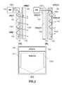
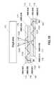
- the important components of the displayare illustrated in the schematic three dimensional drawing of FIG. 3 and the side elevation view of FIG. 4 .
- the displaysplits the FOV into upper and lower FOV tiles (referred to by the numerals 1 , 2 in the drawing labelling) Note that the waveguide substrates of the DigiLens and HBE components have not been shown in order to simplify the explanation.
- the displaycomprises a DigiLens® comprised of two waveguide layers sandwiching a HWF is split into input and output components DIGI-I and DIGI-O. Note that wide sagittal angular bandwidth of SBGs removes the need to tile horizontally.
- Two Horizontal Beam Expanders HBEeach comprising input gratings HBE-I and output gratings HBE-O are provided.
- the expanded output light from HBE-O1enters the first DigiLens waveguide via DIGI-I11 and similarly for the second waveguide.
- DIGI-I11The expanded output light from HBE-O1 enters the first DigiLens waveguide via DIGI-I11 and similarly for the second waveguide.
- the above componentsare also referenced by numerals 130 - 145 in FIGS. 3-4 .
- Two IINare provided: one for the upper FOV and one for the lower FOV.
- the display panel in each IINis a 1080p 5 mm ⁇ 3 mm LCoS devices.
- One laser modulemay be used to illuminate both display panels.
- the inventiondoes not place any restriction on the number of microdisplays to be used. A single microdisplay with a fast enough refresh rate and high enough resolution is likely to be sufficient for all but the most demanding display applications.
- the DIGI-Iis the most challenging grating in the system since it needs high input coupling efficiency at the projected pupil output point from the HBE-O, across the full angular range.
- the DIGI-I gratingsswitch, sampling the 52° horizontal ⁇ 30° vertical field output by the HBE-O into the two DigiLens waveguides. It is desirable that this grating needs a high angular bandwidth and high DE.
- the DIGI-Icomprises 2 SBGs each operating over 8.5° angular bandwidths overlapping to provide at least 15°. DIGI-I uses two 3 micron SBGs of DE approximately 87% with angular bandwidth of 8.5°-9.0° in air.
- DIGI-I1provides 52° horizontal ⁇ 15° vertical
- DIGI-I2provides 52° horizontal x+15° vertical.
- All gratings in the DIGI-Oare passive, and therefore can be thin gratings. One of each pair is for red and the other for blue/green.
- DIGI-O1the rear grating providing the lower 15°
- the front grating DIGI-O2providing the upper 15° giving a total 52° horizontal ⁇ 30° vertical.
- the DigiLens®is tilted at a rake angle of ⁇ 8-10°. This is found from ray-tracing analysis to give better DE than simply projecting image light normally into the DigiLens®.
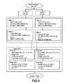
- FIG. 5A flow chart representing the interaction between the IIN, HBE and DigiLens in the image formation process is provided in FIG. 5 . Since diffractive optical elements are dispersive it usually desirable where more than one grating is combined to configured them in a complementary fashion such that the dispersions introduced by the gratings cancel. Complementarily is normally achieved by designing the gratings to have the same grating pitch (that is, the spatial frequencies of the intersections of the Bragg gratings with the substrates are identical). It should be noted that HBE-I2 and HBE-O2 need to be complementary in the embodiment described above. However, HBE-I1 and HBE-I2 do not need to be complementary.
- the HWF between the DigiLens waveguides(overlapping the DIGI-O gratings) is removed and a HWD is inserted in the spaced between the DigiLens DIGI-I input gratings.
- the air gap left by the HWPmay be filled with a low index nanoporous material.
- Quarter Wavelength Film (QWF)is applied to opposing faces 157 , 158 of the front and rear waveguides with the effect that each TIR bounce results in a 90° polarization rotation allowing an approximately ⁇ 4 thinner grating and no interaction between the front and rear DigiLens®.
- QWFQuarter Wavelength Film
- FIG. 7shows the propagation of upper and lower FOV light in the two DigiLens waveguides as represented by the ray paths 1010 , 1012 , 1014 in the first waveguide and 1011 , 1013 , 1015
- the components shown in FIGS. 6-7are also referenced by the numerals 150 - 159 .
- FIG. 8is a view of one of the DigiLens waveguides 160 illustrating the function of the QWF layer 162 in more detail.
- Input light from the HBE 1020is deflected into the TIR path 1021 by the DIGI-I grating 161 . Rays such as 1022 incident on the QWF coating have their polarization converted from P to circularly polarized light of a first sense.
- the polarizationremains circular but in an opposing sense such that after passing through the QWF the second time the light emerges as S-polarized 1023 .
- the S lightis not diffracted by the SBG and therefore continues to undergo TIR.
- P polarized light 1024On the next reflection at the QWF film the light is converted to P polarized light 1024 , which is off-Bragg with respect to DIGI-I and so does nor get diffracted back towards the HBE.
- the TIR of the beamthen proceeds onto the DIGI-O grating where it is progressively extracted from the waveguide as described above.
- the two stacked DIGI-I gratingsmay be provided in each DigiLens waveguide to increase the angular bandwidth.
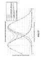
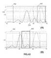
- FIG. 9is a chart showing the effect of combining the individual DE angular bandwidths to create upper and lower FOVs of approximately 15 degrees (FWHM) in air using two gratings of angular bandwidth 8.5 degrees (FWHM) in air.
- the DigiLenscould comprised more layers, for example 3 DIGI-I layers combined with 2 DIGI-I layers in each waveguide. Note that DIGI-I and DIGI-O gratings do no need to be co-planar. However in fabrication terms it is advantageous to limit the number of grating, substrate, electrode layers and low index material layers to minimize material costs and process steps.
- FIG. 10shows the HBEs in cross section in relation to the DigiLens 170 .
- the HBEsare coupled to the DigiLens 170
- Two IINsIIN1 and IIN2
- the paths of light from the IIN to the DigiLensare indicated by rays 1030 , 1031 , 1034 and 1032 , 1033 , 1035 . Note the components are also reference by numerals 170 - 183 .
- Each LCoSprovides a FOV of 26° H ⁇ 30° V.
- Each HBE-Icontains three gratings that operate on P-polarized light in 8.5° ABW steps to provide the 26° half horizontal field. The 30° field will couple in its entirety owing to the much increased ABW in the sagittal plane.
- the HBE-I SBGsare thick gratings allowing high DE but narrow ABW.
- the gratingsare typically of thickness 1-2 micron and lossy such that light is extracted with uniform efficiency along the length of the grating. Lossy gratings have large ABW and low DE.
- the gratings of HBE-I1 and HBE-I2do not need to be complementary (i.e. chromatic dispersion correcting).
- Gratings of HBE-I1 and HBE-O1(as well as HBE-I2 and HBE-O2) need to be complementary.
- a passive HBE-Ia single unswitched grating needs to be thin to achieve higher angular bandwidth. With current materials roughly 30% peak DE with current materials, and 60% is within the range of expected material improvements may be achieved.
- FIGS. 12-13provide a walkthrough of the process of projecting image light from one (left eye) IIN into the eyebox providing ⁇ 15° vertical and 0°-26° horizontal field of view.
- the componentsare identical to the ones shown in FIGS. 3-4 .
- FIG. 12Aillustrates the path 1040 from the LCoS panel to the output of the IIN.
- FIG. 12Bshows the light path through the HBE indicating the TIR path 1042 within one of the waveguides and light extraction 1043 along its length.
- FIG. 13Ashows the coupling of light 1044 extracted from the HBE into the DigiLens (vie DIGI-I).
- FIG. 13Bshows the downward propagation of light 1045 in the DigiLens with the output put image light 1046 providing the lower half of the FOV.
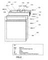
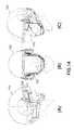
- FIGS. 14A-14Cshows three 3D views of the above invention implemented in a HMD 190 .
- Threes difference perspectives 191 - 193are shown.
- the display moduleincludes a horizontal hinge 194 .
- the userIn the deployed position, the user will have full panoramic see-through with high transparency.
- the userIn the stowed position, the user will be free to use range finders, night-vision systems, or other such equipment.
- spectacle wearersare accommodated and the design will can also accommodate the use of Polaroid eyewear.
- a simple display retracting mechanismallows the display to be hidden in a compact module under the brow of the helmet when not in use.
- the display when not in useis retracted vertically into the helmet.
- the currently preferred implementationuses a custom helmet is linked to a belt pack via an umbilical fiber-optic communications link and power supply connection. In training applications the belt pack would be wirelessly linked to the training center.
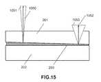
- the gratings used in one or both of the HBE and DigiLenswill have a tailored DE profile achieved by varying the thickness of the gratings along the propagation direction as shown in FIG. 15 .
- the wedge grating 203is provided by including a small wedge in of the grating substrates 201 .
- the second substrate 202may be rectangular.
- Other ways of achieving wedge gratingswill be apparent to those skilled in the art of optics. Where two stacked gratings are used the DE profiles of the two gratings would run in opposing directions.
- the grating thicknessmay vary from 1.0-1.2 micron up to 2.8-3.0 micron, the lower thickness producing the largest bandwidth 1052 and lowest DE for a given output direction 1053 .
- the higher thicknessproduces the lowest bandwidth 1050 and higher DE for a given output direction 1051 .
- the wedge anglesare tiny and will have minimal impact on illumination uniformity and image quality.
- a refractive index of approximately 1.585is needed to support waveguide TIR angles typically not greater than 70° with respect to the TIR surface.
- Higher angles(approximately 85°) can lead to image fold over where gratings are designed to provide very high angular bandwidth.
- Polycarbonateswill enable a TIR angles up to approximately 72°.
- FIG. 16illustrates a DigiLens used in an embodiment of the invention for color displays comprising two DigiLens doublet waveguides. Each doublet waveguide is similar to the embodiments of FIGS. 6-7 .
- each DigiLens waveguide doubletone of the waveguides operates on red light and the second one operates on a mixture of blue and green light.
- the red gratingis placed after the B/G grating, i.e. closer to the eye.
- the input and output DigiLens gratingsare represented by DIGI-IR and DIGI-OR in the case of the red doublet and DIGI-IB/G and DIGI-OB/G in the case of the blue/green doublet.
- the output grating portions of the waveguidessandwich a HWF.
- the input grating portionsmay sandwich an air gap as illustrated or preferably a low index material.
- QWFsare applied to the opposing face of the waveguides in each doublet.
- the componentsare also labelled by numerals 210 - 227 .
- the red and blue/green waveguidesare optically separated by air or a low index (near unity) material such as mesoporous silica which are not illustrated but will be described later.
- a HWFconverts the rear output from P to S. As SBG gratings are P-sensitive, this prevents re-coupling of the light with gratings in front.
- the rake angle (8-10°)affords higher angular bandwidth, and lower chromatic dispersion enabling shared blue/green gratings. In most cases color imaging may need high index substrates and special coatings for enhancing the blue TIR angular range.
- the ray paths for red lightare indicated by the rays 1071 , 1073 , 1075 .
- the ray paths for the blue/green lightare indicated by 1070 , 1072 , 1074 .
- some of this lightwill couple into the second waveguide doublet, that is the light paths indicated by 1076 , 1078 (blue/green) and 1077 , 1079 (red).
- the risk of light diffracted from the rear waveguide interacting with the light on the layer above and coupling back into the waveguideis avoided in our HMD design.
- the red and blue/green gratingsdo not cross-couple due to the polarization management. Each color channel can cross couple with itself.
- a HWPcan be introduced at one layer in the passive waveguide stack.
- a half wave retarder layerconverts the rear output light from P to S.
- the SBG gratingsare P-sensitive only, and so this prevents re-coupling of the light with gratings in front.
- a 10° rake anglealleviates demands on grating prescription affording higher ABW and lower chromatic dispersion. This enables shared blue/green gratings. However, in most embodiments of the invention red may need a separate grating.
- the graph in FIG. 17shows calculated DE versus angles for each grating and the output DE for the layer minus the light coupled back into TIR. It is assumed that this light is not coupled back out again.
- the composite output of the gratings including the single interaction coupling lossis represented by circular symbols. Note that with the 2*1/e offset of the peak DE profile, and accounting for re-coupling effects of the rear grating into the front grating, that an effective doubling in the FWHM of a single grating is achieved. With secondary output coupling of re-coupled light, the profile will approach the lossless composite grating profile (triangular symbols).
- FIG. 18shows a further embodiment of the invention for color image.
- the DigiLenscomprises two separated monochromatic doublet waveguides 230 , 231 one for red (DIGI-O1A,DIGI-O1B) and one for blue-green (DIGI-O2A,DIGI-O2B).
- the input SBGs(DIGI1A-1D, DIGI2A-2D) comprising a stack of four monochromatic red or blue-green gratings indicated by A-D.
- HWF and QWFsare disposed as in FIG. 16 .
- the doubletsmay be air separated or may sandwich a low index material.
- the componentsare also labelled by the numerals 230 - 246 .
- each DigiLens waveguidecomprises a single SBG layer that supports red, green and blue TIR.
- the pathsare illustrated by numerals 1080 , 1082 , 1083 in the first waveguide 250 and 1081 , 1084 , 1085 in the second waveguide 251 .
- the red, green and blue pathsare referenced by characters R, G, B.
- the system componentsare labelled as in FIG. 1 and additionally referenced in FIG. 19 by the numerals 250 - 258 . It should be appreciated that such an implementation of the invention needs careful control of the TIR angles to ensure that the diffracted light paths for the three colors overlap exactly. The inventors have found that additional coatings may be needed to improve the reflection at the blue end of the spectrum.
- the DIGI-O gratingscould be implements as a multiplexed grating.
- the optical systemcomprises a waveguide 260 containing overlapping SBG elements 261 , 262 , overlapping SBG elements 263 , 264 a beam splitter layer 265 a curved mirror 266 , a prism 267 a projection lens 268 and a microdisplay panel 269 .
- An air gap 270 between the curved mirror elementsis provided to enable TIR of reflected light.
- separate SBG input and output gratingsare provided for each image field.
- the waveguide 260 and the gratings 263 , 264in particular may provide the input gratings of the HBE. Alternatively it waveguide 260 may be used to couple light into the input grating of the HBE.
- the IINmay be configured in many different ways to satisfy constraints of space, cost and optical efficiency.
- half the image from the microdisplayis imaged into the HBE sequentially.
- the gratings 261 , 264are in their active state and the others are inactive.
- Light from the image portion 1090is projected into the path 1091 by the projection lens. It is then reflected by the prism into the ray path 1092 reflected at the curved mirror 266 into the path 1093 diffractive by grating 261 into the path 1094 undergoes TIR into the path 1095 and is diffracted out of the waveguide by the grating 264 .
- FIG. 20Billustrate the light paths from the second image field 1097 .
- the gratings 261 , 264are switched to their inactive states and gratings 262 , 263 are switched to their active states.
- the path from the microdisplaysis indicated by 1098 - 1104 .
- the IINcouples the entire image into the HBE. However, splitting the input image into two enables more optimal coupling of the image into waveguide paths.
- monochrome implementationsOnly. Initial design calculation by the inventors show that the fundamental approach is sound, meeting near diffraction limited performance across the field in a compact design form while including features such as projected pupil (20 mm. ahead of the grating coupling point), telecentricity, a re-imaged stop and less than 2% geometric distortion.
- the design wavelength for the monochrome implementation of the IINis 532 nm.
- the resolutionis matched to 1080p LCoS vertically (LCoS pixel pitch: 2.8 micron; Nyquist frequency 178 lp/mm.). Note that a feature of the design is that IIN/HBE can be located on the same side of the waveguide as the eye without compromising grating reciprocity.
- Lightis projected from each LCoS at F/2.8 (focal length: 5.65 mm.) to provide a FOV of 26° H ⁇ 30° V.
- Lightenters the HBE-I grating at angles from 0° to +26°.
- the IINis inclined at angle of 13°.
- angular thisincreases angular bandwidth is increased by approximately 20%.
- red colored rays in FIG. 13strike the HBE-I at 0°, and diffract into TIR.
- the green colored raysstrike the SBG at approximately 26°/n where the refractive index n is 1.592 (polycarbonate).
- S-BAL25 glasswhich has a very similar refractive index to polycarbonate can be used for prototyping.
- the designcan be extended to two and three colors.
- Initial resultsshow that the fundamental approach is sound, meeting near diffraction limited performance across the field in a compact design form while including features such as projected pupil (20 mm. ahead of the grating coupling point), telecentricity, a re-imaged stop and less than 2% geometric distortion.
- the design wavelengthis 532 nm.
- the resolutionis matched to 1080p LCoS vertically (LCoS pixel pitch: 2.8 micron; Nyquist frequency 178 lp/mm.).
- Preliminary specifications for the IINare provided in Table 2.
- Input Image Node (IIN) SpecificationInput Image Node (IIN) Optical Specification Glass Polycarbonate (can use S-BAL25 glass for prototyping).
- Image FormatLCoS aspect ratio of 3:2 in portrait. Pupil Diameter 2 mm. projected pupil (20 mm. ahead of the grating coupling point) LCoS FOV of 26° H ⁇ 30° V; F/2.8; focal length 5.65 mm. Projection Lens Color Monochrome 532 nm. (proof-of-design); extendable to color. Resolution Near diffraction limited across the field; matched to 1080 p LCoS vertical pixel pitch: 2.8 micron; Nyquist frequency 178 line pair/mm.). Geometric ⁇ 2%. Distortion Telecentricity Fully telecentric.
- a projected stopis provided.
- the benefits of a projected stopare decreased waveguide thickness.
- the stopis projected midway up the HBE to minimize aperture diameter within the waveguides, and hence minimizing the aperture width of the DigiLens waveguide coupler.
- a graduated reflection profile underneath the SBG layeris used to control (or assist) with grating DE variation along length of the DigiLens waveguides. This normally achieved in SBG grating using index modulation. This may offer advantages the HBE where a low percentage of light is out coupled in 1 st bounce, but high percentage is coupled out at the other end of the waveguide.
- the volume of the IIN designis currently ⁇ 20 ⁇ 40 cubic mm.
- the refractive elements of the designsuch as the bird bath mirror and the projection lens system could be replaced by diffractive optical elements.
- An SBG waveguidecould be introduced in front of the microdisplay to provide a polarizing grating beamsplitter for illuminating the microdisplay and allowing polarization rotated reflected light to proceed through said wave guided towards the curved mirror.
- a HBE 281comprises a coupling grating 283 (e.g., the HBE-I of the earlier embodiments) at its input end and an output grating (e.g., the HBE-O) comprising alternating SBG stripes of two different prescription 284 , 285 inclined at typically 45 degrees.
- an output gratinge.g., the HBE-O
- FIG. 22shows the HBE integrated in a display with a DigiLens 287 comprising DIGI-I 288 and DIGI-O 289 and an IIN 286 .
- the ray paths from the IINare indicated by 1105 - 1110 where the TIR paths in the HBE and DIGI-O are indicated by 1107 , 1109 .
- the light coupled output of the HBE into the DigiLens (DIGI-I)is indicated by 1108 .
- the output light from the display from the DIGI-Ois indicated by 1110 .
- FIG. 80provides a transparent waveguide display in another embodiment.
- the amplitude of the refractive index modulation in at least one of the input grating 8003 and output grating 8002varies by a small amount along the x direction.
- the input and output grating pitchesshould be identical to satisfy the reciprocity requirement.
- the index modulationmay also be varied in the z direction.
- the design of this embodimentmay help control the output light homogeneity.
- the principles illustrated in this embodimentmay be applied to the vertical and horizontal beam expanders.
- the index modulationmay be time-varied to adapt to temporal variations in the input image content.
- efficient waveguidingmay need that the TIR beams are confined between low index media. Air gaps are difficult to fabricate and maintain while the refractive indices of currently available low index materials such as Magnesium Fluoride (1.46) and Silicon Dioxide (1.39) are much too high to meet the tight TIR angle constraints needed in full color implementations of the HMD.
- the proposed solutionis to use nanoporous (Mesoporous Silicon) materials. Nanoporous materials (e.g., mesoporous Silicon) are currently being used in many optical applications including anti reflection coatings and planar optical waveguides. Their high porosity enables the fabrication of high-quality low-dielectric constant thin films.
- Nanoporous materialscan be fabricated in thin layers in a single coating step. To achieve very low, near unity, index the porosities need to be very high, approaching 95%. High transparency and low index can be achieved simultaneously with these films. Since they are highly efficient at absorbing water they must be carefully sealed against moisture. The best approach may be to seal the passive gratings, HWP and material together. SBG Labs is also investigating the potential role of nanoporous materials as high refractive index media. This would increase the range of TIR angles that can be sustained in our waveguides with potential for increasing the horizontal FOV from 40° to around 45°. Nanoporous materials are currently being used in many optical applications including anti reflection coatings and planar optical waveguides.
- Nanoporous materialscan be fabricated in single coating step. Alternatively graded index multi layer architectures can be used. SBG Labs is also investigating the potential role of nanoporous materials as high refractive index media. This would increase the range of TIR angles that can be sustained in our waveguides.
- the chief benefitsare a monolithic structure will provide greater mechanical stability and durability and better beam confinement leading to higher FOV.
- the inventionmay be used in many different applications. Some embodiments of the invention directed specifically at automobile HUDs will be discussed in the following paragraphs.
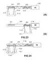
- FIG. 23is a is a schematic side elevation view of an in car HUD 300 with more than one exit pupil integrating DigiLens waveguides for the driver 301 and passenger 302 .
- the displaymay be based on any of the embodiments described above.
- the DigiLens elementsare integrated within a common waveguide structure with the input imagery being produced by an IIN 303 as described above.
- the ray paths to the driver exit pupilare indicated by the rays 1110 - 1113 with the pupil indicated by 1113 .
- the ray paths to the passenger exit pupilare indicated by the rays 1114 - 1116 with the pupil indicated by 1117 .
- FIG. 25is a schematic side elevation view of a show an embodiment of the invention similar to the one of FIG. 23 the exit pupil of the driver display is tiled using multiple overlapping DigiLens elements 305 , 306 to provide the abutting exit pupils 1120 , 1121 . Ray paths to the pupil are indicated by 1118 - 1120 .
- FIG. 25is a schematic side elevation view of a further embodiment of the invention based on the one of FIG. 23 in which overlapping DigiLens elements 311 , 312 are used to tile the FOV as indicated by 1131 with the abutting field of view tiles 1132 while providing a common exit pupil 1133 .
- waveguide a DigiLensmay be used to form a pixelated collimated image.
- a simple classical analogue of such a displaywhich is shown in the schematic side elevation view of FIG. 26 comprises a pixelated display panel 321 located at the focal surface of a collimating lens 320 .
- a waveguide holographic version of this displayis shown in FIG. 27 .
- the input imageis provided by a pixelated SBG 323 comprising a two dimensional array of switchable elements such as the one labelled by 324 . Each element diffracts incident collimated light into a TIR path within the waveguide.
- the SBG arrayis illuminated by collimated light indicated by 1142 , 1143 from an external source which is not shown.
- the pixel 324is illuminated by the collimated light 1145 .
- the SBG pixelswill have diffusing characteristics.
- the DigiLens elements 325 , 326are not simple planar gratings such as the ones described so far but have optical power such that light originating at points on the surface of the SBG array is collimated to provide switchable fields of view (FOV tiles) bounded by the rays 1146 , 1147 for viewing through a pupil 1148 .
- the DigiLens elementsprovided a diffractive analogue of the lens in FIG. 27A .
- the DigiLens elementsare configure to tile the FOV as in the embodiment of FIG. 25 .
- a DigiLens as described abovemay be configured to provide a mirror.
- FIG. 28shows how a rear view mirror for automotive applications can be provided using transmission SBG 333 sandwiched between the substrates 330 , 331 and a mirror coating 332 overlaying the DigiLens.
- the SBG diffraction anglesare designed such that light incident on the DigiLens following the path labelled by R1,R2 is diffracted by the SBG layer and reflected at the mirror layer while that the reflected path labelled R3,R4 leading to the drivers eyebox is off Bragg or, in other words, falls outside the angular range for diffraction by the SBG.
- the light pathsare also labelled by the numerals 1151 - 1154 . It should be apparent from consideration of FIG. 28 that the DigiLens can be configured to provide a range of different reflection angles by a suitable choice of grating prescription.
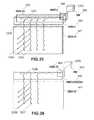
- FIG. 29shows a HUD 335 for relaying an external image to a viewing pupil near to the driver.
- Light 1155 from the external image sourceenters the waveguide via the DigiLens 338 undergoes TIR as indicated by 1156 - 1157 and is coupled out of the waveguide towards the viewer as light 1158 by DigiLens 336 .
- This embodimentmay be useful for viewing blind spots.
- the apparatus of FIG. 29further comprises a beam splitter layer 337 which, by splitting incident TIR light into multiple paths, can improve homogeneity and minimize gaps in the output illumination. This principle may be applied to any of the other embodiments of the invention.
- FIG. 30is a front elevation view of a car HUD 340 comprising a IIN 341 and a DigiLens 342 according to the principles of the invention and further comprises a structured light source 343 emitting infrared light 1159 and detector 344 for detecting return infrared light 1159 for sensing driver hand movements for display control.
- a structured light source 343emitting infrared light 1159 and detector 344 for detecting return infrared light 1159 for sensing driver hand movements for display control.
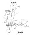
- FIG. 31is an embodiment of the invention similar to that of FIG. 26 in which the information contained in the field of view tiles (FOV Tile 1,2) is presented at different ranges indicated by D1,D2.
- Image light from the IIN 351is converted into wave guided light 1170 .
- the DigiLens 354forms an image at range D2 with an FOV of 1174 centered on the direction 1173 and the DigiLens 355 forms an image at D1 with FOV of 1171 centered on the direction 1172 .
- the two FOV tilesare viewed through the pupil 1175 .
- FIG. 32Aillustrates an embodiment of the invention in which SBGs are used to compensate for the spectral bandwidth of RGB LEDs in a color HUD.
- the red LED illustratedhas a peak output at 639 nm. and FWHM bandwidth defined at the wavelengths 634 nm. and 644 nm. as shown in FIG. 32B .
- the DigiLenscomprises a stack of RGB diffracting layers, each layer comprising input and output gratings.
- each layerthe SBGs are recorded to provide peak diffraction efficiency vs. wavelength characteristics (along the waveguide) shifted by small increments from the peak wavelength as indicated in the Table in FIG. 32C .
- the techniques for recording a Bragg grating that provides a wavelength shift in play back, which normally involve control of the construction wavelengths and recording angles,are well known to those skilled in the art of holography.
- the RGB SBG layersare switched sequentially and synchronously with the RGB LEDs. As shown in FIG.
- the color display 360comprises red green and blue DigiLens waveguides labelled by the symbols R, G, B and comprise DIGI-I gratings indicated by 360 R, 360 G, 360 B and DIGI-O gratings indicated by 361 R, 361 G, 361 B, red, green and blue light sources 362 R, 362 G, 362 B providing light 1180 a microdisplay 363 a beam expander comprising the diffractive or holographic lenses 364 , 365 for providing collimated light 1182 . After being coupled into the DigiLens elements the light undergoes TIR as described above and represented by 1183 and is diffracted out of the DigiLens as the red, green, blue light 1184 R, 1184 G, 1184 B.
- the DigiLensis combined with a windscreen.
- a DigiLensis eminently suitably for such an implementation as it can be designed to operate in a curved waveguide and can be built up from very thin layers using substrates as thin as 100 microns sandwiching SBG layers of thickness 1.8-3 microns.
- the DigiLensesare separated by thin layers of mesoporous materials of the type described above. It should also be noted that typical car windscreens have radii of curvature typically of several thousand mm which does not present a great challenge for maintaining waveguiding.
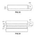
- the DigiLensis formed as a flexible layer 371 that can be bonded onto an existing windscreen 370 to the inner or exterior surfaces as shown in FIG. 33 .
- the IIN 372would typically be located below the dashboard.
- the DigiLens layerscan be integrated within a windscreen as part of the screen fabrication process as shown in FIG. 34 .
- a windscreencomprises an outer toughened glass layer 373 ; two or more layers of PVB 374 , 376 for UV blocking and an inner toughened Glass layer 377 .
- the DigiLens 375would be sandwiched by two of the PVB layers.
- the windscreen integrated DigiLens fabrication processesincludes the steps of spraying RMLCM onto polyvinylbutyrol (PVB) film and sandwiching it with a second PVB film prior to recording an SBG in a holographic recording step.
- PVBpolyvinylbutyrol
- a transparent displaycomprising the waveguide components DIGI-I.
- DIGI-O HBE-I, HBE-O and an IINsimilar to the ones described above.
- each said waveguide componentcomprises a single SBG layer.
- the ray paths from the IINare indicated by 1200 - 1203 include the TIR path in the HBE 1201 , the extraction of the expanded beam from the HBE 1202 , TIR within the DigiLens 1203 and extraction of light for display 1204 from the DigiLens.
- the componentsare also reference by the numerals 390 - 394 .
- FIG. 36there is provided a transparent display DIGI-O, HBE-I and an IIN similar to the ones described above.
- the two waveguide components HBE-O and DIGI-Iare combined into a single waveguide component labelled HBE-O/DIGI-I that performs the dual functions of beams expansion and beam turning.
- the advantage of this arrangementis the change in beam direction is accomplish without the need to exit and then re-enter the waveguide gratis as for example in FIG. 35 and most of the other embodiments. This may need that the gratin in the DIGI-I is slanted in the plane of the drawing, in most cases of practical interest at an angle of 45 degrees.
- the TIR pathis rotate through 90 degrees and proceed into the DIGI-O.
- the ray paths from the IINare indicated by 1205 - 1208 .
- the components of the displaysare also reference by the numerals 400 - 403 .
- the HBE-I and HBE-O and the DIGI-I and DIGI-Omay be implemented in a single SBG layer. However while this reduce the number of layers overall there is the penalty the overall size of the display will increase. The widths of the HBE and DIGI-O will to a large extend be terminated by the microdisplay dimensions and the field of view needed.
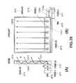
- the DigiLenscomprises separate red green and blue waveguides
- the waveguidesare optically isolated from each other which may need that they are air separated or separated by a thin layers of low index film.
- the preferred optionis to use nanoporous materials.
- the DigiLens waveguidesare shown in FIG. 37 the layers being referenced by numerals 1 - 3 in the DIGI-I and DIGI-O labels (the waveguide components also reference by numerals 415 - 420 .
- the IIN and HBE componentsare not shown in detail but are simply indicated by 421 .
- FIG. 3is a three dimension view of the same display shown the three DigiLens lens
- FIG. 38shows a color display based on the embodiment of FIG. 35 .
- This implementationhas three DigiLens layers 410 - 412 , one for each color, with the DIGI-I and HBE-I being combined in turning/beam expansion gratings such as the ones indicated by 436 red green and blue ray paths from the IIN are indicated by 1220 - 1223 with red, green and blue being labeled by the symbols R, G, B.
- the HBE-I componentwhich is not illustrated will be similar to the one shown in FIG. 35 but with separate layers for red, green a blue.
- FIG. 39there is provide a passive single SBG layer DigiLens which waveguides and diffracts at least two colors using holographic multiplexing. Multiplexing is the ability to record multiple Bragg gratings in the same layer.
- multiplexingmay be used to encode two distinct diffraction prescriptions which may be design to project light into distinct field of regions or diffract light of two different wavelengths into a give field of view region. Multiplexing also offers the significant benefit of reducing the number of layers in the waveguiding structure. Care is needed to ensure that there is no competition between gratings during recording leading to unequal Des and cross talk between gratings in playback.
- the apparatus of FIG. 39is similar to that of FIG.
- the DIGI-O componentis now a multiplexed grating.
- the componentsare also referenced by the numerals 470 - 474 and ray paths from the IIN through the HBE and DigiLens by numerals 1240 - 1243 .
- the Horizontal Beam Expanderwould run along bottom edge of the DigiLens® to enable the IIN to be hidden below the dashboard.
- a HUDwould have an eyebox of 145 mm. horizontal by 80 mm. vertical at an eye relief of 800-900 mm.
- the target field of viewwould be 10°-15° vertical ⁇ 10°-15° horizontal.
- the windscreenwould have a transparency greater than 75%.
- windscreenshave curvature of Horizontal: 3000 mm.; Vertical 9000 mm.
- the IINcould be accommodated within a volume of 1-2 liters.
- FIG. 40The integration of the DigiLens into the windscreen is shown in FIG. 40 .
- the stack of layers in the windscreencomprises Glass (External) 1.60 mm.; PVB (3 layers): 0.8 mm.; Glass (Internal): 2.0 mm. TOTAL 4.4 mm.
- the SBG layerwould comprise an SBG of 5 microns sandwiched by substrates of 50-100 microns, the SBG cell sandwiched by low index layers of 0.5-2 microns thickness.
- a UV glue gasket linelimits the SBG material fill, bounding the effective area of the display. Gaps between grating areas are filled with clear acrylic and UV-cured for full transparency.
- This multilayer architectureallows very strong lamination and does not rely at all on the SBG film for lamination strength.
- FIG. 41is a flow chart illustrating the implementation of the embodiment of FIG. 39 in an automobile HUD.
- the color multiplexing used in the embodiment of FIG. 39can be provided in two ways: firstly using two multiple gratings: for example, red and blue/green diffracting; or secondly using three multiplexed gratings: i.e. using multiplexed red green and blue gratings.
- the design problemis to determine the optimal prescription using two or more multiplexed gratings for a vertical (or more precisely tangential plane) field of 10 degrees.
- the design variablesare Bragg wavelengths and TIR angles for each color; DE profiles (i.e., grating thickness and modulation. Since the DigiLens will be bonded to or in some cases embedded with a windscreen the waveguides will be sandwiched by low index material (unless air gaps can be tolerated).
- a nanoporous material layer refractive index of 1.2has been assumed. For an SBG index of 1.52 this corresponds to a minimum TIR angle of 52 deg.
- special attentionmay be needed to achieve the shape of the DE profile is important and, in general, narrower DE profiles are preferred to avoid crosstalk between the colors.
- the desired DE profilescan be achieved by optimising the thickness and refractive modulation of the gratings. Simulated diffraction efficiency (DE) versus TIR angle profiles based on the Kogelnik diffraction theory for typical red, green and blue diffracting gratings multiplexed in a single SBG layer are shown in FIGS. 42A-42B .
- the curvesrepresent the DE profiles for each of the three multiplexed gratings.
- the rectangular regionsrepresent the approximate RGB TIR angle ranges.
- FIG. 42Ashows the case where the multiplexed grating is illuminated with red light.
- FIG. 42Bshows the case where green or blue light illuminates the grating. Note that the curves shift owing to the angles satisfying the Bragg condition shift as the illumination wavelength changes. Since the TIR range for the blue green band is below the TIR range for red, there is no cross talk between the two color bands.
- FIGS. 43-44illustrated a further embodiment of the invention comprising a IIN, two HBE components each comprising a HBE-I and HBE-O; two DigiLens components each comprising a DIGI-I, DIGI-O and beam splitter (B/S) the DIG-I sandwich a half wave film (HWF).
- FIG. 43shows a three dimension view.
- FIG. 44is a cross sectional view of the DigiLens only showing the ray paths.
- the HBE-O and DIGI-O gratingsmultiplex red and blue-green diffracting gratings as indicated by the solid and dashed rays respectively in FIG. 44 .
- the red rays in the rear DigiLens waveguide 460follow the path 1231 , 1232 , 1239 .
- the blue-green rays in the same waveguidefollow the ray path 1230 , 1233 , 1239 .
- the ray paths in the forward waveguideare labelled by the numerals 1234 - 1237 .
- the rear and forward waveguide componentsare referenced by numeral 1 , 2 respectively and are also referenced by the numerals 440 - 447 .
- the HBEcomprises two waveguiding element (i.e., two switchable SBG layers separated by suitable substrates) each supporting 20 degrees horizontal ⁇ 22.5 degrees vertically. The HBEs are switchable. Each HBE waveguide is separated from the other by a low index layer.
- the IINwould use a HD 1366 ⁇ 768 (0.37′′ diagonal LCoS microdisplay such as the one supplied by Himax Inc.
- An alternative microdisplayis the Syndiant 720P (0.37′′ display) supplied by Syndiant Inc. This would give a resolution of 1.76 arc min/pixel (over the full 40 degree ⁇ 22.5 degree FOV).
- Each gratingprovides approximately 10 degrees in air (equivalent to about 6.5 degrees in glass) of angle width for a single color.
- There is a slight bias of angular spacedue to the HBE rake angle (on side entry of IIN) which causes the fields to be slightly unequal e.g. 18 degrees and 22 degrees.
- each waveguideis narrowband blue mirror coated to extend the waveguide angular range.
- the light output from each HBE into the DigiLensis: ⁇ 20 to 0 degrees horizontal (approximately) ⁇ 11.25 degrees vertical; and 0 to +20 degrees g horizontal (approximately) ⁇ 11.25 degrees vertical. This gives a composite field is ⁇ 20 to +20 degrees horizontal ⁇ 15 degrees (i.e., 40 degrees ⁇ 22.5 degrees).
- the substrate thicknessis 0.5 mm.
- Each cellis 1.0 mm thick, so that each HBE waveguide is 2.0 mm thick.
- Both HBE waveguidesare 4.0 mm thick with a small air or low index material gap.
- the HBEswould be multiplexed for color as discussed above.
- the HBE dimensionsare: 70 mm in width ⁇ 11 mm in height. Note that the height includes a 1 mm margin on the vertical edges.
- the IIN used in the embodiment of FIGS. 43-44has a focal length of 1.3 mm.
- the microdisplay (LCoS) pixel pitchis 6.0 micron.
- the optics F-numberis 4.6.
- the aperture of the IINis 2.4 mm.
- the optical design of FIGS. 43-44may need two DigiLens waveguides (i.e., two SBG layers separated by suitable substrates), each supporting 11.25 degrees vertical ⁇ 40 degrees horizontal.
- the input DIGI-I elementswould be switchable.
- the DIGI-O elementswould be passive.
- Both input and output gratingswould be multiplexed red and green-blue gratings as described earlier.
- the dimension of DigiLens substrateis 50 mm width ⁇ 61 mm height.
- the input gratingsare switchable, and not multiplexed, that is four switchable input gratings are used in this case. importantly, the input and output prescriptions are reciprocal.
- the input lightmust be P-polarized (since the DigiLens only diffracts P-polarized light).
- Each waveguidehas a QW film down full length: This permits a 2 ⁇ thinner waveguide. TIR reflections are rotated by a half wave (owing to the double pass through the QW film). Ray extraction from the waveguide thus occurs only at every other interaction with SBG.
- the output of the rear DigiLensi.e., the one nearest the IIN as shown in FIGS. 43-44 ) experiences two QW film interactions, rotates to S and therefore does not interact with the forward DigiLens. Hence the output from the display is mixed P and S polarized light.
- FIGS. 45-52there is provided a transparent display based on completely passive HBE and DigiLens waveguide components.
- this embodimentuses a HBE-I configured for sampling the aperture and/or FOV of the image light from the IIN.
- This embodimentwill now be described with reference to a 52 degree ⁇ 30 degree FOV monochrome display such as may be used to provide a HMD.
- this embodimentmay with the benefit of the teachings presented herein be used to provide a wide range of different FOVs.
- FIG. 45is a three dimensional illustration of an embodiment of a display in one embodiment in which there are provided three HBE waveguides and three DigiLens waveguides.
- the HBE waveguidesare indicated by numerals 541 and the DigiLens waveguides by 542 with the HBE waveguides being labelled by symbols W-Z as before and the DigiLens waveguides by symbols P-R.
- Each HBE waveguidescontains a HBE-I and HBE-O also referenced by 543 , 544 respectively and each DigiLens contains a DIGI-I and a DIGI-O also referenced by 545 , 546 respectively.
- the IINis indicated by 394 .
- a ray path from the IIN through the HBE waveguide 541 Z and DigiLens waveguide 542 Ris shown using the rays 1330 - 1334 . Note that the pupil; has been combined before the DIGI-I so that the full 52 degree horizontal ⁇ 30 degrees vertical FOV exist at this stage.
- FIG. 46is a schematic side elevation view showing the formation of a projected stop by the IIN.
- Light from an image pixels at the center and edges of the image displayed on the microdisplay 500passes through a stop 502 to provide the marginal beams 1300 , 1302 and the on axis beam 1301 .
- the projection lens 501collimates this light to provide the collimated beams 1303 - 1305 which overlap at the projected stop 1306 .
- Light from other points in the inputis similarly converged into the projected stop. Note that the projection optics has been simplified in FIG. 46 and in practice the projection lens will be a multi-element system as discussed earlier.
- NAnumerical aperture
- FIG. 47is a schematic plan view illustrating the coupling of light from the IIN into the HBE waveguide 503 .
- the input grating or HBE-Icomprises the two gratings 504 , 505 having a small separation along the waveguide propagation axis. Importantly, the two gratings have substantially non-overlapping DE versus angle characteristics.
- the HBE-O gratingis located further down the waveguide as indicated by 506 . In contrast to the input gratings the output grating multiplexed two different grating prescriptions as will be explained below.
- This coupling schemeis that it enables mapping of the angular content of the input light to defined gratings areas 504 , 505 allowing the input gratings (HBE-I) of the HBE to be separated along the waveguide optical axis. This effect is accentuated by having small entrance pupil diameters.
- HBE-Iinput gratings
- For simplicity illustrated hereinare just two ray paths through the waveguide. In the first path an incident rays 1307 is diffracted into a first TIR path 1309 by the first grating element 504 of the HBE-I. In the second path incident ray 1308 is diffracted into a second TIR path 1308 by the second grating element 505 .
- FIG. 48shows a portion of the HBE waveguide containing the input gratings of FIG. 47 .
- the incident ray 1307is diffracted by the first grating 504 into the ray path 1311 .
- the reflected ray 1312is off Bragg and therefore passes through the first grating without deviation.
- the rayjust skirts the trailing edge of the first grating avoiding diffraction.
- TIRnow proceeds to the next grating.
- the ray 1314skirts the leading edge of the second grating.
- the resulting ray 1315is off Bragg.
- FIG. 49is a schematic cross-sectional view of the four layer HBE shown in FIG. 45 .
- each waveguide layercomprises a HBE-I gratings comprising two separate gratings and a HBE-O comprise a multiplexed grating.
- the waveguidesmay be separated by air gaps or preferably by thin layers of nanoporous low index material.
- the input gratingsare labelled by the numerals 511 , 512 and the output grating by the numerals 510 with the waveguide layers being referenced by the symbols W, X, Y, and Z.
- the drawingshows input rays from the projection lens 514 interacting with each of the input gratings in each layer.
- the output light from waveguide layer Wmay interact with one or more of layers X-Z.
- the property of grating reciprocitymaintains the beam angle for any such interactions.
- the result beam shifts resulting from such interlayer interactionsmay provide beamsplitter or homogenizer.
- the input ray 1320This ray is diffracted by the first grating 511 W into a TIR path 1321 which propagates through the second grating 512 W without deviation and continues its TIR path 1322 .
- the output grating 510 Wa portion of this light is diffracted into the ray 1323 in waveguide 510 X.
- On entering the second waveguidea portion of this light is diffracted into the TIR path 1324 the remainder proceeding in the direction 1323 .
- Further interactions with the grating 510 Yare indicated by the rays 1325 and 1326 .
- FIG. 50is a table showing the pairings of multiplexed gratings used in each waveguide layer of the embodiment of FIG. 48 .
- Each pair of gratingsmust have DE versus angle bandwidths with sufficient separation to avoid appreciable overlap. Since the gratings will be lossy thin gratings characterized by low DE peaks and wide angular bandwidths this separation needs to be quite large.
- FIG. 51is a chart a chart showing one possible scheme for overlapping the DE versus angle profiles in the embodiment of FIG. 45 .
- Each pair of gratingscorresponds to a 26 degree chief ray angular separation. It is assumed that the total horizontal FOV is 52 degrees. For a thin (low peak DE, high ABW) grating the ABW is approximately 13 degrees.
- the input HBE gratingshave ABWs of 6.5 degrees referring to the angle ranges: ⁇ 6.6 degrees to 0 degrees as A and the angle range: 0 degrees to 6.5 degrees as B. It is recognized that A and B should not be used in the same waveguide owing to: firstly, DE versus angle overlap and secondly, lack of reciprocity.
- the grating separationsare based on the FWHM. However, other measures may provide better optimization of the overall illumination profile. For example the grating overlaps could be at the 30% of peak angles. Assuming FWHM this gives 8 gratings to span a FOV of 52 degrees (i.e., 8 ⁇ 6.5 degrees).
- Achieving high illumination uniformityis an important issue in SGO design.
- the chief design parametersare thickness and index modulation.
- applying a small wedge angle to the grating layerallows the peak DE and angular bandwidth to be tuned along the waveguide.
- the light remaining in the waveguide at the end of the propagation pathwill tend to accumulate at larger angles leading to uneven output illumination.
- the inventorsbelieve that this effect may not be very significant.
- a more sophisticated strategy in cases where very tight illumination control is neededis to shape the grating layer by applying tilt in two directions.
- the surfaces of the gratingcould be curved. Since the needed grating thickness variations are very tiny typically 1-2 microns across the waveguide the effect on collimation and MTF are negligible in most implementations.
- 51is a three dimensional view of an SBG grating 530 characterized by two orthogonal slants.
- the four different corner heights with respect the plane of the waveguide resulting from the orthogonal slantsare indicated by 531 - 532 .
- preliminary ray-tracing analysis by the inventorshas yielded some evidence that the optimal DE profile needed within the waveguide is a one dimensional function and is a function of the length of the waveguide not the number of bounces of the beam within the waveguide.
- the ray angle displacementsi.e., ⁇ angles
- Note that to first order DEmust scale as the reciprocal of the difference between the waveguide length and the distance traveled by the beam.
- FIGS. 53A-53Care schematic illustrations of a three operational states of the HBE in one embodiment.
- a portion of the waveguide 551 and the projection of the IIN projection lens 550is shown in each cased with three collimate beam portions indicated by 1341 - 1342 .
- the shaded areascorrespond to the HBE cross sections seen by each DigiLens waveguide for each of the three separate 10 degree vertical FOV bands coupled into one of the DigiLens waveguides to give the 30 degree total vertical FOV.
- the shaded areas in FIGS. 53A-53Calso show the portion of the DIGI-I that accepts light from the HBE-O for the three vertical FOV regions. Only 1 ⁇ 3 of the aperture is collected by DIGI-I in each state.
- a unique feature of the above embodimentis the way in which the HBE selectively samples portions of the input image each portion being characterized by either angular field or spatial field. This approach ensures that the waveguides in particular the DigiLens can be made very thin. This is a particularly important feature in HMDs and near eye.
- the process of sampling the input image described aboveshould be distinguished from the process of switching the entire input image into the waveguides used in FOV tiling, as disclosed in earlier filings.
- optical powermay be provided in at least one of the gratings used in the HBE and DigiLens waveguides.
- the recording of lens prescriptions in diffractive optical elementsis well known. In the present invention this offers potential for fine tuning the focus of the display without the need for auxiliary lenses. Such a lens could also be used for correcting aberrations.
- a switching hologramoffers the potential for a solid state (no moving parts) solution for providing images at different ranges. This may need multiple layers. This would provide an attractive feature in HUD and HDD applications. Recording holographic lens of appreciable optical power may need careful attention to overcoming off-axis holographic aberrations. The construction optics are potentially more complicated but once a master hologram is made, the contact copy process is the same as any other hologram.
- the coating design problemis to achieve a reflectivity coating prescription that achieves the needed reflectivity, without image degradation or loss of see-through transmission. The coating may need optimizing for wavelength polarisation, angle, scatter, Loses from absorption.
- the dielectric coatinghas the following characteristics: a) high reflectivity for S&P light for angles of 30° (in glass) to 39° (TIR angle). b) high transmission for 0° ⁇ 13° (in glass) for P-light; equates to 35° ⁇ 20° corner fields in air; c) good angular control of reflectivity can be achieved due to narrow band nature of sources; and d) high see through for non-laser notch wavelengths on all layers.
- the input gratings in at least one of the HBE or DigiLenscomprises stacks of gratings of different k-vectors to provide DE versus angles characteristically distributed uniformly over the range of beam angles to be transmitted through the HBE and DigiLens.
- the gratingswill be separated by 200 micron (or even 100 micron) substrates) to keep the stack as thin as possible.
- the inventorsbelieve that the minimum practical grating stack thickness can be achieved using spin coating techniques.
- an alternative scheme of multiplexed gratings of different k-vectorsavoids the need for stacking.
- any of the above-described embodiments using laser illuminationmay incorporate a despeckler device for eliminating laser speckle disposed at any point in the illumination path from the laser path to the eyeglass.
- the despeckleris an electro-optic device.
- the despeckleris based on a HPDLC device.
- the displayincorporates a homogenizer that combines beam shaping and despeckling.
- the SBG array used to perform the above functionsare themselves diffractive waveguide devices that can be implemented seamlessly as additional SBG layers within one or more of the waveguides or in the IIN. Despeckling is achieved by a combination of angular and phase diversity.
- Exemplary waveguide homogenizersare disclosed in U.S. Provisional Patent Application No. 61/796,795, entitled COMPACT LASER ILLUMINATOR INCORPORATING A DESPCKLER, with filing date of 20 Nov. 2012 and PCT Application No. US 2008/001909, with International Filing Date: 22 Jul. 2008, entitled LASER ILLUMINATION DEVICE. It should be apparent from consideration of the drawings and descriptions that the invention offers several opportunities for integrating such devices within the IIN and the waveguide components of the display.
- the inventionprovides a transparent display based on a DigiLens which comprises one or more passive SBG waveguides, each one projecting a portion of the vertical field of view or a specific color.
- the inventionis enabled by improvement in diffraction efficiency angular bandwidth obtained from using thinner SBGs and taking advantage of the intrinsically broad sagittal angular bandwidth of Bragg gratings.
- the inventioncan deliver a large field of view, for example 52° horizontal ⁇ 30° vertical, without sacrificing any of the usual goals of high transparency, high resolution, ultra compact (thin) form factor, light weight and generous eyebox.
- the waveguide components and compact input image nodeare consistent with a small form factor, path to curved visor, and slim-line goals.
- the display modular design approachpermits ready growth from monochrome to color with no major architecture redesign being needed.
- Reasonable imaging performancecan be delivered out to 1.0 cyc/mr (cycles/milliradian) for both color and monochrome solutions.
- Optical performance in the monochromewill exceed the 1.4 cyc/mr display pixel resolution. The best resolution will be achieved in monochrome, but good performance can be achieved also for a color display.
- the inventioncan provide a 25 mm wide eye box at 25 mm. eye relief. This will permit 90% of the population to be accommodated without any adjustment.
- Substrate guided diffractive opticsare used everywhere except in the Input Image Node (IIN).
- the refractive componentscan be replaced by diffractive elements in future developments of the design to yield further form factor compression, and manufacturing benefits.
- the IINmay be mounted above or to the side of and at the front or rear of the DigiLens. This allows a range of ergonomic demands to be met while preserving core DigiLens functionality.
- the designmay need no partitioning or tessellation of the near eye DigiLens, eliminating the problems of illumination ripple and discontinuities and scatter from electrodes.
- a transparent display according to the principles of the inventionwill also benefit from results from plastic SBG technology disclosed in U.S. Provisional Patent Application No. 61/573,066 with filing date 24 Aug. 2012 by the present inventors entitled IMPROVEMENTS TO HOLOGRAPHIC POLYMER DISPERSED LIQUID CRYSTAL MATERIALS AND DEVICES.
- the present inventionassumes the teachings of earlier filings as specified as above.
- the inventionmay make use of a scheme for polarization recycling disclosed in U.S. Provisional Patent Application No. 61/687,436 with filing date 25 Apr. 2012 by the present inventors entitled WIDE ANGLE COLOR HEAD MOUNTED DISPLAY.
- This particular featuremay be relevant in the event that polarization is not maintained with an SBG outcoupling waveguide, either by virtue of the properties of the and SBG material (current or one developed in future), or where a polarization rotation component is deliberately introduced in the waveguide, then opens the opportunity for: polarization recycling and increased device efficiency through polarization recycling.
- a thinner DigiLens waveguidecan be used if linearly polarized light is input into the DigiLens waveguide (i.e., p light coupled from HBE into the waveguide), and light is converted to a mixture of S and P polarized light. This may allow up to a factor of two times reduction thinness of the waveguide.
- the present inventionmay incorporate beam splitters layers in a waveguide to achieve uniformity.
- a beam splitter offset in waveguidemay be obtained—i.e., not in middle of waveguiding surfaces, but offset from waveguide midpoint to maximize uniformity following multiple bounce interactions.
- a yet further refinementis to use different reflectivity in beam splitter to optimize and tailor beam mixing. The concept is that by varying the reflectivity % of the beam splitter to something other than 50/50, or by varying the tx/Rx split along a B/S length, so the pupil fill can be homogenized and optimized.
- the thickness of the holograms shown in the drawingshas been exaggerated.
- the gratingswill be 1.8-3 microns in thickness sandwiched by substrates of thicknesses of 100-200 microns.
- the transparent electrodes applied to opposing faces of the substratesare measured in nanometers.
- a holographic brightness enhancing film, or other narrow band reflectoris affixed to one side of the display, the purpose of which is to reflect the display illumination wavelength light only; the see-through display can be made invisible (and hence secure) in the opposite direction of view.
- the reflected display illuminationis effectively mirrored and therefore blocked in one direction, making it ideal for transparent desktop display applications in customer or personal interview settings, common in bank or financial services settings.
- the variables that have an impact on transmissionare the ITO coating (0.995), the AR coatings (0.99), and the absorption of the substrates and holographic layers. There will also be Fresnel losses at the interfaces between the waveguides and the low-index bonding layers.
- the needed transmission for the color displayis >70%, with an objective of >90%. Assuming three waveguides per display and two substrates per waveguide, the calculated transmission is 93%, meeting the stipulated objective. Note that it is our intent to implement this design using 100-micron glass substrates.
- the total thickness of the display of the color displayis still less than 1 mm.
- the thicknesses of the holographic layers (including the coatings)are negligible; each contributes only 4-5 microns to the overall thickness. Since weight is always an issue, this is an extremely important feature of our approach. When plastic is employed, the weight may be reduced even further.
- the SBGsoperate in reverse mode such that they diffract when a voltage is applied and remain optically passive at all other times.
- the SBGswill be implemented as continuous SBG lamina separated by thin (as thin as 100 microns) substrate layers as shown.
- the design goalis to use plastic substrates with transmissive conductive coatings (to replace ITO).
- Plastic SBG technology suitable for the present applicationis being developed in a parallel Small Business Innovation Research (SBIR) project. This is a planar monolithic design harnessing the full assets of narrow band laser illumination with monolithic holographic optics.
- the present inventionhas a suite of advantages ideally suited for substrate guided optics.
- the optical complexityis contained in the various holographic optical elements.
- the planar structurescan be cost-effectively laminated together with very high optical precision using alignment fiducials.
- the touch laboris greatly reduced compared to that of building a piece-part assembly to exacting standards.
- the eye lens and retinamay be replaced by any type of imaging lens and a screen.
- Any of the above described embodiments of the inventionmay be used in either directly viewed or virtual image displays. Possible applications range from miniature displays, such as those used in viewfinders, to large area public information displays.
- the above-described embodimentsmay be used in applications where a transparent display is needed.
- the inventionmay be used in applications where the displayed imagery is superimposed on a background scene such as heads up displays and teleprompters.
- the inventionmay be used to provide a display device that is located at or near to an internal image plane of an optical system.
- any of the above described embodimentsmay be used to provide a symbolic data display for a camera viewfinder in which symbol data is projected at an intermediate image plane and then magnified by a viewfinder eyepiece.
- the inventionmay be applied in biocular or monocular displays.
- the inventionmay also be used in a stereoscopic wearable display.
- Any of the above described embodiments of the inventionmay be used in a rear projection television.
- the inventionmay be applied in avionic, industrial and medical displays. There are also applications in entertainment, simulation, virtual reality, training systems and sport.
- the preferred light source for the displayis a laser which is the ideal match to the diffractive optical elements and therefore unleashes the full power of our HMD, HUD and HDD designs.
- the inventioncould also in some applications where optical performance is not very important to be applied using LEDs.
- SBGs for use in one embodimentare manufactured using stand-off exposure.
- the processescan be readily converted to a contact-copy process.
- the IINmay be implemented as an assembly of discrete refractive components.
- the substrates used in the waveguidewould be fabricated from ballistic-quality plastic substrates. Proof of feasibility has been established and process optimization activities are underway. Replacing refractive components with laminated plastic-based planar holographic elements will make displays based on the invention inherently more rugged.
- the following embodimentsare directed at a display that uses a single waveguide HBE.
- This particular embodimentis presently considered to be more suitable for lower field of view devices such as HUDs.
- HUDsfield of view devices
- the same embodimentcould not be used for higher FOV applications such as HMDs.
- the prerequisiteis a non-projected pupil.
- FIG. 54illustrates projection schemes that do not result in a projected pupil of the type discussed earlier in the description.
- the pupilmay be formed inside the projection lens, as shown in FIG. 54A , or before the projection lens using the aperture 562 as shown in FIG. 54B .
- Such projection schemesresult in an angular diversity at some distance along the z axis or optical axis that is less than the full FOV.
- FIG. 54Aif light from the source image points 1350 A- 1350 C is considered, which is collimated by the lens 560 into the collimated ray bundles 1351 A- 1351 C, overlap exits between the bundles 1351 A, 1351 B and between the bundles 1351 B, 1351 C. From basic geometry the angular diversity to first order is given by the projection lens exit pupil aperture D and the distance along the optical axis z.
- FIG. 55is a schematic illustration of the use of rolled k-vector gratings to maximize the peak DE of in-couple light, (for example in the HBE-I grating).
- the k-vector roll for the grating elements 572 A- 572 C in the waveguide section 570is indicated by the differing orientates of the k-vectors 573 A- 573 C.
- the surface grating pitch Pis constant along the length of the waveguide.
- the grating vectorsare optimized to diffract the rays 1360 A- 1360 , representing the chief rays and off-axis rays, with high diffraction efficiency.
- the use of rolled k-vectorsenables high efficiency input coupling into a grating, and also allows the beam spread angle to be optimized to minimize the thickness of the waveguide; this may need balancing the waveguide thickness, the angular bandwidth of the input grating, and the spread of field angles at any given point on the input grating.
- the low angular response of gratings as the k-vector is rolled (and surface pitch maintained)prevents output coupling, allowing the waveguide thickness to be minimized.
- FIG. 56is a schematic illustration showing the propagation of a typical ray through a waveguide section 580 containing rolled k-vector gratings.
- the dimension a separating the points X and Yis approximately twice the waveguide thickness t for a 45 degree TIR angle in the waveguide.
- the propagation pathis indicated by the rays 1370 - 1371 .
- the point Xcorresponds to the point at which the ray 1370 couples into the grating.
- the chief ray anglemay be needed to change by an amount greater than or equal to the FWHM angular bandwidth of the grating.
- the ray angleis off Bragg. Hence, reciprocal output coupling at Y is not obtained.
- the design aimis to ensure maximum input coupling at X and at the same time to design the distance along z to minimize the angular diversity such that the grating thickness can be minimized without reciprocally out-coupling at position Y.
- FIGS. 57-59show perspective view of an embodiment that uses k-vector rolling to provide exit pupil expansion in orthogonal directions.
- FIG. 57is a plan view showing the HBE 590 and the VBE 591 .
- FIG. 58is a schematic side elevation view of the HBE and the VBE.
- FIG. 59is an unfolded view of the HBE showing the beam propagation inside the waveguide.
- a Cartesian XYZ coordinate systemis provided for reference.
- the lossy output grating of the HBEis indicated by 592 .
- the input gratingis indicated by 593 .
- the angular diversitycan be used to fine-tune the thickness of the VBE.
- FIGS. 60-62illustrate an apparatus for fabrication the waveguide illustrated in FIGS. 57-59 .
- all points along the ray 1390 Asuch as 600 A- 602 C must have identical surface grating pitches and parallel k-vectors. The k-vectors are rolled in planes orthogonal to the z axis.
- FIG. 60illustrates an apparatus for fabricating the HBE using a contact copying process.
- FIG. 61Bshows a plan view of the lens and
- the grating layeris indicated by 611 and the rolled grating is indicated by the detail 612 .
- the paths of the collimated recording beam incident on the lensare indicated by 1391 , 1393 .
- the convergent rays that are used to form the rolled gratingare indicated by 1392 , 1394 .
- the lensis illustrated as a refractive element. In one embodiment a diffractive lens of equivalent prescription may be used.
- the cone-shaped lens contact copying set-upmay need careful attention to overcome holographic off-axis aberrations, which may need to be compensated at the recording stage.
- FIG. 62illustrates the generation of the conic section from a cone of tip 620 and base 621 .
- the coneis shown in side view in FIG. 62A which indicates the cut out optic and the cut line and in-front view in FIG. 62B , which again indicates the cut out optic.
- a view of the cut out optics projected from the base along the cut lineis shown in FIG. 62C .
- the conic sectionis obtained by cutting parallel to cone edge. Rays parallel to the z-axis then remain non-deflected (i.e., with no refracted component) in the y-axis. The amount of deflection (refraction) in the x-axis is a function of the position the ray strikes the y-axis.
- FIGS. 63-66illustrate the principles of k-vector rolling.
- FIG. 63shows the basic architecture of a waveguide according to the principle of the invention.
- the waveguide 630comprises a multiplicity of grating lamina which can be grouped into input gratings 631 and output gratings 632 . In each case associated with each Bragg grating there will be a surface grating as indicated by 633 , 634 .
- Input image lightis represented by the collimated beams 1400 - 1402 where characters A, B indicate the extreme rays of each beam.
- the corresponding output image lightis represented by three collimated beams 1410 - 1412 with characters A, B again indicating the extreme rays.
- the output beamhas a greatly expanded pupil owing to the extraction of light along the waveguide as discussed above.
- the output gratingswill be much longer, extending over most of the length of the waveguide.
- the DIGI-I, HBE-I gratings discussed in relation to certain embodimentsare examples of input gratings while DIG-O, HBE-O gratings are examples of output gratings.
- multiple gratingsmay be stacked or disposed in a layer adjacent each other.
- FIG. 64is an illustration of a waveguide in which the input gratings 635 A- 635 C are stacked. Each grating has a unique k-vector 636 A- 636 C.
- the k-vector 636 Ais designed to give high diffraction efficiency for a field of view centered on the beam direction 1401 .
- the k-vectors 636 B, 636 Care optimized for high diffraction efficiency around the incident beam directions 1400 , 1402 , respectively.
- the input imageis sampled into a plurality of angular intervals. Each angular interval is associated with an effective exit pupil that is a fraction of the full pupil.
- the input gratingsare disposed adjacent to each other along the waveguide propagation direction.
- the waveguidesare indicated by 637 A- 637 C and the k-vectors by 638 A- 638 C.
- the inventorshave coined the term “rolled k-vector” to describe the varying orientation of the k-vectors along the waveguide propagation direction.
- FIGS. 64-65may also be applied in the output grating as illustrated in FIG. 66 .
- the output gratingcomprises a multiplicity of adjacently disposed gratings such as 639 A- 639 C with k-vectors 640 A- 640 C.
- the output gratingmay be comprised of stacked gratings based on the principles of FIG. 64 .
- a method of displaying an imageis one embodiment of the invention in accordance with the basic principles of the invention is shown in the flow diagram in FIG. 67 .
- the methodmay comprise the following steps:
- step 650providing: a first optical substrate for propagating light in a first direction; a second optical substrate for propagating light in a second direction; and an Input Image Node (IIN), the first and second optical substrates comprising at least one waveguide layer, each at least one waveguide layer comprising at least one grating lamina, and the at least one grating lamina comprising a passive mode SBG.
- IINInput Image Node
- step 651providing image modulated light using the IIN.
- step 652coupling the image light into the First Optical Substrate
- step 653extracting light from first optical substrate along the first direction
- step 655extracting light from the first optical Substrate along the second direction
- step 656providing image light for display.
- Each waveguidecontains input and output Bragg gratings.
- Each of the waveguidesmay comprise more than one waveguide layer.
- a separate monochromatic waveguidemay be used for each primary color.
- Another option for providing coloris to record multiplexed gratings, in which holograms with different color prescriptions are superimposed, into a waveguide.
- collimated image lightis fed into the horizontal beam expansion waveguide with a Field of View (FOV) defined by the microdisplay and collimating optics.
- FOVField of View
- the inventionallows the input or “coupling” optics to be configured in many different ways ranging from classical optical lens-mirror designs to more compact designs based entirely on diffractive (holographic) optics.
- the horizontal beam expansion waveguideis lossy, that is, it is designed to extract light out of the waveguide uniformly along its length. The extracted light is then coupled into the vertical expansion waveguide.
- the vertical expansion waveguidewhich is also lossy, completes the beam expansion to provide a vertically and horizontally expanded exit pupil.
- a unique feature of the inventionis that all of the above can be accomplished using passive gratings (although the use of switchable gratings is still an option for some applications). Conventional passive gratings would not work.
- the chief benefit of using passive SBGsis that the refractive index modulation of the grating can be tuned from very low to very high values with a correspondingly broad range of diffraction efficiencies.
- the high index modulation of SBGsresults from the alternating bands of polymer-rich and LC-rich regions that form the Bragg fringes.
- the present inventionis unique in achieving efficient and uniform extraction from the waveguide by varying the thickness (and modulation) across the grating. In its simplest case this entails creating a wedged grating (by inclining the cell walls) such that the hologram thickness increases in the direction of propagation. Typically, the grating thickness may vary from 1.0-1.2 micron up to 2.8-3.0 micron, the lower thickness producing the lowest efficiency (and largest angular bandwidth).
- the inventionallows more sophisticated control of extraction by varying the thickness in orthogonal directions, using two wedge angles, or in a more general fashion by applying curvature to one or both faces of the grating.
- a further unique feature of the beam expansion gratingsis that they can be made very thin (well below 3 microns) which results in very broad diffraction efficiency angular bandwidth which, in turn, results in a wide FOV.
- thickness and refractive index modulationit is possible to meet all of the needed grating characteristics needed in the display, i.e., very high efficiency for coupling into gratings and large dynamic range for the efficient, uniform extraction needed for beam expansion.
- An extremely important feature of the invention that has implications for image transfer inefficiency and form factoris the use of image sampling. Coupling wide FOV image light into a waveguide would normally result in some loss of image angular content owing to the limited range of angles that can be efficiently propagated down a waveguide. Some of this light may couple out of the waveguide.
- the inventionovercomes this problem by sampling the input image into multiple angular intervals, each of which has an effective exit pupil that is a fraction of the size of the full pupil, the thickness of the waveguide being reduced correspondingly.
- the inventioncombines fixed frequency surface gratings at the input and output of each waveguide with rolled k-vectors along the waveguide.
- the surface gratingis the intersection of the Bragg fringes with the substrate edge and accounts (approximately) for the basic ray optics of the waveguide.
- the k-vectoris the direction normal to the Bragg grating and accounts for the diffraction efficiency vs. angle characteristics of the grating.
- the propagate of angular content down the waveguidecan be optimized by fine tuning of one or more of the following: grating thickness; refractive index modulation; k-vector rolling; surface grating period; and the hologram-substrate index difference.
- the apparatuses and methods described hereinmay be applied to HMD, HUD and HDD.
- the first optical substrateselectively samples portions of the image modulated light, each portion being characterized by either angular field or spatial field.
- At least one grating lamina in each optical substratecomprises an input grating operative to diffract light coupled into said substrate into a TIR path and an output grating operative to diffract light from said TIR path out of said substrate.
- extraction from said second substratetakes place through a face of the waveguiding layer.
- extraction from second substratetakes place through a waveguiding layer edge.
- the grating vectors of grating lamina in the first substratelie in a plane substantially orthogonal to the faces of the first substrate.
- the grating vectors of grating lamina in the first substratelie in a plane substantially parallel to the faces of the first substrate.
- the waveguide layersare transparent dielectrics.
- the waveguiding layerspropagate monochromatic light.
- first, second and third waveguiding layersare provided in at least one of the first or second substrates for the purpose of propagating red, green and blue light.
- first and second waveguiding layersare provided in at least one of the first or second substrates for the purpose of propagating red light and mixed blue and green light.
- waveguiding layers in at least one of the first or second substratessandwich a half wave film.
- waveguiding layers in at least one of the first or second substratessandwich an air space.
- grating lamina in at least one of the first or second substratesmultiplex gratings of at least two different monochromatic prescriptions.
- grating lamina in at least one of said first or second substratesmultiplex gratings of at least two different colors.
- the first substrateprovides pupil expansion along the first direction and the second substrate provides pupil expansion along the second direction.
- light extracted from the first and second substratesprovides uniform illumination in any field of view direction.
- each grating in at least one of the first substrate or second substrateshas first and second diffracting state.
- the first diffracting stateis characterized by high diffraction efficiency and the second diffraction state is characterized by low diffraction efficiency.
- the diffracting stateoccurs when an electric field is applied across the grating and a non-diffracting state exists when no electric field is applied.
- the non diffracting stateoccurs when an electric field is applied across the grating and a diffracting state exists when no electric field is applied.
- first and second propagation directionsare orthogonal.
- At least one of the substratesis curved in at least one orthogonal plane.
- At least one of the waveguiding layersincludes a beam splitter lamina.
- quarter wavelength filmis applied to at least one face of the waveguiding layer in either the first substrate or the second substrate.
- a reflective thin film coatingis applied to at least one face of the waveguiding layer in either the first substrate or the second substrate.
- the first coupling meanscomprises at least one grating lamina substantially overlapping a portion of the first substrate.
- the first coupling meanscomprises at least one grating lamina disposed within the waveguiding layer.
- the first coupling meanscomprises at least one grating lamina.
- Each grating laminacomprises at least two multiplexed gratings of different prescriptions.
- Each grating laminasubstantially overlaps a portion of the first substrate.
- the second coupling meanscomprises at least one grating lamina substantially overlapping the first substrate.
- the second coupling meanscomprises at least one grating lamina.
- Each grating laminacomprises at least two multiplexed gratings of two different prescriptions.
- Each grating laminasubstantially overlaps the first substrate.
- the second coupling meansis disposed within the second substrate.
- grating vectors of grating lamina in the first substratelie in a plane substantially parallel to the faces of the substrate and the first substrate grating provides the second coupling means.
- the inventionmay be used to provide one eye piece of a HMD, a HHD or a HUD.
- At least one grating in the first or second substratesencodes optical power.
- the second substrateis embedded within a windscreen.
- the waveguiding layershave at least one face in contact with a nanoporous film.
- a display according to the principles of the inventionmay further comprise an eye tracker.
- a display according to the principles of the inventionmay further comprise a beam homogenizer.
- the input image nodecomprises a microdisplay, laser and collimating optics.
- the grating laminaare switchable Bragg gratings.
- the grating lamina used in at least one of the first or second substratesare non switching Bragg gratings recorded in HPDLC material.
- POLICRYPSPOlymer Liquid CRYstal Polymer Slice
- HPDLC materialsmay be characterized by alternating bands of LC-rich (e.g., high LC concentration and low polymer concentration) and polymer-rich (e.g., high polymer concentration and low LC concentration) material. Since the LC has a droplet morphology in many instances HPDLC may suffer from two problems: scatter from the LC droplets and low grating contrast (which may ultimately limit the peak diffraction efficiency).
- a new class of materials, of which POLICRYPS is an examplecombines LC and polymer to provide a more uniform morphology that overcomes both the above problems.
- the end result in POLICRYPSmay be a grating comprising alternate bands of homogeneous highly-aligned LC and homogeneous polymer. Particulate scattering losses may be almost, if not entirely, removed by a lack of LC droplets.
- the gratingmay be of very high contrast with a refractive index modulation close to the theoretical limit set by the bulk LC birefringence. As a result, diffraction efficiency values as high as about 98% (or in some instances even higher) may be readily obtained.
- Grating pitches covering the range of interest for practical displaysmay be achieved without difficulty; in fact, in one embodiment the material may sustain pitches as low as 0.2 microns and as high as 15 microns.
- POLICRYPSmay be similar to conventional HPDLC.
- the switching speed of POLICRYPSmay be higher than HPDLC and the switching voltage is at least equal to or lower than that of HPDLC.
- POLICRYPS gratingmay be utilized both in transmission and in reflection and may be implemented in waveguides.
- the holographic recording process in POLICRYPSmay be the same as that in HPDLC and may involve standard commercially-available monomers and LCs.
- one challenge of POLICRYPSis that a high temperature process may be needed. In this embodiment, the temperature should be high enough to maintain isotropic mixture and to prevent isotropic-to-nematic transition during exposure.
- POLYICRYPSwas developed at LICRYL (Liquid Crystals Laboratory, IPCF-CNR), Center of Excellence and Department of Physics, University of Calabria, Italy).
- LICRYLLiquid Crystals Laboratory, IPCF-CNR
- An example of POLICRYPSis described in Caputo, R. et al., Journal of Display Technology , Vol. 2, No. 1, March 2006, pp. 38-50, which is incorporated by reference in its entirety. Further details of POLICRYIPS may be found in U.S. Patent Application No. 2007/0019152 by Caputo, R.; et al., entitled “Holographic Diffraction Grating, Process for Its Preparation and Opto-Electronic Device Incorporating It”; published in Jan. 25, 2007, which is incorporated by reference in its entirety
- POLIPHEMPOlymer LIquid Crystal Polymer Holograms Electrically Manageable
- PCT/EP2005/006950PCT/EP2005/006950
- the gratings described heremay be desirable for the gratings described here to provide both high diffraction efficiency and wide angular bandwidth.
- these two goalsconflict in that wide angular bandwidth dictates that the gratings should be thin, while thin gratings may suffer from progressively diminishing diffraction efficiency as the thickness is reduced.
- One solutionis to stack a multiplicity of thin gratings, such that each grating may diffract the 0-order light from the grating beneath it, so that most of the input light eventually may get diffracted.
- the grating layersmay be separated by spacers.
- Such a stratified grating structuremay be considered to be equivalent to diffraction by a thick or volume (i.e., Bragg) grating with at least one benefit of a much wider bandwidth resulting from using thin gratings as a basic building block.
- the thin gratingsmay desirably operate in the Bragg regime (rather than thin gratings according to the Raman Nath regime) to avoid higher order diffraction.
- the thin gratingswhen the thin gratings operate in the Raman-Nath regime, careful optimization of the thickness and pitch may be employed to ensure that the relative phasing of the diffraction orders as they propagate from layer to layer give rise to a unique notched diffraction response of the +1 order (for the case of Bragg incidence).
- Bragg gratingsmay be recorded in a stratified grating structure known as a Stratified Volume Holographic Element (SVHOE).
- SVHOEStratified Volume Holographic Element
- An apparatus for displaying an imagecomprising:
- a first optical substratecomprising at least one waveguiding layer, each said waveguiding layer propagating light in a first direction, each said waveguiding layer comprising at least one grating lamina operative to extract light from said first substrate along said first direction;
- a second optical substratecomprising at least one waveguiding layer, each said waveguiding layer propagating light in a second direction, each said waveguiding layer containing at least one grating lamina operative to extract light for display from said second substrate along said second direction;
- a second optical meansfor coupling light extracted from said first substrate into said second substrate.
- each said optical substratecomprises an input grating operative to diffract light coupled into said substrate into a TIR path and an output grating operative to diffract light from said TIR path out of said substrate.
- first, second and third waveguiding layersare provided in at least one of said substrates for propagating red, green and blue.
- first and second waveguiding layersare provided in at least one of said substrates for propagating red light and mixed blue and green light.
- grating lamina in at least one of said first and second substratescomprises multiplex gratings of at least two different monochromatic prescriptions.
- grating lamina in at least one of said first and second substratescomprise multiplex gratings of at least two different colors.
- each said grating in at least one of said first substrate or second substratehas a first diffracting state wherein said first diffracting state is characterized by a high diffraction efficiency and said second diffraction state is characterized by a low diffraction efficiency.
- said first coupling meanscomprises at least one grating lamina, each said grating lamina comprising at least two multiplexed gratings of two different prescriptions, each said grating lamina substantially overlapping a portion of said first substrate.
- each said grating laminacomprises at least two multiplexed gratings of two different prescriptions, each said grating lamina substantially overlapping said first substrate.
- FIG. 68is a ray trace of a monochromatic version of the design.
- FIG. 69shows the approximate dimensions of the IIN of FIG. 68 .
- FIG. 70provides unfolded views of the optical layout of FIG. 69 .
- the IIN stopis formed by controlling profile of input illumination. There is currently no hard physical stop in the projection optics. The benefits of a projected stop are decreased waveguide thicknesses. A stop is projected midway up the HBE to minimize aperture diameter within the VBE, and hence minimizing the aperture width of the VBE to DigiLens waveguide coupler, i.e., reducing the width of the 1 st axis expander limits the thickness of the 2 nd axis expansion optic.
- FIGS. 71A and 71Billustrate the formation of a projected stop inside the HBE using a simplified thin lens representation of the microdisplay projection optics.
- a graduated reflection profile underneath SBG layeris used to control (or assist) with grating DE variation along length (normally achieved in SBG grating using index modulation). This may be useful in cases such as the HBE, where a low percentage of light is out coupled in 1 st bounce, but a high percentage is coupled out at the other end of the expander.
- the HBEcomprises a coupling grating at its input end and alternating SBG stripes of two different prescriptions are inclined at 45 degrees within the plane as shown in FIG. 72 .
- the stripesare shown as equi-spaced, their size and spacing may be varied for better illumination and image sampling control. However the stripes should not be made too narrow as this may impact the MTF.
- the stripe geometrymay need careful optimization as there are, for example, rays from extremities of a stripe that may result in a phase difference in the pupil.
- the input SBGsneed a large angular bandwidth and a high efficiency while the DigiLens passive grating is lossy.
- FIG. 73illustrates beam propagation from the IIN through a single layer of the DigiLens showing the four changes in direction that occur along the path to the exit pupil.
- the optical pathis labelled by numerals 1 - 7 .
- the near eye geometry of the proposed helmet mounted displayis shown in plan view in FIG. 74 , in side view in FIG. 75 , and in front view in FIG. 76 .
- the relationship of the DigiLens® aperture to the FOV, eye relief and eye boxis also shown in FIG. 77 . Note that the DigiLens® aperture will scale with eye relief.
- partial binocular overlapcan be provided using convergent or divergent optics. In either case binocular overlap can provide up to 1.4 ⁇ contrast improvement. Convergent overlap may be better for avoiding binocular rivalry. As a very rough guide, mostly distance work may need only low overlap, while mostly close-up work (typically at arm's length) may need higher overlap. In general, published data on FOV vs. task performance is often anecdotal or limited to small and specialized samples. Extrapolating data from one application domain to another can be risky. There is no research that examines the FOV vs. task performance tradeoffs for a particular type of display.
- IPDInter Pupillary Distance
- the Inter-Pupillary Distance (IPD) targetis to have no interpupillary distance adjustment for the majority of the adult population (90%). More than 90% of the adult population has IPDs in the range of 57 mm to 70 mm (+/ ⁇ 6.5 mm range).
- the pupil position change due to eye roll +/ ⁇ 20°is +/ ⁇ 4.5 mm.
- Nanoporous (Mesoporous Silicon) materialsare currently being used in many optical applications including anti reflection coatings and planar optical waveguides. Their high porosity enables the fabrication of high-quality low-dielectric constant thin films. Nanoporous materials can be fabricated in thin layers in a single coating step.
- Nanoporous materialscan be fabricated in single coating step. Alternatively, graded index multilayer architectures can be used. SBG Labs is also investigating the potential role of nanoporous materials as high refractive index media. This would increase the range of TIR angles that can be sustained in our waveguides.
- inventive embodimentsare presented by way of example only and that, within the scope of the appended claims and equivalents thereto, inventive embodiments may be practiced otherwise than as specifically described and claimed.
- inventive embodiments of the present disclosureare directed to each individual feature, system, article, material, kit, and/or method described herein.
- the technology described hereinmay be embodied as a method, of which at least one example has been provided.
- the acts performed as part of the methodmay be ordered in any suitable way. Accordingly, embodiments may be constructed in which acts are performed in an order different than illustrated, which may include performing some acts simultaneously, even though shown as sequential acts in illustrative embodiments.
- substantially and “about” used throughout this Specificationare used to describe and account for small fluctuations. For example, they can refer to less than or equal to ⁇ 5%, such as less than or equal to ⁇ 2%, such as less than or equal to ⁇ 1%, such as less than or equal to ⁇ 0.5%, such as less than or equal to ⁇ 0.2%, such as less than or equal to ⁇ 0.1%, such as less than or equal to ⁇ 0.05%.
- a reference to “A and/or B”, when used in conjunction with open-ended language such as “comprising”can refer, in one embodiment, to A only (optionally including elements other than B); in another embodiment, to B only (optionally including elements other than A); in yet another embodiment, to both A and B (optionally including other elements); etc.
- the phrase “at least one,” in reference to a list of one or more elements,should be understood to mean at least one element selected from any one or more of the elements in the list of elements, but not necessarily including at least one of each and every element specifically listed within the list of elements and not excluding any combinations of elements in the list of elements.
- This definitionalso allows that elements may optionally be present other than the elements specifically identified within the list of elements to which the phrase “at least one” refers, whether related or unrelated to those elements specifically identified.
- “at least one of A and B”can refer, in one embodiment, to at least one, optionally including more than one, A, with no B present (and optionally including elements other than B); in another embodiment, to at least one, optionally including more than one, B, with no A present (and optionally including elements other than A); in yet another embodiment, to at least one, optionally including more than one, A, and at least one, optionally including more than one, B (and optionally including other elements); etc.
Landscapes
- Physics & Mathematics (AREA)
- General Physics & Mathematics (AREA)
- Optics & Photonics (AREA)
- Nonlinear Science (AREA)
- Diffracting Gratings Or Hologram Optical Elements (AREA)
- Optical Couplings Of Light Guides (AREA)
- Optical Integrated Circuits (AREA)
Abstract
Description
| TABLE 1 |
| Target HMD Specifications. |
| Helmet Mounted Display Specification |
| Color | Monochrome - Extendable to Full Color |
| Total Field of View (FOV) | 85° H × 30° V |
| Monocular Field of View | 52° H × 30° V |
| Binocular Overlap | 20° |
| 25 mm. × 25 mm. | |
| 25 mm. | |
| Resolution | 1080 p |
| Form Factor | Ultra compact (thin) |
| DigiLens Active Area | 49.4 mm. × 33.4 mm. |
| Transparency | >95% |
| TABLE 2 |
| Input Image Node (IIN) Specification. |
| Input Image Node (IIN) Optical Specification |
| Glass | Polycarbonate (can use S-BAL25 glass for prototyping). |
| Image Format | LCoS aspect ratio of 3:2 in portrait. |
| 2 mm. projected pupil (20 mm. ahead of the | |
| grating coupling point) | |
| LCoS | FOV of 26° H × 30° V; F/2.8; focal length 5.65 mm. |
| Projection | |
| Color | Monochrome |
| 532 nm. (proof-of-design); extendable | |
| to color. | |
| Resolution | Near diffraction limited across the field; matched |
| to 1080 p LCoS vertical pixel pitch: 2.8 micron; | |
| frequency | |
| 178 line pair/mm.). | |
| Geometric | <2%. |
| Distortion | |
| Telecentricity | Fully telecentric. |
- U.S. Provisional Patent Application No. 61/687,436 with filing
date 25 Apr. 12 by the present inventors entitled WIDE ANGLE COLOUR HEAD MOUNTED DISPLAY; - U.S. Provisional Patent Application No. 61/689,907 with filing
date 25 Apr. 12 by the present inventors entitled HOLOGRAPHIC HEAD MOUNTED DISPLAY WITH IMPROVED IMAGE UNIFORMITY; - PCT Application No.
US 2008/001909, with International Filing Date: 22 Jul. 2008, entitled LASER ILLUMINATION DEVICE; - PCT Application No. US 2006/043938, entitled METHOD AND APPARATUS FOR PROVIDING A TRANSPARENT DISPLAY;
- PCT Application No. PCT/GB2010/001982 entitled COMPACT EDGE ILLUMINATED EYEGLASS DISPLAY;
- U.S. Provisional Patent Application No. 61/573,066 with filing
date 24 Aug. 12 by the present inventors entitled IMPROVEMENTS TO HOLOGRAPHIC POLYMER DISPERSED LIQUID CRYSTAL MATERIALS AND DEVICES; - PCT Application No. PCT/GB2010/002023 filed on 2 Nov. 2010 by the present inventors entitled APPARATUS FOR REDUCING LASER SPECKLE;
- PCT Application No. PCT/GB2010/000835 with International Filing Date: 26 Apr. 2010 entitled COMPACT HOLOGRAPHIC EDGE ILLUMINATED EYEGLASS DISPLAY;
- U.S. Pat. No. 6,115,152 entitled HOLOGRAPHIC ILLUMINATION SYSTEM, issued 5 Sep. 2000; and
- U.S. Provisional Patent Application No. 61/796,795 entitled COMPACT LASER ILLUMINATOR INCORPORATING A DESPCKLER with filing date 20 Nov. 2012.
Claims (8)
Priority Applications (12)
| Application Number | Priority Date | Filing Date | Title |
|---|---|---|---|
| US14/044,676US9933684B2 (en) | 2012-11-16 | 2013-10-02 | Transparent waveguide display providing upper and lower fields of view having a specific light output aperture configuration |
| JP2013231450AJP6463597B2 (en) | 2012-11-16 | 2013-11-07 | Transparent waveguide display |
| CN201310557623.4ACN103823267B (en) | 2012-11-16 | 2013-11-11 | Transparent waveguide display device |
| EP13192383.1AEP2733517B1 (en) | 2012-11-16 | 2013-11-11 | Transparent waveguide display |
| US15/943,590US20180373115A1 (en) | 2012-11-16 | 2018-04-02 | Transparent Waveguide Display |
| JP2018164677AJP6847901B2 (en) | 2012-11-16 | 2018-09-03 | Transparent waveguide display |
| US17/153,588US11448937B2 (en) | 2012-11-16 | 2021-01-20 | Transparent waveguide display for tiling a display having plural optical powers using overlapping and offset FOV tiles |
| JP2021033089AJP2021099519A (en) | 2012-11-16 | 2021-03-03 | Transparent waveguide display |
| US17/736,005US11815781B2 (en) | 2012-11-16 | 2022-05-03 | Transparent waveguide display |
| US17/933,462US12405507B2 (en) | 2012-11-16 | 2022-09-19 | Transparent waveguide display with grating lamina that both couple and extract modulated light |
| JP2023009338AJP2023058529A (en) | 2012-11-16 | 2023-01-25 | transparent waveguide display |
| US18/377,683US12276895B2 (en) | 2012-11-16 | 2023-10-06 | Transparent waveguide display with passive expander input bragg gratings with different angular diffraction efficiencies |
Applications Claiming Priority (4)
| Application Number | Priority Date | Filing Date | Title |
|---|---|---|---|
| US201261796632P | 2012-11-16 | 2012-11-16 | |
| US201361849853P | 2013-02-04 | 2013-02-04 | |
| US13/844,456US11320571B2 (en) | 2012-11-16 | 2013-03-15 | Transparent waveguide display providing upper and lower fields of view with uniform light extraction |
| US14/044,676US9933684B2 (en) | 2012-11-16 | 2013-10-02 | Transparent waveguide display providing upper and lower fields of view having a specific light output aperture configuration |
Related Parent Applications (1)
| Application Number | Title | Priority Date | Filing Date |
|---|---|---|---|
| US13/844,456Continuation-In-PartUS11320571B2 (en) | 2009-09-30 | 2013-03-15 | Transparent waveguide display providing upper and lower fields of view with uniform light extraction |
Related Child Applications (1)
| Application Number | Title | Priority Date | Filing Date |
|---|---|---|---|
| US15/943,590ContinuationUS20180373115A1 (en) | 2012-11-16 | 2018-04-02 | Transparent Waveguide Display |
Publications (2)
| Publication Number | Publication Date |
|---|---|
| US20140140654A1 US20140140654A1 (en) | 2014-05-22 |
| US9933684B2true US9933684B2 (en) | 2018-04-03 |
Family
ID=49619798
Family Applications (6)
| Application Number | Title | Priority Date | Filing Date |
|---|---|---|---|
| US14/044,676ActiveUS9933684B2 (en) | 2012-11-16 | 2013-10-02 | Transparent waveguide display providing upper and lower fields of view having a specific light output aperture configuration |
| US15/943,590AbandonedUS20180373115A1 (en) | 2012-11-16 | 2018-04-02 | Transparent Waveguide Display |
| US17/153,588Active2033-05-19US11448937B2 (en) | 2012-11-16 | 2021-01-20 | Transparent waveguide display for tiling a display having plural optical powers using overlapping and offset FOV tiles |
| US17/736,005ActiveUS11815781B2 (en) | 2012-11-16 | 2022-05-03 | Transparent waveguide display |
| US17/933,462ActiveUS12405507B2 (en) | 2012-11-16 | 2022-09-19 | Transparent waveguide display with grating lamina that both couple and extract modulated light |
| US18/377,683ActiveUS12276895B2 (en) | 2012-11-16 | 2023-10-06 | Transparent waveguide display with passive expander input bragg gratings with different angular diffraction efficiencies |
Family Applications After (5)
| Application Number | Title | Priority Date | Filing Date |
|---|---|---|---|
| US15/943,590AbandonedUS20180373115A1 (en) | 2012-11-16 | 2018-04-02 | Transparent Waveguide Display |
| US17/153,588Active2033-05-19US11448937B2 (en) | 2012-11-16 | 2021-01-20 | Transparent waveguide display for tiling a display having plural optical powers using overlapping and offset FOV tiles |
| US17/736,005ActiveUS11815781B2 (en) | 2012-11-16 | 2022-05-03 | Transparent waveguide display |
| US17/933,462ActiveUS12405507B2 (en) | 2012-11-16 | 2022-09-19 | Transparent waveguide display with grating lamina that both couple and extract modulated light |
| US18/377,683ActiveUS12276895B2 (en) | 2012-11-16 | 2023-10-06 | Transparent waveguide display with passive expander input bragg gratings with different angular diffraction efficiencies |
Country Status (4)
| Country | Link |
|---|---|
| US (6) | US9933684B2 (en) |
| EP (1) | EP2733517B1 (en) |
| JP (2) | JP6463597B2 (en) |
| CN (1) | CN103823267B (en) |
Cited By (118)
| Publication number | Priority date | Publication date | Assignee | Title |
|---|---|---|---|---|
| US20140140653A1 (en)* | 2012-11-16 | 2014-05-22 | Rockwell Collins, Inc. | Transparent waveguide display |
| US20170168211A1 (en)* | 2015-12-09 | 2017-06-15 | Glotech Inc. | Multicolor transparent displays |
| US20180143509A1 (en)* | 2016-11-18 | 2018-05-24 | Magic Leap, Inc. | Waveguide light multiplexer using crossed gratings |
| US20180180817A1 (en)* | 2016-12-22 | 2018-06-28 | Magic Leap, Inc. | Color separation in waveguides using dichroic filters |
| US20180188528A1 (en)* | 2016-12-28 | 2018-07-05 | Magic Leap, Inc. | Dual depth exit pupil expander |
| US10156681B2 (en) | 2015-02-12 | 2018-12-18 | Digilens Inc. | Waveguide grating device |
| US20180373115A1 (en)* | 2012-11-16 | 2018-12-27 | Digilens, Inc. | Transparent Waveguide Display |
| US20190107723A1 (en)* | 2016-12-20 | 2019-04-11 | Facebook Technologies, Llc | Waveguide display with a small form factor, a large field of view, and a large eyebox |
| US20190155032A1 (en)* | 2017-11-22 | 2019-05-23 | Microsoft Technology Licensing, Llc | Waveguide for generating overlapping images in a display module |
| US10302835B2 (en)* | 2017-02-22 | 2019-05-28 | Lumus Ltd. | Light guide optical assembly |
| US20190204595A1 (en)* | 2017-12-29 | 2019-07-04 | Microsoft Technology Licensing, Llc | Pupil-expanding display device |
| US10359736B2 (en) | 2014-08-08 | 2019-07-23 | Digilens Inc. | Method for holographic mastering and replication |
| US10437031B2 (en) | 2016-11-08 | 2019-10-08 | Lumus Ltd. | Light-guide device with optical cutoff edge and corresponding production methods |
| US10481319B2 (en) | 2017-03-22 | 2019-11-19 | Lumus Ltd. | Overlapping facets |
| US10509241B1 (en) | 2009-09-30 | 2019-12-17 | Rockwell Collins, Inc. | Optical displays |
| US10520731B2 (en) | 2014-11-11 | 2019-12-31 | Lumus Ltd. | Compact head-mounted display system protected by a hyperfine structure |
| US10545346B2 (en) | 2017-01-05 | 2020-01-28 | Digilens Inc. | Wearable heads up displays |
| US10551544B2 (en) | 2018-01-21 | 2020-02-04 | Lumus Ltd. | Light-guide optical element with multiple-axis internal aperture expansion |
| US10564417B2 (en) | 2016-10-09 | 2020-02-18 | Lumus Ltd. | Aperture multiplier using a rectangular waveguide |
| US10598937B2 (en) | 2005-11-08 | 2020-03-24 | Lumus Ltd. | Polarizing optical system |
| US10642058B2 (en) | 2011-08-24 | 2020-05-05 | Digilens Inc. | Wearable data display |
| US10649214B2 (en) | 2005-02-10 | 2020-05-12 | Lumus Ltd. | Substrate-guide optical device |
| US10670876B2 (en) | 2011-08-24 | 2020-06-02 | Digilens Inc. | Waveguide laser illuminator incorporating a despeckler |
| US10678053B2 (en) | 2009-04-27 | 2020-06-09 | Digilens Inc. | Diffractive projection apparatus |
| US10690916B2 (en) | 2015-10-05 | 2020-06-23 | Digilens Inc. | Apparatus for providing waveguide displays with two-dimensional pupil expansion |
| US10690915B2 (en) | 2012-04-25 | 2020-06-23 | Rockwell Collins, Inc. | Holographic wide angle display |
| US10698203B1 (en) | 2015-05-18 | 2020-06-30 | Rockwell Collins, Inc. | Turning light pipe for a pupil expansion system and method |
| US10705337B2 (en) | 2017-01-26 | 2020-07-07 | Rockwell Collins, Inc. | Head up display with an angled light pipe |
| US10725312B2 (en) | 2007-07-26 | 2020-07-28 | Digilens Inc. | Laser illumination device |
| WO2020152668A1 (en)* | 2019-01-25 | 2020-07-30 | Ben Yacov Michael Shlomo | Augmented reality optical and corrective lens system |
| US10732569B2 (en) | 2018-01-08 | 2020-08-04 | Digilens Inc. | Systems and methods for high-throughput recording of holographic gratings in waveguide cells |
| US10746989B2 (en) | 2015-05-18 | 2020-08-18 | Rockwell Collins, Inc. | Micro collimator system and method for a head up display (HUD) |
| US10747982B2 (en) | 2013-07-31 | 2020-08-18 | Digilens Inc. | Method and apparatus for contact image sensing |
| US10795160B1 (en) | 2014-09-25 | 2020-10-06 | Rockwell Collins, Inc. | Systems for and methods of using fold gratings for dual axis expansion |
| US10809528B2 (en) | 2014-04-23 | 2020-10-20 | Lumus Ltd. | Compact head-mounted display system |
| US10859768B2 (en) | 2016-03-24 | 2020-12-08 | Digilens Inc. | Method and apparatus for providing a polarization selective holographic waveguide device |
| US10890707B2 (en) | 2016-04-11 | 2021-01-12 | Digilens Inc. | Holographic waveguide apparatus for structured light projection |
| US10895679B2 (en) | 2017-04-06 | 2021-01-19 | Lumus Ltd. | Light-guide optical element and method of its manufacture |
| US10895784B2 (en) | 2016-12-14 | 2021-01-19 | Magic Leap, Inc. | Patterning of liquid crystals using soft-imprint replication of surface alignment patterns |
| US10911743B2 (en) | 2018-10-19 | 2021-02-02 | Facebook Technologies, Llc | Field of view expansion by color separation |
| US10914950B2 (en) | 2018-01-08 | 2021-02-09 | Digilens Inc. | Waveguide architectures and related methods of manufacturing |
| US10921630B2 (en) | 2016-11-18 | 2021-02-16 | Magic Leap, Inc. | Spatially variable liquid crystal diffraction gratings |
| US10942430B2 (en) | 2017-10-16 | 2021-03-09 | Digilens Inc. | Systems and methods for multiplying the image resolution of a pixelated display |
| US10948642B2 (en) | 2015-06-15 | 2021-03-16 | Magic Leap, Inc. | Display system with optical elements for in-coupling multiplexed light streams |
| US10955668B2 (en)* | 2017-02-14 | 2021-03-23 | Optecks, Llc | Optical display system for augmented reality and virtual reality |
| US10962855B2 (en) | 2017-02-23 | 2021-03-30 | Magic Leap, Inc. | Display system with variable power reflector |
| US10969588B2 (en) | 2015-03-16 | 2021-04-06 | Magic Leap, Inc. | Methods and systems for diagnosing contrast sensitivity |
| US11048087B2 (en)* | 2019-06-10 | 2021-06-29 | Facebook Technologies, Llc | Optical assemblies having polarization volume gratings for projecting augmented reality content |
| US11054566B2 (en) | 2019-10-25 | 2021-07-06 | Facebook Technologies, Llc | Display waveguide with a high-index layer |
| US11067860B2 (en) | 2016-11-18 | 2021-07-20 | Magic Leap, Inc. | Liquid crystal diffractive devices with nano-scale pattern and methods of manufacturing the same |
| US11073695B2 (en) | 2017-03-21 | 2021-07-27 | Magic Leap, Inc. | Eye-imaging apparatus using diffractive optical elements |
| US11106041B2 (en) | 2016-04-08 | 2021-08-31 | Magic Leap, Inc. | Augmented reality systems and methods with variable focus lens elements |
| US11119444B2 (en)* | 2016-07-26 | 2021-09-14 | Samsung Electronics Co., Ltd. | Slim backlight unit for holographic display device and holographic display device including the same |
| US11181815B1 (en) | 2019-06-11 | 2021-11-23 | Facebook Technologies, Llc | Optical devices including reflective spatial light modulators for projecting augmented reality content |
| US11204462B2 (en) | 2017-01-23 | 2021-12-21 | Magic Leap, Inc. | Eyepiece for virtual, augmented, or mixed reality systems |
| US11237393B2 (en) | 2018-11-20 | 2022-02-01 | Magic Leap, Inc. | Eyepieces for augmented reality display system |
| US11256155B2 (en) | 2012-01-06 | 2022-02-22 | Digilens Inc. | Contact image sensor using switchable Bragg gratings |
| US20220075109A1 (en)* | 2019-01-31 | 2022-03-10 | Facebook Technologies, Llc | Duty cycle range increase for waveguide combiners |
| US11300795B1 (en) | 2009-09-30 | 2022-04-12 | Digilens Inc. | Systems for and methods of using fold gratings coordinated with output couplers for dual axis expansion |
| US11307432B2 (en) | 2014-08-08 | 2022-04-19 | Digilens Inc. | Waveguide laser illuminator incorporating a Despeckler |
| US11314084B1 (en) | 2011-09-30 | 2022-04-26 | Rockwell Collins, Inc. | Waveguide combiner system and method with less susceptibility to glare |
| US11347063B2 (en) | 2017-12-15 | 2022-05-31 | Magic Leap, Inc. | Eyepieces for augmented reality display system |
| US20220187765A1 (en)* | 2020-12-15 | 2022-06-16 | EARDG Photonics, Inc. | Volume holographic optical elements with expanded angular acceptance |
| US11366316B2 (en) | 2015-05-18 | 2022-06-21 | Rockwell Collins, Inc. | Head up display (HUD) using a light pipe |
| US11378732B2 (en) | 2019-03-12 | 2022-07-05 | DigLens Inc. | Holographic waveguide backlight and related methods of manufacturing |
| US11402801B2 (en) | 2018-07-25 | 2022-08-02 | Digilens Inc. | Systems and methods for fabricating a multilayer optical structure |
| US11422376B2 (en)* | 2017-12-07 | 2022-08-23 | Canon Kabushiki Kaisha | Display apparatus and head mounted display |
| EP3998506A4 (en)* | 2019-07-12 | 2022-09-07 | Samsung Electronics Co., Ltd. | NEAR-EYE DISPLAY DEVICE, AUGMENTED REALITY GLASSES THEREOF, AND METHOD OF OPERATING THEREOR |
| US11442222B2 (en) | 2019-08-29 | 2022-09-13 | Digilens Inc. | Evacuated gratings and methods of manufacturing |
| US11448816B2 (en) | 2019-01-24 | 2022-09-20 | Lumus Ltd. | Optical systems including light-guide optical elements with two-dimensional expansion |
| US11454809B2 (en) | 2018-10-16 | 2022-09-27 | Meta Platforms Technologies LLC | Display waveguide assembly with color cross-coupling |
| US11487131B2 (en) | 2011-04-07 | 2022-11-01 | Digilens Inc. | Laser despeckler based on angular diversity |
| US11513350B2 (en) | 2016-12-02 | 2022-11-29 | Digilens Inc. | Waveguide device with uniform output illumination |
| US11523092B2 (en) | 2019-12-08 | 2022-12-06 | Lumus Ltd. | Optical systems with compact image projector |
| US11526003B2 (en) | 2018-05-23 | 2022-12-13 | Lumus Ltd. | Optical system including light-guide optical element with partially-reflective internal surfaces |
| US11543594B2 (en) | 2019-02-15 | 2023-01-03 | Digilens Inc. | Methods and apparatuses for providing a holographic waveguide display using integrated gratings |
| US11543583B2 (en) | 2018-09-09 | 2023-01-03 | Lumus Ltd. | Optical systems including light-guide optical elements with two-dimensional expansion |
| US11561335B2 (en) | 2019-12-05 | 2023-01-24 | Lumus Ltd. | Light-guide optical element employing complementary coated partial reflectors, and light-guide optical element having reduced light scattering |
| US11630260B2 (en) | 2020-05-24 | 2023-04-18 | Lumus Ltd. | Production method and corresponding structures of compound light-guide optical elements |
| US11650423B2 (en) | 2019-06-20 | 2023-05-16 | Magic Leap, Inc. | Eyepieces for augmented reality display system |
| US11668989B2 (en) | 2016-12-08 | 2023-06-06 | Magic Leap, Inc. | Diffractive devices based on cholesteric liquid crystal |
| US11681143B2 (en) | 2019-07-29 | 2023-06-20 | Digilens Inc. | Methods and apparatus for multiplying the image resolution and field-of-view of a pixelated display |
| US11726329B2 (en) | 2015-01-12 | 2023-08-15 | Digilens Inc. | Environmentally isolated waveguide display |
| US11726323B2 (en) | 2014-09-19 | 2023-08-15 | Digilens Inc. | Method and apparatus for generating input images for holographic waveguide displays |
| US11726332B2 (en) | 2009-04-27 | 2023-08-15 | Digilens Inc. | Diffractive projection apparatus |
| US11747568B2 (en) | 2019-06-07 | 2023-09-05 | Digilens Inc. | Waveguides incorporating transmissive and reflective gratings and related methods of manufacturing |
| US11789264B2 (en) | 2021-07-04 | 2023-10-17 | Lumus Ltd. | Display with stacked light-guide elements providing different parts of field of view |
| US11796729B2 (en) | 2021-02-25 | 2023-10-24 | Lumus Ltd. | Optical aperture multipliers having a rectangular waveguide |
| US11822088B2 (en) | 2021-05-19 | 2023-11-21 | Lumus Ltd. | Active optical engine |
| US11841481B2 (en) | 2017-09-21 | 2023-12-12 | Magic Leap, Inc. | Augmented reality display with waveguide configured to capture images of eye and/or environment |
| US20230408746A1 (en)* | 2021-03-05 | 2023-12-21 | Panasonic Intellectual Property Management Co., Ltd. | Optical system and image display device |
| US11860369B2 (en) | 2021-03-01 | 2024-01-02 | Lumus Ltd. | Optical system with compact coupling from a projector into a waveguide |
| US11885966B2 (en) | 2019-12-30 | 2024-01-30 | Lumus Ltd. | Optical systems including light-guide optical elements with two-dimensional expansion |
| US11886008B2 (en) | 2021-08-23 | 2024-01-30 | Lumus Ltd. | Methods of fabrication of compound light-guide optical elements having embedded coupling-in reflectors |
| US11894035B2 (en) | 2020-03-26 | 2024-02-06 | Microsoft Technology Licensing, Llc. | Holographic storage |
| US11914187B2 (en) | 2019-07-04 | 2024-02-27 | Lumus Ltd. | Image waveguide with symmetric beam multiplication |
| US11914161B2 (en) | 2019-06-27 | 2024-02-27 | Lumus Ltd. | Apparatus and methods for eye tracking based on eye imaging via light-guide optical element |
| US11984145B2 (en) | 2020-03-26 | 2024-05-14 | Microsoft Technology Licensing, Llc. | Holographic storage |
| US11990165B2 (en) | 2020-03-26 | 2024-05-21 | Microsoft Technology Licensing, Llc | Optical data transfer |
| US12092914B2 (en) | 2018-01-08 | 2024-09-17 | Digilens Inc. | Systems and methods for manufacturing waveguide cells |
| US12099196B2 (en) | 2018-05-17 | 2024-09-24 | Lumus Ltd. | Near-eye display having overlapping projector assemblies |
| US12124036B2 (en) | 2020-09-22 | 2024-10-22 | Samsung Electronics Co., Ltd. | Holographic waveguide, method of producing the same, and display device including the holographic waveguide |
| US12124050B2 (en) | 2019-02-28 | 2024-10-22 | Lumus Ltd. | Compact collimated image projector |
| US12135445B2 (en) | 2019-04-15 | 2024-11-05 | Lumus Ltd. | Method of fabricating a light-guide optical element |
| US12140790B2 (en) | 2019-07-18 | 2024-11-12 | Lumus Ltd. | Encapsulated light-guide optical element |
| US12140764B2 (en) | 2019-02-15 | 2024-11-12 | Digilens Inc. | Wide angle waveguide display |
| US12153209B2 (en) | 2016-10-28 | 2024-11-26 | Magic Leap, Inc. | Method and system for large field of view display with scanning reflector |
| US12158612B2 (en) | 2021-03-05 | 2024-12-03 | Digilens Inc. | Evacuated periodic structures and methods of manufacturing |
| US12210153B2 (en) | 2019-01-14 | 2025-01-28 | Digilens Inc. | Holographic waveguide display with light control layer |
| US12298567B2 (en) | 2020-03-26 | 2025-05-13 | Microsoft Technology Licensing, Llc | Waveguide network |
| US12306585B2 (en) | 2018-01-08 | 2025-05-20 | Digilens Inc. | Methods for fabricating optical waveguides |
| US12326562B2 (en) | 2020-03-23 | 2025-06-10 | Interdigital Ce Patent Holdings, Sas | Waveguide display system with wide field of view |
| US12326574B2 (en) | 2017-12-10 | 2025-06-10 | Lumus Ltd. | Image projector |
| US12372799B2 (en) | 2020-05-12 | 2025-07-29 | Lumus Ltd. | Rotatable lightpipe |
| US12399366B2 (en) | 2020-10-20 | 2025-08-26 | Samsung Electronics Co., Ltd. | Waveguide structure with segmented diffractive optical elements and near-eye display apparatus employing the same |
| US12399326B2 (en) | 2021-01-07 | 2025-08-26 | Digilens Inc. | Grating structures for color waveguides |
| US12397477B2 (en) | 2019-02-05 | 2025-08-26 | Digilens Inc. | Methods for compensating for optical surface nonuniformity |
| US12416815B2 (en) | 2020-10-08 | 2025-09-16 | Samsung Electronics Co., Ltd. | Waveguide architecture based on diffractive optical elements for augmented reality displays with a wide field of view |
Families Citing this family (356)
| Publication number | Priority date | Publication date | Assignee | Title |
|---|---|---|---|---|
| IL166799A (en) | 2005-02-10 | 2014-09-30 | Lumus Ltd | Substrate-guided optical device utilizing beam splitters |
| GB0522968D0 (en) | 2005-11-11 | 2005-12-21 | Popovich Milan M | Holographic illumination device |
| US20200057353A1 (en) | 2009-10-09 | 2020-02-20 | Digilens Inc. | Compact Edge Illuminated Diffractive Display |
| US11204540B2 (en) | 2009-10-09 | 2021-12-21 | Digilens Inc. | Diffractive waveguide providing a retinal image |
| US8659826B1 (en) | 2010-02-04 | 2014-02-25 | Rockwell Collins, Inc. | Worn display system and method without requiring real time tracking for boresight precision |
| GB2484713A (en) | 2010-10-21 | 2012-04-25 | Optovate Ltd | Illumination apparatus |
| US9366864B1 (en) | 2011-09-30 | 2016-06-14 | Rockwell Collins, Inc. | System for and method of displaying information without need for a combiner alignment detector |
| US9507150B1 (en) | 2011-09-30 | 2016-11-29 | Rockwell Collins, Inc. | Head up display (HUD) using a bent waveguide assembly |
| US9715067B1 (en) | 2011-09-30 | 2017-07-25 | Rockwell Collins, Inc. | Ultra-compact HUD utilizing waveguide pupil expander with surface relief gratings in high refractive index materials |
| US9223138B2 (en) | 2011-12-23 | 2015-12-29 | Microsoft Technology Licensing, Llc | Pixel opacity for augmented reality |
| US9606586B2 (en) | 2012-01-23 | 2017-03-28 | Microsoft Technology Licensing, Llc | Heat transfer device |
| US9726887B2 (en) | 2012-02-15 | 2017-08-08 | Microsoft Technology Licensing, Llc | Imaging structure color conversion |
| US9368546B2 (en) | 2012-02-15 | 2016-06-14 | Microsoft Technology Licensing, Llc | Imaging structure with embedded light sources |
| US9297996B2 (en) | 2012-02-15 | 2016-03-29 | Microsoft Technology Licensing, Llc | Laser illumination scanning |
| US9779643B2 (en) | 2012-02-15 | 2017-10-03 | Microsoft Technology Licensing, Llc | Imaging structure emitter configurations |
| US9578318B2 (en) | 2012-03-14 | 2017-02-21 | Microsoft Technology Licensing, Llc | Imaging structure emitter calibration |
| US11068049B2 (en) | 2012-03-23 | 2021-07-20 | Microsoft Technology Licensing, Llc | Light guide display and field of view |
| US9523852B1 (en) | 2012-03-28 | 2016-12-20 | Rockwell Collins, Inc. | Micro collimator system and method for a head up display (HUD) |
| US10191515B2 (en) | 2012-03-28 | 2019-01-29 | Microsoft Technology Licensing, Llc | Mobile device light guide display |
| US9558590B2 (en) | 2012-03-28 | 2017-01-31 | Microsoft Technology Licensing, Llc | Augmented reality light guide display |
| US9717981B2 (en) | 2012-04-05 | 2017-08-01 | Microsoft Technology Licensing, Llc | Augmented reality and physical games |
| WO2013167864A1 (en) | 2012-05-11 | 2013-11-14 | Milan Momcilo Popovich | Apparatus for eye tracking |
| IL219907A (en) | 2012-05-21 | 2017-08-31 | Lumus Ltd | Head-mounted display eyeball tracker integrated system |
| US10502876B2 (en) | 2012-05-22 | 2019-12-10 | Microsoft Technology Licensing, Llc | Waveguide optics focus elements |
| US8989535B2 (en) | 2012-06-04 | 2015-03-24 | Microsoft Technology Licensing, Llc | Multiple waveguide imaging structure |
| EP2929378A1 (en)* | 2012-12-10 | 2015-10-14 | BAE Systems PLC | Display comprising an optical waveguide and switchable diffraction gratings and method of producing the same |
| US10146053B2 (en)* | 2012-12-19 | 2018-12-04 | Microsoft Technology Licensing, Llc | Multiplexed hologram tiling in a waveguide display |
| US10192358B2 (en) | 2012-12-20 | 2019-01-29 | Microsoft Technology Licensing, Llc | Auto-stereoscopic augmented reality display |
| US9674413B1 (en) | 2013-04-17 | 2017-06-06 | Rockwell Collins, Inc. | Vision system and method having improved performance and solar mitigation |
| US9488836B2 (en) | 2013-05-02 | 2016-11-08 | Microsoft Technology Licensing, Llc | Spherical interface for binocular display |
| US10209517B2 (en) | 2013-05-20 | 2019-02-19 | Digilens, Inc. | Holographic waveguide eye tracker |
| US9625723B2 (en) | 2013-06-25 | 2017-04-18 | Microsoft Technology Licensing, Llc | Eye-tracking system using a freeform prism |
| US10228561B2 (en) | 2013-06-25 | 2019-03-12 | Microsoft Technology Licensing, Llc | Eye-tracking system using a freeform prism and gaze-detection light |
| US10345903B2 (en) | 2013-07-30 | 2019-07-09 | Microsoft Technology Licensing, Llc | Feedback for optic positioning in display devices |
| US9244281B1 (en) | 2013-09-26 | 2016-01-26 | Rockwell Collins, Inc. | Display system and method using a detached combiner |
| US9164290B2 (en) | 2013-11-06 | 2015-10-20 | Microsoft Corporation | Grating configurations for a tiled waveguide display |
| JP6287095B2 (en)* | 2013-11-19 | 2018-03-07 | セイコーエプソン株式会社 | Optical device and electronic apparatus |
| JP6234208B2 (en)* | 2013-12-18 | 2017-11-22 | マイクロソフト テクノロジー ライセンシング,エルエルシー | NED polarization system for wavelength passage |
| US9719639B2 (en)* | 2013-12-20 | 2017-08-01 | Apple Inc. | Display having backlight with narrowband collimated light sources |
| US9804316B2 (en)* | 2013-12-20 | 2017-10-31 | Apple Inc. | Display having backlight with narrowband collimated light sources |
| US9459451B2 (en) | 2013-12-26 | 2016-10-04 | Microsoft Technology Licensing, Llc | Eye tracking apparatus, method and system |
| US10732407B1 (en) | 2014-01-10 | 2020-08-04 | Rockwell Collins, Inc. | Near eye head up display system and method with fixed combiner |
| US9519089B1 (en) | 2014-01-30 | 2016-12-13 | Rockwell Collins, Inc. | High performance volume phase gratings |
| JP6341270B2 (en)* | 2014-02-21 | 2018-06-13 | 旭硝子株式会社 | Light guide element and video display device |
| US9244280B1 (en) | 2014-03-25 | 2016-01-26 | Rockwell Collins, Inc. | Near eye display system and method for display enhancement or redundancy |
| US10048647B2 (en) | 2014-03-27 | 2018-08-14 | Microsoft Technology Licensing, Llc | Optical waveguide including spatially-varying volume hologram |
| AU2015266670B2 (en) | 2014-05-30 | 2019-05-09 | Magic Leap, Inc. | Methods and systems for displaying stereoscopy with a freeform optical system with addressable focus for virtual and augmented reality |
| CA2950432C (en) | 2014-05-30 | 2022-01-04 | Magic Leap, Inc. | Methods and systems for generating virtual content display with a virtual or augmented reality apparatus |
| US9606354B2 (en) | 2014-07-17 | 2017-03-28 | Google Inc. | Heads-up display with integrated display and imaging system |
| JP6571110B2 (en)* | 2014-07-18 | 2019-09-04 | ビュージックス コーポレーションVuzix Corporation | Eyepiece display with self-emitting microdisplay engine |
| US9304235B2 (en) | 2014-07-30 | 2016-04-05 | Microsoft Technology Licensing, Llc | Microfabrication |
| US10678412B2 (en) | 2014-07-31 | 2020-06-09 | Microsoft Technology Licensing, Llc | Dynamic joint dividers for application windows |
| US10592080B2 (en) | 2014-07-31 | 2020-03-17 | Microsoft Technology Licensing, Llc | Assisted presentation of application windows |
| US10254942B2 (en) | 2014-07-31 | 2019-04-09 | Microsoft Technology Licensing, Llc | Adaptive sizing and positioning of application windows |
| US9377623B2 (en)* | 2014-08-11 | 2016-06-28 | Microsoft Technology Licensing, Llc | Waveguide eye tracking employing volume Bragg grating |
| US9494799B2 (en) | 2014-09-24 | 2016-11-15 | Microsoft Technology Licensing, Llc | Waveguide eye tracking employing switchable diffraction gratings |
| US9715110B1 (en)* | 2014-09-25 | 2017-07-25 | Rockwell Collins, Inc. | Automotive head up display (HUD) |
| EP3198192A1 (en) | 2014-09-26 | 2017-08-02 | Milan Momcilo Popovich | Holographic waveguide opticaltracker |
| CN112925100B (en)* | 2014-09-29 | 2023-10-31 | 奇跃公司 | Optical system |
| DE102014115341B4 (en)* | 2014-10-21 | 2016-11-03 | Carl Zeiss Smart Optics Gmbh | Imaging optics and data glasses |
| KR101646390B1 (en)* | 2014-11-26 | 2016-08-05 | 현대자동차주식회사 | Combination structure of Head up display system and Driven State Monitoring |
| JP6690550B2 (en)* | 2014-11-27 | 2020-04-28 | ソニー株式会社 | Optical device and display device |
| US20180275402A1 (en) | 2015-01-12 | 2018-09-27 | Digilens, Inc. | Holographic waveguide light field displays |
| EP3248026B1 (en) | 2015-01-20 | 2019-09-04 | DigiLens Inc. | Holographic waveguide lidar |
| US10108011B2 (en) | 2015-01-20 | 2018-10-23 | Microsoft Technology Licensing, Llc | Microsphere spaced waveguide display |
| IL310369A (en)* | 2015-01-26 | 2024-03-01 | Magic Leap Inc | Virtual and augmented reality systems and methods with improved diffractive lattice structures |
| US9827209B2 (en) | 2015-02-09 | 2017-11-28 | Microsoft Technology Licensing, Llc | Display system |
| US11086216B2 (en) | 2015-02-09 | 2021-08-10 | Microsoft Technology Licensing, Llc | Generating electronic components |
| US10018844B2 (en) | 2015-02-09 | 2018-07-10 | Microsoft Technology Licensing, Llc | Wearable image display system |
| US9535253B2 (en) | 2015-02-09 | 2017-01-03 | Microsoft Technology Licensing, Llc | Display system |
| US9513480B2 (en) | 2015-02-09 | 2016-12-06 | Microsoft Technology Licensing, Llc | Waveguide |
| US9423360B1 (en) | 2015-02-09 | 2016-08-23 | Microsoft Technology Licensing, Llc | Optical components |
| US10317677B2 (en) | 2015-02-09 | 2019-06-11 | Microsoft Technology Licensing, Llc | Display system |
| US9372347B1 (en) | 2015-02-09 | 2016-06-21 | Microsoft Technology Licensing, Llc | Display system |
| US9429692B1 (en) | 2015-02-09 | 2016-08-30 | Microsoft Technology Licensing, Llc | Optical components |
| DE102015001930A1 (en)* | 2015-02-13 | 2016-08-18 | GM Global Technology Operations LLC (n. d. Ges. d. Staates Delaware) | Display device for a vehicle |
| IL237337B (en)* | 2015-02-19 | 2020-03-31 | Amitai Yaakov | Compact head-mounted display system having uniform image |
| US10088689B2 (en) | 2015-03-13 | 2018-10-02 | Microsoft Technology Licensing, Llc | Light engine with lenticular microlenslet arrays |
| WO2016146963A1 (en)* | 2015-03-16 | 2016-09-22 | Popovich, Milan, Momcilo | Waveguide device incorporating a light pipe |
| WO2016156776A1 (en) | 2015-03-31 | 2016-10-06 | Milan Momcilo Popovich | Method and apparatus for contact image sensing |
| US10247943B1 (en) | 2015-05-18 | 2019-04-02 | Rockwell Collins, Inc. | Head up display (HUD) using a light pipe |
| US10162180B2 (en) | 2015-06-04 | 2018-12-25 | Google Llc | Efficient thin curved eyepiece for see-through head wearable display |
| US9977493B2 (en) | 2015-06-17 | 2018-05-22 | Microsoft Technology Licensing, Llc | Hybrid display system |
| US10210844B2 (en) | 2015-06-29 | 2019-02-19 | Microsoft Technology Licensing, Llc | Holographic near-eye display |
| US10108010B2 (en) | 2015-06-29 | 2018-10-23 | Rockwell Collins, Inc. | System for and method of integrating head up displays and head down displays |
| US9910276B2 (en) | 2015-06-30 | 2018-03-06 | Microsoft Technology Licensing, Llc | Diffractive optical elements with graded edges |
| US10670862B2 (en)* | 2015-07-02 | 2020-06-02 | Microsoft Technology Licensing, Llc | Diffractive optical elements with asymmetric profiles |
| US10852541B2 (en)* | 2015-07-03 | 2020-12-01 | Essilor International | Methods and systems for augmented reality |
| US10146054B2 (en) | 2015-07-06 | 2018-12-04 | Google Llc | Adding prescriptive correction to eyepieces for see-through head wearable displays |
| US9864208B2 (en) | 2015-07-30 | 2018-01-09 | Microsoft Technology Licensing, Llc | Diffractive optical elements with varying direction for depth modulation |
| US10038840B2 (en) | 2015-07-30 | 2018-07-31 | Microsoft Technology Licensing, Llc | Diffractive optical element using crossed grating for pupil expansion |
| US10180520B2 (en) | 2015-08-24 | 2019-01-15 | Akonia Holographics, Llc | Skew mirrors, methods of use, and methods of manufacture |
| US11988854B2 (en) | 2015-08-24 | 2024-05-21 | Akonia Holographics Llc | Wide field-of-view holographic skew mirrors |
| US10073278B2 (en) | 2015-08-27 | 2018-09-11 | Microsoft Technology Licensing, Llc | Diffractive optical element using polarization rotation grating for in-coupling |
| US11016306B2 (en) | 2015-09-02 | 2021-05-25 | Sony Corporation | Optical device and method for producing the same, and display device |
| AU2016336546B2 (en)* | 2015-10-06 | 2021-09-16 | Magic Leap, Inc. | Virtual/augmented reality system having reverse angle diffraction grating |
| US10429645B2 (en) | 2015-10-07 | 2019-10-01 | Microsoft Technology Licensing, Llc | Diffractive optical element with integrated in-coupling, exit pupil expansion, and out-coupling |
| US10241332B2 (en) | 2015-10-08 | 2019-03-26 | Microsoft Technology Licensing, Llc | Reducing stray light transmission in near eye display using resonant grating filter |
| JP6597196B2 (en)* | 2015-11-05 | 2019-10-30 | セイコーエプソン株式会社 | Virtual image display measures |
| US11231544B2 (en)* | 2015-11-06 | 2022-01-25 | Magic Leap, Inc. | Metasurfaces for redirecting light and methods for fabricating |
| US9915825B2 (en)* | 2015-11-10 | 2018-03-13 | Microsoft Technology Licensing, Llc | Waveguides with embedded components to improve intensity distributions |
| US9791696B2 (en) | 2015-11-10 | 2017-10-17 | Microsoft Technology Licensing, Llc | Waveguide gratings to improve intensity distributions |
| US10359627B2 (en) | 2015-11-10 | 2019-07-23 | Microsoft Technology Licensing, Llc | Waveguide coatings or substrates to improve intensity distributions having adjacent planar optical component separate from an input, output, or intermediate coupler |
| US10234686B2 (en) | 2015-11-16 | 2019-03-19 | Microsoft Technology Licensing, Llc | Rainbow removal in near-eye display using polarization-sensitive grating |
| US9671615B1 (en) | 2015-12-01 | 2017-06-06 | Microsoft Technology Licensing, Llc | Extended field of view in near-eye display using wide-spectrum imager |
| US9989763B2 (en)* | 2015-12-04 | 2018-06-05 | Microsoft Technology Licensing, Llc | Imaging using multiple different narrow bands of light having respective different emission peaks |
| WO2017120341A1 (en)* | 2016-01-06 | 2017-07-13 | Vuzix Corporation | Double-sided imaging light guide |
| US10598932B1 (en) | 2016-01-06 | 2020-03-24 | Rockwell Collins, Inc. | Head up display for integrating views of conformally mapped symbols and a fixed image source |
| NZ743884A (en) | 2016-01-07 | 2019-11-29 | Magic Leap Inc | Virtual and augmented reality systems and methods having unequal numbers of component color images distributed across depth planes |
| CN109073889B (en) | 2016-02-04 | 2021-04-27 | 迪吉伦斯公司 | Holographic waveguide optical tracker |
| US10473933B2 (en) | 2016-02-19 | 2019-11-12 | Microsoft Technology Licensing, Llc | Waveguide pupil relay |
| CA3015077A1 (en) | 2016-02-24 | 2017-08-31 | Magic Leap, Inc. | Low profile interconnect for light emitter |
| WO2017147520A1 (en) | 2016-02-26 | 2017-08-31 | Magic Leap, Inc. | Light output system with reflector and lens for highly spatially uniform light output |
| AU2017224107B2 (en)* | 2016-02-26 | 2021-11-04 | Magic Leap, Inc. | Display system having a plurality of light pipes for a plurality of light emitters |
| CN118112800A (en) | 2016-03-01 | 2024-05-31 | 奇跃公司 | Reflective switching device for inputting light of different wavelengths into a waveguide |
| KR102123175B1 (en)* | 2016-04-04 | 2020-06-15 | 아코니아 홀로그래픽스 엘엘씨 | Pupil lights |
| US10317679B2 (en) | 2016-04-04 | 2019-06-11 | Akonia Holographics, Llc | Light homogenization |
| US9897811B2 (en) | 2016-04-07 | 2018-02-20 | Google Llc | Curved eyepiece with color correction for head wearable display |
| US9946074B2 (en) | 2016-04-07 | 2018-04-17 | Google Llc | See-through curved eyepiece with patterned optical combiner |
| US11067797B2 (en) | 2016-04-07 | 2021-07-20 | Magic Leap, Inc. | Systems and methods for augmented reality |
| US10067347B2 (en) | 2016-04-13 | 2018-09-04 | Microsoft Technology Licensing, Llc | Waveguides with improved intensity distributions |
| KR102315190B1 (en)* | 2016-04-21 | 2021-10-19 | 배 시스템즈 피엘시 | Display with meta-material coated waveguide |
| US9885870B2 (en)* | 2016-04-25 | 2018-02-06 | Microsoft Technology Licensing, Llc | Diffractive optical elements with analog modulations and switching |
| US20170315356A1 (en)* | 2016-04-28 | 2017-11-02 | Jani Kari Tapio Tervo | Waveguides of near-eye display devices for suppressing ghost images |
| AU2017264780B2 (en) | 2016-05-12 | 2022-05-12 | Magic Leap, Inc. | Distributed light manipulation over imaging waveguide |
| GB201609027D0 (en)* | 2016-05-23 | 2016-07-06 | Bae Systems Plc | Waveguide manufacturing method |
| EP3463983B1 (en)* | 2016-05-26 | 2020-07-08 | Gentex Corporation | Waveguide mirror display system |
| US10025170B2 (en)* | 2016-06-13 | 2018-07-17 | Microsoft Technology Licensing, Llc | Avoiding interference by reducing spatial coherence in a near-eye display |
| US10338390B2 (en) | 2016-06-17 | 2019-07-02 | Google Llc | Method for fabricating a curved eyepiece |
| US10649143B2 (en)* | 2016-06-20 | 2020-05-12 | Akonia Holographics Llc | Polarization management |
| JP7166927B2 (en)* | 2016-06-20 | 2022-11-08 | アコニア ホログラフィックス、エルエルシー | pupil dilation |
| TWI609199B (en)* | 2016-06-30 | 2017-12-21 | 葉天守 | Reflective virtual image displaying device |
| CN107632406A (en)* | 2016-07-18 | 2018-01-26 | 北京灵犀微光科技有限公司 | Holographic waveguide, augmented reality display system and display method |
| US10315371B2 (en) | 2016-07-28 | 2019-06-11 | Microsoft Technology Licensing, Llc | Multiphase optical grating |
| CN106054441B (en)* | 2016-08-12 | 2022-06-14 | 京东方科技集团股份有限公司 | Polarizing device, driving method thereof and display device |
| US10481317B2 (en) | 2016-08-22 | 2019-11-19 | Magic Leap, Inc. | Nanograting method and apparatus |
| DE102016115938A1 (en)* | 2016-08-26 | 2018-03-01 | Carl Zeiss Jena Gmbh | Waveguides and devices for data input |
| US10095045B2 (en) | 2016-09-12 | 2018-10-09 | Microsoft Technology Licensing, Llc | Waveguide comprising a bragg polarization grating |
| US11774657B2 (en) | 2016-10-12 | 2023-10-03 | Akonia Holographics Llc | Spatially varying skew mirrors |
| US10604075B2 (en)* | 2016-10-13 | 2020-03-31 | Gentex Corporation | Waveguide mirror display system |
| US10254542B2 (en) | 2016-11-01 | 2019-04-09 | Microsoft Technology Licensing, Llc | Holographic projector for a waveguide display |
| US10120337B2 (en)* | 2016-11-04 | 2018-11-06 | Microsoft Technology Licensing, Llc | Adjustable scanned beam projector |
| US10948714B2 (en) | 2016-11-18 | 2021-03-16 | Akonia Holographies LLC | Dispersion compensation |
| GB2556094A (en)* | 2016-11-18 | 2018-05-23 | Wave Optics Ltd | Optical device |
| CN115685626A (en) | 2016-11-18 | 2023-02-03 | 奇跃公司 | Multilayer liquid crystal diffraction grating for redirecting light with a wide range of incident angles |
| CN113866876B (en)* | 2016-11-30 | 2024-03-19 | 分子印记公司 | Multi-waveguide light field display |
| EP4152077A1 (en) | 2016-11-30 | 2023-03-22 | Magic Leap, Inc. | Method and system for high resolution digitized display |
| CN108152955B (en)* | 2016-12-06 | 2021-12-28 | 艾菲瑞斯特有限公司 | Image directing optics for near-eye displays |
| US10429652B2 (en)* | 2016-12-12 | 2019-10-01 | Facebook Technologies, Llc | Tiled waveguide display with a wide field-of-view |
| KR102296369B1 (en)* | 2016-12-31 | 2021-09-01 | 루머스 리미티드 | Retinal Imaging-Based Eye Tracker with Light-Guiding Optics |
| US11022939B2 (en) | 2017-01-03 | 2021-06-01 | Microsoft Technology Licensing, Llc | Reduced bandwidth holographic near-eye display |
| US10108014B2 (en)* | 2017-01-10 | 2018-10-23 | Microsoft Technology Licensing, Llc | Waveguide display with multiple focal depths |
| CN108873327B (en)* | 2017-05-16 | 2021-03-05 | 中强光电股份有限公司 | Head-mounted display device |
| US10409066B2 (en)* | 2017-01-19 | 2019-09-10 | Coretronic Corporation | Head-mounted display device with waveguide elements |
| EP3572863B1 (en) | 2017-01-20 | 2024-10-09 | Sony Group Corporation | Optical device and display device |
| CN110431467A (en) | 2017-01-28 | 2019-11-08 | 鲁姆斯有限公司 | Augmented reality imaging system |
| WO2018152336A1 (en)* | 2017-02-15 | 2018-08-23 | Akonia Holographics Llc | Skew illuminator |
| US11347054B2 (en) | 2017-02-16 | 2022-05-31 | Magic Leap, Inc. | Systems and methods for augmented reality |
| US11054581B2 (en) | 2017-03-01 | 2021-07-06 | Akonia Holographics Llc | Ducted pupil expansion |
| CN106597658B (en)* | 2017-03-09 | 2020-05-22 | 京东方科技集团股份有限公司 | Display panel and display device |
| KR101811448B1 (en)* | 2017-03-16 | 2017-12-21 | 한국전자통신연구원 | Holographic display apparatus and method using focus plane scanning scheme |
| JP7077334B2 (en) | 2017-03-21 | 2022-05-30 | マジック リープ, インコーポレイテッド | Display system with spatial light modulator lighting for split pupils |
| KR102699560B1 (en) | 2017-03-21 | 2024-08-27 | 매직 립, 인코포레이티드 | Stacked waveguides with different diffraction gratings for combined fields of view |
| EP3602174A4 (en)* | 2017-03-21 | 2020-04-08 | Magic Leap, Inc. | METHOD AND SYSTEM FOR WAVE GUIDE PROJECTOR WITH A WIDE FIELD OF VIEW |
| GB201705365D0 (en) | 2017-04-03 | 2017-05-17 | Optovate Ltd | Illumination apparatus |
| US10185393B2 (en)* | 2017-04-03 | 2019-01-22 | Facebook Technologies, Llc | Waveguide display with spatially switchable grating |
| GB201705364D0 (en) | 2017-04-03 | 2017-05-17 | Optovate Ltd | Illumination apparatus |
| US10969585B2 (en) | 2017-04-06 | 2021-04-06 | Microsoft Technology Licensing, Llc | Waveguide display with increased uniformity and reduced cross-coupling between colors |
| WO2018190007A1 (en)* | 2017-04-13 | 2018-10-18 | ソニー株式会社 | Image display device |
| CN117930510A (en) | 2017-04-17 | 2024-04-26 | 阿科尼亚全息有限责任公司 | Imaging assisted by oblique mirror |
| JP7063328B2 (en)* | 2017-04-28 | 2022-05-17 | ソニーグループ株式会社 | Optical device, image display device and display device |
| US20180321736A1 (en)* | 2017-05-03 | 2018-11-08 | Intel Corporation | Beam guiding device |
| US10930710B2 (en)* | 2017-05-04 | 2021-02-23 | Apple Inc. | Display with nanostructure angle-of-view adjustment structures |
| CN108873326A (en)* | 2017-05-16 | 2018-11-23 | 中强光电股份有限公司 | Head-mounted display device |
| EP3625616B1 (en)* | 2017-05-16 | 2025-06-25 | Magic Leap, Inc. | Systems and methods for mixed reality |
| CN108873328A (en)* | 2017-05-16 | 2018-11-23 | 中强光电股份有限公司 | Head-mounted display device |
| EP3916465B1 (en)* | 2017-05-17 | 2023-03-08 | Vuzix Corporation | Fixed focus image light guide with zoned diffraction gratings |
| CN107238928B (en)* | 2017-06-09 | 2020-03-06 | 京东方科技集团股份有限公司 | an arrayed waveguide |
| CN110582717B (en)* | 2017-06-14 | 2022-04-15 | 苹果公司 | Display illumination system |
| US10955605B1 (en)* | 2017-06-14 | 2021-03-23 | Facebook Technologies, Llc | Multi-layered substrates for waveguide displays |
| US10712567B2 (en) | 2017-06-15 | 2020-07-14 | Microsoft Technology Licensing, Llc | Holographic display system |
| CN107121824A (en)* | 2017-06-16 | 2017-09-01 | 北京灵犀微光科技有限公司 | Waveguide display device |
| CN107092093A (en)* | 2017-06-16 | 2017-08-25 | 北京灵犀微光科技有限公司 | Waveguide display device |
| CN107272202A (en)* | 2017-06-16 | 2017-10-20 | 北京灵犀微光科技有限公司 | Optical devices and waveguide display device |
| AU2018288698A1 (en)* | 2017-06-19 | 2019-12-19 | Magic Leap, Inc. | Dynamically actuable diffractive optical element |
| EP4328656A3 (en) | 2017-07-06 | 2024-05-15 | Magic Leap, Inc. | Speckle-reduction in virtual and augmented reality systems and methods |
| US10521658B2 (en)* | 2017-07-07 | 2019-12-31 | Facebook Technologies, Llc | Embedded eye tracker with dichroic mirror |
| KR102642282B1 (en)* | 2017-07-12 | 2024-02-28 | 호야 가부시키가이샤 | Light guide plate and image display device |
| DE112018003552A5 (en)* | 2017-07-13 | 2020-03-26 | Seereal Technologies S.A. | Display device for enlarging the field of view |
| CN107277496B (en)* | 2017-07-17 | 2019-05-10 | 京东方科技集团股份有限公司 | Near-eye light field display system and control circuit |
| EP4215980A1 (en) | 2017-07-19 | 2023-07-26 | Lumus Ltd. | Lcos illumination via loe |
| US10578870B2 (en) | 2017-07-26 | 2020-03-03 | Magic Leap, Inc. | Exit pupil expander |
| KR102485447B1 (en) | 2017-08-09 | 2023-01-05 | 삼성전자주식회사 | Optical window system and see-through type display apparatus including the same |
| CN107490871A (en)* | 2017-08-24 | 2017-12-19 | 北京灵犀微光科技有限公司 | Display device |
| WO2019066429A1 (en)* | 2017-09-26 | 2019-04-04 | 주식회사 엘지화학 | Optical film, optical element, and imaging device |
| US10930709B2 (en) | 2017-10-03 | 2021-02-23 | Lockheed Martin Corporation | Stacked transparent pixel structures for image sensors |
| JP7042903B2 (en) | 2017-10-04 | 2022-03-28 | アコニア ホログラフィックス、エルエルシー | Comb shift type skew mirror |
| WO2019079014A1 (en) | 2017-10-16 | 2019-04-25 | Akonia Holographics Llc | Two-dimensional light homogenization |
| US20190113746A1 (en)* | 2017-10-18 | 2019-04-18 | Thalmic Labs Inc. | Systems, devices, and methods for optical waveguides |
| US11119261B1 (en) | 2017-11-01 | 2021-09-14 | Akonia Holographics Llc | Coherent skew mirrors |
| GB201718307D0 (en) | 2017-11-05 | 2017-12-20 | Optovate Ltd | Display apparatus |
| US10510812B2 (en) | 2017-11-09 | 2019-12-17 | Lockheed Martin Corporation | Display-integrated infrared emitter and sensor structures |
| US10732427B2 (en)* | 2017-11-20 | 2020-08-04 | Microsoft Technology Licensing, Llc | Eye-tracking system positioning diffractive couplers on waveguide |
| FI129214B (en) | 2017-11-28 | 2021-09-30 | Dispelix Oy | Head-up screen |
| JPWO2019111926A1 (en)* | 2017-12-07 | 2020-12-10 | キヤノン株式会社 | Display device and head-mounted display |
| KR102096928B1 (en)* | 2017-12-18 | 2020-04-03 | 삼성전자주식회사 | Optical system and Wearable display apparatus haivng the same |
| US11966053B2 (en) | 2017-12-19 | 2024-04-23 | Apple Inc. | Optical system with dispersion compensation |
| WO2019125575A1 (en) | 2017-12-19 | 2019-06-27 | Akonia Holographics Llc | Optical system with dispersion compensation |
| CN109946907A (en) | 2017-12-20 | 2019-06-28 | 中强光电股份有限公司 | Projection device |
| FI128028B (en)* | 2017-12-22 | 2019-08-15 | Dispelix Oy | Multilayer waveguide display element |
| CN109991737B (en)* | 2017-12-29 | 2024-06-14 | 深圳点石创新科技有限公司 | Optical projection system |
| US10523930B2 (en)* | 2017-12-29 | 2019-12-31 | Microsoft Technology Licensing, Llc | Mitigating binocular rivalry in near-eye displays |
| US10506220B2 (en) | 2018-01-02 | 2019-12-10 | Lumus Ltd. | Augmented reality displays with active alignment and corresponding methods |
| US20190212589A1 (en)* | 2018-01-08 | 2019-07-11 | Digilens, Inc. | Liquid Crystal Materials and Formulations |
| US20190212597A1 (en)* | 2018-01-08 | 2019-07-11 | Digilens, Inc. | Low Haze Liquid Crystal Materials |
| GB201800574D0 (en) | 2018-01-14 | 2018-02-28 | Optovate Ltd | Illumination apparatus |
| US10942355B2 (en) | 2018-01-22 | 2021-03-09 | Facebook Technologies, Llc | Systems, devices, and methods for tiled multi-monochromatic displays |
| US11616941B2 (en) | 2018-02-07 | 2023-03-28 | Lockheed Martin Corporation | Direct camera-to-display system |
| US10594951B2 (en) | 2018-02-07 | 2020-03-17 | Lockheed Martin Corporation | Distributed multi-aperture camera array |
| US10838250B2 (en) | 2018-02-07 | 2020-11-17 | Lockheed Martin Corporation | Display assemblies with electronically emulated transparency |
| US10652529B2 (en) | 2018-02-07 | 2020-05-12 | Lockheed Martin Corporation | In-layer Signal processing |
| US10979699B2 (en) | 2018-02-07 | 2021-04-13 | Lockheed Martin Corporation | Plenoptic cellular imaging system |
| US10951883B2 (en) | 2018-02-07 | 2021-03-16 | Lockheed Martin Corporation | Distributed multi-screen array for high density display |
| US10129984B1 (en) | 2018-02-07 | 2018-11-13 | Lockheed Martin Corporation | Three-dimensional electronics distribution by geodesic faceting |
| US10690910B2 (en) | 2018-02-07 | 2020-06-23 | Lockheed Martin Corporation | Plenoptic cellular vision correction |
| WO2019157986A1 (en)* | 2018-02-13 | 2019-08-22 | 成都理想境界科技有限公司 | Monocular large-view-field near-eye display module, display method and head-mounted display apparatus |
| US10866426B2 (en)* | 2018-02-28 | 2020-12-15 | Apple Inc. | Scanning mirror display devices |
| GB201803767D0 (en) | 2018-03-09 | 2018-04-25 | Optovate Ltd | Illumination apparatus |
| US10690851B2 (en) | 2018-03-16 | 2020-06-23 | Digilens Inc. | Holographic waveguides incorporating birefringence control and methods for their fabrication |
| US11092808B1 (en) | 2018-03-20 | 2021-08-17 | Facebook Technologies, Llc | Waveguide with multilayer waveplate |
| FI129359B (en)* | 2018-03-28 | 2021-12-31 | Dispelix Oy | Diffractive grating |
| FI130178B (en)* | 2018-03-28 | 2023-03-29 | Dispelix Oy | Waveguide element and waveguide stack for display applications |
| CN112041716A (en)* | 2018-04-02 | 2020-12-04 | 奇跃公司 | Hybrid polymer waveguide and method for manufacturing hybrid polymer waveguide |
| FI129306B (en)* | 2018-04-19 | 2021-11-30 | Dispelix Oy | Diffractive exit pupil expander arrangement for display applications |
| US10747309B2 (en)* | 2018-05-10 | 2020-08-18 | Microsoft Technology Licensing, Llc | Reconfigurable optics for switching between near-to-eye display modes |
| GB201807747D0 (en) | 2018-05-13 | 2018-06-27 | Optovate Ltd | Colour micro-LED display apparatus |
| KR102752134B1 (en) | 2018-05-14 | 2025-01-08 | 루머스 리미티드 | Projector configuration with sub-optical aperture for near-eye display and corresponding optical system |
| WO2019220931A1 (en) | 2018-05-15 | 2019-11-21 | ソニー株式会社 | Display device |
| US10901229B2 (en)* | 2018-05-22 | 2021-01-26 | Microsoft Technology Licensing, Llc | Systems and methods of providing visual information with one dimensional pupil expansion |
| IL259518B2 (en) | 2018-05-22 | 2023-04-01 | Lumus Ltd | Optical system and method for improvement of light field uniformity |
| US10914953B1 (en)* | 2018-06-11 | 2021-02-09 | Facebook Technologies, Llc | Varifocal waveguide display using tunable lens |
| WO2019238895A1 (en)* | 2018-06-15 | 2019-12-19 | Continental Automotive Gmbh | Apparatus for displaying a virtual image |
| WO2019238875A1 (en)* | 2018-06-15 | 2019-12-19 | Continental Automotive Gmbh | Device for displaying a virtual image |
| WO2019238869A1 (en)* | 2018-06-15 | 2019-12-19 | Continental Automotive Gmbh | Apparatus for generating a virtual image |
| JP7134728B2 (en) | 2018-06-15 | 2022-09-12 | 株式会社ジャパンディスプレイ | Display device |
| WO2019238840A1 (en)* | 2018-06-15 | 2019-12-19 | Continental Automotive Gmbh | Head-up display with exactly aligned optical waveguides |
| US10345077B1 (en)* | 2018-06-19 | 2019-07-09 | Hel Technologies, Llc | Holographic optical element with edge lighting |
| CN108957749A (en)* | 2018-07-06 | 2018-12-07 | 成都理想境界科技有限公司 | A kind of nearly eye display module of simple eye big visual field |
| TWI797142B (en)* | 2018-07-12 | 2023-04-01 | 揚明光學股份有限公司 | Optical device and fabrication method thereof |
| CN109948410B (en) | 2018-07-20 | 2020-09-11 | 华为技术有限公司 | Electronic equipment with texture detection function |
| CN109061932B (en)* | 2018-08-30 | 2021-11-02 | 京东方科技集团股份有限公司 | A transparent display panel and transparent display device |
| JP2020042212A (en)* | 2018-09-12 | 2020-03-19 | ソニー株式会社 | Display unit, display control method, and recording medium |
| CN113168017A (en)* | 2018-09-21 | 2021-07-23 | 谷歌有限责任公司 | Optical combination lens for wearable head-up displays |
| JP7360453B2 (en)* | 2018-09-28 | 2023-10-12 | マジック リープ, インコーポレイテッド | Projector integrated with scanning mirror |
| WO2020069371A1 (en) | 2018-09-28 | 2020-04-02 | Magic Leap, Inc. | Method and system for fiber scanning projector with angled eyepiece |
| WO2020090463A1 (en)* | 2018-10-29 | 2020-05-07 | 日本精機株式会社 | Power transmission device |
| WO2020092620A1 (en)* | 2018-10-30 | 2020-05-07 | Magic Leap, Inc. | Polymer eyepiece assemblies for augmented and mixed reality systems |
| US11567322B2 (en)* | 2018-11-02 | 2023-01-31 | Google Llc | Systems, devices, and methods for eyebox expansion in wearable heads-up displays |
| US11740460B2 (en) | 2018-11-29 | 2023-08-29 | Apple Inc. | Optical systems with multi-layer holographic combiners |
| US10866413B2 (en) | 2018-12-03 | 2020-12-15 | Lockheed Martin Corporation | Eccentric incident luminance pupil tracking |
| CN113168016B (en)* | 2018-12-11 | 2023-06-09 | 富士胶片株式会社 | Light guide element, image display device and sensor device |
| US11281160B2 (en) | 2018-12-17 | 2022-03-22 | Facebook Technologies, Llc | Holographic pattern generation for head-mounted display (HMD) eye tracking using a fiber exposure |
| US10942489B2 (en)* | 2018-12-17 | 2021-03-09 | Facebook Technologies, Llc | Wide-field holographic pattern generation for head-mounted display (HMD) eye tracking |
| US10816809B2 (en) | 2018-12-17 | 2020-10-27 | Facebook Technologies, Llc | Holographic in-field illuminator |
| US11409240B2 (en) | 2018-12-17 | 2022-08-09 | Meta Platforms Technologies, Llc | Holographic pattern generation for head-mounted display (HMD) eye tracking using a diffractive optical element |
| US11256213B2 (en) | 2018-12-17 | 2022-02-22 | Facebook Technologies, Llc | Holographic pattern generation for head-mounted display (HMD) eye tracking using an array of parabolic mirrors |
| US11067811B2 (en) | 2019-01-11 | 2021-07-20 | Facebook Technologies, Llc | Volume bragg gratings for near-eye waveguide display |
| KR102816729B1 (en) | 2019-01-15 | 2025-06-04 | 루머스 리미티드 | Method for fabricating symmetrical light guide optical elements |
| DE102019102605A1 (en)* | 2019-02-01 | 2020-08-06 | Carl Zeiss Jena Gmbh | Functionalized waveguide for a detector system |
| US11237389B1 (en)* | 2019-02-11 | 2022-02-01 | Facebook Technologies, Llc | Wedge combiner for eye-tracking |
| FR3092916B1 (en)* | 2019-02-14 | 2023-01-13 | Thales Sa | VISUALIZATION DEVICE COMPRISING A PUPIL EXPANDER WITH TWO MIRRORS |
| US11372246B2 (en) | 2019-02-22 | 2022-06-28 | Facebook Technologies, Llc | Near-eye display system having optical combiner |
| US10976483B2 (en) | 2019-02-26 | 2021-04-13 | Facebook Technologies, Llc | Variable-etch-depth gratings |
| TWI800657B (en) | 2019-03-12 | 2023-05-01 | 以色列商魯姆斯有限公司 | Image projector |
| CN111694150A (en)* | 2019-03-14 | 2020-09-22 | 中强光电股份有限公司 | Near-to-eye display device |
| US11262578B2 (en) | 2019-03-15 | 2022-03-01 | Microsoft Technology Licensing, Llc | Pixel sampling for spatial light modulator |
| US11194087B1 (en)* | 2019-03-28 | 2021-12-07 | Facebook Technologies, Llc | Integrated waveguide coupler and light source |
| WO2020203285A1 (en)* | 2019-03-29 | 2020-10-08 | ソニー株式会社 | Image display device, image display method, and head-mounted display |
| US10698201B1 (en) | 2019-04-02 | 2020-06-30 | Lockheed Martin Corporation | Plenoptic cellular axis redirection |
| CN216434536U (en) | 2019-04-04 | 2022-05-03 | 鲁姆斯有限公司 | Near-eye display |
| US10775626B1 (en)* | 2019-05-16 | 2020-09-15 | Rockwell Collins, Inc. | Wide field of view head worn display device |
| RU2732340C1 (en)* | 2019-05-17 | 2020-09-15 | Общество с ограниченной ответственностью "Научно-технический центр "Биолюмен" (ООО "НТЦ "Биолюмен") | Automotive display on windshield |
| US11768271B2 (en)* | 2019-05-23 | 2023-09-26 | Lumotive, Inc. | Waveguide-integrated tunable liquid crystal metasurface devices |
| TWI756691B (en) | 2019-05-30 | 2022-03-01 | 美商蘋果公司 | Optical system, head-mounted device, and display system |
| TW202102883A (en) | 2019-07-02 | 2021-01-16 | 美商瑞爾D斯帕克有限責任公司 | Directional display apparatus |
| US11561399B2 (en)* | 2019-07-05 | 2023-01-24 | Samsung Electronics Co., Ltd. | Fourier-beam shaper and display apparatus including the same |
| US11099309B2 (en) | 2019-08-23 | 2021-08-24 | Facebook Technologies, Llc | Outward coupling suppression in waveguide display |
| JP7685306B2 (en) | 2019-08-23 | 2025-05-29 | リアルディー スパーク エルエルシー | Directional lighting devices and privacy displays |
| US20210055551A1 (en)* | 2019-08-23 | 2021-02-25 | Facebook Technologies, Llc | Dispersion compensation in volume bragg grating-based waveguide display |
| US10845526B1 (en)* | 2019-08-23 | 2020-11-24 | Facebook Technologies, Llc | Outward coupling suppression in waveguide display |
| JP7210406B2 (en)* | 2019-08-23 | 2023-01-23 | 株式会社日立エルジーデータストレージ | Light guide plate, light guide plate manufacturing apparatus, light guide plate manufacturing method, and image display device using the same |
| EP4028805A4 (en) | 2019-09-11 | 2023-10-18 | RealD Spark, LLC | Switchable illumination apparatus and privacy display |
| WO2021055256A1 (en) | 2019-09-17 | 2021-03-25 | Akalana Management Llc | Optical systems with lens-based static foveation |
| US10989928B2 (en)* | 2019-09-17 | 2021-04-27 | Facebook Technologies, Llc | Thin see-through pancake lens assembly and display device including the same |
| WO2021055343A1 (en) | 2019-09-19 | 2021-03-25 | Akalana Management Llc | Optical systems with flare-mitigating angular filters |
| WO2021055278A2 (en) | 2019-09-19 | 2021-03-25 | Akalana Management Llc | Optical systems with reflective prism input couplers |
| US11175509B2 (en)* | 2019-09-30 | 2021-11-16 | Microsoft Technology Licensing, Llc | Tuned waveguides |
| WO2021066391A1 (en)* | 2019-09-30 | 2021-04-08 | 주식회사 엘지화학 | Holographic optical device and manufacturing method therefor |
| WO2021067639A1 (en) | 2019-10-03 | 2021-04-08 | Reald Spark, Llc | Illumination apparatus comprising passive optical nanostructures |
| EP4038313A4 (en) | 2019-10-03 | 2023-11-22 | RealD Spark, LLC | Illumination apparatus comprising passive optical nanostructures |
| CN112764159B (en)* | 2019-10-21 | 2023-06-16 | 杭州光粒科技有限公司 | Optical waveguide element, method of manufacturing the same, and holographic optical waveguide display device |
| US11269184B2 (en)* | 2019-11-20 | 2022-03-08 | Coretronic Corporation | Head-mounted display device |
| US11428938B2 (en)* | 2019-12-23 | 2022-08-30 | Meta Platforms Technologies, Llc | Switchable diffractive optical element and waveguide containing the same |
| US11662584B2 (en) | 2019-12-26 | 2023-05-30 | Meta Platforms Technologies, Llc | Gradient refractive index grating for display leakage reduction |
| EP4095844A4 (en) | 2020-01-22 | 2023-10-18 | Sony Group Corporation | Display device |
| CN115023173A (en)* | 2020-02-10 | 2022-09-06 | 株式会社岛津制作所 | Visual function inspection device |
| US11709363B1 (en) | 2020-02-10 | 2023-07-25 | Avegant Corp. | Waveguide illumination of a spatial light modulator |
| US11287562B2 (en) | 2020-02-20 | 2022-03-29 | Reald Spark, Llc | Illumination apparatus including mask with plurality of apertures and display apparatus comprising same |
| EP3875999B1 (en)* | 2020-03-06 | 2025-08-13 | Micledi Microdisplays BV | Full color display systems and calibration methods thereof |
| US11740465B2 (en) | 2020-03-27 | 2023-08-29 | Apple Inc. | Optical systems with authentication and privacy capabilities |
| US11372248B2 (en)* | 2020-03-31 | 2022-06-28 | Facebook Technologies, Llc | Thin waveguide wavelength-selective projector |
| US11385464B2 (en)* | 2020-04-09 | 2022-07-12 | Nvidia Corporation | Wide angle augmented reality display |
| CN111487774B (en)* | 2020-05-15 | 2022-03-15 | 北京至格科技有限公司 | Augmented reality display device |
| KR20210149522A (en) | 2020-06-02 | 2021-12-09 | 삼성전자주식회사 | Display apparatus providing expanded viewing angle |
| JP2021189379A (en)* | 2020-06-03 | 2021-12-13 | 株式会社日立エルジーデータストレージ | Video display device |
| US12276793B2 (en) | 2020-06-10 | 2025-04-15 | Sony Group Corporation | Display apparatus, optical member, method for manufacturing optical member, and stamping apparatus |
| US12344093B2 (en)* | 2020-06-27 | 2025-07-01 | Lumus Ltd. | Vehicle head-up display (HUD) |
| JP2022025901A (en) | 2020-07-30 | 2022-02-10 | セイコーエプソン株式会社 | Virtual image display device |
| WO2022046648A1 (en)* | 2020-08-24 | 2022-03-03 | Vuzix Corporation | Dual input imaging light guide |
| US11314093B2 (en)* | 2020-08-27 | 2022-04-26 | Facebook Technologies, Llc | Light guide display assembly for providing expanded field of view |
| EP3964880A1 (en)* | 2020-09-07 | 2022-03-09 | Nokia Technologies Oy | Optical apparatuses, systems and methods |
| US11709422B2 (en) | 2020-09-17 | 2023-07-25 | Meta Platforms Technologies, Llc | Gray-tone lithography for precise control of grating etch depth |
| GB2599023B (en) | 2020-09-21 | 2023-02-22 | Trulife Optics Ltd | Cylindrical optical waveguide system |
| US11592681B2 (en)* | 2020-09-23 | 2023-02-28 | Meta Platforms Technologies, Llc | Device including diffractive optical element |
| US11860366B2 (en) | 2020-09-29 | 2024-01-02 | Avegant Corp. | Architecture to illuminate a display panel |
| RU2752296C1 (en)* | 2020-10-08 | 2021-07-26 | Самсунг Электроникс Ко., Лтд. | Waveguide architecture based on diffractive optical elements for augmented reality displays with wide field of view |
| FR3115890B3 (en)* | 2020-11-05 | 2022-10-21 | La Choue De La Mettrie Aymar De | VISUAL INFORMATION DISPLAY DEVICE |
| CN112462497A (en)* | 2020-12-07 | 2021-03-09 | 中国科学院长春光学精密机械与物理研究所 | Photon integrated interference large-view-field imaging system |
| JP2024502255A (en) | 2020-12-21 | 2024-01-18 | ディジレンズ インコーポレイテッド | Eye glow suppression in waveguide-based displays |
| US11474352B2 (en)* | 2020-12-30 | 2022-10-18 | Meta Platforms Technologies, Llc | Optical system and method for providing expanded field of view |
| US11733521B2 (en)* | 2021-02-17 | 2023-08-22 | Meta Platforms Technologies, Llc | Heterogeneous layered volume Bragg grating waveguide architecture |
| EP4308850A1 (en)* | 2021-05-06 | 2024-01-24 | Apple Inc. | Optical systems with modulated surface relief gratings |
| CN115390179A (en)* | 2021-05-19 | 2022-11-25 | 华为技术有限公司 | Light guide and near-to-eye display device |
| WO2022271582A1 (en)* | 2021-06-22 | 2022-12-29 | Reald Spark, Llc | Illumination apparatus |
| JP7469261B2 (en) | 2021-06-22 | 2024-04-16 | 株式会社デンソー | Blind Spot Aid |
| CN113589540B (en)* | 2021-07-22 | 2023-07-18 | 亿信科技发展有限公司 | Beam expanding optical film, display device and multidirectional beam expanding optical film |
| EP4130848B1 (en)* | 2021-08-02 | 2024-05-08 | Nokia Technologies Oy | Optical apparatus, head-up display and corresponding method |
| EP4388365A1 (en)* | 2021-08-16 | 2024-06-26 | BAE SYSTEMS plc | Waveguide |
| GB2609919B (en)* | 2021-08-16 | 2024-11-27 | Bae Systems Plc | Waveguide |
| US12250099B2 (en)* | 2021-09-08 | 2025-03-11 | PassiveLogic, Inc. | External activation of quiescent device |
| CN117813542A (en) | 2021-09-13 | 2024-04-02 | 三星电子株式会社 | Diffractive optical element-based waveguide architecture for augmented reality glasses with wide field of view |
| US20230084541A1 (en)* | 2021-09-16 | 2023-03-16 | Meta Platforms Technologies, Llc | Compact imaging optics using spatially located, free form optical components for distortion compensation and image clarity enhancement |
| US12282164B2 (en) | 2021-10-08 | 2025-04-22 | Samsung Electronics Co., Ltd. | Augmented reality device |
| CN114252997A (en)* | 2021-11-03 | 2022-03-29 | 上海大学 | Color near-to-eye display device and method based on cylindrical waveguide |
| US20230185095A1 (en)* | 2021-12-10 | 2023-06-15 | Meta Materials Inc. | Display devices incorporating metalenses |
| CN114637116B (en)* | 2022-03-15 | 2023-02-10 | 嘉兴驭光光电科技有限公司 | Diffractive light waveguide and display apparatus having the same |
| JP7751358B2 (en)* | 2022-03-31 | 2025-10-08 | パナソニックオートモーティブシステムズ株式会社 | display device |
| JPWO2024004287A1 (en)* | 2022-06-29 | 2024-01-04 | ||
| TWI839769B (en)* | 2022-07-05 | 2024-04-21 | 友達光電股份有限公司 | Head-up display and operating method thereof |
| US12189134B2 (en)* | 2022-07-08 | 2025-01-07 | Meta Platforms Technologies, Llc | Compact beam expander for VR/AR headsets |
| GB2621117B (en)* | 2022-07-29 | 2024-09-25 | Envisics Ltd | Hologram waveguiding |
| US12270995B2 (en) | 2022-09-27 | 2025-04-08 | Envisics Ltd | Waveguide with four gradient coating |
| GB2623054A (en) | 2022-09-27 | 2024-04-10 | Envisics Ltd | Waveguide with four gradient coating |
| WO2024178421A2 (en)* | 2023-02-24 | 2024-08-29 | Red Six Aerospace Inc. | System and method for controlling computer display brightness based on pupil dilation |
| TW202507361A (en)* | 2023-06-09 | 2025-02-16 | 美商應用材料股份有限公司 | Split input coupler grating for multi-sheet diffractive waveguides with single-pupil light engines |
| GB2630966A (en)* | 2023-06-15 | 2024-12-18 | Trulife Optics Ltd | Illumination optics system |
Citations (514)
| Publication number | Priority date | Publication date | Assignee | Title |
|---|---|---|---|---|
| US2141884A (en) | 1936-11-12 | 1938-12-27 | Zeiss Carl Fa | Photographic objective |
| US3620601A (en) | 1969-10-24 | 1971-11-16 | Leonard Cyril Waghorn | Head-up display apparatus |
| US3851303A (en) | 1972-11-17 | 1974-11-26 | Sundstrand Data Control | Head up display and pitch generator |
| US3885095A (en) | 1973-04-30 | 1975-05-20 | Hughes Aircraft Co | Combined head-up multisensor display |
| US3940204A (en) | 1975-01-23 | 1976-02-24 | Hughes Aircraft Company | Optical display systems utilizing holographic lenses |
| US4082432A (en) | 1975-01-09 | 1978-04-04 | Sundstrand Data Control, Inc. | Head-up visual display system using on-axis optics with image window at the focal plane of the collimating mirror |
| US4099841A (en) | 1976-06-30 | 1978-07-11 | Elliott Brothers (London) Limited | Head up displays using optical combiner with three or more partially reflective films |
| US4178074A (en) | 1977-03-28 | 1979-12-11 | Elliott Brothers (London) Limited | Head-up displays |
| US4218111A (en) | 1978-07-10 | 1980-08-19 | Hughes Aircraft Company | Holographic head-up displays |
| US4232943A (en) | 1975-09-13 | 1980-11-11 | Pilkington P. E. Limited | Modified Petzval lens |
| US4309070A (en) | 1979-01-19 | 1982-01-05 | Smiths Industries Limited | Display apparatus |
| GB2115178A (en) | 1978-12-21 | 1983-09-01 | Redifon Simulation Ltd | Projection screen for display apparatus |
| US4647967A (en) | 1986-01-28 | 1987-03-03 | Sundstrand Data Control, Inc. | Head-up display independent test site |
| US4711512A (en) | 1985-07-12 | 1987-12-08 | Environmental Research Institute Of Michigan | Compact head-up display |
| US4714320A (en) | 1980-08-21 | 1987-12-22 | The Secretary Of State For Defence In Her Britannic Majesty's Government Of The United Kingdom Of Great Britain And Northern Ireland | Display systems |
| US4743083A (en) | 1985-12-30 | 1988-05-10 | Schimpe Robert M | Cylindrical diffraction grating couplers and distributed feedback resonators for guided wave devices |
| US4749256A (en) | 1987-02-13 | 1988-06-07 | Gec Avionics, Inc. | Mounting apparatus for head-up display |
| US4775218A (en) | 1987-04-17 | 1988-10-04 | Flight Dynamics, Inc. | Combiner alignment detector for head up display system |
| US4799765A (en) | 1986-03-31 | 1989-01-24 | Hughes Aircraft Company | Integrated head-up and panel display unit |
| US4854688A (en) | 1988-04-14 | 1989-08-08 | Honeywell Inc. | Optical arrangement |
| US4928301A (en) | 1988-12-30 | 1990-05-22 | Bell Communications Research, Inc. | Teleconferencing terminal with camera behind display screen |
| US4946245A (en) | 1987-10-01 | 1990-08-07 | British Telecommunications Public Limited Company | Optical filters |
| US5007711A (en) | 1988-11-30 | 1991-04-16 | Flight Dynamics, Inc. | Compact arrangement for head-up display components |
| US5035734A (en) | 1989-04-13 | 1991-07-30 | Oy Nokia Ab | Method of producing optical waveguides |
| US5076664A (en) | 1989-05-23 | 1991-12-31 | Thomson-Csf | Optical device enabling the introduction of a collimated image in an observer's field of vision |
| US5079416A (en) | 1987-10-27 | 1992-01-07 | Night Vision General Partnership | Compact see-through night vision goggles |
| US5117285A (en) | 1991-01-15 | 1992-05-26 | Bell Communications Research | Eye contact apparatus for video conferencing |
| US5124821A (en) | 1987-03-31 | 1992-06-23 | Thomson Csf | Large-field holographic binocular helmet visor |
| US5148302A (en) | 1986-04-10 | 1992-09-15 | Akihiko Nagano | Optical modulation element having two-dimensional phase type diffraction grating |
| US5151958A (en) | 1990-08-23 | 1992-09-29 | Oy Nokia Ab | Adaptor device for coupling together optical waveguides produced by k-na ion exchange with optical waveguides produced by ag-na ion exchange |
| US5153751A (en) | 1990-04-27 | 1992-10-06 | Central Glass Company, Limited | Holographic display element |
| US5159445A (en) | 1990-12-31 | 1992-10-27 | At&T Bell Laboratories | Teleconferencing video display system for improving eye contact |
| US5160523A (en) | 1990-07-10 | 1992-11-03 | Oy Nokia Ab | Method of producing optical waveguides by an ion exchange technique on a glass substrate |
| FR2677463A1 (en) | 1991-06-04 | 1992-12-11 | Thomson Csf | Collimated display having wide horizontal and vertical fields, in particular for simulators |
| US5183545A (en) | 1989-04-28 | 1993-02-02 | Branca Phillip A | Electrolytic cell with composite, porous diaphragm |
| US5187597A (en) | 1990-06-29 | 1993-02-16 | Fujitsu Limited | Display unit |
| US5210624A (en) | 1989-09-19 | 1993-05-11 | Fujitsu Limited | Heads-up display |
| US5218360A (en) | 1991-05-23 | 1993-06-08 | Trw Inc. | Millimeter-wave aircraft landing and taxing system |
| US5243413A (en) | 1992-09-02 | 1993-09-07 | At&T Bell Laboratories | Color parallax-free camera and display |
| US5289315A (en) | 1991-05-29 | 1994-02-22 | Central Glass Company, Limited | Head-up display system including a uniformly reflecting layer and a selectively reflecting layer |
| US5295208A (en) | 1992-02-26 | 1994-03-15 | The University Of Alabama In Huntsville | Multimode waveguide holograms capable of using non-coherent light |
| US5303085A (en) | 1992-02-07 | 1994-04-12 | Rallison Richard D | Optically corrected helmet mounted display |
| US5317405A (en) | 1991-03-08 | 1994-05-31 | Nippon Telegraph And Telephone Corporation | Display and image capture apparatus which enables eye contact |
| US5341230A (en) | 1992-12-22 | 1994-08-23 | Hughes Aircraft Company | Waveguide holographic telltale display |
| US5351151A (en) | 1993-02-01 | 1994-09-27 | Levy George S | Optical filter using microlens arrays |
| US5359362A (en) | 1993-03-30 | 1994-10-25 | Nec Usa, Inc. | Videoconference system using a virtual camera image |
| US5363220A (en) | 1988-06-03 | 1994-11-08 | Canon Kabushiki Kaisha | Diffraction device |
| US5369511A (en) | 1989-08-21 | 1994-11-29 | Amos; Carl R. | Methods of and apparatus for manipulating electromagnetic phenomenon |
| US5400069A (en) | 1993-06-16 | 1995-03-21 | Bell Communications Research, Inc. | Eye contact video-conferencing system and screen |
| US5408346A (en) | 1993-10-20 | 1995-04-18 | Kaiser Electro-Optics, Inc. | Optical collimating device employing cholesteric liquid crystal and a non-transmissive reflector |
| US5418584A (en) | 1992-12-31 | 1995-05-23 | Honeywell Inc. | Retroreflective array virtual image projection screen |
| US5438357A (en) | 1993-11-23 | 1995-08-01 | Mcnelley; Steve H. | Image manipulating teleconferencing system |
| US5455693A (en) | 1992-09-24 | 1995-10-03 | Hughes Aircraft Company | Display hologram |
| US5471326A (en) | 1993-04-30 | 1995-11-28 | Northrop Grumman Corporation | Holographic laser scanner and rangefinder |
| US5473222A (en) | 1994-07-05 | 1995-12-05 | Delco Electronics Corporation | Active matrix vacuum fluorescent display with microprocessor integration |
| US5496621A (en) | 1993-04-16 | 1996-03-05 | Central Glass Company, Limited | Glass pane with reflectance reducing coating and combiner of head-up display system |
| US5500671A (en) | 1994-10-25 | 1996-03-19 | At&T Corp. | Video conference system and method of providing parallax correction and a sense of presence |
| US5510913A (en) | 1992-07-23 | 1996-04-23 | Central Glass Company, Limited | Head-up display system where polarized light from a display impinges on a glass plate containing twisted nematic liquid crystal at the plate's Brewsters angle |
| US5515184A (en) | 1991-11-12 | 1996-05-07 | The University Of Alabama In Huntsville | Waveguide hologram illuminators |
| US5524272A (en) | 1993-12-22 | 1996-06-04 | Gte Airfone Incorporated | Method and apparatus for distributing program material |
| US5532736A (en) | 1992-07-31 | 1996-07-02 | Nippon Telegraph And Telephone Corporation | Display and image capture apparatus |
| US5537232A (en) | 1993-10-05 | 1996-07-16 | In Focus Systems, Inc. | Reflection hologram multiple-color filter array formed by sequential exposure to a light source |
| US5572248A (en) | 1994-09-19 | 1996-11-05 | Teleport Corporation | Teleconferencing method and system for providing face-to-face, non-animated teleconference environment |
| US5579026A (en) | 1993-05-14 | 1996-11-26 | Olympus Optical Co., Ltd. | Image display apparatus of head mounted type |
| US5583795A (en) | 1995-03-17 | 1996-12-10 | The United States Of America As Represented By The Secretary Of The Army | Apparatus for measuring eye gaze and fixation duration, and method therefor |
| US5604611A (en) | 1991-10-09 | 1997-02-18 | Nippondenso Co., Ltd. | Hologram |
| US5606433A (en) | 1994-08-31 | 1997-02-25 | Hughes Electronics | Lamination of multilayer photopolymer holograms |
| US5612734A (en) | 1995-11-13 | 1997-03-18 | Bell Communications Research, Inc. | Eye contact apparatus employing a directionally transmissive layer for video conferencing |
| US5612733A (en) | 1994-07-18 | 1997-03-18 | C-Phone Corporation | Optics orienting arrangement for videoconferencing system |
| US5619254A (en) | 1995-04-11 | 1997-04-08 | Mcnelley; Steve H. | Compact teleconferencing eye contact terminal |
| US5629259A (en) | 1986-04-11 | 1997-05-13 | Dai Nippon Insatsu Kabushiki Kaisha | Image formation on objective bodies |
| US5631107A (en) | 1994-02-18 | 1997-05-20 | Nippondenso Co., Ltd. | Method for producing optical member |
| US5633100A (en) | 1991-11-27 | 1997-05-27 | E. I. Du Pont De Nemours And Company | Holographic imaging using filters |
| US5646785A (en) | 1993-11-04 | 1997-07-08 | Elbit Ltd. | Helmet with wind resistant visor |
| US5648857A (en) | 1994-02-18 | 1997-07-15 | Nippondenso Co., Ltd. | Manufacturing method for hologram which can prevent the formation of ghant holograms due to noise light |
| US5661577A (en) | 1990-04-06 | 1997-08-26 | University Of Southern California | Incoherent/coherent double angularly multiplexed volume holographic optical elements |
| US5661603A (en) | 1994-09-05 | 1997-08-26 | Olympus Optical Co., Ltd. | Image display apparatus including a first and second prism array |
| US5665494A (en) | 1991-04-17 | 1997-09-09 | Nippon Paint Company, Ltd. | Photosensitive composition for volume hologram recording |
| US5668907A (en) | 1996-01-11 | 1997-09-16 | Associated Universities, Inc. | Thin optical display panel |
| US5682255A (en) | 1993-02-26 | 1997-10-28 | Yeda Research & Development Co. Ltd. | Holographic optical devices for the transmission of optical signals of a plurality of channels |
| US5694230A (en) | 1995-06-07 | 1997-12-02 | Digital Optics Corp. | Diffractive optical elements as combiners |
| US5701132A (en) | 1996-03-29 | 1997-12-23 | University Of Washington | Virtual retinal display with expanded exit pupil |
| US5706108A (en) | 1995-07-20 | 1998-01-06 | Nippondenso Co., Ltd. | Hologram display apparatus including a curved surface of constant curvature |
| US5707925A (en) | 1986-04-11 | 1998-01-13 | Dai Nippon Insatsu Kabushiki Kaisha | Image formation on objective bodies |
| EP0822441A2 (en) | 1996-08-01 | 1998-02-04 | Sharp Kabushiki Kaisha | Optical device and directional display |
| US5724189A (en) | 1995-12-15 | 1998-03-03 | Mcdonnell Douglas Corporation | Methods and apparatus for creating an aspheric optical element and the aspheric optical elements formed thereby |
| US5727098A (en) | 1994-09-07 | 1998-03-10 | Jacobson; Joseph M. | Oscillating fiber optic display and imager |
| US5726782A (en) | 1991-10-09 | 1998-03-10 | Nippondenso Co., Ltd. | Hologram and method of fabricating |
| US5729242A (en) | 1996-05-08 | 1998-03-17 | Hughes Electronics | Dual PDLC-projection head-up display |
| US5731060A (en) | 1994-03-31 | 1998-03-24 | Central Glass Company, Limited | Holographic laminate |
| US5731853A (en) | 1995-02-24 | 1998-03-24 | Matsushita Electric Industrial Co., Ltd. | Display device |
| US5742262A (en) | 1993-06-23 | 1998-04-21 | Olympus Optical Co., Ltd. | Image display apparatus |
| US5751452A (en) | 1993-02-22 | 1998-05-12 | Nippon Telegraph And Telephone Corporation | Optical devices with high polymer material and method of forming the same |
| US5760931A (en) | 1992-12-14 | 1998-06-02 | Nippondenso Co., Ltd. | Image display unit |
| US5764414A (en) | 1991-08-19 | 1998-06-09 | Hughes Aircraft Company | Biocular display system using binary optics |
| US5790288A (en) | 1994-04-15 | 1998-08-04 | Nokia Telecommunications Oy | Transport network with high transmission capacity for telecommunications |
| US5812608A (en) | 1995-05-05 | 1998-09-22 | Nokia Technology Gmbh | Method and circuit arrangement for processing received signal |
| US5822127A (en) | 1995-05-15 | 1998-10-13 | Hughes Electronics | Low-cost light-weight head-mounted virtual-image projection display with low moments of inertia and low center of gravity |
| US5841507A (en) | 1995-06-07 | 1998-11-24 | Barnes; Elwood E. | Light intensity reduction apparatus and method |
| US5856842A (en) | 1996-08-26 | 1999-01-05 | Kaiser Optical Systems Corporation | Apparatus facilitating eye-contact video communications |
| US5868951A (en) | 1997-05-09 | 1999-02-09 | University Technology Corporation | Electro-optical device and method |
| US5886822A (en) | 1996-10-08 | 1999-03-23 | The Microoptical Corporation | Image combining system for eyeglasses and face masks |
| US5892598A (en) | 1994-07-15 | 1999-04-06 | Matsushita Electric Industrial Co., Ltd. | Head up display unit, liquid crystal display panel, and method of fabricating the liquid crystal display panel |
| US5898511A (en) | 1992-09-03 | 1999-04-27 | Nippondenso Co., Ltd. | Process for making holograms and holography device |
| US5903395A (en) | 1994-08-31 | 1999-05-11 | I-O Display Systems Llc | Personal visual display system |
| US5907416A (en) | 1997-01-27 | 1999-05-25 | Raytheon Company | Wide FOV simulator heads-up display with selective holographic reflector combined |
| US5907436A (en) | 1995-09-29 | 1999-05-25 | The Regents Of The University Of California | Multilayer dielectric diffraction gratings |
| US5917459A (en) | 1996-09-07 | 1999-06-29 | Korea Institute Of Science And Technology | Holographic head up display |
| US5926147A (en) | 1995-08-25 | 1999-07-20 | Nokia Telecommunications Oy | Planar antenna design |
| US5929946A (en) | 1995-05-23 | 1999-07-27 | Colorlink, Inc. | Retarder stack for preconditioning light for a modulator having modulation and isotropic states of polarization |
| US5937115A (en) | 1997-02-12 | 1999-08-10 | Foster-Miller, Inc. | Switchable optical components/structures and methods for the fabrication thereof |
| US5942157A (en) | 1996-07-12 | 1999-08-24 | Science Applications International Corporation | Switchable volume hologram materials and devices |
| US5945893A (en) | 1996-03-29 | 1999-08-31 | Nokia Moile Phones Limited | Acoustic wave impedance element ladder filter having a reflector integral with a busbar |
| US5949302A (en) | 1994-09-15 | 1999-09-07 | Nokia Telecommunications Oy | Method for tuning a summing network of a base station, and a bandpass filter |
| US5966223A (en) | 1993-02-26 | 1999-10-12 | Yeda Research & Development Co., Ltd. | Planar holographic optical device |
| WO1999052002A1 (en) | 1998-04-02 | 1999-10-14 | Elop Electro-Optics Industries Ltd. | Holographic optical devices |
| US5985422A (en) | 1996-08-08 | 1999-11-16 | Pelikan Produktions Ag | Thermo-transfer color ribbon for luminescent lettering |
| US5991087A (en) | 1993-11-12 | 1999-11-23 | I-O Display System Llc | Non-orthogonal plate in a virtual reality or heads up display |
| US5999314A (en) | 1996-11-20 | 1999-12-07 | Central Glass Company Limited | Optical display system having a Brewster's angle regulating film |
| US6042947A (en) | 1995-12-25 | 2000-03-28 | Central Glass Company, Limited | Laminate including optically functioning film |
| US6043585A (en) | 1996-03-29 | 2000-03-28 | Nokia Mobile Phones Limited | Acoustic wave filter |
| WO2000028369A2 (en) | 1998-11-12 | 2000-05-18 | Digilens, Inc. | Head mounted apparatus for viewing an image |
| US6075626A (en) | 1997-06-25 | 2000-06-13 | Denso Corporation | Hologram |
| US6078427A (en) | 1998-12-01 | 2000-06-20 | Kaiser Electro-Optics, Inc. | Smooth transition device for area of interest head-mounted display |
| US6115152A (en) | 1998-09-14 | 2000-09-05 | Digilens, Inc. | Holographic illumination system |
| US6127066A (en) | 1992-11-27 | 2000-10-03 | Dai Nippon Printing Co., Ltd. | Hologram recording sheet, holographic optical element using said sheet, and its production process |
| US6137630A (en) | 1998-07-13 | 2000-10-24 | Industrial Technology Research Institute | Thin-film multilayer systems for use in a head-up display |
| US6176837B1 (en) | 1998-04-17 | 2001-01-23 | Massachusetts Institute Of Technology | Motion tracking system |
| US6195206B1 (en) | 1998-01-13 | 2001-02-27 | Elbit Systems Ltd. | Optical system for day and night use |
| US6222971B1 (en) | 1998-07-17 | 2001-04-24 | David Slobodin | Small inlet optical panel and a method of making a small inlet optical panel |
| US6222675B1 (en) | 1998-12-01 | 2001-04-24 | Kaiser Electro-Optics, Inc. | Area of interest head-mounted display using low resolution, wide angle; high resolution, narrow angle; and see-through views |
| US6249386B1 (en) | 1998-07-28 | 2001-06-19 | Elbit Systems Ltd. | Non-adjustable helmet mounted optical systems |
| US6259559B1 (en) | 1995-03-28 | 2001-07-10 | Central Glass Company, Limited | Glass arrangement including an outside glass plate, a polarization direction changing film and an adhesive layer therebetween, and an inside glass layer |
| US6259423B1 (en) | 1997-08-26 | 2001-07-10 | Kabushiki Kaisha Toyoto Chuo Kenkyusho | Display device using organic electroluminescent elements |
| US6285813B1 (en) | 1997-10-03 | 2001-09-04 | Georgia Tech Research Corporation | Diffractive grating coupler and method |
| US6317083B1 (en) | 1998-05-29 | 2001-11-13 | Nokia Mobile Phones Limited | Antenna having a feed and a shorting post connected between reference plane and planar conductor interacting to form a transmission line |
| US6321069B1 (en) | 1997-04-30 | 2001-11-20 | Nokia Telecommunications Oy | Arrangement for reducing intermodulation distortion of radio frequency signals |
| US6327089B1 (en) | 1998-09-30 | 2001-12-04 | Central Glass Company, Limited | Laminated transparent structure for reflective display |
| US6333819B1 (en) | 1999-05-26 | 2001-12-25 | Telefonaktiebolaget Lm Ericsson (Publ) | Display for head mounting |
| US20020012064A1 (en) | 2000-03-17 | 2002-01-31 | Hiroshi Yamaguchi | Photographing device |
| US20020021461A1 (en) | 1999-05-10 | 2002-02-21 | Asahi Glass Company, Limited | Holographic display device and method for producing a transmission diffusion hologram suitable for it |
| US6351333B2 (en) | 1997-09-16 | 2002-02-26 | Canon Kabushiki Kaisha | Optical element and optical system having the same |
| US6356172B1 (en) | 1999-12-29 | 2002-03-12 | Nokia Networks Oy | Resonator structure embedded in mechanical structure |
| US6359737B1 (en) | 2000-07-28 | 2002-03-19 | Generals Motors Corporation | Combined head-up display |
| US6359730B2 (en) | 1998-10-21 | 2002-03-19 | Nokia Network Oy | Amplification of an optical WDM signal |
| US6366378B1 (en) | 1997-05-26 | 2002-04-02 | Nokia Networks Oy | Optical multiplexing and demultiplexing |
| US6392812B1 (en) | 1999-09-29 | 2002-05-21 | Bae Systems Electronics Limited | Head up displays |
| US20020131175A1 (en) | 2001-03-14 | 2002-09-19 | Fuji Photo Optical Co., Ltd. | Diffraction type optical pickup lens and optical pickup apparatus using the same |
| US6470132B1 (en) | 2000-09-05 | 2002-10-22 | Nokia Mobile Phones Ltd. | Optical hinge apparatus |
| US6486997B1 (en) | 1997-10-28 | 2002-11-26 | 3M Innovative Properties Company | Reflective LCD projection system using wide-angle Cartesian polarizing beam splitter |
| US6504518B1 (en) | 1996-10-09 | 2003-01-07 | Shimadzu Corporation | Head-up display |
| US20030030912A1 (en) | 2000-10-20 | 2003-02-13 | Gleckman Philip Landon | Compact wide field of view imaging system |
| US6524771B2 (en) | 1992-06-30 | 2003-02-25 | Nippon Sheet Glass Co., Ltd. | Optical recording film and process for production thereof |
| US20030039442A1 (en) | 2001-08-24 | 2003-02-27 | Aaron Bond | Grating dispersion compensator and method of manufacture |
| US20030063042A1 (en) | 1999-07-29 | 2003-04-03 | Asher A. Friesem | Electronic utility devices incorporating a compact virtual image display |
| US6550949B1 (en) | 1996-06-13 | 2003-04-22 | Gentex Corporation | Systems and components for enhancing rear vision from a vehicle |
| US6557413B2 (en) | 2000-10-02 | 2003-05-06 | Nokia Mobile Phones Ltd. | Micromechanical structure |
| US6583873B1 (en) | 2000-09-25 | 2003-06-24 | The Carnegie Institution Of Washington | Optical devices having a wavelength-tunable dispersion assembly that has a volume dispersive diffraction grating |
| US6587619B1 (en) | 1998-08-04 | 2003-07-01 | Kabushiki Kaisha Toshiba | Optical functional devices their manufacturing method and optical communication system |
| US6598987B1 (en) | 2000-06-15 | 2003-07-29 | Nokia Mobile Phones Limited | Method and apparatus for distributing light to the user interface of an electronic device |
| US20030149346A1 (en)* | 2000-03-03 | 2003-08-07 | Arnone Donald Dominic | Imaging apparatus and method |
| US6608720B1 (en) | 1997-06-02 | 2003-08-19 | Robin John Freeman | Optical instrument and optical element thereof |
| US6611253B1 (en) | 2000-09-19 | 2003-08-26 | Harel Cohen | Virtual input environment |
| WO2003081320A1 (en) | 2002-03-21 | 2003-10-02 | Lumus Ltd. | Light guide optical device |
| US6646810B2 (en) | 2001-09-04 | 2003-11-11 | Delphi Technologies, Inc. | Display backlighting apparatus |
| US6661578B2 (en) | 2001-03-02 | 2003-12-09 | Innovative Solutions & Support, Inc. | Image display generator for a head-up display |
| US20030228019A1 (en) | 2002-06-11 | 2003-12-11 | Elbit Systems Ltd. | Method and system for reducing noise |
| US6674578B2 (en) | 2001-05-31 | 2004-01-06 | Yazaki Corporation | Display device for motor vehicle |
| US6686815B1 (en) | 1999-08-11 | 2004-02-03 | Nokia Corporation | Microwave filter |
| US6690516B2 (en) | 2000-01-31 | 2004-02-10 | Fujitsu Limited | Head mount type display device |
| US6741189B1 (en) | 1999-10-06 | 2004-05-25 | Microsoft Corporation | Keypad having optical waveguides |
| US6744478B1 (en) | 1998-12-28 | 2004-06-01 | Central Glass Company, Limited | Heads-up display system with optical rotation layers |
| JP2004157245A (en) | 2002-11-05 | 2004-06-03 | Nippon Telegr & Teleph Corp <Ntt> | Hologram drawing method and hologram |
| US6748342B1 (en) | 1999-04-20 | 2004-06-08 | Nokia Corporation | Method and monitoring device for monitoring the quality of data transmission over analog lines |
| US6750995B2 (en) | 2001-07-09 | 2004-06-15 | Dickson Leroy David | Enhanced volume phase grating with high dispersion, high diffraction efficiency and low polarization sensitivity |
| US6750941B2 (en) | 1999-09-27 | 2004-06-15 | Nippon Mitsubishi Oil Corporation | Complex diffraction device |
| US6757105B2 (en) | 2002-04-25 | 2004-06-29 | Planop Planar Optics Ltd. | Optical device having a wide field-of-view for multicolor images |
| US20040130797A1 (en) | 2001-04-07 | 2004-07-08 | Leigh Travis Adrian Robert | Far-field display |
| US6771403B1 (en) | 2003-01-22 | 2004-08-03 | Minolta Co., Ltd. | Image display apparatus |
| US6776339B2 (en) | 2002-09-27 | 2004-08-17 | Nokia Corporation | Wireless communication device providing a contactless interface for a smart card reader |
| US6781701B1 (en) | 2001-04-10 | 2004-08-24 | Intel Corporation | Method and apparatus for measuring optical phase and amplitude |
| US20040188617A1 (en) | 2002-11-08 | 2004-09-30 | Devitt John W. | Methods and apparatuses for selectively limiting undesired radiation |
| US6805490B2 (en) | 2002-09-30 | 2004-10-19 | Nokia Corporation | Method and system for beam expansion in a display device |
| US20040208466A1 (en) | 2000-03-16 | 2004-10-21 | Mossberg Thomas W. | Multimode planar waveguide spectral filter |
| US6825987B2 (en) | 2002-07-17 | 2004-11-30 | C.R.F. Societa Consortile Per Azioni | Light guide for display devices of the head-mounted or head-up type |
| US6829095B2 (en) | 2000-06-05 | 2004-12-07 | Lumus, Ltd. | Substrate-guided optical beam expander |
| US6833955B2 (en) | 2001-10-09 | 2004-12-21 | Planop Planar Optics Ltd. | Compact two-plane optical device |
| US6836369B2 (en) | 2002-03-08 | 2004-12-28 | Denso Corporation | Head-up display |
| US6844980B2 (en) | 2001-04-23 | 2005-01-18 | Reveo, Inc. | Image display system and electrically actuatable image combiner therefor |
| US6847274B2 (en) | 2000-06-09 | 2005-01-25 | Nokia Corporation | Multilayer coaxial structures and resonator formed therefrom |
| US6853491B1 (en) | 2003-11-26 | 2005-02-08 | Frank Ruhle | Collimating optical member for real world simulation |
| US6864927B1 (en) | 1996-12-31 | 2005-03-08 | Micron Technology, Inc. | Head up display with adjustable transparency screen |
| US6864861B2 (en) | 1997-12-31 | 2005-03-08 | Brillian Corporation | Image generator having a miniature display device |
| US6885483B2 (en) | 1998-07-07 | 2005-04-26 | Denso Corporation | Hologram screen and a method of producing the same |
| US6903872B2 (en) | 2001-05-03 | 2005-06-07 | Nokia Corporation | Electrically reconfigurable optical devices |
| US6909345B1 (en) | 1999-07-09 | 2005-06-21 | Nokia Corporation | Method for creating waveguides in multilayer ceramic structures and a waveguide having a core bounded by air channels |
| US20050136260A1 (en) | 2003-12-18 | 2005-06-23 | Lintec Corporation | Photochromic film material |
| US20050135747A1 (en) | 2000-03-16 | 2005-06-23 | Greiner Christoph M. | Multiple distributed optical structures in a single optical element |
| US6922267B2 (en) | 2001-03-21 | 2005-07-26 | Minolta Co., Ltd. | Image display apparatus |
| US6926429B2 (en) | 2002-01-30 | 2005-08-09 | Delphi Technologies, Inc. | Eye tracking/HUD system |
| US6940361B1 (en) | 2000-10-06 | 2005-09-06 | Nokia Corporation | Self-aligned transition between a transmission line and a module |
| US6950173B1 (en) | 2003-04-08 | 2005-09-27 | Science Applications International Corporation | Optimizing performance parameters for switchable polymer dispersed liquid crystal optical elements |
| US6950227B2 (en) | 2001-05-03 | 2005-09-27 | Nokia Corporation | Electrically controlled variable thickness plate |
| US6952312B2 (en) | 2002-12-31 | 2005-10-04 | 3M Innovative Properties Company | Head-up display with polarized light source and wide-angle p-polarization reflective polarizer |
| US6951393B2 (en) | 2002-07-31 | 2005-10-04 | Canon Kabushiki Kaisha | Projection type image display apparatus and image display system |
| US6958662B1 (en) | 2000-10-18 | 2005-10-25 | Nokia Corporation | Waveguide to stripline transition with via forming an impedance matching fence |
| US20050259302A9 (en) | 1987-09-11 | 2005-11-24 | Metz Michael H | Holographic light panels and flat panel display systems and method and apparatus for making same |
| US20050269481A1 (en) | 2002-08-05 | 2005-12-08 | Elbit Systems Ltd. | Vehicle mounted night vision imaging system and method |
| WO2006002870A1 (en) | 2004-06-29 | 2006-01-12 | Fraunhofer-Gesellschaft zur Förderung der angewandten Forschung e.V. | Method for the preparation of high-efficient, tuneable and switchable optical elements based on polymer-liquid crystal composites |
| US7003187B2 (en) | 2000-08-07 | 2006-02-21 | Rosemount Inc. | Optical switch with moveable holographic optical element |
| US7018744B2 (en) | 2001-08-27 | 2006-03-28 | Dai Nippon Printing Co, Ltd | Volume type hologram recording photosensitive composition, volume type hologram recording medium using the same and method of producing volume type hologram |
| US7021777B2 (en) | 2003-09-10 | 2006-04-04 | Lumus Ltd. | Optical devices particularly for remote viewing applications |
| US7027671B2 (en) | 2002-03-18 | 2006-04-11 | Koninklijke Philips Electronics N.V. | Polarized-light-emitting waveguide, illumination arrangement and display device comprising such |
| US7026892B2 (en) | 2003-12-17 | 2006-04-11 | Microsoft Corporation | Transmission line phase shifter with controllable high permittivity dielectric element |
| US20060093793A1 (en) | 2003-06-19 | 2006-05-04 | Nikon Corporation | Optical element |
| US20060114564A1 (en) | 1996-07-12 | 2006-06-01 | Science Applications International Corporation | Switchable polymer-dispersed liquid crystal optical elements |
| US7058434B2 (en) | 2002-12-19 | 2006-06-06 | Nokia Corporation | Mobile communication |
| US20060119916A1 (en) | 1996-07-12 | 2006-06-08 | Science Applications International Corporation | Switchable polymer-dispersed liquid crystal optical elements |
| US20060132914A1 (en) | 2003-06-10 | 2006-06-22 | Victor Weiss | Method and system for displaying an informative image against a background image |
| US7095562B1 (en) | 2004-09-27 | 2006-08-22 | Rockwell Collins, Inc. | Advanced compact head up display |
| US7101048B2 (en) | 2001-09-25 | 2006-09-05 | Cambridge Flat Protection Displays Limited | Flat-panel projection display |
| US7110184B1 (en) | 2004-07-19 | 2006-09-19 | Elbit Systems Ltd. | Method and apparatus for combining an induced image with a scene image |
| US20060215244A1 (en) | 2003-12-02 | 2006-09-28 | Jacob Yosha | Vehicle display system |
| US20060221448A1 (en) | 2005-04-04 | 2006-10-05 | Mirage Innovations Ltd. | Multi-plane optical apparatus |
| US20060228073A1 (en) | 2004-03-29 | 2006-10-12 | Hiroshi Mukawa | Optical device and virtual image display device |
| US7126583B1 (en) | 1999-12-15 | 2006-10-24 | Automotive Technologies International, Inc. | Interactive vehicle display system |
| US7126418B2 (en) | 2002-12-18 | 2006-10-24 | Powerwave Technologies, Inc. | Delay mismatched feed forward amplifier system using penalties and floors for control |
| US7149385B2 (en) | 2001-04-12 | 2006-12-12 | Nokia Corporation | Optical coupling arrangement |
| US20060279662A1 (en) | 2003-03-16 | 2006-12-14 | Explay Ltd. | Projection system and method |
| US7151246B2 (en) | 2001-07-06 | 2006-12-19 | Palantyr Research, Llc | Imaging system and methodology |
| JP2006350129A (en) | 2005-06-17 | 2006-12-28 | Sony Corp | Optical apparatus and virtual image display apparatus |
| US7158095B2 (en) | 2003-07-17 | 2007-01-02 | Big Buddy Performance, Inc. | Visual display system for displaying virtual images onto a field of vision |
| JP2007011057A (en) | 2005-06-30 | 2007-01-18 | Sony Corp | Optical device and virtual image display device |
| US20070019297A1 (en) | 2005-07-25 | 2007-01-25 | Stewart Robert J | Universal vehicle head display (HUD) device and method for using the same |
| US20070019152A1 (en) | 2003-07-09 | 2007-01-25 | Robert Caputo | Holographic diffraction grating, process for its preparation and opto-electronic devices incorporating it |
| US7181105B2 (en) | 2003-03-25 | 2007-02-20 | Fuji Photo Film Co., Ltd. | Method for adjusting alignment of laser beams in combined-laser-light source where the laser beams are incident on restricted area of light-emission end face of optical fiber |
| US7181108B2 (en) | 2003-05-13 | 2007-02-20 | Nokia Corporation | Method and optical system for coupling light into a waveguide |
| US20070041684A1 (en) | 2003-05-09 | 2007-02-22 | Sbg Labs Inc. A Delaware Corporation | Switchable viewfinder display |
| US7184615B2 (en) | 2002-09-19 | 2007-02-27 | Nokia Corporation | Electrically tunable diffractive grating element |
| US20070045596A1 (en) | 2005-08-31 | 2007-03-01 | King Eric M | Photochromic article |
| US20070052929A1 (en)* | 2005-09-06 | 2007-03-08 | Stuart Allman | Light coupling system and method |
| US7190849B2 (en) | 2004-02-03 | 2007-03-13 | Seiko Epson Corporation | Display device |
| US7199934B2 (en) | 2004-05-06 | 2007-04-03 | Olympus Corporation | Head-mounted display apparatus |
| US7205960B2 (en) | 2003-02-19 | 2007-04-17 | Mirage Innovations Ltd. | Chromatic planar optic display system |
| US7205964B1 (en) | 1998-09-02 | 2007-04-17 | Seiko Epson Corporation | Light source and display device |
| US7206107B2 (en) | 2004-12-13 | 2007-04-17 | Nokia Corporation | Method and system for beam expansion in a display device |
| US20070089625A1 (en) | 2005-10-20 | 2007-04-26 | Elbit Vision Systems Ltd. | Method and system for detecting defects during the fabrication of a printing cylinder |
| US7230767B2 (en) | 2001-01-16 | 2007-06-12 | Ppg Industries, Inc. | Image display system utilizing light emitting material |
| US20070133920A1 (en) | 2005-12-08 | 2007-06-14 | Lee Myung H | Optical device having optical waveguide including organic bragg grating sheet |
| US20070133983A1 (en) | 2005-12-14 | 2007-06-14 | Matilda Traff | Light-controlling element for a camera |
| US7242527B2 (en) | 2005-03-22 | 2007-07-10 | The Microoptical Corporation | Optical system using total internal reflection images |
| US7248128B2 (en) | 2004-02-03 | 2007-07-24 | Nokia Corporation | Reference oscillator frequency stabilization |
| DE102006003785A1 (en) | 2006-01-25 | 2007-07-26 | Adc Automotive Distance Control Systems Gmbh | Sensor with a controllable dimming device |
| US20070188837A1 (en) | 2006-02-16 | 2007-08-16 | Konica Minolta Holdings, Inc. | Beam expanding optical element, beam expansion method, image display apparatus, and head-mounted display |
| US7259906B1 (en) | 2002-09-03 | 2007-08-21 | Cheetah Omni, Llc | System and method for voice control of medical devices |
| CN200944140Y (en) | 2006-09-08 | 2007-09-05 | 李伯伦 | Straight waveguide display panel |
| US7268946B2 (en) | 2003-02-10 | 2007-09-11 | Jian Wang | Universal broadband polarizer, devices incorporating same, and method of making same |
| US20070211164A1 (en) | 2004-08-25 | 2007-09-13 | Olsen Richard I | Imager module optical focus and assembly method |
| US7286272B2 (en) | 2002-04-25 | 2007-10-23 | Sony Corporation | Image display unit |
| US7285903B2 (en) | 2004-07-15 | 2007-10-23 | Honeywell International, Inc. | Display with bright backlight |
| US7289069B2 (en) | 2005-01-04 | 2007-10-30 | Nokia Corporation | Wireless device antenna |
| WO2007130130A2 (en) | 2006-04-06 | 2007-11-15 | Sbg Labs Inc. | Method and apparatus for providing a transparent display |
| US7313291B2 (en) | 2002-04-26 | 2007-12-25 | Nokia Corporation | Optical modulator |
| US7319573B2 (en) | 2003-06-16 | 2008-01-15 | Hitachi Global Storage Technologies Japan, Ltd. | Magnetic disk drive having a suspension mounted transmission line including read and write conductors and a lower conductor |
| US7320534B2 (en) | 2004-07-23 | 2008-01-22 | Murakami Corporation | Display device |
| US7323275B2 (en) | 2001-02-09 | 2008-01-29 | Dai Nippon Printing Co., Ltd | Photosensitive composition for volume hologram recording and photosensitive medium for volume hologram recording |
| US20080043334A1 (en) | 2006-08-18 | 2008-02-21 | Mirage Innovations Ltd. | Diffractive optical relay and method for manufacturing the same |
| US7336271B2 (en) | 2002-09-03 | 2008-02-26 | Optrex Corporation | Image display system |
| US7339742B2 (en) | 2003-09-10 | 2008-03-04 | Lumas Ltd. | High brightness optical device |
| US7339737B2 (en) | 2004-04-23 | 2008-03-04 | Microvision, Inc. | Beam multiplier that can be used as an exit-pupil expander and related system and method |
| US7375870B2 (en) | 2002-06-13 | 2008-05-20 | Nokia Corporation | Enhancement electrode configuration for electrically controlled light modulators |
| US20080136923A1 (en) | 2004-11-14 | 2008-06-12 | Elbit Systems, Ltd. | System And Method For Stabilizing An Image |
| US7391573B2 (en) | 2003-09-10 | 2008-06-24 | Lumus Ltd. | Substrate-guided optical devices |
| US20080151379A1 (en) | 2005-02-10 | 2008-06-26 | Lumus Ltd. | Substrate-Guide Optical Device Utilizing Polarization Beam Splitters |
| US7394865B2 (en) | 2003-06-25 | 2008-07-01 | Nokia Corporation | Signal constellations for multi-carrier systems |
| US7397606B1 (en) | 2005-08-04 | 2008-07-08 | Rockwell Collins, Inc. | Meniscus head up display combiner |
| US7401920B1 (en) | 2003-05-20 | 2008-07-22 | Elbit Systems Ltd. | Head mounted eye tracking and display system |
| US7404644B2 (en) | 2004-05-12 | 2008-07-29 | Sharp Kabushiki Kaisha | Time-sequential colour projection |
| US20080186604A1 (en) | 2005-02-10 | 2008-08-07 | Lumus Ltd | Substrate-Guided Optical Device Particularly for Vision Enhanced Optical Systems |
| US7410286B2 (en) | 2001-08-02 | 2008-08-12 | Microsoft Corporation | Flat-panel display using tapered waveguide |
| US7411637B2 (en) | 2002-02-15 | 2008-08-12 | Elop Electro-Optics Industries Ltd. | System and method for varying the reflectance or transmittance of light |
| US7415173B2 (en) | 2006-06-13 | 2008-08-19 | Nokia Corporation | Position sensor |
| US20080198471A1 (en) | 2004-06-17 | 2008-08-21 | Lumus Ltd. | Substrate-Guided Optical Device with Wide Aperture |
| US7436568B1 (en) | 2004-08-17 | 2008-10-14 | Kuykendall Jr Jacob L | Head mountable video display |
| US20080278812A1 (en) | 2005-11-08 | 2008-11-13 | Lumus Ltd. | Polarizing Optical System |
| US7454103B2 (en) | 2004-04-23 | 2008-11-18 | Parriaux Olivier M | High efficiency optical diffraction device |
| US7466994B2 (en) | 2004-12-31 | 2008-12-16 | Nokia Corporation | Sub-display of a mobile device |
| US20080309586A1 (en) | 2007-06-13 | 2008-12-18 | Anthony Vitale | Viewing System for Augmented Reality Head Mounted Display |
| US20090017424A1 (en) | 2005-05-30 | 2009-01-15 | Elbit Systems Ltd. | Combined head up display |
| US20090019222A1 (en) | 2007-01-11 | 2009-01-15 | International Business Machines Corporation | Method and system for placement of logical data stores to minimize request response time |
| US7480215B2 (en) | 2002-11-27 | 2009-01-20 | Nokia Corporation | Read write device for optical memory and method therefore |
| US7482996B2 (en) | 2004-06-28 | 2009-01-27 | Honeywell International Inc. | Head-up display |
| US7483604B2 (en) | 2002-12-16 | 2009-01-27 | Nokia Corporation | Diffractive grating element for balancing diffraction efficiency |
| WO2009013597A2 (en) | 2007-07-26 | 2009-01-29 | Milan Momcilo Popovich | Laser illumination device |
| US7492512B2 (en) | 2004-07-23 | 2009-02-17 | Mirage International Ltd. | Wide field-of-view binocular device, system and kit |
| US7496293B2 (en) | 2004-01-14 | 2009-02-24 | Elbit Systems Ltd. | Versatile camera for various visibility conditions |
| US20090052047A1 (en) | 2006-02-14 | 2009-02-26 | Lumus Ltd. | Substrate-guided imaging lens |
| US7500104B2 (en) | 2001-06-15 | 2009-03-03 | Microsoft Corporation | Networked device branding for secure interaction in trust webs on open networks |
| US20090067774A1 (en) | 2004-07-30 | 2009-03-12 | Robert Magnusson | Tunable resonant leaky-mode N/MEMS elements and uses in optical devices |
| US20090097122A1 (en) | 2005-09-14 | 2009-04-16 | Mirage Innovations Ltd | Diffractive Optical Device and System |
| US7528385B2 (en) | 2002-03-15 | 2009-05-05 | Pd-Ld, Inc. | Fiber optic devices having volume Bragg grating elements |
| US20090122414A1 (en) | 2005-02-10 | 2009-05-14 | Lumus Ltd. | Substrate-Guided Optical Device Utilzing Thin Transparent Layer |
| US20090122413A1 (en) | 2007-02-28 | 2009-05-14 | Joe Hoffman | Systems and methods for aiding situational awareness |
| US20090121301A1 (en) | 2007-11-09 | 2009-05-14 | Hon Hai Precision Industry Co., Ltd. | Image capture module |
| US20090128902A1 (en) | 2005-11-03 | 2009-05-21 | Yehuda Niv | Binocular Optical Relay Device |
| US7545429B2 (en) | 2000-11-30 | 2009-06-09 | Microsoft Corporation | Flat-panel camera |
| US20090153437A1 (en) | 2006-03-08 | 2009-06-18 | Lumus Ltd. | Device and method for alignment of binocular personal display |
| WO2009077802A1 (en) | 2007-12-18 | 2009-06-25 | Nokia Corporation | Exit pupil expanders with wide field-of-view |
| US7567372B2 (en) | 2003-08-29 | 2009-07-28 | Nokia Corporation | Electrical device utilizing charge recycling within a cell |
| US20090190222A1 (en) | 2005-09-07 | 2009-07-30 | Bae Systems Plc | Projection Display |
| US7570429B2 (en) | 2005-11-10 | 2009-08-04 | Elbit Systems Electro-Optics Elop Ltd. | Head up display mechanism |
| US7572555B2 (en) | 2004-09-30 | 2009-08-11 | Fujifilm Corporation | Hologram recording material, hologram recording method and optical recording medium |
| US7577326B2 (en) | 2004-08-05 | 2009-08-18 | Lumus Ltd. | Optical device for light coupling |
| US20090213208A1 (en) | 2008-02-21 | 2009-08-27 | Otto Glatt | Panoramic camera |
| US7589901B2 (en) | 2007-07-10 | 2009-09-15 | Microvision, Inc. | Substrate-guided relays for use with scanned beam light sources |
| US7589900B1 (en) | 2008-03-11 | 2009-09-15 | Microvision, Inc. | Eyebox shaping through virtual vignetting |
| US7588863B2 (en) | 2003-08-25 | 2009-09-15 | Fujifilm Corporation | Hologram recording method and hologram recording material |
| US7592988B2 (en) | 2004-02-03 | 2009-09-22 | Seiko Epson Corporation | Display device having optical waveguides and light-emitting units |
| US7593575B2 (en) | 2002-03-15 | 2009-09-22 | Computer Sciences Corporation | Systems and methods of capturing information using association of text representations |
| US7597447B2 (en) | 2004-07-14 | 2009-10-06 | Honeywell International Inc. | Color correcting contrast enhancement of displays |
| US7599012B2 (en) | 2005-12-08 | 2009-10-06 | Yazaki Corporation | Luminous display device |
| US7600893B2 (en) | 2007-05-01 | 2009-10-13 | Exalos Ag | Display apparatus, method and light source |
| US7602552B1 (en) | 2005-05-15 | 2009-10-13 | Elbit Systems Electro-Optics Elop Ltd. | Head-up display system |
| EP2110701A1 (en) | 2008-04-14 | 2009-10-21 | BAE Systems PLC | Improvements in or relating to waveguides |
| US7616270B2 (en) | 2006-02-21 | 2009-11-10 | Seiko Epson Corporation | Electro-optical device, and projector and electronic apparatus including the same |
| US20090303599A1 (en) | 2005-06-03 | 2009-12-10 | Nokia Corporation | General diffractive optics method for expanding an exit pupil |
| US20090316246A1 (en) | 2006-06-30 | 2009-12-24 | Hoya Corporation | Photochromic film, photochromic lens comprising the same, and method of manufacturing photochromic lens |
| US7656585B1 (en) | 2008-08-19 | 2010-02-02 | Microvision, Inc. | Embedded relay lens for head-up displays or the like |
| US7660047B1 (en) | 2008-09-03 | 2010-02-09 | Microsoft Corporation | Flat panel lens |
| US20100039796A1 (en) | 2008-08-18 | 2010-02-18 | Sony Corporation | Image display apparatus |
| US20100060551A1 (en) | 2007-09-26 | 2010-03-11 | Keiji Sugiyama | Beam scanning-type display device, method, program and integrated circuit |
| US20100060990A1 (en) | 2008-08-07 | 2010-03-11 | Elbit Systems Ltd | Wide field of view coverage head-up display system |
| US20100079865A1 (en) | 2008-09-26 | 2010-04-01 | Nokia Corporation | Near-to-eye scanning display with exit-pupil expansion |
| US20100092124A1 (en) | 2004-07-30 | 2010-04-15 | University Of Connecticut | Resonant Leaky-Mode Photonic Elements and Methods for Spectral and Polarization Control |
| US20100096562A1 (en) | 2006-12-21 | 2010-04-22 | Koninklijke Philips Electronics N.V. | Wiregrid waveguide |
| US20100103078A1 (en) | 2008-10-23 | 2010-04-29 | Sony Corporation | Head-mounted display apparatus |
| US7710654B2 (en) | 2003-05-12 | 2010-05-04 | Elbit Systems Ltd. | Method and system for improving audiovisual communication |
| US20100136319A1 (en) | 2008-12-03 | 2010-06-03 | Keio University | Method for forming mesoporous silica layer, its porous coating, anti-reflection coating, and optical member |
| US7733572B1 (en) | 2008-06-09 | 2010-06-08 | Rockwell Collins, Inc. | Catadioptric system, apparatus, and method for producing images on a universal, head-up display |
| US20100141555A1 (en) | 2005-12-25 | 2010-06-10 | Elbit Systems Ltd. | Real-time image scanning and processing |
| WO2010067114A1 (en) | 2008-12-12 | 2010-06-17 | Bae Systems Plc | Improvements in or relating to waveguides |
| WO2010067117A1 (en) | 2008-12-12 | 2010-06-17 | Bae Systems Plc | Improvements in or relating to waveguides |
| US20100165465A1 (en) | 2006-06-02 | 2010-07-01 | Tapani Levola | Color Distribution in Exit Pupil Expanders |
| US20100171680A1 (en) | 2007-06-04 | 2010-07-08 | Lumus Ltd. | Distributed head-mounted display system |
| US20100177388A1 (en) | 2006-08-23 | 2010-07-15 | Mirage Innovations Ltd. | Diffractive optical relay device with improved color uniformity |
| US7764413B2 (en) | 2004-12-13 | 2010-07-27 | Nokia Corporation | General diffractive optics method for expanding an exit pupil |
| US7778305B2 (en) | 2005-12-22 | 2010-08-17 | Université Jean-Monnet | Mirror structure and laser device comprising such a mirror structure |
| US7778508B2 (en) | 2004-12-06 | 2010-08-17 | Nikon Corporation | Image display optical system, image display unit, illuminating optical system, and liquid crystal display unit |
| US7777819B2 (en) | 2005-11-10 | 2010-08-17 | Bae Systems Plc | Display source |
| US20100214659A1 (en) | 2007-06-04 | 2010-08-26 | Tapani Levola | Diffractive beam expander and a virtual display based on a diffractive beam expander |
| US20100231705A1 (en) | 2007-07-18 | 2010-09-16 | Elbit Systems Ltd. | Aircraft landing assistance |
| US20100232003A1 (en) | 2009-03-13 | 2010-09-16 | Transitions Optical, Inc. | Vision enhancing optical articles |
| US20100231693A1 (en) | 2006-06-02 | 2010-09-16 | Tapani Levola | Stereoscopic Exit Pupil Expander Display |
| US20100246004A1 (en) | 2007-12-18 | 2010-09-30 | Bae Systems Plc | display projectors |
| US20100246993A1 (en) | 2008-12-12 | 2010-09-30 | Fei Company | Method for determining distortions in a particle-optical apparatus |
| US20100265117A1 (en) | 2007-10-24 | 2010-10-21 | Elta Systems Ltd. | System and method for imaging objects |
| US20100277803A1 (en) | 2006-12-14 | 2010-11-04 | Nokia Corporation | Display Device Having Two Operating Modes |
| WO2010125337A2 (en) | 2009-04-27 | 2010-11-04 | Milan Momcilo Popovich | Compact holographic edge illuminated wearable display |
| CN101881936A (en) | 2010-06-04 | 2010-11-10 | 谈顺毅 | Holographical wave guide display and generation method of holographical image thereof |
| US20100284085A1 (en) | 2006-09-28 | 2010-11-11 | Nokia Corporation | Beam expansion with three-dimensional diffractive elements |
| US7847235B2 (en) | 2005-01-20 | 2010-12-07 | Elbit Systems Electro-Optics Elop Ltd. | Laser obstacle ranging and display |
| US20100315719A1 (en) | 2007-12-17 | 2010-12-16 | Pasi Saarikko | Exit Pupil Expanders with Spherical and Aspheric Substrates |
| US20100321781A1 (en) | 2006-12-28 | 2010-12-23 | Nokia Corporation | Device for expanding an exit pupil in two dimensions |
| US7864427B2 (en) | 2005-08-29 | 2011-01-04 | Panasonic Corporation | Diffractive optical element and method for manufacturing the same, and imaging apparatus using the diffractive optical element |
| US7865080B2 (en) | 2005-01-26 | 2011-01-04 | Nokia Siemens Networks Gmbh & Co. Kg | Methods for the optical transmission of polarization multiplex signals |
| US20110002143A1 (en) | 2006-12-28 | 2011-01-06 | Nokia Corporation | Light guide plate and a method of manufacturing thereof |
| US7872804B2 (en) | 2002-08-20 | 2011-01-18 | Illumina, Inc. | Encoded particle having a grating with variations in the refractive index |
| US20110013423A1 (en) | 2007-12-03 | 2011-01-20 | Selbrede Martin G | Light injection system and method for uniform luminosity of waveguide-based displays |
| US20110019250A1 (en) | 2009-07-22 | 2011-01-27 | Sony Corporation | Image displaying apparatus and optical Apparatus |
| US20110019874A1 (en) | 2008-02-14 | 2011-01-27 | Nokia Corporation | Device and method for determining gaze direction |
| US20110026774A1 (en) | 2009-02-05 | 2011-02-03 | Elbit Systems Ltd. | Controlling an imaging apparatus over a delayed communication link |
| WO2011012825A1 (en) | 2009-07-31 | 2011-02-03 | Horiba Jobin Yvon Sas | Planar optical system for wide field-of-view polychromatic imaging |
| US20110026128A1 (en) | 2008-04-14 | 2011-02-03 | Bae Systems Plc | waveguides |
| US7887186B2 (en) | 2004-09-29 | 2011-02-15 | Brother Kogyo Kabushiki Kaisha | Retinal scanning display with exit pupil expanded by optics offset from intermediate image plane |
| US20110038024A1 (en) | 2009-08-13 | 2011-02-17 | Darwin Optical Co., Ltd. | Photochromic optical article |
| US20110050548A1 (en) | 2008-03-04 | 2011-03-03 | Elbit Systems Electro Optics Elop Ltd. | Head up display utilizing an lcd and a diffuser |
| US7903921B2 (en) | 2005-07-07 | 2011-03-08 | Nokia Corporation | Manufacturing of optical waveguides |
| US7907342B2 (en) | 2005-09-07 | 2011-03-15 | Bae Systems Plc | Projection display |
| US7920787B2 (en) | 2002-04-12 | 2011-04-05 | Nokia Siemens Networks Gmbh & Co. Kg | Method for detecting a check-back signal in an optical transmission system |
| US20110096401A1 (en) | 2006-06-02 | 2011-04-28 | Tapani Levola | Split Exit Pupil Expander |
| WO2011051660A1 (en) | 2009-10-27 | 2011-05-05 | Milan Momcilo Popovich | Compact holographic edge illuminated eyeglass display |
| WO2011055109A2 (en) | 2009-11-03 | 2011-05-12 | Milan Momcilo Popovich | Apparatus for reducing laser speckle |
| US7944428B2 (en) | 2003-06-06 | 2011-05-17 | Microsoft Corporation | Scanning backlight for flat-panel display |
| US7970246B2 (en) | 2009-08-21 | 2011-06-28 | Microsoft Corporation | Efficient collimation of light with optical wedge |
| US7969644B2 (en) | 2008-09-02 | 2011-06-28 | Elbit Systems Of America, Llc | System and method for despeckling an image illuminated by a coherent light source |
| US20110157707A1 (en) | 2009-12-29 | 2011-06-30 | Elbit Systems Of America, Llc | System and Method for Adjusting a Projected Image |
| US20110164221A1 (en) | 2010-01-04 | 2011-07-07 | Elbit Systems Of America, Llc | System and Method for Efficiently Delivering Rays from a Light Source to Create an Image |
| US7976208B2 (en) | 2005-02-05 | 2011-07-12 | Microsoft Corporation | Flat panel lens |
| US7999982B2 (en) | 2007-05-31 | 2011-08-16 | Konica Minolta Holdings, Inc. | Hologram optical element, fabrication method thereof, and image display apparatus |
| US8000491B2 (en) | 2006-10-24 | 2011-08-16 | Nokia Corporation | Transducer device and assembly |
| WO2011107831A1 (en) | 2010-03-04 | 2011-09-09 | Nokia Corporation | Optical apparatus and method for expanding an exit pupil |
| US8016475B2 (en) | 2006-10-10 | 2011-09-13 | Microsoft Corporation | Prismatic film backlight |
| US8022942B2 (en) | 2007-01-25 | 2011-09-20 | Microsoft Corporation | Dynamic projected user interface |
| US20110235179A1 (en) | 2008-12-12 | 2011-09-29 | Bae Systems Plc | waveguides |
| US20110235365A1 (en) | 2007-12-03 | 2011-09-29 | Mccollum Timothy A | Light injection system and method for uniform luminosity of waveguide-based displays |
| US20110238399A1 (en) | 2008-11-19 | 2011-09-29 | Elbit Systems Ltd. | System and a method for mapping a magnetic field |
| US20110242349A1 (en) | 2010-03-31 | 2011-10-06 | Sony Corporation | Solid-state image capturing device and electronic device |
| EP2381290A1 (en) | 2010-04-23 | 2011-10-26 | BAE Systems PLC | Optical waveguide and display device |
| US8079713B2 (en) | 2005-09-12 | 2011-12-20 | Elbit Systems Ltd. | Near eye display system |
| US8082222B2 (en) | 2009-01-14 | 2011-12-20 | Bmc Software, Inc. | CMDB federation method and management system |
| US20110310356A1 (en) | 2009-02-27 | 2011-12-22 | Epicrystals Oy | Image projector and an illuminating unit suitable for use in an image projector |
| US8086030B2 (en) | 2005-07-19 | 2011-12-27 | Elbit Systems Electro-Optics Elop Ltd. | Method and system for visually presenting a high dynamic range image |
| US8089568B1 (en) | 2009-10-02 | 2012-01-03 | Rockwell Collins, Inc. | Method of and system for providing a head up display (HUD) |
| US20120007979A1 (en) | 2008-04-16 | 2012-01-12 | Elbit Systems Ltd. Advanced Technology Center | Multispectral enhanced vision system and method for aircraft landing in inclement weather conditions |
| US8107023B2 (en) | 2007-12-18 | 2012-01-31 | Bae Systems Plc | Projection displays |
| US20120033306A1 (en) | 2009-04-14 | 2012-02-09 | Bae Systems Plc | Optical waveguide and display device |
| US20120044573A1 (en) | 2009-04-29 | 2012-02-23 | Bae Systems Plc | Head mounted display |
| US20120044572A1 (en) | 2009-04-20 | 2012-02-23 | Bae Systems Plc | Optical waveguides |
| US8132948B2 (en) | 2008-10-17 | 2012-03-13 | Microsoft Corporation | Method and apparatus for directing light around an obstacle using an optical waveguide for uniform lighting of a cylindrical cavity |
| US8132976B2 (en) | 2007-12-05 | 2012-03-13 | Microsoft Corporation | Reduced impact keyboard with cushioned keys |
| US20120062850A1 (en) | 2010-09-15 | 2012-03-15 | Microsoft Corporation | Laser-scanning virtual image display |
| US8137981B2 (en) | 2010-02-02 | 2012-03-20 | Nokia Corporation | Apparatus and associated methods |
| US8136690B2 (en) | 2009-04-14 | 2012-03-20 | Microsoft Corporation | Sensing the amount of liquid in a vessel |
| US8149086B2 (en) | 2004-06-29 | 2012-04-03 | Elbit Systems Ltd. | Security systems and methods relating to travelling vehicles |
| US8152315B2 (en) | 2006-10-02 | 2012-04-10 | Microsoft Corporation | Flat-panel optical projection apparatus with reduced distortion |
| US8155489B2 (en) | 2006-11-02 | 2012-04-10 | Nokia Corporation | Method for coupling light into a thin planar waveguide |
| US8160409B2 (en) | 2006-09-29 | 2012-04-17 | Microsoft Corporation | Flat-panel optical projection apparatus |
| US20120099203A1 (en) | 2009-03-05 | 2012-04-26 | Elbit Systems Electro-Optics Elop Ltd. | Optical device and method for correcting chromatic aberrations |
| US20120105634A1 (en) | 2009-07-08 | 2012-05-03 | Elbit Systems Ltd. | Automatic video surveillance system and method |
| US20120120493A1 (en) | 2009-04-20 | 2012-05-17 | Bae Systems Plc | Optical waveguides |
| US8188925B2 (en) | 2008-11-07 | 2012-05-29 | Microsoft Corporation | Bent monopole antenna with shared segments |
| US8189263B1 (en) | 2011-04-01 | 2012-05-29 | Google Inc. | Image waveguide with mirror arrays |
| US8186874B2 (en) | 2007-08-08 | 2012-05-29 | Semi-Conductor Devices—An Elbit Systems-Rafael Partnership | Thermally based system and method for detecting counterfeit drugs |
| US8199803B2 (en) | 2006-07-14 | 2012-06-12 | Nokia Siemens Neworks GmbH & Co. KG | Receiver structure and method for the demodulation of a quadrature-modulated signal |
| US8213065B2 (en) | 2007-11-29 | 2012-07-03 | Sony Corporation | Image display device |
| US8233204B1 (en) | 2009-09-30 | 2012-07-31 | Rockwell Collins, Inc. | Optical displays |
| US8253914B2 (en) | 2010-06-23 | 2012-08-28 | Microsoft Corporation | Liquid crystal display (LCD) |
| US20120224062A1 (en) | 2009-08-07 | 2012-09-06 | Light Blue Optics Ltd | Head up displays |
| US20120235884A1 (en) | 2010-02-28 | 2012-09-20 | Osterhout Group, Inc. | Optical imperfections in a light transmissive illumination system for see-through near-eye display glasses |
| US20120235900A1 (en) | 2010-02-28 | 2012-09-20 | Osterhout Group, Inc. | See-through near-eye display glasses with a fast response photochromic film system for quick transition from dark to clear |
| US20120242661A1 (en) | 2008-09-24 | 2012-09-27 | Kabushiki Kaisha Toshiba | Stereoscopic image display apparatus |
| US8295710B2 (en) | 2008-07-04 | 2012-10-23 | Nokia Siemens Networks Oy | Optical I-Q-modulator |
| US8301031B2 (en) | 2006-06-13 | 2012-10-30 | Nokia Siemens Networks Gmbh & Co. Kg | Method and arrangement for switching a Raman pump laser on and/or off |
| US8306423B2 (en) | 2008-12-08 | 2012-11-06 | Nokia Siemens Networks Oy | Method and optical network component for signal processing in an optical network and communication system |
| US8305577B2 (en) | 2010-11-04 | 2012-11-06 | Nokia Corporation | Method and apparatus for spectrometry |
| US20120280956A1 (en) | 2007-11-21 | 2012-11-08 | Kakuya Yamamoto | Display apparatus |
| US8314819B2 (en) | 2007-06-14 | 2012-11-20 | Nokia Corporation | Displays with integrated backlighting |
| US20120294037A1 (en) | 2008-01-30 | 2012-11-22 | Qualcomm Mems Technologies, Inc. | Illumination device |
| US8321810B2 (en) | 2009-04-30 | 2012-11-27 | Microsoft Corporation | Configuring an adaptive input device with selected graphical images |
| US20120300311A1 (en) | 2010-01-25 | 2012-11-29 | Bae Systems Plc | Projection display |
| US8355610B2 (en) | 2007-10-18 | 2013-01-15 | Bae Systems Plc | Display systems |
| US8354806B2 (en) | 2009-08-21 | 2013-01-15 | Microsoft Corporation | Scanning collimation of light via flat panel lamp |
| US8384694B2 (en) | 2009-11-17 | 2013-02-26 | Microsoft Corporation | Infrared vision with liquid crystal display device |
| WO2013027006A1 (en) | 2011-08-24 | 2013-02-28 | Milan Momcilo Popovich | Improvements to holographic polymer dispersed liquid crystal materials and devices |
| WO2013033274A1 (en) | 2011-08-29 | 2013-03-07 | Vuzix Corporation | Controllable waveguide for near-eye display applications |
| US20130093893A1 (en) | 2004-04-15 | 2013-04-18 | Donnelly Corporation | Imaging system for vehicle |
| US8427439B2 (en) | 2009-04-13 | 2013-04-23 | Microsoft Corporation | Avoiding optical effects of touch on liquid crystal display |
| US20130101253A1 (en)* | 2011-10-19 | 2013-04-25 | Milan Momcilo Popovich | Compact wearable display |
| US8432372B2 (en) | 2007-11-30 | 2013-04-30 | Microsoft Corporation | User input using proximity sensing |
| US8432363B2 (en) | 2007-02-23 | 2013-04-30 | Nokia Corporation | Optical actuators in keypads |
| US8447365B1 (en) | 2009-08-11 | 2013-05-21 | Howard M. Imanuel | Vehicle communication system |
| US20130138275A1 (en) | 2010-03-03 | 2013-05-30 | Elbit Systems Ltd. | System for guiding an aircraft to a reference point in low visibility conditions |
| US20130141937A1 (en) | 2010-08-10 | 2013-06-06 | Sharp Kabushiki Kaisha | Light-controlling element, display device and illumination device |
| US8472119B1 (en) | 2011-08-12 | 2013-06-25 | Google Inc. | Image waveguide having a bend |
| US8477261B2 (en) | 2010-05-26 | 2013-07-02 | Microsoft Corporation | Shadow elimination in the backlight for a 3-D display |
| US20130170031A1 (en) | 2012-01-04 | 2013-07-04 | David D. Bohn | Eyebox adjustment for interpupillary distance |
| US20130184904A1 (en) | 2012-01-18 | 2013-07-18 | John Gadzinski | Vehicle operator display and assistive mechanisms |
| US8493662B2 (en) | 2008-09-16 | 2013-07-23 | Bae Systems Plc | Waveguides |
| US8491121B2 (en) | 2007-10-09 | 2013-07-23 | Elbit Systems Of America, Llc | Pupil scan apparatus |
| US20130200710A1 (en) | 2012-02-04 | 2013-08-08 | Steven Andrew Robbins | Solar Power Module with Safety Features and Related Method of Operation |
| US20130250207A1 (en) | 2012-03-21 | 2013-09-26 | David D. Bohn | Freeform-prism eyepiece with illumination waveguide |
| US20130249895A1 (en) | 2012-03-23 | 2013-09-26 | Microsoft Corporation | Light guide display and field of view |
| US20130258701A1 (en) | 2012-03-28 | 2013-10-03 | Microsoft Corporation | Mobile Device Light Guide Display |
| US20130257848A1 (en) | 2012-03-28 | 2013-10-03 | Microsoft Corporation | Augmented Reality Light Guide Display |
| WO2013163347A1 (en) | 2012-04-25 | 2013-10-31 | Rockwell Collins, Inc. | Holographic wide angle display |
| US8578038B2 (en) | 2009-11-30 | 2013-11-05 | Nokia Corporation | Method and apparatus for providing access to social content |
| US20130314793A1 (en) | 2012-05-22 | 2013-11-28 | Steven John Robbins | Waveguide optics focus elements |
| US20130322810A1 (en) | 2012-06-04 | 2013-12-05 | Steven John Robbins | Multiple waveguide imaging structure |
| US20130328948A1 (en) | 2012-06-06 | 2013-12-12 | Dolby Laboratories Licensing Corporation | Combined Emissive and Reflective Dual Modulation Display System |
| US8619062B2 (en) | 2011-02-03 | 2013-12-31 | Microsoft Corporation | Touch-pressure sensing in a display panel |
| US8633786B2 (en) | 2010-09-27 | 2014-01-21 | Nokia Corporation | Apparatus and associated methods |
| US8634139B1 (en) | 2011-09-30 | 2014-01-21 | Rockwell Collins, Inc. | System for and method of catadioptric collimation in a compact head up display (HUD) |
| US8643691B2 (en) | 2008-05-12 | 2014-02-04 | Microsoft Corporation | Gaze accurate video conferencing |
| US8649099B2 (en) | 2010-09-13 | 2014-02-11 | Vuzix Corporation | Prismatic multiple waveguide for near-eye display |
| US20140043689A1 (en) | 2011-04-18 | 2014-02-13 | Stephen Paul Mason | Projection display |
| US8659826B1 (en) | 2010-02-04 | 2014-02-25 | Rockwell Collins, Inc. | Worn display system and method without requiring real time tracking for boresight precision |
| US8670029B2 (en) | 2010-06-16 | 2014-03-11 | Microsoft Corporation | Depth camera illuminator with superluminescent light-emitting diode |
| US8693087B2 (en) | 2011-06-30 | 2014-04-08 | Microsoft Corporation | Passive matrix quantum dot display |
| EP2733517A1 (en) | 2012-11-16 | 2014-05-21 | Rockwell Collins, Inc. | Transparent waveguide display |
| US20140140653A1 (en)* | 2012-11-16 | 2014-05-22 | Rockwell Collins, Inc. | Transparent waveguide display |
| US8736963B2 (en) | 2012-03-21 | 2014-05-27 | Microsoft Corporation | Two-dimensional exit-pupil expansion |
| US20140146394A1 (en) | 2012-11-28 | 2014-05-29 | Nigel David Tout | Peripheral display for a near-eye display device |
| US20140152778A1 (en) | 2011-07-26 | 2014-06-05 | Magna Electronics Inc. | Imaging system for vehicle |
| US8749890B1 (en) | 2011-09-30 | 2014-06-10 | Rockwell Collins, Inc. | Compact head up display (HUD) for cockpits with constrained space envelopes |
| US8749886B2 (en) | 2012-03-21 | 2014-06-10 | Google Inc. | Wide-angle wide band polarizing beam splitter |
| WO2014091200A1 (en) | 2012-12-10 | 2014-06-19 | Bae Systems Plc | Display comprising an optical waveguide and switchable diffraction gratings and method of producing the same |
| US20140168055A1 (en) | 2012-12-17 | 2014-06-19 | Clinton B. Smith | Method and system for the display of virtual image edits |
| US20140172296A1 (en) | 2012-07-30 | 2014-06-19 | Aleksandr Shtukater | Systems and methods for navigation |
| US20140168260A1 (en) | 2012-12-13 | 2014-06-19 | Paul M. O'Brien | Waveguide spacers within an ned device |
| US20140168735A1 (en) | 2012-12-19 | 2014-06-19 | Sheng Yuan | Multiplexed hologram tiling in a waveguide display |
| US20140176528A1 (en) | 2012-12-20 | 2014-06-26 | Microsoft Corporation | Auto-stereoscopic augmented reality display |
| US8767294B2 (en) | 2011-07-05 | 2014-07-01 | Microsoft Corporation | Optic with extruded conic profile |
| US20140204455A1 (en) | 2011-08-24 | 2014-07-24 | Milan Momcilo Popovich | Wearable data display |
| US20140211322A1 (en) | 2013-01-28 | 2014-07-31 | David D. Bohn | Projection optical system for coupling image light to a near-eye display |
| US20140218801A1 (en) | 2011-08-17 | 2014-08-07 | Bae Systems Plc | Projection display |
| US8810600B2 (en) | 2012-01-23 | 2014-08-19 | Microsoft Corporation | Wearable display device calibration |
| US8814691B2 (en) | 2010-02-28 | 2014-08-26 | Microsoft Corporation | System and method for social networking gaming with an augmented reality |
| US8830588B1 (en) | 2012-03-28 | 2014-09-09 | Rockwell Collins, Inc. | Reflector and cover glass for substrate guided HUD |
| US8903207B1 (en) | 2011-09-30 | 2014-12-02 | Rockwell Collins, Inc. | System for and method of extending vertical field of view in head up display utilizing a waveguide combiner |
| US8913324B2 (en) | 2012-08-07 | 2014-12-16 | Nokia Corporation | Display illumination light guide |
| US20150010265A1 (en) | 2012-01-06 | 2015-01-08 | Milan, Momcilo POPOVICH | Contact image sensor using switchable bragg gratings |
| US8937772B1 (en) | 2011-09-30 | 2015-01-20 | Rockwell Collins, Inc. | System for and method of stowing HUD combiners |
| US8964298B2 (en) | 2010-02-28 | 2015-02-24 | Microsoft Corporation | Video display modification based on sensor input for a see-through near-to-eye display |
| US20150167868A1 (en) | 2013-12-17 | 2015-06-18 | Scott Boncha | Maple sap vacuum collection systems with chew proof tubing |
| US20150177688A1 (en) | 2012-06-18 | 2015-06-25 | Milan Momcilo Popovich | Apparatus for copying a hologram |
| US9097890B2 (en) | 2010-02-28 | 2015-08-04 | Microsoft Technology Licensing, Llc | Grating in a light transmissive illumination system for see-through near-eye display glasses |
| US20150277375A1 (en) | 2014-03-27 | 2015-10-01 | Microsoft Corporation | Optical waveguide including spatially-varying volume hologram |
| US20150289762A1 (en)* | 2012-05-11 | 2015-10-15 | Milan Momcilo Popovich | Apparatus for eye tracking |
| US20150316768A1 (en) | 2012-12-10 | 2015-11-05 | Bae Systems Plc | Improvements in and relating to displays |
| US9244280B1 (en) | 2014-03-25 | 2016-01-26 | Rockwell Collins, Inc. | Near eye display system and method for display enhancement or redundancy |
| US9366864B1 (en) | 2011-09-30 | 2016-06-14 | Rockwell Collins, Inc. | System for and method of displaying information without need for a combiner alignment detector |
| US20160209657A1 (en) | 2013-05-20 | 2016-07-21 | Digilens, Inc. | Holographic waveguide eye tracker |
| US20160238772A1 (en)* | 2015-02-12 | 2016-08-18 | Digilens Inc. | Waveguide grating device |
| US9523852B1 (en) | 2012-03-28 | 2016-12-20 | Rockwell Collins, Inc. | Micro collimator system and method for a head up display (HUD) |
Family Cites Families (1205)
| Publication number | Priority date | Publication date | Assignee | Title |
|---|---|---|---|---|
| US1043938A (en) | 1911-08-17 | 1912-11-12 | Friedrich Huttenlocher | Safety device for gas-lamps. |
| US3482498A (en) | 1967-05-09 | 1969-12-09 | Trw Inc | Ridge pattern recording apparatus |
| DE2115312C3 (en) | 1971-03-30 | 1975-06-26 | Hoechst Ag, 6000 Frankfurt | Heatable spinning shaft |
| US3843231A (en) | 1971-04-22 | 1974-10-22 | Commissariat Energie Atomique | Liquid crystal diffraction grating |
| JPS4992850U (en) | 1972-12-01 | 1974-08-12 | ||
| US3804496A (en) | 1972-12-11 | 1974-04-16 | Stanford Research Inst | Two dimensional eye tracker and method for tracking an eye |
| US3965029A (en) | 1974-02-04 | 1976-06-22 | Kent State University | Liquid crystal materials |
| US3975711A (en) | 1974-08-30 | 1976-08-17 | Sperry Rand Corporation | Real time fingerprint recording terminal |
| US4066334A (en) | 1975-01-06 | 1978-01-03 | National Research Development Corporation | Liquid crystal light deflector |
| GB1548164A (en) | 1975-06-25 | 1979-07-04 | Penrose R | Set of tiles for covering a surface |
| US4035068A (en) | 1975-06-25 | 1977-07-12 | Xerox Corporation | Speckle minimization in projection displays by reducing spatial coherence of the image light |
| US4028725A (en) | 1976-04-21 | 1977-06-07 | Grumman Aerospace Corporation | High-resolution vision system |
| US4251137A (en) | 1977-09-28 | 1981-02-17 | Rca Corporation | Tunable diffractive subtractive filter |
| US4322163A (en) | 1977-10-25 | 1982-03-30 | Fingermatrix Inc. | Finger identification |
| US4248093A (en) | 1979-04-13 | 1981-02-03 | The Boeing Company | Holographic resolution of complex sound fields |
| US4389612A (en) | 1980-06-17 | 1983-06-21 | S.H.E. Corporation | Apparatus for reducing low frequency noise in dc biased SQUIDS |
| US4403189A (en) | 1980-08-25 | 1983-09-06 | S.H.E. Corporation | Superconducting quantum interference device having thin film Josephson junctions |
| US4403827A (en) | 1980-09-12 | 1983-09-13 | Mcdonnell Douglas Corporation | Process for producing a diffraction grating |
| US4386361A (en) | 1980-09-26 | 1983-05-31 | S.H.E. Corporation | Thin film SQUID with low inductance |
| JPS5789722A (en) | 1980-11-25 | 1982-06-04 | Sharp Corp | Manufacture of display cell |
| US4544267A (en) | 1980-11-25 | 1985-10-01 | Fingermatrix, Inc. | Finger identification |
| IL62627A (en) | 1981-04-10 | 1984-09-30 | Yissum Res Dev Co | Eye testing system |
| US4418993A (en) | 1981-05-07 | 1983-12-06 | Stereographics Corp. | Stereoscopic zoom lens system for three-dimensional motion pictures and television |
| US4562463A (en) | 1981-05-15 | 1985-12-31 | Stereographics Corp. | Stereoscopic television system with field storage for sequential display of right and left images |
| US4472037A (en) | 1981-08-24 | 1984-09-18 | Stereographics Corporation | Additive color means for the calibration of stereoscopic projection |
| US4523226A (en) | 1982-01-27 | 1985-06-11 | Stereographics Corporation | Stereoscopic television system |
| US4566758A (en) | 1983-05-09 | 1986-01-28 | Tektronix, Inc. | Rapid starting, high-speed liquid crystal variable optical retarder |
| US4884876A (en) | 1983-10-30 | 1989-12-05 | Stereographics Corporation | Achromatic liquid crystal shutter for stereoscopic and other applications |
| AU4117585A (en) | 1984-03-19 | 1985-10-11 | Kent State University | Light modulating material comprising a liquid crystal dispersion in a synthetic resin matrix |
| US4583117A (en) | 1984-07-17 | 1986-04-15 | Stereographics Corporation | Stereoscopic video camera |
| US4729640A (en) | 1984-10-03 | 1988-03-08 | Canon Kabushiki Kaisha | Liquid crystal light modulation device |
| US4643515A (en) | 1985-04-01 | 1987-02-17 | Environmental Research Institute Of Michigan | Method and apparatus for recording and displaying edge-illuminated holograms |
| US4728547A (en) | 1985-06-10 | 1988-03-01 | General Motors Corporation | Liquid crystal droplets dispersed in thin films of UV-curable polymers |
| JPS6232425A (en) | 1985-08-05 | 1987-02-12 | Brother Ind Ltd | optical deflector |
| US4890902A (en) | 1985-09-17 | 1990-01-02 | Kent State University | Liquid crystal light modulating materials with selectable viewing angles |
| US4741926A (en) | 1985-10-29 | 1988-05-03 | Rca Corporation | Spin-coating procedure |
| US4794021A (en) | 1986-11-13 | 1988-12-27 | Microelectronics And Computer Technology Corporation | Method of providing a planarized polymer coating on a substrate wafer |
| US4970129A (en) | 1986-12-19 | 1990-11-13 | Polaroid Corporation | Holograms |
| US4811414A (en) | 1987-02-27 | 1989-03-07 | C.F.A. Technologies, Inc. | Methods for digitally noise averaging and illumination equalizing fingerprint images |
| US5736424A (en) | 1987-02-27 | 1998-04-07 | Lucent Technologies Inc. | Device fabrication involving planarization |
| DE3881252D1 (en) | 1987-03-30 | 1993-07-01 | Siemens Ag | INTEGRATED-OPTICAL ARRANGEMENT FOR BIDIRECTIONAL OPTICAL MESSAGE OR SIGNAL TRANSMISSION. |
| US4848093A (en) | 1987-08-24 | 1989-07-18 | Quantum Design | Apparatus and method for regulating temperature in a cryogenic test chamber |
| US4791788A (en) | 1987-08-24 | 1988-12-20 | Quantum Design, Inc. | Method for obtaining improved temperature regulation when using liquid helium cooling |
| US5710645A (en) | 1993-01-29 | 1998-01-20 | Imedge Technology, Inc. | Grazing incidence holograms and system and method for producing the same |
| US5822089A (en) | 1993-01-29 | 1998-10-13 | Imedge Technology Inc. | Grazing incidence holograms and system and method for producing the same |
| US4792850A (en) | 1987-11-25 | 1988-12-20 | Sterographics Corporation | Method and system employing a push-pull liquid crystal modulator |
| JP2667029B2 (en) | 1987-12-30 | 1997-10-22 | ヒューズ・エアクラフト・カンパニー | Manufacturing method of composite material used for liquid crystal display device, liquid crystal display device, and composite material used for liquid crystal display device |
| US4938568A (en) | 1988-01-05 | 1990-07-03 | Hughes Aircraft Company | Polymer dispersed liquid crystal film devices, and method of forming the same |
| US5096282A (en) | 1988-01-05 | 1992-03-17 | Hughes Aircraft Co. | Polymer dispersed liquid crystal film devices |
| US4933976A (en) | 1988-01-25 | 1990-06-12 | C.F.A. Technologies, Inc. | System for generating rolled fingerprint images |
| US4994204A (en) | 1988-11-04 | 1991-02-19 | Kent State University | Light modulating materials comprising a liquid crystal phase dispersed in a birefringent polymeric phase |
| US5240636A (en) | 1988-04-11 | 1993-08-31 | Kent State University | Light modulating materials comprising a liquid crystal microdroplets dispersed in a birefringent polymeric matri method of making light modulating materials |
| US5119454A (en) | 1988-05-23 | 1992-06-02 | Polaroid Corporation | Bulk optic wavelength division multiplexer |
| US5150234A (en) | 1988-08-08 | 1992-09-22 | Olympus Optical Co., Ltd. | Imaging apparatus having electrooptic devices comprising a variable focal length lens |
| US5004323A (en) | 1988-08-30 | 1991-04-02 | Kent State University | Extended temperature range polymer dispersed liquid crystal light shutters |
| US4852988A (en) | 1988-09-12 | 1989-08-01 | Applied Science Laboratories | Visor and camera providing a parallax-free field-of-view image for a head-mounted eye movement measurement system |
| US4964701A (en) | 1988-10-04 | 1990-10-23 | Raytheon Company | Deflector for an optical beam |
| JPH02186319A (en) | 1989-01-13 | 1990-07-20 | Fujitsu Ltd | display system |
| US5033814A (en) | 1989-04-10 | 1991-07-23 | Nilford Laboratories, Inc. | Line light source |
| US5009483A (en) | 1989-04-12 | 1991-04-23 | Rockwell Iii Marshall A | Optical waveguide display system |
| US5099343A (en) | 1989-05-25 | 1992-03-24 | Hughes Aircraft Company | Edge-illuminated liquid crystal display devices |
| US4967268A (en) | 1989-07-31 | 1990-10-30 | Stereographics | Liquid crystal shutter system for stereoscopic and other applications |
| US5016953A (en) | 1989-08-31 | 1991-05-21 | Hughes Aircraft Company | Reduction of noise in computer generated holograms |
| US4960311A (en) | 1989-08-31 | 1990-10-02 | Hughes Aircraft Company | Holographic exposure system for computer generated holograms |
| US4963007A (en) | 1989-09-05 | 1990-10-16 | U.S. Precision Lens, Inc. | Color corrected projection lens |
| US4971719A (en) | 1989-09-22 | 1990-11-20 | General Motors Corporation | Polymer dispersed liquid crystal films formed by electron beam curing |
| US5138687A (en) | 1989-09-26 | 1992-08-11 | Omron Corporation | Rib optical waveguide and method of manufacturing the same |
| US5198912A (en) | 1990-01-12 | 1993-03-30 | Polaroid Corporation | Volume phase hologram with liquid crystal in microvoids between fringes |
| US5109465A (en) | 1990-01-16 | 1992-04-28 | Summit Technology, Inc. | Beam homogenizer |
| JPH03239384A (en) | 1990-02-16 | 1991-10-24 | Fujitsu Ltd | Semiconductor laser protection circuit |
| FR2660440B1 (en) | 1990-04-03 | 1992-10-16 | Commissariat Energie Atomique | INTEGRATED OPTICAL COMPONENT PROTECTED AGAINST THE ENVIRONMENT AND ITS MANUFACTURING METHOD. |
| US5117302A (en) | 1990-04-13 | 1992-05-26 | Stereographics Corporation | High dynamic range electro-optical shutter for steroscopic and other applications |
| GB2249192B (en) | 1990-07-18 | 1994-10-12 | Sony Magnescale Inc | Hologram scales |
| US5139192A (en) | 1990-08-30 | 1992-08-18 | Quantum Magnetics, Inc. | Superconducting bonds for thin film devices |
| US5110034A (en) | 1990-08-30 | 1992-05-05 | Quantum Magnetics, Inc. | Superconducting bonds for thin film devices |
| US5053834A (en) | 1990-08-31 | 1991-10-01 | Quantum Magnetics, Inc. | High symmetry dc SQUID system |
| DE4028275A1 (en) | 1990-09-06 | 1992-03-12 | Kabelmetal Electro Gmbh | METHOD FOR THE PRODUCTION OF FIBERGLASS FIBER OPTICS WITH INCREASED STRENGTH |
| US5063441A (en) | 1990-10-11 | 1991-11-05 | Stereographics Corporation | Stereoscopic video cameras with image sensors having variable effective position |
| US5142357A (en) | 1990-10-11 | 1992-08-25 | Stereographics Corp. | Stereoscopic video camera with image sensors having variable effective position |
| US5166989A (en) | 1990-11-16 | 1992-11-24 | International Business Machines Corporation | Integrated polarization detection system |
| US10593092B2 (en) | 1990-12-07 | 2020-03-17 | Dennis J Solomon | Integrated 3D-D2 visual effects display |
| US5619586A (en) | 1990-12-20 | 1997-04-08 | Thorn Emi Plc | Method and apparatus for producing a directly viewable image of a fingerprint |
| US5416514A (en) | 1990-12-27 | 1995-05-16 | North American Philips Corporation | Single panel color projection video display having control circuitry for synchronizing the color illumination system with reading/writing of the light valve |
| US5410370A (en) | 1990-12-27 | 1995-04-25 | North American Philips Corporation | Single panel color projection video display improved scanning |
| US5867238A (en) | 1991-01-11 | 1999-02-02 | Minnesota Mining And Manufacturing Company | Polymer-dispersed liquid crystal device having an ultraviolet-polymerizable matrix and a variable optical transmission and a method for preparing same |
| US5481321A (en) | 1991-01-29 | 1996-01-02 | Stereographics Corp. | Stereoscopic motion picture projection system |
| US5093747A (en) | 1991-02-28 | 1992-03-03 | Raytheon Company | Method for providing beam steering in a subaperture-addressed optical beam steerer |
| US5142644A (en) | 1991-03-08 | 1992-08-25 | General Motors Corporation | Electrical contacts for polymer dispersed liquid crystal films |
| GB9105520D0 (en) | 1991-03-15 | 1991-05-01 | Marconi Gec Ltd | Holograms |
| JP2998272B2 (en) | 1991-03-30 | 2000-01-11 | 凸版印刷株式会社 | Head-up display |
| JP2970033B2 (en) | 1991-03-30 | 1999-11-02 | 凸版印刷株式会社 | Head-up display |
| US5695682A (en) | 1991-05-02 | 1997-12-09 | Kent State University | Liquid crystalline light modulating device and material |
| US5453863A (en) | 1991-05-02 | 1995-09-26 | Kent State University | Multistable chiral nematic displays |
| US6104448A (en) | 1991-05-02 | 2000-08-15 | Kent State University | Pressure sensitive liquid crystalline light modulating device and material |
| US5241337A (en) | 1991-05-13 | 1993-08-31 | Eastman Kodak Company | Real image viewfinder requiring no field lens |
| US5181133A (en) | 1991-05-15 | 1993-01-19 | Stereographics Corporation | Drive method for twisted nematic liquid crystal shutters for stereoscopic and other applications |
| EP0584236B1 (en) | 1991-05-15 | 1997-07-16 | Minnesota Mining And Manufacturing Company | Blue-green laser diode |
| US5268792A (en) | 1991-05-20 | 1993-12-07 | Eastman Kodak Company | Zoom lens |
| US5299289A (en) | 1991-06-11 | 1994-03-29 | Matsushita Electric Industrial Co., Ltd. | Polymer dispersed liquid crystal panel with diffraction grating |
| JPH05224018A (en) | 1991-07-30 | 1993-09-03 | Nippondenso Co Ltd | Light guide device |
| US5193000A (en) | 1991-08-28 | 1993-03-09 | Stereographics Corporation | Multiplexing technique for stereoscopic video system |
| US5416510A (en) | 1991-08-28 | 1995-05-16 | Stereographics Corporation | Camera controller for stereoscopic video system |
| WO1993005436A1 (en) | 1991-08-29 | 1993-03-18 | Merk Patent Gesellschaft Mit Beschränkter Haftung | Electrooptical liquid crystal system |
| US5200861A (en) | 1991-09-27 | 1993-04-06 | U.S. Precision Lens Incorporated | Lens systems |
| US5224198A (en) | 1991-09-30 | 1993-06-29 | Motorola, Inc. | Waveguide virtual image display |
| US5315440A (en) | 1991-11-04 | 1994-05-24 | Eastman Kodak Company | Zoom lens having weak front lens group |
| US5198914A (en) | 1991-11-26 | 1993-03-30 | Hughes Aircraft Company | Automatic constant wavelength holographic exposure system |
| US5218480A (en) | 1991-12-03 | 1993-06-08 | U.S. Precision Lens Incorporated | Retrofocus wide angle lens |
| FR2684805B1 (en) | 1991-12-04 | 1998-08-14 | France Telecom | VERY LOW RESISTANCE OPTOELECTRONIC DEVICE. |
| US5239372A (en) | 1991-12-31 | 1993-08-24 | Stereographics Corporation | Stereoscopic video projection system |
| US5264950A (en) | 1992-01-06 | 1993-11-23 | Kent State University | Light modulating device with polarizer and liquid crystal interspersed as spherical or randomly distorted droplets in isotropic polymer |
| US5296967A (en) | 1992-03-02 | 1994-03-22 | U.S. Precision Lens Incorporated | High speed wide angle projection TV lens system |
| US5528720A (en) | 1992-03-23 | 1996-06-18 | Minnesota Mining And Manufacturing Co. | Tapered multilayer luminaire devices |
| EP0564869A1 (en) | 1992-03-31 | 1993-10-13 | MERCK PATENT GmbH | Electrooptical liquid crystal systems |
| EP0591508B2 (en) | 1992-04-27 | 2003-01-15 | MERCK PATENT GmbH | Electrooptical liquid crystal system |
| US5284499A (en) | 1992-05-01 | 1994-02-08 | Corning Incorporated | Method and apparatus for drawing optical fibers |
| US5327269A (en) | 1992-05-13 | 1994-07-05 | Standish Industries, Inc. | Fast switching 270° twisted nematic liquid crystal device and eyewear incorporating the device |
| US5251048A (en) | 1992-05-18 | 1993-10-05 | Kent State University | Method and apparatus for electronic switching of a reflective color display |
| DE69229003T2 (en) | 1992-05-18 | 1999-10-21 | Kent State University, Kent | LIQUID CRYSTALINE, LIGHT-MODULATING DEVICE AND MATERIAL |
| KR100320567B1 (en) | 1992-05-18 | 2002-06-20 | Liquid Crystal Light Modulators & Materials | |
| US5315419A (en) | 1992-05-19 | 1994-05-24 | Kent State University | Method of producing a homogeneously aligned chiral smectic C liquid crystal having homeotropic alignment layers |
| US5368770A (en) | 1992-06-01 | 1994-11-29 | Kent State University | Method of preparing thin liquid crystal films |
| DE69310442T2 (en) | 1992-06-10 | 1997-11-06 | Merck Patent Gmbh | Liquid crystal composite layer of the dispersion type, its production process and liquid crystal material to be used in it |
| US5313330A (en) | 1992-08-31 | 1994-05-17 | U.S. Precision Lens Incorporated | Zoom projection lens systems |
| US5343147A (en) | 1992-09-08 | 1994-08-30 | Quantum Magnetics, Inc. | Method and apparatus for using stochastic excitation and a superconducting quantum interference device (SAUID) to perform wideband frequency response measurements |
| US6052540A (en) | 1992-09-11 | 2000-04-18 | Canon Kabushiki Kaisha | Viewfinder device for displaying photographic information relating to operation of a camera |
| US5321533A (en) | 1992-09-24 | 1994-06-14 | Kent State Universtiy | Polymer dispersed ferroelectric smectic liquid crystal |
| US5315324A (en) | 1992-12-09 | 1994-05-24 | Delphax Systems | High precision charge imaging cartridge |
| US6151142A (en) | 1993-01-29 | 2000-11-21 | Imedge Technology, Inc. | Grazing incidence holograms and system and method for producing the same |
| US5428480A (en) | 1993-02-16 | 1995-06-27 | Eastman Kodak Company | Zoom lens having weak plastic element |
| US5371817A (en) | 1993-02-16 | 1994-12-06 | Eastman Kodak Company | Multichannel optical waveguide page scanner with individually addressable electro-optic modulators |
| US5371626A (en) | 1993-03-09 | 1994-12-06 | Benopcon, Inc. | Wide angle binocular system with variable power capability |
| JP2823470B2 (en) | 1993-03-09 | 1998-11-11 | シャープ株式会社 | Optical scanning device, display device using the same, and image information input / output device |
| US5309283A (en) | 1993-03-30 | 1994-05-03 | U.S. Precision Lens Incorporated | Hybrid, color-corrected, projection TV lens system |
| JP3202831B2 (en) | 1993-04-09 | 2001-08-27 | 日本電信電話株式会社 | Method for manufacturing reflective color liquid crystal display |
| AU6667994A (en) | 1993-04-28 | 1994-11-21 | R. Douglas Mcpheters | Holographic operator interface |
| KR950702217A (en) | 1993-05-03 | 1995-06-19 | 에드워드 케이. 웰치 2세 | POLYMER DISPERSED LIQUID CRYSTALS IN ELECTRON-RICH ALKENE-THIOL POLYMERS |
| JP2689851B2 (en) | 1993-05-28 | 1997-12-10 | 株式会社島津製作所 | Method of manufacturing holographic grating |
| FR2706079B1 (en) | 1993-06-02 | 1995-07-21 | France Telecom | Integrated laser-modulator monolithic component with quantum multi-well structure. |
| US5329363A (en) | 1993-06-15 | 1994-07-12 | U. S. Precision Lens Incorporated | Projection lens systems having reduced spherochromatism |
| US5455713A (en) | 1993-06-23 | 1995-10-03 | Kreitzer; Melvyn H. | High performance, thermally-stabilized projection television lens systems |
| US5481385A (en) | 1993-07-01 | 1996-01-02 | Alliedsignal Inc. | Direct view display device with array of tapered waveguide on viewer side |
| US5585035A (en) | 1993-08-06 | 1996-12-17 | Minnesota Mining And Manufacturing Company | Light modulating device having a silicon-containing matrix |
| JPH0766383A (en) | 1993-08-30 | 1995-03-10 | Nissan Motor Co Ltd | Semiconductor laser device |
| JPH0798439A (en) | 1993-09-29 | 1995-04-11 | Nippon Telegr & Teleph Corp <Ntt> | 3D stereoscopic display |
| US5686975A (en) | 1993-10-18 | 1997-11-11 | Stereographics Corporation | Polarel panel for stereoscopic displays |
| US5485313A (en) | 1993-10-27 | 1996-01-16 | Polaroid Corporation | Zoom lens systems |
| US5462700A (en) | 1993-11-08 | 1995-10-31 | Alliedsignal Inc. | Process for making an array of tapered photopolymerized waveguides |
| US5757546A (en) | 1993-12-03 | 1998-05-26 | Stereographics Corporation | Electronic stereoscopic viewer |
| GB2286057A (en)* | 1994-01-21 | 1995-08-02 | Sharp Kk | Electrically controllable grating |
| US5410376A (en) | 1994-02-04 | 1995-04-25 | Pulse Medical Instruments | Eye tracking method and apparatus |
| US5559637A (en) | 1994-02-04 | 1996-09-24 | Corning Incorporated | Field curvature corrector |
| US5677797A (en) | 1994-02-04 | 1997-10-14 | U.S. Precision Lens Inc. | Method for correcting field curvature |
| US5463428A (en) | 1994-02-08 | 1995-10-31 | Stereographics Corporation | Wireless active eyewear for stereoscopic applications |
| EP0749610B1 (en) | 1994-02-18 | 2000-08-02 | Imedge Technology, Inc. | Compact device for producing an image of the surface of the topolographical surface structure of an object and a method of making the device |
| US5986746A (en) | 1994-02-18 | 1999-11-16 | Imedge Technology Inc. | Topographical object detection system |
| WO1995029968A1 (en)* | 1994-04-29 | 1995-11-09 | Minnesota Mining And Manufacturing Company | Light modulating device having a matrix prepared from acid reactants |
| AU2921795A (en) | 1994-07-08 | 1996-02-09 | Forskningscenter Riso | An optical measurement method and apparatus |
| US5493430A (en) | 1994-08-03 | 1996-02-20 | Kent Display Systems, L.P. | Color, reflective liquid crystal displays |
| US5647036A (en) | 1994-09-09 | 1997-07-08 | Deacon Research | Projection display with electrically-controlled waveguide routing |
| US6167169A (en) | 1994-09-09 | 2000-12-26 | Gemfire Corporation | Scanning method and architecture for display |
| US5544268A (en) | 1994-09-09 | 1996-08-06 | Deacon Research | Display panel with electrically-controlled waveguide-routing |
| US5506929A (en)* | 1994-10-19 | 1996-04-09 | Clio Technologies, Inc. | Light expanding system for producing a linear or planar light beam from a point-like light source |
| US5572250A (en) | 1994-10-20 | 1996-11-05 | Stereographics Corporation | Universal electronic stereoscopic display |
| SG47360A1 (en) | 1994-11-14 | 1998-04-17 | Hoffmann La Roche | Colour display with serially-connected lc filters |
| US5625495A (en) | 1994-12-07 | 1997-04-29 | U.S. Precision Lens Inc. | Telecentric lens systems for forming an image of an object composed of pixels |
| US5745301A (en) | 1994-12-19 | 1998-04-28 | Benopcon, Inc. | Variable power lens systems for producing small images |
| US6154190A (en) | 1995-02-17 | 2000-11-28 | Kent State University | Dynamic drive methods and apparatus for a bistable liquid crystal display |
| US5748277A (en) | 1995-02-17 | 1998-05-05 | Kent State University | Dynamic drive method and apparatus for a bistable liquid crystal display |
| US6061463A (en) | 1995-02-21 | 2000-05-09 | Imedge Technology, Inc. | Holographic fingerprint device |
| JP3658034B2 (en) | 1995-02-28 | 2005-06-08 | キヤノン株式会社 | Image observation optical system and imaging optical system |
| US5621529A (en) | 1995-04-05 | 1997-04-15 | Intelligent Automation Systems, Inc. | Apparatus and method for projecting laser pattern with reduced speckle noise |
| US5764619A (en) | 1995-04-07 | 1998-06-09 | Matsushita Electric Industrial Co., Ltd. | Optical recording medium having two separate recording layers |
| US5668614A (en) | 1995-05-01 | 1997-09-16 | Kent State University | Pixelized liquid crystal display materials including chiral material adopted to change its chirality upon photo-irradiation |
| US5543950A (en) | 1995-05-04 | 1996-08-06 | Kent State University | Liquid crystalline electrooptical device |
| US5825448A (en) | 1995-05-19 | 1998-10-20 | Kent State University | Reflective optically active diffractive device |
| WO1996036892A1 (en) | 1995-05-19 | 1996-11-21 | Cornell Research Foundation, Inc. | Cascaded self-induced holography |
| US5831700A (en) | 1995-05-19 | 1998-11-03 | Kent State University | Polymer stabilized four domain twisted nematic liquid crystal display |
| US5680231A (en) | 1995-06-06 | 1997-10-21 | Hughes Aircraft Company | Holographic lenses with wide angular and spectral bandwidths for use in a color display device |
| KR19990028317A (en) | 1995-06-23 | 1999-04-15 | 모크 파이 | Multiplexed Hologram Copy System and Method |
| US5629764A (en) | 1995-07-07 | 1997-05-13 | Advanced Precision Technology, Inc. | Prism fingerprint sensor using a holographic optical element |
| ES2199266T3 (en) | 1995-09-21 | 2004-02-16 | 3M Innovative Properties Company | PROJECTION LENS SYSTEM FOR TELEVISION. |
| JPH0990312A (en) | 1995-09-27 | 1997-04-04 | Olympus Optical Co Ltd | Optical device |
| US5999282A (en) | 1995-11-08 | 1999-12-07 | Victor Company Of Japan, Ltd. | Color filter and color image display apparatus employing the filter |
| JPH09185313A (en) | 1995-12-27 | 1997-07-15 | Asahi Glass Co Ltd | Hologram production method |
| US6469683B1 (en) | 1996-01-17 | 2002-10-22 | Nippon Telegraph And Telephone Corporation | Liquid crystal optical device |
| WO1997027519A1 (en) | 1996-01-29 | 1997-07-31 | Foster-Miller, Inc. | Optical components containing complex diffraction gratings and methods for the fabrication thereof |
| US5963375A (en) | 1996-01-31 | 1999-10-05 | U.S. Precision Lens Inc. | Athermal LCD projection lens |
| EP0886802B1 (en) | 1996-03-15 | 2001-11-21 | Retinal Display Cayman Ltd. | Method of and apparatus for viewing an image |
| US6166834A (en) | 1996-03-15 | 2000-12-26 | Matsushita Electric Industrial Co., Ltd. | Display apparatus and method for forming hologram suitable for the display apparatus |
| US5841587A (en) | 1996-04-29 | 1998-11-24 | U.S. Precision Lens Inc. | LCD projection lens |
| WO1997041477A1 (en) | 1996-04-29 | 1997-11-06 | U.S. Precision Lens Incorporated | Projection television lens system |
| DE69724115T2 (en) | 1996-04-29 | 2004-06-03 | 3M Innovative Properties Co., St. Paul | PROJECTION LENS FOR LIQUID CRYSTAL DISPLAY |
| US5771320A (en) | 1996-04-30 | 1998-06-23 | Wavefront Research, Inc. | Optical switching and routing system |
| US6583838B1 (en) | 1996-05-10 | 2003-06-24 | Kent State University | Bistable liquid crystal display device using polymer stabilization |
| US6133975A (en) | 1996-05-10 | 2000-10-17 | Kent State University | Bistable liquid crystal display device using polymer stabilization |
| US6061107A (en) | 1996-05-10 | 2000-05-09 | Kent State University | Bistable polymer dispersed cholesteric liquid crystal displays |
| US5870228A (en) | 1996-05-24 | 1999-02-09 | U.S. Precision Lens Inc. | Projection lenses having larger back focal length to focal length ratios |
| US5969874A (en) | 1996-05-30 | 1999-10-19 | U.S. Precision Lens Incorporated | Long focal length projection lenses |
| CA2207226C (en) | 1996-06-10 | 2005-06-21 | Sumitomo Electric Industries, Ltd. | Optical fiber grating and method of manufacturing the same |
| US7077984B1 (en) | 1996-07-12 | 2006-07-18 | Science Applications International Corporation | Electrically switchable polymer-dispersed liquid crystal materials |
| US6821457B1 (en) | 1998-07-29 | 2004-11-23 | Science Applications International Corporation | Electrically switchable polymer-dispersed liquid crystal materials including switchable optical couplers and reconfigurable optical interconnects |
| US6323989B1 (en) | 1996-07-19 | 2001-11-27 | E Ink Corporation | Electrophoretic displays using nanoparticles |
| US5847787A (en) | 1996-08-05 | 1998-12-08 | Motorola, Inc. | Low driving voltage polymer dispersed liquid crystal display device with conductive nanoparticles |
| US5857043A (en) | 1996-08-12 | 1999-01-05 | Corning Incorporated | Variable period amplitude grating mask and method for use |
| EP0825474B1 (en) | 1996-08-16 | 2003-11-26 | 3M Innovative Properties Company | Mini-zoom projection lenses for use with pixelized panels |
| JPH1096903A (en) | 1996-09-25 | 1998-04-14 | Sumitomo Bakelite Co Ltd | Liquid crystal display element and its production |
| US5936776A (en) | 1996-09-27 | 1999-08-10 | U.S. Precision Lens Inc. | Focusable front projection lens systems for use with large screen formats |
| US5745266A (en) | 1996-10-02 | 1998-04-28 | Raytheon Company | Quarter-wave film for brightness enhancement of holographic thin taillamp |
| FR2755530B1 (en) | 1996-11-05 | 1999-01-22 | Thomson Csf | VISUALIZATION DEVICE AND FLAT TELEVISION SCREEN USING THE SAME |
| US6577411B1 (en) | 1996-11-12 | 2003-06-10 | Planop-Planar Optics Ltd. | Optical system for alternative or simultaneous direction of light originating from two scenes to the eye of a viewer |
| US5962147A (en)* | 1996-11-26 | 1999-10-05 | General Latex And Chemical Corporation | Method of bonding with a natural rubber latex and laminate produced |
| EP1010028B1 (en) | 1996-11-29 | 2004-03-17 | 3M Innovative Properties Company | Lenses for electronic imaging systems |
| WO1998027456A2 (en) | 1996-12-06 | 1998-06-25 | Stereographics Corporation | Synthetic panoramagram |
| US6133971A (en) | 1997-01-31 | 2000-10-17 | Xerox Corporation | Holographically formed reflective display, liquid crystal display and projection system and methods of forming the same |
| US5956113A (en) | 1997-01-31 | 1999-09-21 | Xerox Corporation | Bistable reflective display and methods of forming the same |
| US6172792B1 (en) | 1997-01-31 | 2001-01-09 | Mary Lou Jepsen | Method and apparatus for forming optical gratings |
| US5790314A (en) | 1997-01-31 | 1998-08-04 | Jds Fitel Inc. | Grin lensed optical device |
| US5875012A (en) | 1997-01-31 | 1999-02-23 | Xerox Corporation | Broadband reflective display, and methods of forming the same |
| US5877826A (en) | 1997-02-06 | 1999-03-02 | Kent State University | Dual frequency switchable cholesteric liquid crystal light shutter and driving waveform |
| US7003181B2 (en) | 1997-02-12 | 2006-02-21 | Domash Lawrence H | Switchable optical components |
| US6567573B1 (en) | 1997-02-12 | 2003-05-20 | Digilens, Inc. | Switchable optical components |
| US5900987A (en) | 1997-02-13 | 1999-05-04 | U.S. Precision Lens Inc | Zoom projection lenses for use with pixelized panels |
| CA2197706A1 (en) | 1997-02-14 | 1998-08-14 | Peter Ehbets | Method of fabricating apodized phase mask |
| US5798641A (en) | 1997-03-17 | 1998-08-25 | Quantum Design, Inc. | Torque magnetometer utilizing integrated piezoresistive levers |
| US6034752A (en) | 1997-03-22 | 2000-03-07 | Kent Displays Incorporated | Display device reflecting visible and infrared radiation |
| US6156243A (en) | 1997-04-25 | 2000-12-05 | Hoya Corporation | Mold and method of producing the same |
| US6351273B1 (en) | 1997-04-30 | 2002-02-26 | Jerome H. Lemelson | System and methods for controlling automatic scrolling of information on a display or screen |
| US5999089A (en) | 1997-05-13 | 1999-12-07 | Carlson; Lance K. | Alarm system |
| US5973727A (en) | 1997-05-13 | 1999-10-26 | New Light Industries, Ltd. | Video image viewing device and method |
| GB2325530A (en) | 1997-05-22 | 1998-11-25 | Sharp Kk | Liquid crystal device |
| IL121067A0 (en) | 1997-06-12 | 1997-11-20 | Yeda Res & Dev | Compact planar optical correlator |
| US6509937B1 (en) | 1997-07-11 | 2003-01-21 | U.S. Precision Lens Incorporated | High performance projection television lens systems |
| US7164818B2 (en) | 2001-05-03 | 2007-01-16 | Neophontonics Corporation | Integrated gradient index lenses |
| US5930433A (en) | 1997-07-23 | 1999-07-27 | Hewlett-Packard Company | Waveguide array document scanner |
| US6417971B1 (en) | 1997-08-05 | 2002-07-09 | U.S. Precision Lens Incorporated | Zoom projection lens having a lens correction unit |
| JP2001516062A (en) | 1997-08-13 | 2001-09-25 | フォスター−ミラー・インコーポレーテッド | Switchable optical components |
| US6141154A (en) | 1997-08-22 | 2000-10-31 | U.S. Precision Lens Inc. | Focusable, color corrected, high performance projection lens systems |
| JP3472103B2 (en) | 1997-09-10 | 2003-12-02 | キヤノン株式会社 | Diffractive optical element and optical system using the same |
| US7028899B2 (en) | 1999-06-07 | 2006-04-18 | Metrologic Instruments, Inc. | Method of speckle-noise pattern reduction and apparatus therefore based on reducing the temporal-coherence of the planar laser illumination beam before it illuminates the target object by applying temporal phase modulation techniques during the transmission of the plib towards the target |
| JP2953444B2 (en) | 1997-10-01 | 1999-09-27 | 日本電気株式会社 | Liquid crystal display device and manufacturing method thereof |
| US5903396A (en)* | 1997-10-17 | 1999-05-11 | I/O Display Systems, Llc | Intensified visual display |
| US5929960A (en) | 1997-10-17 | 1999-07-27 | Kent State University | Method for forming liquid crystal display cell walls using a patterned electric field |
| DE69833682T2 (en) | 1997-11-13 | 2006-11-09 | 3M Innovative Properties Co., St. Paul | PROJECTION OBJECTIVES WITH A WIDE SEA FIELD FOR COMPACT PROJECTIVE LENS SYSTEMS USING PIXELED PANELS |
| JP3331559B2 (en) | 1997-11-13 | 2002-10-07 | 日本電信電話株式会社 | Optical device |
| DE19751190A1 (en) | 1997-11-19 | 1999-05-20 | Bosch Gmbh Robert | Laser display device has a polymer-dispersed liquid crystal disk |
| US6437563B1 (en) | 1997-11-21 | 2002-08-20 | Quantum Design, Inc. | Method and apparatus for making measurements of accumulations of magnetically susceptible particles combined with analytes |
| US6046585A (en) | 1997-11-21 | 2000-04-04 | Quantum Design, Inc. | Method and apparatus for making quantitative measurements of localized accumulations of target particles having magnetic particles bound thereto |
| US5949508A (en) | 1997-12-10 | 1999-09-07 | Kent State University | Phase separated composite organic film and methods for the manufacture thereof |
| WO1999031658A1 (en) | 1997-12-16 | 1999-06-24 | Daewoo Electronics Co., Ltd. | Integrated optical pickup system for use with optical disks of different thicknesses |
| JP3500963B2 (en) | 1998-01-22 | 2004-02-23 | 日本ビクター株式会社 | Master hologram |
| US6560019B2 (en) | 1998-02-05 | 2003-05-06 | Canon Kabushiki Kaisha | Diffractive optical element and optical system having the same |
| US6011512A (en) | 1998-02-25 | 2000-01-04 | Space Systems/Loral, Inc. | Thinned multiple beam phased array antenna |
| US6975345B1 (en) | 1998-03-27 | 2005-12-13 | Stereographics Corporation | Polarizing modulator for an electronic stereoscopic display |
| US20040108971A1 (en) | 1998-04-09 | 2004-06-10 | Digilens, Inc. | Method of and apparatus for viewing an image |
| US6204835B1 (en) | 1998-05-12 | 2001-03-20 | Kent State University | Cumulative two phase drive scheme for bistable cholesteric reflective displays |
| US6268839B1 (en) | 1998-05-12 | 2001-07-31 | Kent State University | Drive schemes for gray scale bistable cholesteric reflective displays |
| JPH11326617A (en) | 1998-05-13 | 1999-11-26 | Olympus Optical Co Ltd | Optical system including diffraction optical element and its design method |
| EP0957477A3 (en) | 1998-05-15 | 2003-11-05 | Matsushita Electric Industrial Co., Ltd. | Optical information recording medium, recording and reproducing method therefor and optical information recording and reproduction apparatus |
| US6388797B1 (en) | 1998-05-29 | 2002-05-14 | Stereographics Corporation | Electrostereoscopic eyewear |
| US6341118B1 (en) | 1998-06-02 | 2002-01-22 | Science Applications International Corporation | Multiple channel scanning device using oversampling and image processing to increase throughput |
| US6215579B1 (en) | 1998-06-24 | 2001-04-10 | Silicon Light Machines | Method and apparatus for modulating an incident light beam for forming a two-dimensional image |
| US6445512B1 (en) | 1998-06-24 | 2002-09-03 | U.S. Precision Lens Incorporated | Projection television lens systems having improved modulation transfer functions |
| US6411444B1 (en) | 1998-06-30 | 2002-06-25 | Corning Precision Lens, Incorporated | Lenses for electronic imaging systems having long wavelength filtering properties |
| US6064354A (en) | 1998-07-01 | 2000-05-16 | Deluca; Michael Joseph | Stereoscopic user interface method and apparatus |
| US6618104B1 (en) | 1998-07-28 | 2003-09-09 | Nippon Telegraph And Telephone Corporation | Optical device having reverse mode holographic PDLC and front light guide |
| WO2000007075A1 (en) | 1998-07-29 | 2000-02-10 | Digilens Inc. | Projection screen based on reconfigurable holographic optics for implementation in head-mounted displays |
| US6396461B1 (en) | 1998-08-05 | 2002-05-28 | Microvision, Inc. | Personal display with vision tracking |
| JP2000056259A (en) | 1998-08-10 | 2000-02-25 | Fuji Xerox Co Ltd | Picture display device |
| US6169594B1 (en) | 1998-08-24 | 2001-01-02 | Physical Optics Corporation | Beam deflector and scanner |
| US6266476B1 (en) | 1998-08-25 | 2001-07-24 | Physical Optics Corporation | Optical element having an integral surface diffuser |
| US6188462B1 (en) | 1998-09-02 | 2001-02-13 | Kent State University | Diffraction grating with electrically controlled periodicity |
| US20020127497A1 (en)* | 1998-09-10 | 2002-09-12 | Brown Daniel J. W. | Large diffraction grating for gas discharge laser |
| US6278429B1 (en) | 1998-09-11 | 2001-08-21 | Kent State University | Bistable reflective cholesteric liquid crystal displays utilizing super twisted nematic driver chips |
| US20020126332A1 (en) | 1998-09-14 | 2002-09-12 | Popovich Milan M. | System and method for modulating light intesity |
| US6082862A (en) | 1998-10-16 | 2000-07-04 | Digilens, Inc. | Image tiling technique based on electrically switchable holograms |
| AU4976099A (en) | 1998-10-16 | 2000-05-08 | Digilens Inc. | Autostereoscopic display based on electrically switchable holograms |
| WO2000023832A1 (en) | 1998-10-16 | 2000-04-27 | Digilens Inc. | Holographic display system |
| WO2000023835A1 (en) | 1998-10-16 | 2000-04-27 | Digilens, Inc. | Holographic technique for illumination of image displays using ambient illumination |
| CA2360606A1 (en) | 1998-10-21 | 2000-04-27 | Carvel E. Holton | Methods and apparatus for optically measuring polarization rotation of optical wave fronts using rare earth iron garnets |
| US6218316B1 (en) | 1998-10-22 | 2001-04-17 | Micron Technology, Inc. | Planarization of non-planar surfaces in device fabrication |
| US6414760B1 (en) | 1998-10-29 | 2002-07-02 | Hewlett-Packard Company | Image scanner with optical waveguide and enhanced optical sampling rate |
| US6567014B1 (en)* | 1998-11-05 | 2003-05-20 | Rockwell Collins, Inc. | Aircraft head up display system |
| US6850210B1 (en) | 1998-11-12 | 2005-02-01 | Stereographics Corporation | Parallax panoramagram having improved depth and sharpness |
| JP2002529781A (en) | 1998-11-12 | 2002-09-10 | ユーエス プレシジョン レンズ インコーポレイテッド | Color corrected projection lens using light diffraction surface |
| US6084998A (en) | 1998-12-30 | 2000-07-04 | Alpha And Omega Imaging, Llc | System and method for fabricating distributed Bragg reflectors with preferred properties |
| KR100430098B1 (en) | 1999-01-11 | 2004-05-03 | 엘지.필립스 엘시디 주식회사 | Apparatus of Driving Liquid Crystal Panel |
| US6185016B1 (en)* | 1999-01-19 | 2001-02-06 | Digilens, Inc. | System for generating an image |
| US6191887B1 (en) | 1999-01-20 | 2001-02-20 | Tropel Corporation | Laser illumination with speckle reduction |
| US6320563B1 (en) | 1999-01-21 | 2001-11-20 | Kent State University | Dual frequency cholesteric display and drive scheme |
| US6301057B1 (en) | 1999-02-02 | 2001-10-09 | Corning Precision Lens | Long focal length projection lenses |
| US6864931B1 (en) | 1999-02-17 | 2005-03-08 | Kent State University | Electrically controllable liquid crystal microstructures |
| JP4089071B2 (en) | 1999-03-10 | 2008-05-21 | ブラザー工業株式会社 | Head mounted camera |
| US6266166B1 (en) | 1999-03-08 | 2001-07-24 | Dai Nippon Printing Co., Ltd. | Self-adhesive film for hologram formation, dry plate for photographing hologram, and method for image formation using the same |
| JP2000321962A (en) | 1999-03-10 | 2000-11-24 | Victor Co Of Japan Ltd | Master hologram and production of hologram filter by using the master hologram |
| US6269203B1 (en) | 1999-03-17 | 2001-07-31 | Radiant Photonics | Holographic optical devices for transmission of optical signals |
| JP2000267042A (en) | 1999-03-17 | 2000-09-29 | Fuji Xerox Co Ltd | Head-mounted type video display device |
| JP2000267552A (en) | 1999-03-19 | 2000-09-29 | Sony Corp | Device and method for image recording and recording medium |
| US6504629B1 (en) | 1999-03-23 | 2003-01-07 | Digilens, Inc. | Method and apparatus for illuminating a display |
| US6909443B1 (en) | 1999-04-06 | 2005-06-21 | Microsoft Corporation | Method and apparatus for providing a three-dimensional task gallery computer interface |
| JP4548680B2 (en) | 1999-04-12 | 2010-09-22 | 大日本印刷株式会社 | Color hologram display and method for producing the same |
| US6121899A (en)* | 1999-04-16 | 2000-09-19 | Rockwell Collins, Inc. | Impending aircraft tail strike warning display symbology |
| US6107943A (en)* | 1999-04-16 | 2000-08-22 | Rockwell Collins, Inc. | Display symbology indicating aircraft ground motion deceleration |
| US20020071472A1 (en) | 1999-04-30 | 2002-06-13 | Metrologic Instruments, Inc. | DOE-based systems and devices for producing laser beams having modified beam characteristics |
| US6195209B1 (en) | 1999-05-04 | 2001-02-27 | U.S. Precision Lens Incorporated | Projection lenses having reduced lateral color for use with pixelized panels |
| CA2272008A1 (en) | 1999-05-11 | 2000-11-11 | Francois Trepanier | Device and method for recording an interference pattern in a photosensitive medium |
| US6306563B1 (en) | 1999-06-21 | 2001-10-23 | Corning Inc. | Optical devices made from radiation curable fluorinated compositions |
| FR2796184B1 (en) | 1999-07-09 | 2001-11-02 | Thomson Csf | SECURE DOCUMENT, MANUFACTURING SYSTEM, AND SYSTEM FOR READING THE DOCUMENT |
| JP4341108B2 (en) | 1999-07-14 | 2009-10-07 | ソニー株式会社 | Virtual image observation optical device |
| US6473209B1 (en) | 1999-08-04 | 2002-10-29 | Digilens, Inc. | Apparatus for producing a three-dimensional image |
| US6317528B1 (en) | 1999-08-23 | 2001-11-13 | Corning Incorporated | Temperature compensated integrated planar bragg grating, and method of formation |
| US6646772B1 (en) | 1999-09-14 | 2003-11-11 | Digilens, Inc. | Holographic illumination system |
| US6317228B2 (en) | 1999-09-14 | 2001-11-13 | Digilens, Inc. | Holographic illumination system |
| US6538775B1 (en) | 1999-09-16 | 2003-03-25 | Reveo, Inc. | Holographically-formed polymer dispersed liquid crystals with multiple gratings |
| JP2001093179A (en) | 1999-09-21 | 2001-04-06 | Pioneer Electronic Corp | Optical pickup |
| US6222297B1 (en)* | 1999-09-24 | 2001-04-24 | Litton Systems, Inc. | Pressed V-groove pancake slip ring |
| US6323970B1 (en) | 1999-09-29 | 2001-11-27 | Digilents, Inc. | Method of producing switchable holograms |
| US6301056B1 (en) | 1999-11-08 | 2001-10-09 | Corning Precision Lens | High speed retrofocus projection television lens systems |
| US20020009299A1 (en) | 1999-12-04 | 2002-01-24 | Lenny Lipton | System for the display of stereoscopic photographs |
| US20010024177A1 (en)* | 1999-12-07 | 2001-09-27 | Popovich Milan M. | Holographic display system |
| WO2001050200A2 (en) | 1999-12-22 | 2001-07-12 | Science Applications International Corp. | Switchable polymer-dispersed liquid crystal optical elements |
| US7502003B2 (en) | 2000-01-20 | 2009-03-10 | Real D | Method for eliminating pi-cell artifacts |
| US6519088B1 (en) | 2000-01-21 | 2003-02-11 | Stereographics Corporation | Method and apparatus for maximizing the viewing zone of a lenticular stereogram |
| US6510263B1 (en) | 2000-01-27 | 2003-01-21 | Unaxis Balzers Aktiengesellschaft | Waveguide plate and process for its production and microtitre plate |
| US6281457B1 (en) | 2000-03-16 | 2001-08-28 | Aten International Co., Ltd. | Power switch apparatus of universal serial bus device |
| US6919003B2 (en)* | 2000-03-23 | 2005-07-19 | Canon Kabushiki Kaisha | Apparatus and process for producing electrophoretic device |
| JP2001296503A (en) | 2000-04-13 | 2001-10-26 | Mitsubishi Heavy Ind Ltd | Device for reducing speckle |
| EP1281022A1 (en) | 2000-05-04 | 2003-02-05 | Koninklijke Philips Electronics N.V. | Illumination unit for a device having a multi-color reflective liquid crystal display |
| US6335224B1 (en) | 2000-05-16 | 2002-01-01 | Sandia Corporation | Protection of microelectronic devices during packaging |
| US6522795B1 (en) | 2000-05-17 | 2003-02-18 | Rebecca Jordan | Tunable etched grating for WDM optical communication systems |
| US6730442B1 (en) | 2000-05-24 | 2004-05-04 | Science Applications International Corporation | System and method for replicating volume holograms |
| JP4433355B2 (en) | 2000-05-25 | 2010-03-17 | 大日本印刷株式会社 | Production method of transmission hologram |
| KR100865598B1 (en) | 2000-05-29 | 2008-10-27 | 브이케이비 인코포레이티드 | Virtual data input device and method for inputting alphanumeric characters and other data |
| US20120105740A1 (en) | 2000-06-02 | 2012-05-03 | Oakley, Inc. | Eyewear with detachable adjustable electronics module |
| US20010050756A1 (en) | 2000-06-07 | 2001-12-13 | Lenny Lipton | Software generated color organ for stereoscopic and planar applications |
| US7671889B2 (en) | 2000-06-07 | 2010-03-02 | Real D | Autostereoscopic pixel arrangement techniques |
| US6830789B2 (en) | 2000-06-09 | 2004-12-14 | Kent Displays, Inc. | Chiral additives for cholesteric displays |
| US20080024598A1 (en) | 2000-07-21 | 2008-01-31 | New York University | Autostereoscopic display |
| US20020021407A1 (en) | 2000-08-01 | 2002-02-21 | Scott Elliott | Eye-wear video game |
| US7660024B2 (en) | 2000-08-07 | 2010-02-09 | Physical Optics Corporation | 3-D HLCD system and method of making |
| US7376068B1 (en) | 2000-08-19 | 2008-05-20 | Jehad Khoury | Nano-scale resolution holographic lens and pickup device |
| US7099080B2 (en) | 2000-08-30 | 2006-08-29 | Stereo Graphics Corporation | Autostereoscopic lenticular screen |
| JP2002090858A (en) | 2000-09-20 | 2002-03-27 | Olympus Optical Co Ltd | In-finder display device |
| US6750968B2 (en) | 2000-10-03 | 2004-06-15 | Accent Optical Technologies, Inc. | Differential numerical aperture methods and device |
| DE10051186B4 (en) | 2000-10-16 | 2005-04-07 | Fibermark Gessner Gmbh & Co. Ohg | Dust filter bag with highly porous carrier material layer |
| JP2002122906A (en) | 2000-10-17 | 2002-04-26 | Olympus Optical Co Ltd | Display device within finder |
| JP2002202192A (en) | 2000-10-24 | 2002-07-19 | Tokyo Electron Ltd | Temperature measurement method, heat treatment apparatus and method, computer program, and radiation thermometer |
| US6738105B1 (en) | 2000-11-02 | 2004-05-18 | Intel Corporation | Coherent light despeckling |
| US6791629B2 (en) | 2000-11-09 | 2004-09-14 | 3M Innovative Properties Company | Lens systems for projection televisions |
| JP2002156617A (en) | 2000-11-20 | 2002-05-31 | Ricoh Co Ltd | Image display device |
| US6552789B1 (en)* | 2000-11-22 | 2003-04-22 | Rockwell Collins, Inc. | Alignment detector |
| US6822713B1 (en) | 2000-11-27 | 2004-11-23 | Kent State University | Optical compensation film for liquid crystal display |
| JP4727034B2 (en) | 2000-11-28 | 2011-07-20 | オリンパス株式会社 | Observation optical system and imaging optical system |
| US7123319B2 (en) | 2000-12-14 | 2006-10-17 | Koninklijke Philips Electronics N.V. | Liquid crystal display laminate and method of manufacturing such comprising a stratified-phase-separated composite |
| US20020093701A1 (en) | 2000-12-29 | 2002-07-18 | Xiaoxiao Zhang | Holographic multifocal lens |
| US7042631B2 (en) | 2001-01-04 | 2006-05-09 | Coherent Technologies, Inc. | Power scalable optical systems for generating, transporting, and delivering high power, high quality, laser beams |
| US6560020B1 (en) | 2001-01-16 | 2003-05-06 | Holotek, Llc | Surface-relief diffraction grating |
| US6563650B2 (en) | 2001-01-17 | 2003-05-13 | 3M Innovative Properties Company | Compact, telecentric projection lenses for use with pixelized panels |
| US6518747B2 (en) | 2001-02-16 | 2003-02-11 | Quantum Design, Inc. | Method and apparatus for quantitative determination of accumulations of magnetic particles |
| US6600590B2 (en) | 2001-02-20 | 2003-07-29 | Eastman Kodak Company | Speckle suppressed laser projection system using RF injection |
| US6625381B2 (en) | 2001-02-20 | 2003-09-23 | Eastman Kodak Company | Speckle suppressed laser projection system with partial beam reflection |
| US6476974B1 (en) | 2001-02-28 | 2002-11-05 | Corning Precision Lens Incorporated | Projection lenses for use with reflective pixelized panels |
| US6678093B1 (en) | 2001-03-15 | 2004-01-13 | Cierra Photonics, Inc. | Optically coupled etalons and methods of making and using same |
| US7184002B2 (en) | 2001-03-29 | 2007-02-27 | Stereographics Corporation | Above-and-below stereoscopic format with signifier |
| JP2003057469A (en) | 2001-04-11 | 2003-02-26 | Makoto Fujimaki | Optical waveguide grating and its forming method, and mask for formation thereof |
| CN1520526A (en) | 2001-04-12 | 2004-08-11 | �ź㴫 | High index-contrast fiber waveguide and applications thereof |
| JP4772204B2 (en) | 2001-04-13 | 2011-09-14 | オリンパス株式会社 | Observation optical system |
| US6771423B2 (en) | 2001-05-07 | 2004-08-03 | Richard Geist | Head-mounted virtual display apparatus with a near-eye light deflecting element in the peripheral field of view |
| CA2449860C (en) | 2001-05-17 | 2012-01-24 | Sioptical, Inc. | Electronic semiconductor control of light in optical waveguide |
| US6999239B1 (en) | 2001-05-23 | 2006-02-14 | Research Foundation Of The University Of Central Florida, Inc | Head-mounted display by integration of phase-conjugate material |
| US6963454B1 (en) | 2002-03-01 | 2005-11-08 | Research Foundation Of The University Of Central Florida | Head-mounted display by integration of phase-conjugate material |
| US7009773B2 (en) | 2001-05-23 | 2006-03-07 | Research Foundation Of The University Of Central Florida, Inc. | Compact microlenslet arrays imager |
| US6731434B1 (en) | 2001-05-23 | 2004-05-04 | University Of Central Florida | Compact lens assembly for the teleportal augmented reality system |
| US7002618B2 (en) | 2001-06-01 | 2006-02-21 | Stereographics Corporation | Plano-stereoscopic DVD movie |
| US6747781B2 (en) | 2001-06-25 | 2004-06-08 | Silicon Light Machines, Inc. | Method, apparatus, and diffuser for reducing laser speckle |
| US7496257B2 (en) | 2001-07-03 | 2009-02-24 | Brown University Research Foundation | Method and apparatus for detecting multiple optical wavelengths |
| US7356224B2 (en) | 2001-07-03 | 2008-04-08 | Brown University Research Foundation | Method and apparatus for detecting multiple optical wave lengths |
| KR100782806B1 (en) | 2001-07-26 | 2007-12-06 | 삼성전자주식회사 | Single Plate Color Image Display |
| JP2003114347A (en) | 2001-07-30 | 2003-04-18 | Furukawa Electric Co Ltd:The | Single mode optical fiber, manufacturing method and manufacturing apparatus |
| KR20040019098A (en) | 2001-08-03 | 2004-03-04 | 디에스엠 엔.브이 | Curable compositions for display devices |
| US6791739B2 (en) | 2001-08-08 | 2004-09-14 | Eastman Kodak Company | Electro-optic despeckling modulator and method of use |
| US6927694B1 (en) | 2001-08-20 | 2005-08-09 | Research Foundation Of The University Of Central Florida | Algorithm for monitoring head/eye motion for driver alertness with one camera |
| JP2003066428A (en) | 2001-08-23 | 2003-03-05 | Toppan Printing Co Ltd | Projector using holographic polymer dispersed liquid crystal |
| US6594090B2 (en) | 2001-08-27 | 2003-07-15 | Eastman Kodak Company | Laser projection display system |
| US6876791B2 (en) | 2001-09-03 | 2005-04-05 | Sumitomo Electric Industries, Ltd. | Diffraction grating device |
| US7447967B2 (en)* | 2001-09-13 | 2008-11-04 | Texas Instruments Incorporated | MIMO hybrid-ARQ using basis hopping |
| CN1559000A (en) | 2001-09-26 | 2004-12-29 | 皇家飞利浦电子股份有限公司 | Waveguide, edge-lit illumination arrangement and display comprising such |
| KR100416548B1 (en) | 2001-10-10 | 2004-02-05 | 삼성전자주식회사 | Three dimensional image displaying apparatus |
| US6842563B2 (en) | 2001-10-22 | 2005-01-11 | Oplux, Inc. | Waveguide grating-based wavelength selective switch actuated by micro-electromechanical system |
| JP2003139958A (en) | 2001-10-31 | 2003-05-14 | Sony Corp | Transmission type laminated hologram optical element, image display element and image display device |
| US6716767B2 (en) | 2001-10-31 | 2004-04-06 | Brewer Science, Inc. | Contact planarization materials that generate no volatile byproducts or residue during curing |
| US6816309B2 (en) | 2001-11-30 | 2004-11-09 | Colorlink, Inc. | Compensated color management systems and methods |
| US6806982B2 (en) | 2001-11-30 | 2004-10-19 | Zebra Imaging, Inc. | Pulsed-laser systems and methods for producing holographic stereograms |
| US6773114B2 (en) | 2001-12-07 | 2004-08-10 | Nokia Corporation | Portable multimode display device |
| AU2002358139A1 (en) | 2001-12-13 | 2003-06-23 | Sony International (Europe) Gmbh | A method of forming a composite |
| US7903228B2 (en) | 2002-01-10 | 2011-03-08 | Kent State University | Material for liquid crystal cell |
| US6577429B1 (en) | 2002-01-15 | 2003-06-10 | Eastman Kodak Company | Laser projection display system |
| US6972788B1 (en)* | 2002-01-28 | 2005-12-06 | Rockwell Collins | Projection display for a aircraft cockpit environment |
| US6952435B2 (en) | 2002-02-11 | 2005-10-04 | Ming Lai | Speckle free laser probe beam |
| US20030175004A1 (en) | 2002-02-19 | 2003-09-18 | Garito Anthony F. | Optical polymer nanocomposites |
| JP2003270419A (en) | 2002-03-18 | 2003-09-25 | Sony Corp | Diffractive optical element and image display device |
| EP1347641A1 (en) | 2002-03-19 | 2003-09-24 | Siemens Aktiengesellschaft | Free projection display device |
| US6963435B2 (en) | 2002-03-27 | 2005-11-08 | Avery Dennison Corporation | Switchable electro-optical laminates |
| DE10312405B4 (en) | 2002-04-16 | 2011-12-01 | Merck Patent Gmbh | Liquid crystalline medium with high birefringence and light stability and its use |
| JP2003315540A (en) | 2002-04-19 | 2003-11-06 | Ricoh Co Ltd | Polarization diffraction element and method of manufacturing the same |
| KR20030088217A (en) | 2002-05-13 | 2003-11-19 | 삼성전자주식회사 | Wearable display system enabling adjustment of magnfication |
| DE10221837B4 (en) | 2002-05-16 | 2005-10-20 | Bat Cigarettenfab Gmbh | Apparatus and method for identifying cigarette packets |
| DE10222828B4 (en) | 2002-05-21 | 2008-05-15 | 3M Espe Ag | irradiator |
| EP1372036A1 (en) | 2002-06-12 | 2003-12-17 | ASML Netherlands B.V. | Lithographic apparatus and device manufacturing method |
| US7804995B2 (en) | 2002-07-02 | 2010-09-28 | Reald Inc. | Stereoscopic format converter |
| DE50306559D1 (en) | 2002-07-06 | 2007-04-05 | Merck Patent Gmbh | Liquid crystalline medium |
| JP3958134B2 (en) | 2002-07-12 | 2007-08-15 | キヤノン株式会社 | measuring device |
| JP3867634B2 (en) | 2002-07-26 | 2007-01-10 | 株式会社ニコン | Image combiner and image display device |
| US8538208B2 (en) | 2002-08-28 | 2013-09-17 | Seng-Tiong Ho | Apparatus for coupling light between input and output waveguides |
| US7619739B1 (en) | 2002-08-29 | 2009-11-17 | Science Applications International Corporation | Detection and identification of biological agents using Bragg filters |
| WO2004022637A2 (en) | 2002-09-05 | 2004-03-18 | Nanosys, Inc. | Nanocomposites |
| GB0220856D0 (en) | 2002-09-07 | 2002-10-16 | Univ Manchester | Photorefractive devices |
| JP3994896B2 (en) | 2002-09-25 | 2007-10-24 | コニカミノルタホールディングス株式会社 | Video display device |
| US7269317B2 (en) | 2002-09-25 | 2007-09-11 | Xponent Photonics Inc | Optical assemblies for free-space optical propagation between waveguide(s) and/or fiber(s) |
| US9134585B2 (en) | 2002-09-30 | 2015-09-15 | Gentex Corporation | Automotive rearview mirror with capacitive switches |
| US7110180B2 (en) | 2002-10-09 | 2006-09-19 | Ricoh Company, Ltd. | Diffraction grating, method of fabricating diffraction optical element, optical pickup device, and optical disk drive |
| ATE412223T1 (en) | 2002-10-24 | 2008-11-15 | L 1 Identity Solutions Ag | CHECKING IMAGE RECORDS OF PERSONS |
| KR100895148B1 (en) | 2002-11-20 | 2009-05-04 | 엘지전자 주식회사 | Polymer optical waveguide grating manufacturing method |
| US8786923B2 (en) | 2002-11-22 | 2014-07-22 | Akonia Holographics, Llc | Methods and systems for recording to holographic storage media |
| US20040263969A1 (en) | 2002-11-25 | 2004-12-30 | Lenny Lipton | Lenticular antireflection display |
| US7018563B1 (en) | 2002-11-26 | 2006-03-28 | Science Applications International Corporation | Tailoring material composition for optimization of application-specific switchable holograms |
| WO2004053531A2 (en) | 2002-12-09 | 2004-06-24 | Oree, Advanced Illumination Solutions Inc. | Flexible optical device |
| US20040112862A1 (en) | 2002-12-12 | 2004-06-17 | Molecular Imprints, Inc. | Planarization composition and method of patterning a substrate using the same |
| US7046888B2 (en) | 2002-12-18 | 2006-05-16 | The Regents Of The University Of Michigan | Enhancing fiber-optic sensing technique using a dual-core fiber |
| US6853493B2 (en) | 2003-01-07 | 2005-02-08 | 3M Innovative Properties Company | Folded, telecentric projection lenses for use with pixelized panels |
| JP2005037872A (en) | 2003-01-28 | 2005-02-10 | Nippon Sheet Glass Co Ltd | Optical element, optical circuit including the same, and optical demultiplexer |
| US7349612B2 (en) | 2003-01-28 | 2008-03-25 | Nippon Sheet Glass Company, Limited | Optical element, optical circuit provided with the optical element, and method for producing the optical element |
| US20040263971A1 (en) | 2003-02-12 | 2004-12-30 | Lenny Lipton | Dual mode autosteroscopic lens sheet |
| US7088515B2 (en) | 2003-02-12 | 2006-08-08 | Stereographics Corporation | Autostereoscopic lens sheet with planar areas |
| US7119965B1 (en) | 2003-02-24 | 2006-10-10 | University Of Central Florida Research Foundation, Inc. | Head mounted projection display with a wide field of view |
| US8230359B2 (en) | 2003-02-25 | 2012-07-24 | Microsoft Corporation | System and method that facilitates computer desktop use via scaling of displayed objects with shifts to the periphery |
| MXPA05009442A (en) | 2003-03-05 | 2005-11-23 | 3M Innovative Properties Co | Diffractive lens. |
| US7092133B2 (en) | 2003-03-10 | 2006-08-15 | Inphase Technologies, Inc. | Polytopic multiplex holography |
| US20040179764A1 (en) | 2003-03-14 | 2004-09-16 | Noureddine Melikechi | Interferometric analog optical modulator for single mode fibers |
| JP4340086B2 (en) | 2003-03-20 | 2009-10-07 | 株式会社日立製作所 | Nanoprinting stamper and fine structure transfer method |
| US7006732B2 (en) | 2003-03-21 | 2006-02-28 | Luxtera, Inc. | Polarization splitting grating couplers |
| US7460696B2 (en) | 2004-06-01 | 2008-12-02 | Lumidigm, Inc. | Multispectral imaging biometrics |
| US7539330B2 (en) | 2004-06-01 | 2009-05-26 | Lumidigm, Inc. | Multispectral liveness determination |
| AU2003901797A0 (en) | 2003-04-14 | 2003-05-01 | Agresearch Limited | Manipulation of condensed tannin biosynthesis |
| US6985296B2 (en) | 2003-04-15 | 2006-01-10 | Stereographics Corporation | Neutralizing device for autostereoscopic lens sheet |
| US7046439B2 (en) | 2003-05-22 | 2006-05-16 | Eastman Kodak Company | Optical element with nanoparticles |
| US7218817B2 (en) | 2003-06-02 | 2007-05-15 | Board Of Regents, The University Of Texas System | Nonlinear optical guided mode resonance filter |
| JP2007524906A (en) | 2003-06-21 | 2007-08-30 | アプリリス,インコーポレイテッド | Method and apparatus for processing images for biometric authentication |
| WO2005008378A2 (en) | 2003-07-03 | 2005-01-27 | Holo Touch. Inc | Holographic human-machine interfaces |
| GB2403814A (en) | 2003-07-10 | 2005-01-12 | Ocuity Ltd | Directional display apparatus with birefringent lens structure |
| EP1651999B1 (en) | 2003-08-08 | 2018-11-28 | Merck Patent GmbH | Alignment layer with reactive mesogens for aligning liquid crystal molecules |
| KR100516601B1 (en) | 2003-08-13 | 2005-09-22 | 삼성전기주식회사 | Lens system being constructed in mobile terminal |
| GB2405519A (en) | 2003-08-30 | 2005-03-02 | Sharp Kk | A multiple-view directional display |
| US7212175B1 (en)* | 2003-09-19 | 2007-05-01 | Rockwell Collins, Inc. | Symbol position monitoring for pixelated heads-up display method and apparatus |
| US7088457B1 (en) | 2003-10-01 | 2006-08-08 | University Of Central Florida Research Foundation, Inc. | Iterative least-squares wavefront estimation for general pupil shapes |
| US7616228B2 (en) | 2003-10-02 | 2009-11-10 | Real D | Hardware based interdigitation |
| US7616227B2 (en) | 2003-10-02 | 2009-11-10 | Real D | Hardware based interdigitation |
| JP4266770B2 (en) | 2003-10-22 | 2009-05-20 | アルプス電気株式会社 | Optical image reader |
| WO2005047988A1 (en) | 2003-11-04 | 2005-05-26 | Inphase Technologies, Inc. | System and method for bitwise readout holographic rom |
| US7277640B2 (en) | 2003-11-18 | 2007-10-02 | Avago Technologies Fiber Ip (Singapore) Pte Ltd | Optical add/drop multiplexing systems |
| US7333685B2 (en) | 2003-11-24 | 2008-02-19 | Avago Technologies Fiber Ip (Singapore) Pte. Ltd. | Variable optical attenuator systems |
| KR100807440B1 (en) | 2003-11-28 | 2008-02-25 | 오므론 가부시키가이샤 | Multi-channel array waveguide diffraction grating type multiplexer/demultiplexer and method of connecting array waveguide with output waveguides |
| JP2005190647A (en) | 2003-12-03 | 2005-07-14 | Ricoh Co Ltd | Phase change optical recording medium |
| JP5079332B2 (en) | 2003-12-04 | 2012-11-21 | ロリク アーゲー | Additive components for liquid crystal materials |
| DE60329642D1 (en) | 2003-12-24 | 2009-11-19 | Pgt Photonics Spa | External cavity laser with adjustable resonant grating filter |
| TWI229751B (en) | 2003-12-26 | 2005-03-21 | Ind Tech Res Inst | Adjustable filter and manufacturing method thereof |
| US7557154B2 (en) | 2004-12-23 | 2009-07-07 | Sabic Innovative Plastics Ip B.V. | Polymer compositions, method of manufacture, and articles formed therefrom |
| WO2005089098A2 (en) | 2004-01-14 | 2005-09-29 | The Regents Of The University Of California | Ultra broadband mirror using subwavelength grating |
| US20080225361A1 (en) | 2004-01-29 | 2008-09-18 | Matsushita Electric Industrial Co., Ltd. | Light Source Device, and Two-Dimensional Image Display Device |
| US7280722B2 (en) | 2004-01-30 | 2007-10-09 | Texas Tech University | Temperature compensated optical multiplexer |
| US7317449B2 (en) | 2004-03-02 | 2008-01-08 | Microsoft Corporation | Key-based advanced navigation techniques |
| US6958868B1 (en) | 2004-03-29 | 2005-10-25 | John George Pender | Motion-free tracking solar concentrator |
| US7119161B2 (en) | 2004-03-31 | 2006-10-10 | Solaris Nanosciences, Inc. | Anisotropic nanoparticles and anisotropic nanostructures and pixels, displays and inks using them |
| US20050232530A1 (en) | 2004-04-01 | 2005-10-20 | Jason Kekas | Electronically controlled volume phase grating devices, systems and fabrication methods |
| JP3952034B2 (en) | 2004-04-14 | 2007-08-01 | 富士ゼロックス株式会社 | Hologram recording method, hologram recording apparatus, hologram reproducing method, hologram reproducing apparatus, and information holding body |
| US7375886B2 (en) | 2004-04-19 | 2008-05-20 | Stereographics Corporation | Method and apparatus for optimizing the viewing distance of a lenticular stereogram |
| US6992830B1 (en) | 2004-04-22 | 2006-01-31 | Raytheon Company | Projection display having an angle-selective coating for enhanced image contrast, and method for enhancing image contrast |
| KR101047830B1 (en) | 2004-04-30 | 2011-07-08 | 아사히 가라스 가부시키가이샤 | Liquid Crystal Lens Element and Optical Head Device |
| EP1748305A4 (en) | 2004-05-17 | 2009-01-14 | Nikon Corp | Optical element, combiner optical system, and image display unit |
| JP2007538292A (en) | 2004-05-18 | 2007-12-27 | サイファージェン バイオシステムズ インコーポレイテッド | Integrated optical waveguide sensor with reduced signal modulation |
| US7301601B2 (en) | 2004-05-20 | 2007-11-27 | Alps Electric (Usa) Inc. | Optical switching device using holographic polymer dispersed liquid crystals |
| US7639208B1 (en) | 2004-05-21 | 2009-12-29 | University Of Central Florida Research Foundation, Inc. | Compact optical see-through head-mounted display with occlusion support |
| US8229185B2 (en) | 2004-06-01 | 2012-07-24 | Lumidigm, Inc. | Hygienic biometric sensors |
| US7002753B2 (en) | 2004-06-02 | 2006-02-21 | 3M Innovative Properties Company | Color-corrected projection lenses for use with pixelized panels |
| IL162572A (en) | 2004-06-17 | 2013-02-28 | Lumus Ltd | High brightness optical device |
| JP2006018864A (en) | 2004-06-30 | 2006-01-19 | Sony Corp | Hologram duplication method |
| US7617022B1 (en)* | 2004-07-01 | 2009-11-10 | Rockwell Collins, Inc. | Dual wavelength enhanced vision system optimized for visual landing light alignment |
| US7605774B1 (en)* | 2004-07-02 | 2009-10-20 | Rockwell Collins, Inc. | Enhanced vision system (EVS) processing window tied to flight path |
| US20060013977A1 (en) | 2004-07-13 | 2006-01-19 | Duke Leslie P | Polymeric ballistic material and method of making |
| KR20070036742A (en) | 2004-07-20 | 2007-04-03 | 아사히 가라스 가부시키가이샤 | Liquid Crystal Lens Element and Optical Head Device |
| JP2006039303A (en) | 2004-07-28 | 2006-02-09 | Sumitomo Electric Ind Ltd | Optical information recording medium, recording method and manufacturing method thereof |
| US7230770B2 (en) | 2004-08-04 | 2007-06-12 | 3M Innovative Properties Company | Projection lenses having color-correcting rear lens units |
| US7145729B2 (en) | 2004-08-04 | 2006-12-05 | 3M Innovative Properties Company | Foldable projection lenses |
| US8248458B2 (en) | 2004-08-06 | 2012-08-21 | University Of Washington Through Its Center For Commercialization | Variable fixation viewing distance scanned light displays |
| US7233446B2 (en) | 2004-08-19 | 2007-06-19 | 3Dtl, Inc. | Transformable, applicable material and methods for using same for optical effects |
| US7167616B2 (en) | 2004-08-20 | 2007-01-23 | Integrated Optics Communications Corp. | Grating-based wavelength selective switch |
| US7075273B2 (en) | 2004-08-24 | 2006-07-11 | Motorola, Inc. | Automotive electrical system configuration using a two bus structure |
| JP4297358B2 (en) | 2004-08-30 | 2009-07-15 | 国立大学法人京都大学 | Two-dimensional photonic crystal and optical device using the same |
| KR20070102983A (en) | 2004-09-03 | 2007-10-22 | 프라운호퍼-게젤샤프트 츄어 푀르더룽 데어 안게반텐 포르슝에.파우. | Preparation of Surface Embossed and Optically Anisotropic Structures by Film Forming Materials and Irradiation on the Materials |
| JP2006318515A (en) | 2004-09-10 | 2006-11-24 | Ricoh Co Ltd | Hologram element, manufacturing method thereof, and optical head device |
| WO2006040902A1 (en) | 2004-10-08 | 2006-04-20 | Pioneer Corporation | Diffraction optical element, objective lens module, optical pickup, and optical information recording/reproducing apparatus |
| WO2006041278A1 (en) | 2004-10-15 | 2006-04-20 | Stichting Dutch Polymer Institute | Waveguide comprising an anisotropic diffracting layer |
| EP1810221B1 (en) | 2004-10-16 | 2014-06-25 | Identix Incorporated | Diffractive imaging system for acquiring an image of skin topology and corresponding method |
| JP4692489B2 (en) | 2004-10-19 | 2011-06-01 | 旭硝子株式会社 | Liquid crystal diffractive lens element and optical head device |
| US7376307B2 (en) | 2004-10-29 | 2008-05-20 | Matsushita Electric Industrial Co., Ltd | Multimode long period fiber bragg grating machined by ultrafast laser direct writing |
| US20080089073A1 (en) | 2004-11-25 | 2008-04-17 | Koninklijke Philips Electronics, N.V. | Dynamic Liquid Crystal Gel Holograms |
| JP4212547B2 (en) | 2004-12-02 | 2009-01-21 | シャープ株式会社 | Variable demultiplexer |
| ATE552524T1 (en) | 2004-12-13 | 2012-04-15 | Nokia Corp | SYSTEM AND METHOD FOR EXPANSION OF NEAR FOCUS RADIANT IN A DISPLAY DEVICE |
| EP1828832B1 (en) | 2004-12-13 | 2013-05-22 | Nokia Corporation | General diffractive optics method for expanding an exit pupil |
| US8885139B2 (en) | 2005-01-21 | 2014-11-11 | Johnson & Johnson Vision Care | Adaptive electro-active lens with variable focal length |
| US20080136916A1 (en) | 2005-01-26 | 2008-06-12 | Robin Quincey Wolff | Eye tracker/head tracker/camera tracker controlled camera/weapon positioner control system |
| US10073264B2 (en) | 2007-08-03 | 2018-09-11 | Lumus Ltd. | Substrate-guide optical device |
| US7325928B2 (en) | 2005-02-14 | 2008-02-05 | Intel Corporation | Resolution multiplication technique for projection display systems |
| GB2423517A (en) | 2005-02-28 | 2006-08-30 | Weatherford Lamb | Apparatus for drawing and annealing an optical fibre |
| EP1863328A4 (en)* | 2005-03-15 | 2010-01-13 | Fujifilm Corp | Light-transmitting electromagnetic shielding film, optical filter and plasma television |
| US7389023B2 (en) | 2005-03-15 | 2008-06-17 | Hewlett-Packard Development Company, L.P. | Method and apparatus for forming a photonic crystal |
| WO2006102073A2 (en) | 2005-03-18 | 2006-09-28 | Sbg Labs, Inc. | Spatial light modulator |
| US7587110B2 (en) | 2005-03-22 | 2009-09-08 | Panasonic Corporation | Multicore optical fiber with integral diffractive elements machined by ultrafast laser direct writing |
| JP4612853B2 (en) | 2005-03-29 | 2011-01-12 | キヤノン株式会社 | Pointed position recognition device and information input device having the same |
| WO2006110646A2 (en) | 2005-04-08 | 2006-10-19 | Real D | Autostereoscopic display with planar pass-through |
| US7123421B1 (en) | 2005-04-22 | 2006-10-17 | Panavision International, L.P. | Compact high performance zoom lens system |
| EP1882209A2 (en) | 2005-05-18 | 2008-01-30 | Douglas S. Hobbs | Microstructured optical device for polarization and wavelength filtering |
| EP1883835A4 (en) | 2005-05-26 | 2011-04-13 | Real D | Ghost-compensation for improved stereoscopic projection |
| KR100687742B1 (en) | 2005-06-03 | 2007-02-27 | 한국전자통신연구원 | Temperature independent polymer optical waveguide lattice element and manufacturing method |
| KR101265893B1 (en) | 2005-06-07 | 2013-05-20 | 리얼디 인크. | Controlling the angular extent of autostereoscopic viewing zones |
| JP5377960B2 (en) | 2005-06-24 | 2013-12-25 | リアルディー インコーポレイテッド | Autostereoscopic display system |
| US7513668B1 (en)* | 2005-08-04 | 2009-04-07 | Rockwell Collins, Inc. | Illumination system for a head up display |
| WO2007015141A2 (en) | 2005-08-04 | 2007-02-08 | Milan Momcilo Popovich | Laser illuminator |
| TWI362213B (en) | 2005-08-09 | 2012-04-11 | Contact image sensor module | |
| GB0518212D0 (en) | 2005-09-08 | 2005-10-19 | Popovich Milan M | Polarisation converter |
| CN101263412A (en)* | 2005-09-14 | 2008-09-10 | 米拉茨创新有限公司 | Diffractive optical device and system |
| GB0518912D0 (en) | 2005-09-16 | 2005-10-26 | Light Blue Optics Ltd | Methods and apparatus for displaying images using holograms |
| JP2007086145A (en) | 2005-09-20 | 2007-04-05 | Sony Corp | Three-dimensional display |
| US20100232016A1 (en) | 2005-09-28 | 2010-09-16 | Mirage Innovations Ltd. | Stereoscopic Binocular System, Device and Method |
| JP4810949B2 (en) | 2005-09-29 | 2011-11-09 | ソニー株式会社 | Optical device and image display device |
| US7558446B2 (en) | 2005-10-12 | 2009-07-07 | Koninklijke Philips Electronics N.V. | All polymer optical waveguide sensor |
| US7394961B2 (en) | 2005-10-13 | 2008-07-01 | Pavel Kornilovich | Waveguide having low index substrate |
| US8018579B1 (en) | 2005-10-21 | 2011-09-13 | Apple Inc. | Three-dimensional imaging and display system |
| US8049772B2 (en) | 2005-10-27 | 2011-11-01 | Reald Inc. | Temperature compensation for the differential expansion of an autostereoscopic lenticular array and display screen |
| JP2007121893A (en) | 2005-10-31 | 2007-05-17 | Olympus Corp | Polarization switching liquid crystal element and image display device equipped with element |
| US10261321B2 (en) | 2005-11-08 | 2019-04-16 | Lumus Ltd. | Polarizing optical system |
| GB0522968D0 (en)* | 2005-11-11 | 2005-12-21 | Popovich Milan M | Holographic illumination device |
| JP2009521137A (en) | 2005-11-14 | 2009-05-28 | リアルデー | Monitor with integral interdigitation |
| JP4954892B2 (en) | 2005-11-21 | 2012-06-20 | パナソニック株式会社 | Optical pickup, optical disc apparatus, computer and optical disc recorder |
| US7477206B2 (en) | 2005-12-06 | 2009-01-13 | Real D | Enhanced ZScreen modulator techniques |
| US7583437B2 (en) | 2005-12-08 | 2009-09-01 | Real D | Projection screen with virtual compound curvature |
| US7522344B1 (en) | 2005-12-14 | 2009-04-21 | University Of Central Florida Research Foundation, Inc. | Projection-based head-mounted display with eye-tracking capabilities |
| US20070151558A1 (en) | 2005-12-22 | 2007-07-05 | Solbeam, Inc. | Variable apex angle prism |
| US8233154B2 (en) | 2005-12-22 | 2012-07-31 | Board Of Supervisors Of Louisiana State University And Agricultural And Mechanical College | High precision code plates and geophones |
| JP4876904B2 (en) | 2005-12-28 | 2012-02-15 | 大日本印刷株式会社 | Hologram exposure apparatus and hologram exposure method |
| US7953308B2 (en) | 2005-12-30 | 2011-05-31 | General Electric Company | System and method for fiber optic bundle-based illumination for imaging system |
| US8384504B2 (en) | 2006-01-06 | 2013-02-26 | Quantum Design International, Inc. | Superconducting quick switch |
| US20070160325A1 (en) | 2006-01-11 | 2007-07-12 | Hyungbin Son | Angle-tunable transmissive grating |
| WO2007085682A1 (en) | 2006-01-26 | 2007-08-02 | Nokia Corporation | Eye tracker device |
| US7760429B2 (en) | 2006-01-27 | 2010-07-20 | Reald Inc. | Multiple mode display device |
| US7928862B1 (en)* | 2006-01-30 | 2011-04-19 | Rockwell Collins, Inc. | Display of hover and touchdown symbology on head-up display |
| KR101241770B1 (en) | 2006-02-17 | 2013-03-14 | 삼성디스플레이 주식회사 | Stereo-scopic image conversion panel and stereo-scopic image display apparatus having the same |
| ITMI20060309A1 (en) | 2006-02-21 | 2007-08-22 | De Nora Elettrodi Spa | ELECTRONIC CELL HEAD CATODO OF MERCURY OF ALKALINE CHLORIDE SOLUTIONS |
| PL2002302T3 (en) | 2006-02-27 | 2016-04-29 | Nokia Technologies Oy | Diffraction gratings with tunable efficiency |
| US7499217B2 (en) | 2006-03-03 | 2009-03-03 | University Of Central Florida Research Foundation, Inc. | Imaging systems for eyeglass-based display devices |
| US20070206155A1 (en) | 2006-03-03 | 2007-09-06 | Real D | Steady state surface mode device for stereoscopic projection |
| JP2007279313A (en) | 2006-04-05 | 2007-10-25 | Konica Minolta Holdings Inc | Method for manufacturing optical element, optical element, image display device and head mount display |
| US7679641B2 (en) | 2006-04-07 | 2010-03-16 | Real D | Vertical surround parallax correction |
| US7733557B2 (en) | 2006-04-24 | 2010-06-08 | Micron Technology, Inc. | Spatial light modulators with changeable phase masks for use in holographic data storage |
| US7843642B2 (en) | 2006-05-04 | 2010-11-30 | University Of Central Florida Research Foundation | Systems and methods for providing compact illumination in head mounted displays |
| US7524053B2 (en) | 2006-05-12 | 2009-04-28 | Real D | 3-D eyewear |
| US7740387B2 (en) | 2006-05-24 | 2010-06-22 | 3M Innovative Properties Company | Backlight wedge with side mounted light source |
| US20090128781A1 (en) | 2006-06-13 | 2009-05-21 | Kenneth Li | LED multiplexer and recycler and micro-projector incorporating the Same |
| US7542210B2 (en) | 2006-06-29 | 2009-06-02 | Chirieleison Sr Anthony | Eye tracking head mounted display |
| KR101229019B1 (en) | 2006-06-30 | 2013-02-15 | 엘지디스플레이 주식회사 | Liquid crystal display device and driving circuit of the same |
| US8502643B2 (en) | 2006-07-18 | 2013-08-06 | L-I Identity Solutions Operating Company | Methods and apparatus for self check-in of items for transportation |
| US7517081B2 (en) | 2006-07-20 | 2009-04-14 | Real D | Low-cost circular polarizing eyewear |
| DE102006036831B9 (en) | 2006-08-07 | 2016-04-14 | Friedrich-Schiller-Universität Jena | Closed, binary transmission grids |
| IL177618A (en) | 2006-08-22 | 2015-02-26 | Lumus Ltd | Substrate- guided optical device |
| US8736672B2 (en) | 2006-08-24 | 2014-05-27 | Reald Inc. | Algorithmic interaxial reduction |
| JP2008058777A (en)* | 2006-09-01 | 2008-03-13 | Sony Corp | Optical device and image display apparatus |
| US8493433B2 (en) | 2006-09-12 | 2013-07-23 | Reald Inc. | Shuttering eyewear for use with stereoscopic liquid crystal display |
| US8830143B1 (en)* | 2006-09-28 | 2014-09-09 | Rockwell Collins, Inc. | Enhanced vision system and method for an aircraft |
| US7525448B1 (en)* | 2006-09-28 | 2009-04-28 | Rockwell Collins, Inc. | Enhanced vision system and method for an aircraft |
| DE102006046555B4 (en) | 2006-09-28 | 2010-12-16 | Grintech Gmbh | Miniaturized optical imaging system with high lateral and axial resolution |
| US7670004B2 (en) | 2006-10-18 | 2010-03-02 | Real D | Dual ZScreen® projection |
| US7857455B2 (en) | 2006-10-18 | 2010-12-28 | Reald Inc. | Combining P and S rays for bright stereoscopic projection |
| WO2008053888A1 (en) | 2006-10-31 | 2008-05-08 | Nippon Shokubai Co., Ltd. | Flexible optical waveguide, method for producing the same, and epoxy resin composition for flexible optical waveguide |
| US20080106779A1 (en) | 2006-11-02 | 2008-05-08 | Infocus Corporation | Laser Despeckle Device |
| JP2008145619A (en) | 2006-12-08 | 2008-06-26 | Ricoh Co Ltd | Polymer-dispersed liquid crystal type polarization selective hologram element and manufacturing method thereof |
| KR100803288B1 (en) | 2006-12-20 | 2008-02-13 | 인하대학교 산학협력단 | Polymer Condensing Waveguide Grating Coupler and Optical PCC |
| US20080155426A1 (en) | 2006-12-21 | 2008-06-26 | Microsoft Corporation | Visualization and navigation of search results |
| US7775387B2 (en) | 2006-12-21 | 2010-08-17 | Reald Inc. | Eyewear receptacle |
| US20080151370A1 (en) | 2006-12-21 | 2008-06-26 | Real D | Method of recycling eyewear |
| JP5303928B2 (en) | 2006-12-26 | 2013-10-02 | 東レ株式会社 | Reflective polarizing plate, method for producing the same, and liquid crystal display device using the same |
| JP2008164680A (en) | 2006-12-27 | 2008-07-17 | Canon Inc | Optical wave plate and method for producing the wave plate |
| USD559250S1 (en) | 2006-12-28 | 2008-01-08 | Kopin Corporation | Viewing device |
| US8134434B2 (en) | 2007-01-05 | 2012-03-13 | Quantum Design, Inc. | Superconducting quick switch |
| US7369911B1 (en)* | 2007-01-10 | 2008-05-06 | International Business Machines Corporation | Methods, systems, and computer program products for managing movement of work-in-process materials in an automated manufacturing environment |
| US7808708B2 (en) | 2007-02-01 | 2010-10-05 | Reald Inc. | Aperture correction for lenticular screens |
| US7508589B2 (en) | 2007-02-01 | 2009-03-24 | Real D | Soft aperture correction for lenticular screens |
| JP4984938B2 (en) | 2007-02-07 | 2012-07-25 | 大日本印刷株式会社 | Optical element and manufacturing method thereof |
| AU2008216707B2 (en) | 2007-02-12 | 2014-06-19 | E. I. Du Pont De Nemours And Company | Production of arachidonic acid in oilseed plants |
| US20080273081A1 (en) | 2007-03-13 | 2008-11-06 | Lenny Lipton | Business system for two and three dimensional snapshots |
| US20080226281A1 (en) | 2007-03-13 | 2008-09-18 | Real D | Business system for three-dimensional snapshots |
| WO2008114502A1 (en) | 2007-03-19 | 2008-09-25 | Panasonic Corporation | Laser illuminating device and image display device |
| US8014050B2 (en) | 2007-04-02 | 2011-09-06 | Vuzix Corporation | Agile holographic optical phased array device and applications |
| US20080239067A1 (en) | 2007-04-02 | 2008-10-02 | Real D | Optical concatenation for field sequential stereoscpoic displays |
| US20080239068A1 (en) | 2007-04-02 | 2008-10-02 | Real D | Color and polarization timeplexed stereoscopic display apparatus |
| EP2388625B1 (en) | 2007-04-16 | 2013-01-09 | North Carolina State University | Low-twist chiral liquid crystal polarization gratings and related fabrication methods |
| US8643948B2 (en) | 2007-04-22 | 2014-02-04 | Lumus Ltd. | Collimating optical device and system |
| DE102007021036A1 (en)* | 2007-05-04 | 2008-11-06 | Carl Zeiss Ag | Display device and display method for binocular display of a multicolor image |
| US8493630B2 (en) | 2007-05-10 | 2013-07-23 | L-I Indentity Solutions, Inc. | Identification reader |
| CN101681056B (en) | 2007-05-20 | 2013-03-27 | 3M创新有限公司 | Backlight and display system using same |
| US20080297731A1 (en) | 2007-06-01 | 2008-12-04 | Microvision, Inc. | Apparent speckle reduction apparatus and method for mems laser projection system |
| US8487982B2 (en) | 2007-06-07 | 2013-07-16 | Reald Inc. | Stereoplexing for film and video applications |
| US8373744B2 (en) | 2007-06-07 | 2013-02-12 | Reald Inc. | Stereoplexing for video and film applications |
| US20080316303A1 (en) | 2007-06-08 | 2008-12-25 | Joseph Chiu | Display Device |
| US8310327B2 (en) | 2007-06-11 | 2012-11-13 | Moog Limited | Low-profile transformer |
| US7633666B2 (en) | 2007-06-20 | 2009-12-15 | Real D | ZScreen® modulator with wire grid polarizer for stereoscopic projection |
| TW200903465A (en) | 2007-07-03 | 2009-01-16 | Ind Tech Res Inst | Difrraction grating recording medium |
| US7675684B1 (en) | 2007-07-09 | 2010-03-09 | NVIS Inc. | Compact optical system |
| US7733571B1 (en)* | 2007-07-24 | 2010-06-08 | Rockwell Collins, Inc. | Phosphor screen and displays systems |
| US7605719B1 (en)* | 2007-07-25 | 2009-10-20 | Rockwell Collins, Inc. | System and methods for displaying a partial images and non-overlapping, shared-screen partial images acquired from vision systems |
| JP5092609B2 (en) | 2007-08-01 | 2012-12-05 | ソニー株式会社 | Image display apparatus and driving method thereof |
| TW200919298A (en) | 2007-08-01 | 2009-05-01 | Silverbrook Res Pty Ltd | Interactive handheld scanner |
| DE102007042385A1 (en) | 2007-09-04 | 2009-03-05 | Bundesdruckerei Gmbh | Method and apparatus for individual holographic drum exposure |
| US7672549B2 (en) | 2007-09-10 | 2010-03-02 | Banyan Energy, Inc. | Solar energy concentrator |
| EP2187259B1 (en) | 2007-09-14 | 2014-05-14 | Panasonic Corporation | Projector |
| FR2922031B1 (en) | 2007-10-03 | 2011-07-29 | Commissariat Energie Atomique | OPTICAL DEVICE WITH SUPERPOSED PHOTONIC CIRCUITS FOR COUPLING WITH ONE OR MORE OPTICAL GUIDES. |
| US7969657B2 (en) | 2007-10-25 | 2011-06-28 | University Of Central Florida Research Foundation, Inc. | Imaging systems for eyeglass-based display devices |
| CA2703642C (en) | 2007-10-26 | 2018-01-09 | Corporation For Laser Optics Research | Laser illuminated backlight for flat panel displays |
| WO2009061861A2 (en) | 2007-11-05 | 2009-05-14 | Lightsmyth Technologies Inc. | Highly efficient optical gratings with reduced thickness requirements and impedance-matching layers |
| US20090128495A1 (en) | 2007-11-20 | 2009-05-21 | Microsoft Corporation | Optical input device |
| US20090136246A1 (en)* | 2007-11-26 | 2009-05-28 | Kabushiki Kaisha Toshiba | Image forming apparatus having paper type detection section and paper type confirmation method of the same |
| JP4395802B2 (en)* | 2007-11-29 | 2010-01-13 | ソニー株式会社 | Image display device |
| JP2009132221A (en) | 2007-11-29 | 2009-06-18 | Nippon Seiki Co Ltd | Head-up display device |
| TWI362470B (en) | 2007-12-06 | 2012-04-21 | Sony Corp | Surface emission apparatus, light guide, and method of manufacturing light guide |
| EP2240808A4 (en) | 2008-01-08 | 2012-06-06 | Lucent Technologies Inc | Eye piece and tunable chromatic dispersion compensator using the same |
| DE102008005817A1 (en) | 2008-01-24 | 2009-07-30 | Carl Zeiss Ag | Optical display device |
| US7884593B2 (en) | 2008-03-26 | 2011-02-08 | Quantum Design, Inc. | Differential and symmetrical current source |
| US20090242021A1 (en) | 2008-03-31 | 2009-10-01 | Noribachi Llc | Solar cell with colorization layer |
| US8264498B1 (en)* | 2008-04-01 | 2012-09-11 | Rockwell Collins, Inc. | System, apparatus, and method for presenting a monochrome image of terrain on a head-up display unit |
| US20100149073A1 (en) | 2008-11-02 | 2010-06-17 | David Chaum | Near to Eye Display System and Appliance |
| SG189776A1 (en) | 2008-04-11 | 2013-05-31 | Seattle Genetics Inc | Detection and treatment of pancreatic, ovarian and other cancers |
| WO2009127856A1 (en) | 2008-04-14 | 2009-10-22 | Bae Systems Plc | Lamination of optical substrates |
| ES2368043B1 (en) | 2008-04-29 | 2012-10-15 | Consejo Superior De Investigaciones Científicas | Diffraction network coupler and system and procedure for the characterization of a specimen through its light coupling to it. |
| WO2009137331A2 (en) | 2008-05-05 | 2009-11-12 | 3M Innovative Properties Company | Light source module |
| USD581447S1 (en) | 2008-05-24 | 2008-11-25 | Oakley, Inc. | Eyeglass |
| JP4518193B2 (en) | 2008-06-10 | 2010-08-04 | ソニー株式会社 | Optical device and virtual image display device |
| FR2932575B1 (en) | 2008-06-12 | 2011-02-18 | Commissariat Energie Atomique | DEVICE FOR COUPLING BETWEEN AN OPTICAL FIBER AND A NANOPHOTONIC COMPONENT |
| US8087698B2 (en) | 2008-06-18 | 2012-01-03 | L-1 Secure Credentialing, Inc. | Personalizing ID document images |
| US8167173B1 (en) | 2008-07-21 | 2012-05-01 | 3Habto, Llc | Multi-stream draught beer dispensing system |
| US7984884B1 (en) | 2008-08-08 | 2011-07-26 | B.I.G. Ideas, LLC | Artificial christmas tree stand |
| JP4858512B2 (en) | 2008-08-21 | 2012-01-18 | ソニー株式会社 | Head-mounted display |
| WO2010023444A1 (en) | 2008-08-27 | 2010-03-04 | Milan Momcilo Popovich | Laser display incorporating speckle reduction |
| US8482858B2 (en) | 2008-09-04 | 2013-07-09 | Innovega Inc. | System and apparatus for deflection optics |
| US8142016B2 (en) | 2008-09-04 | 2012-03-27 | Innovega, Inc. | Method and apparatus for constructing a contact lens with optics |
| US8520309B2 (en) | 2008-09-04 | 2013-08-27 | Innovega Inc. | Method and apparatus to process display and non-display information |
| US8441731B2 (en) | 2008-09-04 | 2013-05-14 | Innovega, Inc. | System and apparatus for pixel matrix see-through display panels |
| EP4325209A3 (en) | 2008-09-16 | 2024-05-01 | Pacific Biosciences Of California, Inc. | Integrated optical device |
| US7961117B1 (en)* | 2008-09-16 | 2011-06-14 | Rockwell Collins, Inc. | System, module, and method for creating a variable FOV image presented on a HUD combiner unit |
| US7885506B2 (en) | 2008-09-26 | 2011-02-08 | Nokia Corporation | Device and a method for polarized illumination of a micro-display |
| US8384730B1 (en)* | 2008-09-26 | 2013-02-26 | Rockwell Collins, Inc. | System, module, and method for generating HUD image data from synthetic vision system image data |
| FR2936613B1 (en) | 2008-09-30 | 2011-03-18 | Commissariat Energie Atomique | LIGHT COUPLER BETWEEN AN OPTICAL FIBER AND A WAVEGUIDE MADE ON A SOIL SUBSTRATE. |
| US20100084261A1 (en) | 2008-10-07 | 2010-04-08 | China Institute Of Technology | Method for fabricating polymeric wavelength filter |
| US7949214B2 (en) | 2008-11-06 | 2011-05-24 | Microvision, Inc. | Substrate guided relay with pupil expanding input coupler |
| US10274660B2 (en) | 2008-11-17 | 2019-04-30 | Luminit, Llc | Holographic substrate-guided wave-based see-through display |
| TWI379102B (en) | 2008-11-20 | 2012-12-11 | Largan Precision Co Ltd | Optical lens system for taking image |
| WO2010065820A1 (en) | 2008-12-05 | 2010-06-10 | Vuzix Corporation | Controllable light array for projection image display |
| EP2196729A1 (en) | 2008-12-12 | 2010-06-16 | BAE Systems PLC | Improvements in or relating to waveguides |
| JP4674634B2 (en) | 2008-12-19 | 2011-04-20 | ソニー株式会社 | Head-mounted display |
| EP3798996A1 (en) | 2009-01-07 | 2021-03-31 | IDEMIA Identity & Security Germany AG | Apparatus for a checkpoint |
| CN101793555B (en) | 2009-02-01 | 2012-10-24 | 复旦大学 | Bragg body grating monochromator prepared from electric tuning holographic polymer dispersed liquid crystal (HPDLC) |
| EP2219073B1 (en) | 2009-02-17 | 2020-06-03 | Covestro Deutschland AG | Holographic media and photopolymer compositions |
| US8587734B2 (en) | 2009-03-06 | 2013-11-19 | The Curators Of The University Of Missouri | Adaptive lens for vision correction |
| KR20100102774A (en) | 2009-03-12 | 2010-09-27 | 삼성전자주식회사 | Touch sensing system and display apparatus employing the same |
| US20100231498A1 (en) | 2009-03-13 | 2010-09-16 | Microsoft Corporation | Image display via multiple light guide sections |
| JP5389493B2 (en) | 2009-03-25 | 2014-01-15 | オリンパス株式会社 | Glasses-mounted image display device |
| JP2010226660A (en) | 2009-03-25 | 2010-10-07 | Olympus Corp | Spectacle mount type image display device |
| US8746008B1 (en) | 2009-03-29 | 2014-06-10 | Montana Instruments Corporation | Low vibration cryocooled system for low temperature microscopy and spectroscopy applications |
| EP2244114A1 (en) | 2009-04-20 | 2010-10-27 | BAE Systems PLC | Surface relief grating in an optical waveguide having a reflecting surface and dielectric layer conforming to the surface |
| US8323854B2 (en) | 2009-04-23 | 2012-12-04 | Akonia Holographics, Llc | Photopolymer media with enhanced dynamic range |
| JP2010256631A (en) | 2009-04-24 | 2010-11-11 | Konica Minolta Opto Inc | Hologram optical element |
| US9335604B2 (en)* | 2013-12-11 | 2016-05-10 | Milan Momcilo Popovich | Holographic waveguide display |
| US11726332B2 (en) | 2009-04-27 | 2023-08-15 | Digilens Inc. | Diffractive projection apparatus |
| GB0908206D0 (en) | 2009-05-13 | 2009-06-24 | Univ Hull | Photonic crystal structure and method of formation thereof |
| GB2539107B (en) | 2009-06-01 | 2017-04-05 | Wilcox Ind Corp | Helmet mount for viewing device |
| US20100322555A1 (en) | 2009-06-22 | 2010-12-23 | Imec | Grating Structures for Simultaneous Coupling to TE and TM Waveguide Modes |
| US8917962B1 (en) | 2009-06-24 | 2014-12-23 | Flex Lighting Ii, Llc | Method of manufacturing a light input coupler and lightguide |
| US8194325B2 (en) | 2009-06-30 | 2012-06-05 | Nokia Corporation | Optical apparatus and method |
| US20110001895A1 (en) | 2009-07-06 | 2011-01-06 | Dahl Scott R | Driving mechanism for liquid crystal based optical device |
| US8699836B2 (en) | 2009-07-07 | 2014-04-15 | Alcatel Lucent | Optical coupler |
| US9244275B1 (en)* | 2009-07-10 | 2016-01-26 | Rockwell Collins, Inc. | Visual display system using multiple image sources and heads-up-display system using the same |
| US8184363B2 (en) | 2009-08-07 | 2012-05-22 | Northrop Grumman Systems Corporation | All-fiber integrated high power coherent beam combination |
| JP5588794B2 (en) | 2009-08-28 | 2014-09-10 | 株式会社フジクラ | Substrate type optical waveguide device having grating structure, chromatic dispersion compensation element, and method of manufacturing substrate type optical waveguide device |
| US8354640B2 (en) | 2009-09-11 | 2013-01-15 | Identix Incorporated | Optically based planar scanner |
| US20110075257A1 (en) | 2009-09-14 | 2011-03-31 | The Arizona Board Of Regents On Behalf Of The University Of Arizona | 3-Dimensional electro-optical see-through displays |
| JP5526682B2 (en) | 2009-09-29 | 2014-06-18 | 大日本印刷株式会社 | Holographic optical element and method of manufacturing holographic optical element |
| US8120548B1 (en)* | 2009-09-29 | 2012-02-21 | Rockwell Collins, Inc. | System, module, and method for illuminating a target on an aircraft windshield |
| US10795160B1 (en) | 2014-09-25 | 2020-10-06 | Rockwell Collins, Inc. | Systems for and methods of using fold gratings for dual axis expansion |
| US11300795B1 (en) | 2009-09-30 | 2022-04-12 | Digilens Inc. | Systems for and methods of using fold gratings coordinated with output couplers for dual axis expansion |
| CA2776235C (en)* | 2009-10-01 | 2018-03-13 | Tornado Medical Systems, Inc. | Optical slicer for improving the spectral resolution of a dispersive spectrograph |
| US11204540B2 (en) | 2009-10-09 | 2021-12-21 | Digilens Inc. | Diffractive waveguide providing a retinal image |
| US20200057353A1 (en) | 2009-10-09 | 2020-02-20 | Digilens Inc. | Compact Edge Illuminated Diffractive Display |
| US9075184B2 (en) | 2012-04-17 | 2015-07-07 | Milan Momcilo Popovich | Compact edge illuminated diffractive display |
| USD659137S1 (en) | 2009-10-19 | 2012-05-08 | Brother Industries, Ltd. | Image display device |
| US8396341B2 (en) | 2009-10-30 | 2013-03-12 | China University Of Science And Technology | Optical filters based on polymer asymmetric bragg couplers and its method of fabrication |
| WO2011054793A1 (en) | 2009-11-03 | 2011-05-12 | Bayer Materialscience Ag | Method for producing holographic media |
| PL2497085T3 (en) | 2009-11-03 | 2014-07-31 | Bayer Ip Gmbh | Method for producing a holographic film |
| US8698705B2 (en) | 2009-12-04 | 2014-04-15 | Vuzix Corporation | Compact near eye display with scanned image generation |
| WO2011073673A1 (en) | 2009-12-17 | 2011-06-23 | Bae Systems Plc | Projector lens assembly |
| JP4865935B2 (en) | 2009-12-28 | 2012-02-01 | キヤノン・コンポーネンツ株式会社 | Contact image sensor unit and image reading apparatus using the same |
| WO2011085233A1 (en) | 2010-01-07 | 2011-07-14 | Holotouch, Inc. | Compact holographic human-machine interface |
| JP5240214B2 (en) | 2010-02-15 | 2013-07-17 | 株式会社島津製作所 | Display device |
| CA2789607C (en) | 2010-02-16 | 2018-05-01 | Midmark Corporation | Led light for examinations and procedures |
| US20140063055A1 (en) | 2010-02-28 | 2014-03-06 | Osterhout Group, Inc. | Ar glasses specific user interface and control interface based on a connected external device type |
| US9128281B2 (en) | 2010-09-14 | 2015-09-08 | Microsoft Technology Licensing, Llc | Eyepiece with uniformly illuminated reflective display |
| US20120194420A1 (en) | 2010-02-28 | 2012-08-02 | Osterhout Group, Inc. | Ar glasses with event triggered user action control of ar eyepiece facility |
| US9341843B2 (en) | 2010-02-28 | 2016-05-17 | Microsoft Technology Licensing, Llc | See-through near-eye display glasses with a small scale image source |
| US20120249797A1 (en) | 2010-02-28 | 2012-10-04 | Osterhout Group, Inc. | Head-worn adaptive display |
| US8472120B2 (en) | 2010-02-28 | 2013-06-25 | Osterhout Group, Inc. | See-through near-eye display glasses with a small scale image source |
| US8488246B2 (en) | 2010-02-28 | 2013-07-16 | Osterhout Group, Inc. | See-through near-eye display glasses including a curved polarizing film in the image source, a partially reflective, partially transmitting optical element and an optically flat film |
| US9366862B2 (en) | 2010-02-28 | 2016-06-14 | Microsoft Technology Licensing, Llc | System and method for delivering content to a group of see-through near eye display eyepieces |
| JP2011187108A (en) | 2010-03-05 | 2011-09-22 | Hitachi Maxell Ltd | Polarization diffraction grating and method for manufacturing the same, and optical pickup apparatus using the polarization diffraction grating |
| JP5570460B2 (en) | 2010-03-10 | 2014-08-13 | オーエフエス ファイテル,エルエルシー | Multi-core fiber transmission system and multi-core fiber transmission method |
| WO2011110821A1 (en) | 2010-03-12 | 2011-09-15 | Milan Momcilo Popovich | Biometric sensor |
| JP2013526008A (en) | 2010-03-24 | 2013-06-20 | ユニバーシティ オブ ノース カロライナ アット シャルロット | Solar energy harvesting using waveguides |
| EP2372454A1 (en) | 2010-03-29 | 2011-10-05 | Bayer MaterialScience AG | Photopolymer formulation for producing visible holograms |
| US8697346B2 (en) | 2010-04-01 | 2014-04-15 | The Regents Of The University Of Colorado | Diffraction unlimited photolithography |
| US9028123B2 (en) | 2010-04-16 | 2015-05-12 | Flex Lighting Ii, Llc | Display illumination device with a film-based lightguide having stacked incident surfaces |
| EP2562593B1 (en) | 2010-04-19 | 2016-10-05 | Citizen Holdings Co., Ltd. | Unedged lens and method of producing an edged lens |
| WO2011131978A1 (en) | 2010-04-23 | 2011-10-27 | Bae Systems Plc | Optical waveguide and display device |
| JP5471775B2 (en) | 2010-04-27 | 2014-04-16 | 大日本印刷株式会社 | Hologram manufacturing method and exposure apparatus |
| IL206143A (en) | 2010-06-02 | 2016-06-30 | Eyal Shekel | Coherent optical amplifier |
| US8631333B2 (en) | 2010-06-07 | 2014-01-14 | Microsoft Corporation | Feature set differentiation by tenant and user |
| NL2006743A (en) | 2010-06-09 | 2011-12-12 | Asml Netherlands Bv | Position sensor and lithographic apparatus. |
| JP5488226B2 (en) | 2010-06-10 | 2014-05-14 | 富士通オプティカルコンポーネンツ株式会社 | Mach-Zehnder type optical modulator |
| JP5790654B2 (en) | 2010-07-23 | 2015-10-07 | 日本電気株式会社 | Optical connection structure |
| US8391656B2 (en) | 2010-07-29 | 2013-03-05 | Hewlett-Packard Development Company, L.P. | Grating coupled converter |
| WO2012018305A1 (en) | 2010-08-04 | 2012-02-09 | Agency For Science, Technology And Research | Polymer waveguide for coupling with light transmissible devices and method of fabricating the same |
| USD691192S1 (en) | 2010-09-10 | 2013-10-08 | 3M Innovative Properties Company | Eyewear lens feature |
| KR101763984B1 (en) | 2010-09-10 | 2017-08-01 | 베르라세 테크놀러지스 엘엘씨 | Methods of fabricating optoelectronic devices using layers detached from semiconductor donors and devices made thereby |
| TWI435391B (en) | 2010-09-16 | 2014-04-21 | Dainippon Screen Mfg | Flash lamp annealer |
| US8376548B2 (en) | 2010-09-22 | 2013-02-19 | Vuzix Corporation | Near-eye display with on-axis symmetry |
| EP2626729A4 (en) | 2010-10-04 | 2017-11-15 | Panasonic Intellectual Property Management Co., Ltd. | Light acquisition sheet and rod, and light receiving device and light emitting device each using the light acquisition sheet or rod |
| US20150015946A1 (en) | 2010-10-08 | 2015-01-15 | SoliDDD Corp. | Perceived Image Depth for Autostereoscopic Displays |
| ES2804475T3 (en) | 2010-10-19 | 2021-02-08 | Bae Systems Plc | Display device comprising an image combiner |
| WO2012061702A1 (en) | 2010-11-04 | 2012-05-10 | The Regents Of The University Of Colorado, A Body Corporate | Dual-cure polymer systems |
| EP2450387A1 (en) | 2010-11-08 | 2012-05-09 | Bayer MaterialScience AG | Photopolymer formulation for producing holographic media |
| EP2450893A1 (en) | 2010-11-08 | 2012-05-09 | Bayer MaterialScience AG | Photopolymer formula for producing of holographic media with highly networked matrix polymers |
| EP2645151B1 (en) | 2010-11-25 | 2016-10-05 | Rights Co. Ltd. | Three-dimensional image viewing device |
| US20130021586A1 (en) | 2010-12-07 | 2013-01-24 | Laser Light Engines | Frequency Control of Despeckling |
| USD640310S1 (en) | 2010-12-21 | 2011-06-21 | Kabushiki Kaisha Toshiba | Glasses for 3-dimensional scenography |
| JP2012138654A (en) | 2010-12-24 | 2012-07-19 | Sony Corp | Head-mounted display |
| WO2012088478A1 (en) | 2010-12-24 | 2012-06-28 | Chunyu Gao | An ergonomic head mounted display device and optical system |
| JP5741901B2 (en) | 2010-12-27 | 2015-07-01 | Dic株式会社 | Birefringent lens material for stereoscopic image display device and method of manufacturing birefringent lens for stereoscopic image display device |
| KR101807691B1 (en) | 2011-01-11 | 2017-12-12 | 삼성전자주식회사 | Three-dimensional image display apparatus |
| BRPI1100786A2 (en) | 2011-01-19 | 2015-08-18 | André Jacobovitz | Photopolymer for volume hologram engraving and process to produce it |
| JP5474844B2 (en) | 2011-02-03 | 2014-04-16 | グーグル・インコーポレーテッド | Tunable resonant grating filter |
| JP2012163642A (en) | 2011-02-04 | 2012-08-30 | Ricoh Co Ltd | Optical deflection element, laser device, and sensing device |
| USD661335S1 (en) | 2011-03-14 | 2012-06-05 | Lg Electronics Inc. | Glasses for 3D images |
| CN103430553B (en) | 2011-03-14 | 2016-08-31 | 杜比实验室特许公司 | Display device and method for generating images |
| WO2012138414A1 (en) | 2011-04-06 | 2012-10-11 | Versatilis Llc | Optoelectronic device containing at least one active device layer having a wurtzite crystal structure, and methods of making same |
| WO2012136970A1 (en) | 2011-04-07 | 2012-10-11 | Milan Momcilo Popovich | Laser despeckler based on angular diversity |
| AU2012253797B2 (en) | 2011-05-06 | 2017-06-22 | Magic Leap, Inc. | Massive simultaneous remote digital presence world |
| WO2012158256A1 (en) | 2011-05-16 | 2012-11-22 | VerLASE TECHNOLOGIES LLC | Resonator-enhanced optoelectronic devices and methods of making same |
| WO2012158950A1 (en) | 2011-05-17 | 2012-11-22 | Cross Match Technologies, Inc. | Fingerprint sensors |
| FR2975506B1 (en) | 2011-05-19 | 2013-08-09 | Thales Sa | OPTICAL COMPONENT WITH STACK OF MICRO OR NANOSTRUCTURED STRUCTURES |
| WO2012168293A2 (en) | 2011-06-06 | 2012-12-13 | Seereal Technologies S.A. | Method and device for the layered production of thin volume grid stacks, and beam combiner for a holographic display |
| WO2012172295A1 (en) | 2011-06-16 | 2012-12-20 | Milan Momcilo Popovich | Holographic beam deflector for autostereoscopic displays |
| TWI443395B (en) | 2011-06-24 | 2014-07-01 | Univ Nat Central | Structure of low - loss optical coupling interface |
| KR101908468B1 (en) | 2011-06-27 | 2018-10-17 | 삼성디스플레이 주식회사 | Display panel |
| EP2729070B1 (en) | 2011-07-04 | 2018-08-08 | Koninklijke Philips N.V. | Apparatus adapting a tomosynthetic scan motion according to paddle position |
| JP6193226B2 (en) | 2011-07-07 | 2017-09-06 | メルク パテント ゲゼルシャフト ミット ベシュレンクテル ハフツングMerck Patent Gesellschaft mit beschraenkter Haftung | Liquid crystal media |
| US8672486B2 (en) | 2011-07-11 | 2014-03-18 | Microsoft Corporation | Wide field-of-view projector |
| JP2014522981A (en) | 2011-07-13 | 2014-09-08 | ファロ テクノロジーズ インコーポレーテッド | Apparatus and method for determining three-dimensional coordinates of an object using a spatial light modulator |
| US8988474B2 (en) | 2011-07-18 | 2015-03-24 | Microsoft Technology Licensing, Llc | Wide field-of-view virtual image projector |
| CN102279557B (en) | 2011-07-26 | 2013-10-30 | 华中科技大学 | Method for preparing colour three-dimensional hologram based on holographic polymer dispersed liquid crystal grating |
| US8907639B2 (en) | 2011-07-28 | 2014-12-09 | Fairchild Semiconductor Corporation | Boost power converter with high-side active damping in discontinuous conduction mode |
| US8754831B2 (en) | 2011-08-02 | 2014-06-17 | Microsoft Corporation | Changing between display device viewing modes |
| USD661334S1 (en) | 2011-08-05 | 2012-06-05 | Samsung Electronics Co., Ltd. | Glasses for watching 3D image |
| US9983361B2 (en) | 2011-08-08 | 2018-05-29 | Greg S. Laughlin | GRIN-lensed, tuned wedge waveguide termination and method of reducing back reflection caused thereby |
| US8548290B2 (en) | 2011-08-23 | 2013-10-01 | Vuzix Corporation | Dynamic apertured waveguide for near-eye display |
| WO2016020630A2 (en) | 2014-08-08 | 2016-02-11 | Milan Momcilo Popovich | Waveguide laser illuminator incorporating a despeckler |
| US10670876B2 (en) | 2011-08-24 | 2020-06-02 | Digilens Inc. | Waveguide laser illuminator incorporating a despeckler |
| GB201114771D0 (en) | 2011-08-26 | 2011-10-12 | Bae Systems Plc | A display |
| WO2013034879A1 (en) | 2011-09-07 | 2013-03-14 | Milan Momcilo Popovich | Method and apparatus for switching electro optical arrays |
| WO2013036925A2 (en) | 2011-09-08 | 2013-03-14 | President And Fellows Of Harvard College | Isolated orthosis for thumb actuation |
| US8755650B2 (en) | 2011-09-08 | 2014-06-17 | Seagate Technology Llc | Gradient index optical waveguide coupler |
| JP5901192B2 (en) | 2011-09-13 | 2016-04-06 | オリンパス株式会社 | Optical mechanism |
| WO2013039897A2 (en) | 2011-09-14 | 2013-03-21 | VerLASE TECHNOLOGIES LLC | Phosphors for use with leds and other optoelectronic devices |
| CN103946732B (en) | 2011-09-26 | 2019-06-14 | 微软技术许可有限责任公司 | Video based on the sensor input to perspective, near-eye display shows modification |
| US8998414B2 (en) | 2011-09-26 | 2015-04-07 | Microsoft Technology Licensing, Llc | Integrated eye tracking and display system |
| US20140330159A1 (en) | 2011-09-26 | 2014-11-06 | Beth Israel Deaconess Medical Center, Inc. | Quantitative methods and systems for neurological assessment |
| JP5696017B2 (en)* | 2011-09-27 | 2015-04-08 | 富士フイルム株式会社 | Curable composition for imprint, pattern forming method and pattern |
| US9377852B1 (en)* | 2013-08-29 | 2016-06-28 | Rockwell Collins, Inc. | Eye tracking as a method to improve the user interface |
| US9507150B1 (en)* | 2011-09-30 | 2016-11-29 | Rockwell Collins, Inc. | Head up display (HUD) using a bent waveguide assembly |
| US9715067B1 (en)* | 2011-09-30 | 2017-07-25 | Rockwell Collins, Inc. | Ultra-compact HUD utilizing waveguide pupil expander with surface relief gratings in high refractive index materials |
| GB201117029D0 (en) | 2011-10-04 | 2011-11-16 | Bae Systems Plc | Optical waveguide and display device |
| WO2013055960A1 (en) | 2011-10-11 | 2013-04-18 | Pelican Imaging Corporation | Lens stack arrays including adaptive optical elements |
| KR20130039918A (en) | 2011-10-13 | 2013-04-23 | 주식회사 플렉스엘시디 | Active type stereoscopic glasses |
| CN102360093A (en) | 2011-10-19 | 2012-02-22 | 苏州大学 | Holographic blazed grating manufacturing method |
| CN106484115B (en) | 2011-10-28 | 2019-04-19 | 奇跃公司 | Systems and methods for augmented and virtual reality |
| US8929589B2 (en) | 2011-11-07 | 2015-01-06 | Eyefluence, Inc. | Systems and methods for high-resolution gaze tracking |
| WO2013069249A1 (en) | 2011-11-08 | 2013-05-16 | パナソニック株式会社 | Light-receiving device comprising light acquisition sheet |
| CN103270442B (en) | 2011-11-08 | 2015-12-23 | 松下电器产业株式会社 | Light-taking plate and rod, and light-receiving device and light-emitting device using them |
| WO2013069250A1 (en) | 2011-11-08 | 2013-05-16 | パナソニック株式会社 | Light acquisition sheet, and light-receiving device and light-emitting device using same |
| US20140140091A1 (en) | 2012-11-20 | 2014-05-22 | Sergiy Victorovich Vasylyev | Waveguide illumination system |
| BR112014012615A2 (en) | 2011-11-23 | 2017-06-13 | Magic Leap Inc | three-dimensional augmented reality and virtual reality display system |
| US8651678B2 (en) | 2011-11-29 | 2014-02-18 | Massachusetts Institute Of Technology | Polarization fields for dynamic light field display |
| CN103403592B (en) | 2011-11-29 | 2016-10-19 | 松下知识产权经营株式会社 | Light-taking plate and rod, and light-receiving device and light-emitting device using them |
| USD673996S1 (en) | 2011-12-01 | 2013-01-08 | Lg Electronics Inc. | Glasses for watching 3D image |
| KR101908079B1 (en) | 2011-12-09 | 2018-12-10 | 루멘텀 오퍼레이션즈 엘엘씨 | Varying beam parameter product of a laser beam |
| US8917453B2 (en) | 2011-12-23 | 2014-12-23 | Microsoft Corporation | Reflective array waveguide |
| RU2629550C2 (en) | 2011-12-23 | 2017-08-29 | Джонсон Энд Джонсон Вижн Кэа, Инк. | Changed optical ophthalmological device containing liquid crystalline elements |
| JP6014166B2 (en) | 2011-12-28 | 2016-10-25 | バーフェリヒト ゲゼルシャフト ミット ベシュレンクテル ハフツング | Spectroscopic apparatus and spectral analysis method |
| USD718304S1 (en) | 2012-01-06 | 2014-11-25 | Google Inc. | Display device component |
| US20150107671A1 (en) | 2012-01-24 | 2015-04-23 | AMI Research & Development, LLC | Monolithic broadband energy collector with dichroic filters and mirrors embedded in waveguide |
| US9001030B2 (en) | 2012-02-15 | 2015-04-07 | Google Inc. | Heads up display |
| EP2634605B1 (en) | 2012-02-29 | 2015-10-28 | Huawei Technologies Co., Ltd. | A diffractive coupling grating for perpendicular coupling |
| US9274338B2 (en) | 2012-03-21 | 2016-03-01 | Microsoft Technology Licensing, Llc | Increasing field of view of reflective waveguide |
| JP2013200467A (en) | 2012-03-26 | 2013-10-03 | Seiko Epson Corp | Virtual image display device |
| WO2013146096A1 (en) | 2012-03-26 | 2013-10-03 | 株式会社Jvcケンウッド | Image display device and control method for image display device |
| GB2500631B (en) | 2012-03-27 | 2017-12-27 | Bae Systems Plc | Improvements in or relating to optical waveguides |
| US9717981B2 (en) | 2012-04-05 | 2017-08-01 | Microsoft Technology Licensing, Llc | Augmented reality and physical games |
| WO2013152205A1 (en) | 2012-04-05 | 2013-10-10 | Augmented Vision Inc. | Wide-field of view (fov) imaging devices with active foveation capability |
| JP5994715B2 (en) | 2012-04-10 | 2016-09-21 | パナソニックIpマネジメント株式会社 | Computer generated hologram display |
| JP6001320B2 (en) | 2012-04-23 | 2016-10-05 | 株式会社ダイセル | Photosensitive composition for volume hologram recording, volume hologram recording medium using the same, method for producing the same, and hologram recording method |
| US20130286053A1 (en) | 2012-04-25 | 2013-10-31 | Rod G. Fleck | Direct view augmented reality eyeglass-type display |
| JP6274384B2 (en) | 2012-04-27 | 2018-02-07 | Nok株式会社 | Metal gasket and manufacturing method thereof |
| US9389415B2 (en) | 2012-04-27 | 2016-07-12 | Leia Inc. | Directional pixel for use in a display screen |
| US20130312811A1 (en) | 2012-05-02 | 2013-11-28 | Prism Solar Technologies Incorporated | Non-latitude and vertically mounted solar energy concentrators |
| JP6145966B2 (en) | 2012-05-09 | 2017-06-14 | ソニー株式会社 | Display device |
| US20130300997A1 (en) | 2012-05-09 | 2013-11-14 | Milan Momcilo Popovich | Apparatus for reducing laser speckle |
| TW201400946A (en) | 2012-05-09 | 2014-01-01 | Sony Corp | Illumination device, and display |
| US8721092B2 (en) | 2012-05-09 | 2014-05-13 | Microvision, Inc. | Wide field of view substrate guided relay |
| US9235057B2 (en) | 2012-05-18 | 2016-01-12 | Reald Inc. | Polarization recovery in a directional display device |
| WO2013176997A1 (en) | 2012-05-19 | 2013-11-28 | Skully Helmets, Inc. | Augmented reality motorcycle helmet |
| EA027806B1 (en) | 2012-05-25 | 2017-09-29 | Джонсон Мэтью Плс | Printing of liquid crystal droplet laser resonators on a wet polymer solution and device made therewith |
| US9459461B2 (en) | 2012-05-31 | 2016-10-04 | Leia Inc. | Directional backlight |
| US9201270B2 (en) | 2012-06-01 | 2015-12-01 | Leia Inc. | Directional backlight with a modulation layer |
| US9671566B2 (en) | 2012-06-11 | 2017-06-06 | Magic Leap, Inc. | Planar waveguide apparatus with diffraction element(s) and system employing same |
| CN115494654B (en) | 2012-06-11 | 2025-08-01 | 奇跃公司 | Multi-depth planar three-dimensional display using waveguide reflector array projector |
| US9098111B2 (en) | 2012-06-22 | 2015-08-04 | Microsoft Technology Licensing, Llc | Focus guidance within a three-dimensional interface |
| US9841537B2 (en) | 2012-07-02 | 2017-12-12 | Nvidia Corporation | Near-eye microlens array displays |
| US9367036B2 (en) | 2012-07-03 | 2016-06-14 | Samsung Electronics Co., Ltd. | High speed hologram recording apparatus |
| US8816578B1 (en)* | 2012-07-16 | 2014-08-26 | Rockwell Collins, Inc. | Display assembly configured for reduced reflection |
| BR112015001491A2 (en) | 2012-07-25 | 2017-08-22 | Csem Centre Suisse D´Electronique Et De Microtechnique Sa Rech Et Developpement | METHOD TO OPTIMIZE A WAVEGUIDE BY LIGHT COUPLING |
| US10111989B2 (en) | 2012-07-26 | 2018-10-30 | Medline Industries, Inc. | Splash-retarding fluid collection system |
| DE102012213685B4 (en) | 2012-08-02 | 2020-12-24 | tooz technologies GmbH | Display device |
| JP6291707B2 (en) | 2012-08-10 | 2018-03-14 | 三菱電機株式会社 | Contact image sensor, output correction device for contact image sensor, and output correction method for contact image sensor |
| US9146407B2 (en) | 2012-08-10 | 2015-09-29 | Mitsui Chemicals, Inc. | Fail-safe electro-active lenses and methodology for choosing optical materials for fail-safe electro-active lenses |
| EP2883091B1 (en) | 2012-08-13 | 2021-04-14 | Covestro Deutschland AG | Illumination device for a liquid crystal display |
| US8742952B1 (en)* | 2012-08-14 | 2014-06-03 | Rockwell Collins, Inc. | Traffic awareness systems and methods |
| US8885997B2 (en) | 2012-08-31 | 2014-11-11 | Microsoft Corporation | NED polarization system for wavelength pass-through |
| WO2014034655A1 (en) | 2012-08-31 | 2014-03-06 | 日本電気株式会社 | Optical probe, inspection device, and inspection method |
| US9563062B2 (en) | 2012-09-04 | 2017-02-07 | SoliDDD Corp. | Switchable lenticular array for autostereoscopic video display |
| DE102012108424A1 (en) | 2012-09-10 | 2014-03-13 | Institut für Mess- und Regelungstechnik der Leibniz Universität Hannover | Optical system for endoscopic applications, has image interface that is oriented parallel to object interface with surface geometry and is oriented orthogonally to optical axis of gradient index (GRIN) lens |
| KR102005367B1 (en) | 2012-09-11 | 2019-10-02 | 삼성디스플레이 주식회사 | Scintillator, method of fabricating the same and X-ray detector including scintillator |
| US8731350B1 (en) | 2012-09-11 | 2014-05-20 | The United States Of America As Represented By The Secretary Of The Navy | Planar-waveguide Bragg gratings in curved waveguides |
| US10025089B2 (en) | 2012-10-05 | 2018-07-17 | Microsoft Technology Licensing, Llc | Backlight for viewing three-dimensional images from a display from variable viewing angles |
| USD694310S1 (en) | 2012-10-23 | 2013-11-26 | Samsung Electronics Co., Ltd. | Glasses with earphones |
| GB201219126D0 (en) | 2012-10-24 | 2012-12-05 | Oxford Energy Technologies Ltd | Low refractive index particles |
| KR20200105965A (en) | 2012-10-24 | 2020-09-09 | 시리얼 테크놀로지즈 에스.에이. | Illumination device |
| JP2014089294A (en) | 2012-10-30 | 2014-05-15 | Toshiba Corp | Liquid crystal lens device and method for driving the same |
| CN102928981B (en) | 2012-11-14 | 2016-08-03 | 中航华东光电有限公司 | Optical system of holographic optical waveguide helmet display |
| WO2014080155A1 (en) | 2012-11-20 | 2014-05-30 | Milan Momcilo Popovich | Waveguide device for homogenizing illumination light |
| US20150288129A1 (en) | 2012-11-28 | 2015-10-08 | VerLASE TECHNOLOGIES LLC | Optically Surface-Pumped Edge-Emitting Devices and Systems and Methods of Making Same |
| GB2508661A (en) | 2012-12-10 | 2014-06-11 | Bae Systems Plc | Improved display |
| EP2929378A1 (en) | 2012-12-10 | 2015-10-14 | BAE Systems PLC | Display comprising an optical waveguide and switchable diffraction gratings and method of producing the same |
| CN103031557A (en) | 2012-12-12 | 2013-04-10 | 中国科学院长春光学精密机械与物理研究所 | Plasma etching method for rectangular-like holographic grating |
| US8937771B2 (en) | 2012-12-12 | 2015-01-20 | Microsoft Corporation | Three piece prism eye-piece |
| US9320534B2 (en) | 2012-12-13 | 2016-04-26 | Alcon Research, Ltd. | Fine membrane forceps with integral scraping feature |
| US10370591B2 (en) | 2012-12-14 | 2019-08-06 | Lg Chem, Ltd. | Liquid crystal device |
| WO2014090379A1 (en) | 2012-12-14 | 2014-06-19 | Merck Patent Gmbh | Birefringent rm lens |
| EP2943823B1 (en) | 2013-01-08 | 2025-05-07 | Snap Inc. | Diffraction gratings and the manufacture thereof |
| GB2509536A (en) | 2013-01-08 | 2014-07-09 | Bae Systems Plc | Diffraction grating |
| US9842562B2 (en) | 2013-01-13 | 2017-12-12 | Qualcomm Incorporated | Dynamic zone plate augmented vision eyeglasses |
| EP3865921A1 (en) | 2013-01-15 | 2021-08-18 | Magic Leap, Inc. | Ultra-high resolution scanning fiber display |
| US20140204437A1 (en) | 2013-01-23 | 2014-07-24 | Akonia Holographics Llc | Dynamic aperture holographic multiplexing |
| US20150262424A1 (en) | 2013-01-31 | 2015-09-17 | Google Inc. | Depth and Focus Discrimination for a Head-mountable device using a Light-Field Display System |
| US9298168B2 (en) | 2013-01-31 | 2016-03-29 | Leia Inc. | Multiview 3D wrist watch |
| US20140240842A1 (en) | 2013-02-22 | 2014-08-28 | Ian Nguyen | Alignment-insensitive image input coupling |
| JP6499154B2 (en) | 2013-03-11 | 2019-04-10 | マジック リープ, インコーポレイテッドMagic Leap,Inc. | Systems and methods for augmented and virtual reality |
| US20140268277A1 (en) | 2013-03-14 | 2014-09-18 | Andreas Georgiou | Image correction using reconfigurable phase mask |
| US20160054563A9 (en) | 2013-03-14 | 2016-02-25 | Honda Motor Co., Ltd. | 3-dimensional (3-d) navigation |
| US10042186B2 (en) | 2013-03-15 | 2018-08-07 | Ipventure, Inc. | Electronic eyewear and display |
| CN107632709B (en) | 2013-03-15 | 2021-06-08 | 奇跃公司 | Display system and method |
| WO2014150705A1 (en) | 2013-03-15 | 2014-09-25 | Station 4 Llc | Devices and methods for bending a tab on a container |
| GB2512077B (en) | 2013-03-19 | 2019-10-23 | Univ Erasmus Med Ct Rotterdam | Intravascular optical imaging system |
| WO2014156885A1 (en) | 2013-03-25 | 2014-10-02 | 技術研究組合光電子融合基盤技術研究所 | Optical circuit |
| WO2014155096A1 (en) | 2013-03-28 | 2014-10-02 | Bae Systems Plc | Improvements in and relating to displays |
| WO2014156167A1 (en) | 2013-03-28 | 2014-10-02 | パナソニック株式会社 | Image display device |
| GB201305691D0 (en) | 2013-03-28 | 2013-05-15 | Bae Systems Plc | Improvements in and relating to displays |
| USD697130S1 (en) | 2013-04-02 | 2014-01-07 | Pulzit AB | Sports glasses |
| WO2014172252A1 (en) | 2013-04-15 | 2014-10-23 | Kent State University | Patterned liquid crystal alignment using ink-jet printed nanoparticles and use thereof to produce patterned, electro-optically addressable devices; ink-jet printable compositions |
| US9674413B1 (en)* | 2013-04-17 | 2017-06-06 | Rockwell Collins, Inc. | Vision system and method having improved performance and solar mitigation |
| USD726180S1 (en) | 2013-04-18 | 2015-04-07 | Vuzix Corporation | Video eyewear device |
| USD694311S1 (en) | 2013-04-22 | 2013-11-26 | Samsung Electronic Co., Ltd. | Earphone glasses |
| WO2014176695A1 (en) | 2013-04-30 | 2014-11-06 | Lensvector Inc. | Reprogrammable tuneable liquid crystal lens intraocular implant and methods therefor |
| US9488836B2 (en) | 2013-05-02 | 2016-11-08 | Microsoft Technology Licensing, Llc | Spherical interface for binocular display |
| CA151094S (en) | 2013-05-10 | 2014-03-31 | Recon Instr Inc | Glasses with heads-up display and modules |
| DE102013209436A1 (en) | 2013-05-22 | 2014-11-27 | Robert Bosch Gmbh | Apparatus and method for generating a lighting pattern |
| US9740030B2 (en) | 2013-05-23 | 2017-08-22 | Omnivision Technologies, Inc. | Near-eye display systems, devices and methods |
| USD701206S1 (en) | 2013-06-04 | 2014-03-18 | Oculus VR, Inc. | Virtual reality headset |
| US9639985B2 (en) | 2013-06-24 | 2017-05-02 | Microsoft Technology Licensing, Llc | Active binocular alignment for near eye displays |
| US9625723B2 (en) | 2013-06-25 | 2017-04-18 | Microsoft Technology Licensing, Llc | Eye-tracking system using a freeform prism |
| US10228561B2 (en) | 2013-06-25 | 2019-03-12 | Microsoft Technology Licensing, Llc | Eye-tracking system using a freeform prism and gaze-detection light |
| US9176324B1 (en)* | 2013-06-25 | 2015-11-03 | Rockwell Collins, Inc. | Enhanced-image presentation system, device, and method |
| US20140375542A1 (en) | 2013-06-25 | 2014-12-25 | Steve Robbins | Adjusting a near-eye display device |
| ES2913103T3 (en) | 2013-06-26 | 2022-05-31 | Bae Systems Plc | Display comprising an optical waveguide for displaying an image |
| US8913865B1 (en) | 2013-06-27 | 2014-12-16 | Microsoft Corporation | Waveguide including light turning gaps |
| ITTO20130541A1 (en) | 2013-06-28 | 2014-12-29 | St Microelectronics Srl | SEMICONDUCTOR DEVICE INTEGRATING A RESISTIVE PARTNER AND PROCESS OF MANUFACTURING A SEMICONDUCTOR DEVICE |
| US9664905B2 (en) | 2013-06-28 | 2017-05-30 | Microsoft Technology Licensing, Llc | Display efficiency optimization by color filtering |
| US9754507B1 (en)* | 2013-07-02 | 2017-09-05 | Rockwell Collins, Inc. | Virtual/live hybrid behavior to mitigate range and behavior constraints |
| WO2015006784A2 (en) | 2013-07-12 | 2015-01-15 | Magic Leap, Inc. | Planar waveguide apparatus with diffraction element(s) and system employing same |
| US10228242B2 (en) | 2013-07-12 | 2019-03-12 | Magic Leap, Inc. | Method and system for determining user input based on gesture |
| US10345903B2 (en) | 2013-07-30 | 2019-07-09 | Microsoft Technology Licensing, Llc | Feedback for optic positioning in display devices |
| PL2938919T3 (en) | 2013-07-30 | 2019-06-28 | Leia Inc. | Multibeam diffraction grating-based backlighting |
| WO2015015138A1 (en) | 2013-07-31 | 2015-02-05 | Milan Momcilo Popovich | Method and apparatus for contact image sensing |
| JP6131766B2 (en) | 2013-08-06 | 2017-05-24 | 株式会社デンソー | Head-up display device for vehicle |
| US9335548B1 (en) | 2013-08-21 | 2016-05-10 | Google Inc. | Head-wearable display with collimated light source and beam steering mechanism |
| JP6232863B2 (en) | 2013-09-06 | 2017-11-22 | セイコーエプソン株式会社 | Optical device and image display apparatus |
| US9785231B1 (en)* | 2013-09-26 | 2017-10-10 | Rockwell Collins, Inc. | Head worn display integrity monitor system and methods |
| US9244281B1 (en)* | 2013-09-26 | 2016-01-26 | Rockwell Collins, Inc. | Display system and method using a detached combiner |
| US9239507B2 (en) | 2013-10-25 | 2016-01-19 | Forelux Inc. | Grating based optical coupler |
| US9164290B2 (en) | 2013-11-06 | 2015-10-20 | Microsoft Corporation | Grating configurations for a tiled waveguide display |
| DE102013223964B3 (en) | 2013-11-22 | 2015-05-13 | Carl Zeiss Ag | Imaging optics and display device with such imaging optics |
| US9857591B2 (en) | 2014-05-30 | 2018-01-02 | Magic Leap, Inc. | Methods and system for creating focal planes in virtual and augmented reality |
| IL313875A (en) | 2013-11-27 | 2024-08-01 | Magic Leap Inc | Virtual and augmented reality systems and methods |
| US9551468B2 (en) | 2013-12-10 | 2017-01-24 | Gary W. Jones | Inverse visible spectrum light and broad spectrum light source for enhanced vision |
| KR20150072151A (en) | 2013-12-19 | 2015-06-29 | 한국전자통신연구원 | Hologram printing apparatus and method for recording of holographic elements images using spatial light modulator |
| EP3084508B1 (en) | 2013-12-19 | 2018-11-28 | BAE Systems PLC | Improvements in and relating to waveguides |
| CN106030375B (en) | 2013-12-19 | 2019-10-18 | Bae系统公共有限公司 | Waveguide Improvements |
| US9804316B2 (en) | 2013-12-20 | 2017-10-31 | Apple Inc. | Display having backlight with narrowband collimated light sources |
| US9459451B2 (en) | 2013-12-26 | 2016-10-04 | Microsoft Technology Licensing, Llc | Eye tracking apparatus, method and system |
| CN105940451B (en) | 2014-01-29 | 2019-05-17 | 日立民用电子株式会社 | Optical information, method for optical information processing |
| US9671612B2 (en) | 2014-01-29 | 2017-06-06 | Google Inc. | Dynamic lens for head mounted display |
| US9519089B1 (en)* | 2014-01-30 | 2016-12-13 | Rockwell Collins, Inc. | High performance volume phase gratings |
| EP4099274B1 (en) | 2014-01-31 | 2024-03-06 | Magic Leap, Inc. | Multi-focal display system and method |
| USD752129S1 (en) | 2014-02-19 | 2016-03-22 | Lg Electroincs Inc. | Frame to fix portable electronic device |
| CN103777282A (en) | 2014-02-26 | 2014-05-07 | 华中科技大学 | Optical grating coupler and optical signal coupling method |
| US9762895B1 (en)* | 2014-03-11 | 2017-09-12 | Rockwell Collins, Inc. | Dual simultaneous image presentation for a three-dimensional aviation display |
| US10203762B2 (en) | 2014-03-11 | 2019-02-12 | Magic Leap, Inc. | Methods and systems for creating virtual and augmented reality |
| JP2015172713A (en) | 2014-03-12 | 2015-10-01 | オリンパス株式会社 | display device |
| JP6201836B2 (en) | 2014-03-14 | 2017-09-27 | ソニー株式会社 | Optical device and method for assembling the same, hologram diffraction grating, display device and alignment device |
| US9939628B2 (en) | 2014-03-20 | 2018-04-10 | CSEM Centre Suisse d'Electronique et de Microtechnique SA—Recherche et Développement | Imaging system |
| WO2015145119A1 (en) | 2014-03-24 | 2015-10-01 | Wave Optics Ltd | Display system |
| USD725102S1 (en) | 2014-03-27 | 2015-03-24 | Lg Electronics Inc. | Head mounted display device |
| USD754782S1 (en) | 2014-05-16 | 2016-04-26 | Kopin Corporation | Eyewear viewing device |
| JP1511166S (en) | 2014-05-21 | 2014-11-10 | ||
| CN104035157B (en) | 2014-05-26 | 2017-12-26 | 北京理工大学 | A kind of Waveguide display based on diffraction optical element |
| CA2950432C (en) | 2014-05-30 | 2022-01-04 | Magic Leap, Inc. | Methods and systems for generating virtual content display with a virtual or augmented reality apparatus |
| USD751551S1 (en) | 2014-06-06 | 2016-03-15 | Alpha Primitus, Inc. | Pair of temple arms for an eyeglass frame with mount |
| JP1544539S (en) | 2014-06-24 | 2019-02-18 | ||
| TWI540401B (en) | 2014-06-26 | 2016-07-01 | 雷亞有限公司 | Multiview 3d wrist watch and method for generating a 3d time view in multiview 3d wrist watch |
| JP6172679B2 (en) | 2014-06-26 | 2017-08-02 | インターナショナル・ビジネス・マシーンズ・コーポレーションInternational Business Machines Corporation | Optical coupling structure, semiconductor device, optical interconnect structure for multi-chip module, and manufacturing method for optical coupling structure |
| WO2016010289A1 (en) | 2014-07-15 | 2016-01-21 | Samsung Electronics Co., Ltd. | Holographic see-through optical device, stereoscopic imaging system, and multimedia head mounted system |
| JP2016030503A (en) | 2014-07-29 | 2016-03-07 | 日本精機株式会社 | Head-up display device |
| CN106662700B (en) | 2014-07-30 | 2019-10-15 | 镭亚股份有限公司 | Chromatic back illumination based on multi beam diffraction grating |
| US9557466B2 (en) | 2014-07-30 | 2017-01-31 | Leia, Inc | Multibeam diffraction grating-based color backlighting |
| GB2529003B (en) | 2014-08-03 | 2020-08-26 | Wave Optics Ltd | Optical device |
| US10359736B2 (en) | 2014-08-08 | 2019-07-23 | Digilens Inc. | Method for holographic mastering and replication |
| US9377623B2 (en) | 2014-08-11 | 2016-06-28 | Microsoft Technology Licensing, Llc | Waveguide eye tracking employing volume Bragg grating |
| US9678345B1 (en)* | 2014-08-15 | 2017-06-13 | Rockwell Collins, Inc. | Dynamic vergence correction in binocular displays |
| US9626936B2 (en) | 2014-08-21 | 2017-04-18 | Microsoft Technology Licensing, Llc | Dimming module for augmented and virtual reality |
| US9733475B1 (en)* | 2014-09-08 | 2017-08-15 | Rockwell Collins, Inc. | Curved waveguide combiner for head-mounted and helmet-mounted displays (HMDS), a collimated virtual window, or a head up display (HUD) |
| US20160077338A1 (en) | 2014-09-16 | 2016-03-17 | Steven John Robbins | Compact Projection Light Engine For A Diffractive Waveguide Display |
| WO2016042283A1 (en) | 2014-09-19 | 2016-03-24 | Milan Momcilo Popovich | Method and apparatus for generating input images for holographic waveguide displays |
| USD746896S1 (en) | 2014-09-23 | 2016-01-05 | Costa Del Mar, Inc. | Eyeglasses |
| US9494799B2 (en) | 2014-09-24 | 2016-11-15 | Microsoft Technology Licensing, Llc | Waveguide eye tracking employing switchable diffraction gratings |
| US9715110B1 (en)* | 2014-09-25 | 2017-07-25 | Rockwell Collins, Inc. | Automotive head up display (HUD) |
| US10088675B1 (en) | 2015-05-18 | 2018-10-02 | Rockwell Collins, Inc. | Turning light pipe for a pupil expansion system and method |
| EP3198192A1 (en) | 2014-09-26 | 2017-08-02 | Milan Momcilo Popovich | Holographic waveguide opticaltracker |
| CN112925100B (en) | 2014-09-29 | 2023-10-31 | 奇跃公司 | Optical system |
| US9435961B2 (en) | 2014-10-15 | 2016-09-06 | Huawei Technologies Co., Ltd. | Stacked photonic chip coupler for SOI chip-fiber coupling |
| WO2016069606A1 (en) | 2014-10-27 | 2016-05-06 | Wichita State University | Lens mount for a wearable mobile device |
| JP2016085430A (en) | 2014-10-29 | 2016-05-19 | セイコーエプソン株式会社 | Virtual image display device |
| WO2016087442A1 (en) | 2014-12-01 | 2016-06-09 | Danmarks Tekniske Universitet | Compact optical sensor for measuring physical parameters |
| USD827641S1 (en) | 2014-12-16 | 2018-09-04 | Sony Corporation | Wearable media player |
| IL236491B (en) | 2014-12-25 | 2020-11-30 | Lumus Ltd | A method for fabricating substrate-guided optical device |
| CN107111084A (en) | 2015-01-10 | 2017-08-29 | 镭亚股份有限公司 | Polarization mixing light guide and use its backlight based on multi-beam grating |
| KR102322340B1 (en) | 2015-01-10 | 2021-11-05 | 레이아 인코포레이티드 | Diffraction grating-based backlighting having controlled diffractive coupling efficiency |
| JP6567058B2 (en) | 2015-01-10 | 2019-08-28 | レイア、インコーポレイテッドLeia Inc. | 2D / 3D (2D / 3D) switchable display backlight and electronic display |
| CN107111059B (en) | 2015-01-10 | 2020-10-13 | 镭亚股份有限公司 | Grating-coupled light guide |
| WO2016113534A1 (en) | 2015-01-12 | 2016-07-21 | Milan Momcilo Popovich | Environmentally isolated waveguide display |
| US20180275402A1 (en) | 2015-01-12 | 2018-09-27 | Digilens, Inc. | Holographic waveguide light field displays |
| PT3248058T (en) | 2015-01-19 | 2020-07-28 | Leia Inc | Unidirectional grating-based backlighting employing a reflective island |
| EP3248026B1 (en) | 2015-01-20 | 2019-09-04 | DigiLens Inc. | Holographic waveguide lidar |
| EP3250960B1 (en) | 2015-01-28 | 2023-06-07 | LEIA Inc. | Three-dimensional (3d) electronic display |
| US9372347B1 (en) | 2015-02-09 | 2016-06-21 | Microsoft Technology Licensing, Llc | Display system |
| US9513480B2 (en) | 2015-02-09 | 2016-12-06 | Microsoft Technology Licensing, Llc | Waveguide |
| US9535253B2 (en) | 2015-02-09 | 2017-01-03 | Microsoft Technology Licensing, Llc | Display system |
| US9423360B1 (en) | 2015-02-09 | 2016-08-23 | Microsoft Technology Licensing, Llc | Optical components |
| US10018844B2 (en) | 2015-02-09 | 2018-07-10 | Microsoft Technology Licensing, Llc | Wearable image display system |
| US9429692B1 (en) | 2015-02-09 | 2016-08-30 | Microsoft Technology Licensing, Llc | Optical components |
| US20180246354A1 (en)* | 2015-02-23 | 2018-08-30 | Digilens, Inc. | Electrically focus-tunable lens |
| US10088689B2 (en) | 2015-03-13 | 2018-10-02 | Microsoft Technology Licensing, Llc | Light engine with lenticular microlenslet arrays |
| WO2016146963A1 (en)* | 2015-03-16 | 2016-09-22 | Popovich, Milan, Momcilo | Waveguide device incorporating a light pipe |
| EP3272118A4 (en) | 2015-03-20 | 2018-12-26 | Magic Leap, Inc. | Light combiner for augmented reality display systems |
| WO2016156776A1 (en) | 2015-03-31 | 2016-10-06 | Milan Momcilo Popovich | Method and apparatus for contact image sensing |
| US10379358B2 (en) | 2015-04-08 | 2019-08-13 | Despelix Oy | Optical see-through display element and device utilizing such element |
| CN107709477B (en) | 2015-04-30 | 2021-10-29 | 科慕埃弗西有限公司 | Durable Architectural Coatings Containing Crosslinkable Polymer Additives |
| WO2016181108A1 (en) | 2015-05-08 | 2016-11-17 | Bae Systems Plc | Improvements in and relating to displays |
| PT3295242T (en) | 2015-05-09 | 2020-07-31 | Leia Inc | Color-scanning grating-based backlight and electronic display using same |
| US20170032166A1 (en) | 2015-05-14 | 2017-02-02 | Cross Match Technologies, Inc. | Handheld biometric scanner device |
| US10247943B1 (en) | 2015-05-18 | 2019-04-02 | Rockwell Collins, Inc. | Head up display (HUD) using a light pipe |
| US10126552B2 (en) | 2015-05-18 | 2018-11-13 | Rockwell Collins, Inc. | Micro collimator system and method for a head up display (HUD) |
| US11366316B2 (en) | 2015-05-18 | 2022-06-21 | Rockwell Collins, Inc. | Head up display (HUD) using a light pipe |
| JP2017003744A (en) | 2015-06-09 | 2017-01-05 | セイコーエプソン株式会社 | Optical device and image display device |
| EP3308220B1 (en) | 2015-06-15 | 2020-11-18 | Magic Leap, Inc. | Display system with optical elements for in-coupling multiplexed light streams |
| CN104880868B (en) | 2015-06-16 | 2017-12-29 | 京东方科技集团股份有限公司 | A kind of liquid crystal grating and preparation method thereof and display device |
| US10670862B2 (en) | 2015-07-02 | 2020-06-02 | Microsoft Technology Licensing, Llc | Diffractive optical elements with asymmetric profiles |
| US10254536B2 (en) | 2015-07-20 | 2019-04-09 | Magic Leap, Inc. | Collimating fiber scanner design with inward pointing angles in virtual/augmented reality system |
| US9541763B1 (en)* | 2015-07-29 | 2017-01-10 | Rockwell Collins, Inc. | Active HUD alignment |
| US9864208B2 (en) | 2015-07-30 | 2018-01-09 | Microsoft Technology Licensing, Llc | Diffractive optical elements with varying direction for depth modulation |
| US10038840B2 (en) | 2015-07-30 | 2018-07-31 | Microsoft Technology Licensing, Llc | Diffractive optical element using crossed grating for pupil expansion |
| US9791694B1 (en)* | 2015-08-07 | 2017-10-17 | Rockwell Collins, Inc. | Transparent film display system for vehicles |
| US10180520B2 (en) | 2015-08-24 | 2019-01-15 | Akonia Holographics, Llc | Skew mirrors, methods of use, and methods of manufacture |
| CN107923600B (en) | 2015-09-05 | 2020-04-14 | 镭亚股份有限公司 | Rendering multiview display angular subpixels using shifted multibeam diffraction gratings |
| KR101759727B1 (en) | 2015-09-11 | 2017-07-20 | 부산대학교 산학협력단 | Apodized Gratings for Polymeric Waveguide Tunable Wavelength Filters in the manufacturing method |
| CN113759555B (en) | 2015-10-05 | 2024-09-20 | 迪吉伦斯公司 | Waveguide Display |
| US10429645B2 (en) | 2015-10-07 | 2019-10-01 | Microsoft Technology Licensing, Llc | Diffractive optical element with integrated in-coupling, exit pupil expansion, and out-coupling |
| US10241332B2 (en) | 2015-10-08 | 2019-03-26 | Microsoft Technology Licensing, Llc | Reducing stray light transmission in near eye display using resonant grating filter |
| US10067346B2 (en) | 2015-10-23 | 2018-09-04 | Microsoft Technology Licensing, Llc | Holographic display |
| US9946072B2 (en) | 2015-10-29 | 2018-04-17 | Microsoft Technology Licensing, Llc | Diffractive optical element with uncoupled grating structures |
| NZ742518A (en) | 2015-11-04 | 2019-08-30 | Magic Leap Inc | Dynamic display calibration based on eye-tracking |
| US11231544B2 (en) | 2015-11-06 | 2022-01-25 | Magic Leap, Inc. | Metasurfaces for redirecting light and methods for fabricating |
| US9915825B2 (en) | 2015-11-10 | 2018-03-13 | Microsoft Technology Licensing, Llc | Waveguides with embedded components to improve intensity distributions |
| US10359627B2 (en) | 2015-11-10 | 2019-07-23 | Microsoft Technology Licensing, Llc | Waveguide coatings or substrates to improve intensity distributions having adjacent planar optical component separate from an input, output, or intermediate coupler |
| US9791696B2 (en) | 2015-11-10 | 2017-10-17 | Microsoft Technology Licensing, Llc | Waveguide gratings to improve intensity distributions |
| FR3043852B1 (en) | 2015-11-13 | 2017-12-22 | Commissariat Energie Atomique | LASER DEVICE AND METHOD FOR MANUFACTURING SUCH A LASER DEVICE |
| WO2017087390A1 (en) | 2015-11-16 | 2017-05-26 | Analog Devices, Inc. | Waveguide-based integrated spectrometer |
| WO2017094129A1 (en) | 2015-12-02 | 2017-06-08 | 株式会社日立製作所 | Holographic optical information reproducing device |
| US10558043B2 (en)* | 2015-12-02 | 2020-02-11 | Rockwell Collins, Inc. | Worn display using a peripheral view |
| US10162181B2 (en) | 2015-12-03 | 2018-12-25 | Microsoft Technology Licensing, Llc | Display device with optics for brightness uniformity tuning having DOE optically coupled to receive light at central and peripheral regions |
| US9989763B2 (en) | 2015-12-04 | 2018-06-05 | Microsoft Technology Licensing, Llc | Imaging using multiple different narrow bands of light having respective different emission peaks |
| US20170176747A1 (en) | 2015-12-21 | 2017-06-22 | Tuomas Heikki Sakari Vallius | Multi-Pupil Display System for Head-Mounted Display Device |
| US9800607B2 (en) | 2015-12-21 | 2017-10-24 | Bank Of America Corporation | System for determining effectiveness and allocation of information security technologies |
| US10038710B2 (en) | 2015-12-22 | 2018-07-31 | Sap Se | Efficient identification of log events in enterprise threat detection |
| USD793468S1 (en) | 2016-01-04 | 2017-08-01 | Garmin Switzerland Gmbh | Display device |
| USD795865S1 (en) | 2016-01-06 | 2017-08-29 | Vuzix Corporation | Monocular smart glasses |
| US10152121B2 (en) | 2016-01-06 | 2018-12-11 | Facebook Technologies, Llc | Eye tracking through illumination by head-mounted displays |
| USD795866S1 (en) | 2016-01-06 | 2017-08-29 | Vuzix Corporation | Monocular smart glasses |
| CN108885310B (en) | 2016-01-06 | 2020-10-23 | 伊奎蒂公司 | Dual channel imaging light guide with dichroic reflector |
| CN106960661B (en) | 2016-01-08 | 2019-06-21 | 京东方科技集团股份有限公司 | A 3D display device and its driving method |
| CN109073889B (en) | 2016-02-04 | 2021-04-27 | 迪吉伦斯公司 | Holographic waveguide optical tracker |
| US9891436B2 (en) | 2016-02-11 | 2018-02-13 | Microsoft Technology Licensing, Llc | Waveguide-based displays with anti-reflective and highly-reflective coating |
| US10056020B2 (en) | 2016-02-11 | 2018-08-21 | Oculus Vr, Llc | Waveguide display with two-dimensional scanner |
| US9874931B1 (en)* | 2016-02-22 | 2018-01-23 | Rockwell Collins, Inc. | Head-tracking system and method |
| JP6736911B2 (en) | 2016-02-29 | 2020-08-05 | セイコーエプソン株式会社 | Luminous flux diameter expanding element and image display device |
| US10540007B2 (en)* | 2016-03-04 | 2020-01-21 | Rockwell Collins, Inc. | Systems and methods for delivering imagery to head-worn display systems |
| US9886742B2 (en) | 2016-03-17 | 2018-02-06 | Google Llc | Electro-optic beam steering for super-resolution/lightfield imagery |
| CN108780224B (en) | 2016-03-24 | 2021-08-03 | 迪吉伦斯公司 | Method and apparatus for providing a polarization selective holographic waveguide device |
| US10890707B2 (en) | 2016-04-11 | 2021-01-12 | Digilens Inc. | Holographic waveguide apparatus for structured light projection |
| US10067347B2 (en) | 2016-04-13 | 2018-09-04 | Microsoft Technology Licensing, Llc | Waveguides with improved intensity distributions |
| US10025093B2 (en) | 2016-04-13 | 2018-07-17 | Microsoft Technology Licensing, Llc | Waveguide-based displays with exit pupil expander |
| US9791703B1 (en) | 2016-04-13 | 2017-10-17 | Microsoft Technology Licensing, Llc | Waveguides with extended field of view |
| US9939577B2 (en) | 2016-04-20 | 2018-04-10 | Kabushiki Kaisha Toyota Chuo Kenkyusho | Diffraction structure, diffraction grating, diffraction grating array, optical phased array, optical modulator, optical filter, laser source |
| KR102315190B1 (en) | 2016-04-21 | 2021-10-19 | 배 시스템즈 피엘시 | Display with meta-material coated waveguide |
| US10197804B2 (en) | 2016-04-25 | 2019-02-05 | Microsoft Technology Licensing, Llc | Refractive coating for diffractive optical elements |
| US10241346B2 (en) | 2016-05-07 | 2019-03-26 | Microsoft Technology Licensing, Llc | Degrees of freedom for diffraction elements in wave expander |
| AU2017264780B2 (en) | 2016-05-12 | 2022-05-12 | Magic Leap, Inc. | Distributed light manipulation over imaging waveguide |
| GB201609026D0 (en) | 2016-05-23 | 2016-07-06 | Bae Systems Plc | Waveguide manufacturing method |
| GB201609027D0 (en) | 2016-05-23 | 2016-07-06 | Bae Systems Plc | Waveguide manufacturing method |
| GB2550958B (en) | 2016-06-03 | 2022-02-23 | Bae Systems Plc | Waveguide structure |
| USD840454S1 (en) | 2016-07-08 | 2019-02-12 | Rockwell Collins, Inc. | Head worn display wave-guide assembly |
| US10481317B2 (en) | 2016-08-22 | 2019-11-19 | Magic Leap, Inc. | Nanograting method and apparatus |
| EP3510321B1 (en) | 2016-09-07 | 2023-10-25 | Magic Leap, Inc. | Virtual reality, augmented reality, and mixed reality systems including thick media and related methods |
| US10095045B2 (en) | 2016-09-12 | 2018-10-09 | Microsoft Technology Licensing, Llc | Waveguide comprising a bragg polarization grating |
| US9959818B2 (en) | 2016-09-22 | 2018-05-01 | Microsoft Technology Licensing, Llc | Display engines for use with optical waveguides |
| KR102646789B1 (en) | 2016-09-22 | 2024-03-13 | 삼성전자주식회사 | Directional backlight unit and three-dimensional image display apparatus including the same |
| KR102335721B1 (en) | 2016-10-05 | 2021-12-07 | 레이아 인코포레이티드 | Mode-Selectable Backlight, Method, and Display Employing a Directional Scattering Feature |
| US10444510B1 (en) | 2016-10-11 | 2019-10-15 | Facebook Technologies, Llc | Opposed gratings in a waveguide display |
| KR102654870B1 (en) | 2016-11-09 | 2024-04-05 | 삼성전자주식회사 | Backlight unit for 3D image display and method of manufacturing the backlight unit |
| US20190278224A1 (en) | 2016-11-17 | 2019-09-12 | Akonia Holographics Llc | Hologram recording systems and optical recording cells |
| CN115685626A (en) | 2016-11-18 | 2023-02-03 | 奇跃公司 | Multilayer liquid crystal diffraction grating for redirecting light with a wide range of incident angles |
| GB2556938B (en) | 2016-11-28 | 2022-09-07 | Bae Systems Plc | Multiple waveguide structure for colour displays |
| WO2018102834A2 (en) | 2016-12-02 | 2018-06-07 | Digilens, Inc. | Waveguide device with uniform output illumination |
| US10551616B2 (en) | 2016-12-09 | 2020-02-04 | Microsoft Technology Licensing, Llc | Display device system with tilted lens group to prevent ghost images |
| CN110073259A (en) | 2016-12-15 | 2019-07-30 | 松下知识产权经营株式会社 | Waveguide piece and photo-electric conversion device |
| US10088686B2 (en) | 2016-12-16 | 2018-10-02 | Microsoft Technology Licensing, Llc | MEMS laser scanner having enlarged FOV |
| US10185151B2 (en) | 2016-12-20 | 2019-01-22 | Facebook Technologies, Llc | Waveguide display with a small form factor, a large field of view, and a large eyebox |
| CN106848835B (en) | 2016-12-22 | 2020-04-28 | 华中科技大学 | A DFB Laser Based on Surface Grating |
| US10545346B2 (en)* | 2017-01-05 | 2020-01-28 | Digilens Inc. | Wearable heads up displays |
| CN106842397B (en) | 2017-01-05 | 2020-07-17 | 苏州苏大维格光电科技股份有限公司 | A resin holographic waveguide lens, a preparation method thereof, and a three-dimensional display device |
| US10698214B2 (en) | 2017-01-17 | 2020-06-30 | Microsoft Technology Licensing, Llc | Optical device to improve image uniformity |
| KR20190105576A (en) | 2017-01-26 | 2019-09-17 | 디지렌즈 인코포레이티드 | Waveguide Device with Uniform Output Illumination |
| US10295824B2 (en)* | 2017-01-26 | 2019-05-21 | Rockwell Collins, Inc. | Head up display with an angled light pipe |
| WO2018150163A1 (en) | 2017-02-14 | 2018-08-23 | Bae Systems Plc | Waveguide structure |
| US10508232B2 (en) | 2017-02-16 | 2019-12-17 | Dow Global Technologies Llc | Polymer composites and films comprising reactive additives having thiol groups for improved quantum dot dispersion and barrier properties |
| US11054581B2 (en) | 2017-03-01 | 2021-07-06 | Akonia Holographics Llc | Ducted pupil expansion |
| US10613268B1 (en) | 2017-03-07 | 2020-04-07 | Facebook Technologies, Llc | High refractive index gratings for waveguide displays manufactured by self-aligned stacked process |
| KR102699560B1 (en) | 2017-03-21 | 2024-08-27 | 매직 립, 인코포레이티드 | Stacked waveguides with different diffraction gratings for combined fields of view |
| US11644669B2 (en) | 2017-03-22 | 2023-05-09 | Magic Leap, Inc. | Depth based foveated rendering for display systems |
| CN106950744B (en) | 2017-04-26 | 2019-07-19 | 华中科技大学 | A kind of holographic polymer dispersed liquid crystal grating and preparation method thereof |
| DE102017110246A1 (en) | 2017-05-11 | 2018-11-15 | Hettich Franke Gmbh & Co. Kg | Swivel fitting and furniture |
| US10560688B2 (en) | 2017-05-22 | 2020-02-11 | Microsoft Technology Licensing, Llc | Display device system with non-telecentric imaging to prevent ghost images |
| US10466487B2 (en) | 2017-06-01 | 2019-11-05 | PogoTec, Inc. | Releasably attachable augmented reality system for eyewear |
| EP3635456A4 (en) | 2017-06-13 | 2021-01-13 | Vuzix Corporation | IMAGE LIGHT GUIDE WITH OVERLAPPING GRIDS WITH EXTENDED LIGHT DISTRIBUTION |
| US10859834B2 (en) | 2017-07-03 | 2020-12-08 | Holovisions | Space-efficient optical structures for wide field-of-view augmented reality (AR) eyewear |
| WO2019046649A1 (en) | 2017-08-30 | 2019-03-07 | Digilens, Inc. | Methods and apparatus for compensating image distortion and illumination nonuniform ity in a waveguide |
| US10107966B1 (en) | 2017-09-06 | 2018-10-23 | International Business Machines Corporation | Single-mode polymer waveguide connector assembly |
| US10983346B2 (en) | 2017-09-07 | 2021-04-20 | Microsoft Technology Licensing, Llc | Display apparatuses, systems and methods including curved waveguides |
| AU201811384S (en) | 2017-09-08 | 2018-05-11 | Bae Systems Plc | Headwear optical articles |
| US10569449B1 (en) | 2017-09-13 | 2020-02-25 | Facebook Technologies, Llc | Nanoimprint lithography system and method |
| US20190094549A1 (en) | 2017-09-28 | 2019-03-28 | Thalmic Labs Inc. | Systems, devices, and methods for waveguide-based eyebox expansion in wearable heads-up displays |
| US10929667B2 (en) | 2017-10-13 | 2021-02-23 | Corning Incorporated | Waveguide-based optical systems and methods for augmented reality systems |
| WO2019079350A2 (en) | 2017-10-16 | 2019-04-25 | Digilens, Inc. | Systems and methods for multiplying the image resolution of a pixelated display |
| KR20250090393A (en) | 2017-10-19 | 2025-06-19 | 스냅 아이엔씨 | An image projection apparatus, and a head up display comprising the same |
| USD872170S1 (en) | 2017-11-09 | 2020-01-07 | OxSight Limited | Glasses |
| US10983257B1 (en) | 2017-11-21 | 2021-04-20 | Facebook Technologies, Llc | Fabrication of self-aligned grating elements with high refractive index for waveguide displays |
| JP1611400S (en) | 2017-11-24 | 2021-08-16 | ||
| JP7073690B2 (en) | 2017-11-29 | 2022-05-24 | セイコーエプソン株式会社 | Recording device |
| EP3499278A1 (en) | 2017-12-13 | 2019-06-19 | Thomson Licensing | A diffraction grating structure comprising several grating lines |
| US10852547B2 (en) | 2017-12-15 | 2020-12-01 | Magic Leap, Inc. | Eyepieces for augmented reality display system |
| KR102662955B1 (en) | 2017-12-21 | 2024-05-02 | 스냅 아이엔씨 | wearable devices |
| FI129167B (en) | 2017-12-22 | 2021-08-31 | Dispelix Oy | Interference-free waveguide display |
| FI129113B (en) | 2017-12-22 | 2021-07-15 | Dispelix Oy | Waveguide display and display element with novel grating configuration |
| FI129400B (en) | 2017-12-22 | 2022-01-31 | Dispelix Oy | Diffractive waveguide element and diffractive waveguide display |
| WO2019136476A1 (en) | 2018-01-08 | 2019-07-11 | Digilens, Inc. | Waveguide architectures and related methods of manufacturing |
| US20190212596A1 (en) | 2018-01-08 | 2019-07-11 | Digilens, Inc. | Holographic Material Systems and Waveguides Incorporating Low Functionality Monomers |
| EP3710894B1 (en) | 2018-01-08 | 2025-07-30 | Digilens Inc. | Methods for fabricating optical waveguides |
| US10732569B2 (en) | 2018-01-08 | 2020-08-04 | Digilens Inc. | Systems and methods for high-throughput recording of holographic gratings in waveguide cells |
| US20190212597A1 (en) | 2018-01-08 | 2019-07-11 | Digilens, Inc. | Low Haze Liquid Crystal Materials |
| US20190212589A1 (en) | 2018-01-08 | 2019-07-11 | Digilens, Inc. | Liquid Crystal Materials and Formulations |
| EP3710876A4 (en) | 2018-01-08 | 2022-02-09 | DigiLens Inc. | SYSTEMS AND METHODS OF FABRICATING WAVEGUIDE CELLS |
| USD859510S1 (en) | 2018-01-16 | 2019-09-10 | Costa Del Mar, Inc. | Eyeglasses |
| US10823887B1 (en) | 2018-01-23 | 2020-11-03 | Facebook Technologigegs, Llc | Diffraction grating with a variable refractive index using multiple resins |
| CN108107506A (en) | 2018-02-12 | 2018-06-01 | 福州大学 | A kind of optical communicating waveband polymer waveguide grating coupler and preparation method thereof |
| US10866426B2 (en) | 2018-02-28 | 2020-12-15 | Apple Inc. | Scanning mirror display devices |
| US12038582B2 (en) | 2018-03-07 | 2024-07-16 | Snap Inc. | Waveguide structure for head up displays |
| USD855687S1 (en) | 2018-03-09 | 2019-08-06 | Kopin Corporation | Eyewear viewing device |
| CN208621784U (en) | 2018-03-15 | 2019-03-19 | 中国计量大学 | A grating optical waveguide device for flexible interventional medical catheter space bending detection |
| US10690851B2 (en) | 2018-03-16 | 2020-06-23 | Digilens Inc. | Holographic waveguides incorporating birefringence control and methods for their fabrication |
| FI129359B (en) | 2018-03-28 | 2021-12-31 | Dispelix Oy | Diffractive grating |
| FI128837B (en) | 2018-03-28 | 2021-01-15 | Dispelix Oy | Exit pupil expander |
| FI129387B (en) | 2018-03-28 | 2022-01-31 | Dispelix Oy | Waveguide element |
| FI130178B (en) | 2018-03-28 | 2023-03-29 | Dispelix Oy | Waveguide element and waveguide stack for display applications |
| US10345519B1 (en) | 2018-04-11 | 2019-07-09 | Microsoft Technology Licensing, Llc | Integrated optical beam steering system |
| US10732351B2 (en) | 2018-04-23 | 2020-08-04 | Facebook Technologies, Llc | Gratings with variable depths formed using planarization for waveguide displays |
| US20190339558A1 (en) | 2018-05-07 | 2019-11-07 | Digilens Inc. | Methods and Apparatuses for Copying a Diversity of Hologram Prescriptions from a Common Master |
| CN108681067A (en) | 2018-05-16 | 2018-10-19 | 上海鲲游光电科技有限公司 | A kind of waveguide display device at extended field of view angle |
| US10649119B2 (en) | 2018-07-16 | 2020-05-12 | Facebook Technologies, Llc | Duty cycle, depth, and surface energy control in nano fabrication |
| WO2020023779A1 (en) | 2018-07-25 | 2020-01-30 | Digilens Inc. | Systems and methods for fabricating a multilayer optical structure |
| US10578876B1 (en) | 2018-09-10 | 2020-03-03 | Facebook Technologies, Llc | Waveguide having a phase-matching region |
| CN113168017A (en) | 2018-09-21 | 2021-07-23 | 谷歌有限责任公司 | Optical combination lens for wearable head-up displays |
| US11103892B1 (en) | 2018-09-25 | 2021-08-31 | Facebook Technologies, Llc | Initiated chemical vapor deposition method for forming nanovoided polymers |
| USD880575S1 (en) | 2018-09-25 | 2020-04-07 | Oakley, Inc. | Eyeglasses |
| JP7155815B2 (en) | 2018-09-27 | 2022-10-19 | セイコーエプソン株式会社 | head mounted display |
| US11454809B2 (en) | 2018-10-16 | 2022-09-27 | Meta Platforms Technologies LLC | Display waveguide assembly with color cross-coupling |
| US11243333B1 (en) | 2018-10-24 | 2022-02-08 | Facebook Technologies, Llc | Nanovoided optical structures and corresponding systems and methods |
| US10598938B1 (en) | 2018-11-09 | 2020-03-24 | Facebook Technologies, Llc | Angular selective grating coupler for waveguide display |
| EP3884337A4 (en) | 2018-11-20 | 2022-08-17 | Magic Leap, Inc. | Eyepieces for augmented reality display system |
| US10690831B2 (en) | 2018-11-20 | 2020-06-23 | Facebook Technologies, Llc | Anisotropically formed diffraction grating device |
| US11340386B1 (en) | 2018-12-07 | 2022-05-24 | Facebook Technologies, Llc | Index-gradient structures with nanovoided materials and corresponding systems and methods |
| US11306193B1 (en) | 2018-12-10 | 2022-04-19 | Facebook Technologies, Llc | Methods for forming ordered and disordered nanovoided composite polymers |
| US11107972B2 (en) | 2018-12-11 | 2021-08-31 | Facebook Technologies, Llc | Nanovoided tunable optics |
| CN113424095B (en) | 2018-12-11 | 2025-06-20 | 迪吉伦斯公司 | Method and apparatus for providing a single grating layer color holographic waveguide display |
| US12124034B2 (en) | 2018-12-19 | 2024-10-22 | Apple Inc. | Modular system for head-mounted device |
| US11307357B2 (en) | 2018-12-28 | 2022-04-19 | Facebook Technologies, Llc | Overcoating slanted surface-relief structures using atomic layer deposition |
| US20200225471A1 (en)* | 2019-01-14 | 2020-07-16 | Digilens Inc. | Holographic Waveguide Display with Light Control Layer |
| US11667059B2 (en) | 2019-01-31 | 2023-06-06 | Meta Platforms Technologies, Llc | Techniques for reducing surface adhesion during demolding in nanoimprint lithography |
| US20200247017A1 (en) | 2019-02-05 | 2020-08-06 | Digilens Inc. | Methods for Compensating for Optical Surface Nonuniformity |
| US20200249568A1 (en) | 2019-02-05 | 2020-08-06 | Facebook Technologies, Llc | Curable formulation with high refractive index and its application in surface relief grating using nanoimprinting lithography |
| KR102866596B1 (en) | 2019-02-15 | 2025-09-29 | 디지렌즈 인코포레이티드. | Method and device for providing a holographic waveguide display using an integral grating |
| US20220283377A1 (en) | 2019-02-15 | 2022-09-08 | Digilens Inc. | Wide Angle Waveguide Display |
| KR20210127237A (en) | 2019-02-22 | 2021-10-21 | 디지렌즈 인코포레이티드. | Holographic polymer dispersed liquid crystal mixture with high diffraction efficiency and low haze |
| WO2020186113A1 (en) | 2019-03-12 | 2020-09-17 | Digilens Inc. | Holographic waveguide backlight and related methods of manufacturing |
| GB2584537B (en) | 2019-04-18 | 2022-11-16 | Bae Systems Plc | Optical arrangements for displays |
| US20200341194A1 (en) | 2019-04-26 | 2020-10-29 | Digilens Inc. | Holographic Waveguide Illumination Homogenizers |
| US20200348519A1 (en) | 2019-05-03 | 2020-11-05 | Digilens Inc. | Waveguide Display with Wide Angle Peripheral Field of View |
| JP1664536S (en) | 2019-05-03 | 2020-07-27 | ||
| EP3980825A4 (en) | 2019-06-07 | 2023-05-03 | Digilens Inc. | WAVEGUIDES WITH TRANSMITTING AND REFLECTING GRIDS AND RELATED MANUFACTURING PROCESSES |
| US11137603B2 (en) | 2019-06-20 | 2021-10-05 | Facebook Technologies, Llc | Surface-relief grating with patterned refractive index modulation |
| WO2020264031A1 (en) | 2019-06-24 | 2020-12-30 | Digilens Inc. | Methods and apparatuses for providing a waveguide display with angularly varying optical power |
| US11391950B2 (en) | 2019-06-26 | 2022-07-19 | Meta Platforms Technologies, Llc | Techniques for controlling effective refractive index of gratings |
| WO2021016371A1 (en) | 2019-07-22 | 2021-01-28 | Digilens Inc. | Systems and methods for high volume manufacturing of waveguides |
| EP4004646A4 (en) | 2019-07-29 | 2023-09-06 | Digilens Inc. | METHODS AND APPARATUS FOR MULTIPLYING THE IMAGE RESOLUTION AND FIELD OF VIEW OF A PIXELATED DISPLAY SCREEN |
| KR20220045988A (en) | 2019-08-21 | 2022-04-13 | 배 시스템즈 피엘시 | optical waveguide |
| BR112022003132B1 (en) | 2019-08-21 | 2023-10-31 | Bae Systems Plc | Etching method and system for etching a burnt surface relief structure onto a substrate |
| US20210055551A1 (en) | 2019-08-23 | 2021-02-25 | Facebook Technologies, Llc | Dispersion compensation in volume bragg grating-based waveguide display |
| KR102775783B1 (en) | 2019-08-29 | 2025-02-28 | 디지렌즈 인코포레이티드. | Vacuum grid and method for manufacturing the same |
| US11747585B2 (en) | 2019-09-04 | 2023-09-05 | Google Llc | Optical combiner and combiner lens with lightguide failure mitigation mechanism |
| WO2021044121A1 (en) | 2019-09-06 | 2021-03-11 | Bae Systems Plc | Waveguide and method for fabricating a waveguide master grating tool |
| US11561400B2 (en) | 2019-10-11 | 2023-01-24 | Google Llc | Wearable heads-up display with optical path fault detection |
| US11598919B2 (en) | 2019-10-14 | 2023-03-07 | Meta Platforms Technologies, Llc | Artificial reality system having Bragg grating |
| US11428938B2 (en) | 2019-12-23 | 2022-08-30 | Meta Platforms Technologies, Llc | Switchable diffractive optical element and waveguide containing the same |
| US11662584B2 (en) | 2019-12-26 | 2023-05-30 | Meta Platforms Technologies, Llc | Gradient refractive index grating for display leakage reduction |
| US20210199873A1 (en) | 2019-12-26 | 2021-07-01 | Facebook Technologies, Llc | Dual-side antireflection coatings for broad angular and wavelength bands |
| CN111025657A (en) | 2019-12-31 | 2020-04-17 | 瑞声通讯科技(常州)有限公司 | Near-to-eye display device |
| WO2021138607A1 (en) | 2020-01-03 | 2021-07-08 | Digilens Inc. | Modular waveguide displays and related applications |
| US20210238374A1 (en) | 2020-02-04 | 2021-08-05 | Facebook Technologies, Llc | Templated synthesis of nanovoided polymers |
| CN115668033A (en) | 2020-05-22 | 2023-01-31 | 奇跃公司 | Method and system for dual-projector waveguide display with wide field of view |
| WO2021242898A1 (en) | 2020-05-26 | 2021-12-02 | Digilens Inc. | Eyed glow suppression in waveguide based displays |
| US20230290290A1 (en) | 2020-06-22 | 2023-09-14 | Digilens Inc. | Systems and Methods for Real-Time Color Correction of Waveguide Based Displays |
| US11543584B2 (en) | 2020-07-14 | 2023-01-03 | Meta Platforms Technologies, Llc | Inorganic matrix nanoimprint lithographs and methods of making thereof with reduced carbon |
| JP2023534472A (en) | 2020-07-14 | 2023-08-09 | ディジレンズ インコーポレイテッド | Nanoparticle-based holographic photopolymer materials and related applications |
| US20220043287A1 (en) | 2020-08-10 | 2022-02-10 | Digilens Inc. | Switchable Raman Nath Gratings |
| US20220082739A1 (en) | 2020-09-17 | 2022-03-17 | Facebook Technologies, Llc | Techniques for manufacturing variable etch depth gratings using gray-tone lithography |
| US11592681B2 (en) | 2020-09-23 | 2023-02-28 | Meta Platforms Technologies, Llc | Device including diffractive optical element |
| WO2022066461A1 (en) | 2020-09-25 | 2022-03-31 | Perdix Systems Llc | Displays with dispersion-compensating interleaved gratings |
| WO2022099312A1 (en) | 2020-11-06 | 2022-05-12 | Digilens Inc. | Waveguide based display device |
| WO2022109615A1 (en) | 2020-11-23 | 2022-05-27 | Digilens Inc. | Photonic crystals and methods for fabricating the same |
| US20220206232A1 (en) | 2020-12-30 | 2022-06-30 | Facebook Technologies, Llc | Layered waveguide fabrication by additive manufacturing |
| US20220204790A1 (en) | 2020-12-31 | 2022-06-30 | Facebook Technologies, Llc | High refractive index overcoat formulation and method of use with inkjet printing |
| WO2022150841A1 (en) | 2021-01-07 | 2022-07-14 | Digilens Inc. | Grating structures for color waveguides |
| US20230061090A1 (en) | 2021-08-26 | 2023-03-02 | Digilens Inc. | Piecewise Rolled Vector Gratings and Methods of Fabrication |
| JP2023044680A (en) | 2021-09-17 | 2023-03-30 | シオノギヘルスケア株式会社 | Pharmaceutical composition containing betamethasone valerate and diphenhydramine |
- 2013
- 2013-10-02USUS14/044,676patent/US9933684B2/enactiveActive
- 2013-11-07JPJP2013231450Apatent/JP6463597B2/enactiveActive
- 2013-11-11CNCN201310557623.4Apatent/CN103823267B/enactiveActive
- 2013-11-11EPEP13192383.1Apatent/EP2733517B1/enactiveActive
- 2018
- 2018-04-02USUS15/943,590patent/US20180373115A1/ennot_activeAbandoned
- 2021
- 2021-01-20USUS17/153,588patent/US11448937B2/enactiveActive
- 2022
- 2022-05-03USUS17/736,005patent/US11815781B2/enactiveActive
- 2022-09-19USUS17/933,462patent/US12405507B2/enactiveActive
- 2023
- 2023-01-25JPJP2023009338Apatent/JP2023058529A/enactivePending
- 2023-10-06USUS18/377,683patent/US12276895B2/enactiveActive
Patent Citations (606)
| Publication number | Priority date | Publication date | Assignee | Title |
|---|---|---|---|---|
| US6545778B2 (en) | 1909-05-10 | 2003-04-08 | Asahi Glass Company, Limited | Holographic display device and method for producing a transmission diffusion hologram suitable for it |
| US2141884A (en) | 1936-11-12 | 1938-12-27 | Zeiss Carl Fa | Photographic objective |
| US3620601A (en) | 1969-10-24 | 1971-11-16 | Leonard Cyril Waghorn | Head-up display apparatus |
| US3851303A (en) | 1972-11-17 | 1974-11-26 | Sundstrand Data Control | Head up display and pitch generator |
| US3885095A (en) | 1973-04-30 | 1975-05-20 | Hughes Aircraft Co | Combined head-up multisensor display |
| US4082432A (en) | 1975-01-09 | 1978-04-04 | Sundstrand Data Control, Inc. | Head-up visual display system using on-axis optics with image window at the focal plane of the collimating mirror |
| US3940204A (en) | 1975-01-23 | 1976-02-24 | Hughes Aircraft Company | Optical display systems utilizing holographic lenses |
| US4232943A (en) | 1975-09-13 | 1980-11-11 | Pilkington P. E. Limited | Modified Petzval lens |
| US4099841A (en) | 1976-06-30 | 1978-07-11 | Elliott Brothers (London) Limited | Head up displays using optical combiner with three or more partially reflective films |
| US4178074A (en) | 1977-03-28 | 1979-12-11 | Elliott Brothers (London) Limited | Head-up displays |
| US4218111A (en) | 1978-07-10 | 1980-08-19 | Hughes Aircraft Company | Holographic head-up displays |
| GB2115178A (en) | 1978-12-21 | 1983-09-01 | Redifon Simulation Ltd | Projection screen for display apparatus |
| US4309070A (en) | 1979-01-19 | 1982-01-05 | Smiths Industries Limited | Display apparatus |
| US4714320A (en) | 1980-08-21 | 1987-12-22 | The Secretary Of State For Defence In Her Britannic Majesty's Government Of The United Kingdom Of Great Britain And Northern Ireland | Display systems |
| US4711512A (en) | 1985-07-12 | 1987-12-08 | Environmental Research Institute Of Michigan | Compact head-up display |
| US4743083A (en) | 1985-12-30 | 1988-05-10 | Schimpe Robert M | Cylindrical diffraction grating couplers and distributed feedback resonators for guided wave devices |
| US4647967A (en) | 1986-01-28 | 1987-03-03 | Sundstrand Data Control, Inc. | Head-up display independent test site |
| US4799765A (en) | 1986-03-31 | 1989-01-24 | Hughes Aircraft Company | Integrated head-up and panel display unit |
| US5148302A (en) | 1986-04-10 | 1992-09-15 | Akihiko Nagano | Optical modulation element having two-dimensional phase type diffraction grating |
| US6917375B2 (en) | 1986-04-11 | 2005-07-12 | Dai Nippon Insatsu Kabushiki Kaisha | Image formation on objective bodies |
| US5707925A (en) | 1986-04-11 | 1998-01-13 | Dai Nippon Insatsu Kabushiki Kaisha | Image formation on objective bodies |
| US5629259A (en) | 1986-04-11 | 1997-05-13 | Dai Nippon Insatsu Kabushiki Kaisha | Image formation on objective bodies |
| US4749256A (en) | 1987-02-13 | 1988-06-07 | Gec Avionics, Inc. | Mounting apparatus for head-up display |
| US5124821A (en) | 1987-03-31 | 1992-06-23 | Thomson Csf | Large-field holographic binocular helmet visor |
| US4775218A (en) | 1987-04-17 | 1988-10-04 | Flight Dynamics, Inc. | Combiner alignment detector for head up display system |
| US20050259302A9 (en) | 1987-09-11 | 2005-11-24 | Metz Michael H | Holographic light panels and flat panel display systems and method and apparatus for making same |
| US4946245A (en) | 1987-10-01 | 1990-08-07 | British Telecommunications Public Limited Company | Optical filters |
| US5079416A (en) | 1987-10-27 | 1992-01-07 | Night Vision General Partnership | Compact see-through night vision goggles |
| US4854688A (en) | 1988-04-14 | 1989-08-08 | Honeywell Inc. | Optical arrangement |
| US5363220A (en) | 1988-06-03 | 1994-11-08 | Canon Kabushiki Kaisha | Diffraction device |
| US5007711A (en) | 1988-11-30 | 1991-04-16 | Flight Dynamics, Inc. | Compact arrangement for head-up display components |
| US4928301A (en) | 1988-12-30 | 1990-05-22 | Bell Communications Research, Inc. | Teleconferencing terminal with camera behind display screen |
| US5035734A (en) | 1989-04-13 | 1991-07-30 | Oy Nokia Ab | Method of producing optical waveguides |
| US5183545A (en) | 1989-04-28 | 1993-02-02 | Branca Phillip A | Electrolytic cell with composite, porous diaphragm |
| US5076664A (en) | 1989-05-23 | 1991-12-31 | Thomson-Csf | Optical device enabling the introduction of a collimated image in an observer's field of vision |
| US5369511A (en) | 1989-08-21 | 1994-11-29 | Amos; Carl R. | Methods of and apparatus for manipulating electromagnetic phenomenon |
| US5210624A (en) | 1989-09-19 | 1993-05-11 | Fujitsu Limited | Heads-up display |
| US5661577A (en) | 1990-04-06 | 1997-08-26 | University Of Southern California | Incoherent/coherent double angularly multiplexed volume holographic optical elements |
| US5153751A (en) | 1990-04-27 | 1992-10-06 | Central Glass Company, Limited | Holographic display element |
| US5187597A (en) | 1990-06-29 | 1993-02-16 | Fujitsu Limited | Display unit |
| US5187597B1 (en) | 1990-06-29 | 1996-05-14 | Fujitsu Ltd | Display unit |
| US5160523A (en) | 1990-07-10 | 1992-11-03 | Oy Nokia Ab | Method of producing optical waveguides by an ion exchange technique on a glass substrate |
| US5151958A (en) | 1990-08-23 | 1992-09-29 | Oy Nokia Ab | Adaptor device for coupling together optical waveguides produced by k-na ion exchange with optical waveguides produced by ag-na ion exchange |
| US5159445A (en) | 1990-12-31 | 1992-10-27 | At&T Bell Laboratories | Teleconferencing video display system for improving eye contact |
| US5117285A (en) | 1991-01-15 | 1992-05-26 | Bell Communications Research | Eye contact apparatus for video conferencing |
| US5317405A (en) | 1991-03-08 | 1994-05-31 | Nippon Telegraph And Telephone Corporation | Display and image capture apparatus which enables eye contact |
| US5665494A (en) | 1991-04-17 | 1997-09-09 | Nippon Paint Company, Ltd. | Photosensitive composition for volume hologram recording |
| US5218360A (en) | 1991-05-23 | 1993-06-08 | Trw Inc. | Millimeter-wave aircraft landing and taxing system |
| US5289315A (en) | 1991-05-29 | 1994-02-22 | Central Glass Company, Limited | Head-up display system including a uniformly reflecting layer and a selectively reflecting layer |
| FR2677463A1 (en) | 1991-06-04 | 1992-12-11 | Thomson Csf | Collimated display having wide horizontal and vertical fields, in particular for simulators |
| US5764414A (en) | 1991-08-19 | 1998-06-09 | Hughes Aircraft Company | Biocular display system using binary optics |
| US5726782A (en) | 1991-10-09 | 1998-03-10 | Nippondenso Co., Ltd. | Hologram and method of fabricating |
| US5604611A (en) | 1991-10-09 | 1997-02-18 | Nippondenso Co., Ltd. | Hologram |
| US5515184A (en) | 1991-11-12 | 1996-05-07 | The University Of Alabama In Huntsville | Waveguide hologram illuminators |
| US5633100A (en) | 1991-11-27 | 1997-05-27 | E. I. Du Pont De Nemours And Company | Holographic imaging using filters |
| US5303085A (en) | 1992-02-07 | 1994-04-12 | Rallison Richard D | Optically corrected helmet mounted display |
| US5295208A (en) | 1992-02-26 | 1994-03-15 | The University Of Alabama In Huntsville | Multimode waveguide holograms capable of using non-coherent light |
| US6524771B2 (en) | 1992-06-30 | 2003-02-25 | Nippon Sheet Glass Co., Ltd. | Optical recording film and process for production thereof |
| US5510913A (en) | 1992-07-23 | 1996-04-23 | Central Glass Company, Limited | Head-up display system where polarized light from a display impinges on a glass plate containing twisted nematic liquid crystal at the plate's Brewsters angle |
| US5532736A (en) | 1992-07-31 | 1996-07-02 | Nippon Telegraph And Telephone Corporation | Display and image capture apparatus |
| US5243413A (en) | 1992-09-02 | 1993-09-07 | At&T Bell Laboratories | Color parallax-free camera and display |
| US5898511A (en) | 1992-09-03 | 1999-04-27 | Nippondenso Co., Ltd. | Process for making holograms and holography device |
| US5455693A (en) | 1992-09-24 | 1995-10-03 | Hughes Aircraft Company | Display hologram |
| US7618750B2 (en) | 1992-11-27 | 2009-11-17 | Dai Nippon Printing Co., Ltd. | Hologram recording sheet, holographic optical element using said sheet, and its production process |
| US6127066A (en) | 1992-11-27 | 2000-10-03 | Dai Nippon Printing Co., Ltd. | Hologram recording sheet, holographic optical element using said sheet, and its production process |
| US7579119B2 (en) | 1992-11-27 | 2009-08-25 | Dai Nippon Printing Co., Ltd. | Hologram recording sheet, holographic optical element using said sheet, and its production process |
| US7132200B1 (en) | 1992-11-27 | 2006-11-07 | Dai Nippon Printing Co., Ltd. | Hologram recording sheet, holographic optical element using said sheet, and its production process |
| US7479354B2 (en) | 1992-11-27 | 2009-01-20 | Dai Nippon Printing Co., Ltd. | Hologram recording sheet, holographic optical element using said sheet, and its production process |
| US6340540B1 (en) | 1992-11-27 | 2002-01-22 | Dai Nippon Printing Co., Ltd. | Hologram recording sheet holographic optical element using said sheet and its production process |
| US5760931A (en) | 1992-12-14 | 1998-06-02 | Nippondenso Co., Ltd. | Image display unit |
| US5341230A (en) | 1992-12-22 | 1994-08-23 | Hughes Aircraft Company | Waveguide holographic telltale display |
| US5418584A (en) | 1992-12-31 | 1995-05-23 | Honeywell Inc. | Retroreflective array virtual image projection screen |
| US5351151A (en) | 1993-02-01 | 1994-09-27 | Levy George S | Optical filter using microlens arrays |
| US5751452A (en) | 1993-02-22 | 1998-05-12 | Nippon Telegraph And Telephone Corporation | Optical devices with high polymer material and method of forming the same |
| US5966223A (en) | 1993-02-26 | 1999-10-12 | Yeda Research & Development Co., Ltd. | Planar holographic optical device |
| US6169613B1 (en) | 1993-02-26 | 2001-01-02 | Yeda Research & Devel Co., Ltd. | Planar holographic optical device for beam expansion and display |
| US5682255A (en) | 1993-02-26 | 1997-10-28 | Yeda Research & Development Co. Ltd. | Holographic optical devices for the transmission of optical signals of a plurality of channels |
| US5359362A (en) | 1993-03-30 | 1994-10-25 | Nec Usa, Inc. | Videoconference system using a virtual camera image |
| US5496621A (en) | 1993-04-16 | 1996-03-05 | Central Glass Company, Limited | Glass pane with reflectance reducing coating and combiner of head-up display system |
| US5471326A (en) | 1993-04-30 | 1995-11-28 | Northrop Grumman Corporation | Holographic laser scanner and rangefinder |
| US5579026A (en) | 1993-05-14 | 1996-11-26 | Olympus Optical Co., Ltd. | Image display apparatus of head mounted type |
| US5400069A (en) | 1993-06-16 | 1995-03-21 | Bell Communications Research, Inc. | Eye contact video-conferencing system and screen |
| US5742262A (en) | 1993-06-23 | 1998-04-21 | Olympus Optical Co., Ltd. | Image display apparatus |
| US5537232A (en) | 1993-10-05 | 1996-07-16 | In Focus Systems, Inc. | Reflection hologram multiple-color filter array formed by sequential exposure to a light source |
| US5408346A (en) | 1993-10-20 | 1995-04-18 | Kaiser Electro-Optics, Inc. | Optical collimating device employing cholesteric liquid crystal and a non-transmissive reflector |
| US5646785A (en) | 1993-11-04 | 1997-07-08 | Elbit Ltd. | Helmet with wind resistant visor |
| US5991087A (en) | 1993-11-12 | 1999-11-23 | I-O Display System Llc | Non-orthogonal plate in a virtual reality or heads up display |
| US5438357A (en) | 1993-11-23 | 1995-08-01 | Mcnelley; Steve H. | Image manipulating teleconferencing system |
| US5524272A (en) | 1993-12-22 | 1996-06-04 | Gte Airfone Incorporated | Method and apparatus for distributing program material |
| US5631107A (en) | 1994-02-18 | 1997-05-20 | Nippondenso Co., Ltd. | Method for producing optical member |
| US5648857A (en) | 1994-02-18 | 1997-07-15 | Nippondenso Co., Ltd. | Manufacturing method for hologram which can prevent the formation of ghant holograms due to noise light |
| US5731060A (en) | 1994-03-31 | 1998-03-24 | Central Glass Company, Limited | Holographic laminate |
| US5790288A (en) | 1994-04-15 | 1998-08-04 | Nokia Telecommunications Oy | Transport network with high transmission capacity for telecommunications |
| US5473222A (en) | 1994-07-05 | 1995-12-05 | Delco Electronics Corporation | Active matrix vacuum fluorescent display with microprocessor integration |
| US5892598A (en) | 1994-07-15 | 1999-04-06 | Matsushita Electric Industrial Co., Ltd. | Head up display unit, liquid crystal display panel, and method of fabricating the liquid crystal display panel |
| US5612733A (en) | 1994-07-18 | 1997-03-18 | C-Phone Corporation | Optics orienting arrangement for videoconferencing system |
| US5606433A (en) | 1994-08-31 | 1997-02-25 | Hughes Electronics | Lamination of multilayer photopolymer holograms |
| US5903395A (en) | 1994-08-31 | 1999-05-11 | I-O Display Systems Llc | Personal visual display system |
| US5661603A (en) | 1994-09-05 | 1997-08-26 | Olympus Optical Co., Ltd. | Image display apparatus including a first and second prism array |
| US5727098A (en) | 1994-09-07 | 1998-03-10 | Jacobson; Joseph M. | Oscillating fiber optic display and imager |
| US5949302A (en) | 1994-09-15 | 1999-09-07 | Nokia Telecommunications Oy | Method for tuning a summing network of a base station, and a bandpass filter |
| US5572248A (en) | 1994-09-19 | 1996-11-05 | Teleport Corporation | Teleconferencing method and system for providing face-to-face, non-animated teleconference environment |
| US5500671A (en) | 1994-10-25 | 1996-03-19 | At&T Corp. | Video conference system and method of providing parallax correction and a sense of presence |
| US5731853A (en) | 1995-02-24 | 1998-03-24 | Matsushita Electric Industrial Co., Ltd. | Display device |
| US5583795A (en) | 1995-03-17 | 1996-12-10 | The United States Of America As Represented By The Secretary Of The Army | Apparatus for measuring eye gaze and fixation duration, and method therefor |
| US6259559B1 (en) | 1995-03-28 | 2001-07-10 | Central Glass Company, Limited | Glass arrangement including an outside glass plate, a polarization direction changing film and an adhesive layer therebetween, and an inside glass layer |
| US5619254A (en) | 1995-04-11 | 1997-04-08 | Mcnelley; Steve H. | Compact teleconferencing eye contact terminal |
| US5812608A (en) | 1995-05-05 | 1998-09-22 | Nokia Technology Gmbh | Method and circuit arrangement for processing received signal |
| US5822127A (en) | 1995-05-15 | 1998-10-13 | Hughes Electronics | Low-cost light-weight head-mounted virtual-image projection display with low moments of inertia and low center of gravity |
| US5929946A (en) | 1995-05-23 | 1999-07-27 | Colorlink, Inc. | Retarder stack for preconditioning light for a modulator having modulation and isotropic states of polarization |
| US5841507A (en) | 1995-06-07 | 1998-11-24 | Barnes; Elwood E. | Light intensity reduction apparatus and method |
| US5694230A (en) | 1995-06-07 | 1997-12-02 | Digital Optics Corp. | Diffractive optical elements as combiners |
| US5706108A (en) | 1995-07-20 | 1998-01-06 | Nippondenso Co., Ltd. | Hologram display apparatus including a curved surface of constant curvature |
| US5926147A (en) | 1995-08-25 | 1999-07-20 | Nokia Telecommunications Oy | Planar antenna design |
| US5907436A (en) | 1995-09-29 | 1999-05-25 | The Regents Of The University Of California | Multilayer dielectric diffraction gratings |
| US5612734A (en) | 1995-11-13 | 1997-03-18 | Bell Communications Research, Inc. | Eye contact apparatus employing a directionally transmissive layer for video conferencing |
| US5724189A (en) | 1995-12-15 | 1998-03-03 | Mcdonnell Douglas Corporation | Methods and apparatus for creating an aspheric optical element and the aspheric optical elements formed thereby |
| US6042947A (en) | 1995-12-25 | 2000-03-28 | Central Glass Company, Limited | Laminate including optically functioning film |
| US5668907A (en) | 1996-01-11 | 1997-09-16 | Associated Universities, Inc. | Thin optical display panel |
| US5945893A (en) | 1996-03-29 | 1999-08-31 | Nokia Moile Phones Limited | Acoustic wave impedance element ladder filter having a reflector integral with a busbar |
| US5701132A (en) | 1996-03-29 | 1997-12-23 | University Of Washington | Virtual retinal display with expanded exit pupil |
| US6043585A (en) | 1996-03-29 | 2000-03-28 | Nokia Mobile Phones Limited | Acoustic wave filter |
| US5729242A (en) | 1996-05-08 | 1998-03-17 | Hughes Electronics | Dual PDLC-projection head-up display |
| US6550949B1 (en) | 1996-06-13 | 2003-04-22 | Gentex Corporation | Systems and components for enhancing rear vision from a vehicle |
| US20060119916A1 (en) | 1996-07-12 | 2006-06-08 | Science Applications International Corporation | Switchable polymer-dispersed liquid crystal optical elements |
| US20040089842A1 (en) | 1996-07-12 | 2004-05-13 | Sutehrland Richard L. | Switchable volume hologram materials and devices |
| US20060114564A1 (en) | 1996-07-12 | 2006-06-01 | Science Applications International Corporation | Switchable polymer-dispersed liquid crystal optical elements |
| US5942157A (en) | 1996-07-12 | 1999-08-24 | Science Applications International Corporation | Switchable volume hologram materials and devices |
| EP0822441A2 (en) | 1996-08-01 | 1998-02-04 | Sharp Kabushiki Kaisha | Optical device and directional display |
| US5985422A (en) | 1996-08-08 | 1999-11-16 | Pelikan Produktions Ag | Thermo-transfer color ribbon for luminescent lettering |
| US5856842A (en) | 1996-08-26 | 1999-01-05 | Kaiser Optical Systems Corporation | Apparatus facilitating eye-contact video communications |
| US5917459A (en) | 1996-09-07 | 1999-06-29 | Korea Institute Of Science And Technology | Holographic head up display |
| US5886822A (en) | 1996-10-08 | 1999-03-23 | The Microoptical Corporation | Image combining system for eyeglasses and face masks |
| US6504518B1 (en) | 1996-10-09 | 2003-01-07 | Shimadzu Corporation | Head-up display |
| US5999314A (en) | 1996-11-20 | 1999-12-07 | Central Glass Company Limited | Optical display system having a Brewster's angle regulating film |
| US6864927B1 (en) | 1996-12-31 | 2005-03-08 | Micron Technology, Inc. | Head up display with adjustable transparency screen |
| US5907416A (en) | 1997-01-27 | 1999-05-25 | Raytheon Company | Wide FOV simulator heads-up display with selective holographic reflector combined |
| US5937115A (en) | 1997-02-12 | 1999-08-10 | Foster-Miller, Inc. | Switchable optical components/structures and methods for the fabrication thereof |
| US6321069B1 (en) | 1997-04-30 | 2001-11-20 | Nokia Telecommunications Oy | Arrangement for reducing intermodulation distortion of radio frequency signals |
| US5868951A (en) | 1997-05-09 | 1999-02-09 | University Technology Corporation | Electro-optical device and method |
| US6366378B1 (en) | 1997-05-26 | 2002-04-02 | Nokia Networks Oy | Optical multiplexing and demultiplexing |
| US6608720B1 (en) | 1997-06-02 | 2003-08-19 | Robin John Freeman | Optical instrument and optical element thereof |
| US6317227B1 (en) | 1997-06-25 | 2001-11-13 | Denso Corporation | Hologram |
| US6075626A (en) | 1997-06-25 | 2000-06-13 | Denso Corporation | Hologram |
| US6259423B1 (en) | 1997-08-26 | 2001-07-10 | Kabushiki Kaisha Toyoto Chuo Kenkyusho | Display device using organic electroluminescent elements |
| US6351333B2 (en) | 1997-09-16 | 2002-02-26 | Canon Kabushiki Kaisha | Optical element and optical system having the same |
| US6285813B1 (en) | 1997-10-03 | 2001-09-04 | Georgia Tech Research Corporation | Diffractive grating coupler and method |
| US6721096B2 (en) | 1997-10-28 | 2004-04-13 | 3M Innovative Properties Company | Polarizing beam splitter |
| US6486997B1 (en) | 1997-10-28 | 2002-11-26 | 3M Innovative Properties Company | Reflective LCD projection system using wide-angle Cartesian polarizing beam splitter |
| US6864861B2 (en) | 1997-12-31 | 2005-03-08 | Brillian Corporation | Image generator having a miniature display device |
| US6195206B1 (en) | 1998-01-13 | 2001-02-27 | Elbit Systems Ltd. | Optical system for day and night use |
| US6580529B1 (en) | 1998-04-02 | 2003-06-17 | Elop Electro -Optics Industries Ltd. | Holographic optical devices |
| WO1999052002A1 (en) | 1998-04-02 | 1999-10-14 | Elop Electro-Optics Industries Ltd. | Holographic optical devices |
| US6409687B1 (en) | 1998-04-17 | 2002-06-25 | Massachusetts Institute Of Technology | Motion tracking system |
| US6176837B1 (en) | 1998-04-17 | 2001-01-23 | Massachusetts Institute Of Technology | Motion tracking system |
| US7395181B2 (en) | 1998-04-17 | 2008-07-01 | Massachusetts Institute Of Technology | Motion tracking system |
| US6317083B1 (en) | 1998-05-29 | 2001-11-13 | Nokia Mobile Phones Limited | Antenna having a feed and a shorting post connected between reference plane and planar conductor interacting to form a transmission line |
| US6885483B2 (en) | 1998-07-07 | 2005-04-26 | Denso Corporation | Hologram screen and a method of producing the same |
| US6137630A (en) | 1998-07-13 | 2000-10-24 | Industrial Technology Research Institute | Thin-film multilayer systems for use in a head-up display |
| US6222971B1 (en) | 1998-07-17 | 2001-04-24 | David Slobodin | Small inlet optical panel and a method of making a small inlet optical panel |
| US6249386B1 (en) | 1998-07-28 | 2001-06-19 | Elbit Systems Ltd. | Non-adjustable helmet mounted optical systems |
| US6587619B1 (en) | 1998-08-04 | 2003-07-01 | Kabushiki Kaisha Toshiba | Optical functional devices their manufacturing method and optical communication system |
| US7205964B1 (en) | 1998-09-02 | 2007-04-17 | Seiko Epson Corporation | Light source and display device |
| US6115152A (en) | 1998-09-14 | 2000-09-05 | Digilens, Inc. | Holographic illumination system |
| US6327089B1 (en) | 1998-09-30 | 2001-12-04 | Central Glass Company, Limited | Laminated transparent structure for reflective display |
| US6359730B2 (en) | 1998-10-21 | 2002-03-19 | Nokia Network Oy | Amplification of an optical WDM signal |
| WO2000028369A2 (en) | 1998-11-12 | 2000-05-18 | Digilens, Inc. | Head mounted apparatus for viewing an image |
| JP2002529790A (en) | 1998-11-12 | 2002-09-10 | デジレンズ・インコーポレイテッド | Head-mounted display device for viewing images |
| US6078427A (en) | 1998-12-01 | 2000-06-20 | Kaiser Electro-Optics, Inc. | Smooth transition device for area of interest head-mounted display |
| US6222675B1 (en) | 1998-12-01 | 2001-04-24 | Kaiser Electro-Optics, Inc. | Area of interest head-mounted display using low resolution, wide angle; high resolution, narrow angle; and see-through views |
| US6744478B1 (en) | 1998-12-28 | 2004-06-01 | Central Glass Company, Limited | Heads-up display system with optical rotation layers |
| US6748342B1 (en) | 1999-04-20 | 2004-06-08 | Nokia Corporation | Method and monitoring device for monitoring the quality of data transmission over analog lines |
| US20020021461A1 (en) | 1999-05-10 | 2002-02-21 | Asahi Glass Company, Limited | Holographic display device and method for producing a transmission diffusion hologram suitable for it |
| US6333819B1 (en) | 1999-05-26 | 2001-12-25 | Telefonaktiebolaget Lm Ericsson (Publ) | Display for head mounting |
| US6909345B1 (en) | 1999-07-09 | 2005-06-21 | Nokia Corporation | Method for creating waveguides in multilayer ceramic structures and a waveguide having a core bounded by air channels |
| US20030063042A1 (en) | 1999-07-29 | 2003-04-03 | Asher A. Friesem | Electronic utility devices incorporating a compact virtual image display |
| US6686815B1 (en) | 1999-08-11 | 2004-02-03 | Nokia Corporation | Microwave filter |
| US6750941B2 (en) | 1999-09-27 | 2004-06-15 | Nippon Mitsubishi Oil Corporation | Complex diffraction device |
| US6392812B1 (en) | 1999-09-29 | 2002-05-21 | Bae Systems Electronics Limited | Head up displays |
| US6741189B1 (en) | 1999-10-06 | 2004-05-25 | Microsoft Corporation | Keypad having optical waveguides |
| US7126583B1 (en) | 1999-12-15 | 2006-10-24 | Automotive Technologies International, Inc. | Interactive vehicle display system |
| US6356172B1 (en) | 1999-12-29 | 2002-03-12 | Nokia Networks Oy | Resonator structure embedded in mechanical structure |
| US6690516B2 (en) | 2000-01-31 | 2004-02-10 | Fujitsu Limited | Head mount type display device |
| US20030149346A1 (en)* | 2000-03-03 | 2003-08-07 | Arnone Donald Dominic | Imaging apparatus and method |
| US20040208466A1 (en) | 2000-03-16 | 2004-10-21 | Mossberg Thomas W. | Multimode planar waveguide spectral filter |
| US20050135747A1 (en) | 2000-03-16 | 2005-06-23 | Greiner Christoph M. | Multiple distributed optical structures in a single optical element |
| US20020012064A1 (en) | 2000-03-17 | 2002-01-31 | Hiroshi Yamaguchi | Photographing device |
| US6829095B2 (en) | 2000-06-05 | 2004-12-07 | Lumus, Ltd. | Substrate-guided optical beam expander |
| US7053735B2 (en) | 2000-06-09 | 2006-05-30 | Nokia Corporation | Waveguide in multilayer structures and resonator formed therefrom |
| US6847274B2 (en) | 2000-06-09 | 2005-01-25 | Nokia Corporation | Multilayer coaxial structures and resonator formed therefrom |
| US6598987B1 (en) | 2000-06-15 | 2003-07-29 | Nokia Mobile Phones Limited | Method and apparatus for distributing light to the user interface of an electronic device |
| US6359737B1 (en) | 2000-07-28 | 2002-03-19 | Generals Motors Corporation | Combined head-up display |
| US7003187B2 (en) | 2000-08-07 | 2006-02-21 | Rosemount Inc. | Optical switch with moveable holographic optical element |
| US6470132B1 (en) | 2000-09-05 | 2002-10-22 | Nokia Mobile Phones Ltd. | Optical hinge apparatus |
| US6611253B1 (en) | 2000-09-19 | 2003-08-26 | Harel Cohen | Virtual input environment |
| US6583873B1 (en) | 2000-09-25 | 2003-06-24 | The Carnegie Institution Of Washington | Optical devices having a wavelength-tunable dispersion assembly that has a volume dispersive diffraction grating |
| US6557413B2 (en) | 2000-10-02 | 2003-05-06 | Nokia Mobile Phones Ltd. | Micromechanical structure |
| US6940361B1 (en) | 2000-10-06 | 2005-09-06 | Nokia Corporation | Self-aligned transition between a transmission line and a module |
| US6958662B1 (en) | 2000-10-18 | 2005-10-25 | Nokia Corporation | Waveguide to stripline transition with via forming an impedance matching fence |
| US6563648B2 (en) | 2000-10-20 | 2003-05-13 | Three-Five Systems, Inc. | Compact wide field of view imaging system |
| US20030030912A1 (en) | 2000-10-20 | 2003-02-13 | Gleckman Philip Landon | Compact wide field of view imaging system |
| US7545429B2 (en) | 2000-11-30 | 2009-06-09 | Microsoft Corporation | Flat-panel camera |
| US7230767B2 (en) | 2001-01-16 | 2007-06-12 | Ppg Industries, Inc. | Image display system utilizing light emitting material |
| US7323275B2 (en) | 2001-02-09 | 2008-01-29 | Dai Nippon Printing Co., Ltd | Photosensitive composition for volume hologram recording and photosensitive medium for volume hologram recording |
| US7629086B2 (en) | 2001-02-09 | 2009-12-08 | Dai Nippon Printing Co., Ltd. | Photosensitive composition for volume hologram recording and photosensitive medium for volume hologram recording |
| US7550234B2 (en) | 2001-02-09 | 2009-06-23 | Dai Nippon Printing Co., Ltd. | Photosensitive composition for volume hologram recording and photosensitive medium for volume hologram recording |
| US6661578B2 (en) | 2001-03-02 | 2003-12-09 | Innovative Solutions & Support, Inc. | Image display generator for a head-up display |
| US20020131175A1 (en) | 2001-03-14 | 2002-09-19 | Fuji Photo Optical Co., Ltd. | Diffraction type optical pickup lens and optical pickup apparatus using the same |
| US6922267B2 (en) | 2001-03-21 | 2005-07-26 | Minolta Co., Ltd. | Image display apparatus |
| US6847488B2 (en) | 2001-04-07 | 2005-01-25 | Cambridge Flat Projection Displays Limited | Far-field display |
| US20040130797A1 (en) | 2001-04-07 | 2004-07-08 | Leigh Travis Adrian Robert | Far-field display |
| US6781701B1 (en) | 2001-04-10 | 2004-08-24 | Intel Corporation | Method and apparatus for measuring optical phase and amplitude |
| US7149385B2 (en) | 2001-04-12 | 2006-12-12 | Nokia Corporation | Optical coupling arrangement |
| US6844980B2 (en) | 2001-04-23 | 2005-01-18 | Reveo, Inc. | Image display system and electrically actuatable image combiner therefor |
| US6903872B2 (en) | 2001-05-03 | 2005-06-07 | Nokia Corporation | Electrically reconfigurable optical devices |
| US6950227B2 (en) | 2001-05-03 | 2005-09-27 | Nokia Corporation | Electrically controlled variable thickness plate |
| US6674578B2 (en) | 2001-05-31 | 2004-01-06 | Yazaki Corporation | Display device for motor vehicle |
| US7500104B2 (en) | 2001-06-15 | 2009-03-03 | Microsoft Corporation | Networked device branding for secure interaction in trust webs on open networks |
| US7151246B2 (en) | 2001-07-06 | 2006-12-19 | Palantyr Research, Llc | Imaging system and methodology |
| US6750995B2 (en) | 2001-07-09 | 2004-06-15 | Dickson Leroy David | Enhanced volume phase grating with high dispersion, high diffraction efficiency and low polarization sensitivity |
| US7410286B2 (en) | 2001-08-02 | 2008-08-12 | Microsoft Corporation | Flat-panel display using tapered waveguide |
| US6844212B2 (en) | 2001-08-24 | 2005-01-18 | T-Networks, Inc. | Grating dispersion compensator and method of manufacture |
| US20030039442A1 (en) | 2001-08-24 | 2003-02-27 | Aaron Bond | Grating dispersion compensator and method of manufacture |
| US6987908B2 (en) | 2001-08-24 | 2006-01-17 | T-Networks, Inc. | Grating dispersion compensator and method of manufacture |
| US20040208446A1 (en) | 2001-08-24 | 2004-10-21 | Aaron Bond | Grating dispersion compensator and method of manufacture |
| US7018744B2 (en) | 2001-08-27 | 2006-03-28 | Dai Nippon Printing Co, Ltd | Volume type hologram recording photosensitive composition, volume type hologram recording medium using the same and method of producing volume type hologram |
| US6646810B2 (en) | 2001-09-04 | 2003-11-11 | Delphi Technologies, Inc. | Display backlighting apparatus |
| US7101048B2 (en) | 2001-09-25 | 2006-09-05 | Cambridge Flat Protection Displays Limited | Flat-panel projection display |
| US6833955B2 (en) | 2001-10-09 | 2004-12-21 | Planop Planar Optics Ltd. | Compact two-plane optical device |
| US6926429B2 (en) | 2002-01-30 | 2005-08-09 | Delphi Technologies, Inc. | Eye tracking/HUD system |
| US7411637B2 (en) | 2002-02-15 | 2008-08-12 | Elop Electro-Optics Industries Ltd. | System and method for varying the reflectance or transmittance of light |
| US6836369B2 (en) | 2002-03-08 | 2004-12-28 | Denso Corporation | Head-up display |
| US7593575B2 (en) | 2002-03-15 | 2009-09-22 | Computer Sciences Corporation | Systems and methods of capturing information using association of text representations |
| US7528385B2 (en) | 2002-03-15 | 2009-05-05 | Pd-Ld, Inc. | Fiber optic devices having volume Bragg grating elements |
| US7027671B2 (en) | 2002-03-18 | 2006-04-11 | Koninklijke Philips Electronics N.V. | Polarized-light-emitting waveguide, illumination arrangement and display device comprising such |
| US7724441B2 (en) | 2002-03-21 | 2010-05-25 | Lumus Ltd. | Light guide optical device |
| US7457040B2 (en) | 2002-03-21 | 2008-11-25 | Lumus Ltd. | Light guide optical device |
| US7576916B2 (en) | 2002-03-21 | 2009-08-18 | Lumus Ltd. | Light guide optical device |
| WO2003081320A1 (en) | 2002-03-21 | 2003-10-02 | Lumus Ltd. | Light guide optical device |
| US20090052046A1 (en) | 2002-03-21 | 2009-02-26 | Lumus Ltd. | Light guide optical device |
| US8004765B2 (en) | 2002-03-21 | 2011-08-23 | Lumus Ltd. | Light guide optical device |
| US20090097127A1 (en) | 2002-03-21 | 2009-04-16 | Lumus Ltd. | Light guide optical device |
| US7920787B2 (en) | 2002-04-12 | 2011-04-05 | Nokia Siemens Networks Gmbh & Co. Kg | Method for detecting a check-back signal in an optical transmission system |
| US6757105B2 (en) | 2002-04-25 | 2004-06-29 | Planop Planar Optics Ltd. | Optical device having a wide field-of-view for multicolor images |
| US7286272B2 (en) | 2002-04-25 | 2007-10-23 | Sony Corporation | Image display unit |
| US7313291B2 (en) | 2002-04-26 | 2007-12-25 | Nokia Corporation | Optical modulator |
| US20030228019A1 (en) | 2002-06-11 | 2003-12-11 | Elbit Systems Ltd. | Method and system for reducing noise |
| US7375870B2 (en) | 2002-06-13 | 2008-05-20 | Nokia Corporation | Enhancement electrode configuration for electrically controlled light modulators |
| US6825987B2 (en) | 2002-07-17 | 2004-11-30 | C.R.F. Societa Consortile Per Azioni | Light guide for display devices of the head-mounted or head-up type |
| US6951393B2 (en) | 2002-07-31 | 2005-10-04 | Canon Kabushiki Kaisha | Projection type image display apparatus and image display system |
| US20050269481A1 (en) | 2002-08-05 | 2005-12-08 | Elbit Systems Ltd. | Vehicle mounted night vision imaging system and method |
| US7872804B2 (en) | 2002-08-20 | 2011-01-18 | Illumina, Inc. | Encoded particle having a grating with variations in the refractive index |
| US7433116B1 (en) | 2002-09-03 | 2008-10-07 | Cheetah Omni, Llc | Infra-red light source including a raman shifter |
| US7259906B1 (en) | 2002-09-03 | 2007-08-21 | Cheetah Omni, Llc | System and method for voice control of medical devices |
| US7336271B2 (en) | 2002-09-03 | 2008-02-26 | Optrex Corporation | Image display system |
| US7184615B2 (en) | 2002-09-19 | 2007-02-27 | Nokia Corporation | Electrically tunable diffractive grating element |
| US6776339B2 (en) | 2002-09-27 | 2004-08-17 | Nokia Corporation | Wireless communication device providing a contactless interface for a smart card reader |
| US7299983B2 (en) | 2002-09-27 | 2007-11-27 | Nokia Corporation | Wireless communication device providing a contactless interface for a smart card reader |
| US6805490B2 (en) | 2002-09-30 | 2004-10-19 | Nokia Corporation | Method and system for beam expansion in a display device |
| JP2004157245A (en) | 2002-11-05 | 2004-06-03 | Nippon Telegr & Teleph Corp <Ntt> | Hologram drawing method and hologram |
| US20040188617A1 (en) | 2002-11-08 | 2004-09-30 | Devitt John W. | Methods and apparatuses for selectively limiting undesired radiation |
| US7480215B2 (en) | 2002-11-27 | 2009-01-20 | Nokia Corporation | Read write device for optical memory and method therefore |
| US7483604B2 (en) | 2002-12-16 | 2009-01-27 | Nokia Corporation | Diffractive grating element for balancing diffraction efficiency |
| US7126418B2 (en) | 2002-12-18 | 2006-10-24 | Powerwave Technologies, Inc. | Delay mismatched feed forward amplifier system using penalties and floors for control |
| US7058434B2 (en) | 2002-12-19 | 2006-06-06 | Nokia Corporation | Mobile communication |
| US7123418B2 (en) | 2002-12-31 | 2006-10-17 | 3M Innovative Properties Company | Head-up display with narrow band reflective polarizer |
| US6952312B2 (en) | 2002-12-31 | 2005-10-04 | 3M Innovative Properties Company | Head-up display with polarized light source and wide-angle p-polarization reflective polarizer |
| US6771403B1 (en) | 2003-01-22 | 2004-08-03 | Minolta Co., Ltd. | Image display apparatus |
| US7268946B2 (en) | 2003-02-10 | 2007-09-11 | Jian Wang | Universal broadband polarizer, devices incorporating same, and method of making same |
| USRE42992E1 (en) | 2003-02-19 | 2011-12-06 | Mirage Innovations Ltd. | Chromatic planar optic display system |
| US7205960B2 (en) | 2003-02-19 | 2007-04-17 | Mirage Innovations Ltd. | Chromatic planar optic display system |
| US20060279662A1 (en) | 2003-03-16 | 2006-12-14 | Explay Ltd. | Projection system and method |
| US7181105B2 (en) | 2003-03-25 | 2007-02-20 | Fuji Photo Film Co., Ltd. | Method for adjusting alignment of laser beams in combined-laser-light source where the laser beams are incident on restricted area of light-emission end face of optical fiber |
| US6950173B1 (en) | 2003-04-08 | 2005-09-27 | Science Applications International Corporation | Optimizing performance parameters for switchable polymer dispersed liquid crystal optical elements |
| US20070041684A1 (en) | 2003-05-09 | 2007-02-22 | Sbg Labs Inc. A Delaware Corporation | Switchable viewfinder display |
| US7710654B2 (en) | 2003-05-12 | 2010-05-04 | Elbit Systems Ltd. | Method and system for improving audiovisual communication |
| US7181108B2 (en) | 2003-05-13 | 2007-02-20 | Nokia Corporation | Method and optical system for coupling light into a waveguide |
| US7401920B1 (en) | 2003-05-20 | 2008-07-22 | Elbit Systems Ltd. | Head mounted eye tracking and display system |
| US7944428B2 (en) | 2003-06-06 | 2011-05-17 | Microsoft Corporation | Scanning backlight for flat-panel display |
| US8581831B2 (en) | 2003-06-06 | 2013-11-12 | Microsoft Corporation | Scanning backlight for flat-panel display |
| US20060132914A1 (en) | 2003-06-10 | 2006-06-22 | Victor Weiss | Method and system for displaying an informative image against a background image |
| US7319573B2 (en) | 2003-06-16 | 2008-01-15 | Hitachi Global Storage Technologies Japan, Ltd. | Magnetic disk drive having a suspension mounted transmission line including read and write conductors and a lower conductor |
| US20060093793A1 (en) | 2003-06-19 | 2006-05-04 | Nikon Corporation | Optical element |
| US7394865B2 (en) | 2003-06-25 | 2008-07-01 | Nokia Corporation | Signal constellations for multi-carrier systems |
| US20070019152A1 (en) | 2003-07-09 | 2007-01-25 | Robert Caputo | Holographic diffraction grating, process for its preparation and opto-electronic devices incorporating it |
| US7158095B2 (en) | 2003-07-17 | 2007-01-02 | Big Buddy Performance, Inc. | Visual display system for displaying virtual images onto a field of vision |
| US7588863B2 (en) | 2003-08-25 | 2009-09-15 | Fujifilm Corporation | Hologram recording method and hologram recording material |
| US7567372B2 (en) | 2003-08-29 | 2009-07-28 | Nokia Corporation | Electrical device utilizing charge recycling within a cell |
| US7339742B2 (en) | 2003-09-10 | 2008-03-04 | Lumas Ltd. | High brightness optical device |
| US20080285140A1 (en) | 2003-09-10 | 2008-11-20 | Lumus Ltd. | Substrate-guided optical devices |
| US20090237804A1 (en) | 2003-09-10 | 2009-09-24 | Lumus Ltd. | High brightness optical device |
| US20080106775A1 (en) | 2003-09-10 | 2008-05-08 | Lumus Ltd. | High brightness optical device |
| US7884985B2 (en) | 2003-09-10 | 2011-02-08 | Lumus Ltd. | High brightness optical device |
| US7672055B2 (en) | 2003-09-10 | 2010-03-02 | Lumus Ltd. | Substrate-guided optical devices |
| US7391573B2 (en) | 2003-09-10 | 2008-06-24 | Lumus Ltd. | Substrate-guided optical devices |
| US7724442B2 (en) | 2003-09-10 | 2010-05-25 | Lumus Ltd. | Substrate-guided optical devices |
| US7021777B2 (en) | 2003-09-10 | 2006-04-04 | Lumus Ltd. | Optical devices particularly for remote viewing applications |
| US6853491B1 (en) | 2003-11-26 | 2005-02-08 | Frank Ruhle | Collimating optical member for real world simulation |
| US20060215244A1 (en) | 2003-12-02 | 2006-09-28 | Jacob Yosha | Vehicle display system |
| US7026892B2 (en) | 2003-12-17 | 2006-04-11 | Microsoft Corporation | Transmission line phase shifter with controllable high permittivity dielectric element |
| US7034748B2 (en) | 2003-12-17 | 2006-04-25 | Microsoft Corporation | Low-cost, steerable, phased array antenna with controllable high permittivity phase shifters |
| US20050136260A1 (en) | 2003-12-18 | 2005-06-23 | Lintec Corporation | Photochromic film material |
| US7496293B2 (en) | 2004-01-14 | 2009-02-24 | Elbit Systems Ltd. | Versatile camera for various visibility conditions |
| US7190849B2 (en) | 2004-02-03 | 2007-03-13 | Seiko Epson Corporation | Display device |
| US7248128B2 (en) | 2004-02-03 | 2007-07-24 | Nokia Corporation | Reference oscillator frequency stabilization |
| US7592988B2 (en) | 2004-02-03 | 2009-09-22 | Seiko Epson Corporation | Display device having optical waveguides and light-emitting units |
| US7747113B2 (en) | 2004-03-29 | 2010-06-29 | Sony Corporation | Optical device and virtual image display device |
| US20060228073A1 (en) | 2004-03-29 | 2006-10-12 | Hiroshi Mukawa | Optical device and virtual image display device |
| US7418170B2 (en) | 2004-03-29 | 2008-08-26 | Sony Corporation | Optical device and virtual image display device |
| US20110211239A1 (en) | 2004-03-29 | 2011-09-01 | Sony Corporation | Optical device, and virtual image display device |
| US20130093893A1 (en) | 2004-04-15 | 2013-04-18 | Donnelly Corporation | Imaging system for vehicle |
| US7339737B2 (en) | 2004-04-23 | 2008-03-04 | Microvision, Inc. | Beam multiplier that can be used as an exit-pupil expander and related system and method |
| US7454103B2 (en) | 2004-04-23 | 2008-11-18 | Parriaux Olivier M | High efficiency optical diffraction device |
| US7199934B2 (en) | 2004-05-06 | 2007-04-03 | Olympus Corporation | Head-mounted display apparatus |
| US7404644B2 (en) | 2004-05-12 | 2008-07-29 | Sharp Kabushiki Kaisha | Time-sequential colour projection |
| US20080198471A1 (en) | 2004-06-17 | 2008-08-21 | Lumus Ltd. | Substrate-Guided Optical Device with Wide Aperture |
| US7643214B2 (en) | 2004-06-17 | 2010-01-05 | Lumus Ltd. | Substrate-guided optical device with wide aperture |
| US7482996B2 (en) | 2004-06-28 | 2009-01-27 | Honeywell International Inc. | Head-up display |
| US8149086B2 (en) | 2004-06-29 | 2012-04-03 | Elbit Systems Ltd. | Security systems and methods relating to travelling vehicles |
| WO2006002870A1 (en) | 2004-06-29 | 2006-01-12 | Fraunhofer-Gesellschaft zur Förderung der angewandten Forschung e.V. | Method for the preparation of high-efficient, tuneable and switchable optical elements based on polymer-liquid crystal composites |
| US7597447B2 (en) | 2004-07-14 | 2009-10-06 | Honeywell International Inc. | Color correcting contrast enhancement of displays |
| US7285903B2 (en) | 2004-07-15 | 2007-10-23 | Honeywell International, Inc. | Display with bright backlight |
| US7110184B1 (en) | 2004-07-19 | 2006-09-19 | Elbit Systems Ltd. | Method and apparatus for combining an induced image with a scene image |
| US7320534B2 (en) | 2004-07-23 | 2008-01-22 | Murakami Corporation | Display device |
| US7492512B2 (en) | 2004-07-23 | 2009-02-17 | Mirage International Ltd. | Wide field-of-view binocular device, system and kit |
| US20090067774A1 (en) | 2004-07-30 | 2009-03-12 | Robert Magnusson | Tunable resonant leaky-mode N/MEMS elements and uses in optical devices |
| US8938141B2 (en) | 2004-07-30 | 2015-01-20 | University Of Connecticut | Tunable resonant leaky-mode N/MEMS elements and uses in optical devices |
| US20100092124A1 (en) | 2004-07-30 | 2010-04-15 | University Of Connecticut | Resonant Leaky-Mode Photonic Elements and Methods for Spectral and Polarization Control |
| US7577326B2 (en) | 2004-08-05 | 2009-08-18 | Lumus Ltd. | Optical device for light coupling |
| US7436568B1 (en) | 2004-08-17 | 2008-10-14 | Kuykendall Jr Jacob L | Head mountable video display |
| US20070211164A1 (en) | 2004-08-25 | 2007-09-13 | Olsen Richard I | Imager module optical focus and assembly method |
| US7095562B1 (en) | 2004-09-27 | 2006-08-22 | Rockwell Collins, Inc. | Advanced compact head up display |
| US7887186B2 (en) | 2004-09-29 | 2011-02-15 | Brother Kogyo Kabushiki Kaisha | Retinal scanning display with exit pupil expanded by optics offset from intermediate image plane |
| US7572555B2 (en) | 2004-09-30 | 2009-08-11 | Fujifilm Corporation | Hologram recording material, hologram recording method and optical recording medium |
| US20080136923A1 (en) | 2004-11-14 | 2008-06-12 | Elbit Systems, Ltd. | System And Method For Stabilizing An Image |
| US7778508B2 (en) | 2004-12-06 | 2010-08-17 | Nikon Corporation | Image display optical system, image display unit, illuminating optical system, and liquid crystal display unit |
| US7764413B2 (en) | 2004-12-13 | 2010-07-27 | Nokia Corporation | General diffractive optics method for expanding an exit pupil |
| US7206107B2 (en) | 2004-12-13 | 2007-04-17 | Nokia Corporation | Method and system for beam expansion in a display device |
| US7466994B2 (en) | 2004-12-31 | 2008-12-16 | Nokia Corporation | Sub-display of a mobile device |
| US7289069B2 (en) | 2005-01-04 | 2007-10-30 | Nokia Corporation | Wireless device antenna |
| US7847235B2 (en) | 2005-01-20 | 2010-12-07 | Elbit Systems Electro-Optics Elop Ltd. | Laser obstacle ranging and display |
| US7865080B2 (en) | 2005-01-26 | 2011-01-04 | Nokia Siemens Networks Gmbh & Co. Kg | Methods for the optical transmission of polarization multiplex signals |
| US7976208B2 (en) | 2005-02-05 | 2011-07-12 | Microsoft Corporation | Flat panel lens |
| US20080151379A1 (en) | 2005-02-10 | 2008-06-26 | Lumus Ltd. | Substrate-Guide Optical Device Utilizing Polarization Beam Splitters |
| US7751122B2 (en) | 2005-02-10 | 2010-07-06 | Lumus Ltd. | Substrate-guided optical device particularly for vision enhanced optical systems |
| US7724443B2 (en) | 2005-02-10 | 2010-05-25 | Lumus Ltd. | Substrate-guided optical device utilizing thin transparent layer |
| US20090122414A1 (en) | 2005-02-10 | 2009-05-14 | Lumus Ltd. | Substrate-Guided Optical Device Utilzing Thin Transparent Layer |
| US20080186604A1 (en) | 2005-02-10 | 2008-08-07 | Lumus Ltd | Substrate-Guided Optical Device Particularly for Vision Enhanced Optical Systems |
| US7242527B2 (en) | 2005-03-22 | 2007-07-10 | The Microoptical Corporation | Optical system using total internal reflection images |
| US20060221448A1 (en) | 2005-04-04 | 2006-10-05 | Mirage Innovations Ltd. | Multi-plane optical apparatus |
| US7573640B2 (en) | 2005-04-04 | 2009-08-11 | Mirage Innovations Ltd. | Multi-plane optical apparatus |
| US7602552B1 (en) | 2005-05-15 | 2009-10-13 | Elbit Systems Electro-Optics Elop Ltd. | Head-up display system |
| US20090017424A1 (en) | 2005-05-30 | 2009-01-15 | Elbit Systems Ltd. | Combined head up display |
| US20090303599A1 (en) | 2005-06-03 | 2009-12-10 | Nokia Corporation | General diffractive optics method for expanding an exit pupil |
| JP2006350129A (en) | 2005-06-17 | 2006-12-28 | Sony Corp | Optical apparatus and virtual image display apparatus |
| US20060291021A1 (en) | 2005-06-17 | 2006-12-28 | Hiroshi Mukawa | Optical device, and virtual image display |
| JP2007011057A (en) | 2005-06-30 | 2007-01-18 | Sony Corp | Optical device and virtual image display device |
| US7903921B2 (en) | 2005-07-07 | 2011-03-08 | Nokia Corporation | Manufacturing of optical waveguides |
| US8086030B2 (en) | 2005-07-19 | 2011-12-27 | Elbit Systems Electro-Optics Elop Ltd. | Method and system for visually presenting a high dynamic range image |
| US20070019297A1 (en) | 2005-07-25 | 2007-01-25 | Stewart Robert J | Universal vehicle head display (HUD) device and method for using the same |
| US7397606B1 (en) | 2005-08-04 | 2008-07-08 | Rockwell Collins, Inc. | Meniscus head up display combiner |
| US7864427B2 (en) | 2005-08-29 | 2011-01-04 | Panasonic Corporation | Diffractive optical element and method for manufacturing the same, and imaging apparatus using the diffractive optical element |
| US20070045596A1 (en) | 2005-08-31 | 2007-03-01 | King Eric M | Photochromic article |
| US20070052929A1 (en)* | 2005-09-06 | 2007-03-08 | Stuart Allman | Light coupling system and method |
| US7907342B2 (en) | 2005-09-07 | 2011-03-15 | Bae Systems Plc | Projection display |
| US20090190222A1 (en) | 2005-09-07 | 2009-07-30 | Bae Systems Plc | Projection Display |
| US8079713B2 (en) | 2005-09-12 | 2011-12-20 | Elbit Systems Ltd. | Near eye display system |
| US20090128911A1 (en) | 2005-09-14 | 2009-05-21 | Moti Itzkovitch | Diffraction Grating With a Spatially Varying Duty-Cycle |
| US20090097122A1 (en) | 2005-09-14 | 2009-04-16 | Mirage Innovations Ltd | Diffractive Optical Device and System |
| US20070089625A1 (en) | 2005-10-20 | 2007-04-26 | Elbit Vision Systems Ltd. | Method and system for detecting defects during the fabrication of a printing cylinder |
| US20090128902A1 (en) | 2005-11-03 | 2009-05-21 | Yehuda Niv | Binocular Optical Relay Device |
| US20080278812A1 (en) | 2005-11-08 | 2008-11-13 | Lumus Ltd. | Polarizing Optical System |
| US7777819B2 (en) | 2005-11-10 | 2010-08-17 | Bae Systems Plc | Display source |
| US7570429B2 (en) | 2005-11-10 | 2009-08-04 | Elbit Systems Electro-Optics Elop Ltd. | Head up display mechanism |
| US7599012B2 (en) | 2005-12-08 | 2009-10-06 | Yazaki Corporation | Luminous display device |
| US7639911B2 (en) | 2005-12-08 | 2009-12-29 | Electronics And Telecommunications Research Institute | Optical device having optical waveguide including organic Bragg grating sheet |
| US20070133920A1 (en) | 2005-12-08 | 2007-06-14 | Lee Myung H | Optical device having optical waveguide including organic bragg grating sheet |
| US20070133983A1 (en) | 2005-12-14 | 2007-06-14 | Matilda Traff | Light-controlling element for a camera |
| US7778305B2 (en) | 2005-12-22 | 2010-08-17 | Université Jean-Monnet | Mirror structure and laser device comprising such a mirror structure |
| US20100141555A1 (en) | 2005-12-25 | 2010-06-10 | Elbit Systems Ltd. | Real-time image scanning and processing |
| DE102006003785A1 (en) | 2006-01-25 | 2007-07-26 | Adc Automotive Distance Control Systems Gmbh | Sensor with a controllable dimming device |
| US20090052047A1 (en) | 2006-02-14 | 2009-02-26 | Lumus Ltd. | Substrate-guided imaging lens |
| US20070188837A1 (en) | 2006-02-16 | 2007-08-16 | Konica Minolta Holdings, Inc. | Beam expanding optical element, beam expansion method, image display apparatus, and head-mounted display |
| JP2007219106A (en) | 2006-02-16 | 2007-08-30 | Konica Minolta Holdings Inc | Optical device for expanding diameter of luminous flux, video display device and head mount display |
| US7616270B2 (en) | 2006-02-21 | 2009-11-10 | Seiko Epson Corporation | Electro-optical device, and projector and electronic apparatus including the same |
| US20090153437A1 (en) | 2006-03-08 | 2009-06-18 | Lumus Ltd. | Device and method for alignment of binocular personal display |
| WO2007130130A2 (en) | 2006-04-06 | 2007-11-15 | Sbg Labs Inc. | Method and apparatus for providing a transparent display |
| WO2007130130A3 (en) | 2006-04-06 | 2009-09-03 | Sbg Labs Inc. | Method and apparatus for providing a transparent display |
| US8254031B2 (en) | 2006-06-02 | 2012-08-28 | Nokia Corporation | Color distribution in exit pupil expanders |
| US20120320460A1 (en) | 2006-06-02 | 2012-12-20 | Nokia Corporation | Color distribution in exit pupil expanders |
| US20110096401A1 (en) | 2006-06-02 | 2011-04-28 | Tapani Levola | Split Exit Pupil Expander |
| US20100165465A1 (en) | 2006-06-02 | 2010-07-01 | Tapani Levola | Color Distribution in Exit Pupil Expanders |
| US8547638B2 (en) | 2006-06-02 | 2013-10-01 | Nokia Corporation | Color distribution in exit pupil expanders |
| US20100231693A1 (en) | 2006-06-02 | 2010-09-16 | Tapani Levola | Stereoscopic Exit Pupil Expander Display |
| US7415173B2 (en) | 2006-06-13 | 2008-08-19 | Nokia Corporation | Position sensor |
| US8301031B2 (en) | 2006-06-13 | 2012-10-30 | Nokia Siemens Networks Gmbh & Co. Kg | Method and arrangement for switching a Raman pump laser on and/or off |
| US20090316246A1 (en) | 2006-06-30 | 2009-12-24 | Hoya Corporation | Photochromic film, photochromic lens comprising the same, and method of manufacturing photochromic lens |
| US8199803B2 (en) | 2006-07-14 | 2012-06-12 | Nokia Siemens Neworks GmbH & Co. KG | Receiver structure and method for the demodulation of a quadrature-modulated signal |
| US20080043334A1 (en) | 2006-08-18 | 2008-02-21 | Mirage Innovations Ltd. | Diffractive optical relay and method for manufacturing the same |
| US20100177388A1 (en) | 2006-08-23 | 2010-07-15 | Mirage Innovations Ltd. | Diffractive optical relay device with improved color uniformity |
| CN200944140Y (en) | 2006-09-08 | 2007-09-05 | 李伯伦 | Straight waveguide display panel |
| US8593734B2 (en) | 2006-09-28 | 2013-11-26 | Nokia Corporation | Beam expansion with three-dimensional diffractive elements |
| US20100284085A1 (en) | 2006-09-28 | 2010-11-11 | Nokia Corporation | Beam expansion with three-dimensional diffractive elements |
| US8160409B2 (en) | 2006-09-29 | 2012-04-17 | Microsoft Corporation | Flat-panel optical projection apparatus |
| US8422840B2 (en) | 2006-09-29 | 2013-04-16 | Microsoft Corporation | Flat-panel optical projection apparatus |
| US8152315B2 (en) | 2006-10-02 | 2012-04-10 | Microsoft Corporation | Flat-panel optical projection apparatus with reduced distortion |
| US8491136B2 (en) | 2006-10-02 | 2013-07-23 | Microsoft Corporation | Flat-panel optical projection apparatus with reduced distortion |
| US8016475B2 (en) | 2006-10-10 | 2011-09-13 | Microsoft Corporation | Prismatic film backlight |
| US8000491B2 (en) | 2006-10-24 | 2011-08-16 | Nokia Corporation | Transducer device and assembly |
| US8155489B2 (en) | 2006-11-02 | 2012-04-10 | Nokia Corporation | Method for coupling light into a thin planar waveguide |
| US20100277803A1 (en) | 2006-12-14 | 2010-11-04 | Nokia Corporation | Display Device Having Two Operating Modes |
| US20100096562A1 (en) | 2006-12-21 | 2010-04-22 | Koninklijke Philips Electronics N.V. | Wiregrid waveguide |
| US20100321781A1 (en) | 2006-12-28 | 2010-12-23 | Nokia Corporation | Device for expanding an exit pupil in two dimensions |
| US8160411B2 (en) | 2006-12-28 | 2012-04-17 | Nokia Corporation | Device for expanding an exit pupil in two dimensions |
| US20110002143A1 (en) | 2006-12-28 | 2011-01-06 | Nokia Corporation | Light guide plate and a method of manufacturing thereof |
| US20090019222A1 (en) | 2007-01-11 | 2009-01-15 | International Business Machines Corporation | Method and system for placement of logical data stores to minimize request response time |
| US8493366B2 (en) | 2007-01-25 | 2013-07-23 | Microsoft Corporation | Dynamic projected user interface |
| US8022942B2 (en) | 2007-01-25 | 2011-09-20 | Microsoft Corporation | Dynamic projected user interface |
| US8432363B2 (en) | 2007-02-23 | 2013-04-30 | Nokia Corporation | Optical actuators in keypads |
| US20090122413A1 (en) | 2007-02-28 | 2009-05-14 | Joe Hoffman | Systems and methods for aiding situational awareness |
| US7600893B2 (en) | 2007-05-01 | 2009-10-13 | Exalos Ag | Display apparatus, method and light source |
| US7999982B2 (en) | 2007-05-31 | 2011-08-16 | Konica Minolta Holdings, Inc. | Hologram optical element, fabrication method thereof, and image display apparatus |
| US20100171680A1 (en) | 2007-06-04 | 2010-07-08 | Lumus Ltd. | Distributed head-mounted display system |
| US20100214659A1 (en) | 2007-06-04 | 2010-08-26 | Tapani Levola | Diffractive beam expander and a virtual display based on a diffractive beam expander |
| US20080309586A1 (en) | 2007-06-13 | 2008-12-18 | Anthony Vitale | Viewing System for Augmented Reality Head Mounted Display |
| US8314819B2 (en) | 2007-06-14 | 2012-11-20 | Nokia Corporation | Displays with integrated backlighting |
| US7589901B2 (en) | 2007-07-10 | 2009-09-15 | Microvision, Inc. | Substrate-guided relays for use with scanned beam light sources |
| US20100231705A1 (en) | 2007-07-18 | 2010-09-16 | Elbit Systems Ltd. | Aircraft landing assistance |
| WO2009013597A2 (en) | 2007-07-26 | 2009-01-29 | Milan Momcilo Popovich | Laser illumination device |
| US8186874B2 (en) | 2007-08-08 | 2012-05-29 | Semi-Conductor Devices—An Elbit Systems-Rafael Partnership | Thermally based system and method for detecting counterfeit drugs |
| US20100060551A1 (en) | 2007-09-26 | 2010-03-11 | Keiji Sugiyama | Beam scanning-type display device, method, program and integrated circuit |
| US8403490B2 (en) | 2007-09-26 | 2013-03-26 | Panasonic Corporation | Beam scanning-type display device, method, program and integrated circuit |
| US8491121B2 (en) | 2007-10-09 | 2013-07-23 | Elbit Systems Of America, Llc | Pupil scan apparatus |
| US8355610B2 (en) | 2007-10-18 | 2013-01-15 | Bae Systems Plc | Display systems |
| US20100265117A1 (en) | 2007-10-24 | 2010-10-21 | Elta Systems Ltd. | System and method for imaging objects |
| US20090121301A1 (en) | 2007-11-09 | 2009-05-14 | Hon Hai Precision Industry Co., Ltd. | Image capture module |
| US20120280956A1 (en) | 2007-11-21 | 2012-11-08 | Kakuya Yamamoto | Display apparatus |
| US8398242B2 (en) | 2007-11-21 | 2013-03-19 | Panasonic Corporation | Display apparatus |
| US8213065B2 (en) | 2007-11-29 | 2012-07-03 | Sony Corporation | Image display device |
| US8432372B2 (en) | 2007-11-30 | 2013-04-30 | Microsoft Corporation | User input using proximity sensing |
| US20110013423A1 (en) | 2007-12-03 | 2011-01-20 | Selbrede Martin G | Light injection system and method for uniform luminosity of waveguide-based displays |
| US20110235365A1 (en) | 2007-12-03 | 2011-09-29 | Mccollum Timothy A | Light injection system and method for uniform luminosity of waveguide-based displays |
| US8132976B2 (en) | 2007-12-05 | 2012-03-13 | Microsoft Corporation | Reduced impact keyboard with cushioned keys |
| US8830584B2 (en) | 2007-12-17 | 2014-09-09 | Nokia Corporation | Exit pupil expanders with spherical and aspheric substrates |
| US20100315719A1 (en) | 2007-12-17 | 2010-12-16 | Pasi Saarikko | Exit Pupil Expanders with Spherical and Aspheric Substrates |
| EP2225592A1 (en) | 2007-12-18 | 2010-09-08 | Nokia Corporation | Exit pupil expanders with wide field-of-view |
| US20100246004A1 (en) | 2007-12-18 | 2010-09-30 | Bae Systems Plc | display projectors |
| WO2009077802A1 (en) | 2007-12-18 | 2009-06-25 | Nokia Corporation | Exit pupil expanders with wide field-of-view |
| US8107780B2 (en) | 2007-12-18 | 2012-01-31 | Bae Systems Plc | Display projectors |
| US8107023B2 (en) | 2007-12-18 | 2012-01-31 | Bae Systems Plc | Projection displays |
| US20100296163A1 (en)* | 2007-12-18 | 2010-11-25 | Pasi Saarikko | Exit Pupil Expanders with Wide Field-of-View |
| US8508848B2 (en) | 2007-12-18 | 2013-08-13 | Nokia Corporation | Exit pupil expanders with wide field-of-view |
| US20120294037A1 (en) | 2008-01-30 | 2012-11-22 | Qualcomm Mems Technologies, Inc. | Illumination device |
| US20110019874A1 (en) | 2008-02-14 | 2011-01-27 | Nokia Corporation | Device and method for determining gaze direction |
| US20090213208A1 (en) | 2008-02-21 | 2009-08-27 | Otto Glatt | Panoramic camera |
| US20110050548A1 (en) | 2008-03-04 | 2011-03-03 | Elbit Systems Electro Optics Elop Ltd. | Head up display utilizing an lcd and a diffuser |
| US7589900B1 (en) | 2008-03-11 | 2009-09-15 | Microvision, Inc. | Eyebox shaping through virtual vignetting |
| EP2110701A1 (en) | 2008-04-14 | 2009-10-21 | BAE Systems PLC | Improvements in or relating to waveguides |
| US8369019B2 (en) | 2008-04-14 | 2013-02-05 | Bae Systems Plc | Waveguides |
| US20110026128A1 (en) | 2008-04-14 | 2011-02-03 | Bae Systems Plc | waveguides |
| US20120007979A1 (en) | 2008-04-16 | 2012-01-12 | Elbit Systems Ltd. Advanced Technology Center | Multispectral enhanced vision system and method for aircraft landing in inclement weather conditions |
| US8643691B2 (en) | 2008-05-12 | 2014-02-04 | Microsoft Corporation | Gaze accurate video conferencing |
| US7733572B1 (en) | 2008-06-09 | 2010-06-08 | Rockwell Collins, Inc. | Catadioptric system, apparatus, and method for producing images on a universal, head-up display |
| US8295710B2 (en) | 2008-07-04 | 2012-10-23 | Nokia Siemens Networks Oy | Optical I-Q-modulator |
| US8159752B2 (en) | 2008-08-07 | 2012-04-17 | Elbit Systems Ltd. | Wide field of view coverage head-up display system |
| US20100060990A1 (en) | 2008-08-07 | 2010-03-11 | Elbit Systems Ltd | Wide field of view coverage head-up display system |
| US20100039796A1 (en) | 2008-08-18 | 2010-02-18 | Sony Corporation | Image display apparatus |
| US7656585B1 (en) | 2008-08-19 | 2010-02-02 | Microvision, Inc. | Embedded relay lens for head-up displays or the like |
| US7969644B2 (en) | 2008-09-02 | 2011-06-28 | Elbit Systems Of America, Llc | System and method for despeckling an image illuminated by a coherent light source |
| US7660047B1 (en) | 2008-09-03 | 2010-02-09 | Microsoft Corporation | Flat panel lens |
| US8493662B2 (en) | 2008-09-16 | 2013-07-23 | Bae Systems Plc | Waveguides |
| US20120242661A1 (en) | 2008-09-24 | 2012-09-27 | Kabushiki Kaisha Toshiba | Stereoscopic image display apparatus |
| US20100079865A1 (en) | 2008-09-26 | 2010-04-01 | Nokia Corporation | Near-to-eye scanning display with exit-pupil expansion |
| US8132948B2 (en) | 2008-10-17 | 2012-03-13 | Microsoft Corporation | Method and apparatus for directing light around an obstacle using an optical waveguide for uniform lighting of a cylindrical cavity |
| US20130069850A1 (en) | 2008-10-23 | 2013-03-21 | Sony Corporation | Head-mounted display apparatus |
| US8335040B2 (en) | 2008-10-23 | 2012-12-18 | Sony Corporation | Head-mounted display apparatus |
| US20100103078A1 (en) | 2008-10-23 | 2010-04-29 | Sony Corporation | Head-mounted display apparatus |
| US8188925B2 (en) | 2008-11-07 | 2012-05-29 | Microsoft Corporation | Bent monopole antenna with shared segments |
| US20110238399A1 (en) | 2008-11-19 | 2011-09-29 | Elbit Systems Ltd. | System and a method for mapping a magnetic field |
| US20100136319A1 (en) | 2008-12-03 | 2010-06-03 | Keio University | Method for forming mesoporous silica layer, its porous coating, anti-reflection coating, and optical member |
| US8306423B2 (en) | 2008-12-08 | 2012-11-06 | Nokia Siemens Networks Oy | Method and optical network component for signal processing in an optical network and communication system |
| WO2010067114A1 (en) | 2008-12-12 | 2010-06-17 | Bae Systems Plc | Improvements in or relating to waveguides |
| US20110242670A1 (en) | 2008-12-12 | 2011-10-06 | Bae Systems Plc | Waveguides |
| US20110235179A1 (en) | 2008-12-12 | 2011-09-29 | Bae Systems Plc | waveguides |
| US20100246993A1 (en) | 2008-12-12 | 2010-09-30 | Fei Company | Method for determining distortions in a particle-optical apparatus |
| US8654420B2 (en) | 2008-12-12 | 2014-02-18 | Bae Systems Plc | Waveguides |
| US20110242661A1 (en) | 2008-12-12 | 2011-10-06 | Bae Systems Plc | waveguides |
| WO2010067117A1 (en) | 2008-12-12 | 2010-06-17 | Bae Systems Plc | Improvements in or relating to waveguides |
| US8082222B2 (en) | 2009-01-14 | 2011-12-20 | Bmc Software, Inc. | CMDB federation method and management system |
| US20110026774A1 (en) | 2009-02-05 | 2011-02-03 | Elbit Systems Ltd. | Controlling an imaging apparatus over a delayed communication link |
| US20110310356A1 (en) | 2009-02-27 | 2011-12-22 | Epicrystals Oy | Image projector and an illuminating unit suitable for use in an image projector |
| US20120099203A1 (en) | 2009-03-05 | 2012-04-26 | Elbit Systems Electro-Optics Elop Ltd. | Optical device and method for correcting chromatic aberrations |
| US20100232003A1 (en) | 2009-03-13 | 2010-09-16 | Transitions Optical, Inc. | Vision enhancing optical articles |
| US8427439B2 (en) | 2009-04-13 | 2013-04-23 | Microsoft Corporation | Avoiding optical effects of touch on liquid crystal display |
| US8136690B2 (en) | 2009-04-14 | 2012-03-20 | Microsoft Corporation | Sensing the amount of liquid in a vessel |
| US8611014B2 (en) | 2009-04-14 | 2013-12-17 | Bae Systems Plc | Optical waveguide and display device |
| US20120033306A1 (en) | 2009-04-14 | 2012-02-09 | Bae Systems Plc | Optical waveguide and display device |
| US20120044572A1 (en) | 2009-04-20 | 2012-02-23 | Bae Systems Plc | Optical waveguides |
| US20120120493A1 (en) | 2009-04-20 | 2012-05-17 | Bae Systems Plc | Optical waveguides |
| WO2010125337A3 (en) | 2009-04-27 | 2010-12-23 | Milan Momcilo Popovich | Compact holographic edge illuminated wearable display |
| WO2010125337A2 (en) | 2009-04-27 | 2010-11-04 | Milan Momcilo Popovich | Compact holographic edge illuminated wearable display |
| US20120044573A1 (en) | 2009-04-29 | 2012-02-23 | Bae Systems Plc | Head mounted display |
| US8321810B2 (en) | 2009-04-30 | 2012-11-27 | Microsoft Corporation | Configuring an adaptive input device with selected graphical images |
| US20120105634A1 (en) | 2009-07-08 | 2012-05-03 | Elbit Systems Ltd. | Automatic video surveillance system and method |
| US20110019250A1 (en) | 2009-07-22 | 2011-01-27 | Sony Corporation | Image displaying apparatus and optical Apparatus |
| WO2011012825A1 (en) | 2009-07-31 | 2011-02-03 | Horiba Jobin Yvon Sas | Planar optical system for wide field-of-view polychromatic imaging |
| US20120127577A1 (en) | 2009-07-31 | 2012-05-24 | Horiba Jobin Yvon Sas | Planar optical system for wide field-of-view polychromatic imaging |
| US20120224062A1 (en) | 2009-08-07 | 2012-09-06 | Light Blue Optics Ltd | Head up displays |
| US8447365B1 (en) | 2009-08-11 | 2013-05-21 | Howard M. Imanuel | Vehicle communication system |
| US20110038024A1 (en) | 2009-08-13 | 2011-02-17 | Darwin Optical Co., Ltd. | Photochromic optical article |
| US8354806B2 (en) | 2009-08-21 | 2013-01-15 | Microsoft Corporation | Scanning collimation of light via flat panel lamp |
| US7970246B2 (en) | 2009-08-21 | 2011-06-28 | Microsoft Corporation | Efficient collimation of light with optical wedge |
| US8189973B2 (en) | 2009-08-21 | 2012-05-29 | Microsoft Corporation | Efficient collimation of light with optical wedge |
| US8351744B2 (en) | 2009-08-21 | 2013-01-08 | Microsoft Corporation | Efficient collimation of light with optical wedge |
| US8233204B1 (en) | 2009-09-30 | 2012-07-31 | Rockwell Collins, Inc. | Optical displays |
| US8089568B1 (en) | 2009-10-02 | 2012-01-03 | Rockwell Collins, Inc. | Method of and system for providing a head up display (HUD) |
| WO2011051660A1 (en) | 2009-10-27 | 2011-05-05 | Milan Momcilo Popovich | Compact holographic edge illuminated eyeglass display |
| WO2011055109A2 (en) | 2009-11-03 | 2011-05-12 | Milan Momcilo Popovich | Apparatus for reducing laser speckle |
| US8384694B2 (en) | 2009-11-17 | 2013-02-26 | Microsoft Corporation | Infrared vision with liquid crystal display device |
| US8578038B2 (en) | 2009-11-30 | 2013-11-05 | Nokia Corporation | Method and apparatus for providing access to social content |
| US20110157707A1 (en) | 2009-12-29 | 2011-06-30 | Elbit Systems Of America, Llc | System and Method for Adjusting a Projected Image |
| US20110164221A1 (en) | 2010-01-04 | 2011-07-07 | Elbit Systems Of America, Llc | System and Method for Efficiently Delivering Rays from a Light Source to Create an Image |
| US20120300311A1 (en) | 2010-01-25 | 2012-11-29 | Bae Systems Plc | Projection display |
| US8137981B2 (en) | 2010-02-02 | 2012-03-20 | Nokia Corporation | Apparatus and associated methods |
| US8659826B1 (en) | 2010-02-04 | 2014-02-25 | Rockwell Collins, Inc. | Worn display system and method without requiring real time tracking for boresight precision |
| US20120235900A1 (en) | 2010-02-28 | 2012-09-20 | Osterhout Group, Inc. | See-through near-eye display glasses with a fast response photochromic film system for quick transition from dark to clear |
| US8814691B2 (en) | 2010-02-28 | 2014-08-26 | Microsoft Corporation | System and method for social networking gaming with an augmented reality |
| US20120235884A1 (en) | 2010-02-28 | 2012-09-20 | Osterhout Group, Inc. | Optical imperfections in a light transmissive illumination system for see-through near-eye display glasses |
| US8964298B2 (en) | 2010-02-28 | 2015-02-24 | Microsoft Corporation | Video display modification based on sensor input for a see-through near-to-eye display |
| US9097890B2 (en) | 2010-02-28 | 2015-08-04 | Microsoft Technology Licensing, Llc | Grating in a light transmissive illumination system for see-through near-eye display glasses |
| US20130138275A1 (en) | 2010-03-03 | 2013-05-30 | Elbit Systems Ltd. | System for guiding an aircraft to a reference point in low visibility conditions |
| WO2011107831A1 (en) | 2010-03-04 | 2011-09-09 | Nokia Corporation | Optical apparatus and method for expanding an exit pupil |
| US20110242349A1 (en) | 2010-03-31 | 2011-10-06 | Sony Corporation | Solid-state image capturing device and electronic device |
| EP2381290A1 (en) | 2010-04-23 | 2011-10-26 | BAE Systems PLC | Optical waveguide and display device |
| US8477261B2 (en) | 2010-05-26 | 2013-07-02 | Microsoft Corporation | Shadow elimination in the backlight for a 3-D display |
| CN101881936A (en) | 2010-06-04 | 2010-11-10 | 谈顺毅 | Holographical wave guide display and generation method of holographical image thereof |
| US8670029B2 (en) | 2010-06-16 | 2014-03-11 | Microsoft Corporation | Depth camera illuminator with superluminescent light-emitting diode |
| US8736802B2 (en) | 2010-06-23 | 2014-05-27 | Microsoft Corporation | Liquid crystal display (LCD) |
| US8253914B2 (en) | 2010-06-23 | 2012-08-28 | Microsoft Corporation | Liquid crystal display (LCD) |
| US20130141937A1 (en) | 2010-08-10 | 2013-06-06 | Sharp Kabushiki Kaisha | Light-controlling element, display device and illumination device |
| US8649099B2 (en) | 2010-09-13 | 2014-02-11 | Vuzix Corporation | Prismatic multiple waveguide for near-eye display |
| US8582206B2 (en) | 2010-09-15 | 2013-11-12 | Microsoft Corporation | Laser-scanning virtual image display |
| US20120062850A1 (en) | 2010-09-15 | 2012-03-15 | Microsoft Corporation | Laser-scanning virtual image display |
| US8633786B2 (en) | 2010-09-27 | 2014-01-21 | Nokia Corporation | Apparatus and associated methods |
| US8305577B2 (en) | 2010-11-04 | 2012-11-06 | Nokia Corporation | Method and apparatus for spectrometry |
| US8619062B2 (en) | 2011-02-03 | 2013-12-31 | Microsoft Corporation | Touch-pressure sensing in a display panel |
| US8189263B1 (en) | 2011-04-01 | 2012-05-29 | Google Inc. | Image waveguide with mirror arrays |
| US20140043689A1 (en) | 2011-04-18 | 2014-02-13 | Stephen Paul Mason | Projection display |
| US8693087B2 (en) | 2011-06-30 | 2014-04-08 | Microsoft Corporation | Passive matrix quantum dot display |
| US8767294B2 (en) | 2011-07-05 | 2014-07-01 | Microsoft Corporation | Optic with extruded conic profile |
| US20140152778A1 (en) | 2011-07-26 | 2014-06-05 | Magna Electronics Inc. | Imaging system for vehicle |
| US8472119B1 (en) | 2011-08-12 | 2013-06-25 | Google Inc. | Image waveguide having a bend |
| US20140218801A1 (en) | 2011-08-17 | 2014-08-07 | Bae Systems Plc | Projection display |
| WO2013027006A1 (en) | 2011-08-24 | 2013-02-28 | Milan Momcilo Popovich | Improvements to holographic polymer dispersed liquid crystal materials and devices |
| US20140204455A1 (en) | 2011-08-24 | 2014-07-24 | Milan Momcilo Popovich | Wearable data display |
| WO2013033274A1 (en) | 2011-08-29 | 2013-03-07 | Vuzix Corporation | Controllable waveguide for near-eye display applications |
| US20140300966A1 (en) | 2011-08-29 | 2014-10-09 | Vuzix Corporation | Controllable waveguide for near-eye display applications |
| US8634139B1 (en) | 2011-09-30 | 2014-01-21 | Rockwell Collins, Inc. | System for and method of catadioptric collimation in a compact head up display (HUD) |
| US8903207B1 (en) | 2011-09-30 | 2014-12-02 | Rockwell Collins, Inc. | System for and method of extending vertical field of view in head up display utilizing a waveguide combiner |
| US8937772B1 (en) | 2011-09-30 | 2015-01-20 | Rockwell Collins, Inc. | System for and method of stowing HUD combiners |
| US8749890B1 (en) | 2011-09-30 | 2014-06-10 | Rockwell Collins, Inc. | Compact head up display (HUD) for cockpits with constrained space envelopes |
| US9366864B1 (en) | 2011-09-30 | 2016-06-14 | Rockwell Collins, Inc. | System for and method of displaying information without need for a combiner alignment detector |
| US20130101253A1 (en)* | 2011-10-19 | 2013-04-25 | Milan Momcilo Popovich | Compact wearable display |
| US8639072B2 (en) | 2011-10-19 | 2014-01-28 | Milan Momcilo Popovich | Compact wearable display |
| US20140104685A1 (en) | 2012-01-04 | 2014-04-17 | David D. Bohn | Eyebox adjustment for interpupillary distance |
| US20130170031A1 (en) | 2012-01-04 | 2013-07-04 | David D. Bohn | Eyebox adjustment for interpupillary distance |
| US20150010265A1 (en) | 2012-01-06 | 2015-01-08 | Milan, Momcilo POPOVICH | Contact image sensor using switchable bragg gratings |
| US20130184904A1 (en) | 2012-01-18 | 2013-07-18 | John Gadzinski | Vehicle operator display and assistive mechanisms |
| US8810600B2 (en) | 2012-01-23 | 2014-08-19 | Microsoft Corporation | Wearable display device calibration |
| US20130200710A1 (en) | 2012-02-04 | 2013-08-08 | Steven Andrew Robbins | Solar Power Module with Safety Features and Related Method of Operation |
| US8736963B2 (en) | 2012-03-21 | 2014-05-27 | Microsoft Corporation | Two-dimensional exit-pupil expansion |
| US8749886B2 (en) | 2012-03-21 | 2014-06-10 | Google Inc. | Wide-angle wide band polarizing beam splitter |
| US20130250207A1 (en) | 2012-03-21 | 2013-09-26 | David D. Bohn | Freeform-prism eyepiece with illumination waveguide |
| US20130249895A1 (en) | 2012-03-23 | 2013-09-26 | Microsoft Corporation | Light guide display and field of view |
| US9523852B1 (en) | 2012-03-28 | 2016-12-20 | Rockwell Collins, Inc. | Micro collimator system and method for a head up display (HUD) |
| US20130258701A1 (en) | 2012-03-28 | 2013-10-03 | Microsoft Corporation | Mobile Device Light Guide Display |
| US20130257848A1 (en) | 2012-03-28 | 2013-10-03 | Microsoft Corporation | Augmented Reality Light Guide Display |
| US8830588B1 (en) | 2012-03-28 | 2014-09-09 | Rockwell Collins, Inc. | Reflector and cover glass for substrate guided HUD |
| WO2013163347A1 (en) | 2012-04-25 | 2013-10-31 | Rockwell Collins, Inc. | Holographic wide angle display |
| US20140104665A1 (en)* | 2012-04-25 | 2014-04-17 | Milan Momcilo Popovich | Holographic wide angle display |
| US20150289762A1 (en)* | 2012-05-11 | 2015-10-15 | Milan Momcilo Popovich | Apparatus for eye tracking |
| US9456744B2 (en) | 2012-05-11 | 2016-10-04 | Digilens, Inc. | Apparatus for eye tracking |
| US20170031160A1 (en)* | 2012-05-11 | 2017-02-02 | Digilens, Inc. | Apparatus for eye tracking |
| US20130314793A1 (en) | 2012-05-22 | 2013-11-28 | Steven John Robbins | Waveguide optics focus elements |
| US20130322810A1 (en) | 2012-06-04 | 2013-12-05 | Steven John Robbins | Multiple waveguide imaging structure |
| US20130328948A1 (en) | 2012-06-06 | 2013-12-12 | Dolby Laboratories Licensing Corporation | Combined Emissive and Reflective Dual Modulation Display System |
| US20150177688A1 (en) | 2012-06-18 | 2015-06-25 | Milan Momcilo Popovich | Apparatus for copying a hologram |
| US20140172296A1 (en) | 2012-07-30 | 2014-06-19 | Aleksandr Shtukater | Systems and methods for navigation |
| US8913324B2 (en) | 2012-08-07 | 2014-12-16 | Nokia Corporation | Display illumination light guide |
| EP2733517A1 (en) | 2012-11-16 | 2014-05-21 | Rockwell Collins, Inc. | Transparent waveguide display |
| US20140140654A1 (en)* | 2012-11-16 | 2014-05-22 | Sbg Labs, Inc. | Transparent waveguide display |
| US20140140653A1 (en)* | 2012-11-16 | 2014-05-22 | Rockwell Collins, Inc. | Transparent waveguide display |
| US20140146394A1 (en) | 2012-11-28 | 2014-05-29 | Nigel David Tout | Peripheral display for a near-eye display device |
| US20150316768A1 (en) | 2012-12-10 | 2015-11-05 | Bae Systems Plc | Improvements in and relating to displays |
| WO2014091200A1 (en) | 2012-12-10 | 2014-06-19 | Bae Systems Plc | Display comprising an optical waveguide and switchable diffraction gratings and method of producing the same |
| US20140168260A1 (en) | 2012-12-13 | 2014-06-19 | Paul M. O'Brien | Waveguide spacers within an ned device |
| US20140168055A1 (en) | 2012-12-17 | 2014-06-19 | Clinton B. Smith | Method and system for the display of virtual image edits |
| US20140168735A1 (en) | 2012-12-19 | 2014-06-19 | Sheng Yuan | Multiplexed hologram tiling in a waveguide display |
| US20140176528A1 (en) | 2012-12-20 | 2014-06-26 | Microsoft Corporation | Auto-stereoscopic augmented reality display |
| US20140211322A1 (en) | 2013-01-28 | 2014-07-31 | David D. Bohn | Projection optical system for coupling image light to a near-eye display |
| US20160209657A1 (en) | 2013-05-20 | 2016-07-21 | Digilens, Inc. | Holographic waveguide eye tracker |
| US20150167868A1 (en) | 2013-12-17 | 2015-06-18 | Scott Boncha | Maple sap vacuum collection systems with chew proof tubing |
| US9244280B1 (en) | 2014-03-25 | 2016-01-26 | Rockwell Collins, Inc. | Near eye display system and method for display enhancement or redundancy |
| US20150277375A1 (en) | 2014-03-27 | 2015-10-01 | Microsoft Corporation | Optical waveguide including spatially-varying volume hologram |
| US20160238772A1 (en)* | 2015-02-12 | 2016-08-18 | Digilens Inc. | Waveguide grating device |
| US9632226B2 (en)* | 2015-02-12 | 2017-04-25 | Digilens Inc. | Waveguide grating device |
Non-Patent Citations (127)
| Title |
|---|
| Amendment and Reply for Application No. 12/571,262, dated Dec. 16, 2011, 7 pages. |
| Amitai, Y., et al. "Visor-display design based on planar holographic optics," Applied Optics, vol. 34, No. 8, Mar. 10, 1995, pp. 1352-1356. |
| Ayras et al., Exit Pupil Expander with a Large Field of View Based on Diffractive Optics, Journal of the SID, 2009, 6 pages. |
| Ayras, et al., "Exit pupil expander with a large field of view based on diffractive optics", Journal of the Society for Information Display, 17/8, 2009, pp. 659-664. |
| Cameron, A., The Application of Holograhpic Optical Waveguide Technology to Q-Sight Family of Helmet Mounted Displays, Proc. of SPIE, vol. 7326, 7326OH-1, 2009, 11 pages. |
| Caputo, R. et al., Policryps Switchable Holographic Grating: A Promising Grating Electro-Optical Pixel for High Resolution Display Application; Journal of Display Technology, vol. 2, No. 1, Mar. 2006, pp. 38-51, 14 pages. |
| Chinese Office Action issued in corresponding application No. 201310557623 dated Jan. 17, 2017. |
| Crawford, "Switchable Bragg Gratings", Optics & Photonics News, Apr. 2003, pp. 54-59. |
| European Office Action for European Patent Application No. 13192383.1 dated Oct. 16, 2017. 5 pages. |
| Extended European Search Report for EP Application No. 13192383, dated Apr. 2, 2014, 7 pages. |
| Extended European Search Report for European Application No. 13765610.4 dated Feb. 16, 2016, 6 pages. |
| Final Notice of Reasons for Rejection on Japanese Application No. JP2015-509120, dated Mar. 7, 2017, English Translation, 2 pages. |
| Final Office Action for U.S. Appl. No. 15/136,841 dated Oct. 27, 2017. 13 pages. |
| Final Office Action in U.S. Appl. No. 13/864,991, dated Apr. 2, 2015, 16 pages. |
| Final Office Action on U.S. Appl. No. 13/250,858 dated Feb. 4, 2015, 18 pages. |
| Final Office Action on U.S. Appl. No. 13/250,858, dated Jul. 11, 2016, 21 pages. |
| Final Office Action on U.S. Appl. No. 13/250,858, dated Oct. 7, 2015, 20 pages. |
| Final Office Action on U.S. Appl. No. 13/250,940 dated Oct. 17, 2014, 15 pages. |
| Final Office Action on U.S. Appl. No. 13/432,662, dated Oct. 29, 2015, 9 pages. |
| Final Office Action on U.S. Appl. No. 13/869,866 dated Oct. 3, 2014, 17 pages. |
| Final Office Action on U.S. Appl. No. 13/892,026 dated Apr. 3, 2015, 17 pages. |
| Final Office Action on U.S. Appl. No. 13/892,026 dated Nov. 20, 2015, 25 pages. |
| Final Office Action on U.S. Appl. No. 13/892,057 dated Mar. 5, 2015, 21 pages. |
| Final Office Action on U.S. Appl. No. 13/892,057 dated Nov. 20, 2015, 30 pages. |
| Final Office Action on U.S. Appl. No. 14/038400 dated Aug. 10, 2015, 32 pages. |
| Final Office Action on U.S. Appl. No. 14/152,756, dated Dec. 21, 2015, 15 pages. |
| Final Office Action on U.S. Appl. No. 14/152,756, dated Jun. 7, 2017, 16 pages. |
| Final Office Action on U.S. Appl. No. 14/152,756, dated Oct. 12, 2016, 18 pages. |
| Final Office Action on U.S. Appl. No. 14/168,173, dated Nov. 4, 2015, 10 pages. |
| Final Office Action on U.S. Appl. No. 14/497,280, dated Mar. 10, 2017, 17 pages. |
| Final Office Action on U.S. Appl. No. 14/715,332, dated Aug. 11, 2017, 14 pages. |
| First Office Action on EPO Application No. 13765610.4, dated Apr. 18, 2017, 4 pages. |
| First Office Action on Japanese Application No. 2013-231450, dated Aug. 8, 2017, 5 pages. |
| First office action received in Chinese patent application No. 201380001530.1, dated Jun. 30, 2015, 9 pages with English translation. |
| International Preliminary Report on Patentability for PCT Application No. PCT/US2013/038070, dated Oct. 28, 2014, 6 pages. |
| International Search Report and Written Opinion regarding PCT/US2013/038070, dated Aug. 14, 2013, 14 pages. |
| Irie, Masahiro, Photochromic diarylethenes for photonic devices, Pure and Applied Chemistry, 1996, pp. 1367-1371, vol. 68, No. 7, IUPAC. |
| Levola, et al., "Replicated slanted gratings with a high refractive index material for in and outcoupling of light" Optics Express, vol. 15, Issue 5, pp. 2067-2074 (2007). |
| Moffitt, "Head-Mounted Display Image Configurations", retrieved from the internet at http://www.kirkmoffitt.com/hmd_image_configurations.pdf on Dec. 19, 2014, dated May 2008, 25 pages. |
| Non-Final Office Action for U.S. Appl. No. 13/844,456 dated Oct. 6, 2017. 19 pages. |
| Non-Final Office Action for U.S. Appl. No. 14/715,332 dated Dec. 26, 2017. 8 pages. |
| Non-Final Office Action on U.S. App. No. 14/168,173 dated Jun. 22, 2015, 14 pages. |
| Non-final Office Action on U.S. Appl. No. 13/25,0858, dated Nov. 14, 2016, 18 pages. |
| Non-Final Office Action on U.S. Appl. No. 13/250,858 dated Jun. 12, 2015, 20 pages. |
| Non-Final Office Action on U.S. Appl. No. 13/250,858 dated Sep. 15, 2014, 16 pages. |
| Non-Final Office Action on U.S. Appl. No. 13/250,858, dated Mar. 18, 2016, 20 pages. |
| Non-Final Office Action on U.S. Appl. No. 13/250,940 dated Mar. 18, 2015, 17 pages. |
| Non-Final Office Action on U.S. Appl. No. 13/432,662 dated May 27, 2015, 15 pages. |
| Non-Final Office Action on U.S. Appl. No. 13/844,456 dated Apr. 1, 2015, XX Pages. |
| Non-Final Office Action on U.S. Appl. No. 13/844,456, dated Aug. 16, 2016, 18 pages. |
| Non-Final Office Action on U.S. Appl. No. 13/844,456, dated Dec. 29, 2016, 24 pages. |
| Non-Final Office Action on U.S. Appl. No. 13/844,456, dated Jan. 15, 2016, 16 Pages. |
| Non-Final Office Action on U.S. Appl. No. 13/864,991 dated Oct. 22, 2014, 16 pages. |
| Non-Final Office Action on U.S. Appl. No. 13/869,866 dated Jul., 22, 2015, 28 pages. |
| Non-Final Office Action on U.S. Appl. No. 13/869,866 dated May 28, 2014, 16 pages. |
| Non-Final Office Action on U.S. Appl. No. 13/892,026 dated Aug. 6, 2015, 22 pages. |
| Non-Final Office Action on U.S. Appl. No. 13/892,057 dated Jul. 30, 2015, 29 pages. |
| Non-Final Office Action on U.S. Appl. No. 14/038,400 dated Feb. 5, 2015, 18 pages. |
| Non-Final Office Action on U.S. Appl. No. 14/109,551 dated Jul. 14, 2015, 32 pages. |
| Non-Final Office Action on U.S. Appl. No. 14/152,756, dated Aug. 25, 2015, 39 pages. |
| Non-Final Office Action on U.S. Appl. No. 14/152,756, dated Feb. 21, 2017, 18 pages. |
| Non-Final Office Action on U.S. Appl. No. 14/168,173 dated Mar. 10, 2016, 9 pages. |
| Non-Final Office Action on U.S. Appl. No. 14/225062 dated May 21, 2015, 11 pages. |
| Non-Final Office Action on U.S. Appl. No. 14/465,763, dated Nov. 19, 2015, 4 pages. |
| Non-Final Office Action on U.S. Appl. No. 14/465,763, dated Sep. 29, 2016, 4 pages. |
| Non-Final Office Action on U.S. Appl. No. 14/497,280, dated Sep. 22, 2016, 15 pages. |
| Non-Final Office Action on U.S. Appl. No. 14/715,332, dated Mar. 9, 2017, 14 pages. |
| Non-Final Office Action on U.S. Appl. No. 14/754,368, dated May 8, 2017, 12 pages. |
| Non-Final Office Action on U.S. Appl. No. 15/005,507, dated Nov. 22, 2016, 7 pages. |
| Non-Final Office Action on U.S. Appl. No. 15/136,841, 12 pages. (dated Jul. 13, 2017). |
| Non-Final Office Action on U.S. Appl. No. 15/178,521, dated Aug. 24, 2017, 10 pages. |
| Nordin, G., et al., Diffraction Properties of Stratified Volume Holographic Optical Elements; Journal of the Optical Society of America A., vol. 9, No. 12, Dec. 1992, pp. 2206-2217, 12 pages. |
| Notice of Allowance for U.S. Appl. No. 12/700,557, dated Oct. 22, 2013, 9 pages. |
| Notice of Allowance for U.S. Appl. No. 14/109,551, dated Nov. 20, 2015, 8 pages. |
| Notice of Allowance on U.S. Appl. No. 13/250,970 dated Sep. 16, 2014, 7 pages. |
| Notice of Allowance on U.S. Appl. No. 13/251,087 dated Jul. 17, 2014, 8 pages. |
| Notice of Allowance on U.S. Appl. No. 13/355,360 dated Apr. 10, 2014, 7 pages. |
| Notice of Allowance on U.S. Appl. No. 13/432,662, dated Feb. 18, 2016, 10 pages. |
| Notice of Allowance on U.S. Appl. No. 13/864,991, dated Feb. 2, 2017, 10 pages. |
| Notice of Allowance on U.S. Appl. No. 13/892,057, dated Nov. 8, 2016, 10 pages. |
| Notice of Allowance on U.S. Appl. No. 14/038,400, dated Oct. 30, 2015, 9 pages. |
| Notice of Allowance on U.S. Appl. No. 14/225,062, dated Dec. 2, 2015, 10 pages. |
| Notice of Allowance on U.S. Appl. No. 14/814,020, dated Aug. 12, 2016, 15 pages. |
| Notice of Allowance on U.S. Appl. No. 14/820,237, dated Jan. 23, 2017, 10 pages. |
| Notice of Reasons for Rejection for Japanese Application No. 2015-509120,with English translation, dated Nov. 1, 2016, 4 pages. |
| Office Action for U.S. Appl. No. 12/571,262, dated Sep. 28, 2011, 5 pages. |
| Office Action for U.S. Appl. No. 12/700,557, dated Aug. 9, 2013, 12 pages. |
| Office Action for U.S. Appl. No. 12/700,557, dated Feb. 4, 2013, 11 pages. |
| Office Action for U.S. Appl. No. 13/250,621, dated May 21, 2013, 10 pages. |
| Office Action for U.S. Appl. No. 13/250,858 dated Feb. 19, 2014, 13 page. |
| Office Action for U.S. Appl. No. 13/250,858, dated Oct. 28, 2013, 9 pages. |
| Office Action for U.S. Appl. No. 13/250,940, dated Aug. 28, 2013, 10 pages. |
| Office Action for U.S. Appl. No. 13/250,940, dated Aug. 28, 2013, 15 pages. |
| Office Action for U.S. Appl. No. 13/250,940, dated Mar. 12, 2013, 11 pages. |
| Office Action for U.S. Appl. No. 13/250,970, dated Jul. 30, 2013, 4 pages. |
| Office Action for U.S. Appl. No. 13/250,994, dated Sep. 16, 2013, 11 pages. |
| Office Action for U.S. Appl. No. 13/355,360, dated Sep. 12, 2013, 7 pages. |
| Office Action on U.S. Appl. No. 13/250,940 dated Mar. 25, 2014, 12 pages. |
| Office Action on U.S. Appl. No. 13/251,087 dated Mar. 28, 2014, 12 pages. |
| Office Action on U.S. Appl. No. 13/892,026 dated Dec. 8, 2014, 19 pages. |
| Office Action on U.S. Appl. No. 13/892,057 dated Nov. 28, 2014, 17 pages. |
| Office Action, U.S. Appl. No. 10/696,507, dated Nov. 13, 2008, 15 pages. |
| Plastic has replaced glass in photochromic lens, www.plastemart.com, 2003, 1 page. |
| Press Release, "USAF Awards SBG Labs an SBIR Contract for Wide Field of View HUD", SBG Labs—DigiLens, Apr. 2013, 1 page. |
| Press Release: "Navy awards SGB Labs a contract for HMDs for simulation and training", Press releases, DigiLens, Oct. 2012, pp. 1-2, retrieved from the internet at http://www.digilens.com/pr10-2012.2.php. 2 pages. |
| Requirement for Restriction/Election on U.S. Appl. No. 13/844,456 dated Sep. 12, 2014, 23 pages. |
| Restriction Requirement for U.S. Appl. No. 12/700,557, dated Oct. 17, 2012, 5 pages. |
| Schechter, et al., "Compact beam expander with linear gratings", Applied Optics, vol. 41, No. 7, Mar. 1, 2002, pp. 1236-1240. |
| Second Office Action for Chinese Patent Application No. 201310557623.4 dated Dec. 1, 2017. 21 pages. |
| Second office action received in Chinese patent application No. 201380001530.1, dated Oct. 12, 2015, 5 pages with English translation. |
| Separate copy of Saarikko Fig. 2 with marks as shown in Office action.* |
| U.S. Appl. No. 13/250,940, filed Sep. 30, 2011 Stahl et al. |
| U.S. Appl. No. 14/497,280, filed Sep. 25, 2014, Stanley et al. |
| U.S. Appl. No. 14/814,020, filed Jul. 30, 2015, Brown et al. |
| U.S. Appl. No. 61/344,748, filed Sep. 28, 2010, Unknown. |
| U.S. Appl. No. 61/457,835, filed Jun. 16, 2011, Unknown. |
| U.S. Appl. No. 61/573,082, filed Aug. 29, 2011, Unknown. |
| U.S. Appl. No. 61/573,121, filed Sep. 7, 2011, Unknown. |
| U.S. Appl. No. 61/573,156, filed Sep. 16, 2011, Unknown. |
| U.S. Appl. No. 61/573,175, filed Sep. 19, 2011, Unknown. |
| U.S. Appl. No. 61/573,176, filed Sep. 19, 2011, Unknown. |
| U.S. Appl. No. 61/573,196, filed Sep. 25, 2011, Unknown. |
| U.S. Appl. No. 61/627,202, filed Oct. 7, 2011, Unknown. |
| U.S. Appl. No. 61/850,856, filed Feb. 25, 2013, Unknown. |
| Urey, "Diffractive exit pupil expander for display applications" Applied Optics, vol. 40, Issue 32, pp. 5840-5851 (2001). |
| Webster's Third New International Dictionary 433 (1986), 3 pages. |
| Wisely, P.L., Head up and head mounted display performance improvements through advanced techniques in the manipulation of light, Proc. of SPIE vol. 7327, 732706-1, 2009, 10 pages. |
Cited By (211)
| Publication number | Priority date | Publication date | Assignee | Title |
|---|---|---|---|---|
| US10962784B2 (en) | 2005-02-10 | 2021-03-30 | Lumus Ltd. | Substrate-guide optical device |
| US10649214B2 (en) | 2005-02-10 | 2020-05-12 | Lumus Ltd. | Substrate-guide optical device |
| US10598937B2 (en) | 2005-11-08 | 2020-03-24 | Lumus Ltd. | Polarizing optical system |
| US10725312B2 (en) | 2007-07-26 | 2020-07-28 | Digilens Inc. | Laser illumination device |
| US11175512B2 (en) | 2009-04-27 | 2021-11-16 | Digilens Inc. | Diffractive projection apparatus |
| US11726332B2 (en) | 2009-04-27 | 2023-08-15 | Digilens Inc. | Diffractive projection apparatus |
| US10678053B2 (en) | 2009-04-27 | 2020-06-09 | Digilens Inc. | Diffractive projection apparatus |
| US11300795B1 (en) | 2009-09-30 | 2022-04-12 | Digilens Inc. | Systems for and methods of using fold gratings coordinated with output couplers for dual axis expansion |
| US10509241B1 (en) | 2009-09-30 | 2019-12-17 | Rockwell Collins, Inc. | Optical displays |
| US11487131B2 (en) | 2011-04-07 | 2022-11-01 | Digilens Inc. | Laser despeckler based on angular diversity |
| US10642058B2 (en) | 2011-08-24 | 2020-05-05 | Digilens Inc. | Wearable data display |
| US11287666B2 (en) | 2011-08-24 | 2022-03-29 | Digilens, Inc. | Wearable data display |
| US10670876B2 (en) | 2011-08-24 | 2020-06-02 | Digilens Inc. | Waveguide laser illuminator incorporating a despeckler |
| US12306418B2 (en) | 2011-08-24 | 2025-05-20 | Rockwell Collins, Inc. | Wearable data display |
| US11314084B1 (en) | 2011-09-30 | 2022-04-26 | Rockwell Collins, Inc. | Waveguide combiner system and method with less susceptibility to glare |
| US11256155B2 (en) | 2012-01-06 | 2022-02-22 | Digilens Inc. | Contact image sensor using switchable Bragg gratings |
| US10690915B2 (en) | 2012-04-25 | 2020-06-23 | Rockwell Collins, Inc. | Holographic wide angle display |
| US11460621B2 (en) | 2012-04-25 | 2022-10-04 | Rockwell Collins, Inc. | Holographic wide angle display |
| US11448937B2 (en) | 2012-11-16 | 2022-09-20 | Digilens Inc. | Transparent waveguide display for tiling a display having plural optical powers using overlapping and offset FOV tiles |
| US11320571B2 (en)* | 2012-11-16 | 2022-05-03 | Rockwell Collins, Inc. | Transparent waveguide display providing upper and lower fields of view with uniform light extraction |
| US12405507B2 (en) | 2012-11-16 | 2025-09-02 | Digilens Inc. | Transparent waveguide display with grating lamina that both couple and extract modulated light |
| US20140140653A1 (en)* | 2012-11-16 | 2014-05-22 | Rockwell Collins, Inc. | Transparent waveguide display |
| US11815781B2 (en) | 2012-11-16 | 2023-11-14 | Rockwell Collins, Inc. | Transparent waveguide display |
| US12276895B2 (en) | 2012-11-16 | 2025-04-15 | Rockwell Collins, Inc. | Transparent waveguide display with passive expander input bragg gratings with different angular diffraction efficiencies |
| US20180373115A1 (en)* | 2012-11-16 | 2018-12-27 | Digilens, Inc. | Transparent Waveguide Display |
| US10747982B2 (en) | 2013-07-31 | 2020-08-18 | Digilens Inc. | Method and apparatus for contact image sensing |
| US10908426B2 (en) | 2014-04-23 | 2021-02-02 | Lumus Ltd. | Compact head-mounted display system |
| US10809528B2 (en) | 2014-04-23 | 2020-10-20 | Lumus Ltd. | Compact head-mounted display system |
| US10359736B2 (en) | 2014-08-08 | 2019-07-23 | Digilens Inc. | Method for holographic mastering and replication |
| US11307432B2 (en) | 2014-08-08 | 2022-04-19 | Digilens Inc. | Waveguide laser illuminator incorporating a Despeckler |
| US11709373B2 (en) | 2014-08-08 | 2023-07-25 | Digilens Inc. | Waveguide laser illuminator incorporating a despeckler |
| US11726323B2 (en) | 2014-09-19 | 2023-08-15 | Digilens Inc. | Method and apparatus for generating input images for holographic waveguide displays |
| US20230194876A1 (en)* | 2014-09-25 | 2023-06-22 | Rockwell Collins, Inc. | Systems for and methods of using fold gratings for dual axis expansion |
| US11579455B2 (en) | 2014-09-25 | 2023-02-14 | Rockwell Collins, Inc. | Systems for and methods of using fold gratings for dual axis expansion using polarized light for wave plates on waveguide faces |
| US10795160B1 (en) | 2014-09-25 | 2020-10-06 | Rockwell Collins, Inc. | Systems for and methods of using fold gratings for dual axis expansion |
| US11543661B2 (en) | 2014-11-11 | 2023-01-03 | Lumus Ltd. | Compact head-mounted display system protected by a hyperfine structure |
| US10520731B2 (en) | 2014-11-11 | 2019-12-31 | Lumus Ltd. | Compact head-mounted display system protected by a hyperfine structure |
| US10782532B2 (en) | 2014-11-11 | 2020-09-22 | Lumus Ltd. | Compact head-mounted display system protected by a hyperfine structure |
| US11740472B2 (en) | 2015-01-12 | 2023-08-29 | Digilens Inc. | Environmentally isolated waveguide display |
| US11726329B2 (en) | 2015-01-12 | 2023-08-15 | Digilens Inc. | Environmentally isolated waveguide display |
| US12379547B2 (en) | 2015-02-12 | 2025-08-05 | Digilens Inc. | Waveguide grating device |
| US10156681B2 (en) | 2015-02-12 | 2018-12-18 | Digilens Inc. | Waveguide grating device |
| US10527797B2 (en) | 2015-02-12 | 2020-01-07 | Digilens Inc. | Waveguide grating device |
| US11703645B2 (en) | 2015-02-12 | 2023-07-18 | Digilens Inc. | Waveguide grating device |
| US11156835B2 (en) | 2015-03-16 | 2021-10-26 | Magic Leap, Inc. | Methods and systems for diagnosing and treating health ailments |
| US11747627B2 (en) | 2015-03-16 | 2023-09-05 | Magic Leap, Inc. | Augmented and virtual reality display systems and methods for diagnosing health conditions based on visual fields |
| US11474359B2 (en) | 2015-03-16 | 2022-10-18 | Magic Leap, Inc. | Augmented and virtual reality display systems and methods for diagnosing health conditions based on visual fields |
| US11256096B2 (en) | 2015-03-16 | 2022-02-22 | Magic Leap, Inc. | Methods and systems for diagnosing and treating presbyopia |
| US12345892B2 (en) | 2015-03-16 | 2025-07-01 | Magic Leap, Inc. | Augmented and virtual reality display systems and methods for diagnosing health conditions based on visual fields |
| US10983351B2 (en) | 2015-03-16 | 2021-04-20 | Magic Leap, Inc. | Augmented and virtual reality display systems and methods for diagnosing health conditions based on visual fields |
| US10969588B2 (en) | 2015-03-16 | 2021-04-06 | Magic Leap, Inc. | Methods and systems for diagnosing contrast sensitivity |
| US10698203B1 (en) | 2015-05-18 | 2020-06-30 | Rockwell Collins, Inc. | Turning light pipe for a pupil expansion system and method |
| US11366316B2 (en) | 2015-05-18 | 2022-06-21 | Rockwell Collins, Inc. | Head up display (HUD) using a light pipe |
| US10746989B2 (en) | 2015-05-18 | 2020-08-18 | Rockwell Collins, Inc. | Micro collimator system and method for a head up display (HUD) |
| US12326585B2 (en) | 2015-06-15 | 2025-06-10 | Magic Leap, Inc. | Display system with optical elements for in-coupling multiplexed light streams |
| US11733443B2 (en) | 2015-06-15 | 2023-08-22 | Magic Leap, Inc. | Virtual and augmented reality systems and methods |
| US11067732B2 (en) | 2015-06-15 | 2021-07-20 | Magic Leap, Inc. | Virtual and augmented reality systems and methods |
| US10948642B2 (en) | 2015-06-15 | 2021-03-16 | Magic Leap, Inc. | Display system with optical elements for in-coupling multiplexed light streams |
| US11789189B2 (en) | 2015-06-15 | 2023-10-17 | Magic Leap, Inc. | Display system with optical elements for in-coupling multiplexed light streams |
| US12405471B2 (en) | 2015-10-05 | 2025-09-02 | Digilens Inc. | Apparatus for providing waveguide displays with two-dimensional pupil expansion |
| US10690916B2 (en) | 2015-10-05 | 2020-06-23 | Digilens Inc. | Apparatus for providing waveguide displays with two-dimensional pupil expansion |
| US11754842B2 (en) | 2015-10-05 | 2023-09-12 | Digilens Inc. | Apparatus for providing waveguide displays with two-dimensional pupil expansion |
| US11281013B2 (en) | 2015-10-05 | 2022-03-22 | Digilens Inc. | Apparatus for providing waveguide displays with two-dimensional pupil expansion |
| US10571623B2 (en)* | 2015-12-09 | 2020-02-25 | Glotech, Inc. | Multicolor transparent displays |
| US20170168211A1 (en)* | 2015-12-09 | 2017-06-15 | Glotech Inc. | Multicolor transparent displays |
| US10859768B2 (en) | 2016-03-24 | 2020-12-08 | Digilens Inc. | Method and apparatus for providing a polarization selective holographic waveguide device |
| US11604314B2 (en) | 2016-03-24 | 2023-03-14 | Digilens Inc. | Method and apparatus for providing a polarization selective holographic waveguide device |
| US11106041B2 (en) | 2016-04-08 | 2021-08-31 | Magic Leap, Inc. | Augmented reality systems and methods with variable focus lens elements |
| US11614626B2 (en) | 2016-04-08 | 2023-03-28 | Magic Leap, Inc. | Augmented reality systems and methods with variable focus lens elements |
| US10890707B2 (en) | 2016-04-11 | 2021-01-12 | Digilens Inc. | Holographic waveguide apparatus for structured light projection |
| US11262700B2 (en)* | 2016-07-26 | 2022-03-01 | Samsung Electronics Co., Ltd. | Slim backlight unit for holographic display device and holographic display device including the same |
| US11119444B2 (en)* | 2016-07-26 | 2021-09-14 | Samsung Electronics Co., Ltd. | Slim backlight unit for holographic display device and holographic display device including the same |
| US11567316B2 (en) | 2016-10-09 | 2023-01-31 | Lumus Ltd. | Aperture multiplier with depolarizer |
| US10564417B2 (en) | 2016-10-09 | 2020-02-18 | Lumus Ltd. | Aperture multiplier using a rectangular waveguide |
| US12153209B2 (en) | 2016-10-28 | 2024-11-26 | Magic Leap, Inc. | Method and system for large field of view display with scanning reflector |
| US10437031B2 (en) | 2016-11-08 | 2019-10-08 | Lumus Ltd. | Light-guide device with optical cutoff edge and corresponding production methods |
| US11378791B2 (en) | 2016-11-08 | 2022-07-05 | Lumus Ltd. | Light-guide device with optical cutoff edge and corresponding production methods |
| US12044952B2 (en)* | 2016-11-18 | 2024-07-23 | Magic Leap, Inc. | Waveguide light multiplexer using crossed gratings |
| US11609480B2 (en)* | 2016-11-18 | 2023-03-21 | Magic Leap, Inc. | Waveguide light multiplexer using crossed gratings |
| US11378864B2 (en)* | 2016-11-18 | 2022-07-05 | Magic Leap, Inc. | Waveguide light multiplexer using crossed gratings |
| US11067860B2 (en) | 2016-11-18 | 2021-07-20 | Magic Leap, Inc. | Liquid crystal diffractive devices with nano-scale pattern and methods of manufacturing the same |
| US20210302802A1 (en)* | 2016-11-18 | 2021-09-30 | Magic Leap, Inc. | Waveguide light multiplexer using crossed gratings |
| US11586065B2 (en) | 2016-11-18 | 2023-02-21 | Magic Leap, Inc. | Spatially variable liquid crystal diffraction gratings |
| US20230205046A1 (en)* | 2016-11-18 | 2023-06-29 | Magic Leap, Inc. | Waveguide light multiplexer using crossed gratings |
| US11693282B2 (en) | 2016-11-18 | 2023-07-04 | Magic Leap, Inc. | Liquid crystal diffractive devices with nano-scale pattern and methods of manufacturing the same |
| US10921630B2 (en) | 2016-11-18 | 2021-02-16 | Magic Leap, Inc. | Spatially variable liquid crystal diffraction gratings |
| US12353101B2 (en) | 2016-11-18 | 2025-07-08 | Magic Leap, Inc. | Liquid crystal diffractive devices with nano-scale pattern and methods of manufacturing the same |
| US20240329492A1 (en)* | 2016-11-18 | 2024-10-03 | Magic Leap, Inc. | Waveguide light multiplexer using crossed gratings |
| US12222594B2 (en) | 2016-11-18 | 2025-02-11 | Magic Leap, Inc. | Spatially variable liquid crystal diffraction gratings |
| US20180143509A1 (en)* | 2016-11-18 | 2018-05-24 | Magic Leap, Inc. | Waveguide light multiplexer using crossed gratings |
| US12001091B2 (en) | 2016-11-18 | 2024-06-04 | Magic Leap, Inc. | Spatially variable liquid crystal diffraction gratings |
| US12298513B2 (en) | 2016-12-02 | 2025-05-13 | Digilens Inc. | Waveguide device with uniform output illumination |
| US11513350B2 (en) | 2016-12-02 | 2022-11-29 | Digilens Inc. | Waveguide device with uniform output illumination |
| US11668989B2 (en) | 2016-12-08 | 2023-06-06 | Magic Leap, Inc. | Diffractive devices based on cholesteric liquid crystal |
| US10895784B2 (en) | 2016-12-14 | 2021-01-19 | Magic Leap, Inc. | Patterning of liquid crystals using soft-imprint replication of surface alignment patterns |
| US11567371B2 (en) | 2016-12-14 | 2023-01-31 | Magic Leap, Inc. | Patterning of liquid crystals using soft-imprint replication of surface alignment patterns |
| US20190107723A1 (en)* | 2016-12-20 | 2019-04-11 | Facebook Technologies, Llc | Waveguide display with a small form factor, a large field of view, and a large eyebox |
| US10585287B2 (en)* | 2016-12-20 | 2020-03-10 | Facebook Technologies, Llc | Waveguide display with a small form factor, a large field of view, and a large eyebox |
| US10551568B2 (en)* | 2016-12-22 | 2020-02-04 | Magic Leap, Inc. | Eyepiece providing color separation in planar waveguides using dichroic filters |
| US10852481B2 (en) | 2016-12-22 | 2020-12-01 | Magic Leap, Inc. | Color separation in planar waveguides using wavelength filters |
| US20180180817A1 (en)* | 2016-12-22 | 2018-06-28 | Magic Leap, Inc. | Color separation in waveguides using dichroic filters |
| US11249255B2 (en) | 2016-12-22 | 2022-02-15 | Magic Leap, Inc. | Color separation in planar waveguides using an optical filter between two diffractive optical elements (DOE) |
| US10371896B2 (en)* | 2016-12-22 | 2019-08-06 | Magic Leap, Inc. | Color separation in planar waveguides using dichroic filters |
| US10746999B2 (en)* | 2016-12-28 | 2020-08-18 | Magic Leap, Inc. | Dual depth exit pupil expander |
| US11391951B2 (en) | 2016-12-28 | 2022-07-19 | Magic Leap, Inc. | Dual depth exit pupil expander |
| US20180188528A1 (en)* | 2016-12-28 | 2018-07-05 | Magic Leap, Inc. | Dual depth exit pupil expander |
| US12248150B2 (en) | 2017-01-05 | 2025-03-11 | Digilens Inc. | Wearable heads up displays |
| US10545346B2 (en) | 2017-01-05 | 2020-01-28 | Digilens Inc. | Wearable heads up displays |
| US11586046B2 (en) | 2017-01-05 | 2023-02-21 | Digilens Inc. | Wearable heads up displays |
| US11194162B2 (en) | 2017-01-05 | 2021-12-07 | Digilens Inc. | Wearable heads up displays |
| US11204462B2 (en) | 2017-01-23 | 2021-12-21 | Magic Leap, Inc. | Eyepiece for virtual, augmented, or mixed reality systems |
| US12216311B2 (en) | 2017-01-23 | 2025-02-04 | Magic Leap, Inc. | Eyepiece for virtual, augmented, or mixed reality systems |
| US11733456B2 (en) | 2017-01-23 | 2023-08-22 | Magic Leap, Inc. | Eyepiece for virtual, augmented, or mixed reality systems |
| US10705337B2 (en) | 2017-01-26 | 2020-07-07 | Rockwell Collins, Inc. | Head up display with an angled light pipe |
| US10955668B2 (en)* | 2017-02-14 | 2021-03-23 | Optecks, Llc | Optical display system for augmented reality and virtual reality |
| US10302835B2 (en)* | 2017-02-22 | 2019-05-28 | Lumus Ltd. | Light guide optical assembly |
| US10473841B2 (en)* | 2017-02-22 | 2019-11-12 | Lumus Ltd. | Light guide optical assembly |
| US11194084B2 (en) | 2017-02-22 | 2021-12-07 | Lumus Ltd. | Light guide optical assembly |
| US10684403B2 (en) | 2017-02-22 | 2020-06-16 | Lumus Ltd. | Light guide optical assembly |
| US11774823B2 (en) | 2017-02-23 | 2023-10-03 | Magic Leap, Inc. | Display system with variable power reflector |
| US10962855B2 (en) | 2017-02-23 | 2021-03-30 | Magic Leap, Inc. | Display system with variable power reflector |
| US11300844B2 (en) | 2017-02-23 | 2022-04-12 | Magic Leap, Inc. | Display system with variable power reflector |
| US12429698B2 (en) | 2017-03-21 | 2025-09-30 | Magic Leap, Inc. | Eye-imaging apparatus using diffractive optical elements |
| US11754840B2 (en) | 2017-03-21 | 2023-09-12 | Magic Leap, Inc. | Eye-imaging apparatus using diffractive optical elements |
| US11073695B2 (en) | 2017-03-21 | 2021-07-27 | Magic Leap, Inc. | Eye-imaging apparatus using diffractive optical elements |
| US12055726B2 (en) | 2017-03-21 | 2024-08-06 | Magic Leap, Inc. | Eye-imaging apparatus using diffractive optical elements |
| US10481319B2 (en) | 2017-03-22 | 2019-11-19 | Lumus Ltd. | Overlapping facets |
| US11125927B2 (en) | 2017-03-22 | 2021-09-21 | Lumus Ltd. | Overlapping facets |
| US10895679B2 (en) | 2017-04-06 | 2021-01-19 | Lumus Ltd. | Light-guide optical element and method of its manufacture |
| US11841481B2 (en) | 2017-09-21 | 2023-12-12 | Magic Leap, Inc. | Augmented reality display with waveguide configured to capture images of eye and/or environment |
| US12298517B2 (en) | 2017-09-21 | 2025-05-13 | Magic Leap, Inc. | Augmented reality display with waveguide configured to capture images of eye and/or environment |
| US10942430B2 (en) | 2017-10-16 | 2021-03-09 | Digilens Inc. | Systems and methods for multiplying the image resolution of a pixelated display |
| US10620440B2 (en)* | 2017-11-22 | 2020-04-14 | Microsoft Technology Licensing, Llc | Waveguide for generating overlapping images in a display module |
| US20190155032A1 (en)* | 2017-11-22 | 2019-05-23 | Microsoft Technology Licensing, Llc | Waveguide for generating overlapping images in a display module |
| US11422376B2 (en)* | 2017-12-07 | 2022-08-23 | Canon Kabushiki Kaisha | Display apparatus and head mounted display |
| US12326574B2 (en) | 2017-12-10 | 2025-06-10 | Lumus Ltd. | Image projector |
| US11977233B2 (en) | 2017-12-15 | 2024-05-07 | Magic Leap, Inc. | Eyepieces for augmented reality display system |
| US12181682B2 (en) | 2017-12-15 | 2024-12-31 | Magic Leap, Inc. | Eyepieces for augmented reality display system |
| US11347063B2 (en) | 2017-12-15 | 2022-05-31 | Magic Leap, Inc. | Eyepieces for augmented reality display system |
| US11137602B2 (en)* | 2017-12-29 | 2021-10-05 | Microsoft Technology Licensing, Llc | Pupil-expanding display device |
| US20190204595A1 (en)* | 2017-12-29 | 2019-07-04 | Microsoft Technology Licensing, Llc | Pupil-expanding display device |
| US12092914B2 (en) | 2018-01-08 | 2024-09-17 | Digilens Inc. | Systems and methods for manufacturing waveguide cells |
| US12352960B2 (en) | 2018-01-08 | 2025-07-08 | Digilens Inc. | Waveguide architectures and related methods of manufacturing |
| US12306585B2 (en) | 2018-01-08 | 2025-05-20 | Digilens Inc. | Methods for fabricating optical waveguides |
| US12366823B2 (en) | 2018-01-08 | 2025-07-22 | Digilens Inc. | Systems and methods for high-throughput recording of holographic gratings in waveguide cells |
| US10732569B2 (en) | 2018-01-08 | 2020-08-04 | Digilens Inc. | Systems and methods for high-throughput recording of holographic gratings in waveguide cells |
| US10914950B2 (en) | 2018-01-08 | 2021-02-09 | Digilens Inc. | Waveguide architectures and related methods of manufacturing |
| US10551544B2 (en) | 2018-01-21 | 2020-02-04 | Lumus Ltd. | Light-guide optical element with multiple-axis internal aperture expansion |
| US11385393B2 (en) | 2018-01-21 | 2022-07-12 | Lumus Ltd. | Light-guide optical element with multiple-axis internal aperture expansion |
| US12099196B2 (en) | 2018-05-17 | 2024-09-24 | Lumus Ltd. | Near-eye display having overlapping projector assemblies |
| US11526003B2 (en) | 2018-05-23 | 2022-12-13 | Lumus Ltd. | Optical system including light-guide optical element with partially-reflective internal surfaces |
| US11402801B2 (en) | 2018-07-25 | 2022-08-02 | Digilens Inc. | Systems and methods for fabricating a multilayer optical structure |
| US11543583B2 (en) | 2018-09-09 | 2023-01-03 | Lumus Ltd. | Optical systems including light-guide optical elements with two-dimensional expansion |
| US11454809B2 (en) | 2018-10-16 | 2022-09-27 | Meta Platforms Technologies LLC | Display waveguide assembly with color cross-coupling |
| US10911743B2 (en) | 2018-10-19 | 2021-02-02 | Facebook Technologies, Llc | Field of view expansion by color separation |
| US11237393B2 (en) | 2018-11-20 | 2022-02-01 | Magic Leap, Inc. | Eyepieces for augmented reality display system |
| US11754841B2 (en) | 2018-11-20 | 2023-09-12 | Magic Leap, Inc. | Eyepieces for augmented reality display system |
| US12306407B2 (en) | 2018-11-20 | 2025-05-20 | Magic Leap, Inc. | Eyepieces for augmented reality display system |
| US12210153B2 (en) | 2019-01-14 | 2025-01-28 | Digilens Inc. | Holographic waveguide display with light control layer |
| US11448816B2 (en) | 2019-01-24 | 2022-09-20 | Lumus Ltd. | Optical systems including light-guide optical elements with two-dimensional expansion |
| US11360316B2 (en) | 2019-01-25 | 2022-06-14 | Michael Shlomo BEN YACOV | Augmented reality optical and corrective lens system |
| WO2020152668A1 (en)* | 2019-01-25 | 2020-07-30 | Ben Yacov Michael Shlomo | Augmented reality optical and corrective lens system |
| US20220075109A1 (en)* | 2019-01-31 | 2022-03-10 | Facebook Technologies, Llc | Duty cycle range increase for waveguide combiners |
| US12397477B2 (en) | 2019-02-05 | 2025-08-26 | Digilens Inc. | Methods for compensating for optical surface nonuniformity |
| US12140764B2 (en) | 2019-02-15 | 2024-11-12 | Digilens Inc. | Wide angle waveguide display |
| US11543594B2 (en) | 2019-02-15 | 2023-01-03 | Digilens Inc. | Methods and apparatuses for providing a holographic waveguide display using integrated gratings |
| US12124050B2 (en) | 2019-02-28 | 2024-10-22 | Lumus Ltd. | Compact collimated image projector |
| US11378732B2 (en) | 2019-03-12 | 2022-07-05 | DigLens Inc. | Holographic waveguide backlight and related methods of manufacturing |
| US12135445B2 (en) | 2019-04-15 | 2024-11-05 | Lumus Ltd. | Method of fabricating a light-guide optical element |
| US12271035B2 (en) | 2019-06-07 | 2025-04-08 | Digilens Inc. | Waveguides incorporating transmissive and reflective gratings and related methods of manufacturing |
| US11747568B2 (en) | 2019-06-07 | 2023-09-05 | Digilens Inc. | Waveguides incorporating transmissive and reflective gratings and related methods of manufacturing |
| US11048087B2 (en)* | 2019-06-10 | 2021-06-29 | Facebook Technologies, Llc | Optical assemblies having polarization volume gratings for projecting augmented reality content |
| US11624922B2 (en)* | 2019-06-10 | 2023-04-11 | Meta Platforms Technologies, Llc | Optical assemblies having polarization volume gratings for projecting augmented reality content |
| US11181815B1 (en) | 2019-06-11 | 2021-11-23 | Facebook Technologies, Llc | Optical devices including reflective spatial light modulators for projecting augmented reality content |
| US11650423B2 (en) | 2019-06-20 | 2023-05-16 | Magic Leap, Inc. | Eyepieces for augmented reality display system |
| US12181678B2 (en) | 2019-06-20 | 2024-12-31 | Magic Leap, Inc. | Eyepieces for augmented reality display system |
| US12379600B2 (en) | 2019-06-20 | 2025-08-05 | Magic Leap, Inc. | Eyepieces for augmented reality display system |
| US11914161B2 (en) | 2019-06-27 | 2024-02-27 | Lumus Ltd. | Apparatus and methods for eye tracking based on eye imaging via light-guide optical element |
| US11914187B2 (en) | 2019-07-04 | 2024-02-27 | Lumus Ltd. | Image waveguide with symmetric beam multiplication |
| US12332443B2 (en) | 2019-07-12 | 2025-06-17 | Samsung Electronics Co., Ltd. | Near-eye display device, augmented reality glasses including same, and operating method therefor |
| EP3998506A4 (en)* | 2019-07-12 | 2022-09-07 | Samsung Electronics Co., Ltd. | NEAR-EYE DISPLAY DEVICE, AUGMENTED REALITY GLASSES THEREOF, AND METHOD OF OPERATING THEREOR |
| US12140790B2 (en) | 2019-07-18 | 2024-11-12 | Lumus Ltd. | Encapsulated light-guide optical element |
| US11681143B2 (en) | 2019-07-29 | 2023-06-20 | Digilens Inc. | Methods and apparatus for multiplying the image resolution and field-of-view of a pixelated display |
| US11592614B2 (en) | 2019-08-29 | 2023-02-28 | Digilens Inc. | Evacuated gratings and methods of manufacturing |
| US11899238B2 (en) | 2019-08-29 | 2024-02-13 | Digilens Inc. | Evacuated gratings and methods of manufacturing |
| US11442222B2 (en) | 2019-08-29 | 2022-09-13 | Digilens Inc. | Evacuated gratings and methods of manufacturing |
| US11054566B2 (en) | 2019-10-25 | 2021-07-06 | Facebook Technologies, Llc | Display waveguide with a high-index layer |
| US11460701B2 (en) | 2019-10-25 | 2022-10-04 | Meta Platforms Technologies LLC | Display waveguide with a high-index portion |
| US11561335B2 (en) | 2019-12-05 | 2023-01-24 | Lumus Ltd. | Light-guide optical element employing complementary coated partial reflectors, and light-guide optical element having reduced light scattering |
| US11523092B2 (en) | 2019-12-08 | 2022-12-06 | Lumus Ltd. | Optical systems with compact image projector |
| US11885966B2 (en) | 2019-12-30 | 2024-01-30 | Lumus Ltd. | Optical systems including light-guide optical elements with two-dimensional expansion |
| US12326562B2 (en) | 2020-03-23 | 2025-06-10 | Interdigital Ce Patent Holdings, Sas | Waveguide display system with wide field of view |
| US12298567B2 (en) | 2020-03-26 | 2025-05-13 | Microsoft Technology Licensing, Llc | Waveguide network |
| US11990165B2 (en) | 2020-03-26 | 2024-05-21 | Microsoft Technology Licensing, Llc | Optical data transfer |
| US11894035B2 (en) | 2020-03-26 | 2024-02-06 | Microsoft Technology Licensing, Llc. | Holographic storage |
| US11984145B2 (en) | 2020-03-26 | 2024-05-14 | Microsoft Technology Licensing, Llc. | Holographic storage |
| US12372799B2 (en) | 2020-05-12 | 2025-07-29 | Lumus Ltd. | Rotatable lightpipe |
| US11630260B2 (en) | 2020-05-24 | 2023-04-18 | Lumus Ltd. | Production method and corresponding structures of compound light-guide optical elements |
| US12124036B2 (en) | 2020-09-22 | 2024-10-22 | Samsung Electronics Co., Ltd. | Holographic waveguide, method of producing the same, and display device including the holographic waveguide |
| US12416815B2 (en) | 2020-10-08 | 2025-09-16 | Samsung Electronics Co., Ltd. | Waveguide architecture based on diffractive optical elements for augmented reality displays with a wide field of view |
| US12399366B2 (en) | 2020-10-20 | 2025-08-26 | Samsung Electronics Co., Ltd. | Waveguide structure with segmented diffractive optical elements and near-eye display apparatus employing the same |
| US11947314B2 (en)* | 2020-12-15 | 2024-04-02 | A9.Com, Inc. | Volume holographic optical elements with expanded angular acceptance |
| US20220187765A1 (en)* | 2020-12-15 | 2022-06-16 | EARDG Photonics, Inc. | Volume holographic optical elements with expanded angular acceptance |
| US12399326B2 (en) | 2021-01-07 | 2025-08-26 | Digilens Inc. | Grating structures for color waveguides |
| US11796729B2 (en) | 2021-02-25 | 2023-10-24 | Lumus Ltd. | Optical aperture multipliers having a rectangular waveguide |
| US11860369B2 (en) | 2021-03-01 | 2024-01-02 | Lumus Ltd. | Optical system with compact coupling from a projector into a waveguide |
| US12158612B2 (en) | 2021-03-05 | 2024-12-03 | Digilens Inc. | Evacuated periodic structures and methods of manufacturing |
| US20230408746A1 (en)* | 2021-03-05 | 2023-12-21 | Panasonic Intellectual Property Management Co., Ltd. | Optical system and image display device |
| US11822088B2 (en) | 2021-05-19 | 2023-11-21 | Lumus Ltd. | Active optical engine |
| US11789264B2 (en) | 2021-07-04 | 2023-10-17 | Lumus Ltd. | Display with stacked light-guide elements providing different parts of field of view |
| US11886008B2 (en) | 2021-08-23 | 2024-01-30 | Lumus Ltd. | Methods of fabrication of compound light-guide optical elements having embedded coupling-in reflectors |
Also Published As
| Publication number | Publication date |
|---|---|
| US20230081115A1 (en) | 2023-03-16 |
| JP2014132328A (en) | 2014-07-17 |
| US11448937B2 (en) | 2022-09-20 |
| US20140140654A1 (en) | 2014-05-22 |
| CN103823267B (en) | 2019-05-07 |
| US11815781B2 (en) | 2023-11-14 |
| JP2023058529A (en) | 2023-04-25 |
| US12276895B2 (en) | 2025-04-15 |
| US12405507B2 (en) | 2025-09-02 |
| EP2733517B1 (en) | 2023-02-15 |
| US20180373115A1 (en) | 2018-12-27 |
| JP6463597B2 (en) | 2019-02-06 |
| CN103823267A (en) | 2014-05-28 |
| US20230114549A1 (en) | 2023-04-13 |
| US20240134244A1 (en) | 2024-04-25 |
| US20210278739A1 (en) | 2021-09-09 |
| EP2733517A1 (en) | 2014-05-21 |
Similar Documents
| Publication | Publication Date | Title |
|---|---|---|
| US12405507B2 (en) | Transparent waveguide display with grating lamina that both couple and extract modulated light | |
| US11320571B2 (en) | Transparent waveguide display providing upper and lower fields of view with uniform light extraction | |
| US20240151890A1 (en) | Holographic Wide Angle Display | |
| JP6847901B2 (en) | Transparent waveguide display | |
| US12352960B2 (en) | Waveguide architectures and related methods of manufacturing | |
| US11586046B2 (en) | Wearable heads up displays | |
| US11681143B2 (en) | Methods and apparatus for multiplying the image resolution and field-of-view of a pixelated display |
Legal Events
| Date | Code | Title | Description |
|---|---|---|---|
| AS | Assignment | Owner name:ROCKWELL COLLINS, INC., IOWA Free format text:ASSIGNMENT OF ASSIGNORS INTEREST;ASSIGNORS:BROWN, ROBERT D.;HENDRICK, WYATT L.;STANLEY, JAMES H.;SIGNING DATES FROM 20130923 TO 20130930;REEL/FRAME:033642/0193 Owner name:SBG LABS, INC., CALIFORNIA Free format text:ASSIGNMENT OF ASSIGNORS INTEREST;ASSIGNORS:GRANT, ALASTAIR JOHN;POPOVICH, MILAN MOMCILO;WALDERN, JONATHAN DAVID;REEL/FRAME:033642/0222 Effective date:20130924 | |
| STCF | Information on status: patent grant | Free format text:PATENTED CASE | |
| AS | Assignment | Owner name:DIGILENS INC., CALIFORNIA Free format text:CHANGE OF NAME;ASSIGNOR:SBG LABS, INC.;REEL/FRAME:053254/0710 Effective date:20150514 | |
| MAFP | Maintenance fee payment | Free format text:PAYMENT OF MAINTENANCE FEE, 4TH YEAR, LARGE ENTITY (ORIGINAL EVENT CODE: M1551); ENTITY STATUS OF PATENT OWNER: LARGE ENTITY Year of fee payment:4 | |
| MAFP | Maintenance fee payment | Free format text:PAYMENT OF MAINTENANCE FEE, 8TH YEAR, LARGE ENTITY (ORIGINAL EVENT CODE: M1552); ENTITY STATUS OF PATENT OWNER: LARGE ENTITY Year of fee payment:8 |