US9929967B2 - Packet deconstruction/reconstruction and link-control - Google Patents
Packet deconstruction/reconstruction and link-controlDownload PDFInfo
- Publication number
- US9929967B2 US9929967B2US14/108,599US201314108599AUS9929967B2US 9929967 B2US9929967 B2US 9929967B2US 201314108599 AUS201314108599 AUS 201314108599AUS 9929967 B2US9929967 B2US 9929967B2
- Authority
- US
- United States
- Prior art keywords
- link
- control layer
- control
- host
- control circuitry
- Prior art date
- Legal status (The legal status is an assumption and is not a legal conclusion. Google has not performed a legal analysis and makes no representation as to the accuracy of the status listed.)
- Active, expires
Links
Images

Classifications
- H—ELECTRICITY
- H04—ELECTRIC COMMUNICATION TECHNIQUE
- H04L—TRANSMISSION OF DIGITAL INFORMATION, e.g. TELEGRAPHIC COMMUNICATION
- H04L47/00—Traffic control in data switching networks
- H04L47/10—Flow control; Congestion control
- H04L47/34—Flow control; Congestion control ensuring sequence integrity, e.g. using sequence numbers
- H—ELECTRICITY
- H04—ELECTRIC COMMUNICATION TECHNIQUE
- H04L—TRANSMISSION OF DIGITAL INFORMATION, e.g. TELEGRAPHIC COMMUNICATION
- H04L47/00—Traffic control in data switching networks
- H04L47/10—Flow control; Congestion control
- H04L47/27—Evaluation or update of window size, e.g. using information derived from acknowledged [ACK] packets
- H—ELECTRICITY
- H04—ELECTRIC COMMUNICATION TECHNIQUE
- H04L—TRANSMISSION OF DIGITAL INFORMATION, e.g. TELEGRAPHIC COMMUNICATION
- H04L69/00—Network arrangements, protocols or services independent of the application payload and not provided for in the other groups of this subclass
- H04L69/30—Definitions, standards or architectural aspects of layered protocol stacks
- H04L69/32—Architecture of open systems interconnection [OSI] 7-layer type protocol stacks, e.g. the interfaces between the data link level and the physical level
- H04L69/322—Intralayer communication protocols among peer entities or protocol data unit [PDU] definitions
- H04L69/324—Intralayer communication protocols among peer entities or protocol data unit [PDU] definitions in the data link layer [OSI layer 2], e.g. HDLC
- H—ELECTRICITY
- H04—ELECTRIC COMMUNICATION TECHNIQUE
- H04L—TRANSMISSION OF DIGITAL INFORMATION, e.g. TELEGRAPHIC COMMUNICATION
- H04L1/00—Arrangements for detecting or preventing errors in the information received
- H04L1/12—Arrangements for detecting or preventing errors in the information received by using return channel
- H04L1/16—Arrangements for detecting or preventing errors in the information received by using return channel in which the return channel carries supervisory signals, e.g. repetition request signals
- H04L1/18—Automatic repetition systems, e.g. Van Duuren systems
- H04L1/1867—Arrangements specially adapted for the transmitter end
- H—ELECTRICITY
- H04—ELECTRIC COMMUNICATION TECHNIQUE
- H04L—TRANSMISSION OF DIGITAL INFORMATION, e.g. TELEGRAPHIC COMMUNICATION
- H04L12/00—Data switching networks
- H04L12/54—Store-and-forward switching systems
- H04L12/56—Packet switching systems
- H04L12/5601—Transfer mode dependent, e.g. ATM
- H04L2012/5603—Access techniques
Definitions
- the present disclosurerelates generally to packet processing in electronic devices, systems, and methods, and more particularly, to packet deconstruction/reconstruction and link-control.
- Memory devicesare typically provided as internal, semiconductor, integrated circuits and/or external removable devices in computers, personal digital assistants (PDAs), digital cameras, and cellular telephones, among various other electronic devices.
- PDAspersonal digital assistants
- RAMrandom-access memory
- ROMread only memory
- DRAMdynamic random access memory
- SDRAMsynchronous dynamic random access memory
- PCRAMphase change random access memory
- flash memoryamong others.
- a systemcan include a host, host system memory, and a number of peripheral devices such as memory devices.
- the hostcan have control circuitry including one or more of a number of processors, a host controller, host controller memory that is located on the host controller, and a number of internal memory devices.
- the hostcan communicate with peripheral devices to perform operations on the peripheral devices, such as receiving data from the devices to the host system or transferring data from the host system to the peripheral devices.
- the commands that control the receiving and/or transferring of datacan be issued by the host system.
- Datamay be communicated, e.g., transferred and/or received, between a host and one or more peripheral devices using a flow of packets.
- packetsmay be generated by a transport layer protocol, e.g., a communication/transport layer protocol, which both the host and the one or more peripheral devices understand. Generation of such transport layer packets can be independent of the method of communication of the packets.
- a transport layer protocole.g., a communication/transport layer protocol, which both the host and the one or more peripheral devices understand. Generation of such transport layer packets can be independent of the method of communication of the packets.
- data flow packets generated by the transport layer protocolcan be communicated between the host and the particular peripheral device directly.
- a link-control layermay be utilized to provide flow control for concurrent data communication between the host and the peripheral devices.
- FIG. 1illustrates a block diagram of a computing system in accordance with one or more embodiments of the present disclosure.
- FIG. 2illustrates a block diagram of a computing system in accordance with one or more embodiments of the present disclosure.
- FIG. 3Aillustrates a block diagram of a layered architecture for an interface in accordance with one or more embodiments of the present disclosure.
- FIG. 3Billustrates a block diagram of a number of packets in a layered architecture in accordance with one or more embodiments of the present disclosure.
- One method embodiment for packet processingincludes deconstructing a transport layer packet into a number of link-control layer packets, wherein each of the link-control layer packets has an associated sequence number, communicating the number of link-control layer packets via a common physical connection for a plurality of peripheral devices, and limiting a number of outstanding link-control layer packets during the communication.
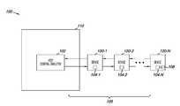
- FIG. 1illustrates a block diagram of a system 100 in accordance with one or more embodiments of the present disclosure.
- a host 110is shown.
- the hostcan be a computing device, such as a personal computer, among other computing device types.
- Examples of a host 110include laptop computers, personal computers, mobile phone, digital cameras, digital recording and play back devices, PDA's, memory card readers, and interface hubs, among other examples.
- the host 110 of FIG. 1includes host control circuitry 102 among other host elements not shown.
- Host control circuitry 102can include one or more of a processor, a host controller, and/or host memory.
- the host control circuitry 102can be used to communicate information between the number of peripheral devices 120 - 1 , 120 - 2 , . . . , 120 -N and another device, such as the host 110 .
- a processorcan intend one or more processors, such as a parallel processing system, a number of coprocessors, etc.
- the host 110can include a transport layer, e.g., a communication/transport layer, a link-control layer, and/or a physical layer, which can be associated with host control circuitry.
- Host control circuitry 102can be coupled to peripheral devices 120 - 1 , 120 - 2 , . . . , 120 -N.
- the host control circuitry 102can manage transport, link, and physical layer activity without processor intervention and manage command retries without processor intervention.
- a transport layercan be analogous to a transaction layer as termed by various standards.
- the host control circuitry 102can be coupled to a standardized interface.
- the host control circuitry 102can be coupled to an interface operated according to a universal flash storage (UFS) standard among other interfaces.
- UFSuniversal flash storage
- host control circuitry 102can be coupled to an interface for communicating, e.g., passing, control, address, data and other signals between the peripheral devices 120 - 1 , 120 - 2 , . . . , 120 -N, the host 110 , and/or other devices.
- the peripheral devices 120 - 1 , 120 - 2 , . . . , 120 -Ncan include peripheral device control circuitry 104 - 1 , 104 - 2 , . . . , 104 -N that can be used to facilitate operations, such as read, write, and/or erase commands for memory devices, among other operations, that are communicated to the peripheral devices 120 - 1 , 120 - 2 , . . . , 120 -N from the host 110 .
- One or more of the peripheral devicescan comprise and/or include an RF transceiver 108 coupled to the control circuitry, e.g., control circuitry 104 -N. Although only peripheral device 120 -N is illustrated in FIG.
- the RF transceiver 108can transmit and/or receive data to and/or from a wireless device (not illustrated).
- the RF transceiver 108can receive a transport layer packet from a wireless device.
- the peripheral devices 120 - 1 , 120 - 2 , . . . , 120 -Ncan share a common physical connection 105 to the host 110 .
- the common physical connection 105can include the upstream and/or downstream connection between the host 110 and the peripheral devices 120 - 1 , 120 - 2 , . . . , 120 -N.
- the peripheral devices 120 - 1 , 120 - 2 , . . . , 120 -Ncan be coupled to the host 110 in a chained topology, e.g., chained together.
- one or more peripheral devicese.g., peripheral device 120 -N, can be removed from the chain.
- the peripheral device control circuitry 104 - 1 , 104 - 2 , . . . , 104 -Ncan provide a translation layer between the host 110 and the peripheral devices 120 - 1 , 120 - 2 , . . . , 120 -N.
- peripheral device control circuitrycould selectively couple an I/O connector (not shown in FIG. 1 ) of a peripheral device to receive the appropriate signal at the appropriate I/O connection at the appropriate time.
- the communication protocol between a host 110 and the peripheral devices 120 - 1 , 120 - 2 , . . . , 120 -Nmay be different than what is required for access to the peripheral devices 120 - 1 , 120 - 2 , .
- the peripheral device control circuitry 104 - 1 , 104 - 2 , . . . , 104 -Ncould then translate the command sequence received from a host 110 into appropriate command sequences to achieve the desired access to peripheral devices 120 - 1 , 120 - 2 , . . . , 120 -N.
- Each translationmay further include changes in signal voltage levels in addition to command sequences.
- chained peripheral devicescan refer to peripheral devices communicatively coupled to a host (e.g., host 110 ) via a common physical connection, such as a shared interface port of a host (e.g., via the same interface port of host control circuitry 102 ).
- a particular host interface portcan include a data input port and a data output port.
- datacan be communicated between the host 110 and the chained peripheral devices 120 - 1 , 120 - 2 , . . . , 120 -N via the same single interface port of the host 110 .
- the use of particular ports on a host or peripheral devicesis described in more detail with respect to FIG. 2 .
- FIG. 1can include additional circuitry that is not illustrated so as not to obscure embodiments of the present disclosure.
- the peripheral devices 120 - 1 , 120 - 2 , . . . , 120 -Nare memory devices
- the memory devicescan include address circuitry to latch address signals provided over I/O connectors through I/O circuitry. Address signals can be received and decoded by a row decoder and a column decoder, to access the memory devices. It will be appreciated by those skilled in the art that the number of address input connectors depends on the density and architecture of the memory devices.
- a host and/or peripheral devicecan include one or more cache lines, e.g., for arranging incoming data prior to processing and/or storing the data, among other operations.
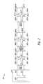
- FIG. 2illustrates a block diagram of a system 200 in accordance with one or more embodiments of the present disclosure.
- the system 200includes a chain of peripheral devices, e.g., memory devices, according to one or more embodiments of the present disclosure.
- peripheral devicese.g., memory devices
- memory devicesare used as an example, other types of peripheral devices or combinations of peripheral devices are also within the scope of embodiments of the present disclosure.
- other peripheral devicesinclude, but are not limited to, printers, scanners, cameras, wireless communication peripherals such as Bluetooth or WiFi devices, external hard drives, solid state drives, flash drives, etc.
- Examples of memory devicesinclude flash memory, DRAM, SRAM, one or more NAND devices or a Managed NAND implementation, e.g., a NAND controller and one or more NAND devices, or other peripheral devices for data storage.
- a host 210is shown having a data output port 212 , a data input port 214 , and a buffer 206 .
- Host 210can be analogous to host 110 illustrated in FIG. 1 and can include control circuitry such as control circuitry 102 illustrated in FIG. 1 .
- Coupling peripheral devices to a single data output port 212 and a single data input port 214can reduce a number of pins that may otherwise be included on a host 210 .
- single data portssuch as the single data output port 212 or the single data input port 214 may each include multiple data lanes.
- the term single data portis used to illustrate a single serial connection to a host for multiple peripheral devices, in contrast to a parallel connection for each peripheral device on a host.
- the host 210can be configured to deconstruct a transport layer packet into a number of link-control layer packets and communicate the number of link-control layer packets via the data output port 212 .
- the hostcan monitor a number of acknowledgements, corresponding to the number of link-control layer packets, received via the data input port 214 .
- the number of acknowledgementscan be used by the host to limit the number of link-control layer packets communicated via the data output port 214 as described herein.
- the host 210can reconstruct a transport layer packet from a number of link-control layer packets received via the data input port 214 .
- a first peripheral device 220 - 1is shown with a second peripheral device 220 - 2 and an Nth peripheral device 220 -N coupled in a chain configuration.
- a chained peripheral device configuration as shown in FIG. 2can allow for point to point signaling. Using the configuration shown, a chain of peripheral devices can be arbitrarily long without the use of complex addressing circuitry as explained herein.
- the peripheral devices 220 - 1 , 220 - 2 , . . . , 220 -N illustrated in FIG. 2can be analogous to the peripheral devices 120 - 1 , 120 - 2 , . . . , 120 -N illustrated in FIG.
- Each peripheral device 220 - 1 , 220 - 2 , . . . , 220 -Ncan be associated with one or more device identifications (DID) and/or logical unit numbers (LUN).
- DIDdevice identifications
- LUNlogical unit numbers
- a particular peripheral devicecould have one DID and two or more LUN.
- the peripheral devices 220 - 1 , 220 - 2 , . . . , 220 -Nare shown with an upstream side 222 - 1 , 222 - 2 , . . . , 222 -N and a downstream side 224 - 1 , 224 - 2 , . . . , 224 -N.
- the peripheral devicescan include an upstream data input port 226 - 1 , 226 - 2 , . . . , 226 -N, a downstream data output port 228 - 1 , 228 - 2 , . . . , 228 -N, a downstream data input port 230 - 1 , 230 - 2 , .
- Each data port for a particular peripheral devicecan be coupled to control circuitry for the particular peripheral device.
- data or device commandssuch as address assignments, requests for data, etc. can pass through a given device such as from the upstream data input port to the downstream data output port along arrow 234 - 1 , 234 - 2 , . . . , 234 -N.
- Data/commandscan pass internally within a given peripheral device such as along arrow 238 - 1 , 238 - 2 , . . .
- Data/commandscan pass directly through a give peripheral device on a return path from the downstream data input port 230 - 1 , 230 - 2 , . . . , 230 -N to the upstream data output port 232 - 1 , 232 - 2 , . . . , 232 -N as shown by arrow 236 - 1 , 236 - 2 , . . . ,
- the peripheral devices 220 - 1 , 220 - 2 , . . . , 220 -Ncan include a buffer 206 - 1 , 206 - 2 , . . . , 206 -N coupled to control circuitry of the respective peripheral device.
- the buffer for each respective peripheral devicecan be coupled to one or more of the upstream and downstream data input and output ports.
- three peripheral devicesare shown in the system 200 , the present disclosure is not so limited. Using the configuration shown, a greater or lesser number of peripheral devices can be included.
- a peripheral device 220 - 1 , 220 - 2 , . . . , 220 -Ncan be configured to deconstruct a transport layer packet into a number of link-control layer packets and communicate, e.g., transfer, the number of link-control layer packets via one or more of the upstream data output port 232 - 1 , 232 - 2 , . . . , 232 -N and the downstream data output port 228 - 1 , 228 - 2 , . . . , 228 -N.
- a peripheral devicecan pass-through a number of link-control layer packets from an input port to an output port either upstream or downstream as described herein.
- a peripheral device 220 - 1 , 220 - 2 , . . . , 220 -Ncan reconstruct a transport layer packet from a number of link-control layer packets received via one or more of the upstream data input port 226 - 1 , 226 - 2 , . . . , 226 -N and the downstream data input port 230 - 1 , 230 - 2 , . . . , 230 -N.
- Control circuitry for a particular peripheral devicecan be configured to reconstruct a transport layer packet from a number of link-control layer packets received via a particular data input port when the link-control layer packets are associated with a destination address, e.g., a DID or LUN, for the peripheral device 220 -N.
- a destination addresse.g., a DID or LUN
- the receiving peripheral device 220 -Ncan pass-through the number of link-control layer packets in an upstream or downstream direction, e.g., through the appropriate output port, toward the destination address associated with the number of link-control layer packets.
- the link-control layermay not be used to route packets.
- the host 210can be configured to maintain packet flow control on the common physical connection, e.g., common physical connection 105 in FIG. 1 , between the host 210 and the plurality of peripheral devices 220 - 1 , 220 - 2 , . . . , 220 -N.
- a peripheral 220 - 1 , 220 - 2 , . . . , 220 -N devicecan be configured to communicate an interrupt link-control layer packet to a host 210 , e.g., in an upstream direction to the host 210 .
- the interrupt link-control layer packetcan serve to notify the host 210 that the peripheral device 220 - 1 , 220 - 2 , . . .
- the interrupt link-control layer packetcan indicate that the peripheral device 220 - 1 , 220 - 2 , . . . , 220 -N has received data, e.g., one or more transport layer packets, via an RF transceiver 108 .
- the interrupt link-control layer packetcan include a context of the data to be communicated via the common physical connection.
- a peripheral device 220 - 1 , 220 - 2 , . . . , 220 -Ncan be configured to communicate an interrupt link-control layer packet to the host 210 after a period of delay from an instruction previously received from the host 210 .
- the interrupt link-control layer packetcan include an indication of the instruction.
- the peripheral device 220 - 1 , 220 - 2 , . . . , 220 -Ncan be configured to communicate the interrupt link-control layer packet when data associated with the instruction is ready to be communicated via the common physical connection.
- Embodiments shown in FIGS. 1-2may include hard wired devices or they may include sockets for assembly or expanding capabilities.
- One or more embodimentsmay include a number of expansion sockets, where there are still available sockets downstream of the last peripheral device in the chain.
- the last peripheral devicee.g., peripheral device 220 -N
- additional peripheral devicescan be placed in the chain, then the last peripheral device can be reinserted at the end of the newly lengthened chain.
- additional peripheral devicescan be added to the end of the chain for expansion purposes without removing and reinstalling a dedicated last peripheral device in the chain.
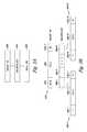
- FIG. 3Aillustrates a block diagram of a layered architecture for an interface in accordance with one or more embodiments of the present disclosure.
- a layered architecturecan be implemented in a host control circuitry, e.g., host control circuitry 102 in FIG. 1 , and/or device control circuitry, e.g., device control circuitry 104 - 1 , 104 - 2 , . . . , 104 -N according to one or more embodiments of the present disclosure.
- the layered architecturecan include a transport layer 356 , a link-control layer 354 , and a physical layer 352 , among other layers.
- Data flow packets between a host and one or more devicesmay be generated by the transport layer, e.g., using a protocol that both the host and devices understand. Such a protocol can be independent of the method of transmission of the data flow of packets, e.g., wired, wireless, etc.
- a deviceis attached directly to a host, data flow packets generated by the transport layer 356 can be communicated between the host and device directly.
- a link-control layer 354may be put in place to improve utilization of the data flow connection between the host and devices and/or to provide flow control for concurrent data communication between the host and multiple devices.
- the link-control layer 354can be implemented to monitor and/or modulate data communication between a host and one or more devices. As described herein, the link-control layer 354 can exert finer control of packet size and flow control by deconstructing and reconstructing the data flow packets generated by the transport layer 356 between the host and devices.
- FIG. 3Billustrates a block diagram of a number of packets in a layered architecture in accordance with one or more embodiments of the present disclosure.
- a data flow from a host to a target device, or from a device to a hostcan be deconstructed into link-control layer packets and reconstructed into the original data flow, e.g., transport layer packets.
- a transport layer packet 372can include one or more of a header 374 , a payload 376 , and an error detection component 378 -T, such as a cyclic redundancy check (CRC) value, a checksum, or an error correction code (ECC) parity value.
- the error detection component 378 -Tcan be part of the payload 376 .
- the header 374may contain the context, e.g., the destination address of the transport layer packet 372 .
- the header 374may contain information relating to a command type, a target device ID (DID), a logical unit number (LUN), status, and/or other attributes.
- the payload 376 of the transport layer packet 372can include data and/or commands.
- the transport layer packet 372can be deconstructed into a number of link-control layer packets, e.g., link-control layer packets 380 - 1 , 380 - 2 , . . . , 380 -N.
- the transport layer packet 372can be deconstructed according to a priority and/or an order associated with the transport layer packet 372 , e.g., with respect to a number of other transport layer packets.
- the transport layer packet 372can be deconstructed into a number of link-control layer packets 380 - 1 , 380 - 2 , . . .
- an entire transport layer packet 372can be loaded to a buffer, e.g., a host buffer 106 or peripheral device buffer 106 - 1 , 106 - 2 , . . . , 106 -N as illustrated in FIG. 1 , before the transport layer packet is deconstructed into link-control layer packets 380 - 1 , 380 - 2 , . . . , 380 -N, as described herein.
- the transport layer packetcan be deconstructed as it enters the link-control layer 354 from the transport layer 356 .
- Each link-control layer packete.g., link-control layer packet 380 - 1
- Deconstructing a transport layer packet according to one or more embodiments of the present disclosurecan provide, for example, more efficient communication of data through a common physical connection.
- a link-control layer packete.g., each link-control layer packet
- can have a sequence numbere.g., sequence number “1” 382 - 1 in link-control layer packet 380 - 1 , appended thereto.
- each link-control layer packet that is deconstructed from a transport layer packetcan have a sequence number inserted in an order corresponding to the sequential portion of the transport layer packet that the link-control layer packet represents, e.g., from 1 to N.
- the last link-control layer packet 380 -Ncan include sequence number “N” 382 -N. Sequence numbers can help maintain link-control layer packet order and aid in reconstruction of the original transport layer packet.
- Sequence numberscan be appended to link-control layer packets in an x-bit field of a header of the link-control layer packets, e.g. a field capable of storing x number of bits.
- sequence numbersmay be recycled. That is, after 2 x sequence numbers have been used, e.g., after 2 x link-control layer packets have had sequence numbers assigned for a particular data flow, sequence numbers may be recycled, e.g., reused.
- sequence numbersare limited to the set including 1, 2, 3, and 4, after all four sequence numbers have been used once, they may be used again, e.g., both a first and a fifth link-control layer packet may have the sequence number 1 assigned thereto.
- Link-control layer packetscan be communicated out of sequence with respect to the sequence numbers appended thereto.
- One or more embodimentscan include limiting the number of outstanding link-control layer packets that are communicated via a common physical connection for a number of peripheral devices. Limiting the number of outstanding link-control layer packets can include limiting the number of outstanding packets to less than or equal to 2 x /2 link-control layer packets. That is, for example, control circuitry, e.g., host control circuitry 102 in FIG. 1 , can confirm that at least half of the total number of sequence numbers worth of link-control layer packets have been acknowledged before communicating an additional link-control layer packet. For example, if 16 sequence numbers are available, the control circuitry can be configured to limit the outstanding number of link-control layer packets to 8.
- An outstanding packetcan include packets that have not been acknowledged and/or packets that have received an acknowledgement such as a retransfer request, e.g., a negative acknowledgement.
- limiting the number of outstanding link-control layer packetscan include using a bit of the x-bit field as a retransfer request bit.
- a particular link-control layer packetcan be recommunicated when the sending device does not receive an acknowledgement for the particular link-control layer packet, or when the sending device receives a negative acknowledgement.
- Such embodimentscan help to prevent packet errors due to a particular sequence number being recycled before a particular link-control layer packet associated with the particular sequence number has been received successfully.
- the link-control layercan treat all data in the transport layer packet 372 , e.g., the header 374 , the payload 376 , and the error detection component 378 -T, as data payload. That is, the entirety of the transport layer packet 372 can be broken up into smaller portions that fit into link-control layer packets 380 - 1 , 380 - 2 , . . . , 380 -N, irrespective of a distinction between the header 374 and the payload 376 .
- link-control layer packet 380 - 1may include a portion of the header 374 of the transport layer packet 372 , it may include the entire header 374 , or it may include at least a portion of the header 374 and a portion of the payload 376 .
- each link-control layer packetcan maintain and/or express the direction and/or end of the data transmission, e.g., upstream or downstream, the data destination, e.g., the target such as a DID or LUN, and the packet sequence number, e.g., packet sequence number 380 - 1 . That is, each link-control layer packet can have the same direction and/or end of data transmission in the link-control layer that the transport layer packet would have had in the transport layer. For example, the direction and/or end of the data transmission can be maintained and/or expressed in a header of a link-control layer packet as assigned by control circuitry of the device transferring the data.
- One or more embodimentscan include deconstructing a transport layer packet 372 into a number of link-control layer packets 380 - 1 , 380 - 2 , . . . , 380 -N such that the number of link-control layer packets 380 - 1 , 380 - 2 , . . . , 380 -N have a payload 384 - 1 , . . . , 384 -N size equivalent to a cache line size of a receiving device.
- Such embodimentscan provide for efficient reception of data and reconstruction of transport layer packets 372 . That is, a cache line of the receiving device can be filled and emptied with each received link-control layer packet payload 384 - 1 , . .
- Example sizes for a cache line according to the present disclosurecan include 32 bytes or 64 bytes, however embodiments are not so limited.
- the receiving devicecan store the transport layer packet 372 payload 376 as a sector of data.
- An example size for a sector of datacan be 512 bytes, however embodiments are not so limited.
- Each link-control layer packet 380 - 1 , 380 - 2 , . . . , 380 -Nmay include its own error detection component 378 -L 1 , . . . , 378 -LN.
- An error detection component, e.g., CRC 378 -L 1for a link-control layer packet, e.g., packet 380 - 1 , can be generated for the link-control layer packet independent of the error detection component, e.g., CRC 378 -T, associated with the transport layer packet 372 from which the link-control layer packet was deconstructed. As illustrated in FIG.
- the sequence number 382 - 1 and the error detection component 378 -L 1are generated by the link-control layer, while the payload 384 - 1 includes data from the original transport layer packet 372 .
- the sequence number 382 - 1 and error detection component 378 -L 1 for a particular link-control layer packet 380 - 1can be used by the link-control for recommunication, flow control, and the like.
- the payload 384 - 1 of a particular link-control layer packet 380 - 1may include data from one or more of the header 374 , payload 376 , and/or error detection component 378 -T of the corresponding transport layer packet 372 .
- a transport layer packet 372can be reconstructed from a number of link-control layer packets 380 - 1 , 380 - 2 , . . . , 380 -N, e.g., according to a sequence number associated with each of the link-control layer packets 380 - 1 , 380 - 2 , . . . , 380 -N.
- the device receiving the number of link-control layer packets 380 - 1 , 380 - 2 , . . . , 380 -Ncan be configured to acknowledge each of the number of link-control layer packets.
- the device receiving the number of link-control layer packets 380 - 1 , 380 - 2 , . . . , 380 -Ncan be configured to acknowledge the transport layer packet 372 once it has been reconstructed.
- a device or hostcan load received link-control layer packets into a buffer in sequential order according to the sequence number associated with each packet, e.g., sequence number 382 - 1 associated with link-control layer packet 380 - 1 .
- sequence number 382 - 1associated with link-control layer packet 380 - 1 .
- the datacan be communicated to its destination according to address information associated with the reconstructed packet, e.g., as stored in the header 374 of the reconstructed packet.
- the payload 384 - 1 of the first link-control layer packet 380 - 1 deconstructed from a transport layer packet 372can store the header 374 of the transport layer packet 372 .
- the header 374can include a context that describes destination information for the transport layer packet 372 .
- the contexte.g., the destination information, can be derived from the header of the transport layer packet 372 received in association with the initial link-control layer packet 380 - 1 .
- the contextcan be loaded into a buffer of the receiving device before transferring the link-control layer packets, e.g., the initial link-control layer packet 380 - 1 and/or the subsequent link-control layer packets 380 - 2 , . . . , 380 -N.
- the link-control layer of a device receiving the first link-control layer packet 380 - 1 deconstructed from the transport layer packet 372can transfer the first link-control layer packet 380 - 1 to its destination.
- Subsequent link-control layer packets 380 - 2 , . . . , 380 -Ncan be transferred without reconstructing the transport layer packet 372 .
- subsequent link-control layer packets 380 - 2 , . . . , 380 -Ncan be transferred to their destination in the order in which they are received by the receiving device:
- the subsequent link-control layer packets 380 - 2 , . . . , 380 -Ncan be transferred according to the context in the buffer.
- transferring subsequent link-control layer packets 380 - 2 , . . . , 380 -N in the order in which they are receivedcan include transferring subsequent link-control layer packets 380 - 2 , . . . , 380 -N out of sequence with respect to a sequence number associated with each link-control layer packet, e.g., sequence number 382 -N associated with link-control layer packet 380 -N.
- the destination devicee.g., the device to which the receiving device transfers the link-control layer packets 380 - 1 , 380 - 2 , . . . , 380 -N, can reconstruct the transport layer packet 372 .
- the receiving devicecan reconstruct and transfer the transport layer packet 372 to a destination described in a context of the transport layer packet 372 , e.g., to the destination device.
- a hostcan generally be a receiving device for a transport layer packet 372 reconstructed from a number of link-control layer packets 380 - 1 , 380 - 2 , . . . , 380 -N received from a peripheral device, however, the transport layer packet 372 can have a more specific destination described in a context associated therewith, e.g., in a transport layer packet header 374 .
- the more specific destination addresscan be a memory address associated with the host, among other specific destination addresses.
- a peripheral devicee.g., peripheral device 220 - 2 in FIG. 2
- the receiving devicecan be the destination device.
- One method embodiment for packet processingincludes deconstructing a transport layer packet into a number of link-control layer packets, wherein each of the link-control layer packets has an associated sequence number, communicating the number of link-control layer packets via a common physical connection for a plurality of peripheral devices, and limiting a number of outstanding link-control layer packets during the communication.
- the term “and/or”includes any and all combinations of one or more of the associated listed items.
- the term “or,” unless otherwise noted,means logically inclusive or. That is, “A or B” can include (only A), (only B), or (both A and B). In other words, “A or B” can mean “A and/or B” or “one or more of A and B.”
Landscapes
- Engineering & Computer Science (AREA)
- Computer Networks & Wireless Communication (AREA)
- Signal Processing (AREA)
- Computer Security & Cryptography (AREA)
- Communication Control (AREA)
- Data Exchanges In Wide-Area Networks (AREA)
- Bag Frames (AREA)
Abstract
Description
Claims (18)
Priority Applications (1)
| Application Number | Priority Date | Filing Date | Title |
|---|---|---|---|
| US14/108,599US9929967B2 (en) | 2009-08-10 | 2013-12-17 | Packet deconstruction/reconstruction and link-control |
Applications Claiming Priority (3)
| Application Number | Priority Date | Filing Date | Title |
|---|---|---|---|
| US12/538,607US8238244B2 (en) | 2009-08-10 | 2009-08-10 | Packet deconstruction/reconstruction and link-control |
| US13/552,028US8630182B2 (en) | 2009-08-10 | 2012-07-18 | Packet deconstruction/reconstruction and link-control |
| US14/108,599US9929967B2 (en) | 2009-08-10 | 2013-12-17 | Packet deconstruction/reconstruction and link-control |
Related Parent Applications (1)
| Application Number | Title | Priority Date | Filing Date |
|---|---|---|---|
| US13/552,028ContinuationUS8630182B2 (en) | 2009-08-10 | 2012-07-18 | Packet deconstruction/reconstruction and link-control |
Publications (2)
| Publication Number | Publication Date |
|---|---|
| US20140185620A1 US20140185620A1 (en) | 2014-07-03 |
| US9929967B2true US9929967B2 (en) | 2018-03-27 |
Family
ID=43534772
Family Applications (3)
| Application Number | Title | Priority Date | Filing Date |
|---|---|---|---|
| US12/538,607Active2030-01-24US8238244B2 (en) | 2009-08-10 | 2009-08-10 | Packet deconstruction/reconstruction and link-control |
| US13/552,028ActiveUS8630182B2 (en) | 2009-08-10 | 2012-07-18 | Packet deconstruction/reconstruction and link-control |
| US14/108,599Active2030-12-17US9929967B2 (en) | 2009-08-10 | 2013-12-17 | Packet deconstruction/reconstruction and link-control |
Family Applications Before (2)
| Application Number | Title | Priority Date | Filing Date |
|---|---|---|---|
| US12/538,607Active2030-01-24US8238244B2 (en) | 2009-08-10 | 2009-08-10 | Packet deconstruction/reconstruction and link-control |
| US13/552,028ActiveUS8630182B2 (en) | 2009-08-10 | 2012-07-18 | Packet deconstruction/reconstruction and link-control |
Country Status (7)
| Country | Link |
|---|---|
| US (3) | US8238244B2 (en) |
| EP (1) | EP2465232B1 (en) |
| JP (1) | JP5545370B2 (en) |
| KR (1) | KR101417543B1 (en) |
| CN (1) | CN102474466B (en) |
| TW (1) | TWI433508B (en) |
| WO (1) | WO2011019372A2 (en) |
Families Citing this family (13)
| Publication number | Priority date | Publication date | Assignee | Title |
|---|---|---|---|---|
| US20110246692A1 (en)* | 2010-03-31 | 2011-10-06 | International Business Machines Corporation | Implementing Control Using A Single Path In A Multiple Path Interconnect System |
| WO2013187667A1 (en)* | 2012-06-11 | 2013-12-19 | 한국전자통신연구원 | Rate adaptation method using bit error rate for multimedia service and apparatus therefor |
| KR20130138638A (en) | 2012-06-11 | 2013-12-19 | 한국전자통신연구원 | The utilization of ber(bit error rate) for rate adaptation in mmt d3-ld |
| US9467326B2 (en) | 2012-12-03 | 2016-10-11 | Hewlett-Packard Development Company, L.P. | Rate limiting mechanism based on device load/capacity or traffic content |
| US9015438B2 (en) | 2012-12-03 | 2015-04-21 | Aruba Networks, Inc. | System and method for achieving enhanced performance with multiple networking central processing unit (CPU) cores |
| US9733847B2 (en)* | 2014-06-02 | 2017-08-15 | Micron Technology, Inc. | Systems and methods for transmitting packets in a scalable memory system protocol |
| US9749448B2 (en)* | 2014-11-25 | 2017-08-29 | Intel Corporation | Header parity error handling |
| KR102528557B1 (en) | 2016-01-12 | 2023-05-04 | 삼성전자주식회사 | Operating Method of semiconductor device and memory system having multi-connection port and Communication Method of storage system |
| KR102656189B1 (en) | 2016-07-19 | 2024-04-11 | 삼성전자주식회사 | Electronic device configured to control non-directly connected storage device among serially connected storage devices, storage device included therein, computing system including the same, and operation method of controller of storage device |
| KR102706118B1 (en) | 2016-09-22 | 2024-09-19 | 삼성전자주식회사 | Electronic device configured to compensate different characteristics of serially connected storage devices, and storage device included therein |
| KR102742690B1 (en) | 2016-09-27 | 2024-12-17 | 삼성전자주식회사 | Electronic device configured to provide bypass path to non-directly connected storage device among serially connected storage devices, storage device included therein, computing system including the same, and method of communicating therewith |
| US10510382B2 (en) | 2016-11-11 | 2019-12-17 | Qualcomm Incorporated | Hardware automated link control of daisy-chained storage device |
| US11853233B2 (en)* | 2021-10-07 | 2023-12-26 | Dell Products L.P. | Sequentially and bidirectionally connecting peripherals and devices to an information handling system |
Citations (28)
| Publication number | Priority date | Publication date | Assignee | Title |
|---|---|---|---|---|
| CN1218346A (en) | 1997-09-25 | 1999-06-02 | 索尼株式会社 | Communication method and terminal for controlling data flow between layers using data communication protocol |
| JP2001308947A (en) | 2000-04-21 | 2001-11-02 | Toshiba Corp | Communication device, relay device, and communication control method |
| US20020118696A1 (en) | 2001-02-27 | 2002-08-29 | Yukinori Suda | Multiple access communication system and data transceiver |
| EP1411690A1 (en) | 2002-10-18 | 2004-04-21 | Nokia Corporation | Method for transferring GPRS data packets from different PDP contexts according to their relative priority |
| US20050135416A1 (en) | 2003-10-15 | 2005-06-23 | Qualcomm Incorporated | Wireless LAN protocol stack |
| US20050243743A1 (en)* | 2004-04-30 | 2005-11-03 | Sony Ericsson Mobile Communications Japan, Inc. | Re-transmission controlling method and wireless communication terminal apparatus |
| US7076569B1 (en) | 2002-10-18 | 2006-07-11 | Advanced Micro Devices, Inc. | Embedded channel adapter having transport layer configured for prioritizing selection of work descriptors based on respective virtual lane priorities |
| US20060187955A1 (en)* | 2005-02-18 | 2006-08-24 | Ramin Rezaiifar | Radio link protocols for multi-link communication systems |
| US7130958B2 (en) | 2003-12-02 | 2006-10-31 | Super Talent Electronics, Inc. | Serial interface to flash-memory chip using PCI-express-like packets and packed data for partial-page writes |
| JP2007181127A (en) | 2005-12-28 | 2007-07-12 | Ntt Docomo Inc | COMMUNICATION DEVICE, COMMUNICATION METHOD, AND PROGRAM |
| US20070275728A1 (en) | 2004-06-15 | 2007-11-29 | Matsushita Electric Industrial Co., Ltd. | Scheduling Mode Dependent Data Transmissions |
| US20080016248A1 (en) | 2006-07-14 | 2008-01-17 | George Tsirtsis | Method and apparatus for time synchronization of parameters |
| US20080043732A1 (en)* | 2006-08-17 | 2008-02-21 | P.A. Semi, Inc. | Network direct memory access |
| WO2008049462A1 (en) | 2006-10-26 | 2008-05-02 | Telefonaktiebolaget Lm Ericsson (Publ) | A method and receiver for controlling the conformance of a data flow in a communication system to a traffic definition |
| US20080186946A1 (en) | 2007-02-02 | 2008-08-07 | Interdigital Technology Corporation | Method and apparatus for versatile mac multiplexing in evolved hspa |
| WO2008128597A1 (en) | 2007-04-20 | 2008-10-30 | Panasonic Corporation | Improved transmission scheme of protocol data units during a procedure that comprises the reset of the protocol layer |
| EP1986698A2 (en) | 2006-02-01 | 2008-11-05 | The Johns Hopkins University | Polypeptide-nucleic acid conjugate for immunoprophylaxis or immunotherapy for neoplastic or infectious disorders |
| US20080310452A1 (en) | 2007-06-14 | 2008-12-18 | Texas Instruments Incorporated | Data link layer headers |
| TWI304536B (en) | 2003-12-15 | 2008-12-21 | Ibm | Apparatus, system, method, and computer readable recording medium recording instruction for backing up data within a grid system |
| US20090003335A1 (en) | 2007-06-29 | 2009-01-01 | International Business Machines Corporation | Device, System and Method of Fragmentation of PCI Express Packets |
| US7475174B2 (en) | 2004-03-17 | 2009-01-06 | Super Talent Electronics, Inc. | Flash / phase-change memory in multi-ring topology using serial-link packet interface |
| US20090103511A1 (en) | 2007-09-28 | 2009-04-23 | Interdigital Patent Holdings, Inc. | Method and apparatus for selecting a radio link control protocol data unit size |
| US20090129406A1 (en)* | 1999-04-08 | 2009-05-21 | In Tae Hwang | Radio protocol for mobile communicatoin system and method |
| US20090257418A1 (en)* | 2008-04-14 | 2009-10-15 | Research In Motion Limited | Apparatus, and associated method, for facilitating radio control system operation with an ics-capable wireless device |
| US20090327830A1 (en) | 2008-06-25 | 2009-12-31 | Lee Young-Dae | Method for retransmitting data unit using delivery status information |
| US20100169466A1 (en)* | 2008-12-26 | 2010-07-01 | Rajeev Atluri | Configuring hosts of a secondary data storage and recovery system |
| US20110032877A1 (en)* | 2007-02-01 | 2011-02-10 | Interdigital Technology Corporation | Method and apparatus for supporting amd re-segmentation |
| US20110194470A1 (en)* | 2002-08-09 | 2011-08-11 | Interdigital Technology Corporation | Efficient memory allocation in a wireless transmit/receiver unit |
- 2009
- 2009-08-10USUS12/538,607patent/US8238244B2/enactiveActive
- 2010
- 2010-08-06KRKR1020127006228Apatent/KR101417543B1/enactiveActive
- 2010-08-06JPJP2012524691Apatent/JP5545370B2/enactiveActive
- 2010-08-06WOPCT/US2010/002186patent/WO2011019372A2/enactiveApplication Filing
- 2010-08-06EPEP10808440.1Apatent/EP2465232B1/enactiveActive
- 2010-08-06CNCN201080035473.5Apatent/CN102474466B/enactiveActive
- 2010-08-10TWTW099126680Apatent/TWI433508B/enactive
- 2012
- 2012-07-18USUS13/552,028patent/US8630182B2/enactiveActive
- 2013
- 2013-12-17USUS14/108,599patent/US9929967B2/enactiveActive
Patent Citations (32)
| Publication number | Priority date | Publication date | Assignee | Title |
|---|---|---|---|---|
| CN1218346A (en) | 1997-09-25 | 1999-06-02 | 索尼株式会社 | Communication method and terminal for controlling data flow between layers using data communication protocol |
| US6233224B1 (en) | 1997-09-25 | 2001-05-15 | Sony Computer Laboratory, Inc. | Communication method and data communications terminal, with data communication protocol for inter-layer flow control |
| US20090129406A1 (en)* | 1999-04-08 | 2009-05-21 | In Tae Hwang | Radio protocol for mobile communicatoin system and method |
| JP2001308947A (en) | 2000-04-21 | 2001-11-02 | Toshiba Corp | Communication device, relay device, and communication control method |
| US20020118696A1 (en) | 2001-02-27 | 2002-08-29 | Yukinori Suda | Multiple access communication system and data transceiver |
| US7505475B2 (en) | 2001-02-27 | 2009-03-17 | Nec Corporation | Multiple access communication system and data transceiver |
| US20110194470A1 (en)* | 2002-08-09 | 2011-08-11 | Interdigital Technology Corporation | Efficient memory allocation in a wireless transmit/receiver unit |
| EP1411690A1 (en) | 2002-10-18 | 2004-04-21 | Nokia Corporation | Method for transferring GPRS data packets from different PDP contexts according to their relative priority |
| US7076569B1 (en) | 2002-10-18 | 2006-07-11 | Advanced Micro Devices, Inc. | Embedded channel adapter having transport layer configured for prioritizing selection of work descriptors based on respective virtual lane priorities |
| US20050135416A1 (en) | 2003-10-15 | 2005-06-23 | Qualcomm Incorporated | Wireless LAN protocol stack |
| US7130958B2 (en) | 2003-12-02 | 2006-10-31 | Super Talent Electronics, Inc. | Serial interface to flash-memory chip using PCI-express-like packets and packed data for partial-page writes |
| US7698428B2 (en) | 2003-12-15 | 2010-04-13 | International Business Machines Corporation | Apparatus, system, and method for grid based data storage |
| TWI304536B (en) | 2003-12-15 | 2008-12-21 | Ibm | Apparatus, system, method, and computer readable recording medium recording instruction for backing up data within a grid system |
| US7475174B2 (en) | 2004-03-17 | 2009-01-06 | Super Talent Electronics, Inc. | Flash / phase-change memory in multi-ring topology using serial-link packet interface |
| US20050243743A1 (en)* | 2004-04-30 | 2005-11-03 | Sony Ericsson Mobile Communications Japan, Inc. | Re-transmission controlling method and wireless communication terminal apparatus |
| US20070275728A1 (en) | 2004-06-15 | 2007-11-29 | Matsushita Electric Industrial Co., Ltd. | Scheduling Mode Dependent Data Transmissions |
| US20060187955A1 (en)* | 2005-02-18 | 2006-08-24 | Ramin Rezaiifar | Radio link protocols for multi-link communication systems |
| JP2007181127A (en) | 2005-12-28 | 2007-07-12 | Ntt Docomo Inc | COMMUNICATION DEVICE, COMMUNICATION METHOD, AND PROGRAM |
| EP1986698A2 (en) | 2006-02-01 | 2008-11-05 | The Johns Hopkins University | Polypeptide-nucleic acid conjugate for immunoprophylaxis or immunotherapy for neoplastic or infectious disorders |
| US20080016248A1 (en) | 2006-07-14 | 2008-01-17 | George Tsirtsis | Method and apparatus for time synchronization of parameters |
| US20080043732A1 (en)* | 2006-08-17 | 2008-02-21 | P.A. Semi, Inc. | Network direct memory access |
| WO2008049462A1 (en) | 2006-10-26 | 2008-05-02 | Telefonaktiebolaget Lm Ericsson (Publ) | A method and receiver for controlling the conformance of a data flow in a communication system to a traffic definition |
| US20110032877A1 (en)* | 2007-02-01 | 2011-02-10 | Interdigital Technology Corporation | Method and apparatus for supporting amd re-segmentation |
| US20080186946A1 (en) | 2007-02-02 | 2008-08-07 | Interdigital Technology Corporation | Method and apparatus for versatile mac multiplexing in evolved hspa |
| US20100118781A1 (en)* | 2007-04-20 | 2010-05-13 | Panasonic Corporation | Transmission Scheme of Protocol Data Units During a Procedure That Comprises the Reset of the Protocol Layer |
| WO2008128597A1 (en) | 2007-04-20 | 2008-10-30 | Panasonic Corporation | Improved transmission scheme of protocol data units during a procedure that comprises the reset of the protocol layer |
| US20080310452A1 (en) | 2007-06-14 | 2008-12-18 | Texas Instruments Incorporated | Data link layer headers |
| US20090003335A1 (en) | 2007-06-29 | 2009-01-01 | International Business Machines Corporation | Device, System and Method of Fragmentation of PCI Express Packets |
| US20090103511A1 (en) | 2007-09-28 | 2009-04-23 | Interdigital Patent Holdings, Inc. | Method and apparatus for selecting a radio link control protocol data unit size |
| US20090257418A1 (en)* | 2008-04-14 | 2009-10-15 | Research In Motion Limited | Apparatus, and associated method, for facilitating radio control system operation with an ics-capable wireless device |
| US20090327830A1 (en) | 2008-06-25 | 2009-12-31 | Lee Young-Dae | Method for retransmitting data unit using delivery status information |
| US20100169466A1 (en)* | 2008-12-26 | 2010-07-01 | Rajeev Atluri | Configuring hosts of a secondary data storage and recovery system |
Non-Patent Citations (10)
| Title |
|---|
| Ajay V. Bhatt, Creating a PCI Express Interconnect, Technology and Research Labs, Intel Corporation, White Paper, http://www.pcisig.com/specifications/pciexpress/resources/PCI_Express_White_Paper.pdf, accessed Jul. 24, 2009. (8 pgs.). |
| European Search Report and Opinion for related European Application No. 10808440.1, dated Nov. 28, 2012, 7 pages. |
| First Official Action from related Chinese patent application No. 201080035473.5, dated Nov. 21, 2013, 21 pp. |
| International Search Report and Written Opinion, 10 pages. |
| Japanese Notice of Rejection from related Japanese application 2012-524691, dated May 28, 2013, 3 pages. |
| Korean Notice of Preliminary Rejection from related Korean application 10-2012-7006228, dated Jun. 26, 2013, 3 pages. |
| Korean Office Action for related Korean Application No. 10-2012-7006228, dated Oct. 31, 2013, 2 pages. |
| Notice of Rejection Grounds from Japanese patent application No. 2012-0524691, dated Dec. 10, 2013, 4 pp. |
| Second Office Action from related Chinese patent application No. 201080035473.5, dated Jun. 27, 2014, 10 pp. |
| Taiwanese Office Action for related Taiwanese Application No. 099126680, dated Aug. 27, 2013, 4 pages. |
Also Published As
| Publication number | Publication date |
|---|---|
| JP2013502149A (en) | 2013-01-17 |
| US8630182B2 (en) | 2014-01-14 |
| TWI433508B (en) | 2014-04-01 |
| JP5545370B2 (en) | 2014-07-09 |
| CN102474466B (en) | 2015-04-29 |
| US20110032823A1 (en) | 2011-02-10 |
| EP2465232A4 (en) | 2012-12-26 |
| KR20120056271A (en) | 2012-06-01 |
| EP2465232A2 (en) | 2012-06-20 |
| WO2011019372A2 (en) | 2011-02-17 |
| EP2465232B1 (en) | 2014-02-12 |
| US8238244B2 (en) | 2012-08-07 |
| TW201114227A (en) | 2011-04-16 |
| US20120281537A1 (en) | 2012-11-08 |
| KR101417543B1 (en) | 2014-07-08 |
| WO2011019372A3 (en) | 2011-05-26 |
| CN102474466A (en) | 2012-05-23 |
| US20140185620A1 (en) | 2014-07-03 |
Similar Documents
| Publication | Publication Date | Title |
|---|---|---|
| US9929967B2 (en) | Packet deconstruction/reconstruction and link-control | |
| CN102272730B (en) | Virtualized ECC NAND | |
| US9588697B2 (en) | Host controller | |
| US8386666B2 (en) | System and method for peripheral device communications | |
| US9921914B2 (en) | Redundant array of independent disks (RAID) write hole solutions | |
| CN102460405B (en) | Method and system for controlling host memory access by memory device | |
| US11704023B2 (en) | Extensible storage system and method | |
| US8335867B1 (en) | Method and apparatus for reducing host processor activity during interaction with peripheral devices | |
| CN117170928A (en) | Post-encapsulation repair management | |
| US12277317B2 (en) | Memory controller, bridge device and method for transferring command and data between memory controllers | |
| US11476874B1 (en) | Method and system for facilitating a storage server with hybrid memory for journaling and data storage | |
| US20160004655A1 (en) | Computing system and operating method of the same | |
| US11960770B2 (en) | Access request management using sub-commands | |
| CN103198039A (en) | Data transmitting controller and hybrid storage device thereof | |
| US12026109B2 (en) | Operating method of transaction accelerator, operating method of computing device including transaction accelerator, and computing device including transaction accelerator | |
| TWI475378B (en) | Storage system to couple to a host, controller to interface with nand memory in storage system, and method of managing a stack of nand memory devices | |
| US20200042231A1 (en) | Dynamic Data Paths In Flash Drives | |
| JP2014238871A (en) | Controller providing single virtualized ecc algorithm, storage system including this controller, and method of managing this storage system |
Legal Events
| Date | Code | Title | Description |
|---|---|---|---|
| AS | Assignment | Owner name:MICRON TECHNOLOGY, INC., IDAHO Free format text:ASSIGNMENT OF ASSIGNORS INTEREST;ASSIGNORS:RADKE, WILLIAM H.;TSAI, VICTOR Y.;GALBO, NEAL A.;AND OTHERS;SIGNING DATES FROM 20090723 TO 20090728;REEL/FRAME:031797/0937 | |
| AS | Assignment | Owner name:U.S. BANK NATIONAL ASSOCIATION, AS COLLATERAL AGENT, CALIFORNIA Free format text:SECURITY INTEREST;ASSIGNOR:MICRON TECHNOLOGY, INC.;REEL/FRAME:038669/0001 Effective date:20160426 Owner name:U.S. BANK NATIONAL ASSOCIATION, AS COLLATERAL AGEN Free format text:SECURITY INTEREST;ASSIGNOR:MICRON TECHNOLOGY, INC.;REEL/FRAME:038669/0001 Effective date:20160426 | |
| AS | Assignment | Owner name:MORGAN STANLEY SENIOR FUNDING, INC., AS COLLATERAL AGENT, MARYLAND Free format text:PATENT SECURITY AGREEMENT;ASSIGNOR:MICRON TECHNOLOGY, INC.;REEL/FRAME:038954/0001 Effective date:20160426 Owner name:MORGAN STANLEY SENIOR FUNDING, INC., AS COLLATERAL Free format text:PATENT SECURITY AGREEMENT;ASSIGNOR:MICRON TECHNOLOGY, INC.;REEL/FRAME:038954/0001 Effective date:20160426 | |
| AS | Assignment | Owner name:U.S. BANK NATIONAL ASSOCIATION, AS COLLATERAL AGENT, CALIFORNIA Free format text:CORRECTIVE ASSIGNMENT TO CORRECT THE REPLACE ERRONEOUSLY FILED PATENT #7358718 WITH THE CORRECT PATENT #7358178 PREVIOUSLY RECORDED ON REEL 038669 FRAME 0001. ASSIGNOR(S) HEREBY CONFIRMS THE SECURITY INTEREST;ASSIGNOR:MICRON TECHNOLOGY, INC.;REEL/FRAME:043079/0001 Effective date:20160426 Owner name:U.S. BANK NATIONAL ASSOCIATION, AS COLLATERAL AGEN Free format text:CORRECTIVE ASSIGNMENT TO CORRECT THE REPLACE ERRONEOUSLY FILED PATENT #7358718 WITH THE CORRECT PATENT #7358178 PREVIOUSLY RECORDED ON REEL 038669 FRAME 0001. ASSIGNOR(S) HEREBY CONFIRMS THE SECURITY INTEREST;ASSIGNOR:MICRON TECHNOLOGY, INC.;REEL/FRAME:043079/0001 Effective date:20160426 | |
| STCF | Information on status: patent grant | Free format text:PATENTED CASE | |
| AS | Assignment | Owner name:JPMORGAN CHASE BANK, N.A., AS COLLATERAL AGENT, ILLINOIS Free format text:SECURITY INTEREST;ASSIGNORS:MICRON TECHNOLOGY, INC.;MICRON SEMICONDUCTOR PRODUCTS, INC.;REEL/FRAME:047540/0001 Effective date:20180703 Owner name:JPMORGAN CHASE BANK, N.A., AS COLLATERAL AGENT, IL Free format text:SECURITY INTEREST;ASSIGNORS:MICRON TECHNOLOGY, INC.;MICRON SEMICONDUCTOR PRODUCTS, INC.;REEL/FRAME:047540/0001 Effective date:20180703 | |
| AS | Assignment | Owner name:MICRON TECHNOLOGY, INC., IDAHO Free format text:RELEASE BY SECURED PARTY;ASSIGNOR:U.S. BANK NATIONAL ASSOCIATION, AS COLLATERAL AGENT;REEL/FRAME:047243/0001 Effective date:20180629 | |
| AS | Assignment | Owner name:MICRON TECHNOLOGY, INC., IDAHO Free format text:RELEASE BY SECURED PARTY;ASSIGNOR:MORGAN STANLEY SENIOR FUNDING, INC., AS COLLATERAL AGENT;REEL/FRAME:050937/0001 Effective date:20190731 | |
| AS | Assignment | Owner name:MICRON SEMICONDUCTOR PRODUCTS, INC., IDAHO Free format text:RELEASE BY SECURED PARTY;ASSIGNOR:JPMORGAN CHASE BANK, N.A., AS COLLATERAL AGENT;REEL/FRAME:051028/0001 Effective date:20190731 Owner name:MICRON TECHNOLOGY, INC., IDAHO Free format text:RELEASE BY SECURED PARTY;ASSIGNOR:JPMORGAN CHASE BANK, N.A., AS COLLATERAL AGENT;REEL/FRAME:051028/0001 Effective date:20190731 | |
| MAFP | Maintenance fee payment | Free format text:PAYMENT OF MAINTENANCE FEE, 4TH YEAR, LARGE ENTITY (ORIGINAL EVENT CODE: M1551); ENTITY STATUS OF PATENT OWNER: LARGE ENTITY Year of fee payment:4 | |
| MAFP | Maintenance fee payment | Free format text:PAYMENT OF MAINTENANCE FEE, 8TH YEAR, LARGE ENTITY (ORIGINAL EVENT CODE: M1552); ENTITY STATUS OF PATENT OWNER: LARGE ENTITY Year of fee payment:8 |