US9927832B2 - Input device having a reduced border region - Google Patents
Input device having a reduced border regionDownload PDFInfo
- Publication number
- US9927832B2 US9927832B2US14/448,527US201414448527AUS9927832B2US 9927832 B2US9927832 B2US 9927832B2US 201414448527 AUS201414448527 AUS 201414448527AUS 9927832 B2US9927832 B2US 9927832B2
- Authority
- US
- United States
- Prior art keywords
- sensor
- electrodes
- electrode
- input device
- sensor electrodes
- Prior art date
- Legal status (The legal status is an assumption and is not a legal conclusion. Google has not performed a legal analysis and makes no representation as to the accuracy of the status listed.)
- Active, expires
Links
Images


Classifications
- G—PHYSICS
- G06—COMPUTING OR CALCULATING; COUNTING
- G06F—ELECTRIC DIGITAL DATA PROCESSING
- G06F3/00—Input arrangements for transferring data to be processed into a form capable of being handled by the computer; Output arrangements for transferring data from processing unit to output unit, e.g. interface arrangements
- G06F3/01—Input arrangements or combined input and output arrangements for interaction between user and computer
- G06F3/03—Arrangements for converting the position or the displacement of a member into a coded form
- G06F3/041—Digitisers, e.g. for touch screens or touch pads, characterised by the transducing means
- G06F3/044—Digitisers, e.g. for touch screens or touch pads, characterised by the transducing means by capacitive means
- G06F3/0443—Digitisers, e.g. for touch screens or touch pads, characterised by the transducing means by capacitive means using a single layer of sensing electrodes
- G—PHYSICS
- G06—COMPUTING OR CALCULATING; COUNTING
- G06F—ELECTRIC DIGITAL DATA PROCESSING
- G06F1/00—Details not covered by groups G06F3/00 - G06F13/00 and G06F21/00
- G06F1/16—Constructional details or arrangements
- G—PHYSICS
- G06—COMPUTING OR CALCULATING; COUNTING
- G06F—ELECTRIC DIGITAL DATA PROCESSING
- G06F1/00—Details not covered by groups G06F3/00 - G06F13/00 and G06F21/00
- G06F1/16—Constructional details or arrangements
- G06F1/1613—Constructional details or arrangements for portable computers
- G06F1/1633—Constructional details or arrangements of portable computers not specific to the type of enclosures covered by groups G06F1/1615 - G06F1/1626
- G06F1/1637—Details related to the display arrangement, including those related to the mounting of the display in the housing
- G06F1/1643—Details related to the display arrangement, including those related to the mounting of the display in the housing the display being associated to a digitizer, e.g. laptops that can be used as penpads
- G—PHYSICS
- G06—COMPUTING OR CALCULATING; COUNTING
- G06F—ELECTRIC DIGITAL DATA PROCESSING
- G06F3/00—Input arrangements for transferring data to be processed into a form capable of being handled by the computer; Output arrangements for transferring data from processing unit to output unit, e.g. interface arrangements
- G06F3/01—Input arrangements or combined input and output arrangements for interaction between user and computer
- G06F3/03—Arrangements for converting the position or the displacement of a member into a coded form
- G06F3/041—Digitisers, e.g. for touch screens or touch pads, characterised by the transducing means
- G06F3/0416—Control or interface arrangements specially adapted for digitisers
- G06F3/04164—Connections between sensors and controllers, e.g. routing lines between electrodes and connection pads
- G—PHYSICS
- G06—COMPUTING OR CALCULATING; COUNTING
- G06F—ELECTRIC DIGITAL DATA PROCESSING
- G06F3/00—Input arrangements for transferring data to be processed into a form capable of being handled by the computer; Output arrangements for transferring data from processing unit to output unit, e.g. interface arrangements
- G06F3/01—Input arrangements or combined input and output arrangements for interaction between user and computer
- G06F3/03—Arrangements for converting the position or the displacement of a member into a coded form
- G06F3/041—Digitisers, e.g. for touch screens or touch pads, characterised by the transducing means
- G06F3/0416—Control or interface arrangements specially adapted for digitisers
- G06F3/04166—Details of scanning methods, e.g. sampling time, grouping of sub areas or time sharing with display driving
- G—PHYSICS
- G06—COMPUTING OR CALCULATING; COUNTING
- G06F—ELECTRIC DIGITAL DATA PROCESSING
- G06F3/00—Input arrangements for transferring data to be processed into a form capable of being handled by the computer; Output arrangements for transferring data from processing unit to output unit, e.g. interface arrangements
- G06F3/01—Input arrangements or combined input and output arrangements for interaction between user and computer
- G06F3/03—Arrangements for converting the position or the displacement of a member into a coded form
- G06F3/041—Digitisers, e.g. for touch screens or touch pads, characterised by the transducing means
- G06F3/044—Digitisers, e.g. for touch screens or touch pads, characterised by the transducing means by capacitive means
- G06F3/0445—Digitisers, e.g. for touch screens or touch pads, characterised by the transducing means by capacitive means using two or more layers of sensing electrodes, e.g. using two layers of electrodes separated by a dielectric layer
- G—PHYSICS
- G06—COMPUTING OR CALCULATING; COUNTING
- G06F—ELECTRIC DIGITAL DATA PROCESSING
- G06F3/00—Input arrangements for transferring data to be processed into a form capable of being handled by the computer; Output arrangements for transferring data from processing unit to output unit, e.g. interface arrangements
- G06F3/01—Input arrangements or combined input and output arrangements for interaction between user and computer
- G06F3/03—Arrangements for converting the position or the displacement of a member into a coded form
- G06F3/041—Digitisers, e.g. for touch screens or touch pads, characterised by the transducing means
- G06F3/044—Digitisers, e.g. for touch screens or touch pads, characterised by the transducing means by capacitive means
- G06F3/0446—Digitisers, e.g. for touch screens or touch pads, characterised by the transducing means by capacitive means using a grid-like structure of electrodes in at least two directions, e.g. using row and column electrodes
- G—PHYSICS
- G06—COMPUTING OR CALCULATING; COUNTING
- G06F—ELECTRIC DIGITAL DATA PROCESSING
- G06F3/00—Input arrangements for transferring data to be processed into a form capable of being handled by the computer; Output arrangements for transferring data from processing unit to output unit, e.g. interface arrangements
- G06F3/01—Input arrangements or combined input and output arrangements for interaction between user and computer
- G06F3/03—Arrangements for converting the position or the displacement of a member into a coded form
- G06F3/041—Digitisers, e.g. for touch screens or touch pads, characterised by the transducing means
- G06F3/044—Digitisers, e.g. for touch screens or touch pads, characterised by the transducing means by capacitive means
- G06F3/0448—Details of the electrode shape, e.g. for enhancing the detection of touches, for generating specific electric field shapes, for enhancing display quality
- G—PHYSICS
- G06—COMPUTING OR CALCULATING; COUNTING
- G06F—ELECTRIC DIGITAL DATA PROCESSING
- G06F2203/00—Indexing scheme relating to G06F3/00 - G06F3/048
- G06F2203/041—Indexing scheme relating to G06F3/041 - G06F3/045
- G06F2203/04103—Manufacturing, i.e. details related to manufacturing processes specially suited for touch sensitive devices
- G—PHYSICS
- G06—COMPUTING OR CALCULATING; COUNTING
- G06F—ELECTRIC DIGITAL DATA PROCESSING
- G06F2203/00—Indexing scheme relating to G06F3/00 - G06F3/048
- G06F2203/041—Indexing scheme relating to G06F3/041 - G06F3/045
- G06F2203/04111—Cross over in capacitive digitiser, i.e. details of structures for connecting electrodes of the sensing pattern where the connections cross each other, e.g. bridge structures comprising an insulating layer, or vias through substrate
- G—PHYSICS
- G06—COMPUTING OR CALCULATING; COUNTING
- G06F—ELECTRIC DIGITAL DATA PROCESSING
- G06F3/00—Input arrangements for transferring data to be processed into a form capable of being handled by the computer; Output arrangements for transferring data from processing unit to output unit, e.g. interface arrangements
- G06F3/01—Input arrangements or combined input and output arrangements for interaction between user and computer
- G06F3/03—Arrangements for converting the position or the displacement of a member into a coded form
- G06F3/041—Digitisers, e.g. for touch screens or touch pads, characterised by the transducing means
- G06F3/044—Digitisers, e.g. for touch screens or touch pads, characterised by the transducing means by capacitive means
- G06F3/0442—Digitisers, e.g. for touch screens or touch pads, characterised by the transducing means by capacitive means using active external devices, e.g. active pens, for transmitting changes in electrical potential to be received by the digitiser
Definitions
- Embodiments of the present disclosuregenerally relate to capacitive sensors having improved response symmetry.
- proximity sensor devicesalso commonly called touchpads or touch sensor devices
- a proximity sensor devicetypically includes a sensing region, often demarked by a surface, in which the proximity sensor device determines the presence, location, and/or motion of one or more input objects.
- Proximity sensor devicesmay be used to provide interfaces for the electronic system.
- proximity sensor devicesare often used as input devices for larger computing systems, such as touchpads integrated in, or peripheral to, notebook or desktop computers.
- proximity sensor devicesare also often used in smaller computing systems, such as touch screens integrated in cellular phones or tablet computers.
- Conventional mutual capacitance proximity sensorstypically include two kinds of electrodes—referred to as transmitter electrodes and receiver electrodes—running orthogonal to each other to form a matrix of unique transmitter-receiver intersections. Each electrode is electrically connected at two edges of the sensor area, necessitating a border width in which conductive routing traces are disposed.
- Embodiments of the present disclosuregenerally provide an input device.
- the input deviceincludes a first plurality of sensor electrodes disposed substantially parallel to each other and a second plurality of sensor electrodes disposed substantially perpendicular to the first plurality of sensor electrodes. An areal extent of the first and second sensor electrodes defines a sensor region.
- the input devicesfurther includes a plurality of routing traces disposed within the sensor region of the input device. A first sensor electrode included in the first plurality of sensor electrodes is coupled to a first routing trace included in the plurality of routing traces, and the first routing trace is routed through a second sensor electrode included in the first plurality of sensor electrodes.
- Embodiments of the present disclosuremay further provide an input device.
- the input deviceincludes a first plurality of sensor electrodes disposed substantially parallel to each other and a second plurality of sensor electrodes disposed substantially perpendicular to the first plurality of sensor electrodes. An areal extent of the first and second sensor electrodes define a sensor region.
- the input devicefurther includes a plurality of routing traces disposed within the sensor region of the input device. A first sensor electrode included in the first plurality of sensor electrodes is coupled to a first routing trace included in the plurality of routing traces, and the first routing trace is routed through a second sensor electrode included in the first plurality of sensor electrodes.
- the input devicefurther includes a processing system coupled to the first plurality of sensor electrodes and the second plurality of sensor electrodes via the plurality of routing traces.
- Embodiments of the present disclosuremay further provide a method of input sensing with an input device.
- the methodincludes driving a first plurality of sensor electrodes disposed substantially parallel to each other for capacitive sensing.
- the methodfurther includes receiving resulting signals from a second plurality of sensor electrodes disposed substantially perpendicular to the first plurality of sensor electrodes while the first plurality of sensor electrodes are being driven for capacitive sensing.
- the first and second sensor electrodeshave an aerial extent defining a sensor region.
- the methodfurther includes receiving, in a processing system, the resulting signals via a plurality of routing traces disposed within the sensor region and coupled to the second plurality of sensor electrodes.
- a first sensor electrode included in the first plurality of sensor electrodesis coupled to a first routing trace included in the plurality of routing traces, and the first routing trace is routed through a second sensor electrode included in the first plurality of sensor electrodes.
- the methodfurther includes determining positional information based on the resulting signals.
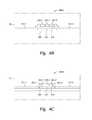
- FIG. 1is a block diagram of an exemplary input device in accordance with embodiments of the disclosure.
- FIG. 2is a partial schematic plan view of the input device of FIG. 1 in accordance with embodiments of the disclosure.
- FIG. 3Aillustrates a schematic plan view of transmitter electrodes included in the input device of FIG. 1 , through which routing traces are routed in accordance with embodiments of the disclosure.
- FIG. 3Billustrates a schematic plan view of receiver electrodes included in the input device of FIG. 1 in accordance with embodiments of the disclosure.
- FIG. 4Aillustrates a partial schematic plan view of the sensing elements of FIGS. 3A and 3B in accordance with embodiments of the disclosure.
- FIGS. 4B-4Fillustrate jumpers that provide electrical connections between segments of the sensing elements of FIGS. 3A and 3B in accordance with embodiments of the disclosure.
- FIG. 5Aillustrates a schematic plan view of transmitter electrodes included in the input device of FIG. 1 , through a portion of which routing traces are routed in accordance with embodiments of the disclosure.
- FIGS. 5B and 5Cillustrate schematic plan views of receiver electrodes included in the input device of FIG. 1 in accordance with embodiments of the disclosure.
- FIG. 6Aillustrates a partial schematic plan view of the sensing elements of FIGS. 5A and 5B in accordance with embodiments of the disclosure.
- FIG. 6Billustrates a partial cross-sectional view of the sensing elements of FIGS. 5A and 5B in accordance with embodiments of the disclosure.
- FIG. 7Aillustrates a partial schematic plan view of sensing elements included in the input device of FIG. 1 in accordance with embodiments of the disclosure.
- FIG. 7Billustrates a partial cross-sectional view of the sensing elements of FIG. 7A in accordance with embodiments of the disclosure.
- FIGS. 8 and 9illustrate partial schematic plan views of sensing elements included in the input device of FIG. 1 in which multiple electrodes cross each other along the same axis in accordance with embodiments of the disclosure.
- FIG. 10illustrates a partial schematic plan view of sensing elements included in the input device of FIG. 1 in which sensor electrodes have topological asymmetry in accordance with embodiments of the disclosure.
- FIG. 11illustrates a partial schematic plan view of sensing elements included in the input device of FIG. 1 in which sensor electrodes have geometrical asymmetry in accordance with embodiments of the disclosure.
- FIG. 12illustrates a partial schematic plan view of sensing elements included in the input device of FIG. 1 in which three sensor electrode types are disposed along the same axis in accordance with embodiments of the disclosure.
- FIG. 13is a flow chart of a method for performing input sensing using the input device of FIG. 1 in accordance with embodiments of the disclosure.
- Various embodiments of the present technologygenerally provide sensor electrode configurations that enable routing traces to be routed through the sensor region of an input device instead of (or in addition to) disposing the routing traces along a border width of the input device. Further, one or more types of sensor electrodes may be routed through each other such that the number of routed traces disposed along the border width of the input device is reduced. In addition to reducing the border width of the input device, routing the sensor electrodes through a sensor region of an input device may improve capacitive response uniformity, such as by increasing geometrical and topological symmetry of the sensor electrodes. For example, reducing the number of routing traces that are routed along the border width of the input device may reduce or eliminate response non-uniformities experienced by capacitive pixels that are positioned near the border width.
- FIG. 1is a block diagram of an exemplary input device 100 in accordance with embodiments of the disclosure.
- the input device 100includes a display device 160 and a discrete sensing device, such as a capacitive sensing device.
- the input device 100includes a display device and a sensing device, such as a capacitive sensing device, that is at least partially integrated with the display device.
- the input device 100may be configured to provide input to an electronic system (not shown).
- the term “electronic system”broadly refers to any system capable of electronically processing information.
- Some non-limiting examples of electronic systemsinclude personal computers of all sizes and shapes, such as desktop computers, laptop computers, tablets, web browsers, e-book readers, and personal digital assistants (PDAs). Additional examples of electronic systems include composite input devices, such as physical keyboards that include the input device 100 and separate joysticks or key switches. Further exemplary electronic systems include peripherals, such as data input devices (including remote controls and mice) and data output devices (including display screens and printers). Other examples include remote terminals, kiosks, and video game machines (e.g., video game consoles, portable gaming devices, and the like). Other examples include communication devices (including cellular phones, such as smart phones) and media devices (including recorders, editors, and players such as televisions, set-top boxes, music players, digital photo frames, and digital cameras). Additionally, the electronic system could be a host or a slave to the input device.
- the input device 100can be implemented as a physical part of the electronic system or can be physically separate from the electronic system. As appropriate, the input device 100 may communicate with parts of the electronic system using any one or more of the following: buses, networks, and other wired or wireless interconnections (including serial and/or parallel connections). Examples include I 2 C, SPI, PS/2, Universal Serial Bus (USB), Bluetooth, RF, and IRDA.
- buses, networks, and other wired or wireless interconnectionsincluding serial and/or parallel connections. Examples include I 2 C, SPI, PS/2, Universal Serial Bus (USB), Bluetooth, RF, and IRDA.
- the input device 100is shown as a proximity sensor device (also often referred to as a “touchpad” or a “touch sensor device”) configured to sense input provided by one or more input objects 140 in a sensing region 120 .
- a proximity sensor devicealso often referred to as a “touchpad” or a “touch sensor device”
- input objects 140include fingers and stylus, as shown in FIG. 1 .
- Sensing region 120overlays the display screen of the display device 160 and encompasses any space above, around, in, and/or near the input device 100 in which the input device 100 is able to detect user input (e.g., user input provided by one or more input objects 140 ).
- user inpute.g., user input provided by one or more input objects 140 .
- the sizes, shapes, and locations of particular sensing regionsmay vary widely from embodiment to embodiment.
- the sensing region 120extends from a surface of the input device 100 in one or more directions into space until signal-to-noise ratios prevent sufficiently accurate object detection.
- the distance to which this sensing region 120 extends in a particular directionmay be on the order of less than a millimeter, millimeters, centimeters, or more, and may vary significantly with the type of sensing technology used and the accuracy desired.
- some embodimentssense input that comprises no contact with any surfaces of the input device 100 , contact with an input surface (e.g., a touch surface) of the input device 100 , contact with an input surface of the input device 100 coupled with some amount of applied force or pressure, and/or a combination thereof.
- input surfacesmay be provided by surfaces of casings within which the sensor electrodes reside, by face sheets applied over the sensor electrodes or any casings, etc.
- the sensing region 120has a rectangular shape when projected onto an input surface of the input device 100 .
- the face sheete.g., an LCD lens
- the face sheetmay provide a useful contact surface for an input object.
- the input device 100may utilize any combination of sensor components and sensing technologies to detect user input in the sensing region 120 .
- the input device 100comprises one or more sensing elements for detecting user input. Some implementations are configured to provide images that span one, two, three, or higher dimensional spaces. Some implementations are configured to provide projections of input along particular axes or planes. Cursors, menus, lists, and items may be displayed as part of a graphical user interface and may be scaled, positioned, selected scrolled, or moved.
- voltage or currentis applied to create an electric field. Nearby input objects cause changes in the electric field and produce detectable changes in capacitive coupling that may be detected as changes in voltage, current, or the like.
- Some capacitive implementationsutilize arrays or other regular or irregular patterns of capacitive sensing elements 150 , such as sensor electrodes, to create electric fields. In some capacitive implementations, separate sensing elements 150 may be ohmically shorted together to form larger sensor electrodes. Some capacitive implementations utilize resistive sheets (e.g., may comprise a resistive material such as ITO, carbon nanotubes, nanowires, metal mesh(es), graphene, or the like), which may be uniformly resistive.
- resistive sheetse.g., may comprise a resistive material such as ITO, carbon nanotubes, nanowires, metal mesh(es), graphene, or the like
- Some capacitive implementationsutilize “self capacitance” (or “absolute capacitance”) sensing methods based on changes in the capacitive coupling between sensor electrodes and an input object.
- an input object near the sensor electrodesalters the electric field near the sensor electrodes, changing the measured capacitive coupling.
- an absolute capacitance sensing methodoperates by modulating sensor electrodes with respect to a reference voltage (e.g., system ground) and by detecting the capacitive coupling between the sensor electrodes and input objects.
- a transcapacitive sensing methodoperates by detecting the capacitive coupling between one or more transmitter sensor electrodes (also “transmitter electrodes” or “transmitters”) and one or more receiver sensor electrodes (also “receiver electrodes” or “receivers”). Transmitter sensor electrodes may be modulated relative to a reference voltage (e.g., system ground) to transmit transmitter signals.
- a reference voltagee.g., system ground
- Receiver sensor electrodesmay be held substantially constant relative to the reference voltage to facilitate receipt of resulting signals.
- a resulting signalmay comprise effect(s) corresponding to one or more transmitter signals and/or to one or more sources of environmental interference (e.g., other electromagnetic signals).
- Sensor electrodesmay be dedicated transmitters or receivers, or sensor electrodes may be configured to both transmit and receive. Alternatively, the receiver electrodes may be modulated relative to ground.
- transmitter electrodescomprise one or more common electrodes (e.g., “V-com electrode”) used in updating the display (e.g., display lines) of the display screen.
- V-com electrodeused in updating the display (e.g., display lines) of the display screen.
- These common electrodesmay be disposed on an appropriate display screen substrate.
- the common electrodesmay be disposed on the TFT glass in some display screens (e.g., in-plane switching (IPS) or plane-to-line switching (PLS)), on the bottom of the color filter glass of some display screens (e.g., patterned vertical alignment (PVA) or multi-domain vertical alignment (MVA)), configured to drive an organic light emitting diode OLED display, etc.
- IPSin-plane switching
- PLSplane-to-line switching
- PVApatterned vertical alignment
- MVAmulti-domain vertical alignment
- the common electrodecan also be referred to as a “combination electrode,” since it performs multiple functions.
- two or more transmitter electrodesmay share one or more common electrodes.
- other display elementssuch as source drivers, gate select lines, storage capacitors, and the like, may be used to perform capacitive sensing.
- the sensing elements 150may be formed as discrete geometric forms, polygons, bars, pads, lines, or other shapes that are ohmically isolated from one another. When formed as discrete geometric elements, the sensing elements 150 may be driven using absolute sensing and/or transcapacitance sensing methods. The sensing elements 150 may be electrically coupled through circuitry to form electrodes of having larger plan area relative to the individual sensing elements 150 . The sensing elements 150 may be formed as a contiguous body of conductive material having little or no open area (i.e., having a planar surface uninterrupted by holes) or may alternatively be fabricated to form a body of material having openings formed therethrough.
- the sensing elements 150may be formed from a mesh of conductive material, such as a plurality of interconnected thin metal wires.
- the sensing electrodes 150may include a grid electrode.
- the grid electrodemay be disposed between at least two discrete sensing elements 150 and/or may at least partially circumscribe one or more discrete sensing elements 150 .
- the grid electrodemay be a planar body having a plurality of apertures, where each aperture circumscribes a discrete sensing element 150 .
- the grid electrodemay also be segmented.
- a processing system 110is shown as part of the input device 100 .
- the processing system 110is configured to operate the hardware of the input device 100 to detect input in the sensing region 120 .
- the sensing region 120includes an array of sensing elements 150 .
- the processing system 110comprises parts of, or all of, one or more integrated circuits (ICs) and/or other circuitry components.
- ICsintegrated circuits
- a processing system for a mutual capacitance sensor devicemay comprise transmitter circuitry configured to transmit signals with transmitter sensor electrodes and/or receiver circuitry configured to receive signals with receiver sensor electrodes.
- the processing system 110also comprises electronically-readable instructions, such as firmware code, software code, and the like.
- components of the processing system 110are located together, such as near sensing element(s) of the input device 100 . In other embodiments, components of processing system 110 are physically separate from one or more components close to sensing element(s) of input device 100 and one or more components elsewhere.
- the input device 100may be a peripheral coupled to a desktop computer, and the processing system 110 may include software configured to run on a central processing unit of the desktop computer and one or more ICs (perhaps with associated firmware) separate from the central processing unit.
- the input device 100may be physically integrated in a phone, and the processing system 110 may comprise circuits and firmware that are part of a main processor of the phone.
- the processing system 110is dedicated to implementing the input device 100 . In other embodiments, the processing system 110 also performs other functions, such as operating display screens, driving haptic actuators, etc.
- the processing system 110may be implemented as a set of modules that handle different functions of the processing system 110 .
- Each modulemay comprise circuitry that is a part of the processing system 110 , firmware, software, or a combination thereof.
- Example modulesinclude hardware operation modules for operating hardware such as sensor electrodes and display screens, data processing modules for processing data such as sensor signals and positional information, and reporting modules for reporting information.
- Further example modulesinclude sensor operation modules configured to operate sensing element(s) to detect input, identification modules configured to identify gestures such as mode changing gestures, and mode changing modules for changing operation modes.
- the processing system 110responds to user input (or lack of user input) in the sensing region 120 directly by causing one or more actions.
- Example actionsinclude changing operation modes, as well as GUI actions such as cursor movement, selection, menu navigation, and other functions.
- the processing system 110provides information about the input (or lack of input) to some part of the electronic system (e.g., to a central processing system of the electronic system that is separate from the processing system 110 , if such a separate central processing system exists).
- some part of the electronic systemprocesses information received from the processing system 110 to act on user input, such as to facilitate a full range of actions, including mode changing actions and GUI actions.
- the processing system 110operates the sensing element(s) of the input device 100 to produce electrical signals indicative of input (or lack of input) in the sensing region 120 .
- the processing system 110may perform any appropriate amount of processing on the electrical signals in producing the information provided to the electronic system.
- the processing system 110may digitize analog electrical signals obtained from the sensor electrodes.
- the processing system 110may perform filtering or other signal conditioning.
- the processing system 110may subtract or otherwise account for a baseline, such that the information reflects a difference between the electrical signals and the baseline.
- the processing system 110may determine positional information, recognize inputs as commands, recognize handwriting, and the like.
- Positional informationas used herein broadly encompasses absolute position, relative position, velocity, acceleration, and other types of spatial information.
- Exemplary “zero-dimensional” positional informationincludes near/far or contact/no contact information.
- Exemplary “one-dimensional” positional informationincludes positions along an axis.
- Exemplary “two-dimensional” positional informationincludes motions in a plane.
- Exemplary “three-dimensional” positional informationincludes instantaneous or average velocities in space. Further examples include other representations of spatial information.
- Historical data regarding one or more types of positional informationmay also be determined and/or stored, including, for example, historical data that tracks position, motion, or instantaneous velocity over time.
- the input device 100is implemented with additional input components that are operated by the processing system 110 or by some other processing system. These additional input components may provide redundant functionality for input in the sensing region 120 or some other functionality.
- FIG. 1shows buttons 130 near the sensing region 120 that can be used to facilitate selection of items using the input device 100 .
- Other types of additional input componentsinclude sliders, balls, wheels, switches, and the like.
- the input device 100may be implemented with no other input components.
- the input device 100comprises a touch screen interface, and the sensing region 120 of the sensing device overlaps at least part of an active area of a display screen of the display device 160 .
- the input device 100may comprise substantially transparent sensor electrodes overlaying the display screen and provide a touch screen interface for the associated electronic system.
- the display screenmay be any type of dynamic display capable of displaying a visual interface to a user, and may include any type of light emitting diode (LED), organic LED (OLED), cathode ray tube (CRT), liquid crystal display (LCD), plasma, electroluminescence (EL), or other display technology.
- the input device 100 and the display screenmay share physical elements.
- some embodimentsmay utilize some of the same electrical components for displaying and sensing.
- a common electrodemay be utilized to update a display line during a display update period and utilized to perform input sensing during a non-display period.
- the display screenmay be operated in part or in total by the processing system 110 .
- the mechanisms of the present disclosureare capable of being distributed as a program product (e.g., software) in a variety of forms.
- the mechanisms of the present disclosuremay be implemented and distributed as a software program on information bearing media that are readable by electronic processors (e.g., non-transitory computer-readable and/or recordable/writable information bearing media readable by the processing system 110 ).
- the embodiments of the present disclosureapply equally regardless of the particular type of medium used to carry out the distribution. Examples of non-transitory, electronically readable media include various discs, memory sticks, memory cards, memory modules, and the like. Electronically readable media may be based on flash, optical, magnetic, holographic, or any other storage technology.
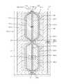
- FIG. 2is a partial schematic plan view of the input device 100 of FIG. 1 in accordance with embodiments of the disclosure.
- the input device 100includes an array of sensing elements 150 and processing system 110 .
- the array of sensing elements 150includes a plurality of transmitter electrodes 210 (e.g., 210 - 1 , 210 - 2 , 210 - 3 , etc.) and a plurality of receiver electrodes 220 (e.g., 220 - 1 , 220 - 2 , 220 - 3 , etc.).
- Each transmitter electrode 210may comprise one or more common electrodes 212 , such as one or more segments of a Vcom electrode, a source line, select line, an anode sub-pixel electrode, cathode pixel electrode, or any other display element that is used for both display updating and input sensing.
- each receiver electrode 220may comprise one or more common electrodes (e.g., gate select lines used for display updating).
- both the transmitter electrodes 210 and the receiver electrodes 220may include one or more common electrodes 212 , such as common electrodes disposed on the TFT substrate and/or color filter glass.
- the transmitter electrodes 210 and receiver electrodes 220are illustrated as being rectangular, in other embodiments, the transmitter electrodes 210 and receiver electrodes 220 may be any practical geometric shape.
- the processing system 110is coupled to the array of sensing elements 150 , for example, through one or more routing traces 230 .
- the processing system 110may include any appropriate number of ICs. As shown in FIG. 2 , the processing system 110 may include a driver module 240 , a receiver module 245 , a determination module 250 , an optional memory 260 , and/or a synchronization mechanism (not shown in FIG. 2 ).
- ICintegrated circuit
- the processing system 110may include a driver module 240 , a receiver module 245 , a determination module 250 , an optional memory 260 , and/or a synchronization mechanism (not shown in FIG. 2 ).
- the driver module 240includes driver circuitry and may be configured for updating images on the display screen of the display device 160 .
- the driver circuitrymay be configured to drive gate select lines and/or apply one or more pixel voltages to the display pixel electrodes through pixel source drivers.
- the driver circuitrymay also be configured to apply one or more common drive voltages to the common electrodes 212 to update one or more display lines of the display screen.
- the processing system 110may be configured to operate the common electrodes 212 as transmitter electrodes 210 for input sensing by driving transmitter signals onto the common electrodes 212 .
- the receiver module 245is coupled to the plurality of receiver electrodes 220 and configured to receive resulting signals from the receiver electrodes 220 indicative of input (or lack of input) in the sensing region 120 and/or of environmental interference.
- the receiver module 245may also be configured to pass the resulting signals to the determination module 250 for determining the presence of an input object and/or to the optional memory 260 for storage.
- the receiver module 245is configured to receive resulting signals while the processing system 110 is not actively transmitting input sensing signals with the transmitter electrodes 210 .
- the receiver electrodes 220may be configured to receive noise (e.g., to determine a baseline interference value) and/or a signal from an active input object 140 capable of transmitting a transmitter signal, such as an active pen capable of transmitting an active pen signal.
- the receiver module 245 and/or driver module 240may be configured to drive a signal onto one or more sensing elements 150 to detect changes in capacitance (e.g., absolute capacitance or transcapacitance) of the sensing element 150 due to the presence of an input object 140 .
- the functions of the processing system 110may be implemented in more than one IC to control elements of the display device 160 (e.g., common electrodes 212 ) and drive transmitter signals and/or receive resulting signals received from the array of sensing elements 150 .
- one ICmay be configured to perform input sensing and another IC may be configured to perform display updating.
- one ICmay be configured to perform the functions of the driver module 240
- another ICmay be configured to perform the functions of the receiver module 245 .
- communications between separate ICs of the processing system 110may be achieved through a synchronization mechanism, which sequences the signals provided to the common electrodes.
- the synchronization mechanismmay be internal to any one of the ICs.
- Transmitter electrodes 210 and receiver electrodes 220are ohmically isolated from each other by one or more insulators which separate the transmitter electrodes 210 from the receiver electrodes 220 and prevent them from electrically shorting to each other.
- the electrically insulative materialseparates the transmitter electrodes 210 and the receiver electrodes 220 at cross-over areas at which the electrodes intersect.
- the transmitter electrodes 210 and/or receiver electrodes 220are formed with jumpers connecting different portions of the same electrode.
- the transmitter electrodes 210 and the receiver electrodes 220are separated by one or more layers of electrically insulative material or by one or more substrates, as described in further detail below.
- the transmitter electrodes 210 and the receiver electrodes 220are optionally disposed on a single layer of the input device 100 .
- the areas of localized capacitive coupling between transmitter electrodes 210 and receiver electrodes 220may be termed “capacitive pixels.”
- the capacitive coupling between the transmitter electrodes 210 and receiver electrodes 220changes with the proximity and motion of input objects in the sensing region 120 associated with the transmitter electrodes 210 and the receiver electrodes 220 .
- the term “capacitive pixels”may refer to the localized capacitance (e.g., absolute capacitance) between a sensing element 150 and an input object 140 .
- the sensor patternis “scanned” to determine these capacitive couplings. That is, the transmitter electrodes 210 are driven to transmit transmitter signals. Transmitters may be operated such that one transmitter electrode 210 transmits at one time, or multiple transmitter electrodes 210 transmit at the same time. Where multiple transmitter electrodes 210 transmit simultaneously, these multiple transmitter electrodes 210 may transmit the same transmitter signal and effectively produce an effectively larger transmitter electrode 210 , or these multiple transmitter electrodes 210 may transmit different transmitter signals. For example, multiple transmitter electrodes 210 may transmit different transmitter signals according to one or more coding schemes that enable their combined effects on the resulting signals of receiver electrodes 220 to be independently determined. Additionally, in embodiments that implement matrix sensing techniques, the sensing elements 150 may be scanned to sense changes to absolute capacitance on the electrodes.
- the receiver electrodes 220may be operated singly or multiply to acquire resulting signals.
- the resulting signalsmay be used to determine measurements of the capacitive couplings at the capacitive pixels.
- a set of measurements from the capacitive pixelsform a “capacitive image” (also “capacitive frame”) representative of the capacitive couplings at the pixels.
- Capacitive imagealso “capacitive frame”
- Multiple capacitive imagesmay be acquired over multiple time periods, and differences between them used to derive information about input in the sensing region. For example, successive capacitive images acquired over successive periods of time can be used to track the motion(s) of one or more input objects entering, exiting, and within the sensing region.
- sensor electrodesmay be coupled to the processing system 110 via a plurality of routing traces 230 that are disposed in a border width 232 of the input device 100 .
- the inclusion of a border width 232 in input device 100prevents the sensing region 150 of the proximity sensor and—in embodiments in which common electrodes are used for both input sensing and displaying updating—the viewable portion of the display device 160 from extending to the edge of the input device 100 .
- signals transmitted through the routing traces 230may couple to transmitter electrodes 210 and/or receiver electrodes 220 , creating an asymmetrical response at capacitive pixels that are located near the border width 232 of the input device 100 .
- the routing traces that couple the sensor electrodes to the processing system 110may be disposed within the areal extent of the sensing elements 150 (referred to herein as the “sensor region”), instead of (or in addition to) disposing the routing traces in a border width 232 of the input device 100 .
- the sensing elements 150referred to herein as the “sensor region”
- FIGS. 3-12Such embodiments are described below in further detail in conjunction with FIGS. 3-12 .
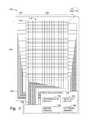
- FIG. 3Aillustrates a schematic plan view of transmitter electrodes 310 included in the input device 100 of FIG. 1 , through which routing traces 330 are routed in accordance with embodiments of the disclosure.
- the routing traces 330 that couple the transmitter electrodes 310 to the processing system 110may be disposed within the sensor region, decreasing the border width of the input device 100 and reducing the degree to which routing traces 330 asymmetrically affect the response of capacitive pixels included in the sensor region.
- the routing traces 330are routed through one or more bypasses 315 included in the transmitter electrodes 310 .
- the routing traces 330 associated with transmitter electrode 310 - 1may be routed through bypasses 315 included in transmitter electrodes 310 - 2 through 310 - 11 .
- the transmitter electrodes 310e.g., transmitter electrodes 310 - 2
- the routing traces 330may be disposed on the same layers or different layers of the input device 100 .
- the transmitter electrodes 310 and the routing traces 330are disposed on the same layer of the input device 100 , the transmitter electrodes 310 may be segmented at bypasses, which enable routing traces 330 to be routed through the transmitter electrodes 310 .
- a given row of transmitter electrode segmentsmay then be electrically coupled using jumpers to form a continuous transmitter electrode 310 along each row of the input device 100 .
- the jumpersmay electrically insulate the transmitter electrodes 310 from routing trace(s) 330 that are routed through the transmitter electrode 310 , as described in further detail in conjunction with FIGS. 4A and 4B .
- the transmitter electrodes 310may be disposed on a first layer of the input device 100 , and the routing traces 330 may be disposed on a second layer of the input device. The routing traces 330 may then be electrically coupled to the transmitter electrodes 310 using one or more through-substrate vias.
- the first layer and second layermay correspond to two sides of a single substrate, or the first layer and second layer may be associated with different substrates.
- more than half of the length of the perimeter of the input deviceis free of routing traces. That is, in contrast to conventional input device designs, the routing traces 330 extend along less than half of the perimeter of the input device 100 .
- the top edge of the input device 100is free of routing traces, and more than 80% of the length of the left edge and the right edge of the input device 100 are free of routing traces, enabling the border width to be reduced, and reducing the degree to which the routing traces produce asymmetrical responses in capacitive pixels along the edges of the input device 100 .
- the top edge, left edge, and right edge of the input device 100may be entirely free of routing of traces, for example, by increasing the number of bypasses 315 that are present in the sensor region.
- increasing the number of bypasses 315 included in the sensor regione.g., by increasing the number of transmitter electrode segments associated with each transmitter electrode 310
- no routing tracesare routed along the edge of the input device 100 .
- FIG. 3Billustrates a schematic plan view of receiver electrodes 320 , 322 included in the input device 100 of FIG. 1 , in accordance with embodiments of the disclosure.
- each receiver electrode 320e.g., receiver electrode 320 - 1
- a receiver electrode 322e.g., receiver electrode 322 - 1
- routing the receiver electrodes 320 , 322 through one another in a given column of the input device 100enables input sensing to be performed using two capacitive pixels for each transmitter electrode 310 intersected by the column. Additionally, in such configurations, substantial topological and geometrical symmetry is maintained relative to the transmitter electrodes 310 .
- FIG. 4Aillustrates a partial schematic plan view of the sensing elements 150 of FIGS. 3A and 3B in accordance with embodiments of the disclosure.
- the sensing elements 150may include transmitter electrode segments 311 - 1 , 311 - 2 and 311 - 3 , receiver electrode segments 321 - 1 and 321 - 2 , receiver electrode segments 323 - 1 and 323 - 2 , and ground electrode segments 341 - 1 , 341 - 2 , and 341 - 3 .
- the transmitter electrode segments 311 - 1 , 311 - 2 , and 311 - 3are electrically coupled by jumpers 360 - 1 and 360 - 2 to form transmitter electrode 310 - 11 .
- each of transmitter electrode segments 311 - 1 , 311 - 2 , 311 - 3 , etc., included in the corresponding row of the input device 100may be coupled to form transmitter electrode 310 - 11 using jumpers 360 that extend over and/or pass underneath the receiver electrodes 320 , 322 , routing traces 330 , ground electrodes 340 , etc.
- jumper 360 - 1extends across receiver electrode 322 - 1 , ground electrode 340 , and receiver electrode 320 - 1 , as shown in FIG. 4B .
- jumper 360 - 1may provide electrical connectivity between transmitter electrode segments 311 - 1 and 311 - 2 while also insulating the transmitter electrode 310 - 11 from receiver electrode 322 - 1 , ground electrode 340 , and receiver electrode 320 - 1 .
- jumper 360 - 2extends across a bypass 315 through which a routing trace 330 associated with transmitter electrode 310 - 8 is routed.
- jumper 360 - 2may provide electrical connectivity between transmitter electrode segments 311 - 2 and 311 - 3 while also insulating the transmitter electrode 310 - 11 from the routing trace 330 that electrically couples transmitter electrode 310 - 8 to the processing system 110 .
- the receiver electrode segments 321 - 1 and 321 - 2are electrically coupled by a jumper 360 - 3 to form receiver electrode 320 - 1
- the receiver electrode segments 323 - 1 and 323 - 2are electrically coupled by a jumper 360 - 4 to form receiver electrode 322 - 1
- the ground electrode segments 341 - 1 , 341 - 2 , and 341 - 3are electrically coupled by a jumper 360 - 5 to form a ground electrode 340 (e.g., ground electrode 340 - 1 ).
- Cross-sectional views of the connectivity provided by jumpers 360 - 3 , 360 - 4 , and 360 - 5is discussed in further detail in conjunction with FIGS. 4C-4F , respectively.
- the sensing elements 150 shown in FIG. 4Amay be composed of a transparent conductive oxide (TCO), such as indium tin oxide (ITO), or any other substantially transparent material, including carbon nanotubes, nanowires, metal mesh(es), and/or graphene structures.
- TCOtransparent conductive oxide
- ITOindium tin oxide
- “dummy” electrodes 350may be disposed in unused areas of the sensor region. These dummy electrodes 350 are not coupled to the processing system 110 and merely provide the substrate with a more uniform optical appearance, such as when the substrate is to be overlaid and/or integrated with a display device to form a touchscreen device.
- a ground electrode 340may disposed between receiver electrode 320 and receiver electrode 322 in order to shield the receiver electrodes 320 , 322 from one another and/or from one or more transmitter electrodes 310 .
- one or more ground electrode segments 341may be disposed between the receiver electrode 320 and receiver electrode 322 in order to control which receiver electrode 320 , 322 is receiving input sensing signals transmitted by a transmitter electrode 310 , and/or to control which receiver electrode 320 , 322 is receiving input sensing signals at a given location on a transmitter electrode 310 .
- ground electrode segments 341 - 1 and 341 - 2are disposed between receiver electrode 320 - 1 and receiver electrode 322 - 1 to reduce the degree to which receiver electrode 322 - 1 receives input sensing signals from transmitter electrode 310 - 11 .
- ground electrode segments 341 - 2 and 341 - 3are disposed between receiver electrode 320 - 1 and receiver electrode 322 - 1 to reduce the degree to which receiver electrode 320 - 1 receives input sensing signals from transmitter electrode 310 - 11 .
- receiver electrode 320 - 1is configured to receive resulting signals for the top portion (e.g., top capacitive pixel) of the transmitter electrode 310 - 11 shown in FIG. 4A
- receiver electrode 322 - 1is configured to receive resulting signals for the bottom portion (e.g., bottom capacitive pixel) of the transmitter electrode 310 - 11 shown in FIG. 4A .
- the ground electrodes 340may be used to perform input sensing, such as proximity sensing.
- the ground electrodes 340may be used to sense a hovering input object 140 (e.g., an input object 140 that is not in contact with the surface of the input device 100 ), such as by holding the ground electrodes 340 at a substantially constant voltage and measuring the amount of charge that must be added to and/or subtracted from the ground electrodes 340 in order to maintain that voltage.
- the ground electrodes 340may still provide sufficient isolation between the receiver electrodes 320 , 322 and the transmitter electrode 310 .
- the ground electrodes 340may be adapted to perform proximity sensing (e.g., hover sensing) and may no longer be configured to provide isolation between the receiver electrodes 320 , 322 and the transmitter electrodes 310 .
- FIGS. 4B-4Fillustrate jumpers 360 that provide electrical connections between segments of the sensing elements 150 of FIGS. 3A and 3B in accordance with embodiments of the disclosure.
- jumper 360 - 1extends across receiver electrode segment 323 - 1 , ground electrode segment 341 - 2 , and receiver electrode segment 321 - 2 and provides electrical connectivity between transmitter electrode segments 311 - 1 and 311 - 2 via a conductive bridge 312 , such as a conductive wire, a carbon nanotube bridge, nanowire bridge, TCO bridge, etc., disposed on the substrate 305 .
- a conductive bridge 312such as a conductive wire, a carbon nanotube bridge, nanowire bridge, TCO bridge, etc.
- transmitter electrode 310 - 11is insulated from receiver electrode 322 - 1 , ground electrode 340 , and receiver electrode 320 - 1 by an insulator 314 , such as a transparent insulator.
- receiver electrode segment 323 - 1 , ground electrode segment 341 - 2 , and receiver electrode segment 321 - 2may pass underneath the conductive bridge 312 and/or may be disposed on a different layer than the transmitter electrode 310 - 11 and/or conductive bridge 312 . More generally, in each of FIGS. 4B-4F , the locations and orientations of any of the electrodes, routing traces, conductive bridges, insulators, etc. with respect to one another—such as whether a particular component is routed over another component, routed underneath the component, etc.—may be modified in various embodiments.
- jumper 360 - 3extends across ground electrode segments 341 - 1 , 341 - 2 and receiver electrode segment 323 - 1 and provides electrical connectivity between receiver electrode segments 321 - 1 and 321 - 2 via a conductive bridge 312 disposed on the substrate 305 .
- receiver electrode 320 - 1is insulated from ground electrode 340 and receiver electrode 322 - 1 by an insulator 314 .
- jumper 360 - 4extends across ground electrode segments 341 - 2 , 341 - 3 and receiver electrode segment 321 - 2 , providing electrical connectivity between receiver electrode segments 323 - 1 and 323 - 2 while insulating the receiver electrode 322 - 1 from ground electrode 340 and receiver electrode 320 - 1 .
- jumper 360 - 5extends across dummy electrodes 350 and receiver electrode segment 321 - 2 , providing electrical connectivity between ground electrode segments 341 - 2 and 341 - 3 while insulating the ground electrode 340 from dummy electrodes 350 and receiver electrode 320 - 1 .
- jumper 360 - 2extends across a routing trace 330 associated with transmitter electrode 310 - 8 , providing electrical connectivity between ground transmitter electrode segments 311 - 2 and 311 - 3 while insulating the transmitter electrode 310 - 11 from the routing trace 330 .
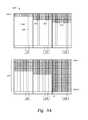
- FIG. 5Aillustrates a schematic plan view of transmitter electrodes 510 included in the input device 100 of FIG. 1 , through a portion of which routing traces 530 are routed in accordance with embodiments of the disclosure.
- one or more of the routing traces 530 that couple the transmitter electrodes 510e.g., to the processing system 110 may be disposed within the sensor region, and one or more of the routing traces 530 may be disposed along the edge of the input device 100 .
- this configurationenables transmitter electrodes 510 to be disposed on a substrate via a reduced number of processing steps while also decreasing the border width of the input device 100 and reducing the degree to which the routing traces 530 asymmetrically affect the response of capacitive pixels included in the sensor region.
- the transmitter electrodes 510 and the associated routing traces 530may be disposed on the substrate via a single patterning procedure (e.g., deposition and etching, deposition and lift-off, etc.) without needing to later fabricate jumpers to electrically couple disparate transmitter electrode segments through which routing traces are routed.
- a single patterning proceduree.g., deposition and etching, deposition and lift-off, etc.
- the routing traces 530 that electrically couple the processing system 110 to transmitter electrodes 510 - 1 through 510 - 4are disposed along either the left edge or the right edge of the input device 100 .
- the routing traces that electrically couple the processing system 110 to transmitter electrodes 510 - 5 through 510 - 9are routed through one or more of transmitter electrodes 510 - 6 through 510 - 10 .
- the routing traces 530 that couple transmitter electrode 510 - 6 to the processing system 110are routed through transmitter electrodes 510 - 7 through 510 - 10 .
- transmitter electrode 510 - 10may be electrically coupled to the processing system 110 using eight separate routing traces 530 .
- FIGS. 5B and 5Cillustrate schematic plan views of receiver electrodes 520 , 522 included in the input device 100 of FIG. 1 , in accordance with embodiments of the disclosure.
- each receiver electrode 520e.g., receiver electrode 520 - 1
- a receiver electrode 522e.g., receiver electrode 522 - 1
- both receiver electrodes 520 and receiver electrodes 522extend along the same column of the input device 100 .
- routing the receiver electrodes 520 , 522 proximate to one another along a given column of the input device 100in the alternating manner shown in FIGS.
- Ground electrodes 540may further be disposed between the receiver electrodes 520 , 522 —on the same layer as the receiver electrodes 520 , 522 or on a different layer than the receiver electrodes 520 , 522 —in order to shield the receiver electrodes 520 , 522 from routing traces 530 associated with the transmitter electrodes 510 .
- the receiver electrodes 520 , 522may be disposed on a first layer of a substrate, and the transmitter electrodes 510 may be disposed on a second layer of the same substrate or a different substrate.
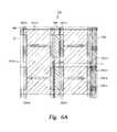
- FIG. 6Aillustrates a partial schematic plan view of the sensing elements 150 of FIGS. 5A and 5B in accordance with embodiments of the disclosure.
- FIG. 6Billustrates a partial cross-sectional view of the sensing elements 150 of FIGS. 5A and 5B in accordance with embodiments of the disclosure.
- the sensing elements 150may include transmitter electrode segments 511 - 2 and 511 - 3 , receiver electrodes 520 - 4 , 522 - 4 , 520 - 5 , 522 - 5 , and ground electrodes 540 disposed on two sides of a substrate 505 .
- one or more of the transmitter electrodes 510may be segmented.
- the routing trace 530 - 2 associated with transmitter electrode 510 - 5 and the routing traces 530 - 1 and 530 - 3 associated with transmitter electrode 510 - 6are routed through transmitter electrode 510 - 8 .
- each of the transmitter electrode segments 511 - 2 and 511 - 3 , as well as transmitter electrode segments 511 - 1 and 511 - 4 (not shown in FIGS. 6A and 6B ), associated with transmitter electrode 510 - 8are electrically coupled to the processing system 110 using separate routing traces 530 .
- each receiver electrode 520 and receiver electrode 522may be varied along the length of the sensor region such that two capacitive pixels—one associated with a receiver electrode 520 and one associated with a receiver electrode 522 —are acquired for each intersection between a column of receiver electrodes 520 , 522 and a transmitter electrode 510 .
- receiver electrodes 522 - 4 and 522 - 5may have a reduced width near the lower portion of the transmitter electrode 510 - 8 in order to enable receiver electrodes 520 - 4 and 520 - 5 to receive resulting signals in this region and to reduce the degree to which receiver electrodes 522 - 4 and 522 - 5 receive resulting signals.
- receiver electrodes 520 - 4 and 520 - 5may have a reduced width near the upper portion of the transmitter electrode 510 - 8 in order to enable receiver electrodes 522 - 4 and 522 - 5 to receive resulting signals in this region and to reduce the degree to which receiver electrodes 520 - 4 and 520 - 5 receive resulting signals. Accordingly, four distinct capacitive pixels may be acquired in the sensor region shown in FIG. 6A .
- FIG. 7Aillustrates a partial schematic plan view of sensing elements 150 included in the input device 100 of FIG. 1 in accordance with embodiments of the disclosure.
- FIG. 7Billustrates a partial cross-sectional view of the sensing elements 150 of FIG. 7A accordance with embodiments of the disclosure.
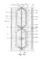
- the sensing elements 150may include transmitter electrodes 710 - 1 , 710 - 2 , and 710 - 3 , receiver electrodes 720 - 1 , 722 - 1 , 720 - 2 , 722 - 2 , 720 - 3 , and 722 - 3 , hover electrodes 724 - 1 , 724 - 2 , 724 - 3 , and 724 - 4 , and ground electrodes 740 disposed on substrate 705 .
- the width of the receiver electrodes 720 , 722has been modified to allow hover electrodes 724 to be present between each column of receiver electrodes 720 , 722 .
- the sensing elements 150may be configured to detect both touch and hover input associated with an input object 140 in the sensing region 120 of the input device 100 .
- the transmitter electrodes 710 , routing traces 730 , and receiver electrodes 720 , 722may be disposed on each side of the substrate via a single patterning procedure without needing to later fabricate jumpers to electrically couple disparate electrode segments.
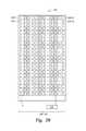
- FIGS. 8 and 9illustrate partial schematic plan views of sensing elements 150 included in the input device 100 of FIG. 1 in which multiple sensor electrodes cross each other along the same axis in accordance with embodiments of the disclosure.
- sensor electrodes 810traverse a vertical axis
- sensor electrodes 820 , 822traverse a horizontal axis.
- Sensor electrodes 820 , 822are routed through each other in order to achieve a symmetrical response of sensor electrodes 820 with respect to sensor electrodes 810 , despite topological asymmetry caused by the absence of a sensor electrode 822 in-between each sensor electrode 820 .
- sensor electrodes 820 and sensor electrodes 822perform different types of sensing and, thus, possess different geometries.
- sensor electrodes 820may be used to detect input objects 140 that are in contact with a surface of the input device 100
- sensor electrodes 822may be used for proximity sensing to detect input objects 140 that are hovering over, but not in contact with, a surface of the input device 100
- the routing traces that couple sensor electrodes 810 , 820 , 822 to the processing system 110may be routed through the sensor region (e.g., through bypasses), as discussed above.
- the sensor electrodes 810 , 820 , 822may be routed through each other such that all of the sensor electrodes 810 , 820 , 822 are routed along the same side of the input device 100 (e.g., all of the routing traces are disposed along a single side of the input device 100 ).
- sensor electrodes 910traverse a vertical axis
- sensor electrodes 920 , 922traverse a horizontal axis.
- Sensor electrodes 920 , 922are routed through each other in order to achieve a symmetrical response of the sensor electrodes 920 , 922 with respect to sensor electrodes 910 .
- a symmetrical responsemay be achieved despite topological asymmetry created by the routing traces of the sensor electrodes 920 , 922 , which are disposed between the sensor electrodes 920 , 922 , away from sensor electrodes 910 .
- Sensor electrodes 920 , 922possess equivalent geometry and alternate to define two columns for each sensor electrode 910 , which, in effect, halves the number of sensor electrodes 910 that are used.
- Such configurationsmay enable a reduced border width, faster capacitive frame scan rates (e.g., when sensor electrodes 910 are configured as transmitters in a mutual capacitance sensing configuration), and lower power/die consumption (e.g., when sensor electrodes 910 are configured as receivers in a mutual capacitance sensing configuration). Additionally, the sensor electrodes 910 , 920 , 922 may be routed through each other such that all of the sensor electrodes 910 , 920 , 922 are routed along the same side of the input device 100 (e.g., all of the routing traces are disposed along a single side of the input device 100 ).
- FIG. 10illustrates a partial schematic plan view of sensing elements 150 included in the input device 100 of FIG. 1 in which the sensor electrodes have topological asymmetry in accordance with embodiments of the disclosure.
- sensor electrodes 1020 and sensor electrodes 1022traverse a horizontal axis.
- each set of sensor electrodes 1020 and sensor electrodes 1022are used to perform a different type of input sensing (e.g., hover/proximity sensing or touch sensing).
- Sensor electrodes 1010traverse a vertical axis and may be used to perform one or more types of input sensing (e.g., hover/proximity sensing and touch sensing).
- sensor electrodes 1022may be positioned on both sides of sensor electrodes 1020 , for example, by allowing sensor electrodes 1022 to pass through sensor electrodes 1020 within each pixel, as shown in FIG. 8 .
- the sensor electrodes 1010 , 1020 , 1022may be routed through each other such that all of the sensor electrodes 1010 , 1020 , 1022 are routed along the same side of the input device 100 (e.g., all of the routing traces are disposed along a single side of the input device 100 ).
- FIG. 11illustrates a partial schematic plan view of sensing elements 150 included in the input device 100 of FIG. 1 in which the sensor electrodes have geometrical asymmetry in accordance with embodiments of the disclosure.
- sensor electrodes 1120 , 1122traverse a horizontal axis and correspond to odd/even columns of a vertical axis defined by sensor electrodes 1110 .
- Geometrical asymmetryexists due to the routing traces associated with sensor electrodes 1120 , 1122 running in-between sensor electrodes 1122 and 1110 and in-between sensor electrodes 1120 and 1110 , respectively, inducing a non-uniform response with respect to sensor electrodes 1110 .
- the sensor electrodes 1110 , 1120 , 1122may be routed through each other such that all of the sensor electrodes 1110 , 1120 , 1122 are routed along the same side of the input device 100 (e.g., all of the routing traces are disposed along a single side of the input device 100 ).
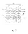
- FIG. 12illustrates a partial schematic plan view of sensing elements 150 included in the input device 100 of FIG. 1 in which three sensor electrode types are disposed along the same axis in accordance with embodiments of the disclosure.
- Sensor electrodes 1220 , 1222 , 1224may be configured to perform touch sensing and/or proximity/hover sensing while reducing the border width of the input device 100 by enabling the associated routing traces to be routed through the sensor region of the input device 100 .
- sensor electrodes 1220 , 1222may be configured as odd/even touch sensing receiver electrodes, while sensor electrodes 1224 may be configured as proximity/hover receiver electrodes.
- sensor electrodes 1224may be coupled to a system ground to mitigate the effect(s) of a weak ground connection between an input object 140 and the input device 100 .
- the sensor electrodes 1210 , 1220 , 1222 , 1224may be routed through each other such that all of the sensor electrodes 1210 , 1220 , 1222 , 1224 are routed along the same side of the input device 100 (e.g., all of the routing traces are disposed along a single side of the input device 100 ).
- FIG. 13is a flow chart of a method 1300 for performing input sensing using the input device 100 of FIG. 1 in accordance with embodiments of the disclosure.
- the method 1300is described in conjunction with FIGS. 1-12 , persons skilled in the art will understand that any system configured to perform the method, in any appropriate order, falls within the scope of the present disclosure.
- the method 1300begins at step 1310 , where the driver module 240 drives one or more types of sensor electrodes (e.g., transmitter electrodes 310 ) for input sensing.
- the receiver module 245receives resulting signals from one or more types of receiver electrodes (e.g., receiver electrodes 320 , 322 ) while the sensor electrodes are being driven for input sensing.
- the determination module 250determines positional information, such as the presence and location of an input object 140 , based on the resulting signals.
- the processing system 110determines whether additional input sensing is to be performed. If additional input sensing is to be performed, then the method 1300 returns to step 1310 . If no additional input sensing is to be performed, then the method 1300 ends.
Landscapes
- Engineering & Computer Science (AREA)
- Theoretical Computer Science (AREA)
- General Engineering & Computer Science (AREA)
- Human Computer Interaction (AREA)
- Physics & Mathematics (AREA)
- General Physics & Mathematics (AREA)
- Computer Hardware Design (AREA)
- Computer Networks & Wireless Communication (AREA)
- Quality & Reliability (AREA)
- Position Input By Displaying (AREA)
Abstract
Description
Claims (21)
Priority Applications (3)
| Application Number | Priority Date | Filing Date | Title |
|---|---|---|---|
| US14/448,527US9927832B2 (en) | 2014-04-25 | 2014-07-31 | Input device having a reduced border region |
| CN201580020380.8ACN106462303B (en) | 2014-04-25 | 2015-04-06 | Input device with reduced border area |
| PCT/US2015/024495WO2015164056A1 (en) | 2014-04-25 | 2015-04-06 | Input device having a reduced border region |
Applications Claiming Priority (2)
| Application Number | Priority Date | Filing Date | Title |
|---|---|---|---|
| US201461984656P | 2014-04-25 | 2014-04-25 | |
| US14/448,527US9927832B2 (en) | 2014-04-25 | 2014-07-31 | Input device having a reduced border region |
Publications (2)
| Publication Number | Publication Date |
|---|---|
| US20150309531A1 US20150309531A1 (en) | 2015-10-29 |
| US9927832B2true US9927832B2 (en) | 2018-03-27 |
Family
ID=54332986
Family Applications (1)
| Application Number | Title | Priority Date | Filing Date |
|---|---|---|---|
| US14/448,527Active2035-12-19US9927832B2 (en) | 2014-04-25 | 2014-07-31 | Input device having a reduced border region |
Country Status (3)
| Country | Link |
|---|---|
| US (1) | US9927832B2 (en) |
| CN (1) | CN106462303B (en) |
| WO (1) | WO2015164056A1 (en) |
Cited By (5)
| Publication number | Priority date | Publication date | Assignee | Title |
|---|---|---|---|---|
| US10185450B2 (en)* | 2015-06-23 | 2019-01-22 | Boe Technology Group Co., Ltd. | In-cell touch display panel with matrix-arranged touch electrodes having multiple common electrodes, method of manufacturing, and display device |
| US20220276761A1 (en)* | 2019-03-26 | 2022-09-01 | Hideep Inc. | Touch sensor panel |
| US11449182B2 (en) | 2019-11-11 | 2022-09-20 | Apple Inc. | Active area routing for touch electrodes |
| US11556216B2 (en) | 2020-02-03 | 2023-01-17 | Apple Inc. | Touch electrodes with bar and stripe pattern |
| US11941214B2 (en) | 2019-11-11 | 2024-03-26 | Apple Inc. | Active area routing for touch electrodes |
Families Citing this family (12)
| Publication number | Priority date | Publication date | Assignee | Title |
|---|---|---|---|---|
| US9952691B2 (en)* | 2014-05-09 | 2018-04-24 | Lg Innotek Co., Ltd. | Touch panel and image display device having the same |
| US9715304B2 (en)* | 2015-06-30 | 2017-07-25 | Synaptics Incorporated | Regular via pattern for sensor-based input device |
| US9958993B2 (en)* | 2015-06-30 | 2018-05-01 | Synaptics Incorporated | Active matrix capacitive fingerprint sensor with 1-TFT pixel architecture for display integration |
| US9715297B2 (en)* | 2015-06-30 | 2017-07-25 | Synaptics Incorporated | Flexible display and touch driver IC architecture |
| US10466839B2 (en) | 2016-03-30 | 2019-11-05 | Synaptics Incorporated | Dynamic differential algorithm for side touch signals |
| US10078406B2 (en) | 2016-03-31 | 2018-09-18 | Synaptics Incorporated | Capacitive side position extrapolation |
| WO2018006231A1 (en) | 2016-07-04 | 2018-01-11 | Boe Technology Group Co., Ltd. | Touch substrate, touch display panel and touch display apparatus having the same, and fabricating method thereof |
| CN107390941B (en)* | 2017-08-17 | 2021-01-29 | 京东方科技集团股份有限公司 | Touch substrate, touch panel, display substrate, display panel and display device |
| US11681380B2 (en)* | 2017-08-31 | 2023-06-20 | Parade Technologies, Ltd. | Adaptive electrode arrangement in a capacitive sense array |
| US11163413B2 (en)* | 2018-05-17 | 2021-11-02 | Cirque Corporation | Capacitive sensor for a three dimensional object |
| US10936135B2 (en)* | 2018-07-17 | 2021-03-02 | Apple Inc. | Single layer touch sensor panel architecture |
| US11301080B2 (en) | 2019-09-27 | 2022-04-12 | Atmel Corporation | Techniques for routing signals using inactive sensor regions of touch sensors and related systems and devices |
Citations (224)
| Publication number | Priority date | Publication date | Assignee | Title |
|---|---|---|---|---|
| US4087625A (en) | 1976-12-29 | 1978-05-02 | International Business Machines Corporation | Capacitive two dimensional tablet with single conductive layer |
| US4233522A (en) | 1978-10-30 | 1980-11-11 | General Electric Company | Capacitive touch switch array |
| US4237421A (en) | 1978-10-19 | 1980-12-02 | General Electric Company | Single-electrode capacitance touchpad sensor systems |
| US4264903A (en) | 1978-06-12 | 1981-04-28 | General Electric Company | Capacitive touch control and display |
| US4293987A (en) | 1978-03-16 | 1981-10-13 | Texas Instruments Incorporated | Method of fabricating capacitive touch switch panel |
| US4484026A (en) | 1983-03-15 | 1984-11-20 | Koala Technologies Corporation | Touch tablet data device |
| US4492958A (en) | 1981-04-22 | 1985-01-08 | Matsushita Electric Industrial Co., Ltd. | Device for controlling and displaying the functions of an electric or electronic apparatus |
| US4550221A (en) | 1983-10-07 | 1985-10-29 | Scott Mabusth | Touch sensitive control device |
| WO1986006551A1 (en) | 1985-04-30 | 1986-11-06 | Amp Incorporated | Flexible electrical jumper cable and assembly |
| US4659874A (en) | 1985-09-23 | 1987-04-21 | Sanders Associates, Inc. | X-Y position sensor |
| US4667259A (en) | 1984-04-19 | 1987-05-19 | Hitachi Metals, Ltd. | Non-magnetic part in magnetic head assembly |
| US4677259A (en) | 1985-03-29 | 1987-06-30 | Pentel Kabushiki Kaisha | Position determination device |
| US4705919A (en) | 1985-02-21 | 1987-11-10 | Dhawan Satish K | Electrostatic pattern-coupled digitizer |
| US4771138A (en) | 1985-02-21 | 1988-09-13 | Dhawan Satish K | Electrostatic pattern-coupled digitizer |
| US4878013A (en) | 1986-04-04 | 1989-10-31 | Mitutoyo Corporation | Capacitive type measurement transducer with improved electrode arrangement |
| US4954823A (en) | 1984-04-17 | 1990-09-04 | Binstead Ronald P | Touch keyboard systems |
| US4999462A (en) | 1989-10-06 | 1991-03-12 | Summagraphics Corporation | Position determining and digitizing method and device |
| US5053715A (en) | 1986-04-04 | 1991-10-01 | Mitutoyo Corporation | Capacitance-type measuring device for absolute measurement of positions |
| US5062916A (en) | 1990-08-01 | 1991-11-05 | W. H. Brady Co. | Method for the manufacture of electrical membrane panels having circuits on flexible plastic films |
| US5239307A (en) | 1989-10-10 | 1993-08-24 | Micro Encoder Inc. | Method and apparatus for sensing of position |
| US5341233A (en) | 1991-05-15 | 1994-08-23 | Idemitsu Kosan Co., Ltd. | Liquid crystal module with tab assemblies connected through a flexible circuit board |
| US5459463A (en) | 1990-05-25 | 1995-10-17 | Sextant Avionique | Device for locating an object situated close to a detection area and a transparent keyboard using said device |
| US5463388A (en) | 1993-01-29 | 1995-10-31 | At&T Ipm Corp. | Computer mouse or keyboard input device utilizing capacitive sensors |
| US5650597A (en) | 1995-01-20 | 1997-07-22 | Dynapro Systems, Inc. | Capacitive touch sensor |
| US5657012A (en) | 1989-06-21 | 1997-08-12 | Tait; David Adams Gilmour | Finger operable control device |
| EP0810540A2 (en) | 1996-05-30 | 1997-12-03 | Motorola, Inc. | Contactless identification system |
| US5777596A (en) | 1995-11-13 | 1998-07-07 | Symbios, Inc. | Touch sensitive flat panel display |
| US5841078A (en) | 1992-06-08 | 1998-11-24 | Synaptics, Inc. | Object position detector |
| US5869790A (en) | 1995-08-16 | 1999-02-09 | Alps Electric Co., Ltd. | Coordinate input apparatus having orthogonal electrodes on opposite surfaces of a dielectric substrate and through-hole connections and manufacturing method thereof |
| EP0919945A2 (en) | 1997-11-28 | 1999-06-02 | Matsushita Electric Industrial Co., Ltd | Card Reader |
| EP0977159A1 (en) | 1998-07-27 | 2000-02-02 | Hitachi Computer Products (Europe) S.A. | Electronic terminal apparatus |
| WO2000057344A1 (en) | 1999-03-22 | 2000-09-28 | Link Pack Limited | Contactless smart card reader |
| US6188391B1 (en) | 1998-07-09 | 2001-02-13 | Synaptics, Inc. | Two-layer capacitive touchpad and method of making same |
| US6222522B1 (en) | 1998-09-18 | 2001-04-24 | Interval Research Corporation | Baton and X, Y, Z, position sensor |
| CN2436978Y (en) | 2000-08-04 | 2001-06-27 | 陈竹林 | Contactless card reading device |
| US6256022B1 (en) | 1998-11-06 | 2001-07-03 | Stmicroelectronics S.R.L. | Low-cost semiconductor user input device |
| US6281888B1 (en) | 1999-01-07 | 2001-08-28 | International Business Machines Corporation | Pen input device using electrostatic coupling |
| US6288707B1 (en) | 1996-07-29 | 2001-09-11 | Harald Philipp | Capacitive position sensor |
| US6297811B1 (en) | 1999-06-02 | 2001-10-02 | Elo Touchsystems, Inc. | Projective capacitive touchscreen |
| US6307751B1 (en) | 1998-06-01 | 2001-10-23 | Wearlogic, Inc. | Flexible circuit assembly |
| US6320394B1 (en) | 1996-02-14 | 2001-11-20 | Stmicroelectronics S.R.L. | Capacitive distance sensor |
| US6362633B1 (en) | 1996-02-14 | 2002-03-26 | Stmicroelectronics S.R.L. | Capacitive distance sensor |
| US6380930B1 (en) | 1999-03-09 | 2002-04-30 | K-Tech Devices Corporation | Laptop touchpad with integrated antenna |
| US20020077313A1 (en) | 1995-11-30 | 2002-06-20 | Board Of Regents, The University Of Texas System | Methods and compositions for the diagnosis and treatment of cancer |
| JP2002215330A (en) | 2001-01-16 | 2002-08-02 | Digital Electronics Corp | User interface device, touch panel, membrane switch, and method of manufacturing the user interface device |
| US6452514B1 (en) | 1999-01-26 | 2002-09-17 | Harald Philipp | Capacitive sensor and array |
| JP2002268768A (en) | 2001-03-13 | 2002-09-20 | Sony Corp | Information processor |
| JP2002268786A (en) | 2001-03-08 | 2002-09-20 | Aoki Ryutsu Kk | Mobile equipment capable of comparing information |
| US6459044B2 (en) | 2000-07-21 | 2002-10-01 | Alps Electric Co., Ltd. | Flexible multilayer wiring board |
| US6486862B1 (en) | 1996-10-31 | 2002-11-26 | Kopin Corporation | Card reader display system |
| US6512381B2 (en) | 1999-12-30 | 2003-01-28 | Stmicroelectronics, Inc. | Enhanced fingerprint detection |
| US6535200B2 (en) | 1999-01-25 | 2003-03-18 | Harald Philipp | Capacitive position sensor |
| US20030052867A1 (en) | 2001-09-20 | 2003-03-20 | Alps Electric Co., Ltd. | Capacitive input device |
| US20030103043A1 (en) | 2001-11-30 | 2003-06-05 | 3M Innovative Properties Company | System and method for locating a touch on a capacitive touch screen |
| US6583632B2 (en) | 1998-07-23 | 2003-06-24 | Micronas Gmbh | Method of determining very small capacitances |
| US6653736B2 (en) | 1999-11-10 | 2003-11-25 | Sony Chemicals Corporation | Multilayer flexible wiring boards |
| US20030234771A1 (en) | 2002-06-21 | 2003-12-25 | Mulligan Roger C. | Capacitive touch sensor architecture with unique sensor bar addressing |
| US20040062012A1 (en) | 2002-09-27 | 2004-04-01 | Kabushiki Kaisha Toshiba | Method of mounting combination-type IC card |
| CN1490713A (en) | 2002-05-29 | 2004-04-21 | ��ʿͨ��ʽ���� | touch screen device |
| US20040077313A1 (en) | 2001-09-13 | 2004-04-22 | Haruo Oba | Information processing apparatus and method |
| US20040125087A1 (en) | 2002-08-02 | 2004-07-01 | Brian Taylor | Single-layer touchpad having touch zones |
| US6771327B2 (en) | 2000-09-18 | 2004-08-03 | Citizen Watch Co., Ltd. | Liquid crystal display device with an input panel |
| US20040222974A1 (en) | 2002-12-31 | 2004-11-11 | Lg.Philips Lcd Co., Ltd. | Touch panel for display device and method of fabricating the same |
| US20040239650A1 (en) | 2003-06-02 | 2004-12-02 | Mackey Bob Lee | Sensor patterns for a capacitive sensing apparatus |
| US20040252109A1 (en) | 2002-04-11 | 2004-12-16 | Synaptics, Inc. | Closed-loop sensor on a solid-state object position detector |
| US20050030048A1 (en) | 2003-08-05 | 2005-02-10 | Bolender Robert J. | Capacitive sensing device for use in a keypad assembly |
| US6879930B2 (en) | 2001-03-30 | 2005-04-12 | Microsoft Corporation | Capacitance touch slider |
| US6910634B1 (en) | 1999-11-12 | 2005-06-28 | Hitachi Maxell, Ltd. | Information input/ output unit |
| US6937031B2 (en) | 2001-07-11 | 2005-08-30 | Sony Corporation | Electrostatic capacity detection apparatus and fingerprint crosscheck apparatus using the same |
| US20060038754A1 (en) | 2004-07-28 | 2006-02-23 | Kim Yang W | Pixel circuit and organic light emitting display using the same |
| US20060097991A1 (en) | 2004-05-06 | 2006-05-11 | Apple Computer, Inc. | Multipoint touchscreen |
| US20060114240A1 (en) | 2004-11-05 | 2006-06-01 | Holtek Semiconductor Inc. | Controlling device for cursor and method for operating the same |
| US20060114241A1 (en) | 2004-11-29 | 2006-06-01 | Holtek Semiconductor Inc. | Identification method for touch control device |
| US20060232600A1 (en) | 2005-04-14 | 2006-10-19 | Semiconductor Energy Laboratory Co., Ltd. | Display device, driving method of the display device, and electronic device |
| US20070008299A1 (en) | 2005-07-08 | 2007-01-11 | Harald Philipp | Two-Dimensional Position Sensor |
| US7218314B2 (en) | 2001-06-07 | 2007-05-15 | Alps Electric Co., Ltd. | Coordinate input device |
| US20070222762A1 (en) | 2004-04-14 | 2007-09-27 | Koninklijke Philips Electronics, N.V. | Touch Sensitive Display |
| US20070229470A1 (en) | 2006-03-31 | 2007-10-04 | Warren Snyder | Capacitive touch sense device having polygonal shaped sensor elements |
| US20070229468A1 (en) | 2006-03-30 | 2007-10-04 | Cypress Semiconductor Corporation | Apparatus and method for reducing average scan rate to detect a conductive object on a sensing device |
| US20070229466A1 (en) | 2006-03-30 | 2007-10-04 | Cypress Semiconductor Corporation | Apparatus and method for recognizing a tap gesture on a touch sensing device |
| US20070229469A1 (en) | 2006-03-31 | 2007-10-04 | Ryan Seguine | Non-planar touch sensor pad |
| US20070242054A1 (en) | 2006-04-14 | 2007-10-18 | Ritdisplay Corporation | Light transmission touch panel and manufacturing method thereof |
| US20070257894A1 (en) | 2006-05-05 | 2007-11-08 | Harald Philipp | Touch Screen Element |
| US20070262962A1 (en) | 2006-05-10 | 2007-11-15 | Cypress Semiconductor Corporation | Apparatus and method for reducing charge time and power consumption of a sensing device |
| US20070262963A1 (en) | 2006-05-11 | 2007-11-15 | Cypress Semiconductor Corporation | Apparatus and method for recognizing a button operation on a sensing device |
| US20070268265A1 (en) | 2006-05-18 | 2007-11-22 | Cypress Semiconductor Corporation | Two-pin buttons |
| US20070273659A1 (en) | 2006-05-26 | 2007-11-29 | Xiaoping Jiang | Multi-function slider in touchpad |
| US20070273660A1 (en) | 2006-05-26 | 2007-11-29 | Xiaoping Jiang | Multi-function slider in touchpad |
| US20070279395A1 (en) | 2006-05-31 | 2007-12-06 | Harald Philipp | Two Dimensional Position Sensor |
| US7306144B2 (en) | 2004-09-16 | 2007-12-11 | Cirque Corporation | Contactless card reader integrated into a touchpad |
| US20070291009A1 (en) | 2006-06-19 | 2007-12-20 | Cypress Semiconductor Corporation | Apparatus and method for detecting a touch-sensor pad gesture |
| US20080006453A1 (en) | 2006-07-06 | 2008-01-10 | Apple Computer, Inc., A California Corporation | Mutual capacitance touch sensing device |
| US20080007534A1 (en) | 2006-07-10 | 2008-01-10 | Cypress Semiconductor Corporation | Touch-sensor with shared capacitive sensors |
| US7327352B2 (en) | 2002-06-14 | 2008-02-05 | 3M Innovative Properties Company | Linearized conductive surface |
| US7339579B2 (en) | 2003-12-15 | 2008-03-04 | 3M Innovative Properties Company | Wiring harness and touch sensor incorporating same |
| US20080062140A1 (en) | 2006-06-09 | 2008-03-13 | Apple Inc. | Touch screen liquid crystal display |
| US7348967B2 (en) | 2001-10-22 | 2008-03-25 | Apple Inc. | Touch pad for handheld device |
| US20080074398A1 (en) | 2006-09-26 | 2008-03-27 | David Gordon Wright | Single-layer capacitive sensing device |
| US20080111795A1 (en) | 2006-11-13 | 2008-05-15 | Apple Inc. | Method of capacitively sensing finger position |
| US20080117182A1 (en) | 2006-11-17 | 2008-05-22 | Samsung Electronics Co., Ltd. | Display device including sensing elements and driving method thereof |
| US7382139B2 (en) | 2004-06-03 | 2008-06-03 | Synaptics Incorporated | One layer capacitive sensing apparatus having varying width sensing elements |
| US7388571B2 (en) | 2002-11-21 | 2008-06-17 | Research In Motion Limited | System and method of integrating a touchscreen within an LCD |
| US20080150906A1 (en) | 2006-12-22 | 2008-06-26 | Grivna Edward L | Multi-axial touch-sensor device with multi-touch resolution |
| US20080158181A1 (en) | 2007-01-03 | 2008-07-03 | Apple Computer, Inc. | Double-sided touch sensitive panel and flex circuit bonding |
| US20080158172A1 (en) | 2007-01-03 | 2008-07-03 | Apple Computer, Inc. | Proximity and multi-touch sensor detection and demodulation |
| US20080164076A1 (en) | 2007-01-04 | 2008-07-10 | Timothy James Orsley | Capacitive sensing and absolute position mapping in displacement type pointing devices |
| US7423219B2 (en) | 2004-06-11 | 2008-09-09 | Ibiden Co., Ltd. | Flex-rigid wiring board |
| US20080218488A1 (en) | 2006-11-30 | 2008-09-11 | Electronics And Telecommunications Research Institute | Active driving type visual-tactile display device |
| US20080245582A1 (en) | 2007-03-29 | 2008-10-09 | Bytheway Jared G | Floating capacitive couplers used to enhance signal coupling in a capacitive touchpad |
| US7439962B2 (en) | 2005-06-01 | 2008-10-21 | Synaptics Incorporated | Touch pad with flexible substrate |
| US20080259044A1 (en) | 2007-04-20 | 2008-10-23 | Seiko Epson Corporation | Coordinate input device and display device |
| US20080264699A1 (en) | 2007-04-27 | 2008-10-30 | Trendon Touch Technology Corp. | Conductor pattern structure of capacitive touch panel |
| US20080265914A1 (en) | 2007-04-24 | 2008-10-30 | Kenichi Matsushima | Proximity detector and proximity detecting method |
| US7455529B2 (en) | 2005-03-31 | 2008-11-25 | Panasonic Corporation | Wiring board, input device using the same wiring board and method of manufacturing the same input device |
| US20080297176A1 (en) | 2006-01-19 | 2008-12-04 | Douglas Malcolm F | Capacitive Sensor and Method for Manufacturing the Same |
| US20080308323A1 (en) | 2007-06-14 | 2008-12-18 | Chun-Chung Huang | Object Location Sensor of Touch Panel |
| US20080309635A1 (en) | 2007-06-14 | 2008-12-18 | Epson Imaging Devices Corporation | Capacitive input device |
| US20090002337A1 (en) | 2007-06-28 | 2009-01-01 | Sense Pad Tech Co., Ltd | Capacitive-type touch panel |
| US20090002338A1 (en) | 2007-06-27 | 2009-01-01 | Masayoshi Kinoshita | Screen input type image display |
| US20090040191A1 (en) | 2007-08-08 | 2009-02-12 | Synaptics Incorporated | Capacitive touch sensor with conductive trace lines in bonding region |
| US20090046077A1 (en) | 2006-03-08 | 2009-02-19 | Shinya Tanaka | Display device |
| US20090091551A1 (en) | 2007-10-04 | 2009-04-09 | Apple Inc. | Single-layer touch-sensitive display |
| US7522230B2 (en) | 2005-09-26 | 2009-04-21 | Samsung Electronics Co., Ltd. | Display device |
| US20090107737A1 (en) | 2007-10-28 | 2009-04-30 | Joesph K Reynolds | Multiple-sensor-electrode capacitive button |
| US20090128518A1 (en) | 2007-11-15 | 2009-05-21 | Hitachi Displays, Ltd. | Screen-input image display device |
| US20090135151A1 (en) | 2007-11-23 | 2009-05-28 | Acrosense Technology Co., Ltd. | High transmittance touch panel |
| US7548073B2 (en) | 2006-01-30 | 2009-06-16 | Synaptics Incorporated | Capacitive sensing apparatus designs |
| US20090153509A1 (en) | 2007-12-14 | 2009-06-18 | Tsinghua University | Touch panel and display device using the same |
| US7554531B2 (en) | 2004-05-18 | 2009-06-30 | Interlink Electronics, Inc. | Annular potentiometric touch sensor |
| US20090185100A1 (en) | 2007-10-24 | 2009-07-23 | Tsutomu Matsuhira | Display device |
| US20090201267A1 (en) | 2008-02-13 | 2009-08-13 | Hitachi Displays, Ltd. | Display device having touch panel |
| US20090207154A1 (en) | 2008-02-18 | 2009-08-20 | Seiko Epson Corporation | Sensing device, display device, electronic apparatus, and sensing method |
| US20090213082A1 (en) | 2008-02-22 | 2009-08-27 | Danotech Co., Ltd. | Touch panel with improved electrode pattern |
| US20090213534A1 (en) | 2008-02-22 | 2009-08-27 | Epson Imaging Devices Corporation | Electro-optical device and electronic apparatus |
| US7589713B2 (en) | 2004-10-07 | 2009-09-15 | Alps Electric Co., Ltd. | Capacitive coordinate detection device |
| US20090236151A1 (en) | 2008-03-21 | 2009-09-24 | I-Hau Yeh | Touch Panel Device |
| US20090262096A1 (en) | 2008-04-22 | 2009-10-22 | Hitachi Displays, Ltd. | Display device with touch panel |
| US20090267916A1 (en) | 2008-04-25 | 2009-10-29 | Apple Inc. | Ground Guard for Capacitive Sensing |
| US20090273573A1 (en) | 2006-07-06 | 2009-11-05 | Apple Inc. | Mutual capacitance touch sensing device |
| US20090273571A1 (en) | 2008-05-01 | 2009-11-05 | Alan Bowens | Gesture Recognition |
| US20090277695A1 (en) | 2008-05-12 | 2009-11-12 | Chen-Yu Liu | Method of Forming Touch Sensing Circuit Pattern |
| US20090283340A1 (en) | 2008-05-13 | 2009-11-19 | Chen-Yu Liu | Capacitive touch control device and method thereof |
| US20090303203A1 (en) | 2008-05-19 | 2009-12-10 | Esat Yilmaz | Capacitive sensing with low-frequency noise reduction |
| US20090309850A1 (en) | 2008-06-16 | 2009-12-17 | Kai-Ti Yang | Capacitive touch panel |
| US20090314621A1 (en) | 2008-04-25 | 2009-12-24 | Apple Inc. | Brick Layout and Stackup for a Touch Screen |
| US20090324621A1 (en) | 2002-07-31 | 2009-12-31 | Seattle Genetics, Inc. | Drug conjugates and their use for treating cancer, an autoimmune disease or an infectious disease |
| US20100001966A1 (en) | 2008-04-07 | 2010-01-07 | Jia-Yih Lii | Two dimensional application of a one dimensional touch sensor in a capacitive touchpad |
| US20100006347A1 (en) | 2008-07-08 | 2010-01-14 | Kai-Ti Yang | Cover lens with touch sensing function |
| US20100013745A1 (en) | 2008-07-21 | 2010-01-21 | Kim Young-Dae | Organic light emitting display device |
| US20100013800A1 (en)* | 2008-07-15 | 2010-01-21 | Elias John G | Capacitive Sensor Coupling Correction |
| US20100044122A1 (en) | 2008-04-10 | 2010-02-25 | Atmel Corporation | Capacitive Touch Screen with Noise Suppression |
| US20100090979A1 (en) | 2007-03-05 | 2010-04-15 | Melfas, Inc. | Touch location detecting panel having a simple layer structure |
| US7724243B2 (en) | 2004-12-22 | 2010-05-25 | 3M Innovative Properties Company | Touch sensors incorporating capacitively coupled electrodes |
| US20100134422A1 (en) | 2008-12-01 | 2010-06-03 | Freescale Semiconductor, Inc. | Touch sensor panel using regional and local electrodes to increase number of sense locations |
| US20100140359A1 (en) | 2008-12-02 | 2010-06-10 | Em Microelectronic-Marin S.A. | Electronic card having control means |
| US20100149108A1 (en)* | 2008-12-11 | 2010-06-17 | Steve Porter Hotelling | Single layer touch panel with segmented drive and sense electrodes |
| US20100147600A1 (en) | 2008-12-11 | 2010-06-17 | Avago Technologies Ecbu Ip (Singapore) Pte. Ltd. | Touch pad device and method for determining a position of an input object on the device using capacitive coupling |
| US20100156839A1 (en) | 2008-12-19 | 2010-06-24 | Silicon Laboratories Inc. | Method and apparatus for implementing a capacitive touch slider |
| US20100163394A1 (en) | 2008-12-31 | 2010-07-01 | Acrosense Technology Co., Ltd. | Capacitive Touch Panel |
| US20100182275A1 (en)* | 2009-01-20 | 2010-07-22 | Hitachi Displays, Ltd. | Display device |
| US20100182273A1 (en) | 2008-03-28 | 2010-07-22 | Sony Corporation | Display device with touch sensor |
| US20100188359A1 (en) | 2006-09-05 | 2010-07-29 | Atlab Inc. | Touchpad comprising structure for tactile sensation and touch sensor using the same |
| US7768273B1 (en) | 1997-09-11 | 2010-08-03 | Upek, Inc. | Electrostatic discharge protection of a capacitive type fingerprint sensing array |
| US20100214247A1 (en) | 2009-02-20 | 2010-08-26 | Acrosense Technology Co., Ltd. | Capacitive Touch Panel |
| US7786981B2 (en) | 2005-04-07 | 2010-08-31 | Microsoft Corporation | Circular touch sensor |
| US20100220075A1 (en) | 2009-03-02 | 2010-09-02 | Au Optronics Corporation | Touch sensing display panel and touch sensing substrate |
| US7808255B2 (en) | 2007-04-05 | 2010-10-05 | Atmel Corporation | Two-dimensional position sensor |
| US20100258360A1 (en) | 2009-04-14 | 2010-10-14 | Atmel Corporation | Two-Dimensional Position Sensor |
| WO2010117946A2 (en) | 2009-04-06 | 2010-10-14 | Synaptics Incorporated | Input device with deflectable electrode |
| US20100265210A1 (en) | 2009-04-20 | 2010-10-21 | Sony Corporation | Information input device and display device |
| US7821274B2 (en) | 2007-05-07 | 2010-10-26 | Atmel Corporation | Capacitive position sensor |
| US20100277433A1 (en) | 2007-11-07 | 2010-11-04 | Atlab Inc. | Touch panel device and method of detecting contact position thereof |
| US20100289770A1 (en) | 2009-05-13 | 2010-11-18 | Chimei Innolux Corporation | Touch panel and touch display device |
| US20100291973A1 (en) | 2007-04-03 | 2010-11-18 | Yasutomo Nakahara | Mobile information terminal and cellular phone |
| US20100302201A1 (en) | 2009-06-02 | 2010-12-02 | Avago Technologies Ecbu (Singapore) Pte. Ltd. | Sensor Patterns for Mutual Capacitance Touchscreens |
| WO2010136932A1 (en) | 2009-05-27 | 2010-12-02 | Koninklijke Philips Electronics N.V. | Touch- or proximity-sensitive interface |
| US20100321326A1 (en) | 2009-06-19 | 2010-12-23 | Grunthaner Martin Paul | Direct Connect Single Layer Touch Panel |
| US7864160B2 (en) | 2005-10-05 | 2011-01-04 | 3M Innovative Properties Company | Interleaved electrodes for touch sensing |
| JP2011004076A (en) | 2009-06-17 | 2011-01-06 | Alps Electric Co Ltd | Computer |
| JP2011002950A (en) | 2009-06-17 | 2011-01-06 | Alps Electric Co Ltd | Touch pad input device with antenna and electronic equipment loaded with the device |
| JP2011002948A (en) | 2009-06-17 | 2011-01-06 | Alps Electric Co Ltd | Touch pad input device with antenna and electronic equipment loaded with the device |
| JP2011002947A (en) | 2009-06-17 | 2011-01-06 | Alps Electric Co Ltd | Touch pad input device with antenna and electronic equipment loaded with the device |
| JP2011002949A (en) | 2009-06-17 | 2011-01-06 | Alps Electric Co Ltd | Touch pad input device with antenna and electronic equipment loaded with the device |
| US7876309B2 (en) | 2006-05-18 | 2011-01-25 | Cypress Semiconductor Corporation | Toothed slider |
| US20110025639A1 (en) | 2009-08-03 | 2011-02-03 | Matthew Trend | Electrode layout for touch screens |
| KR101018065B1 (en) | 2010-04-02 | 2011-03-02 | 충청대학 산학협력단 | Health drink manufacturing method using jujube and health drink produced by |
| US20110048812A1 (en) | 2009-09-03 | 2011-03-03 | Esat Yilmaz | Two-dimensional position sensor |
| US20110048813A1 (en) | 2009-09-03 | 2011-03-03 | Esat Yilmaz | Two-dimensional position sensor |
| US20110057887A1 (en) | 2009-09-07 | 2011-03-10 | Au Optronics Corporation | Touch panel |
| US20110062971A1 (en) | 2009-09-11 | 2011-03-17 | Massoud Badaye | Single layer transcapacitive sensing |
| US20110080357A1 (en) | 2009-10-06 | 2011-04-07 | Samsung Mobile Display Co., Ltd. | Liquid crystal display with built-in touch screen |
| US20110090159A1 (en) | 2009-10-21 | 2011-04-21 | Sony Corporation | Electrostatic capacitance-type input device and input device-attached electro-optical apparatus |
| US20110096016A1 (en) | 2009-10-26 | 2011-04-28 | Esat Yilmaz | Sense electrode design |
| US20110109579A1 (en) | 2009-11-12 | 2011-05-12 | Wintek Corporation | Touch-Sensitive Display Panel |
| US20110109590A1 (en) | 2008-06-27 | 2011-05-12 | Jae Bum Park | Window panel integrated capacitive-type touch sensor and a fabrication method therefor |
| JP2011100379A (en) | 2009-11-09 | 2011-05-19 | Alps Electric Co Ltd | Touch pad input device with antenna and electronic apparatus loaded with the same |
| US20110134052A1 (en)* | 2009-12-09 | 2011-06-09 | Au Optronics Corporation | Touch display panel and touch substrate |
| US20110141051A1 (en) | 2008-08-14 | 2011-06-16 | Melfas, Inc. | Touch sensing panel including bidirectional adjacent electrodes, and touch sensing apparatus |
| US7973771B2 (en) | 2007-04-12 | 2011-07-05 | 3M Innovative Properties Company | Touch sensor with electrode array |
| US7977953B2 (en) | 2007-10-23 | 2011-07-12 | Tpk Touch Solutions Inc. | In-mould molding touch module and method for manufacturing the same |
| US20110169783A1 (en)* | 2010-01-08 | 2011-07-14 | Wintek Corporation | Touch Display Device |
| US20110169770A1 (en) | 2010-01-13 | 2011-07-14 | Alps Electric Co., Ltd. | Antenna embedded input device and electronic device having the device |
| US20110187666A1 (en) | 2008-08-27 | 2011-08-04 | Dong Jin Min | Touch-sensing panel including electrode-integrated window, and manufacturing method thereof |
| US8040326B2 (en) | 2007-06-13 | 2011-10-18 | Apple Inc. | Integrated in-plane switching display and touch sensor |
| US20110267300A1 (en) | 2007-08-10 | 2011-11-03 | Iee International Electronics & Engineering S.A. | Touchpad with strip-shaped input area |
| US8059015B2 (en) | 2006-05-25 | 2011-11-15 | Cypress Semiconductor Corporation | Capacitance sensing matrix for keyboard architecture |
| US20120044171A1 (en) | 2010-08-19 | 2012-02-23 | Jin-Hee Lee | Liquid crystal display integrated touch screen panel |
| US20120044662A1 (en)* | 2010-08-19 | 2012-02-23 | Jong-Hyuk Kim | Display device having touch panel |
| US20120056820A1 (en) | 2010-09-03 | 2012-03-08 | Mark Corbridge | Touch-screen panel comprising cells that have holed or dummied interior portions |
| US8237453B2 (en)* | 2009-07-24 | 2012-08-07 | Synaptics Incorporated | Capacitive sensing pattern |
| US8243027B2 (en) | 2006-06-09 | 2012-08-14 | Apple Inc. | Touch screen liquid crystal display |
| US8278571B2 (en) | 2009-04-03 | 2012-10-02 | Pixart Imaging Inc. | Capacitive touchscreen or touchpad for finger and active stylus |
| US20120262385A1 (en)* | 2011-04-12 | 2012-10-18 | Seung-Hyun Kim | Touch panel and method for fabricating the same |
| US20120313901A1 (en) | 2011-06-08 | 2012-12-13 | Cirque Corporation | Compensating for an antenna that is close enough to a touchpad to cause interference with touch sensor operation |
| US20120319966A1 (en) | 2011-06-20 | 2012-12-20 | Synaptics Incorporated | Touch and display device having an integrated sensor controller |
| US20130113752A1 (en) | 2011-11-03 | 2013-05-09 | Synaptics Incorporated | Single substrate touch sensor |
| US20130181943A1 (en)* | 2012-01-12 | 2013-07-18 | Synaptics Incorporated | Single layer capacitive imaging sensors |
| US20130191804A1 (en) | 2012-01-23 | 2013-07-25 | Cirque Corporation | Graduated routing for routing electrodes coupled to touch sensor electrodes to thereby balance capacitance on the touch sensor electrodes |
| KR101302634B1 (en) | 2012-10-26 | 2013-09-03 | 한상현 | Touch sensor panel and method of manufacturing the same |
| US20140070875A1 (en) | 2012-09-12 | 2014-03-13 | Synaptics Incorporated | Routing trace compensation |
| US20140078100A1 (en)* | 2012-09-17 | 2014-03-20 | Au Optronics Corporation | Touch panel and touch display panel |
| US20140078097A1 (en)* | 2012-09-20 | 2014-03-20 | Synaptics Incorporated | Concurrent input sensing and display updating |
| US20140168536A1 (en) | 2012-08-31 | 2014-06-19 | Focaltech Systems, Ltd. | Single-layer electrode mutual capacitive touch screen |
| US20140191978A1 (en)* | 2013-01-10 | 2014-07-10 | Stmicroelectronics Asia Pacific Pte. Ltd. | Borderless touch panel design |
Family Cites Families (3)
| Publication number | Priority date | Publication date | Assignee | Title |
|---|---|---|---|---|
| US8358276B2 (en)* | 2007-12-21 | 2013-01-22 | Apple Inc. | Touch pad electrode design |
| JP2013526746A (en)* | 2010-05-14 | 2013-06-24 | イーロ・タッチ・ソリューションズ・インコーポレイテッド | System and method for detecting the position of a touch on a touch sensor |
| US8952925B2 (en)* | 2012-03-22 | 2015-02-10 | Synaptics Incorporated | System and method for determining resistance in an input device |
- 2014
- 2014-07-31USUS14/448,527patent/US9927832B2/enactiveActive
- 2015
- 2015-04-06WOPCT/US2015/024495patent/WO2015164056A1/enactiveApplication Filing
- 2015-04-06CNCN201580020380.8Apatent/CN106462303B/enactiveActive
Patent Citations (247)
| Publication number | Priority date | Publication date | Assignee | Title |
|---|---|---|---|---|
| US4087625A (en) | 1976-12-29 | 1978-05-02 | International Business Machines Corporation | Capacitive two dimensional tablet with single conductive layer |
| US4293987A (en) | 1978-03-16 | 1981-10-13 | Texas Instruments Incorporated | Method of fabricating capacitive touch switch panel |
| US4264903A (en) | 1978-06-12 | 1981-04-28 | General Electric Company | Capacitive touch control and display |
| US4237421A (en) | 1978-10-19 | 1980-12-02 | General Electric Company | Single-electrode capacitance touchpad sensor systems |
| US4233522A (en) | 1978-10-30 | 1980-11-11 | General Electric Company | Capacitive touch switch array |
| US4492958A (en) | 1981-04-22 | 1985-01-08 | Matsushita Electric Industrial Co., Ltd. | Device for controlling and displaying the functions of an electric or electronic apparatus |
| US4484026A (en) | 1983-03-15 | 1984-11-20 | Koala Technologies Corporation | Touch tablet data device |
| US4550221A (en) | 1983-10-07 | 1985-10-29 | Scott Mabusth | Touch sensitive control device |
| US4954823A (en) | 1984-04-17 | 1990-09-04 | Binstead Ronald P | Touch keyboard systems |
| US4667259A (en) | 1984-04-19 | 1987-05-19 | Hitachi Metals, Ltd. | Non-magnetic part in magnetic head assembly |
| US4705919A (en) | 1985-02-21 | 1987-11-10 | Dhawan Satish K | Electrostatic pattern-coupled digitizer |
| US4771138A (en) | 1985-02-21 | 1988-09-13 | Dhawan Satish K | Electrostatic pattern-coupled digitizer |
| US4677259A (en) | 1985-03-29 | 1987-06-30 | Pentel Kabushiki Kaisha | Position determination device |
| WO1986006551A1 (en) | 1985-04-30 | 1986-11-06 | Amp Incorporated | Flexible electrical jumper cable and assembly |
| US4659874A (en) | 1985-09-23 | 1987-04-21 | Sanders Associates, Inc. | X-Y position sensor |
| US4878013A (en) | 1986-04-04 | 1989-10-31 | Mitutoyo Corporation | Capacitive type measurement transducer with improved electrode arrangement |
| US5053715A (en) | 1986-04-04 | 1991-10-01 | Mitutoyo Corporation | Capacitance-type measuring device for absolute measurement of positions |
| US5657012A (en) | 1989-06-21 | 1997-08-12 | Tait; David Adams Gilmour | Finger operable control device |
| US4999462A (en) | 1989-10-06 | 1991-03-12 | Summagraphics Corporation | Position determining and digitizing method and device |
| US5239307A (en) | 1989-10-10 | 1993-08-24 | Micro Encoder Inc. | Method and apparatus for sensing of position |
| US5459463A (en) | 1990-05-25 | 1995-10-17 | Sextant Avionique | Device for locating an object situated close to a detection area and a transparent keyboard using said device |
| US5062916A (en) | 1990-08-01 | 1991-11-05 | W. H. Brady Co. | Method for the manufacture of electrical membrane panels having circuits on flexible plastic films |
| US5341233A (en) | 1991-05-15 | 1994-08-23 | Idemitsu Kosan Co., Ltd. | Liquid crystal module with tab assemblies connected through a flexible circuit board |
| US5841078A (en) | 1992-06-08 | 1998-11-24 | Synaptics, Inc. | Object position detector |
| US5463388A (en) | 1993-01-29 | 1995-10-31 | At&T Ipm Corp. | Computer mouse or keyboard input device utilizing capacitive sensors |
| US5650597A (en) | 1995-01-20 | 1997-07-22 | Dynapro Systems, Inc. | Capacitive touch sensor |
| US5869790A (en) | 1995-08-16 | 1999-02-09 | Alps Electric Co., Ltd. | Coordinate input apparatus having orthogonal electrodes on opposite surfaces of a dielectric substrate and through-hole connections and manufacturing method thereof |
| US5777596A (en) | 1995-11-13 | 1998-07-07 | Symbios, Inc. | Touch sensitive flat panel display |
| US20020077313A1 (en) | 1995-11-30 | 2002-06-20 | Board Of Regents, The University Of Texas System | Methods and compositions for the diagnosis and treatment of cancer |
| US6320394B1 (en) | 1996-02-14 | 2001-11-20 | Stmicroelectronics S.R.L. | Capacitive distance sensor |
| US6998855B2 (en) | 1996-02-14 | 2006-02-14 | Upek, Inc. | Capacitive distance sensor |
| US6731120B2 (en) | 1996-02-14 | 2004-05-04 | Stmicroelectronics, S.R.L. | Capacitive distance sensor |
| US6362633B1 (en) | 1996-02-14 | 2002-03-26 | Stmicroelectronics S.R.L. | Capacitive distance sensor |
| EP0810540A2 (en) | 1996-05-30 | 1997-12-03 | Motorola, Inc. | Contactless identification system |
| US6288707B1 (en) | 1996-07-29 | 2001-09-11 | Harald Philipp | Capacitive position sensor |
| US6486862B1 (en) | 1996-10-31 | 2002-11-26 | Kopin Corporation | Card reader display system |
| US7768273B1 (en) | 1997-09-11 | 2010-08-03 | Upek, Inc. | Electrostatic discharge protection of a capacitive type fingerprint sensing array |
| EP0919945A2 (en) | 1997-11-28 | 1999-06-02 | Matsushita Electric Industrial Co., Ltd | Card Reader |
| US6307751B1 (en) | 1998-06-01 | 2001-10-23 | Wearlogic, Inc. | Flexible circuit assembly |
| US6188391B1 (en) | 1998-07-09 | 2001-02-13 | Synaptics, Inc. | Two-layer capacitive touchpad and method of making same |
| US6583632B2 (en) | 1998-07-23 | 2003-06-24 | Micronas Gmbh | Method of determining very small capacitances |
| EP0977159A1 (en) | 1998-07-27 | 2000-02-02 | Hitachi Computer Products (Europe) S.A. | Electronic terminal apparatus |
| US6222522B1 (en) | 1998-09-18 | 2001-04-24 | Interval Research Corporation | Baton and X, Y, Z, position sensor |
| US6256022B1 (en) | 1998-11-06 | 2001-07-03 | Stmicroelectronics S.R.L. | Low-cost semiconductor user input device |
| US6281888B1 (en) | 1999-01-07 | 2001-08-28 | International Business Machines Corporation | Pen input device using electrostatic coupling |
| US6535200B2 (en) | 1999-01-25 | 2003-03-18 | Harald Philipp | Capacitive position sensor |
| US6452514B1 (en) | 1999-01-26 | 2002-09-17 | Harald Philipp | Capacitive sensor and array |
| US6380930B1 (en) | 1999-03-09 | 2002-04-30 | K-Tech Devices Corporation | Laptop touchpad with integrated antenna |
| WO2000057344A1 (en) | 1999-03-22 | 2000-09-28 | Link Pack Limited | Contactless smart card reader |
| US6297811B1 (en) | 1999-06-02 | 2001-10-02 | Elo Touchsystems, Inc. | Projective capacitive touchscreen |
| US6653736B2 (en) | 1999-11-10 | 2003-11-25 | Sony Chemicals Corporation | Multilayer flexible wiring boards |
| US6910634B1 (en) | 1999-11-12 | 2005-06-28 | Hitachi Maxell, Ltd. | Information input/ output unit |
| US6512381B2 (en) | 1999-12-30 | 2003-01-28 | Stmicroelectronics, Inc. | Enhanced fingerprint detection |
| US6459044B2 (en) | 2000-07-21 | 2002-10-01 | Alps Electric Co., Ltd. | Flexible multilayer wiring board |
| CN2436978Y (en) | 2000-08-04 | 2001-06-27 | 陈竹林 | Contactless card reading device |
| US6771327B2 (en) | 2000-09-18 | 2004-08-03 | Citizen Watch Co., Ltd. | Liquid crystal display device with an input panel |
| JP2002215330A (en) | 2001-01-16 | 2002-08-02 | Digital Electronics Corp | User interface device, touch panel, membrane switch, and method of manufacturing the user interface device |
| JP2002268786A (en) | 2001-03-08 | 2002-09-20 | Aoki Ryutsu Kk | Mobile equipment capable of comparing information |
| JP2002268768A (en) | 2001-03-13 | 2002-09-20 | Sony Corp | Information processor |
| US7158125B2 (en) | 2001-03-30 | 2007-01-02 | Microsoft Corporation | Capacitance touch slider |
| US7812825B2 (en) | 2001-03-30 | 2010-10-12 | Microsoft Corporation | Capacitance touch slider |
| US6879930B2 (en) | 2001-03-30 | 2005-04-12 | Microsoft Corporation | Capacitance touch slider |
| US7218314B2 (en) | 2001-06-07 | 2007-05-15 | Alps Electric Co., Ltd. | Coordinate input device |
| US6937031B2 (en) | 2001-07-11 | 2005-08-30 | Sony Corporation | Electrostatic capacity detection apparatus and fingerprint crosscheck apparatus using the same |
| US20040077313A1 (en) | 2001-09-13 | 2004-04-22 | Haruo Oba | Information processing apparatus and method |
| US20030052867A1 (en) | 2001-09-20 | 2003-03-20 | Alps Electric Co., Ltd. | Capacitive input device |
| US7348967B2 (en) | 2001-10-22 | 2008-03-25 | Apple Inc. | Touch pad for handheld device |
| US20030103043A1 (en) | 2001-11-30 | 2003-06-05 | 3M Innovative Properties Company | System and method for locating a touch on a capacitive touch screen |
| US6825833B2 (en) | 2001-11-30 | 2004-11-30 | 3M Innovative Properties Company | System and method for locating a touch on a capacitive touch screen |
| US20040252109A1 (en) | 2002-04-11 | 2004-12-16 | Synaptics, Inc. | Closed-loop sensor on a solid-state object position detector |
| CN1490713A (en) | 2002-05-29 | 2004-04-21 | ��ʿͨ��ʽ���� | touch screen device |
| US7327352B2 (en) | 2002-06-14 | 2008-02-05 | 3M Innovative Properties Company | Linearized conductive surface |
| US20030234771A1 (en) | 2002-06-21 | 2003-12-25 | Mulligan Roger C. | Capacitive touch sensor architecture with unique sensor bar addressing |
| US20090324621A1 (en) | 2002-07-31 | 2009-12-31 | Seattle Genetics, Inc. | Drug conjugates and their use for treating cancer, an autoimmune disease or an infectious disease |
| US20040125087A1 (en) | 2002-08-02 | 2004-07-01 | Brian Taylor | Single-layer touchpad having touch zones |
| US7423635B2 (en) | 2002-08-02 | 2008-09-09 | Cirque Corporation | Single-layer touchpad having touch zones |
| US20040062012A1 (en) | 2002-09-27 | 2004-04-01 | Kabushiki Kaisha Toshiba | Method of mounting combination-type IC card |
| US7388571B2 (en) | 2002-11-21 | 2008-06-17 | Research In Motion Limited | System and method of integrating a touchscreen within an LCD |
| US20040222974A1 (en) | 2002-12-31 | 2004-11-11 | Lg.Philips Lcd Co., Ltd. | Touch panel for display device and method of fabricating the same |
| US7129935B2 (en) | 2003-06-02 | 2006-10-31 | Synaptics Incorporated | Sensor patterns for a capacitive sensing apparatus |
| US20040239650A1 (en) | 2003-06-02 | 2004-12-02 | Mackey Bob Lee | Sensor patterns for a capacitive sensing apparatus |
| US20090160682A1 (en) | 2003-08-05 | 2009-06-25 | Bolender Robert J | Capacitive sensing device for use in a keypad assembly |
| US8305359B2 (en) | 2003-08-05 | 2012-11-06 | Synaptics Incorporated | Capacitive sensing device for use in a keypad assembly |
| US20050030048A1 (en) | 2003-08-05 | 2005-02-10 | Bolender Robert J. | Capacitive sensing device for use in a keypad assembly |
| US7339579B2 (en) | 2003-12-15 | 2008-03-04 | 3M Innovative Properties Company | Wiring harness and touch sensor incorporating same |
| US20070222762A1 (en) | 2004-04-14 | 2007-09-27 | Koninklijke Philips Electronics, N.V. | Touch Sensitive Display |
| US20060097991A1 (en) | 2004-05-06 | 2006-05-11 | Apple Computer, Inc. | Multipoint touchscreen |
| US20090096757A1 (en) | 2004-05-06 | 2009-04-16 | Steve Hotelling | Multipoint touchscreen |
| US8125463B2 (en) | 2004-05-06 | 2012-02-28 | Apple Inc. | Multipoint touchscreen |
| US7663607B2 (en) | 2004-05-06 | 2010-02-16 | Apple Inc. | Multipoint touchscreen |
| US7554531B2 (en) | 2004-05-18 | 2009-06-30 | Interlink Electronics, Inc. | Annular potentiometric touch sensor |
| US7382139B2 (en) | 2004-06-03 | 2008-06-03 | Synaptics Incorporated | One layer capacitive sensing apparatus having varying width sensing elements |
| US7423219B2 (en) | 2004-06-11 | 2008-09-09 | Ibiden Co., Ltd. | Flex-rigid wiring board |
| US20060038754A1 (en) | 2004-07-28 | 2006-02-23 | Kim Yang W | Pixel circuit and organic light emitting display using the same |
| US7306144B2 (en) | 2004-09-16 | 2007-12-11 | Cirque Corporation | Contactless card reader integrated into a touchpad |
| US7589713B2 (en) | 2004-10-07 | 2009-09-15 | Alps Electric Co., Ltd. | Capacitive coordinate detection device |
| US20060114240A1 (en) | 2004-11-05 | 2006-06-01 | Holtek Semiconductor Inc. | Controlling device for cursor and method for operating the same |
| US20060114241A1 (en) | 2004-11-29 | 2006-06-01 | Holtek Semiconductor Inc. | Identification method for touch control device |
| US7724243B2 (en) | 2004-12-22 | 2010-05-25 | 3M Innovative Properties Company | Touch sensors incorporating capacitively coupled electrodes |
| US7455529B2 (en) | 2005-03-31 | 2008-11-25 | Panasonic Corporation | Wiring board, input device using the same wiring board and method of manufacturing the same input device |
| US7786981B2 (en) | 2005-04-07 | 2010-08-31 | Microsoft Corporation | Circular touch sensor |
| US20060232600A1 (en) | 2005-04-14 | 2006-10-19 | Semiconductor Energy Laboratory Co., Ltd. | Display device, driving method of the display device, and electronic device |
| US7439962B2 (en) | 2005-06-01 | 2008-10-21 | Synaptics Incorporated | Touch pad with flexible substrate |
| US20110018841A1 (en) | 2005-07-08 | 2011-01-27 | Atmel Uk | Two-Dimensional Position Sensor |
| US20070008299A1 (en) | 2005-07-08 | 2007-01-11 | Harald Philipp | Two-Dimensional Position Sensor |
| US7821502B2 (en) | 2005-07-08 | 2010-10-26 | Atmel Corporation | Two-dimensional position sensor |
| US7522230B2 (en) | 2005-09-26 | 2009-04-21 | Samsung Electronics Co., Ltd. | Display device |
| US20110063251A1 (en) | 2005-10-05 | 2011-03-17 | 3M Innovative Properties Company | Interleaved electrodes for touch sensing |
| US7864160B2 (en) | 2005-10-05 | 2011-01-04 | 3M Innovative Properties Company | Interleaved electrodes for touch sensing |
| US20080297176A1 (en) | 2006-01-19 | 2008-12-04 | Douglas Malcolm F | Capacitive Sensor and Method for Manufacturing the Same |
| US7548073B2 (en) | 2006-01-30 | 2009-06-16 | Synaptics Incorporated | Capacitive sensing apparatus designs |
| US20090046077A1 (en) | 2006-03-08 | 2009-02-19 | Shinya Tanaka | Display device |
| US20070229466A1 (en) | 2006-03-30 | 2007-10-04 | Cypress Semiconductor Corporation | Apparatus and method for recognizing a tap gesture on a touch sensing device |
| US20070229468A1 (en) | 2006-03-30 | 2007-10-04 | Cypress Semiconductor Corporation | Apparatus and method for reducing average scan rate to detect a conductive object on a sensing device |
| US20070229469A1 (en) | 2006-03-31 | 2007-10-04 | Ryan Seguine | Non-planar touch sensor pad |
| US20070229470A1 (en) | 2006-03-31 | 2007-10-04 | Warren Snyder | Capacitive touch sense device having polygonal shaped sensor elements |
| US20070242054A1 (en) | 2006-04-14 | 2007-10-18 | Ritdisplay Corporation | Light transmission touch panel and manufacturing method thereof |
| US20070257894A1 (en) | 2006-05-05 | 2007-11-08 | Harald Philipp | Touch Screen Element |
| US20100271330A1 (en) | 2006-05-05 | 2010-10-28 | Atmel Corporation | Touch screen element |
| US20070262962A1 (en) | 2006-05-10 | 2007-11-15 | Cypress Semiconductor Corporation | Apparatus and method for reducing charge time and power consumption of a sensing device |
| US20070262963A1 (en) | 2006-05-11 | 2007-11-15 | Cypress Semiconductor Corporation | Apparatus and method for recognizing a button operation on a sensing device |
| US20070268265A1 (en) | 2006-05-18 | 2007-11-22 | Cypress Semiconductor Corporation | Two-pin buttons |
| US7876309B2 (en) | 2006-05-18 | 2011-01-25 | Cypress Semiconductor Corporation | Toothed slider |
| US8059015B2 (en) | 2006-05-25 | 2011-11-15 | Cypress Semiconductor Corporation | Capacitance sensing matrix for keyboard architecture |
| US20070273660A1 (en) | 2006-05-26 | 2007-11-29 | Xiaoping Jiang | Multi-function slider in touchpad |
| US20070273659A1 (en) | 2006-05-26 | 2007-11-29 | Xiaoping Jiang | Multi-function slider in touchpad |
| US20070279395A1 (en) | 2006-05-31 | 2007-12-06 | Harald Philipp | Two Dimensional Position Sensor |
| US8243027B2 (en) | 2006-06-09 | 2012-08-14 | Apple Inc. | Touch screen liquid crystal display |
| US20080062140A1 (en) | 2006-06-09 | 2008-03-13 | Apple Inc. | Touch screen liquid crystal display |
| US8259078B2 (en) | 2006-06-09 | 2012-09-04 | Apple Inc. | Touch screen liquid crystal display |
| US20070291009A1 (en) | 2006-06-19 | 2007-12-20 | Cypress Semiconductor Corporation | Apparatus and method for detecting a touch-sensor pad gesture |
| US20080006453A1 (en) | 2006-07-06 | 2008-01-10 | Apple Computer, Inc., A California Corporation | Mutual capacitance touch sensing device |
| US20090273573A1 (en) | 2006-07-06 | 2009-11-05 | Apple Inc. | Mutual capacitance touch sensing device |
| US20080007534A1 (en) | 2006-07-10 | 2008-01-10 | Cypress Semiconductor Corporation | Touch-sensor with shared capacitive sensors |
| US20100188359A1 (en) | 2006-09-05 | 2010-07-29 | Atlab Inc. | Touchpad comprising structure for tactile sensation and touch sensor using the same |
| US20080074398A1 (en) | 2006-09-26 | 2008-03-27 | David Gordon Wright | Single-layer capacitive sensing device |
| US20080111795A1 (en) | 2006-11-13 | 2008-05-15 | Apple Inc. | Method of capacitively sensing finger position |
| US20080117182A1 (en) | 2006-11-17 | 2008-05-22 | Samsung Electronics Co., Ltd. | Display device including sensing elements and driving method thereof |
| US20080218488A1 (en) | 2006-11-30 | 2008-09-11 | Electronics And Telecommunications Research Institute | Active driving type visual-tactile display device |
| US20080150906A1 (en) | 2006-12-22 | 2008-06-26 | Grivna Edward L | Multi-axial touch-sensor device with multi-touch resolution |
| US20080158172A1 (en) | 2007-01-03 | 2008-07-03 | Apple Computer, Inc. | Proximity and multi-touch sensor detection and demodulation |
| US20080158181A1 (en) | 2007-01-03 | 2008-07-03 | Apple Computer, Inc. | Double-sided touch sensitive panel and flex circuit bonding |
| US20080164076A1 (en) | 2007-01-04 | 2008-07-10 | Timothy James Orsley | Capacitive sensing and absolute position mapping in displacement type pointing devices |
| US20100090979A1 (en) | 2007-03-05 | 2010-04-15 | Melfas, Inc. | Touch location detecting panel having a simple layer structure |
| US20110273391A1 (en) | 2007-03-05 | 2011-11-10 | Melfas, Inc. | Touch location detecting panel having a simple layer structure |
| US20080245582A1 (en) | 2007-03-29 | 2008-10-09 | Bytheway Jared G | Floating capacitive couplers used to enhance signal coupling in a capacitive touchpad |
| US20100291973A1 (en) | 2007-04-03 | 2010-11-18 | Yasutomo Nakahara | Mobile information terminal and cellular phone |
| US20100321043A1 (en) | 2007-04-05 | 2010-12-23 | Harald Philipp | Two-dimensional position sensor |
| US7808255B2 (en) | 2007-04-05 | 2010-10-05 | Atmel Corporation | Two-dimensional position sensor |
| US7973771B2 (en) | 2007-04-12 | 2011-07-05 | 3M Innovative Properties Company | Touch sensor with electrode array |
| US20080259044A1 (en) | 2007-04-20 | 2008-10-23 | Seiko Epson Corporation | Coordinate input device and display device |
| US20080265914A1 (en) | 2007-04-24 | 2008-10-30 | Kenichi Matsushima | Proximity detector and proximity detecting method |
| US20080264699A1 (en) | 2007-04-27 | 2008-10-30 | Trendon Touch Technology Corp. | Conductor pattern structure of capacitive touch panel |
| US7821274B2 (en) | 2007-05-07 | 2010-10-26 | Atmel Corporation | Capacitive position sensor |
| US20110022351A1 (en) | 2007-05-07 | 2011-01-27 | Atmel Uk | Capacitive position sensor |
| US7986152B2 (en) | 2007-05-07 | 2011-07-26 | Atmel Corporation | Capacitive position sensor |
| US8040326B2 (en) | 2007-06-13 | 2011-10-18 | Apple Inc. | Integrated in-plane switching display and touch sensor |
| US20080309635A1 (en) | 2007-06-14 | 2008-12-18 | Epson Imaging Devices Corporation | Capacitive input device |
| US20080308323A1 (en) | 2007-06-14 | 2008-12-18 | Chun-Chung Huang | Object Location Sensor of Touch Panel |
| US20090002338A1 (en) | 2007-06-27 | 2009-01-01 | Masayoshi Kinoshita | Screen input type image display |
| US20090002337A1 (en) | 2007-06-28 | 2009-01-01 | Sense Pad Tech Co., Ltd | Capacitive-type touch panel |
| US20090040191A1 (en) | 2007-08-08 | 2009-02-12 | Synaptics Incorporated | Capacitive touch sensor with conductive trace lines in bonding region |
| US20110267300A1 (en) | 2007-08-10 | 2011-11-03 | Iee International Electronics & Engineering S.A. | Touchpad with strip-shaped input area |
| US20090091551A1 (en) | 2007-10-04 | 2009-04-09 | Apple Inc. | Single-layer touch-sensitive display |
| US7977953B2 (en) | 2007-10-23 | 2011-07-12 | Tpk Touch Solutions Inc. | In-mould molding touch module and method for manufacturing the same |
| US20090185100A1 (en) | 2007-10-24 | 2009-07-23 | Tsutomu Matsuhira | Display device |
| US20090107737A1 (en) | 2007-10-28 | 2009-04-30 | Joesph K Reynolds | Multiple-sensor-electrode capacitive button |
| US20100277433A1 (en) | 2007-11-07 | 2010-11-04 | Atlab Inc. | Touch panel device and method of detecting contact position thereof |
| US20090128518A1 (en) | 2007-11-15 | 2009-05-21 | Hitachi Displays, Ltd. | Screen-input image display device |
| US20090135151A1 (en) | 2007-11-23 | 2009-05-28 | Acrosense Technology Co., Ltd. | High transmittance touch panel |
| US20090153509A1 (en) | 2007-12-14 | 2009-06-18 | Tsinghua University | Touch panel and display device using the same |
| US20090201267A1 (en) | 2008-02-13 | 2009-08-13 | Hitachi Displays, Ltd. | Display device having touch panel |
| US20090207154A1 (en) | 2008-02-18 | 2009-08-20 | Seiko Epson Corporation | Sensing device, display device, electronic apparatus, and sensing method |
| US20090213082A1 (en) | 2008-02-22 | 2009-08-27 | Danotech Co., Ltd. | Touch panel with improved electrode pattern |
| US20090213534A1 (en) | 2008-02-22 | 2009-08-27 | Epson Imaging Devices Corporation | Electro-optical device and electronic apparatus |
| US20090236151A1 (en) | 2008-03-21 | 2009-09-24 | I-Hau Yeh | Touch Panel Device |
| US20100182273A1 (en) | 2008-03-28 | 2010-07-22 | Sony Corporation | Display device with touch sensor |
| US20100001966A1 (en) | 2008-04-07 | 2010-01-07 | Jia-Yih Lii | Two dimensional application of a one dimensional touch sensor in a capacitive touchpad |
| US20100044122A1 (en) | 2008-04-10 | 2010-02-25 | Atmel Corporation | Capacitive Touch Screen with Noise Suppression |
| US20090262096A1 (en) | 2008-04-22 | 2009-10-22 | Hitachi Displays, Ltd. | Display device with touch panel |
| US20090314621A1 (en) | 2008-04-25 | 2009-12-24 | Apple Inc. | Brick Layout and Stackup for a Touch Screen |
| US20090267916A1 (en) | 2008-04-25 | 2009-10-29 | Apple Inc. | Ground Guard for Capacitive Sensing |
| US20090273571A1 (en) | 2008-05-01 | 2009-11-05 | Alan Bowens | Gesture Recognition |
| US20090277695A1 (en) | 2008-05-12 | 2009-11-12 | Chen-Yu Liu | Method of Forming Touch Sensing Circuit Pattern |
| US20090283340A1 (en) | 2008-05-13 | 2009-11-19 | Chen-Yu Liu | Capacitive touch control device and method thereof |
| US20090303203A1 (en) | 2008-05-19 | 2009-12-10 | Esat Yilmaz | Capacitive sensing with low-frequency noise reduction |
| US20090309850A1 (en) | 2008-06-16 | 2009-12-17 | Kai-Ti Yang | Capacitive touch panel |
| US20110109590A1 (en) | 2008-06-27 | 2011-05-12 | Jae Bum Park | Window panel integrated capacitive-type touch sensor and a fabrication method therefor |
| US20100006347A1 (en) | 2008-07-08 | 2010-01-14 | Kai-Ti Yang | Cover lens with touch sensing function |
| US20100013800A1 (en)* | 2008-07-15 | 2010-01-21 | Elias John G | Capacitive Sensor Coupling Correction |
| US20100013745A1 (en) | 2008-07-21 | 2010-01-21 | Kim Young-Dae | Organic light emitting display device |
| US20110141051A1 (en) | 2008-08-14 | 2011-06-16 | Melfas, Inc. | Touch sensing panel including bidirectional adjacent electrodes, and touch sensing apparatus |
| US20110187666A1 (en) | 2008-08-27 | 2011-08-04 | Dong Jin Min | Touch-sensing panel including electrode-integrated window, and manufacturing method thereof |
| US20100134422A1 (en) | 2008-12-01 | 2010-06-03 | Freescale Semiconductor, Inc. | Touch sensor panel using regional and local electrodes to increase number of sense locations |
| US20100140359A1 (en) | 2008-12-02 | 2010-06-10 | Em Microelectronic-Marin S.A. | Electronic card having control means |
| US20100147600A1 (en) | 2008-12-11 | 2010-06-17 | Avago Technologies Ecbu Ip (Singapore) Pte. Ltd. | Touch pad device and method for determining a position of an input object on the device using capacitive coupling |
| US8319747B2 (en) | 2008-12-11 | 2012-11-27 | Apple Inc. | Single layer touch panel with segmented drive and sense electrodes |
| US20100149108A1 (en)* | 2008-12-11 | 2010-06-17 | Steve Porter Hotelling | Single layer touch panel with segmented drive and sense electrodes |
| US20100156839A1 (en) | 2008-12-19 | 2010-06-24 | Silicon Laboratories Inc. | Method and apparatus for implementing a capacitive touch slider |
| US20100163394A1 (en) | 2008-12-31 | 2010-07-01 | Acrosense Technology Co., Ltd. | Capacitive Touch Panel |
| US20100182275A1 (en)* | 2009-01-20 | 2010-07-22 | Hitachi Displays, Ltd. | Display device |
| US20100214247A1 (en) | 2009-02-20 | 2010-08-26 | Acrosense Technology Co., Ltd. | Capacitive Touch Panel |
| US20100220075A1 (en) | 2009-03-02 | 2010-09-02 | Au Optronics Corporation | Touch sensing display panel and touch sensing substrate |
| US8278571B2 (en) | 2009-04-03 | 2012-10-02 | Pixart Imaging Inc. | Capacitive touchscreen or touchpad for finger and active stylus |
| WO2010117946A2 (en) | 2009-04-06 | 2010-10-14 | Synaptics Incorporated | Input device with deflectable electrode |
| US20100258360A1 (en) | 2009-04-14 | 2010-10-14 | Atmel Corporation | Two-Dimensional Position Sensor |
| US20100265210A1 (en) | 2009-04-20 | 2010-10-21 | Sony Corporation | Information input device and display device |
| US20100289770A1 (en) | 2009-05-13 | 2010-11-18 | Chimei Innolux Corporation | Touch panel and touch display device |
| WO2010136932A1 (en) | 2009-05-27 | 2010-12-02 | Koninklijke Philips Electronics N.V. | Touch- or proximity-sensitive interface |
| US20100302201A1 (en) | 2009-06-02 | 2010-12-02 | Avago Technologies Ecbu (Singapore) Pte. Ltd. | Sensor Patterns for Mutual Capacitance Touchscreens |
| JP2011004076A (en) | 2009-06-17 | 2011-01-06 | Alps Electric Co Ltd | Computer |
| JP2011002950A (en) | 2009-06-17 | 2011-01-06 | Alps Electric Co Ltd | Touch pad input device with antenna and electronic equipment loaded with the device |
| JP2011002948A (en) | 2009-06-17 | 2011-01-06 | Alps Electric Co Ltd | Touch pad input device with antenna and electronic equipment loaded with the device |
| JP2011002947A (en) | 2009-06-17 | 2011-01-06 | Alps Electric Co Ltd | Touch pad input device with antenna and electronic equipment loaded with the device |
| JP2011002949A (en) | 2009-06-17 | 2011-01-06 | Alps Electric Co Ltd | Touch pad input device with antenna and electronic equipment loaded with the device |
| US20100321326A1 (en) | 2009-06-19 | 2010-12-23 | Grunthaner Martin Paul | Direct Connect Single Layer Touch Panel |
| US8237453B2 (en)* | 2009-07-24 | 2012-08-07 | Synaptics Incorporated | Capacitive sensing pattern |
| US20110025639A1 (en) | 2009-08-03 | 2011-02-03 | Matthew Trend | Electrode layout for touch screens |
| US20110048812A1 (en) | 2009-09-03 | 2011-03-03 | Esat Yilmaz | Two-dimensional position sensor |
| US20110048813A1 (en) | 2009-09-03 | 2011-03-03 | Esat Yilmaz | Two-dimensional position sensor |
| US20110057887A1 (en) | 2009-09-07 | 2011-03-10 | Au Optronics Corporation | Touch panel |
| US20110062969A1 (en) | 2009-09-11 | 2011-03-17 | Kirk Hargreaves | Single layer capacitive image sensing |
| US20110062971A1 (en) | 2009-09-11 | 2011-03-17 | Massoud Badaye | Single layer transcapacitive sensing |
| US20110080357A1 (en) | 2009-10-06 | 2011-04-07 | Samsung Mobile Display Co., Ltd. | Liquid crystal display with built-in touch screen |
| US20110090159A1 (en) | 2009-10-21 | 2011-04-21 | Sony Corporation | Electrostatic capacitance-type input device and input device-attached electro-optical apparatus |
| US20110096016A1 (en) | 2009-10-26 | 2011-04-28 | Esat Yilmaz | Sense electrode design |
| JP2011100379A (en) | 2009-11-09 | 2011-05-19 | Alps Electric Co Ltd | Touch pad input device with antenna and electronic apparatus loaded with the same |
| US20110109579A1 (en) | 2009-11-12 | 2011-05-12 | Wintek Corporation | Touch-Sensitive Display Panel |
| US20110134052A1 (en)* | 2009-12-09 | 2011-06-09 | Au Optronics Corporation | Touch display panel and touch substrate |
| US20110169783A1 (en)* | 2010-01-08 | 2011-07-14 | Wintek Corporation | Touch Display Device |
| US20110169770A1 (en) | 2010-01-13 | 2011-07-14 | Alps Electric Co., Ltd. | Antenna embedded input device and electronic device having the device |
| KR101018065B1 (en) | 2010-04-02 | 2011-03-02 | 충청대학 산학협력단 | Health drink manufacturing method using jujube and health drink produced by |
| US20120044662A1 (en)* | 2010-08-19 | 2012-02-23 | Jong-Hyuk Kim | Display device having touch panel |
| US20120044171A1 (en) | 2010-08-19 | 2012-02-23 | Jin-Hee Lee | Liquid crystal display integrated touch screen panel |
| US20120056820A1 (en) | 2010-09-03 | 2012-03-08 | Mark Corbridge | Touch-screen panel comprising cells that have holed or dummied interior portions |
| US20120262385A1 (en)* | 2011-04-12 | 2012-10-18 | Seung-Hyun Kim | Touch panel and method for fabricating the same |
| US20120313901A1 (en) | 2011-06-08 | 2012-12-13 | Cirque Corporation | Compensating for an antenna that is close enough to a touchpad to cause interference with touch sensor operation |
| US20120319966A1 (en) | 2011-06-20 | 2012-12-20 | Synaptics Incorporated | Touch and display device having an integrated sensor controller |
| US20130113752A1 (en) | 2011-11-03 | 2013-05-09 | Synaptics Incorporated | Single substrate touch sensor |
| US20130181943A1 (en)* | 2012-01-12 | 2013-07-18 | Synaptics Incorporated | Single layer capacitive imaging sensors |
| US20130191804A1 (en) | 2012-01-23 | 2013-07-25 | Cirque Corporation | Graduated routing for routing electrodes coupled to touch sensor electrodes to thereby balance capacitance on the touch sensor electrodes |
| US20140168536A1 (en) | 2012-08-31 | 2014-06-19 | Focaltech Systems, Ltd. | Single-layer electrode mutual capacitive touch screen |
| US20140070875A1 (en) | 2012-09-12 | 2014-03-13 | Synaptics Incorporated | Routing trace compensation |
| US20140078100A1 (en)* | 2012-09-17 | 2014-03-20 | Au Optronics Corporation | Touch panel and touch display panel |
| US20140078097A1 (en)* | 2012-09-20 | 2014-03-20 | Synaptics Incorporated | Concurrent input sensing and display updating |
| KR101302634B1 (en) | 2012-10-26 | 2013-09-03 | 한상현 | Touch sensor panel and method of manufacturing the same |
| US20140191978A1 (en)* | 2013-01-10 | 2014-07-10 | Stmicroelectronics Asia Pacific Pte. Ltd. | Borderless touch panel design |
Non-Patent Citations (24)
| Title |
|---|
| "IDT Claims World's First True Single-Layer Multi-Touch Projected Capacitive Touch Screen Technology", EE Times Europe. Dec. 8, 2010. |
| "Mesh Patterns for Capacitive Touch or Proximity Sensors", IP.com. May 14, 2010. 3pages. |
| "Novel Single Layer Touchscreen Based on Indium", 2011. |
| ASIC Packaging Guidebook, Toshiba Corporation. (2000). 35 pages. |
| Calvin Wang et al. "Single Side All-Point-Addressable Clear Glass Substrate Sensor Design", IP.com. Apr. 2, 2009. 3 Pages. |
| Colin Holland. "SID: Single Layer Technology Boosts Capacitive Touchscreens", www.eetimes.com/General. 2011. |
| Fujitsu Microelectronics Limited. "IC Package." (2002). 10 pages. |
| Gary L. Barrett et al. "Projected Capacitive Touch Screens", iTouchInternational. 9 pages. |
| Hal Philipp. "Charge Transfer Sensing", vol. 19, No. 2. 1999. pp. 96-105. |
| International Search Report and Written Opinion dated Jun. 16, 2015, Application No. PCT/US/2015/024495, Consists of 11 pages. |
| International Search Report, PCT/US2013/021314 dated Jun. 25, 2013. |
| Johannes Schoning et al. " Multi-Touch Surfaces: A Technical Guide", Technical Report TUM-I0833. 2008. |
| Ken Gilleo, "The Definitive History of the Printed Circuit", 1999 PC Fab. |
| Ken Gilleo. "The Circuit Centennial", 16 Pages. |
| Lubart, et al. "One Layer Optically Transparent Keyboard for Input Display", IP.com. Mar. 1, 1979. 3 Pages. |
| Mike Williams, "Dream Screens from Graphene", Technology Developed at Rice could Revolutionize Touch-Screen Displays. Aug. 2011. |
| Olivier Bau, "TeslaTouch Electrovibration for Touch Surfaces", 2010. |
| Paul Leopardi, "A Partition of the Unit Sphere into Regions of Equal Area and Small Diameter", 2005. |
| Quantum Research Application Note An-KD01. "Qmatrix Panel Design Guidelines", Oct. 10, 2002. 4 Pages. |
| Quantum Research Group. "Qmatrix Technology White Paper", 2006. 4 Pages. |
| Shawn Day. "Low Cost Touch Sensor on the Underside of a Casing", IP.com. Oct. 14, 2004. |
| Sunkook Kim et al. "A Highly Sensitive Capacitive Touch Sensor Integrated on a Thin-Film-Encapsulated Active-Matrix OLED for Ultrathin Displays", IEEE Transactions on Electron Devices, vol. 58, No. 10, Oct. 2011. |
| Tracy V. Wilson et al. "How the iPhone Works", HowStuffWorks "Multi-touch Systems". 2011. |
| Tsz-Kin Ho et al. "32.3: Simple Single-Layer Multi-Touch Projected Capacitive Touch Panel", SID 09 Digest. |
Cited By (8)
| Publication number | Priority date | Publication date | Assignee | Title |
|---|---|---|---|---|
| US10185450B2 (en)* | 2015-06-23 | 2019-01-22 | Boe Technology Group Co., Ltd. | In-cell touch display panel with matrix-arranged touch electrodes having multiple common electrodes, method of manufacturing, and display device |
| US20220276761A1 (en)* | 2019-03-26 | 2022-09-01 | Hideep Inc. | Touch sensor panel |
| US11861112B2 (en)* | 2019-03-26 | 2024-01-02 | Hideep Inc. | Touch sensor panel |
| US11449182B2 (en) | 2019-11-11 | 2022-09-20 | Apple Inc. | Active area routing for touch electrodes |
| US11941214B2 (en) | 2019-11-11 | 2024-03-26 | Apple Inc. | Active area routing for touch electrodes |
| US12405695B2 (en) | 2019-11-11 | 2025-09-02 | Apple Inc. | Active area routing for touch electrodes |
| US11556216B2 (en) | 2020-02-03 | 2023-01-17 | Apple Inc. | Touch electrodes with bar and stripe pattern |
| US12045427B2 (en) | 2020-02-03 | 2024-07-23 | Apple Inc. | Touch electrodes with bar and stripe pattern |
Also Published As
| Publication number | Publication date |
|---|---|
| CN106462303B (en) | 2019-11-15 |
| WO2015164056A1 (en) | 2015-10-29 |
| CN106462303A (en) | 2017-02-22 |
| US20150309531A1 (en) | 2015-10-29 |
Similar Documents
| Publication | Publication Date | Title |
|---|---|---|
| US9927832B2 (en) | Input device having a reduced border region | |
| US10534485B2 (en) | Display device having an integrated sensing device with improved proximity sensing | |
| US9652072B2 (en) | Full in-cell sensor | |
| US9720541B2 (en) | Arrangement of sensor pads and display driver pads for input device | |
| US9715304B2 (en) | Regular via pattern for sensor-based input device | |
| US9274662B2 (en) | Sensor matrix pad for performing multiple capacitive sensing techniques | |
| US9075488B2 (en) | Virtual geometries for integrated display and sensing devices | |
| US9448675B2 (en) | Input sensing using a gate select line of a display device | |
| US9372584B2 (en) | Mitigating electrode interference in an integrated input device | |
| US10067587B2 (en) | Routing conductors in an integrated display device and sensing device | |
| US10133421B2 (en) | Display stackups for matrix sensor | |
| US10133419B2 (en) | Flexible processing module for different integrated touch and display configurations | |
| US9857925B2 (en) | Combining sensor electrodes in a matrix sensor | |
| US9367189B2 (en) | Compensating for source line interference | |
| US9594458B2 (en) | Shielding with display elements | |
| US9733756B2 (en) | Integrated display device and sensing device with force sensing | |
| US9874973B2 (en) | Techniques for reducing cross talk for simultaneous touch sensing and display updating | |
| US9798429B2 (en) | Guard electrodes in a sensing stack | |
| US9436307B2 (en) | Modulated back plate for capacitive sensing | |
| US9870105B2 (en) | Far-field sensing with a display device having an integrated sensing device |
Legal Events
| Date | Code | Title | Description |
|---|---|---|---|
| AS | Assignment | Owner name:SYNAPTICS INCORPORATED, CALIFORNIA Free format text:ASSIGNMENT OF ASSIGNORS INTEREST;ASSIGNORS:TANEMURA, TETSUO;KOKUBU, KOJI;SIGNING DATES FROM 20140708 TO 20140709;REEL/FRAME:033438/0182 | |
| AS | Assignment | Owner name:WELLS FARGO BANK, NATIONAL ASSOCIATION, NORTH CARO Free format text:SECURITY INTEREST;ASSIGNOR:SYNAPTICS INCORPORATED;REEL/FRAME:033889/0039 Effective date:20140930 | |
| AS | Assignment | Owner name:SYNAPTICS INCORPORATED, CALIFORNIA Free format text:ASSIGNMENT OF ASSIGNORS INTEREST;ASSIGNORS:TANEMURA, TETSUO;KOKUBU, KOJI;REEL/FRAME:038004/0142 Effective date:20160316 | |
| AS | Assignment | Owner name:WELLS FARGO BANK, NATIONAL ASSOCIATION, NORTH CAROLINA Free format text:SECURITY INTEREST;ASSIGNOR:SYNAPTICS INCORPORATED;REEL/FRAME:044037/0896 Effective date:20170927 Owner name:WELLS FARGO BANK, NATIONAL ASSOCIATION, NORTH CARO Free format text:SECURITY INTEREST;ASSIGNOR:SYNAPTICS INCORPORATED;REEL/FRAME:044037/0896 Effective date:20170927 | |
| STCF | Information on status: patent grant | Free format text:PATENTED CASE | |
| MAFP | Maintenance fee payment | Free format text:PAYMENT OF MAINTENANCE FEE, 4TH YEAR, LARGE ENTITY (ORIGINAL EVENT CODE: M1551); ENTITY STATUS OF PATENT OWNER: LARGE ENTITY Year of fee payment:4 | |
| MAFP | Maintenance fee payment | Free format text:PAYMENT OF MAINTENANCE FEE, 8TH YEAR, LARGE ENTITY (ORIGINAL EVENT CODE: M1552); ENTITY STATUS OF PATENT OWNER: LARGE ENTITY Year of fee payment:8 |