US9921757B1 - Using an FPGA for integration with low-latency, non-volatile memory - Google Patents
Using an FPGA for integration with low-latency, non-volatile memoryDownload PDFInfo
- Publication number
- US9921757B1 US9921757B1US15/087,948US201615087948AUS9921757B1US 9921757 B1US9921757 B1US 9921757B1US 201615087948 AUS201615087948 AUS 201615087948AUS 9921757 B1US9921757 B1US 9921757B1
- Authority
- US
- United States
- Prior art keywords
- configuration
- algorithm
- gate array
- field programmable
- programmable gate
- Prior art date
- Legal status (The legal status is an assumption and is not a legal conclusion. Google has not performed a legal analysis and makes no representation as to the accuracy of the status listed.)
- Active, expires
Links
Images


Classifications
- G—PHYSICS
- G06—COMPUTING OR CALCULATING; COUNTING
- G06F—ELECTRIC DIGITAL DATA PROCESSING
- G06F13/00—Interconnection of, or transfer of information or other signals between, memories, input/output devices or central processing units
- G06F13/38—Information transfer, e.g. on bus
- G06F13/40—Bus structure
- G06F13/4063—Device-to-bus coupling
- G06F13/4068—Electrical coupling
- G—PHYSICS
- G06—COMPUTING OR CALCULATING; COUNTING
- G06F—ELECTRIC DIGITAL DATA PROCESSING
- G06F3/00—Input arrangements for transferring data to be processed into a form capable of being handled by the computer; Output arrangements for transferring data from processing unit to output unit, e.g. interface arrangements
- G06F3/06—Digital input from, or digital output to, record carriers, e.g. RAID, emulated record carriers or networked record carriers
- G06F3/0601—Interfaces specially adapted for storage systems
- G06F3/0602—Interfaces specially adapted for storage systems specifically adapted to achieve a particular effect
- G06F3/061—Improving I/O performance
- G06F3/0611—Improving I/O performance in relation to response time
- G—PHYSICS
- G06—COMPUTING OR CALCULATING; COUNTING
- G06F—ELECTRIC DIGITAL DATA PROCESSING
- G06F11/00—Error detection; Error correction; Monitoring
- G06F11/07—Responding to the occurrence of a fault, e.g. fault tolerance
- G06F11/08—Error detection or correction by redundancy in data representation, e.g. by using checking codes
- G06F11/10—Adding special bits or symbols to the coded information, e.g. parity check, casting out 9's or 11's
- G06F11/1008—Adding special bits or symbols to the coded information, e.g. parity check, casting out 9's or 11's in individual solid state devices
- G06F11/1068—Adding special bits or symbols to the coded information, e.g. parity check, casting out 9's or 11's in individual solid state devices in sector programmable memories, e.g. flash disk
- G—PHYSICS
- G06—COMPUTING OR CALCULATING; COUNTING
- G06F—ELECTRIC DIGITAL DATA PROCESSING
- G06F12/00—Accessing, addressing or allocating within memory systems or architectures
- G06F12/02—Addressing or allocation; Relocation
- G06F12/0223—User address space allocation, e.g. contiguous or non contiguous base addressing
- G06F12/023—Free address space management
- G06F12/0238—Memory management in non-volatile memory, e.g. resistive RAM or ferroelectric memory
- G06F12/0246—Memory management in non-volatile memory, e.g. resistive RAM or ferroelectric memory in block erasable memory, e.g. flash memory
- G—PHYSICS
- G06—COMPUTING OR CALCULATING; COUNTING
- G06F—ELECTRIC DIGITAL DATA PROCESSING
- G06F12/00—Accessing, addressing or allocating within memory systems or architectures
- G06F12/02—Addressing or allocation; Relocation
- G06F12/08—Addressing or allocation; Relocation in hierarchically structured memory systems, e.g. virtual memory systems
- G06F12/0802—Addressing of a memory level in which the access to the desired data or data block requires associative addressing means, e.g. caches
- G—PHYSICS
- G06—COMPUTING OR CALCULATING; COUNTING
- G06F—ELECTRIC DIGITAL DATA PROCESSING
- G06F3/00—Input arrangements for transferring data to be processed into a form capable of being handled by the computer; Output arrangements for transferring data from processing unit to output unit, e.g. interface arrangements
- G06F3/06—Digital input from, or digital output to, record carriers, e.g. RAID, emulated record carriers or networked record carriers
- G06F3/0601—Interfaces specially adapted for storage systems
- G06F3/0602—Interfaces specially adapted for storage systems specifically adapted to achieve a particular effect
- G06F3/0604—Improving or facilitating administration, e.g. storage management
- G—PHYSICS
- G06—COMPUTING OR CALCULATING; COUNTING
- G06F—ELECTRIC DIGITAL DATA PROCESSING
- G06F3/00—Input arrangements for transferring data to be processed into a form capable of being handled by the computer; Output arrangements for transferring data from processing unit to output unit, e.g. interface arrangements
- G06F3/06—Digital input from, or digital output to, record carriers, e.g. RAID, emulated record carriers or networked record carriers
- G06F3/0601—Interfaces specially adapted for storage systems
- G06F3/0602—Interfaces specially adapted for storage systems specifically adapted to achieve a particular effect
- G06F3/0614—Improving the reliability of storage systems
- G06F3/0616—Improving the reliability of storage systems in relation to life time, e.g. increasing Mean Time Between Failures [MTBF]
- G—PHYSICS
- G06—COMPUTING OR CALCULATING; COUNTING
- G06F—ELECTRIC DIGITAL DATA PROCESSING
- G06F3/00—Input arrangements for transferring data to be processed into a form capable of being handled by the computer; Output arrangements for transferring data from processing unit to output unit, e.g. interface arrangements
- G06F3/06—Digital input from, or digital output to, record carriers, e.g. RAID, emulated record carriers or networked record carriers
- G06F3/0601—Interfaces specially adapted for storage systems
- G06F3/0628—Interfaces specially adapted for storage systems making use of a particular technique
- G06F3/0646—Horizontal data movement in storage systems, i.e. moving data in between storage devices or systems
- G06F3/0647—Migration mechanisms
- G—PHYSICS
- G06—COMPUTING OR CALCULATING; COUNTING
- G06F—ELECTRIC DIGITAL DATA PROCESSING
- G06F3/00—Input arrangements for transferring data to be processed into a form capable of being handled by the computer; Output arrangements for transferring data from processing unit to output unit, e.g. interface arrangements
- G06F3/06—Digital input from, or digital output to, record carriers, e.g. RAID, emulated record carriers or networked record carriers
- G06F3/0601—Interfaces specially adapted for storage systems
- G06F3/0668—Interfaces specially adapted for storage systems adopting a particular infrastructure
- G06F3/0671—In-line storage system
- G06F3/0683—Plurality of storage devices
- G06F3/0685—Hybrid storage combining heterogeneous device types, e.g. hierarchical storage, hybrid arrays
- G—PHYSICS
- G11—INFORMATION STORAGE
- G11C—STATIC STORES
- G11C29/00—Checking stores for correct operation ; Subsequent repair; Testing stores during standby or offline operation
- G11C29/52—Protection of memory contents; Detection of errors in memory contents
- G—PHYSICS
- G06—COMPUTING OR CALCULATING; COUNTING
- G06F—ELECTRIC DIGITAL DATA PROCESSING
- G06F2212/00—Indexing scheme relating to accessing, addressing or allocation within memory systems or architectures
- G06F2212/10—Providing a specific technical effect
- G06F2212/1016—Performance improvement
- G06F2212/1024—Latency reduction
- G—PHYSICS
- G06—COMPUTING OR CALCULATING; COUNTING
- G06F—ELECTRIC DIGITAL DATA PROCESSING
- G06F2212/00—Indexing scheme relating to accessing, addressing or allocation within memory systems or architectures
- G06F2212/60—Details of cache memory
- G—PHYSICS
- G06—COMPUTING OR CALCULATING; COUNTING
- G06F—ELECTRIC DIGITAL DATA PROCESSING
- G06F2212/00—Indexing scheme relating to accessing, addressing or allocation within memory systems or architectures
- G06F2212/72—Details relating to flash memory management
- G06F2212/7203—Temporary buffering, e.g. using volatile buffer or dedicated buffer blocks
- G—PHYSICS
- G11—INFORMATION STORAGE
- G11C—STATIC STORES
- G11C29/00—Checking stores for correct operation ; Subsequent repair; Testing stores during standby or offline operation
- G11C29/04—Detection or location of defective memory elements, e.g. cell constructio details, timing of test signals
- G11C2029/0409—Online test
Definitions
- Non-volatile memoryprovides a benefit to a user in that it can retrieve and retain stored information even after a power cycle.
- Non-volatile memoryis typically used for secondary or tertiary storage as it provides lower performance including higher latency and/or lower throughput over volatile dynamic random access memory (DRAM).
- DRAMvolatile dynamic random access memory
- Novel NVM technologiesmay improve performance by lowering latency, but may require ancillary challenges to be properly used or harness the lower latency and/or higher throughput. Any integration with these novel NVM technologies must overcome these ancillary challenges, while managing the lower latency and/or higher throughput of the device.
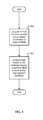
- FIG. 1is a block diagram illustrating an embodiment of a system for a memory access device.
- FIG. 2is a block diagram illustrating an embodiment of system for a memory module.
- FIG. 3is a flow chart illustrating an embodiment of a process for using an FPGA for integration with NVM.
- FIG. 4is a flow chart illustrating an embodiment of a process for responding to new information about an NVM device.
- FIG. 5is a flow chart illustrating an embodiment of a process for reprogramming an FPGA in place.
- the inventioncan be implemented in numerous ways, including as a process; an apparatus; a system; a composition of matter; a computer program product embodied on a computer readable storage medium; and/or a processor, such as a processor configured to execute instructions stored on and/or provided by a memory coupled to the processor.
- these implementations, or any other form that the invention may take,may be referred to as techniques.
- the order of the steps of disclosed processesmay be altered within the scope of the invention.
- a componentsuch as a processor or a memory described as being configured to perform a task may be implemented as a general component that is temporarily configured to perform the task at a given time or a specific component that is manufactured to perform the task.
- the term ‘processor’refers to one or more devices, circuits, and/or processing cores configured to process data, such as computer program instructions.
- An FPGAfield programmable gate array
- An FPGAis a gate array device that may be programmed “in the field”, after the gate array device has been manufactured. This is useful for integration with emerging technologies as an FPGA has the ability to reprogram once deployed.
- Emerging NVM technologiesmay not be fully or precisely characterized and/or the characteristics of which may change through and after development and integration design.
- a software programmable controller system-on-chipis used for NAND-based flash memory, for example a PMC Princeton PCIe NVMe controller.
- SOCsoftware programmable controller system-on-chip
- Such a software programmable controlleruses an internal CPU with firmware to integrate 8-32 independent flash channels, each for a flash memory device, with a host interface, typically PCIe, SATA, and/or SAS.
- An external SDRAM buffertypically using DDR3 protocol, may be integrated to provide throughput matching between the flash channel bus and the host interface bus.
- a lower latency NVMincludes next generation memory, for example a memory technology that is a transistorless and/or resistive-based memory.
- a higher throughput/lower latency NVMprovides the following advantages over flash memory:
- a higher throughput/lower latency NVMmay require differing procedures over traditional NAND-based flash NVM to handle:
- a memoryis fully “bit-addressable” if it allows a bit to be rewritten without having to rewrite other bits, for example read-modify-write as with flash memory.
- An FPGA controlleris a novel approach at controlling an emerging NVM technology to provide new parallelizable logic as new physical phenomena are discovered about the device.
- flashtraditionally uses a 40-bit BCH error correction coding (ECC) which research has determined to be most effective for channel coding for the NAND flash media.
- ECCerror correction coding
- NVM technologymay not be handled by existing software programmable controller SOC approaches.
- a flash channelmay be four bytes wide
- an emerging NVMmay be sixteen bytes wide.
- a controllermay need to handle 6.6 MB/sec per device or 106 MB/sec per controller.
- control module ( 102 ) with 36 memory modules ( 106 )this results in a 3.5 GB/s throughput chassis.
- An FPGA-based controllercan handle such high throughput by parallelizing logic on a per channel basis, for example.
- FIG. 1is a block diagram illustrating an embodiment of a system for a memory access device.
- the systemcomprises a control module ( 102 ) coupled to both a host/user/client, a service module ( 104 ) and a plurality of memory modules ( 106 a - 106 z ). In one embodiment, up to 36 memory modules ( 106 ) may be used.
- the control moduleuses a high throughput bus to couple to the host, for example PCIe Gen 3 with between x4 and x96 lanes.
- processors ( 114 )within the control module ( 102 ) there are one or more processors ( 114 ) that are external to the memory modules ( 106 a )-( 106 z ).
- An external processor ( 114 )may have one or more processing cores.
- An external processor ( 114 )may be coupled internally using a lower throughput bus, for example PCIe 2.0 with x1 lane.
- the control module ( 102 )is coupled by PCIe to a memory module ( 106 z ), which comprises: an FPGA controller ( 116 ); a non-volatile memory media ( 118 ), and an associated DDR4 buffer/cache ( 120 ).
- a non-volatile memory media ( 118 )may include next generation non-volatile memory.
- FIG. 2is a block diagram illustrating an embodiment of system for a memory module.
- each memory module ( 106 )comprises an FPGA ( 116 ) with 8-32 channels of NVM ( 118 a - 118 z ), and is coupled to an SDRAM ( 120 ).
- the FPGA ( 116 )interfaces hostward via a PCIe bus, for example dual PCIe Gen3 x4, for a data rate up to 6 GB/s.
- the FPGA ( 116 )interfaces using DDR4 with the SDRAM cache ( 120 ).
- the function of the settling time cacheis to provide a host with a cache for reading Within the settled time window.
- a communication interface ( 210 ), for example an SDRAM controller logic block, within FPGA ( 116 )is used to provide a high data transfer rate connection to the external RAM ( 120 ).
- DDR4is also used to interface each device ( 118 a , 118 b , 118 c , . . . 118 z ) to the FPGA ( 116 ).
- one or more RAM buffers ( 212 )may be used to handle the throughput mismatch between the respective busses.
- FPGA field programmable logic blocksare used to provide one or more access modules ( 214 ) which provide access functions to the NVM modules ( 118 a - 118 z ).
- FPGA field programmable logic blocksare used to provide one or more management modules ( 216 ) which provide management functions to the NVM modules ( 118 a - 118 z ).
- the management function for a module ( 216 )is forward error correction and/or ECC.
- a BCH algorithm used for flash memoryis based on error pattern and statistical error correlations that may be inappropriate for emerging NVM technologies.
- Forward error correction and/or ECC algorithms/machines/modulesmay be designed and improved by updating the FPGA and/or module ( 216 ) even after being deployed in the field.
- the management function for a module ( 216 )is wear leveling. Unlike flash memory which requires read-modify-write over blocks of flash, emerging NVM may enable fully bit-addressable rewrite, for write-in-place.
- the module ( 216 )may include field programmable algorithms/modules for wear detection and wear migration that resolve wear bit-by-bit.
- the management function for a module ( 216 )is tile replacement.
- Using an FPGA ( 116 )allows emerging NVM technology vendors to insert proprietary modules ( 216 ) to indicate when memory tiles are failing and require replacement.
- a tile replacement module ( 216 )may take this indication and provide tile migration.
- the management function for a module ( 216 )is media scheduling control.
- a start-gap algorithmmay be used when emerging NVM technologies only require mild wear leveling to avoid the higher complexity and lower performance of table-based methods for wear leveling.
- the start-gapuses a start and gap addressing register to gently migrate read/write access to spread out access, for example uniformly, over time to avoid ‘hot spots’.
- the communication interface ( 210 ) and/or management function for module ( 216 )includes a write settling time cache controller.
- a settling period for an emerging NVM technologymay increase from 1 usec to 100 ms.
- Using an FPGA ( 116 )allows flexibility not only for caching algorithms, but also cache size and flexibility for new physical settling time characteristics to permit a new settling time cache characteristic.
- the access module ( 214 )comprises a new NVM interface protocol to succeed DDR4.
- the access module ( 214 )comprises a new host interface protocol to succeed PCIe/NVMe, for example a proprietary protocol such as NVMd. Having a flexibility to change the interface protocols or other management modules ( 216 ) in the field based on new physical insights for the emerging NVM technology associated with the NVM modules ( 118 a - 118 z ) may provide dynamic improvements to reliability and performance of the memory module ( 106 ).
- a read access to given cell in the emerging NVM technologymay affect the payload of the cell and/or one or more physically adjacent cells.
- cellsmay be adjacent in three-dimensions, such that there are at least six near neighbors along the X-axis, Y-axis, and Z-axis.
- read disturbThe phenomena where reading a cell causes errors in the cell or its adjacent cells.
- write disturbThe phenomena where writing a cell causes errors in the cell or its adjacent cells.
- write disturbThe management module ( 216 ) may include algorithms/modules to minimize the deleterious effects of read disturb and write disturb.
- FIG. 3is a flow chart illustrating an embodiment of a process for using an FPGA for integration with NVM.
- the FPGAis programmed to provide a high speed/data transfer rate connection and/or communication interface to an external random access memory device, wherein said at least a subset of FPGA programmable logic blocks are programmed in a first configuration to perform one of both of an access function and a management function at least in part using data sent via the communication interface, wherein the communication interface is coupled to at least a subset of the programmable logic blocks.
- step 304a plurality of programmable logic blocks are programmed in the first configuration to perform one or both of the access function and the management function with respect to a plurality of non-volatile memory modules.
- FIG. 4is a flow chart illustrating an embodiment of a process for responding to new information about an NVM device. In one embodiment, this process occurs with the designers of the system of FIG. 1 and/or FIG. 2 .
- an indication of a new value for an NVM device ( 118 ) characteristicis received.
- the manufacturer of an NVM device ( 118 )may change the specification of the settling time cache from 1 ms to 100 ms.
- a new algorithm and/or parameteris determined to reflect the changed value.
- step 406the FPGA device ( 116 ) is reprogrammed in place (i.e. in the field) to implement the new algorithm instead of the previously-implemented algorithm.
- the FPGA ( 116 )is reprogrammed to expand the settling time cache from 6 MB to 600 MB.
- FIG. 5is a flow chart illustrating an embodiment of a process for reprogramming an FPGA in place. In one embodiment, FIG. 5 is included in step 406 of FIG. 4 .
- instructionsare received to program and/or reprogram one or more logic blocks on FPGA ( 116 ).
- instructionsare received via a file transmitted to the field by physical media (e.g. a hard drive or thumb drive) or over the internet (e.g. email, web address, ftp site, etc).
- step 504logic blocks in the FPGA ( 116 ) are implemented according to the instructions of step 502 .
- a hardware and/or software deviceis used to reconfigure the FPGA ( 116 ) via a logic block configuration bitstream, for example via an SD card, JTAG port, SPI interface, etc.
Landscapes
- Engineering & Computer Science (AREA)
- Theoretical Computer Science (AREA)
- General Engineering & Computer Science (AREA)
- Physics & Mathematics (AREA)
- General Physics & Mathematics (AREA)
- Human Computer Interaction (AREA)
- Computer Hardware Design (AREA)
- Quality & Reliability (AREA)
- Techniques For Improving Reliability Of Storages (AREA)
Abstract
Description
- a. fully bit-addressable to allow reading and writing by bit rather than by block, for example providing write-in-place and rewrite-in-place instead of page-size rewrites, or read-modify-write, as with flash memory;
- b. more than 100 times lower latency than flash memory;
- c. higher throughput, for example 2100 MT/s or 150 ns/byte as compared to flash memory at 400 MT/s; and
- d. greater endurance and/or wear resistance than flash memory.
- a. Device characteristics including settling time after writing a specific bit before being able to read, in the range of 1 usec to 300 ms.
- b. Wear leveling including using write-in-place/fully bit-addressable migration within a device or across a plurality of devices, handling different patterns;
- c. Physical location “disturb” tracking wherein a read and/or write access may disturb one of the physically adjacent bits;
- d. Error correction including handling different error patterns over flash;
- e. Tile replacement to handle remapping when tiles fail;
- f. Media scheduling control, for example using a start-gap algorithm; and
- g. Command mapping to provide backwards compatibility with older NVM technologies such as flash.
Claims (18)
Priority Applications (1)
| Application Number | Priority Date | Filing Date | Title |
|---|---|---|---|
| US15/087,948US9921757B1 (en) | 2016-03-31 | 2016-03-31 | Using an FPGA for integration with low-latency, non-volatile memory |
Applications Claiming Priority (1)
| Application Number | Priority Date | Filing Date | Title |
|---|---|---|---|
| US15/087,948US9921757B1 (en) | 2016-03-31 | 2016-03-31 | Using an FPGA for integration with low-latency, non-volatile memory |
Publications (1)
| Publication Number | Publication Date |
|---|---|
| US9921757B1true US9921757B1 (en) | 2018-03-20 |
Family
ID=61598511
Family Applications (1)
| Application Number | Title | Priority Date | Filing Date |
|---|---|---|---|
| US15/087,948Active2036-04-02US9921757B1 (en) | 2016-03-31 | 2016-03-31 | Using an FPGA for integration with low-latency, non-volatile memory |
Country Status (1)
| Country | Link |
|---|---|
| US (1) | US9921757B1 (en) |
Cited By (2)
| Publication number | Priority date | Publication date | Assignee | Title |
|---|---|---|---|---|
| US20180074757A1 (en)* | 2016-09-09 | 2018-03-15 | Toshiba Memory Corporation | Switch and memory device |
| US10949361B1 (en)* | 2017-08-04 | 2021-03-16 | Nimbus Data, Inc. | Multiprocessor software-defined solid-state storage drive |
Citations (39)
| Publication number | Priority date | Publication date | Assignee | Title |
|---|---|---|---|---|
| US20010052038A1 (en)* | 2000-02-03 | 2001-12-13 | Realtime Data, Llc | Data storewidth accelerator |
| US20030084244A1 (en)* | 2001-10-30 | 2003-05-01 | Dominic Paulraj | Reconfigurable cache |
| US20040068621A1 (en)* | 2002-10-03 | 2004-04-08 | Van Doren Stephen R. | Generalized active inheritance consistency mechanism for a computer system |
| US6782410B1 (en)* | 2000-08-28 | 2004-08-24 | Ncr Corporation | Method for managing user and server applications in a multiprocessor computer system |
| US6842377B2 (en)* | 2002-04-12 | 2005-01-11 | Kabushiki Kaisha Toshiba | Nonvolatile semiconductor memory device with first and second read modes |
| US20050125607A1 (en)* | 2003-12-08 | 2005-06-09 | International Business Machines Corporation | Intelligent caching of working directories in auxiliary storage |
| US7017011B2 (en)* | 2001-02-15 | 2006-03-21 | Bull S.A. | Coherence controller for a multiprocessor system, module, and multiprocessor system with a multimodule architecture incorporating such a controller |
| US20060202999A1 (en)* | 2005-03-10 | 2006-09-14 | Microsoft Corporation | Method to manage graphics address remap table (GART) translations in a secure system |
| US20070008328A1 (en)* | 2005-07-05 | 2007-01-11 | Macwilliams Peter | Identifying and accessing individual memory devices in a memory channel |
| US7196942B2 (en)* | 2004-10-20 | 2007-03-27 | Stmicroelectronics Pvt. Ltd. | Configuration memory structure |
| US7269715B2 (en)* | 2005-02-03 | 2007-09-11 | International Business Machines Corporation | Instruction grouping history on fetch-side dispatch group formation |
| US7321955B2 (en)* | 2004-03-31 | 2008-01-22 | Fujitsu Limited | Control device, control method and storage medium recording a control program for controlling write-back schedule of data from cache memory to a plurality of storage devices |
| US7512736B1 (en)* | 2005-05-02 | 2009-03-31 | Nvidia Corporation | System and method for adaptive raid configuration |
| US20090094413A1 (en)* | 2007-10-08 | 2009-04-09 | Lehr Douglas L | Techniques for Dynamic Volume Allocation in a Storage System |
| US20090228648A1 (en)* | 2008-03-04 | 2009-09-10 | International Business Machines Corporation | High performance disk array rebuild |
| US20090282101A1 (en)* | 1998-09-10 | 2009-11-12 | Vmware, Inc. | Mechanism for providing virtual machines for use by multiple users |
| US20100046267A1 (en)* | 2008-08-25 | 2010-02-25 | Tianhong Yan | Memory system with sectional data lines |
| US20100050016A1 (en)* | 2004-10-22 | 2010-02-25 | Broadcom Corporation | Preventing write corruption in a raid array |
| US20100125712A1 (en)* | 2008-11-17 | 2010-05-20 | Hitachi, Ltd. | Data backup system and method for virtual infrastructure |
| US20100142243A1 (en)* | 2008-12-08 | 2010-06-10 | Xilinx, Inc. | Data storage system with removable memory module having parallel channels of dram memory and flash memory |
| US20100241785A1 (en)* | 2006-04-27 | 2010-09-23 | Vmware, Inc. | Management of host physical memory allocation to virtual machines with a balloon application |
| US20100332780A1 (en)* | 2009-06-30 | 2010-12-30 | Fujitsu Limited | Storage system, control apparatus and method of controlling control apparatus |
| US20110202735A1 (en)* | 2010-02-17 | 2011-08-18 | Hitachi, Ltd. | Computer system, and backup method and program for computer system |
| US20110307745A1 (en)* | 2010-06-11 | 2011-12-15 | International Business Machines Corporation | Updating class assignments for data sets during a recall operation |
| US20120110293A1 (en)* | 2010-11-03 | 2012-05-03 | Yang Xiaowei | Method and system for managing virtual machine storage space and physical host |
| US8230193B2 (en)* | 2006-05-24 | 2012-07-24 | Compellent Technologies | System and method for raid management, reallocation, and restriping |
| US20120198107A1 (en)* | 2011-01-31 | 2012-08-02 | Lsi Corporation | Methods and systems for migrating data between storage tiers |
| US20130007373A1 (en)* | 2011-06-30 | 2013-01-03 | Advanced Micro Devices, Inc. | Region based cache replacement policy utilizing usage information |
| US20130067161A1 (en)* | 2011-09-09 | 2013-03-14 | Lsi Corporation | Methods and structure for task management in storage controllers of a clustered storage system |
| US20130080805A1 (en)* | 2011-09-23 | 2013-03-28 | Qualcomm Incorporated | Dynamic partitioning for heterogeneous cores |
| US20130111129A1 (en)* | 2011-10-28 | 2013-05-02 | Hitachi, Ltd. | Computer system and storage management method |
| US20130152097A1 (en)* | 2011-12-09 | 2013-06-13 | Microsoft Corporation | Resource Health Based Scheduling of Workload Tasks |
| US8566546B1 (en)* | 2010-09-27 | 2013-10-22 | Emc Corporation | Techniques for enforcing capacity restrictions of an allocation policy |
| US20130326270A1 (en)* | 2012-05-31 | 2013-12-05 | International Business Machines Corporation | Maximizing Use of Storage in a Data Replication Environment |
| US20140003114A1 (en)* | 2012-06-29 | 2014-01-02 | Fabio Pellizzer | Compact socket connection to cross-point array |
| US8990527B1 (en)* | 2007-06-29 | 2015-03-24 | Emc Corporation | Data migration with source device reuse |
| US20160217835A1 (en)* | 2015-01-28 | 2016-07-28 | Xilinx, Inc. | Circuits for and methods of controlling the operation of a hybrid memory system |
| US20160313914A1 (en)* | 2015-04-27 | 2016-10-27 | Southwest Research Institute | Systems and methods for improved access to flash memory devices |
| US20170123995A1 (en)* | 2015-11-03 | 2017-05-04 | Intel Corporation | Efficient redundant array of independent disks (raid) write hole solutions |
- 2016
- 2016-03-31USUS15/087,948patent/US9921757B1/enactiveActive
Patent Citations (39)
| Publication number | Priority date | Publication date | Assignee | Title |
|---|---|---|---|---|
| US20090282101A1 (en)* | 1998-09-10 | 2009-11-12 | Vmware, Inc. | Mechanism for providing virtual machines for use by multiple users |
| US20010052038A1 (en)* | 2000-02-03 | 2001-12-13 | Realtime Data, Llc | Data storewidth accelerator |
| US6782410B1 (en)* | 2000-08-28 | 2004-08-24 | Ncr Corporation | Method for managing user and server applications in a multiprocessor computer system |
| US7017011B2 (en)* | 2001-02-15 | 2006-03-21 | Bull S.A. | Coherence controller for a multiprocessor system, module, and multiprocessor system with a multimodule architecture incorporating such a controller |
| US20030084244A1 (en)* | 2001-10-30 | 2003-05-01 | Dominic Paulraj | Reconfigurable cache |
| US6842377B2 (en)* | 2002-04-12 | 2005-01-11 | Kabushiki Kaisha Toshiba | Nonvolatile semiconductor memory device with first and second read modes |
| US20040068621A1 (en)* | 2002-10-03 | 2004-04-08 | Van Doren Stephen R. | Generalized active inheritance consistency mechanism for a computer system |
| US20050125607A1 (en)* | 2003-12-08 | 2005-06-09 | International Business Machines Corporation | Intelligent caching of working directories in auxiliary storage |
| US7321955B2 (en)* | 2004-03-31 | 2008-01-22 | Fujitsu Limited | Control device, control method and storage medium recording a control program for controlling write-back schedule of data from cache memory to a plurality of storage devices |
| US7196942B2 (en)* | 2004-10-20 | 2007-03-27 | Stmicroelectronics Pvt. Ltd. | Configuration memory structure |
| US20100050016A1 (en)* | 2004-10-22 | 2010-02-25 | Broadcom Corporation | Preventing write corruption in a raid array |
| US7269715B2 (en)* | 2005-02-03 | 2007-09-11 | International Business Machines Corporation | Instruction grouping history on fetch-side dispatch group formation |
| US20060202999A1 (en)* | 2005-03-10 | 2006-09-14 | Microsoft Corporation | Method to manage graphics address remap table (GART) translations in a secure system |
| US7512736B1 (en)* | 2005-05-02 | 2009-03-31 | Nvidia Corporation | System and method for adaptive raid configuration |
| US20070008328A1 (en)* | 2005-07-05 | 2007-01-11 | Macwilliams Peter | Identifying and accessing individual memory devices in a memory channel |
| US20100241785A1 (en)* | 2006-04-27 | 2010-09-23 | Vmware, Inc. | Management of host physical memory allocation to virtual machines with a balloon application |
| US8230193B2 (en)* | 2006-05-24 | 2012-07-24 | Compellent Technologies | System and method for raid management, reallocation, and restriping |
| US8990527B1 (en)* | 2007-06-29 | 2015-03-24 | Emc Corporation | Data migration with source device reuse |
| US20090094413A1 (en)* | 2007-10-08 | 2009-04-09 | Lehr Douglas L | Techniques for Dynamic Volume Allocation in a Storage System |
| US20090228648A1 (en)* | 2008-03-04 | 2009-09-10 | International Business Machines Corporation | High performance disk array rebuild |
| US20100046267A1 (en)* | 2008-08-25 | 2010-02-25 | Tianhong Yan | Memory system with sectional data lines |
| US20100125712A1 (en)* | 2008-11-17 | 2010-05-20 | Hitachi, Ltd. | Data backup system and method for virtual infrastructure |
| US20100142243A1 (en)* | 2008-12-08 | 2010-06-10 | Xilinx, Inc. | Data storage system with removable memory module having parallel channels of dram memory and flash memory |
| US20100332780A1 (en)* | 2009-06-30 | 2010-12-30 | Fujitsu Limited | Storage system, control apparatus and method of controlling control apparatus |
| US20110202735A1 (en)* | 2010-02-17 | 2011-08-18 | Hitachi, Ltd. | Computer system, and backup method and program for computer system |
| US20110307745A1 (en)* | 2010-06-11 | 2011-12-15 | International Business Machines Corporation | Updating class assignments for data sets during a recall operation |
| US8566546B1 (en)* | 2010-09-27 | 2013-10-22 | Emc Corporation | Techniques for enforcing capacity restrictions of an allocation policy |
| US20120110293A1 (en)* | 2010-11-03 | 2012-05-03 | Yang Xiaowei | Method and system for managing virtual machine storage space and physical host |
| US20120198107A1 (en)* | 2011-01-31 | 2012-08-02 | Lsi Corporation | Methods and systems for migrating data between storage tiers |
| US20130007373A1 (en)* | 2011-06-30 | 2013-01-03 | Advanced Micro Devices, Inc. | Region based cache replacement policy utilizing usage information |
| US20130067161A1 (en)* | 2011-09-09 | 2013-03-14 | Lsi Corporation | Methods and structure for task management in storage controllers of a clustered storage system |
| US20130080805A1 (en)* | 2011-09-23 | 2013-03-28 | Qualcomm Incorporated | Dynamic partitioning for heterogeneous cores |
| US20130111129A1 (en)* | 2011-10-28 | 2013-05-02 | Hitachi, Ltd. | Computer system and storage management method |
| US20130152097A1 (en)* | 2011-12-09 | 2013-06-13 | Microsoft Corporation | Resource Health Based Scheduling of Workload Tasks |
| US20130326270A1 (en)* | 2012-05-31 | 2013-12-05 | International Business Machines Corporation | Maximizing Use of Storage in a Data Replication Environment |
| US20140003114A1 (en)* | 2012-06-29 | 2014-01-02 | Fabio Pellizzer | Compact socket connection to cross-point array |
| US20160217835A1 (en)* | 2015-01-28 | 2016-07-28 | Xilinx, Inc. | Circuits for and methods of controlling the operation of a hybrid memory system |
| US20160313914A1 (en)* | 2015-04-27 | 2016-10-27 | Southwest Research Institute | Systems and methods for improved access to flash memory devices |
| US20170123995A1 (en)* | 2015-11-03 | 2017-05-04 | Intel Corporation | Efficient redundant array of independent disks (raid) write hole solutions |
Non-Patent Citations (2)
| Title |
|---|
| Author Unknown, PMC, Flashtec, PCLE Flash Controllers, Product Brief, Flashtec NVMe2032 & NVMe2016 Controllers, 32 and 16 Channel PCI Express Flash Controller Products, 2015, Issue 2. |
| Author Unknown, Xilinx, Spartan-6 FPGA Memory Controller User Guide, UG388 (v2.3) Aug. 9, 2013. |
Cited By (4)
| Publication number | Priority date | Publication date | Assignee | Title |
|---|---|---|---|---|
| US20180074757A1 (en)* | 2016-09-09 | 2018-03-15 | Toshiba Memory Corporation | Switch and memory device |
| US10445018B2 (en)* | 2016-09-09 | 2019-10-15 | Toshiba Memory Corporation | Switch and memory device |
| USRE49273E1 (en)* | 2016-09-09 | 2022-11-01 | Kioxia Corporation | Switch and memory device |
| US10949361B1 (en)* | 2017-08-04 | 2021-03-16 | Nimbus Data, Inc. | Multiprocessor software-defined solid-state storage drive |
Similar Documents
| Publication | Publication Date | Title |
|---|---|---|
| US12094545B2 (en) | Techniques for preventing read disturb in NAND memory | |
| US10628319B2 (en) | Methods for caching and reading data to be programmed into a storage unit and apparatuses using the same | |
| US10877900B1 (en) | Enabling faster and regulated device initialization times | |
| US9417960B2 (en) | Preventing programming errors from occurring when programming flash memory cells | |
| CN102723099B (en) | Including for processing many command descriptor blocks so that the flash memory device of the HPI using concurrency | |
| US9946661B2 (en) | Command executing method, memory controller and memory storage apparatus | |
| US10224107B1 (en) | Method and apparatus for dynamically determining start program voltages for a memory device | |
| CN106164873B (en) | The method and apparatus of constraint write-in solid-state memory when reaching end-of-life condition | |
| US9477423B2 (en) | Eliminating or reducing programming errors when programming flash memory cells | |
| CN113448497A (en) | Dynamic allocation of subblocks | |
| US20250306909A1 (en) | Firmware updating method, apparatus and data system | |
| US11892928B2 (en) | Delayed thermal throttling and associated data routing techniques | |
| US11023138B2 (en) | Management operations in predictable latency mode | |
| US20150058531A1 (en) | Data writing method, memory control circuit unit and memory storage apparatus | |
| US9823880B1 (en) | Method and apparatus for initiating pre-read operation before completion of data load operation | |
| CN114341985A (en) | Sequential SLC read optimization | |
| US9921757B1 (en) | Using an FPGA for integration with low-latency, non-volatile memory | |
| US10489077B2 (en) | Systems and methods for controlling metapage storage on data storage devices | |
| TWI633435B (en) | Methods for migrating data to avoid read disturbance and apparatuses using the same | |
| TWI648628B (en) | Methods for migrating data to avoid read disturbance and apparatuses using the same | |
| CN112086121B (en) | Memory proximity interference management | |
| US9778864B2 (en) | Data storage device using non-sequential segment access and operating method thereof | |
| KR20230043408A (en) | Memory controller and storage device | |
| KR102557992B1 (en) | Memory controller, storage device, and operating method of storage device | |
| CN114981786B (en) | Cache media management |
Legal Events
| Date | Code | Title | Description |
|---|---|---|---|
| AS | Assignment | Owner name:EMC CORPORATION, MASSACHUSETTS Free format text:ASSIGNMENT OF ASSIGNORS INTEREST;ASSIGNOR:ROWETT, KEVIN;REEL/FRAME:038972/0452 Effective date:20160614 | |
| AS | Assignment | Owner name:EMC IP HOLDING COMPANY LLC, MASSACHUSETTS Free format text:ASSIGNMENT OF ASSIGNORS INTEREST;ASSIGNOR:EMC CORPORATION;REEL/FRAME:041872/0001 Effective date:20160901 | |
| STCF | Information on status: patent grant | Free format text:PATENTED CASE | |
| AS | Assignment | Owner name:CREDIT SUISSE AG, CAYMAN ISLANDS BRANCH, AS COLLATERAL AGENT, NORTH CAROLINA Free format text:PATENT SECURITY AGREEMENT (CREDIT);ASSIGNORS:DELL PRODUCTS L.P.;EMC CORPORATION;EMC IP HOLDING COMPANY LLC;REEL/FRAME:046286/0653 Effective date:20180529 Owner name:THE BANK OF NEW YORK MELLON TRUST COMPANY, N.A., AS COLLATERAL AGENT, TEXAS Free format text:PATENT SECURITY AGREEMENT (NOTES);ASSIGNORS:DELL PRODUCTS L.P.;EMC CORPORATION;EMC IP HOLDING COMPANY LLC;REEL/FRAME:046366/0014 Effective date:20180529 Owner name:CREDIT SUISSE AG, CAYMAN ISLANDS BRANCH, AS COLLAT Free format text:PATENT SECURITY AGREEMENT (CREDIT);ASSIGNORS:DELL PRODUCTS L.P.;EMC CORPORATION;EMC IP HOLDING COMPANY LLC;REEL/FRAME:046286/0653 Effective date:20180529 Owner name:THE BANK OF NEW YORK MELLON TRUST COMPANY, N.A., A Free format text:PATENT SECURITY AGREEMENT (NOTES);ASSIGNORS:DELL PRODUCTS L.P.;EMC CORPORATION;EMC IP HOLDING COMPANY LLC;REEL/FRAME:046366/0014 Effective date:20180529 | |
| AS | Assignment | Owner name:THE BANK OF NEW YORK MELLON TRUST COMPANY, N.A., T Free format text:SECURITY AGREEMENT;ASSIGNORS:CREDANT TECHNOLOGIES, INC.;DELL INTERNATIONAL L.L.C.;DELL MARKETING L.P.;AND OTHERS;REEL/FRAME:049452/0223 Effective date:20190320 Owner name:THE BANK OF NEW YORK MELLON TRUST COMPANY, N.A., TEXAS Free format text:SECURITY AGREEMENT;ASSIGNORS:CREDANT TECHNOLOGIES, INC.;DELL INTERNATIONAL L.L.C.;DELL MARKETING L.P.;AND OTHERS;REEL/FRAME:049452/0223 Effective date:20190320 | |
| AS | Assignment | Owner name:THE BANK OF NEW YORK MELLON TRUST COMPANY, N.A., TEXAS Free format text:SECURITY AGREEMENT;ASSIGNORS:CREDANT TECHNOLOGIES INC.;DELL INTERNATIONAL L.L.C.;DELL MARKETING L.P.;AND OTHERS;REEL/FRAME:053546/0001 Effective date:20200409 | |
| MAFP | Maintenance fee payment | Free format text:PAYMENT OF MAINTENANCE FEE, 4TH YEAR, LARGE ENTITY (ORIGINAL EVENT CODE: M1551); ENTITY STATUS OF PATENT OWNER: LARGE ENTITY Year of fee payment:4 | |
| AS | Assignment | Owner name:EMC IP HOLDING COMPANY LLC, TEXAS Free format text:RELEASE OF SECURITY INTEREST AT REEL 046286 FRAME 0653;ASSIGNOR:CREDIT SUISSE AG, CAYMAN ISLANDS BRANCH;REEL/FRAME:058298/0093 Effective date:20211101 Owner name:EMC CORPORATION, MASSACHUSETTS Free format text:RELEASE OF SECURITY INTEREST AT REEL 046286 FRAME 0653;ASSIGNOR:CREDIT SUISSE AG, CAYMAN ISLANDS BRANCH;REEL/FRAME:058298/0093 Effective date:20211101 Owner name:DELL PRODUCTS L.P., TEXAS Free format text:RELEASE OF SECURITY INTEREST AT REEL 046286 FRAME 0653;ASSIGNOR:CREDIT SUISSE AG, CAYMAN ISLANDS BRANCH;REEL/FRAME:058298/0093 Effective date:20211101 | |
| AS | Assignment | Owner name:EMC IP HOLDING COMPANY LLC, TEXAS Free format text:RELEASE OF SECURITY INTEREST IN PATENTS PREVIOUSLY RECORDED AT REEL/FRAME (046366/0014);ASSIGNOR:THE BANK OF NEW YORK MELLON TRUST COMPANY, N.A., AS NOTES COLLATERAL AGENT;REEL/FRAME:060450/0306 Effective date:20220329 Owner name:EMC CORPORATION, MASSACHUSETTS Free format text:RELEASE OF SECURITY INTEREST IN PATENTS PREVIOUSLY RECORDED AT REEL/FRAME (046366/0014);ASSIGNOR:THE BANK OF NEW YORK MELLON TRUST COMPANY, N.A., AS NOTES COLLATERAL AGENT;REEL/FRAME:060450/0306 Effective date:20220329 Owner name:DELL PRODUCTS L.P., TEXAS Free format text:RELEASE OF SECURITY INTEREST IN PATENTS PREVIOUSLY RECORDED AT REEL/FRAME (046366/0014);ASSIGNOR:THE BANK OF NEW YORK MELLON TRUST COMPANY, N.A., AS NOTES COLLATERAL AGENT;REEL/FRAME:060450/0306 Effective date:20220329 | |
| AS | Assignment | Owner name:DELL MARKETING L.P. (ON BEHALF OF ITSELF AND AS SUCCESSOR-IN-INTEREST TO CREDANT TECHNOLOGIES, INC.), TEXAS Free format text:RELEASE OF SECURITY INTEREST IN PATENTS PREVIOUSLY RECORDED AT REEL/FRAME (053546/0001);ASSIGNOR:THE BANK OF NEW YORK MELLON TRUST COMPANY, N.A., AS NOTES COLLATERAL AGENT;REEL/FRAME:071642/0001 Effective date:20220329 Owner name:DELL INTERNATIONAL L.L.C., TEXAS Free format text:RELEASE OF SECURITY INTEREST IN PATENTS PREVIOUSLY RECORDED AT REEL/FRAME (053546/0001);ASSIGNOR:THE BANK OF NEW YORK MELLON TRUST COMPANY, N.A., AS NOTES COLLATERAL AGENT;REEL/FRAME:071642/0001 Effective date:20220329 Owner name:DELL PRODUCTS L.P., TEXAS Free format text:RELEASE OF SECURITY INTEREST IN PATENTS PREVIOUSLY RECORDED AT REEL/FRAME (053546/0001);ASSIGNOR:THE BANK OF NEW YORK MELLON TRUST COMPANY, N.A., AS NOTES COLLATERAL AGENT;REEL/FRAME:071642/0001 Effective date:20220329 Owner name:DELL USA L.P., TEXAS Free format text:RELEASE OF SECURITY INTEREST IN PATENTS PREVIOUSLY RECORDED AT REEL/FRAME (053546/0001);ASSIGNOR:THE BANK OF NEW YORK MELLON TRUST COMPANY, N.A., AS NOTES COLLATERAL AGENT;REEL/FRAME:071642/0001 Effective date:20220329 Owner name:EMC CORPORATION, MASSACHUSETTS Free format text:RELEASE OF SECURITY INTEREST IN PATENTS PREVIOUSLY RECORDED AT REEL/FRAME (053546/0001);ASSIGNOR:THE BANK OF NEW YORK MELLON TRUST COMPANY, N.A., AS NOTES COLLATERAL AGENT;REEL/FRAME:071642/0001 Effective date:20220329 Owner name:DELL MARKETING CORPORATION (SUCCESSOR-IN-INTEREST TO FORCE10 NETWORKS, INC. AND WYSE TECHNOLOGY L.L.C.), TEXAS Free format text:RELEASE OF SECURITY INTEREST IN PATENTS PREVIOUSLY RECORDED AT REEL/FRAME (053546/0001);ASSIGNOR:THE BANK OF NEW YORK MELLON TRUST COMPANY, N.A., AS NOTES COLLATERAL AGENT;REEL/FRAME:071642/0001 Effective date:20220329 Owner name:EMC IP HOLDING COMPANY LLC, TEXAS Free format text:RELEASE OF SECURITY INTEREST IN PATENTS PREVIOUSLY RECORDED AT REEL/FRAME (053546/0001);ASSIGNOR:THE BANK OF NEW YORK MELLON TRUST COMPANY, N.A., AS NOTES COLLATERAL AGENT;REEL/FRAME:071642/0001 Effective date:20220329 | |
| MAFP | Maintenance fee payment | Free format text:PAYMENT OF MAINTENANCE FEE, 8TH YEAR, LARGE ENTITY (ORIGINAL EVENT CODE: M1552); ENTITY STATUS OF PATENT OWNER: LARGE ENTITY Year of fee payment:8 |