US9917133B2 - Optoelectronic device with flexible substrate - Google Patents
Optoelectronic device with flexible substrateDownload PDFInfo
- Publication number
- US9917133B2 US9917133B2US14/103,989US201314103989AUS9917133B2US 9917133 B2US9917133 B2US 9917133B2US 201314103989 AUS201314103989 AUS 201314103989AUS 9917133 B2US9917133 B2US 9917133B2
- Authority
- US
- United States
- Prior art keywords
- flexible substrate
- disposed
- module assembly
- tft array
- substrate
- Prior art date
- Legal status (The legal status is an assumption and is not a legal conclusion. Google has not performed a legal analysis and makes no representation as to the accuracy of the status listed.)
- Expired - Fee Related
Links
- 239000000758substrateSubstances0.000titleclaimsabstractdescription83
- 230000005693optoelectronicsEffects0.000titleclaimsabstractdescription17
- 239000010409thin filmSubstances0.000claimsabstractdescription8
- 239000000463materialSubstances0.000claimsdescription11
- 230000035939shockEffects0.000claimsdescription5
- 239000010410layerSubstances0.000description23
- 239000011521glassSubstances0.000description13
- 230000003287optical effectEffects0.000description4
- -1polyethylene terephthalatePolymers0.000description4
- 238000012546transferMethods0.000description3
- XLOMVQKBTHCTTD-UHFFFAOYSA-NZinc monoxideChemical compound[Zn]=OXLOMVQKBTHCTTD-UHFFFAOYSA-N0.000description2
- 239000011230binding agentSubstances0.000description2
- 230000005540biological transmissionEffects0.000description2
- XQPRBTXUXXVTKB-UHFFFAOYSA-Mcaesium iodideChemical compound[I-].[Cs+]XQPRBTXUXXVTKB-UHFFFAOYSA-M0.000description2
- 239000002131composite materialSubstances0.000description2
- 238000013461designMethods0.000description2
- 239000011888foilSubstances0.000description2
- 239000011159matrix materialSubstances0.000description2
- 229910052751metalInorganic materials0.000description2
- 239000002184metalSubstances0.000description2
- 239000002245particleSubstances0.000description2
- 239000002985plastic filmSubstances0.000description2
- 239000004417polycarbonateSubstances0.000description2
- 229920000515polycarbonatePolymers0.000description2
- 239000011359shock absorbing materialSubstances0.000description2
- 229920002430Fibre-reinforced plasticPolymers0.000description1
- 239000004642PolyimideSubstances0.000description1
- 239000004793PolystyreneSubstances0.000description1
- BQCADISMDOOEFD-UHFFFAOYSA-NSilverChemical compound[Ag]BQCADISMDOOEFD-UHFFFAOYSA-N0.000description1
- GWEVSGVZZGPLCZ-UHFFFAOYSA-NTitan oxideChemical compoundO=[Ti]=OGWEVSGVZZGPLCZ-UHFFFAOYSA-N0.000description1
- 229910052782aluminiumInorganic materials0.000description1
- XAGFODPZIPBFFR-UHFFFAOYSA-NaluminiumChemical compound[Al]XAGFODPZIPBFFR-UHFFFAOYSA-N0.000description1
- 238000005452bendingMethods0.000description1
- 150000001721carbonChemical class0.000description1
- 230000032798delaminationEffects0.000description1
- 238000005516engineering processMethods0.000description1
- 239000011151fibre-reinforced plasticSubstances0.000description1
- 230000005669field effectEffects0.000description1
- 229920002313fluoropolymerPolymers0.000description1
- 239000004811fluoropolymerSubstances0.000description1
- 230000006870functionEffects0.000description1
- PCHJSUWPFVWCPO-UHFFFAOYSA-NgoldChemical compound[Au]PCHJSUWPFVWCPO-UHFFFAOYSA-N0.000description1
- 239000010931goldSubstances0.000description1
- 229910052737goldInorganic materials0.000description1
- 238000003384imaging methodMethods0.000description1
- 238000005259measurementMethods0.000description1
- 229910044991metal oxideInorganic materials0.000description1
- 150000004706metal oxidesChemical class0.000description1
- 238000000034methodMethods0.000description1
- JFNLZVQOOSMTJK-KNVOCYPGSA-NnorborneneChemical compoundC1[C@@H]2CC[C@H]1C=C2JFNLZVQOOSMTJK-KNVOCYPGSA-N0.000description1
- 229920003207poly(ethylene-2,6-naphthalate)Polymers0.000description1
- 229920003229poly(methyl methacrylate)Polymers0.000description1
- 229920003050poly-cycloolefinPolymers0.000description1
- 229920000728polyesterPolymers0.000description1
- 229920006393polyether sulfonePolymers0.000description1
- 239000011112polyethylene naphthalateSubstances0.000description1
- 229920000139polyethylene terephthalatePolymers0.000description1
- 239000005020polyethylene terephthalateSubstances0.000description1
- 229920001721polyimidePolymers0.000description1
- 229920000642polymerPolymers0.000description1
- 239000004926polymethyl methacrylateSubstances0.000description1
- 229920002223polystyrenePolymers0.000description1
- 238000012545processingMethods0.000description1
- 239000012858resilient materialSubstances0.000description1
- 229920005989resinPolymers0.000description1
- 239000011347resinSubstances0.000description1
- 239000004065semiconductorSubstances0.000description1
- 230000035945sensitivityEffects0.000description1
- 229910052710siliconInorganic materials0.000description1
- 239000010703siliconSubstances0.000description1
- 229910052709silverInorganic materials0.000description1
- 239000004332silverSubstances0.000description1
- 239000002356single layerSubstances0.000description1
- 229910001220stainless steelInorganic materials0.000description1
- 239000010935stainless steelSubstances0.000description1
- 238000002207thermal evaporationMethods0.000description1
- OGIDPMRJRNCKJF-UHFFFAOYSA-Ntitanium oxideInorganic materials[Ti]=OOGIDPMRJRNCKJF-UHFFFAOYSA-N0.000description1
- 239000011787zinc oxideSubstances0.000description1
Images


Classifications
- H—ELECTRICITY
- H10—SEMICONDUCTOR DEVICES; ELECTRIC SOLID-STATE DEVICES NOT OTHERWISE PROVIDED FOR
- H10F—INORGANIC SEMICONDUCTOR DEVICES SENSITIVE TO INFRARED RADIATION, LIGHT, ELECTROMAGNETIC RADIATION OF SHORTER WAVELENGTH OR CORPUSCULAR RADIATION
- H10F39/00—Integrated devices, or assemblies of multiple devices, comprising at least one element covered by group H10F30/00, e.g. radiation detectors comprising photodiode arrays
- H10F39/10—Integrated devices
- H10F39/12—Image sensors
- H10F39/18—Complementary metal-oxide-semiconductor [CMOS] image sensors; Photodiode array image sensors
- H10F39/189—X-ray, gamma-ray or corpuscular radiation imagers
- H10F39/1898—Indirect radiation image sensors, e.g. using luminescent members
- H01L27/14663—
- G—PHYSICS
- G01—MEASURING; TESTING
- G01T—MEASUREMENT OF NUCLEAR OR X-RADIATION
- G01T1/00—Measuring X-radiation, gamma radiation, corpuscular radiation, or cosmic radiation
- G01T1/16—Measuring radiation intensity
- G01T1/20—Measuring radiation intensity with scintillation detectors
- G01T1/2018—Scintillation-photodiode combinations
- H01L27/14632—
- H01L27/14636—
- H01L27/14659—
- H—ELECTRICITY
- H10—SEMICONDUCTOR DEVICES; ELECTRIC SOLID-STATE DEVICES NOT OTHERWISE PROVIDED FOR
- H10F—INORGANIC SEMICONDUCTOR DEVICES SENSITIVE TO INFRARED RADIATION, LIGHT, ELECTROMAGNETIC RADIATION OF SHORTER WAVELENGTH OR CORPUSCULAR RADIATION
- H10F39/00—Integrated devices, or assemblies of multiple devices, comprising at least one element covered by group H10F30/00, e.g. radiation detectors comprising photodiode arrays
- H10F39/011—Manufacture or treatment of image sensors covered by group H10F39/12
- H10F39/026—Wafer-level processing
- H—ELECTRICITY
- H10—SEMICONDUCTOR DEVICES; ELECTRIC SOLID-STATE DEVICES NOT OTHERWISE PROVIDED FOR
- H10F—INORGANIC SEMICONDUCTOR DEVICES SENSITIVE TO INFRARED RADIATION, LIGHT, ELECTROMAGNETIC RADIATION OF SHORTER WAVELENGTH OR CORPUSCULAR RADIATION
- H10F39/00—Integrated devices, or assemblies of multiple devices, comprising at least one element covered by group H10F30/00, e.g. radiation detectors comprising photodiode arrays
- H10F39/10—Integrated devices
- H10F39/12—Image sensors
- H10F39/18—Complementary metal-oxide-semiconductor [CMOS] image sensors; Photodiode array image sensors
- H10F39/189—X-ray, gamma-ray or corpuscular radiation imagers
- H10F39/1892—Direct radiation image sensors
- H—ELECTRICITY
- H10—SEMICONDUCTOR DEVICES; ELECTRIC SOLID-STATE DEVICES NOT OTHERWISE PROVIDED FOR
- H10F—INORGANIC SEMICONDUCTOR DEVICES SENSITIVE TO INFRARED RADIATION, LIGHT, ELECTROMAGNETIC RADIATION OF SHORTER WAVELENGTH OR CORPUSCULAR RADIATION
- H10F39/00—Integrated devices, or assemblies of multiple devices, comprising at least one element covered by group H10F30/00, e.g. radiation detectors comprising photodiode arrays
- H10F39/80—Constructional details of image sensors
- H10F39/811—Interconnections
- H01L27/14687—
Definitions
- Portable x-ray detectorsare a fast growing market in the medical and industrial markets.
- Digital x-ray (DXR) detectorsare typically fabricated on thick glass substrates.
- DXRDigital x-ray
- the glass substraterequires significant package thickness and weight to protect the fragile glass substrate from breaking. Trade-offs may be required to balance detector ruggedness against detector weight and thickness.
- the critical limitation for a highly portable, front-line deployed digital x-ray detectoris the glass substrate.
- Display technologiessuch as e-readers and e-books offer the opportunity for a light-weight and rugged substrate.
- Many of the requirements for an active matrix displayoverlap with those for a digital x-ray detector.
- a flexible displayhas the potential to be integrated into a rugged digital x-ray detector.
- a flexible, unbreakable, thin substratewould enable thin, rugged, light-weight x-ray detectors and new processing capability that was not previously possible.
- the present inventionmeets these and other needs by providing an optoelectronic device that includes a flexible substrate with electrical interconnects that penetrate through the substrate and allow electrical connections to the back side of the substrate.
- the inventionrelates to an optoelectronic device.
- the optoelectronic deviceincludes a flexible substrate, a thin film transistor (TFT) array disposed on a first surface of the flexible substrate, a photodiode layer disposed on the TFT array, and a plurality of data lines and scan lines connected to the TFT array and disposed on the first surface of the flexible substrate.
- the devicefurther includes an electronics signal module assembly disposed on a second surface of the flexible substrate opposite the TFT array, and an interconnect disposed through the flexible substrate, connecting the data lines and scan lines to the electronics signal module assembly.
- FIG. 1is a schematic representation of an optoelectronic device of the prior-art
- FIG. 2is a schematic representation of an optoelectronic device having a flexible substrate, according to one embodiment of the present invention.
- FIG. 3is a top view of a TFT array, data lines, scan lines, and through via's, according to one embodiment of the present invention.
- One aspect of the inventionis to provide a portable optoelectronic device, such as, but not limited to light emitting devices (LED), organic light emitting devices (OLED), photovoltaic devices, light imagers, light emitters, and x-ray detectors.
- LEDlight emitting devices
- OLEDorganic light emitting devices
- photovoltaic deviceslight imagers
- light emitterslight emitters
- x-ray detectorsx-ray detectors
- a general existing electro-optical (alternately optoelectronic) device 10is as shown in FIG. 1 .
- the deviceincludes an active area (array) 12 on a substrate 14 .
- the substrate 14 in a general optical devicesuch as an optical imager is predominantly made of glass.
- the glass substrate 14normally has a mechanical support 16 so that the load and shock experienced by the glass substrate is minimized.
- the device 10may further have a backscatter shielding 18 to minimize the scattering of the light waves to the surroundings.
- the electronics 20 of the device 10is normally assembled at the back of the substrate 14 , preferably back of the backscatter shielding 18 , so as to maximize the active area 12 in the front side of the substrate 14 .
- the electrical connections from the active area 12 to the electronics 20were formed through a flexible interconnect (alternately TAB bond) 20 .
- the flexible interconnect 22is bonded to the active array 12 in the front side of the substrate 14 , and wraps around the edge of the substrate 14 , substrate support 16 , and the backscatter shielding 18 to connect to the electronics signal module assembly including the data module assembly 30 and scan module assembly 32 on the back side and further connect to the electronics 20 modules.
- the active area 12 , substrate 14 , and the electronics 20are covered with a device outer cover (casing) 24 . Supports and shock absorbing materials 26 are added inside the device casing 24 on the top, sides, and bottom to protect the substrate 14 glass from breakage.
- a distance “d” between the outside of the outer casing 24 and the active area 12is an important parameter indicating the useful utility of the active area for many imaging applications. Maximization of the available active area 12 may be aided by the minimum “d”. With the glass substrate 14 , the distance d is increased by the flexible interconnect 22 as well as the panel supports 26 . The thickness “t” of the device also increases by the support structures 26 and panel support 16 . Replacing the glass substrate 14 with a flexible substrate would reduce the need for the panel support 16 and the support structures and shock absorbing materials.
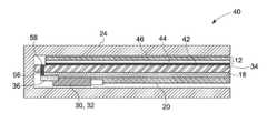
- an optoelectronic device 40is disclosed as shown in FIG. 2 .
- the optoelectronic device 40has an active area 12 disposed on a flexible substrate 34 .
- a “flexible substrate”is a substrate that can be bent to a radius equal to or less than about 1 centimeter, without any fracture or material delamination that affects the performance of the substrate 34 .
- Suitable flexible substrate 34includes a flexible sheet such as a thin plastic sheet, a composite plastic sheet, and metal foils.
- the flexible substrateincludes a polycarbonate.
- suitable materials for the flexible substrateare flexible glass, polymers, including polyesters, such as polyethylene terephthalate, polybutylene phthalate, polyethylene naphthalate, polystyrenes, polycarbonates, polymethylmethacrylate, polyether sulfones, polyallylate, polyimides, polycycloolefins, norbornene resins, and fluoropolymers, metal foils, such as stainless steel, aluminum, silver and gold, metal oxides, such as titanium oxide and zinc oxide, and semiconductors such as silicon.
- Substrate materialmay include composite materials such as fiber reinforced plastic or carbon composites. Combinations of materials may also be used. By using an unbreakable material instead of a fragile glass substrate for the x-ray detector, the components and materials designed to absorb bending stress or drop shock can be reduced in size and weight or eliminated, and the overall weight and thickness of the detector can be reduced.
- the active area 12 , substrate 14 , and the electronics 20are covered with a device outer casing 24 .
- the electronics 20may be disposed outside of the casing. Since the flexible substrate is made up of a shock resilient material, there is no need for additional mechanical support for the substrate 34 between upper casing 24 and active area 12 , between the electronics assembly 20 and the lower casing 24 , and between the substrate 34 and the casing 24 in the sides. There may be an optional backscatter shielding 18 disposed at the back of the flexible support 34 as shown in FIG. 2 .
- the data module assembly 30 and scan module assembly 32 on the back side of the flexible substrate 34are disposed inside the casing 24 and connected to the electronics 20 modules. In a further embodiment, the data module assembly 30 and/or the scan module assembly 32 may be connected with the electronics 20 modules through a flexible module.
- the active area 12 of the optoelectronic device 40includes a thin film transistor (TFT) array 42 and a photodiode layer 44 .
- the TFT array 42is disposed on the first surface of the flexible substrate 34 and the photodiode layer 44 is disposed on the TFT array 42 .
- the TFT array 42may include a plurality of thin film transistors arranged in a particular order on the first surface of the substrate 34 .
- the thin film transistors of the TFT arraymay be arranged in a side by side manner or may be arranged with gaps in between the individual thin film transistors.
- the photodiode layermay include a block of photodiode or may be having a plurality of individual photodiodes arranged in a layer form.
- the photodiode layer 44may include organic photodiodes or inorganic photodiodes. Depending on the application and variations in design, the photodiode layer 44 may be of a single layer or may include multiple layers. Further, the photodiode layer 44 may be directly disposed on the TFT array 42 or the design may include one or more layers disposed between the photodiode layer 44 and the TFT array 42 . In one embodiment, a plurality of photodiodes is arranged in the photodiode layer 44 on the TFT array 42 . In one embodiment, the TFT array 42 is electrically connected to the photodiode layer 44 .
- the optical deviceis a light imager.
- the light imageris an x-ray detector having a scintillator material.
- the scintillator material 46may disposed on the photodiode layer 42 .
- the optoelectronic device 40is a portable x-ray detector and includes the scintillator layer 46 that is excited by an impinging x-ray and produces visible light.
- the scintillator layer 46may be a monolithic scintillator or pixelated scintillator array.
- GOSGa 2 O 2 S
- Cesium Iodide (CsI)is another scintillator material that can be used for a high sensitivity scintillator, and may be deposited by thermal evaporation.
- Another scintillator that may be usedis a PIB (particle in binder) scintillator, where scintillating particles may be incorporated in a binder matrix material and flattened on a substrate.
- the visible light generated by the scintillatorirradiates the photodiode layer 44 disposed on the TFT array 42 .
- the visible light impinged on the photodiode layer 44partially discharges capacitance of the diodes of the photodiode layer 44 .
- the amount of photodiode dischargeis proportional to the quantity of the incident light.
- Each pixel of the TFT array 42incorporates a switching field effect transistor (FET) used to control when charge is restored to the photodiode capacitance.
- FETswitching field effect transistor
- the charge required to restore the capacitanceis provided and measured by external charge measurement circuitry.
- This circuitrycoupled with the TFT array 42 , allows sequential scanning and readout of all photodiodes in the array 44 .
- a custom A/D integrator/converteris normally used to measure the charge required to restore the photodiode to its initial un-discharged state.
- the magnitude of the dischargeis proportional to the incident x-ray dose at each pixel integrated by both the scintillator layer 46 and the photodiode layer 44 during the length of the x-ray exposure.
- the final x-ray imageis reconstructed pixel-by-pixel using the photodiode layer 44 discharge levels to set the image pixel intensity.
- a plurality of data lines 52 and scan lines 54may be connected to the TFT array 42 and disposed on the first surface of the flexible substrate, as shown in the top view of the TFT array 42 (without showing any of the other active layers on top of TFT array 42 ) depicted in FIG. 3 .
- the data lines 52 and the scan lines 54may be connected to each of the transistor of the TFT array 42 . Therefore, depending on the number of transistors in the TFT array, there may be hundreds of data lines 52 and scan lines 54 present on the first surface of the flexible substrate 34 . In one embodiment, the number of data lines 52 present is more than 1000. In one embodiment, the number of scan lines 54 present is more than 1000.
- an electronic signal module(not shown) includes the data module assembly 30 and the scan module assembly 32 and is disposed in the backside (second surface) of the flexible substrate 34 .
- the data module assembly 30is disposed on the first surface of the flexible substrate 34 and the scan module assembly 32 is disposed in the backside of the flexible substrate 34 .
- the scan module assembly 32is disposed on the first surface of the flexible substrate 34 and the data module assembly 30 is disposed in the backside of the flexible substrate 34 .
- the data module assembly 30 and the scan module assembly 32are connected to the data lines 52 and the scan lines 54 respectively through a flexible bond.
- a through via 56( FIG. 2 and FIG. 3 ) may be made through the substrate 34 connecting the first surface and second surface.
- the data lines 52may be connected to the data module assembly 30 by passing through the through via 56 without the need to go around the edges of the substrate 34 .
- the scan lines 54may be connected to the scan module assembly 32 by passing through the through via 56 without the need to go around the edges of the substrate 34 .
- the through via's 56 used for the data information (including data signal) transfer to the data module assembly 30 and the scan information (including scan signal) to the scan module assembly 32may be the same or different.
- one set of through via's 56may be exclusively used for the transmission of the data line 52 information to the data module assembly 30
- another set of through via's 56may be used for the transmission of the scan line 54 information to the scan module assembly 32 .
- An interconnect 58FIG. 2
- the interconnect 58 for transfer of the data information to the data module assembly 30may be different from the interconnect 58 used for the transfer of the scan information to the scan module assembly 32 .
- the data module assembly 30 and/or the scan module assembly 32may be connected with the interconnect 58 through a flexible module.
- the through via 56 on the flexible substrate 34may be disposed anywhere on the substrate 34 .
- the through via 56is near an edge portion of the flexible substrate 34 , and therefore, the interconnect 58 is disposed near an edge portion of the substrate, away from the active area 12 .
- the through via 56 and the interconnect 58are disposed in the array portion (not shown) of the flexible substrate 34 where the TFT array 42 is disposed.
- a clearance between the casing 24 and the flexible substrate 34 at a direction perpendicular to the through via 56 (and parallel to the substrate 34 first surface and second surface)is less than about 0.5 mm. In one embodiment, the distance d between the outer part of casing 24 and the active area 12 is less than about 5 millimeter.
Landscapes
- Physics & Mathematics (AREA)
- Health & Medical Sciences (AREA)
- Life Sciences & Earth Sciences (AREA)
- General Physics & Mathematics (AREA)
- High Energy & Nuclear Physics (AREA)
- Molecular Biology (AREA)
- Spectroscopy & Molecular Physics (AREA)
- Measurement Of Radiation (AREA)
Abstract
Description
Portable x-ray detectors are a fast growing market in the medical and industrial markets. Digital x-ray (DXR) detectors are typically fabricated on thick glass substrates. As a result, current portable products have a limited ruggedness specification, including a maximum 30 cm drop height. The glass substrate requires significant package thickness and weight to protect the fragile glass substrate from breaking. Trade-offs may be required to balance detector ruggedness against detector weight and thickness.
Therefore, the critical limitation for a highly portable, front-line deployed digital x-ray detector is the glass substrate. Display technologies such as e-readers and e-books offer the opportunity for a light-weight and rugged substrate. Many of the requirements for an active matrix display overlap with those for a digital x-ray detector. As a result, a flexible display has the potential to be integrated into a rugged digital x-ray detector. A flexible, unbreakable, thin substrate would enable thin, rugged, light-weight x-ray detectors and new processing capability that was not previously possible.
The present invention meets these and other needs by providing an optoelectronic device that includes a flexible substrate with electrical interconnects that penetrate through the substrate and allow electrical connections to the back side of the substrate.
Accordingly, in one aspect, the invention relates to an optoelectronic device. The optoelectronic device includes a flexible substrate, a thin film transistor (TFT) array disposed on a first surface of the flexible substrate, a photodiode layer disposed on the TFT array, and a plurality of data lines and scan lines connected to the TFT array and disposed on the first surface of the flexible substrate. The device further includes an electronics signal module assembly disposed on a second surface of the flexible substrate opposite the TFT array, and an interconnect disposed through the flexible substrate, connecting the data lines and scan lines to the electronics signal module assembly.
In the following description, like reference characters designate like or corresponding parts throughout the several views shown in the figures. It is also understood that terms such as “top,” “above,” “over,” “on,” and the like are words of convenience and are not to be construed as limiting terms.
One aspect of the invention is to provide a portable optoelectronic device, such as, but not limited to light emitting devices (LED), organic light emitting devices (OLED), photovoltaic devices, light imagers, light emitters, and x-ray detectors.
A general existing electro-optical (alternately optoelectronic)device 10 is as shown inFIG. 1 . The device includes an active area (array)12 on asubstrate 14. In general, thesubstrate 14 in a general optical device such as an optical imager is predominantly made of glass. Theglass substrate 14 normally has amechanical support 16 so that the load and shock experienced by the glass substrate is minimized. Thedevice 10 may further have abackscatter shielding 18 to minimize the scattering of the light waves to the surroundings. Theelectronics 20 of thedevice 10 is normally assembled at the back of thesubstrate 14, preferably back of thebackscatter shielding 18, so as to maximize theactive area 12 in the front side of thesubstrate 14.
In a device with theglass substrate 14, the electrical connections from theactive area 12 to theelectronics 20 were formed through a flexible interconnect (alternately TAB bond)20. Theflexible interconnect 22 is bonded to theactive array 12 in the front side of thesubstrate 14, and wraps around the edge of thesubstrate 14,substrate support 16, and thebackscatter shielding 18 to connect to the electronics signal module assembly including the data module assembly30 and scan module assembly32 on the back side and further connect to theelectronics 20 modules. Theactive area 12,substrate 14, and theelectronics 20 are covered with a device outer cover (casing)24. Supports andshock absorbing materials 26 are added inside thedevice casing 24 on the top, sides, and bottom to protect thesubstrate 14 glass from breakage.
A distance “d” between the outside of theouter casing 24 and theactive area 12 is an important parameter indicating the useful utility of the active area for many imaging applications. Maximization of the availableactive area 12 may be aided by the minimum “d”. With theglass substrate 14, the distance d is increased by theflexible interconnect 22 as well as the panel supports26. The thickness “t” of the device also increases by thesupport structures 26 andpanel support 16. Replacing theglass substrate 14 with a flexible substrate would reduce the need for thepanel support 16 and the support structures and shock absorbing materials.
In one embodiment of the present invention, anoptoelectronic device 40 is disclosed as shown inFIG. 2 . Theoptoelectronic device 40 has anactive area 12 disposed on aflexible substrate 34. As used herein, a “flexible substrate” is a substrate that can be bent to a radius equal to or less than about 1 centimeter, without any fracture or material delamination that affects the performance of thesubstrate 34.
Suitableflexible substrate 34 includes a flexible sheet such as a thin plastic sheet, a composite plastic sheet, and metal foils. In one particular embodiment, the flexible substrate includes a polycarbonate. Examples of suitable materials for the flexible substrate are flexible glass, polymers, including polyesters, such as polyethylene terephthalate, polybutylene phthalate, polyethylene naphthalate, polystyrenes, polycarbonates, polymethylmethacrylate, polyether sulfones, polyallylate, polyimides, polycycloolefins, norbornene resins, and fluoropolymers, metal foils, such as stainless steel, aluminum, silver and gold, metal oxides, such as titanium oxide and zinc oxide, and semiconductors such as silicon. Substrate material may include composite materials such as fiber reinforced plastic or carbon composites. Combinations of materials may also be used. By using an unbreakable material instead of a fragile glass substrate for the x-ray detector, the components and materials designed to absorb bending stress or drop shock can be reduced in size and weight or eliminated, and the overall weight and thickness of the detector can be reduced.
In one embodiment, theactive area 12,substrate 14, and theelectronics 20 are covered with a deviceouter casing 24. In an alternate embodiment, theelectronics 20 may be disposed outside of the casing. Since the flexible substrate is made up of a shock resilient material, there is no need for additional mechanical support for thesubstrate 34 betweenupper casing 24 andactive area 12, between theelectronics assembly 20 and thelower casing 24, and between thesubstrate 34 and thecasing 24 in the sides. There may be anoptional backscatter shielding 18 disposed at the back of theflexible support 34 as shown inFIG. 2 . In one embodiment, the data module assembly30 and scan module assembly32 on the back side of theflexible substrate 34 are disposed inside thecasing 24 and connected to theelectronics 20 modules. In a further embodiment, the data module assembly30 and/or the scan module assembly32 may be connected with theelectronics 20 modules through a flexible module.
In one embodiment, theactive area 12 of theoptoelectronic device 40 includes a thin film transistor (TFT)array 42 and aphotodiode layer 44. In one embodiment, theTFT array 42 is disposed on the first surface of theflexible substrate 34 and thephotodiode layer 44 is disposed on theTFT array 42. TheTFT array 42 may include a plurality of thin film transistors arranged in a particular order on the first surface of thesubstrate 34. The thin film transistors of the TFT array may be arranged in a side by side manner or may be arranged with gaps in between the individual thin film transistors.
The photodiode layer may include a block of photodiode or may be having a plurality of individual photodiodes arranged in a layer form. Thephotodiode layer 44 may include organic photodiodes or inorganic photodiodes. Depending on the application and variations in design, thephotodiode layer 44 may be of a single layer or may include multiple layers. Further, thephotodiode layer 44 may be directly disposed on theTFT array 42 or the design may include one or more layers disposed between thephotodiode layer 44 and theTFT array 42. In one embodiment, a plurality of photodiodes is arranged in thephotodiode layer 44 on theTFT array 42. In one embodiment, theTFT array 42 is electrically connected to thephotodiode layer 44.
Depending on the function of theoptoelectronic device 40, there may be additional layers as a part of theactive area 12. For example, in one embodiment, the optical device is a light imager. In one embodiment, the light imager is an x-ray detector having a scintillator material. In this embodiment, thescintillator material 46 may disposed on thephotodiode layer 42.
In one particular embodiment, theoptoelectronic device 40 is a portable x-ray detector and includes thescintillator layer 46 that is excited by an impinging x-ray and produces visible light. Thescintillator layer 46 may be a monolithic scintillator or pixelated scintillator array. GOS (Gd2O2S) is a commonly used low cost scintillator, which is in the form of thin film with millimeter range thickness. Cesium Iodide (CsI) is another scintillator material that can be used for a high sensitivity scintillator, and may be deposited by thermal evaporation. Another scintillator that may be used is a PIB (particle in binder) scintillator, where scintillating particles may be incorporated in a binder matrix material and flattened on a substrate. The visible light generated by the scintillator irradiates thephotodiode layer 44 disposed on theTFT array 42.
The visible light impinged on thephotodiode layer 44 partially discharges capacitance of the diodes of thephotodiode layer 44. The amount of photodiode discharge is proportional to the quantity of the incident light. Each pixel of theTFT array 42 incorporates a switching field effect transistor (FET) used to control when charge is restored to the photodiode capacitance. The charge required to restore the capacitance is provided and measured by external charge measurement circuitry. This circuitry, coupled with theTFT array 42, allows sequential scanning and readout of all photodiodes in thearray 44. A custom A/D integrator/converter is normally used to measure the charge required to restore the photodiode to its initial un-discharged state. The magnitude of the discharge is proportional to the incident x-ray dose at each pixel integrated by both thescintillator layer 46 and thephotodiode layer 44 during the length of the x-ray exposure. The final x-ray image is reconstructed pixel-by-pixel using thephotodiode layer 44 discharge levels to set the image pixel intensity.
To provide and measure the charge required to restore the capacitance of the photodiodes by external circuitry, a plurality ofdata lines 52 andscan lines 54 may be connected to theTFT array 42 and disposed on the first surface of the flexible substrate, as shown in the top view of the TFT array42 (without showing any of the other active layers on top of TFT array42) depicted inFIG. 3 . The data lines52 and thescan lines 54 may be connected to each of the transistor of theTFT array 42. Therefore, depending on the number of transistors in the TFT array, there may be hundreds ofdata lines 52 andscan lines 54 present on the first surface of theflexible substrate 34. In one embodiment, the number ofdata lines 52 present is more than 1000. In one embodiment, the number ofscan lines 54 present is more than 1000.
The data lines52 and thescan lines 54 need to be connected to the data module assembly30 and scan module assembly32 respectively (FIG. 2 ). In one embodiment, an electronic signal module (not shown) includes the data module assembly30 and the scan module assembly32 and is disposed in the backside (second surface) of theflexible substrate 34. In one embodiment, the data module assembly30 is disposed on the first surface of theflexible substrate 34 and the scan module assembly32 is disposed in the backside of theflexible substrate 34. In an alternate embodiment, the scan module assembly32 is disposed on the first surface of theflexible substrate 34 and the data module assembly30 is disposed in the backside of theflexible substrate 34. In one embodiment, the data module assembly30 and the scan module assembly32 are connected to the data lines52 and thescan lines 54 respectively through a flexible bond. Considering the compliantflexible substrate 34 of the presentoptical device 40, a through via56 (FIG. 2 andFIG. 3 ) may be made through thesubstrate 34 connecting the first surface and second surface. The data lines52 may be connected to the data module assembly30 by passing through the through via56 without the need to go around the edges of thesubstrate 34. Similarly, thescan lines 54 may be connected to the scan module assembly32 by passing through the through via56 without the need to go around the edges of thesubstrate 34.
There may be a plurality of through via56 disposed on thesubstrate 34 depending on the requirement. The through via's56 used for the data information (including data signal) transfer to the data module assembly30 and the scan information (including scan signal) to the scan module assembly32 may be the same or different. For example, one set of through via's56 may be exclusively used for the transmission of thedata line 52 information to the data module assembly30, and another set of through via's56 may be used for the transmission of thescan line 54 information to the scan module assembly32. An interconnect58 (FIG. 2 ) may be passed through the through via56 for the connection of the data lines52 with the data module assembly30 and thescan lines 54 with the scan module assembly32 through atab bond pad 36. Theinterconnect 58 for transfer of the data information to the data module assembly30 may be different from theinterconnect 58 used for the transfer of the scan information to the scan module assembly32. In one embodiment, the data module assembly30 and/or the scan module assembly32 may be connected with theinterconnect 58 through a flexible module.
The through via56 on theflexible substrate 34 may be disposed anywhere on thesubstrate 34. In one embodiment, the through via56 is near an edge portion of theflexible substrate 34, and therefore, theinterconnect 58 is disposed near an edge portion of the substrate, away from theactive area 12. In an alternate embodiment, the through via56 and theinterconnect 58 are disposed in the array portion (not shown) of theflexible substrate 34 where theTFT array 42 is disposed.
In one embodiment of anoptoelectronic device 40 having aflexible substrate 34, a clearance between thecasing 24 and theflexible substrate 34 at a direction perpendicular to the through via56 (and parallel to thesubstrate 34 first surface and second surface) is less than about 0.5 mm. In one embodiment, the distance d between the outer part ofcasing 24 and theactive area 12 is less than about 5 millimeter.
This written description uses examples to disclose the invention, including the best mode, and also to enable any person skilled in the art to practice the invention, including making and using any devices or systems and performing any incorporated methods. The patentable scope of the invention is defined by the claims, and may include other examples that occur to those skilled in the art. Such other examples are intended to be within the scope of the claims if they have structural elements that do not differ from the literal language of the claims, or if they include equivalent structural elements with insubstantial differences from the literal languages of the claims.
Claims (11)
1. An optoelectronic device comprising:
a flexible substrate;
an active area comprising a thin film transistor (TFT) array disposed on a first surface of the flexible substrate and a photodiode layer disposed on the TFT array, wherein the active area defines a border region, offset from the active area and extending to an edge of the flexible substrate;
a plurality of data lines and scan lines connected to the TFT array and disposed on the first surface of the flexible substrate;
an electronics signal module assembly disposed on a second surface of the flexible substrate opposite to the TFT array and comprising a data module assembly and a scan module assembly;
a through via disposed in the border region, extending from the second surface to the first surface of the flexible substrate; and
an interconnect disposed in the through via, connecting the plurality of data lines to the data module assembly and the plurality of scan lines to the scan module assembly, through a TAB bond.
2. The device ofclaim 1 , wherein the TFT array comprises a plurality of transistors, and wherein each transistor of the TFT array is connected to the electronics signal module assembly.
3. The device ofclaim 1 , wherein the photodiode layer comprises a plurality of photodiodes.
4. The device ofclaim 1 , wherein the TFT array is electrically connected to the photodiode layer.
5. The device ofclaim 1 , wherein the plurality of data lines comprises greater than about 100 data lines.
6. The device ofclaim 1 , wherein the plurality of scan lines comprises greater than about 100 scan lines.
7. The device ofclaim 1 , further comprising a scintillator material disposed on the photodiode layer.
8. The device ofclaim 7 , wherein the flexible substrate, the scintillator material, the TFT array, the photodiode layer, the plurality of data lines, and the plurality of scan lines are disposed inside a casing.
9. The device ofclaim 8 , wherein the electronics signal module assembly is disposed inside the casing.
10. The device ofclaim 8 , wherein the flexible substrate is a shock resilient substrate and a clearance between the casing and the shock resilient substrate is less than about 0.5 mm.
11. The device ofclaim 1 , wherein the device is a portable X-ray detector.
Priority Applications (4)
| Application Number | Priority Date | Filing Date | Title |
|---|---|---|---|
| US14/103,989US9917133B2 (en) | 2013-12-12 | 2013-12-12 | Optoelectronic device with flexible substrate |
| EP14772018.9AEP3080846A1 (en) | 2013-12-12 | 2014-09-08 | Optoelectronic device with flexible substrate |
| PCT/US2014/054560WO2015088605A1 (en) | 2013-12-12 | 2014-09-08 | Optoelectronic device with flexible substrate |
| CN201480067759.XACN106489205B (en) | 2013-12-12 | 2014-09-08 | Optoelectronic device with flexible substrate |
Applications Claiming Priority (1)
| Application Number | Priority Date | Filing Date | Title |
|---|---|---|---|
| US14/103,989US9917133B2 (en) | 2013-12-12 | 2013-12-12 | Optoelectronic device with flexible substrate |
Publications (2)
| Publication Number | Publication Date |
|---|---|
| US20150171134A1 US20150171134A1 (en) | 2015-06-18 |
| US9917133B2true US9917133B2 (en) | 2018-03-13 |
Family
ID=51589531
Family Applications (1)
| Application Number | Title | Priority Date | Filing Date |
|---|---|---|---|
| US14/103,989Expired - Fee RelatedUS9917133B2 (en) | 2013-12-12 | 2013-12-12 | Optoelectronic device with flexible substrate |
Country Status (4)
| Country | Link |
|---|---|
| US (1) | US9917133B2 (en) |
| EP (1) | EP3080846A1 (en) |
| CN (1) | CN106489205B (en) |
| WO (1) | WO2015088605A1 (en) |
Cited By (3)
| Publication number | Priority date | Publication date | Assignee | Title |
|---|---|---|---|---|
| US20170082558A1 (en)* | 2014-07-25 | 2017-03-23 | General Electric Company | X-ray detectors supported on a substrate having a metal barrier |
| US20190353805A1 (en)* | 2018-05-21 | 2019-11-21 | General Electric Company | Digital x-ray detector having polymeric substrate |
| US11385361B2 (en)* | 2016-06-16 | 2022-07-12 | Arizona Board Of Regents On Behalf Of Arizona State University | Electronic devices and related methods |
Families Citing this family (7)
| Publication number | Priority date | Publication date | Assignee | Title |
|---|---|---|---|---|
| US9513380B2 (en)* | 2014-07-25 | 2016-12-06 | General Electric Company | X-ray detectors supported on a substrate having a surrounding metal barrier |
| US9535173B2 (en)* | 2014-09-11 | 2017-01-03 | General Electric Company | Organic x-ray detector and x-ray systems |
| WO2017099784A1 (en)* | 2015-12-10 | 2017-06-15 | Intel Corporation | Flexible computing device that includes a plurality of displays |
| JP2017203672A (en)* | 2016-05-11 | 2017-11-16 | 東芝電子管デバイス株式会社 | Radiation detector |
| CN108107060A (en)* | 2017-11-30 | 2018-06-01 | 上海奕瑞光电子科技股份有限公司 | Flat panel detector based on fexible film encapsulation and preparation method thereof |
| EP3495849A1 (en)* | 2017-12-11 | 2019-06-12 | Koninklijke Philips N.V. | Multilayer pixelated scintillator with enlarged fill factor |
| CN114038866A (en)* | 2021-10-12 | 2022-02-11 | 上海奕瑞光电子科技股份有限公司 | Flexible folding X-ray detector and preparation method thereof |
Citations (138)
| Publication number | Priority date | Publication date | Assignee | Title |
|---|---|---|---|---|
| DE2520065B1 (en) | 1975-05-06 | 1976-07-15 | Seifert & Co Rich | Automatic X-ray inspection of longitudinally welded tubes - synchronizes X-ray gun position and film content automatically |
| US5319206A (en) | 1992-12-16 | 1994-06-07 | E. I. Du Pont De Nemours And Company | Method and apparatus for acquiring an X-ray image using a solid state device |
| WO1994023458A2 (en) | 1993-04-05 | 1994-10-13 | Cardiac Mariners, Inc. | X-ray detector for a low dosage scanning beam digital x-ray imaging system |
| US5357121A (en)* | 1991-10-14 | 1994-10-18 | Mitsubishi Denki Kabushiki Kaisha | Optoelectronic integrated circuit |
| US5381014A (en) | 1993-12-29 | 1995-01-10 | E. I. Du Pont De Nemours And Company | Large area X-ray imager and method of fabrication |
| US5399884A (en) | 1993-11-10 | 1995-03-21 | General Electric Company | Radiation imager with single passivation dielectric for transistor and diode |
| US5614720A (en) | 1990-06-22 | 1997-03-25 | Integrated Diagnostic Measurement Corporation | Mobile, multi-mode apparatus and method for nondestructively inspecting components of an operating system |
| US5721422A (en) | 1995-03-16 | 1998-02-24 | U.S. Philips Corporation | Electronic devices having an array with shared column conductors |
| GB2317742A (en) | 1996-09-30 | 1998-04-01 | Sharp Kk | Imaging device |
| US6181769B1 (en) | 1997-10-01 | 2001-01-30 | Siemens Aktiengesellschaft | X-ray detector with anatomically adapted recess |
| US6205199B1 (en) | 1995-06-23 | 2001-03-20 | Science Applications International Corporation | Pixel-correlated, digital X-ray imaging system |
| US6262421B1 (en) | 1992-02-20 | 2001-07-17 | Imation Corp. | Solid state radiation detector for x-ray imaging |
| US6303943B1 (en) | 1998-02-02 | 2001-10-16 | Uniax Corporation | Organic diodes with switchable photosensitivity useful in photodetectors |
| US6341153B1 (en) | 2000-10-27 | 2002-01-22 | Genesis Engineering Company | System and method for portable nondestructive examination with realtime three-dimensional tomography |
| US6380543B1 (en) | 1998-09-16 | 2002-04-30 | Lg. Philipa Lcd Co., Ltd. | Thin film transistor type X-ray image detecting device and method for fabricating the same |
| US20020079458A1 (en) | 1999-07-26 | 2002-06-27 | Edge Medical Devices Ltd. | Hybrid detector for X-ray imaging |
| US6426991B1 (en) | 2000-11-16 | 2002-07-30 | Koninklijke Philips Electronics N.V. | Back-illuminated photodiodes for computed tomography detectors |
| US6465824B1 (en)* | 2000-03-09 | 2002-10-15 | General Electric Company | Imager structure |
| US6483099B1 (en) | 1998-08-14 | 2002-11-19 | Dupont Displays, Inc. | Organic diodes with switchable photosensitivity |
| US20030001222A1 (en) | 2001-07-02 | 2003-01-02 | Xerox Corporation | Low data line capacitance image sensor array using air-gap metal crossover |
| US20030010923A1 (en) | 2001-07-16 | 2003-01-16 | Edge Medical Devices Ltd. | High resolution detector for X-ray imaging |
| US20030030004A1 (en) | 2001-01-31 | 2003-02-13 | General Electric Company | Shared memory control between detector framing node and processor |
| US20030031296A1 (en) | 2001-07-27 | 2003-02-13 | Martin Hoheisel | X-ray diagnostics installation with a flexible solid state X-ray detector |
| US20030122083A1 (en) | 2002-01-03 | 2003-07-03 | General Electric Company | Optimized scintillator and pixilated photodiode detector array for multi-slice CT x-ray detector using backside illumination |
| US20030210761A1 (en) | 2002-05-10 | 2003-11-13 | Hoffman David Michael | Computed tomography system with integrated scatter detectors |
| US20030227997A1 (en) | 2002-06-11 | 2003-12-11 | Petrick Scott W. | Method and apparatus for acquiring a series of images utilizing a solid state detector with alternating scan lines |
| US20030234364A1 (en) | 2002-06-25 | 2003-12-25 | Hennessy William Andrew | Imaging array and method for manufacturing same |
| US20040016886A1 (en) | 2002-07-25 | 2004-01-29 | General Electric Company | Flexible imager and digital imaging method |
| US6717150B2 (en) | 2000-12-12 | 2004-04-06 | Ge Medical Systems Global Technology Company, Llc | Solid-state CT detector modules with improved scintillator/diode coupling |
| US20040085598A1 (en) | 2002-10-09 | 2004-05-06 | Konica Corporation | Digital still camera and manufacturing method thereof |
| US6740884B2 (en) | 2002-04-03 | 2004-05-25 | General Electric Company | Imaging array and methods for fabricating same |
| US20040113086A1 (en)* | 2002-09-23 | 2004-06-17 | Bjoern Heismann | Image detector for x-ray devices with rear-contact organic image sensors |
| US20040170861A1 (en) | 2003-02-28 | 2004-09-02 | Eastman Kodak Company | Organic light emitting diodes for production of polarized light |
| US20040190676A1 (en) | 2001-12-03 | 2004-09-30 | Shinichi Kojima | Radiological imaging apparatus |
| US20040229051A1 (en) | 2003-05-15 | 2004-11-18 | General Electric Company | Multilayer coating package on flexible substrates for electro-optical devices |
| US6841784B2 (en) | 2002-07-02 | 2005-01-11 | Ray Therapy Imaging Ab | Radiation sensor device |
| US20050008213A1 (en) | 2003-07-09 | 2005-01-13 | General Electric Company | System and method for analyzing and identifying flaws in a manufactured part |
| US6867418B2 (en)* | 2000-01-13 | 2005-03-15 | Hamamatsu Photonics K.K. | Radiation image sensor and scintillator panel |
| US6901159B2 (en) | 2001-01-31 | 2005-05-31 | General Electric Company | Communication of image data from image detector to host computer |
| US6904124B2 (en) | 2001-01-31 | 2005-06-07 | General Electric Company | Indirect programming of detector framing node |
| US20050178971A1 (en) | 2004-02-17 | 2005-08-18 | Hoge Michael F. | Methods and apparatus for radiation detection |
| US20050236614A1 (en) | 2004-04-22 | 2005-10-27 | Parker Ian D | Processes for forming organic layers, organic electronic devices, and transistors |
| US6970586B2 (en) | 2001-01-31 | 2005-11-29 | General Electric Company | Detector framing node architecture to communicate image data |
| US6982424B2 (en) | 2003-06-02 | 2006-01-03 | Ge Medical Systems Global Technology Company, Llc | X-ray and CT image detector |
| US20060008054A1 (en) | 2004-07-12 | 2006-01-12 | Hiromu Ohara | Radiographic image capturing system and radiographic image capturing method |
| US7053381B2 (en) | 2001-12-06 | 2006-05-30 | General Electric Company | Dual para-xylylene layers for an X-ray detector |
| US7081627B2 (en) | 2002-09-23 | 2006-07-25 | Siemens Aktiengesellschaft | Image detector for X-ray radiation |
| US7105830B2 (en) | 2003-03-12 | 2006-09-12 | Canon Kabushiki Kaisha | Radiation detecting device and method of manufacturing the same |
| US7122804B2 (en) | 2002-02-15 | 2006-10-17 | Varian Medical Systems Technologies, Inc. | X-ray imaging device |
| US20060256922A1 (en) | 2005-05-11 | 2006-11-16 | Ge Medical Systems Global Technology Company, Llc | X-ray CT apparatus |
| US20060282946A1 (en) | 2005-06-15 | 2006-12-21 | Meyer Matthew E | Patient transfer device |
| US7180075B2 (en) | 2002-09-23 | 2007-02-20 | Siemens Aktiengesellschaft | X-ray detector including a scintillator with a photosensor coating, and a production process |
| US20070039102A1 (en) | 2003-04-25 | 2007-02-22 | Thompson Harlyn J | Lumbar back support device |
| US7196331B2 (en) | 2004-01-12 | 2007-03-27 | Siemens Aktiengesellschaft | Detector module |
| US20070085015A1 (en) | 2005-10-14 | 2007-04-19 | Castleberry Donald E | Lightweight and rugged digital x-ray detector |
| US7211825B2 (en) | 2004-06-14 | 2007-05-01 | Yi-Chi Shih | Indium oxide-based thin film transistors and circuits |
| US7259037B2 (en) | 2002-07-12 | 2007-08-21 | Hannstar Display Corp. | Method of fabricating an X-ray detector array element |
| US20070257253A1 (en) | 2006-03-27 | 2007-11-08 | Choong-Youl Im | Organic light emitting display device and method of fabricating the same |
| US20070262266A1 (en) | 2004-06-02 | 2007-11-15 | Siemens Aktiengesellschaft | X-Ray Detector Comprising Scintillators That Are Attached To Both Sides Of A Light Sensor |
| US20070289625A1 (en) | 2004-04-21 | 2007-12-20 | Renaud Demadrille | -Conjugated Mono-, Oligo-and Polymeric Compounds, and Photovoltaic Cells Comprising Them |
| US20070295973A1 (en) | 2006-03-03 | 2007-12-27 | Yasuhiro Jinbo | Method for manufacturing semiconductor device |
| US20070295966A1 (en)* | 2006-06-09 | 2007-12-27 | Canon Kabushiki Kaisha | Conversion apparatus and imaging system |
| US20080078940A1 (en)* | 2006-10-03 | 2008-04-03 | General Electric Company | Portable imaging device having shock absorbent assembly |
| US7366280B2 (en) | 2003-06-19 | 2008-04-29 | General Electric Company | Integrated arc anode x-ray source for a computed tomography system |
| US7379528B2 (en) | 2003-01-06 | 2008-05-27 | Koninklijke Philips Electronics N.V. | Radiation detector with shielded electronics for computed tomography |
| US20080135891A1 (en)* | 2006-12-08 | 2008-06-12 | Palo Alto Research Center, Incorporated | Transistor Device Formed on a Flexible Substrate Including Anodized Gate Dielectric |
| US20080149652A1 (en) | 2006-12-26 | 2008-06-26 | Ming-Chi Chang | Handle enclosing assembly of toolbox |
| US20080267345A1 (en) | 2007-04-26 | 2008-10-30 | Nagumo Yasushi | Method for inspecting pipes, and radiographic non-destructive inspection apparatus |
| US20080278068A1 (en) | 2005-11-17 | 2008-11-13 | Imperial College Innovations Limited | Method of Patterning a Thin Film |
| WO2008148815A1 (en) | 2007-06-04 | 2008-12-11 | Detection Technology Oy | Photodetector for imaging system |
| US20090026383A1 (en) | 2007-07-23 | 2009-01-29 | Samsung Electronics Co., Ltd | X-Ray Detector and Method of Manufacturing the Same |
| US20090026379A1 (en) | 2007-07-26 | 2009-01-29 | Hiroyuki Yaegashi | Radiation imaging device |
| US7486766B1 (en) | 2004-06-21 | 2009-02-03 | Radiation Monitoring Devices, Inc. | Micro CT scanners incorporating internal gain charge-coupled devices |
| US20090166512A1 (en) | 2005-11-17 | 2009-07-02 | Fuerst Jens | Organic Pixeled Flat Detector Having Increased Sensitivity |
| US7560702B2 (en) | 2005-11-28 | 2009-07-14 | General Electric Company | Interconnect and packaging method for multi-slice CT detector modules |
| US7606346B2 (en) | 2007-01-04 | 2009-10-20 | General Electric Company | CT detector module construction |
| US7605875B2 (en) | 1998-10-21 | 2009-10-20 | Samsung Electronics Co., Ltd. | Thin film transistor array panel for a liquid crystal display and a method for manufacturing the same |
| US20090279029A1 (en) | 2008-05-08 | 2009-11-12 | Sony Corporation | Liquid crystal display |
| US20090285352A1 (en) | 2005-11-21 | 2009-11-19 | Paul Scherrer Institut | Readout Chip for Single Photon Counting |
| US20100059804A1 (en)* | 2008-09-10 | 2010-03-11 | Mitsubishi Electric Corporation | Photoelectric conversion device and method of manufacturing the same |
| US20100102242A1 (en) | 2008-10-29 | 2010-04-29 | General Electric Company | Multi-layer radiation detector assembly |
| US20100102300A1 (en) | 2007-04-04 | 2010-04-29 | Cambridge Display Technology Limited | Active Matrix Optical Device |
| CN101718912A (en) | 2009-11-27 | 2010-06-02 | 北京工业大学 | Digitalized detail visualizer of industrial X-ray negative with variable zooming ratio |
| US20100148072A1 (en) | 2005-08-08 | 2010-06-17 | Fuerst Jens | Photodetector, flat x-ray detector and method for producing the same |
| US20100155578A1 (en) | 2008-12-24 | 2010-06-24 | Seiko Epson Corporation | Light source integrated photoelectric conversion apparatus |
| US20100193691A1 (en) | 2007-11-05 | 2010-08-05 | Canon Kabushiki Kaisha | Manufacturing method of radiation detecting apparatus, and radiation detecting apparatus and radiation imaging system |
| US20100224784A1 (en) | 2007-11-20 | 2010-09-09 | Toshiba Electron Tubes & Devices Co., Ltd. | Radiation detector and method for producing the same |
| US7838994B2 (en) | 2003-02-24 | 2010-11-23 | Hamamatsu Photonics K.K. | Semiconductor device and radiation detector employing it |
| US20100305427A1 (en) | 2009-06-01 | 2010-12-02 | General Electric Company | Long-range planar sensor array for use in a surgical navigation system |
| CN201681056U (en) | 2009-11-27 | 2010-12-22 | 北京工业大学 | Industrial high-resolution observation device for X-ray negative films |
| US20100320391A1 (en) | 2009-06-17 | 2010-12-23 | Regents Of The University Of Michigan | Photodiode and other sensor structures in flat-panel x-ray imagers and method for improving topological uniformity of the photodiode and other sensor structures in flat-panel x-ray imagers based on thin-film electronics |
| US20110026685A1 (en) | 2009-07-29 | 2011-02-03 | Spectrum Dynamics Llc | Method and system of optimized volumetric imaging |
| US20110024711A1 (en) | 2009-07-30 | 2011-02-03 | Wen Li | Apparatus for reducing photodiode thermal gain coefficient and method of making same |
| CN101975787A (en) | 2010-10-21 | 2011-02-16 | 丹东奥龙射线仪器有限公司 | Arm device for spiral welded pipe X-ray detector |
| US20110042656A1 (en) | 2007-12-19 | 2011-02-24 | Cambridge Display Technology Limited | Electronic Devices and Methods of Making the Same Using Solution Processing Techniques |
| US7897929B2 (en) | 2007-12-06 | 2011-03-01 | General Electric Company | Reduced cost pixel design for flat panel x-ray imager |
| US20110049661A1 (en) | 2009-08-28 | 2011-03-03 | Fujifilm Corporation | Solid-state imaging device and process of making solid state imaging device |
| US7947961B2 (en) | 2008-10-24 | 2011-05-24 | Advanced Silicon Sa | X-ray imaging readout and system |
| US7947960B2 (en) | 2008-02-13 | 2011-05-24 | Ge Medical Systems Global Technology Company, Llc | Detector panel and X-ray imaging apparatus |
| EP2328177A2 (en) | 2009-11-27 | 2011-06-01 | Fujifilm Corporation | Radiation sensor and radiation image detection apparatus |
| US20110127504A1 (en) | 2008-04-03 | 2011-06-02 | Cambridge Display Technology Limited | Organic Thin Film Transistors |
| US7964903B2 (en) | 2002-12-11 | 2011-06-21 | Samsung Electronics Co., Ltd. | Thin film transistor array panel for x-ray detector |
| US20110168905A1 (en) | 2010-01-14 | 2011-07-14 | Canon Kabushiki Kaisha | X-ray detector and method for manufacturing the same |
| US20110204341A1 (en) | 2009-09-04 | 2011-08-25 | Plextronics, Inc. | Organic electronic devices and polymers, including photovoltaic cells and diketone-based polymers |
| US8076647B2 (en) | 2008-10-21 | 2011-12-13 | Matt Danielsson | X-ray detector, a corresponding x-ray imaging device and a method for improving the resolution of a scintillator-based x-ray detector |
| US20110305315A1 (en) | 2010-06-15 | 2011-12-15 | Park Se Hee | Table type digital x-ray detector, housing and x-ray photographing apparatus using the same |
| US8084743B2 (en) | 2004-11-10 | 2011-12-27 | Canon Kabushiki Kaisha | Sensor and image pickup device |
| US20120018627A1 (en) | 2010-07-21 | 2012-01-26 | Tredwell Timothy J | Digital radiographic imaging arrays with reduced noise |
| US20120037809A1 (en) | 2009-04-22 | 2012-02-16 | Koninklijke Philips Electronics N. V. | Imaging measurement system with a printed organic photodiode array |
| US8120683B1 (en) | 1999-04-08 | 2012-02-21 | Nova R & D, Inc. | High resoultion digital imaging apparatus |
| US20120068076A1 (en) | 2007-10-30 | 2012-03-22 | Farhad Daghighian | Portable pet scanner for imaging of a portion of the body |
| US20120097858A1 (en) | 2010-10-22 | 2012-04-26 | Daniel Morf | Method and apparatus for multi-layered high efficiency mega-voltage imager |
| US8173969B2 (en) | 2008-09-25 | 2012-05-08 | Fujifilm Corporation | Radiation detecting apparatus and radiation image capturing system |
| US20120121067A1 (en) | 2010-11-11 | 2012-05-17 | Oliver Hayden | Hybrid organic photodiode |
| US20120161270A1 (en) | 2009-08-28 | 2012-06-28 | Fujifilm Corporation | Solid-state imaging device, process of making solid state imaging device, digital still camera, digital video camera, mobile phone, and endoscope |
| US20120161018A1 (en) | 2010-12-22 | 2012-06-28 | Samsung Mobile Display Co., Ltd. | Thin film transistor array substrate for x-ray detector and x-ray detector |
| CN102539454A (en) | 2010-09-27 | 2012-07-04 | 通用电气公司 | Digital x-ray detector with increased dynamic range |
| CN102576415A (en) | 2009-09-30 | 2012-07-11 | 希福特株式会社 | Two-dimensional code, two-dimensional code reader, and program |
| US8222158B2 (en) | 2009-07-09 | 2012-07-17 | Fujifilm Corporation | Electronic device, method of manufacturing the same, display and sensor |
| US20120193542A1 (en) | 2011-01-31 | 2012-08-02 | Sony Corporation | Radiation image pickup apparatus and radiation image pickup/display system |
| US20120201347A1 (en) | 2009-08-28 | 2012-08-09 | Shawcor Ltd. | Method and apparatus for external pipeline weld inspection |
| US20120201348A1 (en) | 2009-10-13 | 2012-08-09 | Shawcor Ltd. | X-ray inspection apparatus for pipeline girth weld inspection |
| US20120223238A1 (en) | 2011-03-02 | 2012-09-06 | Michael Stark | X-Ray Detector And Medical X-Ray Device |
| US20120259378A1 (en) | 2011-04-11 | 2012-10-11 | Heinrichs John R | Emergency response backboard with integrated scale |
| US20120267535A1 (en) | 2011-04-25 | 2012-10-25 | Fujifilm Corporation | Radiation imaging device, system, and method |
| US8300125B2 (en) | 2008-09-22 | 2012-10-30 | Palo Alto Research Center Incorporated | Method and apparatus for using thin-film transistors and MIS capacitors as light-sensing elements in charge mapping arrays |
| US8343779B2 (en) | 2007-04-19 | 2013-01-01 | Basf Se | Method for forming a pattern on a substrate and electronic device formed thereby |
| US8405832B2 (en) | 2009-12-10 | 2013-03-26 | Palo Alto Research Center Incorporated | Light scattering measurement system based on flexible sensor array |
| US20130082264A1 (en) | 2011-09-30 | 2013-04-04 | General Electric Company | Photodetector having improved quantum efficiency |
| US20130092840A1 (en) | 2010-05-25 | 2013-04-18 | Fujifilm Corporation | Radiological imaging device |
| CN202903698U (en) | 2012-11-19 | 2013-04-24 | 南京奥特电气股份有限公司 | Pipeline welded joint digitalized automatic flaw detection device |
| US20130140568A1 (en) | 2011-12-01 | 2013-06-06 | Kenichi Miyamoto | Image detector |
| US20130140464A1 (en)* | 2010-07-26 | 2013-06-06 | Fujifilm Corporation | Radiation detection panel |
| US8477125B2 (en) | 2005-12-21 | 2013-07-02 | Samsung Display Co., Ltd. | Photo sensor and organic light-emitting display using the same |
| US20130170616A1 (en) | 2011-12-31 | 2013-07-04 | Ravi K. Mruthyunjaya | Radiographic detector including block address pixel architecture, imaging apparatus and methods using the same |
| US20140010353A1 (en) | 2010-11-16 | 2014-01-09 | Michael C. Lalena | Systems and methods for calibrating, correcting and processing images on a radiographic detector |
| US20140014843A1 (en) | 2012-07-11 | 2014-01-16 | Konica Minolta, Inc. | Radiation detecting panel and radiographic detector |
| US20140054442A1 (en) | 2012-07-20 | 2014-02-27 | Board Of Regents Of The University Of Nebraska | Nanocomposite Photodetector |
Family Cites Families (1)
| Publication number | Priority date | Publication date | Assignee | Title |
|---|---|---|---|---|
| JP5675062B2 (en)* | 2009-06-05 | 2015-02-25 | キヤノン株式会社 | X-ray imaging device |
- 2013
- 2013-12-12USUS14/103,989patent/US9917133B2/ennot_activeExpired - Fee Related
- 2014
- 2014-09-08CNCN201480067759.XApatent/CN106489205B/ennot_activeExpired - Fee Related
- 2014-09-08WOPCT/US2014/054560patent/WO2015088605A1/enactiveApplication Filing
- 2014-09-08EPEP14772018.9Apatent/EP3080846A1/ennot_activeWithdrawn
Patent Citations (145)
| Publication number | Priority date | Publication date | Assignee | Title |
|---|---|---|---|---|
| DE2520065B1 (en) | 1975-05-06 | 1976-07-15 | Seifert & Co Rich | Automatic X-ray inspection of longitudinally welded tubes - synchronizes X-ray gun position and film content automatically |
| US5614720A (en) | 1990-06-22 | 1997-03-25 | Integrated Diagnostic Measurement Corporation | Mobile, multi-mode apparatus and method for nondestructively inspecting components of an operating system |
| US5357121A (en)* | 1991-10-14 | 1994-10-18 | Mitsubishi Denki Kabushiki Kaisha | Optoelectronic integrated circuit |
| US6262421B1 (en) | 1992-02-20 | 2001-07-17 | Imation Corp. | Solid state radiation detector for x-ray imaging |
| US5319206A (en) | 1992-12-16 | 1994-06-07 | E. I. Du Pont De Nemours And Company | Method and apparatus for acquiring an X-ray image using a solid state device |
| WO1994023458A2 (en) | 1993-04-05 | 1994-10-13 | Cardiac Mariners, Inc. | X-ray detector for a low dosage scanning beam digital x-ray imaging system |
| US5399884A (en) | 1993-11-10 | 1995-03-21 | General Electric Company | Radiation imager with single passivation dielectric for transistor and diode |
| US5381014A (en) | 1993-12-29 | 1995-01-10 | E. I. Du Pont De Nemours And Company | Large area X-ray imager and method of fabrication |
| US5381014B1 (en) | 1993-12-29 | 1997-06-10 | Du Pont | Large area x-ray imager and method of fabrication |
| US5721422A (en) | 1995-03-16 | 1998-02-24 | U.S. Philips Corporation | Electronic devices having an array with shared column conductors |
| US6205199B1 (en) | 1995-06-23 | 2001-03-20 | Science Applications International Corporation | Pixel-correlated, digital X-ray imaging system |
| GB2317742A (en) | 1996-09-30 | 1998-04-01 | Sharp Kk | Imaging device |
| US6181769B1 (en) | 1997-10-01 | 2001-01-30 | Siemens Aktiengesellschaft | X-ray detector with anatomically adapted recess |
| US6303943B1 (en) | 1998-02-02 | 2001-10-16 | Uniax Corporation | Organic diodes with switchable photosensitivity useful in photodetectors |
| US6483099B1 (en) | 1998-08-14 | 2002-11-19 | Dupont Displays, Inc. | Organic diodes with switchable photosensitivity |
| US6380543B1 (en) | 1998-09-16 | 2002-04-30 | Lg. Philipa Lcd Co., Ltd. | Thin film transistor type X-ray image detecting device and method for fabricating the same |
| US7605875B2 (en) | 1998-10-21 | 2009-10-20 | Samsung Electronics Co., Ltd. | Thin film transistor array panel for a liquid crystal display and a method for manufacturing the same |
| US8120683B1 (en) | 1999-04-08 | 2012-02-21 | Nova R & D, Inc. | High resoultion digital imaging apparatus |
| US20020079458A1 (en) | 1999-07-26 | 2002-06-27 | Edge Medical Devices Ltd. | Hybrid detector for X-ray imaging |
| US6867418B2 (en)* | 2000-01-13 | 2005-03-15 | Hamamatsu Photonics K.K. | Radiation image sensor and scintillator panel |
| US6465824B1 (en)* | 2000-03-09 | 2002-10-15 | General Electric Company | Imager structure |
| US6341153B1 (en) | 2000-10-27 | 2002-01-22 | Genesis Engineering Company | System and method for portable nondestructive examination with realtime three-dimensional tomography |
| US6426991B1 (en) | 2000-11-16 | 2002-07-30 | Koninklijke Philips Electronics N.V. | Back-illuminated photodiodes for computed tomography detectors |
| US6717150B2 (en) | 2000-12-12 | 2004-04-06 | Ge Medical Systems Global Technology Company, Llc | Solid-state CT detector modules with improved scintillator/diode coupling |
| US20030030004A1 (en) | 2001-01-31 | 2003-02-13 | General Electric Company | Shared memory control between detector framing node and processor |
| US6970586B2 (en) | 2001-01-31 | 2005-11-29 | General Electric Company | Detector framing node architecture to communicate image data |
| US6904124B2 (en) | 2001-01-31 | 2005-06-07 | General Electric Company | Indirect programming of detector framing node |
| US6901159B2 (en) | 2001-01-31 | 2005-05-31 | General Electric Company | Communication of image data from image detector to host computer |
| US20030001222A1 (en) | 2001-07-02 | 2003-01-02 | Xerox Corporation | Low data line capacitance image sensor array using air-gap metal crossover |
| US20030010923A1 (en) | 2001-07-16 | 2003-01-16 | Edge Medical Devices Ltd. | High resolution detector for X-ray imaging |
| US20030031296A1 (en) | 2001-07-27 | 2003-02-13 | Martin Hoheisel | X-ray diagnostics installation with a flexible solid state X-ray detector |
| DE10136756A1 (en) | 2001-07-27 | 2003-02-13 | Siemens Ag | Medical X-ray imaging system has a flexible solid-state detector, based on thin film transistors, photo-diodes and scintillator, that can generate real-time images |
| US6856670B2 (en)* | 2001-07-27 | 2005-02-15 | Siemens Aktiengesellschaft | X-ray diagnostics installation with a flexible solid state X-ray detector |
| US20040190676A1 (en) | 2001-12-03 | 2004-09-30 | Shinichi Kojima | Radiological imaging apparatus |
| US7053381B2 (en) | 2001-12-06 | 2006-05-30 | General Electric Company | Dual para-xylylene layers for an X-ray detector |
| US20030122083A1 (en) | 2002-01-03 | 2003-07-03 | General Electric Company | Optimized scintillator and pixilated photodiode detector array for multi-slice CT x-ray detector using backside illumination |
| US7122804B2 (en) | 2002-02-15 | 2006-10-17 | Varian Medical Systems Technologies, Inc. | X-ray imaging device |
| US6740884B2 (en) | 2002-04-03 | 2004-05-25 | General Electric Company | Imaging array and methods for fabricating same |
| US20030210761A1 (en) | 2002-05-10 | 2003-11-13 | Hoffman David Michael | Computed tomography system with integrated scatter detectors |
| US20030227997A1 (en) | 2002-06-11 | 2003-12-11 | Petrick Scott W. | Method and apparatus for acquiring a series of images utilizing a solid state detector with alternating scan lines |
| US20030234364A1 (en) | 2002-06-25 | 2003-12-25 | Hennessy William Andrew | Imaging array and method for manufacturing same |
| US6841784B2 (en) | 2002-07-02 | 2005-01-11 | Ray Therapy Imaging Ab | Radiation sensor device |
| US7259037B2 (en) | 2002-07-12 | 2007-08-21 | Hannstar Display Corp. | Method of fabricating an X-ray detector array element |
| US20040016886A1 (en) | 2002-07-25 | 2004-01-29 | General Electric Company | Flexible imager and digital imaging method |
| US7078702B2 (en) | 2002-07-25 | 2006-07-18 | General Electric Company | Imager |
| US7180075B2 (en) | 2002-09-23 | 2007-02-20 | Siemens Aktiengesellschaft | X-ray detector including a scintillator with a photosensor coating, and a production process |
| US20040113086A1 (en)* | 2002-09-23 | 2004-06-17 | Bjoern Heismann | Image detector for x-ray devices with rear-contact organic image sensors |
| US7081627B2 (en) | 2002-09-23 | 2006-07-25 | Siemens Aktiengesellschaft | Image detector for X-ray radiation |
| US7148486B2 (en) | 2002-09-23 | 2006-12-12 | Siemens Aktiengesellschaft | Image detector for x-ray devices with rear-contact organic image sensors |
| US20040085598A1 (en) | 2002-10-09 | 2004-05-06 | Konica Corporation | Digital still camera and manufacturing method thereof |
| US7964903B2 (en) | 2002-12-11 | 2011-06-21 | Samsung Electronics Co., Ltd. | Thin film transistor array panel for x-ray detector |
| US7379528B2 (en) | 2003-01-06 | 2008-05-27 | Koninklijke Philips Electronics N.V. | Radiation detector with shielded electronics for computed tomography |
| US7838994B2 (en) | 2003-02-24 | 2010-11-23 | Hamamatsu Photonics K.K. | Semiconductor device and radiation detector employing it |
| US20040170861A1 (en) | 2003-02-28 | 2004-09-02 | Eastman Kodak Company | Organic light emitting diodes for production of polarized light |
| US7105830B2 (en) | 2003-03-12 | 2006-09-12 | Canon Kabushiki Kaisha | Radiation detecting device and method of manufacturing the same |
| US20070039102A1 (en) | 2003-04-25 | 2007-02-22 | Thompson Harlyn J | Lumbar back support device |
| US20040229051A1 (en) | 2003-05-15 | 2004-11-18 | General Electric Company | Multilayer coating package on flexible substrates for electro-optical devices |
| US6982424B2 (en) | 2003-06-02 | 2006-01-03 | Ge Medical Systems Global Technology Company, Llc | X-ray and CT image detector |
| US7366280B2 (en) | 2003-06-19 | 2008-04-29 | General Electric Company | Integrated arc anode x-ray source for a computed tomography system |
| US20050008213A1 (en) | 2003-07-09 | 2005-01-13 | General Electric Company | System and method for analyzing and identifying flaws in a manufactured part |
| US7196331B2 (en) | 2004-01-12 | 2007-03-27 | Siemens Aktiengesellschaft | Detector module |
| US20050178971A1 (en) | 2004-02-17 | 2005-08-18 | Hoge Michael F. | Methods and apparatus for radiation detection |
| US20070289625A1 (en) | 2004-04-21 | 2007-12-20 | Renaud Demadrille | -Conjugated Mono-, Oligo-and Polymeric Compounds, and Photovoltaic Cells Comprising Them |
| US20050236614A1 (en) | 2004-04-22 | 2005-10-27 | Parker Ian D | Processes for forming organic layers, organic electronic devices, and transistors |
| US20070262266A1 (en) | 2004-06-02 | 2007-11-15 | Siemens Aktiengesellschaft | X-Ray Detector Comprising Scintillators That Are Attached To Both Sides Of A Light Sensor |
| US7211825B2 (en) | 2004-06-14 | 2007-05-01 | Yi-Chi Shih | Indium oxide-based thin film transistors and circuits |
| US7486766B1 (en) | 2004-06-21 | 2009-02-03 | Radiation Monitoring Devices, Inc. | Micro CT scanners incorporating internal gain charge-coupled devices |
| US20060008054A1 (en) | 2004-07-12 | 2006-01-12 | Hiromu Ohara | Radiographic image capturing system and radiographic image capturing method |
| US8084743B2 (en) | 2004-11-10 | 2011-12-27 | Canon Kabushiki Kaisha | Sensor and image pickup device |
| US20060256922A1 (en) | 2005-05-11 | 2006-11-16 | Ge Medical Systems Global Technology Company, Llc | X-ray CT apparatus |
| US20060282946A1 (en) | 2005-06-15 | 2006-12-21 | Meyer Matthew E | Patient transfer device |
| US20100148072A1 (en) | 2005-08-08 | 2010-06-17 | Fuerst Jens | Photodetector, flat x-ray detector and method for producing the same |
| US20070085015A1 (en) | 2005-10-14 | 2007-04-19 | Castleberry Donald E | Lightweight and rugged digital x-ray detector |
| US20090166512A1 (en) | 2005-11-17 | 2009-07-02 | Fuerst Jens | Organic Pixeled Flat Detector Having Increased Sensitivity |
| US20080278068A1 (en) | 2005-11-17 | 2008-11-13 | Imperial College Innovations Limited | Method of Patterning a Thin Film |
| US20090285352A1 (en) | 2005-11-21 | 2009-11-19 | Paul Scherrer Institut | Readout Chip for Single Photon Counting |
| US7560702B2 (en) | 2005-11-28 | 2009-07-14 | General Electric Company | Interconnect and packaging method for multi-slice CT detector modules |
| US8477125B2 (en) | 2005-12-21 | 2013-07-02 | Samsung Display Co., Ltd. | Photo sensor and organic light-emitting display using the same |
| US20070295973A1 (en) | 2006-03-03 | 2007-12-27 | Yasuhiro Jinbo | Method for manufacturing semiconductor device |
| US20070257253A1 (en) | 2006-03-27 | 2007-11-08 | Choong-Youl Im | Organic light emitting display device and method of fabricating the same |
| CN101114668A (en) | 2006-03-27 | 2008-01-30 | 三星Sdi株式会社 | Organic light emitting display device and manufacturing method thereof |
| US20070295966A1 (en)* | 2006-06-09 | 2007-12-27 | Canon Kabushiki Kaisha | Conversion apparatus and imaging system |
| US20080078940A1 (en)* | 2006-10-03 | 2008-04-03 | General Electric Company | Portable imaging device having shock absorbent assembly |
| US20080135891A1 (en)* | 2006-12-08 | 2008-06-12 | Palo Alto Research Center, Incorporated | Transistor Device Formed on a Flexible Substrate Including Anodized Gate Dielectric |
| US20080149652A1 (en) | 2006-12-26 | 2008-06-26 | Ming-Chi Chang | Handle enclosing assembly of toolbox |
| US7606346B2 (en) | 2007-01-04 | 2009-10-20 | General Electric Company | CT detector module construction |
| US20100102300A1 (en) | 2007-04-04 | 2010-04-29 | Cambridge Display Technology Limited | Active Matrix Optical Device |
| US8343779B2 (en) | 2007-04-19 | 2013-01-01 | Basf Se | Method for forming a pattern on a substrate and electronic device formed thereby |
| US20080267345A1 (en) | 2007-04-26 | 2008-10-30 | Nagumo Yasushi | Method for inspecting pipes, and radiographic non-destructive inspection apparatus |
| WO2008148815A1 (en) | 2007-06-04 | 2008-12-11 | Detection Technology Oy | Photodetector for imaging system |
| US20090026383A1 (en) | 2007-07-23 | 2009-01-29 | Samsung Electronics Co., Ltd | X-Ray Detector and Method of Manufacturing the Same |
| US20090026379A1 (en) | 2007-07-26 | 2009-01-29 | Hiroyuki Yaegashi | Radiation imaging device |
| US20120068076A1 (en) | 2007-10-30 | 2012-03-22 | Farhad Daghighian | Portable pet scanner for imaging of a portion of the body |
| US20100193691A1 (en) | 2007-11-05 | 2010-08-05 | Canon Kabushiki Kaisha | Manufacturing method of radiation detecting apparatus, and radiation detecting apparatus and radiation imaging system |
| US20100224784A1 (en) | 2007-11-20 | 2010-09-09 | Toshiba Electron Tubes & Devices Co., Ltd. | Radiation detector and method for producing the same |
| US7897929B2 (en) | 2007-12-06 | 2011-03-01 | General Electric Company | Reduced cost pixel design for flat panel x-ray imager |
| US20110042656A1 (en) | 2007-12-19 | 2011-02-24 | Cambridge Display Technology Limited | Electronic Devices and Methods of Making the Same Using Solution Processing Techniques |
| US7947960B2 (en) | 2008-02-13 | 2011-05-24 | Ge Medical Systems Global Technology Company, Llc | Detector panel and X-ray imaging apparatus |
| US20110127504A1 (en) | 2008-04-03 | 2011-06-02 | Cambridge Display Technology Limited | Organic Thin Film Transistors |
| US20090279029A1 (en) | 2008-05-08 | 2009-11-12 | Sony Corporation | Liquid crystal display |
| US20100059804A1 (en)* | 2008-09-10 | 2010-03-11 | Mitsubishi Electric Corporation | Photoelectric conversion device and method of manufacturing the same |
| US8300125B2 (en) | 2008-09-22 | 2012-10-30 | Palo Alto Research Center Incorporated | Method and apparatus for using thin-film transistors and MIS capacitors as light-sensing elements in charge mapping arrays |
| US8173969B2 (en) | 2008-09-25 | 2012-05-08 | Fujifilm Corporation | Radiation detecting apparatus and radiation image capturing system |
| US8076647B2 (en) | 2008-10-21 | 2011-12-13 | Matt Danielsson | X-ray detector, a corresponding x-ray imaging device and a method for improving the resolution of a scintillator-based x-ray detector |
| US7947961B2 (en) | 2008-10-24 | 2011-05-24 | Advanced Silicon Sa | X-ray imaging readout and system |
| US20100102242A1 (en) | 2008-10-29 | 2010-04-29 | General Electric Company | Multi-layer radiation detector assembly |
| US20100155578A1 (en) | 2008-12-24 | 2010-06-24 | Seiko Epson Corporation | Light source integrated photoelectric conversion apparatus |
| US20120037809A1 (en) | 2009-04-22 | 2012-02-16 | Koninklijke Philips Electronics N. V. | Imaging measurement system with a printed organic photodiode array |
| US20100305427A1 (en) | 2009-06-01 | 2010-12-02 | General Electric Company | Long-range planar sensor array for use in a surgical navigation system |
| US20100320391A1 (en) | 2009-06-17 | 2010-12-23 | Regents Of The University Of Michigan | Photodiode and other sensor structures in flat-panel x-ray imagers and method for improving topological uniformity of the photodiode and other sensor structures in flat-panel x-ray imagers based on thin-film electronics |
| US8222158B2 (en) | 2009-07-09 | 2012-07-17 | Fujifilm Corporation | Electronic device, method of manufacturing the same, display and sensor |
| US20110026685A1 (en) | 2009-07-29 | 2011-02-03 | Spectrum Dynamics Llc | Method and system of optimized volumetric imaging |
| US20110024711A1 (en) | 2009-07-30 | 2011-02-03 | Wen Li | Apparatus for reducing photodiode thermal gain coefficient and method of making same |
| US20110049661A1 (en) | 2009-08-28 | 2011-03-03 | Fujifilm Corporation | Solid-state imaging device and process of making solid state imaging device |
| US20120201347A1 (en) | 2009-08-28 | 2012-08-09 | Shawcor Ltd. | Method and apparatus for external pipeline weld inspection |
| US20120161270A1 (en) | 2009-08-28 | 2012-06-28 | Fujifilm Corporation | Solid-state imaging device, process of making solid state imaging device, digital still camera, digital video camera, mobile phone, and endoscope |
| US20110204341A1 (en) | 2009-09-04 | 2011-08-25 | Plextronics, Inc. | Organic electronic devices and polymers, including photovoltaic cells and diketone-based polymers |
| CN102576415A (en) | 2009-09-30 | 2012-07-11 | 希福特株式会社 | Two-dimensional code, two-dimensional code reader, and program |
| US20120201348A1 (en) | 2009-10-13 | 2012-08-09 | Shawcor Ltd. | X-ray inspection apparatus for pipeline girth weld inspection |
| CN201681056U (en) | 2009-11-27 | 2010-12-22 | 北京工业大学 | Industrial high-resolution observation device for X-ray negative films |
| CN101718912A (en) | 2009-11-27 | 2010-06-02 | 北京工业大学 | Digitalized detail visualizer of industrial X-ray negative with variable zooming ratio |
| EP2328177A2 (en) | 2009-11-27 | 2011-06-01 | Fujifilm Corporation | Radiation sensor and radiation image detection apparatus |
| US8405832B2 (en) | 2009-12-10 | 2013-03-26 | Palo Alto Research Center Incorporated | Light scattering measurement system based on flexible sensor array |
| US20110168905A1 (en) | 2010-01-14 | 2011-07-14 | Canon Kabushiki Kaisha | X-ray detector and method for manufacturing the same |
| US20130092840A1 (en) | 2010-05-25 | 2013-04-18 | Fujifilm Corporation | Radiological imaging device |
| US20110305315A1 (en) | 2010-06-15 | 2011-12-15 | Park Se Hee | Table type digital x-ray detector, housing and x-ray photographing apparatus using the same |
| US20120018627A1 (en) | 2010-07-21 | 2012-01-26 | Tredwell Timothy J | Digital radiographic imaging arrays with reduced noise |
| US20130140464A1 (en)* | 2010-07-26 | 2013-06-06 | Fujifilm Corporation | Radiation detection panel |
| US8605862B2 (en) | 2010-09-27 | 2013-12-10 | General Electric Company | Digital X-ray detector with increased dynamic range |
| CN102539454A (en) | 2010-09-27 | 2012-07-04 | 通用电气公司 | Digital x-ray detector with increased dynamic range |
| CN101975787A (en) | 2010-10-21 | 2011-02-16 | 丹东奥龙射线仪器有限公司 | Arm device for spiral welded pipe X-ray detector |
| US20120097858A1 (en) | 2010-10-22 | 2012-04-26 | Daniel Morf | Method and apparatus for multi-layered high efficiency mega-voltage imager |
| US20120121067A1 (en) | 2010-11-11 | 2012-05-17 | Oliver Hayden | Hybrid organic photodiode |
| US20140010353A1 (en) | 2010-11-16 | 2014-01-09 | Michael C. Lalena | Systems and methods for calibrating, correcting and processing images on a radiographic detector |
| US20120161018A1 (en) | 2010-12-22 | 2012-06-28 | Samsung Mobile Display Co., Ltd. | Thin film transistor array substrate for x-ray detector and x-ray detector |
| US20120193542A1 (en) | 2011-01-31 | 2012-08-02 | Sony Corporation | Radiation image pickup apparatus and radiation image pickup/display system |
| US20120223238A1 (en) | 2011-03-02 | 2012-09-06 | Michael Stark | X-Ray Detector And Medical X-Ray Device |
| US20120259378A1 (en) | 2011-04-11 | 2012-10-11 | Heinrichs John R | Emergency response backboard with integrated scale |
| US20120267535A1 (en) | 2011-04-25 | 2012-10-25 | Fujifilm Corporation | Radiation imaging device, system, and method |
| US20130082264A1 (en) | 2011-09-30 | 2013-04-04 | General Electric Company | Photodetector having improved quantum efficiency |
| US20130140568A1 (en) | 2011-12-01 | 2013-06-06 | Kenichi Miyamoto | Image detector |
| US20130170616A1 (en) | 2011-12-31 | 2013-07-04 | Ravi K. Mruthyunjaya | Radiographic detector including block address pixel architecture, imaging apparatus and methods using the same |
| US20140014843A1 (en) | 2012-07-11 | 2014-01-16 | Konica Minolta, Inc. | Radiation detecting panel and radiographic detector |
| US20140054442A1 (en) | 2012-07-20 | 2014-02-27 | Board Of Regents Of The University Of Nebraska | Nanocomposite Photodetector |
| CN202903698U (en) | 2012-11-19 | 2013-04-24 | 南京奥特电气股份有限公司 | Pipeline welded joint digitalized automatic flaw detection device |
Non-Patent Citations (42)
| Title |
|---|
| "Weld Inspection", GE Measurement & Control, Integrity, safety & productivity through non-destructive testing solutions from GE's Inspection Technologies business, pp. 1-40, Apr. 2012. |
| Gong, et al. "High-Detectivity Polymer Photodectors with Spectral Response from 300 nm to 1450 nm", Science vol. 325, Sep. 2009 pp. 1665-1667. |
| Granfors et al., "Performance of a 41×41-cm2 amorphous silicon flat panel x-ray detector for radiographic imaging applications", Medical Physics, vol. No. 27, Issue No. 06, pp. 1324-1331, Mar. 13, 2000. |
| Greener et al., "Moisture Permeability Through Multilayered Barrier Films as Applied to Flexible OLED Display", Journal of Applied Polymer Science,vol. No. 106, Issue No. 5, pp. 3534-3542, 2007. |
| International preliminary Report on Patentability issued in connection with Related PCT Application No. PCT/US2014/054558 dated Jul. 14, 2016. |
| International preliminary Report on Patentability issued in connection with Related PCT Application No. PCT/US2015/019468 dated Sep. 22, 2016. |
| Kao et al., "Fabrication of organic light-emitting devices on flexible substrates using a combined roller imprinting and photolithograph y-patterning technique, Journal of Vacuum Science & Technology B: Microelectronics and Nanometer Structures," IEEE, vol. No. 24, Issue No. 03, pp. 1278-1282, May 2006. |
| Kim et al., "Characteristic Study of Multi-layer using Hybrid Method for Digital X-ray Detector", IEEE Nuclear Science Symposium Conference Record, pp. 3327-3329, 2009. |
| Liu et al., "An Alternate Line Erasure and Readout (ALER) Method for Implementing Slot-Scan Imaging Technique With a Flat-Panel Detector-Initial Experiences", IEEE Transactions on Medical Imaging, , vol. No. 25, Issue No. 04, pp. 496-502, Apr. 2006. |
| Lujan et al., "Flexible X-Ray Detector Array Fabricated With Oxide Thin-Film Transistors", IEEE Electron Device Letters, vol. No. 33, Issue No. 5, pp. 688-690, May 2012. |
| Ng et al., "Characterization of Charge Collection in Photodiodes Under Mechanical Strain: Comparison Between Organic Bulk Heterojunction and Amorphous Silicon", Advanced Materials, vol. No. 21, Issue No. 18, pp, 1855-1859, 2009. |
| Ng, et al. "Flexible image sensor array with bulk heterojunction organic photodiode", Applied Physics Letters, 92, 2008 pp. 213303-1-213303-3. |
| PCT Search Report and Written Opinion issued in connection with corresponding Application No. PCT/US2014/054560 dated Dec. 5, 2014. |
| PCT Search Report and Written Opinion issued in connection with Related PCT Application No. PCT/US2014/054558 dated Nov. 20, 2014. |
| PCT Search Report and Written Opinion issued in connection with Related PCT Application No. PCT/US2015/019468 dated May 28, 2015. |
| Phoenix x/act: http://www/ge-mcs .com/download/x-ray/phoenix-x-ray/GEIT-31342EN-x-act.pdf, retrieved on Jan. 1, 2010. |
| Phoenix x/act: http://www/ge-mcs .com/download/x-ray/phoenix-x-ray/GEIT-31342EN—x-act.pdf, retrieved on Jan. 1, 2010. |
| Shorey et al.,"Development of Substrates Featuring Through Glass Vias (TGV) for 3D-IC Integration",Downloaded from the Internet:<http://www.corning.com/WorkArea/downloadasset.aspx?id=47685> on Dec. 10, 2013, 3 Pages. |
| U.S. Final Office Action issued in connection with Related U.S. Appl. No. 13/728,052 dated Dec. 31, 2015. |
| U.S. Final Office Action issued in connection with Related U.S. Appl. No. 13/728,052 dated Mar. 10, 2017. |
| U.S. Final Office Action issued in connection with Related U.S. Appl. No. 13/728,052 dated Nov. 24, 2014. |
| U.S. Final Office Action issued in connection with Related U.S. Appl. No. 13/955,355 dated Feb. 12, 2016. |
| U.S. Final Office Action issued in connection with Related U.S. Appl. No. 14/014,003 dated Aug. 28, 2015. |
| U.S. Final Office Action issued in connection with Related U.S. Appl. No. 14/109,454 dated Jul. 9, 2015. |
| U.S. Non-Final Office Action issued in connection with Related U.S. Appl. No. 13/728,052 dated Aug. 19, 2016. |
| U.S. Non-Final Office Action issued in connection with Related U.S. Appl. No. 13/728,052 dated Aug. 6, 2015. |
| U.S. Non-Final Office Action issued in connection with Related U.S. Appl. No. 13/728,052 dated May 12, 2014. |
| U.S. Non-Final Office Action issued in connection with Related U.S. Appl. No. 13/955,355 dated Aug. 1, 2016. |
| U.S. Non-Final Office Action issued in connection with Related U.S. Appl. No. 13/955,355 dated May 29, 2015. |
| U.S. Non-Final Office Action issued in connection with Related U.S. Appl. No. 13/955,355 dated Sep. 25, 2014. |
| U.S. Non-Final Office Action issued in connection with Related U.S. Appl. No. 14/109,454 dated Feb. 23, 2015. |
| U.S. Non-Final Office Action issued in connection with Related U.S. Appl. No. 14/109,454 dated Nov. 27, 2015. |
| U.S. Non-Final Office Action issued in connection with Related U.S. Appl. No. 14/144,253 dated May 27, 2015. |
| U.S. Non-Final Office Action issued in connection with Related U.S. Appl. No. 15/122,187 dated Jan. 27, 2017. |
| U.S. Non-Final Office Action issued in connection with RelatedU.S. Appl. No. 14/014,003 dated Feb. 2, 2015. |
| U.S. Notice of Allowance issued in connection with Related U.S. Appl. No. 14/144,253 dated Dec. 7, 2015. |
| Unofficial English Translation of Chinese Office Action issued in connection with Related CN Application No. 201310741529.4 dated Jan. 4, 2016. |
| Unofficial English Translation of Chinese Office Action issued in connection with Related CN Application No. 201410433906.2 dated Apr. 22 2016. |
| Unofficial English Translation of Chinese Office Action issued in connection with Related CN Application No. 201410433906.2 dated Oct. 8, 2016. |
| Weisfield et al, "Performance analysis of a 127-micron pixel large-area TFT/photodiode array with boosted fill factor", www.dpix.com/technology/Documents/, Jul. 25, 2011. |
| Xu et al., "Organic Photodetector Arrays with Indium Tin Oxide Electrodes Patterned Using Directly Transferred Metal Masks", Applied Physics Letters 94 from the American Institute of Physics, vol. No. 94, pp. 043313-1-043313-3, 2009. |
| Zhao et al., "X-ray imaging using amorphous selenium: Feasibility of a flat panel self-scanned detector for digital radiology", Medical Physics, vol. No. 22, Issue No. 10, pp. 1595-1604, Jul. 13, 1995. |
Cited By (4)
| Publication number | Priority date | Publication date | Assignee | Title |
|---|---|---|---|---|
| US20170082558A1 (en)* | 2014-07-25 | 2017-03-23 | General Electric Company | X-ray detectors supported on a substrate having a metal barrier |
| US10712454B2 (en)* | 2014-07-25 | 2020-07-14 | General Electric Company | X-ray detectors supported on a substrate having a metal barrier |
| US11385361B2 (en)* | 2016-06-16 | 2022-07-12 | Arizona Board Of Regents On Behalf Of Arizona State University | Electronic devices and related methods |
| US20190353805A1 (en)* | 2018-05-21 | 2019-11-21 | General Electric Company | Digital x-ray detector having polymeric substrate |
Also Published As
| Publication number | Publication date |
|---|---|
| US20150171134A1 (en) | 2015-06-18 |
| EP3080846A1 (en) | 2016-10-19 |
| CN106489205B (en) | 2020-08-21 |
| CN106489205A (en) | 2017-03-08 |
| WO2015088605A1 (en) | 2015-06-18 |
Similar Documents
| Publication | Publication Date | Title |
|---|---|---|
| US9917133B2 (en) | Optoelectronic device with flexible substrate | |
| EP2902807B1 (en) | Radiograph detection device | |
| JP5693174B2 (en) | Radiation detection apparatus and radiation detection system | |
| US8440977B2 (en) | Manufacturing method of radiation detecting apparatus, and radiation detecting apparatus and radiation imaging system | |
| CN110286397B (en) | Radiation detector, radiation imaging device, and manufacturing method | |
| EP2610642A1 (en) | Radiation detector | |
| TWI780129B (en) | Radiography detector and radiography imaging device | |
| US20150204986A1 (en) | Radiographic image detection device | |
| JPWO2018173893A1 (en) | Radiation detector and radiation imaging apparatus | |
| CN210005699U (en) | Radiation detector and radiographic imaging device | |
| CN105989906B (en) | Radiation detecting apparatus, radiation imaging system and manufacture method | |
| US20180348382A1 (en) | Radiation detector | |
| KR20200112986A (en) | Radiation detection panel, radiation detector, and manufacturing method of radiation detection panel | |
| JP6948815B2 (en) | Radiation detector | |
| TW201830053A (en) | Radiography detector and radiography imaging device | |
| CN111801599B (en) | Radiation detector, radiation imaging device, and method of manufacturing radiation detector | |
| JP6953186B2 (en) | Radiation detector | |
| JP6818617B2 (en) | Radiation detectors, radiation detector manufacturing equipment, and radiation detector manufacturing methods | |
| US10061036B2 (en) | Radiation detector, method of manufacturing radiation detector, and imaging apparatus | |
| JP2013019691A (en) | Radiation detector | |
| JP6521617B2 (en) | Radiation detection apparatus and radiation detection system | |
| JP2019039819A (en) | Radiation detector and manufacturing method thereof | |
| JP2018119849A (en) | Radiation detector, radiation detector manufacturing apparatus, and radiation detector manufacturing method |
Legal Events
| Date | Code | Title | Description |
|---|---|---|---|
| AS | Assignment | Owner name:GENERAL ELECTRIC COMPANY, NEW YORK Free format text:ASSIGNMENT OF ASSIGNORS INTEREST;ASSIGNORS:COUTURE, AARON JUDY;KONKLE, NICHOLAS RYAN;SCHMITZ, ANDREA MARIE;SIGNING DATES FROM 20131209 TO 20131210;REEL/FRAME:032473/0835 | |
| STCF | Information on status: patent grant | Free format text:PATENTED CASE | |
| FEPP | Fee payment procedure | Free format text:MAINTENANCE FEE REMINDER MAILED (ORIGINAL EVENT CODE: REM.); ENTITY STATUS OF PATENT OWNER: LARGE ENTITY | |
| LAPS | Lapse for failure to pay maintenance fees | Free format text:PATENT EXPIRED FOR FAILURE TO PAY MAINTENANCE FEES (ORIGINAL EVENT CODE: EXP.); ENTITY STATUS OF PATENT OWNER: LARGE ENTITY | |
| STCH | Information on status: patent discontinuation | Free format text:PATENT EXPIRED DUE TO NONPAYMENT OF MAINTENANCE FEES UNDER 37 CFR 1.362 | |
| FP | Lapsed due to failure to pay maintenance fee | Effective date:20220313 |