US9911876B2 - Solar cell module - Google Patents
Solar cell moduleDownload PDFInfo
- Publication number
- US9911876B2 US9911876B2US14/619,253US201514619253AUS9911876B2US 9911876 B2US9911876 B2US 9911876B2US 201514619253 AUS201514619253 AUS 201514619253AUS 9911876 B2US9911876 B2US 9911876B2
- Authority
- US
- United States
- Prior art keywords
- solar cell
- wiring
- electrode
- cell module
- conductive
- Prior art date
- Legal status (The legal status is an assumption and is not a legal conclusion. Google has not performed a legal analysis and makes no representation as to the accuracy of the status listed.)
- Active
Links
Images


Classifications
- H—ELECTRICITY
- H10—SEMICONDUCTOR DEVICES; ELECTRIC SOLID-STATE DEVICES NOT OTHERWISE PROVIDED FOR
- H10F—INORGANIC SEMICONDUCTOR DEVICES SENSITIVE TO INFRARED RADIATION, LIGHT, ELECTROMAGNETIC RADIATION OF SHORTER WAVELENGTH OR CORPUSCULAR RADIATION
- H10F77/00—Constructional details of devices covered by this subclass
- H10F77/20—Electrodes
- H10F77/206—Electrodes for devices having potential barriers
- H10F77/211—Electrodes for devices having potential barriers for photovoltaic cells
- H10F77/219—Arrangements for electrodes of back-contact photovoltaic cells
- H01L31/022441—
- H01L31/0512—
- H01L31/0516—
- H—ELECTRICITY
- H10—SEMICONDUCTOR DEVICES; ELECTRIC SOLID-STATE DEVICES NOT OTHERWISE PROVIDED FOR
- H10F—INORGANIC SEMICONDUCTOR DEVICES SENSITIVE TO INFRARED RADIATION, LIGHT, ELECTROMAGNETIC RADIATION OF SHORTER WAVELENGTH OR CORPUSCULAR RADIATION
- H10F19/00—Integrated devices, or assemblies of multiple devices, comprising at least one photovoltaic cell covered by group H10F10/00, e.g. photovoltaic modules
- H10F19/90—Structures for connecting between photovoltaic cells, e.g. interconnections or insulating spacers
- H10F19/902—Structures for connecting between photovoltaic cells, e.g. interconnections or insulating spacers for series or parallel connection of photovoltaic cells
- H10F19/906—Structures for connecting between photovoltaic cells, e.g. interconnections or insulating spacers for series or parallel connection of photovoltaic cells characterised by the materials of the structures
- H—ELECTRICITY
- H10—SEMICONDUCTOR DEVICES; ELECTRIC SOLID-STATE DEVICES NOT OTHERWISE PROVIDED FOR
- H10F—INORGANIC SEMICONDUCTOR DEVICES SENSITIVE TO INFRARED RADIATION, LIGHT, ELECTROMAGNETIC RADIATION OF SHORTER WAVELENGTH OR CORPUSCULAR RADIATION
- H10F19/00—Integrated devices, or assemblies of multiple devices, comprising at least one photovoltaic cell covered by group H10F10/00, e.g. photovoltaic modules
- H10F19/90—Structures for connecting between photovoltaic cells, e.g. interconnections or insulating spacers
- H10F19/902—Structures for connecting between photovoltaic cells, e.g. interconnections or insulating spacers for series or parallel connection of photovoltaic cells
- H10F19/908—Structures for connecting between photovoltaic cells, e.g. interconnections or insulating spacers for series or parallel connection of photovoltaic cells for back-contact photovoltaic cells
- Y—GENERAL TAGGING OF NEW TECHNOLOGICAL DEVELOPMENTS; GENERAL TAGGING OF CROSS-SECTIONAL TECHNOLOGIES SPANNING OVER SEVERAL SECTIONS OF THE IPC; TECHNICAL SUBJECTS COVERED BY FORMER USPC CROSS-REFERENCE ART COLLECTIONS [XRACs] AND DIGESTS
- Y02—TECHNOLOGIES OR APPLICATIONS FOR MITIGATION OR ADAPTATION AGAINST CLIMATE CHANGE
- Y02E—REDUCTION OF GREENHOUSE GAS [GHG] EMISSIONS, RELATED TO ENERGY GENERATION, TRANSMISSION OR DISTRIBUTION
- Y02E10/00—Energy generation through renewable energy sources
- Y02E10/50—Photovoltaic [PV] energy
Definitions
- the disclosurerelates to solar cell modules.
- a solar cell modulecapable of achieving high output characteristics
- a solar cell module including a back contact solar cell with both first and second electrodes provided on the back side thereofis known (see Japanese Patent Application Publication No. 2012-142456, for example, and others).
- a solar cell moduleincludes a solar cell, a wiring member, and a resin adhesive layer.
- the solar cellincludes first and second electrodes on one main surface side thereof.
- the wiring memberis electrically connected to the solar cell.
- the resin adhesive layerbonds the solar cell and the wiring member to each other.
- Each of the first and second electrodesincludes finger parts extending in one direction.
- the wiring memberincludes an insulating substrate and a wiring.
- the wiringis disposed on the insulating substrate.
- the wiringis electrically connected to the finger parts of the first or second electrode.
- the resin adhesive layerincludes an adhesive layer body, and a conductive member.
- the adhesive layer bodyis made of resin.
- the conductive memberis disposed in the adhesive layer body. A portion of the conductive member digs into at least one of the finger parts and the wiring.
- FIG. 1is a schematic plan view of a solar cell module according to an embodiment.
- FIG. 2is a schematic cross section of a solar cell module according to an embodiment.
- FIG. 3is a schematic back side view of a solar cell module according to an embodiment.
- FIG. 4is a schematic back side view of a portion of a solar cell module according to an embodiment.
- FIG. 4does not present first and second protective members and a bonding layer.
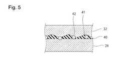
- FIG. 5is a schematic cross section of a V-shaped portion of FIG. 4 .
- solar cell module 1includes solar cells 20 .
- Solar cells 20are electrically connected to each other via wiring member 30 .
- Solar cells 20are disposed within bonding layer 13 filled between first protective member 11 and second protective member 12 .
- First protective member 11may be made of, for example, a glass plate, a resin plate, a ceramic plate, or the like.
- second protective member 12may be made of a resin sheet, a resin sheet having a barrier layer such as a metal layer and an inorganic oxide layer, a glass plate, a resin plate, a ceramic plate or the like.
- Bonding layer 13may is made of a crosslinkable resin such as ethylene and vinyl acetate copolymer (EVA), and a non-crosslinkable resin such as olefin.
- EVAethylene and vinyl acetate copolymer
- solar cell 20includes light-receiving surface 20 a , and back surface 20 b .
- light-receiving surface 20 ais oriented toward first protective member 11
- back surface 20 bis oriented toward second protective member 12 .
- Light-receiving surfaceis a main surface mainly receiving light among a pair of main surfaces of the solar cell, and the other main surface forms the back surface.
- Solar cell 20includes photoelectric conversion body 23 .
- Photoelectric conversion body 23generates carriers such as electrons or holes when receiving light.
- Photoelectric conversion body 23may is made of, for example, a crystal semiconductor plate.
- Photoelectric conversion body 23includes first and second main surfaces 23 a , 23 b .
- First main surface 23 aforms light-receiving surface 20 a .
- Second main surface 23 bforms back surface 20 b.
- first electrode 21 and second electrode 22are disposed on second main surface 23 b .
- Each of first electrode 21 and second electrode 22includes finger parts 24 , and bus bar part 25 .
- the first and second electrodes according to the inventionmay include finger parts only without having a bus bar part.
- Finger parts 24extend in the X axis direction. Finger parts 24 are disposed at intervals therebetween in the Y axis direction. Finger parts 24 of first electrode 21 and finger part 24 s of second electrode 22 are disposed alternately in the Y axis direction. Bus bar part 25 extends in the Y axis direction. Bus bar part 25 of the first electrode 21 is disposed at an end of x1 side in the X axis direction on second main surface 23 b . Bus bar part 25 of the second electrode 22 is disposed at an end of x2 side in the X axis direction on second main surface 23 b . In each of first and second electrodes 21 , 22 , finger parts 24 are electrically connected with bus bar part 25 .
- Solar cells 20 adjacent in the X axis directionare electrically connected to each other via wiring member 30 disposed on second main surface 23 b .
- first electrode 21 of one solar cell 20 , and second electrode 22 of other solar cell 20are electrically connected to each other via wiring member 30 .
- Wiring member 30includes insulating substrate 31 and wiring 32 .
- Insulating substrate 31may is made of, for example, a resin sheet or a ceramic plate.
- Wiring 32is disposed on a surface, which orient to the second main surface 23 b , of insulating substrate 31 .
- Wiring 32is electrically connected to finger part 24 of first electrode on one solar cell 20 , and finger part 24 of second electrode 22 on the other solar cell 20 .
- wiring 32includes first linear parts 32 a , second linear parts 32 b , and connection part 32 c .
- Connection part 32 cextends in the Y axis direction between adjacent solar cells 20 while extending from an end of one solar cell 20 on the x1 side in the X axis direction to an end of other solar cell 20 on the x2 side in the X axis direction. Connection part 32 c covers at least portions of bus bar part 25 of first electrode 21 on one solar cell 20 , and bus bar part 25 of second electrode 22 in other solar cell 20 .
- First linear parts 32 aare electrically connected to connection part 32 c .
- First linear parts 32 aextend in a convex shape from connection part 32 c toward the x1 side in the X axis direction.
- First linear parts 32 aare arranged at intervals therebetween in the Y axis direction. At least some of first linear parts 32 a are disposed on finger parts 24 of second electrode 22 on the other solar cell 20 .
- First linear parts 32 aare electrically connected to finger parts 24 of second electrode 22 .
- Second linear parts 32 bare electrically connected to connection part 32 c .
- Second linear parts 32 bextend in a convex shape from connection part 32 c toward the x2 side in the X axis direction.
- Second linear parts 32 bare disposed at intervals therebetween in the Y axis direction. At least some of second linear parts 32 b are positioned on finger parts 24 of first electrode 21 on one solar cell 20 .
- Second linear parts 32 bare electrically connected to finger parts 24 of first electrode 21 .
- Resin adhesive layer 40includes adhesive layer body 41 , and conductive members 42 .
- Adhesive layer body 41is made of a resin. Specifically, adhesive layer body 41 is made of a cured resin adhesive.
- Conductive members 42are disposed within adhesive layer body 41 . At least a surface layer of each conductive member 42 is made of a conductive material. That is, according to the invention, the conductive member may be conductive on at least a surface thereof, and does not need to have conductivity in the entirety.
- Conductive member 42may be made of, for example, a metal particle, or inorganic oxide particle coated with a metal layer.
- conductive member 42digs into at least one of finger part 24 and wiring 32 (specifically, first or second linear part 32 a , 32 b ). In other words, a portion of conductive member 42 is embedded within at least one of finger part 24 and wiring 32 . This provides an increased contact area between conductive member 42 and at least one of finger part 24 and wiring 32 , and thereby reduces electrical resistivity between wiring member 30 and solar cell 20 . Accordingly, improved output characteristics can be obtained. This also strengthens an anchoring effect by conductive member 42 , which makes electrical breakdown of wiring 32 and electrodes 21 , 22 less likely. Thus, improved reliability can be obtained.
- conductive members 42digs into both finger part 24 and wiring 32 . All conductive members 42 do not need to dig into at least one of finger part 24 and wiring 32 , but at least one conductive member 42 may dig into at least one of finger part 24 and wiring 32 .
- finger part 24 and wiring 32In order to suitably dig conductive member 42 into finger part 24 and wiring 32 , it is preferable that at least one of finger part 24 and wiring 32 have a rough surface. This makes it possible to increase stress applied between conductive member 42 and finger part 24 or wiring 32 in bonding wiring member 30 and solar cell 20 together with pressure. This facilitates digging of conductive member 42 into finger part 24 and wiring 32 .
- wiring 32is provided with a rough surface such that conductive member 42 easily can be dug into wiring 32 .
- the average particle diameter of conductive member 42is preferably smaller than the average pitch of roughness (shortest distance between apexes of adjacent projection portions), more preferably 0.7 times or less and even more preferably 0.5 times or less than the average pitch of roughness.
- the average particle diameter of conductive member 42is preferably, for example, between 15 ⁇ m and 1 ⁇ m, more preferably between 10 ⁇ m and 2 ⁇ m, and even more preferably between 5 ⁇ m and 2 ⁇ m.
- the average pitch of roughnessis preferably between 40 ⁇ m and 5 ⁇ m, and more preferably between 20 ⁇ m and 10 ⁇ m.
- a method of providing roughness to the surfaceis not limited.
- roughnessmay be provided by subjecting the surface to roughing treatment.
- the roughing treatment on the surfaceprovides the rough surface, and also reduces hardness of the surface layer. This facilitates digging of conductive member 42 into finger part 24 and wiring 32 .
- Preferably used roughening treatmentsinclude, for example, a surface etching such as a multi-bond treatment.
- conductive member 42In order to dig conductive member 42 into finger part 24 and wiring 32 , conductive member 42 preferably has a spherical shape.
- the spherical shapemeans a shape having an aspect ratio of 2 or less, where the aspect ratio is a ratio of the major axis diameter to the minor axis diameter ((major axis diameter)/(minor axis diameter)).
- conductive member 42In order to dig conductive member 42 into finger part 24 and wiring 32 , conductive member 42 preferably has hardness higher than a surface layer of at least one of finger part 24 and wiring 32 .
- conductive member 42is made of copper or a copper alloy, and a surface layer of at least one of finger part 24 and wiring 32 is made of tin or a tin alloy.
- conductive member 42has hardness higher than the surface layer of finger part 24 . More specifically, conductive member 42 includes copper or a copper alloy, and the surface layer of finger part 24 is made of tin or a tin alloy. This facilitates digging conductive member 42 into the surface layer of finger part 24 .
- the portion of finger part 24 other than the surface layeris made of copper or a copper alloy.
Landscapes
- Photovoltaic Devices (AREA)
- Life Sciences & Earth Sciences (AREA)
- Engineering & Computer Science (AREA)
- Sustainable Development (AREA)
- Sustainable Energy (AREA)
Abstract
Description
Claims (12)
Applications Claiming Priority (1)
| Application Number | Priority Date | Filing Date | Title |
|---|---|---|---|
| PCT/JP2012/073417WO2014041650A1 (en) | 2012-09-13 | 2012-09-13 | Solar cell module |
Related Parent Applications (1)
| Application Number | Title | Priority Date | Filing Date |
|---|---|---|---|
| PCT/JP2012/073417ContinuationWO2014041650A1 (en) | 2012-09-13 | 2012-09-13 | Solar cell module |
Publications (2)
| Publication Number | Publication Date |
|---|---|
| US20150162466A1 US20150162466A1 (en) | 2015-06-11 |
| US9911876B2true US9911876B2 (en) | 2018-03-06 |
Family
ID=50277804
Family Applications (1)
| Application Number | Title | Priority Date | Filing Date |
|---|---|---|---|
| US14/619,253ActiveUS9911876B2 (en) | 2012-09-13 | 2015-02-11 | Solar cell module |
Country Status (4)
| Country | Link |
|---|---|
| US (1) | US9911876B2 (en) |
| JP (1) | JP6074756B2 (en) |
| DE (1) | DE112012006899T5 (en) |
| WO (1) | WO2014041650A1 (en) |
Families Citing this family (1)
| Publication number | Priority date | Publication date | Assignee | Title |
|---|---|---|---|---|
| CN116110980A (en)* | 2021-11-10 | 2023-05-12 | 浙江晶科能源有限公司 | Battery piece and photovoltaic module |
Citations (15)
| Publication number | Priority date | Publication date | Assignee | Title |
|---|---|---|---|---|
| US5478402A (en)* | 1994-02-17 | 1995-12-26 | Ase Americas, Inc. | Solar cell modules and method of making same |
| JPH11204567A (en) | 1997-10-28 | 1999-07-30 | Seiko Epson Corp | Anisotropic conductive adhesive, method for forming the same on a substrate, method for mounting semiconductor chip, and semiconductor device |
| JP2001343903A (en) | 2000-05-31 | 2001-12-14 | Canon Inc | Electrode interconnection structure, electrode interconnection method, image display device, and method of manufacturing the same |
| US20050268959A1 (en)* | 2004-06-04 | 2005-12-08 | Sunpower Corporation | Interconnection of solar cells in a solar cell module |
| JP2007214533A (en) | 2006-01-16 | 2007-08-23 | Hitachi Chem Co Ltd | Conductive bonding film and solar cell module |
| JP2008085225A (en) | 2006-09-28 | 2008-04-10 | Sanyo Electric Co Ltd | Solar cell module |
| WO2008139995A1 (en) | 2007-05-09 | 2008-11-20 | Hitachi Chemical Company, Ltd. | Method for connecting conductor, member for connecting conductor, connecting structure and solar cell module |
| US20090032081A1 (en) | 2007-08-02 | 2009-02-05 | Sanyo Electric Co., Ltd. | Solar cell module and method for manufacturing the same |
| JP2009054981A (en) | 2007-08-02 | 2009-03-12 | Sanyo Electric Co Ltd | Solar cell module and manufacturing method thereof |
| EP2058868A1 (en)* | 2006-08-29 | 2009-05-13 | Hitachi Chemical Company, Ltd. | Conductive adhesive film and solar cell module |
| US20090183759A1 (en) | 2008-01-21 | 2009-07-23 | Sanyo Electric Co., Ltd. | Solar cell module |
| US20110126878A1 (en) | 2006-12-22 | 2011-06-02 | Peter Hacke | Interconnect technologies for back contact solar cells and modules |
| US20120042924A1 (en)* | 2010-08-20 | 2012-02-23 | Youngsik Lee | Solar cell module |
| JP2012142456A (en) | 2010-12-29 | 2012-07-26 | Sanyo Electric Co Ltd | Solar battery, solar battery module, and manufacturing method of the solar battery module |
| US9640677B2 (en)* | 2012-06-07 | 2017-05-02 | Panasonic Intellectual Property Management Co., Ltd. | Solar cell, solar cell module |
Family Cites Families (2)
| Publication number | Priority date | Publication date | Assignee | Title |
|---|---|---|---|---|
| JP5618274B2 (en)* | 2010-11-17 | 2014-11-05 | 凸版印刷株式会社 | Manufacturing method of solar cell module |
| JP2014212140A (en)* | 2011-08-30 | 2014-11-13 | シャープ株式会社 | Solar cell connecting structure and solar battery cell array |
- 2012
- 2012-09-13JPJP2014535296Apatent/JP6074756B2/ennot_activeExpired - Fee Related
- 2012-09-13WOPCT/JP2012/073417patent/WO2014041650A1/enactiveApplication Filing
- 2012-09-13DEDE112012006899.8Tpatent/DE112012006899T5/ennot_activeWithdrawn
- 2015
- 2015-02-11USUS14/619,253patent/US9911876B2/enactiveActive
Patent Citations (20)
| Publication number | Priority date | Publication date | Assignee | Title |
|---|---|---|---|---|
| US5478402A (en)* | 1994-02-17 | 1995-12-26 | Ase Americas, Inc. | Solar cell modules and method of making same |
| JPH11204567A (en) | 1997-10-28 | 1999-07-30 | Seiko Epson Corp | Anisotropic conductive adhesive, method for forming the same on a substrate, method for mounting semiconductor chip, and semiconductor device |
| JP2001343903A (en) | 2000-05-31 | 2001-12-14 | Canon Inc | Electrode interconnection structure, electrode interconnection method, image display device, and method of manufacturing the same |
| US20050268959A1 (en)* | 2004-06-04 | 2005-12-08 | Sunpower Corporation | Interconnection of solar cells in a solar cell module |
| JP2007214533A (en) | 2006-01-16 | 2007-08-23 | Hitachi Chem Co Ltd | Conductive bonding film and solar cell module |
| EP2058868A1 (en)* | 2006-08-29 | 2009-05-13 | Hitachi Chemical Company, Ltd. | Conductive adhesive film and solar cell module |
| US20090288697A1 (en) | 2006-08-29 | 2009-11-26 | Hitachi Chemical Co., Ltd. | Conductive adhesive film and solar cell module |
| JP2008085225A (en) | 2006-09-28 | 2008-04-10 | Sanyo Electric Co Ltd | Solar cell module |
| US20100084001A1 (en) | 2006-09-28 | 2010-04-08 | Yasufumi Tsunomura | Solar cell module |
| US20110126878A1 (en) | 2006-12-22 | 2011-06-02 | Peter Hacke | Interconnect technologies for back contact solar cells and modules |
| US20100108141A1 (en) | 2007-05-09 | 2010-05-06 | Hitachi Chemical Company, Ltd. | Method for connecting conductor, member for connecting conductor, connecting structure and solar cell module |
| WO2008139995A1 (en) | 2007-05-09 | 2008-11-20 | Hitachi Chemical Company, Ltd. | Method for connecting conductor, member for connecting conductor, connecting structure and solar cell module |
| US20130220540A1 (en) | 2007-05-09 | 2013-08-29 | Hitachi Chemical Company, Ltd. | Method for connecting conductor, member for connecting conductor, connecting structure and solar cell module |
| JP2009054981A (en) | 2007-08-02 | 2009-03-12 | Sanyo Electric Co Ltd | Solar cell module and manufacturing method thereof |
| US20090032081A1 (en) | 2007-08-02 | 2009-02-05 | Sanyo Electric Co., Ltd. | Solar cell module and method for manufacturing the same |
| US20090183759A1 (en) | 2008-01-21 | 2009-07-23 | Sanyo Electric Co., Ltd. | Solar cell module |
| JP2009176782A (en) | 2008-01-21 | 2009-08-06 | Sanyo Electric Co Ltd | Solar cell module |
| US20120042924A1 (en)* | 2010-08-20 | 2012-02-23 | Youngsik Lee | Solar cell module |
| JP2012142456A (en) | 2010-12-29 | 2012-07-26 | Sanyo Electric Co Ltd | Solar battery, solar battery module, and manufacturing method of the solar battery module |
| US9640677B2 (en)* | 2012-06-07 | 2017-05-02 | Panasonic Intellectual Property Management Co., Ltd. | Solar cell, solar cell module |
Also Published As
| Publication number | Publication date |
|---|---|
| JP6074756B2 (en) | 2017-02-08 |
| JPWO2014041650A1 (en) | 2016-08-12 |
| US20150162466A1 (en) | 2015-06-11 |
| DE112012006899T5 (en) | 2015-05-28 |
| WO2014041650A1 (en) | 2014-03-20 |
Similar Documents
| Publication | Publication Date | Title |
|---|---|---|
| EP3506373B1 (en) | Solar cell module | |
| CN104868004B (en) | Solar module | |
| US9741885B2 (en) | Solar cell module | |
| US8354733B2 (en) | IGBT power semiconductor package having a conductive clip | |
| US8927851B2 (en) | Solar cell module and method of manufacturing solar cell module | |
| US20130104961A1 (en) | Solar cell module and solar cell | |
| JP5999527B2 (en) | Solar cell module and method for manufacturing solar cell module | |
| US10985144B2 (en) | Light emitting apparatus | |
| US20130074903A1 (en) | Solar cell module and method for manufacturing same | |
| US20160064587A1 (en) | Solar cell module and method for manufacturing solar cell module | |
| US9379268B2 (en) | Solar cell module and method of manufacturing the same | |
| US20160126387A1 (en) | Solar cell module | |
| US9306081B2 (en) | Solar cell module | |
| WO2014155418A1 (en) | Solar cell module and solar cell module manufacturing method | |
| US9911876B2 (en) | Solar cell module | |
| US9640677B2 (en) | Solar cell, solar cell module | |
| CN103296037A (en) | Contact pad, flat panel image detector and manufacturing method thereof | |
| KR101826734B1 (en) | Solar cell module and method of fabricating the same | |
| KR20220101385A (en) | A conductive line applied to shingled solar cell module | |
| US20140209164A1 (en) | Solar cell module | |
| KR20160034706A (en) | Solar cell module and manufacturing method thereof | |
| JP2018186247A (en) | Solar cell module | |
| KR20150092607A (en) | Solar cell and solar cell module | |
| JP2013207218A (en) | Wiring board assembly, semiconductor device, solar cell module, and connection member | |
| WO2012090622A1 (en) | Solar cell module |
Legal Events
| Date | Code | Title | Description |
|---|---|---|---|
| AS | Assignment | Owner name:SANYO ELECTRIC CO., LTD., JAPAN Free format text:ASSIGNMENT OF ASSIGNORS INTEREST;ASSIGNOR:ISHII, YOSUKE;REEL/FRAME:034936/0839 Effective date:20150126 | |
| AS | Assignment | Owner name:PANASONIC CORPORATION, JAPAN Free format text:ASSIGNMENT OF ASSIGNORS INTEREST;ASSIGNOR:SANYO ELECTRIC CO., LTD.;REEL/FRAME:035269/0821 Effective date:20150327 Owner name:PANASONIC INTELLECTUAL PROPERTY MANAGEMENT CO., LT Free format text:ASSIGNMENT OF ASSIGNORS INTEREST;ASSIGNOR:PANASONIC CORPORATION;REEL/FRAME:035269/0827 Effective date:20150327 | |
| STCF | Information on status: patent grant | Free format text:PATENTED CASE | |
| MAFP | Maintenance fee payment | Free format text:PAYMENT OF MAINTENANCE FEE, 4TH YEAR, LARGE ENTITY (ORIGINAL EVENT CODE: M1551); ENTITY STATUS OF PATENT OWNER: LARGE ENTITY Year of fee payment:4 | |
| MAFP | Maintenance fee payment | Free format text:PAYMENT OF MAINTENANCE FEE, 8TH YEAR, LARGE ENTITY (ORIGINAL EVENT CODE: M1552); ENTITY STATUS OF PATENT OWNER: LARGE ENTITY Year of fee payment:8 |