US9906128B2 - Intermediate voltage bus converter with power saving modes - Google Patents
Intermediate voltage bus converter with power saving modesDownload PDFInfo
- Publication number
- US9906128B2 US9906128B2US14/526,812US201414526812AUS9906128B2US 9906128 B2US9906128 B2US 9906128B2US 201414526812 AUS201414526812 AUS 201414526812AUS 9906128 B2US9906128 B2US 9906128B2
- Authority
- US
- United States
- Prior art keywords
- stage
- operable
- set point
- controller
- voltage
- Prior art date
- Legal status (The legal status is an assumption and is not a legal conclusion. Google has not performed a legal analysis and makes no representation as to the accuracy of the status listed.)
- Active, expires
Links
Images


Classifications
- H—ELECTRICITY
- H02—GENERATION; CONVERSION OR DISTRIBUTION OF ELECTRIC POWER
- H02M—APPARATUS FOR CONVERSION BETWEEN AC AND AC, BETWEEN AC AND DC, OR BETWEEN DC AND DC, AND FOR USE WITH MAINS OR SIMILAR POWER SUPPLY SYSTEMS; CONVERSION OF DC OR AC INPUT POWER INTO SURGE OUTPUT POWER; CONTROL OR REGULATION THEREOF
- H02M3/00—Conversion of DC power input into DC power output
- H02M3/02—Conversion of DC power input into DC power output without intermediate conversion into AC
- H02M3/04—Conversion of DC power input into DC power output without intermediate conversion into AC by static converters
- H02M3/10—Conversion of DC power input into DC power output without intermediate conversion into AC by static converters using discharge tubes with control electrode or semiconductor devices with control electrode
- H02M3/145—Conversion of DC power input into DC power output without intermediate conversion into AC by static converters using discharge tubes with control electrode or semiconductor devices with control electrode using devices of a triode or transistor type requiring continuous application of a control signal
- H02M3/155—Conversion of DC power input into DC power output without intermediate conversion into AC by static converters using discharge tubes with control electrode or semiconductor devices with control electrode using devices of a triode or transistor type requiring continuous application of a control signal using semiconductor devices only
- H02M3/156—Conversion of DC power input into DC power output without intermediate conversion into AC by static converters using discharge tubes with control electrode or semiconductor devices with control electrode using devices of a triode or transistor type requiring continuous application of a control signal using semiconductor devices only with automatic control of output voltage or current, e.g. switching regulators
- H02M3/158—Conversion of DC power input into DC power output without intermediate conversion into AC by static converters using discharge tubes with control electrode or semiconductor devices with control electrode using devices of a triode or transistor type requiring continuous application of a control signal using semiconductor devices only with automatic control of output voltage or current, e.g. switching regulators including plural semiconductor devices as final control devices for a single load
- H—ELECTRICITY
- H02—GENERATION; CONVERSION OR DISTRIBUTION OF ELECTRIC POWER
- H02M—APPARATUS FOR CONVERSION BETWEEN AC AND AC, BETWEEN AC AND DC, OR BETWEEN DC AND DC, AND FOR USE WITH MAINS OR SIMILAR POWER SUPPLY SYSTEMS; CONVERSION OF DC OR AC INPUT POWER INTO SURGE OUTPUT POWER; CONTROL OR REGULATION THEREOF
- H02M3/00—Conversion of DC power input into DC power output
- H02M3/02—Conversion of DC power input into DC power output without intermediate conversion into AC
- H02M3/04—Conversion of DC power input into DC power output without intermediate conversion into AC by static converters
- H02M3/10—Conversion of DC power input into DC power output without intermediate conversion into AC by static converters using discharge tubes with control electrode or semiconductor devices with control electrode
- H02M3/145—Conversion of DC power input into DC power output without intermediate conversion into AC by static converters using discharge tubes with control electrode or semiconductor devices with control electrode using devices of a triode or transistor type requiring continuous application of a control signal
- H02M3/155—Conversion of DC power input into DC power output without intermediate conversion into AC by static converters using discharge tubes with control electrode or semiconductor devices with control electrode using devices of a triode or transistor type requiring continuous application of a control signal using semiconductor devices only
- H02M3/156—Conversion of DC power input into DC power output without intermediate conversion into AC by static converters using discharge tubes with control electrode or semiconductor devices with control electrode using devices of a triode or transistor type requiring continuous application of a control signal using semiconductor devices only with automatic control of output voltage or current, e.g. switching regulators
- H02M3/158—Conversion of DC power input into DC power output without intermediate conversion into AC by static converters using discharge tubes with control electrode or semiconductor devices with control electrode using devices of a triode or transistor type requiring continuous application of a control signal using semiconductor devices only with automatic control of output voltage or current, e.g. switching regulators including plural semiconductor devices as final control devices for a single load
- H02M3/1584—Conversion of DC power input into DC power output without intermediate conversion into AC by static converters using discharge tubes with control electrode or semiconductor devices with control electrode using devices of a triode or transistor type requiring continuous application of a control signal using semiconductor devices only with automatic control of output voltage or current, e.g. switching regulators including plural semiconductor devices as final control devices for a single load with a plurality of power processing stages connected in parallel
- H—ELECTRICITY
- H02—GENERATION; CONVERSION OR DISTRIBUTION OF ELECTRIC POWER
- H02M—APPARATUS FOR CONVERSION BETWEEN AC AND AC, BETWEEN AC AND DC, OR BETWEEN DC AND DC, AND FOR USE WITH MAINS OR SIMILAR POWER SUPPLY SYSTEMS; CONVERSION OF DC OR AC INPUT POWER INTO SURGE OUTPUT POWER; CONTROL OR REGULATION THEREOF
- H02M1/00—Details of apparatus for conversion
- H02M1/0003—Details of control, feedback or regulation circuits
- H02M1/0032—Control circuits allowing low power mode operation, e.g. in standby mode
- H—ELECTRICITY
- H02—GENERATION; CONVERSION OR DISTRIBUTION OF ELECTRIC POWER
- H02M—APPARATUS FOR CONVERSION BETWEEN AC AND AC, BETWEEN AC AND DC, OR BETWEEN DC AND DC, AND FOR USE WITH MAINS OR SIMILAR POWER SUPPLY SYSTEMS; CONVERSION OF DC OR AC INPUT POWER INTO SURGE OUTPUT POWER; CONTROL OR REGULATION THEREOF
- H02M1/00—Details of apparatus for conversion
- H02M1/0048—Circuits or arrangements for reducing losses
- H—ELECTRICITY
- H02—GENERATION; CONVERSION OR DISTRIBUTION OF ELECTRIC POWER
- H02M—APPARATUS FOR CONVERSION BETWEEN AC AND AC, BETWEEN AC AND DC, OR BETWEEN DC AND DC, AND FOR USE WITH MAINS OR SIMILAR POWER SUPPLY SYSTEMS; CONVERSION OF DC OR AC INPUT POWER INTO SURGE OUTPUT POWER; CONTROL OR REGULATION THEREOF
- H02M1/00—Details of apparatus for conversion
- H02M1/0067—Converter structures employing plural converter units, other than for parallel operation of the units on a single load
- H02M1/007—Plural converter units in cascade
- H02M2001/0032—
- H02M2001/007—
- Y—GENERAL TAGGING OF NEW TECHNOLOGICAL DEVELOPMENTS; GENERAL TAGGING OF CROSS-SECTIONAL TECHNOLOGIES SPANNING OVER SEVERAL SECTIONS OF THE IPC; TECHNICAL SUBJECTS COVERED BY FORMER USPC CROSS-REFERENCE ART COLLECTIONS [XRACs] AND DIGESTS
- Y02—TECHNOLOGIES OR APPLICATIONS FOR MITIGATION OR ADAPTATION AGAINST CLIMATE CHANGE
- Y02B—CLIMATE CHANGE MITIGATION TECHNOLOGIES RELATED TO BUILDINGS, e.g. HOUSING, HOUSE APPLIANCES OR RELATED END-USER APPLICATIONS
- Y02B70/00—Technologies for an efficient end-user side electric power management and consumption
- Y02B70/10—Technologies improving the efficiency by using switched-mode power supplies [SMPS], i.e. efficient power electronics conversion e.g. power factor correction or reduction of losses in power supplies or efficient standby modes
- Y02B70/16—
Definitions
- the present applicationrelates to intermediate DC/DC voltage bus converters, in particular entering and exiting power saving modes by intermediate DC/DC voltage bus converters.
- a typical 12V DC distribution buscan be replaced by a higher voltage bus e.g. typically 48V nominal.
- This higher distribution voltageis stepped down on the motherboard in one or more stages to the low DC voltage required by the CPU (central processing unit), memory, and other electronic components included in the system such as memory, graphics logic, I/O (input/output), etc.
- a single DC/DC converterconventionally generates an intermediate bus voltage that is fed to all lower-voltage converter stages.
- the intermediate busis typically between 5-12V and can therefore use existing infrastructure to be highly scalable.
- the CPUhas a dedicated converter (e.g.
- 48V to 1Vthat can be a single conversion stage, or two converter stages in series to achieve the step down.
- the other voltage railse.g. memory, graphics logic, etc.
- all voltage railsare fed directly from the 48V distribution bus. In this case scalability is limited, and the use of existing infrastructure is not an option.
- Other architecturesemploy multiple intermediate bus voltages for feeding different voltage rails, using direct conversion for the CPU and some other voltage rails with the intermediate bus powering the rest, or some combination thereof.
- the final conversion stage of the DC/DC converter that supplies the CPUis widely known as a voltage regulator.
- the voltage regulatorconverts an intermediate voltage e.g. 12V to the CPU voltage e.g. 1V.
- the CPUcommunicates with the voltage regulator using a protocol for status, protection, and system optimization. Part of the optimization includes instructing the voltage regulator to enter power saving modes of operation to increase light-load efficiency when the CPU enters low power states.
- a problemoccurs with higher-voltage distribution systems such as 48V systems when the converter stage that converts the high distribution bus voltage to an intermediate bus voltage is not privy to the communication between the CPU and the voltage regulator that converts between the intermediate bus voltage and the load voltage.
- the 48V-to-12V converter stagemonitors its output current and adjusts its operating point (e.g. active phases, pulse frequency modulation (PFM) mode, etc.) accordingly.
- PFMpulse frequency modulation
- the voltage regulatoris still in the most active power state but the 48V-to-12V converter stage enters a low power mode, the slow response of the 48V-to-12V converter stage can feed through to the CPU voltage rail when a transient occurs. Such a condition would result in a CPU hang which is prohibited in a server where high reliability is a fundamental necessity.
- This problemhas been solved by increasing the intelligence of the converter stage that converts the high distribution bus voltage to an intermediate bus voltage.
- this intermediate converter stagecan measure its output voltage and current, and make decisions to enter power-saving states based on those measurements. Detection of a transient event may cause the intermediate converter stage to leave the power saving state by adding phases (if applicable) or leaving pulse frequency modulation (PFM) mode and entering PWM (pulse width modulation) mode.
- PFMpulse frequency modulation
- PWMpulse width modulation
- converters on a higher-voltage distribution bussuch as a 48V bus typically switch at lower frequencies than the downstream lower voltage regulators that feed the CPUs.
- the filter inductance of these higher-voltage converter stagesis significantly larger than that of the downstream voltage regulators, by more than an order of magnitude. As such, their response is significantly slower.
- a voltage regulatorsheds phases to conserve power.
- the multiple phases, high switching frequency, and low inductancepromote fast reaction time to allow the voltage regulator to respond quickly to a load transient without the CPU voltage experiencing undershoot.
- the response of the upstream higher-voltage converter stageis significantly slower than the voltage regulator. Therefore, if the converter stage that converts the high distribution bus voltage to the intermediate bus voltage enters a power saving state while the CPU is still in the maximum power state, the slow response of this intermediate converter stage generates a sag on the intermediate voltage input to the voltage regulator which in turn propagates and manifests itself as undershoot at the CPU.
- the DC/DC voltage convertercomprises a first stage operable to convert a first DC voltage rail to a second DC voltage rail different than the first DC voltage rail and a second stage operable to convert the second DC voltage rail to a third DC voltage rail lower than the second DC voltage rail and deliver current to a load at the third DC voltage rail, the amount of current delivered to the load corresponding to an operating set point of the second stage.
- the second stageis operable to change its operating set point responsive to a command received from the load, such that the amount of current delivered to the load is reduced.
- the first stageis operable to change its operating set point responsive to a command issued by the load, such that the amount of current delivered to the second stage is reduced.
- the servercomprises a central processing unit (CPU), memory coupled to the CPU, a DC/DC voltage converter for powering the CPU and the memory, a communication bus for coupling the CPU to the memory and the DC/DC voltage converter and a DC voltage distribution bus coupled to the DC/DC voltage converter.
- the DC/DC voltage convertercomprises a first stage operable to convert a first DC voltage rail provided by the DC voltage distribution bus to a second DC voltage rail different than the first DC voltage rail and a second stage operable to convert the second DC voltage rail to a third DC voltage rail lower than the second DC voltage rail and deliver current to the CPU at the third DC voltage rail, the amount of current delivered to the CPU corresponding to an operating set point of the second stage.
- the second stageis operable to change its operating set point responsive to a command received from the CPU, such that the amount of current delivered to the CPU is reduced.
- the first stageis operable to change its operating set point responsive to a command issued by the CPU, such that the amount of current delivered to the second stage is reduced.
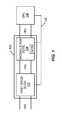
- FIG. 1illustrates a block diagram of an embodiment of a DC/DC converter that includes a first stage for converting a high bus voltage to an intermediate bus voltage and a second stage for converting the intermediate bus voltage to a low bus voltage that supplies a load.
- FIG. 2illustrates a more detailed block diagram of the DC/DC converter shown in FIG. 1 .
- FIG. 3illustrates examples of different operating set point changes that can be made by the first stage of the DC/DC converter shown in FIGS. 1 and 2 , in response to commands issued by the load which indicate a change in power demand at the load.
- FIGS. 4 through 6illustrate different variables that affect each operating point variable shown in FIG. 3 .
- FIG. 7illustrates a block diagram of an embodiment of a server that includes a DC/DC converter having a first stage for converting a high bus voltage to an intermediate bus voltage and a second stage for converting the intermediate bus voltage to a low bus voltage that supplies a load.
- Embodiments described hereinrelate to a DC/DC converter that includes a first stage for converting a high bus voltage to an intermediate bus voltage and a second stage for converting the intermediate bus voltage to a low bus voltage that supplies a load such as a CPU.
- the loadcommunicates with the DC/DC converter using a protocol for status, protection, and system optimization. Part of the optimization process includes the load instructing the second stage to change its operating set point so that the light-load efficiency of the second stage can be increased when the load enters a lower-power state.
- the first stageis aware of the power saving intentions of the load, e.g. by monitoring the communication between the load and the second stage, or by receiving communications directly from the load.
- the first stagechanges its operating set point such that the amount of current delivered to the second stage is reduced.
- the first stageimplements an anticipatory power savings approach as opposed to a reactionary approach that merely relies on observation of system parameters such as bus voltage, output current, etc.
- the first stage of the DC/DC converteris therefore less likely to hinder operation of the second stage, and hence, load performance.
- FIG. 1illustrates an embodiment of the DC/DC converter 100 .
- the DC/DC voltage converter 100comprises a first stage 102 for converting a first DC voltage rail (VR 1 ) to a second DC voltage rail (VR 2 ) different than the first DC voltage rail.
- the level of the second DC voltage rail VR 2can be lower or higher than the first DC voltage rail VR 1 .
- 48Vis the nominal voltage for systems that can vary from 35-75V for VR 1 . So in one embodiment VR 1 is at 48V (but can be 35-75V) and VR 2 is at 12V. In another embodiment, VR 1 again is at 48V but the second rail VR 2 can be 54V. In general, the second DC voltage rail VR 2 is different than the first DC voltage rail VR 1 .
- the DC/DC voltage converter 100further comprises a second stage 104 for converting the second DC voltage rail VR 2 to a third DC voltage rail (VR 3 ) lower than the second DC voltage rail VR 2 .
- the second stage 104delivers current to a load 106 such as a CPU at the third DC voltage rail VR 3 .
- the amount of current delivered to the load 106corresponds to the operating set point of the second stage 104 , and the operating set point of the second stage 104 in turn corresponds to the amount of current required by the load 106 .
- the second stage 104 of the DC/DC converter 100can change its operating set point responsive to a command received from the load 106 powered by the DC/DC converter 100 , such that the amount of current delivered to the load 106 is reduced.
- the CPUcommunicates with the second stage 104 over a communication bus 108 using a protocol for status, protection, and system optimization.
- Part of the optimization processincludes the CPU instructing the second stage 104 to change its operating set point so that the light-load efficiency of the second stage 104 is increased when the CPU enters a low power state.
- phase sheddingwhere the second stage 104 deactivates or sheds (drops) one or more previously active phases, dynamic reduction in the output voltage of the second stage 104 , transitioning the second stage 104 from PWM to PFM operation, etc.
- Any standard communication protocolcan be used by the load 106 to communicate commands to the second stage 104 of the DC/DC converter 100 which cause the second stage 104 to change its operating set point and correspondingly lower its power output.
- the load 106is a CPU that can dynamically control the output voltage, slew rates and power states of the second stage 104 , as well as monitor the second stage 104 for telemetry purposes.
- the first stage 102 of the DC/DC converter 100also can change its operating set point responsive to a command issued by the load 106 , such that the amount of current delivered to the second stage 104 is reduced.
- the first stage 102has insight into the power consumption behavior of the downstream load 106 .
- the load 106is a CPU that communicates with the second stage 104 by transmitting communication packets over a communication bus 108 .
- the packetsare addressed to the second stage 104 .
- the second stage 104extracts commands from the packets, and takes corresponding action. This can include taking one or more power saving-related actions such as phase shedding, dynamic output voltage reduction, transitioning the second stage 104 from PWM to PFM operation, etc.
- the first stage 102 of the DC/DC converter 100monitors the communication bus 108 between the second stage 104 and the load 106 for a command addressed to the second stage 104 that instructs the second stage 104 to change its operating set point.
- the load 106actively controls the power state of second stage 104 , and the first stage 102 decides whether to change its operating point based on power state instructions to the second stage 104 .
- the load 106does not directly communicate with the first stage 102 according to this embodiment.
- the first stage 102can change its operating set point responsive to commands addressed to the second stage 104 , when the amount of current required by the second stage 104 is reduced. If the first stage 102 has more than one phase, this can include phase shedding where the first stage 102 deactivates or sheds (drops) one or more previously active phases. Alternatively or in addition, the first stage 102 can dynamically reduce its output voltage, transition from PWM to PFM operation, etc. For example, if the load 106 issues a command to enter a lower power state that results in the second stage 104 shedding phases, the first stage 102 can then know what its maximum load is limited to and could potentially shed phases as well if it were safe to do so.
- the first stage 102can also enter its most efficient mode of operation where the term ‘most efficient mode of operation’ is not limited to phase shedding or PFM operation. From a system perspective, this could include the first stage 102 adjusting the second DC voltage rail (VR 2 ) to minimize losses.
- the first stage 102 of the DC/DC converter 100is aware of the command and can enter its own maximum power state in response.
- the first stage 102 of the DC/DC converter 100can be coupled to the load 106 via the same or different communication bus 108 as the second stage 104 and receive packets with commands addressed to the first stage 102 .
- the load 106can send messages independently to both the second stage 104 and first stage 102 of the DC/DC converter 100 .
- the first stage 102need not necessarily monitor for commands addressed to the second stage 104 which instruct the second stage 104 to take power saving action.
- the load 106can communicate directly with the first stage 102 by addressing power saving commands to the first stage 102 .
- the first stage 102can change its operating set point responsive to a power saving command received over the communication bus 108 and addressed to the first stage 102 e.g.
- the dashed line in FIG. 1indicates that the first stage 102 can monitor the communication bus 108 between the load 106 and the second stage 104 or receive packets from the load 106 uniquely addressed to the first stage 102 , in order to gain insight into the power consumption behavior of the downstream load 106 .
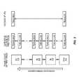
- FIG. 2illustrates an embodiment of the first stage 102 of the DC/DC converter 100 .
- the first stage 102comprises a plurality of power stages (phases) 110 and a controller 112 such as a microcontroller, microprocessor, ASIC (application-specific integrated-circuit), etc. for controlling operation of the power stages 110 .
- Each power stage 110is operable to deliver a phase current (i Ln ) through a separate inductor (L n ) to yield the second DC voltage rail VR 2 .
- the first stage 102produces a DC voltage rail VR 2 less than VR 1 .
- the first stage 102can be implemented using any standard DC/DC converter architecture such as buck-boost converter, flyback converter, etc. such that the second DC voltage rail VR 2 can be lower or higher than the first DC voltage rail VR 1 .
- Each power stage 102 of the multiphase buck converter shown in FIG. 2has a high-side transistor (HSn) and a low-side transistor (LSn) for coupling to the second DC voltage rail VR 2 through the corresponding inductor.
- the high-side transistor of each power stage 110switchably connects the second DC voltage rail VR 2 to the first DC voltage rail VR 1
- the corresponding low-side transistorswitchably connects the second DC voltage rail VR 2 to ground at different periods.
- N power stages 110are shown in FIG. 2 .
- the first stage 102can include any number of power stages 110 including a single power stage (phase) or more than one power stage (i.e. multi-phase where each power stage is one phase of the multi-phase regulator).
- the first stage 102switches at a lower frequency than the second stage 104 of the DC/DC converter 100 .
- the first stage 102can have a lower phase count than the second stage 104 , and larger inductors.
- the first stage 102typically has a slower inherent response time to transient conditions as compared to the second stage 104 .
- the second stage 104 of the DC/DC converter 100can have the same or similar construction as the first stage 102 .
- the controller 112 of the DC/DC converter 100regulates the second DC voltage rail VR 2 delivered by the power stage(s) 110 , by adjusting the phase currents delivered by the power stage(s) 110 .
- Each phase 110is configured to output a maximum rated current at the second DC voltage rail.
- the controller 112includes a pulse width modulator (PWM) unit 114 for switching each power stage 110 via a corresponding PWM control signal (pwm).
- PFMpulse frequency modulator
- Drivers 118 for the power stage(s) 110provide gate drive signals (Vdrive) to the gates of the corresponding high-side and low-side transistors in response to the PWM or PFM control signals provided by the controller 112 .
- the controller 112can manage changes from one reference voltage to another.
- the controller 112also can determine errors between the second DC voltage rail VR 2 and a reference voltage, and convert the error voltage into a digital representation provided to the PWM and PFM units 114 , 116 for modifying the switching cycle of each power stage 110 e.g. by adjusting the PWM duty cycle in PWM mode or switching frequency in PFM mode.
- FIG. 3illustrates examples of different operating set point changes that can be made by the first stage 102 of the DC/DC converter 100 in response to commands issued by the load 106 which indicate a change in power demand at the load 106 .
- the operating set point changes available at the first stage 102depend on the architecture of the first stage 102 . For example, if the first stage 102 has more than one phase (power stage) 110 , the first stage 102 can shed (deactivate) one or more phases 110 in response to a command from the load 106 indicating a reduced power state at the load 106 . With only one phase 110 active, the first stage 102 can transition from PWM mode to PFM mode for that phase 110 . The PWM-to-PFM mode change option is available even if the first stage 110 has only one phase (i.e. is a single-phase stage).
- the first stage 102can change the gate drive signals (Vdrive) applied to the gates of the high-side and low-side transistor of each active phase 110 from a higher voltage (Vdrive,high) to a lower voltage (Vdrive,low) in response to a command from the load 106 indicating a reduced power state at the load 106 .
- Vdrivegate drive signals
- the first stage 102can change the level of the second DC voltage rail VR 2 from a higher voltage (Vbus,high) to a lower voltage (Vbus,low) in response to a command from the load 106 indicating a reduced power state at the load 106 .
- the first stage 102can increase or decrease the level of the second DC voltage rail VR 2 responsive to the second stage 104 being instructed by the load 106 to shed one or more phases, each phase of the second stage 104 configured to output a maximum rated current at the third DC voltage rail VR 3 .
- the first stage 102can change the level of the second DC voltage rail VR 2 for each active phase 110 , and can perform this level adjustment to VR 2 each time a phase 110 is shed.
- Each of the operating set point changes shown in FIG. 3allows the first stage 102 of the DC/DC converter 100 to adjust its operating set point when the current required by the second stage 104 is reduced in response to power saving commands issued by the load 106 .
- the commandscan be addressed to the second stage 104 and monitored by the first stage 102 , or addressed directly to the first stage 102 as explained above. In either case, the overall efficiency of the DC/DC converter 100 can be increased under light-load conditions.
- FIGS. 4 through 6illustrate the variables that affect each operating point variable shown in FIG. 3 .
- the first stage 102 of the DC/DC converter 100has a plurality of phases (power stages) 110 each of which has a programmed phase current limit for protection.
- the controller 112 of the first stage 102can monitor commands addressed to the second stage 104 that affect the number of active phases N ⁇ for the second stage 104 , or receive the same or similar commands directly from the load 106 .
- the controller 112can optimize efficiency while assuming safe operation by measuring input voltage, input current and output current of the first stage 102 .
- two phases 110 of the first stage 102may be active at some operating point, but one phase 110 can handle the load current demand. In this case the controller 112 can switch to one phase 110 if safe and more efficient than two phases 110 , based on the input power and output current measurements.
- the output voltage (VR 2 ) of the first stage 102can be adjusted and its impact on efficiency determined by measuring the input power and output current of the first stage 102 .
- the controller 112 of the first stage 102can monitor output current for protection and the possibility of phase count increase. For a given power level, reduction of the output voltage VR 2 may increase the efficiency of the downstream second stage 104 but lower the efficiency of the first stage 102 . Or reduction of the output voltage VR 2 may increase both efficiencies, or decrease both. Output voltage adjustments are very dependent on the converter implementation, but in general the controller 112 can adjust the output voltage VR 2 of first stage 102 to increase overall efficiency of the DC/DC converter 100 .
- the voltage of the signals (Vdrive) used to drive the gates of the power transistors of the first stage 102can be adjusted to improve overall system efficiency. For example, it may be beneficial to reduce the gate drive voltage under lower load power conditions as indicated by measuring the input power and output current of the first stage 102 . However, the first stage 102 output current need not necessarily be measured or sensed.
- the way in which the first stage 102 of the DC/DC converter 100 implements operating set point changesdepends on the architecture of the first stage 102 .
- the first stage 102is hard-wired with different operating set point options. Each of the hard-wired operating set point options corresponds to a different power mode of the first stage 102 .
- the first stage 102selects the operating set point option associated with a corresponding command issued by the load 106 . The command can be addressed to the second stage 104 and monitored by the first stage 102 , or addressed directly to the first stage 102 as explained above.
- the different operating set point options available to the first stage 102 of the DC/DC converter 100are stored in registers 200 of the system in which the DC/DC converter 100 is included e.g. as shown in FIG. 2 .
- the first stage 102changes its operating set point responsive to a command issued by the load 106 , in accordance with the register settings 200 which are accessible by the first stage 102 .
- the first stage 102develops a history of power mode behavior by monitoring prior activity on the second DC voltage rail VR 2 in response to different commands issued by the load 106 . The first stage 102 then determines whether to change its operating set point based at least partly on the history of power mode behavior.
- the DC/DC converter 100can use its current monitoring pin (IMON) with knowledge of the load power state to implement an adaptive filter that determines the threshold and delays required for the first stage 102 of the DC/DC converter 100 to safely enter and exit a power saving state. Then the power state commands for the second stage 104 of the DC/DC converter 100 need only be required for a few power state transitions until the controller 112 of the first stage 102 learns the behavior of the load 106 during each power state via the current monitoring pin.
- IMONcurrent monitoring pin
- the DC/DC voltage converter 100can communicate with electronic components other than a CPU, e.g. including memory, graphics, I/O, and other electronic components.
- electronic components other than a CPUe.g. including memory, graphics, I/O, and other electronic components.
- a CPUe.g. including memory, graphics, I/O, and other electronic components.
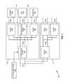
- FIG. 7illustrates an embodiment of a server 300 that includes a first DC/DC converter 100 of the kind previously described herein that provides an intermediate voltage rail VR 2 a for powering all voltage rails VR 3 a , VR 3 b , VR 3 c that supply electronic components in communication with the CPU 106 .
- the server 300can include memory 302 such as volatile and/or nonvolatile memory and graphics logic 304 such as a graphics processor coupled to the CPU 106 .
- the first DC/DC voltage converter 100powers the CPU 106 and each electronic component 302 , 304 that communicates with the CPU 106 .
- a communication bus 108couples the CPU 106 to the first DC/DC converter 100 , memory 302 , graphics logic 304 , etc.
- a DC voltage distribution bus (rail) VR 1is coupled to the first DC/DC voltage converter 100 .
- the first DC/DC voltage converter 100also includes an additional stage 306 , 308 for converting the second DC voltage rail VR 2 a to an additional DC voltage rail VR 3 b , VR 3 c lower than the second DC voltage rail VR 2 a and different than the third DC voltage rail VR 3 a .
- Each additional stage 306 , 308delivers current to an electronic component 302 , 304 other than the CPU 106 at the corresponding additional DC voltage rail VR 3 b , VR 3 c , where the amount of current delivered to each of these electronic component(s) 302 , 304 corresponds to an operating set point of the corresponding additional stage 306 , 308 of the first DC/DC converter 100 .
- Each additional stage 306 , 308 of the first DC/DC converter 100can change its operating set point responsive to a command received from the load 106 and addressed to that stage 306 , 308 , such that the amount of current delivered to the corresponding electronic component 302 , 304 is reduced.
- the first stage 102 of the first DC/DC converter 100can be responsible for multiple voltage rails VR 3 a , VR 3 b , VR 3 c , and therefore the decision making process of the first stage 102 becomes more complex.
- the first stage 102can monitor for multiple addresses (one for each rail/component) and make a decision for all downstream voltage rails VR 3 a , VR 3 b , VR 3 c .
- the first stage 102should be able to support the worst operating point for each voltage rail VR 3 a , VR 3 b , VR 3 c .
- the electronic components 106 , 302 , 304 supplied by the first DC/DC converter 100may not all be at same power levels.
- the CPU 106can be in a lower power state than the graphics processor 304 .
- the first stage 102 of the first DC/DC converter 100can change its operating set point responsive to commands issued by the CPU 106 to the downstream stages 104 , 306 , 308 , or responsive to a command issued by the CPU 106 directly to the first stage 102 .
- the first stage 102 of the first DC/DC converter 100can monitor communication between the CPU 106 and each stage 104 , 306 , 308 of the first DC/DC converter 100 downstream of the first stage 102 , or the first stage 102 can communicate directly with the CPU 106 .
- the first stage 102 of the first DC/DC converter 100can monitor the communication bus 108 between the CPU 106 and each downstream stage 104 , 306 , 308 of the first DC/DC converter 100 , or receive packets from the CPU 106 over the communication bus 108 that are uniquely addressed to the first stage 102 , in order to gain insight into the power consumption behavior of the CPU 106 . In either case, the ability to enter a power saving mode is then calculated by the first stage controller 112 of the first DC/DC converter 100 based on knowledge of the rated power of the different downstream voltage rails VR 3 a , VR 3 b , VR 3 c.
- the first stage 102can change its operating set point by shedding one or more phases 110 , each phase 110 configured to output a maximum rated current at VR 2 a , based on the operating set point of one or more downstream converter stages 104 , 306 , 308 .
- the first stage 102 of the first DC/DC converter 100can change its operating set point by changing from a PWM operating mode to a PFM mode for one or more of the phases 110 .
- the first stage 102 of the first DC/DC converter 100can change its operating set point by changing the gate drive signal (Vdrive) applied to the power transistors of one or more phases 110 of the first stage 102 .
- the first stage 102 of the first DC/DC converter 100can change its operating set point by changing the level of the second DC voltage rail VR 2 a provided by the first stage 102 to the downstream stages 104 , 306 , 308 .
- the server 300also includes a second DC/DC converter 310 that provides an intermediate voltage rail VR 2 b for powering the voltage rails VR 3 d , VR 3 e that supply electronic components that are not in direct communication with the CPU 106 .
- the same or different DC voltage distribution bus (rail) VR 1is coupled to both the first and second DC/DC voltage converters 100 , 310 .
- the second DC/DC converter 310can have one or more stages 312 , 314 in series. Any standard converter can be used as the second DC/DC converter 310 .
- the way in which the first stage 102 of the first DC/DC converter 100 implements operating set point changesdepend on the architecture of the first stage 102 as previously described herein.
- the first stage 102can be hard-wired with different operating set point options each of which corresponds to a different power mode of the first stage 102 .
- the first stage 102selects the operating set point option associated with a corresponding command issued by the load 106 .
- the different operating set point options available to the first stage 102 of the first DC/DC converter 100are stored in registers 200 of the server 300 .
- the first stage 102changes its operating set point responsive to a command issued by the load 106 , in accordance with the register settings 200 which are accessible by the first stage 102 .
- the first stage 102 of the first DC/DC converter 100develops a history of power mode behavior by monitoring prior activity on the second DC voltage rail VR 2 a in response to different commands issued by the load 106 .
- the first stage 102determines whether to change its operating set point based at least partly on the history of power mode behavior.
- the observed power mode behaviorcan include power mode behavior for all electronic components 302 , 304 that are in communication with the CPU 106 .
Landscapes
- Engineering & Computer Science (AREA)
- Power Engineering (AREA)
- Dc-Dc Converters (AREA)
- Theoretical Computer Science (AREA)
- Physics & Mathematics (AREA)
- General Engineering & Computer Science (AREA)
- General Physics & Mathematics (AREA)
- Power Sources (AREA)
Abstract
Description
Claims (28)
Priority Applications (4)
| Application Number | Priority Date | Filing Date | Title |
|---|---|---|---|
| US14/526,812US9906128B2 (en) | 2014-10-29 | 2014-10-29 | Intermediate voltage bus converter with power saving modes |
| KR1020150150399AKR101783103B1 (en) | 2014-10-29 | 2015-10-28 | Intermediate voltage bus converter with power saving modes |
| CN201510711617.9ACN105576957B (en) | 2014-10-29 | 2015-10-28 | Medium voltage bus converter with battery saving mode |
| DE102015118521.0ADE102015118521B4 (en) | 2014-10-29 | 2015-10-29 | Intermediate voltage bus converter with power saving modes |
Applications Claiming Priority (1)
| Application Number | Priority Date | Filing Date | Title |
|---|---|---|---|
| US14/526,812US9906128B2 (en) | 2014-10-29 | 2014-10-29 | Intermediate voltage bus converter with power saving modes |
Publications (2)
| Publication Number | Publication Date |
|---|---|
| US20160126837A1 US20160126837A1 (en) | 2016-05-05 |
| US9906128B2true US9906128B2 (en) | 2018-02-27 |
Family
ID=55753908
Family Applications (1)
| Application Number | Title | Priority Date | Filing Date |
|---|---|---|---|
| US14/526,812Active2036-02-04US9906128B2 (en) | 2014-10-29 | 2014-10-29 | Intermediate voltage bus converter with power saving modes |
Country Status (4)
| Country | Link |
|---|---|
| US (1) | US9906128B2 (en) |
| KR (1) | KR101783103B1 (en) |
| CN (1) | CN105576957B (en) |
| DE (1) | DE102015118521B4 (en) |
Cited By (3)
| Publication number | Priority date | Publication date | Assignee | Title |
|---|---|---|---|---|
| US20160344291A1 (en)* | 2013-03-06 | 2016-11-24 | Infineon Technologies Americas Corp. | Current balancing in a multi-phase power supply |
| US10476395B2 (en)* | 2017-11-30 | 2019-11-12 | Futurewei Technologies, Inc. | Voltage converting system and method of using the same |
| US20230361680A1 (en)* | 2020-01-28 | 2023-11-09 | Mitsubishi Electric Corporation | Power conversion device |
Families Citing this family (10)
| Publication number | Priority date | Publication date | Assignee | Title |
|---|---|---|---|---|
| US9906128B2 (en) | 2014-10-29 | 2018-02-27 | Infineon Technologies Austria Ag | Intermediate voltage bus converter with power saving modes |
| US10141841B1 (en)* | 2017-08-30 | 2018-11-27 | Apple Inc. | DC-DC converter with a dynamically adapting load-line |
| KR102049965B1 (en)* | 2018-02-21 | 2019-11-28 | 정연문 | Rectifying apparatus having stand-by power saving function |
| US11770073B2 (en)* | 2019-04-26 | 2023-09-26 | Texas Instruments Incorporated | Methods and apparatus for regulated hybrid converters |
| JP7310501B2 (en)* | 2019-09-27 | 2023-07-19 | 株式会社デンソーウェーブ | programmable controller |
| US11108322B2 (en)* | 2019-10-16 | 2021-08-31 | Semiconductor Components Industries, Llc | Dual-mode control of a switch mode power supply |
| WO2021146991A1 (en)* | 2020-01-22 | 2021-07-29 | Current Lighting Solutions, Llc | Emergency driver and intelligent module for emergency driver |
| CN111600464B (en)* | 2020-06-30 | 2023-12-26 | 上海晶丰明源半导体股份有限公司 | Multi-phase power supply dynamic response control circuit and control method |
| CN113422532B (en)* | 2021-04-29 | 2022-05-20 | 上海奉天电子股份有限公司 | Variable output power vehicle-mounted power supply inverter circuit of fuel and new energy vehicle |
| CN113691102A (en)* | 2021-07-22 | 2021-11-23 | 浪潮商用机器有限公司 | Multi-power supply control method and multi-power supply |
Citations (65)
| Publication number | Priority date | Publication date | Assignee | Title |
|---|---|---|---|---|
| US5568044A (en) | 1994-09-27 | 1996-10-22 | Micrel, Inc. | Voltage regulator that operates in either PWM or PFM mode |
| US6198642B1 (en)* | 1999-10-19 | 2001-03-06 | Tracewell Power, Inc. | Compact multiple output power supply |
| US6278263B1 (en) | 1999-09-01 | 2001-08-21 | Intersil Corporation | Multi-phase converter with balanced currents |
| US20050094330A1 (en)* | 2003-11-05 | 2005-05-05 | Guenther Robert A. | Intermediate bus power architecture |
| US6911848B2 (en) | 2002-01-31 | 2005-06-28 | Vlt, Inc. | Low-loss transformer-coupled gate driver |
| KR20050071685A (en) | 2002-11-11 | 2005-07-07 | 인터내쇼널 렉티파이어 코포레이션 | Two stage power conversion circuit |
| US20050184713A1 (en)* | 2004-02-20 | 2005-08-25 | Ming Xu | Two-stage voltage regulators with adjustable intermediate bus voltage, adjustable switching frequency, and adjustable number of active phases |
| US20050184590A1 (en)* | 2004-02-05 | 2005-08-25 | Dobbs Robert W. | Redundant input power system |
| US20050240814A1 (en) | 2004-04-08 | 2005-10-27 | Takahiro Sasakura | Power supply control system and storage device |
| US7026800B2 (en) | 2002-10-17 | 2006-04-11 | Richtek Technology Corp. | Feed-forward method for improving a transient response for a DC—DC power conversion and DC—DC voltage converter utilizing the same |
| US7053713B1 (en) | 2004-06-02 | 2006-05-30 | Rf Micro Devices, Inc. | Multi-phase switching power supply having both voltage and current feedback loops |
| US7109689B2 (en) | 2003-04-04 | 2006-09-19 | Intersil Americas Inc. | Transient-phase PWM power supply and method |
| US7161335B2 (en) | 2004-02-20 | 2007-01-09 | Virginia Tech Intellectual Properties, Inc. | Adaptive bus voltage positioning for two-stage voltage regulators |
| US20070103136A1 (en) | 2005-10-31 | 2007-05-10 | Jain Praveen K | Power supply and related circuits |
| US7380146B2 (en)* | 2005-04-22 | 2008-05-27 | Hewlett-Packard Development Company, L.P. | Power management system |
| US7383145B2 (en) | 2003-06-30 | 2008-06-03 | Nupower Semiconductor, Inc. | Programmable calibration circuit for power supply current sensing and droop loss compensation |
| US7466116B2 (en) | 2004-04-12 | 2008-12-16 | Renesas Technology America, Inc. | Current sensing circuit for a multi-phase DC-DC converter |
| US7479772B2 (en) | 2005-02-25 | 2009-01-20 | The Regents Of The University Of Colorado | Active current sharing multiphase DC-DC converter |
| US7489117B2 (en) | 2005-10-31 | 2009-02-10 | Chil Semiconductor Corporation | Dynamic conversion circuit for a voltage regulator module |
| US20090039843A1 (en)* | 2007-08-08 | 2009-02-12 | Ryotaro Kudo | Semiconductor circuit and switching power supply apparatus |
| US20090296432A1 (en) | 2008-05-27 | 2009-12-03 | Alain Chapuis | Apparatus and method of optimizing power system efficiency using a power loss model |
| CN101667019A (en) | 2009-07-01 | 2010-03-10 | 成都诺奇尔微电子技术有限公司 | Control method and circuit of double-module modulation and mode smooth conversion switching power supply |
| US7688046B2 (en)* | 2005-07-25 | 2010-03-30 | Apple Inc. | Power converters having varied switching frequencies |
| US7777461B2 (en) | 2005-10-31 | 2010-08-17 | Chil Semiconductor Corporation | Power supply and controller circuits |
| US20100320983A1 (en) | 2009-06-23 | 2010-12-23 | Intersil Americas Inc. | System and method for pfm/pwm mode transition within a multi-phase buck converter |
| US20110025289A1 (en)* | 2009-07-31 | 2011-02-03 | Delta Electronics, Inc. | Two-stage switching power supply |
| US20110050190A1 (en)* | 2009-09-02 | 2011-03-03 | Tigo Energy, Inc. | Systems and Methods for Enhanced Efficiency Auxiliary Power Supply Module |
| US8030908B2 (en) | 2007-12-13 | 2011-10-04 | Upi Semiconductor Corporation | Control method for multi-phase DC-DC controller and multi-phase DC-DC controller |
| US20110241640A1 (en) | 2010-04-01 | 2011-10-06 | Intersil Americas Inc. | System and method of intermittent diode braking for multiple phase voltage regulator |
| US20110289335A1 (en) | 2010-05-20 | 2011-11-24 | Google Inc. | Adaptive gate drive systems and methods |
| US8120205B2 (en) | 2008-07-18 | 2012-02-21 | Zilker Labs, Inc. | Adding and dropping phases in current sharing |
| US8190932B2 (en) | 2009-06-23 | 2012-05-29 | Hong Fu Jin Precision Industry (Shenzhen) Co., Ltd. | Power supply converting circuit |
| US8232782B2 (en) | 2009-11-12 | 2012-07-31 | Intersil Americas Inc. | System and method for equalizing the small signal response of variable phase voltage regulators |
| US8237423B2 (en) | 2008-07-18 | 2012-08-07 | Intersil Americas Inc. | Active droop current sharing |
| US8242759B2 (en) | 2008-06-26 | 2012-08-14 | International Rectifier Corporation | Power supply circuit and multi-phase control based on peak and average current |
| US20120223691A1 (en)* | 2011-03-02 | 2012-09-06 | Exar Corporation | Digital pulse-frequency modulation controller for switch-mode power supplies with frequency targeting and ultrasonic modes |
| US20120223693A1 (en) | 2010-06-08 | 2012-09-06 | Infineon Inc. | Methods and apparatus for dc-dc conversion using digitally controlled adaptive pulse frequency modulation |
| CN102710113A (en) | 2011-02-11 | 2012-10-03 | 英特赛尔美国有限公司 | System and method for soft-starting a power converter with a pre-charged output |
| US20130027009A1 (en) | 2011-07-29 | 2013-01-31 | Primarion, Inc. | Switching Regulator with Increased Light Load Efficiency |
| CN103280974A (en) | 2012-06-22 | 2013-09-04 | 成都芯源系统有限公司 | Multi-phase switch mode power supply and control circuit and control method thereof |
| US20130335043A1 (en) | 2010-11-09 | 2013-12-19 | Tdk-Lambda Corporation | Multi-level voltage regulator system and method |
| US8638571B2 (en) | 2010-02-19 | 2014-01-28 | Sparq Systems Inc. | Controller for a resonant power converter |
| US8710810B1 (en) | 2010-06-23 | 2014-04-29 | Volterra Semiconductor Corporation | Systems and methods for DC-to-DC converter control |
| CN103856079A (en) | 2012-11-28 | 2014-06-11 | 台达电子企业管理(上海)有限公司 | Switching power-conversion circuit and power supply device for the same |
| US20140159681A1 (en) | 2008-06-30 | 2014-06-12 | Bradley S. Oraw | Series and parallel hybrid switched capacitor networks for ic power delivery |
| US8803492B2 (en) | 2008-02-20 | 2014-08-12 | Richtek Technology Corp. | Cross-interference reduction of a buck power converter |
| TW201435537A (en) | 2012-10-30 | 2014-09-16 | Nvidia Corp | Multi-stage power supply with fast transient response |
| US20150015219A1 (en) | 2013-04-15 | 2015-01-15 | Rohm Co., Ltd | Dc/dc converter |
| US9093862B2 (en)* | 2009-01-16 | 2015-07-28 | Zbb Energy Corporation | Method and apparatus for controlling a hybrid power system |
| US20150326120A1 (en) | 2014-05-08 | 2015-11-12 | Powervation Limited | Method for controlling a dc-to-dc converter |
| US20150340949A1 (en)* | 2013-06-12 | 2015-11-26 | Telefonaktiebolaget L M Ericsson (Publ) | Programmable voltage converter |
| US20150349634A1 (en) | 2014-05-27 | 2015-12-03 | Infineon Technologies Austria Ag | Inductor current measurement compensation for switching voltage regulators |
| US9214858B2 (en) | 2010-07-16 | 2015-12-15 | Telefonaktiebolaget L M Ericsson (Publ) | Intermediate bus architecture power supply controller |
| US20150367735A1 (en) | 2014-06-20 | 2015-12-24 | Cooper Technologies Company | Multi-phase bidirectional dc to dc power converter circuits, systems and methods with transient stress control |
| US9231477B2 (en) | 2013-04-23 | 2016-01-05 | Nvidia Corporation | Control of a soft-switched variable frequency buck regulator |
| US9312767B2 (en) | 2013-12-06 | 2016-04-12 | Infineon Technologies Austria Ag | Reconfigurable multiphase power stage for switched mode chargers |
| US20160105108A1 (en) | 2014-10-14 | 2016-04-14 | Dialog Semiconductor (Uk) Limited | Method and Apparatus for a Buck Converter with Pulse Width Modulation and Pulse Frequency Modulation Mode |
| US9331565B2 (en)* | 2010-07-14 | 2016-05-03 | Delta Electronics (Shanghai) Co., Ltd. | Switching power conversion circuit and power supply using same |
| US20160126837A1 (en) | 2014-10-29 | 2016-05-05 | Infineon Technologies Austria Ag | Intermediate Voltage Bus Converter with Power Saving Modes |
| US20160149489A1 (en) | 2014-11-20 | 2016-05-26 | Infineon Technologies Austria Ag | Switching Voltage Regulator Input Power Estimation |
| US20160226385A1 (en) | 2015-02-03 | 2016-08-04 | Astec International Limited | Dc-dc power converter for use in data communications distributed power architecture |
| US20160241126A1 (en)* | 2013-11-27 | 2016-08-18 | Intel Corporation | Continuous current mode multi-load power regulator |
| US20160259353A1 (en) | 2015-03-02 | 2016-09-08 | Texas Instruments Incorporated | Power combiner and balancer |
| US9443431B1 (en) | 2012-05-08 | 2016-09-13 | Western Digital Technologies, Inc. | System and method for preventing undesirable substantially concurrent switching in multiple power circuits |
| US20160266639A1 (en) | 2015-03-13 | 2016-09-15 | International Business Machines Corporation | Device and method for reconfigurable power conversion |
- 2014
- 2014-10-29USUS14/526,812patent/US9906128B2/enactiveActive
- 2015
- 2015-10-28KRKR1020150150399Apatent/KR101783103B1/enactiveActive
- 2015-10-28CNCN201510711617.9Apatent/CN105576957B/enactiveActive
- 2015-10-29DEDE102015118521.0Apatent/DE102015118521B4/enactiveActive
Patent Citations (73)
| Publication number | Priority date | Publication date | Assignee | Title |
|---|---|---|---|---|
| US5568044A (en) | 1994-09-27 | 1996-10-22 | Micrel, Inc. | Voltage regulator that operates in either PWM or PFM mode |
| US6278263B1 (en) | 1999-09-01 | 2001-08-21 | Intersil Corporation | Multi-phase converter with balanced currents |
| US6198642B1 (en)* | 1999-10-19 | 2001-03-06 | Tracewell Power, Inc. | Compact multiple output power supply |
| US6911848B2 (en) | 2002-01-31 | 2005-06-28 | Vlt, Inc. | Low-loss transformer-coupled gate driver |
| US7026800B2 (en) | 2002-10-17 | 2006-04-11 | Richtek Technology Corp. | Feed-forward method for improving a transient response for a DC—DC power conversion and DC—DC voltage converter utilizing the same |
| KR20050071685A (en) | 2002-11-11 | 2005-07-07 | 인터내쇼널 렉티파이어 코포레이션 | Two stage power conversion circuit |
| KR100667288B1 (en) | 2002-11-11 | 2007-01-12 | 인터내쇼널 렉티파이어 코포레이션 | Two phase power conversion circuit |
| US7109689B2 (en) | 2003-04-04 | 2006-09-19 | Intersil Americas Inc. | Transient-phase PWM power supply and method |
| US7383145B2 (en) | 2003-06-30 | 2008-06-03 | Nupower Semiconductor, Inc. | Programmable calibration circuit for power supply current sensing and droop loss compensation |
| US20050094330A1 (en)* | 2003-11-05 | 2005-05-05 | Guenther Robert A. | Intermediate bus power architecture |
| US20050184590A1 (en)* | 2004-02-05 | 2005-08-25 | Dobbs Robert W. | Redundant input power system |
| US7161335B2 (en) | 2004-02-20 | 2007-01-09 | Virginia Tech Intellectual Properties, Inc. | Adaptive bus voltage positioning for two-stage voltage regulators |
| US20050184713A1 (en)* | 2004-02-20 | 2005-08-25 | Ming Xu | Two-stage voltage regulators with adjustable intermediate bus voltage, adjustable switching frequency, and adjustable number of active phases |
| US20050240814A1 (en) | 2004-04-08 | 2005-10-27 | Takahiro Sasakura | Power supply control system and storage device |
| US7466116B2 (en) | 2004-04-12 | 2008-12-16 | Renesas Technology America, Inc. | Current sensing circuit for a multi-phase DC-DC converter |
| US7053713B1 (en) | 2004-06-02 | 2006-05-30 | Rf Micro Devices, Inc. | Multi-phase switching power supply having both voltage and current feedback loops |
| US7479772B2 (en) | 2005-02-25 | 2009-01-20 | The Regents Of The University Of Colorado | Active current sharing multiphase DC-DC converter |
| US7380146B2 (en)* | 2005-04-22 | 2008-05-27 | Hewlett-Packard Development Company, L.P. | Power management system |
| US7688046B2 (en)* | 2005-07-25 | 2010-03-30 | Apple Inc. | Power converters having varied switching frequencies |
| US20130020870A1 (en) | 2005-07-25 | 2013-01-24 | Li Li | Power Converters Having Varied Switching Frequencies |
| US20070103136A1 (en) | 2005-10-31 | 2007-05-10 | Jain Praveen K | Power supply and related circuits |
| US7777461B2 (en) | 2005-10-31 | 2010-08-17 | Chil Semiconductor Corporation | Power supply and controller circuits |
| US7489117B2 (en) | 2005-10-31 | 2009-02-10 | Chil Semiconductor Corporation | Dynamic conversion circuit for a voltage regulator module |
| US20090039843A1 (en)* | 2007-08-08 | 2009-02-12 | Ryotaro Kudo | Semiconductor circuit and switching power supply apparatus |
| US20100176782A1 (en) | 2007-08-08 | 2010-07-15 | Renesas Technology Corp. | Semiconductor circuit and switching power supply apparatus |
| US8030908B2 (en) | 2007-12-13 | 2011-10-04 | Upi Semiconductor Corporation | Control method for multi-phase DC-DC controller and multi-phase DC-DC controller |
| US8803492B2 (en) | 2008-02-20 | 2014-08-12 | Richtek Technology Corp. | Cross-interference reduction of a buck power converter |
| US20090296432A1 (en) | 2008-05-27 | 2009-12-03 | Alain Chapuis | Apparatus and method of optimizing power system efficiency using a power loss model |
| US8242759B2 (en) | 2008-06-26 | 2012-08-14 | International Rectifier Corporation | Power supply circuit and multi-phase control based on peak and average current |
| US20140159681A1 (en) | 2008-06-30 | 2014-06-12 | Bradley S. Oraw | Series and parallel hybrid switched capacitor networks for ic power delivery |
| US8237423B2 (en) | 2008-07-18 | 2012-08-07 | Intersil Americas Inc. | Active droop current sharing |
| US8120205B2 (en) | 2008-07-18 | 2012-02-21 | Zilker Labs, Inc. | Adding and dropping phases in current sharing |
| US9093862B2 (en)* | 2009-01-16 | 2015-07-28 | Zbb Energy Corporation | Method and apparatus for controlling a hybrid power system |
| US8190932B2 (en) | 2009-06-23 | 2012-05-29 | Hong Fu Jin Precision Industry (Shenzhen) Co., Ltd. | Power supply converting circuit |
| US20100320983A1 (en) | 2009-06-23 | 2010-12-23 | Intersil Americas Inc. | System and method for pfm/pwm mode transition within a multi-phase buck converter |
| US8330439B2 (en) | 2009-06-23 | 2012-12-11 | Intersil Americas Inc. | System and method for PFM/PWM mode transition within a multi-phase buck converter |
| CN101667019A (en) | 2009-07-01 | 2010-03-10 | 成都诺奇尔微电子技术有限公司 | Control method and circuit of double-module modulation and mode smooth conversion switching power supply |
| US20110025289A1 (en)* | 2009-07-31 | 2011-02-03 | Delta Electronics, Inc. | Two-stage switching power supply |
| US20110050190A1 (en)* | 2009-09-02 | 2011-03-03 | Tigo Energy, Inc. | Systems and Methods for Enhanced Efficiency Auxiliary Power Supply Module |
| US8232782B2 (en) | 2009-11-12 | 2012-07-31 | Intersil Americas Inc. | System and method for equalizing the small signal response of variable phase voltage regulators |
| US8638571B2 (en) | 2010-02-19 | 2014-01-28 | Sparq Systems Inc. | Controller for a resonant power converter |
| US20110241640A1 (en) | 2010-04-01 | 2011-10-06 | Intersil Americas Inc. | System and method of intermittent diode braking for multiple phase voltage regulator |
| US8471542B2 (en) | 2010-05-20 | 2013-06-25 | Google Inc. | Adaptive gate drive power control systems and methods |
| US20110289335A1 (en) | 2010-05-20 | 2011-11-24 | Google Inc. | Adaptive gate drive systems and methods |
| US20120223693A1 (en) | 2010-06-08 | 2012-09-06 | Infineon Inc. | Methods and apparatus for dc-dc conversion using digitally controlled adaptive pulse frequency modulation |
| US8901908B2 (en) | 2010-06-08 | 2014-12-02 | Infineon Technologies Austria Ag | Methods and apparatus for DC-DC conversion using digitally controlled adaptive pulse frequency modulation |
| US8710810B1 (en) | 2010-06-23 | 2014-04-29 | Volterra Semiconductor Corporation | Systems and methods for DC-to-DC converter control |
| US9331565B2 (en)* | 2010-07-14 | 2016-05-03 | Delta Electronics (Shanghai) Co., Ltd. | Switching power conversion circuit and power supply using same |
| US9214858B2 (en) | 2010-07-16 | 2015-12-15 | Telefonaktiebolaget L M Ericsson (Publ) | Intermediate bus architecture power supply controller |
| US20130335043A1 (en) | 2010-11-09 | 2013-12-19 | Tdk-Lambda Corporation | Multi-level voltage regulator system and method |
| CN102710113A (en) | 2011-02-11 | 2012-10-03 | 英特赛尔美国有限公司 | System and method for soft-starting a power converter with a pre-charged output |
| US20120223691A1 (en)* | 2011-03-02 | 2012-09-06 | Exar Corporation | Digital pulse-frequency modulation controller for switch-mode power supplies with frequency targeting and ultrasonic modes |
| US20130027009A1 (en) | 2011-07-29 | 2013-01-31 | Primarion, Inc. | Switching Regulator with Increased Light Load Efficiency |
| US9350244B2 (en) | 2011-07-29 | 2016-05-24 | Infineon Technologies Austria Ag | Switching regulator with increased light load efficiency in pulse frequency modulation mode |
| US9443431B1 (en) | 2012-05-08 | 2016-09-13 | Western Digital Technologies, Inc. | System and method for preventing undesirable substantially concurrent switching in multiple power circuits |
| CN103280974A (en) | 2012-06-22 | 2013-09-04 | 成都芯源系统有限公司 | Multi-phase switch mode power supply and control circuit and control method thereof |
| TW201435537A (en) | 2012-10-30 | 2014-09-16 | Nvidia Corp | Multi-stage power supply with fast transient response |
| US9178421B2 (en)* | 2012-10-30 | 2015-11-03 | Nvidia Corporation | Multi-stage power supply with fast transient response |
| CN103856079A (en) | 2012-11-28 | 2014-06-11 | 台达电子企业管理(上海)有限公司 | Switching power-conversion circuit and power supply device for the same |
| US20150015219A1 (en) | 2013-04-15 | 2015-01-15 | Rohm Co., Ltd | Dc/dc converter |
| US9231477B2 (en) | 2013-04-23 | 2016-01-05 | Nvidia Corporation | Control of a soft-switched variable frequency buck regulator |
| US20150340949A1 (en)* | 2013-06-12 | 2015-11-26 | Telefonaktiebolaget L M Ericsson (Publ) | Programmable voltage converter |
| US20160241126A1 (en)* | 2013-11-27 | 2016-08-18 | Intel Corporation | Continuous current mode multi-load power regulator |
| US9312767B2 (en) | 2013-12-06 | 2016-04-12 | Infineon Technologies Austria Ag | Reconfigurable multiphase power stage for switched mode chargers |
| US20150326120A1 (en) | 2014-05-08 | 2015-11-12 | Powervation Limited | Method for controlling a dc-to-dc converter |
| US20150349634A1 (en) | 2014-05-27 | 2015-12-03 | Infineon Technologies Austria Ag | Inductor current measurement compensation for switching voltage regulators |
| US20150367735A1 (en) | 2014-06-20 | 2015-12-24 | Cooper Technologies Company | Multi-phase bidirectional dc to dc power converter circuits, systems and methods with transient stress control |
| US20160105108A1 (en) | 2014-10-14 | 2016-04-14 | Dialog Semiconductor (Uk) Limited | Method and Apparatus for a Buck Converter with Pulse Width Modulation and Pulse Frequency Modulation Mode |
| US20160126837A1 (en) | 2014-10-29 | 2016-05-05 | Infineon Technologies Austria Ag | Intermediate Voltage Bus Converter with Power Saving Modes |
| US20160149489A1 (en) | 2014-11-20 | 2016-05-26 | Infineon Technologies Austria Ag | Switching Voltage Regulator Input Power Estimation |
| US20160226385A1 (en) | 2015-02-03 | 2016-08-04 | Astec International Limited | Dc-dc power converter for use in data communications distributed power architecture |
| US20160259353A1 (en) | 2015-03-02 | 2016-09-08 | Texas Instruments Incorporated | Power combiner and balancer |
| US20160266639A1 (en) | 2015-03-13 | 2016-09-15 | International Business Machines Corporation | Device and method for reconfigurable power conversion |
Non-Patent Citations (7)
| Title |
|---|
| "Motor Control PWM", Microchip Technology, Inc., DS70187E, dsPIC33F/PIC24H Family Reference Manual, Section 14, pp. 1-56, Publication date not known, downloaded from http://ww1.microchip.com/downloads/en/DeviceDoc/70187E.pdf on Aug. 19, 2015. |
| "UCC28950 Green Phase-Shifted Full-Bridge Controller With Synchronous Rectification", Texas Instruments, SLUSA16B, Mar. 2010, Revised Oct. 2011, pp. 1-47. |
| "UCC38C40 BiCMOS Low-Power Current-Mode PWM Controller", Texas Instruments, SLUS458E, Aug. 2001, Revised Oct. 2010, pp. 1-32. |
| "UCD3138 Highly Integrated Digital Controller for Isolated Power", Data Manual, Texas Instruments, Literature No. SLUSAP2F, Mar. 2012, Revised Nov. 2013, pp. 1-78. |
| Siemens, et al., "Scaled Size Frequency Multiphase Converter", IP.com, IPCOM000031287D, Electronic Publication Date: Sep. 21, 2004, Siemens AG, Oct. 25, 2004, p. 1. |
| Unknown, Author, "Multi Phase DC-DC Converter Efficiency Based Phase Optimization", an IP .com Prior Art Database Technical Disclosure, IPCOM000238748D, Sep. 16, 2014, p. 1. |
| Unknown, Author, "STIC Search Report; EIC 2800", Received from searcher John DiGeronimo, STIC Database Tracking No. 522241, U.S. Appl. No. 14/830,430, filed Aug. 31, 2016, Office Action dated Nov. 3, 2016 in U.S. Appl. No. 14/830,430, pp. 1-13. |
Cited By (5)
| Publication number | Priority date | Publication date | Assignee | Title |
|---|---|---|---|---|
| US20160344291A1 (en)* | 2013-03-06 | 2016-11-24 | Infineon Technologies Americas Corp. | Current balancing in a multi-phase power supply |
| US10498235B2 (en)* | 2013-03-06 | 2019-12-03 | Infineon Technologies Americas Corp. | Current balancing in a multi-phase power supply |
| US10476395B2 (en)* | 2017-11-30 | 2019-11-12 | Futurewei Technologies, Inc. | Voltage converting system and method of using the same |
| US20230361680A1 (en)* | 2020-01-28 | 2023-11-09 | Mitsubishi Electric Corporation | Power conversion device |
| US12074522B2 (en)* | 2020-01-28 | 2024-08-27 | Mitsubishi Electric Corporation | Power conversion device with parallel DC-DC coverters and multiple driving modes |
Also Published As
| Publication number | Publication date |
|---|---|
| DE102015118521A1 (en) | 2016-05-04 |
| KR20160052360A (en) | 2016-05-12 |
| KR101783103B1 (en) | 2017-09-28 |
| CN105576957B (en) | 2019-04-26 |
| DE102015118521B4 (en) | 2018-12-06 |
| CN105576957A (en) | 2016-05-11 |
| US20160126837A1 (en) | 2016-05-05 |
Similar Documents
| Publication | Publication Date | Title |
|---|---|---|
| US9906128B2 (en) | Intermediate voltage bus converter with power saving modes | |
| US8957661B2 (en) | DC-DC converter with modulation mode switch | |
| US8174854B2 (en) | Switching power supply system with reduced current consumption at light load | |
| US8274267B2 (en) | Hybrid power converter | |
| US8436591B2 (en) | Buck-boost converter with smooth transitions between modes | |
| US9401637B2 (en) | Switching regulator with adaptive PWM/PFM modulator | |
| US10547240B2 (en) | Power converter having low power operating mode | |
| US7489117B2 (en) | Dynamic conversion circuit for a voltage regulator module | |
| US8829872B1 (en) | Systems and methods for dropping and/or adding phases in multiphase regulators | |
| US9483065B2 (en) | Power regulation with load detection | |
| US8922180B2 (en) | Method for enhancing conversion efficiency at low load of a step-down DC-DC switching converter and related circuit | |
| WO2015188195A2 (en) | Power delivery in a multiple-output system | |
| KR101919625B1 (en) | Current controlling mode DC-DC Converter | |
| US20170364107A1 (en) | Switching regulator control circuit | |
| US20170054368A1 (en) | Multi-Topology Power Converter Controller | |
| US8981752B2 (en) | Energy-based oriented switching mode power supply | |
| US11347300B2 (en) | Central processing unit voltage rail that is independent of power state commands | |
| US7436159B1 (en) | Compound power supply | |
| TWI466410B (en) | Power supply system, voltage regulating device and control method thereof | |
| US11496052B2 (en) | Insulated power supply circuit | |
| JP2012139003A (en) | Switching power supply device | |
| US20250175081A1 (en) | Enhancing efficiency of a switching converter | |
| JP7268827B1 (en) | POWER SWITCHING DEVICE, POWER SWITCHING METHOD, POWER SYSTEM, AND PROGRAM | |
| US20250149988A1 (en) | Power stage circuit with dual-output and method thereof | |
| US20240413755A1 (en) | Scalable power supply system |
Legal Events
| Date | Code | Title | Description |
|---|---|---|---|
| AS | Assignment | Owner name:INFINEON TECHNOLOGIES NORTH AMERICA CORP., CALIFOR Free format text:ASSIGNMENT OF ASSIGNORS INTEREST;ASSIGNOR:TSCHIRHART, DARRYL;REEL/FRAME:034059/0020 Effective date:20141024 | |
| AS | Assignment | Owner name:INFINEON TECHNOLOGIES AMERICAS CORP., CALIFORNIA Free format text:MERGER AND CHANGE OF NAME;ASSIGNORS:INFINEON TECHNOLOGIES NORTH AMERICA CORP.;INTERNATIONAL RECTIFIER CORPORATION;REEL/FRAME:037197/0290 Effective date:20150929 | |
| AS | Assignment | Owner name:INFINEON TECHNOLOGIES AUSTRIA AG, AUSTRIA Free format text:ASSIGNMENT OF ASSIGNORS INTEREST;ASSIGNOR:INFINEON TECHNOLOGIES AMERICAS CORP.;REEL/FRAME:037243/0523 Effective date:20151208 | |
| STCF | Information on status: patent grant | Free format text:PATENTED CASE | |
| MAFP | Maintenance fee payment | Free format text:PAYMENT OF MAINTENANCE FEE, 4TH YEAR, LARGE ENTITY (ORIGINAL EVENT CODE: M1551); ENTITY STATUS OF PATENT OWNER: LARGE ENTITY Year of fee payment:4 | |
| AS | Assignment | Owner name:VITESCO TECHNOLOGIES USA, LLC, MICHIGAN Free format text:ASSIGNMENT OF ASSIGNORS INTEREST;ASSIGNOR:CONTINENTAL AUTOMOTIVE SYSTEMS, INC.;REEL/FRAME:057426/0356 Effective date:20210810 | |
| MAFP | Maintenance fee payment | Free format text:PAYMENT OF MAINTENANCE FEE, 8TH YEAR, LARGE ENTITY (ORIGINAL EVENT CODE: M1552); ENTITY STATUS OF PATENT OWNER: LARGE ENTITY Year of fee payment:8 |