US9905414B2 - Vapor deposition of metal oxides, silicates and phosphates, and silicon dioxide - Google Patents
Vapor deposition of metal oxides, silicates and phosphates, and silicon dioxideDownload PDFInfo
- Publication number
- US9905414B2 US9905414B2US15/161,903US201615161903AUS9905414B2US 9905414 B2US9905414 B2US 9905414B2US 201615161903 AUS201615161903 AUS 201615161903AUS 9905414 B2US9905414 B2US 9905414B2
- Authority
- US
- United States
- Prior art keywords
- metal
- chem
- vapor
- liquid
- nme
- Prior art date
- Legal status (The legal status is an assumption and is not a legal conclusion. Google has not performed a legal analysis and makes no representation as to the accuracy of the status listed.)
- Expired - Lifetime
Links
- 0[1*]C([2*])([3*])O[Si](O)(OC([4*])([5*])[6*])OC([7*])([8*])[9*]Chemical compound[1*]C([2*])([3*])O[Si](O)(OC([4*])([5*])[6*])OC([7*])([8*])[9*]0.000description5
- FRVNUOVETXSTAF-UHFFFAOYSA-NC1=CC=CC=C1.O.OC1C=CC=CC1Chemical compoundC1=CC=CC=C1.O.OC1C=CC=CC1FRVNUOVETXSTAF-UHFFFAOYSA-N0.000description1
- HLDBBQREZCVBMA-UHFFFAOYSA-NCC(C)(C)O[Si](O)(OC(C)(C)C)OC(C)(C)CChemical compoundCC(C)(C)O[Si](O)(OC(C)(C)C)OC(C)(C)CHLDBBQREZCVBMA-UHFFFAOYSA-N0.000description1
- HDXRECAPVGYOAC-UHFFFAOYSA-NCC1=CC(O)CC=C1.CC1=CC=CC(O)C1.CC1=CC=CCC1O.CC1=CCC(O)C=C1.CC1C=CC=CC1OChemical compoundCC1=CC(O)CC=C1.CC1=CC=CC(O)C1.CC1=CC=CCC1O.CC1=CCC(O)C=C1.CC1C=CC=CC1OHDXRECAPVGYOAC-UHFFFAOYSA-N0.000description1
- ORJFXWYTRPGGRK-UHFFFAOYSA-NCCC(C)(C)O[Si](O)(OC(C)(C)CC)OC(C)(C)CCChemical compoundCCC(C)(C)O[Si](O)(OC(C)(C)CC)OC(C)(C)CCORJFXWYTRPGGRK-UHFFFAOYSA-N0.000description1
- DTZLONFRIBIPGK-UHFFFAOYSA-NOC1C=C2C=CC=CC2=CC1.OC1CC=CC2=C1C=CC=C2Chemical compoundOC1C=C2C=CC=CC2=CC1.OC1CC=CC2=C1C=CC=C2DTZLONFRIBIPGK-UHFFFAOYSA-N0.000description1
- WZPMZMCZAGFKOC-UHFFFAOYSA-N[H]C(C)(C)OP(=O)(O)OC([H])(C)CChemical compound[H]C(C)(C)OP(=O)(O)OC([H])(C)CWZPMZMCZAGFKOC-UHFFFAOYSA-N0.000description1
Images

Classifications
- H—ELECTRICITY
- H01—ELECTRIC ELEMENTS
- H01L—SEMICONDUCTOR DEVICES NOT COVERED BY CLASS H10
- H01L21/00—Processes or apparatus adapted for the manufacture or treatment of semiconductor or solid state devices or of parts thereof
- H01L21/02—Manufacture or treatment of semiconductor devices or of parts thereof
- H01L21/02104—Forming layers
- H01L21/02107—Forming insulating materials on a substrate
- H01L21/02109—Forming insulating materials on a substrate characterised by the type of layer, e.g. type of material, porous/non-porous, pre-cursors, mixtures or laminates
- H01L21/02112—Forming insulating materials on a substrate characterised by the type of layer, e.g. type of material, porous/non-porous, pre-cursors, mixtures or laminates characterised by the material of the layer
- H01L21/02123—Forming insulating materials on a substrate characterised by the type of layer, e.g. type of material, porous/non-porous, pre-cursors, mixtures or laminates characterised by the material of the layer the material containing silicon
- H01L21/02142—Forming insulating materials on a substrate characterised by the type of layer, e.g. type of material, porous/non-porous, pre-cursors, mixtures or laminates characterised by the material of the layer the material containing silicon the material containing silicon and at least one metal element, e.g. metal silicate based insulators or metal silicon oxynitrides
- H01L21/02148—Forming insulating materials on a substrate characterised by the type of layer, e.g. type of material, porous/non-porous, pre-cursors, mixtures or laminates characterised by the material of the layer the material containing silicon the material containing silicon and at least one metal element, e.g. metal silicate based insulators or metal silicon oxynitrides the material containing hafnium, e.g. HfSiOx or HfSiON
- C—CHEMISTRY; METALLURGY
- C01—INORGANIC CHEMISTRY
- C01B—NON-METALLIC ELEMENTS; COMPOUNDS THEREOF; METALLOIDS OR COMPOUNDS THEREOF NOT COVERED BY SUBCLASS C01C
- C01B13/00—Oxygen; Ozone; Oxides or hydroxides in general
- C01B13/14—Methods for preparing oxides or hydroxides in general
- C01B13/34—Methods for preparing oxides or hydroxides in general by oxidation or hydrolysis of sprayed or atomised solutions
- C—CHEMISTRY; METALLURGY
- C01—INORGANIC CHEMISTRY
- C01B—NON-METALLIC ELEMENTS; COMPOUNDS THEREOF; METALLOIDS OR COMPOUNDS THEREOF NOT COVERED BY SUBCLASS C01C
- C01B25/00—Phosphorus; Compounds thereof
- C01B25/16—Oxyacids of phosphorus; Salts thereof
- C01B25/26—Phosphates
- C01B25/30—Alkali metal phosphates
- C—CHEMISTRY; METALLURGY
- C01—INORGANIC CHEMISTRY
- C01B—NON-METALLIC ELEMENTS; COMPOUNDS THEREOF; METALLOIDS OR COMPOUNDS THEREOF NOT COVERED BY SUBCLASS C01C
- C01B25/00—Phosphorus; Compounds thereof
- C01B25/16—Oxyacids of phosphorus; Salts thereof
- C01B25/26—Phosphates
- C01B25/36—Aluminium phosphates
- C—CHEMISTRY; METALLURGY
- C01—INORGANIC CHEMISTRY
- C01B—NON-METALLIC ELEMENTS; COMPOUNDS THEREOF; METALLOIDS OR COMPOUNDS THEREOF NOT COVERED BY SUBCLASS C01C
- C01B33/00—Silicon; Compounds thereof
- C01B33/113—Silicon oxides; Hydrates thereof
- C01B33/12—Silica; Hydrates thereof, e.g. lepidoic silicic acid
- C01B33/126—Preparation of silica of undetermined type
- C—CHEMISTRY; METALLURGY
- C01—INORGANIC CHEMISTRY
- C01B—NON-METALLIC ELEMENTS; COMPOUNDS THEREOF; METALLOIDS OR COMPOUNDS THEREOF NOT COVERED BY SUBCLASS C01C
- C01B33/00—Silicon; Compounds thereof
- C01B33/20—Silicates
- C—CHEMISTRY; METALLURGY
- C01—INORGANIC CHEMISTRY
- C01B—NON-METALLIC ELEMENTS; COMPOUNDS THEREOF; METALLOIDS OR COMPOUNDS THEREOF NOT COVERED BY SUBCLASS C01C
- C01B33/00—Silicon; Compounds thereof
- C01B33/20—Silicates
- C01B33/26—Aluminium-containing silicates, i.e. silico-aluminates
- C—CHEMISTRY; METALLURGY
- C01—INORGANIC CHEMISTRY
- C01G—COMPOUNDS CONTAINING METALS NOT COVERED BY SUBCLASSES C01D OR C01F
- C01G25/00—Compounds of zirconium
- C01G25/02—Oxides
- C—CHEMISTRY; METALLURGY
- C01—INORGANIC CHEMISTRY
- C01G—COMPOUNDS CONTAINING METALS NOT COVERED BY SUBCLASSES C01D OR C01F
- C01G27/00—Compounds of hafnium
- C01G27/02—Oxides
- C—CHEMISTRY; METALLURGY
- C01—INORGANIC CHEMISTRY
- C01G—COMPOUNDS CONTAINING METALS NOT COVERED BY SUBCLASSES C01D OR C01F
- C01G35/00—Compounds of tantalum
- C—CHEMISTRY; METALLURGY
- C07—ORGANIC CHEMISTRY
- C07F—ACYCLIC, CARBOCYCLIC OR HETEROCYCLIC COMPOUNDS CONTAINING ELEMENTS OTHER THAN CARBON, HYDROGEN, HALOGEN, OXYGEN, NITROGEN, SULFUR, SELENIUM OR TELLURIUM
- C07F9/00—Compounds containing elements of Groups 5 or 15 of the Periodic Table
- C07F9/02—Phosphorus compounds
- C07F9/06—Phosphorus compounds without P—C bonds
- C07F9/08—Esters of oxyacids of phosphorus
- C07F9/09—Esters of phosphoric acids
- C07F9/091—Esters of phosphoric acids with hydroxyalkyl compounds with further substituents on alkyl
- C—CHEMISTRY; METALLURGY
- C07—ORGANIC CHEMISTRY
- C07F—ACYCLIC, CARBOCYCLIC OR HETEROCYCLIC COMPOUNDS CONTAINING ELEMENTS OTHER THAN CARBON, HYDROGEN, HALOGEN, OXYGEN, NITROGEN, SULFUR, SELENIUM OR TELLURIUM
- C07F9/00—Compounds containing elements of Groups 5 or 15 of the Periodic Table
- C07F9/02—Phosphorus compounds
- C07F9/06—Phosphorus compounds without P—C bonds
- C07F9/08—Esters of oxyacids of phosphorus
- C07F9/09—Esters of phosphoric acids
- C07F9/11—Esters of phosphoric acids with hydroxyalkyl compounds without further substituents on alkyl
- C—CHEMISTRY; METALLURGY
- C23—COATING METALLIC MATERIAL; COATING MATERIAL WITH METALLIC MATERIAL; CHEMICAL SURFACE TREATMENT; DIFFUSION TREATMENT OF METALLIC MATERIAL; COATING BY VACUUM EVAPORATION, BY SPUTTERING, BY ION IMPLANTATION OR BY CHEMICAL VAPOUR DEPOSITION, IN GENERAL; INHIBITING CORROSION OF METALLIC MATERIAL OR INCRUSTATION IN GENERAL
- C23C—COATING METALLIC MATERIAL; COATING MATERIAL WITH METALLIC MATERIAL; SURFACE TREATMENT OF METALLIC MATERIAL BY DIFFUSION INTO THE SURFACE, BY CHEMICAL CONVERSION OR SUBSTITUTION; COATING BY VACUUM EVAPORATION, BY SPUTTERING, BY ION IMPLANTATION OR BY CHEMICAL VAPOUR DEPOSITION, IN GENERAL
- C23C16/00—Chemical coating by decomposition of gaseous compounds, without leaving reaction products of surface material in the coating, i.e. chemical vapour deposition [CVD] processes
- C23C16/22—Chemical coating by decomposition of gaseous compounds, without leaving reaction products of surface material in the coating, i.e. chemical vapour deposition [CVD] processes characterised by the deposition of inorganic material, other than metallic material
- C23C16/30—Deposition of compounds, mixtures or solid solutions, e.g. borides, carbides, nitrides
- C23C16/40—Oxides
- C23C16/401—Oxides containing silicon
- C23C16/402—Silicon dioxide
- C—CHEMISTRY; METALLURGY
- C23—COATING METALLIC MATERIAL; COATING MATERIAL WITH METALLIC MATERIAL; CHEMICAL SURFACE TREATMENT; DIFFUSION TREATMENT OF METALLIC MATERIAL; COATING BY VACUUM EVAPORATION, BY SPUTTERING, BY ION IMPLANTATION OR BY CHEMICAL VAPOUR DEPOSITION, IN GENERAL; INHIBITING CORROSION OF METALLIC MATERIAL OR INCRUSTATION IN GENERAL
- C23C—COATING METALLIC MATERIAL; COATING MATERIAL WITH METALLIC MATERIAL; SURFACE TREATMENT OF METALLIC MATERIAL BY DIFFUSION INTO THE SURFACE, BY CHEMICAL CONVERSION OR SUBSTITUTION; COATING BY VACUUM EVAPORATION, BY SPUTTERING, BY ION IMPLANTATION OR BY CHEMICAL VAPOUR DEPOSITION, IN GENERAL
- C23C16/00—Chemical coating by decomposition of gaseous compounds, without leaving reaction products of surface material in the coating, i.e. chemical vapour deposition [CVD] processes
- C23C16/22—Chemical coating by decomposition of gaseous compounds, without leaving reaction products of surface material in the coating, i.e. chemical vapour deposition [CVD] processes characterised by the deposition of inorganic material, other than metallic material
- C23C16/30—Deposition of compounds, mixtures or solid solutions, e.g. borides, carbides, nitrides
- C23C16/40—Oxides
- C23C16/405—Oxides of refractory metals or yttrium
- C—CHEMISTRY; METALLURGY
- C23—COATING METALLIC MATERIAL; COATING MATERIAL WITH METALLIC MATERIAL; CHEMICAL SURFACE TREATMENT; DIFFUSION TREATMENT OF METALLIC MATERIAL; COATING BY VACUUM EVAPORATION, BY SPUTTERING, BY ION IMPLANTATION OR BY CHEMICAL VAPOUR DEPOSITION, IN GENERAL; INHIBITING CORROSION OF METALLIC MATERIAL OR INCRUSTATION IN GENERAL
- C23C—COATING METALLIC MATERIAL; COATING MATERIAL WITH METALLIC MATERIAL; SURFACE TREATMENT OF METALLIC MATERIAL BY DIFFUSION INTO THE SURFACE, BY CHEMICAL CONVERSION OR SUBSTITUTION; COATING BY VACUUM EVAPORATION, BY SPUTTERING, BY ION IMPLANTATION OR BY CHEMICAL VAPOUR DEPOSITION, IN GENERAL
- C23C16/00—Chemical coating by decomposition of gaseous compounds, without leaving reaction products of surface material in the coating, i.e. chemical vapour deposition [CVD] processes
- C23C16/44—Chemical coating by decomposition of gaseous compounds, without leaving reaction products of surface material in the coating, i.e. chemical vapour deposition [CVD] processes characterised by the method of coating
- C23C16/455—Chemical coating by decomposition of gaseous compounds, without leaving reaction products of surface material in the coating, i.e. chemical vapour deposition [CVD] processes characterised by the method of coating characterised by the method used for introducing gases into reaction chamber or for modifying gas flows in reaction chamber
- C23C16/45523—Pulsed gas flow or change of composition over time
- C23C16/45525—Atomic layer deposition [ALD]
- C23C16/45527—Atomic layer deposition [ALD] characterized by the ALD cycle, e.g. different flows or temperatures during half-reactions, unusual pulsing sequence, use of precursor mixtures or auxiliary reactants or activations
- C23C16/45531—Atomic layer deposition [ALD] characterized by the ALD cycle, e.g. different flows or temperatures during half-reactions, unusual pulsing sequence, use of precursor mixtures or auxiliary reactants or activations specially adapted for making ternary or higher compositions
- C—CHEMISTRY; METALLURGY
- C23—COATING METALLIC MATERIAL; COATING MATERIAL WITH METALLIC MATERIAL; CHEMICAL SURFACE TREATMENT; DIFFUSION TREATMENT OF METALLIC MATERIAL; COATING BY VACUUM EVAPORATION, BY SPUTTERING, BY ION IMPLANTATION OR BY CHEMICAL VAPOUR DEPOSITION, IN GENERAL; INHIBITING CORROSION OF METALLIC MATERIAL OR INCRUSTATION IN GENERAL
- C23C—COATING METALLIC MATERIAL; COATING MATERIAL WITH METALLIC MATERIAL; SURFACE TREATMENT OF METALLIC MATERIAL BY DIFFUSION INTO THE SURFACE, BY CHEMICAL CONVERSION OR SUBSTITUTION; COATING BY VACUUM EVAPORATION, BY SPUTTERING, BY ION IMPLANTATION OR BY CHEMICAL VAPOUR DEPOSITION, IN GENERAL
- C23C16/00—Chemical coating by decomposition of gaseous compounds, without leaving reaction products of surface material in the coating, i.e. chemical vapour deposition [CVD] processes
- C23C16/44—Chemical coating by decomposition of gaseous compounds, without leaving reaction products of surface material in the coating, i.e. chemical vapour deposition [CVD] processes characterised by the method of coating
- C23C16/455—Chemical coating by decomposition of gaseous compounds, without leaving reaction products of surface material in the coating, i.e. chemical vapour deposition [CVD] processes characterised by the method of coating characterised by the method used for introducing gases into reaction chamber or for modifying gas flows in reaction chamber
- C23C16/45523—Pulsed gas flow or change of composition over time
- C23C16/45525—Atomic layer deposition [ALD]
- C23C16/45553—Atomic layer deposition [ALD] characterized by the use of precursors specially adapted for ALD
- H—ELECTRICITY
- H01—ELECTRIC ELEMENTS
- H01L—SEMICONDUCTOR DEVICES NOT COVERED BY CLASS H10
- H01L21/00—Processes or apparatus adapted for the manufacture or treatment of semiconductor or solid state devices or of parts thereof
- H01L21/02—Manufacture or treatment of semiconductor devices or of parts thereof
- H01L21/02104—Forming layers
- H01L21/02107—Forming insulating materials on a substrate
- H01L21/02109—Forming insulating materials on a substrate characterised by the type of layer, e.g. type of material, porous/non-porous, pre-cursors, mixtures or laminates
- H01L21/02112—Forming insulating materials on a substrate characterised by the type of layer, e.g. type of material, porous/non-porous, pre-cursors, mixtures or laminates characterised by the material of the layer
- H01L21/02123—Forming insulating materials on a substrate characterised by the type of layer, e.g. type of material, porous/non-porous, pre-cursors, mixtures or laminates characterised by the material of the layer the material containing silicon
- H01L21/02142—Forming insulating materials on a substrate characterised by the type of layer, e.g. type of material, porous/non-porous, pre-cursors, mixtures or laminates characterised by the material of the layer the material containing silicon the material containing silicon and at least one metal element, e.g. metal silicate based insulators or metal silicon oxynitrides
- H01L21/02156—Forming insulating materials on a substrate characterised by the type of layer, e.g. type of material, porous/non-porous, pre-cursors, mixtures or laminates characterised by the material of the layer the material containing silicon the material containing silicon and at least one metal element, e.g. metal silicate based insulators or metal silicon oxynitrides the material containing at least one rare earth element, e.g. silicate of lanthanides, scandium or yttrium
- H—ELECTRICITY
- H01—ELECTRIC ELEMENTS
- H01L—SEMICONDUCTOR DEVICES NOT COVERED BY CLASS H10
- H01L21/00—Processes or apparatus adapted for the manufacture or treatment of semiconductor or solid state devices or of parts thereof
- H01L21/02—Manufacture or treatment of semiconductor devices or of parts thereof
- H01L21/02104—Forming layers
- H01L21/02107—Forming insulating materials on a substrate
- H01L21/02109—Forming insulating materials on a substrate characterised by the type of layer, e.g. type of material, porous/non-porous, pre-cursors, mixtures or laminates
- H01L21/02112—Forming insulating materials on a substrate characterised by the type of layer, e.g. type of material, porous/non-porous, pre-cursors, mixtures or laminates characterised by the material of the layer
- H01L21/02123—Forming insulating materials on a substrate characterised by the type of layer, e.g. type of material, porous/non-porous, pre-cursors, mixtures or laminates characterised by the material of the layer the material containing silicon
- H01L21/02142—Forming insulating materials on a substrate characterised by the type of layer, e.g. type of material, porous/non-porous, pre-cursors, mixtures or laminates characterised by the material of the layer the material containing silicon the material containing silicon and at least one metal element, e.g. metal silicate based insulators or metal silicon oxynitrides
- H01L21/02159—Forming insulating materials on a substrate characterised by the type of layer, e.g. type of material, porous/non-porous, pre-cursors, mixtures or laminates characterised by the material of the layer the material containing silicon the material containing silicon and at least one metal element, e.g. metal silicate based insulators or metal silicon oxynitrides the material containing zirconium, e.g. ZrSiOx
- H—ELECTRICITY
- H01—ELECTRIC ELEMENTS
- H01L—SEMICONDUCTOR DEVICES NOT COVERED BY CLASS H10
- H01L21/00—Processes or apparatus adapted for the manufacture or treatment of semiconductor or solid state devices or of parts thereof
- H01L21/02—Manufacture or treatment of semiconductor devices or of parts thereof
- H01L21/02104—Forming layers
- H01L21/02107—Forming insulating materials on a substrate
- H01L21/02109—Forming insulating materials on a substrate characterised by the type of layer, e.g. type of material, porous/non-porous, pre-cursors, mixtures or laminates
- H01L21/02112—Forming insulating materials on a substrate characterised by the type of layer, e.g. type of material, porous/non-porous, pre-cursors, mixtures or laminates characterised by the material of the layer
- H01L21/02123—Forming insulating materials on a substrate characterised by the type of layer, e.g. type of material, porous/non-porous, pre-cursors, mixtures or laminates characterised by the material of the layer the material containing silicon
- H01L21/02164—Forming insulating materials on a substrate characterised by the type of layer, e.g. type of material, porous/non-porous, pre-cursors, mixtures or laminates characterised by the material of the layer the material containing silicon the material being a silicon oxide, e.g. SiO2
- H—ELECTRICITY
- H01—ELECTRIC ELEMENTS
- H01L—SEMICONDUCTOR DEVICES NOT COVERED BY CLASS H10
- H01L21/00—Processes or apparatus adapted for the manufacture or treatment of semiconductor or solid state devices or of parts thereof
- H01L21/02—Manufacture or treatment of semiconductor devices or of parts thereof
- H01L21/02104—Forming layers
- H01L21/02107—Forming insulating materials on a substrate
- H01L21/02109—Forming insulating materials on a substrate characterised by the type of layer, e.g. type of material, porous/non-porous, pre-cursors, mixtures or laminates
- H01L21/02205—Forming insulating materials on a substrate characterised by the type of layer, e.g. type of material, porous/non-porous, pre-cursors, mixtures or laminates the layer being characterised by the precursor material for deposition
- H—ELECTRICITY
- H01—ELECTRIC ELEMENTS
- H01L—SEMICONDUCTOR DEVICES NOT COVERED BY CLASS H10
- H01L21/00—Processes or apparatus adapted for the manufacture or treatment of semiconductor or solid state devices or of parts thereof
- H01L21/02—Manufacture or treatment of semiconductor devices or of parts thereof
- H01L21/02104—Forming layers
- H01L21/02107—Forming insulating materials on a substrate
- H01L21/02225—Forming insulating materials on a substrate characterised by the process for the formation of the insulating layer
- H01L21/0226—Forming insulating materials on a substrate characterised by the process for the formation of the insulating layer formation by a deposition process
- H01L21/02263—Forming insulating materials on a substrate characterised by the process for the formation of the insulating layer formation by a deposition process deposition from the gas or vapour phase
- H01L21/02271—Forming insulating materials on a substrate characterised by the process for the formation of the insulating layer formation by a deposition process deposition from the gas or vapour phase deposition by decomposition or reaction of gaseous or vapour phase compounds, i.e. chemical vapour deposition
- H01L21/0228—Forming insulating materials on a substrate characterised by the process for the formation of the insulating layer formation by a deposition process deposition from the gas or vapour phase deposition by decomposition or reaction of gaseous or vapour phase compounds, i.e. chemical vapour deposition deposition by cyclic CVD, e.g. ALD, ALE, pulsed CVD
- H—ELECTRICITY
- H01—ELECTRIC ELEMENTS
- H01L—SEMICONDUCTOR DEVICES NOT COVERED BY CLASS H10
- H01L21/00—Processes or apparatus adapted for the manufacture or treatment of semiconductor or solid state devices or of parts thereof
- H01L21/02—Manufacture or treatment of semiconductor devices or of parts thereof
- H01L21/04—Manufacture or treatment of semiconductor devices or of parts thereof the devices having potential barriers, e.g. a PN junction, depletion layer or carrier concentration layer
- H01L21/18—Manufacture or treatment of semiconductor devices or of parts thereof the devices having potential barriers, e.g. a PN junction, depletion layer or carrier concentration layer the devices having semiconductor bodies comprising elements of Group IV of the Periodic Table or AIIIBV compounds with or without impurities, e.g. doping materials
- H01L21/30—Treatment of semiconductor bodies using processes or apparatus not provided for in groups H01L21/20 - H01L21/26
- H01L21/31—Treatment of semiconductor bodies using processes or apparatus not provided for in groups H01L21/20 - H01L21/26 to form insulating layers thereon, e.g. for masking or by using photolithographic techniques; After treatment of these layers; Selection of materials for these layers
- H01L21/314—Inorganic layers
- H01L21/3141—Deposition using atomic layer deposition techniques [ALD]
- H01L28/40—
- H01L29/0684—
- H01L29/42364—
- H01L29/517—
- H—ELECTRICITY
- H10—SEMICONDUCTOR DEVICES; ELECTRIC SOLID-STATE DEVICES NOT OTHERWISE PROVIDED FOR
- H10D—INORGANIC ELECTRIC SEMICONDUCTOR DEVICES
- H10D1/00—Resistors, capacitors or inductors
- H10D1/60—Capacitors
- H10D1/68—Capacitors having no potential barriers
- H—ELECTRICITY
- H10—SEMICONDUCTOR DEVICES; ELECTRIC SOLID-STATE DEVICES NOT OTHERWISE PROVIDED FOR
- H10D—INORGANIC ELECTRIC SEMICONDUCTOR DEVICES
- H10D62/00—Semiconductor bodies, or regions thereof, of devices having potential barriers
- H10D62/10—Shapes, relative sizes or dispositions of the regions of the semiconductor bodies; Shapes of the semiconductor bodies
- H10D62/124—Shapes, relative sizes or dispositions of the regions of semiconductor bodies or of junctions between the regions
- H—ELECTRICITY
- H10—SEMICONDUCTOR DEVICES; ELECTRIC SOLID-STATE DEVICES NOT OTHERWISE PROVIDED FOR
- H10D—INORGANIC ELECTRIC SEMICONDUCTOR DEVICES
- H10D64/00—Electrodes of devices having potential barriers
- H10D64/20—Electrodes characterised by their shapes, relative sizes or dispositions
- H10D64/27—Electrodes not carrying the current to be rectified, amplified, oscillated or switched, e.g. gates
- H10D64/311—Gate electrodes for field-effect devices
- H10D64/411—Gate electrodes for field-effect devices for FETs
- H10D64/511—Gate electrodes for field-effect devices for FETs for IGFETs
- H10D64/514—Gate electrodes for field-effect devices for FETs for IGFETs characterised by the insulating layers
- H—ELECTRICITY
- H10—SEMICONDUCTOR DEVICES; ELECTRIC SOLID-STATE DEVICES NOT OTHERWISE PROVIDED FOR
- H10D—INORGANIC ELECTRIC SEMICONDUCTOR DEVICES
- H10D64/00—Electrodes of devices having potential barriers
- H10D64/60—Electrodes characterised by their materials
- H10D64/66—Electrodes having a conductor capacitively coupled to a semiconductor by an insulator, e.g. MIS electrodes
- H10D64/68—Electrodes having a conductor capacitively coupled to a semiconductor by an insulator, e.g. MIS electrodes characterised by the insulator, e.g. by the gate insulator
- H10D64/691—Electrodes having a conductor capacitively coupled to a semiconductor by an insulator, e.g. MIS electrodes characterised by the insulator, e.g. by the gate insulator comprising metallic compounds, e.g. metal oxides or metal silicates
- H—ELECTRICITY
- H01—ELECTRIC ELEMENTS
- H01L—SEMICONDUCTOR DEVICES NOT COVERED BY CLASS H10
- H01L21/00—Processes or apparatus adapted for the manufacture or treatment of semiconductor or solid state devices or of parts thereof
- H01L21/02—Manufacture or treatment of semiconductor devices or of parts thereof
- H01L21/02104—Forming layers
- H01L21/02107—Forming insulating materials on a substrate
- H01L21/02109—Forming insulating materials on a substrate characterised by the type of layer, e.g. type of material, porous/non-porous, pre-cursors, mixtures or laminates
- H01L21/02112—Forming insulating materials on a substrate characterised by the type of layer, e.g. type of material, porous/non-porous, pre-cursors, mixtures or laminates characterised by the material of the layer
- H01L21/02123—Forming insulating materials on a substrate characterised by the type of layer, e.g. type of material, porous/non-porous, pre-cursors, mixtures or laminates characterised by the material of the layer the material containing silicon
- H01L21/02126—Forming insulating materials on a substrate characterised by the type of layer, e.g. type of material, porous/non-porous, pre-cursors, mixtures or laminates characterised by the material of the layer the material containing silicon the material containing Si, O, and at least one of H, N, C, F, or other non-metal elements, e.g. SiOC, SiOC:H or SiONC
- H01L21/02129—Forming insulating materials on a substrate characterised by the type of layer, e.g. type of material, porous/non-porous, pre-cursors, mixtures or laminates characterised by the material of the layer the material containing silicon the material containing Si, O, and at least one of H, N, C, F, or other non-metal elements, e.g. SiOC, SiOC:H or SiONC the material being boron or phosphorus doped silicon oxides, e.g. BPSG, BSG or PSG
- H—ELECTRICITY
- H01—ELECTRIC ELEMENTS
- H01L—SEMICONDUCTOR DEVICES NOT COVERED BY CLASS H10
- H01L21/00—Processes or apparatus adapted for the manufacture or treatment of semiconductor or solid state devices or of parts thereof
- H01L21/02—Manufacture or treatment of semiconductor devices or of parts thereof
- H01L21/02104—Forming layers
- H01L21/02107—Forming insulating materials on a substrate
- H01L21/02109—Forming insulating materials on a substrate characterised by the type of layer, e.g. type of material, porous/non-porous, pre-cursors, mixtures or laminates
- H01L21/02112—Forming insulating materials on a substrate characterised by the type of layer, e.g. type of material, porous/non-porous, pre-cursors, mixtures or laminates characterised by the material of the layer
- H01L21/02172—Forming insulating materials on a substrate characterised by the type of layer, e.g. type of material, porous/non-porous, pre-cursors, mixtures or laminates characterised by the material of the layer the material containing at least one metal element, e.g. metal oxides, metal nitrides, metal oxynitrides or metal carbides
- H01L21/02175—Forming insulating materials on a substrate characterised by the type of layer, e.g. type of material, porous/non-porous, pre-cursors, mixtures or laminates characterised by the material of the layer the material containing at least one metal element, e.g. metal oxides, metal nitrides, metal oxynitrides or metal carbides characterised by the metal
- H01L21/02178—Forming insulating materials on a substrate characterised by the type of layer, e.g. type of material, porous/non-porous, pre-cursors, mixtures or laminates characterised by the material of the layer the material containing at least one metal element, e.g. metal oxides, metal nitrides, metal oxynitrides or metal carbides characterised by the metal the material containing aluminium, e.g. Al2O3
- H—ELECTRICITY
- H01—ELECTRIC ELEMENTS
- H01L—SEMICONDUCTOR DEVICES NOT COVERED BY CLASS H10
- H01L21/00—Processes or apparatus adapted for the manufacture or treatment of semiconductor or solid state devices or of parts thereof
- H01L21/02—Manufacture or treatment of semiconductor devices or of parts thereof
- H01L21/02104—Forming layers
- H01L21/02107—Forming insulating materials on a substrate
- H01L21/02109—Forming insulating materials on a substrate characterised by the type of layer, e.g. type of material, porous/non-porous, pre-cursors, mixtures or laminates
- H01L21/02112—Forming insulating materials on a substrate characterised by the type of layer, e.g. type of material, porous/non-porous, pre-cursors, mixtures or laminates characterised by the material of the layer
- H01L21/02172—Forming insulating materials on a substrate characterised by the type of layer, e.g. type of material, porous/non-porous, pre-cursors, mixtures or laminates characterised by the material of the layer the material containing at least one metal element, e.g. metal oxides, metal nitrides, metal oxynitrides or metal carbides
- H01L21/02175—Forming insulating materials on a substrate characterised by the type of layer, e.g. type of material, porous/non-porous, pre-cursors, mixtures or laminates characterised by the material of the layer the material containing at least one metal element, e.g. metal oxides, metal nitrides, metal oxynitrides or metal carbides characterised by the metal
- H01L21/02181—Forming insulating materials on a substrate characterised by the type of layer, e.g. type of material, porous/non-porous, pre-cursors, mixtures or laminates characterised by the material of the layer the material containing at least one metal element, e.g. metal oxides, metal nitrides, metal oxynitrides or metal carbides characterised by the metal the material containing hafnium, e.g. HfO2
- H—ELECTRICITY
- H01—ELECTRIC ELEMENTS
- H01L—SEMICONDUCTOR DEVICES NOT COVERED BY CLASS H10
- H01L21/00—Processes or apparatus adapted for the manufacture or treatment of semiconductor or solid state devices or of parts thereof
- H01L21/02—Manufacture or treatment of semiconductor devices or of parts thereof
- H01L21/02104—Forming layers
- H01L21/02107—Forming insulating materials on a substrate
- H01L21/02109—Forming insulating materials on a substrate characterised by the type of layer, e.g. type of material, porous/non-porous, pre-cursors, mixtures or laminates
- H01L21/02112—Forming insulating materials on a substrate characterised by the type of layer, e.g. type of material, porous/non-porous, pre-cursors, mixtures or laminates characterised by the material of the layer
- H01L21/02172—Forming insulating materials on a substrate characterised by the type of layer, e.g. type of material, porous/non-porous, pre-cursors, mixtures or laminates characterised by the material of the layer the material containing at least one metal element, e.g. metal oxides, metal nitrides, metal oxynitrides or metal carbides
- H01L21/02175—Forming insulating materials on a substrate characterised by the type of layer, e.g. type of material, porous/non-porous, pre-cursors, mixtures or laminates characterised by the material of the layer the material containing at least one metal element, e.g. metal oxides, metal nitrides, metal oxynitrides or metal carbides characterised by the metal
- H01L21/02189—Forming insulating materials on a substrate characterised by the type of layer, e.g. type of material, porous/non-porous, pre-cursors, mixtures or laminates characterised by the material of the layer the material containing at least one metal element, e.g. metal oxides, metal nitrides, metal oxynitrides or metal carbides characterised by the metal the material containing zirconium, e.g. ZrO2
- H—ELECTRICITY
- H01—ELECTRIC ELEMENTS
- H01L—SEMICONDUCTOR DEVICES NOT COVERED BY CLASS H10
- H01L21/00—Processes or apparatus adapted for the manufacture or treatment of semiconductor or solid state devices or of parts thereof
- H01L21/02—Manufacture or treatment of semiconductor devices or of parts thereof
- H01L21/02104—Forming layers
- H01L21/02107—Forming insulating materials on a substrate
- H01L21/02109—Forming insulating materials on a substrate characterised by the type of layer, e.g. type of material, porous/non-porous, pre-cursors, mixtures or laminates
- H01L21/02112—Forming insulating materials on a substrate characterised by the type of layer, e.g. type of material, porous/non-porous, pre-cursors, mixtures or laminates characterised by the material of the layer
- H01L21/02172—Forming insulating materials on a substrate characterised by the type of layer, e.g. type of material, porous/non-porous, pre-cursors, mixtures or laminates characterised by the material of the layer the material containing at least one metal element, e.g. metal oxides, metal nitrides, metal oxynitrides or metal carbides
- H01L21/02175—Forming insulating materials on a substrate characterised by the type of layer, e.g. type of material, porous/non-porous, pre-cursors, mixtures or laminates characterised by the material of the layer the material containing at least one metal element, e.g. metal oxides, metal nitrides, metal oxynitrides or metal carbides characterised by the metal
- H01L21/02194—Forming insulating materials on a substrate characterised by the type of layer, e.g. type of material, porous/non-porous, pre-cursors, mixtures or laminates characterised by the material of the layer the material containing at least one metal element, e.g. metal oxides, metal nitrides, metal oxynitrides or metal carbides characterised by the metal the material containing more than one metal element
- H—ELECTRICITY
- H01—ELECTRIC ELEMENTS
- H01L—SEMICONDUCTOR DEVICES NOT COVERED BY CLASS H10
- H01L21/00—Processes or apparatus adapted for the manufacture or treatment of semiconductor or solid state devices or of parts thereof
- H01L21/02—Manufacture or treatment of semiconductor devices or of parts thereof
- H01L21/04—Manufacture or treatment of semiconductor devices or of parts thereof the devices having potential barriers, e.g. a PN junction, depletion layer or carrier concentration layer
- H01L21/18—Manufacture or treatment of semiconductor devices or of parts thereof the devices having potential barriers, e.g. a PN junction, depletion layer or carrier concentration layer the devices having semiconductor bodies comprising elements of Group IV of the Periodic Table or AIIIBV compounds with or without impurities, e.g. doping materials
- H01L21/30—Treatment of semiconductor bodies using processes or apparatus not provided for in groups H01L21/20 - H01L21/26
- H01L21/31—Treatment of semiconductor bodies using processes or apparatus not provided for in groups H01L21/20 - H01L21/26 to form insulating layers thereon, e.g. for masking or by using photolithographic techniques; After treatment of these layers; Selection of materials for these layers
- H01L21/314—Inorganic layers
- H01L21/316—Inorganic layers composed of oxides or glassy oxides or oxide based glass
- H01L21/31604—Deposition from a gas or vapour
- H01L21/31608—Deposition of SiO2
- H01L21/31612—Deposition of SiO2 on a silicon body
Definitions
- This inventionrelates to novel reagents for use in thin film deposition processes such as chemical vapor deposition (CVD) and atomic layer deposition (ALD). These reagents can be used for deposition of materials containing silicon and/or phosphorus along with metals and/or oxygen, commonly called metal oxides, silicates or metal phosphates, or silicon dioxide.
- CVDchemical vapor deposition
- ALDatomic layer deposition
- Chemical vapor depositionis a widely-used process for forming solid materials, such as coatings or powders, from reactants in the vapor phase.
- Comprehensive reviews of CVD processeshave been given recently in CVD of Nonmetals , W. S. Rees, Jr., Editor, VCH Publishers, Weinheim, Germany, 1996 ; CVD of Compound Semiconductors , A. C. Jones and P. O'Brien, VCH, 1996; and The Chemistry of Metal CVD , T. Kodas and M. Hampden-Smith, Editors, VCH, 1994.
- ALDatomic layer deposition
- Coatings of metal silicateshave many applications or potential applications.
- silicates of zirconium, hafnium, yttrium or lanthanumare being considered as potential replacements for silicon dioxide in gate insulators in silicon semiconductor technology.
- Silicates of zirconium, hafnium, yttrium or lanthanumare being considered as potential replacements for silicon dioxide in gate insulators in silicon semiconductor technology.
- Ritala et al.report the use of the sequential ALD reaction of metal chlorides and silicon alkoxides to produce metal silicates, including zirconium silicate.
- this reactiondeposits films containing residual chlorine, which can be deleterious to the properties of the film or to its adhesion to substrates or subsequent coatings.
- the chlorine in the precursorscan also corrode metal substrates or the apparatus used for the deposition.
- ALD of silicon dioxidehas been achieved by Klaus et al., U.S. Pat. No. 6,090,442 (2000), but the deposition rate is very slow and the substrate temperature is limited to values near room temperature.
- Lithium phosphateis a material of current interest as a lithium ion conductor in lithium batteries.
- a principal feature of the present inventionincludes volatile chemical precursors with reactivity adapted for CVD or ALD of metal silicates, phosphates or oxides.
- An advantage of these chemical precursorsis that they do not contain chlorine, and leave no chlorine residue during a process for the CVD or ALD of metal silicates, phosphates or oxides.
- a related feature of the present inventionis the deposition of metal silicates under conditions that produce a sharp interface between silicon substrates and the deposited metal silicate.
- An advantage of the processis that it permits deposition of materials containing metal silicates or phosphates by a CVD process in which all the reactants may be mixed homogeneously before delivery to the heated surface of the substrate.
- An additional advantage of the processis the vapor deposition of metal silicates or phosphates with relatively fixed ratio of metal to silicon over a range of conditions such as concentrations of reactants and position of the substrate inside the reactor.
- Another advantage of the inventionis its ability to make conformal coatings over substrates with narrow holes, trenches or other structures. This ability is commonly known as good step coverage.
- Another feature of the present inventionis the preparation of material comprising lithium phosphate.
- An advantage of the inventionis that the reactants are stable and relatively nonhazardous.
- Another feature of the inventionincludes a chemical vapor deposition or atomic layer deposition process for metal oxides or mixtures of metal oxides.
- a further feature of the inventionincludes process for atomic layer deposition of silicon dioxide.
- One particular feature of the present inventionincludes a process for depositing oxides or silicates of zirconium, hafnium, yttrium and/or lanthanum having high dielectric constants of use as gate insulators or trench capacitors in microelectronic devices.
- Another particular feature of the present inventionincludes a process for depositing silicon dioxide or metal silicates having useful optical properties, such as in planar waveguides and multiplexers/demultiplexers, and in optical interference filters.
- An additional feature of the present inventionincludes a process for depositing lithium phosphate coatings allowing rapid diffusion of lithium for use as separators in batteries or electrochromic devices.
- vapors of alkoxysilanolsare reacted with the vapors of suitably reactive metal or metalloid compounds, such as metal or metalloid alkylamides, alkyls or cyclopentadienyls, to form metal silicates.
- the reactionmay be carried out in a manner to form films.
- tris(alkoxy)silanol compoundshave the general formula 1, in which R n represents hydrogen, alkyl groups, fluoroalkyl groups or alkyl groups substituted with other atoms or groups, preferably selected to enhance the volatility of the compound, where R n is any one of R 1 through R n .
- the R nmay be the same or different from each other.
- methyl groupsare selected for each of the R n in the general formula 1 given above one obtains a highly preferred compound tris(tert-butoxy)silanol 2, which may be written more compactly as ( t BuO) 3 SiOH.
- Another compound of the inventionis tris(tert-pentyloxy)silanol, also known as tris(tert-amyloxy)silanol 3, which may be written more compactly as ( t AmO) 3 SiOH.
- Di(alkoxy)silanediolssuch as ( 4 BuO) 2 Si(OH) 2 can also be used, although they are less stable than tris(alkoxy)silanol compounds in at least some applications.
- Di(alkoxy)silanediol compounds having the general formula 4may be used according to the invention, where R n , represents hydrogen, alkyl groups, fluoroalkyl groups or alkyl groups substituted by other atoms or groups, preferably selected to enhance volatility and stability, and may be the same or different for any R n , and R n is any of R 1 through R 6 may be the same or different.
- the groups R 1 for the general formula 1 or R 1 -R 6 for the general formula 4may be selected from the group consisting of hydrogen, methyl, ethyl, n-propyl and isopropyl groups.
- alkyl groups R 1 through R 9 for general formula or R 1 through R 6 for general formula 4may be a hydrocarbon having some degrees of unsaturation, e.g., aryl, alkenyl or alkynyl groups.
- metal compoundsinclude those that react readily with the slightly acidic protons in silanols. These acidic protons are the ones attached directly to oxygen in the silanol. Metal compounds that generally react with these acidic protons include most metal alkyls and other organometallic compounds, metal alkylamides, and some metal alkoxides. The reactivity of any particular compound can be established readily by mixing it with an alkoxysilanol and analyzing the mixture for products by techniques such as nuclear magnetic resonance (NMR). We have found that compounds that are known to react with water also generally react with alkoxysilanols.
- NMRnuclear magnetic resonance
- the stoichiometry of the deposited metal silicatescan be controlled.
- the silicon/metal ratiomay be decreased by replacing some or all of the silanol with water or an alcohol.
- the silicon/metal ratiomay be increased by replacing some or all of the metal source by a suitably reactive silicon-containing compound such as a silicon amide or a silylene.
- the composition of the deposited materialmay be chosen to be any composition from pure metal oxide to pure silicon dioxide or any desired silicon/metal ratio in between.
- the stoichiometrymay even be varied during the course of one deposition.
- a silicon-rich layerclose to the silicon surface in order to improve the electrical properties of the interface, followed by a metal-rich layer with higher dielectric constant.
- vapors of bis(alkyl)phosphatesare reacted with the vapors of reactive metal compounds, such as metal alkylamides, metal alkyls, metal cyclopentadienides or metal alkoxides, to form metal phosphates.
- the reactionmay be carried out in a way that forms films.
- phosphorus-containing precursorsinclude bis(alkyl)phosphates 5 in which R n , represents hydrogen, alkyl groups, fluoroalkyl groups or alkyl groups, substituted with other atoms or groups where R n may be any of R 1 through R 6 .
- R nmay be the same or different from each other.
- the phosphorus precursoris diisopropylphosphate, represented by the formula 6.
- the phosphorus/metal ratiomay be decreased by replacing some or all of the bis(alkyl)phosphate with water or an alcohol. Conversely, the phosphorus/metal ratio may be increased by replacing some or all of the metal source by a suitably reactive phosphorus source.
- the composition of the deposited materialmay be varied from pure metal oxide to pure phosphorus oxide or any desired phosphorus/metal ratio.
- the groups R—R 6 for the general formula 5may be selected from the group consisting of hydrogen, methyl, ethyl, n-propyl or isopropyl groups.
- the alkyl groups R 1 through R 9 for general formula 1 or R 1 through R 6 for general formula 4may be a hydrocarbon having some degrees of unsaturation, e.g., aryl, alkenyl—alkynyl groups.
- a process for preparing a material comprising siliconincludes exposing a substrate to one or more vapors chosen from the group consisting of alkoxysilanols, alkoxysilanediols and silylenes.
- the silyleneis the compound described by the formula
- Ris an alkyl group, or R is tert-butyl.
- a process for forming a material including phosphorusincludes exposing a substrate to one or more vapors chosen from the group consisting of bis(alkyl)phosphates, phosphorus(III) oxide and white phosphorus.
- a process for preparing oxygen-containing materialsincluding exposing a substrate to one or more vapors chosen from the group consisting of arene hydrates, such as benzene hydrate, naphthalene hydrate, or a substituted benzene hydrate or a substituted naphthalene hydrate.
- a process for forming a metal oxideincluding exposing a heated surface alternately to the vapor of one or more metal amides and then to the vapors of water or an alcohol.
- the alcoholis an arene hydrate, or in at least some embodiments, the metal amide or amides are chosen from Table 1.
- a process for forming material including oxygen and one or more metalsis provided by exposing a surface alternately to the vapor of one or more organometallic compounds and to the vapor of an arene hydrate.
- the organometallic compoundsare chosen from Table 2.
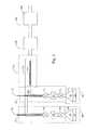
- FIG. 1is a cross-sectional illustration of an atomic deposition layer apparatus used in the practice of at least one embodiment of the invention
- FIG. 2is a cross-sectional illustration of an atomic deposition layer apparatus used in the practice of at least one embodiment of the invention.
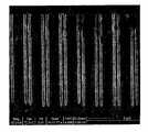
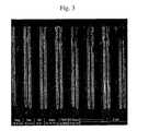
- FIG. 3is a cross-sectional scanning electron micrograph of holes in a silicon wafer uniformly coated with hafnium dioxide using one embodiment of the invention.
- the present inventionprovides a method for preparing metal silicates of varying metal and silicon content.
- the methodinvolves the reaction of a vapor of an alkoxysilanol or alkoxysilanediol with a vapor of one or more metal or metalloid compounds.
- the compoundmay be formed as a powder or as a film on a substrate, and in some embodiments, on a heated substrate.
- the compoundmay be formed on a substrate by mixing the vapors of the alkoxysilanol or alkoxysilanediol and the metal or metalloid compound prior to deposition on a substrate.
- a substrateis alternately exposed to a alkoxysilanol or alkoxysilanediol vapor and a vapor of one or more of a metal or metalloid compound.
- Silanol and silanediol reactantsare commercially available or may be prepared using conventional or known techniques.
- Silicon precursor, tris(tert-butoxy)silanolis commercially available from Aldrich Chemical Company (Milwaukee, Wis.) and Gelest, Inc. (Tullytown, Pa.). Tris(tert-butoxy)silanol may be prepared as follows.
- First tris(tert-butoxy)chlorosilaneis made by either of the following two reactions: SiCL 4 +3 t BuOH ⁇ ( t BuO) 3 SiCl+3HCl (1) SiCl 4 +3NaO t Bu ⁇ ( t BuO) 3 SiCl+3NaCl (2) The tris(tert-butoxy)chlorosilane is then hydrolyzed according to the reaction ( t BuO) 3 SiCl+H 2 O ⁇ ( t BuO) 3 SiOH+HCl (3)
- This compoundis a solid at room temperature and melts at about 66° C. It sublimes at room temperature at a low pressure of about 10 ⁇ 4 Torr, and can be distilled at a temperature of about 104° C. at a pressure of 20 Torr. It is highly soluble in organic solvents such as mesitylene or tetradecane, so that its vapors can be formed conveniently by flash vaporization of its solution.
- Tris(tert-alkoxy)silanolsmay be prepared by similar reactions, by substituting other tertiary alcohols, such as ferr-pentyl alcohol (also known as tert-amyl alcohol), for tert-butanol.
- Tris(tert-amyloxy)silanol, ( t AmO) 3 SiOHis a liquid at room temperature, so its vapors can be formed conveniently by flash vaporization of the neat liquid. It has a vapor pressure of about 2 Torr at 96° C. It is commercially available from Aldrich Chemical Company.
- Silanols and silanediolsmay be reacted with a metal source to obtain a metal silicate.
- the metal sourcemay contain one or more metals and the resultant metal silicate may contain one or more metals.
- metal compoundsinclude those that react readily with the slightly acidic protons in silanols. These acidic protons are the ones attached directly to oxygen in the silanol.
- Metal compounds that generally react with these acidic protonsinclude most metal alkyls and other organometallic compounds, metal alkylamides, and some metal alkoxides. The reactivity of any particular compound can be established readily by mixing it with an alkoxysilanol and analyzing the mixture for products by techniques such as nuclear magnetic resonance (NMR). We have found that compounds that are known to react with water also generally react with alkoxysilanols.
- NMRnuclear magnetic resonance
- the reactionis carried out in the vapor state and may be carried out using CVD or ALD techniques.
- ALDprovides control over the deposition process and is suitable for use in a wide range of reaction conditions and reactant reactivity.
- the silicon/metal ratiomay be increased by replacing some or all of the metal precursor by a suitably reactive silicon compound.
- Silicon halidessuch as silicon tetrachloride, SiCl 4 , may be used to increase the silicon content, but they may leave chloride as an impurity in the product, and their reactions may be slower than desired.
- Silicon amidessuch as tetraisocyanatosilane, tetrakis(dimethylamido)silane or tris(dimethylamido)silane avoid the halogen contamination. However, their deposition rates may also be slower than desired.
- Silylenesare more rapidly reactive. For example, the thermally stable silylene 7
- Ris an alkyl group or, in at least some embodiments, is tert-butyl
- Rcan be used as a rapidly reacting silicon source in place of part or all of the metal source, in order to increase the silicon/metal ratio.
- pure silicon dioxidemay be prepared.
- a pulse of silyleneis followed by a pulse of oxygen gas, in order to fully oxidize the silylene after it has reacted with the surface.
- Pure silicon dioxidecan be deposited rapidly by repeating the pulse sequence of silylene and oxygen.
- the present inventionprovides a method for preparing metal phosphates of varying metal and phosphorus content.
- the methodinvolves the reaction of a vapor of an bis(alkyl)phosphate with a vapor of one or more metal or metalloid compounds.
- the compoundmay be formed as a powder or as a film on a substrate, and in some embodiments, on a heated substrate.
- the compoundmay be formed on a substrate by mixing the vapors of the bis(alkyl)phosphate and the metal or metalloid compound prior to deposition on a substrate.
- a substrateis alternately exposed to a bis(alkyl)phosphate vapor and a vapor of one or more of a metal or metalloid compound.
- Bis(alkyl) phosphate reactantsare commercially available or may be prepared using conventional or known techniques.
- Phosphorus precursor, diethylphosphateis commercially available from a number of chemical companies, including Fisher Scientific (Pittsburgh, Pa.) and Pfaltz and Bauer (Waterbury, Conn.).
- Diethylphosphatemay be prepared by the air oxidation of phosphinic acid in ethanol, catalyzed by copper chloride: 2 P(O)OH+2EtOH+O 2 ⁇ (EtO) 2 P(O)OH+2H 2 O (4) See, Y. Okamoto, T. Kusano and S. Takamuku, Phosphorus, Sulfur and Silicon , volume 55, pages 195-200 (1991).
- Diisopropylphosphatemay also be prepared by first forming its potassium salt by the following two reactions: PCl 3 +3 i PrOH ⁇ ( i PrO) 2 P(O)H+ i PrCl+2HCl (8) 2( i PrO) 2 P(O)H+KMnO 4 +KHCO 3 ⁇ 2( i PrO) 2 P(O)OK+MnO 2 (9) See, A. Zwierak and M. Kluba, Tetrahedron , volume 27, pages 3163 to 3170 (1971).
- the analogous sodium saltmay be prepared by the following two reactions: POCl 3 +3 i PrOH ⁇ ( i PrO) 3 P ⁇ O+3HCl (10) ( i PrO) 3 P ⁇ O+NaOH ⁇ ( i PrO) 2 P(O)ONa+ i PrOH (11)
- metal compounds that generally react with the acid phosphate protonsinclude most metal alkyls and other organometallic compounds, metal alkylamides, and some metal alkoxides.
- the reactivity of any particular compoundcan be established readily by mixing it with a bis(alkyl)phosphate and analyzing the mixture for products by techniques such as nuclear magnetic resonance (NMR).
- the reactionis carried out in the vapor state and may be carried out using CVD or ALD techniques.
- ALDprovides control over the deposition process and is suitable for use in a wide range of reaction conditions and reactant reactivity.
- the phosphorus/metal ratiomay be increased by replacing some or all of the metal precursor by a suitably reactive phosphorus compound.
- Phosphorus halidessuch as phosphorus trichloride, PCl 3 , phosphorus pentachloride, PCl 5 , or phosphorus oxychloride, POCl 3 , may be used, but some halogen impurity may be included in the film.
- Phosphorus alkylamidessuch as hexamethylphosphorus triamide, (Me 2 N) 3 P, hexamethylphosphorimidic triamide, (Me 2 N)3P ⁇ NH, or hexamethylphosphoramide, (Me 2 N) 3 PO, avoid the halogen contamination, but their reactions may be slow.
- White phosphorus, P 4 , and phosphorus(III) oxide, P 4 O 6are more quickly reactive and can be used to increase the phosphorus/metal ratio in an ALD process. Doses of white phosphorus or phosphorus(III) oxide generally are followed by a pulse of oxygen in order to form fully oxidized films.
- the phosphorus/metal ratio of material made by ALDmay be decreased by replacing some of the phosphorus doses by doses of water or alcohol.
- metal or metalloid amidesare useful in the practice of this invention. Some examples are given in Table 1, as well as a commercial source and/or literature references for their synthesis.
- the metalloids referred to in Table 1are boron, silicon and arsenic.
- TMPD2,2,6,6-tetramethylpiperidide
- metal alkylsare useful in the practice of this invention. Some examples are given in Table 2, as well as a commercial source or literature reference of their synthesis.
- Cpis an abbreviation for cyclopentadienide
- Me s Cprepresents pentamethylcyclopentadienide
- i PrCprepresents isopropylcyclopentadienide
- i PrMe 4 pstands for isopropyltetramethylcyclopentadienide
- i Pr 4 Cpstands for tetraisopropylcyclopentadienide
- EtCpstands for ethylcyclopentadienide
- PrCpstands for propylcyclopentadienide
- i PrCpstands for isopropylcyclopentadienide
- BuCpstands for butylcyclopentadienide
- Bzfor benzenide
- EtBzfor a mixture of isomers of ethylbenzenide and 1,5-COD for 1,5-cyclooctadienide.
- metal or metalloid alkoxidescan be used in the practice of this invention. Suitable compounds are listed in Table 3, as well as a commercial source or a literature reference of their synthesis.
- part of the silanol or phosphateis replaced with water in order to deposit metal-rich silicates and phosphates.
- water vaportends to react very quickly with the vapors of the metal precursors near the vapor entrance to produce powder, rather than film on the substrate.
- ALD reactorsuch premature reactions are avoided because the reactants are introduced alternately into the reactor, so reactions near the entrance are prevented and reaction is confined to the surface of the substrate.
- watertends to adsorb strongly on surfaces, so it can take a long time to purge the ALD reactor between pulses of the reactants.
- Alcohols such as isopropanol and tert-butanolcan alleviate these problems with water, since the reactions of alcohols with metal compounds are slower, and the more volatile alcohols can be pumped more quickly from an ALD reactor. Alcohols such as isopropanol and tert-butanol are particularly appropriate for reactions involving thermally liable metal compounds. In some cases the substrate temperature is raised in order to decompose alkyl alcohols and thereby remove their carbon content from the film. A thermally labile metal compound may self-decompose at higher substrate temperatures, so self-limiting ALD reactions cannot be achieved.
- the arene hydratesare a class of alcohols that decompose at lower temperatures than ordinary alkyl alcohols, and thus can be used to provide carbon-free metal oxides at low enough temperatures to avoid self-decomposition of even thermally labile metal compounds.
- benzene hydratedecomposes easily to water and benzene because of the aromatic stabilization of the benzene byproduct:
- alkyl-substituted benzene hydratessuch as the various isomers of toluene hydrate:
- naphthalene hydratessuch as methyl naphthalene hydrate.
- ne alcoholsmay be used in the reaction of metal compounds at moderate deposition conditions.
- metal oxidesor for the formation of metal silicates or metal phosphates when used in combination with the silicon and phosphorus precursors described herein.
- a metal oxideis obtained by reaction of a metal amide with water.
- Suitable metal amidesinclude any of those listed in Table 1.
- hafnium oxidewas prepared by ALD using water vapor and tetrakis(dimethylamido)hafnium. This ALD reaction was found to be surprisingly efficient, in that almost all of the precursor that was delivered into the reaction chamber was deposited as film on the substrate and on the exposed wall of the chamber.
- Vapors of liquid precursorsmay be formed by conventional methods, including heating in a bubbler, in a thin-film evaporator, or by nebulization into a carrier gas preheated to about 100 to 250° C.
- the nebulizationmay be carried out pneumatically or ultrasonically.
- Solid precursorsmay be dissolved in organic solvents, including hydrocarbons such as decane, dodecane, tetradecane, toluene, xylene and mesitylene, and with ethers, esters, ketones and chlorinated hydrocarbons. Solutions of liquid precursors generally have lower viscosities than the pure liquids, so that in some cases it may be preferable to nebulize and evaporate solutions rather than the pure liquids.
- the liquids or solutionscan also be evaporated with thin-film evaporators or by direct injection of the liquids into a heated zone.
- Thin-film evaporatorsare made by Artisan Industries (Waltham, Mass.). Commercial equipment for direct vaporization of liquids is made by MKS Instruments (Andover, Mass.), ATMI, Inc. (Danbury, Conn.), Novellus Systems, Inc. (San Jose, Calif.) and COVA Technologies (Colorado Springs, Colo.).
- Ultrasonic nebulizersare made by Sonotek Corporation (Milton, N.Y.) and Cetac Technologies (Omaha, Nebr.).
- the silicon precursors of the present inventionmay be reacted with metal or metalloid amides, such as those in Table 1, to form metal or metalloid silicates.
- the silicon precursors of the present inventionmay be reacted with organometallic compounds, such as those in Table 2, to form metal silicates.
- the silicon precursors of the present inventionmay be reacted with metal or metalloid alkoxides, such as those in Table 3, to form metal or metalloid silicates.
- the silicon precursors of the present inventionmay also be reacted with other suitably reactive metal compounds to form metal silicates.
- tris(tert-butoxy)silanolmay be reacted with tris(tert-butyl(trimethylsilyl)amido)yttrium (Table 1) to form yttrium silicate (Examples 5 and 6).
- tris(tert-butoxy)silanolmay be reacted with tris(tert-butyl(trimethylsilyl)amido)lanthanum (Table 1) to form lanthanum silicate (Examples 7 and 8).
- Metal oxidesmay be obtained by reaction of a suitable metal and with water.
- Tris(bis(trimethylsilyl)amido)lanthanumreacts with water vapor to form a more lanthanum-rich silicate (Example 21).
- Lanthanum oxidemay be deposited from silicon-free precursors such as tris(2,2,6,6-tetramethylpiperidido)lanthanum (Example 22).
- the phosphorus precursors of the present inventionmay be reacted with suitably reactive metal compounds, such as those in the Tables, to form metal phosphates.
- metal phosphatessuch as those in the Tables
- diisopropylphosphatemay be reacted with lithium bis(ethyldimethylsilyl)amide (Table 1) to provide a process for depositing lithium phosphate films that are lithium ion conductors, as is shown in Examples 9 and 10.
- the process of the inventioncan be carried out in standard equipment well known in the art of chemical vapor deposition (CVD).
- the CVD apparatusbrings the vapors of the reactants into contact with a heated substrate on which the material deposits.
- a CVD processcan operate at a variety of pressures, including in particular normal atmospheric pressure, and also lower pressures.
- Commercial atmospheric pressure CVD furnacesare made in the USA by the Watkins-Johnson Company (Scotts Valley, Calif.), BTU International (North Billerica, Mass.) and SierraTherm (Watsonville, Calif.).
- ALDatomic layer deposition
- ALDintroduces a metered amount of a first reactant component into a deposition chamber having a substrate therein for layer deposition. A thin layer of the first reactant is deposited on the substrate. After a preselected time period, a metered amount of a second reactant component is then introduced into the deposition chamber, which is deposited on and interacts with the already deposited layer of the first reactant component. Alternating layers of first and second reactant components are introduced into the deposition chamber and deposited on the substrate to form a layer of controlled composition and thickness.
- Alternation of depositionmay be on the order of seconds to minutes and is selected to provide adequate time for the just introduced component to deposit on the substrate and for any excess vapor to be removed from the headspace above the substrate. It has been determined that the surface reactions are self-limiting so that a reproducible layer of predictable composition is deposited. Use of more than two reactant components is within the scope of the invention.
- automobile fuel injectors(Ford model CM-4722 F13Z-9F593-A) may be used to deliver pulses of the solutions of precursors into the nitrogen carrier gas. Solution is delivered each time a valve opens for about 50 milliseconds.
- 6-port sampling valves(Valco model EP4C6WEPH, Valco Instruments, Houston, Tex.) normally used for injecting samples into gas chromatographs may be used to deliver pulses of solutions into a suitable carrier gas. Each time that a valve is opened, solution flows into a tube in which solution is vaporized by heat from hot oil flowing over the outside of the tube. Carrier gas moves the vapor from the tube into the ADD reactor tube.
- a layeris deposited by ALD using an apparatus such as that illustrated in FIG. 1 .
- measured doses of reactant vapor 30are introduced into the heated deposition chamber 110 by the use of a pair of air-actuated diaphragm valves, 50 and 70 (Titan II model made by Parker-Hannifin, Richmond Calif.).
- the valvesare connected by a chamber 60 having a measured volume V, and this assembly is placed inside an oven 80 held at a controlled temperature T 2 .
- the pressure of the reactant vapor 30 in the precursor reservoir 10is equal to the equilibrium vapor pressure P eq of the solid or liquid reactant 20 at a temperature T 1 determined by the surrounding oven 40 .
- the temperature T 1is chosen to be high enough so that the precursor pressure P eq is higher than the pressure P dep in the deposition chamber.
- the temperature T 2is chosen to be higher than T 1 so that only vapor and no condensed phase is present in the valves 50 and 70 or the chamber 60 .
- its pressurecan be set by a pressure regulator (not shown) that reduces its pressure from the pressure in the precursor gas cylinder 10 .
- a precursor reservoir 11holds a solid or liquid reactant 21 having a vapor pressure 31 at a temperature T 1 ′ maintained by surrounding oven 41 .
- Valves 51 and 71are connected by a chamber 61 having a measured volume V′ and this assembly is housed in oven 81 at temperature T 2 ′.
- Carrier gas(such as nitrogen) flows at a controlled rate into inlet 90 in order to speed the flow of the reactants into the deposition chamber and the purging of reaction byproducts and un-reacted reactant vapor.
- a static mixermay be placed in the tubing 100 leading into the reactor, to provide a more uniform concentration of the precursor vapor in the carrier gas as it enters the deposition chamber 110 heated by furnace 120 and containing one or more substrates 130 .
- the reaction byproducts and un-reacted reactant vaporsare removed by trap 140 before passing into a vacuum pump 150 .
- Carrier gasexits from exhaust 160 .
- valve 70is opened so that the pressure inside chamber 60 is reduced to a value P dep close to that of the deposition chamber 110 . Then valve 70 is closed and valve 50 is opened to admit precursor vapor from precursor reservoir 10 into chamber 60 . Then valve 50 is closed so that the volume V of chamber 60 contains vapor of the precursor at a pressure P eq . Finally, valve 70 is opened to admit most of the precursor vapor contained in chamber 60 into the deposition chamber.
- This cycle of delivering precursor 20is repeated if necessary until the required dose of precursor 20 has been delivered into reaction chamber.
- the dose of precursor 20 delivered by this cycle(or several such cycles repeated to give a larger dose) is chosen to be large enough to cause the surface reactions to go to completion (also called “saturation”).
- a dose of vapor 31 from a second precursor 21may be measured and delivered by a similar apparatus with components numbered similarly to the apparatus for the first precursor 20 .
- vapor pressurecan be increased by raising the temperature T 1 , but in some cases a higher temperature would result in thermal decomposition of the precursor. In such cases of thermally sensitive precursors with low vapor pressure, vapor may be delivered using the apparatus in FIG. 2 .
- the chamber 220is first pressurized with carrier gas delivered through tube 240 and valve 200 from a pressure controller (not shown). Valve 200 is then closed and valve 210 opened to allow the carrier gas to pressurize precursor reservoir 220 to pressure P tot .
- This doseis delivered by opening valve 230 .
- Tf carrier gas from tube 90enters the volume 30 during the time that the valve 230 is open, then a dose somewhat larger than this estimate may be delivered.
- volume VBy making the volume V large enough, a precursor dose that is certainly large enough to saturate the surface reaction may be delivered. If the vapor pressure P eq is so low that the required volume V would be impracticably large, then additional doses from volume V may be delivered before delivering a dose of the other reactant.
- chamber 221is first pressurized with carrier gas delivered through tube 241 and valve 201 from a pressure controller (not shown). Valve 201 is then closed and valve 211 is opened to allow the carrier gas to pressurize precursor reservoir 11 to pressure P tot . This dose is delivered by opening valve 231 . Carrier gas from tube 91 promotes transport of the metered dose to the deposition chamber.
- materialis generally deposited on all surfaces exposed to the precursor vapors, including substrates and the interior chamber walls.
- precursor doses used in terms of moles per unit area of the substrates and exposed chamber wallsare generally deposited on all surfaces exposed to the precursor vapors, including substrates and the interior chamber walls.
- liquids and solutions described hereinmay also be used as metal-containing precursors for other types of deposition processes, such as spray coating, spin coating or sol-gel formation of mixed metal oxides.
- spray coatingspin coating
- sol-gel formation of mixed metal oxidesThe high solubility and miscibility of these precursors is an advantage in forming the required solutions.
- amides disclosed in these examplesappeared to be non-pyrophoric by the methods published by the United States Department of Transportation.
- One testcalls for placing about 5 milliliters of the material on an non-flammable porous solid, and observing that no spontaneous combustion occurs.
- Another testinvolves dropping 0.5 milliliters of the liquid or solution on a Whatman No. 3 filter paper, and observing that no flame or charring of the paper occurs.
- the precursorsgenerally react with moisture in the ambient air, and should be stored under an inert, dry atmosphere such as pure nitrogen gas.
- a solution (1% by weight) of tris(tert-butoxy)silanol in mesitylenewas pumped at a rate of 6 ml/hour into a 1/16′′ O.D. tee joint through which nitrogen gas flowed at 0.4 L/min.
- the resulting fogflowed into a tube heated to 250° C.
- a solution (1% by weight) of tetrakis(ethylmethylamido)zirconium in mesitylenewas pumped at a rate of 12 ml/hour into another tee joint through which nitrogen gas flowed at 0.4 L/min.
- the resulting fogflowed into the same heated tube.
- the gas pressurewas maintained at 5 Torr by a vacuum pump attached to the outlet of the glass tube by a liquid nitrogen trap.
- Substrates of silicon and glassy carbon placed inside the tubewere coated with a film of zirconium silicate whose thickness varied along the length of the tube.
- Analysis of the film by Rutherford backscattering spectroscopygave a composition ZrSi 2 O 6 for films deposited on glassy carbon. No carbon or nitrogen was detected in the film.
- the refractive indexes of films deposited on siliconwere found to be about 1.6 by ellipsometry.
- Example 1was repeated except that the precursors were injected in alternate pulses spaced 5 seconds apart, instead of continuously.
- a film of similar composition, ZrSi 2 O 6was deposited with uniform thickness along the whole length of the heated zone. The thickness was about 0.3 nm per cycle.
- Example 1was repeated with tetrakis(ethylmethylamido)hafnium in place of tetrakis(ethylmethylamido)zirconium. Films of composition approximately HfSi 2 O 6 were formed. No carbon or nitrogen was detected in the film. The refractive indexes of films deposited on silicon were found to be about 1.6 by ellipsometry.
- Example 3was repeated except that the precursors were injected in alternate pulses spaced 5 seconds apart, instead of continuously.
- a film of similar composition, HfSi 2 O 6was deposited with uniform thickness along the whole length of the heated zone. The thickness was about 0.3 nm per cycle.
- Example 1was repeated with tris(tert-butyl(trimethylsilyl)amido)yttrium in place of tetrakis(ethylmethylamido)zirconium. Films of composition approximately Y 2 Si 2 O 7 were formed. No carbon or nitrogen was detected in the film. The refractive indexes of films deposited on silicon were found to be about 1.6 by ellipsometry.
- Example 5was repeated except that the precursors were injected in alternate pulses spaced 5 seconds apart, instead of continuously.
- a film of similar composition, Y 2 Si 2 O 7was deposited with uniform thickness along the whole length of the heated zone. The thickness was about 0.3 nm per cycle. Composition approximately Y 2 Si 2 O 7 .
- Example 1was repeated with tris(bis(trimethylsilyl)amido)lanthanum in place of tetrakis(ethylmethylamido)zirconium and tetradecane in place of mesitylene. Films with a La:Si ratio of about 0.9 were formed on a glassy carbon substrate at a substrate temperature of 250° C. No carbon or nitrogen was detected in the films.
- Example 7was repeated except that the precursors were injected in alternate pulses spaced 5 seconds apart, instead of continuously. A film of similar composition was deposited with uniform thickness along the whole length of the heated zone.
- Liquid lithium bis(ethyldimethylsilyl)amide(1 part by weight) was mixed with mesitylene (99 parts).
- the resulting solutionwas nebulized by pumping at a rate of 12 ml/hour into a tee joint into nitrogen gas flowing at 0.30 L/min into the deposition zone inside a tube (24 mm inside diameter) in a furnace heated to 250° C.
- a 1% mesitylene solution of diisopropylphosphatewas similarly nebulized into another nitrogen carrier gas stream flowing at 0.30 L/min into the same tube furnace.
- the gas pressurewas maintained at 5 Torr by a vacuum pump attached to the outlet of the glass tube by a liquid nitrogen trap.
- a thin filmwas deposited on a silicon substrate placed on the bottom of the glass tube, as well as on the inside of the tube.
- the thickness profileshowed a peak near the gas entrance to the tube furnace.
- the filmwas analyzed by X-ray photoelectron spectroscopy to contain lithium, phosphorus and oxygen.
- Example 9was repeated with the change that the materials were introduced in alternating pulses spaced 5 seconds apart in time. A similar lithium phosphate film was deposited, except that the thickness was nearly constant throughout the deposition zone.
- Example 1was repeated using only the silicon precursor and no zirconium precursor. No film was deposited.
- Example 1was repeated using only the zirconium precursor and no silicon precursor. No film was deposited.
- Example 3was repeated using only the hafnium precursor and no silicon precursor. No film was deposited.
- Example 5was repeated using only the yttrium precursor and no silicon precursor. No film was deposited.
- Example 7was repeated using only the lanthanum precursor and no silicon precursor. No film was deposited.
- Example 9was repeated using only the phosphorus precursor and no lithium precursor. No film was deposited.
- Example 9was repeated using only the lithium precursor and no phosphorus precursor. No film was deposited.
- the ALD examples 2, 4, 6, 8 and 10were repeated using automobile fuel injectors (Ford model CM-4722 F13Z-9F593-A) to deliver pulses of the solutions of precursors into the nitrogen carrier gas. About 0.05 m of solution was delivered each time that a valve was opened for about 50 milliseconds. Similar results were obtained.
- the ALD examples 2, 4, 6, 8 and 10were repeated using a 6-port sampling valves (Valco model EP4C6WEPH, Valco Instruments, Houston, Tex.) normally used for injecting samples into gas chromatographs to deliver pulses of tetradecane solutions into the nitrogen carrier gas. External sample loops having volumes of 50 microliters were used. Each time that a valve was opened, about 50 microliters of solution flowed into a 1/16′′ O. D., 0.040′′ I. D. nickel tube in which the solution was vaporized by heat from hot oil flowing over the outside of the tube. Nitrogen carrier gas moved the vapor from the small tube into the ALD reactor tube. Similar results were obtained.
- a 6-port sampling valvesValco model EP4C6WEPH, Valco Instruments, Houston, Tex.
- pulses of those precursors that are liquids at room temperaturewere delivered for ALD experiments similar to examples 2, 4, 6, 8 and 10 using 4-port sampling valves with small (0.5 microliter) internal sampling loops (Valco model EH2CI4WE.5PH, Valco Instruments, Houston, Tex.). Each time that a valve was opened, about 0.5 microliters of liquid flowed into a 1/16′′ O. D., 0.040′′ I. D. nickel tube in which the liquid was vaporized by heat from hot oil flowing over the outside of the tube. Nitrogen carrier gas moved the vapor from the small tube into the ALD reactor tube. Similar results were obtained.
- a hafnium oxide layerwas deposited using the apparatus of FIG. 1 .
- Doses of 0.5 ⁇ 10 ⁇ 9 moles/cm 2 of tetrakis(dimethylamido)hafnium vapor and 4 ⁇ 10 ⁇ 9 moles/cm 2 of water vaporwere injected alternately every 5 seconds into a deposition chamber held at 250° C.
- the chamberwas also fed a continuous flow of nitrogen carrier gas sufficient to maintain a pressure of 0.15 Torr.
- the deposition chamberhad a cross-sectional area of 2.3 square centimeters in the plane perpendicular to the direction of gas flow through the chamber.
- the outlet of the deposition chamberwas attached to a vacuum pump with capacity (195 liters/minute) sufficient to pump a volume equal to the deposition chamber in about 0.012 seconds.
- a transparent, electrically insulating hafnium oxide filmwas deposited on substrates in the deposition chamber and onto its inner walls. Its composition was determined to be HfO 2 by Rutherford backscattering spectroscopy (RBS) of a film on a glassy carbon substrate. No carbon or nitrogen was detected ( ⁇ 1 atomic percent). By ellipsometry, its thickness was determined to be 0.1 nanometer/cycle and its refractive index 2.05. Combining data from RBS and ellipsometry yielded a density of about 9. The thickness was constant over the whole deposition region, to within the estimated measurement error of about 1%.
- RBSRutherford backscattering spectroscopy
- Example 12Repeating Example 12 with higher doses of either reactant did not increase the film thickness or change its properties. These results show that the surface reactions are self-limiting. This conclusion was confirmed by placing inside the deposition chamber 110 a quartz crystal micro-balance (not shown), which showed that the amount of mass deposited first increased and then reached a plateau as the size of each dose was increased. As a result of these self-limiting surface reactions, uniform films could be deposited inside holes with ratios of length to diameter over 50. Uniformity of thickness inside these holes was improved by increasing the dose to 10 times the minimum required for saturation of the reactions on a flat surface without the holes.
- FIG. 3shows a scanning micrograph of holes coated with hafnium oxide, cleaved to reveal their highly uniform thickness.
- the hafnium oxide layeris the bright line outlining each of the narrow vertical holes in the silicon, which appears as a dark background.
- At the top of the micrographis the upper surface of the silicon from which the holes were etched prior to the deposition of the hafnium oxide.
- Example 12Repeating Example 12 with substrate temperatures in the range from 100° C. to 300° C. gave similar results. At temperatures above 300° C., the thickness increased with increasing the dose of tetrakis(dimethylamido)hafnium. This shows that the surface reaction is not self-limiting at temperatures above 300° C., due to thermal decomposition of tetrakis(dimethylamido)hafnium.
- Example 12was repeated with tetrakis(dimethylamido)zirconium in place of tetrakis(dimethylamido)hafnium. Films of zirconium dioxide with similar properties were deposited.
- Example 12was repeated with tert-butmol vapor in place of water vapor. Films of hafnium dioxide with similar properties were deposited.
- Example 12was repeated with ethylimidotris(diethylamido)tantalum vapor in place of tetrakis(dimethylamido)hafnium vapor.
- Transparent films of Ta 2 O 5were deposited. They have a refractive index of 2.2, and a thickness of about 0.06 nm per cycle.
- ALDwas carried out using alternating doses of 3 ⁇ H) ⁇ 9 moles/cm 2 of the vapors of trimethylaluminum and diisopropylphosphate at a substrate temperature of 400° C.
- Transparent aluminum phosphate films with approximate composition A 12 P 4 O 13were deposited at a rate of 0.1 nm per cycle. They had a refractive index of about 1.5.
- ALDwas carried out using alternating doses of 3 ⁇ 10 ⁇ 9 moles/cm 2 of trimethylaluminum vapor and 1.2 ⁇ 10 ⁇ 8 moles/cm 2 of tris(tert-butoxy)silanol vapor at a substrate temperature of 300° C.
- Transparent aluminum silicate filmswith approximate composition Al 2 Si 8 O 19 were deposited at a remarkably high rate of 1 nm per cycle. They had a refractive index of about 1.48. The surfaces of the films are very smooth; atomic force microscopy determined a root mean square roughness of less than 0.8 nm for an aluminum silicate film 150 nm thick.
- the tensile stress in a film 2 micrometers thick on a silica substratewas measured to be about 0.2 giga-Pascals.
- a similar film deposited on single-crystalline siliconshowed a smaller tensile stress of 0.03 giga-Pascals.
- a film 6 microns thickshowed cracks and delamination because of the tensile stress.
- This tensile stresscan be reduced, eliminated, or even reversed to compressive stress by plasma treatment.
- the depositionis temporarily halted after a thin layer (such as 5 to 10 nm) has been deposited, a radio-frequency plasma (in a low-pressure gas such as O 2 +argon) is applied, and then the plasma power is stopped and the deposition is resumed.
- a radio-frequency plasmain a low-pressure gas such as O 2 +argon
- Multiple cycles of deposition and plasma treatmentmay be used to build up thicker layers with tensile or compressive stress values adjusted to the requirements of particular applications, particularly those requiring thicker films.
- ALDwas carried out using alternating doses of 3 ⁇ 10 ⁇ 9 moles/cm 2 of trimethylaluminum vapor and 3 ⁇ 10 ⁇ 8 moles/cm 2 of tris(tert-butoxy)silanol vapor at a substrate temperature 200° C.
- Transparent aluminum silicate films with approximate composition Al 2 Si 16 O 35were deposited at a remarkably high rate of 2 nm per cycle. They had a refractive index of about 1.47.
- ALDwas carried out with alternating doses of 3 ⁇ 10 ⁇ 9 moles/cm 2 of tris(dimethylamino)aluminum vapor and 3 ⁇ 10 ⁇ 8 moles/cm 2 of tris(tert-butoxy)silanol vapor at a substrate temperature 250° C.
- An aluminum silicate filmwas formed with thickness 0.1 nm/cycle and a refractive index of about 1.46.
- Example 19was repeated with tris(tert-pentyloxy)silanol vapor in place of the tris(tert-butoxy)silanol vapor. Similar results were obtained.
- Example 19was repeated with a dose of water vapor between the doses of tris(dimethylamino)aluminum vapor and tris(tert-butoxy)silanol vapor. A similar film was obtained with very uniform thickness of 0.1 nm/cycle ( ⁇ 1%) along the direction of gas flow.
- Example 12was repeated with tris(bis(trimethylsilyl)amido)lanthanum vapor in place of tetrakis(dimethylamido)hafnium vapor and with the apparatus of FIG. 2 , used as described herein above.
- Transparent oxide films with a La: Si ratio of about 2were formed on substrates at a substrate temperature of 250° C. No carbon or nitrogen was detected in the films. They have a refractive index of 1.7, and a thickness of about 0.1 nm per cycle.
- ALDcan be carried out with alternating doses of tris(2,2,6,6-tetramethylpiperidido)lanthanum vapor using the apparatus of FIG. 2 and water vapor to form lanthanum oxide films.
- ALDcan be carried out with alternating doses of tetraisocyanatosilane vapor and tris(tot-butoxy)silanol vapor to form silicon dioxide films. Larger fluxes of exposure (>10 ⁇ 7 Langmuirs) are required for these less reactive precursors.
Landscapes
- Chemical & Material Sciences (AREA)
- Organic Chemistry (AREA)
- Engineering & Computer Science (AREA)
- Inorganic Chemistry (AREA)
- Chemical Kinetics & Catalysis (AREA)
- Metallurgy (AREA)
- Mechanical Engineering (AREA)
- Materials Engineering (AREA)
- General Chemical & Material Sciences (AREA)
- Power Engineering (AREA)
- General Physics & Mathematics (AREA)
- Microelectronics & Electronic Packaging (AREA)
- Computer Hardware Design (AREA)
- Manufacturing & Machinery (AREA)
- Condensed Matter Physics & Semiconductors (AREA)
- Physics & Mathematics (AREA)
- Life Sciences & Earth Sciences (AREA)
- Biochemistry (AREA)
- General Health & Medical Sciences (AREA)
- Molecular Biology (AREA)
- Health & Medical Sciences (AREA)
- Chemical Vapour Deposition (AREA)
- Formation Of Insulating Films (AREA)
Abstract
Description
This application is a continuation of U.S. patent application Ser. No. 14/974,399, filed on Dec. 18, 2015, which is a continuation of U.S. patent application Ser. No. 14/959,283, filed on Dec. 4, 2015, which is a continuation of U.S. patent application Ser. No. 14/587,909, filed on Dec. 31, 2014, which is a continuation of U.S. patent application Ser. No. 13/719,110, filed on Dec. 18, 2012, which is a divisional of U.S. patent application Ser. No. 12/407,556, filed on Mar. 19, 2009, now U.S. Pat. No. 8,334,016, which is a continuation of U.S. patent application Ser. No. 11/199,032, filed on Aug. 8, 2005, now U.S. Pat. No. 7,507,848, which is a continuation of U.S. patent application Ser. No. 10/381,628, filed on Sep. 2, 2003, now U.S. Pat. No. 6,969,539, which is the national stage application of PCT Application No. PCT/US01/30507, filed on Sep. 28, 2001, which claims the benefit of the filing date of U.S. Provisional Patent Application No. 60/236,283, filed Sep. 28, 2000 and 60/253,917, filed Nov. 29, 2000, the contents of which are hereby incorporated by reference herein in their entireties.
This invention was made with the support of the United States government under National Science Foundation Grant No. ECS-9975504. The United States government has certain rights in the invention.
1. Field of the Invention
This invention relates to novel reagents for use in thin film deposition processes such as chemical vapor deposition (CVD) and atomic layer deposition (ALD). These reagents can be used for deposition of materials containing silicon and/or phosphorus along with metals and/or oxygen, commonly called metal oxides, silicates or metal phosphates, or silicon dioxide.
2. Description of the Related Art
Chemical vapor deposition (CVD) is a widely-used process for forming solid materials, such as coatings or powders, from reactants in the vapor phase. Comprehensive reviews of CVD processes have been given recently inCVD of Nonmetals, W. S. Rees, Jr., Editor, VCH Publishers, Weinheim, Germany, 1996; CVD of Compound Semiconductors, A. C. Jones and P. O'Brien, VCH, 1996; andThe Chemistry of Metal CVD, T. Kodas and M. Hampden-Smith, Editors, VCH, 1994.
In CVD processes, a reactant vapor or vapor mixture is brought into contact with a heated surface on which a thin film is deposited. In a related form of CVD, two reactant vapors are alternately exposed to the heated surface. This form of CVD is often called atomic layer deposition (ALD). For suitable reactants, ALD can provide improved step coverage and thickness uniformity compared to CVD with mixed vapors. For a review of ALD, see the paper by Mikko Ritala inApplied Surface Science, volume 112, pages 223-230 (1997).
Coatings of metal silicates have many applications or potential applications. For example, silicates of zirconium, hafnium, yttrium or lanthanum are being considered as potential replacements for silicon dioxide in gate insulators in silicon semiconductor technology. See, for example, A. Kingon et al.,Nature, volume 406, pages 1032-1038 (2000). InScience, (volume 288, pages 319 to 321 (2000)), Ritala et al. report the use of the sequential ALD reaction of metal chlorides and silicon alkoxides to produce metal silicates, including zirconium silicate. However, this reaction deposits films containing residual chlorine, which can be deleterious to the properties of the film or to its adhesion to substrates or subsequent coatings. The chlorine in the precursors can also corrode metal substrates or the apparatus used for the deposition. Thus it would be advantageous to have chlorine-free precursors for CVD or ALD of metal silicates or oxides.
ALD of silicon dioxide has been achieved by Klaus et al., U.S. Pat. No. 6,090,442 (2000), but the deposition rate is very slow and the substrate temperature is limited to values near room temperature.
Lithium phosphate is a material of current interest as a lithium ion conductor in lithium batteries. Currently there is no known process for CVD or ALD of lithium phosphate.
A principal feature of the present invention includes volatile chemical precursors with reactivity adapted for CVD or ALD of metal silicates, phosphates or oxides.
An advantage of these chemical precursors is that they do not contain chlorine, and leave no chlorine residue during a process for the CVD or ALD of metal silicates, phosphates or oxides.
A related feature of the present invention is the deposition of metal silicates under conditions that produce a sharp interface between silicon substrates and the deposited metal silicate.
An advantage of the process is that it permits deposition of materials containing metal silicates or phosphates by a CVD process in which all the reactants may be mixed homogeneously before delivery to the heated surface of the substrate.
An additional advantage of the process is the vapor deposition of metal silicates or phosphates with relatively fixed ratio of metal to silicon over a range of conditions such as concentrations of reactants and position of the substrate inside the reactor.
Another advantage of the invention is its ability to make conformal coatings over substrates with narrow holes, trenches or other structures. This ability is commonly known as good step coverage.
Another feature of the present invention is the preparation of material comprising lithium phosphate.
An advantage of the invention is that the reactants are stable and relatively nonhazardous.
Another feature of the invention includes a chemical vapor deposition or atomic layer deposition process for metal oxides or mixtures of metal oxides.
A further feature of the invention includes process for atomic layer deposition of silicon dioxide.
One particular feature of the present invention includes a process for depositing oxides or silicates of zirconium, hafnium, yttrium and/or lanthanum having high dielectric constants of use as gate insulators or trench capacitors in microelectronic devices.
Another particular feature of the present invention includes a process for depositing silicon dioxide or metal silicates having useful optical properties, such as in planar waveguides and multiplexers/demultiplexers, and in optical interference filters.
An additional feature of the present invention includes a process for depositing lithium phosphate coatings allowing rapid diffusion of lithium for use as separators in batteries or electrochromic devices.
Other features and advantages of the invention will be obvious to those skilled in the art on reading the instant invention.
In one aspect of the invention vapors of alkoxysilanols are reacted with the vapors of suitably reactive metal or metalloid compounds, such as metal or metalloid alkylamides, alkyls or cyclopentadienyls, to form metal silicates. The reaction may be carried out in a manner to form films.
In at least some embodiments, tris(alkoxy)silanol compounds have thegeneral formula 1, in which Rnrepresents hydrogen, alkyl groups, fluoroalkyl groups or alkyl groups substituted with other atoms or groups, preferably selected to enhance the volatility of the compound, where Rnis any one of R1through Rn. The Rnmay be the same or different from each other.

In at least some embodiments methyl groups are selected for each of the Rnin thegeneral formula 1 given above one obtains a highly preferred compound tris(tert-butoxy)silanol 2, which may be written more compactly as (tBuO)3SiOH.

Another compound of the invention is tris(tert-pentyloxy)silanol, also known as tris(tert-amyloxy)silanol 3, which may be written more compactly as (tAmO)3SiOH.

In at least some embodiments of the invention Di(alkoxy)silanediols such as (4BuO)2Si(OH)2can also be used, although they are less stable than tris(alkoxy)silanol compounds in at least some applications. Di(alkoxy)silanediol compounds having the general formula 4 may be used according to the invention, where Rn, represents hydrogen, alkyl groups, fluoroalkyl groups or alkyl groups substituted by other atoms or groups, preferably selected to enhance volatility and stability, and may be the same or different for any Rn, and Rnis any of R1through R6may be the same or different.

In at least some embodiments, the groups R1for thegeneral formula 1 or R1-R6for the general formula 4 may be selected from the group consisting of hydrogen, methyl, ethyl, n-propyl and isopropyl groups.
In the foregoing compounds, it is also understood that the alkyl groups R1through R9for general formula or R1through R6for general formula 4 may be a hydrocarbon having some degrees of unsaturation, e.g., aryl, alkenyl or alkynyl groups.
In at least some embodiments, metal compounds include those that react readily with the slightly acidic protons in silanols. These acidic protons are the ones attached directly to oxygen in the silanol. Metal compounds that generally react with these acidic protons include most metal alkyls and other organometallic compounds, metal alkylamides, and some metal alkoxides. The reactivity of any particular compound can be established readily by mixing it with an alkoxysilanol and analyzing the mixture for products by techniques such as nuclear magnetic resonance (NMR). We have found that compounds that are known to react with water also generally react with alkoxysilanols.
We have also discovered that the stoichiometry of the deposited metal silicates can be controlled. The silicon/metal ratio may be decreased by replacing some or all of the silanol with water or an alcohol. Conversely, the silicon/metal ratio may be increased by replacing some or all of the metal source by a suitably reactive silicon-containing compound such as a silicon amide or a silylene. By these methods the composition of the deposited material may be chosen to be any composition from pure metal oxide to pure silicon dioxide or any desired silicon/metal ratio in between. The stoichiometry may even be varied during the course of one deposition. For example, in the deposition of a gate insulator for a silicon semiconductor device, it may be desirable to begin the deposition with a silicon-rich layer close to the silicon surface in order to improve the electrical properties of the interface, followed by a metal-rich layer with higher dielectric constant.
In another aspect of the invention, vapors of bis(alkyl)phosphates are reacted with the vapors of reactive metal compounds, such as metal alkylamides, metal alkyls, metal cyclopentadienides or metal alkoxides, to form metal phosphates. The reaction may be carried out in a way that forms films.
In at least some embodiments of the invention, phosphorus-containing precursors include bis(alkyl)phosphates 5 in which Rn, represents hydrogen, alkyl groups, fluoroalkyl groups or alkyl groups, substituted with other atoms or groups where Rnmay be any of R1through R6. The Rnmay be the same or different from each other.

In at least one embodiment, the phosphorus precursor is diisopropylphosphate, represented by the formula 6.

It is also possible to control the stoichiometry of the metal phosphates. The phosphorus/metal ratio may be decreased by replacing some or all of the bis(alkyl)phosphate with water or an alcohol. Conversely, the phosphorus/metal ratio may be increased by replacing some or all of the metal source by a suitably reactive phosphorus source. By these methods, the composition of the deposited material may be varied from pure metal oxide to pure phosphorus oxide or any desired phosphorus/metal ratio.
In at least some embodiments, the groups R—R6for the general formula 5 may be selected from the group consisting of hydrogen, methyl, ethyl, n-propyl or isopropyl groups. In the foregoing compounds, it is also understood that the alkyl groups R1through R9forgeneral formula 1 or R1through R6for general formula 4 may be a hydrocarbon having some degrees of unsaturation, e.g., aryl, alkenyl—alkynyl groups.
In another aspect of the invention, a process for preparing a material comprising silicon includes exposing a substrate to one or more vapors chosen from the group consisting of alkoxysilanols, alkoxysilanediols and silylenes. In at least some embodiments, the silylene is the compound described by the formula

In one aspect of the invention, a process for forming a material including phosphorus includes exposing a substrate to one or more vapors chosen from the group consisting of bis(alkyl)phosphates, phosphorus(III) oxide and white phosphorus.
In another aspect of the invention, a process is provided for preparing oxygen-containing materials including exposing a substrate to one or more vapors chosen from the group consisting of arene hydrates, such as benzene hydrate, naphthalene hydrate, or a substituted benzene hydrate or a substituted naphthalene hydrate.
In another aspect of the invention, a process for forming a metal oxide is provided including exposing a heated surface alternately to the vapor of one or more metal amides and then to the vapors of water or an alcohol.
In at least some embodiments, the alcohol is an arene hydrate, or in at least some embodiments, the metal amide or amides are chosen from Table 1.
In another aspect of the invention, a process for forming material including oxygen and one or more metals is provided by exposing a surface alternately to the vapor of one or more organometallic compounds and to the vapor of an arene hydrate.
In at least one embodiment, the organometallic compounds are chosen from Table 2.
Various objects, features, and advantages of the present invention can be more fully appreciated with reference to the following detailed description of the invention when considered in connection with the following drawings. The drawings are presented for the purpose of illustration only are not intended to be limiting of the invention, in which:
1. Metal Silicates and Silicon Dioxide.
The present invention provides a method for preparing metal silicates of varying metal and silicon content. The method involves the reaction of a vapor of an alkoxysilanol or alkoxysilanediol with a vapor of one or more metal or metalloid compounds. The compound may be formed as a powder or as a film on a substrate, and in some embodiments, on a heated substrate. The compound may be formed on a substrate by mixing the vapors of the alkoxysilanol or alkoxysilanediol and the metal or metalloid compound prior to deposition on a substrate. In at least some embodiments, a substrate is alternately exposed to a alkoxysilanol or alkoxysilanediol vapor and a vapor of one or more of a metal or metalloid compound.
Silanol and silanediol reactants are commercially available or may be prepared using conventional or known techniques. Silicon precursor, tris(tert-butoxy)silanol, is commercially available from Aldrich Chemical Company (Milwaukee, Wis.) and Gelest, Inc. (Tullytown, Pa.). Tris(tert-butoxy)silanol may be prepared as follows. First tris(tert-butoxy)chlorosilane is made by either of the following two reactions:
SiCL4+3tBuOH→(tBuO)3SiCl+3HCl (1)
SiCl4+3NaOtBu→(tBuO)3SiCl+3NaCl (2)
The tris(tert-butoxy)chlorosilane is then hydrolyzed according to the reaction
(tBuO)3SiCl+H2O→(tBuO)3SiOH+HCl (3)
SiCL4+3tBuOH→(tBuO)3SiCl+3HCl (1)
SiCl4+3NaOtBu→(tBuO)3SiCl+3NaCl (2)
The tris(tert-butoxy)chlorosilane is then hydrolyzed according to the reaction
(tBuO)3SiCl+H2O→(tBuO)3SiOH+HCl (3)
See, Backer et al,Rec. Trav. Chim.,volume 61, page 500 (1942). This compound is a solid at room temperature and melts at about 66° C. It sublimes at room temperature at a low pressure of about 10−4Torr, and can be distilled at a temperature of about 104° C. at a pressure of 20 Torr. It is highly soluble in organic solvents such as mesitylene or tetradecane, so that its vapors can be formed conveniently by flash vaporization of its solution.
Other tris(tert-alkoxy)silanols may be prepared by similar reactions, by substituting other tertiary alcohols, such as ferr-pentyl alcohol (also known as tert-amyl alcohol), for tert-butanol. Tris(tert-amyloxy)silanol, (tAmO)3SiOH, is a liquid at room temperature, so its vapors can be formed conveniently by flash vaporization of the neat liquid. It has a vapor pressure of about 2 Torr at 96° C. It is commercially available from Aldrich Chemical Company.
Silanols and silanediols may be reacted with a metal source to obtain a metal silicate. The metal source may contain one or more metals and the resultant metal silicate may contain one or more metals. In at least some embodiments, metal compounds include those that react readily with the slightly acidic protons in silanols. These acidic protons are the ones attached directly to oxygen in the silanol. Metal compounds that generally react with these acidic protons include most metal alkyls and other organometallic compounds, metal alkylamides, and some metal alkoxides. The reactivity of any particular compound can be established readily by mixing it with an alkoxysilanol and analyzing the mixture for products by techniques such as nuclear magnetic resonance (NMR). We have found that compounds that are known to react with water also generally react with alkoxysilanols.
The reaction is carried out in the vapor state and may be carried out using CVD or ALD techniques. As is discussed in greater detail below, ALD provides control over the deposition process and is suitable for use in a wide range of reaction conditions and reactant reactivity.
The silicon/metal ratio may be increased by replacing some or all of the metal precursor by a suitably reactive silicon compound. Silicon halides such as silicon tetrachloride, SiCl4, may be used to increase the silicon content, but they may leave chloride as an impurity in the product, and their reactions may be slower than desired. Silicon amides such as tetraisocyanatosilane, tetrakis(dimethylamido)silane or tris(dimethylamido)silane avoid the halogen contamination. However, their deposition rates may also be slower than desired. Silylenes are more rapidly reactive. For example, the thermally stable silylene7

where R is an alkyl group or, in at least some embodiments, is tert-butyl, can be used as a rapidly reacting silicon source in place of part or all of the metal source, in order to increase the silicon/metal ratio.
In at least some embodiments, pure silicon dioxide may be prepared. In an ALD system, a pulse of silylene is followed by a pulse of oxygen gas, in order to fully oxidize the silylene after it has reacted with the surface. Pure silicon dioxide can be deposited rapidly by repeating the pulse sequence of silylene and oxygen.
2. Metal Phosphate and Phosphorus Oxide.
The present invention provides a method for preparing metal phosphates of varying metal and phosphorus content. The method involves the reaction of a vapor of an bis(alkyl)phosphate with a vapor of one or more metal or metalloid compounds. The compound may be formed as a powder or as a film on a substrate, and in some embodiments, on a heated substrate. The compound may be formed on a substrate by mixing the vapors of the bis(alkyl)phosphate and the metal or metalloid compound prior to deposition on a substrate. In at least some embodiments, a substrate is alternately exposed to a bis(alkyl)phosphate vapor and a vapor of one or more of a metal or metalloid compound.
Bis(alkyl) phosphate reactants are commercially available or may be prepared using conventional or known techniques. Phosphorus precursor, diethylphosphate, is commercially available from a number of chemical companies, including Fisher Scientific (Pittsburgh, Pa.) and Pfaltz and Bauer (Waterbury, Conn.). Diethylphosphate may be prepared by the air oxidation of phosphinic acid in ethanol, catalyzed by copper chloride:
2P(O)OH+2EtOH+O2→(EtO)2P(O)OH+2H2O (4)
See, Y. Okamoto, T. Kusano and S. Takamuku,Phosphorus, Sulfur and Silicon, volume 55, pages 195-200 (1991).
2P(O)OH+2EtOH+O2→(EtO)2P(O)OH+2H2O (4)
See, Y. Okamoto, T. Kusano and S. Takamuku,Phosphorus, Sulfur and Silicon, volume 55, pages 195-200 (1991).
An alternative reaction sequence is shown for diisopropylphosphate and may be used for other precursor compounds by appropriate substitutions for isopropanol.
PCl3+3iPrOH→(iPrO)2P(O)H+iPrCl+2HCl (5)
(iPrO)2P(O)H+SO2Cl2→(iPrO)2P(O)Cl+HCl+SO2 (6)
(iPrO)2P(O)Cl+H2O→(iPrO)2P(O)OH+HCl (7)
See, Melvor et al.,Canadian J. Chemistry, volume 34, pages 1825 and 1827.
PCl3+3iPrOH→(iPrO)2P(O)H+iPrCl+2HCl (5)
(iPrO)2P(O)H+SO2Cl2→(iPrO)2P(O)Cl+HCl+SO2 (6)
(iPrO)2P(O)Cl+H2O→(iPrO)2P(O)OH+HCl (7)
See, Melvor et al.,Canadian J. Chemistry, volume 34, pages 1825 and 1827.
Diisopropylphosphate may also be prepared by first forming its potassium salt by the following two reactions:
PCl3+3iPrOH→(iPrO)2P(O)H+iPrCl+2HCl (8)
2(iPrO)2P(O)H+KMnO4+KHCO3→2(iPrO)2P(O)OK+MnO2 (9)
See, A. Zwierak and M. Kluba,Tetrahedron, volume 27, pages 3163 to 3170 (1971). The analogous sodium salt may be prepared by the following two reactions:
POCl3+3iPrOH→(iPrO)3P═O+3HCl (10)
(iPrO)3P═O+NaOH→(iPrO)2P(O)ONa+iPrOH (11)
The precursor diisopropylphosphate may then be liberated from its alkali salt by reaction with hydrochloric acid:
(iPrO)2P(O)OM+HCl→(iPrO)2P(O)OH+MCl,M=Na,K (12)
The above bis(alkyl)phosphates react with a wide range of metal compounds to form metal phosphates. Metal compounds that generally react with the acid phosphate protons include most metal alkyls and other organometallic compounds, metal alkylamides, and some metal alkoxides. The reactivity of any particular compound can be established readily by mixing it with a bis(alkyl)phosphate and analyzing the mixture for products by techniques such as nuclear magnetic resonance (NMR).
The reaction is carried out in the vapor state and may be carried out using CVD or ALD techniques. As is discussed in greater detail below, ALD provides control over the deposition process and is suitable for use in a wide range of reaction conditions and reactant reactivity.
The phosphorus/metal ratio may be increased by replacing some or all of the metal precursor by a suitably reactive phosphorus compound. Phosphorus halides such as phosphorus trichloride, PCl3, phosphorus pentachloride, PCl5, or phosphorus oxychloride, POCl3, may be used, but some halogen impurity may be included in the film. Phosphorus alkylamides such as hexamethylphosphorus triamide, (Me2N)3P, hexamethylphosphorimidic triamide, (Me2N)3P═NH, or hexamethylphosphoramide, (Me2N)3PO, avoid the halogen contamination, but their reactions may be slow. White phosphorus, P4, and phosphorus(III) oxide, P4O6, are more quickly reactive and can be used to increase the phosphorus/metal ratio in an ALD process. Doses of white phosphorus or phosphorus(III) oxide generally are followed by a pulse of oxygen in order to form fully oxidized films.
The phosphorus/metal ratio of material made by ALD may be decreased by replacing some of the phosphorus doses by doses of water or alcohol.
3. Metal Amides, Metal Alkyls and Metal Alkoxides.
In at least some embodiments, metal or metalloid amides are useful in the practice of this invention. Some examples are given in Table 1, as well as a commercial source and/or literature references for their synthesis. The metalloids referred to in Table 1 are boron, silicon and arsenic.
| TABLE 1 |
| Some Volatile Metal or Metalloid Amides |
| Melt. Pt. | Vapor Press. | ||
| Compound | ° C. | ° C./Torr | Reference and/or commercial source |
| Al(N(SiMe3)2)3 | 188 | Waimagat, J. Organomet. Chem. 33, 1 | |
| (1971) | |||
| Al2(NEt2)6 | liquid | Barry & Gordon, 2000 | |
| Al2(NEtMe)6 | liquid | 100/0.25 | Barry & Gordon, 2000 |
| Al(NiPr2)3 | 56-59 | Brothers, Organometallics 13, 2792 (1994) | |
| Al2(NMe2)6 | 88-89 | 90/0.1 | Ruff, JACS 83, 2835 (1961) |
| Al(N(Et)CH2CH2NMe2)(NMe2)2 | liquid | 65-70/0.3 | Barry, Gordon & Wagner, Mat. Res. Soc. |
| Symp. Proc. 606, 83-89 (2000) | |||
| As(NMe2)3 | −53 | 55/10 | Cowley, JACS 95, 6505 (1973) |
| As(N(Me)(SiMe3))3 | 11-13 | 67-70/0.1 | Birkofer & Ritter, Chem. Ber. 93, 424 |
| (1960) | |||
| B(NMe2)3 | −10 | 39/10 | Abel et al., J. Chem. Soc. 1964, 5584 |
| B(NEt2)3 | 95/11 | Abel & Armitage J. Organomet. Chem. 5, | |
| 326 (1966) | |||
| Ba(N(SiMe3)2)2 | >150 | Westerhauser, Inorg. Chem. 30, 96 (1991) | |
| Be(NMe2)2 | 88-90 | 175/760 | Anderson, JACS 74, 1421 (1952) |
| Be(N(SiMe3)2)2 | −5, liquid | 110/3 | Clark & Haaland, Chem. Commun., 1969, |
| 912 | |||
| Be(TMPD)2 | −10, liquid | 106/0.001 | Noeth & Schlosser, Inorg. Chem. 22,2700 |
| (1983) | |||
| Bi(N(SiMe3)2)3 | 90 | Lappert, J. Chem. Soc, Dalton, 2428(1980) | |
| Bi(N(Me)(SiMe3))3 | 90-92/0.1 | Birkofer & Ritter, Chem. Ber. 93,424 | |
| (1960) | |||
| Ca(N(SiMe3)2)2 | >120 | Lappert, J. Chem. Soc., Chem. Comm., | |
| 1141(1990) | |||
| Cd(N(SiMe3)2)2 | liquid | Burger, Wannagat, J. Organomet. Chem. 3, | |
| 11 (1965) | |||
| Cd(NtBuSiMe3)2 | Fisher & Alyea, Polyhedron 3, 509 (1984) | ||
| Cd(TMPD)2 | Fisher & Alyea, Polyhedron 3, 509 (1984) | ||
| Ce(N(SiMe3)2)3 | 95-100/10−4 | Bradley, J. Chem. Soc, Dalton 1973, 1021 | |
| Ce(NiPr2)3 | Angew. Chem., Int. Ed. Engl. 36, 2480 | ||
| (1997) | |||
| Co(N(SiBuMe2)2)2 | liquid | 146/0.085 | Broomhall-Dillard & Gordon, 1999 |
| Co(N(SiEtMe2)2)2 | liquid | 106/0.05 | Broomhall-Dillard & Gordon, 1999 |
| Co(N(SiMe3)2)2 | >70 | 50-70/0.01 | Chisholm, |
| Co(N(SiMe3)2)3 | 86-88 | Power, | |
| Co(N(SiPrMe2)2)2 | liquid | 106/0.05 | Broomhall-Dillard & Gordon, 1999 |
| Cr(N(SiMe3)2)3 | 120 | 80/0.005 | Bradley, J. Chem. Soc, Dalton 1972, 1580 |
| Cr(Net2)4 | liquid | 40-60/10−3 | Bradley, Proc. Chem. Soc, London 1963, |
| 305 | |||
| Cr(NiPr2)3 | Bradley & Chisholm, Chem. Comm. 1968, | ||
| 495 | |||
| Cr(NMe2)4 | Bradley, J. Chem. Soc. A, 1971, 1433 | ||
| Cu4(N(SiMe3)2)4 | >180(d.) | 160/0.1 | Chisholm, |
| Er(N(SiMe3)2)3 | 150-180 | Wolczanski, Inorg. Chem. 31,1311 (1992) | |
| Eu(N(SiMe3)2)3 | 160-162 | 82-84/10−4 | Bradley, Chem. Comm. 1972, 349 |
| Fe(N(SiBuMe2)2)2 | 130/0.2 | Broomhall-Dillard & Gordon, 1999 | |
| Fe(N(SiMe3)2)2 | 5, liquid | 80-90/0.01 | Chisholm, |
| Fe(N(SiMe3)2)3 | >80 | 80/0.005 | Bradley, J. Chem. Soc, Dalton 1972, 1580 |
| Ga(NMe2)3 | 91 | 125/0.01 | Chemat Catalog, Northridge, CA |
| Ga(NEt2)3 | Chemat Catalog, Northridge, CA | ||
| Ga(N(SiMe3)2)3 | 187 | Wannagat, J. Organomet. Chem. 33, 1 | |
| (1971) | |||
| Ga(NtBuSiMe3)3 | 174-176 | Cowley, Inorg. Chem. 33, 3251 (1994) | |
| Ga(TMPD)3 | 130-132 | Cowley, Inorg. Chem. 33, 3251 (1994) | |
| Ga(N(Me)CH2CH2NMe2)(NMe2)2 | liquid | 48-55/0.18 | Barry, Gordon & Wagner, Mat. Res. Soc. |
| Symp. Proc. 606, 83-89 (2000) | |||
| Gd(N(SiMe3)2)3 | 160-163 | 80-83/10−4 | Bradley, Chem. Comm. 1972, 349 |
| Ge(N(SiMe3)2)2 | 33 | 60/0.04 | Chisholm, |
| Ge(NEt2)4 | >109 | 109/2 | Chemat Catalog, Northridge, CA |
| Ge(NMe2)4 | 14, liquid | 203/760 | Abel, J. Chem. Soc. 1961, 4933; Chemat |
| Ge(NtBu2)2 | 2, liquid | Lappert, J. Chem. Soc, Chem. | |
| Com. 13, 621 (1 980) | |||
| Ge(NtBuSiMe3)2 | 22 | 50/0.04 | Lappert, J. Chem. Soc, Dalton Trans. 1977, |
| 2004 | |||
| Ge(TMPD)2 | 60-62 | 70/0.02 | Lappert, J. Chem. Soc., Chem. Com. 13, |
| 621 (1980) | |||
| Hf(NEt2)4 | liquid | 100/0.84 | Bradley, J. Chem. Soc A, 1969, 980 |
| Hf(NEtMe)4 | liquid | 83/0.05 | Becker & Gordon, 2000; Aldrich |
| Hf(NMe2)4 | 30 | 70/0.73 | Bradley, J. Chem. Soc. A, 1969, 980 |
| Hg(N(SiMe3)2)2 | liquid | Earborn, J. Chem. Soc, Chem. Comm., | |
| 1051 (1968) | |||
| Ho(N(SiMe3)2)3 | 161-164 | 80-85/10−4 | Bradley, J. Chem. Soc, Dalton 1973, 1021 |
| In(N(SiMe3)2)3 | 168 | Wannagat, J. Organomet. Chem. 33, 1 | |
| (1971) | |||
| In(TMPD)3 | Frey et al., Z. Anorg. Allg. Chem. 622, 1060 | ||
| (1996) | |||
| KN(SiHexMe2)2 | liquid | Broomhall-Dillard, Mater. Res. Soc. 606, | |
| 139 (2000) | |||
| KN(SiMe3)2 | 90-100/10−3 | Fieser & Fieser 4, 407 | |
| La(N(SiMe3)2)3 | 145-149 | 100/10−4 | Bradley, J. Chem. Soc, Dalton 1973, 1021 |
| La(NtBuSiMe3)3 | 146-147 | 90-95/10−4 | Becker, Suh & Gordon, 2000 |
| La(NiPr2)3 | Aspinall, J. Chem. Soc, Dalton 1993, 993 | ||
| La(TMPD)3 | 137-139 | 100/10−4 | Suh & Gordon, 2000 |
| LiN(SiEtMe2)2 | liquid | 123/0.2 | Broomhall-Dillard, Mater. Res. Soc. 606, |
| 139(2000) | |||
| LiN(SiMe3)2 | 71-72 | 115/1 | Inorg. Synth. 8, 19(1966) |
| Li(TMPD) | Kopka, J. Org. Chem. 52, 448 (1987) | ||
| Lu(N(SiMe3)2)3 | 167-170 | 75-80/10−4 | Bradley, Chem. Comm. 1972, 349 |
| Mg(N(SiMe3)2)2 | 123 | Andersen, .!. Chem. Soc, Dalton Trans. | |
| 1982, 887 | |||
| Mg(TMPD)2 | Eaton, JACS 111, 8016 (1989) | ||
| Mn(N(SiBuMe2)2)2 | liquid | 143/0.06 | Broomhall-Dillard & Gordon, 1999 |
| Mn(N(SiMe3)2)2 | 55-60 | 112-120/0.2 | Bradley, Trans. Met. Chem. 3, 253 (1978) |
| Mn(N(SiMe3)2)3 | 108-110 | Power, | |
| Mo(NtBuSiMe3)3 | Laplaza, Cummins, JACS 118, 8623 (1996) | ||
| Mo2(NEt2)6 | Chisholm, JACS 98, 4469 (1976) | ||
| Mo2(NMe2)6 | solid | 100/10−4 | Chisholm, JACS 98, 4469 (1976) |
| Mo(NEt2)4 | liquid | 80-110/10−4 | Bradley & Chisholm, J. Chem. Soc. A 1971, |
| 2741 | |||
| Mo(NMe2)4 | solid | 40-70/0.1 | Bradley & Chisholm, J. Chem. Soc. A |
| 1971, 2741 | |||
| NaN(SinBuMe2)2 | liquid | 189/0.08 | Broomhall-Dillard, Mater. Res. Soc. 606, |
| 139 (2000) | |||
| NaN(SiMe3)2 | 171-175 | 170/2 | Chem. Ber. 94, 1540 (1961) |
| Nb(N(SiMe3)2)3 | solid | Broomhall-Dillard & Gordon, 1998 | |
| Nb(NEt2)4 | liquid | Bradley & Thomas, Can. J. Chem. 40, 449 | |
| (1962) | |||
| Nb(NEt2)5 | >120 | 120/0.1 | Bradley & Thomas, Can. J. Chem. 40, 449 |
| (1962) | |||
| Nb(NMe2)5 | >100 | 100/0.1 | Bradley & Thomas, Can. J. Chem. 40, 449 |
| (1962) | |||
| Nd(N(SiMe3)2)3 | 161-164 | 85-90/10−4 | Bradley, J. Chem. Soc, Dalton 1973, 1021 |
| Nd(NiPr2)3 | Bradley, | ||
| Inorg. Nucl. Chem. Lett. 12, 735 (1976) | |||
| Ni(N(SiMe3)2)2 | liquid | 80/0.2 | Burger & Wannagat, Mh. Chem. 95, 1099 |
| (1964) | |||
| Pb(N(SiMe3)2)2 | 39 | 60/0.04 | Lappert, J. Chem. Soc, Chem. Com. 16, |
| 776 (1980) | |||
| Pb(NtBuSiMe3)2 | 22 | 50/0.04 | Lappert, J. Chem. Soc, Dalton Trans. 1977, |
| 2004 | |||
| Pr(N(SiMe3)2)3 | 155-158 | 88-90/10″4 | Bradley, Chem. Comm. 1972, 349 |
| Sb(NMe2)3 | liquid | 50/0.5 | Cowley, JACS 95, 6506 (1973) |
| Sb(N(Me)(SiMe3))3 | 9-11 | 78-79/0.1 | Birkofer & Ritter, Chem. Ber. 93, 424 |
| (1960) | |||
| Sc(N(SiMe3)2)3 | 172-174 | Bradley, J. Chem. Soc, Dalton 1972, 1580 | |
| SiH2(NMe2)2 | −104 | 93/760 | Anderson et al., J. Chem. Soc. Dalton 12, |
| 3061 (1987) | |||
| SiH(NMe2)3 | −90 | 62/45 | Gelest, Pfaltz & Bauer, Strem Catalogs |
| Si(NMe2)4 | 1-2 | 196/760 | Gordon, Hoffman & Riaz, Chem. Mater. 2, |
| 480 (1990) | |||
| Si(NHMe)4 | 37 | 45/0.05 | Schmisbaur, Inorg. Chem. 37, 510 (1998) |
| Si(NHn-Pr)4 | liquid | 75/0.05 | Schmisbaur, Inorg. Chem. 37, 510 (1998) |
| Si(NEt2)4 | 3-4 | 74/19 | Abel et al., J. Chem. Soc. 1965, 62; Chemat |
| Si(NCO)4 | 25-26 | 40/1 | Forbes & Anderson, JACS 62, 761 (1940); |
| Gelest, Petrarch, Showa-Denko | |||
| Si(NCO)4 | 25-26 | 40/1 | Forbes & Anderson, JACS 62, 761 (1940); |
| Gelest, Petrarch, Showa-Denko | |||
| Sm(N(SiMe3)2)3 | 155-158 | 83-84/10−4 | Bradley, Chem. Comm. 1972, 349 |
| Sn(N(SiMe3)2)2 | 38 | 84/0.04 | Chisholm, |
| Sn(NEt2)4 | liquid | 90/0.05 | Jones & Lappert, J. Chem. Soc. 1965, 1944 |
| Sn(NMe2)4 | liquid | 51/0.15 | Jones & Lappert, J. Chem. Soc. 1965, 1944 |
| Sn(NtBu2)2 | 47 | Lappert, J. Chem. Soc, Chem. Com. 13, 621 | |
| (1980) | |||
| Sn(NtBu2)3 | Hudson, J. Chem. Soc. Dalton Trans. 1976, | ||
| 2369 | |||
| Sn(NtBuSiMe3)2 | 19, liquid | 50/0.04 | Lappert, J. Chem. Soc, Dalton Trans. 1977, |
| 2004 | |||
| Sn(NtBuSiMe3)3 | Hudson, J. Chem. Soc. Dalton Trans. 1976, | ||
| 2369 | |||
| Sn(TMPD)2 | Lappert, J. Chem. Soc, Chem. Com. 16, | ||
| 776 (1980) | |||
| Sr(N(SiMc3)2)2 | 164 | Westerhauser, Inorg. Chem. 30, 96 (1991) | |
| Ta(NEt2)4 | 120/0.1 | Bradley & Thomas, Can. J. Chem. 40, 1355 | |
| (1962) | |||
| Ta(NMe2)5 | >180 | 100/0.1 | Bradley & Thomas, Can. J. |
| Chem. 40, 1355 (1962); Strem | |||
| Ta(NtBu)(NEt2)3 | liquid | 90/0. i | Inorgtech |
| Ta(NEt)(NEt2)3 | liquid | 120/0.1 | Becke-Goehring & Wunsch, Chem. Ber. |
| 93, 326 (1960) | |||
| Tb(N(SiMe3)2)3 | 162-165 | 78-82/10−4 | Wolczanski, Inorg. Chem. 31, 1311 (1992) |
| Th(NEt2)4 | 40-50/10−4 | Reynolds & Edelstein, Inorg. Chem. 16, | |
| 2822 (1977) | |||
| Th(NPr2)4 | liquid | 60-70/10−4 | Reynolds & Edelstein, Inorg. Chem. 16, |
| 2822 (1977) | |||
| Ti(N(SiMe3)2)3 | solid | Bradley, J. Chem. Soc, Dalton 1972, 1580 | |
| Ti(N£t2)4 | liquid | 112/0.1 | Bradley & Thomas, J. Chem. Soc. 1960, |
| 3857 | |||
| Ti(N′Pr2)3 | Kruse, Inorg. Chem. 9, 2615 (1970) | ||
| Ti(N′Pr2)4 | 82-85 | 110/0.001 | Froneman, P, S, Si, Relat. Elem. 47, 273 |
| (1990) | |||
| Ti(NMe2)4 | liquid | 50/0.05 | Bradley & Thomas, J. Chem. Soc 1960, |
| 3857 | |||
| Tl(N(SiMc3)2)3 | Allman, J. Organomet. Chem. 162, 283 | ||
| (1978) | |||
| U(N(SiMe3)2)3 | 137-140 | 80-100/10−3 | Andersen, Inorg. Chem. 18, 1507 (1979) |
| U(NEt2)4 | 115-125/.06 | Jones, JACS 78, 4285 (1956) | |
| U(NPr2)4 | liquid | 40-50/10−4 | Reynolds & Edelstein, Inorg. Chem. 16, |
| 2822 (1977) | |||
| V(N(SiMe3)2)3 | >95 | 95/0.005 | Bradley, J. Chem. Soc, Dalton 1972, 1580 |
| V(NEt2)4 | liquid | 90/0.001 | Bradley, Chem. Commun. 1964, 1064 |
| V(NMe2)4 | solid | 50/0.001 | Bradley, J. Chem. Soc A, 1969, 2330 |
| V(O)(NMe2)3 | 40 | 40/0.001 | Davidson, Harris & Lappert, JCS Dalton |
| 1976, 2268 | |||
| W2(NEt2)6 | solid | 140-170/10−4 | Chisholm, JACS 97, 5626 (1975); 98, 4477 |
| (1976) | |||
| W2(NMeEt)6 | solid | 100-130/10−4 | Burger & Wannagat, Monatsh. 95, 1099 |
| (1964) | |||
| W2(NMe2)6 | solid | 100-120/10−4 | Burger & Wannagat, Monatsh. 95, 1099 |
| (1964) | |||
| W(NtBu)2(NHtBu)2 | 89-90 | 60-65/10−4 | Nugent & Harlow, Inorg. Chem. 19, 777 |
| (1980) | |||
| W(NtBu)2(NEtMe)2 | liquid | 87/0.1 | Suh & Gordon, 2000 |
| W(NtBu)2(NMe2)2 | liquid | 75/0.1 | Suh & Gordon, 2000 |
| Y(N(SiMe3)2)3 | 180-184 | 100/10−4 | Bradley, J. Chem. Soc, Dalton 1973, 1021; |
| Alfa | |||
| Y(NiPr2)3 | Bradley, Inorg. Nucl. Chem. Lett.12, | ||
| 735 (1976) | |||
| Y(NtBuSiMe3)3 | 158-160 | 90-95/10−4 | Suh & Gordon, 2000 |
| Y(TMPD)3 | 177-179 | 100/10−4 | Suh & Gordon, 2000 |
| Yb(N(SiMe3)2)3 | 162-165 | Bradley, J. Chem. Soc, Dalton 1973, 1021 | |
| Yb(NlPr2)3 | Bradley, Inorg. Nucl. Chem. Lett. 12, 735 | ||
| (1976) | |||
| Zn(N(SiMe3)2)2 | 120/0.1 | Inorg. Chem. 23, 1972 (1984) | |
| Zn(NtBu2)2 | Schumann, Z. Anorg. Allg. Chem. 623, | ||
| 1881 (1997) | |||
| Zn(TMPD)2 | Schumann, Z. Anorg. Allg. Chem. 623, | ||
| 1881 (1997) | |||
| Zr(NEt2)4 | liquid | 112/0.1 | Bradley & Thomas, .1. Chem. Soc. 1960, |
| 3857 | |||
| Zr(NEtMe)4 | liquid | 82/0.05 | Becker & Gordon, 2000 |
| Zr(NiPr2)4 | >120 | 120/0.001 | Bradley, Inorg. Nucl. Chem. Lett. 11, 155 |
| (1975) | |||
| Zr(NMe2)4 | 70 | 65-80/0.1 | Bradley & Thomas, J. Chem. Soc. 1960, |
| 3857 | |||
In Table 1, TMPD stands for 2,2,6,6-tetramethylpiperidide. Further examples may be found in the book Metal and Metalloid Amides, by M. F. Lappert, P. P. Power, A. R. Sanger and R. C. Srivastava, published in 1980 by Ellis Horwood Ltd., a division of John Wiley & Sons.
In at least some embodiments, metal alkyls are useful in the practice of this invention. Some examples are given in Table 2, as well as a commercial source or literature reference of their synthesis.
| TABLE 2 |
| Some Volatile Organometallic Compounds |
| Melt. Pt. | Vapor Press. | ||
| Compound | ° C. | ° C./Torr | Sources |
| AlMe3 | 15.4 | 20/8 | Strem |
| Ba(n-PrMe4Cp)2 | liquid | Strem | |
| Ba(iPr4Cp)2 | 149-150 | 90/0.01 | J. Am. Chem. Soc. 113, 4843-4851 (1991) |
| Ba(Me5Cp)2 | 265-268 | 140/0.01 | J. Organomet. Chem. 325, 31-37 (1987) |
| BeEt2 | 12, liquid | 110/15 | Strem |
| BiMe3 | liquid | 110/760 | Pfaltz & Bauer, Organometallics |
| Ca(iPr4Cp)2 | 196-200 | 190/0.01 | J. Am. Chem. Soc. 113, 4843-4851 (1991) |
| Ca(Me5Cp)2 | 207-210 | 90/0.01 | J. Organomet. Chem. 325, 31-37 (1987) |
| CdMe2 | −4.5 | 105.5/760 | Strem |
| CeCp3 | 452 | 230/0.01 | Strem |
| Ce(iPrCp)3 | Strem | ||
| Ce(Me4Cp)3 | solid | Aldrich | |
| CoCp2 | 176-180 | Aldrich, Strem | |
| CoCp(CO)2 | liquid | 37-38.5/2 | Strem |
| Co(CO)3NO | liquid | 50/760 | Strem |
| CrCp2 | 168-170 | Aldrich, Strem | |
| Cr(Me5Cp)2 | 200 | Strem | |
| Cr(iPrCp)2 | solid | Strem | |
| Cr(EtBz)2 | liquid | 140-160/1 | Strem |
| CuCpPEt3 | solid | 60/0.01 | Strem |
| Er(Cp)3 | 285 | 200/0.01 | Strem |
| Er(iPrCp)3 | 63-65 | 222/10 | Aldrich, Alfa, Strem |
| Er(BuCp)3 | liquid | 240/0.1 | Aldrich, Alfa (pyrophoric) |
| Eu(Me4Cp)3 | solid | Aldrich | |
| FeCp(Me2NCH2Cp) | liquid | 91-92/0.5 | Strem |
| FeCp(iBuCp) | liquid | 80/0.15 | Strem |
| GaMe3 | −15, liquid | 55.7/760 | Strem |
| GdCp3 | 295 | Aldrich, Alfa, Strem | |
| Gd(iPrCp)3 | liquid | 200/0.01 | Erbil, U.S. Pat. No. 4,882,206 (1989) |
| InCp3 | solid | 50/0.01 | Strem |
| In(Me5Cp)3 | Strem | ||
| InMe3 | 88 | Strem | |
| Ir(MeCp)(1,5-COD) | Strem | ||
| La(lPrCp)3 | liquid | 180-195/0.01 | Strem; Erbil, U.S. Pat. No. 4,882,206 (1989) |
| LaCp3 | 295 dec. | 218/0.1 | Aldrich, Alfa, Strem |
| LaCp3(NCCH3)2 | 162 | Inorganica Chim. | |
| La(Me2NC2H4Cp)3 | 75 | 160/0.001 | J. Organomet. Chem. 462, 163-174 (1993) |
| Mg(PrCp)2 | liquid | Strem | |
| Mg(EtCp)2 | liquid | Aldrich, Strem | |
| MgCp2 | 180 | 160/0.1 | Aldrich, Strem |
| MnCp2 | 175 | Aldrich, Strem | |
| Mn(EtCp)2 | liquid | Aldrich (pyrophoric) | |
| Mn(Me5Cp)2 | 292 | Strem | |
| Mo(EtBz)2 | liquid | Strem | |
| NdCp3 | 417 | 220/0.01 | Aldrich, Alfa, Strem |
| Nd(iPrCp)3 | solid | Aldrich, Alfa, Strem | |
| Ni(PF3)4 | liquid | 70.7/760 | Strem |
| PrCp3 | 427 | 220/0.01 | Aldrich, Alfa, Strem |
| Pr(iPrCp)3 | 50-54 | Aldrich, Alfa, Strem | |
| SbEt3 | 156/ | Strem | |
| ScCp | |||
| 3 | 240 | 200/0.05 | Aldrich, Strem |
| SmCp3 | 356 | 220/0.01 | Strem |
| Sm(iPrCp)3 | Zh. Neorg. Khim. 27, 2231-4 (1982) | ||
| Sr(iPr4Cp)2 | 151-153 | Chem. Rev. 93, 1023-1-36 (1993) | |
| Sr(Me5Cp)2 | 216-218 | J. Organomet. Chem. 325, 31-37 (1987) | |
| solid | Aldrich, Strem | ||
| TmCp3 | solid | Strem | |
| Tm(iPrCp)3 | MRS Symp. Proc. 301, 3-13 (1993) | ||
| TICp | solid | 75/0.1 | Strem |
| VCp2 | 165-167 | 200/0.1 | Aldrich, Strem |
| V(EtCp)2 | liquid | Aldrich | |
| W(lPrCp)2H2 | liquid | 122-125/0.1 | Aldrich, Strem |
| YCp3 | 296 | 200/2 | Alfa, Strem |
| Y(MeCp)3 | Strem | ||
| Y(nPrCp)3 | Strem | ||
| Y(BuCp)3 | liquid | Aldrich, Alfa, Strem | |
| YbCp3 | 277 | 150(vac.) | Strem |
| Yb(iPrCp)3 | 47 | Zh. Neorg. Khim. 27, 2231-4 (1982) | |
| ZnEt2 | −28, liquid | 124/760 | Aldrich, Strem |
| ZnMe2 | −42, liquid | 46/760 | Aldrich, Strem |
| ZrCp2Me2 | 170 | Aldrich, Strem | |
| Zr(tBuCp)2Me2 | Strem | ||
In Table 2, Cp is an abbreviation for cyclopentadienide, MesCp represents pentamethylcyclopentadienide,iPrCp represents isopropylcyclopentadienide,iPrMe4p stands for isopropyltetramethylcyclopentadienide,iPr4Cp stands for tetraisopropylcyclopentadienide, EtCp stands for ethylcyclopentadienide, PrCp stands for propylcyclopentadienide,iPrCp stands for isopropylcyclopentadienide, BuCp stands for butylcyclopentadienide, Bz for benzenide, EtBz for a mixture of isomers of ethylbenzenide and 1,5-COD for 1,5-cyclooctadienide.
In at least some embodiments, metal or metalloid alkoxides can be used in the practice of this invention. Suitable compounds are listed in Table 3, as well as a commercial source or a literature reference of their synthesis.
| TABLE 3 |
| Some Volatile Metal or Metalloid Alkoxides |
| Melt. Pt. | Vapor Press. | ||
| Compound | ° C. | ° C./Torr | Sources |
| Al2Et3(O-sec-Bu)3 | liquid | 190/0.1 | Strem |
| B(OMe)3 | −29, liquid | 68.7/760 | Aldrich, Rohm and Haas, Strem |
| Hf(OtBu)4 | liquid | 90/5 | Strem |
| Nb(OEt)5 | 6, liquid | 156/0.05 | Aldrich, Chemat, Strem |
| Ta(OEt)5 | 21 | 146/0.15 | Aldrich, Chemat, Strem |
| Ti(OiPr)4 | 20 | 58/1 | Aldrich, Chemat, DuPont, Strem |
| Y(OCMe2CH2NMe2)3 | liquid | 80/0.001 | Herrmann, Inorg. Chem. 36, 3545-3552 (1997) |
| Zr(OtBu)4 | liquid | 81/3, 90/5 | Aldrich, Strem |
Metal halides may also be used in the practice of this invention, but they have the disadvantages that they tend to leave some halide impurity in the film and cause corrosion of substrates or apparatus.
4. Reactions with Water and Alcohols.
In at least some embodiments, part of the silanol or phosphate is replaced with water in order to deposit metal-rich silicates and phosphates. In a CVD reactor, water vapor tends to react very quickly with the vapors of the metal precursors near the vapor entrance to produce powder, rather than film on the substrate. In an ALD reactor such premature reactions are avoided because the reactants are introduced alternately into the reactor, so reactions near the entrance are prevented and reaction is confined to the surface of the substrate. However, water tends to adsorb strongly on surfaces, so it can take a long time to purge the ALD reactor between pulses of the reactants.
Alcohols such as isopropanol and tert-butanol can alleviate these problems with water, since the reactions of alcohols with metal compounds are slower, and the more volatile alcohols can be pumped more quickly from an ALD reactor. Alcohols such as isopropanol and tert-butanol are particularly appropriate for reactions involving thermally liable metal compounds. In some cases the substrate temperature is raised in order to decompose alkyl alcohols and thereby remove their carbon content from the film. A thermally labile metal compound may self-decompose at higher substrate temperatures, so self-limiting ALD reactions cannot be achieved.
The arene hydrates are a class of alcohols that decompose at lower temperatures than ordinary alkyl alcohols, and thus can be used to provide carbon-free metal oxides at low enough temperatures to avoid self-decomposition of even thermally labile metal compounds. For example, benzene hydrate decomposes easily to water and benzene because of the aromatic stabilization of the benzene byproduct:

Other examples of useful arene hydrates are alkyl-substituted benzene hydrates such as the various isomers of toluene hydrate:


and alkyl-substituted naphthalene hydrates such as methyl naphthalene hydrate. Thus arene alcohols may be used in the reaction of metal compounds at moderate deposition conditions. In particular, it can be used for the formation of metal oxides, or for the formation of metal silicates or metal phosphates when used in combination with the silicon and phosphorus precursors described herein.
In at least some embodiments of the present invention, a metal oxide is obtained by reaction of a metal amide with water. Suitable metal amides include any of those listed in Table 1. Thus, by way of example, hafnium oxide was prepared by ALD using water vapor and tetrakis(dimethylamido)hafnium. This ALD reaction was found to be surprisingly efficient, in that almost all of the precursor that was delivered into the reaction chamber was deposited as film on the substrate and on the exposed wall of the chamber. It was also found to be surprisingly fast, going to completion (saturation of the surface reaction on a flat surface) with less than 50 Langmuirs of vapor flux (1 Langmuir is the flux delivered to a surface in one second by a partial pressure of 10−6Torr of the precursor). The byproducts of the reaction were found to consist of dimethylamine vapor, which does not etch the deposited hafnium oxide film. Most surprisingly, the use of tetrakis(alkylamido)hafnium precursors succeeded in the ALD of highly uniform films of hafnium oxide even in holes with very high aspect rations (over 40). By way of contrast, the reactants commonly used in the prior art for ALD of hafnium oxide, HfCl4and Hf(O-tert-Bu)4, have not succeeded in the uniform deposition of HfO2in holes with such high aspect ratios.
Vaporization of Reactants and Product Deposition.
Vapors of liquid precursors may be formed by conventional methods, including heating in a bubbler, in a thin-film evaporator, or by nebulization into a carrier gas preheated to about 100 to 250° C. The nebulization may be carried out pneumatically or ultrasonically. Solid precursors may be dissolved in organic solvents, including hydrocarbons such as decane, dodecane, tetradecane, toluene, xylene and mesitylene, and with ethers, esters, ketones and chlorinated hydrocarbons. Solutions of liquid precursors generally have lower viscosities than the pure liquids, so that in some cases it may be preferable to nebulize and evaporate solutions rather than the pure liquids. The liquids or solutions can also be evaporated with thin-film evaporators or by direct injection of the liquids into a heated zone. Thin-film evaporators are made by Artisan Industries (Waltham, Mass.). Commercial equipment for direct vaporization of liquids is made by MKS Instruments (Andover, Mass.), ATMI, Inc. (Danbury, Conn.), Novellus Systems, Inc. (San Jose, Calif.) and COVA Technologies (Colorado Springs, Colo.). Ultrasonic nebulizers are made by Sonotek Corporation (Milton, N.Y.) and Cetac Technologies (Omaha, Nebr.).
The silicon precursors of the present invention may be reacted with metal or metalloid amides, such as those in Table 1, to form metal or metalloid silicates. The silicon precursors of the present invention may be reacted with organometallic compounds, such as those in Table 2, to form metal silicates. The silicon precursors of the present invention may be reacted with metal or metalloid alkoxides, such as those in Table 3, to form metal or metalloid silicates. The silicon precursors of the present invention may also be reacted with other suitably reactive metal compounds to form metal silicates. For example, tris(tert-butoxy)silanol may be reacted with tris(tert-butyl(trimethylsilyl)amido)yttrium (Table 1) to form yttrium silicate (Examples 5 and 6). Also, tris(tert-butoxy)silanol may be reacted with tris(tert-butyl(trimethylsilyl)amido)lanthanum (Table 1) to form lanthanum silicate (Examples 7 and 8). Metal oxides may be obtained by reaction of a suitable metal and with water. Tris(bis(trimethylsilyl)amido)lanthanum reacts with water vapor to form a more lanthanum-rich silicate (Example 21). Lanthanum oxide may be deposited from silicon-free precursors such as tris(2,2,6,6-tetramethylpiperidido)lanthanum (Example 22).
The phosphorus precursors of the present invention may be reacted with suitably reactive metal compounds, such as those in the Tables, to form metal phosphates. For example, diisopropylphosphate may be reacted with lithium bis(ethyldimethylsilyl)amide (Table 1) to provide a process for depositing lithium phosphate films that are lithium ion conductors, as is shown in Examples 9 and 10.
The process of the invention can be carried out in standard equipment well known in the art of chemical vapor deposition (CVD). The CVD apparatus brings the vapors of the reactants into contact with a heated substrate on which the material deposits. A CVD process can operate at a variety of pressures, including in particular normal atmospheric pressure, and also lower pressures. Commercial atmospheric pressure CVD furnaces are made in the USA by the Watkins-Johnson Company (Scotts Valley, Calif.), BTU International (North Billerica, Mass.) and SierraTherm (Watsonville, Calif.). Commercial atmospheric pressure CVD equipment for coating glass on the float production line is made in the USA by Pilkington North America (Toledo, Ohio), PPG Industries (Pittsburgh, Pa.) and AFG Industries (Kingsport, Tenn.). Low-pressure CVD equipment is made by Applied Materials (Santa Clara, Calif.), Spire Corporation (Bedford, Mass.), Materials Research Corporation (Gilbert, Ariz.), Novellus Systems, Inc. (San Jose, Calif.), Genus (Sunneyvale, Calif.), Mattson Technology (Fremont, Calif.), Emcore Corporation (Somerset, N.J.), NZ Applied Technologies (Woburn, Mass.), COVA Technologies (Colorado Springs, Colo.) and CVC Corporation (Freemont, Calif.). Apparatus adapted to atomic layer deposition (ALD) is available from Genus (Sunneyvale, Calif.) and ASM Microchemistry (Espoo, Finland).
The process of the invention may also be carried out using atomic layer deposition (ALD). ALD introduces a metered amount of a first reactant component into a deposition chamber having a substrate therein for layer deposition. A thin layer of the first reactant is deposited on the substrate. After a preselected time period, a metered amount of a second reactant component is then introduced into the deposition chamber, which is deposited on and interacts with the already deposited layer of the first reactant component. Alternating layers of first and second reactant components are introduced into the deposition chamber and deposited on the substrate to form a layer of controlled composition and thickness. Alternation of deposition may be on the order of seconds to minutes and is selected to provide adequate time for the just introduced component to deposit on the substrate and for any excess vapor to be removed from the headspace above the substrate. It has been determined that the surface reactions are self-limiting so that a reproducible layer of predictable composition is deposited. Use of more than two reactant components is within the scope of the invention.
In at least some embodiments of the invention, automobile fuel injectors (Ford model CM-4722 F13Z-9F593-A) may be used to deliver pulses of the solutions of precursors into the nitrogen carrier gas. Solution is delivered each time a valve opens for about 50 milliseconds.
In another embodiment of the invention, 6-port sampling valves (Valco model EP4C6WEPH, Valco Instruments, Houston, Tex.) normally used for injecting samples into gas chromatographs may be used to deliver pulses of solutions into a suitable carrier gas. Each time that a valve is opened, solution flows into a tube in which solution is vaporized by heat from hot oil flowing over the outside of the tube. Carrier gas moves the vapor from the tube into the ADD reactor tube.
In at least some embodiments, a layer is deposited by ALD using an apparatus such as that illustrated inFIG. 1 . According to at least some embodiments, measured doses ofreactant vapor 30 are introduced into theheated deposition chamber 110 by the use of a pair of air-actuated diaphragm valves,50 and70 (Titan II model made by Parker-Hannifin, Richmond Calif.). The valves are connected by achamber 60 having a measured volume V, and this assembly is placed inside anoven 80 held at a controlled temperature T2. The pressure of thereactant vapor 30 in theprecursor reservoir 10 is equal to the equilibrium vapor pressure Peqof the solid orliquid reactant 20 at a temperature T1determined by the surroundingoven 40. The temperature T1is chosen to be high enough so that the precursor pressure Peqis higher than the pressure Pdepin the deposition chamber. The temperature T2is chosen to be higher than T1so that only vapor and no condensed phase is present in thevalves chamber 60. In the case of a gaseous reactant, its pressure can be set by a pressure regulator (not shown) that reduces its pressure from the pressure in theprecursor gas cylinder 10.
A similar arrangement is provided for each reactive precursor introduced into thedeposition chamber 110. Thus, aprecursor reservoir 11 holds a solid orliquid reactant 21 having avapor pressure 31 at a temperature T1′ maintained by surroundingoven 41.Valves chamber 61 having a measured volume V′ and this assembly is housed inoven 81 at temperature T2′.
Carrier gas (such as nitrogen) flows at a controlled rate intoinlet 90 in order to speed the flow of the reactants into the deposition chamber and the purging of reaction byproducts and un-reacted reactant vapor. A static mixer may be placed in thetubing 100 leading into the reactor, to provide a more uniform concentration of the precursor vapor in the carrier gas as it enters thedeposition chamber 110 heated byfurnace 120 and containing one ormore substrates 130. The reaction byproducts and un-reacted reactant vapors are removed bytrap 140 before passing into avacuum pump 150. Carrier gas exits fromexhaust 160.
In operation,valve 70 is opened so that the pressure insidechamber 60 is reduced to a value Pdepclose to that of thedeposition chamber 110. Thenvalve 70 is closed andvalve 50 is opened to admit precursor vapor fromprecursor reservoir 10 intochamber 60. Thenvalve 50 is closed so that the volume V ofchamber 60 contains vapor of the precursor at a pressure Peq. Finally,valve 70 is opened to admit most of the precursor vapor contained inchamber 60 into the deposition chamber. The number of moles, n, of precursor delivered by this cycle can be estimated by assuming that the vapor obeys the ideal gas law:
n=(Peq−Pdep)(V/RT1) (14)
where R is the gas constant. This expression also assumes that carrier gas fromtube 90 does not enterchamber 60 throughvalve 70 during the brief time that it is open to release the precursor vapor. If mixing of carrier gas with the precursor vapor does occur during the time thatvalve 70 is open, then a larger dose of precursor vapor may be delivered, up to a maximum value
n=(Peq)(V/RT1) (15)
if all the residual precursor vapor inchamber 60 is displaced by carrier gas. For precursors with relatively high vapor pressure (Peq>>Pdep), there is not much difference between these two estimates of the precursor dose.
n=(Peq−Pdep)(V/RT1) (14)
where R is the gas constant. This expression also assumes that carrier gas from
n=(Peq)(V/RT1) (15)
if all the residual precursor vapor in
This cycle of deliveringprecursor 20 is repeated if necessary until the required dose ofprecursor 20 has been delivered into reaction chamber. Normally, in an ALD process, the dose ofprecursor 20 delivered by this cycle (or several such cycles repeated to give a larger dose) is chosen to be large enough to cause the surface reactions to go to completion (also called “saturation”).
Next a dose ofvapor 31 from asecond precursor 21 may be measured and delivered by a similar apparatus with components numbered similarly to the apparatus for thefirst precursor 20.
In the case of precursors with vapor pressure so low that Peqis less than Pdep, this method will not deliver any precursor vapor into the deposition chamber. The vapor pressure can be increased by raising the temperature T1, but in some cases a higher temperature would result in thermal decomposition of the precursor. In such cases of thermally sensitive precursors with low vapor pressure, vapor may be delivered using the apparatus inFIG. 2 . Thechamber 220 is first pressurized with carrier gas delivered throughtube 240 andvalve 200 from a pressure controller (not shown).Valve 200 is then closed andvalve 210 opened to allow the carrier gas to pressurizeprecursor reservoir 220 to pressure Ptot. The mole fraction of precursor vapor in thevapor space 30 ofreservoir 10 is then Peq/Ptot. If Ptotis set to a pressure larger than the pressure Pdepin the deposition chamber, then the number of moles delivered in a dose can be estimated from the equation
n=(Peq/Ptot)(Ptot−Pdep)(V/RT1), (16)
where V is the volume of thevapor space 30 inchamber 10. This dose is delivered by openingvalve 230. Tf carrier gas fromtube 90 enters thevolume 30 during the time that thevalve 230 is open, then a dose somewhat larger than this estimate may be delivered. By making the volume V large enough, a precursor dose that is certainly large enough to saturate the surface reaction may be delivered. If the vapor pressure Peqis so low that the required volume V would be impracticably large, then additional doses from volume V may be delivered before delivering a dose of the other reactant.
n=(Peq/Ptot)(Ptot−Pdep)(V/RT1), (16)
where V is the volume of the
A similar apparatus is provided for each precursor reactant of the system. Thus,chamber 221 is first pressurized with carrier gas delivered throughtube 241 andvalve 201 from a pressure controller (not shown).Valve 201 is then closed andvalve 211 is opened to allow the carrier gas to pressurizeprecursor reservoir 11 to pressure Ptot. This dose is delivered by openingvalve 231. Carrier gas fromtube 91 promotes transport of the metered dose to the deposition chamber.
In an isothermal deposition zone, material is generally deposited on all surfaces exposed to the precursor vapors, including substrates and the interior chamber walls. Thus it is appropriate to report the precursor doses used in terms of moles per unit area of the substrates and exposed chamber walls.
The liquids and solutions described herein may also be used as metal-containing precursors for other types of deposition processes, such as spray coating, spin coating or sol-gel formation of mixed metal oxides. The high solubility and miscibility of these precursors is an advantage in forming the required solutions.
The amides disclosed in these examples appeared to be non-pyrophoric by the methods published by the United States Department of Transportation. One test calls for placing about 5 milliliters of the material on an non-flammable porous solid, and observing that no spontaneous combustion occurs. Another test involves dropping 0.5 milliliters of the liquid or solution on a Whatman No. 3 filter paper, and observing that no flame or charring of the paper occurs.
The precursors generally react with moisture in the ambient air, and should be stored under an inert, dry atmosphere such as pure nitrogen gas.
The invention may be understood with reference to the following examples which are for the purpose of illustration only and which are not limiting of the invention, the full scope of which is set forth in the claims which follow.
A solution (1% by weight) of tris(tert-butoxy)silanol in mesitylene was pumped at a rate of 6 ml/hour into a 1/16″ O.D. tee joint through which nitrogen gas flowed at 0.4 L/min. The resulting fog flowed into a tube heated to 250° C. A solution (1% by weight) of tetrakis(ethylmethylamido)zirconium in mesitylene was pumped at a rate of 12 ml/hour into another tee joint through which nitrogen gas flowed at 0.4 L/min. The resulting fog flowed into the same heated tube. The gas pressure was maintained at 5 Torr by a vacuum pump attached to the outlet of the glass tube by a liquid nitrogen trap. Substrates of silicon and glassy carbon placed inside the tube were coated with a film of zirconium silicate whose thickness varied along the length of the tube. Analysis of the film by Rutherford backscattering spectroscopy gave a composition ZrSi2O6for films deposited on glassy carbon. No carbon or nitrogen was detected in the film. The refractive indexes of films deposited on silicon were found to be about 1.6 by ellipsometry.
Example 1 was repeated except that the precursors were injected in alternate pulses spaced 5 seconds apart, instead of continuously. A film of similar composition, ZrSi2O6, was deposited with uniform thickness along the whole length of the heated zone. The thickness was about 0.3 nm per cycle.
Example 1 was repeated with tetrakis(ethylmethylamido)hafnium in place of tetrakis(ethylmethylamido)zirconium. Films of composition approximately HfSi2O6were formed. No carbon or nitrogen was detected in the film. The refractive indexes of films deposited on silicon were found to be about 1.6 by ellipsometry.
Example 3 was repeated except that the precursors were injected in alternate pulses spaced 5 seconds apart, instead of continuously. A film of similar composition, HfSi2O6, was deposited with uniform thickness along the whole length of the heated zone. The thickness was about 0.3 nm per cycle.
Example 1 was repeated with tris(tert-butyl(trimethylsilyl)amido)yttrium in place of tetrakis(ethylmethylamido)zirconium. Films of composition approximately Y2Si2O7were formed. No carbon or nitrogen was detected in the film. The refractive indexes of films deposited on silicon were found to be about 1.6 by ellipsometry.
Example 5 was repeated except that the precursors were injected in alternate pulses spaced 5 seconds apart, instead of continuously. A film of similar composition, Y2Si2O7, was deposited with uniform thickness along the whole length of the heated zone. The thickness was about 0.3 nm per cycle. Composition approximately Y2Si2O7.
Example 1 was repeated with tris(bis(trimethylsilyl)amido)lanthanum in place of tetrakis(ethylmethylamido)zirconium and tetradecane in place of mesitylene. Films with a La:Si ratio of about 0.9 were formed on a glassy carbon substrate at a substrate temperature of 250° C. No carbon or nitrogen was detected in the films.
Example 7 was repeated except that the precursors were injected in alternate pulses spaced 5 seconds apart, instead of continuously. A film of similar composition was deposited with uniform thickness along the whole length of the heated zone.
Liquid lithium bis(ethyldimethylsilyl)amide (1 part by weight) was mixed with mesitylene (99 parts). The resulting solution was nebulized by pumping at a rate of 12 ml/hour into a tee joint into nitrogen gas flowing at 0.30 L/min into the deposition zone inside a tube (24 mm inside diameter) in a furnace heated to 250° C. Simultaneously a 1% mesitylene solution of diisopropylphosphate was similarly nebulized into another nitrogen carrier gas stream flowing at 0.30 L/min into the same tube furnace. The gas pressure was maintained at 5 Torr by a vacuum pump attached to the outlet of the glass tube by a liquid nitrogen trap. A thin film was deposited on a silicon substrate placed on the bottom of the glass tube, as well as on the inside of the tube. The thickness profile showed a peak near the gas entrance to the tube furnace. The film was analyzed by X-ray photoelectron spectroscopy to contain lithium, phosphorus and oxygen.
Example 9 was repeated with the change that the materials were introduced in alternating pulses spaced 5 seconds apart in time. A similar lithium phosphate film was deposited, except that the thickness was nearly constant throughout the deposition zone.
Example 1 was repeated using only the silicon precursor and no zirconium precursor. No film was deposited.
Example 1 was repeated using only the zirconium precursor and no silicon precursor. No film was deposited.
Example 3 was repeated using only the hafnium precursor and no silicon precursor. No film was deposited.
Example 5 was repeated using only the yttrium precursor and no silicon precursor. No film was deposited.
Example 7 was repeated using only the lanthanum precursor and no silicon precursor. No film was deposited.
Example 9 was repeated using only the phosphorus precursor and no lithium precursor. No film was deposited.
Example 9 was repeated using only the lithium precursor and no phosphorus precursor. No film was deposited.
The ALD examples 2, 4, 6, 8 and 10 were repeated using automobile fuel injectors (Ford model CM-4722 F13Z-9F593-A) to deliver pulses of the solutions of precursors into the nitrogen carrier gas. About 0.05 m of solution was delivered each time that a valve was opened for about 50 milliseconds. Similar results were obtained.
The ALD examples 2, 4, 6, 8 and 10 were repeated using a 6-port sampling valves (Valco model EP4C6WEPH, Valco Instruments, Houston, Tex.) normally used for injecting samples into gas chromatographs to deliver pulses of tetradecane solutions into the nitrogen carrier gas. External sample loops having volumes of 50 microliters were used. Each time that a valve was opened, about 50 microliters of solution flowed into a 1/16″ O. D., 0.040″ I. D. nickel tube in which the solution was vaporized by heat from hot oil flowing over the outside of the tube. Nitrogen carrier gas moved the vapor from the small tube into the ALD reactor tube. Similar results were obtained.
In another series of examples, pulses of those precursors that are liquids at room temperature were delivered for ALD experiments similar to examples 2, 4, 6, 8 and 10 using 4-port sampling valves with small (0.5 microliter) internal sampling loops (Valco model EH2CI4WE.5PH, Valco Instruments, Houston, Tex.). Each time that a valve was opened, about 0.5 microliters of liquid flowed into a 1/16″ O. D., 0.040″ I. D. nickel tube in which the liquid was vaporized by heat from hot oil flowing over the outside of the tube. Nitrogen carrier gas moved the vapor from the small tube into the ALD reactor tube. Similar results were obtained.
A hafnium oxide layer was deposited using the apparatus ofFIG. 1 . Doses of 0.5×10⁻⁹moles/cm2of tetrakis(dimethylamido)hafnium vapor and 4×10⁻⁹moles/cm2of water vapor were injected alternately every 5 seconds into a deposition chamber held at 250° C. The chamber was also fed a continuous flow of nitrogen carrier gas sufficient to maintain a pressure of 0.15 Torr. The deposition chamber had a cross-sectional area of 2.3 square centimeters in the plane perpendicular to the direction of gas flow through the chamber. The outlet of the deposition chamber was attached to a vacuum pump with capacity (195 liters/minute) sufficient to pump a volume equal to the deposition chamber in about 0.012 seconds.
As a result of these reaction conditions, a transparent, electrically insulating hafnium oxide film was deposited on substrates in the deposition chamber and onto its inner walls. Its composition was determined to be HfO2by Rutherford backscattering spectroscopy (RBS) of a film on a glassy carbon substrate. No carbon or nitrogen was detected (<1 atomic percent). By ellipsometry, its thickness was determined to be 0.1 nanometer/cycle and its refractive index 2.05. Combining data from RBS and ellipsometry yielded a density of about 9. The thickness was constant over the whole deposition region, to within the estimated measurement error of about 1%. Small-angle X-ray reflectivity measurements confirmed the thickness and gave a density of 9.23 g/cm3. X-ray reflectivity also showed that the films are very smooth, with root mean square surface roughness about 0.4 nm for a film 43 nm thick. Scanning electron microscopy showed that films grown at 150° C. are even smoother than the ones grown at 250° C.
Repeating Example 12 with higher doses of either reactant did not increase the film thickness or change its properties. These results show that the surface reactions are self-limiting. This conclusion was confirmed by placing inside the deposition chamber110 a quartz crystal micro-balance (not shown), which showed that the amount of mass deposited first increased and then reached a plateau as the size of each dose was increased. As a result of these self-limiting surface reactions, uniform films could be deposited inside holes with ratios of length to diameter over 50. Uniformity of thickness inside these holes was improved by increasing the dose to 10 times the minimum required for saturation of the reactions on a flat surface without the holes. Reducing the capacity (speed) of the vacuum pump also helps to improve the step coverage by reducing the linear velocity of the vapors through the deposition chamber, thereby increasing the time during which the vapors can diffuse down the holes, i.e. increasing the flux (Langmuirs of exposure).FIG. 3 shows a scanning micrograph of holes coated with hafnium oxide, cleaved to reveal their highly uniform thickness. The hafnium oxide layer is the bright line outlining each of the narrow vertical holes in the silicon, which appears as a dark background. At the top of the micrograph is the upper surface of the silicon from which the holes were etched prior to the deposition of the hafnium oxide.
Repeating Example 12 with substrate temperatures in the range from 100° C. to 300° C. gave similar results. At temperatures above 300° C., the thickness increased with increasing the dose of tetrakis(dimethylamido)hafnium. This shows that the surface reaction is not self-limiting at temperatures above 300° C., due to thermal decomposition of tetrakis(dimethylamido)hafnium.
Example 12 was repeated with tetrakis(dimethylamido)zirconium in place of tetrakis(dimethylamido)hafnium. Films of zirconium dioxide with similar properties were deposited.
Example 12 was repeated with tert-butmol vapor in place of water vapor. Films of hafnium dioxide with similar properties were deposited.
Example 12 was repeated with ethylimidotris(diethylamido)tantalum vapor in place of tetrakis(dimethylamido)hafnium vapor. Transparent films of Ta2O5were deposited. They have a refractive index of 2.2, and a thickness of about 0.06 nm per cycle.
ALD was carried out using alternating doses of 3×H)−9moles/cm2of the vapors of trimethylaluminum and diisopropylphosphate at a substrate temperature of 400° C. Transparent aluminum phosphate films with approximate composition A12P4O13were deposited at a rate of 0.1 nm per cycle. They had a refractive index of about 1.5.
ALD was carried out using alternating doses of 3×10⁻⁹moles/cm2of trimethylaluminum vapor and 1.2×10⁻⁸moles/cm2of tris(tert-butoxy)silanol vapor at a substrate temperature of 300° C. Transparent aluminum silicate films with approximate composition Al2Si8O19were deposited at a remarkably high rate of 1 nm per cycle. They had a refractive index of about 1.48. The surfaces of the films are very smooth; atomic force microscopy determined a root mean square roughness of less than 0.8 nm for analuminum silicate film 150 nm thick. The tensile stress in afilm 2 micrometers thick on a silica substrate was measured to be about 0.2 giga-Pascals. A similar film deposited on single-crystalline silicon showed a smaller tensile stress of 0.03 giga-Pascals. A film 6 microns thick showed cracks and delamination because of the tensile stress.
This tensile stress can be reduced, eliminated, or even reversed to compressive stress by plasma treatment. The deposition is temporarily halted after a thin layer (such as 5 to 10 nm) has been deposited, a radio-frequency plasma (in a low-pressure gas such as O2+argon) is applied, and then the plasma power is stopped and the deposition is resumed. Multiple cycles of deposition and plasma treatment may be used to build up thicker layers with tensile or compressive stress values adjusted to the requirements of particular applications, particularly those requiring thicker films.
ALD was carried out using alternating doses of 3×10⁻⁹moles/cm2of trimethylaluminum vapor and 3×10⁻⁸moles/cm2of tris(tert-butoxy)silanol vapor at asubstrate temperature 200° C. Transparent aluminum silicate films with approximate composition Al2Si16O35were deposited at a remarkably high rate of 2 nm per cycle. They had a refractive index of about 1.47.
ALD was carried out with alternating doses of 3×10⁻⁹moles/cm2of tris(dimethylamino)aluminum vapor and 3×10⁻⁸moles/cm2of tris(tert-butoxy)silanol vapor at a substrate temperature 250° C. An aluminum silicate film was formed with thickness 0.1 nm/cycle and a refractive index of about 1.46.
Example 19 was repeated with tris(tert-pentyloxy)silanol vapor in place of the tris(tert-butoxy)silanol vapor. Similar results were obtained.
Example 19 was repeated with a dose of water vapor between the doses of tris(dimethylamino)aluminum vapor and tris(tert-butoxy)silanol vapor. A similar film was obtained with very uniform thickness of 0.1 nm/cycle (±1%) along the direction of gas flow.
Example 12 was repeated with tris(bis(trimethylsilyl)amido)lanthanum vapor in place of tetrakis(dimethylamido)hafnium vapor and with the apparatus ofFIG. 2 , used as described herein above. Transparent oxide films with a La: Si ratio of about 2 were formed on substrates at a substrate temperature of 250° C. No carbon or nitrogen was detected in the films. They have a refractive index of 1.7, and a thickness of about 0.1 nm per cycle.
ALD can be carried out with alternating doses of tris(2,2,6,6-tetramethylpiperidido)lanthanum vapor using the apparatus ofFIG. 2 and water vapor to form lanthanum oxide films.
ALD can be carried out with alternating doses of tetraisocyanatosilane vapor and tris(tot-butoxy)silanol vapor to form silicon dioxide films. Larger fluxes of exposure (>10−7Langmuirs) are required for these less reactive precursors.
Those skilled in the art will recognize or be able to ascertain using no more than routine experimentation, many equivalents to the specific embodiments of the invention described specifically herein. Such equivalents are intended to be encompassed in the scope of the following claims.
Claims (12)
1. A process for making an insulating metal oxide layer in a microelectronic device, the process comprising:
alternatingly exposing a substrate to a) a first reactant vapor comprising a metal alkylamide, the metal alkylamide comprising a metal attached to two or more different ligands, at least one of which is an alkylamide, so as to form a deposited metal alkylamide, and b) water, so as to form a metal oxide,
wherein the deposition of the metal alkylamide and water are self-limiting, and
wherein said metal oxide comprises oxygen and the metal from the metal alkylamide.
2. The process ofclaim 1 , wherein the metal oxide insulates a gate.
3. The process ofclaim 1 , wherein the metal oxide insulates a capacitor.
4. The process ofclaim 1 , wherein the substrate has a hole and the metal oxide conformally coats said hole.
5. The process ofclaim 4 , wherein the hole comprises a trench.
6. The process ofclaim 4 , wherein the substrate comprises silicon.
7. The process ofclaim 4 , wherein the metal oxide has a thickness that varies by less than 1%.
8. The process ofclaim 4 , wherein the metal oxide has a root mean square surface roughness less than 0.4 nm.
9. The process ofclaim 1 , wherein the metal alkylamide is selected from the group consisting of Al(N(Et)CH2CH2NMe2)(NMe2)2, Ga(N(Me)CH2CH2NMe2)(NMe2)2, Ta(NtBu)(NEt2)3, Ta(NEt)(NEt2)3, W(NtBu)2(NHtBu)2, W(NtBu)2(NEtMe)2, V(O)(NMe2)3, and W(NtBu)2(NMe2)2.
10. The process ofclaim 9 , wherein the metal alkylamide is Al(N(Et)CH2CH2N Me2)(NMe2)2.
11. The process ofclaim 1 , wherein the metal from the metal alkylamide is selected from the group consisting of aluminum, gallium, tungsten, vanadium, and tantalum.
12. The process ofclaim 1 , wherein the alternatingly exposing the substrate to the first reactant vapor and water comprises a plurality of cycles.
Priority Applications (1)
| Application Number | Priority Date | Filing Date | Title |
|---|---|---|---|
| US15/161,903US9905414B2 (en) | 2000-09-28 | 2016-05-23 | Vapor deposition of metal oxides, silicates and phosphates, and silicon dioxide |
Applications Claiming Priority (11)
| Application Number | Priority Date | Filing Date | Title |
|---|---|---|---|
| US23628300P | 2000-09-28 | 2000-09-28 | |
| US25391700P | 2000-11-29 | 2000-11-29 | |
| PCT/US2001/030507WO2002027063A2 (en) | 2000-09-28 | 2001-09-28 | Vapor deposition of oxides, silicates and phosphates |
| US10/381,628US6969539B2 (en) | 2000-09-28 | 2001-09-28 | Vapor deposition of metal oxides, silicates and phosphates, and silicon dioxide |
| US11/199,032US7507848B2 (en) | 2000-09-28 | 2005-08-08 | Vapor deposition of metal oxides, silicates and phosphates, and silicon dioxide |
| US12/407,556US8334016B2 (en) | 2000-09-28 | 2009-03-19 | Vapor deposition of metal oxides, silicates and phosphates, and silicon dioxide |
| US13/719,110US20130122328A1 (en) | 2000-09-28 | 2012-12-18 | Vapor deposition of metal oxides, silicates and phosphates, and silicon dioxide |
| US14/587,909US20150118395A1 (en) | 2000-09-28 | 2014-12-31 | Vapor Deposition of Metal Oxides, Silicates and Phosphates, and Silicon Dioxide |
| US14/959,283US20160087066A1 (en) | 2000-09-28 | 2015-12-04 | Vapor deposition of metal oxides, silicates and phosphates, and silicon dioxide |
| US14/974,399US20160111276A1 (en) | 2000-09-28 | 2015-12-18 | Vapor deposition of metal oxides, silicates and phosphates, and silicon dioxide |
| US15/161,903US9905414B2 (en) | 2000-09-28 | 2016-05-23 | Vapor deposition of metal oxides, silicates and phosphates, and silicon dioxide |
Related Parent Applications (1)
| Application Number | Title | Priority Date | Filing Date |
|---|---|---|---|
| US14/974,399ContinuationUS20160111276A1 (en) | 2000-09-28 | 2015-12-18 | Vapor deposition of metal oxides, silicates and phosphates, and silicon dioxide |
Publications (2)
| Publication Number | Publication Date |
|---|---|
| US20160268121A1 US20160268121A1 (en) | 2016-09-15 |
| US9905414B2true US9905414B2 (en) | 2018-02-27 |
Family
ID=26929629
Family Applications (8)
| Application Number | Title | Priority Date | Filing Date |
|---|---|---|---|
| US10/381,628Expired - LifetimeUS6969539B2 (en) | 2000-09-28 | 2001-09-28 | Vapor deposition of metal oxides, silicates and phosphates, and silicon dioxide |
| US11/199,032Expired - LifetimeUS7507848B2 (en) | 2000-09-28 | 2005-08-08 | Vapor deposition of metal oxides, silicates and phosphates, and silicon dioxide |
| US12/407,556Expired - Fee RelatedUS8334016B2 (en) | 2000-09-28 | 2009-03-19 | Vapor deposition of metal oxides, silicates and phosphates, and silicon dioxide |
| US13/719,110AbandonedUS20130122328A1 (en) | 2000-09-28 | 2012-12-18 | Vapor deposition of metal oxides, silicates and phosphates, and silicon dioxide |
| US14/587,909AbandonedUS20150118395A1 (en) | 2000-09-28 | 2014-12-31 | Vapor Deposition of Metal Oxides, Silicates and Phosphates, and Silicon Dioxide |
| US14/959,283AbandonedUS20160087066A1 (en) | 2000-09-28 | 2015-12-04 | Vapor deposition of metal oxides, silicates and phosphates, and silicon dioxide |
| US14/974,399AbandonedUS20160111276A1 (en) | 2000-09-28 | 2015-12-18 | Vapor deposition of metal oxides, silicates and phosphates, and silicon dioxide |
| US15/161,903Expired - LifetimeUS9905414B2 (en) | 2000-09-28 | 2016-05-23 | Vapor deposition of metal oxides, silicates and phosphates, and silicon dioxide |
Family Applications Before (7)
| Application Number | Title | Priority Date | Filing Date |
|---|---|---|---|
| US10/381,628Expired - LifetimeUS6969539B2 (en) | 2000-09-28 | 2001-09-28 | Vapor deposition of metal oxides, silicates and phosphates, and silicon dioxide |
| US11/199,032Expired - LifetimeUS7507848B2 (en) | 2000-09-28 | 2005-08-08 | Vapor deposition of metal oxides, silicates and phosphates, and silicon dioxide |
| US12/407,556Expired - Fee RelatedUS8334016B2 (en) | 2000-09-28 | 2009-03-19 | Vapor deposition of metal oxides, silicates and phosphates, and silicon dioxide |
| US13/719,110AbandonedUS20130122328A1 (en) | 2000-09-28 | 2012-12-18 | Vapor deposition of metal oxides, silicates and phosphates, and silicon dioxide |
| US14/587,909AbandonedUS20150118395A1 (en) | 2000-09-28 | 2014-12-31 | Vapor Deposition of Metal Oxides, Silicates and Phosphates, and Silicon Dioxide |
| US14/959,283AbandonedUS20160087066A1 (en) | 2000-09-28 | 2015-12-04 | Vapor deposition of metal oxides, silicates and phosphates, and silicon dioxide |
| US14/974,399AbandonedUS20160111276A1 (en) | 2000-09-28 | 2015-12-18 | Vapor deposition of metal oxides, silicates and phosphates, and silicon dioxide |
Country Status (5)
| Country | Link |
|---|---|
| US (8) | US6969539B2 (en) |
| EP (2) | EP1772534A3 (en) |
| JP (2) | JP5290488B2 (en) |
| KR (2) | KR100815009B1 (en) |
| WO (1) | WO2002027063A2 (en) |
Cited By (2)
| Publication number | Priority date | Publication date | Assignee | Title |
|---|---|---|---|---|
| US20200165161A1 (en)* | 2017-07-20 | 2020-05-28 | Click Materials Corp. | Photodeposition of Metal Oxides for Electrochromic Devices |
| EP3744324A1 (en) | 2006-06-15 | 2020-12-02 | Mars Incorporated | Methods and compositions for improving cognitive function |
Families Citing this family (551)
| Publication number | Priority date | Publication date | Assignee | Title |
|---|---|---|---|---|
| US7157385B2 (en) | 2003-09-05 | 2007-01-02 | Micron Technology, Inc. | Method of depositing a silicon dioxide-comprising layer in the fabrication of integrated circuitry |
| US6300219B1 (en) | 1999-08-30 | 2001-10-09 | Micron Technology, Inc. | Method of forming trench isolation regions |
| FI118804B (en) | 1999-12-03 | 2008-03-31 | Asm Int | Process for making oxide films |
| FI117979B (en)* | 2000-04-14 | 2007-05-15 | Asm Int | Process for making oxide thin films |
| US6620723B1 (en)* | 2000-06-27 | 2003-09-16 | Applied Materials, Inc. | Formation of boride barrier layers using chemisorption techniques |
| KR100815009B1 (en)* | 2000-09-28 | 2008-03-18 | 프레지던트 앤드 펠로우즈 오브 하바드 칼리지 | Precipitation Using Vapors of Oxides, Silicates and Phosphates |
| US20070014801A1 (en)* | 2001-01-24 | 2007-01-18 | Gish Kurt C | Methods of diagnosis of prostate cancer, compositions and methods of screening for modulators of prostate cancer |
| JP3915054B2 (en)* | 2002-03-05 | 2007-05-16 | 株式会社トリケミカル研究所 | Film forming material, film forming method, and element |
| US6730163B2 (en) | 2002-03-14 | 2004-05-04 | Micron Technology, Inc. | Aluminum-containing material and atomic layer deposition methods |
| EP1490529A1 (en) | 2002-03-28 | 2004-12-29 | President And Fellows Of Harvard College | Vapor deposition of silicon dioxide nanolaminates |
| KR100468847B1 (en)* | 2002-04-02 | 2005-01-29 | 삼성전자주식회사 | Chemical vapor deposition method using alcohols for forming metal-oxide thin film |
| US7439191B2 (en)* | 2002-04-05 | 2008-10-21 | Applied Materials, Inc. | Deposition of silicon layers for active matrix liquid crystal display (AMLCD) applications |
| US6846516B2 (en) | 2002-04-08 | 2005-01-25 | Applied Materials, Inc. | Multiple precursor cyclical deposition system |
| US20030235961A1 (en)* | 2002-04-17 | 2003-12-25 | Applied Materials, Inc. | Cyclical sequential deposition of multicomponent films |
| JP3627106B2 (en)* | 2002-05-27 | 2005-03-09 | 株式会社高純度化学研究所 | Method for producing hafnium silicate thin film by atomic layer adsorption deposition |
| US20030232501A1 (en)* | 2002-06-14 | 2003-12-18 | Kher Shreyas S. | Surface pre-treatment for enhancement of nucleation of high dielectric constant materials |
| US6858547B2 (en) | 2002-06-14 | 2005-02-22 | Applied Materials, Inc. | System and method for forming a gate dielectric |
| US7067439B2 (en)* | 2002-06-14 | 2006-06-27 | Applied Materials, Inc. | ALD metal oxide deposition process using direct oxidation |
| WO2004007796A1 (en)* | 2002-07-12 | 2004-01-22 | President And Fellows Of Harvard College | Vapor deposition of tungsten nitride |
| US20040014327A1 (en)* | 2002-07-18 | 2004-01-22 | Bing Ji | Method for etching high dielectric constant materials and for cleaning deposition chambers for high dielectric constant materials |
| US6960538B2 (en)* | 2002-08-21 | 2005-11-01 | Micron Technology, Inc. | Composite dielectric forming methods and composite dielectrics |
| US7041609B2 (en) | 2002-08-28 | 2006-05-09 | Micron Technology, Inc. | Systems and methods for forming metal oxides using alcohols |
| US6958300B2 (en)* | 2002-08-28 | 2005-10-25 | Micron Technology, Inc. | Systems and methods for forming metal oxides using metal organo-amines and metal organo-oxides |
| US7112485B2 (en)* | 2002-08-28 | 2006-09-26 | Micron Technology, Inc. | Systems and methods for forming zirconium and/or hafnium-containing layers |
| US7033560B2 (en) | 2002-08-30 | 2006-04-25 | Air Products And Chemicals, Inc. | Single source mixtures of metal siloxides |
| US6936086B2 (en)* | 2002-09-11 | 2005-08-30 | Planar Systems, Inc. | High conductivity particle filter |
| KR100473806B1 (en)* | 2002-09-28 | 2005-03-10 | 한국전자통신연구원 | Method and apparatus using large area organic vapor deposition for organic thin film and organic devices |
| DE10248980B4 (en)* | 2002-10-21 | 2004-11-11 | Infineon Technologies Ag | Process for producing structured layers of silicon dioxide on process surfaces arranged perpendicular or inclined to a substrate surface |
| US7262133B2 (en) | 2003-01-07 | 2007-08-28 | Applied Materials, Inc. | Enhancement of copper line reliability using thin ALD tan film to cap the copper line |
| JP4009550B2 (en)* | 2003-03-27 | 2007-11-14 | エルピーダメモリ株式会社 | Method for forming metal oxide film |
| US20040198069A1 (en) | 2003-04-04 | 2004-10-07 | Applied Materials, Inc. | Method for hafnium nitride deposition |
| JP4954448B2 (en)* | 2003-04-05 | 2012-06-13 | ローム・アンド・ハース・エレクトロニック・マテリアルズ,エル.エル.シー. | Organometallic compounds |
| TW200506093A (en)* | 2003-04-21 | 2005-02-16 | Aviza Tech Inc | System and method for forming multi-component films |
| US7141500B2 (en)* | 2003-06-05 | 2006-11-28 | American Air Liquide, Inc. | Methods for forming aluminum containing films utilizing amino aluminum precursors |
| US6835664B1 (en) | 2003-06-26 | 2004-12-28 | Micron Technology, Inc. | Methods of forming trenched isolation regions |
| US7125815B2 (en)* | 2003-07-07 | 2006-10-24 | Micron Technology, Inc. | Methods of forming a phosphorous doped silicon dioxide comprising layer |
| JP4312006B2 (en)* | 2003-08-25 | 2009-08-12 | 株式会社Adeka | Rare earth metal complex, raw material for thin film formation, and method for producing thin film |
| US20050056219A1 (en)* | 2003-09-16 | 2005-03-17 | Tokyo Electron Limited | Formation of a metal-containing film by sequential gas exposure in a batch type processing system |
| US7312163B2 (en) | 2003-09-24 | 2007-12-25 | Micron Technology, Inc. | Atomic layer deposition methods, and methods of forming materials over semiconductor substrates |
| US6867152B1 (en) | 2003-09-26 | 2005-03-15 | Novellus Systems, Inc. | Properties of a silica thin film produced by a rapid vapor deposition (RVD) process |
| US7166528B2 (en)* | 2003-10-10 | 2007-01-23 | Applied Materials, Inc. | Methods of selective deposition of heavily doped epitaxial SiGe |
| US7618681B2 (en) | 2003-10-28 | 2009-11-17 | Asm International N.V. | Process for producing bismuth-containing oxide films |
| WO2009105668A1 (en)* | 2008-02-20 | 2009-08-27 | President And Fellows Of Harvard College | Bicyclic guanidines, metal complexes thereof and their use in vapor deposition |
| US7203001B2 (en)* | 2003-12-19 | 2007-04-10 | Nanoopto Corporation | Optical retarders and related devices and systems |
| KR100519800B1 (en)* | 2004-01-13 | 2005-10-10 | 삼성전자주식회사 | method of fabricating Lanthanum oxide layer and method of fabricating MOSFET transistor and capacitor using the same |
| US7142375B2 (en)* | 2004-02-12 | 2006-11-28 | Nanoopto Corporation | Films for optical use and methods of making such films |
| KR20050091488A (en)* | 2004-03-12 | 2005-09-15 | 주식회사 유피케미칼 | The precursor compounds for the metal and ceramic film, and the method of synthesis |
| US7053010B2 (en) | 2004-03-22 | 2006-05-30 | Micron Technology, Inc. | Methods of depositing silicon dioxide comprising layers in the fabrication of integrated circuitry, methods of forming trench isolation, and methods of forming arrays of memory cells |
| DE102004015174A1 (en)* | 2004-03-27 | 2005-10-13 | Aixtron Ag | Process for separating in particular metal oxides by means of non-continuous precursor injection |
| US7670758B2 (en)* | 2004-04-15 | 2010-03-02 | Api Nanofabrication And Research Corporation | Optical films and methods of making the same |
| US20050275944A1 (en) | 2004-06-11 | 2005-12-15 | Wang Jian J | Optical films and methods of making the same |
| JP2005322668A (en)* | 2004-05-06 | 2005-11-17 | Renesas Technology Corp | Film deposition equipment and film deposition method |
| US20050252449A1 (en) | 2004-05-12 | 2005-11-17 | Nguyen Son T | Control of gas flow and delivery to suppress the formation of particles in an MOCVD/ALD system |
| US8119210B2 (en) | 2004-05-21 | 2012-02-21 | Applied Materials, Inc. | Formation of a silicon oxynitride layer on a high-k dielectric material |
| US20060019033A1 (en)* | 2004-05-21 | 2006-01-26 | Applied Materials, Inc. | Plasma treatment of hafnium-containing materials |
| US20060153995A1 (en)* | 2004-05-21 | 2006-07-13 | Applied Materials, Inc. | Method for fabricating a dielectric stack |
| US20060062917A1 (en)* | 2004-05-21 | 2006-03-23 | Shankar Muthukrishnan | Vapor deposition of hafnium silicate materials with tris(dimethylamino)silane |
| US8323754B2 (en)* | 2004-05-21 | 2012-12-04 | Applied Materials, Inc. | Stabilization of high-k dielectric materials |
| US7202185B1 (en) | 2004-06-22 | 2007-04-10 | Novellus Systems, Inc. | Silica thin films produced by rapid surface catalyzed vapor deposition (RVD) using a nucleation layer |
| US7097878B1 (en) | 2004-06-22 | 2006-08-29 | Novellus Systems, Inc. | Mixed alkoxy precursors and methods of their use for rapid vapor deposition of SiO2 films |
| US7297608B1 (en) | 2004-06-22 | 2007-11-20 | Novellus Systems, Inc. | Method for controlling properties of conformal silica nanolaminates formed by rapid vapor deposition |
| US7129189B1 (en) | 2004-06-22 | 2006-10-31 | Novellus Systems, Inc. | Aluminum phosphate incorporation in silica thin films produced by rapid surface catalyzed vapor deposition (RVD) |
| US20060038293A1 (en)* | 2004-08-23 | 2006-02-23 | Rueger Neal R | Inter-metal dielectric fill |
| US7235459B2 (en) | 2004-08-31 | 2007-06-26 | Micron Technology, Inc. | Methods of forming trench isolation in the fabrication of integrated circuitry, methods of fabricating memory circuitry, integrated circuitry and memory integrated circuitry |
| US8158488B2 (en) | 2004-08-31 | 2012-04-17 | Micron Technology, Inc. | Method of increasing deposition rate of silicon dioxide on a catalyst |
| KR100652378B1 (en)* | 2004-09-08 | 2006-12-01 | 삼성전자주식회사 | Antimony precursor and manufacturing method of phase change memory device using same |
| US7148155B1 (en) | 2004-10-26 | 2006-12-12 | Novellus Systems, Inc. | Sequential deposition/anneal film densification method |
| US7790633B1 (en) | 2004-10-26 | 2010-09-07 | Novellus Systems, Inc. | Sequential deposition/anneal film densification method |
| US7682940B2 (en)* | 2004-12-01 | 2010-03-23 | Applied Materials, Inc. | Use of Cl2 and/or HCl during silicon epitaxial film formation |
| US7312128B2 (en)* | 2004-12-01 | 2007-12-25 | Applied Materials, Inc. | Selective epitaxy process with alternating gas supply |
| US7560352B2 (en)* | 2004-12-01 | 2009-07-14 | Applied Materials, Inc. | Selective deposition |
| US7064227B1 (en)* | 2004-12-09 | 2006-06-20 | Air Products And Chemicals, Inc. | Precursors for silica or metal silicate films |
| JP2006169556A (en)* | 2004-12-13 | 2006-06-29 | Horiba Ltd | Method for forming metal oxide thin film |
| US7619816B2 (en)* | 2004-12-15 | 2009-11-17 | Api Nanofabrication And Research Corp. | Structures for polarization and beam control |
| US20060127830A1 (en)* | 2004-12-15 | 2006-06-15 | Xuegong Deng | Structures for polarization and beam control |
| US7294583B1 (en) | 2004-12-23 | 2007-11-13 | Novellus Systems, Inc. | Methods for the use of alkoxysilanol precursors for vapor deposition of SiO2 films |
| KR100618879B1 (en) | 2004-12-27 | 2006-09-01 | 삼성전자주식회사 | Germanium precursor, UST thin film formed using the same, method for manufacturing the thin film and phase change memory device |
| KR100640620B1 (en)* | 2004-12-27 | 2006-11-02 | 삼성전자주식회사 | NOR type flash memory device of twin bit cell structure and manufacturing method thereof |
| US7223707B1 (en) | 2004-12-30 | 2007-05-29 | Novellus Systems, Inc. | Dynamic rapid vapor deposition process for conformal silica laminates |
| US7271112B1 (en) | 2004-12-30 | 2007-09-18 | Novellus Systems, Inc. | Methods for forming high density, conformal, silica nanolaminate films via pulsed deposition layer in structures of confined geometry |
| US7482247B1 (en) | 2004-12-30 | 2009-01-27 | Novellus Systems, Inc. | Conformal nanolaminate dielectric deposition and etch bag gap fill process |
| EP1676934A1 (en)* | 2004-12-30 | 2006-07-05 | STMicroelectronics S.r.l. | Chemical vapor deposition chamber for depositing titanium silicon nitride films for forming phase change memories |
| US7235492B2 (en)* | 2005-01-31 | 2007-06-26 | Applied Materials, Inc. | Low temperature etchant for treatment of silicon-containing surfaces |
| US7064224B1 (en)* | 2005-02-04 | 2006-06-20 | Air Products And Chemicals, Inc. | Organometallic complexes and their use as precursors to deposit metal films |
| US7217634B2 (en) | 2005-02-17 | 2007-05-15 | Micron Technology, Inc. | Methods of forming integrated circuitry |
| US7510966B2 (en) | 2005-03-07 | 2009-03-31 | Micron Technology, Inc. | Electrically conductive line, method of forming an electrically conductive line, and method of reducing titanium silicide agglomeration in fabrication of titanium silicide over polysilicon transistor gate lines |
| US7109129B1 (en) | 2005-03-09 | 2006-09-19 | Novellus Systems, Inc. | Optimal operation of conformal silica deposition reactors |
| US7135418B1 (en)* | 2005-03-09 | 2006-11-14 | Novellus Systems, Inc. | Optimal operation of conformal silica deposition reactors |
| FR2883287A1 (en)* | 2005-03-16 | 2006-09-22 | Air Liquide | Preparing organometallic precursor molecules comprises introducing reagents in reactor, reacting to obtain solid-liquid phase mixture, filtering to recover liquid phase and removing solvents present in liquid phase by distillation |
| JP2006261434A (en) | 2005-03-17 | 2006-09-28 | L'air Liquide Sa Pour L'etude & L'exploitation Des Procede S Georges Claude | Method for forming silicon oxide film |
| US20060210800A1 (en)* | 2005-03-21 | 2006-09-21 | Irene Spitsberg | Environmental barrier layer for silcon-containing substrate and process for preparing same |
| US20060211241A1 (en)* | 2005-03-21 | 2006-09-21 | Christine Govern | Protective layer for barrier coating for silicon-containing substrate and process for preparing same |
| US7485338B2 (en)* | 2005-03-31 | 2009-02-03 | Tokyo Electron Limited | Method for precursor delivery |
| US8012847B2 (en) | 2005-04-01 | 2011-09-06 | Micron Technology, Inc. | Methods of forming trench isolation in the fabrication of integrated circuitry and methods of fabricating integrated circuitry |
| US7514119B2 (en)* | 2005-04-29 | 2009-04-07 | Linde, Inc. | Method and apparatus for using solution based precursors for atomic layer deposition |
| US20060280955A1 (en)* | 2005-06-13 | 2006-12-14 | Irene Spitsberg | Corrosion resistant sealant for EBC of silicon-containing substrate and processes for preparing same |
| US7354651B2 (en)* | 2005-06-13 | 2008-04-08 | General Electric Company | Bond coat for corrosion resistant EBC for silicon-containing substrate and processes for preparing same |
| US7442444B2 (en)* | 2005-06-13 | 2008-10-28 | General Electric Company | Bond coat for silicon-containing substrate for EBC and processes for preparing same |
| US20060280954A1 (en)* | 2005-06-13 | 2006-12-14 | Irene Spitsberg | Corrosion resistant sealant for outer EBL of silicon-containing substrate and processes for preparing same |
| US7648927B2 (en)* | 2005-06-21 | 2010-01-19 | Applied Materials, Inc. | Method for forming silicon-containing materials during a photoexcitation deposition process |
| US7651955B2 (en)* | 2005-06-21 | 2010-01-26 | Applied Materials, Inc. | Method for forming silicon-containing materials during a photoexcitation deposition process |
| US20060286774A1 (en)* | 2005-06-21 | 2006-12-21 | Applied Materials. Inc. | Method for forming silicon-containing materials during a photoexcitation deposition process |
| US20070049043A1 (en)* | 2005-08-23 | 2007-03-01 | Applied Materials, Inc. | Nitrogen profile engineering in HI-K nitridation for device performance enhancement and reliability improvement |
| US7402534B2 (en)* | 2005-08-26 | 2008-07-22 | Applied Materials, Inc. | Pretreatment processes within a batch ALD reactor |
| US7521356B2 (en)* | 2005-09-01 | 2009-04-21 | Micron Technology, Inc. | Atomic layer deposition systems and methods including silicon-containing tantalum precursor compounds |
| US20070054048A1 (en)* | 2005-09-07 | 2007-03-08 | Suvi Haukka | Extended deposition range by hot spots |
| US7495743B2 (en)* | 2005-09-30 | 2009-02-24 | International Business Machines Corporation | Immersion optical lithography system having protective optical coating |
| US7393779B2 (en)* | 2005-10-31 | 2008-07-01 | International Business Machines Corporation | Shrinking contact apertures through LPD oxide |
| US7589028B1 (en) | 2005-11-15 | 2009-09-15 | Novellus Systems, Inc. | Hydroxyl bond removal and film densification method for oxide films using microwave post treatment |
| GB2432363B (en) | 2005-11-16 | 2010-06-23 | Epichem Ltd | Hafnocene and zirconocene precursors, and use thereof in atomic layer deposition |
| US20070139771A1 (en)* | 2005-12-15 | 2007-06-21 | Jian Wang | Optical retarders and methods of making the same |
| US20070165308A1 (en)* | 2005-12-15 | 2007-07-19 | Jian Wang | Optical retarders and methods of making the same |
| US7713584B2 (en) | 2005-12-22 | 2010-05-11 | Asm International N.V. | Process for producing oxide films |
| US7491653B1 (en) | 2005-12-23 | 2009-02-17 | Novellus Systems, Inc. | Metal-free catalysts for pulsed deposition layer process for conformal silica laminates |
| US7510939B2 (en) | 2006-01-31 | 2009-03-31 | International Business Machines Corporation | Microelectronic structure by selective deposition |
| CA2535064A1 (en)* | 2006-02-01 | 2007-08-01 | Hydro Quebec | Multi-layer material, production and use thereof as an electrode |
| JP2009538808A (en) | 2006-02-07 | 2009-11-12 | ザ プレジデント アンド フェロウズ オブ ハーバード カレッジ | Gas phase functionalization of carbon nanotubes |
| US7964514B2 (en)* | 2006-03-02 | 2011-06-21 | Applied Materials, Inc. | Multiple nitrogen plasma treatments for thin SiON dielectrics |
| US7638074B2 (en) | 2006-03-10 | 2009-12-29 | Advanced Technology Materials, Inc. | Precursor compositions for atomic layer deposition and chemical vapor deposition of titanate, lanthanate, and tantalate dielectric films |
| US20070217008A1 (en)* | 2006-03-17 | 2007-09-20 | Wang Jian J | Polarizer films and methods of making the same |
| US7737035B1 (en) | 2006-03-31 | 2010-06-15 | Novellus Systems, Inc. | Dual seal deposition process chamber and process |
| US7674337B2 (en)* | 2006-04-07 | 2010-03-09 | Applied Materials, Inc. | Gas manifolds for use during epitaxial film formation |
| US7288463B1 (en) | 2006-04-28 | 2007-10-30 | Novellus Systems, Inc. | Pulsed deposition layer gap fill with expansion material |
| US7798096B2 (en) | 2006-05-05 | 2010-09-21 | Applied Materials, Inc. | Plasma, UV and ion/neutral assisted ALD or CVD in a batch tool |
| US7625820B1 (en) | 2006-06-21 | 2009-12-01 | Novellus Systems, Inc. | Method of selective coverage of high aspect ratio structures with a conformal film |
| US8318966B2 (en)* | 2006-06-23 | 2012-11-27 | Praxair Technology, Inc. | Organometallic compounds |
| US7956168B2 (en)* | 2006-07-06 | 2011-06-07 | Praxair Technology, Inc. | Organometallic compounds having sterically hindered amides |
| WO2008008319A2 (en)* | 2006-07-10 | 2008-01-17 | President And Fellows Of Harvard College | Selective sealing of porous dielectric materials |
| KR100780865B1 (en) | 2006-07-19 | 2007-11-30 | 삼성전자주식회사 | Method of Forming Semiconductor Device Including Phase Change Film |
| KR20090037473A (en)* | 2006-07-20 | 2009-04-15 | 린드 인코포레이티드 | Improved atomic layer deposition method |
| US7795160B2 (en)* | 2006-07-21 | 2010-09-14 | Asm America Inc. | ALD of metal silicate films |
| US8029620B2 (en)* | 2006-07-31 | 2011-10-04 | Applied Materials, Inc. | Methods of forming carbon-containing silicon epitaxial layers |
| JP5175285B2 (en)* | 2006-07-31 | 2013-04-03 | アプライド マテリアルズ インコーポレイテッド | Method for controlling morphology during epitaxial layer formation |
| US7737047B2 (en)* | 2006-08-25 | 2010-06-15 | Micron Technology, Inc. | Semiconductor constructions, and methods of forming dielectric materials |
| US7956207B2 (en)* | 2006-09-28 | 2011-06-07 | Praxair Technology, Inc. | Heteroleptic organometallic compounds |
| US20080081114A1 (en)* | 2006-10-03 | 2008-04-03 | Novellus Systems, Inc. | Apparatus and method for delivering uniform fluid flow in a chemical deposition system |
| US7776395B2 (en)* | 2006-11-14 | 2010-08-17 | Applied Materials, Inc. | Method of depositing catalyst assisted silicates of high-k materials |
| US7749574B2 (en)* | 2006-11-14 | 2010-07-06 | Applied Materials, Inc. | Low temperature ALD SiO2 |
| KR100852234B1 (en)* | 2006-11-17 | 2008-08-13 | 삼성전자주식회사 | Method of forming a metal oxide layer, method of manufacturing a gate structure, and method of manufacturing a capacitor using the same |
| US7960236B2 (en)* | 2006-12-12 | 2011-06-14 | Applied Materials, Inc. | Phosphorus containing Si epitaxial layers in N-type source/drain junctions |
| US8394196B2 (en)* | 2006-12-12 | 2013-03-12 | Applied Materials, Inc. | Formation of in-situ phosphorus doped epitaxial layer containing silicon and carbon |
| US7678422B2 (en)* | 2006-12-13 | 2010-03-16 | Air Products And Chemicals, Inc. | Cyclic chemical vapor deposition of metal-silicon containing films |
| JP4353379B2 (en)* | 2006-12-19 | 2009-10-28 | 株式会社トリケミカル研究所 | Film forming material, film forming method, and element |
| US7993457B1 (en) | 2007-01-23 | 2011-08-09 | Novellus Systems, Inc. | Deposition sub-chamber with variable flow |
| US20080217730A1 (en)* | 2007-03-07 | 2008-09-11 | Toshiharu Furukawa | Methods of forming gas dielectric and related structure |
| US8624050B2 (en)* | 2007-06-22 | 2014-01-07 | General Electric Company | Solution process for transparent conductive oxide coatings |
| US20090035946A1 (en)* | 2007-07-31 | 2009-02-05 | Asm International N.V. | In situ deposition of different metal-containing films using cyclopentadienyl metal precursors |
| WO2009039187A1 (en) | 2007-09-17 | 2009-03-26 | L'air Liquide - Societe Anonyme Pour L'etude Et L'exploitation Des Procedes Georges Claude | Tellurium precursors for gst film deposition |
| US20090087561A1 (en)* | 2007-09-28 | 2009-04-02 | Advanced Technology Materials, Inc. | Metal and metalloid silylamides, ketimates, tetraalkylguanidinates and dianionic guanidinates useful for cvd/ald of thin films |
| EP2215282B1 (en)* | 2007-10-11 | 2016-11-30 | Valence Process Equipment, Inc. | Chemical vapor deposition reactor |
| US20100279011A1 (en)* | 2007-10-31 | 2010-11-04 | Advanced Technology Materials, Inc. | Novel bismuth precursors for cvd/ald of thin films |
| US20090117274A1 (en)* | 2007-11-06 | 2009-05-07 | Ce Ma | Solution based lanthanum precursors for atomic layer deposition |
| US20090130414A1 (en)* | 2007-11-08 | 2009-05-21 | Air Products And Chemicals, Inc. | Preparation of A Metal-containing Film Via ALD or CVD Processes |
| US8016945B2 (en)* | 2007-12-21 | 2011-09-13 | Applied Materials, Inc. | Hafnium oxide ALD process |
| US8501637B2 (en)* | 2007-12-21 | 2013-08-06 | Asm International N.V. | Silicon dioxide thin films by ALD |
| USRE48853E1 (en) | 2007-12-28 | 2021-12-14 | Universitetet I Oslo | Formation of a lithium comprising structure on a substrate by ALD |
| US7892968B2 (en)* | 2008-01-21 | 2011-02-22 | International Business Machines Corporation | Via gouging methods and related semiconductor structure |
| JP5492098B2 (en) | 2008-02-29 | 2014-05-14 | アルベマール・コーポレーシヨン | Process for producing transition metal amide and metal imide compounds |
| US7816278B2 (en)* | 2008-03-28 | 2010-10-19 | Tokyo Electron Limited | In-situ hybrid deposition of high dielectric constant films using atomic layer deposition and chemical vapor deposition |
| US7659158B2 (en) | 2008-03-31 | 2010-02-09 | Applied Materials, Inc. | Atomic layer deposition processes for non-volatile memory devices |
| US8383525B2 (en)* | 2008-04-25 | 2013-02-26 | Asm America, Inc. | Plasma-enhanced deposition process for forming a metal oxide thin film and related structures |
| TWI467045B (en) | 2008-05-23 | 2015-01-01 | Sigma Aldrich Co | High-k dielectric films and methods of producing high-k dielectric films using cerium-based precursors |
| KR20110014160A (en) | 2008-05-29 | 2011-02-10 | 레르 리키드 쏘시에떼 아노님 뿌르 레드 에렉스뿔라따시옹 데 프로세데 조르즈 클로드 | Tellurium Precursor for Film Deposition |
| US8802194B2 (en) | 2008-05-29 | 2014-08-12 | L'Air Liquide, Société Anonyme pour l'Etude et l'Exploitation des Procédés Georges Claude | Tellurium precursors for film deposition |
| US8636845B2 (en) | 2008-06-25 | 2014-01-28 | L'Air Liquide, Société Anonyme pour l'Etude et l'Exploitation des Procédés Georges Claude | Metal heterocyclic compounds for deposition of thin films |
| WO2010012595A1 (en) | 2008-08-01 | 2010-02-04 | L'air Liquide Societe Anonyme Pour L'etude Et L'exploitation Des Procedes Georges Claude | Method of forming a tantalum-containing layer on a substrate |
| US8236381B2 (en) | 2008-08-08 | 2012-08-07 | L'air Liquide Societe Anonyme Pour L'etude Et L'exploitation Des Procedes Georges Claude | Metal piperidinate and metal pyridinate precursors for thin film deposition |
| US20100062149A1 (en)* | 2008-09-08 | 2010-03-11 | Applied Materials, Inc. | Method for tuning a deposition rate during an atomic layer deposition process |
| US8491967B2 (en)* | 2008-09-08 | 2013-07-23 | Applied Materials, Inc. | In-situ chamber treatment and deposition process |
| SG174296A1 (en) | 2009-03-10 | 2011-10-28 | Air Liquide | Cyclic amino compounds for low-k silylation |
| US9394608B2 (en) | 2009-04-06 | 2016-07-19 | Asm America, Inc. | Semiconductor processing reactor and components thereof |
| FI20095630A0 (en) | 2009-06-05 | 2009-06-05 | Beneq Oy | Protective coating, method of protecting a substrate and use of the method |
| KR101832500B1 (en)* | 2009-07-06 | 2018-02-26 | 린데 악티엔게젤샤프트 | Solution based precursors |
| JP5507909B2 (en)* | 2009-07-14 | 2014-05-28 | 東京エレクトロン株式会社 | Deposition method |
| US8802201B2 (en) | 2009-08-14 | 2014-08-12 | Asm America, Inc. | Systems and methods for thin-film deposition of metal oxides using excited nitrogen-oxygen species |
| JP2013503849A (en) | 2009-09-02 | 2013-02-04 | レール・リキード−ソシエテ・アノニム・プール・レテュード・エ・レクスプロワタシオン・デ・プロセデ・ジョルジュ・クロード | Germanium (II) dihalide precursor for deposition of germanium-containing films |
| EP2499274B1 (en)* | 2009-11-09 | 2016-04-20 | L'Air Liquide Société Anonyme pour l'Etude et l'Exploitation des Procédés Georges Claude | Deposition methods using hafnium-containing compounds |
| FI20096262A0 (en) | 2009-11-30 | 2009-11-30 | Beneq Oy | A method for forming a decorative coating on a gemstone, a gemstone coating and its uses |
| US9240319B2 (en) | 2010-02-03 | 2016-01-19 | L'Air Liquide, Société Anonyme pour l'Etude et l'Exploitation des Procédés Georges Claude | Chalcogenide-containing precursors, methods of making, and methods of using the same for thin film deposition |
| US8871845B2 (en) | 2010-04-30 | 2014-10-28 | Battelle Memorial Institute | Composition for easy to clean surfaces |
| US9373677B2 (en) | 2010-07-07 | 2016-06-21 | Entegris, Inc. | Doping of ZrO2 for DRAM applications |
| EP2444404A1 (en) | 2010-10-07 | 2012-04-25 | L'Air Liquide Société Anonyme pour l'Etude et l'Exploitation des Procédés Georges Claude | Metal compounds for deposition of chalcogenide films at low temperature |
| EP2444406A1 (en) | 2010-10-07 | 2012-04-25 | L'Air Liquide Société Anonyme pour l'Etude et l'Exploitation des Procédés Georges Claude | Metal compounds for deposition of chalcogenide films at low temperature |
| EP2444407A1 (en) | 2010-10-07 | 2012-04-25 | L'Air Liquide Société Anonyme pour l'Etude et l'Exploitation des Procédés Georges Claude | Metal compounds for deposition of chalcogenide films at low temperature |
| EP2444405A1 (en) | 2010-10-07 | 2012-04-25 | L'Air Liquide Société Anonyme pour l'Etude et l'Exploitation des Procédés Georges Claude | Metal compounds for deposition of chalcogenide films at low temperature |
| KR101274522B1 (en)* | 2010-11-30 | 2013-06-13 | 한양대학교 산학협력단 | Microfluidic filter using three dimensional carbon nanotube network and the fabrication method thereof |
| FR2968677A1 (en)* | 2010-12-09 | 2012-06-15 | Commissariat Energie Atomique | PROCESS FOR PRODUCING LITHIUM-BASED CVD LAYERS |
| WO2012124913A2 (en)* | 2011-03-15 | 2012-09-20 | 주식회사 메카로닉스 | Noble group iv-b organometallic compound, and method for preparing same |
| US9315894B2 (en) | 2011-03-30 | 2016-04-19 | Asm Ip Holding B.V. | Atomic layer deposition of metal phosphates and lithium silicates |
| WO2013011297A1 (en)* | 2011-07-15 | 2013-01-24 | Universitetet I Oslo | Method |
| US20130023129A1 (en) | 2011-07-20 | 2013-01-24 | Asm America, Inc. | Pressure transmitter for a semiconductor processing environment |
| US20130022658A1 (en)* | 2011-07-23 | 2013-01-24 | Synos Technology, Inc. | Depositing material with antimicrobial properties on permeable substrate using atomic layer deposition |
| US9206507B2 (en) | 2011-09-27 | 2015-12-08 | L'Air Liquide, Société Anonyme pour l'Etude et l'Exploitation des Procédés Georges Claude | Nickel bis diazabutadiene precursors, their synthesis, and their use for nickel containing films depositions |
| US9017481B1 (en) | 2011-10-28 | 2015-04-28 | Asm America, Inc. | Process feed management for semiconductor substrate processing |
| WO2013078110A1 (en)* | 2011-11-21 | 2013-05-30 | President And Fellows Of Harvard College | Self-aligned deposition of silica layers for dye-sensitized solar cells |
| US8901706B2 (en) | 2012-01-06 | 2014-12-02 | International Business Machines Corporation | Thermally stable high-K tetragonal HFO2 layer within high aspect ratio deep trenches |
| US9048294B2 (en) | 2012-04-13 | 2015-06-02 | Applied Materials, Inc. | Methods for depositing manganese and manganese nitrides |
| WO2013177326A1 (en) | 2012-05-25 | 2013-11-28 | Advanced Technology Materials, Inc. | Silicon precursors for low temperature ald of silicon-based thin-films |
| US10714315B2 (en) | 2012-10-12 | 2020-07-14 | Asm Ip Holdings B.V. | Semiconductor reaction chamber showerhead |
| US20160376700A1 (en) | 2013-02-01 | 2016-12-29 | Asm Ip Holding B.V. | System for treatment of deposition reactor |
| WO2014124056A1 (en) | 2013-02-08 | 2014-08-14 | Advanced Technology Materials, Inc. | Ald processes for low leakage current and low equivalent oxide thickness bitao films |
| CN105027316B (en)* | 2013-03-14 | 2018-07-17 | 应用材料公司 | Thin-film package-is used for the thin superelevation barrier layer of OLED applications |
| US9353439B2 (en) | 2013-04-05 | 2016-05-31 | Lam Research Corporation | Cascade design showerhead for transient uniformity |
| US9663546B2 (en)* | 2013-07-26 | 2017-05-30 | President And Fellows Of Harvard College | Metal amides of cyclic amines |
| US10554624B2 (en)* | 2013-09-25 | 2020-02-04 | Mcafee, Llc | Proxy authentication for single sign-on |
| WO2015056944A1 (en)* | 2013-10-14 | 2015-04-23 | 한국화학연구원 | Molybdenum compound or tungsten compound, method for preparing same and method for forming thin film using same |
| US9518075B2 (en) | 2013-12-13 | 2016-12-13 | L'Air Liquide, Société Anonyme pour l'Etude et l'Exploitation des Procédés Georges Claude | Group 5 cyclopentadienyl transition metal-containing precursors for deposition of group 5 transition metal-containing films |
| US11286557B2 (en)* | 2014-01-24 | 2022-03-29 | Commissariat A L'energie Atomique Et Aux Engergies Alternatives | Method of forming a crystalline thin film having the formula MY2 using an ALD-formed amorphous thin film having the formula MYx as a precursor |
| US11015245B2 (en) | 2014-03-19 | 2021-05-25 | Asm Ip Holding B.V. | Gas-phase reactor and system having exhaust plenum and components thereof |
| WO2015200758A2 (en)* | 2014-06-26 | 2015-12-30 | Tufts University | 3d graphene transistor |
| US10858737B2 (en) | 2014-07-28 | 2020-12-08 | Asm Ip Holding B.V. | Showerhead assembly and components thereof |
| US9890456B2 (en) | 2014-08-21 | 2018-02-13 | Asm Ip Holding B.V. | Method and system for in situ formation of gas-phase compounds |
| KR101590720B1 (en)* | 2014-08-25 | 2016-02-03 | 고려대학교 산학협력단 | Method of forming a metal phosophate thin film by an atomic layer deposition process |
| US10941490B2 (en) | 2014-10-07 | 2021-03-09 | Asm Ip Holding B.V. | Multiple temperature range susceptor, assembly, reactor and system including the susceptor, and methods of using the same |
| JP5913663B2 (en)* | 2015-02-19 | 2016-04-27 | 株式会社Adeka | Molybdenum amide compounds |
| US10276355B2 (en) | 2015-03-12 | 2019-04-30 | Asm Ip Holding B.V. | Multi-zone reactor, system including the reactor, and method of using the same |
| US10763103B2 (en)* | 2015-03-31 | 2020-09-01 | Versum Materials Us, Llc | Boron-containing compounds, compositions, and methods for the deposition of a boron containing films |
| US10023959B2 (en) | 2015-05-26 | 2018-07-17 | Lam Research Corporation | Anti-transient showerhead |
| US10458018B2 (en) | 2015-06-26 | 2019-10-29 | Asm Ip Holding B.V. | Structures including metal carbide material, devices including the structures, and methods of forming same |
| DE102015217809A1 (en)* | 2015-09-17 | 2017-03-23 | Robert Bosch Gmbh | Prelithiated, carbon-coated anode active material |
| TWI740848B (en)* | 2015-10-16 | 2021-10-01 | 荷蘭商Asm智慧財產控股公司 | Implementing atomic layer deposition for gate dielectrics |
| US10211308B2 (en) | 2015-10-21 | 2019-02-19 | Asm Ip Holding B.V. | NbMC layers |
| US10570514B2 (en) | 2015-11-30 | 2020-02-25 | Basf Se | Process for the generation of metallic films |
| EP3384065B1 (en)* | 2015-11-30 | 2021-04-28 | Basf Se | Process for the generation of metallic films |
| US11139308B2 (en) | 2015-12-29 | 2021-10-05 | Asm Ip Holding B.V. | Atomic layer deposition of III-V compounds to form V-NAND devices |
| US9719167B2 (en) | 2015-12-31 | 2017-08-01 | L'Air Liquide, Société Anonyme pour l'Etude et l'Exploitation des Procédés Georges Claude | Cobalt-containing film forming compositions, their synthesis, and use in film deposition |
| US10011903B2 (en) | 2015-12-31 | 2018-07-03 | L'Air Liquide, Société Anonyme pour l'Etude et l'Exploitation des Procédés Georges Claude | Manganese-containing film forming compositions, their synthesis, and use in film deposition |
| US9738971B2 (en) | 2015-12-31 | 2017-08-22 | L'Air Liquide, Société Anonyme pour l'Etude et l'Exploitation des Procédés Georges Claude | Vapor deposition methods to form group 8-containing films |
| GB201523156D0 (en) | 2015-12-31 | 2016-02-17 | Pilkington Group Ltd | High strength glass containers |
| US10529554B2 (en) | 2016-02-19 | 2020-01-07 | Asm Ip Holding B.V. | Method for forming silicon nitride film selectively on sidewalls or flat surfaces of trenches |
| US10343920B2 (en) | 2016-03-18 | 2019-07-09 | Asm Ip Holding B.V. | Aligned carbon nanotubes |
| US10190213B2 (en) | 2016-04-21 | 2019-01-29 | Asm Ip Holding B.V. | Deposition of metal borides |
| US10865475B2 (en) | 2016-04-21 | 2020-12-15 | Asm Ip Holding B.V. | Deposition of metal borides and silicides |
| US10651080B2 (en) | 2016-04-26 | 2020-05-12 | Lam Research Corporation | Oxidizing treatment of aluminum nitride films in semiconductor device manufacturing |
| US10367080B2 (en) | 2016-05-02 | 2019-07-30 | Asm Ip Holding B.V. | Method of forming a germanium oxynitride film |
| JP6548086B2 (en)* | 2016-05-17 | 2019-07-24 | 株式会社フィルテック | Film formation method |
| US11453943B2 (en) | 2016-05-25 | 2022-09-27 | Asm Ip Holding B.V. | Method for forming carbon-containing silicon/metal oxide or nitride film by ALD using silicon precursor and hydrocarbon precursor |
| US10612137B2 (en) | 2016-07-08 | 2020-04-07 | Asm Ip Holdings B.V. | Organic reactants for atomic layer deposition |
| US9859151B1 (en) | 2016-07-08 | 2018-01-02 | Asm Ip Holding B.V. | Selective film deposition method to form air gaps |
| US10714385B2 (en) | 2016-07-19 | 2020-07-14 | Asm Ip Holding B.V. | Selective deposition of tungsten |
| KR102532607B1 (en) | 2016-07-28 | 2023-05-15 | 에이에스엠 아이피 홀딩 비.브이. | Substrate processing apparatus and method of operating the same |
| US9887082B1 (en) | 2016-07-28 | 2018-02-06 | Asm Ip Holding B.V. | Method and apparatus for filling a gap |
| US9812320B1 (en) | 2016-07-28 | 2017-11-07 | Asm Ip Holding B.V. | Method and apparatus for filling a gap |
| US10049869B2 (en)* | 2016-09-30 | 2018-08-14 | Lam Research Corporation | Composite dielectric interface layers for interconnect structures |
| US10643826B2 (en) | 2016-10-26 | 2020-05-05 | Asm Ip Holdings B.V. | Methods for thermally calibrating reaction chambers |
| US11532757B2 (en) | 2016-10-27 | 2022-12-20 | Asm Ip Holding B.V. | Deposition of charge trapping layers |
| US10714350B2 (en) | 2016-11-01 | 2020-07-14 | ASM IP Holdings, B.V. | Methods for forming a transition metal niobium nitride film on a substrate by atomic layer deposition and related semiconductor device structures |
| US10229833B2 (en) | 2016-11-01 | 2019-03-12 | Asm Ip Holding B.V. | Methods for forming a transition metal nitride film on a substrate by atomic layer deposition and related semiconductor device structures |
| US9859153B1 (en) | 2016-11-14 | 2018-01-02 | Lam Research Corporation | Deposition of aluminum oxide etch stop layers |
| KR102546317B1 (en) | 2016-11-15 | 2023-06-21 | 에이에스엠 아이피 홀딩 비.브이. | Gas supply unit and substrate processing apparatus including the same |
| KR102762543B1 (en) | 2016-12-14 | 2025-02-05 | 에이에스엠 아이피 홀딩 비.브이. | Substrate processing apparatus |
| US11581186B2 (en) | 2016-12-15 | 2023-02-14 | Asm Ip Holding B.V. | Sequential infiltration synthesis apparatus |
| US11447861B2 (en) | 2016-12-15 | 2022-09-20 | Asm Ip Holding B.V. | Sequential infiltration synthesis apparatus and a method of forming a patterned structure |
| KR102700194B1 (en) | 2016-12-19 | 2024-08-28 | 에이에스엠 아이피 홀딩 비.브이. | Substrate processing apparatus |
| US10269558B2 (en) | 2016-12-22 | 2019-04-23 | Asm Ip Holding B.V. | Method of forming a structure on a substrate |
| US10867788B2 (en) | 2016-12-28 | 2020-12-15 | Asm Ip Holding B.V. | Method of forming a structure on a substrate |
| US11390950B2 (en) | 2017-01-10 | 2022-07-19 | Asm Ip Holding B.V. | Reactor system and method to reduce residue buildup during a film deposition process |
| US10468261B2 (en) | 2017-02-15 | 2019-11-05 | Asm Ip Holding B.V. | Methods for forming a metallic film on a substrate by cyclical deposition and related semiconductor device structures |
| US10043656B1 (en)* | 2017-03-10 | 2018-08-07 | Lam Research Corporation | Selective growth of silicon oxide or silicon nitride on silicon surfaces in the presence of silicon oxide |
| EP3597789B1 (en)* | 2017-03-15 | 2022-08-24 | Canon Optron Inc. | Hydrophilic vapor deposition film and vapor deposition material |
| US10529563B2 (en) | 2017-03-29 | 2020-01-07 | Asm Ip Holdings B.V. | Method for forming doped metal oxide films on a substrate by cyclical deposition and related semiconductor device structures |
| JP7113651B2 (en) | 2017-04-11 | 2022-08-05 | 東京エレクトロン株式会社 | Void-free filling method for recessed features with retrograde profiles |
| KR102457289B1 (en) | 2017-04-25 | 2022-10-21 | 에이에스엠 아이피 홀딩 비.브이. | Method for depositing a thin film and manufacturing a semiconductor device |
| CA3059211A1 (en) | 2017-05-05 | 2018-11-08 | Quantum-Si Incorporated | Substrates having modified surface reactivity and antifouling properties in biological reactions |
| US10770286B2 (en) | 2017-05-08 | 2020-09-08 | Asm Ip Holdings B.V. | Methods for selectively forming a silicon nitride film on a substrate and related semiconductor device structures |
| US10892156B2 (en) | 2017-05-08 | 2021-01-12 | Asm Ip Holding B.V. | Methods for forming a silicon nitride film on a substrate and related semiconductor device structures |
| US10886123B2 (en) | 2017-06-02 | 2021-01-05 | Asm Ip Holding B.V. | Methods for forming low temperature semiconductor layers and related semiconductor device structures |
| US12040200B2 (en) | 2017-06-20 | 2024-07-16 | Asm Ip Holding B.V. | Semiconductor processing apparatus and methods for calibrating a semiconductor processing apparatus |
| US11306395B2 (en) | 2017-06-28 | 2022-04-19 | Asm Ip Holding B.V. | Methods for depositing a transition metal nitride film on a substrate by atomic layer deposition and related deposition apparatus |
| US11114347B2 (en) | 2017-06-30 | 2021-09-07 | Taiwan Semiconductor Manufacturing Co., Ltd. | Self-protective layer formed on high-k dielectric layers with different materials |
| US10283417B1 (en)* | 2017-06-30 | 2019-05-07 | Taiwan Semiconductor Manufacturing Co., Ltd. | Self-protective layer formed on high-k dielectric layers with different materials |
| US10685834B2 (en) | 2017-07-05 | 2020-06-16 | Asm Ip Holdings B.V. | Methods for forming a silicon germanium tin layer and related semiconductor device structures |
| KR20190009245A (en) | 2017-07-18 | 2019-01-28 | 에이에스엠 아이피 홀딩 비.브이. | Methods for forming a semiconductor device structure and related semiconductor device structures |
| US11018002B2 (en) | 2017-07-19 | 2021-05-25 | Asm Ip Holding B.V. | Method for selectively depositing a Group IV semiconductor and related semiconductor device structures |
| US10541333B2 (en) | 2017-07-19 | 2020-01-21 | Asm Ip Holding B.V. | Method for depositing a group IV semiconductor and related semiconductor device structures |
| US11374112B2 (en) | 2017-07-19 | 2022-06-28 | Asm Ip Holding B.V. | Method for depositing a group IV semiconductor and related semiconductor device structures |
| US10590535B2 (en) | 2017-07-26 | 2020-03-17 | Asm Ip Holdings B.V. | Chemical treatment, deposition and/or infiltration apparatus and method for using the same |
| TWI815813B (en) | 2017-08-04 | 2023-09-21 | 荷蘭商Asm智慧財產控股公司 | Showerhead assembly for distributing a gas within a reaction chamber |
| US10770336B2 (en) | 2017-08-08 | 2020-09-08 | Asm Ip Holding B.V. | Substrate lift mechanism and reactor including same |
| US10692741B2 (en) | 2017-08-08 | 2020-06-23 | Asm Ip Holdings B.V. | Radiation shield |
| US11139191B2 (en) | 2017-08-09 | 2021-10-05 | Asm Ip Holding B.V. | Storage apparatus for storing cassettes for substrates and processing apparatus equipped therewith |
| US11769682B2 (en) | 2017-08-09 | 2023-09-26 | Asm Ip Holding B.V. | Storage apparatus for storing cassettes for substrates and processing apparatus equipped therewith |
| US11830730B2 (en) | 2017-08-29 | 2023-11-28 | Asm Ip Holding B.V. | Layer forming method and apparatus |
| US11056344B2 (en) | 2017-08-30 | 2021-07-06 | Asm Ip Holding B.V. | Layer forming method |
| US11295980B2 (en) | 2017-08-30 | 2022-04-05 | Asm Ip Holding B.V. | Methods for depositing a molybdenum metal film over a dielectric surface of a substrate by a cyclical deposition process and related semiconductor device structures |
| KR102491945B1 (en) | 2017-08-30 | 2023-01-26 | 에이에스엠 아이피 홀딩 비.브이. | Substrate processing apparatus |
| KR102401446B1 (en) | 2017-08-31 | 2022-05-24 | 에이에스엠 아이피 홀딩 비.브이. | Substrate processing apparatus |
| KR102630301B1 (en) | 2017-09-21 | 2024-01-29 | 에이에스엠 아이피 홀딩 비.브이. | Method of sequential infiltration synthesis treatment of infiltrateable material and structures and devices formed using same |
| US10844484B2 (en) | 2017-09-22 | 2020-11-24 | Asm Ip Holding B.V. | Apparatus for dispensing a vapor phase reactant to a reaction chamber and related methods |
| US10658205B2 (en) | 2017-09-28 | 2020-05-19 | Asm Ip Holdings B.V. | Chemical dispensing apparatus and methods for dispensing a chemical to a reaction chamber |
| US10403504B2 (en) | 2017-10-05 | 2019-09-03 | Asm Ip Holding B.V. | Method for selectively depositing a metallic film on a substrate |
| US10319588B2 (en) | 2017-10-10 | 2019-06-11 | Asm Ip Holding B.V. | Method for depositing a metal chalcogenide on a substrate by cyclical deposition |
| US10923344B2 (en) | 2017-10-30 | 2021-02-16 | Asm Ip Holding B.V. | Methods for forming a semiconductor structure and related semiconductor structures |
| US10910262B2 (en) | 2017-11-16 | 2021-02-02 | Asm Ip Holding B.V. | Method of selectively depositing a capping layer structure on a semiconductor device structure |
| US11022879B2 (en) | 2017-11-24 | 2021-06-01 | Asm Ip Holding B.V. | Method of forming an enhanced unexposed photoresist layer |
| WO2019103613A1 (en) | 2017-11-27 | 2019-05-31 | Asm Ip Holding B.V. | A storage device for storing wafer cassettes for use with a batch furnace |
| CN111344522B (en) | 2017-11-27 | 2022-04-12 | 阿斯莫Ip控股公司 | Including clean mini-environment device |
| US10872771B2 (en) | 2018-01-16 | 2020-12-22 | Asm Ip Holding B. V. | Method for depositing a material film on a substrate within a reaction chamber by a cyclical deposition process and related device structures |
| TWI799494B (en) | 2018-01-19 | 2023-04-21 | 荷蘭商Asm 智慧財產控股公司 | Deposition method |
| KR102695659B1 (en) | 2018-01-19 | 2024-08-14 | 에이에스엠 아이피 홀딩 비.브이. | Method for depositing a gap filling layer by plasma assisted deposition |
| US11018047B2 (en) | 2018-01-25 | 2021-05-25 | Asm Ip Holding B.V. | Hybrid lift pin |
| USD880437S1 (en) | 2018-02-01 | 2020-04-07 | Asm Ip Holding B.V. | Gas supply plate for semiconductor manufacturing apparatus |
| US11081345B2 (en) | 2018-02-06 | 2021-08-03 | Asm Ip Holding B.V. | Method of post-deposition treatment for silicon oxide film |
| US10896820B2 (en) | 2018-02-14 | 2021-01-19 | Asm Ip Holding B.V. | Method for depositing a ruthenium-containing film on a substrate by a cyclical deposition process |
| WO2019158960A1 (en) | 2018-02-14 | 2019-08-22 | Asm Ip Holding B.V. | A method for depositing a ruthenium-containing film on a substrate by a cyclical deposition process |
| US10731249B2 (en) | 2018-02-15 | 2020-08-04 | Asm Ip Holding B.V. | Method of forming a transition metal containing film on a substrate by a cyclical deposition process, a method for supplying a transition metal halide compound to a reaction chamber, and related vapor deposition apparatus |
| KR102636427B1 (en) | 2018-02-20 | 2024-02-13 | 에이에스엠 아이피 홀딩 비.브이. | Substrate processing method and apparatus |
| US10975470B2 (en) | 2018-02-23 | 2021-04-13 | Asm Ip Holding B.V. | Apparatus for detecting or monitoring for a chemical precursor in a high temperature environment |
| US11473195B2 (en) | 2018-03-01 | 2022-10-18 | Asm Ip Holding B.V. | Semiconductor processing apparatus and a method for processing a substrate |
| US11629406B2 (en) | 2018-03-09 | 2023-04-18 | Asm Ip Holding B.V. | Semiconductor processing apparatus comprising one or more pyrometers for measuring a temperature of a substrate during transfer of the substrate |
| US11114283B2 (en) | 2018-03-16 | 2021-09-07 | Asm Ip Holding B.V. | Reactor, system including the reactor, and methods of manufacturing and using same |
| KR102646467B1 (en) | 2018-03-27 | 2024-03-11 | 에이에스엠 아이피 홀딩 비.브이. | Method of forming an electrode on a substrate and a semiconductor device structure including an electrode |
| US11230766B2 (en) | 2018-03-29 | 2022-01-25 | Asm Ip Holding B.V. | Substrate processing apparatus and method |
| US11088002B2 (en) | 2018-03-29 | 2021-08-10 | Asm Ip Holding B.V. | Substrate rack and a substrate processing system and method |
| KR102501472B1 (en) | 2018-03-30 | 2023-02-20 | 에이에스엠 아이피 홀딩 비.브이. | Substrate processing method |
| US10443126B1 (en) | 2018-04-06 | 2019-10-15 | Applied Materials, Inc. | Zone-controlled rare-earth oxide ALD and CVD coatings |
| KR102600229B1 (en) | 2018-04-09 | 2023-11-10 | 에이에스엠 아이피 홀딩 비.브이. | Substrate supporting device, substrate processing apparatus including the same and substrate processing method |
| US12025484B2 (en) | 2018-05-08 | 2024-07-02 | Asm Ip Holding B.V. | Thin film forming method |
| TWI811348B (en) | 2018-05-08 | 2023-08-11 | 荷蘭商Asm 智慧財產控股公司 | Methods for depositing an oxide film on a substrate by a cyclical deposition process and related device structures |
| US12272527B2 (en) | 2018-05-09 | 2025-04-08 | Asm Ip Holding B.V. | Apparatus for use with hydrogen radicals and method of using same |
| KR20190129718A (en) | 2018-05-11 | 2019-11-20 | 에이에스엠 아이피 홀딩 비.브이. | Methods for forming a doped metal carbide film on a substrate and related semiconductor device structures |
| KR102596988B1 (en) | 2018-05-28 | 2023-10-31 | 에이에스엠 아이피 홀딩 비.브이. | Method of processing a substrate and a device manufactured by the same |
| US11718913B2 (en) | 2018-06-04 | 2023-08-08 | Asm Ip Holding B.V. | Gas distribution system and reactor system including same |
| TWI840362B (en) | 2018-06-04 | 2024-05-01 | 荷蘭商Asm Ip私人控股有限公司 | Wafer handling chamber with moisture reduction |
| US11286562B2 (en) | 2018-06-08 | 2022-03-29 | Asm Ip Holding B.V. | Gas-phase chemical reactor and method of using same |
| US11401599B2 (en) | 2018-06-18 | 2022-08-02 | Applied Materials, Inc. | Erosion resistant metal silicate coatings |
| KR102568797B1 (en) | 2018-06-21 | 2023-08-21 | 에이에스엠 아이피 홀딩 비.브이. | Substrate processing system |
| US10797133B2 (en) | 2018-06-21 | 2020-10-06 | Asm Ip Holding B.V. | Method for depositing a phosphorus doped silicon arsenide film and related semiconductor device structures |
| TWI873894B (en) | 2018-06-27 | 2025-02-21 | 荷蘭商Asm Ip私人控股有限公司 | Cyclic deposition methods for forming metal-containing material and films and structures including the metal-containing material |
| KR102854019B1 (en) | 2018-06-27 | 2025-09-02 | 에이에스엠 아이피 홀딩 비.브이. | Periodic deposition method for forming a metal-containing material and films and structures comprising the metal-containing material |
| US10612136B2 (en) | 2018-06-29 | 2020-04-07 | ASM IP Holding, B.V. | Temperature-controlled flange and reactor system including same |
| KR102686758B1 (en) | 2018-06-29 | 2024-07-18 | 에이에스엠 아이피 홀딩 비.브이. | Method for depositing a thin film and manufacturing a semiconductor device |
| US10755922B2 (en) | 2018-07-03 | 2020-08-25 | Asm Ip Holding B.V. | Method for depositing silicon-free carbon-containing film as gap-fill layer by pulse plasma-assisted deposition |
| US10388513B1 (en) | 2018-07-03 | 2019-08-20 | Asm Ip Holding B.V. | Method for depositing silicon-free carbon-containing film as gap-fill layer by pulse plasma-assisted deposition |
| US10767789B2 (en) | 2018-07-16 | 2020-09-08 | Asm Ip Holding B.V. | Diaphragm valves, valve components, and methods for forming valve components |
| CN112513053B (en)* | 2018-07-30 | 2024-02-23 | Up化学株式会社 | Aluminum compound and method for forming aluminum-containing film using the same |
| US11053591B2 (en) | 2018-08-06 | 2021-07-06 | Asm Ip Holding B.V. | Multi-port gas injection system and reactor system including same |
| US10883175B2 (en) | 2018-08-09 | 2021-01-05 | Asm Ip Holding B.V. | Vertical furnace for processing substrates and a liner for use therein |
| US10829852B2 (en) | 2018-08-16 | 2020-11-10 | Asm Ip Holding B.V. | Gas distribution device for a wafer processing apparatus |
| US11430674B2 (en) | 2018-08-22 | 2022-08-30 | Asm Ip Holding B.V. | Sensor array, apparatus for dispensing a vapor phase reactant to a reaction chamber and related methods |
| US11024523B2 (en) | 2018-09-11 | 2021-06-01 | Asm Ip Holding B.V. | Substrate processing apparatus and method |
| KR102707956B1 (en) | 2018-09-11 | 2024-09-19 | 에이에스엠 아이피 홀딩 비.브이. | Method for deposition of a thin film |
| US11049751B2 (en) | 2018-09-14 | 2021-06-29 | Asm Ip Holding B.V. | Cassette supply system to store and handle cassettes and processing apparatus equipped therewith |
| CN110970344B (en) | 2018-10-01 | 2024-10-25 | Asmip控股有限公司 | Substrate holding apparatus, system comprising the same and method of using the same |
| JP2020056104A (en) | 2018-10-02 | 2020-04-09 | エーエスエム アイピー ホールディング ビー.ブイ. | Selective passivation and selective deposition |
| US11232963B2 (en) | 2018-10-03 | 2022-01-25 | Asm Ip Holding B.V. | Substrate processing apparatus and method |
| KR102592699B1 (en) | 2018-10-08 | 2023-10-23 | 에이에스엠 아이피 홀딩 비.브이. | Substrate support unit and apparatuses for depositing thin film and processing the substrate including the same |
| US10847365B2 (en) | 2018-10-11 | 2020-11-24 | Asm Ip Holding B.V. | Method of forming conformal silicon carbide film by cyclic CVD |
| US10811256B2 (en) | 2018-10-16 | 2020-10-20 | Asm Ip Holding B.V. | Method for etching a carbon-containing feature |
| KR102546322B1 (en) | 2018-10-19 | 2023-06-21 | 에이에스엠 아이피 홀딩 비.브이. | Substrate processing apparatus and substrate processing method |
| KR102605121B1 (en) | 2018-10-19 | 2023-11-23 | 에이에스엠 아이피 홀딩 비.브이. | Substrate processing apparatus and substrate processing method |
| USD948463S1 (en) | 2018-10-24 | 2022-04-12 | Asm Ip Holding B.V. | Susceptor for semiconductor substrate supporting apparatus |
| US12378665B2 (en) | 2018-10-26 | 2025-08-05 | Asm Ip Holding B.V. | High temperature coatings for a preclean and etch apparatus and related methods |
| US11087997B2 (en) | 2018-10-31 | 2021-08-10 | Asm Ip Holding B.V. | Substrate processing apparatus for processing substrates |
| KR102748291B1 (en) | 2018-11-02 | 2024-12-31 | 에이에스엠 아이피 홀딩 비.브이. | Substrate support unit and substrate processing apparatus including the same |
| US11572620B2 (en) | 2018-11-06 | 2023-02-07 | Asm Ip Holding B.V. | Methods for selectively depositing an amorphous silicon film on a substrate |
| US11031242B2 (en) | 2018-11-07 | 2021-06-08 | Asm Ip Holding B.V. | Methods for depositing a boron doped silicon germanium film |
| US10847366B2 (en) | 2018-11-16 | 2020-11-24 | Asm Ip Holding B.V. | Methods for depositing a transition metal chalcogenide film on a substrate by a cyclical deposition process |
| US10818758B2 (en) | 2018-11-16 | 2020-10-27 | Asm Ip Holding B.V. | Methods for forming a metal silicate film on a substrate in a reaction chamber and related semiconductor device structures |
| US12040199B2 (en) | 2018-11-28 | 2024-07-16 | Asm Ip Holding B.V. | Substrate processing apparatus for processing substrates |
| US11217444B2 (en) | 2018-11-30 | 2022-01-04 | Asm Ip Holding B.V. | Method for forming an ultraviolet radiation responsive metal oxide-containing film |
| KR102636428B1 (en) | 2018-12-04 | 2024-02-13 | 에이에스엠 아이피 홀딩 비.브이. | A method for cleaning a substrate processing apparatus |
| US11158513B2 (en) | 2018-12-13 | 2021-10-26 | Asm Ip Holding B.V. | Methods for forming a rhenium-containing film on a substrate by a cyclical deposition process and related semiconductor device structures |
| TWI874340B (en) | 2018-12-14 | 2025-03-01 | 荷蘭商Asm Ip私人控股有限公司 | Method of forming device structure, structure formed by the method and system for performing the method |
| TWI866480B (en) | 2019-01-17 | 2024-12-11 | 荷蘭商Asm Ip 私人控股有限公司 | Methods of forming a transition metal containing film on a substrate by a cyclical deposition process |
| KR102727227B1 (en) | 2019-01-22 | 2024-11-07 | 에이에스엠 아이피 홀딩 비.브이. | Semiconductor processing device |
| CN111524788B (en) | 2019-02-01 | 2023-11-24 | Asm Ip私人控股有限公司 | Method for forming topologically selective films of silicon oxide |
| KR102700784B1 (en) | 2019-02-06 | 2024-08-29 | 레르 리키드 쏘시에떼 아노님 뿌르 레드 에렉스뿔라따시옹 데 프로세데 조르즈 클로드 | Method for producing compound and lithium-containing film |
| TWI838458B (en) | 2019-02-20 | 2024-04-11 | 荷蘭商Asm Ip私人控股有限公司 | Apparatus and methods for plug fill deposition in 3-d nand applications |
| TWI845607B (en) | 2019-02-20 | 2024-06-21 | 荷蘭商Asm Ip私人控股有限公司 | Cyclical deposition method and apparatus for filling a recess formed within a substrate surface |
| TWI873122B (en) | 2019-02-20 | 2025-02-21 | 荷蘭商Asm Ip私人控股有限公司 | Method of filling a recess formed within a surface of a substrate, semiconductor structure formed according to the method, and semiconductor processing apparatus |
| KR102626263B1 (en) | 2019-02-20 | 2024-01-16 | 에이에스엠 아이피 홀딩 비.브이. | Cyclical deposition method including treatment step and apparatus for same |
| TWI842826B (en) | 2019-02-22 | 2024-05-21 | 荷蘭商Asm Ip私人控股有限公司 | Substrate processing apparatus and method for processing substrate |
| KR102858005B1 (en) | 2019-03-08 | 2025-09-09 | 에이에스엠 아이피 홀딩 비.브이. | Method for Selective Deposition of Silicon Nitride Layer and Structure Including Selectively-Deposited Silicon Nitride Layer |
| KR102782593B1 (en) | 2019-03-08 | 2025-03-14 | 에이에스엠 아이피 홀딩 비.브이. | Structure Including SiOC Layer and Method of Forming Same |
| US11742198B2 (en) | 2019-03-08 | 2023-08-29 | Asm Ip Holding B.V. | Structure including SiOCN layer and method of forming same |
| JP2020167398A (en) | 2019-03-28 | 2020-10-08 | エーエスエム・アイピー・ホールディング・ベー・フェー | Door openers and substrate processing equipment provided with door openers |
| KR102809999B1 (en) | 2019-04-01 | 2025-05-19 | 에이에스엠 아이피 홀딩 비.브이. | Method of manufacturing semiconductor device |
| KR20200123380A (en) | 2019-04-19 | 2020-10-29 | 에이에스엠 아이피 홀딩 비.브이. | Layer forming method and apparatus |
| KR20200125453A (en) | 2019-04-24 | 2020-11-04 | 에이에스엠 아이피 홀딩 비.브이. | Gas-phase reactor system and method of using same |
| US11289326B2 (en) | 2019-05-07 | 2022-03-29 | Asm Ip Holding B.V. | Method for reforming amorphous carbon polymer film |
| KR20200130121A (en) | 2019-05-07 | 2020-11-18 | 에이에스엠 아이피 홀딩 비.브이. | Chemical source vessel with dip tube |
| KR20200130652A (en) | 2019-05-10 | 2020-11-19 | 에이에스엠 아이피 홀딩 비.브이. | Method of depositing material onto a surface and structure formed according to the method |
| JP7612342B2 (en) | 2019-05-16 | 2025-01-14 | エーエスエム・アイピー・ホールディング・ベー・フェー | Wafer boat handling apparatus, vertical batch furnace and method |
| JP7598201B2 (en) | 2019-05-16 | 2024-12-11 | エーエスエム・アイピー・ホールディング・ベー・フェー | Wafer boat handling apparatus, vertical batch furnace and method |
| USD975665S1 (en) | 2019-05-17 | 2023-01-17 | Asm Ip Holding B.V. | Susceptor shaft |
| USD947913S1 (en) | 2019-05-17 | 2022-04-05 | Asm Ip Holding B.V. | Susceptor shaft |
| USD935572S1 (en) | 2019-05-24 | 2021-11-09 | Asm Ip Holding B.V. | Gas channel plate |
| US11773488B2 (en)* | 2019-05-30 | 2023-10-03 | Uchicago Argonne, Llc | Methods for low-temperature p-CVD and thermal ALD of magnesium diboride |
| USD922229S1 (en) | 2019-06-05 | 2021-06-15 | Asm Ip Holding B.V. | Device for controlling a temperature of a gas supply unit |
| KR20200141002A (en) | 2019-06-06 | 2020-12-17 | 에이에스엠 아이피 홀딩 비.브이. | Method of using a gas-phase reactor system including analyzing exhausted gas |
| KR20200141931A (en) | 2019-06-10 | 2020-12-21 | 에이에스엠 아이피 홀딩 비.브이. | Method for cleaning quartz epitaxial chambers |
| KR20200143254A (en) | 2019-06-11 | 2020-12-23 | 에이에스엠 아이피 홀딩 비.브이. | Method of forming an electronic structure using an reforming gas, system for performing the method, and structure formed using the method |
| USD944946S1 (en) | 2019-06-14 | 2022-03-01 | Asm Ip Holding B.V. | Shower plate |
| USD931978S1 (en) | 2019-06-27 | 2021-09-28 | Asm Ip Holding B.V. | Showerhead vacuum transport |
| KR20210005515A (en) | 2019-07-03 | 2021-01-14 | 에이에스엠 아이피 홀딩 비.브이. | Temperature control assembly for substrate processing apparatus and method of using same |
| JP7499079B2 (en) | 2019-07-09 | 2024-06-13 | エーエスエム・アイピー・ホールディング・ベー・フェー | Plasma device using coaxial waveguide and substrate processing method |
| CN112216646A (en) | 2019-07-10 | 2021-01-12 | Asm Ip私人控股有限公司 | Substrate supporting assembly and substrate processing device comprising same |
| KR20210010307A (en) | 2019-07-16 | 2021-01-27 | 에이에스엠 아이피 홀딩 비.브이. | Substrate processing apparatus |
| KR20210010816A (en) | 2019-07-17 | 2021-01-28 | 에이에스엠 아이피 홀딩 비.브이. | Radical assist ignition plasma system and method |
| KR102860110B1 (en) | 2019-07-17 | 2025-09-16 | 에이에스엠 아이피 홀딩 비.브이. | Methods of forming silicon germanium structures |
| US11643724B2 (en) | 2019-07-18 | 2023-05-09 | Asm Ip Holding B.V. | Method of forming structures using a neutral beam |
| KR20210010817A (en) | 2019-07-19 | 2021-01-28 | 에이에스엠 아이피 홀딩 비.브이. | Method of Forming Topology-Controlled Amorphous Carbon Polymer Film |
| TWI839544B (en) | 2019-07-19 | 2024-04-21 | 荷蘭商Asm Ip私人控股有限公司 | Method of forming topology-controlled amorphous carbon polymer film |
| TWI851767B (en) | 2019-07-29 | 2024-08-11 | 荷蘭商Asm Ip私人控股有限公司 | Methods for selective deposition utilizing n-type dopants and/or alternative dopants to achieve high dopant incorporation |
| CN112309899A (en) | 2019-07-30 | 2021-02-02 | Asm Ip私人控股有限公司 | Substrate processing apparatus |
| CN112309900A (en) | 2019-07-30 | 2021-02-02 | Asm Ip私人控股有限公司 | Substrate processing apparatus |
| US12169361B2 (en) | 2019-07-30 | 2024-12-17 | Asm Ip Holding B.V. | Substrate processing apparatus and method |
| US11587815B2 (en) | 2019-07-31 | 2023-02-21 | Asm Ip Holding B.V. | Vertical batch furnace assembly |
| US11227782B2 (en) | 2019-07-31 | 2022-01-18 | Asm Ip Holding B.V. | Vertical batch furnace assembly |
| US11587814B2 (en) | 2019-07-31 | 2023-02-21 | Asm Ip Holding B.V. | Vertical batch furnace assembly |
| CN112323048B (en) | 2019-08-05 | 2024-02-09 | Asm Ip私人控股有限公司 | Liquid level sensor for chemical source container |
| CN112342526A (en) | 2019-08-09 | 2021-02-09 | Asm Ip私人控股有限公司 | Heater assembly including cooling device and method of using same |
| USD965044S1 (en) | 2019-08-19 | 2022-09-27 | Asm Ip Holding B.V. | Susceptor shaft |
| USD965524S1 (en) | 2019-08-19 | 2022-10-04 | Asm Ip Holding B.V. | Susceptor support |
| JP2021031769A (en) | 2019-08-21 | 2021-03-01 | エーエスエム アイピー ホールディング ビー.ブイ. | Production apparatus of mixed gas of film deposition raw material and film deposition apparatus |
| USD930782S1 (en) | 2019-08-22 | 2021-09-14 | Asm Ip Holding B.V. | Gas distributor |
| USD940837S1 (en) | 2019-08-22 | 2022-01-11 | Asm Ip Holding B.V. | Electrode |
| USD949319S1 (en) | 2019-08-22 | 2022-04-19 | Asm Ip Holding B.V. | Exhaust duct |
| USD979506S1 (en) | 2019-08-22 | 2023-02-28 | Asm Ip Holding B.V. | Insulator |
| KR20210024423A (en) | 2019-08-22 | 2021-03-05 | 에이에스엠 아이피 홀딩 비.브이. | Method for forming a structure with a hole |
| KR20210024420A (en) | 2019-08-23 | 2021-03-05 | 에이에스엠 아이피 홀딩 비.브이. | Method for depositing silicon oxide film having improved quality by peald using bis(diethylamino)silane |
| US11286558B2 (en) | 2019-08-23 | 2022-03-29 | Asm Ip Holding B.V. | Methods for depositing a molybdenum nitride film on a surface of a substrate by a cyclical deposition process and related semiconductor device structures including a molybdenum nitride film |
| KR102806450B1 (en) | 2019-09-04 | 2025-05-12 | 에이에스엠 아이피 홀딩 비.브이. | Methods for selective deposition using a sacrificial capping layer |
| KR102733104B1 (en) | 2019-09-05 | 2024-11-22 | 에이에스엠 아이피 홀딩 비.브이. | Substrate processing apparatus |
| US11562901B2 (en) | 2019-09-25 | 2023-01-24 | Asm Ip Holding B.V. | Substrate processing method |
| CN112593212B (en) | 2019-10-02 | 2023-12-22 | Asm Ip私人控股有限公司 | Method for forming topologically selective silicon oxide film by cyclic plasma enhanced deposition process |
| TW202128273A (en) | 2019-10-08 | 2021-08-01 | 荷蘭商Asm Ip私人控股有限公司 | Gas injection system, reactor system, and method of depositing material on surface of substratewithin reaction chamber |
| TWI862702B (en) | 2019-10-08 | 2024-11-21 | 法商液態空氣喬治斯克勞帝方法研究開發股份有限公司 | Lithium precursors for deposition of lithium-containing layers, islets or clusters and methods of using the same |
| KR20210042810A (en) | 2019-10-08 | 2021-04-20 | 에이에스엠 아이피 홀딩 비.브이. | Reactor system including a gas distribution assembly for use with activated species and method of using same |
| TWI846953B (en) | 2019-10-08 | 2024-07-01 | 荷蘭商Asm Ip私人控股有限公司 | Substrate processing device |
| TWI846966B (en) | 2019-10-10 | 2024-07-01 | 荷蘭商Asm Ip私人控股有限公司 | Method of forming a photoresist underlayer and structure including same |
| MX2022004346A (en)* | 2019-10-11 | 2022-07-19 | Quantum Si Inc | Surface modification in the vapor phase. |
| US12009241B2 (en) | 2019-10-14 | 2024-06-11 | Asm Ip Holding B.V. | Vertical batch furnace assembly with detector to detect cassette |
| TWI834919B (en) | 2019-10-16 | 2024-03-11 | 荷蘭商Asm Ip私人控股有限公司 | Method of topology-selective film formation of silicon oxide |
| US11637014B2 (en) | 2019-10-17 | 2023-04-25 | Asm Ip Holding B.V. | Methods for selective deposition of doped semiconductor material |
| KR102845724B1 (en) | 2019-10-21 | 2025-08-13 | 에이에스엠 아이피 홀딩 비.브이. | Apparatus and methods for selectively etching films |
| KR20210050453A (en) | 2019-10-25 | 2021-05-07 | 에이에스엠 아이피 홀딩 비.브이. | Methods for filling a gap feature on a substrate surface and related semiconductor structures |
| US11646205B2 (en) | 2019-10-29 | 2023-05-09 | Asm Ip Holding B.V. | Methods of selectively forming n-type doped material on a surface, systems for selectively forming n-type doped material, and structures formed using same |
| KR20210054983A (en) | 2019-11-05 | 2021-05-14 | 에이에스엠 아이피 홀딩 비.브이. | Structures with doped semiconductor layers and methods and systems for forming same |
| US11501968B2 (en) | 2019-11-15 | 2022-11-15 | Asm Ip Holding B.V. | Method for providing a semiconductor device with silicon filled gaps |
| CN110922897B (en)* | 2019-11-18 | 2024-03-08 | 宁波日晟新材料有限公司 | Low-haze nondestructive polishing solution for silicon compound and preparation method thereof |
| KR102861314B1 (en) | 2019-11-20 | 2025-09-17 | 에이에스엠 아이피 홀딩 비.브이. | Method of depositing carbon-containing material on a surface of a substrate, structure formed using the method, and system for forming the structure |
| US11450529B2 (en) | 2019-11-26 | 2022-09-20 | Asm Ip Holding B.V. | Methods for selectively forming a target film on a substrate comprising a first dielectric surface and a second metallic surface |
| CN112951697B (en) | 2019-11-26 | 2025-07-29 | Asmip私人控股有限公司 | Substrate processing apparatus |
| CN120432376A (en) | 2019-11-29 | 2025-08-05 | Asm Ip私人控股有限公司 | Substrate processing apparatus |
| CN112885692B (en) | 2019-11-29 | 2025-08-15 | Asmip私人控股有限公司 | Substrate processing apparatus |
| JP7527928B2 (en) | 2019-12-02 | 2024-08-05 | エーエスエム・アイピー・ホールディング・ベー・フェー | Substrate processing apparatus and substrate processing method |
| KR20210070898A (en) | 2019-12-04 | 2021-06-15 | 에이에스엠 아이피 홀딩 비.브이. | Substrate processing apparatus |
| KR20210078405A (en) | 2019-12-17 | 2021-06-28 | 에이에스엠 아이피 홀딩 비.브이. | Method of forming vanadium nitride layer and structure including the vanadium nitride layer |
| KR20210080214A (en) | 2019-12-19 | 2021-06-30 | 에이에스엠 아이피 홀딩 비.브이. | Methods for filling a gap feature on a substrate and related semiconductor structures |
| JP7730637B2 (en) | 2020-01-06 | 2025-08-28 | エーエスエム・アイピー・ホールディング・ベー・フェー | Gas delivery assembly, components thereof, and reactor system including same |
| JP7636892B2 (en) | 2020-01-06 | 2025-02-27 | エーエスエム・アイピー・ホールディング・ベー・フェー | Channeled Lift Pins |
| US11993847B2 (en) | 2020-01-08 | 2024-05-28 | Asm Ip Holding B.V. | Injector |
| KR20210093163A (en) | 2020-01-16 | 2021-07-27 | 에이에스엠 아이피 홀딩 비.브이. | Method of forming high aspect ratio features |
| KR102675856B1 (en) | 2020-01-20 | 2024-06-17 | 에이에스엠 아이피 홀딩 비.브이. | Method of forming thin film and method of modifying surface of thin film |
| TWI889744B (en) | 2020-01-29 | 2025-07-11 | 荷蘭商Asm Ip私人控股有限公司 | Contaminant trap system, and baffle plate stack |
| TW202513845A (en) | 2020-02-03 | 2025-04-01 | 荷蘭商Asm Ip私人控股有限公司 | Semiconductor structures and methods for forming the same |
| KR20210100010A (en) | 2020-02-04 | 2021-08-13 | 에이에스엠 아이피 홀딩 비.브이. | Method and apparatus for transmittance measurements of large articles |
| US11776846B2 (en) | 2020-02-07 | 2023-10-03 | Asm Ip Holding B.V. | Methods for depositing gap filling fluids and related systems and devices |
| KR20210103956A (en) | 2020-02-13 | 2021-08-24 | 에이에스엠 아이피 홀딩 비.브이. | Substrate processing apparatus including light receiving device and calibration method of light receiving device |
| TW202146691A (en) | 2020-02-13 | 2021-12-16 | 荷蘭商Asm Ip私人控股有限公司 | Gas distribution assembly, shower plate assembly, and method of adjusting conductance of gas to reaction chamber |
| TWI855223B (en) | 2020-02-17 | 2024-09-11 | 荷蘭商Asm Ip私人控股有限公司 | Method for growing phosphorous-doped silicon layer |
| CN113410160A (en) | 2020-02-28 | 2021-09-17 | Asm Ip私人控股有限公司 | System specially used for cleaning parts |
| KR20210113043A (en) | 2020-03-04 | 2021-09-15 | 에이에스엠 아이피 홀딩 비.브이. | Alignment fixture for a reactor system |
| US11876356B2 (en) | 2020-03-11 | 2024-01-16 | Asm Ip Holding B.V. | Lockout tagout assembly and system and method of using same |
| KR20210116240A (en) | 2020-03-11 | 2021-09-27 | 에이에스엠 아이피 홀딩 비.브이. | Substrate handling device with adjustable joints |
| KR102775390B1 (en) | 2020-03-12 | 2025-02-28 | 에이에스엠 아이피 홀딩 비.브이. | Method for Fabricating Layer Structure Having Target Topological Profile |
| US12173404B2 (en) | 2020-03-17 | 2024-12-24 | Asm Ip Holding B.V. | Method of depositing epitaxial material, structure formed using the method, and system for performing the method |
| KR102755229B1 (en) | 2020-04-02 | 2025-01-14 | 에이에스엠 아이피 홀딩 비.브이. | Thin film forming method |
| TWI887376B (en) | 2020-04-03 | 2025-06-21 | 荷蘭商Asm Ip私人控股有限公司 | Method for manufacturing semiconductor device |
| TWI888525B (en) | 2020-04-08 | 2025-07-01 | 荷蘭商Asm Ip私人控股有限公司 | Apparatus and methods for selectively etching silcon oxide films |
| KR20210128343A (en) | 2020-04-15 | 2021-10-26 | 에이에스엠 아이피 홀딩 비.브이. | Method of forming chromium nitride layer and structure including the chromium nitride layer |
| US11821078B2 (en) | 2020-04-15 | 2023-11-21 | Asm Ip Holding B.V. | Method for forming precoat film and method for forming silicon-containing film |
| US11996289B2 (en) | 2020-04-16 | 2024-05-28 | Asm Ip Holding B.V. | Methods of forming structures including silicon germanium and silicon layers, devices formed using the methods, and systems for performing the methods |
| KR20210130646A (en) | 2020-04-21 | 2021-11-01 | 에이에스엠 아이피 홀딩 비.브이. | Method for processing a substrate |
| CN113555279A (en) | 2020-04-24 | 2021-10-26 | Asm Ip私人控股有限公司 | Methods of forming vanadium nitride-containing layers and structures comprising the same |
| KR102866804B1 (en) | 2020-04-24 | 2025-09-30 | 에이에스엠 아이피 홀딩 비.브이. | Vertical batch furnace assembly comprising a cooling gas supply |
| KR20210132600A (en) | 2020-04-24 | 2021-11-04 | 에이에스엠 아이피 홀딩 비.브이. | Methods and systems for depositing a layer comprising vanadium, nitrogen, and a further element |
| TW202208671A (en) | 2020-04-24 | 2022-03-01 | 荷蘭商Asm Ip私人控股有限公司 | Methods of forming structures including vanadium boride and vanadium phosphide layers |
| KR20210132612A (en) | 2020-04-24 | 2021-11-04 | 에이에스엠 아이피 홀딩 비.브이. | Methods and apparatus for stabilizing vanadium compounds |
| KR102783898B1 (en) | 2020-04-29 | 2025-03-18 | 에이에스엠 아이피 홀딩 비.브이. | Solid source precursor vessel |
| KR20210134869A (en) | 2020-05-01 | 2021-11-11 | 에이에스엠 아이피 홀딩 비.브이. | Fast FOUP swapping with a FOUP handler |
| JP7726664B2 (en) | 2020-05-04 | 2025-08-20 | エーエスエム・アイピー・ホールディング・ベー・フェー | Substrate processing system for processing a substrate |
| KR102788543B1 (en) | 2020-05-13 | 2025-03-27 | 에이에스엠 아이피 홀딩 비.브이. | Laser alignment fixture for a reactor system |
| TW202146699A (en) | 2020-05-15 | 2021-12-16 | 荷蘭商Asm Ip私人控股有限公司 | Method of forming a silicon germanium layer, semiconductor structure, semiconductor device, method of forming a deposition layer, and deposition system |
| KR20210143653A (en) | 2020-05-19 | 2021-11-29 | 에이에스엠 아이피 홀딩 비.브이. | Substrate processing apparatus |
| KR20210145079A (en) | 2020-05-21 | 2021-12-01 | 에이에스엠 아이피 홀딩 비.브이. | Flange and apparatus for processing substrates |
| KR102795476B1 (en) | 2020-05-21 | 2025-04-11 | 에이에스엠 아이피 홀딩 비.브이. | Structures including multiple carbon layers and methods of forming and using same |
| TWI873343B (en) | 2020-05-22 | 2025-02-21 | 荷蘭商Asm Ip私人控股有限公司 | Reaction system for forming thin film on substrate |
| KR20210146802A (en) | 2020-05-26 | 2021-12-06 | 에이에스엠 아이피 홀딩 비.브이. | Method for depositing boron and gallium containing silicon germanium layers |
| TWI876048B (en) | 2020-05-29 | 2025-03-11 | 荷蘭商Asm Ip私人控股有限公司 | Substrate processing device |
| TW202212620A (en) | 2020-06-02 | 2022-04-01 | 荷蘭商Asm Ip私人控股有限公司 | Apparatus for processing substrate, method of forming film, and method of controlling apparatus for processing substrate |
| US11404465B2 (en)* | 2020-06-15 | 2022-08-02 | Taiwan Semiconductor Manufacturing Company Limited | Epitaxial semiconductor liner for enhancing uniformity of a charged layer in a deep trench and methods of forming the same |
| TW202208659A (en) | 2020-06-16 | 2022-03-01 | 荷蘭商Asm Ip私人控股有限公司 | Method for depositing boron containing silicon germanium layers |
| TWI797640B (en) | 2020-06-18 | 2023-04-01 | 法商液態空氣喬治斯克勞帝方法研究開發股份有限公司 | Silicon-based self-assembling monolayer compositions and surface preparation using the same |
| TW202218133A (en) | 2020-06-24 | 2022-05-01 | 荷蘭商Asm Ip私人控股有限公司 | Method for forming a layer provided with silicon |
| TWI873359B (en) | 2020-06-30 | 2025-02-21 | 荷蘭商Asm Ip私人控股有限公司 | Substrate processing method |
| US12431354B2 (en) | 2020-07-01 | 2025-09-30 | Asm Ip Holding B.V. | Silicon nitride and silicon oxide deposition methods using fluorine inhibitor |
| TW202202649A (en) | 2020-07-08 | 2022-01-16 | 荷蘭商Asm Ip私人控股有限公司 | Substrate processing method |
| KR20220010438A (en) | 2020-07-17 | 2022-01-25 | 에이에스엠 아이피 홀딩 비.브이. | Structures and methods for use in photolithography |
| TWI878570B (en) | 2020-07-20 | 2025-04-01 | 荷蘭商Asm Ip私人控股有限公司 | Method and system for depositing molybdenum layers |
| KR20220011092A (en) | 2020-07-20 | 2022-01-27 | 에이에스엠 아이피 홀딩 비.브이. | Method and system for forming structures including transition metal layers |
| US12322591B2 (en) | 2020-07-27 | 2025-06-03 | Asm Ip Holding B.V. | Thin film deposition process |
| US11274069B2 (en) | 2020-08-13 | 2022-03-15 | L'Air Liquide, Société Anonyme pour l'Etude et l'Exploitation des Procédés Georges Claude | Mono-substituted cyclopentadienes and metal cyclopentadienyl complexes and synthesis methods thereof |
| KR20220021863A (en) | 2020-08-14 | 2022-02-22 | 에이에스엠 아이피 홀딩 비.브이. | Method for processing a substrate |
| US12040177B2 (en) | 2020-08-18 | 2024-07-16 | Asm Ip Holding B.V. | Methods for forming a laminate film by cyclical plasma-enhanced deposition processes |
| TW202228863A (en) | 2020-08-25 | 2022-08-01 | 荷蘭商Asm Ip私人控股有限公司 | Method for cleaning a substrate, method for selectively depositing, and reaction system |
| US11725280B2 (en) | 2020-08-26 | 2023-08-15 | Asm Ip Holding B.V. | Method for forming metal silicon oxide and metal silicon oxynitride layers |
| TW202229601A (en) | 2020-08-27 | 2022-08-01 | 荷蘭商Asm Ip私人控股有限公司 | Method of forming patterned structures, method of manipulating mechanical property, device structure, and substrate processing system |
| TW202217045A (en) | 2020-09-10 | 2022-05-01 | 荷蘭商Asm Ip私人控股有限公司 | Methods for depositing gap filing fluids and related systems and devices |
| USD990534S1 (en) | 2020-09-11 | 2023-06-27 | Asm Ip Holding B.V. | Weighted lift pin |
| KR20220036866A (en) | 2020-09-16 | 2022-03-23 | 에이에스엠 아이피 홀딩 비.브이. | Silicon oxide deposition method |
| USD1012873S1 (en) | 2020-09-24 | 2024-01-30 | Asm Ip Holding B.V. | Electrode for semiconductor processing apparatus |
| TWI889903B (en) | 2020-09-25 | 2025-07-11 | 荷蘭商Asm Ip私人控股有限公司 | Semiconductor processing method |
| US12009224B2 (en) | 2020-09-29 | 2024-06-11 | Asm Ip Holding B.V. | Apparatus and method for etching metal nitrides |
| FR3114915B1 (en)* | 2020-10-01 | 2022-10-21 | Univ Lille | Process for manufacturing a lithiated material in thin layers |
| KR20220045900A (en) | 2020-10-06 | 2022-04-13 | 에이에스엠 아이피 홀딩 비.브이. | Deposition method and an apparatus for depositing a silicon-containing material |
| CN114293174A (en) | 2020-10-07 | 2022-04-08 | Asm Ip私人控股有限公司 | Gas supply unit and substrate processing apparatus including the same |
| TW202229613A (en) | 2020-10-14 | 2022-08-01 | 荷蘭商Asm Ip私人控股有限公司 | Method of depositing material on stepped structure |
| TW202232565A (en) | 2020-10-15 | 2022-08-16 | 荷蘭商Asm Ip私人控股有限公司 | Method of manufacturing semiconductor device, and substrate treatment apparatus using ether-cat |
| TW202217037A (en) | 2020-10-22 | 2022-05-01 | 荷蘭商Asm Ip私人控股有限公司 | Method of depositing vanadium metal, structure, device and a deposition assembly |
| TW202223136A (en) | 2020-10-28 | 2022-06-16 | 荷蘭商Asm Ip私人控股有限公司 | Method for forming layer on substrate, and semiconductor processing system |
| TW202229620A (en) | 2020-11-12 | 2022-08-01 | 特文特大學 | Deposition system, method for controlling reaction condition, method for depositing |
| CN116583621B (en) | 2020-11-20 | 2025-07-25 | 默克专利股份有限公司 | Complexes of lanthanide and lanthanide-like transition metals |
| TW202229795A (en) | 2020-11-23 | 2022-08-01 | 荷蘭商Asm Ip私人控股有限公司 | A substrate processing apparatus with an injector |
| TW202235649A (en) | 2020-11-24 | 2022-09-16 | 荷蘭商Asm Ip私人控股有限公司 | Methods for filling a gap and related systems and devices |
| TW202235675A (en) | 2020-11-30 | 2022-09-16 | 荷蘭商Asm Ip私人控股有限公司 | Injector, and substrate processing apparatus |
| US12255053B2 (en) | 2020-12-10 | 2025-03-18 | Asm Ip Holding B.V. | Methods and systems for depositing a layer |
| TW202233884A (en) | 2020-12-14 | 2022-09-01 | 荷蘭商Asm Ip私人控股有限公司 | Method of forming structures for threshold voltage control |
| US11946137B2 (en) | 2020-12-16 | 2024-04-02 | Asm Ip Holding B.V. | Runout and wobble measurement fixtures |
| TW202232639A (en) | 2020-12-18 | 2022-08-16 | 荷蘭商Asm Ip私人控股有限公司 | Wafer processing apparatus with a rotatable table |
| TW202231903A (en) | 2020-12-22 | 2022-08-16 | 荷蘭商Asm Ip私人控股有限公司 | Transition metal deposition method, transition metal layer, and deposition assembly for depositing transition metal on substrate |
| TW202226899A (en) | 2020-12-22 | 2022-07-01 | 荷蘭商Asm Ip私人控股有限公司 | Plasma treatment device having matching box |
| TW202242184A (en) | 2020-12-22 | 2022-11-01 | 荷蘭商Asm Ip私人控股有限公司 | Precursor capsule, precursor vessel, vapor deposition assembly, and method of loading solid precursor into precursor vessel |
| US20220238323A1 (en)* | 2021-01-28 | 2022-07-28 | Tokyo Electron Limited | Method for selective deposition of dielectric on dielectric |
| WO2022190994A1 (en)* | 2021-03-08 | 2022-09-15 | 株式会社クリエイティブコーティングス | Method for producing zeolite membrane, gas adsorbent, and gas adsorption device |
| US20240194456A1 (en)* | 2021-03-31 | 2024-06-13 | Tokyo Electron Limited | Film forming method and substrate processing apparatus |
| USD980814S1 (en) | 2021-05-11 | 2023-03-14 | Asm Ip Holding B.V. | Gas distributor for substrate processing apparatus |
| USD980813S1 (en) | 2021-05-11 | 2023-03-14 | Asm Ip Holding B.V. | Gas flow control plate for substrate processing apparatus |
| USD1023959S1 (en) | 2021-05-11 | 2024-04-23 | Asm Ip Holding B.V. | Electrode for substrate processing apparatus |
| USD981973S1 (en) | 2021-05-11 | 2023-03-28 | Asm Ip Holding B.V. | Reactor wall for substrate processing apparatus |
| KR102592398B1 (en)* | 2021-05-12 | 2023-10-25 | 한국화학연구원 | Composite fluorescent structure and manufacturing method thereof |
| CN117597467A (en)* | 2021-06-18 | 2024-02-23 | 乔治洛德方法研究和开发液化空气有限公司 | Gallium precursor for depositing gallium-containing oxide film |
| USD990441S1 (en) | 2021-09-07 | 2023-06-27 | Asm Ip Holding B.V. | Gas flow control plate |
| CN118201939A (en) | 2021-10-21 | 2024-06-14 | 弗萨姆材料美国有限责任公司 | Silanol and silanol diol |
| USD1060598S1 (en) | 2021-12-03 | 2025-02-04 | Asm Ip Holding B.V. | Split showerhead cover |
| JP2025510329A (en)* | 2022-03-28 | 2025-04-14 | メルク パテント ゲゼルシャフト ミット ベシュレンクテル ハフツング | Metal carbonyl complexes with phosphorus-based ligands for use in CVD and ALD - Patent Application 20070123333 |
| US12305279B2 (en)* | 2023-03-09 | 2025-05-20 | Applied Materials, Inc. | Ultra high-k hafnium oxide and hafnium zirconium oxide films |
| KR102851576B1 (en)* | 2023-08-22 | 2025-08-29 | 주식회사 한솔케미칼 | Novel composition, precursor composition including the same, and preparing method of thin film using the same |
| WO2025047584A1 (en)* | 2023-08-28 | 2025-03-06 | 株式会社Adeka | Method for producing thin film and raw material for forming thin film |
Citations (168)
| Publication number | Priority date | Publication date | Assignee | Title |
|---|---|---|---|---|
| US4042610A (en) | 1975-09-22 | 1977-08-16 | E. I. Du Pont De Nemours And Company | Process for preparing hydrocarbyl and silahydrocarbyl transition metal dihydrocarbylamides |
| US4058430A (en) | 1974-11-29 | 1977-11-15 | Tuomo Suntola | Method for producing compound thin films |
| GB1519699A (en) | 1975-09-15 | 1978-08-02 | Westinghouse Canada Ltd | Producing coatings of compounds of hafnium |
| US4107352A (en) | 1977-01-13 | 1978-08-15 | Westinghouse Canada Limited | Chemical vapor deposition |
| FR2511047A1 (en) | 1981-08-07 | 1983-02-11 | Solarex Corp | METHOD FOR APPLYING AN ANTIREFLECTIVE AND / OR DIELECTRIC COATING FOR SOLAR CELLS |
| US4386117A (en) | 1981-11-20 | 1983-05-31 | Gordon Roy G | Coating process using alkoxy substituted silicon-bearing reactant |
| US4474642A (en) | 1982-07-20 | 1984-10-02 | Tokyo Denshi Kagaku Co., Ltd. | Method for pattern-wise etching of a metallic coating film |
| US4512862A (en) | 1983-08-08 | 1985-04-23 | International Business Machines Corporation | Method of making a thin film insulator |
| EP0174743A2 (en) | 1984-09-05 | 1986-03-19 | Morton Thiokol, Inc. | Process for transition metal nitrides thin film deposition |
| US4723978A (en) | 1985-10-31 | 1988-02-09 | International Business Machines Corporation | Method for a plasma-treated polysiloxane coating |
| US4758539A (en) | 1987-02-25 | 1988-07-19 | The United States Of America As Represented By The United States Department Of Energy | Process for producing ceramic nitrides and carbonitrides and their precursors |
| JPS63236335A (en) | 1987-03-24 | 1988-10-03 | Nec Corp | Vapor growth method for hafnium oxide film |
| US4792463A (en) | 1985-09-17 | 1988-12-20 | Masaru Okada | Method of producing ferroelectric thin film |
| US4864374A (en) | 1987-11-30 | 1989-09-05 | Texas Instruments Incorporated | Two-transistor dram cell with high alpha particle immunity |
| US4956323A (en) | 1987-11-30 | 1990-09-11 | The Dow Chemical Company | Catalysts prepared from tetrakis(dialkylamide or diarylamide) derivatives of titanium and polymerization of olefins therewith |
| WO1991008322A1 (en) | 1989-11-30 | 1991-06-13 | President And Fellows Of Harvard College | Process for chemical vapor deposition of transition metal nitrides |
| JPH03177560A (en) | 1989-12-06 | 1991-08-01 | Nippon Steel Corp | Method for manufacturing electrically insulating plate material |
| US5064686A (en) | 1990-10-29 | 1991-11-12 | Olin Corporation | Sub-valent molybdenum, tungsten, and chromium amides as sources for thermal chemical vapor deposition of metal-containing films |
| DE4120344A1 (en) | 1990-06-26 | 1992-01-02 | Kali Chemie Ag | Deposition of films contg. titanium, zirconium or hafnium - by decomposition of di:alkylamino-pyrrolyl-metal derivs. |
| EP0468395A1 (en) | 1990-07-27 | 1992-01-29 | Kali-Chemie Aktiengesellschaft | Process for depositing layers containing titanium, zirconium or hafnium |
| JPH04357788A (en) | 1991-06-03 | 1992-12-10 | Toshiba Corp | Video encoding device and video playback device |
| JPH04359515A (en) | 1991-06-06 | 1992-12-11 | Nec Corp | Method and apparatus for plasma chemical vapor growth and manufacture of multlayer wiring |
| EP0527661A1 (en) | 1991-08-14 | 1993-02-17 | The Associated Octel Company Limited | Metal beta-diketonates |
| US5192589A (en) | 1991-09-05 | 1993-03-09 | Micron Technology, Inc. | Low-pressure chemical vapor deposition process for depositing thin titanium nitride films having low and stable resistivity |
| DE4231778C1 (en) | 1992-09-23 | 1993-05-27 | Fraunhofer-Gesellschaft Zur Foerderung Der Angewandten Forschung Ev, 8000 Muenchen, De | Formation of hafnium di:oxide for optical interference film system - by evaporating hafnium from melt while introducing oxygen@ of water vapour as reactive gas |
| US5219464A (en) | 1990-10-09 | 1993-06-15 | Tokyo Electron Limited | Clean air apparatus |
| EP0560617A2 (en) | 1992-03-13 | 1993-09-15 | Kawasaki Steel Corporation | Method of manufacturing insulating film on semiconductor device and apparatus for carrying out the same |
| US5252518A (en) | 1992-03-03 | 1993-10-12 | Micron Technology, Inc. | Method for forming a mixed phase TiN/TiSi film for semiconductor manufacture using metal organometallic precursors and organic silane |
| US5261167A (en) | 1990-09-27 | 1993-11-16 | Tokyo Electron Sagami Limited | Vertical heat treating apparatus |
| US5290609A (en) | 1991-03-25 | 1994-03-01 | Tokyo Electron Limited | Method of forming dielectric film for semiconductor devices |
| WO1994010084A1 (en) | 1992-10-23 | 1994-05-11 | Symetrix Corporation | Precursors and processes for making metal oxides |
| JPH06140390A (en) | 1992-09-10 | 1994-05-20 | Kawasaki Steel Corp | Equipment for manufacturing semiconductor device |
| US5356718A (en) | 1993-02-16 | 1994-10-18 | Ppg Industries, Inc. | Coating apparatus, method of coating glass, compounds and compositions for coating glasss and coated glass substrates |
| DE4316883A1 (en) | 1993-05-19 | 1994-11-24 | Michael Dr Denk | Silylen, process for its preparation and its use |
| US5389401A (en) | 1994-02-23 | 1995-02-14 | Gordon; Roy G. | Chemical vapor deposition of metal oxides |
| US5395786A (en) | 1994-06-30 | 1995-03-07 | International Business Machines Corporation | Method of making a DRAM cell with trench capacitor |
| US5403630A (en) | 1992-10-27 | 1995-04-04 | Kabushiki Kaisha Toshiba | Vapor-phase growth method for forming S2 O2 films |
| US5405796A (en) | 1992-05-26 | 1995-04-11 | Motorola, Inc. | Capacitor and method of formation and a memory cell formed therefrom |
| JPH07153696A (en) | 1993-11-26 | 1995-06-16 | Canon Sales Co Inc | Method of forming film |
| EP0660359A2 (en) | 1993-12-22 | 1995-06-28 | Canon Kabushiki Kaisha | Method of manufacturing electron-emitting device and image-forming apparatus |
| US5474955A (en) | 1993-08-06 | 1995-12-12 | Micron Technology, Inc. | Method for optimizing thermal budgets in fabricating semconductors |
| US5503875A (en) | 1993-03-18 | 1996-04-02 | Tokyo Electron Limited | Film forming method wherein a partial pressure of a reaction byproduct in a processing container is reduced temporarily |
| WO1996041035A1 (en) | 1995-06-07 | 1996-12-19 | Advanced Technology Materials, Inc. | Source reagent liquid delivery apparatus, and chemical vapor deposition system comprising same |
| WO1997038355A1 (en) | 1996-04-08 | 1997-10-16 | Micrion Corporation | Systems and methods for deposition of dielectric films |
| US5710075A (en) | 1996-11-06 | 1998-01-20 | Vanguard International Semiconductor Corporation | Method to increase surface area of a storage node electrode, of an STC structure, for DRAM devices |
| DE19732432A1 (en) | 1996-07-31 | 1998-02-05 | Lg Semicon Co Ltd | Titanium nitride film formation by CVD |
| JPH1079378A (en) | 1996-07-12 | 1998-03-24 | Tokyo Electron Ltd | Film forming method and device thereof |
| WO1998015669A1 (en) | 1996-10-08 | 1998-04-16 | Felts John T | Method and apparatus for plasma deposition of a thin film onto the interior surface of a container |
| WO1998043988A1 (en) | 1997-03-31 | 1998-10-08 | Advanced Technology Materials, Inc. | Bismuth amide compounds and compositions, and method of forming bismuth-containing films therewith |
| WO1998045499A1 (en) | 1997-04-08 | 1998-10-15 | Advanced Technology Materials, Inc. | GROWTH OF BaSrTiO3 USING POLYAMINE-BASED PRECURSORS |
| WO1998051837A2 (en) | 1997-05-14 | 1998-11-19 | Secretary Of State For Defence Acting Through His Defence Evaluation And Research Agency | Chemical vapour deposition precursors |
| US5840897A (en) | 1990-07-06 | 1998-11-24 | Advanced Technology Materials, Inc. | Metal complex source reagents for chemical vapor deposition |
| KR0156980B1 (en) | 1995-06-23 | 1998-12-01 | 신현주 | Metal nitride thin film deposition compound and deposition method using the same |
| US5889128A (en) | 1997-04-11 | 1999-03-30 | Massachusetts Institute Of Technology | Living olefin polymerization processes |
| EP0905174A2 (en) | 1997-09-25 | 1999-03-31 | Mitsubishi Chemical Corporation | Deposited plastic film |
| US5908947A (en) | 1996-02-09 | 1999-06-01 | Micron Technology, Inc. | Difunctional amino precursors for the deposition of films comprising metals |
| WO1999029924A1 (en) | 1997-12-09 | 1999-06-17 | Asm Microchemistry Ltd. | Method for coating inner surfaces of equipment |
| WO1999029926A1 (en) | 1997-12-10 | 1999-06-17 | Siemens Aktiengesellschaft | Process for low temperature cvd using bi amides |
| US5919552A (en) | 1997-05-07 | 1999-07-06 | Xerox Corporation | Coated substrates and methods |
| US5922787A (en) | 1996-03-21 | 1999-07-13 | Sony Corporation | Composition for forming antifouling antifouling film, optical component, and display device |
| US5972430A (en) | 1997-11-26 | 1999-10-26 | Advanced Technology Materials, Inc. | Digital chemical vapor deposition (CVD) method for forming a multi-component oxide layer |
| GB2338594A (en) | 1998-06-16 | 1999-12-22 | Samsung Electronics Co Ltd | A method of forming a selective metal layer |
| WO2000000497A1 (en) | 1998-06-30 | 2000-01-06 | Inorgtech Limited | Precursors for growth of heterometal-oxide films by mocvd |
| WO2000001006A1 (en) | 1998-06-26 | 2000-01-06 | The Regents Of The University Of California | Low resistance barrier layer for isolating, adhering, and passivating copper metal in semiconductor fabrication |
| US6013553A (en) | 1997-07-24 | 2000-01-11 | Texas Instruments Incorporated | Zirconium and/or hafnium oxynitride gate dielectric |
| US6020024A (en) | 1997-08-04 | 2000-02-01 | Motorola, Inc. | Method for forming high dielectric constant metal oxides |
| FI981959L (en) | 1998-09-11 | 2000-03-12 | Mikrokemia Oy | Method for growing oxide thin films containing barium and strontium |
| US6037013A (en) | 1997-03-06 | 2000-03-14 | Texas Instruments Incorporated | Barrier/liner with a SiNx-enriched surface layer on MOCVD prepared films |
| WO2000016377A2 (en) | 1998-09-10 | 2000-03-23 | Genitech Co., Ltd. | Method for forming a three-component nitride film containing metal and silicon |
| US6057031A (en) | 1997-08-21 | 2000-05-02 | Gfe Metalle Und Materialien Gmbh. | Plastic substrate with thin metal-containing layer |
| US6060755A (en) | 1999-07-19 | 2000-05-09 | Sharp Laboratories Of America, Inc. | Aluminum-doped zirconium dielectric film transistor structure and deposition method for same |
| FR2785897A1 (en) | 1998-11-16 | 2000-05-19 | Commissariat Energie Atomique | THIN LAYER OF HAFNIUM OXIDE AND DEPOSIT PROCESS |
| US6090442A (en) | 1997-04-14 | 2000-07-18 | University Technology Corporation | Method of growing films on substrates at room temperatures using catalyzed binary reaction sequence chemistry |
| WO2000049646A1 (en) | 1999-02-19 | 2000-08-24 | Advanced Technology Materials, Inc. | Scalable lead zirconium titanate (pzt) thin film material and deposition method, and ferroelectric memory device structures comprising such thin film material |
| US6110529A (en) | 1990-07-06 | 2000-08-29 | Advanced Tech Materials | Method of forming metal films on a substrate by chemical vapor deposition |
| US6110531A (en) | 1991-02-25 | 2000-08-29 | Symetrix Corporation | Method and apparatus for preparing integrated circuit thin films by chemical vapor deposition |
| WO2000051165A2 (en) | 1999-02-24 | 2000-08-31 | Augusto Carlos J R P | Misfet with narrow bandgap source |
| WO2000054320A1 (en) | 1999-03-11 | 2000-09-14 | Genus, Inc. | Radical-assisted sequential cvd |
| US6124626A (en)* | 1997-08-22 | 2000-09-26 | Micron Technology, Inc. | Capacitor structures formed using excess oxygen containing material provided relative to electrodes thereof |
| US6143081A (en) | 1996-07-12 | 2000-11-07 | Tokyo Electron Limited | Film forming apparatus and method, and film modifying apparatus and method |
| US6159855A (en)* | 1998-04-28 | 2000-12-12 | Micron Technology, Inc. | Organometallic compound mixtures in chemical vapor deposition |
| EP1067595A2 (en) | 1999-07-08 | 2001-01-10 | Air Products And Chemicals, Inc. | Liquid precursor mixtures for deposition of multicomponent metal containing materials |
| US6194310B1 (en) | 2000-06-01 | 2001-02-27 | Sharp Laboratories Of America, Inc. | Method of forming amorphous conducting diffusion barriers |
| US6200866B1 (en) | 1998-02-23 | 2001-03-13 | Sharp Laboratories Of America, Inc. | Use of silicon germanium and other alloys as the replacement gate for the fabrication of MOSFET |
| US6203613B1 (en) | 1999-10-19 | 2001-03-20 | International Business Machines Corporation | Atomic layer deposition with nitrate containing precursors |
| JP2001074931A (en) | 1999-08-31 | 2001-03-23 | Nikon Corp | Optical thin film, optical element and optical device |
| JP2001102326A (en) | 1999-10-01 | 2001-04-13 | Tori Chemical Kenkyusho:Kk | Conductive barrier film forming material, conductive barrier film forming method, wiring film forming method, as well as ulsi |
| WO2001027347A1 (en) | 1999-10-15 | 2001-04-19 | Asm Microchemistry Oy | Method of depositing transition metal nitride thin films |
| WO2001029893A1 (en) | 1999-10-15 | 2001-04-26 | Asm America, Inc. | Method for depositing nanolaminate thin films on sensitive surfaces |
| WO2001029280A1 (en) | 1999-10-15 | 2001-04-26 | Asm America, Inc. | Deposition of transition metal carbides |
| US6224934B1 (en) | 1999-06-07 | 2001-05-01 | Tokyo Electron Limited | Ozone-processing apparatus for semiconductor process system |
| US6235121B1 (en) | 1999-01-26 | 2001-05-22 | Tokyo Electron Limited | Vertical thermal treatment apparatus |
| WO2001040541A1 (en) | 1999-12-03 | 2001-06-07 | Asm Microchemistry Oy | Atomic-layer-chemical-vapor-deposition of films that contain silicon dioxide |
| JP3177560B2 (en) | 1994-03-31 | 2001-06-18 | 富士機工株式会社 | Seat reclining device |
| WO2001045158A1 (en) | 1999-12-17 | 2001-06-21 | Genus, Inc. | Apparatus and concept for minimizing parasitic chemical vapor deposition during atomic layer deposition |
| WO2001045156A1 (en) | 1999-12-17 | 2001-06-21 | Koninklijke Philips Electronics N.V. | A method of manufacturing a semiconductor device |
| US6258707B1 (en) | 1999-01-07 | 2001-07-10 | International Business Machines Corporation | Triple damascence tungsten-copper interconnect structure |
| JP2001217206A (en) | 1999-12-08 | 2001-08-10 | Samsung Electronics Co Ltd | Metal layer forming method using atomic layer deposition and semiconductor device using the same |
| US6287965B1 (en) | 1997-07-28 | 2001-09-11 | Samsung Electronics Co, Ltd. | Method of forming metal layer using atomic layer deposition and semiconductor device having the metal layer as barrier metal layer or upper or lower electrode of capacitor |
| EP1146141A2 (en) | 2000-04-10 | 2001-10-17 | Air Products And Chemicals, Inc. | Liquid precursor mixtures for deposition of multicomponent metal containing materials |
| US6319327B1 (en) | 1999-07-27 | 2001-11-20 | Tokyo Electron Limited | MOCVD system |
| US20010054769A1 (en) | 2000-05-15 | 2001-12-27 | Ivo Raaijmakers | Protective layers prior to alternating layer deposition |
| US6335288B1 (en) | 2000-08-24 | 2002-01-01 | Applied Materials, Inc. | Gas chemistry cycling to achieve high aspect ratio gapfill with HDP-CVD |
| US20020004281A1 (en) | 2000-07-10 | 2002-01-10 | Samsung Electronics Co.,Ltd. | Trench isolation method |
| US6339004B1 (en) | 1999-03-25 | 2002-01-15 | Anam Semiconductor Inc. | Method of forming shallow trench isolation for preventing torn oxide |
| US6342432B1 (en) | 1999-08-11 | 2002-01-29 | Advanced Micro Devices, Inc. | Shallow trench isolation formation without planarization mask |
| US20020018849A1 (en) | 2000-06-29 | 2002-02-14 | George Steven M. | Method for forming SIO2 by chemical vapor deposition at room temperature |
| US6359160B1 (en) | 1997-12-05 | 2002-03-19 | Taiwan Semiconductor Manufacturing Company | MOCVD molybdenum nitride diffusion barrier for CU metallization |
| JP2002093804A (en) | 2000-09-18 | 2002-03-29 | Tri Chemical Laboratory Inc | Material for forming hafnium-based oxide film |
| JP2002093803A (en) | 2000-09-14 | 2002-03-29 | Tri Chemical Laboratory Inc | Film-forming material, film-forming method, film and device |
| WO2002027063A2 (en) | 2000-09-28 | 2002-04-04 | President And Fellows Of Harward College | Vapor deposition of oxides, silicates and phosphates |
| WO2002031875A2 (en) | 2000-10-10 | 2002-04-18 | Asm America, Inc. | Dielectric interface films and methods therefor |
| US6407435B1 (en) | 2000-02-11 | 2002-06-18 | Sharp Laboratories Of America, Inc. | Multilayer dielectric stack and method |
| US20020102814A1 (en) | 2001-01-26 | 2002-08-01 | Applied Materials, Inc. | Trench fill process for reducing stress in shallow trench isolation |
| US6444592B1 (en) | 2000-06-20 | 2002-09-03 | International Business Machines Corporation | Interfacial oxidation process for high-k gate dielectric process integration |
| WO2002079211A1 (en) | 2001-03-30 | 2002-10-10 | Advanced Technology Materials, Inc. | Metalloamide and aminosilane precursors for cvd formation of dielectric thin films |
| US6475276B1 (en) | 1999-10-15 | 2002-11-05 | Asm Microchemistry Oy | Production of elemental thin films using a boron-containing reducing agent |
| US6486080B2 (en) | 2000-11-30 | 2002-11-26 | Chartered Semiconductor Manufacturing Ltd. | Method to form zirconium oxide and hafnium oxide for high dielectric constant materials |
| US6500499B1 (en) | 2000-03-10 | 2002-12-31 | Air Products And Chemicals, Inc. | Deposition and annealing of multicomponent ZrSnTi and HfSnTi oxide thin films using solventless liquid mixture of precursors |
| US20030015764A1 (en) | 2001-06-21 | 2003-01-23 | Ivo Raaijmakers | Trench isolation for integrated circuit |
| US6511873B2 (en) | 2001-06-15 | 2003-01-28 | International Business Machines Corporation | High-dielectric constant insulators for FEOL capacitors |
| US6534395B2 (en) | 2000-03-07 | 2003-03-18 | Asm Microchemistry Oy | Method of forming graded thin films using alternating pulses of vapor phase reactants |
| US6537613B1 (en) | 2000-04-10 | 2003-03-25 | Air Products And Chemicals, Inc. | Process for metal metalloid oxides and nitrides with compositional gradients |
| US6583048B2 (en) | 2001-01-17 | 2003-06-24 | Air Products And Chemicals, Inc. | Organosilicon precursors for interlayer dielectric films with low dielectric constants |
| US20030129087A1 (en) | 2001-06-13 | 2003-07-10 | The Regents Of The University Of California | Ordered adsorbed layers of nano particulate materials on structured nano-laminate templates |
| WO2003083167A1 (en) | 2002-03-28 | 2003-10-09 | President And Fellows Of Harvard College | Vapor deposition of silicon dioxide nanolaminates |
| US6632279B1 (en)* | 1999-10-14 | 2003-10-14 | Asm Microchemistry, Oy | Method for growing thin oxide films |
| US20040018694A1 (en) | 2002-07-08 | 2004-01-29 | Samsung Electronics Co., Ltd. | Methods for forming silicon dioxide layers on substrates using atomic layer deposition |
| US6743475B2 (en) | 2000-10-23 | 2004-06-01 | Asm International N.V. | Process for producing aluminum oxide films at low temperatures |
| US6780704B1 (en)* | 1999-12-03 | 2004-08-24 | Asm International Nv | Conformal thin films over textured capacitor electrodes |
| US6787413B2 (en) | 2001-06-13 | 2004-09-07 | Micron Technology, Inc. | Capacitor structure forming methods |
| US6867152B1 (en) | 2003-09-26 | 2005-03-15 | Novellus Systems, Inc. | Properties of a silica thin film produced by a rapid vapor deposition (RVD) process |
| US20050065358A1 (en) | 2003-09-19 | 2005-03-24 | Atsushi Itsuki | Hafnium-containing material for film formation, method for producing the same, and method for producing hafnium-containing thin film using the same |
| KR20050039421A (en) | 2003-10-25 | 2005-04-29 | 삼성전자주식회사 | Method for forming layer in semiconductor device |
| US20050112874A1 (en) | 2000-10-23 | 2005-05-26 | Jarmo Skarp | Process for producing metal oxide films at low temperatures |
| US6949269B2 (en) | 2002-10-21 | 2005-09-27 | Infineon Technologies Ag | Method for producing vertical patterned layers made of silicon dioxide |
| US6960538B2 (en) | 2002-08-21 | 2005-11-01 | Micron Technology, Inc. | Composite dielectric forming methods and composite dielectrics |
| US6984591B1 (en) | 2000-04-20 | 2006-01-10 | International Business Machines Corporation | Precursor source mixtures |
| US7005674B2 (en) | 2003-07-03 | 2006-02-28 | Samsung Electronics Co., Ltd. | Organic thin film transistor comprising multi-layered gate insulator |
| US20060046518A1 (en) | 2004-08-31 | 2006-03-02 | Micron Technology, Inc. | Method of increasing deposition rate of silicon dioxide on a catalyst |
| US20060046426A1 (en) | 2004-08-31 | 2006-03-02 | Micron Technology, Inc. | Methods of forming trench isolation in the fabrication of integrated circuitry, methods of fabricating memory circuitry, integrated circuitry and memory integrated circuitry |
| US20060062910A1 (en) | 2004-03-01 | 2006-03-23 | Meiere Scott H | Low zirconium, hafnium-containing compositions, processes for the preparation thereof and methods of use thereof |
| US7030450B2 (en) | 2002-08-12 | 2006-04-18 | Samsung Electronics Co., Ltd. | Precursor for hafnium oxide layer and method for forming halnium oxide film using the precursor |
| US7049192B2 (en) | 2003-06-24 | 2006-05-23 | Micron Technology, Inc. | Lanthanide oxide / hafnium oxide dielectrics |
| US7064227B1 (en) | 2004-12-09 | 2006-06-20 | Air Products And Chemicals, Inc. | Precursors for silica or metal silicate films |
| US7087482B2 (en) | 2001-01-19 | 2006-08-08 | Samsung Electronics Co., Ltd. | Method of forming material using atomic layer deposition and method of forming capacitor of semiconductor device using the same |
| US7097878B1 (en) | 2004-06-22 | 2006-08-29 | Novellus Systems, Inc. | Mixed alkoxy precursors and methods of their use for rapid vapor deposition of SiO2 films |
| US7109129B1 (en) | 2005-03-09 | 2006-09-19 | Novellus Systems, Inc. | Optimal operation of conformal silica deposition reactors |
| US7112485B2 (en) | 2002-08-28 | 2006-09-26 | Micron Technology, Inc. | Systems and methods for forming zirconium and/or hafnium-containing layers |
| US7115528B2 (en) | 2003-04-29 | 2006-10-03 | Micron Technology, Inc. | Systems and method for forming silicon oxide layers |
| US20060219157A1 (en) | 2001-06-28 | 2006-10-05 | Antti Rahtu | Oxide films containing titanium |
| US7129189B1 (en) | 2004-06-22 | 2006-10-31 | Novellus Systems, Inc. | Aluminum phosphate incorporation in silica thin films produced by rapid surface catalyzed vapor deposition (RVD) |
| US20060246719A1 (en) | 2004-08-23 | 2006-11-02 | Micron Technology, Inc | Inter-metal dielectric fill |
| US7135421B2 (en) | 2002-06-05 | 2006-11-14 | Micron Technology, Inc. | Atomic layer-deposited hafnium aluminum oxide |
| US7135418B1 (en) | 2005-03-09 | 2006-11-14 | Novellus Systems, Inc. | Optimal operation of conformal silica deposition reactors |
| US20060258078A1 (en) | 2002-08-18 | 2006-11-16 | Lee Sang-In | Atomic layer deposition of high-k metal oxides |
| US7148155B1 (en) | 2004-10-26 | 2006-12-12 | Novellus Systems, Inc. | Sequential deposition/anneal film densification method |
| US7151039B2 (en) | 2002-08-17 | 2006-12-19 | Samsung Electronics Co., Ltd. | Method of forming oxide layer using atomic layer deposition method and method of forming capacitor of semiconductor device using the same |
| US7157385B2 (en) | 2003-09-05 | 2007-01-02 | Micron Technology, Inc. | Method of depositing a silicon dioxide-comprising layer in the fabrication of integrated circuitry |
| US7192824B2 (en) | 2003-06-24 | 2007-03-20 | Micron Technology, Inc. | Lanthanide oxide / hafnium oxide dielectric layers |
| US7199023B2 (en) | 2002-08-28 | 2007-04-03 | Micron Technology, Inc. | Atomic layer deposited HfSiON dielectric films wherein each precursor is independendently pulsed |
| US7235501B2 (en) | 2004-12-13 | 2007-06-26 | Micron Technology, Inc. | Lanthanum hafnium oxide dielectrics |
| US20070160761A1 (en) | 2006-01-05 | 2007-07-12 | H.C. Starck Gmbh & Co. Kg | Tungsten and molybdenum compounds and thier use for chemical vapour deposition (CVD) |
| US7390756B2 (en) | 2005-04-28 | 2008-06-24 | Micron Technology, Inc. | Atomic layer deposited zirconium silicon oxide films |
| US7592251B2 (en) | 2005-12-08 | 2009-09-22 | Micron Technology, Inc. | Hafnium tantalum titanium oxide films |
| US20090236691A1 (en) | 2008-03-24 | 2009-09-24 | International Business Machines Corporation | Deep trench (dt) metal-insulator-metal (mim) capacitor |
| US7790628B2 (en) | 2007-08-16 | 2010-09-07 | Tokyo Electron Limited | Method of forming high dielectric constant films using a plurality of oxidation sources |
| US8901706B2 (en) | 2012-01-06 | 2014-12-02 | International Business Machines Corporation | Thermally stable high-K tetragonal HFO2 layer within high aspect ratio deep trenches |
- 2001
- 2001-09-28KRKR1020037004494Apatent/KR100815009B1/ennot_activeExpired - Fee Related
- 2001-09-28EPEP20060026277patent/EP1772534A3/ennot_activeWithdrawn
- 2001-09-28JPJP2002530823Apatent/JP5290488B2/ennot_activeExpired - Fee Related
- 2001-09-28EPEP01975576.8Apatent/EP1327010B1/ennot_activeExpired - Lifetime
- 2001-09-28WOPCT/US2001/030507patent/WO2002027063A2/enactiveApplication Filing
- 2001-09-28KRKR1020077024096Apatent/KR100814980B1/ennot_activeExpired - Fee Related
- 2001-09-28USUS10/381,628patent/US6969539B2/ennot_activeExpired - Lifetime
- 2005
- 2005-08-08USUS11/199,032patent/US7507848B2/ennot_activeExpired - Lifetime
- 2008
- 2008-10-08JPJP2008261738Apatent/JP5175157B2/ennot_activeExpired - Lifetime
- 2009
- 2009-03-19USUS12/407,556patent/US8334016B2/ennot_activeExpired - Fee Related
- 2012
- 2012-12-18USUS13/719,110patent/US20130122328A1/ennot_activeAbandoned
- 2014
- 2014-12-31USUS14/587,909patent/US20150118395A1/ennot_activeAbandoned
- 2015
- 2015-12-04USUS14/959,283patent/US20160087066A1/ennot_activeAbandoned
- 2015-12-18USUS14/974,399patent/US20160111276A1/ennot_activeAbandoned
- 2016
- 2016-05-23USUS15/161,903patent/US9905414B2/ennot_activeExpired - Lifetime
Patent Citations (190)
| Publication number | Priority date | Publication date | Assignee | Title |
|---|---|---|---|---|
| US6482262B1 (en) | 1959-10-10 | 2002-11-19 | Asm Microchemistry Oy | Deposition of transition metal carbides |
| US4058430A (en) | 1974-11-29 | 1977-11-15 | Tuomo Suntola | Method for producing compound thin films |
| GB1519699A (en) | 1975-09-15 | 1978-08-02 | Westinghouse Canada Ltd | Producing coatings of compounds of hafnium |
| US4042610A (en) | 1975-09-22 | 1977-08-16 | E. I. Du Pont De Nemours And Company | Process for preparing hydrocarbyl and silahydrocarbyl transition metal dihydrocarbylamides |
| US4107352A (en) | 1977-01-13 | 1978-08-15 | Westinghouse Canada Limited | Chemical vapor deposition |
| FR2511047A1 (en) | 1981-08-07 | 1983-02-11 | Solarex Corp | METHOD FOR APPLYING AN ANTIREFLECTIVE AND / OR DIELECTRIC COATING FOR SOLAR CELLS |
| US4386117A (en) | 1981-11-20 | 1983-05-31 | Gordon Roy G | Coating process using alkoxy substituted silicon-bearing reactant |
| US4474642A (en) | 1982-07-20 | 1984-10-02 | Tokyo Denshi Kagaku Co., Ltd. | Method for pattern-wise etching of a metallic coating film |
| US4512862A (en) | 1983-08-08 | 1985-04-23 | International Business Machines Corporation | Method of making a thin film insulator |
| EP0174743A2 (en) | 1984-09-05 | 1986-03-19 | Morton Thiokol, Inc. | Process for transition metal nitrides thin film deposition |
| US4792463A (en) | 1985-09-17 | 1988-12-20 | Masaru Okada | Method of producing ferroelectric thin film |
| US4723978A (en) | 1985-10-31 | 1988-02-09 | International Business Machines Corporation | Method for a plasma-treated polysiloxane coating |
| US4758539A (en) | 1987-02-25 | 1988-07-19 | The United States Of America As Represented By The United States Department Of Energy | Process for producing ceramic nitrides and carbonitrides and their precursors |
| JPS63236335A (en) | 1987-03-24 | 1988-10-03 | Nec Corp | Vapor growth method for hafnium oxide film |
| US4864374A (en) | 1987-11-30 | 1989-09-05 | Texas Instruments Incorporated | Two-transistor dram cell with high alpha particle immunity |
| US4956323A (en) | 1987-11-30 | 1990-09-11 | The Dow Chemical Company | Catalysts prepared from tetrakis(dialkylamide or diarylamide) derivatives of titanium and polymerization of olefins therewith |
| WO1991008322A1 (en) | 1989-11-30 | 1991-06-13 | President And Fellows Of Harvard College | Process for chemical vapor deposition of transition metal nitrides |
| US5139825A (en) | 1989-11-30 | 1992-08-18 | President And Fellows Of Harvard College | Process for chemical vapor deposition of transition metal nitrides |
| JPH03177560A (en) | 1989-12-06 | 1991-08-01 | Nippon Steel Corp | Method for manufacturing electrically insulating plate material |
| DE4120344A1 (en) | 1990-06-26 | 1992-01-02 | Kali Chemie Ag | Deposition of films contg. titanium, zirconium or hafnium - by decomposition of di:alkylamino-pyrrolyl-metal derivs. |
| US6110529A (en) | 1990-07-06 | 2000-08-29 | Advanced Tech Materials | Method of forming metal films on a substrate by chemical vapor deposition |
| US5840897A (en) | 1990-07-06 | 1998-11-24 | Advanced Technology Materials, Inc. | Metal complex source reagents for chemical vapor deposition |
| EP0468395A1 (en) | 1990-07-27 | 1992-01-29 | Kali-Chemie Aktiengesellschaft | Process for depositing layers containing titanium, zirconium or hafnium |
| US5261167A (en) | 1990-09-27 | 1993-11-16 | Tokyo Electron Sagami Limited | Vertical heat treating apparatus |
| US5219464A (en) | 1990-10-09 | 1993-06-15 | Tokyo Electron Limited | Clean air apparatus |
| US5064686A (en) | 1990-10-29 | 1991-11-12 | Olin Corporation | Sub-valent molybdenum, tungsten, and chromium amides as sources for thermal chemical vapor deposition of metal-containing films |
| US6110531A (en) | 1991-02-25 | 2000-08-29 | Symetrix Corporation | Method and apparatus for preparing integrated circuit thin films by chemical vapor deposition |
| US5290609A (en) | 1991-03-25 | 1994-03-01 | Tokyo Electron Limited | Method of forming dielectric film for semiconductor devices |
| JPH04357788A (en) | 1991-06-03 | 1992-12-10 | Toshiba Corp | Video encoding device and video playback device |
| JPH04359515A (en) | 1991-06-06 | 1992-12-11 | Nec Corp | Method and apparatus for plasma chemical vapor growth and manufacture of multlayer wiring |
| EP0527661A1 (en) | 1991-08-14 | 1993-02-17 | The Associated Octel Company Limited | Metal beta-diketonates |
| US5192589A (en) | 1991-09-05 | 1993-03-09 | Micron Technology, Inc. | Low-pressure chemical vapor deposition process for depositing thin titanium nitride films having low and stable resistivity |
| US5252518A (en) | 1992-03-03 | 1993-10-12 | Micron Technology, Inc. | Method for forming a mixed phase TiN/TiSi film for semiconductor manufacture using metal organometallic precursors and organic silane |
| EP0560617A2 (en) | 1992-03-13 | 1993-09-15 | Kawasaki Steel Corporation | Method of manufacturing insulating film on semiconductor device and apparatus for carrying out the same |
| US5405796A (en) | 1992-05-26 | 1995-04-11 | Motorola, Inc. | Capacitor and method of formation and a memory cell formed therefrom |
| JPH06140390A (en) | 1992-09-10 | 1994-05-20 | Kawasaki Steel Corp | Equipment for manufacturing semiconductor device |
| DE4231778C1 (en) | 1992-09-23 | 1993-05-27 | Fraunhofer-Gesellschaft Zur Foerderung Der Angewandten Forschung Ev, 8000 Muenchen, De | Formation of hafnium di:oxide for optical interference film system - by evaporating hafnium from melt while introducing oxygen@ of water vapour as reactive gas |
| WO1994010084A1 (en) | 1992-10-23 | 1994-05-11 | Symetrix Corporation | Precursors and processes for making metal oxides |
| US5403630A (en) | 1992-10-27 | 1995-04-04 | Kabushiki Kaisha Toshiba | Vapor-phase growth method for forming S2 O2 films |
| US5356718A (en) | 1993-02-16 | 1994-10-18 | Ppg Industries, Inc. | Coating apparatus, method of coating glass, compounds and compositions for coating glasss and coated glass substrates |
| US5503875A (en) | 1993-03-18 | 1996-04-02 | Tokyo Electron Limited | Film forming method wherein a partial pressure of a reaction byproduct in a processing container is reduced temporarily |
| US5728856A (en) | 1993-05-19 | 1998-03-17 | Denk; Michael | Silylene, a process for its production and its use |
| DE4316883A1 (en) | 1993-05-19 | 1994-11-24 | Michael Dr Denk | Silylen, process for its preparation and its use |
| US5474955A (en) | 1993-08-06 | 1995-12-12 | Micron Technology, Inc. | Method for optimizing thermal budgets in fabricating semconductors |
| JPH07153696A (en) | 1993-11-26 | 1995-06-16 | Canon Sales Co Inc | Method of forming film |
| EP0660359A2 (en) | 1993-12-22 | 1995-06-28 | Canon Kabushiki Kaisha | Method of manufacturing electron-emitting device and image-forming apparatus |
| US5389401A (en) | 1994-02-23 | 1995-02-14 | Gordon; Roy G. | Chemical vapor deposition of metal oxides |
| JP3177560B2 (en) | 1994-03-31 | 2001-06-18 | 富士機工株式会社 | Seat reclining device |
| US5395786A (en) | 1994-06-30 | 1995-03-07 | International Business Machines Corporation | Method of making a DRAM cell with trench capacitor |
| WO1996041035A1 (en) | 1995-06-07 | 1996-12-19 | Advanced Technology Materials, Inc. | Source reagent liquid delivery apparatus, and chemical vapor deposition system comprising same |
| KR0156980B1 (en) | 1995-06-23 | 1998-12-01 | 신현주 | Metal nitride thin film deposition compound and deposition method using the same |
| US5908947A (en) | 1996-02-09 | 1999-06-01 | Micron Technology, Inc. | Difunctional amino precursors for the deposition of films comprising metals |
| US5922787A (en) | 1996-03-21 | 1999-07-13 | Sony Corporation | Composition for forming antifouling antifouling film, optical component, and display device |
| WO1997038355A1 (en) | 1996-04-08 | 1997-10-16 | Micrion Corporation | Systems and methods for deposition of dielectric films |
| US6143081A (en) | 1996-07-12 | 2000-11-07 | Tokyo Electron Limited | Film forming apparatus and method, and film modifying apparatus and method |
| JPH1079378A (en) | 1996-07-12 | 1998-03-24 | Tokyo Electron Ltd | Film forming method and device thereof |
| DE19732432A1 (en) | 1996-07-31 | 1998-02-05 | Lg Semicon Co Ltd | Titanium nitride film formation by CVD |
| WO1998015669A1 (en) | 1996-10-08 | 1998-04-16 | Felts John T | Method and apparatus for plasma deposition of a thin film onto the interior surface of a container |
| US5710075A (en) | 1996-11-06 | 1998-01-20 | Vanguard International Semiconductor Corporation | Method to increase surface area of a storage node electrode, of an STC structure, for DRAM devices |
| US6037013A (en) | 1997-03-06 | 2000-03-14 | Texas Instruments Incorporated | Barrier/liner with a SiNx-enriched surface layer on MOCVD prepared films |
| WO1998043988A1 (en) | 1997-03-31 | 1998-10-08 | Advanced Technology Materials, Inc. | Bismuth amide compounds and compositions, and method of forming bismuth-containing films therewith |
| WO1998045499A1 (en) | 1997-04-08 | 1998-10-15 | Advanced Technology Materials, Inc. | GROWTH OF BaSrTiO3 USING POLYAMINE-BASED PRECURSORS |
| US5889128A (en) | 1997-04-11 | 1999-03-30 | Massachusetts Institute Of Technology | Living olefin polymerization processes |
| US6090442A (en) | 1997-04-14 | 2000-07-18 | University Technology Corporation | Method of growing films on substrates at room temperatures using catalyzed binary reaction sequence chemistry |
| US5919552A (en) | 1997-05-07 | 1999-07-06 | Xerox Corporation | Coated substrates and methods |
| WO1998051837A2 (en) | 1997-05-14 | 1998-11-19 | Secretary Of State For Defence Acting Through His Defence Evaluation And Research Agency | Chemical vapour deposition precursors |
| US6013553A (en) | 1997-07-24 | 2000-01-11 | Texas Instruments Incorporated | Zirconium and/or hafnium oxynitride gate dielectric |
| US6287965B1 (en) | 1997-07-28 | 2001-09-11 | Samsung Electronics Co, Ltd. | Method of forming metal layer using atomic layer deposition and semiconductor device having the metal layer as barrier metal layer or upper or lower electrode of capacitor |
| US6020024A (en) | 1997-08-04 | 2000-02-01 | Motorola, Inc. | Method for forming high dielectric constant metal oxides |
| US6057031A (en) | 1997-08-21 | 2000-05-02 | Gfe Metalle Und Materialien Gmbh. | Plastic substrate with thin metal-containing layer |
| US6124626A (en)* | 1997-08-22 | 2000-09-26 | Micron Technology, Inc. | Capacitor structures formed using excess oxygen containing material provided relative to electrodes thereof |
| EP0905174A2 (en) | 1997-09-25 | 1999-03-31 | Mitsubishi Chemical Corporation | Deposited plastic film |
| US6395209B2 (en) | 1997-09-25 | 2002-05-28 | Mitsubishi Chemical Corporation | Deposited plastic film |
| US5972430A (en) | 1997-11-26 | 1999-10-26 | Advanced Technology Materials, Inc. | Digital chemical vapor deposition (CVD) method for forming a multi-component oxide layer |
| US6359160B1 (en) | 1997-12-05 | 2002-03-19 | Taiwan Semiconductor Manufacturing Company | MOCVD molybdenum nitride diffusion barrier for CU metallization |
| WO1999029924A1 (en) | 1997-12-09 | 1999-06-17 | Asm Microchemistry Ltd. | Method for coating inner surfaces of equipment |
| WO1999029926A1 (en) | 1997-12-10 | 1999-06-17 | Siemens Aktiengesellschaft | Process for low temperature cvd using bi amides |
| US6200866B1 (en) | 1998-02-23 | 2001-03-13 | Sharp Laboratories Of America, Inc. | Use of silicon germanium and other alloys as the replacement gate for the fabrication of MOSFET |
| US6159855A (en)* | 1998-04-28 | 2000-12-12 | Micron Technology, Inc. | Organometallic compound mixtures in chemical vapor deposition |
| GB2338594A (en) | 1998-06-16 | 1999-12-22 | Samsung Electronics Co Ltd | A method of forming a selective metal layer |
| WO2000001006A1 (en) | 1998-06-26 | 2000-01-06 | The Regents Of The University Of California | Low resistance barrier layer for isolating, adhering, and passivating copper metal in semiconductor fabrication |
| WO2000000497A1 (en) | 1998-06-30 | 2000-01-06 | Inorgtech Limited | Precursors for growth of heterometal-oxide films by mocvd |
| WO2000016377A2 (en) | 1998-09-10 | 2000-03-23 | Genitech Co., Ltd. | Method for forming a three-component nitride film containing metal and silicon |
| US8685165B2 (en) | 1998-09-11 | 2014-04-01 | Asm International N.V. | Metal oxide films |
| US7108747B1 (en) | 1998-09-11 | 2006-09-19 | Asm International N.V. | Method for growing oxide thin films containing barium and strontium |
| WO2000015865A1 (en) | 1998-09-11 | 2000-03-23 | Asm Microchemistry Oy | Method for growing oxide thin films containing barium and strontium |
| FI981959L (en) | 1998-09-11 | 2000-03-12 | Mikrokemia Oy | Method for growing oxide thin films containing barium and strontium |
| FR2785897A1 (en) | 1998-11-16 | 2000-05-19 | Commissariat Energie Atomique | THIN LAYER OF HAFNIUM OXIDE AND DEPOSIT PROCESS |
| US6258707B1 (en) | 1999-01-07 | 2001-07-10 | International Business Machines Corporation | Triple damascence tungsten-copper interconnect structure |
| US6235121B1 (en) | 1999-01-26 | 2001-05-22 | Tokyo Electron Limited | Vertical thermal treatment apparatus |
| WO2000049646A1 (en) | 1999-02-19 | 2000-08-24 | Advanced Technology Materials, Inc. | Scalable lead zirconium titanate (pzt) thin film material and deposition method, and ferroelectric memory device structures comprising such thin film material |
| WO2000051165A2 (en) | 1999-02-24 | 2000-08-31 | Augusto Carlos J R P | Misfet with narrow bandgap source |
| WO2000054320A1 (en) | 1999-03-11 | 2000-09-14 | Genus, Inc. | Radical-assisted sequential cvd |
| US6339004B1 (en) | 1999-03-25 | 2002-01-15 | Anam Semiconductor Inc. | Method of forming shallow trench isolation for preventing torn oxide |
| US6224934B1 (en) | 1999-06-07 | 2001-05-01 | Tokyo Electron Limited | Ozone-processing apparatus for semiconductor process system |
| US6503561B1 (en) | 1999-07-08 | 2003-01-07 | Air Products And Chemicals, Inc. | Liquid precursor mixtures for deposition of multicomponent metal containing materials |
| EP1067595A2 (en) | 1999-07-08 | 2001-01-10 | Air Products And Chemicals, Inc. | Liquid precursor mixtures for deposition of multicomponent metal containing materials |
| EP1067595A3 (en) | 1999-07-08 | 2002-01-16 | Air Products And Chemicals, Inc. | Liquid precursor mixtures for deposition of multicomponent metal containing materials |
| US6238734B1 (en) | 1999-07-08 | 2001-05-29 | Air Products And Chemicals, Inc. | Liquid precursor mixtures for deposition of multicomponent metal containing materials |
| US6060755A (en) | 1999-07-19 | 2000-05-09 | Sharp Laboratories Of America, Inc. | Aluminum-doped zirconium dielectric film transistor structure and deposition method for same |
| US6319327B1 (en) | 1999-07-27 | 2001-11-20 | Tokyo Electron Limited | MOCVD system |
| US6342432B1 (en) | 1999-08-11 | 2002-01-29 | Advanced Micro Devices, Inc. | Shallow trench isolation formation without planarization mask |
| JP2001074931A (en) | 1999-08-31 | 2001-03-23 | Nikon Corp | Optical thin film, optical element and optical device |
| JP2001102326A (en) | 1999-10-01 | 2001-04-13 | Tori Chemical Kenkyusho:Kk | Conductive barrier film forming material, conductive barrier film forming method, wiring film forming method, as well as ulsi |
| US6632279B1 (en)* | 1999-10-14 | 2003-10-14 | Asm Microchemistry, Oy | Method for growing thin oxide films |
| WO2001027347A1 (en) | 1999-10-15 | 2001-04-19 | Asm Microchemistry Oy | Method of depositing transition metal nitride thin films |
| WO2001029893A1 (en) | 1999-10-15 | 2001-04-26 | Asm America, Inc. | Method for depositing nanolaminate thin films on sensitive surfaces |
| US6475276B1 (en) | 1999-10-15 | 2002-11-05 | Asm Microchemistry Oy | Production of elemental thin films using a boron-containing reducing agent |
| WO2001029280A1 (en) | 1999-10-15 | 2001-04-26 | Asm America, Inc. | Deposition of transition metal carbides |
| US6203613B1 (en) | 1999-10-19 | 2001-03-20 | International Business Machines Corporation | Atomic layer deposition with nitrate containing precursors |
| US6780704B1 (en)* | 1999-12-03 | 2004-08-24 | Asm International Nv | Conformal thin films over textured capacitor electrodes |
| WO2001040541A1 (en) | 1999-12-03 | 2001-06-07 | Asm Microchemistry Oy | Atomic-layer-chemical-vapor-deposition of films that contain silicon dioxide |
| JP2001217206A (en) | 1999-12-08 | 2001-08-10 | Samsung Electronics Co Ltd | Metal layer forming method using atomic layer deposition and semiconductor device using the same |
| WO2001045156A1 (en) | 1999-12-17 | 2001-06-21 | Koninklijke Philips Electronics N.V. | A method of manufacturing a semiconductor device |
| WO2001045158A1 (en) | 1999-12-17 | 2001-06-21 | Genus, Inc. | Apparatus and concept for minimizing parasitic chemical vapor deposition during atomic layer deposition |
| US6407435B1 (en) | 2000-02-11 | 2002-06-18 | Sharp Laboratories Of America, Inc. | Multilayer dielectric stack and method |
| US6534395B2 (en) | 2000-03-07 | 2003-03-18 | Asm Microchemistry Oy | Method of forming graded thin films using alternating pulses of vapor phase reactants |
| US6500499B1 (en) | 2000-03-10 | 2002-12-31 | Air Products And Chemicals, Inc. | Deposition and annealing of multicomponent ZrSnTi and HfSnTi oxide thin films using solventless liquid mixture of precursors |
| US6537613B1 (en) | 2000-04-10 | 2003-03-25 | Air Products And Chemicals, Inc. | Process for metal metalloid oxides and nitrides with compositional gradients |
| EP1146141A2 (en) | 2000-04-10 | 2001-10-17 | Air Products And Chemicals, Inc. | Liquid precursor mixtures for deposition of multicomponent metal containing materials |
| US6984591B1 (en) | 2000-04-20 | 2006-01-10 | International Business Machines Corporation | Precursor source mixtures |
| US6482733B2 (en) | 2000-05-15 | 2002-11-19 | Asm Microchemistry Oy | Protective layers prior to alternating layer deposition |
| US20010054769A1 (en) | 2000-05-15 | 2001-12-27 | Ivo Raaijmakers | Protective layers prior to alternating layer deposition |
| US6194310B1 (en) | 2000-06-01 | 2001-02-27 | Sharp Laboratories Of America, Inc. | Method of forming amorphous conducting diffusion barriers |
| US6444592B1 (en) | 2000-06-20 | 2002-09-03 | International Business Machines Corporation | Interfacial oxidation process for high-k gate dielectric process integration |
| US20020018849A1 (en) | 2000-06-29 | 2002-02-14 | George Steven M. | Method for forming SIO2 by chemical vapor deposition at room temperature |
| US6875670B2 (en) | 2000-07-10 | 2005-04-05 | Samsung Electronics Co., Ltd. | Trench isolation method |
| US20020004281A1 (en) | 2000-07-10 | 2002-01-10 | Samsung Electronics Co.,Ltd. | Trench isolation method |
| US6335288B1 (en) | 2000-08-24 | 2002-01-01 | Applied Materials, Inc. | Gas chemistry cycling to achieve high aspect ratio gapfill with HDP-CVD |
| JP2002093803A (en) | 2000-09-14 | 2002-03-29 | Tri Chemical Laboratory Inc | Film-forming material, film-forming method, film and device |
| JP3409290B2 (en) | 2000-09-18 | 2003-05-26 | 株式会社トリケミカル研究所 | Gate oxide film forming material |
| JP2002093804A (en) | 2000-09-18 | 2002-03-29 | Tri Chemical Laboratory Inc | Material for forming hafnium-based oxide film |
| US7507848B2 (en) | 2000-09-28 | 2009-03-24 | President And Fellows Of Harvard College | Vapor deposition of metal oxides, silicates and phosphates, and silicon dioxide |
| US8334016B2 (en) | 2000-09-28 | 2012-12-18 | President And Fellows Of Harvard College | Vapor deposition of metal oxides, silicates and phosphates, and silicon dioxide |
| WO2002027063A2 (en) | 2000-09-28 | 2002-04-04 | President And Fellows Of Harward College | Vapor deposition of oxides, silicates and phosphates |
| US6969539B2 (en)* | 2000-09-28 | 2005-11-29 | President And Fellows Of Harvard College | Vapor deposition of metal oxides, silicates and phosphates, and silicon dioxide |
| WO2002031875A2 (en) | 2000-10-10 | 2002-04-18 | Asm America, Inc. | Dielectric interface films and methods therefor |
| US20050112874A1 (en) | 2000-10-23 | 2005-05-26 | Jarmo Skarp | Process for producing metal oxide films at low temperatures |
| US6743475B2 (en) | 2000-10-23 | 2004-06-01 | Asm International N.V. | Process for producing aluminum oxide films at low temperatures |
| US6486080B2 (en) | 2000-11-30 | 2002-11-26 | Chartered Semiconductor Manufacturing Ltd. | Method to form zirconium oxide and hafnium oxide for high dielectric constant materials |
| US6583048B2 (en) | 2001-01-17 | 2003-06-24 | Air Products And Chemicals, Inc. | Organosilicon precursors for interlayer dielectric films with low dielectric constants |
| US7087482B2 (en) | 2001-01-19 | 2006-08-08 | Samsung Electronics Co., Ltd. | Method of forming material using atomic layer deposition and method of forming capacitor of semiconductor device using the same |
| US20020102814A1 (en) | 2001-01-26 | 2002-08-01 | Applied Materials, Inc. | Trench fill process for reducing stress in shallow trench isolation |
| WO2002079211A1 (en) | 2001-03-30 | 2002-10-10 | Advanced Technology Materials, Inc. | Metalloamide and aminosilane precursors for cvd formation of dielectric thin films |
| US6787413B2 (en) | 2001-06-13 | 2004-09-07 | Micron Technology, Inc. | Capacitor structure forming methods |
| US20030129087A1 (en) | 2001-06-13 | 2003-07-10 | The Regents Of The University Of California | Ordered adsorbed layers of nano particulate materials on structured nano-laminate templates |
| US6511873B2 (en) | 2001-06-15 | 2003-01-28 | International Business Machines Corporation | High-dielectric constant insulators for FEOL capacitors |
| US20030015764A1 (en) | 2001-06-21 | 2003-01-23 | Ivo Raaijmakers | Trench isolation for integrated circuit |
| US20060219157A1 (en) | 2001-06-28 | 2006-10-05 | Antti Rahtu | Oxide films containing titanium |
| WO2003083167A1 (en) | 2002-03-28 | 2003-10-09 | President And Fellows Of Harvard College | Vapor deposition of silicon dioxide nanolaminates |
| US7135421B2 (en) | 2002-06-05 | 2006-11-14 | Micron Technology, Inc. | Atomic layer-deposited hafnium aluminum oxide |
| US20040018694A1 (en) | 2002-07-08 | 2004-01-29 | Samsung Electronics Co., Ltd. | Methods for forming silicon dioxide layers on substrates using atomic layer deposition |
| US6992019B2 (en) | 2002-07-08 | 2006-01-31 | Samsung Electronics Co., Ltd. | Methods for forming silicon dioxide layers on substrates using atomic layer deposition |
| US7030450B2 (en) | 2002-08-12 | 2006-04-18 | Samsung Electronics Co., Ltd. | Precursor for hafnium oxide layer and method for forming halnium oxide film using the precursor |
| US7151039B2 (en) | 2002-08-17 | 2006-12-19 | Samsung Electronics Co., Ltd. | Method of forming oxide layer using atomic layer deposition method and method of forming capacitor of semiconductor device using the same |
| US20060258078A1 (en) | 2002-08-18 | 2006-11-16 | Lee Sang-In | Atomic layer deposition of high-k metal oxides |
| US6960538B2 (en) | 2002-08-21 | 2005-11-01 | Micron Technology, Inc. | Composite dielectric forming methods and composite dielectrics |
| US7112485B2 (en) | 2002-08-28 | 2006-09-26 | Micron Technology, Inc. | Systems and methods for forming zirconium and/or hafnium-containing layers |
| US7199023B2 (en) | 2002-08-28 | 2007-04-03 | Micron Technology, Inc. | Atomic layer deposited HfSiON dielectric films wherein each precursor is independendently pulsed |
| US6949269B2 (en) | 2002-10-21 | 2005-09-27 | Infineon Technologies Ag | Method for producing vertical patterned layers made of silicon dioxide |
| US7115528B2 (en) | 2003-04-29 | 2006-10-03 | Micron Technology, Inc. | Systems and method for forming silicon oxide layers |
| US7049192B2 (en) | 2003-06-24 | 2006-05-23 | Micron Technology, Inc. | Lanthanide oxide / hafnium oxide dielectrics |
| US7192824B2 (en) | 2003-06-24 | 2007-03-20 | Micron Technology, Inc. | Lanthanide oxide / hafnium oxide dielectric layers |
| US7005674B2 (en) | 2003-07-03 | 2006-02-28 | Samsung Electronics Co., Ltd. | Organic thin film transistor comprising multi-layered gate insulator |
| US7157385B2 (en) | 2003-09-05 | 2007-01-02 | Micron Technology, Inc. | Method of depositing a silicon dioxide-comprising layer in the fabrication of integrated circuitry |
| US20050065358A1 (en) | 2003-09-19 | 2005-03-24 | Atsushi Itsuki | Hafnium-containing material for film formation, method for producing the same, and method for producing hafnium-containing thin film using the same |
| US6867152B1 (en) | 2003-09-26 | 2005-03-15 | Novellus Systems, Inc. | Properties of a silica thin film produced by a rapid vapor deposition (RVD) process |
| KR20050039421A (en) | 2003-10-25 | 2005-04-29 | 삼성전자주식회사 | Method for forming layer in semiconductor device |
| US20060062910A1 (en) | 2004-03-01 | 2006-03-23 | Meiere Scott H | Low zirconium, hafnium-containing compositions, processes for the preparation thereof and methods of use thereof |
| US7129189B1 (en) | 2004-06-22 | 2006-10-31 | Novellus Systems, Inc. | Aluminum phosphate incorporation in silica thin films produced by rapid surface catalyzed vapor deposition (RVD) |
| US7097878B1 (en) | 2004-06-22 | 2006-08-29 | Novellus Systems, Inc. | Mixed alkoxy precursors and methods of their use for rapid vapor deposition of SiO2 films |
| US20060246719A1 (en) | 2004-08-23 | 2006-11-02 | Micron Technology, Inc | Inter-metal dielectric fill |
| US20060046518A1 (en) | 2004-08-31 | 2006-03-02 | Micron Technology, Inc. | Method of increasing deposition rate of silicon dioxide on a catalyst |
| US8158488B2 (en) | 2004-08-31 | 2012-04-17 | Micron Technology, Inc. | Method of increasing deposition rate of silicon dioxide on a catalyst |
| US20060046426A1 (en) | 2004-08-31 | 2006-03-02 | Micron Technology, Inc. | Methods of forming trench isolation in the fabrication of integrated circuitry, methods of fabricating memory circuitry, integrated circuitry and memory integrated circuitry |
| US8110891B2 (en) | 2004-08-31 | 2012-02-07 | Micron Technology, Inc. | Method of increasing deposition rate of silicon dioxide on a catalyst |
| US7387940B2 (en) | 2004-08-31 | 2008-06-17 | Micron Technology, Inc. | Methods of forming trench isolation in the fabrication of integrated circuitry, methods of fabricating memory circuitry, integrated circuitry and memory integrated circuitry |
| US20060110936A1 (en) | 2004-08-31 | 2006-05-25 | Micron Technology, Inc. | Method of increasing deposition rate of silicon dioxide on a catalyst |
| US7163899B1 (en) | 2004-10-26 | 2007-01-16 | Novellus Systems, Inc. | Localized energy pulse rapid thermal anneal dielectric film densification method |
| US7148155B1 (en) | 2004-10-26 | 2006-12-12 | Novellus Systems, Inc. | Sequential deposition/anneal film densification method |
| US7064227B1 (en) | 2004-12-09 | 2006-06-20 | Air Products And Chemicals, Inc. | Precursors for silica or metal silicate films |
| US7235501B2 (en) | 2004-12-13 | 2007-06-26 | Micron Technology, Inc. | Lanthanum hafnium oxide dielectrics |
| US7135418B1 (en) | 2005-03-09 | 2006-11-14 | Novellus Systems, Inc. | Optimal operation of conformal silica deposition reactors |
| US7109129B1 (en) | 2005-03-09 | 2006-09-19 | Novellus Systems, Inc. | Optimal operation of conformal silica deposition reactors |
| US7390756B2 (en) | 2005-04-28 | 2008-06-24 | Micron Technology, Inc. | Atomic layer deposited zirconium silicon oxide films |
| US7592251B2 (en) | 2005-12-08 | 2009-09-22 | Micron Technology, Inc. | Hafnium tantalum titanium oxide films |
| US20070160761A1 (en) | 2006-01-05 | 2007-07-12 | H.C. Starck Gmbh & Co. Kg | Tungsten and molybdenum compounds and thier use for chemical vapour deposition (CVD) |
| US7790628B2 (en) | 2007-08-16 | 2010-09-07 | Tokyo Electron Limited | Method of forming high dielectric constant films using a plurality of oxidation sources |
| US20090236691A1 (en) | 2008-03-24 | 2009-09-24 | International Business Machines Corporation | Deep trench (dt) metal-insulator-metal (mim) capacitor |
| US8901706B2 (en) | 2012-01-06 | 2014-12-02 | International Business Machines Corporation | Thermally stable high-K tetragonal HFO2 layer within high aspect ratio deep trenches |
Non-Patent Citations (249)
| Title |
|---|
| "IBM and Intel both announce high-k gate dielectric transistors," Semiconductor Today, dated Jan. 30, 2007 (3 pages). |
| "Influence of substrate temperature on atomic layer growth and properties of HfO2 thin films", Aarik et al, Thin Solid Films 340 (1999) 110-116.* |
| "Metal-organic atomic layer deposition of titanium-silicon-nitride films", Min et al, Applied Physics Letters, Sep. 1999, vol. 75, No. 11, 1521-1523.* |
| "Monomeric Chelated Amides of Aluminum and Gallium: Volatile, Miscible Liquid Precursors for CVD", Sean T. Barry, Roy G. Gordon and Valerie A. Wagner, Mat. Res. Soc. Symp. Proc. vol. 606, 2000, pp. 83-89.* |
| "Table 36 DRAM Trench Capacitor Films Technology Requirements." 2000 Update, International Technology Roadmap for Semiconductors, 1 Page, retrieved from http://www.itrs.net/Links/2000UpdateFinal/2kUdFinal.html. |
| Aarik et al., "Influence of Substrate Temperature on Atomic Layer Growth and Properties of HfO2 Thin Films," Thin Solid Films, 340, 1999, pp. 110-116. |
| Aarik et al., "Influence of substrate temperature on atomic layer growth and properties of HfO2 thin films," Thin Solid Films, 340:110-116 (1999). |
| Aarik et al., "Texture Development in Nanocrystalline Hafnium Dioxide Thin Films Grown by Atomic Layer Deposition," Journal of Crystal Growth, 220: 105-113 (2002). |
| Airoldi et al., "Preparation, Properties, and Crystal Structures of the Monochlorotris-[bis(trimethylsilyl)amido]-compounds of Titanium, Zirconium, and Hafnium," J.C.S. Dalton, 2010-2015 (1980). |
| Aldrich , Handbook of Fine Chemicals and Laboratory Equipment, pp. 1746-1751 (2003-2004) (7 pages). |
| Aldrich, Catalog Handbook of Fine Chemicals, pp. 275 , 699, 770, 1392-1395 (1996-1997) (8 pages). |
| Aldrich, Handbook of Fine Chemicals and Laboratory Equipment, pp. 313, 787, 870-871, 1574-7, 1611-1614, 1747-1750 (2000-2001) (17 pages). |
| Aldrich, Handbook of Fine Chemicals, pp. 852, 1578-1580, 1613-1618, 1749-1752 (1998-1999) (17 pages). |
| Aoki et al., "Silicon nitride film growth by remote plasma CVD using Tris (dimethylamino) silanene," Vacuum, 51(4): 747-750 (1998). |
| Backer et al., "Esters Mixtes De L'Acide Tetrathio Orthosilicique," Rev. Trav. Chim., vol. 61, pp. 500-512, 1942. |
| Backer et al., "Esters Mixtes De L'Acide Tetrathioo-Othosilicique," Rev Trav Chim. 61: 500-512 (1941). |
| Ballantyne et al., "The acute toxicity of tris (dimethylamino) silane," Toxicology and Industrial Health, 5(1): 45-54 (1989). |
| Barry et al., "Monomeric Chelated Amides of Aluminum and Gallium: Volatile, Miscible Liquid Precursors for CVD," Mat Res Soc Symo Proc. 606: 83-89 (2000). |
| Bastianini et al., "Chemical Vapor Deposition of ZrO2 Thin Films Using Zr (NEt2)4 as a Precursor," Journal de Physique IV Colloque, 5(C5): C5-525-C5-531 (1995). |
| Becker et al., "Diffusion Barrier Properties of Tungsten Nitride Films Grown by Atomic Layer Deposition from bis(tert-butylimido) bis(dimethylamido )tungsten and ammonia," Applied Physics Letters, 82(14): 2239-2241 (2003). |
| Becker, et al., "Diffusion Barrier Properties of Tungsten Nitride Films Grown by Atomic Layer Deposition from bix(tert-butylimido)bis(dimethylamido)tungsten and ammonia," Applied Physics Letters, vol. 82, No. 14, Apr. 2003, pp. 2239-2241. |
| Bergstrom et al. "Molecular Descriptors Influencing Melting Point and Their Role in Classification of Solid Drugs," J. Chem. Inf. Comput. Sci. 2003, 43, 1177-1185. |
| Bergstrom et al., "Molecular Descriptors Influencing Melting Point and Their Role in Classification of Solid Drugs," J Chem Inf Comput Sci. 43: 1177-1185 (2003). |
| Biercuk et al., "Low-temperature atomic-layer-deposition lift-off method for microelectronic and nanoelectronic applications," Applied Physics Letters. 83(12): 2405-2407 (2003). |
| Bouman et al., "Reductive Eliminations from Amido Metal Complexes: Implications for Metal Film Deposition," J. Electrochem. Soc.158(8): D524-D526 (2011). |
| Bradley et al., "Metallo-organic Compounds containing Metal-Nitrogen bonds. Part I. Some Dialkylamino-derivatives of Titanium and Zirconium," Journal of the Chemical Society. 3857-3861 (1960). |
| Bradley et al., "Metallo-organic Compounds Containing Metal-Nitrogen Bonds. Part VI Infrared and Nuclear Magnetic Resonance of Dialkylamido-derivatives of Titanium, Vanadium, Zirconium Niobium, Hafnium, Tantalum, and Thorium," J Chem Soc (A). 980-984 (1969). |
| Bradley et al., Metallo-organic Compounds Containing Metal-Nitrogen Bonds. Part VI Infrared and Nuclear Magnetic Resonance of Dialkylamido-derivatives of Titanium, Vanadium, Zirconium Niobium, Hafnium, Tantalum, and Thorium, J. Chem. Soc.. A., pp. 980-984, 1969. |
| Bradley, "Organometallic Compounds and Polymers Based on Metal-Nitrogen Bond Systems," Technical Report AFML-TR-65-131, University of Western Ontario, 1965 (27 pages). |
| Bradley, et al., "Metallo-organic Compounds containing Metal-Nitrogen bonds. Part I. Some Dialkylamino-derivatives of Titanium and Zirconium," J. Amer. Chem. Soc., 1955, 77, pp. 3857-3861. |
| Brian Vaartstra Linkedln Profile, available at https://www.linkedin.com/in/brian-vaartstra-58009323, accessed on Jan. 8, 2017 (3 pages). |
| Brusasco, "High Index of Refraction Films for Dielectric Mirrors Prepared by Metal-Organic Chemical Vapor Deposition," SPIE. 1047: 23-32 (1989). |
| Buchanan., "Scaling the gate dielectric Materials, integration, and reliability," IBM Journal of research and Development. 43(3): 245-264 (1999). |
| Burggraaf, "IEDM 1999 focused on CMOS solutions," Solid State Tech., dated Feb. 1, 2000 (3 pages). |
| Campbell et al., "Titanium dioxide (TiO2)-based gate insulators," IBM J. Res. Develop.. 43(3):383-392 (1999). |
| Chandra et al., "Amido-derivatives of Metals and Metalloids. Part VI. Reactions of Titanium(IV), Zirconium(IV), and Hafnium(IV) Amides with Protic Compounds," J Chem Soc. 8:1940-1945 (1968). |
| Chandra et al., "Amido-derivatives of Metals and Metalloids. Part X.1 Reactions of Titanium(IV), Zirconium(IV), and Hafnium(IV) Amides with Unsaturated Substrates, and Some Related Experiments with Amides of Boron, Silicon, Germanium, and Tin(IV)," J Chem Soc (A) 2550-2558 (1970). |
| Chang, J.P. and Lin, Y.S. "Thermal stability of stacked high-k dielectrics on silicon," Applied Physics Lettes, vol. 79, No. 23, Dec. 3, 2001 (3824-3826). |
| Chang, J.P. et al., "Thermal stability of stacked high-k dielectrics on silicon," Applied Physics Letters, 79(23): 3824-3826 (2001). |
| ChemSrc, Description of tetrakis(diethylamino)zirconium's chemical properties, available at http://www.chemsrc.com/en/cas/13801-49-5_224745.html, accessed on Dec. 12, 2016 (2 pages). |
| Chiu, "Chemical Vapor Deposition 803," Kirk-Othmer Encyclopedia of Chemical Technology, vol. 5, Jul. 2004, pp. 803-813. |
| Chiu, "Chemical Vapor Deposition," Kirk-Othmer Encyclopedia of Chemical Technology, 5: 803-813 (2004). |
| Choy, "Chemical Vapour Deposition of Coatings," Progress in Materials Science, 48, 2003, pp. 57-170. |
| Clark et al., "High-K Gate Dielectric Structures by Atomic Layer Deposition for the 32nm and Beyond Nodes," ECS Transactions. 16(4): 291-305 (2008). |
| Colombo et al., "Anhydrous Metal Nitrates as Volatile Single Source Precursors for the CVD of Metal Oxide Films," Chem. Vap. Deposition. 4(6): 220-222 (1998). |
| Coltrin et al., "Chemical kinetics in chemical vapor deposition: growth of silicon dioxide from tetraethoxysilane (TEOS)," Thin Solid Films. 365(2): 251-263 (2000). |
| Coltrin, M. et al., "Chemical kinetics in chemical vapor deposition: growth of silicon dioxide from tetraethoxysilane (TEOS)," Thin Solid Films, Elsevier-Sequoia S.A., Lausanne, C, vol. 365, No. 2, pp. 251-263, XP004197205, ISSN: 0040-6090, Apr. 2000. |
| Condorelli et al., "Engineering of Molecular Architectures of beta-diketonate Precursors Toward New Advanced Materials," Coordination Chemistry Reviews. 251:1931-1950 (2007). |
| Condorelli et al., "Engineering of Molecular Architectures of β-diketonate Precursors Toward New Advanced Materials," Science Direct, Coordination Chemistry Reviews, 251, 2007, pp. 1931-1950. |
| Cotton et al., Advanced Inorganic Chemistry, Sixth Edition, John Wiley & Sons, Inc., 877-895, 1108-1129, 1301-1304 (1999) (54 pages). |
| Declaration of Roy G. Gordon regarding U.S. Appl. No. 11/199,032, dated Aug. 12, 2008 (26 pages). |
| Declaration of Sanjay Banerjee, Ph.D. In Support of Petition for Inter Partes Review of U.S. Pat. No. 8,334,016, IPR Case No. IPR2017-00664 dated Jan. 12, 2017 (78 pages). |
| Declaration of Sanjay Banerjee, Ph.D. In Support of Petition for Inter Partes Review of U.S. Pat. No. 8,334,016, IPR Case No. IPR2017-00666 dated Jan. 12, 2017 (99 pages). |
| Declaration of Sanjay Banerjee, Ph.D. In Support of Petition for Inter Partes Review of U.S. Pat. No. 8,344,016, IPR Case No. IPR2017-00663 dated Jan. 12, 2017 (97 pages). |
| Declaration of Sanjay Banerjee, Ph.D., in Support of Petition for Inter Partes Review of U.S. Pat. No. 6,969,539, IPR Case No. IPR2017-00662 dated Jan. 12, 2017 (99 pages). |
| Declaration of Sharon Wiles-Young regarding A. Bastianini et al., "Chemical Vapor Deposition of ZrO2 Thin Films Using Zr(NEt2)4 as Precursor," dated Dec. 21, 2016 (1 page). |
| Declaration of Sharon Wiles-Young regarding Jae-Sik Min, et al., "Atomic Layer Deposition of TiN Films by Alternate Supply of Tetrakis(ethylmethylamino)-Titanium and Ammonia," dated Dec. 20, 2016 (1 page). |
| Declaration of Sharon Wiles-Young regarding M. Leskelä and M. Ritala, "ALD precursor chemistry: Evolution and future challenges," dated Dec. 21, 2016 (1 page). |
| Declaration of Sharon Wiles-Young regarding M. Leskelä and M. Ritala, "Atomic Layer Epitaxy in Deposition of Various Oxide and Nitride Thin Films," dated Dec. 21, 2016 (1 page). |
| Douglas Buchanan LinkedIn Profile, available at https://www.linkedin.com/in/douglas-buchanan-0112658, accessed on Jan. 8, 2017 (3 pages). |
| European Search Report for European Patent Application No. 06026277 dated Feb. 27, 2007 (2 pages). |
| European Search Report issued for European Patent Application No. EP 06026277, dated Feb. 27, 2007, 2 pages. |
| Exhibit H of Harvardv. GLOBALFOUNDRIES, Case No. 16-CV-11252-WGY (D. Mass), Defendant's Preliminary Invalidity Disclosures, Bastianini et al., "Chemical Vapor Deposition of ZrO2 Thin Films Using Zr(NEt2)4 as a Precursor," J. de Physique IV (5): C5 525-531 (1995), 18 pages. |
| Exhibit I of Harvardv. GLOBALFOUNDRIES, Case No. 16-CV-11252-WGY (D. Mass), et al., "MOCVD of Titanium Nitride from a New Precursor, Ti[N(CH3)C2H5]4," Chem. Mater. 9: 76-80 (1997), and Lee et al., "MOCVD of TiN and/or Ti from new precursors," Thin Solid Films 320: 15-19 (1998), 22 pages. |
| Exhibit J of Harvardv. GLOBALFOUNDRIES, Case No. 16-CV-11252-WGY (D. Mass), Defendant's Preliminary Invalidity Disclosures, Gordon, New Liquid Precursors for CVD of Metal-Containing Materials, Electrochemical Soc. Proc., 2000-13: 248-259, 15 pages. |
| Exhibit K of Harvardv. GLOBALFOUNDRIES, Case No. 16-CV-11252-WGY (D. Mass), Defendant's Preliminary Invalidity Disclosures, Min et al., "Atomic Layer Deposition of TiN Films by Alternate Supply of Tetrakis (ethylmethylamino)-Titanium and Ammonia," J. Appl. Phys., 37:4999-5004 (1998), 23 pages. |
| Ferguson et al., "Atomic Layer Deposition of A12O3 and SiO2 on BN Particles using Sequential Surface Reactions," Applied Surface Science, vols. 162-163, pp. 280-292, 2000. |
| Ferguson et al., "Atomic Layer Deposition of Al2O3 and SiO2 on BN Particles using Sequential Surface Reactions," Applied Surface Science. 162-163: 280-292 (2000). |
| Ferguson et al., "Atomic Layer Deposition of Si02 Films on BN Particles using Sequential Surface Reactions," Chem Mater. 12: 3472-3480 (2000). |
| Ferguson et al., "Atomic Layer Deposition of SiO2 Films on BB Particles using Sequential Surface Reactions," Chem. Mater, vol. 12, pp. 3472-3480, 2000. |
| Fictorie et al., "Kinetic and mechanistic study of the chemical vapor deposition of titanium oxide thin films using tetrakis-(isopropoxo)-titanium(IV)," J Vacuum Sci Technol. 12(4): 1108-1113 (1994). |
| Fix et al., "Chemical Vapor Deposition of Titanium, Zirconium, and Hafnium Nitride Thin Films," Chem Mater. 3: 1138-1148 (1991). |
| Fix et al., "Solution-phase reactivity as a guide to the low-temperature chemical vapor deposition of early-transition-metal nitride thin films," J Am Chem Soc. 112(21): 7833-7835 (1990). |
| Fix, R. et al., "Chemical Vapor Deposition of Titanium, Zirconium, and Hafnium Nitride Thin Films," Chemistry of Materials 3(Nov./Dec. 1999), No. 6, Washington, DC, US, pp. 1138-1148. |
| FMC Lithium, Tetrakis(Ethylmethylamino)Hafnium (TEMAH) Product Information, Case No. 352535-01-4, 2007 (2 pages). |
| Furumura, Y. Abstract for "High-K dielectrics for DRAM applications," (1996), 1 Page. |
| Gasser et al., "Quasi-Monolayer Deposition of Silicon Dioxide," Thin Solid Films, vol. 250, pp. 213-218, 1994. |
| Gasser et al., "Quasi-Monolayer Deposition of Silicon Dioxide," Thin Solid Films. 250: 213-218 (1994). |
| Gates, "Surface Chemistry in the Chemical Vapor Deposition of Electronic Materials," Chem Rev. 96(4): 1519-1532 (1996). |
| George et al., "Atomic Layer Controlled Deposition of SiO2 and Al2O3 Using ABAB . . . binary reaction sequence chemistry," Appl. Surf. Sci., 82/83, pp. 460-467, 1994. |
| George et al., "Atomic Layer Controlled Deposition of SiO2 and Al2O3 Using ABAB . . . binary reaction sequence chemistry," Applied Surface Science 82/83: 460-467 (1994). |
| George et al., "Surface Chemistry for Atomic Layer Growth," J. Phys. Chem. 100: 13121-13131 (1996). |
| Goodman, "Atomic Layer Epitaxy," J Appl Phys. 60(3): R65-R81 (1986). |
| Gordon et al., "A Kinetic Model for Step Coverage by Atomic Layer Deposition in Narrow Holes or Trenches," Chem Vap Deposition. 9(2): 73-78 (2003). |
| Gordon et al., "Alternating layer chemical vapor deposition (ALD) of metal silicates and oxides for gate insulators," Mat. Res. Soc. Symp. Proc. 670:K2.4.1-K2.4.6 (2001). |
| Gordon et al., "CVD precursors containing hydropyridine ligands," Mat Res Soc Symp Proc. 363: 183-194 (1995). |
| Gordon et al., "Liquid Compounds for CVD of Alkaline Earth Metals," Mat Res Soc Sym Proc. 574: 23-30 (1999). |
| Gordon et al., "New Liquid Precursors for Chemical Vapor Deposition," Mat Res Soc Symp Proc 495: 63-68 (1998). |
| Gordon et al., "Vapor Deposition of Metal Oxides and Silicates: Possible Gate Insulators for Future Microelectronics," Chem. Mater., 2001, 13, pp. 2463-2464. |
| Gordon et al., "Vapor Deposition of Metal Oxides and Silicates: Possible Gate Insulators for Future Microelectronics" Chem Mater. 13: 2463-2464 (2001). |
| Gordon, "New Liquid Precursors for CVD of Main-Group Metals," The 19th Meeting of the Electrochemical Society, May 14-18, Toronto, vol. 2000-1, Abstract No. 868, 2000 (5 pages). |
| Gordon, "New Liquid Precursors for CVD of Metal-Containing Materials," Electrochemical Society Proceedings. 2000-13: 248-259 (2000). |
| Gordon, Depositions and Reactions of Metals and Metal Compounds, Electronic Materials Chemistry. Ed. Pogge. 171-197 (1996). |
| Gordon, R.G., ALD Precursors and Reaction Mechanisms. Atomic Layer Deposition for Semiconductors. Hwang, C.S., 15-46 (2014). |
| Graf, Modern Dictionary of Electronics. 6th ed., 254-257 (1997) (4 pages). |
| Gusev et al., "Ultrathin high-K metal oxides on silicon: processing, characterization and integration issues," Microelectronic Engineering. 59: 341-349 (2001). |
| Hampden-Smith, M.J.,"Chemical Vapor Deposition of Metals: Part 1. An Overview of CVD Processes," Chemical Vapor Deposition. 1: 8-23 (1995). |
| Hampel, C.A. And Hawley, G.G., Glossary of Chemical Terms. 2nd ed.,1982 (3 pages). |
| Han et al., "Growth of Hf(C,N) thin films on Si(100) and D2 Steel Substrates by Plasma Assisted MOCVD," Surface and Coatings Technology. 131: 73-78 (2000). |
| Harvard Complaint, President and Fellows of Harvard College, v. Micron Tech., Inc., Case No. 1:16-cv-11249 (D. Mass.) dated Jun. 24, 2016 (23 pages). |
| Haukka, et al., "Chemisorption of chromium acetylacetonate on porous high surface area silica," Applied Surface Science 75, 1994, 220-227, 8 pages. |
| Hausmann et al. "Atomic Layer Deposition of Hafnium and Zirconium Oxides Using Metal Amide Precursors," Chem. Mater. 2002, 14, 4350-4358. |
| Hausmann et al., "Atomic Layer Deposition of Hafnium and Zirconium Oxides Using Metal Amide Precursors," Chem Mater. 14(10): 4350-4358 (2002). |
| Hausmann et al., "Rapid Vapor Deposition of Highly Conformal Silica Nanolaminates," Science, vol. 298, pp. 402-406, 2002. |
| Hausmann et al., "Rapid Vapor Deposition of Highly Conformal Silica Nanolaminates," Science. 298: 402-406 (2002). |
| Herrmann et al., "Unsymmetrical ansa-metallocenes of zirconium and hafnium," Journal of Organometallic Chemistry. 506: 351-355 (1996). |
| Hoffman, "Chemical Vapour Deposition of Nitride Thin Films," Polyhedron. 13(8): 1169-1179 (1994). |
| Houssa et al., "Charge trapping in very thin high-permittivity gate dielectric layers," Appl Phys Lett. 77(9): 1381-1383 (2000). |
| Hubbard et al., "Thermodynamic stability of binary oxides in contact with silicon," J. Mater. Res.11(11): 2757-2776 (1996). |
| Hughes et al. "Why are some properties more difficult to predict than others? A study of QSPR models of solubility, melting point, and Log P," J. Chem. Inf. Model, 2008, 48, 220-232. |
| Hughes et al., "Efficient New Synthetic Route to Bidentate, Monomeric Cyclopentadienyl-Amide Complexes of Group 4 Transition Metals: Synthesis and Characterization of the Zirconium and Hafnium Complexes . . ." Organometallics. 12(5): 1936-1945 (1993). |
| Hughes et al., "Why are some properties more difficult to predict than others? A study of QSPR Models of Solubility, Melting Point, and Log P," J Chem Inf Model. 48(1): 220-232 (2008) (70 pages). |
| Hwang et al., Introduction. Atomic Layer Deposition for Semiconductors. Hwang, C.S., 3-12 (2014). |
| Ikeda et al., "Ozone/Organic-Source APCVD for ULSI Reflow Glass Films," NEC Research and Development. 298(94): 1-7 (1989). |
| Ikeda, Y. et al., "Ozone/Organic-Source APCVD for ULSI Reflow Glass Films," NEC Research and Development, Nippon Electric, Ltd., No. 94, pp. 1-7, XP000067542, ISSN: 0547-051X, Jul. 1, 1989. |
| International Search Report and Written Opinion of the International Searching Authority, the European Patent Office, for International Application No. PCT/US03/09736, mailing date Sep. 12, 2003, 7 pages. |
| International Search Report for International Application No. PCT/US01/30507 dated Aug. 19, 2002 (5 pages). |
| International Search Report for International Patent Application No. PCT/US03/09736 dated Sep. 12, 2003 (4 pages). |
| International Search Report of the International Searching Authority, the European Patent Office, for PCT/US01/30507, mailing date Aug. 19, 2002, 5 pages. |
| International Technology Roadmap for Semiconductors, 1999 edition (411 pages). |
| International Technology Roadmap for Semiconductors, pp. 17, 99 (1999)(3 pages). |
| Jeon et al. "Thermal stability of ultrathin ZrO2 films prepared by chemical vapor deposition on Si(100)," Applied Physics Letters, vol. 78, No. 3, Jan. 15, 2001 (368-370). |
| Jeon et al., "Thermal stability of ultrathin ZrO2 films prepared by chemical vapor deposition on Si(100)," Applied Physics Letters. 78(3): 368-370 (2001). |
| Jones et al., "MOCVD and ALD of High-kappa Dielectric Oxides Using Alkoxide Precursors," Chemical Vapor Deposition. 12: 83-98 (2006). |
| Jones, "MOCVD of Electroceramic Oxides: A Precursor Manufacturer's Perspective," Chem. Vap. Deposition. 4(5): 169-179 (1998). |
| Jones, et al., "MOCVD and ALD of High-K Dielectric Oxides Using Alkoxide Precursors," Chemical Vapor Deposition, 2006, 12, pp. 83-98. |
| Kang et al. Abstract for "Electrical characteristics of highly reliable ultrathin hafnium oxide gate dielectric," (2000), 1 Page. |
| Kang et al. Abstract for "Highly reliable thin hafnium oxide gate dielectric," (2000), 1 Page. |
| Kang et al., "Electrical characteristics of highly reliable ultrathin hafnium oxide gate dielectric," IEEE Electron Device Letters. 21(4) (2000) (abstract only). |
| Kang et al., "Highly reliable thin hafnium oxide gate dielectric," Mat Res Soc Symp Proc. 592 (2000) (abstract only). |
| Kim, "Atomic layer deposition of metal and nitride thin films: Current research efforts and applications for semiconductor device processing," J Vac Sci Technol. 21(6):2231-2261 (2003). |
| Kingon et al., "Alternative dielectrics to silicon dioxide for memory and logic devices," Nature, vol. 406, pp. 1032-1038, 2000. |
| Kingon et al., "Alternative dielectrics to silicon dioxide for memory and logic devices," Nature. 406:1032-1038 (2000). |
| Klaus et al., "Atomic Layer Deposition of Si02 at room temperature using NH3-catalyzed sequential surface reactions," Surface Science 447: 81-90 (2000). |
| Klaus et al., "Atomic layer deposition of Si02 using catalyzed and uncatalyzed self -limiting surface reactions," Surface Review and Letters. 6(3-4): 435-448 (1999). |
| Klaus et al., "Atomic Layer Deposition of SiO2 at Room Temperature using NH3-catalyzed Sequential Surface Reactions," Surf. Sci., vol. 447, pp. 81-90, 2000. |
| Klaus et al., "Atomic Layer Deposition of SiO2 using Catalyzed and Uncatalyzed Self-Limiting Surface Reactions," Surface Review and Letters, vol. 6, No. 3, pp. 435-448, 1999. |
| Kukli et al., "Atomic Layer Deposition of Hafnium Dioxide Films from Hafnium Tetrakis (ethylmethylamide) and Water," Chemical Vapor Deposition, 2002, 8, No. 5, pp. 199-204. |
| Kukli et al., "Atomic Layer Deposition of Hafnium Dioxide Films from Hafnium Tetrakis (ethylmethylamide) and Water," Chemical Vapor Deposition. 8(5): 199-204 (2002). |
| Kukli et al., "Low-Temperature Deposition of Zirconium Oxide-Based Nanocrystalline Films by Alternate Supply of Zr[Oc(CH3)3]4 and H20," Chem Vap Deposition. 6(6): 297-302 (2000). |
| Kukli et al., "Low-Temperature Deposition of Zirconium Oxide-Based Nanocrystalline Films by Alternate Supply of Zr[OC(CH3)3]4 and H2O," Chemical Vapor Deposition, 2000, 6, No. 6, pp. 297-302. |
| Kukli et al., "Tailoring the dielectric properties of HfO2-Ta2O5 nanolaminates," Appl Phys Lett. 68(26): 3737-3739 (1996). |
| KytOkivi et al., "Controlled Formation of ZrO2 in the Reaction of ZrCI4 Vapor with Porous Silica and gamma-Alumina Surfaces," Langmuir. 12(18): 4395-4403 (1996). |
| LaPedus, "IBM and partners tip high-k, metal gates," Ee Times, dated Jan. 27, 2007 (1 p.). |
| Lee et al. Abstract for "High-quality ultrathin CVD HfO2 gate stack with poly-Si gate electrode," (2000), 1 Page. |
| Lee et al. Abstract for "Ultrathin hafnium oxide with low leakage and excellent reliability for alternative gate dielectric application," Technical Digest: International Electron Devices Meeting, 1999, 1 Page. |
| Lee et al., " High-quality ultrathin Cvd HfO2 gate stack with poly-Si gate electrode," International Electronic Devices Meeting. (2000) (abstract only). |
| Lee et al., "Comparison of TiN films produced by Tdeat (Ti[N(C2H5)2]4), Tdmat (Ti[N(CH3)2]4), and a new precursor Temat (Ti[N(CH3)C2H5]4)," Materials Research Society Symposium Proceedings. 427: 371-376 (1996). |
| Lee et al., "Mass Production Worthy HfO2 -A1203 Laminate Capacitor Technology using Hf Liquid Precursor for Sub-100nm DRAMs," presented at International Electronic Devices Meeting, 2002 (4 pp.). |
| Lee et al., "Mass Production Worthy HfO2-Al2O3 Laminate Capacitor Technology using Hf Liquid Precursor for Sub-100nm DRAMS," Presented at IEEE IEDM (International Electronic Devices Meeting), San Francisco, CA, Dec. 9-11, 2002. |
| Lee et al., "MOCVD of TiN and/or Ti from new precursors," Thin Solid Films. 320(1): 15-19 (1998). |
| Lee et al., "Ultrathin hafnium oxide with low leakage and excellent reliability for alternative gate dielectric application," International Electronic Devices Meeting. (1999) (abstract only). |
| Leng et al. Abstract for "Rotating compensator spectroscopic ellipsometry (RCSE) and its application to high-k dielectric film HfO2," Proceedings of SPIE, 2008, 1 Page. |
| Leng et al., "Rotating compensator spectroscopic ellipsometry (RCSE) and its application to high-k dielectric film HfO2," Proceedings of the SPIE (2000) (abstract only). |
| Leskelä et al., "ALD precursor chemistry: Evolution and future challenges," J Phys IV France. 9: 837-852 (1999). |
| Leskela et al., "Atomic Layer Deposition (ALD): From Precursors to Thin Film Structures," Thin Solid Films 409, 2002, pp. 138-146. |
| Leskelä et al., "Atomic Layer Deposition (ALD): From Precursors to Thin Film Structures," Thin Solid Films: 409: 138-146 (2002). |
| Leskelä et al., "Atomic Layer Deposition Chemistry: Recent Developments and Future Challenges," Agnew Chem Int Ed. 42: 5548-5554 (2003). |
| Leskelä et al., "Atomic Layer Epitaxy in Deposition of Various Oxide and Nitride Thin Films," Journal De Physique IV. 5:C5-937-05-951 (1995). |
| Leskela, M. et al., "ALD precursor chemistry: Evolution and future challenges," Journal de Physique IV France, 9:Pr8-837-Pr8-852, 1999 (16 pages). |
| Lide et al., CRC Handbook of Chemistry and Physics, 75th Edition, pp. 1-13 to 1-15, 4-13, 4-31, 4-34, 4-61, 4-108 to 4-109, 4-113 to 4-114, 10-205 to 10-206, 12-159 to 12-160 (1995) (31 pages). |
| Lide et al., CRC Handbook of Chemistry and Physics, 81st Edition, 1-1 to 1-2, 1-18 to 1-19, 4-14, 4-35 to 4-36, 4-62, 4-85, 4-94, 4-100, 10-175 to 10-176, 12-197 to 12-198 (2000-2001) (41 pages). |
| Liu et al., "Improved Conformality of CVD Titanium Nitride Films," Mat Res Soc Symp Proc. 555: 135-140 (1999). |
| Liu et al., "Reactions of Tetrakis(dimethylamide)-Titanium, -Zirconium and -Hafnium with Silanes: Synthesis of Unusual Amide Hydride Complexes and Mechanistic Studies of Titanium-Silicon-Nitride (Ti-Si-N) Formation," J Am Chem Soc. 123(33): 8011-8021 (2001). |
| Liu, et al., "ALD of Hafnium Oxide Thin Films from Tetrakis(ethylmethylamino)hafnium and Ozone, Journal of the Electrochemical Society," 152(3): G213-219 (2005). |
| Markku Leskelä Linkedln Profile, available at https://www.linkedin.com/in/markku-leskel%C3%A4-60a5601, accessed on Jan. 8, 2017 (2 pages). |
| Material Safety Data Sheet: Trimethyl Borate. Matheson Tri-Gas, Inc., 7 pages, accessed online Jun. 11, 2015, (https://www.mathesongas.com/pdfs/msds/00227178.pdf). |
| McElwee-White, "Design of Precursors for the CVD of Inorganic Thin Films," Dalton Trans., 2006, pp. 5327-5333. |
| McElwee-White, Lisa, "Design of Precursors for the CVD of Inorganic Thin Films," Dalton Trans. 5327-5333 (2006). |
| McIvor et al., "Preparation and Toxicity of Some Alkyl Thiopyrophosphates," Canadian J. Chemistry, vol. 34, pp. 1825-1827, 1956. |
| McIvor et al., "Preparation and Toxicity of Some Alkyl Thiopyrophosphates," Canadian Journal of Chemistry. 34: 1819-1832 (1950). |
| Miikkulainen et al., " Crystallinity of inorganic films grown by atomic layer deposition: Overview and general trends," J Appl Phys. 113(021301): 1-101 (2013). |
| Min et al. "Atomic Layer Deposition of TiN Films by Alternate Supply of Tetrakis (ethylmethylamino)-Titanium and Ammonia," J. Appl. Phys. vol. 37 (1998) 4999-5004. |
| Min et al., "Metal-Organic Atomic-Layer Deposition of Titanium-Silicon-Nitride Films," Applied Physics Letters, vol. 75, No. 11, Sep. 1999, pp. 1521-1523. |
| Min et al., "Metal-Organic Atomic-Layer Deposition of Titanium-Silicon-Nitride Films," Applied Physics Letters. 75(11): 1521-1523 (1999). |
| Min et al., Atomic Layer Deposition of TiN Films by Alternate Supply of Tetrakis (ethylmethylamino)-Titanium and Ammonia, Jpn J Appl Phys 37(9A): 4999-5004 (1998). |
| Morgan, "IBM Commits $3 Billion to Future Chip, Systems Research," EnterpriseTech. Jul. 9, 2014 (3 pages). |
| Morishita et al., "New Substances for Atomic-Layer Deposition of Silicon Dioxide," J. Non-Crystalline Solids, vol. 187, pp. 66-69, 1995. |
| Morishita et al., "New Substances for Atomic-Layer Deposition of Silicon Dioxide," Journal of Non-Crystalline Solids. 187: 66-69 (1995). |
| Musher, J.N. et al., "Atmospheric pressure chemical vapor deposition of TiN from tetrakis(dimethylamino) titanium and ammonia," J Mater Res. 11(4): 989-1001 (1996). |
| Musher, J.N. et al., "Atmospheric Pressure Chemical Vapor Deposition of Titanium Nitride of Tetrakis (diethylamido) Titanium and Ammonia," J Electrochem Soc. 143(2): 736-744 (1996). |
| Niinisto et al., "Atomic Layer Deposition of High-k Oxides of the Group 4 Metals for Memory Applications," Advanced Engineering Materials. 11(4): 223-234 (2009). |
| Niinistö et al., "Synthesis of oxide thin films and overlayers by atomic layer epitaxy for advanced applications," Mat. Sci. And Eng. B41: 23-29 (1996). |
| Niinisto, "From Precursors to Thin Films -Thermoanalytical techniques in the thin film technology," J Therm Anal Cal. 56: 7-15 (1999). |
| Notice of the Filing Date Accorded to Petition and Time for Filing Patent Owner Preliminary Response for Case No. IPR2017-00666, U.S. Pat. No. 8,334,016 dated Jan. 31, 2017 (5 pages). |
| Notice of the Filing Date Accorded to Petition and Time for Filing Patent Owner Preliminary Response, Inter Partes Review No. IPR2017-00662, dated Jan. 31, 2017 (5 pages). |
| Notice of the Filing Date Accorded to Petition and Time for Filing Patent Owner Preliminary Response, Inter Partes Review No. IPR2017-00663, dated Jan. 31, 2017 (5 pages). |
| Notice of the Filing Date Accorded to Petition and Time for Filing Patent Owner Preliminary Response, Inter Partes Review No. IPR2017-00664, dated Jan. 31, 2017 (5 pages). |
| Nugent et al., "Some Bis(tert--butylimido) Complexes of the Group 6 Transition Metals and a Related Alkylamido Derivative," Inorg Chem 19(3): 777-779 (1980). |
| Nugent et al., "Some Bis(tert-butylimido) Complexes of the Group 6 Transition Metals and a Related Alkylamido Derivative," Inorg. Chem., vol. 19, pp. 777-779, 1980. |
| Okamoto et al., "Convenient Synthetic Route to Mono-Or Dialkyl Phosphate from Inorganic Phosphorus Acids," Phosphorus, Sulfur and Silicon. 55: 195-200 (1991). |
| Okamoto et al., "Convenient Synthetic Route to Mono-Or Dialkyl Phosphate from Inorganix Phosphorus Acids," Phosphorus, Sulfur and Silicon, vol. 55, pp. 195-200, 1991. |
| O'Meara et al., "Silicon Nitride Molecular Layer Deposition Process Development Using Dichlorosilane and Ammonia," ECS Transactions. 3(15): 51-59 (2007). |
| Ott et al., "Modification of Porous Alumina Membranes Using Al2O3 Atomic Layer Controlled Deposition," Chem Mater. 9: 707-714 (1997). |
| Ott, et al., "Modification of Porous Alumina Membranes Using A12O3 Atomic Layer Controlled Deposition," Chem. Matter, 1997, 9, pp. 707-714, 8 pages. |
| Panda et al., "Low temperature chemical vapor deposition of titanium nitride films from tetrakis(ethylmethylamido)titanium and ammonia," Thin Solid Films. 357: 125-131 (1999). |
| Park et al., "Mass-Productive Ultra-Low Temperature ALD SiO2 Process Promising for Sub 90nm Memory and Logic Devices," Presented at IEEE IEDM (International Electronic Devices Meeting), San Francisco, CA, Dec. 9-11, 2002. |
| Park et al., "Mass-Productive Ultra-Low Temperature ALD SiO2 Process Promising for Sub 90nm Memory and Logic Devices," Presented at IEEE IEDM, San Francisco, CA, 4 (2002). |
| Patent Owner's Mandatory Notices, Inter Partes Review No. IPR2017-00662, dated Feb. 2, 2017 (5 pages). |
| Patent Owner's Mandatory Notices, Inter Partes Review No. IPR2017-00663, dated Feb. 2, 2017 (5 pages). |
| Patent Owner's Mandatory Notices, Inter Partes Review No. IPR2017-00664, dated Feb. 2, 2017 (5 pages). |
| Patent Owner's Mandatory Notices, Inter Partes Review No. IPR2017-00666, dated Feb. 2, 2017 (5 pages). |
| Petition for Inter Partes Review of U.S. Pat. No. 6,969,539, Inter Partes Review No. IPR2017-00662, dated Jan. 12, 2017 (78 pages). |
| Petition for Inter Partes Review of U.S. Pat. No. 8,334,016, Inter Partes Review No. IPR2017-00663, dated Jan. 12, 2017 (79 pages). |
| Petition for Inter Partes Review of U.S. Pat. No. 8,334,016, Inter Partes Review No. IPR2017-00664, dated Jan. 12, 2017 (63 pages). |
| Petition for Inter Partes Review of U.S. Pat. No. 8,334,016, Inter Partes Review No. IPR2017-00666, dated Jan. 12, 2017 (80 pages). |
| Pierson, H., Handbook of Chemical Vapor Deposition (CVD): Priciples, Technology, and Applications. 2nd Ed., pp. xi-xxiv, 36-107 (1999) (88 pages). |
| Puurenen, "Surface Chemistry of Atomic Layer Deposition: A Case Study for the Trimethyaluminum/water Process," Journal of Applied Physics. 97(121301): 1-52 (2005). |
| Puurunen, "A Short History of Atomic Layer Deposition: Tuomo Suntola's Atomic Layer Epitaxy," Chem Vap Deposition. 20: 332-344 (2014). |
| Puurunen, "Surface Chemistry of Atomic Layer Deposition: A Case Study for the Trimethyaluminum/water Process," Journal of Applied Physics 97, 121301, 2005, 52 pages. |
| Qi et al. Abstract for "High-K gate dielectrics," Proceedings of SPIE, 2008, 1 Page. |
| Qi, et al., "High-K gate dielectrics". Proceedings of SPIE. (1999) (abstract only). |
| Qi, et al., "MOSCAP and MOSFET characteristics using ZrO2 gate dielectric deposited directly on Si," IEDM.145-148 (1999). |
| Rahtu et al., " Reaction mechanism studies on the zirconium chloride-water atomic layer deposition process," Journal of Materials Chemistry. 12: 1484-1489 (2002). |
| Ritala et al., "Atomic Layer Deposition of Oxide Thin Films with Metal Alkoxides as Oxygen Sources," Science, vol. 288, pp. 319-321, 2000. |
| Ritala et al., "Atomic Layer Deposition of Oxide Thin Films with Metal Alkoxides as Oxygen Sources," Science. 288: 319-321 (2000). |
| Ritala et al., "Controlled Growth of TaN, Ta3N5, and TaOxNy Thin Films by Atomic Layer Deposition," Chem. Mater, vol. 11, No. 7, 1999, pp. 1712-1718. |
| Ritala et al., "Controlled Growth of TaN, Ta3N5, and TaOxNy Thin Films by Atomic Layer Deposition," Chem. Mater. 11(7):1712-1718 (1999). |
| Ritala et al., "Perfectly Conformal TiN and Al2O3 Films Deposited by Atomic Layer Deposition," Chem. Vap. Deposition. 5(1): 7-9 (1999). |
| Ritala, "Advanced ALE processes of amorphous and polycrystalline films," Applied Surface Science, vol. 112, pp. 223-230, 1997. |
| Ritala, "Advanced ALE processes of amorphous and polycrystalline films" Applied Surface Science. 112: 223-230 (1997). |
| Ritala, M. And M. Leskelä, "Zirconium dioxide thin films deposited by ALE using zirconium tetrachloride as precursor," Applied Surface Science. 75: 333-340 (1994). |
| Roh et al., " Diffusion Barrier Characteristics of Hf(C,N) Thin Films Deposited by Plasma Enhanced Metal Organic Chemical Vapor Deposition for Cu Metallization," Jpn. J. Appl. Phys. 37: 406-408 (1998). |
| Roozeboom et al., "High-Density, Low-Loss MOS Capacitors for Integrated RF Decoupling," The International Journal of Microcircuits and Electronic Packaging. 24(3): 182-196 (2001). |
| Roozeboom et al., "High-value MOS capacitor arrays in ultradeep trenches in silicon," Microelectronic Engineering. 53: 581-584 (2000). |
| Roy Gordon Linkedln Profile, available at https://www.linkedin.com/in/roy-gordon-63550413, accessed on Jan. 11, 2017 (2 pages). |
| Ruhl et al., In Situ XPS Studies of the Deposition of TiNxCy Films from Tetrakis(dimethylamido)titanium(IV) and Bis[N,N-bis(tert-butyl)ethylenediamido]titanium(IV), Chem. Mater. 8(12): 2712-2720 (1996). |
| Shin et al., "MOCVD of Titanium Nitride from a New Precursor Ti[N(CH3)C2H5]4," Chem. Mater. 9(1): 76-80 (1997). |
| Sigma Aldrich, Tetrakis(dimethylamido)hafnium(IV) Production Information, 2016 (3 pages). |
| Sigma-Aldrich Product Specification, Product No. 553131, 2011 (1 page). |
| Smith et al., "Chemical Vapour Deposition of the Oxides of Titanium, Zirconium and Hafnium for Use as High-k Materials in Microelectronic Devices. A Carbon-free Precursor for the Synthesis of Hafnium Dioxide," Advanced Materials for Optics and Electronics. 10: 105-114 (2000). |
| Solid State Technology, Insights for Electronics Manufacturing, "Executive Millennium Report: 1999 Roadmap: Solutions and caveats," dated May 1, 2000 (17 pages). |
| Sun et al. "Interfacial silicon oxide formation during synthesis of ZrO2 on Si(100)," Applied Surface Science 161 (2000) 115-122. |
| Sun et al., "Interfacial silicon oxide formation during synthesis of ZrO2 on Si(100)," Applied Surface Science. 161:115-122 (2000). |
| Sundermeyer, "Neue Organometall-Imide des Molybdans and Wolframs—die direkte Einfuhrung der Cyclopentadienyl-Gruppe durch Maskierung der hohen Oxidationsstufe," Chem. Ber., 124, 1991, pp. 1977-1979. |
| Sundermeyer, J., "Neue Organometall-Imide des Molybdans und Wolframs—die direkte Einfuhrung der Cyclopentadienyil-Gruppe durch Maskierung der hohen Oxidationsstufe," Chem Ber. 124: 1977-1979 (1991). |
| Suntola, T. et al., "Atomic Layer Epitaxy," Annu. Rev. Mater. Sci.15: 177-195 (1985). |
| Suntola, T., "Atomic Layer Epitaxy," Thin Solid Films. 216: 84-89 (1992). |
| Timonen et al., "Immobilization of zirconium amide on a Cp-modified silica surface and its use as a catalyst for ethylene polymerization," Journal of Organometallic Chemistry. 582: 273-278 (1999). |
| Toprac et al., "Step Coverage and Material Properties of CVD Titanium Nitride Films from TDMAT and TDEAT Organic Precursors," Mat Res Soc Symp Proc. 355: 323-328 (1995). |
| Tsyganova et al., "Thermal Stability of Zirconium Organic Derivatives with Ligands of Different Nature," Russian J. of General Chem. 69(10): 1532-1535 (1999). |
| Voronkov, et al., "Reaction of TRIS (Trimethylsilyl) Phosphate with Salts of Inorganic and Organic Acids," UDS 542.91:547.1′128′118, 1 page, 1978. |
| Xu et al., "Deposition of SiNx Thin Film Using mu-SLAN Surface Wave Plasma Source," Jpn. J. of Appl. Phys. 38: 4538-4541 (1999). |
| Yamaguchi et al., "Atomic-Layer Chemical-Vapor-Deposition of Silicon Dioxide Films with an Extremely Low Hydrogen Content," Applied Surface Science, vols. 130-132, pp. 202-207, 1998. |
| Yamaguchi et al., "Atomic-Layer Chemical-Vapor-Deposition of Silicon Dioxide Films with an Extremely Low Hydrogen Content," Applied Surface Science. 130-132: 202-207 (1998). |
| Yasui et al., "Silicon nitride films grown by hydrogen radical enhanced chemical vapor deposition utilizing trisdimethylaminosilane," Journal of Non-Crystalline Solids. 169: 301-305 (1994). |
| Zumdahl, Chemical Principles, Third Edition, pp. v-xiii, 566-572, 892-898 (1998) (26 pages). |
| Zwierzak et al., "Organophosphorus Esters- I-Butyl As Protecting Group in Phosphorylation via Nucleophilic Displacement" Tetrahedron. 27: 3163-3170 (1971). |
| Zwierzak et al., "Organophosphorus Esters—t-Butyl As Protecting Group in Phosphorylation via Nucleophilic Displacement," Tetrahedron, vol. 27, pp. 3163-3170, 1971. |
Cited By (3)
| Publication number | Priority date | Publication date | Assignee | Title |
|---|---|---|---|---|
| EP3744324A1 (en) | 2006-06-15 | 2020-12-02 | Mars Incorporated | Methods and compositions for improving cognitive function |
| US20200165161A1 (en)* | 2017-07-20 | 2020-05-28 | Click Materials Corp. | Photodeposition of Metal Oxides for Electrochromic Devices |
| US12384715B2 (en)* | 2017-07-20 | 2025-08-12 | Miru Smart Technologies Corp. | Photodeposition of metal oxides for electrochromic devices |
Also Published As
| Publication number | Publication date |
|---|---|
| EP1772534A2 (en) | 2007-04-11 |
| KR20070107813A (en) | 2007-11-07 |
| US20150118395A1 (en) | 2015-04-30 |
| US20130122328A1 (en) | 2013-05-16 |
| KR100814980B1 (en) | 2008-03-18 |
| US20160111276A1 (en) | 2016-04-21 |
| US20040043149A1 (en) | 2004-03-04 |
| US20050277780A1 (en) | 2005-12-15 |
| EP1327010A2 (en) | 2003-07-16 |
| US20160087066A1 (en) | 2016-03-24 |
| JP2004527651A (en) | 2004-09-09 |
| US6969539B2 (en) | 2005-11-29 |
| KR20030038775A (en) | 2003-05-16 |
| WO2002027063A3 (en) | 2002-10-10 |
| US20120028478A1 (en) | 2012-02-02 |
| KR100815009B1 (en) | 2008-03-18 |
| US7507848B2 (en) | 2009-03-24 |
| EP1327010B1 (en) | 2013-12-04 |
| JP5175157B2 (en) | 2013-04-03 |
| JP5290488B2 (en) | 2013-09-18 |
| JP2009079297A (en) | 2009-04-16 |
| EP1772534A3 (en) | 2007-04-25 |
| WO2002027063A2 (en) | 2002-04-04 |
| US8334016B2 (en) | 2012-12-18 |
| US20160268121A1 (en) | 2016-09-15 |
Similar Documents
| Publication | Publication Date | Title |
|---|---|---|
| US9905414B2 (en) | Vapor deposition of metal oxides, silicates and phosphates, and silicon dioxide | |
| US7084080B2 (en) | Silicon source reagent compositions, and method of making and using same for microelectronic device structure | |
| US8318966B2 (en) | Organometallic compounds | |
| US20060148271A1 (en) | Silicon source reagent compositions, and method of making and using same for microelectronic device structure | |
| US7615250B2 (en) | Organoaluminum precursor compounds | |
| US20110206863A1 (en) | Organometallic compounds having sterically hindered amides | |
| US20060193984A1 (en) | Organoaluminum precursor compounds | |
| Gordon et al. | Alternating layer chemical vapor deposition (ALD) of metal silicates and oxides for gate insulators | |
| WO2025132279A1 (en) | Group 13 metal compounds for ald applications | |
| JP2023035820A (en) | Niobium precursor compound for thin film deposition and method of forming thin film containing niobium using the same |
Legal Events
| Date | Code | Title | Description |
|---|---|---|---|
| AS | Assignment | Owner name:PRESIDENT AND FELLOWS OF HARVARD COLLEGE, MASSACHU Free format text:ASSIGNMENT OF ASSIGNORS INTEREST;ASSIGNORS:BECKER, JILL;GORDON, ROY G.;HAUSMANN, DENNIS;AND OTHERS;SIGNING DATES FROM 20031201 TO 20031227;REEL/FRAME:039554/0214 | |
| STCF | Information on status: patent grant | Free format text:PATENTED CASE | |
| MAFP | Maintenance fee payment | Free format text:PAYMENT OF MAINTENANCE FEE, 4TH YEAR, LARGE ENTITY (ORIGINAL EVENT CODE: M1551); ENTITY STATUS OF PATENT OWNER: LARGE ENTITY Year of fee payment:4 |