US9899432B2 - Printable device wafers with sacrificial layers gaps - Google Patents
Printable device wafers with sacrificial layers gapsDownload PDFInfo
- Publication number
- US9899432B2 US9899432B2US15/243,228US201615243228AUS9899432B2US 9899432 B2US9899432 B2US 9899432B2US 201615243228 AUS201615243228 AUS 201615243228AUS 9899432 B2US9899432 B2US 9899432B2
- Authority
- US
- United States
- Prior art keywords
- layer
- wafer
- devices
- substrate
- sacrificial
- Prior art date
- Legal status (The legal status is an assumption and is not a legal conclusion. Google has not performed a legal analysis and makes no representation as to the accuracy of the status listed.)
- Active
Links
- 235000012431wafersNutrition0.000title1
- 239000004065semiconductorSubstances0.000claimsabstractdescription109
- 239000000758substrateSubstances0.000claimsabstractdescription99
- 229910021417amorphous siliconInorganic materials0.000claimsdescription17
- 229910021420polycrystalline siliconInorganic materials0.000claimsdescription8
- PXHVJJICTQNCMI-UHFFFAOYSA-NNickelChemical compound[Ni]PXHVJJICTQNCMI-UHFFFAOYSA-N0.000claimsdescription7
- 229920005591polysiliconPolymers0.000claimsdescription7
- 239000000463materialSubstances0.000claimsdescription5
- 239000011651chromiumSubstances0.000claimsdescription4
- 239000010949copperSubstances0.000claimsdescription4
- 229910052751metalInorganic materials0.000claimsdescription4
- 239000002184metalSubstances0.000claimsdescription4
- 239000010936titaniumSubstances0.000claimsdescription4
- VYZAMTAEIAYCRO-UHFFFAOYSA-NChromiumChemical compound[Cr]VYZAMTAEIAYCRO-UHFFFAOYSA-N0.000claimsdescription3
- RYGMFSIKBFXOCR-UHFFFAOYSA-NCopperChemical compound[Cu]RYGMFSIKBFXOCR-UHFFFAOYSA-N0.000claimsdescription3
- ZOKXTWBITQBERF-UHFFFAOYSA-NMolybdenumChemical compound[Mo]ZOKXTWBITQBERF-UHFFFAOYSA-N0.000claimsdescription3
- RTAQQCXQSZGOHL-UHFFFAOYSA-NTitaniumChemical compound[Ti]RTAQQCXQSZGOHL-UHFFFAOYSA-N0.000claimsdescription3
- 229910052782aluminiumInorganic materials0.000claimsdescription3
- XAGFODPZIPBFFR-UHFFFAOYSA-NaluminiumChemical compound[Al]XAGFODPZIPBFFR-UHFFFAOYSA-N0.000claimsdescription3
- 229910052804chromiumInorganic materials0.000claimsdescription3
- 229910052802copperInorganic materials0.000claimsdescription3
- 229910052750molybdenumInorganic materials0.000claimsdescription3
- 239000011733molybdenumSubstances0.000claimsdescription3
- 229910052759nickelInorganic materials0.000claimsdescription3
- 229910052719titaniumInorganic materials0.000claimsdescription3
- WFKWXMTUELFFGS-UHFFFAOYSA-NtungstenChemical compound[W]WFKWXMTUELFFGS-UHFFFAOYSA-N0.000claimsdescription3
- 229910052721tungstenInorganic materials0.000claimsdescription3
- 239000010937tungstenSubstances0.000claimsdescription3
- 229910045601alloyInorganic materials0.000claimsdescription2
- 239000000956alloySubstances0.000claimsdescription2
- 238000000034methodMethods0.000abstractdescription28
- 239000012212insulatorSubstances0.000abstractdescription6
- 239000010410layerSubstances0.000description237
- 239000010409thin filmSubstances0.000description18
- 238000005530etchingMethods0.000description14
- 238000007639printingMethods0.000description12
- 238000000151depositionMethods0.000description10
- 239000002346layers by functionSubstances0.000description10
- 238000004519manufacturing processMethods0.000description7
- XLOMVQKBTHCTTD-UHFFFAOYSA-NZinc monoxideChemical compound[Zn]=OXLOMVQKBTHCTTD-UHFFFAOYSA-N0.000description6
- 230000015572biosynthetic processEffects0.000description6
- 239000011229interlayerSubstances0.000description6
- 238000007788rougheningMethods0.000description5
- 239000000126substanceSubstances0.000description5
- XUIMIQQOPSSXEZ-UHFFFAOYSA-NSiliconChemical compound[Si]XUIMIQQOPSSXEZ-UHFFFAOYSA-N0.000description4
- 238000000059patterningMethods0.000description4
- 210000002381plasmaAnatomy0.000description4
- 229910052710siliconInorganic materials0.000description4
- 239000010703siliconSubstances0.000description4
- KRHYYFGTRYWZRS-UHFFFAOYSA-NFluoraneChemical compoundFKRHYYFGTRYWZRS-UHFFFAOYSA-N0.000description3
- GYHNNYVSQQEPJS-UHFFFAOYSA-NGalliumChemical compound[Ga]GYHNNYVSQQEPJS-UHFFFAOYSA-N0.000description3
- 238000004140cleaningMethods0.000description3
- 229910052733galliumInorganic materials0.000description3
- 229910052738indiumInorganic materials0.000description3
- APFVFJFRJDLVQX-UHFFFAOYSA-Nindium atomChemical compound[In]APFVFJFRJDLVQX-UHFFFAOYSA-N0.000description3
- 229910021423nanocrystalline siliconInorganic materials0.000description3
- 239000004033plasticSubstances0.000description3
- VYPSYNLAJGMNEJ-UHFFFAOYSA-Nsilicon dioxideInorganic materialsO=[Si]=OVYPSYNLAJGMNEJ-UHFFFAOYSA-N0.000description3
- 238000001039wet etchingMethods0.000description3
- 239000011787zinc oxideSubstances0.000description3
- 229910018503SF6Inorganic materials0.000description2
- 239000000919ceramicSubstances0.000description2
- 238000010586diagramMethods0.000description2
- 239000011521glassSubstances0.000description2
- 238000004518low pressure chemical vapour depositionMethods0.000description2
- 238000000623plasma-assisted chemical vapour depositionMethods0.000description2
- 235000012239silicon dioxideNutrition0.000description2
- SFZCNBIFKDRMGX-UHFFFAOYSA-Nsulfur hexafluorideChemical compoundFS(F)(F)(F)(F)FSFZCNBIFKDRMGX-UHFFFAOYSA-N0.000description2
- YCKRFDGAMUMZLT-UHFFFAOYSA-NFluorine atomChemical compound[F]YCKRFDGAMUMZLT-UHFFFAOYSA-N0.000description1
- 238000004873anchoringMethods0.000description1
- 238000000137annealingMethods0.000description1
- XKRFYHLGVUSROY-UHFFFAOYSA-NargonSubstances[Ar]XKRFYHLGVUSROY-UHFFFAOYSA-N0.000description1
- 229910052786argonInorganic materials0.000description1
- -1argon ionsChemical class0.000description1
- 238000003491arrayMethods0.000description1
- 239000002131composite materialSubstances0.000description1
- 239000004020conductorSubstances0.000description1
- 238000007796conventional methodMethods0.000description1
- 230000008021depositionEffects0.000description1
- 239000012777electrically insulating materialSubstances0.000description1
- 239000011737fluorineSubstances0.000description1
- 229910052731fluorineInorganic materials0.000description1
- 239000007789gasSubstances0.000description1
- 239000011261inert gasSubstances0.000description1
- 238000013532laser treatmentMethods0.000description1
- 238000001465metallisationMethods0.000description1
- QPJSUIGXIBEQAC-UHFFFAOYSA-Nn-(2,4-dichloro-5-propan-2-yloxyphenyl)acetamideChemical compoundCC(C)OC1=CC(NC(C)=O)=C(Cl)C=C1ClQPJSUIGXIBEQAC-UHFFFAOYSA-N0.000description1
- 239000002086nanomaterialSubstances0.000description1
- 230000005693optoelectronicsEffects0.000description1
- 238000012545processingMethods0.000description1
- 239000011241protective layerSubstances0.000description1
- 239000010453quartzSubstances0.000description1
- 239000000377silicon dioxideSubstances0.000description1
- 238000004544sputter depositionMethods0.000description1
- 229960000909sulfur hexafluorideDrugs0.000description1
- 238000007669thermal treatmentMethods0.000description1
- MAKDTFFYCIMFQP-UHFFFAOYSA-Ntitanium tungstenChemical compound[Ti].[W]MAKDTFFYCIMFQP-UHFFFAOYSA-N0.000description1
- 238000012546transferMethods0.000description1
- 238000010023transfer printingMethods0.000description1
Images


Classifications
- H—ELECTRICITY
- H10—SEMICONDUCTOR DEVICES; ELECTRIC SOLID-STATE DEVICES NOT OTHERWISE PROVIDED FOR
- H10D—INORGANIC ELECTRIC SEMICONDUCTOR DEVICES
- H10D86/00—Integrated devices formed in or on insulating or conducting substrates, e.g. formed in silicon-on-insulator [SOI] substrates or on stainless steel or glass substrates
- H10D86/01—Manufacture or treatment
- H10D86/021—Manufacture or treatment of multiple TFTs
- H10D86/0214—Manufacture or treatment of multiple TFTs using temporary substrates
- H01L27/1266—
- H—ELECTRICITY
- H01—ELECTRIC ELEMENTS
- H01L—SEMICONDUCTOR DEVICES NOT COVERED BY CLASS H10
- H01L21/00—Processes or apparatus adapted for the manufacture or treatment of semiconductor or solid state devices or of parts thereof
- H01L21/02—Manufacture or treatment of semiconductor devices or of parts thereof
- H01L21/04—Manufacture or treatment of semiconductor devices or of parts thereof the devices having potential barriers, e.g. a PN junction, depletion layer or carrier concentration layer
- H01L21/18—Manufacture or treatment of semiconductor devices or of parts thereof the devices having potential barriers, e.g. a PN junction, depletion layer or carrier concentration layer the devices having semiconductor bodies comprising elements of Group IV of the Periodic Table or AIIIBV compounds with or without impurities, e.g. doping materials
- H01L21/30—Treatment of semiconductor bodies using processes or apparatus not provided for in groups H01L21/20 - H01L21/26
- H01L21/302—Treatment of semiconductor bodies using processes or apparatus not provided for in groups H01L21/20 - H01L21/26 to change their surface-physical characteristics or shape, e.g. etching, polishing, cutting
- H01L21/306—Chemical or electrical treatment, e.g. electrolytic etching
- H01L21/3065—Plasma etching; Reactive-ion etching
- H—ELECTRICITY
- H01—ELECTRIC ELEMENTS
- H01L—SEMICONDUCTOR DEVICES NOT COVERED BY CLASS H10
- H01L21/00—Processes or apparatus adapted for the manufacture or treatment of semiconductor or solid state devices or of parts thereof
- H01L21/02—Manufacture or treatment of semiconductor devices or of parts thereof
- H01L21/04—Manufacture or treatment of semiconductor devices or of parts thereof the devices having potential barriers, e.g. a PN junction, depletion layer or carrier concentration layer
- H01L21/18—Manufacture or treatment of semiconductor devices or of parts thereof the devices having potential barriers, e.g. a PN junction, depletion layer or carrier concentration layer the devices having semiconductor bodies comprising elements of Group IV of the Periodic Table or AIIIBV compounds with or without impurities, e.g. doping materials
- H01L21/30—Treatment of semiconductor bodies using processes or apparatus not provided for in groups H01L21/20 - H01L21/26
- H01L21/31—Treatment of semiconductor bodies using processes or apparatus not provided for in groups H01L21/20 - H01L21/26 to form insulating layers thereon, e.g. for masking or by using photolithographic techniques; After treatment of these layers; Selection of materials for these layers
- H01L21/3205—Deposition of non-insulating-, e.g. conductive- or resistive-, layers on insulating layers; After-treatment of these layers
- H01L21/32055—Deposition of semiconductive layers, e.g. poly - or amorphous silicon layers
- H—ELECTRICITY
- H01—ELECTRIC ELEMENTS
- H01L—SEMICONDUCTOR DEVICES NOT COVERED BY CLASS H10
- H01L21/00—Processes or apparatus adapted for the manufacture or treatment of semiconductor or solid state devices or of parts thereof
- H01L21/70—Manufacture or treatment of devices consisting of a plurality of solid state components formed in or on a common substrate or of parts thereof; Manufacture of integrated circuit devices or of parts thereof
- H01L21/71—Manufacture of specific parts of devices defined in group H01L21/70
- H01L21/768—Applying interconnections to be used for carrying current between separate components within a device comprising conductors and dielectrics
- H01L21/76801—Applying interconnections to be used for carrying current between separate components within a device comprising conductors and dielectrics characterised by the formation and the after-treatment of the dielectrics, e.g. smoothing
- H01L21/76829—Applying interconnections to be used for carrying current between separate components within a device comprising conductors and dielectrics characterised by the formation and the after-treatment of the dielectrics, e.g. smoothing characterised by the formation of thin functional dielectric layers, e.g. dielectric etch-stop, barrier, capping or liner layers
- H01L21/76834—Applying interconnections to be used for carrying current between separate components within a device comprising conductors and dielectrics characterised by the formation and the after-treatment of the dielectrics, e.g. smoothing characterised by the formation of thin functional dielectric layers, e.g. dielectric etch-stop, barrier, capping or liner layers formation of thin insulating films on the sidewalls or on top of conductors
- H—ELECTRICITY
- H01—ELECTRIC ELEMENTS
- H01L—SEMICONDUCTOR DEVICES NOT COVERED BY CLASS H10
- H01L21/00—Processes or apparatus adapted for the manufacture or treatment of semiconductor or solid state devices or of parts thereof
- H01L21/70—Manufacture or treatment of devices consisting of a plurality of solid state components formed in or on a common substrate or of parts thereof; Manufacture of integrated circuit devices or of parts thereof
- H01L21/71—Manufacture of specific parts of devices defined in group H01L21/70
- H01L21/768—Applying interconnections to be used for carrying current between separate components within a device comprising conductors and dielectrics
- H01L21/76838—Applying interconnections to be used for carrying current between separate components within a device comprising conductors and dielectrics characterised by the formation and the after-treatment of the conductors
- H01L21/76877—Filling of holes, grooves or trenches, e.g. vias, with conductive material
- H01L27/1222—
- H01L29/78666—
- H—ELECTRICITY
- H10—SEMICONDUCTOR DEVICES; ELECTRIC SOLID-STATE DEVICES NOT OTHERWISE PROVIDED FOR
- H10D—INORGANIC ELECTRIC SEMICONDUCTOR DEVICES
- H10D30/00—Field-effect transistors [FET]
- H10D30/60—Insulated-gate field-effect transistors [IGFET]
- H10D30/67—Thin-film transistors [TFT]
- H10D30/6729—Thin-film transistors [TFT] characterised by the electrodes
- H10D30/673—Thin-film transistors [TFT] characterised by the electrodes characterised by the shapes, relative sizes or dispositions of the gate electrodes
- H10D30/6731—Top-gate only TFTs
- H—ELECTRICITY
- H10—SEMICONDUCTOR DEVICES; ELECTRIC SOLID-STATE DEVICES NOT OTHERWISE PROVIDED FOR
- H10D—INORGANIC ELECTRIC SEMICONDUCTOR DEVICES
- H10D30/00—Field-effect transistors [FET]
- H10D30/60—Insulated-gate field-effect transistors [IGFET]
- H10D30/67—Thin-film transistors [TFT]
- H10D30/674—Thin-film transistors [TFT] characterised by the active materials
- H10D30/6741—Group IV materials, e.g. germanium or silicon carbide
- H10D30/6743—Silicon
- H10D30/6746—Amorphous silicon
- H—ELECTRICITY
- H10—SEMICONDUCTOR DEVICES; ELECTRIC SOLID-STATE DEVICES NOT OTHERWISE PROVIDED FOR
- H10D—INORGANIC ELECTRIC SEMICONDUCTOR DEVICES
- H10D86/00—Integrated devices formed in or on insulating or conducting substrates, e.g. formed in silicon-on-insulator [SOI] substrates or on stainless steel or glass substrates
- H10D86/01—Manufacture or treatment
- H—ELECTRICITY
- H10—SEMICONDUCTOR DEVICES; ELECTRIC SOLID-STATE DEVICES NOT OTHERWISE PROVIDED FOR
- H10D—INORGANIC ELECTRIC SEMICONDUCTOR DEVICES
- H10D86/00—Integrated devices formed in or on insulating or conducting substrates, e.g. formed in silicon-on-insulator [SOI] substrates or on stainless steel or glass substrates
- H10D86/40—Integrated devices formed in or on insulating or conducting substrates, e.g. formed in silicon-on-insulator [SOI] substrates or on stainless steel or glass substrates characterised by multiple TFTs
- H10D86/421—Integrated devices formed in or on insulating or conducting substrates, e.g. formed in silicon-on-insulator [SOI] substrates or on stainless steel or glass substrates characterised by multiple TFTs having a particular composition, shape or crystalline structure of the active layer
- H—ELECTRICITY
- H10—SEMICONDUCTOR DEVICES; ELECTRIC SOLID-STATE DEVICES NOT OTHERWISE PROVIDED FOR
- H10D—INORGANIC ELECTRIC SEMICONDUCTOR DEVICES
- H10D86/00—Integrated devices formed in or on insulating or conducting substrates, e.g. formed in silicon-on-insulator [SOI] substrates or on stainless steel or glass substrates
- H10D86/40—Integrated devices formed in or on insulating or conducting substrates, e.g. formed in silicon-on-insulator [SOI] substrates or on stainless steel or glass substrates characterised by multiple TFTs
- H10D86/441—Interconnections, e.g. scanning lines
- H—ELECTRICITY
- H10—SEMICONDUCTOR DEVICES; ELECTRIC SOLID-STATE DEVICES NOT OTHERWISE PROVIDED FOR
- H10D—INORGANIC ELECTRIC SEMICONDUCTOR DEVICES
- H10D86/00—Integrated devices formed in or on insulating or conducting substrates, e.g. formed in silicon-on-insulator [SOI] substrates or on stainless steel or glass substrates
- H10D86/40—Integrated devices formed in or on insulating or conducting substrates, e.g. formed in silicon-on-insulator [SOI] substrates or on stainless steel or glass substrates characterised by multiple TFTs
- H10D86/451—Integrated devices formed in or on insulating or conducting substrates, e.g. formed in silicon-on-insulator [SOI] substrates or on stainless steel or glass substrates characterised by multiple TFTs characterised by the compositions or shapes of the interlayer dielectrics
- H—ELECTRICITY
- H10—SEMICONDUCTOR DEVICES; ELECTRIC SOLID-STATE DEVICES NOT OTHERWISE PROVIDED FOR
- H10D—INORGANIC ELECTRIC SEMICONDUCTOR DEVICES
- H10D86/00—Integrated devices formed in or on insulating or conducting substrates, e.g. formed in silicon-on-insulator [SOI] substrates or on stainless steel or glass substrates
- H10D86/40—Integrated devices formed in or on insulating or conducting substrates, e.g. formed in silicon-on-insulator [SOI] substrates or on stainless steel or glass substrates characterised by multiple TFTs
- H10D86/60—Integrated devices formed in or on insulating or conducting substrates, e.g. formed in silicon-on-insulator [SOI] substrates or on stainless steel or glass substrates characterised by multiple TFTs wherein the TFTs are in active matrices
Definitions
- the present inventionrelates to integrated circuit fabrication methods and, more particularly, to methods of forming integrated circuit substrates using semiconductor-on-insulator (SOI) fabrication techniques.
- SOIsemiconductor-on-insulator
- a variety of conventional methodsare available for printing integrated circuit device structures on substrates. Many of these device structures may include nanostructures, microstructures, flexible electronics, and/or a variety of other patterned structures. Some of these device structures are disclosed in U.S. Pat. Nos. 7,195,733 and 7,521,292 and in US Patent Publication Nos. 2007/0032089, 20080108171 and 2009/0199960, the disclosures of which are hereby incorporated herein by reference.
- Methods of forming integrated circuit devicesinclude forming a sacrificial layer on a handling substrate and forming a semiconductor active layer on the sacrificial layer.
- a stepis performed to selectively etch through the semiconductor active layer and the sacrificial layer in sequence to define a semiconductor-on-insulator (SOI) substrate, which includes a first portion of the semiconductor active layer.
- the sacrificial layermay be an electrically insulating layer.
- a multi-layer electrical interconnect networkmay be formed on the SOI substrate. This multi-layer electrical interconnect network may be encapsulated by an inorganic capping layer that contacts an upper surface of the first portion of the semiconductor active layer. This inorganic capping layer may be formed as an amorphous silicon layer or a metal layer, for example.
- the capping layer and the first portion of the semiconductor active layercan be selectively etched to thereby expose the sacrificial layer.
- the sacrificial layermay then be selectively removed from between the first portion of the semiconductor active layer and the handling substrate to thereby define a suspended integrated circuit chip encapsulated by the capping layer.
- encapsulating the electrical interconnect networkmay be preceded by roughening the upper surface of the first portion of the semiconductor active layer so that a greater level of adhesion can be achieved between the capping layer and the semiconductor active layer.
- the upper surfacemay be roughened by exposing the upper surface to a plasma etchant.
- selectively etching through the semiconductor active layer and the sacrificial layermay include selectively etching the semiconductor active layer and the sacrificial layer in sequence to define a trench therein having a bottom that exposes the handling substrate.
- This trenchwhich can be a ring-shaped trench that surrounds the SOI substrate, can be filled with an inorganic anchor (e.g., semiconductor anchor) in advance of forming the multi-layer electrical interconnect network.
- the trenchcan be filled by depositing a semiconductor layer into the trench and onto the SOI substrate and then planarizing the deposited semiconductor layer to define a semiconductor anchor.
- selectively removing the sacrificial insulating layer from between the first portion of the semiconductor active layer and the handling substratemay include exposing a sidewall of the semiconductor anchor.
- the multi-layer electrical interconnect networkincludes a plurality of interlayer dielectric layers, which can be selectively etched to expose the anchor.
- the encapsulating stepmay also include depositing the inorganic capping layer directly onto the exposed anchor.
- the inorganic capping layeris formed as amorphous silicon and the anchor is formed as polysilicon.
- a method of forming an integrated circuit devicemay include forming a semiconductor-on-insulator (SOI) substrate anchored at a periphery thereof to an underlying handling substrate.
- the SOI substrateincludes a semiconductor active layer on an underlying sacrificial layer.
- the methodsfurther include forming a multi-layer electrical interconnect network, which has a plurality of interlayer dielectric layers, on the SOI substrate.
- a stepis performed to selectively etch through the plurality of interlayer dielectric layers to expose an upper surface of the SOI substrate.
- the multi-layer electrical interconnect networkis then encapsulated with an inorganic capping layer (e.g., a-Si), which contacts the exposed upper surface of the SOI substrate.
- an inorganic capping layere.g., a-Si
- a stepis performed to selectively etch through the capping layer and the semiconductor active layer to expose the sacrificial layer. Then, the sacrificial layer is removed from the SOI substrate to thereby suspend the semiconductor active layer from the handling substrate.
- the step of forming a semiconductor-on-insulator (SOI) substratemay include anchoring the SOI substrate to the underlying handling substrate using a ring-shaped polysilicon anchor.
- the step of removing the sacrificial layermay include removing the sacrificial layer from the SOI substrate to thereby expose a sidewall of the ring-shaped polysilicon anchor.
- Methods of forming substrates according to additional embodiments of the inventioninclude forming a plurality of spaced-apart sacrificial patterns on a first substrate, such as a glass, quartz, ceramic, plastic metal or semiconductor substrate, for example.
- a semiconductor layeris formed on the plurality of spaced-apart sacrificial patterns and on portions of the first substrate extending between sidewalls of the plurality of spaced-apart sacrificial patterns.
- the semiconductor layeris patterned to define openings therein. These openings expose respective ones of the plurality of spaced-apart sacrificial patterns.
- a stepis performed to selectively etch the plurality of spaced-apart sacrificial patterns through the openings to thereby convert at least a first portion of the patterned semiconductor layer into a plurality of suspended semiconductor device layers. These suspended semiconductor device layers are anchored to a second portion of the patterned semiconductor layer.
- the step of forming a plurality of spaced-apart sacrificial patternsincludes forming a sacrificial layer on the first substrate and then roughening an upper surface of the sacrificial layer. The roughened surface of the sacrificial layer is then selectively etched to define the plurality of spaced-apart sacrificial patterns.
- the step of forming a semiconductor layerincludes depositing a semiconductor layer onto the roughened surface of the sacrificial layer.
- the roughening stepmay include exposing the surface of the sacrificial layer to a chemical etchant prior to cleaning.
- This sacrificial layermay include a material selected from a group consisting of molybdenum, aluminum, copper, nickel, chromium, tungsten, titanium and alloys thereof.
- the semiconductor layermay include a material selected from a group consisting of amorphous silicon, polycrystalline silicon, nanocrystalline silicon, and indium gallium zinc oxide, for example.
- the step of patterning the semiconductor layerincludes selectively etching an upper surface of the semiconductor layer to define the openings.
- This step of selectively etching the upper surface of the semiconductor layermay be followed by printing the plurality of suspended semiconductor device layers onto a second substrate after the plurality of spaced-apart sacrificial patterns have been removed. This printing may be performed by contacting and bonding the upper surface of the semiconductor layer to the second substrate and then fracturing anchors between the plurality of suspended semiconductor device layers and the second portion of the patterned semiconductor layer by removing the first substrate from the second substrate.
- Additional embodiments of the inventioninclude printing substrates by forming a plurality of spaced-apart sacrificial patterns on a first substrate and then forming at least one thin-film transistor on each of the plurality of spaced-apart sacrificial patterns.
- a stepis then performed to pattern a semiconductor layer associated with each of the plurality of thin-film transistors to define openings therein that expose respective ones of the plurality of spaced-apart sacrificial patterns.
- the plurality of spaced-apart sacrificial patternsare then selectively etched through the openings. This selective etching step converts at least a first portion of the patterned semiconductor layer into a plurality of suspended semiconductor device layers, which are anchored to a second portion of the patterned semiconductor layer.
- the plurality of suspended semiconductor device layersare printed (e.g., contact bonded) onto a second substrate.
- the anchors between the plurality of suspended semiconductor device layers and the second portion of the patterned semiconductor layerare then fractured by removing the first and second substrates from each other. This fracturing step results in the formation of a plurality of separated semiconductor device layers that are bonded to the second substrate.
- the step of forming at least one thin-film transistorincludes forming source and drain electrodes of a first thin-film transistor on a first sacrificial pattern.
- An amorphous semiconductor layeris then formed on upper surfaces of the source and drain electrodes and on sidewalls of the first sacrificial pattern.
- An electrically insulating layeris then formed on the amorphous semiconductor layer and a gate electrode of the first thin-film transistor is formed on the electrically insulating layer.
- the step of forming at least one thin-film transistorincludes forming a gate electrode of a first thin-film transistor on a first sacrificial pattern and then forming an electrically insulating layer on the gate electrode and on sidewalls of the first sacrificial pattern.
- An amorphous semiconductor layeris formed on the electrically insulating layer and source and drain electrodes of the first thin-film transistor are formed on the amorphous semiconductor layer.
- Additional embodiments of the inventioninclude forming an array of suspended substrates by forming a plurality of spaced-apart sacrificial patterns on a first substrate.
- An amorphous semiconductor layeris formed on the plurality of spaced-apart sacrificial patterns and on portions of the first substrate extending between sidewalls of the plurality of spaced-apart sacrificial patterns. Portions of the amorphous semiconductor layer extending opposite the plurality of spaced-apart sacrificial patterns are then converted into respective semiconductor regions having higher degrees of crystallinity therein relative to the amorphous semiconductor layer.
- the amorphous semiconductor layeris patterned to define openings therein that expose respective ones of the plurality of spaced-apart sacrificial patterns.
- a stepis then performed to selectively etch the plurality of spaced-apart sacrificial patterns through the openings to thereby convert at least a first portion of the patterned amorphous semiconductor layer into a plurality of suspended semiconductor device layers, which are anchored to a second portion of the patterned amorphous semiconductor layer.
- the converting stepincludes annealing the portions of the amorphous semiconductor layer extending opposite the plurality of spaced-apart sacrificial patterns.
- the converting stepmay include selectively exposing the portions of the amorphous semiconductor layer extending opposite the plurality of spaced-apart sacrificial patterns to laser light.
- the step of forming a plurality of spaced-apart sacrificial patternsincludes forming a sacrificial layer on the first substrate and then roughening a surface of the sacrificial layer. A step is then performed to selectively etch the roughened surface of the sacrificial layer to define the plurality of spaced-apart sacrificial patterns.
- the step of forming an amorphous semiconductor layerincludes depositing an amorphous semiconductor layer on the roughened surface of the sacrificial layer.
- the roughening stepmay include exposing the surface of the sacrificial layer to a chemical etchant prior to cleaning.
- FIGS. 1A-1Jare cross-sectional views of intermediate structures that illustrate methods of forming integrated circuit chips according to embodiments of the present invention.
- FIG. 1Kis a plan view of an integrated circuit substrate having a plurality of integrated circuit chips therein, according to embodiments of the present invention.
- FIG. 2is a flow diagram that illustrates fabrication methods according to some embodiments of the invention.
- FIGS. 3A-3Eare cross-sectional views of intermediate structures that illustrate methods of forming substrates according to embodiments of the invention.
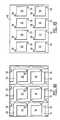
- FIG. 4Ais a plan view photograph of an array of suspended substrates according to embodiments of the invention.
- FIG. 4Bis a plan view photograph of an array of substrates that have been printed according to embodiments of the invention.
- FIG. 5is a flow diagram that illustrates fabrication methods according to some embodiments of the invention.
- FIGS. 6A-6Care cross-sectional views of intermediate structures that illustrate methods of forming substrates according to embodiments of the invention.
- FIGS. 7A-7Bare cross-sectional views of intermediate structures that illustrate methods of forming TFT transistors according to embodiments of the present invention.
- FIGS. 8A-8Bare cross-sectional views of intermediate structures that illustrate methods of forming TFT transistors according to embodiments of the present invention.
- FIGS. 9A-9Bare cross-sectional views of intermediate structures that illustrate methods of forming TFT transistors according to embodiments of the present invention.
- first, second, third etc.may be used herein to describe various elements, components, regions, layers and/or sections, these elements, components, regions, layers and/or sections should not be limited by these terms. These terms are only used to distinguish one element, component, region, layer or section from another region, layer or section. Thus, a first element, component, region, layer or section discussed below could be termed a second element, component, region, layer or section without departing from the teachings of the present invention.
- spatially relative termssuch as “beneath,” “below,” “lower,” “above,” “upper” and the like, may be used herein for ease of description to describe one element or feature's relationship to another element(s) or feature(s) as illustrated in the figures. It will be understood that the spatially relative terms are intended to encompass different orientations of the device in use or operation in addition to the orientation depicted in the figures. For example, if the device in the figures is turned over, elements described as “below” or “beneath” other elements or features would then be oriented “above” the other elements or features. Thus, the term “below” can encompass both an orientation of above and below. The device may be otherwise oriented (rotated 90 degrees or at other orientations) and the spatially relative descriptors used herein interpreted accordingly.
- Embodiments of the present inventionare described herein with reference to cross-section and perspective illustrations that are schematic illustrations of idealized embodiments (and intermediate structures) of the present invention. As such, variations from the shapes of the illustrations as a result, for example, of manufacturing techniques and/or tolerances, are to be expected. Thus, embodiments of the present invention should not be construed as limited to the particular shapes of regions illustrated herein but are to include deviations in shapes that result, for example, from manufacturing. For example, a sharp angle may be somewhat rounded due to manufacturing techniques/tolerances.
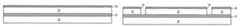
- FIG. 1Aillustrates forming an integrated circuit device by forming a sacrificial layer 12 on a handling substrate 10 (e.g., silicon wafer), forming a semiconductor active layer 14 on the sacrificial layer 12 and forming a field oxide layer 16 on the semiconductor active layer 14 .
- the semiconductor active layer 14may be a thinned silicon wafer that is bonded to the sacrificial layer 12 and the sacrificial layer may be an electrically insulating layer.
- FIGS. 1B-1Cillustrate selectively etching through the field oxide layer 16 , the semiconductor active layer 14 and the sacrificial layer 12 in sequence to define trenches 18 therein that expose the handling substrate 10 and define a plurality of semiconductor-on-insulator (SOI) substrates 20 containing respective portions of the semiconductor active layer 14 .
- SOIsemiconductor-on-insulator
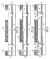
- FIG. 1D-1Eillustrate filling the trenches 18 with inorganic anchors 24 (e.g., semiconductor anchors) by depositing an inorganic layer 22 into the trenches 18 and onto the SOI substrates 20 and then planarizing the deposited inorganic layer 22 to define the anchors 24 , using the field oxide layer 16 as a etch/planarization stop.
- the inorganic layer 22may be a polysilicon layer that is conformally deposited by low-pressure chemical vapor deposition (LPCVD).
- FIGS. 1F-1Gillustrate forming a plurality of multi-layer electrical interconnect networks 26 on respective SOI substrates 20 , after active devices (e.g., CMOS devices, not shown) have been formed therein.
- Each of these multi-layer electrical interconnect networks 26may include multiple layers of metallization and vertical interconnects within a stacked composite of multiple interlayer insulating layers 28 .
- an interlayer dielectric layer (ILD) etching stepmay be performed to expose the anchors 24 , which may be ring-shaped or formed as parallel stripes that extend in a third dimension (see, e.g., FIG. 1K ), and also expose adjacent portions of the semiconductor active layer 14 .
- ILDinterlayer dielectric layer
- Plasmas that operate to etch siliconmay utilize fluorine-containing gases (e.g., sulfur hexafluoride, SF 6 ).
- siliconmay be removed from a surface of the active layer 14 by exposing the surface to a relatively inert gas containing argon ions, for example.
- the intermediate structure illustrated by FIG. 1Gmay be achieved by providing an SOI substrate having active electronic devices (not shown) within the semiconductor active layer 14 and a plurality of multi-layer electrical interconnect networks on the active layer 14 .
- the interlayer dielectric layers associated with the multi-layer electrically interconnect networksmay then be selectively etched to expose the active layer 14 and then the active layer 14 and the sacrificial layer 12 may be selectively etched using a mask (not shown) to define a plurality of trenches having bottoms that expose the handling substrate 10 .
- the trenchesmay then be filled with inorganic anchors prior to deposition of an inorganic capping layer.
- each of the plurality of multi-layer electrical interconnect networks 26is encapsulated by depositing an inorganic capping layer 32 that contacts the roughened upper surfaces of the semiconductor active layer 14 to thereby form chemically impervious and etch resistant bonds (e.g., a hermetic seal) at the interface between the capping layer 32 and the roughened surfaces of the semiconductor active layer 14 .
- the semiconductor capping layer 32may be formed as an amorphous silicon layer or a metal layer.
- an amorphous silicon capping layermay be deposited at a temperature of less than about 350° C. using a plasma-enhanced deposition technique.
- FIG. 1Iillustrates the formation of through-substrate openings 34 by selectively patterning of the capping layer 32 to define openings therein followed by the deep etching of the semiconductor active layer 14 to thereby expose underlying portions of the sacrificial layer 12 and define relatively thin supporting tethers 36 (see, e.g., FIG. 1K ).
- the sacrificial layer 12is selectively removed from between the semiconductor active layer 14 and the handling substrate 10 to thereby define a plurality of suspended integrated circuit chips 40 which are individually encapsulated by the patterned capping layer 32 .
- this removal stepwhich may include exposing the intermediate structure of FIG.
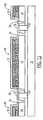
- FIG. 1Kis a plan view of an integrated circuit substrate of FIG. 1J (with capping layer 32 removed), which shows thin supporting tethers 36 extending between adjacent portions of the semiconductor active layer 14 . These supporting tethers 36 enable each of the integrated circuit chips 40 to remain attached to the anchors 24 .
- the patterned capping layer 32may also be removed or remain as a passivating/protective layer.
- methods of forming a plurality of functional layersinclude depositing a sacrificial layer on a substrate (step 1) and then patterning the sacrificial layer (step 2) into a plurality of sacrificial patterns.
- a functional layeris then deposited (step 3) onto the plurality of sacrificial patterns.
- the functional layeris then patterned (step 4) to define openings therein.
- the sacrificial patternsare then removed (step 5) from underneath respective functional patterns.
- the functional patternsare then transferred to another substrate (step 6) by printing, for example.
- FIGS. 3A-3Eare cross-sectional views of intermediate structures. These intermediate structures illustrate additional methods of forming substrates according to embodiments of the invention.
- FIG. 3Aillustrates forming a sacrificial layer 52 on a handling substrate 50 .
- the sacrificial layer 52may be formed of an electrically conductive material such as molybdenum (Mo), aluminum (Al), copper (Cu), nickel (Ni), chromium (Cr), tungsten (W), titanium tungsten (TiW), titanium (Ti) or an electrically insulating material such as silicon dioxide, for example.
- the handling substrate 50may be a semiconductor wafer, a glass substrate, or a ceramic board, for example.
- a stepmay be performed to increase a roughness of an upper surface of the sacrificial layer 52 by exposing the upper surface to a chemical etchant for a sufficient duration to increase an average RMS roughness of the surface, prior to cleaning.
- the sacrificial layer 52is selectively etched using a mask (not shown) to define a plurality of spaced-apart sacrificial patterns 52 ′ and expose portions of the underlying handling substrate 50 , as illustrated.
- a functional layer 54is formed directly on upper surfaces of the plurality of spaced-apart sacrificial patterns 52 ′ and directly on the exposed portions of the underlying handling substrate 50 .
- the functional layer 54may be formed as a semiconductor layer, such as a polysilicon layer, an amorphous silicon layer, a nanocrystalline silicon layer, or an indium gallium zinc oxide layer.
- the amorphous silicon layermay be formed using a plasma enhanced chemical vapor deposition (PECVD) technique.
- PECVDplasma enhanced chemical vapor deposition
- the polysilicon layer, amorphous silicon layer, nanocrystalline silicon layer or indium gallium zinc oxide layermay be formed using sputtering techniques.
- a patterned functional layer 54is defined by selectively etching the functional layer 54 of FIG. 3C using a mask (not shown), to define a plurality of openings 56 therein that expose respective portions of the underlying sacrificial patterns 52 ′.
- a selective etching stepis performed to remove the sacrificial patterns 52 ′ from underneath the patterned functional layer 54 and thereby define a plurality of underlying gaps or recesses 55 .
- This selective etching stepmay include exposing the sacrificial patterns 52 ′ to a chemical etchant that passes through the openings in the functional layer 54 and removes the sacrificial patterns 52 ′.
- the removal of the sacrificial patterns 52 ′may result in the formation of a plurality of suspended semiconductor device layers 54 that are attached by respective pairs of anchors 58 to a surrounding semiconductor layer. These anchors 58 are formed at diametrically opposite corners of the device layers 54 , which are spaced apart from each other by respective openings 56 .
- the semiconductor device layers 54may be printed at spaced-apart locations onto a second substrate 60 using a bonding technique. This printing step may also include fracturing the device layers 54 at the respective anchors 58 by removing the handling substrate 50 from the second substrate 60 , so that the device layers 54 are provided at spaced locations on the second substrate 60 .
- additional embodiments of the inventioninclude depositing a sacrificial layer onto a first substrate 60 (step 1) and then patterning the sacrificial layer to define a plurality of openings therein (step 2) that extend between respective sacrificial patterns 62 .
- a device layer 64e.g., amorphous semiconductor layer
- step 3Portions of the device layer 64 are then treated by thermal and/or laser treatment.
- the portions of the device layer 64 extending opposite the plurality of spaced-apart sacrificial patterns 62may be converted into respective semiconductor regions 65 having higher degrees of crystallinity therein relative to the surrounding amorphous silicon regions 64 ′.
- the treated device layer 64is then patterned (step 4) to define a plurality of openings 68 therein between amorphous silicon regions 64 ′ and higher crystallinity regions 65 ′. These openings 68 expose respective ones of the plurality of spaced-apart sacrificial patterns 62 .
- the sacrificial patterns 62are then selectively etched through the openings (step 5) to thereby convert at least a first portion of the patterned device layer (e.g., amorphous semiconductor layer) into a plurality of suspended semiconductor device layers 65 ′ that are anchored to a second portion of the patterned device layer 64 ′.
- a transfer printing stepmay be performed to transfer the semiconductor device layers (as functional layers 54 ) to a second substrate 60 .
- FIGS. 7A-7Billustrate methods of forming printable thin-film transistor (TFT) substrates according to additional embodiments of the invention.
- a sacrificial pattern 75is formed on a first substrate 70 .
- a source electrode 76 a and a drain electrode 76 bare formed on the sacrificial pattern 75 , as illustrated.
- a semiconductor layer 72e.g., a-Si
- an electrically insulating layer 74is formed on the semiconductor layer 72 and a gate electrode 76 c is formed on the electrically insulating layer 74 .
- the source, drain and gate electrodes 76 a - 76 ccollectively define the three terminals of a thin-film transistor having an active channel region defined within the semiconductor layer 72 .
- the insulating layer 74 and semiconductor layer 72are then selectively etched to define openings 78 therein.
- An etching step(e.g., wet etching) is then performed to remove the sacrificial patter 75 from underneath the source and drain electrodes 76 a - 76 b and the semiconductor layer 72 , as illustrated.
- a printing stepmay then be performed to print the gate electrode 76 c and insulating layer 74 directly onto a second substrate (not shown) prior to removal of the first substrate 70 . This printing step results in the formation of a thin-film transistor (TFT) having exposed source and drain electrodes 76 a - 76 b.
- TFTthin-film transistor
- FIGS. 8A-8Billustrate methods of forming printable thin-film transistor (TFT) substrates according to additional embodiments of the invention.
- a sacrificial pattern 85is formed on a first substrate 80 .
- a gate electrode 86 cis formed on the sacrificial pattern 85 , as illustrated.
- An electrically insulating layer 82is then formed on the gate electrode 86 c , the sacrificial pattern 85 and the substrate 80 , as illustrated.
- a semiconductor layer 84e.g., a-Si
- Source and drain electrodes 86 a - 86 bare formed on the semiconductor layer 84 .
- the source, drain and gate electrodes 86 a - 86 ccollectively define the three terminals of a thin-film transistor having an active channel region defined within the semiconductor layer 84 .
- the semiconductor layer 84 and insulating layer 82are then selectively etched to define openings 88 therein.
- An etching step(e.g., wet etching) is then performed to remove the sacrificial patter 85 from underneath the gate electrode 86 c and the insulating layer 82 , as illustrated.
- a printing stepmay then be performed to print the source and drain electrodes 86 a - 86 b and semiconductor layer 84 directly onto a second substrate (not shown) prior to removal of the first substrate 80 . This printing step results in the formation of a thin-film transistor (TFT) having an exposed gate electrode 86 c.
- TFTthin-film transistor
- FIGS. 9A-9Billustrate methods of forming printable thin-film transistor (TFT) substrates according to additional embodiments of the invention.
- a sacrificial pattern 95is formed on a first substrate 90 .
- a semiconductor layer 92e.g., a-Si
- an electrically insulating layer 94 having an embedded gate electrode 96 a thereinis formed on the semiconductor layer 92 .
- Source and drain electrodes 96 b - 96 care then formed on the insulating layer 94 .
- Source and drain electrodesuse source and drain electrode plugs 96 b ′ and 96 c ′, which extend through the electrically insulating layer 94 , to contact the semiconductor layer 92 , as illustrated.
- the insulating layer 94 and semiconductor layer 92are then selectively etched to define openings 98 therein.
- An etching step(e.g., wet etching) is then performed to remove the sacrificial patter 95 from underneath the semiconductor layer 92 , as illustrated.
- a printing stepmay then be performed to print the source and drain electrodes 96 b - 96 c and insulating layer 94 directly onto a second substrate (not shown) prior to removal of the first substrate 90 . This printing step results in the formation of a thin-film transistor (TFT) having buried source and drain electrodes 96 b - 96 c.
- TFTthin-film transistor
Landscapes
- Engineering & Computer Science (AREA)
- Physics & Mathematics (AREA)
- Microelectronics & Electronic Packaging (AREA)
- General Physics & Mathematics (AREA)
- Manufacturing & Machinery (AREA)
- Computer Hardware Design (AREA)
- Condensed Matter Physics & Semiconductors (AREA)
- Power Engineering (AREA)
- Plasma & Fusion (AREA)
- Thin Film Transistor (AREA)
- Chemical & Material Sciences (AREA)
- Crystallography & Structural Chemistry (AREA)
- Internal Circuitry In Semiconductor Integrated Circuit Devices (AREA)
- Metal-Oxide And Bipolar Metal-Oxide Semiconductor Integrated Circuits (AREA)
Abstract
Description
Claims (19)
Priority Applications (5)
| Application Number | Priority Date | Filing Date | Title |
|---|---|---|---|
| US15/243,228US9899432B2 (en) | 2009-03-26 | 2016-08-22 | Printable device wafers with sacrificial layers gaps |
| US15/864,813US10163945B2 (en) | 2009-03-26 | 2018-01-08 | Printable device wafers with sacrificial layers |
| US16/192,751US10522575B2 (en) | 2009-03-26 | 2018-11-15 | Methods of making printable device wafers with sacrificial layers |
| US16/697,104US10943931B2 (en) | 2009-03-26 | 2019-11-26 | Wafers with etchable sacrificial patterns, anchors, tethers, and printable devices |
| US17/167,945US11469259B2 (en) | 2009-03-26 | 2021-02-04 | Printable device wafers with sacrificial layers |
Applications Claiming Priority (5)
| Application Number | Priority Date | Filing Date | Title |
|---|---|---|---|
| US16353509P | 2009-03-26 | 2009-03-26 | |
| US12/732,868US8877648B2 (en) | 2009-03-26 | 2010-03-26 | Methods of forming printable integrated circuit devices by selective etching to suspend the devices from a handling substrate and devices formed thereby |
| US14/334,179US9040425B2 (en) | 2009-03-26 | 2014-07-17 | Methods of forming printable integrated circuit devices and devices formed thereby |
| US14/708,893US9443883B2 (en) | 2009-03-26 | 2015-05-11 | Methods of forming printable integrated circuit devices and devices formed thereby |
| US15/243,228US9899432B2 (en) | 2009-03-26 | 2016-08-22 | Printable device wafers with sacrificial layers gaps |
Related Parent Applications (1)
| Application Number | Title | Priority Date | Filing Date |
|---|---|---|---|
| US14/708,893ContinuationUS9443883B2 (en) | 2009-03-26 | 2015-05-11 | Methods of forming printable integrated circuit devices and devices formed thereby |
Related Child Applications (1)
| Application Number | Title | Priority Date | Filing Date |
|---|---|---|---|
| US15/864,813ContinuationUS10163945B2 (en) | 2009-03-26 | 2018-01-08 | Printable device wafers with sacrificial layers |
Publications (2)
| Publication Number | Publication Date |
|---|---|
| US20170133412A1 US20170133412A1 (en) | 2017-05-11 |
| US9899432B2true US9899432B2 (en) | 2018-02-20 |
Family
ID=42357254
Family Applications (8)
| Application Number | Title | Priority Date | Filing Date |
|---|---|---|---|
| US12/732,868Active2032-12-15US8877648B2 (en) | 2009-03-26 | 2010-03-26 | Methods of forming printable integrated circuit devices by selective etching to suspend the devices from a handling substrate and devices formed thereby |
| US14/334,179ActiveUS9040425B2 (en) | 2009-03-26 | 2014-07-17 | Methods of forming printable integrated circuit devices and devices formed thereby |
| US14/708,893ActiveUS9443883B2 (en) | 2009-03-26 | 2015-05-11 | Methods of forming printable integrated circuit devices and devices formed thereby |
| US15/243,228ActiveUS9899432B2 (en) | 2009-03-26 | 2016-08-22 | Printable device wafers with sacrificial layers gaps |
| US15/864,813ActiveUS10163945B2 (en) | 2009-03-26 | 2018-01-08 | Printable device wafers with sacrificial layers |
| US16/192,751ActiveUS10522575B2 (en) | 2009-03-26 | 2018-11-15 | Methods of making printable device wafers with sacrificial layers |
| US16/697,104ActiveUS10943931B2 (en) | 2009-03-26 | 2019-11-26 | Wafers with etchable sacrificial patterns, anchors, tethers, and printable devices |
| US17/167,945Active2030-07-30US11469259B2 (en) | 2009-03-26 | 2021-02-04 | Printable device wafers with sacrificial layers |
Family Applications Before (3)
| Application Number | Title | Priority Date | Filing Date |
|---|---|---|---|
| US12/732,868Active2032-12-15US8877648B2 (en) | 2009-03-26 | 2010-03-26 | Methods of forming printable integrated circuit devices by selective etching to suspend the devices from a handling substrate and devices formed thereby |
| US14/334,179ActiveUS9040425B2 (en) | 2009-03-26 | 2014-07-17 | Methods of forming printable integrated circuit devices and devices formed thereby |
| US14/708,893ActiveUS9443883B2 (en) | 2009-03-26 | 2015-05-11 | Methods of forming printable integrated circuit devices and devices formed thereby |
Family Applications After (4)
| Application Number | Title | Priority Date | Filing Date |
|---|---|---|---|
| US15/864,813ActiveUS10163945B2 (en) | 2009-03-26 | 2018-01-08 | Printable device wafers with sacrificial layers |
| US16/192,751ActiveUS10522575B2 (en) | 2009-03-26 | 2018-11-15 | Methods of making printable device wafers with sacrificial layers |
| US16/697,104ActiveUS10943931B2 (en) | 2009-03-26 | 2019-11-26 | Wafers with etchable sacrificial patterns, anchors, tethers, and printable devices |
| US17/167,945Active2030-07-30US11469259B2 (en) | 2009-03-26 | 2021-02-04 | Printable device wafers with sacrificial layers |
Country Status (2)
| Country | Link |
|---|---|
| US (8) | US8877648B2 (en) |
| WO (1) | WO2010111601A2 (en) |
Cited By (1)
| Publication number | Priority date | Publication date | Assignee | Title |
|---|---|---|---|---|
| US10522575B2 (en) | 2009-03-26 | 2019-12-31 | X-Celeprint Limited | Methods of making printable device wafers with sacrificial layers |
Families Citing this family (181)
| Publication number | Priority date | Publication date | Assignee | Title |
|---|---|---|---|---|
| US9161448B2 (en) | 2010-03-29 | 2015-10-13 | Semprius, Inc. | Laser assisted transfer welding process |
| EP2588789B1 (en) | 2010-07-01 | 2022-06-08 | EMD Millipore Corporation | Rigid disposable flow path |
| WO2012027458A1 (en) | 2010-08-26 | 2012-03-01 | Semprius, Inc. | Structures and methods for testing printable integrated circuits |
| US9899329B2 (en) | 2010-11-23 | 2018-02-20 | X-Celeprint Limited | Interconnection structures and methods for transfer-printed integrated circuit elements with improved interconnection alignment tolerance |
| US8889485B2 (en) | 2011-06-08 | 2014-11-18 | Semprius, Inc. | Methods for surface attachment of flipped active componenets |
| US9412727B2 (en) | 2011-09-20 | 2016-08-09 | Semprius, Inc. | Printing transferable components using microstructured elastomeric surfaces with pressure modulated reversible adhesion |
| US8333860B1 (en) | 2011-11-18 | 2012-12-18 | LuxVue Technology Corporation | Method of transferring a micro device |
| US8518204B2 (en) | 2011-11-18 | 2013-08-27 | LuxVue Technology Corporation | Method of fabricating and transferring a micro device and an array of micro devices utilizing an intermediate electrically conductive bonding layer |
| US8794501B2 (en) | 2011-11-18 | 2014-08-05 | LuxVue Technology Corporation | Method of transferring a light emitting diode |
| US8573469B2 (en) | 2011-11-18 | 2013-11-05 | LuxVue Technology Corporation | Method of forming a micro LED structure and array of micro LED structures with an electrically insulating layer |
| US8349116B1 (en) | 2011-11-18 | 2013-01-08 | LuxVue Technology Corporation | Micro device transfer head heater assembly and method of transferring a micro device |
| US9773750B2 (en) | 2012-02-09 | 2017-09-26 | Apple Inc. | Method of transferring and bonding an array of micro devices |
| US8456969B1 (en) | 2012-03-27 | 2013-06-04 | Seagate Technology Llc | Laser integrated recording head for heat assisted magnetic recording |
| US9548332B2 (en) | 2012-04-27 | 2017-01-17 | Apple Inc. | Method of forming a micro LED device with self-aligned metallization stack |
| US9105492B2 (en) | 2012-05-08 | 2015-08-11 | LuxVue Technology Corporation | Compliant micro device transfer head |
| US8415771B1 (en) | 2012-05-25 | 2013-04-09 | LuxVue Technology Corporation | Micro device transfer head with silicon electrode |
| US9034754B2 (en) | 2012-05-25 | 2015-05-19 | LuxVue Technology Corporation | Method of forming a micro device transfer head with silicon electrode |
| US8569115B1 (en) | 2012-07-06 | 2013-10-29 | LuxVue Technology Corporation | Method of forming a compliant bipolar micro device transfer head with silicon electrodes |
| US8415767B1 (en) | 2012-07-06 | 2013-04-09 | LuxVue Technology Corporation | Compliant bipolar micro device transfer head with silicon electrodes |
| US8383506B1 (en) | 2012-07-06 | 2013-02-26 | LuxVue Technology Corporation | Method of forming a compliant monopolar micro device transfer head with silicon electrode |
| US8415768B1 (en) | 2012-07-06 | 2013-04-09 | LuxVue Technology Corporation | Compliant monopolar micro device transfer head with silicon electrode |
| US8933433B2 (en) | 2012-07-30 | 2015-01-13 | LuxVue Technology Corporation | Method and structure for receiving a micro device |
| US8791530B2 (en) | 2012-09-06 | 2014-07-29 | LuxVue Technology Corporation | Compliant micro device transfer head with integrated electrode leads |
| US9162880B2 (en) | 2012-09-07 | 2015-10-20 | LuxVue Technology Corporation | Mass transfer tool |
| US8835940B2 (en) | 2012-09-24 | 2014-09-16 | LuxVue Technology Corporation | Micro device stabilization post |
| US8941215B2 (en) | 2012-09-24 | 2015-01-27 | LuxVue Technology Corporation | Micro device stabilization post |
| US9558721B2 (en) | 2012-10-15 | 2017-01-31 | Apple Inc. | Content-based adaptive refresh schemes for low-power displays |
| US9029880B2 (en) | 2012-12-10 | 2015-05-12 | LuxVue Technology Corporation | Active matrix display panel with ground tie lines |
| US9255001B2 (en) | 2012-12-10 | 2016-02-09 | LuxVue Technology Corporation | Micro device transfer head array with metal electrodes |
| US9159700B2 (en) | 2012-12-10 | 2015-10-13 | LuxVue Technology Corporation | Active matrix emissive micro LED display |
| US9236815B2 (en) | 2012-12-10 | 2016-01-12 | LuxVue Technology Corporation | Compliant micro device transfer head array with metal electrodes |
| US9178123B2 (en) | 2012-12-10 | 2015-11-03 | LuxVue Technology Corporation | Light emitting device reflective bank structure |
| US9105714B2 (en) | 2012-12-11 | 2015-08-11 | LuxVue Technology Corporation | Stabilization structure including sacrificial release layer and staging bollards |
| US9166114B2 (en) | 2012-12-11 | 2015-10-20 | LuxVue Technology Corporation | Stabilization structure including sacrificial release layer and staging cavity |
| US9391042B2 (en) | 2012-12-14 | 2016-07-12 | Apple Inc. | Micro device transfer system with pivot mount |
| US9314930B2 (en) | 2012-12-14 | 2016-04-19 | LuxVue Technology Corporation | Micro pick up array with integrated pivot mount |
| US9153171B2 (en) | 2012-12-17 | 2015-10-06 | LuxVue Technology Corporation | Smart pixel lighting and display microcontroller |
| US9308649B2 (en) | 2013-02-25 | 2016-04-12 | LuxVue Techonology Corporation | Mass transfer tool manipulator assembly |
| US9095980B2 (en) | 2013-02-25 | 2015-08-04 | LuxVue Technology Corporation | Micro pick up array mount with integrated displacement sensor |
| US9252375B2 (en) | 2013-03-15 | 2016-02-02 | LuxVue Technology Corporation | Method of fabricating a light emitting diode display with integrated defect detection test |
| US8791474B1 (en) | 2013-03-15 | 2014-07-29 | LuxVue Technology Corporation | Light emitting diode display with redundancy scheme |
| US9484504B2 (en) | 2013-05-14 | 2016-11-01 | Apple Inc. | Micro LED with wavelength conversion layer |
| US9136161B2 (en) | 2013-06-04 | 2015-09-15 | LuxVue Technology Corporation | Micro pick up array with compliant contact |
| EP3008553B1 (en) | 2013-06-12 | 2023-06-07 | Rohinni, Inc. | Keyboard backlighting with deposited light-generating sources |
| US8987765B2 (en) | 2013-06-17 | 2015-03-24 | LuxVue Technology Corporation | Reflective bank structure and method for integrating a light emitting device |
| US8928021B1 (en) | 2013-06-18 | 2015-01-06 | LuxVue Technology Corporation | LED light pipe |
| US9111464B2 (en) | 2013-06-18 | 2015-08-18 | LuxVue Technology Corporation | LED display with wavelength conversion layer |
| US9035279B2 (en) | 2013-07-08 | 2015-05-19 | LuxVue Technology Corporation | Micro device with stabilization post |
| US9296111B2 (en) | 2013-07-22 | 2016-03-29 | LuxVue Technology Corporation | Micro pick up array alignment encoder |
| US9087764B2 (en) | 2013-07-26 | 2015-07-21 | LuxVue Technology Corporation | Adhesive wafer bonding with controlled thickness variation |
| US9153548B2 (en) | 2013-09-16 | 2015-10-06 | Lux Vue Technology Corporation | Adhesive wafer bonding with sacrificial spacers for controlled thickness variation |
| US9367094B2 (en) | 2013-12-17 | 2016-06-14 | Apple Inc. | Display module and system applications |
| US9768345B2 (en) | 2013-12-20 | 2017-09-19 | Apple Inc. | LED with current injection confinement trench |
| US9583466B2 (en) | 2013-12-27 | 2017-02-28 | Apple Inc. | Etch removal of current distribution layer for LED current confinement |
| US9450147B2 (en) | 2013-12-27 | 2016-09-20 | Apple Inc. | LED with internally confined current injection area |
| US9542638B2 (en) | 2014-02-18 | 2017-01-10 | Apple Inc. | RFID tag and micro chip integration design |
| US9583533B2 (en) | 2014-03-13 | 2017-02-28 | Apple Inc. | LED device with embedded nanowire LEDs |
| US9522468B2 (en) | 2014-05-08 | 2016-12-20 | Apple Inc. | Mass transfer tool manipulator assembly with remote center of compliance |
| US9318475B2 (en) | 2014-05-15 | 2016-04-19 | LuxVue Technology Corporation | Flexible display and method of formation with sacrificial release layer |
| US9741286B2 (en) | 2014-06-03 | 2017-08-22 | Apple Inc. | Interactive display panel with emitting and sensing diodes |
| US9624100B2 (en) | 2014-06-12 | 2017-04-18 | Apple Inc. | Micro pick up array pivot mount with integrated strain sensing elements |
| US9425151B2 (en) | 2014-06-17 | 2016-08-23 | Apple Inc. | Compliant electrostatic transfer head with spring support layer |
| US9570002B2 (en) | 2014-06-17 | 2017-02-14 | Apple Inc. | Interactive display panel with IR diodes |
| US9444015B2 (en) | 2014-06-18 | 2016-09-13 | X-Celeprint Limited | Micro assembled LED displays and lighting elements |
| TWI697057B (en) | 2014-06-18 | 2020-06-21 | 愛爾蘭商艾克斯展示公司技術有限公司 | Systems and methods for controlling release of transferable semiconductor structures |
| WO2015193436A1 (en) | 2014-06-18 | 2015-12-23 | X-Celeprint Limited | Systems and methods for preparing gan and related materials for micro assembly |
| US9865600B2 (en) | 2014-06-18 | 2018-01-09 | X-Celeprint Limited | Printed capacitors |
| US9929053B2 (en) | 2014-06-18 | 2018-03-27 | X-Celeprint Limited | Systems and methods for controlling release of transferable semiconductor structures |
| US10050351B2 (en) | 2014-06-18 | 2018-08-14 | X-Celeprint Limited | Multilayer printed capacitors |
| US9358775B2 (en) | 2014-07-20 | 2016-06-07 | X-Celeprint Limited | Apparatus and methods for micro-transfer-printing |
| WO2016030422A1 (en) | 2014-08-26 | 2016-03-03 | X-Celeprint Limited | Micro assembled hybrid displays and lighting elements |
| US9468050B1 (en) | 2014-09-25 | 2016-10-11 | X-Celeprint Limited | Self-compensating circuit for faulty display pixels |
| US9991163B2 (en) | 2014-09-25 | 2018-06-05 | X-Celeprint Limited | Small-aperture-ratio display with electrical component |
| US9537069B1 (en) | 2014-09-25 | 2017-01-03 | X-Celeprint Limited | Inorganic light-emitting diode with encapsulating reflector |
| US20160093600A1 (en)* | 2014-09-25 | 2016-03-31 | X-Celeprint Limited | Compound micro-assembly strategies and devices |
| US9818725B2 (en) | 2015-06-01 | 2017-11-14 | X-Celeprint Limited | Inorganic-light-emitter display with integrated black matrix |
| US9799719B2 (en) | 2014-09-25 | 2017-10-24 | X-Celeprint Limited | Active-matrix touchscreen |
| US9799261B2 (en) | 2014-09-25 | 2017-10-24 | X-Celeprint Limited | Self-compensating circuit for faulty display pixels |
| US9705432B2 (en) | 2014-09-30 | 2017-07-11 | Apple Inc. | Micro pick up array pivot mount design for strain amplification |
| US9828244B2 (en) | 2014-09-30 | 2017-11-28 | Apple Inc. | Compliant electrostatic transfer head with defined cavity |
| US9478583B2 (en) | 2014-12-08 | 2016-10-25 | Apple Inc. | Wearable display having an array of LEDs on a conformable silicon substrate |
| CN107210294B (en) | 2015-01-30 | 2020-03-03 | 欧司朗光电半导体有限公司 | Method for producing a semiconductor component and semiconductor component |
| US9640715B2 (en) | 2015-05-15 | 2017-05-02 | X-Celeprint Limited | Printable inorganic semiconductor structures |
| US10102794B2 (en) | 2015-06-09 | 2018-10-16 | X-Celeprint Limited | Distributed charge-pump power-supply system |
| US9871345B2 (en) | 2015-06-09 | 2018-01-16 | X-Celeprint Limited | Crystalline color-conversion device |
| US10133426B2 (en) | 2015-06-18 | 2018-11-20 | X-Celeprint Limited | Display with micro-LED front light |
| US11061276B2 (en) | 2015-06-18 | 2021-07-13 | X Display Company Technology Limited | Laser array display |
| US9704821B2 (en) | 2015-08-11 | 2017-07-11 | X-Celeprint Limited | Stamp with structured posts |
| US10255834B2 (en) | 2015-07-23 | 2019-04-09 | X-Celeprint Limited | Parallel redundant chiplet system for controlling display pixels |
| US9640108B2 (en) | 2015-08-25 | 2017-05-02 | X-Celeprint Limited | Bit-plane pulse width modulated digital display system |
| US10468363B2 (en) | 2015-08-10 | 2019-11-05 | X-Celeprint Limited | Chiplets with connection posts |
| US10380930B2 (en) | 2015-08-24 | 2019-08-13 | X-Celeprint Limited | Heterogeneous light emitter display system |
| US10230048B2 (en) | 2015-09-29 | 2019-03-12 | X-Celeprint Limited | OLEDs for micro transfer printing |
| US10066819B2 (en) | 2015-12-09 | 2018-09-04 | X-Celeprint Limited | Micro-light-emitting diode backlight system |
| CN108700542A (en)* | 2015-12-14 | 2018-10-23 | 瓦伦汀·杜布瓦 | Crack structure, tunnel junction using crack structure, and method of making same |
| US9930277B2 (en) | 2015-12-23 | 2018-03-27 | X-Celeprint Limited | Serial row-select matrix-addressed system |
| US10091446B2 (en) | 2015-12-23 | 2018-10-02 | X-Celeprint Limited | Active-matrix displays with common pixel control |
| US9786646B2 (en) | 2015-12-23 | 2017-10-10 | X-Celeprint Limited | Matrix addressed device repair |
| US9928771B2 (en) | 2015-12-24 | 2018-03-27 | X-Celeprint Limited | Distributed pulse width modulation control |
| JP6959697B2 (en) | 2016-01-15 | 2021-11-05 | ロヒンニ リミテッド ライアビリティ カンパニー | Devices and methods that are backlit through a cover on the device |
| US10200013B2 (en) | 2016-02-18 | 2019-02-05 | X-Celeprint Limited | Micro-transfer-printed acoustic wave filter device |
| US10361677B2 (en) | 2016-02-18 | 2019-07-23 | X-Celeprint Limited | Transverse bulk acoustic wave filter |
| US10109753B2 (en) | 2016-02-19 | 2018-10-23 | X-Celeprint Limited | Compound micro-transfer-printed optical filter device |
| TWI710061B (en) | 2016-02-25 | 2020-11-11 | 愛爾蘭商艾克斯展示公司技術有限公司 | Efficiently micro-transfer printing micro-scale devices onto large-format substrates |
| US10150325B2 (en) | 2016-02-29 | 2018-12-11 | X-Celeprint Limited | Hybrid banknote with electronic indicia |
| US10193025B2 (en) | 2016-02-29 | 2019-01-29 | X-Celeprint Limited | Inorganic LED pixel structure |
| US10150326B2 (en) | 2016-02-29 | 2018-12-11 | X-Celeprint Limited | Hybrid document with variable state |
| US10153256B2 (en) | 2016-03-03 | 2018-12-11 | X-Celeprint Limited | Micro-transfer printable electronic component |
| US10153257B2 (en) | 2016-03-03 | 2018-12-11 | X-Celeprint Limited | Micro-printed display |
| US10103069B2 (en) | 2016-04-01 | 2018-10-16 | X-Celeprint Limited | Pressure-activated electrical interconnection by micro-transfer printing |
| US10199546B2 (en) | 2016-04-05 | 2019-02-05 | X-Celeprint Limited | Color-filter device |
| US10008483B2 (en) | 2016-04-05 | 2018-06-26 | X-Celeprint Limited | Micro-transfer printed LED and color filter structure |
| US9997102B2 (en) | 2016-04-19 | 2018-06-12 | X-Celeprint Limited | Wirelessly powered display and system |
| US10198890B2 (en) | 2016-04-19 | 2019-02-05 | X-Celeprint Limited | Hybrid banknote with electronic indicia using near-field-communications |
| US10360846B2 (en) | 2016-05-10 | 2019-07-23 | X-Celeprint Limited | Distributed pulse-width modulation system with multi-bit digital storage and output device |
| US10622700B2 (en) | 2016-05-18 | 2020-04-14 | X-Celeprint Limited | Antenna with micro-transfer-printed circuit element |
| US9997501B2 (en) | 2016-06-01 | 2018-06-12 | X-Celeprint Limited | Micro-transfer-printed light-emitting diode device |
| US10453826B2 (en) | 2016-06-03 | 2019-10-22 | X-Celeprint Limited | Voltage-balanced serial iLED pixel and display |
| US11137641B2 (en) | 2016-06-10 | 2021-10-05 | X Display Company Technology Limited | LED structure with polarized light emission |
| US10222698B2 (en) | 2016-07-28 | 2019-03-05 | X-Celeprint Limited | Chiplets with wicking posts |
| US11064609B2 (en) | 2016-08-04 | 2021-07-13 | X Display Company Technology Limited | Printable 3D electronic structure |
| US9980341B2 (en) | 2016-09-22 | 2018-05-22 | X-Celeprint Limited | Multi-LED components |
| US10157880B2 (en) | 2016-10-03 | 2018-12-18 | X-Celeprint Limited | Micro-transfer printing with volatile adhesive layer |
| US10782002B2 (en) | 2016-10-28 | 2020-09-22 | X Display Company Technology Limited | LED optical components |
| US10347168B2 (en) | 2016-11-10 | 2019-07-09 | X-Celeprint Limited | Spatially dithered high-resolution |
| US10395966B2 (en) | 2016-11-15 | 2019-08-27 | X-Celeprint Limited | Micro-transfer-printable flip-chip structures and methods |
| EP3542394B1 (en) | 2016-11-15 | 2025-09-24 | X Display Company Technology Limited | Micro-transfer-printable flip-chip structures and manufacturing methods thereof |
| US10600671B2 (en) | 2016-11-15 | 2020-03-24 | X-Celeprint Limited | Micro-transfer-printable flip-chip structures and methods |
| US10297502B2 (en) | 2016-12-19 | 2019-05-21 | X-Celeprint Limited | Isolation structure for micro-transfer-printable devices |
| US10438859B2 (en) | 2016-12-19 | 2019-10-08 | X-Celeprint Limited | Transfer printed device repair |
| US10832609B2 (en) | 2017-01-10 | 2020-11-10 | X Display Company Technology Limited | Digital-drive pulse-width-modulated output system |
| US10332868B2 (en) | 2017-01-26 | 2019-06-25 | X-Celeprint Limited | Stacked pixel structures |
| US10468391B2 (en) | 2017-02-08 | 2019-11-05 | X-Celeprint Limited | Inorganic light-emitting-diode displays with multi-ILED pixels |
| US10396137B2 (en) | 2017-03-10 | 2019-08-27 | X-Celeprint Limited | Testing transfer-print micro-devices on wafer |
| US11024608B2 (en) | 2017-03-28 | 2021-06-01 | X Display Company Technology Limited | Structures and methods for electrical connection of micro-devices and substrates |
| US10468397B2 (en) | 2017-05-05 | 2019-11-05 | X-Celeprint Limited | Matrix addressed tiles and arrays |
| US10804880B2 (en) | 2018-12-03 | 2020-10-13 | X-Celeprint Limited | Device structures with acoustic wave transducers and connection posts |
| US10943946B2 (en) | 2017-07-21 | 2021-03-09 | X Display Company Technology Limited | iLED displays with substrate holes |
| US10832935B2 (en) | 2017-08-14 | 2020-11-10 | X Display Company Technology Limited | Multi-level micro-device tethers |
| US10836200B2 (en) | 2017-11-13 | 2020-11-17 | X Display Company Technology Limited | Rigid micro-modules with ILED and light conductor |
| US10297585B1 (en) | 2017-12-21 | 2019-05-21 | X-Celeprint Limited | Multi-resolution compound micro-devices |
| GB201801457D0 (en) | 2018-01-30 | 2018-03-14 | Pragmatic Printing Ltd | Integrated circuit manufacturing process and apparatus |
| US10505079B2 (en) | 2018-05-09 | 2019-12-10 | X-Celeprint Limited | Flexible devices and methods using laser lift-off |
| US10832934B2 (en) | 2018-06-14 | 2020-11-10 | X Display Company Technology Limited | Multi-layer tethers for micro-transfer printing |
| US10714001B2 (en) | 2018-07-11 | 2020-07-14 | X Display Company Technology Limited | Micro-light-emitting-diode displays |
| CN110797372A (en)* | 2018-08-01 | 2020-02-14 | 创王光电股份有限公司 | flexible display |
| US10796971B2 (en) | 2018-08-13 | 2020-10-06 | X Display Company Technology Limited | Pressure-activated electrical interconnection with additive repair |
| US20200083280A1 (en) | 2018-09-11 | 2020-03-12 | Prilit Optronics, Inc. | Top emission microled display and bottom emission microled display and a method of forming the same |
| US10796938B2 (en) | 2018-10-17 | 2020-10-06 | X Display Company Technology Limited | Micro-transfer printing with selective component removal |
| US10573544B1 (en) | 2018-10-17 | 2020-02-25 | X-Celeprint Limited | Micro-transfer printing with selective component removal |
| US11528808B2 (en) | 2018-12-03 | 2022-12-13 | X Display Company Technology Limited | Printing components to substrate posts |
| US12162747B2 (en) | 2018-12-03 | 2024-12-10 | X-Celeprint Limited | Enclosed cavity structures |
| US10790173B2 (en) | 2018-12-03 | 2020-09-29 | X Display Company Technology Limited | Printed components on substrate posts |
| US11274035B2 (en) | 2019-04-24 | 2022-03-15 | X-Celeprint Limited | Overhanging device structures and related methods of manufacture |
| US11482979B2 (en) | 2018-12-03 | 2022-10-25 | X Display Company Technology Limited | Printing components over substrate post edges |
| US11282786B2 (en) | 2018-12-12 | 2022-03-22 | X Display Company Technology Limited | Laser-formed interconnects for redundant devices |
| US11483937B2 (en) | 2018-12-28 | 2022-10-25 | X Display Company Technology Limited | Methods of making printed structures |
| US11322460B2 (en) | 2019-01-22 | 2022-05-03 | X-Celeprint Limited | Secure integrated-circuit systems |
| US11251139B2 (en) | 2019-01-22 | 2022-02-15 | X-Celeprint Limited | Secure integrated-circuit systems |
| US11088121B2 (en) | 2019-02-13 | 2021-08-10 | X Display Company Technology Limited | Printed LED arrays with large-scale uniformity |
| US10748793B1 (en) | 2019-02-13 | 2020-08-18 | X Display Company Technology Limited | Printing component arrays with different orientations |
| US11094870B2 (en) | 2019-03-12 | 2021-08-17 | X Display Company Technology Limited | Surface-mountable pixel packages and pixel engines |
| US11164934B2 (en) | 2019-03-12 | 2021-11-02 | X Display Company Technology Limited | Tiled displays with black-matrix support screens |
| US10714374B1 (en) | 2019-05-09 | 2020-07-14 | X Display Company Technology Limited | High-precision printed structures |
| US11488943B2 (en) | 2019-06-14 | 2022-11-01 | X Display Company Technology Limited | Modules with integrated circuits and devices |
| US10944027B2 (en) | 2019-06-14 | 2021-03-09 | X Display Company Technology Limited | Pixel modules with controllers and light emitters |
| US11101417B2 (en) | 2019-08-06 | 2021-08-24 | X Display Company Technology Limited | Structures and methods for electrically connecting printed components |
| US11626856B2 (en) | 2019-10-30 | 2023-04-11 | X-Celeprint Limited | Non-linear tethers for suspended devices |
| US11127889B2 (en) | 2019-10-30 | 2021-09-21 | X Display Company Technology Limited | Displays with unpatterned layers of light-absorbing material |
| US11637540B2 (en) | 2019-10-30 | 2023-04-25 | X-Celeprint Limited | Non-linear tethers for suspended devices |
| US11062936B1 (en) | 2019-12-19 | 2021-07-13 | X Display Company Technology Limited | Transfer stamps with multiple separate pedestals |
| US11315909B2 (en) | 2019-12-20 | 2022-04-26 | X Display Company Technology Limited | Displays with embedded light emitters |
| US11037912B1 (en) | 2020-01-31 | 2021-06-15 | X Display Company Technology Limited | LED color displays with multiple LEDs connected in series and parallel in different sub-pixels of a pixel |
| US11088007B1 (en) | 2020-05-07 | 2021-08-10 | X-Celeprint Limited | Component tethers with spacers |
| US11538849B2 (en) | 2020-05-28 | 2022-12-27 | X Display Company Technology Limited | Multi-LED structures with reduced circuitry |
| US12009347B1 (en) | 2020-07-13 | 2024-06-11 | Apple Inc. | Nano-tether micro LED structure |
| US12006205B2 (en) | 2020-10-08 | 2024-06-11 | X-Celeprint Limited | Micro-device structures with etch holes |
| US11952266B2 (en) | 2020-10-08 | 2024-04-09 | X-Celeprint Limited | Micro-device structures with etch holes |
| US12057340B2 (en) | 2020-12-04 | 2024-08-06 | X-Celeprint Limited | Hybrid tethers for micro-transfer printing |
| CN115117211B (en) | 2021-03-18 | 2025-07-01 | 隆达电子股份有限公司 | Semiconductor chip and light emitting device |
| US12074583B2 (en) | 2021-05-11 | 2024-08-27 | X Display Company Technology Limited | Printing components to adhesive substrate posts |
Citations (108)
| Publication number | Priority date | Publication date | Assignee | Title |
|---|---|---|---|---|
| US5216490A (en)* | 1988-01-13 | 1993-06-01 | Charles Stark Draper Laboratory, Inc. | Bridge electrodes for microelectromechanical devices |
| US5258325A (en)* | 1990-12-31 | 1993-11-02 | Kopin Corporation | Method for manufacturing a semiconductor device using a circuit transfer film |
| US5317236A (en)* | 1990-12-31 | 1994-05-31 | Kopin Corporation | Single crystal silicon arrayed devices for display panels |
| US5343064A (en)* | 1988-03-18 | 1994-08-30 | Spangler Leland J | Fully integrated single-crystal silicon-on-insulator process, sensors and circuits |
| US5798283A (en)* | 1995-09-06 | 1998-08-25 | Sandia Corporation | Method for integrating microelectromechanical devices with electronic circuitry |
| US5827751A (en)* | 1991-12-06 | 1998-10-27 | Picogiga Societe Anonyme | Method of making semiconductor components, in particular on GaAs of InP, with the substrate being recovered chemically |
| US5963788A (en)* | 1995-09-06 | 1999-10-05 | Sandia Corporation | Method for integrating microelectromechanical devices with electronic circuitry |
| US5990542A (en)* | 1995-12-14 | 1999-11-23 | Semiconductor Energy Laboratory Co., Ltd. | Semiconductor device |
| US6021675A (en)* | 1995-06-07 | 2000-02-08 | Ssi Technologies, Inc. | Resonating structure and method for forming the resonating structure |
| US6044705A (en)* | 1993-10-18 | 2000-04-04 | Xros, Inc. | Micromachined members coupled for relative rotation by torsion bars |
| US6142358A (en) | 1997-05-31 | 2000-11-07 | The Regents Of The University Of California | Wafer-to-wafer transfer of microstructures using break-away tethers |
| US20010015256A1 (en)* | 2000-01-17 | 2001-08-23 | Shunpei Yamazaki | Display device and method of manufacturing the same |
| US20020004300A1 (en)* | 1999-08-09 | 2002-01-10 | Marina V. Plat | Ultra-thin resist coating qualityby by increasing surface roughness of the substrate |
| US20020117728A1 (en)* | 2000-08-03 | 2002-08-29 | Brosnihhan Timothy J. | Bonded wafer optical MEMS process |
| US6458615B1 (en)* | 1999-09-30 | 2002-10-01 | Carnegie Mellon University | Method of fabricating micromachined structures and devices formed therefrom |
| US6465280B1 (en)* | 2001-03-07 | 2002-10-15 | Analog Devices, Inc. | In-situ cap and method of fabricating same for an integrated circuit device |
| US6569702B2 (en)* | 2000-07-03 | 2003-05-27 | Chromux Technologies, Inc. | Triple layer isolation for silicon microstructure and structures formed using the same |
| US20030117369A1 (en)* | 1992-03-13 | 2003-06-26 | Kopin Corporation | Head-mounted display system |
| US20030148550A1 (en)* | 2001-11-07 | 2003-08-07 | International Business Machines Corporation | Method of fabricating micro-electromechanical switches on cmos compatible substrates |
| US20030153116A1 (en)* | 2000-05-30 | 2003-08-14 | Carley L. Richard | Encapsulation of MEMS devices using pillar-supported caps |
| US20040048410A1 (en)* | 2002-09-09 | 2004-03-11 | Motorola Inc. | SOI polysilicon trench refill perimeter oxide anchor scheme |
| US20040121506A1 (en)* | 2002-12-23 | 2004-06-24 | Motorola Inc. | Release etch method for micromachined sensors |
| US20040166688A1 (en)* | 2003-02-26 | 2004-08-26 | Huikai Xie | Method of fabricating microstructures and devices made therefrom |
| US6787051B2 (en)* | 1997-07-15 | 2004-09-07 | Silverbrook Research Pty Ltd | Method of manufacturing a micro-electromechanical fluid ejecting device |
| US20040188785A1 (en)* | 2001-11-09 | 2004-09-30 | Cunningham Shawn Jay | Trilayered beam MEMS device and related methods |
| US20040200281A1 (en)* | 2003-04-11 | 2004-10-14 | Kenny Thomas W. | Ultra-miniature accelerometers |
| US20040248344A1 (en)* | 2003-06-04 | 2004-12-09 | Aaron Partridge | Microelectromechanical systems, and methods for encapsualting and fabricating same |
| US20040256618A1 (en)* | 2003-02-28 | 2004-12-23 | Keitaro Imai | Semiconductor device and method of manufacturing the same |
| US20050048687A1 (en)* | 2002-07-18 | 2005-03-03 | Svetlana Tatic-Lucic | Recessed electrode for electrostatically actuated structures |
| US20050067633A1 (en)* | 2003-09-29 | 2005-03-31 | Matsushita Electric Industrial Co., Ltd. | Microelectromechanical system and method for fabricating the same |
| US20050148121A1 (en)* | 2003-12-19 | 2005-07-07 | Shunpei Yamazaki | Manufacturing method of thin film integrated circuit device and manufacturing method of non-contact type thin film integrated circuit device |
| US6930366B2 (en)* | 2001-10-01 | 2005-08-16 | Valtion Teknillinen Tutkimuskeskus | Method for forming a cavity structure on SOI substrate and cavity structure formed on SOI substrate |
| US6930367B2 (en)* | 2003-10-31 | 2005-08-16 | Robert Bosch Gmbh | Anti-stiction technique for thin film and wafer-bonded encapsulated microelectromechanical systems |
| US20050196933A1 (en)* | 2004-03-02 | 2005-09-08 | Nunan Thomas K. | Single crystal silicon sensor with additional layer and method of producing the same |
| US6952041B2 (en)* | 2003-07-25 | 2005-10-04 | Robert Bosch Gmbh | Anchors for microelectromechanical systems having an SOI substrate, and method of fabricating same |
| US6960488B2 (en)* | 1997-06-13 | 2005-11-01 | The Regents Of The University Of California | Method of fabricating a microfabricated high aspect ratio device with electrical isolation |
| US6964894B2 (en)* | 2003-06-23 | 2005-11-15 | Analog Devices, Inc. | Apparatus and method of forming a device layer |
| US20060003482A1 (en)* | 2004-06-30 | 2006-01-05 | International Business Machines Corporation | Elastomeric cmos based micro electromechanical varactor |
| US20060063309A1 (en)* | 2004-09-21 | 2006-03-23 | Eiji Sugiyama | Method for manufacturing semiconductor device |
| US7045381B1 (en)* | 2002-06-28 | 2006-05-16 | Silicon Light Machines Corporation | Conductive etch stop for etching a sacrificial layer |
| US7049164B2 (en)* | 2001-09-13 | 2006-05-23 | Silicon Light Machines Corporation | Microelectronic mechanical system and methods |
| US20060121694A1 (en)* | 2004-12-03 | 2006-06-08 | Semiconductor Energy Laboratory Co., Ltd. | Manufacturing method of semiconductor device |
| US7067067B2 (en)* | 1997-07-15 | 2006-06-27 | Silverbrook Research Pty Ltd | Method of fabricating an ink jet printhead chip with active and passive nozzle chamber structures |
| US7071109B2 (en)* | 2003-03-22 | 2006-07-04 | Active Optical Networks, Inc. | Methods for fabricating spatial light modulators with hidden comb actuators |
| US7098065B2 (en)* | 2004-09-28 | 2006-08-29 | Stmicroelectronics, Inc. | Integrated lid formed on MEMS device |
| US20060205106A1 (en)* | 2005-02-25 | 2006-09-14 | Hiroshi Fukuda | Integrated micro electro-mechanical system and manufacturing method thereof |
| US7115436B2 (en)* | 2004-02-12 | 2006-10-03 | Robert Bosch Gmbh | Integrated getter area for wafer level encapsulated microelectromechanical systems |
| US20060246631A1 (en)* | 2005-04-27 | 2006-11-02 | Markus Lutz | Anti-stiction technique for electromechanical systems and electromechanical device employing same |
| US20060270191A1 (en)* | 2005-05-31 | 2006-11-30 | Semiconductor Energy Laboratory Co., Ltd. | Manufacturing method of semiconductor device |
| WO2006130721A2 (en) | 2005-06-02 | 2006-12-07 | The Board Of Trustees Of The University Of Illinois | Printable semiconductor structures and related methods of making and assembling |
| US20070026636A1 (en)* | 2005-07-27 | 2007-02-01 | Gogoi Bishnu P | Wide and narrow trench formation in high aspect ratio MEMS |
| US20070032089A1 (en) | 2004-06-04 | 2007-02-08 | The Board Of Trustees Of The University Of Illinois | Printable Semiconductor Structures and Related Methods of Making and Assembling |
| US7195733B2 (en) | 2004-04-27 | 2007-03-27 | The Board Of Trustees Of The University Of Illinois | Composite patterning devices for soft lithography |
| US20070090474A1 (en)* | 2005-09-08 | 2007-04-26 | Li Gary G | MEMS device and method of fabrication |
| US7241638B2 (en)* | 2001-08-30 | 2007-07-10 | Kabushiki Kaisha Toshiba | Micromechanical device and method of manufacture thereof |
| US20070161159A1 (en)* | 2004-02-06 | 2007-07-12 | Semiconductor Energy Laboratory Co., Ltd. | Method for manufacturing thin film integrated circuit, and element substrate |
| US20070172976A1 (en)* | 2006-01-20 | 2007-07-26 | Aaron Partridge | Wafer encapsulated microelectromechanical structure and method of manufacturing same |
| US7250322B2 (en)* | 2005-03-16 | 2007-07-31 | Delphi Technologies, Inc. | Method of making microsensor |
| US20070181875A1 (en)* | 2006-02-08 | 2007-08-09 | Semiconductor Energy Laboratory Co., Ltd. | Semiconductor device |
| US20070212875A1 (en)* | 2004-06-24 | 2007-09-13 | Semiconductor Energy Laboratory Co., Ltd. | Method for manufacturing thin film integrated circuit |
| US7273762B2 (en)* | 2004-11-09 | 2007-09-25 | Freescale Semiconductor, Inc. | Microelectromechanical (MEM) device including a spring release bridge and method of making the same |
| US20070224832A1 (en)* | 2006-03-21 | 2007-09-27 | Peter Zurcher | Method for forming and sealing a cavity for an integrated MEMS device |
| US20070272992A1 (en)* | 2006-03-29 | 2007-11-29 | Mitsuyoshi Mori | Method for fabricating condenser microphone and condenser microphone |
| US20070281381A1 (en)* | 2006-05-31 | 2007-12-06 | Georgia Tech Research Corporation | Method for sealing and backside releasing of microelectromechanical systems |
| US20080012126A1 (en)* | 2006-06-26 | 2008-01-17 | Yoshitaka Dozen | Paper including semiconductor device and manufacturing method thereof |
| US7361519B2 (en)* | 1995-02-16 | 2008-04-22 | Semiconductor Energy Laboratory Co., Ltd. | Method of manufacturing a semiconductor device |
| US7364954B2 (en)* | 2005-04-28 | 2008-04-29 | Semiconductor Energy Laboratory Co., Ltd. | Method for manufacturing semiconductor device |
| US20080108171A1 (en) | 2006-09-20 | 2008-05-08 | Rogers John A | Release strategies for making transferable semiconductor structures, devices and device components |
| US7452786B2 (en)* | 2004-06-29 | 2008-11-18 | Semiconductor Energy Laboratory Co., Ltd. | Method for manufacturing thin film integrated circuit, and element substrate |
| US7462038B2 (en)* | 2007-02-20 | 2008-12-09 | Qimonda Ag | Interconnection structure and method of manufacturing the same |
| US7514760B1 (en)* | 2007-03-09 | 2009-04-07 | Silicon Clocks, Inc. | IC-compatible MEMS structure |
| US7521292B2 (en) | 2004-06-04 | 2009-04-21 | The Board Of Trustees Of The University Of Illinois | Stretchable form of single crystal silicon for high performance electronics on rubber substrates |
| US20090108381A1 (en)* | 2001-12-10 | 2009-04-30 | International Business Machines Corporation | Low temperature bi-CMOS compatible process for MEMS RF resonators and filters |
| US7541214B2 (en)* | 1999-12-15 | 2009-06-02 | Chang-Feng Wan | Micro-electro mechanical device made from mono-crystalline silicon and method of manufacture therefore |
| US7557367B2 (en) | 2004-06-04 | 2009-07-07 | The Board Of Trustees Of The University Of Illinois | Stretchable semiconductor elements and stretchable electrical circuits |
| US7566640B2 (en)* | 2003-12-15 | 2009-07-28 | Semiconductor Energy Laboratory Co., Ltd. | Method for manufacturing thin film integrated circuit device, noncontact thin film integrated circuit device and method for manufacturing the same, and idtag and coin including the noncontact thin film integrated circuit device |
| US20090199960A1 (en) | 2004-06-04 | 2009-08-13 | Nuzzo Ralph G | Pattern Transfer Printing by Kinetic Control of Adhesion to an Elastomeric Stamp |
| US7588969B2 (en)* | 2005-05-31 | 2009-09-15 | Semiconductor Energy Laboratory Co., Ltd. | Method for manufacturing semiconductor device, and semiconductor device |
| US7611965B2 (en)* | 2005-08-31 | 2009-11-03 | Semiconductor Energy Laboratory Co., Ltd. | Semiconductor device and manufacturing method thereof |
| US20090275163A1 (en)* | 2008-04-30 | 2009-11-05 | Joseph Damian Gordon Lacey | System and Method of Encapsulation |
| US20090317931A1 (en)* | 2008-06-23 | 2009-12-24 | Commissariat A L'energie Atomique | Method of fabricating an electromechanical device including at least one active element |
| US20090325335A1 (en)* | 2008-06-23 | 2009-12-31 | Commissariat A L'energie Atomique | Heterogeneous substrate including a sacrificial layer, and a method of fabricating it |
| US7645627B2 (en)* | 2008-01-24 | 2010-01-12 | Delphi Technologies, Inc. | Method for manufacturing a sensor device |
| US7651932B2 (en)* | 2005-05-31 | 2010-01-26 | Semiconductor Energy Laboratory Co., Ltd. | Method for manufacturing antenna and method for manufacturing semiconductor device |
| US7659150B1 (en)* | 2007-03-09 | 2010-02-09 | Silicon Clocks, Inc. | Microshells for multi-level vacuum cavities |
| US7663447B2 (en)* | 2006-10-31 | 2010-02-16 | Semiconductor Energy Laboratory Co., Ltd. | Oscillator circuit having a stable output signal resistant to power supply voltage fluctuation |
| US20100072561A1 (en)* | 2008-09-22 | 2010-03-25 | Solid State System Co., Ltd. | Method for fabricating micro-electro-mechanical system (mems) device |
| US7685706B2 (en)* | 2005-07-08 | 2010-03-30 | Semiconductor Energy Laboratory Co., Ltd | Method of manufacturing a semiconductor device |
| US20100090302A1 (en)* | 2006-10-09 | 2010-04-15 | Nxp, B.V. | Resonator |
| US7728332B2 (en)* | 2004-09-24 | 2010-06-01 | Semiconductor Energy Laboratory Co., Ltd | Method for manufacturing semiconductor device, and semiconductor device and electronic device |
| US7759256B2 (en)* | 2007-10-17 | 2010-07-20 | Pixart Imaging Incorporation | Micro-electro-mechanical system device and method for making same |
| US20100213607A1 (en)* | 2009-02-20 | 2010-08-26 | National Semiconductor Corporation | Integrated circuit micro-module |
| US7785912B2 (en)* | 2002-04-23 | 2010-08-31 | Sharp Laboratories Of America, Inc. | Piezo-TFT cantilever MEMS fabrication |
| US7820529B2 (en)* | 2004-03-22 | 2010-10-26 | Semiconductor Energy Laboratory Co., Ltd. | Method for manufacturing integrated circuit |
| US20100276783A1 (en)* | 2009-04-30 | 2010-11-04 | Texas Instruments Inc | Selective plasma etch of top electrodes for metal-insulator-metal (mim) capacitors |
| US20100314668A1 (en)* | 2007-12-04 | 2010-12-16 | COMMISSARIAT a L' ENERGIE ATOMIQUE ET AUX ENG ALT. | Device with integrated circuit and encapsulated n/mems and method for production |
| US7858423B2 (en)* | 2008-06-02 | 2010-12-28 | Fouladi Azarnaminy Siamak | MEMS based RF components with vertical motion and parallel-plate structure and manufacture thereof using standard CMOS technologies |
| US7863071B1 (en)* | 2007-08-21 | 2011-01-04 | Rf Micro Devices, Inc. | Combined micro-electro-mechanical systems device and integrated circuit on a silicon-on-insulator wafer |
| US7868360B2 (en)* | 1997-06-10 | 2011-01-11 | Semiconductor Energy Laboratory Co., Ltd. | Semiconductor device with heat-resistant gate |
| US7879629B2 (en)* | 2006-12-06 | 2011-02-01 | Electronics And Telecommunications Research Institute | Method for manufacturing floating structure of microelectromechanical system |
| US7906439B2 (en)* | 2008-06-23 | 2011-03-15 | Commissarit A L'energie Atomique | Method of fabricating a MEMS/NEMS electromechanical component |
| US7927971B2 (en)* | 2004-07-30 | 2011-04-19 | Semiconductor Energy Laboratory Co., Ltd. | Method for manufacturing semiconductor device |
| US8110442B2 (en)* | 2006-06-30 | 2012-02-07 | Semiconductor Energy Laboratory Co., Ltd. | Method of manufacturing semiconductor device |
| US8173471B2 (en)* | 2008-04-29 | 2012-05-08 | Solid State System Co., Ltd. | Method for fabricating micro-electro-mechanical system (MEMS) device |
| US8288835B2 (en)* | 2007-03-09 | 2012-10-16 | Silicon Laboratories Inc. | Microshells with integrated getter layer |
| US8506867B2 (en) | 2008-11-19 | 2013-08-13 | Semprius, Inc. | Printing semiconductor elements by shear-assisted elastomeric stamp transfer |
| US20150169011A1 (en) | 2013-12-17 | 2015-06-18 | LuxVue Technology Corporation | Display module and system applications |
| US9153171B2 (en) | 2012-12-17 | 2015-10-06 | LuxVue Technology Corporation | Smart pixel lighting and display microcontroller |
Family Cites Families (49)
| Publication number | Priority date | Publication date | Assignee | Title |
|---|---|---|---|---|
| US6608370B1 (en) | 2002-01-28 | 2003-08-19 | Motorola, Inc. | Semiconductor wafer having a thin die and tethers and methods of making the same |
| JP2007523468A (en) | 2003-12-01 | 2007-08-16 | ザ ボード オブ トラスティーズ オブ ザ ユニヴァーシティー オブ イリノイ | Method and apparatus for forming a three-dimensional nanoscale structure |
| GB0330010D0 (en)* | 2003-12-24 | 2004-01-28 | Cavendish Kinetics Ltd | Method for containing a device and a corresponding device |
| US7662545B2 (en) | 2004-10-14 | 2010-02-16 | The Board Of Trustees Of The University Of Illinois | Decal transfer lithography |
| US7482193B2 (en)* | 2004-12-20 | 2009-01-27 | Honeywell International Inc. | Injection-molded package for MEMS inertial sensor |
| ES2258917B1 (en)* | 2005-02-17 | 2007-12-01 | Fundacion Fatronik | PARALLEL ROBOT WITH FOUR DEGREES OF HIGH SPEED FREEDOM. |
| EP2104954B1 (en) | 2007-01-17 | 2022-03-16 | The Board of Trustees of the University of Illinois | Optical systems fabricated by printing-based assembly |
| US8739398B2 (en) | 2007-11-20 | 2014-06-03 | Board Of Regents, The University Of Texas System | Method and apparatus for detethering mesoscale, microscale, and nanoscale components and devices |
| US8470701B2 (en) | 2008-04-03 | 2013-06-25 | Advanced Diamond Technologies, Inc. | Printable, flexible and stretchable diamond for thermal management |
| US9123614B2 (en) | 2008-10-07 | 2015-09-01 | Mc10, Inc. | Methods and applications of non-planar imaging arrays |
| WO2010111601A2 (en) | 2009-03-26 | 2010-09-30 | Semprius, Inc. | Methods of forming printable integrated circuit devices and devices formed thereby |
| EP2430652B1 (en) | 2009-05-12 | 2019-11-20 | The Board of Trustees of the University of Illionis | Printed assemblies of ultrathin, microscale inorganic light emitting diodes for deformable and semitransparent displays |
| US9165989B2 (en) | 2009-09-16 | 2015-10-20 | Semprius, Inc. | High-yield fabrication of large-format substrates with distributed, independent control elements |
| WO2011126726A1 (en) | 2010-03-29 | 2011-10-13 | Semprius, Inc. | Electrically bonded arrays of transfer printed active components |
| US9161448B2 (en) | 2010-03-29 | 2015-10-13 | Semprius, Inc. | Laser assisted transfer welding process |
| WO2012018997A2 (en) | 2010-08-06 | 2012-02-09 | Semprius, Inc. | Materials and processes for releasing printable compound semiconductor devices |
| US9139425B2 (en) | 2010-12-07 | 2015-09-22 | Spts Technologies Limited | Process for manufacturing electro-mechanical systems |
| US8877536B1 (en)* | 2011-03-30 | 2014-11-04 | Silicon Laboratories Inc. | Technique for forming a MEMS device using island structures |
| US9765934B2 (en) | 2011-05-16 | 2017-09-19 | The Board Of Trustees Of The University Of Illinois | Thermally managed LED arrays assembled by printing |
| US8889485B2 (en) | 2011-06-08 | 2014-11-18 | Semprius, Inc. | Methods for surface attachment of flipped active componenets |
| US9555644B2 (en) | 2011-07-14 | 2017-01-31 | The Board Of Trustees Of The University Of Illinois | Non-contact transfer printing |
| US9412727B2 (en) | 2011-09-20 | 2016-08-09 | Semprius, Inc. | Printing transferable components using microstructured elastomeric surfaces with pressure modulated reversible adhesion |
| US8794501B2 (en) | 2011-11-18 | 2014-08-05 | LuxVue Technology Corporation | Method of transferring a light emitting diode |
| US8333860B1 (en) | 2011-11-18 | 2012-12-18 | LuxVue Technology Corporation | Method of transferring a micro device |
| US8933433B2 (en) | 2012-07-30 | 2015-01-13 | LuxVue Technology Corporation | Method and structure for receiving a micro device |
| US8941215B2 (en) | 2012-09-24 | 2015-01-27 | LuxVue Technology Corporation | Micro device stabilization post |
| US8835940B2 (en) | 2012-09-24 | 2014-09-16 | LuxVue Technology Corporation | Micro device stabilization post |
| US9178123B2 (en) | 2012-12-10 | 2015-11-03 | LuxVue Technology Corporation | Light emitting device reflective bank structure |
| US9029880B2 (en) | 2012-12-10 | 2015-05-12 | LuxVue Technology Corporation | Active matrix display panel with ground tie lines |
| US9105714B2 (en) | 2012-12-11 | 2015-08-11 | LuxVue Technology Corporation | Stabilization structure including sacrificial release layer and staging bollards |
| US9166114B2 (en) | 2012-12-11 | 2015-10-20 | LuxVue Technology Corporation | Stabilization structure including sacrificial release layer and staging cavity |
| US9252375B2 (en) | 2013-03-15 | 2016-02-02 | LuxVue Technology Corporation | Method of fabricating a light emitting diode display with integrated defect detection test |
| US8791474B1 (en) | 2013-03-15 | 2014-07-29 | LuxVue Technology Corporation | Light emitting diode display with redundancy scheme |
| US9484504B2 (en) | 2013-05-14 | 2016-11-01 | Apple Inc. | Micro LED with wavelength conversion layer |
| US9217541B2 (en) | 2013-05-14 | 2015-12-22 | LuxVue Technology Corporation | Stabilization structure including shear release posts |
| US8987765B2 (en) | 2013-06-17 | 2015-03-24 | LuxVue Technology Corporation | Reflective bank structure and method for integrating a light emitting device |
| US9111464B2 (en) | 2013-06-18 | 2015-08-18 | LuxVue Technology Corporation | LED display with wavelength conversion layer |
| US9087764B2 (en) | 2013-07-26 | 2015-07-21 | LuxVue Technology Corporation | Adhesive wafer bonding with controlled thickness variation |
| US9583533B2 (en) | 2014-03-13 | 2017-02-28 | Apple Inc. | LED device with embedded nanowire LEDs |
| US9929053B2 (en) | 2014-06-18 | 2018-03-27 | X-Celeprint Limited | Systems and methods for controlling release of transferable semiconductor structures |
| WO2015193436A1 (en) | 2014-06-18 | 2015-12-23 | X-Celeprint Limited | Systems and methods for preparing gan and related materials for micro assembly |
| TWI697057B (en) | 2014-06-18 | 2020-06-21 | 愛爾蘭商艾克斯展示公司技術有限公司 | Systems and methods for controlling release of transferable semiconductor structures |
| US9444015B2 (en) | 2014-06-18 | 2016-09-13 | X-Celeprint Limited | Micro assembled LED displays and lighting elements |
| US9358775B2 (en) | 2014-07-20 | 2016-06-07 | X-Celeprint Limited | Apparatus and methods for micro-transfer-printing |
| WO2016030422A1 (en) | 2014-08-26 | 2016-03-03 | X-Celeprint Limited | Micro assembled hybrid displays and lighting elements |
| US20160093600A1 (en) | 2014-09-25 | 2016-03-31 | X-Celeprint Limited | Compound micro-assembly strategies and devices |
| US9478583B2 (en) | 2014-12-08 | 2016-10-25 | Apple Inc. | Wearable display having an array of LEDs on a conformable silicon substrate |
| US9640715B2 (en) | 2015-05-15 | 2017-05-02 | X-Celeprint Limited | Printable inorganic semiconductor structures |
| US10193012B2 (en) | 2015-05-21 | 2019-01-29 | Goertek, Inc. | Transferring method, manufacturing method, device and electronic apparatus of micro-LED |
- 2010
- 2010-03-26WOPCT/US2010/028844patent/WO2010111601A2/enactiveApplication Filing
- 2010-03-26USUS12/732,868patent/US8877648B2/enactiveActive
- 2014
- 2014-07-17USUS14/334,179patent/US9040425B2/enactiveActive
- 2015
- 2015-05-11USUS14/708,893patent/US9443883B2/enactiveActive
- 2016
- 2016-08-22USUS15/243,228patent/US9899432B2/enactiveActive
- 2018
- 2018-01-08USUS15/864,813patent/US10163945B2/enactiveActive
- 2018-11-15USUS16/192,751patent/US10522575B2/enactiveActive
- 2019
- 2019-11-26USUS16/697,104patent/US10943931B2/enactiveActive
- 2021
- 2021-02-04USUS17/167,945patent/US11469259B2/enactiveActive
Patent Citations (140)
| Publication number | Priority date | Publication date | Assignee | Title |
|---|---|---|---|---|
| US5216490A (en)* | 1988-01-13 | 1993-06-01 | Charles Stark Draper Laboratory, Inc. | Bridge electrodes for microelectromechanical devices |
| US5343064A (en)* | 1988-03-18 | 1994-08-30 | Spangler Leland J | Fully integrated single-crystal silicon-on-insulator process, sensors and circuits |
| US5258325A (en)* | 1990-12-31 | 1993-11-02 | Kopin Corporation | Method for manufacturing a semiconductor device using a circuit transfer film |
| US5317236A (en)* | 1990-12-31 | 1994-05-31 | Kopin Corporation | Single crystal silicon arrayed devices for display panels |
| US5827751A (en)* | 1991-12-06 | 1998-10-27 | Picogiga Societe Anonyme | Method of making semiconductor components, in particular on GaAs of InP, with the substrate being recovered chemically |
| US20030117369A1 (en)* | 1992-03-13 | 2003-06-26 | Kopin Corporation | Head-mounted display system |
| US6044705A (en)* | 1993-10-18 | 2000-04-04 | Xros, Inc. | Micromachined members coupled for relative rotation by torsion bars |
| US7361519B2 (en)* | 1995-02-16 | 2008-04-22 | Semiconductor Energy Laboratory Co., Ltd. | Method of manufacturing a semiconductor device |
| US6021675A (en)* | 1995-06-07 | 2000-02-08 | Ssi Technologies, Inc. | Resonating structure and method for forming the resonating structure |
| US5963788A (en)* | 1995-09-06 | 1999-10-05 | Sandia Corporation | Method for integrating microelectromechanical devices with electronic circuitry |
| US5798283A (en)* | 1995-09-06 | 1998-08-25 | Sandia Corporation | Method for integrating microelectromechanical devices with electronic circuitry |
| US5990542A (en)* | 1995-12-14 | 1999-11-23 | Semiconductor Energy Laboratory Co., Ltd. | Semiconductor device |
| US6142358A (en) | 1997-05-31 | 2000-11-07 | The Regents Of The University Of California | Wafer-to-wafer transfer of microstructures using break-away tethers |
| US7868360B2 (en)* | 1997-06-10 | 2011-01-11 | Semiconductor Energy Laboratory Co., Ltd. | Semiconductor device with heat-resistant gate |
| US6960488B2 (en)* | 1997-06-13 | 2005-11-01 | The Regents Of The University Of California | Method of fabricating a microfabricated high aspect ratio device with electrical isolation |
| US6787051B2 (en)* | 1997-07-15 | 2004-09-07 | Silverbrook Research Pty Ltd | Method of manufacturing a micro-electromechanical fluid ejecting device |
| US7067067B2 (en)* | 1997-07-15 | 2006-06-27 | Silverbrook Research Pty Ltd | Method of fabricating an ink jet printhead chip with active and passive nozzle chamber structures |
| US7347952B2 (en)* | 1997-07-15 | 2008-03-25 | Balmain, New South Wales, Australia | Method of fabricating an ink jet printhead |
| US20020004300A1 (en)* | 1999-08-09 | 2002-01-10 | Marina V. Plat | Ultra-thin resist coating qualityby by increasing surface roughness of the substrate |
| US6458615B1 (en)* | 1999-09-30 | 2002-10-01 | Carnegie Mellon University | Method of fabricating micromachined structures and devices formed therefrom |
| US7541214B2 (en)* | 1999-12-15 | 2009-06-02 | Chang-Feng Wan | Micro-electro mechanical device made from mono-crystalline silicon and method of manufacture therefore |
| US20010015256A1 (en)* | 2000-01-17 | 2001-08-23 | Shunpei Yamazaki | Display device and method of manufacturing the same |
| US7060153B2 (en)* | 2000-01-17 | 2006-06-13 | Semiconductor Energy Laboratory Co., Ltd. | Display device and method of manufacturing the same |
| US7862677B2 (en)* | 2000-01-17 | 2011-01-04 | Semiconductor Energy Laboratory Co., Ltd. | Display device and method of manufacturing the same |
| US20030153116A1 (en)* | 2000-05-30 | 2003-08-14 | Carley L. Richard | Encapsulation of MEMS devices using pillar-supported caps |
| US6569702B2 (en)* | 2000-07-03 | 2003-05-27 | Chromux Technologies, Inc. | Triple layer isolation for silicon microstructure and structures formed using the same |
| US7083997B2 (en)* | 2000-08-03 | 2006-08-01 | Analog Devices, Inc. | Bonded wafer optical MEMS process |
| US20020117728A1 (en)* | 2000-08-03 | 2002-08-29 | Brosnihhan Timothy J. | Bonded wafer optical MEMS process |
| US6465280B1 (en)* | 2001-03-07 | 2002-10-15 | Analog Devices, Inc. | In-situ cap and method of fabricating same for an integrated circuit device |
| US7241638B2 (en)* | 2001-08-30 | 2007-07-10 | Kabushiki Kaisha Toshiba | Micromechanical device and method of manufacture thereof |
| US7049164B2 (en)* | 2001-09-13 | 2006-05-23 | Silicon Light Machines Corporation | Microelectronic mechanical system and methods |
| US6930366B2 (en)* | 2001-10-01 | 2005-08-16 | Valtion Teknillinen Tutkimuskeskus | Method for forming a cavity structure on SOI substrate and cavity structure formed on SOI substrate |
| US20030148550A1 (en)* | 2001-11-07 | 2003-08-07 | International Business Machines Corporation | Method of fabricating micro-electromechanical switches on cmos compatible substrates |
| US20040188785A1 (en)* | 2001-11-09 | 2004-09-30 | Cunningham Shawn Jay | Trilayered beam MEMS device and related methods |
| US7943412B2 (en)* | 2001-12-10 | 2011-05-17 | International Business Machines Corporation | Low temperature Bi-CMOS compatible process for MEMS RF resonators and filters |
| US20090108381A1 (en)* | 2001-12-10 | 2009-04-30 | International Business Machines Corporation | Low temperature bi-CMOS compatible process for MEMS RF resonators and filters |
| US7785912B2 (en)* | 2002-04-23 | 2010-08-31 | Sharp Laboratories Of America, Inc. | Piezo-TFT cantilever MEMS fabrication |
| US7045381B1 (en)* | 2002-06-28 | 2006-05-16 | Silicon Light Machines Corporation | Conductive etch stop for etching a sacrificial layer |
| US20050048687A1 (en)* | 2002-07-18 | 2005-03-03 | Svetlana Tatic-Lucic | Recessed electrode for electrostatically actuated structures |
| US20040048410A1 (en)* | 2002-09-09 | 2004-03-11 | Motorola Inc. | SOI polysilicon trench refill perimeter oxide anchor scheme |
| US6913941B2 (en)* | 2002-09-09 | 2005-07-05 | Freescale Semiconductor, Inc. | SOI polysilicon trench refill perimeter oxide anchor scheme |
| US20040121506A1 (en)* | 2002-12-23 | 2004-06-24 | Motorola Inc. | Release etch method for micromachined sensors |
| US6770506B2 (en)* | 2002-12-23 | 2004-08-03 | Motorola, Inc. | Release etch method for micromachined sensors |
| US20040166688A1 (en)* | 2003-02-26 | 2004-08-26 | Huikai Xie | Method of fabricating microstructures and devices made therefrom |
| US7026184B2 (en)* | 2003-02-26 | 2006-04-11 | Carnegie Mellon University | Method of fabricating microstructures and devices made therefrom |
| US20040256618A1 (en)* | 2003-02-28 | 2004-12-23 | Keitaro Imai | Semiconductor device and method of manufacturing the same |
| US7071109B2 (en)* | 2003-03-22 | 2006-07-04 | Active Optical Networks, Inc. | Methods for fabricating spatial light modulators with hidden comb actuators |
| US20040200281A1 (en)* | 2003-04-11 | 2004-10-14 | Kenny Thomas W. | Ultra-miniature accelerometers |
| US20060108652A1 (en)* | 2003-06-04 | 2006-05-25 | Aaron Partridge | Microelectromechanical systems, and methods for encapsulating and fabricating same |
| US20040248344A1 (en)* | 2003-06-04 | 2004-12-09 | Aaron Partridge | Microelectromechanical systems, and methods for encapsualting and fabricating same |
| US6964894B2 (en)* | 2003-06-23 | 2005-11-15 | Analog Devices, Inc. | Apparatus and method of forming a device layer |
| US7579206B2 (en)* | 2003-07-25 | 2009-08-25 | Robert Bosch Gmbh | Anchors for microelectromechanical systems having an SOI substrate, and method of fabricating same |
| US6952041B2 (en)* | 2003-07-25 | 2005-10-04 | Robert Bosch Gmbh | Anchors for microelectromechanical systems having an SOI substrate, and method of fabricating same |
| US7317233B2 (en)* | 2003-07-25 | 2008-01-08 | Robert Bosch Gmbh | Anchors for microelectromechanical systems having an SOI substrate, and method of fabricating same |
| US20050067633A1 (en)* | 2003-09-29 | 2005-03-31 | Matsushita Electric Industrial Co., Ltd. | Microelectromechanical system and method for fabricating the same |
| US7074637B2 (en)* | 2003-10-31 | 2006-07-11 | Robert Bosch Gmbh | Anti-stiction technique for thin film and wafer-bonded encapsulated microelectromechanical systems |
| US6930367B2 (en)* | 2003-10-31 | 2005-08-16 | Robert Bosch Gmbh | Anti-stiction technique for thin film and wafer-bonded encapsulated microelectromechanical systems |
| US20050260783A1 (en)* | 2003-10-31 | 2005-11-24 | Markus Lutz | Anti-stiction technique for thin film and wafer-bonded encapsulated microelectromechanical systems |
| US7566640B2 (en)* | 2003-12-15 | 2009-07-28 | Semiconductor Energy Laboratory Co., Ltd. | Method for manufacturing thin film integrated circuit device, noncontact thin film integrated circuit device and method for manufacturing the same, and idtag and coin including the noncontact thin film integrated circuit device |
| US7271076B2 (en)* | 2003-12-19 | 2007-09-18 | Semiconductor Energy Laboratory Co., Ltd. | Manufacturing method of thin film integrated circuit device and manufacturing method of non-contact type thin film integrated circuit device |
| US7465647B2 (en)* | 2003-12-19 | 2008-12-16 | Semiconductor Energy Laboratory Co., Ltd. | Manufacturing method of thin film integrated circuit device and manufacturing method of non-contact type thin film integrated circuit device |
| US20050148121A1 (en)* | 2003-12-19 | 2005-07-07 | Shunpei Yamazaki | Manufacturing method of thin film integrated circuit device and manufacturing method of non-contact type thin film integrated circuit device |
| US20070161159A1 (en)* | 2004-02-06 | 2007-07-12 | Semiconductor Energy Laboratory Co., Ltd. | Method for manufacturing thin film integrated circuit, and element substrate |
| US7115436B2 (en)* | 2004-02-12 | 2006-10-03 | Robert Bosch Gmbh | Integrated getter area for wafer level encapsulated microelectromechanical systems |
| US20060214248A1 (en)* | 2004-03-02 | 2006-09-28 | Analog Devices, Inc. | Single crystal silicon sensor with additional layer and method of producing the same |
| US20050196933A1 (en)* | 2004-03-02 | 2005-09-08 | Nunan Thomas K. | Single crystal silicon sensor with additional layer and method of producing the same |
| US7138694B2 (en)* | 2004-03-02 | 2006-11-21 | Analog Devices, Inc. | Single crystal silicon sensor with additional layer and method of producing the same |
| US8227876B2 (en)* | 2004-03-02 | 2012-07-24 | Analog Devices, Inc. | Single crystal silicon sensor with additional layer and method of producing the same |
| US7820529B2 (en)* | 2004-03-22 | 2010-10-26 | Semiconductor Energy Laboratory Co., Ltd. | Method for manufacturing integrated circuit |
| US7195733B2 (en) | 2004-04-27 | 2007-03-27 | The Board Of Trustees Of The University Of Illinois | Composite patterning devices for soft lithography |
| US7982296B2 (en) | 2004-06-04 | 2011-07-19 | The Board Of Trustees Of The University Of Illinois | Methods and devices for fabricating and assembling printable semiconductor elements |
| US7557367B2 (en) | 2004-06-04 | 2009-07-07 | The Board Of Trustees Of The University Of Illinois | Stretchable semiconductor elements and stretchable electrical circuits |
| US8440546B2 (en) | 2004-06-04 | 2013-05-14 | The Board Of Trustees Of The University Of Illinois | Methods and devices for fabricating and assembling printable semiconductor elements |
| US20090199960A1 (en) | 2004-06-04 | 2009-08-13 | Nuzzo Ralph G | Pattern Transfer Printing by Kinetic Control of Adhesion to an Elastomeric Stamp |
| US7521292B2 (en) | 2004-06-04 | 2009-04-21 | The Board Of Trustees Of The University Of Illinois | Stretchable form of single crystal silicon for high performance electronics on rubber substrates |
| US8039847B2 (en) | 2004-06-04 | 2011-10-18 | The Board Of Trustees Of The University Of Illinois | Printable semiconductor structures and related methods of making and assembling |
| US7622367B1 (en) | 2004-06-04 | 2009-11-24 | The Board Of Trustees Of The University Of Illinois | Methods and devices for fabricating and assembling printable semiconductor elements |
| US20070032089A1 (en) | 2004-06-04 | 2007-02-08 | The Board Of Trustees Of The University Of Illinois | Printable Semiconductor Structures and Related Methods of Making and Assembling |
| US20070212875A1 (en)* | 2004-06-24 | 2007-09-13 | Semiconductor Energy Laboratory Co., Ltd. | Method for manufacturing thin film integrated circuit |
| US7476575B2 (en)* | 2004-06-24 | 2009-01-13 | Semiconductor Energy Laboratory Co., Ltd. | Method for manufacturing thin film integrated circuit |
| US7452786B2 (en)* | 2004-06-29 | 2008-11-18 | Semiconductor Energy Laboratory Co., Ltd. | Method for manufacturing thin film integrated circuit, and element substrate |
| US20060003482A1 (en)* | 2004-06-30 | 2006-01-05 | International Business Machines Corporation | Elastomeric cmos based micro electromechanical varactor |
| US7927971B2 (en)* | 2004-07-30 | 2011-04-19 | Semiconductor Energy Laboratory Co., Ltd. | Method for manufacturing semiconductor device |
| US20060063309A1 (en)* | 2004-09-21 | 2006-03-23 | Eiji Sugiyama | Method for manufacturing semiconductor device |
| US7728332B2 (en)* | 2004-09-24 | 2010-06-01 | Semiconductor Energy Laboratory Co., Ltd | Method for manufacturing semiconductor device, and semiconductor device and electronic device |
| US7098065B2 (en)* | 2004-09-28 | 2006-08-29 | Stmicroelectronics, Inc. | Integrated lid formed on MEMS device |
| US7273762B2 (en)* | 2004-11-09 | 2007-09-25 | Freescale Semiconductor, Inc. | Microelectromechanical (MEM) device including a spring release bridge and method of making the same |
| US20060121694A1 (en)* | 2004-12-03 | 2006-06-08 | Semiconductor Energy Laboratory Co., Ltd. | Manufacturing method of semiconductor device |
| US7482248B2 (en)* | 2004-12-03 | 2009-01-27 | Semiconductor Energy Laboratory Co., Ltd. | Manufacturing method of semiconductor device |
| US20090049911A1 (en)* | 2005-02-25 | 2009-02-26 | Hitachi, Ltd. | Integrated micro electro-mechanical system and manufacturing method thereof |
| US20090064785A1 (en)* | 2005-02-25 | 2009-03-12 | Hitachi, Ltd. | Integrated micro electro-mechanical system and manufacturing method thereof |
| US20060205106A1 (en)* | 2005-02-25 | 2006-09-14 | Hiroshi Fukuda | Integrated micro electro-mechanical system and manufacturing method thereof |
| US7250322B2 (en)* | 2005-03-16 | 2007-07-31 | Delphi Technologies, Inc. | Method of making microsensor |
| US20060246631A1 (en)* | 2005-04-27 | 2006-11-02 | Markus Lutz | Anti-stiction technique for electromechanical systems and electromechanical device employing same |
| US7364954B2 (en)* | 2005-04-28 | 2008-04-29 | Semiconductor Energy Laboratory Co., Ltd. | Method for manufacturing semiconductor device |
| US7465674B2 (en)* | 2005-05-31 | 2008-12-16 | Semiconductor Energy Laboratory Co., Ltd. | Manufacturing method of semiconductor device |
| US7651932B2 (en)* | 2005-05-31 | 2010-01-26 | Semiconductor Energy Laboratory Co., Ltd. | Method for manufacturing antenna and method for manufacturing semiconductor device |
| US7588969B2 (en)* | 2005-05-31 | 2009-09-15 | Semiconductor Energy Laboratory Co., Ltd. | Method for manufacturing semiconductor device, and semiconductor device |
| US20060270191A1 (en)* | 2005-05-31 | 2006-11-30 | Semiconductor Energy Laboratory Co., Ltd. | Manufacturing method of semiconductor device |
| WO2006130721A2 (en) | 2005-06-02 | 2006-12-07 | The Board Of Trustees Of The University Of Illinois | Printable semiconductor structures and related methods of making and assembling |
| US7685706B2 (en)* | 2005-07-08 | 2010-03-30 | Semiconductor Energy Laboratory Co., Ltd | Method of manufacturing a semiconductor device |
| US20070026636A1 (en)* | 2005-07-27 | 2007-02-01 | Gogoi Bishnu P | Wide and narrow trench formation in high aspect ratio MEMS |
| US7405099B2 (en)* | 2005-07-27 | 2008-07-29 | Freescale Semiconductor, Inc. | Wide and narrow trench formation in high aspect ratio MEMS |
| US7611965B2 (en)* | 2005-08-31 | 2009-11-03 | Semiconductor Energy Laboratory Co., Ltd. | Semiconductor device and manufacturing method thereof |
| US20070090474A1 (en)* | 2005-09-08 | 2007-04-26 | Li Gary G | MEMS device and method of fabrication |
| US20070172976A1 (en)* | 2006-01-20 | 2007-07-26 | Aaron Partridge | Wafer encapsulated microelectromechanical structure and method of manufacturing same |
| US20070181875A1 (en)* | 2006-02-08 | 2007-08-09 | Semiconductor Energy Laboratory Co., Ltd. | Semiconductor device |
| US7666698B2 (en)* | 2006-03-21 | 2010-02-23 | Freescale Semiconductor, Inc. | Method for forming and sealing a cavity for an integrated MEMS device |
| US20070224832A1 (en)* | 2006-03-21 | 2007-09-27 | Peter Zurcher | Method for forming and sealing a cavity for an integrated MEMS device |
| US20070272992A1 (en)* | 2006-03-29 | 2007-11-29 | Mitsuyoshi Mori | Method for fabricating condenser microphone and condenser microphone |
| US7767484B2 (en)* | 2006-05-31 | 2010-08-03 | Georgia Tech Research Corporation | Method for sealing and backside releasing of microelectromechanical systems |
| US20070281381A1 (en)* | 2006-05-31 | 2007-12-06 | Georgia Tech Research Corporation | Method for sealing and backside releasing of microelectromechanical systems |
| US20080012126A1 (en)* | 2006-06-26 | 2008-01-17 | Yoshitaka Dozen | Paper including semiconductor device and manufacturing method thereof |
| US8110442B2 (en)* | 2006-06-30 | 2012-02-07 | Semiconductor Energy Laboratory Co., Ltd. | Method of manufacturing semiconductor device |
| US20080108171A1 (en) | 2006-09-20 | 2008-05-08 | Rogers John A | Release strategies for making transferable semiconductor structures, devices and device components |
| US20100090302A1 (en)* | 2006-10-09 | 2010-04-15 | Nxp, B.V. | Resonator |
| US7663447B2 (en)* | 2006-10-31 | 2010-02-16 | Semiconductor Energy Laboratory Co., Ltd. | Oscillator circuit having a stable output signal resistant to power supply voltage fluctuation |
| US7879629B2 (en)* | 2006-12-06 | 2011-02-01 | Electronics And Telecommunications Research Institute | Method for manufacturing floating structure of microelectromechanical system |
| US7462038B2 (en)* | 2007-02-20 | 2008-12-09 | Qimonda Ag | Interconnection structure and method of manufacturing the same |
| US8288835B2 (en)* | 2007-03-09 | 2012-10-16 | Silicon Laboratories Inc. | Microshells with integrated getter layer |
| US7659150B1 (en)* | 2007-03-09 | 2010-02-09 | Silicon Clocks, Inc. | Microshells for multi-level vacuum cavities |
| US7514760B1 (en)* | 2007-03-09 | 2009-04-07 | Silicon Clocks, Inc. | IC-compatible MEMS structure |
| US7863071B1 (en)* | 2007-08-21 | 2011-01-04 | Rf Micro Devices, Inc. | Combined micro-electro-mechanical systems device and integrated circuit on a silicon-on-insulator wafer |
| US7759256B2 (en)* | 2007-10-17 | 2010-07-20 | Pixart Imaging Incorporation | Micro-electro-mechanical system device and method for making same |
| US20100314668A1 (en)* | 2007-12-04 | 2010-12-16 | COMMISSARIAT a L' ENERGIE ATOMIQUE ET AUX ENG ALT. | Device with integrated circuit and encapsulated n/mems and method for production |
| US7645627B2 (en)* | 2008-01-24 | 2010-01-12 | Delphi Technologies, Inc. | Method for manufacturing a sensor device |
| US8173471B2 (en)* | 2008-04-29 | 2012-05-08 | Solid State System Co., Ltd. | Method for fabricating micro-electro-mechanical system (MEMS) device |
| US20090275163A1 (en)* | 2008-04-30 | 2009-11-05 | Joseph Damian Gordon Lacey | System and Method of Encapsulation |
| US7858423B2 (en)* | 2008-06-02 | 2010-12-28 | Fouladi Azarnaminy Siamak | MEMS based RF components with vertical motion and parallel-plate structure and manufacture thereof using standard CMOS technologies |
| US20090317931A1 (en)* | 2008-06-23 | 2009-12-24 | Commissariat A L'energie Atomique | Method of fabricating an electromechanical device including at least one active element |
| US20090325335A1 (en)* | 2008-06-23 | 2009-12-31 | Commissariat A L'energie Atomique | Heterogeneous substrate including a sacrificial layer, and a method of fabricating it |
| US7906439B2 (en)* | 2008-06-23 | 2011-03-15 | Commissarit A L'energie Atomique | Method of fabricating a MEMS/NEMS electromechanical component |
| US20100072561A1 (en)* | 2008-09-22 | 2010-03-25 | Solid State System Co., Ltd. | Method for fabricating micro-electro-mechanical system (mems) device |
| US8506867B2 (en) | 2008-11-19 | 2013-08-13 | Semprius, Inc. | Printing semiconductor elements by shear-assisted elastomeric stamp transfer |
| US20100213607A1 (en)* | 2009-02-20 | 2010-08-26 | National Semiconductor Corporation | Integrated circuit micro-module |
| US20100276783A1 (en)* | 2009-04-30 | 2010-11-04 | Texas Instruments Inc | Selective plasma etch of top electrodes for metal-insulator-metal (mim) capacitors |
| US9153171B2 (en) | 2012-12-17 | 2015-10-06 | LuxVue Technology Corporation | Smart pixel lighting and display microcontroller |
| US9626908B2 (en) | 2012-12-17 | 2017-04-18 | Apple Inc. | Smart pixel lighting and display microcontroller |
| US20170206845A1 (en) | 2012-12-17 | 2017-07-20 | Apple Inc. | Smart pixel lighting and display microcontroller |
| US20150169011A1 (en) | 2013-12-17 | 2015-06-18 | LuxVue Technology Corporation | Display module and system applications |
Non-Patent Citations (3)
| Title |
|---|
| Invitation to Pay Additional Fees and, Where Applicable, Protest Fee, International Application No. PCT/US2010/028844, dated Aug. 11, 2010, 6 pages. |
| Notification Concerning Transmittal of International Preliminary Report on Patentability in corresponding PCT Application No. PCT/US2010/028844, dated Sep. 27, 2011, 15 pages. |
| Notification of Transmittal of the International Search Report and the Written Opinion of the International Searching Authority, or the Declaration, in corresponding PCT Application No. PCT/US2010/028844, dated Dec. 2, 2010, 24 pages. |
Cited By (3)
| Publication number | Priority date | Publication date | Assignee | Title |
|---|---|---|---|---|
| US10522575B2 (en) | 2009-03-26 | 2019-12-31 | X-Celeprint Limited | Methods of making printable device wafers with sacrificial layers |
| US10943931B2 (en) | 2009-03-26 | 2021-03-09 | X Display Company Technology Limited | Wafers with etchable sacrificial patterns, anchors, tethers, and printable devices |
| US11469259B2 (en) | 2009-03-26 | 2022-10-11 | X Display Company Technology Limited | Printable device wafers with sacrificial layers |
Also Published As
| Publication number | Publication date |
|---|---|
| US20180130829A1 (en) | 2018-05-10 |
| US20100248484A1 (en) | 2010-09-30 |
| US10943931B2 (en) | 2021-03-09 |
| US20200098796A1 (en) | 2020-03-26 |
| US20210167100A1 (en) | 2021-06-03 |
| US8877648B2 (en) | 2014-11-04 |
| US10522575B2 (en) | 2019-12-31 |
| US20190088690A1 (en) | 2019-03-21 |
| WO2010111601A2 (en) | 2010-09-30 |
| US10163945B2 (en) | 2018-12-25 |
| US20150079783A1 (en) | 2015-03-19 |
| US9443883B2 (en) | 2016-09-13 |
| US11469259B2 (en) | 2022-10-11 |
| US9040425B2 (en) | 2015-05-26 |
| US20170133412A1 (en) | 2017-05-11 |
| WO2010111601A3 (en) | 2011-01-20 |
| US20150380436A1 (en) | 2015-12-31 |
Similar Documents
| Publication | Publication Date | Title |
|---|---|---|
| US11469259B2 (en) | Printable device wafers with sacrificial layers | |
| US9731962B2 (en) | MEMS device and fabrication method | |
| US9550666B2 (en) | MEMS device with release aperture | |
| US8330559B2 (en) | Wafer level packaging | |
| US8633554B2 (en) | MEMS device etch stop | |
| KR101145095B1 (en) | A method of sealing a chamber of an electromechanical device, a method of manufacturing an electromechanical device, and an electromechanical device | |
| TW201225220A (en) | Method for manufacturing microelectronic device and integrated circuit to prevent metal pad damage in wafer level package | |
| CN102074564A (en) | Bonding process for CMOS image sensor | |
| WO2010120448A2 (en) | Through substrate vias | |
| US20250243051A1 (en) | Bypass structure | |
| US20240381034A1 (en) | Top notch slit profile for mems device | |
| JP2011083881A (en) | Manufacturing method for mems device, and mems device | |
| US8426233B1 (en) | Methods of packaging microelectromechanical resonators | |
| US10273148B2 (en) | Micro-electro-mechanical system and manufacturing method thereof |
Legal Events
| Date | Code | Title | Description |
|---|---|---|---|
| AS | Assignment | Owner name:SEMPRIUS (ASSIGNMENT FOR THE BENEFIT OF CREDITORS), LLC, CALIFORNIA Free format text:ASSIGNMENT OF ASSIGNORS INTEREST;ASSIGNOR:SEMPRIUS, INC.;REEL/FRAME:042231/0140 Effective date:20170131 Owner name:SEMPRIUS (ASSIGNMENT FOR THE BENEFIT OF CREDITORS) Free format text:ASSIGNMENT OF ASSIGNORS INTEREST;ASSIGNOR:SEMPRIUS, INC.;REEL/FRAME:042231/0140 Effective date:20170131 | |
| AS | Assignment | Owner name:X-CELEPRINT LIMITED, IRELAND Free format text:ASSIGNMENT OF ASSIGNORS INTEREST;ASSIGNOR:SEMPRIUS (ASSIGNMENT FOR THE BENEFIT OF CREDITORS), LLC;REEL/FRAME:042244/0531 Effective date:20170330 | |
| AS | Assignment | Owner name:SEMPRIUS, INC., NORTH CAROLINA Free format text:ASSIGNMENT OF ASSIGNORS INTEREST;ASSIGNORS:BOWER, CHRISTOPHER;MENARD, ETIENNE;MEITL, MATTHEW;AND OTHERS;REEL/FRAME:042508/0916 Effective date:20100326 | |
| STCF | Information on status: patent grant | Free format text:PATENTED CASE | |
| AS | Assignment | Owner name:X DISPLAY COMPANY TECHNOLOGY LIMITED, IRELAND Free format text:CHANGE OF NAME;ASSIGNOR:X-CELEPRINT LIMITED;REEL/FRAME:052631/0800 Effective date:20191223 | |
| MAFP | Maintenance fee payment | Free format text:PAYMENT OF MAINTENANCE FEE, 4TH YEAR, LARGE ENTITY (ORIGINAL EVENT CODE: M1551); ENTITY STATUS OF PATENT OWNER: LARGE ENTITY Year of fee payment:4 | |
| AS | Assignment | Owner name:X DISPLAY COMPANY TECHNOLOGY LIMITED, IRELAND Free format text:CHANGE OF NAME;ASSIGNOR:X-CELEPRINT LIMITED;REEL/FRAME:057500/0658 Effective date:20191223 |