US9899405B2 - Semiconductor device and manufacturing method thereof - Google Patents
Semiconductor device and manufacturing method thereofDownload PDFInfo
- Publication number
- US9899405B2 US9899405B2US14/938,180US201514938180AUS9899405B2US 9899405 B2US9899405 B2US 9899405B2US 201514938180 AUS201514938180 AUS 201514938180AUS 9899405 B2US9899405 B2US 9899405B2
- Authority
- US
- United States
- Prior art keywords
- gas
- layer
- supplying
- time
- cycle
- Prior art date
- Legal status (The legal status is an assumption and is not a legal conclusion. Google has not performed a legal analysis and makes no representation as to the accuracy of the status listed.)
- Active, expires
Links
Images


Classifications
- H—ELECTRICITY
- H10—SEMICONDUCTOR DEVICES; ELECTRIC SOLID-STATE DEVICES NOT OTHERWISE PROVIDED FOR
- H10B—ELECTRONIC MEMORY DEVICES
- H10B43/00—EEPROM devices comprising charge-trapping gate insulators
- H10B43/20—EEPROM devices comprising charge-trapping gate insulators characterised by three-dimensional arrangements, e.g. with cells on different height levels
- H10B43/23—EEPROM devices comprising charge-trapping gate insulators characterised by three-dimensional arrangements, e.g. with cells on different height levels with source and drain on different levels, e.g. with sloping channels
- H10B43/27—EEPROM devices comprising charge-trapping gate insulators characterised by three-dimensional arrangements, e.g. with cells on different height levels with source and drain on different levels, e.g. with sloping channels the channels comprising vertical portions, e.g. U-shaped channels
- H—ELECTRICITY
- H10—SEMICONDUCTOR DEVICES; ELECTRIC SOLID-STATE DEVICES NOT OTHERWISE PROVIDED FOR
- H10B—ELECTRONIC MEMORY DEVICES
- H10B41/00—Electrically erasable-and-programmable ROM [EEPROM] devices comprising floating gates
- H10B41/30—Electrically erasable-and-programmable ROM [EEPROM] devices comprising floating gates characterised by the memory core region
- H01L27/11582—
- H—ELECTRICITY
- H01—ELECTRIC ELEMENTS
- H01L—SEMICONDUCTOR DEVICES NOT COVERED BY CLASS H10
- H01L21/00—Processes or apparatus adapted for the manufacture or treatment of semiconductor or solid state devices or of parts thereof
- H01L21/02—Manufacture or treatment of semiconductor devices or of parts thereof
- H01L21/04—Manufacture or treatment of semiconductor devices or of parts thereof the devices having potential barriers, e.g. a PN junction, depletion layer or carrier concentration layer
- H01L21/18—Manufacture or treatment of semiconductor devices or of parts thereof the devices having potential barriers, e.g. a PN junction, depletion layer or carrier concentration layer the devices having semiconductor bodies comprising elements of Group IV of the Periodic Table or AIIIBV compounds with or without impurities, e.g. doping materials
- H01L21/22—Diffusion of impurity materials, e.g. doping materials, electrode materials, into or out of a semiconductor body, or between semiconductor regions; Interactions between two or more impurities; Redistribution of impurities
- H01L21/225—Diffusion of impurity materials, e.g. doping materials, electrode materials, into or out of a semiconductor body, or between semiconductor regions; Interactions between two or more impurities; Redistribution of impurities using diffusion into or out of a solid from or into a solid phase, e.g. a doped oxide layer
- H01L21/2251—Diffusion into or out of group IV semiconductors
- H01L21/2254—Diffusion into or out of group IV semiconductors from or through or into an applied layer, e.g. photoresist, nitrides
- H01L21/2255—Diffusion into or out of group IV semiconductors from or through or into an applied layer, e.g. photoresist, nitrides the applied layer comprising oxides only, e.g. P2O5, PSG, H3BO3, doped oxides
- H01L21/28282—
- H—ELECTRICITY
- H10—SEMICONDUCTOR DEVICES; ELECTRIC SOLID-STATE DEVICES NOT OTHERWISE PROVIDED FOR
- H10D—INORGANIC ELECTRIC SEMICONDUCTOR DEVICES
- H10D64/00—Electrodes of devices having potential barriers
- H10D64/01—Manufacture or treatment
- H10D64/031—Manufacture or treatment of data-storage electrodes
- H10D64/037—Manufacture or treatment of data-storage electrodes comprising charge-trapping insulators
Definitions
- the present inventionrelates to a semiconductor device and a manufacturing method thereof.
- a novel structurethat is able to substitute for the conventional 2-dimentional gate structure, for example, a 3-dimentional vertical NAND (3D VNAND) flash memory that overcomes the limit of the degree of integration by vertically stacking gate structures, has attracted attention.
- 3D VNAND3-dimentional vertical NAND
- the present inventionhas been made in an effort to provide a semiconductor device and a manufacturing method thereof that may prevent a reduction of charge from being able to occur in a channel layer of a 3-dimentional vertical NAND flash memory.
- An exemplary embodiment of the present inventionprovides a semiconductor device, including: a structure in which a gate layer and an interlayer insulation layer are alternately stacked; a non-conductive layer formed at a lateral surface of the structure; a channel layer formed at a lateral surface of the non-conductive layer; a barrier layer formed at a lateral surface of the channel layer; and a source layer formed at a lateral surface of the barrier layer.
- the source layermay contain phosphorous elements.
- the source layermay be a phosphosilicate glass (PSG) layer.
- PSGphosphosilicate glass
- the non-conductive layermay be an oxide-nitride-oxide (ONO) layer.
- ONOoxide-nitride-oxide
- the semiconductor devicemay further include a capping layer formed at a lateral surface of the source layer.
- the barrier layer and the capping layermay be silicon oxide layers having different film qualities or different thicknesses.
- Another embodiment of the present inventionprovides a manufacturing method of a semiconductor device, including: forming a non-conductive layer to be perpendicular to a surface of a substrate in a trench of a structure in which a gate layer and an interlayer insulation layer are alternately stacked; forming a channel layer to be perpendicular to the surface of the substrate at a lateral surface of the non-conductive layer; repeating a first gas-supplying cycle for forming a barrier layer to be perpendicular to the surface of the substrate at a lateral surface of the channel layer; and repeating a second gas-supplying cycle for forming a source layer at a lateral surface of the barrier layer, wherein the first gas-supplying cycle and the second gas-supplying cycle may be performed by an atomic layer deposition method.
- the first gas-supplying cyclemay include: while supplying oxygen gas and a purge gas to a reactor during a first time, a second time, a third time, and a fourth time, supplying a silicon source during the first time; and activating the oxygen gas with plasma during the third time.
- the second gas-supplying cyclemay include a first sub-gas-supplying cycle and a second sub-gas-supplying cycle, wherein while supplying the oxygen gas and the purge gas to the reactor during a fifth time, a sixth time, a seventh time, an eighth time, a ninth time, and a tenth time, the first sub-gas-supplying cycle includes a step of supplying a silicon source gas during the fifth time without supplying plasma and a step of stopping supplying of the silicon source gas during the sixth time, and the second sub-gas-supplying cycle includes a step of supplying a phosphorous source gas during the seventh time and a step of supplying plasma during the ninth time.
- a number of repetitions of the first sub-gas-supplying cycle and a number of repetitions of the second sub-gas-supplying cyclemay be different.
- the manufacturing method of the semiconductor devicemay further include repeating a third gas-supplying cycle for forming a capping layer at a lateral surface of the source layer.
- the third gas-supplying cyclemay include: while supplying the oxygen gas and the purge gas to the reactor during an eleventh time, a twelfth time, a thirteenth time, and a fourteenth time, supplying the silicon source during the eleventh time; and activating the oxygen gas with the plasma during the thirteenth time.
- Conditions of the first gas-supplying cycle and the third gas-supplying cyclemay be different.
- the manufacturing method of the semiconductor devicemay further include performing heat treatment to the semiconductor device.
- the step of forming of the channel layermay include forming the channel layer as a polysilicon layer.
- FIG. 1illustrates a cross-sectional view of a semiconductor device according to an exemplary embodiment of the present invention.
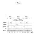
- FIG. 2illustrates a schematic timing chart of a gas-supplying cycle in a manufacturing method of a semiconductor device according to an exemplary embodiment of the present invention.
- FIG. 3illustrates a graph of results of an experimental example of the present invention.
- FIG. 1illustrates a cross-sectional view of a semiconductor device according to an exemplary embodiment of the present invention.
- a gate layer 121 and an interlayer insulation layer 122are alternately stacked on a substrate 110 .
- the gate layer 121may be formed of a metal layer, or may be made of a conductive material such as doped polysilicon.
- the interlayer insulation layer 122may include a silicon oxide (SiO2).
- a trenchis formed in a structure in which the gate layer 121 and the interlayer insulation layer 122 are alternately stacked, and a non-conductive layer 131 , a channel layer 132 , a barrier layer 133 , a source layer 134 , and a capping layer 135 are sequentially formed in the trench.
- the non-conductive layer 131 , the channel layer 132 , the barrier layer 133 , the source layer 134 , and the capping layer 135are formed to be perpendicular to a surface of the gate layer 121 in the trench, and are sequentially formed at a lateral surface of the structure in which the gate layer 121 and the interlayer insulation layer 122 are alternately stacked.
- the non-conductive layer 131 , the channel layer 132 , the barrier layer 133 , the source layer 134 , and the capping layer 135are vertically formed to be perpendicular to the surface of the gate layer 121 along the lateral surface of the structure in which the gate layer 121 and the interlayer insulation layer 122 are alternately stacked.
- the non-conductive layer 131may be formed as an oxide-nitride-oxide (ONO) layer. More specifically, the non-conductive layer 131 may have a structure in which a silicon oxide layer, a silicon nitride layer, and a silicon oxide layer (SiO2/SiN/SiO2) are stacked. The non-conductive layer 131 serves to trap charges in the channel layer 132 .
- ONOoxide-nitride-oxide
- SiO2/SiN/SiO2silicon oxide layer
- the channel layer 132may be a polysilicon layer.
- the barrier layer 133may be formed of a silicon oxide (SiO2) layer.
- the source layer 134which supplies dopants, may be a layer containing a phosphorous element.
- the source layer 134may be a phosphosilicate glass (PSG) layer.
- the dopants in the source layer 134are diffused into the channel layer 132 , and by the dopant acting as a carrier, it is possible to prevent charge concentration from decreasing or charge distribution from being imbalanced in the channel layer 132 .
- the barrier layer 133when the dopants supplied from the source layer 134 are diffused into the channel layer 132 , serves to control diffusion concentration and speed.
- the capping layer 135may be formed of a silicon oxide (SiO2) layer.
- the capping layer 135prevents the dopants from being diffused in an opposite direction.
- the barrier layer 133 and the capping layer 135may be different in layer properties such as density and thickness to be suitable for their functions.
- the capping layer 135may be etched and removed in a subsequent process.
- FIG. 2illustrates a schematic timing chart of a gas-supplying cycle in a manufacturing method of a semiconductor device according to an exemplary embodiment of the present invention.
- a manufacturing method of a semiconductor deviceincludes a first step (step A) of repeating a first gas-supplying cycle (n-cycle), a second step (step B) of repeating a second gas-supplying cycle (m cycle), and a third step (step C) of repeating a third gas-supplying cycle (x cycle).
- the first gas-supplying cycle (n-cycle)is repeated a predetermined number of times.
- the first gas-supplying cycle (n-cycle)includes a step of activating oxygen gas by supplying oxygen gas and a purge gas (argon gas (purge Ar)) to a reactor during a first time t 1 , a second time t 2 , a third time t 3 , and a fourth time t 4 , supplying a silicon source thereto during the first time t 1 , and supplying plasma thereto during the third time t 3 .
- argon gaspurge Ar
- the barrier layer 133is formed on the channel layer 132 .
- the barrier layer 133is formed through the first step (step A) of repeating the first gas-supplying cycle (n-cycle) until the barrier layer 133 having a predetermined thickness is formed.
- the activated oxygen gasreacts with the silicon source.
- the oxygen gasacts as the purge gas while the plasma is not supplied,.
- step Bthe second gas-supplying cycle (m cycle) is repeated a predetermined number of times.
- the second gas-supplying cycle (n cycle)includes a first sub-gas-supplying cycle (m 1 cycle) and a second sub-gas-supplying cycle (m 2 cycle).
- the first sub-gas-supplying cycle (m 1 cycle)while supplying the oxygen gas and purge argon gas (purge Ar) to the reactor during a fifth time t 5 , a sixth time t 6 , a seventh time t 7 , an eighth time t 8 , a ninth time t 9 , and a tenth time t 10 , the silicon source gas is supplied during the fifth time t 5 without supplying the plasma, and the supplying of the silicon source gas stops during the sixth time t 6 .
- a phosphorous source gasis supplied during the seventh time t 7
- the plasmais supplied during the ninth time t 9 .
- the silicon sourceis supplied in the first sub-gas-supplying cycle (m 1 cycle), and in the second sub-gas-supplying cycle (m 2 cycle), the phosphorous source gas and the activated oxygen gas by the plasma react such that phosphorus oxide (PO) layers are stacked.
- the phosphosilicate glass (PSG) layerwhich is the source layer 134 , is formed.
- the silicon sourcemay be an aminosilane-based, halide-based, or chloride-based material that contains silicon (Si), and the phosphorous source may be an organic metal source that contains phosphorous.
- a phosphorus content of the phosphosilicate glass (PSG) layermay be controlled, and a concentration of the phosphorus, which is the dopant diffused into the channel layer 132 , may be controlled.
- step Cthe third gas-supplying cycle (x cycle) is repeated a predetermined number of times.
- the third gas-supplying cycle (x cycle)includes a step of activating oxygen gas by supplying the oxygen gas and the purge gas, argon gas (purge Ar) to the reactor during an eleventh time t 11 , a twelfth time t 12 , a thirteenth time t 13 , and a fourteenth time t 14 , supplying the silicon source thereto during the eleventh time t 11 , and supplying plasma thereto during the thirteenth time t 13 .
- the capping layer 135is formed on the source layer 134 .
- the capping layer 135is formed through the third step (step C) of repeating the third gas-supplying cycle (x cycle) until the capping layer 135 having a predetermined thickness is formed.
- the silicon sourcemay be an aminosilane-based, halide-based, or chloride-based material that contains silicon (Si).
- the first step (step A) of forming the barrier layer 133 and the third step (step C) of forming the capping layer 135may have different deposition conditions.
- the capping layer 135may be about 50 ⁇ , and the thickness of the barrier layer 133 may be about 10 ⁇ or 20 ⁇ .
- the barrier layer 133 and the capping layer 135 with different film qualitiesmay be formed by differently setting processing conditions of the barrier layer 133 and the capping layer 135 so that the phosphorus elements are not diffused through the capping layer 135 .
- the manufacturing method of the semiconductor devicemay use an in-situ method and a direct plasma-processing method in the first step (step A) of repeating the first gas-supplying cycle (n-cycle), the second step (step B) of repeating the second gas-supplying cycle (m cycle), and the third step (step C) of repeating the third gas-supplying cycle (x cycle).
- a remote plasma method of supplying the plasma from the outside of the reactormay be used.
- the barrier layer, the dopant source layer, and the capping layerare deposited by an atomic layer deposition method, for example, a plasma-enhanced atomic layer deposition (PEALD) method using plasma. That is, the barrier layer, the dopant source layer, and the capping layer may be formed by the plasma-enhanced atomic layer deposition (PEALD) method, thereby forming a uniform thin film (or layer).
- PEALDplasma-enhanced atomic layer deposition
- the barrier layer, the dopant source layer, and the capping layermay be uniformly deposited at a low temperature inside a trench structure that is vertically and thickly stacked and has a high aspect ratio.
- a manufacturing method of the semiconductor devicefurther includes a step of performing heat treatment, after the first step (step A) of repeating the first gas-supplying cycle (n-cycle), the second step (step B) of repeating the second gas-supplying cycle (m cycle), and the third step (step C) of repeating the third gas-supplying cycle (x cycle).
- the dopants in the source layer 134are diffused into the channel layer 132 through the barrier layer 133 .
- the dopants in the source layer 134may not be diffused through the capping layer 135 .
- the step of performing the heat treatmentmay proceed for about 1 hr at a temperature of about 600° C.
- FIG. 3illustrates a graph of results of an experimental data of the present invention.
- the concentration of the phosphorus diffused into the channel layerincreases, and when the barrier layer is formed, it can be seen that the concentration of the phosphorus diffused into the channel layer decreases (B) compared to when the barrier layer is not formed (A).
- the source layerwhich is the dopant source
- the barrier layerit can be seen that dopants of a predetermined concentration may be diffused into the channel layer such that the reduction of the charge concentration in the channel layer may be prevented.
- the manufacturing method thereofaccording to the exemplary embodiments of the present invention, after the dopant source layer is uniformly deposited on a channel layer of the device with the 3-demensional vertical structure by the plasma-enhanced atomic layer deposition (PEALD) method, the deposited dopant source layer is heat-treated so that the dopants are diffused into the channel layer to function as charge carriers, thereby preventing the charges in the channel layer from being reduced.
- PEALDplasma-enhanced atomic layer deposition
- the diffusion speed and concentration of the dopantmay be controlled by forming the barrier layer between the channel layer and the dopant source layer.
Landscapes
- Engineering & Computer Science (AREA)
- Microelectronics & Electronic Packaging (AREA)
- Condensed Matter Physics & Semiconductors (AREA)
- General Physics & Mathematics (AREA)
- Manufacturing & Machinery (AREA)
- Computer Hardware Design (AREA)
- Physics & Mathematics (AREA)
- Power Engineering (AREA)
- Formation Of Insulating Films (AREA)
- Non-Volatile Memory (AREA)
- Semiconductor Memories (AREA)
- Chemical & Material Sciences (AREA)
- Crystallography & Structural Chemistry (AREA)
Abstract
Description
This application claims priority to and the benefit of Korean Patent Application No. 10-2014-0186115 filed in the Korean Intellectual Property Office on Dec. 22, 2014, the entire contents of which are incorporated herein by reference.
(a) Field of the Invention
The present invention relates to a semiconductor device and a manufacturing method thereof.
(b) Description of the Related Art
Recently, although a flash memory semiconductor has been highly integrated, there is a limit in improvement of the degree of integration due to a physical limit such as an increase of current leakage in a channel according to a conventional 2-dimentional gate structure.
Thus, a novel structure that is able to substitute for the conventional 2-dimentional gate structure, for example, a 3-dimentional vertical NAND (3D VNAND) flash memory that overcomes the limit of the degree of integration by vertically stacking gate structures, has attracted attention. However, since charge distribution is non-uniform in the vertically stacked polysilicon channel layer of the 3D VNAND device, the 3D VNAND device may not be normally operated.
The above information disclosed in this Background section is only to enhance the understanding of the background of the invention and therefore it may contain information that does not form the prior art that is already known in this country to a person of ordinary skill in the art.
The present invention has been made in an effort to provide a semiconductor device and a manufacturing method thereof that may prevent a reduction of charge from being able to occur in a channel layer of a 3-dimentional vertical NAND flash memory.
An exemplary embodiment of the present invention provides a semiconductor device, including: a structure in which a gate layer and an interlayer insulation layer are alternately stacked; a non-conductive layer formed at a lateral surface of the structure; a channel layer formed at a lateral surface of the non-conductive layer; a barrier layer formed at a lateral surface of the channel layer; and a source layer formed at a lateral surface of the barrier layer.
The source layer may contain phosphorous elements.
The source layer may be a phosphosilicate glass (PSG) layer.
The non-conductive layer may be an oxide-nitride-oxide (ONO) layer.
The channel layer may be a polysilicon layer.
The semiconductor device may further include a capping layer formed at a lateral surface of the source layer.
The barrier layer and the capping layer may be silicon oxide layers.
The barrier layer and the capping layer may be silicon oxide layers having different film qualities or different thicknesses.
Another embodiment of the present invention provides a manufacturing method of a semiconductor device, including: forming a non-conductive layer to be perpendicular to a surface of a substrate in a trench of a structure in which a gate layer and an interlayer insulation layer are alternately stacked; forming a channel layer to be perpendicular to the surface of the substrate at a lateral surface of the non-conductive layer; repeating a first gas-supplying cycle for forming a barrier layer to be perpendicular to the surface of the substrate at a lateral surface of the channel layer; and repeating a second gas-supplying cycle for forming a source layer at a lateral surface of the barrier layer, wherein the first gas-supplying cycle and the second gas-supplying cycle may be performed by an atomic layer deposition method.
The first gas-supplying cycle may include: while supplying oxygen gas and a purge gas to a reactor during a first time, a second time, a third time, and a fourth time, supplying a silicon source during the first time; and activating the oxygen gas with plasma during the third time.
The second gas-supplying cycle may include a first sub-gas-supplying cycle and a second sub-gas-supplying cycle, wherein while supplying the oxygen gas and the purge gas to the reactor during a fifth time, a sixth time, a seventh time, an eighth time, a ninth time, and a tenth time, the first sub-gas-supplying cycle includes a step of supplying a silicon source gas during the fifth time without supplying plasma and a step of stopping supplying of the silicon source gas during the sixth time, and the second sub-gas-supplying cycle includes a step of supplying a phosphorous source gas during the seventh time and a step of supplying plasma during the ninth time.
A number of repetitions of the first sub-gas-supplying cycle and a number of repetitions of the second sub-gas-supplying cycle may be different.
The manufacturing method of the semiconductor device may further include repeating a third gas-supplying cycle for forming a capping layer at a lateral surface of the source layer.
The third gas-supplying cycle may include: while supplying the oxygen gas and the purge gas to the reactor during an eleventh time, a twelfth time, a thirteenth time, and a fourteenth time, supplying the silicon source during the eleventh time; and activating the oxygen gas with the plasma during the thirteenth time.
Conditions of the first gas-supplying cycle and the third gas-supplying cycle may be different.
The manufacturing method of the semiconductor device may further include performing heat treatment to the semiconductor device.
The step of forming of the channel layer may include forming the channel layer as a polysilicon layer.
According to the embodiments of the present invention, it is possible to prevent a reduction of charge and imbalance of charge distribution from occuring in a channel layer with a 3-dimentional vertical structure.
The present invention will be described more fully hereinafter with reference to the accompanying drawings, in which exemplary embodiments of the invention are shown. As those skilled in the art would realize, the described embodiments may be modified in various different ways, all without departing from the spirit or scope of the present invention.
In the drawings, the thickness of layers, films, panels, regions, etc., are exaggerated for clarity. Like reference numerals designate like elements throughout the specification. It will be understood that when an element such as a layer, film, region, or substrate is referred to as being “on” another element, it can be directly on the other element or intervening elements may also be present. In contrast, when an element is referred to as being “directly on” another element, there are no intervening elements present.
First, a semiconductor device according to an exemplary embodiment of the present invention will be described with reference toFIG. 1 .FIG. 1 illustrates a cross-sectional view of a semiconductor device according to an exemplary embodiment of the present invention.
Referring toFIG. 1 , agate layer 121 and aninterlayer insulation layer 122 are alternately stacked on asubstrate 110. Thegate layer 121 may be formed of a metal layer, or may be made of a conductive material such as doped polysilicon. Theinterlayer insulation layer 122 may include a silicon oxide (SiO2).
A trench is formed in a structure in which thegate layer 121 and theinterlayer insulation layer 122 are alternately stacked, and anon-conductive layer 131, achannel layer 132, abarrier layer 133, asource layer 134, and acapping layer 135 are sequentially formed in the trench. Thenon-conductive layer 131, thechannel layer 132, thebarrier layer 133, thesource layer 134, and thecapping layer 135 are formed to be perpendicular to a surface of thegate layer 121 in the trench, and are sequentially formed at a lateral surface of the structure in which thegate layer 121 and theinterlayer insulation layer 122 are alternately stacked.
Thenon-conductive layer 131, thechannel layer 132, thebarrier layer 133, thesource layer 134, and thecapping layer 135 are vertically formed to be perpendicular to the surface of thegate layer 121 along the lateral surface of the structure in which thegate layer 121 and theinterlayer insulation layer 122 are alternately stacked.
Thenon-conductive layer 131 may be formed as an oxide-nitride-oxide (ONO) layer. More specifically, thenon-conductive layer 131 may have a structure in which a silicon oxide layer, a silicon nitride layer, and a silicon oxide layer (SiO2/SiN/SiO2) are stacked. Thenon-conductive layer 131 serves to trap charges in thechannel layer 132.
Thechannel layer 132 may be a polysilicon layer.
Thebarrier layer 133 may be formed of a silicon oxide (SiO2) layer.
Thesource layer 134, which supplies dopants, may be a layer containing a phosphorous element. For example, thesource layer 134 may be a phosphosilicate glass (PSG) layer.
By performing heat treatment after forming thebarrier layer 133 and thesource layer 134 on thechannel layer 132, the dopants in thesource layer 134 are diffused into thechannel layer 132, and by the dopant acting as a carrier, it is possible to prevent charge concentration from decreasing or charge distribution from being imbalanced in thechannel layer 132.
Thebarrier layer 133, when the dopants supplied from thesource layer 134 are diffused into thechannel layer 132, serves to control diffusion concentration and speed.
Thecapping layer 135 may be formed of a silicon oxide (SiO2) layer. Thecapping layer 135 prevents the dopants from being diffused in an opposite direction.
Thebarrier layer 133 and thecapping layer 135 may be different in layer properties such as density and thickness to be suitable for their functions.
Thecapping layer 135 may be etched and removed in a subsequent process.
Next, a manufacturing method of a semiconductor device according to an exemplary embodiment of the present invention will be described with reference toFIG. 2 .FIG. 2 illustrates a schematic timing chart of a gas-supplying cycle in a manufacturing method of a semiconductor device according to an exemplary embodiment of the present invention.
Referring toFIG. 2 , a manufacturing method of a semiconductor device according to an exemplary embodiment of the present invention includes a first step (step A) of repeating a first gas-supplying cycle (n-cycle), a second step (step B) of repeating a second gas-supplying cycle (m cycle), and a third step (step C) of repeating a third gas-supplying cycle (x cycle).
In the first step (step A), the first gas-supplying cycle (n-cycle) is repeated a predetermined number of times. The first gas-supplying cycle (n-cycle) includes a step of activating oxygen gas by supplying oxygen gas and a purge gas (argon gas (purge Ar)) to a reactor during a first time t1, a second time t2, a third time t3, and a fourth time t4, supplying a silicon source thereto during the first time t1, and supplying plasma thereto during the third time t3.
By repeating the first gas-supplying cycle (n-cycle), thebarrier layer 133 is formed on thechannel layer 132. Thebarrier layer 133 is formed through the first step (step A) of repeating the first gas-supplying cycle (n-cycle) until thebarrier layer 133 having a predetermined thickness is formed.
Here, only the activated oxygen gas reacts with the silicon source. Thus, the oxygen gas acts as the purge gas while the plasma is not supplied,.
A thickness of thebarrier layer 133 may be about 10 to 20 Å. The silicon source (Si source) may be an aminosilane-based, halide-based, or chloride-based material that contains silicon (Si).
In the second step (step B), the second gas-supplying cycle (m cycle) is repeated a predetermined number of times.
The second gas-supplying cycle (n cycle) includes a first sub-gas-supplying cycle (m1 cycle) and a second sub-gas-supplying cycle (m2 cycle). In the first sub-gas-supplying cycle (m1 cycle), while supplying the oxygen gas and purge argon gas (purge Ar) to the reactor during a fifth time t5, a sixth time t6, a seventh time t7, an eighth time t8, a ninth time t9, and a tenth time t10, the silicon source gas is supplied during the fifth time t5 without supplying the plasma, and the supplying of the silicon source gas stops during the sixth time t6. In the second sub-gas-supplying cycle (m2 cycle), while supplying the oxygen gas and the purge argon gas (purge Ar) to the reactor during the fifth time t5, the sixth time t6, the seventh time t7, the eighth time t8, the ninth time t9, and the tenth time t10, a phosphorous source gas is supplied during the seventh time t7, and the plasma is supplied during the ninth time t9. The silicon source is supplied in the first sub-gas-supplying cycle (m1 cycle), and in the second sub-gas-supplying cycle (m2 cycle), the phosphorous source gas and the activated oxygen gas by the plasma react such that phosphorus oxide (PO) layers are stacked.
In the second step (step B) in which the first sub-gas-supplying cycle (m1 cycle) and the second sub-gas-supplying cycle (m2 cycle) are repeated, the phosphosilicate glass (PSG) layer, which is thesource layer 134, is formed.
In this case, the silicon source (Si source) may be an aminosilane-based, halide-based, or chloride-based material that contains silicon (Si), and the phosphorous source may be an organic metal source that contains phosphorous.
In the second step (step B), by adjusting a repetition ratio of the first sub-gas-supplying cycle (m1 cycle) and the second sub-gas-supplying cycle (m2 cycle), a phosphorus content of the phosphosilicate glass (PSG) layer may be controlled, and a concentration of the phosphorus, which is the dopant diffused into thechannel layer 132, may be controlled.
In the third step (step C), the third gas-supplying cycle (x cycle) is repeated a predetermined number of times.
The third gas-supplying cycle (x cycle) includes a step of activating oxygen gas by supplying the oxygen gas and the purge gas, argon gas (purge Ar) to the reactor during an eleventh time t11, a twelfth time t12, a thirteenth time t13, and a fourteenth time t14, supplying the silicon source thereto during the eleventh time t11, and supplying plasma thereto during the thirteenth time t13.
By repeating the third gas-supplying cycle (x cycle), thecapping layer 135 is formed on thesource layer 134. Thecapping layer 135 is formed through the third step (step C) of repeating the third gas-supplying cycle (x cycle) until thecapping layer 135 having a predetermined thickness is formed.
In this case, the silicon source (Si source) may be an aminosilane-based, halide-based, or chloride-based material that contains silicon (Si).
The first step (step A) of forming thebarrier layer 133 and the third step (step C) of forming thecapping layer 135 may have different deposition conditions.
More specifically, it is possible to increase density of the silicon oxide layer by increasing plasma power supplied during the third step (step C) of forming thecapping layer 135 compared to the first step (step A) of forming thebarrier layer 133, and it is possible to increase a thickness of the silicon oxide layer by increasing the number of repetitions of the third step (step C) of forming thecapping layer 135 compared to the first step (step A). The thickness of thecapping layer 135 may be about 50 Å, and the thickness of thebarrier layer 133 may be about 10 Å or 20 Å.
As such, by changing the deposition conditions depending on the functions of thebarrier layer 133 and thecapping layer 135, it is possible to form a silicon oxide layer with appropriate film quality.
For example, although phosphorus elements, which are the dopants of thesource layer 134, may be diffused into thechannel layer 132 through thebarrier layer 133, thebarrier layer 133 and thecapping layer 135 with different film qualities may be formed by differently setting processing conditions of thebarrier layer 133 and thecapping layer 135 so that the phosphorus elements are not diffused through thecapping layer 135.
The manufacturing method of the semiconductor device according to the exemplary embodiment of the present invention may use an in-situ method and a direct plasma-processing method in the first step (step A) of repeating the first gas-supplying cycle (n-cycle), the second step (step B) of repeating the second gas-supplying cycle (m cycle), and the third step (step C) of repeating the third gas-supplying cycle (x cycle). In a manufacturing method of a semiconductor device according to another exemplary embodiment of the present invention, a remote plasma method of supplying the plasma from the outside of the reactor may be used.
As such, according to the manufacturing method of the semiconductor device according to the exemplary embodiment of the present invention, the barrier layer, the dopant source layer, and the capping layer are deposited by an atomic layer deposition method, for example, a plasma-enhanced atomic layer deposition (PEALD) method using plasma. That is, the barrier layer, the dopant source layer, and the capping layer may be formed by the plasma-enhanced atomic layer deposition (PEALD) method, thereby forming a uniform thin film (or layer). Particularly, the barrier layer, the dopant source layer, and the capping layer may be uniformly deposited at a low temperature inside a trench structure that is vertically and thickly stacked and has a high aspect ratio.
A manufacturing method of the semiconductor device according to another exemplary embodiment of the present invention further includes a step of performing heat treatment, after the first step (step A) of repeating the first gas-supplying cycle (n-cycle), the second step (step B) of repeating the second gas-supplying cycle (m cycle), and the third step (step C) of repeating the third gas-supplying cycle (x cycle).
By performing the heat treatment, the dopants in thesource layer 134 are diffused into thechannel layer 132 through thebarrier layer 133. However, the dopants in thesource layer 134 may not be diffused through thecapping layer 135. The step of performing the heat treatment may proceed for about 1 hr at a temperature of about 600° C.
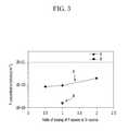
An experimental example of the present invention will now be described with reference toFIG. 3 .FIG. 3 illustrates a graph of results of an experimental data of the present invention.
In the experimental data, while changing supply ratios of the phosphorous source gas (P-source) to the silicon source gas (Si-source) with respect to a first case (A) in which the barrier layer is not formed and a second case (B) in which the barrier layer is formed, diffusion concentrations of the phosphorus in the channel layer are measured, and the measured results are shown inFIG. 3 . The diffusion concentration of the phosphorus in the channel layer was measured by secondary ion mass spectrometry (SIMS).
Referring toFIG. 3 , as the supply ratio of the phosphorous source gas to the silicon source gas increases, it can be seen that the concentration of the phosphorus diffused into the channel layer increases, and when the barrier layer is formed, it can be seen that the concentration of the phosphorus diffused into the channel layer decreases (B) compared to when the barrier layer is not formed (A).
As such, by using the source layer, which is the dopant source, and the barrier layer, it can be seen that dopants of a predetermined concentration may be diffused into the channel layer such that the reduction of the charge concentration in the channel layer may be prevented.
As described above, according to the semiconductor device the manufacturing method thereof according to the exemplary embodiments of the present invention, after the dopant source layer is uniformly deposited on a channel layer of the device with the 3-demensional vertical structure by the plasma-enhanced atomic layer deposition (PEALD) method, the deposited dopant source layer is heat-treated so that the dopants are diffused into the channel layer to function as charge carriers, thereby preventing the charges in the channel layer from being reduced.
Further, according to the exemplary embodiments of the present invention, the diffusion speed and concentration of the dopant may be controlled by forming the barrier layer between the channel layer and the dopant source layer.
While this invention has been described in connection with what is presently considered to be practical exemplary embodiments, it is to be understood that the invention is not limited to the disclosed embodiments, but, on the contrary, is intended to cover various modifications and equivalent arrangements included within the spirit and scope of the appended claims.
Claims (17)
1. A manufacturing method of a semiconductor device, comprising:
forming a non-conductive layer to be perpendicular to a surface of a substrate in a trench of a structure in which a gate layer and an interlayer insulation layer are alternately stacked;
forming a channel layer to be perpendicular to the surface of the substrate at a lateral surface of the non-conductive layer;
repeating a first gas-supplying cycle for forming a barrier layer to be perpendicular to the surface of the substrate at a lateral surface of the channel layer wherein the first gas-supplying cycle includes, while supplying oxygen gas and a purge gas to a reactor during a first time, a second time, a third time, and a fourth time: supplying a silicon source during the first time; and activating the oxygen gas with plasma during the third time, and wherein the second gas-supplying cycle includes a first sub-gas-supplying cycle and a second sub-gas-supplying cycle, wherein, while supplying the oxygen gas and the purge gas to the reactor during a fifth time, a sixth time, a seventh time, an eighth time, a ninth time, and a tenth time, the first sub-gas-supplying cycle includes a step of supplying a silicon source gas during the fifth time without supplying the plasma and a step of stopping supplying of the silicon source gas during the sixth time, and the second sub-gas-supplying cycle includes a step of supplying phosphorous source gas during the seventh time and a step of supplying plasma during the ninth time; and
repeating a second gas-supplying cycle for forming a source layer, comprising one or more dopants, at a lateral surface of the barrier layer,
wherein the first gas-supplying cycle and the second gas-supplying cycle are performed by an atomic layer deposition method, and
wherein the one or more dopants diffuse through the barrier layer to the channel layer.
2. The manufacturing method of the semiconductor device ofclaim 1 , wherein
a number of repetitions of the first sub-gas-supplying cycle and a number of repetitions of the second sub-gas-supplying cycle are different.
3. The manufacturing method of the semiconductor device ofclaim 1 , further comprising
repeating a third gas-supplying cycle for forming a capping layer at a lateral surface of the source layer.
4. The manufacturing method of the semiconductor device ofclaim 3 , wherein
the third gas-supplying cycle includes:
while supplying the oxygen gas and the purge gas to the reactor during an eleventh time, a twelfth time, a thirteenth time, and a fourteenth time,
supplying the silicon source during the eleventh time; and
activating the oxygen gas with the plasma during the thirteenth time.
5. The manufacturing method of the semiconductor device ofclaim 3 , further comprising
performing heat treatment to the semiconductor device.
6. The manufacturing method of the semiconductor device ofclaim 4 , wherein
conditions of the first gas-supplying cycle and the third gas-supplying cycle are different.
7. The manufacturing method of the semiconductor device ofclaim 6 , wherein
the plasma powers supplied during the first gas-supplying cycle and the third gas-supplying cycle are different.
8. The manufacturing method of the semiconductor device ofclaim 6 , wherein
the thickness of the films formed in the first gas-supplying cycle and the third gas-supplying cycle are different.
9. The manufacturing method of the semiconductor device ofclaim 1 , further comprising
performing heat treatment to the semiconductor device to cause the one or more dopants to diffuse from the source layer to the channel layer.
10. The manufacturing method of the semiconductor device ofclaim 1 , wherein
the forming of the channel layer includes forming the channel layer as a polysilicon layer.
11. A manufacturing method of a semiconductor device, comprising:
forming a non-conductive layer to be perpendicular to a surface of a substrate in a trench of a structure in which a gate layer and an interlayer insulation layer are alternately stacked;
forming a channel layer to be perpendicular to the surface of the substrate at a lateral surface of the non-conductive layer;
repeating a first gas-supplying cycle for forming a barrier layer to be perpendicular to the surface of the substrate at a lateral surface of the channel layer; and
repeating a second gas-supplying cycle for forming a source layer, comprising one or more dopants, at a lateral surface of the barrier layer,
wherein the first gas-supplying cycle and the second gas-supplying cycle are performed by an atomic layer deposition method, and
wherein the one or more dopants diffuse through the barrier layer to the channel layer,
wherein the first gas-supplying cycle includes,
while supplying oxygen gas and a purge gas to a reactor during a first time, a second time, a third time, and a fourth time:
supplying a silicon source during the first time; and
activating the oxygen gas with plasma during the third time,
repeating a third gas-supplying cycle for forming a capping layer at a lateral surface of the source layer, and
wherein the third gas-supplying cycle includes:
while supplying the oxygen gas and the purge gas to the reactor during an eleventh time, a twelfth time, a thirteenth time, and a fourteenth time,
supplying the silicon source during the eleventh time; and
activating the oxygen gas with the plasma during the thirteenth time.
12. The manufacturing method of the semiconductor device ofclaim 11 , wherein conditions of the first gas-supplying cycle and the third gas-supplying cycle are different.
13. The manufacturing method of the semiconductor device ofclaim 12 , wherein the plasma powers supplied during the first gas-supplying cycle and the third gas-supplying cycle are different.
14. The manufacturing method of the semiconductor device ofclaim 12 , wherein the thickness of the films formed in the first gas-supplying cycle and the third gas-supplying cycle are different.
15. The manufacturing method of the semiconductor device ofclaim 11 , further comprising performing heat treatment to the semiconductor device to cause the one or more dopants to diffuse from the source layer to the channel layer.
16. The manufacturing method of the semiconductor device ofclaim 11 , further comprising performing heat treatment to the semiconductor device.
17. The manufacturing method of the semiconductor device ofclaim 11 , wherein the forming of the channel layer includes forming the channel layer as a polysilicon layer.
Priority Applications (2)
| Application Number | Priority Date | Filing Date | Title |
|---|---|---|---|
| US15/798,120US10032792B2 (en) | 2014-12-22 | 2017-10-30 | Semiconductor device and manufacturing method thereof |
| US15/798,150US10438965B2 (en) | 2014-12-22 | 2017-10-30 | Semiconductor device and manufacturing method thereof |
Applications Claiming Priority (2)
| Application Number | Priority Date | Filing Date | Title |
|---|---|---|---|
| KR1020140186115AKR102263121B1 (en) | 2014-12-22 | 2014-12-22 | Semiconductor device and manufacuring method thereof |
| KR10-2014-0186115 | 2014-12-22 |
Related Child Applications (2)
| Application Number | Title | Priority Date | Filing Date |
|---|---|---|---|
| US15/798,120ContinuationUS10032792B2 (en) | 2014-12-22 | 2017-10-30 | Semiconductor device and manufacturing method thereof |
| US15/798,150DivisionUS10438965B2 (en) | 2014-12-22 | 2017-10-30 | Semiconductor device and manufacturing method thereof |
Publications (2)
| Publication Number | Publication Date |
|---|---|
| US20160181273A1 US20160181273A1 (en) | 2016-06-23 |
| US9899405B2true US9899405B2 (en) | 2018-02-20 |
Family
ID=56130365
Family Applications (3)
| Application Number | Title | Priority Date | Filing Date |
|---|---|---|---|
| US14/938,180Active2035-11-22US9899405B2 (en) | 2014-12-22 | 2015-11-11 | Semiconductor device and manufacturing method thereof |
| US15/798,120ActiveUS10032792B2 (en) | 2014-12-22 | 2017-10-30 | Semiconductor device and manufacturing method thereof |
| US15/798,150ActiveUS10438965B2 (en) | 2014-12-22 | 2017-10-30 | Semiconductor device and manufacturing method thereof |
Family Applications After (2)
| Application Number | Title | Priority Date | Filing Date |
|---|---|---|---|
| US15/798,120ActiveUS10032792B2 (en) | 2014-12-22 | 2017-10-30 | Semiconductor device and manufacturing method thereof |
| US15/798,150ActiveUS10438965B2 (en) | 2014-12-22 | 2017-10-30 | Semiconductor device and manufacturing method thereof |
Country Status (2)
| Country | Link |
|---|---|
| US (3) | US9899405B2 (en) |
| KR (1) | KR102263121B1 (en) |
Cited By (352)
| Publication number | Priority date | Publication date | Assignee | Title |
|---|---|---|---|---|
| US10083836B2 (en) | 2015-07-24 | 2018-09-25 | Asm Ip Holding B.V. | Formation of boron-doped titanium metal films with high work function |
| US10134757B2 (en) | 2016-11-07 | 2018-11-20 | Asm Ip Holding B.V. | Method of processing a substrate and a device manufactured by using the method |
| US10229833B2 (en) | 2016-11-01 | 2019-03-12 | Asm Ip Holding B.V. | Methods for forming a transition metal nitride film on a substrate by atomic layer deposition and related semiconductor device structures |
| US10249524B2 (en) | 2017-08-09 | 2019-04-02 | Asm Ip Holding B.V. | Cassette holder assembly for a substrate cassette and holding member for use in such assembly |
| US10249577B2 (en) | 2016-05-17 | 2019-04-02 | Asm Ip Holding B.V. | Method of forming metal interconnection and method of fabricating semiconductor apparatus using the method |
| US10262859B2 (en) | 2016-03-24 | 2019-04-16 | Asm Ip Holding B.V. | Process for forming a film on a substrate using multi-port injection assemblies |
| US10269558B2 (en) | 2016-12-22 | 2019-04-23 | Asm Ip Holding B.V. | Method of forming a structure on a substrate |
| US10276355B2 (en) | 2015-03-12 | 2019-04-30 | Asm Ip Holding B.V. | Multi-zone reactor, system including the reactor, and method of using the same |
| US10283353B2 (en) | 2017-03-29 | 2019-05-07 | Asm Ip Holding B.V. | Method of reforming insulating film deposited on substrate with recess pattern |
| US10290508B1 (en) | 2017-12-05 | 2019-05-14 | Asm Ip Holding B.V. | Method for forming vertical spacers for spacer-defined patterning |
| US10312055B2 (en) | 2017-07-26 | 2019-06-04 | Asm Ip Holding B.V. | Method of depositing film by PEALD using negative bias |
| US10312129B2 (en) | 2015-09-29 | 2019-06-04 | Asm Ip Holding B.V. | Variable adjustment for precise matching of multiple chamber cavity housings |
| US10319588B2 (en) | 2017-10-10 | 2019-06-11 | Asm Ip Holding B.V. | Method for depositing a metal chalcogenide on a substrate by cyclical deposition |
| US10322384B2 (en) | 2015-11-09 | 2019-06-18 | Asm Ip Holding B.V. | Counter flow mixer for process chamber |
| US10340125B2 (en) | 2013-03-08 | 2019-07-02 | Asm Ip Holding B.V. | Pulsed remote plasma method and system |
| US10340135B2 (en) | 2016-11-28 | 2019-07-02 | Asm Ip Holding B.V. | Method of topologically restricted plasma-enhanced cyclic deposition of silicon or metal nitride |
| US10343920B2 (en) | 2016-03-18 | 2019-07-09 | Asm Ip Holding B.V. | Aligned carbon nanotubes |
| US10361201B2 (en) | 2013-09-27 | 2019-07-23 | Asm Ip Holding B.V. | Semiconductor structure and device formed using selective epitaxial process |
| US10364496B2 (en) | 2011-06-27 | 2019-07-30 | Asm Ip Holding B.V. | Dual section module having shared and unshared mass flow controllers |
| US10367080B2 (en) | 2016-05-02 | 2019-07-30 | Asm Ip Holding B.V. | Method of forming a germanium oxynitride film |
| US10366864B2 (en) | 2013-03-08 | 2019-07-30 | Asm Ip Holding B.V. | Method and system for in-situ formation of intermediate reactive species |
| US10381226B2 (en) | 2016-07-27 | 2019-08-13 | Asm Ip Holding B.V. | Method of processing substrate |
| US10381219B1 (en) | 2018-10-25 | 2019-08-13 | Asm Ip Holding B.V. | Methods for forming a silicon nitride film |
| US10378106B2 (en) | 2008-11-14 | 2019-08-13 | Asm Ip Holding B.V. | Method of forming insulation film by modified PEALD |
| US10388509B2 (en) | 2016-06-28 | 2019-08-20 | Asm Ip Holding B.V. | Formation of epitaxial layers via dislocation filtering |
| US10388513B1 (en) | 2018-07-03 | 2019-08-20 | Asm Ip Holding B.V. | Method for depositing silicon-free carbon-containing film as gap-fill layer by pulse plasma-assisted deposition |
| US10395919B2 (en) | 2016-07-28 | 2019-08-27 | Asm Ip Holding B.V. | Method and apparatus for filling a gap |
| US10403504B2 (en) | 2017-10-05 | 2019-09-03 | Asm Ip Holding B.V. | Method for selectively depositing a metallic film on a substrate |
| US10410943B2 (en) | 2016-10-13 | 2019-09-10 | Asm Ip Holding B.V. | Method for passivating a surface of a semiconductor and related systems |
| US10438965B2 (en) | 2014-12-22 | 2019-10-08 | Asm Ip Holding B.V. | Semiconductor device and manufacturing method thereof |
| US10435790B2 (en) | 2016-11-01 | 2019-10-08 | Asm Ip Holding B.V. | Method of subatmospheric plasma-enhanced ALD using capacitively coupled electrodes with narrow gap |
| US10446393B2 (en) | 2017-05-08 | 2019-10-15 | Asm Ip Holding B.V. | Methods for forming silicon-containing epitaxial layers and related semiconductor device structures |
| US10458018B2 (en) | 2015-06-26 | 2019-10-29 | Asm Ip Holding B.V. | Structures including metal carbide material, devices including the structures, and methods of forming same |
| US10468261B2 (en) | 2017-02-15 | 2019-11-05 | Asm Ip Holding B.V. | Methods for forming a metallic film on a substrate by cyclical deposition and related semiconductor device structures |
| US10468251B2 (en) | 2016-02-19 | 2019-11-05 | Asm Ip Holding B.V. | Method for forming spacers using silicon nitride film for spacer-defined multiple patterning |
| US10483099B1 (en) | 2018-07-26 | 2019-11-19 | Asm Ip Holding B.V. | Method for forming thermally stable organosilicon polymer film |
| US10480072B2 (en) | 2009-04-06 | 2019-11-19 | Asm Ip Holding B.V. | Semiconductor processing reactor and components thereof |
| US10501866B2 (en) | 2016-03-09 | 2019-12-10 | Asm Ip Holding B.V. | Gas distribution apparatus for improved film uniformity in an epitaxial system |
| US10504742B2 (en) | 2017-05-31 | 2019-12-10 | Asm Ip Holding B.V. | Method of atomic layer etching using hydrogen plasma |
| US10510536B2 (en) | 2018-03-29 | 2019-12-17 | Asm Ip Holding B.V. | Method of depositing a co-doped polysilicon film on a surface of a substrate within a reaction chamber |
| US10529554B2 (en) | 2016-02-19 | 2020-01-07 | Asm Ip Holding B.V. | Method for forming silicon nitride film selectively on sidewalls or flat surfaces of trenches |
| US10529563B2 (en) | 2017-03-29 | 2020-01-07 | Asm Ip Holdings B.V. | Method for forming doped metal oxide films on a substrate by cyclical deposition and related semiconductor device structures |
| US10529542B2 (en) | 2015-03-11 | 2020-01-07 | Asm Ip Holdings B.V. | Cross-flow reactor and method |
| US10535516B2 (en) | 2018-02-01 | 2020-01-14 | Asm Ip Holdings B.V. | Method for depositing a semiconductor structure on a surface of a substrate and related semiconductor structures |
| US10541173B2 (en) | 2016-07-08 | 2020-01-21 | Asm Ip Holding B.V. | Selective deposition method to form air gaps |
| US10541333B2 (en) | 2017-07-19 | 2020-01-21 | Asm Ip Holding B.V. | Method for depositing a group IV semiconductor and related semiconductor device structures |
| US10559458B1 (en) | 2018-11-26 | 2020-02-11 | Asm Ip Holding B.V. | Method of forming oxynitride film |
| US10566223B2 (en) | 2012-08-28 | 2020-02-18 | Asm Ip Holdings B.V. | Systems and methods for dynamic semiconductor process scheduling |
| US10561975B2 (en) | 2014-10-07 | 2020-02-18 | Asm Ip Holdings B.V. | Variable conductance gas distribution apparatus and method |
| US10590535B2 (en) | 2017-07-26 | 2020-03-17 | Asm Ip Holdings B.V. | Chemical treatment, deposition and/or infiltration apparatus and method for using the same |
| US10600673B2 (en) | 2015-07-07 | 2020-03-24 | Asm Ip Holding B.V. | Magnetic susceptor to baseplate seal |
| US10607895B2 (en) | 2017-09-18 | 2020-03-31 | Asm Ip Holdings B.V. | Method for forming a semiconductor device structure comprising a gate fill metal |
| US10605530B2 (en) | 2017-07-26 | 2020-03-31 | Asm Ip Holding B.V. | Assembly of a liner and a flange for a vertical furnace as well as the liner and the vertical furnace |
| US10604847B2 (en) | 2014-03-18 | 2020-03-31 | Asm Ip Holding B.V. | Gas distribution system, reactor including the system, and methods of using the same |
| US10612136B2 (en) | 2018-06-29 | 2020-04-07 | ASM IP Holding, B.V. | Temperature-controlled flange and reactor system including same |
| US10612137B2 (en) | 2016-07-08 | 2020-04-07 | Asm Ip Holdings B.V. | Organic reactants for atomic layer deposition |
| USD880437S1 (en) | 2018-02-01 | 2020-04-07 | Asm Ip Holding B.V. | Gas supply plate for semiconductor manufacturing apparatus |
| US10643904B2 (en) | 2016-11-01 | 2020-05-05 | Asm Ip Holdings B.V. | Methods for forming a semiconductor device and related semiconductor device structures |
| US10643826B2 (en) | 2016-10-26 | 2020-05-05 | Asm Ip Holdings B.V. | Methods for thermally calibrating reaction chambers |
| US10658205B2 (en) | 2017-09-28 | 2020-05-19 | Asm Ip Holdings B.V. | Chemical dispensing apparatus and methods for dispensing a chemical to a reaction chamber |
| US10655221B2 (en) | 2017-02-09 | 2020-05-19 | Asm Ip Holding B.V. | Method for depositing oxide film by thermal ALD and PEALD |
| US10658181B2 (en) | 2018-02-20 | 2020-05-19 | Asm Ip Holding B.V. | Method of spacer-defined direct patterning in semiconductor fabrication |
| US10665452B2 (en) | 2016-05-02 | 2020-05-26 | Asm Ip Holdings B.V. | Source/drain performance through conformal solid state doping |
| US10685834B2 (en) | 2017-07-05 | 2020-06-16 | Asm Ip Holdings B.V. | Methods for forming a silicon germanium tin layer and related semiconductor device structures |
| US10683571B2 (en) | 2014-02-25 | 2020-06-16 | Asm Ip Holding B.V. | Gas supply manifold and method of supplying gases to chamber using same |
| US10692741B2 (en) | 2017-08-08 | 2020-06-23 | Asm Ip Holdings B.V. | Radiation shield |
| US10707106B2 (en) | 2011-06-06 | 2020-07-07 | Asm Ip Holding B.V. | High-throughput semiconductor-processing apparatus equipped with multiple dual-chamber modules |
| US10714385B2 (en) | 2016-07-19 | 2020-07-14 | Asm Ip Holding B.V. | Selective deposition of tungsten |
| US10714350B2 (en) | 2016-11-01 | 2020-07-14 | ASM IP Holdings, B.V. | Methods for forming a transition metal niobium nitride film on a substrate by atomic layer deposition and related semiconductor device structures |
| US10714335B2 (en) | 2017-04-25 | 2020-07-14 | Asm Ip Holding B.V. | Method of depositing thin film and method of manufacturing semiconductor device |
| US10714315B2 (en) | 2012-10-12 | 2020-07-14 | Asm Ip Holdings B.V. | Semiconductor reaction chamber showerhead |
| US10734497B2 (en) | 2017-07-18 | 2020-08-04 | Asm Ip Holding B.V. | Methods for forming a semiconductor device structure and related semiconductor device structures |
| US10731249B2 (en) | 2018-02-15 | 2020-08-04 | Asm Ip Holding B.V. | Method of forming a transition metal containing film on a substrate by a cyclical deposition process, a method for supplying a transition metal halide compound to a reaction chamber, and related vapor deposition apparatus |
| US10734244B2 (en) | 2017-11-16 | 2020-08-04 | Asm Ip Holding B.V. | Method of processing a substrate and a device manufactured by the same |
| US10741385B2 (en) | 2016-07-28 | 2020-08-11 | Asm Ip Holding B.V. | Method and apparatus for filling a gap |
| US10755922B2 (en) | 2018-07-03 | 2020-08-25 | Asm Ip Holding B.V. | Method for depositing silicon-free carbon-containing film as gap-fill layer by pulse plasma-assisted deposition |
| US10770336B2 (en) | 2017-08-08 | 2020-09-08 | Asm Ip Holding B.V. | Substrate lift mechanism and reactor including same |
| US10770286B2 (en) | 2017-05-08 | 2020-09-08 | Asm Ip Holdings B.V. | Methods for selectively forming a silicon nitride film on a substrate and related semiconductor device structures |
| US10767789B2 (en) | 2018-07-16 | 2020-09-08 | Asm Ip Holding B.V. | Diaphragm valves, valve components, and methods for forming valve components |
| US10787741B2 (en) | 2014-08-21 | 2020-09-29 | Asm Ip Holding B.V. | Method and system for in situ formation of gas-phase compounds |
| US10797133B2 (en) | 2018-06-21 | 2020-10-06 | Asm Ip Holding B.V. | Method for depositing a phosphorus doped silicon arsenide film and related semiconductor device structures |
| US10804098B2 (en) | 2009-08-14 | 2020-10-13 | Asm Ip Holding B.V. | Systems and methods for thin-film deposition of metal oxides using excited nitrogen-oxygen species |
| US10811256B2 (en) | 2018-10-16 | 2020-10-20 | Asm Ip Holding B.V. | Method for etching a carbon-containing feature |
| US10818758B2 (en) | 2018-11-16 | 2020-10-27 | Asm Ip Holding B.V. | Methods for forming a metal silicate film on a substrate in a reaction chamber and related semiconductor device structures |
| USD900036S1 (en) | 2017-08-24 | 2020-10-27 | Asm Ip Holding B.V. | Heater electrical connector and adapter |
| US10829852B2 (en) | 2018-08-16 | 2020-11-10 | Asm Ip Holding B.V. | Gas distribution device for a wafer processing apparatus |
| US10832903B2 (en) | 2011-10-28 | 2020-11-10 | Asm Ip Holding B.V. | Process feed management for semiconductor substrate processing |
| US10847366B2 (en) | 2018-11-16 | 2020-11-24 | Asm Ip Holding B.V. | Methods for depositing a transition metal chalcogenide film on a substrate by a cyclical deposition process |
| US10844484B2 (en) | 2017-09-22 | 2020-11-24 | Asm Ip Holding B.V. | Apparatus for dispensing a vapor phase reactant to a reaction chamber and related methods |
| US10847371B2 (en) | 2018-03-27 | 2020-11-24 | Asm Ip Holding B.V. | Method of forming an electrode on a substrate and a semiconductor device structure including an electrode |
| US10847365B2 (en) | 2018-10-11 | 2020-11-24 | Asm Ip Holding B.V. | Method of forming conformal silicon carbide film by cyclic CVD |
| US10851456B2 (en) | 2016-04-21 | 2020-12-01 | Asm Ip Holding B.V. | Deposition of metal borides |
| USD903477S1 (en) | 2018-01-24 | 2020-12-01 | Asm Ip Holdings B.V. | Metal clamp |
| US10854498B2 (en) | 2011-07-15 | 2020-12-01 | Asm Ip Holding B.V. | Wafer-supporting device and method for producing same |
| US10858737B2 (en) | 2014-07-28 | 2020-12-08 | Asm Ip Holding B.V. | Showerhead assembly and components thereof |
| US10867788B2 (en) | 2016-12-28 | 2020-12-15 | Asm Ip Holding B.V. | Method of forming a structure on a substrate |
| US10865475B2 (en) | 2016-04-21 | 2020-12-15 | Asm Ip Holding B.V. | Deposition of metal borides and silicides |
| US10867786B2 (en) | 2018-03-30 | 2020-12-15 | Asm Ip Holding B.V. | Substrate processing method |
| US10872771B2 (en) | 2018-01-16 | 2020-12-22 | Asm Ip Holding B. V. | Method for depositing a material film on a substrate within a reaction chamber by a cyclical deposition process and related device structures |
| US10883175B2 (en) | 2018-08-09 | 2021-01-05 | Asm Ip Holding B.V. | Vertical furnace for processing substrates and a liner for use therein |
| US10886123B2 (en) | 2017-06-02 | 2021-01-05 | Asm Ip Holding B.V. | Methods for forming low temperature semiconductor layers and related semiconductor device structures |
| US10892156B2 (en) | 2017-05-08 | 2021-01-12 | Asm Ip Holding B.V. | Methods for forming a silicon nitride film on a substrate and related semiconductor device structures |
| US10896820B2 (en) | 2018-02-14 | 2021-01-19 | Asm Ip Holding B.V. | Method for depositing a ruthenium-containing film on a substrate by a cyclical deposition process |
| US10910262B2 (en) | 2017-11-16 | 2021-02-02 | Asm Ip Holding B.V. | Method of selectively depositing a capping layer structure on a semiconductor device structure |
| US10914004B2 (en) | 2018-06-29 | 2021-02-09 | Asm Ip Holding B.V. | Thin-film deposition method and manufacturing method of semiconductor device |
| US10923344B2 (en) | 2017-10-30 | 2021-02-16 | Asm Ip Holding B.V. | Methods for forming a semiconductor structure and related semiconductor structures |
| US10928731B2 (en) | 2017-09-21 | 2021-02-23 | Asm Ip Holding B.V. | Method of sequential infiltration synthesis treatment of infiltrateable material and structures and devices formed using same |
| US10934619B2 (en) | 2016-11-15 | 2021-03-02 | Asm Ip Holding B.V. | Gas supply unit and substrate processing apparatus including the gas supply unit |
| US10941490B2 (en) | 2014-10-07 | 2021-03-09 | Asm Ip Holding B.V. | Multiple temperature range susceptor, assembly, reactor and system including the susceptor, and methods of using the same |
| US10975470B2 (en) | 2018-02-23 | 2021-04-13 | Asm Ip Holding B.V. | Apparatus for detecting or monitoring for a chemical precursor in a high temperature environment |
| US11001925B2 (en) | 2016-12-19 | 2021-05-11 | Asm Ip Holding B.V. | Substrate processing apparatus |
| US11015245B2 (en) | 2014-03-19 | 2021-05-25 | Asm Ip Holding B.V. | Gas-phase reactor and system having exhaust plenum and components thereof |
| US11018002B2 (en) | 2017-07-19 | 2021-05-25 | Asm Ip Holding B.V. | Method for selectively depositing a Group IV semiconductor and related semiconductor device structures |
| US11018047B2 (en) | 2018-01-25 | 2021-05-25 | Asm Ip Holding B.V. | Hybrid lift pin |
| US11022879B2 (en) | 2017-11-24 | 2021-06-01 | Asm Ip Holding B.V. | Method of forming an enhanced unexposed photoresist layer |
| US11024523B2 (en) | 2018-09-11 | 2021-06-01 | Asm Ip Holding B.V. | Substrate processing apparatus and method |
| US11031242B2 (en) | 2018-11-07 | 2021-06-08 | Asm Ip Holding B.V. | Methods for depositing a boron doped silicon germanium film |
| USD922229S1 (en) | 2019-06-05 | 2021-06-15 | Asm Ip Holding B.V. | Device for controlling a temperature of a gas supply unit |
| US11049751B2 (en) | 2018-09-14 | 2021-06-29 | Asm Ip Holding B.V. | Cassette supply system to store and handle cassettes and processing apparatus equipped therewith |
| US11056344B2 (en) | 2017-08-30 | 2021-07-06 | Asm Ip Holding B.V. | Layer forming method |
| US11056567B2 (en) | 2018-05-11 | 2021-07-06 | Asm Ip Holding B.V. | Method of forming a doped metal carbide film on a substrate and related semiconductor device structures |
| US11053591B2 (en) | 2018-08-06 | 2021-07-06 | Asm Ip Holding B.V. | Multi-port gas injection system and reactor system including same |
| US11069510B2 (en) | 2017-08-30 | 2021-07-20 | Asm Ip Holding B.V. | Substrate processing apparatus |
| US11081345B2 (en) | 2018-02-06 | 2021-08-03 | Asm Ip Holding B.V. | Method of post-deposition treatment for silicon oxide film |
| US11088002B2 (en) | 2018-03-29 | 2021-08-10 | Asm Ip Holding B.V. | Substrate rack and a substrate processing system and method |
| US11087997B2 (en) | 2018-10-31 | 2021-08-10 | Asm Ip Holding B.V. | Substrate processing apparatus for processing substrates |
| US11114294B2 (en) | 2019-03-08 | 2021-09-07 | Asm Ip Holding B.V. | Structure including SiOC layer and method of forming same |
| US11114283B2 (en) | 2018-03-16 | 2021-09-07 | Asm Ip Holding B.V. | Reactor, system including the reactor, and methods of manufacturing and using same |
| USD930782S1 (en) | 2019-08-22 | 2021-09-14 | Asm Ip Holding B.V. | Gas distributor |
| US11127617B2 (en) | 2017-11-27 | 2021-09-21 | Asm Ip Holding B.V. | Storage device for storing wafer cassettes for use with a batch furnace |
| US11127589B2 (en) | 2019-02-01 | 2021-09-21 | Asm Ip Holding B.V. | Method of topology-selective film formation of silicon oxide |
| USD931978S1 (en) | 2019-06-27 | 2021-09-28 | Asm Ip Holding B.V. | Showerhead vacuum transport |
| US11139308B2 (en) | 2015-12-29 | 2021-10-05 | Asm Ip Holding B.V. | Atomic layer deposition of III-V compounds to form V-NAND devices |
| US11139191B2 (en) | 2017-08-09 | 2021-10-05 | Asm Ip Holding B.V. | Storage apparatus for storing cassettes for substrates and processing apparatus equipped therewith |
| US11158513B2 (en) | 2018-12-13 | 2021-10-26 | Asm Ip Holding B.V. | Methods for forming a rhenium-containing film on a substrate by a cyclical deposition process and related semiconductor device structures |
| USD935572S1 (en) | 2019-05-24 | 2021-11-09 | Asm Ip Holding B.V. | Gas channel plate |
| US11171025B2 (en) | 2019-01-22 | 2021-11-09 | Asm Ip Holding B.V. | Substrate processing device |
| US11205585B2 (en) | 2016-07-28 | 2021-12-21 | Asm Ip Holding B.V. | Substrate processing apparatus and method of operating the same |
| US11217444B2 (en) | 2018-11-30 | 2022-01-04 | Asm Ip Holding B.V. | Method for forming an ultraviolet radiation responsive metal oxide-containing film |
| US11222772B2 (en) | 2016-12-14 | 2022-01-11 | Asm Ip Holding B.V. | Substrate processing apparatus |
| USD940837S1 (en) | 2019-08-22 | 2022-01-11 | Asm Ip Holding B.V. | Electrode |
| US11227782B2 (en) | 2019-07-31 | 2022-01-18 | Asm Ip Holding B.V. | Vertical batch furnace assembly |
| US11227789B2 (en) | 2019-02-20 | 2022-01-18 | Asm Ip Holding B.V. | Method and apparatus for filling a recess formed within a substrate surface |
| US11230766B2 (en) | 2018-03-29 | 2022-01-25 | Asm Ip Holding B.V. | Substrate processing apparatus and method |
| US11232963B2 (en) | 2018-10-03 | 2022-01-25 | Asm Ip Holding B.V. | Substrate processing apparatus and method |
| US11233133B2 (en) | 2015-10-21 | 2022-01-25 | Asm Ip Holding B.V. | NbMC layers |
| US11251040B2 (en) | 2019-02-20 | 2022-02-15 | Asm Ip Holding B.V. | Cyclical deposition method including treatment step and apparatus for same |
| US11251068B2 (en) | 2018-10-19 | 2022-02-15 | Asm Ip Holding B.V. | Substrate processing apparatus and substrate processing method |
| USD944946S1 (en) | 2019-06-14 | 2022-03-01 | Asm Ip Holding B.V. | Shower plate |
| US11270899B2 (en) | 2018-06-04 | 2022-03-08 | Asm Ip Holding B.V. | Wafer handling chamber with moisture reduction |
| US11274369B2 (en) | 2018-09-11 | 2022-03-15 | Asm Ip Holding B.V. | Thin film deposition method |
| US11282698B2 (en) | 2019-07-19 | 2022-03-22 | Asm Ip Holding B.V. | Method of forming topology-controlled amorphous carbon polymer film |
| US11289326B2 (en) | 2019-05-07 | 2022-03-29 | Asm Ip Holding B.V. | Method for reforming amorphous carbon polymer film |
| US11286562B2 (en) | 2018-06-08 | 2022-03-29 | Asm Ip Holding B.V. | Gas-phase chemical reactor and method of using same |
| US11286558B2 (en) | 2019-08-23 | 2022-03-29 | Asm Ip Holding B.V. | Methods for depositing a molybdenum nitride film on a surface of a substrate by a cyclical deposition process and related semiconductor device structures including a molybdenum nitride film |
| USD947913S1 (en) | 2019-05-17 | 2022-04-05 | Asm Ip Holding B.V. | Susceptor shaft |
| US11295980B2 (en) | 2017-08-30 | 2022-04-05 | Asm Ip Holding B.V. | Methods for depositing a molybdenum metal film over a dielectric surface of a substrate by a cyclical deposition process and related semiconductor device structures |
| USD948463S1 (en) | 2018-10-24 | 2022-04-12 | Asm Ip Holding B.V. | Susceptor for semiconductor substrate supporting apparatus |
| US11306395B2 (en) | 2017-06-28 | 2022-04-19 | Asm Ip Holding B.V. | Methods for depositing a transition metal nitride film on a substrate by atomic layer deposition and related deposition apparatus |
| USD949319S1 (en) | 2019-08-22 | 2022-04-19 | Asm Ip Holding B.V. | Exhaust duct |
| US11315794B2 (en) | 2019-10-21 | 2022-04-26 | Asm Ip Holding B.V. | Apparatus and methods for selectively etching films |
| US11339476B2 (en) | 2019-10-08 | 2022-05-24 | Asm Ip Holding B.V. | Substrate processing device having connection plates, substrate processing method |
| US11342216B2 (en) | 2019-02-20 | 2022-05-24 | Asm Ip Holding B.V. | Cyclical deposition method and apparatus for filling a recess formed within a substrate surface |
| US11345999B2 (en) | 2019-06-06 | 2022-05-31 | Asm Ip Holding B.V. | Method of using a gas-phase reactor system including analyzing exhausted gas |
| US11355338B2 (en) | 2019-05-10 | 2022-06-07 | Asm Ip Holding B.V. | Method of depositing material onto a surface and structure formed according to the method |
| US11361990B2 (en) | 2018-05-28 | 2022-06-14 | Asm Ip Holding B.V. | Substrate processing method and device manufactured by using the same |
| US11374112B2 (en) | 2017-07-19 | 2022-06-28 | Asm Ip Holding B.V. | Method for depositing a group IV semiconductor and related semiconductor device structures |
| US11378337B2 (en) | 2019-03-28 | 2022-07-05 | Asm Ip Holding B.V. | Door opener and substrate processing apparatus provided therewith |
| US11390946B2 (en) | 2019-01-17 | 2022-07-19 | Asm Ip Holding B.V. | Methods of forming a transition metal containing film on a substrate by a cyclical deposition process |
| US11393690B2 (en) | 2018-01-19 | 2022-07-19 | Asm Ip Holding B.V. | Deposition method |
| US11390945B2 (en) | 2019-07-03 | 2022-07-19 | Asm Ip Holding B.V. | Temperature control assembly for substrate processing apparatus and method of using same |
| US11401605B2 (en) | 2019-11-26 | 2022-08-02 | Asm Ip Holding B.V. | Substrate processing apparatus |
| US11414760B2 (en) | 2018-10-08 | 2022-08-16 | Asm Ip Holding B.V. | Substrate support unit, thin film deposition apparatus including the same, and substrate processing apparatus including the same |
| US11424119B2 (en) | 2019-03-08 | 2022-08-23 | Asm Ip Holding B.V. | Method for selective deposition of silicon nitride layer and structure including selectively-deposited silicon nitride layer |
| US11430640B2 (en) | 2019-07-30 | 2022-08-30 | Asm Ip Holding B.V. | Substrate processing apparatus |
| US11430674B2 (en) | 2018-08-22 | 2022-08-30 | Asm Ip Holding B.V. | Sensor array, apparatus for dispensing a vapor phase reactant to a reaction chamber and related methods |
| US11437241B2 (en) | 2020-04-08 | 2022-09-06 | Asm Ip Holding B.V. | Apparatus and methods for selectively etching silicon oxide films |
| US11443926B2 (en) | 2019-07-30 | 2022-09-13 | Asm Ip Holding B.V. | Substrate processing apparatus |
| US11447864B2 (en) | 2019-04-19 | 2022-09-20 | Asm Ip Holding B.V. | Layer forming method and apparatus |
| US11447861B2 (en) | 2016-12-15 | 2022-09-20 | Asm Ip Holding B.V. | Sequential infiltration synthesis apparatus and a method of forming a patterned structure |
| US11453943B2 (en) | 2016-05-25 | 2022-09-27 | Asm Ip Holding B.V. | Method for forming carbon-containing silicon/metal oxide or nitride film by ALD using silicon precursor and hydrocarbon precursor |
| USD965044S1 (en) | 2019-08-19 | 2022-09-27 | Asm Ip Holding B.V. | Susceptor shaft |
| USD965524S1 (en) | 2019-08-19 | 2022-10-04 | Asm Ip Holding B.V. | Susceptor support |
| US11469098B2 (en) | 2018-05-08 | 2022-10-11 | Asm Ip Holding B.V. | Methods for depositing an oxide film on a substrate by a cyclical deposition process and related device structures |
| US11476109B2 (en) | 2019-06-11 | 2022-10-18 | Asm Ip Holding B.V. | Method of forming an electronic structure using reforming gas, system for performing the method, and structure formed using the method |
| US11473195B2 (en) | 2018-03-01 | 2022-10-18 | Asm Ip Holding B.V. | Semiconductor processing apparatus and a method for processing a substrate |
| US11482412B2 (en) | 2018-01-19 | 2022-10-25 | Asm Ip Holding B.V. | Method for depositing a gap-fill layer by plasma-assisted deposition |
| US11482418B2 (en) | 2018-02-20 | 2022-10-25 | Asm Ip Holding B.V. | Substrate processing method and apparatus |
| US11482533B2 (en) | 2019-02-20 | 2022-10-25 | Asm Ip Holding B.V. | Apparatus and methods for plug fill deposition in 3-D NAND applications |
| US11488854B2 (en) | 2020-03-11 | 2022-11-01 | Asm Ip Holding B.V. | Substrate handling device with adjustable joints |
| US11488819B2 (en) | 2018-12-04 | 2022-11-01 | Asm Ip Holding B.V. | Method of cleaning substrate processing apparatus |
| US11495459B2 (en) | 2019-09-04 | 2022-11-08 | Asm Ip Holding B.V. | Methods for selective deposition using a sacrificial capping layer |
| US11492703B2 (en) | 2018-06-27 | 2022-11-08 | Asm Ip Holding B.V. | Cyclic deposition methods for forming metal-containing material and films and structures including the metal-containing material |
| US11499226B2 (en) | 2018-11-02 | 2022-11-15 | Asm Ip Holding B.V. | Substrate supporting unit and a substrate processing device including the same |
| US11499222B2 (en) | 2018-06-27 | 2022-11-15 | Asm Ip Holding B.V. | Cyclic deposition methods for forming metal-containing material and films and structures including the metal-containing material |
| US11501968B2 (en) | 2019-11-15 | 2022-11-15 | Asm Ip Holding B.V. | Method for providing a semiconductor device with silicon filled gaps |
| US11515188B2 (en) | 2019-05-16 | 2022-11-29 | Asm Ip Holding B.V. | Wafer boat handling device, vertical batch furnace and method |
| US11515187B2 (en) | 2020-05-01 | 2022-11-29 | Asm Ip Holding B.V. | Fast FOUP swapping with a FOUP handler |
| US11521851B2 (en) | 2020-02-03 | 2022-12-06 | Asm Ip Holding B.V. | Method of forming structures including a vanadium or indium layer |
| US11527403B2 (en) | 2019-12-19 | 2022-12-13 | Asm Ip Holding B.V. | Methods for filling a gap feature on a substrate surface and related semiconductor structures |
| US11527400B2 (en) | 2019-08-23 | 2022-12-13 | Asm Ip Holding B.V. | Method for depositing silicon oxide film having improved quality by peald using bis(diethylamino)silane |
| US11530876B2 (en) | 2020-04-24 | 2022-12-20 | Asm Ip Holding B.V. | Vertical batch furnace assembly comprising a cooling gas supply |
| US11530483B2 (en) | 2018-06-21 | 2022-12-20 | Asm Ip Holding B.V. | Substrate processing system |
| US11532757B2 (en) | 2016-10-27 | 2022-12-20 | Asm Ip Holding B.V. | Deposition of charge trapping layers |
| US11551912B2 (en) | 2020-01-20 | 2023-01-10 | Asm Ip Holding B.V. | Method of forming thin film and method of modifying surface of thin film |
| US11551925B2 (en) | 2019-04-01 | 2023-01-10 | Asm Ip Holding B.V. | Method for manufacturing a semiconductor device |
| US11557474B2 (en) | 2019-07-29 | 2023-01-17 | Asm Ip Holding B.V. | Methods for selective deposition utilizing n-type dopants and/or alternative dopants to achieve high dopant incorporation |
| USD975665S1 (en) | 2019-05-17 | 2023-01-17 | Asm Ip Holding B.V. | Susceptor shaft |
| US11562901B2 (en) | 2019-09-25 | 2023-01-24 | Asm Ip Holding B.V. | Substrate processing method |
| US11572620B2 (en) | 2018-11-06 | 2023-02-07 | Asm Ip Holding B.V. | Methods for selectively depositing an amorphous silicon film on a substrate |
| US11581186B2 (en) | 2016-12-15 | 2023-02-14 | Asm Ip Holding B.V. | Sequential infiltration synthesis apparatus |
| US11587815B2 (en) | 2019-07-31 | 2023-02-21 | Asm Ip Holding B.V. | Vertical batch furnace assembly |
| US11587814B2 (en) | 2019-07-31 | 2023-02-21 | Asm Ip Holding B.V. | Vertical batch furnace assembly |
| US11594450B2 (en) | 2019-08-22 | 2023-02-28 | Asm Ip Holding B.V. | Method for forming a structure with a hole |
| US11594600B2 (en) | 2019-11-05 | 2023-02-28 | Asm Ip Holding B.V. | Structures with doped semiconductor layers and methods and systems for forming same |
| USD979506S1 (en) | 2019-08-22 | 2023-02-28 | Asm Ip Holding B.V. | Insulator |
| US11605528B2 (en) | 2019-07-09 | 2023-03-14 | Asm Ip Holding B.V. | Plasma device using coaxial waveguide, and substrate treatment method |
| USD980813S1 (en) | 2021-05-11 | 2023-03-14 | Asm Ip Holding B.V. | Gas flow control plate for substrate processing apparatus |
| USD980814S1 (en) | 2021-05-11 | 2023-03-14 | Asm Ip Holding B.V. | Gas distributor for substrate processing apparatus |
| US11610774B2 (en) | 2019-10-02 | 2023-03-21 | Asm Ip Holding B.V. | Methods for forming a topographically selective silicon oxide film by a cyclical plasma-enhanced deposition process |
| US11610775B2 (en) | 2016-07-28 | 2023-03-21 | Asm Ip Holding B.V. | Method and apparatus for filling a gap |
| USD981973S1 (en) | 2021-05-11 | 2023-03-28 | Asm Ip Holding B.V. | Reactor wall for substrate processing apparatus |
| US11615970B2 (en) | 2019-07-17 | 2023-03-28 | Asm Ip Holding B.V. | Radical assist ignition plasma system and method |
| US11626316B2 (en) | 2019-11-20 | 2023-04-11 | Asm Ip Holding B.V. | Method of depositing carbon-containing material on a surface of a substrate, structure formed using the method, and system for forming the structure |
| US11626308B2 (en) | 2020-05-13 | 2023-04-11 | Asm Ip Holding B.V. | Laser alignment fixture for a reactor system |
| US11629407B2 (en) | 2019-02-22 | 2023-04-18 | Asm Ip Holding B.V. | Substrate processing apparatus and method for processing substrates |
| US11629406B2 (en) | 2018-03-09 | 2023-04-18 | Asm Ip Holding B.V. | Semiconductor processing apparatus comprising one or more pyrometers for measuring a temperature of a substrate during transfer of the substrate |
| US11637014B2 (en) | 2019-10-17 | 2023-04-25 | Asm Ip Holding B.V. | Methods for selective deposition of doped semiconductor material |
| US11637011B2 (en) | 2019-10-16 | 2023-04-25 | Asm Ip Holding B.V. | Method of topology-selective film formation of silicon oxide |
| US11639548B2 (en) | 2019-08-21 | 2023-05-02 | Asm Ip Holding B.V. | Film-forming material mixed-gas forming device and film forming device |
| US11639811B2 (en) | 2017-11-27 | 2023-05-02 | Asm Ip Holding B.V. | Apparatus including a clean mini environment |
| US11644758B2 (en) | 2020-07-17 | 2023-05-09 | Asm Ip Holding B.V. | Structures and methods for use in photolithography |
| US11643724B2 (en) | 2019-07-18 | 2023-05-09 | Asm Ip Holding B.V. | Method of forming structures using a neutral beam |
| US11646184B2 (en) | 2019-11-29 | 2023-05-09 | Asm Ip Holding B.V. | Substrate processing apparatus |
| US11646205B2 (en) | 2019-10-29 | 2023-05-09 | Asm Ip Holding B.V. | Methods of selectively forming n-type doped material on a surface, systems for selectively forming n-type doped material, and structures formed using same |
| US11646204B2 (en) | 2020-06-24 | 2023-05-09 | Asm Ip Holding B.V. | Method for forming a layer provided with silicon |
| US11658029B2 (en) | 2018-12-14 | 2023-05-23 | Asm Ip Holding B.V. | Method of forming a device structure using selective deposition of gallium nitride and system for same |
| US11658035B2 (en) | 2020-06-30 | 2023-05-23 | Asm Ip Holding B.V. | Substrate processing method |
| US11664199B2 (en) | 2018-10-19 | 2023-05-30 | Asm Ip Holding B.V. | Substrate processing apparatus and substrate processing method |
| US11664245B2 (en) | 2019-07-16 | 2023-05-30 | Asm Ip Holding B.V. | Substrate processing device |
| US11664267B2 (en) | 2019-07-10 | 2023-05-30 | Asm Ip Holding B.V. | Substrate support assembly and substrate processing device including the same |
| US11674220B2 (en) | 2020-07-20 | 2023-06-13 | Asm Ip Holding B.V. | Method for depositing molybdenum layers using an underlayer |
| US11680839B2 (en) | 2019-08-05 | 2023-06-20 | Asm Ip Holding B.V. | Liquid level sensor for a chemical source vessel |
| USD990441S1 (en) | 2021-09-07 | 2023-06-27 | Asm Ip Holding B.V. | Gas flow control plate |
| US11685991B2 (en) | 2018-02-14 | 2023-06-27 | Asm Ip Holding B.V. | Method for depositing a ruthenium-containing film on a substrate by a cyclical deposition process |
| US11688603B2 (en) | 2019-07-17 | 2023-06-27 | Asm Ip Holding B.V. | Methods of forming silicon germanium structures |
| USD990534S1 (en) | 2020-09-11 | 2023-06-27 | Asm Ip Holding B.V. | Weighted lift pin |
| US11705333B2 (en) | 2020-05-21 | 2023-07-18 | Asm Ip Holding B.V. | Structures including multiple carbon layers and methods of forming and using same |
| US11718913B2 (en) | 2018-06-04 | 2023-08-08 | Asm Ip Holding B.V. | Gas distribution system and reactor system including same |
| US11725277B2 (en) | 2011-07-20 | 2023-08-15 | Asm Ip Holding B.V. | Pressure transmitter for a semiconductor processing environment |
| US11725280B2 (en) | 2020-08-26 | 2023-08-15 | Asm Ip Holding B.V. | Method for forming metal silicon oxide and metal silicon oxynitride layers |
| US11735422B2 (en) | 2019-10-10 | 2023-08-22 | Asm Ip Holding B.V. | Method of forming a photoresist underlayer and structure including same |
| US11742198B2 (en) | 2019-03-08 | 2023-08-29 | Asm Ip Holding B.V. | Structure including SiOCN layer and method of forming same |
| US11769682B2 (en) | 2017-08-09 | 2023-09-26 | Asm Ip Holding B.V. | Storage apparatus for storing cassettes for substrates and processing apparatus equipped therewith |
| US11767589B2 (en) | 2020-05-29 | 2023-09-26 | Asm Ip Holding B.V. | Substrate processing device |
| US11773323B2 (en)* | 2022-01-27 | 2023-10-03 | Nichia Corporation | Fluorescent material and method for producing same |
| US11776846B2 (en) | 2020-02-07 | 2023-10-03 | Asm Ip Holding B.V. | Methods for depositing gap filling fluids and related systems and devices |
| US11781243B2 (en) | 2020-02-17 | 2023-10-10 | Asm Ip Holding B.V. | Method for depositing low temperature phosphorous-doped silicon |
| US11781221B2 (en) | 2019-05-07 | 2023-10-10 | Asm Ip Holding B.V. | Chemical source vessel with dip tube |
| US11804364B2 (en) | 2020-05-19 | 2023-10-31 | Asm Ip Holding B.V. | Substrate processing apparatus |
| US11814747B2 (en) | 2019-04-24 | 2023-11-14 | Asm Ip Holding B.V. | Gas-phase reactor system-with a reaction chamber, a solid precursor source vessel, a gas distribution system, and a flange assembly |
| US11823876B2 (en) | 2019-09-05 | 2023-11-21 | Asm Ip Holding B.V. | Substrate processing apparatus |
| US11821078B2 (en) | 2020-04-15 | 2023-11-21 | Asm Ip Holding B.V. | Method for forming precoat film and method for forming silicon-containing film |
| US11823866B2 (en) | 2020-04-02 | 2023-11-21 | Asm Ip Holding B.V. | Thin film forming method |
| US11830730B2 (en) | 2017-08-29 | 2023-11-28 | Asm Ip Holding B.V. | Layer forming method and apparatus |
| US11827981B2 (en) | 2020-10-14 | 2023-11-28 | Asm Ip Holding B.V. | Method of depositing material on stepped structure |
| US11828707B2 (en) | 2020-02-04 | 2023-11-28 | Asm Ip Holding B.V. | Method and apparatus for transmittance measurements of large articles |
| US11830738B2 (en) | 2020-04-03 | 2023-11-28 | Asm Ip Holding B.V. | Method for forming barrier layer and method for manufacturing semiconductor device |
| US11840761B2 (en) | 2019-12-04 | 2023-12-12 | Asm Ip Holding B.V. | Substrate processing apparatus |
| US11876356B2 (en) | 2020-03-11 | 2024-01-16 | Asm Ip Holding B.V. | Lockout tagout assembly and system and method of using same |
| US11873557B2 (en) | 2020-10-22 | 2024-01-16 | Asm Ip Holding B.V. | Method of depositing vanadium metal |
| US11885013B2 (en) | 2019-12-17 | 2024-01-30 | Asm Ip Holding B.V. | Method of forming vanadium nitride layer and structure including the vanadium nitride layer |
| US11885020B2 (en) | 2020-12-22 | 2024-01-30 | Asm Ip Holding B.V. | Transition metal deposition method |
| US11887857B2 (en) | 2020-04-24 | 2024-01-30 | Asm Ip Holding B.V. | Methods and systems for depositing a layer comprising vanadium, nitrogen, and a further element |
| US11885023B2 (en) | 2018-10-01 | 2024-01-30 | Asm Ip Holding B.V. | Substrate retaining apparatus, system including the apparatus, and method of using same |
| USD1012873S1 (en) | 2020-09-24 | 2024-01-30 | Asm Ip Holding B.V. | Electrode for semiconductor processing apparatus |
| US11891696B2 (en) | 2020-11-30 | 2024-02-06 | Asm Ip Holding B.V. | Injector configured for arrangement within a reaction chamber of a substrate processing apparatus |
| US11898243B2 (en) | 2020-04-24 | 2024-02-13 | Asm Ip Holding B.V. | Method of forming vanadium nitride-containing layer |
| US11901179B2 (en) | 2020-10-28 | 2024-02-13 | Asm Ip Holding B.V. | Method and device for depositing silicon onto substrates |
| US11915929B2 (en) | 2019-11-26 | 2024-02-27 | Asm Ip Holding B.V. | Methods for selectively forming a target film on a substrate comprising a first dielectric surface and a second metallic surface |
| US11923181B2 (en) | 2019-11-29 | 2024-03-05 | Asm Ip Holding B.V. | Substrate processing apparatus for minimizing the effect of a filling gas during substrate processing |
| US11929251B2 (en) | 2019-12-02 | 2024-03-12 | Asm Ip Holding B.V. | Substrate processing apparatus having electrostatic chuck and substrate processing method |
| US11946137B2 (en) | 2020-12-16 | 2024-04-02 | Asm Ip Holding B.V. | Runout and wobble measurement fixtures |
| US11959168B2 (en) | 2020-04-29 | 2024-04-16 | Asm Ip Holding B.V. | Solid source precursor vessel |
| US11961741B2 (en) | 2020-03-12 | 2024-04-16 | Asm Ip Holding B.V. | Method for fabricating layer structure having target topological profile |
| USD1023959S1 (en) | 2021-05-11 | 2024-04-23 | Asm Ip Holding B.V. | Electrode for substrate processing apparatus |
| US11967488B2 (en) | 2013-02-01 | 2024-04-23 | Asm Ip Holding B.V. | Method for treatment of deposition reactor |
| US11976359B2 (en) | 2020-01-06 | 2024-05-07 | Asm Ip Holding B.V. | Gas supply assembly, components thereof, and reactor system including same |
| US11987881B2 (en) | 2020-05-22 | 2024-05-21 | Asm Ip Holding B.V. | Apparatus for depositing thin films using hydrogen peroxide |
| US11986868B2 (en) | 2020-02-28 | 2024-05-21 | Asm Ip Holding B.V. | System dedicated for parts cleaning |
| US11996289B2 (en) | 2020-04-16 | 2024-05-28 | Asm Ip Holding B.V. | Methods of forming structures including silicon germanium and silicon layers, devices formed using the methods, and systems for performing the methods |
| US11993843B2 (en) | 2017-08-31 | 2024-05-28 | Asm Ip Holding B.V. | Substrate processing apparatus |
| US11996309B2 (en) | 2019-05-16 | 2024-05-28 | Asm Ip Holding B.V. | Wafer boat handling device, vertical batch furnace and method |
| US11996292B2 (en) | 2019-10-25 | 2024-05-28 | Asm Ip Holding B.V. | Methods for filling a gap feature on a substrate surface and related semiconductor structures |
| US11993847B2 (en) | 2020-01-08 | 2024-05-28 | Asm Ip Holding B.V. | Injector |
| US12009224B2 (en) | 2020-09-29 | 2024-06-11 | Asm Ip Holding B.V. | Apparatus and method for etching metal nitrides |
| US12006572B2 (en) | 2019-10-08 | 2024-06-11 | Asm Ip Holding B.V. | Reactor system including a gas distribution assembly for use with activated species and method of using same |
| US12009241B2 (en) | 2019-10-14 | 2024-06-11 | Asm Ip Holding B.V. | Vertical batch furnace assembly with detector to detect cassette |
| US12020934B2 (en) | 2020-07-08 | 2024-06-25 | Asm Ip Holding B.V. | Substrate processing method |
| US12025484B2 (en) | 2018-05-08 | 2024-07-02 | Asm Ip Holding B.V. | Thin film forming method |
| US12027365B2 (en) | 2020-11-24 | 2024-07-02 | Asm Ip Holding B.V. | Methods for filling a gap and related systems and devices |
| US12033885B2 (en) | 2020-01-06 | 2024-07-09 | Asm Ip Holding B.V. | Channeled lift pin |
| US12040200B2 (en) | 2017-06-20 | 2024-07-16 | Asm Ip Holding B.V. | Semiconductor processing apparatus and methods for calibrating a semiconductor processing apparatus |
| US12040177B2 (en) | 2020-08-18 | 2024-07-16 | Asm Ip Holding B.V. | Methods for forming a laminate film by cyclical plasma-enhanced deposition processes |
| US12040199B2 (en) | 2018-11-28 | 2024-07-16 | Asm Ip Holding B.V. | Substrate processing apparatus for processing substrates |
| US12043899B2 (en) | 2017-01-10 | 2024-07-23 | Asm Ip Holding B.V. | Reactor system and method to reduce residue buildup during a film deposition process |
| US12051567B2 (en) | 2020-10-07 | 2024-07-30 | Asm Ip Holding B.V. | Gas supply unit and substrate processing apparatus including gas supply unit |
| US12051602B2 (en) | 2020-05-04 | 2024-07-30 | Asm Ip Holding B.V. | Substrate processing system for processing substrates with an electronics module located behind a door in a front wall of the substrate processing system |
| US12057314B2 (en) | 2020-05-15 | 2024-08-06 | Asm Ip Holding B.V. | Methods for silicon germanium uniformity control using multiple precursors |
| US12074022B2 (en) | 2020-08-27 | 2024-08-27 | Asm Ip Holding B.V. | Method and system for forming patterned structures using multiple patterning process |
| US12087586B2 (en) | 2020-04-15 | 2024-09-10 | Asm Ip Holding B.V. | Method of forming chromium nitride layer and structure including the chromium nitride layer |
| US12106944B2 (en) | 2020-06-02 | 2024-10-01 | Asm Ip Holding B.V. | Rotating substrate support |
| US12107005B2 (en) | 2020-10-06 | 2024-10-01 | Asm Ip Holding B.V. | Deposition method and an apparatus for depositing a silicon-containing material |
| US12112940B2 (en) | 2019-07-19 | 2024-10-08 | Asm Ip Holding B.V. | Method of forming topology-controlled amorphous carbon polymer film |
| US12125700B2 (en) | 2020-01-16 | 2024-10-22 | Asm Ip Holding B.V. | Method of forming high aspect ratio features |
| US12129545B2 (en) | 2020-12-22 | 2024-10-29 | Asm Ip Holding B.V. | Precursor capsule, a vessel and a method |
| US12131885B2 (en) | 2020-12-22 | 2024-10-29 | Asm Ip Holding B.V. | Plasma treatment device having matching box |
| US12148609B2 (en) | 2020-09-16 | 2024-11-19 | Asm Ip Holding B.V. | Silicon oxide deposition method |
| US12154824B2 (en) | 2020-08-14 | 2024-11-26 | Asm Ip Holding B.V. | Substrate processing method |
| US12159788B2 (en) | 2020-12-14 | 2024-12-03 | Asm Ip Holding B.V. | Method of forming structures for threshold voltage control |
| US12169361B2 (en) | 2019-07-30 | 2024-12-17 | Asm Ip Holding B.V. | Substrate processing apparatus and method |
| US12173404B2 (en) | 2020-03-17 | 2024-12-24 | Asm Ip Holding B.V. | Method of depositing epitaxial material, structure formed using the method, and system for performing the method |
| US12195852B2 (en) | 2020-11-23 | 2025-01-14 | Asm Ip Holding B.V. | Substrate processing apparatus with an injector |
| US12209308B2 (en) | 2020-11-12 | 2025-01-28 | Asm Ip Holding B.V. | Reactor and related methods |
| US12211742B2 (en) | 2020-09-10 | 2025-01-28 | Asm Ip Holding B.V. | Methods for depositing gap filling fluid |
| USD1060598S1 (en) | 2021-12-03 | 2025-02-04 | Asm Ip Holding B.V. | Split showerhead cover |
| US12217946B2 (en) | 2020-10-15 | 2025-02-04 | Asm Ip Holding B.V. | Method of manufacturing semiconductor device, and substrate treatment apparatus using ether-CAT |
| US12218000B2 (en) | 2020-09-25 | 2025-02-04 | Asm Ip Holding B.V. | Semiconductor processing method |
| US12218269B2 (en) | 2020-02-13 | 2025-02-04 | Asm Ip Holding B.V. | Substrate processing apparatus including light receiving device and calibration method of light receiving device |
| US12217954B2 (en) | 2020-08-25 | 2025-02-04 | Asm Ip Holding B.V. | Method of cleaning a surface |
| US12221357B2 (en) | 2020-04-24 | 2025-02-11 | Asm Ip Holding B.V. | Methods and apparatus for stabilizing vanadium compounds |
| US12230531B2 (en) | 2018-04-09 | 2025-02-18 | Asm Ip Holding B.V. | Substrate supporting apparatus, substrate processing apparatus including the same, and substrate processing method |
| US12241158B2 (en) | 2020-07-20 | 2025-03-04 | Asm Ip Holding B.V. | Method for forming structures including transition metal layers |
| US12243742B2 (en) | 2020-04-21 | 2025-03-04 | Asm Ip Holding B.V. | Method for processing a substrate |
| US12243757B2 (en) | 2020-05-21 | 2025-03-04 | Asm Ip Holding B.V. | Flange and apparatus for processing substrates |
| US12243747B2 (en) | 2020-04-24 | 2025-03-04 | Asm Ip Holding B.V. | Methods of forming structures including vanadium boride and vanadium phosphide layers |
| US12247286B2 (en) | 2019-08-09 | 2025-03-11 | Asm Ip Holding B.V. | Heater assembly including cooling apparatus and method of using same |
| US12252785B2 (en) | 2019-06-10 | 2025-03-18 | Asm Ip Holding B.V. | Method for cleaning quartz epitaxial chambers |
| US12255053B2 (en) | 2020-12-10 | 2025-03-18 | Asm Ip Holding B.V. | Methods and systems for depositing a layer |
| US12266524B2 (en) | 2020-06-16 | 2025-04-01 | Asm Ip Holding B.V. | Method for depositing boron containing silicon germanium layers |
| US12272527B2 (en) | 2018-05-09 | 2025-04-08 | Asm Ip Holding B.V. | Apparatus for use with hydrogen radicals and method of using same |
| US12276023B2 (en) | 2017-08-04 | 2025-04-15 | Asm Ip Holding B.V. | Showerhead assembly for distributing a gas within a reaction chamber |
| US12278129B2 (en) | 2020-03-04 | 2025-04-15 | Asm Ip Holding B.V. | Alignment fixture for a reactor system |
| US12288710B2 (en) | 2020-12-18 | 2025-04-29 | Asm Ip Holding B.V. | Wafer processing apparatus with a rotatable table |
| US12322591B2 (en) | 2020-07-27 | 2025-06-03 | Asm Ip Holding B.V. | Thin film deposition process |
| US12378665B2 (en) | 2018-10-26 | 2025-08-05 | Asm Ip Holding B.V. | High temperature coatings for a preclean and etch apparatus and related methods |
| US12406846B2 (en) | 2020-05-26 | 2025-09-02 | Asm Ip Holding B.V. | Method for depositing boron and gallium containing silicon germanium layers |
| US12410515B2 (en) | 2020-01-29 | 2025-09-09 | Asm Ip Holding B.V. | Contaminant trap system for a reactor system |
| US12431354B2 (en) | 2020-07-01 | 2025-09-30 | Asm Ip Holding B.V. | Silicon nitride and silicon oxide deposition methods using fluorine inhibitor |
| US12428726B2 (en) | 2019-10-08 | 2025-09-30 | Asm Ip Holding B.V. | Gas injection system and reactor system including same |
| US12431334B2 (en) | 2020-02-13 | 2025-09-30 | Asm Ip Holding B.V. | Gas distribution assembly |
| US12442082B2 (en) | 2021-05-04 | 2025-10-14 | Asm Ip Holding B.V. | Reactor system comprising a tuning circuit |
Families Citing this family (9)
| Publication number | Priority date | Publication date | Assignee | Title |
|---|---|---|---|---|
| US9136128B2 (en) | 2011-08-31 | 2015-09-15 | Micron Technology, Inc. | Methods and apparatuses including memory cells with air gaps and other low dielectric constant materials |
| KR102613349B1 (en) | 2016-08-25 | 2023-12-14 | 에이에스엠 아이피 홀딩 비.브이. | Exhaust apparatus and substrate processing apparatus and thin film fabricating method using the same |
| US10680006B2 (en) | 2017-08-11 | 2020-06-09 | Micron Technology, Inc. | Charge trap structure with barrier to blocking region |
| US10453855B2 (en) | 2017-08-11 | 2019-10-22 | Micron Technology, Inc. | Void formation in charge trap structures |
| US10164009B1 (en) | 2017-08-11 | 2018-12-25 | Micron Technology, Inc. | Memory device including voids between control gates |
| US10446572B2 (en) | 2017-08-11 | 2019-10-15 | Micron Technology, Inc. | Void formation for charge trap structures |
| US20210343736A1 (en)* | 2020-04-29 | 2021-11-04 | Micron Technology, Inc. | Electronic structures comprising multiple, adjoining high-k dielectric materials and related electronic devices, systems, and methods |
| CN112151553B (en)* | 2020-07-21 | 2024-06-11 | 长江存储科技有限责任公司 | Manufacturing method of 3D memory device |
| US20220246679A1 (en)* | 2021-01-29 | 2022-08-04 | Samsung Electronics Co., Ltd. | Variable resistance memory device |
Citations (1377)
| Publication number | Priority date | Publication date | Assignee | Title |
|---|---|---|---|---|
| US2161626A (en) | 1937-09-25 | 1939-06-06 | Walworth Patents Inc | Locking device |
| US2745640A (en) | 1953-09-24 | 1956-05-15 | American Viscose Corp | Heat exchanging apparatus |
| US2990045A (en) | 1959-09-18 | 1961-06-27 | Lipe Rollway Corp | Thermally responsive transmission for automobile fan |
| US3089507A (en) | 1963-05-14 | Air eject system control valve | ||
| US3094396A (en) | 1959-07-07 | 1963-06-18 | Continental Can Co | Method of and apparatus for curing internal coatings on can bodies |
| US3232437A (en) | 1963-03-13 | 1966-02-01 | Champlon Lab Inc | Spin-on filter cartridge |
| US3833492A (en) | 1971-09-22 | 1974-09-03 | Pollution Control Ind Inc | Method of producing ozone |
| US3854443A (en) | 1973-12-19 | 1974-12-17 | Intel Corp | Gas reactor for depositing thin films |
| US3862397A (en) | 1972-03-24 | 1975-01-21 | Applied Materials Tech | Cool wall radiantly heated reactor |
| US3887790A (en) | 1974-10-07 | 1975-06-03 | Vernon H Ferguson | Wrap-around electric resistance heater |
| US3913617A (en) | 1972-11-20 | 1975-10-21 | Hoogovens Ijmuiden Bv | Apparatus for mixing two gas flows |
| US4054071A (en) | 1975-06-17 | 1977-10-18 | Aetna-Standard Engineering Company | Flying saw with movable work shifter |
| US4058430A (en) | 1974-11-29 | 1977-11-15 | Tuomo Suntola | Method for producing compound thin films |
| US4134425A (en) | 1976-03-12 | 1979-01-16 | Siemens Aktiengesellschaft | Device for distributing flowing media over a flow cross section |
| US4145699A (en) | 1977-12-07 | 1979-03-20 | Bell Telephone Laboratories, Incorporated | Superconducting junctions utilizing a binary semiconductor barrier |
| US4164959A (en) | 1977-04-15 | 1979-08-21 | The Salk Institute For Biological Studies | Metering valve |
| US4176630A (en) | 1977-06-01 | 1979-12-04 | Dynair Limited | Automatic control valves |
| US4181330A (en) | 1977-03-22 | 1980-01-01 | Noriatsu Kojima | Horn shaped multi-inlet pipe fitting |
| US4194536A (en) | 1976-12-09 | 1980-03-25 | Eaton Corporation | Composite tubing product |
| US4322592A (en) | 1980-08-22 | 1982-03-30 | Rca Corporation | Susceptor for heating semiconductor substrates |
| US4389973A (en) | 1980-03-18 | 1983-06-28 | Oy Lohja Ab | Apparatus for performing growth of compound thin films |
| US4393013A (en) | 1970-05-20 | 1983-07-12 | J. C. Schumacher Company | Vapor mass flow control system |
| US4401507A (en) | 1982-07-14 | 1983-08-30 | Advanced Semiconductor Materials/Am. | Method and apparatus for achieving spatially uniform externally excited non-thermal chemical reactions |
| US4414492A (en) | 1982-02-02 | 1983-11-08 | Intent Patent A.G. | Electronic ballast system |
| US4436674A (en) | 1981-07-30 | 1984-03-13 | J.C. Schumacher Co. | Vapor mass flow control system |
| US4479831A (en) | 1980-09-15 | 1984-10-30 | Burroughs Corporation | Method of making low resistance polysilicon gate transistors and low resistance interconnections therefor via gas deposited in-situ doped amorphous layer and heat-treatment |
| US4499354A (en) | 1982-10-06 | 1985-02-12 | General Instrument Corp. | Susceptor for radiant absorption heater system |
| US4512113A (en) | 1982-09-23 | 1985-04-23 | Budinger William D | Workpiece holder for polishing operation |
| US4570328A (en) | 1983-03-07 | 1986-02-18 | Motorola, Inc. | Method of producing titanium nitride MOS device gate electrode |
| US4579623A (en) | 1983-08-31 | 1986-04-01 | Hitachi, Ltd. | Method and apparatus for surface treatment by plasma |
| USD288556S (en) | 1984-02-21 | 1987-03-03 | Pace, Incorporated | Ornamental design for a frame of circuit elements utilized to replace damaged elements on printed circuit boards |
| US4653541A (en) | 1985-06-26 | 1987-03-31 | Parker Hannifin Corporation | Dual wall safety tube |
| US4654226A (en) | 1986-03-03 | 1987-03-31 | The University Of Delaware | Apparatus and method for photochemical vapor deposition |
| US4681134A (en) | 1986-07-23 | 1987-07-21 | Paris Sr Raymond L | Valve lock |
| US4718637A (en) | 1986-07-02 | 1988-01-12 | Mdc Vacuum Products Corporation | High vacuum gate valve having improved metal vacuum joint |
| US4722298A (en) | 1986-05-19 | 1988-02-02 | Machine Technology, Inc. | Modular processing apparatus for processing semiconductor wafers |
| US4735259A (en) | 1984-02-21 | 1988-04-05 | Hewlett-Packard Company | Heated transfer line for capillary tubing |
| US4753192A (en) | 1987-01-08 | 1988-06-28 | Btu Engineering Corporation | Movable core fast cool-down furnace |
| US4756794A (en) | 1987-08-31 | 1988-07-12 | The United States Of America As Represented By The Secretary Of The Navy | Atomic layer etching |
| US4780169A (en) | 1987-05-11 | 1988-10-25 | Tegal Corporation | Non-uniform gas inlet for dry etching apparatus |
| US4789294A (en) | 1985-08-30 | 1988-12-06 | Canon Kabushiki Kaisha | Wafer handling apparatus and method |
| US4821674A (en) | 1987-03-31 | 1989-04-18 | Deboer Wiebe B | Rotatable substrate supporting mechanism with temperature sensing device for use in chemical vapor deposition equipment |
| US4827430A (en) | 1987-05-11 | 1989-05-02 | Baxter International Inc. | Flow measurement system |
| US4837185A (en) | 1988-10-26 | 1989-06-06 | Intel Corporation | Pulsed dual radio frequency CVD process |
| US4854263A (en) | 1987-08-14 | 1989-08-08 | Applied Materials, Inc. | Inlet manifold and methods for increasing gas dissociation and for PECVD of dielectric films |
| US4857382A (en) | 1988-04-26 | 1989-08-15 | General Electric Company | Apparatus and method for photoetching of polyimides, polycarbonates and polyetherimides |
| US4857137A (en) | 1986-01-31 | 1989-08-15 | Hitachi, Ltd. | Process for surface treatment |
| US4882199A (en) | 1986-08-15 | 1989-11-21 | Massachusetts Institute Of Technology | Method of forming a metal coating on a substrate |
| US4976996A (en) | 1987-02-17 | 1990-12-11 | Lam Research Corporation | Chemical vapor deposition reactor and method of use thereof |
| US4978567A (en) | 1988-03-31 | 1990-12-18 | Materials Technology Corporation, Subsidiary Of The Carbon/Graphite Group, Inc. | Wafer holding fixture for chemical reaction processes in rapid thermal processing equipment and method for making same |
| US4984904A (en) | 1987-12-24 | 1991-01-15 | Kawaso Electric Industrial Co., Ltd. | Apparatus for continuously measuring temperature of molten metal and method for making same |
| US4985114A (en) | 1988-10-14 | 1991-01-15 | Hitachi, Ltd. | Dry etching by alternately etching and depositing |
| US4986215A (en) | 1988-09-01 | 1991-01-22 | Kyushu Electronic Metal Co., Ltd. | Susceptor for vapor-phase growth system |
| US4987856A (en) | 1989-05-22 | 1991-01-29 | Advanced Semiconductor Materials America, Inc. | High throughput multi station processor for multiple single wafers |
| US4991614A (en) | 1987-06-25 | 1991-02-12 | Kvaerner Engineering A/S | Method and a plant for transport of hydrocarbons over a long distance from an offshore source of hydrocarbons |
| JPH0344472A (en) | 1989-07-11 | 1991-02-26 | Seiko Epson Corp | Production of plasma thin film |
| US5013691A (en) | 1989-07-31 | 1991-05-07 | At&T Bell Laboratories | Anisotropic deposition of silicon dioxide |
| US5028366A (en) | 1988-01-12 | 1991-07-02 | Air Products And Chemicals, Inc. | Water based mold release compositions for making molded polyurethane foam |
| US5027746A (en) | 1988-03-22 | 1991-07-02 | U.S. Philips Corporation | Epitaxial reactor having a wall which is protected from deposits |
| US5060322A (en) | 1989-07-27 | 1991-10-29 | Delepine Jean C | Shower room and ceiling element, especially for a shower room |
| US5062386A (en) | 1987-07-27 | 1991-11-05 | Epitaxy Systems, Inc. | Induction heated pancake epitaxial reactor |
| US5065698A (en) | 1988-04-11 | 1991-11-19 | Canon Kabushiki Kaisha | Film forming apparatus capable of preventing adhesion of film deposits |
| US5074017A (en) | 1989-01-13 | 1991-12-24 | Toshiba Ceramics Co., Ltd. | Susceptor |
| US5098638A (en) | 1989-04-25 | 1992-03-24 | Matsushita Electric Industrial Co., Ltd. | Method of manufacturing a semiconductor device |
| US5104514A (en) | 1991-05-16 | 1992-04-14 | The United States Of America As Represented By The Secretary Of The Navy | Protective coating system for aluminum |
| JPH04115531A (en) | 1990-09-05 | 1992-04-16 | Mitsubishi Electric Corp | chemical vapor deposition equipment |
| US5116018A (en) | 1991-04-12 | 1992-05-26 | Automax, Inc. | Lockout modules |
| US5119760A (en) | 1988-12-27 | 1992-06-09 | Symetrix Corporation | Methods and apparatus for material deposition |
| USD327534S (en) | 1987-07-30 | 1992-06-30 | CLM Investments, Inc. | Floor drain strainer |
| US5130003A (en) | 1990-06-14 | 1992-07-14 | Conrad Richard H | method of powering corona discharge in ozone generators |
| US5167716A (en) | 1990-09-28 | 1992-12-01 | Gasonics, Inc. | Method and apparatus for batch processing a semiconductor wafer |
| US5178682A (en) | 1988-06-21 | 1993-01-12 | Mitsubishi Denki Kabushiki Kaisha | Method for forming a thin layer on a semiconductor substrate and apparatus therefor |
| US5183511A (en) | 1986-07-23 | 1993-02-02 | Semiconductor Energy Laboratory Co., Ltd. | Photo CVD apparatus with a glow discharge system |
| US5192717A (en) | 1989-04-28 | 1993-03-09 | Canon Kabushiki Kaisha | Process for the formation of a polycrystalline semiconductor film by microwave plasma chemical vapor deposition method |
| US5194401A (en) | 1989-04-18 | 1993-03-16 | Applied Materials, Inc. | Thermally processing semiconductor wafers at non-ambient pressures |
| US5199603A (en) | 1991-11-26 | 1993-04-06 | Prescott Norman F | Delivery system for organometallic compounds |
| US5221556A (en) | 1987-06-24 | 1993-06-22 | Epsilon Technology, Inc. | Gas injectors for reaction chambers in CVD systems |
| US5225366A (en) | 1990-06-22 | 1993-07-06 | The United States Of America As Represented By The Secretary Of The Navy | Apparatus for and a method of growing thin films of elemental semiconductors |
| US5243195A (en) | 1991-04-25 | 1993-09-07 | Nikon Corporation | Projection exposure apparatus having an off-axis alignment system and method of alignment therefor |
| US5242539A (en) | 1991-04-04 | 1993-09-07 | Hitachi, Ltd. | Plasma treatment method and apparatus |
| US5246500A (en) | 1991-09-05 | 1993-09-21 | Kabushiki Kaisha Toshiba | Vapor phase epitaxial growth apparatus |
| US5266526A (en) | 1991-03-19 | 1993-11-30 | Kabushiki Kaisha Toshiba | Method of forming trench buried wiring for semiconductor device |
| US5271967A (en) | 1992-08-21 | 1993-12-21 | General Motors Corporation | Method and apparatus for application of thermal spray coatings to engine blocks |
| US5278494A (en) | 1991-02-19 | 1994-01-11 | Tokyo Electron Yamanashi Limited | Wafer probing test machine |
| US5288684A (en) | 1990-03-27 | 1994-02-22 | Semiconductor Energy Laboratory Co., Ltd. | Photochemical vapor phase reaction apparatus and method of causing a photochemical vapor phase reaction |
| US5306946A (en) | 1990-10-15 | 1994-04-26 | Seiko Epson Corporation | Semiconductor device having a passivation layer with silicon nitride layers |
| US5310456A (en) | 1990-07-30 | 1994-05-10 | Sony Corporation | Dry etching method |
| US5315092A (en) | 1990-10-11 | 1994-05-24 | Dainippon Screen Mfg. Co., Ltd. | Apparatus for heat-treating wafer by light-irradiation and device for measuring temperature of substrate used in such apparatus |
| US5326427A (en) | 1992-09-11 | 1994-07-05 | Lsi Logic Corporation | Method of selectively etching titanium-containing materials on a semiconductor wafer using remote plasma generation |
| US5336327A (en) | 1992-06-01 | 1994-08-09 | Motorola, Inc. | CVD reactor with uniform layer depositing ability |
| US5354580A (en) | 1993-06-08 | 1994-10-11 | Cvd Incorporated | Triangular deposition chamber for a vapor deposition system |
| US5356478A (en) | 1992-06-22 | 1994-10-18 | Lam Research Corporation | Plasma cleaning method for removing residues in a plasma treatment chamber |
| US5360269A (en) | 1989-05-10 | 1994-11-01 | Tokyo Kogyo Kabushiki Kaisha | Immersion-type temperature measuring apparatus using thermocouple |
| US5380367A (en) | 1992-12-04 | 1995-01-10 | Cselt - Centro Studi E Laboratori Telecomunicazioni S.P.A. | Vapour generator for chemical vapour deposition systems |
| US5382311A (en) | 1992-12-17 | 1995-01-17 | Tokyo Electron Limited | Stage having electrostatic chuck and plasma processing apparatus using same |
| JPH0734936A (en) | 1993-07-16 | 1995-02-03 | Hitachi Ltd | Engine system diagnostic device |
| US5404082A (en) | 1993-04-23 | 1995-04-04 | North American Philips Corporation | High frequency inverter with power-line-controlled frequency modulation |
| US5414221A (en) | 1991-12-31 | 1995-05-09 | Intel Corporation | Embedded ground plane and shielding structures using sidewall insulators in high frequency circuits having vias |
| US5413813A (en) | 1993-11-23 | 1995-05-09 | Enichem S.P.A. | CVD of silicon-based ceramic materials on internal surface of a reactor |
| US5415753A (en) | 1993-07-22 | 1995-05-16 | Materials Research Corporation | Stationary aperture plate for reactive sputter deposition |
| US5422139A (en) | 1990-04-12 | 1995-06-06 | Balzers Aktiengesellschaft | Method for a reactive surface treatment of a workpiece and a treatment chamber for practicing such method |
| US5421893A (en) | 1993-02-26 | 1995-06-06 | Applied Materials, Inc. | Susceptor drive and wafer displacement mechanism |
| US5430011A (en) | 1991-09-17 | 1995-07-04 | Sumitomi Electric Industries, Ltd. | Crystal compensated superconducting thin film formed of oxide superconductor material |
| US5444217A (en) | 1993-01-21 | 1995-08-22 | Moore Epitaxial Inc. | Rapid thermal processing apparatus for processing semiconductor wafers |
| US5453124A (en) | 1992-12-30 | 1995-09-26 | Texas Instruments Incorporated | Programmable multizone gas injector for single-wafer semiconductor processing equipment |
| JPH07272694A (en) | 1994-03-30 | 1995-10-20 | Ushio Inc | Dielectric barrier discharge fluorescent lamp |
| JPH07283149A (en) | 1994-04-04 | 1995-10-27 | Nissin Electric Co Ltd | Thin film vapor growth device |
| US5494494A (en) | 1992-06-24 | 1996-02-27 | Anelva Corporation | Integrated module multi-chamber CVD processing system and its method for processing substrates |
| US5496408A (en) | 1992-11-20 | 1996-03-05 | Mitsubishi Denki Kabushiki Kaisha | Apparatus for producing compound semiconductor devices |
| US5504042A (en) | 1994-06-23 | 1996-04-02 | Texas Instruments Incorporated | Porous dielectric material with improved pore surface properties for electronics applications |
| US5518549A (en) | 1995-04-18 | 1996-05-21 | Memc Electronic Materials, Inc. | Susceptor and baffle therefor |
| US5527417A (en) | 1992-07-06 | 1996-06-18 | Kabushiki Kaisha Toshiba | Photo-assisted CVD apparatus |
| US5531835A (en) | 1994-05-18 | 1996-07-02 | Applied Materials, Inc. | Patterned susceptor to reduce electrostatic force in a CVD chamber |
| JPH08181135A (en) | 1994-12-22 | 1996-07-12 | Sharp Corp | Method for manufacturing semiconductor device |
| US5574247A (en) | 1993-06-21 | 1996-11-12 | Hitachi, Ltd. | CVD reactor apparatus |
| US5577331A (en) | 1994-06-30 | 1996-11-26 | Nippon Precision Circuits Inc. | Downflow spin dryer |
| JPH08335558A (en) | 1995-06-08 | 1996-12-17 | Nissin Electric Co Ltd | Thin film vapor phase deposition apparatus |
| US5589002A (en) | 1994-03-24 | 1996-12-31 | Applied Materials, Inc. | Gas distribution plate for semiconductor wafer processing apparatus with means for inhibiting arcing |
| US5595606A (en) | 1995-04-20 | 1997-01-21 | Tokyo Electron Limited | Shower head and film forming apparatus using the same |
| US5601641A (en) | 1992-07-21 | 1997-02-11 | Tse Industries, Inc. | Mold release composition with polybutadiene and method of coating a mold core |
| US5604410A (en) | 1993-04-05 | 1997-02-18 | Patent-Treuhand-Gesellschaft Fur Elektrische Gluhlampen Mbh | Method to operate an incoherently emitting radiation source having at least one dielectrically impeded electrode |
| US5616947A (en) | 1994-02-01 | 1997-04-01 | Matsushita Electric Industrial Co., Ltd. | Semiconductor device having an MIS structure |
| US5621982A (en) | 1992-07-29 | 1997-04-22 | Shinko Electric Co., Ltd. | Electronic substrate processing system using portable closed containers and its equipments |
| US5632919A (en) | 1996-01-25 | 1997-05-27 | T.G.M., Inc. | Temperature controlled insulation system |
| USD380527S (en) | 1996-03-19 | 1997-07-01 | Cherle Velez | Sink drain shield |
| US5679215A (en) | 1996-01-02 | 1997-10-21 | Lam Research Corporation | Method of in situ cleaning a vacuum plasma processing chamber |
| US5681779A (en) | 1994-02-04 | 1997-10-28 | Lsi Logic Corporation | Method of doping metal layers for electromigration resistance |
| US5683517A (en) | 1995-06-07 | 1997-11-04 | Applied Materials, Inc. | Plasma reactor with programmable reactant gas distribution |
| US5695567A (en) | 1996-02-26 | 1997-12-09 | Abb Research Ltd. | Susceptor for a device for epitaxially growing objects and such a device |
| US5718574A (en) | 1995-03-01 | 1998-02-17 | Tokyo Electron Limited | Heat treatment apparatus |
| JPH1064696A (en) | 1996-08-23 | 1998-03-06 | Tokyo Electron Ltd | Plasma processing device |
| US5724748A (en) | 1996-07-24 | 1998-03-10 | Brooks; Ray G. | Apparatus for packaging contaminant-sensitive articles and resulting package |
| US5728223A (en) | 1995-06-09 | 1998-03-17 | Ebara Corporation | Reactant gas ejector head and thin-film vapor deposition apparatus |
| US5730801A (en) | 1994-08-23 | 1998-03-24 | Applied Materials, Inc. | Compartnetalized substrate processing chamber |
| US5732744A (en) | 1996-03-08 | 1998-03-31 | Control Systems, Inc. | Method and apparatus for aligning and supporting semiconductor process gas delivery and regulation components |
| US5736314A (en) | 1995-11-16 | 1998-04-07 | Microfab Technologies, Inc. | Inline thermo-cycler |
| US5777838A (en) | 1995-12-19 | 1998-07-07 | Fujitsu Limited | Electrostatic chuck and method of attracting wafer |
| US5781693A (en) | 1996-07-24 | 1998-07-14 | Applied Materials, Inc. | Gas introduction showerhead for an RTP chamber with upper and lower transparent plates and gas flow therebetween |
| US5782979A (en) | 1993-04-22 | 1998-07-21 | Mitsubishi Denki Kabushiki Kaisha | Substrate holder for MOCVD |
| WO1998032893A2 (en) | 1997-01-23 | 1998-07-30 | Asm America, Inc. | Wafer support system |
| US5796074A (en) | 1995-11-28 | 1998-08-18 | Applied Materials, Inc. | Wafer heater assembly |
| US5801104A (en) | 1995-10-24 | 1998-09-01 | Micron Technology, Inc. | Uniform dielectric film deposition on textured surfaces |
| JPH10261620A (en) | 1997-03-19 | 1998-09-29 | Hitachi Ltd | Surface treatment equipment |
| US5819434A (en) | 1996-04-25 | 1998-10-13 | Applied Materials, Inc. | Etch enhancement using an improved gas distribution plate |
| US5827757A (en) | 1996-07-16 | 1998-10-27 | Direct Radiography Corp. | Fabrication of large area x-ray image capturing element |
| US5837320A (en) | 1996-02-27 | 1998-11-17 | The University Of New Mexico | Chemical vapor deposition of metal sulfide films from metal thiocarboxylate complexes with monodenate or multidentate ligands |
| US5836483A (en) | 1997-02-05 | 1998-11-17 | Aerotech Dental Systems, Inc. | Self-regulating fluid dispensing cap with safety pressure relief valve for dental/medical unit fluid bottles |
| US5852879A (en) | 1995-04-26 | 1998-12-29 | Schumaier; Daniel R. | Moisture sensitive item drying appliance |
| US5853484A (en) | 1995-10-28 | 1998-12-29 | Lg Semicon Co., Ltd. | Gas distribution system and method for chemical vapor deposition apparatus |
| US5855681A (en) | 1996-11-18 | 1999-01-05 | Applied Materials, Inc. | Ultra high throughput wafer vacuum processing system |
| US5855680A (en) | 1994-11-28 | 1999-01-05 | Neste Oy | Apparatus for growing thin films |
| JP2845163B2 (en) | 1994-10-27 | 1999-01-13 | 日本電気株式会社 | Plasma processing method and apparatus |
| US5873942A (en) | 1996-08-08 | 1999-02-23 | Samsung Electronics Co., Ltd. | Apparatus and method for low pressure chemical vapor deposition using multiple chambers and vacuum pumps |
| US5877095A (en) | 1994-09-30 | 1999-03-02 | Nippondenso Co., Ltd. | Method of fabricating a semiconductor device having a silicon nitride film made of silane, ammonia and nitrogen |
| USD409894S (en) | 1997-12-30 | 1999-05-18 | Mcclurg Ben B | Sheet rock plug |
| US5908672A (en) | 1997-10-15 | 1999-06-01 | Applied Materials, Inc. | Method and apparatus for depositing a planarized passivation layer |
| US5916365A (en) | 1996-08-16 | 1999-06-29 | Sherman; Arthur | Sequential chemical vapor deposition |
| US5920798A (en) | 1996-05-28 | 1999-07-06 | Matsushita Battery Industrial Co., Ltd. | Method of preparing a semiconductor layer for an optical transforming device |
| US5937323A (en) | 1997-06-03 | 1999-08-10 | Applied Materials, Inc. | Sequencing of the recipe steps for the optimal low-k HDP-CVD processing |
| US5968275A (en) | 1997-06-25 | 1999-10-19 | Lam Research Corporation | Methods and apparatus for passivating a substrate in a plasma reactor |
| US5975492A (en) | 1997-07-14 | 1999-11-02 | Brenes; Arthur | Bellows driver slot valve |
| US5979506A (en) | 1995-08-16 | 1999-11-09 | Aker Engineering As | Arrangement in a pipe bundle |
| US5997588A (en) | 1995-10-13 | 1999-12-07 | Advanced Semiconductor Materials America, Inc. | Semiconductor processing system with gas curtain |
| US5997768A (en) | 1993-06-29 | 1999-12-07 | Ciba Specialty Chemicals Corporation | Pelletization of metal soap powders |
| US6013553A (en) | 1997-07-24 | 2000-01-11 | Texas Instruments Incorporated | Zirconium and/or hafnium oxynitride gate dielectric |
| US6015465A (en) | 1998-04-08 | 2000-01-18 | Applied Materials, Inc. | Temperature control system for semiconductor process chamber |
| USD419652S (en) | 1997-09-23 | 2000-01-25 | Imbibitive Technologies Corp. | Stand-pipe assembly unit for a containment basin which holds a sorbent material containing cartridge and which can hold a silt-collecting sock over its top tray |
| US6017818A (en) | 1996-01-22 | 2000-01-25 | Texas Instruments Incorporated | Process for fabricating conformal Ti-Si-N and Ti-B-N based barrier films with low defect density |
| US6017779A (en) | 1994-06-15 | 2000-01-25 | Seiko Epson Corporation | Fabrication method for a thin film semiconductor device, the thin film semiconductor device itself, liquid crystal display, and electronic device |
| US6024799A (en) | 1997-07-11 | 2000-02-15 | Applied Materials, Inc. | Chemical vapor deposition manifold |
| US6035101A (en) | 1997-02-12 | 2000-03-07 | Applied Materials, Inc. | High temperature multi-layered alloy heater assembly and related methods |
| US6042652A (en) | 1999-05-01 | 2000-03-28 | P.K. Ltd | Atomic layer deposition apparatus for depositing atomic layer on multiple substrates |
| US6044860A (en) | 1999-02-01 | 2000-04-04 | Spx Corporation | Adjustable lockout device for knife gate valves |
| US6048154A (en) | 1996-10-02 | 2000-04-11 | Applied Materials, Inc. | High vacuum dual stage load lock and method for loading and unloading wafers using a high vacuum dual stage load lock |
| US6050506A (en) | 1998-02-13 | 2000-04-18 | Applied Materials, Inc. | Pattern of apertures in a showerhead for chemical vapor deposition |
| US6060691A (en) | 1997-04-21 | 2000-05-09 | Fujikin Incorporated | Device for heating fluid controller |
| US6068441A (en) | 1997-11-21 | 2000-05-30 | Asm America, Inc. | Substrate transfer system for semiconductor processing equipment |
| US6072163A (en) | 1998-03-05 | 2000-06-06 | Fsi International Inc. | Combination bake/chill apparatus incorporating low thermal mass, thermally conductive bakeplate |
| US6074443A (en) | 1996-10-21 | 2000-06-13 | Applied Materials, Inc. | Method and apparatus for scheduling wafer processing within a multiple chamber semiconductor wafer processing tool having a multiple blade robot |
| US6083321A (en) | 1997-07-11 | 2000-07-04 | Applied Materials, Inc. | Fluid delivery system and method |
| US6086677A (en) | 1998-06-16 | 2000-07-11 | Applied Materials, Inc. | Dual gas faceplate for a showerhead in a semiconductor wafer processing system |
| US6099302A (en) | 1998-06-23 | 2000-08-08 | Samsung Electronics Co., Ltd. | Semiconductor wafer boat with reduced wafer contact area |
| US6122036A (en) | 1993-10-21 | 2000-09-19 | Nikon Corporation | Projection exposure apparatus and method |
| US6124600A (en) | 1997-05-27 | 2000-09-26 | Ushiodenki Kabushiki Kaisha | Ultraviolet irradiation device of the optical path division type |
| US6125789A (en) | 1998-01-30 | 2000-10-03 | Applied Materials, Inc. | Increasing the sensitivity of an in-situ particle monitor |
| US6129044A (en) | 1996-07-12 | 2000-10-10 | Applied Materials, Inc. | Apparatus for substrate processing with improved throughput and yield |
| US6137240A (en) | 1998-12-31 | 2000-10-24 | Lumion Corporation | Universal ballast control circuit |
| US6134807A (en) | 1997-05-16 | 2000-10-24 | Tokyo Electron Limited | Drying processing method and apparatus using same |
| US6148761A (en) | 1998-06-16 | 2000-11-21 | Applied Materials, Inc. | Dual channel gas distribution plate |
| US6160244A (en) | 1998-05-29 | 2000-12-12 | Ngk Insulators, Ltd. | Susceptors |
| US6162323A (en) | 1997-08-12 | 2000-12-19 | Tokyo Electron Yamanashi Limited | Plasma processing apparatus |
| US6161500A (en) | 1997-09-30 | 2000-12-19 | Tokyo Electron Limited | Apparatus and method for preventing the premature mixture of reactant gases in CVD and PECVD reactions |
| JP2001015698A (en) | 1999-07-02 | 2001-01-19 | Matsushita Electronics Industry Corp | Semiconductor device and manufacture thereof |
| US6180979B1 (en) | 1996-03-12 | 2001-01-30 | Siemens Aktiengesellschaft | Memory cell arrangement with vertical MOS transistors and the production process thereof |
| US6187691B1 (en) | 1999-05-14 | 2001-02-13 | Asm Japan K.K. | Method of forming film on semiconductor substrate in film-forming apparatus |
| US6190634B1 (en) | 1995-06-07 | 2001-02-20 | President And Fellows Of Harvard College | Carbide nanomaterials |
| US6191399B1 (en) | 2000-02-01 | 2001-02-20 | Asm America, Inc. | System of controlling the temperature of a processing chamber |
| US6194037B1 (en) | 1995-12-28 | 2001-02-27 | Kokusai Electric Co., Ltd. | Method of plasma processing a substrate placed on a substrate table |
| US6201999B1 (en) | 1997-06-09 | 2001-03-13 | Applied Materials, Inc. | Method and apparatus for automatically generating schedules for wafer processing within a multichamber semiconductor wafer processing tool |
| US6207932B1 (en) | 1997-12-30 | 2001-03-27 | Hyundai Electronics Industries, Co., Ltd. | Heater block for heating wafer |
| US6212789B1 (en) | 1998-06-19 | 2001-04-10 | Canon Sales Co., Inc. | Semiconductor device manufacturing system |
| US6218288B1 (en) | 1998-05-11 | 2001-04-17 | Micron Technology, Inc. | Multiple step methods for forming conformal layers |
| US6242359B1 (en) | 1997-08-20 | 2001-06-05 | Air Liquide America Corporation | Plasma cleaning and etching methods using non-global-warming compounds |
| US6250250B1 (en) | 1999-03-18 | 2001-06-26 | Yuri Maishev | Multiple-cell source of uniform plasma |
| US6271148B1 (en) | 1997-04-23 | 2001-08-07 | Applied Materials, Inc. | Method for improved remote microwave plasma source for use with substrate processing system |
| US6274878B1 (en) | 1997-07-23 | 2001-08-14 | Applied Materials, Inc. | Wafer out-of-pocket detection method |
| US6281098B1 (en) | 1999-06-15 | 2001-08-28 | Midwest Research Institute | Process for Polycrystalline film silicon growth |
| US20010017103A1 (en) | 1997-12-15 | 2001-08-30 | Tokyo Electron Limited | Method of coating film, coating unit, aging unit, solvent replacement unit, and apparatus for coating film |
| US20010018267A1 (en) | 1998-07-03 | 2001-08-30 | Hiroshi Shinriki | Single-substrate-heat-processing apparatus and method for performing reformation and crystallization |
| US20010019900A1 (en) | 2000-02-28 | 2001-09-06 | Hiroyuki Hasegawa | Semiconductor manufacturing method and semiconductor manufacturing apparatus |
| US20010019777A1 (en) | 2000-02-04 | 2001-09-06 | Kabushiki Kaisha Kobe Seiko Sho (Kobe Steel, Ltd.) | Chamber material made of Al alloy and heater block |
| US6287965B1 (en) | 1997-07-28 | 2001-09-11 | Samsung Electronics Co, Ltd. | Method of forming metal layer using atomic layer deposition and semiconductor device having the metal layer as barrier metal layer or upper or lower electrode of capacitor |
| US20010020715A1 (en) | 2000-03-02 | 2001-09-13 | Tokyo Electron Limited | Semiconductor device and manufacturing method therefor |
| US6296909B1 (en) | 1998-12-22 | 2001-10-02 | General Electric Company | Method for thermally spraying crack-free mullite coatings on ceramic-based substrates |
| US6299133B2 (en) | 1999-12-21 | 2001-10-09 | Smc Kabushiki Kaisha | Gate valve |
| US20010028924A1 (en) | 1996-08-16 | 2001-10-11 | Arthur Sherman | Sequential chemical vapor deposition |
| US6303523B2 (en) | 1998-02-11 | 2001-10-16 | Applied Materials, Inc. | Plasma processes for depositing low dielectric constant films |
| US6302964B1 (en) | 1998-06-16 | 2001-10-16 | Applied Materials, Inc. | One-piece dual gas faceplate for a showerhead in a semiconductor wafer processing system |
| US6305898B1 (en) | 1998-07-22 | 2001-10-23 | Asm Japan K.K. | Wafer transfer mechanism |
| USD449873S1 (en) | 2000-09-22 | 2001-10-30 | James Bronson | Garbage disposal strainer and splash guard |
| US6312525B1 (en) | 1997-07-11 | 2001-11-06 | Applied Materials, Inc. | Modular architecture for semiconductor wafer fabrication equipment |
| US6315512B1 (en) | 1997-11-28 | 2001-11-13 | Mattson Technology, Inc. | Systems and methods for robotic transfer of workpieces between a storage area and a processing chamber |
| US20010046765A1 (en) | 2000-05-05 | 2001-11-29 | Annalisa Cappellani | Method for producing a barrier layer in an electronic component and method for producing an electronic component with a barrier layer |
| US6325858B1 (en) | 1997-11-03 | 2001-12-04 | Asm America, Inc. | Long life high temperature process chamber |
| US6326597B1 (en) | 1999-04-15 | 2001-12-04 | Applied Materials, Inc. | Temperature control system for process chamber |
| US20010049202A1 (en) | 1998-05-20 | 2001-12-06 | Kazuo Maeda | Method of film formation and method for manufacturing semiconductor device |
| US6329297B1 (en) | 2000-04-21 | 2001-12-11 | Applied Materials, Inc. | Dilute remote plasma clean |
| USD451893S1 (en) | 1998-10-15 | 2001-12-11 | Meto International Gmbh | Arrangement of aluminum foil coils forming an inductor of a resonant frequency identification element |
| JP2001342570A (en) | 2000-03-30 | 2001-12-14 | Hitachi Kokusai Electric Inc | Semiconductor device manufacturing method and semiconductor manufacturing apparatus |
| US20020001976A1 (en) | 1995-07-06 | 2002-01-03 | Michal Danek | Chamber for constructing a film on a semiconductor wafer |
| US20020001974A1 (en) | 2000-06-30 | 2002-01-03 | Lim Chan | Method for manufacturing zirconium oxide film for use in semiconductor device |
| US6342427B1 (en) | 1999-12-02 | 2002-01-29 | Electronics And Telecommunications Research Institute | Method for forming micro cavity |
| US20020011210A1 (en) | 2000-01-18 | 2002-01-31 | Kiyoshi Satoh | Semiconductor-processing device provided with a remote plasma source for self-cleaning |
| US20020014204A1 (en) | 2000-06-13 | 2002-02-07 | Pyo Sung Gyu | Heater block having catalyst spray means |
| US6347636B1 (en) | 1996-11-13 | 2002-02-19 | Applied Materials, Inc. | Methods and apparatus for gettering fluorine from chamber material surfaces |
| US6352945B1 (en) | 1998-02-05 | 2002-03-05 | Asm Japan K.K. | Silicone polymer insulation film on semiconductor substrate and method for forming the film |
| US6367410B1 (en) | 1996-12-16 | 2002-04-09 | Applied Materials, Inc. | Closed-loop dome thermal control apparatus for a semiconductor wafer processing system |
| US6372583B1 (en) | 2000-02-09 | 2002-04-16 | Intel Corporation | Process for making semiconductor device with epitaxially grown source and drain |
| US6370796B1 (en) | 2000-09-29 | 2002-04-16 | Sony Corporation | Heater block cooling system for wafer processing apparatus |
| US6374831B1 (en) | 1999-02-04 | 2002-04-23 | Applied Materials, Inc. | Accelerated plasma clean |
| US6375312B1 (en) | 1993-06-28 | 2002-04-23 | Canon Kabushiki Kaisha | HEAT GENERATING RESISTOR CONTAINING TaN0.8, SUBSTRATE PROVIDED WITH SAID HEAT GENERATING RESISTOR FOR LIQUID JET HEAD, LIQUID JET HEAD PROVIDED WITH SAID SUBSTRATE, AND LIQUID JET APPARATUS PROVIDED WITH SAID LIQUID JET HEAD |
| US6383566B1 (en) | 1999-06-30 | 2002-05-07 | Saint-Gobain Vitrage | Process for depositing a tungsten-based and/or molybdenum-based layer on a rigid substrate, and substrate thus coated |
| US6383955B1 (en) | 1998-02-05 | 2002-05-07 | Asm Japan K.K. | Silicone polymer insulation film on semiconductor substrate and method for forming the film |
| US6387207B1 (en) | 2000-04-28 | 2002-05-14 | Applied Materials, Inc. | Integration of remote plasma generator with semiconductor processing chamber |
| USD457609S1 (en) | 2000-09-29 | 2002-05-21 | American Standard International Inc. | Shower plate |
| US6391803B1 (en) | 2001-06-20 | 2002-05-21 | Samsung Electronics Co., Ltd. | Method of forming silicon containing thin films by atomic layer deposition utilizing trisdimethylaminosilane |
| US20020064592A1 (en) | 2000-11-29 | 2002-05-30 | Madhav Datta | Electroless method of seed layer depostion, repair, and fabrication of Cu interconnects |
| US6398184B1 (en) | 2000-12-29 | 2002-06-04 | General Signal Corporation | Lock device and lock method for knife gate valves |
| US20020076507A1 (en) | 2000-12-15 | 2002-06-20 | Chiang Tony P. | Process sequence for atomic layer deposition |
| US6410459B2 (en) | 1999-09-02 | 2002-06-25 | Micron Technology, Inc. | Wafer planarization using a uniform layer of material and method and apparatus for forming uniform layer of material used in semiconductor processing |
| US20020079714A1 (en) | 2000-10-02 | 2002-06-27 | Soucy Alan J. | Apparatus and methods for handling semiconductor wafers |
| US6413321B1 (en) | 2000-12-07 | 2002-07-02 | Applied Materials, Inc. | Method and apparatus for reducing particle contamination on wafer backside during CVD process |
| US6413583B1 (en) | 1998-02-11 | 2002-07-02 | Applied Materials, Inc. | Formation of a liquid-like silica layer by reaction of an organosilicon compound and a hydroxyl forming compound |
| US20020088542A1 (en) | 1999-07-07 | 2002-07-11 | Kazuyasu Nishikawa | Plasma processing apparatus |
| US6420279B1 (en) | 2001-06-28 | 2002-07-16 | Sharp Laboratories Of America, Inc. | Methods of using atomic layer deposition to deposit a high dielectric constant material on a substrate |
| US20020098627A1 (en) | 2000-11-24 | 2002-07-25 | Pomarede Christophe F. | Surface preparation prior to deposition |
| USD461233S1 (en) | 2001-11-29 | 2002-08-06 | James Michael Whalen | Marine deck drain strainer |
| US20020108670A1 (en) | 2001-02-12 | 2002-08-15 | Baker John Eric | High purity chemical container with external level sensor and removable dip tube |
| US20020110991A1 (en) | 2001-02-13 | 2002-08-15 | Micron Technology, Inc. | Sequential pulse deposition |
| US6435798B1 (en) | 1999-04-09 | 2002-08-20 | Asm Japan K.K. | Semiconductor processing apparatus with substrate-supporting mechanism |
| US6437444B2 (en) | 1996-12-19 | 2002-08-20 | Intel Corporation | Interlayer dielectric with a composite dielectric stack |
| US6436819B1 (en) | 2000-02-01 | 2002-08-20 | Applied Materials, Inc. | Nitrogen treatment of a metal nitride/metal stack |
| US20020114886A1 (en) | 1995-07-06 | 2002-08-22 | Applied Materials, Inc. | Method of tisin deposition using a chemical vapor deposition process |
| US20020115252A1 (en) | 2000-10-10 | 2002-08-22 | Haukka Suvi P. | Dielectric interface films and methods therefor |
| US6445574B1 (en) | 2000-10-30 | 2002-09-03 | Motorola, Inc. | Electronic device |
| US6448192B1 (en) | 2001-04-16 | 2002-09-10 | Motorola, Inc. | Method for forming a high dielectric constant material |
| US6447651B1 (en) | 2001-03-07 | 2002-09-10 | Applied Materials, Inc. | High-permeability magnetic shield for improved process uniformity in nonmagnetized plasma process chambers |
| US6446573B2 (en) | 1999-05-31 | 2002-09-10 | Tadahiro Ohmi | Plasma process device |
| US6450757B1 (en) | 1998-11-17 | 2002-09-17 | Tokyo Electron Limited | Conveyor system |
| US6454860B2 (en) | 1998-10-27 | 2002-09-24 | Applied Materials, Inc. | Deposition reactor having vaporizing, mixing and cleaning capabilities |
| US20020139775A1 (en) | 2001-03-30 | 2002-10-03 | Taiwan Semiconductor Manufacturing Co. Ltd. | Method and apparatus for in-situ descum/hot bake/dry etch photoresist/polyimide layer |
| US6461435B1 (en) | 2000-06-22 | 2002-10-08 | Applied Materials, Inc. | Showerhead with reduced contact area |
| US6468924B2 (en) | 2000-12-06 | 2002-10-22 | Samsung Electronics Co., Ltd. | Methods of forming thin films by atomic layer deposition |
| US6472266B1 (en) | 2001-06-18 | 2002-10-29 | Taiwan Semiconductor Manufacturing Company | Method to reduce bit line capacitance in cub drams |
| US6475930B1 (en) | 2000-01-31 | 2002-11-05 | Motorola, Inc. | UV cure process and tool for low k film formation |
| US6475276B1 (en) | 1999-10-15 | 2002-11-05 | Asm Microchemistry Oy | Production of elemental thin films using a boron-containing reducing agent |
| US20020164420A1 (en) | 2002-02-25 | 2002-11-07 | Derderian Garo J. | Deposition methods and apparatus for improved delivery of metastable species |
| US6478872B1 (en) | 1999-01-18 | 2002-11-12 | Samsung Electronics Co., Ltd. | Method of delivering gas into reaction chamber and shower head used to deliver gas |
| US6482663B1 (en) | 1995-04-27 | 2002-11-19 | Telefonaktiebolaget Lm Ericsson (Publ) | Silicon substrate having a recess for receiving an element, and a method of producing such a recess |
| US6482331B2 (en) | 2001-04-18 | 2002-11-19 | Taiwan Semiconductor Manufacturing Co., Ltd. | Method for preventing contamination in a plasma process chamber |
| US6483989B1 (en) | 2000-11-21 | 2002-11-19 | Hitachi Kokusai Electric Inc. | Substrate processing apparatus and semiconductor device producing method |
| US20020172768A1 (en) | 2001-05-21 | 2002-11-21 | Nec Corporation | Method for vapor deposition of a metal compound film |
| US6494065B2 (en) | 2000-09-26 | 2002-12-17 | Babbitt Steam Specialty Company | Valve lockout/tag out system |
| US20020197849A1 (en) | 2000-01-18 | 2002-12-26 | Applied Materials, Inc. | Very low dielectric constant plasma-enhanced CVD films |
| US6499533B2 (en) | 2000-05-25 | 2002-12-31 | Sumitomo Heavy Industries, Ltd. | Cooling disk unit for use in a wafer chucking device |
| US20030003696A1 (en) | 2001-06-29 | 2003-01-02 | Avgerinos Gelatos | Method and apparatus for tuning a plurality of processing chambers |
| US20030003635A1 (en) | 2001-05-23 | 2003-01-02 | Paranjpe Ajit P. | Atomic layer deposition for fabricating thin films |
| US6503562B1 (en) | 1999-05-17 | 2003-01-07 | Applied Materials, Inc. | Semiconductor fabrication apparatus and fabrication method thereof |
| US6503826B1 (en) | 1997-11-12 | 2003-01-07 | Nec Corporation | Semiconductor device and method for manufacturing the same |
| US20030010452A1 (en) | 2001-07-16 | 2003-01-16 | Jong-Chul Park | Shower head of a wafer treatment apparatus having a gap controller |
| US20030015596A1 (en) | 2001-06-05 | 2003-01-23 | Evans Richard O. | Mixing fluid streams |
| US6511539B1 (en) | 1999-09-08 | 2003-01-28 | Asm America, Inc. | Apparatus and method for growth of a thin film |
| US20030019580A1 (en) | 2000-03-30 | 2003-01-30 | Strang Eric J. | Method of and apparatus for tunable gas injection in a plasma processing system |
| US20030019428A1 (en) | 2001-04-28 | 2003-01-30 | Applied Materials, Inc. | Chemical vapor deposition chamber |
| US20030025146A1 (en) | 2001-07-23 | 2003-02-06 | Pravin Narwankar | Processes for making a barrier between a dielectric and a conductor and products produced therefrom |
| US6521547B1 (en) | 2001-09-07 | 2003-02-18 | United Microelectronics Corp. | Method of repairing a low dielectric constant material layer |
| US6521295B1 (en) | 2001-04-17 | 2003-02-18 | Pilkington North America, Inc. | Chemical vapor deposition of antimony-doped metal oxide and the coated article made thereby |
| US20030040158A1 (en) | 2001-08-21 | 2003-02-27 | Nec Corporation | Semiconductor device and method of fabricating the same |
| US6528767B2 (en) | 2001-05-22 | 2003-03-04 | Applied Materials, Inc. | Pre-heating and load lock pedestal material for high temperature CVD liquid crystal and flat panel display applications |
| US6528430B2 (en) | 2001-05-01 | 2003-03-04 | Samsung Electronics Co., Ltd. | Method of forming silicon containing thin films by atomic layer deposition utilizing Si2C16 and NH3 |
| US20030042419A1 (en) | 1999-12-21 | 2003-03-06 | Hirohumi Katsumata | Method and apparatus for detecting a wafer's posture on a susceptor |
| US6531412B2 (en) | 2001-08-10 | 2003-03-11 | International Business Machines Corporation | Method for low temperature chemical vapor deposition of low-k films using selected cyclosiloxane and ozone gases for semiconductor applications |
| US6531193B2 (en) | 1997-07-07 | 2003-03-11 | The Penn State Research Foundation | Low temperature, high quality silicon dioxide thin films deposited using tetramethylsilane (TMS) for stress control and coverage applications |
| US20030049375A1 (en) | 2001-09-10 | 2003-03-13 | Tue Nguyen | Nanolayer thick film processing system and method |
| US6534395B2 (en) | 2000-03-07 | 2003-03-18 | Asm Microchemistry Oy | Method of forming graded thin films using alternating pulses of vapor phase reactants |
| US20030054670A1 (en) | 2001-09-17 | 2003-03-20 | Taiwan Semiconductor Manufacturing Co., Ltd. | Composite microelectronic dielectric layer with inhibited crack susceptibility |
| US20030059535A1 (en) | 2001-09-25 | 2003-03-27 | Lee Luo | Cycling deposition of low temperature films in a cold wall single wafer process chamber |
| US20030059980A1 (en) | 2001-09-25 | 2003-03-27 | Ling Chen | Copper interconnect barrier layer structure and formation method |
| US20030066826A1 (en) | 2001-10-05 | 2003-04-10 | Samsung Electronics Co., Ltd. | Apparatus for processing a substrate including a heating apparatus |
| US6552209B1 (en) | 2002-06-24 | 2003-04-22 | Air Products And Chemicals, Inc. | Preparation of metal imino/amino complexes for metal oxide and metal nitride thin films |
| US20030075925A1 (en) | 2001-07-03 | 2003-04-24 | Sven Lindfors | Source chemical container assembly |
| US20030082307A1 (en) | 2001-10-26 | 2003-05-01 | Applied Materials, Inc. | Integration of ALD tantalum nitride and alpha-phase tantalum for copper metallization application |
| US6558755B2 (en) | 2000-03-20 | 2003-05-06 | Dow Corning Corporation | Plasma curing process for porous silica thin film |
| US20030091938A1 (en) | 2000-02-17 | 2003-05-15 | Applied Materials, Inc. | Method of depositing an amorphous carbon layer |
| US20030094133A1 (en) | 2001-11-21 | 2003-05-22 | Applied Materials, Inc. | Piezoelectric vaporizer |
| US6569239B2 (en) | 1998-07-29 | 2003-05-27 | Shin-Etsu Handotai Co., Ltd. | Silicon epitaxial wafer and production method therefor |
| US6576064B2 (en) | 1997-07-10 | 2003-06-10 | Sandia Corporation | Support apparatus for semiconductor wafer processing |
| US6576300B1 (en) | 2000-03-20 | 2003-06-10 | Dow Corning Corporation | High modulus, low dielectric constant coatings |
| US6576062B2 (en) | 2000-01-06 | 2003-06-10 | Tokyo Electron Limited | Film forming apparatus and film forming method |
| US6578589B1 (en) | 1999-03-31 | 2003-06-17 | Super Silicon Crystal Research Institute Corp. | Apparatus for manufacturing semiconductor wafer |
| US6579833B1 (en) | 1999-09-01 | 2003-06-17 | The Board Of Trustees Of The University Of Illinois | Process for converting a metal carbide to carbon by etching in halogens |
| US20030111963A1 (en) | 2001-12-14 | 2003-06-19 | Tolmachev Yuri Nikolaevich | Inductively coupled plasma system |
| US6583048B2 (en) | 2001-01-17 | 2003-06-24 | Air Products And Chemicals, Inc. | Organosilicon precursors for interlayer dielectric films with low dielectric constants |
| US20030116087A1 (en) | 2001-12-21 | 2003-06-26 | Nguyen Anh N. | Chamber hardware design for titanium nitride atomic layer deposition |
| US20030121608A1 (en) | 2001-10-26 | 2003-07-03 | Applied Materials, Inc. | Gas delivery apparatus for atomic layer deposition |
| US6590251B2 (en) | 1999-12-08 | 2003-07-08 | Samsung Electronics Co., Ltd. | Semiconductor devices having metal layers as barrier layers on upper or lower electrodes of capacitors |
| US6589868B2 (en) | 2001-02-08 | 2003-07-08 | Applied Materials, Inc. | Si seasoning to reduce particles, extend clean frequency, block mobile ions and increase chamber throughput |
| US6594550B1 (en) | 2002-03-29 | 2003-07-15 | Asm America, Inc. | Method and system for using a buffer to track robotic movement |
| US20030134038A1 (en) | 1997-08-11 | 2003-07-17 | Paranjpe Ajit P. | Method and apparatus for layer by layer deposition of thin films |
| US6596653B2 (en) | 2001-05-11 | 2003-07-22 | Applied Materials, Inc. | Hydrogen assisted undoped silicon oxide deposition process for HDP-CVD |
| US6598559B1 (en) | 2000-03-24 | 2003-07-29 | Applied Materials, Inc. | Temperature controlled chamber |
| US20030143328A1 (en) | 2002-01-26 | 2003-07-31 | Applied Materials, Inc. | Apparatus and method for plasma assisted deposition |
| US20030141820A1 (en) | 2002-01-30 | 2003-07-31 | Applied Materials, Inc. | Method and apparatus for substrate processing |
| US20030157436A1 (en) | 2002-02-20 | 2003-08-21 | Dirk Manger | Method for forming a hard mask in a layer on a planar device |
| US20030168001A1 (en) | 2002-03-08 | 2003-09-11 | Sundew Technologies, Llc | ALD method and apparatus |
| US20030170583A1 (en) | 2002-03-01 | 2003-09-11 | Hitachi Kokusai Electric Inc. | Heat treatment apparatus and a method for fabricating substrates |
| US6624064B1 (en) | 1997-10-10 | 2003-09-23 | Applied Materials, Inc. | Chamber seasoning method to improve adhesion of F-containing dielectric film to metal for VLSI application |
| US20030180458A1 (en) | 2002-01-17 | 2003-09-25 | Sundew Technologies, Llc | ALD apparatus and method |
| US6627503B2 (en) | 2000-02-11 | 2003-09-30 | Sharp Laboratories Of America, Inc. | Method of forming a multilayer dielectric stack |
| US20030183156A1 (en) | 2002-03-26 | 2003-10-02 | Dando Ross S. | Chemical vapor deposition methods, atomic layer deposition methods, and valve assemblies for use with a reactive precursor in semiconductor processing |
| US20030183856A1 (en)* | 2002-03-28 | 2003-10-02 | Karsten Wieczorek | Semiconductor device having a retrograde dopant profile in a channel region and method for fabricating the same |
| US20030188685A1 (en) | 2002-04-08 | 2003-10-09 | Applied Materials, Inc. | Laser drilled surfaces for substrate processing chambers |
| US6632478B2 (en) | 2001-02-22 | 2003-10-14 | Applied Materials, Inc. | Process for forming a low dielectric constant carbon-containing film |
| US6633364B2 (en) | 2000-03-31 | 2003-10-14 | Nikon Corporation | Exposure apparatus, exposure method, and device manufacturing method |
| US20030192875A1 (en) | 2002-04-12 | 2003-10-16 | Lisa Bieker | Heating jacket assembly with field replaceable thermostat |
| US6635117B1 (en) | 2000-04-26 | 2003-10-21 | Axcelis Technologies, Inc. | Actively-cooled distribution plate for reducing reactive gas temperature in a plasma processing system |
| US20030198587A1 (en) | 1999-02-12 | 2003-10-23 | Gelest, Inc. | Method for low-temperature organic chemical vapor deposition of tungsten nitride, tungsten nitride films and tungsten nitride diffusion barriers for computer interconnect metallization |
| US6638839B2 (en) | 2001-07-26 | 2003-10-28 | The University Of Toledo | Hot-filament chemical vapor deposition chamber and process with multiple gas inlets |
| US6645304B2 (en) | 2000-10-23 | 2003-11-11 | Ngk Insulators, Ltd. | Susceptors for semiconductor-producing apparatuses |
| US20030209323A1 (en) | 2002-05-07 | 2003-11-13 | Nec Electronics Corporation | Production apparatus for manufacturing semiconductor device |
| US6648974B1 (en) | 1999-02-12 | 2003-11-18 | Lpe Spa | Device and method for handling substrates by means of a self-leveling vacuum system in epitaxial induction |
| US6649921B1 (en) | 2002-08-19 | 2003-11-18 | Fusion Uv Systems, Inc. | Apparatus and method providing substantially two-dimensionally uniform irradiation |
| US20030217915A1 (en) | 2002-05-24 | 2003-11-27 | Luc Ouellet | Fabrication of microstructures with vacuum-sealed cavity |
| US6656281B1 (en) | 1999-06-09 | 2003-12-02 | Tokyo Electron Limited | Substrate processing apparatus and substrate processing method |
| US20030228772A1 (en) | 2002-06-05 | 2003-12-11 | Cowans Kenneth W. | Lateral temperature equalizing system for large area surfaces during processing |
| US6662817B2 (en) | 2000-10-04 | 2003-12-16 | Asm Japan K.K. | Gas-line system for semiconductor-manufacturing apparatus |
| US20030232138A1 (en) | 2002-06-17 | 2003-12-18 | Marko Tuominen | System for controlling the sublimation of reactants |
| US6673196B1 (en) | 1999-09-02 | 2004-01-06 | Tokyo Electron Limited | Plasma processing apparatus |
| US20040009679A1 (en) | 2001-01-19 | 2004-01-15 | Yeo Jae-Hyun | Method of forming material using atomic layer deposition and method of forming capacitor of semiconductor device using the same |
| US20040009307A1 (en) | 2000-06-08 | 2004-01-15 | Won-Yong Koh | Thin film forming method |
| JP2004014952A (en) | 2002-06-10 | 2004-01-15 | Tokyo Electron Ltd | Processing system and processing method |
| US20040013818A1 (en) | 2002-07-19 | 2004-01-22 | Moon Kwang-Jin | Method of cleaning a chemical vapor deposition chamber |
| US20040013577A1 (en) | 2002-07-17 | 2004-01-22 | Seshadri Ganguli | Method and apparatus for providing gas to a processing chamber |
| US6682973B1 (en) | 2002-05-16 | 2004-01-27 | Advanced Micro Devices, Inc. | Formation of well-controlled thin SiO, SiN, SiON layer for multilayer high-K dielectric applications |
| US20040016637A1 (en) | 2002-07-24 | 2004-01-29 | Applied Materials, Inc. | Multi-chemistry plating system |
| WO2004010467A2 (en) | 2002-07-19 | 2004-01-29 | Aviza Technology, Inc. | Low temperature dielectric deposition using aminosilane and ozone |
| WO2004008827A2 (en) | 2002-07-19 | 2004-01-29 | Aviza Technology, Inc. | Atomic layer deposition of high k dielectric films |
| US20040018750A1 (en) | 2002-07-02 | 2004-01-29 | Sophie Auguste J.L. | Method for deposition of nitrogen doped silicon carbide films |
| US20040018307A1 (en) | 2002-07-26 | 2004-01-29 | Park In-Sung | Methods of forming atomic layers of a material on a substrate by sequentially introducing precursors of the material |
| US20040023516A1 (en) | 2001-10-02 | 2004-02-05 | Londergan Ana R. | Passivation method for improved uniformity and repeatability for atomic layer deposition and chemical vapor deposition |
| US6688784B1 (en) | 2000-10-25 | 2004-02-10 | Advanced Micro Devices, Inc. | Parallel plate development with multiple holes in top plate for control of developer flow and pressure |
| US6689220B1 (en) | 2000-11-22 | 2004-02-10 | Simplus Systems Corporation | Plasma enhanced pulsed layer deposition |
| US20040029052A1 (en) | 2002-08-09 | 2004-02-12 | Samsung Electronics Co., Ltd. | Method of forming fine patterns using silicon oxide layer |
| US6692575B1 (en) | 1998-09-03 | 2004-02-17 | Cvc Products Inc. | Apparatus for supporting a substrate in a reaction chamber |
| USD486891S1 (en) | 2003-01-21 | 2004-02-17 | Richard W. Cronce, Jr. | Vent pipe protective cover |
| US20040036129A1 (en) | 2002-08-22 | 2004-02-26 | Micron Technology, Inc. | Atomic layer deposition of CMOS gates with variable work functions |
| US20040048439A1 (en) | 2002-08-21 | 2004-03-11 | Ravindra Soman | Method for fabricating a bipolar transistor base |
| US20040050325A1 (en) | 2002-09-12 | 2004-03-18 | Samoilov Arkadii V. | Apparatus and method for delivering process gas to a substrate processing system |
| US6710364B2 (en) | 1999-09-24 | 2004-03-23 | Texas Instruments Incorporated | Semiconductor wafer edge marking |
| US6709989B2 (en) | 2001-06-21 | 2004-03-23 | Motorola, Inc. | Method for fabricating a semiconductor structure including a metal oxide interface with silicon |
| JP2004091848A (en) | 2002-08-30 | 2004-03-25 | Tokyo Electron Ltd | Gaseous raw material supply system for thin film forming apparatus and thin film forming apparatus |
| US6713824B1 (en) | 1998-12-15 | 2004-03-30 | Kabushiki Kaisha Toshiba | Reliable semiconductor device and method of manufacturing the same |
| US20040063289A1 (en) | 2002-09-30 | 2004-04-01 | Fujitsu Limited | Reduction in source-drain resistance of semiconductor device |
| US20040062081A1 (en) | 2002-06-10 | 2004-04-01 | Drewes Joel A. | Multilayer dielectric tunnel barrier used in magnetic tunnel junction devices, and its method of fabrication |
| US6716571B2 (en) | 2001-03-28 | 2004-04-06 | Advanced Micro Devices, Inc. | Selective photoresist hardening to facilitate lateral trimming |
| US20040071897A1 (en) | 2002-10-11 | 2004-04-15 | Applied Materials, Inc. | Activated species generator for rapid cycle deposition processes |
| US6723642B1 (en) | 2002-10-22 | 2004-04-20 | Electronics And Telecommunications Research Institute | Method for forming nitrogen-containing oxide thin film using plasma enhanced atomic layer deposition |
| JP2004128019A (en) | 2002-09-30 | 2004-04-22 | Applied Materials Inc | Plasma processing method and apparatus |
| US20040079960A1 (en) | 1994-08-22 | 2004-04-29 | Rohm Co., Ltd. | Semiconductor light emitting device and method for producing the same |
| US20040080697A1 (en) | 1998-05-16 | 2004-04-29 | Song Jang-Kun | Liquid crystal displays having multi-domains and a manufacturing method thereof |
| US20040082171A1 (en) | 2002-09-17 | 2004-04-29 | Shin Cheol Ho | ALD apparatus and ALD method for manufacturing semiconductor device |
| JP2004134553A (en) | 2002-10-10 | 2004-04-30 | Sony Corp | Process for forming resist pattern and process for fabricating semiconductor device |
| US6730614B1 (en) | 2002-11-29 | 2004-05-04 | Electronics And Telecommunications Research Institute | Method of forming a thin film in a semiconductor device |
| US6734090B2 (en) | 2002-02-20 | 2004-05-11 | International Business Machines Corporation | Method of making an edge seal for a semiconductor device |
| US20040094402A1 (en) | 2002-08-01 | 2004-05-20 | Applied Materials, Inc. | Self-ionized and capacitively-coupled plasma for sputtering and resputtering |
| US6740853B1 (en) | 1999-09-29 | 2004-05-25 | Tokyo Electron Limited | Multi-zone resistance heater |
| US20040101622A1 (en) | 2002-11-20 | 2004-05-27 | Park Young Hoon | Method of depositing thin film using aluminum oxide |
| US6743738B2 (en) | 2001-02-12 | 2004-06-01 | Asm America, Inc. | Dopant precursors and processes |
| US6743475B2 (en) | 2000-10-23 | 2004-06-01 | Asm International N.V. | Process for producing aluminum oxide films at low temperatures |
| US20040106249A1 (en) | 2002-12-03 | 2004-06-03 | Hannu Huotari | Method to fabricate dual metal CMOS devices |
| US20040103914A1 (en) | 2002-12-02 | 2004-06-03 | Au Optronics Corp. | Method for cleaning a plasma chamber |
| US6753507B2 (en) | 2001-04-27 | 2004-06-22 | Kyocera Corporation | Wafer heating apparatus |
| US6756293B2 (en) | 1999-07-16 | 2004-06-29 | Micron Technology, Inc. | Combined gate cap or digit line and spacer deposition using HDP |
| US20040126990A1 (en) | 2002-12-26 | 2004-07-01 | Fujitsu Limited | Semiconductor device having STI without divot its manufacture |
| US20040124131A1 (en) | 2002-09-11 | 2004-07-01 | Aitchison Bradley J. | Precursor material delivery system for atomic layer deposition |
| US20040124549A1 (en) | 2002-09-16 | 2004-07-01 | Curran William J. | Liquid vapor delivery system and method of maintaining a constant level of fluid therein |
| US6759098B2 (en) | 2000-03-20 | 2004-07-06 | Axcelis Technologies, Inc. | Plasma curing of MSQ-based porous low-k film materials |
| US6760981B2 (en) | 2002-01-18 | 2004-07-13 | Speedline Technologies, Inc. | Compact convection drying chamber for drying printed circuit boards and other electronic assemblies by enhanced evaporation |
| US20040134429A1 (en) | 1999-01-22 | 2004-07-15 | Hideo Yamanaka | Film forming method and film forming apparatus |
| US20040144980A1 (en) | 2003-01-27 | 2004-07-29 | Ahn Kie Y. | Atomic layer deposition of metal oxynitride layers as gate dielectrics and semiconductor device structures utilizing metal oxynitride layers |
| US20040146644A1 (en) | 2003-01-23 | 2004-07-29 | Manchao Xiao | Precursors for depositing silicon containing films and processes thereof |
| US6784108B1 (en) | 2000-08-31 | 2004-08-31 | Micron Technology, Inc. | Gas pulsing for etch profile control |
| US20040169032A1 (en) | 2003-02-27 | 2004-09-02 | Dainippon Screen Mfg. Co., Ltd. | Heat treatment apparatus by means of light irradiation |
| US20040168627A1 (en) | 2003-02-27 | 2004-09-02 | Sharp Laboratories Of America, Inc. | Atomic layer deposition of oxide film |
| US20040198069A1 (en) | 2003-04-04 | 2004-10-07 | Applied Materials, Inc. | Method for hafnium nitride deposition |
| US20040200499A1 (en) | 2003-04-11 | 2004-10-14 | Applied Materials, Inc. | Backflush chamber clean |
| US20040209477A1 (en) | 2003-04-18 | 2004-10-21 | Applied Materials, Inc. | Methods for substrate orientation |
| JP2004294638A (en) | 2003-03-26 | 2004-10-21 | Tokyo Ohka Kogyo Co Ltd | Negative resist material and method for forming resist pattern |
| US20040206305A1 (en) | 2003-04-16 | 2004-10-21 | Applied Materials, Inc. | Gas distribution plate assembly for large area plasma enhanced chemical vapor deposition |
| US20040213921A1 (en) | 2003-04-23 | 2004-10-28 | Taiwan Semiconductor Manufacturing Co. | Solution for FSG induced metal corrosion & metal peeling defects with extra bias liner and smooth RF bias ramp up |
| US20040212947A1 (en) | 2003-04-22 | 2004-10-28 | Applied Materials, Inc. | Substrate support having heat transfer system |
| US20040214399A1 (en) | 2003-04-22 | 2004-10-28 | Micron Technology, Inc. | Atomic layer deposited ZrTiO4 films |
| US20040211357A1 (en) | 2003-04-24 | 2004-10-28 | Gadgil Pradad N. | Method of manufacturing a gap-filled structure of a semiconductor device |
| US20040214445A1 (en) | 2001-07-10 | 2004-10-28 | Akitaka Shimizu | Dry etching method |
| USD497977S1 (en) | 2003-01-22 | 2004-11-02 | Tour & Andersson Ab | Sealing ring membrane |
| US20040219793A1 (en) | 2000-12-05 | 2004-11-04 | Shingo Hishiya | Method and apparatus for treating article to be treated |
| JP2004310019A (en) | 2003-03-24 | 2004-11-04 | Shin Etsu Chem Co Ltd | Antireflection film material, substrate having antireflection film, and pattern forming method |
| US6815350B2 (en) | 2002-03-05 | 2004-11-09 | Samsung Electronics Co., Ltd. | Method for forming a thin film using an atomic layer deposition (ALD) process |
| US20040221807A1 (en) | 2003-05-09 | 2004-11-11 | Mohith Verghese | Reactor surface passivation through chemical deactivation |
| US6820570B2 (en) | 2001-08-15 | 2004-11-23 | Nobel Biocare Services Ag | Atomic layer deposition reactor |
| US6821910B2 (en) | 2000-07-24 | 2004-11-23 | University Of Maryland, College Park | Spatially programmable microelectronics process equipment using segmented gas injection showerhead with exhaust gas recirculation |
| US6824665B2 (en) | 2000-10-25 | 2004-11-30 | Shipley Company, L.L.C. | Seed layer deposition |
| US6825134B2 (en) | 2002-03-26 | 2004-11-30 | Applied Materials, Inc. | Deposition of film layers by alternately pulsing a precursor and high frequency power in a continuous gas flow |
| US20040247779A1 (en) | 2003-06-05 | 2004-12-09 | Venkat Selvamanickam | Ultraviolet (UV) and plasma assisted metalorganic chemical vapor deposition (MOCVD) system |
| US6835039B2 (en) | 2002-03-15 | 2004-12-28 | Asm International N.V. | Method and apparatus for batch processing of wafers in a furnace |
| US20040266011A1 (en) | 2003-06-26 | 2004-12-30 | Samsung Electronics Co., Ltd. | In-situ analysis method for atomic layer deposition process |
| US20040261712A1 (en) | 2003-04-25 | 2004-12-30 | Daisuke Hayashi | Plasma processing apparatus |
| US20050003662A1 (en) | 2003-06-05 | 2005-01-06 | Jursich Gregory M. | Methods for forming aluminum containing films utilizing amino aluminum precursors |
| TWI226380B (en) | 1999-12-03 | 2005-01-11 | Asm Int | Method of growing oxide films |
| CN1563483A (en) | 2004-04-01 | 2005-01-12 | 南昌大学 | Bilayer inlet gas spray nozzle in use for metal-organic chemical vapor deposition device |
| US20050008799A1 (en) | 2003-07-08 | 2005-01-13 | Shizuo Tomiyasu | Solid organometallic compound-filled container and filling method thereof |
| US6847014B1 (en) | 2001-04-30 | 2005-01-25 | Lam Research Corporation | Method and apparatus for controlling the spatial temperature distribution across the surface of a workpiece support |
| US6846515B2 (en) | 2002-04-17 | 2005-01-25 | Air Products And Chemicals, Inc. | Methods for using porogens and/or porogenated precursors to provide porous organosilica glass films with low dielectric constants |
| US20050019026A1 (en) | 2003-07-23 | 2005-01-27 | Luping Wang | Delivery systems for efficient vaporization of precursor source material |
| US20050020071A1 (en) | 2001-07-31 | 2005-01-27 | Jun Sonobe | Method and apparatus for cleaning and method and apparatus for etching |
| US20050023624A1 (en) | 2002-06-05 | 2005-02-03 | Micron Technology, Inc. | Atomic layer-deposited HfAlO3 films for gate dielectrics |
| US20050037610A1 (en) | 2003-08-14 | 2005-02-17 | Yong-Won Cha | Methods of filling trenches using high-density plasma deposition (HDP) |
| US20050034674A1 (en) | 2002-03-29 | 2005-02-17 | Tokyo Electron Limited | Processing apparatus for object to be processed and processing method using same |
| US20050037154A1 (en) | 2001-11-08 | 2005-02-17 | Koh Won Yong | Method for forming thin film |
| US6858547B2 (en) | 2002-06-14 | 2005-02-22 | Applied Materials, Inc. | System and method for forming a gate dielectric |
| US6858524B2 (en) | 2002-12-03 | 2005-02-22 | Asm International, Nv | Method of depositing barrier layer for metal gates |
| US6863019B2 (en) | 2000-06-13 | 2005-03-08 | Applied Materials, Inc. | Semiconductor device fabrication chamber cleaning method and apparatus with recirculation of cleaning gas |
| US6864041B2 (en) | 2001-05-02 | 2005-03-08 | International Business Machines Corporation | Gate linewidth tailoring and critical dimension control for sub-100 nm devices using plasma etching |
| JP2005507030A (en) | 2001-10-26 | 2005-03-10 | アプライド マテリアルズ インコーポレイテッド | Gas delivery device for atomic layer deposition |
| US20050051093A1 (en) | 2003-09-08 | 2005-03-10 | Akitaka Makino | Vacuum processing apparatus |
| US20050054228A1 (en) | 2003-05-01 | 2005-03-10 | March David Martin | Mid-line connector and method for pipe-in-pipe electrical heating |
| US20050059262A1 (en) | 2003-09-12 | 2005-03-17 | Zhiping Yin | Transparent amorphous carbon structure in semiconductor devices |
| US20050064719A1 (en) | 2003-09-19 | 2005-03-24 | Applied Materials, Inc. | Method of controlling critical dimension microloading of photoresist trimming process by selective sidewall polymer deposition |
| US20050064207A1 (en) | 2003-04-21 | 2005-03-24 | Yoshihide Senzaki | System and method for forming multi-component dielectric films |
| US20050070123A1 (en) | 2003-08-27 | 2005-03-31 | Tomoyuki Hirano | Method for forming a thin film and method for fabricating a semiconductor device |
| US20050066893A1 (en) | 2003-09-29 | 2005-03-31 | Soininen Pekka T. | Safe liquid source containers |
| US20050070729A1 (en) | 2003-09-25 | 2005-03-31 | Ayumu Kiyomori | Processes of making gamma,delta-unsaturated carboxylic acid and silyl ester thereof, carboxyl group-containing organosilicon compound and process of making |
| US20050069651A1 (en) | 2003-09-30 | 2005-03-31 | Tokyo Electron Limited | Plasma processing system |
| US6874480B1 (en) | 2000-07-03 | 2005-04-05 | Combustion Dynamics Corp. | Flow meter |
| US6874247B1 (en) | 2004-10-12 | 2005-04-05 | Tsang-Hung Hsu | Toothbrush dryer |
| US6876017B2 (en) | 2003-02-08 | 2005-04-05 | Intel Corporation | Polymer sacrificial light absorbing structure and method |
| US6875677B1 (en) | 2003-09-30 | 2005-04-05 | Sharp Laboratories Of America, Inc. | Method to control the interfacial layer for deposition of high dielectric constant films |
| US20050072357A1 (en) | 2002-07-30 | 2005-04-07 | Shero Eric J. | Sublimation bed employing carrier gas guidance structures |
| US20050074983A1 (en) | 2002-03-26 | 2005-04-07 | Tokyo Electron Limited | Substrate processing apparatus and substrate processing method, high speed rotary valve, and cleaning method |
| US6884319B2 (en) | 2001-11-12 | 2005-04-26 | Jusung Engineering Co., Ltd. | Susceptor of apparatus for manufacturing semiconductor device |
| US6884066B2 (en) | 2002-09-10 | 2005-04-26 | Fsi International, Inc. | Thermal process station with heated lid |
| US20050095770A1 (en) | 2002-01-15 | 2005-05-05 | Takeshi Kumagai | Cvd method and device for forming silicon-containing insulation film |
| US20050092247A1 (en) | 2003-08-29 | 2005-05-05 | Schmidt Ryan M. | Gas mixer and manifold assembly for ALD reactor |
| US20050101154A1 (en) | 1999-06-18 | 2005-05-12 | Judy Huang | Plasma treatment to enhance adhesion and to minimize oxidation of carbon-containing layers |
| US20050100669A1 (en) | 2003-11-12 | 2005-05-12 | Veeco Instruments, Inc. | Method and apparatus for fabricating a conformal thin film on a substrate |
| US6895158B2 (en) | 2002-12-09 | 2005-05-17 | Eastman Kodak Company | Waveguide and method of smoothing optical surfaces |
| US20050106893A1 (en) | 2003-08-04 | 2005-05-19 | Glen Wilk | Surface preparation prior to deposition on germanium |
| US20050110069A1 (en) | 2003-11-22 | 2005-05-26 | Hynix Semiconductor Inc. | Hafnium oxide and aluminium oxide alloyed dielectric layer and method for fabricating the same |
| US6899507B2 (en) | 2002-02-08 | 2005-05-31 | Asm Japan K.K. | Semiconductor processing apparatus comprising chamber partitioned into reaction and transfer sections |
| US20050123690A1 (en) | 2003-12-09 | 2005-06-09 | Derderian Garo J. | Atomic layer deposition method of depositing an oxide on a substrate |
| US20050120805A1 (en) | 2003-12-04 | 2005-06-09 | John Lane | Method and apparatus for substrate temperature control |
| US20050120962A1 (en) | 2001-02-08 | 2005-06-09 | Joichi Ushioda | Substrate supporting table, method for producing same, and processing system |
| US20050133161A1 (en) | 2002-07-08 | 2005-06-23 | Carpenter Craig M. | Apparatus and method for depositing materials onto microelectronic workpieces |
| US20050142361A1 (en) | 2003-12-04 | 2005-06-30 | Kabushiki Kaisha Toyota Chuo Kenkyusho | Amorphous carbon, amorphous-carbon coated member, and process for forming amorphous carbon film |
| US6913796B2 (en) | 2000-03-20 | 2005-07-05 | Axcelis Technologies, Inc. | Plasma curing process for porous low-k materials |
| US20050153571A1 (en) | 2003-11-17 | 2005-07-14 | Yoshihide Senzaki | Nitridation of high-k dielectric films |
| US20050173003A1 (en) | 2002-07-19 | 2005-08-11 | Mykrolis Corporation | Liquid flow controller and precision dispense apparatus and system |
| US20050175789A1 (en) | 2002-06-23 | 2005-08-11 | Helms Jr Aubrey L. | Method for energy-assisted atomic layer deposition and removal |
| US6930059B2 (en) | 2003-02-27 | 2005-08-16 | Sharp Laboratories Of America, Inc. | Method for depositing a nanolaminate film by atomic layer deposition |
| US20050181535A1 (en) | 2004-02-17 | 2005-08-18 | Yun Sun J. | Method of fabricating passivation layer for organic devices |
| US20050187647A1 (en) | 2004-02-19 | 2005-08-25 | Kuo-Hua Wang | Intelligent full automation controlled flow for a semiconductor furnace tool |
| US6935269B2 (en) | 2000-05-02 | 2005-08-30 | Sem Technology Co., Ltd. | Apparatus for treating the surface with neutral particle beams |
| US20050191828A1 (en) | 2000-08-11 | 2005-09-01 | Applied Materials, Inc. | Method for ion implanting insulator material to reduce dielectric constant |
| US6939817B2 (en) | 2003-05-08 | 2005-09-06 | Micron Technology, Inc. | Removal of carbon from an insulative layer using ozone |
| US20050199013A1 (en) | 2004-03-12 | 2005-09-15 | Applied Materials, Inc. | Use of amorphous carbon film as a hardmask in the fabrication of optical waveguides |
| US20050208718A1 (en) | 2004-03-16 | 2005-09-22 | Lim Jae-Soon | Methods of forming a capacitor using an atomic layer deposition process |
| US20050214457A1 (en) | 2004-03-29 | 2005-09-29 | Applied Materials, Inc. | Deposition of low dielectric constant films by N2O addition |
| US20050211167A1 (en) | 2002-06-10 | 2005-09-29 | Tokyo Electron Limited | Processing device and processing method |
| US20050214458A1 (en) | 2004-03-01 | 2005-09-29 | Meiere Scott H | Low zirconium hafnium halide compositions |
| US20050212119A1 (en) | 2001-10-02 | 2005-09-29 | Shero Eric J | Incorporation of nitrogen into high k dielectric film |
| US6951587B1 (en) | 1999-12-01 | 2005-10-04 | Tokyo Electron Limited | Ceramic heater system and substrate processing apparatus having the same installed therein |
| US20050221618A1 (en) | 2004-03-31 | 2005-10-06 | Amrhein Frederick J | System for controlling a plenum output flow geometry |
| US6953609B2 (en) | 2002-10-11 | 2005-10-11 | Stmicroelectronics S.R.L. | High-density plasma process for depositing a layer of silicon nitride |
| US20050223994A1 (en) | 2004-04-08 | 2005-10-13 | Blomiley Eric R | Substrate susceptors for receiving semiconductor substrates to be deposited upon and methods of depositing materials over semiconductor substrates |
| US20050227502A1 (en) | 2004-04-12 | 2005-10-13 | Applied Materials, Inc. | Method for forming an ultra low dielectric film by forming an organosilicon matrix and large porogens as a template for increased porosity |
| US20050223982A1 (en) | 2002-04-19 | 2005-10-13 | Park Young H | Apparatus and method for depositing thin film on wafer using remote plasma |
| US6955836B2 (en) | 2001-12-25 | 2005-10-18 | Anelva Corporation | Silicon oxide film formation method |
| US20050229972A1 (en) | 2001-03-05 | 2005-10-20 | George Hoshi | Fluid controller |
| US20050229848A1 (en) | 2004-04-15 | 2005-10-20 | Asm Japan K.K. | Thin-film deposition apparatus |
| US20050241176A1 (en) | 2003-10-29 | 2005-11-03 | Shero Eric J | Reaction system for growing a thin film |
| US20050241763A1 (en) | 2004-04-30 | 2005-11-03 | Zhisong Huang | Gas distribution system having fast gas switching capabilities |
| US20050249876A1 (en) | 2004-05-06 | 2005-11-10 | Semiconductor Leading Edge Technologies, Inc. | Film forming apparatus and method |
| US20050251990A1 (en) | 2004-05-12 | 2005-11-17 | Applied Materials, Inc. | Plasma uniformity control by gas diffuser hole design |
| US20050255257A1 (en) | 2004-04-20 | 2005-11-17 | Choi Soo Y | Method of controlling the film properties of PECVD-deposited thin films |
| US20050260347A1 (en) | 2004-05-21 | 2005-11-24 | Narwankar Pravin K | Formation of a silicon oxynitride layer on a high-k dielectric material |
| US20050260850A1 (en) | 2004-05-24 | 2005-11-24 | Asm Japan K.K. | Low-carbon-doped silicon oxide film and damascene structure using same |
| US20050258280A1 (en) | 2004-05-24 | 2005-11-24 | Shin-Etsu Chemical Co., Ltd. | Shower plate for plasma processing apparatus and plasma processing apparatus |
| US20050263932A1 (en) | 2002-08-02 | 2005-12-01 | Martin Heugel | Device and method for the production of three-dimensional objects by means of generative production method |
| US6972478B1 (en) | 2005-03-07 | 2005-12-06 | Advanced Micro Devices, Inc. | Integrated circuit and method for its manufacture |
| US20050271813A1 (en) | 2004-05-12 | 2005-12-08 | Shreyas Kher | Apparatuses and methods for atomic layer deposition of hafnium-containing high-k dielectric materials |
| US6974781B2 (en) | 2003-10-20 | 2005-12-13 | Asm International N.V. | Reactor precoating for reduced stress and uniform CVD |
| US20050274323A1 (en) | 2001-10-29 | 2005-12-15 | Seidel Thomas E | Massively parallel atomic layer deposition/chemical vapor deposition system |
| US20050277271A1 (en) | 2004-06-09 | 2005-12-15 | International Business Machines Corporation | RAISED STI PROCESS FOR MULTIPLE GATE OX AND SIDEWALL PROTECTION ON STRAINED Si/SGOI STRUCTURE WITH ELEVATED SOURCE/DRAIN |
| US6976822B2 (en) | 2002-07-16 | 2005-12-20 | Semitool, Inc. | End-effectors and transfer devices for handling microelectronic workpieces |
| US20050282101A1 (en) | 2004-06-21 | 2005-12-22 | Naoshi Adachi | Heat treatment jig for silicon semiconductor substrate |
| US20050287771A1 (en) | 2004-03-05 | 2005-12-29 | Applied Materials, Inc. | Liquid precursors for the CVD deposition of amorphous carbon films |
| US20050287725A1 (en) | 2003-02-06 | 2005-12-29 | Tokyo Electron Limited | Plasma processing method, plasma processing apparatus, and computer recording medium |
| US6984595B1 (en) | 1984-11-26 | 2006-01-10 | Semiconductor Energy Laboratory Co., Ltd. | Layer member forming method |
| US20060014397A1 (en) | 2004-07-13 | 2006-01-19 | Seamons Martin J | Methods for the reduction and elimination of particulate contamination with CVD of amorphous carbon |
| US20060013946A1 (en) | 2004-07-15 | 2006-01-19 | Park Hong-Bae | Methods of forming a thin film structure, and a gate structure and a capacitor including the thin film structure |
| US20060014384A1 (en) | 2002-06-05 | 2006-01-19 | Jong-Cheol Lee | Method of forming a layer and forming a capacitor of a semiconductor device having the same layer |
| US6990430B2 (en) | 2002-12-20 | 2006-01-24 | Brooks Automation, Inc. | System and method for on-the-fly eccentricity recognition |
| US20060019502A1 (en) | 2004-07-23 | 2006-01-26 | Park Beom S | Method of controlling the film properties of a CVD-deposited silicon nitride film |
| US20060019033A1 (en) | 2004-05-21 | 2006-01-26 | Applied Materials, Inc. | Plasma treatment of hafnium-containing materials |
| US20060016783A1 (en) | 2004-07-22 | 2006-01-26 | Dingjun Wu | Process for titanium nitride removal |
| US20060021703A1 (en) | 2004-07-29 | 2006-02-02 | Applied Materials, Inc. | Dual gas faceplate for a showerhead in a semiconductor wafer processing system |
| US7005391B2 (en) | 2002-06-19 | 2006-02-28 | Samsung Electronics Co., Ltd. | Method of manufacturing inorganic nanotube |
| US20060046518A1 (en) | 2004-08-31 | 2006-03-02 | Micron Technology, Inc. | Method of increasing deposition rate of silicon dioxide on a catalyst |
| US20060051520A1 (en) | 2004-08-31 | 2006-03-09 | Schott Ag | Process and apparatus for the plasma coating of workpieces with spectral evaluation of the process parameters |
| US20060057828A1 (en) | 2004-09-10 | 2006-03-16 | Mitsuhiro Omura | Method of manufacturing semiconductor device |
| US20060062910A1 (en) | 2004-03-01 | 2006-03-23 | Meiere Scott H | Low zirconium, hafnium-containing compositions, processes for the preparation thereof and methods of use thereof |
| US20060060930A1 (en) | 2004-09-17 | 2006-03-23 | Metz Matthew V | Atomic layer deposition of high dielectric constant gate dielectrics |
| US20060063346A1 (en) | 2004-06-10 | 2006-03-23 | Jong-Cheol Lee | Method of forming a layer and method of forming a capacitor of a semiconductor device having the same |
| US20060068125A1 (en) | 2004-09-30 | 2006-03-30 | Gouri Radhakrishnan | Method for producing carbon surface films by plasma exposure of a carbide compound |
| US20060068121A1 (en) | 2004-08-27 | 2006-03-30 | Lg Philips Lcd Co., Ltd. | Apparatus for treating thin film and method of treating thin film |
| US20060087638A1 (en) | 2004-10-26 | 2006-04-27 | Noriyuki Hirayanagi | Substrate conveyor apparatus, substrate conveyance method and exposure apparatus |
| US7045430B2 (en) | 2002-05-02 | 2006-05-16 | Micron Technology Inc. | Atomic layer-deposited LaAlO3 films for gate dielectrics |
| US20060105566A1 (en) | 2004-11-12 | 2006-05-18 | Carlo Waldfried | Ultraviolet assisted pore sealing of porous low k dielectric films |
| US7049247B2 (en) | 2004-05-03 | 2006-05-23 | International Business Machines Corporation | Method for fabricating an ultralow dielectric constant material as an intralevel or interlevel dielectric in a semiconductor device and electronic device made |
| US20060110934A1 (en) | 2004-11-08 | 2006-05-25 | Yusuke Fukuchi | Method and apparatus for forming insulating film |
| US20060107898A1 (en) | 2004-11-19 | 2006-05-25 | Blomberg Tom E | Method and apparatus for measuring consumption of reactants |
| WO2006054854A1 (en) | 2004-11-18 | 2006-05-26 | Ips Ltd. | A method for depositing thin film using ald |
| US20060113806A1 (en) | 2004-11-29 | 2006-06-01 | Asm Japan K.K. | Wafer transfer mechanism |
| WO2006056091A1 (en) | 2004-11-24 | 2006-06-01 | Oc Oerlikon Balzers Ag | Vacuum processing chamber for very large area substrates |
| US20060113675A1 (en) | 2004-12-01 | 2006-06-01 | Chung-Liang Chang | Barrier material and process for Cu interconnect |
| US7055875B2 (en) | 2003-07-11 | 2006-06-06 | Asyst Technologies, Inc. | Ultra low contact area end effector |
| US20060128168A1 (en) | 2004-12-13 | 2006-06-15 | Micron Technology, Inc. | Atomic layer deposited lanthanum hafnium oxide dielectrics |
| US20060130767A1 (en) | 2004-12-22 | 2006-06-22 | Applied Materials, Inc. | Purged vacuum chuck with proximity pins |
| US20060137609A1 (en) | 2004-09-13 | 2006-06-29 | Puchacz Jerzy P | Multi-single wafer processing apparatus |
| US7071051B1 (en) | 2004-01-20 | 2006-07-04 | Advanced Micro Devices, Inc. | Method for forming a thin, high quality buffer layer in a field effect transistor and related structure |
| US20060147626A1 (en) | 2004-12-30 | 2006-07-06 | Blomberg Tom E | Method of pulsing vapor precursors in an ALD reactor |
| US20060148180A1 (en) | 2005-01-05 | 2006-07-06 | Micron Technology, Inc. | Atomic layer deposited hafnium tantalum oxide dielectrics |
| JP2006186271A (en) | 2004-12-28 | 2006-07-13 | Sharp Corp | Vapor phase growth apparatus and method of manufacturing film-formed substrate |
| WO2006078666A2 (en) | 2005-01-18 | 2006-07-27 | Asm America, Inc. | Reaction system for growing a thin film |
| US20060163612A1 (en) | 2003-06-13 | 2006-07-27 | Arizona Board Of Regents | Sixsnyge1-x-y and related alloy heterostructures based on si, ge and sn |
| US20060172531A1 (en) | 2005-02-01 | 2006-08-03 | Keng-Chu Lin | Sealing pores of low-k dielectrics using CxHy |
| WO2006080782A1 (en) | 2005-01-26 | 2006-08-03 | Ips Ltd. | Method of depositing thin layer using atomic layer deposition |
| US7088003B2 (en) | 2004-02-19 | 2006-08-08 | International Business Machines Corporation | Structures and methods for integration of ultralow-k dielectrics with improved reliability |
| US20060177855A1 (en) | 2005-01-21 | 2006-08-10 | Utermohlen Joseph G | Nanoparticles for manipulation of biopolymers and methods of thereof |
| US7092287B2 (en) | 2002-12-18 | 2006-08-15 | Asm International N.V. | Method of fabricating silicon nitride nanodots |
| US7098149B2 (en) | 2003-03-04 | 2006-08-29 | Air Products And Chemicals, Inc. | Mechanical enhancement of dense and porous organosilicate materials by UV exposure |
| US20060191555A1 (en) | 2005-02-28 | 2006-08-31 | Atsushi Yoshida | Method of cleaning etching apparatus |
| US7101763B1 (en) | 2005-05-17 | 2006-09-05 | International Business Machines Corporation | Low capacitance junction-isolation for bulk FinFET technology |
| US20060199357A1 (en) | 2005-03-07 | 2006-09-07 | Wan Yuet M | High stress nitride film and method for formation thereof |
| US20060205223A1 (en) | 2004-12-30 | 2006-09-14 | Smayling Michael C | Line edge roughness reduction compatible with trimming |
| US7109098B1 (en) | 2005-05-17 | 2006-09-19 | Applied Materials, Inc. | Semiconductor junction formation process including low temperature plasma deposition of an optical absorption layer and high speed optical annealing |
| WO2006101857A2 (en) | 2005-03-21 | 2006-09-28 | Tokyo Electron Limited | A plasma enhanced atomic layer deposition system and method |
| US20060213439A1 (en) | 2005-03-25 | 2006-09-28 | Tadahiro Ishizaka | Plasma enhanced atomic layer deposition system having reduced contamination |
| US7115838B2 (en) | 2003-07-23 | 2006-10-03 | Espec Corp. | Unit for varying a temperature of a test piece and testing instrument incorporating same |
| US20060223301A1 (en) | 2004-12-17 | 2006-10-05 | Serge Vanhaelemeersch | Formation of deep via airgaps for three dimensional wafer to wafer interconnect |
| US20060228888A1 (en) | 2002-08-18 | 2006-10-12 | Lee Sang-In | Atomic layer deposition of high k metal silicates |
| US20060228496A1 (en) | 2004-05-12 | 2006-10-12 | Applied Materials, Inc. | Plasma uniformity control by gas diffuser curvature |
| US20060226117A1 (en) | 2005-03-29 | 2006-10-12 | Bertram Ronald T | Phase change based heating element system and method |
| US20060240574A1 (en) | 2005-04-20 | 2006-10-26 | Toru Yoshie | Method for manufacturing semiconductor device |
| US20060240662A1 (en) | 2005-04-25 | 2006-10-26 | Sharp Laboratories Of America, Inc. | Method to perform selective atomic layer deposition of zinc oxide |
| US7129165B2 (en) | 2003-02-04 | 2006-10-31 | Asm Nutool, Inc. | Method and structure to improve reliability of copper interconnects |
| US7132360B2 (en) | 2004-06-10 | 2006-11-07 | Freescale Semiconductor, Inc. | Method for treating a semiconductor surface to form a metal-containing layer |
| US20060252228A1 (en) | 2005-05-05 | 2006-11-09 | Pei-Ren Jeng | Shallow trench isolation structure having reduced dislocation density |
| US20060251827A1 (en) | 2005-05-09 | 2006-11-09 | Applied Materials, Inc. | Tandem uv chamber for curing dielectric materials |
| US20060257563A1 (en) | 2004-10-13 | 2006-11-16 | Seok-Joo Doh | Method of fabricating silicon-doped metal oxide layer using atomic layer deposition technique |
| US20060258173A1 (en) | 2005-05-16 | 2006-11-16 | Manchao Xiao | Precursors for CVD silicon carbo-nitride films |
| US20060258078A1 (en) | 2002-08-18 | 2006-11-16 | Lee Sang-In | Atomic layer deposition of high-k metal oxides |
| US20060264060A1 (en) | 2005-05-17 | 2006-11-23 | Kartik Ramaswamy | Low temperature plasma deposition process for carbon layer deposition |
| US20060264066A1 (en) | 2005-04-07 | 2006-11-23 | Aviza Technology, Inc. | Multilayer multicomponent high-k films and methods for depositing the same |
| US20060263522A1 (en) | 2005-05-19 | 2006-11-23 | Piezonics Co., Ltd. | Apparatus for chemical vapor deposition (CVD) with showerhead and method thereof |
| US20060260545A1 (en) | 2005-05-17 | 2006-11-23 | Kartik Ramaswamy | Low temperature absorption layer deposition and high speed optical annealing system |
| US20060269692A1 (en) | 2005-05-26 | 2006-11-30 | Applied Materials, Inc. A Delaware Corporation | Method to increase the compressive stress of PECVD silicon nitride films |
| US7143897B1 (en) | 2003-12-09 | 2006-12-05 | H20 International, Inc. | Water filter |
| US7147766B2 (en) | 1999-09-17 | 2006-12-12 | Asm Nutool, Inc. | Chip interconnect and packaging deposition methods and structures |
| US20060278524A1 (en) | 2005-06-14 | 2006-12-14 | Stowell Michael W | System and method for modulating power signals to control sputtering |
| US20060283629A1 (en) | 2005-06-17 | 2006-12-21 | Nec Corporation | Wiring board and method for manufacturing the same |
| US20060286818A1 (en) | 2005-06-17 | 2006-12-21 | Yaxin Wang | Method for silicon based dielectric chemical vapor deposition |
| US7153542B2 (en) | 2002-08-06 | 2006-12-26 | Tegal Corporation | Assembly line processing method |
| US20060291982A1 (en) | 2004-11-15 | 2006-12-28 | Keiichi Tanaka | Substrate conveyor apparatus, substrate conveyance method and exposure apparatus |
| US20070006806A1 (en) | 2003-03-26 | 2007-01-11 | Masayuki Imai | Wafer Support Tool for Heat Treatment and Heat Treatment Apparatus |
| US20070010072A1 (en) | 2005-07-09 | 2007-01-11 | Aviza Technology, Inc. | Uniform batch film deposition process and films so produced |
| US7163900B2 (en) | 2004-11-01 | 2007-01-16 | Infineon Technologies Ag | Using polydentate ligands for sealing pores in low-k dielectrics |
| US7163721B2 (en) | 2003-02-04 | 2007-01-16 | Tegal Corporation | Method to plasma deposit on organic polymer dielectric film |
| US20070020953A1 (en) | 2005-07-21 | 2007-01-25 | Taiwan Semiconductor Manufacturing Co., Ltd. | Method for forming a high density dielectric film by chemical vapor deposition |
| US20070020830A1 (en)* | 2005-07-21 | 2007-01-25 | International Business Machines Corporation | IMPROVED CMOS (Complementary Metal Oxide Semiconductor) TECHNOLOGY |
| US20070022954A1 (en) | 2003-09-03 | 2007-02-01 | Tokyo Electron Limited | Gas treatment device and heat readiting method |
| US7172497B2 (en) | 2001-01-05 | 2007-02-06 | Asm Nutool, Inc. | Fabrication of semiconductor interconnect structures |
| US20070031599A1 (en) | 2004-02-03 | 2007-02-08 | Alexander Gschwandtner | Use of dissolved hafnium alkoxides or zirconium alkoxides as precursors for hafnium oxide and hafnium oxynitride layers or zirconium oxide and zirconium oxynitride layers |
| US20070028842A1 (en) | 2005-08-02 | 2007-02-08 | Makoto Inagawa | Vacuum chamber bottom |
| US20070031598A1 (en) | 2005-07-08 | 2007-02-08 | Yoshikazu Okuyama | Method for depositing silicon-containing films |
| US20070032082A1 (en) | 2005-08-08 | 2007-02-08 | Applied Materials, Inc. | Semiconductor substrate process using an optically writable carbon-containing mask |
| US20070037412A1 (en) | 2005-08-05 | 2007-02-15 | Tokyo Electron Limited | In-situ atomic layer deposition |
| US20070042117A1 (en) | 2005-08-17 | 2007-02-22 | Applied Materials, Inc. | Method and apparatus to control semiconductor film deposition characteristics |
| US20070049053A1 (en) | 2005-08-26 | 2007-03-01 | Applied Materials, Inc. | Pretreatment processes within a batch ALD reactor |
| US7186648B1 (en) | 2001-03-13 | 2007-03-06 | Novellus Systems, Inc. | Barrier first method for single damascene trench applications |
| US20070054499A1 (en) | 2005-09-06 | 2007-03-08 | Terasemicon Co., Ltd. | Apparatus and method for forming polycrystalline silicon thin film |
| US20070059948A1 (en) | 2002-06-14 | 2007-03-15 | Metzner Craig R | Ald metal oxide deposition process using direct oxidation |
| US7192824B2 (en) | 2003-06-24 | 2007-03-20 | Micron Technology, Inc. | Lanthanide oxide / hafnium oxide dielectric layers |
| US7192892B2 (en) | 2003-03-04 | 2007-03-20 | Micron Technology, Inc. | Atomic layer deposited dielectric layers |
| US20070065578A1 (en) | 2005-09-21 | 2007-03-22 | Applied Materials, Inc. | Treatment processes for a batch ALD reactor |
| US20070062453A1 (en) | 2005-06-15 | 2007-03-22 | Tokyo Electron Limited | Substrate processing method, computer readable recording medium and substrate processing apparatus |
| US20070066010A1 (en) | 2005-09-21 | 2007-03-22 | Takashi Ando | Method of manufacturing semiconductor device |
| US20070066079A1 (en) | 2003-07-25 | 2007-03-22 | Grant Kloster | Sealing porous dielectrics with silane coupling reagents |
| US20070077355A1 (en) | 2005-09-30 | 2007-04-05 | Applied Materials, Inc. | Film formation apparatus and methods including temperature and emissivity/pattern compensation |
| US20070082132A1 (en) | 2005-10-07 | 2007-04-12 | Asm Japan K.K. | Method for forming metal wiring structure |
| US7205246B2 (en) | 2001-11-16 | 2007-04-17 | Aviza Technology Limited | Forming low k dielectric layers |
| US7205247B2 (en) | 2003-09-30 | 2007-04-17 | Aviza Technology, Inc. | Atomic layer deposition of hafnium-based high-k dielectric |
| US7204887B2 (en) | 2000-10-16 | 2007-04-17 | Nippon Steel Corporation | Wafer holding, wafer support member, wafer boat and heat treatment furnace |
| US20070087579A1 (en) | 2004-03-31 | 2007-04-19 | Hitachi Kokusai Electric Inc. | Semiconductor device manufacturing method |
| US20070084405A1 (en) | 2003-09-09 | 2007-04-19 | Adaptive Plasama Technology Corporation | Adaptive plasma source for generating uniform plasma |
| US7207763B2 (en) | 2004-01-15 | 2007-04-24 | Terasemicon Co., Ltd | Semiconductor manufacturing system and wafer holder for semiconductor manufacturing system |
| US7208389B1 (en) | 2003-03-31 | 2007-04-24 | Novellus Systems, Inc. | Method of porogen removal from porous low-k films using UV radiation |
| US7211524B2 (en) | 2002-05-17 | 2007-05-01 | Hynix Semiconductor Inc. | Method of forming insulating layer in semiconductor device |
| US20070098527A1 (en) | 2005-07-11 | 2007-05-03 | Hall Daniel A | Equipment storage for substrate processing apparatus |
| US20070096194A1 (en) | 2005-10-31 | 2007-05-03 | Christof Streck | Technique for strain engineering in si-based transistors by using embedded semiconductor layers including atoms with high covalent radius |
| US20070111545A1 (en) | 2005-11-16 | 2007-05-17 | Sung-Hae Lee | Methods of forming silicon dioxide layers using atomic layer deposition |
| US20070107845A1 (en) | 2001-08-14 | 2007-05-17 | Shigeru Ishizawa | Semiconductor processing system |
| US20070116873A1 (en) | 2005-11-18 | 2007-05-24 | Tokyo Electron Limited | Apparatus for thermal and plasma enhanced vapor deposition and method of operating |
| US20070123037A1 (en) | 2005-04-19 | 2007-05-31 | Ji-Young Lee | Method of forming pattern using fine pitch hard mask |
| US20070128876A1 (en) | 2005-12-02 | 2007-06-07 | Noriaki Fukiage | Chamber dry cleaning |
| US20070128888A1 (en) | 2005-12-06 | 2007-06-07 | Shigehiro Goto | Substrate heat treatment apparatus |
| US20070125762A1 (en) | 2005-12-01 | 2007-06-07 | Applied Materials, Inc. | Multi-zone resistive heater |
| US20070134942A1 (en) | 2005-12-08 | 2007-06-14 | Micron Technology, Inc. | Hafnium tantalum titanium oxide films |
| US7235482B2 (en) | 2003-09-08 | 2007-06-26 | Taiwan Semiconductor Manufacturing Company, Ltd. | Method of manufacturing a contact interconnection layer containing a metal and nitrogen by atomic layer deposition for deep sub-micron semiconductor technology |
| US7235137B2 (en) | 2001-01-23 | 2007-06-26 | Tokyo Electron Limited | Conductor treating single-wafer type treating device and method for semi-conductor treating |
| US7234476B2 (en) | 2002-03-11 | 2007-06-26 | Asm Japan K.K. | Method of cleaning CVD equipment processing chamber |
| US20070146621A1 (en) | 2005-12-28 | 2007-06-28 | Lg.Philips Lcd Co., Ltd. | Apparatus for fabricating flat panel display, and apparatus and method for detecting quantity of static electricity thereof |
| US20070148990A1 (en) | 1997-02-27 | 2007-06-28 | Micron Technology, Inc. | Methods and apparatus for forming a high dielectric film and the dielectric film formed thereby |
| US7238596B2 (en) | 2003-06-13 | 2007-07-03 | Arizona Board of Regenta, a body corporate of the State of Arizona acting for and on behalf of Arizona State University | Method for preparing Ge1-x-ySnxEy (E=P, As, Sb) semiconductors and related Si-Ge-Sn-E and Si-Ge-E analogs |
| US20070155138A1 (en) | 2005-05-24 | 2007-07-05 | Pierre Tomasini | Apparatus and method for depositing silicon germanium films |
| US20070158026A1 (en) | 2004-01-16 | 2007-07-12 | Manabu Amikura | Processing apparatus |
| US20070166966A1 (en) | 2004-09-03 | 2007-07-19 | Asm America, Inc. | Deposition from liquid sources |
| US20070166457A1 (en) | 2003-03-07 | 2007-07-19 | Hisayoshi Yamoto | Vaporizer, film forming apparatus including the same, method of vaporization and method of forming film |
| US20070166999A1 (en) | 2002-08-28 | 2007-07-19 | Micron Technology, Inc. | Systems and methods of forming refractory metal nitride layers using disilazanes |
| US20070163440A1 (en) | 2006-01-19 | 2007-07-19 | Atto Co., Ltd. | Gas separation type showerhead |
| US20070173071A1 (en) | 2006-01-20 | 2007-07-26 | International Business Machines Corporation | SiCOH dielectric |
| US20070175397A1 (en) | 2006-01-27 | 2007-08-02 | Shizuo Tomiyasu | Method for packing solid organometallic compound and packed container |
| US20070175393A1 (en) | 2006-01-31 | 2007-08-02 | Tokyo Electron Limited | Substrate processing apparatus, substrate processing method, and storage medium storing program for implementing the method |
| US20070186952A1 (en) | 2006-02-13 | 2007-08-16 | Tokyo Electron Limited | Method of cleaning substrate processing chamber, storage medium, and substrate processing chamber |
| US7265061B1 (en) | 2003-05-09 | 2007-09-04 | Novellus Systems, Inc. | Method and apparatus for UV exposure of low dielectric constant materials for porogen removal and improved mechanical properties |
| US20070207275A1 (en) | 2006-02-21 | 2007-09-06 | Applied Materials, Inc. | Enhancement of remote plasma source clean for dielectric films |
| US20070209590A1 (en) | 2006-03-08 | 2007-09-13 | Tokyo Electron Limited | Sealing device and method for a processing system |
| US20070210890A1 (en) | 2006-03-09 | 2007-09-13 | International Business Machines Corporation | Electronic fuse with conformal fuse element formed over a freestanding dielectric spacer |
| US20070218200A1 (en) | 2006-03-16 | 2007-09-20 | Kenji Suzuki | Method and apparatus for reducing particle formation in a vapor distribution system |
| US20070218705A1 (en) | 2004-08-09 | 2007-09-20 | Asm Japan K.K. | Method of forming a carbon polymer film using plasma CVD |
| US20070215048A1 (en) | 2006-03-16 | 2007-09-20 | Kenji Suzuki | Method and apparatus for reducing particle contamination in a deposition system |
| US20070224777A1 (en) | 2004-01-30 | 2007-09-27 | Tokyo Electron Limited | Substrate Holder Having a Fluid Gap and Method of Fabricating the Substrate Holder |
| US20070224833A1 (en) | 2006-03-23 | 2007-09-27 | Asm Japan K.K. | Method of forming carbon polymer film using plasma CVD |
| US20070232071A1 (en) | 2006-03-31 | 2007-10-04 | Applied Materials, Inc. | Method to improve the step coverage and pattern loading for dielectric films |
| US20070232031A1 (en) | 2004-06-10 | 2007-10-04 | Applied Materials, Inc. | UV assisted low temperature epitaxial growth of silicon-containing films |
| US20070232501A1 (en) | 2006-03-29 | 2007-10-04 | Osamu Tonomura | Manufacturing method of semiconductor integrated circuit |
| US20070237697A1 (en) | 2006-03-31 | 2007-10-11 | Tokyo Electron Limited | Method of forming mixed rare earth oxide and aluminate films by atomic layer deposition |
| US20070237699A1 (en) | 2006-03-31 | 2007-10-11 | Tokyo Electron Limited | Method of forming mixed rare earth oxynitride and aluminum oxynitride films by atomic layer deposition |
| US20070234955A1 (en) | 2006-03-29 | 2007-10-11 | Tokyo Electron Limited | Method and apparatus for reducing carbon monoxide poisoning at the peripheral edge of a substrate in a thin film deposition system |
| USD553104S1 (en) | 2004-04-21 | 2007-10-16 | Tokyo Electron Limited | Absorption board for an electric chuck used in semiconductor manufacture |
| US20070241688A1 (en) | 2005-10-27 | 2007-10-18 | Devincentis Marc | Plasma lamp with conductive material positioned relative to rf feed |
| US20070249131A1 (en) | 2006-04-21 | 2007-10-25 | International Business Machines Corporation | Opto-thermal annealing methods for forming metal gate and fully silicided gate field effect transistors |
| US20070248767A1 (en) | 2006-04-19 | 2007-10-25 | Asm Japan K.K. | Method of self-cleaning of carbon-based film |
| US20070252532A1 (en) | 2005-10-27 | 2007-11-01 | Devincentis Marc | Plasma lamp with stable feedback amplification and method therefor |
| US20070252244A1 (en) | 2006-04-28 | 2007-11-01 | Micron Technology, Inc. | Methods of forming material over substrates |
| US20070251444A1 (en) | 2006-04-25 | 2007-11-01 | Stmicroelectronics S.A. | PEALD Deposition of a Silicon-Based Material |
| US7290813B2 (en) | 2004-12-16 | 2007-11-06 | Asyst Technologies, Inc. | Active edge grip rest pad |
| US7294581B2 (en) | 2005-10-17 | 2007-11-13 | Applied Materials, Inc. | Method for fabricating silicon nitride spacer structures |
| US20070264807A1 (en) | 2004-08-30 | 2007-11-15 | Stefano Leone | Cleaining Process and Operating Process for a Cvd Reactor |
| US7298009B2 (en) | 2005-02-01 | 2007-11-20 | Infineon Technologies Ag | Semiconductor method and device with mixed orientation substrate |
| US7297641B2 (en) | 2002-07-19 | 2007-11-20 | Asm America, Inc. | Method to form ultra high quality silicon-containing compound layers |
| US20070275166A1 (en) | 2006-05-23 | 2007-11-29 | Hareesh Thridandam | Process for producing silicon oxide films from organoaminosilane precursors |
| US20070277735A1 (en) | 2006-06-02 | 2007-12-06 | Nima Mokhlesi | Systems for Atomic Layer Deposition of Oxides Using Krypton as an Ion Generating Feeding Gas |
| WO2007140376A2 (en) | 2006-05-30 | 2007-12-06 | Applied Materials, Inc. | A method for depositing and curing low-k films for gapfill and conformal film applications |
| US20070281496A1 (en) | 2006-05-30 | 2007-12-06 | Applied Materials, Inc. | Chemical vapor deposition of high quality flow-like silicon dioxide using a silicon containing precursor and atomic oxygen |
| USD557226S1 (en) | 2005-08-25 | 2007-12-11 | Hitachi High-Technologies Corporation | Electrode cover for a plasma processing apparatus |
| US7312148B2 (en) | 2005-08-08 | 2007-12-25 | Applied Materials, Inc. | Copper barrier reflow process employing high speed optical annealing |
| US20070298362A1 (en) | 2006-06-26 | 2007-12-27 | Applied Materials, Inc. | Increased tool utilization/reduction in mwbc for uv curing chamber |
| US20080003838A1 (en) | 2006-06-22 | 2008-01-03 | Asm International N.V. | Deposition of complex nitride films |
| US20080003824A1 (en) | 2006-06-28 | 2008-01-03 | Deenesh Padhi | Method For Depositing an Amorphous Carbon Film with Improved Density and Step Coverage |
| US20080006208A1 (en) | 2006-07-05 | 2008-01-10 | Sumitomo Electric Industries, Ltd. | Metal organic chemical vapor deposition equipment |
| US20080018004A1 (en) | 2006-06-09 | 2008-01-24 | Air Products And Chemicals, Inc. | High Flow GaCl3 Delivery |
| US7323401B2 (en) | 2005-08-08 | 2008-01-29 | Applied Materials, Inc. | Semiconductor substrate process using a low temperature deposited carbon-containing hard mask |
| US20080023436A1 (en) | 2006-07-27 | 2008-01-31 | Stmicroelectronics S.A. | Deposition by adsorption under an electrical field |
| US20080026574A1 (en) | 2004-05-26 | 2008-01-31 | Tokyo Electron Limited | Method and apparatus of distributed plasma processing system for conformal ion stimulated nanoscale deposition process |
| US7326657B2 (en) | 1999-08-17 | 2008-02-05 | Applied Materials, Inc. | Post-deposition treatment to enhance properties of Si-O-C low k films |
| US7327948B1 (en) | 2005-04-26 | 2008-02-05 | Novellus Systems, Inc. | Cast pedestal with heating element and coaxial heat exchanger |
| US20080029790A1 (en) | 2006-08-03 | 2008-02-07 | Micron Technology, Inc. | ALD of silicon films on germanium |
| US7329947B2 (en) | 2003-11-07 | 2008-02-12 | Sumitomo Mitsubishi Silicon Corporation | Heat treatment jig for semiconductor substrate |
| US20080038485A1 (en) | 2006-08-08 | 2008-02-14 | Asm Japan K.K. | Method for forming silicon carbide film containing oxygen |
| US20080036354A1 (en) | 2006-08-11 | 2008-02-14 | Martin Letz | External electrode fluorescent lamp with optimized operating efficiency |
| US7335611B2 (en) | 2005-08-08 | 2008-02-26 | Applied Materials, Inc. | Copper conductor annealing process employing high speed optical annealing with a low temperature-deposited optical absorber layer |
| US20080050538A1 (en) | 2004-08-06 | 2008-02-28 | Tokyo Electron Limited | Thin Film Forming Method and Thin Film Forming Apparatus |
| US20080057659A1 (en) | 2006-08-31 | 2008-03-06 | Micron Technology, Inc. | Hafnium aluminium oxynitride high-K dielectric and metal gates |
| US20080054332A1 (en) | 2006-08-30 | 2008-03-06 | Korea Research Institute Of Chemical Technology | Method of depositing nanolaminate film for non-volatile floating gate memory devices by atomic layer deposition |
| JP2008060304A (en) | 2006-08-31 | 2008-03-13 | Hitachi High-Technologies Corp | Plasma processing apparatus and plasma processing method |
| JP3140111U (en) | 2007-12-21 | 2008-03-13 | 日本エー・エス・エム株式会社 | Gas supply equipment for semiconductor manufacturing equipment |
| US20080061667A1 (en) | 2004-07-09 | 2008-03-13 | Koninklijke Philips Electronics, N.V. | Uvc/Vuv Dielectric Barrier Discharge Lamp with Reflector |
| US20080066778A1 (en) | 2006-09-19 | 2008-03-20 | Asm Japan K.K. | Method of cleaning uv irradiation chamber |
| US20080069955A1 (en) | 2006-09-20 | 2008-03-20 | Asm Genitech Korea Ltd. | Atomic layer deposition apparatus |
| US20080076266A1 (en) | 2006-09-21 | 2008-03-27 | Asm Japan K.K. | Method for forming insulation film having high density |
| US20080075881A1 (en) | 2006-07-26 | 2008-03-27 | Won Seok-Jun | Method of Forming A Metallic Oxide Film Using Atomic Layer Deposition |
| US20080081113A1 (en) | 2006-09-29 | 2008-04-03 | Tokyo Electron Limited | Nitrogen profile engineering in nitrided high dielectric constant films |
| US20080081121A1 (en) | 2006-09-21 | 2008-04-03 | Fujifilm Corporation | Composition, film and formation process thereof |
| US20080081104A1 (en) | 2006-09-28 | 2008-04-03 | Kazuhide Hasebe | Film formation method and apparatus for forming silicon oxide film |
| US7354847B2 (en) | 2004-01-26 | 2008-04-08 | Taiwan Semiconductor Manufacturing Company | Method of trimming technology |
| US20080085226A1 (en) | 2006-10-10 | 2008-04-10 | Asm America, Inc. | Precursor delivery system |
| US7357138B2 (en) | 2002-07-18 | 2008-04-15 | Air Products And Chemicals, Inc. | Method for etching high dielectric constant materials and for cleaning deposition chambers for high dielectric constant materials |
| US20080092815A1 (en) | 2006-10-18 | 2008-04-24 | Advanced Micro-Fabrication Equipment, Inc. Asia | Gas distribution assembly for use in a semiconductor work piece processing reactor |
| US20080102203A1 (en) | 2001-10-26 | 2008-05-01 | Dien-Yeh Wu | Vortex chamber lids for atomic layer deposition |
| US20080113097A1 (en) | 2006-11-14 | 2008-05-15 | Maitreyee Mahajani | LOW TEMPERATURE ALD SiO2 |
| US20080113096A1 (en) | 2006-11-14 | 2008-05-15 | Maitreyee Mahajani | Method of depositing catalyst assisted silicates of high-k materials |
| US20080113094A1 (en) | 2006-11-15 | 2008-05-15 | Casper Daniel J | Compositions with Improved Adhesion to Low Surface Energy Substrates |
| US20080124197A1 (en) | 2003-11-10 | 2008-05-29 | Van Der Meulen Peter | Semiconductor manufacturing process modules |
| US20080124946A1 (en) | 2006-11-28 | 2008-05-29 | Air Products And Chemicals, Inc. | Organosilane compounds for modifying dielectrical properties of silicon oxide and silicon nitride films |
| US20080124908A1 (en) | 2006-08-31 | 2008-05-29 | Micron Technology, Inc. | Hafnium tantalum oxynitride high-k dielectric and metal gates |
| US7381644B1 (en) | 2005-12-23 | 2008-06-03 | Novellus Systems, Inc. | Pulsed PECVD method for modulating hydrogen content in hard mask |
| US20080133154A1 (en) | 2002-04-12 | 2008-06-05 | Schneider Electric | System and Method for Detecting Non-Cathode Arcing in a Plasma Generation Apparatus |
| US20080142483A1 (en) | 2006-12-07 | 2008-06-19 | Applied Materials, Inc. | Multi-step dep-etch-dep high density plasma chemical vapor deposition processes for dielectric gapfills |
| US20080149031A1 (en) | 2006-03-30 | 2008-06-26 | Applied Materials, Inc. | Ampoule with a thermally conductive coating |
| US20080152463A1 (en) | 2006-09-27 | 2008-06-26 | Mahendran Chidambaram | Wafer processing system with dual wafer robots capable of asynchronous motion |
| US20080153311A1 (en) | 2006-06-28 | 2008-06-26 | Deenesh Padhi | Method for depositing an amorphous carbon film with improved density and step coverage |
| US7393736B2 (en) | 2005-08-29 | 2008-07-01 | Micron Technology, Inc. | Atomic layer deposition of Zrx Hfy Sn1-x-y O2 films as high k gate dielectrics |
| US7393765B2 (en) | 2002-06-05 | 2008-07-01 | Applied Materials, Inc. | Low temperature CVD process with selected stress of the CVD layer on CMOS devices |
| US7393418B2 (en) | 2004-09-29 | 2008-07-01 | Covalent Materials Corporation | Susceptor |
| US7396491B2 (en) | 2006-04-06 | 2008-07-08 | Osram Sylvania Inc. | UV-emitting phosphor and lamp containing same |
| US7399388B2 (en) | 2003-07-25 | 2008-07-15 | Applied Materials, Inc. | Sequential gas flow oxide deposition technique |
| US20080173326A1 (en) | 2007-01-23 | 2008-07-24 | Quancheng Gu | Oxygen plasma clean to remove carbon species deposited on a glass dome surface |
| US20080176375A1 (en) | 2007-01-19 | 2008-07-24 | Qimonda Ag | Method for forming a dielectric layer |
| US20080173240A1 (en) | 2007-01-24 | 2008-07-24 | Asm Japan K.K. | Liquid material vaporization apparatus for semiconductor processing apparatus |
| US7405166B2 (en) | 2006-01-10 | 2008-07-29 | Industrial Technology Research Institute | Method of manufacturing charge storage device |
| US20080182075A1 (en) | 2006-12-12 | 2008-07-31 | Saurabh Chopra | Phosphorus Containing Si Epitaxial Layers in N-Type Source/Drain Junctions |
| US20080179104A1 (en) | 2006-11-14 | 2008-07-31 | Smith International, Inc. | Nano-reinforced wc-co for improved properties |
| US20080182390A1 (en) | 2006-12-07 | 2008-07-31 | Francesco Lemmi | Methods of filling a set of interstitial spaces of a nanoparticle thin film with a dielectric material |
| US20080179715A1 (en) | 2007-01-30 | 2008-07-31 | Micron Technology, Inc. | Shallow trench isolation using atomic layer deposition during fabrication of a semiconductor device |
| US20080178805A1 (en) | 2006-12-05 | 2008-07-31 | Applied Materials, Inc. | Mid-chamber gas distribution plate, tuned plasma flow control grid and electrode |
| US7411352B2 (en) | 2002-09-19 | 2008-08-12 | Applied Process Technologies, Inc. | Dual plasma beam sources and method |
| US20080191193A1 (en) | 2007-01-22 | 2008-08-14 | Xuegeng Li | In situ modification of group iv nanoparticles using gas phase nanoparticle reactors |
| US7414281B1 (en) | 2003-09-09 | 2008-08-19 | Spansion Llc | Flash memory with high-K dielectric material between substrate and gate |
| US20080199977A1 (en) | 2007-02-15 | 2008-08-21 | Air Products And Chemicals, Inc. | Activated Chemical Process for Enhancing Material Properties of Dielectric Films |
| USD575713S1 (en) | 2007-06-21 | 2008-08-26 | Ratcliffe Peter W | Vehicle accessory |
| US20080203487A1 (en) | 2007-02-28 | 2008-08-28 | Joerg Hohage | Field effect transistor having an interlayer dielectric material having increased intrinsic stress |
| US20080202416A1 (en) | 2006-01-19 | 2008-08-28 | Provencher Timothy J | High temperature ALD inlet manifold |
| JP2008202107A (en) | 2007-02-21 | 2008-09-04 | Hitachi Kokusai Electric Inc | Substrate processing equipment |
| US20080211526A1 (en) | 2005-07-25 | 2008-09-04 | Kenji Shinma | Wafer holder, heater unit used for wafer prober and having wafer holder, and wafer prober |
| US20080211423A1 (en) | 2004-12-24 | 2008-09-04 | Minebea Co., Ltd. | Multiple-Light Discharge Lamp Lighting Device |
| US20080216077A1 (en) | 2007-03-02 | 2008-09-04 | Applied Materials, Inc. | Software sequencer for integrated substrate processing system |
| US7422775B2 (en) | 2005-05-17 | 2008-09-09 | Applied Materials, Inc. | Process for low temperature plasma deposition of an optical absorption layer and high speed optical annealing |
| US7422653B2 (en) | 2004-07-13 | 2008-09-09 | Applied Materials, Inc. | Single-sided inflatable vertical slit valve |
| US20080220619A1 (en) | 2007-03-09 | 2008-09-11 | Asm Japan K.K. | Method for increasing mechanical strength of dielectric film by using sequential combination of two types of uv irradiation |
| US20080233288A1 (en) | 2007-03-20 | 2008-09-25 | Tokyo Electron Limited | Method of forming crystallographically stabilized doped hafnium zirconium based films |
| US20080242116A1 (en) | 2007-03-30 | 2008-10-02 | Tokyo Electron Limited | Method for forming strained silicon nitride films and a device containing such films |
| US20080241384A1 (en) | 2007-04-02 | 2008-10-02 | Asm Genitech Korea Ltd. | Lateral flow deposition apparatus and method of depositing film by using the apparatus |
| US20080237572A1 (en) | 2007-03-27 | 2008-10-02 | Chi On Chui | Forming a type i heterostructure in a group iv semiconductor |
| US20080248310A1 (en) | 2007-04-04 | 2008-10-09 | Samsung Sdi Co., Ltd. | Carbon nanotube hybrid system using carbide-derived carbon, a method of making the same, an electron emitter comprising the same, and an electron emission device comprising the electron emitter |
| US20080257494A1 (en) | 2007-01-31 | 2008-10-23 | Tokyo Electron Limited | Substrate processing apparatus |
| US20080267598A1 (en) | 2004-04-21 | 2008-10-30 | Hitachi Kokusai Electric Inc. | Heat Treating Apparatus |
| US20080264337A1 (en) | 2007-04-02 | 2008-10-30 | Hitachi Kokusai Electric Inc. | Substrate processing apparatus and method for manufacturing semiconductor device |
| US20080277715A1 (en) | 2000-12-28 | 2008-11-13 | Tadahiro Ohmi | Dielectric film and formation method thereof, semiconductor device, non-volatile semiconductor memory device, and fabrication method for a semiconductor device |
| US20080283962A1 (en) | 2007-05-15 | 2008-11-20 | International Business Machines Corporation | Self-aligned and extended inter-well isolation structure |
| US20080282970A1 (en) | 2005-11-16 | 2008-11-20 | Peter Nicholas Heys | Cyclopentadienyl Type Hafnium and Zirconium Precursors and Use Thereof in Atomic Layer Deposition |
| US20080298945A1 (en) | 2007-05-31 | 2008-12-04 | Applied Materials, Inc. | Methods and apparatus for extending the reach of a dual scara robot linkage |
| US20080295872A1 (en) | 2007-05-30 | 2008-12-04 | Applied Materials, Inc. | Substrate cleaning chamber and components |
| US20080299326A1 (en) | 2007-05-30 | 2008-12-04 | Asm Japan K.K. | Plasma cvd apparatus having non-metal susceptor |
| US20080305443A1 (en) | 2007-06-11 | 2008-12-11 | Hiroko Nakamura | Pattern forming method using relacs process |
| US20080305246A1 (en) | 2007-06-07 | 2008-12-11 | Applied Materials, Inc. | Apparatus for depositing a uniform silicon film and methods for manufacturing the same |
| US20080302303A1 (en) | 2007-06-07 | 2008-12-11 | Applied Materials, Inc. | Methods and apparatus for depositing a uniform silicon film with flow gradient designs |
| CN101330015A (en) | 2007-06-22 | 2008-12-24 | 中芯国际集成电路制造(上海)有限公司 | Atomic layer deposition method and formed semiconductor device |
| US20080317972A1 (en) | 2007-06-21 | 2008-12-25 | Asm International N.V. | Method for depositing thin films by mixed pulsed cvd and ald |
| US20090000550A1 (en) | 2007-06-29 | 2009-01-01 | Applied Materials, Inc. | Manifold assembly |
| US20090011608A1 (en) | 2007-05-15 | 2009-01-08 | Renesas Technology Corp. | Manufacturing method of semiconductor device |
| US7476291B2 (en) | 2006-09-28 | 2009-01-13 | Lam Research Corporation | High chamber temperature process and chamber design for photo-resist stripping and post-metal etch passivation |
| US7479198B2 (en) | 2005-04-07 | 2009-01-20 | Timothy D'Annunzio | Methods for forming nanofiber adhesive structures |
| JP2009016815A (en) | 2007-06-08 | 2009-01-22 | Tokyo Electron Ltd | Method for forming fine pattern |
| US20090020072A1 (en) | 2007-07-20 | 2009-01-22 | Tokyo Electron Limited | Chemical solution vaporizing tank and chemical solution treating system |
| US20090023229A1 (en) | 2007-07-19 | 2009-01-22 | Asm Japan K.K. | Method for managing uv irradiation for curing semiconductor substrate |
| US20090029528A1 (en) | 2007-07-26 | 2009-01-29 | Applied Materials, Inc. | Method and apparatus for cleaning a substrate surface |
| US20090029503A1 (en) | 2007-07-27 | 2009-01-29 | Semiconductor Energy Laboratory Co., Ltd. | Method for manufacturing photoelectric conversion device |
| US20090029564A1 (en) | 2005-05-31 | 2009-01-29 | Tokyo Electron Limited | Plasma treatment apparatus and plasma treatment method |
| USD585968S1 (en) | 2008-03-06 | 2009-02-03 | West Coast Washers, Inc. | Pipe flashing |
| US20090033907A1 (en) | 2007-07-05 | 2009-02-05 | Nikon Corporation | Devices and methods for decreasing residual chucking forces |
| US20090035947A1 (en) | 2005-06-13 | 2009-02-05 | Hitachi Kokusai Electric Inc. | Manufacturing Method of Semiconductor Device, and Substrate Processing Apparatus |
| US7489389B2 (en) | 2003-02-17 | 2009-02-10 | Nikon Corporation | Stage device with frame-shaped member movable in at least three degrees of freedom within a two-dimensional plane |
| US20090042344A1 (en) | 2007-06-15 | 2009-02-12 | Amberwave Systems Corporation | InP-Based Transistor Fabrication |
| US20090041984A1 (en) | 2007-08-10 | 2009-02-12 | Nano Terra Inc. | Structured Smudge-Resistant Coatings and Methods of Making and Using the Same |
| US20090041952A1 (en) | 2007-08-10 | 2009-02-12 | Asm Genitech Korea Ltd. | Method of depositing silicon oxide films |
| US20090045829A1 (en) | 2005-08-04 | 2009-02-19 | Sumitomo Electric Industries, Ltd. | Wafer holder for wafer prober and wafer prober equipped with same |
| US7494882B2 (en) | 2006-03-10 | 2009-02-24 | Texas Instruments Incorporated | Manufacturing a semiconductive device using a controlled atomic layer removal process |
| US20090050621A1 (en) | 2005-07-27 | 2009-02-26 | Tomoyuki Awazu | Wafer holder, heater unit used for wafer prober having the wafer holder, and wafer prober having the heater unit |
| US20090053023A1 (en) | 2006-08-25 | 2009-02-26 | Shinji Wakabayashi | Wafer transfer apparatus, wafer transfer method and storage medium |
| US7498242B2 (en) | 2005-02-22 | 2009-03-03 | Asm America, Inc. | Plasma pre-treating surfaces for atomic layer deposition |
| US20090061647A1 (en) | 2007-08-27 | 2009-03-05 | Applied Materials, Inc. | Curing methods for silicon dioxide thin films deposited from alkoxysilane precursor with harp ii process |
| US20090061644A1 (en) | 2007-09-05 | 2009-03-05 | Chiang Tony P | Vapor based combinatorial processing |
| US7503980B2 (en) | 2005-12-27 | 2009-03-17 | Nhk Spring Co., Ltd. | Substrate supporting apparatus |
| EP2036600A1 (en) | 2006-07-04 | 2009-03-18 | Toshiba Mitsubishi-Electric Industrial Systems Corporation | Apparatus and method for the concentration and dilution of specific gas |
| US20090085156A1 (en) | 2007-09-28 | 2009-04-02 | Gilbert Dewey | Metal surface treatments for uniformly growing dielectric layers |
| US7514375B1 (en) | 2006-08-08 | 2009-04-07 | Novellus Systems, Inc. | Pulsed bias having high pulse frequency for filling gaps with dielectric material |
| US20090090382A1 (en) | 2007-10-05 | 2009-04-09 | Asm Japan K.K. | Method of self-cleaning of carbon-based film |
| US20090093094A1 (en) | 2007-10-05 | 2009-04-09 | Zhiyuan Ye | Selective Formation of Silicon Carbon Epitaxial Layer |
| US20090095221A1 (en) | 2007-10-16 | 2009-04-16 | Alexander Tam | Multi-gas concentric injection showerhead |
| USD590933S1 (en) | 2008-03-31 | 2009-04-21 | Mcp Industries, Inc. | Vent cap device |
| US20090104789A1 (en) | 2007-10-22 | 2009-04-23 | Applied Materials, Inc. | Method and system for improving dielectric film quality for void free gap fill |
| US20090107404A1 (en) | 2004-07-30 | 2009-04-30 | Katten Muchin Rosenman Llp | Epitaxial reactor with susceptor controlled positioning |
| JP2009099938A (en) | 2007-09-28 | 2009-05-07 | Tokyo Electron Ltd | Method and apparatus for manufacturing semiconductor device, control program, and program recording medium |
| US20090120580A1 (en) | 2001-06-29 | 2009-05-14 | Akira Kagoshima | Disturbance-Free, Recipe-Controlled Plasma Processing System And Method |
| US20090130331A1 (en) | 2005-08-16 | 2009-05-21 | Hitachi Kokusai Electric Inc. | Method of Forming Thin Film and Method of Manufacturing Semiconductor Device |
| US20090136668A1 (en) | 2002-07-23 | 2009-05-28 | Advanced Technology Materials, Inc. | Method and apparatus to help promote contact of gas with vaporized material |
| US20090136683A1 (en) | 2007-11-27 | 2009-05-28 | Asm Japan K.K. | Method of plasma treatment using amplitude-modulated rf power |
| US20090142935A1 (en) | 2007-12-03 | 2009-06-04 | Asm Japan K.K. | Method for forming silazane-based dielectric film |
| US20090139657A1 (en) | 2007-12-04 | 2009-06-04 | Applied Materials, Inc. | Etch system |
| US20090142905A1 (en) | 2007-12-03 | 2009-06-04 | Semiconductor Energy Laboratory Co., Ltd. | Method for manufacturing soi substrate |
| USD593969S1 (en) | 2006-10-10 | 2009-06-09 | Tokyo Electron Limited | Processing chamber for manufacturing semiconductors |
| US20090146322A1 (en) | 2007-12-07 | 2009-06-11 | Milind Weling | Method of eliminating a lithography operation |
| US20090156015A1 (en) | 2007-12-18 | 2009-06-18 | Asm Genitech Korea Ltd. | Deposition apparatus |
| DE102008052750A1 (en) | 2007-12-13 | 2009-06-18 | Samsung Electro - Mechanics Co., Ltd., Suwon-shi | Device for metal organic chemical vapor deposition, comprises reactor with upper- and lower cover, wafer-applying unit with susceptors, heating unit, rotary drive unit, gas supply unit with gas supply connections, and gas output unit |
| US7550396B2 (en) | 2006-09-29 | 2009-06-23 | Advanced Micro Devices, Inc. | Method for reducing resist poisoning during patterning of silicon nitride layers in a semiconductor device |
| US20090163038A1 (en) | 2006-05-31 | 2009-06-25 | Tokyo Electron Limited | Heat treatment method, heat treatment apparatus and substrate processing apparatus |
| US7563715B2 (en) | 2005-12-05 | 2009-07-21 | Asm International N.V. | Method of producing thin films |
| US7566891B2 (en) | 2006-03-17 | 2009-07-28 | Applied Materials, Inc. | Apparatus and method for treating a substrate with UV radiation using primary and secondary reflectors |
| US20090200494A1 (en) | 2008-02-11 | 2009-08-13 | Varian Semiconductor Equipment Associates, Inc. | Techniques for cold implantation of carbon-containing species |
| US7575968B2 (en) | 2007-04-30 | 2009-08-18 | Freescale Semiconductor, Inc. | Inverse slope isolation and dual surface orientation integration |
| US20090206056A1 (en) | 2008-02-14 | 2009-08-20 | Songlin Xu | Method and Apparatus for Plasma Process Performance Matching in Multiple Wafer Chambers |
| US20090209081A1 (en) | 2007-12-21 | 2009-08-20 | Asm International N.V. | Silicon Dioxide Thin Films by ALD |
| US20090211525A1 (en) | 2008-02-22 | 2009-08-27 | Demetrius Sarigiannis | Multiple ampoule delivery systems |
| US7582555B1 (en) | 2005-12-29 | 2009-09-01 | Novellus Systems, Inc. | CVD flowable gap fill |
| US20090227094A1 (en) | 2008-03-05 | 2009-09-10 | Nicholas Bateman | Use of chained implants in solar cells |
| US7589003B2 (en) | 2003-06-13 | 2009-09-15 | Arizona Board Of Regents, Acting For And On Behalf Of Arizona State University, A Corporate Body Organized Under Arizona Law | GeSn alloys and ordered phases with direct tunable bandgaps grown directly on silicon |
| US7589029B2 (en) | 2002-05-02 | 2009-09-15 | Micron Technology, Inc. | Atomic layer deposition and conversion |
| US20090236014A1 (en) | 2008-03-20 | 2009-09-24 | Tecvac Limited | Treatment of metal components |
| US20090239386A1 (en) | 2003-09-19 | 2009-09-24 | Kenichi Suzaki | Producing method of semiconductor device and substrate processing apparatus |
| US20090242957A1 (en) | 2008-03-31 | 2009-10-01 | Yi Ma | Atomic layer deposition processes for non-volatile memory devices |
| US20090246399A1 (en) | 2008-03-28 | 2009-10-01 | Asm Japan K.K. | Method for activating reactive oxygen species for cleaning carbon-based film deposition |
| US20090246374A1 (en) | 2008-03-28 | 2009-10-01 | Tokyo Electron Limited | Gas distribution system and method for distributing process gas in a processing system |
| US20090246971A1 (en) | 2008-03-28 | 2009-10-01 | Tokyo Electron Limited | In-situ hybrid deposition of high dielectric constant films using atomic layer deposition and chemical vapor deposition |
| US20090250955A1 (en) | 2008-04-07 | 2009-10-08 | Applied Materials, Inc. | Wafer transfer blade |
| US7601223B2 (en) | 2003-04-29 | 2009-10-13 | Asm International N.V. | Showerhead assembly and ALD methods |
| US20090255901A1 (en) | 2005-10-12 | 2009-10-15 | Shogo Okita | Plasma processing apparatus, plasma processing method, and tray |
| USD602575S1 (en) | 2007-11-19 | 2009-10-20 | Silvano Breda | Shower strainer |
| US20090261331A1 (en) | 2008-04-17 | 2009-10-22 | Applied Materials, Inc. | Low temperature thin film transistor process, device property, and device stability improvement |
| US20090269941A1 (en) | 2008-04-25 | 2009-10-29 | Asm America, Inc. | Plasma-enhanced deposition process for forming a metal oxide thin film and related structures |
| US20090269506A1 (en) | 2008-04-24 | 2009-10-29 | Seiji Okura | Method and apparatus for cleaning of a CVD reactor |
| US7611751B2 (en) | 2006-11-01 | 2009-11-03 | Asm America, Inc. | Vapor deposition of metal carbide films |
| US7611980B2 (en) | 2006-08-30 | 2009-11-03 | Micron Technology, Inc. | Single spacer process for multiplying pitch by a factor greater than two and related intermediate IC structures |
| US20090275205A1 (en) | 2008-05-02 | 2009-11-05 | Micron Technology, Inc. | Methods of removing silicon oxide and gaseous mixtures for achieving same |
| US20090277510A1 (en) | 2005-06-17 | 2009-11-12 | Fujikin Incorporated | Fluid control device |
| US7618226B2 (en) | 2005-06-24 | 2009-11-17 | Asm Japan K.K. | Semiconductor substrate transfer apparatus and semiconductor substrate processing apparatus equipped with the same |
| US20090286402A1 (en) | 2008-05-13 | 2009-11-19 | Applied Materials, Inc | Method for critical dimension shrink using conformal pecvd films |
| US20090286400A1 (en) | 2008-05-13 | 2009-11-19 | Lam Research Corporation | Plasma process with photoresist mask pretreatment |
| US20090283217A1 (en) | 2008-05-15 | 2009-11-19 | Applied Materials, Inc. | Apparatus for etching semiconductor wafers |
| US20090289300A1 (en) | 2007-07-27 | 2009-11-26 | Yuichiro Sasaki | Semiconductor device and method for producing the same |
| US7629277B2 (en) | 2005-11-23 | 2009-12-08 | Honeywell International Inc. | Frag shield |
| US20090304558A1 (en) | 2007-04-26 | 2009-12-10 | John Madison Patton | Apparatus, system, and method for generating a gas from solid reactant pouches |
| US7632549B2 (en) | 2008-05-05 | 2009-12-15 | Asm Japan K.K. | Method of forming a high transparent carbon film |
| WO2009154889A2 (en) | 2008-06-20 | 2009-12-23 | Applied Materials, Inc. | Gas distribution showerhead skirt |
| US7640142B2 (en) | 2005-07-28 | 2009-12-29 | Nuflare Technology, Inc. | Position measurement apparatus and method and pattern forming apparatus and writing method |
| USD606952S1 (en) | 2009-01-16 | 2009-12-29 | Asm Genitech Korea Ltd. | Plasma inducing plate for semiconductor deposition apparatus |
| US20100001409A1 (en) | 2006-11-09 | 2010-01-07 | Nxp, B.V. | Semiconductor device and method of manufacturing thereof |
| US20100006031A1 (en) | 2008-07-08 | 2010-01-14 | Jusung Engineering Co., Ltd. | Gas distribution plate and substrate treating apparatus including the same |
| US20100006923A1 (en)* | 2008-07-08 | 2010-01-14 | Ryota Fujitsuka | Semiconductor device and method for manufacturing the same |
| US20100014479A1 (en) | 2004-06-01 | 2010-01-21 | Myeong Cheol Kim | Method and apparatus for providing enhanced messages on common control channel in wireless communication system |
| US20100015813A1 (en) | 2008-07-17 | 2010-01-21 | Micron Technology, Inc. | Gap processing |
| US7651583B2 (en) | 2004-06-04 | 2010-01-26 | Tokyo Electron Limited | Processing system and method for treating a substrate |
| US20100024872A1 (en) | 2006-12-27 | 2010-02-04 | Katsushi Kishimoto | Semiconductor layer manufacturing method, semiconductor layer manufacturing apparatus, and semiconductor device manufactured using such method and apparatus |
| US20100025796A1 (en) | 2008-08-04 | 2010-02-04 | Amir Massoud Dabiran | Microchannel plate photocathode |
| US20100024727A1 (en) | 2008-08-04 | 2010-02-04 | Samsung Electro-Mechanics Co., Ltd | Showerhead and chemical vapor deposition apparatus including the same |
| USD609652S1 (en) | 2008-07-22 | 2010-02-09 | Tokyo Electron Limited | Wafer attracting plate |
| USD609655S1 (en) | 2008-10-03 | 2010-02-09 | Ngk Insulators, Ltd. | Electrostatic chuck |
| US20100041179A1 (en) | 2008-08-13 | 2010-02-18 | Synos Technology, Inc. | Forming Substrate Structure by Filling Recesses with Deposition Material |
| US20100041243A1 (en) | 2008-08-12 | 2010-02-18 | Air Products And Chemicals, Inc. | Precursors for Depositing Silicon-containing Films and Methods for Making and Using Same |
| KR20100020834A (en) | 2008-08-13 | 2010-02-23 | 주식회사 동부하이텍 | Back metal process chamber |
| US20100055442A1 (en) | 2008-09-03 | 2010-03-04 | International Business Machines Corporation | METHOD OF PE-ALD OF SiNxCy AND INTEGRATION OF LINER MATERIALS ON POROUS LOW K SUBSTRATES |
| US20100055312A1 (en) | 2008-09-04 | 2010-03-04 | Tokyo Electron Limited | Film deposition apparatus, substrate processing apparatus, film deposition method, and computer-readable storage medium |
| US20100058984A1 (en) | 2008-09-10 | 2010-03-11 | Tetsuya Marubayashi | Substrate Processing Apparatus |
| US7678197B2 (en) | 2002-08-09 | 2010-03-16 | Sumitomo Osaka Cement Co., Ltd. | Susceptor device |
| US7678715B2 (en) | 2007-12-21 | 2010-03-16 | Applied Materials, Inc. | Low wet etch rate silicon nitride film |
| US20100068009A1 (en) | 2008-09-12 | 2010-03-18 | Shingo Kimura | Vacuum processing apparatus |
| US7682454B2 (en) | 2003-08-07 | 2010-03-23 | Sundew Technologies, Llc | Perimeter partition-valve with protected seals and associated small size process chambers and multiple chamber systems |
| US20100075507A1 (en) | 2008-09-22 | 2010-03-25 | Taiwan Semiconductor Manufacturing Company, Ltd. | Method of Fabricating a Gate Dielectric for High-K Metal Gate Devices |
| KR20100032812A (en) | 2009-05-11 | 2010-03-26 | 주식회사 테스 | Cvd apparatus and substrate processing system |
| US7691205B2 (en) | 2005-10-18 | 2010-04-06 | Asm Japan K.K. | Substrate-supporting device |
| US7690881B2 (en) | 2006-08-30 | 2010-04-06 | Asm Japan K.K. | Substrate-processing apparatus with buffer mechanism and substrate-transferring apparatus |
| WO2010039363A2 (en) | 2008-10-01 | 2010-04-08 | Applied Materials, Inc. | Methods for forming silicon nitride based film or silicon carbon based film |
| US7695808B2 (en) | 2005-11-07 | 2010-04-13 | 3M Innovative Properties Company | Thermal transfer coating |
| USD613829S1 (en) | 2006-09-13 | 2010-04-13 | Hayward Industries, Inc. | Circular suction outlet assembly cover |
| US20100090149A1 (en) | 2008-10-01 | 2010-04-15 | Compressor Engineering Corp. | Poppet valve assembly, system, and apparatus for use in high speed compressor applications |
| US20100092696A1 (en) | 2008-10-14 | 2010-04-15 | Asm Japan K.K. | Method for forming metal film by ald using beta-diketone metal complex |
| US20100089320A1 (en) | 2008-10-13 | 2010-04-15 | Asm Genitech Korea Ltd. | Plasma processing member, deposition apparatus including the same, and depositing method using the same |
| US20100093187A1 (en) | 2008-10-14 | 2010-04-15 | Applied Materials, Inc. | Method for Depositing Conformal Amorphous Carbon Film by Plasma-Enhanced Chemical Vapor Deposition (PECVD) |
| USD614267S1 (en) | 2007-09-10 | 2010-04-20 | Silvano Breda | Circular shower strainer |
| USD614268S1 (en) | 2007-11-19 | 2010-04-20 | Silvano Breda | Shower strainer |
| USD614593S1 (en) | 2008-07-21 | 2010-04-27 | Asm Genitech Korea Ltd | Substrate support for a semiconductor deposition apparatus |
| US20100102417A1 (en) | 2008-10-27 | 2010-04-29 | Applied Materials, Inc. | Vapor deposition method for ternary compounds |
| JP2010097834A (en) | 2008-10-17 | 2010-04-30 | Ushio Inc | Backlight unit |
| US7713874B2 (en) | 2007-05-02 | 2010-05-11 | Asm America, Inc. | Periodic plasma annealing in an ALD-type process |
| US20100116209A1 (en) | 2008-11-10 | 2010-05-13 | Tokyo Electron Limited | Film deposition apparatus |
| US7720560B2 (en) | 2007-07-26 | 2010-05-18 | International Business Machines Corporation | Semiconductor manufacturing process monitoring |
| US20100124618A1 (en) | 2008-11-14 | 2010-05-20 | Asm Japan K.K. | Method of Forming Insulation Film Using Plasma Treatment Cycles |
| US20100124621A1 (en) | 2008-11-14 | 2010-05-20 | Asm Japan K.K. | Method of Forming Insulation Film by Modified PEALD |
| US20100124610A1 (en) | 2008-11-19 | 2010-05-20 | Tokyo Electron Limited | Substrate position detection apparatus, substrate position detection method, film deposition apparatus, film deposition method, and a computer readable storage medium |
| US7723648B2 (en) | 2006-09-25 | 2010-05-25 | Tokyo Electron Limited | Temperature controlled substrate holder with non-uniform insulation layer for a substrate processing system |
| US20100130017A1 (en) | 2008-11-21 | 2010-05-27 | Axcelis Technologies, Inc. | Front end of line plasma mediated ashing processes and apparatus |
| US20100126605A1 (en) | 2006-08-08 | 2010-05-27 | Edwards Limited | Apparatus for conveying a waste stream |
| US7727864B2 (en) | 2006-11-01 | 2010-06-01 | Asm America, Inc. | Controlled composition using plasma-enhanced atomic layer deposition |
| US20100134023A1 (en) | 2008-12-01 | 2010-06-03 | Mills Robert L | Methods and systems for dimmable fluorescent lighting |
| US20100136216A1 (en) | 2008-12-01 | 2010-06-03 | Applied Materials, Inc. | Gas distribution blocker apparatus |
| US7732343B2 (en) | 2006-04-07 | 2010-06-08 | Micron Technology, Inc. | Simplified pitch doubling process flow |
| US20100144162A1 (en) | 2009-01-21 | 2010-06-10 | Asm Japan K.K. | METHOD OF FORMING CONFORMAL DIELECTRIC FILM HAVING Si-N BONDS BY PECVD |
| US20100143609A1 (en) | 2008-12-09 | 2010-06-10 | Asm Japan K.K. | Method for forming low-carbon cvd film for filling trenches |
| US20100140221A1 (en) | 2008-12-09 | 2010-06-10 | Tokyo Electron Limited | Plasma etching apparatus and plasma cleaning method |
| US20100151206A1 (en) | 2008-12-11 | 2010-06-17 | Air Products And Chemicals, Inc. | Method for Removal of Carbon From An Organosilicate Material |
| US7740705B2 (en) | 2006-03-08 | 2010-06-22 | Tokyo Electron Limited | Exhaust apparatus configured to reduce particle contamination in a deposition system |
| US20100159638A1 (en) | 2008-12-24 | 2010-06-24 | Samsung Electronics Co., Ltd. | Method of fabricating nonvolatile memory device |
| US7745346B2 (en) | 2008-10-17 | 2010-06-29 | Novellus Systems, Inc. | Method for improving process control and film conformality of PECVD film |
| US20100163524A1 (en) | 2008-12-26 | 2010-07-01 | Hideki Arai | Method for manufacturing susceptor |
| US20100163937A1 (en) | 2008-12-31 | 2010-07-01 | Scott Bruce Clendenning | Methods of forming nickel sulfide film on a semiconductor device |
| US7748760B2 (en) | 2006-10-27 | 2010-07-06 | Daihen Corporation | Work holding mechanism |
| US20100170441A1 (en) | 2006-07-10 | 2010-07-08 | Won Seok-Jun | Method of Forming Metal Oxide and Apparatus for Performing the Same |
| US7754621B2 (en) | 2000-04-14 | 2010-07-13 | Asm International N.V. | Process for producing zirconium oxide thin films |
| US20100178137A1 (en) | 2009-01-11 | 2010-07-15 | Applied Materials, Inc. | Systems, apparatus and methods for moving substrates |
| US20100178423A1 (en) | 2009-01-13 | 2010-07-15 | Asm Japan K.K. | Method for controlling flow and concentration of liquid precursor |
| US20100183825A1 (en) | 2008-12-31 | 2010-07-22 | Cambridge Nanotech Inc. | Plasma atomic layer deposition system and method |
| US20100184302A1 (en) | 2009-01-21 | 2010-07-22 | Asm Japan K.K. | Method of Forming Conformal Dielectric Film Having Si-N Bonds by PECVD |
| US7763869B2 (en) | 2007-03-23 | 2010-07-27 | Asm Japan K.K. | UV light irradiating apparatus with liquid filter |
| US20100186669A1 (en) | 2008-12-29 | 2010-07-29 | K.C. Tech Co., Ltd. | Atomic layer deposition apparatus |
| US20100193501A1 (en) | 2009-02-04 | 2010-08-05 | Mattson Technology, Inc. | Electrostatic chuck system and process for radially tuning the temperature profile across the surface of a substrate |
| US20100195392A1 (en) | 2009-02-03 | 2010-08-05 | Micron Technology, Inc. | Capacitor structure having improved area efficiency, a memory device including the same, and a method of forming the same |
| US7771796B2 (en) | 2004-11-09 | 2010-08-10 | Tokyo Electron Limited | Plasma processing method and film forming method |
| US7780440B2 (en) | 2004-10-19 | 2010-08-24 | Canon Anelva Corporation | Substrate supporting/transferring tray |
| US20100221452A1 (en) | 2005-07-09 | 2010-09-02 | Bang-Kwon Kang | Surface coating method for hydrophobic and superhydrophobic treatment in atmospheric pressure plasma |
| US7790633B1 (en) | 2004-10-26 | 2010-09-07 | Novellus Systems, Inc. | Sequential deposition/anneal film densification method |
| US20100229795A1 (en) | 2009-03-10 | 2010-09-16 | Hitach-Kokusai Electric Inc. | Substrate processing apparatus |
| JP2010205967A (en) | 2009-03-04 | 2010-09-16 | Tokyo Electron Ltd | Plasma etching method, plasma etching device, and computer storage medium |
| US20100233886A1 (en) | 2009-03-13 | 2010-09-16 | Air Products And Chemicals, Inc. | Dielectric Films Comprising Silicon And Methods For Making Same |
| US20100230051A1 (en) | 2009-03-10 | 2010-09-16 | Tokyo Electron Limited | Shower head and plasma processing apparatus having same |
| US20100236691A1 (en) | 2009-03-18 | 2010-09-23 | Semiconductor Energy Laboratory Co., Ltd. | Manufacturing Apparatus and Manufacturing Method of Lighting Device |
| US7803722B2 (en) | 2007-10-22 | 2010-09-28 | Applied Materials, Inc | Methods for forming a dielectric layer within trenches |
| US20100243166A1 (en) | 2009-03-31 | 2010-09-30 | Tokyo Electron Limited | Gas flow path structure and substrate processing apparatus |
| US20100248465A1 (en)* | 2009-03-24 | 2010-09-30 | In-Sun Yi | Methods of fabricating silicon oxide layers using inorganic silicon precursors and methods of fabricating semiconductor devices including the same |
| US20100244688A1 (en) | 2007-11-28 | 2010-09-30 | Koninklijke Philips Electronics N.V. | Dielectric barrier discharge lamp |
| US7807578B2 (en) | 2007-06-01 | 2010-10-05 | Applied Materials, Inc. | Frequency doubling using spacer mask |
| US20100255198A1 (en) | 2006-08-31 | 2010-10-07 | Advanced Technology Materials, Inc. | Solid precursor-based delivery of fluid utilizing controlled solids morphology |
| US20100255625A1 (en) | 2007-09-07 | 2010-10-07 | Fujifilm Manufacturing Europe B.V. | Method and apparatus for atomic layer deposition using an atmospheric pressure glow discharge plasma |
| US20100255658A1 (en) | 2009-04-07 | 2010-10-07 | Asm America, Inc. | Substrate reactor with adjustable injectors for mixing gases within reaction chamber |
| WO2010118051A2 (en) | 2009-04-06 | 2010-10-14 | Asm America, Inc. | Semiconductor processing reactor and components thereof |
| US20100259152A1 (en) | 2007-12-17 | 2010-10-14 | Orc Manufacturing Co., Ltd. | Discharge lamp |
| US20100270675A1 (en) | 1998-06-11 | 2010-10-28 | Oki Semiconductor Co., Ltd. | Semiconductor device having damascene interconnection structure that prevents void formation between interconnections having transparent dielectric substrate |
| US7825040B1 (en) | 2009-06-22 | 2010-11-02 | Asm Japan K.K. | Method for depositing flowable material using alkoxysilane or aminosilane precursor |
| JP2010251444A (en) | 2009-04-14 | 2010-11-04 | Shin Etsu Handotai Co Ltd | Manufacturing method of SOI wafer |
| US20100282645A1 (en) | 2007-10-31 | 2010-11-11 | China Petroleum & Chemical Corporation | Pre-passivation process for a continuous reforming apparatus, and passivation process for a continuous reforming apparatus during the initial reacation |
| US20100285319A1 (en) | 2008-01-07 | 2010-11-11 | Soonjong Kwak | Method for fabrication of transparent gas barrier film using plasma surface treatment and transparent gas barrier film fabricated thereby |
| US20100294199A1 (en) | 2009-04-21 | 2010-11-25 | Applied Materials, Inc. | Cvd apparatus for improved film thickness non-uniformity and particle performance |
| US7842622B1 (en) | 2009-05-15 | 2010-11-30 | Asm Japan K.K. | Method of forming highly conformal amorphous carbon layer |
| US7842518B2 (en) | 2006-11-02 | 2010-11-30 | Kabushiki Kaisha Toshiba | Method for fabricating semiconductor device |
| US20100301752A1 (en) | 2009-05-28 | 2010-12-02 | Osram Sylvania Inc. | Resetting an electronic ballast in the event of fault |
| US20100304047A1 (en) | 2008-06-02 | 2010-12-02 | Air Products And Chemicals, Inc. | Low Temperature Deposition of Silicon-Containing Films |
| US7851232B2 (en) | 2006-10-30 | 2010-12-14 | Novellus Systems, Inc. | UV treatment for carbon-containing low-k dielectric repair in semiconductor processing |
| US20100317198A1 (en) | 2009-06-12 | 2010-12-16 | Novellus Systems, Inc. | Remote plasma processing of interface surfaces |
| US20100322604A1 (en) | 2006-10-10 | 2010-12-23 | Kyle Fondurulia | Precursor delivery system |
| USD629874S1 (en) | 2009-11-23 | 2010-12-28 | Ty Gerard Hermans | Garbage disposal cover with scraper |
| US20110000619A1 (en) | 2008-02-29 | 2011-01-06 | Allied Techfinders Co., Ltd | Rotational antenna and semiconductor device including the same |
| US20110006402A1 (en) | 2006-11-29 | 2011-01-13 | Micron Technology, Inc. | Methods to reduce the critical dimension of semiconductor devices and related semiconductor devices |
| US20110006406A1 (en) | 2009-07-08 | 2011-01-13 | Imec | Fabrication of porogen residues free and mechanically robust low-k materials |
| US20110014795A1 (en) | 2009-07-15 | 2011-01-20 | Asm Japan K.K. | Method of Forming Stress-Tuned Dielectric Film Having Si-N Bonds by Modified PEALD |
| US20110027999A1 (en) | 2006-08-16 | 2011-02-03 | Freescale Semiconductor, Inc. | Etch method in the manufacture of an integrated circuit |
| US7884918B2 (en) | 2008-06-09 | 2011-02-08 | Canon Kabushiki Kaisha | Exposure apparatus and method of manufacturing device |
| US20110034039A1 (en) | 2009-08-06 | 2011-02-10 | Applied Materials, Inc. | Formation of silicon oxide using non-carbon flowable cvd processes |
| US7888233B1 (en) | 2004-03-25 | 2011-02-15 | Novellus Systems, Inc. | Flowable film dielectric gap fill process |
| WO2011019950A1 (en) | 2009-08-14 | 2011-02-17 | Asm America, Inc. | Systems and methods for thin-film deposition of metal oxides using excited nitrogen-oxygen species |
| US7897215B1 (en) | 2001-05-03 | 2011-03-01 | Novellus Systems, Inc. | Sequential UV induced chemical vapor deposition |
| US20110052833A1 (en) | 2009-08-27 | 2011-03-03 | Applied Materials, Inc. | Gas distribution showerhead and method of cleaning |
| US20110048642A1 (en) | 2009-09-02 | 2011-03-03 | Tokyo Electron Limited | Plasma processing apparatus |
| US7902582B2 (en) | 2006-08-31 | 2011-03-08 | Micron Technology, Inc. | Tantalum lanthanide oxynitride films |
| US20110056626A1 (en) | 2009-09-10 | 2011-03-10 | Lam Research Corporation | Replaceable upper chamber parts of plasma processing apparatus |
| US20110056513A1 (en) | 2008-06-05 | 2011-03-10 | Axel Hombach | Method for treating surfaces, lamp for said method, and irradiation system having said lamp |
| US20110061810A1 (en) | 2009-09-11 | 2011-03-17 | Applied Materials, Inc. | Apparatus and Methods for Cyclical Oxidation and Etching |
| US7910288B2 (en) | 2004-09-01 | 2011-03-22 | Micron Technology, Inc. | Mask material conversion |
| USD634719S1 (en) | 2009-08-27 | 2011-03-22 | Ebara Corporation | Elastic membrane for semiconductor wafer polishing apparatus |
| US20110081519A1 (en) | 2008-03-07 | 2011-04-07 | Nederlandse Organisatie Voor Toegepast-Natuurweten | Process for adjusting the coefficient of friction and/or adhesion between surfaces of two solid objects |
| US7925378B2 (en) | 2005-07-11 | 2011-04-12 | Brooks Automation, Inc. | Process apparatus with on-the-fly workpiece centering |
| US20110086516A1 (en) | 2009-10-14 | 2011-04-14 | Asm Japan K.K. | METHOD OF DEPOSITING DIELECTRIC FILM HAVING Si-N BONDS BY MODIFIED PEALD METHOD |
| US20110089469A1 (en) | 2009-10-02 | 2011-04-21 | Imec | Method for Manufacturing a Low Defect Interface Between a Dielectric and a III-V Compound |
| US20110097901A1 (en) | 2009-10-26 | 2011-04-28 | Applied Materials, Inc. | Dual mode inductively coupled plasma reactor with adjustable phase coil assembly |
| US7935940B1 (en) | 2008-01-08 | 2011-05-03 | Novellus Systems, Inc. | Measuring in-situ UV intensity in UV cure tool |
| US7939447B2 (en) | 2007-10-26 | 2011-05-10 | Asm America, Inc. | Inhibitors for selective deposition of silicon containing films |
| US20110108929A1 (en) | 2002-08-26 | 2011-05-12 | Round Rock Research, Llc | Enhanced atomic layer deposition |
| US20110107512A1 (en) | 2008-02-12 | 2011-05-12 | Patrick Gilbert | Heat exchange devices |
| US20110108194A1 (en) | 2009-11-10 | 2011-05-12 | Hitachi High-Technologies Corporation | Plasma processing apparatus |
| US20110108741A1 (en) | 2009-11-12 | 2011-05-12 | Vela Technologies, Inc. | Integrating Optical System and Methods |
| US20110117749A1 (en) | 2009-11-17 | 2011-05-19 | Lam Research Corporation | Method for reducing line width roughness with plasma pre-etch treatment on photoresist |
| US20110117490A1 (en) | 2009-11-19 | 2011-05-19 | Rohm And Haas Electronic Materials Llc | Methods of forming electronic devices |
| US20110117737A1 (en) | 2009-01-09 | 2011-05-19 | Birendra Agarwala | Method of Forming Metal Interconnect Structures in Ultra Low-K Dielectrics |
| US20110124196A1 (en) | 2009-11-20 | 2011-05-26 | Hynix Semiconductor Inc. | Method for forming fine pattern in semiconductor device |
| US7955516B2 (en) | 2006-11-02 | 2011-06-07 | Applied Materials, Inc. | Etching of nano-imprint templates using an etch reactor |
| US20110143032A1 (en) | 2002-04-17 | 2011-06-16 | Air Products And Chemicals, Inc. | Porogens, Porogenated Precursors and Methods for Using the Same to Provide Porous Organosilica Glass Films With Low Dielectric Constants |
| US20110139748A1 (en) | 2009-12-15 | 2011-06-16 | University Of Houston | Atomic layer etching with pulsed plasmas |
| US20110143461A1 (en) | 2009-12-15 | 2011-06-16 | Varian Semiconductor Equipment Associates, Inc. | In vacuum optical wafer heater for cryogenic processing |
| US7963736B2 (en) | 2008-04-03 | 2011-06-21 | Asm Japan K.K. | Wafer processing apparatus with wafer alignment device |
| US20110159202A1 (en) | 2009-12-29 | 2011-06-30 | Asm Japan K.K. | Method for Sealing Pores at Surface of Dielectric Layer by UV Light-Assisted CVD |
| US20110159680A1 (en)* | 2009-12-31 | 2011-06-30 | Samsung Electronics Co., Ltd. | Method of forming a dielectric layer and method of manufacturing a semiconductor device using the same |
| US20110159673A1 (en) | 2008-02-08 | 2011-06-30 | Hiroji Hanawa | Novel method for conformal plasma immersed ion implantation assisted by atomic layer deposition |
| US7972980B2 (en) | 2009-01-21 | 2011-07-05 | Asm Japan K.K. | Method of forming conformal dielectric film having Si-N bonds by PECVD |
| US7981751B2 (en) | 2007-10-26 | 2011-07-19 | International Business Machines Corporation | Structure and method for fabricating self-aligned metal contacts |
| US20110175011A1 (en) | 2008-09-29 | 2011-07-21 | Vat Holding Ag | Vacuum valve |
| US20110183527A1 (en) | 2009-08-18 | 2011-07-28 | Youn-Joung Cho | Precursor Composition, Methods of Forming a Layer, Methods of Forming a Gate Structure and Methods of Forming a Capacitor |
| US20110183269A1 (en) | 2010-01-25 | 2011-07-28 | Hongbin Zhu | Methods Of Forming Patterns, And Methods For Trimming Photoresist Features |
| US20110183079A1 (en) | 2009-08-31 | 2011-07-28 | Penn State Research Foundation | Plasma enhanced atomic layer deposition process |
| US7994721B2 (en) | 2005-10-27 | 2011-08-09 | Luxim Corporation | Plasma lamp and methods using a waveguide body and protruding bulb |
| USD643055S1 (en) | 2008-09-11 | 2011-08-09 | Asm Japan K.K. | Heater block for use in a semiconductor processing tool |
| US7992318B2 (en) | 2007-01-22 | 2011-08-09 | Tokyo Electron Limited | Heating apparatus, heating method, and computer readable storage medium |
| US20110192820A1 (en) | 2010-02-09 | 2011-08-11 | Sungkyunkwan University Foundation For Corporate Collaboration | Atomic layer etching apparatus and etching method using the same |
| US7998875B2 (en) | 2007-12-19 | 2011-08-16 | Lam Research Corporation | Vapor phase repair and pore sealing of low-K dielectric materials |
| US20110198736A1 (en) | 2010-02-17 | 2011-08-18 | Asm America, Inc. | Reactive site deactivation against vapor deposition |
| US8003174B2 (en) | 2007-12-13 | 2011-08-23 | Asm Japan K.K. | Method for forming dielectric film using siloxane-silazane mixture |
| US20110210468A1 (en) | 2010-01-27 | 2011-09-01 | Shannon Mark A | Method of forming a patterned layer of a material on a substrate |
| US20110220874A1 (en) | 2008-08-08 | 2011-09-15 | Tobias Hanrath | Inorganic Bulk Multijunction Materials and Processes for Preparing the Same |
| US8020315B2 (en) | 2006-09-07 | 2011-09-20 | Tokyo Electron Limited | Substrate processing method, substrate processing apparatus, and program storage medium |
| US20110237040A1 (en) | 2010-03-24 | 2011-09-29 | Taiwan Semiconductor Manufacturing Company, Ltd. | Main spacer trim-back method for replacement gate process |
| US20110236600A1 (en) | 2010-03-25 | 2011-09-29 | Keith Fox | Smooth Silicon-Containing Films |
| US8041450B2 (en) | 2007-10-04 | 2011-10-18 | Asm Japan K.K. | Position sensor system for substrate transfer robot |
| US8038835B2 (en) | 2002-03-27 | 2011-10-18 | Tokyo Electron Limited | Processing device, electrode, electrode plate, and processing method |
| US8041197B2 (en) | 2005-11-14 | 2011-10-18 | Tokyo Electron Limited | Heating apparatus, heat treatment apparatus, computer program and storage medium |
| US20110256675A1 (en) | 2005-01-07 | 2011-10-20 | International Business Machines Corporation | SELF-ALIGNED PROCESS FOR NANOTUBE/NANOWIRE FETs |
| US20110256734A1 (en) | 2010-04-15 | 2011-10-20 | Hausmann Dennis M | Silicon nitride films and methods |
| US20110256727A1 (en) | 2010-04-14 | 2011-10-20 | Asm Genitech Korea Ltd. | Method of forming semiconductor patterns |
| US20110254052A1 (en) | 2008-10-15 | 2011-10-20 | Arizona Board of Regents, a body corporate acting for and on behalf of Arizona State University | Hybrid Group IV/III-V Semiconductor Structures |
| US8043972B1 (en) | 2006-06-30 | 2011-10-25 | Novellus Systems, Inc. | Adsorption based material removal process |
| US20110265715A1 (en) | 2010-04-29 | 2011-11-03 | Amt Ag | Device for Coating Substrates by Means of High-Velocity Flame Spraying |
| US20110265725A1 (en) | 2008-09-26 | 2011-11-03 | Tokyo Electron Limited | Film deposition device and substrate processing device |
| US20110265549A1 (en) | 2010-04-30 | 2011-11-03 | Applied Materials, Inc. | Methods and apparatus for calibrating flow controllers in substrate processing systems |
| US20110265951A1 (en) | 2010-04-30 | 2011-11-03 | Applied Materials, Inc. | Twin chamber processing system |
| US8055378B2 (en) | 2007-09-18 | 2011-11-08 | Tokyo Electron Limited | Device for controlling processing system, method for controlling processing system and computer-readable storage medium stored processing program |
| US20110275166A1 (en) | 2010-05-07 | 2011-11-10 | Asm America, Inc. | Systems and methods for thin-film deposition of metal oxides using excited nitrogen-oxygen species |
| US8060252B2 (en) | 2007-11-30 | 2011-11-15 | Novellus Systems, Inc. | High throughput method of in transit wafer position correction in system using multiple robots |
| US20110281417A1 (en) | 2002-03-28 | 2011-11-17 | Gordon Roy G | Vapor deposition of silicon dioxide nanolaminates |
| US20110283933A1 (en) | 2007-01-24 | 2011-11-24 | Yuri Makarov | METHOD, SYSTEM, AND APPARATUS FOR THE GROWTH OF SiC AND RELATED OR SIMILAR MATERIAL, BY CHEMICAL VAPOR DEPOSITION, USING PRECURSORS IN MODIFIED COLD-WALL REACTOR |
| WO2011149640A1 (en) | 2010-05-28 | 2011-12-01 | Exxonmobil Upstream Research Company | Integrated adsorber head and valve design and swing adsorption methods related thereto |
| US20110294075A1 (en) | 2010-05-25 | 2011-12-01 | United Microelectronics Corp. | Patterning method |
| US8071452B2 (en) | 2009-04-27 | 2011-12-06 | Asm America, Inc. | Atomic layer deposition of hafnium lanthanum oxides |
| US8072578B2 (en) | 2004-11-18 | 2011-12-06 | Nikon Corporation | Position measurement method, position control method, measurement method, loading method, exposure method and exposure apparatus, and device manufacturing method |
| US8071451B2 (en) | 2009-07-29 | 2011-12-06 | Axcelis Technologies, Inc. | Method of doping semiconductors |
| US8076230B2 (en) | 2005-07-01 | 2011-12-13 | Macronix International Co. Ltd. | Method of forming self-aligned contacts and local interconnects |
| US8076237B2 (en) | 2008-05-09 | 2011-12-13 | Asm America, Inc. | Method and apparatus for 3D interconnect |
| US20120003500A1 (en) | 2009-02-16 | 2012-01-05 | Mitsubishi Plastics, Inc. | Process for producing multilayered gas-barrier film |
| US20120006489A1 (en) | 2009-03-26 | 2012-01-12 | Shogo Okita | Plasma processing apparatus and plasma processing method |
| US20120009802A1 (en) | 2010-04-15 | 2012-01-12 | Adrien Lavoie | Plasma activated conformal dielectric film deposition |
| USD652896S1 (en) | 2009-06-17 | 2012-01-24 | Neoperl Gmbh | Faucet stream former |
| US20120024479A1 (en) | 2010-07-30 | 2012-02-02 | Applied Materials, Inc. | Apparatus for controlling the flow of a gas in a process chamber |
| USD653734S1 (en) | 2010-01-08 | 2012-02-07 | Bulk Tank, Inc. | Screened gasket |
| US20120032311A1 (en) | 2010-08-09 | 2012-02-09 | International Business Machines Corporation | Multi component dielectric layer |
| US20120043556A1 (en) | 2010-08-20 | 2012-02-23 | International Business Machines Corporation | Epitaxial growth of silicon doped with carbon and phosphorus using hydrogen carrier gas |
| USD654884S1 (en) | 2010-10-21 | 2012-02-28 | Tokyo Electron Limited | Top plate for reactor for manufacturing semiconductor |
| USD655055S1 (en) | 2011-04-28 | 2012-02-28 | Carolyn Grace Toll | Pet outfit |
| US20120052681A1 (en) | 2010-08-31 | 2012-03-01 | Micron Technology, Inc. | Methods of selectively forming a material |
| EP2426233A1 (en) | 2010-09-03 | 2012-03-07 | L'air Liquide, Societe Anonyme Pour L'etude Et L'exploitation Des Procedes Georges Claude | Growth of Al2O3 thin films for photovoltaic applications |
| US20120058630A1 (en) | 2010-09-08 | 2012-03-08 | Veeco Instruments Inc. | Linear Cluster Deposition System |
| CN102383106A (en) | 2010-09-03 | 2012-03-21 | 甘志银 | Metal organic chemical vapour deposition reaction chamber for fast removing residual reaction gas |
| US20120070136A1 (en) | 2010-08-09 | 2012-03-22 | Applied Materials, Inc. | Transparent Reflector Plate For Rapid Thermal Processing Chamber |
| US20120070997A1 (en) | 2006-01-11 | 2012-03-22 | Lam Research Corporation | Gas switching section including valves having different flow coefficient's for gas distribution system |
| US20120080756A1 (en) | 2009-07-01 | 2012-04-05 | Panasonic Corporation | Semiconductor device and method for fabricating the same |
| US20120098107A1 (en) | 2009-08-14 | 2012-04-26 | Petri Raisanen | Systems and methods for thin-film deposition of metal oxides using excited nitrogen-oxygen species |
| US20120100464A1 (en) | 2010-10-21 | 2012-04-26 | Asahi Glass Company, Limited | Glass substrate-holding tool |
| US20120107607A1 (en) | 2009-07-17 | 2012-05-03 | Mitsui Chemicals, Inc. | Multilayered material and method of producing the same |
| US20120103939A1 (en) | 2010-10-27 | 2012-05-03 | Applied Materials, Inc. | Methods and apparatus for controlling photoresist line width roughness |
| US20120114877A1 (en) | 2010-11-05 | 2012-05-10 | Synos Technology, Inc. | Radical Reactor with Multiple Plasma Chambers |
| US20120122302A1 (en) | 2010-11-03 | 2012-05-17 | Applied Materials, Inc. | Apparatus And Methods For Deposition Of Silicon Carbide And Silicon Carbonitride Films |
| US20120121823A1 (en) | 2010-11-12 | 2012-05-17 | Applied Materials, Inc. | Process for lowering adhesion layer thickness and improving damage resistance for thin ultra low-k dielectric film |
| US20120128897A1 (en) | 2010-06-02 | 2012-05-24 | Air Products And Chemicals, Inc. | Organoaminosilane Precursors and Methods for Depositing Films Comprising Same |
| US8187951B1 (en) | 2006-11-01 | 2012-05-29 | Novellus Systems, Inc. | CVD flowable gap fill |
| US20120135145A1 (en) | 2009-07-08 | 2012-05-31 | Sung Tae Je | Substrate-processing apparatus and substrate-processing method for selectively inserting diffusion plates |
| US8196234B2 (en) | 2007-01-16 | 2012-06-12 | Hansgrohe Ag | Shower installation |
| US8197915B2 (en) | 2009-04-01 | 2012-06-12 | Asm Japan K.K. | Method of depositing silicon oxide film by plasma enhanced atomic layer deposition at low temperature |
| US20120149213A1 (en) | 2010-12-09 | 2012-06-14 | Lakshminarayana Nittala | Bottom up fill in high aspect ratio trenches |
| US20120164842A1 (en) | 2010-12-27 | 2012-06-28 | Tokyo Electron Limited | Trench embedding method and film-forming apparatus |
| US20120161405A1 (en) | 2010-12-20 | 2012-06-28 | Mohn Jonathan D | System and apparatus for flowable deposition in semiconductor fabrication |
| US20120164837A1 (en) | 2010-12-23 | 2012-06-28 | Tan Elliot N | Feature size reduction |
| US20120164327A1 (en) | 2010-12-27 | 2012-06-28 | Tokyo Electron Limited | Film-forming method and film-forming apparatus for forming silicon oxide film on tungsten film or tungsten oxide film |
| US20120160172A1 (en) | 2010-12-28 | 2012-06-28 | Tokyo Electron Limited | Raw material supplying device and film forming apparatus |
| US20120171874A1 (en) | 2007-02-27 | 2012-07-05 | Air Products And Chemicals, Inc. | Plasma Enhanced Cyclic Chemical Vapor Deposition of Silicon- Containing Films |
| US20120171391A1 (en) | 2010-12-30 | 2012-07-05 | Applied Materials, Inc. | Thin film deposition using microwave plasma |
| US8216380B2 (en) | 2009-01-08 | 2012-07-10 | Asm America, Inc. | Gap maintenance for opening to process chamber |
| US8231799B2 (en) | 2006-04-28 | 2012-07-31 | Applied Materials, Inc. | Plasma reactor apparatus with multiple gas injection zones having time-changing separate configurable gas compositions for each zone |
| JP2012146939A (en) | 2010-12-21 | 2012-08-02 | Hitachi Kokusai Electric Inc | Substrate processing apparatus, method of manufacturing substrate, and method of manufacturing semiconductor device |
| USD665055S1 (en) | 2012-01-24 | 2012-08-07 | Asm Ip Holding B.V. | Shower plate |
| US8242031B2 (en) | 2007-10-22 | 2012-08-14 | Applied Materials, Inc. | High quality silicon oxide films by remote plasma CVD from disilane precursors |
| US8241991B2 (en) | 2010-03-05 | 2012-08-14 | Asm Japan K.K. | Method for forming interconnect structure having airgap |
| US20120207456A1 (en) | 2009-08-21 | 2012-08-16 | Ap Systems Inc. | Heater block for a rapid thermal processing apparatus |
| US20120212121A1 (en) | 2011-02-21 | 2012-08-23 | Lin Wen-Fei | Ceramic-glass composite electrode and fluorescent lamp having the same |
| US20120214318A1 (en) | 2011-02-18 | 2012-08-23 | Asm Japan K.K. | Method of Depositing Dielectric Film by ALD Using Precursor Containing Silicon, Hydrocarbon, and Halogen |
| US8252659B2 (en) | 2008-12-02 | 2012-08-28 | Imec | Method for producing interconnect structures for integrated circuits |
| US20120220139A1 (en) | 2009-10-14 | 2012-08-30 | Asm Japan K.K. | Method of depositing dielectric film by modified peald method |
| US20120219824A1 (en) | 2011-02-28 | 2012-08-30 | Uchicago Argonne Llc | Atomic layer deposition of super-conducting niobium silicide |
| US20120225561A1 (en) | 2011-03-03 | 2012-09-06 | Tokyo Electron Limited | Semiconductor device manufacturing method and computer-readable storage medium |
| US8267633B2 (en) | 2008-08-13 | 2012-09-18 | Tokyo Electron Limited | FOUP opening/closing device and probe apparatus |
| US8272516B2 (en) | 2007-11-19 | 2012-09-25 | Caterpillar Inc. | Fluid filter system |
| US20120240858A1 (en) | 2011-03-22 | 2012-09-27 | Kitz Sct Corporation | Substrate processing apparatus and solid raw material replenishing method |
| US8278176B2 (en) | 2006-06-07 | 2012-10-02 | Asm America, Inc. | Selective epitaxial formation of semiconductor films |
| US8282847B2 (en) | 2007-12-21 | 2012-10-09 | Lam Research Corporation | Photoresist double patterning |
| US8287648B2 (en) | 2009-02-09 | 2012-10-16 | Asm America, Inc. | Method and apparatus for minimizing contamination in semiconductor processing chamber |
| US20120263876A1 (en) | 2011-02-14 | 2012-10-18 | Asm Ip Holding B.V. | Deposition of silicon dioxide on hydrophobic surfaces |
| US8293642B2 (en) | 2010-04-27 | 2012-10-23 | Hynix Semiconductor Inc. | Method of manufacturing semiconductor devices |
| US8293016B2 (en) | 2008-10-07 | 2012-10-23 | Applied Materials, Inc. | Apparatus for efficient removal of halogen residues from etched substrates |
| US20120270393A1 (en) | 2008-12-19 | 2012-10-25 | Asm International N.V. | Metal silicide, metal germanide, methods for making the same |
| US20120270339A1 (en) | 2011-04-25 | 2012-10-25 | Applied Materials, Inc. | Uv assisted silylation for recovery and pore sealing of damaged low k films |
| US8298951B1 (en) | 2011-04-13 | 2012-10-30 | Asm Japan K.K. | Footing reduction using etch-selective layer |
| US8307472B1 (en) | 2009-02-04 | 2012-11-13 | Thomas Jason Saxon | Light emitting diode system |
| US20120289053A1 (en) | 2011-05-10 | 2012-11-15 | Lam Research Corporation | Semiconductor Processing System Having Multiple Decoupled Plasma Sources |
| US20120295427A1 (en) | 2011-05-19 | 2012-11-22 | Asm America, Inc. | High throughput cyclical epitaxial deposition and etch process |
| US8323413B2 (en) | 2006-03-14 | 2012-12-04 | Lg Innotek Co., Ltd | Susceptor and semiconductor manufacturing apparatus including the same |
| US20120304935A1 (en) | 2011-05-31 | 2012-12-06 | Oosterlaken Theodorus G M | Bubbler assembly and method for vapor flow control |
| US20120305196A1 (en) | 2011-06-06 | 2012-12-06 | Asm Japan K.K. | High-Throughput Semiconductor-Processing Apparatus Equipped with Multiple Dual-Chamber Modules |
| US8328939B2 (en) | 2004-05-12 | 2012-12-11 | Applied Materials, Inc. | Diffuser plate with slit valve compensation |
| US20120315113A1 (en) | 2010-02-05 | 2012-12-13 | Tokyo Electron Limited | Substrate holder, substrate transfer apparatus, and substrate processing apparatus |
| US20120322252A1 (en) | 2009-04-01 | 2012-12-20 | Byoungkeun Son | Semiconductor memory device comprising three-dimensional memory cell array |
| US20120321786A1 (en) | 2011-06-17 | 2012-12-20 | Intermolecular, Inc. | System for multi-region processing |
| US20120318334A1 (en) | 2011-06-14 | 2012-12-20 | International Business Machines Corporation | Spalling methods to form multi-junction photovoltaic structure |
| US20120328780A1 (en) | 2011-06-27 | 2012-12-27 | Asm Japan K.K. | Dual Section Module Having Shared and Unshared Mass Flow Controllers |
| US20120325148A1 (en) | 2011-06-22 | 2012-12-27 | Asm Japan K.K. | Method for Positioning Wafers in Multiple Wafer Transport |
| US20130005122A1 (en) | 2010-03-18 | 2013-01-03 | Soitec | Method for finishing a substrate of the semiconductor-on-insulator type |
| US20130011983A1 (en) | 2011-07-07 | 2013-01-10 | Taiwan Semiconductor Manufacturing Company, Ltd. | In-Situ Doping of Arsenic for Source and Drain Epitaxy |
| US20130014896A1 (en) | 2011-07-15 | 2013-01-17 | Asm Japan K.K. | Wafer-Supporting Device and Method for Producing Same |
| US20130014697A1 (en) | 2011-07-12 | 2013-01-17 | Asm Japan K.K. | Container Having Multiple Compartments Containing Liquid Material for Multiple Wafer-Processing Chambers |
| US20130019945A1 (en) | 2011-07-21 | 2013-01-24 | International Business Machines Corporation | Method of stabilizing hydrogenated amorphous silicon and amorphous hydrogenated silicon alloys |
| US20130023129A1 (en) | 2011-07-20 | 2013-01-24 | Asm America, Inc. | Pressure transmitter for a semiconductor processing environment |
| US8367528B2 (en) | 2009-11-17 | 2013-02-05 | Asm America, Inc. | Cyclical epitaxial deposition and etch |
| US8372204B2 (en) | 2002-05-13 | 2013-02-12 | Cree, Inc. | Susceptor for MOCVD reactor |
| USD676943S1 (en) | 2012-01-11 | 2013-02-26 | Bill Kluss | Pipe end cap |
| US20130048606A1 (en) | 2011-08-31 | 2013-02-28 | Zhigang Mao | Methods for in-situ chamber dry clean in photomask plasma etching processing chamber |
| US8393091B2 (en) | 2007-02-21 | 2013-03-12 | Fujitsu Semiconductor Limited | Substrate processing method, and method of manufacturing semiconductor device |
| US8394466B2 (en) | 2010-09-03 | 2013-03-12 | Asm Japan K.K. | Method of forming conformal film having si-N bonds on high-aspect ratio pattern |
| US20130064973A1 (en) | 2011-09-09 | 2013-03-14 | Taiwan Semiconductor Manufacturing Company, Ltd. | Chamber Conditioning Method |
| US20130068727A1 (en) | 2010-06-01 | 2013-03-21 | Shogo Okita | Plasma processing apparatus and plasma processing method |
| US20130068970A1 (en) | 2011-09-21 | 2013-03-21 | Asm Japan K.K. | UV Irradiation Apparatus Having UV Lamp-Shared Multiple Process Stations |
| US20130078392A1 (en) | 2011-09-27 | 2013-03-28 | Air Products And Chemicals, Inc. | Halogenated organoaminosilane precursors and methods for depositing films comprising same |
| US20130084156A1 (en) | 2010-06-10 | 2013-04-04 | Nabtesco Corporation | Robot arm |
| US20130084714A1 (en) | 2011-09-30 | 2013-04-04 | Asm Japan K.K. | Method for Forming Single-Phase Multi-Element Film by PEALD |
| US20130081702A1 (en) | 2011-09-29 | 2013-04-04 | Applied Materials, Inc. | Methods for in-situ calibration of a flow controller |
| US20130104992A1 (en) | 2011-10-27 | 2013-05-02 | Asm America, Inc. | Deposition valve assembly and method of heating the same |
| US20130104988A1 (en) | 2011-10-27 | 2013-05-02 | Asm America, Inc. | Heater jacket for a fluid line |
| US20130115763A1 (en) | 2011-11-04 | 2013-05-09 | ASM International. N.V. | Methods for forming doped silicon oxide thin films |
| US20130115383A1 (en) | 2011-11-08 | 2013-05-09 | Xinliang Lu | Deposition of metal films using alane-based precursors |
| US20130115768A1 (en) | 2008-12-19 | 2013-05-09 | Viljami J. Pore | Methods for depositing nickel films and for making nickel silicide and nickel germanide |
| US20130122712A1 (en) | 2011-11-14 | 2013-05-16 | Jong Mun Kim | Method of etching high aspect ratio features in a dielectric layer |
| US8445075B2 (en) | 2006-03-31 | 2013-05-21 | Applied Materials, Inc. | Method to minimize wet etch undercuts and provide pore sealing of extreme low k (k<2.5) dielectrics |
| US20130129577A1 (en) | 2011-11-23 | 2013-05-23 | ASM Holding B.V. | Chamber sealing member |
| US20130126515A1 (en) | 2011-11-23 | 2013-05-23 | Asm Ip Holding B.V. | Radiation shielding for a substrate holder |
| US20130134148A1 (en) | 2011-11-25 | 2013-05-30 | Nhk Spring Co., Ltd. | Substrate support device |
| US8466411B2 (en) | 2011-03-03 | 2013-06-18 | Asm Japan K.K. | Calibration method of UV sensor for UV curing |
| US8465811B2 (en) | 2011-01-28 | 2013-06-18 | Asm Japan K.K. | Method of depositing film by atomic layer deposition with pulse-time-modulated plasma |
| US8470187B2 (en) | 2010-11-05 | 2013-06-25 | Asm Japan K.K. | Method of depositing film with tailored comformality |
| US20130160709A1 (en) | 2011-12-27 | 2013-06-27 | Asm America, Inc. | Vapor flow control apparatus for atomic layer deposition |
| US20130168354A1 (en) | 2011-12-28 | 2013-07-04 | Keren Jacobs Kanarik | Mixed mode pulsing etching in plasma processing systems |
| US20130175596A1 (en) | 2012-01-06 | 2013-07-11 | International Business Machines Corporation | Integrated circuit with a thin body field effect transistor and capacitor |
| US8484846B2 (en) | 2008-08-15 | 2013-07-16 | Lam Research Corporation | Method of joining components for a composite showerhead electrode assembly for a plasma processing apparatus |
| US20130183814A1 (en) | 2012-01-13 | 2013-07-18 | Applied Materials, Inc. | Method of depositing a silicon germanium tin layer on a substrate |
| US20130180448A1 (en) | 2011-07-15 | 2013-07-18 | Tokyo Electron Limited | Substrate transfer device and substrate processing system |
| US8496756B2 (en) | 2010-04-30 | 2013-07-30 | Applied Materials, Inc. | Methods for processing substrates in process systems having shared resources |
| US20130203266A1 (en) | 2012-02-02 | 2013-08-08 | Globalfoundries Inc. | Methods of Forming Metal Nitride Materials |
| US8506713B2 (en) | 2007-09-12 | 2013-08-13 | Tokyo Electron Limited | Film deposition apparatus and film deposition method |
| US20130210241A1 (en) | 2012-02-14 | 2013-08-15 | Novellus Systems Inc. | Precursors for Plasma Activated Conformal Film Deposition |
| US20130217241A1 (en) | 2011-09-09 | 2013-08-22 | Applied Materials, Inc. | Treatments for decreasing etch rates after flowable deposition of silicon-carbon-and-nitrogen-containing layers |
| US20130217243A1 (en) | 2011-09-09 | 2013-08-22 | Applied Materials, Inc. | Doping of dielectric layers |
| US20130217239A1 (en) | 2011-09-09 | 2013-08-22 | Applied Materials, Inc. | Flowable silicon-and-carbon-containing layers for semiconductor processing |
| US20130217240A1 (en) | 2011-09-09 | 2013-08-22 | Applied Materials, Inc. | Flowable silicon-carbon-nitrogen layers for semiconductor processing |
| US20130224964A1 (en) | 2012-02-28 | 2013-08-29 | Asm Ip Holding B.V. | Method for Forming Dielectric Film Containing Si-C bonds by Atomic Layer Deposition Using Precursor Containing Si-C-Si bond |
| US20130230814A1 (en) | 2012-03-02 | 2013-09-05 | Asm Ip Holding B.V. | Susceptor heater shim |
| US8535767B1 (en) | 2012-04-18 | 2013-09-17 | Asm Ip Holding B.V. | Method for repairing damage of dielectric film by hydrocarbon restoration and hydrocarbon depletion using UV irradiation |
| US20130256838A1 (en) | 2012-04-02 | 2013-10-03 | Errol Antonio C. Sanchez | Method of epitaxial doped germanium tin alloy formation |
| US8551892B2 (en) | 2011-07-27 | 2013-10-08 | Asm Japan K.K. | Method for reducing dielectric constant of film using direct plasma of hydrogen |
| US20130264659A1 (en) | 2012-04-04 | 2013-10-10 | Asm Ip Holdings B.V. | Metal Oxide Protective Layer for a Semiconductor Device |
| US20130269612A1 (en) | 2012-04-16 | 2013-10-17 | Hermes-Epitek Corporation | Gas Treatment Apparatus with Surrounding Spray Curtains |
| US8563443B2 (en) | 2011-02-18 | 2013-10-22 | Asm Japan K.K. | Method of depositing dielectric film by ALD using precursor containing silicon, hydrocarbon, and halogen |
| USD691974S1 (en) | 2011-12-22 | 2013-10-22 | Tokyo Electron Limited | Holding pad for transferring a wafer |
| US20130285155A1 (en) | 2011-12-20 | 2013-10-31 | Glenn A. Glass | Iii-v layers for n-type and p-type mos source-drain contacts |
| US20130288480A1 (en) | 2012-04-26 | 2013-10-31 | Applied Materials, Inc. | Method of epitaxial germanium tin alloy surface preparation |
| US20130292807A1 (en) | 2012-05-07 | 2013-11-07 | Asm Ip Holdings B.V. | Semiconductor Device Dielectric Interface Layer |
| US20130292676A1 (en) | 2012-05-02 | 2013-11-07 | Asm Ip Holding B.V. | Phase-stabilized thin films, structures and devices including the thin films, and methods of forming same |
| US20130292047A1 (en) | 2006-01-20 | 2013-11-07 | Tokyo Electron Limited | Manufacturing method of top plate of plasma processing apparatus |
| JP2013235912A (en) | 2012-05-08 | 2013-11-21 | Tokyo Electron Ltd | Method for etching substrate to be processed and plasma etching device |
| US8592005B2 (en) | 2011-04-26 | 2013-11-26 | Asm Japan K.K. | Atomic layer deposition for controlling vertical film growth |
| US8591659B1 (en) | 2009-01-16 | 2013-11-26 | Novellus Systems, Inc. | Plasma clean method for deposition chamber |
| US20130313656A1 (en) | 2012-05-24 | 2013-11-28 | Intermolecular, Inc. | Methods of atomic layer deposition of hafnium oxide / erbium oxide bi-layer as advanced gate dielectrics |
| US20130320429A1 (en) | 2012-05-31 | 2013-12-05 | Asm Ip Holding B.V. | Processes and structures for dopant profile control in epitaxial trench fill |
| US20130319290A1 (en) | 2012-06-01 | 2013-12-05 | Air Products And Chemicals, Inc. | Organoaminodisilane precursors and methods for depositing films comprising same |
| US20130323435A1 (en) | 2012-06-01 | 2013-12-05 | Air Products And Chemicals, Inc. | Organoaminodisilane precursors and methods for depositing films comprising same |
| US20130330933A1 (en) | 2012-06-11 | 2013-12-12 | Asm Ip Holding B.V. | Method for Forming Silicon-Containing Dielectric Film by Cyclic Deposition with Side Wall Coverage Control |
| US20130330165A1 (en) | 2010-12-20 | 2013-12-12 | Ev Group E. Thallner Gmbh | Accommodating device for retaining wafers |
| US20130330911A1 (en) | 2012-06-08 | 2013-12-12 | Yi-Chiau Huang | Method of semiconductor film stabilization |
| US8608885B2 (en) | 2005-12-07 | 2013-12-17 | Dainippon Screen Mfg. Co., Ltd. | Substrate heat treatment apparatus |
| US20130337653A1 (en) | 2012-06-15 | 2013-12-19 | Asm Ip Holding B.V. | Semiconductor processing apparatus with compact free radical source |
| US20130337583A1 (en) | 2012-05-31 | 2013-12-19 | Asm Ip Holding B.V. | Method for repairing damage of dielectric film by cyclic processes |
| US20130344248A1 (en) | 2012-06-22 | 2013-12-26 | Tokyo Electron Limited | Method for depositing dielectric films |
| US20130340619A1 (en) | 2011-03-01 | 2013-12-26 | Robert F. Tammera | Apparatus and Systems Having a Reciprocating Valve Head Assembly and Swing Adsorption Processes Related Thereto |
| US8617411B2 (en) | 2011-07-20 | 2013-12-31 | Lam Research Corporation | Methods and apparatus for atomic layer etching |
| US20140000843A1 (en) | 2012-06-27 | 2014-01-02 | Asm Ip Holding B.V. | Susceptor heater and method of heating a substrate |
| US20140001520A1 (en) | 2012-06-29 | 2014-01-02 | Glenn A. Glass | Contact resistance reduced p-mos transistors employing ge-rich contact layer |
| US20140014644A1 (en) | 2011-03-28 | 2014-01-16 | Tokyo Electron Limited | Heating Device |
| US20140014642A1 (en) | 2012-06-12 | 2014-01-16 | Component Re-Engineering Company, Inc. | Multiple Zone Heater |
| US8633115B2 (en) | 2011-11-30 | 2014-01-21 | Applied Materials, Inc. | Methods for atomic layer etching |
| US20140020619A1 (en) | 2011-03-31 | 2014-01-23 | Benjamin Vincent | Method for Growing a Monocrystalline Tin-Containing Semiconductor Material |
| US20140027884A1 (en) | 2012-07-27 | 2014-01-30 | Asm Ip Holding B.V. | System and method for gas-phase sulfur passivation of a semiconductor surface |
| US20140033978A1 (en) | 2012-08-02 | 2014-02-06 | Asm Ip Holding B.V. | Method of Parallel Shift Operation of Multiple Reactors |
| US20140036274A1 (en) | 2012-07-31 | 2014-02-06 | Asm Ip Holding B.V. | Apparatus and method for calculating a wafer position in a processing chamber under process conditions |
| US20140048765A1 (en) | 2012-08-16 | 2014-02-20 | Xiaolong Ma | Semiconductor device and method for manufacturing the same |
| US20140057454A1 (en) | 2007-08-31 | 2014-02-27 | Novellus Systems, Inc. | Methods and apparatus for plasma-based deposition |
| US20140056679A1 (en) | 2011-04-15 | 2014-02-27 | Tazmo Co., Ltd. | Wafer exchange apparatus and wafer supporting hand |
| US8664627B1 (en) | 2012-08-08 | 2014-03-04 | Asm Ip Holding B.V. | Method for supplying gas with flow rate gradient over substrate |
| US20140060147A1 (en) | 2012-08-28 | 2014-03-06 | Asm Ip Holding B.V. | Systems and methods for mass flow controller verification |
| US20140067110A1 (en) | 2012-08-28 | 2014-03-06 | Asm Ip Holding B.V. | Systems and methods for dynamic semiconductor process scheduling |
| US20140062304A1 (en) | 2012-09-05 | 2014-03-06 | Asm Ip Holding B.V. | Method for Stabilizing Plasma Ignition |
| US8667654B2 (en) | 2010-12-29 | 2014-03-11 | Stmicroelectronics (Crolles 2) Sas | Method for manufacturing a polycrystalline dielectric layer |
| US8669185B2 (en) | 2010-07-30 | 2014-03-11 | Asm Japan K.K. | Method of tailoring conformality of Si-containing film |
| US8668957B2 (en) | 2006-06-02 | 2014-03-11 | L'Air Liquide, Société Anonyme pour l'Etude et l'Exploitation des Procédés Georges Claude | Method of forming dielectric films, new precursors and their use in semiconductor manufacturing |
| US20140073143A1 (en) | 2012-09-12 | 2014-03-13 | Asm Ip Holdings B.V. | Process Gas Management for an Inductively-Coupled Plasma Deposition Reactor |
| US20140077240A1 (en) | 2012-09-17 | 2014-03-20 | Radek Roucka | Iv material photonic device on dbr |
| US20140084341A1 (en) | 2012-09-26 | 2014-03-27 | Asm Ip Holding B.V. | Structures and devices including a tensile-stressed silicon arsenic layer and methods of forming same |
| US20140087544A1 (en) | 2012-09-24 | 2014-03-27 | Asm America, Inc. | Tin precursors for vapor deposition and deposition processes |
| US8683943B2 (en) | 2009-05-01 | 2014-04-01 | Tokyo Electron Limited | Plasma process apparatus and plasma process method |
| US20140094027A1 (en) | 2012-10-03 | 2014-04-03 | Osaka University | Film forming method and film forming apparatus |
| US20140096716A1 (en) | 2012-10-05 | 2014-04-10 | Asm Ip Holding B.V. | Heating/Cooling Pedestal for Semiconductor-Processing Apparatus |
| US20140099798A1 (en) | 2012-10-05 | 2014-04-10 | Asm Ip Holding B.V. | UV-Curing Apparatus Provided With Wavelength-Tuned Excimer Lamp and Method of Processing Semiconductor Substrate Using Same |
| US20140103145A1 (en) | 2012-10-12 | 2014-04-17 | Asm Ip Holding B.V. | Semiconductor reaction chamber showerhead |
| US20140113457A1 (en) | 2010-04-15 | 2014-04-24 | Lam Research Corporation | Plasma enhanced atomic layer deposition with pulsed plasma exposure |
| US20140110798A1 (en) | 2012-10-22 | 2014-04-24 | Globalfoundries Inc. | Methods of forming a semiconductor device with low-k spacers and the resulting device |
| US8711338B2 (en) | 2009-10-16 | 2014-04-29 | Msp Corporation | Apparatus for counting particles in a gas |
| US20140120487A1 (en) | 2012-10-31 | 2014-05-01 | Tokyo Electron Limited | Heat treatment apparatus |
| US20140120723A1 (en) | 2012-10-26 | 2014-05-01 | Xinyu Fu | Methods for depositing fluorine/carbon-free conformal tungsten |
| US20140116335A1 (en) | 2012-10-31 | 2014-05-01 | Asm Ip Holding B.V. | UV Irradiation Apparatus with Cleaning Mechanism and Method for Cleaning UV Irradiation Apparatus |
| US20140127907A1 (en) | 2012-11-08 | 2014-05-08 | Micron Technology, Inc. | Methods of forming semiconductor structures and related sulfur dioxide etch chemistries |
| US8721791B2 (en) | 2010-07-28 | 2014-05-13 | Applied Materials, Inc. | Showerhead support structure for improved gas flow |
| US8720965B2 (en) | 2011-09-26 | 2014-05-13 | Kabushiki Kaisha Yaskawa Denki | Robot hand and robot |
| US8726837B2 (en) | 2008-06-23 | 2014-05-20 | Applied Materials, Inc. | Semiconductor process chamber vision and monitoring system |
| US20140141625A1 (en) | 2012-11-16 | 2014-05-22 | Asm Ip Holding B.V. | Method for Forming Insulation Film Using Non-Halide Precursor Having Four or More Silicons |
| USD705745S1 (en) | 2013-07-08 | 2014-05-27 | Witricity Corporation | Printed resonator coil |
| US20140158786A1 (en) | 2012-12-07 | 2014-06-12 | LGS Innovations LLC | Gas dispersion disc assembly |
| US20140175054A1 (en) | 2006-11-21 | 2014-06-26 | Applied Materials, Inc. | Independent radiant gas preheating for precursor disassociation control and gas reaction kinetics in low temperature cvd systems |
| US20140174354A1 (en) | 2012-12-26 | 2014-06-26 | Asm Ip Holding B.V. | Single-and dual-chamber module-attachable wafer-handling chamber |
| US8764085B2 (en) | 2012-10-19 | 2014-07-01 | Sinfonia Technology Co., Ltd. | Clamping device and workpiece conveying robot |
| US20140182053A1 (en) | 2012-12-29 | 2014-07-03 | Alexander Yeh Industry Co., Ltd. | Pullable drain plug |
| US20140193983A1 (en) | 2013-01-10 | 2014-07-10 | Adrien Lavoie | APPARATUSES AND METHODS FOR DEPOSITING SiC/SiCN FILMS VIA CROSS-METATHESIS REACTIONS WITH ORGANOMETALLIC CO-REACTANTS |
| US8784950B2 (en) | 2012-07-16 | 2014-07-22 | Asm Ip Holding B.V. | Method for forming aluminum oxide film using Al compound containing alkyl group and alkoxy or alkylamine group |
| US20140202386A1 (en) | 2013-01-24 | 2014-07-24 | Tokyo Electron Limited | Substrate processing apparatus and susceptor |
| US20140202388A1 (en) | 2008-09-30 | 2014-07-24 | Eugene Technology Co., Ltd. | Shower head unit and chemical vapor deposition apparatus |
| US8790749B2 (en) | 2010-04-16 | 2014-07-29 | Zuzana {hacek over (S)}kutchanová | Method for providing a grinding surface on glass implements used in personal care |
| US20140209976A1 (en) | 2013-01-25 | 2014-07-31 | Samsung Electronics Co., Ltd. | Transistors and methods of manufacturing the same |
| US20140217065A1 (en) | 2013-02-01 | 2014-08-07 | Asm Ip Holding B.V. | Multi-step method and apparatus for etching compounds containing a metal |
| US20140225065A1 (en) | 2011-12-23 | 2014-08-14 | Willy Rachmady | Non-planar gate all-around device and method of fabrication thereof |
| US20140227072A1 (en) | 2013-02-14 | 2014-08-14 | Samsung Electronics Co., Ltd. | Wafer transfer blade and wafer transfer apparatus having the same |
| US20140227881A1 (en) | 2013-02-08 | 2014-08-14 | Applied Materials, Inc. | Semiconductor processing systems having multiple plasma configurations |
| US8820809B2 (en) | 2012-01-26 | 2014-09-02 | Kabushiki Kaisha Yaskawa Denki | Robot hand and robot |
| US20140251953A1 (en) | 2013-03-08 | 2014-09-11 | Asm Ip Holding B.V. | Method and systems for in-situ formation of intermediate reactive species |
| US20140252134A1 (en) | 2013-03-08 | 2014-09-11 | Applied Materials, Inc. | Insulated semiconductor faceplate designs |
| US20140251954A1 (en) | 2013-03-08 | 2014-09-11 | Asm Ip Holding B.V. | Pulsed remote plasma method and system |
| US20140273528A1 (en) | 2013-03-14 | 2014-09-18 | Asm Ip Holding B.V. | Si PRECURSORS FOR DEPOSITION OF SiN AT LOW TEMPERATURES |
| US20140273477A1 (en) | 2013-03-14 | 2014-09-18 | Asm Ip Holding B.V. | Si PRECURSORS FOR DEPOSITION OF SiN AT LOW TEMPERATURES |
| US20140273530A1 (en) | 2013-03-15 | 2014-09-18 | Victor Nguyen | Post-Deposition Treatment Methods For Silicon Nitride |
| US8841182B1 (en) | 2013-03-14 | 2014-09-23 | Asm Ip Holding B.V. | Silane and borane treatments for titanium carbide films |
| US20140283747A1 (en) | 2013-03-21 | 2014-09-25 | Tokyo Electron Limited | Plasma processing apparatus and shower plate |
| US8845806B2 (en) | 2010-10-22 | 2014-09-30 | Asm Japan K.K. | Shower plate having different aperture dimensions and/or distributions |
| USD715410S1 (en) | 2012-03-21 | 2014-10-14 | Blucher Metal A/S | Roof drain |
| US8864202B1 (en) | 2013-04-12 | 2014-10-21 | Varian Semiconductor Equipment Associates, Inc. | Spring retained end effector contact pad |
| USD716742S1 (en) | 2013-09-13 | 2014-11-04 | Asm Ip Holding B.V. | Substrate supporter for semiconductor deposition apparatus |
| US20140349033A1 (en) | 2013-05-23 | 2014-11-27 | Asm Ip Holding B.V. | Method For Forming Film By Plasma-Assisted Deposition Using Two-Frequency Combined Pulsed RF Power |
| US8901016B2 (en) | 2010-12-28 | 2014-12-02 | Asm Japan K.K. | Method of forming metal oxide hardmask |
| US20140363980A1 (en) | 2012-02-17 | 2014-12-11 | Tokyo Electron Limited | Semiconductor device manufacturing method |
| US20140363983A1 (en) | 2013-06-07 | 2014-12-11 | Asm Ip Holding B.V. | Method For Filling Recesses Using Pre-Treatment With Hydrocarbon-Containing Gas |
| US20140363985A1 (en) | 2013-06-07 | 2014-12-11 | Dnf Co., Ltd. | Novel Amino-Silyl Amine Compound, Method for Preparing the Same and Silicon-Containing Thin-Film Using the Same |
| US8912101B2 (en) | 2012-03-15 | 2014-12-16 | Asm Ip Holding B.V. | Method for forming Si-containing film using two precursors by ALD |
| US20140367043A1 (en) | 2013-06-17 | 2014-12-18 | Applied Materials, Inc. | Method for fast and repeatable plasma ignition and tuning in plasma chambers |
| US20150004316A1 (en) | 2013-06-26 | 2015-01-01 | Applied Materials, Inc. | Methods Of Depositing A Metal Alloy Film |
| US20150004317A1 (en) | 2012-07-20 | 2015-01-01 | American Air Liquide, Inc. | Organosilane precursors for ald/cvd silicon-containing film applications |
| USD720838S1 (en) | 2014-02-04 | 2015-01-06 | Asm Ip Holding B.V. | Shower plate |
| US20150007770A1 (en) | 2013-07-03 | 2015-01-08 | Novellus Systems, Inc. | Multi-plenum, dual-temperature showerhead |
| US20150014632A1 (en) | 2013-03-15 | 2015-01-15 | Matthew H. Kim | Advanced Heterojunction Devices and Methods of Manufacturing Advanced Heterojunction Devices |
| US20150024609A1 (en) | 2013-07-22 | 2015-01-22 | Asm Ip Holding B.V. | Semiconductor reaction chamber with plasma capabilities |
| US20150021599A1 (en) | 2012-03-09 | 2015-01-22 | Air Products And Chemicals, Inc. | Barrier materials for display devices |
| US8940646B1 (en) | 2013-07-12 | 2015-01-27 | Lam Research Corporation | Sequential precursor dosing in an ALD multi-station/batch reactor |
| US8945306B2 (en) | 2008-02-20 | 2015-02-03 | Tokyo Electron Limited | Gas supply device |
| US8956983B2 (en) | 2010-04-15 | 2015-02-17 | Novellus Systems, Inc. | Conformal doping via plasma activated atomic layer deposition and conformal film deposition |
| US8956971B2 (en) | 2010-06-10 | 2015-02-17 | Asm International N.V. | Selective formation of metallic films on metallic surfaces |
| US20150048485A1 (en) | 2013-08-14 | 2015-02-19 | Asm Ip Holding B.V. | Methods of forming films including germanium tin and structures and devices including the films |
| USD723153S1 (en) | 2013-03-08 | 2015-02-24 | Olen Borkholder | Recess ceiling fan bezel |
| US8967608B2 (en) | 2011-01-18 | 2015-03-03 | Asahi Glass Company, Limited | Glass substrate-holding tool and method for producing an EUV mask blank by employing the same |
| USD724701S1 (en) | 2014-02-04 | 2015-03-17 | ASM IP Holding, B.V. | Shower plate |
| USD724553S1 (en) | 2013-09-13 | 2015-03-17 | Asm Ip Holding B.V. | Substrate supporter for semiconductor deposition apparatus |
| US20150079311A1 (en) | 2013-09-19 | 2015-03-19 | Asm Ip Holding B.V. | Method for Forming Oxide Film by Plasma-Assisted Processing |
| US20150078874A1 (en) | 2013-09-16 | 2015-03-19 | Applied Materials, Inc. | Compliant robot blade for defect reduction |
| USD725168S1 (en) | 2014-02-04 | 2015-03-24 | Asm Ip Holding B.V. | Heater block |
| US20150086316A1 (en) | 2013-09-26 | 2015-03-26 | Applied Materials, Inc. | Pneumatic end effector apparatus, substrate transportation systems, and methods for transporting substrates |
| US8991887B2 (en) | 2013-07-08 | 2015-03-31 | Kabushiki Kaisha Yaskawa Denki | Suction structure, robot hand and robot |
| US8993054B2 (en) | 2013-07-12 | 2015-03-31 | Asm Ip Holding B.V. | Method and system to reduce outgassing in a reaction chamber |
| US20150091057A1 (en) | 2013-09-27 | 2015-04-02 | Asm Ip Holding B.V. | Semiconductor structure and device and methods of forming same using selective epitaxial process |
| USD726365S1 (en) | 2013-05-29 | 2015-04-07 | Sis Resources Ltd. | Mouthpiece plug for electronic cigarette |
| US20150099342A1 (en) | 2013-10-04 | 2015-04-09 | Taiwan Semiconductor Manufacturing Company, Ltd. | Mechanism of Forming a Trench Structure |
| US20150099072A1 (en) | 2013-10-09 | 2015-04-09 | Asm Ip Holding B.V. | Method for Forming Ti-Containing Film by PEALD using TDMAT or TDEAT |
| USD726884S1 (en) | 2014-02-04 | 2015-04-14 | Asm Ip Holding B.V. | Heater block |
| US20150111374A1 (en) | 2013-10-18 | 2015-04-23 | International Business Machines Corporation | Surface treatment in a dep-etch-dep process |
| US9018093B2 (en) | 2013-01-25 | 2015-04-28 | Asm Ip Holding B.V. | Method for forming layer constituted by repeated stacked layers |
| US9017481B1 (en) | 2011-10-28 | 2015-04-28 | Asm America, Inc. | Process feed management for semiconductor substrate processing |
| US9023737B2 (en) | 2012-07-11 | 2015-05-05 | Asm Ip Holding B.V. | Method for forming conformal, homogeneous dielectric film by cyclic deposition and heat treatment |
| US9029272B1 (en) | 2013-10-31 | 2015-05-12 | Asm Ip Holding B.V. | Method for treating SiOCH film with hydrogen plasma |
| US20150132212A1 (en) | 2013-11-13 | 2015-05-14 | Asm Ip Holding B.V. | Method for forming conformal carbon films, structures and devices including a conformal carbon film, and system of forming same |
| US20150147483A1 (en) | 2013-11-26 | 2015-05-28 | Asm Ip Holding B.V. | Method for Forming Conformal Nitrided, Oxidized, or Carbonized Dielectric Film by Atomic Layer Deposition |
| US20150162214A1 (en) | 2013-12-09 | 2015-06-11 | Applied Materials, Inc. | Methods Of Selective Layer Deposition |
| US20150162168A1 (en) | 2013-12-06 | 2015-06-11 | University Of Maryland, College Park | Reactor for plasma-based atomic layer etching of materials |
| USD732145S1 (en) | 2014-02-04 | 2015-06-16 | Asm Ip Holding B.V. | Shower plate |
| US20150170954A1 (en) | 2013-12-17 | 2015-06-18 | Applied Materials, Inc. | Substrate support apparatus having reduced substrate particle generation |
| USD732644S1 (en) | 2014-02-04 | 2015-06-23 | Asm Ip Holding B.V. | Top plate |
| US20150174768A1 (en) | 2013-12-23 | 2015-06-25 | Lam Research Corporation | Microstructures for improved wafer handling |
| USD733262S1 (en) | 2014-05-22 | 2015-06-30 | Young Boung Kang | Disposer of connection member for kitchen sink bowl |
| US20150187559A1 (en) | 2013-12-27 | 2015-07-02 | Hitachi Kokusai Electric Inc. | Method of manufacturing semiconductor device, substrate processing apparatus, and recording medium |
| USD734377S1 (en) | 2013-03-28 | 2015-07-14 | Hirata Corporation | Top cover of a load lock chamber |
| US20150217456A1 (en) | 2014-02-04 | 2015-08-06 | Asm Ip Holding B.V. | Anti-slip end-effector for transporting workpiece |
| US20150243545A1 (en) | 2014-02-26 | 2015-08-27 | Lam Research Corporation | Inhibitor plasma mediated atomic layer deposition for seamless feature fill |
| US20150243658A1 (en) | 2014-02-25 | 2015-08-27 | Globalfoundries Inc. | Integrated circuits with varying gate structures and fabrication methods |
| US20150240359A1 (en) | 2014-02-25 | 2015-08-27 | Asm Ip Holding B.V. | Gas Supply Manifold And Method Of Supplying Gases To Chamber Using Same |
| US9123510B2 (en) | 2013-06-12 | 2015-09-01 | ASM IP Holding, B.V. | Method for controlling in-plane uniformity of substrate processed by plasma-assisted process |
| US9136108B2 (en) | 2013-09-04 | 2015-09-15 | Asm Ip Holding B.V. | Method for restoring porous surface of dielectric layer by UV light-assisted ALD |
| US20150259790A1 (en) | 2010-08-11 | 2015-09-17 | Unit Cell Diamond Llc | Methods for producing diamond mass and apparatus therefor |
| USD739222S1 (en) | 2013-11-13 | 2015-09-22 | Jeff Chadbourne | Two-piece magnetic clamp |
| US9142393B2 (en) | 2013-05-23 | 2015-09-22 | Asm Ip Holding B.V. | Method for cleaning reaction chamber using pre-cleaning process |
| US20150270140A1 (en) | 2014-06-09 | 2015-09-24 | American Air Liquide, Inc. | Atomic layer or cyclic plasma etching chemistries and processes |
| US20150267301A1 (en) | 2014-03-19 | 2015-09-24 | Asm Ip Holding B.V. | Gas-phase reactor and system having exhaust plenum and components thereof |
| US20150267299A1 (en) | 2014-03-18 | 2015-09-24 | Asm Ip Holding B.V. | Gas distribution system, reactor including the system, and methods of using the same |
| US20150267297A1 (en) | 2014-03-18 | 2015-09-24 | Asm Ip Holding B.V. | Method for Performing Uniform Processing in Gas System-Sharing Multiple Reaction Chambers |
| US20150267295A1 (en) | 2014-03-19 | 2015-09-24 | Asm Ip Holding B.V. | Removable substrate tray and assembly and reactor including same |
| US20150287626A1 (en) | 2014-04-03 | 2015-10-08 | Asm Ip Holding B.V. | Anti-Slip End Effector For Transporting Workpiece Using Van Der Waals Force |
| US20150284848A1 (en) | 2014-04-07 | 2015-10-08 | Asm Ip Holding B.V. | Method for Stabilizing Reaction Chamber Pressure |
| US9171714B2 (en) | 2012-09-07 | 2015-10-27 | Applied Materials, Inc. | Integrated processing of porous dielectric, polymer-coated substrates and epoxy within a multi-chamber vacuum system confirmation |
| US20150308586A1 (en) | 2014-04-24 | 2015-10-29 | Asm Ip Holding B.V. | Lockout tagout for semiconductor vacuum valve |
| US20150315704A1 (en) | 2014-05-02 | 2015-11-05 | Asm Ip Holding B.V. | Low-Oxidation Plasma-Assisted Process |
| US9190263B2 (en) | 2013-08-22 | 2015-11-17 | Asm Ip Holding B.V. | Method for forming SiOCH film using organoaminosilane annealing |
| USD743513S1 (en) | 2014-06-13 | 2015-11-17 | Asm Ip Holding B.V. | Seal ring |
| US9196483B1 (en) | 2014-05-14 | 2015-11-24 | National Tsing Hua University | Carrier channel with element concentration gradient distribution and fabrication method thereof |
| US20150343741A1 (en) | 2014-05-27 | 2015-12-03 | Panasonic Intellectual Property Management Co., Ltd. | Gas barrier film, film substrate provided with gas barrier film, and electronic device including the film substrate |
| US20150376211A1 (en) | 2015-03-30 | 2015-12-31 | L'Air Liquide, Société Anonyme pour l'Etude et l'Exploitation des Procédés Georges Claude | Si-CONTAINING FILM FORMING PRECURSORS AND METHODS OF USING THE SAME |
| US20160020092A1 (en) | 2010-09-23 | 2016-01-21 | Lam Research Corporation | Methods for depositing silicon oxide |
| US20160024656A1 (en) | 2014-07-28 | 2016-01-28 | Asm Ip Holding B.V. | Showerhead assembly and components thereof |
| US20160035566A1 (en) | 2014-07-30 | 2016-02-04 | Lam Research Corporation | Methods and apparatuses for showerhead backside parasitic plasma suppression in a secondary purge enabled ald system |
| US20160051964A1 (en) | 2014-08-21 | 2016-02-25 | Asm Ip Holding B.V. | Method and system for in situ formation of gas-phase compounds |
| US20160099150A1 (en) | 2014-10-03 | 2016-04-07 | Taiwan Semiconductor Manufacturing Company, Ltd. | Finfets and methods of forming finfets |
| US9324846B1 (en) | 2015-01-08 | 2016-04-26 | Globalfoundries Inc. | Field plate in heterojunction bipolar transistor with improved break-down voltage |
| US20160141172A1 (en) | 2014-11-19 | 2016-05-19 | Asm Ip Holding B.V. | Method for depositing thin film |
| US20160148821A1 (en) | 2014-11-26 | 2016-05-26 | Applied Materials, Inc. | Methods and systems to enhance process uniformity |
| US20160190137A1 (en) | 2014-12-26 | 2016-06-30 | Taiwan Semiconductor Manufacturing Company Ltd. | Finfet structure and method for manufacturing thereof |
| US9396956B1 (en) | 2015-01-16 | 2016-07-19 | Asm Ip Holding B.V. | Method of plasma-enhanced atomic layer etching |
| US20160268107A1 (en) | 2015-03-12 | 2016-09-15 | Asm Ip Holding B.V. | Multi-zone reactor, system including the reactor, and method of using the same |
| US20160276148A1 (en) | 2015-03-20 | 2016-09-22 | Lam Research Corporation | Ultrathin atomic layer deposition film accuracy thickness control |
| US9455138B1 (en) | 2015-11-10 | 2016-09-27 | Asm Ip Holding B.V. | Method for forming dielectric film in trenches by PEALD using H-containing gas |
| US20160376700A1 (en) | 2013-02-01 | 2016-12-29 | Asm Ip Holding B.V. | System for treatment of deposition reactor |
| US9543180B2 (en) | 2014-08-01 | 2017-01-10 | Asm Ip Holding B.V. | Apparatus and method for transporting wafers between wafer carrier and process tool under vacuum |
| US20170018477A1 (en) | 2015-07-13 | 2017-01-19 | Asm Ip Holding B.V. | Method for protecting layer by forming hydrocarbon-based extremely thin film |
| US20170092531A1 (en) | 2015-09-29 | 2017-03-30 | Asm Ip Holding B.V. | Variable adjustment for precise matching of multiple chamber cavity housings |
| US20170100742A1 (en) | 2015-10-09 | 2017-04-13 | Asm Ip Holding B.V. | Vapor phase deposition of organic films |
| US20170107621A1 (en) | 2015-10-15 | 2017-04-20 | Asm Ip Holding B.V. | Method for depositing dielectric film in trenches by peald |
| US20170117202A1 (en) | 2012-07-27 | 2017-04-27 | Asm Ip Holding B.V. | System and method for gas-phase passivation of a semiconductor surface |
| US9647114B2 (en) | 2015-08-14 | 2017-05-09 | Asm Ip Holding B.V. | Methods of forming highly p-type doped germanium tin films and structures and devices including the films |
| US20170130332A1 (en) | 2015-11-09 | 2017-05-11 | Asm Ip Holding B.V. | Counter flow mixer for process chamber |
Family Cites Families (1089)
| Publication number | Priority date | Publication date | Assignee | Title |
|---|---|---|---|---|
| US2059480A (en) | 1933-09-20 | 1936-11-03 | John A Obermaier | Thermocouple |
| US2266416A (en) | 1939-01-14 | 1941-12-16 | Western Electric Co | Control apparatus |
| US2280778A (en) | 1939-09-29 | 1942-04-28 | John C Andersen | Garden tool |
| US2410420A (en) | 1944-01-01 | 1946-11-05 | Robert B Bennett | Scraper |
| US2563931A (en) | 1946-04-02 | 1951-08-14 | Honeywell Regulator Co | Rate responsive thermocouple |
| US2660061A (en) | 1949-03-05 | 1953-11-24 | Dominion Eng Works Ltd | Immersion type thermocouple temperature measuring device |
| GB752277A (en) | 1953-10-28 | 1956-07-11 | Canadian Ind 1954 Ltd | Improved thermocouple unit |
| US3038951A (en) | 1961-01-19 | 1962-06-12 | Leeds & Northrup Co | Fast acting totally expendable immersion thermocouple |
| US3410349A (en) | 1964-01-02 | 1968-11-12 | Ted R. Troutman | Tubing scraper and method |
| US3263502A (en) | 1964-01-21 | 1966-08-02 | Redwood L Springfield | Multiple thermocouple support |
| FR1408266A (en) | 1964-06-30 | 1965-08-13 | Realisations Electr Et Electro | Connection socket for thermocouples |
| US3588192A (en) | 1969-06-02 | 1971-06-28 | Trw Inc | Hydraulic skid control system |
| US3647387A (en) | 1970-03-19 | 1972-03-07 | Stanford Research Inst | Detection device |
| US3647716A (en) | 1970-04-03 | 1972-03-07 | Westvaco Corp | Transport reactor with a venturi tube connection to a combustion chamber for producing activated carbon |
| US3713899A (en) | 1970-11-12 | 1973-01-30 | Ford Motor Co | Thermocouple probe |
| US3885504A (en) | 1971-01-09 | 1975-05-27 | Max Baermann | Magnetic stabilizing or suspension system |
| US3718429A (en) | 1971-03-15 | 1973-02-27 | Du Pont | No-no2 analyzer |
| CA1002299A (en) | 1971-06-24 | 1976-12-28 | William H. Trembley | Installation tool |
| FR2181175A5 (en) | 1972-04-20 | 1973-11-30 | Commissariat Energie Atomique | |
| JPS5132766B2 (en) | 1972-07-25 | 1976-09-14 | ||
| JPS5539903B2 (en) | 1972-10-19 | 1980-10-14 | ||
| DE2427992A1 (en) | 1973-06-13 | 1975-03-13 | Thermal Syndicate Ltd | METHOD OF MEASURING HIGH TEMPERATURES WITH THERMOCOUPLES |
| DE2407133B2 (en) | 1974-02-15 | 1976-12-09 | Deutsche Forschungs- und Versuchsanstalt für Luft- und Raumfahrt e.V., 5300 Bonn | METHOD AND DEVICE FOR DETERMINING NITROGEN OXIDE |
| US3904371A (en) | 1974-03-04 | 1975-09-09 | Beckman Instruments Inc | Chemiluminescent ammonia detection |
| US3997638A (en) | 1974-09-18 | 1976-12-14 | Celanese Corporation | Production of metal ion containing carbon fibers useful in electron shielding applications |
| USD249341S (en) | 1976-11-11 | 1978-09-12 | Umc Industries, Inc. | Electro-mechanical pulser |
| US4126027A (en) | 1977-06-03 | 1978-11-21 | Westinghouse Electric Corp. | Method and apparatus for eccentricity correction in a rolling mill |
| US4217463A (en) | 1978-03-13 | 1980-08-12 | National Distillers And Chemical Corporation | Fast responsive, high pressure thermocouple |
| US4234449A (en) | 1979-05-30 | 1980-11-18 | The United States Of America As Represented By The United States Department Of Energy | Method of handling radioactive alkali metal waste |
| US4355912A (en) | 1980-09-12 | 1982-10-26 | Haak Raymond L | Spring loaded sensor fitting |
| US4333735A (en) | 1981-03-16 | 1982-06-08 | Exxon Research & Engineering Co. | Process and apparatus for measuring gaseous fixed nitrogen species |
| US4466766A (en) | 1981-05-20 | 1984-08-21 | Ruska Instrument Corporation | Transfer apparatus |
| JPS5819462A (en) | 1981-07-24 | 1983-02-04 | Kawasaki Steel Corp | Electric welded steel pipe |
| FR2529714A1 (en) | 1982-07-01 | 1984-01-06 | Commissariat Energie Atomique | METHOD FOR PRODUCING THE FIELD OXIDE OF AN INTEGRATED CIRCUIT |
| US4454370A (en) | 1982-09-07 | 1984-06-12 | Wahl Instruments, Inc. | Thermocouple surface probe |
| US4444990A (en) | 1982-09-08 | 1984-04-24 | Servo Corporation Of America | Heat sensing device |
| JPS5945900U (en) | 1982-09-17 | 1984-03-27 | 住友電気工業株式会社 | Torch for high frequency induced plasma |
| JPS59211779A (en) | 1983-05-14 | 1984-11-30 | Toshiba Corp | Compressor |
| US4537001A (en) | 1983-05-23 | 1985-08-27 | Uppstroem Leif R | Building elements |
| US4548688A (en) | 1983-05-23 | 1985-10-22 | Fusion Semiconductor Systems | Hardening of photoresist |
| US5259881A (en) | 1991-05-17 | 1993-11-09 | Materials Research Corporation | Wafer processing cluster tool batch preheating and degassing apparatus |
| US4527005A (en) | 1984-03-13 | 1985-07-02 | The United States Of America As Represented By The United States Department Of Energy | Spring loaded thermocouple module |
| US4724272A (en) | 1984-04-17 | 1988-02-09 | Rockwell International Corporation | Method of controlling pyrolysis temperature |
| US4575636A (en) | 1984-04-30 | 1986-03-11 | Rca Corporation | Deep ultraviolet (DUV) flood exposure system |
| US4611966A (en) | 1984-05-30 | 1986-09-16 | Johnson Lester R | Apparatus for transferring semiconductor wafers |
| US4590326A (en) | 1984-06-14 | 1986-05-20 | Texaco Inc. | Multi-element thermocouple |
| JPS6138863A (en) | 1984-07-30 | 1986-02-24 | Toshiba Corp | polishing equipment |
| US4579378A (en) | 1984-10-31 | 1986-04-01 | Snyders Robert V | Mortar joint pointing guide |
| US4620998A (en) | 1985-02-05 | 1986-11-04 | Haresh Lalvani | Crescent-shaped polygonal tiles |
| US4664769A (en) | 1985-10-28 | 1987-05-12 | International Business Machines Corporation | Photoelectric enhanced plasma glow discharge system and method including radiation means |
| JPH0651909B2 (en) | 1985-12-28 | 1994-07-06 | キヤノン株式会社 | Method of forming thin film multilayer structure |
| US4721533A (en) | 1986-08-01 | 1988-01-26 | System Planning Corporation | Protective structure for an immersion pyrometer |
| US4749416A (en) | 1986-08-01 | 1988-06-07 | System Planning Corporation | Immersion pyrometer with protective structure for sidewall use |
| USD311126S (en) | 1986-12-23 | 1990-10-09 | Joseph Crowley | Shelf extending mounting bracket for additional product display |
| US4753856A (en) | 1987-01-02 | 1988-06-28 | Dow Corning Corporation | Multilayer ceramic coatings from silicate esters and metal oxides |
| US5198034A (en) | 1987-03-31 | 1993-03-30 | Epsilon Technology, Inc. | Rotatable substrate supporting mechanism with temperature sensing device for use in chemical vapor deposition equipment |
| US4837113A (en) | 1987-07-16 | 1989-06-06 | Texas Instruments Incorporated | Method for depositing compound from group II-VI |
| JPH0777211B2 (en) | 1987-08-19 | 1995-08-16 | 富士通株式会社 | Ashing method |
| US4854266A (en) | 1987-11-02 | 1989-08-08 | Btu Engineering Corporation | Cross-flow diffusion furnace |
| US4916091A (en) | 1987-11-05 | 1990-04-10 | Texas Instruments Incorporated | Plasma and plasma UV deposition of SiO2 |
| US4830515A (en) | 1987-12-28 | 1989-05-16 | Omega Engineering, Inc. | Mounting clip for a thermocouple assembly |
| US4949848A (en) | 1988-04-29 | 1990-08-21 | Fluoroware, Inc. | Wafer carrier |
| JPH01296613A (en) | 1988-05-25 | 1989-11-30 | Nec Corp | Method of vapor growth of iii-v compound semiconductor |
| IT1227708B (en) | 1988-07-29 | 1991-05-06 | Pomini Farrel Spa | TEMPERATURE DETECTION DEVICE OF THE MATERIAL CONTAINED WITHIN A CLOSED APPLIANCE. |
| US5158128A (en) | 1988-09-01 | 1992-10-27 | Sumitec, Inc. | Thermocouple for a continuous casting machine |
| JPH0293071A (en) | 1988-09-29 | 1990-04-03 | Toshiba Corp | Method of forming thin film |
| JPH02185038A (en) | 1989-01-11 | 1990-07-19 | Nec Corp | Thermal treatment equipment |
| US4934831A (en) | 1989-03-20 | 1990-06-19 | Claud S. Gordon Company | Temperature sensing device |
| US5061083A (en) | 1989-06-19 | 1991-10-29 | The United States Of America As Represented By The Department Of Energy | Temperature monitoring device and thermocouple assembly therefor |
| US5213650A (en) | 1989-08-25 | 1993-05-25 | Applied Materials, Inc. | Apparatus for removing deposits from backside and end edge of semiconductor wafer while preventing removal of materials from front surface of wafer |
| US5057436A (en) | 1989-10-02 | 1991-10-15 | Agmaster, Inc. | Method and apparatus for detecting toxic gases |
| US5098865A (en) | 1989-11-02 | 1992-03-24 | Machado Jose R | High step coverage silicon oxide thin films |
| JPH03155625A (en) | 1989-11-14 | 1991-07-03 | Seiko Epson Corp | Manufacturing method of plasma CVD film |
| DE68927182T2 (en) | 1989-11-22 | 1997-01-30 | Nippon Steel Corp | THERMOCOUPLE-LIKE TEMPERATURE PROBE AND METHOD FOR TEMPERATURE MEASURING LIQUID STEEL |
| JP2936623B2 (en) | 1990-02-26 | 1999-08-23 | 日本電気株式会社 | Method for manufacturing semiconductor device |
| LU87693A1 (en) | 1990-03-07 | 1991-10-08 | Wurth Paul Sa | PROBE FOR TAKING GAS SAMPLES AND THERMAL MEASUREMENTS IN A TANK OVEN |
| US5243202A (en) | 1990-04-25 | 1993-09-07 | Casio Computer Co., Ltd. | Thin-film transistor and a liquid crystal matrix display device using thin-film transistors of this type |
| US5356672A (en) | 1990-05-09 | 1994-10-18 | Jet Process Corporation | Method for microwave plasma assisted supersonic gas jet deposition of thin films |
| CA2016970A1 (en) | 1990-05-16 | 1991-11-16 | Prasad N. Gadgil | Inverted diffusion stagnation point flow reactor for vapor deposition of thin films |
| JPH0429313A (en) | 1990-05-24 | 1992-01-31 | Fujitsu Ltd | Semiconductor crystal manufacturing equipment |
| JPH0464025A (en) | 1990-07-02 | 1992-02-28 | Matsushita Electric Ind Co Ltd | Temperature sensor for cooking apparatus |
| KR0184849B1 (en) | 1990-07-18 | 1999-05-01 | 하지메 히토추야나기 | Diamond manufacturing method and apparatus |
| US5228114A (en) | 1990-10-30 | 1993-07-13 | Tokyo Electron Sagami Limited | Heat-treating apparatus with batch scheme having improved heat controlling capability |
| US5071258A (en) | 1991-02-01 | 1991-12-10 | Vesuvius Crucible Company | Thermocouple assembly |
| JPH0523079A (en) | 1991-07-19 | 1993-02-02 | Shimano Inc | Fishing rod and production thereof |
| US5137286A (en) | 1991-08-23 | 1992-08-11 | General Electric Company | Permanent magnet floating shaft seal |
| US5294778A (en) | 1991-09-11 | 1994-03-15 | Lam Research Corporation | CVD platen heater system utilizing concentric electric heating elements |
| US5154301A (en) | 1991-09-12 | 1992-10-13 | Fluoroware, Inc. | Wafer carrier |
| JPH05118928A (en) | 1991-10-25 | 1993-05-14 | Tokyo Electron Ltd | Contact type temperature measuring method |
| JP3140111B2 (en) | 1991-11-19 | 2001-03-05 | オリンパス光学工業株式会社 | High magnification microscope objective |
| JPH05171446A (en) | 1991-12-24 | 1993-07-09 | Furukawa Electric Co Ltd:The | Formation of thin film |
| US5215588A (en) | 1992-01-17 | 1993-06-01 | Amtech Systems, Inc. | Photo-CVD system |
| JP2506539B2 (en) | 1992-02-27 | 1996-06-12 | 株式会社ジーティシー | Method of forming insulating film |
| NL9200446A (en) | 1992-03-10 | 1993-10-01 | Tempress B V | Apparatus for handling microcircuit disks (wafers). |
| US5226383A (en) | 1992-03-12 | 1993-07-13 | Bell Communications Research, Inc. | Gas foil rotating substrate holder |
| US5306666A (en) | 1992-07-24 | 1994-04-26 | Nippon Steel Corporation | Process for forming a thin metal film by chemical vapor deposition |
| JPH0653210A (en) | 1992-07-28 | 1994-02-25 | Nec Corp | Semiconductor device |
| ES2078718T3 (en) | 1992-08-04 | 1995-12-16 | Ibm | MANUFACTURING CHAIN STRUCTURES BASED ON FULLY AUTOMATED AND COMPUTERIZED CONVEYORS ADAPTED TO PRESSURE SEALABLE TRANSPORTABLE CONTAINERS. |
| US5246218A (en) | 1992-09-25 | 1993-09-21 | Intel Corporation | Apparatus for securing an automatically loaded wafer cassette on a wafer processing equipment |
| US6438502B1 (en) | 1992-10-07 | 2002-08-20 | Dallas Semiconductor Corporation | Environmental condition sensor device and method |
| JP3093487B2 (en) | 1992-10-28 | 2000-10-03 | 松下電子工業株式会社 | Semiconductor device and manufacturing method thereof |
| US6235858B1 (en) | 1992-10-30 | 2001-05-22 | Ppg Industries Ohio, Inc. | Aminoplast curable film-forming compositions providing films having resistance to acid etching |
| DE4244189C2 (en) | 1992-12-24 | 1995-06-01 | Busch Dieter & Co Prueftech | Contact temperature sensor |
| JP3265042B2 (en) | 1993-03-18 | 2002-03-11 | 東京エレクトロン株式会社 | Film formation method |
| USD353452S (en) | 1993-04-27 | 1994-12-13 | Groenhoff Larry C | Window adapter for portable box fans |
| JP2508581B2 (en) | 1993-05-28 | 1996-06-19 | 日本電気株式会社 | Chemical vapor deposition |
| US5501740A (en) | 1993-06-04 | 1996-03-26 | Applied Science And Technology, Inc. | Microwave plasma reactor |
| US5616264A (en) | 1993-06-15 | 1997-04-01 | Tokyo Electron Limited | Method and apparatus for controlling temperature in rapid heat treatment system |
| JPH0729836A (en) | 1993-07-14 | 1995-01-31 | Sony Corp | Deposition of plasma silicon nitride |
| JPH07109576A (en) | 1993-10-07 | 1995-04-25 | Shinko Seiki Co Ltd | Formation of film by plasma cvd |
| JP2682403B2 (en) | 1993-10-29 | 1997-11-26 | 日本電気株式会社 | Method for manufacturing semiconductor device |
| JPH07209093A (en) | 1994-01-20 | 1995-08-11 | Tokyo Electron Ltd | Thermometer |
| US5900103A (en) | 1994-04-20 | 1999-05-04 | Tokyo Electron Limited | Plasma treatment method and apparatus |
| JPH07297271A (en) | 1994-04-22 | 1995-11-10 | Shinko Electric Co Ltd | Support mechanism for supporting wafer cassettes with different sizes arbitrarily |
| US6447232B1 (en) | 1994-04-28 | 2002-09-10 | Semitool, Inc. | Semiconductor wafer processing apparatus having improved wafer input/output handling system |
| US5431734A (en) | 1994-04-28 | 1995-07-11 | International Business Machines Corporation | Aluminum oxide low pressure chemical vapor deposition (LPCVD) system-fourier transform infrared (FTIR) source chemical control |
| KR0144956B1 (en) | 1994-06-10 | 1998-08-17 | 김광호 | Wiring Structure of Semiconductor Device and Formation Method |
| US5423942A (en) | 1994-06-20 | 1995-06-13 | Texas Instruments Incorporated | Method and apparatus for reducing etching erosion in a plasma containment tube |
| US6022414A (en) | 1994-07-18 | 2000-02-08 | Semiconductor Equipment Group, Llc | Single body injector and method for delivering gases to a surface |
| US5669713A (en) | 1994-09-27 | 1997-09-23 | Rosemount Inc. | Calibration of process control temperature transmitter |
| US5514439A (en) | 1994-10-14 | 1996-05-07 | Sibley; Thomas | Wafer support fixtures for rapid thermal processing |
| US5576629A (en) | 1994-10-24 | 1996-11-19 | Fourth State Technology, Inc. | Plasma monitoring and control method and system |
| CA2204736A1 (en) | 1994-11-08 | 1996-05-23 | Charles H. Ferguson | An online service development tool with fee setting capabilities |
| US5583736A (en) | 1994-11-17 | 1996-12-10 | The United States Of America As Represented By The Department Of Energy | Micromachined silicon electrostatic chuck |
| FI100409B (en) | 1994-11-28 | 1997-11-28 | Asm Int | Process and plant for making thin films |
| FI97731C (en) | 1994-11-28 | 1997-02-10 | Mikrokemia Oy | Method and apparatus for making thin films |
| US5558717A (en) | 1994-11-30 | 1996-09-24 | Applied Materials | CVD Processing chamber |
| US5716133A (en) | 1995-01-17 | 1998-02-10 | Applied Komatsu Technology, Inc. | Shielded heat sensor for measuring temperature |
| US5761328A (en) | 1995-05-22 | 1998-06-02 | Solberg Creations, Inc. | Computer automated system and method for converting source-documents bearing alphanumeric text relating to survey measurements |
| US5708825A (en) | 1995-05-26 | 1998-01-13 | Iconovex Corporation | Automatic summary page creation and hyperlink generation |
| US5540898A (en) | 1995-05-26 | 1996-07-30 | Vasogen Inc. | Ozone generator with in-line ozone sensor |
| US5663899A (en) | 1995-06-05 | 1997-09-02 | Advanced Micro Devices | Redundant thermocouple |
| US5982931A (en) | 1995-06-07 | 1999-11-09 | Ishimaru; Mikio | Apparatus and method for the manipulation of image containing documents |
| USD392855S (en) | 1995-06-26 | 1998-03-31 | Pillow Daryl R | Floor protection template for use while spray-painting door frames |
| TW294820B (en) | 1995-07-10 | 1997-01-01 | Watkins Johnson Co | Gas distribution apparatus |
| TW283250B (en) | 1995-07-10 | 1996-08-11 | Watkins Johnson Co | Plasma enhanced chemical processing reactor and method |
| US6093252A (en) | 1995-08-03 | 2000-07-25 | Asm America, Inc. | Process chamber with inner support |
| JP3504784B2 (en) | 1995-09-07 | 2004-03-08 | 東京エレクトロン株式会社 | Heat treatment method |
| US5791782A (en) | 1995-09-21 | 1998-08-11 | Fusion Systems Corporation | Contact temperature probe with unrestrained orientation |
| JPH0989676A (en) | 1995-09-21 | 1997-04-04 | Casio Comput Co Ltd | Electronic thermometer |
| TW356554B (en) | 1995-10-23 | 1999-04-21 | Watkins Johnson Co | Gas injection system for semiconductor processing |
| US6299404B1 (en) | 1995-10-27 | 2001-10-09 | Brooks Automation Inc. | Substrate transport apparatus with double substrate holders |
| IL115931A0 (en) | 1995-11-09 | 1996-01-31 | Oramir Semiconductor Ltd | Laser stripping improvement by modified gas composition |
| JPH09148322A (en) | 1995-11-22 | 1997-06-06 | Sharp Corp | Silicon oxide film forming method and plasma CVD film forming apparatus |
| US5954375A (en) | 1995-12-21 | 1999-09-21 | Edstrom Industries, Inc. | Sanitary fitting having ferrule with grooved undercut |
| US5697706A (en) | 1995-12-26 | 1997-12-16 | Chrysler Corporation | Multi-point temperature probe |
| US5656093A (en) | 1996-03-08 | 1997-08-12 | Applied Materials, Inc. | Wafer spacing mask for a substrate support chuck and method of fabricating same |
| US6106678A (en) | 1996-03-29 | 2000-08-22 | Lam Research Corporation | Method of high density plasma CVD gap-filling |
| KR100212132B1 (en) | 1996-04-24 | 1999-08-02 | 윤종용 | Profile thermocouple in horizontal diffuser |
| US5844683A (en) | 1996-05-22 | 1998-12-01 | Applied Materials, Inc. | Position sensor system for substrate holders |
| US6534133B1 (en) | 1996-06-14 | 2003-03-18 | Research Foundation Of State University Of New York | Methodology for in-situ doping of aluminum coatings |
| US5779203A (en) | 1996-06-28 | 1998-07-14 | Edlinger; Erich | Adjustable wafer cassette stand |
| US5837058A (en) | 1996-07-12 | 1998-11-17 | Applied Materials, Inc. | High temperature susceptor |
| US5846332A (en) | 1996-07-12 | 1998-12-08 | Applied Materials, Inc. | Thermally floating pedestal collar in a chemical vapor deposition chamber |
| EP0818671A3 (en) | 1996-07-12 | 1998-07-08 | Isuzu Ceramics Research Institute Co., Ltd. | A ceramic sheath type thermocouple |
| US5700729A (en) | 1996-07-15 | 1997-12-23 | Taiwan Semiconductor Manufacturing Company, Ltd. | Masked-gate MOS S/D implantation |
| JP3122617B2 (en) | 1996-07-19 | 2001-01-09 | 東京エレクトロン株式会社 | Plasma processing equipment |
| US5879128A (en) | 1996-07-24 | 1999-03-09 | Applied Materials, Inc. | Lift pin and support pin apparatus for a processing chamber |
| US5987480A (en) | 1996-07-25 | 1999-11-16 | Donohue; Michael | Method and system for delivering documents customized for a particular user over the internet using imbedded dynamic content |
| US5806980A (en) | 1996-09-11 | 1998-09-15 | Novellus Systems, Inc. | Methods and apparatus for measuring temperatures at high potential |
| US5857777A (en) | 1996-09-25 | 1999-01-12 | Claud S. Gordon Company | Smart temperature sensing device |
| US6073973A (en) | 1996-10-31 | 2000-06-13 | Stanley Aviation Corporation | Lightweight positive lock coupling |
| JP3740587B2 (en) | 1996-11-25 | 2006-02-01 | 山里産業株式会社 | thermocouple |
| US5753835A (en) | 1996-12-12 | 1998-05-19 | Caterpillar Inc. | Receptacle for holding a sensing device |
| US5984391A (en) | 1997-02-03 | 1999-11-16 | Novellus Systems, Inc. | Microfeature wafer handling apparatus and methods |
| US20020174106A1 (en) | 1997-02-10 | 2002-11-21 | Actioneer, Inc. | Method and apparatus for receiving information in response to a request |
| JP3492135B2 (en) | 1997-02-13 | 2004-02-03 | 三菱重工業株式会社 | Heat flux meter |
| JPH10239165A (en) | 1997-02-27 | 1998-09-11 | Sony Corp | Method and apparatus for measuring temperature of substrate, and heating method for substrate |
| US6096267A (en) | 1997-02-28 | 2000-08-01 | Extraction Systems, Inc. | System for detecting base contaminants in air |
| US5947718A (en) | 1997-03-07 | 1999-09-07 | Semitool, Inc. | Semiconductor processing furnace |
| JP3124506B2 (en) | 1997-03-14 | 2001-01-15 | 白光株式会社 | Heater / sensor complex |
| US6214122B1 (en) | 1997-03-17 | 2001-04-10 | Motorola, Inc. | Rapid thermal processing susceptor |
| US6891138B2 (en) | 1997-04-04 | 2005-05-10 | Robert C. Dalton | Electromagnetic susceptors with coatings for artificial dielectric systems and devices |
| US5865205A (en) | 1997-04-17 | 1999-02-02 | Applied Materials, Inc. | Dynamic gas flow controller |
| US6104401A (en) | 1997-06-12 | 2000-08-15 | Netscape Communications Corporation | Link filters |
| EP0887632A1 (en) | 1997-06-24 | 1998-12-30 | Isuzu Ceramics Research Institute Co., Ltd. | A ceramic thermocouple for measuring temperature of molten metal |
| US5884640A (en) | 1997-08-07 | 1999-03-23 | Applied Materials, Inc. | Method and apparatus for drying substrates |
| US6321680B2 (en) | 1997-08-11 | 2001-11-27 | Torrex Equipment Corporation | Vertical plasma enhanced process apparatus and method |
| US20030049372A1 (en) | 1997-08-11 | 2003-03-13 | Cook Robert C. | High rate deposition at low pressures in a small batch reactor |
| US6121158A (en) | 1997-08-13 | 2000-09-19 | Sony Corporation | Method for hardening a photoresist material formed on a substrate |
| US6104011A (en) | 1997-09-04 | 2000-08-15 | Watlow Electric Manufacturing Company | Sheathed thermocouple with internal coiled wires |
| AUPO904597A0 (en) | 1997-09-08 | 1997-10-02 | Canon Information Systems Research Australia Pty Ltd | Method for non-linear document conversion and printing |
| JP3581537B2 (en) | 1997-09-24 | 2004-10-27 | 三菱重工業株式会社 | High frequency heating coil installation gap holding device |
| AU1269499A (en) | 1997-10-07 | 1999-04-27 | Electronics Development Corporation | Transducer assembly with smart connector |
| JPH11118615A (en) | 1997-10-09 | 1999-04-30 | Kakunenryo Cycle Kaihatsu Kiko | Temperature sensor for object to be measured having stretchability |
| EP1036406B1 (en) | 1997-11-03 | 2003-04-02 | ASM America, Inc. | Improved low mass wafer support system |
| WO1999023690A1 (en) | 1997-11-03 | 1999-05-14 | Asm America, Inc. | Method of processing wafers with low mass support |
| US6136211A (en) | 1997-11-12 | 2000-10-24 | Applied Materials, Inc. | Self-cleaning etch process |
| GB9724168D0 (en) | 1997-11-14 | 1998-01-14 | Air Prod & Chem | Gas control device and method of supplying gas |
| US6574644B2 (en) | 1997-11-26 | 2003-06-03 | Siemens Corporate Research, Inc | Automatic capturing of hyperlink specifications for multimedia documents |
| WO1999028952A2 (en) | 1997-11-28 | 1999-06-10 | Fortrend Engineering Corporation | Wafer-mapping load port interface |
| KR100295043B1 (en) | 1997-12-03 | 2001-10-19 | 윤종용 | Method for forming a metal film of a semiconductor device using an insulating film having a low dielectric constant as an interdielectric layer |
| JPH11319545A (en) | 1997-12-15 | 1999-11-24 | Canon Inc | Plasma processing method and substrate processing method |
| JPH11183264A (en) | 1997-12-16 | 1999-07-09 | Tokyo Yogyo Co Ltd | Temperature measuring instrument with thermocouple |
| JPH11183265A (en) | 1997-12-16 | 1999-07-09 | Tokyo Yogyo Co Ltd | Temperature measuring instrument with thermocouple |
| JPH11195688A (en) | 1997-12-26 | 1999-07-21 | Mc Electronics Kk | Substrate treatment device |
| KR100269328B1 (en) | 1997-12-31 | 2000-10-16 | 윤종용 | Method for forming conductive layer using atomic layer deposition process |
| JP3314151B2 (en) | 1998-01-05 | 2002-08-12 | 株式会社日立国際電気 | Plasma CVD apparatus and method for manufacturing semiconductor device |
| WO1999036336A1 (en) | 1998-01-16 | 1999-07-22 | Pri Automation, Inc. | Semiconductor wafer cassette positioning and detection mechanism |
| US6091062A (en) | 1998-01-27 | 2000-07-18 | Kinetrix, Inc. | Method and apparatus for temperature control of a semiconductor electrical-test contractor assembly |
| TWI237305B (en) | 1998-02-04 | 2005-08-01 | Nikon Corp | Exposure apparatus and positioning apparatus of substrate receiving cassette |
| US7582575B2 (en) | 1998-02-05 | 2009-09-01 | Asm Japan K.K. | Method for forming insulation film |
| US7354873B2 (en) | 1998-02-05 | 2008-04-08 | Asm Japan K.K. | Method for forming insulation film |
| US7181501B2 (en) | 1998-03-19 | 2007-02-20 | Isochron, Inc. | Remote data acquisition, transmission and analysis system including handheld wireless equipment |
| JPH11287715A (en) | 1998-04-02 | 1999-10-19 | Canon Inc | thermocouple |
| SE9801190D0 (en) | 1998-04-06 | 1998-04-06 | Abb Research Ltd | A method and a device for epitaxial growth of objects by Chemical Vapor Deposition |
| KR100376983B1 (en) | 1998-04-30 | 2003-08-02 | 주식회사 하이닉스반도체 | Photoresist polymer and method for forming micropattern by using the same |
| KR100376984B1 (en) | 1998-04-30 | 2003-07-16 | 주식회사 하이닉스반도체 | Photoresist polymer and method for forming micropattern by using the same |
| US6126848A (en) | 1998-05-06 | 2000-10-03 | International Business Machines Corporation | Indirect endpoint detection by chemical reaction and chemiluminescence |
| US6060721A (en) | 1998-05-06 | 2000-05-09 | Taiwan Semiconductor Manufacturing Co., Ltd | Apparatus for detecting correct positioning of a wafer cassette |
| KR20010071235A (en) | 1998-05-11 | 2001-07-28 | 세미툴 인코포레이티드 | Temperature control system for a thermal reactor |
| US6284050B1 (en) | 1998-05-18 | 2001-09-04 | Novellus Systems, Inc. | UV exposure for improving properties and adhesion of dielectric polymer films formed by chemical vapor deposition |
| JP3333135B2 (en) | 1998-06-25 | 2002-10-07 | 東京エレクトロン株式会社 | Heat treatment apparatus and heat treatment method |
| JP3472482B2 (en) | 1998-06-30 | 2003-12-02 | 富士通株式会社 | Semiconductor device manufacturing method and manufacturing apparatus |
| US6182603B1 (en) | 1998-07-13 | 2001-02-06 | Applied Komatsu Technology, Inc. | Surface-treated shower head for use in a substrate processing chamber |
| US6344232B1 (en) | 1998-07-30 | 2002-02-05 | The United States Of America As Represented By The Secretary Of The Air Force | Computer controlled temperature and oxygen maintenance for fiber coating CVD |
| USD412270S (en) | 1998-08-10 | 1999-07-27 | David Frank Fredrickson | Article lifter |
| US6569971B2 (en) | 1998-08-27 | 2003-05-27 | Hyundai Electronics Industries Co., Ltd. | Polymers for photoresist and photoresist compositions using the same |
| EP1038996B1 (en) | 1998-09-11 | 2007-09-05 | Japan Science and Technology Agency | Combinatorial molecular layer epitaxy device |
| US6187672B1 (en) | 1998-09-22 | 2001-02-13 | Conexant Systems, Inc. | Interconnect with low dielectric constant insulators for semiconductor integrated circuit manufacturing |
| US6257758B1 (en) | 1998-10-09 | 2001-07-10 | Claud S. Gordon Company | Surface temperature sensor |
| US6462671B2 (en) | 1998-10-20 | 2002-10-08 | Brendyl Trent Bushner | Remote securities based data reception and order system |
| KR100317238B1 (en) | 1998-11-03 | 2002-02-19 | 윤종용 | Spike Thermocouple Device for Temperature Detection of Furnace_ |
| US6423613B1 (en) | 1998-11-10 | 2002-07-23 | Micron Technology, Inc. | Low temperature silicon wafer bond process with bulk material bond strength |
| JP3664897B2 (en) | 1998-11-18 | 2005-06-29 | 東京エレクトロン株式会社 | Vertical heat treatment equipment |
| DE19956531A1 (en) | 1998-11-27 | 2000-05-31 | Hyundai Electronics Ind | Crosslinker for a photoresist and a photoresist composition containing the same |
| JP2000174123A (en) | 1998-12-09 | 2000-06-23 | Nec Corp | Semiconductor device and manufacturing method thereof |
| US6310328B1 (en) | 1998-12-10 | 2001-10-30 | Mattson Technologies, Inc. | Rapid thermal processing chamber for processing multiple wafers |
| US6607948B1 (en) | 1998-12-24 | 2003-08-19 | Kabushiki Kaisha Toshiba | Method of manufacturing a substrate using an SiGe layer |
| US6496819B1 (en) | 1998-12-28 | 2002-12-17 | Oracle Corporation | Rewriting a query in terms of a summary based on functional dependencies and join backs, and based on join derivability |
| KR100281094B1 (en) | 1998-12-30 | 2001-02-01 | 서평원 | Cell navigation method in mobile communication system |
| US7217325B2 (en) | 1999-01-22 | 2007-05-15 | Semitool, Inc. | System for processing a workpiece |
| US6281141B1 (en) | 1999-02-08 | 2001-08-28 | Steag Rtp Systems, Inc. | Process for forming thin dielectric layers in semiconductor devices |
| US6426125B1 (en) | 1999-03-17 | 2002-07-30 | General Electric Company | Multilayer article and method of making by ARC plasma deposition |
| US6264467B1 (en) | 1999-04-14 | 2001-07-24 | Applied Materials, Inc. | Micro grooved support surface for reducing substrate wear and slip formation |
| JP3965258B2 (en) | 1999-04-30 | 2007-08-29 | 日本碍子株式会社 | Ceramic gas supply structure for semiconductor manufacturing equipment |
| JP2000329447A (en) | 1999-05-17 | 2000-11-30 | Matsushita Refrig Co Ltd | Refrigerator and defrost heater |
| US6119710A (en) | 1999-05-26 | 2000-09-19 | Cyber Instrument Technologies Llc | Method for wide range gas flow system with real time flow measurement and correction |
| US6461801B1 (en) | 1999-05-27 | 2002-10-08 | Matrix Integrated Systems, Inc. | Rapid heating and cooling of workpiece chucks |
| KR100495551B1 (en) | 1999-05-28 | 2005-06-16 | 동경 엘렉트론 주식회사 | Ozone treatment device of semiconductor process system |
| US20020033183A1 (en) | 1999-05-29 | 2002-03-21 | Sheng Sun | Method and apparatus for enhanced chamber cleaning |
| US6548402B2 (en) | 1999-06-11 | 2003-04-15 | Applied Materials, Inc. | Method of depositing a thick titanium nitride film |
| US6555183B2 (en) | 1999-06-11 | 2003-04-29 | Applied Materials, Inc. | Plasma treatment of a titanium nitride film formed by chemical vapor deposition |
| JP2001023872A (en) | 1999-07-09 | 2001-01-26 | Hitachi Ltd | Semiconductor substrate processing equipment |
| JP3701148B2 (en) | 1999-07-28 | 2005-09-28 | 株式会社日立製作所 | Content distribution method |
| KR100557594B1 (en) | 1999-08-17 | 2006-03-10 | 주식회사 하이닉스반도체 | Novel photoresist monomers, copolymers thereof, and photoresist compositions containing the same, having post-exposure delay stability |
| US6293700B1 (en) | 1999-09-24 | 2001-09-25 | Fluke Corporation | Calibrated isothermal assembly for a thermocouple thermometer |
| US7010580B1 (en) | 1999-10-08 | 2006-03-07 | Agile Software Corp. | Method and apparatus for exchanging data in a platform independent manner |
| JP5331282B2 (en) | 1999-10-13 | 2013-10-30 | ジーイー・エナジー・ユーエスエー・エルエルシー | Sapphire reinforced thermocouple protection tube |
| US6203613B1 (en) | 1999-10-19 | 2001-03-20 | International Business Machines Corporation | Atomic layer deposition with nitrate containing precursors |
| US6287913B1 (en) | 1999-10-26 | 2001-09-11 | International Business Machines Corporation | Double polysilicon process for providing single chip high performance logic and compact embedded memory structure |
| KR20010045418A (en) | 1999-11-05 | 2001-06-05 | 박종섭 | Novel photoresist monomer, polymer thereof and photoresist composition containing it |
| KR100547248B1 (en) | 1999-11-12 | 2006-02-01 | 주식회사 하이닉스반도체 | Method for forming gate insulating film of semiconductor device using alumina |
| EP1107512A1 (en) | 1999-12-03 | 2001-06-13 | Sony International (Europe) GmbH | Communication device and software for operating multimedia applications |
| WO2001050349A1 (en) | 1999-12-30 | 2001-07-12 | Rutgers, The State University Of New Jersey | Electronic document customization and transformation utilizing user feedback |
| TW473792B (en) | 2000-01-20 | 2002-01-21 | Ngk Insulators Ltd | Electrostatic chuck |
| JP4384770B2 (en) | 2000-01-27 | 2009-12-16 | 株式会社日立国際電気 | Substrate processing equipment |
| JP2001207268A (en) | 2000-01-27 | 2001-07-31 | Kubota Corp | Film forming equipment |
| JP2001207265A (en) | 2000-01-27 | 2001-07-31 | Kubota Corp | Film forming equipment |
| JP4174941B2 (en) | 2000-02-03 | 2008-11-05 | 株式会社デンソー | Thin film manufacturing method and thin film manufacturing apparatus |
| US20020009119A1 (en) | 2000-02-11 | 2002-01-24 | Matthew William T. | Environmental heat stress monitor |
| KR100520188B1 (en) | 2000-02-18 | 2005-10-10 | 주식회사 하이닉스반도체 | Partially crosslinked polymer for bilayer photoresist |
| US7419903B2 (en) | 2000-03-07 | 2008-09-02 | Asm International N.V. | Thin films |
| JP4054159B2 (en) | 2000-03-08 | 2008-02-27 | 東京エレクトロン株式会社 | Substrate processing method and apparatus |
| WO2001069329A2 (en) | 2000-03-10 | 2001-09-20 | Cyrano Sciences, Inc. | Control for an industrial process using one or more multidimensional variables |
| JP2001332609A (en) | 2000-03-13 | 2001-11-30 | Nikon Corp | Substrate holding device and exposure device |
| JP3676983B2 (en) | 2000-03-29 | 2005-07-27 | 株式会社日立国際電気 | Semiconductor manufacturing method, substrate processing method, and semiconductor manufacturing apparatus |
| WO2001078115A2 (en) | 2000-04-06 | 2001-10-18 | Asm America, Inc. | Barrier coating for vitreous materials |
| ATE518239T1 (en) | 2000-04-17 | 2011-08-15 | Mattson Tech Inc | METHOD FOR UV PRETREATMENT OF ULTRATHIN OXYNITRIDE FOR PRODUCING SILICON NITRIDE LAYERS |
| US6641350B2 (en) | 2000-04-17 | 2003-11-04 | Hitachi Kokusai Electric Inc. | Dual loading port semiconductor processing equipment |
| US7141768B2 (en) | 2000-04-28 | 2006-11-28 | Nexicor, Llc | Fastening device |
| US20020078893A1 (en) | 2000-05-18 | 2002-06-27 | Applied Materials , Inc. | Plasma enhanced chemical processing reactor and method |
| US6559026B1 (en) | 2000-05-25 | 2003-05-06 | Applied Materials, Inc | Trench fill with HDP-CVD process including coupled high power density plasma deposition |
| TW578214B (en) | 2000-05-29 | 2004-03-01 | Tokyo Electron Ltd | Method of forming oxynitride film or the like and system for carrying out the same |
| KR100783841B1 (en) | 2000-05-31 | 2007-12-10 | 동경 엘렉트론 주식회사 | Heat treatment system |
| US7630063B2 (en)* | 2000-08-02 | 2009-12-08 | Honeywell International Inc. | Miniaturized cytometer for detecting multiple species in a sample |
| USD455024S1 (en) | 2000-06-09 | 2002-04-02 | Levenger Company | Portable writing surface |
| DE60123366T2 (en) | 2000-06-15 | 2007-08-23 | Koninklijke Philips Electronics N.V. | HOLDER FOR A SUBSTRATE CASSETTE AND DEVICE EQUIPPED WITH THIS HOLDER |
| US6620723B1 (en) | 2000-06-27 | 2003-09-16 | Applied Materials, Inc. | Formation of boride barrier layers using chemisorption techniques |
| KR100546138B1 (en) | 2000-06-30 | 2006-01-24 | 주식회사 하이닉스반도체 | Novel photoresist monomers, polymers thereof and photoresist compositions containing them |
| JP3497450B2 (en) | 2000-07-06 | 2004-02-16 | 東京エレクトロン株式会社 | Batch heat treatment apparatus and control method thereof |
| JP2002164342A (en) | 2000-07-21 | 2002-06-07 | Canon Sales Co Inc | Semiconductor device and manufacturing method therefor |
| US20020136214A1 (en) | 2000-08-14 | 2002-09-26 | Consumer Direct Link | Pervasive computing network architecture |
| DE60127973T2 (en) | 2000-08-18 | 2008-01-17 | Tokyo Electron Ltd. | PRODUCTION PROCESS OF SEMICONDUCTOR COMPONENT WITH SILICON NITRIDE INTERMEDIATE WITH LOW DIELECTRIC CONSTANT |
| US6566278B1 (en) | 2000-08-24 | 2003-05-20 | Applied Materials Inc. | Method for densification of CVD carbon-doped silicon oxide films through UV irradiation |
| US6494998B1 (en) | 2000-08-30 | 2002-12-17 | Tokyo Electron Limited | Process apparatus and method for improving plasma distribution and performance in an inductively coupled plasma using an internal inductive element |
| US6878906B2 (en) | 2000-08-30 | 2005-04-12 | Ibiden Co., Ltd. | Ceramic heater for semiconductor manufacturing and inspecting equipment |
| KR20020019414A (en) | 2000-09-05 | 2002-03-12 | 엔도 마코토 | Substrate processing apparatus and method for manufacturing a semiconductor device by using the substrate processing apparatus |
| JP4232330B2 (en) | 2000-09-22 | 2009-03-04 | 東京エレクトロン株式会社 | Excited gas forming apparatus, processing apparatus and processing method |
| US6632068B2 (en) | 2000-09-27 | 2003-10-14 | Asm International N.V. | Wafer handling system |
| US6745095B1 (en) | 2000-10-04 | 2004-06-01 | Applied Materials, Inc. | Detection of process endpoint through monitoring fluctuation of output data |
| US6395650B1 (en) | 2000-10-23 | 2002-05-28 | International Business Machines Corporation | Methods for forming metal oxide layers with enhanced purity |
| US7032614B2 (en) | 2000-11-03 | 2006-04-25 | Applied Materials, Inc. | Facilities connection box for pre-facilitation of wafer fabrication equipment |
| KR100688484B1 (en) | 2000-11-30 | 2007-02-28 | 삼성전자주식회사 | Apparatus and method for treating substrate using activated oxygen |
| JP3610900B2 (en) | 2000-11-30 | 2005-01-19 | 東京エレクトロン株式会社 | Heat treatment equipment |
| US20020069222A1 (en) | 2000-12-01 | 2002-06-06 | Wiznet, Inc. | System and method for placing active tags in HTML document |
| US6913152B2 (en) | 2000-12-04 | 2005-07-05 | Peter Zuk, Jr. | Disposable vacuum filtration apparatus capable of detecting microorganisms and particulates in liquid samples |
| US6878402B2 (en) | 2000-12-06 | 2005-04-12 | Novellus Systems, Inc. | Method and apparatus for improved temperature control in atomic layer deposition |
| US6930041B2 (en) | 2000-12-07 | 2005-08-16 | Micron Technology, Inc. | Photo-assisted method for semiconductor fabrication |
| US6576564B2 (en) | 2000-12-07 | 2003-06-10 | Micron Technology, Inc. | Photo-assisted remote plasma apparatus and method |
| AU2002221122A1 (en) | 2000-12-12 | 2002-06-24 | Tokyo Electron Limited | Thin film forming method and thin film forming device |
| US6814096B2 (en) | 2000-12-15 | 2004-11-09 | Nor-Cal Products, Inc. | Pressure controller and method |
| US6641673B2 (en) | 2000-12-20 | 2003-11-04 | General Electric Company | Fluid injector for and method of prolonged delivery and distribution of reagents into plasma |
| US7015422B2 (en) | 2000-12-21 | 2006-03-21 | Mattson Technology, Inc. | System and process for heating semiconductor wafers by optimizing absorption of electromagnetic energy |
| US6544906B2 (en) | 2000-12-21 | 2003-04-08 | Texas Instruments Incorporated | Annealing of high-k dielectric materials |
| US20020151327A1 (en) | 2000-12-22 | 2002-10-17 | David Levitt | Program selector and guide system and method |
| US20020152244A1 (en) | 2000-12-22 | 2002-10-17 | International Business Machines Corporation | Method and apparatus to dynamically create a customized user interface based on a document type definition |
| JP4633269B2 (en) | 2001-01-15 | 2011-02-16 | 株式会社日立国際電気 | Substrate processing apparatus and semiconductor device manufacturing method |
| JP4429300B2 (en) | 2001-01-25 | 2010-03-10 | 東京エレクトロン株式会社 | Manufacturing method of electronic device material |
| US6660662B2 (en) | 2001-01-26 | 2003-12-09 | Applied Materials, Inc. | Method of reducing plasma charge damage for plasma processes |
| KR20020064028A (en) | 2001-01-31 | 2002-08-07 | 한빛 세마텍(주) | Cleaning and surface treatment equipment by pulsed ultra-violet light radiation |
| WO2002063535A2 (en) | 2001-02-07 | 2002-08-15 | Exalt Solutions, Inc. | Intelligent multimedia e-catalog |
| JP2005033221A (en) | 2001-02-08 | 2005-02-03 | Tokyo Electron Ltd | Substrate mounting stand and processor |
| US7072061B2 (en) | 2001-02-13 | 2006-07-04 | Ariba, Inc. | Method and system for extracting information from RFQ documents and compressing RFQ files into a common RFQ file type |
| KR100410991B1 (en) | 2001-02-22 | 2003-12-18 | 삼성전자주식회사 | Loadport for semiconductor processing apparatus |
| US6878206B2 (en) | 2001-07-16 | 2005-04-12 | Applied Materials, Inc. | Lid assembly for a processing system to facilitate sequential deposition techniques |
| US7111232B1 (en) | 2001-03-07 | 2006-09-19 | Thomas Layne Bascom | Method and system for making document objects available to users of a network |
| TW538327B (en) | 2001-04-24 | 2003-06-21 | Unit Instr Inc | System and method for a mass flow controller |
| KR20020086763A (en) | 2001-05-10 | 2002-11-20 | 주식회사 엘지이아이 | Thermocouple for continuous polymerizing system using plasma |
| US7159597B2 (en) | 2001-06-01 | 2007-01-09 | Applied Materials, Inc. | Multistep remote plasma clean process |
| US6758909B2 (en) | 2001-06-05 | 2004-07-06 | Honeywell International Inc. | Gas port sealing for CVD/CVI furnace hearth plates |
| US6514313B1 (en) | 2001-06-22 | 2003-02-04 | Aeronex, Inc. | Gas purification system and method |
| US20030002562A1 (en) | 2001-06-27 | 2003-01-02 | Yerlikaya Y. Denis | Temperature probe adapter |
| US20030017268A1 (en) | 2001-07-18 | 2003-01-23 | Applied Materials, Inc. | .method of cvd titanium nitride film deposition for increased titanium nitride film uniformity |
| JP3926588B2 (en) | 2001-07-19 | 2007-06-06 | キヤノンマーケティングジャパン株式会社 | Manufacturing method of semiconductor device |
| JP2003035574A (en) | 2001-07-23 | 2003-02-07 | Mitsubishi Heavy Ind Ltd | Responsive sensor and application measurement system |
| US20080268635A1 (en) | 2001-07-25 | 2008-10-30 | Sang-Ho Yu | Process for forming cobalt and cobalt silicide materials in copper contact applications |
| US7085616B2 (en) | 2001-07-27 | 2006-08-01 | Applied Materials, Inc. | Atomic layer deposition apparatus |
| US6435865B1 (en) | 2001-07-30 | 2002-08-20 | Taiwan Semiconductor Manufacturing Co., Ltd. | Apparatus and method for positioning gas injectors in a vertical furnace |
| US6678583B2 (en) | 2001-08-06 | 2004-01-13 | Seminet, Inc. | Robotic storage buffer system for substrate carrier pods |
| JP3775262B2 (en) | 2001-08-09 | 2006-05-17 | ヤマハ株式会社 | Electronic musical instrument and electronic musical instrument system |
| TW559905B (en) | 2001-08-10 | 2003-11-01 | Toshiba Corp | Vertical chemical vapor deposition system cross-reference to related applications |
| US20030035002A1 (en) | 2001-08-15 | 2003-02-20 | Samsung Electronics Co., Ltd. | Alternate interpretation of markup language documents |
| KR100604751B1 (en) | 2001-08-24 | 2006-07-26 | 주식회사 하이닉스반도체 | Acid Resistant Photoresist Copolymer and Photoresist Composition Containing the Same |
| JP3832294B2 (en) | 2001-08-31 | 2006-10-11 | 株式会社ダイフク | Load storage equipment |
| JP3832293B2 (en) | 2001-08-31 | 2006-10-11 | 株式会社ダイフク | Load storage equipment |
| JP4460803B2 (en) | 2001-09-05 | 2010-05-12 | パナソニック株式会社 | Substrate surface treatment method |
| US9708707B2 (en) | 2001-09-10 | 2017-07-18 | Asm International N.V. | Nanolayer deposition using bias power treatment |
| JP4094262B2 (en) | 2001-09-13 | 2008-06-04 | 住友大阪セメント株式会社 | Adsorption fixing device and manufacturing method thereof |
| US6756085B2 (en) | 2001-09-14 | 2004-06-29 | Axcelis Technologies, Inc. | Ultraviolet curing processes for advanced low-k materials |
| JP4938962B2 (en) | 2001-09-14 | 2012-05-23 | エーエスエム インターナショナル エヌ.ヴェー. | Metal nitride deposition by ALD using gettering reactant |
| US6782305B2 (en) | 2001-10-01 | 2004-08-24 | Massachusetts Institute Of Technology | Method of geometric information sharing and parametric consistency maintenance in a collaborative design environment |
| US6461436B1 (en) | 2001-10-15 | 2002-10-08 | Micron Technology, Inc. | Apparatus and process of improving atomic layer deposition chamber performance |
| US6936183B2 (en) | 2001-10-17 | 2005-08-30 | Applied Materials, Inc. | Etch process for etching microstructures |
| JP2003133300A (en) | 2001-10-26 | 2003-05-09 | Tokyo Electron Ltd | Apparatus and method for forming film |
| US20040253867A1 (en) | 2001-11-05 | 2004-12-16 | Shuzo Matsumoto | Circuit part connector structure and gasket |
| US6975921B2 (en) | 2001-11-09 | 2005-12-13 | Asm International Nv | Graphical representation of a wafer processing process |
| US20040010772A1 (en) | 2001-11-13 | 2004-01-15 | General Electric Company | Interactive method and system for faciliting the development of computer software applications |
| JP2003153706A (en) | 2001-11-20 | 2003-05-27 | Toyobo Co Ltd | Female material for hook-and-loop fastener and production method thereof |
| US7017514B1 (en) | 2001-12-03 | 2006-03-28 | Novellus Systems, Inc. | Method and apparatus for plasma optimization in water processing |
| US6638879B2 (en) | 2001-12-06 | 2003-10-28 | Macronix International Co., Ltd. | Method for forming nitride spacer by using atomic layer deposition |
| SE0104252D0 (en) | 2001-12-17 | 2001-12-17 | Sintercast Ab | New device |
| US6766260B2 (en) | 2002-01-04 | 2004-07-20 | Mks Instruments, Inc. | Mass flow ratio system and method |
| US6580050B1 (en) | 2002-01-16 | 2003-06-17 | Pace, Incorporated | Soldering station with built-in self-calibration function |
| JP4071968B2 (en) | 2002-01-17 | 2008-04-02 | 東芝三菱電機産業システム株式会社 | Gas supply system and gas supply method |
| KR100377095B1 (en) | 2002-02-01 | 2003-03-20 | Nexo Co Ltd | Semiconductor fabrication apparatus using low energy plasma |
| US7115305B2 (en) | 2002-02-01 | 2006-10-03 | California Institute Of Technology | Method of producing regular arrays of nano-scale objects using nano-structured block-copolymeric materials |
| US6732006B2 (en) | 2002-02-06 | 2004-05-04 | Asm International Nv | Method and system to process semiconductor wafers |
| US20030159653A1 (en) | 2002-02-28 | 2003-08-28 | Dando Ross S. | Manifold assembly for feeding reactive precursors to substrate processing chambers |
| KR100997699B1 (en) | 2002-03-05 | 2010-12-02 | 가부시키가이샤 한도오따이 에네루기 켄큐쇼 | Transistor |
| US6753618B2 (en) | 2002-03-11 | 2004-06-22 | Micron Technology, Inc. | MIM capacitor with metal nitride electrode materials and method of formation |
| JP4157914B2 (en) | 2002-03-20 | 2008-10-01 | 坂野 數仁 | Temperature measuring apparatus and temperature measuring method |
| US20030231698A1 (en) | 2002-03-29 | 2003-12-18 | Takatomo Yamaguchi | Apparatus and method for fabricating a semiconductor device and a heat treatment apparatus |
| JP4092937B2 (en) | 2002-04-11 | 2008-05-28 | 松下電工株式会社 | Plasma processing apparatus and plasma processing method |
| KR100472730B1 (en) | 2002-04-26 | 2005-03-08 | 주식회사 하이닉스반도체 | Method for fabricating metal electrode with Atomic Layer Deposition in semiconductor device |
| KR100437458B1 (en) | 2002-05-07 | 2004-06-23 | 삼성전자주식회사 | Phase change memory cells and methods of fabricating the same |
| US20030209326A1 (en) | 2002-05-07 | 2003-11-13 | Mattson Technology, Inc. | Process and system for heating semiconductor substrates in a processing chamber containing a susceptor |
| US6797525B2 (en) | 2002-05-22 | 2004-09-28 | Agere Systems Inc. | Fabrication process for a semiconductor device having a metal oxide dielectric material with a high dielectric constant, annealed with a buffered anneal process |
| KR20030092305A (en) | 2002-05-29 | 2003-12-06 | 삼성전자주식회사 | A MEAN MEASURING ON A TEMPERATURE OF A CHAMBER's OUTER WALL IN A MACHINE DEPOSITING HTUSG |
| JP4311914B2 (en) | 2002-06-05 | 2009-08-12 | 住友電気工業株式会社 | Heater module for semiconductor manufacturing equipment |
| JP2004022902A (en) | 2002-06-18 | 2004-01-22 | Fujitsu Ltd | Method for manufacturing semiconductor device |
| JP3670628B2 (en) | 2002-06-20 | 2005-07-13 | 株式会社東芝 | Film forming method, film forming apparatus, and semiconductor device manufacturing method |
| JP3999059B2 (en) | 2002-06-26 | 2007-10-31 | 東京エレクトロン株式会社 | Substrate processing system and substrate processing method |
| US7356762B2 (en) | 2002-07-08 | 2008-04-08 | Asm International Nv | Method for the automatic generation of an interactive electronic equipment documentation package |
| US6838125B2 (en) | 2002-07-10 | 2005-01-04 | Applied Materials, Inc. | Method of film deposition using activated precursor gases |
| WO2004007800A1 (en) | 2002-07-15 | 2004-01-22 | Aviza Technology, Inc. | Thermal processing apparatus and method for evacuating a process chamber |
| US7018555B2 (en) | 2002-07-26 | 2006-03-28 | Dainippon Screen Mfg. Co., Ltd. | Substrate treatment method and substrate treatment apparatus |
| US7085623B2 (en) | 2002-08-15 | 2006-08-01 | Asm International Nv | Method and system for using short ranged wireless enabled computers as a service tool |
| US7041609B2 (en) | 2002-08-28 | 2006-05-09 | Micron Technology, Inc. | Systems and methods for forming metal oxides using alcohols |
| JP2004103990A (en) | 2002-09-12 | 2004-04-02 | Hitachi Kokusai Electric Inc | Semiconductor manufacturing apparatus and semiconductor device manufacturing method |
| JP4231953B2 (en) | 2002-09-24 | 2009-03-04 | ペガサスネット株式会社 | Ear hole type SAW thermometer and body temperature management system using the thermometer |
| US7749563B2 (en) | 2002-10-07 | 2010-07-06 | Applied Materials, Inc. | Two-layer film for next generation damascene barrier application with good oxidation resistance |
| JP3671951B2 (en) | 2002-10-08 | 2005-07-13 | 住友電気工業株式会社 | Temperature measuring device and ceramic heater using the same |
| US7080545B2 (en) | 2002-10-17 | 2006-07-25 | Advanced Technology Materials, Inc. | Apparatus and process for sensing fluoro species in semiconductor processing systems |
| US6821909B2 (en) | 2002-10-30 | 2004-11-23 | Applied Materials, Inc. | Post rinse to improve selective deposition of electroless cobalt on copper for ULSI application |
| EP1420080A3 (en) | 2002-11-14 | 2005-11-09 | Applied Materials, Inc. | Apparatus and method for hybrid chemical deposition processes |
| US6676290B1 (en) | 2002-11-15 | 2004-01-13 | Hsueh-Yu Lu | Electronic clinical thermometer |
| KR100935291B1 (en) | 2002-11-28 | 2010-01-06 | 도쿄엘렉트론가부시키가이샤 | Substrate Processing System and Coating Developer |
| US7062161B2 (en) | 2002-11-28 | 2006-06-13 | Dainippon Screen Mfg. Co., Ltd. | Photoirradiation thermal processing apparatus and thermal processing susceptor employed therefor |
| CN2588350Y (en) | 2002-12-26 | 2003-11-26 | 张连合 | Electric thermo-couple |
| DE10261362B8 (en) | 2002-12-30 | 2008-08-28 | Osram Opto Semiconductors Gmbh | Substrate holder |
| US7270713B2 (en) | 2003-01-07 | 2007-09-18 | Applied Materials, Inc. | Tunable gas distribution plate assembly |
| US20040152287A1 (en) | 2003-01-31 | 2004-08-05 | Sherrill Adrian B. | Deposition of a silicon film |
| US7713592B2 (en) | 2003-02-04 | 2010-05-11 | Tegal Corporation | Nanolayer deposition process |
| US7374696B2 (en) | 2003-02-14 | 2008-05-20 | Applied Materials, Inc. | Method and apparatus for removing a halogen-containing residue |
| US6917755B2 (en) | 2003-02-27 | 2005-07-12 | Applied Materials, Inc. | Substrate support |
| US7077911B2 (en) | 2003-03-03 | 2006-07-18 | Seiko Epson Corporation | MOCVD apparatus and MOCVD method |
| US7238653B2 (en) | 2003-03-10 | 2007-07-03 | Hynix Semiconductor Inc. | Cleaning solution for photoresist and method for forming pattern using the same |
| JP2004288916A (en) | 2003-03-24 | 2004-10-14 | Renesas Technology Corp | Cvd apparatus |
| US6972055B2 (en) | 2003-03-28 | 2005-12-06 | Finens Corporation | Continuous flow deposition system |
| US7223014B2 (en) | 2003-03-28 | 2007-05-29 | Intempco Controls Ltd. | Remotely programmable integrated sensor transmitter |
| KR100500246B1 (en) | 2003-04-09 | 2005-07-11 | 삼성전자주식회사 | Gas supplying apparatus |
| JP2004336019A (en) | 2003-04-18 | 2004-11-25 | Advanced Lcd Technologies Development Center Co Ltd | Film forming method, semiconductor element forming method, semiconductor element, display device forming method, and display device |
| KR200319645Y1 (en) | 2003-04-28 | 2003-07-12 | 이규옥 | Wafer carrier locker device |
| US20090204403A1 (en) | 2003-05-07 | 2009-08-13 | Omega Engineering, Inc. | Speech generating means for use with signal sensors |
| US20040250600A1 (en) | 2003-05-12 | 2004-12-16 | Bevers William Daniel | Method of mass flow control flow verification and calibration |
| US20050000428A1 (en) | 2003-05-16 | 2005-01-06 | Shero Eric J. | Method and apparatus for vaporizing and delivering reactant |
| USD505590S1 (en) | 2003-05-22 | 2005-05-31 | Kraft Foods Holdings, Inc. | Susceptor tray |
| JP4403824B2 (en) | 2003-05-26 | 2010-01-27 | 東京エレクトロン株式会社 | Method for forming silicon nitride film |
| CN1795290B (en) | 2003-05-27 | 2010-06-16 | 应用材料股份有限公司 | A method and apparatus for producing a precursor usable in a semiconductor processing system |
| WO2004112114A1 (en) | 2003-06-16 | 2004-12-23 | Tokyo Electron Limited | Process for depositing film, process for fabricating semiconductor device, semiconductor device and system for depositing film |
| DE10328660B3 (en) | 2003-06-26 | 2004-12-02 | Infineon Technologies Ag | Determining temperature of semiconductor wafer at instant of contact with sensor, records varying sensor output over time, to deduce initial wafer temperature |
| ATE468421T1 (en) | 2003-06-27 | 2010-06-15 | Sundew Technologies Llc | DEVICE AND METHOD FOR CONTROLLING THE VAPOR PRESSURE OF A CHEMICAL SOURCE |
| US20070012402A1 (en) | 2003-07-08 | 2007-01-18 | Sundew Technologies, Llc | Apparatus and method for downstream pressure control and sub-atmospheric reactive gas abatement |
| US7361447B2 (en) | 2003-07-30 | 2008-04-22 | Hynix Semiconductor Inc. | Photoresist polymer and photoresist composition containing the same |
| US7422635B2 (en) | 2003-08-28 | 2008-09-09 | Micron Technology, Inc. | Methods and apparatus for processing microfeature workpieces, e.g., for depositing materials on microfeature workpieces |
| JP3881973B2 (en) | 2003-08-29 | 2007-02-14 | 三菱重工業株式会社 | Method for forming silicon nitride film |
| JP4235066B2 (en) | 2003-09-03 | 2009-03-04 | 日本エー・エス・エム株式会社 | Thin film formation method |
| US20050098107A1 (en) | 2003-09-24 | 2005-05-12 | Du Bois Dale R. | Thermal processing system with cross-flow liner |
| US20070137794A1 (en) | 2003-09-24 | 2007-06-21 | Aviza Technology, Inc. | Thermal processing system with across-flow liner |
| US6982046B2 (en) | 2003-10-01 | 2006-01-03 | General Electric Company | Light sources with nanometer-sized VUV radiation-absorbing phosphors |
| US20050101843A1 (en) | 2003-11-06 | 2005-05-12 | Welch Allyn, Inc. | Wireless disposable physiological sensor |
| JP4320323B2 (en) | 2003-11-20 | 2009-08-26 | 株式会社日立国際電気 | Semiconductor device manufacturing method and substrate processing apparatus |
| KR20050054122A (en) | 2003-12-04 | 2005-06-10 | 성명모 | Method of fabricating thin film using uv-enhanced atomic layer deposition |
| JP2005172489A (en) | 2003-12-09 | 2005-06-30 | Tokyo Yogyo Co Ltd | Temperature measuring probe for molten metal |
| KR100519798B1 (en) | 2003-12-11 | 2005-10-10 | 삼성전자주식회사 | method of forming a thin film having enhanced productavity |
| EP1709214A1 (en) | 2003-12-22 | 2006-10-11 | Seco Tools Ab | Carrier body and method for coating cutting tools. |
| US7645341B2 (en) | 2003-12-23 | 2010-01-12 | Lam Research Corporation | Showerhead electrode assembly for plasma processing apparatuses |
| KR100620673B1 (en) | 2004-01-05 | 2006-09-13 | 주식회사 하이닉스반도체 | Photoresist cleaning liquid composition and pattern formation method using the same |
| KR100593960B1 (en) | 2004-01-09 | 2006-06-30 | 병호 최 | Substrate deposition equipment and deposition method |
| US7005227B2 (en) | 2004-01-21 | 2006-02-28 | Intel Corporation | One component EUV photoresist |
| US7163393B2 (en) | 2004-02-02 | 2007-01-16 | Sumitomo Mitsubishi Silicon Corporation | Heat treatment jig for semiconductor silicon substrate |
| US20050229849A1 (en) | 2004-02-13 | 2005-10-20 | Applied Materials, Inc. | High productivity plasma processing chamber |
| US20100297391A1 (en) | 2004-02-25 | 2010-11-25 | General Nanotechnoloy Llc | Diamond capsules and methods of manufacture |
| WO2005086331A2 (en) | 2004-03-02 | 2005-09-15 | Rosemount, Inc. | Process device with improved power generation |
| US20050233477A1 (en) | 2004-03-05 | 2005-10-20 | Tokyo Electron Limited | Substrate processing apparatus, substrate processing method, and program for implementing the method |
| CN100373545C (en) | 2004-03-05 | 2008-03-05 | 东京毅力科创株式会社 | Base plate processing device,base plate processing method and progarm |
| US7053010B2 (en) | 2004-03-22 | 2006-05-30 | Micron Technology, Inc. | Methods of depositing silicon dioxide comprising layers in the fabrication of integrated circuitry, methods of forming trench isolation, and methods of forming arrays of memory cells |
| US20050221021A1 (en) | 2004-03-31 | 2005-10-06 | Tokyo Electron Limited | Method and system for performing atomic layer deposition |
| US7018941B2 (en) | 2004-04-21 | 2006-03-28 | Applied Materials, Inc. | Post treatment of low k dielectric films |
| US6982208B2 (en) | 2004-05-03 | 2006-01-03 | Taiwan Semiconductor Manufacturing Co., Ltd. | Method for producing high throughput strained-Si channel MOSFETS |
| US7109114B2 (en) | 2004-05-07 | 2006-09-19 | Applied Materials, Inc. | HDP-CVD seasoning process for high power HDP-CVD gapfil to improve particle performance |
| WO2005109486A1 (en) | 2004-05-12 | 2005-11-17 | Viatron Technologies Inc. | System for heat treatment of semiconductor device |
| KR100469132B1 (en) | 2004-05-18 | 2005-01-29 | 주식회사 아이피에스 | Cyclically pulsed two level plasma atomic layer deposition apparatus and method thereof |
| US7622005B2 (en) | 2004-05-26 | 2009-11-24 | Applied Materials, Inc. | Uniformity control for low flow process and chamber to chamber matching |
| JP4565897B2 (en) | 2004-06-14 | 2010-10-20 | 株式会社Adeka | Thin film forming raw material and thin film manufacturing method |
| US7399570B2 (en) | 2004-06-18 | 2008-07-15 | Hynix Semiconductor Inc. | Water-soluble negative photoresist polymer and composition containing the same |
| US7951262B2 (en) | 2004-06-21 | 2011-05-31 | Tokyo Electron Limited | Plasma processing apparatus and method |
| TWI574318B (en) | 2004-06-21 | 2017-03-11 | Tokyo Electron Ltd | A plasma processing apparatus, a plasma processing method, and a computer-readable recording medium |
| KR20050121426A (en) | 2004-06-22 | 2005-12-27 | 삼성에스디아이 주식회사 | Method for preparing catalyst for manufacturing carbon nano tubes |
| US7244958B2 (en) | 2004-06-24 | 2007-07-17 | International Business Machines Corporation | Integration of strained Ge into advanced CMOS technology |
| US7073834B2 (en) | 2004-06-25 | 2006-07-11 | Applied Materials, Inc. | Multiple section end effector assembly |
| KR100614801B1 (en) | 2004-07-05 | 2006-08-22 | 삼성전자주식회사 | Film Formation Method of Semiconductor Device |
| US7363195B2 (en) | 2004-07-07 | 2008-04-22 | Sensarray Corporation | Methods of configuring a sensor network |
| US9111972B2 (en) | 2004-07-13 | 2015-08-18 | Hitachi Kokusai Electric Inc. | Substrate processing apparatus and manufacturing method for a semiconductor device |
| US7409263B2 (en) | 2004-07-14 | 2008-08-05 | Applied Materials, Inc. | Methods and apparatus for repositioning support for a substrate carrier |
| US20060021572A1 (en) | 2004-07-30 | 2006-02-02 | Colorado School Of Mines | High Vacuum Plasma-Assisted Chemical Vapor Deposition System |
| KR100689401B1 (en) | 2004-07-30 | 2007-03-08 | 주식회사 하이닉스반도체 | Photoresist Polymer and Photoresist Composition Containing the Same |
| US7689687B2 (en) | 2004-07-30 | 2010-03-30 | Fisher-Rosemount Systems, Inc. | Communication controller with automatic time stamping |
| KR101114219B1 (en) | 2004-08-09 | 2012-03-05 | 주성엔지니어링(주) | Apparatus for atomic layer deposition comprising light source, and the method of deposition using the same |
| US20060040054A1 (en) | 2004-08-18 | 2006-02-23 | Pearlstein Ronald M | Passivating ALD reactor chamber internal surfaces to prevent residue buildup |
| JP2006059931A (en) | 2004-08-18 | 2006-03-02 | Canon Anelva Corp | Rapid heat treatment equipment |
| US7119032B2 (en) | 2004-08-23 | 2006-10-10 | Air Products And Chemicals, Inc. | Method to protect internal components of semiconductor processing equipment using layered superlattice materials |
| JP4698190B2 (en) | 2004-09-22 | 2011-06-08 | 川惣電機工業株式会社 | Temperature measuring device |
| US7806587B2 (en) | 2004-09-29 | 2010-10-05 | Citizen Holdings Co., Ltd. | Electronic clinical thermometer and method of producing the same |
| US20060099782A1 (en) | 2004-10-15 | 2006-05-11 | Massachusetts Institute Of Technology | Method for forming an interface between germanium and other materials |
| KR100782369B1 (en) | 2004-11-11 | 2007-12-07 | 삼성전자주식회사 | Semiconductor manufacturing device |
| JP2006153706A (en) | 2004-11-30 | 2006-06-15 | Taiyo Nippon Sanso Corp | Thermometer and vapor phase growth apparatus |
| US7368377B2 (en) | 2004-12-09 | 2008-05-06 | Interuniversitair Microelektronica Centrum (Imec) Vzw | Method for selective deposition of a thin self-assembled monolayer |
| US7271463B2 (en) | 2004-12-10 | 2007-09-18 | Micron Technology, Inc. | Trench insulation structures including an oxide liner that is thinner along the walls of the trench than along the base |
| US7482247B1 (en) | 2004-12-30 | 2009-01-27 | Novellus Systems, Inc. | Conformal nanolaminate dielectric deposition and etch bag gap fill process |
| JP2006188729A (en) | 2005-01-05 | 2006-07-20 | Hitachi Kokusai Electric Inc | Substrate processing equipment |
| US7169668B2 (en) | 2005-01-09 | 2007-01-30 | United Microelectronics Corp. | Method of manufacturing a split-gate flash memory device |
| CN101495668A (en) | 2005-01-18 | 2009-07-29 | Asm美国公司 | Wafer support pin assembly |
| JP2006203120A (en) | 2005-01-24 | 2006-08-03 | Toshiba Corp | Manufacturing method of semiconductor device |
| US7235492B2 (en) | 2005-01-31 | 2007-06-26 | Applied Materials, Inc. | Low temperature etchant for treatment of silicon-containing surfaces |
| KR100585178B1 (en) | 2005-02-05 | 2006-05-30 | 삼성전자주식회사 | A semiconductor device comprising a metal FET having a metal gate electrode, and a manufacturing method thereof |
| US20060182885A1 (en) | 2005-02-14 | 2006-08-17 | Xinjian Lei | Preparation of metal silicon nitride films via cyclic deposition |
| US7410340B2 (en) | 2005-02-24 | 2008-08-12 | Asyst Technologies, Inc. | Direct tool loading |
| KR100667598B1 (en) | 2005-02-25 | 2007-01-12 | 주식회사 아이피에스 | Semiconductor processing equipment |
| KR100854995B1 (en) | 2005-03-02 | 2008-08-28 | 삼성전자주식회사 | High Density Plasma Chemical Vapor Deposition Equipment |
| JP4258518B2 (en) | 2005-03-09 | 2009-04-30 | 東京エレクトロン株式会社 | Film forming method, film forming apparatus, and storage medium |
| JP4214124B2 (en) | 2005-03-14 | 2009-01-28 | 株式会社バイオエコーネット | Ear thermometer |
| US7211525B1 (en) | 2005-03-16 | 2007-05-01 | Novellus Systems, Inc. | Hydrogen treatment enhanced gap fill |
| US7376520B2 (en) | 2005-03-16 | 2008-05-20 | Lam Research Corporation | System and method for gas flow verification |
| US8974868B2 (en) | 2005-03-21 | 2015-03-10 | Tokyo Electron Limited | Post deposition plasma cleaning system and method |
| US20060211259A1 (en) | 2005-03-21 | 2006-09-21 | Maes Jan W | Silicon oxide cap over high dielectric constant films |
| KR100655431B1 (en) | 2005-03-23 | 2006-12-11 | 삼성전자주식회사 | Wafer carrier capable of minimizing contact area with wafers and wafer cleaning method using the same |
| JP2006278058A (en) | 2005-03-28 | 2006-10-12 | Matsushita Electric Works Ltd | Plasma processing device |
| US7282415B2 (en) | 2005-03-29 | 2007-10-16 | Freescale Semiconductor, Inc. | Method for making a semiconductor device with strain enhancement |
| WO2006114781A2 (en) | 2005-04-26 | 2006-11-02 | University College Cork - National University Of Ireland, Cork | Deposition of materials |
| US7351057B2 (en) | 2005-04-27 | 2008-04-01 | Asm International N.V. | Door plate for furnace |
| US7084060B1 (en) | 2005-05-04 | 2006-08-01 | International Business Machines Corporation | Forming capping layer over metal wire structure using selective atomic layer deposition |
| US7169018B2 (en) | 2005-05-04 | 2007-01-30 | Micrel, Incorporated | Wafer carrier checker and method of using same |
| US7214630B1 (en) | 2005-05-06 | 2007-05-08 | Novellus Systems, Inc. | PMOS transistor with compressive dielectric capping layer |
| JP4666473B2 (en) | 2005-05-12 | 2011-04-06 | 大日本スクリーン製造株式会社 | Substrate heat treatment equipment |
| JP2006319261A (en) | 2005-05-16 | 2006-11-24 | Dainippon Screen Mfg Co Ltd | Substrate processing apparatus |
| US8129290B2 (en) | 2005-05-26 | 2012-03-06 | Applied Materials, Inc. | Method to increase tensile stress of silicon nitride films using a post PECVD deposition UV cure |
| US8138104B2 (en) | 2005-05-26 | 2012-03-20 | Applied Materials, Inc. | Method to increase silicon nitride tensile stress using nitrogen plasma in-situ treatment and ex-situ UV cure |
| US20060269690A1 (en) | 2005-05-27 | 2006-11-30 | Asm Japan K.K. | Formation technology for nanoparticle films having low dielectric constant |
| US20060275933A1 (en) | 2005-06-02 | 2006-12-07 | Applied Materials, Inc. | Thermally conductive ceramic tipped contact thermocouple |
| EP1889287A1 (en) | 2005-06-09 | 2008-02-20 | Axcelis Technologies, Inc. | Ultraviolet curing process for spin-on dielectric materials used in pre-metal and/or shallow trench isolation applications |
| US7651955B2 (en) | 2005-06-21 | 2010-01-26 | Applied Materials, Inc. | Method for forming silicon-containing materials during a photoexcitation deposition process |
| US20060286774A1 (en) | 2005-06-21 | 2006-12-21 | Applied Materials. Inc. | Method for forming silicon-containing materials during a photoexcitation deposition process |
| US7648927B2 (en) | 2005-06-21 | 2010-01-19 | Applied Materials, Inc. | Method for forming silicon-containing materials during a photoexcitation deposition process |
| US20060286819A1 (en) | 2005-06-21 | 2006-12-21 | Applied Materials, Inc. | Method for silicon based dielectric deposition and clean with photoexcitation |
| US7601652B2 (en) | 2005-06-21 | 2009-10-13 | Applied Materials, Inc. | Method for treating substrates and films with photoexcitation |
| US7579285B2 (en) | 2005-07-11 | 2009-08-25 | Imec | Atomic layer deposition method for depositing a layer |
| TW200702647A (en) | 2005-07-13 | 2007-01-16 | Actherm Inc | Heat conductive structure of electronic clinical thermometer and clinical thermometer with the same |
| TWI327339B (en) | 2005-07-29 | 2010-07-11 | Nuflare Technology Inc | Vapor phase growing apparatus and vapor phase growing method |
| CN101238095B (en) | 2005-08-04 | 2011-08-10 | 东曹株式会社 | Metal-containing compound, method for producing the compound, metal-containing thin film and method for forming the thin film |
| WO2007018157A1 (en) | 2005-08-05 | 2007-02-15 | Tokyo Electron Limited | Substrate processing apparatus and substrate stage used therein |
| US7229873B2 (en) | 2005-08-10 | 2007-06-12 | Texas Instruments Incorporated | Process for manufacturing dual work function metal gates in a microelectronics device |
| JP4666215B2 (en) | 2005-08-10 | 2011-04-06 | 株式会社ダイフク | Article conveying device |
| JP5184357B2 (en) | 2005-08-24 | 2013-04-17 | エレクトロニクス アンド テレコミュニケーションズ リサーチ インスチチュート | Method for producing vanadium oxide thin film |
| US8123968B2 (en) | 2005-08-25 | 2012-02-28 | Round Rock Research, Llc | Multiple deposition for integration of spacers in pitch multiplication process |
| US20070056843A1 (en) | 2005-09-13 | 2007-03-15 | Applied Materials, Inc. | Method of processing a substrate using a large-area magnetron sputtering chamber with individually controlled sputtering zones |
| US20070056850A1 (en) | 2005-09-13 | 2007-03-15 | Applied Materials, Inc. | Large-area magnetron sputtering chamber with individually controlled sputtering zones |
| US20070066084A1 (en) | 2005-09-21 | 2007-03-22 | Cory Wajda | Method and system for forming a layer with controllable spstial variation |
| JP5017950B2 (en) | 2005-09-21 | 2012-09-05 | 株式会社Sumco | Temperature control method for epitaxial growth equipment |
| US7578616B2 (en) | 2005-09-22 | 2009-08-25 | Lam Research Corporation | Apparatus for determining a temperature of a substrate and methods therefor |
| US7754906B2 (en) | 2005-10-07 | 2010-07-13 | Air Products And Chemicals, Inc. | Ti, Ta, Hf, Zr and related metal silicon amides for ALD/CVD of metal-silicon nitrides, oxides or oxynitrides |
| US8993055B2 (en) | 2005-10-27 | 2015-03-31 | Asm International N.V. | Enhanced thin film deposition |
| TWI332532B (en) | 2005-11-04 | 2010-11-01 | Applied Materials Inc | Apparatus and process for plasma-enhanced atomic layer deposition |
| US7622378B2 (en) | 2005-11-09 | 2009-11-24 | Tokyo Electron Limited | Multi-step system and method for curing a dielectric film |
| US7561982B2 (en) | 2005-11-10 | 2009-07-14 | Shake Awake Products, LLC | Physical attribute recording method and system |
| US20070116888A1 (en) | 2005-11-18 | 2007-05-24 | Tokyo Electron Limited | Method and system for performing different deposition processes within a single chamber |
| US7897217B2 (en) | 2005-11-18 | 2011-03-01 | Tokyo Electron Limited | Method and system for performing plasma enhanced atomic layer deposition |
| KR100975268B1 (en) | 2005-11-18 | 2010-08-11 | 가부시키가이샤 히다치 고쿠사이 덴키 | Method of manufacturing semiconductor device and substrate processing apparatus |
| US7912439B2 (en) | 2005-11-25 | 2011-03-22 | Semiconductor Energy Laboratory Co., Ltd. | Semiconductor device and operating method thereof |
| US7857506B2 (en) | 2005-12-05 | 2010-12-28 | Sencal Llc | Disposable, pre-calibrated, pre-validated sensors for use in bio-processing applications |
| US7963917B2 (en) | 2005-12-05 | 2011-06-21 | Echo Therapeutics, Inc. | System and method for continuous non-invasive glucose monitoring |
| TWM292692U (en) | 2005-12-29 | 2006-06-21 | Powerchip Semiconductor Corp | Thermocouple apparatus |
| JP5324026B2 (en) | 2006-01-18 | 2013-10-23 | 東京エレクトロン株式会社 | Plasma processing apparatus and plasma processing apparatus control method |
| US7736437B2 (en) | 2006-02-03 | 2010-06-15 | Integrated Materials, Incorporated | Baffled liner cover |
| JP2007211326A (en) | 2006-02-13 | 2007-08-23 | Nec Electronics Corp | Film deposition apparatus and film deposition method |
| US20070187363A1 (en) | 2006-02-13 | 2007-08-16 | Tokyo Electron Limited | Substrate processing apparatus and substrate processing method |
| KR101186740B1 (en) | 2006-02-17 | 2012-09-28 | 삼성전자주식회사 | Method for Fabricating Bank and Organic Thin Film Transistor Having the Bank |
| KR20070084683A (en) | 2006-02-21 | 2007-08-27 | 국민대학교산학협력단 | Molecular Layer Deposition |
| US7354849B2 (en) | 2006-02-28 | 2008-04-08 | Intel Corporation | Catalytically enhanced atomic layer deposition process |
| KR101117749B1 (en) | 2006-03-07 | 2012-03-16 | 씨케이디 가부시키 가이샤 | Gas flow rate verification unit |
| KR101003446B1 (en) | 2006-03-07 | 2010-12-28 | 가부시키가이샤 히다치 고쿠사이 덴키 | Substrate processing apparatus and substrate processing method |
| US7692171B2 (en) | 2006-03-17 | 2010-04-06 | Andrzei Kaszuba | Apparatus and method for exposing a substrate to UV radiation using asymmetric reflectors |
| EP2008068A2 (en) | 2006-03-31 | 2008-12-31 | Mesoscribe Technologies, Inc. | Thermocouples |
| US7645484B2 (en) | 2006-03-31 | 2010-01-12 | Tokyo Electron Limited | Method of forming a metal carbide or metal carbonitride film having improved adhesion |
| US8012442B2 (en) | 2006-03-31 | 2011-09-06 | Tokyo Electron Limited | Method of forming mixed rare earth nitride and aluminum nitride films by atomic layer deposition |
| US8399349B2 (en) | 2006-04-18 | 2013-03-19 | Air Products And Chemicals, Inc. | Materials and methods of forming controlled void |
| US20070251456A1 (en) | 2006-04-27 | 2007-11-01 | Applied Materials, Inc., A Delaware Corporation | Composite heater and chill plate |
| US7547633B2 (en) | 2006-05-01 | 2009-06-16 | Applied Materials, Inc. | UV assisted thermal processing |
| US7997795B2 (en) | 2006-05-02 | 2011-08-16 | Watlow Electric Manufacturing Company | Temperature sensors and methods of manufacture thereof |
| US7798096B2 (en) | 2006-05-05 | 2010-09-21 | Applied Materials, Inc. | Plasma, UV and ion/neutral assisted ALD or CVD in a batch tool |
| US20070266945A1 (en) | 2006-05-16 | 2007-11-22 | Asm Japan K.K. | Plasma cvd apparatus equipped with plasma blocking insulation plate |
| US7718732B2 (en) | 2006-05-26 | 2010-05-18 | Ineos Manufacturing Belgium Nv | Loop type reactor for polymerization |
| US20070281105A1 (en) | 2006-06-02 | 2007-12-06 | Nima Mokhlesi | Atomic Layer Deposition of Oxides Using Krypton as an Ion Generating Feeding Gas |
| US7623940B2 (en) | 2006-06-02 | 2009-11-24 | The Boeing Company | Direct-manufactured duct interconnects |
| US20070281082A1 (en) | 2006-06-02 | 2007-12-06 | Nima Mokhlesi | Flash Heating in Atomic Layer Deposition |
| US20090324971A1 (en) | 2006-06-16 | 2009-12-31 | Fujifilm Manufacturing Europe B.V. | Method and apparatus for atomic layer deposition using an atmospheric pressure glow discharge plasma |
| JP5045000B2 (en) | 2006-06-20 | 2012-10-10 | 東京エレクトロン株式会社 | Film forming apparatus, gas supply apparatus, film forming method, and storage medium |
| US7625820B1 (en) | 2006-06-21 | 2009-12-01 | Novellus Systems, Inc. | Method of selective coverage of high aspect ratio structures with a conformal film |
| US7494272B2 (en) | 2006-06-27 | 2009-02-24 | Applied Materials, Inc. | Dynamic surface annealing using addressable laser array with pyrometry feedback |
| US7501355B2 (en) | 2006-06-29 | 2009-03-10 | Applied Materials, Inc. | Decreasing the etch rate of silicon nitride by carbon addition |
| JP5027573B2 (en) | 2006-07-06 | 2012-09-19 | 株式会社小松製作所 | Temperature sensor and temperature controller |
| US7597523B2 (en) | 2006-07-10 | 2009-10-06 | Asyst Technologies, Inc. | Variable lot size load port |
| KR100782484B1 (en) | 2006-07-13 | 2007-12-05 | 삼성전자주식회사 | Heat treatment equipment |
| JP5171625B2 (en) | 2006-07-20 | 2013-03-27 | 株式会社日立国際電気 | Semiconductor device manufacturing method and substrate processing apparatus |
| US7795160B2 (en) | 2006-07-21 | 2010-09-14 | Asm America Inc. | ALD of metal silicate films |
| US8187679B2 (en) | 2006-07-29 | 2012-05-29 | Lotus Applied Technology, Llc | Radical-enhanced atomic layer deposition system and method |
| JP2008041734A (en) | 2006-08-02 | 2008-02-21 | Sony Corp | Semiconductor device and manufacturing method of semiconductor device |
| JP5037510B2 (en) | 2006-08-23 | 2012-09-26 | 株式会社堀場エステック | Integrated gas panel device |
| JP4904995B2 (en) | 2006-08-28 | 2012-03-28 | シンフォニアテクノロジー株式会社 | Load port device |
| US20080260963A1 (en) | 2007-04-17 | 2008-10-23 | Hyungsuk Alexander Yoon | Apparatus and method for pre and post treatment of atomic layer deposition |
| JP5138253B2 (en) | 2006-09-05 | 2013-02-06 | 東京エレクトロン株式会社 | Annealing equipment |
| DE502007004378D1 (en) | 2006-09-06 | 2010-08-26 | Kistler Holding Ag | Temperature sensor with machinable front |
| JP2008066159A (en) | 2006-09-08 | 2008-03-21 | Noritsu Koki Co Ltd | Plasma generating apparatus and work processing apparatus using the same |
| KR100761857B1 (en) | 2006-09-08 | 2007-09-28 | 삼성전자주식회사 | Method of forming fine pattern of semiconductor device and manufacturing method of semiconductor device using same |
| US7740437B2 (en) | 2006-09-22 | 2010-06-22 | Asm International N.V. | Processing system with increased cassette storage capacity |
| JP4814038B2 (en) | 2006-09-25 | 2011-11-09 | 株式会社日立国際電気 | Substrate processing apparatus and method for attaching / detaching reaction vessel |
| USD634329S1 (en) | 2006-09-26 | 2011-03-15 | Margareta Wastrom | Computer platform with forearm support |
| TW200822253A (en) | 2006-10-02 | 2008-05-16 | Matsushita Electric Industrial Co Ltd | Component crimping apparatus control method, component crimping apparatus, and measuring tool |
| KR101064354B1 (en) | 2006-11-09 | 2011-09-14 | 가부시키가이샤 알박 | Barrier Film Formation Method |
| US20080118334A1 (en) | 2006-11-22 | 2008-05-22 | Bonora Anthony C | Variable pitch storage shelves |
| US20080121177A1 (en) | 2006-11-28 | 2008-05-29 | Applied Materials, Inc. | Dual top gas feed through distributor for high density plasma chamber |
| US20080132046A1 (en) | 2006-12-04 | 2008-06-05 | Varian Semiconductor Equipment Associates, Inc. | Plasma Doping With Electronically Controllable Implant Angle |
| US7906174B1 (en) | 2006-12-07 | 2011-03-15 | Novellus Systems, Inc. | PECVD methods for producing ultra low-k dielectric films using UV treatment |
| US20080202689A1 (en) | 2006-12-08 | 2008-08-28 | Tes Co., Ltd. | Plasma processing apparatus |
| US20080173238A1 (en) | 2006-12-12 | 2008-07-24 | Hitachi Kokusai Electric Inc. | Substrate processing apparatus, method of manufacturing semiconductor device, and reaction vessel |
| JP5662022B2 (en) | 2006-12-19 | 2015-01-28 | コーニンクレッカ フィリップス エヌ ヴェ | System and method for heating objects in a production line |
| US8178436B2 (en) | 2006-12-21 | 2012-05-15 | Intel Corporation | Adhesion and electromigration performance at an interface between a dielectric and metal |
| JP2008166360A (en) | 2006-12-27 | 2008-07-17 | Hitachi Ltd | Semiconductor integrated circuit device |
| US8120114B2 (en) | 2006-12-27 | 2012-02-21 | Intel Corporation | Transistor having an etch stop layer including a metal compound that is selectively formed over a metal gate |
| JP2008172083A (en) | 2007-01-12 | 2008-07-24 | Sharp Corp | Vapor growth apparatus and vapor growth method |
| JP5108489B2 (en) | 2007-01-16 | 2012-12-26 | 株式会社日立ハイテクノロジーズ | Plasma processing method |
| WO2008089168A2 (en) | 2007-01-19 | 2008-07-24 | Applied Materials, Inc. | Plasma immersion chamber |
| CN101589459A (en) | 2007-01-26 | 2009-11-25 | 应用材料股份有限公司 | Uv curing of pecvd-deposited sacrificial polymer films for air-gap ild |
| JP4270284B2 (en) | 2007-01-30 | 2009-05-27 | トヨタ自動車株式会社 | Wheel state monitoring system and wheel state detection device |
| DE102007004867B4 (en) | 2007-01-31 | 2009-07-30 | Advanced Micro Devices, Inc., Sunnyvale | A method of increasing the reliability of copper-based metallization structures in a microstructure device by using aluminum nitride |
| USD576001S1 (en) | 2007-02-16 | 2008-09-02 | Brenda Brunderman | Faux brick tool |
| US7871198B2 (en) | 2007-02-26 | 2011-01-18 | Battelle Energy Alliance, Llc | High-temperature thermocouples and related methods |
| US8012259B2 (en) | 2007-03-09 | 2011-09-06 | Hitachi Kokusai Electric, Inc. | Substrate processing apparatus |
| US7621672B2 (en) | 2007-03-19 | 2009-11-24 | Babcock & Wilcox Technical Services Y-12, Llc | Thermocouple shield |
| US8906249B2 (en) | 2007-03-22 | 2014-12-09 | Panasonic Corporation | Plasma processing apparatus and plasma processing method |
| US20080241387A1 (en) | 2007-03-29 | 2008-10-02 | Asm International N.V. | Atomic layer deposition reactor |
| ITMI20070671A1 (en) | 2007-04-02 | 2008-10-03 | St Microelectronics Srl | CIRCUIT ARCHITECTURE ON ORGANIC BASIS AND RELATIVE METHOD OF IMPLEMENTATION |
| US8242028B1 (en) | 2007-04-03 | 2012-08-14 | Novellus Systems, Inc. | UV treatment of etch stop and hard mask films for selectivity and hermeticity enhancement |
| US8362220B2 (en) | 2007-04-13 | 2013-01-29 | The Board Of Trustees Of The University Of Illinois | Metal complex compositions and methods for making metal-containing films |
| CN101641272B (en) | 2007-04-16 | 2011-11-16 | 株式会社爱发科 | Conveyor and film forming device and maintenance method thereof |
| WO2008129977A1 (en) | 2007-04-17 | 2008-10-30 | Ulvac, Inc. | Film forming apparatus |
| JP4853374B2 (en) | 2007-04-27 | 2012-01-11 | 東京エレクトロン株式会社 | Coating and developing apparatus and method, and storage medium |
| US8110099B2 (en) | 2007-05-09 | 2012-02-07 | Contech Stormwater Solutions Inc. | Stormwater filter assembly |
| GB0709723D0 (en) | 2007-05-22 | 2007-06-27 | Goodrich Control Sys Ltd | Temperature sensing |
| US7874726B2 (en) | 2007-05-24 | 2011-01-25 | Asm America, Inc. | Thermocouple |
| US20090017631A1 (en) | 2007-06-01 | 2009-01-15 | Bencher Christopher D | Self-aligned pillar patterning using multiple spacer masks |
| US8084352B2 (en) | 2007-06-04 | 2011-12-27 | Panasonic Corporation | Method of manufacturing semiconductor device |
| US7781352B2 (en) | 2007-06-06 | 2010-08-24 | Asm Japan K.K. | Method for forming inorganic silazane-based dielectric film |
| US20080305014A1 (en) | 2007-06-07 | 2008-12-11 | Hitachi Kokusai Electric Inc. | Substrate processing apparatus |
| US7955650B2 (en) | 2007-06-07 | 2011-06-07 | Asm Japan K.K. | Method for forming dielectric film using porogen gas |
| KR101011490B1 (en) | 2007-06-08 | 2011-01-31 | 도쿄엘렉트론가부시키가이샤 | Patterning method |
| KR101593352B1 (en) | 2007-06-28 | 2016-02-15 | 인티그리스, 인코포레이티드 | Precursors for silicon dioxide gap fill |
| JP2009016672A (en) | 2007-07-06 | 2009-01-22 | Tokyo Electron Ltd | Semiconductor device manufacturing method, semiconductor device, semiconductor manufacturing apparatus, and storage medium. |
| US8021514B2 (en) | 2007-07-11 | 2011-09-20 | Applied Materials, Inc. | Remote plasma source for pre-treatment of substrates prior to deposition |
| US7651269B2 (en) | 2007-07-19 | 2010-01-26 | Lam Research Corporation | Temperature probes having a thermally isolated tip |
| WO2009020024A1 (en) | 2007-08-03 | 2009-02-12 | Shin-Etsu Handotai Co., Ltd. | Susceptor and method for manufacturing silicon epitaxial wafer |
| JP2009044023A (en) | 2007-08-10 | 2009-02-26 | Hitachi Kokusai Electric Inc | Semiconductor device manufacturing method and substrate processing apparatus |
| US20090052498A1 (en) | 2007-08-24 | 2009-02-26 | Asm America, Inc. | Thermocouple |
| US8084372B2 (en) | 2007-08-24 | 2011-12-27 | Tokyo Electron Limited | Substrate processing method and computer storage medium |
| WO2009028619A1 (en) | 2007-08-30 | 2009-03-05 | Tokyo Electron Limited | Treating-gas supply system and treating apparatus |
| JP2009076881A (en) | 2007-08-30 | 2009-04-09 | Tokyo Electron Ltd | Treatment gas supply system and processing device |
| US7879250B2 (en) | 2007-09-05 | 2011-02-01 | Applied Materials, Inc. | Method of processing a workpiece in a plasma reactor with independent wafer edge process gas injection |
| US7832354B2 (en) | 2007-09-05 | 2010-11-16 | Applied Materials, Inc. | Cathode liner with wafer edge gas injection in a plasma reactor chamber |
| US20090075491A1 (en) | 2007-09-13 | 2009-03-19 | Tokyo Electron Limited | Method for curing a dielectric film |
| CN101889331A (en) | 2007-09-18 | 2010-11-17 | 乔治洛德方法研究和开发液化空气有限公司 | Method for forming silicon-containing film |
| US20090084317A1 (en) | 2007-09-28 | 2009-04-02 | Applied Materials, Inc. | Atomic layer deposition chamber and components |
| JP2009088421A (en) | 2007-10-03 | 2009-04-23 | Renesas Technology Corp | Semiconductor device manufacturing method |
| JP4730369B2 (en) | 2007-10-30 | 2011-07-20 | 株式会社デンソー | Navigation system |
| KR101369907B1 (en) | 2007-10-31 | 2014-03-04 | 주성엔지니어링(주) | Transistor and method of manufacturing the same |
| US7737039B2 (en) | 2007-11-01 | 2010-06-15 | Micron Technology, Inc. | Spacer process for on pitch contacts and related structures |
| US20090124131A1 (en) | 2007-11-09 | 2009-05-14 | Electronic Controls Design | Thermocouple adapter |
| US20090122458A1 (en) | 2007-11-14 | 2009-05-14 | Varian Semiconductor Epuipment Associated, Inc. | Embossed electrostatic chuck |
| KR101412144B1 (en) | 2007-11-26 | 2014-06-26 | 삼성전자 주식회사 | Fabricating method of metal interconnection and fabricating method of image sensor using the same |
| EP2065927B1 (en) | 2007-11-27 | 2013-10-02 | Imec | Integration and manufacturing method of Cu germanide and Cu silicide as Cu capping layer |
| KR20090055443A (en) | 2007-11-28 | 2009-06-02 | 주식회사 케이씨텍 | Atomic layer deposition apparatus |
| US20100282170A1 (en) | 2007-12-06 | 2010-11-11 | Tsuyoshi Nishizawa | Vapor phase growth susceptor and vapor phase growth apparatus |
| US7807566B2 (en) | 2007-12-07 | 2010-10-05 | Asm Japan K.K. | Method for forming dielectric SiOCH film having chemical stability |
| US8628616B2 (en) | 2007-12-11 | 2014-01-14 | Sumitomo Electric Industries, Ltd. | Vapor-phase process apparatus, vapor-phase process method, and substrate |
| US8137463B2 (en) | 2007-12-19 | 2012-03-20 | Applied Materials, Inc. | Dual zone gas injection nozzle |
| US7993057B2 (en) | 2007-12-20 | 2011-08-09 | Asm America, Inc. | Redundant temperature sensor for semiconductor processing chambers |
| US7989329B2 (en) | 2007-12-21 | 2011-08-02 | Applied Materials, Inc. | Removal of surface dopants from a substrate |
| US20090197015A1 (en) | 2007-12-25 | 2009-08-06 | Applied Materials, Inc. | Method and apparatus for controlling plasma uniformity |
| US8333839B2 (en) | 2007-12-27 | 2012-12-18 | Synos Technology, Inc. | Vapor deposition reactor |
| US8496377B2 (en) | 2007-12-31 | 2013-07-30 | Covidien Lp | Thermometer having molded probe component |
| US8198567B2 (en) | 2008-01-15 | 2012-06-12 | Applied Materials, Inc. | High temperature vacuum chuck assembly |
| JP5548841B2 (en) | 2008-01-16 | 2014-07-16 | チャーム エンジニアリング シーオー エルティーディー | Substrate processing equipment |
| US20090186571A1 (en) | 2008-01-22 | 2009-07-23 | Asm America, Inc. | Air ventilation system |
| CN101911253B (en) | 2008-01-31 | 2012-08-22 | 应用材料公司 | Closed loop MOCVD deposition control |
| KR101043211B1 (en) | 2008-02-12 | 2011-06-22 | 신웅철 | Batch Atomic Layer Deposition Apparatus |
| JP2009194248A (en) | 2008-02-15 | 2009-08-27 | Tokyo Electron Ltd | Pattern forming method, semiconductor manufacturing apparatus and storage medium |
| WO2009107718A1 (en) | 2008-02-27 | 2009-09-03 | 東京エレクトロン株式会社 | Plasma etching apparatus and plasma etching method |
| US7858533B2 (en) | 2008-03-06 | 2010-12-28 | Tokyo Electron Limited | Method for curing a porous low dielectric constant dielectric film |
| US7977256B2 (en) | 2008-03-06 | 2011-07-12 | Tokyo Electron Limited | Method for removing a pore-generating material from an uncured low-k dielectric film |
| JP5507097B2 (en) | 2008-03-12 | 2014-05-28 | 富士フイルム株式会社 | Perovskite oxide and method for producing the same, piezoelectric body, piezoelectric element, and liquid ejection device |
| US7695619B2 (en) | 2008-03-21 | 2010-04-13 | Pentair Filtration, Inc. | Modular drinking water filtration system with adapter rings for replaceable cartridges to assure proper fit |
| JP2009239082A (en) | 2008-03-27 | 2009-10-15 | Tokyo Electron Ltd | Gas feeding device, treating device, and treating method |
| WO2009122751A1 (en) | 2008-04-04 | 2009-10-08 | ダイセル化学工業株式会社 | Polyol compound for photoresist |
| JP5007827B2 (en) | 2008-04-04 | 2012-08-22 | 信越化学工業株式会社 | Double pattern formation method |
| KR101540077B1 (en) | 2008-04-16 | 2015-07-28 | 에이에스엠 아메리카, 인코포레이티드 | Atomic layer deposition of metal carbide films using aluminum hydrocarbon compounds |
| WO2009131902A2 (en) | 2008-04-23 | 2009-10-29 | Intermolecular, Inc. | Yttrium and titanium high-k dielectric films |
| RU2010148303A (en) | 2008-04-28 | 2012-06-10 | Басф Се (De) | LOW-TO DIELECTRICS OBTAINED BY TWIN POLYMERIZATION METHOD |
| WO2009140371A2 (en) | 2008-05-14 | 2009-11-19 | Applied Materials, Inc. | Method and apparatus for pulsed plasma processing using a time resolved tuning scheme for rf power delivery |
| US7622369B1 (en) | 2008-05-30 | 2009-11-24 | Asm Japan K.K. | Device isolation technology on semiconductor substrate |
| US8283201B2 (en) | 2008-06-05 | 2012-10-09 | American Air Liquide, Inc. | Preparation of lanthanide-containing precursors and deposition of lanthanide-containing films |
| US7915667B2 (en) | 2008-06-11 | 2011-03-29 | Qimonda Ag | Integrated circuits having a contact region and methods for manufacturing the same |
| US20090308315A1 (en) | 2008-06-13 | 2009-12-17 | Asm International N.V. | Semiconductor processing apparatus with improved thermal characteristics and method for providing the same |
| US7946762B2 (en) | 2008-06-17 | 2011-05-24 | Asm America, Inc. | Thermocouple |
| US20090325391A1 (en) | 2008-06-30 | 2009-12-31 | Asm International Nv | Ozone and teos process for silicon oxide deposition |
| KR101036605B1 (en) | 2008-06-30 | 2011-05-24 | 세메스 주식회사 | Substrate support unit and sheet type substrate polishing apparatus using the same |
| US8291857B2 (en) | 2008-07-03 | 2012-10-23 | Applied Materials, Inc. | Apparatuses and methods for atomic layer deposition |
| US9997325B2 (en) | 2008-07-17 | 2018-06-12 | Verity Instruments, Inc. | Electron beam exciter for use in chemical analysis in processing systems |
| USD600223S1 (en) | 2008-08-07 | 2009-09-15 | Ravinder Aggarwal | Susceptor ring |
| US8328585B2 (en) | 2008-08-07 | 2012-12-11 | Texas Instruments Incorporated | Modulated deposition process for stress control in thick TiN films |
| JP5593472B2 (en) | 2008-08-27 | 2014-09-24 | 株式会社日立国際電気 | Substrate processing apparatus and semiconductor device manufacturing method |
| JP5188326B2 (en) | 2008-08-28 | 2013-04-24 | 株式会社日立国際電気 | Semiconductor device manufacturing method, substrate processing method, and substrate processing apparatus |
| US8084104B2 (en) | 2008-08-29 | 2011-12-27 | Asm Japan K.K. | Atomic composition controlled ruthenium alloy film formed by plasma-enhanced atomic layer deposition |
| JP5276388B2 (en) | 2008-09-04 | 2013-08-28 | 東京エレクトロン株式会社 | Film forming apparatus and substrate processing apparatus |
| US20100065758A1 (en) | 2008-09-16 | 2010-03-18 | Tokyo Electron Limited | Dielectric material treatment system and method of operating |
| US20100075037A1 (en) | 2008-09-22 | 2010-03-25 | Marsh Eugene P | Deposition Systems, ALD Systems, CVD Systems, Deposition Methods, ALD Methods and CVD Methods |
| JP4638550B2 (en) | 2008-09-29 | 2011-02-23 | 東京エレクトロン株式会社 | Mask pattern forming method, fine pattern forming method, and film forming apparatus |
| US8114734B2 (en) | 2008-10-21 | 2012-02-14 | United Microelectronics Corp. | Metal capacitor and method of making the same |
| US8697189B2 (en) | 2008-10-21 | 2014-04-15 | Intevac, Inc. | Method and apparatus for precision surface modification in nano-imprint lithography |
| US7967913B2 (en) | 2008-10-22 | 2011-06-28 | Applied Materials, Inc. | Remote plasma clean process with cycled high and low pressure clean steps |
| US8185443B2 (en) | 2008-10-27 | 2012-05-22 | Ebay, Inc. | Method and apparatus for authorizing a payment via a remote device |
| KR101714660B1 (en) | 2008-11-07 | 2017-03-22 | 에이에스엠 아메리카, 인코포레이티드 | Reaction chamber |
| KR101004434B1 (en) | 2008-11-26 | 2010-12-28 | 세메스 주식회사 | Substrate support unit, substrate polishing apparatus and method using same |
| US8714169B2 (en) | 2008-11-26 | 2014-05-06 | Semes Co. Ltd. | Spin head, apparatus for treating substrate, and method for treating substrate |
| US8262287B2 (en) | 2008-12-08 | 2012-09-11 | Asm America, Inc. | Thermocouple |
| JP5356005B2 (en)* | 2008-12-10 | 2013-12-04 | 株式会社東芝 | Nonvolatile semiconductor memory device and manufacturing method thereof |
| US8033771B1 (en) | 2008-12-11 | 2011-10-11 | Novellus Systems, Inc. | Minimum contact area wafer clamping with gas flow for rapid wafer cooling |
| US8816424B2 (en) | 2008-12-26 | 2014-08-26 | SK Hynix Inc. | Nonvolatile memory device |
| US9640396B2 (en) | 2009-01-07 | 2017-05-02 | Brewer Science Inc. | Spin-on spacer materials for double- and triple-patterning lithography |
| KR101481104B1 (en)* | 2009-01-19 | 2015-01-13 | 삼성전자주식회사 | Nonvolatile memory device and manufacturing method thereof |
| WO2010100702A1 (en) | 2009-03-04 | 2010-09-10 | 富士電機ホールディングス株式会社 | Film forming method and film forming apparatus |
| KR101049801B1 (en) | 2009-03-05 | 2011-07-15 | 삼성모바일디스플레이주식회사 | Method for manufacturing polycrystalline silicon layer and atomic layer deposition apparatus used therein |
| JP5275094B2 (en) | 2009-03-13 | 2013-08-28 | 東京エレクトロン株式会社 | Substrate processing method |
| US8118484B2 (en) | 2009-03-31 | 2012-02-21 | Rosemount Inc. | Thermocouple temperature sensor with connection detection circuitry |
| JP5647792B2 (en) | 2009-04-01 | 2015-01-07 | ピーエスフォー ルクスコ エスエイアールエルPS4 Luxco S.a.r.l. | Method for manufacturing capacitor insulating film for capacitor |
| US9431237B2 (en) | 2009-04-20 | 2016-08-30 | Applied Materials, Inc. | Post treatment methods for oxide layers on semiconductor devices |
| US8404499B2 (en) | 2009-04-20 | 2013-03-26 | Applied Materials, Inc. | LED substrate processing |
| US20100266765A1 (en) | 2009-04-21 | 2010-10-21 | White Carl L | Method and apparatus for growing a thin film onto a substrate |
| US9297705B2 (en) | 2009-05-06 | 2016-03-29 | Asm America, Inc. | Smart temperature measuring device |
| US8100583B2 (en) | 2009-05-06 | 2012-01-24 | Asm America, Inc. | Thermocouple |
| US8382370B2 (en) | 2009-05-06 | 2013-02-26 | Asm America, Inc. | Thermocouple assembly with guarded thermocouple junction |
| KR101311621B1 (en) | 2009-05-20 | 2013-09-26 | 가부시끼가이샤 도시바 | Method for forming uneven pattern |
| KR101064210B1 (en) | 2009-06-01 | 2011-09-14 | 한국생산기술연구원 | Shower head for membrane deposition vacuum equipment |
| WO2010143306A1 (en) | 2009-06-12 | 2010-12-16 | 株式会社 東芝 | Nonvolatile semiconductor storage device |
| US8546276B2 (en) | 2009-07-14 | 2013-10-01 | L'Air Liquide, Société Anonyme pour l'Etude et l'Exploitation des Procédés Georges Claude | Deposition of group IV metal-containing films at high temperature |
| JP5618505B2 (en) | 2009-07-30 | 2014-11-05 | テクノクオーツ株式会社 | Recycling method of quartz glass member |
| US9117773B2 (en) | 2009-08-26 | 2015-08-25 | Asm America, Inc. | High concentration water pulses for atomic layer deposition |
| US9117769B2 (en) | 2009-08-27 | 2015-08-25 | Tokyo Electron Limited | Plasma etching method |
| JP2011054708A (en) | 2009-09-01 | 2011-03-17 | Elpida Memory Inc | Insulating film, method of manufacturing the same, semiconductor device, and data processing system |
| US9012333B2 (en) | 2009-09-09 | 2015-04-21 | Spansion Llc | Varied silicon richness silicon nitride formation |
| JP5504793B2 (en) | 2009-09-26 | 2014-05-28 | 東京エレクトロン株式会社 | Heat treatment apparatus and cooling method |
| WO2011040385A1 (en) | 2009-09-29 | 2011-04-07 | 東京エレクトロン株式会社 | PROCESS FOR PRODUCTION OF Ni FILM |
| JP5467007B2 (en) | 2009-09-30 | 2014-04-09 | 株式会社日立国際電気 | Semiconductor device manufacturing method and substrate processing apparatus |
| US8544317B2 (en) | 2009-10-09 | 2013-10-01 | Taiwan Semiconductor Manufacturing Co., Ltd. | Semiconductor processing apparatus with simultaneously movable stages |
| US8637794B2 (en) | 2009-10-21 | 2014-01-28 | Lam Research Corporation | Heating plate with planar heating zones for semiconductor processing |
| WO2011056519A2 (en) | 2009-10-26 | 2011-05-12 | Asm International N.V. | Synthesis and use of precursors for ald of group va element containing thin films |
| US8528224B2 (en) | 2009-11-12 | 2013-09-10 | Novellus Systems, Inc. | Systems and methods for at least partially converting films to silicon oxide and/or improving film quality using ultraviolet curing in steam and densification of films using UV curing in ammonia |
| KR101829472B1 (en) | 2009-11-13 | 2018-02-14 | 바스프 에스이 | Method for purifying a chlorine supply |
| US8389977B2 (en) | 2009-12-10 | 2013-03-05 | Transphorm Inc. | Reverse side engineered III-nitride devices |
| JP2011166106A (en) | 2010-01-13 | 2011-08-25 | Renesas Electronics Corp | Semiconductor device manufacturing method and semiconductor device |
| JP5549441B2 (en) | 2010-01-14 | 2014-07-16 | 東京エレクトロン株式会社 | Holder mechanism, load lock device, processing device, and transport mechanism |
| USD651291S1 (en) | 2010-01-24 | 2011-12-27 | Glv International (1995) Ltd. | Duct connector ring |
| US20110180233A1 (en) | 2010-01-27 | 2011-07-28 | Applied Materials, Inc. | Apparatus for controlling temperature uniformity of a showerhead |
| JP5107372B2 (en) | 2010-02-04 | 2012-12-26 | 東京エレクトロン株式会社 | Heat treatment apparatus, coating and developing treatment system, heat treatment method, coating and developing treatment method, and recording medium on which program for executing the heat treatment method or coating and developing treatment method is recorded |
| JP2011162830A (en) | 2010-02-09 | 2011-08-25 | Fuji Electric Co Ltd | Film-forming method with plasma cvd technique, substrate having film formed thereon, and film-forming apparatus |
| WO2011100293A2 (en) | 2010-02-12 | 2011-08-18 | Applied Materials, Inc. | Process chamber gas flow improvements |
| US8562272B2 (en) | 2010-02-16 | 2013-10-22 | Lam Research Corporation | Substrate load and unload mechanisms for high throughput |
| JP2011181681A (en) | 2010-03-01 | 2011-09-15 | Mitsui Eng & Shipbuild Co Ltd | Atomic layer deposition method and atomic layer deposition device |
| SG183536A1 (en) | 2010-03-12 | 2012-09-27 | Applied Materials Inc | Atomic layer deposition chamber with multi inject |
| KR20110108216A (en)* | 2010-03-26 | 2011-10-05 | 삼성전자주식회사 | 3D semiconductor device |
| US8242460B2 (en) | 2010-03-29 | 2012-08-14 | Tokyo Electron Limited | Ultraviolet treatment apparatus |
| US20110256692A1 (en) | 2010-04-14 | 2011-10-20 | Applied Materials, Inc. | Multiple precursor concentric delivery showerhead |
| US8637411B2 (en) | 2010-04-15 | 2014-01-28 | Novellus Systems, Inc. | Plasma activated conformal dielectric film deposition |
| US9390909B2 (en) | 2013-11-07 | 2016-07-12 | Novellus Systems, Inc. | Soft landing nanolaminates for advanced patterning |
| US9257274B2 (en) | 2010-04-15 | 2016-02-09 | Lam Research Corporation | Gapfill of variable aspect ratio features with a composite PEALD and PECVD method |
| KR101796656B1 (en) | 2010-04-30 | 2017-11-13 | 어플라이드 머티어리얼스, 인코포레이티드 | Vertical inline cvd system |
| US9441295B2 (en) | 2010-05-14 | 2016-09-13 | Solarcity Corporation | Multi-channel gas-delivery system |
| US8513129B2 (en) | 2010-05-28 | 2013-08-20 | Applied Materials, Inc. | Planarizing etch hardmask to increase pattern density and aspect ratio |
| US8637390B2 (en) | 2010-06-04 | 2014-01-28 | Applied Materials, Inc. | Metal gate structures and methods for forming thereof |
| WO2011156576A1 (en) | 2010-06-09 | 2011-12-15 | The Procter & Gamble Company | Semi-continuous feed production of liquid personal care compositions |
| JP2012004401A (en) | 2010-06-18 | 2012-01-05 | Fujitsu Semiconductor Ltd | Method of manufacturing semiconductor device |
| JP5405667B2 (en) | 2010-07-22 | 2014-02-05 | 株式会社日立国際電気 | Substrate processing apparatus and semiconductor device manufacturing method |
| JP5490753B2 (en) | 2010-07-29 | 2014-05-14 | 東京エレクトロン株式会社 | Trench filling method and film forming system |
| JP2012038819A (en) | 2010-08-04 | 2012-02-23 | Sanyo Electric Co Ltd | Semiconductor laser device and optical apparatus |
| US9449793B2 (en) | 2010-08-06 | 2016-09-20 | Lam Research Corporation | Systems, methods and apparatus for choked flow element extraction |
| KR101658492B1 (en) | 2010-08-13 | 2016-09-21 | 삼성전자주식회사 | Method for forming fine patterns and method for manufacturing a semiconductor device by using the same |
| US9487600B2 (en) | 2010-08-17 | 2016-11-08 | Uchicago Argonne, Llc | Ordered nanoscale domains by infiltration of block copolymers |
| JP2012080095A (en) | 2010-09-10 | 2012-04-19 | Elpida Memory Inc | Semiconductor device and manufacturing method therefor |
| JP5560147B2 (en) | 2010-09-13 | 2014-07-23 | 東京エレクトロン株式会社 | Film-forming method and semiconductor device manufacturing method |
| KR20120029291A (en) | 2010-09-16 | 2012-03-26 | 삼성전자주식회사 | Semiconductor devices and methods of fabricating the same |
| US8524612B2 (en) | 2010-09-23 | 2013-09-03 | Novellus Systems, Inc. | Plasma-activated deposition of conformal films |
| US8722548B2 (en) | 2010-09-24 | 2014-05-13 | International Business Machines Corporation | Structures and techniques for atomic layer deposition |
| US8076250B1 (en) | 2010-10-06 | 2011-12-13 | Applied Materials, Inc. | PECVD oxide-nitride and oxide-silicon stacks for 3D memory application |
| US8664127B2 (en) | 2010-10-15 | 2014-03-04 | Applied Materials, Inc. | Two silicon-containing precursors for gapfill enhancing dielectric liner |
| WO2012054206A2 (en) | 2010-10-19 | 2012-04-26 | Applied Materials, Inc. | Quartz showerhead for nanocure uv chamber |
| US11675269B2 (en) | 2010-10-21 | 2023-06-13 | Nissan Chemical Industries, Ltd. | Composition for forming resist overlayer film for EUV lithography |
| US8926788B2 (en) | 2010-10-27 | 2015-01-06 | Lam Research Ag | Closed chamber for wafer wet processing |
| JP5544343B2 (en) | 2010-10-29 | 2014-07-09 | 東京エレクトロン株式会社 | Deposition equipment |
| JP5722595B2 (en) | 2010-11-11 | 2015-05-20 | 株式会社日立国際電気 | Substrate processing apparatus and semiconductor device manufacturing method |
| US20140144500A1 (en) | 2010-11-22 | 2014-05-29 | E I Du Pont De Nemours And Company | Semiconductor inks films, coated substrates and methods of preparation |
| CN103249858B (en) | 2010-12-09 | 2015-06-10 | 株式会社爱发科 | Apparatus for forming organic thin film |
| WO2012087493A2 (en) | 2010-12-20 | 2012-06-28 | Applied Materials, Inc. | In-situ low-k capping to improve integration damage resistance |
| US20120180954A1 (en) | 2011-01-18 | 2012-07-19 | Applied Materials, Inc. | Semiconductor processing system and methods using capacitively coupled plasma |
| JP5782279B2 (en) | 2011-01-20 | 2015-09-24 | 株式会社Screenホールディングス | Substrate processing method and substrate processing apparatus |
| US8398773B2 (en) | 2011-01-21 | 2013-03-19 | Asm International N.V. | Thermal processing furnace and liner for the same |
| US8969823B2 (en) | 2011-01-21 | 2015-03-03 | Uchicago Argonne, Llc | Microchannel plate detector and methods for their fabrication |
| US8450191B2 (en) | 2011-01-24 | 2013-05-28 | Applied Materials, Inc. | Polysilicon films by HDP-CVD |
| KR20130118963A (en) | 2011-01-26 | 2013-10-30 | 어플라이드 머티어리얼스, 인코포레이티드 | Plasma treatment of silicon nitride and silicon oxynitride |
| JP2012195562A (en) | 2011-02-28 | 2012-10-11 | Hitachi Kokusai Electric Inc | Attachment for substrate of different diameter, substrate processing apparatus, and method of manufacturing substrate or semiconductor device |
| US8501605B2 (en) | 2011-03-14 | 2013-08-06 | Applied Materials, Inc. | Methods and apparatus for conformal doping |
| US9684234B2 (en) | 2011-03-24 | 2017-06-20 | Uchicago Argonne, Llc | Sequential infiltration synthesis for enhancing multiple-patterning lithography |
| US8980418B2 (en) | 2011-03-24 | 2015-03-17 | Uchicago Argonne, Llc | Sequential infiltration synthesis for advanced lithography |
| US8371567B2 (en) | 2011-04-13 | 2013-02-12 | Novellus Systems, Inc. | Pedestal covers |
| US8746284B2 (en) | 2011-05-11 | 2014-06-10 | Intermolecular, Inc. | Apparatus and method for multiple symmetrical divisional gas distribution |
| US8771807B2 (en) | 2011-05-24 | 2014-07-08 | Air Products And Chemicals, Inc. | Organoaminosilane precursors and methods for making and using same |
| JP2013012719A (en) | 2011-05-31 | 2013-01-17 | Hitachi Kokusai Electric Inc | Substrate processing apparatus and substrate processing method |
| US9136180B2 (en) | 2011-06-01 | 2015-09-15 | Asm Ip Holding B.V. | Process for depositing electrode with high effective work function |
| US8692319B2 (en) | 2011-06-03 | 2014-04-08 | Infineon Technologies Austria Ag | Lateral trench MESFET |
| US8753978B2 (en) | 2011-06-03 | 2014-06-17 | Novellus Systems, Inc. | Metal and silicon containing capping layers for interconnects |
| US10707082B2 (en) | 2011-07-06 | 2020-07-07 | Asm International N.V. | Methods for depositing thin films comprising indium nitride by atomic layer deposition |
| DE112012002871T5 (en) | 2011-07-06 | 2014-03-20 | Wayne State University | Atomic layer deposition of thin films on transition metal |
| CN103620751B (en) | 2011-07-12 | 2017-08-01 | 松下知识产权经营株式会社 | Nitride semiconductor device and manufacturing method thereof |
| US9018567B2 (en) | 2011-07-13 | 2015-04-28 | Asm International N.V. | Wafer processing apparatus with heated, rotating substrate support |
| US9630127B2 (en) | 2011-07-19 | 2017-04-25 | Hayward Industries, Inc. | Filter vessel assembly and related methods of use |
| JP5789149B2 (en) | 2011-07-21 | 2015-10-07 | Jswアフティ株式会社 | Atomic layer growth method and atomic layer growth apparatus |
| US8716072B2 (en) | 2011-07-25 | 2014-05-06 | International Business Machines Corporation | Hybrid CMOS technology with nanowire devices and double gated planar devices |
| US20130025786A1 (en) | 2011-07-28 | 2013-01-31 | Vladislav Davidkovich | Systems for and methods of controlling time-multiplexed deep reactive-ion etching processes |
| CN102931083B (en) | 2011-08-10 | 2015-07-29 | 中芯国际集成电路制造(北京)有限公司 | Semiconductor device and manufacture method thereof |
| US9184100B2 (en) | 2011-08-10 | 2015-11-10 | United Microelectronics Corp. | Semiconductor device having strained fin structure and method of making the same |
| US8614047B2 (en) | 2011-08-26 | 2013-12-24 | International Business Machines Corporation | Photodecomposable bases and photoresist compositions |
| TWI492298B (en) | 2011-08-26 | 2015-07-11 | Applied Materials Inc | Double patterning etching process |
| JP2013062361A (en) | 2011-09-13 | 2013-04-04 | Tokyo Electron Ltd | Heat treatment apparatus, temperature control system, heat treatment method, temperature control method, and record medium recording program for executing heat treatment method or temperature control method |
| US9177872B2 (en) | 2011-09-16 | 2015-11-03 | Micron Technology, Inc. | Memory cells, semiconductor devices, systems including such cells, and methods of fabrication |
| US20130082274A1 (en) | 2011-09-29 | 2013-04-04 | Bridgelux, Inc. | Light emitting devices having dislocation density maintaining buffer layers |
| JP6042656B2 (en) | 2011-09-30 | 2016-12-14 | 株式会社日立国際電気 | Semiconductor device manufacturing method, substrate processing method, substrate processing apparatus, and program |
| NL2009555A (en) | 2011-10-03 | 2013-04-08 | Asml Netherlands Bv | Method to provide a patterned orientation template for a self-assemblable polymer. |
| WO2013055798A1 (en) | 2011-10-10 | 2013-04-18 | Brewer Science Inc. | Spin-on carbon compositions for lithographic processing |
| JP6202798B2 (en) | 2011-10-12 | 2017-09-27 | エーエスエム インターナショナル エヌ.ヴェー.Asm International N.V. | Atomic layer deposition of antimony oxide films. |
| US9281231B2 (en) | 2011-10-12 | 2016-03-08 | Ferrotec (Usa) Corporation | Non-contact magnetic drive assembly with mechanical stop elements |
| USD695240S1 (en) | 2011-10-20 | 2013-12-10 | Tokyo Electron Limited | Arm for wafer transportation for manufacturing semiconductor |
| US9574268B1 (en) | 2011-10-28 | 2017-02-21 | Asm America, Inc. | Pulsed valve manifold for atomic layer deposition |
| US20130119018A1 (en) | 2011-11-15 | 2013-05-16 | Keren Jacobs Kanarik | Hybrid pulsing plasma processing systems |
| JP5694129B2 (en) | 2011-11-29 | 2015-04-01 | 株式会社東芝 | Semiconductor device and manufacturing method thereof |
| CN104115270B (en) | 2011-12-14 | 2017-12-08 | 英特尔公司 | Metal-insulator-metal (MIM) capacitor with insulator stack comprising multiple metal oxide layers |
| US20130157409A1 (en) | 2011-12-16 | 2013-06-20 | Kaushik Vaidya | Selective atomic layer deposition of passivation layers for silicon-based photovoltaic devices |
| US20130161629A1 (en) | 2011-12-27 | 2013-06-27 | Applied Materials, Inc. | Zero shrinkage smooth interface oxy-nitride and oxy-amorphous-silicon stacks for 3d memory vertical gate application |
| JP5679581B2 (en) | 2011-12-27 | 2015-03-04 | 東京エレクトロン株式会社 | Deposition method |
| KR20130076979A (en) | 2011-12-29 | 2013-07-09 | 삼성전자주식회사 | Semiconductor device and method of manufacturing the same |
| CN102505114A (en) | 2012-01-03 | 2012-06-20 | 西安电子科技大学 | Preparation method of graphene on SiC substrate based on Ni film-aided annealing |
| TW201330086A (en) | 2012-01-05 | 2013-07-16 | Duan-Ren Yu | Etching apparatus |
| US8592328B2 (en) | 2012-01-20 | 2013-11-26 | Novellus Systems, Inc. | Method for depositing a chlorine-free conformal sin film |
| US9466524B2 (en) | 2012-01-31 | 2016-10-11 | Applied Materials, Inc. | Method of depositing metals using high frequency plasma |
| USD698904S1 (en) | 2012-02-08 | 2014-02-04 | Asm Ip Holding B.V. | Vacuum flange ring |
| US8686386B2 (en) | 2012-02-17 | 2014-04-01 | Sandisk 3D Llc | Nonvolatile memory device using a varistor as a current limiter element |
| JP6092902B2 (en) | 2012-03-09 | 2017-03-08 | エア プロダクツ アンド ケミカルズ インコーポレイテッドAir Products And Chemicals Incorporated | Method for producing a silicon-containing film on a thin film transistor device |
| US9682398B2 (en) | 2012-03-30 | 2017-06-20 | Applied Materials, Inc. | Substrate processing system having susceptorless substrate support with enhanced substrate heating control |
| US9460912B2 (en) | 2012-04-12 | 2016-10-04 | Air Products And Chemicals, Inc. | High temperature atomic layer deposition of silicon oxide thin films |
| KR102104688B1 (en) | 2012-04-19 | 2020-05-29 | 인테벡, 인코포레이티드 | Dual-mask arrangement for solar cell fabrication |
| US10679883B2 (en) | 2012-04-19 | 2020-06-09 | Intevac, Inc. | Wafer plate and mask arrangement for substrate fabrication |
| CN104582863B (en) | 2012-04-26 | 2016-09-21 | 因特瓦克公司 | System structure for vacuum processing |
| US10062600B2 (en) | 2012-04-26 | 2018-08-28 | Intevac, Inc. | System and method for bi-facial processing of substrates |
| US20130288485A1 (en) | 2012-04-30 | 2013-10-31 | Applied Materials, Inc. | Densification for flowable films |
| TWI522490B (en) | 2012-05-10 | 2016-02-21 | 應用材料股份有限公司 | Method of depositing a film on a substrate using microwave plasma chemical vapor deposition |
| DE112013002823T5 (en) | 2012-06-07 | 2015-03-19 | Soitec | Gas injection components for deposition systems, deposition systems with such components and associated methods |
| USD723330S1 (en) | 2012-06-11 | 2015-03-03 | Barry Dean York | Debris mask and basin |
| US10325773B2 (en) | 2012-06-12 | 2019-06-18 | Novellus Systems, Inc. | Conformal deposition of silicon carbide films |
| TWD157605S (en) | 2012-07-04 | 2013-12-01 | 中磊電子股份有限公司 | Communication device having multi-module assembly used as femtocell |
| US9630284B2 (en) | 2012-07-12 | 2017-04-25 | Lincoln Global, Inc. | Configurable welding table and force indicating clamp |
| US20140023794A1 (en) | 2012-07-23 | 2014-01-23 | Maitreyee Mahajani | Method And Apparatus For Low Temperature ALD Deposition |
| US9514932B2 (en) | 2012-08-08 | 2016-12-06 | Applied Materials, Inc. | Flowable carbon for semiconductor processing |
| US9370757B2 (en) | 2012-08-21 | 2016-06-21 | Uop Llc | Pyrolytic reactor |
| US9707530B2 (en) | 2012-08-21 | 2017-07-18 | Uop Llc | Methane conversion apparatus and process using a supersonic flow reactor |
| US9171715B2 (en) | 2012-09-05 | 2015-10-27 | Asm Ip Holding B.V. | Atomic layer deposition of GeO2 |
| KR102031179B1 (en)* | 2012-09-11 | 2019-11-08 | 삼성전자주식회사 | Three dimensional semiconductor memory device Method for manufacturing the same |
| JP5882167B2 (en) | 2012-09-13 | 2016-03-09 | 東京エレクトロン株式会社 | Heat treatment equipment |
| WO2014046729A1 (en) | 2012-09-19 | 2014-03-27 | Apjet, Inc. | Atmospheric-pressure plasma processing apparatus and method |
| US9018639B2 (en) | 2012-10-26 | 2015-04-28 | Dow Corning Corporation | Flat SiC semiconductor substrate |
| US9330899B2 (en) | 2012-11-01 | 2016-05-03 | Asm Ip Holding B.V. | Method of depositing thin film |
| US9190486B2 (en) | 2012-11-20 | 2015-11-17 | Globalfoundries Inc. | Integrated circuits and methods for fabricating integrated circuits with reduced parasitic capacitance |
| US20150292088A1 (en) | 2012-11-27 | 2015-10-15 | Claudio Canizares | Deposition systems having interchangeable gas injectors and related methods |
| KR102046976B1 (en) | 2012-12-04 | 2019-12-02 | 삼성전자주식회사 | Semiconductor memory device and method for fabricating the same |
| US9123577B2 (en) | 2012-12-12 | 2015-09-01 | Sandisk Technologies Inc. | Air gap isolation in non-volatile memory using sacrificial films |
| WO2014094103A1 (en) | 2012-12-18 | 2014-06-26 | Seastar Chemicals Inc. | Process and method for in-situ dry cleaning of thin film deposition reactors and thin film layers |
| US9064857B2 (en) | 2012-12-19 | 2015-06-23 | Taiwan Semiconductor Manufacturing Company, Ltd. | N metal for FinFET |
| US20140186544A1 (en) | 2013-01-02 | 2014-07-03 | Applied Materials, Inc. | Metal processing using high density plasma |
| KR20140089793A (en) | 2013-01-07 | 2014-07-16 | 에스케이하이닉스 주식회사 | Semiconductor device and method of manufacturing the same |
| EP2765218A1 (en) | 2013-02-07 | 2014-08-13 | Nederlandse Organisatie voor toegepast-natuurwetenschappelijk Onderzoek TNO | Method and apparatus for depositing atomic layers on a substrate |
| US9184045B2 (en) | 2013-02-08 | 2015-11-10 | Taiwan Semiconductor Manufacturing Co., Ltd. | Bottom-up PEALD process |
| JP5934665B2 (en) | 2013-02-22 | 2016-06-15 | 東京エレクトロン株式会社 | Film forming method, program, computer storage medium, and film forming system |
| USD743357S1 (en) | 2013-03-01 | 2015-11-17 | Asm Ip Holding B.V. | Susceptor |
| US8790743B1 (en) | 2013-03-04 | 2014-07-29 | Asm Ip Holding B.V. | Method for controlling cyclic plasma-assisted process |
| USD702188S1 (en) | 2013-03-08 | 2014-04-08 | Asm Ip Holding B.V. | Thermocouple |
| US8933528B2 (en) | 2013-03-11 | 2015-01-13 | International Business Machines Corporation | Semiconductor fin isolation by a well trapping fin portion |
| US9312222B2 (en) | 2013-03-12 | 2016-04-12 | Taiwan Semiconductor Manufacturing Co., Ltd. | Patterning approach for improved via landing profile |
| US20140273531A1 (en) | 2013-03-14 | 2014-09-18 | Asm Ip Holding B.V. | Si PRECURSORS FOR DEPOSITION OF SiN AT LOW TEMPERATURES |
| US8846550B1 (en) | 2013-03-14 | 2014-09-30 | Asm Ip Holding B.V. | Silane or borane treatment of metal thin films |
| US20140273534A1 (en) | 2013-03-14 | 2014-09-18 | Tokyo Electron Limited | Integration of absorption based heating bake methods into a photolithography track system |
| MX2015013113A (en) | 2013-03-15 | 2016-08-03 | Prime Group Alliance Llc | Opposed piston internal combustion engine with inviscid layer sealing. |
| US9355876B2 (en) | 2013-03-15 | 2016-05-31 | Applied Materials, Inc. | Process load lock apparatus, lift assemblies, electronic device processing systems, and methods of processing substrates in load lock locations |
| KR102146501B1 (en) | 2013-03-15 | 2020-08-20 | 어플라이드 머티어리얼스, 인코포레이티드 | Apparatus and method for tuning a plasma profile using a tuning electrode in a processing chamber |
| US8984962B2 (en) | 2013-03-15 | 2015-03-24 | H. Aaron Christmann | Rotatable torque-measuring apparatus and method |
| JP6134191B2 (en) | 2013-04-07 | 2017-05-24 | 村川 惠美 | Rotary semi-batch ALD equipment |
| US9142437B2 (en) | 2013-04-10 | 2015-09-22 | Globalfoundries Inc. | System for separately handling different size FOUPs |
| US9252024B2 (en) | 2013-05-17 | 2016-02-02 | Applied Materials, Inc. | Deposition chambers with UV treatment and methods of use |
| US8900467B1 (en) | 2013-05-25 | 2014-12-02 | HGST Netherlands B.V. | Method for making a chemical contrast pattern using block copolymers and sequential infiltration synthesis |
| US20150004798A1 (en) | 2013-06-28 | 2015-01-01 | Lam Research Corporation | Chemical deposition chamber having gas seal |
| CN105518838B (en) | 2013-07-02 | 2019-11-26 | 雅达公司 | Heteroepitaxial layer formation using rapid thermal processing to remove lattice dislocations |
| US20150010381A1 (en) | 2013-07-08 | 2015-01-08 | United Microelectronics Corp. | Wafer processing chamber and method for transferring wafer in the same |
| US8986562B2 (en) | 2013-08-07 | 2015-03-24 | Ultratech, Inc. | Methods of laser processing photoresist in a gaseous environment |
| US9793115B2 (en) | 2013-08-14 | 2017-10-17 | Asm Ip Holding B.V. | Structures and devices including germanium-tin films and methods of forming same |
| WO2015026230A1 (en) | 2013-08-19 | 2015-02-26 | Asm Ip Holding B.V. | Twin-assembly of diverging semiconductor processing systems |
| US9209033B2 (en) | 2013-08-21 | 2015-12-08 | Tel Epion Inc. | GCIB etching method for adjusting fin height of finFET devices |
| US9484199B2 (en) | 2013-09-06 | 2016-11-01 | Applied Materials, Inc. | PECVD microcrystalline silicon germanium (SiGe) |
| US9378971B1 (en) | 2014-12-04 | 2016-06-28 | Lam Research Corporation | Technique to deposit sidewall passivation for high aspect ratio cylinder etch |
| US9018103B2 (en) | 2013-09-26 | 2015-04-28 | Lam Research Corporation | High aspect ratio etch with combination mask |
| CN105493248B (en) | 2013-09-30 | 2018-04-10 | 株式会社日立国际电气 | Manufacturing method of semiconductor device, substrate processing apparatus, substrate processing system, and recording medium |
| US9034717B2 (en) | 2013-10-16 | 2015-05-19 | Taiwan Semiconductor Manufacturing Company Limited | Semiconductor-on-insulator structure and method of fabricating the same |
| JP5847783B2 (en) | 2013-10-21 | 2016-01-27 | 株式会社日立国際電気 | Semiconductor device manufacturing method, substrate processing apparatus, program, and recording medium |
| US9343308B2 (en) | 2013-10-28 | 2016-05-17 | Asm Ip Holding B.V. | Method for trimming carbon-containing film at reduced trimming rate |
| KR20150052996A (en) | 2013-11-07 | 2015-05-15 | 삼성디스플레이 주식회사 | Substrate transferring apparatus and thin film deposition apparatus having the same |
| KR20150061179A (en) | 2013-11-26 | 2015-06-04 | 에스케이하이닉스 주식회사 | Deposition using plasma enhanced vapor phase method |
| US9401273B2 (en) | 2013-12-11 | 2016-07-26 | Asm Ip Holding B.V. | Atomic layer deposition of silicon carbon nitride based materials |
| US9362385B2 (en) | 2013-12-18 | 2016-06-07 | Taiwan Semiconductor Manufacturing Company Ltd. | Method for tuning threshold voltage of semiconductor device with metal gate structure |
| US9245742B2 (en) | 2013-12-18 | 2016-01-26 | Asm Ip Holding B.V. | Sulfur-containing thin films |
| US9478419B2 (en) | 2013-12-18 | 2016-10-25 | Asm Ip Holding B.V. | Sulfur-containing thin films |
| US9984874B2 (en) | 2013-12-18 | 2018-05-29 | Imec Vzw | Method of producing transition metal dichalcogenide layer |
| KR20150073251A (en) | 2013-12-20 | 2015-07-01 | 에스케이하이닉스 주식회사 | Semiconductor device and method of manufacturing the same |
| KR102146705B1 (en) | 2013-12-23 | 2020-08-21 | 삼성전자주식회사 | Wiring structure in a semiconductor device and method for forming the same |
| US9406547B2 (en) | 2013-12-24 | 2016-08-02 | Intel Corporation | Techniques for trench isolation using flowable dielectric materials |
| CN106415810B (en) | 2014-01-17 | 2020-03-20 | 皇家飞利浦有限公司 | Heating system comprising semiconductor light source |
| TWI661072B (en) | 2014-02-04 | 2019-06-01 | 荷蘭商Asm Ip控股公司 | Selective deposition of metals, metal oxides, and dielectrics |
| US8993457B1 (en) | 2014-02-06 | 2015-03-31 | Cypress Semiconductor Corporation | Method of fabricating a charge-trapping gate stack using a CMOS process flow |
| US9416447B2 (en) | 2014-02-07 | 2016-08-16 | HGST Netherlands B.V. | Method for line density multiplication using block copolymers and sequential infiltration synthesis |
| US9281211B2 (en) | 2014-02-10 | 2016-03-08 | International Business Machines Corporation | Nanoscale interconnect structure |
| TWI626701B (en) | 2014-02-27 | 2018-06-11 | 斯克林集團公司 | Substrate processing apparatus and substrate processing method |
| KR20150104817A (en) | 2014-03-06 | 2015-09-16 | 에스케이하이닉스 주식회사 | Semiconductor device and method of manufacturing the same |
| JP2015173230A (en) | 2014-03-12 | 2015-10-01 | 株式会社東芝 | Semiconductor device and manufacturing method of semiconductor device |
| JP6379550B2 (en) | 2014-03-18 | 2018-08-29 | 東京エレクトロン株式会社 | Deposition equipment |
| US9299557B2 (en) | 2014-03-19 | 2016-03-29 | Asm Ip Holding B.V. | Plasma pre-clean module and process |
| KR102308587B1 (en) | 2014-03-19 | 2021-10-01 | 가부시키가이샤 스크린 홀딩스 | Substrate processing apparatus and substrate processing method |
| JP6275822B2 (en) | 2014-03-20 | 2018-02-07 | 株式会社東芝 | Non-aqueous electrolyte battery active material, non-aqueous electrolyte battery electrode, non-aqueous electrolyte secondary battery, battery pack, and method for producing non-aqueous electrolyte battery active material |
| JP6270575B2 (en) | 2014-03-24 | 2018-01-31 | 株式会社日立国際電気 | Reaction tube, substrate processing apparatus, and semiconductor device manufacturing method |
| JP6304592B2 (en) | 2014-03-25 | 2018-04-04 | 株式会社Screenホールディングス | Substrate processing method and substrate processing apparatus |
| JP6254036B2 (en) | 2014-03-31 | 2017-12-27 | 三菱重工業株式会社 | Three-dimensional laminating apparatus and three-dimensional laminating method |
| US9637823B2 (en) | 2014-03-31 | 2017-05-02 | Asm Ip Holding B.V. | Plasma atomic layer deposition |
| KR102094470B1 (en) | 2014-04-08 | 2020-03-27 | 삼성전자주식회사 | Semiconductor Device and Method of Fabricating the Same |
| US10047435B2 (en) | 2014-04-16 | 2018-08-14 | Asm Ip Holding B.V. | Dual selective deposition |
| KR102168792B1 (en) | 2014-05-08 | 2020-10-23 | 스트라타시스 엘티디. | Method and apparatus for 3d printing by selective sintering |
| US9343343B2 (en) | 2014-05-19 | 2016-05-17 | Asm Ip Holding B.V. | Method for reducing particle generation at bevel portion of substrate |
| US9257557B2 (en) | 2014-05-20 | 2016-02-09 | Globalfoundries Inc. | Semiconductor structure with self-aligned wells and multiple channel materials |
| US9577192B2 (en) | 2014-05-21 | 2017-02-21 | Sony Semiconductor Solutions Corporation | Method for forming a metal cap in a semiconductor memory device |
| US20150348755A1 (en) | 2014-05-29 | 2015-12-03 | Charm Engineering Co., Ltd. | Gas distribution apparatus and substrate processing apparatus including same |
| US10998228B2 (en) | 2014-06-12 | 2021-05-04 | Taiwan Semiconductor Manufacturing Company, Ltd. | Self-aligned interconnect with protection layer |
| USD753629S1 (en) | 2014-06-19 | 2016-04-12 | Yamaha Corporation | Speaker |
| US20150367253A1 (en) | 2014-06-24 | 2015-12-24 | Us Synthetic Corporation | Photoluminescent thin-layer chromatography plate and methods for making same |
| US20150380296A1 (en) | 2014-06-25 | 2015-12-31 | Lam Research Corporation | Cleaning of carbon-based contaminants in metal interconnects for interconnect capping applications |
| US9825191B2 (en) | 2014-06-27 | 2017-11-21 | Sunpower Corporation | Passivation of light-receiving surfaces of solar cells with high energy gap (EG) materials |
| US9349620B2 (en) | 2014-07-09 | 2016-05-24 | Asm Ip Holdings B.V. | Apparatus and method for pre-baking substrate upstream of process chamber |
| US9349637B2 (en) | 2014-08-21 | 2016-05-24 | Lam Research Corporation | Method for void-free cobalt gap fill |
| USD742202S1 (en) | 2014-09-11 | 2015-11-03 | Thomas Jason Cyphers | Sign frame key |
| US9576792B2 (en) | 2014-09-17 | 2017-02-21 | Asm Ip Holding B.V. | Deposition of SiN |
| WO2016048306A1 (en) | 2014-09-24 | 2016-03-31 | Intel Corporation | Scaled tfet transistor formed using nanowire with surface termination |
| US9214333B1 (en) | 2014-09-24 | 2015-12-15 | Lam Research Corporation | Methods and apparatuses for uniform reduction of the in-feature wet etch rate of a silicon nitride film formed by ALD |
| US9478414B2 (en) | 2014-09-26 | 2016-10-25 | Asm Ip Holding B.V. | Method for hydrophobization of surface of silicon-containing film by ALD |
| WO2015041376A1 (en) | 2014-09-30 | 2015-03-26 | 株式会社日立国際電気 | Substrate processing device, manufacturing method for semiconductor device, and reaction tube |
| US9657845B2 (en) | 2014-10-07 | 2017-05-23 | Asm Ip Holding B.V. | Variable conductance gas distribution apparatus and method |
| US10941490B2 (en) | 2014-10-07 | 2021-03-09 | Asm Ip Holding B.V. | Multiple temperature range susceptor, assembly, reactor and system including the susceptor, and methods of using the same |
| ES2703911T3 (en) | 2014-10-13 | 2019-03-13 | Heraeus Deutschland Gmbh & Co Kg | Copper-colored paint |
| US9530787B2 (en) | 2014-10-20 | 2016-12-27 | Sandisk Technologies Llc | Batch contacts for multiple electrically conductive layers |
| KR101535573B1 (en) | 2014-11-04 | 2015-07-13 | 연세대학교 산학협력단 | Method for synthesis of transition metal chalcogenide |
| KR102268187B1 (en) | 2014-11-10 | 2021-06-24 | 삼성전자주식회사 | Magnetic memory device and method of manufacturing the same |
| US9305836B1 (en) | 2014-11-10 | 2016-04-05 | International Business Machines Corporation | Air gap semiconductor structure with selective cap bilayer |
| KR102493327B1 (en) | 2014-11-21 | 2023-01-27 | 어플라이드 머티어리얼스, 인코포레이티드 | Alcohol assisted ald film deposition |
| US9564312B2 (en) | 2014-11-24 | 2017-02-07 | Lam Research Corporation | Selective inhibition in atomic layer deposition of silicon-containing films |
| JP6086892B2 (en) | 2014-11-25 | 2017-03-01 | 株式会社日立国際電気 | Semiconductor device manufacturing method, substrate processing apparatus, and program |
| US9837281B2 (en) | 2014-11-26 | 2017-12-05 | Asm Ip Holding B.V. | Cyclic doped aluminum nitride deposition |
| US9384998B2 (en) | 2014-12-04 | 2016-07-05 | Lam Research Corporation | Technique to deposit sidewall passivation for high aspect ratio cylinder etch |
| US9406683B2 (en) | 2014-12-04 | 2016-08-02 | International Business Machines Corporation | Wet bottling process for small diameter deep trench capacitors |
| US20160168699A1 (en) | 2014-12-12 | 2016-06-16 | Asm Ip Holding B.V. | Method for depositing metal-containing film using particle-reduction step |
| KR102263121B1 (en) | 2014-12-22 | 2021-06-09 | 에이에스엠 아이피 홀딩 비.브이. | Semiconductor device and manufacuring method thereof |
| USD753269S1 (en) | 2015-01-09 | 2016-04-05 | Asm Ip Holding B.V. | Top plate |
| US9496040B2 (en) | 2015-01-22 | 2016-11-15 | Sandisk Technologies Llc | Adaptive multi-page programming methods and apparatus for non-volatile memory |
| JP6470057B2 (en) | 2015-01-29 | 2019-02-13 | 株式会社Kokusai Electric | Semiconductor device manufacturing method, substrate processing apparatus, and program |
| US9478415B2 (en) | 2015-02-13 | 2016-10-25 | Asm Ip Holding B.V. | Method for forming film having low resistance and shallow junction depth |
| US10228291B2 (en) | 2015-02-25 | 2019-03-12 | Kokusai Electric Corporation | Substrate processing apparatus, and thermocouple |
| US10548504B2 (en) | 2015-03-06 | 2020-02-04 | Ethicon Llc | Overlaid multi sensor radio frequency (RF) electrode system to measure tissue compression |
| US9808246B2 (en) | 2015-03-06 | 2017-11-07 | Ethicon Endo-Surgery, Llc | Method of operating a powered surgical instrument |
| US10529542B2 (en) | 2015-03-11 | 2020-01-07 | Asm Ip Holdings B.V. | Cross-flow reactor and method |
| IL237775B (en) | 2015-03-16 | 2019-03-31 | Redler Tech Ltd | Automatic, highly reliable, fully redundant electornic circuit breaker that includes means for preventing short-circuit overcurrent |
| JP6484478B2 (en) | 2015-03-25 | 2019-03-13 | 株式会社Kokusai Electric | Semiconductor device manufacturing method, substrate processing apparatus, and program |
| JP6458595B2 (en) | 2015-03-27 | 2019-01-30 | 東京エレクトロン株式会社 | Film forming apparatus, film forming method, and storage medium |
| US9502238B2 (en) | 2015-04-03 | 2016-11-22 | Lam Research Corporation | Deposition of conformal films by atomic layer deposition and atomic layer etch |
| US20160307708A1 (en) | 2015-04-16 | 2016-10-20 | L'Air Liquide, Société Anonyme pour l'Etude et l'Exploitation des Procédés Georges Claude | Tantalum-containing film forming compositions and vapor deposition of tantalum-containing films |
| US20160314964A1 (en) | 2015-04-21 | 2016-10-27 | Lam Research Corporation | Gap fill using carbon-based films |
| US9343297B1 (en) | 2015-04-22 | 2016-05-17 | Asm Ip Holding B.V. | Method for forming multi-element thin film constituted by at least five elements by PEALD |
| US11384432B2 (en) | 2015-04-22 | 2022-07-12 | Applied Materials, Inc. | Atomic layer deposition chamber with funnel-shaped gas dispersion channel and gas distribution plate |
| JP2016213475A (en) | 2015-05-13 | 2016-12-15 | 東京エレクトロン株式会社 | Extreme ultraviolet sensitivity reduction using shrink and growth method |
| JP1547057S (en) | 2015-05-28 | 2016-04-04 | ||
| US9711350B2 (en) | 2015-06-03 | 2017-07-18 | Asm Ip Holding B.V. | Methods for semiconductor passivation by nitridation |
| JP1545222S (en) | 2015-06-10 | 2016-03-07 | ||
| KR102696320B1 (en) | 2015-06-12 | 2024-08-20 | 어플라이드 머티어리얼스, 인코포레이티드 | Injector for semiconductor epitaxy growth |
| US10053774B2 (en) | 2015-06-12 | 2018-08-21 | Asm Ip Holding B.V. | Reactor system for sublimation of pre-clean byproducts and method thereof |
| US9646883B2 (en) | 2015-06-12 | 2017-05-09 | International Business Machines Corporation | Chemoepitaxy etch trim using a self aligned hard mask for metal line to via |
| US9711396B2 (en) | 2015-06-16 | 2017-07-18 | Asm Ip Holding B.V. | Method for forming metal chalcogenide thin films on a semiconductor device |
| US10458018B2 (en) | 2015-06-26 | 2019-10-29 | Asm Ip Holding B.V. | Structures including metal carbide material, devices including the structures, and methods of forming same |
| US20160379851A1 (en) | 2015-06-29 | 2016-12-29 | Bharath Swaminathan | Temperature controlled substrate processing |
| US10600673B2 (en) | 2015-07-07 | 2020-03-24 | Asm Ip Holding B.V. | Magnetic susceptor to baseplate seal |
| US10043661B2 (en) | 2015-07-13 | 2018-08-07 | Asm Ip Holding B.V. | Method for protecting layer by forming hydrocarbon-based extremely thin film |
| JP6578243B2 (en) | 2015-07-17 | 2019-09-18 | 株式会社Kokusai Electric | Gas supply nozzle, substrate processing apparatus, semiconductor device manufacturing method and program |
| US20170025291A1 (en) | 2015-07-22 | 2017-01-26 | Taiwan Semiconductor Manufacturing Co., Ltd. | Multi-chamber furnace for batch processing |
| US10083836B2 (en) | 2015-07-24 | 2018-09-25 | Asm Ip Holding B.V. | Formation of boron-doped titanium metal films with high work function |
| JP6688949B2 (en) | 2015-07-29 | 2020-04-28 | コリア リサーチ インスティチュート オブ スタンダーズ アンド サイエンス | Method for producing two-dimensional transition metal dichalcogenide thin film |
| JP6560924B2 (en) | 2015-07-29 | 2019-08-14 | 株式会社Kokusai Electric | Substrate processing apparatus, semiconductor device manufacturing method, and program |
| KR102420087B1 (en) | 2015-07-31 | 2022-07-12 | 삼성전자주식회사 | Method of fabricating a semiconductor device |
| US10428421B2 (en) | 2015-08-03 | 2019-10-01 | Asm Ip Holding B.V. | Selective deposition on metal or metallic surfaces relative to dielectric surfaces |
| US10087525B2 (en) | 2015-08-04 | 2018-10-02 | Asm Ip Holding B.V. | Variable gap hard stop design |
| US10566185B2 (en) | 2015-08-05 | 2020-02-18 | Asm Ip Holding B.V. | Selective deposition of aluminum and nitrogen containing material |
| US9978610B2 (en) | 2015-08-21 | 2018-05-22 | Lam Research Corporation | Pulsing RF power in etch process to enhance tungsten gapfill performance |
| US10410857B2 (en) | 2015-08-24 | 2019-09-10 | Asm Ip Holding B.V. | Formation of SiN thin films |
| US9711345B2 (en) | 2015-08-25 | 2017-07-18 | Asm Ip Holding B.V. | Method for forming aluminum nitride-based film by PEALD |
| US11514096B2 (en) | 2015-09-01 | 2022-11-29 | Panjiva, Inc. | Natural language processing for entity resolution |
| JP1546345S (en) | 2015-09-04 | 2016-03-22 | ||
| JP6448502B2 (en) | 2015-09-09 | 2019-01-09 | 株式会社Kokusai Electric | Semiconductor device manufacturing method, substrate processing apparatus, and program |
| US10373809B2 (en) | 2015-09-25 | 2019-08-06 | Applied Materials Inc. | Grooved backing plate for standing wave compensation |
| KR102395997B1 (en) | 2015-09-30 | 2022-05-10 | 삼성전자주식회사 | Magnetoresistive random access device and method of manufacturing the same |
| EP4138121A1 (en) | 2015-10-09 | 2023-02-22 | Applied Materials, Inc. | Diode laser for wafer heating for epi processes |
| TWI740848B (en) | 2015-10-16 | 2021-10-01 | 荷蘭商Asm智慧財產控股公司 | Implementing atomic layer deposition for gate dielectrics |
| US10211308B2 (en) | 2015-10-21 | 2019-02-19 | Asm Ip Holding B.V. | NbMC layers |
| JP6464990B2 (en) | 2015-10-21 | 2019-02-06 | 東京エレクトロン株式会社 | Vertical heat treatment equipment |
| KR102424720B1 (en) | 2015-10-22 | 2022-07-25 | 삼성전자주식회사 | Vertical memory devices and methods of manufacturing the same |
| TWD177995S (en) | 2015-11-18 | 2016-09-01 | Asm Ip Holding Bv | Gas supply plate for semiconductor manufacturing apparatus |
| US9905420B2 (en) | 2015-12-01 | 2018-02-27 | Asm Ip Holding B.V. | Methods of forming silicon germanium tin films and structures and devices including the films |
| US20170178899A1 (en) | 2015-12-18 | 2017-06-22 | Lam Research Corporation | Directional deposition on patterned structures |
| US9607837B1 (en) | 2015-12-21 | 2017-03-28 | Asm Ip Holding B.V. | Method for forming silicon oxide cap layer for solid state diffusion process |
| AT518081B1 (en) | 2015-12-22 | 2017-07-15 | Sico Tech Gmbh | Injector made of silicon for the semiconductor industry |
| CH711990A2 (en) | 2015-12-22 | 2017-06-30 | Interglass Tech Ag | Vacuum coating system for coating lenses. |
| US9735024B2 (en) | 2015-12-28 | 2017-08-15 | Asm Ip Holding B.V. | Method of atomic layer etching using functional group-containing fluorocarbon |
| US9627221B1 (en) | 2015-12-28 | 2017-04-18 | Asm Ip Holding B.V. | Continuous process incorporating atomic layer etching |
| US9633838B2 (en) | 2015-12-28 | 2017-04-25 | L'Air Liquide, Société Anonyme pour l'Etude et l'Exploitation des Procédés Georges Claude | Vapor deposition of silicon-containing films using penta-substituted disilanes |
| US11139308B2 (en) | 2015-12-29 | 2021-10-05 | Asm Ip Holding B.V. | Atomic layer deposition of III-V compounds to form V-NAND devices |
| TWD178424S (en) | 2016-01-08 | 2016-09-21 | Asm Ip Holding Bv | Gas flow control plate for semiconductor manufacturing apparatus |
| TWD178698S (en) | 2016-01-08 | 2016-10-01 | Asm Ip Holding Bv | Outer wall of reactor for semiconductor manufacturing apparatus |
| TWD178425S (en) | 2016-01-08 | 2016-09-21 | Asm Ip Holding Bv | Electrode plate for semiconductor manufacturing apparatus |
| US9412648B1 (en) | 2016-01-11 | 2016-08-09 | Taiwan Semiconductor Manufacturing Company, Ltd. | Via patterning using multiple photo multiple etch |
| JP6538582B2 (en) | 2016-02-15 | 2019-07-03 | 株式会社Kokusai Electric | Substrate processing apparatus, method of manufacturing semiconductor device, and program |
| US10468251B2 (en) | 2016-02-19 | 2019-11-05 | Asm Ip Holding B.V. | Method for forming spacers using silicon nitride film for spacer-defined multiple patterning |
| US9754779B1 (en) | 2016-02-19 | 2017-09-05 | Asm Ip Holding B.V. | Method for forming silicon nitride film selectively on sidewalls or flat surfaces of trenches |
| US10529554B2 (en) | 2016-02-19 | 2020-01-07 | Asm Ip Holding B.V. | Method for forming silicon nitride film selectively on sidewalls or flat surfaces of trenches |
| US9748145B1 (en) | 2016-02-29 | 2017-08-29 | Globalfoundries Inc. | Semiconductor devices with varying threshold voltage and fabrication methods thereof |
| US10501866B2 (en) | 2016-03-09 | 2019-12-10 | Asm Ip Holding B.V. | Gas distribution apparatus for improved film uniformity in an epitaxial system |
| TWI722132B (en) | 2016-03-13 | 2021-03-21 | 美商應用材料股份有限公司 | Selective deposition of silicon nitride films for spacer applications |
| KR20170107323A (en) | 2016-03-15 | 2017-09-25 | 연세대학교 산학협력단 | Transition metal dichalcogenides alloy and manufacturing the same |
| US10134672B2 (en) | 2016-03-15 | 2018-11-20 | Toshiba Memory Corporation | Semiconductor memory device having a stepped structure and contact wirings formed thereon |
| US10343920B2 (en) | 2016-03-18 | 2019-07-09 | Asm Ip Holding B.V. | Aligned carbon nanotubes |
| US9892913B2 (en) | 2016-03-24 | 2018-02-13 | Asm Ip Holding B.V. | Radial and thickness control via biased multi-port injection settings |
| JP6566904B2 (en) | 2016-03-29 | 2019-08-28 | 東京エレクトロン株式会社 | Substrate processing equipment |
| JP6095825B2 (en) | 2016-04-08 | 2017-03-15 | 株式会社日立国際電気 | Substrate processing apparatus and semiconductor device manufacturing method |
| US10190213B2 (en) | 2016-04-21 | 2019-01-29 | Asm Ip Holding B.V. | Deposition of metal borides |
| US10087522B2 (en) | 2016-04-21 | 2018-10-02 | Asm Ip Holding B.V. | Deposition of metal borides |
| US10865475B2 (en) | 2016-04-21 | 2020-12-15 | Asm Ip Holding B.V. | Deposition of metal borides and silicides |
| US10367080B2 (en) | 2016-05-02 | 2019-07-30 | Asm Ip Holding B.V. | Method of forming a germanium oxynitride film |
| US10032628B2 (en) | 2016-05-02 | 2018-07-24 | Asm Ip Holding B.V. | Source/drain performance through conformal solid state doping |
| KR102592471B1 (en) | 2016-05-17 | 2023-10-20 | 에이에스엠 아이피 홀딩 비.브이. | Method of forming metal interconnection and method of fabricating semiconductor device using the same |
| US11453943B2 (en) | 2016-05-25 | 2022-09-27 | Asm Ip Holding B.V. | Method for forming carbon-containing silicon/metal oxide or nitride film by ALD using silicon precursor and hydrocarbon precursor |
| KR102326377B1 (en) | 2016-06-07 | 2021-11-15 | 가부시키가이샤 코쿠사이 엘렉트릭 | Substrate processing apparatus, method of manufacturing semiconductor device and program |
| US10002958B2 (en) | 2016-06-08 | 2018-06-19 | The United States Of America, As Represented By The Secretary Of The Navy | Diamond on III-nitride device |
| USD785766S1 (en) | 2016-06-15 | 2017-05-02 | Asm Ip Holding B.V. | Shower plate |
| US10388509B2 (en) | 2016-06-28 | 2019-08-20 | Asm Ip Holding B.V. | Formation of epitaxial layers via dislocation filtering |
| CN110265322B (en) | 2016-06-30 | 2020-10-30 | 株式会社国际电气 | Substrate processing apparatus, method of manufacturing semiconductor device, and recording medium |
| US20180344956A1 (en) | 2016-07-01 | 2018-12-06 | Cai Gu Huang | Inhaler Device for Administering Powered Pharmaceutical Compositions via Inhalation |
| WO2018008088A1 (en) | 2016-07-05 | 2018-01-11 | 株式会社日立国際電気 | Substrate treatment apparatus, gas nozzle, and semiconductor device manufacturing method |
| US9812319B1 (en) | 2016-07-06 | 2017-11-07 | Asm Ip Holding B.V. | Method for forming film filled in trench without seam or void |
| US10612137B2 (en) | 2016-07-08 | 2020-04-07 | Asm Ip Holdings B.V. | Organic reactants for atomic layer deposition |
| US9859151B1 (en) | 2016-07-08 | 2018-01-02 | Asm Ip Holding B.V. | Selective film deposition method to form air gaps |
| USD793352S1 (en) | 2016-07-11 | 2017-08-01 | Asm Ip Holding B.V. | Getter plate |
| US9793135B1 (en) | 2016-07-14 | 2017-10-17 | ASM IP Holding B.V | Method of cyclic dry etching using etchant film |
| US10714385B2 (en) | 2016-07-19 | 2020-07-14 | Asm Ip Holding B.V. | Selective deposition of tungsten |
| JP6616258B2 (en) | 2016-07-26 | 2019-12-04 | 株式会社Kokusai Electric | Substrate processing apparatus, lid cover, and semiconductor device manufacturing method |
| KR102354490B1 (en) | 2016-07-27 | 2022-01-21 | 에이에스엠 아이피 홀딩 비.브이. | Method of processing a substrate |
| KR102532607B1 (en) | 2016-07-28 | 2023-05-15 | 에이에스엠 아이피 홀딩 비.브이. | Substrate processing apparatus and method of operating the same |
| US10395919B2 (en) | 2016-07-28 | 2019-08-27 | Asm Ip Holding B.V. | Method and apparatus for filling a gap |
| US9812320B1 (en) | 2016-07-28 | 2017-11-07 | Asm Ip Holding B.V. | Method and apparatus for filling a gap |
| US9887082B1 (en) | 2016-07-28 | 2018-02-06 | Asm Ip Holding B.V. | Method and apparatus for filling a gap |
| US10177025B2 (en) | 2016-07-28 | 2019-01-08 | Asm Ip Holding B.V. | Method and apparatus for filling a gap |
| KR102613349B1 (en) | 2016-08-25 | 2023-12-14 | 에이에스엠 아이피 홀딩 비.브이. | Exhaust apparatus and substrate processing apparatus and thin film fabricating method using the same |
| US10037884B2 (en) | 2016-08-31 | 2018-07-31 | Lam Research Corporation | Selective atomic layer deposition for gapfill using sacrificial underlayer |
| US10090316B2 (en) | 2016-09-01 | 2018-10-02 | Asm Ip Holding B.V. | 3D stacked multilayer semiconductor memory using doped select transistor channel |
| JP6710130B2 (en) | 2016-09-13 | 2020-06-17 | 東京エレクトロン株式会社 | Substrate processing equipment |
| JP6710134B2 (en) | 2016-09-27 | 2020-06-17 | 東京エレクトロン株式会社 | Gas introduction mechanism and processing device |
| JP6550029B2 (en) | 2016-09-28 | 2019-07-24 | 株式会社Kokusai Electric | Substrate processing apparatus, nozzle base and method of manufacturing semiconductor device |
| US10410943B2 (en) | 2016-10-13 | 2019-09-10 | Asm Ip Holding B.V. | Method for passivating a surface of a semiconductor and related systems |
| US10643826B2 (en) | 2016-10-26 | 2020-05-05 | Asm Ip Holdings B.V. | Methods for thermally calibrating reaction chambers |
| US11532757B2 (en) | 2016-10-27 | 2022-12-20 | Asm Ip Holding B.V. | Deposition of charge trapping layers |
| US10643904B2 (en) | 2016-11-01 | 2020-05-05 | Asm Ip Holdings B.V. | Methods for forming a semiconductor device and related semiconductor device structures |
| US10229833B2 (en) | 2016-11-01 | 2019-03-12 | Asm Ip Holding B.V. | Methods for forming a transition metal nitride film on a substrate by atomic layer deposition and related semiconductor device structures |
| US10435790B2 (en) | 2016-11-01 | 2019-10-08 | Asm Ip Holding B.V. | Method of subatmospheric plasma-enhanced ALD using capacitively coupled electrodes with narrow gap |
| US10714350B2 (en) | 2016-11-01 | 2020-07-14 | ASM IP Holdings, B.V. | Methods for forming a transition metal niobium nitride film on a substrate by atomic layer deposition and related semiconductor device structures |
| US10134757B2 (en) | 2016-11-07 | 2018-11-20 | Asm Ip Holding B.V. | Method of processing a substrate and a device manufactured by using the method |
| JP6737139B2 (en) | 2016-11-14 | 2020-08-05 | 東京エレクトロン株式会社 | Gas injector and vertical heat treatment equipment |
| KR102546317B1 (en) | 2016-11-15 | 2023-06-21 | 에이에스엠 아이피 홀딩 비.브이. | Gas supply unit and substrate processing apparatus including the same |
| KR102147174B1 (en) | 2016-11-18 | 2020-08-28 | 가부시키가이샤 코쿠사이 엘렉트릭 | Substrate processing apparatus, reaction tube structure and method of manufacturing semiconductor device |
| JP6804270B2 (en) | 2016-11-21 | 2020-12-23 | 東京エレクトロン株式会社 | Substrate processing equipment and substrate processing method |
| US10340135B2 (en) | 2016-11-28 | 2019-07-02 | Asm Ip Holding B.V. | Method of topologically restricted plasma-enhanced cyclic deposition of silicon or metal nitride |
| KR102762543B1 (en) | 2016-12-14 | 2025-02-05 | 에이에스엠 아이피 홀딩 비.브이. | Substrate processing apparatus |
| JP2020502790A (en) | 2016-12-15 | 2020-01-23 | アーエスエム・イーぺー・ホールディング・ベスローテン・フェンノートシャップ | Semiconductor processing equipment |
| US9916980B1 (en) | 2016-12-15 | 2018-03-13 | Asm Ip Holding B.V. | Method of forming a structure on a substrate |
| US11447861B2 (en) | 2016-12-15 | 2022-09-20 | Asm Ip Holding B.V. | Sequential infiltration synthesis apparatus and a method of forming a patterned structure |
| US11581186B2 (en) | 2016-12-15 | 2023-02-14 | Asm Ip Holding B.V. | Sequential infiltration synthesis apparatus |
| KR102700194B1 (en) | 2016-12-19 | 2024-08-28 | 에이에스엠 아이피 홀딩 비.브이. | Substrate processing apparatus |
| US10269558B2 (en) | 2016-12-22 | 2019-04-23 | Asm Ip Holding B.V. | Method of forming a structure on a substrate |
| US10867788B2 (en) | 2016-12-28 | 2020-12-15 | Asm Ip Holding B.V. | Method of forming a structure on a substrate |
| US10049426B2 (en) | 2017-01-03 | 2018-08-14 | Qualcomm Incorporated | Draw call visibility stream |
| US11390950B2 (en) | 2017-01-10 | 2022-07-19 | Asm Ip Holding B.V. | Reactor system and method to reduce residue buildup during a film deposition process |
| US10655221B2 (en) | 2017-02-09 | 2020-05-19 | Asm Ip Holding B.V. | Method for depositing oxide film by thermal ALD and PEALD |
| US10468261B2 (en) | 2017-02-15 | 2019-11-05 | Asm Ip Holding B.V. | Methods for forming a metallic film on a substrate by cyclical deposition and related semiconductor device structures |
| US10283353B2 (en) | 2017-03-29 | 2019-05-07 | Asm Ip Holding B.V. | Method of reforming insulating film deposited on substrate with recess pattern |
| US10529563B2 (en) | 2017-03-29 | 2020-01-07 | Asm Ip Holdings B.V. | Method for forming doped metal oxide films on a substrate by cyclical deposition and related semiconductor device structures |
| US10103040B1 (en) | 2017-03-31 | 2018-10-16 | Asm Ip Holding B.V. | Apparatus and method for manufacturing a semiconductor device |
| USD830981S1 (en) | 2017-04-07 | 2018-10-16 | Asm Ip Holding B.V. | Susceptor for semiconductor substrate processing apparatus |
| US9984869B1 (en) | 2017-04-17 | 2018-05-29 | Asm Ip Holding B.V. | Method of plasma-assisted cyclic deposition using ramp-down flow of reactant gas |
- 2014
- 2014-12-22KRKR1020140186115Apatent/KR102263121B1/enactiveActive
- 2015
- 2015-11-11USUS14/938,180patent/US9899405B2/enactiveActive
- 2017
- 2017-10-30USUS15/798,120patent/US10032792B2/enactiveActive
- 2017-10-30USUS15/798,150patent/US10438965B2/enactiveActive
Patent Citations (1566)
| Publication number | Priority date | Publication date | Assignee | Title |
|---|---|---|---|---|
| US3089507A (en) | 1963-05-14 | Air eject system control valve | ||
| US2161626A (en) | 1937-09-25 | 1939-06-06 | Walworth Patents Inc | Locking device |
| US2745640A (en) | 1953-09-24 | 1956-05-15 | American Viscose Corp | Heat exchanging apparatus |
| US3094396A (en) | 1959-07-07 | 1963-06-18 | Continental Can Co | Method of and apparatus for curing internal coatings on can bodies |
| US2990045A (en) | 1959-09-18 | 1961-06-27 | Lipe Rollway Corp | Thermally responsive transmission for automobile fan |
| US3232437A (en) | 1963-03-13 | 1966-02-01 | Champlon Lab Inc | Spin-on filter cartridge |
| US4393013A (en) | 1970-05-20 | 1983-07-12 | J. C. Schumacher Company | Vapor mass flow control system |
| US3833492A (en) | 1971-09-22 | 1974-09-03 | Pollution Control Ind Inc | Method of producing ozone |
| US3862397A (en) | 1972-03-24 | 1975-01-21 | Applied Materials Tech | Cool wall radiantly heated reactor |
| US3913617A (en) | 1972-11-20 | 1975-10-21 | Hoogovens Ijmuiden Bv | Apparatus for mixing two gas flows |
| US3854443A (en) | 1973-12-19 | 1974-12-17 | Intel Corp | Gas reactor for depositing thin films |
| US3887790A (en) | 1974-10-07 | 1975-06-03 | Vernon H Ferguson | Wrap-around electric resistance heater |
| US4058430A (en) | 1974-11-29 | 1977-11-15 | Tuomo Suntola | Method for producing compound thin films |
| US4054071A (en) | 1975-06-17 | 1977-10-18 | Aetna-Standard Engineering Company | Flying saw with movable work shifter |
| US4134425A (en) | 1976-03-12 | 1979-01-16 | Siemens Aktiengesellschaft | Device for distributing flowing media over a flow cross section |
| US4194536A (en) | 1976-12-09 | 1980-03-25 | Eaton Corporation | Composite tubing product |
| US4181330A (en) | 1977-03-22 | 1980-01-01 | Noriatsu Kojima | Horn shaped multi-inlet pipe fitting |
| US4164959A (en) | 1977-04-15 | 1979-08-21 | The Salk Institute For Biological Studies | Metering valve |
| US4176630A (en) | 1977-06-01 | 1979-12-04 | Dynair Limited | Automatic control valves |
| US4145699A (en) | 1977-12-07 | 1979-03-20 | Bell Telephone Laboratories, Incorporated | Superconducting junctions utilizing a binary semiconductor barrier |
| US4389973A (en) | 1980-03-18 | 1983-06-28 | Oy Lohja Ab | Apparatus for performing growth of compound thin films |
| US4322592A (en) | 1980-08-22 | 1982-03-30 | Rca Corporation | Susceptor for heating semiconductor substrates |
| US4479831A (en) | 1980-09-15 | 1984-10-30 | Burroughs Corporation | Method of making low resistance polysilicon gate transistors and low resistance interconnections therefor via gas deposited in-situ doped amorphous layer and heat-treatment |
| US4436674A (en) | 1981-07-30 | 1984-03-13 | J.C. Schumacher Co. | Vapor mass flow control system |
| US4414492A (en) | 1982-02-02 | 1983-11-08 | Intent Patent A.G. | Electronic ballast system |
| US4401507A (en) | 1982-07-14 | 1983-08-30 | Advanced Semiconductor Materials/Am. | Method and apparatus for achieving spatially uniform externally excited non-thermal chemical reactions |
| US4512113A (en) | 1982-09-23 | 1985-04-23 | Budinger William D | Workpiece holder for polishing operation |
| US4499354A (en) | 1982-10-06 | 1985-02-12 | General Instrument Corp. | Susceptor for radiant absorption heater system |
| US4570328A (en) | 1983-03-07 | 1986-02-18 | Motorola, Inc. | Method of producing titanium nitride MOS device gate electrode |
| US4579623A (en) | 1983-08-31 | 1986-04-01 | Hitachi, Ltd. | Method and apparatus for surface treatment by plasma |
| USD288556S (en) | 1984-02-21 | 1987-03-03 | Pace, Incorporated | Ornamental design for a frame of circuit elements utilized to replace damaged elements on printed circuit boards |
| US4735259A (en) | 1984-02-21 | 1988-04-05 | Hewlett-Packard Company | Heated transfer line for capillary tubing |
| US6984595B1 (en) | 1984-11-26 | 2006-01-10 | Semiconductor Energy Laboratory Co., Ltd. | Layer member forming method |
| US4653541A (en) | 1985-06-26 | 1987-03-31 | Parker Hannifin Corporation | Dual wall safety tube |
| US4789294A (en) | 1985-08-30 | 1988-12-06 | Canon Kabushiki Kaisha | Wafer handling apparatus and method |
| US4857137A (en) | 1986-01-31 | 1989-08-15 | Hitachi, Ltd. | Process for surface treatment |
| US4654226A (en) | 1986-03-03 | 1987-03-31 | The University Of Delaware | Apparatus and method for photochemical vapor deposition |
| US4722298A (en) | 1986-05-19 | 1988-02-02 | Machine Technology, Inc. | Modular processing apparatus for processing semiconductor wafers |
| US4718637A (en) | 1986-07-02 | 1988-01-12 | Mdc Vacuum Products Corporation | High vacuum gate valve having improved metal vacuum joint |
| US5183511A (en) | 1986-07-23 | 1993-02-02 | Semiconductor Energy Laboratory Co., Ltd. | Photo CVD apparatus with a glow discharge system |
| US4681134A (en) | 1986-07-23 | 1987-07-21 | Paris Sr Raymond L | Valve lock |
| US4882199A (en) | 1986-08-15 | 1989-11-21 | Massachusetts Institute Of Technology | Method of forming a metal coating on a substrate |
| US4753192A (en) | 1987-01-08 | 1988-06-28 | Btu Engineering Corporation | Movable core fast cool-down furnace |
| US4976996A (en) | 1987-02-17 | 1990-12-11 | Lam Research Corporation | Chemical vapor deposition reactor and method of use thereof |
| US4821674A (en) | 1987-03-31 | 1989-04-18 | Deboer Wiebe B | Rotatable substrate supporting mechanism with temperature sensing device for use in chemical vapor deposition equipment |
| US4827430A (en) | 1987-05-11 | 1989-05-02 | Baxter International Inc. | Flow measurement system |
| US4780169A (en) | 1987-05-11 | 1988-10-25 | Tegal Corporation | Non-uniform gas inlet for dry etching apparatus |
| US5221556A (en) | 1987-06-24 | 1993-06-22 | Epsilon Technology, Inc. | Gas injectors for reaction chambers in CVD systems |
| US4991614A (en) | 1987-06-25 | 1991-02-12 | Kvaerner Engineering A/S | Method and a plant for transport of hydrocarbons over a long distance from an offshore source of hydrocarbons |
| US5062386A (en) | 1987-07-27 | 1991-11-05 | Epitaxy Systems, Inc. | Induction heated pancake epitaxial reactor |
| USD327534S (en) | 1987-07-30 | 1992-06-30 | CLM Investments, Inc. | Floor drain strainer |
| US4854263A (en) | 1987-08-14 | 1989-08-08 | Applied Materials, Inc. | Inlet manifold and methods for increasing gas dissociation and for PECVD of dielectric films |
| US4854263B1 (en) | 1987-08-14 | 1997-06-17 | Applied Materials Inc | Inlet manifold and methods for increasing gas dissociation and for PECVD of dielectric films |
| US4756794A (en) | 1987-08-31 | 1988-07-12 | The United States Of America As Represented By The Secretary Of The Navy | Atomic layer etching |
| US4984904A (en) | 1987-12-24 | 1991-01-15 | Kawaso Electric Industrial Co., Ltd. | Apparatus for continuously measuring temperature of molten metal and method for making same |
| US5028366A (en) | 1988-01-12 | 1991-07-02 | Air Products And Chemicals, Inc. | Water based mold release compositions for making molded polyurethane foam |
| US5027746A (en) | 1988-03-22 | 1991-07-02 | U.S. Philips Corporation | Epitaxial reactor having a wall which is protected from deposits |
| US4978567A (en) | 1988-03-31 | 1990-12-18 | Materials Technology Corporation, Subsidiary Of The Carbon/Graphite Group, Inc. | Wafer holding fixture for chemical reaction processes in rapid thermal processing equipment and method for making same |
| US5065698A (en) | 1988-04-11 | 1991-11-19 | Canon Kabushiki Kaisha | Film forming apparatus capable of preventing adhesion of film deposits |
| US4857382A (en) | 1988-04-26 | 1989-08-15 | General Electric Company | Apparatus and method for photoetching of polyimides, polycarbonates and polyetherimides |
| US5178682A (en) | 1988-06-21 | 1993-01-12 | Mitsubishi Denki Kabushiki Kaisha | Method for forming a thin layer on a semiconductor substrate and apparatus therefor |
| US4986215A (en) | 1988-09-01 | 1991-01-22 | Kyushu Electronic Metal Co., Ltd. | Susceptor for vapor-phase growth system |
| US4985114A (en) | 1988-10-14 | 1991-01-15 | Hitachi, Ltd. | Dry etching by alternately etching and depositing |
| US4837185A (en) | 1988-10-26 | 1989-06-06 | Intel Corporation | Pulsed dual radio frequency CVD process |
| US5119760A (en) | 1988-12-27 | 1992-06-09 | Symetrix Corporation | Methods and apparatus for material deposition |
| US5074017A (en) | 1989-01-13 | 1991-12-24 | Toshiba Ceramics Co., Ltd. | Susceptor |
| US5194401A (en) | 1989-04-18 | 1993-03-16 | Applied Materials, Inc. | Thermally processing semiconductor wafers at non-ambient pressures |
| US5098638A (en) | 1989-04-25 | 1992-03-24 | Matsushita Electric Industrial Co., Ltd. | Method of manufacturing a semiconductor device |
| US5192717A (en) | 1989-04-28 | 1993-03-09 | Canon Kabushiki Kaisha | Process for the formation of a polycrystalline semiconductor film by microwave plasma chemical vapor deposition method |
| US5360269A (en) | 1989-05-10 | 1994-11-01 | Tokyo Kogyo Kabushiki Kaisha | Immersion-type temperature measuring apparatus using thermocouple |
| US4987856A (en) | 1989-05-22 | 1991-01-29 | Advanced Semiconductor Materials America, Inc. | High throughput multi station processor for multiple single wafers |
| JPH0344472A (en) | 1989-07-11 | 1991-02-26 | Seiko Epson Corp | Production of plasma thin film |
| US5060322A (en) | 1989-07-27 | 1991-10-29 | Delepine Jean C | Shower room and ceiling element, especially for a shower room |
| US5013691A (en) | 1989-07-31 | 1991-05-07 | At&T Bell Laboratories | Anisotropic deposition of silicon dioxide |
| US5288684A (en) | 1990-03-27 | 1994-02-22 | Semiconductor Energy Laboratory Co., Ltd. | Photochemical vapor phase reaction apparatus and method of causing a photochemical vapor phase reaction |
| US5422139A (en) | 1990-04-12 | 1995-06-06 | Balzers Aktiengesellschaft | Method for a reactive surface treatment of a workpiece and a treatment chamber for practicing such method |
| US5130003A (en) | 1990-06-14 | 1992-07-14 | Conrad Richard H | method of powering corona discharge in ozone generators |
| US5225366A (en) | 1990-06-22 | 1993-07-06 | The United States Of America As Represented By The Secretary Of The Navy | Apparatus for and a method of growing thin films of elemental semiconductors |
| US5310456A (en) | 1990-07-30 | 1994-05-10 | Sony Corporation | Dry etching method |
| JPH04115531A (en) | 1990-09-05 | 1992-04-16 | Mitsubishi Electric Corp | chemical vapor deposition equipment |
| US5167716A (en) | 1990-09-28 | 1992-12-01 | Gasonics, Inc. | Method and apparatus for batch processing a semiconductor wafer |
| US5315092A (en) | 1990-10-11 | 1994-05-24 | Dainippon Screen Mfg. Co., Ltd. | Apparatus for heat-treating wafer by light-irradiation and device for measuring temperature of substrate used in such apparatus |
| US5306946A (en) | 1990-10-15 | 1994-04-26 | Seiko Epson Corporation | Semiconductor device having a passivation layer with silicon nitride layers |
| US5278494A (en) | 1991-02-19 | 1994-01-11 | Tokyo Electron Yamanashi Limited | Wafer probing test machine |
| US5266526A (en) | 1991-03-19 | 1993-11-30 | Kabushiki Kaisha Toshiba | Method of forming trench buried wiring for semiconductor device |
| US5242539A (en) | 1991-04-04 | 1993-09-07 | Hitachi, Ltd. | Plasma treatment method and apparatus |
| US5116018A (en) | 1991-04-12 | 1992-05-26 | Automax, Inc. | Lockout modules |
| US5243195A (en) | 1991-04-25 | 1993-09-07 | Nikon Corporation | Projection exposure apparatus having an off-axis alignment system and method of alignment therefor |
| US5104514A (en) | 1991-05-16 | 1992-04-14 | The United States Of America As Represented By The Secretary Of The Navy | Protective coating system for aluminum |
| US5246500A (en) | 1991-09-05 | 1993-09-21 | Kabushiki Kaisha Toshiba | Vapor phase epitaxial growth apparatus |
| US5430011A (en) | 1991-09-17 | 1995-07-04 | Sumitomi Electric Industries, Ltd. | Crystal compensated superconducting thin film formed of oxide superconductor material |
| US5199603A (en) | 1991-11-26 | 1993-04-06 | Prescott Norman F | Delivery system for organometallic compounds |
| US5414221A (en) | 1991-12-31 | 1995-05-09 | Intel Corporation | Embedded ground plane and shielding structures using sidewall insulators in high frequency circuits having vias |
| US5336327A (en) | 1992-06-01 | 1994-08-09 | Motorola, Inc. | CVD reactor with uniform layer depositing ability |
| US5356478A (en) | 1992-06-22 | 1994-10-18 | Lam Research Corporation | Plasma cleaning method for removing residues in a plasma treatment chamber |
| US5494494A (en) | 1992-06-24 | 1996-02-27 | Anelva Corporation | Integrated module multi-chamber CVD processing system and its method for processing substrates |
| US5527417A (en) | 1992-07-06 | 1996-06-18 | Kabushiki Kaisha Toshiba | Photo-assisted CVD apparatus |
| US5601641A (en) | 1992-07-21 | 1997-02-11 | Tse Industries, Inc. | Mold release composition with polybutadiene and method of coating a mold core |
| US5621982A (en) | 1992-07-29 | 1997-04-22 | Shinko Electric Co., Ltd. | Electronic substrate processing system using portable closed containers and its equipments |
| US5271967A (en) | 1992-08-21 | 1993-12-21 | General Motors Corporation | Method and apparatus for application of thermal spray coatings to engine blocks |
| US5326427A (en) | 1992-09-11 | 1994-07-05 | Lsi Logic Corporation | Method of selectively etching titanium-containing materials on a semiconductor wafer using remote plasma generation |
| US5589110A (en) | 1992-11-20 | 1996-12-31 | Mitsubishi Electric Corp | Container for liquid metal organic compound |
| US5496408A (en) | 1992-11-20 | 1996-03-05 | Mitsubishi Denki Kabushiki Kaisha | Apparatus for producing compound semiconductor devices |
| US5380367A (en) | 1992-12-04 | 1995-01-10 | Cselt - Centro Studi E Laboratori Telecomunicazioni S.P.A. | Vapour generator for chemical vapour deposition systems |
| US5382311A (en) | 1992-12-17 | 1995-01-17 | Tokyo Electron Limited | Stage having electrostatic chuck and plasma processing apparatus using same |
| US5453124A (en) | 1992-12-30 | 1995-09-26 | Texas Instruments Incorporated | Programmable multizone gas injector for single-wafer semiconductor processing equipment |
| US5444217A (en) | 1993-01-21 | 1995-08-22 | Moore Epitaxial Inc. | Rapid thermal processing apparatus for processing semiconductor wafers |
| US5421893A (en) | 1993-02-26 | 1995-06-06 | Applied Materials, Inc. | Susceptor drive and wafer displacement mechanism |
| US5604410A (en) | 1993-04-05 | 1997-02-18 | Patent-Treuhand-Gesellschaft Fur Elektrische Gluhlampen Mbh | Method to operate an incoherently emitting radiation source having at least one dielectrically impeded electrode |
| US5782979A (en) | 1993-04-22 | 1998-07-21 | Mitsubishi Denki Kabushiki Kaisha | Substrate holder for MOCVD |
| US5404082A (en) | 1993-04-23 | 1995-04-04 | North American Philips Corporation | High frequency inverter with power-line-controlled frequency modulation |
| US5354580A (en) | 1993-06-08 | 1994-10-11 | Cvd Incorporated | Triangular deposition chamber for a vapor deposition system |
| US5574247A (en) | 1993-06-21 | 1996-11-12 | Hitachi, Ltd. | CVD reactor apparatus |
| US6375312B1 (en) | 1993-06-28 | 2002-04-23 | Canon Kabushiki Kaisha | HEAT GENERATING RESISTOR CONTAINING TaN0.8, SUBSTRATE PROVIDED WITH SAID HEAT GENERATING RESISTOR FOR LIQUID JET HEAD, LIQUID JET HEAD PROVIDED WITH SAID SUBSTRATE, AND LIQUID JET APPARATUS PROVIDED WITH SAID LIQUID JET HEAD |
| US5997768A (en) | 1993-06-29 | 1999-12-07 | Ciba Specialty Chemicals Corporation | Pelletization of metal soap powders |
| JPH0734936A (en) | 1993-07-16 | 1995-02-03 | Hitachi Ltd | Engine system diagnostic device |
| US5415753A (en) | 1993-07-22 | 1995-05-16 | Materials Research Corporation | Stationary aperture plate for reactive sputter deposition |
| US6122036A (en) | 1993-10-21 | 2000-09-19 | Nikon Corporation | Projection exposure apparatus and method |
| US5413813A (en) | 1993-11-23 | 1995-05-09 | Enichem S.P.A. | CVD of silicon-based ceramic materials on internal surface of a reactor |
| US5616947A (en) | 1994-02-01 | 1997-04-01 | Matsushita Electric Industrial Co., Ltd. | Semiconductor device having an MIS structure |
| US5681779A (en) | 1994-02-04 | 1997-10-28 | Lsi Logic Corporation | Method of doping metal layers for electromigration resistance |
| US5589002A (en) | 1994-03-24 | 1996-12-31 | Applied Materials, Inc. | Gas distribution plate for semiconductor wafer processing apparatus with means for inhibiting arcing |
| JPH07272694A (en) | 1994-03-30 | 1995-10-20 | Ushio Inc | Dielectric barrier discharge fluorescent lamp |
| JPH07283149A (en) | 1994-04-04 | 1995-10-27 | Nissin Electric Co Ltd | Thin film vapor growth device |
| US5531835A (en) | 1994-05-18 | 1996-07-02 | Applied Materials, Inc. | Patterned susceptor to reduce electrostatic force in a CVD chamber |
| US6017779A (en) | 1994-06-15 | 2000-01-25 | Seiko Epson Corporation | Fabrication method for a thin film semiconductor device, the thin film semiconductor device itself, liquid crystal display, and electronic device |
| US6140252A (en) | 1994-06-23 | 2000-10-31 | Texas Instruments Incorporated | Porous dielectric material with improved pore surface properties for electronics applications |
| US5504042A (en) | 1994-06-23 | 1996-04-02 | Texas Instruments Incorporated | Porous dielectric material with improved pore surface properties for electronics applications |
| US5577331A (en) | 1994-06-30 | 1996-11-26 | Nippon Precision Circuits Inc. | Downflow spin dryer |
| US20040079960A1 (en) | 1994-08-22 | 2004-04-29 | Rohm Co., Ltd. | Semiconductor light emitting device and method for producing the same |
| US5730801A (en) | 1994-08-23 | 1998-03-24 | Applied Materials, Inc. | Compartnetalized substrate processing chamber |
| US5877095A (en) | 1994-09-30 | 1999-03-02 | Nippondenso Co., Ltd. | Method of fabricating a semiconductor device having a silicon nitride film made of silane, ammonia and nitrogen |
| JP2845163B2 (en) | 1994-10-27 | 1999-01-13 | 日本電気株式会社 | Plasma processing method and apparatus |
| US5855680A (en) | 1994-11-28 | 1999-01-05 | Neste Oy | Apparatus for growing thin films |
| JPH08181135A (en) | 1994-12-22 | 1996-07-12 | Sharp Corp | Method for manufacturing semiconductor device |
| US5718574A (en) | 1995-03-01 | 1998-02-17 | Tokyo Electron Limited | Heat treatment apparatus |
| US5518549A (en) | 1995-04-18 | 1996-05-21 | Memc Electronic Materials, Inc. | Susceptor and baffle therefor |
| US5595606A (en) | 1995-04-20 | 1997-01-21 | Tokyo Electron Limited | Shower head and film forming apparatus using the same |
| US5852879A (en) | 1995-04-26 | 1998-12-29 | Schumaier; Daniel R. | Moisture sensitive item drying appliance |
| US6482663B1 (en) | 1995-04-27 | 2002-11-19 | Telefonaktiebolaget Lm Ericsson (Publ) | Silicon substrate having a recess for receiving an element, and a method of producing such a recess |
| US6190634B1 (en) | 1995-06-07 | 2001-02-20 | President And Fellows Of Harvard College | Carbide nanomaterials |
| US5683517A (en) | 1995-06-07 | 1997-11-04 | Applied Materials, Inc. | Plasma reactor with programmable reactant gas distribution |
| JPH08335558A (en) | 1995-06-08 | 1996-12-17 | Nissin Electric Co Ltd | Thin film vapor phase deposition apparatus |
| US5728223A (en) | 1995-06-09 | 1998-03-17 | Ebara Corporation | Reactant gas ejector head and thin-film vapor deposition apparatus |
| US20020114886A1 (en) | 1995-07-06 | 2002-08-22 | Applied Materials, Inc. | Method of tisin deposition using a chemical vapor deposition process |
| US20020001976A1 (en) | 1995-07-06 | 2002-01-03 | Michal Danek | Chamber for constructing a film on a semiconductor wafer |
| US5979506A (en) | 1995-08-16 | 1999-11-09 | Aker Engineering As | Arrangement in a pipe bundle |
| US6692576B2 (en) | 1995-09-01 | 2004-02-17 | Asm America, Inc. | Wafer support system |
| US5997588A (en) | 1995-10-13 | 1999-12-07 | Advanced Semiconductor Materials America, Inc. | Semiconductor processing system with gas curtain |
| US5801104A (en) | 1995-10-24 | 1998-09-01 | Micron Technology, Inc. | Uniform dielectric film deposition on textured surfaces |
| US5853484A (en) | 1995-10-28 | 1998-12-29 | Lg Semicon Co., Ltd. | Gas distribution system and method for chemical vapor deposition apparatus |
| US5736314A (en) | 1995-11-16 | 1998-04-07 | Microfab Technologies, Inc. | Inline thermo-cycler |
| US5796074A (en) | 1995-11-28 | 1998-08-18 | Applied Materials, Inc. | Wafer heater assembly |
| US5777838A (en) | 1995-12-19 | 1998-07-07 | Fujitsu Limited | Electrostatic chuck and method of attracting wafer |
| US6194037B1 (en) | 1995-12-28 | 2001-02-27 | Kokusai Electric Co., Ltd. | Method of plasma processing a substrate placed on a substrate table |
| US5679215A (en) | 1996-01-02 | 1997-10-21 | Lam Research Corporation | Method of in situ cleaning a vacuum plasma processing chamber |
| US6017818A (en) | 1996-01-22 | 2000-01-25 | Texas Instruments Incorporated | Process for fabricating conformal Ti-Si-N and Ti-B-N based barrier films with low defect density |
| US5632919A (en) | 1996-01-25 | 1997-05-27 | T.G.M., Inc. | Temperature controlled insulation system |
| US5695567A (en) | 1996-02-26 | 1997-12-09 | Abb Research Ltd. | Susceptor for a device for epitaxially growing objects and such a device |
| US5837320A (en) | 1996-02-27 | 1998-11-17 | The University Of New Mexico | Chemical vapor deposition of metal sulfide films from metal thiocarboxylate complexes with monodenate or multidentate ligands |
| US5732744A (en) | 1996-03-08 | 1998-03-31 | Control Systems, Inc. | Method and apparatus for aligning and supporting semiconductor process gas delivery and regulation components |
| US6180979B1 (en) | 1996-03-12 | 2001-01-30 | Siemens Aktiengesellschaft | Memory cell arrangement with vertical MOS transistors and the production process thereof |
| USD380527S (en) | 1996-03-19 | 1997-07-01 | Cherle Velez | Sink drain shield |
| US5819434A (en) | 1996-04-25 | 1998-10-13 | Applied Materials, Inc. | Etch enhancement using an improved gas distribution plate |
| US5920798A (en) | 1996-05-28 | 1999-07-06 | Matsushita Battery Industrial Co., Ltd. | Method of preparing a semiconductor layer for an optical transforming device |
| US6129044A (en) | 1996-07-12 | 2000-10-10 | Applied Materials, Inc. | Apparatus for substrate processing with improved throughput and yield |
| US5827757A (en) | 1996-07-16 | 1998-10-27 | Direct Radiography Corp. | Fabrication of large area x-ray image capturing element |
| US5724748A (en) | 1996-07-24 | 1998-03-10 | Brooks; Ray G. | Apparatus for packaging contaminant-sensitive articles and resulting package |
| US5781693A (en) | 1996-07-24 | 1998-07-14 | Applied Materials, Inc. | Gas introduction showerhead for an RTP chamber with upper and lower transparent plates and gas flow therebetween |
| US5873942A (en) | 1996-08-08 | 1999-02-23 | Samsung Electronics Co., Ltd. | Apparatus and method for low pressure chemical vapor deposition using multiple chambers and vacuum pumps |
| US20010028924A1 (en) | 1996-08-16 | 2001-10-11 | Arthur Sherman | Sequential chemical vapor deposition |
| US7682657B2 (en) | 1996-08-16 | 2010-03-23 | Asm International N.V. | Sequential chemical vapor deposition |
| US6652924B2 (en) | 1996-08-16 | 2003-11-25 | Licensee For Microelectronics: Asm America, Inc. | Sequential chemical vapor deposition |
| US5916365A (en) | 1996-08-16 | 1999-06-29 | Sherman; Arthur | Sequential chemical vapor deposition |
| JPH1064696A (en) | 1996-08-23 | 1998-03-06 | Tokyo Electron Ltd | Plasma processing device |
| US6048154A (en) | 1996-10-02 | 2000-04-11 | Applied Materials, Inc. | High vacuum dual stage load lock and method for loading and unloading wafers using a high vacuum dual stage load lock |
| US6074443A (en) | 1996-10-21 | 2000-06-13 | Applied Materials, Inc. | Method and apparatus for scheduling wafer processing within a multiple chamber semiconductor wafer processing tool having a multiple blade robot |
| US6347636B1 (en) | 1996-11-13 | 2002-02-19 | Applied Materials, Inc. | Methods and apparatus for gettering fluorine from chamber material surfaces |
| US5855681A (en) | 1996-11-18 | 1999-01-05 | Applied Materials, Inc. | Ultra high throughput wafer vacuum processing system |
| US6367410B1 (en) | 1996-12-16 | 2002-04-09 | Applied Materials, Inc. | Closed-loop dome thermal control apparatus for a semiconductor wafer processing system |
| US6437444B2 (en) | 1996-12-19 | 2002-08-20 | Intel Corporation | Interlayer dielectric with a composite dielectric stack |
| WO1998032893A2 (en) | 1997-01-23 | 1998-07-30 | Asm America, Inc. | Wafer support system |
| US5836483A (en) | 1997-02-05 | 1998-11-17 | Aerotech Dental Systems, Inc. | Self-regulating fluid dispensing cap with safety pressure relief valve for dental/medical unit fluid bottles |
| US6035101A (en) | 1997-02-12 | 2000-03-07 | Applied Materials, Inc. | High temperature multi-layered alloy heater assembly and related methods |
| US20070148990A1 (en) | 1997-02-27 | 2007-06-28 | Micron Technology, Inc. | Methods and apparatus for forming a high dielectric film and the dielectric film formed thereby |
| JPH10261620A (en) | 1997-03-19 | 1998-09-29 | Hitachi Ltd | Surface treatment equipment |
| US6060691A (en) | 1997-04-21 | 2000-05-09 | Fujikin Incorporated | Device for heating fluid controller |
| US6271148B1 (en) | 1997-04-23 | 2001-08-07 | Applied Materials, Inc. | Method for improved remote microwave plasma source for use with substrate processing system |
| US6134807A (en) | 1997-05-16 | 2000-10-24 | Tokyo Electron Limited | Drying processing method and apparatus using same |
| US6124600A (en) | 1997-05-27 | 2000-09-26 | Ushiodenki Kabushiki Kaisha | Ultraviolet irradiation device of the optical path division type |
| US6217658B1 (en) | 1997-06-03 | 2001-04-17 | Applied Materials, Inc. | Sequencing of the recipe steps for the optimal low-dielectric constant HDP-CVD Processing |
| US5937323A (en) | 1997-06-03 | 1999-08-10 | Applied Materials, Inc. | Sequencing of the recipe steps for the optimal low-k HDP-CVD processing |
| US6201999B1 (en) | 1997-06-09 | 2001-03-13 | Applied Materials, Inc. | Method and apparatus for automatically generating schedules for wafer processing within a multichamber semiconductor wafer processing tool |
| US5968275A (en) | 1997-06-25 | 1999-10-19 | Lam Research Corporation | Methods and apparatus for passivating a substrate in a plasma reactor |
| US6531193B2 (en) | 1997-07-07 | 2003-03-11 | The Penn State Research Foundation | Low temperature, high quality silicon dioxide thin films deposited using tetramethylsilane (TMS) for stress control and coverage applications |
| US6576064B2 (en) | 1997-07-10 | 2003-06-10 | Sandia Corporation | Support apparatus for semiconductor wafer processing |
| US6083321A (en) | 1997-07-11 | 2000-07-04 | Applied Materials, Inc. | Fluid delivery system and method |
| US6312525B1 (en) | 1997-07-11 | 2001-11-06 | Applied Materials, Inc. | Modular architecture for semiconductor wafer fabrication equipment |
| US6024799A (en) | 1997-07-11 | 2000-02-15 | Applied Materials, Inc. | Chemical vapor deposition manifold |
| US5975492A (en) | 1997-07-14 | 1999-11-02 | Brenes; Arthur | Bellows driver slot valve |
| US6274878B1 (en) | 1997-07-23 | 2001-08-14 | Applied Materials, Inc. | Wafer out-of-pocket detection method |
| US6013553A (en) | 1997-07-24 | 2000-01-11 | Texas Instruments Incorporated | Zirconium and/or hafnium oxynitride gate dielectric |
| US6287965B1 (en) | 1997-07-28 | 2001-09-11 | Samsung Electronics Co, Ltd. | Method of forming metal layer using atomic layer deposition and semiconductor device having the metal layer as barrier metal layer or upper or lower electrode of capacitor |
| US20030134038A1 (en) | 1997-08-11 | 2003-07-17 | Paranjpe Ajit P. | Method and apparatus for layer by layer deposition of thin films |
| US6162323A (en) | 1997-08-12 | 2000-12-19 | Tokyo Electron Yamanashi Limited | Plasma processing apparatus |
| US6242359B1 (en) | 1997-08-20 | 2001-06-05 | Air Liquide America Corporation | Plasma cleaning and etching methods using non-global-warming compounds |
| USD419652S (en) | 1997-09-23 | 2000-01-25 | Imbibitive Technologies Corp. | Stand-pipe assembly unit for a containment basin which holds a sorbent material containing cartridge and which can hold a silt-collecting sock over its top tray |
| US6368987B1 (en) | 1997-09-30 | 2002-04-09 | Tokyo Electron Limited | Apparatus and method for preventing the premature mixture of reactant gases in CVD and PECVD reactions |
| US6161500A (en) | 1997-09-30 | 2000-12-19 | Tokyo Electron Limited | Apparatus and method for preventing the premature mixture of reactant gases in CVD and PECVD reactions |
| US6624064B1 (en) | 1997-10-10 | 2003-09-23 | Applied Materials, Inc. | Chamber seasoning method to improve adhesion of F-containing dielectric film to metal for VLSI application |
| US5908672A (en) | 1997-10-15 | 1999-06-01 | Applied Materials, Inc. | Method and apparatus for depositing a planarized passivation layer |
| US6325858B1 (en) | 1997-11-03 | 2001-12-04 | Asm America, Inc. | Long life high temperature process chamber |
| US6503826B1 (en) | 1997-11-12 | 2003-01-07 | Nec Corporation | Semiconductor device and method for manufacturing the same |
| US6068441A (en) | 1997-11-21 | 2000-05-30 | Asm America, Inc. | Substrate transfer system for semiconductor processing equipment |
| US6315512B1 (en) | 1997-11-28 | 2001-11-13 | Mattson Technology, Inc. | Systems and methods for robotic transfer of workpieces between a storage area and a processing chamber |
| US20010017103A1 (en) | 1997-12-15 | 2001-08-30 | Tokyo Electron Limited | Method of coating film, coating unit, aging unit, solvent replacement unit, and apparatus for coating film |
| USD409894S (en) | 1997-12-30 | 1999-05-18 | Mcclurg Ben B | Sheet rock plug |
| US6207932B1 (en) | 1997-12-30 | 2001-03-27 | Hyundai Electronics Industries, Co., Ltd. | Heater block for heating wafer |
| US6125789A (en) | 1998-01-30 | 2000-10-03 | Applied Materials, Inc. | Increasing the sensitivity of an in-situ particle monitor |
| US6383955B1 (en) | 1998-02-05 | 2002-05-07 | Asm Japan K.K. | Silicone polymer insulation film on semiconductor substrate and method for forming the film |
| US6352945B1 (en) | 1998-02-05 | 2002-03-05 | Asm Japan K.K. | Silicone polymer insulation film on semiconductor substrate and method for forming the film |
| US6455445B2 (en) | 1998-02-05 | 2002-09-24 | Asm Japan K.K. | Silicone polymer insulation film on semiconductor substrate and method for forming the film |
| US6413583B1 (en) | 1998-02-11 | 2002-07-02 | Applied Materials, Inc. | Formation of a liquid-like silica layer by reaction of an organosilicon compound and a hydroxyl forming compound |
| US6303523B2 (en) | 1998-02-11 | 2001-10-16 | Applied Materials, Inc. | Plasma processes for depositing low dielectric constant films |
| US6050506A (en) | 1998-02-13 | 2000-04-18 | Applied Materials, Inc. | Pattern of apertures in a showerhead for chemical vapor deposition |
| US6072163A (en) | 1998-03-05 | 2000-06-06 | Fsi International Inc. | Combination bake/chill apparatus incorporating low thermal mass, thermally conductive bakeplate |
| US6015465A (en) | 1998-04-08 | 2000-01-18 | Applied Materials, Inc. | Temperature control system for semiconductor process chamber |
| US6218288B1 (en) | 1998-05-11 | 2001-04-17 | Micron Technology, Inc. | Multiple step methods for forming conformal layers |
| US20040080697A1 (en) | 1998-05-16 | 2004-04-29 | Song Jang-Kun | Liquid crystal displays having multi-domains and a manufacturing method thereof |
| US20010049202A1 (en) | 1998-05-20 | 2001-12-06 | Kazuo Maeda | Method of film formation and method for manufacturing semiconductor device |
| US6160244A (en) | 1998-05-29 | 2000-12-12 | Ngk Insulators, Ltd. | Susceptors |
| US20100270675A1 (en) | 1998-06-11 | 2010-10-28 | Oki Semiconductor Co., Ltd. | Semiconductor device having damascene interconnection structure that prevents void formation between interconnections having transparent dielectric substrate |
| US6148761A (en) | 1998-06-16 | 2000-11-21 | Applied Materials, Inc. | Dual channel gas distribution plate |
| US6302964B1 (en) | 1998-06-16 | 2001-10-16 | Applied Materials, Inc. | One-piece dual gas faceplate for a showerhead in a semiconductor wafer processing system |
| US6086677A (en) | 1998-06-16 | 2000-07-11 | Applied Materials, Inc. | Dual gas faceplate for a showerhead in a semiconductor wafer processing system |
| US6212789B1 (en) | 1998-06-19 | 2001-04-10 | Canon Sales Co., Inc. | Semiconductor device manufacturing system |
| US6099302A (en) | 1998-06-23 | 2000-08-08 | Samsung Electronics Co., Ltd. | Semiconductor wafer boat with reduced wafer contact area |
| US20010018267A1 (en) | 1998-07-03 | 2001-08-30 | Hiroshi Shinriki | Single-substrate-heat-processing apparatus and method for performing reformation and crystallization |
| US6305898B1 (en) | 1998-07-22 | 2001-10-23 | Asm Japan K.K. | Wafer transfer mechanism |
| US6569239B2 (en) | 1998-07-29 | 2003-05-27 | Shin-Etsu Handotai Co., Ltd. | Silicon epitaxial wafer and production method therefor |
| US6692575B1 (en) | 1998-09-03 | 2004-02-17 | Cvc Products Inc. | Apparatus for supporting a substrate in a reaction chamber |
| USD452220S1 (en) | 1998-10-15 | 2001-12-18 | Meto International Gmbh | Arrangement of aluminum foil coils forming an inductor of a resonant frequency identification element |
| USD451893S1 (en) | 1998-10-15 | 2001-12-11 | Meto International Gmbh | Arrangement of aluminum foil coils forming an inductor of a resonant frequency identification element |
| US6454860B2 (en) | 1998-10-27 | 2002-09-24 | Applied Materials, Inc. | Deposition reactor having vaporizing, mixing and cleaning capabilities |
| US6450757B1 (en) | 1998-11-17 | 2002-09-17 | Tokyo Electron Limited | Conveyor system |
| US6699003B2 (en) | 1998-11-17 | 2004-03-02 | Tokyo Electron Limited | Carrying device |
| US20030012632A1 (en) | 1998-11-17 | 2003-01-16 | Hiroaki Saeki | Carrying device |
| US6713824B1 (en) | 1998-12-15 | 2004-03-30 | Kabushiki Kaisha Toshiba | Reliable semiconductor device and method of manufacturing the same |
| US6296909B1 (en) | 1998-12-22 | 2001-10-02 | General Electric Company | Method for thermally spraying crack-free mullite coatings on ceramic-based substrates |
| US6137240A (en) | 1998-12-31 | 2000-10-24 | Lumion Corporation | Universal ballast control circuit |
| US6478872B1 (en) | 1999-01-18 | 2002-11-12 | Samsung Electronics Co., Ltd. | Method of delivering gas into reaction chamber and shower head used to deliver gas |
| US20040134429A1 (en) | 1999-01-22 | 2004-07-15 | Hideo Yamanaka | Film forming method and film forming apparatus |
| US6044860A (en) | 1999-02-01 | 2000-04-04 | Spx Corporation | Adjustable lockout device for knife gate valves |
| US6374831B1 (en) | 1999-02-04 | 2002-04-23 | Applied Materials, Inc. | Accelerated plasma clean |
| US6648974B1 (en) | 1999-02-12 | 2003-11-18 | Lpe Spa | Device and method for handling substrates by means of a self-leveling vacuum system in epitaxial induction |
| US20030198587A1 (en) | 1999-02-12 | 2003-10-23 | Gelest, Inc. | Method for low-temperature organic chemical vapor deposition of tungsten nitride, tungsten nitride films and tungsten nitride diffusion barriers for computer interconnect metallization |
| US6250250B1 (en) | 1999-03-18 | 2001-06-26 | Yuri Maishev | Multiple-cell source of uniform plasma |
| US6578589B1 (en) | 1999-03-31 | 2003-06-17 | Super Silicon Crystal Research Institute Corp. | Apparatus for manufacturing semiconductor wafer |
| US6435798B1 (en) | 1999-04-09 | 2002-08-20 | Asm Japan K.K. | Semiconductor processing apparatus with substrate-supporting mechanism |
| US6326597B1 (en) | 1999-04-15 | 2001-12-04 | Applied Materials, Inc. | Temperature control system for process chamber |
| US6042652A (en) | 1999-05-01 | 2000-03-28 | P.K. Ltd | Atomic layer deposition apparatus for depositing atomic layer on multiple substrates |
| US6187691B1 (en) | 1999-05-14 | 2001-02-13 | Asm Japan K.K. | Method of forming film on semiconductor substrate in film-forming apparatus |
| US6503562B1 (en) | 1999-05-17 | 2003-01-07 | Applied Materials, Inc. | Semiconductor fabrication apparatus and fabrication method thereof |
| US6446573B2 (en) | 1999-05-31 | 2002-09-10 | Tadahiro Ohmi | Plasma process device |
| US6656281B1 (en) | 1999-06-09 | 2003-12-02 | Tokyo Electron Limited | Substrate processing apparatus and substrate processing method |
| US6281098B1 (en) | 1999-06-15 | 2001-08-28 | Midwest Research Institute | Process for Polycrystalline film silicon growth |
| US20050101154A1 (en) | 1999-06-18 | 2005-05-12 | Judy Huang | Plasma treatment to enhance adhesion and to minimize oxidation of carbon-containing layers |
| US6383566B1 (en) | 1999-06-30 | 2002-05-07 | Saint-Gobain Vitrage | Process for depositing a tungsten-based and/or molybdenum-based layer on a rigid substrate, and substrate thus coated |
| JP2001015698A (en) | 1999-07-02 | 2001-01-19 | Matsushita Electronics Industry Corp | Semiconductor device and manufacture thereof |
| US20020088542A1 (en) | 1999-07-07 | 2002-07-11 | Kazuyasu Nishikawa | Plasma processing apparatus |
| US6756293B2 (en) | 1999-07-16 | 2004-06-29 | Micron Technology, Inc. | Combined gate cap or digit line and spacer deposition using HDP |
| US7326657B2 (en) | 1999-08-17 | 2008-02-05 | Applied Materials, Inc. | Post-deposition treatment to enhance properties of Si-O-C low k films |
| US8143174B2 (en) | 1999-08-17 | 2012-03-27 | Applied Materials, Inc. | Post-deposition treatment to enhance properties of Si-O-C low K films |
| US6579833B1 (en) | 1999-09-01 | 2003-06-17 | The Board Of Trustees Of The University Of Illinois | Process for converting a metal carbide to carbon by etching in halogens |
| US6673196B1 (en) | 1999-09-02 | 2004-01-06 | Tokyo Electron Limited | Plasma processing apparatus |
| US20020187650A1 (en) | 1999-09-02 | 2002-12-12 | Micron Technology, Inc. | Wafer planarization using a uniform layer of material and method and apparatus for forming uniform layer of material used in semiconductor processing |
| US6410459B2 (en) | 1999-09-02 | 2002-06-25 | Micron Technology, Inc. | Wafer planarization using a uniform layer of material and method and apparatus for forming uniform layer of material used in semiconductor processing |
| US6511539B1 (en) | 1999-09-08 | 2003-01-28 | Asm America, Inc. | Apparatus and method for growth of a thin film |
| US7147766B2 (en) | 1999-09-17 | 2006-12-12 | Asm Nutool, Inc. | Chip interconnect and packaging deposition methods and structures |
| US6710364B2 (en) | 1999-09-24 | 2004-03-23 | Texas Instruments Incorporated | Semiconductor wafer edge marking |
| US6740853B1 (en) | 1999-09-29 | 2004-05-25 | Tokyo Electron Limited | Multi-zone resistance heater |
| US6475276B1 (en) | 1999-10-15 | 2002-11-05 | Asm Microchemistry Oy | Production of elemental thin films using a boron-containing reducing agent |
| US6951587B1 (en) | 1999-12-01 | 2005-10-04 | Tokyo Electron Limited | Ceramic heater system and substrate processing apparatus having the same installed therein |
| US6342427B1 (en) | 1999-12-02 | 2002-01-29 | Electronics And Telecommunications Research Institute | Method for forming micro cavity |
| US7824492B2 (en) | 1999-12-03 | 2010-11-02 | Asm International N.V. | Method of growing oxide thin films |
| TWI226380B (en) | 1999-12-03 | 2005-01-11 | Asm Int | Method of growing oxide films |
| US6590251B2 (en) | 1999-12-08 | 2003-07-08 | Samsung Electronics Co., Ltd. | Semiconductor devices having metal layers as barrier layers on upper or lower electrodes of capacitors |
| US20030042419A1 (en) | 1999-12-21 | 2003-03-06 | Hirohumi Katsumata | Method and apparatus for detecting a wafer's posture on a susceptor |
| US6299133B2 (en) | 1999-12-21 | 2001-10-09 | Smc Kabushiki Kaisha | Gate valve |
| US6576062B2 (en) | 2000-01-06 | 2003-06-10 | Tokyo Electron Limited | Film forming apparatus and film forming method |
| US20020011210A1 (en) | 2000-01-18 | 2002-01-31 | Kiyoshi Satoh | Semiconductor-processing device provided with a remote plasma source for self-cleaning |
| US20020197849A1 (en) | 2000-01-18 | 2002-12-26 | Applied Materials, Inc. | Very low dielectric constant plasma-enhanced CVD films |
| US6475930B1 (en) | 2000-01-31 | 2002-11-05 | Motorola, Inc. | UV cure process and tool for low k film formation |
| US6436819B1 (en) | 2000-02-01 | 2002-08-20 | Applied Materials, Inc. | Nitrogen treatment of a metal nitride/metal stack |
| US6191399B1 (en) | 2000-02-01 | 2001-02-20 | Asm America, Inc. | System of controlling the temperature of a processing chamber |
| US20010019777A1 (en) | 2000-02-04 | 2001-09-06 | Kabushiki Kaisha Kobe Seiko Sho (Kobe Steel, Ltd.) | Chamber material made of Al alloy and heater block |
| US6372583B1 (en) | 2000-02-09 | 2002-04-16 | Intel Corporation | Process for making semiconductor device with epitaxially grown source and drain |
| US6627503B2 (en) | 2000-02-11 | 2003-09-30 | Sharp Laboratories Of America, Inc. | Method of forming a multilayer dielectric stack |
| US20070128538A1 (en) | 2000-02-17 | 2007-06-07 | Applied Materials, Inc. | Method of depositing an amorphous carbon layer |
| US20030091938A1 (en) | 2000-02-17 | 2003-05-15 | Applied Materials, Inc. | Method of depositing an amorphous carbon layer |
| US6573030B1 (en) | 2000-02-17 | 2003-06-03 | Applied Materials, Inc. | Method for depositing an amorphous carbon layer |
| US20010019900A1 (en) | 2000-02-28 | 2001-09-06 | Hiroyuki Hasegawa | Semiconductor manufacturing method and semiconductor manufacturing apparatus |
| US20010020715A1 (en) | 2000-03-02 | 2001-09-13 | Tokyo Electron Limited | Semiconductor device and manufacturing method therefor |
| US6534395B2 (en) | 2000-03-07 | 2003-03-18 | Asm Microchemistry Oy | Method of forming graded thin films using alternating pulses of vapor phase reactants |
| US6759098B2 (en) | 2000-03-20 | 2004-07-06 | Axcelis Technologies, Inc. | Plasma curing of MSQ-based porous low-k film materials |
| US6576300B1 (en) | 2000-03-20 | 2003-06-10 | Dow Corning Corporation | High modulus, low dielectric constant coatings |
| US6913796B2 (en) | 2000-03-20 | 2005-07-05 | Axcelis Technologies, Inc. | Plasma curing process for porous low-k materials |
| US6558755B2 (en) | 2000-03-20 | 2003-05-06 | Dow Corning Corporation | Plasma curing process for porous silica thin film |
| US6598559B1 (en) | 2000-03-24 | 2003-07-29 | Applied Materials, Inc. | Temperature controlled chamber |
| JP2001342570A (en) | 2000-03-30 | 2001-12-14 | Hitachi Kokusai Electric Inc | Semiconductor device manufacturing method and semiconductor manufacturing apparatus |
| US20030019580A1 (en) | 2000-03-30 | 2003-01-30 | Strang Eric J. | Method of and apparatus for tunable gas injection in a plasma processing system |
| US6872259B2 (en) | 2000-03-30 | 2005-03-29 | Tokyo Electron Limited | Method of and apparatus for tunable gas injection in a plasma processing system |
| US6633364B2 (en) | 2000-03-31 | 2003-10-14 | Nikon Corporation | Exposure apparatus, exposure method, and device manufacturing method |
| US7754621B2 (en) | 2000-04-14 | 2010-07-13 | Asm International N.V. | Process for producing zirconium oxide thin films |
| US6329297B1 (en) | 2000-04-21 | 2001-12-11 | Applied Materials, Inc. | Dilute remote plasma clean |
| US6635117B1 (en) | 2000-04-26 | 2003-10-21 | Axcelis Technologies, Inc. | Actively-cooled distribution plate for reducing reactive gas temperature in a plasma processing system |
| US6387207B1 (en) | 2000-04-28 | 2002-05-14 | Applied Materials, Inc. | Integration of remote plasma generator with semiconductor processing chamber |
| US6935269B2 (en) | 2000-05-02 | 2005-08-30 | Sem Technology Co., Ltd. | Apparatus for treating the surface with neutral particle beams |
| US20010046765A1 (en) | 2000-05-05 | 2001-11-29 | Annalisa Cappellani | Method for producing a barrier layer in an electronic component and method for producing an electronic component with a barrier layer |
| US6499533B2 (en) | 2000-05-25 | 2002-12-31 | Sumitomo Heavy Industries, Ltd. | Cooling disk unit for use in a wafer chucking device |
| US20040009307A1 (en) | 2000-06-08 | 2004-01-15 | Won-Yong Koh | Thin film forming method |
| US20020014204A1 (en) | 2000-06-13 | 2002-02-07 | Pyo Sung Gyu | Heater block having catalyst spray means |
| US6863019B2 (en) | 2000-06-13 | 2005-03-08 | Applied Materials, Inc. | Semiconductor device fabrication chamber cleaning method and apparatus with recirculation of cleaning gas |
| US6461435B1 (en) | 2000-06-22 | 2002-10-08 | Applied Materials, Inc. | Showerhead with reduced contact area |
| US20020001974A1 (en) | 2000-06-30 | 2002-01-03 | Lim Chan | Method for manufacturing zirconium oxide film for use in semiconductor device |
| US6874480B1 (en) | 2000-07-03 | 2005-04-05 | Combustion Dynamics Corp. | Flow meter |
| US6821910B2 (en) | 2000-07-24 | 2004-11-23 | University Of Maryland, College Park | Spatially programmable microelectronics process equipment using segmented gas injection showerhead with exhaust gas recirculation |
| US20050191828A1 (en) | 2000-08-11 | 2005-09-01 | Applied Materials, Inc. | Method for ion implanting insulator material to reduce dielectric constant |
| US6784108B1 (en) | 2000-08-31 | 2004-08-31 | Micron Technology, Inc. | Gas pulsing for etch profile control |
| USD449873S1 (en) | 2000-09-22 | 2001-10-30 | James Bronson | Garbage disposal strainer and splash guard |
| US6494065B2 (en) | 2000-09-26 | 2002-12-17 | Babbitt Steam Specialty Company | Valve lockout/tag out system |
| USD461882S1 (en) | 2000-09-29 | 2002-08-20 | American Standard International Inc. | Shower plate |
| USD457609S1 (en) | 2000-09-29 | 2002-05-21 | American Standard International Inc. | Shower plate |
| US6370796B1 (en) | 2000-09-29 | 2002-04-16 | Sony Corporation | Heater block cooling system for wafer processing apparatus |
| US20020079714A1 (en) | 2000-10-02 | 2002-06-27 | Soucy Alan J. | Apparatus and methods for handling semiconductor wafers |
| US6662817B2 (en) | 2000-10-04 | 2003-12-16 | Asm Japan K.K. | Gas-line system for semiconductor-manufacturing apparatus |
| US20020115252A1 (en) | 2000-10-10 | 2002-08-22 | Haukka Suvi P. | Dielectric interface films and methods therefor |
| US7204887B2 (en) | 2000-10-16 | 2007-04-17 | Nippon Steel Corporation | Wafer holding, wafer support member, wafer boat and heat treatment furnace |
| US6743475B2 (en) | 2000-10-23 | 2004-06-01 | Asm International N.V. | Process for producing aluminum oxide films at low temperatures |
| US6645304B2 (en) | 2000-10-23 | 2003-11-11 | Ngk Insulators, Ltd. | Susceptors for semiconductor-producing apparatuses |
| US6824665B2 (en) | 2000-10-25 | 2004-11-30 | Shipley Company, L.L.C. | Seed layer deposition |
| US6688784B1 (en) | 2000-10-25 | 2004-02-10 | Advanced Micro Devices, Inc. | Parallel plate development with multiple holes in top plate for control of developer flow and pressure |
| US6445574B1 (en) | 2000-10-30 | 2002-09-03 | Motorola, Inc. | Electronic device |
| US6483989B1 (en) | 2000-11-21 | 2002-11-19 | Hitachi Kokusai Electric Inc. | Substrate processing apparatus and semiconductor device producing method |
| US6689220B1 (en) | 2000-11-22 | 2004-02-10 | Simplus Systems Corporation | Plasma enhanced pulsed layer deposition |
| US20020098627A1 (en) | 2000-11-24 | 2002-07-25 | Pomarede Christophe F. | Surface preparation prior to deposition |
| US20020064592A1 (en) | 2000-11-29 | 2002-05-30 | Madhav Datta | Electroless method of seed layer depostion, repair, and fabrication of Cu interconnects |
| US20040219793A1 (en) | 2000-12-05 | 2004-11-04 | Shingo Hishiya | Method and apparatus for treating article to be treated |
| US6468924B2 (en) | 2000-12-06 | 2002-10-22 | Samsung Electronics Co., Ltd. | Methods of forming thin films by atomic layer deposition |
| US6413321B1 (en) | 2000-12-07 | 2002-07-02 | Applied Materials, Inc. | Method and apparatus for reducing particle contamination on wafer backside during CVD process |
| US20020076507A1 (en) | 2000-12-15 | 2002-06-20 | Chiang Tony P. | Process sequence for atomic layer deposition |
| US20080277715A1 (en) | 2000-12-28 | 2008-11-13 | Tadahiro Ohmi | Dielectric film and formation method thereof, semiconductor device, non-volatile semiconductor memory device, and fabrication method for a semiconductor device |
| US6398184B1 (en) | 2000-12-29 | 2002-06-04 | General Signal Corporation | Lock device and lock method for knife gate valves |
| US7172497B2 (en) | 2001-01-05 | 2007-02-06 | Asm Nutool, Inc. | Fabrication of semiconductor interconnect structures |
| US6583048B2 (en) | 2001-01-17 | 2003-06-24 | Air Products And Chemicals, Inc. | Organosilicon precursors for interlayer dielectric films with low dielectric constants |
| US20040009679A1 (en) | 2001-01-19 | 2004-01-15 | Yeo Jae-Hyun | Method of forming material using atomic layer deposition and method of forming capacitor of semiconductor device using the same |
| US7235137B2 (en) | 2001-01-23 | 2007-06-26 | Tokyo Electron Limited | Conductor treating single-wafer type treating device and method for semi-conductor treating |
| US6589868B2 (en) | 2001-02-08 | 2003-07-08 | Applied Materials, Inc. | Si seasoning to reduce particles, extend clean frequency, block mobile ions and increase chamber throughput |
| US20050120962A1 (en) | 2001-02-08 | 2005-06-09 | Joichi Ushioda | Substrate supporting table, method for producing same, and processing system |
| US20030211735A1 (en) | 2001-02-08 | 2003-11-13 | Applied Materials, Inc. | Si seasoning to reduce particles, extend clean frequency, block mobile ions and increase chamber throughput |
| US6743738B2 (en) | 2001-02-12 | 2004-06-01 | Asm America, Inc. | Dopant precursors and processes |
| US20020108670A1 (en) | 2001-02-12 | 2002-08-15 | Baker John Eric | High purity chemical container with external level sensor and removable dip tube |
| US20020110991A1 (en) | 2001-02-13 | 2002-08-15 | Micron Technology, Inc. | Sequential pulse deposition |
| US6632478B2 (en) | 2001-02-22 | 2003-10-14 | Applied Materials, Inc. | Process for forming a low dielectric constant carbon-containing film |
| US20050229972A1 (en) | 2001-03-05 | 2005-10-20 | George Hoshi | Fluid controller |
| US6447651B1 (en) | 2001-03-07 | 2002-09-10 | Applied Materials, Inc. | High-permeability magnetic shield for improved process uniformity in nonmagnetized plasma process chambers |
| US7186648B1 (en) | 2001-03-13 | 2007-03-06 | Novellus Systems, Inc. | Barrier first method for single damascene trench applications |
| US6716571B2 (en) | 2001-03-28 | 2004-04-06 | Advanced Micro Devices, Inc. | Selective photoresist hardening to facilitate lateral trimming |
| US20020139775A1 (en) | 2001-03-30 | 2002-10-03 | Taiwan Semiconductor Manufacturing Co. Ltd. | Method and apparatus for in-situ descum/hot bake/dry etch photoresist/polyimide layer |
| US6448192B1 (en) | 2001-04-16 | 2002-09-10 | Motorola, Inc. | Method for forming a high dielectric constant material |
| US6521295B1 (en) | 2001-04-17 | 2003-02-18 | Pilkington North America, Inc. | Chemical vapor deposition of antimony-doped metal oxide and the coated article made thereby |
| US6482331B2 (en) | 2001-04-18 | 2002-11-19 | Taiwan Semiconductor Manufacturing Co., Ltd. | Method for preventing contamination in a plasma process chamber |
| US6753507B2 (en) | 2001-04-27 | 2004-06-22 | Kyocera Corporation | Wafer heating apparatus |
| US20030019428A1 (en) | 2001-04-28 | 2003-01-30 | Applied Materials, Inc. | Chemical vapor deposition chamber |
| US6847014B1 (en) | 2001-04-30 | 2005-01-25 | Lam Research Corporation | Method and apparatus for controlling the spatial temperature distribution across the surface of a workpiece support |
| US6528430B2 (en) | 2001-05-01 | 2003-03-04 | Samsung Electronics Co., Ltd. | Method of forming silicon containing thin films by atomic layer deposition utilizing Si2C16 and NH3 |
| US6864041B2 (en) | 2001-05-02 | 2005-03-08 | International Business Machines Corporation | Gate linewidth tailoring and critical dimension control for sub-100 nm devices using plasma etching |
| US7897215B1 (en) | 2001-05-03 | 2011-03-01 | Novellus Systems, Inc. | Sequential UV induced chemical vapor deposition |
| US20030159656A1 (en) | 2001-05-11 | 2003-08-28 | Applied Materials, Inc. | Hydrogen assisted undoped silicon oxide deposition process for HDP-CVD |
| US6596653B2 (en) | 2001-05-11 | 2003-07-22 | Applied Materials, Inc. | Hydrogen assisted undoped silicon oxide deposition process for HDP-CVD |
| US20020172768A1 (en) | 2001-05-21 | 2002-11-21 | Nec Corporation | Method for vapor deposition of a metal compound film |
| US6528767B2 (en) | 2001-05-22 | 2003-03-04 | Applied Materials, Inc. | Pre-heating and load lock pedestal material for high temperature CVD liquid crystal and flat panel display applications |
| US20030003635A1 (en) | 2001-05-23 | 2003-01-02 | Paranjpe Ajit P. | Atomic layer deposition for fabricating thin films |
| US20030015596A1 (en) | 2001-06-05 | 2003-01-23 | Evans Richard O. | Mixing fluid streams |
| US6472266B1 (en) | 2001-06-18 | 2002-10-29 | Taiwan Semiconductor Manufacturing Company | Method to reduce bit line capacitance in cub drams |
| US6391803B1 (en) | 2001-06-20 | 2002-05-21 | Samsung Electronics Co., Ltd. | Method of forming silicon containing thin films by atomic layer deposition utilizing trisdimethylaminosilane |
| US6709989B2 (en) | 2001-06-21 | 2004-03-23 | Motorola, Inc. | Method for fabricating a semiconductor structure including a metal oxide interface with silicon |
| US6420279B1 (en) | 2001-06-28 | 2002-07-16 | Sharp Laboratories Of America, Inc. | Methods of using atomic layer deposition to deposit a high dielectric constant material on a substrate |
| US20030003696A1 (en) | 2001-06-29 | 2003-01-02 | Avgerinos Gelatos | Method and apparatus for tuning a plurality of processing chambers |
| US20090120580A1 (en) | 2001-06-29 | 2009-05-14 | Akira Kagoshima | Disturbance-Free, Recipe-Controlled Plasma Processing System And Method |
| US20030075925A1 (en) | 2001-07-03 | 2003-04-24 | Sven Lindfors | Source chemical container assembly |
| US6889864B2 (en) | 2001-07-03 | 2005-05-10 | Asm International, Nv | Source chemical container assembly |
| US20040214445A1 (en) | 2001-07-10 | 2004-10-28 | Akitaka Shimizu | Dry etching method |
| US20030010452A1 (en) | 2001-07-16 | 2003-01-16 | Jong-Chul Park | Shower head of a wafer treatment apparatus having a gap controller |
| US6872258B2 (en) | 2001-07-16 | 2005-03-29 | Samsung Electronics Co., Ltd. | Shower head of a wafer treatment apparatus having a gap controller |
| US20050145338A1 (en) | 2001-07-16 | 2005-07-07 | Samsung Electronics Co., Ltd. | Shower head of a wafer treatment apparatus having a gap controller |
| US20030025146A1 (en) | 2001-07-23 | 2003-02-06 | Pravin Narwankar | Processes for making a barrier between a dielectric and a conductor and products produced therefrom |
| US6638839B2 (en) | 2001-07-26 | 2003-10-28 | The University Of Toledo | Hot-filament chemical vapor deposition chamber and process with multiple gas inlets |
| US20050020071A1 (en) | 2001-07-31 | 2005-01-27 | Jun Sonobe | Method and apparatus for cleaning and method and apparatus for etching |
| US7084079B2 (en) | 2001-08-10 | 2006-08-01 | International Business Machines Corporation | Method for low temperature chemical vapor deposition of low-k films using selected cyclosiloxane and ozone gases for semiconductor applications |
| US6531412B2 (en) | 2001-08-10 | 2003-03-11 | International Business Machines Corporation | Method for low temperature chemical vapor deposition of low-k films using selected cyclosiloxane and ozone gases for semiconductor applications |
| US20070107845A1 (en) | 2001-08-14 | 2007-05-17 | Shigeru Ishizawa | Semiconductor processing system |
| US6820570B2 (en) | 2001-08-15 | 2004-11-23 | Nobel Biocare Services Ag | Atomic layer deposition reactor |
| JP2004538374A (en) | 2001-08-15 | 2004-12-24 | エーエスエム インターナショナル エヌ.ヴェー. | Atomic layer deposition reactor |
| US20050092249A1 (en) | 2001-08-15 | 2005-05-05 | Olli Kilpela | Atomic layer deposition reactor |
| US20030040158A1 (en) | 2001-08-21 | 2003-02-27 | Nec Corporation | Semiconductor device and method of fabricating the same |
| US6521547B1 (en) | 2001-09-07 | 2003-02-18 | United Microelectronics Corp. | Method of repairing a low dielectric constant material layer |
| US20030049375A1 (en) | 2001-09-10 | 2003-03-13 | Tue Nguyen | Nanolayer thick film processing system and method |
| US6756318B2 (en) | 2001-09-10 | 2004-06-29 | Tegal Corporation | Nanolayer thick film processing system and method |
| US20030054670A1 (en) | 2001-09-17 | 2003-03-20 | Taiwan Semiconductor Manufacturing Co., Ltd. | Composite microelectronic dielectric layer with inhibited crack susceptibility |
| US20030059980A1 (en) | 2001-09-25 | 2003-03-27 | Ling Chen | Copper interconnect barrier layer structure and formation method |
| US20030059535A1 (en) | 2001-09-25 | 2003-03-27 | Lee Luo | Cycling deposition of low temperature films in a cold wall single wafer process chamber |
| US20040023516A1 (en) | 2001-10-02 | 2004-02-05 | Londergan Ana R. | Passivation method for improved uniformity and repeatability for atomic layer deposition and chemical vapor deposition |
| US20050212119A1 (en) | 2001-10-02 | 2005-09-29 | Shero Eric J | Incorporation of nitrogen into high k dielectric film |
| US20030066826A1 (en) | 2001-10-05 | 2003-04-10 | Samsung Electronics Co., Ltd. | Apparatus for processing a substrate including a heating apparatus |
| US20030121608A1 (en) | 2001-10-26 | 2003-07-03 | Applied Materials, Inc. | Gas delivery apparatus for atomic layer deposition |
| JP2005507030A (en) | 2001-10-26 | 2005-03-10 | アプライド マテリアルズ インコーポレイテッド | Gas delivery device for atomic layer deposition |
| US20030082307A1 (en) | 2001-10-26 | 2003-05-01 | Applied Materials, Inc. | Integration of ALD tantalum nitride and alpha-phase tantalum for copper metallization application |
| US20080102203A1 (en) | 2001-10-26 | 2008-05-01 | Dien-Yeh Wu | Vortex chamber lids for atomic layer deposition |
| US20050274323A1 (en) | 2001-10-29 | 2005-12-15 | Seidel Thomas E | Massively parallel atomic layer deposition/chemical vapor deposition system |
| US20050037154A1 (en) | 2001-11-08 | 2005-02-17 | Koh Won Yong | Method for forming thin film |
| US6884319B2 (en) | 2001-11-12 | 2005-04-26 | Jusung Engineering Co., Ltd. | Susceptor of apparatus for manufacturing semiconductor device |
| US7205246B2 (en) | 2001-11-16 | 2007-04-17 | Aviza Technology Limited | Forming low k dielectric layers |
| US20030094133A1 (en) | 2001-11-21 | 2003-05-22 | Applied Materials, Inc. | Piezoelectric vaporizer |
| USD461233S1 (en) | 2001-11-29 | 2002-08-06 | James Michael Whalen | Marine deck drain strainer |
| US20030111963A1 (en) | 2001-12-14 | 2003-06-19 | Tolmachev Yuri Nikolaevich | Inductively coupled plasma system |
| US20030116087A1 (en) | 2001-12-21 | 2003-06-26 | Nguyen Anh N. | Chamber hardware design for titanium nitride atomic layer deposition |
| US6955836B2 (en) | 2001-12-25 | 2005-10-18 | Anelva Corporation | Silicon oxide film formation method |
| US20050095770A1 (en) | 2002-01-15 | 2005-05-05 | Takeshi Kumagai | Cvd method and device for forming silicon-containing insulation film |
| US6911092B2 (en) | 2002-01-17 | 2005-06-28 | Sundew Technologies, Llc | ALD apparatus and method |
| US20030180458A1 (en) | 2002-01-17 | 2003-09-25 | Sundew Technologies, Llc | ALD apparatus and method |
| US6760981B2 (en) | 2002-01-18 | 2004-07-13 | Speedline Technologies, Inc. | Compact convection drying chamber for drying printed circuit boards and other electronic assemblies by enhanced evaporation |
| US20030143328A1 (en) | 2002-01-26 | 2003-07-31 | Applied Materials, Inc. | Apparatus and method for plasma assisted deposition |
| US20030141820A1 (en) | 2002-01-30 | 2003-07-31 | Applied Materials, Inc. | Method and apparatus for substrate processing |
| US7021881B2 (en) | 2002-02-08 | 2006-04-04 | Asm Japan K.K. | Semiconductor processing apparatus comprising chamber partitioned into reaction and transfer sections |
| US6899507B2 (en) | 2002-02-08 | 2005-05-31 | Asm Japan K.K. | Semiconductor processing apparatus comprising chamber partitioned into reaction and transfer sections |
| US6734090B2 (en) | 2002-02-20 | 2004-05-11 | International Business Machines Corporation | Method of making an edge seal for a semiconductor device |
| US20030157436A1 (en) | 2002-02-20 | 2003-08-21 | Dirk Manger | Method for forming a hard mask in a layer on a planar device |
| US20020164420A1 (en) | 2002-02-25 | 2002-11-07 | Derderian Garo J. | Deposition methods and apparatus for improved delivery of metastable species |
| US20030170583A1 (en) | 2002-03-01 | 2003-09-11 | Hitachi Kokusai Electric Inc. | Heat treatment apparatus and a method for fabricating substrates |
| US6815350B2 (en) | 2002-03-05 | 2004-11-09 | Samsung Electronics Co., Ltd. | Method for forming a thin film using an atomic layer deposition (ALD) process |
| US20030168001A1 (en) | 2002-03-08 | 2003-09-11 | Sundew Technologies, Llc | ALD method and apparatus |
| US7234476B2 (en) | 2002-03-11 | 2007-06-26 | Asm Japan K.K. | Method of cleaning CVD equipment processing chamber |
| US6835039B2 (en) | 2002-03-15 | 2004-12-28 | Asm International N.V. | Method and apparatus for batch processing of wafers in a furnace |
| US6825134B2 (en) | 2002-03-26 | 2004-11-30 | Applied Materials, Inc. | Deposition of film layers by alternately pulsing a precursor and high frequency power in a continuous gas flow |
| US20050074983A1 (en) | 2002-03-26 | 2005-04-07 | Tokyo Electron Limited | Substrate processing apparatus and substrate processing method, high speed rotary valve, and cleaning method |
| US20030183156A1 (en) | 2002-03-26 | 2003-10-02 | Dando Ross S. | Chemical vapor deposition methods, atomic layer deposition methods, and valve assemblies for use with a reactive precursor in semiconductor processing |
| US8038835B2 (en) | 2002-03-27 | 2011-10-18 | Tokyo Electron Limited | Processing device, electrode, electrode plate, and processing method |
| US20110281417A1 (en) | 2002-03-28 | 2011-11-17 | Gordon Roy G | Vapor deposition of silicon dioxide nanolaminates |
| US20030183856A1 (en)* | 2002-03-28 | 2003-10-02 | Karsten Wieczorek | Semiconductor device having a retrograde dopant profile in a channel region and method for fabricating the same |
| US6594550B1 (en) | 2002-03-29 | 2003-07-15 | Asm America, Inc. | Method and system for using a buffer to track robotic movement |
| US20050034674A1 (en) | 2002-03-29 | 2005-02-17 | Tokyo Electron Limited | Processing apparatus for object to be processed and processing method using same |
| US20030188685A1 (en) | 2002-04-08 | 2003-10-09 | Applied Materials, Inc. | Laser drilled surfaces for substrate processing chambers |
| US20080133154A1 (en) | 2002-04-12 | 2008-06-05 | Schneider Electric | System and Method for Detecting Non-Cathode Arcing in a Plasma Generation Apparatus |
| US20030192875A1 (en) | 2002-04-12 | 2003-10-16 | Lisa Bieker | Heating jacket assembly with field replaceable thermostat |
| US6846515B2 (en) | 2002-04-17 | 2005-01-25 | Air Products And Chemicals, Inc. | Methods for using porogens and/or porogenated precursors to provide porous organosilica glass films with low dielectric constants |
| US20110143032A1 (en) | 2002-04-17 | 2011-06-16 | Air Products And Chemicals, Inc. | Porogens, Porogenated Precursors and Methods for Using the Same to Provide Porous Organosilica Glass Films With Low Dielectric Constants |
| US20050223982A1 (en) | 2002-04-19 | 2005-10-13 | Park Young H | Apparatus and method for depositing thin film on wafer using remote plasma |
| US7589029B2 (en) | 2002-05-02 | 2009-09-15 | Micron Technology, Inc. | Atomic layer deposition and conversion |
| US7045430B2 (en) | 2002-05-02 | 2006-05-16 | Micron Technology Inc. | Atomic layer-deposited LaAlO3 films for gate dielectrics |
| US20030209323A1 (en) | 2002-05-07 | 2003-11-13 | Nec Electronics Corporation | Production apparatus for manufacturing semiconductor device |
| US8372204B2 (en) | 2002-05-13 | 2013-02-12 | Cree, Inc. | Susceptor for MOCVD reactor |
| US6682973B1 (en) | 2002-05-16 | 2004-01-27 | Advanced Micro Devices, Inc. | Formation of well-controlled thin SiO, SiN, SiON layer for multilayer high-K dielectric applications |
| US7211524B2 (en) | 2002-05-17 | 2007-05-01 | Hynix Semiconductor Inc. | Method of forming insulating layer in semiconductor device |
| US20030217915A1 (en) | 2002-05-24 | 2003-11-27 | Luc Ouellet | Fabrication of microstructures with vacuum-sealed cavity |
| US20050023624A1 (en) | 2002-06-05 | 2005-02-03 | Micron Technology, Inc. | Atomic layer-deposited HfAlO3 films for gate dielectrics |
| US7195693B2 (en) | 2002-06-05 | 2007-03-27 | Advanced Thermal Sciences | Lateral temperature equalizing system for large area surfaces during processing |
| US7135421B2 (en) | 2002-06-05 | 2006-11-14 | Micron Technology, Inc. | Atomic layer-deposited hafnium aluminum oxide |
| US20030228772A1 (en) | 2002-06-05 | 2003-12-11 | Cowans Kenneth W. | Lateral temperature equalizing system for large area surfaces during processing |
| US7442275B2 (en) | 2002-06-05 | 2008-10-28 | Advanced Thermal Sciences | Lateral temperature equalizing system for large area surfaces during processing |
| US20060014384A1 (en) | 2002-06-05 | 2006-01-19 | Jong-Cheol Lee | Method of forming a layer and forming a capacitor of a semiconductor device having the same layer |
| US7393765B2 (en) | 2002-06-05 | 2008-07-01 | Applied Materials, Inc. | Low temperature CVD process with selected stress of the CVD layer on CMOS devices |
| US20050211167A1 (en) | 2002-06-10 | 2005-09-29 | Tokyo Electron Limited | Processing device and processing method |
| JP2004014952A (en) | 2002-06-10 | 2004-01-15 | Tokyo Electron Ltd | Processing system and processing method |
| US20040062081A1 (en) | 2002-06-10 | 2004-04-01 | Drewes Joel A. | Multilayer dielectric tunnel barrier used in magnetic tunnel junction devices, and its method of fabrication |
| US6858547B2 (en) | 2002-06-14 | 2005-02-22 | Applied Materials, Inc. | System and method for forming a gate dielectric |
| US20070059948A1 (en) | 2002-06-14 | 2007-03-15 | Metzner Craig R | Ald metal oxide deposition process using direct oxidation |
| US20060024439A2 (en) | 2002-06-17 | 2006-02-02 | Asm International N.V. | System for controlling the sublimation of reactants |
| US7851019B2 (en) | 2002-06-17 | 2010-12-14 | Asm International N.V. | Method for controlling the sublimation of reactants |
| US20030232138A1 (en) | 2002-06-17 | 2003-12-18 | Marko Tuominen | System for controlling the sublimation of reactants |
| US8309173B2 (en) | 2002-06-17 | 2012-11-13 | Asm International N.V. | System for controlling the sublimation of reactants |
| US7601225B2 (en) | 2002-06-17 | 2009-10-13 | Asm International N.V. | System for controlling the sublimation of reactants |
| US7005391B2 (en) | 2002-06-19 | 2006-02-28 | Samsung Electronics Co., Ltd. | Method of manufacturing inorganic nanotube |
| US20050175789A1 (en) | 2002-06-23 | 2005-08-11 | Helms Jr Aubrey L. | Method for energy-assisted atomic layer deposition and removal |
| US6552209B1 (en) | 2002-06-24 | 2003-04-22 | Air Products And Chemicals, Inc. | Preparation of metal imino/amino complexes for metal oxide and metal nitride thin films |
| US20040018750A1 (en) | 2002-07-02 | 2004-01-29 | Sophie Auguste J.L. | Method for deposition of nitrogen doped silicon carbide films |
| US20050133161A1 (en) | 2002-07-08 | 2005-06-23 | Carpenter Craig M. | Apparatus and method for depositing materials onto microelectronic workpieces |
| US7387685B2 (en) | 2002-07-08 | 2008-06-17 | Micron Technology, Inc. | Apparatus and method for depositing materials onto microelectronic workpieces |
| US6976822B2 (en) | 2002-07-16 | 2005-12-20 | Semitool, Inc. | End-effectors and transfer devices for handling microelectronic workpieces |
| US20040013577A1 (en) | 2002-07-17 | 2004-01-22 | Seshadri Ganguli | Method and apparatus for providing gas to a processing chamber |
| US7357138B2 (en) | 2002-07-18 | 2008-04-15 | Air Products And Chemicals, Inc. | Method for etching high dielectric constant materials and for cleaning deposition chambers for high dielectric constant materials |
| WO2004008827A2 (en) | 2002-07-19 | 2004-01-29 | Aviza Technology, Inc. | Atomic layer deposition of high k dielectric films |
| US20090311857A1 (en) | 2002-07-19 | 2009-12-17 | Asm America, Inc. | Method to form ultra high quality silicon-containing compound layers |
| WO2004010467A2 (en) | 2002-07-19 | 2004-01-29 | Aviza Technology, Inc. | Low temperature dielectric deposition using aminosilane and ozone |
| US20050173003A1 (en) | 2002-07-19 | 2005-08-11 | Mykrolis Corporation | Liquid flow controller and precision dispense apparatus and system |
| US8082946B2 (en) | 2002-07-19 | 2011-12-27 | Entegris, Inc. | Liquid flow controller and precision dispense apparatus and system |
| US7297641B2 (en) | 2002-07-19 | 2007-11-20 | Asm America, Inc. | Method to form ultra high quality silicon-containing compound layers |
| US20120090704A1 (en) | 2002-07-19 | 2012-04-19 | Entegris, Inc. | Liquid Flow Controller And Precision Dispense Apparatus And System |
| US20040013818A1 (en) | 2002-07-19 | 2004-01-22 | Moon Kwang-Jin | Method of cleaning a chemical vapor deposition chamber |
| US20090136668A1 (en) | 2002-07-23 | 2009-05-28 | Advanced Technology Materials, Inc. | Method and apparatus to help promote contact of gas with vaporized material |
| US8444120B2 (en) | 2002-07-23 | 2013-05-21 | Advanced Technology Materials, Inc. | Method and apparatus to help promote contact of gas with vaporized material |
| US20040016637A1 (en) | 2002-07-24 | 2004-01-29 | Applied Materials, Inc. | Multi-chemistry plating system |
| US7201943B2 (en) | 2002-07-26 | 2007-04-10 | Samsung Electronics Co., Ltd. | Methods of forming atomic layers of a material on a substrate by sequentially introducing precursors of the material |
| US20040018307A1 (en) | 2002-07-26 | 2004-01-29 | Park In-Sung | Methods of forming atomic layers of a material on a substrate by sequentially introducing precursors of the material |
| US7122085B2 (en) | 2002-07-30 | 2006-10-17 | Asm America, Inc. | Sublimation bed employing carrier gas guidance structures |
| US20050072357A1 (en) | 2002-07-30 | 2005-04-07 | Shero Eric J. | Sublimation bed employing carrier gas guidance structures |
| US20040094402A1 (en) | 2002-08-01 | 2004-05-20 | Applied Materials, Inc. | Self-ionized and capacitively-coupled plasma for sputtering and resputtering |
| US20050263932A1 (en) | 2002-08-02 | 2005-12-01 | Martin Heugel | Device and method for the production of three-dimensional objects by means of generative production method |
| US7153542B2 (en) | 2002-08-06 | 2006-12-26 | Tegal Corporation | Assembly line processing method |
| US20040029052A1 (en) | 2002-08-09 | 2004-02-12 | Samsung Electronics Co., Ltd. | Method of forming fine patterns using silicon oxide layer |
| US7678197B2 (en) | 2002-08-09 | 2010-03-16 | Sumitomo Osaka Cement Co., Ltd. | Susceptor device |
| US20060258078A1 (en) | 2002-08-18 | 2006-11-16 | Lee Sang-In | Atomic layer deposition of high-k metal oxides |
| US20060228888A1 (en) | 2002-08-18 | 2006-10-12 | Lee Sang-In | Atomic layer deposition of high k metal silicates |
| US6649921B1 (en) | 2002-08-19 | 2003-11-18 | Fusion Uv Systems, Inc. | Apparatus and method providing substantially two-dimensionally uniform irradiation |
| US20040048439A1 (en) | 2002-08-21 | 2004-03-11 | Ravindra Soman | Method for fabricating a bipolar transistor base |
| US20040036129A1 (en) | 2002-08-22 | 2004-02-26 | Micron Technology, Inc. | Atomic layer deposition of CMOS gates with variable work functions |
| US20110108929A1 (en) | 2002-08-26 | 2011-05-12 | Round Rock Research, Llc | Enhanced atomic layer deposition |
| US20070166999A1 (en) | 2002-08-28 | 2007-07-19 | Micron Technology, Inc. | Systems and methods of forming refractory metal nitride layers using disilazanes |
| JP2004091848A (en) | 2002-08-30 | 2004-03-25 | Tokyo Electron Ltd | Gaseous raw material supply system for thin film forming apparatus and thin film forming apparatus |
| US6884066B2 (en) | 2002-09-10 | 2005-04-26 | Fsi International, Inc. | Thermal process station with heated lid |
| US20040124131A1 (en) | 2002-09-11 | 2004-07-01 | Aitchison Bradley J. | Precursor material delivery system for atomic layer deposition |
| US20040050325A1 (en) | 2002-09-12 | 2004-03-18 | Samoilov Arkadii V. | Apparatus and method for delivering process gas to a substrate processing system |
| US20040124549A1 (en) | 2002-09-16 | 2004-07-01 | Curran William J. | Liquid vapor delivery system and method of maintaining a constant level of fluid therein |
| US20040082171A1 (en) | 2002-09-17 | 2004-04-29 | Shin Cheol Ho | ALD apparatus and ALD method for manufacturing semiconductor device |
| US7411352B2 (en) | 2002-09-19 | 2008-08-12 | Applied Process Technologies, Inc. | Dual plasma beam sources and method |
| US20040063289A1 (en) | 2002-09-30 | 2004-04-01 | Fujitsu Limited | Reduction in source-drain resistance of semiconductor device |
| JP2004128019A (en) | 2002-09-30 | 2004-04-22 | Applied Materials Inc | Plasma processing method and apparatus |
| JP2004134553A (en) | 2002-10-10 | 2004-04-30 | Sony Corp | Process for forming resist pattern and process for fabricating semiconductor device |
| US6953609B2 (en) | 2002-10-11 | 2005-10-11 | Stmicroelectronics S.R.L. | High-density plasma process for depositing a layer of silicon nitride |
| US20040071897A1 (en) | 2002-10-11 | 2004-04-15 | Applied Materials, Inc. | Activated species generator for rapid cycle deposition processes |
| US6723642B1 (en) | 2002-10-22 | 2004-04-20 | Electronics And Telecommunications Research Institute | Method for forming nitrogen-containing oxide thin film using plasma enhanced atomic layer deposition |
| US20040077182A1 (en) | 2002-10-22 | 2004-04-22 | Lim Jung-Wook | Method for forming introgen-containing oxide thin film using plasma enhanced atomic layer deposition |
| US20040101622A1 (en) | 2002-11-20 | 2004-05-27 | Park Young Hoon | Method of depositing thin film using aluminum oxide |
| US6730614B1 (en) | 2002-11-29 | 2004-05-04 | Electronics And Telecommunications Research Institute | Method of forming a thin film in a semiconductor device |
| US20040103914A1 (en) | 2002-12-02 | 2004-06-03 | Au Optronics Corp. | Method for cleaning a plasma chamber |
| US20040106249A1 (en) | 2002-12-03 | 2004-06-03 | Hannu Huotari | Method to fabricate dual metal CMOS devices |
| US6858524B2 (en) | 2002-12-03 | 2005-02-22 | Asm International, Nv | Method of depositing barrier layer for metal gates |
| US6895158B2 (en) | 2002-12-09 | 2005-05-17 | Eastman Kodak Company | Waveguide and method of smoothing optical surfaces |
| US7092287B2 (en) | 2002-12-18 | 2006-08-15 | Asm International N.V. | Method of fabricating silicon nitride nanodots |
| US6990430B2 (en) | 2002-12-20 | 2006-01-24 | Brooks Automation, Inc. | System and method for on-the-fly eccentricity recognition |
| US20040126990A1 (en) | 2002-12-26 | 2004-07-01 | Fujitsu Limited | Semiconductor device having STI without divot its manufacture |
| USD486891S1 (en) | 2003-01-21 | 2004-02-17 | Richard W. Cronce, Jr. | Vent pipe protective cover |
| USD497977S1 (en) | 2003-01-22 | 2004-11-02 | Tour & Andersson Ab | Sealing ring membrane |
| US7122222B2 (en) | 2003-01-23 | 2006-10-17 | Air Products And Chemicals, Inc. | Precursors for depositing silicon containing films and processes thereof |
| US20040146644A1 (en) | 2003-01-23 | 2004-07-29 | Manchao Xiao | Precursors for depositing silicon containing films and processes thereof |
| US20060051925A1 (en) | 2003-01-27 | 2006-03-09 | Ahn Kie Y | Atomic layer deposition of metal oxynitride layers as gate dielectrics |
| US20040144980A1 (en) | 2003-01-27 | 2004-07-29 | Ahn Kie Y. | Atomic layer deposition of metal oxynitride layers as gate dielectrics and semiconductor device structures utilizing metal oxynitride layers |
| US20050218462A1 (en) | 2003-01-27 | 2005-10-06 | Ahn Kie Y | Atomic layer deposition of metal oxynitride layers as gate dielectrics |
| US7129165B2 (en) | 2003-02-04 | 2006-10-31 | Asm Nutool, Inc. | Method and structure to improve reliability of copper interconnects |
| US7163721B2 (en) | 2003-02-04 | 2007-01-16 | Tegal Corporation | Method to plasma deposit on organic polymer dielectric film |
| US20100275846A1 (en) | 2003-02-06 | 2010-11-04 | Tokyo Electron Limited | Plasma processing method, plasma processing apparatus, and computer recording medium |
| US20050287725A1 (en) | 2003-02-06 | 2005-12-29 | Tokyo Electron Limited | Plasma processing method, plasma processing apparatus, and computer recording medium |
| US6876017B2 (en) | 2003-02-08 | 2005-04-05 | Intel Corporation | Polymer sacrificial light absorbing structure and method |
| US20090122293A1 (en) | 2003-02-17 | 2009-05-14 | Nikon Corporation | Stage device, exposure apparatus, and method of manufacturing devices |
| US7489389B2 (en) | 2003-02-17 | 2009-02-10 | Nikon Corporation | Stage device with frame-shaped member movable in at least three degrees of freedom within a two-dimensional plane |
| US20040168627A1 (en) | 2003-02-27 | 2004-09-02 | Sharp Laboratories Of America, Inc. | Atomic layer deposition of oxide film |
| US20040169032A1 (en) | 2003-02-27 | 2004-09-02 | Dainippon Screen Mfg. Co., Ltd. | Heat treatment apparatus by means of light irradiation |
| US7053009B2 (en) | 2003-02-27 | 2006-05-30 | Sharp Laboratories Of America, Inc. | Nanolaminate film atomic layer deposition method |
| US6930059B2 (en) | 2003-02-27 | 2005-08-16 | Sharp Laboratories Of America, Inc. | Method for depositing a nanolaminate film by atomic layer deposition |
| US7192892B2 (en) | 2003-03-04 | 2007-03-20 | Micron Technology, Inc. | Atomic layer deposited dielectric layers |
| US7098149B2 (en) | 2003-03-04 | 2006-08-29 | Air Products And Chemicals, Inc. | Mechanical enhancement of dense and porous organosilicate materials by UV exposure |
| US7405454B2 (en) | 2003-03-04 | 2008-07-29 | Micron Technology, Inc. | Electronic apparatus with deposited dielectric layers |
| US20070166457A1 (en) | 2003-03-07 | 2007-07-19 | Hisayoshi Yamoto | Vaporizer, film forming apparatus including the same, method of vaporization and method of forming film |
| JP2004310019A (en) | 2003-03-24 | 2004-11-04 | Shin Etsu Chem Co Ltd | Antireflection film material, substrate having antireflection film, and pattern forming method |
| US20070006806A1 (en) | 2003-03-26 | 2007-01-11 | Masayuki Imai | Wafer Support Tool for Heat Treatment and Heat Treatment Apparatus |
| JP2004294638A (en) | 2003-03-26 | 2004-10-21 | Tokyo Ohka Kogyo Co Ltd | Negative resist material and method for forming resist pattern |
| US7208389B1 (en) | 2003-03-31 | 2007-04-24 | Novellus Systems, Inc. | Method of porogen removal from porous low-k films using UV radiation |
| US20040198069A1 (en) | 2003-04-04 | 2004-10-07 | Applied Materials, Inc. | Method for hafnium nitride deposition |
| US20060208215A1 (en) | 2003-04-04 | 2006-09-21 | Craig Metzner | Method for hafnium nitride deposition |
| US20040200499A1 (en) | 2003-04-11 | 2004-10-14 | Applied Materials, Inc. | Backflush chamber clean |
| US20040206305A1 (en) | 2003-04-16 | 2004-10-21 | Applied Materials, Inc. | Gas distribution plate assembly for large area plasma enhanced chemical vapor deposition |
| US6942753B2 (en) | 2003-04-16 | 2005-09-13 | Applied Materials, Inc. | Gas distribution plate assembly for large area plasma enhanced chemical vapor deposition |
| US20040209477A1 (en) | 2003-04-18 | 2004-10-21 | Applied Materials, Inc. | Methods for substrate orientation |
| US20050064207A1 (en) | 2003-04-21 | 2005-03-24 | Yoshihide Senzaki | System and method for forming multi-component dielectric films |
| US20040212947A1 (en) | 2003-04-22 | 2004-10-28 | Applied Materials, Inc. | Substrate support having heat transfer system |
| US20040214399A1 (en) | 2003-04-22 | 2004-10-28 | Micron Technology, Inc. | Atomic layer deposited ZrTiO4 films |
| US20040213921A1 (en) | 2003-04-23 | 2004-10-28 | Taiwan Semiconductor Manufacturing Co. | Solution for FSG induced metal corrosion & metal peeling defects with extra bias liner and smooth RF bias ramp up |
| US20040211357A1 (en) | 2003-04-24 | 2004-10-28 | Gadgil Pradad N. | Method of manufacturing a gap-filled structure of a semiconductor device |
| US20040261712A1 (en) | 2003-04-25 | 2004-12-30 | Daisuke Hayashi | Plasma processing apparatus |
| US7601223B2 (en) | 2003-04-29 | 2009-10-13 | Asm International N.V. | Showerhead assembly and ALD methods |
| US20050054228A1 (en) | 2003-05-01 | 2005-03-10 | March David Martin | Mid-line connector and method for pipe-in-pipe electrical heating |
| US6939817B2 (en) | 2003-05-08 | 2005-09-06 | Micron Technology, Inc. | Removal of carbon from an insulative layer using ozone |
| US7265061B1 (en) | 2003-05-09 | 2007-09-04 | Novellus Systems, Inc. | Method and apparatus for UV exposure of low dielectric constant materials for porogen removal and improved mechanical properties |
| US20040221807A1 (en) | 2003-05-09 | 2004-11-11 | Mohith Verghese | Reactor surface passivation through chemical deactivation |
| US20040247779A1 (en) | 2003-06-05 | 2004-12-09 | Venkat Selvamanickam | Ultraviolet (UV) and plasma assisted metalorganic chemical vapor deposition (MOCVD) system |
| US20050003662A1 (en) | 2003-06-05 | 2005-01-06 | Jursich Gregory M. | Methods for forming aluminum containing films utilizing amino aluminum precursors |
| US7598513B2 (en) | 2003-06-13 | 2009-10-06 | Arizona Board Of Regents, Acting For And On Behalf Of Arizona State University, A Corporate Body Organized Under Arizona Law | SixSnyGe1-x-y and related alloy heterostructures based on Si, Ge and Sn |
| US7238596B2 (en) | 2003-06-13 | 2007-07-03 | Arizona Board of Regenta, a body corporate of the State of Arizona acting for and on behalf of Arizona State University | Method for preparing Ge1-x-ySnxEy (E=P, As, Sb) semiconductors and related Si-Ge-Sn-E and Si-Ge-E analogs |
| US20060163612A1 (en) | 2003-06-13 | 2006-07-27 | Arizona Board Of Regents | Sixsnyge1-x-y and related alloy heterostructures based on si, ge and sn |
| US7589003B2 (en) | 2003-06-13 | 2009-09-15 | Arizona Board Of Regents, Acting For And On Behalf Of Arizona State University, A Corporate Body Organized Under Arizona Law | GeSn alloys and ordered phases with direct tunable bandgaps grown directly on silicon |
| US7192824B2 (en) | 2003-06-24 | 2007-03-20 | Micron Technology, Inc. | Lanthanide oxide / hafnium oxide dielectric layers |
| US7312494B2 (en) | 2003-06-24 | 2007-12-25 | Micron Technology, Inc. | Lanthanide oxide / hafnium oxide dielectric layers |
| US20040266011A1 (en) | 2003-06-26 | 2004-12-30 | Samsung Electronics Co., Ltd. | In-situ analysis method for atomic layer deposition process |
| US20090283041A1 (en) | 2003-07-08 | 2009-11-19 | Shizuo Tomiyasu | Solid organometallic compound-filled container and filling method thereof |
| US8092604B2 (en) | 2003-07-08 | 2012-01-10 | Tosoh Finechem Corporation | Solid organometallic compound-filled container and filling method thereof |
| US20050008799A1 (en) | 2003-07-08 | 2005-01-13 | Shizuo Tomiyasu | Solid organometallic compound-filled container and filling method thereof |
| US7547363B2 (en) | 2003-07-08 | 2009-06-16 | Tosoh Finechem Corporation | Solid organometallic compound-filled container and filling method thereof |
| US7055875B2 (en) | 2003-07-11 | 2006-06-06 | Asyst Technologies, Inc. | Ultra low contact area end effector |
| US7115838B2 (en) | 2003-07-23 | 2006-10-03 | Espec Corp. | Unit for varying a temperature of a test piece and testing instrument incorporating same |
| US20050019026A1 (en) | 2003-07-23 | 2005-01-27 | Luping Wang | Delivery systems for efficient vaporization of precursor source material |
| US20050263075A1 (en) | 2003-07-23 | 2005-12-01 | Luping Wang | Delivery systems for efficient vaporization of precursor source material |
| US7437060B2 (en) | 2003-07-23 | 2008-10-14 | Advanced Technology Materials, Inc. | Delivery systems for efficient vaporization of precursor source material |
| US6909839B2 (en) | 2003-07-23 | 2005-06-21 | Advanced Technology Materials, Inc. | Delivery systems for efficient vaporization of precursor source material |
| US7399388B2 (en) | 2003-07-25 | 2008-07-15 | Applied Materials, Inc. | Sequential gas flow oxide deposition technique |
| US20070066079A1 (en) | 2003-07-25 | 2007-03-22 | Grant Kloster | Sealing porous dielectrics with silane coupling reagents |
| US20050106893A1 (en) | 2003-08-04 | 2005-05-19 | Glen Wilk | Surface preparation prior to deposition on germanium |
| US7682454B2 (en) | 2003-08-07 | 2010-03-23 | Sundew Technologies, Llc | Perimeter partition-valve with protected seals and associated small size process chambers and multiple chamber systems |
| US20050037610A1 (en) | 2003-08-14 | 2005-02-17 | Yong-Won Cha | Methods of filling trenches using high-density plasma deposition (HDP) |
| US20050070123A1 (en) | 2003-08-27 | 2005-03-31 | Tomoyuki Hirano | Method for forming a thin film and method for fabricating a semiconductor device |
| US20050092247A1 (en) | 2003-08-29 | 2005-05-05 | Schmidt Ryan M. | Gas mixer and manifold assembly for ALD reactor |
| US20070022954A1 (en) | 2003-09-03 | 2007-02-01 | Tokyo Electron Limited | Gas treatment device and heat readiting method |
| US7235482B2 (en) | 2003-09-08 | 2007-06-26 | Taiwan Semiconductor Manufacturing Company, Ltd. | Method of manufacturing a contact interconnection layer containing a metal and nitrogen by atomic layer deposition for deep sub-micron semiconductor technology |
| US20050051093A1 (en) | 2003-09-08 | 2005-03-10 | Akitaka Makino | Vacuum processing apparatus |
| US20070084405A1 (en) | 2003-09-09 | 2007-04-19 | Adaptive Plasama Technology Corporation | Adaptive plasma source for generating uniform plasma |
| US7414281B1 (en) | 2003-09-09 | 2008-08-19 | Spansion Llc | Flash memory with high-K dielectric material between substrate and gate |
| US20050059262A1 (en) | 2003-09-12 | 2005-03-17 | Zhiping Yin | Transparent amorphous carbon structure in semiconductor devices |
| US20090239386A1 (en) | 2003-09-19 | 2009-09-24 | Kenichi Suzaki | Producing method of semiconductor device and substrate processing apparatus |
| US20050064719A1 (en) | 2003-09-19 | 2005-03-24 | Applied Materials, Inc. | Method of controlling critical dimension microloading of photoresist trimming process by selective sidewall polymer deposition |
| US20110239936A1 (en) | 2003-09-19 | 2011-10-06 | Kenichi Suzaki | Producing method of semiconductor device and substrate processing apparatus |
| US20050070729A1 (en) | 2003-09-25 | 2005-03-31 | Ayumu Kiyomori | Processes of making gamma,delta-unsaturated carboxylic acid and silyl ester thereof, carboxyl group-containing organosilicon compound and process of making |
| US7307178B2 (en) | 2003-09-25 | 2007-12-11 | Shin-Etsu Chemical Co., Ltd. | Processes of making γ,δ-unsaturated carboxylic acid and silyl ester thereof, carboxyl group-containing organosilicon compound and process of making |
| US20050066893A1 (en) | 2003-09-29 | 2005-03-31 | Soininen Pekka T. | Safe liquid source containers |
| US20050069651A1 (en) | 2003-09-30 | 2005-03-31 | Tokyo Electron Limited | Plasma processing system |
| US6875677B1 (en) | 2003-09-30 | 2005-04-05 | Sharp Laboratories Of America, Inc. | Method to control the interfacial layer for deposition of high dielectric constant films |
| US7205247B2 (en) | 2003-09-30 | 2007-04-17 | Aviza Technology, Inc. | Atomic layer deposition of hafnium-based high-k dielectric |
| US6974781B2 (en) | 2003-10-20 | 2005-12-13 | Asm International N.V. | Reactor precoating for reduced stress and uniform CVD |
| US20050241176A1 (en) | 2003-10-29 | 2005-11-03 | Shero Eric J | Reaction system for growing a thin film |
| US7329947B2 (en) | 2003-11-07 | 2008-02-12 | Sumitomo Mitsubishi Silicon Corporation | Heat treatment jig for semiconductor substrate |
| US20080124197A1 (en) | 2003-11-10 | 2008-05-29 | Van Der Meulen Peter | Semiconductor manufacturing process modules |
| US20050100669A1 (en) | 2003-11-12 | 2005-05-12 | Veeco Instruments, Inc. | Method and apparatus for fabricating a conformal thin film on a substrate |
| US20050153571A1 (en) | 2003-11-17 | 2005-07-14 | Yoshihide Senzaki | Nitridation of high-k dielectric films |
| US20050110069A1 (en) | 2003-11-22 | 2005-05-26 | Hynix Semiconductor Inc. | Hafnium oxide and aluminium oxide alloyed dielectric layer and method for fabricating the same |
| US20050142361A1 (en) | 2003-12-04 | 2005-06-30 | Kabushiki Kaisha Toyota Chuo Kenkyusho | Amorphous carbon, amorphous-carbon coated member, and process for forming amorphous carbon film |
| US20050120805A1 (en) | 2003-12-04 | 2005-06-09 | John Lane | Method and apparatus for substrate temperature control |
| US7143897B1 (en) | 2003-12-09 | 2006-12-05 | H20 International, Inc. | Water filter |
| US20060257584A1 (en) | 2003-12-09 | 2006-11-16 | Derderian Garo J | Atomic layer deposition method of depositing an oxide on a substrate |
| US7431966B2 (en) | 2003-12-09 | 2008-10-07 | Micron Technology, Inc. | Atomic layer deposition method of depositing an oxide on a substrate |
| US7838084B2 (en) | 2003-12-09 | 2010-11-23 | Micron Technology, Inc. | Atomic layer deposition method of depositing an oxide on a substrate |
| US20050123690A1 (en) | 2003-12-09 | 2005-06-09 | Derderian Garo J. | Atomic layer deposition method of depositing an oxide on a substrate |
| US7207763B2 (en) | 2004-01-15 | 2007-04-24 | Terasemicon Co., Ltd | Semiconductor manufacturing system and wafer holder for semiconductor manufacturing system |
| US20070158026A1 (en) | 2004-01-16 | 2007-07-12 | Manabu Amikura | Processing apparatus |
| US7071051B1 (en) | 2004-01-20 | 2006-07-04 | Advanced Micro Devices, Inc. | Method for forming a thin, high quality buffer layer in a field effect transistor and related structure |
| US7354847B2 (en) | 2004-01-26 | 2008-04-08 | Taiwan Semiconductor Manufacturing Company | Method of trimming technology |
| US20070224777A1 (en) | 2004-01-30 | 2007-09-27 | Tokyo Electron Limited | Substrate Holder Having a Fluid Gap and Method of Fabricating the Substrate Holder |
| US20070031599A1 (en) | 2004-02-03 | 2007-02-08 | Alexander Gschwandtner | Use of dissolved hafnium alkoxides or zirconium alkoxides as precursors for hafnium oxide and hafnium oxynitride layers or zirconium oxide and zirconium oxynitride layers |
| US20050181535A1 (en) | 2004-02-17 | 2005-08-18 | Yun Sun J. | Method of fabricating passivation layer for organic devices |
| US20050187647A1 (en) | 2004-02-19 | 2005-08-25 | Kuo-Hua Wang | Intelligent full automation controlled flow for a semiconductor furnace tool |
| US7088003B2 (en) | 2004-02-19 | 2006-08-08 | International Business Machines Corporation | Structures and methods for integration of ultralow-k dielectrics with improved reliability |
| US20050214458A1 (en) | 2004-03-01 | 2005-09-29 | Meiere Scott H | Low zirconium hafnium halide compositions |
| US20060193979A1 (en) | 2004-03-01 | 2006-08-31 | Meiere Scott H | Low zirconium, hafnium-containing compositions, processes for the preparation thereof and methods of use thereof |
| US20060062910A1 (en) | 2004-03-01 | 2006-03-23 | Meiere Scott H | Low zirconium, hafnium-containing compositions, processes for the preparation thereof and methods of use thereof |
| US20050287771A1 (en) | 2004-03-05 | 2005-12-29 | Applied Materials, Inc. | Liquid precursors for the CVD deposition of amorphous carbon films |
| US20050199013A1 (en) | 2004-03-12 | 2005-09-15 | Applied Materials, Inc. | Use of amorphous carbon film as a hardmask in the fabrication of optical waveguides |
| US20050208718A1 (en) | 2004-03-16 | 2005-09-22 | Lim Jae-Soon | Methods of forming a capacitor using an atomic layer deposition process |
| US7888233B1 (en) | 2004-03-25 | 2011-02-15 | Novellus Systems, Inc. | Flowable film dielectric gap fill process |
| US20050214457A1 (en) | 2004-03-29 | 2005-09-29 | Applied Materials, Inc. | Deposition of low dielectric constant films by N2O addition |
| US20070087579A1 (en) | 2004-03-31 | 2007-04-19 | Hitachi Kokusai Electric Inc. | Semiconductor device manufacturing method |
| US20050221618A1 (en) | 2004-03-31 | 2005-10-06 | Amrhein Frederick J | System for controlling a plenum output flow geometry |
| CN1563483A (en) | 2004-04-01 | 2005-01-12 | 南昌大学 | Bilayer inlet gas spray nozzle in use for metal-organic chemical vapor deposition device |
| US20050223994A1 (en) | 2004-04-08 | 2005-10-13 | Blomiley Eric R | Substrate susceptors for receiving semiconductor substrates to be deposited upon and methods of depositing materials over semiconductor substrates |
| US20050227502A1 (en) | 2004-04-12 | 2005-10-13 | Applied Materials, Inc. | Method for forming an ultra low dielectric film by forming an organosilicon matrix and large porogens as a template for increased porosity |
| US20050229848A1 (en) | 2004-04-15 | 2005-10-20 | Asm Japan K.K. | Thin-film deposition apparatus |
| US20050255257A1 (en) | 2004-04-20 | 2005-11-17 | Choi Soo Y | Method of controlling the film properties of PECVD-deposited thin films |
| US20080267598A1 (en) | 2004-04-21 | 2008-10-30 | Hitachi Kokusai Electric Inc. | Heat Treating Apparatus |
| USD553104S1 (en) | 2004-04-21 | 2007-10-16 | Tokyo Electron Limited | Absorption board for an electric chuck used in semiconductor manufacture |
| US7865070B2 (en) | 2004-04-21 | 2011-01-04 | Hitachi Kokusai Electric Inc. | Heat treating apparatus |
| US20050241763A1 (en) | 2004-04-30 | 2005-11-03 | Zhisong Huang | Gas distribution system having fast gas switching capabilities |
| US7049247B2 (en) | 2004-05-03 | 2006-05-23 | International Business Machines Corporation | Method for fabricating an ultralow dielectric constant material as an intralevel or interlevel dielectric in a semiconductor device and electronic device made |
| US20050249876A1 (en) | 2004-05-06 | 2005-11-10 | Semiconductor Leading Edge Technologies, Inc. | Film forming apparatus and method |
| US8083853B2 (en) | 2004-05-12 | 2011-12-27 | Applied Materials, Inc. | Plasma uniformity control by gas diffuser hole design |
| US20050251990A1 (en) | 2004-05-12 | 2005-11-17 | Applied Materials, Inc. | Plasma uniformity control by gas diffuser hole design |
| US8328939B2 (en) | 2004-05-12 | 2012-12-11 | Applied Materials, Inc. | Diffuser plate with slit valve compensation |
| US20050271813A1 (en) | 2004-05-12 | 2005-12-08 | Shreyas Kher | Apparatuses and methods for atomic layer deposition of hafnium-containing high-k dielectric materials |
| US20060228496A1 (en) | 2004-05-12 | 2006-10-12 | Applied Materials, Inc. | Plasma uniformity control by gas diffuser curvature |
| US20060236934A1 (en) | 2004-05-12 | 2006-10-26 | Choi Soo Y | Plasma uniformity control by gas diffuser hole design |
| US20060019033A1 (en) | 2004-05-21 | 2006-01-26 | Applied Materials, Inc. | Plasma treatment of hafnium-containing materials |
| US20050260347A1 (en) | 2004-05-21 | 2005-11-24 | Narwankar Pravin K | Formation of a silicon oxynitride layer on a high-k dielectric material |
| US20050260850A1 (en) | 2004-05-24 | 2005-11-24 | Asm Japan K.K. | Low-carbon-doped silicon oxide film and damascene structure using same |
| US20050258280A1 (en) | 2004-05-24 | 2005-11-24 | Shin-Etsu Chemical Co., Ltd. | Shower plate for plasma processing apparatus and plasma processing apparatus |
| US20080026574A1 (en) | 2004-05-26 | 2008-01-31 | Tokyo Electron Limited | Method and apparatus of distributed plasma processing system for conformal ion stimulated nanoscale deposition process |
| US20100014479A1 (en) | 2004-06-01 | 2010-01-21 | Myeong Cheol Kim | Method and apparatus for providing enhanced messages on common control channel in wireless communication system |
| US7651583B2 (en) | 2004-06-04 | 2010-01-26 | Tokyo Electron Limited | Processing system and method for treating a substrate |
| US20050277271A1 (en) | 2004-06-09 | 2005-12-15 | International Business Machines Corporation | RAISED STI PROCESS FOR MULTIPLE GATE OX AND SIDEWALL PROTECTION ON STRAINED Si/SGOI STRUCTURE WITH ELEVATED SOURCE/DRAIN |
| US7132360B2 (en) | 2004-06-10 | 2006-11-07 | Freescale Semiconductor, Inc. | Method for treating a semiconductor surface to form a metal-containing layer |
| US20070232031A1 (en) | 2004-06-10 | 2007-10-04 | Applied Materials, Inc. | UV assisted low temperature epitaxial growth of silicon-containing films |
| US20060063346A1 (en) | 2004-06-10 | 2006-03-23 | Jong-Cheol Lee | Method of forming a layer and method of forming a capacitor of a semiconductor device having the same |
| US20050282101A1 (en) | 2004-06-21 | 2005-12-22 | Naoshi Adachi | Heat treatment jig for silicon semiconductor substrate |
| US20080061667A1 (en) | 2004-07-09 | 2008-03-13 | Koninklijke Philips Electronics, N.V. | Uvc/Vuv Dielectric Barrier Discharge Lamp with Reflector |
| US7422653B2 (en) | 2004-07-13 | 2008-09-09 | Applied Materials, Inc. | Single-sided inflatable vertical slit valve |
| US20060014397A1 (en) | 2004-07-13 | 2006-01-19 | Seamons Martin J | Methods for the reduction and elimination of particulate contamination with CVD of amorphous carbon |
| US20060013946A1 (en) | 2004-07-15 | 2006-01-19 | Park Hong-Bae | Methods of forming a thin film structure, and a gate structure and a capacitor including the thin film structure |
| US20060016783A1 (en) | 2004-07-22 | 2006-01-26 | Dingjun Wu | Process for titanium nitride removal |
| US20060019502A1 (en) | 2004-07-23 | 2006-01-26 | Park Beom S | Method of controlling the film properties of a CVD-deposited silicon nitride film |
| US20060021703A1 (en) | 2004-07-29 | 2006-02-02 | Applied Materials, Inc. | Dual gas faceplate for a showerhead in a semiconductor wafer processing system |
| US20090107404A1 (en) | 2004-07-30 | 2009-04-30 | Katten Muchin Rosenman Llp | Epitaxial reactor with susceptor controlled positioning |
| US20080050538A1 (en) | 2004-08-06 | 2008-02-28 | Tokyo Electron Limited | Thin Film Forming Method and Thin Film Forming Apparatus |
| US20070218705A1 (en) | 2004-08-09 | 2007-09-20 | Asm Japan K.K. | Method of forming a carbon polymer film using plasma CVD |
| US20060068121A1 (en) | 2004-08-27 | 2006-03-30 | Lg Philips Lcd Co., Ltd. | Apparatus for treating thin film and method of treating thin film |
| US20070264807A1 (en) | 2004-08-30 | 2007-11-15 | Stefano Leone | Cleaining Process and Operating Process for a Cvd Reactor |
| US20060046518A1 (en) | 2004-08-31 | 2006-03-02 | Micron Technology, Inc. | Method of increasing deposition rate of silicon dioxide on a catalyst |
| US20060051520A1 (en) | 2004-08-31 | 2006-03-09 | Schott Ag | Process and apparatus for the plasma coating of workpieces with spectral evaluation of the process parameters |
| US7910288B2 (en) | 2004-09-01 | 2011-03-22 | Micron Technology, Inc. | Mask material conversion |
| US20070166966A1 (en) | 2004-09-03 | 2007-07-19 | Asm America, Inc. | Deposition from liquid sources |
| US20060057828A1 (en) | 2004-09-10 | 2006-03-16 | Mitsuhiro Omura | Method of manufacturing semiconductor device |
| US20060137609A1 (en) | 2004-09-13 | 2006-06-29 | Puchacz Jerzy P | Multi-single wafer processing apparatus |
| US20060060930A1 (en) | 2004-09-17 | 2006-03-23 | Metz Matthew V | Atomic layer deposition of high dielectric constant gate dielectrics |
| US7393418B2 (en) | 2004-09-29 | 2008-07-01 | Covalent Materials Corporation | Susceptor |
| US20060068125A1 (en) | 2004-09-30 | 2006-03-30 | Gouri Radhakrishnan | Method for producing carbon surface films by plasma exposure of a carbide compound |
| US6874247B1 (en) | 2004-10-12 | 2005-04-05 | Tsang-Hung Hsu | Toothbrush dryer |
| US20060257563A1 (en) | 2004-10-13 | 2006-11-16 | Seok-Joo Doh | Method of fabricating silicon-doped metal oxide layer using atomic layer deposition technique |
| US8147242B2 (en) | 2004-10-19 | 2012-04-03 | Canon Anelva Corporation | Substrate supporting/transferring tray |
| US7780440B2 (en) | 2004-10-19 | 2010-08-24 | Canon Anelva Corporation | Substrate supporting/transferring tray |
| US7790633B1 (en) | 2004-10-26 | 2010-09-07 | Novellus Systems, Inc. | Sequential deposition/anneal film densification method |
| US20060087638A1 (en) | 2004-10-26 | 2006-04-27 | Noriyuki Hirayanagi | Substrate conveyor apparatus, substrate conveyance method and exposure apparatus |
| US7163900B2 (en) | 2004-11-01 | 2007-01-16 | Infineon Technologies Ag | Using polydentate ligands for sealing pores in low-k dielectrics |
| US20060110934A1 (en) | 2004-11-08 | 2006-05-25 | Yusuke Fukuchi | Method and apparatus for forming insulating film |
| US7771796B2 (en) | 2004-11-09 | 2010-08-10 | Tokyo Electron Limited | Plasma processing method and film forming method |
| US20060105566A1 (en) | 2004-11-12 | 2006-05-18 | Carlo Waldfried | Ultraviolet assisted pore sealing of porous low k dielectric films |
| US20060291982A1 (en) | 2004-11-15 | 2006-12-28 | Keiichi Tanaka | Substrate conveyor apparatus, substrate conveyance method and exposure apparatus |
| WO2006054854A1 (en) | 2004-11-18 | 2006-05-26 | Ips Ltd. | A method for depositing thin film using ald |
| US8072578B2 (en) | 2004-11-18 | 2011-12-06 | Nikon Corporation | Position measurement method, position control method, measurement method, loading method, exposure method and exposure apparatus, and device manufacturing method |
| US20060107898A1 (en) | 2004-11-19 | 2006-05-25 | Blomberg Tom E | Method and apparatus for measuring consumption of reactants |
| WO2006056091A1 (en) | 2004-11-24 | 2006-06-01 | Oc Oerlikon Balzers Ag | Vacuum processing chamber for very large area substrates |
| US20060113806A1 (en) | 2004-11-29 | 2006-06-01 | Asm Japan K.K. | Wafer transfer mechanism |
| US20060113675A1 (en) | 2004-12-01 | 2006-06-01 | Chung-Liang Chang | Barrier material and process for Cu interconnect |
| US7235501B2 (en) | 2004-12-13 | 2007-06-26 | Micron Technology, Inc. | Lanthanum hafnium oxide dielectrics |
| US20060128168A1 (en) | 2004-12-13 | 2006-06-15 | Micron Technology, Inc. | Atomic layer deposited lanthanum hafnium oxide dielectrics |
| US7290813B2 (en) | 2004-12-16 | 2007-11-06 | Asyst Technologies, Inc. | Active edge grip rest pad |
| US20060223301A1 (en) | 2004-12-17 | 2006-10-05 | Serge Vanhaelemeersch | Formation of deep via airgaps for three dimensional wafer to wafer interconnect |
| US20060130767A1 (en) | 2004-12-22 | 2006-06-22 | Applied Materials, Inc. | Purged vacuum chuck with proximity pins |
| US20080211423A1 (en) | 2004-12-24 | 2008-09-04 | Minebea Co., Ltd. | Multiple-Light Discharge Lamp Lighting Device |
| US7579785B2 (en) | 2004-12-24 | 2009-08-25 | Minebea Co., Ltd. | Multiple-light discharge lamp lighting device |
| JP2006186271A (en) | 2004-12-28 | 2006-07-13 | Sharp Corp | Vapor phase growth apparatus and method of manufacturing film-formed substrate |
| US20060205223A1 (en) | 2004-12-30 | 2006-09-14 | Smayling Michael C | Line edge roughness reduction compatible with trimming |
| US20060147626A1 (en) | 2004-12-30 | 2006-07-06 | Blomberg Tom E | Method of pulsing vapor precursors in an ALD reactor |
| US20060148180A1 (en) | 2005-01-05 | 2006-07-06 | Micron Technology, Inc. | Atomic layer deposited hafnium tantalum oxide dielectrics |
| US20110256675A1 (en) | 2005-01-07 | 2011-10-20 | International Business Machines Corporation | SELF-ALIGNED PROCESS FOR NANOTUBE/NANOWIRE FETs |
| US8119466B2 (en) | 2005-01-07 | 2012-02-21 | International Business Machines Corporation | Self-aligned process for nanotube/nanowire FETs |
| TW200701301A (en) | 2005-01-18 | 2007-01-01 | Asm Inc | Reaction system for growing a thin film |
| WO2006078666A2 (en) | 2005-01-18 | 2006-07-27 | Asm America, Inc. | Reaction system for growing a thin film |
| US20060266289A1 (en) | 2005-01-18 | 2006-11-30 | Mohith Verghese | Reaction system for growing a thin film |
| JP2008527748A (en) | 2005-01-18 | 2008-07-24 | エーエスエム アメリカ インコーポレイテッド | Reactor for thin film growth |
| US20060177855A1 (en) | 2005-01-21 | 2006-08-10 | Utermohlen Joseph G | Nanoparticles for manipulation of biopolymers and methods of thereof |
| WO2006080782A1 (en) | 2005-01-26 | 2006-08-03 | Ips Ltd. | Method of depositing thin layer using atomic layer deposition |
| US20060172531A1 (en) | 2005-02-01 | 2006-08-03 | Keng-Chu Lin | Sealing pores of low-k dielectrics using CxHy |
| US7298009B2 (en) | 2005-02-01 | 2007-11-20 | Infineon Technologies Ag | Semiconductor method and device with mixed orientation substrate |
| US7498242B2 (en) | 2005-02-22 | 2009-03-03 | Asm America, Inc. | Plasma pre-treating surfaces for atomic layer deposition |
| US20060191555A1 (en) | 2005-02-28 | 2006-08-31 | Atsushi Yoshida | Method of cleaning etching apparatus |
| US6972478B1 (en) | 2005-03-07 | 2005-12-06 | Advanced Micro Devices, Inc. | Integrated circuit and method for its manufacture |
| US20060199357A1 (en) | 2005-03-07 | 2006-09-07 | Wan Yuet M | High stress nitride film and method for formation thereof |
| WO2006101857A2 (en) | 2005-03-21 | 2006-09-28 | Tokyo Electron Limited | A plasma enhanced atomic layer deposition system and method |
| US20060213439A1 (en) | 2005-03-25 | 2006-09-28 | Tadahiro Ishizaka | Plasma enhanced atomic layer deposition system having reduced contamination |
| US20060226117A1 (en) | 2005-03-29 | 2006-10-12 | Bertram Ronald T | Phase change based heating element system and method |
| US7479198B2 (en) | 2005-04-07 | 2009-01-20 | Timothy D'Annunzio | Methods for forming nanofiber adhesive structures |
| US20060264066A1 (en) | 2005-04-07 | 2006-11-23 | Aviza Technology, Inc. | Multilayer multicomponent high-k films and methods for depositing the same |
| US20070123037A1 (en) | 2005-04-19 | 2007-05-31 | Ji-Young Lee | Method of forming pattern using fine pitch hard mask |
| US20060240574A1 (en) | 2005-04-20 | 2006-10-26 | Toru Yoshie | Method for manufacturing semiconductor device |
| US20060240662A1 (en) | 2005-04-25 | 2006-10-26 | Sharp Laboratories Of America, Inc. | Method to perform selective atomic layer deposition of zinc oxide |
| US8137465B1 (en) | 2005-04-26 | 2012-03-20 | Novellus Systems, Inc. | Single-chamber sequential curing of semiconductor wafers |
| US7327948B1 (en) | 2005-04-26 | 2008-02-05 | Novellus Systems, Inc. | Cast pedestal with heating element and coaxial heat exchanger |
| US20060252228A1 (en) | 2005-05-05 | 2006-11-09 | Pei-Ren Jeng | Shallow trench isolation structure having reduced dislocation density |
| US20060251827A1 (en) | 2005-05-09 | 2006-11-09 | Applied Materials, Inc. | Tandem uv chamber for curing dielectric materials |
| US20060258173A1 (en) | 2005-05-16 | 2006-11-16 | Manchao Xiao | Precursors for CVD silicon carbo-nitride films |
| US20060260545A1 (en) | 2005-05-17 | 2006-11-23 | Kartik Ramaswamy | Low temperature absorption layer deposition and high speed optical annealing system |
| US7422775B2 (en) | 2005-05-17 | 2008-09-09 | Applied Materials, Inc. | Process for low temperature plasma deposition of an optical absorption layer and high speed optical annealing |
| US7312162B2 (en) | 2005-05-17 | 2007-12-25 | Applied Materials, Inc. | Low temperature plasma deposition process for carbon layer deposition |
| US7101763B1 (en) | 2005-05-17 | 2006-09-05 | International Business Machines Corporation | Low capacitance junction-isolation for bulk FinFET technology |
| US20060264060A1 (en) | 2005-05-17 | 2006-11-23 | Kartik Ramaswamy | Low temperature plasma deposition process for carbon layer deposition |
| US7109098B1 (en) | 2005-05-17 | 2006-09-19 | Applied Materials, Inc. | Semiconductor junction formation process including low temperature plasma deposition of an optical absorption layer and high speed optical annealing |
| US20060263522A1 (en) | 2005-05-19 | 2006-11-23 | Piezonics Co., Ltd. | Apparatus for chemical vapor deposition (CVD) with showerhead and method thereof |
| US20070155138A1 (en) | 2005-05-24 | 2007-07-05 | Pierre Tomasini | Apparatus and method for depositing silicon germanium films |
| US20060269692A1 (en) | 2005-05-26 | 2006-11-30 | Applied Materials, Inc. A Delaware Corporation | Method to increase the compressive stress of PECVD silicon nitride films |
| US20090029564A1 (en) | 2005-05-31 | 2009-01-29 | Tokyo Electron Limited | Plasma treatment apparatus and plasma treatment method |
| US20090035947A1 (en) | 2005-06-13 | 2009-02-05 | Hitachi Kokusai Electric Inc. | Manufacturing Method of Semiconductor Device, and Substrate Processing Apparatus |
| US20060278524A1 (en) | 2005-06-14 | 2006-12-14 | Stowell Michael W | System and method for modulating power signals to control sputtering |
| US20070062453A1 (en) | 2005-06-15 | 2007-03-22 | Tokyo Electron Limited | Substrate processing method, computer readable recording medium and substrate processing apparatus |
| US20060286818A1 (en) | 2005-06-17 | 2006-12-21 | Yaxin Wang | Method for silicon based dielectric chemical vapor deposition |
| US20090277510A1 (en) | 2005-06-17 | 2009-11-12 | Fujikin Incorporated | Fluid control device |
| US20060283629A1 (en) | 2005-06-17 | 2006-12-21 | Nec Corporation | Wiring board and method for manufacturing the same |
| US7618226B2 (en) | 2005-06-24 | 2009-11-17 | Asm Japan K.K. | Semiconductor substrate transfer apparatus and semiconductor substrate processing apparatus equipped with the same |
| US8076230B2 (en) | 2005-07-01 | 2011-12-13 | Macronix International Co. Ltd. | Method of forming self-aligned contacts and local interconnects |
| US20070031598A1 (en) | 2005-07-08 | 2007-02-08 | Yoshikazu Okuyama | Method for depositing silicon-containing films |
| US20070010072A1 (en) | 2005-07-09 | 2007-01-11 | Aviza Technology, Inc. | Uniform batch film deposition process and films so produced |
| US20100221452A1 (en) | 2005-07-09 | 2010-09-02 | Bang-Kwon Kang | Surface coating method for hydrophobic and superhydrophobic treatment in atmospheric pressure plasma |
| US20070098527A1 (en) | 2005-07-11 | 2007-05-03 | Hall Daniel A | Equipment storage for substrate processing apparatus |
| US7925378B2 (en) | 2005-07-11 | 2011-04-12 | Brooks Automation, Inc. | Process apparatus with on-the-fly workpiece centering |
| US20070020953A1 (en) | 2005-07-21 | 2007-01-25 | Taiwan Semiconductor Manufacturing Co., Ltd. | Method for forming a high density dielectric film by chemical vapor deposition |
| US20070020830A1 (en)* | 2005-07-21 | 2007-01-25 | International Business Machines Corporation | IMPROVED CMOS (Complementary Metal Oxide Semiconductor) TECHNOLOGY |
| US20080211526A1 (en) | 2005-07-25 | 2008-09-04 | Kenji Shinma | Wafer holder, heater unit used for wafer prober and having wafer holder, and wafer prober |
| US20090050621A1 (en) | 2005-07-27 | 2009-02-26 | Tomoyuki Awazu | Wafer holder, heater unit used for wafer prober having the wafer holder, and wafer prober having the heater unit |
| US7640142B2 (en) | 2005-07-28 | 2009-12-29 | Nuflare Technology, Inc. | Position measurement apparatus and method and pattern forming apparatus and writing method |
| US20070028842A1 (en) | 2005-08-02 | 2007-02-08 | Makoto Inagawa | Vacuum chamber bottom |
| US20090045829A1 (en) | 2005-08-04 | 2009-02-19 | Sumitomo Electric Industries, Ltd. | Wafer holder for wafer prober and wafer prober equipped with same |
| US20070037412A1 (en) | 2005-08-05 | 2007-02-15 | Tokyo Electron Limited | In-situ atomic layer deposition |
| US7323401B2 (en) | 2005-08-08 | 2008-01-29 | Applied Materials, Inc. | Semiconductor substrate process using a low temperature deposited carbon-containing hard mask |
| US7312148B2 (en) | 2005-08-08 | 2007-12-25 | Applied Materials, Inc. | Copper barrier reflow process employing high speed optical annealing |
| US20070032082A1 (en) | 2005-08-08 | 2007-02-08 | Applied Materials, Inc. | Semiconductor substrate process using an optically writable carbon-containing mask |
| US7335611B2 (en) | 2005-08-08 | 2008-02-26 | Applied Materials, Inc. | Copper conductor annealing process employing high speed optical annealing with a low temperature-deposited optical absorber layer |
| US7429532B2 (en) | 2005-08-08 | 2008-09-30 | Applied Materials, Inc. | Semiconductor substrate process using an optically writable carbon-containing mask |
| US20090130331A1 (en) | 2005-08-16 | 2009-05-21 | Hitachi Kokusai Electric Inc. | Method of Forming Thin Film and Method of Manufacturing Semiconductor Device |
| US20090211523A1 (en) | 2005-08-17 | 2009-08-27 | Applied Materials, Inc. | Apparatus to Control Semiconductor Film Deposition Characteristics |
| US20070042117A1 (en) | 2005-08-17 | 2007-02-22 | Applied Materials, Inc. | Method and apparatus to control semiconductor film deposition characteristics |
| USD557226S1 (en) | 2005-08-25 | 2007-12-11 | Hitachi High-Technologies Corporation | Electrode cover for a plasma processing apparatus |
| US20080261413A1 (en) | 2005-08-26 | 2008-10-23 | Maitreyee Mahajani | Pretreatment processes within a batch ald reactor |
| US20070049053A1 (en) | 2005-08-26 | 2007-03-01 | Applied Materials, Inc. | Pretreatment processes within a batch ALD reactor |
| US7402534B2 (en) | 2005-08-26 | 2008-07-22 | Applied Materials, Inc. | Pretreatment processes within a batch ALD reactor |
| US20080224240A1 (en) | 2005-08-29 | 2008-09-18 | Micron Technology, Inc. | ATOMIC LAYER DEPOSITION OF Zrx Hfy Sn1-x-y O2 FILMS AS HIGH k GATE DIELECTRICS |
| US7393736B2 (en) | 2005-08-29 | 2008-07-01 | Micron Technology, Inc. | Atomic layer deposition of Zrx Hfy Sn1-x-y O2 films as high k gate dielectrics |
| US20070054499A1 (en) | 2005-09-06 | 2007-03-08 | Terasemicon Co., Ltd. | Apparatus and method for forming polycrystalline silicon thin film |
| US20070065578A1 (en) | 2005-09-21 | 2007-03-22 | Applied Materials, Inc. | Treatment processes for a batch ALD reactor |
| US20070066010A1 (en) | 2005-09-21 | 2007-03-22 | Takashi Ando | Method of manufacturing semiconductor device |
| US20070077355A1 (en) | 2005-09-30 | 2007-04-05 | Applied Materials, Inc. | Film formation apparatus and methods including temperature and emissivity/pattern compensation |
| US20070082132A1 (en) | 2005-10-07 | 2007-04-12 | Asm Japan K.K. | Method for forming metal wiring structure |
| US20090255901A1 (en) | 2005-10-12 | 2009-10-15 | Shogo Okita | Plasma processing apparatus, plasma processing method, and tray |
| US7294581B2 (en) | 2005-10-17 | 2007-11-13 | Applied Materials, Inc. | Method for fabricating silicon nitride spacer structures |
| US7691205B2 (en) | 2005-10-18 | 2010-04-06 | Asm Japan K.K. | Substrate-supporting device |
| US20080054813A1 (en) | 2005-10-27 | 2008-03-06 | Luxim Corporation | Plasma lamp with conductive material positioned relative to rf feed |
| US7994721B2 (en) | 2005-10-27 | 2011-08-09 | Luxim Corporation | Plasma lamp and methods using a waveguide body and protruding bulb |
| US20070252532A1 (en) | 2005-10-27 | 2007-11-01 | Devincentis Marc | Plasma lamp with stable feedback amplification and method therefor |
| US20070241688A1 (en) | 2005-10-27 | 2007-10-18 | Devincentis Marc | Plasma lamp with conductive material positioned relative to rf feed |
| US20070096194A1 (en) | 2005-10-31 | 2007-05-03 | Christof Streck | Technique for strain engineering in si-based transistors by using embedded semiconductor layers including atoms with high covalent radius |
| US7695808B2 (en) | 2005-11-07 | 2010-04-13 | 3M Innovative Properties Company | Thermal transfer coating |
| US8041197B2 (en) | 2005-11-14 | 2011-10-18 | Tokyo Electron Limited | Heating apparatus, heat treatment apparatus, computer program and storage medium |
| US20080282970A1 (en) | 2005-11-16 | 2008-11-20 | Peter Nicholas Heys | Cyclopentadienyl Type Hafnium and Zirconium Precursors and Use Thereof in Atomic Layer Deposition |
| US20070111545A1 (en) | 2005-11-16 | 2007-05-17 | Sung-Hae Lee | Methods of forming silicon dioxide layers using atomic layer deposition |
| US20070116873A1 (en) | 2005-11-18 | 2007-05-24 | Tokyo Electron Limited | Apparatus for thermal and plasma enhanced vapor deposition and method of operating |
| US7629277B2 (en) | 2005-11-23 | 2009-12-08 | Honeywell International Inc. | Frag shield |
| US20070125762A1 (en) | 2005-12-01 | 2007-06-07 | Applied Materials, Inc. | Multi-zone resistive heater |
| US20070128876A1 (en) | 2005-12-02 | 2007-06-07 | Noriaki Fukiage | Chamber dry cleaning |
| US7563715B2 (en) | 2005-12-05 | 2009-07-21 | Asm International N.V. | Method of producing thin films |
| US20070128888A1 (en) | 2005-12-06 | 2007-06-07 | Shigehiro Goto | Substrate heat treatment apparatus |
| US8608885B2 (en) | 2005-12-07 | 2013-12-17 | Dainippon Screen Mfg. Co., Ltd. | Substrate heat treatment apparatus |
| US20070134942A1 (en) | 2005-12-08 | 2007-06-14 | Micron Technology, Inc. | Hafnium tantalum titanium oxide films |
| US7381644B1 (en) | 2005-12-23 | 2008-06-03 | Novellus Systems, Inc. | Pulsed PECVD method for modulating hydrogen content in hard mask |
| US7503980B2 (en) | 2005-12-27 | 2009-03-17 | Nhk Spring Co., Ltd. | Substrate supporting apparatus |
| US20070146621A1 (en) | 2005-12-28 | 2007-06-28 | Lg.Philips Lcd Co., Ltd. | Apparatus for fabricating flat panel display, and apparatus and method for detecting quantity of static electricity thereof |
| US7582555B1 (en) | 2005-12-29 | 2009-09-01 | Novellus Systems, Inc. | CVD flowable gap fill |
| US7915139B1 (en) | 2005-12-29 | 2011-03-29 | Novellus Systems, Inc. | CVD flowable gap fill |
| US7405166B2 (en) | 2006-01-10 | 2008-07-29 | Industrial Technology Research Institute | Method of manufacturing charge storage device |
| US20120070997A1 (en) | 2006-01-11 | 2012-03-22 | Lam Research Corporation | Gas switching section including valves having different flow coefficient's for gas distribution system |
| US20080202416A1 (en) | 2006-01-19 | 2008-08-28 | Provencher Timothy J | High temperature ALD inlet manifold |
| US20070163440A1 (en) | 2006-01-19 | 2007-07-19 | Atto Co., Ltd. | Gas separation type showerhead |
| US20070173071A1 (en) | 2006-01-20 | 2007-07-26 | International Business Machines Corporation | SiCOH dielectric |
| US20130292047A1 (en) | 2006-01-20 | 2013-11-07 | Tokyo Electron Limited | Manufacturing method of top plate of plasma processing apparatus |
| US20070175397A1 (en) | 2006-01-27 | 2007-08-02 | Shizuo Tomiyasu | Method for packing solid organometallic compound and packed container |
| US20070175393A1 (en) | 2006-01-31 | 2007-08-02 | Tokyo Electron Limited | Substrate processing apparatus, substrate processing method, and storage medium storing program for implementing the method |
| US20070186952A1 (en) | 2006-02-13 | 2007-08-16 | Tokyo Electron Limited | Method of cleaning substrate processing chamber, storage medium, and substrate processing chamber |
| US20070207275A1 (en) | 2006-02-21 | 2007-09-06 | Applied Materials, Inc. | Enhancement of remote plasma source clean for dielectric films |
| US20070209590A1 (en) | 2006-03-08 | 2007-09-13 | Tokyo Electron Limited | Sealing device and method for a processing system |
| US7740705B2 (en) | 2006-03-08 | 2010-06-22 | Tokyo Electron Limited | Exhaust apparatus configured to reduce particle contamination in a deposition system |
| US20070210890A1 (en) | 2006-03-09 | 2007-09-13 | International Business Machines Corporation | Electronic fuse with conformal fuse element formed over a freestanding dielectric spacer |
| US7494882B2 (en) | 2006-03-10 | 2009-02-24 | Texas Instruments Incorporated | Manufacturing a semiconductive device using a controlled atomic layer removal process |
| US8323413B2 (en) | 2006-03-14 | 2012-12-04 | Lg Innotek Co., Ltd | Susceptor and semiconductor manufacturing apparatus including the same |
| US20070218200A1 (en) | 2006-03-16 | 2007-09-20 | Kenji Suzuki | Method and apparatus for reducing particle formation in a vapor distribution system |
| US20070215048A1 (en) | 2006-03-16 | 2007-09-20 | Kenji Suzuki | Method and apparatus for reducing particle contamination in a deposition system |
| US7566891B2 (en) | 2006-03-17 | 2009-07-28 | Applied Materials, Inc. | Apparatus and method for treating a substrate with UV radiation using primary and secondary reflectors |
| US20070224833A1 (en) | 2006-03-23 | 2007-09-27 | Asm Japan K.K. | Method of forming carbon polymer film using plasma CVD |
| US20070234955A1 (en) | 2006-03-29 | 2007-10-11 | Tokyo Electron Limited | Method and apparatus for reducing carbon monoxide poisoning at the peripheral edge of a substrate in a thin film deposition system |
| US20070232501A1 (en) | 2006-03-29 | 2007-10-04 | Osamu Tonomura | Manufacturing method of semiconductor integrated circuit |
| US20080149031A1 (en) | 2006-03-30 | 2008-06-26 | Applied Materials, Inc. | Ampoule with a thermally conductive coating |
| US20070237699A1 (en) | 2006-03-31 | 2007-10-11 | Tokyo Electron Limited | Method of forming mixed rare earth oxynitride and aluminum oxynitride films by atomic layer deposition |
| US8445075B2 (en) | 2006-03-31 | 2013-05-21 | Applied Materials, Inc. | Method to minimize wet etch undercuts and provide pore sealing of extreme low k (k<2.5) dielectrics |
| US20070232071A1 (en) | 2006-03-31 | 2007-10-04 | Applied Materials, Inc. | Method to improve the step coverage and pattern loading for dielectric films |
| US20070237697A1 (en) | 2006-03-31 | 2007-10-11 | Tokyo Electron Limited | Method of forming mixed rare earth oxide and aluminate films by atomic layer deposition |
| US7396491B2 (en) | 2006-04-06 | 2008-07-08 | Osram Sylvania Inc. | UV-emitting phosphor and lamp containing same |
| US7732343B2 (en) | 2006-04-07 | 2010-06-08 | Micron Technology, Inc. | Simplified pitch doubling process flow |
| US20070248767A1 (en) | 2006-04-19 | 2007-10-25 | Asm Japan K.K. | Method of self-cleaning of carbon-based film |
| US20070249131A1 (en) | 2006-04-21 | 2007-10-25 | International Business Machines Corporation | Opto-thermal annealing methods for forming metal gate and fully silicided gate field effect transistors |
| US20070251444A1 (en) | 2006-04-25 | 2007-11-01 | Stmicroelectronics S.A. | PEALD Deposition of a Silicon-Based Material |
| US20070252244A1 (en) | 2006-04-28 | 2007-11-01 | Micron Technology, Inc. | Methods of forming material over substrates |
| US8231799B2 (en) | 2006-04-28 | 2012-07-31 | Applied Materials, Inc. | Plasma reactor apparatus with multiple gas injection zones having time-changing separate configurable gas compositions for each zone |
| US20070275166A1 (en) | 2006-05-23 | 2007-11-29 | Hareesh Thridandam | Process for producing silicon oxide films from organoaminosilane precursors |
| US20080026597A1 (en) | 2006-05-30 | 2008-01-31 | Applied Materials, Inc. | Method for depositing and curing low-k films for gapfill and conformal film applications |
| WO2007140376A2 (en) | 2006-05-30 | 2007-12-06 | Applied Materials, Inc. | A method for depositing and curing low-k films for gapfill and conformal film applications |
| US20070281496A1 (en) | 2006-05-30 | 2007-12-06 | Applied Materials, Inc. | Chemical vapor deposition of high quality flow-like silicon dioxide using a silicon containing precursor and atomic oxygen |
| US20090163038A1 (en) | 2006-05-31 | 2009-06-25 | Tokyo Electron Limited | Heat treatment method, heat treatment apparatus and substrate processing apparatus |
| US8668957B2 (en) | 2006-06-02 | 2014-03-11 | L'Air Liquide, Société Anonyme pour l'Etude et l'Exploitation des Procédés Georges Claude | Method of forming dielectric films, new precursors and their use in semiconductor manufacturing |
| US20070277735A1 (en) | 2006-06-02 | 2007-12-06 | Nima Mokhlesi | Systems for Atomic Layer Deposition of Oxides Using Krypton as an Ion Generating Feeding Gas |
| US8278176B2 (en) | 2006-06-07 | 2012-10-02 | Asm America, Inc. | Selective epitaxial formation of semiconductor films |
| US20080018004A1 (en) | 2006-06-09 | 2008-01-24 | Air Products And Chemicals, Inc. | High Flow GaCl3 Delivery |
| US20080003838A1 (en) | 2006-06-22 | 2008-01-03 | Asm International N.V. | Deposition of complex nitride films |
| US20070298362A1 (en) | 2006-06-26 | 2007-12-27 | Applied Materials, Inc. | Increased tool utilization/reduction in mwbc for uv curing chamber |
| US20080153311A1 (en) | 2006-06-28 | 2008-06-26 | Deenesh Padhi | Method for depositing an amorphous carbon film with improved density and step coverage |
| US20080003824A1 (en) | 2006-06-28 | 2008-01-03 | Deenesh Padhi | Method For Depositing an Amorphous Carbon Film with Improved Density and Step Coverage |
| US8043972B1 (en) | 2006-06-30 | 2011-10-25 | Novellus Systems, Inc. | Adsorption based material removal process |
| EP2036600A1 (en) | 2006-07-04 | 2009-03-18 | Toshiba Mitsubishi-Electric Industrial Systems Corporation | Apparatus and method for the concentration and dilution of specific gas |
| US20100162752A1 (en) | 2006-07-04 | 2010-07-01 | Toshiba Mitsubishi Electric Industrial Systems | Apparatus for concentrating and diluting specific gas and method for concentrating and diluting specific gas |
| US20080006208A1 (en) | 2006-07-05 | 2008-01-10 | Sumitomo Electric Industries, Ltd. | Metal organic chemical vapor deposition equipment |
| US20100170441A1 (en) | 2006-07-10 | 2010-07-08 | Won Seok-Jun | Method of Forming Metal Oxide and Apparatus for Performing the Same |
| US20080075881A1 (en) | 2006-07-26 | 2008-03-27 | Won Seok-Jun | Method of Forming A Metallic Oxide Film Using Atomic Layer Deposition |
| US20080023436A1 (en) | 2006-07-27 | 2008-01-31 | Stmicroelectronics S.A. | Deposition by adsorption under an electrical field |
| US20080029790A1 (en) | 2006-08-03 | 2008-02-07 | Micron Technology, Inc. | ALD of silicon films on germanium |
| US20080038485A1 (en) | 2006-08-08 | 2008-02-14 | Asm Japan K.K. | Method for forming silicon carbide film containing oxygen |
| US20100126605A1 (en) | 2006-08-08 | 2010-05-27 | Edwards Limited | Apparatus for conveying a waste stream |
| US7514375B1 (en) | 2006-08-08 | 2009-04-07 | Novellus Systems, Inc. | Pulsed bias having high pulse frequency for filling gaps with dielectric material |
| US20080036354A1 (en) | 2006-08-11 | 2008-02-14 | Martin Letz | External electrode fluorescent lamp with optimized operating efficiency |
| US20110027999A1 (en) | 2006-08-16 | 2011-02-03 | Freescale Semiconductor, Inc. | Etch method in the manufacture of an integrated circuit |
| US20090053023A1 (en) | 2006-08-25 | 2009-02-26 | Shinji Wakabayashi | Wafer transfer apparatus, wafer transfer method and storage medium |
| US7611980B2 (en) | 2006-08-30 | 2009-11-03 | Micron Technology, Inc. | Single spacer process for multiplying pitch by a factor greater than two and related intermediate IC structures |
| US7690881B2 (en) | 2006-08-30 | 2010-04-06 | Asm Japan K.K. | Substrate-processing apparatus with buffer mechanism and substrate-transferring apparatus |
| US20080054332A1 (en) | 2006-08-30 | 2008-03-06 | Korea Research Institute Of Chemical Technology | Method of depositing nanolaminate film for non-volatile floating gate memory devices by atomic layer deposition |
| US20080057659A1 (en) | 2006-08-31 | 2008-03-06 | Micron Technology, Inc. | Hafnium aluminium oxynitride high-K dielectric and metal gates |
| US8821640B2 (en) | 2006-08-31 | 2014-09-02 | Advanced Technology Materials, Inc. | Solid precursor-based delivery of fluid utilizing controlled solids morphology |
| JP2008060304A (en) | 2006-08-31 | 2008-03-13 | Hitachi High-Technologies Corp | Plasma processing apparatus and plasma processing method |
| US20080124908A1 (en) | 2006-08-31 | 2008-05-29 | Micron Technology, Inc. | Hafnium tantalum oxynitride high-k dielectric and metal gates |
| US20100255198A1 (en) | 2006-08-31 | 2010-10-07 | Advanced Technology Materials, Inc. | Solid precursor-based delivery of fluid utilizing controlled solids morphology |
| US7902582B2 (en) | 2006-08-31 | 2011-03-08 | Micron Technology, Inc. | Tantalum lanthanide oxynitride films |
| US8020315B2 (en) | 2006-09-07 | 2011-09-20 | Tokyo Electron Limited | Substrate processing method, substrate processing apparatus, and program storage medium |
| USD613829S1 (en) | 2006-09-13 | 2010-04-13 | Hayward Industries, Inc. | Circular suction outlet assembly cover |
| US20080066778A1 (en) | 2006-09-19 | 2008-03-20 | Asm Japan K.K. | Method of cleaning uv irradiation chamber |
| US7789965B2 (en) | 2006-09-19 | 2010-09-07 | Asm Japan K.K. | Method of cleaning UV irradiation chamber |
| US20110308460A1 (en) | 2006-09-20 | 2011-12-22 | Asm Genitech Korea Ltd. | Atomic layer deposition apparatus |
| US20080069955A1 (en) | 2006-09-20 | 2008-03-20 | Asm Genitech Korea Ltd. | Atomic layer deposition apparatus |
| US20080076266A1 (en) | 2006-09-21 | 2008-03-27 | Asm Japan K.K. | Method for forming insulation film having high density |
| US20080081121A1 (en) | 2006-09-21 | 2008-04-03 | Fujifilm Corporation | Composition, film and formation process thereof |
| US7723648B2 (en) | 2006-09-25 | 2010-05-25 | Tokyo Electron Limited | Temperature controlled substrate holder with non-uniform insulation layer for a substrate processing system |
| US20080152463A1 (en) | 2006-09-27 | 2008-06-26 | Mahendran Chidambaram | Wafer processing system with dual wafer robots capable of asynchronous motion |
| US20080081104A1 (en) | 2006-09-28 | 2008-04-03 | Kazuhide Hasebe | Film formation method and apparatus for forming silicon oxide film |
| US7476291B2 (en) | 2006-09-28 | 2009-01-13 | Lam Research Corporation | High chamber temperature process and chamber design for photo-resist stripping and post-metal etch passivation |
| US20080081113A1 (en) | 2006-09-29 | 2008-04-03 | Tokyo Electron Limited | Nitrogen profile engineering in nitrided high dielectric constant films |
| US7767262B2 (en) | 2006-09-29 | 2010-08-03 | Tokyo Electron Limited | Nitrogen profile engineering in nitrided high dielectric constant films |
| US7550396B2 (en) | 2006-09-29 | 2009-06-23 | Advanced Micro Devices, Inc. | Method for reducing resist poisoning during patterning of silicon nitride layers in a semiconductor device |
| USD593969S1 (en) | 2006-10-10 | 2009-06-09 | Tokyo Electron Limited | Processing chamber for manufacturing semiconductors |
| USD614153S1 (en) | 2006-10-10 | 2010-04-20 | Asm America, Inc. | Reactant source vessel |
| US20120156108A1 (en) | 2006-10-10 | 2012-06-21 | Asm America, Inc. | Precursor delivery system |
| US20080085226A1 (en) | 2006-10-10 | 2008-04-10 | Asm America, Inc. | Precursor delivery system |
| US8137462B2 (en) | 2006-10-10 | 2012-03-20 | Asm America, Inc. | Precursor delivery system |
| US8986456B2 (en) | 2006-10-10 | 2015-03-24 | Asm America, Inc. | Precursor delivery system |
| US20100322604A1 (en) | 2006-10-10 | 2010-12-23 | Kyle Fondurulia | Precursor delivery system |
| CN101522943A (en) | 2006-10-10 | 2009-09-02 | Asm美国公司 | Precursor delivery system |
| US20080092815A1 (en) | 2006-10-18 | 2008-04-24 | Advanced Micro-Fabrication Equipment, Inc. Asia | Gas distribution assembly for use in a semiconductor work piece processing reactor |
| US7748760B2 (en) | 2006-10-27 | 2010-07-06 | Daihen Corporation | Work holding mechanism |
| US7851232B2 (en) | 2006-10-30 | 2010-12-14 | Novellus Systems, Inc. | UV treatment for carbon-containing low-k dielectric repair in semiconductor processing |
| US7727864B2 (en) | 2006-11-01 | 2010-06-01 | Asm America, Inc. | Controlled composition using plasma-enhanced atomic layer deposition |
| US7611751B2 (en) | 2006-11-01 | 2009-11-03 | Asm America, Inc. | Vapor deposition of metal carbide films |
| US8187951B1 (en) | 2006-11-01 | 2012-05-29 | Novellus Systems, Inc. | CVD flowable gap fill |
| US7955516B2 (en) | 2006-11-02 | 2011-06-07 | Applied Materials, Inc. | Etching of nano-imprint templates using an etch reactor |
| US7842518B2 (en) | 2006-11-02 | 2010-11-30 | Kabushiki Kaisha Toshiba | Method for fabricating semiconductor device |
| US20100001409A1 (en) | 2006-11-09 | 2010-01-07 | Nxp, B.V. | Semiconductor device and method of manufacturing thereof |
| US20080113097A1 (en) | 2006-11-14 | 2008-05-15 | Maitreyee Mahajani | LOW TEMPERATURE ALD SiO2 |
| US20080179104A1 (en) | 2006-11-14 | 2008-07-31 | Smith International, Inc. | Nano-reinforced wc-co for improved properties |
| US20080113096A1 (en) | 2006-11-14 | 2008-05-15 | Maitreyee Mahajani | Method of depositing catalyst assisted silicates of high-k materials |
| US20080113094A1 (en) | 2006-11-15 | 2008-05-15 | Casper Daniel J | Compositions with Improved Adhesion to Low Surface Energy Substrates |
| US20140175054A1 (en) | 2006-11-21 | 2014-06-26 | Applied Materials, Inc. | Independent radiant gas preheating for precursor disassociation control and gas reaction kinetics in low temperature cvd systems |
| US20080124946A1 (en) | 2006-11-28 | 2008-05-29 | Air Products And Chemicals, Inc. | Organosilane compounds for modifying dielectrical properties of silicon oxide and silicon nitride films |
| US20110006402A1 (en) | 2006-11-29 | 2011-01-13 | Micron Technology, Inc. | Methods to reduce the critical dimension of semiconductor devices and related semiconductor devices |
| US20080178805A1 (en) | 2006-12-05 | 2008-07-31 | Applied Materials, Inc. | Mid-chamber gas distribution plate, tuned plasma flow control grid and electrode |
| US20080142483A1 (en) | 2006-12-07 | 2008-06-19 | Applied Materials, Inc. | Multi-step dep-etch-dep high density plasma chemical vapor deposition processes for dielectric gapfills |
| US20080182390A1 (en) | 2006-12-07 | 2008-07-31 | Francesco Lemmi | Methods of filling a set of interstitial spaces of a nanoparticle thin film with a dielectric material |
| US20080182075A1 (en) | 2006-12-12 | 2008-07-31 | Saurabh Chopra | Phosphorus Containing Si Epitaxial Layers in N-Type Source/Drain Junctions |
| US20100024872A1 (en) | 2006-12-27 | 2010-02-04 | Katsushi Kishimoto | Semiconductor layer manufacturing method, semiconductor layer manufacturing apparatus, and semiconductor device manufactured using such method and apparatus |
| US8196234B2 (en) | 2007-01-16 | 2012-06-12 | Hansgrohe Ag | Shower installation |
| US20080176375A1 (en) | 2007-01-19 | 2008-07-24 | Qimonda Ag | Method for forming a dielectric layer |
| US20080191193A1 (en) | 2007-01-22 | 2008-08-14 | Xuegeng Li | In situ modification of group iv nanoparticles using gas phase nanoparticle reactors |
| US7992318B2 (en) | 2007-01-22 | 2011-08-09 | Tokyo Electron Limited | Heating apparatus, heating method, and computer readable storage medium |
| US20080173326A1 (en) | 2007-01-23 | 2008-07-24 | Quancheng Gu | Oxygen plasma clean to remove carbon species deposited on a glass dome surface |
| US7833353B2 (en) | 2007-01-24 | 2010-11-16 | Asm Japan K.K. | Liquid material vaporization apparatus for semiconductor processing apparatus |
| US20110283933A1 (en) | 2007-01-24 | 2011-11-24 | Yuri Makarov | METHOD, SYSTEM, AND APPARATUS FOR THE GROWTH OF SiC AND RELATED OR SIMILAR MATERIAL, BY CHEMICAL VAPOR DEPOSITION, USING PRECURSORS IN MODIFIED COLD-WALL REACTOR |
| US20080173240A1 (en) | 2007-01-24 | 2008-07-24 | Asm Japan K.K. | Liquid material vaporization apparatus for semiconductor processing apparatus |
| US20080179715A1 (en) | 2007-01-30 | 2008-07-31 | Micron Technology, Inc. | Shallow trench isolation using atomic layer deposition during fabrication of a semiconductor device |
| US20080257494A1 (en) | 2007-01-31 | 2008-10-23 | Tokyo Electron Limited | Substrate processing apparatus |
| US20080199977A1 (en) | 2007-02-15 | 2008-08-21 | Air Products And Chemicals, Inc. | Activated Chemical Process for Enhancing Material Properties of Dielectric Films |
| US8393091B2 (en) | 2007-02-21 | 2013-03-12 | Fujitsu Semiconductor Limited | Substrate processing method, and method of manufacturing semiconductor device |
| JP2008202107A (en) | 2007-02-21 | 2008-09-04 | Hitachi Kokusai Electric Inc | Substrate processing equipment |
| US20120171874A1 (en) | 2007-02-27 | 2012-07-05 | Air Products And Chemicals, Inc. | Plasma Enhanced Cyclic Chemical Vapor Deposition of Silicon- Containing Films |
| US20080203487A1 (en) | 2007-02-28 | 2008-08-28 | Joerg Hohage | Field effect transistor having an interlayer dielectric material having increased intrinsic stress |
| US20080216077A1 (en) | 2007-03-02 | 2008-09-04 | Applied Materials, Inc. | Software sequencer for integrated substrate processing system |
| US20080220619A1 (en) | 2007-03-09 | 2008-09-11 | Asm Japan K.K. | Method for increasing mechanical strength of dielectric film by using sequential combination of two types of uv irradiation |
| US20080233288A1 (en) | 2007-03-20 | 2008-09-25 | Tokyo Electron Limited | Method of forming crystallographically stabilized doped hafnium zirconium based films |
| US7763869B2 (en) | 2007-03-23 | 2010-07-27 | Asm Japan K.K. | UV light irradiating apparatus with liquid filter |
| US20080237572A1 (en) | 2007-03-27 | 2008-10-02 | Chi On Chui | Forming a type i heterostructure in a group iv semiconductor |
| US7651961B2 (en) | 2007-03-30 | 2010-01-26 | Tokyo Electron Limited | Method for forming strained silicon nitride films and a device containing such films |
| US20080242116A1 (en) | 2007-03-30 | 2008-10-02 | Tokyo Electron Limited | Method for forming strained silicon nitride films and a device containing such films |
| US20080241384A1 (en) | 2007-04-02 | 2008-10-02 | Asm Genitech Korea Ltd. | Lateral flow deposition apparatus and method of depositing film by using the apparatus |
| US20080264337A1 (en) | 2007-04-02 | 2008-10-30 | Hitachi Kokusai Electric Inc. | Substrate processing apparatus and method for manufacturing semiconductor device |
| US20080248310A1 (en) | 2007-04-04 | 2008-10-09 | Samsung Sdi Co., Ltd. | Carbon nanotube hybrid system using carbide-derived carbon, a method of making the same, an electron emitter comprising the same, and an electron emission device comprising the electron emitter |
| US20090304558A1 (en) | 2007-04-26 | 2009-12-10 | John Madison Patton | Apparatus, system, and method for generating a gas from solid reactant pouches |
| US7575968B2 (en) | 2007-04-30 | 2009-08-18 | Freescale Semiconductor, Inc. | Inverse slope isolation and dual surface orientation integration |
| US7713874B2 (en) | 2007-05-02 | 2010-05-11 | Asm America, Inc. | Periodic plasma annealing in an ALD-type process |
| US20090011608A1 (en) | 2007-05-15 | 2009-01-08 | Renesas Technology Corp. | Manufacturing method of semiconductor device |
| US20080283962A1 (en) | 2007-05-15 | 2008-11-20 | International Business Machines Corporation | Self-aligned and extended inter-well isolation structure |
| US20080295872A1 (en) | 2007-05-30 | 2008-12-04 | Applied Materials, Inc. | Substrate cleaning chamber and components |
| US20080299326A1 (en) | 2007-05-30 | 2008-12-04 | Asm Japan K.K. | Plasma cvd apparatus having non-metal susceptor |
| US20080298945A1 (en) | 2007-05-31 | 2008-12-04 | Applied Materials, Inc. | Methods and apparatus for extending the reach of a dual scara robot linkage |
| US7807578B2 (en) | 2007-06-01 | 2010-10-05 | Applied Materials, Inc. | Frequency doubling using spacer mask |
| US20120103264A1 (en) | 2007-06-07 | 2012-05-03 | Soo Young Choi | Methods and apparatus for depositing a uniform silicon film with flow gradient designs |
| US20080302303A1 (en) | 2007-06-07 | 2008-12-11 | Applied Materials, Inc. | Methods and apparatus for depositing a uniform silicon film with flow gradient designs |
| US20090000551A1 (en) | 2007-06-07 | 2009-01-01 | Soo Young Choi | Methods and apparatus for depositing a uniform silicon film with flow gradient designs |
| US20080305246A1 (en) | 2007-06-07 | 2008-12-11 | Applied Materials, Inc. | Apparatus for depositing a uniform silicon film and methods for manufacturing the same |
| JP2009016815A (en) | 2007-06-08 | 2009-01-22 | Tokyo Electron Ltd | Method for forming fine pattern |
| US20080305443A1 (en) | 2007-06-11 | 2008-12-11 | Hiroko Nakamura | Pattern forming method using relacs process |
| US20090042344A1 (en) | 2007-06-15 | 2009-02-12 | Amberwave Systems Corporation | InP-Based Transistor Fabrication |
| US20080317972A1 (en) | 2007-06-21 | 2008-12-25 | Asm International N.V. | Method for depositing thin films by mixed pulsed cvd and ald |
| USD575713S1 (en) | 2007-06-21 | 2008-08-26 | Ratcliffe Peter W | Vehicle accessory |
| US20080315292A1 (en) | 2007-06-22 | 2008-12-25 | Semiconductor Manufacturing International (Shanghai) Corporation | Atomic Layer Deposition Method and Semiconductor Device Formed by the Same |
| CN101330015A (en) | 2007-06-22 | 2008-12-24 | 中芯国际集成电路制造(上海)有限公司 | Atomic layer deposition method and formed semiconductor device |
| US20090000550A1 (en) | 2007-06-29 | 2009-01-01 | Applied Materials, Inc. | Manifold assembly |
| US20090033907A1 (en) | 2007-07-05 | 2009-02-05 | Nikon Corporation | Devices and methods for decreasing residual chucking forces |
| US7501292B2 (en) | 2007-07-19 | 2009-03-10 | Asm Japan K.K. | Method for managing UV irradiation for curing semiconductor substrate |
| US20090023229A1 (en) | 2007-07-19 | 2009-01-22 | Asm Japan K.K. | Method for managing uv irradiation for curing semiconductor substrate |
| US20090020072A1 (en) | 2007-07-20 | 2009-01-22 | Tokyo Electron Limited | Chemical solution vaporizing tank and chemical solution treating system |
| US7720560B2 (en) | 2007-07-26 | 2010-05-18 | International Business Machines Corporation | Semiconductor manufacturing process monitoring |
| US20090029528A1 (en) | 2007-07-26 | 2009-01-29 | Applied Materials, Inc. | Method and apparatus for cleaning a substrate surface |
| US20090029503A1 (en) | 2007-07-27 | 2009-01-29 | Semiconductor Energy Laboratory Co., Ltd. | Method for manufacturing photoelectric conversion device |
| US20090289300A1 (en) | 2007-07-27 | 2009-11-26 | Yuichiro Sasaki | Semiconductor device and method for producing the same |
| US20090041984A1 (en) | 2007-08-10 | 2009-02-12 | Nano Terra Inc. | Structured Smudge-Resistant Coatings and Methods of Making and Using the Same |
| US20090041952A1 (en) | 2007-08-10 | 2009-02-12 | Asm Genitech Korea Ltd. | Method of depositing silicon oxide films |
| US20090061647A1 (en) | 2007-08-27 | 2009-03-05 | Applied Materials, Inc. | Curing methods for silicon dioxide thin films deposited from alkoxysilane precursor with harp ii process |
| US20140057454A1 (en) | 2007-08-31 | 2014-02-27 | Novellus Systems, Inc. | Methods and apparatus for plasma-based deposition |
| US8440259B2 (en) | 2007-09-05 | 2013-05-14 | Intermolecular, Inc. | Vapor based combinatorial processing |
| US20090061644A1 (en) | 2007-09-05 | 2009-03-05 | Chiang Tony P | Vapor based combinatorial processing |
| US20100255625A1 (en) | 2007-09-07 | 2010-10-07 | Fujifilm Manufacturing Europe B.V. | Method and apparatus for atomic layer deposition using an atmospheric pressure glow discharge plasma |
| USD614267S1 (en) | 2007-09-10 | 2010-04-20 | Silvano Breda | Circular shower strainer |
| US8506713B2 (en) | 2007-09-12 | 2013-08-13 | Tokyo Electron Limited | Film deposition apparatus and film deposition method |
| US8055378B2 (en) | 2007-09-18 | 2011-11-08 | Tokyo Electron Limited | Device for controlling processing system, method for controlling processing system and computer-readable storage medium stored processing program |
| US20090085156A1 (en) | 2007-09-28 | 2009-04-02 | Gilbert Dewey | Metal surface treatments for uniformly growing dielectric layers |
| JP2009099938A (en) | 2007-09-28 | 2009-05-07 | Tokyo Electron Ltd | Method and apparatus for manufacturing semiconductor device, control program, and program recording medium |
| US8041450B2 (en) | 2007-10-04 | 2011-10-18 | Asm Japan K.K. | Position sensor system for substrate transfer robot |
| US20090093094A1 (en) | 2007-10-05 | 2009-04-09 | Zhiyuan Ye | Selective Formation of Silicon Carbon Epitaxial Layer |
| US20090090382A1 (en) | 2007-10-05 | 2009-04-09 | Asm Japan K.K. | Method of self-cleaning of carbon-based film |
| US20090095221A1 (en) | 2007-10-16 | 2009-04-16 | Alexander Tam | Multi-gas concentric injection showerhead |
| CN101423937B (en) | 2007-10-16 | 2011-09-28 | 应用材料股份有限公司 | Multi-gas concentric injection showerhead |
| US20090104789A1 (en) | 2007-10-22 | 2009-04-23 | Applied Materials, Inc. | Method and system for improving dielectric film quality for void free gap fill |
| US8242031B2 (en) | 2007-10-22 | 2012-08-14 | Applied Materials, Inc. | High quality silicon oxide films by remote plasma CVD from disilane precursors |
| US7803722B2 (en) | 2007-10-22 | 2010-09-28 | Applied Materials, Inc | Methods for forming a dielectric layer within trenches |
| US7541297B2 (en) | 2007-10-22 | 2009-06-02 | Applied Materials, Inc. | Method and system for improving dielectric film quality for void free gap fill |
| US7939447B2 (en) | 2007-10-26 | 2011-05-10 | Asm America, Inc. | Inhibitors for selective deposition of silicon containing films |
| US7981751B2 (en) | 2007-10-26 | 2011-07-19 | International Business Machines Corporation | Structure and method for fabricating self-aligned metal contacts |
| US20100282645A1 (en) | 2007-10-31 | 2010-11-11 | China Petroleum & Chemical Corporation | Pre-passivation process for a continuous reforming apparatus, and passivation process for a continuous reforming apparatus during the initial reacation |
| USD614268S1 (en) | 2007-11-19 | 2010-04-20 | Silvano Breda | Shower strainer |
| USD602575S1 (en) | 2007-11-19 | 2009-10-20 | Silvano Breda | Shower strainer |
| US8272516B2 (en) | 2007-11-19 | 2012-09-25 | Caterpillar Inc. | Fluid filter system |
| US20090136683A1 (en) | 2007-11-27 | 2009-05-28 | Asm Japan K.K. | Method of plasma treatment using amplitude-modulated rf power |
| US20100244688A1 (en) | 2007-11-28 | 2010-09-30 | Koninklijke Philips Electronics N.V. | Dielectric barrier discharge lamp |
| US8060252B2 (en) | 2007-11-30 | 2011-11-15 | Novellus Systems, Inc. | High throughput method of in transit wafer position correction in system using multiple robots |
| US20090142905A1 (en) | 2007-12-03 | 2009-06-04 | Semiconductor Energy Laboratory Co., Ltd. | Method for manufacturing soi substrate |
| US20090142935A1 (en) | 2007-12-03 | 2009-06-04 | Asm Japan K.K. | Method for forming silazane-based dielectric film |
| US20090139657A1 (en) | 2007-12-04 | 2009-06-04 | Applied Materials, Inc. | Etch system |
| US20090146322A1 (en) | 2007-12-07 | 2009-06-11 | Milind Weling | Method of eliminating a lithography operation |
| US8003174B2 (en) | 2007-12-13 | 2011-08-23 | Asm Japan K.K. | Method for forming dielectric film using siloxane-silazane mixture |
| DE102008052750A1 (en) | 2007-12-13 | 2009-06-18 | Samsung Electro - Mechanics Co., Ltd., Suwon-shi | Device for metal organic chemical vapor deposition, comprises reactor with upper- and lower cover, wafer-applying unit with susceptors, heating unit, rotary drive unit, gas supply unit with gas supply connections, and gas output unit |
| US20100259152A1 (en) | 2007-12-17 | 2010-10-14 | Orc Manufacturing Co., Ltd. | Discharge lamp |
| US20090156015A1 (en) | 2007-12-18 | 2009-06-18 | Asm Genitech Korea Ltd. | Deposition apparatus |
| US7998875B2 (en) | 2007-12-19 | 2011-08-16 | Lam Research Corporation | Vapor phase repair and pore sealing of low-K dielectric materials |
| JP3140111U (en) | 2007-12-21 | 2008-03-13 | 日本エー・エス・エム株式会社 | Gas supply equipment for semiconductor manufacturing equipment |
| US7678715B2 (en) | 2007-12-21 | 2010-03-16 | Applied Materials, Inc. | Low wet etch rate silicon nitride film |
| US8282847B2 (en) | 2007-12-21 | 2012-10-09 | Lam Research Corporation | Photoresist double patterning |
| US20090209081A1 (en) | 2007-12-21 | 2009-08-20 | Asm International N.V. | Silicon Dioxide Thin Films by ALD |
| US20100285319A1 (en) | 2008-01-07 | 2010-11-11 | Soonjong Kwak | Method for fabrication of transparent gas barrier film using plasma surface treatment and transparent gas barrier film fabricated thereby |
| US7935940B1 (en) | 2008-01-08 | 2011-05-03 | Novellus Systems, Inc. | Measuring in-situ UV intensity in UV cure tool |
| US20110159673A1 (en) | 2008-02-08 | 2011-06-30 | Hiroji Hanawa | Novel method for conformal plasma immersed ion implantation assisted by atomic layer deposition |
| US20090200494A1 (en) | 2008-02-11 | 2009-08-13 | Varian Semiconductor Equipment Associates, Inc. | Techniques for cold implantation of carbon-containing species |
| US20110107512A1 (en) | 2008-02-12 | 2011-05-12 | Patrick Gilbert | Heat exchange devices |
| US20090206056A1 (en) | 2008-02-14 | 2009-08-20 | Songlin Xu | Method and Apparatus for Plasma Process Performance Matching in Multiple Wafer Chambers |
| US8945306B2 (en) | 2008-02-20 | 2015-02-03 | Tokyo Electron Limited | Gas supply device |
| US20090211525A1 (en) | 2008-02-22 | 2009-08-27 | Demetrius Sarigiannis | Multiple ampoule delivery systems |
| US20110000619A1 (en) | 2008-02-29 | 2011-01-06 | Allied Techfinders Co., Ltd | Rotational antenna and semiconductor device including the same |
| US20090227094A1 (en) | 2008-03-05 | 2009-09-10 | Nicholas Bateman | Use of chained implants in solar cells |
| USD585968S1 (en) | 2008-03-06 | 2009-02-03 | West Coast Washers, Inc. | Pipe flashing |
| US20110081519A1 (en) | 2008-03-07 | 2011-04-07 | Nederlandse Organisatie Voor Toegepast-Natuurweten | Process for adjusting the coefficient of friction and/or adhesion between surfaces of two solid objects |
| US20090236014A1 (en) | 2008-03-20 | 2009-09-24 | Tecvac Limited | Treatment of metal components |
| US20090246399A1 (en) | 2008-03-28 | 2009-10-01 | Asm Japan K.K. | Method for activating reactive oxygen species for cleaning carbon-based film deposition |
| US20090246374A1 (en) | 2008-03-28 | 2009-10-01 | Tokyo Electron Limited | Gas distribution system and method for distributing process gas in a processing system |
| US7816278B2 (en) | 2008-03-28 | 2010-10-19 | Tokyo Electron Limited | In-situ hybrid deposition of high dielectric constant films using atomic layer deposition and chemical vapor deposition |
| US8252114B2 (en) | 2008-03-28 | 2012-08-28 | Tokyo Electron Limited | Gas distribution system and method for distributing process gas in a processing system |
| US20090246971A1 (en) | 2008-03-28 | 2009-10-01 | Tokyo Electron Limited | In-situ hybrid deposition of high dielectric constant films using atomic layer deposition and chemical vapor deposition |
| USD590933S1 (en) | 2008-03-31 | 2009-04-21 | Mcp Industries, Inc. | Vent cap device |
| US20090242957A1 (en) | 2008-03-31 | 2009-10-01 | Yi Ma | Atomic layer deposition processes for non-volatile memory devices |
| US7963736B2 (en) | 2008-04-03 | 2011-06-21 | Asm Japan K.K. | Wafer processing apparatus with wafer alignment device |
| US20090250955A1 (en) | 2008-04-07 | 2009-10-08 | Applied Materials, Inc. | Wafer transfer blade |
| US20090261331A1 (en) | 2008-04-17 | 2009-10-22 | Applied Materials, Inc. | Low temperature thin film transistor process, device property, and device stability improvement |
| US20090269506A1 (en) | 2008-04-24 | 2009-10-29 | Seiji Okura | Method and apparatus for cleaning of a CVD reactor |
| US20090269941A1 (en) | 2008-04-25 | 2009-10-29 | Asm America, Inc. | Plasma-enhanced deposition process for forming a metal oxide thin film and related structures |
| US20090275205A1 (en) | 2008-05-02 | 2009-11-05 | Micron Technology, Inc. | Methods of removing silicon oxide and gaseous mixtures for achieving same |
| US7632549B2 (en) | 2008-05-05 | 2009-12-15 | Asm Japan K.K. | Method of forming a high transparent carbon film |
| US8076237B2 (en) | 2008-05-09 | 2011-12-13 | Asm America, Inc. | Method and apparatus for 3D interconnect |
| US20090286400A1 (en) | 2008-05-13 | 2009-11-19 | Lam Research Corporation | Plasma process with photoresist mask pretreatment |
| US20090286402A1 (en) | 2008-05-13 | 2009-11-19 | Applied Materials, Inc | Method for critical dimension shrink using conformal pecvd films |
| US20090283217A1 (en) | 2008-05-15 | 2009-11-19 | Applied Materials, Inc. | Apparatus for etching semiconductor wafers |
| US20100304047A1 (en) | 2008-06-02 | 2010-12-02 | Air Products And Chemicals, Inc. | Low Temperature Deposition of Silicon-Containing Films |
| US20110056513A1 (en) | 2008-06-05 | 2011-03-10 | Axel Hombach | Method for treating surfaces, lamp for said method, and irradiation system having said lamp |
| US7884918B2 (en) | 2008-06-09 | 2011-02-08 | Canon Kabushiki Kaisha | Exposure apparatus and method of manufacturing device |
| WO2009154889A2 (en) | 2008-06-20 | 2009-12-23 | Applied Materials, Inc. | Gas distribution showerhead skirt |
| US8726837B2 (en) | 2008-06-23 | 2014-05-20 | Applied Materials, Inc. | Semiconductor process chamber vision and monitoring system |
| US20100006923A1 (en)* | 2008-07-08 | 2010-01-14 | Ryota Fujitsuka | Semiconductor device and method for manufacturing the same |
| US20100006031A1 (en) | 2008-07-08 | 2010-01-14 | Jusung Engineering Co., Ltd. | Gas distribution plate and substrate treating apparatus including the same |
| US20100015813A1 (en) | 2008-07-17 | 2010-01-21 | Micron Technology, Inc. | Gap processing |
| USD614593S1 (en) | 2008-07-21 | 2010-04-27 | Asm Genitech Korea Ltd | Substrate support for a semiconductor deposition apparatus |
| USD609652S1 (en) | 2008-07-22 | 2010-02-09 | Tokyo Electron Limited | Wafer attracting plate |
| US20100025796A1 (en) | 2008-08-04 | 2010-02-04 | Amir Massoud Dabiran | Microchannel plate photocathode |
| US20100024727A1 (en) | 2008-08-04 | 2010-02-04 | Samsung Electro-Mechanics Co., Ltd | Showerhead and chemical vapor deposition apparatus including the same |
| US20110220874A1 (en) | 2008-08-08 | 2011-09-15 | Tobias Hanrath | Inorganic Bulk Multijunction Materials and Processes for Preparing the Same |
| US20100041243A1 (en) | 2008-08-12 | 2010-02-18 | Air Products And Chemicals, Inc. | Precursors for Depositing Silicon-containing Films and Methods for Making and Using Same |
| US20100041179A1 (en) | 2008-08-13 | 2010-02-18 | Synos Technology, Inc. | Forming Substrate Structure by Filling Recesses with Deposition Material |
| US8267633B2 (en) | 2008-08-13 | 2012-09-18 | Tokyo Electron Limited | FOUP opening/closing device and probe apparatus |
| KR20100020834A (en) | 2008-08-13 | 2010-02-23 | 주식회사 동부하이텍 | Back metal process chamber |
| US8484846B2 (en) | 2008-08-15 | 2013-07-16 | Lam Research Corporation | Method of joining components for a composite showerhead electrode assembly for a plasma processing apparatus |
| US20100055442A1 (en) | 2008-09-03 | 2010-03-04 | International Business Machines Corporation | METHOD OF PE-ALD OF SiNxCy AND INTEGRATION OF LINER MATERIALS ON POROUS LOW K SUBSTRATES |
| US20100055312A1 (en) | 2008-09-04 | 2010-03-04 | Tokyo Electron Limited | Film deposition apparatus, substrate processing apparatus, film deposition method, and computer-readable storage medium |
| US20100058984A1 (en) | 2008-09-10 | 2010-03-11 | Tetsuya Marubayashi | Substrate Processing Apparatus |
| USD643055S1 (en) | 2008-09-11 | 2011-08-09 | Asm Japan K.K. | Heater block for use in a semiconductor processing tool |
| US20100068009A1 (en) | 2008-09-12 | 2010-03-18 | Shingo Kimura | Vacuum processing apparatus |
| US20100075507A1 (en) | 2008-09-22 | 2010-03-25 | Taiwan Semiconductor Manufacturing Company, Ltd. | Method of Fabricating a Gate Dielectric for High-K Metal Gate Devices |
| US20110265725A1 (en) | 2008-09-26 | 2011-11-03 | Tokyo Electron Limited | Film deposition device and substrate processing device |
| US20110175011A1 (en) | 2008-09-29 | 2011-07-21 | Vat Holding Ag | Vacuum valve |
| US20140202388A1 (en) | 2008-09-30 | 2014-07-24 | Eugene Technology Co., Ltd. | Shower head unit and chemical vapor deposition apparatus |
| WO2010039363A2 (en) | 2008-10-01 | 2010-04-08 | Applied Materials, Inc. | Methods for forming silicon nitride based film or silicon carbon based film |
| US20100090149A1 (en) | 2008-10-01 | 2010-04-15 | Compressor Engineering Corp. | Poppet valve assembly, system, and apparatus for use in high speed compressor applications |
| USD609655S1 (en) | 2008-10-03 | 2010-02-09 | Ngk Insulators, Ltd. | Electrostatic chuck |
| US8293016B2 (en) | 2008-10-07 | 2012-10-23 | Applied Materials, Inc. | Apparatus for efficient removal of halogen residues from etched substrates |
| US20100089320A1 (en) | 2008-10-13 | 2010-04-15 | Asm Genitech Korea Ltd. | Plasma processing member, deposition apparatus including the same, and depositing method using the same |
| US20100092696A1 (en) | 2008-10-14 | 2010-04-15 | Asm Japan K.K. | Method for forming metal film by ald using beta-diketone metal complex |
| US20100093187A1 (en) | 2008-10-14 | 2010-04-15 | Applied Materials, Inc. | Method for Depositing Conformal Amorphous Carbon Film by Plasma-Enhanced Chemical Vapor Deposition (PECVD) |
| US20110254052A1 (en) | 2008-10-15 | 2011-10-20 | Arizona Board of Regents, a body corporate acting for and on behalf of Arizona State University | Hybrid Group IV/III-V Semiconductor Structures |
| JP2010097834A (en) | 2008-10-17 | 2010-04-30 | Ushio Inc | Backlight unit |
| US7745346B2 (en) | 2008-10-17 | 2010-06-29 | Novellus Systems, Inc. | Method for improving process control and film conformality of PECVD film |
| US20100102417A1 (en) | 2008-10-27 | 2010-04-29 | Applied Materials, Inc. | Vapor deposition method for ternary compounds |
| US20100116209A1 (en) | 2008-11-10 | 2010-05-13 | Tokyo Electron Limited | Film deposition apparatus |
| US20100124621A1 (en) | 2008-11-14 | 2010-05-20 | Asm Japan K.K. | Method of Forming Insulation Film by Modified PEALD |
| US8647722B2 (en) | 2008-11-14 | 2014-02-11 | Asm Japan K.K. | Method of forming insulation film using plasma treatment cycles |
| US20100124618A1 (en) | 2008-11-14 | 2010-05-20 | Asm Japan K.K. | Method of Forming Insulation Film Using Plasma Treatment Cycles |
| US20100124610A1 (en) | 2008-11-19 | 2010-05-20 | Tokyo Electron Limited | Substrate position detection apparatus, substrate position detection method, film deposition apparatus, film deposition method, and a computer readable storage medium |
| US20100130017A1 (en) | 2008-11-21 | 2010-05-27 | Axcelis Technologies, Inc. | Front end of line plasma mediated ashing processes and apparatus |
| US20100136216A1 (en) | 2008-12-01 | 2010-06-03 | Applied Materials, Inc. | Gas distribution blocker apparatus |
| US20100134023A1 (en) | 2008-12-01 | 2010-06-03 | Mills Robert L | Methods and systems for dimmable fluorescent lighting |
| US8138676B2 (en) | 2008-12-01 | 2012-03-20 | Mills Robert L | Methods and systems for dimmable fluorescent lighting using multiple frequencies |
| US8252659B2 (en) | 2008-12-02 | 2012-08-28 | Imec | Method for producing interconnect structures for integrated circuits |
| US20100140221A1 (en) | 2008-12-09 | 2010-06-10 | Tokyo Electron Limited | Plasma etching apparatus and plasma cleaning method |
| US20100143609A1 (en) | 2008-12-09 | 2010-06-10 | Asm Japan K.K. | Method for forming low-carbon cvd film for filling trenches |
| US20100151206A1 (en) | 2008-12-11 | 2010-06-17 | Air Products And Chemicals, Inc. | Method for Removal of Carbon From An Organosilicate Material |
| US20120270393A1 (en) | 2008-12-19 | 2012-10-25 | Asm International N.V. | Metal silicide, metal germanide, methods for making the same |
| US20130115768A1 (en) | 2008-12-19 | 2013-05-09 | Viljami J. Pore | Methods for depositing nickel films and for making nickel silicide and nickel germanide |
| US20100159638A1 (en) | 2008-12-24 | 2010-06-24 | Samsung Electronics Co., Ltd. | Method of fabricating nonvolatile memory device |
| US8030129B2 (en) | 2008-12-24 | 2011-10-04 | Samsung Electronics Co., Ltd. | Method of fabricating nonvolatile memory device |
| US20100163524A1 (en) | 2008-12-26 | 2010-07-01 | Hideki Arai | Method for manufacturing susceptor |
| US20100186669A1 (en) | 2008-12-29 | 2010-07-29 | K.C. Tech Co., Ltd. | Atomic layer deposition apparatus |
| US20100183825A1 (en) | 2008-12-31 | 2010-07-22 | Cambridge Nanotech Inc. | Plasma atomic layer deposition system and method |
| US20100163937A1 (en) | 2008-12-31 | 2010-07-01 | Scott Bruce Clendenning | Methods of forming nickel sulfide film on a semiconductor device |
| US8216380B2 (en) | 2009-01-08 | 2012-07-10 | Asm America, Inc. | Gap maintenance for opening to process chamber |
| US20110117737A1 (en) | 2009-01-09 | 2011-05-19 | Birendra Agarwala | Method of Forming Metal Interconnect Structures in Ultra Low-K Dielectrics |
| US20100178137A1 (en) | 2009-01-11 | 2010-07-15 | Applied Materials, Inc. | Systems, apparatus and methods for moving substrates |
| US20100178423A1 (en) | 2009-01-13 | 2010-07-15 | Asm Japan K.K. | Method for controlling flow and concentration of liquid precursor |
| USD606952S1 (en) | 2009-01-16 | 2009-12-29 | Asm Genitech Korea Ltd. | Plasma inducing plate for semiconductor deposition apparatus |
| US8591659B1 (en) | 2009-01-16 | 2013-11-26 | Novellus Systems, Inc. | Plasma clean method for deposition chamber |
| US20100184302A1 (en) | 2009-01-21 | 2010-07-22 | Asm Japan K.K. | Method of Forming Conformal Dielectric Film Having Si-N Bonds by PECVD |
| US8142862B2 (en) | 2009-01-21 | 2012-03-27 | Asm Japan K.K. | Method of forming conformal dielectric film having Si-N bonds by PECVD |
| US7919416B2 (en) | 2009-01-21 | 2011-04-05 | Asm Japan K.K. | Method of forming conformal dielectric film having Si-N bonds by PECVD |
| US20100144162A1 (en) | 2009-01-21 | 2010-06-10 | Asm Japan K.K. | METHOD OF FORMING CONFORMAL DIELECTRIC FILM HAVING Si-N BONDS BY PECVD |
| US7972980B2 (en) | 2009-01-21 | 2011-07-05 | Asm Japan K.K. | Method of forming conformal dielectric film having Si-N bonds by PECVD |
| US20100195392A1 (en) | 2009-02-03 | 2010-08-05 | Micron Technology, Inc. | Capacitor structure having improved area efficiency, a memory device including the same, and a method of forming the same |
| US8307472B1 (en) | 2009-02-04 | 2012-11-13 | Thomas Jason Saxon | Light emitting diode system |
| US20100193501A1 (en) | 2009-02-04 | 2010-08-05 | Mattson Technology, Inc. | Electrostatic chuck system and process for radially tuning the temperature profile across the surface of a substrate |
| US8287648B2 (en) | 2009-02-09 | 2012-10-16 | Asm America, Inc. | Method and apparatus for minimizing contamination in semiconductor processing chamber |
| US20120003500A1 (en) | 2009-02-16 | 2012-01-05 | Mitsubishi Plastics, Inc. | Process for producing multilayered gas-barrier film |
| JP2010205967A (en) | 2009-03-04 | 2010-09-16 | Tokyo Electron Ltd | Plasma etching method, plasma etching device, and computer storage medium |
| US8282769B2 (en) | 2009-03-10 | 2012-10-09 | Tokyo Electron Limited | Shower head and plasma processing apparatus having same |
| US20100230051A1 (en) | 2009-03-10 | 2010-09-16 | Tokyo Electron Limited | Shower head and plasma processing apparatus having same |
| US20100229795A1 (en) | 2009-03-10 | 2010-09-16 | Hitach-Kokusai Electric Inc. | Substrate processing apparatus |
| US20100233886A1 (en) | 2009-03-13 | 2010-09-16 | Air Products And Chemicals, Inc. | Dielectric Films Comprising Silicon And Methods For Making Same |
| US20100236691A1 (en) | 2009-03-18 | 2010-09-23 | Semiconductor Energy Laboratory Co., Ltd. | Manufacturing Apparatus and Manufacturing Method of Lighting Device |
| US20100248465A1 (en)* | 2009-03-24 | 2010-09-30 | In-Sun Yi | Methods of fabricating silicon oxide layers using inorganic silicon precursors and methods of fabricating semiconductor devices including the same |
| US20120006489A1 (en) | 2009-03-26 | 2012-01-12 | Shogo Okita | Plasma processing apparatus and plasma processing method |
| US20100243166A1 (en) | 2009-03-31 | 2010-09-30 | Tokyo Electron Limited | Gas flow path structure and substrate processing apparatus |
| US8197915B2 (en) | 2009-04-01 | 2012-06-12 | Asm Japan K.K. | Method of depositing silicon oxide film by plasma enhanced atomic layer deposition at low temperature |
| US20120322252A1 (en) | 2009-04-01 | 2012-12-20 | Byoungkeun Son | Semiconductor memory device comprising three-dimensional memory cell array |
| WO2010118051A2 (en) | 2009-04-06 | 2010-10-14 | Asm America, Inc. | Semiconductor processing reactor and components thereof |
| US20100307415A1 (en) | 2009-04-06 | 2010-12-09 | Eric Shero | Semiconductor processing reactor and components thereof |
| US9394608B2 (en) | 2009-04-06 | 2016-07-19 | Asm America, Inc. | Semiconductor processing reactor and components thereof |
| US20160289828A1 (en) | 2009-04-06 | 2016-10-06 | ASM IP Holding, B.V. | Semiconductor processing reactor and components thereof |
| US20100255658A1 (en) | 2009-04-07 | 2010-10-07 | Asm America, Inc. | Substrate reactor with adjustable injectors for mixing gases within reaction chamber |
| JP2010251444A (en) | 2009-04-14 | 2010-11-04 | Shin Etsu Handotai Co Ltd | Manufacturing method of SOI wafer |
| US20100294199A1 (en) | 2009-04-21 | 2010-11-25 | Applied Materials, Inc. | Cvd apparatus for improved film thickness non-uniformity and particle performance |
| US8071452B2 (en) | 2009-04-27 | 2011-12-06 | Asm America, Inc. | Atomic layer deposition of hafnium lanthanum oxides |
| US8683943B2 (en) | 2009-05-01 | 2014-04-01 | Tokyo Electron Limited | Plasma process apparatus and plasma process method |
| KR20100032812A (en) | 2009-05-11 | 2010-03-26 | 주식회사 테스 | Cvd apparatus and substrate processing system |
| US7842622B1 (en) | 2009-05-15 | 2010-11-30 | Asm Japan K.K. | Method of forming highly conformal amorphous carbon layer |
| US8004198B2 (en) | 2009-05-28 | 2011-08-23 | Osram Sylvania Inc. | Resetting an electronic ballast in the event of fault |
| US20100301752A1 (en) | 2009-05-28 | 2010-12-02 | Osram Sylvania Inc. | Resetting an electronic ballast in the event of fault |
| US20100317198A1 (en) | 2009-06-12 | 2010-12-16 | Novellus Systems, Inc. | Remote plasma processing of interface surfaces |
| USD652896S1 (en) | 2009-06-17 | 2012-01-24 | Neoperl Gmbh | Faucet stream former |
| US7825040B1 (en) | 2009-06-22 | 2010-11-02 | Asm Japan K.K. | Method for depositing flowable material using alkoxysilane or aminosilane precursor |
| US20120080756A1 (en) | 2009-07-01 | 2012-04-05 | Panasonic Corporation | Semiconductor device and method for fabricating the same |
| US20110006406A1 (en) | 2009-07-08 | 2011-01-13 | Imec | Fabrication of porogen residues free and mechanically robust low-k materials |
| US20120135145A1 (en) | 2009-07-08 | 2012-05-31 | Sung Tae Je | Substrate-processing apparatus and substrate-processing method for selectively inserting diffusion plates |
| US8334219B2 (en) | 2009-07-15 | 2012-12-18 | Asm Japan K.K. | Method of forming stress-tuned dielectric film having Si-N bonds by modified PEALD |
| US20110014795A1 (en) | 2009-07-15 | 2011-01-20 | Asm Japan K.K. | Method of Forming Stress-Tuned Dielectric Film Having Si-N Bonds by Modified PEALD |
| US20120107607A1 (en) | 2009-07-17 | 2012-05-03 | Mitsui Chemicals, Inc. | Multilayered material and method of producing the same |
| US8071451B2 (en) | 2009-07-29 | 2011-12-06 | Axcelis Technologies, Inc. | Method of doping semiconductors |
| US20110034039A1 (en) | 2009-08-06 | 2011-02-10 | Applied Materials, Inc. | Formation of silicon oxide using non-carbon flowable cvd processes |
| US8883270B2 (en) | 2009-08-14 | 2014-11-11 | Asm America, Inc. | Systems and methods for thin-film deposition of metal oxides using excited nitrogen—oxygen species |
| US20140346650A1 (en) | 2009-08-14 | 2014-11-27 | Asm Ip Holding B.V. | Systems and methods for thin-film deposition of metal oxides using excited nitrogen-oxygen species |
| US20120098107A1 (en) | 2009-08-14 | 2012-04-26 | Petri Raisanen | Systems and methods for thin-film deposition of metal oxides using excited nitrogen-oxygen species |
| US8802201B2 (en) | 2009-08-14 | 2014-08-12 | Asm America, Inc. | Systems and methods for thin-film deposition of metal oxides using excited nitrogen-oxygen species |
| WO2011019950A1 (en) | 2009-08-14 | 2011-02-17 | Asm America, Inc. | Systems and methods for thin-film deposition of metal oxides using excited nitrogen-oxygen species |
| US20110070380A1 (en) | 2009-08-14 | 2011-03-24 | Eric Shero | Systems and methods for thin-film deposition of metal oxides using excited nitrogen-oxygen species |
| US20110183527A1 (en) | 2009-08-18 | 2011-07-28 | Youn-Joung Cho | Precursor Composition, Methods of Forming a Layer, Methods of Forming a Gate Structure and Methods of Forming a Capacitor |
| US20120207456A1 (en) | 2009-08-21 | 2012-08-16 | Ap Systems Inc. | Heater block for a rapid thermal processing apparatus |
| USD634719S1 (en) | 2009-08-27 | 2011-03-22 | Ebara Corporation | Elastic membrane for semiconductor wafer polishing apparatus |
| US20110052833A1 (en) | 2009-08-27 | 2011-03-03 | Applied Materials, Inc. | Gas distribution showerhead and method of cleaning |
| US20110183079A1 (en) | 2009-08-31 | 2011-07-28 | Penn State Research Foundation | Plasma enhanced atomic layer deposition process |
| US20110048642A1 (en) | 2009-09-02 | 2011-03-03 | Tokyo Electron Limited | Plasma processing apparatus |
| US20110056626A1 (en) | 2009-09-10 | 2011-03-10 | Lam Research Corporation | Replaceable upper chamber parts of plasma processing apparatus |
| US20110061810A1 (en) | 2009-09-11 | 2011-03-17 | Applied Materials, Inc. | Apparatus and Methods for Cyclical Oxidation and Etching |
| US20110089469A1 (en) | 2009-10-02 | 2011-04-21 | Imec | Method for Manufacturing a Low Defect Interface Between a Dielectric and a III-V Compound |
| US8415259B2 (en) | 2009-10-14 | 2013-04-09 | Asm Japan K.K. | Method of depositing dielectric film by modified PEALD method |
| US20120220139A1 (en) | 2009-10-14 | 2012-08-30 | Asm Japan K.K. | Method of depositing dielectric film by modified peald method |
| US20110086516A1 (en) | 2009-10-14 | 2011-04-14 | Asm Japan K.K. | METHOD OF DEPOSITING DIELECTRIC FILM HAVING Si-N BONDS BY MODIFIED PEALD METHOD |
| US8173554B2 (en) | 2009-10-14 | 2012-05-08 | Asm Japan K.K. | Method of depositing dielectric film having Si-N bonds by modified peald method |
| US8711338B2 (en) | 2009-10-16 | 2014-04-29 | Msp Corporation | Apparatus for counting particles in a gas |
| US20110097901A1 (en) | 2009-10-26 | 2011-04-28 | Applied Materials, Inc. | Dual mode inductively coupled plasma reactor with adjustable phase coil assembly |
| US20110108194A1 (en) | 2009-11-10 | 2011-05-12 | Hitachi High-Technologies Corporation | Plasma processing apparatus |
| US20110108741A1 (en) | 2009-11-12 | 2011-05-12 | Vela Technologies, Inc. | Integrating Optical System and Methods |
| US8367528B2 (en) | 2009-11-17 | 2013-02-05 | Asm America, Inc. | Cyclical epitaxial deposition and etch |
| US20110117749A1 (en) | 2009-11-17 | 2011-05-19 | Lam Research Corporation | Method for reducing line width roughness with plasma pre-etch treatment on photoresist |
| US20110117490A1 (en) | 2009-11-19 | 2011-05-19 | Rohm And Haas Electronic Materials Llc | Methods of forming electronic devices |
| US20110124196A1 (en) | 2009-11-20 | 2011-05-26 | Hynix Semiconductor Inc. | Method for forming fine pattern in semiconductor device |
| USD629874S1 (en) | 2009-11-23 | 2010-12-28 | Ty Gerard Hermans | Garbage disposal cover with scraper |
| US20110139748A1 (en) | 2009-12-15 | 2011-06-16 | University Of Houston | Atomic layer etching with pulsed plasmas |
| US20110143461A1 (en) | 2009-12-15 | 2011-06-16 | Varian Semiconductor Equipment Associates, Inc. | In vacuum optical wafer heater for cryogenic processing |
| US20110159202A1 (en) | 2009-12-29 | 2011-06-30 | Asm Japan K.K. | Method for Sealing Pores at Surface of Dielectric Layer by UV Light-Assisted CVD |
| US20110159680A1 (en)* | 2009-12-31 | 2011-06-30 | Samsung Electronics Co., Ltd. | Method of forming a dielectric layer and method of manufacturing a semiconductor device using the same |
| USD653734S1 (en) | 2010-01-08 | 2012-02-07 | Bulk Tank, Inc. | Screened gasket |
| US20110183269A1 (en) | 2010-01-25 | 2011-07-28 | Hongbin Zhu | Methods Of Forming Patterns, And Methods For Trimming Photoresist Features |
| US20110210468A1 (en) | 2010-01-27 | 2011-09-01 | Shannon Mark A | Method of forming a patterned layer of a material on a substrate |
| US20120315113A1 (en) | 2010-02-05 | 2012-12-13 | Tokyo Electron Limited | Substrate holder, substrate transfer apparatus, and substrate processing apparatus |
| US20110192820A1 (en) | 2010-02-09 | 2011-08-11 | Sungkyunkwan University Foundation For Corporate Collaboration | Atomic layer etching apparatus and etching method using the same |
| US20110198736A1 (en) | 2010-02-17 | 2011-08-18 | Asm America, Inc. | Reactive site deactivation against vapor deposition |
| US8241991B2 (en) | 2010-03-05 | 2012-08-14 | Asm Japan K.K. | Method for forming interconnect structure having airgap |
| US20130005122A1 (en) | 2010-03-18 | 2013-01-03 | Soitec | Method for finishing a substrate of the semiconductor-on-insulator type |
| US20110237040A1 (en) | 2010-03-24 | 2011-09-29 | Taiwan Semiconductor Manufacturing Company, Ltd. | Main spacer trim-back method for replacement gate process |
| US20110236600A1 (en) | 2010-03-25 | 2011-09-29 | Keith Fox | Smooth Silicon-Containing Films |
| US8252691B2 (en) | 2010-04-14 | 2012-08-28 | Asm Genitech Korea Ltd. | Method of forming semiconductor patterns |
| US20110256727A1 (en) | 2010-04-14 | 2011-10-20 | Asm Genitech Korea Ltd. | Method of forming semiconductor patterns |
| US20110256734A1 (en) | 2010-04-15 | 2011-10-20 | Hausmann Dennis M | Silicon nitride films and methods |
| US8956983B2 (en) | 2010-04-15 | 2015-02-17 | Novellus Systems, Inc. | Conformal doping via plasma activated atomic layer deposition and conformal film deposition |
| US20140113457A1 (en) | 2010-04-15 | 2014-04-24 | Lam Research Corporation | Plasma enhanced atomic layer deposition with pulsed plasma exposure |
| US20110256726A1 (en) | 2010-04-15 | 2011-10-20 | Adrien Lavoie | Plasma activated conformal film deposition |
| US20120009802A1 (en) | 2010-04-15 | 2012-01-12 | Adrien Lavoie | Plasma activated conformal dielectric film deposition |
| US8790749B2 (en) | 2010-04-16 | 2014-07-29 | Zuzana {hacek over (S)}kutchanová | Method for providing a grinding surface on glass implements used in personal care |
| US8293642B2 (en) | 2010-04-27 | 2012-10-23 | Hynix Semiconductor Inc. | Method of manufacturing semiconductor devices |
| US20110265715A1 (en) | 2010-04-29 | 2011-11-03 | Amt Ag | Device for Coating Substrates by Means of High-Velocity Flame Spraying |
| US20110265549A1 (en) | 2010-04-30 | 2011-11-03 | Applied Materials, Inc. | Methods and apparatus for calibrating flow controllers in substrate processing systems |
| US20110265951A1 (en) | 2010-04-30 | 2011-11-03 | Applied Materials, Inc. | Twin chamber processing system |
| US8496756B2 (en) | 2010-04-30 | 2013-07-30 | Applied Materials, Inc. | Methods for processing substrates in process systems having shared resources |
| US20110275166A1 (en) | 2010-05-07 | 2011-11-10 | Asm America, Inc. | Systems and methods for thin-film deposition of metal oxides using excited nitrogen-oxygen species |
| US8877655B2 (en) | 2010-05-07 | 2014-11-04 | Asm America, Inc. | Systems and methods for thin-film deposition of metal oxides using excited nitrogen-oxygen species |
| US20110294075A1 (en) | 2010-05-25 | 2011-12-01 | United Microelectronics Corp. | Patterning method |
| US20130061755A1 (en) | 2010-05-28 | 2013-03-14 | Jeffrey W. Frederick | Integrated Adsorber Head and Valve Design and Swing Adsorption Methods Related Thereto |
| WO2011149640A1 (en) | 2010-05-28 | 2011-12-01 | Exxonmobil Upstream Research Company | Integrated adsorber head and valve design and swing adsorption methods related thereto |
| US20130068727A1 (en) | 2010-06-01 | 2013-03-21 | Shogo Okita | Plasma processing apparatus and plasma processing method |
| US20120128897A1 (en) | 2010-06-02 | 2012-05-24 | Air Products And Chemicals, Inc. | Organoaminosilane Precursors and Methods for Depositing Films Comprising Same |
| US20130084156A1 (en) | 2010-06-10 | 2013-04-04 | Nabtesco Corporation | Robot arm |
| US8956971B2 (en) | 2010-06-10 | 2015-02-17 | Asm International N.V. | Selective formation of metallic films on metallic surfaces |
| US8721791B2 (en) | 2010-07-28 | 2014-05-13 | Applied Materials, Inc. | Showerhead support structure for improved gas flow |
| US8669185B2 (en) | 2010-07-30 | 2014-03-11 | Asm Japan K.K. | Method of tailoring conformality of Si-containing film |
| US20120024479A1 (en) | 2010-07-30 | 2012-02-02 | Applied Materials, Inc. | Apparatus for controlling the flow of a gas in a process chamber |
| US20120032311A1 (en) | 2010-08-09 | 2012-02-09 | International Business Machines Corporation | Multi component dielectric layer |
| US20120070136A1 (en) | 2010-08-09 | 2012-03-22 | Applied Materials, Inc. | Transparent Reflector Plate For Rapid Thermal Processing Chamber |
| US20150259790A1 (en) | 2010-08-11 | 2015-09-17 | Unit Cell Diamond Llc | Methods for producing diamond mass and apparatus therefor |
| US20120043556A1 (en) | 2010-08-20 | 2012-02-23 | International Business Machines Corporation | Epitaxial growth of silicon doped with carbon and phosphorus using hydrogen carrier gas |
| US20120052681A1 (en) | 2010-08-31 | 2012-03-01 | Micron Technology, Inc. | Methods of selectively forming a material |
| CN102383106A (en) | 2010-09-03 | 2012-03-21 | 甘志银 | Metal organic chemical vapour deposition reaction chamber for fast removing residual reaction gas |
| EP2426233A1 (en) | 2010-09-03 | 2012-03-07 | L'air Liquide, Societe Anonyme Pour L'etude Et L'exploitation Des Procedes Georges Claude | Growth of Al2O3 thin films for photovoltaic applications |
| US8394466B2 (en) | 2010-09-03 | 2013-03-12 | Asm Japan K.K. | Method of forming conformal film having si-N bonds on high-aspect ratio pattern |
| US20120058630A1 (en) | 2010-09-08 | 2012-03-08 | Veeco Instruments Inc. | Linear Cluster Deposition System |
| US20160020092A1 (en) | 2010-09-23 | 2016-01-21 | Lam Research Corporation | Methods for depositing silicon oxide |
| USD654884S1 (en) | 2010-10-21 | 2012-02-28 | Tokyo Electron Limited | Top plate for reactor for manufacturing semiconductor |
| US20120100464A1 (en) | 2010-10-21 | 2012-04-26 | Asahi Glass Company, Limited | Glass substrate-holding tool |
| US8192901B2 (en) | 2010-10-21 | 2012-06-05 | Asahi Glass Company, Limited | Glass substrate-holding tool |
| JP2012089837A (en) | 2010-10-21 | 2012-05-10 | Asahi Glass Co Ltd | Glass substrate holding means |
| US8845806B2 (en) | 2010-10-22 | 2014-09-30 | Asm Japan K.K. | Shower plate having different aperture dimensions and/or distributions |
| US20120103939A1 (en) | 2010-10-27 | 2012-05-03 | Applied Materials, Inc. | Methods and apparatus for controlling photoresist line width roughness |
| US20120122302A1 (en) | 2010-11-03 | 2012-05-17 | Applied Materials, Inc. | Apparatus And Methods For Deposition Of Silicon Carbide And Silicon Carbonitride Films |
| US8470187B2 (en) | 2010-11-05 | 2013-06-25 | Asm Japan K.K. | Method of depositing film with tailored comformality |
| US20120114877A1 (en) | 2010-11-05 | 2012-05-10 | Synos Technology, Inc. | Radical Reactor with Multiple Plasma Chambers |
| US20120121823A1 (en) | 2010-11-12 | 2012-05-17 | Applied Materials, Inc. | Process for lowering adhesion layer thickness and improving damage resistance for thin ultra low-k dielectric film |
| US20120149213A1 (en) | 2010-12-09 | 2012-06-14 | Lakshminarayana Nittala | Bottom up fill in high aspect ratio trenches |
| US20130330165A1 (en) | 2010-12-20 | 2013-12-12 | Ev Group E. Thallner Gmbh | Accommodating device for retaining wafers |
| US20120161405A1 (en) | 2010-12-20 | 2012-06-28 | Mohn Jonathan D | System and apparatus for flowable deposition in semiconductor fabrication |
| JP2012146939A (en) | 2010-12-21 | 2012-08-02 | Hitachi Kokusai Electric Inc | Substrate processing apparatus, method of manufacturing substrate, and method of manufacturing semiconductor device |
| US20120164837A1 (en) | 2010-12-23 | 2012-06-28 | Tan Elliot N | Feature size reduction |
| US20120164327A1 (en) | 2010-12-27 | 2012-06-28 | Tokyo Electron Limited | Film-forming method and film-forming apparatus for forming silicon oxide film on tungsten film or tungsten oxide film |
| US20120164842A1 (en) | 2010-12-27 | 2012-06-28 | Tokyo Electron Limited | Trench embedding method and film-forming apparatus |
| US20120160172A1 (en) | 2010-12-28 | 2012-06-28 | Tokyo Electron Limited | Raw material supplying device and film forming apparatus |
| US9171716B2 (en) | 2010-12-28 | 2015-10-27 | Asm Japan K.K. | Method of forming metal oxide hardmask |
| US8901016B2 (en) | 2010-12-28 | 2014-12-02 | Asm Japan K.K. | Method of forming metal oxide hardmask |
| US8667654B2 (en) | 2010-12-29 | 2014-03-11 | Stmicroelectronics (Crolles 2) Sas | Method for manufacturing a polycrystalline dielectric layer |
| US20120171391A1 (en) | 2010-12-30 | 2012-07-05 | Applied Materials, Inc. | Thin film deposition using microwave plasma |
| US8967608B2 (en) | 2011-01-18 | 2015-03-03 | Asahi Glass Company, Limited | Glass substrate-holding tool and method for producing an EUV mask blank by employing the same |
| US8465811B2 (en) | 2011-01-28 | 2013-06-18 | Asm Japan K.K. | Method of depositing film by atomic layer deposition with pulse-time-modulated plasma |
| US20120263876A1 (en) | 2011-02-14 | 2012-10-18 | Asm Ip Holding B.V. | Deposition of silicon dioxide on hydrophobic surfaces |
| US8329599B2 (en) | 2011-02-18 | 2012-12-11 | Asm Japan K.K. | Method of depositing dielectric film by ALD using precursor containing silicon, hydrocarbon, and halogen |
| US8563443B2 (en) | 2011-02-18 | 2013-10-22 | Asm Japan K.K. | Method of depositing dielectric film by ALD using precursor containing silicon, hydrocarbon, and halogen |
| US20120214318A1 (en) | 2011-02-18 | 2012-08-23 | Asm Japan K.K. | Method of Depositing Dielectric Film by ALD Using Precursor Containing Silicon, Hydrocarbon, and Halogen |
| US20120212121A1 (en) | 2011-02-21 | 2012-08-23 | Lin Wen-Fei | Ceramic-glass composite electrode and fluorescent lamp having the same |
| US20120219824A1 (en) | 2011-02-28 | 2012-08-30 | Uchicago Argonne Llc | Atomic layer deposition of super-conducting niobium silicide |
| US20130340619A1 (en) | 2011-03-01 | 2013-12-26 | Robert F. Tammera | Apparatus and Systems Having a Reciprocating Valve Head Assembly and Swing Adsorption Processes Related Thereto |
| US8466411B2 (en) | 2011-03-03 | 2013-06-18 | Asm Japan K.K. | Calibration method of UV sensor for UV curing |
| US20120225561A1 (en) | 2011-03-03 | 2012-09-06 | Tokyo Electron Limited | Semiconductor device manufacturing method and computer-readable storage medium |
| US20120240858A1 (en) | 2011-03-22 | 2012-09-27 | Kitz Sct Corporation | Substrate processing apparatus and solid raw material replenishing method |
| US20140014644A1 (en) | 2011-03-28 | 2014-01-16 | Tokyo Electron Limited | Heating Device |
| US20140020619A1 (en) | 2011-03-31 | 2014-01-23 | Benjamin Vincent | Method for Growing a Monocrystalline Tin-Containing Semiconductor Material |
| US8298951B1 (en) | 2011-04-13 | 2012-10-30 | Asm Japan K.K. | Footing reduction using etch-selective layer |
| US20140056679A1 (en) | 2011-04-15 | 2014-02-27 | Tazmo Co., Ltd. | Wafer exchange apparatus and wafer supporting hand |
| US20120270339A1 (en) | 2011-04-25 | 2012-10-25 | Applied Materials, Inc. | Uv assisted silylation for recovery and pore sealing of damaged low k films |
| US8492170B2 (en) | 2011-04-25 | 2013-07-23 | Applied Materials, Inc. | UV assisted silylation for recovery and pore sealing of damaged low K films |
| US8592005B2 (en) | 2011-04-26 | 2013-11-26 | Asm Japan K.K. | Atomic layer deposition for controlling vertical film growth |
| USD655055S1 (en) | 2011-04-28 | 2012-02-28 | Carolyn Grace Toll | Pet outfit |
| US20120289053A1 (en) | 2011-05-10 | 2012-11-15 | Lam Research Corporation | Semiconductor Processing System Having Multiple Decoupled Plasma Sources |
| US20120295427A1 (en) | 2011-05-19 | 2012-11-22 | Asm America, Inc. | High throughput cyclical epitaxial deposition and etch process |
| US20120304935A1 (en) | 2011-05-31 | 2012-12-06 | Oosterlaken Theodorus G M | Bubbler assembly and method for vapor flow control |
| US20160181128A1 (en) | 2011-06-06 | 2016-06-23 | Asm Ip Holding B.V. | High-throughput semiconductor-processing apparatus equipped with multiple dual-chamber modules |
| US20120305196A1 (en) | 2011-06-06 | 2012-12-06 | Asm Japan K.K. | High-Throughput Semiconductor-Processing Apparatus Equipped with Multiple Dual-Chamber Modules |
| US20120318334A1 (en) | 2011-06-14 | 2012-12-20 | International Business Machines Corporation | Spalling methods to form multi-junction photovoltaic structure |
| US20120321786A1 (en) | 2011-06-17 | 2012-12-20 | Intermolecular, Inc. | System for multi-region processing |
| US20120325148A1 (en) | 2011-06-22 | 2012-12-27 | Asm Japan K.K. | Method for Positioning Wafers in Multiple Wafer Transport |
| US20120328780A1 (en) | 2011-06-27 | 2012-12-27 | Asm Japan K.K. | Dual Section Module Having Shared and Unshared Mass Flow Controllers |
| US20130011983A1 (en) | 2011-07-07 | 2013-01-10 | Taiwan Semiconductor Manufacturing Company, Ltd. | In-Situ Doping of Arsenic for Source and Drain Epitaxy |
| US20130014697A1 (en) | 2011-07-12 | 2013-01-17 | Asm Japan K.K. | Container Having Multiple Compartments Containing Liquid Material for Multiple Wafer-Processing Chambers |
| US20130180448A1 (en) | 2011-07-15 | 2013-07-18 | Tokyo Electron Limited | Substrate transfer device and substrate processing system |
| US20130014896A1 (en) | 2011-07-15 | 2013-01-17 | Asm Japan K.K. | Wafer-Supporting Device and Method for Producing Same |
| JP2014522104A (en) | 2011-07-20 | 2014-08-28 | ラム リサーチ コーポレーション | Atomic layer etching using metastable gas generated from inert gas |
| US8617411B2 (en) | 2011-07-20 | 2013-12-31 | Lam Research Corporation | Methods and apparatus for atomic layer etching |
| US20130023129A1 (en) | 2011-07-20 | 2013-01-24 | Asm America, Inc. | Pressure transmitter for a semiconductor processing environment |
| US20130019945A1 (en) | 2011-07-21 | 2013-01-24 | International Business Machines Corporation | Method of stabilizing hydrogenated amorphous silicon and amorphous hydrogenated silicon alloys |
| US20130019944A1 (en) | 2011-07-21 | 2013-01-24 | International Business Machines Corporation | Method of stabilizing hydrogenated amorphous silicon and amorphous hydrogenated silicon alloys |
| US8551892B2 (en) | 2011-07-27 | 2013-10-08 | Asm Japan K.K. | Method for reducing dielectric constant of film using direct plasma of hydrogen |
| US20130048606A1 (en) | 2011-08-31 | 2013-02-28 | Zhigang Mao | Methods for in-situ chamber dry clean in photomask plasma etching processing chamber |
| US20130217239A1 (en) | 2011-09-09 | 2013-08-22 | Applied Materials, Inc. | Flowable silicon-and-carbon-containing layers for semiconductor processing |
| US20130064973A1 (en) | 2011-09-09 | 2013-03-14 | Taiwan Semiconductor Manufacturing Company, Ltd. | Chamber Conditioning Method |
| US20130217243A1 (en) | 2011-09-09 | 2013-08-22 | Applied Materials, Inc. | Doping of dielectric layers |
| US20130217241A1 (en) | 2011-09-09 | 2013-08-22 | Applied Materials, Inc. | Treatments for decreasing etch rates after flowable deposition of silicon-carbon-and-nitrogen-containing layers |
| US20130217240A1 (en) | 2011-09-09 | 2013-08-22 | Applied Materials, Inc. | Flowable silicon-carbon-nitrogen layers for semiconductor processing |
| US20130068970A1 (en) | 2011-09-21 | 2013-03-21 | Asm Japan K.K. | UV Irradiation Apparatus Having UV Lamp-Shared Multiple Process Stations |
| US8720965B2 (en) | 2011-09-26 | 2014-05-13 | Kabushiki Kaisha Yaskawa Denki | Robot hand and robot |
| US20130078392A1 (en) | 2011-09-27 | 2013-03-28 | Air Products And Chemicals, Inc. | Halogenated organoaminosilane precursors and methods for depositing films comprising same |
| US20130081702A1 (en) | 2011-09-29 | 2013-04-04 | Applied Materials, Inc. | Methods for in-situ calibration of a flow controller |
| US20130084714A1 (en) | 2011-09-30 | 2013-04-04 | Asm Japan K.K. | Method for Forming Single-Phase Multi-Element Film by PEALD |
| US8569184B2 (en) | 2011-09-30 | 2013-10-29 | Asm Japan K.K. | Method for forming single-phase multi-element film by PEALD |
| US20130104992A1 (en) | 2011-10-27 | 2013-05-02 | Asm America, Inc. | Deposition valve assembly and method of heating the same |
| US9096931B2 (en) | 2011-10-27 | 2015-08-04 | Asm America, Inc | Deposition valve assembly and method of heating the same |
| US9341296B2 (en) | 2011-10-27 | 2016-05-17 | Asm America, Inc. | Heater jacket for a fluid line |
| US20130104988A1 (en) | 2011-10-27 | 2013-05-02 | Asm America, Inc. | Heater jacket for a fluid line |
| US9017481B1 (en) | 2011-10-28 | 2015-04-28 | Asm America, Inc. | Process feed management for semiconductor substrate processing |
| US20150187568A1 (en) | 2011-10-28 | 2015-07-02 | Asm America, Inc. | Process feed management for semiconductor substrate processing |
| US20150017794A1 (en) | 2011-11-04 | 2015-01-15 | ASM International. N.V. | Methods for forming doped silicon oxide thin films |
| US20130115763A1 (en) | 2011-11-04 | 2013-05-09 | ASM International. N.V. | Methods for forming doped silicon oxide thin films |
| US20130115383A1 (en) | 2011-11-08 | 2013-05-09 | Xinliang Lu | Deposition of metal films using alane-based precursors |
| US20130122712A1 (en) | 2011-11-14 | 2013-05-16 | Jong Mun Kim | Method of etching high aspect ratio features in a dielectric layer |
| US9005539B2 (en) | 2011-11-23 | 2015-04-14 | Asm Ip Holding B.V. | Chamber sealing member |
| US20130129577A1 (en) | 2011-11-23 | 2013-05-23 | ASM Holding B.V. | Chamber sealing member |
| WO2013078066A1 (en) | 2011-11-23 | 2013-05-30 | Asm Ip Holding B.V. | Radiation shielding for a substrate holder |
| WO2013078065A1 (en) | 2011-11-23 | 2013-05-30 | Asm Ip Holding B.V. | Chamber sealing member |
| US20130126515A1 (en) | 2011-11-23 | 2013-05-23 | Asm Ip Holding B.V. | Radiation shielding for a substrate holder |
| US20150167159A1 (en) | 2011-11-23 | 2015-06-18 | Asm Ip Holding B.V. | Chamber sealing member |
| US20130134148A1 (en) | 2011-11-25 | 2013-05-30 | Nhk Spring Co., Ltd. | Substrate support device |
| US8633115B2 (en) | 2011-11-30 | 2014-01-21 | Applied Materials, Inc. | Methods for atomic layer etching |
| US20130285155A1 (en) | 2011-12-20 | 2013-10-31 | Glenn A. Glass | Iii-v layers for n-type and p-type mos source-drain contacts |
| USD691974S1 (en) | 2011-12-22 | 2013-10-22 | Tokyo Electron Limited | Holding pad for transferring a wafer |
| US20140225065A1 (en) | 2011-12-23 | 2014-08-14 | Willy Rachmady | Non-planar gate all-around device and method of fabrication thereof |
| US20130160709A1 (en) | 2011-12-27 | 2013-06-27 | Asm America, Inc. | Vapor flow control apparatus for atomic layer deposition |
| US20130168354A1 (en) | 2011-12-28 | 2013-07-04 | Keren Jacobs Kanarik | Mixed mode pulsing etching in plasma processing systems |
| US20130175596A1 (en) | 2012-01-06 | 2013-07-11 | International Business Machines Corporation | Integrated circuit with a thin body field effect transistor and capacitor |
| USD676943S1 (en) | 2012-01-11 | 2013-02-26 | Bill Kluss | Pipe end cap |
| US20130183814A1 (en) | 2012-01-13 | 2013-07-18 | Applied Materials, Inc. | Method of depositing a silicon germanium tin layer on a substrate |
| USD665055S1 (en) | 2012-01-24 | 2012-08-07 | Asm Ip Holding B.V. | Shower plate |
| US8820809B2 (en) | 2012-01-26 | 2014-09-02 | Kabushiki Kaisha Yaskawa Denki | Robot hand and robot |
| US20130203266A1 (en) | 2012-02-02 | 2013-08-08 | Globalfoundries Inc. | Methods of Forming Metal Nitride Materials |
| US20130210241A1 (en) | 2012-02-14 | 2013-08-15 | Novellus Systems Inc. | Precursors for Plasma Activated Conformal Film Deposition |
| US20140363980A1 (en) | 2012-02-17 | 2014-12-11 | Tokyo Electron Limited | Semiconductor device manufacturing method |
| US20130224964A1 (en) | 2012-02-28 | 2013-08-29 | Asm Ip Holding B.V. | Method for Forming Dielectric Film Containing Si-C bonds by Atomic Layer Deposition Using Precursor Containing Si-C-Si bond |
| US20130230814A1 (en) | 2012-03-02 | 2013-09-05 | Asm Ip Holding B.V. | Susceptor heater shim |
| US9202727B2 (en) | 2012-03-02 | 2015-12-01 | ASM IP Holding | Susceptor heater shim |
| US20150021599A1 (en) | 2012-03-09 | 2015-01-22 | Air Products And Chemicals, Inc. | Barrier materials for display devices |
| US8912101B2 (en) | 2012-03-15 | 2014-12-16 | Asm Ip Holding B.V. | Method for forming Si-containing film using two precursors by ALD |
| USD715410S1 (en) | 2012-03-21 | 2014-10-14 | Blucher Metal A/S | Roof drain |
| US20130256838A1 (en) | 2012-04-02 | 2013-10-03 | Errol Antonio C. Sanchez | Method of epitaxial doped germanium tin alloy formation |
| US20130264659A1 (en) | 2012-04-04 | 2013-10-10 | Asm Ip Holdings B.V. | Metal Oxide Protective Layer for a Semiconductor Device |
| US8946830B2 (en) | 2012-04-04 | 2015-02-03 | Asm Ip Holdings B.V. | Metal oxide protective layer for a semiconductor device |
| US20150147877A1 (en) | 2012-04-04 | 2015-05-28 | Asm Ip Holding B.V. | Metal oxide protective layer for a semiconductor device |
| US9384987B2 (en) | 2012-04-04 | 2016-07-05 | Asm Ip Holding B.V. | Metal oxide protective layer for a semiconductor device |
| US20130269612A1 (en) | 2012-04-16 | 2013-10-17 | Hermes-Epitek Corporation | Gas Treatment Apparatus with Surrounding Spray Curtains |
| US8535767B1 (en) | 2012-04-18 | 2013-09-17 | Asm Ip Holding B.V. | Method for repairing damage of dielectric film by hydrocarbon restoration and hydrocarbon depletion using UV irradiation |
| US20130288480A1 (en) | 2012-04-26 | 2013-10-31 | Applied Materials, Inc. | Method of epitaxial germanium tin alloy surface preparation |
| US9029253B2 (en) | 2012-05-02 | 2015-05-12 | Asm Ip Holding B.V. | Phase-stabilized thin films, structures and devices including the thin films, and methods of forming same |
| US20130292676A1 (en) | 2012-05-02 | 2013-11-07 | Asm Ip Holding B.V. | Phase-stabilized thin films, structures and devices including the thin films, and methods of forming same |
| US9177784B2 (en) | 2012-05-07 | 2015-11-03 | Asm Ip Holdings B.V. | Semiconductor device dielectric interface layer |
| US8728832B2 (en) | 2012-05-07 | 2014-05-20 | Asm Ip Holdings B.V. | Semiconductor device dielectric interface layer |
| US20130292807A1 (en) | 2012-05-07 | 2013-11-07 | Asm Ip Holdings B.V. | Semiconductor Device Dielectric Interface Layer |
| US20140159170A1 (en) | 2012-05-07 | 2014-06-12 | Asm Ip Holding B.V. | Semiconductor device dielectric interface layer |
| JP2013235912A (en) | 2012-05-08 | 2013-11-21 | Tokyo Electron Ltd | Method for etching substrate to be processed and plasma etching device |
| US20130313656A1 (en) | 2012-05-24 | 2013-11-28 | Intermolecular, Inc. | Methods of atomic layer deposition of hafnium oxide / erbium oxide bi-layer as advanced gate dielectrics |
| US20130337583A1 (en) | 2012-05-31 | 2013-12-19 | Asm Ip Holding B.V. | Method for repairing damage of dielectric film by cyclic processes |
| US8785215B2 (en) | 2012-05-31 | 2014-07-22 | Asm Ip Holding B.V. | Method for repairing damage of dielectric film by cyclic processes |
| US20130320429A1 (en) | 2012-05-31 | 2013-12-05 | Asm Ip Holding B.V. | Processes and structures for dopant profile control in epitaxial trench fill |
| US20130323435A1 (en) | 2012-06-01 | 2013-12-05 | Air Products And Chemicals, Inc. | Organoaminodisilane precursors and methods for depositing films comprising same |
| US20130319290A1 (en) | 2012-06-01 | 2013-12-05 | Air Products And Chemicals, Inc. | Organoaminodisilane precursors and methods for depositing films comprising same |
| US20130330911A1 (en) | 2012-06-08 | 2013-12-12 | Yi-Chiau Huang | Method of semiconductor film stabilization |
| US20130330933A1 (en) | 2012-06-11 | 2013-12-12 | Asm Ip Holding B.V. | Method for Forming Silicon-Containing Dielectric Film by Cyclic Deposition with Side Wall Coverage Control |
| US8722546B2 (en) | 2012-06-11 | 2014-05-13 | Asm Ip Holding B.V. | Method for forming silicon-containing dielectric film by cyclic deposition with side wall coverage control |
| US20140014642A1 (en) | 2012-06-12 | 2014-01-16 | Component Re-Engineering Company, Inc. | Multiple Zone Heater |
| US20130337653A1 (en) | 2012-06-15 | 2013-12-19 | Asm Ip Holding B.V. | Semiconductor processing apparatus with compact free radical source |
| US20130344248A1 (en) | 2012-06-22 | 2013-12-26 | Tokyo Electron Limited | Method for depositing dielectric films |
| US8933375B2 (en) | 2012-06-27 | 2015-01-13 | Asm Ip Holding B.V. | Susceptor heater and method of heating a substrate |
| US9299595B2 (en) | 2012-06-27 | 2016-03-29 | Asm Ip Holding B.V. | Susceptor heater and method of heating a substrate |
| US20140000843A1 (en) | 2012-06-27 | 2014-01-02 | Asm Ip Holding B.V. | Susceptor heater and method of heating a substrate |
| US20150096973A1 (en) | 2012-06-27 | 2015-04-09 | Asm Ip Holding B.V. | Susceptor heater and method of heating a substrate |
| US20140001520A1 (en) | 2012-06-29 | 2014-01-02 | Glenn A. Glass | Contact resistance reduced p-mos transistors employing ge-rich contact layer |
| US9023737B2 (en) | 2012-07-11 | 2015-05-05 | Asm Ip Holding B.V. | Method for forming conformal, homogeneous dielectric film by cyclic deposition and heat treatment |
| US8784950B2 (en) | 2012-07-16 | 2014-07-22 | Asm Ip Holding B.V. | Method for forming aluminum oxide film using Al compound containing alkyl group and alkoxy or alkylamine group |
| US20150004317A1 (en) | 2012-07-20 | 2015-01-01 | American Air Liquide, Inc. | Organosilane precursors for ald/cvd silicon-containing film applications |
| US20140027884A1 (en) | 2012-07-27 | 2014-01-30 | Asm Ip Holding B.V. | System and method for gas-phase sulfur passivation of a semiconductor surface |
| US20170117202A1 (en) | 2012-07-27 | 2017-04-27 | Asm Ip Holding B.V. | System and method for gas-phase passivation of a semiconductor surface |
| US20170117203A1 (en) | 2012-07-27 | 2017-04-27 | Asm Ip Holding B.V. | System and method for gas-phase passivation of a semiconductor surface |
| US20140036274A1 (en) | 2012-07-31 | 2014-02-06 | Asm Ip Holding B.V. | Apparatus and method for calculating a wafer position in a processing chamber under process conditions |
| US9117866B2 (en) | 2012-07-31 | 2015-08-25 | Asm Ip Holding B.V. | Apparatus and method for calculating a wafer position in a processing chamber under process conditions |
| US20140033978A1 (en) | 2012-08-02 | 2014-02-06 | Asm Ip Holding B.V. | Method of Parallel Shift Operation of Multiple Reactors |
| US8911826B2 (en) | 2012-08-02 | 2014-12-16 | Asm Ip Holding B.V. | Method of parallel shift operation of multiple reactors |
| US8664627B1 (en) | 2012-08-08 | 2014-03-04 | Asm Ip Holding B.V. | Method for supplying gas with flow rate gradient over substrate |
| US20140048765A1 (en) | 2012-08-16 | 2014-02-20 | Xiaolong Ma | Semiconductor device and method for manufacturing the same |
| US9169975B2 (en) | 2012-08-28 | 2015-10-27 | Asm Ip Holding B.V. | Systems and methods for mass flow controller verification |
| US20140067110A1 (en) | 2012-08-28 | 2014-03-06 | Asm Ip Holding B.V. | Systems and methods for dynamic semiconductor process scheduling |
| US20140060147A1 (en) | 2012-08-28 | 2014-03-06 | Asm Ip Holding B.V. | Systems and methods for mass flow controller verification |
| US8742668B2 (en) | 2012-09-05 | 2014-06-03 | Asm Ip Holdings B.V. | Method for stabilizing plasma ignition |
| US20140062304A1 (en) | 2012-09-05 | 2014-03-06 | Asm Ip Holding B.V. | Method for Stabilizing Plasma Ignition |
| US9171714B2 (en) | 2012-09-07 | 2015-10-27 | Applied Materials, Inc. | Integrated processing of porous dielectric, polymer-coated substrates and epoxy within a multi-chamber vacuum system confirmation |
| US20140073143A1 (en) | 2012-09-12 | 2014-03-13 | Asm Ip Holdings B.V. | Process Gas Management for an Inductively-Coupled Plasma Deposition Reactor |
| US9021985B2 (en) | 2012-09-12 | 2015-05-05 | Asm Ip Holdings B.V. | Process gas management for an inductively-coupled plasma deposition reactor |
| US20150184291A1 (en) | 2012-09-12 | 2015-07-02 | Asm Ip Holding B.V. | Process gas management for an inductively-coupled plasma deposition reactor |
| US9605342B2 (en) | 2012-09-12 | 2017-03-28 | Asm Ip Holding B.V. | Process gas management for an inductively-coupled plasma deposition reactor |
| US20140077240A1 (en) | 2012-09-17 | 2014-03-20 | Radek Roucka | Iv material photonic device on dbr |
| US20140087544A1 (en) | 2012-09-24 | 2014-03-27 | Asm America, Inc. | Tin precursors for vapor deposition and deposition processes |
| US9324811B2 (en) | 2012-09-26 | 2016-04-26 | Asm Ip Holding B.V. | Structures and devices including a tensile-stressed silicon arsenic layer and methods of forming same |
| US20140084341A1 (en) | 2012-09-26 | 2014-03-27 | Asm Ip Holding B.V. | Structures and devices including a tensile-stressed silicon arsenic layer and methods of forming same |
| US20140094027A1 (en) | 2012-10-03 | 2014-04-03 | Osaka University | Film forming method and film forming apparatus |
| US20140096716A1 (en) | 2012-10-05 | 2014-04-10 | Asm Ip Holding B.V. | Heating/Cooling Pedestal for Semiconductor-Processing Apparatus |
| US20140099798A1 (en) | 2012-10-05 | 2014-04-10 | Asm Ip Holding B.V. | UV-Curing Apparatus Provided With Wavelength-Tuned Excimer Lamp and Method of Processing Semiconductor Substrate Using Same |
| US20140103145A1 (en) | 2012-10-12 | 2014-04-17 | Asm Ip Holding B.V. | Semiconductor reaction chamber showerhead |
| US8764085B2 (en) | 2012-10-19 | 2014-07-01 | Sinfonia Technology Co., Ltd. | Clamping device and workpiece conveying robot |
| US20140110798A1 (en) | 2012-10-22 | 2014-04-24 | Globalfoundries Inc. | Methods of forming a semiconductor device with low-k spacers and the resulting device |
| US20140120723A1 (en) | 2012-10-26 | 2014-05-01 | Xinyu Fu | Methods for depositing fluorine/carbon-free conformal tungsten |
| US20140116335A1 (en) | 2012-10-31 | 2014-05-01 | Asm Ip Holding B.V. | UV Irradiation Apparatus with Cleaning Mechanism and Method for Cleaning UV Irradiation Apparatus |
| US20140120487A1 (en) | 2012-10-31 | 2014-05-01 | Tokyo Electron Limited | Heat treatment apparatus |
| US20140127907A1 (en) | 2012-11-08 | 2014-05-08 | Micron Technology, Inc. | Methods of forming semiconductor structures and related sulfur dioxide etch chemistries |
| US8784951B2 (en) | 2012-11-16 | 2014-07-22 | Asm Ip Holding B.V. | Method for forming insulation film using non-halide precursor having four or more silicons |
| US20140141625A1 (en) | 2012-11-16 | 2014-05-22 | Asm Ip Holding B.V. | Method for Forming Insulation Film Using Non-Halide Precursor Having Four or More Silicons |
| US20140158786A1 (en) | 2012-12-07 | 2014-06-12 | LGS Innovations LLC | Gas dispersion disc assembly |
| US20140174354A1 (en) | 2012-12-26 | 2014-06-26 | Asm Ip Holding B.V. | Single-and dual-chamber module-attachable wafer-handling chamber |
| US9640416B2 (en) | 2012-12-26 | 2017-05-02 | Asm Ip Holding B.V. | Single-and dual-chamber module-attachable wafer-handling chamber |
| US20140182053A1 (en) | 2012-12-29 | 2014-07-03 | Alexander Yeh Industry Co., Ltd. | Pullable drain plug |
| US20140193983A1 (en) | 2013-01-10 | 2014-07-10 | Adrien Lavoie | APPARATUSES AND METHODS FOR DEPOSITING SiC/SiCN FILMS VIA CROSS-METATHESIS REACTIONS WITH ORGANOMETALLIC CO-REACTANTS |
| US20140202386A1 (en) | 2013-01-24 | 2014-07-24 | Tokyo Electron Limited | Substrate processing apparatus and susceptor |
| US20140209976A1 (en) | 2013-01-25 | 2014-07-31 | Samsung Electronics Co., Ltd. | Transistors and methods of manufacturing the same |
| US9018093B2 (en) | 2013-01-25 | 2015-04-28 | Asm Ip Holding B.V. | Method for forming layer constituted by repeated stacked layers |
| US20160376700A1 (en) | 2013-02-01 | 2016-12-29 | Asm Ip Holding B.V. | System for treatment of deposition reactor |
| US9228259B2 (en) | 2013-02-01 | 2016-01-05 | Asm Ip Holding B.V. | Method for treatment of deposition reactor |
| US20140220247A1 (en) | 2013-02-01 | 2014-08-07 | Asm Ip Holding B.V. | Method and system for treatment of deposition reactor |
| US20140217065A1 (en) | 2013-02-01 | 2014-08-07 | Asm Ip Holding B.V. | Multi-step method and apparatus for etching compounds containing a metal |
| US20140227881A1 (en) | 2013-02-08 | 2014-08-14 | Applied Materials, Inc. | Semiconductor processing systems having multiple plasma configurations |
| US20140227072A1 (en) | 2013-02-14 | 2014-08-14 | Samsung Electronics Co., Ltd. | Wafer transfer blade and wafer transfer apparatus having the same |
| USD723153S1 (en) | 2013-03-08 | 2015-02-24 | Olen Borkholder | Recess ceiling fan bezel |
| US20140252134A1 (en) | 2013-03-08 | 2014-09-11 | Applied Materials, Inc. | Insulated semiconductor faceplate designs |
| US20140251953A1 (en) | 2013-03-08 | 2014-09-11 | Asm Ip Holding B.V. | Method and systems for in-situ formation of intermediate reactive species |
| US20140251954A1 (en) | 2013-03-08 | 2014-09-11 | Asm Ip Holding B.V. | Pulsed remote plasma method and system |
| US9589770B2 (en) | 2013-03-08 | 2017-03-07 | Asm Ip Holding B.V. | Method and systems for in-situ formation of intermediate reactive species |
| US20140273528A1 (en) | 2013-03-14 | 2014-09-18 | Asm Ip Holding B.V. | Si PRECURSORS FOR DEPOSITION OF SiN AT LOW TEMPERATURES |
| US20140273477A1 (en) | 2013-03-14 | 2014-09-18 | Asm Ip Holding B.V. | Si PRECURSORS FOR DEPOSITION OF SiN AT LOW TEMPERATURES |
| US8841182B1 (en) | 2013-03-14 | 2014-09-23 | Asm Ip Holding B.V. | Silane and borane treatments for titanium carbide films |
| US20150014632A1 (en) | 2013-03-15 | 2015-01-15 | Matthew H. Kim | Advanced Heterojunction Devices and Methods of Manufacturing Advanced Heterojunction Devices |
| US20140273530A1 (en) | 2013-03-15 | 2014-09-18 | Victor Nguyen | Post-Deposition Treatment Methods For Silicon Nitride |
| US20140283747A1 (en) | 2013-03-21 | 2014-09-25 | Tokyo Electron Limited | Plasma processing apparatus and shower plate |
| USD734377S1 (en) | 2013-03-28 | 2015-07-14 | Hirata Corporation | Top cover of a load lock chamber |
| US8864202B1 (en) | 2013-04-12 | 2014-10-21 | Varian Semiconductor Equipment Associates, Inc. | Spring retained end effector contact pad |
| US20140349033A1 (en) | 2013-05-23 | 2014-11-27 | Asm Ip Holding B.V. | Method For Forming Film By Plasma-Assisted Deposition Using Two-Frequency Combined Pulsed RF Power |
| US9142393B2 (en) | 2013-05-23 | 2015-09-22 | Asm Ip Holding B.V. | Method for cleaning reaction chamber using pre-cleaning process |
| USD726365S1 (en) | 2013-05-29 | 2015-04-07 | Sis Resources Ltd. | Mouthpiece plug for electronic cigarette |
| US20140363983A1 (en) | 2013-06-07 | 2014-12-11 | Asm Ip Holding B.V. | Method For Filling Recesses Using Pre-Treatment With Hydrocarbon-Containing Gas |
| US20140363985A1 (en) | 2013-06-07 | 2014-12-11 | Dnf Co., Ltd. | Novel Amino-Silyl Amine Compound, Method for Preparing the Same and Silicon-Containing Thin-Film Using the Same |
| US9117657B2 (en) | 2013-06-07 | 2015-08-25 | Asm Ip Holding B.V. | Method for filling recesses using pre-treatment with hydrocarbon-containing gas |
| US9123510B2 (en) | 2013-06-12 | 2015-09-01 | ASM IP Holding, B.V. | Method for controlling in-plane uniformity of substrate processed by plasma-assisted process |
| US20140367043A1 (en) | 2013-06-17 | 2014-12-18 | Applied Materials, Inc. | Method for fast and repeatable plasma ignition and tuning in plasma chambers |
| US20150004316A1 (en) | 2013-06-26 | 2015-01-01 | Applied Materials, Inc. | Methods Of Depositing A Metal Alloy Film |
| US20150007770A1 (en) | 2013-07-03 | 2015-01-08 | Novellus Systems, Inc. | Multi-plenum, dual-temperature showerhead |
| USD705745S1 (en) | 2013-07-08 | 2014-05-27 | Witricity Corporation | Printed resonator coil |
| US8991887B2 (en) | 2013-07-08 | 2015-03-31 | Kabushiki Kaisha Yaskawa Denki | Suction structure, robot hand and robot |
| US8993054B2 (en) | 2013-07-12 | 2015-03-31 | Asm Ip Holding B.V. | Method and system to reduce outgassing in a reaction chamber |
| US8940646B1 (en) | 2013-07-12 | 2015-01-27 | Lam Research Corporation | Sequential precursor dosing in an ALD multi-station/batch reactor |
| US20150140210A1 (en) | 2013-07-12 | 2015-05-21 | Asm Ip Holding B.V. | Method and system to reduce outgassing in a reaction chamber |
| US20150024609A1 (en) | 2013-07-22 | 2015-01-22 | Asm Ip Holding B.V. | Semiconductor reaction chamber with plasma capabilities |
| US9018111B2 (en) | 2013-07-22 | 2015-04-28 | Asm Ip Holding B.V. | Semiconductor reaction chamber with plasma capabilities |
| US9412564B2 (en) | 2013-07-22 | 2016-08-09 | Asm Ip Holding B.V. | Semiconductor reaction chamber with plasma capabilities |
| US20160013024A1 (en) | 2013-07-22 | 2016-01-14 | Asm Ip Holding B.V. | Semiconductor reaction chamber with plasma capabilities |
| US9396934B2 (en) | 2013-08-14 | 2016-07-19 | Asm Ip Holding B.V. | Methods of forming films including germanium tin and structures and devices including the films |
| US20150048485A1 (en) | 2013-08-14 | 2015-02-19 | Asm Ip Holding B.V. | Methods of forming films including germanium tin and structures and devices including the films |
| US9190263B2 (en) | 2013-08-22 | 2015-11-17 | Asm Ip Holding B.V. | Method for forming SiOCH film using organoaminosilane annealing |
| US9136108B2 (en) | 2013-09-04 | 2015-09-15 | Asm Ip Holding B.V. | Method for restoring porous surface of dielectric layer by UV light-assisted ALD |
| USD716742S1 (en) | 2013-09-13 | 2014-11-04 | Asm Ip Holding B.V. | Substrate supporter for semiconductor deposition apparatus |
| USD724553S1 (en) | 2013-09-13 | 2015-03-17 | Asm Ip Holding B.V. | Substrate supporter for semiconductor deposition apparatus |
| US20150078874A1 (en) | 2013-09-16 | 2015-03-19 | Applied Materials, Inc. | Compliant robot blade for defect reduction |
| US20150079311A1 (en) | 2013-09-19 | 2015-03-19 | Asm Ip Holding B.V. | Method for Forming Oxide Film by Plasma-Assisted Processing |
| US20150086316A1 (en) | 2013-09-26 | 2015-03-26 | Applied Materials, Inc. | Pneumatic end effector apparatus, substrate transportation systems, and methods for transporting substrates |
| US20160133628A1 (en) | 2013-09-27 | 2016-05-12 | Asm Ip Holding B.V. | Semiconductor structure and device and methods of forming same using selective epitaxial process |
| US9240412B2 (en) | 2013-09-27 | 2016-01-19 | Asm Ip Holding B.V. | Semiconductor structure and device and methods of forming same using selective epitaxial process |
| US20150091057A1 (en) | 2013-09-27 | 2015-04-02 | Asm Ip Holding B.V. | Semiconductor structure and device and methods of forming same using selective epitaxial process |
| US20150099342A1 (en) | 2013-10-04 | 2015-04-09 | Taiwan Semiconductor Manufacturing Company, Ltd. | Mechanism of Forming a Trench Structure |
| US9556516B2 (en) | 2013-10-09 | 2017-01-31 | ASM IP Holding B.V | Method for forming Ti-containing film by PEALD using TDMAT or TDEAT |
| US20150099072A1 (en) | 2013-10-09 | 2015-04-09 | Asm Ip Holding B.V. | Method for Forming Ti-Containing Film by PEALD using TDMAT or TDEAT |
| US20150111374A1 (en) | 2013-10-18 | 2015-04-23 | International Business Machines Corporation | Surface treatment in a dep-etch-dep process |
| US9029272B1 (en) | 2013-10-31 | 2015-05-12 | Asm Ip Holding B.V. | Method for treating SiOCH film with hydrogen plasma |
| US20150132212A1 (en) | 2013-11-13 | 2015-05-14 | Asm Ip Holding B.V. | Method for forming conformal carbon films, structures and devices including a conformal carbon film, and system of forming same |
| US9605343B2 (en) | 2013-11-13 | 2017-03-28 | Asm Ip Holding B.V. | Method for forming conformal carbon films, structures conformal carbon film, and system of forming same |
| USD739222S1 (en) | 2013-11-13 | 2015-09-22 | Jeff Chadbourne | Two-piece magnetic clamp |
| US20150147483A1 (en) | 2013-11-26 | 2015-05-28 | Asm Ip Holding B.V. | Method for Forming Conformal Nitrided, Oxidized, or Carbonized Dielectric Film by Atomic Layer Deposition |
| US20150162168A1 (en) | 2013-12-06 | 2015-06-11 | University Of Maryland, College Park | Reactor for plasma-based atomic layer etching of materials |
| US20150162214A1 (en) | 2013-12-09 | 2015-06-11 | Applied Materials, Inc. | Methods Of Selective Layer Deposition |
| US20150170954A1 (en) | 2013-12-17 | 2015-06-18 | Applied Materials, Inc. | Substrate support apparatus having reduced substrate particle generation |
| US20150174768A1 (en) | 2013-12-23 | 2015-06-25 | Lam Research Corporation | Microstructures for improved wafer handling |
| US20150187559A1 (en) | 2013-12-27 | 2015-07-02 | Hitachi Kokusai Electric Inc. | Method of manufacturing semiconductor device, substrate processing apparatus, and recording medium |
| USD720838S1 (en) | 2014-02-04 | 2015-01-06 | Asm Ip Holding B.V. | Shower plate |
| USD725168S1 (en) | 2014-02-04 | 2015-03-24 | Asm Ip Holding B.V. | Heater block |
| USD733261S1 (en) | 2014-02-04 | 2015-06-30 | Asm Ip Holding B.V. | Top plate |
| USD724701S1 (en) | 2014-02-04 | 2015-03-17 | ASM IP Holding, B.V. | Shower plate |
| USD726884S1 (en) | 2014-02-04 | 2015-04-14 | Asm Ip Holding B.V. | Heater block |
| USD732145S1 (en) | 2014-02-04 | 2015-06-16 | Asm Ip Holding B.V. | Shower plate |
| USD732644S1 (en) | 2014-02-04 | 2015-06-23 | Asm Ip Holding B.V. | Top plate |
| USD735836S1 (en) | 2014-02-04 | 2015-08-04 | Asm Ip Holding B.V. | Shower plate |
| US20150217456A1 (en) | 2014-02-04 | 2015-08-06 | Asm Ip Holding B.V. | Anti-slip end-effector for transporting workpiece |
| US20150243658A1 (en) | 2014-02-25 | 2015-08-27 | Globalfoundries Inc. | Integrated circuits with varying gate structures and fabrication methods |
| US20150240359A1 (en) | 2014-02-25 | 2015-08-27 | Asm Ip Holding B.V. | Gas Supply Manifold And Method Of Supplying Gases To Chamber Using Same |
| US20150243545A1 (en) | 2014-02-26 | 2015-08-27 | Lam Research Corporation | Inhibitor plasma mediated atomic layer deposition for seamless feature fill |
| US20150267297A1 (en) | 2014-03-18 | 2015-09-24 | Asm Ip Holding B.V. | Method for Performing Uniform Processing in Gas System-Sharing Multiple Reaction Chambers |
| US20150267299A1 (en) | 2014-03-18 | 2015-09-24 | Asm Ip Holding B.V. | Gas distribution system, reactor including the system, and methods of using the same |
| US9447498B2 (en) | 2014-03-18 | 2016-09-20 | Asm Ip Holding B.V. | Method for performing uniform processing in gas system-sharing multiple reaction chambers |
| US20150267301A1 (en) | 2014-03-19 | 2015-09-24 | Asm Ip Holding B.V. | Gas-phase reactor and system having exhaust plenum and components thereof |
| US20150267295A1 (en) | 2014-03-19 | 2015-09-24 | Asm Ip Holding B.V. | Removable substrate tray and assembly and reactor including same |
| US20150287626A1 (en) | 2014-04-03 | 2015-10-08 | Asm Ip Holding B.V. | Anti-Slip End Effector For Transporting Workpiece Using Van Der Waals Force |
| US20150284848A1 (en) | 2014-04-07 | 2015-10-08 | Asm Ip Holding B.V. | Method for Stabilizing Reaction Chamber Pressure |
| US20150308586A1 (en) | 2014-04-24 | 2015-10-29 | Asm Ip Holding B.V. | Lockout tagout for semiconductor vacuum valve |
| US9404587B2 (en) | 2014-04-24 | 2016-08-02 | ASM IP Holding B.V | Lockout tagout for semiconductor vacuum valve |
| US20150315704A1 (en) | 2014-05-02 | 2015-11-05 | Asm Ip Holding B.V. | Low-Oxidation Plasma-Assisted Process |
| US9196483B1 (en) | 2014-05-14 | 2015-11-24 | National Tsing Hua University | Carrier channel with element concentration gradient distribution and fabrication method thereof |
| USD733262S1 (en) | 2014-05-22 | 2015-06-30 | Young Boung Kang | Disposer of connection member for kitchen sink bowl |
| US20150343741A1 (en) | 2014-05-27 | 2015-12-03 | Panasonic Intellectual Property Management Co., Ltd. | Gas barrier film, film substrate provided with gas barrier film, and electronic device including the film substrate |
| US20150270140A1 (en) | 2014-06-09 | 2015-09-24 | American Air Liquide, Inc. | Atomic layer or cyclic plasma etching chemistries and processes |
| USD743513S1 (en) | 2014-06-13 | 2015-11-17 | Asm Ip Holding B.V. | Seal ring |
| US20160024656A1 (en) | 2014-07-28 | 2016-01-28 | Asm Ip Holding B.V. | Showerhead assembly and components thereof |
| US20160035566A1 (en) | 2014-07-30 | 2016-02-04 | Lam Research Corporation | Methods and apparatuses for showerhead backside parasitic plasma suppression in a secondary purge enabled ald system |
| US9543180B2 (en) | 2014-08-01 | 2017-01-10 | Asm Ip Holding B.V. | Apparatus and method for transporting wafers between wafer carrier and process tool under vacuum |
| US20160051964A1 (en) | 2014-08-21 | 2016-02-25 | Asm Ip Holding B.V. | Method and system for in situ formation of gas-phase compounds |
| US20160099150A1 (en) | 2014-10-03 | 2016-04-07 | Taiwan Semiconductor Manufacturing Company, Ltd. | Finfets and methods of forming finfets |
| US20160141172A1 (en) | 2014-11-19 | 2016-05-19 | Asm Ip Holding B.V. | Method for depositing thin film |
| US20160148821A1 (en) | 2014-11-26 | 2016-05-26 | Applied Materials, Inc. | Methods and systems to enhance process uniformity |
| US20160190137A1 (en) | 2014-12-26 | 2016-06-30 | Taiwan Semiconductor Manufacturing Company Ltd. | Finfet structure and method for manufacturing thereof |
| US9324846B1 (en) | 2015-01-08 | 2016-04-26 | Globalfoundries Inc. | Field plate in heterojunction bipolar transistor with improved break-down voltage |
| US9396956B1 (en) | 2015-01-16 | 2016-07-19 | Asm Ip Holding B.V. | Method of plasma-enhanced atomic layer etching |
| US20160211147A1 (en) | 2015-01-16 | 2016-07-21 | Asm Ip Holding B.V. | Method of plasma-enhanced atomic layer etching |
| US20160268107A1 (en) | 2015-03-12 | 2016-09-15 | Asm Ip Holding B.V. | Multi-zone reactor, system including the reactor, and method of using the same |
| US20160276148A1 (en) | 2015-03-20 | 2016-09-22 | Lam Research Corporation | Ultrathin atomic layer deposition film accuracy thickness control |
| US20150376211A1 (en) | 2015-03-30 | 2015-12-31 | L'Air Liquide, Société Anonyme pour l'Etude et l'Exploitation des Procédés Georges Claude | Si-CONTAINING FILM FORMING PRECURSORS AND METHODS OF USING THE SAME |
| US20170018477A1 (en) | 2015-07-13 | 2017-01-19 | Asm Ip Holding B.V. | Method for protecting layer by forming hydrocarbon-based extremely thin film |
| US9647114B2 (en) | 2015-08-14 | 2017-05-09 | Asm Ip Holding B.V. | Methods of forming highly p-type doped germanium tin films and structures and devices including the films |
| US20170092531A1 (en) | 2015-09-29 | 2017-03-30 | Asm Ip Holding B.V. | Variable adjustment for precise matching of multiple chamber cavity housings |
| US20170100742A1 (en) | 2015-10-09 | 2017-04-13 | Asm Ip Holding B.V. | Vapor phase deposition of organic films |
| US20170107621A1 (en) | 2015-10-15 | 2017-04-20 | Asm Ip Holding B.V. | Method for depositing dielectric film in trenches by peald |
| US20170130332A1 (en) | 2015-11-09 | 2017-05-11 | Asm Ip Holding B.V. | Counter flow mixer for process chamber |
| US9455138B1 (en) | 2015-11-10 | 2016-09-27 | Asm Ip Holding B.V. | Method for forming dielectric film in trenches by PEALD using H-containing gas |
Non-Patent Citations (508)
| Title |
|---|
| Athavale et al., "Realization of Atomic Layer Etching of Silicon", Journal of Vacuum Science and Technology B, vol. 14, pp. 3702-3705 (1996). |
| Bearzotti, et al., "Fast Humidity Response of a Metal Halide-Doped Novel Polymer," Sensors and Actuators B, 7, pp. 451-454, (1992). |
| Becker et al., "Atomic Layer Deposition of Insulating Hafnium and Zirconium Nitrides," Chem. Mater., 16, 3497-3501 (2004). |
| Bhatnagar et al., "Copper Interconnect Advances to Meet Moore's Law Milestones," Solid State Technology, 52, 10 (2009). |
| Buriak, "Organometallic Chemistry on Silicon and Germanium Surfaces," Chemical Reviews, 102, 5 (2002). |
| Cant et al., "Chemisorption Sites on Porous Silica Glass and on Mixed-Oxide Catalysis," Can. J. Chem. 46, 1373 (1968). |
| Chang et al. "Small-Subthreshold-Swing and Low-Voltage Flexible Organic Thin-Film Transistors Which Use HfLaO as the Gate Dielectric," IEEE Electron Device Letters, pp. 133-135; vol. 30, No. 2; IEEE Electron Device Society (2009). |
| Chatterjee et al., "Sub-100nm Gate Length Metal Gate NMOS Transistors Fabricated by a Replacement by a Replacement Gate Process," IEEE Semiconductor Process and Device Center, 821-824 (1997). |
| Chemistry Stack Exchange, "Why is CF4 Non-Polar and CHF Polar," https://chemistry.stackexchange.com/questions/31604/why-is-cf4-non-polar-and-chf3-polar, (2015). |
| Chen et al., "A Self-Aligned Airgap Interconnect Scheme," IEEE International Interconnect Technology Conference, vol. 1-3, 146-148 (2009). |
| Chinese Patent Office; Office Action dated Feb. 8, 2014 in Application No. 201110155056. |
| Chinese Patent Office; Office Action dated Feb. 9, 2015 in Application No. 201110155056. |
| Chinese Patent Office; Office Action dated Jan. 10, 2013 in Application No. 201080015699.9. |
| Chinese Patent Office; Office Action dated Jan. 12, 2015 in Application No. 201080015699.9. |
| Chinese Patent Office; Office Action dated Jan. 2, 2014 in Application No. 201080036764.6. |
| Chinese Patent Office; Office Action dated Jul. 1, 2014 in Application No. 201080036764.6. |
| Chinese Patent Office; Office Action dated May 24, 2013 in Application No. 201080036764.6. |
| Chinese Patent Office; Office Action dated Sep. 16, 2014 in Application No. 201110155056. |
| Choi et al., "Improvement of Silicon Direct Bonding using Surfaces Activated by Hydrogen Plasma Treatement," Journal of the Korean Physical Society, 37, 6, 878-881 (2000). |
| Choi et al., "Low Temperature Formation of Silicon Oxide Thin Films by Atomic Layer Deposition Using NH3/O2 Plasma," ECS Solid State Letters, 2(12) P114-P116 (2013). |
| Crowell, "Chemical methods of thin film deposition: Chemical vapor deposition, atomic layer deposition, and related technologies," Journal of Vacuum Science & Technology A 21.5, (2003): S88-S95. |
| Cui et al., "Impact of Reductive N2/H2 Plasma on Porous Low-Dielectric Constant SiCOH Thin Films," Journal of Applied Physics 97, 113302, 1-8 (2005). |
| Dingemans et al., "Comparison Between Aluminum Oxide Surface Passivation Films Deposited with Thermal Aid," Plasma Aid and Pecvd, 35th IEEE PVCS, Jun. 2010. |
| Drummond et al., "Hydrophobic Radiofrequency Plasma-Deposited Polymer Films: Dielectric Properties and Surface Forces," Colloids and Surfaces A, 129-130, 117-129 (2006). |
| Easley et al., "Thermal Isolation of Microchip Reaction Chambers for Rapid Non-Contact DNA Amplification," J. Micromech. Microeng. 17, 1758-1766 (2007). |
| Ge et al., "Carbon Nanotube-Based Synthetic Gecko Tapes," Department of Polymer Science, PNAS, 10792-10795 (2007). |
| George et al., "Atomic Layer Deposition: An Overview," Chem. Rev. 110, 111-131 (2010). |
| Grill et al., "The Effect of Plasma Chemistry on the Damage Induced Porous SiCOH Dielectrics," IBM Research Division, RC23683 (W0508-008), Materials Science, 1-19 (2005). |
| Gupta et al., "Conversion of Metal Carbides to Carbide Derived Carbon by Reactive Ion Etching in Halogen Gas," Proceedings of SPIE—The International Society for Optical Engineering and Nanotechnologies for Space Applications, ISSN: 0277-786X (2006). |
| H.J. Yun et al., "Comparison of Atomic Scale Etching of Poly-Si in Inductively Coupled Ar and He Plasmas", Korean Journal of Chemical Engineering, vol. 24, 670-673 (2007). |
| Harrison et al., "Poly-gate Replacement Through Contact Hole (PRETCH): A New Method for High-K/ Metal Gate and Multi-Oxide Implementation on Chip," IEEE (2004). |
| Heo et al., "Structural Characterization of Nanoporous Low-Dielectric Constant SiCOH Films Using Organosilane Precursors," NSTI—Nanotech, vol. 4, 122-123 (2007). |
| Hubert et al., "A Stacked SONOS Technology, up to 4 Levels and 6nm Crystalline Nanowires, With Gate-All-Around or Independent Gates (-Flash), Suitable for Full 3D Integration," Minatec, IEDM09-637-640 (2009). |
| Japanese Patent Office; Office Action dated Dec. 1, 2014 in Application No. 2012-504786. |
| Japanese Patent Office; Office Action dated Jan. 25, 2014 in Application No. 2012-504786. |
| Jones et al., "Growth of Aluminium Films by Low Pressure Chemical Vapour Deposition Using Tritertiarybutylaluminium," Journal of Crystal Growth 135, pp. 285-289, Elsevier Science B.V. (1994). |
| Jones et al., "Recent Developments in Metalorganic Precursors for Metalorganic Chemical Vapour Deposition," Journal of Crystal Growth 146, pp. 503-510, Elsevier Science B.V. (1995). |
| Jung et al., "Double Patterning of Contact Array with Carbon Polymer," Proc. of SPIE, 6924, 69240C, 1-10 (2008). |
| Katamreddy et al., "ALD and Characterization of Aluminum Oxide Deposited on Si(100) using Tris(diethylamino) Aluminum and Water Vapor," Journal of the Electrochemical Society, 153 (10) C701-C706 (2006). |
| Kim et al., "Characteristics of Low Temperaure High Quality Silicon Oxide by Plasma Enhanced Atomic Layer Deposition with In-Situ Plasma Densification Process," The Electrochemical Society, ECS Transactions, College of Information and Communication Engineerign, Sungkyunkwan University, 53(1), 321-329 (2013). |
| Kim et al., "Passivation Effect on Low-k S/OC Dielectrics by H2 Plasma Treatment," Journal of the Korean Physical Society, 40, 1, 94-98 (2002). |
| King, Plasma Enhanced Atomic Layer Deposition of SiNx: H and SiO2, J. Vac. Sci. Technol., A29(4) (2011). |
| Knoops et al., "Atomic Layer Deposition of Silicon Nitride from Bis(tert-butyloamino) silane and N2 Plama," Applied Materials & Interfaces, American Chemical Society, A-E (2015). |
| Kobayshi, et al., "Temperature Dependence of SiO2 Film Growth with Plasma-Enhanced Atomic Layer Deposition," regarding Thin Solid Films, published by Elsevier in the International Journal on the Science and Technology of Condensed Matter, in vol. 520, No. 11, 3994-3998 (2012). |
| Koo et al., "Characteristics of Al2O3 Thin Films Deposited Using Dimethylaluminum Isopropoxide and Trimethylaluminum Precursors by the Plasma-Enhanced Atomic-Layer Deposition Method," Journal of Physical Society, 48, 1, 131-136 (2006). |
| Korean Patent Office; Office Action dated Dec. 10, 2015 in Application No. 10-2010-0028336. |
| Koutsokeras et al. "Texture and Microstructure Evolution in Single-Phase TixTa1-xN Alloys of Rocksalt Structure," Journal of Applied Physics, 110, pp. 043535-1-043535-6, (2011). |
| Krenek et al. "IR Laser CVD of Nanodisperse Ge—Si—Sn Alloys Obtained by Dielectric Breakdown of GeH4/SiH4/SnH4 Mixtures", NanoCon, Nov. 5-7, Brno, Czech Republic, EU (2014). |
| Kurosawa et al., "Synthesis and Characterization of Plasma-Polymerized Hexamethyldisiloxane Films," Thin Solid Films, 506-507, 176-179 (2006). |
| Lanford et al., "The Hydrogen Content of Plasmadeposited Silicon Nitride," J. Appl. Phys., 49, 2473 (1978). |
| Lee et al., Layer Selection by Multi-Level Permutation in 3-D Stacked NAND Flash Memory, IEEE Electron Device Letters, vol. 37, No. 7, 866-869 (2016). |
| Lieberman, et al., "Principles of Plasma Discharges and Materials Processing," Second Edition, 368-381. |
| Lim et al., "Low-Temperature Growth of SiO2 Films by Plasma-Enhanced Atomic Layer Deposition," ETRI Journal, 27 (1), 118-121 (2005). |
| Liu et al., "Research, Design, and Experimen of End Effector for Wafer Transfer Robot," Industrial Robot: An International Journal, 79-91 (2012). |
| Mackus et al., "Optical Emission Spectroscopy as a Tool for Studying Optimizing, and Monitoring Plasma-Assisted Atomic Layer Deposition Processes," Journal of Vacuum Science and Technology, 77-87 (2010). |
| Maeng et al. Electrical properties of atomic layer disposition Hf02 and Hf0xNy on Si substrates with various crystal orientations, Journal of the Electrochemical Society, Apr. 2008, p. H267-H271, vol. 155, No. 4, Department of Materials Science and Engineering, Pohang University of Science and Technology, Pohang, Korea (2008). |
| Maeno, "Gecko Tape Using Carbon Nanotubes," Nitto Denko Gihou, 47, 48-51 (2009). |
| Marsik et al., "Effect of Ultraviolet Curing Wavelength on Low-k Dielectric Material Proerties and Plasma Damage Resistance," Sciencedirect.com, 519, 11, 3619-3626 (2011). |
| Mason et al., "Hydrolysis of Tri-tert-butylaluminum: The First Structural Characterization of Alkylalumoxanes [(R2A1)2O]n and (RAIO)n," J. American Chemical Society, vol. 115, No. 12, pp. 4971-4984 (1993). |
| Massachusetts Institute of Technology Lincoln Laboratory, "Solid State Research," Quarterly Technical Report (1995). |
| Meng et al., "Atomic Layer of Deposition of Silicon Nitride Thin Films: A Review of Recent Progress, Challenges, and Outlooks," Materials, 9, 1007 (2016). |
| Moeen, "Design, Modelling and Characterization of Si/SiGe Structures for IR Bolometer Applications," KTH Royal Institute of Technology. Information and Communication Technology, Department of Integrated Devices and Circuits, Stockholm Sweden (2015). |
| Morishige et al., "Thermal Desorption and Infrared Studies of Ammonia Amines and Pyridines Chemisorbed on Chromic Oxide," J.Chem. Soc., Faraday Trans. 1, 78, 2947-2957 (1982). |
| Mukai et al., "A Study of CD Budget in Spacer Patterning Technology," Proc. of SPIE, 6924, 1-8 (2008). |
| Nigamananda et al., "Low-Temperature (<200oC) Plasma Enhanced Atomic Deposition of Dense Titanium Nitride Thin Films." (2012). |
| Nogueira et al., "Production of Highly Hydrophobic Films Using Low Frequency and High Density Plasma," Revista Brasileira de Aplicacoes de Vacuo, 25(1), 45-53 (2006). |
| Novaro et al. Theoretical Study on a Reaction Pathway of Ziegler-Natta-Type Catalysis, J. Chem. Phys. 68(5), p. 2337-2351 (1978). |
| Park "Substituted Aluminum Metal Gate on High-K Dielectric for Low Work-Function and Fermi-Level Pinning Free," 4 pages, IEEE 0-7803-8684-1/04 (2004). |
| PCT; International Preliminary Report on Patentability dated Oct. 11, 2011 Application No. PCT/US2010/030126. |
| PCT; International Search report and Written Opinion dated Feb. 13, 2013 in Application No. PCT/US2012/065347. |
| PCT; International Search report and Written Opinion dated Feb. 6, 2013 in Application No. PCT/US2012/065343. |
| PCT; International Search report and Written Opinion dated Jan. 20, 2011 in Application No. PCT/US2010/045368. |
| PCT; International Search report and Written Opinion dated Nov. 12, 2010 in Application No. PCT/US2010/030126. |
| Portet et al., "Impact of Synthesis Conditions on Surface Chemistry and Structure of Carbide-Derived Carbons," Thermochimica Acta, 497, 137-142 (2010). |
| Potts et al., "Low Temperature Plasma-Enhanced Atomic Layer Deposition of metal Oxide Thin Films," Journal of the Electrochemical Society, 157, 66-74 (2010). |
| Presser, et al., "Effect of Pore Size on Carbon Dioxide Sorption by Carbide Derived Caton," Energy & Environmental Science 4.8, 3059-3066 (2011). |
| Provine et al., "Correlation of Film Density and Wet Etch Rate in Hydrofluoric Acid of Plama Enhanced Atomic Layer Deposited Silicon Nitride," AIP Advances, 6 (2016). |
| Radamson et al. "Growth of Sn-alloyed Group IV Materials for Photonic and Electronic Applications", Chapter 5 pp. 129-144, Manufacturing NanoStructures. |
| S. Okamoto et al., "Luminescent Properties of Pr3+- sensitized LaPO4: Gd3+ Ultraviolet-B Phosphor Under Vacuum-Ultraviolet Light Excitation," J. App. Phys. 106, 013522 (2009). |
| Sakuma et al., "Highly Scalable Horizontal Channel 3-D NAND Memory Excellent in Compatibility with Conventional Fabrication Technology," IEEE Electron Device Letters, vol. 34, No. 9, 1142-1144 (2013). |
| Salim et al., "In Situ Concentration Monitoring in a Vertical OMVPE Reactor by Fiber-Optics-Based Fourier Transform Infrared Spectroscopy," Journal of Crystal Growth 169, pp. 443-449, Elsevier Science B.V. (1996). |
| Salim, "In-situ Fourier Transform Infrared Spectroscopy of Chemistry and Growth in Chemical Vapor Deposition," Massachusetts Institute of Technology, 187 pages (1995). |
| Schmatz et al., "Unusual Isomerization Reactions in 1.3-Diaza-2-Silcyclopentanes," Organometallics, 23, 1180-1182 (2004). |
| Scientific and Technical Information Center EIC 2800 Search Report dated Feb. 16, 2012. |
| Shamma et al., "PDL Oxide Enabled Doubling," Proc. of SPIE, 6924, 69240D, 1-10 (2008). |
| Taiwan Patent Office; Office Action dated Dec. 19, 2014 in Taiwan Application No. 099127063. |
| Taiwan Patent Office; Office Action dated Jul. 4, 2014 in Application No. 099110511. |
| Taiwan Patent Office; Office Action dated May 13, 2016 in Taiwan Application No. 101142582. |
| UPPTO; Notice of Allowance dated Oct. 21, 2014 in U.S. Appl. No. 13/439,528. |
| USPTO; Final Office Action dated Apr. 10, 2013 in U.S. Appl. No. 13/191,762. |
| USPTO; Final Office Action dated Apr. 10, 2015 in U.S. Appl. No. 13/915,732. |
| USPTO; Final Office Action dated Apr. 12, 2016 in U.S. Appl. No. 13/791,339. |
| USPTO; Final Office Action dated Apr. 13, 2017 in U.S. Appl. No. 15/203,642. |
| USPTO; Final Office Action dated Apr. 14, 2017 in U.S. Appl. No. 14/997,683. |
| USPTO; Final Office Action dated Apr. 15, 2015 in U.S. Appl. No. 13/187,300. |
| USPTO; Final Office Action dated Apr. 16, 2015 in U.S. Appl. No. 13/901,372. |
| USPTO; Final Office Action dated Apr. 20, 2016 in U.S. Appl. No. 13/791,246. |
| USPTO; Final Office Action dated Apr. 21, 2014 in U.S. Appl. No. 13/406,791. |
| USPTO; Final Office Action dated Apr. 21, 2015 in U.S. Appl. No. 13/646,471. |
| USPTO; Final Office Action dated Apr. 22, 2013 in U.S. Appl. No. 12/847,848. |
| USPTO; Final Office Action dated Apr. 22, 2013 in U.S. Appl. No. 12/953,870. |
| USPTO; Final Office Action dated Apr. 28, 2014 in U.S. Appl. No. 12/910,607. |
| USPTO; Final Office Action dated Apr. 29, 2016 in U.S. Appl. No. 14/268,348. |
| USPTO; Final Office Action dated Apr. 5, 2016 in U.S. Appl. No. 14/498,036. |
| USPTO; Final Office Action dated Apr. 8, 2015 in U.S. Appl. No. 13/181,407. |
| USPTO; Final Office Action dated Aug. 12, 2015 in U.S. Appl. No. 12/754,223. |
| USPTO; Final Office Action dated Aug. 18, 2014 in U.S. Appl. No. 13/646,471. |
| USPTO; Final Office Action dated Aug. 22, 2012 in U.S. Appl. No. 13/030,438. |
| USPTO; Final Office Action dated Aug. 22, 2016 in U.S. Appl. No. 14/079,302. |
| USPTO; Final Office Action dated Aug. 23, 2013 in U.S. Appl. No. 13/406,791. |
| USPTO; Final Office Action dated Aug. 25, 2016 in U.S. Appl. No. 14/188,760. |
| USPTO; Final Office Action dated Aug. 28, 2015 in U.S. Appl. No. 14/031,982. |
| USPTO; Final Office Action dated Dec. 10, 2014 in U.S. Appl. No. 13/749,878. |
| USPTO; Final Office Action dated Dec. 18, 2013 in U.S. Appl. No. 13/339,609. |
| USPTO; Final Office Action dated Dec. 18, 2015 in U.S. Appl. No. 13/283,408. |
| USPTO; Final Office Action dated Dec. 30, 2016 in U.S. Appl. No. 13/166,367. |
| USPTO; Final Office Action dated Dec. 6, 2011 in U.S. Appl. No. 12/416,809. |
| USPTO; Final Office Action dated Dec. 7, 2016 in U.S. Appl. No. 14/508,296. |
| USPTO; Final Office Action dated Dec. 9, 2016 in U.S. Appl. No. 13/169,951. |
| USPTO; Final Office Action dated Feb. 10, 2017 in U.S. Appl. No. 12/618,355. |
| USPTO; Final Office Action dated Feb. 11, 2013 in U.S. Appl. No. 13/016,735. |
| USPTO; Final Office Action dated Feb. 11, 2016 U.S. Appl. No. 14/090,750. |
| USPTO; Final Office Action dated Feb. 12, 2015 in U.S. Appl. No. 13/563,066. |
| USPTO; Final Office Action dated Feb. 12, 2016 in U.S. Appl. No. 13/184,351. |
| USPTO; Final Office Action dated Feb. 13, 2013 in U.S. Appl. No. 12/940,906. |
| USPTO; Final Office Action dated Feb. 17, 2015 in U.S. Appl. No. 13/184,351. |
| USPTO; Final Office Action dated Feb. 22, 2016 in U.S. Appl. No. 14/571,126. |
| USPTO; Final Office Action dated Feb. 23, 2016 in U.S. Appl. No. 14/218,374. |
| USPTO; Final Office Action dated Feb. 25, 2014 in U.S. Appl. No. 13/679,502. |
| USPTO; Final Office Action dated Feb. 28, 2014 in U.S. Appl. No. 13/565,564. |
| USPTO; Final Office Action dated Feb. 9, 2017 in U.S. Appl. No. 14/829,565. |
| USPTO; Final Office Action dated Feb. 9, 2017 in U.S. Appl. No. 14/884,695. |
| USPTO; Final Office Action dated Jan. 12, 2017 in U.S. Appl. No. 14/606,364. |
| USPTO; Final Office Action dated Jan. 14, 2016 in U.S. Appl. No. 13/901,400. |
| USPTO; Final Office Action dated Jan. 16, 2015 in U.S. Appl. No. 13/411,271. |
| USPTO; Final Office Action dated Jan. 2, 2015 in U.S. Appl. No. 13/154,271. |
| USPTO; Final Office Action dated Jan. 22, 2016 in U.S. Appl. No. 13/646,471. |
| USPTO; Final Office Action dated Jan. 22, 2016 in U.S. Appl. No. 13/727,324. |
| USPTO; Final Office Action dated Jan. 27, 2014 in U.S. Appl. No. 13/550,419. |
| USPTO; Final Office Action dated Jan. 29, 2015 in U.S. Appl. No. 13/283,408. |
| USPTO; Final Office Action dated Jan. 31, 2013 in U.S. Appl. No. 13/406,791. |
| USPTO; Final Office Action dated Jan. 4, 2016 in U.S. Appl. No. 13/966,782. |
| USPTO; Final Office Action dated Jul. 10, 2015 in U.S. Appl. No. 14/183,187. |
| USPTO; Final Office Action dated Jul. 14, 2014 in U.S. Appl. No. 12/754,223. |
| USPTO; Final Office Action dated Jul. 14, 2015 in U.S. Appl. No. 14/457,058. |
| USPTO; Final Office Action dated Jul. 16, 2015 in U.S. Appl. No. 14/563,044. |
| USPTO; Final Office Action dated Jul. 17, 2013 in U.S. Appl. No. 13/094,402. |
| USPTO; Final Office Action dated Jul. 29, 2013 in U.S. Appl. No. 13/184,351. |
| USPTO; Final Office Action dated Jul. 29, 2016 in U.S. Appl. No. 14/659,152. |
| USPTO; Final Office Action dated Jul. 8, 2014 in U.S. Appl. No. 13/439,528. |
| USPTO; Final Office Action dated Jul. 8, 2016 in U.S. Appl. No. 14/050,150. |
| USPTO; Final Office Action dated Jun. 1, 2015 in U.S. Appl. No. 13/597,108. |
| USPTO; Final Office Action dated Jun. 15, 2016 in U.S. Appl. No. 14/050,150. |
| USPTO; Final Office Action dated Jun. 18, 2014 in U.S. Appl. No. 13/535,214. |
| USPTO; Final Office Action dated Jun. 19, 2015 in U.S. Appl. No. 14/065,114. |
| USPTO; Final Office Action dated Jun. 2, 2016 in U.S. Appl. No. 13/597,108. |
| USPTO; Final Office Action dated Jun. 22, 2012 in U.S. Appl. No. 12/618,419. |
| USPTO; Final Office Action dated Jun. 28, 2013 in U.S. Appl. No. 12/754,223. |
| USPTO; Final Office Action dated Mar. 13, 2013 in U.S. Appl. No. 12/854,818. |
| USPTO; Final Office Action dated Mar. 13, 2015 in U.S. Appl. No. 13/597,043. |
| USPTO; Final Office Action dated Mar. 17, 2016 in U.S. Appl. No. 14/659,437. |
| USPTO; Final Office Action dated Mar. 20, 2015 in U.S. Appl. No. 13/312,591. |
| USPTO; Final Office Action dated Mar. 25, 2014 in U.S. Appl. No. 13/102,980. |
| USPTO; Final Office Action dated Mar. 25, 2015 in U.S. Appl. No. 13/791,246. |
| USPTO; Final Office Action dated Mar. 25, 2016 in U.S. Appl. No. 14/219,839. |
| USPTO; Final Office Action dated Mar. 26, 2014 in U.S. Appl. No. 12/854,818. |
| USPTO; Final Office Action dated Mar. 3, 2016 in U.S. Appl. No. 13/169,951. |
| USPTO; Final Office Action dated May 14, 2014 in U.S. Appl. No. 13/312,591. |
| USPTO; Final Office Action dated May 17, 2013 in U.S. Appl. No. 13/339,609. |
| USPTO; Final Office Action dated May 19, 2017 in U.S. Appl. No. 14/568,647. |
| USPTO; Final Office Action dated May 26, 2015 in U.S. Appl. No. 13/169,951. |
| USPTO; Final Office Action dated May 26, 2016 in U.S. Appl. No. 14/508,296. |
| USPTO; Final Office Action dated May 3, 2013 in U.S. Appl. No. 13/238,960. |
| USPTO; Final Office Action dated May 4, 2011 in U.S. Appl. No. 12/553,759. |
| USPTO; Final Office Action dated May 4, 2016 in U.S. Appl. No. 14/246,969. |
| USPTO; Final Office Action dated May 5, 2017 in U.S. Appl. No. 15/222/749. |
| USPTO; Final Office Action dated May 5, 2017 in U.S. Appl. No. 15/222/780. |
| USPTO; Final Office Action dated May 8, 2013 in U.S. Appl. No. 12/618,355. |
| USPTO; Final Office Action dated Nov. 1, 2016 in U.S. Appl. No. 14/465,252. |
| USPTO; Final Office Action dated Nov. 14, 2014 in U.S. Appl. No. 13/677,151. |
| USPTO; Final Office Action dated Nov. 14, 2016 in U.S. Appl. No. 14/218,690. |
| USPTO; Final Office Action dated Nov. 19, 2015 in U.S. Appl. No. 13/651,144. |
| USPTO; Final Office Action dated Nov. 23, 2015 in U.S. Appl. No. 13/154,271. |
| USPTO; Final Office Action dated Nov. 25, 2016 in U.S. Appl. No. 14/835,637. |
| USPTO; Final Office Action dated Nov. 7, 2014 in U.S. Appl. No. 14/183,187. |
| USPTO; Final Office Action dated Oct. 15, 2015 in U.S. Appl. No. 13/646,403. |
| USPTO; Final Office Action dated Oct. 21, 2013 in U.S. Appl. No. 12/763,037. |
| USPTO; Final Office Action dated Oct. 22, 2015 in U.S. Appl. No. 12/618,355. |
| USPTO; Final Office Action dated Oct. 30, 2013 in U.S. Appl. No. 13/465,340. |
| USPTO; Final Office Action dated Sep. 1, 2010 in U.S. Appl. No. 12/357,174. |
| USPTO; Final Office Action dated Sep. 1, 2015 in U.S. Appl. No. 14/079,302. |
| USPTO; Final Office Action dated Sep. 14, 2015 in U.S. Appl. No. 14/018,345. |
| USPTO; Final Office Action dated Sep. 20, 2016 in U.S. Appl. No. 13/651,144. |
| USPTO; Final Office Action dated Sep. 24, 2014 in U.S. Appl. No. 13/181,407. |
| USPTO; Final Office Action dated Sep. 25, 2014 in U.S. Appl. No. 13/912,666. |
| USPTO; Final Office Action dated Sep. 29, 2016 in U.S. Appl. No. 14/568,647. |
| USPTO; Final Office Acton dated Sep. 23, 2016 in U.S. Appl. No. 13/187,300. |
| USPTO; Final Office Acton dated Sep. 30, 2016 in U.S. Appl. No. 14/808,979. |
| USPTO; Non Final Office Action dated Apr. 21, 2017 in U.S. Appl. No. 15/222,715. |
| USPTO; Non Final Office Action dated Aug. 12, 2016 in U.S. Appl. No. 14/246,969. |
| USPTO; Non Final Office Action dated Nov. 21, 2016 in U.S. Appl. No. 15/144,481. |
| USPTO; Non-Final Action dated Dec. 3, 2015 in U.S. Appl. No. 14/050,150. |
| USPTO; Non-Final Office Action dated Apr. 1, 2010 in U.S. Appl. No. 12/357,174. |
| USPTO; Non-Final Office Action dated Apr. 10, 2015 in U.S. Appl. No. 14/505,290. |
| USPTO; Non-Final Office Action dated Apr. 11, 2013 in U.S. Appl. No. 13/450,368. |
| USPTO; Non-Final Office Action dated Apr. 14, 2017 in U.S. Appl. No. 14/956,115. |
| USPTO; Non-Final Office Action dated Apr. 15, 2015 in U.S. Appl. No. 13/646,403. |
| USPTO; Non-Final Office Action dated Apr. 24, 2014 in U.S. Appl. No. 13/912,666. |
| USPTO; Non-Final Office Action dated Apr. 25, 2013 in U.S. Appl. No. 13/406,791. |
| USPTO; Non-Final Office Action dated Apr. 26, 2013 in U.S. Appl. No. 13/250,721. |
| USPTO; Non-Final Office Action dated Apr. 26, 2017 in U.S. Appl. No. 13/169,951. |
| USPTO; Non-Final Office Action dated Apr. 27, 2016 in U.S. Appl. No. 14/079,302. |
| USPTO; Non-Final Office Action dated Apr. 28, 2015 in U.S. Appl. No. 14/040,196. |
| USPTO; Non-Final Office Action dated Apr. 29, 2016 in U.S. Appl. No. 14/835,637. |
| USPTO; Non-Final Office Action dated Apr. 3, 2015 in U.S. Appl. No. 13/677,133. |
| USPTO; Non-Final Office Action dated Apr. 4, 2012 in U.S. Appl. No. 13/030,438. |
| USPTO; Non-Final Office Action dated Apr. 6, 2017 in U.S. Appl. No. 14/218,690. |
| USPTO; Non-Final Office Action dated Apr. 7, 2015 in U.S. Appl. No. 14/018,345. |
| USPTO; Non-Final Office Action dated Apr. 7, 2016 in U.S. Appl. No. 13/187,300. |
| USPTO; Non-Final Office Action dated Apr. 8, 2015 in U.S. Appl. No. 12/618,355. |
| USPTO; Non-Final Office Action dated Apr. 9, 2014 in U.S. Appl. No. 13/333,420. |
| USPTO; Non-Final Office Action dated Aug. 10, 2015 in U.S. Appl. No. 13/184,351. |
| USPTO; Non-Final Office Action dated Aug. 11, 2016 in U.S. Appl. No. 13/791,246. |
| USPTO; Non-Final Office Action dated Aug. 12, 2016 in U.S. Appl. No. 14/981,434. |
| USPTO; Non-Final Office Action dated Aug. 19, 2015 in U.S. Appl. No. 13/646,471. |
| USPTO; Non-Final Office Action dated Aug. 19, 2015 in U.S. Appl. No. 14/268,348. |
| USPTO; Non-Final Office Action dated Aug. 20, 2013 in U.S. Appl. No. 13/679,502. |
| USPTO; Non-Final Office Action dated Aug. 30, 2013 in U.S. Appl. No. 13/570,067. |
| USPTO; Non-Final Office Action dated Aug. 8, 2014 in U.S. Appl. No. 13/563,066. |
| USPTO; Non-Final Office Action dated Dec. 1, 2016 in U.S. Appl. No. 14/919,536. |
| USPTO; Non-Final Office Action dated Dec. 14, 2016 in U.S. Appl. No. 14/997,683. |
| USPTO; Non-Final Office Action dated Dec. 15, 2010 in U.S. Appl. No. 12/553,759. |
| USPTO; Non-Final Office Action dated Dec. 15, 2014 in U.S. Appl. No. 14/065,114. |
| USPTO; Non-Final Office Action dated Dec. 15, 2016 in U.S. Appl. No. 13/184,351. |
| USPTO; Non-Final Office Action dated Dec. 16, 2014 in U.S. Appl. No. 13/646,471. |
| USPTO; Non-Final Office Action dated Dec. 16, 2014 in U.S. Appl. No. 13/915,732. |
| USPTO; Non-Final Office Action dated Dec. 17, 2015 in U.S. Appl. No. 14/508,296. |
| USPTO; Non-Final Office Action dated Dec. 19, 2013 in U.S. Appl. No. 13/784,388. |
| USPTO; Non-Final Office Action dated Dec. 20, 2016 in U.S. Appl. No. 14/808,979. |
| USPTO; Non-Final Office Action dated Dec. 22, 2016 in U.S. Appl. No. 14/219,839. |
| USPTO; Non-Final Office Action dated Dec. 23, 2016 in U.S. Appl. No. 14/219,879. |
| USPTO; Non-Final Office Action dated Dec. 29, 2010 in U.S. Appl. No. 12/362,023. |
| USPTO; Non-Final Office Action dated Dec. 3, 2012 in U.S. Appl. No. 13/040,013. |
| USPTO; Non-Final Office Action dated Dec. 4, 2013 in U.S. Appl. No. 13/406,791. |
| USPTO; Non-Final Office Action dated Dec. 6, 2011 in U.S. Appl. No. 12/718,731. |
| USPTO; Non-Final Office Action dated Dec. 7, 2012 in U.S. Appl. No. 12/953,870. |
| USPTO; Non-Final Office Action dated Dec. 8, 2015 in U.S. Appl. No. 13/597,108. |
| USPTO; Non-Final Office Action dated Feb. 12, 2015 in U.S. Appl. No. 13/597,108. |
| USPTO; Non-Final Office Action dated Feb. 12, 2015 in U.S. Appl. No. 14/457,058. |
| USPTO; Non-Final Office Action dated Feb. 13, 2014 in U.S. Appl. No. 13/411,271. |
| USPTO; Non-Final Office Action dated Feb. 16, 2012 in U.S. Appl. No. 12/618,419. |
| USPTO; Non-Final Office Action dated Feb. 2, 2017 in U.S. Appl. No. 14/568,647. |
| USPTO; Non-Final Office Action dated Feb. 20, 2015 in U.S. Appl. No. 14/018,231. |
| USPTO; Non-Final Office Action dated Feb. 3, 2017 in U.S. Appl. No. 15/222,738. |
| USPTO; Non-Final Office Action dated Jan. 11, 2016 in U.S. Appl. No. 14/188,760. |
| USPTO; Non-Final Office Action dated Jan. 12, 2017 in U.S. Appl. No. 14/981,468. |
| USPTO; Non-Final Office Action dated Jan. 13, 2017 in U.S. Appl. No. 14/444,744. |
| USPTO; Non-Final Office Action dated Jan. 14, 2013 in U.S. Appl. No. 13/410,970. |
| USPTO; Non-Final Office Action dated Jan. 15, 2016 in U.S. Appl. No. 14/606,364. |
| USPTO; Non-Final Office Action dated Jan. 16, 2015 in U.S. Appl. No. 14/563,044. |
| USPTO; Non-Final Office Action dated Jan. 17, 2017 in U.S. Appl. No. 15/222,749. |
| USPTO; Non-Final Office Action dated Jan. 2, 2015 in U.S. Appl. No. 13/181,407. |
| USPTO; Non-Final Office Action dated Jan. 2, 2015 in U.S. Appl. No. 13/901,372. |
| USPTO; Non-Final Office Action dated Jan. 20, 2017 in U.S. Appl. No. 15/210,256. |
| USPTO; Non-Final Office Action dated Jan. 23, 2013 in U.S. Appl. No. 13/184,351. |
| USPTO; Non-Final Office Action dated Jan. 24, 2011 in U.S. Appl. No. 12/778,808. |
| USPTO; Non-Final Office Action dated Jan. 26, 2015 in U.S. Appl. No. 13/912,666. |
| USPTO; Non-Final Office Action dated Jan. 3, 2017 in U.S. Appl. No. 15/222,780. |
| USPTO; Non-Final Office Action dated Jan. 30, 2017 in U.S. Appl. No. 13/187,300. |
| USPTO; Non-Final Office Action dated Jan. 6, 2016 in U.S. Appl. No. 14/268,348. |
| USPTO; Non-Final Office Action dated Jul. 11, 2012 in U.S. Appl. No. 12/875,889. |
| USPTO; Non-Final Office Action dated Jul. 15, 2016 in U.S. Appl. No. 14/218,690. |
| USPTO; Non-Final Office Action dated Jul. 16, 2014 in U.S. Appl. No. 13/184,351. |
| USPTO; Non-Final Office Action dated Jul. 17, 2014 in U.S. Appl. No. 13/154,271. |
| USPTO; Non-Final Office Action dated Jul. 2, 2014 in U.S. Appl. No. 13/283,408. |
| USPTO; Non-Final Office Action dated Jul. 2, 2014 in U.S. Appl. No. 13/565,564. |
| USPTO; Non-Final Office Action dated Jul. 21, 2015 in U.S. Appl. No. 13/727,324. |
| USPTO; Non-Final Office Action dated Jul. 26, 2011 in U.S. Appl. No. 12/416,809. |
| USPTO; Non-Final Office Action dated Jul. 29, 2016 in U.S. Appl. No. 14/884,695. |
| USPTO; Non-Final Office Action dated Jul. 30, 2015 in U.S. Appl. No. 13/941,216. |
| USPTO; Non-Final Office Action dated Jul. 31, 2014 in U.S. Appl. No. 13/411,271. |
| USPTO; Non-Final Office Action dated Jul. 8, 2015 in U.S. Appl. No. 13/901,400. |
| USPTO; Non-Final Office Action dated Jun. 15, 2016 in U.S. Appl. No. 13/941,216. |
| USPTO; Non-Final Office Action dated Jun. 17, 2015 in U.S. Appl. No. 13/283,408. |
| USPTO; Non-Final Office Action dated Jun. 18, 2014 in U.S. Appl. No. 13/749,878. |
| USPTO; Non-Final Office Action dated Jun. 18, 2015 in U.S. Appl. No. 13/665,366. |
| USPTO; Non-Final Office Action dated Jun. 2, 2016 in U.S. Appl. No. 13/646,471. |
| USPTO; Non-Final Office Action dated Jun. 24, 2014 in U.S. Appl. No. 13/181,407. |
| USPTO; Non-Final Office Action dated Jun. 27, 2016 in U.S. Appl. No. 13/166,367. |
| USPTO; Non-Final Office Action dated Jun. 29, 2015 in U.S. Appl. No. 13/966,782. |
| USPTO; Non-Final Office Action dated Jun. 30, 2016 in U.S. Appl. No. 12/618,355. |
| USPTO; Non-Final Office Action dated Jun. 9, 2016 in U.S. Appl. No. 13/169,951. |
| USPTO; Non-Final Office Action dated Mar. 14, 2017 in U.S. Appl. No. 14/938,180. |
| USPTO; Non-Final Office Action dated Mar. 16, 2015 in U.S. Appl. No. 14/183,187. |
| Uspto; Non-Final Office Action dated Mar. 16, 2015 in U.S. Appl. No. 29/447,298. |
| USPTO; Non-Final Office Action dated Mar. 18, 2010 in U.S. Appl. No. 12/489,252. |
| USPTO; Non-Final Office Action dated Mar. 19, 2015 in U.S. Appl. No. 14/079,302. |
| USPTO; Non-Final Office Action dated Mar. 19, 2015 in U.S. Appl. No. 14/166,462. |
| USPTO; Non-Final Office Action dated Mar. 21, 2014 in U.S. Appl. No. 13/799,708. |
| USPTO; Non-Final Office Action dated Mar. 21, 2016 in U.S. Appl. No. 14/659,152. |
| USPTO; Non-Final Office Action dated Mar. 22, 2016 in U.S. Appl. No. 14/987,420. |
| USPTO; Non-Final Office Action dated Mar. 25, 2015 in U.S. Appl. No. 12/754,223. |
| USPTO; Non-Final Office Action dated Mar. 26, 2015 in U.S. Appl. No. 14/031,982. |
| USPTO; Non-Final Office Action dated Mar. 29, 2013 in U.S. Appl. No. 13/094,402. |
| USPTO; Non-Final Office Action dated Mar. 3, 2016 in U.S. Appl. No. 14/622,603. |
| USPTO; Non-Final Office Action dated Mar. 30, 2016 in U.S. Appl. No. 14/808,979. |
| USPTO; Non-Final Office Action dated May 10, 2016 in U.S. Appl. No. 13/651,144. |
| USPTO; Non-Final Office Action dated May 10, 2017 in U.S. Appl. No. 14/606,364. |
| USPTO; Non-Final Office Action dated May 15, 2014 in U.S. Appl. No. 13/646,471. |
| USPTO; Non-Final Office Action dated May 17, 2017 in U.S. Appl. No. 13/651,144. |
| USPTO; Non-Final Office Action dated May 18, 2016 in U.S. Appl. No. 14/449,838. |
| USPTO; Non-Final Office Action dated May 18, 2017 in U.S. Appl. No. 14/884,695. |
| USPTO; Non-Final Office Action dated May 18, 2017 in U.S. Appl. No. 14/886,571. |
| USPTO; Non-Final Office Action dated May 25, 206 in U.S. Appl. No. 13/727,324. |
| USPTO; Non-Final Office Action dated May 27, 2015 in U.S. Appl. No. 13/154,271. |
| USPTO; Non-Final Office Action dated May 28, 2015 in U.S. Appl. No. 13/651,144. |
| USPTO; Non-Final Office Action dated May 4, 2016 in U.S. Appl. No. 14/568,647. |
| USPTO; Non-Final Office Action dated Nov. 14, 2014 in U.S. Appl. No. 14/069,244. |
| USPTO; Non-Final Office Action dated Nov. 17, 2015 in U.S. Appl. No. 14/172,220. |
| USPTO; Non-Final Office Action dated Nov. 19, 2015 in U.S. Appl. No. 14/659,437. |
| USPTO; Non-Final Office Action dated Nov. 20, 2013 in U.S. Appl. No. 12/910,607. |
| USPTO; Non-Final Office Action dated Nov. 20, 2015 in U.S. Appl. No. 14/260,701. |
| USPTO; Non-Final Office Action dated Nov. 24, 2015 in U.S. Appl. No. 14/498,036. |
| USPTO; Non-Final Office Action dated Nov. 25, 2015 in U.S. Appl. No. 14/219,879. |
| USPTO; Non-Final Office Action dated Nov. 25, 2015 in U.S. Appl. No. 14/598,532. |
| USPTO; Non-Final Office Action dated Nov. 26, 2014 in U.S. Appl. No. 13/312,591. |
| USPTO; Non-Final Office Action dated Nov. 27, 2012 in U.S. Appl. No. 12/618,419. |
| USPTO; Non-Final Office Action dated Nov. 28, 2016 in U.S. Appl. No. 15/203,632. |
| USPTO; Non-Final Office Action dated Nov. 29, 2016 in U.S. Appl. No. 15/203,642. |
| USPTO; Non-Final Office Action dated Nov. 6, 2015 in U.S. Appl. No. 13/791,339. |
| USPTO; Non-Final Office Action dated Nov. 6, 2015 in U.S. Appl. No. 14/457,058. |
| USPTO; Non-Final Office Action dated Nov. 7, 2013 in U.S. Appl. No. 13/565,564. |
| USPTO; Non-Final Office Action dated Oct. 1, 2012 in U.S. Appl. No. 13/191,762. |
| USPTO; Non-Final Office Action dated Oct. 1, 2015 in U.S. Appl. No. 14/571,126. |
| USPTO; Non-Final Office Action dated Oct. 10, 2012 in U.S. Appl. No. 13/406,791. |
| USPTO; Non-Final Office Action dated Oct. 15, 2014 in U.S. Appl. No. 13/597,043. |
| USPTO; Non-Final Office Action dated Oct. 16, 2012 in U.S. Appl. No. 12/847,848. |
| USPTO; Non-Final Office Action dated Oct. 17, 2013 in U.S. Appl. No. 13/493,897. |
| USPTO; Non-Final Office Action dated Oct. 19, 2012 in U.S. Appl. No. 12/618,355. |
| USPTO; Non-Final Office Action dated Oct. 20, 2015 in U.S. Appl. No. 14/281,477. |
| USPTO; Non-Final Office Action dated Oct. 22, 2012 in U.S. Appl. No. 13/238,960. |
| USPTO; Non-Final Office Action dated Oct. 24, 2012 in U.S. Appl. No. 12/940,906. |
| USPTO; Non-Final Office Action dated Oct. 24, 2013 in U.S. Appl. No. 13/749,878. |
| USPTO; Non-Final Office Action dated Oct. 26, 2015 in U.S. Appl. No. 13/791,246. |
| USPTO; Non-Final Office Action dated Oct. 27, 2014 in U.S. Appl. No. 13/169,951. |
| USPTO; Non-Final Office Action dated Oct. 30, 2014 in U.S. Appl. No. 13/948,055. |
| USPTO; Non-Final Office Action dated Oct. 7, 2015 in U.S. Appl. No. 14/065,114. |
| USPTO; Non-Final Office Action dated Oct. 7, 2015 in U.S. Appl. No. 14/246,969. |
| USPTO; Non-Final Office Action dated Oct. 8, 2015 in U.S. Appl. No. 14/218,374. |
| USPTO; Non-Final Office Action dated Oct. 9, 2014 in U.S. Appl. No. 13/874,708. |
| USPTO; Non-Final Office Action dated Sep. 1, 2015 in U.S. Appl. No. 13/169,951. |
| USPTO; Non-Final Office Action dated Sep. 1, 2016 in U.S. Appl. No. 14/827,177. |
| USPTO; Non-Final Office Action dated Sep. 11, 2013 in U.S. Appl. No. 13/550,419. |
| USPTO; Non-Final Office Action dated Sep. 12, 2014 in U.S. Appl. No. 13/941,134. |
| USPTO; Non-Final Office Action dated Sep. 15, 2016 in U.S. Appl. No. 13/597,108. |
| USPTO; Non-Final Office Action dated Sep. 16, 2016 in U.S. Appl. No. 14/465,252. |
| USPTO; Non-Final Office Action dated Sep. 17, 2014 in U.S. Appl. No. 13/187,300. |
| USPTO; Non-Final Office Action dated Sep. 18, 2015 in U.S. Appl. No. 14/244,689. |
| USPTO; Non-Final Office Action dated Sep. 19, 2012 in U.S. Appl. No. 13/016,735. |
| USPTO; Non-Final Office Action dated Sep. 19, 2014 in U.S. Appl. No. 13/791,246. |
| USPTO; Non-Final Office Action dated Sep. 22, 2015 in U.S. Appl. No. 14/219,839. |
| USPTO; Non-Final Office Action dated Sep. 23, 2016 in U.S. Appl. No. 15/048,422. |
| USPTO; Non-Final Office Action dated Sep. 6, 2011 in U.S. Appl. No. 12/553,759. |
| USPTO; Non-Final Office Action dated Sep. 8, 2016 in U.S. Appl. No. 14/508,296. |
| USPTO; Non-Final Office Action dated Sep. 9, 2015 in U.S. Appl. No. 14/090,750. |
| USPTO; Non-Final Office Action dated Sep. 9, 2016 in U.S. Appl. No. 14/829,565. |
| USPTO; Notice of Allowance dated Apr. 10, 2014 in U.S. Appl. No. 13/901,341. |
| USPTO; Notice of Allowance dated Apr. 12, 2013 in U.S. Appl. No. 12/618,419. |
| USPTO; Notice of Allowance dated Apr. 12, 2016 in U.S. Appl. No. 13/901,400. |
| USPTO; Notice of Allowance dated Apr. 23, 2013 in U.S. Appl. No. 12/940,906. |
| USPTO; Notice of Allowance dated Apr. 24, 2013 in U.S. Appl. No. 13/016,735. |
| USPTO; Notice of Allowance dated Apr. 25, 2017 in U.S. Appl. No. 14/835,637. |
| USPTO; Notice of Allowance dated Apr. 30, 2015 in U.S. Appl. No. 29/481,315. |
| USPTO; Notice of Allowance dated Apr. 7, 2014 in U.S. Appl. No. 13/339,609. |
| USPTO; Notice of Allowance dated Aug. 13, 2014 in U.S. Appl. No. 13/784,362. |
| USPTO; Notice of Allowance dated Aug. 15, 2013 in U.S. Appl. No. 13/191,762. |
| USPTO; Notice of Allowance dated Aug. 15, 2014 in U.S. Appl. No. 12/910,607. |
| USPTO; Notice of Allowance dated Aug. 21, 2015 in U.S. Appl. No. 14/505,290. |
| USPTO; Notice of Allowance dated Aug. 24, 2016 in U.S. Appl. No. 13/791,339. |
| USPTO; Notice of Allowance dated Aug. 4, 2011 in U.S. Appl. No. 12/118,596. |
| USPTO; Notice of Allowance dated Aug. 4, 2015 in U.S. Appl. No. 13/677,133. |
| USPTO; Notice of Allowance dated Aug. 5, 2015 in U.S. Appl. No. 13/901,372. |
| USPTO; Notice of Allowance dated Dec. 13, 2010 in U.S. Appl. No. 12/357,174. |
| USPTO; Notice of Allowance dated Dec. 14, 2015 in U.S. Appl. No. 29/514,264. |
| USPTO; Notice of Allowance dated Dec. 14, 2016 in U.S. Appl. No. 14/079,302. |
| USPTO; Notice of Allowance dated Dec. 2, 2015 in U.S. Appl. No. 14/563,044. |
| USPTO; Notice of Allowance dated Feb. 10, 2016 in U.S. Appl. No. 13/154,271. |
| USPTO; Notice of Allowance dated Feb. 11, 2015 in U.S. Appl. No. 13/284,642. |
| USPTO; Notice of Allowance dated Feb. 11, 2016 in U.S. Appl. No. 14/244,689. |
| USPTO; Notice of Allowance dated Feb. 12, 2014 in U.S. Appl. No. 13/465,340. |
| USPTO; Notice of Allowance dated Feb. 14, 2013 in U.S. Appl. No. 13/410,970. |
| USPTO; Notice of Allowance dated Feb. 17, 2015 in U.S. Appl. No. 29/481,308. |
| USPTO; Notice of Allowance dated Feb. 2, 2016 in U.S. Appl. No. 13/646,403. |
| USPTO; Notice of Allowance dated Feb. 22, 2016 in U.S. Appl. No. 14/065,114. |
| USPTO; Notice of Allowance dated Feb. 23, 2016 in U.S. Appl. No. 14/327,134. |
| USPTO; Notice of Allowance dated Feb. 26, 2015 in U.S. Appl. No. 13/677,151. |
| USPTO; Notice of Allowance dated Feb. 3, 2017 in U.S. Appl. No. 14/977,291. |
| USPTO; Notice of Allowance dated Jan. 12, 2015 in U.S. Appl. No. 29/481,312. |
| USPTO; Notice of Allowance dated Jan. 14, 2016 in U.S. Appl. No. 14/018,345. |
| USPTO; Notice of Allowance dated Jan. 16, 2014 in U.S. Appl. No. 12/847,848. |
| USPTO; Notice of Allowance dated Jan. 20, 2015 in U.S. Appl. No. 13/941,134. |
| USPTO; Notice of Allowance dated Jan. 24, 2012 in U.S. Appl. No. 12/553,759. |
| USPTO; Notice of Allowance dated Jan. 27, 2015 in U.S. Appl. No. 12/763,037. |
| USPTO; Notice of Allowance dated Jan. 4, 2013 in U.S. Appl. No. 12/875,889. |
| USPTO; Notice of Allowance dated Jan. 6, 2014 in U.S. Appl. No. 13/570,067. |
| USPTO; Notice of Allowance dated Jan. 9, 2012 in U.S. Appl. No. 12/901,323. |
| USPTO; Notice of Allowance dated Jul. 16, 2015 in U.S. Appl. No. 13/563,066. |
| USPTO; Notice of Allowance dated Jul. 17, 2013 in U.S. Appl. No. 13/450,368. |
| USPTO; Notice of Allowance dated Jul. 20, 2015 in U.S. Appl. No. 14/018,231. |
| USPTO; Notice of Allowance dated Jul. 27, 2011 in U.S. Appl. No. 12/430,751. |
| USPTO; Notice of Allowance dated Jul. 3, 2014 in U.S. Appl. No. 13/102,980. |
| USPTO; Notice of Allowance dated Jul. 6, 2015 in U.S. Appl. No. 29/447,298. |
| USPTO; Notice of Allowance dated Jun. 12, 2015 in U.S. Appl. No. 13/563,066. |
| USPTO; Notice of Allowance dated Jun. 16, 2011 in U.S. Appl. No. 12/430,751. |
| USPTO; Notice of Allowance dated Jun. 19, 2015 in U.S. Appl. No. 13/915,732. |
| USPTO; Notice of Allowance dated Jun. 2, 2016 in U.S. Appl. No. 14/260,701. |
| USPTO; Notice of Allowance dated Jun. 2, 2016 in U.S. Appl. No. 14/571,126. |
| USPTO; Notice of Allowance dated Jun. 25, 2015 in U.S. Appl. No. 13/912,666. |
| USPTO; Notice of Allowance dated Jun. 4, 2014 in U.S. Appl. No. 13/784,388. |
| USPTO; Notice of Allowance dated Jun. 6, 2014 in U.S. Appl. No. 13/901,341. |
| USPTO; Notice of Allowance dated Mar. 10, 2015 in U.S. Appl. No. 13/874,708. |
| USPTO; Notice of Allowance dated Mar. 13, 2015 dated in U.S. Appl. No. 13/749,878. |
| USPTO; Notice of Allowance dated Mar. 16, 2012 in U.S. Appl. No. 12/718,731. |
| USPTO; Notice of Allowance dated Mar. 17, 2015 in U.S. Appl. No. 13/923,197. |
| USPTO; Notice of Allowance dated Mar. 17, 2016 in U.S. Appl. No. 14/018,345. |
| USPTO; Notice of Allowance dated Mar. 20, 2014 in U.S. Appl. No. 13/493,897. |
| USPTO; Notice of Allowance dated Mar. 25, 2015 in U.S. Appl. No. 14/069,244. |
| USPTO; Notice of Allowance dated Mar. 25, 2016 in U.S. Appl. No. 14/693,138. |
| USPTO; Notice of Allowance dated Mar. 27, 2014 in U.S. Appl. No. 13/604,498. |
| USPTO; Notice of Allowance dated Mar. 28, 2016 in U.S. Appl. No. 13/283,408. |
| USPTO; Notice of Allowance dated May 11, 2015 in U.S. Appl. No. 29/511,011. |
| USPTO; Notice of Allowance dated May 11, 2015 in U.S. Appl. No. 29/514,153. |
| USPTO; Notice of Allowance dated May 14, 2015 in U.S. Appl. No. 13/312,591. |
| USPTO; Notice of Allowance dated May 16, 2016 in U.S. Appl. No. 14/598,532. |
| USPTO; Notice of Allowance dated May 18, 2017 in U.S. Appl. No. 15/210,256. |
| USPTO; Notice of Allowance dated May 2, 2014 in U.S. Appl. No. 13/679,502. |
| USPTO; Notice of Allowance dated May 23, 2016 in U.S. Appl. No. 12/754,223. |
| USPTO; Notice of Allowance dated May 29, 2014 in U.S. Appl. No. 13/550,419. |
| USPTO; Notice of Allowance dated May 3, 2013 in U.S. Appl. No. 13/040,013. |
| USPTO; Notice of Allowance dated May 31, 2016 in U.S. Appl. No. 14/659,437. |
| USPTO; Notice of Allowance dated May 4, 2017 in U.S. Appl. No. 15/048,422. |
| USPTO; Notice of Allowance dated May 9, 2011 in U.S. Appl. No. 12/778,808. |
| USPTO; Notice of Allowance dated Nov. 17, 2015 in U.S. Appl. No. 14/031,982. |
| USPTO; Notice of Allowance dated Nov. 22, 2016 in U.S. Appl. No. 14/659,152. |
| USPTO; Notice of Allowance dated Nov. 25, 2016 in U.S. Appl. No. 13/791,246. |
| USPTO; Notice of Allowance dated Nov. 26, 2014 in U.S. Appl. No. 29/481,301. |
| USPTO; Notice of Allowance dated Nov. 3, 2014 in U.S. Appl. No. 13/565,564. |
| USPTO; Notice of Allowance dated Oct. 1, 2010 in U.S. Appl. No. 12/467,017. |
| USPTO; Notice of Allowance dated Oct. 12, 2012 in U.S. Appl. No. 12/832,739. |
| USPTO; Notice of Allowance dated Oct. 15, 2015 in U.S. Appl. No. 14/563,044. |
| USPTO; Notice of Allowance dated Oct. 20, 2016 in U.S. Appl. No. 14/050,150. |
| USPTO; Notice of Allowance dated Oct. 23, 2014 in U.S. Appl. No. 13/535,214. |
| USPTO; Notice of Allowance dated Oct. 24, 2012 in U.S. Appl. No. 13/030,438. |
| USPTO; Notice of Allowance dated Oct. 31, 2014 in U.S. Appl. No. 13/799,708. |
| USPTO; Notice of Allowance dated Oct. 6, 2015 in U.S. Appl. No. 13/411,271. |
| USPTO; Notice of Allowance dated Oct. 7, 2015 in U.S. Appl. No. 13/973,777. |
| USPTO; Notice of Allowance dated Sep. 11, 2013 in U.S. Appl. No. 13/250,721. |
| USPTO; Notice of Allowance dated Sep. 11, 2015 in U.S. Appl. No. 14/040,196. |
| USPTO; Notice of Allowance dated Sep. 13, 2012 in U.S. Appl. No. 13/085,698. |
| USPTO; Notice of Allowance dated Sep. 13, 2016 in U.S. Appl. No. 13/941,216. |
| USPTO; Notice of Allowance dated Sep. 15, 2014 in U.S. Appl. No. 13/333,420. |
| USPTO; Notice of Allowance dated Sep. 2, 2010 in U.S. Appl. No. 12/489,252. |
| USPTO; Notice of Allowance dated Sep. 3, 2015 in U.S. Appl. No. 14/166,462. |
| USPTO; Notice of Allowance dated Sep. 30, 2013 in U.S. Appl. No. 13/094,402. |
| USPTO; Office Action dated Apr. 23, 2013 in U.S. Appl. No. 12/763,037. |
| USPTO; Office Action dated Apr. 23, 2014 in U.S. Appl. No. 13/784,362. |
| USPTO; Office Action dated Aug. 27, 2010 in U.S. Appl. No. 12/118,596. |
| USPTO; Office Action dated Aug. 29, 2013 in U.S. Appl. No. 13/339,609. |
| USPTO; Office Action dated Aug. 30, 2013 in U.S. Appl. No. 12/854,818. |
| USPTO; Office Action dated Dec. 20, 2013 in U.S. Appl. No. 13/535,214. |
| USPTO; Office Action dated Dec. 6, 2012 in U.S. Appl. No. 12/854,818. |
| USPTO; Office Action dated Feb. 11, 2013 in U.S. Appl. No. 13/339,609. |
| USPTO; Office Action dated Feb. 15, 2011 in U.S. Appl. No. 12/118,596. |
| USPTO; Office Action dated Feb. 25, 2014 in U.S. Appl. No. 12/754,223. |
| USPTO; Office Action dated Feb. 26, 2013 in U.S. Appl. No. 12/754,223. |
| USPTO; Office Action dated Feb. 4, 2014 in U.S. Appl. No. 13/439,528. |
| USPTO; Office Action dated Jan. 10, 2013 in U.S. Appl. No. 13/339,609. |
| USPTO; Office Action dated Jan. 28, 2014 in U.S. Appl. No. 13/312,591. |
| USPTO; Office Action dated Jul. 10, 2014 in U.S. Appl. No. 13/612,538. |
| USPTO; Office Action dated Jul. 30, 2014 in U.S. Appl. No. 13/284,642. |
| USPTO; Office Action dated Jun. 2, 2014 in U.S. Appl. No. 13/677,151. |
| USPTO; Office Action dated Jun. 3, 2014 in U.S. Appl. No. 12/854,818. |
| USPTO; Office Action dated May 23, 2013 in U.S. Appl. No. 13/465,340. |
| USPTO; Office Action dated May 29, 2014 in U.S. Appl. No. 14/183,187. |
| USPTO; Office Action dated Nov. 15, 2013 in U.S. Appl. No. 13/612,538. |
| USPTO; Office Action dated Oct. 7, 2013 in U.S. Appl. No. 13/102,980. |
| USPTO; Office Action dated Oct. 8, 2014 in U.S. Appl. No. 12/763,037. |
| USPTO; Restriction Requirement Action dated Jan. 28, 2015 in U.S. Appl. No. 14/018,345. |
| USPTO; Restriction Requirement dated Apr. 21, 2014 in U.S. Appl. No. 13/284,642. |
| USPTO; Restriction Requirement dated Apr. 30, 2015 in U.S. Appl. No. 13/941,216. |
| USPTO; Restriction Requirement dated Dec. 16, 2013 in U.S. Appl. No. 13/284,642. |
| USPTO; Restriction Requirement dated Jan. 15, 2013 in U.S. Appl. No. 12/754,223. |
| USPTO; Restriction Requirement dated Jun. 26, 2014 in U.S. Appl. No. 13/874,708. |
| USPTO; Restriction Requirement dated May 20, 2016 in U.S. Appl. No. 14/218,690. |
| USPTO; Restriction Requirement dated May 8, 2013 in U.S. Appl. No. 13/102,980. |
| USPTO; Restriction Requirement dated May 8, 2014 in U.S. Appl. No. 13/791,246. |
| USPTO; Restriction Requirement dated Oct. 29, 2013 in U.S. Appl. No. 13/439,528. |
| USPTO; Restriction Requirement dated Sep. 16, 2014 in U.S. Appl. No. 13/948,055. |
| USPTO; Restriction Requirement dated Sep. 25, 2012 in U.S. Appl. No. 12/854,818. |
| USPTO;; Notice of Allowance dated Aug. 28, 2015 in U.S. Appl. No. 13/597,043. |
| Varma, et al., "Effect of Metal Halides on Thermal, Mechanical, and Electrical Properties of Polypyromelitimide Films," Journal of Applied Polymer Science, vol. 32, pp. 3987-4000, (1986). |
| Wang et al., "Tritertiarybutylaluminum as an Organometallic Source for Epitaxial Growth of AlGaSb," Appl. Phys. Lett. 67 (10), Sep. 4, pp. 1384-1386, American Institute of Physics (1995). |
| Wirths, et al, "SiGeSn Growth tudies Using Reduced Pressure Chemical Vapor Deposition Towards Optoeleconic Applications," This Soid Films, 557, 183-187 (2014). |
| Yu et al., "Modulation of the Ni FUSI Workfunction by Yb Doping: from Midgap to N-Type Band-Edge," 4 pages, IEEE 0-7803-9269-8/05 (2005). |
| Yun et al., "Behavior of Various Organosilicon Molecules in PECVD Processes for Hydrocathon-Doped Silicon Oxide Films," Solid State Phenomena, vol. 124-126, 347-350 (2007). |
| Yun et al., "Effect of Plasma on Characteristics of Zirconium Oxide Films Deposited by Plasma-Enhanced Atomic Layer Deposition," Electrochemical and Solid State Letters, 8(11) F47-F50 (2005). |
| Yun et al., "Single-Crystalline Si Stacked Array (STAR) NAND Flash Memory," IEEE Transactions on Electron Devices, vol. 58, No. 4, 1006-1014 (2011). |
| Yushin et al., "Carbon-Derived Carbon," Department of Materials Science and Engineering, Taylor & Francis Group, LLC (2006). |
Cited By (452)
| Publication number | Priority date | Publication date | Assignee | Title |
|---|---|---|---|---|
| US10378106B2 (en) | 2008-11-14 | 2019-08-13 | Asm Ip Holding B.V. | Method of forming insulation film by modified PEALD |
| US10480072B2 (en) | 2009-04-06 | 2019-11-19 | Asm Ip Holding B.V. | Semiconductor processing reactor and components thereof |
| US10844486B2 (en) | 2009-04-06 | 2020-11-24 | Asm Ip Holding B.V. | Semiconductor processing reactor and components thereof |
| US10804098B2 (en) | 2009-08-14 | 2020-10-13 | Asm Ip Holding B.V. | Systems and methods for thin-film deposition of metal oxides using excited nitrogen-oxygen species |
| US10707106B2 (en) | 2011-06-06 | 2020-07-07 | Asm Ip Holding B.V. | High-throughput semiconductor-processing apparatus equipped with multiple dual-chamber modules |
| US10364496B2 (en) | 2011-06-27 | 2019-07-30 | Asm Ip Holding B.V. | Dual section module having shared and unshared mass flow controllers |
| US10854498B2 (en) | 2011-07-15 | 2020-12-01 | Asm Ip Holding B.V. | Wafer-supporting device and method for producing same |
| US11725277B2 (en) | 2011-07-20 | 2023-08-15 | Asm Ip Holding B.V. | Pressure transmitter for a semiconductor processing environment |
| US10832903B2 (en) | 2011-10-28 | 2020-11-10 | Asm Ip Holding B.V. | Process feed management for semiconductor substrate processing |
| US10566223B2 (en) | 2012-08-28 | 2020-02-18 | Asm Ip Holdings B.V. | Systems and methods for dynamic semiconductor process scheduling |
| US10714315B2 (en) | 2012-10-12 | 2020-07-14 | Asm Ip Holdings B.V. | Semiconductor reaction chamber showerhead |
| US11501956B2 (en) | 2012-10-12 | 2022-11-15 | Asm Ip Holding B.V. | Semiconductor reaction chamber showerhead |
| US11967488B2 (en) | 2013-02-01 | 2024-04-23 | Asm Ip Holding B.V. | Method for treatment of deposition reactor |
| US10366864B2 (en) | 2013-03-08 | 2019-07-30 | Asm Ip Holding B.V. | Method and system for in-situ formation of intermediate reactive species |
| US10340125B2 (en) | 2013-03-08 | 2019-07-02 | Asm Ip Holding B.V. | Pulsed remote plasma method and system |
| US10361201B2 (en) | 2013-09-27 | 2019-07-23 | Asm Ip Holding B.V. | Semiconductor structure and device formed using selective epitaxial process |
| US10683571B2 (en) | 2014-02-25 | 2020-06-16 | Asm Ip Holding B.V. | Gas supply manifold and method of supplying gases to chamber using same |
| US10604847B2 (en) | 2014-03-18 | 2020-03-31 | Asm Ip Holding B.V. | Gas distribution system, reactor including the system, and methods of using the same |
| US11015245B2 (en) | 2014-03-19 | 2021-05-25 | Asm Ip Holding B.V. | Gas-phase reactor and system having exhaust plenum and components thereof |
| US10858737B2 (en) | 2014-07-28 | 2020-12-08 | Asm Ip Holding B.V. | Showerhead assembly and components thereof |
| US10787741B2 (en) | 2014-08-21 | 2020-09-29 | Asm Ip Holding B.V. | Method and system for in situ formation of gas-phase compounds |
| US11795545B2 (en) | 2014-10-07 | 2023-10-24 | Asm Ip Holding B.V. | Multiple temperature range susceptor, assembly, reactor and system including the susceptor, and methods of using the same |
| US10941490B2 (en) | 2014-10-07 | 2021-03-09 | Asm Ip Holding B.V. | Multiple temperature range susceptor, assembly, reactor and system including the susceptor, and methods of using the same |
| US10561975B2 (en) | 2014-10-07 | 2020-02-18 | Asm Ip Holdings B.V. | Variable conductance gas distribution apparatus and method |
| US10438965B2 (en) | 2014-12-22 | 2019-10-08 | Asm Ip Holding B.V. | Semiconductor device and manufacturing method thereof |
| US10529542B2 (en) | 2015-03-11 | 2020-01-07 | Asm Ip Holdings B.V. | Cross-flow reactor and method |
| US11742189B2 (en) | 2015-03-12 | 2023-08-29 | Asm Ip Holding B.V. | Multi-zone reactor, system including the reactor, and method of using the same |
| US10276355B2 (en) | 2015-03-12 | 2019-04-30 | Asm Ip Holding B.V. | Multi-zone reactor, system including the reactor, and method of using the same |
| US10458018B2 (en) | 2015-06-26 | 2019-10-29 | Asm Ip Holding B.V. | Structures including metal carbide material, devices including the structures, and methods of forming same |
| US11242598B2 (en) | 2015-06-26 | 2022-02-08 | Asm Ip Holding B.V. | Structures including metal carbide material, devices including the structures, and methods of forming same |
| US10600673B2 (en) | 2015-07-07 | 2020-03-24 | Asm Ip Holding B.V. | Magnetic susceptor to baseplate seal |
| US10083836B2 (en) | 2015-07-24 | 2018-09-25 | Asm Ip Holding B.V. | Formation of boron-doped titanium metal films with high work function |
| US10312129B2 (en) | 2015-09-29 | 2019-06-04 | Asm Ip Holding B.V. | Variable adjustment for precise matching of multiple chamber cavity housings |
| US11233133B2 (en) | 2015-10-21 | 2022-01-25 | Asm Ip Holding B.V. | NbMC layers |
| US10322384B2 (en) | 2015-11-09 | 2019-06-18 | Asm Ip Holding B.V. | Counter flow mixer for process chamber |
| US11139308B2 (en) | 2015-12-29 | 2021-10-05 | Asm Ip Holding B.V. | Atomic layer deposition of III-V compounds to form V-NAND devices |
| US11956977B2 (en) | 2015-12-29 | 2024-04-09 | Asm Ip Holding B.V. | Atomic layer deposition of III-V compounds to form V-NAND devices |
| US10529554B2 (en) | 2016-02-19 | 2020-01-07 | Asm Ip Holding B.V. | Method for forming silicon nitride film selectively on sidewalls or flat surfaces of trenches |
| US10468251B2 (en) | 2016-02-19 | 2019-11-05 | Asm Ip Holding B.V. | Method for forming spacers using silicon nitride film for spacer-defined multiple patterning |
| US11676812B2 (en) | 2016-02-19 | 2023-06-13 | Asm Ip Holding B.V. | Method for forming silicon nitride film selectively on top/bottom portions |
| US10720322B2 (en) | 2016-02-19 | 2020-07-21 | Asm Ip Holding B.V. | Method for forming silicon nitride film selectively on top surface |
| US10501866B2 (en) | 2016-03-09 | 2019-12-10 | Asm Ip Holding B.V. | Gas distribution apparatus for improved film uniformity in an epitaxial system |
| US12240760B2 (en) | 2016-03-18 | 2025-03-04 | Asm Ip Holding B.V. | Aligned carbon nanotubes |
| US10343920B2 (en) | 2016-03-18 | 2019-07-09 | Asm Ip Holding B.V. | Aligned carbon nanotubes |
| US10262859B2 (en) | 2016-03-24 | 2019-04-16 | Asm Ip Holding B.V. | Process for forming a film on a substrate using multi-port injection assemblies |
| US10851456B2 (en) | 2016-04-21 | 2020-12-01 | Asm Ip Holding B.V. | Deposition of metal borides |
| US10865475B2 (en) | 2016-04-21 | 2020-12-15 | Asm Ip Holding B.V. | Deposition of metal borides and silicides |
| US11101370B2 (en) | 2016-05-02 | 2021-08-24 | Asm Ip Holding B.V. | Method of forming a germanium oxynitride film |
| US10367080B2 (en) | 2016-05-02 | 2019-07-30 | Asm Ip Holding B.V. | Method of forming a germanium oxynitride film |
| US10665452B2 (en) | 2016-05-02 | 2020-05-26 | Asm Ip Holdings B.V. | Source/drain performance through conformal solid state doping |
| US10249577B2 (en) | 2016-05-17 | 2019-04-02 | Asm Ip Holding B.V. | Method of forming metal interconnection and method of fabricating semiconductor apparatus using the method |
| US11453943B2 (en) | 2016-05-25 | 2022-09-27 | Asm Ip Holding B.V. | Method for forming carbon-containing silicon/metal oxide or nitride film by ALD using silicon precursor and hydrocarbon precursor |
| US10388509B2 (en) | 2016-06-28 | 2019-08-20 | Asm Ip Holding B.V. | Formation of epitaxial layers via dislocation filtering |
| US11094582B2 (en) | 2016-07-08 | 2021-08-17 | Asm Ip Holding B.V. | Selective deposition method to form air gaps |
| US11649546B2 (en) | 2016-07-08 | 2023-05-16 | Asm Ip Holding B.V. | Organic reactants for atomic layer deposition |
| US11749562B2 (en) | 2016-07-08 | 2023-09-05 | Asm Ip Holding B.V. | Selective deposition method to form air gaps |
| US10612137B2 (en) | 2016-07-08 | 2020-04-07 | Asm Ip Holdings B.V. | Organic reactants for atomic layer deposition |
| US10541173B2 (en) | 2016-07-08 | 2020-01-21 | Asm Ip Holding B.V. | Selective deposition method to form air gaps |
| US10714385B2 (en) | 2016-07-19 | 2020-07-14 | Asm Ip Holding B.V. | Selective deposition of tungsten |
| US10381226B2 (en) | 2016-07-27 | 2019-08-13 | Asm Ip Holding B.V. | Method of processing substrate |
| US11205585B2 (en) | 2016-07-28 | 2021-12-21 | Asm Ip Holding B.V. | Substrate processing apparatus and method of operating the same |
| US11694892B2 (en) | 2016-07-28 | 2023-07-04 | Asm Ip Holding B.V. | Method and apparatus for filling a gap |
| US10741385B2 (en) | 2016-07-28 | 2020-08-11 | Asm Ip Holding B.V. | Method and apparatus for filling a gap |
| US11610775B2 (en) | 2016-07-28 | 2023-03-21 | Asm Ip Holding B.V. | Method and apparatus for filling a gap |
| US11107676B2 (en) | 2016-07-28 | 2021-08-31 | Asm Ip Holding B.V. | Method and apparatus for filling a gap |
| US10395919B2 (en) | 2016-07-28 | 2019-08-27 | Asm Ip Holding B.V. | Method and apparatus for filling a gap |
| US10410943B2 (en) | 2016-10-13 | 2019-09-10 | Asm Ip Holding B.V. | Method for passivating a surface of a semiconductor and related systems |
| US10643826B2 (en) | 2016-10-26 | 2020-05-05 | Asm Ip Holdings B.V. | Methods for thermally calibrating reaction chambers |
| US10943771B2 (en) | 2016-10-26 | 2021-03-09 | Asm Ip Holding B.V. | Methods for thermally calibrating reaction chambers |
| US11532757B2 (en) | 2016-10-27 | 2022-12-20 | Asm Ip Holding B.V. | Deposition of charge trapping layers |
| US10435790B2 (en) | 2016-11-01 | 2019-10-08 | Asm Ip Holding B.V. | Method of subatmospheric plasma-enhanced ALD using capacitively coupled electrodes with narrow gap |
| US11810788B2 (en) | 2016-11-01 | 2023-11-07 | Asm Ip Holding B.V. | Methods for forming a transition metal niobium nitride film on a substrate by atomic layer deposition and related semiconductor device structures |
| US10714350B2 (en) | 2016-11-01 | 2020-07-14 | ASM IP Holdings, B.V. | Methods for forming a transition metal niobium nitride film on a substrate by atomic layer deposition and related semiconductor device structures |
| US10643904B2 (en) | 2016-11-01 | 2020-05-05 | Asm Ip Holdings B.V. | Methods for forming a semiconductor device and related semiconductor device structures |
| US10229833B2 (en) | 2016-11-01 | 2019-03-12 | Asm Ip Holding B.V. | Methods for forming a transition metal nitride film on a substrate by atomic layer deposition and related semiconductor device structures |
| US10720331B2 (en) | 2016-11-01 | 2020-07-21 | ASM IP Holdings, B.V. | Methods for forming a transition metal nitride film on a substrate by atomic layer deposition and related semiconductor device structures |
| US10134757B2 (en) | 2016-11-07 | 2018-11-20 | Asm Ip Holding B.V. | Method of processing a substrate and a device manufactured by using the method |
| US10644025B2 (en) | 2016-11-07 | 2020-05-05 | Asm Ip Holding B.V. | Method of processing a substrate and a device manufactured by using the method |
| US10622375B2 (en) | 2016-11-07 | 2020-04-14 | Asm Ip Holding B.V. | Method of processing a substrate and a device manufactured by using the method |
| US11396702B2 (en) | 2016-11-15 | 2022-07-26 | Asm Ip Holding B.V. | Gas supply unit and substrate processing apparatus including the gas supply unit |
| US10934619B2 (en) | 2016-11-15 | 2021-03-02 | Asm Ip Holding B.V. | Gas supply unit and substrate processing apparatus including the gas supply unit |
| US10340135B2 (en) | 2016-11-28 | 2019-07-02 | Asm Ip Holding B.V. | Method of topologically restricted plasma-enhanced cyclic deposition of silicon or metal nitride |
| US11222772B2 (en) | 2016-12-14 | 2022-01-11 | Asm Ip Holding B.V. | Substrate processing apparatus |
| US11447861B2 (en) | 2016-12-15 | 2022-09-20 | Asm Ip Holding B.V. | Sequential infiltration synthesis apparatus and a method of forming a patterned structure |
| US11851755B2 (en) | 2016-12-15 | 2023-12-26 | Asm Ip Holding B.V. | Sequential infiltration synthesis apparatus and a method of forming a patterned structure |
| US12000042B2 (en) | 2016-12-15 | 2024-06-04 | Asm Ip Holding B.V. | Sequential infiltration synthesis apparatus and a method of forming a patterned structure |
| US11581186B2 (en) | 2016-12-15 | 2023-02-14 | Asm Ip Holding B.V. | Sequential infiltration synthesis apparatus |
| US11970766B2 (en) | 2016-12-15 | 2024-04-30 | Asm Ip Holding B.V. | Sequential infiltration synthesis apparatus |
| US11001925B2 (en) | 2016-12-19 | 2021-05-11 | Asm Ip Holding B.V. | Substrate processing apparatus |
| US10784102B2 (en) | 2016-12-22 | 2020-09-22 | Asm Ip Holding B.V. | Method of forming a structure on a substrate |
| US10269558B2 (en) | 2016-12-22 | 2019-04-23 | Asm Ip Holding B.V. | Method of forming a structure on a substrate |
| US11251035B2 (en) | 2016-12-22 | 2022-02-15 | Asm Ip Holding B.V. | Method of forming a structure on a substrate |
| US10867788B2 (en) | 2016-12-28 | 2020-12-15 | Asm Ip Holding B.V. | Method of forming a structure on a substrate |
| US12043899B2 (en) | 2017-01-10 | 2024-07-23 | Asm Ip Holding B.V. | Reactor system and method to reduce residue buildup during a film deposition process |
| US10655221B2 (en) | 2017-02-09 | 2020-05-19 | Asm Ip Holding B.V. | Method for depositing oxide film by thermal ALD and PEALD |
| US11410851B2 (en) | 2017-02-15 | 2022-08-09 | Asm Ip Holding B.V. | Methods for forming a metallic film on a substrate by cyclical deposition and related semiconductor device structures |
| US12106965B2 (en) | 2017-02-15 | 2024-10-01 | Asm Ip Holding B.V. | Methods for forming a metallic film on a substrate by cyclical deposition and related semiconductor device structures |
| US10468262B2 (en) | 2017-02-15 | 2019-11-05 | Asm Ip Holding B.V. | Methods for forming a metallic film on a substrate by a cyclical deposition and related semiconductor device structures |
| US10468261B2 (en) | 2017-02-15 | 2019-11-05 | Asm Ip Holding B.V. | Methods for forming a metallic film on a substrate by cyclical deposition and related semiconductor device structures |
| US11658030B2 (en) | 2017-03-29 | 2023-05-23 | Asm Ip Holding B.V. | Method for forming doped metal oxide films on a substrate by cyclical deposition and related semiconductor device structures |
| US10283353B2 (en) | 2017-03-29 | 2019-05-07 | Asm Ip Holding B.V. | Method of reforming insulating film deposited on substrate with recess pattern |
| US10529563B2 (en) | 2017-03-29 | 2020-01-07 | Asm Ip Holdings B.V. | Method for forming doped metal oxide films on a substrate by cyclical deposition and related semiconductor device structures |
| US10714335B2 (en) | 2017-04-25 | 2020-07-14 | Asm Ip Holding B.V. | Method of depositing thin film and method of manufacturing semiconductor device |
| US10950432B2 (en) | 2017-04-25 | 2021-03-16 | Asm Ip Holding B.V. | Method of depositing thin film and method of manufacturing semiconductor device |
| US10446393B2 (en) | 2017-05-08 | 2019-10-15 | Asm Ip Holding B.V. | Methods for forming silicon-containing epitaxial layers and related semiconductor device structures |
| US10770286B2 (en) | 2017-05-08 | 2020-09-08 | Asm Ip Holdings B.V. | Methods for selectively forming a silicon nitride film on a substrate and related semiconductor device structures |
| US10892156B2 (en) | 2017-05-08 | 2021-01-12 | Asm Ip Holding B.V. | Methods for forming a silicon nitride film on a substrate and related semiconductor device structures |
| US11848200B2 (en) | 2017-05-08 | 2023-12-19 | Asm Ip Holding B.V. | Methods for selectively forming a silicon nitride film on a substrate and related semiconductor device structures |
| US10504742B2 (en) | 2017-05-31 | 2019-12-10 | Asm Ip Holding B.V. | Method of atomic layer etching using hydrogen plasma |
| US10886123B2 (en) | 2017-06-02 | 2021-01-05 | Asm Ip Holding B.V. | Methods for forming low temperature semiconductor layers and related semiconductor device structures |
| US12040200B2 (en) | 2017-06-20 | 2024-07-16 | Asm Ip Holding B.V. | Semiconductor processing apparatus and methods for calibrating a semiconductor processing apparatus |
| US11976361B2 (en) | 2017-06-28 | 2024-05-07 | Asm Ip Holding B.V. | Methods for depositing a transition metal nitride film on a substrate by atomic layer deposition and related deposition apparatus |
| US11306395B2 (en) | 2017-06-28 | 2022-04-19 | Asm Ip Holding B.V. | Methods for depositing a transition metal nitride film on a substrate by atomic layer deposition and related deposition apparatus |
| US10685834B2 (en) | 2017-07-05 | 2020-06-16 | Asm Ip Holdings B.V. | Methods for forming a silicon germanium tin layer and related semiconductor device structures |
| US11164955B2 (en) | 2017-07-18 | 2021-11-02 | Asm Ip Holding B.V. | Methods for forming a semiconductor device structure and related semiconductor device structures |
| US10734497B2 (en) | 2017-07-18 | 2020-08-04 | Asm Ip Holding B.V. | Methods for forming a semiconductor device structure and related semiconductor device structures |
| US11695054B2 (en) | 2017-07-18 | 2023-07-04 | Asm Ip Holding B.V. | Methods for forming a semiconductor device structure and related semiconductor device structures |
| US10541333B2 (en) | 2017-07-19 | 2020-01-21 | Asm Ip Holding B.V. | Method for depositing a group IV semiconductor and related semiconductor device structures |
| US12363960B2 (en) | 2017-07-19 | 2025-07-15 | Asm Ip Holding B.V. | Method for depositing a Group IV semiconductor and related semiconductor device structures |
| US11018002B2 (en) | 2017-07-19 | 2021-05-25 | Asm Ip Holding B.V. | Method for selectively depositing a Group IV semiconductor and related semiconductor device structures |
| US11374112B2 (en) | 2017-07-19 | 2022-06-28 | Asm Ip Holding B.V. | Method for depositing a group IV semiconductor and related semiconductor device structures |
| US11004977B2 (en) | 2017-07-19 | 2021-05-11 | Asm Ip Holding B.V. | Method for depositing a group IV semiconductor and related semiconductor device structures |
| US10590535B2 (en) | 2017-07-26 | 2020-03-17 | Asm Ip Holdings B.V. | Chemical treatment, deposition and/or infiltration apparatus and method for using the same |
| US11802338B2 (en) | 2017-07-26 | 2023-10-31 | Asm Ip Holding B.V. | Chemical treatment, deposition and/or infiltration apparatus and method for using the same |
| US10312055B2 (en) | 2017-07-26 | 2019-06-04 | Asm Ip Holding B.V. | Method of depositing film by PEALD using negative bias |
| US10605530B2 (en) | 2017-07-26 | 2020-03-31 | Asm Ip Holding B.V. | Assembly of a liner and a flange for a vertical furnace as well as the liner and the vertical furnace |
| US12276023B2 (en) | 2017-08-04 | 2025-04-15 | Asm Ip Holding B.V. | Showerhead assembly for distributing a gas within a reaction chamber |
| US11587821B2 (en) | 2017-08-08 | 2023-02-21 | Asm Ip Holding B.V. | Substrate lift mechanism and reactor including same |
| US10770336B2 (en) | 2017-08-08 | 2020-09-08 | Asm Ip Holding B.V. | Substrate lift mechanism and reactor including same |
| US11417545B2 (en) | 2017-08-08 | 2022-08-16 | Asm Ip Holding B.V. | Radiation shield |
| US10692741B2 (en) | 2017-08-08 | 2020-06-23 | Asm Ip Holdings B.V. | Radiation shield |
| US10249524B2 (en) | 2017-08-09 | 2019-04-02 | Asm Ip Holding B.V. | Cassette holder assembly for a substrate cassette and holding member for use in such assembly |
| US11769682B2 (en) | 2017-08-09 | 2023-09-26 | Asm Ip Holding B.V. | Storage apparatus for storing cassettes for substrates and processing apparatus equipped therewith |
| US11139191B2 (en) | 2017-08-09 | 2021-10-05 | Asm Ip Holding B.V. | Storage apparatus for storing cassettes for substrates and processing apparatus equipped therewith |
| US10672636B2 (en) | 2017-08-09 | 2020-06-02 | Asm Ip Holding B.V. | Cassette holder assembly for a substrate cassette and holding member for use in such assembly |
| USD900036S1 (en) | 2017-08-24 | 2020-10-27 | Asm Ip Holding B.V. | Heater electrical connector and adapter |
| US11830730B2 (en) | 2017-08-29 | 2023-11-28 | Asm Ip Holding B.V. | Layer forming method and apparatus |
| US11581220B2 (en) | 2017-08-30 | 2023-02-14 | Asm Ip Holding B.V. | Methods for depositing a molybdenum metal film over a dielectric surface of a substrate by a cyclical deposition process and related semiconductor device structures |
| US11069510B2 (en) | 2017-08-30 | 2021-07-20 | Asm Ip Holding B.V. | Substrate processing apparatus |
| US11295980B2 (en) | 2017-08-30 | 2022-04-05 | Asm Ip Holding B.V. | Methods for depositing a molybdenum metal film over a dielectric surface of a substrate by a cyclical deposition process and related semiconductor device structures |
| US11056344B2 (en) | 2017-08-30 | 2021-07-06 | Asm Ip Holding B.V. | Layer forming method |
| US11993843B2 (en) | 2017-08-31 | 2024-05-28 | Asm Ip Holding B.V. | Substrate processing apparatus |
| US10607895B2 (en) | 2017-09-18 | 2020-03-31 | Asm Ip Holdings B.V. | Method for forming a semiconductor device structure comprising a gate fill metal |
| US10928731B2 (en) | 2017-09-21 | 2021-02-23 | Asm Ip Holding B.V. | Method of sequential infiltration synthesis treatment of infiltrateable material and structures and devices formed using same |
| US10844484B2 (en) | 2017-09-22 | 2020-11-24 | Asm Ip Holding B.V. | Apparatus for dispensing a vapor phase reactant to a reaction chamber and related methods |
| US10658205B2 (en) | 2017-09-28 | 2020-05-19 | Asm Ip Holdings B.V. | Chemical dispensing apparatus and methods for dispensing a chemical to a reaction chamber |
| US11387120B2 (en) | 2017-09-28 | 2022-07-12 | Asm Ip Holding B.V. | Chemical dispensing apparatus and methods for dispensing a chemical to a reaction chamber |
| US12033861B2 (en) | 2017-10-05 | 2024-07-09 | Asm Ip Holding B.V. | Method for selectively depositing a metallic film on a substrate |
| US10403504B2 (en) | 2017-10-05 | 2019-09-03 | Asm Ip Holding B.V. | Method for selectively depositing a metallic film on a substrate |
| US11094546B2 (en) | 2017-10-05 | 2021-08-17 | Asm Ip Holding B.V. | Method for selectively depositing a metallic film on a substrate |
| US10319588B2 (en) | 2017-10-10 | 2019-06-11 | Asm Ip Holding B.V. | Method for depositing a metal chalcogenide on a substrate by cyclical deposition |
| US10734223B2 (en) | 2017-10-10 | 2020-08-04 | Asm Ip Holding B.V. | Method for depositing a metal chalcogenide on a substrate by cyclical deposition |
| US10923344B2 (en) | 2017-10-30 | 2021-02-16 | Asm Ip Holding B.V. | Methods for forming a semiconductor structure and related semiconductor structures |
| US12040184B2 (en) | 2017-10-30 | 2024-07-16 | Asm Ip Holding B.V. | Methods for forming a semiconductor structure and related semiconductor structures |
| US10734244B2 (en) | 2017-11-16 | 2020-08-04 | Asm Ip Holding B.V. | Method of processing a substrate and a device manufactured by the same |
| US10910262B2 (en) | 2017-11-16 | 2021-02-02 | Asm Ip Holding B.V. | Method of selectively depositing a capping layer structure on a semiconductor device structure |
| US11022879B2 (en) | 2017-11-24 | 2021-06-01 | Asm Ip Holding B.V. | Method of forming an enhanced unexposed photoresist layer |
| US11127617B2 (en) | 2017-11-27 | 2021-09-21 | Asm Ip Holding B.V. | Storage device for storing wafer cassettes for use with a batch furnace |
| US11639811B2 (en) | 2017-11-27 | 2023-05-02 | Asm Ip Holding B.V. | Apparatus including a clean mini environment |
| US11682572B2 (en) | 2017-11-27 | 2023-06-20 | Asm Ip Holdings B.V. | Storage device for storing wafer cassettes for use with a batch furnace |
| US10290508B1 (en) | 2017-12-05 | 2019-05-14 | Asm Ip Holding B.V. | Method for forming vertical spacers for spacer-defined patterning |
| US11501973B2 (en) | 2018-01-16 | 2022-11-15 | Asm Ip Holding B.V. | Method for depositing a material film on a substrate within a reaction chamber by a cyclical deposition process and related device structures |
| US10872771B2 (en) | 2018-01-16 | 2020-12-22 | Asm Ip Holding B. V. | Method for depositing a material film on a substrate within a reaction chamber by a cyclical deposition process and related device structures |
| US11482412B2 (en) | 2018-01-19 | 2022-10-25 | Asm Ip Holding B.V. | Method for depositing a gap-fill layer by plasma-assisted deposition |
| US11393690B2 (en) | 2018-01-19 | 2022-07-19 | Asm Ip Holding B.V. | Deposition method |
| US12119228B2 (en) | 2018-01-19 | 2024-10-15 | Asm Ip Holding B.V. | Deposition method |
| US11972944B2 (en) | 2018-01-19 | 2024-04-30 | Asm Ip Holding B.V. | Method for depositing a gap-fill layer by plasma-assisted deposition |
| USD903477S1 (en) | 2018-01-24 | 2020-12-01 | Asm Ip Holdings B.V. | Metal clamp |
| US11018047B2 (en) | 2018-01-25 | 2021-05-25 | Asm Ip Holding B.V. | Hybrid lift pin |
| US10535516B2 (en) | 2018-02-01 | 2020-01-14 | Asm Ip Holdings B.V. | Method for depositing a semiconductor structure on a surface of a substrate and related semiconductor structures |
| USD880437S1 (en) | 2018-02-01 | 2020-04-07 | Asm Ip Holding B.V. | Gas supply plate for semiconductor manufacturing apparatus |
| USD913980S1 (en) | 2018-02-01 | 2021-03-23 | Asm Ip Holding B.V. | Gas supply plate for semiconductor manufacturing apparatus |
| US11735414B2 (en) | 2018-02-06 | 2023-08-22 | Asm Ip Holding B.V. | Method of post-deposition treatment for silicon oxide film |
| US11081345B2 (en) | 2018-02-06 | 2021-08-03 | Asm Ip Holding B.V. | Method of post-deposition treatment for silicon oxide film |
| US10896820B2 (en) | 2018-02-14 | 2021-01-19 | Asm Ip Holding B.V. | Method for depositing a ruthenium-containing film on a substrate by a cyclical deposition process |
| US11685991B2 (en) | 2018-02-14 | 2023-06-27 | Asm Ip Holding B.V. | Method for depositing a ruthenium-containing film on a substrate by a cyclical deposition process |
| US11387106B2 (en) | 2018-02-14 | 2022-07-12 | Asm Ip Holding B.V. | Method for depositing a ruthenium-containing film on a substrate by a cyclical deposition process |
| US12173402B2 (en) | 2018-02-15 | 2024-12-24 | Asm Ip Holding B.V. | Method of forming a transition metal containing film on a substrate by a cyclical deposition process, a method for supplying a transition metal halide compound to a reaction chamber, and related vapor deposition apparatus |
| US10731249B2 (en) | 2018-02-15 | 2020-08-04 | Asm Ip Holding B.V. | Method of forming a transition metal containing film on a substrate by a cyclical deposition process, a method for supplying a transition metal halide compound to a reaction chamber, and related vapor deposition apparatus |
| US10658181B2 (en) | 2018-02-20 | 2020-05-19 | Asm Ip Holding B.V. | Method of spacer-defined direct patterning in semiconductor fabrication |
| US11482418B2 (en) | 2018-02-20 | 2022-10-25 | Asm Ip Holding B.V. | Substrate processing method and apparatus |
| US10975470B2 (en) | 2018-02-23 | 2021-04-13 | Asm Ip Holding B.V. | Apparatus for detecting or monitoring for a chemical precursor in a high temperature environment |
| US11939673B2 (en) | 2018-02-23 | 2024-03-26 | Asm Ip Holding B.V. | Apparatus for detecting or monitoring for a chemical precursor in a high temperature environment |
| US11473195B2 (en) | 2018-03-01 | 2022-10-18 | Asm Ip Holding B.V. | Semiconductor processing apparatus and a method for processing a substrate |
| US11629406B2 (en) | 2018-03-09 | 2023-04-18 | Asm Ip Holding B.V. | Semiconductor processing apparatus comprising one or more pyrometers for measuring a temperature of a substrate during transfer of the substrate |
| US11114283B2 (en) | 2018-03-16 | 2021-09-07 | Asm Ip Holding B.V. | Reactor, system including the reactor, and methods of manufacturing and using same |
| US12020938B2 (en) | 2018-03-27 | 2024-06-25 | Asm Ip Holding B.V. | Method of forming an electrode on a substrate and a semiconductor device structure including an electrode |
| US11398382B2 (en) | 2018-03-27 | 2022-07-26 | Asm Ip Holding B.V. | Method of forming an electrode on a substrate and a semiconductor device structure including an electrode |
| US10847371B2 (en) | 2018-03-27 | 2020-11-24 | Asm Ip Holding B.V. | Method of forming an electrode on a substrate and a semiconductor device structure including an electrode |
| US10510536B2 (en) | 2018-03-29 | 2019-12-17 | Asm Ip Holding B.V. | Method of depositing a co-doped polysilicon film on a surface of a substrate within a reaction chamber |
| US11088002B2 (en) | 2018-03-29 | 2021-08-10 | Asm Ip Holding B.V. | Substrate rack and a substrate processing system and method |
| US11230766B2 (en) | 2018-03-29 | 2022-01-25 | Asm Ip Holding B.V. | Substrate processing apparatus and method |
| US10867786B2 (en) | 2018-03-30 | 2020-12-15 | Asm Ip Holding B.V. | Substrate processing method |
| US12230531B2 (en) | 2018-04-09 | 2025-02-18 | Asm Ip Holding B.V. | Substrate supporting apparatus, substrate processing apparatus including the same, and substrate processing method |
| US12025484B2 (en) | 2018-05-08 | 2024-07-02 | Asm Ip Holding B.V. | Thin film forming method |
| US11469098B2 (en) | 2018-05-08 | 2022-10-11 | Asm Ip Holding B.V. | Methods for depositing an oxide film on a substrate by a cyclical deposition process and related device structures |
| US12272527B2 (en) | 2018-05-09 | 2025-04-08 | Asm Ip Holding B.V. | Apparatus for use with hydrogen radicals and method of using same |
| US11056567B2 (en) | 2018-05-11 | 2021-07-06 | Asm Ip Holding B.V. | Method of forming a doped metal carbide film on a substrate and related semiconductor device structures |
| US11361990B2 (en) | 2018-05-28 | 2022-06-14 | Asm Ip Holding B.V. | Substrate processing method and device manufactured by using the same |
| US11908733B2 (en) | 2018-05-28 | 2024-02-20 | Asm Ip Holding B.V. | Substrate processing method and device manufactured by using the same |
| US11837483B2 (en) | 2018-06-04 | 2023-12-05 | Asm Ip Holding B.V. | Wafer handling chamber with moisture reduction |
| US11718913B2 (en) | 2018-06-04 | 2023-08-08 | Asm Ip Holding B.V. | Gas distribution system and reactor system including same |
| US11270899B2 (en) | 2018-06-04 | 2022-03-08 | Asm Ip Holding B.V. | Wafer handling chamber with moisture reduction |
| US11286562B2 (en) | 2018-06-08 | 2022-03-29 | Asm Ip Holding B.V. | Gas-phase chemical reactor and method of using same |
| US10797133B2 (en) | 2018-06-21 | 2020-10-06 | Asm Ip Holding B.V. | Method for depositing a phosphorus doped silicon arsenide film and related semiconductor device structures |
| US11296189B2 (en) | 2018-06-21 | 2022-04-05 | Asm Ip Holding B.V. | Method for depositing a phosphorus doped silicon arsenide film and related semiconductor device structures |
| US11530483B2 (en) | 2018-06-21 | 2022-12-20 | Asm Ip Holding B.V. | Substrate processing system |
| US11499222B2 (en) | 2018-06-27 | 2022-11-15 | Asm Ip Holding B.V. | Cyclic deposition methods for forming metal-containing material and films and structures including the metal-containing material |
| US11492703B2 (en) | 2018-06-27 | 2022-11-08 | Asm Ip Holding B.V. | Cyclic deposition methods for forming metal-containing material and films and structures including the metal-containing material |
| US11952658B2 (en) | 2018-06-27 | 2024-04-09 | Asm Ip Holding B.V. | Cyclic deposition methods for forming metal-containing material and films and structures including the metal-containing material |
| US11814715B2 (en) | 2018-06-27 | 2023-11-14 | Asm Ip Holding B.V. | Cyclic deposition methods for forming metal-containing material and films and structures including the metal-containing material |
| US11168395B2 (en) | 2018-06-29 | 2021-11-09 | Asm Ip Holding B.V. | Temperature-controlled flange and reactor system including same |
| US10612136B2 (en) | 2018-06-29 | 2020-04-07 | ASM IP Holding, B.V. | Temperature-controlled flange and reactor system including same |
| US10914004B2 (en) | 2018-06-29 | 2021-02-09 | Asm Ip Holding B.V. | Thin-film deposition method and manufacturing method of semiconductor device |
| US10755922B2 (en) | 2018-07-03 | 2020-08-25 | Asm Ip Holding B.V. | Method for depositing silicon-free carbon-containing film as gap-fill layer by pulse plasma-assisted deposition |
| US11646197B2 (en) | 2018-07-03 | 2023-05-09 | Asm Ip Holding B.V. | Method for depositing silicon-free carbon-containing film as gap-fill layer by pulse plasma-assisted deposition |
| US11923190B2 (en) | 2018-07-03 | 2024-03-05 | Asm Ip Holding B.V. | Method for depositing silicon-free carbon-containing film as gap-fill layer by pulse plasma-assisted deposition |
| US10388513B1 (en) | 2018-07-03 | 2019-08-20 | Asm Ip Holding B.V. | Method for depositing silicon-free carbon-containing film as gap-fill layer by pulse plasma-assisted deposition |
| US10755923B2 (en) | 2018-07-03 | 2020-08-25 | Asm Ip Holding B.V. | Method for depositing silicon-free carbon-containing film as gap-fill layer by pulse plasma-assisted deposition |
| US10767789B2 (en) | 2018-07-16 | 2020-09-08 | Asm Ip Holding B.V. | Diaphragm valves, valve components, and methods for forming valve components |
| US10483099B1 (en) | 2018-07-26 | 2019-11-19 | Asm Ip Holding B.V. | Method for forming thermally stable organosilicon polymer film |
| US11053591B2 (en) | 2018-08-06 | 2021-07-06 | Asm Ip Holding B.V. | Multi-port gas injection system and reactor system including same |
| US10883175B2 (en) | 2018-08-09 | 2021-01-05 | Asm Ip Holding B.V. | Vertical furnace for processing substrates and a liner for use therein |
| US10829852B2 (en) | 2018-08-16 | 2020-11-10 | Asm Ip Holding B.V. | Gas distribution device for a wafer processing apparatus |
| US11430674B2 (en) | 2018-08-22 | 2022-08-30 | Asm Ip Holding B.V. | Sensor array, apparatus for dispensing a vapor phase reactant to a reaction chamber and related methods |
| US11274369B2 (en) | 2018-09-11 | 2022-03-15 | Asm Ip Holding B.V. | Thin film deposition method |
| US11024523B2 (en) | 2018-09-11 | 2021-06-01 | Asm Ip Holding B.V. | Substrate processing apparatus and method |
| US11804388B2 (en) | 2018-09-11 | 2023-10-31 | Asm Ip Holding B.V. | Substrate processing apparatus and method |
| US11049751B2 (en) | 2018-09-14 | 2021-06-29 | Asm Ip Holding B.V. | Cassette supply system to store and handle cassettes and processing apparatus equipped therewith |
| US11885023B2 (en) | 2018-10-01 | 2024-01-30 | Asm Ip Holding B.V. | Substrate retaining apparatus, system including the apparatus, and method of using same |
| US11232963B2 (en) | 2018-10-03 | 2022-01-25 | Asm Ip Holding B.V. | Substrate processing apparatus and method |
| US11414760B2 (en) | 2018-10-08 | 2022-08-16 | Asm Ip Holding B.V. | Substrate support unit, thin film deposition apparatus including the same, and substrate processing apparatus including the same |
| US10847365B2 (en) | 2018-10-11 | 2020-11-24 | Asm Ip Holding B.V. | Method of forming conformal silicon carbide film by cyclic CVD |
| US10811256B2 (en) | 2018-10-16 | 2020-10-20 | Asm Ip Holding B.V. | Method for etching a carbon-containing feature |
| US11664199B2 (en) | 2018-10-19 | 2023-05-30 | Asm Ip Holding B.V. | Substrate processing apparatus and substrate processing method |
| US11251068B2 (en) | 2018-10-19 | 2022-02-15 | Asm Ip Holding B.V. | Substrate processing apparatus and substrate processing method |
| USD948463S1 (en) | 2018-10-24 | 2022-04-12 | Asm Ip Holding B.V. | Susceptor for semiconductor substrate supporting apparatus |
| US10381219B1 (en) | 2018-10-25 | 2019-08-13 | Asm Ip Holding B.V. | Methods for forming a silicon nitride film |
| US12378665B2 (en) | 2018-10-26 | 2025-08-05 | Asm Ip Holding B.V. | High temperature coatings for a preclean and etch apparatus and related methods |
| US11087997B2 (en) | 2018-10-31 | 2021-08-10 | Asm Ip Holding B.V. | Substrate processing apparatus for processing substrates |
| US11735445B2 (en) | 2018-10-31 | 2023-08-22 | Asm Ip Holding B.V. | Substrate processing apparatus for processing substrates |
| US11866823B2 (en) | 2018-11-02 | 2024-01-09 | Asm Ip Holding B.V. | Substrate supporting unit and a substrate processing device including the same |
| US11499226B2 (en) | 2018-11-02 | 2022-11-15 | Asm Ip Holding B.V. | Substrate supporting unit and a substrate processing device including the same |
| US11572620B2 (en) | 2018-11-06 | 2023-02-07 | Asm Ip Holding B.V. | Methods for selectively depositing an amorphous silicon film on a substrate |
| US11031242B2 (en) | 2018-11-07 | 2021-06-08 | Asm Ip Holding B.V. | Methods for depositing a boron doped silicon germanium film |
| US11798999B2 (en) | 2018-11-16 | 2023-10-24 | Asm Ip Holding B.V. | Methods for forming a metal silicate film on a substrate in a reaction chamber and related semiconductor device structures |
| US10818758B2 (en) | 2018-11-16 | 2020-10-27 | Asm Ip Holding B.V. | Methods for forming a metal silicate film on a substrate in a reaction chamber and related semiconductor device structures |
| US11411088B2 (en) | 2018-11-16 | 2022-08-09 | Asm Ip Holding B.V. | Methods for forming a metal silicate film on a substrate in a reaction chamber and related semiconductor device structures |
| US11244825B2 (en) | 2018-11-16 | 2022-02-08 | Asm Ip Holding B.V. | Methods for depositing a transition metal chalcogenide film on a substrate by a cyclical deposition process |
| US10847366B2 (en) | 2018-11-16 | 2020-11-24 | Asm Ip Holding B.V. | Methods for depositing a transition metal chalcogenide film on a substrate by a cyclical deposition process |
| US10559458B1 (en) | 2018-11-26 | 2020-02-11 | Asm Ip Holding B.V. | Method of forming oxynitride film |
| US12040199B2 (en) | 2018-11-28 | 2024-07-16 | Asm Ip Holding B.V. | Substrate processing apparatus for processing substrates |
| US11217444B2 (en) | 2018-11-30 | 2022-01-04 | Asm Ip Holding B.V. | Method for forming an ultraviolet radiation responsive metal oxide-containing film |
| US11488819B2 (en) | 2018-12-04 | 2022-11-01 | Asm Ip Holding B.V. | Method of cleaning substrate processing apparatus |
| US11158513B2 (en) | 2018-12-13 | 2021-10-26 | Asm Ip Holding B.V. | Methods for forming a rhenium-containing film on a substrate by a cyclical deposition process and related semiconductor device structures |
| US11769670B2 (en) | 2018-12-13 | 2023-09-26 | Asm Ip Holding B.V. | Methods for forming a rhenium-containing film on a substrate by a cyclical deposition process and related semiconductor device structures |
| US11658029B2 (en) | 2018-12-14 | 2023-05-23 | Asm Ip Holding B.V. | Method of forming a device structure using selective deposition of gallium nitride and system for same |
| US11390946B2 (en) | 2019-01-17 | 2022-07-19 | Asm Ip Holding B.V. | Methods of forming a transition metal containing film on a substrate by a cyclical deposition process |
| US11959171B2 (en) | 2019-01-17 | 2024-04-16 | Asm Ip Holding B.V. | Methods of forming a transition metal containing film on a substrate by a cyclical deposition process |
| US11171025B2 (en) | 2019-01-22 | 2021-11-09 | Asm Ip Holding B.V. | Substrate processing device |
| US11127589B2 (en) | 2019-02-01 | 2021-09-21 | Asm Ip Holding B.V. | Method of topology-selective film formation of silicon oxide |
| US11342216B2 (en) | 2019-02-20 | 2022-05-24 | Asm Ip Holding B.V. | Cyclical deposition method and apparatus for filling a recess formed within a substrate surface |
| US11227789B2 (en) | 2019-02-20 | 2022-01-18 | Asm Ip Holding B.V. | Method and apparatus for filling a recess formed within a substrate surface |
| US12176243B2 (en) | 2019-02-20 | 2024-12-24 | Asm Ip Holding B.V. | Method and apparatus for filling a recess formed within a substrate surface |
| US11482533B2 (en) | 2019-02-20 | 2022-10-25 | Asm Ip Holding B.V. | Apparatus and methods for plug fill deposition in 3-D NAND applications |
| US11798834B2 (en) | 2019-02-20 | 2023-10-24 | Asm Ip Holding B.V. | Cyclical deposition method and apparatus for filling a recess formed within a substrate surface |
| US11251040B2 (en) | 2019-02-20 | 2022-02-15 | Asm Ip Holding B.V. | Cyclical deposition method including treatment step and apparatus for same |
| US11615980B2 (en) | 2019-02-20 | 2023-03-28 | Asm Ip Holding B.V. | Method and apparatus for filling a recess formed within a substrate surface |
| US12410522B2 (en) | 2019-02-22 | 2025-09-09 | Asm Ip Holding B.V. | Substrate processing apparatus and method for processing substrates |
| US11629407B2 (en) | 2019-02-22 | 2023-04-18 | Asm Ip Holding B.V. | Substrate processing apparatus and method for processing substrates |
| US11901175B2 (en) | 2019-03-08 | 2024-02-13 | Asm Ip Holding B.V. | Method for selective deposition of silicon nitride layer and structure including selectively-deposited silicon nitride layer |
| US11742198B2 (en) | 2019-03-08 | 2023-08-29 | Asm Ip Holding B.V. | Structure including SiOCN layer and method of forming same |
| US11424119B2 (en) | 2019-03-08 | 2022-08-23 | Asm Ip Holding B.V. | Method for selective deposition of silicon nitride layer and structure including selectively-deposited silicon nitride layer |
| US11114294B2 (en) | 2019-03-08 | 2021-09-07 | Asm Ip Holding B.V. | Structure including SiOC layer and method of forming same |
| US11378337B2 (en) | 2019-03-28 | 2022-07-05 | Asm Ip Holding B.V. | Door opener and substrate processing apparatus provided therewith |
| US11551925B2 (en) | 2019-04-01 | 2023-01-10 | Asm Ip Holding B.V. | Method for manufacturing a semiconductor device |
| US11447864B2 (en) | 2019-04-19 | 2022-09-20 | Asm Ip Holding B.V. | Layer forming method and apparatus |
| US11814747B2 (en) | 2019-04-24 | 2023-11-14 | Asm Ip Holding B.V. | Gas-phase reactor system-with a reaction chamber, a solid precursor source vessel, a gas distribution system, and a flange assembly |
| US11781221B2 (en) | 2019-05-07 | 2023-10-10 | Asm Ip Holding B.V. | Chemical source vessel with dip tube |
| US11289326B2 (en) | 2019-05-07 | 2022-03-29 | Asm Ip Holding B.V. | Method for reforming amorphous carbon polymer film |
| US11355338B2 (en) | 2019-05-10 | 2022-06-07 | Asm Ip Holding B.V. | Method of depositing material onto a surface and structure formed according to the method |
| US11515188B2 (en) | 2019-05-16 | 2022-11-29 | Asm Ip Holding B.V. | Wafer boat handling device, vertical batch furnace and method |
| US11996309B2 (en) | 2019-05-16 | 2024-05-28 | Asm Ip Holding B.V. | Wafer boat handling device, vertical batch furnace and method |
| USD947913S1 (en) | 2019-05-17 | 2022-04-05 | Asm Ip Holding B.V. | Susceptor shaft |
| USD975665S1 (en) | 2019-05-17 | 2023-01-17 | Asm Ip Holding B.V. | Susceptor shaft |
| USD935572S1 (en) | 2019-05-24 | 2021-11-09 | Asm Ip Holding B.V. | Gas channel plate |
| USD922229S1 (en) | 2019-06-05 | 2021-06-15 | Asm Ip Holding B.V. | Device for controlling a temperature of a gas supply unit |
| US11345999B2 (en) | 2019-06-06 | 2022-05-31 | Asm Ip Holding B.V. | Method of using a gas-phase reactor system including analyzing exhausted gas |
| US11453946B2 (en) | 2019-06-06 | 2022-09-27 | Asm Ip Holding B.V. | Gas-phase reactor system including a gas detector |
| US12195855B2 (en) | 2019-06-06 | 2025-01-14 | Asm Ip Holding B.V. | Gas-phase reactor system including a gas detector |
| US12252785B2 (en) | 2019-06-10 | 2025-03-18 | Asm Ip Holding B.V. | Method for cleaning quartz epitaxial chambers |
| US11908684B2 (en) | 2019-06-11 | 2024-02-20 | Asm Ip Holding B.V. | Method of forming an electronic structure using reforming gas, system for performing the method, and structure formed using the method |
| US11476109B2 (en) | 2019-06-11 | 2022-10-18 | Asm Ip Holding B.V. | Method of forming an electronic structure using reforming gas, system for performing the method, and structure formed using the method |
| USD944946S1 (en) | 2019-06-14 | 2022-03-01 | Asm Ip Holding B.V. | Shower plate |
| USD931978S1 (en) | 2019-06-27 | 2021-09-28 | Asm Ip Holding B.V. | Showerhead vacuum transport |
| US11746414B2 (en) | 2019-07-03 | 2023-09-05 | Asm Ip Holding B.V. | Temperature control assembly for substrate processing apparatus and method of using same |
| US11390945B2 (en) | 2019-07-03 | 2022-07-19 | Asm Ip Holding B.V. | Temperature control assembly for substrate processing apparatus and method of using same |
| US11605528B2 (en) | 2019-07-09 | 2023-03-14 | Asm Ip Holding B.V. | Plasma device using coaxial waveguide, and substrate treatment method |
| US12107000B2 (en) | 2019-07-10 | 2024-10-01 | Asm Ip Holding B.V. | Substrate support assembly and substrate processing device including the same |
| US11664267B2 (en) | 2019-07-10 | 2023-05-30 | Asm Ip Holding B.V. | Substrate support assembly and substrate processing device including the same |
| US11996304B2 (en) | 2019-07-16 | 2024-05-28 | Asm Ip Holding B.V. | Substrate processing device |
| US11664245B2 (en) | 2019-07-16 | 2023-05-30 | Asm Ip Holding B.V. | Substrate processing device |
| US11615970B2 (en) | 2019-07-17 | 2023-03-28 | Asm Ip Holding B.V. | Radical assist ignition plasma system and method |
| US11688603B2 (en) | 2019-07-17 | 2023-06-27 | Asm Ip Holding B.V. | Methods of forming silicon germanium structures |
| US11643724B2 (en) | 2019-07-18 | 2023-05-09 | Asm Ip Holding B.V. | Method of forming structures using a neutral beam |
| US12129548B2 (en) | 2019-07-18 | 2024-10-29 | Asm Ip Holding B.V. | Method of forming structures using a neutral beam |
| US12112940B2 (en) | 2019-07-19 | 2024-10-08 | Asm Ip Holding B.V. | Method of forming topology-controlled amorphous carbon polymer film |
| US11282698B2 (en) | 2019-07-19 | 2022-03-22 | Asm Ip Holding B.V. | Method of forming topology-controlled amorphous carbon polymer film |
| US11557474B2 (en) | 2019-07-29 | 2023-01-17 | Asm Ip Holding B.V. | Methods for selective deposition utilizing n-type dopants and/or alternative dopants to achieve high dopant incorporation |
| US11430640B2 (en) | 2019-07-30 | 2022-08-30 | Asm Ip Holding B.V. | Substrate processing apparatus |
| US11443926B2 (en) | 2019-07-30 | 2022-09-13 | Asm Ip Holding B.V. | Substrate processing apparatus |
| US12169361B2 (en) | 2019-07-30 | 2024-12-17 | Asm Ip Holding B.V. | Substrate processing apparatus and method |
| US11587815B2 (en) | 2019-07-31 | 2023-02-21 | Asm Ip Holding B.V. | Vertical batch furnace assembly |
| US11227782B2 (en) | 2019-07-31 | 2022-01-18 | Asm Ip Holding B.V. | Vertical batch furnace assembly |
| US11587814B2 (en) | 2019-07-31 | 2023-02-21 | Asm Ip Holding B.V. | Vertical batch furnace assembly |
| US11876008B2 (en) | 2019-07-31 | 2024-01-16 | Asm Ip Holding B.V. | Vertical batch furnace assembly |
| US11680839B2 (en) | 2019-08-05 | 2023-06-20 | Asm Ip Holding B.V. | Liquid level sensor for a chemical source vessel |
| US12247286B2 (en) | 2019-08-09 | 2025-03-11 | Asm Ip Holding B.V. | Heater assembly including cooling apparatus and method of using same |
| USD965044S1 (en) | 2019-08-19 | 2022-09-27 | Asm Ip Holding B.V. | Susceptor shaft |
| USD965524S1 (en) | 2019-08-19 | 2022-10-04 | Asm Ip Holding B.V. | Susceptor support |
| US11639548B2 (en) | 2019-08-21 | 2023-05-02 | Asm Ip Holding B.V. | Film-forming material mixed-gas forming device and film forming device |
| US11594450B2 (en) | 2019-08-22 | 2023-02-28 | Asm Ip Holding B.V. | Method for forming a structure with a hole |
| USD979506S1 (en) | 2019-08-22 | 2023-02-28 | Asm Ip Holding B.V. | Insulator |
| US12040229B2 (en) | 2019-08-22 | 2024-07-16 | Asm Ip Holding B.V. | Method for forming a structure with a hole |
| USD949319S1 (en) | 2019-08-22 | 2022-04-19 | Asm Ip Holding B.V. | Exhaust duct |
| USD930782S1 (en) | 2019-08-22 | 2021-09-14 | Asm Ip Holding B.V. | Gas distributor |
| USD940837S1 (en) | 2019-08-22 | 2022-01-11 | Asm Ip Holding B.V. | Electrode |
| US11898242B2 (en) | 2019-08-23 | 2024-02-13 | Asm Ip Holding B.V. | Methods for forming a polycrystalline molybdenum film over a surface of a substrate and related structures including a polycrystalline molybdenum film |
| US12033849B2 (en) | 2019-08-23 | 2024-07-09 | Asm Ip Holding B.V. | Method for depositing silicon oxide film having improved quality by PEALD using bis(diethylamino)silane |
| US11827978B2 (en) | 2019-08-23 | 2023-11-28 | Asm Ip Holding B.V. | Methods for depositing a molybdenum nitride film on a surface of a substrate by a cyclical deposition process and related semiconductor device structures including a molybdenum nitride film |
| US11286558B2 (en) | 2019-08-23 | 2022-03-29 | Asm Ip Holding B.V. | Methods for depositing a molybdenum nitride film on a surface of a substrate by a cyclical deposition process and related semiconductor device structures including a molybdenum nitride film |
| US11527400B2 (en) | 2019-08-23 | 2022-12-13 | Asm Ip Holding B.V. | Method for depositing silicon oxide film having improved quality by peald using bis(diethylamino)silane |
| US11495459B2 (en) | 2019-09-04 | 2022-11-08 | Asm Ip Holding B.V. | Methods for selective deposition using a sacrificial capping layer |
| US11823876B2 (en) | 2019-09-05 | 2023-11-21 | Asm Ip Holding B.V. | Substrate processing apparatus |
| US11562901B2 (en) | 2019-09-25 | 2023-01-24 | Asm Ip Holding B.V. | Substrate processing method |
| US12230497B2 (en) | 2019-10-02 | 2025-02-18 | Asm Ip Holding B.V. | Methods for forming a topographically selective silicon oxide film by a cyclical plasma-enhanced deposition process |
| US11610774B2 (en) | 2019-10-02 | 2023-03-21 | Asm Ip Holding B.V. | Methods for forming a topographically selective silicon oxide film by a cyclical plasma-enhanced deposition process |
| US12006572B2 (en) | 2019-10-08 | 2024-06-11 | Asm Ip Holding B.V. | Reactor system including a gas distribution assembly for use with activated species and method of using same |
| US12428726B2 (en) | 2019-10-08 | 2025-09-30 | Asm Ip Holding B.V. | Gas injection system and reactor system including same |
| US11339476B2 (en) | 2019-10-08 | 2022-05-24 | Asm Ip Holding B.V. | Substrate processing device having connection plates, substrate processing method |
| US11735422B2 (en) | 2019-10-10 | 2023-08-22 | Asm Ip Holding B.V. | Method of forming a photoresist underlayer and structure including same |
| US12009241B2 (en) | 2019-10-14 | 2024-06-11 | Asm Ip Holding B.V. | Vertical batch furnace assembly with detector to detect cassette |
| US11637011B2 (en) | 2019-10-16 | 2023-04-25 | Asm Ip Holding B.V. | Method of topology-selective film formation of silicon oxide |
| US11637014B2 (en) | 2019-10-17 | 2023-04-25 | Asm Ip Holding B.V. | Methods for selective deposition of doped semiconductor material |
| US11315794B2 (en) | 2019-10-21 | 2022-04-26 | Asm Ip Holding B.V. | Apparatus and methods for selectively etching films |
| US11996292B2 (en) | 2019-10-25 | 2024-05-28 | Asm Ip Holding B.V. | Methods for filling a gap feature on a substrate surface and related semiconductor structures |
| US11646205B2 (en) | 2019-10-29 | 2023-05-09 | Asm Ip Holding B.V. | Methods of selectively forming n-type doped material on a surface, systems for selectively forming n-type doped material, and structures formed using same |
| US12266695B2 (en) | 2019-11-05 | 2025-04-01 | Asm Ip Holding B.V. | Structures with doped semiconductor layers and methods and systems for forming same |
| US11594600B2 (en) | 2019-11-05 | 2023-02-28 | Asm Ip Holding B.V. | Structures with doped semiconductor layers and methods and systems for forming same |
| US11501968B2 (en) | 2019-11-15 | 2022-11-15 | Asm Ip Holding B.V. | Method for providing a semiconductor device with silicon filled gaps |
| US11626316B2 (en) | 2019-11-20 | 2023-04-11 | Asm Ip Holding B.V. | Method of depositing carbon-containing material on a surface of a substrate, structure formed using the method, and system for forming the structure |
| US11401605B2 (en) | 2019-11-26 | 2022-08-02 | Asm Ip Holding B.V. | Substrate processing apparatus |
| US11915929B2 (en) | 2019-11-26 | 2024-02-27 | Asm Ip Holding B.V. | Methods for selectively forming a target film on a substrate comprising a first dielectric surface and a second metallic surface |
| US11646184B2 (en) | 2019-11-29 | 2023-05-09 | Asm Ip Holding B.V. | Substrate processing apparatus |
| US11923181B2 (en) | 2019-11-29 | 2024-03-05 | Asm Ip Holding B.V. | Substrate processing apparatus for minimizing the effect of a filling gas during substrate processing |
| US11929251B2 (en) | 2019-12-02 | 2024-03-12 | Asm Ip Holding B.V. | Substrate processing apparatus having electrostatic chuck and substrate processing method |
| US11840761B2 (en) | 2019-12-04 | 2023-12-12 | Asm Ip Holding B.V. | Substrate processing apparatus |
| US11885013B2 (en) | 2019-12-17 | 2024-01-30 | Asm Ip Holding B.V. | Method of forming vanadium nitride layer and structure including the vanadium nitride layer |
| US12119220B2 (en) | 2019-12-19 | 2024-10-15 | Asm Ip Holding B.V. | Methods for filling a gap feature on a substrate surface and related semiconductor structures |
| US11527403B2 (en) | 2019-12-19 | 2022-12-13 | Asm Ip Holding B.V. | Methods for filling a gap feature on a substrate surface and related semiconductor structures |
| US12033885B2 (en) | 2020-01-06 | 2024-07-09 | Asm Ip Holding B.V. | Channeled lift pin |
| US11976359B2 (en) | 2020-01-06 | 2024-05-07 | Asm Ip Holding B.V. | Gas supply assembly, components thereof, and reactor system including same |
| US11993847B2 (en) | 2020-01-08 | 2024-05-28 | Asm Ip Holding B.V. | Injector |
| US12125700B2 (en) | 2020-01-16 | 2024-10-22 | Asm Ip Holding B.V. | Method of forming high aspect ratio features |
| US11551912B2 (en) | 2020-01-20 | 2023-01-10 | Asm Ip Holding B.V. | Method of forming thin film and method of modifying surface of thin film |
| US12410515B2 (en) | 2020-01-29 | 2025-09-09 | Asm Ip Holding B.V. | Contaminant trap system for a reactor system |
| US11521851B2 (en) | 2020-02-03 | 2022-12-06 | Asm Ip Holding B.V. | Method of forming structures including a vanadium or indium layer |
| US11828707B2 (en) | 2020-02-04 | 2023-11-28 | Asm Ip Holding B.V. | Method and apparatus for transmittance measurements of large articles |
| US11776846B2 (en) | 2020-02-07 | 2023-10-03 | Asm Ip Holding B.V. | Methods for depositing gap filling fluids and related systems and devices |
| US12218269B2 (en) | 2020-02-13 | 2025-02-04 | Asm Ip Holding B.V. | Substrate processing apparatus including light receiving device and calibration method of light receiving device |
| US12431334B2 (en) | 2020-02-13 | 2025-09-30 | Asm Ip Holding B.V. | Gas distribution assembly |
| US11781243B2 (en) | 2020-02-17 | 2023-10-10 | Asm Ip Holding B.V. | Method for depositing low temperature phosphorous-doped silicon |
| US11986868B2 (en) | 2020-02-28 | 2024-05-21 | Asm Ip Holding B.V. | System dedicated for parts cleaning |
| US12278129B2 (en) | 2020-03-04 | 2025-04-15 | Asm Ip Holding B.V. | Alignment fixture for a reactor system |
| US11876356B2 (en) | 2020-03-11 | 2024-01-16 | Asm Ip Holding B.V. | Lockout tagout assembly and system and method of using same |
| US11837494B2 (en) | 2020-03-11 | 2023-12-05 | Asm Ip Holding B.V. | Substrate handling device with adjustable joints |
| US11488854B2 (en) | 2020-03-11 | 2022-11-01 | Asm Ip Holding B.V. | Substrate handling device with adjustable joints |
| US11961741B2 (en) | 2020-03-12 | 2024-04-16 | Asm Ip Holding B.V. | Method for fabricating layer structure having target topological profile |
| US12173404B2 (en) | 2020-03-17 | 2024-12-24 | Asm Ip Holding B.V. | Method of depositing epitaxial material, structure formed using the method, and system for performing the method |
| US11823866B2 (en) | 2020-04-02 | 2023-11-21 | Asm Ip Holding B.V. | Thin film forming method |
| US11830738B2 (en) | 2020-04-03 | 2023-11-28 | Asm Ip Holding B.V. | Method for forming barrier layer and method for manufacturing semiconductor device |
| US11437241B2 (en) | 2020-04-08 | 2022-09-06 | Asm Ip Holding B.V. | Apparatus and methods for selectively etching silicon oxide films |
| US12087586B2 (en) | 2020-04-15 | 2024-09-10 | Asm Ip Holding B.V. | Method of forming chromium nitride layer and structure including the chromium nitride layer |
| US11821078B2 (en) | 2020-04-15 | 2023-11-21 | Asm Ip Holding B.V. | Method for forming precoat film and method for forming silicon-containing film |
| US11996289B2 (en) | 2020-04-16 | 2024-05-28 | Asm Ip Holding B.V. | Methods of forming structures including silicon germanium and silicon layers, devices formed using the methods, and systems for performing the methods |
| US12243742B2 (en) | 2020-04-21 | 2025-03-04 | Asm Ip Holding B.V. | Method for processing a substrate |
| US12130084B2 (en) | 2020-04-24 | 2024-10-29 | Asm Ip Holding B.V. | Vertical batch furnace assembly comprising a cooling gas supply |
| US12243747B2 (en) | 2020-04-24 | 2025-03-04 | Asm Ip Holding B.V. | Methods of forming structures including vanadium boride and vanadium phosphide layers |
| US12221357B2 (en) | 2020-04-24 | 2025-02-11 | Asm Ip Holding B.V. | Methods and apparatus for stabilizing vanadium compounds |
| US11898243B2 (en) | 2020-04-24 | 2024-02-13 | Asm Ip Holding B.V. | Method of forming vanadium nitride-containing layer |
| US11530876B2 (en) | 2020-04-24 | 2022-12-20 | Asm Ip Holding B.V. | Vertical batch furnace assembly comprising a cooling gas supply |
| US11887857B2 (en) | 2020-04-24 | 2024-01-30 | Asm Ip Holding B.V. | Methods and systems for depositing a layer comprising vanadium, nitrogen, and a further element |
| US11959168B2 (en) | 2020-04-29 | 2024-04-16 | Asm Ip Holding B.V. | Solid source precursor vessel |
| US11798830B2 (en) | 2020-05-01 | 2023-10-24 | Asm Ip Holding B.V. | Fast FOUP swapping with a FOUP handler |
| US11515187B2 (en) | 2020-05-01 | 2022-11-29 | Asm Ip Holding B.V. | Fast FOUP swapping with a FOUP handler |
| US12051602B2 (en) | 2020-05-04 | 2024-07-30 | Asm Ip Holding B.V. | Substrate processing system for processing substrates with an electronics module located behind a door in a front wall of the substrate processing system |
| US11626308B2 (en) | 2020-05-13 | 2023-04-11 | Asm Ip Holding B.V. | Laser alignment fixture for a reactor system |
| US12057314B2 (en) | 2020-05-15 | 2024-08-06 | Asm Ip Holding B.V. | Methods for silicon germanium uniformity control using multiple precursors |
| US11804364B2 (en) | 2020-05-19 | 2023-10-31 | Asm Ip Holding B.V. | Substrate processing apparatus |
| US12243757B2 (en) | 2020-05-21 | 2025-03-04 | Asm Ip Holding B.V. | Flange and apparatus for processing substrates |
| US11705333B2 (en) | 2020-05-21 | 2023-07-18 | Asm Ip Holding B.V. | Structures including multiple carbon layers and methods of forming and using same |
| US11987881B2 (en) | 2020-05-22 | 2024-05-21 | Asm Ip Holding B.V. | Apparatus for depositing thin films using hydrogen peroxide |
| US12406846B2 (en) | 2020-05-26 | 2025-09-02 | Asm Ip Holding B.V. | Method for depositing boron and gallium containing silicon germanium layers |
| US11767589B2 (en) | 2020-05-29 | 2023-09-26 | Asm Ip Holding B.V. | Substrate processing device |
| US12106944B2 (en) | 2020-06-02 | 2024-10-01 | Asm Ip Holding B.V. | Rotating substrate support |
| US12266524B2 (en) | 2020-06-16 | 2025-04-01 | Asm Ip Holding B.V. | Method for depositing boron containing silicon germanium layers |
| US11646204B2 (en) | 2020-06-24 | 2023-05-09 | Asm Ip Holding B.V. | Method for forming a layer provided with silicon |
| US11658035B2 (en) | 2020-06-30 | 2023-05-23 | Asm Ip Holding B.V. | Substrate processing method |
| US12431354B2 (en) | 2020-07-01 | 2025-09-30 | Asm Ip Holding B.V. | Silicon nitride and silicon oxide deposition methods using fluorine inhibitor |
| US12020934B2 (en) | 2020-07-08 | 2024-06-25 | Asm Ip Holding B.V. | Substrate processing method |
| US12055863B2 (en) | 2020-07-17 | 2024-08-06 | Asm Ip Holding B.V. | Structures and methods for use in photolithography |
| US11644758B2 (en) | 2020-07-17 | 2023-05-09 | Asm Ip Holding B.V. | Structures and methods for use in photolithography |
| US11674220B2 (en) | 2020-07-20 | 2023-06-13 | Asm Ip Holding B.V. | Method for depositing molybdenum layers using an underlayer |
| US12241158B2 (en) | 2020-07-20 | 2025-03-04 | Asm Ip Holding B.V. | Method for forming structures including transition metal layers |
| US12322591B2 (en) | 2020-07-27 | 2025-06-03 | Asm Ip Holding B.V. | Thin film deposition process |
| US12154824B2 (en) | 2020-08-14 | 2024-11-26 | Asm Ip Holding B.V. | Substrate processing method |
| US12040177B2 (en) | 2020-08-18 | 2024-07-16 | Asm Ip Holding B.V. | Methods for forming a laminate film by cyclical plasma-enhanced deposition processes |
| US12217954B2 (en) | 2020-08-25 | 2025-02-04 | Asm Ip Holding B.V. | Method of cleaning a surface |
| US11725280B2 (en) | 2020-08-26 | 2023-08-15 | Asm Ip Holding B.V. | Method for forming metal silicon oxide and metal silicon oxynitride layers |
| US12074022B2 (en) | 2020-08-27 | 2024-08-27 | Asm Ip Holding B.V. | Method and system for forming patterned structures using multiple patterning process |
| US12211742B2 (en) | 2020-09-10 | 2025-01-28 | Asm Ip Holding B.V. | Methods for depositing gap filling fluid |
| USD990534S1 (en) | 2020-09-11 | 2023-06-27 | Asm Ip Holding B.V. | Weighted lift pin |
| US12148609B2 (en) | 2020-09-16 | 2024-11-19 | Asm Ip Holding B.V. | Silicon oxide deposition method |
| USD1012873S1 (en) | 2020-09-24 | 2024-01-30 | Asm Ip Holding B.V. | Electrode for semiconductor processing apparatus |
| US12218000B2 (en) | 2020-09-25 | 2025-02-04 | Asm Ip Holding B.V. | Semiconductor processing method |
| US12009224B2 (en) | 2020-09-29 | 2024-06-11 | Asm Ip Holding B.V. | Apparatus and method for etching metal nitrides |
| US12107005B2 (en) | 2020-10-06 | 2024-10-01 | Asm Ip Holding B.V. | Deposition method and an apparatus for depositing a silicon-containing material |
| US12051567B2 (en) | 2020-10-07 | 2024-07-30 | Asm Ip Holding B.V. | Gas supply unit and substrate processing apparatus including gas supply unit |
| US11827981B2 (en) | 2020-10-14 | 2023-11-28 | Asm Ip Holding B.V. | Method of depositing material on stepped structure |
| US12217946B2 (en) | 2020-10-15 | 2025-02-04 | Asm Ip Holding B.V. | Method of manufacturing semiconductor device, and substrate treatment apparatus using ether-CAT |
| US11873557B2 (en) | 2020-10-22 | 2024-01-16 | Asm Ip Holding B.V. | Method of depositing vanadium metal |
| US11901179B2 (en) | 2020-10-28 | 2024-02-13 | Asm Ip Holding B.V. | Method and device for depositing silicon onto substrates |
| US12209308B2 (en) | 2020-11-12 | 2025-01-28 | Asm Ip Holding B.V. | Reactor and related methods |
| US12195852B2 (en) | 2020-11-23 | 2025-01-14 | Asm Ip Holding B.V. | Substrate processing apparatus with an injector |
| US12027365B2 (en) | 2020-11-24 | 2024-07-02 | Asm Ip Holding B.V. | Methods for filling a gap and related systems and devices |
| US11891696B2 (en) | 2020-11-30 | 2024-02-06 | Asm Ip Holding B.V. | Injector configured for arrangement within a reaction chamber of a substrate processing apparatus |
| US12255053B2 (en) | 2020-12-10 | 2025-03-18 | Asm Ip Holding B.V. | Methods and systems for depositing a layer |
| US12159788B2 (en) | 2020-12-14 | 2024-12-03 | Asm Ip Holding B.V. | Method of forming structures for threshold voltage control |
| US11946137B2 (en) | 2020-12-16 | 2024-04-02 | Asm Ip Holding B.V. | Runout and wobble measurement fixtures |
| US12288710B2 (en) | 2020-12-18 | 2025-04-29 | Asm Ip Holding B.V. | Wafer processing apparatus with a rotatable table |
| US11885020B2 (en) | 2020-12-22 | 2024-01-30 | Asm Ip Holding B.V. | Transition metal deposition method |
| US12129545B2 (en) | 2020-12-22 | 2024-10-29 | Asm Ip Holding B.V. | Precursor capsule, a vessel and a method |
| US12131885B2 (en) | 2020-12-22 | 2024-10-29 | Asm Ip Holding B.V. | Plasma treatment device having matching box |
| US12442082B2 (en) | 2021-05-04 | 2025-10-14 | Asm Ip Holding B.V. | Reactor system comprising a tuning circuit |
| USD980813S1 (en) | 2021-05-11 | 2023-03-14 | Asm Ip Holding B.V. | Gas flow control plate for substrate processing apparatus |
| USD980814S1 (en) | 2021-05-11 | 2023-03-14 | Asm Ip Holding B.V. | Gas distributor for substrate processing apparatus |
| USD1023959S1 (en) | 2021-05-11 | 2024-04-23 | Asm Ip Holding B.V. | Electrode for substrate processing apparatus |
| USD981973S1 (en) | 2021-05-11 | 2023-03-28 | Asm Ip Holding B.V. | Reactor wall for substrate processing apparatus |
| USD990441S1 (en) | 2021-09-07 | 2023-06-27 | Asm Ip Holding B.V. | Gas flow control plate |
| USD1060598S1 (en) | 2021-12-03 | 2025-02-04 | Asm Ip Holding B.V. | Split showerhead cover |
| US12444599B2 (en) | 2021-12-08 | 2025-10-14 | Asm Ip Holding B.V. | Method for forming an ultraviolet radiation responsive metal oxide-containing film |
| US11773323B2 (en)* | 2022-01-27 | 2023-10-03 | Nichia Corporation | Fluorescent material and method for producing same |
Also Published As
| Publication number | Publication date |
|---|---|
| US20180069019A1 (en) | 2018-03-08 |
| US10438965B2 (en) | 2019-10-08 |
| US10032792B2 (en) | 2018-07-24 |
| KR20160076208A (en) | 2016-06-30 |
| US20180047749A1 (en) | 2018-02-15 |
| US20160181273A1 (en) | 2016-06-23 |
| KR102263121B1 (en) | 2021-06-09 |
Similar Documents
| Publication | Publication Date | Title |
|---|---|---|
| US10438965B2 (en) | Semiconductor device and manufacturing method thereof | |
| KR102419568B1 (en) | Charge trapping layers formed by atomic layer deposition | |
| US11532757B2 (en) | Deposition of charge trapping layers | |
| US7994070B1 (en) | Low-temperature dielectric film formation by chemical vapor deposition | |
| US20100270609A1 (en) | Modification of charge trap silicon nitride with oxygen plasma | |
| TW201702425A (en) | Method for protecting layer by forming hydrocarbon-based extremely thin film | |
| US10720533B2 (en) | Non-volatile memory device and method for manufacturing the same | |
| US20080157185A1 (en) | Non-Volatile Memory Device Having Charge Trapping Layer and Method for Fabricating the Same | |
| US8809935B2 (en) | Semiconductor device and method for manufacturing the same | |
| US11769838B2 (en) | Semiconductor device with change storage layer | |
| US9087910B2 (en) | Semiconductor device and manufacturing method of the same | |
| US7507644B2 (en) | Method of forming dielectric layer of flash memory device | |
| US9312271B2 (en) | Non-volatile memory device and method for manufacturing same | |
| US8952445B2 (en) | Nonvolatile semiconductor memory device | |
| US9905462B2 (en) | Semiconductor device and method for manufacturing the same | |
| KR101494274B1 (en) | Cyclic deposition method of thin film and manufacturing method of semiconductor, non-volatile memory cell | |
| Roizin et al. | ONO structures and oxynitrides in modern microelectronics: material science, characterization and application | |
| KR100889550B1 (en) | Semiconductor element and manufacturing method thereof | |
| KR102218552B1 (en) | Method of forming a thin film and method of manufacturing a nonvolatile memory device using the same | |
| KR101038398B1 (en) | Floating gate film formation method of semiconductor device | |
| KR100914292B1 (en) | Method for forming charge trap layer having silicon nanocrystal, nonvolatile memory device using same and manufacturing method therefor | |
| KR20150047286A (en) | Manufacturing method of semiconductor memory device | |
| KR20080002012A (en) | Manufacturing Method of Flash Memory Device |
Legal Events
| Date | Code | Title | Description |
|---|---|---|---|
| AS | Assignment | Owner name:ASM IP HOLDING B.V., NETHERLANDS Free format text:ASSIGNMENT OF ASSIGNORS INTEREST;ASSIGNORS:KIM, YOUNG JAE;CHOI, SEUNG WOO;YOO, YONG MIN;REEL/FRAME:037090/0249 Effective date:20151111 | |
| STCF | Information on status: patent grant | Free format text:PATENTED CASE | |
| MAFP | Maintenance fee payment | Free format text:PAYMENT OF MAINTENANCE FEE, 4TH YEAR, LARGE ENTITY (ORIGINAL EVENT CODE: M1551); ENTITY STATUS OF PATENT OWNER: LARGE ENTITY Year of fee payment:4 | |
| MAFP | Maintenance fee payment | Free format text:PAYMENT OF MAINTENANCE FEE, 8TH YEAR, LARGE ENTITY (ORIGINAL EVENT CODE: M1552); ENTITY STATUS OF PATENT OWNER: LARGE ENTITY Year of fee payment:8 |