US9892767B2 - Data gathering in memory - Google Patents
Data gathering in memoryDownload PDFInfo
- Publication number
- US9892767B2 US9892767B2US15/043,236US201615043236AUS9892767B2US 9892767 B2US9892767 B2US 9892767B2US 201615043236 AUS201615043236 AUS 201615043236AUS 9892767 B2US9892767 B2US 9892767B2
- Authority
- US
- United States
- Prior art keywords
- memory cells
- sense line
- stored
- coupled
- data
- Prior art date
- Legal status (The legal status is an assumption and is not a legal conclusion. Google has not performed a legal analysis and makes no representation as to the accuracy of the status listed.)
- Active
Links
Images


Classifications
- G—PHYSICS
- G11—INFORMATION STORAGE
- G11C—STATIC STORES
- G11C5/00—Details of stores covered by group G11C11/00
- G11C5/06—Arrangements for interconnecting storage elements electrically, e.g. by wiring
- G11C5/066—Means for reducing external access-lines for a semiconductor memory clip, e.g. by multiplexing at least address and data signals
- G—PHYSICS
- G11—INFORMATION STORAGE
- G11C—STATIC STORES
- G11C7/00—Arrangements for writing information into, or reading information out from, a digital store
- G11C7/10—Input/output [I/O] data interface arrangements, e.g. I/O data control circuits, I/O data buffers
- G11C7/1006—Data managing, e.g. manipulating data before writing or reading out, data bus switches or control circuits therefor
- G11C7/1012—Data reordering during input/output, e.g. crossbars, layers of multiplexers, shifting or rotating
- G—PHYSICS
- G11—INFORMATION STORAGE
- G11C—STATIC STORES
- G11C11/00—Digital stores characterised by the use of particular electric or magnetic storage elements; Storage elements therefor
- G11C11/21—Digital stores characterised by the use of particular electric or magnetic storage elements; Storage elements therefor using electric elements
- G11C11/34—Digital stores characterised by the use of particular electric or magnetic storage elements; Storage elements therefor using electric elements using semiconductor devices
- G11C11/40—Digital stores characterised by the use of particular electric or magnetic storage elements; Storage elements therefor using electric elements using semiconductor devices using transistors
- G11C11/401—Digital stores characterised by the use of particular electric or magnetic storage elements; Storage elements therefor using electric elements using semiconductor devices using transistors forming cells needing refreshing or charge regeneration, i.e. dynamic cells
- G11C11/4063—Auxiliary circuits, e.g. for addressing, decoding, driving, writing, sensing or timing
- G11C11/407—Auxiliary circuits, e.g. for addressing, decoding, driving, writing, sensing or timing for memory cells of the field-effect type
- G11C11/409—Read-write [R-W] circuits
- G11C11/4091—Sense or sense/refresh amplifiers, or associated sense circuitry, e.g. for coupled bit-line precharging, equalising or isolating
- G—PHYSICS
- G11—INFORMATION STORAGE
- G11C—STATIC STORES
- G11C5/00—Details of stores covered by group G11C11/00
- G11C5/06—Arrangements for interconnecting storage elements electrically, e.g. by wiring
- G—PHYSICS
- G11—INFORMATION STORAGE
- G11C—STATIC STORES
- G11C7/00—Arrangements for writing information into, or reading information out from, a digital store
- G11C7/10—Input/output [I/O] data interface arrangements, e.g. I/O data control circuits, I/O data buffers
- G11C7/1006—Data managing, e.g. manipulating data before writing or reading out, data bus switches or control circuits therefor
Definitions
- the present disclosurerelates generally to semiconductor memory apparatuses and methods, and more particularly, to apparatuses and methods related to performing gathering operations in memory.
- Memory devicesare typically provided as internal, semiconductor, integrated circuits in computers or other electronic systems. There are many different types of memory including volatile and non-volatile memory. Volatile memory can require power to maintain its data (e.g., host data, error data, etc.) and includes random access memory (RAM), dynamic random access memory (DRAM), static random access memory (SRAM), synchronous dynamic random access memory (SDRAM), and thyristor random access memory (TRAM), among others.
- RAMrandom access memory
- DRAMdynamic random access memory
- SRAMstatic random access memory
- SDRAMsynchronous dynamic random access memory
- TAMthyristor random access memory
- Non-volatile memorycan provide persistent data by retaining stored data when not powered and can include NAND flash memory, NOR flash memory, and resistance variable memory such as phase change random access memory (PCRAM), resistive random access memory (RRAM), and magnetoresistive random access memory (MRAM), such as spin torque transfer random access memory (STT RAM), among others.
- PCRAMphase change random access memory
- RRAMresistive random access memory
- MRAMmagnetoresistive random access memory
- STT RAMspin torque transfer random access memory
- a processorcan comprise a number of functional units (e.g., herein referred to as functional unit circuitry such as arithmetic logic unit (ALU) circuitry, floating point unit (FPU) circuitry, and/or a combinatorial logic block, for example, which can execute instructions to perform logical operations such as AND, OR, NOT, NAND, NOR, and XOR logical operations on data (e.g., one or more operands).
- ALUarithmetic logic unit
- FPUfloating point unit
- combinatorial logic blockfor example, which can execute instructions to perform logical operations such as AND, OR, NOT, NAND, NOR, and XOR logical operations on data (e.g., one or more operands).
- a number of components in an electronic systemmay be involved in providing instructions to the functional unit circuitry for execution.
- the instructionsmay be generated, for instance, by a processing resource such as a controller and/or host processor.
- Datae.g., the operands on which the instructions will be executed to perform the logical operations
- the instructions and/or datamay be retrieved from the memory array and sequenced and/or buffered before the functional unit circuitry begins to execute instructions on the data.
- intermediate results of the operations and/or datamay also be sequenced and/or buffered.
- the processing resourcesmay be external to the memory array, and data can be accessed (e.g., via a bus between the processing resources and the memory array) to execute instructions. Data can be moved from the memory array to registers external to the memory array via a bus.
- FIG. 1is a block diagram of an apparatus in the form of a computing system including a memory device in accordance with a number of embodiments of the present disclosure.
- FIG. 2Aillustrates a schematic diagram of a portion of a memory array in accordance with a number of embodiments of the present disclosure.
- FIG. 2Bis a schematic diagram illustrating a portion of sensing circuitry in accordance with a number of embodiments of the present disclosure.
- FIGS. 3A-3Ceach illustrate a schematic diagram of a portion of a memory array in accordance with a number of embodiments of the present disclosure.
- FIG. 4illustrates a table showing the states of memory cells of an array at a particular phase associated with performing a gathering operation in accordance with a number of embodiments of the present disclosure.
- FIGS. 5A-5Dillustrate timing diagrams associated with performing a number of logical operations using sensing circuitry in accordance with a number of embodiments of the present disclosure.
- FIGS. 6A-6Billustrate timing diagrams associated with performing a number of logical operations using sensing circuitry in accordance with a number of embodiments of the present disclosure.
- FIG. 7is a schematic diagram illustrating sensing circuitry having selectable logical operation selection logic in accordance with a number of embodiments of the present disclosure.
- FIG. 8is a logic table illustrating selectable logic operation results implemented by a sensing circuitry in accordance with a number of embodiments of the present disclosure.
- a gathering operationcan be performed on a number of non-contiguous vectors of data stored in a memory array.
- Each vectorcan be stored in memory cells coupled to a sense line and a plurality of access lines.
- Each vectorcan be separated by at least one sense line from a neighboring vector.
- the vectorscan be reorganized such that the number of vectors are stored in a contiguous manner (e.g., without a sense line separating each of the vectors from the corresponding neighboring vector).
- contiguousrefers to two vectors being stored next to or in sequence with each other.
- a vector in a first columnis stored next to a vector in a second column where the first column and the second column are in consecutive columns.
- the datacan be vectors stored in a vertical fashion in the array such that memory cells storing each of the vectors are coupled to a same sense line and to a number of access lines vertically along a column of memory cells.
- Each vectorcan be separated by an additional number of vertical cells in adjacent columns that do not store a vector.
- vectorsare separated by columns of cells that do not store vectors, resulting in vectors being stored vertically in a horizontally non-contiguous manner.
- horizontally non-contiguousrefers to vectors being stored in columns (e.g., vertically) of cells that are not consecutive (in reference to horizontal spacing) and/or not next to one another horizontally.
- a gathering operationcan include reorganizing the number of vertical vectors to be stored horizontally contiguous in the array, thereby eliminating adjacent columns of memory cells without stored vectors between the columns of memory cells storing vectors.
- the gathering operationcan result in the vertical vectors being stored in a horizontally contiguous manner. For example, vectors stored vertically in columns of cells are stored next to one another such that the vectors are stored consecutively along the memory cells in a horizontal direction.
- the gathering operationcan include a number of AND operations, OR operations, SHIFT operations, and INVERT operations performed without transferring data via an input/output (I/O) line.
- a vectorcan be an element.
- An elementcan, in a number of embodiments, be numerical values that can be stored in memory as bit-vectors. For example, a first element (e.g., a first operand) having a first value and stored as a first bit-vector can be stored in a number of memory cells vertically in the memory array. A second element (e.g., a second operand) having a second value and stored as a second bit-vector can be stored in an additional number of memory cells vertically in a different column of the memory array.
- an elementcan represent an object and/or other construct, which may be stored in memory as a bit-vector.
- a gathering operationcan be performed to organize the bit-vectors that represent the respective objects such that they are stored closer to one another (e.g., adjacent or in sequential order) than they would be as compared to previous data organizing approaches.
- a number of embodiments of the present disclosurecan provide a reduction of the number of computations and/or time involved in performing a number of gathering operations (e.g., gathering functions) relative to previous approaches. For instance, the number of computations and/or the time can be reduced due to an ability to perform various portions of the number of gathering operations in parallel (e.g., simultaneously). Performing a number of gathering operations as described herein can also reduce power consumption as compared to previous approaches.
- a gathering operationcan be performed on elements (e.g., data in the form of bit-vectors stored in an array) without transferring data out of the memory array and/or sensing circuitry via a bus (e.g., data bus, address bus, control bus, etc.).
- a gathering operationcan involve performing a number of operations (e.g., AND operations, OR operations, SHIFT operations, INVERT operations, and Block_OR operations, etc.). However, embodiments are not limited to these examples.
- elementse.g., a first value and a second value
- elementsmay have been transferred from the array and sensing circuitry to a number of registers via a bus comprising input/output (I/O) lines.
- the number of registerscan be used by a processing resource such as a processor, microprocessor, and/or compute engine, which may comprise ALU circuitry and/or other functional unit circuitry configured to perform the appropriate logical operations.
- a processing resourcesuch as a processor, microprocessor, and/or compute engine, which may comprise ALU circuitry and/or other functional unit circuitry configured to perform the appropriate logical operations.
- ALU circuitryoften only a single gather function can be performed by the ALU circuitry, and transferring data to/from memory from/to registers via a bus can involve significant power consumption and time requirements.
- moving the data from the memory array to the processing resourcecan include performing a sense line address access (e.g., firing of a column decode signal) in order to transfer data from sense lines onto I/O lines, moving the data to the array periphery, and providing the data to a register in association with performing a gather operation, for instance.
- a sense line address accesse.g., firing of a column decode signal
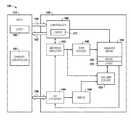
- FIG. 1is a block diagram of an apparatus in the form of a computing system 100 including a memory device 120 in accordance with a number of embodiments of the present disclosure.
- a memory device 120 , controller 140 , channel controller 143 , memory array 130 , sensing circuitry 150 , and logic circuitry 170might also be separately considered an “apparatus.”
- System 100includes a host 110 coupled (e.g., connected) to memory device 120 , which includes a memory array 130 .
- Host 110can be a host system such as a personal laptop computer, a desktop computer, a digital camera, a smart phone, or a memory card reader, among various other types of hosts.
- Host 110can include a system motherboard and/or backplane and can include a number of processing resources (e.g., one or more processors, microprocessors, or some other type of controlling circuitry).
- the system 100can include separate integrated circuits or both the host 110 and the memory device 120 can be on the same integrated circuit.
- the system 100can be, for instance, a server system and/or a high performance computing (HPC) system and/or a portion thereof.
- HPChigh performance computing
- FIG. 1illustrates a system having a Von Neumann architecture
- embodiments of the present disclosurecan be implemented in non-Von Neumann architectures, which may not include one or more components (e.g., CPU, ALU, etc.) often associated with a Von Neumann architecture.
- componentse.g., CPU, ALU, etc.
- the memory array 130can be a DRAM array, SRAM array, STT RAM array, PCRAM array, TRAM array, RRAM array, NAND flash array, and/or NOR flash array, for instance.
- the array 130can comprise memory cells arranged in rows coupled by access lines (which may be referred to herein as word lines or select lines) and columns coupled by sense lines, which may be referred to herein as data lines or digit lines. Although a single array 130 is shown in FIG. 1 , embodiments are not so limited.
- memory device 120may include a number of arrays 130 (e.g., a number of banks of DRAM cells, NAND flash cells, etc.).
- the memory device 120includes address circuitry 142 to latch address signals provided over a bus 156 (e.g., an I/O bus) through I/O circuitry 144 . Status and/or exception information can be provided from the controller 140 on the memory device 120 to a channel controller 143 (e.g., via a high speed interface (HSI) that can include an out-of-band bus 157 . Address signals are received through address circuitry 142 and decoded by a row decoder 146 and a column decoder 152 to access the memory array 130 . The address signals can also be provided to controller 140 (e.g., via address circuitry 142 and/or via a control bus 154 ).
- a bus 156e.g., an I/O bus
- Status and/or exception informationcan be provided from the controller 140 on the memory device 120 to a channel controller 143 (e.g., via a high speed interface (HSI) that can include an out-of-band bus 157 .
- HSAhigh speed interface
- Datacan be read from memory array 130 by sensing voltage and/or current changes on the data lines using sensing circuitry 150 .
- the sensing circuitry 150can read and latch a page (e.g., row) of data from the memory array 130 .
- the I/O circuitry 144can be used for bi-directional data communication with host 110 over the data bus 156 .
- the write circuitry 148is used to write data to the memory array 130 .
- Cache 171can be used to store data associated with the controller 140 .
- Controller 140which may be referred to as bank control logic and/or a sequencer, decodes signals provided by control bus 154 from the host 110 and/or channel controller 143 . These signals can include chip enable signals, write enable signals, and address latch signals that are used to control operations performed on the memory array 130 , including data read, data write, and data erase operations.
- the controller 140is responsible for executing instructions from the host 110 and sequencing access to the array 130 .
- the memory controller 140can be a state machine, a sequencer, or some other type of controller.
- the controller 140can control shifting data (e.g., right or left) in an array (e.g., memory array 130 ), as well as gathering data in accordance with a number of embodiments described herein.
- Examples of the sensing circuitry 150can comprise a number of sensing components that each may comprise a sense amplifier and a corresponding compute component, which may serve as, and be referred to herein as, an accumulator and can be used to perform logical operations (e.g., on data associated with complementary data lines).
- the sensing circuitry 150can be used to perform logical operations using data stored in array 130 as inputs and store the results of the logical operations back to the array 130 without transferring data via a sense line address access (e.g., without firing a column decode signal).
- various operationscan be performed using, and within, sensing circuitry 150 rather than (or in association with) being performed by processing resources external to the sensing circuitry (e.g., by a processor associated with host 110 and/or other processing circuitry, such as ALU circuitry, located on device 120 (e.g., on controller 140 or elsewhere)).
- processing resources external to the sensing circuitrye.g., by a processor associated with host 110 and/or other processing circuitry, such as ALU circuitry, located on device 120 (e.g., on controller 140 or elsewhere)).
- sensing circuitry 150is configured to perform logical operations on data stored in memory array 130 and store the result back to the memory array 130 without enabling an I/O line (e.g., a local I/O line) coupled to the sensing circuitry 150 .
- the sensing circuitry 150can be formed on pitch with the memory cells of the array. Additional logic circuitry 170 can be coupled to the sensing circuitry 150 and can be used to store (e.g., cache and/or buffer), results of operations described herein.
- circuitry external to array 130 and sensing circuitry 150is not needed to perform compute functions as the sensing circuitry 150 can perform the appropriate logical operations to perform such compute functions without the use of an external processing resource. Therefore, the sensing circuitry 150 may be used to compliment and/or to replace, at least to some extent, such an external processing resource (or at least the bandwidth consumption of such an external processing resource).
- the sensing circuitry 150may be used to perform logical operations (e.g., to execute instructions) in addition to logical operations performed by an external processing resource (e.g., host 110 ).
- host 110 and/or sensing circuitry 150may be limited to performing only certain logical operations and/or a certain number of logical operations.
- Enabling an I/O linecan include enabling (e.g., turning on) a transistor having a gate coupled to a decode signal (e.g., a column decode signal) and a source/drain coupled to the I/O line.
- a decode signale.g., a column decode signal
- embodimentsare not limited to not enabling an I/O line.
- sensing circuitrye.g., 150
- the local I/O line(s)may be enabled in order to transfer a result to a suitable location other than back to the array 130 (e.g., to an external register).
- FIG. 2Aillustrates a schematic diagram of a portion of a memory array 230 in accordance with a number of embodiments of the present disclosure.
- a memory celle.g., one of memory cells 201 - 1 , 201 - 2 , 201 - 3 , 201 - 4 , 201 - 5 , 201 - 6
- comprises a storage elemente.g., one of corresponding capacitors 203 - 1 to 203 - 6
- an access devicee.g., one of corresponding transistors 202 - 1 to 202 - 6 ).
- memory cell 201 - 3comprises transistor 202 - 3 and capacitor 203 - 3
- memory cell 201 - 4comprises transistor 202 - 4 and capacitor 203 - 4
- memory cell 201 - 3comprises transistor 202 - 3 and capacitor 203 - 3
- memory cell 201 - 4comprises transistor 202 - 4 and capacitor 203 - 4
- the memory array 230is a DRAM array of 1T1C (one transistor one capacitor) memory cells.
- the memory cellsmay be destructive read memory cells (e.g., reading the data stored in the cell destroys the data such that the data originally stored in the cell is refreshed after being read).
- the cells of the memory array 230are arranged in rows coupled by word lines 204 -X (Row X), 204 -Y (Row Y), etc., and columns coupled by pairs of complementary data lines DIGIT(n ⁇ 1)/DIGIT(n ⁇ 1)_, DIGIT(n)/DIGIT(n)_, DIGIT(n+1)/DIGIT(n+1)_.
- the individual data lines corresponding to each pair of complementary data linescan also be referred to as data lines 205 - 1 (D) and 205 - 2 (D_) respectively.
- the pair of complementary data linescan be referred to as a column.
- referring to a columncan refer to complementary sense lines such as D 205 - 1 and D_ 205 - 2 being included when referring to a “column.”
- complementary sense linessuch as D 205 - 1 and D_ 205 - 2 being included when referring to a “column.”
- FIG. 2AAlthough only three pair of complementary data lines are shown in FIG. 2A (e.g., three “columns”), embodiments of the present disclosure are not so limited, and an array of memory cells can include additional columns of memory cells and/or data lines (e.g., 4,096, 8,192, 16,384, etc.).
- Memory cellscan be coupled to different data lines and/or word lines.
- a first source/drain region of a transistor 202 - 3can be coupled to data line 205 - 1 (D)
- a second source/drain region of transistor 202 - 3can be coupled to capacitor 203 - 3
- a gate of a transistor 202 - 3can be coupled to word line 204 -Y.
- a first source/drain region of a transistor 202 - 4can be coupled to data line 205 - 2 (D_)
- a second source/drain region of transistor 202 - 4can be coupled to capacitor 203 - 4
- a gate of a transistor 202 - 4can be coupled to word line 204 -X.
- the cell plateas shown in FIG. 2A , can be coupled to each of capacitors 203 - 3 and 203 - 4 .
- the cell platecan be a common node to which a reference voltage (e.g., ground) can be applied in various memory array configurations.
- a reference voltagee.g., ground
- the memory array 230is coupled to sensing circuitry comprising a number of sensing components 250 - 1 , 250 - 2 , 250 - 3 , etc., in accordance with a number of embodiments of the present disclosure.
- Each sensing componentcomprises a sense amplifier and a corresponding compute component corresponding to respective columns of memory cells (e.g., coupled to respective pairs of complementary data lines).
- the sensing circuitrycan comprise a number of elements, but it at least includes a sense amp and corresponding compute component per column (e.g., the two complementary sense lines in reference to a column) of the array.
- the sensing circuitry 250 - 1comprises a sense amplifier 206 - 1 and a compute component 231 - 1 corresponding to respective columns of memory cells (e.g., memory cells 201 - 1 and 201 - 2 coupled to respective pairs of complementary data lines).
- Sensing circuitry 250 - 2comprises a sense amplifier 206 - 2 and a compute component 231 - 2 corresponding to respective columns of memory cells (e.g., memory cells 201 - 3 and 201 - 4 coupled to respective pairs of complementary data lines).
- Sensing circuitry 250 - 3comprises a sense amplifier 206 - 3 and a compute component 231 - 3 corresponding to respective columns of memory cells (e.g., memory cells 201 - 5 and 201 - 6 coupled to respective pairs of complementary data lines).
- a sense amplifiere.g., sense amplifier 206 - 1
- the sense amplifiercan be configured, for example, as described with respect to FIG. 2B .
- the compute components of array 230can be referred to generally as compute components 231 and the sense amplifiers of array 230 can be referred to generally as sense amplifiers 206 .
- the circuitry corresponding to compute component 231 - 2comprises a static latch 264 and an additional number of (e.g., ten) transistors that implement, among other things, a dynamic latch.
- compute component 231 - 2has been illustrated in an expanded format to describe the functioning of the compute component.
- Additional compute componentse.g., compute components 231 - 1 and 231 - 3
- the dynamic latch and/or static latch 264 of the compute components 231can be referred to herein as a secondary latch, which can serve as an accumulator.
- the compute components 231can operate as and/or be referred to herein as an accumulator.
- Each of the compute components 231can be coupled to a pair of complementary data lines (e.g., D 205 - 1 and D_ 205 - 2 ) as shown in FIG. 2A .
- the transistors of compute componentse.g., 231 - 2
- embodimentsare not limited to this example.
- data line D 205 - 1is coupled to a first source/drain region of transistors 216 - 1 and 239 - 1 , as well as to a first source/drain region of load/pass transistor 218 - 1 .
- Data line D_ 205 - 2is coupled to a first source/drain region of transistors 216 - 2 and 239 - 2 , as well as to a first source/drain region of load/pass transistor 218 - 2 .
- load/pass transistor 218 - 1 and 218 - 2are commonly coupled to a LOAD control signal, or respectively coupled to a PASSD/PASSDB control signal, as discussed further below.
- a second source/drain region of load/pass transistor 218 - 1is directly coupled to the gates of transistors 216 - 1 and 239 - 2 .
- a second source/drain region of load/pass transistor 218 - 2is directly coupled to the gates of transistors 216 - 2 and 239 - 1 .
- a second source/drain region of transistor 216 - 1is directly coupled to a first source/drain region of pull-down transistor 214 - 1 .
- a second source/drain region of transistor 239 - 1is directly coupled to a first source/drain region of pull-down transistor 207 - 1 .
- a second source/drain region of transistor 216 - 2is directly coupled to a first source/drain region of pull-down transistor 214 - 2 .
- a second source/drain region of transistor 239 - 2is directly coupled to a first source/drain region of pull-down transistor 207 - 2 .
- a second source/drain region of each of pull-down transistors 207 - 1 , 207 - 2 , 214 - 1 , and 214 - 2is commonly coupled together to a reference voltage (e.g., ground (GND) 291 - 1 ).
- a gate of pull-down transistor 207 - 1is coupled to an AND control signal line
- a gate of pull-down transistor 214 - 1is coupled to an ANDinv control signal line 213 - 1
- a gate of pull-down transistor 214 - 2is coupled to an ORinv control signal line 213 - 2
- a gate of pull-down transistor 207 - 2is coupled to an OR control signal line.
- the gate of transistor 239 - 1can be referred to as node S 1
- the gate of transistor 239 - 2can be referred to as node S 2
- the circuit shown in FIG. 2Astores accumulator data dynamically on nodes S 1 and S 2 .
- Activating a LOAD control signalcauses load/pass transistors 218 - 1 and 218 - 2 to conduct, and thereby load complementary data onto nodes S 1 and S 2 .
- the LOAD control signalcan be elevated to a voltage greater than V DD to pass a full V DD level to S 1 /S 2 .
- elevating the LOAD control signal to a voltage greater than V DDis optional, and functionality of the circuit shown in FIG. 2A is not contingent on the LOAD control signal being elevated to a voltage greater than V DD .
- the configuration of compute component 231 - 2 shown in FIG. 2Ahas the benefit of balancing the sense amplifier for functionality when the pull-down transistors 207 - 1 , 207 - 2 , 214 - 1 , and 214 - 2 are conducting before the sense amplifier 206 - 2 is fired (e.g., during pre-seeding of the sense amplifier 206 - 2 ).
- firing the sense amplifier 206 - 2refers to enabling the sense amplifier 206 - 2 to set the primary latch and subsequently disabling the sense amplifier 206 - 2 to retain the set primary latch.
- full rail voltagese.g., V DD , GND
- Inverting transistorscan pull-down a respective data line in performing certain logical operations.
- transistor 216 - 1having a gate coupled to S 2 of the dynamic latch
- transistor 214 - 1having a gate coupled to an ANDinv control signal line 213 - 1
- transistor 216 - 2having a gate coupled to S 1 of the dynamic latch
- transistor 214 - 2having a gate coupled to an ORinv control signal line 213 - 2
- D_pull-down data line
- the latch 264can be controllably enabled by coupling to an active negative control signal line 212 - 1 (ACCUMB) and an active positive control signal line 212 - 2 (ACCUM) rather than be configured to be continuously enabled by coupling to ground and V DD .
- load/pass transistors 208 - 1 and 208 - 2can each have a gate coupled to one of a LOAD control signal or a PASSD/PASSDB control signal.
- the gates of load/pass transistors 218 - 1 and 218 - 2can be commonly coupled to a LOAD control signal.
- transistors 218 - 1 and 218 - 2can be load transistors.
- the gate of load/pass transistor 218 - 1can be coupled to a PASSD control signal
- the gate of load/pass transistor 218 - 2can be coupled to a PASSDB control signal.
- transistors 218 - 1 and 218 - 2can be pass transistors. Pass transistors can be operated differently (e.g., at different times and/or under different voltage/current conditions) than load transistors. As such, the configuration of pass transistors can be different than the configuration of load transistors.
- configurationis intended to mean size, doping level, and transition type.
- Load transistorscan be configured (e.g., can be sized, doped, etc.) to handle loading specifications associated with coupling data lines to the local dynamic nodes S 1 and S 2 , for example.
- Pass transistorscan be configured to handle heavier loading associated with coupling data lines to an adjacent accumulator (e.g., through the adjacent compute component 231 - 3 and shift circuitry 223 - 2 in memory array 230 , as shown in FIG. 2A ).
- load/pass transistors 218 - 1 and 218 - 2can be configured to accommodate the heavier loading corresponding to a pass transistor but be coupled and operated as a load transistor.
- load/pass transistors 218 - 1 and 218 - 2 configured as pass transistorscan also be utilized as load transistors.
- load/pass transistors 218 - 1 and 218 - 2 configured as load transistorsmay not be capable of being utilized as pass transistors.
- the compute componentscan comprise a number of transistors formed on pitch with the transistors of the corresponding memory cells of an array (e.g., array 230 shown in FIG. 2A ) to which they are coupled, which may conform to a particular feature size (e.g., 4F 2 , 6F 2 , etc.).
- latch 264includes four transistors 208 - 1 , 208 - 2 , 209 - 1 , and 209 - 2 coupled to a pair of complementary data lines D 205 - 1 and D_ 205 - 2 through load/pass transistors 218 - 1 and 218 - 2 .
- the latch 264can be a cross coupled latch.
- the gates of a pair of transistorssuch as n-channel transistors (e.g., NMOS transistors) 209 - 1 and 209 - 2 are cross coupled with the gates of another pair of transistors, such as p-channel transistors (e.g., PMOS transistors) 208 - 1 and 208 - 2 .
- the cross coupled latch 264can be referred to as a static latch.
- the voltages or currents on the respective data lines D and D —can be provided to the respective latch inputs 217 - 1 and 217 - 2 of the cross coupled latch 264 (e.g., the input of the secondary latch).
- the latch input 217 - 1is coupled to a first source/drain region of transistors 208 - 1 and 209 - 1 as well as to the gates of transistors 208 - 2 and 209 - 2 .
- the latch input 217 - 2can be coupled to a first source/drain region of transistors 208 - 2 and 209 - 2 as well as to the gates of transistors 208 - 1 and 209 - 1 .
- a second source/drain region of transistor 209 - 1 and 209 - 2is commonly coupled to a negative control signal line 212 - 1 (e.g., ground (GND) or ACCUMB control signal similar to control signal RnIF shown in FIG. 2B with respect to the primary latch).
- a second source/drain region of transistors 208 - 1 and 208 - 2is commonly coupled to a positive control signal line 212 - 2 (e.g., V DD or ACCUM control signal similar to control signal ACT shown in FIG. 2B with respect to the primary latch).
- the positive control signal 212 - 2can provide a supply voltage (e.g., V DD ) and the negative control signal 212 - 1 can be a reference voltage (e.g., ground) to enable the cross coupled latch 264 .
- the second source/drain region of transistors 208 - 1 and 208 - 2are commonly coupled directly to the supply voltage (e.g., V DD ), and the second source/drain region of transistor 209 - 1 and 209 - 2 are commonly coupled directly to the reference voltage (e.g., ground) so as to continuously enable latch 264 .
- the enabled cross coupled latch 264operates to amplify a differential voltage between latch input 217 - 1 (e.g., first common node) and latch input 217 - 2 (e.g., second common node) such that latch input 217 - 1 is driven to either the activated positive control signal voltage (e.g., V DD ) or the activated negative control signal voltage (e.g., ground), and latch input 217 - 2 is driven to the other of the activated positive control signal voltage (e.g., V DD ) or the activated negative control signal voltage (e.g., ground).
- the activated positive control signal voltagee.g., V DD
- the activated negative control signal voltagee.g., ground
- the sense amplifier 206 - 2 and the compute component 231 - 2can be coupled to the array 230 via shift circuitry 223 - 2 .
- the sensing circuitrycan include shifting circuitry, such as shifting circuitry 223 - 1 , 223 - 2 , and 223 - 3 , as shown in FIG. 2A and referred to generally as shifting circuitry 223 .
- the shift circuitry 223comprises a pair of isolation devices coupled to respective data lines of a complementary data line pair (e.g., isolation transistors 221 - 1 and 221 - 2 of shifting circuitry 223 - 2 are coupled to data lines 205 - 1 (D) and 205 - 2 (D_), respectively).
- the isolation transistorsare coupled to a control signal 222 (NORM) that, when activated, enables (e.g., turns on) the isolation transistors 221 - 1 and 221 - 2 to couple the corresponding sense amplifier 206 - 2 and compute component 231 - 2 to a corresponding column of memory cells (e.g., to a corresponding pair of complementary data lines 205 - 1 (D) and 205 - 2 (D_), and compute component 231 - 6 corresponding to DIGIT(n ⁇ 1) and DIGIT(n ⁇ 1) illustrated on the left complementary pair of sense lines and compute component 231 - 6 corresponding to DIGIT (n+1) and DIGIT(n+1) illustrated on the right complementary pair of sense lines).
- conduction of the isolation transistorse.g., 221 - 1 and 221 - 2
- conduction of the isolation transistorscan be referred to as a “normal” configuration of the shift circuitry
- the shift circuitry 223includes another (e.g., a second) pair of isolation devices coupled to a complementary control signal (e.g., shift circuitry 223 - 2 includes isolation transistors 221 - 3 and 221 - 4 coupled to complementary control signal 219 (SHIFT)), which can be activated, for example, when NORM 222 is deactivated.
- a complementary control signale.g., shift circuitry 223 - 2 includes isolation transistors 221 - 3 and 221 - 4 coupled to complementary control signal 219 (SHIFT)
- the isolation transistorscan be operated (e.g., via control signal 219 ) such that a particular sense amplifier (e.g., 206 - 2 ) and compute component (e.g., 231 - 2 ) are coupled to a different pair of complementary data lines (e.g., a pair of complementary data lines different than the pair of complementary data lines to which isolation transistors 221 - 1 and 221 - 2 couple the particular sense amplifier 206 - 2 and compute component 231 - 2 ), or can couple a particular sense amplifier 206 - 2 and compute component 231 - 2 to another memory array (and isolate the particular sense amplifier 206 - 2 and compute component 231 - 2 from a first memory array).
- the shift circuitry 223can be arranged as a portion of (e.g., within) a corresponding sense amplifier 206 , for instance.
- the shift circuitry 223 - 2 shown in FIG. 2Aincludes isolation transistors 221 - 1 and 221 - 2 used to couple particular a particular sensing component 250 - 2 (e.g., a particular sense amplifier 206 - 2 and corresponding compute component 231 - 2 ) to a particular pair of complementary data lines 205 - 1 (D) and 205 - 2 (D_) (e.g., DIGIT(n) and DIGIT(n)_) and isolation transistors 221 - 3 and 221 - 4 are arranged to couple the particular sensing component 250 - 2 to an adjacent pair of complementary data lines in one particular direction (e.g., adjacent data lines DIGIT(n+1) and DIGIT(n+1) shown to the right in FIG.
- a particular sensing component 250 - 2e.g., a particular sense amplifier 206 - 2 and corresponding compute component 231 - 2
- D_complementary data lines
- isolation transistors 221 - 3 and 221 - 4are
- shift circuitry 223can include isolation transistors (e.g., 221 - 1 and 221 - 2 ) used to couple particular sensing circuitry to a particular pair of complementary data lines (e.g., DIGIT(n) and DIGIT(n)) and isolation transistors (e.g., 221 - 3 and 221 - 4 ) arranged so as to be used to couple a particular sensing component (e.g., 250 - 2 ) to an adjacent pair of complementary data lines in another particular direction (e.g., adjacent data lines DIGIT(n ⁇ 1) and DIGIT(n ⁇ 1)_).
- isolation transistorse.g., 221 - 1 and 221 - 2
- isolation transistorse.g., 221 - 3 and 221 - 4
- Embodiments of the present disclosureare not limited to the configuration of shift circuitry shown in FIG. 2A .
- determining whether to shift in a particular direction to perform a shift operationis independent of the circuitry implementation.
- shift circuitrysuch as that shown in FIG. 2A (e.g., shift circuitry 223 ) can be operated (e.g., in conjunction with corresponding sensing components 250 ) in association with performing mathematical operations such as adding and subtracting operations without transferring data out of the sensing circuitry via an I/O line (e.g., local I/O line (IO/IO_)), for instance.
- I/O linee.g., local I/O line (IO/IO_)
- each column of memory cellscan be coupled to a column decode line that can be activated to transfer, via a local I/O line (e.g., I/O line 334 in FIG. 3A ), a data value from a corresponding sense amplifier 206 and/or compute component 231 to a control component external to the array such as an external processing resource (e.g., host processor and/or other functional unit circuitry).
- the column decode linecan be coupled to a column decoder.
- shift circuitry 223can be operated in conjunction with sense amplifiers 206 and compute components 231 to perform logical operations without transferring data to a control component external to the array, for instance.
- FIG. 2Bis a schematic diagram illustrating a portion of sensing circuitry in accordance with a number of embodiments of the present disclosure.
- sense amplifier 206can comprise a cross coupled latch.
- embodiments of the sense amplifier 206are not limited to a cross coupled latch.
- the sense amplifier 206 in FIG. 2Bcan be current-mode sense amplifier and/or single-ended sense amplifier (e.g., sense amplifier coupled to one data line).
- embodiments of the present disclosureare not limited to a folded data line architecture.
- a sense amplifier(e.g., 206 - 2 shown in FIG. 2A ) can comprise a number of transistors formed on pitch with the transistors of a corresponding compute component (e.g., 231 - 2 shown in FIG. 2A ) and/or the memory cells of an array (e.g., 230 shown in FIG. 2A ) to which they are coupled, which may conform to a particular feature size (e.g., 4F 2 , 6F 2 , etc.).
- Sense amplifier 206 shown in FIG. 2Bcomprises a latch 215 including four transistors coupled to a pair of complementary data lines D 205 - 1 and D_ 205 - 2 .
- the latch 215can be a cross coupled latch.
- the gates of a pair of transistorssuch as n-channel transistors (e.g., NMOS transistors) 227 - 1 and 227 - 2 are cross coupled with the gates of another pair of transistors, such as p-channel transistors (e.g., PMOS transistors) 229 - 1 and 229 - 2 .
- the latch 215comprising transistors 227 - 1 , 227 - 2 , 229 - 1 , and 229 - 2 can be referred to as a primary latch.
- embodimentsare not limited to this example.
- the voltages or currents on the respective data lines D and D —can be provided to the respective latch inputs 233 - 1 and 233 - 2 of the cross coupled latch 215 (e.g., the input of the primary latch).
- the latch input 233 - 1is coupled to a first source/drain region of transistors 227 - 1 and 229 - 1 as well as to the gates of transistors 227 - 2 and 229 - 2 .
- the latch input 233 - 2can be coupled to a first source/drain region of transistors 227 - 2 and 229 - 2 as well as to the gates of transistors 227 - 1 and 229 - 1 .
- the compute component 231 shown in FIG. 2ABcan be a compute component such as compute component 231 - 2 shown in FIG. 2A .
- a second source/drain region of transistor 227 - 1 and 227 - 2is commonly coupled to an active negative control signal 228 (RnIF).
- a second source/drain region of transistors 229 - 1 and 229 - 2is commonly coupled to an active positive control signal 265 (ACT).
- the ACT signal 265can be a supply voltage (e.g., V DD ) and the RnIF signal can be a reference voltage (e.g., ground).
- Activating signals 228 and 265enables the cross coupled latch 215 .
- the enabled cross coupled latch 215operates to amplify a differential voltage between latch input 233 - 1 (e.g., first common node) and latch input 233 - 2 (e.g., second common node) such that latch input 233 - 1 is driven to one of the ACT signal voltage and the RnIF signal voltage (e.g., to one of V DD and ground), and latch input 233 - 2 is driven to the other of the ACT signal voltage and the RnIF signal voltage.
- latch input 233 - 1e.g., first common node
- latch input 233 - 2e.g., second common node
- the sense amplifier 206can also include circuitry configured to equilibrate the data lines D and D — (e.g., in association with preparing the sense amplifier for a sensing operation).
- the equilibration circuitrycomprises a transistor 224 having a first source/drain region coupled to a first source/drain region of transistor 225 - 1 and data line D 205 - 1 .
- a second source/drain region of transistor 224can be coupled to a first source/drain region of transistor 225 - 2 and data line D_ 205 - 2 .
- a gate of transistor 224can be coupled to gates of transistors 225 - 1 and 225 - 2 .
- the second source drain regions of transistors 225 - 1 and 225 - 2are coupled to an equilibration voltage 238 (e.g., V DD /2), which can be equal to V DD /2 where V DD is a supply voltage associated with the array.
- the gates of transistors 224 , 225 - 1 , and 225 - 2can be coupled to control signal 226 (EQ).
- EQcontrol signal 226
- activating EQenables the transistors 224 , 225 - 1 , and 225 - 2 , which effectively shorts data line D to data line D — such that the data lines D and D — are equilibrated to equilibration voltage V DD /2.
- a number of logical operationscan be performed using the sense amplifier 206 and corresponding compute component 231 , and the result can be stored in the sense amplifier and/or compute component.
- sensing circuitrysuch as a sensing component comprising sense amplifier 206 and compute component 231 , can be operated in several modes to perform logical operations, including a first mode in which a result of the logical operation is initially stored in the sense amplifier 206 , and a second mode in which a result of the logical operation is initially stored in the compute component 231 .
- sensing circuitrycan be operated in both pre-sensing (e.g., sense amps fired before logical operation control signal active) and post-sensing (e.g., sense amps fired after logical operation control signal active) modes with a result of a logical operation being initially stored in the sense amplifier 206 .
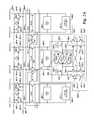
- FIG. 3Aillustrates a schematic diagram of a portion of a memory array 330 in accordance with a number of embodiments of the present disclosure.
- the array 330includes memory cells (referred to generally as memory cells 303 , and more specifically as 303 - 0 to 303 -J) coupled to rows of access lines 304 - 0 , 304 - 1 , 304 - 2 , 304 - 3 , 304 - 4 , 304 - 5 , 304 - 6 , . . .
- each column of memory cellscan be associated with a corresponding pair of complementary sense lines (e.g., complementary sense lines 205 - 1 and 205 - 2 in FIG. 2A ).
- Each column of memory cellscan be coupled to sensing circuitry (e.g., sensing circuitry 150 shown in FIG. 1 ).
- the sensing circuitrycomprises a number of sense amplifiers 306 - 0 , 306 - 1 , 306 - 2 , 306 - 3 , 306 - 4 , 306 - 5 , 306 - 6 , 306 - 7 , . . .
- sense amplifiers 306coupled to the respective sense lines 305 - 0 , 305 - 1 , 305 - 2 , 305 - 3 , 305 - 4 , 305 - 5 , 305 - 6 , 305 - 7 , . . . , 305 -S.
- the sense amplifiers 306are coupled to input/output (I/O) line 334 (e.g., a local I/O line) via access devices (e.g., transistors) 308 - 0 , 308 - 1 , 308 - 2 , 308 - 3 , 308 - 4 , 308 - 5 , 308 - 6 , 308 - 7 , . . . , 308 -V.
- I/O line 334e.g., a local I/O line
- access devicese.g., transistors
- the sensing circuitryalso comprises a number of compute components 331 - 0 , 331 - 1 , 331 - 2 , 331 - 3 , 331 - 4 , 331 - 5 , 331 - 6 , 331 - 7 , . . . , 331 -X corresponding to respective sense amplifiers 306 and coupled to the respective sense lines 305 .
- Column decode lines 310 - 1 to 310 -Ware coupled to the gates of transistors 308 - 1 to 308 -V, respectively, and can be selectively activated to transfer data sensed by respective sense amplifiers 306 - 0 to 306 -U and/or stored in respective compute components 331 - 0 to 331 -X to a secondary sense amplifier 312 .
- the compute components 331can be formed on pitch with the memory cells of their corresponding columns and/or with the corresponding sense amplifiers 306 .
- the sensing circuitrye.g., compute components 331 and sense amplifiers 306
- the sensing circuitryis configured to perform a gather operation on elements stored in array 330 .
- a plurality of elements each comprising four data unitse.g., 4-bit elements
- a first element of the plurality of elementscan be stored in a first group of memory cells coupled to a number of access lines (e.g., 304 - 0 , 304 - 1 , 304 - 2 , 304 - 3 ) and to a sense line (e.g., 305 - 0 ), and a second element can be stored in a second group of memory cells coupled to the number of access lines (e.g., 304 - 0 to 304 - 3 ) and to a different sense line (e.g., sense line 305 - 4 , which corresponds to a different column of array 330 ).
- a number of access linese.g., 304 - 0 , 304 - 1 , 304 - 2 , 304 - 3
- a sense linee.g., 305 - 0
- a second elementcan be stored in a second group of memory cells coupled to the number of access lines (e.g., 304
- the first element and the second elementare stored in a horizontally non-contiguous fashion (e.g., since the cells storing the first element and the second element correspond to non-adjacent columns).
- the sense line 305 - 0 coupled to cells storing the first elementis separated from the sense line 305 - 4 coupled to cells storing the second element by intervening sense lines 305 - 1 , 305 - 2 , and 305 - 3 .
- FIG. 3Billustrates a schematic diagram of a portion of a memory array in accordance with a number of embodiments of the present disclosure.
- FIG. 3Brepresents an example of data stored in a portion of an array such as array 330 shown in FIG. 3A .
- the array shown in FIG. 3Bincludes a number of elements comprising data units (e.g., bits) stored vertically in the array. However, in FIG. 3B the elements are stored in a horizontally non-contiguous fashion.
- the array shown in FIG. 3Bincludes four 8-bit elements.
- a first element (“11111111”)is stored in memory cells coupled to sense line 305 - 0 and to access lines 304 - 0 to 304 - 7 .
- a second element(“00000000”) is stored in memory cells coupled to sense line 305 - 8 and access lines 304 - 0 to 304 - 7 .
- the first element and the second elementare considered to be horizontally non-contiguous because there are intervening columns (e.g., columns corresponding to sense lines 305 - 1 to 305 - 7 ) between the first and second element.
- the “X”s shown in FIG. 3Bdesignate cells not storing data corresponding to elements of interest.
- a third element(“11110000”) is stored in memory cells coupled to sense line 305 - 0 and access lines 304 - 8 to 304 - 15
- a fourth element(“11110000”) is stored in memory cells coupled to sense line 305 - 8 and access lines 304 - 8 to 304 - 15
- the third element and fourth elementare also horizontally non-contiguous. While the example shown in FIG. 3B illustrates two elements (that are stored vertically) per row (e.g., elements stored in memory cells coupled to two different sense lines, 305 - 0 and 305 - 8 ), examples are not so limited.
- a first example element(such as element “11111111”) is stored in cells of row 304 - 0 to 304 - 7 and column 205 - 0 and a second example element (such as element “00000000”) is stored in cells of rows 304 - 0 to 304 - 7 and column 305 - 8 but the first and second elements are only stored in two cells along row 304 - 0 (e.g., corresponding to columns 305 - 0 and 305 - 8 ).
- a third example element(such as element “11110000”) is stored in cells of rows 304 - 8 to 304 - 15 and column 305 - 0 and a fourth example element (such as element “11110000”) is stored in cells of rows 304 - 8 to 304 - 15 and column 305 - 8 .
- examplesare not so limited and any number of elements can be stored vertically along a row of memory cells.
- a memory arrayis not limited to the number of columns or number of rows of memory cells and/or elements within those columns and rows of memory cells.
- FIG. 3Cillustrates a schematic of a portion of a memory array in accordance with a number of embodiments of the present disclosure.
- FIG. 3Cis an example of data units being stored in a memory array in a horizontally contiguous fashion.
- a first element including “11111111”is stored as a vertical vector in memory cells coupled to access lines 304 - 0 to 304 - 7 and sense line 305 - 0
- a second element including “00000000”is stored as a vertical vector in memory cells coupled to access lines 304 - 0 to 304 - 7 and sense line 305 - 1
- a third element including “11110000”is stored as a vertical vector in memory cells coupled to access lines 304 - 8 to 304 - 15 and sense line 305 - 8
- a fourth element including “11110000”is stored as a vertical vector in memory cells coupled to access lines 304 - 8 to 304 - 15 and sense line 305 - 9 .
- the first element and second elementare stored as horizontally contiguous vectors in FIG. 3C .
- the third and fourth elementsare stored as horizontally contiguous vectors in FIG. 3C .
- FIGS. 3B and 3Creference elements including eight (8) data units (e.g., bits), examples are not so limited.
- element widthscan be 4, 8, 16, 32, etc. data units.
- FIG. 4illustrates tables showing the states of memory cells of an array (e.g., 330 in FIG. 3A ) at a number of particular phases associated with performing a gathering operation in accordance with a number of embodiments described herein.
- the reference numbers of the rows of the tables shown in FIG. 4correspond to respective reference numbers of the pseudo code described below (e.g., row 451 - 0 corresponds to reference number 0 of the pseudo code, rows 451 - 4 . 1 a to 451 - 4 . 1 k correspond to reference number 4 (e.g., 4a to 4k) of the pseudo code, etc.).
- Each row of the tablesindicates the data values of a number of bit vectors 431 (COMP_COMP), 433 (TMPLOOKUP), 435 (TMPELEM), 437 (ELEM_MASK), and 439 (DEST) at a particular phase of the gathering operation as can be stored in rows and/or columns of memory cells in the array (e.g., 330 in FIG. 3A ).
- the example shown in FIG. 4is associated with gathering a first data unit of elements stored in memory cells coupled to access line 304 - 0 and to sense lines 305 - 0 to 305 - 31 . More specifically, the example illustrates a first data unit position (e.g., most significant bit of each element stored in a first row of memory cells such as memory cells 303 - 0 to 303 - 31 in FIG. 3A , cells 303 - 8 to 303 - 31 not shown) of each element stored in an array.
- a first data unit positione.g., most significant bit of each element stored in a first row of memory cells such as memory cells 303 - 0 to 303 - 31 in FIG. 3A , cells 303 - 8 to 303 - 31 not shown
- the gathering operation examplewill perform a gather of a first data unit of each element stored vertically in memory cells coupled to sense lines 305 - 0 , 305 - 4 , 305 - 8 , 305 - 12 , 305 - 16 , 305 - 20 , 305 - 24 , and 305 - 28 , respectively (sense lines 305 - 8 to 305 - 28 not shown but indicated by 305 -S).
- the horizontal vector [0x88,88,88,88](binary [1000 1000, 1000, 1000, 1000 1000 1000) illustrated as DEST 439 in row 451 - 0 designates a first data unit of each of eight elements (where each element is eight data units in length) stored vertically in the array.
- the “1” bit stored in memory cell of access line 304 - 0 and sense line 305 - 0 in FIG. 3Cis a first data unit (e.g., most significant bit) of the vertically stored element “11111111.”
- 3Cis a first data unit of the vertically stored element “00000000.”
- the data stored in memory cells coupled to access line 304 - 0 stored as a row (illustrated horizontally)includes “10XXXXXXXXXXXX” and corresponds to the DEST 439 vector [0x88,88,88,88] illustrated in FIG. 4 .
- the first data unit of each elementshown as a horizontal row of values illustrated in FIG.
- FIG. 4can be compared, for illustrative purposes, with the first data unit of each element (e.g., bolded bit of [10XXXXXXXXXXXX]) stored in cells coupled to access line 304 - 0 and sense lines 305 - 0 to 305 - 15 (not to be directly correlated as FIG. 3C is a 16 element example, meaning 16 elements across 16 sense lines that are stored vertically, and FIG. 4 is a 32 element example, meaning 32 elements across 32 sense lines that are stored vertically but only illustrated as the first horizontal row of first data units of each element).
- the first data unit of each elemente.g., bolded bit of [10XXXXXXXXXXXXX]
- the first data unit (e.g., most significant bit) of the first elemente.g., the “1” indicated by the first “8” in [0x88,88,88,88], indicated in bold
- the subsequent seven data units (e.g., next most significant bit to least significant bit) of the first element stored verticallyare not illustrated (although these next seven data units would be stored in memory cells coupled to access lines 304 - 1 to 304 - 7 , indicated by 304 -R in FIG. 3A ).
- the first data unit of the second element(e.g., the second 8 in [0x88,88,88,88], indicated in bold) is in the first row of cells and stored in a memory cell coupled to a fourth column of cells or coupled to sense line 305 - 4 .
- the first data unit of the third elementis stored in a memory cell coupled to sense line 305 - 8
- the first data unit of the fourth elementis stored in a memory cell coupled to a sense line 305 - 12
- the first data unit of the fifth elementis stored in a memory cell coupled to sense line 305 - 16
- the first data unit of the sixth elementis stored in a memory cell coupled to sense line 305 - 20
- the first data unit of the seventh elementis stored in a memory cell coupled to sense line 305 - 24
- the first data unit of the eighth elementis stored in a memory cell coupled to sense line 305 - 28 .
- bit-vector DEST 439e.g., [1000 1000 1000 1000 1000 1000 1000 1000], which can be represented in hexadecimal notation as [0X88888888] (where the “Ox” indicates hexadecimal notation and commas can separate different elements) and is shown in FIG. 4 as “0X88,88,88,88”).
- bit-vector DEST 439has a width of 32 data units (e.g., bits). Each element of bit-vector DEST 439 is 4 data units (e.g., bits) wide. It is noted that although hexadecimal notation is used in FIG. 4 , the bit-vectors are stored as binary data patterns in the array during the gathering operation. Also, in the examples described herein, commas and/or spaces may be used to separate a number of elements within a bit-vector for ease of reference. For instance, in the example above, bit-vector DEST 439 groups elements by twos between each comma.
- Embodimentsare not limited to a particular element size (e.g., to a particular number of bits per element) or to a particular quantity of elements.
- the result of the gathering operationcan be stored in an array (e.g., 330 ) with the vectors comprising the elements being gathered being stored, and/or being transferred external to the array (e.g., to functional unit circuitry of a host).
- the expected result of gathering the first data units of each of the elements of DEST 439is resulting bit-vector [0XFF,00,00,00] (e.g., DEST 439 stored at 451 - 4 . 8 in FIG. 4 ).
- the result of a gathering operationcan be stored as a bit-vector in a particular group of memory cells. For instance, in the example of FIG. 4 , the memory cells corresponding to DEST 439 can be used to store the result of the gathering operation at 451 - 4 . 8 . As such, at the conclusion of the example described in FIG.
- DEST 439 in hexadecimal(e.g., binary [1111 1111 0000 0000 0000 0000]), which represents the eight resultant elements being stored in the 8 columns furthest to the left of the memory array (e.g., 1 st through 8 th ) rather than the 1 st , 5 th , 9 th , 13th, 17 th , 21 st , 25 th , and 29 th columns at the start of the example.
- bit vectors 433TMPLOOKUP
- 435TMPELEM
- 437EML_MASK
- DESTDEST
- the bit-vectors 433 , 435 , 437 , and 439can be stored in respective groups of memory cells coupled to particular access lines, which may be referred to as temporary storage rows.
- temporary storage rows of memory cellsare storing data that may be updated during various phases of a gathering operation.
- the bit-vectors 433 , 435 , 437 , and 439can have a same width (e.g., 32 bits) and can each be stored in cells coupled to a plurality of sense lines and an access line (e.g., horizontally stored).
- the bit-vector 439(DEST) can have a width of 32 bits and can be stored in a group of cells coupled to access line 304 - 0 and to sense lines 305 - 0 to 305 - 31 .
- Bit-vector 439can include a first data unit of each of a number of vertically stored elements, as described above (where the second through the eighth data units are not illustrated and would be stored in subsequent second through eight rows of memory cells and gathered per data stored in each row of cells).
- a gathering operationincludes performing a number of AND operations, OR operations, SHIFT operations, and INVERT operations.
- the gathering operationincludes performing the AND operations, OR operations, SHIFT operations, and INVERT operations without transferring data via an input/output (I/O) line to gather a number of elements of a bit-vector.
- the number of AND operations, OR operations, INVERT operations, and SHIFT operationscan be performed using sensing circuitry on pitch with the memory array and with each of a number of columns of complementary sense lines.
- the below pseudocoderepresents instructions executable to perform a number of gathering operations in a memory in accordance with a number of embodiments of the present disclosure.
- the example pseudocodeis referenced using reference numbers 0-4, which correspond to the reference numbers of the rows shown in the tables of FIG. 4 and in reference to the column numbers of the tables of FIG. 4 .
- reference number 0(e.g., “Get Temp Rows TMPLOOKUP, TMPELEM, ELEM_MASK, and DEST”) corresponds to row 451 - 0 and to columns 433 , 435 , 437 , and 439
- reference number 1(e.g., “Generate MSB and Shift Right for Vector Width”) corresponds to row 451 - 1 and to column 431
- Reference number 4a.(e.g., “Load Tmp_Lookup into COMP_COMP”) corresponds to rows 451 - 4 . 1 a , 451 - 4 . 2 a , 451 - 4 . 3 a , 451 - 4 .
- the above pseudo codewill be divided into a setup phase and a gathering phase associated with performing a gathering operation (e.g., gathering a first data unit of each of eight elements initially stored as DEST 439 , each first data unit at a particular position horizontally).
- the pseudo code referenced by reference numbers 0-3can correspond to the setup phase.
- the setup phasecan be performed simultaneously for a number of the gathering operations.
- a bit-vector value illustrated in boldindicates a change in the value of the bit-vector (e.g., the value of the bit-vector stored in the memory cells corresponding to TMPLOOKUP 433 is shown in bold in FIG.
- FIG. 4illustrates the values of a number of bit-vectors associated with performing the setup phase of a gathering operation.
- the pseudo code referenced by reference number 4e.g., 4a-4k can correspond to the gathering phase.
- the setup phasecan be performed simultaneously for all of the vertically stored elements to be gathered.
- the resultse.g., the resulting stored bit-vectors
- FIG. 4The results (e.g., the resulting stored bit-vectors) corresponding to a number of operations performed in the setup phase are shown in FIG. 4 .
- Rows 451 - 0 to 451 - 3 of the table in FIG. 4correspond to the above pseudocode instructions referenced by reference numbers 0 to 3, respectively.
- rows 451 - 0 to 451 - 3indicate values of the bit vectors 431 , 433 , 435 , 437 , and 439 during execution of the setup phase as described by the above pseudocode.
- Reference number 0(e.g., “Get Temp Rows TMPLOOKUP, TMPELEM, ELEM_MASK, and DEST”) of the above pseudocode is associated with initializing a number of groups of memory cells for use as temporary storage rows to be used to store bit-vectors (e.g., 433 , 435 , 437 , and 439 ).
- Initializingrefers to designating and/or assigning particular access lines used to store particular bit-vectors for performing the gathering operation.
- the number of groups of memory cellscan be initialized and/or designated groups of cells that can be coupled to respective access lines (e.g., rows) that store data (e.g., on a temporary basis) in association with performing the gathering operation.
- a first group of memory cellscan be coupled to a particular access line (e.g., 304 - 0 , ROW 0 in FIG. 3A ) and can store a bit-vector referred to as a “TMPLOOKUP” bit-vector 433 .
- a second group of memory cellscan be coupled to another access line (e.g., 304 - 1 , ROW 1 , not shown) and can store a bit-vector referred to as a “TMPELEM” bit-vector 435 .
- a third group of memory cellscan be coupled to another access line (e.g., 304 - 2 , ROW 2 , not shown) and can store a bit-vector referred to as an “ELEM_MASK” bit-vector 437 .
- a fourth group of memory cellscan be coupled to another access line (e.g., 304 - 3 , ROW 3 , not shown) and can store a bit-vector referred to as a “DEST” bit-vector 439 .
- Embodimentsare not limited to a particular number of temporary storage rows and/or to storage of the corresponding bit-vectors on particular access lines.
- the groups of memory cells used to store bit-vectors 433 , 435 , 437 , and 439may be referred to as “rows,” the respective groups of memory cells may comprise fewer than all of the cells coupled to a particular access line.
- temporary storage rowscan refer to access lines which may not be addressable by a user (e.g., access lines that are outside of a user-addressable address space).
- the bit-vectors stored in memory cells corresponding to the temporary storage rowsare stored in memory cells coupled to the same sense lines as the elements that are being gathered.
- the ELEM_MASK 437indicates a most significant bit (MSB) associated with the first data unit (e.g., most significant bit) of the second element of the bit-vector of the elements being gathered.
- MSBmost significant bit
- a bit patterncomprising a “1” in a MSB position of the second element and all “0s” in the remaining bit positions can be used to indicate the MSB of the constituent bit-vector of the source elements (e.g., DEST 439 ).
- the bit pattern of ELEM_MASK 439identifies a starting point indicated as the most significant bit of the second element to be gathered. As shown in row 451 - 0 of FIG.
- ELEM_MASK 439is a 32-bit hexadecimal bit-vector [0x08,00,00,00] (e.g., binary [0000 1000 0000 0000 0000 0000 0000]).
- Row 451 - 0 of the table shown in FIG. 4illustrates the values of the first data unit (e.g., most significant bit) of each element to be gathered stored as DEST 439 upon being stored (e.g., loaded) in an array (e.g., 330 ).
- the values of the bit-vectorare shown in FIG. 4 in hexadecimal form for convenience, designated by the leading “0x” (e.g., the value of bit-vector 439 is shown as [0x88,88,88,88]), the bit-vectors can be stored as binary data patterns in the array.
- an example gathering operation associated with execution of the above pseudocodeincludes gathering eight elements that are separated from each other by three columns (e.g., by three memory cells (further indicated as three columns of pairs of complementary sense lines, as described above) each as indicated by vector [0x88,88,88,88], binary [1000 1000, 1000 1000, 1000, 1000]).
- the resulting gathered first data units of each of the elementsinclude a bit-vector of [0xFF,00,00,00] (e.g., binary [1111 1111, 0000 0000, 0000 0000, 0000 0000], as indicated at row 451 - 4 . 8 in FIG. 4 ).
- Reference number 1(e.g., “Generate MSB and Shift Right for Vector Width”) of the above pseudocode is associated with generating a most significant bit (“MSB”) of the bit-vector which indicates a first data unit of each of the eight elements (e.g., horizontal bit-vector) and shifting right a width of the vector width (e.g., width of an element in the vector, which is illustrated as 32 bits in this example). Since each element in the horizontal bit-vector is 4 bits apart, the MSB will be shifted 4 positions (4 memory cells, which corresponds to 4 columns) to the right. Finding the MSB of the horizontal bit-vector includes the following operations.
- the compute components (e.g., 331 ) storing the bit-vector COMP_COMP 431are cleared by loading zeros such that value of COMP_COMP 431 is [0x00,00,00,00].
- the compute components corresponding to COMP_COMP 431are then set to all data values being “1” such that the value of COMP_COMP 431 is [0xFF,FF,FF,FF].
- the value of COMP_COMP 431is then shifted one position to the right by replacing open positions that are shifted (e.g., most significant bit shifted to next most significant bit position) with a “0” data value.
- COMP_COMP 431For example, after a right shift by one position, the value of COMP_COMP 431 would be [0x7F,FF,FF,FF] (e.g., binary [0111 1111, 1111 1111, 1111 1111, 1111 1111]). COMP_COMP 431 is then inverted, resulting in the value of COMP_COMP becoming [0x80,00,00,00], as illustrated in COMP_COMP 431 at row 451 - 1 .
- Reference number 2(e.g., “Shift Right for Vector Width”), includes shifting COMP_COMP 431 one vector width (e.g., distance between each element within the vector) to the right.
- COMP_COMP 431e.g., [0x80,00,00,00]
- COMP_COMP 431is shifted 4 positions to the right as each element is 4 data unit positions apart.
- the shiftingresults in COMP_COMP 431 having a value of [0x08,00,00,00] as shown at row 451 - 2 of the table shown in FIG. 4 .
- Reference number 3(e.g., “Store in ELEM_MASK, TMPLOOKUP and Obtain number of elements with vector width and array size”) includes storing the value of COMP_COMP 431 to ELEM_MASK 437 and to TMPLOOKUP 433 and obtaining the number of elements, a distance between elements, and the total bit-vector width (e.g., in this case distance between each vertically stored element, which is 4 bits).
- bit-vector [0x08,00,00,00] stored in the compute components corresponding to COMP_COMP 431is stored to TMPLOOKUP 433 and ELEM_MASK 437 .
- DEST 439indicates that there are eight elements to be gathered, each element is 4 data units apart, and the bit-vector comprises a total of 32 data units.
- DEST 439in binary, is [1000 1000, 1000 1000, 1000 1000, 1000], where each “1” in the DEST 439 bit-vector indicates a first data unit of each vertically stored element and, since there are eight “1”s in DEST 439 , eight elements are indicated.
- TMPLOOKUP 433The value of TMPLOOKUP 433 is [0x08,00,00,00] (e.g., binary [0000 1000, 0000 0000, 0000 0000, 0000 0000]), the value of TMPELEM 435 is [0x00,00,00,00] (e.g., binary [0000 0000, 0000 0000, 0000 0000]), the value of ELEM_MASK 437 is [0x08,00,00,00] (e.g., binary [0000 10000, 0000 0000, 0000 0000]), and the value of DEST 439 is [0x88,88,88,88] (e.g., binary [1000 1000, 1000, 1000, 1000]).
- FIG. 4illustrates the values of the number of bit-vectors 433 , 435 , 437 , and 439 during a first iteration 451 - 4 . 1 , a second iteration 451 - 4 . 2 , a third iteration 451 - 4 . 3 , a fourth iteration 451 - 4 . 4 , a fifth iteration 451 - 4 . 5 , a sixth iteration 451 - 4 . 6 , a seventh iteration 451 - 4 . 7 , and an eighth iteration 451 - 4 . 8 of gathering phases associated with reference numbers 4a-4k referenced above.
- Each iterationis associated with gathering a particular data unit of each of the vertically stored elements such that it is contiguous (e.g., adjacent) to a data unit of a preceding vertically stored element. For example, a first iteration gathers a first data unit of a second element to be next to a first data unit of a first element. A second iteration gathers a first data unit of a third element to be next to the first data unit of the second element, and so forth until the first data units of each of the eight elements are contiguously stored in eight neighboring memory cells (e.g., memory cells 303 - 0 to 303 - 7 ).
- eight neighboring memory cellse.g., memory cells 303 - 0 to 303 - 7 .
- Reference number 4(e.g., “Run fixed loop for e elements”), includes performing a loop that gathers each element next to a previous element in the bit-vector a number of iterations equal to the number (“e”) of elements. Since there are eight elements in DEST 439 (e.g., [0x88,88,88,88]), the loop will run eight times to gather each of the eight elements. Each loop of reference number 4 is associated with an element to be gathered. For example, a first loop represented by rows 451 - 4 . 1 a to 451 - 4 . 1 k will gather a first data unit of a second element to be next to a first data unit of a first element.
- [0x88] of DEST 439(e.g., [0x88,88,88,88]) will be gathered to result in [0xC0] as indicated by DEST 439 at row 451 - 4 . 1 h .
- a second loop indicated by rows 451 - 4 . 2 a to 451 - 4 . 2 kwill gather [0x88,8] of [0x88,88,88,88] to result in [0xE0] as indicated by DEST 439 of [0xEo,08,88,88] at row 451 - 4 . 2 h .
- a third, fourth, fifth, sixth, and seventh loopwill result in gathering DEST 439 of [0x88,88,88] at row 451 - 4 . 1 a to DEST 439 of [0xFF,00,00,00] at row 451 - 4 . 7 k.
- reference number 4a(e.g., “Load Tmp_Lookup to COMP_COMP”) of the above pseudocode is associated with storing bit-vector TMPLOOKUP 433 (e.g., [0x08,00,00,00]) as COMP_COMP 431 , as illustrated at row 451 - 4 . 1 a in FIG. 4 .
- Reference number 4b(e.g., “AND COMP_COMP and DEST”) of the above pseudocode is associated with performing an AND operation on COMP_COMP 431 and DEST 439 .
- COMP_COMP 431e.g., bit-vector [0x08,00,00,00]
- DEST 439e.g., [0x88,88,88,88]
- bit-vector [0x08,00,00,00]is ANDed with DEST 439 (e.g., [0x88,88,88,88]), resulting in bit-vector [0x08,00,00,00], as illustrated at row 451 - 4 . 1 b .
- performing a logical operation on a first and second bit-vectorcan include performing, in parallel, the logical operation on each of the respective bits at corresponding bit positions of the bit-vectors.
- bit-vector [1000]For instance, performing an AND operation on a bit-vector [1110] and on bit-vector [1000] would result in bit-vector [1000] (e.g., the MSB of the resultant bit-vector is “1” since “1” AND “1” is “1”, the next MSB is “0” since “1” AND “0” is “0”, the next MSB is “0” since “1” AND “0” is “0”, and the LSB is “0” since “0” AND “0” is “0”).
- Reference number 4c(e.g., “SHIFT left e* (element width minus 1)”) of the above pseudocode is associated with shifting left a number of positions of memory cells equal to an element width minus 1 multiplied by an element number (e.g., “e”).
- the resulting value of 3is multiplied by an element number, which refers to which iteration of element is being gathered.
- COMP_COMP 431e.g., [0x08,00,00,00]
- bit-vector [0x40,00,00,00]e.g., binary [0000 1000] is shifted 3 positions to the left resulting in [0100 0000]
- Bit-vector [0x40,00,00,00]is stored in COMP_COMP 431 at row 451 - 4 . 1 c.
- Reference number 4d(e.g., “Store COMP_COMP in TMPELEM”) of the above pseudocode is associated with storing COMP_COMP 431 (e.g., [0x40,00,00,00]) as TMPELEM bit-vector 435 , as illustrated at row 451 - 4 . 1 d .
- Reference number 4e(e.g., “INVERT TMPLOOKUP and store as COMP_COMP”) of the above pseudocode is associated with inverting TMPLOOKUP bit-vector 433 (e.g., [0x08,00,00,00]) and storing as COMP_COMP 431 .
- TMPLOOKUP 433(e.g., [0x08,00,00,00]) is inverted to result in bit-vector [0xF7,FF,FF,FF] and as COMP_COMP 431 , as illustrated at row 451 - 4 . 1 e.
- Reference number 4f(e.g., AND COMP_COMP and DEST”), of the above pseudocode is associated with performing an AND operation on COMP_COMP 431 and DEST 439 .
- COMP_COMP 431e.g., [0xF7,FF,FF,FF]
- DEST 439e.g., [0x88,88,88,88]
- Reference number 4g(e.g., “OR COMP_COMP and TMPELEM”) of the above pseudocode is associated with performing an OR operation on COMP_COMP 431 (e.g., [0x80,88,88,88]) and TMPELEM 435 (e.g., 40,00,00,00).
- performing a logical operation on a first and second bit-vectorcan include performing, in parallel, the logical operation on each of the respective bits at corresponding bit positions of the bit-vectors.
- bit-vector [1110]For instance, performing an OR operation on a bit-vector [1110] and on bit-vector [1000] would result in bit-vector [1110] (e.g., the MSB of the resultant bit-vector is “1” since “1” OR “1” is “1”, the next MSB is “1” since “1” OR “0” is “1”, the next MSB is “1” since “1” OR “0” is “1”, and the LSB is “0” since “0” OR “0” is “0”).
- COMP_COMP 431e.g., [0x80,88,88,88]
- TMPELEM 435e.g., [0x40,00,00,00]
- Reference number 4h(e.g., “Store COMP_COMP in DEST”), of the above pseudocode is associated with storing the resultant COMP_COMP 431 (e.g., [0xCo,88,88,88]) as DEST 439 , as shown at row 451 - 4 . 1 h .
- Reference 4.i(e.g., “Load TMPLOOKUP into COMP_COMP”) of the above pseudocode is associated with loading TMPLOOKUP bit-vector 433 (e.g., [0x08,00,00,00]) as COMP_COMP 431 (e.g., loading into compute components 331 ), as shown at row 451 - 4 . 1 i .
- Reference 4.j(e.g., “SHIFT Right element width”) of the above pseudocode is associated with shifting COMP_COMP 431 (e.g., [0x08,00,00,00]) by an element width to the right (e.g., by a distance between elements, which in this example is 4 bits).
- COMP_COMP 431e.g., [0x08,00,00,00]
- element widthe.g., by a distance between elements, which in this example is 4 bits.
- the resulting bit-vector [0x00,80,00,00]is illustrated as COMP_COMP 431 at row 451 - 4 . j .
- Reference 4.k(e.g., “Store COMP_COMP in TMPLOOKUP”) of the above pseudocode is associated with storing the resulting bit-vector (e.g., [0x00,80,00,00]) as TMPLOOKUP 433 , as shown at row 451 - 4 . 1 k .
- the bit-vector stored as TMPLOOKUP 433(e.g., [0x00,80,00,00]) at the end of the first iteration (e.g., illustrated by rows 451 - 4 . 1 a through 451 - 4 .
- 1 kindicates during the next iteration which position in the bit-vector to gather the data (e.g., move an element next to a closest element such as a third element next to a second element during a second iteration, where the second element has already been gathered to be next to a first element during this first described iteration).
- reference number 4.a(e.g., “Load Tmp_Lookup to COMP_COMP”) of the above pseudocode is associated with storing TMPLOOKUP 433 (e.g., [0x00,80,00,00]) as COMP_COMP 431 (e.g., compute components 331 - 0 to 331 - 31 in FIG. 3A ), as illustrated at row 451 - 4 . 2 a in FIG. 4 .
- Reference number 4b(e.g., “AND COMP_COMP and DEST”) of the above pseudocode is associated with performing an AND operation on COMP_COMP 431 and DEST 439 .
- COMP_COMP 431e.g., bit-vector [0x00,80,00,00]
- DEST bit-vector 439e.g., [0xC0,88,88,88]
- Reference number 4c(e.g., “SHIFT left e* (element width minus 1)”) of the above pseudocode is associated with shifting left a number of positions of memory cells equal to an element width minus 1 multiplied by an element number.
- the resulting value of 3is multiplied by an element number, which refers to which iteration of element is being gathered.
- COMP_COMP 431e.g., bit-vector [0x00,80,00,00]
- bit-vector [0x20,00,00,00]is shifted 6 positions to the left resulting in bit-vector [0x20,00,00,00] (e.g., binary [0000 0000 1000 0000] is shifted 6 positions to the left resulting in [0010 0000 0000]).
- Bit-vector [0x20,00,00,00]is stored as COMP_COMP 431 at row 451 - 4 . 2 c.
- Reference number 4d(e.g., “Store COMP_COMP in TMPELEM”) of the above pseudocode is associated with storing COMP_COMP 431 (e.g., [0x20,00,00,00]) as TMPELEM 435 , as illustrated at row 451 - 4 . 2 d .
- Reference number 4e(e.g., “INVERT TMPLOOKUP and store as COMP_COMP”) of the above pseudocode is associated with inverting TMPLOOKUP 433 (e.g., [0x00,80,00,00]) and storing as COMP_COMP 431 .
- TMPLOOKUP 433(e.g., [0x00,80,00,00]) is inverted to result in bit-vector [0xFF,7F,FF,FF] and stored as COMP_COMP 431 , as illustrated at row 451 - 4 . 2 e.
- Reference number 4f(e.g., AND COMP_COMP and DEST”), of the above pseudocode is associated with performing an AND operation on COMP_COMP 431 and DEST 439 .
- COMP_COMP 431e.g., [0xFF,7F,FF,FF]
- DEST 439e.g., [0xC0,88,88,88]
- Reference number 4g(e.g., “OR COMP_COMP and TMPELEM”) of the above pseudocode is associated with performing an OR operation on COMP_COMP 431 (e.g., [0xC0,08,88,88]) and TMPELEM 435 (e.g., 20,00,00,00).
- COMP_COMP 431e.g., [0xC0,08,88,88]
- TMPELEM 435e.g., [0x20,00,00,00]
- Reference number 4h(e.g., “Store COMP_COMP in DEST”), of the above pseudocode is associated with storing the resultant value of COMP_COMP 431 (e.g., [0xE0,08,88,88]) as DEST 439 , as shown at row 451 - 4 . 2 h .
- Reference 4.i(e.g., “Load TMPLOOKUP into COMP_COMP”) of the above pseudocode is associated with loading TMPLOOKUP bit-vector 433 (e.g., [0x00,80,00,00]) as COMP_COMP 431 , as shown at row 451 - 4 . 2 i .
- Reference 4.j(e.g., “SHIFT Right element width”) of the above pseudocode is associated with shifting COMP_COMP 431 (e.g., [0x00,80,00,00]) by an element width to the right (e.g., by a distance between elements, which in this example is 4 bits).
- COMP_COMP 431e.g., [0x00,80,00,00]
- element widthe.g., by a distance between elements, which in this example is 4 bits.
- the resulting bit-vector [0x00,08,00,00]is illustrated as stored as COMP_COMP 431 at row 451 - 4 . 2 j .
- Reference 4.k(e.g., “Store COMP_COMP in TMPLOOKUP”) of the above pseudocode is associated with storing the resulting bit-vector (e.g., [0x00,08,00,00]) as TMPLOOKUP 433 , as shown at row 451 - 4 . 2 k .
- TMPLOOKUP 433(e.g., [0x00,08,00,00]) at the end of the second iteration (e.g., illustrated by rows 451 - 4 . 2 a through 451 - 4 .
- 2 kindicates during the next iteration which position in the bit-vector to gather the data (e.g., move an element next to a closest element such as a fourth element next to a third element during a third iteration, where the third element has already been gathered to be next to a second element during the second iteration described above).
- bit-vector [0x00,00,80,00]is stored as COMP_COMP 431 .
- TMPLOOKUP bit-vector 433is [0x00,00,80,00]
- TMPELEM bit-vector 435is [0x10,00,00,00]
- ELEM_MASK bit-vector 437is [0x08,00,00,00]
- DEST bit-vector 439is [0xF0,00,88,88], as illustrated at row 451 - 4 . 3 .
- bit-vector [0x00,00,08,00]is stored as COMP_COMP 431
- TMPLOOKUP bit-vector 433is [0x00,00,08,00]
- TMPELEM bit-vector 435is [0x08,00,00,00]
- ELEM_MASK bit-vector 437is [0x08,00,00,00]
- DEST bit-vector 439is [0xF8,00,08,88], as illustrated at row 451 - 4 . 4 .
- bit-vector [0x00,00,00,80]is stored as COMP_COMP 431
- TMPLOOKUP bit-vector 433is [0x00,00,00,80]
- TMPELEM bit-vector 435is [0x04,00,00,00]
- ELEM_MASK bit-vector 437is [0x08,00,00,00]
- DEST bit-vector 439is [0xFC,00,00,88], as illustrated at row 451 - 4 . 5 .
- bit-vector [0x00,00,00,08]is stored as COMP_COMP 431
- TMPLOOKUP bit-vector 433is [0x00,00,00,08]
- TMPELEM bit-vector 435is [0x02,00,00,00]
- ELEM_MASK bit-vector 437is [0x08,00,00,00]
- DEST bit-vector 439is [0xFE,00,00,08], as illustrated at row 451 - 4 . 6 .
- reference number 4.a(e.g., “Load Tmp_Lookup to COMP_COMP”) of the above pseudocode is associated with storing TMPLOOKUP 433 (e.g., [0x00,00,00,08]) as COMP_COMP 431 (e.g., compute components 331 - 0 to 331 - 31 in FIG. 3A ), as illustrated at row 451 - 4 . 7 a in FIG. 4 .
- Reference number 4b(e.g., “AND COMP_COMP and DEST”) of the above pseudocode is associated with performing an AND operation on the bit-vector stored as COMP_COMP 431 and DEST 439 .
- bit-vector [0x00,00,00,08] stored as COMP_COMP 431is ANDed with DEST 439 (e.g., [0xFE,00,00,08]), resulting in bit-vector [0x00,00,00,08], as illustrated at row 451 - 4 . 7 b.
- Reference number 4c(e.g., “SHIFT left e* (element width minus 1)”) of the above pseudocode is associated with shifting left a number of positions of memory cells equal to an element width minus 1 multiplied by an element number.
- the resulting value of 3is multiplied by an element number, which refers to which iteration of element is being gathered.
- bit-vector [0x00,00,00,08] stored in COMP_COMP 431is shifted 21 positions to the left resulting in bit-vector [0x01,00,00,00] (e.g., binary [0000 0000, 0000 0000, 0000 0000, 0000 1000] is shifted 21 positions to the left resulting in [0000 0001, 0000 0000, 0000 0000, 0000 0000]).
- Bit-vector [0x01,00,00,00]is stored as COMP_COMP 431 at row 451 - 4 . 7 c.
- Reference number 4d(e.g., “Store COMP_COMP in TMPELEM”) of the above pseudocode is associated with storing COMP_COMP 431 (e.g., [0x01,00,00,00]) as TMPELEM 435 , as illustrated at row 451 - 4 . 7 d .
- Reference number 4e(e.g., “INVERT TMPLOOKUP and store as COMP_COMP”) of the above pseudocode is associated with inverting TMPLOOKUP bit-vector 433 (e.g., [0x00,00,00,08]) and storing as COMP_COMP 431 .
- TMPLOOKUP 433(e.g., [0x00,00,00,08]) is inverted to result in bit-vector [0xFF,FF,FF,F7] and stored as COMP_COMP 431 , as illustrated at row 451 - 4 . 7 e.
- Reference number 4f(e.g., AND COMP_COMP and DEST”), of the above pseudocode is associated with performing an AND operation on the bit-vector stored as COMP_COMP 431 and DEST 439 .
- COMP_COMP 431e.g., [0xFF,FF,FF,F7]
- DEST 439e.g., [0xFE,00,00,08]
- Reference number 4g(e.g., “OR COMP_COMP and TMPELEM”) of the above pseudocode is associated with performing an OR operation on COMP_COMP 431 (e.g., [0xFE,00,00,00]) and TMPELEM 435 (e.g., 01,00,00,00).
- COMP_COMP 431e.g., [0xFE,00,00,00]
- TMPELEM 435e.g., [0x01,00,00,00]
- Reference number 4h(e.g., “Store COMP_COMP in DEST”), of the above pseudocode is associated with storing the resultant value stored as COMP_COMP 431 (e.g., [0xFF,00,00,00]) as DEST 439 , as shown at row 451 - 4 . 7 h .
- Reference 4.i(e.g., “Load TMPLOOKUP into COMP_COMP”) of the above pseudocode is associated with loading TMPLOOKUP 433 (e.g., [0x00,00,00,08]) as COMP_COMP 431 , as shown at row 451 - 4 . 7 i .
- Reference 4.j(e.g., “SHIFT Right element width”) of the above pseudocode is associated with shifting COMP_COMP 431 (e.g., [0x00,00,00,08]) by an element width to the right (e.g., by a distance between elements, which in this example is 4 bits).
- COMP_COMP 431e.g., [0x00,00,00,08]
- element widthe.g., by a distance between elements, which in this example is 4 bits.
- the resulting bit-vector [0x00,00,00,00]is illustrated as stored as COMP_COMP 431 at row 451 - 4 . 7 j .
- Reference 4.k(e.g., “Store COMP_COMP in TMPLOOKUP”) of the above pseudocode is associated with storing the resulting bit-vector (e.g., [0x00,00,00,00]) as TMPLOOKUP 433 , as shown at row 451 - 4 . 7 k .
- the bit-vector stored as TMPLOOKUP 433(e.g., [0x00,00,00,00]) at the end of the seventh iteration (e.g., illustrated by rows 451 - 4 . 7 a through 451 - 4 .
- bit-vector [0x00,00,00,00]is stored as COMP_COMP 431
- TMPLOOKUP bit-vector 433is [0x00,00,00,00]
- TMPELEM bit-vector 435is [0x00,00,00,00]
- ELEM_MASK bit-vector 437is [0x08,00,00,00]
- DEST bit-vector 439is [0xFF,00,00,00], as illustrated at row 451 - 4 . 8 .
- a first element and a second elementcan be stored in a first column of cells and be referred to as a first vertical vector.
- a third element and a fourth elementcan be stored in a second column and be referred to as a second vertical vector.
- the first vertical vector and the second vertical vectorcan be gathered such that the first element is adjacent to the third element and the second element is adjacent to the fourth element.
- the above described setup and gathering phasesgather vectors stored vertically in the memory array that are horizontally non-contiguous and result in the vertical vectors (e.g., a number of elements stored vertically) being stored horizontally contiguous.
- a number of operationscan result in vertical vectors being stored with empty memory cells between each vertical vector and increase a number of operations used to perform further operations.
- operations performed on data that are horizontally non-contiguousmay include additional operations to place the data in memory cells next to each other.
- sensing circuitry 250 - 2 of FIG. 2AThe functionality of the sensing circuitry 250 - 2 of FIG. 2A is described below and summarized in Table 1 below with respect to performing logical operations and initially storing a result in the sense amplifier 206 - 2 .
- Initially storing the result of a particular logical operation in the primary latch of sense amplifier 206 - 2can provide improved versatility as compared to previous approaches in which the result may initially reside in a secondary latch (e.g., accumulator) of a compute component 231 - 2 , and then be subsequently transferred to the sense amplifier 206 - 2 , for instance.
- a secondary latche.g., accumulator
- Initially storing the result of a particular operation in the sense amplifier 206 - 2(e.g., without having to perform an additional operation to move the result from the compute component 231 - 2 (e.g., accumulator) to the sense amplifier 206 - 2 ) is advantageous because, for instance, the result can be written to a row (of the array of memory cells) or back into the accumulator without performing a precharge cycle (e.g., on the complementary data lines 205 - 1 and/or 205 - 2 ).
- FIG. 5Aillustrates a timing diagram associated with performing a number of logical operations using sensing circuitry in accordance with a number of embodiments of the present disclosure.
- the functionality of the sensing circuitry 250 - 2 of FIG. 2Ais described below with respect to performing logical operations and initially storing a result in the compute component 231 - 2 (e.g., secondary latch of the accumulator).
- the timing diagram shown in FIG. 5Aillustrates signals (e.g., voltage signals) associated with performing a first operation phase of a logical operation (e.g., an R-input logical operation) using the sensing circuitry illustrated in FIG. 2A .
- 5Acan be a first operation phase of an AND, NAND, OR, or NOR operation, for instance.
- Performing the operation phase illustrated in FIG. 5Acan involve consuming significantly less energy (e.g., about half) than previous processing approaches that may involve providing a full swing between voltage rails (e.g., between a supply and ground for accessing I/O lines).
- the voltage rails corresponding to complementary logic valuesare a supply voltage (V DD ) and a reference voltage (e.g., ground (Gnd)).
- V DDsupply voltage
- Gndground
- an equilibrationcan occur such that the complementary data lines D and D — are shorted together at an equilibration voltage (V DD /2), as previously described.
- the first operation phase of a logical operation described belowinvolves loading a first operand of the logical operation into the accumulator.
- the time referencese.g., t 1 , etc.
- the time references shown in FIG. 5Ado not necessarily represent a same absolute or relative time as similar time references in other timing diagrams.
- the equilibration signal 526is deactivated, and then a selected row is enabled (e.g., the row corresponding to a memory cell whose data value is to be sensed and used as a first input).
- Signal 504 - 0represents the voltage signal applied to the selected row (e.g., Row Y 204 -Y shown in FIG. 2A ).
- row signal 504 - 0reaches the threshold voltage (Vt) of the access transistor (e.g., 202 - 3 shown in FIG. 2A ) corresponding to the selected cell, the access transistor turns on and couples the data line D to the selected memory cell (e.g., to the capacitor 203 - 3 shown in FIG.
- the cellis a 1 T1C DRAM cell
- a differential voltage signalbetween the data lines D and D — (e.g., as indicated by signals 505 - 1 and 505 - 2 on the data lines, respectively) between times t 2 and t 3 .
- the voltage of the selected cellis represented by signal 503 . Due to conservation of energy, creating the differential signal between data lines D and D — (e.g., by coupling the cell to data line D) does not consume energy. However, the energy associated with enabling/disabling the row signal 504 - 0 is distributed over the plurality of memory cells coupled to the row.
- the sense amplifier(e.g., 206 - 2 shown in FIG. 2A ) is enabled.
- a positive control signal 590e.g., corresponding to ACT 265 shown in FIG. 2B
- the negative control signal 528e.g., corresponding to RnIF 228 shown in FIG. 2B .
- the sensed data valueis stored in the primary latch of sense amplifier 206 - 2 .
- the primary energy consumptionoccurs in charging the data line D ( 205 - 1 ) from the equilibration voltage V DD /2 to the rail voltage V DD .
- FIG. 5Ashows, in example, the data line voltages 505 - 1 and 505 - 2 that correspond to a logic “1” being on data line D.
- the primary latch of sense amplifier 206 - 2can be coupled to the complementary data lines D and D — through respective pass transistors (not shown in FIG. 2A but in a similar configuration as the manner in which latch 264 is coupled to the data lines D and D — through load/pass transistors 218 - 1 and 218 - 2 shown in FIG. 2A ).
- the Passd control signal 511controls one pass transistor.
- the Passdb control signalcontrols the other pass transistor, and here the Passdb control signal can behave here the same as the Passd control signal.
- the pass transistorscan be enabled (e.g., via respective Passd and Passdb control signals 511 applied to control lines coupled to the respective gates of the pass transistors going high).
- the accumulator negative control signal 512 - 1e.g., Accumb
- the accumulator positive control signal 512 - 2e.g., Accum
- the accumulator control signals ACCUMB 512 - 1 and ACCUM 512 - 2may remain activated for subsequent operation phases.
- activating the control signals ACCUMB 512 - 1 and ACCUM 512 - 2enables the secondary latch (e.g., accumulator) of compute component 231 - 2 shown in FIG. 2A .
- the sensed data value stored in sense amplifier 206 - 2is transferred (e.g., copied) to the secondary latch, including the dynamic latch and static latch 264 , as shown in FIG. 2A .
- the Passd control signal 511goes low thereby turning off the pass transistors (if present).
- the accumulator control signals ACCUMB 512 - 1 and ACCUM 512 - 2remain activated, an accumulated result is stored (e.g., latched) in the secondary latches (e.g., accumulator).
- the row signal 504 - 0is deactivated, and the array sense amps are disabled at time t 8 (e.g., sense amplifier control signals 528 and 590 are deactivated).
- the data lines D and D —are equilibrated (e.g., equilibration signal 526 is activated), as illustrated by data line voltage signals 505 - 1 and 505 - 2 moving from their respective rail values to the equilibration voltage (V DD /2).
- the equilibrationconsumes little energy due to the law of conservation of energy.
- equilibrationcan involve shorting the complementary data lines D and D — together at an equilibration voltage, which is V DD /2, in this example. Equilibration can occur, for instance, prior to a memory cell sensing operation.
- FIGS. 5B and 5Crespectively illustrate timing diagrams associated with performing a number of logical operations using sensing circuitry in accordance with a number of embodiments of the present disclosure.
- Timing diagrams shown in FIGS. 5B and 5Cillustrate signals (e.g., voltage signals) associated with performing a number of intermediate operation phases of a logical operation (e.g., an R-input logical operation).
- a logical operatione.g., an R-input logical operation
- FIG. 5Bcorresponds to a number of intermediate operation phases of an R-input NAND operation or an R-input AND operation
- timing diagram shown in FIG. 5Ccorresponds to a number of intermediate operation phases of an R-input NOR operation or an R-input OR operation.
- performing an AND or NAND operationcan include performing the operation phase shown in FIG. 5B one or more times subsequent to an initial operation phase such as that described with respect to FIG. 5A .
- performing an OR or NOR operationcan include performing the operation phase shown and described with respect to FIG. 5C one or more times subsequent to an initial operation phase such as that described with respect to FIG. 5A .
- equilibrationis disabled (e.g., the equilibration signal 526 is deactivated), and then a selected row is enabled (e.g., the row corresponding to a memory cell whose data value is to be sensed and used as an input such as a second input, third input, etc.).
- Signal 504 - 1represents the voltage signal applied to the selected row (e.g., Row Y 204 -Y shown in FIG. 2A ).
- row signal 504 - 1reaches the threshold voltage (Vt) of the access transistor (e.g., 202 - 3 shown in FIG.
- the access transistorturns on and couples the data line D to the selected memory cell (e.g., to the capacitor 203 - 3 if the cell is a 1T1C DRAM cell), which creates a differential voltage signal between the data lines D and D — (e.g., as indicated by signals 505 - 1 and 505 - 2 , respectively) between times t 2 and t 3 .
- the voltage of the selected cellis represented by signal 503 . Due to conservation of energy, creating the differential signal between D and D — (e.g., by coupling the cell to data line D) does not consume energy. However, the energy associated with activating/deactivating the row signal 504 - 1 can be amortized over the plurality of memory cells coupled to the row.
- the sense amplifier(e.g., 206 - 2 shown in FIG. 2A ) is enabled (e.g., a positive control signal 590 (e.g., corresponding to ACT 233 shown in FIG. 2B ) goes high, and the negative control signal 528 (e.g., RnIF 228 shown in FIG. 2B ) goes low).
- a positive control signal 590e.g., corresponding to ACT 233 shown in FIG. 2B
- the negative control signal 528e.g., RnIF 228 shown in FIG. 2B
- the sensed data valueis stored in the primary latch of sense amplifier 206 - 2 .
- the primary energy consumptionoccurs in charging the data line D ( 205 - 1 ) from the equilibration voltage V DD /2 to the rail voltage V DD .
- control signal 511 - 1 (Passd) shown in FIG. 5B and 511-2 (Passdb) shown in FIG. 5Cis activated (e.g., only one of pass transistors (if present) is enabled), depending on the particular logic operation.
- control signal 511 - 1 (Passd)is activated at time t 4 to turn on the pass transistor coupling the primary latch to data line D and the Passdb control signal remains deactivated leaving the pass transistor coupling the primary latch to data line D — turned off.
- control signal 511 - 2(Passdb) is activated at time t 4 to turn on the pass transistor coupling the primary latch to data line D — and control signal Passd remains deactivated leaving the pass transistor coupling the primary latch to data line D turned off.
- the accumulator control signals 512 - 1 (Accumb) and 512 - 2 (Accum)were activated during the initial operation phase described with respect to FIG. 5A , and they remain activated during the intermediate operation phase(s).
- activating only Passdresults in accumulating the data value corresponding to the voltage signal 505 - 1 shown in FIG. 5B corresponding to data line D.
- activating only Passdbresults in accumulating the data value corresponding to the voltage signal 505 - 2 corresponding to data line D_.
- the Passd signal 511 - 1e.g., for AND/NAND
- the Passdb signal 511 - 2e.g., for OR/NOR
- the selected rowis disabled (e.g., at time t 6 )
- the sense amplifieris disabled (e.g., at time t 7 )
- equilibration occurse.g., at time t 8 ).
- An intermediate operation phasesuch as that illustrated in FIG. 5B or 5C can be repeated in order to accumulate results from a number of additional rows. As an example, the sequence of timing diagram illustrated in FIGS.
- 5B and/or 5Ccan be performed a subsequent (e.g., second) time for a third memory cell, a subsequent (e.g., third) time for a fourth memory cell, etc.
- a subsequent (e.g., second) time for a third memory celle.g., a subsequent (e.g., third) time for a fourth memory cell, etc.
- the intermediate phase shown in FIG. 5Ccan occur 9 times to provide 9 inputs of the 10-input logical operation, with the tenth input being determined during the initial operation phase (e.g., as described with respect to FIG. 5A ).
- FIG. 5Dillustrates a timing diagram associated with performing a number of logical operations using sensing circuitry in accordance with a number of embodiments of the present disclosure.
- the timing diagram illustrated in FIG. 5Dshows signals (e.g., voltage signals) associated with performing a last operation phase of a logical operation (e.g., an R-input logical operation).
- a logical operatione.g., an R-input logical operation
- the timing diagram illustrated in FIG. 5Dcorresponds to a last operation phase of an R-input AND operation or an R-input OR operation.
- performing a last operation phase of an R-inputcan include performing the operation phase shown in FIG. 5D subsequent to a number of iterations of the intermediate operation phase(s) described in association with FIGS. 5B and/or 5C .
- Table 2 shown belowindicates the Figures corresponding to the sequence of operation phases associated with performing a number of R-input logical operations in accordance with a number of embodiments described herein.
- a NAND operationcan be implemented, for example, by storing the result of the R ⁇ 1 iterations for an AND operation in the sense amplifier, then inverting the sense amplifier before conducting the last operation phase to store the result (described below).
- a NOR operationcan be implemented, for example, by storing the result of the R ⁇ 1 iterations for an OR operation in the sense amplifier, then inverting the sense amplifier before conducting the last operation phase to store the result (described below).
- the last operation phase illustrated in the timing diagram of FIG. 5Dis described in association with storing a result of an R-input logical operation to a row of the array (e.g., array 230 shown in FIG. 2A ).
- the resultcan be stored to a suitable location other than back to the array (e.g., to an external register associated with a controller and/or host processor, to a memory array of a different memory device, etc., via I/O lines).
- Activating the Passd control signal 511(and Passdb signal) (e.g., in association with an AND or OR operation) transfers the accumulated output stored in the secondary latch of compute component 231 - 2 shown in FIG. 2A to the primary latch of sense amplifier 206 - 2 .
- Passd control signal 511and Passdb signal
- Activating the Passd control signal 511transfers the accumulated output stored in the secondary latch of compute component 231 - 2 shown in FIG. 2A to the primary latch of sense amplifier 206 - 2 .
- the prior operation phasese.g., the first operation phase illustrated in FIG. 5A and one or more iterations of the intermediate operation phase illustrated in FIG.
- the primary latch of sense amplifier 206 - 2is then enabled (e.g., a positive control signal 590 (e.g., corresponding to ACT 265 shown in FIG. 2B ) goes high and the negative control signal 528 (e.g., corresponding to RnIF 228 shown in FIG. 2B ) goes low), which amplifies the differential signal between data lines D and D — such that the data line D now carries the ANDed result of the respective input data values as determined from the memory cells sensed during the prior operation phases.
- data line Dwill be at ground if any of the input data values are a logic “0” and data line D will be at V DD if all of the input data values are a logic “1.”
- any of the memory cells sensed in the prior operation phasese.g., the first operation phase of FIG. 5A and one or more iterations of the intermediate operation phase shown in FIG. 5C ) stored a logic “1” (e.g., if any of the R-inputs of the OR operation were a logic “1”)
- the data line D —will carry a voltage corresponding to logic “0” (e.g., ground) and data line D will carry a voltage corresponding to logic “1” (e.g., V DD ).
- the result of the R-input AND or OR logical operationscan then be stored back to a memory cell of array 230 shown in FIG. 2A .
- the result of the R-input logical operationis stored to a memory cell coupled to the last row enabled (e.g., row of the last logical operation operand).
- Storing the result of the logical operation to a memory cellsimply involves enabling the associated row access transistor by enabling the particular row.
- the capacitor of the memory cellwill be driven to a voltage corresponding to the data value on the data line D (e.g., logic “1” or logic “0”), which essentially overwrites whatever data value was previously stored in the selected memory cell.
- the selected memory cellcan be a same memory cell that stored a data value used as an input for the logical operation.
- the result of the logical operationcan be stored back to a memory cell that stored an operand of the logical operation.
- the timing diagram illustrated in FIG. 5Dshow, at time t 3 , the positive control signal 590 and the negative control signal 528 being deactivated (e.g., signal 590 goes high and signal 528 goes low) to disable the sense amplifier 206 - 2 shown in FIG. 2A .
- the Passd control signal 511 (and Passdb signal) that was activated at time t 2is deactivated.
- the sense amplifier 206 - 2 shown in FIG. 2Amay be enabled subsequent to time t 4 (e.g., after the Passd control signal 511 (and Passdb signal) are deactivated).
- a selected rowis enabled (e.g., by row activation signal 504 going high, which drives the capacitor of the selected cell to the voltage corresponding to the logic value stored in the accumulator.
- the selected rowis disabled.
- the sense amplifier 206 - 2 shown in FIG. 2Ais disabled (e.g., positive control signal 528 and negative control signal 590 are deactivated in FIG. 5D ), and at time t 8 equilibration occurs (e.g., signal 526 is activated and the voltages on the complementary data lines 505 - 1 (D) and 505 - 2 (D_) are brought to the equilibration voltage, as shown in FIG. 5D ).
- the NAND and NOR operationscan also involve a last operation phase of an R-input that is stored back to a memory cell of array 230 using control signals to operate the sensing circuitry illustrated in FIG. 2A .
- sensing circuitry 250 - 2 of FIG. 2Aas described previously and summarized once again in Table 1 below with respect to performing logical operations and initially storing a result in the sense amplifier 206 - 2 .
- Initially storing the result of a particular logical operation in the primary latch of sense amplifier 206 - 2can provide improved versatility as compared to previous approaches in which the result may initially reside in a secondary latch (e.g., accumulator) of a compute component 231 - 2 , and then be subsequently transferred to the sense amplifier 206 - 2 , for instance.
- a secondary latche.g., accumulator
- Initially storing the result of a particular operation in the sense amplifier 206 - 2(e.g., without having to perform an additional operation to move the result from the compute component 231 - 2 (e.g., accumulator) to the sense amplifier 206 - 2 ) is advantageous because, for instance, the result can be written to a row (of the array of memory cells) or back into the accumulator without performing a precharge cycle (e.g., on the complementary data lines 205 - 1 (D) and/or 205 - 2 (D_)).
- a precharge cyclee.g., on the complementary data lines 205 - 1 (D) and/or 205 - 2 (D_)
- FIG. 6Aillustrates a timing diagram associated with performing a number of logical operations using sensing circuitry in accordance with a number of embodiments of the present disclosure.
- FIG. 6Aillustrates a timing diagram associated with initiating an AND logical operation on a first operand and a second operand.
- the first operandis stored in a memory cell coupled to a first access line (e.g., ROW X) and the second operand is stored in a memory cell coupled to a second access line (e.g., ROW Y).
- ROW Xa first access line
- ROW Ysecond access line
- the examplerefers to performing an AND on data stored in cells corresponding to one particular column, embodiments are not so limited. For instance, an entire row of data values can be ANDed, in parallel, with a different row of data values. For example, if an array comprises 2,048 columns, then 2,048 AND operations could be performed in parallel.
- FIG. 6Aillustrates a number of control signals associated with operating sensing circuitry (e.g., 250 - 2 in FIG. 2A ) to perform the AND logical operation.
- EQcorresponds to an equilibrate signal applied to the sense amp 206 - 2
- ROW Xcorresponds to an activation signal applied to access line 204 -X
- ROW Ycorresponds to an activation signal applied to access line 204 -Y
- Act and “RnIF”correspond to a respective active positive and negative control signal applied to the sense amp 206 - 2
- LOADcorresponds to a load control signal (e.g., LOAD/PASSD and LOAD/PASSDb shown in FIG.
- FIG. 6Aalso illustrates the waveform diagrams showing the signals (e.g., voltage signals) on the digit lines D and D — corresponding to sense amp 206 - 2 and on the nodes S 1 and S 2 corresponding to the compute component 231 - 2 (e.g., accumulator) during an AND logical operation for the various data value combinations of the Row X and Row Y data values (e.g., diagrams correspond to respective data value combinations 00, 10, 01, 11).
- the particular timing diagram waveformsare discussed below with respect to the pseudo code associated with an AND operation of the circuit shown in FIG. 2A .
- pseudo code associated with loadinge.g., copying
- a first data value stored in a cell coupled to row 204 -X into the accumulatorcan be summarized as follows:
- “Deactivate EQ”indicates that an equilibration signal (EQ signal shown in FIG. 6A ) corresponding to the sense amplifier 206 - 2 is disabled at t 1 as shown in FIG. 6A (e.g., such that the complementary data lines (e.g., 205 - 1 (D) and 205 - 2 (D_) are no longer shorted to V DD /2).
- a selected rowe.g., ROW X
- is enablede.g., selected, opened such as by activating a signal to select a particular row
- the access transistorWhen the voltage signal applied to ROW X reaches the threshold voltage (Vt) of the access transistor (e.g., 202 - 4 ) corresponding to the selected cell, the access transistor turns on and couples the data line (e.g., 205 - 2 (D_)) to the selected cell (e.g., to capacitor 203 - 4 ) which creates a differential voltage signal between the data lines.
- Vtthreshold voltage
- “Fire Sense Amps”indicates that the sense amplifier 206 - 2 is enabled to set the primary latch, as has been described herein, and subsequently disabled. For example, as shown at t 3 in FIG. 6A , the ACT positive control signal (e.g., 265 shown in FIG. 2B ) goes high and the RnIF negative control signal (e.g., 228 shown in FIG.
- FIG. 6Ashows the behavior of signals on data lines D and D_.
- the Row X data valueis stored in the primary latch of the sense amp.
- FIG. 2Ashows that the memory cell including storage element 203 - 4 , corresponding to Row X, is coupled to the complementary data line D_, while the memory cell including storage element 203 - 3 , corresponding to Row Y, is coupled to data line D.
- FIG. 2Ashows that the memory cell including storage element 203 - 4 , corresponding to Row X, is coupled to the complementary data line D_, while the memory cell including storage element 203 - 3 , corresponding to Row Y, is coupled to data line D.
- the charge stored in memory cell 201 - 4(corresponding to Row X) corresponding to a “0” data value causes the voltage on data line D — (to which memory cell 201 - 4 is coupled) to go high and the charge stored in memory cell 201 - 4 corresponding to a “1” data value causes the voltage on data line D — to go low, which is opposite correspondence between data states and charge stored in memory cell 201 - 4 , corresponding to Row Y, that is coupled to data line D.
- Activate LOADindicates that the LOAD control signal goes high as shown at t 4 in FIG. 6A , causing load/pass transistors 218 - 1 and 218 - 2 to conduct. In this manner, activating the LOAD control signal enables the secondary latch in the accumulator of the compute component 231 - 2 .
- the sensed data value stored in the sense amplifier 206 - 2is transferred (e.g., copied) to the secondary latch.
- the behavior at inputs of the secondary latch of the accumulatorindicates the secondary latch is loaded with the Row X data value. As shown in FIG.
- Deactivate LOADindicates that the LOAD control signal goes back low as shown at t 5 in FIG. 6A to cause the load/pass transistors 218 - 1 and 218 - 2 to stop conducting and thereby isolate the dynamic latch from the complementary data lines.
- the data valueremains dynamically stored in secondary latch of the accumulator.
- the selected row(e.g., ROW X) is disabled (e.g., deselected, closed such as by deactivating a select signal for a particular row) as indicated by “Close Row X” and indicated at t 6 in FIG. 6A , which can be accomplished by the access transistor turning off to decouple the selected cell from the corresponding data line.
- the data linescan be precharged as indicated by the “Precharge” in the pseudo code above.
- a precharge of the data linescan be accomplished by an equilibrate operation, as indicated in FIG. 6A by the EQ signal going high at t 7 .
- the equilibrate operationcauses the voltage on data lines D and D — to each return to V DD /2. Equilibration can occur, for instance, prior to a memory cell sensing operation or the logical operations (described below).
- a subsequent operation phase associated with performing the AND or the OR operation on the first data value (now stored in the sense amplifier 206 - 2 and the secondary latch of the compute component 231 - 2 shown in FIG. 2A ) and the second data value (stored in a memory cell 201 - 3 coupled to Row Y 204 -Y)includes performing particular steps which depend on the whether an AND or an OR is to be performed.
- Example pseudo code associated with “ANDing” and “ORing” the data value residing in the accumulatore.g., the first data value stored in the memory cell 201 - 4 coupled to Row X 204 -X
- the second data valuee.g., the data value stored in the memory cell 201 - 3 coupled to Row Y 204 -Y
- Example pseudo code associated with “ANDing” the data valuescan include:
- Deactivate EQindicates that an equilibration signal corresponding to the sense amplifier 206 - 2 is disabled (e.g., such that the complementary data lines 205 - 1 (D) and 205 - 2 (D_) are no longer shorted to V DD /2), which is illustrated in FIG. 6A at t 8 .
- a selected rowe.g., ROW Y
- Open Row Yis enabled as indicated in the pseudo code above by “Open Row Y” and shown in FIG. 6A at t 9 .
- the access transistorWhen the voltage signal applied to ROW Y reaches the threshold voltage (Vt) of the access transistor (e.g., 202 - 3 ) corresponding to the selected cell, the access transistor turns on and couples the data line (e.g., D_ 205 - 2 ) to the selected cell (e.g., to capacitor 203 - 3 ) which creates a differential voltage signal between the data lines.
- Vtthreshold voltage
- “Fire Sense Amps”indicates that the sense amplifier 206 - 2 is enabled to amplify the differential signal between 205 - 1 (D) and 205 - 2 (D_), resulting in a voltage (e.g., V DD ) corresponding to a logic 1 or a voltage (e.g., GND) corresponding to a logic 0 being on data line 205 - 1 (D).
- the voltage corresponding to the other logic stateis on complementary data line 205 - 2 (D_).
- the ACT positive control signale.g., 265 shown in FIG.
- the sensed data value from memory cell 201 - 3is stored in the primary latch of sense amplifier 206 - 2 , as previously described.
- the secondary latchstill corresponds to the data value from memory cell 201 - 4 since the dynamic latch is unchanged.
- “Close Row Y”indicates that the selected row (e.g., ROW Y) can be disabled if it is not desired to store the result of the AND logical operation back in the memory cell corresponding to Row Y.
- FIG. 6Ashows that Row Y is left enabled such that the result of the logical operation can be stored back in the memory cell corresponding to Row Y. Isolating the memory cell corresponding to Row Y can be accomplished by the access transistor turning off to decouple the selected cell 201 - 3 from the data line 205 - 1 (D).
- “Activate AND” in the pseudo code aboveindicates that the AND control signal goes high as shown in FIG. 6A at t 11 , causing pass transistor 207 - 1 to conduct. In this manner, activating the AND control signal causes the value of the function (e.g., Row X AND Row Y) to be written to the sense amp.
- the functione.g., Row X AND Row Y
- the dynamic latch of the compute component 231 - 2contains a “0” (i.e., a voltage corresponding to a “0” on node S 2 and a voltage corresponding to a “1” on node S 1 ), the sense amplifier data is written to a “0” (regardless of the data value previously stored in the sense amp).
- the result of the AND operationdepends on the data value stored in the sense amplifier 206 - 2 (e.g., from Row Y).
- the result of the AND operationshould be a “1” if the data value stored in the sense amplifier 206 - 2 (e.g., from Row Y) is also a “1,” but the result of the AND operation should be a “0” if the data value stored in the sense amplifier 206 - 2 (e.g., from Row Y) is a “0.”
- the sensing circuitry 250 - 2is configured such that if the dynamic latch of the accumulator contains a “1” (i.e., a voltage corresponding to a “1” on node S 2 and a voltage corresponding to a “0” on node S 1 ), transistor 209 - 1 does not conduct, the sense amplifier is not coupled to ground (as described above), and the data value previously stored in the sense amplifier
- “Deactivate AND” in the pseudo code aboveindicates that the AND control signal goes low as shown at t 12 in FIG. 6A , causing pass transistor 207 - 1 to stop conducting to isolate the sense amplifier 206 - 2 (and data line 205 - 1 (D)) from ground. If not previously done, Row Y can be closed (as shown at t 13 in FIG. 6A ) and the sense amplifier can be disabled (as shown at t 14 in FIG. 6A by the ACT positive control signal going low and the RnIF negative control signal going high). With the data lines isolated, “Precharge” in the pseudo code above can cause a precharge of the data lines by an equilibrate operation, as described previously (e.g., commencing at t 14 shown in FIG. 6A ).
- FIG. 6Ashows, in the alternative, the behavior of voltage signals on the data lines (e.g., 205 - 1 (D) and 205 - 2 (D_) shown in FIG. 2A ) coupled to the sense amplifier (e.g., 206 - 2 shown in FIG. 2A ) and the behavior of voltage signals on nodes S 1 and S 2 of the secondary latch of the compute component (e.g., 231 - 2 shown in FIG. 2A ) for an AND logical operation involving each of the possible combination of operands (e.g., Row X/Row Y data values 00, 10, 01, and 11).
- the data linese.g., 205 - 1 (D) and 205 - 2 (D_) shown in FIG. 2A
- the sense amplifiere.g., 206 - 2 shown in FIG. 2A
- nodes S 1 and S 2 of the secondary latch of the compute componente.g., 231 - 2 shown in FIG. 2A
- timing diagrams illustrated in FIG. 6A and the pseudo code described aboveindicate initiating the AND logical operation after starting to load the second operand (e.g., Row Y data value) into the sense amplifier
- the circuit shown in FIG. 2Acan be successfully operated by initiating the AND logical operation before starting to load the second operand (e.g., Row Y data value) into the sense amplifier.
- FIG. 6Billustrates a timing diagram associated with performing a number of logical operations using sensing circuitry in accordance with a number of embodiments of the present disclosure.
- FIG. 6Billustrates a timing diagram associated with initiating an OR logical operation after starting to load the second operand (e.g., Row Y data value) into the sense amplifier.
- FIG. 6Billustrates the sense amplifier and accumulator signals for various combinations of first and second operand data values.
- the particular timing diagram signalsare discussed below with respect to the pseudo code associated with an AND logical operation of the circuit shown in FIG. 2A .
- a subsequent operation phasecan alternately be associated with performing the OR operation on the first data value (now stored in the sense amplifier 206 - 2 and the secondary latch of the compute component 231 - 2 ) and the second data value (stored in a memory cell 201 - 3 coupled to Row Y 204 -Y).
- the operations to load the Row X data into the sense amplifier and accumulator that were previously described with respect to times t 1 -t 7 shown in FIG. 6Aare not repeated with respect to FIG. 6B .
- Example pseudo code associated with “ORing” the data valuescan include:
- the “Deactivate EQ”(shown at is in FIG. 6B ), “Open Row Y” (shown at t 9 in FIG. 6B ), “Fire Sense Amps” (shown at t 10 in FIG. 6B ), and “Close Row Y” (shown at t 13 in FIG. 6B , and which may occur prior to initiating the particular logical function control signal), shown in the pseudo code above indicate the same functionality as previously described with respect to the AND operation pseudo code.
- Activate ORin the pseudo code above indicates that the OR control signal goes high as shown at t 11 in FIG. 6B , which causes pass transistor 207 - 2 to conduct. In this manner, activating the OR control signal causes the value of the function (e.g., Row X OR Row Y) to be written to the sense amp.
- the dynamic latch of the accumulatorcontains a “0” (i.e., a voltage corresponding to a “0” on node S 2 and a voltage corresponding to a “1” on node S 1 ), then the result of the OR operation depends on the data value stored in the sense amplifier 206 - 2 (e.g., from Row Y).
- the result of the OR operationshould be a “1” if the data value stored in the sense amplifier 206 - 2 (e.g., from Row Y) is a “1,” but the result of the OR operation should be a “0” if the data value stored in the sense amplifier 206 - 2 (e.g., from Row Y) is also a “0.”
- the sensing circuitry 250 - 2is configured such that if the dynamic latch of the accumulator contains a “0,” with the voltage corresponding to a “0” on node S 2 , transistor 209 - 2 is off and does not conduct (and pass transistor 207 - 1 is also off since the AND control signal is not asserted) so the sense amplifier 206 - 2 is not coupled to ground (either side), and the data value previously stored in the sense amplifier 206 - 2 remains unchanged (e.g., Row Y data value such that the OR operation result is a “1” if the Row Y data value is a “1” and the OR operation result
- the dynamic latch of the accumulatorcontains a “1” (i.e., a voltage corresponding to a “1” on node S 2 and a voltage corresponding to a “0” on node S 1 ), transistor 209 - 2 does conduct (as does pass transistor 207 - 2 since the OR control signal is asserted), and the sense amplifier 206 - 2 input coupled to data line 205 - 2 (D_) is coupled to ground since the voltage corresponding to a “1” on node S 2 causes transistor 209 - 2 to conduct along with pass transistor 207 - 2 (which also conducts since the OR control signal is asserted).
- a “1”i.e., a voltage corresponding to a “1” on node S 2 and a voltage corresponding to a “0” on node S 1
- FIG. 6Bshows, in the alternative, the behavior of voltage signals on the data lines (e.g., 205 - 1 (D) and 205 - 2 (D_) shown in FIG. 2 A) coupled to the sense amplifier (e.g., 206 - 2 shown in FIG.
- “Deactivate OR” in the pseudo code aboveindicates that the OR control signal goes low as shown at t 12 in FIG. 6B , causing pass transistor 207 - 2 to stop conducting to isolate the sense amplifier 206 - 2 (and data line D 205 - 2 ) from ground. If not previously done, Row Y can be closed (as shown at t 13 in FIG. 6B ) and the sense amplifier can be disabled (as shown at t 14 in FIG. 4 by the ACT positive control signal going low and the RnIF negative control signal going high). With the data lines isolated, “Precharge” in the pseudo code above can cause a precharge of the data lines by an equilibrate operation, as described previously and shown at t 14 in FIG. 6B .
- the sensing circuitry 250 - 2 illustrated in FIG. 2Acan provide additional logical operations flexibility as follows.
- the logical operationscan be changed from ⁇ Row X AND Row Y ⁇ to ⁇ ⁇ Row X AND Row Y ⁇ (where “ ⁇ Row X” indicates an opposite of the Row X data value, e.g., NOT Row X) and can be changed from ⁇ Row X OR Row Y ⁇ to ⁇ ⁇ Row X OR Row Y ⁇ .
- the ANDinv control signalcan be asserted instead of the AND control signal
- the ORInv control signalcan be asserted instead of the OR control signal.
- Activating the ORinv control signalcauses transistor 214 - 2 to conduct and activating the ANDinv control signal causes transistor 214 - 1 to conduct.
- asserting the appropriate inverted control signalcan flip the sense amplifier and cause the result initially stored in the sense amplifier 206 - 2 to be that of the AND operation using the inverted Row X and true Row Y data values or that of the OR operation using the inverted Row X and true Row Y data values.
- a true or compliment version of one data valuecan be used in the accumulator to perform the logical operation (e.g., AND, OR), for example, by loading a data value to be inverted first and a data value that is not to be inverted second.
- the sensing circuitry shown in FIG. 2Acan perform a NOT (e.g., invert) operation by putting the non-inverted data value into the dynamic latch of the accumulator and using that data to invert the data value in the sense amplifier 206 - 2 .
- a NOTe.g., invert
- activating the ORinv control signalcauses transistor 214 - 2 to conduct and activating the ANDinv control signal causes transistor 214 - 1 to conduct.
- the ORinv and/or ANDinv control signalsare used in implementing the NOT function, as described in the pseudocode below:
- the “Deactivate EQ,” “Open Row X,” “Fire Sense Amps,” “Activate LOAD,” and “Deactivate LOAD” shown in the pseudo code aboveindicate the same functionality as the same operations in the pseudo code for the “Copy Row X into the Accumulator” initial operation phase described above for the AND operation and OR operation. However, rather than closing the Row X and Precharging after the Row X data is loaded into the sense amplifier 206 - 2 and copied into the dynamic latch, a compliment version of the data value in the dynamic latch of the accumulator can be placed on the data line and thus transferred to the sense amplifier 206 - 2 .
- the sensing circuitry 250 - 2 shown in FIG. 2Ainitially stores the result of the AND, OR, and/or NOT logical operations in the sense amplifier 206 - 2 (e.g., on the sense amplifier nodes), these logical operation results can be communicated easily and quickly to any enabled row, any row activated after the logical operation is complete, and/or into the secondary latch of the compute component 231 - 2 .
- the sense amplifier 206 - 2 and sequencing for the AND, OR, and/or NOT logical operationscan also be interchanged by appropriate firing of the AND, OR, ANDinv, and/or ORinv control signals (and operation of corresponding transistors having a gate coupled to the particular control signal) before the sense amplifier 206 - 2 fires.
- the sense amplifier 206 - 2can be pre-seeded with a data value from the dynamic latch of the accumulator to reduce overall current utilized because the sense amps 206 - 2 are not at full rail voltages (e.g., supply voltage or ground/reference voltage) when accumulator function is copied to the sense amplifier 206 - 2 .
- An operation sequence with a pre-seeded sense amplifier 206 - 2either forces one of the data lines to the reference voltage (leaving the complementary data line at V DD /2, or leaves the complementary data lines unchanged.
- the sense amplifier 206 - 2pulls the respective data lines to full rails when the sense amplifier 206 - 2 fires. Using this sequence of operations will overwrite data in an enabled row.
- a SHIFT operationcan be accomplished by multiplexing (“muxing”) two neighboring data line complementary pairs using a DRAM isolation (ISO) scheme.
- the shift circuitry 223can be used for shifting data values stored in memory cells coupled by a particular pair of complementary data lines to the sensing circuitry 250 - 2 (e.g., sense amplifier 206 - 2 ) corresponding to a different pair of complementary data lines (e.g., such as a sense amplifier 206 - 2 corresponding to a left or right adjacent pair of complementary data lines.
- a sense amplifier 206 - 2corresponds to the pair of complementary data lines to which the sense amplifier is coupled when isolation transistors 221 - 1 and 221 - 2 are conducting.
- the SHIFT operations(right or left) do not pre-copy the Row X data value into the accumulator. Operations to shift right Row X can be summarized by the following pseudocode follows:
- “Deactivate Norm and Activate Shift”indicates that a NORM control signal goes low causing isolation transistors 221 - 1 and 221 - 2 of the shift circuitry 223 to not conduct (e.g., isolate the sense amplifier from the corresponding pair of complementary data lines).
- the SHIFT control signalgoes high causing isolation transistors 221 - 3 and 221 - 4 to conduct, thereby coupling the sense amplifier 206 - 3 to the left adjacent pair of complementary data lines (e.g., on the memory array side of non-conducting isolation transistors 221 - 1 and 221 - 2 for the left adjacent pair of complementary data lines).
- the “Deactivate EQ,” “Open Row X,” and “Fire Sense Amps” shown in the pseudo code aboveindicate the same functionality as the same operations in the pseudo code for the “Copy Row X into the Accumulator” initial operation phase described above prior to pseudo code for the AND operation and OR operation. After these operations, the Row X data value for the memory cell coupled to the left adjacent pair of complementary data lines is shifted right and stored in the sense amplifier 206 - 3 .
- “Activate Norm and Deactivate Shift”indicates that a NORM control signal goes high causing isolation transistors 221 - 1 and 221 - 2 of the shift circuitry 223 to conduct (e.g., coupling the sense amplifier to the corresponding pair of complementary data lines), and the SHIFT control signal goes low causing isolation transistors 221 - 3 and 221 - 4 to not conduct and isolating the sense amplifier 206 - 3 from the left adjacent pair of complementary data lines (e.g., on the memory array side of non-conducting isolation transistors 221 - 1 and 221 - 2 for the left adjacent pair of complementary data lines). Since Row X is still active, the Row X data value that has been shifted right is transferred to Row X of the corresponding pair of complementary data lines through isolation transistors 221 - 1 and 221 - 2 .
- the selected row(e.g., ROW X) is disabled as indicated by “Close Row X” in the pseudo code above, which can be accomplished by the access transistor turning off to decouple the selected cell from the corresponding data line.
- the data linescan be precharged as indicated by the “Precharge” in the pseudo code above. A precharge of the data lines can be accomplished by an equilibrate operation, as described above.
- Sense amplifier data(shifted left Row X) is transferred to Row X;
- “Activate Norm and Deactivate Shift”indicates that a NORM control signal goes high causing isolation transistors 221 - 1 and 221 - 2 of the shift circuitry 223 to conduct, and the SHIFT control signal goes low causing isolation transistors 221 - 3 and 221 - 4 to not conduct.
- This configurationcouples the sense amplifier 206 - 2 to a corresponding pair of complementary data lines and isolates the sense amplifier from the right adjacent pair of complementary data lines.
- the “Deactivate EQ,” “Open Row X,” and “Fire Sense Amps” shown in the pseudo code aboveindicate the same functionality as the same operations in the pseudo code for the “Copy Row X into the Accumulator” initial operation phase described above prior to pseudocode for the AND operation and OR operation.
- the Row X data value for the memory cell coupled to the pair of complementary data lines corresponding to the sense circuitry 250 - 2is stored in the sense amplifier 206 - 2 .
- “Deactivate Norm and Activate Shift”indicates that a NORM control signal goes low causing isolation transistors 221 - 1 and 221 - 2 of the shift circuitry 223 to not conduct (e.g., isolate the sense amplifier from the corresponding pair of complementary data lines), and the SHIFT control signal goes high causing isolation transistors 221 - 3 and 221 - 4 to conduct coupling the sense amplifier to the left adjacent pair of complementary data lines (e.g., on the memory array side of non-conducting isolation transistors 221 - 1 and 221 - 2 for the left adjacent pair of complementary data lines. Since Row X is still active, the Row X data value that has been shifted left is transferred to Row X of the left adjacent pair of complementary data lines.
- the selected row(e.g., ROW X) is disabled as indicated by “Close Row X,” which can be accomplished by the access transistor turning off to decouple the selected cell from the corresponding data line.
- the data linescan be precharged as indicated by the “Precharge” in the pseudo code above. A precharge of the data lines can be accomplished by an equilibrate operation, as described above.
- FIG. 7is a schematic diagram illustrating sensing circuitry having selectable logical operation selection logic in accordance with a number of embodiments of the present disclosure.
- FIG. 7shows a sense amplifier 706 coupled to a pair of complementary sense lines 705 - 1 and 705 - 2 , and a compute component 731 coupled to the sense amplifier 706 via pass gates 707 - 1 and 707 - 2 .
- the gates of the pass gates 707 - 1 and 707 - 2can be controlled by a logical operation selection logic signal, PASS, which can be output from logical operation selection logic 713 - 5 .
- FIG. 7shows a logical operation selection logic signal, PASS, which can be output from logical operation selection logic 713 - 5 .
- FIG. 7shows the compute component 731 labeled “A” and the sense amplifier 706 labeled “B” to indicate that the data value stored in the compute component 731 is the “A” data value and the data value stored in the sense amplifier 706 is the “B” data value shown in the logic tables illustrated with respect to FIG. 8 .
- the sensing circuitry 750 illustrated in FIG. 7includes logical operation selection logic 713 - 5 .
- the logic 713 - 5comprises swap gates 742 controlled by a logical operation selection logic signal PASS*.
- the logical operation selection logic 713 - 5also comprises four logic selection transistors: logic selection transistor 762 coupled between the gates of the swap transistors 742 and a TF signal control line, logic selection transistor 752 coupled between the gates of the pass gates 707 - 1 and 707 - 2 and a TT signal control line, logic selection transistor 754 coupled between the gates of the pass gates 707 - 1 and 707 - 2 and a FT signal control line, and logic selection transistor 764 coupled between the gates of the swap transistors 742 and a FF signal control line.
- Gates of logic selection transistors 762 and 752are coupled to the true sense line (e.g., 705 - 1 ) through isolation transistor 750 - 1 (having a gate coupled to an ISO signal control line), and gates of logic selection transistors 764 and 754 are coupled to the complementary sense line (e.g., 705 - 2 ) through isolation transistor 750 - 2 (also having a gate coupled to an ISO signal control line).
- Logic selection transistors 752 and 754are arranged similarly to transistor 207 - 1 (coupled to an AND signal control line) and transistor 207 - 2 (coupled to an OR signal control line) respectively, as shown in FIG. 2A . Operation of logic selection transistors 752 and 754 are similar based on the state of the TT and FT selection signals and the data values on the respective complementary sense lines at the time the ISO signal is asserted. Logic selection transistors 762 and 764 also operate in a similar manner to control continuity of the swap transistors 742 .
- the swap transistors 742For example, to OPEN (e.g., turn on) the swap transistors 742 , either the TF control signal is activated (e.g., high) with data value on the true sense line being “1,” or the FF control signal is activated (e.g., high) with the data value on the complement sense line being “1.” If either the respective control signal or the data value on the corresponding sense line (e.g., sense line to which the gate of the particular logic selection transistor is coupled) is not high, then the swap transistors 742 will not be OPENed by a particular logic selection transistor.
- the TF control signalis activated (e.g., high) with data value on the true sense line being “1”
- the FF control signalis activated (e.g., high) with the data value on the complement sense line being “1.” If either the respective control signal or the data value on the corresponding sense line (e.g., sense line to which the gate of the particular logic selection transistor is coupled) is not high, then
- the PASS* control signalis not necessarily complementary to the PASS control signal. For instance, it is possible for the PASS and PASS* control signals to both be activated or both be deactivated at the same time. However, activation of both the PASS and PASS* control signals at the same time shorts the pair of complementary sense lines together, which may be a disruptive configuration to be avoided. Logical operations results for the sensing circuitry illustrated in FIG. 7 are summarized in the logic table illustrated in FIG. 8 .
- FIG. 8is a logic table illustrating selectable logic operation results implementable by the sensing circuitry shown in FIG. 7 in accordance with a number of embodiments of the present disclosure.
- the four logic selection control signalse.g., TF, TT, FT, and FF
- the four control signalsin conjunction with a particular data value present on the complementary sense lines, can be used to select one of plural logical operations to implement involving the starting data values stored in the sense amplifier 706 and compute component 731 .
- the four control signalsin conjunction with a particular data value present on the complementary sense lines, controls the continuity of the pass gates 707 - 1 and 707 - 2 and swap transistors 742 , which in turn affects the data value in the compute component 731 and/or sense amplifier 706 before/after firing.
- the capability to selectably control continuity of the swap transistors 742facilitates implementing logical operations involving inverse data values (e.g., inverse operands and/or inverse result), among others.
- the logic table illustrated in FIG. 8shows the starting data value stored in the compute component 731 shown in column A at 844 , and the starting data value stored in the sense amplifier 706 shown in column B at 845 .
- the pass gates 707 - 1 and 707 - 2refer to the continuity of the pass gates 707 - 1 and 707 - 2 , and the swap transistors 742 , which can respectively be controlled to be OPEN or CLOSED depending on the state of the four logic selection control signals (e.g., TF, TT, FT, and FF), in conjunction with a particular data value present on the pair of complementary sense lines 705 - 1 and 705 - 2 when the ISO control signal is asserted.
- the four logic selection control signalse.g., TF, TT, FT, and FF
- the “Not Open” column 856corresponds to the pass gates 707 - 1 and 707 - 2 and the swap transistors 742 both being in a non-conducting condition
- the “Open True” 870corresponds to the pass gates 707 - 1 and 707 - 2 being in a conducting condition
- the “Open Invert” 871corresponds to the swap transistors 742 being in a conducting condition.
- the configuration corresponding to the pass gates 707 - 1 and 707 - 2 and the swap transistors 742 both being in a conducting conditionis not reflected in the logic table of FIG. 8 since this results in the sense lines being shorted together.
- the nine different selectable logical operations that can be implemented by the sensing circuitry 750are summarized in the logic table illustrated in FIG. 8 .
- the columns of the lower portion of the logic table illustrated in FIG. 8show a heading 880 that includes the state of logic selection control signals.
- the state of a first logic selection control signalis provided in row 876
- the state of a second logic selection control signalis provided in row 877
- the state of a third logic selection control signalis provided in row 878
- the state of a fourth logic selection control signalis provided in row 879 .
- the particular logical operation corresponding to the resultsis summarized in row 847 .
- the sensing circuitry shown in FIG. 7can be used to perform various logical operations as shown in FIG. 8 .
- the sensing circuitry 750can be operated to perform various logical operations (e.g., AND and OR logical operations) in association with comparing data patterns in memory in accordance with a number of embodiments of the present disclosure.
- general computingcan be enabled in a memory array core of a processor-in-memory (PIM) device such as a DRAM one transistor per memory cell (e.g., 1T1C) configuration at 6F ⁇ 2 or 4F ⁇ 2 memory cell sizes, for example.
- PIMprocessor-in-memory
- the advantage of the apparatuses and methods described hereinis not realized in terms of single instruction speed, but rather the cumulative speed that can be achieved by an entire bank of data being computed in parallel without ever transferring data out of the memory array (e.g., DRAM) or firing a column decode. In other words, data transfer time can be eliminated.
- apparatus of the present disclosurecan perform ANDs, ORs, or SHIFTs in parallel, e.g., concurrently, using data values in memory cells coupled to a data line (e.g., a column of 16K memory cells).
- datamay need to be horizontally contiguous (e.g., stored in memory cells next to each other) so that calculations of distances between memory cells storing data do not need to be calculated along with the operations being performed.
- the operationscan be performed more efficiently.
- previous approachesincluded sensing circuits where data is moved out for logical operation processing (e.g., using 32 or 64 bit registers) and included fewer operations being performed in parallel compared to the apparatus of the present disclosure. In this manner, significantly higher throughput is effectively provided along with more efficient use of avoiding transferring data out of the array by insuring the data is stored in such a way to perform operations on the data in parallel.
- An apparatus and/or methods according to the present disclosurecan also use less energy/area than configurations where the logical operation is discrete from the memory. Furthermore, an apparatus and/or methods of the present disclosure can provide additional energy/area advantages since the in-memory-array logical operations eliminate certain data value transfers.
Landscapes
- Engineering & Computer Science (AREA)
- Microelectronics & Electronic Packaging (AREA)
- Computer Hardware Design (AREA)
- Static Random-Access Memory (AREA)
- Dram (AREA)
Abstract
Description
- 0. Get Temp Rows TMPLOOKUP, TMPELEM, ELEM_MASK, and DEST;
- 1. Generate MSB;
- 2. Shift Right for Vector Width;
- 3. Store in ELEM_MASK, TMPLOOKUP and Obtain number of elements with vector width and array size;
- 4. Run fixed loop for e elements;
- 4a. Load Tmp_Lookup to COMP_COMP;
- 4b. AND COMP_COMP and DEST;
- 4c. SHIFT left e*(element width minus 1);
- 4d. Store COMP_COMP in TMPELEM;
- 4e. INVERT TMPLOOKUP and store as COMP_COMP;
- 4f. AND COMP_COMP and DEST;
- 4g. OR COMP_COMP and TMPELEM;
- 4h. Store COMP_COMP in DEST;
- 4i. Load TMPLOOKUP into COMP_COMP;
- 4j. SHIFT Right element width;
- 4k. Store COMP_COMP in TMPLOOKUP;
| TABLE 1 | ||||
| Operation | Accumulator | Sense Amp | ||
| AND | Unchanged | Result | ||
| OR | Unchanged | Result | ||
| NOT | Unchanged | Result | ||
| SHIFT | Unchanged | Shifted Data | ||
| TABLE 2 | ||||||
| Operation | Fig. 5A | Fig. 5B | Fig. 5C | Fig. 5D | ||
| AND | First | R-1 | Last | |||
| phase | iterations | phase | ||||
| NAND | First | R-1 | ||||
| phase | iterations | |||||
| OR | First | R-1 | Last | |||
| phase | iterations | phase | ||||
| NOR | First | R-1 | ||||
| phase | iterations | |||||
| TABLE 1 | ||||
| Operation | Accumulator | Sense Amp | ||
| AND | Unchanged | Result | ||
| OR | Unchanged | Result | ||
| NOT | Unchanged | Result | ||
| SHIFT | Unchanged | Shifted Data | ||
- Deactivate EQ;
- Open Row X;
- Fire Sense Amps (after which Row X data resides in the sense amps);
- Activate LOAD (sense amplifier data (Row X) is transferred to nodes S1 and S2 of the Accumulator and resides there dynamically);
- Deactivate LOAD;
- Close Row X;
- Precharge;
- The result of the logic operation, in the next operation, will be placed on the sense amp, which will overwrite any row that is active;
- Even when Row Y is closed, the sense amplifier still contains the Row Y data value;
- This results in the sense amplifier being written to the value of the function (e.g., Row X AND Row Y);
- If the accumulator contains a “0” (i.e., a voltage corresponding to a “0” on node S2 and a voltage corresponding to a “1” on node S1), the sense amplifier data is written to a “0”;
- If the accumulator contains a “1” (i.e., a voltage corresponding to a “1” on node S2 and a voltage corresponding to a “0” on node S1), the sense amplifier data remains unchanged (Row Y data);
- This operation leaves the data in the accumulator unchanged.
- When Row Y is closed, the sense amplifier still contains the Row Y data value;
- This results in the sense amplifier being written to the value of the function (e.g., Row X OR Row Y), which may overwrite the data value from Row Y previously stored in the sense amplifier as follows:
- If the accumulator contains a “0” (i.e., a voltage corresponding to a “0” on node S2 and a voltage corresponding to a “1” on node S1), the sense amplifier data remains unchanged (Row Y data);
- If the accumulator contains a “1” (i.e., a voltage corresponding to a “1” on node S2 and a voltage corresponding to a “0” on node S1), the sense amplifier data is written to a “1”;
- This operation leaves the data in the accumulator unchanged;
- Deactivate EQ;
- Open Row X;
- Fire Sense Amps (after which Row X data resides in the sense amps);
- Activate LOAD (sense amplifier data (Row X) is transferred to nodes S1 and S2 of the Accumulator and resides there dynamically;
- Deactivate LOAD;
- Activate ANDinv and ORinv (which puts the compliment data value on the data lines);
This results in the data value in the sense amplifier being inverted (e.g., the sense amplifier latch is flipped); - This operation leaves the data in the accumulator unchanged
Claims (25)
Priority Applications (5)
| Application Number | Priority Date | Filing Date | Title |
|---|---|---|---|
| US15/043,236US9892767B2 (en) | 2016-02-12 | 2016-02-12 | Data gathering in memory |
| PCT/US2017/016425WO2017139191A1 (en) | 2016-02-12 | 2017-02-03 | Data gathering in memory |
| CN201780020601.0ACN108885885B (en) | 2016-02-12 | 2017-02-03 | Data collection in memory |
| TW106104347ATWI623941B (en) | 2016-02-12 | 2017-02-10 | Method for operating a system, memory system and memory apparatus |
| US15/692,783US10026459B2 (en) | 2016-02-12 | 2017-08-31 | Data gathering in memory |
Applications Claiming Priority (1)
| Application Number | Priority Date | Filing Date | Title |
|---|---|---|---|
| US15/043,236US9892767B2 (en) | 2016-02-12 | 2016-02-12 | Data gathering in memory |
Related Child Applications (1)
| Application Number | Title | Priority Date | Filing Date |
|---|---|---|---|
| US15/692,783ContinuationUS10026459B2 (en) | 2016-02-12 | 2017-08-31 | Data gathering in memory |
Publications (2)
| Publication Number | Publication Date |
|---|---|
| US20170236564A1 US20170236564A1 (en) | 2017-08-17 |
| US9892767B2true US9892767B2 (en) | 2018-02-13 |
Family
ID=59561690
Family Applications (2)
| Application Number | Title | Priority Date | Filing Date |
|---|---|---|---|
| US15/043,236ActiveUS9892767B2 (en) | 2016-02-12 | 2016-02-12 | Data gathering in memory |
| US15/692,783ActiveUS10026459B2 (en) | 2016-02-12 | 2017-08-31 | Data gathering in memory |
Family Applications After (1)
| Application Number | Title | Priority Date | Filing Date |
|---|---|---|---|
| US15/692,783ActiveUS10026459B2 (en) | 2016-02-12 | 2017-08-31 | Data gathering in memory |
Country Status (4)
| Country | Link |
|---|---|
| US (2) | US9892767B2 (en) |
| CN (1) | CN108885885B (en) |
| TW (1) | TWI623941B (en) |
| WO (1) | WO2017139191A1 (en) |
Families Citing this family (24)
| Publication number | Priority date | Publication date | Assignee | Title |
|---|---|---|---|---|
| US8971124B1 (en)* | 2013-08-08 | 2015-03-03 | Micron Technology, Inc. | Apparatuses and methods for performing logical operations using sensing circuitry |
| CN207637499U (en) | 2016-11-08 | 2018-07-20 | 美光科技公司 | The equipment for being used to form the computation module above memory cell array |
| US10534553B2 (en) | 2017-08-30 | 2020-01-14 | Micron Technology, Inc. | Memory array accessibility |
| US10346092B2 (en) | 2017-08-31 | 2019-07-09 | Micron Technology, Inc. | Apparatuses and methods for in-memory operations using timing circuitry |
| US10741239B2 (en) | 2017-08-31 | 2020-08-11 | Micron Technology, Inc. | Processing in memory device including a row address strobe manager |
| US10416927B2 (en) | 2017-08-31 | 2019-09-17 | Micron Technology, Inc. | Processing in memory |
| US10409739B2 (en) | 2017-10-24 | 2019-09-10 | Micron Technology, Inc. | Command selection policy |
| US10522210B2 (en) | 2017-12-14 | 2019-12-31 | Micron Technology, Inc. | Apparatuses and methods for subarray addressing |
| US10332586B1 (en) | 2017-12-19 | 2019-06-25 | Micron Technology, Inc. | Apparatuses and methods for subrow addressing |
| US10614875B2 (en) | 2018-01-30 | 2020-04-07 | Micron Technology, Inc. | Logical operations using memory cells |
| US10437557B2 (en) | 2018-01-31 | 2019-10-08 | Micron Technology, Inc. | Determination of a match between data values stored by several arrays |
| US10725696B2 (en) | 2018-04-12 | 2020-07-28 | Micron Technology, Inc. | Command selection policy with read priority |
| US10440341B1 (en) | 2018-06-07 | 2019-10-08 | Micron Technology, Inc. | Image processor formed in an array of memory cells |
| US10769071B2 (en) | 2018-10-10 | 2020-09-08 | Micron Technology, Inc. | Coherent memory access |
| US11175915B2 (en) | 2018-10-10 | 2021-11-16 | Micron Technology, Inc. | Vector registers implemented in memory |
| US10483978B1 (en) | 2018-10-16 | 2019-11-19 | Micron Technology, Inc. | Memory device processing |
| US11184446B2 (en) | 2018-12-05 | 2021-11-23 | Micron Technology, Inc. | Methods and apparatus for incentivizing participation in fog networks |
| US12118056B2 (en) | 2019-05-03 | 2024-10-15 | Micron Technology, Inc. | Methods and apparatus for performing matrix transformations within a memory array |
| US10867655B1 (en) | 2019-07-08 | 2020-12-15 | Micron Technology, Inc. | Methods and apparatus for dynamically adjusting performance of partitioned memory |
| US11360768B2 (en) | 2019-08-14 | 2022-06-14 | Micron Technolgy, Inc. | Bit string operations in memory |
| US11055003B2 (en)* | 2019-08-20 | 2021-07-06 | Micron Technology, Inc. | Supplemental AI processing in memory |
| US11449577B2 (en) | 2019-11-20 | 2022-09-20 | Micron Technology, Inc. | Methods and apparatus for performing video processing matrix operations within a memory array |
| US11853385B2 (en) | 2019-12-05 | 2023-12-26 | Micron Technology, Inc. | Methods and apparatus for performing diversity matrix operations within a memory array |
| US11227641B1 (en) | 2020-07-21 | 2022-01-18 | Micron Technology, Inc. | Arithmetic operations in memory |
Citations (304)
| Publication number | Priority date | Publication date | Assignee | Title |
|---|---|---|---|---|
| US4380046A (en) | 1979-05-21 | 1983-04-12 | Nasa | Massively parallel processor computer |
| US4435793A (en) | 1979-07-26 | 1984-03-06 | Tokyo Shibaura Denki Kabushiki Kaisha | Semiconductor memory device with dummy word line/sense amplifier activation |
| US4435792A (en) | 1982-06-30 | 1984-03-06 | Sun Microsystems, Inc. | Raster memory manipulation apparatus |
| EP0214718A2 (en) | 1985-07-22 | 1987-03-18 | Alliant Computer Systems Corporation | Digital computer |
| US4727474A (en) | 1983-02-18 | 1988-02-23 | Loral Corporation | Staging memory for massively parallel processor |
| US4843264A (en) | 1987-11-25 | 1989-06-27 | Visic, Inc. | Dynamic sense amplifier for CMOS static RAM |
| US4852065A (en) | 1984-06-02 | 1989-07-25 | Eric Baddiley | Data reorganization apparatus |
| US4958378A (en) | 1989-04-26 | 1990-09-18 | Sun Microsystems, Inc. | Method and apparatus for detecting changes in raster data |
| US4977542A (en) | 1988-08-30 | 1990-12-11 | Mitsubishi Denki Kabushiki Kaisha | Dynamic semiconductor memory device of a twisted bit line system having improved reliability of readout |
| US5023838A (en) | 1988-12-02 | 1991-06-11 | Ncr Corporation | Random access memory device with integral logic capability |
| US5034636A (en) | 1990-06-04 | 1991-07-23 | Motorola, Inc. | Sense amplifier with an integral logic function |
| US5079739A (en) | 1988-09-23 | 1992-01-07 | Datacard Corporation | Apparatus and method for converting bit-mapped data from row orientation to column or orientation |
| US5201039A (en) | 1987-09-30 | 1993-04-06 | Mitsubishi Denki Kabushiki Kaisha | Multiple address-space data processor with addressable register and context switching |
| US5210850A (en) | 1990-06-15 | 1993-05-11 | Compaq Computer Corporation | Memory address space determination using programmable limit registers with single-ended comparators |
| US5253308A (en) | 1989-06-21 | 1993-10-12 | Amber Engineering, Inc. | Massively parallel digital image data processor using pixel-mapped input/output and relative indexed addressing |
| US5276643A (en) | 1988-08-11 | 1994-01-04 | Siemens Aktiengesellschaft | Integrated semiconductor circuit |
| US5325519A (en) | 1991-10-18 | 1994-06-28 | Texas Microsystems, Inc. | Fault tolerant computer with archival rollback capabilities |
| US5367488A (en) | 1992-03-18 | 1994-11-22 | Goldstar Electron Co., Ltd. | DRAM having bidirectional global bit lines |
| US5379257A (en) | 1990-11-16 | 1995-01-03 | Mitsubishi Denki Kabushiki Kaisha | Semiconductor integrated circuit device having a memory and an operational unit integrated therein |
| US5386379A (en) | 1992-01-03 | 1995-01-31 | France Telecom, Establissement Autonome De Droit Public | Memory cell for associative memory |
| US5398213A (en) | 1992-10-08 | 1995-03-14 | Samsung Electronics Co., Ltd. | Access time speed-up circuit for a semiconductor memory device |
| US5406525A (en)* | 1994-06-06 | 1995-04-11 | Motorola, Inc. | Configurable SRAM and method for providing the same |
| US5430687A (en) | 1994-04-01 | 1995-07-04 | Xilinx, Inc. | Programmable logic device including a parallel input device for loading memory cells |
| US5440482A (en) | 1993-03-25 | 1995-08-08 | Taligent, Inc. | Forward and reverse Boyer-Moore string searching of multilingual text having a defined collation order |
| US5446690A (en) | 1993-08-10 | 1995-08-29 | Hitachi, Ltd. | Semiconductor nonvolatile memory device |
| US5449907A (en) | 1993-10-29 | 1995-09-12 | International Business Machines Corporation | Programmable on-focal plane signal processor |
| US5473576A (en) | 1993-07-27 | 1995-12-05 | Nec Corporation | Dynamic random access memory device with low-power consumption column selector |
| US5481500A (en) | 1994-07-22 | 1996-01-02 | International Business Machines Corporation | Precharged bit decoder and sense amplifier with integrated latch usable in pipelined memories |
| US5485373A (en) | 1993-03-25 | 1996-01-16 | Taligent, Inc. | Language-sensitive text searching system with modified Boyer-Moore process |
| JPH0831168A (en) | 1994-07-13 | 1996-02-02 | Hitachi Ltd | Semiconductor memory device |
| US5506811A (en) | 1993-04-20 | 1996-04-09 | Micron Technology Inc. | Dynamic memory with isolated digit lines |
| US5606707A (en) | 1994-09-30 | 1997-02-25 | Martin Marietta Corporation | Real-time image processor |
| US5615404A (en) | 1994-10-31 | 1997-03-25 | Intel Corporation | System having independently addressable bus interfaces coupled to serially connected multi-ported signal distributors generating and maintaining frame based polling schedule favoring isochronous peripherals |
| US5638317A (en) | 1990-08-22 | 1997-06-10 | Texas Instruments Incorporated | Hierarchical DRAM array with grouped I/O lines and high speed sensing circuit |
| US5638128A (en) | 1994-11-08 | 1997-06-10 | General Instrument Corporation Of Delaware | Pixel interpolation filters for video decompression processor |
| US5654936A (en) | 1995-05-25 | 1997-08-05 | Samsung Electronics Co., Ltd. | Control circuit and method for controlling a data line switching circuit in a semiconductor memory device |
| US5678021A (en) | 1992-08-25 | 1997-10-14 | Texas Instruments Incorporated | Apparatus and method for a memory unit with a processor integrated therein |
| US5724366A (en) | 1995-05-16 | 1998-03-03 | Mitsubishi Denki Kabushiki Kaisha | Semiconductor memory device |
| US5724291A (en) | 1995-11-30 | 1998-03-03 | Nec Corporation | Semiconductor memory device with reduced chip area |
| US5740340A (en) | 1993-08-09 | 1998-04-14 | C-Cube Microsystems, Inc. | 2-dimensional memory allowing access both as rows of data words and columns of data words |
| US5751987A (en) | 1990-03-16 | 1998-05-12 | Texas Instruments Incorporated | Distributed processing memory chip with embedded logic having both data memory and broadcast memory |
| US5787458A (en) | 1995-08-31 | 1998-07-28 | Nec Corporation | Content addressable memory of a simple construction capable of retrieving a variable word length data |
| US5854636A (en) | 1994-04-11 | 1998-12-29 | Hitachi, Ltd. | Semiconductor IC with a plurality of processing circuits which receive parallel data via a parallel data transfer circuit |
| US5867429A (en) | 1997-11-19 | 1999-02-02 | Sandisk Corporation | High density non-volatile flash memory without adverse effects of electric field coupling between adjacent floating gates |
| US5870504A (en) | 1996-02-29 | 1999-02-09 | International Business Machines Corporation | High speed outline smoothing method and apparatus including the operation of shifting bits of the current, preceding, and succeeding lines left and right |
| US5915084A (en) | 1996-09-30 | 1999-06-22 | Advanced Micro Devices, Inc. | Scannable sense amplifier circuit |
| US5935263A (en) | 1997-07-01 | 1999-08-10 | Micron Technology, Inc. | Method and apparatus for memory array compressed data testing |
| US5953738A (en) | 1997-07-02 | 1999-09-14 | Silicon Aquarius, Inc | DRAM with integral SRAM and arithmetic-logic units |
| US5954831A (en)* | 1997-10-08 | 1999-09-21 | Ects Inc. | Method for testing a memory device |
| US5986942A (en) | 1998-01-20 | 1999-11-16 | Nec Corporation | Semiconductor memory device |
| US5991785A (en) | 1997-11-13 | 1999-11-23 | Lucent Technologies Inc. | Determining an extremum value and its index in an array using a dual-accumulation processor |
| US5991209A (en) | 1997-04-11 | 1999-11-23 | Raytheon Company | Split sense amplifier and staging buffer for wide memory architecture |
| US6005799A (en) | 1998-08-06 | 1999-12-21 | Silicon Aquarius | Methods and circuits for single-memory dynamic cell multivalue data storage |
| US6009020A (en) | 1998-03-13 | 1999-12-28 | Nec Corporation | Semiconductor memory device having dynamic data amplifier circuit capable of reducing power dissipation |
| US6092186A (en) | 1996-05-07 | 2000-07-18 | Lucent Technologies Inc. | Apparatus and method for aborting un-needed instruction fetches in a digital microprocessor device |
| US6122211A (en) | 1993-04-20 | 2000-09-19 | Micron Technology, Inc. | Fast, low power, write scheme for memory circuits using pulsed off isolation device |
| US6125071A (en) | 1998-04-22 | 2000-09-26 | Kabushiki Kaisha Toshiba | Semiconductor memory device with high data read rate |
| US6134164A (en) | 1999-04-22 | 2000-10-17 | International Business Machines Corp. | Sensing circuit for a memory cell array |
| US6147514A (en) | 1997-12-11 | 2000-11-14 | Kabushiki Kaisha Toshiba | Sense amplifier circuit |
| US6151244A (en) | 1998-03-17 | 2000-11-21 | Mitsubishi Denki Kabushiki Kaisha | Dynamic semiconductor memory device |
| US6157578A (en) | 1999-07-15 | 2000-12-05 | Stmicroelectronics, Inc. | Method and apparatus for accessing a memory device |
| US6163862A (en) | 1997-12-01 | 2000-12-19 | International Business Machines Corporation | On-chip test circuit for evaluating an on-chip signal using an external test signal |
| US6166942A (en) | 1998-08-21 | 2000-12-26 | Micron Technology, Inc. | Embedded DRAM architecture with local data drivers and programmable number of data read and data write lines |
| US6172918B1 (en) | 1998-12-08 | 2001-01-09 | Mitsubishi Denki Kabushiki Kaisha | Semiconductor memory device allowing high-speed operation of internal data buses |
| US6175514B1 (en) | 1999-01-15 | 2001-01-16 | Fast-Chip, Inc. | Content addressable memory device |
| US6181698B1 (en) | 1997-07-09 | 2001-01-30 | Yoichi Hariguchi | Network routing table using content addressable memory |
| US6208544B1 (en) | 1999-09-09 | 2001-03-27 | Harris Corporation | Content addressable memory cell providing simultaneous read and compare capability |
| US6226215B1 (en) | 1998-12-30 | 2001-05-01 | Hyundai Electronics Industries Co., Ltd. | Semiconductor memory device having reduced data access time and improve speed |
| US20010007112A1 (en) | 1997-07-02 | 2001-07-05 | Porterfield A. Kent | System for implementing a graphic address remapping table as a virtual register file in system memory |
| US20010008492A1 (en) | 2000-01-18 | 2001-07-19 | Fujitsu Limited | Semiconductor memory and method for controlling the same |
| US20010010057A1 (en) | 1997-06-24 | 2001-07-26 | Matsushita Electronics Corporation | Semiconductor integrated circuit, computer system, data processor and data processing method |
| WO2001065359A2 (en) | 2000-02-29 | 2001-09-07 | Peter Petrov | Method and apparatus for building a memory image |
| US6301164B1 (en) | 2000-08-25 | 2001-10-09 | Micron Technology, Inc. | Antifuse method to repair columns in a prefetched output memory architecture |
| US6301153B1 (en) | 1997-04-30 | 2001-10-09 | Kabushiki Kaisha Toshiba | Nonvolatile semiconductor memory device |
| US20010028584A1 (en) | 2000-03-28 | 2001-10-11 | Kabushiki Kaisha Toshiba | Semiconductor memory device having replacing defective columns with redundant columns |
| US6304477B1 (en) | 2001-01-31 | 2001-10-16 | Motorola, Inc. | Content addressable magnetic random access memory |
| US20010043089A1 (en) | 1999-05-26 | 2001-11-22 | Leonard Forbes | Dram sense amplifier for low voltages |
| US6389507B1 (en) | 1999-01-15 | 2002-05-14 | Gigabus, Inc. | Memory device search system and method |
| US20020059355A1 (en) | 1995-08-31 | 2002-05-16 | Intel Corporation | Method and apparatus for performing multiply-add operations on packed data |
| US6411333B1 (en) | 1999-04-02 | 2002-06-25 | Teralogic, Inc. | Format conversion using patch-based filtering |
| US6418498B1 (en) | 1999-12-30 | 2002-07-09 | Intel Corporation | Integrated system management memory for system management interrupt handler independent of BIOS and operating system |
| US6466499B1 (en) | 2000-07-11 | 2002-10-15 | Micron Technology, Inc. | DRAM sense amplifier having pre-charged transistor body nodes |
| US6510098B1 (en) | 1997-05-28 | 2003-01-21 | Cirrus Logic, Inc. | Method and apparatus for transferring data in a dual port memory |
| US6563754B1 (en) | 2001-02-08 | 2003-05-13 | Integrated Device Technology, Inc. | DRAM circuit with separate refresh memory |
| US6578058B1 (en) | 1999-10-06 | 2003-06-10 | Agilent Technologies, Inc. | System and method for comparing values from target systems |
| US20030167426A1 (en) | 2001-12-20 | 2003-09-04 | Richard Slobodnik | Method and apparatus for memory self testing |
| US20030196030A1 (en) | 1990-10-18 | 2003-10-16 | Elliott Duncan G. | Method and apparatus for an energy efficient operation of multiple processors in a memory |
| US20030222879A1 (en) | 2002-04-09 | 2003-12-04 | University Of Rochester | Multiplier-based processor-in-memory architectures for image and graphics processing |
| US20040073773A1 (en) | 2002-02-06 | 2004-04-15 | Victor Demjanenko | Vector processor architecture and methods performed therein |
| US20040073592A1 (en) | 2002-06-10 | 2004-04-15 | International Business Machines Corporation | Sense-amp based adder with source follower evaluation tree |
| US6731542B1 (en) | 2002-12-05 | 2004-05-04 | Advanced Micro Devices, Inc. | Circuit for accurate memory read operations |
| US20040085840A1 (en) | 2001-08-29 | 2004-05-06 | Micron Technology, Inc. | High voltage low power sensing device for flash memory |
| US20040095826A1 (en) | 2002-11-19 | 2004-05-20 | Frederick Perner | System and method for sensing memory cells of an array of memory cells |
| US6754746B1 (en) | 1994-07-05 | 2004-06-22 | Monolithic System Technology, Inc. | Memory array with read/write methods |
| US6768679B1 (en) | 2003-02-10 | 2004-07-27 | Advanced Micro Devices, Inc. | Selection circuit for accurate memory read operations |
| US20040154002A1 (en) | 2003-02-04 | 2004-08-05 | Ball Michael S. | System & method of linking separately compiled simulations |
| US20040205289A1 (en) | 2003-04-11 | 2004-10-14 | Sujaya Srinivasan | Reclaiming blocks in a block-alterable memory |
| US6807614B2 (en) | 2001-07-19 | 2004-10-19 | Shine C. Chung | Method and apparatus for using smart memories in computing |
| US6816422B2 (en) | 2002-05-13 | 2004-11-09 | Renesas Technology Corp. | Semiconductor memory device having multi-bit testing function |
| US6819612B1 (en) | 2003-03-13 | 2004-11-16 | Advanced Micro Devices, Inc. | Apparatus and method for a sense amplifier circuit that samples and holds a reference voltage |
| US20040240251A1 (en) | 2003-05-27 | 2004-12-02 | Rohm Co., Ltd. | Memory device with function to perform operation, and method of performing operation and storage |
| US20050015557A1 (en) | 2002-12-27 | 2005-01-20 | Chih-Hung Wang | Nonvolatile memory unit with specific cache |
| US20050078514A1 (en) | 2003-09-30 | 2005-04-14 | Scheuerlein Roy E. | Multiple twin cell non-volatile memory array and logic block structure and method therefor |
| US20050097417A1 (en) | 2003-11-04 | 2005-05-05 | Agrawal Ghasi R. | Novel bisr mode to test the redundant elements and regular functional memory to avoid test escapes |
| US6894549B2 (en) | 2001-02-21 | 2005-05-17 | Ramtron International Corporation | Ferroelectric non-volatile logic elements |
| US6943579B1 (en) | 2002-12-20 | 2005-09-13 | Altera Corporation | Variable fixed multipliers using memory blocks |
| US6948056B1 (en) | 2000-09-28 | 2005-09-20 | Intel Corporation | Maintaining even and odd array pointers to extreme values by searching and comparing multiple elements concurrently where a pointer is adjusted after processing to account for a number of pipeline stages |
| US6950898B2 (en) | 2000-08-31 | 2005-09-27 | Micron Technology, Inc. | Data amplifier having reduced data lines and/or higher data rates |
| US6950771B1 (en) | 2003-12-09 | 2005-09-27 | Xilinx, Inc. | Correlation of electrical test data with physical defect data |
| TW200532708A (en) | 2004-03-29 | 2005-10-01 | Saifun Semiconductors Ltd | Apparatus and methods for multi-level sensing in a memory array |
| US6956770B2 (en) | 2003-09-17 | 2005-10-18 | Sandisk Corporation | Non-volatile memory and method with bit line compensation dependent on neighboring operating modes |
| US6961272B2 (en) | 2002-02-15 | 2005-11-01 | Micron Technology, Inc. | Physically alternating sense amplifier activation |
| US6965648B1 (en) | 2000-05-04 | 2005-11-15 | Sun Microsystems, Inc. | Source synchronous link integrity validation |
| US6985394B2 (en) | 2002-12-05 | 2006-01-10 | Samsung Electronics Co., Ltd | Integrated circuit devices including input/output line pairs and precharge circuits and related memory devices |
| US6987693B2 (en) | 2002-09-24 | 2006-01-17 | Sandisk Corporation | Non-volatile memory and method with reduced neighboring field errors |
| US20060036801A1 (en)* | 2004-08-11 | 2006-02-16 | Jones Christpher S | Scalable matrix register file |
| US20060047937A1 (en) | 2004-08-30 | 2006-03-02 | Ati Technologies Inc. | SIMD processor and addressing method |
| US7020017B2 (en) | 2004-04-06 | 2006-03-28 | Sandisk Corporation | Variable programming of non-volatile memory |
| US20060069849A1 (en) | 2004-09-30 | 2006-03-30 | Rudelic John C | Methods and apparatus to update information in a memory |
| US7028170B2 (en) | 2000-03-08 | 2006-04-11 | Sun Microsystems, Inc. | Processing architecture having a compare capability |
| US7045834B2 (en) | 1997-08-22 | 2006-05-16 | Micron Technology, Inc. | Memory cell arrays |
| US7054178B1 (en) | 2002-09-06 | 2006-05-30 | Etron Technology, Inc. | Datapath architecture for high area efficiency |
| US7058880B1 (en) | 2001-12-26 | 2006-06-06 | Altera Corporation | Techniques for programming and verifying data in a programmable circuit |
| US7061817B2 (en) | 2004-06-30 | 2006-06-13 | Micron Technology, Inc. | Data path having grounded precharge operation and test compression capability |
| US20060146623A1 (en) | 2000-02-04 | 2006-07-06 | Renesas Technology Corp. | Semiconductor device |
| US20060149804A1 (en) | 2004-11-30 | 2006-07-06 | International Business Machines Corporation | Multiply-sum dot product instruction with mask and splat |
| US7079407B1 (en) | 2002-10-18 | 2006-07-18 | Netlogic Microsystems, Inc. | Content addressable memory (CAM) device including match line sensing |
| US20060181917A1 (en) | 2005-01-28 | 2006-08-17 | Kang Hee-Bok | Semiconductor memory device for low voltage |
| US20060215432A1 (en) | 2005-03-28 | 2006-09-28 | Wickeraad John A | TCAM BIST with redundancy |
| US20060225072A1 (en) | 2004-05-18 | 2006-10-05 | Oracle International Corporation | Packaging multiple groups of read-only files of an application's components into multiple shared libraries |
| US20060291282A1 (en) | 2004-05-07 | 2006-12-28 | Zhizheng Liu | Flash memory cell and methods for programming and erasing |
| US7173857B2 (en) | 2002-05-23 | 2007-02-06 | Renesas Technology Corp. | Nonvolatile semiconductor memory device capable of uniformly inputting/outputting data |
| US7187585B2 (en) | 2005-04-05 | 2007-03-06 | Sandisk Corporation | Read operation for non-volatile storage that includes compensation for coupling |
| US7196928B2 (en) | 2005-04-05 | 2007-03-27 | Sandisk Corporation | Compensating for coupling during read operations of non-volatile memory |
| US20070171747A1 (en) | 2006-01-23 | 2007-07-26 | Freescale Semiconductor, Inc. | Memory and method for sensing data in a memory using complementary sensing scheme |
| US20070180184A1 (en) | 2005-12-13 | 2007-08-02 | Mototada Sakashita | Semiconductor device and control method therefor |
| US20070180006A1 (en) | 2006-01-31 | 2007-08-02 | Renesas Technology Corp. | Parallel operational processing device |
| US7260672B2 (en) | 2001-09-07 | 2007-08-21 | Intel Corporation | Using data stored in a destructive-read memory |
| US7260565B2 (en) | 2000-03-09 | 2007-08-21 | Broadcom Corporation | Method and apparatus for high speed table search |
| US20070195602A1 (en) | 2004-12-23 | 2007-08-23 | Yupin Fong | Reducing floating gate to floating gate coupling effect |
| US20070241405A1 (en) | 2006-04-18 | 2007-10-18 | Gregory Allan Popoff | Semiconductor memory array architecture, and method of controlling same |
| US20070285131A1 (en) | 2006-04-28 | 2007-12-13 | Young-Soo Sohn | Sense amplifier circuit and sense amplifier-based flip-flop having the same |
| US20070285979A1 (en) | 2004-03-10 | 2007-12-13 | Altera Corporation | Dynamic ram storage techniques |
| US20070291532A1 (en) | 2004-02-23 | 2007-12-20 | Renesas Technology Corp. | Semiconductor integrated circuit device and magnetic memory device capable of maintaining data integrity |
| US20080025073A1 (en) | 2006-07-14 | 2008-01-31 | Igor Arsovski | Self-Referenced Match-Line Sense Amplifier For Content Addressable Memories |
| US20080037333A1 (en) | 2006-04-17 | 2008-02-14 | Kyoung Ho Kim | Memory device with separate read and write gate voltage controls |
| US20080052711A1 (en) | 1998-09-09 | 2008-02-28 | Microsoft Corporation | Highly componentized system architecture with loadable virtual memory manager |
| KR100821616B1 (en) | 2006-12-14 | 2008-04-16 | 한국과학기술원 | Two Numeric Comparators in Semiconductor Integrated Circuits |
| US7372715B2 (en) | 2006-06-14 | 2008-05-13 | Micron Technology, Inc. | Architecture and method for NAND flash memory |
| US20080137388A1 (en) | 2006-12-08 | 2008-06-12 | Krishnan Rengarajan S | Novel match mismatch emulation scheme for an addressed location in a cam |
| US20080165601A1 (en) | 2007-01-05 | 2008-07-10 | International Business Machines Corporation | eDRAM HIERARCHICAL DIFFERENTIAL SENSE AMP |
| US7400532B2 (en) | 2006-02-16 | 2008-07-15 | Micron Technology, Inc. | Programming method to reduce gate coupling interference for non-volatile memory |
| US20080178053A1 (en) | 2004-01-29 | 2008-07-24 | Gorman Kevin W | Hybrid built-in self test (bist) architecture for embedded memory arrays and an associated method |
| US7406494B2 (en) | 2002-05-14 | 2008-07-29 | Texas Instruments Incorporated | Method of generating a cycle-efficient bit-reverse index array for a wireless communication system |
| US20080215937A1 (en) | 2004-01-29 | 2008-09-04 | International Business Machines Corporation | Remote bist for high speed test and redundancy calculation |
| US7447720B2 (en) | 2003-04-23 | 2008-11-04 | Micron Technology, Inc. | Method for finding global extrema of a set of bytes distributed across an array of parallel processing elements |
| US7454451B2 (en) | 2003-04-23 | 2008-11-18 | Micron Technology, Inc. | Method for finding local extrema of a set of values for a parallel processing element |
| US7457181B2 (en) | 2005-11-17 | 2008-11-25 | Samsung Electronics Co., Ltd. | Memory device and method of operating the same |
| EP2026209A2 (en) | 2007-08-14 | 2009-02-18 | Dell Products, L.P. | System and method for using a memory mapping function to map memory defects |
| US20090067218A1 (en) | 2007-09-06 | 2009-03-12 | Philippe Graber | Sense amplifier circuitry for integrated circuit having memory cell array, and method of operating same |
| US7535769B2 (en) | 2005-06-20 | 2009-05-19 | Sandisk Corporation | Time-dependent compensation currents in non-volatile memory read operations |
| US7546438B2 (en) | 2001-07-19 | 2009-06-09 | Chung Shine C | Algorithm mapping, specialized instructions and architecture features for smart memory computing |
| US7546516B2 (en)* | 2002-03-14 | 2009-06-09 | The Helbig Company, Llc | System and method for forward error correction |
| US20090154238A1 (en) | 2007-07-25 | 2009-06-18 | Micron Technology, Inc. | Programming multilevel cell memory arrays |
| US20090154273A1 (en) | 2007-12-17 | 2009-06-18 | Stmicroelectronics Sa | Memory including a performance test circuit |
| US7562198B2 (en) | 2004-06-09 | 2009-07-14 | Renesas Technology Corp. | Semiconductor device and semiconductor signal processing apparatus |
| US7574466B2 (en) | 2003-04-23 | 2009-08-11 | Micron Technology, Inc. | Method for finding global extrema of a set of shorts distributed across an array of parallel processing elements |
| US20090254697A1 (en) | 2008-04-02 | 2009-10-08 | Zikbit Ltd. | Memory with embedded associative section for computations |
| US7602647B2 (en) | 2006-07-20 | 2009-10-13 | Sandisk Corporation | System that compensates for coupling based on sensing a neighbor using coupling |
| JP2009259193A (en) | 2008-02-20 | 2009-11-05 | Renesas Technology Corp | Semiconductor signal processor |
| US7663928B2 (en) | 2007-10-09 | 2010-02-16 | Ememory Technology Inc. | Sense amplifier circuit having current mirror architecture |
| US20100067296A1 (en) | 2006-07-20 | 2010-03-18 | Yan Li | Compensating for coupling during programming |
| US7685365B2 (en) | 2004-09-30 | 2010-03-23 | Intel Corporation | Transactional memory execution utilizing virtual memory |
| US7692466B2 (en) | 2006-08-18 | 2010-04-06 | Ati Technologies Ulc | Sense amplifier based flip-flop |
| US20100091582A1 (en) | 2008-10-09 | 2010-04-15 | Micron Technology, Inc. | Architecture and method for memory programming |
| US7752417B2 (en) | 2006-06-05 | 2010-07-06 | Oracle America, Inc. | Dynamic selection of memory virtualization techniques |
| US20100172190A1 (en) | 2007-09-18 | 2010-07-08 | Zikbit, Inc. | Processor Arrays Made of Standard Memory Cells |
| WO2010079451A1 (en) | 2009-01-08 | 2010-07-15 | Zikbit Ltd. | Memory with smaller, faster, and/or less complex storage cells |
| US20100210076A1 (en) | 2003-04-29 | 2010-08-19 | Infineon Technologies Ag | Memory circuit arrangement and method for the production thereof |
| US20100226183A1 (en) | 2007-03-07 | 2010-09-09 | Mosaid Technologies Incorporated | Partial block erase architecture for flash memory |
| US7796453B2 (en) | 2007-06-29 | 2010-09-14 | Elpida Memory, Inc. | Semiconductor device |
| US7805587B1 (en) | 2006-11-01 | 2010-09-28 | Nvidia Corporation | Memory addressing controlled by PTE fields |
| US7808854B2 (en) | 2008-02-19 | 2010-10-05 | Kabushiki Kaisha Toshiba | Systems and methods for data transfers between memory cells |
| US7827372B2 (en) | 2003-09-04 | 2010-11-02 | Nxp B.V. | Intergrated circuit and a method of cache remapping |
| KR20100134235A (en) | 2009-06-15 | 2010-12-23 | 삼성전자주식회사 | Semiconductor memory device |
| US20100332895A1 (en) | 2009-06-30 | 2010-12-30 | Gurkirat Billing | Non-volatile memory to store memory remap information |
| US7869273B2 (en) | 2007-09-04 | 2011-01-11 | Sandisk Corporation | Reducing the impact of interference during programming |
| US7898864B2 (en) | 2009-06-24 | 2011-03-01 | Sandisk Corporation | Read operation for memory with compensation for coupling based on write-erase cycles |
| US20110051523A1 (en) | 2009-09-02 | 2011-03-03 | Micron Technology, Inc. | Small unit internal verify read in a memory device |
| US7907473B2 (en) | 2007-07-23 | 2011-03-15 | Renesas Electronics Corporation | Semiconductor memory device and data storage method including address conversion circuit to convert coordinate information of data into one-dimensional information to amplifier |
| US20110063919A1 (en) | 2009-09-14 | 2011-03-17 | Micron Technology, Inc. | Memory kink checking |
| US7924628B2 (en) | 2007-11-14 | 2011-04-12 | Spansion Israel Ltd | Operation of a non-volatile memory array |
| US20110093662A1 (en) | 2009-10-21 | 2011-04-21 | Micron Technology, Inc. | Memory having internal processors and data communication methods in memory |
| US7937535B2 (en) | 2007-02-22 | 2011-05-03 | Arm Limited | Managing cache coherency in a data processing apparatus |
| US20110103151A1 (en) | 2009-11-03 | 2011-05-05 | Samsung Electronics Co., Ltd. | Methods of Programming Semiconductor Memory Devices |
| US20110119467A1 (en) | 2009-11-13 | 2011-05-19 | Nec Laboratories America, Inc. | Massively parallel, smart memory based accelerator |
| US20110122695A1 (en) | 2009-11-24 | 2011-05-26 | Yan Li | Programming memory with bit line floating to reduce channel-to-floating gate coupling |
| US7957206B2 (en) | 2008-04-04 | 2011-06-07 | Micron Technology, Inc. | Read circuitry for an integrated circuit having memory cells and/or a memory cell array, and method of operating same |
| US20110140741A1 (en) | 1999-10-19 | 2011-06-16 | Zerbe Jared L | Integrating receiver with precharge circuitry |
| US20110142419A1 (en) | 2008-08-19 | 2011-06-16 | Thomson Licensing | Changeable block list |
| US7979667B2 (en) | 2007-12-10 | 2011-07-12 | Spansion Llc | Memory array search engine |
| CN102141905A (en) | 2010-01-29 | 2011-08-03 | 上海芯豪微电子有限公司 | Processor system structure |
| US7996749B2 (en) | 2007-07-03 | 2011-08-09 | Altera Corporation | Signal loss detector for high-speed serial interface of a programmable logic device |
| US20110219260A1 (en) | 2007-01-22 | 2011-09-08 | Micron Technology, Inc. | Defective memory block remapping method and system, and memory device and processor-based system using same |
| US8042082B2 (en) | 2007-09-12 | 2011-10-18 | Neal Solomon | Three dimensional memory in a system on a chip |
| US8045391B2 (en) | 2007-06-07 | 2011-10-25 | Sandisk Technologies Inc. | Non-volatile memory and method with improved sensing having bit-line lockout control |
| US20110267883A1 (en) | 2010-05-03 | 2011-11-03 | Peter Wung Lee | Dram-like nvm memory array and sense amplifier design for high temperature and high endurance operation |
| US8059438B2 (en) | 2009-08-28 | 2011-11-15 | International Business Machines Corporation | Content addressable memory array programmed to perform logic operations |
| US20110317496A1 (en) | 2010-06-23 | 2011-12-29 | International Business Machines Corporation | Jam latch for latching memory array output data |
| US20120005397A1 (en) | 2010-07-02 | 2012-01-05 | Hynix Semiconductor Inc. | Sense amplifier and semiconductor apparatus including the same |
| US8095825B2 (en) | 2006-01-16 | 2012-01-10 | Renesas Electronics Corporation | Error correction method with instruction level rollback |
| US20120017039A1 (en) | 2010-07-16 | 2012-01-19 | Plx Technology, Inc. | Caching using virtual memory |
| US20120023281A1 (en) | 1993-09-17 | 2012-01-26 | Shumpei Kawasaki | Single-chip microcomputer |
| US8117462B2 (en) | 2000-08-21 | 2012-02-14 | United States Postal Service | Delivery point validation system |
| US8164942B2 (en) | 2010-02-01 | 2012-04-24 | International Business Machines Corporation | High performance eDRAM sense amplifier |
| TW201218070A (en) | 2010-09-24 | 2012-05-01 | Intel Corp | Performing a multiply-multiply-accumulate instruction |
| US20120120705A1 (en) | 2010-11-11 | 2012-05-17 | Elpida Memory, Inc. | Semiconductor device having bit lines and local i/o lines |
| US20120134226A1 (en) | 2010-11-29 | 2012-05-31 | Chow Daniel C | Sense amplifier and sense amplifier latch having common control |
| US20120134216A1 (en) | 2006-06-26 | 2012-05-31 | Micron Technology, Inc. | Integrated circuit having memory array including ecc and column redundancy, and method of operating same |
| US20120140540A1 (en) | 2009-07-16 | 2012-06-07 | Agam Oren | Charge sharing in a tcam array |
| US8213248B2 (en) | 2009-03-06 | 2012-07-03 | Samsung Electronics Co., Ltd. | Semiconductor memory device having improved local input/output line precharge scheme |
| US8223568B2 (en) | 2008-12-19 | 2012-07-17 | Samsung Electronics Co., Ltd. | Semiconductor memory device adopting improved local input/output line precharging scheme |
| US20120182798A1 (en) | 2000-03-08 | 2012-07-19 | Kabushiki Kaisha Toshiba | Non-Volatile Semiconductor Memory |
| US20120198310A1 (en) | 2010-09-28 | 2012-08-02 | Texas Instruments Incorporated | Configurable source based/requestor based error detection and correction for soft errors in multi-level cache memory to minimize cpu interrupt service routines |
| US20120195146A1 (en) | 2011-02-01 | 2012-08-02 | Jun In-Woo | Local sense amplifier circuit and semiconductor memory device including the same |
| US8238173B2 (en) | 2009-07-16 | 2012-08-07 | Zikbit Ltd | Using storage cells to perform computation |
| US20120246380A1 (en) | 2009-10-21 | 2012-09-27 | Avidan Akerib | Neighborhood operations for parallel processing |
| US8279683B2 (en) | 2004-07-15 | 2012-10-02 | Micron Technology, Inc. | Digit line comparison circuits |
| US20120265964A1 (en) | 2011-02-22 | 2012-10-18 | Renesas Electronics Corporation | Data processing device and data processing method thereof |
| US20120281486A1 (en) | 2008-08-18 | 2012-11-08 | Elpida Memory, Inc | Semiconductor memory device and method with auxiliary i/o line assist circuit and functionality |
| US8310884B2 (en) | 2009-08-06 | 2012-11-13 | Kabushiki Kaisha Toshiba | Semiconductor memory device |
| US20120303627A1 (en) | 2011-05-23 | 2012-11-29 | Kimberly Keeton | Responding to a query in a data processing system |
| US8332367B2 (en) | 2010-10-20 | 2012-12-11 | International Business Machines Corporation | Parallel data redundancy removal |
| US8339824B2 (en) | 2008-07-02 | 2012-12-25 | Cooke Laurence H | Nearest neighbor serial content addressable memory |
| US8339883B2 (en) | 2009-11-18 | 2012-12-25 | Samsung Electronics Co., Ltd. | Semiconductor memory device |
| US8347154B2 (en) | 2010-09-21 | 2013-01-01 | International Business Machines Corporation | Use of hashing function to distinguish random and repeat errors in a memory system |
| US8351292B2 (en) | 2010-01-15 | 2013-01-08 | Elpida Memory, Inc. | Semiconductor device and data processing system |
| US8356144B2 (en) | 2005-02-10 | 2013-01-15 | Richard Hessel | Vector processor system |
| US20130061006A1 (en) | 2011-09-01 | 2013-03-07 | Elpida Memory, Inc. | Data mask encoding in data bit inversion scheme |
| US8417921B2 (en) | 2008-08-15 | 2013-04-09 | Apple Inc. | Running-min and running-max instructions for processing vectors using a base value from a key element of an input vector |
| WO2013062596A1 (en) | 2011-10-28 | 2013-05-02 | Hewlett-Packard Development Company, L.P. | Row shifting shiftable memory |
| US20130107623A1 (en) | 2011-11-01 | 2013-05-02 | Micron Technology, Inc. | Memory cell sensing |
| US8437217B2 (en) | 2007-09-11 | 2013-05-07 | Micron Technology, Inc. | Storing operational information in an array of memory cells |
| US20130117541A1 (en) | 2011-11-04 | 2013-05-09 | Jack Hilaire Choquette | Speculative execution and rollback |
| KR20130049421A (en) | 2011-11-04 | 2013-05-14 | 에스케이하이닉스 주식회사 | Semiconductor memory apparatus and test circuit therefor |
| US20130124783A1 (en) | 2011-11-14 | 2013-05-16 | Samsung Electronics Co., Ltd. | Method of operating nonvolatile memory devices storing randomized data generated by copyback operation |
| US8447962B2 (en) | 2009-12-22 | 2013-05-21 | Intel Corporation | Gathering and scattering multiple data elements |
| US20130132702A1 (en) | 2011-11-22 | 2013-05-23 | Mips Technologies, Inc. | Processor with Kernel Mode Access to User Space Virtual Addresses |
| US20130138646A1 (en) | 2010-04-27 | 2013-05-30 | Emin Gun Sirer | System and methods for mapping and searching objects in multidimensional space |
| WO2013081588A1 (en) | 2011-11-30 | 2013-06-06 | Intel Corporation | Instruction and logic to provide vector horizontal compare functionality |
| US8462532B1 (en) | 2010-08-31 | 2013-06-11 | Netlogic Microsystems, Inc. | Fast quaternary content addressable memory cell |
| WO2013095592A1 (en) | 2011-12-22 | 2013-06-27 | Intel Corporation | Apparatus and method for vector compute and accumulate |
| US20130163362A1 (en) | 2011-12-22 | 2013-06-27 | SK Hynix Inc. | Precharge circuit and non-volatile memory device |
| US20130173888A1 (en) | 1998-08-24 | 2013-07-04 | Microunity Systems Engineering, Inc. | Processor for Executing Wide Operand Operations Using a Control Register and a Results Register |
| US8484276B2 (en) | 2009-03-18 | 2013-07-09 | International Business Machines Corporation | Processing array data on SIMD multi-core processor architectures |
| US8495438B2 (en) | 2007-12-28 | 2013-07-23 | Texas Instruments Incorporated | Technique for memory imprint reliability improvement |
| US8503250B2 (en) | 2000-07-07 | 2013-08-06 | Mosaid Technologies Incorporated | High speed DRAM architecture with uniform access latency |
| US20130205114A1 (en) | 2006-12-06 | 2013-08-08 | Fusion-Io | Object-based memory storage |
| US20130219112A1 (en) | 2007-10-19 | 2013-08-22 | Virident Systems Inc. | Managing memory systems containing components with asymmetric characteristics |
| US20130227361A1 (en) | 2009-06-30 | 2013-08-29 | Micro Technology, Inc. | Hardwired remapped memory |
| US8526239B2 (en) | 2010-04-29 | 2013-09-03 | Hynix Semiconductor Inc. | Semiconductor memory device and method of operating the same |
| US8533245B1 (en) | 2010-03-03 | 2013-09-10 | Altera Corporation | Multipliers with a reduced number of memory blocks |
| US8555037B2 (en) | 2008-08-15 | 2013-10-08 | Apple Inc. | Processing vectors using wrapping minima and maxima instructions in the macroscalar architecture |
| US20130283122A1 (en) | 2009-10-15 | 2013-10-24 | Apple Inc. | Error Correction Coding Over Multiple Memory Pages |
| US20130286705A1 (en) | 2012-04-26 | 2013-10-31 | David B. Grover | Low power content addressable memory hitline precharge and sensing circuit |
| TW201346724A (en) | 2011-12-19 | 2013-11-16 | Intel Corp | SIMD integer multiply-accumulate instruction for multi-precision arithmetic |
| US8599613B2 (en) | 2011-03-29 | 2013-12-03 | Kabushiki Kaisha Toshiba | Nonvolatile semiconductor memory |
| US20130326154A1 (en) | 2012-05-31 | 2013-12-05 | Samsung Electronics Co., Ltd. | Cache system optimized for cache miss detection |
| US8605015B2 (en) | 2009-12-23 | 2013-12-10 | Syndiant, Inc. | Spatial light modulator with masking-comparators |
| US20130332707A1 (en) | 2012-06-07 | 2013-12-12 | Intel Corporation | Speed up big-number multiplication using single instruction multiple data (simd) architectures |
| US8625376B2 (en) | 2010-11-02 | 2014-01-07 | Hynix Semiconductor Inc. | Semiconductor memory device and method of operation the same |
| US20140040596A1 (en) | 2012-08-03 | 2014-02-06 | International Business Machines Corporation | Packed load/store with gather/scatter |
| US8650232B2 (en) | 2009-10-26 | 2014-02-11 | Via Technologies, Inc. | System and method for determination of a horizontal minimum of digital values |
| US8688962B2 (en) | 2011-04-01 | 2014-04-01 | Intel Corporation | Gather cache architecture |
| US20140185395A1 (en) | 2013-01-03 | 2014-07-03 | Seong-young Seo | Methods of copying a page in a memory device and methods of managing pages in a memory system |
| US20140215185A1 (en) | 2013-01-29 | 2014-07-31 | Atmel Norway | Fetching instructions of a loop routine |
| US20140250279A1 (en) | 2013-03-04 | 2014-09-04 | Micron Technology, Inc. | Apparatuses and methods for performing logical operations using sensing circuitry |
| US20140281371A1 (en) | 2013-03-13 | 2014-09-18 | Hariharan Thantry | Techniques for enabling bit-parallel wide string matching with a simd register |
| US20140344934A1 (en) | 2013-05-17 | 2014-11-20 | Hewlett-Packard Development Company, L.P. | Bloom filter with memory element |
| US20150029798A1 (en) | 2013-07-26 | 2015-01-29 | Micron Technology, Inc. | Apparatuses and methods for performing compare operations using sensing circuitry |
| US20150042380A1 (en) | 2013-08-08 | 2015-02-12 | Micron Technology, Inc. | Apparatuses and methods for performing logical operations using sensing circuitry |
| US20150063052A1 (en) | 2013-08-30 | 2015-03-05 | Micron Technology, Inc. | Independently addressable memory array address spaces |
| US20150078108A1 (en) | 2013-09-19 | 2015-03-19 | Micron Technology, Inc. | Data shifting via a number of isolation devices |
| US20150089166A1 (en) | 2013-09-26 | 2015-03-26 | Emu Solutions, Inc. | Reducing memory accesses for enhanced in-memory parallel operations |
| US20150085589A1 (en) | 2013-09-26 | 2015-03-26 | Shih-Lien Lu | Data movement in memory devices |
| US9015390B2 (en) | 2003-04-25 | 2015-04-21 | Micron Technology, Inc. | Active memory data compression system and method |
| US20150120987A1 (en) | 2013-10-31 | 2015-04-30 | Micron Technology, Inc. | Apparatuses and methods for identifying an extremum value stored in an array of memory cells |
| US20150134713A1 (en) | 2013-11-08 | 2015-05-14 | Micron Technology, Inc. | Divsion operations for memory |
| US20150270015A1 (en) | 2014-03-19 | 2015-09-24 | Micron Technology, Inc. | Memory mapping |
| US20150279466A1 (en) | 2014-03-31 | 2015-10-01 | Micron Technology, Inc. | Apparatuses and methods for comparing data patterns in memory |
| US9165023B2 (en) | 2011-01-31 | 2015-10-20 | Freescale Semiconductor, Inc. | Integrated circuit device and method for determining an index of an extreme value within an array of values |
| US20150324290A1 (en) | 2014-05-08 | 2015-11-12 | John Leidel | Hybrid memory cube system interconnect directory-based cache coherence methodology |
| US20150325272A1 (en) | 2014-05-08 | 2015-11-12 | Richard C. Murphy | In-memory lightweight coherency |
| US20150357023A1 (en) | 2014-06-05 | 2015-12-10 | Micron Technology, Inc. | Performing logical operations using sensing circuitry |
| US20150357020A1 (en) | 2014-06-05 | 2015-12-10 | Micron Technology, Inc. | Apparatuses and methods for performing an exclusive or operation using sensing circuitry |
| US20150357008A1 (en) | 2014-06-05 | 2015-12-10 | Micron Technology, Inc. | Apparatuses and methods for performing logical operations using sensing circuitry |
| US20150357007A1 (en) | 2014-06-05 | 2015-12-10 | Micron Technology, Inc. | Apparatuses and methods for parity determination using sensing circuitry |
| US20150357024A1 (en) | 2014-06-05 | 2015-12-10 | Micron Technology, Inc. | Apparatuses and methods for performing logical operations using sensing circuitry |
| US20150357021A1 (en) | 2014-06-05 | 2015-12-10 | Micron Technology, Inc. | Performing logical operations using sensing circuitry |
| US20150357047A1 (en) | 2014-06-05 | 2015-12-10 | Micron Technology, Inc. | Comparison operations in memory |
| US20150357022A1 (en) | 2014-06-05 | 2015-12-10 | Micron Technology, Inc. | Performing logical operations using sensing circuitry |
| US20150357019A1 (en) | 2014-06-05 | 2015-12-10 | Micron Technology, Inc. | Comparison operations in memory |
| US20150356022A1 (en) | 2014-06-05 | 2015-12-10 | Micron Technology, Inc. | Virtual address table |
| US20150356009A1 (en) | 2014-06-05 | 2015-12-10 | Micron Technology, Inc. | Data storage layout |
Family Cites Families (2)
| Publication number | Priority date | Publication date | Assignee | Title |
|---|---|---|---|---|
| US9697147B2 (en)* | 2012-08-06 | 2017-07-04 | Advanced Micro Devices, Inc. | Stacked memory device with metadata management |
| CN104240761B (en)* | 2013-06-08 | 2017-07-14 | 光宝科技股份有限公司 | Method for estimating distribution curve of storage state in solid-state storage device |
- 2016
- 2016-02-12USUS15/043,236patent/US9892767B2/enactiveActive
- 2017
- 2017-02-03WOPCT/US2017/016425patent/WO2017139191A1/ennot_activeCeased
- 2017-02-03CNCN201780020601.0Apatent/CN108885885B/enactiveActive
- 2017-02-10TWTW106104347Apatent/TWI623941B/enactive
- 2017-08-31USUS15/692,783patent/US10026459B2/enactiveActive
Patent Citations (321)
| Publication number | Priority date | Publication date | Assignee | Title |
|---|---|---|---|---|
| US4380046A (en) | 1979-05-21 | 1983-04-12 | Nasa | Massively parallel processor computer |
| US4435793A (en) | 1979-07-26 | 1984-03-06 | Tokyo Shibaura Denki Kabushiki Kaisha | Semiconductor memory device with dummy word line/sense amplifier activation |
| US4435792A (en) | 1982-06-30 | 1984-03-06 | Sun Microsystems, Inc. | Raster memory manipulation apparatus |
| US4727474A (en) | 1983-02-18 | 1988-02-23 | Loral Corporation | Staging memory for massively parallel processor |
| US4852065A (en) | 1984-06-02 | 1989-07-25 | Eric Baddiley | Data reorganization apparatus |
| EP0214718A2 (en) | 1985-07-22 | 1987-03-18 | Alliant Computer Systems Corporation | Digital computer |
| US5201039A (en) | 1987-09-30 | 1993-04-06 | Mitsubishi Denki Kabushiki Kaisha | Multiple address-space data processor with addressable register and context switching |
| US4843264A (en) | 1987-11-25 | 1989-06-27 | Visic, Inc. | Dynamic sense amplifier for CMOS static RAM |
| US5276643A (en) | 1988-08-11 | 1994-01-04 | Siemens Aktiengesellschaft | Integrated semiconductor circuit |
| US4977542A (en) | 1988-08-30 | 1990-12-11 | Mitsubishi Denki Kabushiki Kaisha | Dynamic semiconductor memory device of a twisted bit line system having improved reliability of readout |
| US5079739A (en) | 1988-09-23 | 1992-01-07 | Datacard Corporation | Apparatus and method for converting bit-mapped data from row orientation to column or orientation |
| US5023838A (en) | 1988-12-02 | 1991-06-11 | Ncr Corporation | Random access memory device with integral logic capability |
| US4958378A (en) | 1989-04-26 | 1990-09-18 | Sun Microsystems, Inc. | Method and apparatus for detecting changes in raster data |
| US5253308A (en) | 1989-06-21 | 1993-10-12 | Amber Engineering, Inc. | Massively parallel digital image data processor using pixel-mapped input/output and relative indexed addressing |
| US5751987A (en) | 1990-03-16 | 1998-05-12 | Texas Instruments Incorporated | Distributed processing memory chip with embedded logic having both data memory and broadcast memory |
| US5034636A (en) | 1990-06-04 | 1991-07-23 | Motorola, Inc. | Sense amplifier with an integral logic function |
| US5210850A (en) | 1990-06-15 | 1993-05-11 | Compaq Computer Corporation | Memory address space determination using programmable limit registers with single-ended comparators |
| US5638317A (en) | 1990-08-22 | 1997-06-10 | Texas Instruments Incorporated | Hierarchical DRAM array with grouped I/O lines and high speed sensing circuit |
| US20030196030A1 (en) | 1990-10-18 | 2003-10-16 | Elliott Duncan G. | Method and apparatus for an energy efficient operation of multiple processors in a memory |
| US5379257A (en) | 1990-11-16 | 1995-01-03 | Mitsubishi Denki Kabushiki Kaisha | Semiconductor integrated circuit device having a memory and an operational unit integrated therein |
| US5325519A (en) | 1991-10-18 | 1994-06-28 | Texas Microsystems, Inc. | Fault tolerant computer with archival rollback capabilities |
| US5386379A (en) | 1992-01-03 | 1995-01-31 | France Telecom, Establissement Autonome De Droit Public | Memory cell for associative memory |
| US5367488A (en) | 1992-03-18 | 1994-11-22 | Goldstar Electron Co., Ltd. | DRAM having bidirectional global bit lines |
| US5678021A (en) | 1992-08-25 | 1997-10-14 | Texas Instruments Incorporated | Apparatus and method for a memory unit with a processor integrated therein |
| US5398213A (en) | 1992-10-08 | 1995-03-14 | Samsung Electronics Co., Ltd. | Access time speed-up circuit for a semiconductor memory device |
| US5440482A (en) | 1993-03-25 | 1995-08-08 | Taligent, Inc. | Forward and reverse Boyer-Moore string searching of multilingual text having a defined collation order |
| US5485373A (en) | 1993-03-25 | 1996-01-16 | Taligent, Inc. | Language-sensitive text searching system with modified Boyer-Moore process |
| US6122211A (en) | 1993-04-20 | 2000-09-19 | Micron Technology, Inc. | Fast, low power, write scheme for memory circuits using pulsed off isolation device |
| US5506811A (en) | 1993-04-20 | 1996-04-09 | Micron Technology Inc. | Dynamic memory with isolated digit lines |
| US5473576A (en) | 1993-07-27 | 1995-12-05 | Nec Corporation | Dynamic random access memory device with low-power consumption column selector |
| US5740340A (en) | 1993-08-09 | 1998-04-14 | C-Cube Microsystems, Inc. | 2-dimensional memory allowing access both as rows of data words and columns of data words |
| US5446690A (en) | 1993-08-10 | 1995-08-29 | Hitachi, Ltd. | Semiconductor nonvolatile memory device |
| US20120023281A1 (en) | 1993-09-17 | 2012-01-26 | Shumpei Kawasaki | Single-chip microcomputer |
| US5449907A (en) | 1993-10-29 | 1995-09-12 | International Business Machines Corporation | Programmable on-focal plane signal processor |
| US5430687A (en) | 1994-04-01 | 1995-07-04 | Xilinx, Inc. | Programmable logic device including a parallel input device for loading memory cells |
| US5854636A (en) | 1994-04-11 | 1998-12-29 | Hitachi, Ltd. | Semiconductor IC with a plurality of processing circuits which receive parallel data via a parallel data transfer circuit |
| US5406525A (en)* | 1994-06-06 | 1995-04-11 | Motorola, Inc. | Configurable SRAM and method for providing the same |
| US6754746B1 (en) | 1994-07-05 | 2004-06-22 | Monolithic System Technology, Inc. | Memory array with read/write methods |
| JPH0831168A (en) | 1994-07-13 | 1996-02-02 | Hitachi Ltd | Semiconductor memory device |
| US5481500A (en) | 1994-07-22 | 1996-01-02 | International Business Machines Corporation | Precharged bit decoder and sense amplifier with integrated latch usable in pipelined memories |
| US5606707A (en) | 1994-09-30 | 1997-02-25 | Martin Marietta Corporation | Real-time image processor |
| US5615404A (en) | 1994-10-31 | 1997-03-25 | Intel Corporation | System having independently addressable bus interfaces coupled to serially connected multi-ported signal distributors generating and maintaining frame based polling schedule favoring isochronous peripherals |
| US5638128A (en) | 1994-11-08 | 1997-06-10 | General Instrument Corporation Of Delaware | Pixel interpolation filters for video decompression processor |
| US5724366A (en) | 1995-05-16 | 1998-03-03 | Mitsubishi Denki Kabushiki Kaisha | Semiconductor memory device |
| US5654936A (en) | 1995-05-25 | 1997-08-05 | Samsung Electronics Co., Ltd. | Control circuit and method for controlling a data line switching circuit in a semiconductor memory device |
| US5787458A (en) | 1995-08-31 | 1998-07-28 | Nec Corporation | Content addressable memory of a simple construction capable of retrieving a variable word length data |
| US20020059355A1 (en) | 1995-08-31 | 2002-05-16 | Intel Corporation | Method and apparatus for performing multiply-add operations on packed data |
| US5724291A (en) | 1995-11-30 | 1998-03-03 | Nec Corporation | Semiconductor memory device with reduced chip area |
| KR100211482B1 (en) | 1995-11-30 | 1999-08-02 | 가네꼬 히사시 | Semiconductor memory device with reduced chip area |
| US5870504A (en) | 1996-02-29 | 1999-02-09 | International Business Machines Corporation | High speed outline smoothing method and apparatus including the operation of shifting bits of the current, preceding, and succeeding lines left and right |
| US6092186A (en) | 1996-05-07 | 2000-07-18 | Lucent Technologies Inc. | Apparatus and method for aborting un-needed instruction fetches in a digital microprocessor device |
| US5915084A (en) | 1996-09-30 | 1999-06-22 | Advanced Micro Devices, Inc. | Scannable sense amplifier circuit |
| US5991209A (en) | 1997-04-11 | 1999-11-23 | Raytheon Company | Split sense amplifier and staging buffer for wide memory architecture |
| US6301153B1 (en) | 1997-04-30 | 2001-10-09 | Kabushiki Kaisha Toshiba | Nonvolatile semiconductor memory device |
| US6510098B1 (en) | 1997-05-28 | 2003-01-21 | Cirrus Logic, Inc. | Method and apparatus for transferring data in a dual port memory |
| US20010010057A1 (en) | 1997-06-24 | 2001-07-26 | Matsushita Electronics Corporation | Semiconductor integrated circuit, computer system, data processor and data processing method |
| US5935263A (en) | 1997-07-01 | 1999-08-10 | Micron Technology, Inc. | Method and apparatus for memory array compressed data testing |
| US5953738A (en) | 1997-07-02 | 1999-09-14 | Silicon Aquarius, Inc | DRAM with integral SRAM and arithmetic-logic units |
| US20010007112A1 (en) | 1997-07-02 | 2001-07-05 | Porterfield A. Kent | System for implementing a graphic address remapping table as a virtual register file in system memory |
| US6181698B1 (en) | 1997-07-09 | 2001-01-30 | Yoichi Hariguchi | Network routing table using content addressable memory |
| US7045834B2 (en) | 1997-08-22 | 2006-05-16 | Micron Technology, Inc. | Memory cell arrays |
| US5954831A (en)* | 1997-10-08 | 1999-09-21 | Ects Inc. | Method for testing a memory device |
| US5991785A (en) | 1997-11-13 | 1999-11-23 | Lucent Technologies Inc. | Determining an extremum value and its index in an array using a dual-accumulation processor |
| US5867429A (en) | 1997-11-19 | 1999-02-02 | Sandisk Corporation | High density non-volatile flash memory without adverse effects of electric field coupling between adjacent floating gates |
| US6163862A (en) | 1997-12-01 | 2000-12-19 | International Business Machines Corporation | On-chip test circuit for evaluating an on-chip signal using an external test signal |
| US6147514A (en) | 1997-12-11 | 2000-11-14 | Kabushiki Kaisha Toshiba | Sense amplifier circuit |
| US5986942A (en) | 1998-01-20 | 1999-11-16 | Nec Corporation | Semiconductor memory device |
| US6009020A (en) | 1998-03-13 | 1999-12-28 | Nec Corporation | Semiconductor memory device having dynamic data amplifier circuit capable of reducing power dissipation |
| US6151244A (en) | 1998-03-17 | 2000-11-21 | Mitsubishi Denki Kabushiki Kaisha | Dynamic semiconductor memory device |
| US6125071A (en) | 1998-04-22 | 2000-09-26 | Kabushiki Kaisha Toshiba | Semiconductor memory device with high data read rate |
| US6005799A (en) | 1998-08-06 | 1999-12-21 | Silicon Aquarius | Methods and circuits for single-memory dynamic cell multivalue data storage |
| US6166942A (en) | 1998-08-21 | 2000-12-26 | Micron Technology, Inc. | Embedded DRAM architecture with local data drivers and programmable number of data read and data write lines |
| US20130173888A1 (en) | 1998-08-24 | 2013-07-04 | Microunity Systems Engineering, Inc. | Processor for Executing Wide Operand Operations Using a Control Register and a Results Register |
| US20080052711A1 (en) | 1998-09-09 | 2008-02-28 | Microsoft Corporation | Highly componentized system architecture with loadable virtual memory manager |
| US6172918B1 (en) | 1998-12-08 | 2001-01-09 | Mitsubishi Denki Kabushiki Kaisha | Semiconductor memory device allowing high-speed operation of internal data buses |
| US6226215B1 (en) | 1998-12-30 | 2001-05-01 | Hyundai Electronics Industries Co., Ltd. | Semiconductor memory device having reduced data access time and improve speed |
| US6389507B1 (en) | 1999-01-15 | 2002-05-14 | Gigabus, Inc. | Memory device search system and method |
| US6175514B1 (en) | 1999-01-15 | 2001-01-16 | Fast-Chip, Inc. | Content addressable memory device |
| US6411333B1 (en) | 1999-04-02 | 2002-06-25 | Teralogic, Inc. | Format conversion using patch-based filtering |
| US6134164A (en) | 1999-04-22 | 2000-10-17 | International Business Machines Corp. | Sensing circuit for a memory cell array |
| US20010043089A1 (en) | 1999-05-26 | 2001-11-22 | Leonard Forbes | Dram sense amplifier for low voltages |
| US6157578A (en) | 1999-07-15 | 2000-12-05 | Stmicroelectronics, Inc. | Method and apparatus for accessing a memory device |
| US6208544B1 (en) | 1999-09-09 | 2001-03-27 | Harris Corporation | Content addressable memory cell providing simultaneous read and compare capability |
| US6578058B1 (en) | 1999-10-06 | 2003-06-10 | Agilent Technologies, Inc. | System and method for comparing values from target systems |
| US20110140741A1 (en) | 1999-10-19 | 2011-06-16 | Zerbe Jared L | Integrating receiver with precharge circuitry |
| US6418498B1 (en) | 1999-12-30 | 2002-07-09 | Intel Corporation | Integrated system management memory for system management interrupt handler independent of BIOS and operating system |
| US20010008492A1 (en) | 2000-01-18 | 2001-07-19 | Fujitsu Limited | Semiconductor memory and method for controlling the same |
| US20060146623A1 (en) | 2000-02-04 | 2006-07-06 | Renesas Technology Corp. | Semiconductor device |
| WO2001065359A2 (en) | 2000-02-29 | 2001-09-07 | Peter Petrov | Method and apparatus for building a memory image |
| US20120182798A1 (en) | 2000-03-08 | 2012-07-19 | Kabushiki Kaisha Toshiba | Non-Volatile Semiconductor Memory |
| US7028170B2 (en) | 2000-03-08 | 2006-04-11 | Sun Microsystems, Inc. | Processing architecture having a compare capability |
| US7260565B2 (en) | 2000-03-09 | 2007-08-21 | Broadcom Corporation | Method and apparatus for high speed table search |
| US20010028584A1 (en) | 2000-03-28 | 2001-10-11 | Kabushiki Kaisha Toshiba | Semiconductor memory device having replacing defective columns with redundant columns |
| US6965648B1 (en) | 2000-05-04 | 2005-11-15 | Sun Microsystems, Inc. | Source synchronous link integrity validation |
| US8503250B2 (en) | 2000-07-07 | 2013-08-06 | Mosaid Technologies Incorporated | High speed DRAM architecture with uniform access latency |
| US6466499B1 (en) | 2000-07-11 | 2002-10-15 | Micron Technology, Inc. | DRAM sense amplifier having pre-charged transistor body nodes |
| US8117462B2 (en) | 2000-08-21 | 2012-02-14 | United States Postal Service | Delivery point validation system |
| US6301164B1 (en) | 2000-08-25 | 2001-10-09 | Micron Technology, Inc. | Antifuse method to repair columns in a prefetched output memory architecture |
| US6950898B2 (en) | 2000-08-31 | 2005-09-27 | Micron Technology, Inc. | Data amplifier having reduced data lines and/or higher data rates |
| US6948056B1 (en) | 2000-09-28 | 2005-09-20 | Intel Corporation | Maintaining even and odd array pointers to extreme values by searching and comparing multiple elements concurrently where a pointer is adjusted after processing to account for a number of pipeline stages |
| US6304477B1 (en) | 2001-01-31 | 2001-10-16 | Motorola, Inc. | Content addressable magnetic random access memory |
| US6563754B1 (en) | 2001-02-08 | 2003-05-13 | Integrated Device Technology, Inc. | DRAM circuit with separate refresh memory |
| US6894549B2 (en) | 2001-02-21 | 2005-05-17 | Ramtron International Corporation | Ferroelectric non-volatile logic elements |
| US6807614B2 (en) | 2001-07-19 | 2004-10-19 | Shine C. Chung | Method and apparatus for using smart memories in computing |
| US7546438B2 (en) | 2001-07-19 | 2009-06-09 | Chung Shine C | Algorithm mapping, specialized instructions and architecture features for smart memory computing |
| US20040085840A1 (en) | 2001-08-29 | 2004-05-06 | Micron Technology, Inc. | High voltage low power sensing device for flash memory |
| US7260672B2 (en) | 2001-09-07 | 2007-08-21 | Intel Corporation | Using data stored in a destructive-read memory |
| US20030167426A1 (en) | 2001-12-20 | 2003-09-04 | Richard Slobodnik | Method and apparatus for memory self testing |
| US7058880B1 (en) | 2001-12-26 | 2006-06-06 | Altera Corporation | Techniques for programming and verifying data in a programmable circuit |
| US20040073773A1 (en) | 2002-02-06 | 2004-04-15 | Victor Demjanenko | Vector processor architecture and methods performed therein |
| US6961272B2 (en) | 2002-02-15 | 2005-11-01 | Micron Technology, Inc. | Physically alternating sense amplifier activation |
| US7546516B2 (en)* | 2002-03-14 | 2009-06-09 | The Helbig Company, Llc | System and method for forward error correction |
| US20030222879A1 (en) | 2002-04-09 | 2003-12-04 | University Of Rochester | Multiplier-based processor-in-memory architectures for image and graphics processing |
| US6816422B2 (en) | 2002-05-13 | 2004-11-09 | Renesas Technology Corp. | Semiconductor memory device having multi-bit testing function |
| US7406494B2 (en) | 2002-05-14 | 2008-07-29 | Texas Instruments Incorporated | Method of generating a cycle-efficient bit-reverse index array for a wireless communication system |
| US7173857B2 (en) | 2002-05-23 | 2007-02-06 | Renesas Technology Corp. | Nonvolatile semiconductor memory device capable of uniformly inputting/outputting data |
| US20040073592A1 (en) | 2002-06-10 | 2004-04-15 | International Business Machines Corporation | Sense-amp based adder with source follower evaluation tree |
| US7054178B1 (en) | 2002-09-06 | 2006-05-30 | Etron Technology, Inc. | Datapath architecture for high area efficiency |
| US6987693B2 (en) | 2002-09-24 | 2006-01-17 | Sandisk Corporation | Non-volatile memory and method with reduced neighboring field errors |
| US7079407B1 (en) | 2002-10-18 | 2006-07-18 | Netlogic Microsystems, Inc. | Content addressable memory (CAM) device including match line sensing |
| US20040095826A1 (en) | 2002-11-19 | 2004-05-20 | Frederick Perner | System and method for sensing memory cells of an array of memory cells |
| US6985394B2 (en) | 2002-12-05 | 2006-01-10 | Samsung Electronics Co., Ltd | Integrated circuit devices including input/output line pairs and precharge circuits and related memory devices |
| US6731542B1 (en) | 2002-12-05 | 2004-05-04 | Advanced Micro Devices, Inc. | Circuit for accurate memory read operations |
| US6943579B1 (en) | 2002-12-20 | 2005-09-13 | Altera Corporation | Variable fixed multipliers using memory blocks |
| US20050015557A1 (en) | 2002-12-27 | 2005-01-20 | Chih-Hung Wang | Nonvolatile memory unit with specific cache |
| US20040154002A1 (en) | 2003-02-04 | 2004-08-05 | Ball Michael S. | System & method of linking separately compiled simulations |
| US6768679B1 (en) | 2003-02-10 | 2004-07-27 | Advanced Micro Devices, Inc. | Selection circuit for accurate memory read operations |
| US6819612B1 (en) | 2003-03-13 | 2004-11-16 | Advanced Micro Devices, Inc. | Apparatus and method for a sense amplifier circuit that samples and holds a reference voltage |
| US20040205289A1 (en) | 2003-04-11 | 2004-10-14 | Sujaya Srinivasan | Reclaiming blocks in a block-alterable memory |
| US7574466B2 (en) | 2003-04-23 | 2009-08-11 | Micron Technology, Inc. | Method for finding global extrema of a set of shorts distributed across an array of parallel processing elements |
| US7447720B2 (en) | 2003-04-23 | 2008-11-04 | Micron Technology, Inc. | Method for finding global extrema of a set of bytes distributed across an array of parallel processing elements |
| US7454451B2 (en) | 2003-04-23 | 2008-11-18 | Micron Technology, Inc. | Method for finding local extrema of a set of values for a parallel processing element |
| US9015390B2 (en) | 2003-04-25 | 2015-04-21 | Micron Technology, Inc. | Active memory data compression system and method |
| US20100210076A1 (en) | 2003-04-29 | 2010-08-19 | Infineon Technologies Ag | Memory circuit arrangement and method for the production thereof |
| US20040240251A1 (en) | 2003-05-27 | 2004-12-02 | Rohm Co., Ltd. | Memory device with function to perform operation, and method of performing operation and storage |
| US7827372B2 (en) | 2003-09-04 | 2010-11-02 | Nxp B.V. | Intergrated circuit and a method of cache remapping |
| US6956770B2 (en) | 2003-09-17 | 2005-10-18 | Sandisk Corporation | Non-volatile memory and method with bit line compensation dependent on neighboring operating modes |
| US20050078514A1 (en) | 2003-09-30 | 2005-04-14 | Scheuerlein Roy E. | Multiple twin cell non-volatile memory array and logic block structure and method therefor |
| US20050097417A1 (en) | 2003-11-04 | 2005-05-05 | Agrawal Ghasi R. | Novel bisr mode to test the redundant elements and regular functional memory to avoid test escapes |
| US6950771B1 (en) | 2003-12-09 | 2005-09-27 | Xilinx, Inc. | Correlation of electrical test data with physical defect data |
| US20080215937A1 (en) | 2004-01-29 | 2008-09-04 | International Business Machines Corporation | Remote bist for high speed test and redundancy calculation |
| US20080178053A1 (en) | 2004-01-29 | 2008-07-24 | Gorman Kevin W | Hybrid built-in self test (bist) architecture for embedded memory arrays and an associated method |
| US20070291532A1 (en) | 2004-02-23 | 2007-12-20 | Renesas Technology Corp. | Semiconductor integrated circuit device and magnetic memory device capable of maintaining data integrity |
| US20070285979A1 (en) | 2004-03-10 | 2007-12-13 | Altera Corporation | Dynamic ram storage techniques |
| TW200532708A (en) | 2004-03-29 | 2005-10-01 | Saifun Semiconductors Ltd | Apparatus and methods for multi-level sensing in a memory array |
| US7532529B2 (en) | 2004-03-29 | 2009-05-12 | Saifun Semiconductors Ltd. | Apparatus and methods for multi-level sensing in a memory array |
| US7020017B2 (en) | 2004-04-06 | 2006-03-28 | Sandisk Corporation | Variable programming of non-volatile memory |
| US20060291282A1 (en) | 2004-05-07 | 2006-12-28 | Zhizheng Liu | Flash memory cell and methods for programming and erasing |
| US20060225072A1 (en) | 2004-05-18 | 2006-10-05 | Oracle International Corporation | Packaging multiple groups of read-only files of an application's components into multiple shared libraries |
| US7562198B2 (en) | 2004-06-09 | 2009-07-14 | Renesas Technology Corp. | Semiconductor device and semiconductor signal processing apparatus |
| US7791962B2 (en) | 2004-06-09 | 2010-09-07 | Renesas Technology Corp. | Semiconductor device and semiconductor signal processing apparatus |
| US20100308858A1 (en)* | 2004-06-09 | 2010-12-09 | Renesas Technology Corp. | Semiconductor device and semiconductor signal processing apparatus |
| US7061817B2 (en) | 2004-06-30 | 2006-06-13 | Micron Technology, Inc. | Data path having grounded precharge operation and test compression capability |
| US8279683B2 (en) | 2004-07-15 | 2012-10-02 | Micron Technology, Inc. | Digit line comparison circuits |
| US20130003467A1 (en) | 2004-07-15 | 2013-01-03 | Micron Technology, Inc. | Digit line comparison circuits |
| US20060036801A1 (en)* | 2004-08-11 | 2006-02-16 | Jones Christpher S | Scalable matrix register file |
| US20060047937A1 (en) | 2004-08-30 | 2006-03-02 | Ati Technologies Inc. | SIMD processor and addressing method |
| US7685365B2 (en) | 2004-09-30 | 2010-03-23 | Intel Corporation | Transactional memory execution utilizing virtual memory |
| US20060069849A1 (en) | 2004-09-30 | 2006-03-30 | Rudelic John C | Methods and apparatus to update information in a memory |
| US20060149804A1 (en) | 2004-11-30 | 2006-07-06 | International Business Machines Corporation | Multiply-sum dot product instruction with mask and splat |
| US20070195602A1 (en) | 2004-12-23 | 2007-08-23 | Yupin Fong | Reducing floating gate to floating gate coupling effect |
| US20060181917A1 (en) | 2005-01-28 | 2006-08-17 | Kang Hee-Bok | Semiconductor memory device for low voltage |
| US8356144B2 (en) | 2005-02-10 | 2013-01-15 | Richard Hessel | Vector processor system |
| US20060215432A1 (en) | 2005-03-28 | 2006-09-28 | Wickeraad John A | TCAM BIST with redundancy |
| US7196928B2 (en) | 2005-04-05 | 2007-03-27 | Sandisk Corporation | Compensating for coupling during read operations of non-volatile memory |
| US7187585B2 (en) | 2005-04-05 | 2007-03-06 | Sandisk Corporation | Read operation for non-volatile storage that includes compensation for coupling |
| US20070103986A1 (en) | 2005-04-05 | 2007-05-10 | Jian Chen | Compensating for coupling during read operations of non-volatile memory |
| US7535769B2 (en) | 2005-06-20 | 2009-05-19 | Sandisk Corporation | Time-dependent compensation currents in non-volatile memory read operations |
| US7457181B2 (en) | 2005-11-17 | 2008-11-25 | Samsung Electronics Co., Ltd. | Memory device and method of operating the same |
| US20070180184A1 (en) | 2005-12-13 | 2007-08-02 | Mototada Sakashita | Semiconductor device and control method therefor |
| US8095825B2 (en) | 2006-01-16 | 2012-01-10 | Renesas Electronics Corporation | Error correction method with instruction level rollback |
| US20070171747A1 (en) | 2006-01-23 | 2007-07-26 | Freescale Semiconductor, Inc. | Memory and method for sensing data in a memory using complementary sensing scheme |
| US20070180006A1 (en) | 2006-01-31 | 2007-08-02 | Renesas Technology Corp. | Parallel operational processing device |
| US7400532B2 (en) | 2006-02-16 | 2008-07-15 | Micron Technology, Inc. | Programming method to reduce gate coupling interference for non-volatile memory |
| US20080037333A1 (en) | 2006-04-17 | 2008-02-14 | Kyoung Ho Kim | Memory device with separate read and write gate voltage controls |
| US20070241405A1 (en) | 2006-04-18 | 2007-10-18 | Gregory Allan Popoff | Semiconductor memory array architecture, and method of controlling same |
| US20070285131A1 (en) | 2006-04-28 | 2007-12-13 | Young-Soo Sohn | Sense amplifier circuit and sense amplifier-based flip-flop having the same |
| US7752417B2 (en) | 2006-06-05 | 2010-07-06 | Oracle America, Inc. | Dynamic selection of memory virtualization techniques |
| US7372715B2 (en) | 2006-06-14 | 2008-05-13 | Micron Technology, Inc. | Architecture and method for NAND flash memory |
| US20120134216A1 (en) | 2006-06-26 | 2012-05-31 | Micron Technology, Inc. | Integrated circuit having memory array including ecc and column redundancy, and method of operating same |
| US20080025073A1 (en) | 2006-07-14 | 2008-01-31 | Igor Arsovski | Self-Referenced Match-Line Sense Amplifier For Content Addressable Memories |
| US7602647B2 (en) | 2006-07-20 | 2009-10-13 | Sandisk Corporation | System that compensates for coupling based on sensing a neighbor using coupling |
| US20100067296A1 (en) | 2006-07-20 | 2010-03-18 | Yan Li | Compensating for coupling during programming |
| US7692466B2 (en) | 2006-08-18 | 2010-04-06 | Ati Technologies Ulc | Sense amplifier based flip-flop |
| US7805587B1 (en) | 2006-11-01 | 2010-09-28 | Nvidia Corporation | Memory addressing controlled by PTE fields |
| US20130205114A1 (en) | 2006-12-06 | 2013-08-08 | Fusion-Io | Object-based memory storage |
| US20080137388A1 (en) | 2006-12-08 | 2008-06-12 | Krishnan Rengarajan S | Novel match mismatch emulation scheme for an addressed location in a cam |
| KR100821616B1 (en) | 2006-12-14 | 2008-04-16 | 한국과학기술원 | Two Numeric Comparators in Semiconductor Integrated Circuits |
| US20080165601A1 (en) | 2007-01-05 | 2008-07-10 | International Business Machines Corporation | eDRAM HIERARCHICAL DIFFERENTIAL SENSE AMP |
| US20110219260A1 (en) | 2007-01-22 | 2011-09-08 | Micron Technology, Inc. | Defective memory block remapping method and system, and memory device and processor-based system using same |
| US7937535B2 (en) | 2007-02-22 | 2011-05-03 | Arm Limited | Managing cache coherency in a data processing apparatus |
| US20100226183A1 (en) | 2007-03-07 | 2010-09-09 | Mosaid Technologies Incorporated | Partial block erase architecture for flash memory |
| US8045391B2 (en) | 2007-06-07 | 2011-10-25 | Sandisk Technologies Inc. | Non-volatile memory and method with improved sensing having bit-line lockout control |
| US7796453B2 (en) | 2007-06-29 | 2010-09-14 | Elpida Memory, Inc. | Semiconductor device |
| US7996749B2 (en) | 2007-07-03 | 2011-08-09 | Altera Corporation | Signal loss detector for high-speed serial interface of a programmable logic device |
| US7907473B2 (en) | 2007-07-23 | 2011-03-15 | Renesas Electronics Corporation | Semiconductor memory device and data storage method including address conversion circuit to convert coordinate information of data into one-dimensional information to amplifier |
| US20090154238A1 (en) | 2007-07-25 | 2009-06-18 | Micron Technology, Inc. | Programming multilevel cell memory arrays |
| EP2026209A2 (en) | 2007-08-14 | 2009-02-18 | Dell Products, L.P. | System and method for using a memory mapping function to map memory defects |
| US7869273B2 (en) | 2007-09-04 | 2011-01-11 | Sandisk Corporation | Reducing the impact of interference during programming |
| US20090067218A1 (en) | 2007-09-06 | 2009-03-12 | Philippe Graber | Sense amplifier circuitry for integrated circuit having memory cell array, and method of operating same |
| US8437217B2 (en) | 2007-09-11 | 2013-05-07 | Micron Technology, Inc. | Storing operational information in an array of memory cells |
| US8042082B2 (en) | 2007-09-12 | 2011-10-18 | Neal Solomon | Three dimensional memory in a system on a chip |
| US20100172190A1 (en) | 2007-09-18 | 2010-07-08 | Zikbit, Inc. | Processor Arrays Made of Standard Memory Cells |
| US7663928B2 (en) | 2007-10-09 | 2010-02-16 | Ememory Technology Inc. | Sense amplifier circuit having current mirror architecture |
| US20130219112A1 (en) | 2007-10-19 | 2013-08-22 | Virident Systems Inc. | Managing memory systems containing components with asymmetric characteristics |
| US7924628B2 (en) | 2007-11-14 | 2011-04-12 | Spansion Israel Ltd | Operation of a non-volatile memory array |
| US7979667B2 (en) | 2007-12-10 | 2011-07-12 | Spansion Llc | Memory array search engine |
| US20090154273A1 (en) | 2007-12-17 | 2009-06-18 | Stmicroelectronics Sa | Memory including a performance test circuit |
| US8495438B2 (en) | 2007-12-28 | 2013-07-23 | Texas Instruments Incorporated | Technique for memory imprint reliability improvement |
| US7808854B2 (en) | 2008-02-19 | 2010-10-05 | Kabushiki Kaisha Toshiba | Systems and methods for data transfers between memory cells |
| JP2009259193A (en) | 2008-02-20 | 2009-11-05 | Renesas Technology Corp | Semiconductor signal processor |
| US8274841B2 (en) | 2008-02-20 | 2012-09-25 | Renesas Electronics Corporation | Semiconductor signal processing device |
| US20090254697A1 (en) | 2008-04-02 | 2009-10-08 | Zikbit Ltd. | Memory with embedded associative section for computations |
| US7957206B2 (en) | 2008-04-04 | 2011-06-07 | Micron Technology, Inc. | Read circuitry for an integrated circuit having memory cells and/or a memory cell array, and method of operating same |
| US8339824B2 (en) | 2008-07-02 | 2012-12-25 | Cooke Laurence H | Nearest neighbor serial content addressable memory |
| US8417921B2 (en) | 2008-08-15 | 2013-04-09 | Apple Inc. | Running-min and running-max instructions for processing vectors using a base value from a key element of an input vector |
| US8555037B2 (en) | 2008-08-15 | 2013-10-08 | Apple Inc. | Processing vectors using wrapping minima and maxima instructions in the macroscalar architecture |
| US20120281486A1 (en) | 2008-08-18 | 2012-11-08 | Elpida Memory, Inc | Semiconductor memory device and method with auxiliary i/o line assist circuit and functionality |
| US20110142419A1 (en) | 2008-08-19 | 2011-06-16 | Thomson Licensing | Changeable block list |
| US20100091582A1 (en) | 2008-10-09 | 2010-04-15 | Micron Technology, Inc. | Architecture and method for memory programming |
| US8223568B2 (en) | 2008-12-19 | 2012-07-17 | Samsung Electronics Co., Ltd. | Semiconductor memory device adopting improved local input/output line precharging scheme |
| WO2010079451A1 (en) | 2009-01-08 | 2010-07-15 | Zikbit Ltd. | Memory with smaller, faster, and/or less complex storage cells |
| US8213248B2 (en) | 2009-03-06 | 2012-07-03 | Samsung Electronics Co., Ltd. | Semiconductor memory device having improved local input/output line precharge scheme |
| US8484276B2 (en) | 2009-03-18 | 2013-07-09 | International Business Machines Corporation | Processing array data on SIMD multi-core processor architectures |
| KR20100134235A (en) | 2009-06-15 | 2010-12-23 | 삼성전자주식회사 | Semiconductor memory device |
| US8208328B2 (en) | 2009-06-15 | 2012-06-26 | Samsung Electronics Co., Ltd. | Semiconductor memory device |
| US7898864B2 (en) | 2009-06-24 | 2011-03-01 | Sandisk Corporation | Read operation for memory with compensation for coupling based on write-erase cycles |
| US20130227361A1 (en) | 2009-06-30 | 2013-08-29 | Micro Technology, Inc. | Hardwired remapped memory |
| US20100332895A1 (en) | 2009-06-30 | 2010-12-30 | Gurkirat Billing | Non-volatile memory to store memory remap information |
| US8238173B2 (en) | 2009-07-16 | 2012-08-07 | Zikbit Ltd | Using storage cells to perform computation |
| US20120140540A1 (en) | 2009-07-16 | 2012-06-07 | Agam Oren | Charge sharing in a tcam array |
| US8310884B2 (en) | 2009-08-06 | 2012-11-13 | Kabushiki Kaisha Toshiba | Semiconductor memory device |
| US8059438B2 (en) | 2009-08-28 | 2011-11-15 | International Business Machines Corporation | Content addressable memory array programmed to perform logic operations |
| US20110051523A1 (en) | 2009-09-02 | 2011-03-03 | Micron Technology, Inc. | Small unit internal verify read in a memory device |
| US20110063919A1 (en) | 2009-09-14 | 2011-03-17 | Micron Technology, Inc. | Memory kink checking |
| US20130283122A1 (en) | 2009-10-15 | 2013-10-24 | Apple Inc. | Error Correction Coding Over Multiple Memory Pages |
| US20120246380A1 (en) | 2009-10-21 | 2012-09-27 | Avidan Akerib | Neighborhood operations for parallel processing |
| US20110093662A1 (en) | 2009-10-21 | 2011-04-21 | Micron Technology, Inc. | Memory having internal processors and data communication methods in memory |
| US8650232B2 (en) | 2009-10-26 | 2014-02-11 | Via Technologies, Inc. | System and method for determination of a horizontal minimum of digital values |
| US20110103151A1 (en) | 2009-11-03 | 2011-05-05 | Samsung Electronics Co., Ltd. | Methods of Programming Semiconductor Memory Devices |
| US20110119467A1 (en) | 2009-11-13 | 2011-05-19 | Nec Laboratories America, Inc. | Massively parallel, smart memory based accelerator |
| US8339883B2 (en) | 2009-11-18 | 2012-12-25 | Samsung Electronics Co., Ltd. | Semiconductor memory device |
| US20110122695A1 (en) | 2009-11-24 | 2011-05-26 | Yan Li | Programming memory with bit line floating to reduce channel-to-floating gate coupling |
| US8447962B2 (en) | 2009-12-22 | 2013-05-21 | Intel Corporation | Gathering and scattering multiple data elements |
| US8605015B2 (en) | 2009-12-23 | 2013-12-10 | Syndiant, Inc. | Spatial light modulator with masking-comparators |
| US8351292B2 (en) | 2010-01-15 | 2013-01-08 | Elpida Memory, Inc. | Semiconductor device and data processing system |
| CN102141905A (en) | 2010-01-29 | 2011-08-03 | 上海芯豪微电子有限公司 | Processor system structure |
| US9047193B2 (en) | 2010-01-29 | 2015-06-02 | Shanghai Xin Hao Micro Electronics Co. Ltd. | Processor-cache system and method |
| US8164942B2 (en) | 2010-02-01 | 2012-04-24 | International Business Machines Corporation | High performance eDRAM sense amplifier |
| US8533245B1 (en) | 2010-03-03 | 2013-09-10 | Altera Corporation | Multipliers with a reduced number of memory blocks |
| US20130138646A1 (en) | 2010-04-27 | 2013-05-30 | Emin Gun Sirer | System and methods for mapping and searching objects in multidimensional space |
| US8526239B2 (en) | 2010-04-29 | 2013-09-03 | Hynix Semiconductor Inc. | Semiconductor memory device and method of operating the same |
| US20110267883A1 (en) | 2010-05-03 | 2011-11-03 | Peter Wung Lee | Dram-like nvm memory array and sense amplifier design for high temperature and high endurance operation |
| US20110317496A1 (en) | 2010-06-23 | 2011-12-29 | International Business Machines Corporation | Jam latch for latching memory array output data |
| US20120005397A1 (en) | 2010-07-02 | 2012-01-05 | Hynix Semiconductor Inc. | Sense amplifier and semiconductor apparatus including the same |
| US20120017039A1 (en) | 2010-07-16 | 2012-01-19 | Plx Technology, Inc. | Caching using virtual memory |
| US8462532B1 (en) | 2010-08-31 | 2013-06-11 | Netlogic Microsystems, Inc. | Fast quaternary content addressable memory cell |
| US8347154B2 (en) | 2010-09-21 | 2013-01-01 | International Business Machines Corporation | Use of hashing function to distinguish random and repeat errors in a memory system |
| US8683183B2 (en) | 2010-09-24 | 2014-03-25 | Intel Corporation | Performing a multiply-multiply-accumulate instruction |
| TW201218070A (en) | 2010-09-24 | 2012-05-01 | Intel Corp | Performing a multiply-multiply-accumulate instruction |
| US20120198310A1 (en) | 2010-09-28 | 2012-08-02 | Texas Instruments Incorporated | Configurable source based/requestor based error detection and correction for soft errors in multi-level cache memory to minimize cpu interrupt service routines |
| US8332367B2 (en) | 2010-10-20 | 2012-12-11 | International Business Machines Corporation | Parallel data redundancy removal |
| US8625376B2 (en) | 2010-11-02 | 2014-01-07 | Hynix Semiconductor Inc. | Semiconductor memory device and method of operation the same |
| US20120120705A1 (en) | 2010-11-11 | 2012-05-17 | Elpida Memory, Inc. | Semiconductor device having bit lines and local i/o lines |
| US20120134225A1 (en) | 2010-11-29 | 2012-05-31 | Chow Daniel C | Sense amplifier latch with integrated test data multiplexer |
| US20120134226A1 (en) | 2010-11-29 | 2012-05-31 | Chow Daniel C | Sense amplifier and sense amplifier latch having common control |
| US9165023B2 (en) | 2011-01-31 | 2015-10-20 | Freescale Semiconductor, Inc. | Integrated circuit device and method for determining an index of an extreme value within an array of values |
| US8644101B2 (en) | 2011-02-01 | 2014-02-04 | Samsung Electronics Co., Ltd. | Local sense amplifier circuit and semiconductor memory device including the same |
| US20120195146A1 (en) | 2011-02-01 | 2012-08-02 | Jun In-Woo | Local sense amplifier circuit and semiconductor memory device including the same |
| US20120265964A1 (en) | 2011-02-22 | 2012-10-18 | Renesas Electronics Corporation | Data processing device and data processing method thereof |
| US8599613B2 (en) | 2011-03-29 | 2013-12-03 | Kabushiki Kaisha Toshiba | Nonvolatile semiconductor memory |
| US8688962B2 (en) | 2011-04-01 | 2014-04-01 | Intel Corporation | Gather cache architecture |
| US20120303627A1 (en) | 2011-05-23 | 2012-11-29 | Kimberly Keeton | Responding to a query in a data processing system |
| US20130061006A1 (en) | 2011-09-01 | 2013-03-07 | Elpida Memory, Inc. | Data mask encoding in data bit inversion scheme |
| WO2013062596A1 (en) | 2011-10-28 | 2013-05-02 | Hewlett-Packard Development Company, L.P. | Row shifting shiftable memory |
| US20140247673A1 (en) | 2011-10-28 | 2014-09-04 | Naveen Muralimanohar | Row shifting shiftable memory |
| US20130107623A1 (en) | 2011-11-01 | 2013-05-02 | Micron Technology, Inc. | Memory cell sensing |
| US8873272B2 (en) | 2011-11-04 | 2014-10-28 | SK Hynix Inc. | Semiconductor memory apparatus and test circuit therefor |
| US20130117541A1 (en) | 2011-11-04 | 2013-05-09 | Jack Hilaire Choquette | Speculative execution and rollback |
| KR20130049421A (en) | 2011-11-04 | 2013-05-14 | 에스케이하이닉스 주식회사 | Semiconductor memory apparatus and test circuit therefor |
| US20130124783A1 (en) | 2011-11-14 | 2013-05-16 | Samsung Electronics Co., Ltd. | Method of operating nonvolatile memory devices storing randomized data generated by copyback operation |
| US20130132702A1 (en) | 2011-11-22 | 2013-05-23 | Mips Technologies, Inc. | Processor with Kernel Mode Access to User Space Virtual Addresses |
| WO2013081588A1 (en) | 2011-11-30 | 2013-06-06 | Intel Corporation | Instruction and logic to provide vector horizontal compare functionality |
| TW201346724A (en) | 2011-12-19 | 2013-11-16 | Intel Corp | SIMD integer multiply-accumulate instruction for multi-precision arithmetic |
| US9235414B2 (en) | 2011-12-19 | 2016-01-12 | Intel Corporation | SIMD integer multiply-accumulate instruction for multi-precision arithmetic |
| US20130163362A1 (en) | 2011-12-22 | 2013-06-27 | SK Hynix Inc. | Precharge circuit and non-volatile memory device |
| WO2013095592A1 (en) | 2011-12-22 | 2013-06-27 | Intel Corporation | Apparatus and method for vector compute and accumulate |
| US20130286705A1 (en) | 2012-04-26 | 2013-10-31 | David B. Grover | Low power content addressable memory hitline precharge and sensing circuit |
| US20130326154A1 (en) | 2012-05-31 | 2013-12-05 | Samsung Electronics Co., Ltd. | Cache system optimized for cache miss detection |
| US20130332707A1 (en) | 2012-06-07 | 2013-12-12 | Intel Corporation | Speed up big-number multiplication using single instruction multiple data (simd) architectures |
| US20140040596A1 (en) | 2012-08-03 | 2014-02-06 | International Business Machines Corporation | Packed load/store with gather/scatter |
| US20140185395A1 (en) | 2013-01-03 | 2014-07-03 | Seong-young Seo | Methods of copying a page in a memory device and methods of managing pages in a memory system |
| US20140215185A1 (en) | 2013-01-29 | 2014-07-31 | Atmel Norway | Fetching instructions of a loop routine |
| US20140250279A1 (en) | 2013-03-04 | 2014-09-04 | Micron Technology, Inc. | Apparatuses and methods for performing logical operations using sensing circuitry |
| US20140281371A1 (en) | 2013-03-13 | 2014-09-18 | Hariharan Thantry | Techniques for enabling bit-parallel wide string matching with a simd register |
| US20140344934A1 (en) | 2013-05-17 | 2014-11-20 | Hewlett-Packard Development Company, L.P. | Bloom filter with memory element |
| US8964496B2 (en) | 2013-07-26 | 2015-02-24 | Micron Technology, Inc. | Apparatuses and methods for performing compare operations using sensing circuitry |
| US20150029798A1 (en) | 2013-07-26 | 2015-01-29 | Micron Technology, Inc. | Apparatuses and methods for performing compare operations using sensing circuitry |
| US8971124B1 (en) | 2013-08-08 | 2015-03-03 | Micron Technology, Inc. | Apparatuses and methods for performing logical operations using sensing circuitry |
| US20150042380A1 (en) | 2013-08-08 | 2015-02-12 | Micron Technology, Inc. | Apparatuses and methods for performing logical operations using sensing circuitry |
| US20150063052A1 (en) | 2013-08-30 | 2015-03-05 | Micron Technology, Inc. | Independently addressable memory array address spaces |
| US20150078108A1 (en) | 2013-09-19 | 2015-03-19 | Micron Technology, Inc. | Data shifting via a number of isolation devices |
| US20150089166A1 (en) | 2013-09-26 | 2015-03-26 | Emu Solutions, Inc. | Reducing memory accesses for enhanced in-memory parallel operations |
| US20150085589A1 (en) | 2013-09-26 | 2015-03-26 | Shih-Lien Lu | Data movement in memory devices |
| US20150120987A1 (en) | 2013-10-31 | 2015-04-30 | Micron Technology, Inc. | Apparatuses and methods for identifying an extremum value stored in an array of memory cells |
| US20150134713A1 (en) | 2013-11-08 | 2015-05-14 | Micron Technology, Inc. | Divsion operations for memory |
| US20150270015A1 (en) | 2014-03-19 | 2015-09-24 | Micron Technology, Inc. | Memory mapping |
| US20150279466A1 (en) | 2014-03-31 | 2015-10-01 | Micron Technology, Inc. | Apparatuses and methods for comparing data patterns in memory |
| US20150324290A1 (en) | 2014-05-08 | 2015-11-12 | John Leidel | Hybrid memory cube system interconnect directory-based cache coherence methodology |
| US20150325272A1 (en) | 2014-05-08 | 2015-11-12 | Richard C. Murphy | In-memory lightweight coherency |
| US20150357007A1 (en) | 2014-06-05 | 2015-12-10 | Micron Technology, Inc. | Apparatuses and methods for parity determination using sensing circuitry |
| US20150357008A1 (en) | 2014-06-05 | 2015-12-10 | Micron Technology, Inc. | Apparatuses and methods for performing logical operations using sensing circuitry |
| US20150357020A1 (en) | 2014-06-05 | 2015-12-10 | Micron Technology, Inc. | Apparatuses and methods for performing an exclusive or operation using sensing circuitry |
| US20150357024A1 (en) | 2014-06-05 | 2015-12-10 | Micron Technology, Inc. | Apparatuses and methods for performing logical operations using sensing circuitry |
| US20150357021A1 (en) | 2014-06-05 | 2015-12-10 | Micron Technology, Inc. | Performing logical operations using sensing circuitry |
| US20150357047A1 (en) | 2014-06-05 | 2015-12-10 | Micron Technology, Inc. | Comparison operations in memory |
| US20150357022A1 (en) | 2014-06-05 | 2015-12-10 | Micron Technology, Inc. | Performing logical operations using sensing circuitry |
| US20150357019A1 (en) | 2014-06-05 | 2015-12-10 | Micron Technology, Inc. | Comparison operations in memory |
| US20150356022A1 (en) | 2014-06-05 | 2015-12-10 | Micron Technology, Inc. | Virtual address table |
| US20150356009A1 (en) | 2014-06-05 | 2015-12-10 | Micron Technology, Inc. | Data storage layout |
| US20150357023A1 (en) | 2014-06-05 | 2015-12-10 | Micron Technology, Inc. | Performing logical operations using sensing circuitry |
Non-Patent Citations (16)
| Title |
|---|
| "4.9.3 Minloc and Maxloc", Jun. 12, 1995, (5pgs.), Message Passing Interface Forum 1.1, retrieved from http://www.mpi-forum.org/docs/mpi-1.1/mpi-11-html/node79.html. |
| Adibi, et al., "Processing-In-Memory Technology for Knowledge Discovery Algorithms," Jun. 25, 2006, (10 pgs.), Proceeding of the Second International Workshop on Data Management on New Hardware, retrieved from: http://www.cs.cmu.edu/˜damon2006/pdf/adibi06inmemory.pdf. |
| Boyd et al., "On the General Applicability of Instruction-Set Randomization", Jul.-Sep. 2010, (14 pgs.), vol. 7, Issue 3, IEEE Transactions on Dependable and Secure Computing. |
| Debnath, Biplob, Bloomflash: Bloom Filter on Flash-Based Storage, 2011 31st Annual Conference on Distributed Computing Systems, Jun. 20-24, 2011, 10 pgs. |
| Derby, et al., "A High-Performance Embedded DSP Core with Novel SIMD Features", Apr. 6-10, 2003, (4 pgs), vol. 2, pp. 301-304, 2003 IEEE International Conference on Accoustics, Speech, and Signal Processing. |
| Draper, et al., "The Architecture of the DIVA Processing-In-Memory Chip," Jun. 22-26, 2002, (12 pgs.), ICS '02, retrieved from: http://www.isi.edu/˜draper/papers/ics02.pdf. |
| Dybdahl, et al., "Destructive-Read in Embedded DRAM, Impact on Power Consumption," Apr. 2006, (10 pgs.), vol. 2, Issue 2, Journal of Embedded Computing-Issues in embedded single-chip multicore architectures. |
| Elliot, et al., "Computational RAM: Implementing Processors in Memory", Jan.-Mar. 1999, (10 pgs.), vol. 16, Issue 1, IEEE Design and Test of Computers Magazine. |
| International Search Report and Written Opinion for PCT Application No. PCT/US2013/043702, mailed Sep. 26, 2013, (11 pgs.). |
| International Search Report and Written Opinion for related PCT Application No. PCT/US2017/016425, dated May 25, 2017, 14 pages. |
| Kogge, et al., "Processing in Memory: Chips to Petaflops," May 23, 1997, (8 pgs.), retrieved from: http://www.cs.ucf.edu/courses/cda5106/summer02/papers/kogge97PIM.pdf. |
| Office Action for related Taiwan Patent Application No. 106104347, dated Oct. 6, 2017, 11 pages. |
| Pagiamtzis, et al., "Content-Addressable Memory (CAM) Circuits and Architectures: A Tutorial and Survey", Mar. 2006, (16 pgs.), vol. 41, No. 3, IEEE Journal of Solid-State Circuits. |
| Pagiamtzis, Kostas, "Content-Addressable Memory Introduction", Jun. 25, 2007, (6 pgs.), retrieved from: http://www.pagiamtzis.com/cam/camintro. |
| Stojmenovic, "Multiplicative Circulant Networks Topological Properties and Communication Algorithms", (25 pgs.), Discrete Applied Mathematics 77 (1997) 281-305. |
| Warren Jr., Henry S., "Hacker's Delight", Second Edition, Oct. 2013, pp. 181-184 and 194. |
Also Published As
| Publication number | Publication date |
|---|---|
| TWI623941B (en) | 2018-05-11 |
| CN108885885B (en) | 2019-12-17 |
| US20170236564A1 (en) | 2017-08-17 |
| CN108885885A (en) | 2018-11-23 |
| US10026459B2 (en) | 2018-07-17 |
| TW201732795A (en) | 2017-09-16 |
| WO2017139191A1 (en) | 2017-08-17 |
| US20170365304A1 (en) | 2017-12-21 |
Similar Documents
| Publication | Publication Date | Title |
|---|---|---|
| US10026459B2 (en) | Data gathering in memory | |
| US12242848B2 (en) | Vector population count determination via comparison iterations in memory | |
| US11205497B2 (en) | Comparison operations in memory | |
| US10984841B2 (en) | Longest element length determination in memory | |
| US11315626B2 (en) | Sort operation in memory | |
| US10157126B2 (en) | Swap operations in memory | |
| US9940985B2 (en) | Comparison operations in memory | |
| US9940981B2 (en) | Division operations in memory | |
| US9947376B2 (en) | Vertical bit vector shift in memory | |
| US10409554B2 (en) | Multiplication operations in memory | |
| US10032491B2 (en) | Apparatuses and methods for storing a data value in multiple columns | |
| US9910637B2 (en) | Signed division in memory |
Legal Events
| Date | Code | Title | Description |
|---|---|---|---|
| AS | Assignment | Owner name:MICRON TECHNOLOGY, INC., IDAHO Free format text:ASSIGNMENT OF ASSIGNORS INTEREST;ASSIGNORS:ZAWODNY, JASON T.;TIWARI, SANJAY;MURPHY, RICHARD C.;SIGNING DATES FROM 20160208 TO 20160211;REEL/FRAME:037729/0762 | |
| AS | Assignment | Owner name:U.S. BANK NATIONAL ASSOCIATION, AS COLLATERAL AGENT, CALIFORNIA Free format text:SECURITY INTEREST;ASSIGNOR:MICRON TECHNOLOGY, INC.;REEL/FRAME:038669/0001 Effective date:20160426 Owner name:U.S. BANK NATIONAL ASSOCIATION, AS COLLATERAL AGEN Free format text:SECURITY INTEREST;ASSIGNOR:MICRON TECHNOLOGY, INC.;REEL/FRAME:038669/0001 Effective date:20160426 | |
| AS | Assignment | Owner name:MORGAN STANLEY SENIOR FUNDING, INC., AS COLLATERAL AGENT, MARYLAND Free format text:PATENT SECURITY AGREEMENT;ASSIGNOR:MICRON TECHNOLOGY, INC.;REEL/FRAME:038954/0001 Effective date:20160426 Owner name:MORGAN STANLEY SENIOR FUNDING, INC., AS COLLATERAL Free format text:PATENT SECURITY AGREEMENT;ASSIGNOR:MICRON TECHNOLOGY, INC.;REEL/FRAME:038954/0001 Effective date:20160426 | |
| AS | Assignment | Owner name:U.S. BANK NATIONAL ASSOCIATION, AS COLLATERAL AGENT, CALIFORNIA Free format text:CORRECTIVE ASSIGNMENT TO CORRECT THE REPLACE ERRONEOUSLY FILED PATENT #7358718 WITH THE CORRECT PATENT #7358178 PREVIOUSLY RECORDED ON REEL 038669 FRAME 0001. ASSIGNOR(S) HEREBY CONFIRMS THE SECURITY INTEREST;ASSIGNOR:MICRON TECHNOLOGY, INC.;REEL/FRAME:043079/0001 Effective date:20160426 Owner name:U.S. BANK NATIONAL ASSOCIATION, AS COLLATERAL AGEN Free format text:CORRECTIVE ASSIGNMENT TO CORRECT THE REPLACE ERRONEOUSLY FILED PATENT #7358718 WITH THE CORRECT PATENT #7358178 PREVIOUSLY RECORDED ON REEL 038669 FRAME 0001. ASSIGNOR(S) HEREBY CONFIRMS THE SECURITY INTEREST;ASSIGNOR:MICRON TECHNOLOGY, INC.;REEL/FRAME:043079/0001 Effective date:20160426 | |
| FEPP | Fee payment procedure | Free format text:PAYOR NUMBER ASSIGNED (ORIGINAL EVENT CODE: ASPN) | |
| STCF | Information on status: patent grant | Free format text:PATENTED CASE | |
| AS | Assignment | Owner name:JPMORGAN CHASE BANK, N.A., AS COLLATERAL AGENT, ILLINOIS Free format text:SECURITY INTEREST;ASSIGNORS:MICRON TECHNOLOGY, INC.;MICRON SEMICONDUCTOR PRODUCTS, INC.;REEL/FRAME:047540/0001 Effective date:20180703 Owner name:JPMORGAN CHASE BANK, N.A., AS COLLATERAL AGENT, IL Free format text:SECURITY INTEREST;ASSIGNORS:MICRON TECHNOLOGY, INC.;MICRON SEMICONDUCTOR PRODUCTS, INC.;REEL/FRAME:047540/0001 Effective date:20180703 | |
| AS | Assignment | Owner name:MICRON TECHNOLOGY, INC., IDAHO Free format text:RELEASE BY SECURED PARTY;ASSIGNOR:U.S. BANK NATIONAL ASSOCIATION, AS COLLATERAL AGENT;REEL/FRAME:047243/0001 Effective date:20180629 | |
| AS | Assignment | Owner name:MICRON TECHNOLOGY, INC., IDAHO Free format text:RELEASE BY SECURED PARTY;ASSIGNOR:MORGAN STANLEY SENIOR FUNDING, INC., AS COLLATERAL AGENT;REEL/FRAME:050937/0001 Effective date:20190731 | |
| AS | Assignment | Owner name:MICRON SEMICONDUCTOR PRODUCTS, INC., IDAHO Free format text:RELEASE BY SECURED PARTY;ASSIGNOR:JPMORGAN CHASE BANK, N.A., AS COLLATERAL AGENT;REEL/FRAME:051028/0001 Effective date:20190731 Owner name:MICRON TECHNOLOGY, INC., IDAHO Free format text:RELEASE BY SECURED PARTY;ASSIGNOR:JPMORGAN CHASE BANK, N.A., AS COLLATERAL AGENT;REEL/FRAME:051028/0001 Effective date:20190731 | |
| MAFP | Maintenance fee payment | Free format text:PAYMENT OF MAINTENANCE FEE, 4TH YEAR, LARGE ENTITY (ORIGINAL EVENT CODE: M1551); ENTITY STATUS OF PATENT OWNER: LARGE ENTITY Year of fee payment:4 | |
| MAFP | Maintenance fee payment | Free format text:PAYMENT OF MAINTENANCE FEE, 8TH YEAR, LARGE ENTITY (ORIGINAL EVENT CODE: M1552); ENTITY STATUS OF PATENT OWNER: LARGE ENTITY Year of fee payment:8 |