US9889297B2 - Reduction of RF electrode edge effect - Google Patents
Reduction of RF electrode edge effectDownload PDFInfo
- Publication number
- US9889297B2 US9889297B2US13/402,320US201213402320AUS9889297B2US 9889297 B2US9889297 B2US 9889297B2US 201213402320 AUS201213402320 AUS 201213402320AUS 9889297 B2US9889297 B2US 9889297B2
- Authority
- US
- United States
- Prior art keywords
- electrode
- applicator
- semiconductive cap
- semiconductive
- energy
- Prior art date
- Legal status (The legal status is an assumption and is not a legal conclusion. Google has not performed a legal analysis and makes no representation as to the accuracy of the status listed.)
- Active, expires
Links
Images


Classifications
- A—HUMAN NECESSITIES
- A61—MEDICAL OR VETERINARY SCIENCE; HYGIENE
- A61N—ELECTROTHERAPY; MAGNETOTHERAPY; RADIATION THERAPY; ULTRASOUND THERAPY
- A61N1/00—Electrotherapy; Circuits therefor
- A61N1/18—Applying electric currents by contact electrodes
- A61N1/32—Applying electric currents by contact electrodes alternating or intermittent currents
- A61N1/328—Applying electric currents by contact electrodes alternating or intermittent currents for improving the appearance of the skin, e.g. facial toning or wrinkle treatment
- A—HUMAN NECESSITIES
- A61—MEDICAL OR VETERINARY SCIENCE; HYGIENE
- A61N—ELECTROTHERAPY; MAGNETOTHERAPY; RADIATION THERAPY; ULTRASOUND THERAPY
- A61N1/00—Electrotherapy; Circuits therefor
- A61N1/02—Details
- A61N1/04—Electrodes
- A61N1/06—Electrodes for high-frequency therapy
Definitions
- the inventionrelates generally to bipolar radio frequency (RF) energy treatment devices, and more particularly, to improving the delivery of RF electrical energy to tissue by improving the spatial uniformity of energy delivered to skin or other tissues.
- RFradio frequency
- a problem with delivering RF energy to tissueis the fundamental concentration of current density along the edges of the electrode in contact with tissue.
- higher skin surface temperaturesoccur along the entire perimeter of the electrode.
- the concentration of currentalso occurs along the edges, but even higher current densities occur along the inner two edges forming the gap between the two electrodes having the shortest electrical path.
- the inventionfeatures a method and apparatus that uses a semiconductive material applied to an electrode that optimizes electrical energy delivered to tissue while minimizing thermal hotspots around edge of the electrode.
- the semiconductive materialcan be a ceramic material, and can have a specified electrical conductivity to improve the spatial uniformity of energy delivered to skin or other tissues.
- the semiconductive materialcan be a cap on the electrode, and can be graded to be thicker at the edges of the electrode than in the center.
- the ceramiccan be asymmetric so that it is thicker along its inner edge compared to its outer edge. The inner edge is the edge adjacent to the next closest electrode.
- the ceramic materialis also selected to have a high thermal conductivity so that heat at the metal electrode-ceramic junction is carried away via a heat sink and does not accumulate causing unwanted skin surface heating.
- the ceramiccan have a low coefficient of thermal expansion and be relatively scratch resistant.
- an applicator for bipolar RF energy delivered through a skin surfaceincludes a base, a first electrode connected to the base, a second electrode connected to the base, a first semiconductive cap disposed on a first distal end of the first electrode, a second semiconductive cap disposed on a second distal end of the second electrode, and a source of RF energy in electrical communication with the base.
- the first electrodeextends from the base toward a first location of the skin surface.
- the second electrodeextends from the base toward a second location of the skin surface, and is laterally offset and has opposite phase from the first electrode along the skin surface.
- the first semiconductive caphas a first blunt surface adapted to contact the first location of the skin surface and a curved surface affixed to the first electrode.
- the second semiconductive caphas a second blunt surface adapted to contact the second location of the skin surface and a second curved surface affixed to the second electrode.
- the RF energyis delivered from the first electrode and the second electrode through the first semiconductive cap and the second semiconductive cap, respectively, through the skin surface.
- a thickness of each semiconductive cap between the blunt surface and the curved surfaceis thicker at an inner portion and thinner at a center portion to homogenize the electrical field at the skin surface.
- the applicatorcan receive the RF energy from a source of RF energy.
- a method for treating a skin surface with bipolar RF energyA first semiconductive cap disposed on a first distal end of a first electrode and a second semiconductive cap disposed on a second distal end of a second electrode are applied to the skin surface. RF energy is delivered from the first electrode and the second electrode through the first semiconductive cap and the second semiconductive cap, respectively, through the skin surface.
- a thickness of each semiconductive cap between a blunt skin contacting surface and a curved surface affixed to a respective electrodeis thicker at an inner portion and thinner at a center portion to homogenize the electrical field at the skin surface.
- an apparatus for treating a skin surface with bipolar RF energyinclude means for applying to the skin surface a first semiconductive cap disposed on a first distal end of a first electrode and a second semiconductive cap disposed on a second distal end of a second electrode and means for delivering RF energy from the first electrode and the second electrode through the first semiconductive cap and the second semiconductive cap, respectively, through the skin surface.
- a thickness of each semiconductive cap between a blunt skin contacting surface and a curved surface affixed to a respective electrodeis thicker at an inner portion and thinner at a center portion to homogenize the electrical field at the skin surface.
- any of the aspects above, or any apparatus, system or device, or method, process or technique, described herein,can include one or more of the following features.
- the sourceprovides the RF energy at a frequency of about 100 kHz to about 10 MHz (e.g., about 1 MHz).
- the sourcecan provide the RF energy at about 10 J/cm 3 to about 500 J/cm 3 (e.g., about 50 J/cm 3 to about 120 J/cm 3 ).
- the sourcecan provide the RF energy in pulses of about 0.1 second to about 1 second.
- the conductivity of each semiconductive capis matched to conductivity of the skin.
- the conductivity of each semiconductive capcan be matched so that about 10% of the RF energy is lost to the semiconductive cap.
- the conductivity of each semiconductive capcan be about 0.1 S/m.
- each semiconductive captapers from an inner edge to the center.
- the thickness of each semiconductive cap between the blunt surface and the curved surfacecan be thickest at the inner portion, thinnest at the center portion, and thicker than the center portion but thinner than the inner portion at an outer portion.
- each semiconductive capincludes a semiconductive ceramic.
- Each semiconductive capcan include a conductive silicon carbide based ceramic doped with a nonconductive material and/or a nonconductive aluminum nitride based ceramic doped with a conductive material.
- each semiconductive capis affixed to the respective electrode with a conductive epoxy.
- FIG. 1shows a cross-section of a temperature profile in skin for a monopolar copper electrode applied to a skin surface without a semiconductive cap.
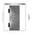
- FIG. 2shows a cross-section of a temperature profile in skin for bipolar copper electrodes applied to a skin surface without semiconductive caps.
- FIG. 3shows a cross-section of a temperature profile in skin when using semiconductive caps on the electrodes.
- FIG. 4shows a cross-section of a temperature profile in skin when using semiconductive caps having a variable thickness.
- FIG. 5shows a cross-section of another temperature profile in skin when using semiconductive caps with a variable thickness.
- FIG. 6Ashows a sectional view of an applicator for bipolar RF energy delivered through a skin surface.
- FIG. 6Bshows a sectional view of a semiconductive cap for an electrode.
- FIG. 6Cshows a side elevation view of a semiconductive cap for an electrode.
- FIG. 7Ashows a perspective view of another electrode and semiconductive cap embodiment.
- FIG. 7Bshows a side view of the embodiment shown in FIG. 7A .
- FIG. 8Ashows a cross-section of a temperature profile in skin when using semiconductive caps having an elliptical shape.
- FIG. 8Bshows temperature of the skin between electrodes.
- FIG. 1shows a cross-section of a temperature profile in skin for a monopolar copper electrode applied to a skin surface without a semiconductive cap.
- FIG. 2shows a cross-section of a temperature profile in skin for bipolar copper electrodes applied to a skin surface without semiconductive caps.
- Uneven heat distributionis seen at the edges of the monopolar electrode and is symmetric (equal at both edges).
- the bipolar electrodesthe uneven heat distribution is seen at the edges, but is asymmetric.
- the current densityis greater along the inner electrode edges because the pathlength is shorter and hence impedance is lower. More current will travel this path.
- 20 joules of RF energyis delivered to tissue.
- temperatures greater than 70° C.lead to adverse skin effects such as blisters.
- FIG. 3shows a cross-section of a temperature profile in skin when using semiconductive caps (e.g., formed from a ceramic material) on the electrodes.
- the capsare illustrated, but the electrodes are not.
- the energy delivered to tissueis 20 joules, the same as was used in FIG. 2 , but because the impedance between the cap and the tissue is better matched, the thermal hotspot is smaller.
- the hotspotsappear on the inner edges due to the shorter electrical pathlength to the next adjacent electrode. High current densities also exist at the edge of the copper electrode-ceramic cap junction. Because of the high thermal conductivity of ceramic, this density does not cause thermal hotspots at this junction.
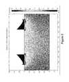
- FIG. 4shows a cross-section of a temperature profile in skin when using semiconductive caps with a variable thickness.
- the capsare illustrated, but the electrodes are not.
- ceramichas finite impedance, it can be shaped to be thicker at the edges to further minimize the thermal hotspot on the inner edges causes by the shorter electrical pathlength. In this case, two times more energy or 40 Joules is delivered to skin, but the thermal hotspots are about half what is seen without the ceramic cap and more importantly less than the 70° C. critical temperature.
- the temperature of skin (1 mm deep, halfway between electrodes)is increased to about 42.8° C., an increase of about 10.8 degrees over the starting temperature of about 32° C. Without the ceramic cap, the increase is about 36.2° C. or only about 4.2 degrees above the initial temperature. So with the cap, the skin is more effectively heated with less risk of adverse effects to the skin surface underneath the electrodes.
- FIG. 5shows a cross-section of a temperature profile in skin when using semiconductive caps with a variable thickness.
- the capsare illustrated, but the electrodes are not.
- Each caphas a blunt surface in contact with the skin and a curved surface contacting the electrode.
- Each capis asymmetric, being thickest at the inner portion, thinnest at the center portion, and thicker than the center portion but thinner than the inner portion at an outer portion. In the center portion, the cap tapers from thicker than the outer portion to thinner than the outer portion. In this case, 48 Joules of RF energy is delivered, but the thermal hotspots remain under 70° C.
- the temperature of skin (1 mm deep, halfway between electrodes)is increased to about 40° C. or an increase of about 8° C.
- the mid-dermal increaseis two times higher while the electrode hotspots are two times lower.
- a larger volume of tissueis heated compared to the previous configuration so the change in temperature is not as high even through more energy is being delivered to tissue.
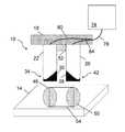
- FIG. 6Ashows an applicator 10 for bipolar RF energy delivered through a skin surface 14 .
- the applicator 10includes a base 18 , a first electrode 22 connected to the base 18 , a second electrode 26 connected to the base 18 , a first semiconductive cap 30 disposed on a first distal end 34 of the first electrode 22 , a second semiconductive cap 38 disposed on a second distal 42 end of the second electrode 26 .
- the first electrode 22extends from the base 18 toward a first location 46 of the skin surface 14 .
- the second electrode 26extends from the base 18 toward a second location 50 of the skin surface 14 .
- the first electrode 22is laterally offset along the skin surface 14 from the second electrode 26 , and the first electrode 22 and the second electrode 26 have opposite phases.
- Each electrode 22 or 26can be cooled to about 10° C. using a thermoelectric cooler 52 attached to the side of the electrode and or the base 18 .
- Each electrode 22 or 26can have separate thermoelectric coolers 52 , which can
- Base 18can be any member to which the electrodes 22 and 26 are attachable. In some embodiments, base 18 is modular and includes separate members for connection to electrodes 22 and 26 . Base 18 can be a portion or section of a hand piece or applicator, or can be the hand piece or applicator. In some embodiments, base 18 and electrodes 22 and 26 are integrally formed.
- Each electrode 22 or 26 and/or each semiconductive cap 30 or 38can have an elliptical shape so that the footprints 46 and 50 of the caps 30 and 38 are elliptical or oval in shape.
- the treatment region 54 formed by the electrodes 22 and 26 and/or semiconductive caps 30 and 38can be rectangular in shape, and can extend into the skin surface to a predetermined depth.
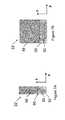
- FIG. 6Bshows a sectional view of a semiconductive cap 30 (or 38 ) for an electrode 22 (or 26 ).
- each electrode 22 (or 26 ) and each semiconductive cap 30 (or 38 )is about 4 mm wide at axis 56 and 12 mm deep at axis 57 .
- Each electrode 22 or 26can be about 4 to 15 mm long (e.g., about 12 mm long).
- the electrodescan be spaced apart by about 5 to 20 mm (e.g., about 12 mm or about 13 mm from inner edge to inner edge).
- Each electrode 22 or 26can be an electrically conductive metal (e.g., copper) or ceramic material. Each electrode 22 or 26 can be plated with a nonoxidizing surface such as chrome. Each electrode can be formed from a semiconductive ceramic with an appropriately shaped solder pad.
- FIG. 6Cshows a side elevation view through axis 56 of a semiconductive cap 30 (or 38 ) for an electrode 22 (or 26 ).
- the semiconductive cap 30 (or 38 )has a blunt surface 58 adapted to contact a location of the skin surface 14 (e.g., the first location 46 if it is the first semiconductive cap 30 and the second location 50 if it is the second semiconductive cap 38 ).
- the semiconductive cap 30 (or 38 )has a curved surface 60 that can be affixed to the first electrode 22 (or the second electrode 26 ).
- the thickness of each semiconductive cap 30 (or 38 ) between the blunt surface 58 and the curved surface 60can be tapered or graded from the inner edge to the outer edge.
- the semiconductive cap 30(or 38 ) can be thicker at an inner portion 62 and thinner at a center portion 66 to homogenize the electrical field at the skin surface 14 .
- An outer portion 70 of the semiconductive cap 30 (or 38 )can be thicker than the center portion 66 but thinner than the inner portion 62 . In this way, the entrance or exit point for current entering or leaving the electrode is spread across the entire cap surface, which homogenizes the tissue entry current field.
- the inner edge or portionis the edge/portion adjacent to the next closest electrode.
- the inner portion 62is about 2 mm thick
- the center portion 66is about 0.5 mm thick
- the outer portion 70is about 1 mm.
- the centeris about 1 mm thick and the upper and lower edges are about 3 mm thick.
- a source 74 of RF energyis in electrical communication with the base 18 via cable 78 , which can include a single wire or a bundle of wires.
- Each electrode 22 and 26includes a separate wire feed 80 and 84 , respectively.
- Wire feeds 80 and 84can be in electrical communication with separate wires or feeds of cable 78 .
- Source 74can deliver RF energy to and through the skin surface 14 .
- the source 74can deliver RF energy via cable 78 to wire feed 80 and 84 to the first electrode 22 and the second electrode 26 , respectively.
- RF energycan be delivered from the first electrode 22 and the second electrode 26 through the first semiconductive cap 30 and the second semiconductive cap 30 , respectively, through the skin surface 14 .
- the electrical conductivity of the semiconductive materialcan be approximate to the electrical conductivity at the tissue-electrode interface.
- the conductivity of each semiconductive capcan be matched or substantially matched to the conductivity of the skin.
- the conductivity of each semiconductive capcan be matched so that about 10% of the RF energy is lost to the semiconductive cap.
- the conductivity of each semiconductive capcan be about 0.1 S/m.
- the conductivity of the semiconductive capscan be graded such that the central and outer portion are more conductive than the inner portion.
- the electrical conductivityis exactly matched, then the current does not concentrate at the ceramic-tissue junction because, from an electrical perspective, no junction exists because of the matched conductivity values.
- the electrical conductivity for skinis about 0.22 S/m at 1 MHz RF frequency.
- the hot spotoccurs at the metal electrode-ceramic interface, which, because of the ceramic's high thermal conductivity, is quickly diffused so that little heating occurs at the skin surface.
- RF energyis lost to the ceramic material and the amount of energy lost is proportional to the electrical conductivity value. In the typical ceramic geometries used, the loss of RF energy to ceramic can be as much as 50%.
- An electrical conductivity of 0.1 S/m at 1 MHz for the ceramic materialcan minimize this.
- the amount of RF energy lost to the ceramic materialis around 10% while the thermal hotspot at the electrode edge is greatly diminished compared to when the ceramic material is not used.
- Each semiconductive capcan include a semiconductive ceramic, which can have an electrical conductivity of about 0.1 S/m.
- the semiconductive capcan be a passive material in that material properties are independent of temperature.
- the shape of the capis made such that the electrical pathlength through the semiconductive cap or ceramic material towards the edges of the electrodes are longer than toward the center. This passively increases the resistance for current flowing towards the edge compared to the center thereby better homogenizing the electric field at the tissue surface. This effectively spreads the current density leaving the probe over a larger area, which reduces the magnitude of the thermal hotspot.
- Each semiconductive capcan include a conductive silicon carbide based ceramic doped with a nonconductive material and/or a nonconductive aluminum nitride based ceramic doped with a conductive material.
- the nonconductive material or the conductive materialcan be used to tune the cap to the desired conductivity.
- a semiconductive capcan be formed by sintering silicon carbide.
- the ceramiccan be prepared from a green perform, which can allow shaping of the electrode cap to the desired shape and can allow mixing of an additional material to tune the electrical conductivity of the finished product.
- Boron, aluminum and nitrogenare dopants that can be used to change the electrical conductivity of silicon carbide materials.
- Each semiconductive capneed not be permanently attached to an electrode.
- Each semiconductive capcan be affixed, bonded or attached.
- Each semiconductive capcan be affixed to the respective electrode with a conductive epoxy.
- a silver conductive epoxyhas good thermal and electrical properties, and can bond to metals, glasses and ceramics.
- Each semiconductive capcan be affixed to the respective electrode with a compressive tongue and groove joint.
- Each semiconductive capcan be affixed to the respective electrode with a screw passing through the cap and securing to the electrode.
- a compressive metal gasketcan be used to improve thermal and electrical conduction between the cap and the electrode at the junction.
- the source 74can provide the RF energy at a frequency of about 100 kHz to about 10 MHz (e.g., about 1 MHz), although higher or lower frequencies can be used depending on the application.
- the source 74can include a controller for the RF energy and/or a controller for the thermoelectric cooler 52 .
- the sourcecan provide the RF energy at about 10 J/cm 3 to about 500 J/cm 3 (e.g., about 50 J/cm 3 to about 120 J/cm 3 ), although higher or lower fluences can be used depending on the application.
- 120 J/cm 3corresponds to a 30° C. rise in skin temperature.
- the sourcecan provide the RF energy in pulses of about 0.1 second to about 1 second, although shorter or longer durations can be used depending on the application.
- FIGS. 7A and 7Bshow a perspective view and a side view, respectively, of an electrode 22 ′ and semiconductive cap 30 ′, which can be used with base 18 shown in FIG. 6A .
- Electrode 22 ′can have a body portion 88 , a tip 92 and a flange 96 .
- Tip 92can extend about 3.5 mm from body 88 , and can be about 9 mm deep and 2 mm wide.
- Semiconductive cap 30 ′can define an opening, which is insertable over tip 92 .
- Semiconductive cap 30 ′can abut flange 96 and be formed so that its outer surface is flush with the outer surface of the body portion 88 of the electrode 22 ′.
- Each semiconductive cap 30 ′can be permanently or semi-permanently attached to an electrode.
- Cap 30 ′can have a variable thickness, e.g., a thickness between the blunt surface and the curved surface is thicker at an inner portion and thinner at a center portion to homogenize the electrical field at the skin surface.
- the variable thickness of cap 30 ′is symmetric.
- the cap 30 ′can be about 0.5 mm thick at the center and about 4.0 mm thick around its perimeter.
- the cap 30 ′can about 12 mm deep and 4 mm wide.
- the thickness of the wall surrounding the openingis about 1 mm in the x-plane and about 1.5 mm in the y-plane.
- FIG. 8Ashows a cross-section of a temperature profile in skin when using semiconductive caps with a variable thickness.
- a capis illustrated, but the electrode is not.
- Each caphas a blunt surface in contact with the skin and a curved surface contacting the electrode.
- Each capis elliptical or oval in shape.
- the hot zone around the edgeis evenly distributed, with peak temperatures reaching about 69° C. (e.g., thermal hotspots remaining under 70° C.).
- FIG. 8Bshows temperature of the skin between electrodes, with the temperature reaching a maximum about 2 mm from the electrode edge. In this configuration, a larger volume of tissue is heated compared to the previous configurations so the change in temperature is not as high even through more energy is being delivered to tissue.
Landscapes
- Health & Medical Sciences (AREA)
- Engineering & Computer Science (AREA)
- Biomedical Technology (AREA)
- Nuclear Medicine, Radiotherapy & Molecular Imaging (AREA)
- Radiology & Medical Imaging (AREA)
- Life Sciences & Earth Sciences (AREA)
- Animal Behavior & Ethology (AREA)
- General Health & Medical Sciences (AREA)
- Public Health (AREA)
- Veterinary Medicine (AREA)
- Oral & Maxillofacial Surgery (AREA)
- Plastic & Reconstructive Surgery (AREA)
- Surgical Instruments (AREA)
Abstract
Description
Claims (25)
Priority Applications (9)
| Application Number | Priority Date | Filing Date | Title |
|---|---|---|---|
| US13/402,320US9889297B2 (en) | 2012-02-22 | 2012-02-22 | Reduction of RF electrode edge effect |
| US13/494,319US9277958B2 (en) | 2012-02-22 | 2012-06-12 | Reduction of RF electrode edge effect |
| ES13155133TES2531153T3 (en) | 2012-02-22 | 2013-02-13 | RF electrode edge effect reduction |
| EP13155133.5AEP2630985B1 (en) | 2012-02-22 | 2013-02-13 | Reduction of RF electrode edge effect |
| KR20147026234AKR20140135772A (en) | 2012-02-22 | 2013-02-18 | Reduction of rf electrode edge effect |
| PCT/IL2013/000020WO2013124838A1 (en) | 2012-02-22 | 2013-02-18 | Reduction of rf electrode edge effect |
| US14/478,191US9895188B2 (en) | 2012-02-22 | 2014-09-05 | Reduction of RF electrode edge effect |
| IL234519AIL234519B (en) | 2012-02-22 | 2014-09-08 | Reduction of rf electrode edge effect |
| US14/566,777US9381057B2 (en) | 2012-02-22 | 2014-12-11 | Reduction of RF electrode edge effect |
Applications Claiming Priority (1)
| Application Number | Priority Date | Filing Date | Title |
|---|---|---|---|
| US13/402,320US9889297B2 (en) | 2012-02-22 | 2012-02-22 | Reduction of RF electrode edge effect |
Related Child Applications (2)
| Application Number | Title | Priority Date | Filing Date |
|---|---|---|---|
| US13/494,319Continuation-In-PartUS9277958B2 (en) | 2012-02-22 | 2012-06-12 | Reduction of RF electrode edge effect |
| US14/478,191Continuation-In-PartUS9895188B2 (en) | 2012-02-22 | 2014-09-05 | Reduction of RF electrode edge effect |
Publications (2)
| Publication Number | Publication Date |
|---|---|
| US20130218242A1 US20130218242A1 (en) | 2013-08-22 |
| US9889297B2true US9889297B2 (en) | 2018-02-13 |
Family
ID=48982850
Family Applications (1)
| Application Number | Title | Priority Date | Filing Date |
|---|---|---|---|
| US13/402,320Active2036-04-08US9889297B2 (en) | 2012-02-22 | 2012-02-22 | Reduction of RF electrode edge effect |
Country Status (1)
| Country | Link |
|---|---|
| US (1) | US9889297B2 (en) |
Cited By (2)
| Publication number | Priority date | Publication date | Assignee | Title |
|---|---|---|---|---|
| US10322296B2 (en) | 2009-07-20 | 2019-06-18 | Syneron Medical Ltd. | Method and apparatus for fractional skin treatment |
| USD971415S1 (en) | 2019-12-30 | 2022-11-29 | Cynosure, Llc | Flexible applicator |
Families Citing this family (3)
| Publication number | Priority date | Publication date | Assignee | Title |
|---|---|---|---|---|
| US11878167B2 (en) | 2020-05-04 | 2024-01-23 | Btl Healthcare Technologies A.S. | Device and method for unattended treatment of a patient |
| WO2021224678A1 (en) | 2020-05-04 | 2021-11-11 | Btl Medical Technologies S.R.O. | Device and method for unattended treatment of a patient |
| US20230079700A1 (en)* | 2021-09-13 | 2023-03-16 | Intelis Instruments Ltd. | Double Monopolar RF Body Contouring |
Citations (51)
| Publication number | Priority date | Publication date | Assignee | Title |
|---|---|---|---|---|
| US5569242A (en) | 1994-05-06 | 1996-10-29 | Lax; Ronald G. | Method and apparatus for controlled contraction of soft tissue |
| US5660836A (en) | 1995-05-05 | 1997-08-26 | Knowlton; Edward W. | Method and apparatus for controlled contraction of collagen tissue |
| US5697909A (en) | 1992-01-07 | 1997-12-16 | Arthrocare Corporation | Methods and apparatus for surgical cutting |
| US5755753A (en) | 1995-05-05 | 1998-05-26 | Thermage, Inc. | Method for controlled contraction of collagen tissue |
| US5772688A (en)* | 1996-06-20 | 1998-06-30 | Polytronics, Ltd. | Skin-contact type medical treatment apparatus |
| US5948011A (en) | 1995-05-05 | 1999-09-07 | Thermage, Inc. | Method for controlled contraction of collagen tissue via non-continuous energy delivery |
| US5976129A (en) | 1991-10-18 | 1999-11-02 | Desai; Ashvin H. | Endoscopic surgical instrument |
| US6277116B1 (en) | 1994-05-06 | 2001-08-21 | Vidaderm | Systems and methods for shrinking collagen in the dermis |
| US6350276B1 (en)* | 1996-01-05 | 2002-02-26 | Thermage, Inc. | Tissue remodeling apparatus containing cooling fluid |
| US6413255B1 (en) | 1999-03-09 | 2002-07-02 | Thermage, Inc. | Apparatus and method for treatment of tissue |
| US6427089B1 (en) | 1999-02-19 | 2002-07-30 | Edward W. Knowlton | Stomach treatment apparatus and method |
| US6425912B1 (en) | 1995-05-05 | 2002-07-30 | Thermage, Inc. | Method and apparatus for modifying skin surface and soft tissue structure |
| US6430446B1 (en) | 1995-05-05 | 2002-08-06 | Thermage, Inc. | Apparatus for tissue remodeling |
| US20030199866A1 (en)* | 1996-01-05 | 2003-10-23 | Stern Roger A. | Method and kit for treatment of tissue |
| US6662054B2 (en) | 2002-03-26 | 2003-12-09 | Syneron Medical Ltd. | Method and system for treating skin |
| US6702808B1 (en) | 2000-09-28 | 2004-03-09 | Syneron Medical Ltd. | Device and method for treating skin |
| US20040206365A1 (en)* | 2003-03-31 | 2004-10-21 | Knowlton Edward Wells | Method for treatment of tissue |
| US20050070896A1 (en) | 2002-08-21 | 2005-03-31 | Daniel Steven A. | Thermal coagulation of tissue during tissue resection |
| US6889090B2 (en) | 2001-11-20 | 2005-05-03 | Syneron Medical Ltd. | System and method for skin treatment using electrical current |
| US20050107781A1 (en) | 2003-11-18 | 2005-05-19 | Isaac Ostrovsky | System and method for tissue ablation |
| US6939344B2 (en) | 2001-08-02 | 2005-09-06 | Syneron Medical Ltd. | Method for controlling skin temperature during thermal treatment |
| US20050222555A1 (en) | 2004-04-01 | 2005-10-06 | Dieter Manstein | Method and apparatus for dermatological treatment |
| US20050222565A1 (en) | 2004-04-01 | 2005-10-06 | Dieter Manstein | Method and apparatus for dermatological treatment and tissue reshaping |
| WO2005096890A1 (en) | 2004-04-09 | 2005-10-20 | Transfert Plus, S.E.C. | Sit-stand seating device |
| US20060025837A1 (en) | 1996-01-05 | 2006-02-02 | Stern Roger A | Handpiece with RF electrode and non-volatile memory |
| US20060036300A1 (en)* | 2004-08-16 | 2006-02-16 | Syneron Medical Ltd. | Method for lypolisis |
| US7006874B2 (en) | 1996-01-05 | 2006-02-28 | Thermage, Inc. | Treatment apparatus with electromagnetic energy delivery device and non-volatile memory |
| US20060047281A1 (en) | 2004-09-01 | 2006-03-02 | Syneron Medical Ltd. | Method and system for invasive skin treatment |
| US7022121B2 (en) | 1999-03-09 | 2006-04-04 | Thermage, Inc. | Handpiece for treatment of tissue |
| US7041100B2 (en) | 2004-01-21 | 2006-05-09 | Syneron Medical Ltd. | Method and system for selective electro-thermolysis of skin targets |
| US20060173518A1 (en) | 2005-01-28 | 2006-08-03 | Syneron Medical Ltd. | Device and method for treating skin |
| US20060206110A1 (en) | 1996-01-05 | 2006-09-14 | Thermage, Inc. | Handpiece with RF electrode and non-volative memory |
| US7141049B2 (en) | 1999-03-09 | 2006-11-28 | Thermage, Inc. | Handpiece for treatment of tissue |
| US20070038156A1 (en) | 2005-07-26 | 2007-02-15 | Avner Rosenberg | Method and apparatus for treatment of skin using RF and ultrasound energies |
| US20070038275A1 (en)* | 2005-07-05 | 2007-02-15 | Hee-Je Kim | High-frequency electrotherapy apparatus |
| US7189230B2 (en) | 1996-01-05 | 2007-03-13 | Thermage, Inc. | Method for treating skin and underlying tissue |
| US20070078502A1 (en) | 2005-10-05 | 2007-04-05 | Thermage, Inc. | Method and apparatus for estimating a local impedance factor |
| US20070083247A1 (en) | 2005-10-11 | 2007-04-12 | Thermage, Inc. | Electrode assembly and handpiece with adjustable system impedance, and methods of operating an energy-based medical system to treat tissue |
| US7238183B2 (en) | 2002-01-22 | 2007-07-03 | Syneron Medical Ltd. | System and method for treating skin |
| US20070208340A1 (en) | 2004-04-05 | 2007-09-06 | Ganz Robert A | Device and Method for Treating Tissue |
| US7267675B2 (en) | 1996-01-05 | 2007-09-11 | Thermage, Inc. | RF device with thermo-electric cooler |
| US20080004678A1 (en) | 2005-01-28 | 2008-01-03 | Michael Kreindel | Device and method for treating skin with temperature control |
| US20080172047A1 (en) | 2000-12-28 | 2008-07-17 | Palomar Medical Technologies, Inc. | Methods And Devices For Fractional Ablation Of Tissue |
| US20080183167A1 (en) | 2007-01-31 | 2008-07-31 | Alma Lasers Ltd. | Skin treatment using a multi-discharge applicator |
| US20080200969A1 (en) | 2007-02-16 | 2008-08-21 | Thermage, Inc. | Temperature sensing apparatus and methods for treatment devices used to deliver high frequency energy to tissue |
| US7452358B2 (en) | 1996-01-05 | 2008-11-18 | Thermage, Inc. | RF electrode assembly for handpiece |
| US20080287943A1 (en) | 2007-01-25 | 2008-11-20 | Thermage, Inc. | Treatment apparatus and methods for inducing microburn patterns in tissue |
| US7473251B2 (en) | 1996-01-05 | 2009-01-06 | Thermage, Inc. | Methods for creating tissue effect utilizing electromagnetic energy and a reverse thermal gradient |
| US20090018628A1 (en) | 2007-07-10 | 2009-01-15 | Thermage, Inc. | Treatment apparatus and methods for delivering high frequency energy across large tissue areas |
| WO2009016634A2 (en) | 2007-08-01 | 2009-02-05 | Syneron Medical Ltd. | Method and device for collagen growth stimulation |
| US7803257B2 (en) | 2004-10-22 | 2010-09-28 | Taiwan Semiconductor Manufacturing Company | Current-leveling electroplating/electropolishing electrode |
- 2012
- 2012-02-22USUS13/402,320patent/US9889297B2/enactiveActive
Patent Citations (74)
| Publication number | Priority date | Publication date | Assignee | Title |
|---|---|---|---|---|
| US5976129A (en) | 1991-10-18 | 1999-11-02 | Desai; Ashvin H. | Endoscopic surgical instrument |
| US5697909A (en) | 1992-01-07 | 1997-12-16 | Arthrocare Corporation | Methods and apparatus for surgical cutting |
| US5569242A (en) | 1994-05-06 | 1996-10-29 | Lax; Ronald G. | Method and apparatus for controlled contraction of soft tissue |
| US6277116B1 (en) | 1994-05-06 | 2001-08-21 | Vidaderm | Systems and methods for shrinking collagen in the dermis |
| US6470216B1 (en) | 1995-05-05 | 2002-10-22 | Thermage, Inc. | Method for smoothing contour irregularities of skin surface |
| US6438424B1 (en) | 1995-05-05 | 2002-08-20 | Thermage, Inc. | Apparatus for tissue remodeling |
| US5919219A (en) | 1995-05-05 | 1999-07-06 | Thermage, Inc. | Method for controlled contraction of collagen tissue using RF energy |
| US5948011A (en) | 1995-05-05 | 1999-09-07 | Thermage, Inc. | Method for controlled contraction of collagen tissue via non-continuous energy delivery |
| US5660836A (en) | 1995-05-05 | 1997-08-26 | Knowlton; Edward W. | Method and apparatus for controlled contraction of collagen tissue |
| US6241753B1 (en) | 1995-05-05 | 2001-06-05 | Thermage, Inc. | Method for scar collagen formation and contraction |
| US5755753A (en) | 1995-05-05 | 1998-05-26 | Thermage, Inc. | Method for controlled contraction of collagen tissue |
| US6311090B1 (en) | 1995-05-05 | 2001-10-30 | Thermage, Inc. | Method and apparatus for controlled contraction of collagen tissue |
| US5871524A (en) | 1995-05-05 | 1999-02-16 | Thermage, Inc. | Apparatus for controlled contraction of collagen tissue |
| US6377854B1 (en) | 1995-05-05 | 2002-04-23 | Thermage, Inc. | Method for controlled contraction of collagen in fibrous septae in subcutaneous fat layers |
| US6377855B1 (en) | 1995-05-05 | 2002-04-23 | Thermage, Inc. | Method and apparatus for controlled contraction of collagen tissue |
| US6381497B1 (en) | 1995-05-05 | 2002-04-30 | Thermage, Inc. | Method for smoothing contour irregularity of skin surface by controlled contraction of collagen tissue |
| US6381498B1 (en) | 1995-05-05 | 2002-04-30 | Thermage, Inc. | Method and apparatus for controlled contraction of collagen tissue |
| US6387380B1 (en) | 1995-05-05 | 2002-05-14 | Thermage, Inc. | Apparatus for controlled contraction of collagen tissue |
| US6405090B1 (en) | 1995-05-05 | 2002-06-11 | Thermage, Inc. | Method and apparatus for tightening skin by controlled contraction of collagen tissue |
| US6461378B1 (en) | 1995-05-05 | 2002-10-08 | Thermage, Inc. | Apparatus for smoothing contour irregularities of skin surface |
| US6453202B1 (en) | 1995-05-05 | 2002-09-17 | Thermage, Inc. | Method and apparatus for controlled contraction of collagen tissue |
| US6425912B1 (en) | 1995-05-05 | 2002-07-30 | Thermage, Inc. | Method and apparatus for modifying skin surface and soft tissue structure |
| US6430446B1 (en) | 1995-05-05 | 2002-08-06 | Thermage, Inc. | Apparatus for tissue remodeling |
| US20060025837A1 (en) | 1996-01-05 | 2006-02-02 | Stern Roger A | Handpiece with RF electrode and non-volatile memory |
| US20070255274A1 (en) | 1996-01-05 | 2007-11-01 | Thermage, Inc. | Method and kit for treatment of tissue |
| US7473251B2 (en) | 1996-01-05 | 2009-01-06 | Thermage, Inc. | Methods for creating tissue effect utilizing electromagnetic energy and a reverse thermal gradient |
| US7229436B2 (en) | 1996-01-05 | 2007-06-12 | Thermage, Inc. | Method and kit for treatment of tissue |
| US20030199866A1 (en)* | 1996-01-05 | 2003-10-23 | Stern Roger A. | Method and kit for treatment of tissue |
| US6350276B1 (en)* | 1996-01-05 | 2002-02-26 | Thermage, Inc. | Tissue remodeling apparatus containing cooling fluid |
| US20060206110A1 (en) | 1996-01-05 | 2006-09-14 | Thermage, Inc. | Handpiece with RF electrode and non-volative memory |
| US7267675B2 (en) | 1996-01-05 | 2007-09-11 | Thermage, Inc. | RF device with thermo-electric cooler |
| US7189230B2 (en) | 1996-01-05 | 2007-03-13 | Thermage, Inc. | Method for treating skin and underlying tissue |
| US7006874B2 (en) | 1996-01-05 | 2006-02-28 | Thermage, Inc. | Treatment apparatus with electromagnetic energy delivery device and non-volatile memory |
| US20070265614A1 (en) | 1996-01-05 | 2007-11-15 | Thermage, Inc. | Rf device with thermo-electric cooler |
| US7115123B2 (en) | 1996-01-05 | 2006-10-03 | Thermage, Inc. | Handpiece with electrode and non-volatile memory |
| US7452358B2 (en) | 1996-01-05 | 2008-11-18 | Thermage, Inc. | RF electrode assembly for handpiece |
| US6749624B2 (en) | 1996-01-05 | 2004-06-15 | Edward W. Knowlton | Fluid delivery apparatus |
| US20090082764A1 (en) | 1996-01-05 | 2009-03-26 | Thermage, Inc. | Methods for creating tissue effect utilizing electromagnetic energy and a reverse thermal gradient |
| US7481809B2 (en) | 1996-01-05 | 2009-01-27 | Thermage, Inc. | Handpiece with RF electrode and non-volatile memory |
| US5772688A (en)* | 1996-06-20 | 1998-06-30 | Polytronics, Ltd. | Skin-contact type medical treatment apparatus |
| US6427089B1 (en) | 1999-02-19 | 2002-07-30 | Edward W. Knowlton | Stomach treatment apparatus and method |
| US7141049B2 (en) | 1999-03-09 | 2006-11-28 | Thermage, Inc. | Handpiece for treatment of tissue |
| US7022121B2 (en) | 1999-03-09 | 2006-04-04 | Thermage, Inc. | Handpiece for treatment of tissue |
| US20070010811A1 (en) | 1999-03-09 | 2007-01-11 | Thermage, Inc. | energy delivery device for treating tissue |
| US6413255B1 (en) | 1999-03-09 | 2002-07-02 | Thermage, Inc. | Apparatus and method for treatment of tissue |
| US6702808B1 (en) | 2000-09-28 | 2004-03-09 | Syneron Medical Ltd. | Device and method for treating skin |
| US20080172047A1 (en) | 2000-12-28 | 2008-07-17 | Palomar Medical Technologies, Inc. | Methods And Devices For Fractional Ablation Of Tissue |
| US6939344B2 (en) | 2001-08-02 | 2005-09-06 | Syneron Medical Ltd. | Method for controlling skin temperature during thermal treatment |
| US6889090B2 (en) | 2001-11-20 | 2005-05-03 | Syneron Medical Ltd. | System and method for skin treatment using electrical current |
| US7238183B2 (en) | 2002-01-22 | 2007-07-03 | Syneron Medical Ltd. | System and method for treating skin |
| US6662054B2 (en) | 2002-03-26 | 2003-12-09 | Syneron Medical Ltd. | Method and system for treating skin |
| US20050070896A1 (en) | 2002-08-21 | 2005-03-31 | Daniel Steven A. | Thermal coagulation of tissue during tissue resection |
| US20040206365A1 (en)* | 2003-03-31 | 2004-10-21 | Knowlton Edward Wells | Method for treatment of tissue |
| US20050107781A1 (en) | 2003-11-18 | 2005-05-19 | Isaac Ostrovsky | System and method for tissue ablation |
| US7041100B2 (en) | 2004-01-21 | 2006-05-09 | Syneron Medical Ltd. | Method and system for selective electro-thermolysis of skin targets |
| US20050222555A1 (en) | 2004-04-01 | 2005-10-06 | Dieter Manstein | Method and apparatus for dermatological treatment |
| US20050222565A1 (en) | 2004-04-01 | 2005-10-06 | Dieter Manstein | Method and apparatus for dermatological treatment and tissue reshaping |
| US20070208340A1 (en) | 2004-04-05 | 2007-09-06 | Ganz Robert A | Device and Method for Treating Tissue |
| WO2005096890A1 (en) | 2004-04-09 | 2005-10-20 | Transfert Plus, S.E.C. | Sit-stand seating device |
| US20060036300A1 (en)* | 2004-08-16 | 2006-02-16 | Syneron Medical Ltd. | Method for lypolisis |
| US20060047281A1 (en) | 2004-09-01 | 2006-03-02 | Syneron Medical Ltd. | Method and system for invasive skin treatment |
| US7803257B2 (en) | 2004-10-22 | 2010-09-28 | Taiwan Semiconductor Manufacturing Company | Current-leveling electroplating/electropolishing electrode |
| US20060173518A1 (en) | 2005-01-28 | 2006-08-03 | Syneron Medical Ltd. | Device and method for treating skin |
| US20080004678A1 (en) | 2005-01-28 | 2008-01-03 | Michael Kreindel | Device and method for treating skin with temperature control |
| US20070038275A1 (en)* | 2005-07-05 | 2007-02-15 | Hee-Je Kim | High-frequency electrotherapy apparatus |
| US20070038156A1 (en) | 2005-07-26 | 2007-02-15 | Avner Rosenberg | Method and apparatus for treatment of skin using RF and ultrasound energies |
| US20070078502A1 (en) | 2005-10-05 | 2007-04-05 | Thermage, Inc. | Method and apparatus for estimating a local impedance factor |
| US20070083247A1 (en) | 2005-10-11 | 2007-04-12 | Thermage, Inc. | Electrode assembly and handpiece with adjustable system impedance, and methods of operating an energy-based medical system to treat tissue |
| US20080287943A1 (en) | 2007-01-25 | 2008-11-20 | Thermage, Inc. | Treatment apparatus and methods for inducing microburn patterns in tissue |
| US20080183167A1 (en) | 2007-01-31 | 2008-07-31 | Alma Lasers Ltd. | Skin treatment using a multi-discharge applicator |
| US20080200969A1 (en) | 2007-02-16 | 2008-08-21 | Thermage, Inc. | Temperature sensing apparatus and methods for treatment devices used to deliver high frequency energy to tissue |
| US20090018628A1 (en) | 2007-07-10 | 2009-01-15 | Thermage, Inc. | Treatment apparatus and methods for delivering high frequency energy across large tissue areas |
| US20090043247A1 (en) | 2007-08-01 | 2009-02-12 | Michael Kreindel | Method and device for collagen growth stimulation |
| WO2009016634A2 (en) | 2007-08-01 | 2009-02-05 | Syneron Medical Ltd. | Method and device for collagen growth stimulation |
Cited By (3)
| Publication number | Priority date | Publication date | Assignee | Title |
|---|---|---|---|---|
| US10322296B2 (en) | 2009-07-20 | 2019-06-18 | Syneron Medical Ltd. | Method and apparatus for fractional skin treatment |
| USD971415S1 (en) | 2019-12-30 | 2022-11-29 | Cynosure, Llc | Flexible applicator |
| USD1014763S1 (en) | 2019-12-30 | 2024-02-13 | Cynosure, Llc | Flexible applicator |
Also Published As
| Publication number | Publication date |
|---|---|
| US20130218242A1 (en) | 2013-08-22 |
Similar Documents
| Publication | Publication Date | Title |
|---|---|---|
| US9381057B2 (en) | Reduction of RF electrode edge effect | |
| US9895188B2 (en) | Reduction of RF electrode edge effect | |
| US11653971B2 (en) | RF device for tissue treatment | |
| US9889297B2 (en) | Reduction of RF electrode edge effect | |
| KR102505869B1 (en) | Method and Apparatus for Controlled RF Processing and RF Generator System | |
| US20190175932A1 (en) | Tissue treatment apparatus and systems with pain mitigation and methods for mitigating pain during tissue treatments | |
| CN107530544B (en) | Non-invasive skin treatment device using RF current with treatment setting limiter | |
| EP2405857B1 (en) | Rf electrode for aesthetic and bodyshaping devices | |
| US20140358069A1 (en) | Method and apparatus for dermatological treatment and tissue reshaping | |
| US10779885B2 (en) | Apparatus and methods for the treatment of tissue using microwave energy | |
| CN101711134A (en) | Systems and methods for creating an effect using microwave energy to specified tissue | |
| US20200406029A1 (en) | Devices and methods for stimulation of hair growth | |
| AU3741500A (en) | Apparatus and method for treatment of tissue | |
| JPH10243947A (en) | High-frequency device | |
| Franco et al. | Controlled volumetric heating of subcutaneous adipose tissue using a novel radiofrequency technology | |
| EP3219279A1 (en) | Skin treatment apparatus | |
| WO2024124988A1 (en) | Radio frequency beauty device and monopolar radio frequency electrode tip | |
| US20220226037A1 (en) | Electrosurgical Electrode and Electrosurgical Tool for Conveying Electrical Energy | |
| RU2458652C2 (en) | Device for radio-frequency polishing of face and body skin | |
| CN118178871A (en) | Radio frequency beauty instrument and monopole radio frequency electrode head | |
| HK40034392A (en) | Methods and apparatus for controlled rf treatments and rf generator system | |
| Hiraki et al. | The size and distance of the opposite flat applicator change the SAR and thermal distributions of RF capacitive intracavitary hyperthermia | |
| Moriyama et al. | Design of hemispherical Radio Frequency (RF) capacitive-type electrode free of edge effects for treatment of intracavitary tumors |
Legal Events
| Date | Code | Title | Description |
|---|---|---|---|
| AS | Assignment | Owner name:CANDELA CORPORATION, MASSACHUSETTS Free format text:ASSIGNMENT OF ASSIGNORS INTEREST;ASSIGNOR:SCHOMACKER, KEVIN T.;REEL/FRAME:027918/0946 Effective date:20120224 | |
| AS | Assignment | Owner name:ING CAPITAL LLC, AS COLLATERAL AGENT, NEW YORK Free format text:SECURITY AGREEMENT;ASSIGNORS:SYNERON MEDICAL LTD.;CANDELA CORPORATION;PRIMAEVA CORPORATION;REEL/FRAME:043925/0001 Effective date:20170920 | |
| STCF | Information on status: patent grant | Free format text:PATENTED CASE | |
| MAFP | Maintenance fee payment | Free format text:PAYMENT OF MAINTENANCE FEE, 4TH YEAR, LARGE ENTITY (ORIGINAL EVENT CODE: M1551); ENTITY STATUS OF PATENT OWNER: LARGE ENTITY Year of fee payment:4 | |
| AS | Assignment | Owner name:PRIMAEVA CORPORATION, MASSACHUSETTS Free format text:RELEASE (REEL 043925 / FRAME 0001);ASSIGNOR:ING CAPITAL LLC;REEL/FRAME:059593/0131 Effective date:20220401 Owner name:CANDELA CORPORATION, MASSACHUSETTS Free format text:RELEASE (REEL 043925 / FRAME 0001);ASSIGNOR:ING CAPITAL LLC;REEL/FRAME:059593/0131 Effective date:20220401 Owner name:SYNERON MEDICAL LTD., ISRAEL Free format text:RELEASE (REEL 043925 / FRAME 0001);ASSIGNOR:ING CAPITAL LLC;REEL/FRAME:059593/0131 Effective date:20220401 Owner name:BARCLAYS BANK PLC, AS COLLATERAL AGENT, NEW YORK Free format text:SECURITY AGREEMENT;ASSIGNORS:CANDELA CORPORATION;SYNERON MEDICAL LTD.;REEL/FRAME:059593/0269 Effective date:20220401 | |
| MAFP | Maintenance fee payment | Free format text:PAYMENT OF MAINTENANCE FEE, 8TH YEAR, LARGE ENTITY (ORIGINAL EVENT CODE: M1552); ENTITY STATUS OF PATENT OWNER: LARGE ENTITY Year of fee payment:8 |