US9885935B2 - Controlling transitions in optically switchable devices - Google Patents
Controlling transitions in optically switchable devicesDownload PDFInfo
- Publication number
- US9885935B2 US9885935B2US14/900,037US201414900037AUS9885935B2US 9885935 B2US9885935 B2US 9885935B2US 201414900037 AUS201414900037 AUS 201414900037AUS 9885935 B2US9885935 B2US 9885935B2
- Authority
- US
- United States
- Prior art keywords
- voltage
- transition
- magnitude
- optical
- open circuit
- Prior art date
- Legal status (The legal status is an assumption and is not a legal conclusion. Google has not performed a legal analysis and makes no representation as to the accuracy of the status listed.)
- Active
Links
Images


Classifications
- G—PHYSICS
- G02—OPTICS
- G02F—OPTICAL DEVICES OR ARRANGEMENTS FOR THE CONTROL OF LIGHT BY MODIFICATION OF THE OPTICAL PROPERTIES OF THE MEDIA OF THE ELEMENTS INVOLVED THEREIN; NON-LINEAR OPTICS; FREQUENCY-CHANGING OF LIGHT; OPTICAL LOGIC ELEMENTS; OPTICAL ANALOGUE/DIGITAL CONVERTERS
- G02F1/00—Devices or arrangements for the control of the intensity, colour, phase, polarisation or direction of light arriving from an independent light source, e.g. switching, gating or modulating; Non-linear optics
- G02F1/01—Devices or arrangements for the control of the intensity, colour, phase, polarisation or direction of light arriving from an independent light source, e.g. switching, gating or modulating; Non-linear optics for the control of the intensity, phase, polarisation or colour
- G02F1/15—Devices or arrangements for the control of the intensity, colour, phase, polarisation or direction of light arriving from an independent light source, e.g. switching, gating or modulating; Non-linear optics for the control of the intensity, phase, polarisation or colour based on an electrochromic effect
- G02F1/163—Operation of electrochromic cells, e.g. electrodeposition cells; Circuit arrangements therefor
- G—PHYSICS
- G09—EDUCATION; CRYPTOGRAPHY; DISPLAY; ADVERTISING; SEALS
- G09G—ARRANGEMENTS OR CIRCUITS FOR CONTROL OF INDICATING DEVICES USING STATIC MEANS TO PRESENT VARIABLE INFORMATION
- G09G3/00—Control arrangements or circuits, of interest only in connection with visual indicators other than cathode-ray tubes
- G09G3/04—Control arrangements or circuits, of interest only in connection with visual indicators other than cathode-ray tubes for presentation of a single character by selection from a plurality of characters, or by composing the character by combination of individual elements, e.g. segments using a combination of such display devices for composing words, rows or the like, in a frame with fixed character positions
- G09G3/16—Control arrangements or circuits, of interest only in connection with visual indicators other than cathode-ray tubes for presentation of a single character by selection from a plurality of characters, or by composing the character by combination of individual elements, e.g. segments using a combination of such display devices for composing words, rows or the like, in a frame with fixed character positions by control of light from an independent source
- G09G3/19—Control arrangements or circuits, of interest only in connection with visual indicators other than cathode-ray tubes for presentation of a single character by selection from a plurality of characters, or by composing the character by combination of individual elements, e.g. segments using a combination of such display devices for composing words, rows or the like, in a frame with fixed character positions by control of light from an independent source using electrochromic devices
Definitions
- Electrochromic (EC) devicesare typically multilayer stacks including (a) at least one layer of electrochromic material, that changes its optical properties in response to the application of an electrical potential, (b) an ion conductor (IC) layer that allows ions, such as lithium ions, to move through it, into and out from the electrochromic material to cause the optical property change, while preventing electrical shorting, and (c) transparent conductor layers, such as transparent conducting oxides or TCOs, over which an electrical potential is applied to the electrochromic layer. In some cases, the electric potential is applied from opposing edges of an electrochromic device and across the viewable area of the device.
- the transparent conductor layersare designed to have relatively high electronic conductances.
- Electrochromic devicesmay have more than the above-described layers such as ion storage or counter electrode layers that optionally change optical states.
- the electrochromic deviceDue to the physics of the device operation, proper function of the electrochromic device depends upon many factors such as ion movement through the material layers, the electrical potential required to move the ions, the sheet resistance of the transparent conductor layers, and other factors.
- the size of the electrochromic deviceplays an important role in the transition of the device from a starting optical state to an ending optical state (e.g., from tinted to clear or clear to tinted).
- the conditions applied to drive such transitionscan have quite different requirements for different sized devices.
- aspects of this disclosureconcern controllers and control methods for applying a drive voltage to bus bars of optically switchable devices such as electrochromic devices. Such devices are often provided on windows such as architectural glass.
- the applied drive voltageis controlled in a manner that efficiently drives an optical transition over the entire surface of the optically switchable device.
- the drive voltageis controlled to account for differences in effective voltage experienced in regions between the bus bars and regions proximate the bus bars. Regions near the bus bars experience the highest effective voltage.
- Certain aspects of the disclosureconcern methods of controlling an optical transition of an optically switchable device from a starting optical state to an ending optical state.
- the methodsmay be characterized by the following operations: (a) applying a drive voltage for driving the optically switchable device to transition from the starting optical state to the ending optical state, where the drive voltage is applied to the bus bars of the optically switchable device; (b) before the transition is complete, periodically determining an open circuit voltage between the bus bars of the optically switchable device, and periodically determining a total delivered charge density supplied to the optically switchable device during the transition; (c) determining whether the open circuit voltage determined in (b) has a magnitude greater than or equal to a magnitude of a target open circuit voltage, and determining whether a magnitude of the total delivered charge density determined in (b) is greater than or equal to a magnitude of a threshold charge density; and (d) if it is determined in (c) that both (i) the magnitude of the open circuit voltage determined in (b) is greater than or equal to the magnitude of the target open circuit voltage
- the open circuit voltageis determined in (b) at a defined time after applying the drive voltage in (a).
- the defined timemay be between about 15-90 seconds, for example about 30 seconds in some cases. In other examples, the defined time is longer, for example up to about 120 minutes in some cases.
- the target open circuit voltagemay have a magnitude that is between about 0-1V greater than the magnitude of the hold voltage, for example between about 0-0.4V greater than the magnitude of the hold voltage. In various cases, the magnitude of the target open circuit voltage is at least about 0.025V greater than the magnitude of the hold voltage.
- the magnitude of the threshold charge densitymay be between about 1 ⁇ 10 ⁇ 5 C/cm 2 and about 5 C/cm 2 in certain embodiments. In some cases, for example, the magnitude of the threshold charge density is between about 0.01-0.04 C/cm 2 .
- the methodmay further include after (c) and before (d), (i) increasing the magnitude of voltage applied to the bus bars to the drive voltage as a result of determining in (c) that either the magnitude of the open circuit voltage determined in (b) is less than the magnitude of the target open circuit voltage, or that the magnitude of the total delivered charge density determined in (b) is less than the magnitude of the threshold charge density; and (ii) repeating (b)-(c).
- (b)-(c)are repeated at a frequency of between about 5 seconds and 5 minutes.
- the optically switchable deviceis an electrochromic device.
- the bus barsmay be separated from one another by at least about 10 inches in some cases.
- Such apparatusmay be characterized by the following elements: a processor and a power supply for providing voltage and/or current at defined magnitudes to optically switchable device to control the optical transition.
- the processormay be designed or configured to (a) apply a drive voltage for driving the optically switchable device to transition from the starting optical state to the ending optical state, where the drive voltage is applied to bus bars of the optically switchable device, (b) before the transition is complete, periodically determine an open circuit voltage between the bus bars of the optically switchable device, and periodically determine a total delivered charge density supplied to the optically switchable device during the transition, (c) determine whether the open circuit voltage determined in (b) has a magnitude greater than or equal to a magnitude of a target open circuit voltage, and determine whether the total delivered charge density determined in (b) has a magnitude greater than or equal to a magnitude of a threshold charge density, and (d) if it is determined in (c) that both (i) the magnitude of the open circuit voltage determined in (b) is greater than or equal to the magnitude of the target open circuit voltage, and (ii) the magnitude of the total delivered charge density determined in (b) is greater than or equal to the magnitude of the threshold charge density, apply a hold voltage for holding the ending
- the processormay be further designed or configured to determine the open circuit voltage and total delivered charge density in (b) at a defined time after applying the drive voltage in (a).
- the defined timemay be between about 15-90 seconds, for example about 30 seconds in some cases. In other examples, the defined time is longer, for example up to about 120 minutes in some cases.
- the target open circuit voltagemay have a magnitude that is between about 0-1V greater than the magnitude of the hold voltage, for example between about 0-0.4V greater than the magnitude of the hold voltage. In various cases, the magnitude of the target open circuit voltage is at least about 0.025V greater than the magnitude of the hold voltage.
- the magnitude of the threshold charge densitymay be between about 1 ⁇ 10 ⁇ 5 C/cm 2 and about 5 C/cm 2 in certain embodiments. In some cases, for example, the magnitude of the threshold charge density is between about 0.01-0.04 C/cm 2 .
- the processoris further designed or configured to, after (c) and before (d), (i) increase the magnitude of voltage applied to the bus bars to the drive voltage as a result of determining in (c) that either the magnitude of the open circuit voltage determined in (b) is less than the magnitude of the target open circuit voltage, or that the magnitude of the total delivered charge density determined in (b) is less than the magnitude of the threshold charge density; and (ii) repeat (b)-(c).
- the processormay be further designed or configured to repeat (b)-(c) at a frequency of between about 5 seconds and 5 minutes.
- the optically switchable devicemay be an electrochromic device.
- the bus barsmay be separated from one another by at least about 10 inches in some cases.
- another method of controlling an optical transition of an optically switchable deviceinvolves transitioning from a starting optical state to an ending optical state by (a) applying a drive voltage for driving the optically switchable device to transition from the starting optical state to the ending optical state, where the drive voltage is applied to bus bars of the optically switchable device; (b) before the transition is complete, periodically reducing the magnitude of the voltage applied to the bus bars of the optically switchable device to a probe voltage and detecting a current response, and periodically determining a total delivered charge density supplied to the optically switchable device during the transition; (c) determining whether the current response detected in (b) reaches a target current, and determining whether a magnitude of the total delivered charge density determined in (b) is greater than or equal to a magnitude of a threshold charge density; and (d) if it is determined in (c) that both (i) the current response detected in (b) reaches the target current, and (ii) the magnitude of the total delivered charge density
- the target currentmay be about 0 Amps in some cases.
- the magnitude of the threshold charge densitymay be between about 1 ⁇ 10 ⁇ 5 C/cm 2 and about 5 C/cm 2 in certain embodiments. In some cases, for example, the magnitude of the threshold charge density is between about 0.01-0.04 C/cm 2 .
- the probe voltagemay have a magnitude that is between about 0-1V greater than the magnitude of the hold voltage, for example between about 0-0.4V greater than the magnitude of the hold voltage.
- an apparatus for controlling an optical transition of an optically switchable deviceinvolves moving from a starting optical state to an ending optical state.
- the apparatusmay include a power supply for providing voltage and/or current at defined magnitudes to the optically switchable device to control the transition, as well as a processor that is designed or configured to control the transition.
- the processormay be designed or configured to (a) apply a drive voltage for driving the optically switchable device to transition from the starting optical state to the ending optical state, where the drive voltage is applied to bus bars of the optically switchable device; (b) before the transition is complete, periodically reduce the magnitude of the voltage applied to the bus bars of the optically switchable device to a probe voltage and detect a current response, and periodically determine a total delivered charge density supplied to the optically switchable device during the transition; (c) determine whether the current response detected in (b) reaches a target current, and determine whether a magnitude of the total delivered charge density determined in (b) is greater than or equal to a magnitude of a threshold charge density; and (d) if it is determined in (c) that both (i) the current response detected in (b) reaches the target current, and (ii) the magnitude of the total delivered charge density determined in (b) is greater than or equal to the magnitude of the threshold charge density, apply a hold voltage for holding the ending optical state.
- the target currentmay be about 0 Amps in some cases.
- the magnitude of the threshold charge densitymay be between about 1 ⁇ 10 ⁇ 5 C/cm 2 and about 5 C/cm 2 in certain embodiments. In some cases, for example, the magnitude of the threshold charge density is between about 0.01-0.04 C/cm 2 .
- the probe voltagemay have a magnitude that is between about 0-1V greater than the magnitude of the hold voltage, for example between about 0-0.4V greater than the magnitude of the hold voltage.
- FIG. 1Aschematically depicts a planar bus bar arrangement.
- FIG. 1Bpresents a simplified plot of the local voltage value on each transparent conductive layer as a function of position on the layer
- FIG. 1Cpresents a simplified plot of V eff as a function of position across the device
- FIG. 2is a graph depicting voltage and current profiles associated with driving an electrochromic device from clear to tinted and from tinted to clear.
- FIG. 3is a graph depicting certain voltage and current profiles associated with driving an electrochromic device from clear to tinted.
- FIG. 4Ais a graph depicting an optical transition in which a drop in applied voltage from V drive to V hold results in a net current flow establishing that the optical transition has proceeded far enough to permit the applied voltage to remain at V hold for the duration of the ending optical state.
- FIG. 4Bis a graph depicting an optical transition in which an initial drop in applied voltage from V drive to V hold results in a net current flow indicating that the optical transition has not yet proceeded far enough to permit the applied voltage to remain at V hold for the duration of the ending optical state. Therefore the applied voltage is returned to V drive for a further period of time before again dropping again to V hold at which point the resulting current establishes that the optical transition has proceeded far enough to permit the applied voltage to remain at V hold for the duration of the ending optical state.
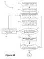
- FIG. 5Ais a flow chart depicting a process for probing the progress of an optical transition and determining when the transition is complete.
- FIG. 5Bis a flow chart depicting a process for probing the progress of an optical transition and speeding the transition if it is not progressing sufficiently fast.
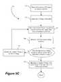
- FIGS. 5C-5Fare flow charts depicting alternative processes for probing the progress of an optical transitioning and determining when the transition is complete.
- FIGS. 6A and 6Bshow graphs depicting the total charge delivered over time and the voltage applied over time during an electrochromic transition when using the method of FIG. 5E to probe and monitor the progress of the transition, at room temperature ( FIG. 6A ) and at a reduced temperature ( FIG. 6B ).
- FIG. 6Cillustrates an electrochromic window having a pair of voltage sensors on the transparent conductive oxide layers according to an embodiment.
- FIGS. 7A and 7Bpresent cross-sectional views of an example electrochromic device in operation.
- FIGS. 8 and 9are representations of window controllers and associated components.
- An “optically switchable device”is a thin device that changes optical state in response to electrical input. It reversibly cycles between two or more optical states. Switching between these states is controlled by applying predefined current and/or voltage to the device.
- the devicetypically includes two thin conductive sheets that straddle at least one optically active layer.
- the electrical input driving the change in optical stateis applied to the thin conductive sheets.
- the inputis provided by bus bars in electrical communication with the conductive sheets.
- optical transitionis a change in any one or more optical properties of an optically switchable device.
- the optical property that changesmay be, for example, tint, reflectivity, refractive index, color, etc.
- the optical transitionwill have a defined starting optical state and a defined ending optical state.
- the starting optical statemay be 80% transmissivity and the ending optical state may be 50% transmissivity.
- the optical transitionis typically driven by applying an appropriate electric potential across the two thin conductive sheets of the optically switchable device.
- a “starting optical state”is the optical state of an optically switchable device immediately prior to the beginning of an optical transition.
- the starting optical stateis typically defined as the magnitude of an optical state which may be tint, reflectivity, refractive index, color, etc.
- the starting optical statemay be a maximum or minimum optical state for the optically switchable device; e.g., 90% or 4% transmissivity.
- the starting optical statemay be an intermediate optical state having a value somewhere between the maximum and minimum optical states for the optically switchable device; e.g., 50% transmissivity.
- An “ending optical state”is the optical state of an optically switchable device immediately after the complete optical transition from a starting optical state.
- the complete transitionoccurs when optical state changes in a manner understood to be complete for a particular application. For example, a complete tinting might be deemed a transition from 75% optical transmissivity to 10% transmissivity.
- the ending optical statemay be a maximum or minimum optical state for the optically switchable device; e.g., 90% or 4% transmissivity.
- the ending optical statemay be an intermediate optical state having a value somewhere between the maximum and minimum optical states for the optically switchable device; e.g., 50% transmissivity.
- Bus barrefers to an electrically conductive strip attached to a conductive layer such as a transparent conductive electrode spanning the area of an optically switchable device.
- the bus bardelivers electrical potential and current from an external lead to the conductive layer.
- An optically switchable deviceincludes two or more bus bars, each connected to a single conductive layer of the device.
- a bus barforms a long thin line that spans most of the length of the length or width of a device. Often, a bus bar is located near the edge of the device.
- Applied Voltagerefers the difference in potential applied to two bus bars of opposite polarity on the electrochromic device.
- Each bus baris electronically connected to a separate transparent conductive layer.
- the applied voltagemay different magnitudes or functions such as driving an optical transition or holding an optical state.
- Between the transparent conductive layersare sandwiched the optically switchable device materials such as electrochromic materials.
- Each of the transparent conductive layersexperiences a potential drop between the position where a bus bar is connected to it and a location remote from the bus bar. Generally, the greater the distance from the bus bar, the greater the potential drop in a transparent conducting layer.
- the local potential of the transparent conductive layersis often referred to herein as the V TCL .
- Bus bars of opposite polaritymay be laterally separated from one another across the face of an optically switchable device.
- Effective Voltagerefers to the potential between the positive and negative transparent conducting layers at any particular location on the optically switchable device. In Cartesian space, the effective voltage is defined for a particular x,y coordinate on the device. At the point where V eff is measured, the two transparent conducting layers are separated in the z-direction (by the device materials), but share the same x,y coordinate.
- “Hold Voltage”refers to the applied voltage necessary to indefinitely maintain the device in an ending optical state. In some cases, without application of a hold voltage, electrochromic windows return to their natural tint state. In other words, maintenance of a desired tint state requires application of a hold voltage.
- Drive Voltagerefers to the applied voltage provided during at least a portion of the optical transition.
- the drive voltagemay be viewed as “driving” at least a portion of the optical transition. Its magnitude is different from that of the applied voltage immediately prior to the start of the optical transition. In certain embodiments, the magnitude of the drive voltage is greater than the magnitude of the hold voltage.
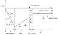
- An example application of drive and hold voltagesis depicted in FIG. 3
- the disclosed embodimentsmake use of electrical probing and monitoring to determine when an optical transition between a first optical state and a second optical state of an optically switchable device has proceeded to a sufficient extent that the application of a drive voltage can be terminated.
- electrical probingallows for application of drive voltages for less time than previously thought possible, as a particular device is driven based on electrical probing of its actual optical transition progression in real time.
- real time monitoringcan help ensure that an optical transition progresses to a desired state.
- terminating the drive voltageis accomplished by dropping the applied voltage to a hold voltage. This approach takes advantage of an aspect of optical transitions that is typically considered undesirable—the propensity of thin optically switchable devices to transition between optical states non-uniformly.
- optically switchable devicesinitially transition at locations close to the bus bars and only later at regions far from the bus bars (e.g., near the center of the device). Surprisingly, this non-uniformity can be harnessed to probe the optical transition.
- optically switchable devicesavoid the need for custom characterization and associated preprogramming of device control algorithms specifying the length of time a drive voltage is applied as well as obviating “one size fits all” fixed time period drive parameters that account for variations in temperature, device structure variability, and the like across many devices.
- Driving a transition in a typical electrochromic deviceis accomplished by applying a defined voltage to two separated bus bars on the device.
- itis convenient to position bus bars perpendicular to the smaller dimension of a rectangular window (see FIG. 1A ). This is because the transparent conducting layers used to deliver an applied voltage over the face of the thin film device have an associated sheet resistance, and the bus bar arrangement allows for the shortest span over which current must travel to cover the entire area of the device, thus lowering the time it takes for the conductor layers to be fully charged across their respective areas, and thus lowering the time to transition the device.
- V appWhile an applied voltage, V app , is supplied across the bus bars, essentially all areas of the device see a lower local effective voltage (V eff ) due to the sheet resistance of the transparent conducting layers and the current draw of the device.
- V effThe center of the device (the position midway between the two bus bars) frequently has the lowest value of V eff . This may result in an unacceptably small optical switching range and/or an unacceptably slow switching time in the center of the device.
- These problemsmay not exist at the edges of the device, nearer the bus bars. This is explained in more detail below with reference to FIGS. 1B and 1C .
- FIG. 1Ashows a top-down view of an electrochromic lite 100 including bus bars having a planar configuration.
- Electrochromic lite 100includes a first bus bar 105 disposed on a first conductive layer 110 and a second bus bar 115 disposed on a second conductive layer, 120 .
- An electrochromic stack(not shown) is sandwiched between first conductive layer 110 and second conductive layer 120 .
- first bus bar 105may extend substantially across one side of first conductive layer 110 .
- Second bus bar 115may extend substantially across one side of second conductive layer 120 opposite the side of electrochromic lite 100 on which first bus bar 105 is disposed.
- Some devicesmay have extra bus bars, e.g. on all four edges, but this complicates fabrication.
- a further discussion of bus bar configurations, including planar configured bus bars,is found in U.S.
- FIG. 1Bis a graph showing a plot of the local voltage in first transparent conductive layer 110 and the voltage in second transparent conductive layer 120 that drives the transition of electrochromic lite 100 from a clear state to a tinted state, for example.
- Plot 125shows the local values of the voltage V TCL in first transparent conductive layer 110 . As shown, the voltage drops from the left hand side (e.g., where first bus bar 105 is disposed on first conductive layer 110 and where the voltage is applied) to the right hand side of first conductive layer 110 due to the sheet resistance and current passing through first conductive layer 110 .
- Plot 130also shows the local voltage V TCL in second conductive layer 120 .
- the voltageincreases (decreases in magnitude) from the right hand side (e.g., where second bus bar 115 is disposed on second conductive layer 120 and where the voltage is applied) to the left hand side of second conductive layer 120 due to the sheet resistance of second conductive layer 120 .
- the value of the applied voltage, V appin this example is the difference in voltage between the right end of potential plot 130 and the left end of potential plot 125 .
- the value of the effective voltage, V effat any location between the bus bars is the difference in values of curves 130 and 125 at the position on the x-axis corresponding to the location of interest.
- FIG. 1Cis a graph showing a plot of V eff across the electrochromic device between first and second conductive layers 110 and 120 of electrochromic lite 100 .
- the effective voltageis the local voltage difference between the first conductive layer 110 and the second conductive layer 120 . Regions of an electrochromic device subjected to higher effective voltages transition between optical states faster than regions subjected to lower effective voltages. As shown, the effective voltage is the lowest at the center of electrochromic lite 100 and highest at the edges of electrochromic lite 100 . The voltage drop across the device is due to ohmic losses as current passes through the device.
- the voltage drop across large electrochromic windowscan be alleviated by configuring additional bus bars within the viewing area of the window, in effect dividing one large optical window into multiple smaller electrochromic windows which can be driven in series or parallel.
- this approachmay not be aesthetically appealing due to the contrast between the viewable area and the bus bar(s) in the viewable area. That is, it may be much more pleasing to the eye to have a monolithic electrochromic device without any distracting bus bars in the viewable area.
- the electronic resistance to current flowing across the thin face of the TC layersalso increases. This resistance may be measured between the points closest to the bus bar (referred to as edge of the device in following description) and in the points furthest away from the bus bars (referred to as the center of the device in following description).
- edge of the device in following descriptionthe points closest to the bus bar
- center of the device in following descriptionthe points furthest away from the bus bars.
- the range of safe operation for solid state electrochromic devicesis between about 0.5V and 4V, or more typically between about 0.8V and about 3V, e.g. between 0.9V and 1.8V. These are local values of V eff .
- an electrochromic device controller or control algorithmprovides a driving profile where V eff is always below 3V, in another embodiment, the controller controls V eff so that it is always below 2.5V, in another embodiment, the controller controls V eff so that it is always below 1.8V.
- the recited voltage valuesrefer to the time averaged voltage (where the averaging time is of the order of time required for small optical response, e.g. few seconds to few minutes).
- An added complexity of electrochromic windowsis that the current drawn through the window is not fixed over the duration of the optical transition. Instead, during the initial part of the transition, the current through the device is substantially larger (up to 100 ⁇ larger) than in the end state when the optical transition is complete or nearly complete. The problem of poor coloration in center of the device is further exacerbated during this initial transition period, as the value V eff at the center is significantly lower than what it will be at the end of the transition period.
- the transparent conducting layersare assumed to have substantially similar, if not the same, sheet resistance for the calculation. However those of ordinary skill in the art will appreciate that the applicable physics of the ohmic voltage drop and local effective voltage still apply even if the transparent conducting layers have dissimilar sheet resistances.
- certain embodimentspertain to controllers and control algorithms for driving optical transitions in devices having planar bus bars.
- substantially linear bus bars of opposite polarityare disposed at opposite sides of a rectangular or other polygonally shaped electrochromic device.
- devices with non-planar bus barsmay be employed.
- Such devicesmay employ, for example, angled bus bars disposed at vertices of the device.
- the bus bar effective separation distance, Lis determined based on the geometry of the device and bus bars.
- V eff across the devicedecreases, thereby slowing or reducing the device coloration during transition and even in the final optical state.
- the V eff across the windowis at least RJL 2 /2 lower than V app . It has been found that as the resistive voltage drop increases (due to increase in the window size, current draw etc.) some of the loss can be negated by increasing V app but doing so only to a value that keeps V eff at the edges of the device below the threshold where reliability degradation would occur.
- the applied voltageis initially provided at a magnitude greater than that required to hold the device at a particular optical state in equilibrium. This approach is illustrated in FIGS. 2 and 3 .
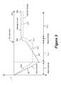
- FIG. 2shows a complete current profile and voltage profile for an electrochromic device employing a simple voltage control algorithm to cause an optical state transition cycle (tinting followed by clearing) of an electrochromic device.
- total current density (I)is represented as a function of time.
- the total current densityis a combination of the ionic current density associated with an electrochromic transition and electronic leakage current between the electrochemically active electrodes.
- electrochomic deviceswill have the depicted current profile.
- a cathodic electrochromic materialsuch as tungsten oxide is used in conjunction with an anodic electrochromic material such as nickel tungsten oxide in counter electrode. In such devices, negative currents indicate coloration/tinting of the device.
- lithium ionsflow from a nickel tungsten oxide anodically coloring electrochromic electrode into a tungsten oxide cathodically coloring electrochromic electrode.
- electronsflow into the tungsten oxide electrode to compensate for the positively charged incoming lithium ions. Therefore, the voltage and current are shown to have a negative value.
- the depicted profileresults from ramping up the voltage to a set level and then holding the voltage to maintain the optical state.
- the current peaks 201are associated with changes in optical state, i.e., tinting and clearing. Specifically, the current peaks represent delivery of the ionic charge needed to tint or clear the device. Mathematically, the shaded area under the peak represents the total charge required to tint or clear the device.
- the portions of the curve after the initial current spikes (portions 203 )represent electronic leakage current while the device is in the new optical state.
- a voltage profile 205is superimposed on the current curve.
- the voltage profilefollows the sequence: negative ramp ( 207 ), negative hold ( 209 ), positive ramp ( 211 ), and positive hold ( 213 ). Note that the voltage remains constant after reaching its maximum magnitude and during the length of time that the device remains in its defined optical state.
- Voltage ramp 207drives the device to its new the tinted state and voltage hold 209 maintains the device in the tinted state until voltage ramp 211 in the opposite direction drives the transition from tinted to clear states.
- a current capis imposed. That is, the current is not permitted to exceed a defined level in order to prevent damaging the device (e.g. driving ion movement through the material layers too quickly can physically damage the material layers).
- the coloration speedis a function of not only the applied voltage, but also the temperature and the voltage ramping rate.
- FIG. 3illustrates a voltage control profile in accordance with certain embodiments.
- a voltage control profileis employed to drive the transition from a clear state to a tinted state (or to an intermediate state).
- a similar but inverted profileis used to drive an electrochromic device in the reverse direction, from a tinted state to a clear state (or from a more tinted to less tinted state).
- the voltage control profile for going from tinted to clearis a mirror image of the one depicted in FIG. 3 .
- V appThe voltage values depicted in FIG. 3 represent the applied voltage (V app ) values.
- the applied voltage profileis shown by the dashed line.
- the current density in the deviceis shown by the solid line.
- V appincludes four components: a ramp to drive component 303 , which initiates the transition, a V drive component 313 , which continues to drive the transition, a ramp to hold component 315 , and a V hold component 317 .
- the ramp componentsare implemented as variations in V app and the V drive and V hold components provide constant or substantially constant V app magnitudes.
- the ramp to drive componentis characterized by a ramp rate (increasing magnitude) and a magnitude of V drive .
- the V drive componentis characterized by the value of V drive as well as the duration of V drive .
- the magnitude of V drivemay be chosen to maintain V eff with a safe but effective range over the entire face of the electrochromic device as described above.
- the ramp to hold componentis characterized by a voltage ramp rate (decreasing magnitude) and the value of V hold (or optionally the difference between V drive and V hold ). V app drops according to the ramp rate until the value of V hold is reached.
- the V hold componentis characterized by the magnitude of V hold and the duration of V hold . Actually, the duration of V hold is typically governed by the length of time that the device is held in the tinted state (or conversely in the clear state). Unlike the ramp to drive, V drive , and ramp to hold components, the V hold component has an arbitrary length, which is independent of the physics of the optical transition of the device.
- Each type of electrochromic devicewill have its own characteristic components of the voltage profile for driving the optical transition. For example, a relatively large device and/or one with a more resistive conductive layer will require a higher value of V drive and possibly a higher ramp rate in the ramp to drive component.
- the values of each component of the applied voltage profileis set for a particular electrochromic device (having its own bus bar separation, resistivity, etc.) and does not vary based on current conditions.
- the voltage profiledoes not take into account feedback such as temperature, current density, and the like.
- the ramp to drive component of the voltage profileis chosen to safely but rapidly induce ionic current to flow between the electrochromic and counter electrodes.
- the current in the devicefollows the profile of the ramp to drive voltage component until the ramp to drive portion of the profile ends and the V drive portion begins. See current component 301 in FIG. 3 .
- Safe levels of current and voltagecan be determined empirically or based on other feedback.
- the value of V driveis chosen based on the considerations described above. Particularly, it is chosen so that the value of V eff over the entire surface of the electrochromic device remains within a range that effectively and safely transitions large electrochromic devices.
- the duration of V drivecan be chosen based on various considerations. One of these ensures that the drive potential is held for a period sufficient to cause the substantial coloration of the device. For this purpose, the duration of V drive may be determined empirically, by monitoring the optical density of the device as a function of the length of time that V drive remains in place. In some embodiments, the duration of V drive is set to a specified time period. In another embodiment, the duration of V drive is set to correspond to a desired amount of ionic and/or electronic charge being passed. As shown, the current ramps down during V drive . See current segment 307 .
- Another considerationis the reduction in current density in the device as the ionic current decays as a consequence of the available lithium ions completing their journey from the anodic coloring electrode to the cathodic coloring electrode (or counter electrode) during the optical transition.
- the transitionis complete, the only current flowing across device is leakage current through the ion conducting layer.
- the ohmic drop in potential across the face of the devicedecreases and the local values of V eff increase.
- V effcan damage or degrade the device if the applied voltage is not reduced.
- another consideration in determining the duration of V driveis the goal of reducing the level of V eff associated with leakage current.
- V effBy dropping the applied voltage from V drive to V hold , not only is V eff reduced on the face of the device but leakage current decreases as well. As shown in FIG. 3 , the device current transitions in a segment 305 during the ramp to hold component. The current settles to a stable leakage current 309 during V hold .
- Devices of different sizes, and more particularly devices having bus bars separated by particular distancesrequire different lengths of time for applying the drive voltage.
- the processes employed to fabricate optically switchable devices such as electrochromic devicesmay vary subtly from one batch to another or one process revision to another. The subtle process variations translate into potentially different requirements for the length of time that the drive voltage must be applied to the devices used in operation. Still further, environmental conditions, and particularly temperature, can influence the length of time that the applied voltage should be applied to drive the transition.
- the transition between two defined optical statesmay be desirable to cause the transition between two defined optical states to occur within a defined duration, regardless of the size of the optically switchable device, the process under which the device is fabricated, and the environmental conditions in which the device is operating at the time of the transition.
- This goalcan be realized by monitoring the course of the transition and adjusting the drive voltage as necessary to ensure that the transition completes in the defined time. Adjusting the magnitude of the drive voltage is one way of accomplishing this.
- Certain disclosed embodimentsapply a probing technique to assess the progress of an optical transition while the device is in transition. As illustrated in FIG. 3 , there are typically distinct ramp to drive and the drive voltage maintenance stages of the optical transition.
- the probe techniquecan be applied during either of these. In many embodiments, it is applied during the drive voltage maintenance portion of the algorithm.
- the probing techniqueinvolves pulsing the current or voltage applied to drive the transition and then monitoring the current or voltage response to detect an overdrive condition in the vicinity of the bus bars.
- An overdrive conditionoccurs when the local effective voltage is greater than needed to cause a local optical transition. For example, if an optical transition to a clear state is deemed complete when V eff reaches 2V, and the local value of V eff near a bus bar is 2.2V, the position near the bus bar may be characterized as in an overdrive condition.
- One example of a probing techniqueinvolves pulsing the applied drive voltage by dropping it to the level of the hold voltage (or the hold voltage modified by an appropriate offset) and monitoring the current response to determine the direction of the current response. In this example, when the current response reaches a defined threshold, the device control system determines that it is now time to transition from the drive voltage to the hold voltage.
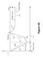
- FIG. 4Ais a graph depicting an optical transition in which a drop in applied voltage from V drive to V hold results in a net current flow establishing that the optical transition has proceeded far enough to permit the applied voltage to remain at V hold for the duration of the ending optical state. This is illustrated by a voltage drop 411 in V app from V drive to V hold . Voltage drop 411 is performed during a period when the V app might otherwise be constrained to remain in the drive phase shown in FIG. 3 . The current flowing between the bus bars began dropping (becoming less negative), as illustrated by current segment 307 , when the applied voltage initially stopped increasing (becoming more negative) and plateaued at V drive .
- the applied voltagenow dropped at 411 , the current began decreasing more readily as illustrated by current segment 415 .
- the level of currentis measured after a defined period of time passes following the voltage drop 411 . If the current is below a certain threshold, the optical transition is deemed complete, and the applied voltage may remain at V hold (or move to V hold if it is at some other level below V drive ). In the particular example of FIG. 4A , the current threshold is exceeded as illustrated. Therefore, the V app remains at V hold for the duration of the ending optical state. V hold may be selected for the ending optical state it provides. Such ending optical state may be a maximum, minimum, or intermediate optical state for the optical device undergoing the transition.
- FIG. 4Billustrates this situation.
- FIG. 4Bis a graph depicting an optical transition in which an initial drop in applied voltage from V drive to V hold (see 411 ) results in a net current flow indicating that the optical transition has not yet proceeded far enough to permit the applied voltage to remain at V hold for the duration of the ending optical state. Note that current segment 415 , which has a trajectory resulting from voltage drop 411 , does not reach the threshold when probed at 419 .
- the applied voltageis returned to V drive for a further period of time—while the current recovers at 417 —before again dropping again to V hold ( 421 ) at which point the resulting current ( 423 ) establishes that the optical transition has proceeded far enough to permit the applied voltage to remain at V hold for the duration of the ending optical state.
- the ending optical statemay be a maximum, minimum, or intermediate optical state for the optical device undergoing the transition.
- the hold voltageis a voltage that will maintain the optical device in equilibrium at a particular optical density or other optical condition. It produces a steady-state result by generating a current that offsets the leakage current in the ending optical state.
- the drive voltageis applied to speed the transition to a point where applying the hold voltage will result in a time invariant desired optical state.
- the probing technique described hereinmay be understood in terms of the physical mechanisms associated with an optical transition driven from bus bars at the edges of a device. Basically, the technique relies on differential values of the effective voltage experienced in the optically switchable device across the face of the device, and particularly the variation in V eff from the center of the device to the edge of the device. The local variation in potential on the transparent conductive layers results in different values of V eff across the face of the device. The value of V eff experienced by the optically switchable device near the bus bars is far greater the value of V eff in the center of the device. As a consequence, the local charge buildup in the region next to the bus bars is significantly greater than the charge buildup in the center the device.
- the value of V eff at the edge of the device near the bus barsis sufficient to exceed the ending optical state desired for the optical transition whereas in the center of the device, the value of V eff is insufficient to reach that ending state.
- the ending statemay be an optical density value associated with the endpoint in the optical transition. While in this intermediate stage of the optical transition, if the drive voltage is dropped to the hold voltage, the portion of the electrochromic device close to the bus bars will effectively try to transition back toward the state from which it started. However, as the device state in the center of the device has not yet reached the end state of the optical transition, when a hold voltage is applied, the center portion of the device will continue transitioning in the direction desired for the optical transition.
- the regions of the device in the centerwhich have not yet fully transitioned to the final state, continue to promote current flow in a direction required to drive the transition.
- the optical transitionis sufficiently complete from the edge of the device to the center of the device.
- Such transitioncan be defined in many ways depending upon the specifications of the product and its application. In one embodiment, it assumes that the transition from the first state to the second state is at least about 80% of complete or at least about 95% of complete. Complete reflecting the change in optical density from the first state to the second state.
- the desired level of completenessmay correspond to a threshold current level as depicted in the examples of FIGS. 4A and 4B .
- Such variationsmay include certain pulse protocols defined in terms of the length of time from the initiation of the transition to the first pulse, the duration of the pulses, the size of the pulses, and the frequency of the pulses.
- the pulse sequenceis begun immediately upon the application of a drive voltage or a ramp to drive voltage that initiates the transition between the first optical state and second optical state. In other words, there would be no lag time between the initiation of the transition and the application of pulsing.
- the probe durationis sufficiently short (e.g., about 1 second or less) that probing back and forth between V drive and V hold for the entire transition is not significantly detrimental to switching time. However, in some embodiments, it is unnecessary to start probing right away. In some cases, switching is initiated after about 50% of an expected or nominal switching period is complete, or about 75% of such period is complete.
- the distance between bus barsis known or can be read using an appropriately configured controller. With the distance known, a conservative lower limit for initiating probing may be implemented based on approximate known switching time. As an example, the controller may be configured to initiate probing after about 50-75% of expected switching duration is complete.
- the probingbegins after about 30 seconds from initiating the optical transition. Relatively earlier probing may be especially helpful in cases where an interrupt command is received.
- An interrupt commandis one that instructs the device to switch to a third optical transmission state when the device is already in the process of changing from a first to a second optical transmission state).
- early probingcan help determine the direction of the transition (i.e, whether the interrupt command requires the window to become lighter or darker than when the command is received).
- the probingbegins about 120 minutes (e.g., about 30 minutes, about 60 minutes, or about 90 minutes) after initiating the optical transition. Relatively later probing may be more useful where larger windows are used, and where the transition occurs from an equilibrium state.
- probingmay begin about 30 seconds to 30 minutes after initiating the optical transition, in some cases between about 1-5 minutes, for example between about 1-3 minutes, or between about 10-30 minutes, or between about 20-30 minutes.
- the probingbegins about 1-5 minutes (e.g., about 1-3 minutes, about 2 minutes in a particular example) after initiating an optical transition through an interrupt command, while the probing begins about 10-30 minutes (e.g., about 20-30 minutes) after initiating an optical transition from an initial command given when the electrochromic device is in an equilibrium state.
- the size of the pulsesis between the drive voltage value and the hold voltage value. This may be done for convenience. Other pulse magnitudes are possible.
- the pulsemay a magnitude of about +/ ⁇ about 500 mV of the hold voltage, or about +/ ⁇ 200 mV of the hold voltage.
- an electrochromic device on a windowsuch as an architectural window, may have a drive voltage of about 0 volts to +/ ⁇ 20 volts (e.g., about +/ ⁇ 2 volts to +/ ⁇ 10 volts) and a hold voltage of about 0 volts to +/ ⁇ 4 volts (e.g., about +/ ⁇ 1 volt to +/ ⁇ 2 volts).
- the controllerdetermines when during the optical transition the polarity of the probe current opposes the polarity of the bias due to transition proceeding to a significant extent. In other words, the current to the bus bars flows in a direction opposite of what would be expected if the optical transition was still proceeding.
- Probing by dropping the applied voltage magnitude from V drive to V holdprovides a convenient, and broadly applicable, mechanism for monitoring the transition to determine when the probe current first reverses polarity. Probing by dropping the voltage to a magnitude other than that of V hold may involve characterization of window performance. It appears that even very large windows (e.g., about 60′′) essentially complete their optical transition when the current first opposes the transition upon probing from V drive to V hold .
- probingoccurs by dropping the applied voltage magnitude from V drive to V probe , where V probe is a probe voltage other than the hold voltage.
- V probemay be V hold as modified by an offset.
- the offsetbecomes increasingly beneficial as the size of the window increases, and as the temperature of the window drops.
- the offsetis between about 0-1V, and the magnitude of V probe is between about 0-1V higher than the magnitude of V hold .
- the offsetmay be between about 0-0.4V.
- the offsetmay be at least about 0.025V, or at least about 0.05V, or at least about 0.1V.
- the offsetmay result in the transition having a longer duration than it otherwise would. The longer duration helps ensure that the optical transition is able to fully complete. Techniques for selecting an appropriate offset from the hold voltage are discussed further below in the context of a target open circuit voltage.
- the controllernotifies a user or the window network master controller of how far (by, e.g., percentage) the optical transition has progressed. This may be an indication of what transmission level the center of the window is currently at. Feedback regarding transition may be provided to user interface in a mobile device or other computational apparatus. See e.g., PCT Patent Application No. US2013/036456 filed Apr. 12, 2013, which is incorporated herein by reference in its entirety.
- the frequency of the probe pulsingmay be between about 10 seconds and 500 seconds.
- the “frequency”means the separation time between the midpoints of adjacent pulses in a sequence of two or more pulses.
- the frequency of the pulsingis between about 10 seconds and 120 seconds.
- the frequency the pulsingis between about 20 seconds and 30 seconds.
- the probe frequencyis influenced by the size of the electrochromic device or the separation between bus bars in the device.
- the probe frequencyis chosen as a function the expected duration of the optical transition.
- the frequencymay be set to be about 1 ⁇ 5 th to about 1/50 th (or about 1/10 th to about 1/30 th ) of the expected duration of the transition time.
- the expected duration of the transitionmay be a function of the size of the electrochromic device (or separation of bus bars).
- the duration for 14′′ windowsis ⁇ 2.5 minutes, while the duration for 60′′ windows is ⁇ 40 minutes.
- the probe frequencyis every 6.5 seconds for a 14′′ window and every 2 minutes for a 60′′ window.
- the duration of each pulseis between about 1 ⁇ 10 ⁇ 5 and 20 seconds. In some embodiments, the duration of the pulses is between about 0.1 and 20 seconds, for example between about 0.5 seconds and 5 seconds.
- an advantage of the probing techniques disclosed hereinis that only very little information need be pre-set with the controller that is responsible for controlling a window transition.
- informationincludes only the hold voltage (and voltage offset, if applicable) associated for each optical end state.
- the controllermay specify a difference in voltage between the hold voltage and a drive voltage, or alternatively, the value of V drive itself. Therefore, for any chosen ending optical state, the controller would know the magnitudes of V hold , V offset and V drive .
- the duration of the drive voltageis determined using the probing algorithm described here. In other words, the controller determines how to appropriately apply the drive voltage as a consequence of actively probing the extent of the transition in real time.
- FIG. 5Apresents a flowchart 501 for a process of monitoring and controlling an optical transition in accordance with certain disclosed embodiments.
- the processbegins with an operation denoted by reference number 503 , where a controller or other control logic receives instructions to direct the optical transition.
- the optical transitionmay be an optical transition between a tinted state and a more clear state of electrochromic device.
- the instructions for directing the optical transitionmay be provided to the controller based upon a preprogrammed schedule, an algorithm reacting to external conditions, manual input from a user, etc. Regardless of how the instructions originate, the controller acts on them by applying a drive voltage to the bus bars of the optically switchable device. See the operation denoted by reference number 505 .
- the drive voltageis applied to the bus bars for a defined period of time after which it is presumed that the optical transition is sufficiently complete that the applied voltage can be dropped to a hold voltage.
- the hold voltageis then maintained for the duration of the pending optical state.
- the transition from a starting optical state to an ending optical stateis controlled by probing the condition of the optically switchable device one or more times during the transition. This procedure is reflected in operations 507 , et seq. of FIG. 5A .
- the magnitude of the applied voltageis dropped after allowing the optical transition to proceed for an incremental period of time.
- the duration of this incremental transitionis significantly less than the total duration required to fully complete the optical transition.
- the controllermeasures the response of the current flowing to the bus bars. See operation 509 .
- the relevant controller logicmay then determine whether the current response indicates that the optical transition is nearly complete. See decision 511 .
- the determination of whether an optical transition is nearly completecan be accomplished in various ways. For example, it may be determined by the current reaching a particular threshold. Assuming that the current response does not indicate that the optical transition is nearly complete, process control is directed to an operation denoted by reference number 513 . In this operation, the applied voltage is returned to the magnitude of the drive voltage. Process controls then loops back to operation 507 where the optical transition is allowed to proceed by a further increment before again dropping the magnitude of the applied voltage to the bus bars.
- decision operation 511determines that the current response indicates that the optical transition is in fact nearly complete.
- process controlproceeds to an operation indicated by reference number 515 , where the applied voltage is transitioned to or maintained at the hold voltage for the duration of the ending optical state. At this point, the process is complete.
- the method or controllermay specify a total duration of the transition.
- the controllermay be programmed to use a modified probing algorithm to monitor the progress of the transition from the starting state to the end state.
- the progresscan be monitored by periodically reading a current value in response to a drop in the applied voltage magnitude such as with the probing technique described above.
- the probing techniquemay also be implemented using a drop in applied current (e.g., measuring the open circuit voltage) as explained below.
- the current or voltage responseindicates how close to completion the optical transition has come. In some cases, the response is compared to a threshold current or voltage for a particular time (e.g., the time that has elapsed since the optical transition was initiated).
- the comparisonis made for a progression of the current or voltage responses using sequential pulses or checks.
- the steepness of the progressionmay indicate when the end state is likely to be reached.
- a linear extension to this threshold currentmay be used to predict when the transition will be complete, or more precisely when it will be sufficiently complete that it is appropriate to drop the drive voltage to the hold voltage.
- the controllermay be configured or designed to increase the drive voltage as appropriate to speed up the transition when the interpretation of the pulse responses suggests that the transition is not progressing fast enough to meet the desired speed of transition.
- the transitionwhen it is determined that the transition is not progressing sufficiently fast, the transition switches to a mode where it is driven by an applied current.
- the currentis sufficiently great to increase the speed of the transition but is not so great that it degrades or damages the electrochromic device.
- the maximum suitably safe currentmay be referred to as I safe . Examples of I safe may range between about 5 and 250 ⁇ A/cm 2 .
- the applied voltageis allowed to float during the optical transition. Then, during this current controlled drive step, could the controller periodically probes by, e.g., dropping to the hold voltage and checking for completeness of transition in the same way as when using a constant drive voltage.
- the probing techniquemay determine whether the optical transition is progressing as expected. If the technique determines that the optical transition is proceeding too slowly, it can take steps to speed the transition. For example, it can increase the drive voltage. Similarly, the technique may determine that the optical transition is proceeding too quickly and risks damaging the device. When such determination is made, the probing technique may take steps to slow the transition. As an example, the controller may reduce the drive voltage.
- groups of windowsare set to matching transition rates by adjusting the voltage and/or driving current based on the feedback obtained during the probing (by pulse or open circuit measurements).
- the magnitude of the current responsemay be compared from controller to controller (for each of the group of windows) to determine how to scale the driving potential or driving current for each window in the group.
- the rate of change of open circuit voltagecould be used in the same manner.
- FIG. 5Bpresents a flowchart 521 depicting an example process for ensuring that the optical transition occurs sufficiently fast, e.g., within a defined time period.
- the first four depicted operations in flowchart 521correspond to the first four operations in flowchart 501 .
- operation 523 , 525 , 527 , and 529 of flowchart 521correspond to operations 503 , 505 , 507 , and 509 of flowchart 501 .
- the controller or other appropriate logicreceives instructions to undergo an optical transition.
- the controllerapplies a drive voltage to the bus bars. After allowing the optical transition to proceed incrementally, the controller drops the magnitude of the applied voltage to the bus bars.
- the magnitude of the lower voltageis typically, though not necessarily, the hold voltage.
- the lower voltagemay also be the hold voltage as modified by an offset (the offset often falling between about 0-1V, for example between about 0-0.4V in many cases).
- the controllermeasures the current response to the applied voltage drop. See operation 529 .
- the controllernext determines whether the current response indicates that the optical transition is proceeding too slowly. See decision 531 .
- the current responsemay be analyzed in various ways determine whether the transition is proceeding with sufficient speed. For example, the magnitude of the current response may be considered or the progression of multiple current responses to multiple voltage pulses may be analyzed to make this determination.
- the controllerthen increases the applied voltage back to the drive voltage. See operation 533 . Thereafter, the controller then determines whether the optical transition is sufficiently complete that further progress checks are unnecessary. See operation 535 . In certain embodiments, the determination in operation 535 is made by considering the magnitude of the current response as discussed in the context of FIG. 5A . Assuming that the optical transition is not yet sufficiently complete, process control returns to operation 527 , where the controller allows the optical transition to progress incrementally further before again dropping the magnitude of the applied voltage.
- process controlis directed to an operation 537 where the controller increases the magnitude of the applied voltage to a level that is greater than the drive voltage. This over drives the transition and hopefully speeds it along to a level that meets specifications.
- process controlis directed to operation 527 where the optical transition continues for a further increment before the magnitude of the applied voltage is dropped.
- the overall processthen continues through operation 529 , 531 , etc. as described above.
- decision 535is answered in the affirmative and the process is complete. In other words, no further progress checks are required.
- the optical transitionthen completes as illustrated in, for example, flowchart 501 .
- Another application of the probing techniques disclosed hereininvolves on-the-fly modification of the optical transition to a different end state.
- it will be necessary to change the end state after a transition begins. Examples of reasons for such modificationinclude a user's manual override a previously specified end tint state and a wide spread electrical power shortage or disruption.
- the probing techniques disclosed hereincan adapt and move directly to the new end state, rather than first completing the transition to the initial end state.
- the transition controller/methoddetects the current state of the window using a voltage/current sense as disclosed herein and then moves to a new drive voltage immediately.
- the new drive voltagemay be determined based on the new end state and optionally the time allotted to complete the transition. If necessary, the drive voltage is increased significantly to speed the transition or drive a greater transition in optical state. The appropriate modification is accomplished without waiting for the initially defined transition to complete.
- the probing techniques disclosed hereinprovide a way to detect where in the transition the device is and make adjustments from there.
- the probing techniques presented hereinneed not be limited to measuring the magnitude of the device's current in response to a voltage drop (pulse).
- a voltage droppulse
- the profil of a current transientprovides useful information.
- measuring the open circuit voltage of the devicemay provide the requisite information.
- the pulseinvolves simply applying no voltage to device and then measuring the voltage that the open circuit device applies.
- current and voltage based algorithmsare equivalent.
- the probeis implemented by dropping the applied current and monitoring the device response. The response may be a measured change in voltage.
- the devicemay be held in an open circuit condition to measure the voltage between bus bars.
- FIG. 5Cpresents a flowchart 501 for a process of monitoring and controlling an optical transition in accordance with certain disclosed embodiments.
- the process condition probedis the open circuit voltage, as described in the previous paragraph.
- the first two depicted operations in flowchart 541correspond to the first two operations in flowcharts 501 and 521 .
- operations 543 and 545 of flowchart 541correspond to operations 503 and 505 of flowchart 501 .
- the controller or other appropriate logicreceives instructions to undergo an optical transition.
- the controllerapplies a drive voltage to the bus bars.
- the controllerapplies open circuit conditions to the electrochromic device at operation 547 .
- the controllermeasures the open circuit voltage response at operation 549 .
- the controllermay measure the electronic response (in this case the open circuit voltage) after a defined period has passed since applying the open circuit conditions.
- the voltagetypically experiences an initial drop relating to the ohmic losses in external components connected to the electrochromic device.
- external componentsmay be, for example, conductors and connections to the device.
- the voltageexperiences a first relaxation and settles at a first plateau voltage.
- the first relaxationrelates to internal ohmic losses, for example over the electrode/electrolyte interfaces within the electrochromic devices.
- the voltage at the first plateaucorresponds to the voltage of the cell, with both the equilibrium voltage and the overvoltages of each electrode. After the first voltage plateau, the voltage experiences a second relaxation to an equilibrium voltage.
- This second relaxationis much slower, for example on the order of hours.
- This techniquemay be beneficial in providing especially reliable open circuit voltage readings.
- the open circuit voltageis measured at some point during the second relaxation. This technique may be beneficial in providing sufficiently reliable open circuit readings while using less expensive and quick-operating power/control equipment.
- the open circuit voltageis measured after a set period of time after the open circuit conditions are applied.
- the optimal time period for measuring the open circuit voltageis dependent upon the distance between the bus bars.
- the set period of timemay relate to a time at which the voltage of a typical or particular device is within the first plateau region described above. In such embodiments, the set period of time may be on the order of milliseconds (e.g., a few milliseconds in some examples). In other cases, the set period of time may relate to a time at which the voltage of a typical or particular device is experiencing the second relaxation described above. Here, the set period of time may be on the order of about 1 second to several seconds, in some cases. Shorter times may also be used depending on the available power supply and controller. As noted above, the longer times (e.g., where the open circuit voltage is measured during the second relaxation) may be beneficial in that they still provide useful open circuit voltage information without the need for high end equipment capable of operating precisely at very short timeframes.
- the open circuit voltageis measured/recorded after a timeframe that is dependent upon the behavior of the open circuit voltage.
- the open circuit voltagemay be measured over time after open circuit conditions are applied, and the voltage chosen for analysis may be selected based on the voltage vs. time behavior.
- the voltagegoes through an initial drop, followed by a first relaxation, a first plateau, and a second relaxation.
- Each of these periodsmay be identified on a voltage vs. time plot based on the slope of curve.
- the first plateau regionwill relate to a portion of the plot where the magnitude of dVoc/dt is relatively low. This may correspond to conditions in which the ionic current has stopped (or nearly stopped) decaying.
- the open circuit voltage used in the feedback/analysisis the voltage measured at a time when the magnitude of dVoc/dt drops below a certain threshold.
- the open circuit voltage responsecan be compared to a target open circuit voltage at operation 551 .
- the target open circuit voltagemay correspond to the hold voltage.
- the target open circuit voltagecorresponds to the hold voltage as modified by an offset. Techniques for choosing an appropriate offset from the hold voltage are discussed further below.
- the open circuit voltage responseindicates that the optical transition is not yet nearly complete (i.e., where the open circuit voltage has not yet reached the target open circuit voltage)
- the methodcontinues at operation 553 , where the applied voltage is increased to the drive voltage for an additional period of time. After the additional period of time has elapsed, the method can repeat from operation 547 , where the open circuit conditions are again applied to the device.
- the open circuit voltage responseindicates that the optical transition is nearly complete (i.e., where the open circuit voltage response has reached the target open circuit voltage).
- the methodcontinues at operation 555 , where the applied voltage is maintained at the hold voltage for the duration of the ending optical state.
- the method 541 of FIG. 5Cis very similar to the method 501 of FIG. 5A .
- the main differenceis that in FIG. 5C , the relevant variable measured is the open circuit voltage, while in FIG. 5A , the relevant variable measured is the current response when a reduced voltage is applied.
- the method 521 of FIG. 5Bis modified in the same way. In other words, the method 521 may be altered such that probing occurs by placing the device in open circuit conditions and measuring the open circuit voltage rather than a current response.
- the process for monitoring and controlling an optical transitiontakes into account the total amount of charge delivered to the electrochromic device during the transition, per unit area of the device. This quantity may be referred to as the delivered charge density or total delivered charge density. As such, an additional criterion such as the total charge density delivered may be used to ensure that the device fully transitions under all conditions.
- the total delivered charge densitymay be compared to a threshold charge density (also referred to as a target charge density) to determine whether the optical transition is nearly complete.
- the threshold charge densitymay be chosen based on the minimum charge density required to fully complete or nearly complete the optical transition under the likely operating conditions.
- the threshold charge densitymay be chosen/estimated based on the charge density required to fully complete or nearly complete the optical transition at a defined temperature (e.g., at about ⁇ 40° C., at about ⁇ 30° C., at about ⁇ 20° C., at about ⁇ 10° C., at about 0° C., at about 10° C., at about 20° C., at about 25° C., at about 30° C., at about 40° C., at about 60° C., etc.).
- a defined temperaturee.g., at about ⁇ 40° C., at about ⁇ 30° C., at about ⁇ 20° C., at about ⁇ 10° C., at about 0° C., at about 10° C., at about 20° C., at about 25° C., at about 30° C., at about 40° C., at about 60° C., etc.
- the optimum threshold charge densitymay also be affected by the leakage current of the electrochromic device. Devices that have higher leakage currents should have higher threshold charge densities.
- an appropriate threshold charge densitymay be determined empirically for an individual window or window design. In other cases, an appropriate threshold may be calculated/selected based on the characteristics of the window such as the size, bus bar separation distance, leakage current, starting and ending optical states, etc.
- Example threshold charge densitiesrange between about 1 ⁇ 10 ⁇ 5 C/cm 2 and about 5 C/cm 2 , for example between about 1 ⁇ 10 ⁇ 4 and about 0.5 C/cm 2 , or between about 0.005-0.05 C/cm 2 , or between about 0.01-0.04 C/cm 2 , or between about 0.01-0.02 in many cases. Smaller threshold charge densities may be used for partial transitions (e.g., fully clear to 25% tinted) and larger threshold charge densities may be used for full transitions. A first threshold charge density may be used for bleaching/clearing transitions, and a second threshold charge density may be used for coloring/tinting transitions.
- the threshold charge densityis higher for tinting transitions than for clearing transitions.
- the threshold charge density for tintingis between about 0.013-0.017 C/cm 2
- the threshold charge density for clearingis between about 0.016-0.020 C/cm 2 .
- Additional threshold charge densitiesmay be appropriate where the window is capable of transitioning between more than two states. For instance, if the device switches between four different optical states: A, B, C, and D, a different threshold charge density may be used for each transition (e.g., A to B, A to C, A to D, B to A, etc.).
- the threshold charge densityis determined empirically. For instance, the amount of charge required to accomplish a particular transition between desired end states may be characterized for devices of different sizes. A curve may be fit for each transition to correlate the bus bar separation distance with the required charge density. Such information may be used to determine the minimum threshold charge density required for a particular transition on a given window. In some cases, the information gathered in such empirical determinations is used to calculate an amount of charge density that corresponds to a certain level of change (increase or decrease) in optical density.
- FIG. 5Dpresents a flow chart for a method 561 for monitoring and controlling an optical transition in an electrochromic device.
- the methodstarts at operations 563 and 565 , which correspond to operations 503 and 505 of FIG. 5A .
- the controller or other appropriate logicreceives instructions to undergo an optical transition.
- the controllerapplies a drive voltage to the bus bars.
- the magnitude of the voltage applied to the bus barsis reduced to a probe voltage (which in some cases is the hold voltage, and in other cases is the hold voltage modified by an offset) at operation 567 .
- the current response to the reduced applied voltageis measured.
- the method 561 of FIG. 5Dis identical to the method 501 of FIG. 5A .
- the two methodsdiverge at this point in the process, with method 561 continuing at operation 570 , where the total delivered charge density is determined.
- the total delivered charge densitymay be calculated based on the current delivered to the device during the optical transition, integrated over time.
- the relevant controller logicmay determine whether the current response and total delivered charge density each indicate that the optical transition is nearly complete. As explained above, the determination of whether an optical transition is nearly complete can be accomplished in various ways. For example, it may be determined by the current reaching a particular threshold, and by the delivered charge density reaching a particular threshold.
- Both the current response and the total delivered charge densitymust indicate that the transition is nearly complete before the method can continue on at operation 575 , where the applied voltage is transitioned to or maintained at the hold voltage for the duration of the ending optical state. Assuming at least one of the current response and total delivered charge density indicate that the optical transition is not yet nearly complete at operation 571 , process control is directed to an operation denoted by reference number 573 . In this operation, the applied voltage is returned to the magnitude of the drive voltage. Process control then loops back to operation 567 where the optical transition is allowed to proceed by a further increment before again dropping the magnitude of the applied voltage to the bus bars.
- FIG. 5Epresents an alternative method for monitoring and controlling an optical transition in an electrochromic device.
- the methodstarts at operations 583 and 585 , which correspond to operations 503 and 505 of FIG. 5A .
- the controller or other appropriate logicreceives instructions to undergo an optical transition.
- the controllerapplies a drive voltage to the bus bars.
- open circuit conditionsare applied to the device at operation 587 .
- the open circuit voltage of the deviceis measured.
- the method 581 of FIG. 5Eis identical to the method 541 of FIG. 5C .
- the two methodsdiverge at this point in the process, with method 581 continuing at operation 590 , where the total delivered charge density is determined.
- the total delivered charge densitymay be calculated based on the current delivered to the device during the optical transition, integrated over time.
- the relevant controller logicmay determine whether the open circuit voltage and total delivered charge density each indicate that the optical transition is nearly complete. Both the open circuit voltage response and the total delivered charge density must indicate that the transition is nearly complete before the method can continue on at operation 595 , where the applied voltage is transitioned to or maintained at the hold voltage for the duration of the ending optical state.
- process controlis directed to an operation denoted by reference number 593 .
- the applied voltageis returned to the magnitude of the drive voltage.
- Process controlthen loops back to operation 587 where the optical transition is allowed to proceed by a further increment before again applying open circuit conditions to the device.
- the method 581 of FIG. 5Eis very similar to the method 561 of FIG. 5D .
- the principal difference between the two embodimentsis that in FIG. 5D , the applied voltage drops and a current response is measured, whereas in FIG. 5E , open circuit conditions are applied and an open circuit voltage is measured.
- FIG. 5Fillustrates a flowchart for a related method 508 for controlling an optical transition in an electrochromic device.
- the method 508 of FIG. 5Fis similar to the method 581 of FIG. 5E .
- the method 508begins at operation 510 where the controller is turned on.
- the open circuit voltage (Voc)is read and the device waits for an initial command.
- An initial commandis received at operation 514 , the command indicating that the window should switch to a different optical state.
- open circuit conditionsare applied and the open circuit voltage is measured at operation 516 .
- the amount of charge delivered (Q)may also be read at block 516 .
- An appropriate drive parameter(e.g., drive voltage) is selected at operation 516 . This operation may also involve revising the target charge count and target open circuit voltage, particularly in cases where an interrupt command is received, as discussed further below.
- the electrochromic deviceis driven for a period of time.
- the drive durationmay be based on the busbar separation distance in some cases. In other cases, a fixed drive duration may be used, for example about 30 seconds.
- This driving operationmay involve applying a drive voltage or current to the device. Operation 518 may also involve modifying a drive parameter based on the sensed open circuit voltage and/or charge count.
- the threshold time indicated in FIG. 5Fis 2 hours, though other time periods may be used as appropriate.
- the controllermay indicate that it is in a fault state at operation 530 . This may indicate that something has caused an error in the transition process. Otherwise, where the total time of transition is determined to be less than the threshold time, the method continues at operation 522 . Here, open circuit conditions are again applied, and the open circuit voltage is measured. At operation 524 , it is determined whether the measured open circuit voltage is greater than or equal to the target voltage (in terms of magnitude). If so, the method continues at operation 526 , where it is determined whether the charge count (Q) is greater than or equal to the target charge count.
- the methodreturns to block 518 where the electrochromic device transition is driven for an additional drive duration.
- the methodcontinues at operation 528 , where a hold voltage is applied to maintain the electrochromic device in the desired tint state. Typically, the hold voltage continues to be applied until a new command is received, or until a timeout is experienced.
- the methodmay return to operation 516 .
- Another event that can cause the method to return to operation 516is receiving an interrupt command, as indicated in operation 532 .
- An interrupt commandmay be received at any point in the method after an initial command is received at operation 514 and before the transition is essentially complete at operation 528 .
- the controllershould be capable of receiving multiple interrupt commands over a transition.
- One example interrupt commandinvolves a user directing a window to change from a first tint state (e.g., fully clear) to a second tint state (e.g., fully tinted), then interrupting the transition before the second tint state is reached to direct the window to change to a third tint state (e.g., half tinted) instead of the second tint state.
- the methodAfter receiving a new command or an interrupt command, the method returns to block 516 as indicated above.
- open circuit conditionsare applied and the open circuit voltage and charge count are read.
- the controllerBased on the open circuit voltage and charge count readings, as well as the desired third/final tint state, the controller is able to determine appropriate drive conditions (e.g., drive voltage, target voltage, target charge count, etc.) for reaching the third tint state.
- the open circuit voltage/charge countmay be used to indicate in which direction the transition should occur.
- the charge count and charge targetmay also be reset after receiving a new command or an interrupt command.
- the updated charge countmay relate to the charge delivered to move from the tint state when the new/interrupt command is received to the desired third tint state. Because the new command/interrupt command will change the starting and ending points of the transition, the target open circuit voltage and target charge count may need to be revised. This is indicated as an optional part of operation 516 , and is particularly relevant where a new or interrupt command is received.
- the methodinvolves using a static offset to the hold voltage.
- This offset hold voltagemay be used to probe the device and elicit a current response, as described in relation to FIGS. 5A, 5B, and 5D .
- the offset hold voltagemay also be used as a target open circuit voltage, as described in relation to FIGS. 5C and 5E .
- the offsetcan be beneficial in ensuring that the optical transition proceeds to completion across the entire window.
- an appropriate offsetis between about 0-0.5V (e.g., about 0.1-0.4V, or between about 0.1-0.2V).
- the magnitude of an appropriate offsetincreases with the size of the window.
- An offset of about 0.2Vmay be appropriate for a window of about 14 inches, and an offset of about 0.4V may be appropriate for a window of about 60 inches.
- a window controlleris programmed to use a static offset to V hold .
- the magnitude and in some cases direction of the static offsetmay be based on the device characteristics such as the size of the device and the distance between the bus bars, the driving voltage used for a particular transition, the leakage current of the device, the peak current density, capacitance of the device, etc.
- the static offsetis determined empirically. In some designs, it is calculated dynamically, when the device is installed or while it is installed and operating, from monitored electrical and/or optical parameters or other feedback.
- a window controllermay be programmed to dynamically calculate the offset to V hold .
- the window controllerdynamically calculates the offset to V hold based on one or more of the device's current optical state (OD), the current delivered to the device (I), the rate of change of current delivered to the device (dI/dt), the open circuit voltage of the device (V oc ), and the rate of change of the open circuit voltage of the device (dV oc /dt).
- This embodimentis particularly useful because it does not require any additional sensors for controlling the transition. Instead, all of the feedback is generated by pulsing the electronic conditions and measuring the electronic response of the device. The feedback, along with the device characteristics mentioned above, may be used to calculate the optimal offset for the particular transition occurring at that time.
- the window controllermay dynamically calculate the offset to V hold based on certain additional parameters.
- additional parametersmay include the temperature of the device, ambient temperature, and signals gathered by photoptic sensors on the window. These additional parameters may be helpful in achieving uniform optical transitions at different conditions. However, use of these additional parameters also increases the cost of manufacture due to the additional sensors required.
- the offsetmay be beneficial in various cases due to the non-uniform quality of the effective voltage, V eff , applied across the device.
- the non-uniform V effis shown in FIG. 2 , for example, described above. Because of this non-uniformity, the optical transition does not occur in a uniform manner. In particular, areas near the bus bars experience the greatest V eff and transition quickly, while areas removed from the bus bars (e.g., the center of the window) experience the lowest V eff and transition more slowly.
- the offsetcan help ensure that the optical transition proceeds to completion at the center of the device where the change is slowest.
- FIGS. 6A and 6Bshow graphs depicting the total charge delivered over time and the applied voltage over time during two different electrochromic tinting transitions.
- the windowin each case measured about 24 ⁇ 24 inches.
- the total charge deliveredis referred to as the Tint Charge Count, and is measured in coulombs (C).
- Ccoulombs
- the total charge deliveredis presented on the left hand y-axis of each graph, and the applied voltage is presented on the right hand y-axis of each graph.
- line 602corresponds to the total charge delivered and line 604 corresponds to the applied voltage.
- line 606 in each graphcorresponds to a threshold charge (the threshold charge density multiplied by the area of the window), and line 608 corresponds to a target open circuit voltage.
- the threshold charge and target open circuit voltageare used in the method shown in FIG. 5E to monitor/control the optical transition.
- the voltage curves 604 in FIGS. 6A and 6Beach start out with a ramp to drive component, where the magnitude of the voltage ramps up to the drive voltage of about ⁇ 2.5V. After an initial period of applying the drive voltage, the voltage begins to spike upwards at regular intervals. These voltage spikes occur when the electrochromic device is being probed. As described in FIG. 5E , the probing occurs by applying open circuit conditions to the device. The open circuit conditions result in an open circuit voltage, which correspond to the voltage spikes seen in the graphs. Between each probe/open circuit voltage, there is an additional period where the applied voltage is the drive voltage. In other words, the electrochromic device is driving the transition and periodically probing the device to test the open circuit voltage and thereby monitor the transition.
- the target open circuit voltage, represented by line 608was selected to be about ⁇ 1.4V for each case.
- the hold voltage in each casewas about ⁇ 1.2V.
- the target open circuit voltagewas offset from the hold voltage by about 0.2V.
- the magnitude of the open circuit voltageexceeds the magnitude of the target open circuit voltage at about 1500 seconds. Because the relevant voltages in this example are negative, this is shown in the graph as the point at which the open circuit voltage spikes first fall below the target open circuit voltage. In the transition of FIG. 6B , the magnitude of the open circuit voltage exceeds the magnitude of the target open circuit voltage sooner than in FIG. 6A , around 1250 seconds.
- the total delivered charge count curves 602 in FIGS. 6A and 6Beach start at 0 and rise monotonically.
- the delivered chargereaches the threshold charge at around 1500 seconds, which was very close to the time at which the target open circuit voltage was met. Once both conditions were met, the voltage switched from the drive voltage to the hold voltage, around 1500 seconds.
- the total delivered chargetook about 2100 seconds to reach the charge threshold, which is about 14 minutes longer than it took the voltage to reach the target voltage for this transition. After both the target voltage and threshold charge are met, the voltage is switched to the hold voltage.
- the additional requirement of the total charge deliveredresults in the FIG. 6B case driving the transition at the drive voltage for a longer time than might otherwise be used. This helps ensure full and uniform transitions across many window designs at various environmental conditions.
- the optical transitionis monitored through voltage sensing pads positioned directly on the transparent conductive layers (TCLs). This allows for a direct measurement of the V eff at the center of the device, between the bus bars where V eff is at a minimum.
- the controllerindicates that the optical transition is complete when the measured V eff at the center of the device reaches a target voltage such as the hold voltage.
- the use of sensorsmay reduce or eliminate the benefit from using a target voltage that is offset from the hold voltage. In other words, the offset may not be needed and the target voltage may equal the hold voltage when the sensors are present. Where voltage sensors are used, there should be at least one sensor on each TCL.
- the voltage sensorsmay be placed at a distance mid-way between the bus bars, typically off to a side of the device (near an edge) so that they do not affect (or minimally affect) the viewing area.
- the voltage sensorsmay be hidden from view in some cases by placing them proximate a spacer/separator and/or frame that obscures the view of the sensor.
- FIG. 6Cpresents an embodiment of an EC window 690 that utilizes sensors to directly measure the effective voltage at the center of the device.
- the EC window 690includes top bus bar 691 and bottom bus bar 692 , which are connected by wires 693 to a controller (not shown).
- Voltage sensor 696is placed on the top TCL
- voltage sensor 697is placed on the bottom TCL.
- the sensors 696 and 697are placed at a distance mid-way between the bus bars 691 and 692 , though they are off to the side of the device. In some cases the voltage sensors may be positioned such that they reside within a frame of the window. This placement helps hide the sensors and promote optimal viewing conditions.
- the voltage sensors 696 and 697are connected to the controller through wires 698 .
- the wires 693 and 698may pass under or through a spacer/separator placed and sealed in between the panes of the window.
- the window 690 shown in FIG. 6Cmay utilize any of the methods described herein for controlling an
- the voltage sensing padsmay be conductive tape pads.
- the padsmay be as small as about 1 mm 2 in some embodiments. In these or other cases, the pads may be about 10 mm 2 or less.
- a four wire systemmay be used in embodiments utilizing such voltage sensing pads.
- FIGS. 7A and 7Bare schematic cross-sections of an electrochromic device, 700 , showing a common structural motif for such devices.
- Electrochromic device 700includes a substrate 702 , a conductive layer (CL) 704 , an electrochromic layer (EC) 706 , an optional ion conducting (electronically resistive) layer (IC) 708 , a counter electrode layer (CE) 710 , and another conductive layer (CL) 712 .
- Elements 704 , 706 , 708 , 710 , and 712are collectively referred to as an electrochromic stack, 714 .
- the stackdoes not contain ion conducting layer 708 , or at least not as a discrete or separately fabricated layer.
- a voltage source, 716operable to apply an electric potential across electrochromic stack 712 effects the transition of the electrochromic device from, e.g., a clear state (refer to FIG. 7A ) to a tinted state (refer to FIG. 7B ).
- the order of layersmay be reversed with respect to the substrate. That is, the layers may be in the following order: substrate, conductive layer, counter electrode layer, ion conducting layer, electrochromic material layer, and conductive layer.
- the counter electrode layermay include a material that is electrochromic or not. If both the electrochromic layer and the counter electrode layer employ electrochromic materials, one of them should be a cathodically coloring material and the other should be an anodically coloring material.
- the electrochromic layermay employ a cathodically coloring material and the counter electrode layer may employ an anodically coloring material. This is the case when the electrochromic layer is a tungsten oxide and the counter electrode layer is a nickel tungsten oxide.
- the conductive layerscommonly comprise transparent conductive materials, such as metal oxides, alloy oxides, and doped versions thereof, and are commonly referred to as “TCO” layers because they are made from transparent conducting oxides.
- TCOtransparent conductive materials
- the transparent layerscan be made of any transparent, electronically conductive material that is compatible with the device stack.
- Some glass substratesare provided with a thin transparent conductive oxide layer such as fluorinated tin oxide, sometimes referred to as “FTO.”
- Device 700is meant for illustrative purposes, in order to understand the context of embodiments described herein. Methods and apparatus described herein are used to identify and reduce defects in electrochromic devices, regardless of the structural arrangement of the electrochromic device.
- an electrochromic devicesuch as device 700 reversibly cycles between a clear state and a tinted state.
- a potentialis applied across the electrodes (transparent conductor layers 704 and 712 ) of electrochromic stack 714 to cause available ions (e.g. lithium ions) in the stack to reside primarily in the counter electrode 710 .
- electrochromic layer 706contains a cathodically coloring material, the device is in a clear state.
- counter electrode layer 710when loaded with the available ions, counter electrode layer 710 can be thought of as an ion storage layer.
- the ionsare transported across ion conducting layer 708 to electrochromic layer 706 and cause the material to enter the tinted state.
- the optically reversible material in the electrochromic deviceis a cathodically coloring electrochromic material.
- the depletion of ions from the counter electrode materialcauses it to color also as depicted.
- the counter electrode materialis anodically coloring electrochromic material.
- layers 706 and 710combine to reduce the amount of light transmitted through the stack.
- Electrochromic devicessuch as those described in relation to FIGS. 7A and 7B are used in, for example, electrochromic windows.
- substrate 702may be architectural glass upon which electrochromic devices are fabricated.
- Architectural glassis glass that is used as a building material.
- Architectural glassis typically used in commercial buildings, but may also be used in residential buildings, and typically, though not necessarily, separates an indoor environment from an outdoor environment.
- architectural glassis at least 20 inches by 20 inches, and can be much larger, e.g., as large as about 72 inches by 120 inches.
- electrochromic glassis integrated into an insulating glass unit (IGU).
- IGUinsulating glass unit
- An insulating glass unitincludes multiple glass panes assembled into a unit, generally with the intention of maximizing the thermal insulating properties of a gas contained in the space formed by the unit while at the same time providing clear vision through the unit.
- Insulating glass units incorporating electrochromic glassare similar to insulating glass units currently known in the art, except for electrical terminals for connecting the electrochromic glass to voltage source.
- the optical transition driving logiccan be implemented in many different controller configurations and coupled with other control logic.
- Various examples of suitable controller design and operationare provided in the following patent applications, each incorporated herein by reference in its entirety: U.S. patent application Ser. No. 13/049,623, filed Mar. 16, 2011; U.S. patent application Ser. No. 13/049,756, filed Mar. 16, 2011; U.S. Pat. No. 8,213,074, filed Mar. 16, 2011; U.S. patent application Ser. No. 13/449,235, filed Apr. 17, 2012; U.S. patent application Ser. No. 13/449,248, filed Apr. 17, 2012; U.S. patent application Ser. No. 13/449,251, filed Apr. 17, 2012; U.S. patent application Ser. No.
- FIGS. 8 and 9present certain non-limiting controller design options suitable for implementing the drive profiles described herein.
- FIG. 8shows a cross-sectional axonometric view of an embodiment of an IGU 102 that includes two window panes or lites 216 and a controller 250 .
- IGU 102can include one, two, or more substantially transparent (e.g., at no applied voltage) lites 216 as well as a frame, 218 , that supports the lites 216 .
- the IGU 102 shown in FIG. 9is configured as a double-pane window.
- One or more of the lites 216can itself be a laminate structure of two, three, or more layers or lites (e.g., shatter-resistant glass similar to automotive windshield glass).
- At least one of the lites 216includes an electrochromic device or stack, 220 , disposed on at least one of its inner surface, 222 , or outer surface, 224 : for example, the inner surface 222 of the outer lite 216 .
- each adjacent set of lites 216can have an interior volume, 226 , disposed between them.
- each of the lites 216 and the IGU 102 as a wholeare rectangular and form a rectangular solid. However, in other embodiments other shapes (e.g., circular, elliptical, triangular, curvilinear, convex, concave) may be desired.
- the volume 226 between the lites 116is evacuated of air.
- the IGU 102is hermetically-sealed.
- the volume 226can be filled (to an appropriate pressure) with one or more gases, such as argon (Ar), krypton (Kr), or xenon (Xn), for example. Filling the volume 226 with a gas such as Ar, Kr, or Xn can reduce conductive heat transfer through the IGU 102 because of the low thermal conductivity of these gases. The latter two gases also can impart improved acoustic insulation due to their increased weight.
- gasessuch as argon (Ar), krypton (Kr), or xenon (Xn)
- frame 218is constructed of one or more pieces.
- frame 218can be constructed of one or more materials such as vinyl, PVC, aluminum (Al), steel, or fiberglass.
- the frame 218may also include or hold one or more foam or other material pieces that work in conjunction with frame 218 to separate the lites 216 and to hermetically seal the volume 226 between the lites 216 .
- a spacerlies between adjacent lites 216 and forms a hermetic seal with the panes in conjunction with an adhesive sealant that can be deposited between them. This is termed the primary seal, around which can be fabricated a secondary seal, typically of an additional adhesive sealant.
- frame 218can be a separate structure that supports the IGU construct.
- Each lite 216includes a substantially transparent or translucent substrate, 228 .
- substrate 228has a first (e.g., inner) surface 222 and a second (e.g., outer) surface 224 opposite the first surface 222 .
- substrate 228can be a glass substrate.
- substrate 228can be a conventional silicon oxide (SO x )-based glass substrate such as soda-lime glass or float glass, composed of, for example, approximately 75% silica (SiO 2 ) plus Na 2 O, CaO, and several minor additives.
- SO xsilicon oxide
- SiO 2silica
- Na 2 O, CaOCaO
- any material having suitable optical, electrical, thermal, and mechanical propertiesmay be used as substrate 228 .
- Such substratesalso can include, for example, other glass materials, plastics and thermoplastics (e.g., poly(methyl methacrylate), polystyrene, polycarbonate, allyl diglycol carbonate, SAN (styrene acrylonitrile copolymer), poly(4-methyl-1-pentene), polyester, polyamide), or mirror materials.
- substrate 228can be strengthened, e.g., by tempering, heating, or chemically strengthening. In other implementations, the substrate 228 is not further strengthened, e.g., the substrate is untempered.
- substrate 228is a glass pane sized for residential or commercial window applications. The size of such a glass pane can vary widely depending on the specific needs of the residence or commercial enterprise.
- substrate 228can be formed of architectural glass.
- Architectural glassis typically used in commercial buildings, but also can be used in residential buildings, and typically, though not necessarily, separates an indoor environment from an outdoor environment.
- a suitable architectural glass substratecan be at least approximately 20 inches by approximately 20 inches, and can be much larger, for example, approximately 80 inches by approximately 120 inches, or larger.
- Architectural glassis typically at least about 2 millimeters (mm) thick and may be as thick as 6 mm or more.
- electrochromic devices 220can be scalable to substrates 228 smaller or larger than architectural glass, including in any or all of the respective length, width, or thickness dimensions.
- substrate 228has a thickness in the range of approximately 1 mm to approximately 10 mm.
- substrate 228may be very thin and flexible, such as Gorilla Glass® or WillowTM Glass, each commercially available from Corning, Inc. of Corning, N.Y., these glasses may be less than 1 mm thick, as thin as 0.3 mm thick.
- Electrochromic device 220is disposed over, for example, the inner surface 222 of substrate 228 of the outer pane 216 (the pane adjacent the outside environment). In some other embodiments, such as in cooler climates or applications in which the IGUs 102 receive greater amounts of direct sunlight (e.g., perpendicular to the surface of electrochromic device 220 ), it may be advantageous for electrochromic device 220 to be disposed over, for example, the inner surface (the surface bordering the volume 226 ) of the inner pane adjacent the interior environment.
- electrochromic device 220includes a first conductive layer (CL) 230 (often transparent), an electrochromic layer (EC) 232 , an ion conducting layer (IC) 234 , a counter electrode layer (CE) 236 , and a second conductive layer (CL) 238 (often transparent).
- CLfirst conductive layer
- ECelectrochromic layer
- ICion conducting layer
- CEcounter electrode layer
- CLsecond conductive layer
- a power source 240operable to apply an electric potential (V app ) to the device and produce V eff across a thickness of electrochromic stack 220 and drive the transition of the electrochromic device 220 from, for example, a clear or lighter state (e.g., a transparent, semitransparent, or translucent state) to a tinted or darker state (e.g., a tinted, less transparent or less translucent state).
- V appelectric potential
- a clear or lighter statee.g., a transparent, semitransparent, or translucent state
- a tinted or darker statee.g., a tinted, less transparent or less translucent state
- the order of layers 230 , 232 , 234 , 236 , and 238can be reversed or otherwise reordered or rearranged with respect to substrate 238 .
- first conductive layer 230 and second conductive layer 238is formed from an inorganic and solid material.
- first conductive layer 230can be made from a number of different materials, including conductive oxides, thin metallic coatings, conductive metal nitrides, and composite conductors, among other suitable materials.
- conductive layers 230 and 238are substantially transparent at least in the range of wavelengths where electrochromism is exhibited by the electrochromic layer 232 .
- Transparent conductive oxidesinclude metal oxides and metal oxides doped with one or more metals.
- metal oxides and doped metal oxides suitable for use as first or second conductive layers 230 and 238can include indium oxide, indium tin oxide (ITO), doped indium oxide, tin oxide, doped tin oxide, zinc oxide, aluminum zinc oxide, doped zinc oxide, ruthenium oxide, doped ruthenium oxide, among others.
- first and second conductive layers 230 and 238are sometimes referred to as “transparent conductive oxide” (TCO) layers.
- TEC GlassTMis, for example, a glass coated with a fluorinated tin oxide conductive layer.
- first or second conductive layers 230 and 238can each be deposited by physical vapor deposition processes including, for example, sputtering. In some embodiments, first and second conductive layers 230 and 238 can each have a thickness in the range of approximately 0.01 ⁇ m to approximately 1 ⁇ m. In some embodiments, it may be generally desirable for the thicknesses of the first and second conductive layers 230 and 238 as well as the thicknesses of any or all of the other layers described below to be individually uniform with respect to the given layer; that is, that the thickness of a given layer is uniform and the surfaces of the layer are smooth and substantially free of defects or other ion traps.
- a primary function of the first and second conductive layers 230 and 238is to spread an electric potential provided by a power source 240 , such as a voltage or current source, over surfaces of the electrochromic stack 220 from outer surface regions of the stack to inner surface regions of the stack.
- a power source 240such as a voltage or current source
- the voltage applied to the electrochromic deviceexperiences some Ohmic potential drop from the outer regions to the inner regions as a result of a sheet resistance of the first and second conductive layers 230 and 238 .
- bus bars 242 and 244are provided with bus bar 242 in contact with conductive layer 230 and bus bar 244 in contact with conductive layer 238 to provide electric connection between the voltage or current source 240 and the conductive layers 230 and 238 .
- bus bar 242can be electrically coupled with a first (e.g., positive) terminal 246 of power source 240 while bus bar 244 can be electrically coupled with a second (e.g., negative) terminal 248 of power source 240 .
- IGU 102includes a plug-in component 250 .
- plug-in component 250includes a first electrical input 252 (e.g., a pin, socket, or other electrical connector or conductor) that is electrically coupled with power source terminal 246 via, for example, one or more wires or other electrical connections, components, or devices.
- plug-in component 250can include a second electrical input 254 that is electrically coupled with power source terminal 248 via, for example, one or more wires or other electrical connections, components, or devices.
- first electrical input 252can be electrically coupled with bus bar 242 , and from there with first conductive layer 230
- second electrical input 254can be coupled with bus bar 244 , and from there with second conductive layer 238
- the conductive layers 230 and 238also can be connected to power source 240 with other conventional means as well as according to other means described below with respect to a window controller.
- first electrical input 252can be connected to a first power line while second electrical input 254 can be connected to a second power line.
- third electrical input 256can be coupled to a device, system, or building ground.
- fourth and fifth electrical inputs/outputs 258 and 260respectively, can be used for communication between, for example, a window controller or microcontroller and a network controller.
- electrical input 252 and electrical input 254receive, carry, or transmit complementary power signals.
- electrical input 252 and its complement electrical input 254can be directly connected to the bus bars 242 and 244 , respectively, and on the other side, to an external power source that provides a variable DC voltage (e.g., sign and magnitude).
- the external power sourcecan be a window controller (see element 114 of FIG. 9 ) itself, or power from a building transmitted to a window controller or otherwise coupled to electrical inputs 252 and 254 .
- the electrical signals transmitted through electrical inputs/outputs 258 and 260can be directly connected to a memory device to allow communication between the window controller and the memory device.
- the electrical signal input to electrical input 256can be internally connected or coupled (within IGU 102 ) to either electrical input 252 or 254 or to the bus bars 242 or 244 in such a way as to enable the electrical potential of one or more of those elements to be remotely measured (sensed). This can allow the window controller to compensate for a voltage drop on the connecting wires from the window controller to the electrochromic device 220 .
- the window controllercan be immediately attached (e.g., external to the IGU 102 but inseparable by the user) or integrated within the IGU 102 .
- the window controllercan be immediately attached (e.g., external to the IGU 102 but inseparable by the user) or integrated within the IGU 102 .
- U.S. patent application Ser. No. 13/049,750 naming Brown et al. as inventors, titled ONBOARD CONTROLLER FOR MULTISTATE WINDOWS and filed 16 Mar. 2011, incorporated by reference hereindescribes in detail various embodiments of an “onboard” controller.
- electrical input 252can be connected to the positive output of an external DC power source.
- electrical input 254can be connected to the negative output of the DC power source.
- electrical inputs 252 and 254can, alternately, be connected to the outputs of an external low voltage AC power source (e.g., a typical 24 V AC transformer common to the HVAC industry).
- electrical inputs/outputs 258 and 260can be connected to the communication bus between the window controller and a network controller.
- electrical input/output 256can be eventually (e.g., at the power source) connected with the earth ground (e.g., Protective Earth, or PE in Europe) terminal of the system.
- the applied voltagesmay be provided as DC voltages, in some embodiments, the voltages actually supplied by the external power source are AC voltage signals. In some other embodiments, the supplied voltage signals are converted to pulse-width modulated voltage signals. However, the voltages actually “seen” or applied to the bus bars 242 and 244 are effectively DC voltages.
- the voltage oscillations applied at terminals 246 and 248are in the range of approximately 1 Hz to 1 MHz, and in particular embodiments, approximately 100 kHz. In various embodiments, the oscillations have asymmetric residence times for the darkening (e.g., tinting) and lightening (e.g., clearing) portions of a period.
- transitioning from a first less transparent state to a second more transparent staterequires more time than the reverse; that is, transitioning from the more transparent second state to the less transparent first state.
- a controllercan be designed or configured to apply a driving voltage meeting these requirements.
- the oscillatory applied voltage controlallows the electrochromic device 220 to operate in, and transition to and from, one or more states without any necessary modification to the electrochromic device stack 220 or to the transitioning time.
- the window controllercan be configured or designed to provide an oscillating drive voltage of appropriate wave profile, taking into account such factors as frequency, duty cycle, mean voltage, amplitude, among other possible suitable or appropriate factors.
- a level of controlpermits the transitioning to any state over the full range of optical states between the two end states.
- an appropriately configured controllercan provide a continuous range of transmissivity (% T) which can be tuned to any value between end states (e.g., opaque and clear end states).
- a controllercould simply apply the appropriate intermediate voltage.
- One technique for increasing the rate at which the electrochromic device 220 reaches a desired intermediate stateis to first apply a high voltage pulse suitable for full transition (to an end state) and then back off to the voltage of the oscillating intermediate state (just described). Stated another way, an initial low frequency single pulse (low in comparison to the frequency employed to maintain the intermediate state) of magnitude and duration chosen for the intended final state can be employed to speed the transition. After this initial pulse, a higher frequency voltage oscillation can be employed to sustain the intermediate state for as long as desired.
- each IGU 102includes a component 250 that is “pluggable” or readily-removable from IGU 102 (e.g., for ease of maintenance, manufacture, or replacement).
- each plug-in component 250itself includes a window controller. That is, in some such embodiments, each electrochromic device 220 is controlled by its own respective local window controller located within plug-in component 250 .
- the window controlleris integrated with another portion of frame 218 , between the glass panes in the secondary seal area, or within volume 226 . In some other embodiments, the window controller can be located external to IGU 102 .
- each window controllercan communicate with the IGUs 102 it controls and drives, as well as communicate to other window controllers, the network controller, BMS, or other servers, systems, or devices (e.g., sensors), via one or more wired (e.g., Ethernet) networks or wireless (e.g., WiFi) networks, for example, via wired (e.g., Ethernet) interface 263 or wireless (WiFi) interface 265 . See FIG. 9 .
- Ethernet or Wifi capabilitiesare also well-suited for use in residential homes and other smaller-scale non-commercial applications.
- the communicationcan be direct or indirect, e.g., via an intermediate node between a master controller such as network controller 112 and the IGU 102 .
- FIG. 9depicts a window controller 114 , which may be deployed as, for example, component 250 .
- window controller 114communicates with a network controller over a communication bus 262 .
- communication bus 262can be designed according to the Controller Area Network (CAN) vehicle bus standard.
- first electrical input 252can be connected to a first power line 264 while second electrical input 254 can be connected to a second power line 266 .
- the power signals sent over power lines 264 and 266are complementary; that is, collectively they represent a differential signal (e.g., a differential voltage signal).
- line 268is coupled to a system or building ground (e.g., an Earth Ground).
- communication over CAN bus 262may proceed along first and second communication lines 270 and 272 transmitted through electrical inputs/outputs 258 and 260 , respectively, according to the CANopen communication protocol or other suitable open, proprietary, or overlying communication protocol.
- the communication signals sent over communication lines 270 and 272are complementary; that is, collectively they represent a differential signal (e.g., a differential voltage signal).
- component 250couples CAN communication bus 262 into window controller 114 , and in particular embodiments, into microcontroller 274 .
- microcontroller 274is also configured to implement the CANopen communication protocol.
- Microcontroller 274is also designed or configured (e.g., programmed) to implement one or more drive control algorithms in conjunction with pulse-width modulated amplifier or pulse-width modulator (PWM) 276 , smart logic 278 , and signal conditioner 280 .
- PWMpulse-width modulated amplifier or pulse-width modulator
- microcontroller 274is configured to generate a command signal V COMMAND , e.g., in the form of a voltage signal, that is then transmitted to PWM 276 .
- PWM 276in turn, generates a pulse-width modulated power signal, including first (e.g., positive) component V PW1 and second (e.g., negative) component V PW2 , based on V COMMAND .
- Power signals V PW1 and V PW2are then transmitted over, for example, interface 288 , to IGU 102 , or more particularly, to bus bars 242 and 244 in order to cause the desired optical transitions in electrochromic device 220 .
- PWM 276is configured to modify the duty cycle of the pulse-width modulated signals such that the durations of the pulses in signals V PW1 and V PW2 are not equal: for example, PWM 276 pulses V PW1 with a first 60% duty cycle and pulses V PW2 for a second 40% duty cycle. The duration of the first duty cycle and the duration of the second duty cycle collectively represent the duration, t PWM of each power cycle. In some embodiments, PWM 276 can additionally or alternatively modify the magnitudes of the signal pulses V PW1 and V PW2 .
- microcontroller 274is configured to generate V COMMAND based on one or more factors or signals such as, for example, any of the signals received over CAN bus 262 as well as voltage or current feedback signals, V FB and I FB respectively, generated by PWM 276 .
- microcontroller 274determines current or voltage levels in the electrochromic device 220 based on feedback signals I FB or V FB , respectively, and adjusts V COMMAND according to one or more rules or algorithms to effect a change in the relative pulse durations (e.g., the relative durations of the first and second duty cycles) or amplitudes of power signals V PW1 and V PW2 to produce voltage profiles as described above.
- microcontroller 274can also adjust V COMMAND in response to signals received from smart logic 278 or signal conditioner 280 .
- a conditioning signal V CONcan be generated by signal conditioner 280 in response to feedback from one or more networked or non-networked devices or sensors, such as, for example, an exterior photosensor or photodetector 282 , an interior photosensor or photodetector 284 , a thermal or temperature sensor 286 , or a tint command signal V TC .
- signal conditioner 280 and V CONare also described in U.S.
- V TCcan be an analog voltage signal between 0 V and 10 V that can be used or adjusted by users (such as residents or workers) to dynamically adjust the tint of an IGU 102 (for example, a user can use a control in a room or zone of building 104 similarly to a thermostat to finely adjust or modify a tint of the IGUs 102 in the room or zone) thereby introducing a dynamic user input into the logic within microcontroller 274 that determines V COMMAND .
- userssuch as residents or workers
- V TCwhen set in the 0 to 2.5 V range, V TC can be used to cause a transition to a 5% T state, while when set in the 2.51 to 5 V range, V TC can be used to cause a transition to a 20% T state, and similarly for other ranges such as 5.1 to 7.5 V and 7.51 to 10 V, among other range and voltage examples.
- signal conditioner 280receives the aforementioned signals or other signals over a communication bus or interface 290 .
- PWM 276also generates V COMMAND based on a signal V SMART received from smart logic 278 .
- microcontroller 274includes a processor, chip, card, or board, or a combination of these, which includes logic for performing one or more control functions. Power and communication functions of microcontroller 274 may be combined in a single chip, for example, a programmable logic device (PLD) chip or field programmable gate array (FPGA), or similar logic. Such integrated circuits can combine logic, control and power functions in a single programmable chip.
- PLDprogrammable logic device
- FPGAfield programmable gate array
- Such integrated circuitscan combine logic, control and power functions in a single programmable chip.
- the logiccan be configured to control each of the two electrochromic devices 220 independently from the other.
- each of the two electrochromic devices 220is controlled in a synergistic fashion, for example, such that each device is controlled in order to complement the other.
- the desired level of light transmission, thermal insulative effect, or other propertycan be controlled via a combination of states for each of the individual electrochromic devices 220 .
- one electrochromic devicemay be placed in a tinted state while the other is used for resistive heating, for example, via a transparent electrode of the device.
- the optical states of the two electrochromic devicesare controlled so that the combined transmissivity is a desired outcome.
- the logic used to control electrochromic device transitionscan be designed or configured in hardware and/or software.
- the instructions for controlling the drive circuitrymay be hard coded or provided as software.
- the instructionsare provided by “programming”.
- Such programmingis understood to include logic of any form including hard coded logic in digital signal processors and other devices which have specific algorithms implemented as hardware.
- Programmingis also understood to include software or firmware instructions that may be executed on a general purpose processor.
- instructions for controlling application of voltage to the bus barsare stored on a memory device associated with the controller or are provided over a network. Examples of suitable memory devices include semiconductor memory, magnetic memory, optical memory, and the like.
- the computer program code for controlling the applied voltagecan be written in any conventional computer readable programming language such as assembly language, C, C++, Pascal, Fortran, and the like. Compiled object code or script is executed by the processor to perform the tasks identified in the program.
- microcontroller 274or window controller 114 generally, also can have wireless capabilities, such as wireless control and powering capabilities.
- wireless control signalssuch as radio-frequency (RF) signals or infra-red (IR) signals can be used, as well as wireless communication protocols such as WiFi (mentioned above), Bluetooth, Zigbee, EnOcean, among others, to send instructions to the microcontroller 274 and for microcontroller 274 to send data out to, for example, other window controllers, a network controller 112 , or directly to a BMS 110 .
- RFradio-frequency
- IRinfra-red
- wireless communicationcan be used for at least one of programming or operating the electrochromic device 220 , collecting data or receiving input from the electrochromic device 220 or the IGU 102 generally, collecting data or receiving input from sensors, as well as using the window controller 114 as a relay point for other wireless communications.
- Data collected from IGU 102also can include count data, such as a number of times an electrochromic device 220 has been activated (cycled), an efficiency of the electrochromic device 220 over time, among other useful data or performance metrics.
- the window controller 114also can have wireless power capability.
- window controllercan have one or more wireless power receivers that receive transmissions from one or more wireless power transmitters as well as one or more wireless power transmitters that transmit power transmissions enabling window controller 114 to receive power wirelessly and to distribute power wirelessly to electrochromic device 220 .
- Wireless power transmissionincludes, for example, induction, resonance induction, RF power transfer, microwave power transfer, and laser power transfer.
- U.S. patent application Ser. No. 12/971,576 naming Rozbicki as inventor, titled WIRELESS POWERED ELECTROCHROMIC WINDOWS and filed 17 Dec. 2010, incorporated by reference hereindescribes in detail various embodiments of wireless power capabilities.
- the pulse-width modulated power signalis generated such that the positive component V PW1 is supplied to, for example, bus bar 244 during the first portion of the power cycle, while the negative component V PW2 is supplied to, for example, bus bar 242 during the second portion of the power cycle.
- bus bar 244floating at substantially the fraction of the magnitude of V PW1 that is given by the ratio of the duration of the first duty cycle to the total duration t PWM of the power cycle.
- bus bar 242floating at substantially the fraction of the magnitude of V PW2 that is given by the ratio of the duration of the second duty cycle to the total duration t PWM of the power cycle.
- the difference between the magnitudes of the pulse-width modulated signal components V PW1 and V PW2is twice the effective DC voltage across terminals 246 and 248 , and consequently, across electrochromic device 220 .
- the difference between the fraction (determined by the relative duration of the first duty cycle) of V PW1 applied to bus bar 244 and the fraction (determined by the relative duration of the second duty cycle) of V PW2 applied to bus bar 242is the effective DC voltage V EFF applied to electrochromic device 220 .
- the current IEFF through the load—electromagnetic device 220is roughly equal to the effective voltage VEFF divided by the effective resistance (represented by resistor 316 ) or impedance of the load.
- the controllermay be configured to monitor voltage and/or current from the optically switchable device.
- the controlleris configured to calculate current by measuring voltage across a known resistor in the driving circuit.
- Other modes of measuring or calculating currentmay be employed. These modes may be digital or analog.
Landscapes
- Physics & Mathematics (AREA)
- Nonlinear Science (AREA)
- General Physics & Mathematics (AREA)
- Engineering & Computer Science (AREA)
- Optics & Photonics (AREA)
- Computer Hardware Design (AREA)
- Theoretical Computer Science (AREA)
- Electrochromic Elements, Electrophoresis, Or Variable Reflection Or Absorption Elements (AREA)
- Control Of Indicators Other Than Cathode Ray Tubes (AREA)
Abstract
Description
ΔV(0)=Vapp−RJL2/2
ΔV(L)=Vapp−RJL2/2
ΔV(L/2)=Vapp−3RJL2/4
where:
- Vappis the voltage difference applied to the bus bars to drive the electrochromic window;
- ΔV(0) is Veffat the bus bar connected to the first transparent conducting layer (in the example below, TEC type TCO);
- ΔV(L) is Veffat the bus bar connected to the second transparent conducting layer (in the example below, ITO type TCO);
- ΔV(L/2) is Veffat the center of the device, midway between the two planar bus bars;
- R=transparent conducting layer sheet resistance;
- J=instantaneous average current density; and
- L=distance between the bus bars of the electrochromic device.
Claims (13)
Priority Applications (2)
| Application Number | Priority Date | Filing Date | Title |
|---|---|---|---|
| US14/900,037US9885935B2 (en) | 2013-06-28 | 2014-06-20 | Controlling transitions in optically switchable devices |
| US15/786,488US10401702B2 (en) | 2013-06-28 | 2017-10-17 | Controlling transitions in optically switchable devices |
Applications Claiming Priority (3)
| Application Number | Priority Date | Filing Date | Title |
|---|---|---|---|
| US13/931,459US9412290B2 (en) | 2013-06-28 | 2013-06-28 | Controlling transitions in optically switchable devices |
| PCT/US2014/043514WO2014209812A1 (en) | 2013-06-28 | 2014-06-20 | Controlling transitions in optically switchable devices |
| US14/900,037US9885935B2 (en) | 2013-06-28 | 2014-06-20 | Controlling transitions in optically switchable devices |
Related Parent Applications (4)
| Application Number | Title | Priority Date | Filing Date |
|---|---|---|---|
| US13/931,456ContinuationUS9239162B2 (en) | 2012-06-29 | 2013-06-28 | Liner for preventing airflow through a recessed light and a method for installing the liner |
| US13/931,459ContinuationUS9412290B2 (en) | 2011-03-16 | 2013-06-28 | Controlling transitions in optically switchable devices |
| US13/931,459Continuation-In-PartUS9412290B2 (en) | 2011-03-16 | 2013-06-28 | Controlling transitions in optically switchable devices |
| PCT/US2014/043514A-371-Of-InternationalWO2014209812A1 (en) | 2011-03-16 | 2014-06-20 | Controlling transitions in optically switchable devices |
Related Child Applications (2)
| Application Number | Title | Priority Date | Filing Date |
|---|---|---|---|
| US15/286,193Continuation-In-PartUS10503039B2 (en) | 2012-04-13 | 2016-10-05 | Controlling transitions in optically switchable devices |
| US15/786,488DivisionUS10401702B2 (en) | 2013-06-28 | 2017-10-17 | Controlling transitions in optically switchable devices |
Publications (2)
| Publication Number | Publication Date |
|---|---|
| US20160139477A1 US20160139477A1 (en) | 2016-05-19 |
| US9885935B2true US9885935B2 (en) | 2018-02-06 |
Family
ID=55961548
Family Applications (2)
| Application Number | Title | Priority Date | Filing Date |
|---|---|---|---|
| US14/900,037ActiveUS9885935B2 (en) | 2013-06-28 | 2014-06-20 | Controlling transitions in optically switchable devices |
| US15/786,488Active2033-08-29US10401702B2 (en) | 2013-06-28 | 2017-10-17 | Controlling transitions in optically switchable devices |
Family Applications After (1)
| Application Number | Title | Priority Date | Filing Date |
|---|---|---|---|
| US15/786,488Active2033-08-29US10401702B2 (en) | 2013-06-28 | 2017-10-17 | Controlling transitions in optically switchable devices |
Country Status (1)
| Country | Link |
|---|---|
| US (2) | US9885935B2 (en) |
Cited By (21)
| Publication number | Priority date | Publication date | Assignee | Title |
|---|---|---|---|---|
| US10120258B2 (en) | 2013-06-28 | 2018-11-06 | View, Inc. | Controlling transitions in optically switchable devices |
| US10401702B2 (en)* | 2013-06-28 | 2019-09-03 | View, Inc. | Controlling transitions in optically switchable devices |
| US20190322219A1 (en)* | 2018-04-18 | 2019-10-24 | Boe Technology Group Co., Ltd. | Anti-glare rearview mirror and use method thereof |
| US10503039B2 (en) | 2013-06-28 | 2019-12-10 | View, Inc. | Controlling transitions in optically switchable devices |
| WO2019236680A1 (en) | 2018-06-05 | 2019-12-12 | View, Inc. | Security event detection with smart windows |
| US10520785B2 (en) | 2012-04-17 | 2019-12-31 | View, Inc. | Driving thin film switchable optical devices |
| US10935865B2 (en) | 2011-03-16 | 2021-03-02 | View, Inc. | Driving thin film switchable optical devices |
| US10942413B2 (en) | 2014-06-30 | 2021-03-09 | View, Inc. | Power management for electrochromic window networks |
| US10949267B2 (en) | 2014-12-08 | 2021-03-16 | View, Inc. | Multiple interacting systems at a site |
| US10948797B2 (en) | 2011-03-16 | 2021-03-16 | View, Inc. | Controlling transitions in optically switchable devices |
| US11030929B2 (en) | 2016-04-29 | 2021-06-08 | View, Inc. | Calibration of electrical parameters in optically switchable windows |
| US11137658B2 (en) | 2011-03-16 | 2021-10-05 | View, Inc. | Controlling transitions in optically switchable devices |
| US11415949B2 (en) | 2011-03-16 | 2022-08-16 | View, Inc. | Security event detection with smart windows |
| US11467463B2 (en)* | 2019-01-29 | 2022-10-11 | Halio, Inc. | Overcharge-aware driver for electrochromic devices |
| US11630367B2 (en) | 2011-03-16 | 2023-04-18 | View, Inc. | Driving thin film switchable optical devices |
| US11640096B2 (en) | 2011-03-16 | 2023-05-02 | View, Inc. | Multipurpose controller for multistate windows |
| US11703814B2 (en) | 2011-03-16 | 2023-07-18 | View, Inc. | Security event detection with smart windows |
| US11822202B2 (en) | 2011-03-16 | 2023-11-21 | View, Inc. | Controlling transitions in optically switchable devices |
| US12061404B2 (en) | 2013-06-28 | 2024-08-13 | View, Inc. | Controlling transitions in optically switchable devices |
| US12320496B2 (en) | 2020-10-27 | 2025-06-03 | HELLA Sonnen- und Wetterschutztechnik GmbH | Shading and illumination system |
| US12353111B2 (en) | 2013-06-28 | 2025-07-08 | View Operating Corporation | Controlling transitions in optically switchable devices |
Families Citing this family (10)
| Publication number | Priority date | Publication date | Assignee | Title |
|---|---|---|---|---|
| EP2539216B1 (en)* | 2010-02-26 | 2015-09-02 | Segway Inc. | Apparatus and method for control of a vehicle |
| JP6720210B2 (en) | 2015-01-12 | 2020-07-08 | キネストラル・テクノロジーズ・インコーポレイテッドKinestral Technologies,Inc. | Driver for electrochromic glass unit |
| JP6727755B2 (en)* | 2015-03-13 | 2020-07-22 | キヤノン株式会社 | Electrochromic device, optical filter, imaging device, lens unit and window material, and electrochromic device driving method |
| US10360330B2 (en)* | 2015-08-10 | 2019-07-23 | Synopsys, Inc. | Evaluation of voltage domains in the presence of leakage and/or dynamic switching |
| US10313024B1 (en)* | 2018-04-26 | 2019-06-04 | Applied Optoelectronics, Inc. | Transmitter optical subassembly with trace routing to provide electrical isolation between power and RF traces |
| US10989870B2 (en) | 2018-08-29 | 2021-04-27 | Applied Optoelectronics, Inc. | Transmitter optical subassembly with hermetically-sealed light engine and external arrayed waveguide grating |
| US11567386B2 (en)* | 2018-10-10 | 2023-01-31 | Sage Electrochromics, Inc. | Electrochromic devices and methods associated therewith |
| US12019346B2 (en)* | 2020-02-03 | 2024-06-25 | Gentex Corporation | Buffer pre-activation for electrochromic device |
| CN115398327B (en)* | 2020-04-17 | 2024-11-26 | 金泰克斯公司 | Multi-zone electro-optical components |
| US20230229051A1 (en)* | 2022-01-18 | 2023-07-20 | Furcifer Inc. | Method and device for controlling states of dynamic glass |
Citations (196)
| Publication number | Priority date | Publication date | Assignee | Title |
|---|---|---|---|---|
| JPS63208830A (en) | 1987-02-25 | 1988-08-30 | Nikon Corp | How to drive an electrochromic device |
| JPH02132420A (en) | 1988-11-14 | 1990-05-21 | Nikon Corp | Electrochromic device control circuit |
| JPH0356943A (en) | 1989-07-11 | 1991-03-12 | Saint Gobain Vitrage Internatl | Electrochromic system and method of using the same |
| EP0445314A1 (en) | 1990-03-03 | 1991-09-11 | Youhichiro Aoyagi | Color changing transparent plate device |
| EP0445720A2 (en) | 1990-03-06 | 1991-09-11 | Bayerische Motoren Werke Aktiengesellschaft | Method and arrangement for supplying a system of electro-optic layers with an operating voltage |
| US5124833A (en) | 1989-07-11 | 1992-06-23 | Saint-Gobain Vitrage | Electrochromic system with less than 30 seconds switching time |
| US5170108A (en) | 1991-01-31 | 1992-12-08 | Daylighting, Inc. | Motion control method and apparatus for motorized window blinds and and the like |
| US5204778A (en) | 1992-04-06 | 1993-04-20 | Gentex Corporation | Control system for automatic rearview mirrors |
| US5220317A (en) | 1990-12-11 | 1993-06-15 | Donnelly Corporation | Electrochromic device capable of prolonged coloration |
| JPH05178645A (en) | 1990-09-14 | 1993-07-20 | Saint Gobain Vitrage Internatl | Electrochromic windowpane |
| US5290986A (en) | 1991-10-22 | 1994-03-01 | International Business Machines Corporation | Thermally assisted shorts removal process for glass ceramic product using an RF field |
| US5353148A (en) | 1991-09-16 | 1994-10-04 | Corning Incorporated | Electrochromic device |
| US5365365A (en) | 1992-04-30 | 1994-11-15 | Saint Gobain Vitrage International | Electrochromic system with measurement of charge to be transferred |
| US5379146A (en) | 1992-04-28 | 1995-01-03 | Saint-Gobain Vitrage International | Electrochromic pane |
| US5402144A (en) | 1992-08-12 | 1995-03-28 | Saint-Gobain Vitrage International | Electrical supply for an electrochromic cell |
| US5451822A (en) | 1991-03-15 | 1995-09-19 | Gentex Corporation | Electronic control system |
| US5598000A (en) | 1996-02-22 | 1997-01-28 | Popat; Pradeep P. | Dual-mode automatic window covering system responsive to AC-induced flicker in ambient illumination |
| US5621526A (en) | 1994-05-30 | 1997-04-15 | Nec Corporation | Interferometer to eliminate the influence of clouds |
| US5673028A (en) | 1993-01-07 | 1997-09-30 | Levy; Henry A. | Electronic component failure indicator |
| US5694144A (en) | 1994-05-16 | 1997-12-02 | Saint-Gobain Vitrage | Electrochromic system and its supply process |
| JPH1063216A (en) | 1996-08-23 | 1998-03-06 | Nikon Corp | Driving device for electrochromic device |
| WO1998016870A1 (en) | 1996-10-16 | 1998-04-23 | Sustainable Technologies Australia Limited | Control of electrochromic devices |
| US5764402A (en) | 1994-04-29 | 1998-06-09 | Glaverbel | Optical cell control system |
| EP0869032A2 (en) | 1997-04-02 | 1998-10-07 | Donnelly Corporation | Digital electrochromic mirror system |
| US5822107A (en) | 1994-12-23 | 1998-10-13 | Saint-Gobain Vitrage | Electrically drivable glazing |
| US5900720A (en) | 1993-09-10 | 1999-05-04 | Kallman; William R. | Micro-electronic power supply for electrochromic eyewear |
| EP0920210A1 (en) | 1997-11-21 | 1999-06-02 | Kazuya Deguchi | Remote monitoring and security system and method |
| US5956012A (en) | 1997-04-02 | 1999-09-21 | Gentex Corporation | Series drive circuit |
| US5973819A (en) | 1998-09-21 | 1999-10-26 | Ppg Industries Ohio, Inc. | Method and apparatus for controlling an electrochromic device |
| US5973818A (en) | 1998-09-21 | 1999-10-26 | Ppg Industries Ohio, Inc. | Method and apparatus for controlling an electrochromic device |
| US5978126A (en) | 1998-09-21 | 1999-11-02 | Ppg Industries Ohio, Inc. | Apparatus for controlling an electrochromic device |
| US6039850A (en) | 1995-12-05 | 2000-03-21 | Minnesota Mining And Manufacturing Company | Sputtering of lithium |
| US6055089A (en) | 1999-02-25 | 2000-04-25 | Minnesota Mining And Manufacturing Company | Photovoltaic powering and control system for electrochromic windows |
| US6084700A (en) | 1998-04-29 | 2000-07-04 | Gentex Corporation | Reflectance control of an electrochromic element using a variable duty cycle drive |
| US6130448A (en) | 1998-08-21 | 2000-10-10 | Gentex Corporation | Optical sensor package and method of making same |
| US6130772A (en) | 1997-06-06 | 2000-10-10 | Cava; Frank James | Electrochromic device and method |
| EP1055961A2 (en) | 1999-05-28 | 2000-11-29 | Sony Corporation | Optical device using an electrochemical operation |
| US6222177B1 (en) | 1999-01-19 | 2001-04-24 | Gentex Corporation | Electrochromic element driver with negative output resistance |
| TW434408B (en) | 1998-02-04 | 2001-05-16 | Bayer Ag | Electrochromic measuring and display instrument for electrical parameters |
| US6262831B1 (en) | 1999-10-22 | 2001-07-17 | Gentex Corporation | Power supply for electrochromic mirrors in high voltage automotive power systems |
| TW460565B (en) | 1996-08-06 | 2001-10-21 | Bayer Ag | Electrochromic display device |
| WO2002013052A2 (en) | 2000-08-03 | 2002-02-14 | Newerhome Technologies Canada, Inc. | Method of interactively profiling a structure |
| US6362806B1 (en) | 1997-02-20 | 2002-03-26 | Pilkington Deutschland Ag | Process for driving an electrochromic element |
| US6386713B1 (en) | 1997-09-16 | 2002-05-14 | Gentex Corporation | Individual mirror control system |
| US6407847B1 (en) | 2000-07-25 | 2002-06-18 | Gentex Corporation | Electrochromic medium having a color stability |
| US6407468B1 (en) | 2000-05-25 | 2002-06-18 | Gentex Corporation | Rearview mirror with buttons incorporating display |
| US20020075472A1 (en) | 2000-09-22 | 2002-06-20 | Holton Carvel E. | Optical fiber ceilometer for meteorological cloud altitude sensing |
| US6449082B1 (en) | 1998-07-02 | 2002-09-10 | Donnelly Corporation | Busbars for electrically powered cells |
| US20020152298A1 (en) | 2001-01-12 | 2002-10-17 | Christopher Kikta | Small building automation control system |
| US6471360B2 (en) | 2000-08-03 | 2002-10-29 | Ppg Industries Ohio, Inc. | Switchable electrochromic devices with uniform switching and preferential area shading |
| DE10124673A1 (en) | 2001-05-18 | 2002-11-21 | Flabeg Gmbh & Co Kg | Varying at least one control variable influencing at least one optical property of switchable element involves limiting temperature gradient produced by absorption of electromagnetic radiation |
| US6535126B2 (en) | 2000-12-15 | 2003-03-18 | Ppg Industries Ohio, Inc. | Electrochromic transparency incorporating security system |
| US6567708B1 (en) | 2000-07-25 | 2003-05-20 | Gentex Corporation | System to interconnect, link, and control variable transmission windows and variable transmission window constructions |
| US6614577B1 (en) | 2000-08-23 | 2003-09-02 | Ppg Industries Ohio, Inc. | Method and apparatus for controlling an electrochromic device |
| US20030210449A1 (en) | 2002-05-10 | 2003-11-13 | Ingalls James F. | Inferential temperature measurement of an electrochromic device |
| CN2590732Y (en) | 2002-12-31 | 2003-12-10 | 湖北省荆门市龙华实业有限公司 | Sandwich light modulating colour change glass |
| US20030227664A1 (en) | 2000-05-24 | 2003-12-11 | Anoop Agrawal | Electrochromic devices |
| US20030227663A1 (en) | 2000-05-04 | 2003-12-11 | Anoop Agrawal | Chromogenic glazing |
| US20040001056A1 (en) | 2002-06-28 | 2004-01-01 | Honeywell International Inc. | Electrochromic window driver |
| KR20040012640A (en) | 2003-12-20 | 2004-02-11 | 주식회사 바이오프로테크 | A sensor unit of a instrument for measuring oxygen-saturation |
| US6707590B1 (en) | 1999-04-29 | 2004-03-16 | Flabeg Gmbh | Control method for electrochromic glazing |
| US20040135989A1 (en) | 2003-01-09 | 2004-07-15 | Klebe Dimitri I | Cloud sensor |
| US20040160322A1 (en) | 2003-02-03 | 2004-08-19 | Stilp Louis A. | RFID reader for a security system |
| EP0835475B1 (en) | 1995-06-26 | 2004-09-01 | Minnesota Mining And Manufacturing Company | Optical panel capable of switching between reflective and transmissive states |
| JP2004245985A (en) | 2003-02-13 | 2004-09-02 | Olympus Corp | Method for driving dimmer element, driving program, dimmer device, and camera using the dimmer device |
| EP1510854A1 (en) | 2002-05-31 | 2005-03-02 | Sony Corporation | Display device drive method |
| US6897936B1 (en) | 1999-04-06 | 2005-05-24 | Inventqjaya Sdn. Bhd | Electro-optical glazing structures having scattering and transparent modes of operation |
| US6940627B2 (en) | 2002-10-30 | 2005-09-06 | Finisar Corporation | Control system for electrochromic devices |
| US20050200934A1 (en) | 2004-03-12 | 2005-09-15 | The Boeing Company | Dimming control system for an array of electrochromic devices |
| CN1672189A (en) | 2002-07-26 | 2005-09-21 | 皇家飞利浦电子股份有限公司 | Electrochromic color displays with different electrochromic materials |
| KR20050092607A (en) | 2004-03-16 | 2005-09-22 | 주식회사 엘지화학 | Driving circuit for electrochromic display |
| TW200532346A (en) | 2004-03-31 | 2005-10-01 | Exon Science Inc | A controlling system and method for controlling an electrochromic element |
| WO2005098811A1 (en) | 2004-03-17 | 2005-10-20 | Siemens Aktiengesellschaft | Control of electrochromic displays |
| WO2005103807A2 (en) | 2004-04-09 | 2005-11-03 | Saint-Gobain Glass France | Method of powering an electrically-controlled device with variable optical and/or energy properties |
| US20050270620A1 (en) | 2004-06-08 | 2005-12-08 | Bauer Frederick T | Rearview mirror element having a circuit mounted to the rear surface of the element |
| US20050268629A1 (en) | 2004-03-25 | 2005-12-08 | Osman Ahmed | Method and apparatus for controlling building component characteristics |
| US20050278047A1 (en) | 2004-03-25 | 2005-12-15 | Siemens Building Technologies, Inc | Method and apparatus for generating a building system model |
| EP1619546A2 (en) | 2004-07-23 | 2006-01-25 | Sage Electrochromics, Inc. | Control system for electrochromic devices |
| KR200412640Y1 (en) | 2006-01-16 | 2006-03-30 | 박기건 | Glass window with shading control |
| US20060107616A1 (en) | 2004-10-08 | 2006-05-25 | Carlo Ratti | Programmable window: a device for controlling the opacity of small-scale areas within a large scale transparent membrane |
| US20060170376A1 (en) | 2005-01-24 | 2006-08-03 | Color Kinetics Incorporated | Methods and apparatus for providing workspace lighting and facilitating workspace customization |
| US20060187608A1 (en) | 2002-03-22 | 2006-08-24 | Stark David H | Insulated glazing units |
| US20060209007A1 (en) | 2005-03-16 | 2006-09-21 | Uksun Pyo | Method and apparatus for controlling electrochromic device |
| US20070002007A1 (en) | 2005-07-04 | 2007-01-04 | Seiko Epson Corporation | Electro-optical arrangement |
| WO2007016546A2 (en) | 2005-07-29 | 2007-02-08 | Kestrel Wireless Inc. | Stable electro-chromic device |
| JP2007101947A (en) | 2005-10-05 | 2007-04-19 | Murakami Corp | Electrochromic element and its driving method |
| US7215318B2 (en) | 2002-06-24 | 2007-05-08 | Gentex Corporation | Electrochromic element drive control circuit |
| US20070162233A1 (en) | 2006-01-06 | 2007-07-12 | Robert Schwenke | Printable sensors for plastic glazing |
| TW200736782A (en) | 2006-01-13 | 2007-10-01 | Ntera Ltd | An electrochromic device employing gel or solid polymers having specific channel direction for the conduction of ions |
| US7304787B2 (en) | 2004-07-27 | 2007-12-04 | E Ink Corporation | Electro-optic displays |
| US20070285759A1 (en) | 2006-06-09 | 2007-12-13 | Ash Kevin L | Variable Transmission Window System |
| WO2007146862A2 (en) | 2006-06-09 | 2007-12-21 | Gentex Corporation | Variable transmission window system |
| KR20080022319A (en) | 2006-09-06 | 2008-03-11 | 주식회사 엘지화학 | Electrochromic device driving device and control method thereof |
| US7417397B2 (en) | 2004-05-06 | 2008-08-26 | Mechoshade Systems, Inc. | Automated shade control method and system |
| WO2008147322A1 (en) | 2007-06-01 | 2008-12-04 | Chromogenics Sweden Ab | Control of electrochromic device |
| US20090027759A1 (en) | 2007-07-23 | 2009-01-29 | University Of Kuwait | Electronic Window Shading System for Houses, Transport Vehicles and the Like |
| US20090066157A1 (en) | 2006-08-05 | 2009-03-12 | Min Ming Tarng | Green Technology: Green circuit and device designs of green chip |
| TW200920221A (en) | 2007-10-24 | 2009-05-01 | Inventec Besta Co Ltd | Device and method for automatic color adjustment of appearance |
| US20090143141A1 (en) | 2002-08-06 | 2009-06-04 | Igt | Intelligent Multiplayer Gaming System With Multi-Touch Display |
| US7548833B2 (en) | 2004-03-25 | 2009-06-16 | Siemens Building Technologies, Inc. | Method and apparatus for graphical display of a condition in a building system with a mobile display unit |
| KR100904847B1 (en) | 2008-12-23 | 2009-06-25 | 박기건 | Shading Glass |
| US20090243802A1 (en) | 2006-05-30 | 2009-10-01 | Andreas Wolf | Insulating Glass Unit With An Electronic Device and Process For Its Production |
| US20090243732A1 (en) | 2006-08-05 | 2009-10-01 | Min Ming Tarng | SDOC with FPHA & FPXC: System Design On Chip with Field Programmable Hybrid Array of FPAA, FPGA, FPLA, FPMA, FPRA, FPTA and Frequency Programmable Xtaless ClockChip with Trimless/Trimfree Self-Adaptive Bandgap Reference Xtaless ClockChip |
| US20090254222A1 (en) | 2004-05-06 | 2009-10-08 | Mechoshade Systems, Inc. | Automated shade control relectance module |
| WO2009124647A1 (en) | 2008-04-10 | 2009-10-15 | Saint-Gobain Glass France | Control device for at least one electrochromic window, control system for one or more electrochromic windows, means of transport with at least one electrochromic window and with at least one control device, and method of |
| US20090296188A1 (en) | 2008-05-30 | 2009-12-03 | The Board Of Trustees Of The University Of Illinois | Energy-Efficient Optoelectronic Smart Window |
| US20100039410A1 (en) | 2006-10-12 | 2010-02-18 | Ntera, Inc. | Distributed display apparatus |
| EP2161615A1 (en) | 2008-09-04 | 2010-03-10 | EControl-Glas GmbH & Co. KG | Process and apparatus for switching large-area electrochromic devices |
| US20100066484A1 (en) | 2008-09-15 | 2010-03-18 | Commtiva Technology Corporation | Remote monitor/control for billboard lighting or standby power system |
| JP2010060893A (en) | 2008-09-04 | 2010-03-18 | Toshiba Corp | Display device and driving method of the same |
| KR20100034361A (en) | 2008-09-23 | 2010-04-01 | 이종오 | A automatic sunshine filter control unit for a glass door and method thereof |
| US20100082081A1 (en) | 2006-12-19 | 2010-04-01 | Koninklijke Philips Electronics N.V. | Electrochromic device and photodynamic treatment device comprising such an electrochromic device |
| US20100172009A1 (en) | 2009-01-02 | 2010-07-08 | Econtrol-Glas Gmbh & Co. Kg | Process and apparatus for switching large-area electrochromic devices |
| US20100188057A1 (en) | 2006-08-05 | 2010-07-29 | Min Ming Tarng | Zilinx : the 11Less Green Technology for FPIC of Smart Window |
| US20100235206A1 (en) | 2008-11-14 | 2010-09-16 | Project Frog, Inc. | Methods and Systems for Modular Buildings |
| US20100245972A1 (en) | 2009-03-30 | 2010-09-30 | Aaron Wright | Variable attenuated transmittance device control system |
| US20100243427A1 (en) | 2009-03-31 | 2010-09-30 | Soladigm, Inc. | Fabrication of low defectivity electrochromic devices |
| US7817326B1 (en) | 2009-04-08 | 2010-10-19 | Stmicroelectronics Design And Application Gmbh | Electrochrome element driver |
| WO2010120771A1 (en) | 2009-04-15 | 2010-10-21 | DiMi, Inc. | Remote building monitoring and controlling system and method |
| US20100315693A1 (en) | 2009-06-11 | 2010-12-16 | Switch Materials, Inc. | Variable transmittance optical filter and uses thereof |
| KR20110003698A (en) | 2009-07-06 | 2011-01-13 | 한국전자통신연구원 | Transparent Information Delivery Window |
| US7873490B2 (en) | 2005-12-28 | 2011-01-18 | Solmetric Corporation | Solar access measurement device |
| CN101969207A (en) | 2010-09-16 | 2011-02-09 | 国网电力科学研究院 | Photovoltaic ultra-short term power predicting method based on satellite remote sensing and meteorology telemetry technology |
| WO2011020478A1 (en) | 2009-08-17 | 2011-02-24 | Vkr Holding A/S | Method and apparatus for control of household devices |
| US20110066302A1 (en) | 2009-09-16 | 2011-03-17 | Mcewan John Arthur | Intelligent energy-saving system and method |
| US7941245B1 (en) | 2007-05-22 | 2011-05-10 | Pradeep Pranjivan Popat | State-based system for automated shading |
| JP4694816B2 (en) | 2004-09-17 | 2011-06-08 | 政安 宮崎 | Multi-layer high airtight insulation member |
| US20110148218A1 (en) | 2009-12-22 | 2011-06-23 | Soladigm, Inc. | Wireless powered electrochromic windows |
| US7972021B2 (en) | 2005-08-23 | 2011-07-05 | Airbus Deutschland Gmbh | Transmission-controlled window glazing |
| US20110164304A1 (en) | 2009-07-07 | 2011-07-07 | Brown G Z | Weather-responsive shade control system |
| US7977904B2 (en) | 2004-05-06 | 2011-07-12 | Mechoshade Systems, Inc. | Automated shade control method and system |
| US20110167617A1 (en) | 2008-07-04 | 2011-07-14 | Saint-Gobain Glass France | Method for electrically securing an electrical power supply of an electrically controlled lighting system or system with variable optical properties and use of the electrically secured system |
| WO2011087684A1 (en) | 2010-01-13 | 2011-07-21 | Masco Corporation | Low voltage control systems and associated methods |
| WO2011087687A1 (en) | 2010-01-13 | 2011-07-21 | Masco Corporation | Low voltage control systems and associated methods |
| EP2357544A2 (en) | 2009-11-03 | 2011-08-17 | VKR Holding A/S | Shading means control |
| KR20110094672A (en) | 2010-02-17 | 2011-08-24 | 박기건 | High thermal efficiency window system |
| CN102203370A (en) | 2008-06-25 | 2011-09-28 | 索拉迪格姆公司 | Multi-pane dynamic window and method of making same |
| WO2011124720A2 (en) | 2010-04-09 | 2011-10-13 | Siemens Concentrated Solar Power Ltd. | Clouds managing system for a solar field, method for operating the clouds management system and solar field with the clouds managing system |
| US20110249313A1 (en) | 2008-12-20 | 2011-10-13 | Philippe Letocart | Optically active glazing with overvoltage protection |
| WO2011127015A1 (en) | 2010-04-05 | 2011-10-13 | Alphamicron Incorporated | Electronically switchable optical device with a multi-functional optical control apparatus and methods for operating the same |
| US20110261293A1 (en) | 2007-05-17 | 2011-10-27 | Semiconductor Energy Laboratory Co., Ltd. | Liquid crystal display device |
| US20110266419A1 (en) | 2010-05-03 | 2011-11-03 | Gm Global Technology Operations, Inc. | Methods and systems for controlling a reflectance of mirror in a vehicle |
| US20110285930A1 (en) | 2010-05-21 | 2011-11-24 | Semiconductor Energy Laboratory Co., Ltd. | Liquid crystal display device |
| US20110292488A1 (en) | 2010-06-01 | 2011-12-01 | RavenBrick LLC. | Multifunctional building component |
| US20110304898A1 (en) | 2008-12-10 | 2011-12-15 | Philippe Letocart | Assembly and method for adapting the polarity of a power source to an electrochromic device |
| US20120026573A1 (en) | 2010-11-08 | 2012-02-02 | Soladigm, Inc. | Electrochromic window fabrication methods |
| US8125172B2 (en) | 2004-05-06 | 2012-02-28 | Mechoshade Systems, Inc. | Automated shade control method and system |
| US20120062975A1 (en) | 2011-03-16 | 2012-03-15 | Soladigm, Inc. | Controlling transitions in optically switchable devices |
| US20120133315A1 (en) | 2004-05-06 | 2012-05-31 | Mechoshade Systems, Inc. | Automated shade control in connection with electrochromic glass |
| WO2012080618A1 (en) | 2010-12-16 | 2012-06-21 | Saint-Gobain Glass France | System for controlling active glass panels in a building using glare, temperature, and luminosity |
| WO2012080656A1 (en) | 2010-12-16 | 2012-06-21 | Saint-Gobain Glass France | System for controlling active glazing units for managing the colour of light in a building |
| WO2012080657A1 (en) | 2010-12-16 | 2012-06-21 | Saint-Gobain Glass France | System for controlling active glass panels including a glare sensor |
| WO2012079159A1 (en) | 2010-12-15 | 2012-06-21 | Switch Materials Inc. | Variable transmittance optical devices |
| US8213074B1 (en) | 2011-03-16 | 2012-07-03 | Soladigm, Inc. | Onboard controller for multistate windows |
| US20120190386A1 (en) | 2008-02-05 | 2012-07-26 | Victor Thomas Anderson | Wireless location establishing device |
| US20120194895A1 (en) | 2011-01-24 | 2012-08-02 | Sage Electrochromics, Inc. | Control system for electrochromic device |
| US20120200908A1 (en) | 2011-02-09 | 2012-08-09 | Bergh Howard S | Electrochromic multi-layer devices with spatially coordinated switching |
| KR20120100665A (en) | 2011-03-04 | 2012-09-12 | 제이 터치 코퍼레이션 | Grating structure of 2d/3d switching display device |
| US20120239209A1 (en) | 2011-03-16 | 2012-09-20 | Soladigm, Inc. | Multipurpose controller for multistate windows |
| US8292228B2 (en) | 2007-03-30 | 2012-10-23 | The Boeing Company | Control system for dimmable windows |
| US20120268803A1 (en) | 2011-04-20 | 2012-10-25 | Sage Electrochromics, Inc. | Electrochromic systems and controls comprising unique identifiers |
| TW201248486A (en) | 2011-05-19 | 2012-12-01 | Waltop Int Corp | Digitizer circuit with phase lock loop circuit |
| US20130057937A1 (en) | 2004-05-06 | 2013-03-07 | Mechoshade Systems, Inc. | Automated shade control in connection with electrochromic glass |
| JP2013057975A (en) | 2008-04-14 | 2013-03-28 | E Ink Corp | Method for driving electro-optic display |
| WO2013059674A1 (en) | 2011-10-21 | 2013-04-25 | View, Inc. | Mitigating thermal shock in tintable windows |
| US20130158790A1 (en) | 2011-12-16 | 2013-06-20 | Continental Automotive Systems, Inc. | Photo-electrochromic window tinter |
| WO2013109881A2 (en) | 2012-01-20 | 2013-07-25 | Sage Electrochromics, Inc. | Electrical connectivity within architectural glazing frame systems |
| US20130242370A1 (en) | 2011-05-25 | 2013-09-19 | Qi Wang | Nano smart glass system |
| US20130263510A1 (en) | 2010-12-16 | 2013-10-10 | Romain Gassion | Method for the individualized and automated control of the means for closing off at least one window, control assembly for implementing said method, and parameter-setting tool for said assembly |
| US20130271815A1 (en) | 2012-04-17 | 2013-10-17 | View, Inc. | Driving thin film switchable optical devices |
| US20130271814A1 (en) | 2012-04-17 | 2013-10-17 | View, Inc. | Controller for optically-switchable windows |
| US20130271813A1 (en) | 2012-04-17 | 2013-10-17 | View, Inc. | Controller for optically-switchable windows |
| US20130271812A1 (en) | 2012-04-17 | 2013-10-17 | View, Inc. | Controlling transitions in optically switchable devices |
| WO2013155467A1 (en) | 2012-04-13 | 2013-10-17 | View, Inc. | Applications for controlling optically switchable devices |
| US20140016053A1 (en) | 2007-05-17 | 2014-01-16 | Semiconductor Energy Laboratory Co., Ltd. | Liquid crystal display device |
| US20140067733A1 (en) | 2012-08-31 | 2014-03-06 | George Loisos | Expert system for prediction of changes to local environment |
| US20140148996A1 (en) | 2012-11-26 | 2014-05-29 | James Wilbert Watkins | System for adjusting the visible light transmission level of a window |
| EP2764998A1 (en) | 2013-02-06 | 2014-08-13 | ISOCLIMA S.p.A. | Window construction |
| WO2014121863A1 (en) | 2013-02-05 | 2014-08-14 | Siemens Aktiengesellschaft | Method and device for controlling an energy-generating system which can be operated with a renewable energy source |
| US20140236323A1 (en) | 2013-02-21 | 2014-08-21 | View, Inc. | Control method for tintable windows |
| WO2014134451A2 (en) | 2013-03-01 | 2014-09-04 | New Energy Technologies, Inc. | Building intergrated photovoltaic devices as smart sensors for intelligent building energy management systems |
| US20140259931A1 (en) | 2013-03-15 | 2014-09-18 | Andersen Corporation | Glazing units with cartridge-based control units |
| US8902486B1 (en) | 2013-11-20 | 2014-12-02 | Ashwin-Ushas Corporation, Inc. | Method and apparatus for control of electrochromic devices |
| US20140371931A1 (en) | 2013-06-16 | 2014-12-18 | Mei-Jech Lin | W5RS: Anlinx & Milinx & Zilinx - the 23Less Green Technology for FSOC of Scalable iPindow of iPhome & Scalable Smart Window of Smart Home with Wire/Wireless/Solar/Battery Communication, Power Supplies & Conversions |
| WO2014209812A1 (en) | 2013-06-28 | 2014-12-31 | View, Inc. | Controlling transitions in optically switchable devices |
| US8976440B2 (en) | 2012-02-03 | 2015-03-10 | Itn Energy Systems, Inc. | Autonomous electrochromic assembly |
| US20150070745A1 (en)* | 2011-03-16 | 2015-03-12 | View, Inc. | Controlling transitions in optically switchable devices |
| US20150116808A1 (en) | 2012-04-18 | 2015-04-30 | Switch Materials, Inc. | System and method for controlling an optical filter assembly |
| US20150122474A1 (en) | 2012-04-27 | 2015-05-07 | Sl Holding, Kolding Aps | Temperature-controlled window and mehtod of controlling thereof |
| WO2015134789A1 (en) | 2014-03-05 | 2015-09-11 | View, Inc. | Monitoring sites containing switchable optical devices and controllers |
| US20150355520A1 (en) | 2014-06-10 | 2015-12-10 | Tintable Smart Material Co., Ltd. | Control circuit and method for maintaining light transmittance of electrochromic device |
| US20160202590A1 (en) | 2015-01-12 | 2016-07-14 | Kinestral Technologies, Inc. | Driver for electrochromic glass unit |
| US20170097553A1 (en)* | 2013-06-28 | 2017-04-06 | View, Inc. | Controlling transitions in optically switchable devices |
| US20170131610A1 (en) | 2015-10-06 | 2017-05-11 | View, Inc. | Controllers for optically-switchable devices |
| US20170146884A1 (en) | 2015-09-18 | 2017-05-25 | View, Inc. | Power distribution networks for electrochromic devices |
| WO2017189307A2 (en) | 2016-04-29 | 2017-11-02 | View, Inc. | Calibration of electrical parameters in optically switchable windows |
Family Cites Families (9)
| Publication number | Priority date | Publication date | Assignee | Title |
|---|---|---|---|---|
| JPS5922949B2 (en) | 1976-09-03 | 1984-05-30 | シャープ株式会社 | Display device drive method |
| SE0003112D0 (en) | 2000-09-04 | 2000-09-04 | Granqvist Claes Goeran | Climate control system and method for controlling such |
| JP4364906B2 (en) | 2003-12-22 | 2009-11-18 | エルジー・ケム・リミテッド | Electrochromic material with increased lifetime |
| CN101673018B (en) | 2008-09-10 | 2011-08-31 | 财团法人工业技术研究院 | Solar photoelectric electrochromic device |
| US8884848B2 (en) | 2009-05-12 | 2014-11-11 | Koninklijke Philips N.V. | Driver for an OLED device |
| CN102033380B (en) | 2009-09-29 | 2013-03-27 | 财团法人工业技术研究院 | Multi-color Solar Photoelectric Electrochromic Device |
| CN202563220U (en) | 2012-01-31 | 2012-11-28 | 亚树科技股份有限公司 | Electrochromic device |
| RU2018117871A (en) | 2012-04-17 | 2018-11-02 | Вью, Инк. | CONTROLLER FOR OPTICALLY SWITCHED WINDOWS |
| US9885935B2 (en) | 2013-06-28 | 2018-02-06 | View, Inc. | Controlling transitions in optically switchable devices |
- 2014
- 2014-06-20USUS14/900,037patent/US9885935B2/enactiveActive
- 2017
- 2017-10-17USUS15/786,488patent/US10401702B2/enactiveActive
Patent Citations (272)
| Publication number | Priority date | Publication date | Assignee | Title |
|---|---|---|---|---|
| JPS63208830A (en) | 1987-02-25 | 1988-08-30 | Nikon Corp | How to drive an electrochromic device |
| JPH02132420A (en) | 1988-11-14 | 1990-05-21 | Nikon Corp | Electrochromic device control circuit |
| JPH0356943A (en) | 1989-07-11 | 1991-03-12 | Saint Gobain Vitrage Internatl | Electrochromic system and method of using the same |
| US5124833A (en) | 1989-07-11 | 1992-06-23 | Saint-Gobain Vitrage | Electrochromic system with less than 30 seconds switching time |
| EP0445314A1 (en) | 1990-03-03 | 1991-09-11 | Youhichiro Aoyagi | Color changing transparent plate device |
| EP0445720A2 (en) | 1990-03-06 | 1991-09-11 | Bayerische Motoren Werke Aktiengesellschaft | Method and arrangement for supplying a system of electro-optic layers with an operating voltage |
| JPH05178645A (en) | 1990-09-14 | 1993-07-20 | Saint Gobain Vitrage Internatl | Electrochromic windowpane |
| US5384578A (en) | 1990-12-11 | 1995-01-24 | Donnelly Corporation | Electrochromic device capable of prolonged coloration |
| US5220317A (en) | 1990-12-11 | 1993-06-15 | Donnelly Corporation | Electrochromic device capable of prolonged coloration |
| US5170108A (en) | 1991-01-31 | 1992-12-08 | Daylighting, Inc. | Motion control method and apparatus for motorized window blinds and and the like |
| US5451822A (en) | 1991-03-15 | 1995-09-19 | Gentex Corporation | Electronic control system |
| US5353148A (en) | 1991-09-16 | 1994-10-04 | Corning Incorporated | Electrochromic device |
| US5290986A (en) | 1991-10-22 | 1994-03-01 | International Business Machines Corporation | Thermally assisted shorts removal process for glass ceramic product using an RF field |
| US5204778A (en) | 1992-04-06 | 1993-04-20 | Gentex Corporation | Control system for automatic rearview mirrors |
| US5379146A (en) | 1992-04-28 | 1995-01-03 | Saint-Gobain Vitrage International | Electrochromic pane |
| US5365365A (en) | 1992-04-30 | 1994-11-15 | Saint Gobain Vitrage International | Electrochromic system with measurement of charge to be transferred |
| US5402144A (en) | 1992-08-12 | 1995-03-28 | Saint-Gobain Vitrage International | Electrical supply for an electrochromic cell |
| US5673028A (en) | 1993-01-07 | 1997-09-30 | Levy; Henry A. | Electronic component failure indicator |
| US5900720A (en) | 1993-09-10 | 1999-05-04 | Kallman; William R. | Micro-electronic power supply for electrochromic eyewear |
| US5764402A (en) | 1994-04-29 | 1998-06-09 | Glaverbel | Optical cell control system |
| US5694144A (en) | 1994-05-16 | 1997-12-02 | Saint-Gobain Vitrage | Electrochromic system and its supply process |
| US5621526A (en) | 1994-05-30 | 1997-04-15 | Nec Corporation | Interferometer to eliminate the influence of clouds |
| US5822107A (en) | 1994-12-23 | 1998-10-13 | Saint-Gobain Vitrage | Electrically drivable glazing |
| EP0835475B1 (en) | 1995-06-26 | 2004-09-01 | Minnesota Mining And Manufacturing Company | Optical panel capable of switching between reflective and transmissive states |
| US6039850A (en) | 1995-12-05 | 2000-03-21 | Minnesota Mining And Manufacturing Company | Sputtering of lithium |
| US5598000A (en) | 1996-02-22 | 1997-01-28 | Popat; Pradeep P. | Dual-mode automatic window covering system responsive to AC-induced flicker in ambient illumination |
| TW460565B (en) | 1996-08-06 | 2001-10-21 | Bayer Ag | Electrochromic display device |
| JPH1063216A (en) | 1996-08-23 | 1998-03-06 | Nikon Corp | Driving device for electrochromic device |
| WO1998016870A1 (en) | 1996-10-16 | 1998-04-23 | Sustainable Technologies Australia Limited | Control of electrochromic devices |
| US6362806B1 (en) | 1997-02-20 | 2002-03-26 | Pilkington Deutschland Ag | Process for driving an electrochromic element |
| US5956012A (en) | 1997-04-02 | 1999-09-21 | Gentex Corporation | Series drive circuit |
| EP0869032A2 (en) | 1997-04-02 | 1998-10-07 | Donnelly Corporation | Digital electrochromic mirror system |
| US6130772A (en) | 1997-06-06 | 2000-10-10 | Cava; Frank James | Electrochromic device and method |
| US6386713B1 (en) | 1997-09-16 | 2002-05-14 | Gentex Corporation | Individual mirror control system |
| EP0920210A1 (en) | 1997-11-21 | 1999-06-02 | Kazuya Deguchi | Remote monitoring and security system and method |
| TW434408B (en) | 1998-02-04 | 2001-05-16 | Bayer Ag | Electrochromic measuring and display instrument for electrical parameters |
| US6084700A (en) | 1998-04-29 | 2000-07-04 | Gentex Corporation | Reflectance control of an electrochromic element using a variable duty cycle drive |
| US6449082B1 (en) | 1998-07-02 | 2002-09-10 | Donnelly Corporation | Busbars for electrically powered cells |
| US6130448A (en) | 1998-08-21 | 2000-10-10 | Gentex Corporation | Optical sensor package and method of making same |
| US5973818A (en) | 1998-09-21 | 1999-10-26 | Ppg Industries Ohio, Inc. | Method and apparatus for controlling an electrochromic device |
| US5978126A (en) | 1998-09-21 | 1999-11-02 | Ppg Industries Ohio, Inc. | Apparatus for controlling an electrochromic device |
| US5973819A (en) | 1998-09-21 | 1999-10-26 | Ppg Industries Ohio, Inc. | Method and apparatus for controlling an electrochromic device |
| US6222177B1 (en) | 1999-01-19 | 2001-04-24 | Gentex Corporation | Electrochromic element driver with negative output resistance |
| US6055089A (en) | 1999-02-25 | 2000-04-25 | Minnesota Mining And Manufacturing Company | Photovoltaic powering and control system for electrochromic windows |
| US6897936B1 (en) | 1999-04-06 | 2005-05-24 | Inventqjaya Sdn. Bhd | Electro-optical glazing structures having scattering and transparent modes of operation |
| US6707590B1 (en) | 1999-04-29 | 2004-03-16 | Flabeg Gmbh | Control method for electrochromic glazing |
| EP1055961A2 (en) | 1999-05-28 | 2000-11-29 | Sony Corporation | Optical device using an electrochemical operation |
| US6262831B1 (en) | 1999-10-22 | 2001-07-17 | Gentex Corporation | Power supply for electrochromic mirrors in high voltage automotive power systems |
| US6795226B2 (en) | 2000-05-04 | 2004-09-21 | Schott Corporation | Chromogenic glazing |
| US20030227663A1 (en) | 2000-05-04 | 2003-12-11 | Anoop Agrawal | Chromogenic glazing |
| US20030227664A1 (en) | 2000-05-24 | 2003-12-11 | Anoop Agrawal | Electrochromic devices |
| US6407468B1 (en) | 2000-05-25 | 2002-06-18 | Gentex Corporation | Rearview mirror with buttons incorporating display |
| US6567708B1 (en) | 2000-07-25 | 2003-05-20 | Gentex Corporation | System to interconnect, link, and control variable transmission windows and variable transmission window constructions |
| US7085609B2 (en) | 2000-07-25 | 2006-08-01 | Gentex Corporation | Variable transmission window constructions |
| US7822490B2 (en) | 2000-07-25 | 2010-10-26 | Gentex Corporation | Variable transmission window constructions |
| US20110046810A1 (en) | 2000-07-25 | 2011-02-24 | Bechtel Jon H | Variable Transmission Window Constructions |
| US6829511B2 (en) | 2000-07-25 | 2004-12-07 | Gentex Corporation | System to control variable transmission windows having a security system interface |
| US6407847B1 (en) | 2000-07-25 | 2002-06-18 | Gentex Corporation | Electrochromic medium having a color stability |
| US20070067048A1 (en) | 2000-07-25 | 2007-03-22 | Bechtel Jon H | Variable Transmission Window Constructions |
| US7542809B2 (en) | 2000-07-25 | 2009-06-02 | Gentex Corporation | Variable transmission window constructions |
| US6471360B2 (en) | 2000-08-03 | 2002-10-29 | Ppg Industries Ohio, Inc. | Switchable electrochromic devices with uniform switching and preferential area shading |
| WO2002013052A2 (en) | 2000-08-03 | 2002-02-14 | Newerhome Technologies Canada, Inc. | Method of interactively profiling a structure |
| US20030210450A1 (en) | 2000-08-23 | 2003-11-13 | Yu Phillip C. | Method and apparatus for controlling an electrochromic device |
| US6614577B1 (en) | 2000-08-23 | 2003-09-02 | Ppg Industries Ohio, Inc. | Method and apparatus for controlling an electrochromic device |
| US20020075472A1 (en) | 2000-09-22 | 2002-06-20 | Holton Carvel E. | Optical fiber ceilometer for meteorological cloud altitude sensing |
| US6535126B2 (en) | 2000-12-15 | 2003-03-18 | Ppg Industries Ohio, Inc. | Electrochromic transparency incorporating security system |
| US20020152298A1 (en) | 2001-01-12 | 2002-10-17 | Christopher Kikta | Small building automation control system |
| DE10124673A1 (en) | 2001-05-18 | 2002-11-21 | Flabeg Gmbh & Co Kg | Varying at least one control variable influencing at least one optical property of switchable element involves limiting temperature gradient produced by absorption of electromagnetic radiation |
| EP1417535A2 (en) | 2001-07-31 | 2004-05-12 | PPG Industries Ohio, Inc. | Switchable electrochromic devices |
| US20060187608A1 (en) | 2002-03-22 | 2006-08-24 | Stark David H | Insulated glazing units |
| US6856444B2 (en) | 2002-05-10 | 2005-02-15 | Sage Electrochromics, Inc. | Inferential temperature measurement of an electrochromic device |
| US20030210449A1 (en) | 2002-05-10 | 2003-11-13 | Ingalls James F. | Inferential temperature measurement of an electrochromic device |
| EP1510854A1 (en) | 2002-05-31 | 2005-03-02 | Sony Corporation | Display device drive method |
| US7215318B2 (en) | 2002-06-24 | 2007-05-08 | Gentex Corporation | Electrochromic element drive control circuit |
| US20040001056A1 (en) | 2002-06-28 | 2004-01-01 | Honeywell International Inc. | Electrochromic window driver |
| WO2004003649A1 (en) | 2002-06-28 | 2004-01-08 | Sage Electrochromics, Inc. | Driving circuit for an electrochromic window |
| CN1672189A (en) | 2002-07-26 | 2005-09-21 | 皇家飞利浦电子股份有限公司 | Electrochromic color displays with different electrochromic materials |
| US20090143141A1 (en) | 2002-08-06 | 2009-06-04 | Igt | Intelligent Multiplayer Gaming System With Multi-Touch Display |
| US6940627B2 (en) | 2002-10-30 | 2005-09-06 | Finisar Corporation | Control system for electrochromic devices |
| CN2590732Y (en) | 2002-12-31 | 2003-12-10 | 湖北省荆门市龙华实业有限公司 | Sandwich light modulating colour change glass |
| US20040135989A1 (en) | 2003-01-09 | 2004-07-15 | Klebe Dimitri I | Cloud sensor |
| US20040160322A1 (en) | 2003-02-03 | 2004-08-19 | Stilp Louis A. | RFID reader for a security system |
| JP2004245985A (en) | 2003-02-13 | 2004-09-02 | Olympus Corp | Method for driving dimmer element, driving program, dimmer device, and camera using the dimmer device |
| KR20040012640A (en) | 2003-12-20 | 2004-02-11 | 주식회사 바이오프로테크 | A sensor unit of a instrument for measuring oxygen-saturation |
| US20050200934A1 (en) | 2004-03-12 | 2005-09-15 | The Boeing Company | Dimming control system for an array of electrochromic devices |
| KR20050092607A (en) | 2004-03-16 | 2005-09-22 | 주식회사 엘지화학 | Driving circuit for electrochromic display |
| KR100752041B1 (en) | 2004-03-16 | 2007-08-23 | 주식회사 엘지화학 | Drive circuit of electrochromic device |
| WO2005098811A1 (en) | 2004-03-17 | 2005-10-20 | Siemens Aktiengesellschaft | Control of electrochromic displays |
| US7548833B2 (en) | 2004-03-25 | 2009-06-16 | Siemens Building Technologies, Inc. | Method and apparatus for graphical display of a condition in a building system with a mobile display unit |
| US7610910B2 (en) | 2004-03-25 | 2009-11-03 | Siemens Building Technologies, Inc. | Method and apparatus for controlling building component characteristics |
| US20050278047A1 (en) | 2004-03-25 | 2005-12-15 | Siemens Building Technologies, Inc | Method and apparatus for generating a building system model |
| US20050268629A1 (en) | 2004-03-25 | 2005-12-08 | Osman Ahmed | Method and apparatus for controlling building component characteristics |
| US20050225830A1 (en) | 2004-03-31 | 2005-10-13 | Exon Science Inc. | Controlling system with fixed frequency driver for controlling an electrochromic element and method for the same |
| TW200532346A (en) | 2004-03-31 | 2005-10-01 | Exon Science Inc | A controlling system and method for controlling an electrochromic element |
| US20080018979A1 (en) | 2004-04-09 | 2008-01-24 | Saint-Gobain Glass France | Method of Powering an Electrically-Controlled Device with Variable Optical and/or Energy Properties |
| WO2005103807A2 (en) | 2004-04-09 | 2005-11-03 | Saint-Gobain Glass France | Method of powering an electrically-controlled device with variable optical and/or energy properties |
| US20130057937A1 (en) | 2004-05-06 | 2013-03-07 | Mechoshade Systems, Inc. | Automated shade control in connection with electrochromic glass |
| US8120292B2 (en) | 2004-05-06 | 2012-02-21 | Mechoshade Systems, Inc. | Automated shade control reflectance module |
| US7417397B2 (en) | 2004-05-06 | 2008-08-26 | Mechoshade Systems, Inc. | Automated shade control method and system |
| US8125172B2 (en) | 2004-05-06 | 2012-02-28 | Mechoshade Systems, Inc. | Automated shade control method and system |
| US7977904B2 (en) | 2004-05-06 | 2011-07-12 | Mechoshade Systems, Inc. | Automated shade control method and system |
| US20120133315A1 (en) | 2004-05-06 | 2012-05-31 | Mechoshade Systems, Inc. | Automated shade control in connection with electrochromic glass |
| US8836263B2 (en) | 2004-05-06 | 2014-09-16 | Mechoshade Systems, Inc. | Automated shade control in connection with electrochromic glass |
| US8248014B2 (en) | 2004-05-06 | 2012-08-21 | Mechoshade Systems, Inc. | Automated shade control system |
| US20090254222A1 (en) | 2004-05-06 | 2009-10-08 | Mechoshade Systems, Inc. | Automated shade control relectance module |
| US20120285630A1 (en) | 2004-05-06 | 2012-11-15 | Mechoshade Systems, Inc. | Automated shade control system |
| US8723467B2 (en) | 2004-05-06 | 2014-05-13 | Mechoshade Systems, Inc. | Automated shade control in connection with electrochromic glass |
| US20050270620A1 (en) | 2004-06-08 | 2005-12-08 | Bauer Frederick T | Rearview mirror element having a circuit mounted to the rear surface of the element |
| US7277215B2 (en) | 2004-07-23 | 2007-10-02 | Sage Electrochromics, Inc. | Control system for electrochromic devices |
| US7133181B2 (en) | 2004-07-23 | 2006-11-07 | Sage Electrochromics, Inc. | Control system for electrochromic devices |
| US20060245024A1 (en) | 2004-07-23 | 2006-11-02 | Sage Electrochromics, Inc. | Control system for electrochromic devices |
| EP1626306A2 (en) | 2004-07-23 | 2006-02-15 | Sage Electrochromics, Inc. | Control system for electrochromic devices |
| US20060018000A1 (en) | 2004-07-23 | 2006-01-26 | Greer Bryan D | Control system for electrochromic devices |
| EP1619546A2 (en) | 2004-07-23 | 2006-01-25 | Sage Electrochromics, Inc. | Control system for electrochromic devices |
| US7304787B2 (en) | 2004-07-27 | 2007-12-04 | E Ink Corporation | Electro-optic displays |
| JP4694816B2 (en) | 2004-09-17 | 2011-06-08 | 政安 宮崎 | Multi-layer high airtight insulation member |
| US20060107616A1 (en) | 2004-10-08 | 2006-05-25 | Carlo Ratti | Programmable window: a device for controlling the opacity of small-scale areas within a large scale transparent membrane |
| US20060170376A1 (en) | 2005-01-24 | 2006-08-03 | Color Kinetics Incorporated | Methods and apparatus for providing workspace lighting and facilitating workspace customization |
| US20060209007A1 (en) | 2005-03-16 | 2006-09-21 | Uksun Pyo | Method and apparatus for controlling electrochromic device |
| US20070002007A1 (en) | 2005-07-04 | 2007-01-04 | Seiko Epson Corporation | Electro-optical arrangement |
| WO2007016546A2 (en) | 2005-07-29 | 2007-02-08 | Kestrel Wireless Inc. | Stable electro-chromic device |
| US7972021B2 (en) | 2005-08-23 | 2011-07-05 | Airbus Deutschland Gmbh | Transmission-controlled window glazing |
| JP4799113B2 (en) | 2005-10-05 | 2011-10-26 | 株式会社村上開明堂 | Electrochromic device and driving method thereof |
| JP2007101947A (en) | 2005-10-05 | 2007-04-19 | Murakami Corp | Electrochromic element and its driving method |
| US7873490B2 (en) | 2005-12-28 | 2011-01-18 | Solmetric Corporation | Solar access measurement device |
| US7567183B2 (en) | 2006-01-06 | 2009-07-28 | Exatec Llc | Printable sensors for plastic glazing |
| US20070162233A1 (en) | 2006-01-06 | 2007-07-12 | Robert Schwenke | Printable sensors for plastic glazing |
| TW200736782A (en) | 2006-01-13 | 2007-10-01 | Ntera Ltd | An electrochromic device employing gel or solid polymers having specific channel direction for the conduction of ions |
| KR200412640Y1 (en) | 2006-01-16 | 2006-03-30 | 박기건 | Glass window with shading control |
| US20090243802A1 (en) | 2006-05-30 | 2009-10-01 | Andreas Wolf | Insulating Glass Unit With An Electronic Device and Process For Its Production |
| US7990603B2 (en) | 2006-06-09 | 2011-08-02 | Gentex Corporation | Variable transmission window system |
| US20070285759A1 (en) | 2006-06-09 | 2007-12-13 | Ash Kevin L | Variable Transmission Window System |
| WO2007146862A2 (en) | 2006-06-09 | 2007-12-21 | Gentex Corporation | Variable transmission window system |
| US20110255142A1 (en) | 2006-06-09 | 2011-10-20 | Ash Kevin L | Variable transmission window system |
| KR20090026181A (en) | 2006-06-09 | 2009-03-11 | 젠텍스 코포레이션 | Transmittance Window System for Vehicles |
| US8547624B2 (en) | 2006-06-09 | 2013-10-01 | Gentex Corporation | Variable transmission window system |
| US20090243732A1 (en) | 2006-08-05 | 2009-10-01 | Min Ming Tarng | SDOC with FPHA & FPXC: System Design On Chip with Field Programmable Hybrid Array of FPAA, FPGA, FPLA, FPMA, FPRA, FPTA and Frequency Programmable Xtaless ClockChip with Trimless/Trimfree Self-Adaptive Bandgap Reference Xtaless ClockChip |
| US20090066157A1 (en) | 2006-08-05 | 2009-03-12 | Min Ming Tarng | Green Technology: Green circuit and device designs of green chip |
| US20100188057A1 (en) | 2006-08-05 | 2010-07-29 | Min Ming Tarng | Zilinx : the 11Less Green Technology for FPIC of Smart Window |
| US20100085624A1 (en) | 2006-09-06 | 2010-04-08 | Tae-Joong Lee | Apparatus for driving electrochromic device and method thereof |
| CN101512423A (en) | 2006-09-06 | 2009-08-19 | Lg化学株式会社 | Apparatus and method for driving electrochromic device |
| WO2008030018A1 (en) | 2006-09-06 | 2008-03-13 | Lg Chem, Ltd. | Apparatus for driving electrochromic device and method thereof |
| KR20080022319A (en) | 2006-09-06 | 2008-03-11 | 주식회사 엘지화학 | Electrochromic device driving device and control method thereof |
| KR100931183B1 (en) | 2006-09-06 | 2009-12-10 | 주식회사 엘지화학 | Electrochromic device driving device and control method thereof |
| US20100039410A1 (en) | 2006-10-12 | 2010-02-18 | Ntera, Inc. | Distributed display apparatus |
| US20100082081A1 (en) | 2006-12-19 | 2010-04-01 | Koninklijke Philips Electronics N.V. | Electrochromic device and photodynamic treatment device comprising such an electrochromic device |
| US9016630B2 (en) | 2007-03-30 | 2015-04-28 | The Boeing Company | Control system for dimmable windows |
| US8292228B2 (en) | 2007-03-30 | 2012-10-23 | The Boeing Company | Control system for dimmable windows |
| US20140016053A1 (en) | 2007-05-17 | 2014-01-16 | Semiconductor Energy Laboratory Co., Ltd. | Liquid crystal display device |
| US20110261293A1 (en) | 2007-05-17 | 2011-10-27 | Semiconductor Energy Laboratory Co., Ltd. | Liquid crystal display device |
| US7941245B1 (en) | 2007-05-22 | 2011-05-10 | Pradeep Pranjivan Popat | State-based system for automated shading |
| US8018644B2 (en) | 2007-06-01 | 2011-09-13 | Chromogenics Ab | Control of electrochromic device |
| CN101707892A (en) | 2007-06-01 | 2010-05-12 | 显色公司 | Control of electrochromic device |
| US20100172010A1 (en) | 2007-06-01 | 2010-07-08 | Chromogenics Sweden Ab | Control of electrochromic device |
| JP2010529488A (en) | 2007-06-01 | 2010-08-26 | クロモゲニクス アクティエボラーグ | Control of electrochromic devices |
| WO2008147322A1 (en) | 2007-06-01 | 2008-12-04 | Chromogenics Sweden Ab | Control of electrochromic device |
| US8102586B2 (en) | 2007-07-23 | 2012-01-24 | Kuwait University | Electronic window shading system for houses, transport vehicles and the like |
| US20090027759A1 (en) | 2007-07-23 | 2009-01-29 | University Of Kuwait | Electronic Window Shading System for Houses, Transport Vehicles and the Like |
| TWI336228B (en) | 2007-10-24 | 2011-01-11 | Inventec Besta Co Ltd | Device and method for automatic color adjustment of appearance |
| TW200920221A (en) | 2007-10-24 | 2009-05-01 | Inventec Besta Co Ltd | Device and method for automatic color adjustment of appearance |
| US20120190386A1 (en) | 2008-02-05 | 2012-07-26 | Victor Thomas Anderson | Wireless location establishing device |
| US20110063708A1 (en) | 2008-04-10 | 2011-03-17 | Philippe Letocart | Control device for at least one electrochromic window, control system for one or more electrochromic windows, means of transport with at least one electrochromic window and with at least one control device, and method of |
| US8004739B2 (en) | 2008-04-10 | 2011-08-23 | Saint-Gobain Glass France | Control device for at least one electrochromic window and method for activating the same |
| WO2009124647A1 (en) | 2008-04-10 | 2009-10-15 | Saint-Gobain Glass France | Control device for at least one electrochromic window, control system for one or more electrochromic windows, means of transport with at least one electrochromic window and with at least one control device, and method of |
| US20110235152A1 (en) | 2008-04-10 | 2011-09-29 | Philippe Letocart | Control device for at least one electrochromic window and method for activating the same |
| JP2013057975A (en) | 2008-04-14 | 2013-03-28 | E Ink Corp | Method for driving electro-optic display |
| US20090296188A1 (en) | 2008-05-30 | 2009-12-03 | The Board Of Trustees Of The University Of Illinois | Energy-Efficient Optoelectronic Smart Window |
| CN102203370A (en) | 2008-06-25 | 2011-09-28 | 索拉迪格姆公司 | Multi-pane dynamic window and method of making same |
| US20110167617A1 (en) | 2008-07-04 | 2011-07-14 | Saint-Gobain Glass France | Method for electrically securing an electrical power supply of an electrically controlled lighting system or system with variable optical properties and use of the electrically secured system |
| WO2010024966A1 (en) | 2008-08-25 | 2010-03-04 | Mechoshade Systems, Inc. | Automated shade control |
| JP2010060893A (en) | 2008-09-04 | 2010-03-18 | Toshiba Corp | Display device and driving method of the same |
| EP2161615A1 (en) | 2008-09-04 | 2010-03-10 | EControl-Glas GmbH & Co. KG | Process and apparatus for switching large-area electrochromic devices |
| US20100066484A1 (en) | 2008-09-15 | 2010-03-18 | Commtiva Technology Corporation | Remote monitor/control for billboard lighting or standby power system |
| KR20100034361A (en) | 2008-09-23 | 2010-04-01 | 이종오 | A automatic sunshine filter control unit for a glass door and method thereof |
| US20100235206A1 (en) | 2008-11-14 | 2010-09-16 | Project Frog, Inc. | Methods and Systems for Modular Buildings |
| US20110304898A1 (en) | 2008-12-10 | 2011-12-15 | Philippe Letocart | Assembly and method for adapting the polarity of a power source to an electrochromic device |
| US20110249313A1 (en) | 2008-12-20 | 2011-10-13 | Philippe Letocart | Optically active glazing with overvoltage protection |
| KR100904847B1 (en) | 2008-12-23 | 2009-06-25 | 박기건 | Shading Glass |
| US20100172009A1 (en) | 2009-01-02 | 2010-07-08 | Econtrol-Glas Gmbh & Co. Kg | Process and apparatus for switching large-area electrochromic devices |
| US20100245972A1 (en) | 2009-03-30 | 2010-09-30 | Aaron Wright | Variable attenuated transmittance device control system |
| US20100243427A1 (en) | 2009-03-31 | 2010-09-30 | Soladigm, Inc. | Fabrication of low defectivity electrochromic devices |
| US7817326B1 (en) | 2009-04-08 | 2010-10-19 | Stmicroelectronics Design And Application Gmbh | Electrochrome element driver |
| WO2010120771A1 (en) | 2009-04-15 | 2010-10-21 | DiMi, Inc. | Remote building monitoring and controlling system and method |
| US20100315693A1 (en) | 2009-06-11 | 2010-12-16 | Switch Materials, Inc. | Variable transmittance optical filter and uses thereof |
| KR20110003698A (en) | 2009-07-06 | 2011-01-13 | 한국전자통신연구원 | Transparent Information Delivery Window |
| US20110164304A1 (en) | 2009-07-07 | 2011-07-07 | Brown G Z | Weather-responsive shade control system |
| US8456729B2 (en) | 2009-07-07 | 2013-06-04 | The State Of Oregon Acting By And Through The State Board Of Higher Education On Behalf Of The University Of Oregon | Weather-responsive shade control system |
| WO2011020478A1 (en) | 2009-08-17 | 2011-02-24 | Vkr Holding A/S | Method and apparatus for control of household devices |
| US20110066302A1 (en) | 2009-09-16 | 2011-03-17 | Mcewan John Arthur | Intelligent energy-saving system and method |
| EP2357544A2 (en) | 2009-11-03 | 2011-08-17 | VKR Holding A/S | Shading means control |
| US20120293855A1 (en) | 2009-12-22 | 2012-11-22 | Soladigm, Inc. | Onboard controller for multistate windows |
| US20110148218A1 (en) | 2009-12-22 | 2011-06-23 | Soladigm, Inc. | Wireless powered electrochromic windows |
| US20150049378A1 (en) | 2009-12-22 | 2015-02-19 | View, Inc. | Onboard controller for multistate windows |
| WO2011087684A1 (en) | 2010-01-13 | 2011-07-21 | Masco Corporation | Low voltage control systems and associated methods |
| WO2011087687A1 (en) | 2010-01-13 | 2011-07-21 | Masco Corporation | Low voltage control systems and associated methods |
| KR20110094672A (en) | 2010-02-17 | 2011-08-24 | 박기건 | High thermal efficiency window system |
| WO2011127015A1 (en) | 2010-04-05 | 2011-10-13 | Alphamicron Incorporated | Electronically switchable optical device with a multi-functional optical control apparatus and methods for operating the same |
| WO2011124720A2 (en) | 2010-04-09 | 2011-10-13 | Siemens Concentrated Solar Power Ltd. | Clouds managing system for a solar field, method for operating the clouds management system and solar field with the clouds managing system |
| US20110266419A1 (en) | 2010-05-03 | 2011-11-03 | Gm Global Technology Operations, Inc. | Methods and systems for controlling a reflectance of mirror in a vehicle |
| US20110285930A1 (en) | 2010-05-21 | 2011-11-24 | Semiconductor Energy Laboratory Co., Ltd. | Liquid crystal display device |
| US20110292488A1 (en) | 2010-06-01 | 2011-12-01 | RavenBrick LLC. | Multifunctional building component |
| CN101969207A (en) | 2010-09-16 | 2011-02-09 | 国网电力科学研究院 | Photovoltaic ultra-short term power predicting method based on satellite remote sensing and meteorology telemetry technology |
| US20120026573A1 (en) | 2010-11-08 | 2012-02-02 | Soladigm, Inc. | Electrochromic window fabrication methods |
| WO2012079159A1 (en) | 2010-12-15 | 2012-06-21 | Switch Materials Inc. | Variable transmittance optical devices |
| WO2012080656A1 (en) | 2010-12-16 | 2012-06-21 | Saint-Gobain Glass France | System for controlling active glazing units for managing the colour of light in a building |
| US20130263510A1 (en) | 2010-12-16 | 2013-10-10 | Romain Gassion | Method for the individualized and automated control of the means for closing off at least one window, control assembly for implementing said method, and parameter-setting tool for said assembly |
| WO2012080618A1 (en) | 2010-12-16 | 2012-06-21 | Saint-Gobain Glass France | System for controlling active glass panels in a building using glare, temperature, and luminosity |
| WO2012080657A1 (en) | 2010-12-16 | 2012-06-21 | Saint-Gobain Glass France | System for controlling active glass panels including a glare sensor |
| US20120194895A1 (en) | 2011-01-24 | 2012-08-02 | Sage Electrochromics, Inc. | Control system for electrochromic device |
| US20120200908A1 (en) | 2011-02-09 | 2012-08-09 | Bergh Howard S | Electrochromic multi-layer devices with spatially coordinated switching |
| KR20120100665A (en) | 2011-03-04 | 2012-09-12 | 제이 터치 코퍼레이션 | Grating structure of 2d/3d switching display device |
| US20120236386A1 (en) | 2011-03-16 | 2012-09-20 | Soladigm, Inc. | Controlling transitions in optically switchable devices |
| US8254013B2 (en) | 2011-03-16 | 2012-08-28 | Soladigm, Inc. | Controlling transitions in optically switchable devices |
| US8864321B2 (en) | 2011-03-16 | 2014-10-21 | View, Inc. | Controlling transitions in optically switchable devices |
| US20140160550A1 (en) | 2011-03-16 | 2014-06-12 | View, Inc. | Multipurpose controller for multistate windows |
| US8213074B1 (en) | 2011-03-16 | 2012-07-03 | Soladigm, Inc. | Onboard controller for multistate windows |
| US20120062975A1 (en) | 2011-03-16 | 2012-03-15 | Soladigm, Inc. | Controlling transitions in optically switchable devices |
| US9778532B2 (en) | 2011-03-16 | 2017-10-03 | View, Inc. | Controlling transitions in optically switchable devices |
| US20150070745A1 (en)* | 2011-03-16 | 2015-03-12 | View, Inc. | Controlling transitions in optically switchable devices |
| US20120239209A1 (en) | 2011-03-16 | 2012-09-20 | Soladigm, Inc. | Multipurpose controller for multistate windows |
| WO2012145155A1 (en) | 2011-04-20 | 2012-10-26 | Sage Electrochromics, Inc. | System for controlling electrochromic glazings based on identifiers |
| US20120268803A1 (en) | 2011-04-20 | 2012-10-25 | Sage Electrochromics, Inc. | Electrochromic systems and controls comprising unique identifiers |
| TW201248486A (en) | 2011-05-19 | 2012-12-01 | Waltop Int Corp | Digitizer circuit with phase lock loop circuit |
| US20130242370A1 (en) | 2011-05-25 | 2013-09-19 | Qi Wang | Nano smart glass system |
| WO2013059674A1 (en) | 2011-10-21 | 2013-04-25 | View, Inc. | Mitigating thermal shock in tintable windows |
| US20140300945A1 (en) | 2011-10-21 | 2014-10-09 | View, Inc. | Mitigating thermal shock in tintable windows |
| US20130158790A1 (en) | 2011-12-16 | 2013-06-20 | Continental Automotive Systems, Inc. | Photo-electrochromic window tinter |
| WO2013109881A2 (en) | 2012-01-20 | 2013-07-25 | Sage Electrochromics, Inc. | Electrical connectivity within architectural glazing frame systems |
| US8976440B2 (en) | 2012-02-03 | 2015-03-10 | Itn Energy Systems, Inc. | Autonomous electrochromic assembly |
| WO2013155467A1 (en) | 2012-04-13 | 2013-10-17 | View, Inc. | Applications for controlling optically switchable devices |
| US20150116811A1 (en) | 2012-04-13 | 2015-04-30 | View, Inc. | Applications for controlling optically switchable devices |
| US9030725B2 (en) | 2012-04-17 | 2015-05-12 | View, Inc. | Driving thin film switchable optical devices |
| US9454056B2 (en) | 2012-04-17 | 2016-09-27 | View, Inc. | Driving thin film switchable optical devices |
| US20130271815A1 (en) | 2012-04-17 | 2013-10-17 | View, Inc. | Driving thin film switchable optical devices |
| US20160342061A1 (en) | 2012-04-17 | 2016-11-24 | View, Inc. | Driving thin film switchable optical devices |
| US9477131B2 (en) | 2012-04-17 | 2016-10-25 | View, Inc. | Driving thin film switchable optical devices |
| US20140268287A1 (en) | 2012-04-17 | 2014-09-18 | View, Inc. | Controlling transitions in optically switchable devices |
| US20150346576A1 (en) | 2012-04-17 | 2015-12-03 | View, Inc. | Driving thin film switchable optical devices |
| US20150293422A1 (en) | 2012-04-17 | 2015-10-15 | View, Inc. | Driving thin film switchable optical devices |
| US9081247B1 (en) | 2012-04-17 | 2015-07-14 | View, Inc. | Driving thin film switchable optical devices |
| US20150185581A1 (en) | 2012-04-17 | 2015-07-02 | View, Inc. | Driving thin film switchable optical devices |
| US20130271814A1 (en) | 2012-04-17 | 2013-10-17 | View, Inc. | Controller for optically-switchable windows |
| US20130271813A1 (en) | 2012-04-17 | 2013-10-17 | View, Inc. | Controller for optically-switchable windows |
| US20130271812A1 (en) | 2012-04-17 | 2013-10-17 | View, Inc. | Controlling transitions in optically switchable devices |
| US8705162B2 (en) | 2012-04-17 | 2014-04-22 | View, Inc. | Controlling transitions in optically switchable devices |
| US20150060648A1 (en) | 2012-04-17 | 2015-03-05 | View, Inc. | Controlling transitions in optically switchable devices |
| US20150116808A1 (en) | 2012-04-18 | 2015-04-30 | Switch Materials, Inc. | System and method for controlling an optical filter assembly |
| US20150122474A1 (en) | 2012-04-27 | 2015-05-07 | Sl Holding, Kolding Aps | Temperature-controlled window and mehtod of controlling thereof |
| US20140067733A1 (en) | 2012-08-31 | 2014-03-06 | George Loisos | Expert system for prediction of changes to local environment |
| US20140148996A1 (en) | 2012-11-26 | 2014-05-29 | James Wilbert Watkins | System for adjusting the visible light transmission level of a window |
| WO2014121863A1 (en) | 2013-02-05 | 2014-08-14 | Siemens Aktiengesellschaft | Method and device for controlling an energy-generating system which can be operated with a renewable energy source |
| EP2764998A1 (en) | 2013-02-06 | 2014-08-13 | ISOCLIMA S.p.A. | Window construction |
| US20140236323A1 (en) | 2013-02-21 | 2014-08-21 | View, Inc. | Control method for tintable windows |
| WO2014130471A1 (en) | 2013-02-21 | 2014-08-28 | View, Inc. | Control method for tintable windows |
| WO2014134451A2 (en) | 2013-03-01 | 2014-09-04 | New Energy Technologies, Inc. | Building intergrated photovoltaic devices as smart sensors for intelligent building energy management systems |
| US20140330538A1 (en) | 2013-03-01 | 2014-11-06 | New Energy Technologies, Inc. | Building integrated photovoltaic devices as smart sensors for intelligent building energy management systems |
| US20140259931A1 (en) | 2013-03-15 | 2014-09-18 | Andersen Corporation | Glazing units with cartridge-based control units |
| US20140371931A1 (en) | 2013-06-16 | 2014-12-18 | Mei-Jech Lin | W5RS: Anlinx & Milinx & Zilinx - the 23Less Green Technology for FSOC of Scalable iPindow of iPhome & Scalable Smart Window of Smart Home with Wire/Wireless/Solar/Battery Communication, Power Supplies & Conversions |
| US9412290B2 (en) | 2013-06-28 | 2016-08-09 | View, Inc. | Controlling transitions in optically switchable devices |
| US20160377949A1 (en) | 2013-06-28 | 2016-12-29 | View, Inc. | Controlling transitions in optically switchable devices |
| US20170097553A1 (en)* | 2013-06-28 | 2017-04-06 | View, Inc. | Controlling transitions in optically switchable devices |
| US20150002919A1 (en) | 2013-06-28 | 2015-01-01 | View, Inc. | Controlling transitions in optically switchable devices |
| WO2014209812A1 (en) | 2013-06-28 | 2014-12-31 | View, Inc. | Controlling transitions in optically switchable devices |
| WO2015077097A1 (en) | 2013-11-20 | 2015-05-28 | Ashwin-Ushas Corporation, Inc. | Method and apparatus for control of electrochromic devices |
| US8902486B1 (en) | 2013-11-20 | 2014-12-02 | Ashwin-Ushas Corporation, Inc. | Method and apparatus for control of electrochromic devices |
| WO2015134789A1 (en) | 2014-03-05 | 2015-09-11 | View, Inc. | Monitoring sites containing switchable optical devices and controllers |
| US20150355520A1 (en) | 2014-06-10 | 2015-12-10 | Tintable Smart Material Co., Ltd. | Control circuit and method for maintaining light transmittance of electrochromic device |
| US20160202590A1 (en) | 2015-01-12 | 2016-07-14 | Kinestral Technologies, Inc. | Driver for electrochromic glass unit |
| US20170146884A1 (en) | 2015-09-18 | 2017-05-25 | View, Inc. | Power distribution networks for electrochromic devices |
| US20170131610A1 (en) | 2015-10-06 | 2017-05-11 | View, Inc. | Controllers for optically-switchable devices |
| US20170131611A1 (en) | 2015-10-06 | 2017-05-11 | View, Inc. | Controllers for optically-switchable devices |
| WO2017189307A2 (en) | 2016-04-29 | 2017-11-02 | View, Inc. | Calibration of electrical parameters in optically switchable windows |
Non-Patent Citations (118)
| Title |
|---|
| "How Cleantech wants to make a 2012 comeback" http://mountainview.patch.com/articles/how-cleantech-wants-to-make-a-2012-comeback, Jan. 23, 2012. |
| "New from Pella: Windows with Smartphone-run blinds", Pella Corp., http://www.desmoinesregister.com/article/20120114/BUSINESS/301140031/0/biggame/?ody ssey=nav%7Chead, Jan. 13, 2012. |
| "Remote Sensing: Clouds," Department of Atmospheric and Ocean Science, University of Maryland, (undated) [http://www.atmos.umd.edu/˜pinker/remote-sensing-clouds.htm]. |
| "SageGlass helps Solar Decathlon- and AIA award-winning home achieve net-zero energy efficiency" in MarketWatch.com, http://www.marketwatch.com/story/sageglass-helps-solar-decathlon-and-aia-award-winning-home-achieve-net-zero-energy-efficiency-2012-06-07, Jun. 7, 2012. |
| "Remote Sensing: Clouds," Department of Atmospheric and Ocean Science, University of Maryland, (undated) [http://www.atmos.umd.edu/˜pinker/remote—sensing—clouds.htm]. |
| APC by Schneider Electric, Smart-UPS 120V Product Brochure, 2013, 8 pp. |
| Chinese Office Action dated Aug. 5, 2015 in Chinese Application No. 201280020475.6. |
| Chinese Office Action dated Jun. 22, 2016 in Chinese Application No. 201380046356.2. |
| Chinese Office Action dated Mar. 26, 2015 in Chinese Application No. 201280060910.8. |
| Chinese Office Action dated May 19, 2016 in Chinese Application No. 201280020475.6. |
| Chinese Office Action dated Nov. 11, 2015 in Chinese Application No. 201380046356.2. |
| Communication re Third-Party Observation dated Dec. 4, 2014 and Third-Party Observation dated Dec. 3, 2014 in PCT/US2014/016974. |
| Duchon, Claude E. et al., "Estimating Cloud Type from Pyranometer Observations," Journal of Applied Meteorology, vol. 38, Jan. 1999, pp. 132-141. |
| European Office Action dated Jul. 12, 2017 in European Application No. 12756917.6. |
| European Search Report dated Aug. 11, 2014 in European Application No. 12757877.1. |
| European Search Report dated Jul. 23, 2014 in European Application No. 12756917.6. |
| European Search Report dated Jul. 29, 2014 in European Application No. 12758250.0. |
| European Search Report dated Mar. 30, 2016 in European Application No. 13828274.4. |
| European Search Report dated Mar. 5, 2015 in European Application No. 12841714.4. |
| European Supplemental Search Report dated Jan. 26, 2017 in European Application No. 14818692.7. |
| Graham, Steve, "Clouds & Radiation," Mar. 1, 1999. [http://earthobservatory.nasa.gov/Features/Clouds/]. |
| Haby, Jeff, "Cloud Detection (IR v. VIS)," (undated) [http://theweatherprediction.com/habyhints2/512/]. |
| Hoosier Energy, "How do they do that? Measuring Real-Time Cloud Activity" Hoosier Energy Current Connections, undated. (http://members.questline.com/Article.aspx?articleID=18550&accountID=196000&nl=11774). |
| International Preliminary Report on Patentability dated Feb. 19, 2015 issued in PCT/US2013/053625. |
| International Preliminary Report on Patentability dated Jan. 7, 2016 issued in PCT/US2014/043514. |
| International Preliminary Report on Patentability dated Mar. 30, 2017, issued in PCT/US2015/050047. |
| International Preliminary Report on Patentability dated May 1, 2014 in PCT/US2012/061137. |
| International Preliminary Report on Patentability dated Oct. 23, 2014 issued in PCT/US2013/036456. |
| International Preliminary Report on Patentability dated Oct. 30, 2014 issued in PCT/US2013/034998. |
| International Preliminary Report on Patentability dated Oct. 30, 2014 issued in PCT/US2013/036235. |
| International Preliminary Report on Patentability dated Sep. 26, 2013, issued in PCT/US2012/027742. |
| International Preliminary Report on Patentability dated Sep. 26, 2013, issued in PCT/US2012/027828. |
| International Preliminary Report on Patentability dated Sep. 26, 2013, issued in PCT/US2012/027909. |
| International Search Report and Written Opinion dated Dec. 26, 2013, issued in PCT/US2013/053625. |
| International Search Report and Written Opinion dated Feb. 19, 2016, issued in PCT/US2015/050047. |
| International Search Report and Written Opinion dated Jan. 19, 2017, issued in PCT/US2016/055781. |
| International Search Report and Written Opinion dated Jul. 11, 2013, issued in PCT/US2013/034998. |
| International Search Report and Written Opinion dated Jul. 23, 2013, issued in PCT/US2013/036235. |
| International Search Report and Written Opinion dated Jul. 26, 2013, issued in PCT/US2013/036456. |
| International Search Report and Written Opinion dated Jun. 19, 2017, issued in PCT/US17/28443. |
| International Search Report and Written Opinion dated Mar. 28, 2013 in PCT/US2012/061137. |
| International Search Report and Written Opinion dated May 26, 2014, issued in PCT/US2014/016974. |
| International Search Report and Written Opinion dated Oct. 16, 2014, issued in PCT/US2014/043514. |
| International Search Report and Written Opinion dated Sep. 24, 2012, issued in PCT/US2012/027742. |
| International Search Report and Written Opinion dated Sep. 24, 2012, issued in PCT/US2012/027909. |
| International Search Report and Written Opinion dated Sep. 26, 2012, issued in PCT/US2012/027828. |
| Japanese Office Action dated Apr. 25, 2017 for JP Application No. 2015-526607. |
| Kipp & Zonen, "Solar Radiation" (undated) [http://www.kippzonen.com/Knowledge-Center/Theoretical-info/Solar-Radiation]. |
| Kleissl, Jan et al., "Recent Advances in Solar Variability Modeling and Solar Forecasting at UC San Diego," Proceedings, American Solar Energy Society, 2013 Solar Conference, Apr. 16-20, 2013, Baltimore, MD. |
| Letter dated Dec. 1, 2014 re Prior Art re U.S. Appl. No. 13/772,969 from Ryan D. Ricks representing MechoShade Systems, Inc. |
| Lim, Sunnie H.N. et al., "Modeling of optical and energy performance of tungsten-oxide-based electrochromic windows including their intermediate states," Solar Energy Materials & Solar Cells, vol. 108, Oct. 16, 2012, pp. 129-135. |
| National Aeronautics & Space Administration, "Cloud Radar System (CRS)," (undated) [http://har.gsfc.nasa.gov/index.php?section=12]. |
| National Aeronautics & Space Administration, "Cloud Remote Sensing and Modeling," (undated) [http://atmospheres.gsfc.nasa.gov/climate/index.php?section=134]. |
| Notice of Allowanced dated Jun. 17, 2014 in U.S. Appl. No. 13/309,990. |
| Preliminary Amendment filed Dec. 8, 2016 for U.S. Appl. No. 15/195,880. |
| Preliminary Amendment filed Oct. 7, 2014 for U.S. Appl. No. 14/391,122. |
| Russian Office Action dated Mar. 11, 2016 in Russian Application No. 2016102399. |
| Science and Technology Facilities Council. "Cloud Radar: Predicting The Weather More Accurately." ScienceDaily, Oct. 1, 2008. [www.sciencedaily.com/releases/2008/09/080924085200.htm]. |
| Taiwanese Office Action dated Jan. 11, 2016 TW Application No. 101108947. |
| Taiwanese Office Action dated Sep. 11, 2017 in TW Application No. 103122419. |
| Taiwanese Office Action dated Sep. 14, 2016 TW Application No. 105119037. |
| Third-Party Submission dated Feb. 2, 2015 and Feb. 18, 2015 PTO Notice re Third-Party Submission for U.S. Appl. No. 13/772,969. |
| U.S. Appl. No. 14/468,778, filed Aug. 26, 2014. |
| U.S. Appl. No. 14/489,414, filed Sep. 17, 2014. |
| U.S. Appl. No. 14/535,080, filed Nov. 6, 2014 + preliminary amdendment filed Nov. 7, 2014. |
| U.S. Appl. No. 14/657,380, filed Mar. 13, 2015 + preliminary amendment filed Mar. 16, 2015. |
| U.S. Appl. No. 14/735,043, filed Jun. 9, 2015 and Preliminary Amendment filed Jul. 2, 2015. |
| U.S. Appl. No. 14/822,781, filed Aug. 10, 2015 and Preliminary Amendment filed Aug. 11, 2015. |
| U.S. Appl. No. 15/195,880 entitled Controlling Transitions in Optically Switchable Devices, filed Jun. 28, 2016. |
| U.S. Appl. No. 15/286,193, filed Oct. 5, 2016, Jack et al. |
| U.S. Appl. No. 15/685,624, filed Aug. 24, 2017, Pradhan et al. |
| U.S. Appl. No. 15/705,170, filed Sep. 14, 2017, Jack et al. |
| U.S. Appl. No. 15/786,488, filed Oct. 17, 2017, Jack et al. |
| U.S. Final Office Action dated Apr. 30, 2012 in U.S. Appl. No. 13/049,750. |
| U.S. Final Office Action dated Aug. 19, 2013 in U.S. Appl. No. 13/049,756. |
| U.S. Final Office Action dated Feb. 26, 2015 in U.S. Appl. No. 13/479,137. |
| U.S. Final Office Action dated Jan. 27, 2014 in U.S. Appl. No. 13/479,137. |
| U.S. Final Office Action dated Jul. 2, 2015 in U.S. Appl. No. 13/049,756. |
| U.S. Final Office Action dated Jun. 5, 2015 U.S. Appl. No. 13/968,258. |
| U.S. Final Office Action dated May 15, 2014 in U.S. Appl. No. 13/449,251. |
| U.S. Final Office Action dated May 16, 2014 in U.S. Appl. No. 13/449,248. |
| U.S. Notice of Allowance (corrected) dated Jul. 12, 2016 in U.S. Appl. No. 13/931,459. |
| U.S. Notice of Allowance (supplemental) dated Jun. 12, 2015 in U.S. Appl. No. 13/479,137. |
| U.S. Notice of Allowance dated Apr. 13, 2015 in U.S. Appl. No. 14/657,380. |
| U.S. Notice of Allowance dated Jan. 10, 2014 in U.S. Appl. No. 13/449,235. |
| U.S. Notice of Allowance dated Jan. 22, 2015 in U.S. Appl. No. 13/682,618. |
| U.S. Notice of Allowance dated Jul. 19, 2016 in U.S. Appl. No. 14/822,781. |
| U.S. Notice of Allowance dated Jul. 20, 2012 in U.S. Appl. No. 13/049,623. |
| U.S. Notice of Allowance dated Jul. 21, 2016 in U.S. Appl. No. 14/735,043. |
| U.S. Notice of Allowance dated Jun. 22, 2016 in U.S. Appl. No. 14/822,781. |
| U.S. Notice of Allowance dated Jun. 27, 2016 in U.S. Appl. No. 14/735,043. |
| U.S. Notice of Allowance dated Jun. 7, 2017 in U.S. Appl. No. 14/489,414. |
| U.S. Notice of Allowance dated Jun. 8, 2016 in U.S. Appl. No. 13/931,459. |
| U.S. Notice of Allowance dated May 14, 2015 in U.S. Appl. No. 13/479,137. |
| U.S. Notice of Allowance dated May 8, 2012 in U.S. Appl. No. 13/049,750. |
| U.S. Office Action dated Apr. 11, 2017 in U.S. Appl. No. 15/226,793. |
| U.S. Office Action dated Dec. 24, 2013 in U.S. Appl. No. 13/309,990. |
| U.S. Office Action dated Feb. 24, 2015 in U.S. Appl. No. 14/163,026. |
| U.S. Office Action dated Feb. 3, 2012 in U.S. Appl. No. 13/049,750. |
| U.S. Office Action dated Jan. 16, 2015 in U.S. Appl. No. 14/468,778. |
| U.S. Office Action dated Jan. 18, 2013 in U.S. Appl. No. 13/049,756. |
| U.S. Office Action dated Jul. 3, 2014 in U.S. Appl. No. 13/479,137. |
| U.S. Office Action dated Jun. 3, 2015 in U.S. Appl. No. 13/449,251. |
| U.S. Office Action dated Mar. 27, 2012 in U.S. Appl. No. 13/049,623. |
| U.S. Office Action dated Nov. 22, 2016 in U.S. Appl. No. 14/489,414. |
| U.S. Office Action dated Nov. 27, 2015 in U.S. Appl. No. 14/163,026. |
| U.S. Office Action dated Nov. 29, 2013 in U.S. Appl. No. 13/449,248. |
| U.S. Office Action dated Nov. 29, 2013 in U.S. Appl. No. 13/449,251. |
| U.S. Office Action dated Oct. 11, 2013 in U.S. Appl. No. 13/449,235. |
| U.S. Office Action dated Oct. 22, 2015 in U.S. Appl. No. 13/931,459. |
| U.S. Office Action dated Oct. 28, 2014 in U.S. Appl. No. 13/449,251. |
| U.S. Office Action dated Oct. 6, 2014 in U.S. Appl. No. 13/049,756. |
| U.S. Office Action dated Oct. 6, 2014 in U.S. Appl. No. 13/968,258. |
| U.S. Office Action dated Sep. 15, 2014 in U.S. Appl. No. 13/682,618. |
| U.S. Office Action dated Sep. 23, 2013 in U.S. Appl. No. 13/479,137. |
| U.S. Office Action dated Sep. 29, 2014 in U.S. Appl. No. 13/449,248. |
| U.S. Preliminary Amendment filed Dec. 20, 2016 in U.S. Appl. No. 15/286,193. |
| U.S. Preliminary Amendment filed Sep. 15, 2017 in U.S. Appl. No. 15/705,170. |
Cited By (39)
| Publication number | Priority date | Publication date | Assignee | Title |
|---|---|---|---|---|
| US10948797B2 (en) | 2011-03-16 | 2021-03-16 | View, Inc. | Controlling transitions in optically switchable devices |
| US11640096B2 (en) | 2011-03-16 | 2023-05-02 | View, Inc. | Multipurpose controller for multistate windows |
| US11137658B2 (en) | 2011-03-16 | 2021-10-05 | View, Inc. | Controlling transitions in optically switchable devices |
| US12153321B2 (en) | 2011-03-16 | 2024-11-26 | View, Inc. | Controlling transitions in optically switchable devices |
| US12117710B2 (en) | 2011-03-16 | 2024-10-15 | View, Inc. | Driving thin film switchable optical devices |
| US11630367B2 (en) | 2011-03-16 | 2023-04-18 | View, Inc. | Driving thin film switchable optical devices |
| US11822202B2 (en) | 2011-03-16 | 2023-11-21 | View, Inc. | Controlling transitions in optically switchable devices |
| US11703814B2 (en) | 2011-03-16 | 2023-07-18 | View, Inc. | Security event detection with smart windows |
| US12379639B2 (en) | 2011-03-16 | 2025-08-05 | View Operating Corporation | Driving thin film switchable optical devices |
| US10935865B2 (en) | 2011-03-16 | 2021-03-02 | View, Inc. | Driving thin film switchable optical devices |
| US11415949B2 (en) | 2011-03-16 | 2022-08-16 | View, Inc. | Security event detection with smart windows |
| US11668991B2 (en) | 2011-03-16 | 2023-06-06 | View, Inc. | Controlling transitions in optically switchable devices |
| US10895796B2 (en) | 2012-04-17 | 2021-01-19 | View, Inc. | Driving thin film switchable optical devices |
| US10520785B2 (en) | 2012-04-17 | 2019-12-31 | View, Inc. | Driving thin film switchable optical devices |
| US11927867B2 (en) | 2012-04-17 | 2024-03-12 | View, Inc. | Driving thin film switchable optical devices |
| US11592724B2 (en) | 2012-04-17 | 2023-02-28 | View, Inc. | Driving thin film switchable optical devices |
| US12197098B2 (en) | 2012-04-17 | 2025-01-14 | View, Inc. | Driving thin film switchable optical devices |
| US11829045B2 (en) | 2013-06-28 | 2023-11-28 | View, Inc. | Controlling transitions in optically switchable devices |
| US11835834B2 (en) | 2013-06-28 | 2023-12-05 | View, Inc. | Controlling transitions in optically switchable devices |
| US10401702B2 (en)* | 2013-06-28 | 2019-09-03 | View, Inc. | Controlling transitions in optically switchable devices |
| US11579509B2 (en) | 2013-06-28 | 2023-02-14 | View, Inc. | Controlling transitions in optically switchable devices |
| US11112674B2 (en) | 2013-06-28 | 2021-09-07 | View, Inc. | Controlling transitions in optically switchable devices |
| US12353111B2 (en) | 2013-06-28 | 2025-07-08 | View Operating Corporation | Controlling transitions in optically switchable devices |
| US10969646B2 (en)* | 2013-06-28 | 2021-04-06 | View, Inc. | Controlling transitions in optically switchable devices |
| US12326640B2 (en) | 2013-06-28 | 2025-06-10 | View Operating Corporation | Controlling transitions in optically switchable devices |
| US10451950B2 (en) | 2013-06-28 | 2019-10-22 | View, Inc. | Controlling transitions in optically switchable devices |
| US10514582B2 (en) | 2013-06-28 | 2019-12-24 | View, Inc. | Controlling transitions in optically switchable devices |
| US10120258B2 (en) | 2013-06-28 | 2018-11-06 | View, Inc. | Controlling transitions in optically switchable devices |
| US10503039B2 (en) | 2013-06-28 | 2019-12-10 | View, Inc. | Controlling transitions in optically switchable devices |
| US12061404B2 (en) | 2013-06-28 | 2024-08-13 | View, Inc. | Controlling transitions in optically switchable devices |
| US10942413B2 (en) | 2014-06-30 | 2021-03-09 | View, Inc. | Power management for electrochromic window networks |
| US10949267B2 (en) | 2014-12-08 | 2021-03-16 | View, Inc. | Multiple interacting systems at a site |
| US12073752B2 (en) | 2016-04-29 | 2024-08-27 | View, Inc. | Calibration of electrical parameters in optically switchable windows |
| US11030929B2 (en) | 2016-04-29 | 2021-06-08 | View, Inc. | Calibration of electrical parameters in optically switchable windows |
| US11482147B2 (en) | 2016-04-29 | 2022-10-25 | View, Inc. | Calibration of electrical parameters in optically switchable windows |
| US20190322219A1 (en)* | 2018-04-18 | 2019-10-24 | Boe Technology Group Co., Ltd. | Anti-glare rearview mirror and use method thereof |
| WO2019236680A1 (en) | 2018-06-05 | 2019-12-12 | View, Inc. | Security event detection with smart windows |
| US11467463B2 (en)* | 2019-01-29 | 2022-10-11 | Halio, Inc. | Overcharge-aware driver for electrochromic devices |
| US12320496B2 (en) | 2020-10-27 | 2025-06-03 | HELLA Sonnen- und Wetterschutztechnik GmbH | Shading and illumination system |
Also Published As
| Publication number | Publication date |
|---|---|
| US20180039149A1 (en) | 2018-02-08 |
| US10401702B2 (en) | 2019-09-03 |
| US20160139477A1 (en) | 2016-05-19 |
Similar Documents
| Publication | Publication Date | Title |
|---|---|---|
| US11579509B2 (en) | Controlling transitions in optically switchable devices | |
| US11835834B2 (en) | Controlling transitions in optically switchable devices | |
| US10401702B2 (en) | Controlling transitions in optically switchable devices | |
| US12353111B2 (en) | Controlling transitions in optically switchable devices | |
| US20220334445A1 (en) | Controlling transitions in optically switchable devices | |
| EP3944013B1 (en) | Controlling transitions in optically switchable devices | |
| US12061404B2 (en) | Controlling transitions in optically switchable devices | |
| HK40001781A (en) | Controlling transitions in electrochromic devices | |
| HK1220775B (en) | Controlling transitions in optically switchable devices |
Legal Events
| Date | Code | Title | Description |
|---|---|---|---|
| AS | Assignment | Owner name:THE BANK OF NEW YORK MELLON TRUST COMPANY, N.A., AS COLLATERAL AGENT, CALIFORNIA Free format text:SECURITY INTEREST;ASSIGNOR:VIEW, INC.;REEL/FRAME:038440/0749 Effective date:20160415 Owner name:THE BANK OF NEW YORK MELLON TRUST COMPANY, N.A., A Free format text:SECURITY INTEREST;ASSIGNOR:VIEW, INC.;REEL/FRAME:038440/0749 Effective date:20160415 | |
| AS | Assignment | Owner name:VIEW, INC., CALIFORNIA Free format text:ASSIGNMENT OF ASSIGNORS INTEREST;ASSIGNORS:JACK, GORDON;KAILASAM, SRIDHAR K.;BROWN, STEPHEN C.;AND OTHERS;SIGNING DATES FROM 20160304 TO 20160329;REEL/FRAME:038477/0508 | |
| AS | Assignment | Owner name:VIEW, INC., CALIFORNIA Free format text:ASSIGNMENT OF ASSIGNORS INTEREST;ASSIGNORS:JACK, GORDON;KAILASAM, SRIDHAR K.;BROWN, STEPHEN C.;AND OTHERS;SIGNING DATES FROM 20151021 TO 20160316;REEL/FRAME:038577/0916 | |
| AS | Assignment | Owner name:THE BANK OF NEW YORK MELLON TRUST COMPANY, N.A., CALIFORNIA Free format text:SECURITY INTEREST;ASSIGNOR:VIEW, INC.;REEL/FRAME:041493/0859 Effective date:20170125 Owner name:THE BANK OF NEW YORK MELLON TRUST COMPANY, N.A., C Free format text:SECURITY INTEREST;ASSIGNOR:VIEW, INC.;REEL/FRAME:041493/0859 Effective date:20170125 | |
| AS | Assignment | Owner name:VIEW, INC., CALIFORNIA Free format text:RELEASE BY SECURED PARTY;ASSIGNOR:THE BANK OF NEW YORK MELLON TRUST COMPANY, N.A.;REEL/FRAME:041549/0094 Effective date:20170125 | |
| STCF | Information on status: patent grant | Free format text:PATENTED CASE | |
| AS | Assignment | Owner name:VIEW, INC., CALIFORNIA Free format text:TERMINATION AND RELEASE OF SECURITY INTEREST;ASSIGNOR:THE BANK OF NEW YORK MELLON TRUST COMPANY, N.A.;REEL/FRAME:049100/0817 Effective date:20190321 | |
| AS | Assignment | Owner name:GREENSILL CAPITAL (UK) LIMITED, ENGLAND Free format text:SECURITY INTEREST;ASSIGNOR:VIEW, INC.;REEL/FRAME:051012/0359 Effective date:20191023 | |
| AS | Assignment | Owner name:VIEW, INC., CALIFORNIA Free format text:RELEASE BY SECURED PARTY;ASSIGNOR:GREENSILL CAPITAL (UK) LIMITED;REEL/FRAME:055542/0516 Effective date:20210308 | |
| MAFP | Maintenance fee payment | Free format text:PAYMENT OF MAINTENANCE FEE, 4TH YEAR, LARGE ENTITY (ORIGINAL EVENT CODE: M1551); ENTITY STATUS OF PATENT OWNER: LARGE ENTITY Year of fee payment:4 | |
| AS | Assignment | Owner name:CANTOR FITZGERALD SECURITIES, NEW YORK Free format text:SECURITY INTEREST;ASSIGNOR:VIEW, INC.;REEL/FRAME:065266/0810 Effective date:20231016 | |
| FEPP | Fee payment procedure | Free format text:ENTITY STATUS SET TO SMALL (ORIGINAL EVENT CODE: SMAL); ENTITY STATUS OF PATENT OWNER: SMALL ENTITY | |
| FEPP | Fee payment procedure | Free format text:ENTITY STATUS SET TO UNDISCOUNTED (ORIGINAL EVENT CODE: BIG.); ENTITY STATUS OF PATENT OWNER: LARGE ENTITY | |
| AS | Assignment | Owner name:VIEW OPERATING CORPORATION, CALIFORNIA Free format text:MERGER AND CHANGE OF NAME;ASSIGNORS:VIEW, INC.;PVMS MERGER SUB, INC.;VIEW OPERATING CORPORATION;REEL/FRAME:069743/0586 Effective date:20210308 | |
| FEPP | Fee payment procedure | Free format text:7.5 YR SURCHARGE - LATE PMT W/IN 6 MO, LARGE ENTITY (ORIGINAL EVENT CODE: M1555); ENTITY STATUS OF PATENT OWNER: LARGE ENTITY | |
| MAFP | Maintenance fee payment | Free format text:PAYMENT OF MAINTENANCE FEE, 8TH YEAR, LARGE ENTITY (ORIGINAL EVENT CODE: M1552); ENTITY STATUS OF PATENT OWNER: LARGE ENTITY Year of fee payment:8 |