US9876031B1 - Three-dimensional memory device having passive devices at a buried source line level and method of making thereof - Google Patents
Three-dimensional memory device having passive devices at a buried source line level and method of making thereofDownload PDFInfo
- Publication number
- US9876031B1 US9876031B1US15/418,989US201715418989AUS9876031B1US 9876031 B1US9876031 B1US 9876031B1US 201715418989 AUS201715418989 AUS 201715418989AUS 9876031 B1US9876031 B1US 9876031B1
- Authority
- US
- United States
- Prior art keywords
- semiconductor
- layer
- dielectric
- plate
- stack
- Prior art date
- Legal status (The legal status is an assumption and is not a legal conclusion. Google has not performed a legal analysis and makes no representation as to the accuracy of the status listed.)
- Active
Links
Images


Classifications
- H—ELECTRICITY
- H10—SEMICONDUCTOR DEVICES; ELECTRIC SOLID-STATE DEVICES NOT OTHERWISE PROVIDED FOR
- H10D—INORGANIC ELECTRIC SEMICONDUCTOR DEVICES
- H10D1/00—Resistors, capacitors or inductors
- H10D1/40—Resistors
- H10D1/47—Resistors having no potential barriers
- H—ELECTRICITY
- H10—SEMICONDUCTOR DEVICES; ELECTRIC SOLID-STATE DEVICES NOT OTHERWISE PROVIDED FOR
- H10B—ELECTRONIC MEMORY DEVICES
- H10B43/00—EEPROM devices comprising charge-trapping gate insulators
- H10B43/20—EEPROM devices comprising charge-trapping gate insulators characterised by three-dimensional arrangements, e.g. with cells on different height levels
- H10B43/23—EEPROM devices comprising charge-trapping gate insulators characterised by three-dimensional arrangements, e.g. with cells on different height levels with source and drain on different levels, e.g. with sloping channels
- H10B43/27—EEPROM devices comprising charge-trapping gate insulators characterised by three-dimensional arrangements, e.g. with cells on different height levels with source and drain on different levels, e.g. with sloping channels the channels comprising vertical portions, e.g. U-shaped channels
- H01L27/11582—
- H—ELECTRICITY
- H01—ELECTRIC ELEMENTS
- H01L—SEMICONDUCTOR DEVICES NOT COVERED BY CLASS H10
- H01L21/00—Processes or apparatus adapted for the manufacture or treatment of semiconductor or solid state devices or of parts thereof
- H01L21/70—Manufacture or treatment of devices consisting of a plurality of solid state components formed in or on a common substrate or of parts thereof; Manufacture of integrated circuit devices or of parts thereof
- H01L21/71—Manufacture of specific parts of devices defined in group H01L21/70
- H01L21/768—Applying interconnections to be used for carrying current between separate components within a device comprising conductors and dielectrics
- H01L21/76838—Applying interconnections to be used for carrying current between separate components within a device comprising conductors and dielectrics characterised by the formation and the after-treatment of the conductors
- H01L21/76895—Local interconnects; Local pads, as exemplified by patent document EP0896365
- H—ELECTRICITY
- H01—ELECTRIC ELEMENTS
- H01L—SEMICONDUCTOR DEVICES NOT COVERED BY CLASS H10
- H01L23/00—Details of semiconductor or other solid state devices
- H01L23/52—Arrangements for conducting electric current within the device in operation from one component to another, i.e. interconnections, e.g. wires, lead frames
- H01L23/522—Arrangements for conducting electric current within the device in operation from one component to another, i.e. interconnections, e.g. wires, lead frames including external interconnections consisting of a multilayer structure of conductive and insulating layers inseparably formed on the semiconductor body
- H01L23/5226—Via connections in a multilevel interconnection structure
- H01L27/0629—
- H01L27/1157—
- H01L29/42344—
- H01L29/66833—
- H01L29/792—
- H—ELECTRICITY
- H10—SEMICONDUCTOR DEVICES; ELECTRIC SOLID-STATE DEVICES NOT OTHERWISE PROVIDED FOR
- H10B—ELECTRONIC MEMORY DEVICES
- H10B43/00—EEPROM devices comprising charge-trapping gate insulators
- H10B43/30—EEPROM devices comprising charge-trapping gate insulators characterised by the memory core region
- H10B43/35—EEPROM devices comprising charge-trapping gate insulators characterised by the memory core region with cell select transistors, e.g. NAND
- H—ELECTRICITY
- H10—SEMICONDUCTOR DEVICES; ELECTRIC SOLID-STATE DEVICES NOT OTHERWISE PROVIDED FOR
- H10D—INORGANIC ELECTRIC SEMICONDUCTOR DEVICES
- H10D1/00—Resistors, capacitors or inductors
- H—ELECTRICITY
- H10—SEMICONDUCTOR DEVICES; ELECTRIC SOLID-STATE DEVICES NOT OTHERWISE PROVIDED FOR
- H10D—INORGANIC ELECTRIC SEMICONDUCTOR DEVICES
- H10D30/00—Field-effect transistors [FET]
- H10D30/01—Manufacture or treatment
- H10D30/021—Manufacture or treatment of FETs having insulated gates [IGFET]
- H10D30/0413—Manufacture or treatment of FETs having insulated gates [IGFET] of FETs having charge-trapping gate insulators, e.g. MNOS transistors
- H—ELECTRICITY
- H10—SEMICONDUCTOR DEVICES; ELECTRIC SOLID-STATE DEVICES NOT OTHERWISE PROVIDED FOR
- H10D—INORGANIC ELECTRIC SEMICONDUCTOR DEVICES
- H10D30/00—Field-effect transistors [FET]
- H10D30/60—Insulated-gate field-effect transistors [IGFET]
- H10D30/69—IGFETs having charge trapping gate insulators, e.g. MNOS transistors
- H10D30/694—IGFETs having charge trapping gate insulators, e.g. MNOS transistors characterised by the shapes, relative sizes or dispositions of the gate electrodes
- H10D30/696—IGFETs having charge trapping gate insulators, e.g. MNOS transistors characterised by the shapes, relative sizes or dispositions of the gate electrodes having at least one additional gate, e.g. program gate, erase gate or select gate
- H—ELECTRICITY
- H10—SEMICONDUCTOR DEVICES; ELECTRIC SOLID-STATE DEVICES NOT OTHERWISE PROVIDED FOR
- H10D—INORGANIC ELECTRIC SEMICONDUCTOR DEVICES
- H10D84/00—Integrated devices formed in or on semiconductor substrates that comprise only semiconducting layers, e.g. on Si wafers or on GaAs-on-Si wafers
- H10D84/80—Integrated devices formed in or on semiconductor substrates that comprise only semiconducting layers, e.g. on Si wafers or on GaAs-on-Si wafers characterised by the integration of at least one component covered by groups H10D12/00 or H10D30/00, e.g. integration of IGFETs
- H10D84/811—Combinations of field-effect devices and one or more diodes, capacitors or resistors
Definitions
- the present disclosurerelates generally to the field of semiconductor devices and specifically to passive devices formed at a buried source line level of a three-dimensional memory device, and methods of making the same.
- a 3D NAND stacked memory devicecan be formed from an array of an alternating stack of insulating materials and spacer material layers that are formed as electrically conductive layer or replaced with electrically conductive layers.
- Memory openingsare formed through the alternating stack, and are filled with memory stack structures, each of which includes a vertical stack of memory elements and a vertical semiconductor channel.
- a memory-level assembly including the alternating stack and the memory stack structuresis formed over a substrate.
- the electrically conductive layerscan function as word lines of a 3D NAND stacked memory device, and bit lines overlying an array of memory stack structures can be connected to drain-side ends of the vertical semiconductor channels.
- Peripheral devices for the three-dimensional stacked memory structureemploy passive devices such as capacitors and resistors. Such passive devices typically require dedicated processing steps in dedicated chip areas. A method of providing such peripheral devices at a low cost is thus desired.
- a semiconductor structurewhich comprises: a first layer stack located over a semiconductor substrate and including a patterned lower semiconductor layer, a patterned dielectric material layer, and a patterned upper semiconductor layer, wherein semiconductor line structures extend through openings in the patterned dielectric material layer; an alternating stack of insulating layers and electrically conductive layers overlying the first layer stack; memory stack structures extending through the alternating stack, the patterned upper semiconductor layer, and the dielectric material layer; and at least one passive device located at a same level as the buried source layer.
- Each of the at least one passive devicecomprising a respective second layer stack that includes: a lower semiconductor plate that is vertically spaced from the semiconductor substrate by a same distance as the patterned lower semiconductor layer is from the semiconductor substrate; a dielectric material plate contacting the lower semiconductor plate and vertically spaced from the semiconductor substrate by a same distance as the patterned dielectric material layer is from the semiconductor substrate; and an upper semiconductor plate contacting a top surface of the dielectric material plate.
- the at least one passive devicecomprises at least one of a resistor and a capacitor.
- a monolithic three dimensional NAND memory devicecomprises a buried source line, an alternating stack of insulating layers and electrically conductive word line layers overlying the buried source line, memory stack structures extending through the alternating stack and the buried source line, wherein each memory stack structure comprises a memory film and a vertical semiconductor channel having at least one sidewall in contact with the buried source line, and at least one passive device located at a same level as the buried source line.
- a method of forming a semiconductor structureis provided.
- a layer stackcomprising a lower semiconductor layer, a lower dielectric layer, and a spacer material layer is formed over a semiconductor substrate.
- the spacer material layeris patterned to form spacer line structures that extend along a first horizontal direction in an array region.
- An upper dielectric layer and an upper semiconductor layerare formed over the spacer line structures and the lower semiconductor layer.
- An alternating stack of insulating layers and spacer material layersis formed over the upper semiconductor layer in the array region.
- Memory stack structuresextending through the alternating stack, the upper semiconductor layer, and the dielectric material layer are formed.
- At least the upper semiconductor layer, the upper dielectric layer, and the lower semiconductor layerare patterned to form a first layer stack including a patterned lower semiconductor layer, a patterned upper dielectric layer, and a patterned upper semiconductor layer and at least one passive device.
- the at least one passive deviceincludes a respective second layer stack that comprises: a lower semiconductor plate that is a patterned portion of the lower semiconductor layer; a dielectric material plate that is a patterned portion of the upper dielectric layer; and an upper semiconductor plate that is a patterned portion of the upper semiconductor layer.
- the at least one passive devicecomprises at least one of a resistor and a capacitor.
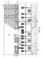
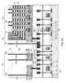
- FIG. 1is a vertical cross-sectional view of an exemplary structure after formation of semiconductor devices, at least one lower level dielectric layer, and lower level metal interconnect structures on a semiconductor substrate according to an embodiment of the present disclosure.
- FIG. 2is a vertical cross-sectional view of the exemplary structure after formation of lower level contact via structures according to an embodiment of the present disclosure.
- FIG. 3is a vertical cross-sectional view of the exemplary structure after formation of a layer stack comprising a lower semiconductor layer, a lower dielectric layer, and a spacer material layer according to an embodiment of the present disclosure.
- FIG. 4Ais a vertical cross-sectional view of the exemplary structure after patterning of the layer stack to form spacer line structures that extend along a first horizontal direction in an array region and spacer plates in a peripheral region according to an embodiment of the present disclosure.
- FIG. 4Bis a horizontal cross-sectional view of the exemplary structure along the horizontal plane B-B′ in FIG. 4A .
- the zig-zag vertical plane A-A′corresponds to the plane of the vertical cross-sectional view of FIG. 4A .
- FIG. 5is a vertical cross-sectional view of the exemplary structure after patterning the lower dielectric layer according to an embodiment of the present disclosure.
- FIG. 6is a vertical cross-sectional view of the exemplary structure after formation of an upper dielectric layer according to an embodiment of the present disclosure.
- FIG. 7is a vertical cross-sectional view of the exemplary structure after deposition of an upper semiconductor layer according to an embodiment of the present disclosure.
- FIG. 8is a vertical cross-sectional view of the exemplary structure after formation of an alternating stack of insulating layers and spacer material layers according to an embodiment of the present disclosure.
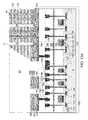
- FIG. 9is a vertical cross-sectional view of the exemplary structure after patterning of passive device structures according to an embodiment of the present disclosure.
- FIG. 10Ais a vertical cross-sectional view of the exemplary structure after formation of a retro-stepped dielectric material layer, memory openings, and support openings according to an embodiment of the present disclosure.
- FIG. 10Bis a horizontal cross-sectional view of the exemplary structure along the horizontal plane B-B′ in FIG. 10A .
- the zig-zag vertical plane A-A′corresponds to the plane of the vertical cross-sectional view of FIG. 10A .
- FIGS. 11A-11Dare sequential schematic vertical cross-sectional views of a memory opening during formation of a memory stack structure, a dielectric core, and a drain region according to an embodiment of the present disclosure.
- FIG. 12is a schematic vertical cross-sectional view of the exemplary structure after formation of memory stack structures according to an embodiment of the present disclosure.
- FIG. 13Ais a schematic vertical cross-sectional view of the exemplary structure after formation of backside trenches and sacrificial spacers according to an embodiment of the present disclosure.
- FIG. 13Bis a partial see-through top-down view of the exemplary structure of FIG. 13A .
- the vertical plane A-A′is the plane of the schematic vertical cross-sectional view of FIG. 13A .
- FIG. 14is a schematic vertical cross-sectional view of the exemplary structure after formation of line cavities by removal of spacer line structures according to an embodiment of the present disclosure.
- FIGS. 15A-15Dare sequential schematic vertical cross-sectional views of a pair of memory openings during formation of a line cavity according to an embodiment of the present disclosure.
- FIG. 16Ais a schematic vertical cross-sectional view of the exemplary structure after formation of a continuous semiconductor structure including semiconductor line structures and semiconductor rails according to an embodiment of the present disclosure.
- FIG. 16Bis a schematic vertical cross-sectional views of a pair of memory openings after formation of a semiconductor line structure according to an embodiment of the present disclosure.
- FIG. 16Cis a schematic vertical cross-sectional views of a memory opening and a backside trench after formation of a semiconductor line structure and a semiconductor rail according to an embodiment of the present disclosure.
- FIG. 17is a schematic vertical cross-sectional view of the exemplary structure after formation of backside recesses according to an embodiment of the present disclosure.
- FIG. 18is a schematic vertical cross-sectional view of the exemplary structure after formation of electrically conductive layers according to an embodiment of the present disclosure.
- FIG. 19is a schematic vertical cross-sectional view of the exemplary structure after removal of a deposited conductive material from within the backside trenches according to an embodiment of the present disclosure.
- FIG. 20Ais a schematic vertical cross-sectional view of the exemplary structure after formation of an insulating wall structure in each backside trench according to an embodiment of the present disclosure.
- FIG. 20Bis a plan (top) view of the exemplary structure of FIG. 20A .
- the zig-zag vertical plane A-A′corresponds to the plane of the vertical cross-sectional view of FIG. 20A .
- FIG. 21Ais a schematic vertical cross-sectional view of the exemplary structure after formation of contact via structures according to an embodiment of the present disclosure.
- FIG. 21Bis a plan (top) view of the exemplary structure of FIG. 21A .
- the zig-zag vertical plane A-A′corresponds to the plane of the vertical cross-sectional view of FIG. 21A .
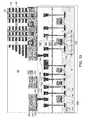
- FIG. 22is a schematic vertical cross-sectional view of the exemplary structure after formation of upper level line structures according to an embodiment of the present disclosure.
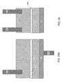
- FIG. 23Ais a schematic vertical cross-sectional view of a first exemplary capacitor structure according to an embodiment of the present disclosure.
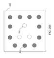
- FIG. 23Bis a plan view of the first exemplary capacitor structure of FIG. 23A .
- FIG. 24Ais a schematic vertical cross-sectional view of a first exemplary resistor structure according to an embodiment of the present disclosure.
- FIG. 24Bis a plan view of the first exemplary resistor structure of FIG. 24A .
- FIG. 25Ais a schematic vertical cross-sectional view of a second exemplary capacitor structure according to an embodiment of the present disclosure.
- FIG. 25Bis a plan view of the first exemplary capacitor structure of FIG. 25A .
- FIG. 26is a schematic vertical cross-sectional view of a second exemplary resistor structure according to an embodiment of the present disclosure.
- the present disclosureis directed to three-dimensional non-volatile memory devices, such as vertical NAND strings and other three-dimensional devices, and methods of making the same, the various aspects of which are described below.
- the embodiments of the disclosurecan be employed to form various semiconductor devices such as three-dimensional monolithic memory array devices comprising a plurality of NAND memory strings.
- the drawingsare not drawn to scale. Multiple instances of an element may be duplicated where a single instance of the element is illustrated, unless absence of duplication of elements is expressly described or clearly indicated otherwise.
- a first element located “on” a second elementcan be located on the exterior side of a surface of the second element or on the interior side of the second element.
- a first elementis located “directly on” a second element if there exist a physical contact between a surface of the first element and a surface of the second element.
- an “in-process” structure or a “transient” structurerefers to a structure that is subsequently modified.
- a “layer”refers to a material portion including a region having a thickness.
- a layermay extend over the entirety of an underlying or overlying structure, or may have an extent less than the extent of an underlying or overlying structure. Further, a layer may be a region of a homogeneous or inhomogeneous continuous structure that has a thickness less than the thickness of the continuous structure. For example, a layer may be located between any pair of horizontal planes between, or at, a top surface and a bottom surface of the continuous structure. A layer may extend horizontally, vertically, and/or along a tapered surface.
- a substratemay be a layer, may include one or more layers therein, and/or may have one or more layer thereupon, thereabove, and/or therebelow.
- a “memory level” or a “memory array level”refers to the level corresponding to a general region between a first horizontal plane including topmost surfaces of an array of memory elements and a second horizontal plane including bottommost surfaces of the array of memory elements.
- a “through-memory-level” elementrefers to an element that vertically extends through a memory level.
- a “semiconductor material”refers to a material having electrical conductivity in the range from 1.0 ⁇ 10 ⁇ 6 S/cm to 1.0 ⁇ 10 5 S/cm, and is capable of producing a doped material having electrical conductivity in a range from 1.0 S/cm to 1.0 ⁇ 10 5 S/cm upon suitable doping with an electrical dopant.
- an “electrical dopant”refers to a p-type dopant that adds a hole to a valence band within a band structure, or an n-type dopant that adds an electron to a conduction band within a band structure.
- a “conductive material”refers to a material having electrical conductivity greater than 1.0 ⁇ 10 5 S/cm.
- an “insulating material” or a “dielectric material”refers to a material having electrical conductivity less than 1.0 ⁇ 10 ⁇ 6 S/cm. All measurements for electrical conductivities are made at the standard condition.
- a monolithic three dimensional memory arrayis one in which multiple memory levels are formed above a single substrate, such as a semiconductor wafer, with no intervening substrates.
- the term “monolithic”means that layers of each level of the array are directly deposited on the layers of each underlying level of the array.
- two dimensional arraysmay be formed separately and then packaged together to form a non-monolithic memory device.
- non-monolithic stacked memorieshave been constructed by forming memory levels on separate substrates and vertically stacking the memory levels, as described in U.S. Pat. No.
- the substratesmay be thinned or removed from the memory levels before bonding, but as the memory levels are initially formed over separate substrates, such memories are not true monolithic three dimensional memory arrays.
- the substratemay include integrated circuits fabricated thereon, such as driver circuits for a memory device
- the various three dimensional memory devices of the present disclosureinclude a monolithic three-dimensional NAND string memory device, and can be fabricated employing the various embodiments described herein.
- the monolithic three dimensional NAND stringis located in a monolithic, three dimensional array of NAND strings located over the substrate. At least one memory cell in the first device level of the three dimensional array of NAND strings is located over another memory cell in the second device level of the three dimensional array of NAND strings.
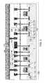
- the exemplary structureincludes a semiconductor substrate (e.g., silicon wafer) 9 , and semiconductor devices formed thereupon.
- the semiconductor devicescan include transistors, at least some of which may be, for example, field effect transistors including respective source regions, drain regions, channel regions, and gate structures 750 .
- Shallow trench isolation structures 720can be formed in an upper portion of the semiconductor substrate 9 to provide electrical isolation among the semiconductor devices.
- the transistor channelis located in the upper portion of the semiconductor substrate 9 between the source and drain regions.
- Each gate structure 750can include, for example, a gate dielectric 752 , a gate electrode ( 753 , 754 , 7 ( 50 , 60 )), a gate cap dielectric 758 , and a dielectric gate spacer 756 .
- the gate electrode ( 753 , 754 , 7 ( 50 , 60 ))can include a stack of multiple gate electrode layers such as a polysilicon gate electrode 753 , an optional metal silicide gate electrode 754 , and an optional metal gate electrode 7 ( 50 , 60 ).
- Source regions 732 and drain regions 738can be formed around each gate structure 750 .
- source extension regions 734can be formed between a respective pair of a gate structure 750 and a source region 732 .
- drain extension regions 736can be formed between a respective pair of a gate structure 750 and a drain region 738 .
- the semiconductor devicescan include any semiconductor circuitry to support operation of a memory structure to be subsequently formed, which is typically referred to as a peripheral circuitry.
- a peripheral circuitryrefers to any, each, or all, of word line decoder circuitry, word line switching circuitry, bit line decoder circuitry, bit line sensing and/or switching circuitry, power supply/distribution circuitry, data buffer and/or latch, or any other semiconductor circuitry that can be implemented outside a memory array structure for a memory device.
- the semiconductor devicescan include word line switching devices for electrically biasing word lines of three-dimensional memory structures to be subsequently formed.
- At least one dielectric layeris formed over the semiconductor devices, which is herein referred to as at least one lower level dielectric layer 760 .
- the at least one lower level dielectric layer 760can include, for example, a planarization dielectric layer 762 that is employed to provide a planar surface overlying the gate structures 750 , an optional planar liner 763 , and at least one lower level interconnect dielectric layer ( 764 , 766 , 768 ).
- the at least one lower level interconnect dielectric layer ( 784 , 866 , 768 )can include, for example, a first lower via level dielectric layer 764 , a lower line level dielectric layer 766 , and a second lower via level dielectric layer 768 .
- the at least one lower level dielectric layer 760can include a dielectric liner (such as a silicon nitride liner) that underlies the planarization dielectric layer 762 and blocks diffusion of mobile ions and/or apply appropriate stress to underlying structures.
- the at least one lower level dielectric layer 760functions as a dielectric matrix for lower level metal interconnect structures 780 that provide electrical wiring among the various nodes of the semiconductor devices and landing pads for through-memory-level via structures to be subsequently formed.
- the lower level metal interconnect structures 780can include various lower level conductive via structures 782 and lower level metal lines 786 . A subset of the lower level metal lines 786 can be configured to function as landing pads for contact via structures to be subsequently formed.
- the region of the semiconductor devices and the combination of the at least one lower level dielectric layer 760 and the lower level metal interconnect structures 780is herein referred to an underlying peripheral device region 700 , which is located underneath a memory-level assembly to be subsequently formed and includes peripheral devices for the memory-level assembly.
- the lower level metal interconnect structures 780are embedded in the at least one lower level dielectric layer 760 .
- the lower level metal interconnect structures 780can be electrically shorted to nodes (i.e., source and drain regions) of the semiconductor devices, and are located at the level of the at least one lower level dielectric layer 760 .
- the through-memory-level via structures(not shown in FIG. 1 ) can be subsequently formed directly on the lower level metal interconnect structures 780 to provide electrically conductive paths between the semiconductor devices on the semiconductor substrate 9 and the various word lines and/or bit lines of three-dimensional memory devices to be subsequently formed.
- underside contact via structures ( 78 A, 78 C)can be formed on a subset of the lower level metal lines 786 within the at least one lower level interconnect dielectric layer ( 764 , 766 , 768 ).
- the underside contact via structures ( 78 A, 78 C)can be formed directly on top surfaces of the subset of the lower level metal lines 786 within the second lower via level dielectric layer 768 .
- the underside contact via structures ( 78 A, 78 C)can include, for example, an underside array source contact via structure 78 A that is electrically shorted to source regions of a three-dimensional memory structure to be subsequently formed, and an underside capacitor contact via structure 78 C that is electrically shorted to a lower electrode of a capacitor to be subsequently formed.
- the lower level conductive via structures 782 and the underside contact via structures ( 78 A, 78 C)are collectively referred to as lower level via structures ( 782 , 78 A, 78 C).
- the lower level metal interconnect structure 780is embedded within at least one lower interconnect level dielectric layer 760 .
- a layer stack( 6 L, 101 L, 32 L, 34 L) including an optional metallic material layer 6 L, a lower semiconductor layer 101 L, a lower dielectric layer 32 L, and a spacer material layer 34 L can be formed over a planar top surface of the at least one lower interconnect level dielectric layer 760 and the lower level metal interconnect structure 780 embedded therein.
- the optional metallic material layer 6 Lcan include a metal silicide such as tungsten silicide or cobalt silicide.
- the metallic material layer 6 Lcan be deposited, for example, by sputtering.
- the thickness of the metallic material layer 6 Lcan be in a range from 5 nm to 100 nm, although lesser and greater thicknesses can also be employed.
- the metallic material layer 6 Lmay include a stack, from bottom to top, of a metallic nitride liner such as a TiN liner and a metal layer such as a tungsten layer. In this case, at least an upper portion of the metal layer can be subsequently converted into a metal silicide layer during a thermal anneal process.
- the lower semiconductor layer 101 Lcan include a conductive doped semiconductor material having a doping of a first conductivity type, which may be p-type or n-type.
- the lower semiconductor layer 101 Lcan include doped polysilicon, a doped silicon-containing semiconductor alloy, a doped compound semiconductor material (such as a doped III-V compound material), or a doped organic semiconductor material.
- the thickness of the lower semiconductor layer 101 Lcan be in a range from 20 nm to 200 nm, although lesser and greater thicknesses can also be employed.
- the lower semiconductor layer 101 Lcan include n-doped polysilicon.
- the lower dielectric layer 32 Lincludes a dielectric material such as silicon oxide, silicon nitride, or a dielectric metal oxide.
- the thickness of the lower dielectric layer 32 Lcan be in a range from 2 nm to 10 nm, although lesser and greater thicknesses can also be employed.
- the lower dielectric layer 32 Lincludes silicon oxide.
- the spacer material layer 34 Lincludes a material that can be removed selective to the lower dielectric layer 32 L and the lower semiconductor layer 101 L.
- the spacer material layer 34 Lcan include a dielectric material such as silicon nitride or a semiconductor material such as germanium.
- the thickness of the spacer material layer 34 Lcan be selected based on the target thickness of straps to be subsequently formed to contact sidewalls of semiconductor channels.
- the thickness of the spacer material layer 34 Lcan be in a range from 20 nm to 80 nm, although lesser and greater thicknesses can also be employed.
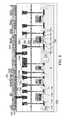
- the spacer material layer 34 Lcan be patterned to form spacers, such as spacer line structures 34 A that extend along a first horizontal direction hd 1 in an array region 100 and spacer plates ( 34 R, 34 C) in a peripheral region 400 .
- a photoresist layercan be applied over the spacer material layer 34 L, and can be lithographically patterned.
- the pattern in the photoresist layercan be transferred through the spacer material layer 34 L by an etch process, which can be an anisotropic etch such as a reactive ion etch.
- the photoresist layercan be subsequently removed, for example, by ashing.
- the array region 100refers to a region in which a three-dimensional memory array is to be subsequently formed.
- a peripheral region 400refers to a region located at a periphery of the array region 100 .
- a contact region 300can be provided between the array region 100 and the peripheral region 400 .
- the spacer line structures 34 Acan have a uniform width (measured in the widthwise direction) that is invariant along the first horizontal direction hd 1 .
- the widthwise directioncan be a second horizontal direction hd 2 that is perpendicular to the first horizontal direction hd 1 .
- the spacer line structures 34 Acan form a periodic one-dimensional array having a pitch along the second horizontal direction hd 2 .
- the pitch of the spacer line structures 34 Acan be the same as the pitch of memory stack structures to be subsequently formed along the second horizontal direction hd 2 .
- the spacer plates ( 34 R, 34 C)can include resistor spacer plates 34 R and capacitor spacer plates 34 C. While the present disclosure is described employing an embodiment in which the resistor spacer plates 34 R and the capacitor spacer plates 34 C are simultaneously formed, embodiments are expressly contemplated herein in which only resistor spacer plates 34 R or only capacitor spacer plates 34 C are formed.
- the resistor spacer plates 34 Rcan have a horizontal cross-sectional shape of any suitable shape for providing a horizontal resistive path between two ends.
- the resistor spacer plates 34 Rcan have a polygonal (e.g., rectangular) shape, an irregular (e.g., tortuous or maze) shape, or any other shape that provides a horizontal path between two ends. If formed, the resistor spacer plates 34 R can be permanent structures that remain in a final device structure.
- the resistor spacer plates 34 Rare optional components for forming a resistor structure. In other words, a resistor structure to be subsequently formed may, or may not, include a respective resistor spacer plate 34 R.
- Each of the capacitor spacer plates 34 Ccan be formed as a continuous structure or as a set of discrete structures. Each capacitor spacer plate 34 C can be formed in areas in which an upper contact via structure is to be subsequently formed on an upper electrode of a respective capacitor.
- a capacitor spacer plate 34 Ccan have a generally annular shape (e.g., hollow polygonal shape, ring shape, etc.) having an opening that overlies a respective set of at least one underside capacitor contact via structure 78 C.
- the capacitor spacer plates 34 Care optional components for forming a capacitor structure. In other words, a capacitor structure to be subsequently formed may, or may not, include a respective capacitor spacer plate 34 C. If formed, the capacitor spacer plates 34 C can be permanent structures that remain in a final device structure, and provide electrical isolation between upper capacitor contact via structures to be subsequently formed and a lower electrode of each capacitor.
- the lower dielectric layer 32 Lcan be patterned by etching the physically exposed portions of the lower dielectric layer 32 L, for example, by an isotropic etch such as a wet etch.
- an isotropic etchsuch as a wet etch.
- a wet etch employing hydrofluoric acidcan be employed to etch physically exposed portions of the lower dielectric layer 32 L.
- Remaining portions of the lower dielectric layer 32 L after patterninginclude array dielectric liners 32 A underlying the spacer line structures 34 A, resistor dielectric liners 32 R underlying the resistor spacer plates 34 R, and capacitor dielectric liners 32 C underlying the capacitor spacer plates 34 C.
- Each array dielectric liner 32 Acan have a substantially same horizontal cross-sectional shape as an overlying spacer line structure 34 A
- each resistor dielectric liner 32 Rcan have a substantially same horizontal cross-sectional shape as an overlying resistor spacer plate 34 R
- each capacitor dielectric liner 32 Ccan have a substantially same horizontal cross-sectional shape as an overlying capacitor spacer plate 34 C.
- the resistor dielectric liners 32 Rare optional components for forming a resistor structure. In other words, a resistor structure to be subsequently formed may, or may not, include a respective resistor dielectric liner 32 R.
- the capacitor dielectric liners 32 Care optional components for forming a capacitor structure. In other words, a capacitor structure to be subsequently formed may, or may not, include a respective capacitor dielectric liner 32 C.
- an upper dielectric layer 36 Lcan be deposited over the spacer line structures 34 A and the spacer plates ( 34 R, 34 C).
- the upper dielectric layer 36 Lincludes a dielectric material such as silicon oxide, silicon nitride, or a dielectric metal oxide.
- the upper dielectric layer 36 Lmay be formed as a single continuous layer by a conformal deposition process such as chemical vapor deposition or atomic layer deposition.
- the thickness of the upper dielectric layer 36 Lcan be in a range from 2 nm to 20 nm, although lesser and greater thicknesses can also be employed.
- the upper dielectric layer 32 Lincludes silicon oxide.
- an upper semiconductor layer 109 Lcan be deposited over the upper dielectric layer 36 L.
- the upper semiconductor layer 109 Lcan include a conductive doped semiconductor material having a doping of the first conductivity type, which is the same type as the conductivity type of the lower semiconductor layer 101 L.
- the upper semiconductor layer 109 Lcan include doped polysilicon, doped amorphous silicon, a doped silicon-containing semiconductor alloy, a doped compound semiconductor material (such as a doped III-V compound material), or a doped organic semiconductor material.
- the thickness of the upper semiconductor layer 109 Lcan be in a range from 100 nm to 600 nm (e.g., 150 to 200 nm), although lesser and greater thicknesses can also be employed.
- the upper semiconductor layer 109 Lcan include n-doped polysilicon.
- the upper semiconductor layer 109 Lcan have a flat top surface due to the larger thickness of the upper semiconductor layer 109 L compared to the underlying structures.
- the top surface of the upper semiconductor layer 109 Lcan be planarized, for example, by a planarization process such as chemical mechanical planarization.
- the lower semiconductor layer 101 L and the upper semiconductor layer 109 Lare collectively referred to as a semiconductor layer stack 10 L.
- the lower semiconductor layer 101 L and the upper semiconductor layer 109 Lare vertically separated from each other in each region at least by a portion of the upper dielectric layer 36 L.
- a gap fill materialsuch as silicon oxide, can be formed between the underlying structures followed by forming a planar upper semiconductor layer 109 L over the gap fill material.
- a stack of an alternating plurality of first material layers (which can be insulating layers 32 ) and second material layers (which can be sacrificial material layer 42 )is formed over the semiconductor layer stack 10 L.
- a “material layer”refers to a layer including a material throughout the entirety thereof.
- an alternating plurality of first elements and second elementsrefers to a structure in which instances of the first elements and instances of the second elements alternate. Each instance of the first elements that is not an end element of the alternating plurality is adjoined by two instances of the second elements on both sides, and each instance of the second elements that is not an end element of the alternating plurality is adjoined by two instances of the first elements on both ends.
- the first elementsmay have the same thickness thereamongst, or may have different thicknesses.
- the second elementsmay have the same thickness thereamongst, or may have different thicknesses.
- the alternating plurality of first material layers and second material layersmay begin with an instance of the first material layers or with an instance of the second material layers, and may end with an instance of the first material layers or with an instance of the second material layers.
- an instance of the first elements and an instance of the second elementsmay form a unit that is repeated with periodicity within the alternating plurality.
- Each first material layerincludes a first material
- each second material layerincludes a second material that is different from the first material.
- each first material layercan be an insulating layer 32
- each second material layercan be a sacrificial material layer.
- the stackcan include an alternating plurality of insulating layers 32 and sacrificial material layers 42 , and constitutes a prototype stack of alternating layers comprising insulating layers 32 and sacrificial material layers 42 .
- a “prototype” structure or an “in-process” structurerefers to a transient structure that is subsequently modified in the shape or composition of at least one component therein.
- the stack of the alternating pluralityis herein referred to as an alternating stack ( 32 , 42 ).
- the alternating stack ( 32 , 42 )can include insulating layers 32 composed of the first material, and sacrificial material layers 42 composed of a second material different from that of insulating layers 32 .
- the first material of the insulating layers 32can be at least one insulating material.
- each insulating layer 32can be an insulating material layer.
- Insulating materials that can be employed for the insulating layers 32include, but are not limited to, silicon oxide (including doped or undoped silicate glass), silicon nitride, silicon oxynitride, organosilicate glass (OSG), spin-on dielectric materials, dielectric metal oxides that are commonly known as high dielectric constant (high-k) dielectric oxides (e.g., aluminum oxide, hafnium oxide, etc.) and silicates thereof, dielectric metal oxynitrides and silicates thereof, and organic insulating materials.
- the first material of the insulating layers 32can be silicon oxide.
- the second material of the sacrificial material layers 42is a sacrificial material that can be removed selective to the first material of the insulating layers 32 .
- a removal of a first materialis “selective to” a second material if the removal process removes the first material at a rate that is at least twice the rate of removal of the second material.
- the ratio of the rate of removal of the first material to the rate of removal of the second materialis herein referred to as a “selectivity” of the removal process for the first material with respect to the second material.
- the sacrificial material layers 42may comprise an insulating material, a semiconductor material, or a conductive material.
- the second material of the sacrificial material layers 42can be subsequently replaced with electrically conductive electrodes which can function, for example, as control gate electrodes of a vertical NAND device.
- Non-limiting examples of the second materialinclude silicon nitride, an amorphous semiconductor material (such as amorphous silicon), and a polycrystalline semiconductor material (such as polysilicon).
- the sacrificial material layers 42can be spacer material layers that comprise silicon nitride or a semiconductor material including at least one of silicon and germanium.
- the insulating layers 32can include silicon oxide, and sacrificial material layers can include silicon nitride sacrificial material layers.
- the first material of the insulating layers 32can be deposited, for example, by chemical vapor deposition (CVD).
- CVDchemical vapor deposition
- TEOStetraethyl orthosilicate
- the second material of the sacrificial material layers 42can be formed, for example, CVD or atomic layer deposition (ALD).
- the thicknesses of the insulating layers 32 and the sacrificial material layers 42can be in a range from 20 nm to 50 nm, although lesser and greater thicknesses can be employed for each insulating layer 32 and for each sacrificial material layer 42 .
- the number of repetitions of the pairs of an insulating layer 32 and a sacrificial material layer (e.g., a control gate electrode or a sacrificial material layer) 42can be in a range from 2 to 1,024, and typically from 8 to 256, although a greater number of repetitions can also be employed.
- the top and bottom gate electrodes in the stackmay function as the select gate electrodes.
- each sacrificial material layer 42 in the alternating stack ( 32 , 42 )can have a uniform thickness that is substantially invariant within each respective sacrificial material layer 42 .
- spacer material layersare sacrificial material layers 42 that are subsequently replaced with electrically conductive layers
- embodimentsare expressly contemplated herein in which the sacrificial material layers are formed as electrically conductive layers. In this case, steps for replacing the spacer material layers with electrically conductive layers can be omitted.
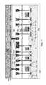
- a stepped cavity 69can be formed within the contact region 300 and over the peripheral region 400 .
- the stepped cavity 69can have various stepped surfaces such that the horizontal cross-sectional shape of the stepped cavity 69 changes in steps as a function of the vertical distance from the top surface of the semiconductor layer stack 10 L.
- stepped surfacesrefer to a set of surfaces that include at least two horizontal surfaces and at least two vertical surfaces such that each horizontal surface is adjoined to a first vertical surface that extends upward from a first edge of the horizontal surface, and is adjoined to a second vertical surface that extends downward from a second edge of the horizontal surface.
- a “stepped cavity”refers to a cavity having stepped surfaces.
- the stepped cavity 69can be formed by repetitively performing a set of processing steps.
- the set of processing stepscan include, for example, an etch process of a first type that vertically increases the depth of a cavity by one or more levels, and an etch process of a second type that laterally expands the area to be vertically etched in a subsequent etch process of the first type.
- a “level” of a structure including the level of the alternating stackis defined as the relative position of a pair of a first material layer and a second material layer within the structure.
- the stepped surfacescan be formed in the contact region 300 .
- the entirety of the alternating stack ( 32 , 42 )can be etched from the peripheral region 400 .
- a terrace regionis formed in the contact region 300 by patterning the alternating stack ( 32 , 42 ).
- the terrace regionincludes stepped surfaces of the alternating stack ( 32 , 42 ) that continuously extend from a bottommost layer within the alternating stack ( 32 , 42 ) to a topmost layer within the alternating stack ( 32 , 42 ).
- the stepped cavity 69can be bounded by the physically exposed portion of the top surface of the semiconductor layer stack 10 L (i.e., the top surface of the upper semiconductor layer 109 L) in the peripheral region 400 , and by the stepped surfaces of the alternating stack ( 32 , 42 ) in the contact region 300 .
- a photoresist layer 47can be applied over the exemplary structure and can be lithographically patterned to cover the entirety of the array region 100 and the contact region 300 , and to cover each area within the peripheral region 400 to be subsequently patterned into resistors or capacitors.
- An anisotropic etchcan be performed to pattern the layer stack of the top semiconductor layer 109 L, the upper dielectric layer 36 L, the lower semiconductor layer 101 L, and the metallic material layer 6 L.
- the etching step of FIG. 9can precede the step of forming the alternating stack ( 32 , 42 ).
- Patterning of at least the upper semiconductor layer 109 L, the upper dielectric layer 36 L, the lower semiconductor layer 101 L, and the metallic material layer 6 Lforms a first layer stack ( 6 , 101 , 32 A, 34 A, 36 A, 109 ) in the array region 100 and the contact region 300 , and second layer stacks ⁇ ( 6 R, 31 R, 32 R, 34 R, 36 R, 39 R) or ( 6 C, 32 C, 32 C, 34 C, 36 C, 39 C) ⁇ in the peripheral region 400 .
- the first layer stack( 6 , 101 , 32 A, 34 A, 36 A, 109 ) includes a patterned metallic material layer 6 that is a remaining portion of the metallic material layer 6 L, a patterned lower semiconductor layer 101 that is a remaining portion of the lower semiconductor layer 101 L, a patterned upper dielectric layer 36 A that is a remaining portion of the upper dielectric layer 36 L, and a patterned upper semiconductor layer 109 that is a remaining portion of the upper semiconductor layer 109 L.
- the first layer stack ( 6 , 101 , 32 A, 34 A, 36 A, 109 )further includes the array dielectric liners 32 A and the spacer line structures 34 A.
- the patterned lower semiconductor layer 101 and the patterned upper semiconductor layer 109collectively constitute a patterned semiconductor layer stack 10 .
- Each of the second layer stacks ⁇ ( 6 R, 31 R, 32 R, 34 R, 36 R, 39 R) or ( 6 C, 32 C, 32 C, 34 C, 36 C, 39 C) ⁇can include a passive device, which can be a resistor or a capacitor.
- the second layer stacks ⁇ ( 6 R, 31 R, 32 R, 34 R, 36 R, 39 R) or ( 6 C, 32 C, 32 C, 34 C, 36 C, 39 C) ⁇can include resistor-type second layer stacks ( 6 R, 31 R, 32 R, 34 R, 36 R, 39 R) and capacitor-type second layer stacks ( 6 C, 32 C, 32 C, 34 C, 36 C, 39 C).
- Each resistor-type second layer stack( 6 R, 31 R, 32 R, 34 R, 36 R, 39 R) includes a resistor-type metal plate 6 R that is a remaining portion of the metallic material layer 6 L, a resistor-type lower semiconductor plate 31 R that is a remaining portion of the lower semiconductor layer 101 L, an optional resistor dielectric liner 32 R, an optional resistor spacer plate 34 R, a resistor-type dielectric material plate 36 R that is a remaining portion of the upper dielectric layer 36 L, and a resistor-type upper semiconductor plate 39 R that is a remaining portion of the upper semiconductor layer 109 L.
- Each capacitor-type second layer stack( 6 C, 31 C, 32 C, 34 C, 36 C, 39 C) includes a capacitor-type metal plate 6 C that is a remaining portion of the metallic material layer 6 L, a capacitor-type lower semiconductor plate 31 C that is a remaining portion of the lower semiconductor layer 101 L, optional capacitor dielectric liners 32 C, an optional capacitor spacer plate 34 C, a capacitor-type dielectric material plate 36 C that is a remaining portion of the upper dielectric layer 36 L, and a capacitor-type upper semiconductor plate 39 C that is a remaining portion of the upper semiconductor layer 109 L.
- each of the passive deviceincludes a respective second layer stack ⁇ ( 6 R, 31 R, 32 R, 34 R, 36 R, 39 R) or ( 6 C, 32 C, 32 C, 34 C, 36 C, 39 C) ⁇ includes: a lower semiconductor plate ( 31 R or 31 C) that is a patterned portion of the lower semiconductor layer 101 L; a dielectric material plate ( 36 R or 36 C) that is a patterned portion of the upper dielectric layer 36 L; and an upper semiconductor plate ( 39 R or 39 C) that is a patterned portion of the upper semiconductor layer 109 L.
- At least one of the passive devicescan include a resistor, and at least another of the passive devices can include a capacitor.
- the lower semiconductor plate ( 31 R or 31 C)can be vertically spaced from the semiconductor substrate 9 by the same distance as the patterned lower semiconductor layer 101 is from the substrate 9 .
- the dielectric material plate ( 36 R or 36 C)can be vertically spaced from the substrate by the same distance as the patterned dielectric material layer 36 A is from the semiconductor substrate 9 .
- An upper semiconductor plate ( 39 R or 39 C)can be vertically spaced from the semiconductor substrate 9 by the same distance as the patterned upper semiconductor layer 109 is from the semiconductor substrate 9 .
- the lower semiconductor plate ( 31 R or 31 C)can have the same composition as, and the same thickness as, the patterned lower semiconductor layer 101 .
- the dielectric material plate ( 36 R or 36 C)can have the same composition as, and the same thickness as, the patterned dielectric material layer 36 A.
- the upper semiconductor plate ( 39 R or 39 C)can have the same composition as the patterned upper semiconductor layer 109 .
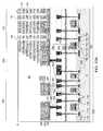
- a retro-stepped dielectric material portion 65(i.e., an insulating fill material portion) can be formed in the stepped cavity 69 by deposition of a dielectric material therein.
- a dielectric materialsuch as silicon oxide can be deposited in the stepped cavity 69 .
- CMPchemical mechanical planarization
- a “retro-stepped” elementrefers to an element that has stepped surfaces and a horizontal cross-sectional area that increases monotonically as a function of a vertical distance from a top surface of a substrate on which the element is present. If silicon oxide is employed for the retro-stepped dielectric material portion 65 , the silicon oxide of the retro-stepped dielectric material portion 65 may, or may not, be doped with dopants such as B, P, and/or F.
- a lithographic material stackincluding at least a photoresist layer can be formed over the alternating stack ( 32 , 42 ) and the retro-stepped dielectric material portion 65 , and can be lithographically patterned to form openings therein.
- the openingsinclude a first set of openings formed over the array region 100 and a second set of openings formed over the contact region 300 .
- the pattern in the lithographic material stackcan be transferred through the retro-stepped dielectric material portion 65 and through the alternating stack ( 32 , 42 ) by at least one anisotropic etch that employs the patterned lithographic material stack as an etch mask. Portions of the alternating stack ( 32 , 42 ) underlying the openings in the patterned lithographic material stack are etched to form memory openings 49 and support openings 19 .
- a “memory opening”refers to a structure in which memory elements, such as a memory stack structure, is subsequently formed.
- a “support opening”refers to a structure in which a support structure (such as a support pillar structure) that mechanically supports other elements is subsequently formed.
- the memory openings 49are formed through the entirety of the alternating stack ( 32 , 42 ) in the array region 100 .
- the support openings 19 shown in FIG. 10Bare formed through the retro-stepped dielectric material portion 65 and the portion of the alternating stack ( 32 , 42 ) that underlie the stepped surfaces in the contact region 300 .
- the memory openings 49extend through the entirety of the alternating stack ( 32 , 42 ).
- the support openings 19extend through a subset of layers within the alternating stack ( 32 , 42 ).
- the chemistry of the anisotropic etch process employed to etch through the materials of the alternating stack ( 32 , 42 )can alternate to optimize etching of the first and second materials in the alternating stack ( 32 , 42 ).
- the anisotropic etchcan be, for example, a series of reactive ion etches.
- the sidewalls of the memory openings 49 and the support openings 19can be substantially vertical, or can be tapered.
- the patterned lithographic material stackcan be subsequently removed, for example, by ashing.
- the memory openings 49 and the support openings 19can extend from the top surface of the alternating stack ( 32 , 42 ) to the patterned bottom semiconductor layer 101 in the patterned semiconductor layer stack 10 .
- the bottom surfaces of the memory openings 49 and the support openings 19can be vertically offset from the top surface of the patterned bottom semiconductor layer by a recess depth.
- the recess depthcan be, for example, in a range from 0 nm to 50 nm, although lesser and greater recess depths can also be employed.
- Each of the memory openings 49 and the support openings 19may include a sidewall (or a plurality of sidewalls) that extends substantially perpendicular to the topmost surface of the semiconductor substrate 9 .
- a two-dimensional array of memory openings 49can be formed in the array region 100 .
- a two-dimensional array of support openings 19can be formed in the contact region 300 .
- the lithographic material stackcan be subsequently removed, for example, by ashing.
- FIGS. 11A-11Hillustrate structural changes in a memory opening 49 , which is one of the memory openings 49 in the exemplary structure of FIGS. 10A and 10B .
- the same structural changeoccurs simultaneously in each of the other memory openings 49 and in each support opening 19 .
- each support opening 19can extend through the retro-stepped dielectric material portion 65 , a subset of layers in the alternating stack ( 32 , 42 ), the patterned upper semiconductor layer 109 , the patterned upper dielectric layer 36 A, a peripheral portion of a respective spacer line structures 34 A, and a peripheral portion of a respective array dielectric liner 32 A, and into an upper portion of the patterned lower dielectric layer 101 .
- each spacer line structure 34 Aincludes a set of lateral indentations in regions of overlap with the memory openings 49 .
- the recess depth of the bottom surface of each memory opening 49 with respect to the top surface of the patterned lower semiconductor layer 101can be in a range from 0 nm to 50 nm, although greater recess depths can also be employed.
- a stack of layers including a blocking dielectric layer 52 , a charge storage layer 54 , a tunneling dielectric layer 56 , and a semiconductor channel layer 60 Lcan be sequentially deposited in the memory openings 49 and in the support openings 19 .
- the blocking dielectric layer 52can include a single dielectric material layer or a stack of a plurality of dielectric material layers.
- the blocking dielectric layercan include a dielectric metal oxide layer consisting essentially of a dielectric metal oxide.
- a dielectric metal oxiderefers to a dielectric material that includes at least one metallic element and at least oxygen.
- the dielectric metal oxidemay consist essentially of the at least one metallic element and oxygen, or may consist essentially of the at least one metallic element, oxygen, and at least one non-metallic element such as nitrogen.
- the blocking dielectric layer 52can include a dielectric metal oxide having a dielectric constant greater than 7.9, i.e., having a dielectric constant greater than the dielectric constant of silicon nitride.
- Non-limiting examples of dielectric metal oxidesinclude aluminum oxide (Al 2 O 3 ), hafnium oxide (HfO 2 ), lanthanum oxide (LaO 2 ), yttrium oxide (Y 2 O 3 ), tantalum oxide (Ta 2 O 5 ), silicates thereof, nitrogen-doped compounds thereof, alloys thereof, and stacks thereof.
- the dielectric metal oxide layercan be deposited, for example, by chemical vapor deposition (CVD), atomic layer deposition (ALD), pulsed laser deposition (PLD), liquid source misted chemical deposition, or a combination thereof.
- the thickness of the dielectric metal oxide layercan be in a range from 1 nm to 20 nm, although lesser and greater thicknesses can also be employed.
- the dielectric metal oxide layercan subsequently function as a dielectric material portion that blocks leakage of stored electrical charges to control gate electrodes.
- the blocking dielectric layer 52includes aluminum oxide.
- the blocking dielectric layer 52can include multiple dielectric metal oxide layers having different material compositions.
- the blocking dielectric layer 52can include a dielectric semiconductor compound such as silicon oxide, silicon oxynitride, silicon nitride, or a combination thereof.
- the blocking dielectric layer 52can include silicon oxide.
- the dielectric semiconductor compound of the blocking dielectric layer 52can be formed by a conformal deposition method such as low pressure chemical vapor deposition, atomic layer deposition, or a combination thereof.
- the thickness of the dielectric semiconductor compoundcan be in a range from 1 nm to 20 nm, although lesser and greater thicknesses can also be employed.
- the blocking dielectric layer 52can be omitted, and a backside blocking dielectric layer can be formed after formation of backside recesses on surfaces of memory films to be subsequently formed.
- the charge storage layer 54can be formed.
- the charge storage layer 54can be a continuous layer or patterned discrete portions of a charge trapping material including a dielectric charge trapping material, which can be, for example, silicon nitride.
- the charge storage layer 54can include a continuous layer or patterned discrete portions of a conductive material such as doped polysilicon or a metallic material that is patterned into multiple electrically isolated portions (e.g., floating gates), for example, by being formed within lateral recesses into sacrificial material layers 42 .
- the charge storage layer 54includes a silicon nitride layer.
- the sacrificial material layers 42can be laterally recessed with respect to the sidewalls of the insulating layers 32 , and a combination of a deposition process and an anisotropic etch process can be employed to form the charge storage layer 54 as a plurality of memory material portions that are vertically spaced apart. While the present disclosure is described employing an embodiment in which the charge storage layer 54 is a single continuous layer, embodiments are expressly contemplated herein in which the charge storage layer 54 is replaced with a plurality of memory material portions (which can be charge trapping material portions or electrically isolated conductive material portions) that are vertically spaced apart.
- the charge storage layer 54can be formed as a single charge storage layer of homogeneous composition, or can include a stack of multiple charge storage layers.
- the multiple charge storage layerscan comprise a plurality of spaced-apart floating gate material layers that contain conductive materials (e.g., metal such as tungsten, molybdenum, tantalum, titanium, platinum, ruthenium, and alloys thereof, or a metal silicide such as tungsten silicide, molybdenum silicide, tantalum silicide, titanium silicide, nickel silicide, cobalt silicide, or a combination thereof) and/or semiconductor materials (e.g., polycrystalline or amorphous semiconductor material including at least one elemental semiconductor element or at least one compound semiconductor material).
- conductive materialse.g., metal such as tungsten, molybdenum, tantalum, titanium, platinum, ruthenium, and alloys thereof, or a metal silicide such as tungsten silicide, molybdenum si
- the charge storage layer 54may comprise an insulating charge trapping material, such as one or more silicon nitride segments.
- the charge storage layer 54may comprise conductive nanoparticles such as metal nanoparticles, which can be, for example, ruthenium nanoparticles.
- the charge storage layer 54can be formed, for example, by chemical vapor deposition (CVD), atomic layer deposition (ALD), physical vapor deposition (PVD), or any suitable deposition technique for storing electrical charges therein.
- the thickness of the charge storage layer 54can be in a range from 2 nm to 20 nm, although lesser and greater thicknesses can also be employed.
- the tunneling dielectric layer 56includes a dielectric material through which charge tunneling can be performed under suitable electrical bias conditions.
- the charge tunnelingmay be performed through hot-carrier injection or by Fowler-Nordheim tunneling induced charge transfer depending on the mode of operation of the monolithic three-dimensional NAND string memory device to be formed.
- the tunneling dielectric layer 56can include silicon oxide, silicon nitride, silicon oxynitride, dielectric metal oxides (such as aluminum oxide and hafnium oxide), dielectric metal oxynitride, dielectric metal silicates, alloys thereof, and/or combinations thereof.
- the tunneling dielectric layer 56can include a stack of a first silicon oxide layer, a silicon oxynitride layer, and a second silicon oxide layer, which is commonly known as an ONO stack.
- the tunneling dielectric layer 56can include a silicon oxide layer that is substantially free of carbon or a silicon oxynitride layer that is substantially free of carbon.
- the thickness of the tunneling dielectric layer 56can be in a range from 2 nm to 20 nm, although lesser and greater thicknesses can also be employed.
- the semiconductor channel layer 60 Lincludes a semiconductor material such as at least one elemental semiconductor material, at least one III-V compound semiconductor material, at least one II-VI compound semiconductor material, at least one organic semiconductor material, or other semiconductor materials known in the art.
- the semiconductor channel layer 60 Lincludes amorphous silicon or polysilicon.
- the semiconductor channel layer 60 Lcan be formed by a conformal deposition method such as low pressure chemical vapor deposition (LPCVD).
- LPCVDlow pressure chemical vapor deposition
- the thickness of the semiconductor channel layer 60 Lcan be in a range from 2 nm to 10 nm, although lesser and greater thicknesses can also be employed.
- a memory cavity 49 ′is formed in the volume of each memory opening 49 that is not filled with the deposited material layers ( 52 , 54 , 56 , 60 L).
- a dielectric materialsuch as silicon oxide can be deposited in each memory cavity 49 ′ and over the semiconductor channel layer 60 L.
- the portions of the deposited dielectric material, the semiconductor channel layer 60 L, the tunneling dielectric layer 56 , the charge storage layer 54 , the blocking dielectric layer 52 that located above the topmost surface of the alternating stack ( 32 , 42 )can be removed by a planarization process.
- the planarization processcan employ chemical mechanical planarization (CMP) and/or at least one recess etch process.
- CMPchemical mechanical planarization
- Each remaining portion of the deposited dielectric materialconstitutes a dielectric core 62 .
- Each remaining portion of the semiconductor channel layer 60 Lconstitutes a vertical semiconductor channel 60 , which includes a vertical semiconductor channel that extends at least from the level of the bottom surface of the spacer line structures 34 A to the level of the topmost surface of the alternating stack ( 32 , 42 ).
- Each remaining portion of the tunneling dielectric layer 56 , the charge storage layer 54 , and the blocking dielectric layer 52can be located entirely within a respective memory opening 49 .
- Each contiguous set of a blocking dielectric layer 52 , a charge storage layer 54 , and a tunneling dielectric layer 56 in a memory opening 49constitutes a memory film 50 , which includes a plurality of charge storage regions (as embodied as the charge storage layer 54 ) that are insulated from surrounding materials by the blocking dielectric layer 52 and the tunneling dielectric layer 56 .
- Electrical currentcan flow through a vertical semiconductor channel 60 when a vertical NAND device including the vertical semiconductor channel 60 is turned on.
- a tunneling dielectric layer 56is surrounded by a charge storage layer 54 , and laterally surrounds a portion of the vertical semiconductor channel 60 .
- the memory film 50can store electrical charges with a macroscopic retention time.
- a blocking dielectric layer 52may not be present in the memory film 50 at this step, and a blocking dielectric layer may be subsequently formed after formation of backside recesses.
- a macroscopic retention timerefers to a retention time suitable for operation of a memory device as a permanent memory device such as a retention time in excess of 24 hours.
- each dielectric core 62can be further recessed within each memory opening 49 , for example, by a recess etch.
- Drain regions 63can be formed by depositing a doped semiconductor material within each recessed region above the dielectric cores 62 .
- the drain regions 63can have a doping of the first conductivity type, i.e., the same conductivity type as the patterned semiconductor layer stack ( 101 , 109 ).
- the dopant concentration in the drain regions 63can be in a range from 5.0 ⁇ 10 19 /cm 3 to 2.0 ⁇ 10 21 /cm 3 , although lesser and greater dopant concentrations can also be employed.
- the doped semiconductor materialcan be, for example, doped polysilicon. Excess portions of the deposited semiconductor material can be removed from above the topmost surface of the alternating stack ( 32 , 42 ), for example, by chemical mechanical planarization (CMP) or a recess etch to form the drain regions 63 .
- CMPchemical mechanical planarization
- FIG. 12illustrates the exemplary structure after the processing steps of FIG. 11D .
- Each combination of a memory film 50 and a vertical semiconductor channel 60 (which is a vertical semiconductor channel) within a memory opening 49constitutes a memory stack structure ( 50 , 60 ).
- the memory stack structure ( 50 , 60 )is a combination of a semiconductor channel, a tunneling dielectric layer, a plurality of memory elements as embodied as portions of the charge storage layer 54 , and an optional blocking dielectric layer 52 .
- Each combination of a memory stack structure ( 50 , 60 ), a dielectric core 62 , and a drain region 63 within a memory opening 49is herein referred to as a memory opening fill structure ( 50 , 60 , 62 , 63 ).
- Each combination of a memory film 50 , a vertical semiconductor channel 60 , a dielectric core 62 , and a drain region 63 within each support opening 19fills the respective support openings 19 , and constitutes a support pillar structure.
- a memory opening fill structure50 , 60 , 62 , 63
- An instance of the support pillar structurecan be formed within each support opening 19 of the structure of FIG. 10B .
- Each memory stack structure( 50 , 60 ) includes a vertical semiconductor channel 60 and a memory film 50 .
- the memory film 50may comprise a tunneling dielectric layer 56 laterally surrounding the vertical semiconductor channel 60 and a vertical stack of charge storage regions laterally surrounding the tunneling dielectric layer 56 (as embodied as a charge storage layer 54 ) and an optional blocking dielectric layer 52 . While the present disclosure is described employing the illustrated configuration for the memory stack structure, the methods of the present disclosure can be applied to alternative memory stack structures including different layer stacks or structures for the memory film 50 and/or for the vertical semiconductor channel 60 .
- a photoresist layer(not shown) can be applied over the alternating stack ( 32 , 42 ), and can be lithographically patterned to form openings in areas between clusters of memory stack structures ( 50 , 60 ) and support pillar structures 20 .
- the pattern in the photoresist layercan be transferred through the alternating stack ( 32 , 42 ), the retro-stepped dielectric material portion 65 , and through the patterned upper semiconductor layer 109 employing an anisotropic etch to form backside trenches 79 .
- the backside trenches 79vertically extend from the top surface of the alternating stack to the top surface of the spacer line structures 34 A, and laterally extend through the array region 100 and the contact region 300 .
- the backside trenches 79laterally extend along a different direction than the lengthwise direction of the spacer line structures 34 A.
- each backside trench 79can straddle multiple spacer line structures 34 A.
- the backside trenches 79can laterally extend along the second horizontal direction hd 2 that is perpendicular to the lengthwise direction of the spacer line structures 34 A, i.e., the first horizontal direction hd 1 .
- a sacrificial spacer 71can be formed on the sidewalls of the backside trenches 79 .
- the sacrificial spacer 71can include a material that can protect the insulating layers 32 and the sacrificial material layers 42 during a subsequent etch process that removes the spacer line structures 34 A.
- the sacrificial spacer 71can include a silicon oxide material that can protect the sacrificial material layers 42 during subsequent removal of the spacer line structures 34 A.
- the sacrificial spacer 71can be formed by depositing a conformal layer of a sacrificial material that is different from the material of the spacer line structures 34 A, and by removing horizontal portions of the conformal layer by an anisotropic etch. Each remaining vertical portion of the conformal layer constitutes the sacrificial spacer 71 .
- the sacrificial spacer 71can cover the entirety of the sidewalls of each backside trench 79 .
- the thickness of the sacrificial spacer 71can be in a range from 3 nm to 60 nm, although lesser and greater thicknesses can also be employed.
- line cavities 37can be formed by removing the spacer line structures 34 A. The process of formation of the line cavities 37 is illustrated in FIGS. 15A-15D .
- FIG. 15Aa region of the exemplary structure including a neighboring pair of memory stack structures ( 50 , 60 ) and a spacer line structure 34 A therebetween at the processing steps of FIGS. 13A and 13B , i.e., prior to removal of the spacer line structures 34 A.
- removal of the spacer line structures 34 Acan be performed selective to the retro-stepped dielectric material portion 65 , the sacrificial spacer 71 , the patterned upper dielectric layer 36 A, and the array dielectric liners 32 A.
- the spacer line structures 34 Aincludes silicon nitride
- the retro-stepped dielectric material portion 65 , the sacrificial spacer 71 , the patterned upper dielectric layer 36 A, and the array dielectric liners 32 Ainclude doped or undoped silicate glass (i.e., silicon oxide)
- removal of the spacer line structures 34 Acan be performed by a wet etch employing hot phosphoric acid provided through the backside trenches 79 .
- removal of the spacer line structures 34 Acan be selective to the blocking dielectric layers 52 .
- the blocking dielectric layers 52include silicon oxide and if the spacer line structures 34 A include silicon nitride, the spacer line structures 34 A can be removed by a wet etch employing hot phosphoric acid without etching the blocking dielectric layers 52 .
- another isotropic etch processcan be performed to remove the physically exposed portions of the blocking dielectric layers 52 around the line cavities 37 , the array dielectric lines 32 A, and physically exposed portions of the patterned upper dielectric layer 36 A that overlie the line cavities 37 .
- the blocking dielectric layers 52 , the array dielectric liners 32 A, and the patterned upper dielectric layer 36 Aincludes silicon oxide
- a wet etch employing hydrofluoric acidcan be employed to etch the blocking dielectric layers 52 , the array dielectric liners 32 A, and the patterned upper dielectric layer 36 A, thereby laterally and vertically expanding each lie cavity 37 .
- a lower portion of the outer surface of each charge storage layer 54can be physically exposed for each memory film 50 .
- the sacrificial spacer 71may be partially or completely removed during the isotropic etch process at this processing step.
- a series of isotropic etch processescan be performed to sequentially etch the physically exposed portions of the charge storage layers 54 and the tunneling dielectric layers 56 .
- the charge storage layers 54include silicon nitride
- a wet etch employing hot phosphoric acidcan be employed to remove the physically exposed portions of the charge storage layers 54 .
- the tunneling dielectric layersinclude silicon oxide or silicon oxynitride
- a wet etch employing hydrofluoric acidcan be employed to remove the physically exposed portions of the tunneling dielectric layer 56 .
- a lower portion of the outer sidewall of each vertical semiconductor channelcan be physically exposed to a respective line cavity 37 .
- the height of terminal portions of each line cavity 37 formed by removal of portions of the memory films 50can have a greater height than a continuously extending central portion of each line cavity 37 that is vertically bounded by the patterned lower semiconductor layer 101 and the patterned upper semiconductor layer 109 .
- Each of the memory stack structures ( 50 , 60 )includes a respective vertical semiconductor channel 60 and a respective memory film 50 that laterally surrounds the respective vertical semiconductor channel 60 . Portions of the memory films 50 around the line cavities 37 are removed to physically expose a lower portion of an outer sidewall of each vertical semiconductor channel 60 while the line cavities 37 are laterally expanded.
- a continuous semiconductor structure 38 including semiconductor line structures 38 A and semiconductor rails 38 Bcan be formed in the line cavities 37 and lower portions of the backside trenches 79 .
- a selective semiconductor deposition processsuch as selective epitaxy, can be performed to deposit a conductive semiconductor material (i.e., a semiconductor material having electrical conductivity greater than 1.0 ⁇ 10 5 S/cm) on the physically exposed semiconductor surfaces, while the semiconductor material does not grow from dielectric surfaces such as the surfaces of the alternating stack ( 32 , 42 ) and the retro-stepped dielectric material portion 65 .
- a reactantsuch as silane, disilane, dichlorosilane, trichlorosilane, silicon tetrachloride, germane, digermane, or a combination thereof can be flowed into a process chamber concurrently, or alternately, with flow of an etchant gas such as hydrogen chloride.
- the flow rate of the etchantcan be set at a level that is greater than the nucleation rate on the dielectric surfaces and less than the deposition rate on the semiconductor surfaces to enable the selective deposition of the semiconductor material.
- the semiconductor line structures 38 A of the continuous semiconductor structure 38are formed in the volumes of line cavities 37 .
- a top surface of each semiconductor line structure 38 Aphysically contacts a raised bottom surface of the patterned upper semiconductor layer 109 ; a bottom surface of each semiconductor line structure 38 A physically contacts a top surface of the patterned lower semiconductor layer 101 ; and sidewall surfaces of each semiconductor line structure 38 A physically contacts outer sidewalls of vertical semiconductor channels 60 within memory openings 49 that are arranged as a pair of rows that extend along the first horizontal direction hd 1 (shown in FIG. 13B ).
- Each semiconductor line structure 38 Acan laterally extend along the first horizontal direction hd 1 .
- the patterned semiconductor layer stack 10 and the continuous semiconductor structure 38collectively constitute a buried source layer ( 10 , 38 ), which is a common source region for the vertical field effect transistors extending through the memory openings 49 and employing the vertical semiconductor channels 60 as respective channels.
- the semiconductor rails 38 B of the continuous semiconductor structureare formed outside the volumes of the line cavities 37 and at the bottom portion of each backside trench 79 .
- Each semiconductor rail 38 Bcan have first bottom surfaces that are adjoined to the top surfaces of the semiconductor line structures 38 A at the height of the raised bottom surfaces of the patterned upper semiconductor layer 109 (as shown by the plane P 1 in FIG. 16C ) and second bottom surfaces that contact recessed top surfaces of the patterned upper semiconductor layer 109 , which are formed during formation of the backside trenches at the processing steps of FIG. 14 .
- the semiconductor rails 38 Blaterally extends along the same horizontal direction as the backside trenches 79 as formed at the processing steps of FIG. 14 .
- the continuous semiconductor structure 38is formed directly on the physically exposed lower portions of outer sidewalls of the vertical semiconductor channels.
- Each bottom portion of the backside trenches 79is filled within a respective semiconductor material portion, i.e., a semiconductor rail 38 B, that extends along the second horizontal direction hd 2 and adjoined to the semiconductor line structures 38 A.
- the semiconductor rails 38 B and the semiconductor line structures 38 Aare formed as an integral continuous structure.
- the semiconductor rails 38 B and the semiconductor line structures 38 Aform a continuous structure in the shape of a criss-cross array.
- an etchant that selectively etches the second material of the sacrificial material layers 42 with respect to the first material of the insulating layers 32can be introduced into the backside trenches 79 , for example, employing an etch process.
- Backside recesses 43are formed in volumes from which the sacrificial material layers 42 are removed.
- the removal of the second material of the sacrificial material layers 42can be selective to the first material of the insulating layers 32 , the material of the retro-stepped dielectric material portion 65 , the semiconductor material of the continuous semiconductor structure 38 , and the material of the outermost layer of the memory films 50 .
- the sacrificial material layers 42can include silicon nitride, and the materials of the insulating layers 32 and the retro-stepped dielectric material portion 65 can be selected from silicon oxide and dielectric metal oxides.
- the etch process that removes the second material selective to the first material and the outermost layer of the memory films 50can be a wet etch process employing a wet etch solution, or can be a gas phase (dry) etch process in which the etchant is introduced in a vapor phase into the backside trenches 79 .
- the etch processcan be a wet etch process in which the exemplary structure is immersed within a wet etch tank including phosphoric acid, which etches silicon nitride selective to silicon oxide, silicon, and various other materials employed in the art.
- the support pillar structure 20 , the retro-stepped dielectric material portion 65 , and the memory stack structures ( 50 , 60 )provide structural support while the backside recesses 43 are present within volumes previously occupied by the sacrificial material layers 42 .
- Each backside recess 43can be a laterally extending cavity having a lateral dimension that is greater than the vertical extent of the cavity. In other words, the lateral dimension of each backside recess 43 can be greater than the height of the backside recess 43 .
- a plurality of backside recesses 43can be formed in the volumes from which the second material of the sacrificial material layers 42 is removed.
- the memory openings in which the memory stack structures ( 50 , 60 ) are formedare herein referred to as front side openings or front side cavities in contrast with the backside recesses 43 .
- the array region 100comprises an array of monolithic three-dimensional NAND strings having a plurality of device levels disposed above the semiconductor substrate 9 .
- each backside recess 43can define a space for receiving a respective word line of the array of monolithic three-dimensional NAND strings.
- Each of the plurality of backside recesses 43can extend substantially parallel to the top surface of the semiconductor substrate 9 .
- a backside recess 43can be vertically bounded by a top surface of an underlying insulating layer 32 and a bottom surface of an overlying insulating layer 32 .
- each backside recess 43can have a uniform height throughout.
- a backside blocking dielectric layer(not shown) can be optionally formed.
- the backside blocking dielectric layerif present, comprises a dielectric material that functions as a control gate dielectric for the control gates to be subsequently formed in the backside recesses 43 .
- At least one conductive materialcan be deposited in the backside recesses 43 and the backside trenches 79 .
- the at least one conductive materialcan include, for example, a metallic barrier layer and a metallic fill material.
- the metallic barrier layerincludes a material that can function as a diffusion barrier layer and/or adhesion promotion layer for a metallic fill material to be subsequently deposited.
- the metallic barrier layercan include a conductive metallic nitride material such as TiN, TaN, WN, or a stack thereof, or can include a conductive metallic carbide material such as TiC, TaC, WC, or a stack thereof.
- the metal fill materialcan be deposited in the remaining volumes of the backside recesses 43 , on the sidewalls of the at least one the backside trench 79 , and over the top surface of the topmost insulating layer 32 .
- the metallic fill materialcan be deposited by a conformal deposition method, which can be, for example, chemical vapor deposition (CVD), atomic layer deposition (ALD), electroless plating, electroplating, or a combination thereof.
- the metallic fill material layercan consist essentially of at least one elemental metal.
- the at least one elemental metal of the metallic fill material layercan be selected, for example, from tungsten, cobalt, ruthenium, titanium, and tantalum.
- the metallic fill material layercan consist essentially of a single elemental metal.
- the metallic fill material layercan be deposited employing a fluorine-containing precursor gas such as WF 6 .
- the metallic fill material layercan be a tungsten layer including a residual level of fluorine atoms as impurities.
- the metallic fill material layeris spaced from the insulating layers 32 and the memory stack structures ( 50 , 60 ) by the metallic barrier layer, which is a metallic barrier layer that blocks diffusion of fluorine atoms therethrough.
- a plurality of electrically conductive layers 46can be formed in the plurality of backside recesses 43 , and a continuous metallic material layer 46 L can be formed on the sidewalls of each backside trench 79 and over the contact level dielectric layer 73 .
- Each electrically conductive layer 46includes a portion of the metallic barrier layer and a portion of the metallic fill material layer that are located between a vertically neighboring pair of dielectric material layers, which can be a pair of insulating layers 32 .
- the continuous metallic material layer 46 Lincludes a continuous portion of the metallic barrier layer and a continuous portion of the metallic fill material layer that are located in the backside trenches 79 or above the topmost insulating layer 32 .
- each sacrificial material layer 42can be replaced with an electrically conductive layer 46 .
- a backside cavity 79 ′is present in the portion of each backside trench 79 that is not filled with the backside blocking dielectric layer 44 and the continuous metallic material layer 46 L.
- the deposited metallic material of the continuous electrically conductive material layer 46 Lis etched back from the sidewalls of each backside trench 79 and from above the topmost insulating layer 32 , for example, by an isotropic wet etch, an anisotropic dry etch, or a combination thereof.
- Each remaining portion of the deposited metallic material in the backside recesses 43constitutes an electrically conductive layer 46 .
- Each electrically conductive layer 46can be a conductive line structure.
- the sacrificial material layers 42are replaced with the electrically conductive layers 46 .
- An alternating stack of the insulating layers 32 and the electrically conductive layers 46is formed in lieu of the alternating stack of the insulating layers 32 and the sacrificial material layers 42 .
- Each electrically conductive layer 46can function as a combination of a plurality of control gate electrodes located at a same level and a word line electrically interconnecting, i.e., electrically shorting, the plurality of control gate electrodes located at the same level.
- the plurality of control gate electrodes within each electrically conductive layer 46are the control gate electrodes for the vertical memory devices including the memory stack structures ( 50 , 60 ).
- each electrically conductive layer 46can be a word line that functions as a common control gate electrode for the plurality of vertical memory devices.
- an insulating materialcan be deposited in unfilled volumes of the backside trenches 79 .
- the insulating materialcan include, for example, silicon oxide, organosilicate glass, and/or silicon nitride. Excess portions of the insulating material can be removed from above the horizontal plane including the top surface of the retro-stepped dielectric material portion 65 . Each remaining portion of the deposited insulating material constitutes an insulating wall structure 77 , which is formed in a respective backside trench 79 and laterally extends along the second horizontal direction and vertically extends through each electrically conductive layer 46 within the alternating stack ( 32 , 46 ).
- contact via structures ( 86 , 84 , 82 R, 82 C)can be formed through the retro-stepped dielectric material portion 65 onto various conductive structures underneath.
- the contact via structures ( 86 , 84 , 82 R, 82 C)can include word line contact via structures 86 that contact a respective electrically conductive layers 46 at the stepped terraces; a through-tier contact via structure that extends through the entire thickness of the retro-stepped dielectric material portion 65 and through the second lower via level dielectric layer 768 and contacts a respective one of the lower level metal lines 786 or any other component of the lower metal interconnect structures 780 ; resistor contact via structures 82 R that contact resistor-type upper semiconductor plates 39 R; and upper capacitor contact via structures 82 C that contact capacitor-type upper semiconductor plates 39 C.
- At least one upper interconnect level dielectric layer 90can be subsequently formed.
- the at least one upper interconnect level dielectric layer 90can include any dielectric material (such as silicon oxide, organosilicate glass, silicon nitride, etc.) that may be employed for embedding an upper level metal interconnect structures.
- the upper level via structuresmay be provided as needed to facilitate electrical wiring in the upper metal interconnect structures.
- the upper level line structures ( 98 , 96 , 94 , 92 R, 92 C)can provide lateral electrical connection in the upper level metal interconnect structures.
- the upper level line structures( 98 , 96 , 94 , 92 R, 92 C) can include bit lines 98 that provide electrical connection to the drain regions 63 , word line interconnection lines 96 that provide electrical connection to the electrically conductive layers 46 (which are word lines), resistor interconnect lines 92 R, and capacitor interconnect lines 92 C.
- the passive devices in the exemplary structure of FIG. 22can include at least one capacitor.
- Each of the at least one capacitorcan include at least one upper contact via structure (i.e., an upper capacitor contact via structures 82 C) contacting a respective upper semiconductor plate (i.e., a capacitor-type upper semiconductor plate 39 C); and at least one lower contact via structure (i.e., an underside capacitor contact via structure 78 C) electrically shorted to a respective lower semiconductor plate (i.e., a capacitor-type lower semiconductor plate 31 C).
- a dielectric material plate(i.e., a capacitor-type dielectric material plate 36 C) can be located between the capacitor-type upper semiconductor plate 39 C and the capacitor-type lower semiconductor plate 31 C.
- the capacitor-type dielectric material plate 36 Ccan be the node dielectric of the capacitor.
- a capacitor-type metal plate 6 Ccan be provided between the capacitor-type lower semiconductor plate 31 C and the underside capacitor contact via structure(s) 78 C.
- the capacitor spacer plate 34 Ccan include a dielectric material such as silicon nitride, and can be located in areas underlying each of the upper capacitor contact via structures 82 C. In this case, the capacitor spacer plate 34 C can provide protection against electrical short between the upper capacitor contact via structures 82 in case an overetch is performed during formation of the upper capacitor contact via structures 82 C and the upper capacitor contact via structures 82 C extend through the capacitor-type dielectric material plate 36 C.
- a capacitor dielectric liner 32 Ccan be provided directly underneath the capacitor spacer plate 34 C.
- the capacitor spacer plate 34 Ccan function as an etch stop structure in case a via cavity for forming an upper capacitor contact via structure 82 C extends through the capacitor-type dielectric material plate 36 C due to process variations, and thus, provides a robust electrical-short-resistant capacitor structure.
- the passive devices in the exemplary structure of FIG. 22can include at least one resistor.
- Each of the at least one resistor structurecan include at least one first-side contact via structure (i.e., a first subset of upper resistor contact via structures 82 R) contacting a first end region of a respective upper semiconductor plate 39 R, and at least one second-side contact via structure (i.e., a second subset of upper resistor contact via structures 82 R) contacting a second end region of the respective upper semiconductor plate 39 R.
- Each resistor structurecan further include the resistor-type lower semiconductor plate 31 R underlying the resistor-type upper semiconductor plate, and a dielectric material plate (i.e., a resistor-type dielectric material plate 36 R) can be located between the resistor-type upper semiconductor plate 39 R and the resistor-type lower semiconductor plate 31 R.
- a resistor-type metal plate 6 Rcan be provided on the bottom surface of the resistor-type lower semiconductor plate 31 R.
- the resistor spacer plate 34 Rcan include a dielectric material such as silicon nitride, and can be located in areas underlying each of the upper resistor contact via structures 82 C. In this case, the resistor spacer plate 34 R can function as an etch stop structure during formation of via cavities for forming the upper resistor contact via structures 82 R.
- a resistor dielectric liner 32 Rcan be provided directly underneath the resistor spacer plate 34 R.
- the capacitor spacer plates 34 C and the capacitor dielectric liners 32 Care optional structures, and as such, can be removed, for example, by removing the spacer material layer 34 L and the lower dielectric layer 32 L from the areas of the capacitor structures to be subsequently formed at the processing steps of FIGS. 4A, 4B, and 5 .
- a second exemplary capacitor structure that can be formed by this modificationis illustrated in FIGS. 25A and 25B .
- resistor spacer plates 34 R and the resistor dielectric liners 32 Rare optional structures, and as such, can be removed, for example, by removing the spacer material layer 34 L and the lower dielectric layer 32 L from the areas of the resistor structures to be subsequently formed at the processing steps of FIGS. 4A, 4B, and 5 .
- a second exemplary resistor structure that can be formed by this modificationis illustrated in FIG. 26 .
- the exemplary structure of the present disclosureincludes a semiconductor structure which includes: a buried source layer ( 10 , 38 ) located over a semiconductor substrate 9 and including a first layer stack of a patterned lower semiconductor layer 101 , a patterned dielectric material layer 36 A, and a patterned upper semiconductor layer 109 .
- Semiconductor line structures 38 Aextend through openings in the patterned dielectric material layer 36 A in the vertical direction.
- the semiconductor structurefurther includes an alternating stack ( 32 , 46 ) of insulating layers 32 and electrically conductive layers 46 overlying the first layer stack ( 101 , 36 A, 109 ); memory stack structures ( 50 , 60 ) extending through the alternating stack ( 32 , 46 ), the patterned upper semiconductor layer 109 , and the dielectric material layer 36 A; and at least one passive device ⁇ ( 6 R, 31 R, 32 R, 34 R, 36 R, 39 R), ( 6 C, 32 C, 32 C, 34 C, 36 C, 39 C) ⁇ located at a same level as the first layer stack ( 101 , 36 A, 109 ), wherein each of the at least one passive device ⁇ ( 6 R, 31 R, 32 R, 34 R, 36 R, 39 R), ( 6 C, 32 C, 32 C, 34 C, 36 C, 39 C) ⁇ comprises a respective second layer stack that includes: a lower semiconductor plate ( 31 R or 31 C) that is vertically spaced from the semiconductor substrate 9 by a same distance as the patterned lower semiconductor
- the semiconductor structurecan further include at least one contact via structure ( 82 R or 82 C) that contacts the upper semiconductor plate ( 39 R or 39 C) and extending upward from the upper semiconductor plate ( 39 R or 39 C).
- the lower semiconductor plate ( 31 R or 31 C)can have a same thickness as, and a same composition as, the patterned lower semiconductor layer 101 ;
- the dielectric material plate ( 36 R or 36 C)can have a same thickness as, or a same composition as, the patterned dielectric material layer 36 A;
- the upper semiconductor plate ( 39 R or 39 C)can have a same composition as the patterned upper semiconductor layer 109 .
- each of the memory stack structures ( 50 , 60 )can comprise: a vertical semiconductor channel 60 that extend vertically through the alternating stack ( 32 , 46 ); and a memory film 50 that laterally surrounds the vertical semiconductor channel 60 and including a lateral opening at a level of the patterned upper semiconductor layer 109 .
- the vertical semiconductor channel 60contacts a sidewall of a respective one of the semiconductor line structures 38 A through the lateral opening in the memory film 50 .
- the semiconductor line structures 38 Aare parallel among one another and laterally extend along a first horizontal direction hd 1 and laterally spaced apart among one another along a second horizontal direction hd 2 .
- Insulating wall structures 77that vertically extend through the alternating stack ( 32 , 46 ) and laterally extend along the second horizontal direction hd 2 can be disposed over the semiconductor line structures 38 A.
- the semiconductor structurecan further comprise: at least one transistor located on a top surface of the semiconductor substrate 9 ; and at least one interconnect level dielectric layer 760 located over the at least one transistor and underlying the first layer stack ( 101 , 36 A, 109 ) and embedding a lower level metal interconnect structure 780 therein.
- the lower level metal interconnect structure 780can include at least one lower level metal line 786 and at least one lower level via structure ( 782 , 78 C, 78 A).
- one of the at least one passive devicecan be a resistor comprising: at least one first-side contact via structure 82 R contacting a first end region of a respective upper semiconductor plate 39 R; and at least one second-side contact via structure 82 R contacting a second end region of the upper semiconductor plate 39 R.
- the passive devicecan further comprise: a spacer material plate 34 R underlying a respective dielectric plate 36 R of the passive device; and a dielectric liner 32 R located between the spacer material plate 34 R and the lower semiconductor plate 31 R of the passive device.
- Outer peripheries of the upper semiconductor plate 39 R, the dielectric material plate 36 R, the spacer material plate 34 R, the dielectric liner 32 R, and the lower semiconductor plate 31 Rcan have vertically coincident sidewalls.
- multiple elementscan have vertically coincident sidewalls if the sidewalls of the multiple elements overlie or underlie one another and if there exists a vertical plane that includes the sidewalls of the multiple elements.
- one of the at least one passive devicecan be a capacitor comprising: at least one upper contact via structure 82 C contacting a respective upper semiconductor plate 39 C; and at least one lower contact via structure 78 C electrically shorted to a respective lower semiconductor plate 31 C.
- the dielectric material plate 36 Ccan be a node dielectric of the capacitor.
- the passive devicecan further comprise a patterned material stack including, from bottom to top, a dielectric liner 32 C and a spacer material plate 34 C. The patterned material stack ( 32 C, 34 C) can be located between the dielectric material plate 36 C and the lower semiconductor plate 31 C of the passive device.
- the dielectric material plate 36 Ccan conformally extends over sidewalls and a top surface of the patterned material stack ( 32 C, 34 C). A portion of the dielectric material plate 36 C contacting the lower semiconductor plate 31 C constitutes a node dielectric of the capacitor.
- the at least one upper contact via structure 82 Ccan overlie, and can be located within an area of, the patterned material stack ( 32 C, 34 C).
- the dielectric material plate ( 36 R, 36 C) of the passive devicecan contact a bottom surface of the upper semiconductor plate ( 39 R, 39 C) and a top surface of the lower semiconductor plate ( 31 R, 31 C) of the passive device as illustrated in FIGS. 23A, 25A, and 26 .
- the exemplary structurescan include a three-dimensional memory device.
- the three-dimensional memory devicecomprises a vertical NAND memory device.
- the electrically conductive layers 46can comprise, or can be electrically connected to, a respective word line of the monolithic three-dimensional NAND memory device.
- the semiconductor substrate 9can comprise a silicon substrate.
- the vertical NAND memory devicecan comprise an array of monolithic three-dimensional NAND strings over the silicon substrate.
- At least one memory cell (as embodied as a portion of a charge storage layer 54 at a level of an electrically conductive layer 46 ) in a first device level of the array of monolithic three-dimensional NAND stringscan be located over another memory cell (as embodied as another portion of the charge storage layer 54 at a level of another electrically conductive layer 46 ) in a second device level of the array of monolithic three-dimensional NAND strings.
- the silicon substratecan contain an integrated circuit comprising a driver circuit for the memory device located thereon.
- the electrically conductive layers 46can comprise a plurality of control gate electrodes having a strip shape extending substantially parallel to the top surface of the semiconductor substrate 9 , e.g., between a pair of backside trenches 79 .
- the plurality of control gate electrodescomprises at least a first control gate electrode located in a first device level and a second control gate electrode located in a second device level.
- the array of monolithic three-dimensional NAND stringscan comprise: a plurality of semiconductor channels 60 , wherein at least one end portion 60 of each of the plurality of semiconductor channels 60 extends substantially perpendicular to a top surface of the semiconductor substrate 9 ; and a plurality of charge storage elements (as embodied as charge trapping material portions). Each charge storage element can be located adjacent to a respective one of the plurality of semiconductor channels 60 .
- the various transistors located directly on the semiconductor substrate 9can include CMOS circuitry, which can include the peripheral circuitry for operating the memory devices formed in the array region 100 .
- the CMOS circuitrycan include a first region that does not underlie the array region 100 or the contact region 300 (i.e., located in the peripheral region 400 ), and a second region that underlies the array region 100 or the contact region 300 .
- the peripheral region 400includes passive devices such as capacitor structures and/or resistor structures. The passive devices in the peripheral region 400 can be employed in conjunction with the CMOS circuitry located on the semiconductor substrate 9 to provide effective operation of the peripheral circuitry (that includes the CMOS circuitry and the passive devices) for the three-dimensional array device of the present disclosure.
- One non-limiting advantage of the structures of the present disclosureinclude compact footprint for the passive devices because the passive devices are formed over the CMOS circuitry and does not take up extra substrate area.
- One non-limiting advantage of the methods of the present disclosureinclude minimal increase in processing steps and cost because the processing steps employed to form the passive devices are processes that are necessary to form the continuous semiconductor structures 38 , which function as buried source lines for the three-dimensional memory device.
Landscapes
- Engineering & Computer Science (AREA)
- Physics & Mathematics (AREA)
- Condensed Matter Physics & Semiconductors (AREA)
- General Physics & Mathematics (AREA)
- Computer Hardware Design (AREA)
- Microelectronics & Electronic Packaging (AREA)
- Power Engineering (AREA)
- Manufacturing & Machinery (AREA)
- Semiconductor Memories (AREA)
Abstract
Description
Claims (14)
Priority Applications (2)
| Application Number | Priority Date | Filing Date | Title |
|---|---|---|---|
| US15/418,989US9876031B1 (en) | 2016-11-30 | 2017-01-30 | Three-dimensional memory device having passive devices at a buried source line level and method of making thereof |
| US15/843,659US9991282B1 (en) | 2016-11-30 | 2017-12-15 | Three-dimensional memory device having passive devices at a buried source line level and method of making thereof |
Applications Claiming Priority (2)
| Application Number | Priority Date | Filing Date | Title |
|---|---|---|---|
| US201662428015P | 2016-11-30 | 2016-11-30 | |
| US15/418,989US9876031B1 (en) | 2016-11-30 | 2017-01-30 | Three-dimensional memory device having passive devices at a buried source line level and method of making thereof |
Related Child Applications (1)
| Application Number | Title | Priority Date | Filing Date |
|---|---|---|---|
| US15/843,659DivisionUS9991282B1 (en) | 2016-11-30 | 2017-12-15 | Three-dimensional memory device having passive devices at a buried source line level and method of making thereof |
Publications (1)
| Publication Number | Publication Date |
|---|---|
| US9876031B1true US9876031B1 (en) | 2018-01-23 |
Family
ID=60956883
Family Applications (2)
| Application Number | Title | Priority Date | Filing Date |
|---|---|---|---|
| US15/418,989ActiveUS9876031B1 (en) | 2016-11-30 | 2017-01-30 | Three-dimensional memory device having passive devices at a buried source line level and method of making thereof |
| US15/843,659ActiveUS9991282B1 (en) | 2016-11-30 | 2017-12-15 | Three-dimensional memory device having passive devices at a buried source line level and method of making thereof |
Family Applications After (1)
| Application Number | Title | Priority Date | Filing Date |
|---|---|---|---|
| US15/843,659ActiveUS9991282B1 (en) | 2016-11-30 | 2017-12-15 | Three-dimensional memory device having passive devices at a buried source line level and method of making thereof |
Country Status (1)
| Country | Link |
|---|---|
| US (2) | US9876031B1 (en) |
Cited By (68)
| Publication number | Priority date | Publication date | Assignee | Title |
|---|---|---|---|---|
| CN108766971A (en)* | 2018-06-06 | 2018-11-06 | 长江存储科技有限责任公司 | Three-dimensional memory and its manufacturing method |
| US10199326B1 (en)* | 2017-10-05 | 2019-02-05 | Sandisk Technologies Llc | Three-dimensional memory device with driver circuitry on the backside of a substrate and method of making thereof |
| US20190043836A1 (en)* | 2018-06-18 | 2019-02-07 | Intel Corporation | Three-dimensional (3d) memory with shared control circuitry using wafer-to-wafer bonding |
| US20190057756A1 (en)* | 2017-03-08 | 2019-02-21 | Yangtze Memory Technologies Co., Ltd. | Structure and method for testing three-dimensional memory device |
| US10269817B2 (en) | 2017-06-01 | 2019-04-23 | Sandisk Technologies Llc | Mid-plane word line switch connection for CMOS under three-dimensional memory device and method of making thereof |
| US10283493B1 (en)* | 2018-01-17 | 2019-05-07 | Sandisk Technologies Llc | Three-dimensional memory device containing bonded memory die and peripheral logic die and method of making thereof |
| US10304735B2 (en)* | 2017-06-22 | 2019-05-28 | Globalfoundries Inc. | Mechanically stable cobalt contacts |
| US10381322B1 (en) | 2018-04-23 | 2019-08-13 | Sandisk Technologies Llc | Three-dimensional memory device containing self-aligned interlocking bonded structure and method of making the same |
| US20190287987A1 (en)* | 2018-03-19 | 2019-09-19 | Toshiba Memory Corporation | Semiconductor memory device and manufacturing method thereof |
| US10446577B1 (en)* | 2018-07-06 | 2019-10-15 | Micron Technology, Inc. | Integrated assemblies having thicker semiconductor material along one region of a conductive structure than along another region |
| US10510738B2 (en) | 2018-01-17 | 2019-12-17 | Sandisk Technologies Llc | Three-dimensional memory device having support-die-assisted source power distribution and method of making thereof |
| US10515897B2 (en) | 2018-05-17 | 2019-12-24 | Sandisk Technologies Llc | Three-dimensional memory device containing hydrogen diffusion blocking structures and method of making the same |
| US10515907B2 (en) | 2018-05-17 | 2019-12-24 | Sandisk Technologies Llc | Three-dimensional memory device containing hydrogen diffusion blocking structures and method of making the same |
| CN110875328A (en)* | 2018-08-29 | 2020-03-10 | 三星电子株式会社 | Three-dimensional semiconductor device |
| US10629675B1 (en) | 2018-12-05 | 2020-04-21 | Sandisk Technologies Llc | Three-dimensional memory device containing capacitor pillars and methods of making the same |
| US10734400B1 (en)* | 2019-02-18 | 2020-08-04 | Sandisk Technologies Llc | Three-dimensional memory device including bit lines between memory elements and an underlying peripheral circuit and methods of making the same |
| US10741577B2 (en) | 2018-04-23 | 2020-08-11 | Samsung Electronics Co., Ltd. | Three-dimensional semiconductor memory devices |
| US10748923B2 (en) | 2018-04-20 | 2020-08-18 | Samsung Electronics Co., Ltd. | Vertical memory devices and methods of manufacturing the same |
| KR20200113871A (en)* | 2019-03-26 | 2020-10-07 | 에스케이하이닉스 주식회사 | Semiconductor memory device and manufacturing method thereof |
| US10825768B2 (en) | 2018-08-08 | 2020-11-03 | Samsung Electronics Co., Ltd. | Semiconductor device including resistor structure |
| US10872857B1 (en)* | 2019-06-18 | 2020-12-22 | Sandisk Technologies Llc | Three-dimensional memory device containing through-array contact via structures between dielectric barrier walls and methods of making the same |
| US10879260B2 (en) | 2019-02-28 | 2020-12-29 | Sandisk Technologies Llc | Bonded assembly of a support die and plural memory dies containing laterally shifted vertical interconnections and methods for making the same |
| US10879264B1 (en) | 2019-06-18 | 2020-12-29 | Sandisk Technologies Llc | Three-dimensional memory device containing through-array contact via structures between dielectric barrier walls and methods of making the same |
| CN112310101A (en)* | 2019-08-01 | 2021-02-02 | 三星电子株式会社 | Vertical memory device |
| US10923498B2 (en) | 2019-04-25 | 2021-02-16 | Sandisk Technologies Llc | Three-dimensional memory device containing direct source contact structure and methods for making the same |
| CN112510049A (en)* | 2019-09-16 | 2021-03-16 | 三星电子株式会社 | Semiconductor memory device with a plurality of memory cells |
| US10991717B2 (en) | 2018-09-28 | 2021-04-27 | Samsung Electronics Co., Ltd. | Vertical memory devices |
| US10998301B2 (en) | 2018-12-21 | 2021-05-04 | Samsung Electronics Co., Ltd. | Semiconductor device |
| US11018063B2 (en) | 2018-11-26 | 2021-05-25 | Sandisk Technologies Llc | Method and apparatus for nanoscale-dimension measurement using a diffraction pattern filter |
| KR20210071551A (en)* | 2019-12-06 | 2021-06-16 | 에스케이하이닉스 주식회사 | Semiconductor memory device and manufacturing method thereof |
| KR20210099344A (en)* | 2020-02-04 | 2021-08-12 | 삼성전자주식회사 | Semiconductor devices including stack structures |
| US11114428B2 (en)* | 2019-08-30 | 2021-09-07 | Samsung Electronics Co., Ltd. | Integrated circuit device |
| US11121153B1 (en) | 2020-02-25 | 2021-09-14 | Sandisk Technologies Llc | Three-dimensional memory devices containing structures for controlling gate-induced drain leakage current and method of making the same |
| US11127759B2 (en) | 2020-02-25 | 2021-09-21 | Sandisk Technologies Llc | Three-dimensional memory devices containing structures for controlling gate-induced drain leakage current and method of making the same |
| US20210320122A1 (en)* | 2020-04-14 | 2021-10-14 | Yangtze Memory Technologies Co., Ltd. | Three-dimensional memory device with backside interconnect structures |
| US11152387B2 (en) | 2018-12-14 | 2021-10-19 | Samsung Electronics Co., Ltd. | Semiconductor memory device and a method of manufacturing the same |
| US11177271B2 (en)* | 2017-09-14 | 2021-11-16 | Micron Technology, Inc. | Device, a method used in forming a circuit structure, a method used in forming an array of elevationally-extending transistors and a circuit structure adjacent thereto |
| CN113675139A (en)* | 2020-05-15 | 2021-11-19 | 爱思开海力士有限公司 | Semiconductor device and method of manufacturing the same |
| US20210408027A1 (en)* | 2020-06-24 | 2021-12-30 | Samsung Electronics Co., Ltd, | Semiconductor device |
| US11233042B2 (en) | 2019-09-02 | 2022-01-25 | Samsung Electronics Co., Ltd. | Three-dimensional semiconductor memory device |
| US11233043B2 (en) | 2019-09-02 | 2022-01-25 | Samsung Electronics Co., Ltd. | Three-dimensional semiconductor memory device |
| US20220045035A1 (en)* | 2018-10-01 | 2022-02-10 | Samsung Electronics Co., Ltd. | Semiconductor devices and manufacturing methods of the same |
| US11296113B2 (en) | 2020-08-31 | 2022-04-05 | Sandisk Technologies Llc | Three-dimensional memory device with vertical field effect transistors and method of making thereof |
| US11302713B2 (en) | 2020-06-25 | 2022-04-12 | Sandisk Technologies Llc | Three-dimensional memory device including III-V compound semiconductor channel layer and method of making the same |
| US11302714B2 (en) | 2020-08-05 | 2022-04-12 | Sandisk Technologies Llc | Three-dimensional memory device including a composite semiconductor channel and a horizontal source contact layer and method of making the same |
| US11322509B2 (en) | 2018-12-17 | 2022-05-03 | Sandisk Technologies Llc | Three-dimensional memory device including a silicon-germanium source contact layer and method of making the same |
| US20220139885A1 (en)* | 2017-11-15 | 2022-05-05 | Taiwan Semiconductor Manufacturing Company, Ltd. | Integrating Passive Devices in Package Structures |
| US11329057B2 (en)* | 2019-08-30 | 2022-05-10 | Samsung Electronics Co., Ltd. | Integrated circuit device |
| US11398488B2 (en) | 2020-06-05 | 2022-07-26 | Sandisk Technologies Llc | Three-dimensional memory device including through-memory-level via structures and methods of making the same |
| US20220246544A1 (en)* | 2021-02-02 | 2022-08-04 | Yangtze Memory Technologies Co., Ltd. | Three-dimensional memory devices and fabricating methods thereof |
| US11444208B2 (en)* | 2019-02-21 | 2022-09-13 | Industry-University Cooperation Foundation Hanyang University | Non-volatile memory device having low-k dielectric layer on sidewall of control gate electrode |
| US11515317B2 (en) | 2020-06-05 | 2022-11-29 | Sandisk Technologies Llc | Three-dimensional memory device including through-memory-level via structures and methods of making the same |
| US11521984B2 (en) | 2020-06-24 | 2022-12-06 | Sandisk Technologies Llc | Three-dimensional memory device containing low resistance source-level contact and method of making thereof |
| US11527473B2 (en)* | 2019-11-12 | 2022-12-13 | Samsung Electronics Co., Ltd. | Semiconductor memory device including capacitor |
| US20220415572A1 (en)* | 2021-06-25 | 2022-12-29 | Intel Corporation | Capacitor formed with coupled dies |
| US11552100B2 (en) | 2020-08-05 | 2023-01-10 | Sandisk Technologies Llc | Three-dimensional memory device including a composite semiconductor channel and a horizontal source contact layer and method of making the same |
| US11563016B2 (en) | 2019-11-12 | 2023-01-24 | Samsung Electronics Co., Ltd. | Semiconductor memory device including capacitor |
| US11569215B2 (en) | 2020-08-31 | 2023-01-31 | Sandisk Technologies Llc | Three-dimensional memory device with vertical field effect transistors and method of making thereof |
| US11600634B2 (en) | 2020-08-05 | 2023-03-07 | Sandisk Technologies Llc | Three-dimensional memory device including a composite semiconductor channel and a horizontal source contact layer and method of making the same |
| US11652042B2 (en)* | 2020-09-02 | 2023-05-16 | Yangtze Memory Technologies Co., Ltd. | On-chip capacitors in semiconductor devices and methods for forming the same |
| US11721727B2 (en) | 2018-12-17 | 2023-08-08 | Sandisk Technologies Llc | Three-dimensional memory device including a silicon-germanium source contact layer and method of making the same |
| US20230255035A1 (en)* | 2020-07-15 | 2023-08-10 | Iucf-Hyu (Industry-Universtiy Cooperation Foundation Hanyang University) | Three-dimensional flash memory with high degree of integration |
| US11728305B2 (en) | 2021-05-11 | 2023-08-15 | Sandisk Technologies Llc | Capacitor structure including bonding pads as electrodes and methods of forming the same |
| US11778817B2 (en) | 2020-06-25 | 2023-10-03 | Sandisk Technologies Llc | Three-dimensional memory device including III-V compound semiconductor channel layer and method of making the same |
| US20240074191A1 (en)* | 2022-08-26 | 2024-02-29 | Institute of Microelectronics, Chinese Academy of Sciences | Memory device and method of manufacturing the same, and electronic apparatus including memory device |
| US11963352B2 (en) | 2020-08-31 | 2024-04-16 | Sandisk Technologies Llc | Three-dimensional memory device with vertical field effect transistors and method of making thereof |
| US12133388B2 (en) | 2022-01-25 | 2024-10-29 | Sandisk Technologies Llc | Three-dimensional memory device with self-aligned etch stop rings for a source contact layer and method of making the same |
| US20250004047A1 (en)* | 2023-06-30 | 2025-01-02 | Kla Corporation | Metrology in the presence of cmos under array (cua) structures utilizing an effective medium model with physical modeling |
Families Citing this family (22)
| Publication number | Priority date | Publication date | Assignee | Title |
|---|---|---|---|---|
| DE102017127920A1 (en)* | 2017-01-26 | 2018-07-26 | Taiwan Semiconductor Manufacturing Company, Ltd. | Increased through-hole for connections on different levels |
| US10622302B2 (en) | 2018-02-14 | 2020-04-14 | Taiwan Semiconductor Manufacturing Company, Ltd. | Via for semiconductor device connection and methods of forming the same |
| DE102018126130B4 (en) | 2018-06-08 | 2023-08-10 | Taiwan Semiconductor Manufacturing Co., Ltd. | semiconductor device and method |
| US11158775B2 (en) | 2018-06-08 | 2021-10-26 | Taiwan Semiconductor Manufacturing Company, Ltd. | Semiconductor device and method |
| JP6922108B1 (en)* | 2018-06-28 | 2021-08-18 | 長江存儲科技有限責任公司Yangtze Memory Technologies Co.,Ltd. | Three-dimensional (3D) memory device and its formation method |
| US10992100B2 (en) | 2018-07-06 | 2021-04-27 | Taiwan Semiconductor Manufacturing Company, Ltd. | Semiconductor device and method |
| KR102481648B1 (en)* | 2018-10-01 | 2022-12-29 | 삼성전자주식회사 | Semiconductor devices |
| KR102564402B1 (en) | 2018-12-07 | 2023-08-08 | 에스케이하이닉스 주식회사 | Method for fabricating a semiconductor device |
| US11011523B2 (en)* | 2019-01-28 | 2021-05-18 | Micron Technology, Inc. | Column formation using sacrificial material |
| US10797062B1 (en)* | 2019-04-16 | 2020-10-06 | Sandisk Technologies Llc | Bonded die assembly using a face-to-back oxide bonding and methods for making the same |
| KR102649964B1 (en)* | 2019-08-02 | 2024-03-21 | 양쯔 메모리 테크놀로지스 씨오., 엘티디. | 3D memory device and manufacturing method thereof |
| WO2021022402A1 (en)* | 2019-08-02 | 2021-02-11 | Yangtze Memory Technologies Co., Ltd. | Three-dimensional memory devices and fabricating methods thereof |
| JP2021048263A (en) | 2019-09-18 | 2021-03-25 | キオクシア株式会社 | Semiconductor storage device |
| WO2021097796A1 (en) | 2019-11-22 | 2021-05-27 | Yangtze Memory Technologies Co., Ltd. | Contact structures having conductive portions in substrate in three-dimensional memory devices and methods for forming the same |
| WO2021097797A1 (en) | 2019-11-22 | 2021-05-27 | Yangtze Memory Technologies Co., Ltd. | Contact structures having conductive portions in substrate in three-dimensional memory devices and methods for forming the same |
| KR102671791B1 (en)* | 2020-01-13 | 2024-06-04 | 에스케이하이닉스 주식회사 | Semiconductor device and manufacturing method thereof |
| KR102844952B1 (en) | 2020-04-07 | 2025-08-13 | 삼성전자주식회사 | Semiconductor device |
| KR102762967B1 (en) | 2020-04-21 | 2025-02-05 | 삼성전자주식회사 | Semiconductor devices including contact plugs |
| KR20220057834A (en) | 2020-10-30 | 2022-05-09 | 삼성전자주식회사 | Semiconductor device and massive data storage system including the same |
| KR20220147752A (en) | 2021-04-27 | 2022-11-04 | 삼성전자주식회사 | Semiconducotr device and electronic system including the same |
| US11869877B2 (en) | 2021-08-06 | 2024-01-09 | Sandisk Technologies Llc | Bonded assembly including inter-die via structures and methods for making the same |
| TWI813024B (en)* | 2021-09-23 | 2023-08-21 | 旺宏電子股份有限公司 | Method of forming three-dimensional memory device |
Citations (51)
| Publication number | Priority date | Publication date | Assignee | Title |
|---|---|---|---|---|
| US5915167A (en) | 1997-04-04 | 1999-06-22 | Elm Technology Corporation | Three dimensional structure memory |
| WO2002015277A2 (en) | 2000-08-14 | 2002-02-21 | Matrix Semiconductor, Inc. | Dense arrays and charge storage devices, and methods for making same |
| US20050117443A1 (en) | 2003-11-28 | 2005-06-02 | Samsung Electronics Co., Ltd. | EEPROM cell and EEPROM device with high integration and low source resistance and method of manufacturing the same |
| US7005350B2 (en) | 2002-12-31 | 2006-02-28 | Matrix Semiconductor, Inc. | Method for fabricating programmable memory array structures incorporating series-connected transistor strings |
| US7023739B2 (en) | 2003-12-05 | 2006-04-04 | Matrix Semiconductor, Inc. | NAND memory array incorporating multiple write pulse programming of individual memory cells and method for operation of same |
| US7177191B2 (en) | 2004-12-30 | 2007-02-13 | Sandisk 3D Llc | Integrated circuit including memory array incorporating multiple types of NAND string structures |
| US7221588B2 (en) | 2003-12-05 | 2007-05-22 | Sandisk 3D Llc | Memory array incorporating memory cells arranged in NAND strings |
| US7233522B2 (en) | 2002-12-31 | 2007-06-19 | Sandisk 3D Llc | NAND memory array incorporating capacitance boosting of channel regions in unselected memory cells and method for operation of same |
| US20070210338A1 (en) | 2006-03-08 | 2007-09-13 | Orlowski Marius K | Charge storage structure formation in transistor with vertical channel region |
| US20070252201A1 (en) | 2006-03-27 | 2007-11-01 | Masaru Kito | Nonvolatile semiconductor memory device and manufacturing method thereof |
| US7514321B2 (en) | 2007-03-27 | 2009-04-07 | Sandisk 3D Llc | Method of making three dimensional NAND memory |
| US7575973B2 (en) | 2007-03-27 | 2009-08-18 | Sandisk 3D Llc | Method of making three dimensional NAND memory |
| US20090230449A1 (en) | 2008-03-17 | 2009-09-17 | Kabushiki Kaisha Toshiba | Semiconductor storage device |
| US20090242967A1 (en) | 2008-03-14 | 2009-10-01 | Kabushiki Kaisha Toshiba | Non-volatile semiconductor storage device and method of manufacturing the same |
| US20100044778A1 (en) | 2008-08-21 | 2010-02-25 | Kwang-Soo Seol | Non-volatile memory device and method of manufacturing same |
| US7696559B2 (en) | 2005-12-28 | 2010-04-13 | Kabushiki Kaisha Toshiba | Semiconductor memory device including pillar-shaped semiconductor layers and a method of fabricating the same |
| US20100112769A1 (en) | 2007-11-08 | 2010-05-06 | Samsung Electronics Co., Ltd. | Vertical-type non-volatile memory devices and methods of manufacturing the same |
| US20100120214A1 (en) | 2008-11-12 | 2010-05-13 | Samsung Electronics Co., Ltd. | Method of manufacturing nonvolatile memory device and nonvolatile memory device manufactured by the method |
| US20100155818A1 (en) | 2008-12-24 | 2010-06-24 | Heung-Jae Cho | Vertical channel type nonvolatile memory device and method for fabricating the same |
| US20100155810A1 (en) | 2008-12-24 | 2010-06-24 | Samsung Electronics Co., Ltd. | Multi-layer nonvolatile memory devices having vertical charge storage regions |
| US7745265B2 (en) | 2007-03-27 | 2010-06-29 | Sandisk 3D, Llc | Method of making three dimensional NAND memory |
| US20100181610A1 (en) | 2009-01-19 | 2010-07-22 | Samsung Electronics Co., Ltd. | Non-volatile memory device and method for fabricating non-volatile memory device |
| US20100207195A1 (en) | 2007-12-11 | 2010-08-19 | Kabushiki Kaisha Toshiba | Non-volatile semiconductor storage device and method of manufacturing the same |
| US7808038B2 (en) | 2007-03-27 | 2010-10-05 | Sandisk 3D Llc | Method of making three dimensional NAND memory |
| US7848145B2 (en) | 2007-03-27 | 2010-12-07 | Sandisk 3D Llc | Three dimensional NAND memory |
| US7851851B2 (en) | 2007-03-27 | 2010-12-14 | Sandisk 3D Llc | Three dimensional NAND memory |
| US20100320528A1 (en) | 2009-06-22 | 2010-12-23 | Samsung Electronics Co., Ltd. | Three-dimensional semiconductor memory device |
| US20110051492A1 (en) | 2009-09-02 | 2011-03-03 | Kabushiki Kaisha Toshiba | Resistance change memory device |
| US20110076819A1 (en) | 2009-09-29 | 2011-03-31 | Jinho Kim | Three-dimensional semiconductor memory device and method of fabricating the same |
| US20110133606A1 (en) | 2008-08-01 | 2011-06-09 | Nikko Company | Apparatus for holding piezoelectric vibrator |
| US8008710B2 (en) | 2008-08-12 | 2011-08-30 | Kabushiki Kaisha Toshiba | Non-volatile semiconductor storage device |
| US8053829B2 (en) | 2008-12-10 | 2011-11-08 | Samsung Electronics Co., Ltd. | Methods of fabricating nonvolatile memory devices |
| US20120001250A1 (en) | 2010-06-30 | 2012-01-05 | Sandisk Corporation | Ultrahigh density vertical nand memory device and method of making thereof |
| US20120001247A1 (en) | 2010-06-30 | 2012-01-05 | Sandisk Corporation | Ultrahigh density vertical nand memory device and method of making thereof |
| US20120001249A1 (en) | 2010-06-30 | 2012-01-05 | Sandisk Corporation | Ultrahigh density vertical nand memory device & method of making thereof |
| US20120012920A1 (en) | 2010-07-15 | 2012-01-19 | Seung-Mok Shin | Vertical non-volatile memory device |
| US20120119287A1 (en) | 2010-11-17 | 2012-05-17 | Samsung Electronics Co., Ltd. | 3d semiconductor devices and methods of fabricating same |
| US8187936B2 (en) | 2010-06-30 | 2012-05-29 | SanDisk Technologies, Inc. | Ultrahigh density vertical NAND memory device and method of making thereof |
| US8394716B2 (en) | 2009-12-18 | 2013-03-12 | Samsung Electronics Co., Ltd. | Methods of manufacturing three-dimensional semiconductor devices and related devices |
| US20130130495A1 (en) | 2011-11-21 | 2013-05-23 | Masaaki Higashitani | Method For Fabricating A Metal Silicide Interconnect In 3D Non-Volatile Memory |
| US20130127011A1 (en) | 2011-11-21 | 2013-05-23 | Masaaki Higashitani | Passive Devices For 3D Non-Volatile Memory |
| US20130130468A1 (en) | 2011-11-21 | 2013-05-23 | Masaaki Higashitani | Method For Fabricating Passive Devices For 3D Non-Volatile Memory |
| US20130264631A1 (en) | 2012-04-10 | 2013-10-10 | SanDisk Technologies, Inc. | Vertical nand device with low capacitance and silicided word lines |
| US8901704B2 (en) | 2006-04-21 | 2014-12-02 | SK Hynix Inc. | Integrated circuit and manufacturing method thereof |
| US20150076584A1 (en) | 2013-09-17 | 2015-03-19 | Jayavel Pachamuthu | High aspect ratio memory hole channel contact formation |
| US20150179660A1 (en) | 2013-12-19 | 2015-06-25 | SanDisk Technologies, Inc. | Three Dimensional NAND Device with Channel Located on Three Sides of Lower Select Gate and Method of Making Thereof |
| US9305934B1 (en) | 2014-10-17 | 2016-04-05 | Sandisk Technologies Inc. | Vertical NAND device containing peripheral devices on epitaxial semiconductor pedestal |
| US20160351709A1 (en) | 2015-05-28 | 2016-12-01 | SanDisk Technologies, Inc. | Field effect transistor with elevated active regions and methods of manufacturing the same |
| US20160365351A1 (en) | 2015-06-15 | 2016-12-15 | SanDisk Technologies, Inc. | Passive devices for integration with three-dimensional memory devices |
| US20160365352A1 (en) | 2015-06-15 | 2016-12-15 | SanDisk Technologies, Inc. | Passive devices for integration with three-dimensional memory devices |
| US20170148811A1 (en)* | 2015-11-20 | 2017-05-25 | Sandisk Technologies Llc | Three-dimensional nand device containing support pedestal structures for a buried source line and method of making the same |
- 2017
- 2017-01-30USUS15/418,989patent/US9876031B1/enactiveActive
- 2017-12-15USUS15/843,659patent/US9991282B1/enactiveActive
Patent Citations (56)
| Publication number | Priority date | Publication date | Assignee | Title |
|---|---|---|---|---|
| US5915167A (en) | 1997-04-04 | 1999-06-22 | Elm Technology Corporation | Three dimensional structure memory |
| WO2002015277A2 (en) | 2000-08-14 | 2002-02-21 | Matrix Semiconductor, Inc. | Dense arrays and charge storage devices, and methods for making same |
| US7005350B2 (en) | 2002-12-31 | 2006-02-28 | Matrix Semiconductor, Inc. | Method for fabricating programmable memory array structures incorporating series-connected transistor strings |
| US7233522B2 (en) | 2002-12-31 | 2007-06-19 | Sandisk 3D Llc | NAND memory array incorporating capacitance boosting of channel regions in unselected memory cells and method for operation of same |
| US20050117443A1 (en) | 2003-11-28 | 2005-06-02 | Samsung Electronics Co., Ltd. | EEPROM cell and EEPROM device with high integration and low source resistance and method of manufacturing the same |
| US7023739B2 (en) | 2003-12-05 | 2006-04-04 | Matrix Semiconductor, Inc. | NAND memory array incorporating multiple write pulse programming of individual memory cells and method for operation of same |
| US7221588B2 (en) | 2003-12-05 | 2007-05-22 | Sandisk 3D Llc | Memory array incorporating memory cells arranged in NAND strings |
| US7177191B2 (en) | 2004-12-30 | 2007-02-13 | Sandisk 3D Llc | Integrated circuit including memory array incorporating multiple types of NAND string structures |
| US7696559B2 (en) | 2005-12-28 | 2010-04-13 | Kabushiki Kaisha Toshiba | Semiconductor memory device including pillar-shaped semiconductor layers and a method of fabricating the same |
| US20070210338A1 (en) | 2006-03-08 | 2007-09-13 | Orlowski Marius K | Charge storage structure formation in transistor with vertical channel region |
| US20070252201A1 (en) | 2006-03-27 | 2007-11-01 | Masaru Kito | Nonvolatile semiconductor memory device and manufacturing method thereof |
| US8901704B2 (en) | 2006-04-21 | 2014-12-02 | SK Hynix Inc. | Integrated circuit and manufacturing method thereof |
| US7848145B2 (en) | 2007-03-27 | 2010-12-07 | Sandisk 3D Llc | Three dimensional NAND memory |
| US7851851B2 (en) | 2007-03-27 | 2010-12-14 | Sandisk 3D Llc | Three dimensional NAND memory |
| US7745265B2 (en) | 2007-03-27 | 2010-06-29 | Sandisk 3D, Llc | Method of making three dimensional NAND memory |
| US7514321B2 (en) | 2007-03-27 | 2009-04-07 | Sandisk 3D Llc | Method of making three dimensional NAND memory |
| US7808038B2 (en) | 2007-03-27 | 2010-10-05 | Sandisk 3D Llc | Method of making three dimensional NAND memory |
| US7575973B2 (en) | 2007-03-27 | 2009-08-18 | Sandisk 3D Llc | Method of making three dimensional NAND memory |
| US20100112769A1 (en) | 2007-11-08 | 2010-05-06 | Samsung Electronics Co., Ltd. | Vertical-type non-volatile memory devices and methods of manufacturing the same |
| US20100207195A1 (en) | 2007-12-11 | 2010-08-19 | Kabushiki Kaisha Toshiba | Non-volatile semiconductor storage device and method of manufacturing the same |
| US20090242967A1 (en) | 2008-03-14 | 2009-10-01 | Kabushiki Kaisha Toshiba | Non-volatile semiconductor storage device and method of manufacturing the same |
| US20090230449A1 (en) | 2008-03-17 | 2009-09-17 | Kabushiki Kaisha Toshiba | Semiconductor storage device |
| US20110133606A1 (en) | 2008-08-01 | 2011-06-09 | Nikko Company | Apparatus for holding piezoelectric vibrator |
| US8008710B2 (en) | 2008-08-12 | 2011-08-30 | Kabushiki Kaisha Toshiba | Non-volatile semiconductor storage device |
| US20100044778A1 (en) | 2008-08-21 | 2010-02-25 | Kwang-Soo Seol | Non-volatile memory device and method of manufacturing same |
| US20100120214A1 (en) | 2008-11-12 | 2010-05-13 | Samsung Electronics Co., Ltd. | Method of manufacturing nonvolatile memory device and nonvolatile memory device manufactured by the method |
| US20110266606A1 (en) | 2008-11-12 | 2011-11-03 | Samsung Electronics Co., Ltd. | Method of manufacturing nonvolatile memory device and nonvolatile memory device manufactured by the method |
| US8053829B2 (en) | 2008-12-10 | 2011-11-08 | Samsung Electronics Co., Ltd. | Methods of fabricating nonvolatile memory devices |
| US20100155810A1 (en) | 2008-12-24 | 2010-06-24 | Samsung Electronics Co., Ltd. | Multi-layer nonvolatile memory devices having vertical charge storage regions |
| US20100155818A1 (en) | 2008-12-24 | 2010-06-24 | Heung-Jae Cho | Vertical channel type nonvolatile memory device and method for fabricating the same |
| US20100181610A1 (en) | 2009-01-19 | 2010-07-22 | Samsung Electronics Co., Ltd. | Non-volatile memory device and method for fabricating non-volatile memory device |
| US20100320528A1 (en) | 2009-06-22 | 2010-12-23 | Samsung Electronics Co., Ltd. | Three-dimensional semiconductor memory device |
| US20110051492A1 (en) | 2009-09-02 | 2011-03-03 | Kabushiki Kaisha Toshiba | Resistance change memory device |
| US20110076819A1 (en) | 2009-09-29 | 2011-03-31 | Jinho Kim | Three-dimensional semiconductor memory device and method of fabricating the same |
| US8394716B2 (en) | 2009-12-18 | 2013-03-12 | Samsung Electronics Co., Ltd. | Methods of manufacturing three-dimensional semiconductor devices and related devices |
| US20120001247A1 (en) | 2010-06-30 | 2012-01-05 | Sandisk Corporation | Ultrahigh density vertical nand memory device and method of making thereof |
| US20120001249A1 (en) | 2010-06-30 | 2012-01-05 | Sandisk Corporation | Ultrahigh density vertical nand memory device & method of making thereof |
| US8187936B2 (en) | 2010-06-30 | 2012-05-29 | SanDisk Technologies, Inc. | Ultrahigh density vertical NAND memory device and method of making thereof |
| US20120001250A1 (en) | 2010-06-30 | 2012-01-05 | Sandisk Corporation | Ultrahigh density vertical nand memory device and method of making thereof |
| US20120012920A1 (en) | 2010-07-15 | 2012-01-19 | Seung-Mok Shin | Vertical non-volatile memory device |
| US20120119287A1 (en) | 2010-11-17 | 2012-05-17 | Samsung Electronics Co., Ltd. | 3d semiconductor devices and methods of fabricating same |
| US20130130495A1 (en) | 2011-11-21 | 2013-05-23 | Masaaki Higashitani | Method For Fabricating A Metal Silicide Interconnect In 3D Non-Volatile Memory |
| US20130127011A1 (en) | 2011-11-21 | 2013-05-23 | Masaaki Higashitani | Passive Devices For 3D Non-Volatile Memory |
| US20130130468A1 (en) | 2011-11-21 | 2013-05-23 | Masaaki Higashitani | Method For Fabricating Passive Devices For 3D Non-Volatile Memory |
| US8643142B2 (en) | 2011-11-21 | 2014-02-04 | Sandisk Technologies Inc. | Passive devices for 3D non-volatile memory |
| US20130264631A1 (en) | 2012-04-10 | 2013-10-10 | SanDisk Technologies, Inc. | Vertical nand device with low capacitance and silicided word lines |
| US20150076584A1 (en) | 2013-09-17 | 2015-03-19 | Jayavel Pachamuthu | High aspect ratio memory hole channel contact formation |
| US9023719B2 (en) | 2013-09-17 | 2015-05-05 | Sandisk Technologies Inc. | High aspect ratio memory hole channel contact formation |
| US20150179660A1 (en) | 2013-12-19 | 2015-06-25 | SanDisk Technologies, Inc. | Three Dimensional NAND Device with Channel Located on Three Sides of Lower Select Gate and Method of Making Thereof |
| US9305934B1 (en) | 2014-10-17 | 2016-04-05 | Sandisk Technologies Inc. | Vertical NAND device containing peripheral devices on epitaxial semiconductor pedestal |
| US20160351709A1 (en) | 2015-05-28 | 2016-12-01 | SanDisk Technologies, Inc. | Field effect transistor with elevated active regions and methods of manufacturing the same |
| US20160365351A1 (en) | 2015-06-15 | 2016-12-15 | SanDisk Technologies, Inc. | Passive devices for integration with three-dimensional memory devices |
| US20160365352A1 (en) | 2015-06-15 | 2016-12-15 | SanDisk Technologies, Inc. | Passive devices for integration with three-dimensional memory devices |
| US9589981B2 (en)* | 2015-06-15 | 2017-03-07 | Sandisk Technologies Llc | Passive devices for integration with three-dimensional memory devices |
| US9646981B2 (en)* | 2015-06-15 | 2017-05-09 | Sandisk Technologies Llc | Passive devices for integration with three-dimensional memory devices |
| US20170148811A1 (en)* | 2015-11-20 | 2017-05-25 | Sandisk Technologies Llc | Three-dimensional nand device containing support pedestal structures for a buried source line and method of making the same |
Non-Patent Citations (12)
| Title |
|---|
| Endoh et al., "Novel Ultra High Density Memory with a Stacked-Surrounding Gate Transistor (S-SGT) Structured Cell," IEDM Proc. (2001) 33-36. |
| International Search Report & Written Opinion, PCT/US2011/042566, dated Jan. 17, 2012. |
| International Search Report and Written Opinion of the International Searching Authority from the International Searching Authority for International Application No. PCT/US2016/036771, dated Dec. 2, 2016, 21 pages. |
| International Search Report, PCT/US2013/035567, dated Sep. 30, 2013, 6pgs. |
| Invitation to Pay Additional Fees & Partial International Search Report, PCT/US2011/042566, dated Sep. 28, 2011. |
| Invitation to Pay Additional Fees and Communication Relating to the Results of the Partial International Search from the International Searching Authority for International Application No. PCT/US2016/036771, dated Oct. 11, 2016, 7 pages. |
| Jang et al., "Vertical Cell Array Using TCAT (Terabit Cell Array Transistor) Technology for Ultra High Density NAND Flash Memory," 2009 Symposium on VLSI Technology Digest of Technical Papers, pp. 192-193. |
| Katsumata et al., "Pipe-Shaped BiCS Flash Memory with 16 Stacked Layers and Multi-Level-Cell Operation for Ultra High Density Storage Devices," 2009 Symposium on VLSI Technology Digest of Technical Papers, pp. 136-137. |
| Kimura, "3D Cells Make Terabit NAND Flash Possible," Nikkei Electronics Asia, Sep. 17, 2009, 6pgs. |
| Maeda et al., "Multi-Stacked 1G Cell/Layer Pipe-Shaped BiCS Flash Memory," 2009 Symposium on VLSI Technology Digest of Technical Papers, pp. 22-23. |
| Non-Final Office Communication for U.S. Appl. No. 14/739,284, filed Jun. 15, 2015, dated Apr. 8, 2016, 10 pages. |
| Tanaka et al., "Bit-Cost Scalable Technology for Low-Cost and Ultrahigh-Density Flash Memory," Toshiba Review, vol. 63, No. 2, 2008, pp. 28-31. |
Cited By (103)
| Publication number | Priority date | Publication date | Assignee | Title |
|---|---|---|---|---|
| US10679721B2 (en)* | 2017-03-08 | 2020-06-09 | Yangtze Memory Technologies Co., Ltd. | Structure and method for testing three-dimensional memory device |
| US10998079B2 (en) | 2017-03-08 | 2021-05-04 | Yangtze Memory Technologies Co., Ltd. | Structure and method for testing three-dimensional memory device |
| US20190057756A1 (en)* | 2017-03-08 | 2019-02-21 | Yangtze Memory Technologies Co., Ltd. | Structure and method for testing three-dimensional memory device |
| US10269817B2 (en) | 2017-06-01 | 2019-04-23 | Sandisk Technologies Llc | Mid-plane word line switch connection for CMOS under three-dimensional memory device and method of making thereof |
| US10699949B2 (en) | 2017-06-22 | 2020-06-30 | Globalfoundries Inc. | Mechanically stable cobalt contacts |
| US10304735B2 (en)* | 2017-06-22 | 2019-05-28 | Globalfoundries Inc. | Mechanically stable cobalt contacts |
| US11889695B2 (en) | 2017-09-14 | 2024-01-30 | Micron Technology, Inc. | Device, a method used in forming a circuit structure, a method used in forming an array of elevationally-extending transistors and a circuit structure adjacent thereto |
| US11177271B2 (en)* | 2017-09-14 | 2021-11-16 | Micron Technology, Inc. | Device, a method used in forming a circuit structure, a method used in forming an array of elevationally-extending transistors and a circuit structure adjacent thereto |
| US10199326B1 (en)* | 2017-10-05 | 2019-02-05 | Sandisk Technologies Llc | Three-dimensional memory device with driver circuitry on the backside of a substrate and method of making thereof |
| US20220139885A1 (en)* | 2017-11-15 | 2022-05-05 | Taiwan Semiconductor Manufacturing Company, Ltd. | Integrating Passive Devices in Package Structures |
| US12132029B2 (en)* | 2017-11-15 | 2024-10-29 | Taiwan Semiconductor Manufacturing Company, Ltd. | Integrating passive devices in package structures |
| US10510738B2 (en) | 2018-01-17 | 2019-12-17 | Sandisk Technologies Llc | Three-dimensional memory device having support-die-assisted source power distribution and method of making thereof |
| US11133297B2 (en)* | 2018-01-17 | 2021-09-28 | Sandisk Technologies Llc | Three-dimensional memory device having support-die-assisted source power distribution and method of making thereof |
| KR20210000753A (en)* | 2018-01-17 | 2021-01-05 | 샌디스크 테크놀로지스 엘엘씨 | Three-dimensional memory device containing bonded memory die and peripheral logic die and method of making thereof |
| US10283493B1 (en)* | 2018-01-17 | 2019-05-07 | Sandisk Technologies Llc | Three-dimensional memory device containing bonded memory die and peripheral logic die and method of making thereof |
| US11791327B2 (en) | 2018-01-17 | 2023-10-17 | Sandisk Technologies Llc | Three-dimensional memory device having support-die-assisted source power distribution and method of making thereof |
| US10535677B2 (en)* | 2018-03-19 | 2020-01-14 | Toshiba Memory Corporation | Semiconductor memory device and manufacturing method thereof |
| US20190287987A1 (en)* | 2018-03-19 | 2019-09-19 | Toshiba Memory Corporation | Semiconductor memory device and manufacturing method thereof |
| US10748923B2 (en) | 2018-04-20 | 2020-08-18 | Samsung Electronics Co., Ltd. | Vertical memory devices and methods of manufacturing the same |
| US11696442B2 (en) | 2018-04-20 | 2023-07-04 | Samsung Electronics Co., Ltd. | Vertical memory devices and methods of manufacturing the same |
| US10741577B2 (en) | 2018-04-23 | 2020-08-11 | Samsung Electronics Co., Ltd. | Three-dimensional semiconductor memory devices |
| US10381322B1 (en) | 2018-04-23 | 2019-08-13 | Sandisk Technologies Llc | Three-dimensional memory device containing self-aligned interlocking bonded structure and method of making the same |
| US10515907B2 (en) | 2018-05-17 | 2019-12-24 | Sandisk Technologies Llc | Three-dimensional memory device containing hydrogen diffusion blocking structures and method of making the same |
| US10515897B2 (en) | 2018-05-17 | 2019-12-24 | Sandisk Technologies Llc | Three-dimensional memory device containing hydrogen diffusion blocking structures and method of making the same |
| CN108766971B (en)* | 2018-06-06 | 2024-04-05 | 长江存储科技有限责任公司 | Three-dimensional memory and method for manufacturing the same |
| CN108766971A (en)* | 2018-06-06 | 2018-11-06 | 长江存储科技有限责任公司 | Three-dimensional memory and its manufacturing method |
| US10651153B2 (en)* | 2018-06-18 | 2020-05-12 | Intel Corporation | Three-dimensional (3D) memory with shared control circuitry using wafer-to-wafer bonding |
| US20190043836A1 (en)* | 2018-06-18 | 2019-02-07 | Intel Corporation | Three-dimensional (3d) memory with shared control circuitry using wafer-to-wafer bonding |
| US12167602B2 (en) | 2018-07-06 | 2024-12-10 | Lodestar Licensing Group Llc | Integrated assemblies having thicker semiconductor material along one region of a conductive structure than along another region, and methods of forming integrated assemblies |
| US11696443B2 (en)* | 2018-07-06 | 2023-07-04 | Micron Technology, Inc. | Integrated assemblies having thicker semiconductor material along one region of a conductive structure than along another region, and methods of forming integrated assemblies |
| US10756111B2 (en)* | 2018-07-06 | 2020-08-25 | Micron Technology, Inc. | Integrated assemblies having thicker semiconductor material along one region of a conductive structure than along another region, and methods of forming integrated assemblies |
| US20210351201A1 (en)* | 2018-07-06 | 2021-11-11 | Micron Technology, Inc. | Integrated Assemblies Having Thicker Semiconductor Material Along One Region of a Conductive Structure than Along Another Region, and Methods of Forming Integrated Assemblies |
| US10446577B1 (en)* | 2018-07-06 | 2019-10-15 | Micron Technology, Inc. | Integrated assemblies having thicker semiconductor material along one region of a conductive structure than along another region |
| US11088169B2 (en)* | 2018-07-06 | 2021-08-10 | Micron Technology, Inc. | Integrated assemblies having thicker semiconductor material along one region of a conductive structure than along another region, and methods of forming integrated assemblies |
| US10825768B2 (en) | 2018-08-08 | 2020-11-03 | Samsung Electronics Co., Ltd. | Semiconductor device including resistor structure |
| CN110875328A (en)* | 2018-08-29 | 2020-03-10 | 三星电子株式会社 | Three-dimensional semiconductor device |
| US10991717B2 (en) | 2018-09-28 | 2021-04-27 | Samsung Electronics Co., Ltd. | Vertical memory devices |
| US20220045035A1 (en)* | 2018-10-01 | 2022-02-10 | Samsung Electronics Co., Ltd. | Semiconductor devices and manufacturing methods of the same |
| US12334471B2 (en)* | 2018-10-01 | 2025-06-17 | Samsung Electronics Co., Ltd. | Semiconductor devices and manufacturing methods of the same |
| US11018063B2 (en) | 2018-11-26 | 2021-05-25 | Sandisk Technologies Llc | Method and apparatus for nanoscale-dimension measurement using a diffraction pattern filter |
| US10629675B1 (en) | 2018-12-05 | 2020-04-21 | Sandisk Technologies Llc | Three-dimensional memory device containing capacitor pillars and methods of making the same |
| US12108599B2 (en) | 2018-12-14 | 2024-10-01 | Samsung Electronics Co., Ltd. | Semiconductor memory device and a method of manufacturing the same |
| US11706923B2 (en) | 2018-12-14 | 2023-07-18 | Samsung Electronics Co., Ltd. | Semiconductor memory device and a method of manufacturing the same |
| US11152387B2 (en) | 2018-12-14 | 2021-10-19 | Samsung Electronics Co., Ltd. | Semiconductor memory device and a method of manufacturing the same |
| US11721727B2 (en) | 2018-12-17 | 2023-08-08 | Sandisk Technologies Llc | Three-dimensional memory device including a silicon-germanium source contact layer and method of making the same |
| US11322509B2 (en) | 2018-12-17 | 2022-05-03 | Sandisk Technologies Llc | Three-dimensional memory device including a silicon-germanium source contact layer and method of making the same |
| US10998301B2 (en) | 2018-12-21 | 2021-05-04 | Samsung Electronics Co., Ltd. | Semiconductor device |
| US11721684B2 (en) | 2018-12-21 | 2023-08-08 | Samsung Electronics Co., Ltd. | Semiconductor device |
| US10734400B1 (en)* | 2019-02-18 | 2020-08-04 | Sandisk Technologies Llc | Three-dimensional memory device including bit lines between memory elements and an underlying peripheral circuit and methods of making the same |
| US11444208B2 (en)* | 2019-02-21 | 2022-09-13 | Industry-University Cooperation Foundation Hanyang University | Non-volatile memory device having low-k dielectric layer on sidewall of control gate electrode |
| US10879260B2 (en) | 2019-02-28 | 2020-12-29 | Sandisk Technologies Llc | Bonded assembly of a support die and plural memory dies containing laterally shifted vertical interconnections and methods for making the same |
| KR20200113871A (en)* | 2019-03-26 | 2020-10-07 | 에스케이하이닉스 주식회사 | Semiconductor memory device and manufacturing method thereof |
| US10923498B2 (en) | 2019-04-25 | 2021-02-16 | Sandisk Technologies Llc | Three-dimensional memory device containing direct source contact structure and methods for making the same |
| US10872857B1 (en)* | 2019-06-18 | 2020-12-22 | Sandisk Technologies Llc | Three-dimensional memory device containing through-array contact via structures between dielectric barrier walls and methods of making the same |
| US10879264B1 (en) | 2019-06-18 | 2020-12-29 | Sandisk Technologies Llc | Three-dimensional memory device containing through-array contact via structures between dielectric barrier walls and methods of making the same |
| KR20210015218A (en)* | 2019-08-01 | 2021-02-10 | 삼성전자주식회사 | Vertical memory devices |
| CN112310101A (en)* | 2019-08-01 | 2021-02-02 | 三星电子株式会社 | Vertical memory device |
| US11621256B2 (en)* | 2019-08-30 | 2023-04-04 | Samsung Electronics Co., Ltd. | Integrated circuit device |
| US11114428B2 (en)* | 2019-08-30 | 2021-09-07 | Samsung Electronics Co., Ltd. | Integrated circuit device |
| US12211830B2 (en) | 2019-08-30 | 2025-01-28 | Samsung Electronics Co., Ltd. | Integrated circuit device |
| US20210366892A1 (en)* | 2019-08-30 | 2021-11-25 | Samsung Electronics Co., Ltd. | Integrated circuit device |
| US11329057B2 (en)* | 2019-08-30 | 2022-05-10 | Samsung Electronics Co., Ltd. | Integrated circuit device |
| US11233042B2 (en) | 2019-09-02 | 2022-01-25 | Samsung Electronics Co., Ltd. | Three-dimensional semiconductor memory device |
| US11664361B2 (en) | 2019-09-02 | 2023-05-30 | Samsung Electronics Co., Ltd. | Three-dimensional semiconductor memory device |
| US11233043B2 (en) | 2019-09-02 | 2022-01-25 | Samsung Electronics Co., Ltd. | Three-dimensional semiconductor memory device |
| US11462554B2 (en)* | 2019-09-16 | 2022-10-04 | Samsung Electronics Co., Ltd. | Three-dimensional semiconductor memory device with concave convex separation structures |
| CN112510049A (en)* | 2019-09-16 | 2021-03-16 | 三星电子株式会社 | Semiconductor memory device with a plurality of memory cells |
| US12302579B2 (en) | 2019-09-16 | 2025-05-13 | Samsung Electronics Co., Ltd. | Method for forming a three-dimensional semiconductor memory device with an improved etching step |
| US11527473B2 (en)* | 2019-11-12 | 2022-12-13 | Samsung Electronics Co., Ltd. | Semiconductor memory device including capacitor |
| US11563016B2 (en) | 2019-11-12 | 2023-01-24 | Samsung Electronics Co., Ltd. | Semiconductor memory device including capacitor |
| KR20210071551A (en)* | 2019-12-06 | 2021-06-16 | 에스케이하이닉스 주식회사 | Semiconductor memory device and manufacturing method thereof |
| KR20210099344A (en)* | 2020-02-04 | 2021-08-12 | 삼성전자주식회사 | Semiconductor devices including stack structures |
| US11121153B1 (en) | 2020-02-25 | 2021-09-14 | Sandisk Technologies Llc | Three-dimensional memory devices containing structures for controlling gate-induced drain leakage current and method of making the same |
| US11127759B2 (en) | 2020-02-25 | 2021-09-21 | Sandisk Technologies Llc | Three-dimensional memory devices containing structures for controlling gate-induced drain leakage current and method of making the same |
| US12082411B2 (en)* | 2020-04-14 | 2024-09-03 | Yangtze Memory Technologies Co., Ltd. | Three-dimensional memory device with backside interconnect structures |
| US12302573B2 (en) | 2020-04-14 | 2025-05-13 | Yangtze Memory Technologies Co., Ltd. | Three-dimensional memory device with backside interconnect structures |
| US20210320122A1 (en)* | 2020-04-14 | 2021-10-14 | Yangtze Memory Technologies Co., Ltd. | Three-dimensional memory device with backside interconnect structures |
| CN113675139A (en)* | 2020-05-15 | 2021-11-19 | 爱思开海力士有限公司 | Semiconductor device and method of manufacturing the same |
| US11515317B2 (en) | 2020-06-05 | 2022-11-29 | Sandisk Technologies Llc | Three-dimensional memory device including through-memory-level via structures and methods of making the same |
| US11398488B2 (en) | 2020-06-05 | 2022-07-26 | Sandisk Technologies Llc | Three-dimensional memory device including through-memory-level via structures and methods of making the same |
| US11805654B2 (en)* | 2020-06-24 | 2023-10-31 | Samsung Electronics Co, Ltd. | Semiconductor device |
| US11521984B2 (en) | 2020-06-24 | 2022-12-06 | Sandisk Technologies Llc | Three-dimensional memory device containing low resistance source-level contact and method of making thereof |
| US12317501B2 (en) | 2020-06-24 | 2025-05-27 | Samsung Electronics Co., Ltd. | Semiconductor device |
| US20210408027A1 (en)* | 2020-06-24 | 2021-12-30 | Samsung Electronics Co., Ltd, | Semiconductor device |
| US11778817B2 (en) | 2020-06-25 | 2023-10-03 | Sandisk Technologies Llc | Three-dimensional memory device including III-V compound semiconductor channel layer and method of making the same |
| US11302713B2 (en) | 2020-06-25 | 2022-04-12 | Sandisk Technologies Llc | Three-dimensional memory device including III-V compound semiconductor channel layer and method of making the same |
| US20230255035A1 (en)* | 2020-07-15 | 2023-08-10 | Iucf-Hyu (Industry-Universtiy Cooperation Foundation Hanyang University) | Three-dimensional flash memory with high degree of integration |
| US11552100B2 (en) | 2020-08-05 | 2023-01-10 | Sandisk Technologies Llc | Three-dimensional memory device including a composite semiconductor channel and a horizontal source contact layer and method of making the same |
| US11302714B2 (en) | 2020-08-05 | 2022-04-12 | Sandisk Technologies Llc | Three-dimensional memory device including a composite semiconductor channel and a horizontal source contact layer and method of making the same |
| US11600634B2 (en) | 2020-08-05 | 2023-03-07 | Sandisk Technologies Llc | Three-dimensional memory device including a composite semiconductor channel and a horizontal source contact layer and method of making the same |
| US11963352B2 (en) | 2020-08-31 | 2024-04-16 | Sandisk Technologies Llc | Three-dimensional memory device with vertical field effect transistors and method of making thereof |
| US11296113B2 (en) | 2020-08-31 | 2022-04-05 | Sandisk Technologies Llc | Three-dimensional memory device with vertical field effect transistors and method of making thereof |
| US11569215B2 (en) | 2020-08-31 | 2023-01-31 | Sandisk Technologies Llc | Three-dimensional memory device with vertical field effect transistors and method of making thereof |
| US11652042B2 (en)* | 2020-09-02 | 2023-05-16 | Yangtze Memory Technologies Co., Ltd. | On-chip capacitors in semiconductor devices and methods for forming the same |
| US11955422B2 (en) | 2020-09-02 | 2024-04-09 | Yangtze Memory Technologies Co., Ltd. | On-chip capacitors in semiconductor devices and methods for forming the same |
| US20220246544A1 (en)* | 2021-02-02 | 2022-08-04 | Yangtze Memory Technologies Co., Ltd. | Three-dimensional memory devices and fabricating methods thereof |
| US12136599B2 (en)* | 2021-02-02 | 2024-11-05 | Yangtze Memory Technologies Co., Ltd. | Three-dimensional memory devices and fabricating methods thereof |
| US11728305B2 (en) | 2021-05-11 | 2023-08-15 | Sandisk Technologies Llc | Capacitor structure including bonding pads as electrodes and methods of forming the same |
| US20220415572A1 (en)* | 2021-06-25 | 2022-12-29 | Intel Corporation | Capacitor formed with coupled dies |
| US12356552B2 (en)* | 2021-06-25 | 2025-07-08 | Intel Corporation | Capacitor formed with coupled dies |
| US12133388B2 (en) | 2022-01-25 | 2024-10-29 | Sandisk Technologies Llc | Three-dimensional memory device with self-aligned etch stop rings for a source contact layer and method of making the same |
| US20240074191A1 (en)* | 2022-08-26 | 2024-02-29 | Institute of Microelectronics, Chinese Academy of Sciences | Memory device and method of manufacturing the same, and electronic apparatus including memory device |
| US20250004047A1 (en)* | 2023-06-30 | 2025-01-02 | Kla Corporation | Metrology in the presence of cmos under array (cua) structures utilizing an effective medium model with physical modeling |
Also Published As
| Publication number | Publication date |
|---|---|
| US20180151589A1 (en) | 2018-05-31 |
| US9991282B1 (en) | 2018-06-05 |
Similar Documents
| Publication | Publication Date | Title |
|---|---|---|
| US9991282B1 (en) | Three-dimensional memory device having passive devices at a buried source line level and method of making thereof | |
| US10608010B2 (en) | Three-dimensional memory device containing replacement contact via structures and method of making the same | |
| US10553599B1 (en) | Three-dimensional memory device containing drain select isolation structures and on-pitch channels and methods of making the same without an etch stop layer | |
| US10741576B2 (en) | Three-dimensional memory device containing drain-select-level air gap and methods of making the same | |
| US10290650B1 (en) | Self-aligned tubular electrode portions inside memory openings for drain select gate electrodes in a three-dimensional memory device | |
| US11968839B2 (en) | Memory device using a multilayer ferroelectric stack and method of forming the same | |
| US10103169B1 (en) | Method of making a three-dimensional memory device using a multi-step hot phosphoric acid wet etch process | |
| US10141331B1 (en) | Three-dimensional memory device containing support pillars underneath a retro-stepped dielectric material and method of making thereof | |
| US10629675B1 (en) | Three-dimensional memory device containing capacitor pillars and methods of making the same | |
| US9960181B1 (en) | Three-dimensional memory device having contact via structures in overlapped terrace region and method of making thereof | |
| US10453798B2 (en) | Three-dimensional memory device with gated contact via structures and method of making thereof | |
| US10319680B1 (en) | Metal contact via structure surrounded by an air gap and method of making thereof | |
| US9905573B1 (en) | Three-dimensional memory device with angled word lines and method of making thereof | |
| US9922987B1 (en) | Three-dimensional memory device containing separately formed drain select transistors and method of making thereof | |
| US10014316B2 (en) | Three-dimensional memory device with leakage reducing support pillar structures and method of making thereof | |
| US10468413B2 (en) | Method for forming hydrogen-passivated semiconductor channels in a three-dimensional memory device | |
| US10381364B2 (en) | Three-dimensional memory device including vertically offset drain select level layers and method of making thereof | |
| US9911748B2 (en) | Epitaxial source region for uniform threshold voltage of vertical transistors in 3D memory devices | |
| EP3286783B1 (en) | Three-dimensional memory devices containing memory block bridges | |
| US9646975B2 (en) | Lateral stack of cobalt and a cobalt-semiconductor alloy for control gate electrodes in a memory structure | |
| US9437543B2 (en) | Composite contact via structure containing an upper portion which fills a cavity within a lower portion | |
| US9524981B2 (en) | Three dimensional memory device with hybrid source electrode for wafer warpage reduction | |
| US9613975B2 (en) | Bridge line structure for bit line connection in a three-dimensional semiconductor device | |
| US9842907B2 (en) | Memory device containing cobalt silicide control gate electrodes and method of making thereof | |
| US10181442B1 (en) | Three-dimensional memory device having L-shaped word lines and methods of making the same |
Legal Events
| Date | Code | Title | Description |
|---|---|---|---|
| AS | Assignment | Owner name:SANDISK TECHNOLOGIES LLC, TEXAS Free format text:ASSIGNMENT OF ASSIGNORS INTEREST;ASSIGNORS:SHIMIZU, SATOSHI;OGAWA, HIROYUKI;KASAGI, YASUO;AND OTHERS;REEL/FRAME:042405/0996 Effective date:20170130 | |
| STCF | Information on status: patent grant | Free format text:PATENTED CASE | |
| MAFP | Maintenance fee payment | Free format text:PAYMENT OF MAINTENANCE FEE, 4TH YEAR, LARGE ENTITY (ORIGINAL EVENT CODE: M1551); ENTITY STATUS OF PATENT OWNER: LARGE ENTITY Year of fee payment:4 | |
| AS | Assignment | Owner name:SANDISK TECHNOLOGIES, INC., CALIFORNIA Free format text:ASSIGNMENT OF ASSIGNORS INTEREST;ASSIGNOR:SANDISK TECHNOLOGIES LLC;REEL/FRAME:069796/0423 Effective date:20241227 | |
| AS | Assignment | Owner name:SANDISK TECHNOLOGIES, INC., CALIFORNIA Free format text:PARTIAL RELEASE OF SECURITY INTERESTS;ASSIGNOR:JPMORGAN CHASE BANK, N.A., AS AGENT;REEL/FRAME:071382/0001 Effective date:20250424 Owner name:JPMORGAN CHASE BANK, N.A., AS COLLATERAL AGENT, ILLINOIS Free format text:SECURITY AGREEMENT;ASSIGNOR:SANDISK TECHNOLOGIES, INC.;REEL/FRAME:071050/0001 Effective date:20250424 | |
| MAFP | Maintenance fee payment | Free format text:PAYMENT OF MAINTENANCE FEE, 8TH YEAR, LARGE ENTITY (ORIGINAL EVENT CODE: M1552); ENTITY STATUS OF PATENT OWNER: LARGE ENTITY Year of fee payment:8 |