US9872626B2 - Printed circuit board assembly with ferrite for medical device - Google Patents
Printed circuit board assembly with ferrite for medical deviceDownload PDFInfo
- Publication number
- US9872626B2 US9872626B2US14/934,783US201514934783AUS9872626B2US 9872626 B2US9872626 B2US 9872626B2US 201514934783 AUS201514934783 AUS 201514934783AUS 9872626 B2US9872626 B2US 9872626B2
- Authority
- US
- United States
- Prior art keywords
- printed circuit
- circuit board
- ferrite
- medical device
- traces
- Prior art date
- Legal status (The legal status is an assumption and is not a legal conclusion. Google has not performed a legal analysis and makes no representation as to the accuracy of the status listed.)
- Active, expires
Links
Images


Classifications
- A—HUMAN NECESSITIES
- A61—MEDICAL OR VETERINARY SCIENCE; HYGIENE
- A61B—DIAGNOSIS; SURGERY; IDENTIFICATION
- A61B5/00—Measuring for diagnostic purposes; Identification of persons
- A61B5/02—Detecting, measuring or recording for evaluating the cardiovascular system, e.g. pulse, heart rate, blood pressure or blood flow
- A61B5/021—Measuring pressure in heart or blood vessels
- A61B5/02141—Details of apparatus construction, e.g. pump units or housings therefor, cuff pressurising systems, arrangements of fluid conduits or circuits
- A—HUMAN NECESSITIES
- A61—MEDICAL OR VETERINARY SCIENCE; HYGIENE
- A61B—DIAGNOSIS; SURGERY; IDENTIFICATION
- A61B5/00—Measuring for diagnostic purposes; Identification of persons
- A61B5/0002—Remote monitoring of patients using telemetry, e.g. transmission of vital signals via a communication network
- A61B5/0015—Remote monitoring of patients using telemetry, e.g. transmission of vital signals via a communication network characterised by features of the telemetry system
- A61B5/002—Monitoring the patient using a local or closed circuit, e.g. in a room or building
- A—HUMAN NECESSITIES
- A61—MEDICAL OR VETERINARY SCIENCE; HYGIENE
- A61B—DIAGNOSIS; SURGERY; IDENTIFICATION
- A61B5/00—Measuring for diagnostic purposes; Identification of persons
- A61B5/02—Detecting, measuring or recording for evaluating the cardiovascular system, e.g. pulse, heart rate, blood pressure or blood flow
- A61B5/0205—Simultaneously evaluating both cardiovascular conditions and different types of body conditions, e.g. heart and respiratory condition
- A61B5/02055—Simultaneously evaluating both cardiovascular condition and temperature
- A—HUMAN NECESSITIES
- A61—MEDICAL OR VETERINARY SCIENCE; HYGIENE
- A61B—DIAGNOSIS; SURGERY; IDENTIFICATION
- A61B5/00—Measuring for diagnostic purposes; Identification of persons
- A61B5/02—Detecting, measuring or recording for evaluating the cardiovascular system, e.g. pulse, heart rate, blood pressure or blood flow
- A61B5/021—Measuring pressure in heart or blood vessels
- A61B5/022—Measuring pressure in heart or blood vessels by applying pressure to close blood vessels, e.g. against the skin; Ophthalmodynamometers
- A61B5/02233—Occluders specially adapted therefor
- A—HUMAN NECESSITIES
- A61—MEDICAL OR VETERINARY SCIENCE; HYGIENE
- A61B—DIAGNOSIS; SURGERY; IDENTIFICATION
- A61B5/00—Measuring for diagnostic purposes; Identification of persons
- A61B5/02—Detecting, measuring or recording for evaluating the cardiovascular system, e.g. pulse, heart rate, blood pressure or blood flow
- A61B5/021—Measuring pressure in heart or blood vessels
- A61B5/022—Measuring pressure in heart or blood vessels by applying pressure to close blood vessels, e.g. against the skin; Ophthalmodynamometers
- A61B5/0235—Valves specially adapted therefor
- A—HUMAN NECESSITIES
- A61—MEDICAL OR VETERINARY SCIENCE; HYGIENE
- A61B—DIAGNOSIS; SURGERY; IDENTIFICATION
- A61B5/00—Measuring for diagnostic purposes; Identification of persons
- A61B5/74—Details of notification to user or communication with user or patient; User input means
- A61B5/7405—Details of notification to user or communication with user or patient; User input means using sound
- A—HUMAN NECESSITIES
- A61—MEDICAL OR VETERINARY SCIENCE; HYGIENE
- A61B—DIAGNOSIS; SURGERY; IDENTIFICATION
- A61B5/00—Measuring for diagnostic purposes; Identification of persons
- A61B5/74—Details of notification to user or communication with user or patient; User input means
- A61B5/742—Details of notification to user or communication with user or patient; User input means using visual displays
- A—HUMAN NECESSITIES
- A61—MEDICAL OR VETERINARY SCIENCE; HYGIENE
- A61B—DIAGNOSIS; SURGERY; IDENTIFICATION
- A61B50/00—Containers, covers, furniture or holders specially adapted for surgical or diagnostic appliances or instruments, e.g. sterile covers
- A61B50/10—Furniture specially adapted for surgical or diagnostic appliances or instruments
- A61B50/13—Trolleys, e.g. carts
- G—PHYSICS
- G02—OPTICS
- G02F—OPTICAL DEVICES OR ARRANGEMENTS FOR THE CONTROL OF LIGHT BY MODIFICATION OF THE OPTICAL PROPERTIES OF THE MEDIA OF THE ELEMENTS INVOLVED THEREIN; NON-LINEAR OPTICS; FREQUENCY-CHANGING OF LIGHT; OPTICAL LOGIC ELEMENTS; OPTICAL ANALOGUE/DIGITAL CONVERTERS
- G02F1/00—Devices or arrangements for the control of the intensity, colour, phase, polarisation or direction of light arriving from an independent light source, e.g. switching, gating or modulating; Non-linear optics
- G02F1/01—Devices or arrangements for the control of the intensity, colour, phase, polarisation or direction of light arriving from an independent light source, e.g. switching, gating or modulating; Non-linear optics for the control of the intensity, phase, polarisation or colour
- G02F1/13—Devices or arrangements for the control of the intensity, colour, phase, polarisation or direction of light arriving from an independent light source, e.g. switching, gating or modulating; Non-linear optics for the control of the intensity, phase, polarisation or colour based on liquid crystals, e.g. single liquid crystal display cells
- G02F1/133—Constructional arrangements; Operation of liquid crystal cells; Circuit arrangements
- G02F1/1333—Constructional arrangements; Manufacturing methods
- G02F1/133308—Support structures for LCD panels, e.g. frames or bezels
- H—ELECTRICITY
- H02—GENERATION; CONVERSION OR DISTRIBUTION OF ELECTRIC POWER
- H02J—CIRCUIT ARRANGEMENTS OR SYSTEMS FOR SUPPLYING OR DISTRIBUTING ELECTRIC POWER; SYSTEMS FOR STORING ELECTRIC ENERGY
- H02J1/00—Circuit arrangements for DC mains or DC distribution networks
- H02J7/0054—
- H—ELECTRICITY
- H02—GENERATION; CONVERSION OR DISTRIBUTION OF ELECTRIC POWER
- H02J—CIRCUIT ARRANGEMENTS OR SYSTEMS FOR SUPPLYING OR DISTRIBUTING ELECTRIC POWER; SYSTEMS FOR STORING ELECTRIC ENERGY
- H02J7/00—Circuit arrangements for charging or depolarising batteries or for supplying loads from batteries
- H02J7/34—Parallel operation in networks using both storage and other DC sources, e.g. providing buffering
- H02J7/342—The other DC source being a battery actively interacting with the first one, i.e. battery to battery charging
- H—ELECTRICITY
- H05—ELECTRIC TECHNIQUES NOT OTHERWISE PROVIDED FOR
- H05K—PRINTED CIRCUITS; CASINGS OR CONSTRUCTIONAL DETAILS OF ELECTRIC APPARATUS; MANUFACTURE OF ASSEMBLAGES OF ELECTRICAL COMPONENTS
- H05K1/00—Printed circuits
- H05K1/02—Details
- H05K1/0213—Electrical arrangements not otherwise provided for
- H05K1/0216—Reduction of cross-talk, noise or electromagnetic interference
- H—ELECTRICITY
- H05—ELECTRIC TECHNIQUES NOT OTHERWISE PROVIDED FOR
- H05K—PRINTED CIRCUITS; CASINGS OR CONSTRUCTIONAL DETAILS OF ELECTRIC APPARATUS; MANUFACTURE OF ASSEMBLAGES OF ELECTRICAL COMPONENTS
- H05K1/00—Printed circuits
- H05K1/02—Details
- H05K1/0296—Conductive pattern lay-out details not covered by sub groups H05K1/02 - H05K1/0295
- A—HUMAN NECESSITIES
- A61—MEDICAL OR VETERINARY SCIENCE; HYGIENE
- A61B—DIAGNOSIS; SURGERY; IDENTIFICATION
- A61B2560/00—Constructional details of operational features of apparatus; Accessories for medical measuring apparatus
- A61B2560/02—Operational features
- A61B2560/0204—Operational features of power management
- A—HUMAN NECESSITIES
- A61—MEDICAL OR VETERINARY SCIENCE; HYGIENE
- A61B—DIAGNOSIS; SURGERY; IDENTIFICATION
- A61B2562/00—Details of sensors; Constructional details of sensor housings or probes; Accessories for sensors
- A61B2562/12—Manufacturing methods specially adapted for producing sensors for in-vivo measurements
- A—HUMAN NECESSITIES
- A61—MEDICAL OR VETERINARY SCIENCE; HYGIENE
- A61B—DIAGNOSIS; SURGERY; IDENTIFICATION
- A61B2562/00—Details of sensors; Constructional details of sensor housings or probes; Accessories for sensors
- A61B2562/16—Details of sensor housings or probes; Details of structural supports for sensors
- A61B2562/166—Details of sensor housings or probes; Details of structural supports for sensors the sensor is mounted on a specially adapted printed circuit board
- G—PHYSICS
- G02—OPTICS
- G02F—OPTICAL DEVICES OR ARRANGEMENTS FOR THE CONTROL OF LIGHT BY MODIFICATION OF THE OPTICAL PROPERTIES OF THE MEDIA OF THE ELEMENTS INVOLVED THEREIN; NON-LINEAR OPTICS; FREQUENCY-CHANGING OF LIGHT; OPTICAL LOGIC ELEMENTS; OPTICAL ANALOGUE/DIGITAL CONVERTERS
- G02F1/00—Devices or arrangements for the control of the intensity, colour, phase, polarisation or direction of light arriving from an independent light source, e.g. switching, gating or modulating; Non-linear optics
- G02F1/01—Devices or arrangements for the control of the intensity, colour, phase, polarisation or direction of light arriving from an independent light source, e.g. switching, gating or modulating; Non-linear optics for the control of the intensity, phase, polarisation or colour
- G02F1/13—Devices or arrangements for the control of the intensity, colour, phase, polarisation or direction of light arriving from an independent light source, e.g. switching, gating or modulating; Non-linear optics for the control of the intensity, phase, polarisation or colour based on liquid crystals, e.g. single liquid crystal display cells
- G02F1/133—Constructional arrangements; Operation of liquid crystal cells; Circuit arrangements
- G02F1/1333—Constructional arrangements; Manufacturing methods
- G02F1/133308—Support structures for LCD panels, e.g. frames or bezels
- G02F1/13332—Front frames
- G—PHYSICS
- G02—OPTICS
- G02F—OPTICAL DEVICES OR ARRANGEMENTS FOR THE CONTROL OF LIGHT BY MODIFICATION OF THE OPTICAL PROPERTIES OF THE MEDIA OF THE ELEMENTS INVOLVED THEREIN; NON-LINEAR OPTICS; FREQUENCY-CHANGING OF LIGHT; OPTICAL LOGIC ELEMENTS; OPTICAL ANALOGUE/DIGITAL CONVERTERS
- G02F1/00—Devices or arrangements for the control of the intensity, colour, phase, polarisation or direction of light arriving from an independent light source, e.g. switching, gating or modulating; Non-linear optics
- G02F1/01—Devices or arrangements for the control of the intensity, colour, phase, polarisation or direction of light arriving from an independent light source, e.g. switching, gating or modulating; Non-linear optics for the control of the intensity, phase, polarisation or colour
- G02F1/13—Devices or arrangements for the control of the intensity, colour, phase, polarisation or direction of light arriving from an independent light source, e.g. switching, gating or modulating; Non-linear optics for the control of the intensity, phase, polarisation or colour based on liquid crystals, e.g. single liquid crystal display cells
- G02F1/133—Constructional arrangements; Operation of liquid crystal cells; Circuit arrangements
- G02F1/1333—Constructional arrangements; Manufacturing methods
- G02F1/133308—Support structures for LCD panels, e.g. frames or bezels
- G02F1/133325—Assembling processes
- G02F2001/13332—
- G02F2001/133325—
- H—ELECTRICITY
- H05—ELECTRIC TECHNIQUES NOT OTHERWISE PROVIDED FOR
- H05K—PRINTED CIRCUITS; CASINGS OR CONSTRUCTIONAL DETAILS OF ELECTRIC APPARATUS; MANUFACTURE OF ASSEMBLAGES OF ELECTRICAL COMPONENTS
- H05K1/00—Printed circuits
- H05K1/18—Printed circuits structurally associated with non-printed electric components
- H05K1/182—Printed circuits structurally associated with non-printed electric components associated with components mounted in the printed circuit board, e.g. insert mounted components [IMC]
- H05K1/183—Components mounted in and supported by recessed areas of the printed circuit board
- H—ELECTRICITY
- H05—ELECTRIC TECHNIQUES NOT OTHERWISE PROVIDED FOR
- H05K—PRINTED CIRCUITS; CASINGS OR CONSTRUCTIONAL DETAILS OF ELECTRIC APPARATUS; MANUFACTURE OF ASSEMBLAGES OF ELECTRICAL COMPONENTS
- H05K2201/00—Indexing scheme relating to printed circuits covered by H05K1/00
- H05K2201/07—Electric details
- H05K2201/0707—Shielding
- H05K2201/0715—Shielding provided by an outer layer of PCB
- H—ELECTRICITY
- H05—ELECTRIC TECHNIQUES NOT OTHERWISE PROVIDED FOR
- H05K—PRINTED CIRCUITS; CASINGS OR CONSTRUCTIONAL DETAILS OF ELECTRIC APPARATUS; MANUFACTURE OF ASSEMBLAGES OF ELECTRICAL COMPONENTS
- H05K2201/00—Indexing scheme relating to printed circuits covered by H05K1/00
- H05K2201/09—Shape and layout
- H05K2201/09009—Substrate related
- H05K2201/09063—Holes or slots in insulating substrate not used for electrical connections
- H—ELECTRICITY
- H05—ELECTRIC TECHNIQUES NOT OTHERWISE PROVIDED FOR
- H05K—PRINTED CIRCUITS; CASINGS OR CONSTRUCTIONAL DETAILS OF ELECTRIC APPARATUS; MANUFACTURE OF ASSEMBLAGES OF ELECTRICAL COMPONENTS
- H05K2201/00—Indexing scheme relating to printed circuits covered by H05K1/00
- H05K2201/10—Details of components or other objects attached to or integrated in a printed circuit board
- H05K2201/10007—Types of components
- H05K2201/1003—Non-printed inductor
Definitions
- Medical devicescan include displays, pumps, batteries and printed circuit boards. As those components are made smaller and the device size decreases, design costs and repair costs can increase. Additionally, some components can cause electromagnetic interference that can detract from the performance of the medical device.
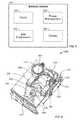
- FIG. 1a block diagram of a wireless healthcare system.
- FIG. 2illustrates an example medical device of FIG. 1 .
- FIG. 3illustrates another example medical device of FIG. 1 .
- FIG. 4illustrates a block diagram of an example medical device.
- FIG. 5illustrates the components of an example carrier assembly.
- FIG. 6illustrates an example power management system.
- FIG. 7illustrates example components of a display.
- FIG. 8illustrates a different view of the components shown in FIG. 7 .
- FIG. 9is a block diagram illustrating physical components of a computing device with which examples and embodiments of the disclosure can be practiced.
- FIG. 10is a block diagram of an example electromagnetic interference (EMI) suppression system.
- EMIelectromagnetic interference
- FIG. 11illustrates an embodiment of the example EMI suppression system shown in FIG. 10 .
- FIG. 12illustrates an exploded view of the embodiment of the example EMI suppression system shown in FIG. 11 .
- FIG. 13illustrates a top plan view of the embodiment of the example EMI suppression system shown in FIG. 11 .
- FIG. 14illustrates a bottom plan view of the embodiment of the example EMI suppression system shown in FIG. 11 .
- FIG. 15illustrates a right side view of the embodiment of the example EMI suppression system shown in FIG. 11 .
- FIG. 16illustrates a front view of the embodiment of the example EMI suppression system shown in FIG. 11 .
- FIG. 17is a block diagram of an example power management system.
- FIG. 18illustrates an embodiment of a child module in the example power management system shown in FIGS. 6 and 17 .
- FIG. 19illustrates an embodiment of a parent module in the example power management system shown in FIGS. 6 and 17 .
- FIG. 20illustrates an embodiment of the example carrier assembly shown in FIG. 5 mounted to an example main printed circuit assembly.
- FIG. 21illustrates a top plan view of the embodiment shown in FIG. 20 .
- FIG. 22illustrates a rear plan view of an embodiment of example front housing.
- FIG. 23illustrates a rear perspective view of the embodiment of example front housing shown in FIG. 22 .
- FIG. 24illustrates a front plan view of the embodiment of example front housing shown in FIG. 22 .
- FIG. 25illustrates a bottom plan view of the embodiment of example front housing shown in FIG. 22 .
- FIG. 26illustrates an embodiment of an example liquid crystal display (LCD) assembly mounted to a printed circuit assembly (PCA).
- LCDliquid crystal display
- PCAprinted circuit assembly
- FIG. 27illustrates a front perspective view of the embodiment of example LCD assembly mounted to the PCA.
- FIG. 28illustrates a side view, along axis A-A in FIG. 26 , of the embodiment of example LCD assembly mounted to the PCA.
- FIG. 29illustrates a top view, along axis B-B in FIG. 26 , of the embodiment of example LCD assembly mounted to the PCA.
- Health care environmentscan include hospitals, clinics, managed care facilities, and other locations where medical care is provided. Medical personnel in health care environments can utilize vital signs monitoring devices, vital signs displays, personal computing devices and electronic medical record access portals. Medical staff and providers often need to record a patient's vital signs and enter those vital signs into the patient's electronic medical record. Currently, providers must perform vital signs measurements, remember the measurements, and then enter those measurements into one or more computing devices which may or may not be directly linked to the patient's electronic medical record.
- FIG. 1illustrates a block diagram of an example wireless health care network 110 .
- the example network 110includes medical devices 103 and 104 , wireless computing devices 108 and 109 , and communication network 110 .
- the example network 110can include more or fewer medical devices 103 and 104 .
- the example networkcan include more or fewer wireless computing devices 108 and 109 .
- the communication network 110can be a wireless network, such as WiFi, Bluetooth, Zigbee, Ant, Z-Wave, etc.
- the one or more medical devices 103 and 104can include one or more vital signs measurement components.
- the medical devices 103can include, for example, a thermometer, a heart rate monitor, a pulse oximeter, a non-invasive blood pressure monitor, and a respiration rate monitor.
- one or more vital signs measurement componentsare wirelessly linked to the medical devices 103 and 104 and can transmit measurements to the medical devices 103 and 104 .
- Example computing components of medical devices 103 and 104are shown and described in more detail with reference to FIG. 9 , below.
- the one or more wireless computing devices 108 and 109can be smart phones, tablet computers, personal digital assistants, laptop computers, and desktop computers, which can optionally be mounted on portable carts.
- Example computing components of the one or more wireless computing devices 108 and 109are shown and described in more detail with reference to FIG. 9 , below.
- the use of less complicated wireless computing devices 108 and 109such as heart rate monitors, pulse oximeters, etc., is also contemplated by this document.
- FIG. 2illustrates one example of the medical device 105 .
- the medical device 105is shown on a mobile cart, and the medical device 105 is programmed to provide the functionalities described herein, which can include, but are not limited to, vital signs monitoring.
- the medical device 105includes a user interface, such as a touch screen, and includes the ability to execute multiple workflows or profiles.
- the medical devices 105 and 106 in FIGS. 2 and 3are the medical device 103 or 104 shown in, and described with reference to, FIG. 1 .
- Other embodimentscan include more or fewer components than those shown in FIG. 2 , or include different components that accomplish the same or a similar function.
- the medical device 105is able to operate within one or more profiles.
- a profileis a series of one or more tasks that a user of the medical device 105 performs.
- the medical device 105provides functionality suitable for assisting the user in performing the profile.
- the medical device 105operates within different profiles, the medical device 105 provides different functionality.
- the medical device 105When the medical device 105 is manufactured, the medical device 105 is configured to be able to operate within one or more profiles. After the medical device 105 is manufactured, the medical device 105 can be reconfigured to operate within one or more additional profiles. In this way, a user can adapt the medical device 105 for use in different profiles as needed.
- the medical device 105operates within various profiles.
- the medical device 105can operate within a monitoring profile or a non-monitoring profile.
- Example types of non-monitoring profilesinclude, but are not limited to, a spot check profile and an office profile.
- An example of a monitoring profileincludes, but is not limited to, an intervals profile.
- FIG. 3An additional example of the medical device 106 is shown in FIG. 3 .
- the medical device 106is similar to that of the medical device 105 described above.
- the medical device 106is mounted on a wall.
- the medical device 106is programmed in a manner similar to that described above to monitor physiological parameters of a patient.
- the medical device 106is a stand-alone device, which can mean that is not part of a mobile cart and it is not part of a wall-mounted station.
- the medical devices 104 , 105 , 106are computing devices that have been programmed to perform special, complex functions. These specially-programmed devices function to manipulate and provide data to the users in an improved form factor and with greater efficiency.
- the medical devices 104 , 105 , 106are specially programmed to provide the user with an improved interface that allows the user to discern important information at a glance.
- This improved interfaceremoves unnecessary information and controls so that the data that is important can be more efficiently and easily viewed, particularly when the user is positioned at a distance from the medical device.
- the medical devices 104 , 105 , 106are computing devices that have been programmed to perform special, complex functions. These specially-programmed devices function to manipulate and provide data to the users in an improved form factor and with greater efficiency.
- the medical devices 104 , 105 , 106are specially programmed to provide the user with an improved interface during initial use of the devices. This allows the user to more efficiently select a profile for controlling the functionality of the device.
- the medical devices 104 , 105 , 106are specially programmed to assist the users once vital signs information is captured from the patients.
- the devicesare programmed to more efficiently and easily capture additional contextual information that is needed when saving vital signs data to a permanent record, such as an EMR record. This is accomplished using an interface that is more intuitive and robust.
- the medical devices 104 and 105 shown in FIGS. 2 and 3are only examples of a medical device. In some examples described herein, the medical devices 104 and 105 are portable devices. In other examples, the medical devices 104 and 105 are non-portable devices, such as computing devices like workstations. All different types of medical devices used to collect patient data can be used. Many configurations are possible.
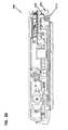
- the example medical product system 100includes the medical device 104 that can have a carrier assembly 200 , power management module 300 , electromagnetic interference (EMI) suppression module 400 , and display 500 .
- Other embodimentsmay include more or fewer components.
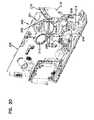
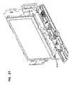
- FIG. 5illustrates an example embodiment of the carrier assembly 200 that can be mounted to a main printed circuit assembly (PCA) 290 of the medical device 104 .
- FIGS. 20 and 21illustrate the example embodiment of carrier assembly 200 mounted to a PCA 290 .
- the example assembly 200can include a plastic carrier 201 supporting a pump 202 , pump retention snaps 204 , valves 206 , a wire routing feature 208 , a WiFi radio 210 , a Bluetooth radio 218 , a speaker 212 , and an integrated pump/valve harness 220 .
- a manifold 214can be in communication with the pump 202 and a blood pressure (BP) cuff port 230 .
- FIGS. 20 and 21illustrate embodiments of a main printed circuit assembly 290 including the example embodiment of carrier assembly 200 . Other embodiments can include more or fewer components.
- the example carrier assembly 200consolidates the blood pressure pneumatic system that includes a pump 202 , a solenoid valve 206 and a check valve 224 .
- the pneumatic systemcan be supported by a plastic carrier 201 .
- the main printed circuit assembly 290has a top surface area that supports and houses various components, including the carrier assembly 200 .
- the carrier assembly 200occupies an amount of surface area on the top surface area of the main printed circuit assembly 290 that is at least less than 50% of the top surface area; at least less than 40% of the top surface area; at least less than 33% of the top surface area; at least less than 25% of the top surface area; or at least less than 20% of the top surface area.
- the pump 202 , solenoid valve 206 and check valve 224are all in fluid communication with each other and with one or more pressure transducers through a single manifold 214 .
- Manifold 214also interfaces with the blood pressure cuff port 230 .
- the example carrier assembly 200provides a single part that provides mounting for the pump 202 and valves 206 .
- the example carrier assembly 200includes features for managing electrical wire routing for the pump and valve wires, such as harnesses, slots, snaps, mounts, ports, and other components known in the art.
- Wire routing feature 208 and integrated pump/valve harness 220are examples of features for managing wire routing for the pump and valve wires.
- the example carrier assembly 200includes mounts for a speaker 212 , a WiFi radio 210 and/or a Bluetooth radio 218 .
- the mountscan include slots in the assembly 200 , harnesses, snaps, recesses, or other components known in the art.
- FIGS. 6 and 17-19illustrate an example power management system 300 .
- the example system 300includes a parent module 320 and a child module 350 , each with input power connectors and connected by wire 372 .
- Parent module 320 and child module 350are the medical devices shown in FIGS. 2 and 3 , although the example power management system 300 can be used in other environments.
- Power management system 300extends the operational time beyond the battery capacity of the parent module 320 .
- the child input power connectorhas exposed pins when the connector is unconnected.
- An embodiment of example child module 394is shown in FIG. 18 and an embodiment of example parent module 396 is shown in FIG. 18 .
- Other embodimentscan include more or fewer components.
- the example system 300can be configured to run on mains power, wherein the parent module 320 and the child module 350 can be powered indefinitely.
- the parent module 320is responsible for charging the battery of the child module 350 when the child module 350 is not connected to mains power.
- the parent module 320can also be responsible for providing operational power to the child module 350 . This is depicted in FIG. 17 as normal mode 380 : power flowing from parent module 320 to child module 350 .
- parent module 320includes a larger battery than child module 350 .
- parent module 320includes a 9 cell battery and child module 350 includes a 2 cell battery.
- Other configurationsare possible.
- the parent module 320when running on battery power, the parent module 320 continues to charge the child module's 350 battery. This is shown as normal mode 380 in FIG. 17 . In some embodiments, it is likely that the child module's 350 battery is powered from the time spent on mains power. In embodiments, the parent module's 320 battery expires. At that point, the example system 300 deploys a backfeed function, shown as backfeed mode 390 in FIG. 17 , that allows power to flow both ways in the interface between the parent module 320 and the child module 350 . In embodiments, the backfeed mode 390 enables the system to continue to operate on the child module's 350 battery after the parent module's 320 battery is exhausted. In embodiments, this configuration can maximize battery life in contrast to non-backfeed configurations.
- the child module 350can operate stand-alone.
- the connector on the child module 350 that connects to the parent module 350is large enough to expose the connector pin. Exposing a powered pin can produce an unsafe and undesirable situation.
- the child module's 350 systemdetects that the pin is disconnected. When the system detects that the pin is disconnected, the child module's 350 system de-energizes the power pin on the child module 350 .
- a wire 372 used to convey power from the parent module 320 to the child module 350(normal mode 380 ) is also used to convey power from the child module 350 to the parent module 320 (backfeed module).
- a battery life status 124 shown on a display of child module 350includes the combined battery life using backfeed mode 390 when the parent module 320 is connected to the child module 350 .
- the example medical device 104can also optionally include an electromagnetic interference (EMI) suppression module 400 .
- EMIelectromagnetic interference
- sensitive signals in a printed circuit boardare buried on inner layers. These signals can go to an external shielded cable. Examples include SpO2, electroencephalograph (EEG), electrocardiograph (ECG), etc. These cables can act as antennas for unwanted electromagnetic interference, such as radio frequency interference (RFI), that is both radiated from and induced into the device.
- RFIDradio frequency interference
- the example EMI suppression 400includes applying a ferrite to surround a printed circuit board.
- the ferriteis wrapped around a bare printed circuit board, or surrounds part of a printed circuit board.
- the ferritehas a geometry such that it suppresses unwanted RFI on traces on inner and/or outer layers of the printed circuit assembly.
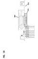
- FIG. 10is a schematic block diagram of an embodiment of EMI suppression 400 .
- Ferrite 410is used to surround traces 404 in printed circuit board 402 .
- the traces 404do not directly connect to the ferrite 410 . Rather, the traces 404 surrounded by ferrite 410 are routed to stay within the printed circuit board 402 and do not come up to the surface of printed circuit board 402 .
- signals in tracesare not interrupted by layer transitions or impedance mismatches. When passing through ferrite 410 , the traces 404 do not transition from their electrical shielding.
- FIG. 11illustrates a perspective view of an embodiment of the example EMI suppression 450 discussed in connection with FIG. 10 .
- EMI suppression 450includes slots 456 in a PCB 452 that define tongue 458 , and ferrite 454 surrounding a portion of the PCB 452 containing traces 470 .
- the tracings 470are shown in phantom form to indicate that the tracings are actually below the surface of the PCB 452 in one of the inner layers.
- a cable connector 460is also depicted.
- Other embodimentscan include more or fewer components.
- FIGS. 12-16additionally illustrate various views of the embodiment of the example EMI suppression 450 shown in FIG. 11 .
- FIG. 12is an exploded, perspective view of EMI suppression 450
- FIG. 13is a top plan view of EMI suppression 450
- FIG. 14is a bottom plan view of EMI suppression 450
- FIG. 15is a right side view of EMI suppression 450
- FIG. 16is a front view of EMI suppression 450 .
- FIGS. 11-16is a front view of EMI suppression 450 .
- EMI suppression 450Surrounding traces 470 with ferrite 454 provides EMI suppression even in embodiments where a cord connecting to printed circuit board 452 does not include EMI suppression components.
- EMI suppression 450is discussed in relation to a medical device, it can be used to suppress EMI in any PCB with a cable connection, regardless of the application.
- Ferrite 454has an annular cross-section thereby enabling it to pass through tongue 458 and surround traces within PCB 452 .
- ferrite 454has a rectangular annulus cross-section, although other shapes are possible.
- Ferrite 454is positioned on the distal end of tongue 458 adjacent to the connector assembly 460 .
- EMI suppressionimproves as ferrite 454 is positioned closer to connector assembly 460 .
- any position of ferrite 454 on tongue 458provides EMI suppression.
- Ferrite 454is positioned over the PCB 452 before soldering near the cable connector 460 . Ferrite 454 can be secured to the PCB 452 using, for example, cloth tape.
- Cable connector 460can connect to, and receive data from, a vital signs device, such as an SpO2 monitor, an EEG, or other device.
- a vital signs devicesuch as an SpO2 monitor, an EEG, or other device.
- ferrite 454has a single-piece construction. Other embodiments are contemplated where ferrite 454 is formed by more than one piece.
- Ferrite 454surrounds the tracings within PCB 452 in at least the x-y planes above and below PCB 452 as well as the x-z planes.
- traces 470carry signals that might be sensitive to noise, such as EMI, which could damage the signal's integrity.
- An example of a signal sensitive to noiseis a peripheral capillary oxygen saturation (SpO2) signal.
- An example installation of the example EMI suppressionwas conducted and reduced EMI.
- a printed circuitwas carved to accept a standard Ferrite. Then the cable connector was removed. Ferrite was inserted and then the connector was replaced.
- FIGS. 7, 8, and 22-29illustrate an example display 500 .
- the example display 500includes a printed circuit assembly (PCA) 290 , a liquid crystal display (LCD) assembly 510 , a front housing 515 , an elastomeric bezel 520 , obround slots 524 and an obround boss 525 .
- a rear housingnot shown, mates with the front housing 515 and PCA 290 .
- Front housing 515is also shown in FIGS. 22-25 : FIG. 22 is a rear plan view of front housing 515 , FIG. 23 is a rear perspective view of the front housing 515 , FIG. 24 is a front plan view of the front housing 515 , and FIG. 25 is a bottom plan view of the front housing 515 .
- FIGS. 26-29are additionally shown in FIGS. 26-29 : FIG. 26 is a front plan view of PCA 290 and LCD assembly 510 , FIG. 27 is a bottom front perspective view of PCA 290 and LCD assembly 510 , FIG. 28 is a side view along axis A-A in FIG. 26 , and FIG. 29 is a top view along axis B-B in FIG. 26 .
- Other example displayscan include more or fewer components than those depicted.
- the example display 500has an LCD assembly 510 mounted directly to the PCA 290 .
- the mountenables the LCD assembly 510 to float relative to the PCA 290 . Because the LCD assembly 510 can float, it can conform to features in the mating front housing/bezel.
- the floating LCD that interfaces with an elastomeric bezel 520 on the front housingseals the LCD from fluid ingress and it can provide impact resistance.
- the example embodiment of the display 500 illustrated in FIGS. 7 and 22-29shows the LCD assembly 510 fastened to the PCA.
- the LCD assembly 510has obround bosses 525 that mate with similarly shaped but larger obround slots 524 in the printed circuit board 290 . This clearance can enable the LCD assembly 510 to float in the x- and y-axes relative to the PCA 290 .
- the LCD assembly 510is thereby secured to the PCA in the z-axis with, for example, screws 526 that thread into the frame bosses 525 , where the head diameter of the screw 526 can be larger than the slot width in the PCA 290 .
- the frame bosses 525are taller than the thickness of the PCA 290 which can prevent the screw 526 head from seating on the PCA 290 and locking the LCD assembly 510 to the PCA 290 . This is illustrated in the cut-out view shown in FIG. 8 , where the frame boss 525 is seen extending through the obround slot 524 and beyond the PCA 290 because the frame boss 525 is taller than the thickness of the PCA 290 .
- an elastomeric bezel 520can be precisely positioned and contained in the front housing 515 relative to the LCD opening, where the bezel 520 can have features that precisely locate the LCD assembly 510 .
- the floatingenables the LCD to be positioned to the LCD opening in the front housing independent of the location of the PCA, which can have other design constraints that could add to the tolerance stackup.
- the bezel 520is pre-assembled to the front housing 515 .
- FIG. 9is a block diagram illustrating physical components (i.e., hardware) of a computing device 1800 with which embodiments of the disclosure may be practiced.
- the computing device components described belowmay be suitable to act as the computing devices described above, such as wireless computing device and/or medical device of FIG. 1 .
- the computing device 1800may include at least one processing unit 1802 , 1803 and a system memory 1804 .
- the system memory 1804may comprise, but is not limited to, volatile storage (e.g., random access memory), non-volatile storage (e.g., read-only memory), flash memory, or any combination of such memories.
- the system memory 1804may include an operating system 1805 and one or more program modules 1806 suitable for running software applications 1820 .
- the operating system 1805may be suitable for controlling the operation of the computing device 1800 .
- embodiments of the disclosuremay be practiced in conjunction with a graphics library, other operating systems, or any other application program and is not limited to any particular application or system.
- This basic configurationis illustrated in FIG. 9 by those components within a dashed line 1808 .
- the computing device 1800may have additional features or functionality.
- the computing device 1800may also include additional data storage devices (removable and/or non-removable) such as, for example, magnetic disks, optical disks, or tape. Such additional storage is illustrated in FIG. 9 by a removable storage device 1809 and a non-removable storage device 1810 .
- a number of program modules and data filesmay be stored in the system memory 1804 . While executing on the processing unit 1802 , the program modules 1806 may perform processes including, but not limited to, generate list of devices, broadcast user-friendly name, broadcast transmitter power, determine proximity of wireless computing device, connect with wireless computing device, transfer vital sign data to a patient's EMR, sort list of wireless computing devices within range, and other processes described with reference to the figures as described herein.
- Other program modulesthat may be used in accordance with embodiments of the present disclosure, and in particular to generate screen content, may include electronic mail and contacts applications, word processing applications, spreadsheet applications, database applications, slide presentation applications, drawing or computer-aided application programs, etc.
- embodiments of the disclosuremay be practiced in an electrical circuit comprising discrete electronic elements, packaged or integrated electronic chips containing logic gates, a circuit utilizing a microprocessor, or on a single chip containing electronic elements or microprocessors.
- embodiments of the disclosuremay be practiced via a system-on-a-chip (SOC) where each or many of the components illustrated in FIG. 9 may be integrated onto a single integrated circuit.
- SOCsystem-on-a-chip
- Such an SOC devicemay include one or more processing units, graphics units, communications units, system virtualization units and various application functionality all of which are integrated (or “burned”) onto the chip substrate as a single integrated circuit.
- the functionality, described herein,may be operated via application-specific logic integrated with other components of the computing device 1800 on the single integrated circuit (chip).
- Embodiments of the disclosuremay also be practiced using other technologies capable of performing logical operations such as, for example, AND, OR, and NOT, including but not limited to mechanical, optical, fluidic, and quantum technologies.
- embodiments of the disclosuremay be practiced within a general purpose computer or in any other circuits or systems.
- the computing device 1800may also have one or more input device(s) 1812 such as a keyboard, a mouse, a pen, a sound or voice input device, a touch or swipe input device, etc.
- the output device(s) 1814such as a display, speakers, a printer, etc. may also be included.
- the aforementioned devicesare examples and others may be used.
- the computing device 1800may include one or more communication connections 1816 allowing communications with other computing devices 1850 . Examples of suitable communication connections 1816 include, but are not limited to, RF transmitter, receiver, and/or transceiver circuitry; universal serial bus (USB), parallel, and/or serial ports.
- USBuniversal serial bus
- Computer readable mediamay include non-transitory computer storage media.
- Computer storage mediamay include volatile and nonvolatile, removable and non-removable media implemented in any method or technology for storage of information, such as computer readable instructions, data structures, or program modules.
- the system memory 1804 , the removable storage device 1809 , and the non-removable storage device 1810are all computer storage media examples (i.e., memory storage.)
- Computer storage mediamay include RAM, ROM, electrically erasable read-only memory (EEPROM), flash memory or other memory technology, CD-ROM, digital versatile disks (DVD) or other optical storage, magnetic cassettes, magnetic tape, magnetic disk storage or other magnetic storage devices, or any other article of manufacture which can be used to store information and which can be accessed by the computing device 1800 . Any such computer storage media may be part of the computing device 1800 .
- Computer storage mediadoes not include a carrier wave or other propagated or modulated data signal.
- Communication mediamay be embodied by computer readable instructions, data structures, program modules, or other data in a modulated data signal, such as a carrier wave or other transport mechanism, and includes any information delivery media.
- modulated data signalmay describe a signal that has one or more characteristics set or changed in such a manner as to encode information in the signal.
- communication mediamay include wired media such as a wired network or direct-wired connection, and wireless media such as acoustic, radio frequency (RF), infrared, and other wireless media.
- RFradio frequency
- the example medical devices described hereinare devices used to monitor patients, other types of medical devices can also be used.
- the different components of the CONNEXTM systemsuch as the intermediary servers that communication with the monitoring devices, can also require maintenance in the form of firmware and software updates.
- These intermediary serverscan be managed by the systems and methods described herein to update the maintenance requirements of the servers.
- Embodiments of the present inventionmay be utilized in various distributed computing environments where tasks are performed by remote processing devices that are linked through a communications network in a distributed computing environment.
Landscapes
- Health & Medical Sciences (AREA)
- Life Sciences & Earth Sciences (AREA)
- Engineering & Computer Science (AREA)
- Physics & Mathematics (AREA)
- Cardiology (AREA)
- Surgery (AREA)
- Heart & Thoracic Surgery (AREA)
- Medical Informatics (AREA)
- Molecular Biology (AREA)
- Animal Behavior & Ethology (AREA)
- General Health & Medical Sciences (AREA)
- Public Health (AREA)
- Veterinary Medicine (AREA)
- Biomedical Technology (AREA)
- Pathology (AREA)
- Biophysics (AREA)
- Physiology (AREA)
- Vascular Medicine (AREA)
- Microelectronics & Electronic Packaging (AREA)
- Nonlinear Science (AREA)
- Ophthalmology & Optometry (AREA)
- Electromagnetism (AREA)
- Power Engineering (AREA)
- Pulmonology (AREA)
- Dentistry (AREA)
- Computer Networks & Wireless Communication (AREA)
- Mathematical Physics (AREA)
- Chemical & Material Sciences (AREA)
- Crystallography & Structural Chemistry (AREA)
- General Physics & Mathematics (AREA)
- Optics & Photonics (AREA)
- Nuclear Medicine, Radiotherapy & Molecular Imaging (AREA)
- Measuring And Recording Apparatus For Diagnosis (AREA)
- Measuring Pulse, Heart Rate, Blood Pressure Or Blood Flow (AREA)
Abstract
Description
Claims (19)
Priority Applications (1)
| Application Number | Priority Date | Filing Date | Title |
|---|---|---|---|
| US14/934,783US9872626B2 (en) | 2014-11-07 | 2015-11-06 | Printed circuit board assembly with ferrite for medical device |
Applications Claiming Priority (2)
| Application Number | Priority Date | Filing Date | Title |
|---|---|---|---|
| US201462076878P | 2014-11-07 | 2014-11-07 | |
| US14/934,783US9872626B2 (en) | 2014-11-07 | 2015-11-06 | Printed circuit board assembly with ferrite for medical device |
Publications (2)
| Publication Number | Publication Date |
|---|---|
| US20160135287A1 US20160135287A1 (en) | 2016-05-12 |
| US9872626B2true US9872626B2 (en) | 2018-01-23 |
Family
ID=55909874
Family Applications (4)
| Application Number | Title | Priority Date | Filing Date |
|---|---|---|---|
| US14/934,783Active2035-12-11US9872626B2 (en) | 2014-11-07 | 2015-11-06 | Printed circuit board assembly with ferrite for medical device |
| US14/934,799Active2036-05-30US9901265B2 (en) | 2014-11-07 | 2015-11-06 | Medical device |
| US14/934,812Active2036-08-03US10085654B2 (en) | 2014-11-07 | 2015-11-06 | Medical device |
| US14/934,834Active2036-10-01US10405758B2 (en) | 2014-11-07 | 2015-11-06 | Carrier assembly for blood pressure module |
Family Applications After (3)
| Application Number | Title | Priority Date | Filing Date |
|---|---|---|---|
| US14/934,799Active2036-05-30US9901265B2 (en) | 2014-11-07 | 2015-11-06 | Medical device |
| US14/934,812Active2036-08-03US10085654B2 (en) | 2014-11-07 | 2015-11-06 | Medical device |
| US14/934,834Active2036-10-01US10405758B2 (en) | 2014-11-07 | 2015-11-06 | Carrier assembly for blood pressure module |
Country Status (5)
| Country | Link |
|---|---|
| US (4) | US9872626B2 (en) |
| EP (1) | EP3215003A4 (en) |
| CN (1) | CN107205666A (en) |
| AU (1) | AU2015342872B2 (en) |
| WO (1) | WO2016073880A1 (en) |
Families Citing this family (4)
| Publication number | Priority date | Publication date | Assignee | Title |
|---|---|---|---|---|
| WO2016073880A1 (en)* | 2014-11-07 | 2016-05-12 | Welch Allyn, Inc. | Medical device |
| JP6695221B2 (en)* | 2016-06-28 | 2020-05-20 | フクダ電子株式会社 | Pump assembly and medical device |
| JP6806659B2 (en)* | 2017-10-31 | 2021-01-06 | ファナック株式会社 | display |
| US11992347B2 (en)* | 2020-02-21 | 2024-05-28 | Canon U.S.A., Inc. | Medical device cart with a tilted holder |
Citations (79)
| Publication number | Priority date | Publication date | Assignee | Title |
|---|---|---|---|---|
| US4455545A (en)* | 1982-11-05 | 1984-06-19 | Sperry Corporation | High frequency output inductor for inverter power supply |
| US4716389A (en)* | 1986-10-20 | 1987-12-29 | Honeywell Inc. | Millimeter wave microstrip surface mounted attenuator |
| US4789224A (en) | 1987-05-04 | 1988-12-06 | General Motors Corporation | Instrument panel having light pipe having legs |
| US4796079A (en)* | 1984-07-25 | 1989-01-03 | Rca Licensing Corporation | Chip component providing rf suppression |
| US4864486A (en)* | 1988-07-29 | 1989-09-05 | International Business Machines Corporation | Plank and frame transformer |
| US4873757A (en)* | 1987-07-08 | 1989-10-17 | The Foxboro Company | Method of making a multilayer electrical coil |
| US5025211A (en)* | 1989-12-20 | 1991-06-18 | At&T Bell Laboratories | Technique for reducing electromagnetic interference |
| US5136120A (en)* | 1989-12-20 | 1992-08-04 | At&T Bell Laboratories | Technique for reducing electromagnetic interference |
| US5321380A (en)* | 1992-11-06 | 1994-06-14 | Power General Corporation | Low profile printed circuit board |
| US5339178A (en) | 1993-03-19 | 1994-08-16 | Motorola, Inc. | LCD assembly with light pipe having lightguides extending from surface to surface and retaining means integral with the lightpipe |
| US5353001A (en)* | 1991-01-24 | 1994-10-04 | Burr-Brown Corporation | Hybrid integrated circuit planar transformer |
| US5422751A (en) | 1992-10-14 | 1995-06-06 | Apple Computer, Inc. | Liquid crystal display assembly employing front bezel, frame holding liquid crystal cell attached to bezel, and light source and back plate attached to bezel |
| US5455552A (en)* | 1994-05-03 | 1995-10-03 | Steward, Inc. | Ferrite common mode choke adapted for circuit board mounting |
| US5469334A (en)* | 1991-09-09 | 1995-11-21 | Power Integrations, Inc. | Plastic quad-packaged switched-mode integrated circuit with integrated transformer windings and mouldings for transformer core pieces |
| US5528025A (en)* | 1994-09-30 | 1996-06-18 | Swintek; William P. | Apparatus and method for the wireless exchange of bar code data |
| US5565837A (en)* | 1992-11-06 | 1996-10-15 | Nidec America Corporation | Low profile printed circuit board |
| US5603847A (en)* | 1993-04-07 | 1997-02-18 | Zycon Corporation | Annular circuit components coupled with printed circuit board through-hole |
| US5631822A (en)* | 1995-08-24 | 1997-05-20 | Interpoint Corporation | Integrated planar magnetics and connector |
| US5748270A (en) | 1996-06-25 | 1998-05-05 | Ericsson, Inc. | LCD with electroluminescent backlighting |
| US5774028A (en)* | 1995-06-07 | 1998-06-30 | Samsung Electro-Mechanics | Surface mount line filter with solder gas discharge paths in the core |
| US5801597A (en)* | 1997-02-05 | 1998-09-01 | Lucent Technologies Inc. | Printed-circuit board-mountable ferrite EMI filter |
| US5801602A (en)* | 1996-04-30 | 1998-09-01 | 3Com Corporation | Isolation and signal filter transformer |
| US5892412A (en)* | 1997-02-20 | 1999-04-06 | Lucent Technologies Inc. | Method of and an apparatus for tunable passive-gain equalization |
| US5896079A (en)* | 1996-07-25 | 1999-04-20 | Fair-Rite Products Corporation | High frequency common mode ferrite bead |
| US5949321A (en)* | 1996-08-05 | 1999-09-07 | International Power Devices, Inc. | Planar transformer |
| US5952909A (en)* | 1994-06-21 | 1999-09-14 | Sumitomo Special Metals Co., Ltd. | Multi-layered printed-coil substrate, printed-coil substrates and printed-coil components |
| US5975711A (en) | 1995-06-27 | 1999-11-02 | Lumitex, Inc. | Integrated display panel assemblies |
| US6000128A (en)* | 1994-06-21 | 1999-12-14 | Sumitomo Special Metals Co., Ltd. | Process of producing a multi-layered printed-coil substrate |
| US6028500A (en)* | 1999-02-12 | 2000-02-22 | Lucent Technologies Inc. | Audible noise suppressor for planar magnetic devices |
| US6089917A (en)* | 1997-10-24 | 2000-07-18 | International Business Machines Corporation | Method and system for circuit board common mode noise suppression utilizing ferrous cores |
| US6116924A (en)* | 1999-05-25 | 2000-09-12 | 3Com Corporation | Electromagnetic emissions shielding structure for circuit board connector assembly |
| US6147583A (en)* | 1998-05-26 | 2000-11-14 | Artesyn Technologies | Transformer assembly |
| US6147928A (en)* | 1998-03-10 | 2000-11-14 | Tdk Corporation | Anti-noise component for flat cable |
| US6181404B1 (en)* | 1998-02-27 | 2001-01-30 | 3Com Corporation | Apparatus and method for mounting a liquid crystal display (LCD) assembly onto a printed circuit board |
| US6195269B1 (en)* | 1998-06-12 | 2001-02-27 | I-Pex Co., Ltd | Noise suppressing apparatus |
| US20010017576A1 (en)* | 1999-07-29 | 2001-08-30 | Tdk Corporation | Isolator device with built-in power amplifier |
| US6288626B1 (en)* | 1998-08-21 | 2001-09-11 | Steward, Inc. | Common mode choke including parallel conductors and associated methods |
| US6335671B1 (en)* | 1999-08-20 | 2002-01-01 | Tyco Electronics Logistics Ag | Surface mount circuit assembly |
| US6356182B1 (en)* | 1999-09-20 | 2002-03-12 | General Motors Corporation | Planar EMI inductor |
| US20020070835A1 (en)* | 2000-05-19 | 2002-06-13 | Majid Dadafshar | Multi-layer, multi-functioning printed circuit board (pcb) with integrated magnetic components |
| US20020070836A1 (en)* | 2000-12-08 | 2002-06-13 | Toshikazu Fujiyoshi | High-frequency large current handling transformer |
| US20020089405A1 (en)* | 2000-09-22 | 2002-07-11 | Ionel Jitaru | Method and apparatus for forming a magnetic component on a printed circuit board |
| US20020159214A1 (en)* | 2000-04-06 | 2002-10-31 | Perlick John A. | Miniaturized ac/dc power supply and battery charger |
| US20020170745A1 (en)* | 2001-05-18 | 2002-11-21 | Opitz Rudi W. | Multilayer board combound and method for the manufacture thereof |
| US20020173202A1 (en)* | 2001-05-18 | 2002-11-21 | Hosiden Corporation | Printed circuit board mounted electrical connector |
| US20030026962A1 (en)* | 2001-08-01 | 2003-02-06 | Hideharu Kawai | Forming method of magnetic body, magnetic body, and printed circuit board |
| US6587166B1 (en) | 1998-08-26 | 2003-07-01 | Samsung Electronics Co., Ltd. | Liquid crystal display module and an assembly method therefor |
| US20040012729A1 (en) | 2002-07-16 | 2004-01-22 | Samsung Electronics Co., Ltd. | Thin display apparatus |
| US6741155B2 (en)* | 2001-05-14 | 2004-05-25 | Sanken Electric Co., Ltd. | Transformer |
| US20040113739A1 (en)* | 2000-12-07 | 2004-06-17 | Delta Electronics Inc. | Low profile transformer |
| US20040133092A1 (en)* | 2001-03-27 | 2004-07-08 | Kain Aron Z. | Wireless system for measuring distension in flexible tubes |
| US20040257190A1 (en)* | 2001-09-28 | 2004-12-23 | Joachim Peck | Planar transformer comprising plug-in secondary windings |
| US6911889B2 (en)* | 2001-08-20 | 2005-06-28 | Steward, Inc. | High frequency filter device and related methods |
| US20050174207A1 (en)* | 2002-03-27 | 2005-08-11 | Commergy Technologies Limited | Magnetic structure assembly |
| US20060158294A1 (en)* | 2004-12-30 | 2006-07-20 | Steward Inc. | Common mode choke including conductors within dielectric layer and associated methods |
| US20080079524A1 (en)* | 2006-09-29 | 2008-04-03 | Tdk Corporation | Planar transformer and switching power supply |
| US20080087072A1 (en) | 2005-09-02 | 2008-04-17 | Abb Inc. | Field mounted analyzer with a graphical user interface |
| US7391137B2 (en)* | 2003-07-08 | 2008-06-24 | Siemens Aktiengesellschaft | Circuit arrangement for EMC interference suppression for a direct current motor and a switching module |
| US7405925B2 (en) | 2000-12-27 | 2008-07-29 | Samsung Electronics Co., Ltd. | Display apparatus |
| US20090026841A1 (en) | 2005-04-22 | 2009-01-29 | Toyota Jidosha Kabushiki Kaisha | Electric power supply system |
| US20090295529A1 (en)* | 2008-05-28 | 2009-12-03 | Arturo Silva | Cross-core transformer |
| US20110019121A1 (en) | 2009-07-24 | 2011-01-27 | Au Optronics Corp. | Flat panel display module |
| US7883369B1 (en)* | 2010-02-24 | 2011-02-08 | Cheng Uei Precision Industry Co., Ltd. | Receptacle connector |
| US20110058355A1 (en) | 2009-09-08 | 2011-03-10 | Chimei Innolux Corporation | Liquid crystal display device and method for assembling same |
| US20110102701A1 (en) | 2009-10-30 | 2011-05-05 | Chimei Innolux Corporation | Liquid crystal display device |
| US20110204720A1 (en) | 2007-11-30 | 2011-08-25 | Johnson Controls Technology Company | Efficient usage, storage, and sharing of energy in buildings, vehicles, and equipment |
| US20110261281A1 (en) | 2010-04-23 | 2011-10-27 | Fih (Hong Kong) Limited | Lcd assembly and portable electronic device utilizing same |
| US8077006B2 (en)* | 2010-04-27 | 2011-12-13 | Harris Corporation | Transmission line impedance transformer and related methods |
| US20120099044A1 (en) | 2010-10-25 | 2012-04-26 | Au Optronics Corporation | Liquid crystal display module |
| US20120120339A1 (en) | 2010-11-12 | 2012-05-17 | Samsung Mobile Display Co., Ltd. | Liquid crystal display device |
| US8203659B2 (en) | 2010-08-13 | 2012-06-19 | Litemax Electronics Inc. | LCD display and gaming machine combination |
| US20120193983A1 (en) | 2009-10-13 | 2012-08-02 | Panasonic Corporation | Power source device and vehicle |
| US20120197340A1 (en)* | 2011-01-28 | 2012-08-02 | Apnex Medical, Inc. | Screening Devices and Methods for Obstructive Sleep Apnea Therapy |
| US8253914B2 (en) | 2010-06-23 | 2012-08-28 | Microsoft Corporation | Liquid crystal display (LCD) |
| US20120267437A1 (en) | 2007-09-12 | 2012-10-25 | Deepak Jain | Amplifying Radio Frequency Signals |
| US8354894B2 (en)* | 2009-04-30 | 2013-01-15 | Harris Corporation | RF signal combiner/splitter and related methods |
| US20140039351A1 (en) | 2011-03-04 | 2014-02-06 | Stryker Corporation | Sensing system for patient supports |
| US20140132877A1 (en) | 2012-11-13 | 2014-05-15 | Westinghouse Digital, Llc | Liquid crystal display, and configuration thereof |
| US20160131935A1 (en) | 2014-11-07 | 2016-05-12 | Welch Allyn, Inc. | Medical Device |
Family Cites Families (21)
| Publication number | Priority date | Publication date | Assignee | Title |
|---|---|---|---|---|
| GB1556036A (en)* | 1975-10-30 | 1979-11-21 | Yazaki Corp | Process and apparatus for producing a wire-harness |
| US5267116A (en) | 1988-01-28 | 1993-11-30 | Aditan, Inc. | Electrical safety socket |
| US5003486A (en)* | 1989-02-24 | 1991-03-26 | Nero Technologies Ltd. | Programmable safety electrical socket controller |
| US5464019A (en)* | 1992-08-11 | 1995-11-07 | Spacelabs, Inc. | Airflow control manifold for automatic blood pressure monitoring device |
| US6251080B1 (en)* | 1999-05-13 | 2001-06-26 | Del Mar Medical Systems, Llc | Self contained ambulatory blood pressure cincture |
| JP2001339911A (en)* | 2000-05-26 | 2001-12-07 | Alps Electric Co Ltd | Index-signal output unit and fdd unit |
| JP2002151866A (en)* | 2000-11-14 | 2002-05-24 | Nec Corp | Strengthened mounting structure of portable apparatus |
| US6591135B2 (en) | 2001-04-16 | 2003-07-08 | Ge Medical Systems Information Technologies, Inc. | Portable patient monitor with defibrillator/pacemaker interface and battery power management |
| US6653813B2 (en) | 2002-03-21 | 2003-11-25 | Thomson Licensing, S.A. | Apparatus and method for the power management of operatively connected modular devices |
| US20080201503A1 (en)* | 2003-12-05 | 2008-08-21 | Mckim James B | Communications System for Implementation of Synchronous, Multichannel, Galvanically Isolated Instrumentation Devices |
| US7957798B2 (en) | 2003-12-17 | 2011-06-07 | Physio-Control, Inc. | Defibrillator/monitor system having a pod with leads capable of wirelessly communicating |
| JP2006259225A (en)* | 2005-03-17 | 2006-09-28 | Orion Denki Kk | Liquid crystal display device with lcd cover |
| US7531918B2 (en)* | 2005-03-30 | 2009-05-12 | Hewlett-Packard Development Company, L.P. | Hot insertion and extraction of power supply module |
| US20070051535A1 (en)* | 2005-09-02 | 2007-03-08 | Hon Hai Precision Industry Co., Ltd. | Circuit board assembly and electronic device utilizing the same |
| US8405512B2 (en)* | 2008-02-01 | 2013-03-26 | Apple Inc. | System and method for accessing diagnostic information |
| JP5453769B2 (en)* | 2008-11-06 | 2014-03-26 | トヨタ自動車株式会社 | Vehicle battery diagnosis system and vehicle battery diagnosis method |
| LT4147999T (en)* | 2009-08-31 | 2024-10-10 | Abbott Diabetes Care, Inc. | MEDICAL DEVICE DISPLAYS |
| CN102340156A (en) | 2010-07-26 | 2012-02-01 | 联想(北京)有限公司 | Charging and discharging method for terminal and terminal |
| KR101841904B1 (en)* | 2011-04-22 | 2018-03-27 | 엘지디스플레이 주식회사 | Display apparatus and manufacturing method the same |
| CN102670183A (en)* | 2012-05-10 | 2012-09-19 | 北京工业大学 | Automobile steering wheel auxiliary device capable of monitoring pulse wave of human body |
| US9317663B2 (en)* | 2013-08-13 | 2016-04-19 | Next Paradigm Inc. | Method of using a medication reminder and compliance system including an electronic pill box |
- 2015
- 2015-11-06WOPCT/US2015/059516patent/WO2016073880A1/enactiveApplication Filing
- 2015-11-06EPEP15857853.4Apatent/EP3215003A4/ennot_activeWithdrawn
- 2015-11-06USUS14/934,783patent/US9872626B2/enactiveActive
- 2015-11-06USUS14/934,799patent/US9901265B2/enactiveActive
- 2015-11-06USUS14/934,812patent/US10085654B2/enactiveActive
- 2015-11-06CNCN201580072737.7Apatent/CN107205666A/enactivePending
- 2015-11-06USUS14/934,834patent/US10405758B2/enactiveActive
- 2015-11-06AUAU2015342872Apatent/AU2015342872B2/enactiveActive
Patent Citations (94)
| Publication number | Priority date | Publication date | Assignee | Title |
|---|---|---|---|---|
| US4455545A (en)* | 1982-11-05 | 1984-06-19 | Sperry Corporation | High frequency output inductor for inverter power supply |
| US4796079A (en)* | 1984-07-25 | 1989-01-03 | Rca Licensing Corporation | Chip component providing rf suppression |
| US4716389A (en)* | 1986-10-20 | 1987-12-29 | Honeywell Inc. | Millimeter wave microstrip surface mounted attenuator |
| US4789224A (en) | 1987-05-04 | 1988-12-06 | General Motors Corporation | Instrument panel having light pipe having legs |
| US4873757A (en)* | 1987-07-08 | 1989-10-17 | The Foxboro Company | Method of making a multilayer electrical coil |
| US4864486A (en)* | 1988-07-29 | 1989-09-05 | International Business Machines Corporation | Plank and frame transformer |
| US5025211A (en)* | 1989-12-20 | 1991-06-18 | At&T Bell Laboratories | Technique for reducing electromagnetic interference |
| US5136120A (en)* | 1989-12-20 | 1992-08-04 | At&T Bell Laboratories | Technique for reducing electromagnetic interference |
| US5353001A (en)* | 1991-01-24 | 1994-10-04 | Burr-Brown Corporation | Hybrid integrated circuit planar transformer |
| US5469334A (en)* | 1991-09-09 | 1995-11-21 | Power Integrations, Inc. | Plastic quad-packaged switched-mode integrated circuit with integrated transformer windings and mouldings for transformer core pieces |
| US5422751A (en) | 1992-10-14 | 1995-06-06 | Apple Computer, Inc. | Liquid crystal display assembly employing front bezel, frame holding liquid crystal cell attached to bezel, and light source and back plate attached to bezel |
| US5321380A (en)* | 1992-11-06 | 1994-06-14 | Power General Corporation | Low profile printed circuit board |
| US5565837A (en)* | 1992-11-06 | 1996-10-15 | Nidec America Corporation | Low profile printed circuit board |
| US5339178A (en) | 1993-03-19 | 1994-08-16 | Motorola, Inc. | LCD assembly with light pipe having lightguides extending from surface to surface and retaining means integral with the lightpipe |
| US5603847A (en)* | 1993-04-07 | 1997-02-18 | Zycon Corporation | Annular circuit components coupled with printed circuit board through-hole |
| US5455552A (en)* | 1994-05-03 | 1995-10-03 | Steward, Inc. | Ferrite common mode choke adapted for circuit board mounting |
| US5952909A (en)* | 1994-06-21 | 1999-09-14 | Sumitomo Special Metals Co., Ltd. | Multi-layered printed-coil substrate, printed-coil substrates and printed-coil components |
| US6000128A (en)* | 1994-06-21 | 1999-12-14 | Sumitomo Special Metals Co., Ltd. | Process of producing a multi-layered printed-coil substrate |
| US5528025A (en)* | 1994-09-30 | 1996-06-18 | Swintek; William P. | Apparatus and method for the wireless exchange of bar code data |
| US5774028A (en)* | 1995-06-07 | 1998-06-30 | Samsung Electro-Mechanics | Surface mount line filter with solder gas discharge paths in the core |
| US5975711A (en) | 1995-06-27 | 1999-11-02 | Lumitex, Inc. | Integrated display panel assemblies |
| US5631822A (en)* | 1995-08-24 | 1997-05-20 | Interpoint Corporation | Integrated planar magnetics and connector |
| US5801602A (en)* | 1996-04-30 | 1998-09-01 | 3Com Corporation | Isolation and signal filter transformer |
| US5748270A (en) | 1996-06-25 | 1998-05-05 | Ericsson, Inc. | LCD with electroluminescent backlighting |
| US5896079A (en)* | 1996-07-25 | 1999-04-20 | Fair-Rite Products Corporation | High frequency common mode ferrite bead |
| US5949321A (en)* | 1996-08-05 | 1999-09-07 | International Power Devices, Inc. | Planar transformer |
| US5801597A (en)* | 1997-02-05 | 1998-09-01 | Lucent Technologies Inc. | Printed-circuit board-mountable ferrite EMI filter |
| US5892412A (en)* | 1997-02-20 | 1999-04-06 | Lucent Technologies Inc. | Method of and an apparatus for tunable passive-gain equalization |
| US6089917A (en)* | 1997-10-24 | 2000-07-18 | International Business Machines Corporation | Method and system for circuit board common mode noise suppression utilizing ferrous cores |
| US6181404B1 (en)* | 1998-02-27 | 2001-01-30 | 3Com Corporation | Apparatus and method for mounting a liquid crystal display (LCD) assembly onto a printed circuit board |
| US6147928A (en)* | 1998-03-10 | 2000-11-14 | Tdk Corporation | Anti-noise component for flat cable |
| US6147583A (en)* | 1998-05-26 | 2000-11-14 | Artesyn Technologies | Transformer assembly |
| US6195269B1 (en)* | 1998-06-12 | 2001-02-27 | I-Pex Co., Ltd | Noise suppressing apparatus |
| US6288626B1 (en)* | 1998-08-21 | 2001-09-11 | Steward, Inc. | Common mode choke including parallel conductors and associated methods |
| US7327430B2 (en) | 1998-08-26 | 2008-02-05 | Samsung Electronics Co., Ltd. | Liquid crystal display module and an assembly method therefor |
| US20080111942A1 (en) | 1998-08-26 | 2008-05-15 | Lee Sang-Duk | Liquid crystal display module and an assembly method therefor |
| US7535537B2 (en) | 1998-08-26 | 2009-05-19 | Samsung Electronics, Co., Ltd. | Liquid crystal display module and an assembly method therefor |
| US20090256989A1 (en) | 1998-08-26 | 2009-10-15 | Lee Sang-Duk | Liquid crystal display module and an assembly method therefor |
| US20040090567A1 (en) | 1998-08-26 | 2004-05-13 | Lee Sang-Duk | Liquid crystal display module and an assembly method therefor |
| US7843526B2 (en) | 1998-08-26 | 2010-11-30 | Samsung Electronics Co., Ltd. | Liquid crystal display module and an assembly method therefor |
| US6587166B1 (en) | 1998-08-26 | 2003-07-01 | Samsung Electronics Co., Ltd. | Liquid crystal display module and an assembly method therefor |
| US6028500A (en)* | 1999-02-12 | 2000-02-22 | Lucent Technologies Inc. | Audible noise suppressor for planar magnetic devices |
| US6116924A (en)* | 1999-05-25 | 2000-09-12 | 3Com Corporation | Electromagnetic emissions shielding structure for circuit board connector assembly |
| US20010017576A1 (en)* | 1999-07-29 | 2001-08-30 | Tdk Corporation | Isolator device with built-in power amplifier |
| US6335671B1 (en)* | 1999-08-20 | 2002-01-01 | Tyco Electronics Logistics Ag | Surface mount circuit assembly |
| US6356182B1 (en)* | 1999-09-20 | 2002-03-12 | General Motors Corporation | Planar EMI inductor |
| US20020159214A1 (en)* | 2000-04-06 | 2002-10-31 | Perlick John A. | Miniaturized ac/dc power supply and battery charger |
| US20020070835A1 (en)* | 2000-05-19 | 2002-06-13 | Majid Dadafshar | Multi-layer, multi-functioning printed circuit board (pcb) with integrated magnetic components |
| US20020089405A1 (en)* | 2000-09-22 | 2002-07-11 | Ionel Jitaru | Method and apparatus for forming a magnetic component on a printed circuit board |
| US20040113739A1 (en)* | 2000-12-07 | 2004-06-17 | Delta Electronics Inc. | Low profile transformer |
| US20020070836A1 (en)* | 2000-12-08 | 2002-06-13 | Toshikazu Fujiyoshi | High-frequency large current handling transformer |
| US7405925B2 (en) | 2000-12-27 | 2008-07-29 | Samsung Electronics Co., Ltd. | Display apparatus |
| US20040133092A1 (en)* | 2001-03-27 | 2004-07-08 | Kain Aron Z. | Wireless system for measuring distension in flexible tubes |
| US6741155B2 (en)* | 2001-05-14 | 2004-05-25 | Sanken Electric Co., Ltd. | Transformer |
| US20020173202A1 (en)* | 2001-05-18 | 2002-11-21 | Hosiden Corporation | Printed circuit board mounted electrical connector |
| US20020170745A1 (en)* | 2001-05-18 | 2002-11-21 | Opitz Rudi W. | Multilayer board combound and method for the manufacture thereof |
| US20030026962A1 (en)* | 2001-08-01 | 2003-02-06 | Hideharu Kawai | Forming method of magnetic body, magnetic body, and printed circuit board |
| US6911889B2 (en)* | 2001-08-20 | 2005-06-28 | Steward, Inc. | High frequency filter device and related methods |
| US20040257190A1 (en)* | 2001-09-28 | 2004-12-23 | Joachim Peck | Planar transformer comprising plug-in secondary windings |
| US20050174207A1 (en)* | 2002-03-27 | 2005-08-11 | Commergy Technologies Limited | Magnetic structure assembly |
| US7545453B2 (en) | 2002-07-16 | 2009-06-09 | Samsung Electronics Co., Ltd. | Thin display apparatus |
| US20040012729A1 (en) | 2002-07-16 | 2004-01-22 | Samsung Electronics Co., Ltd. | Thin display apparatus |
| US7864263B2 (en) | 2002-07-16 | 2011-01-04 | Samsung Electronics Co., Ltd. | Thin display apparatus |
| US7391137B2 (en)* | 2003-07-08 | 2008-06-24 | Siemens Aktiengesellschaft | Circuit arrangement for EMC interference suppression for a direct current motor and a switching module |
| US20060158294A1 (en)* | 2004-12-30 | 2006-07-20 | Steward Inc. | Common mode choke including conductors within dielectric layer and associated methods |
| US20090026841A1 (en) | 2005-04-22 | 2009-01-29 | Toyota Jidosha Kabushiki Kaisha | Electric power supply system |
| US7954360B2 (en) | 2005-09-02 | 2011-06-07 | Abb Inc. | Field mounted analyzer with a graphical user interface |
| US20080087072A1 (en) | 2005-09-02 | 2008-04-17 | Abb Inc. | Field mounted analyzer with a graphical user interface |
| US20080079524A1 (en)* | 2006-09-29 | 2008-04-03 | Tdk Corporation | Planar transformer and switching power supply |
| US20120267437A1 (en) | 2007-09-12 | 2012-10-25 | Deepak Jain | Amplifying Radio Frequency Signals |
| US20110204720A1 (en) | 2007-11-30 | 2011-08-25 | Johnson Controls Technology Company | Efficient usage, storage, and sharing of energy in buildings, vehicles, and equipment |
| US20090295529A1 (en)* | 2008-05-28 | 2009-12-03 | Arturo Silva | Cross-core transformer |
| US8354894B2 (en)* | 2009-04-30 | 2013-01-15 | Harris Corporation | RF signal combiner/splitter and related methods |
| US8345179B2 (en) | 2009-07-24 | 2013-01-01 | Au Optronics Corp. | Flat panel display module |
| US20110019121A1 (en) | 2009-07-24 | 2011-01-27 | Au Optronics Corp. | Flat panel display module |
| US20110058355A1 (en) | 2009-09-08 | 2011-03-10 | Chimei Innolux Corporation | Liquid crystal display device and method for assembling same |
| US20120193983A1 (en) | 2009-10-13 | 2012-08-02 | Panasonic Corporation | Power source device and vehicle |
| US20110102701A1 (en) | 2009-10-30 | 2011-05-05 | Chimei Innolux Corporation | Liquid crystal display device |
| US7883369B1 (en)* | 2010-02-24 | 2011-02-08 | Cheng Uei Precision Industry Co., Ltd. | Receptacle connector |
| US20110261281A1 (en) | 2010-04-23 | 2011-10-27 | Fih (Hong Kong) Limited | Lcd assembly and portable electronic device utilizing same |
| US8077006B2 (en)* | 2010-04-27 | 2011-12-13 | Harris Corporation | Transmission line impedance transformer and related methods |
| US8736802B2 (en) | 2010-06-23 | 2014-05-27 | Microsoft Corporation | Liquid crystal display (LCD) |
| US8253914B2 (en) | 2010-06-23 | 2012-08-28 | Microsoft Corporation | Liquid crystal display (LCD) |
| US8203659B2 (en) | 2010-08-13 | 2012-06-19 | Litemax Electronics Inc. | LCD display and gaming machine combination |
| US8384841B2 (en) | 2010-10-25 | 2013-02-26 | Au Optronics Corporation | Liquid crystal display module |
| US20120099044A1 (en) | 2010-10-25 | 2012-04-26 | Au Optronics Corporation | Liquid crystal display module |
| US20120120339A1 (en) | 2010-11-12 | 2012-05-17 | Samsung Mobile Display Co., Ltd. | Liquid crystal display device |
| US20120197340A1 (en)* | 2011-01-28 | 2012-08-02 | Apnex Medical, Inc. | Screening Devices and Methods for Obstructive Sleep Apnea Therapy |
| US20140039351A1 (en) | 2011-03-04 | 2014-02-06 | Stryker Corporation | Sensing system for patient supports |
| US20140132877A1 (en) | 2012-11-13 | 2014-05-15 | Westinghouse Digital, Llc | Liquid crystal display, and configuration thereof |
| US20160131935A1 (en) | 2014-11-07 | 2016-05-12 | Welch Allyn, Inc. | Medical Device |
| US20160134107A1 (en) | 2014-11-07 | 2016-05-12 | Welch Allyn, Inc. | Medical Device |
| US20160135287A1 (en)* | 2014-11-07 | 2016-05-12 | Welch Allyn, Inc. | Medical Device |
| US20160128585A1 (en) | 2014-11-07 | 2016-05-12 | Welch Allyn, Inc. | Medical Device |
Non-Patent Citations (1)
| Title |
|---|
| International Search Report and Written Opinion in PCT/US2015/059516, dated Mar. 17, 2016, 13 pages. |
Also Published As
| Publication number | Publication date |
|---|---|
| EP3215003A4 (en) | 2018-08-22 |
| US20160135287A1 (en) | 2016-05-12 |
| US10085654B2 (en) | 2018-10-02 |
| US20160128585A1 (en) | 2016-05-12 |
| US9901265B2 (en) | 2018-02-27 |
| AU2015342872B2 (en) | 2020-07-30 |
| CN107205666A (en) | 2017-09-26 |
| US10405758B2 (en) | 2019-09-10 |
| WO2016073880A1 (en) | 2016-05-12 |
| US20160134107A1 (en) | 2016-05-12 |
| AU2015342872A1 (en) | 2017-05-25 |
| EP3215003A1 (en) | 2017-09-13 |
| US20160131935A1 (en) | 2016-05-12 |
Similar Documents
| Publication | Publication Date | Title |
|---|---|---|
| US12211617B2 (en) | System for displaying medical monitoring data | |
| US11816771B2 (en) | Augmented reality system for displaying patient data | |
| EP3054835B1 (en) | System for displaying medical monitoring data | |
| US9872626B2 (en) | Printed circuit board assembly with ferrite for medical device | |
| CN105896185B (en) | Electronic equipment and its operating method including connector | |
| US9736282B2 (en) | Electronic device having through-hole formed therein | |
| US12199378B2 (en) | Modular patient monitoring medical device and connector | |
| US20200225295A1 (en) | Electronic device having conductive exterior member and method for detecting leak current regarding same | |
| US8971049B1 (en) | Portable electronic device having integrated peripheral expansion module | |
| KR20170112761A (en) | Printed circuit board and electronic device including the same | |
| KR20180115153A (en) | Support structure including conductive paths and electronic device having the same | |
| KR20180032902A (en) | Wireless power transmission apparatus in electronic device and method thereof | |
| KR102550590B1 (en) | Connector and electronic device including the same | |
| KR20160009910A (en) | Electrical connecting device and electronic device having it | |
| KR20150082044A (en) | An electronic device including a sensor | |
| US20110245627A1 (en) | Electronic health record storage device, system, and method | |
| CN111177044A (en) | Panel computer control circuit and panel computer |
Legal Events
| Date | Code | Title | Description |
|---|---|---|---|
| AS | Assignment | Owner name:WELCH ALLYN, INC., NEW YORK Free format text:ASSIGNMENT OF ASSIGNORS INTEREST;ASSIGNORS:DELUCIA, PAUL;KNIERIEM, ALAN S;BABSON, DAVID M;AND OTHERS;REEL/FRAME:037233/0738 Effective date:20151203 | |
| AS | Assignment | Owner name:JPMORGAN CHASE BANK, N.A., AS COLLATERAL AGENT, ILLINOIS Free format text:SECURITY AGREEMENT;ASSIGNORS:HILL-ROM SERVICES, INC.;ASPEN SURGICAL PRODUCTS, INC.;ALLEN MEDICAL SYSTEMS, INC.;AND OTHERS;REEL/FRAME:040145/0445 Effective date:20160921 Owner name:JPMORGAN CHASE BANK, N.A., AS COLLATERAL AGENT, IL Free format text:SECURITY AGREEMENT;ASSIGNORS:HILL-ROM SERVICES, INC.;ASPEN SURGICAL PRODUCTS, INC.;ALLEN MEDICAL SYSTEMS, INC.;AND OTHERS;REEL/FRAME:040145/0445 Effective date:20160921 | |
| STCF | Information on status: patent grant | Free format text:PATENTED CASE | |
| AS | Assignment | Owner name:HILL-ROM COMPANY, INC., ILLINOIS Free format text:RELEASE BY SECURED PARTY;ASSIGNOR:JPMORGAN CHASE BANK, N.A.;REEL/FRAME:050254/0513 Effective date:20190830 Owner name:ALLEN MEDICAL SYSTEMS, INC., ILLINOIS Free format text:RELEASE BY SECURED PARTY;ASSIGNOR:JPMORGAN CHASE BANK, N.A.;REEL/FRAME:050254/0513 Effective date:20190830 Owner name:HILL-ROM SERVICES, INC., ILLINOIS Free format text:RELEASE BY SECURED PARTY;ASSIGNOR:JPMORGAN CHASE BANK, N.A.;REEL/FRAME:050254/0513 Effective date:20190830 Owner name:VOALTE, INC., FLORIDA Free format text:RELEASE BY SECURED PARTY;ASSIGNOR:JPMORGAN CHASE BANK, N.A.;REEL/FRAME:050254/0513 Effective date:20190830 Owner name:WELCH ALLYN, INC., NEW YORK Free format text:RELEASE BY SECURED PARTY;ASSIGNOR:JPMORGAN CHASE BANK, N.A.;REEL/FRAME:050254/0513 Effective date:20190830 Owner name:HILL-ROM, INC., ILLINOIS Free format text:RELEASE BY SECURED PARTY;ASSIGNOR:JPMORGAN CHASE BANK, N.A.;REEL/FRAME:050254/0513 Effective date:20190830 Owner name:MORTARA INSTRUMENT SERVICES, INC., WISCONSIN Free format text:RELEASE BY SECURED PARTY;ASSIGNOR:JPMORGAN CHASE BANK, N.A.;REEL/FRAME:050254/0513 Effective date:20190830 Owner name:ANODYNE MEDICAL DEVICE, INC., FLORIDA Free format text:RELEASE BY SECURED PARTY;ASSIGNOR:JPMORGAN CHASE BANK, N.A.;REEL/FRAME:050254/0513 Effective date:20190830 Owner name:MORTARA INSTRUMENT, INC., WISCONSIN Free format text:RELEASE BY SECURED PARTY;ASSIGNOR:JPMORGAN CHASE BANK, N.A.;REEL/FRAME:050254/0513 Effective date:20190830 | |
| AS | Assignment | Owner name:JPMORGAN CHASE BANK, N.A., ILLINOIS Free format text:SECURITY AGREEMENT;ASSIGNORS:HILL-ROM HOLDINGS, INC.;HILL-ROM, INC.;HILL-ROM SERVICES, INC.;AND OTHERS;REEL/FRAME:050260/0644 Effective date:20190830 | |
| MAFP | Maintenance fee payment | Free format text:PAYMENT OF MAINTENANCE FEE, 4TH YEAR, LARGE ENTITY (ORIGINAL EVENT CODE: M1551); ENTITY STATUS OF PATENT OWNER: LARGE ENTITY Year of fee payment:4 | |
| AS | Assignment | Owner name:HILL-ROM HOLDINGS, INC., ILLINOIS Free format text:RELEASE OF SECURITY INTEREST AT REEL/FRAME 050260/0644;ASSIGNOR:JPMORGAN CHASE BANK, N.A.;REEL/FRAME:058517/0001 Effective date:20211213 Owner name:BARDY DIAGNOSTICS, INC., ILLINOIS Free format text:RELEASE OF SECURITY INTEREST AT REEL/FRAME 050260/0644;ASSIGNOR:JPMORGAN CHASE BANK, N.A.;REEL/FRAME:058517/0001 Effective date:20211213 Owner name:VOALTE, INC., FLORIDA Free format text:RELEASE OF SECURITY INTEREST AT REEL/FRAME 050260/0644;ASSIGNOR:JPMORGAN CHASE BANK, N.A.;REEL/FRAME:058517/0001 Effective date:20211213 Owner name:HILL-ROM, INC., ILLINOIS Free format text:RELEASE OF SECURITY INTEREST AT REEL/FRAME 050260/0644;ASSIGNOR:JPMORGAN CHASE BANK, N.A.;REEL/FRAME:058517/0001 Effective date:20211213 Owner name:WELCH ALLYN, INC., NEW YORK Free format text:RELEASE OF SECURITY INTEREST AT REEL/FRAME 050260/0644;ASSIGNOR:JPMORGAN CHASE BANK, N.A.;REEL/FRAME:058517/0001 Effective date:20211213 Owner name:ALLEN MEDICAL SYSTEMS, INC., ILLINOIS Free format text:RELEASE OF SECURITY INTEREST AT REEL/FRAME 050260/0644;ASSIGNOR:JPMORGAN CHASE BANK, N.A.;REEL/FRAME:058517/0001 Effective date:20211213 Owner name:HILL-ROM SERVICES, INC., ILLINOIS Free format text:RELEASE OF SECURITY INTEREST AT REEL/FRAME 050260/0644;ASSIGNOR:JPMORGAN CHASE BANK, N.A.;REEL/FRAME:058517/0001 Effective date:20211213 Owner name:BREATHE TECHNOLOGIES, INC., CALIFORNIA Free format text:RELEASE OF SECURITY INTEREST AT REEL/FRAME 050260/0644;ASSIGNOR:JPMORGAN CHASE BANK, N.A.;REEL/FRAME:058517/0001 Effective date:20211213 | |
| MAFP | Maintenance fee payment | Free format text:PAYMENT OF MAINTENANCE FEE, 8TH YEAR, LARGE ENTITY (ORIGINAL EVENT CODE: M1552); ENTITY STATUS OF PATENT OWNER: LARGE ENTITY Year of fee payment:8 |