US9870830B1 - Optimal multilevel sensing for reading data from a storage medium - Google Patents
Optimal multilevel sensing for reading data from a storage mediumDownload PDFInfo
- Publication number
- US9870830B1 US9870830B1US13/831,133US201313831133AUS9870830B1US 9870830 B1US9870830 B1US 9870830B1US 201313831133 AUS201313831133 AUS 201313831133AUS 9870830 B1US9870830 B1US 9870830B1
- Authority
- US
- United States
- Prior art keywords
- reading threshold
- read
- threshold voltages
- error indicator
- indicator value
- Prior art date
- Legal status (The legal status is an assumption and is not a legal conclusion. Google has not performed a legal analysis and makes no representation as to the accuracy of the status listed.)
- Active
Links
Images


Classifications
- G—PHYSICS
- G06—COMPUTING OR CALCULATING; COUNTING
- G06F—ELECTRIC DIGITAL DATA PROCESSING
- G06F11/00—Error detection; Error correction; Monitoring
- G06F11/07—Responding to the occurrence of a fault, e.g. fault tolerance
- G06F11/08—Error detection or correction by redundancy in data representation, e.g. by using checking codes
- G06F11/10—Adding special bits or symbols to the coded information, e.g. parity check, casting out 9's or 11's
- G06F11/1008—Adding special bits or symbols to the coded information, e.g. parity check, casting out 9's or 11's in individual solid state devices
- G06F11/1072—Adding special bits or symbols to the coded information, e.g. parity check, casting out 9's or 11's in individual solid state devices in multilevel memories
- G—PHYSICS
- G11—INFORMATION STORAGE
- G11C—STATIC STORES
- G11C16/00—Erasable programmable read-only memories
- G11C16/02—Erasable programmable read-only memories electrically programmable
- G11C16/06—Auxiliary circuits, e.g. for writing into memory
- G11C16/34—Determination of programming status, e.g. threshold voltage, overprogramming or underprogramming, retention
- G11C16/3436—Arrangements for verifying correct programming or erasure
- G11C16/3454—Arrangements for verifying correct programming or for detecting overprogrammed cells
- G11C16/3459—Circuits or methods to verify correct programming of nonvolatile memory cells
- G—PHYSICS
- G11—INFORMATION STORAGE
- G11C—STATIC STORES
- G11C11/00—Digital stores characterised by the use of particular electric or magnetic storage elements; Storage elements therefor
- G11C11/56—Digital stores characterised by the use of particular electric or magnetic storage elements; Storage elements therefor using storage elements with more than two stable states represented by steps, e.g. of voltage, current, phase, frequency
- G11C11/5621—Digital stores characterised by the use of particular electric or magnetic storage elements; Storage elements therefor using storage elements with more than two stable states represented by steps, e.g. of voltage, current, phase, frequency using charge storage in a floating gate
- G11C11/5642—Sensing or reading circuits; Data output circuits
Definitions
- the disclosed embodimentsrelate generally to memory systems, and in particular, to improving the error correction capability when using soft information error control decoding.
- flash memory devicestypically utilize memory cells to store data as an electrical value, such as an electrical charge or voltage.
- a flash memory cellfor example, includes a single transistor with a floating gate that is used to store a charge representative of a data value.
- Increases in storage densityhave been facilitated in various ways, including increasing the density of memory cells on a chip enabled by manufacturing developments, and transitioning from single-level flash memory cells to multi-level flash memory cells, so that two or more bits can be stored by each flash memory cell.
- ECCerror control coding
- an error indicator obtained from using one reading threshold voltage for decodingis used to adaptively determine the reading threshold voltage(s) used for subsequent decoding attempts.
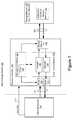
- FIG. 1is a block diagram illustrating an implementation of a data storage system, in accordance with some embodiments.
- FIG. 2is a block diagram illustrating an implementation of a management module, in accordance with some embodiments.
- FIG. 3Ais a prophetic diagram of voltage distributions that may be found in a single-level flash memory cell (SLC) over time, in accordance with some embodiments.
- SLCsingle-level flash memory cell
- FIG. 3Bis a prophetic diagram of voltage distributions that may be found in a multi-level flash memory cell (MLC) over time, in accordance with some embodiments.
- MLCmulti-level flash memory cell
- FIG. 3Cis a prophetic diagram of voltage distributions that may be found in a single-level flash memory cell (SLC) with a low syndrome weight, showing various reading threshold voltages, in accordance with some embodiments.
- SLCsingle-level flash memory cell
- FIG. 3Dis a prophetic diagram of voltage distributions that may be found in a single-level flash memory cell (SLC) with a high syndrome weight, showing various reading threshold voltages, in accordance with some embodiments.
- SLCsingle-level flash memory cell
- FIGS. 4A-4Billustrate a flowchart representation of a method for reading from a storage medium, in accordance with some embodiments.
- FIG. 5illustrates a flowchart representation of a method for reading from a storage medium, in accordance with some embodiments.
- the various implementations described hereininclude systems, methods and/or devices used to improve the error correction capability when using soft information error control decoding. Some implementations include systems, methods and/or devices to obtain and utilize error information for determining reading threshold voltages used for reading symbols from a storage medium.
- some implementationsinclude a method for reading from a storage medium.
- the methodincludes initiating performance of a first read operation, using a first reading threshold voltage, to obtain a first error indicator.
- the methodfurther includes initiating performance of a second set of additional read operations using two or more second reading threshold voltages, the second reading threshold voltages determined in accordance with the first error indicator, to obtain a second error indicator.
- a difference between two of the second reading threshold voltagesis greater than when the first error indicator is less than a first threshold.
- the methodfurther includes initiating performance of a third set of additional read operations using two or more third reading threshold voltages, the third reading threshold voltages determined in accordance with the first error indicator, the second error indicator, or a combination of the first error indicator and the second error indicator, to obtain a third error indicator.
- the first error indicatoris based at least in part on a syndrome weight.
- the first error indicatoris based at least in part on a bit error count
- the methodfurther comprises setting a set of default reading threshold voltages to the second reading threshold voltages.
- the second error indicatoris based at least in part on a bit error count
- the methodfurther comprises setting a set of default reading threshold voltages to the third reading threshold voltages.
- the two or more second reading threshold voltagesare different from the first reading threshold voltage.
- At least one of the two or more second reading threshold voltagesis the same as the first reading threshold voltage.
- Some implementationsinclude a method for reading from a storage medium.
- the methodincludes initiating performance of a first read operation, using a first reading threshold voltage, to obtain a first error indicator.
- the methodfurther includes initiating performance of a second read operation using a second reading threshold voltage, the second reading threshold voltage determined in accordance with the first indicator, to obtain a second error indicator.
- a difference between the first reading threshold voltage and the second reading threshold voltageis greater than when the first error indicator is less than a first threshold.
- the storage mediumcomprises one or more flash memory devices.
- a device operable to read from a storage mediumis configured to read from the storage medium in accordance with any of the methods described above.
- the deviceincludes a storage medium interface for coupling the device to the storage medium, means for initiating performance of a first read operation, using a first reading threshold voltage, to obtain a first error indicator, and means for initiating performance of a second set of additional read operations, using two or more second reading threshold voltages, the second reading threshold voltages determined in accordance with the first error indicator, to obtain a second error indicator.
- the deviceincludes a storage medium interface for coupling the device to the storage medium, means for initiating performance of a first read operation, using a first reading threshold voltage, to obtain a first error indicator, and means for initiating performance of a second read operation using a second reading threshold voltage, the second reading threshold voltage determined in accordance with the first indicator, to obtain a second error indicator.
- a non-transitory computer readable storage mediumstores one or more programs configured for execution by a device coupled to a storage medium, the one or more programs comprising instructions for causing the device and/or storage medium to read from the storage medium in accordance with any of the methods described above.
- FIG. 1is a diagram of an implementation of a data storage system 100 , in accordance with some embodiments. While some example features are illustrated, various other features have not been illustrated for the sake of brevity and so as not to obscure more pertinent aspects of the example implementations disclosed herein. To that end, as a non-limiting example, the data storage system 100 includes a memory controller 120 , and a storage medium 130 , and is used in conjunction with a computer system 110 .
- storage medium 130is a single flash memory device while in other implementations storage medium 130 includes a plurality of flash memory devices.
- storage medium 130is NAND-type flash memory or NOR-type flash memory.
- memory controller 120is a solid-state drive (SSD) controller.
- SSDsolid-state drive
- Computer system 110is coupled to memory controller 120 through data connections 101 .
- computer system 110includes memory controller 120 as a component and/or a sub-system.
- Computer system 110may be any suitable computer device, such as a computer, a laptop computer, a tablet device, a netbook, an internet kiosk, a personal digital assistant, a mobile phone, a smart phone, a gaming device, a computer server, or any other computing device.
- Computer system 110is sometimes called a host or host system.
- computer system 110includes one or more processors, one or more types of memory, a display and/or other user interface components such as a keyboard, a touch screen display, a mouse, a track-pad, a digital camera and/or any number of supplemental devices to add functionality.
- Storage medium 130is coupled to memory controller 120 through connections 103 .
- Connections 103are sometimes called data connections, but typically convey commands in addition to data, and optionally convey metadata, error correction information and/or other information in addition to data values to be stored in storage medium 130 and data values read from storage medium 130 .
- memory controller 120 and storage medium 130are included in the same device as components thereof.
- Storage medium 130may include any number (i.e., one or more) of memory devices including, without limitation, non-volatile semiconductor memory devices, such as flash memory.
- flash memory devicescan be configured for enterprise storage suitable for applications such as cloud computing, or for caching data stored (or to be stored) in secondary storage, such as hard disk drives. Additionally and/or alternatively, flash memory can also be configured for relatively smaller-scale applications such as personal flash drives or hard-disk replacements for personal, laptop and tablet computers.
- Storage medium 130is divided into a number of addressable and individually selectable blocks, such as selectable portion 131 .
- the individually selectable blocksare the minimum size erasable units in a flash memory device. In other words, each block contains the minimum number of memory cells that can be erased simultaneously.
- Each blockis usually further divided into a plurality of pages and/or word lines, where each page or word line is typically an instance of the smallest individually accessible (readable) portion in a block.
- the smallest individually accessible unit of a data setis a sector, which is a subunit of a page. That is, a block includes a plurality of pages, each page contains a plurality of sectors, and each sector is the minimum unit of data for reading data from the flash memory device.
- one blockcomprises any number of pages, for example, 64 pages, 128 pages, 256 pages or another suitable number of pages.
- Blocksare typically grouped into a plurality of zones. Each block zone can be independently managed to some extent, which increases the degree of parallelism for parallel operations and simplifies management of storage medium 130 .
- error control codingcan be utilized to limit the number of uncorrectable errors that are introduced by electrical fluctuations, defects in the storage medium, operating conditions, device history, write-read circuitry, etc., or a combination of these and various other factors.
- memory controller 120includes a management module 121 , an input buffer 123 , an output buffer 124 , an error control module 125 and a storage medium interface (I/O) 128 .
- Memory controller 120may include various additional features that have not been illustrated for the sake of brevity and so as not to obscure more pertinent features of the example implementations disclosed herein, and that a different arrangement of features may be possible.
- Input and output buffers 123 , 124provide an interface to computer system 110 through data connections 101 .
- storage medium I/O 128provides an interface to storage medium 130 though connections 103 .
- storage medium I/O 128includes read and write circuitry, including circuitry capable of providing reading signals to storage medium 130 (e.g., reading threshold voltages for NAND-type flash memory).
- management module 121includes one or more processing units (CPUs, also sometimes called processors) 122 configured to execute instructions in one or more programs (e.g., in management module 121 ).
- the one or more CPUs 122are shared by one or more components within, and in some cases, beyond the function of memory controller 120 .
- Management module 121is coupled to input buffer 123 , output buffer 124 (connection not shown), error control module 125 and storage medium I/O 128 in order to coordinate the operation of these components.
- Error control module 125is coupled to storage medium I/O 128 , input buffer 123 and output buffer 124 . Error control module 125 is provided to limit the number of uncorrectable errors inadvertently introduced into data. In some embodiments, error control module 125 is executed in software by the one or more CPUs 122 of management module 121 , and, in other embodiments, error control module 125 is implemented in whole or in part using special purpose circuitry to perform encoding and decoding functions. To that end, error control module 125 includes an encoder 126 and a decoder 127 . Encoder 126 encodes data by applying an error control code to produce a codeword, which is subsequently stored in storage medium 130 .
- decoder 127applies a decoding process to the encoded data to recover the data, and to correct errors in the recovered data within the error correcting capability of the error control code.
- error control codeshave different error detection and correction capacities, and that particular codes are selected for various applications for reasons beyond the scope of this disclosure. As such, an exhaustive review of the various types of error control codes is not provided herein.
- each type or family of error control codesmay have encoding and decoding algorithms that are particular to the type or family of error control codes.
- some algorithmssuch as the Viterbi algorithm, may be utilized at least to some extent in the decoding of a number of different types or families of error control codes.
- an exhaustive description of the various types of encoding and decoding algorithms generally available and known to those skilled in the artis not provided herein.
- input buffer 123receives data to be stored in storage medium 130 from computer system 110 .
- the data held in input buffer 123is made available to encoder 126 , which encodes the data to produce one or more codewords.
- the one or more codewordsare made available to storage medium I/O 128 , which transfers the one or more codewords to storage medium 130 in a manner dependent on the type of storage medium being utilized.
- a read operationis initiated when computer system (host) 110 sends one or more host read commands on control line 111 to memory controller 120 requesting data from storage medium 130 .
- Memory controller 120sends one or more read access commands to storage medium 130 , via storage medium I/O 128 , to obtain raw read data in accordance with memory locations (addresses) specified by the one or more host read commands.
- Storage medium I/O 128provides the raw read data (e.g., comprising one or more codewords) to decoder 127 . If the decoding is successful (e.g., 405 —Yes, FIG. 4A ), the decoded data is provided to output buffer 124 , where the decoded data is made available to computer system 110 (e.g., step 407 , FIG. 4A ). In some implementations, if the decoding is not successful (e.g., 405 —No, FIG. 4A ), memory controller 120 may resort to a number of remedial actions or provide an indication of an irresolvable error
- Flash memory devicesutilize memory cells to store data as electrical values, such as electrical charges or voltages.
- Each flash memory celltypically includes a single transistor with a floating gate that is used to store a charge, which modifies the threshold voltage of the transistor (i.e., the voltage needed to turn the transistor on).
- the magnitude of the charge, and the corresponding threshold voltage the charge creates,is used to represent one or more data values.
- a reading threshold voltageis applied to the control gate of the transistor and the resulting sensed current or voltage is mapped to a data value.
- cell voltageand “memory cell voltage,” in the context of flash memory cells, means the threshold voltage of the memory cell, which is the minimum voltage that needs to be applied to the gate of the memory cell's transistor in order for the transistor to conduct current.
- reading threshold voltagessometimes also called reading signals and reading voltages
- gate voltagesapplied to the gates of the flash memory cells to determine whether the memory cells conduct current at that gate voltage.
- the raw data value for that read operationis a “1” and otherwise the raw data value is a “0.”
- FIG. 2is a block diagram illustrating an exemplary management module 121 in accordance with some embodiments.
- Management module 121typically includes one or more processing units (CPUs) 122 for executing modules, programs and/or instructions stored in memory 206 and thereby performing processing operations, memory 206 , and one or more communication buses 208 for interconnecting these components.
- Communication buses 208optionally include circuitry (sometimes called a chipset) that interconnects and controls communications between system components.
- Management module 121is coupled to buffer 123 , buffer 124 , error control module 125 , and storage medium I/O 128 by communication buses 208 .
- Memory 206includes high-speed random access memory, such as DRAM, SRAM, DDR RAM or other random access solid state memory devices, and may include non-volatile memory, such as one or more magnetic disk storage devices, optical disk storage devices, flash memory devices, or other non-volatile solid state storage devices. Memory 206 optionally includes one or more storage devices remotely located from the CPU(s) 122 . Memory 206 , or alternately the non-volatile memory device(s) within memory 206 , comprises a non-transitory computer readable storage medium. In some embodiments, memory 206 , or the computer readable storage medium of memory 206 stores the following programs, modules, and data structures, or a subset thereof:
- the data read module 218optionally includes the following modules or sub-modules, or a subset thereof:
- Each of the above identified elementsmay be stored in one or more of the previously mentioned memory devices, and corresponds to a set of instructions for performing a function described above.
- the above identified modules or programsi.e., sets of instructions
- memory 206may store a subset of the modules and data structures identified above.
- memory 206may store additional modules and data structures not described above.
- the programs, modules, and data structures stored in memory 206 , or the computer readable storage medium of memory 206provide instructions for implementing any of the methods described below with reference to FIGS. 4A-4B and 5 .
- FIG. 2shows a management module 121
- FIG. 2is intended more as functional description of the various features which may be present in a management module than as a structural schematic of the embodiments described herein. In practice, and as recognized by those of ordinary skill in the art, items shown separately could be combined and some items could be separated.
- a single-level flash memory cellstores one bit (“0” or “1”).
- the storage density of a SLC memory deviceis one bit of information per memory cell.
- a multi-level flash memory cellcan store two or more bits of information per cell by using different ranges within the total voltage range of the memory cell to represent a multi-bit bit-tuple.
- the storage density of a MLC memory deviceis multiple-bits per cell (e.g., two bits per memory cell).
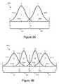
- FIG. 3Ais a simplified, prophetic diagram of voltage distributions 300 a found in a single-level flash memory cell (SLC) over time, in accordance with some embodiments.
- the voltage distributions 300 a shown in FIG. 3Ahave been simplified for illustrative purposes.
- the SLC's voltage rangeextends approximately from a voltage, V SS , at a source terminal of an NMOS transistor to a voltage, V DD , at a drain terminal of the NMOS transistor.
- voltage distributions 300 aextend between V SS and V DD .
- Sequential voltage ranges 301 and 302 between source voltage V SS and drain voltage V DDare used to represent corresponding bit values “1” and “0,” respectively.
- Each voltage range 301 , 302has a respective center voltage V 1 301 b , V 0 302 b .
- the memory cell current sensed in response to an applied reading threshold voltagesis indicative of a memory cell voltage different from the respective center voltage V 1 301 b or V 0 302 b corresponding to the respective bit value written into the memory cell.
- Errors in cell voltage, and/or the cell voltage sensed when reading the memory cellcan occur during write operations, read operations, or due to “drift” of the cell voltage between the time data is written to the memory cell and the time a read operation is performed to read the data stored in the memory cell. For ease of discussion, these effects are collectively described as “cell voltage drift.”
- Each voltage range 301 , 302also has a respective voltage distribution 301 a , 302 a that may occur as a result of any number of a combination of error-inducing factors, examples of which are identified above.
- a reading threshold voltage V Ris applied between adjacent center voltages (e.g., applied proximate to the halfway region between adjacent center voltages V 1 301 b and V 0 302 b ).
- the reading threshold voltageis located between voltage ranges 301 and 302 .
- reading threshold voltage V Ris applied in the region proximate to where the voltage distributions 301 a and 302 a overlap, which is not necessarily proximate to the halfway region between adjacent center voltages V 1 301 b and V 0 302 b.
- flash memoryIn order to increase storage density in flash memory, flash memory has developed from single-level (SLC) cell flash memory to multi-level cell (MLC) flash memory so that two or more bits can be stored by each memory cell.
- SLCsingle-level
- MLCmulti-level cell
- a MLC flash memory deviceis used to store multiple bits by using voltage ranges within the total voltage range of the memory cell to represent different bit-tuples.
- a MLC flash memory deviceis typically more error-prone than a SLC flash memory device created using the same manufacturing process because the effective voltage difference between the voltages used to store different data values is smaller for a MLC flash memory device.
- a typical errorincludes a stored voltage level in a particular MLC being in a voltage range that is adjacent to the voltage range that would otherwise be representative of the correct storage of a particular bit-tuple.
- the impact of such errorscan be reduced by gray-coding the data, such that adjacent voltage ranges represent single-bit changes between bit-tuples.
- FIG. 3Bis a simplified, prophetic diagram of voltage distributions 300 b that may be found in a multi-level flash memory cell (MLC) over time, in accordance with some embodiments.
- the voltage distributions 300 b shown in FIG. 3Bhave been simplified for illustrative purposes.
- the cell voltage of a MLCapproximately extends from a voltage, V SS , at the source terminal of a NMOS transistor to a voltage, V DD , at the drain terminal.
- voltage distributions 300 bextend between V SS and V DD .
- Sequential voltage ranges 311 , 312 , 313 , 314 between the source voltage V SS and drain voltages V DDare used to represent corresponding bit-tuples “11,” “01,” “00,” “10,” respectively.
- Each voltage range 311 , 312 , 313 , 314has a respective center voltage 311 b , 312 b , 313 b , 314 b .
- Each voltage range 311 , 312 , 313 , 314also has a respective voltage distribution 311 a , 312 a , 313 a , 314 a that may occur as a result of any number of a combination of factors, such as electrical fluctuations, defects in the storage medium, operating conditions, device history (e.g., number of program-erase (PE) cycles), and/or imperfect performance or design of write-read circuitry.
- PEprogram-erase
- the charge on the floating gate of the MLCwould be set such that the resultant cell voltage is at the center of one of the ranges 311 , 312 , 313 , 314 in order to write the corresponding bit-tuple to the MLC.
- the resultant cell voltagewould be set to one of V 11 311 b , V 00 312 b , V 00 313 b and V 10 314 b in order to write a corresponding one of the bit-tuples “11,” “01,” “00” and “10.”
- the initial cell voltagemay differ from the center voltage for the data written to the MLC.
- Reading threshold voltages V RA , V RB and V RCare positioned between adjacent center voltages (e.g., positioned at or near the halfway point between adjacent center voltages) and, thus, define threshold voltages between the voltage ranges 311 , 312 , 313 , 314 .
- one of the reading threshold voltages V RA , V RB and V RCis applied to determine the cell voltage using a comparison process.
- the actual cell voltage, and/or the cell voltage received when reading the MLCmay be different from the respective center voltage V 11 311 b , V 01 312 b , V 00 313 b or V 10 314 b corresponding to the data value written into the cell.
- the actual cell voltagemay be in an altogether different voltage range, strongly indicating that the MLC is storing a different bit-tuple than was written to the MLC. More commonly, the actual cell voltage may be close to one of the read comparison voltages, making it difficult to determine with certainty which of two adjacent bit-tuples is stored by the MLC.
- Errors in cell voltage, and/or the cell voltage received when reading the MLCcan occur during write operations, read operations, or due to “drift” of the cell voltage between the time data is written to the MLC and the time a read operation is performed to read the data stored in the MLC.
- driftsometimes errors in cell voltage, and/or the cell voltage received when reading the MLC, are collectively called “cell voltage drift.”
- Gray-coding the bit-tuplesincludes constraining the assignment of bit-tuples such that a respective bit-tuple of a particular voltage range is different from a respective bit-tuple of an adjacent voltage range by only one bit. For example, as shown in FIG.
- the corresponding bit-tuples for adjacent ranges 301 and 302are respectively “11” and “01”
- the corresponding bit-tuples for adjacent ranges 302 and 303are respectively “01” and “00”
- the corresponding bit-tuples for adjacent ranges 303 and 304are respectively “00” and “10.”
- gray-codingif the cell voltage drifts close to a read comparison voltage level, the error is typically limited to a single bit within the 2-bit bit-tuple.
- a decodere.g., decoder 127 , FIG. 1
- a decoderapplies a decoding process to the encoded data to recover the data, and to correct errors in the recovered data within the error correcting capability of the error control code.
- the decoderdetermines an error indicator.
- the error indicatoris a syndrome weight, which indicates the number of bit errors detected in a given iteration of the decoding process. A syndrome weight of zero indicates decoding was successful and the data has been recovered.
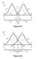
- the relatively small overlap 323 of voltage distributions 321 a and 322 aindicates a smaller area in which errors occur when reading from the memory cell, and thus relates to a low starting syndrome weight.
- the relatively large overlap 333 of voltage distributions 331 a and 332 aindicates a larger area in which errors occur when reading from the memory cell, and thus relates to a high starting syndrome weight.
- a decoderprocesses a read operation using a single reading threshold voltage (e.g., “1-Read decoding”). If the decoding fails or the syndrome weight is too high to be corrected by 1-Read decoding, one or more additional decoding attempts are made with one or more additional read operations using one or more additional reading threshold voltages. For example, if 1-Read decoding fails or if the syndrome weight is too high to be corrected by 1-Read decoding, an additional decoding attempt with two reading threshold voltages (e.g., “2-Read decoding”) is made. The error indicator from the 1-Read decoding is used to determine the reading threshold voltages used for the 2-Read decoding.
- a single reading threshold voltagee.g., “1-Read decoding”.
- the difference between the two reading threshold voltages used for the 2-Read decodingis greater (e.g., see FIG. 3D , as described below) than when the error indicator is less than a threshold (e.g., see FIG. 3C , as described below).
- a thresholde.g., see FIG. 3C , as described below.
- one or more additional decoding attemptsare made with one or more additional read operations using one or more additional reading threshold voltages. For example, if 2-Read decoding fails or if the syndrome weight is too high to be corrected by 2-Read decoding, an additional decoding attempt with four reading threshold voltages (e.g., “4-Read decoding”) is made.
- the error indicator from the 1-Read decodingis used to determine the reading threshold voltages used for the 4-Read decoding.
- the error indicator from the 2-Read decodingis used to determine the reading threshold voltages used for the 4-Read decoding.
- a combination of the error indicator from the 1-Read decoding and the error indicator from the 2-Read decodingis used to determine the reading threshold voltages used for the 4-Read decoding.
- the error indicatoris greater than a threshold
- the difference between the four reading threshold voltages used for the 4-Read decodingis greater than when the error indicator is less than a threshold.
- this schemeis applicable to any combination of N 1 -Read decoding, N j -Read decoding, . . . , and N k -Read decoding, where j is an integer greater than 1 and k is an integer greater than 2.
- this schemeis applicable to 1-Read decoding, 3-Read decoding, and 5-Read decoding.
- the decoderdetermines an error indicator.
- the error indicatoris a bit error count.
- the bit error countis called a fail bit count, and indicates the number of bit errors detected in the decoding. After successful decoding, the bit error count is available. In some embodiments, the bit error count is used to adjust and/or update the default reading threshold voltages for subsequent decoding attempts. For example, after a successful 1-Read decoding, the bit error count from the 1-Read decoding is used to adjust and/or update the default reading threshold voltages for subsequent 2-Read decodings.
- FIG. 3Cis a simplified, prophetic diagram of voltage distributions 300 c found in a single-level flash memory cell (SLC) with a low syndrome weight, in accordance with some embodiments.
- SLCsingle-level flash memory cell
- the relatively small overlap 323 of voltage distributions 321 a and 322 aindicates a smaller area in which errors occur when reading from the memory cell, and thus relates to a low starting syndrome weight.
- the two reading threshold voltages used for the 2-Read decodingare narrowly separated.
- the two reading threshold voltages V RL1 and V RL2 used for 2-Read decodingare narrowly separated.
- this schemeis applicable to any combinations of N 1 -Read decoding, N a -Read decoding, . . . , and N k -Read decoding, where j is an integer greater than 1 and k is an integer greater than 2.
- this schemeis applicable to 1-Read decoding, 3-Read decoding, and 5-Read decoding.
- FIG. 3Cillustrates an example using a single-level flash memory cell, this scheme is also applicable to a multi-level flash memory cell (e.g., as illustrated in FIG. 3B ).
- FIG. 3Dis a simplified, prophetic diagram of voltage distributions 300 d found in a single-level flash memory cell (SLC) with a high syndrome weight, in accordance with some embodiments.
- SLCsingle-level flash memory cell
- FIG. 3AExplanations provided above in connection with FIG. 3A , with respect to voltage distributions 300 a , sequential voltage ranges 301 and 302 , center voltages V 1 301 b and V 0 302 b , voltage distributions 301 a and 302 a and their overlap, and reading threshold voltage V R are equally applicable to voltage distributions 300 d , sequential voltage ranges 331 and 332 , center voltages V 1 331 b and V 0 332 b , voltage distributions 331 a and 332 a and their overlap, and reading threshold voltage V R as shown in FIG. 3D , except as described next.
- the relatively large overlap 333 of voltage distributions 331 a and 332 aindicates a larger area in which errors occur when reading from the memory cell, and thus relates to a high starting syndrome weight.
- the two reading threshold voltages used for the 2-Read decodingare widely separated.
- the two reading threshold voltages V RH1 and V RH2 used for 2-Read decodingare widely separated.
- FIG. 3Dillustrates an example using a single-level flash memory cell
- this schemeis also applicable to a multi-level flash memory cell (e.g., as illustrated in FIG. 3B ).
- FIGS. 4A-4Billustrate a flowchart representation of a method 400 for reading from a storage medium.
- a read operationis typically initiated when a computer system (e.g., computer system 110 , FIG. 1 , sometimes called a host) sends one or more host read commands on control line 111 to memory controller 120 requesting data from storage medium 130 .
- memory controller 120sends one or more read access commands to storage medium 130 , via storage medium I/O 128 , which initiates performance of method 400 .
- method 400is performed by a memory controller (e.g., memory controller 120 , FIG. 1 ) or one or more components of the memory controller (e.g., management module 121 , FIGS. 1 and 2 ) to read from a storage medium (e.g., storage medium 130 , FIG. 1 ).
- a memory controllere.g., memory controller 120 , FIG. 1
- management module 121e.g., FIGS. 1 and 2
- storage mediume.g., storage medium 130 , FIG. 1
- method 400is governed by instructions that are stored in a non-transitory computer readable storage medium and that are executed by one or more processors of a device, such as the one or more processing units (CPUs) 122 of management module 121 , shown in FIGS. 1 and 2 .
- CPUsprocessing units
- a memory controllerinitiates ( 402 ) performance of a first read operation, using a first reading threshold voltage (e.g., reading threshold voltage V R , FIG. 3C , or reading threshold voltage V R , FIG. 3D ), to obtain a first error indicator.
- a first reading threshold voltagee.g., reading threshold voltage V R , FIG. 3C , or reading threshold voltage V R , FIG. 3D
- the first read operationis primarily performed to obtain data from the storage medium (e.g., storage medium 130 , FIG. 1 ), and secondarily to obtain the first error indicator.
- FIG. 1shows management module 121 (a component of memory controller 120 ) configured to initiate performance of a read operation from storage medium 130 via storage medium I/O 128 .
- the first error indicatoris ( 404 ) based at least in part on a syndrome weight.
- a syndrome weightindicates the number of bit errors detected in a given iteration of the decoding process and a syndrome weight of zero indicates decoding was successful ( 405 —Yes) and the data has been recovered ( 407 ).
- the memory controllerinitiates ( 406 ) performance of a second set of additional read operations using two or more second reading threshold voltages, the second reading threshold voltages determined in accordance with the first error indicator, to obtain a second error indicator.
- the second set of additional read operationsare primarily performed to obtain data from the storage medium (e.g., storage medium 130 , FIG. 1 ), and secondarily to obtain the second error indicator.
- FIG. 1shows management module 121 (a component of memory controller 120 ) configured to initiate performance of a set of read operations using two or more reading threshold voltages (e.g., reading threshold voltages VRL 1 and VRL 2 , FIG. 3C , or reading threshold voltages VRH 1 and VRH 2 , FIG. 3D ).
- step 406is performed in response to a determination that the first read operation failed ( 405 —No). In some embodiments, step 406 is performed in response to a determination that the syndrome weight is too high to be corrected by 1-Read decoding, as explained above.
- the second error indicatoris based at least in part on a syndrome weight.
- a syndrome weightindicates the number of bit errors detected in a given iteration of the decoding process and a syndrome weight of zero indicates decoding was successful and the data has been recovered.
- a difference between two of the second reading threshold voltagesis greater than when the first error indicator is less than a first threshold.
- FIG. 3Dshows an example of when the error indicator is greater than a first threshold, and thus, the difference between reading threshold voltages V RH1 and V RH2 is greater than the difference between reading threshold voltages V RL1 and V RL2 in FIG. 3C , which shows an example of when the error indicator is less than the first threshold.
- the first error indicatoris ( 410 ) based at least in part on a bit error count.
- the bit error countis sometimes called a fail bit count, and indicates the number of bit errors detected in the decoding. After successful decoding, the bit error count is available. For example, after a successful 1-Read decoding, the bit error count from the 1-Read decoding is available.
- the memory controllersets ( 412 ) a set of default reading threshold voltages to the second reading threshold voltages. Using FIG. 3C as an example, when the error indicator is based on a bit error count determined after successful 1-Read decoding using reading threshold voltage V R , the memory controller sets the default reading threshold voltages for subsequent 2-Read decoding to reading threshold voltages V RL1 and V RL2 .
- the memory controllersets the default reading threshold voltages for subsequent 2 -Read decoding to reading threshold voltages V RH1 and V RH2 .
- the two or more second reading threshold voltagesare ( 414 ) different from the first reading threshold voltage.
- FIG. 3Cshows two second reading threshold voltages V RL1 and V RL2 which are different from the first reading threshold voltage V R .
- FIG. 3Dshows two second reading threshold voltages V RH1 and V RH2 which are different from the first reading threshold voltage V R .
- At least one of the two or more second reading threshold voltagesis ( 416 ) the same as the first reading threshold voltage.
- the first reading threshold voltageis reading threshold voltage V R and the second reading threshold voltages are reading threshold voltages V RL1 and V R , where at least one of the two second reading threshold voltages is the same as the first reading threshold voltage.
- the first reading threshold voltageis reading threshold voltage V R and the second reading threshold voltages are reading threshold voltages V RL2 and V R , where at least one of the two second reading threshold voltages is the same as the first reading threshold voltage.
- an additional example of the second reading threshold voltagesis reading threshold voltages V RH1 and V R
- another exampleis reading threshold voltages V RH2 and V R .
- the memory controllerinitiates ( 418 ) performance of a third set of additional read operations using two or more third reading threshold voltages, the third reading threshold voltages determined in accordance with the first error indicator, the second error indicator, or a combination of the first error indicator and the second error indicator, to obtain a third error indicator.
- the third set of additional read operationsare primarily performed to obtain data from the storage medium (e.g., storage medium 130 , FIG. 1 ), and secondarily to obtain the third error indicator.
- FIG. 1shows management module 121 (a component of memory controller 120 ) configured to initiate performance of a set of read operations using two or more reading threshold voltages.
- step 418is performed in response to a determination that the second set of read operations failed.
- step 418is performed in response to a determination that the syndrome weight is too high to be corrected by 2-Read decoding, as explained above.
- the third error indicatoris based at least in part on a syndrome weight.
- a syndrome weightindicates the number of bit errors detected in a given iteration of the decoding process and a syndrome weight of zero indicates decoding was successful and the data has been recovered.
- a difference between at least two of the third reading threshold voltagesis greater than when the first error indicator, the second error indicator, or the combination of the first and second error indicators is less than a threshold.
- the second error indicatoris ( 420 ) based at least in part on a bit error count.
- the bit error countis sometimes called a fail bit count, and indicates the number of bit errors detected in the decoding. After successful decoding, the bit error count is available. For example, after a successful 2-Read decoding, the bit error count from the 2-Read decoding is available.
- the memory controllersets ( 422 ) a set of default reading threshold voltages to the third reading threshold voltages. Using FIG.
- the memory controllersets the default reading threshold voltages for subsequent 4-Read decoding to four reading threshold voltages (not shown in FIG. 3C ).
- the memory controllersets the default reading threshold voltages for subsequent 4-Read decoding to four reading threshold voltages (not shown in FIG. 3D ).
- the two or more third reading threshold voltagesare different from the first reading threshold voltage. In some embodiments, the two or more third reading threshold voltages are different from the two or more second reading threshold voltages.
- At least one of the two or more third reading threshold voltagesis the same as the first reading threshold voltage. In some embodiments, at least one of the two or more third reading threshold voltages is the same as at least one of the two or more second reading threshold voltages.
- FIG. 5illustrates a flowchart representation of a method 500 for reading from a storage medium.
- a read operationis typically initiated when a computer system (e.g., computer system 110 , FIG. 1 , sometimes called a host) sends one or more host read commands on control line 111 to memory controller 120 requesting data from storage medium 130 .
- memory controller 120sends one or more read access commands to storage medium 130 , via storage medium I/O 128 , which initiates performance of method 500 .
- method 500is performed by a memory controller (e.g., memory controller 120 , FIG. 1 ) or a component of the memory controller (e.g., management module 121 , FIGS. 1 and 2 ) to read from a storage medium (e.g., storage medium 130 , FIG. 1 ).
- a memory controllere.g., memory controller 120 , FIG. 1
- a component of the memory controllere.g., management module 121 , FIGS. 1 and 2
- method 500is governed by instructions that are stored in a non-transitory computer readable storage medium and that are executed by one or more processors of a device, such as the one or more processing units (CPUs) 122 of management module 121 , shown in FIGS. 1 and 2 .
- CPUsprocessing units
- a memory controllerinitiates ( 502 ) performance of a first read operation, using a first reading threshold voltage (e.g., reading threshold voltage V R , FIG. 3C , or reading threshold voltage V R , FIG. 3D ), to obtain a first error indicator.
- a first reading threshold voltagee.g., reading threshold voltage V R , FIG. 3C , or reading threshold voltage V R , FIG. 3D
- the first read operationis primarily performed to obtain data from the storage medium (e.g., storage medium 130 , FIG. 1 ), and secondarily to obtain the first error indicator.
- FIG. 1shows management module 121 (a component of memory controller 120 ) configured to initiate performance of a read operation from storage medium 130 via storage medium I/O 128 .
- the first error indicatoris based at least in part on a syndrome weight.
- a syndrome weightindicates the number of bit errors detected in a given iteration of the decoding process and a syndrome weight of zero indicates decoding was successful and the data has been recovered.
- the memory controllerinitiates ( 504 ) performance of a second read operation using a second reading threshold voltage, the second reading threshold voltage determined in accordance with the first indicator, to obtain a second error indicator.
- the second read operationis primarily performed to obtain data from the storage medium (e.g., storage medium 130 , FIG. 1 ), and secondarily to obtain the second error indicator.
- FIG. 1shows management module 121 (a component of memory controller 120 ) configured to initiate performance of a second read operation using a second reading threshold voltage (e.g., reading threshold voltage V RL1 or reading threshold voltage V RL2 , FIG. 3C , or reading threshold voltage V RH1 or reading threshold voltage V RH2 , FIG. 3D ).
- step 504is performed in response to a determination that the first read operation failed.
- step 504is performed in response to a determination that the syndrome weight is too high to be corrected by 1-Read decoding, as explained above.
- the second error indicatoris based at least in part on a syndrome weight.
- a syndrome weightindicates the number of bit errors detected in a given iteration of the decoding process and a syndrome weight of zero indicates decoding was successful and the data has been recovered.
- a difference between the first reading threshold voltage and the second reading threshold voltageis greater than when the first error indicator is less than a first threshold.
- reading threshold voltage V Re.g., in FIGS. 3C and 3D
- reading threshold voltage V RH1is the second reading threshold voltage in FIG. 3D
- reading threshold voltage V RL1is the second reading threshold voltage in FIG. 3C .
- FIG. 3Dshows an example of when the error indicator is greater than a first threshold
- FIG. 3Cshows an example of when the error indicator is less than a first threshold.
- the difference between reading threshold voltage V R and reading threshold voltage V RH1is greater than the difference between reading threshold voltage V R and reading threshold voltage V RL1 (e.g., in FIG. 3C ).
- the first error indicatoris based at least in part on a bit error count.
- the bit error countis sometimes called a fail bit count, and indicates the number of bit errors detected in the decoding. After successful decoding, the bit error count is available. For example, after a successful 1-Read decoding, the bit error count from the 1-Read decoding is available.
- the memory controllersets a default reading threshold voltage to the second reading threshold voltage.
- the memory controllerinitiates performance of a third set of additional read operations using two or more third reading threshold voltages, the third reading threshold voltages determined in accordance with the first error indicator, the second error indicator, or a combination of the first error indicator and the second error indicator, to obtain a third error indicator.
- the third set of additional read operationsare primarily performed to obtain data from the storage medium (e.g., storage medium 130 , FIG. 1 ), and secondarily to obtain the third error indicator.
- FIG. 1shows management module 121 (a component of memory controller 120 ) configured to initiate performance of a set of read operations using two or more reading threshold voltages.
- the third set of additional read operationsis performed in response to a determination that the second read operation failed, or produced a syndrome weight too high to be corrected, as explained above.
- the third error indicatoris based at least in part on a syndrome weight.
- a syndrome weightindicates the number of bit errors detected in a given iteration of the decoding process and a syndrome weight of zero indicates decoding was successful and the data has been recovered.
- the two or more third reading threshold voltagesare different from the first reading threshold voltage. In some embodiments, the two or more third reading threshold voltages are different from the second reading threshold voltage.
- At least one of the two or more third reading threshold voltagesis the same as the first reading threshold voltage. In some embodiments, at least one of the two or more third reading threshold voltages is the same as the second reading threshold voltage.
- the storage medium(e.g., storage medium 130 , FIG. 1 ) is a single flash memory device while in other implementations the storage medium includes a plurality of flash memory devices.
- a device operable to read from a storage mediumincludes a storage medium interface (e.g., storage medium I/O 128 , FIG. 1 ) for coupling the device to the storage medium (e.g., storage medium 130 , FIG. 1 ) and one or more modules, including a memory management module (e.g., management module 121 , FIGS. 1 and 2 ) that includes one or more processors (e.g., CPUs 122 , FIGS. 1 and 2 ) and memory (e.g., memory 206 , FIG.
- a storage medium interfacee.g., storage medium I/O 128 , FIG. 1
- modulesincluding a memory management module (e.g., management module 121 , FIGS. 1 and 2 ) that includes one or more processors (e.g., CPUs 122 , FIGS. 1 and 2 ) and memory (e.g., memory 206 , FIG.
- the storage medium interfacee.g., storage medium I/O 128 , FIG. 1
- the storage medium interfacee.g., storage medium I/O 128 , FIG. 1
- firstfirst
- secondsecond
- first contactfirst contact
- first contactsecond contact
- first contactsecond contact
- the term “if”may be construed to mean “when” or “upon” or “in response to determining” or “in accordance with a determination” or “in response to detecting,” that a stated condition precedent is true, depending on the context.
- the phrase “if it is determined [that a stated condition precedent is true]” or “if [a stated condition precedent is true]” or “when [a stated condition precedent is true]”may be construed to mean “upon determining” or “in response to determining” or “in accordance with a determination” or “upon detecting” or “in response to detecting” that the stated condition precedent is true, depending on the context.
Landscapes
- Engineering & Computer Science (AREA)
- Theoretical Computer Science (AREA)
- Quality & Reliability (AREA)
- Physics & Mathematics (AREA)
- General Engineering & Computer Science (AREA)
- General Physics & Mathematics (AREA)
- Computer Hardware Design (AREA)
- Read Only Memory (AREA)
- Techniques For Improving Reliability Of Storages (AREA)
Abstract
Description
- a reading threshold voltages table216 that includes a table of reading threshold voltages used for reading symbols from a storage medium;
- a data read
module 218 that is used for reading data from a storage medium; - a
data write module 226 that is used for writing data to a storage medium; and - a data erase
module 228 that is used for erasing data from a storage medium.
- a
read management module 220 that is used for controlling or managing execution of read commands received from a host device such as computer system110 (FIG. 1 ); - an error
control management module 222 that is used to receive error indicators (e.g., syndrome weights) fromerror control module 125, and optionally to control operation oferror control module 125; and - a reading threshold
voltage control module 224 that is used for selecting reading threshold voltages from the reading threshold voltages table216.
- a
Claims (16)
Priority Applications (1)
| Application Number | Priority Date | Filing Date | Title |
|---|---|---|---|
| US13/831,133US9870830B1 (en) | 2013-03-14 | 2013-03-14 | Optimal multilevel sensing for reading data from a storage medium |
Applications Claiming Priority (1)
| Application Number | Priority Date | Filing Date | Title |
|---|---|---|---|
| US13/831,133US9870830B1 (en) | 2013-03-14 | 2013-03-14 | Optimal multilevel sensing for reading data from a storage medium |
Publications (1)
| Publication Number | Publication Date |
|---|---|
| US9870830B1true US9870830B1 (en) | 2018-01-16 |
Family
ID=60935539
Family Applications (1)
| Application Number | Title | Priority Date | Filing Date |
|---|---|---|---|
| US13/831,133ActiveUS9870830B1 (en) | 2013-03-14 | 2013-03-14 | Optimal multilevel sensing for reading data from a storage medium |
Country Status (1)
| Country | Link |
|---|---|
| US (1) | US9870830B1 (en) |
Cited By (10)
| Publication number | Priority date | Publication date | Assignee | Title |
|---|---|---|---|---|
| US20180024881A1 (en)* | 2014-07-22 | 2018-01-25 | Ngd Systems, Inc. | System and method for adaptive multiple read of nand flash |
| US10037164B1 (en) | 2016-06-29 | 2018-07-31 | EMC IP Holding Company LLC | Flash interface for processing datasets |
| US10055351B1 (en) | 2016-06-29 | 2018-08-21 | EMC IP Holding Company LLC | Low-overhead index for a flash cache |
| US10089025B1 (en)* | 2016-06-29 | 2018-10-02 | EMC IP Holding Company LLC | Bloom filters in a flash memory |
| US10146438B1 (en) | 2016-06-29 | 2018-12-04 | EMC IP Holding Company LLC | Additive library for data structures in a flash memory |
| US10261704B1 (en) | 2016-06-29 | 2019-04-16 | EMC IP Holding Company LLC | Linked lists in flash memory |
| US10331561B1 (en) | 2016-06-29 | 2019-06-25 | Emc Corporation | Systems and methods for rebuilding a cache index |
| US20200097189A1 (en)* | 2018-09-26 | 2020-03-26 | Western Digital Technologies, Inc. | Data storage systems and methods for improved data relocation based on read-level voltages associated with error recovery |
| US10795765B2 (en) | 2014-07-22 | 2020-10-06 | Ngd Systems, Inc. | SSD for long term data retention |
| US10943634B2 (en)* | 2018-11-30 | 2021-03-09 | SK Hynix Inc. | Read latency improvement method and memory system thereof |
Citations (531)
| Publication number | Priority date | Publication date | Assignee | Title |
|---|---|---|---|---|
| US4173737A (en) | 1978-05-04 | 1979-11-06 | Zenith Radio Corporation | Limited position, non-volatile memory tuning system |
| US4888750A (en) | 1986-03-07 | 1989-12-19 | Kryder Mark H | Method and system for erase before write magneto-optic recording |
| US4916652A (en) | 1987-09-30 | 1990-04-10 | International Business Machines Corporation | Dynamic multiple instruction stream multiple data multiple pipeline apparatus for floating-point single instruction stream single data architectures |
| US5129089A (en) | 1987-12-18 | 1992-07-07 | Digital Equipment Corporation | Distributed interlock apparatus and distributed interlock management method |
| US5270979A (en) | 1991-03-15 | 1993-12-14 | Sundisk Corporation | Method for optimum erasing of EEPROM |
| US5329491A (en) | 1993-06-30 | 1994-07-12 | Intel Corporation | Nonvolatile memory card with automatic power supply configuration |
| US5381528A (en) | 1992-10-15 | 1995-01-10 | Maxtor Corporation | Demand allocation of read/write buffer partitions favoring sequential read cache |
| US5404485A (en) | 1993-03-08 | 1995-04-04 | M-Systems Flash Disk Pioneers Ltd. | Flash file system |
| US5488702A (en) | 1994-04-26 | 1996-01-30 | Unisys Corporation | Data block check sequence generation and validation in a file cache system |
| US5519847A (en) | 1993-06-30 | 1996-05-21 | Intel Corporation | Method of pipelining sequential writes in a flash memory |
| US5530705A (en) | 1995-02-08 | 1996-06-25 | International Business Machines Corporation | Soft error recovery system and method |
| US5537555A (en) | 1993-03-22 | 1996-07-16 | Compaq Computer Corporation | Fully pipelined and highly concurrent memory controller |
| US5551003A (en) | 1992-12-11 | 1996-08-27 | International Business Machines Corporation | System for managing log structured array (LSA) of DASDS by managing segment space availability and reclaiming regions of segments using garbage collection procedure |
| US5636342A (en) | 1995-02-17 | 1997-06-03 | Dell Usa, L.P. | Systems and method for assigning unique addresses to agents on a system management bus |
| US5657332A (en) | 1992-05-20 | 1997-08-12 | Sandisk Corporation | Soft errors handling in EEPROM devices |
| US5666114A (en) | 1994-11-22 | 1997-09-09 | International Business Machines Corporation | Method and means for managing linear mapped address spaces storing compressed data at the storage subsystem control unit or device level |
| US5708849A (en) | 1994-01-26 | 1998-01-13 | Intel Corporation | Implementing scatter/gather operations in a direct memory access device on a personal computer |
| US5765185A (en) | 1995-03-17 | 1998-06-09 | Atmel Corporation | EEPROM array with flash-like core having ECC or a write cache or interruptible load cycles |
| US5890193A (en) | 1995-07-28 | 1999-03-30 | Micron Technology, Inc. | Architecture for state machine for controlling internal operations of flash memory |
| US5930188A (en) | 1995-08-04 | 1999-07-27 | Micron Technology, Inc. | Memory circuit for performing threshold voltage tests on cells of a memory array |
| US5938884A (en) | 1995-05-18 | 1999-08-17 | Obsidian, Inc. | Apparatus for chemical mechanical polishing |
| US5943692A (en) | 1997-04-30 | 1999-08-24 | International Business Machines Corporation | Mobile client computer system with flash memory management utilizing a virtual address map and variable length data |
| US5946714A (en) | 1996-10-21 | 1999-08-31 | Mitsubishi Denki Kabushiki Kaisha | Semiconductor storage device utilizing address management tables and table state maps for managing data storage and retrieval |
| US5982664A (en) | 1997-10-22 | 1999-11-09 | Oki Electric Industry Co., Ltd. | Semiconductor memory capable of writing and reading data |
| US6000006A (en) | 1997-08-25 | 1999-12-07 | Bit Microsystems, Inc. | Unified re-map and cache-index table with dual write-counters for wear-leveling of non-volatile flash RAM mass storage |
| US6006345A (en) | 1997-05-09 | 1999-12-21 | International Business Machines Corporation | Pattern generator for memory burn-in and test |
| US6016560A (en) | 1995-06-14 | 2000-01-18 | Hitachi, Ltd. | Semiconductor memory, memory device, and memory card |
| US6018304A (en) | 1997-12-18 | 2000-01-25 | Texas Instruments Incorporated | Method and apparatus for high-rate n/n+1 low-complexity modulation codes with adjustable codeword length and error control capability |
| US6044472A (en) | 1996-06-21 | 2000-03-28 | Archos | Device and method for supplying power to an external data medium reader unit connected to a computer, and external reader unit including this device |
| US6070074A (en) | 1998-04-24 | 2000-05-30 | Trw Inc. | Method for enhancing the performance of a regenerative satellite communications system |
| US6104304A (en) | 1999-07-06 | 2000-08-15 | Conexant Systems, Inc. | Self-test and status reporting system for microcontroller-controlled devices |
| US6119250A (en) | 1996-05-07 | 2000-09-12 | Matsushita Electric Industrial Co., Ltd. | Semiconductor integrated circuit |
| US6138261A (en) | 1998-04-29 | 2000-10-24 | Trw Inc. | Concatenated coding system for satellite communications |
| US6182264B1 (en) | 1998-05-22 | 2001-01-30 | Vlsi Technology, Inc. | Smart dynamic selection of error correction methods for DECT based data services |
| US6192092B1 (en) | 1998-06-15 | 2001-02-20 | Intel Corp. | Method and apparatus for clock skew compensation |
| US6260120B1 (en) | 1998-06-29 | 2001-07-10 | Emc Corporation | Storage mapping and partitioning among multiple host processors in the presence of login state changes and host controller replacement |
| US6295592B1 (en) | 1998-07-31 | 2001-09-25 | Micron Technology, Inc. | Method of processing memory requests in a pipelined memory controller |
| US20010026949A1 (en) | 2000-03-27 | 2001-10-04 | Sumio Ogawa | Semiconductor device manufacturing system and method of manufacturing semiconductor devices |
| US6311263B1 (en) | 1994-09-23 | 2001-10-30 | Cambridge Silicon Radio Limited | Data processing circuits and interfaces |
| US20010050824A1 (en) | 1999-01-04 | 2001-12-13 | Maxtor Corporation | Servo area numbering strategy for computer disk drives |
| US20020024846A1 (en) | 1996-09-30 | 2002-02-28 | Takayuki Kawahara | Semiconductor integrated circuit and data processing system |
| US20020032891A1 (en) | 2000-09-12 | 2002-03-14 | Hitachi, Ltd. | Data processing system and data processing method |
| US20020036515A1 (en) | 2000-01-18 | 2002-03-28 | Formfactor, Inc. | Apparatus for reducing power supply noise in an integrated circuit |
| US6408394B1 (en) | 1998-11-18 | 2002-06-18 | Compaq Computer Corp. | System and method for applying initialization power to SCSI devices |
| US6412042B1 (en) | 1999-11-17 | 2002-06-25 | Maxtor Corporation | System and method for improved disk drive performance and reliability |
| US20020083299A1 (en) | 2000-12-22 | 2002-06-27 | International Business Machines Corporation | High speed remote storage controller |
| US20020099904A1 (en) | 2001-01-19 | 2002-07-25 | Conley Kevin M. | Partial block data programming and reading operations in a non-volatile memory |
| US20020116651A1 (en) | 2000-12-20 | 2002-08-22 | Beckert Richard Dennis | Automotive computing devices with emergency power shut down capabilities |
| US6442076B1 (en) | 2000-06-30 | 2002-08-27 | Micron Technology, Inc. | Flash memory with multiple status reading capability |
| US20020122334A1 (en) | 2001-01-03 | 2002-09-05 | Samsung Electronics Co., Ltd. | Flash memory device with cell current measuring scheme using write driver |
| US6449625B1 (en) | 1999-04-20 | 2002-09-10 | Lucent Technologies Inc. | Use of a two-way stack approach to optimize flash memory management for embedded database systems |
| JP2002532806A (en) | 1998-12-18 | 2002-10-02 | ユニシス コーポレーション | Computer system and method for operating multiple operating systems in different partitions of a computer system so that different partitions can communicate with each other via shared memory |
| US20020152305A1 (en) | 2000-03-03 | 2002-10-17 | Jackson Gregory J. | Systems and methods for resource utilization analysis in information management environments |
| US20020162075A1 (en) | 2001-04-30 | 2002-10-31 | Talagala Nisha D. | Storage array employing scrubbing operations at the disk-controller level |
| US20020165896A1 (en) | 2001-05-02 | 2002-11-07 | Kim Jason Seung-Min | Multiprocessor communication system and method |
| US6484224B1 (en) | 1999-11-29 | 2002-11-19 | Cisco Technology Inc. | Multi-interface symmetric multiprocessor |
| US6516437B1 (en) | 2000-03-07 | 2003-02-04 | General Electric Company | Turbo decoder control for use with a programmable interleaver, variable block length, and multiple code rates |
| US20030041299A1 (en) | 2001-08-23 | 2003-02-27 | Fujitsu Limited | Memory controller for multilevel cell memory |
| US20030043829A1 (en) | 2001-07-06 | 2003-03-06 | Abbas Rashid | Cross-bar switch employing a multiple entry point FIFO |
| EP1299800A2 (en) | 2000-06-02 | 2003-04-09 | Sun Microsystems, Inc. | System and method for migrating processes on a network |
| US20030079172A1 (en) | 2001-07-18 | 2003-04-24 | Hiroyuki Yamagishi | Encoding method and encoder |
| US20030088805A1 (en) | 2001-09-28 | 2003-05-08 | Tim Majni | Error indication in a raid memory system |
| US6564285B1 (en) | 1994-06-03 | 2003-05-13 | Intel Corporation | Synchronous interface for a nonvolatile memory |
| US20030093628A1 (en) | 2001-11-14 | 2003-05-15 | Matter Eugene P. | Memory adaptedt to provide dedicated and or shared memory to multiple processors and method therefor |
| US20030163594A1 (en) | 2002-02-27 | 2003-08-28 | Aasheim Jered Donald | Open-architecture file system |
| US20030163629A1 (en) | 2002-02-22 | 2003-08-28 | Conley Kevin M. | Pipelined parallel programming operation in a non-volatile memory system |
| US20030188045A1 (en) | 2000-04-13 | 2003-10-02 | Jacobson Michael B. | System and method for distributing storage controller tasks |
| US20030189856A1 (en) | 2002-04-04 | 2003-10-09 | Samsung Electronics Co., Ltd. | Multi-level flash memory with temperature compensation |
| US20030198100A1 (en) | 2001-12-04 | 2003-10-23 | Hitachi, Ltd. | Method of controlling the operation of non-volatile semiconductor memory chips |
| US20030204341A1 (en) | 2000-03-30 | 2003-10-30 | Guliani Sandeep K. | Method and apparatus for flash voltage detection and lockout |
| US6647387B1 (en) | 2000-04-27 | 2003-11-11 | International Business Machine Corporation | System, apparatus, and method for enhancing storage management in a storage area network |
| US20030212719A1 (en) | 2002-05-08 | 2003-11-13 | Hitachi, Ltd. | Method for heap memory management and computer system using the same method |
| US20030225961A1 (en) | 2002-06-03 | 2003-12-04 | James Chow | Flash memory management system and method |
| US6675258B1 (en) | 2000-06-30 | 2004-01-06 | Lsi Logic Corporation | Methods and apparatus for seamless firmware update and propagation in a dual raid controller system |
| US6678788B1 (en) | 2000-05-26 | 2004-01-13 | Emc Corporation | Data type and topological data categorization and ordering for a mass storage system |
| US20040024963A1 (en) | 2002-08-05 | 2004-02-05 | Nisha Talagala | Method and system for striping data to accommodate integrity metadata |
| US20040024957A1 (en) | 2001-08-07 | 2004-02-05 | Chun-Hung Lin | Window-based flash memory storage system and management and access methods thereof |
| US20040057575A1 (en) | 2002-09-25 | 2004-03-25 | Tong Zhang | LDPC code and encoder/decoder regarding same |
| US20040062157A1 (en)* | 2001-03-30 | 2004-04-01 | Fujitsu Limited | Storage apparatus and its focus control method |
| US20040073829A1 (en) | 1998-07-16 | 2004-04-15 | Olarig Sompong P. | Fail-over of multiple memory blocks in multiple memory modules in computer system |
| US6728879B1 (en) | 1999-06-02 | 2004-04-27 | Microsoft Corporation | Transactional log with multi-sector log block validation |
| US20040085849A1 (en) | 2002-04-11 | 2004-05-06 | Samsung Electronics Co., Ltd. | Flash memory, and flash memory access method and apparatus |
| US20040114265A1 (en) | 2002-12-16 | 2004-06-17 | Xerox Corporation | User-selectable automatic secure data file erasure of job after job completion |
| US6757768B1 (en) | 2001-05-17 | 2004-06-29 | Cisco Technology, Inc. | Apparatus and technique for maintaining order among requests issued over an external bus of an intermediate network node |
| US20040143710A1 (en) | 2002-12-02 | 2004-07-22 | Walmsley Simon Robert | Cache updating method and apparatus |
| US20040148561A1 (en) | 2003-01-23 | 2004-07-29 | Ba-Zhong Shen | Stopping and/or reducing oscillations in low density parity check (LDPC) decoding |
| US20040153902A1 (en)* | 2003-01-21 | 2004-08-05 | Nexflash Technologies, Inc. | Serial flash integrated circuit having error detection and correction |
| US6775792B2 (en) | 2001-01-29 | 2004-08-10 | Snap Appliance, Inc. | Discrete mapping of parity blocks |
| US20040158775A1 (en) | 2003-01-28 | 2004-08-12 | Renesas Technology Corp. | Nonvolatile memory |
| US20040167898A1 (en) | 2003-02-26 | 2004-08-26 | Margolus Norman H. | History preservation in a computer storage system |
| US20040181734A1 (en) | 2003-03-14 | 2004-09-16 | Saliba George A. | Extended error correction codes |
| EP1465203A1 (en) | 2003-04-03 | 2004-10-06 | Samsung Electronics Co., Ltd. | Nonvolatile memory with page copy capability and method thereof |
| US20040199714A1 (en) | 1995-07-31 | 2004-10-07 | Petro Estakhri | Increasing the memory performance of flash memory devices by writing sectors simultaneously to multiple flash memory devices |
| US20040210706A1 (en) | 2002-07-26 | 2004-10-21 | Samsung Electronics Co., Ltd. | Method for managing flash memory |
| US6810440B2 (en) | 1999-06-09 | 2004-10-26 | Qlogic Corporation | Method and apparatus for automatically transferring I/O blocks between a host system and a host adapter |
| US20040237018A1 (en) | 2003-05-23 | 2004-11-25 | Riley Dwight D. | Dual decode scheme |
| US6836808B2 (en) | 2002-02-25 | 2004-12-28 | International Business Machines Corporation | Pipelined packet processing |
| US6836815B1 (en) | 2001-07-11 | 2004-12-28 | Pasternak Solutions Llc | Layered crossbar for interconnection of multiple processors and shared memories |
| US6842436B2 (en) | 1999-12-17 | 2005-01-11 | Siemens Aktiengesellschaft | Multiport-RAM memory device |
| US6865650B1 (en) | 2000-09-29 | 2005-03-08 | Emc Corporation | System and method for hierarchical data storage |
| US20050060456A1 (en) | 2003-09-16 | 2005-03-17 | Denali Software, Inc. | Method and apparatus for multi-port memory controller |
| US20050060501A1 (en) | 2003-09-16 | 2005-03-17 | Denali Software, Inc. | Port independent data transaction interface for multi-port devices |
| US20050073884A1 (en) | 2003-10-03 | 2005-04-07 | Gonzalez Carlos J. | Flash memory data correction and scrub techniques |
| US20050108588A1 (en) | 2003-11-14 | 2005-05-19 | Ming-Huan Yuan | System and method for starting up plural electronic devices in an orderly manner |
| US20050114587A1 (en) | 2003-11-22 | 2005-05-26 | Super Talent Electronics Inc. | ExpressCard with On-Card Flash Memory with Shared Flash-Control Bus but Separate Ready Lines |
| US20050138442A1 (en) | 2003-12-22 | 2005-06-23 | International Business Machines Corporation | Method and system for energy management in a simultaneous multi-threaded (SMT) processing system including per-thread device usage monitoring |
| US20050144516A1 (en) | 2003-12-30 | 2005-06-30 | Gonzalez Carlos J. | Adaptive deterministic grouping of blocks into multi-block units |
| US20050144361A1 (en) | 2003-12-30 | 2005-06-30 | Gonzalez Carlos J. | Adaptive mode switching of flash memory address mapping based on host usage characteristics |
| US20050144367A1 (en) | 2003-12-30 | 2005-06-30 | Sinclair Alan W. | Data run programming |
| US20050144358A1 (en) | 2003-12-30 | 2005-06-30 | Conley Kevin M. | Management of non-volatile memory systems having large erase blocks |
| US20050154825A1 (en) | 2004-01-08 | 2005-07-14 | Fair Robert L. | Adaptive file readahead based on multiple factors |
| US20050172207A1 (en) | 2004-01-30 | 2005-08-04 | Radke William H. | Error detection and correction scheme for a memory device |
| US20050172065A1 (en) | 2004-01-30 | 2005-08-04 | Micron Technology, Inc. | Data move method and apparatus |
| US20050193161A1 (en) | 2004-02-26 | 2005-09-01 | Lee Charles C. | System and method for controlling flash memory |
| US20050201148A1 (en) | 2004-03-12 | 2005-09-15 | Super Talent Electronics, Inc. | Flash memory device and architecture with multi level cells |
| US20050210348A1 (en) | 2004-03-16 | 2005-09-22 | Nec Electronics Corporation | Microcomputer and method of testing same |
| US20050231765A1 (en) | 2003-12-16 | 2005-10-20 | Matsushita Electric Industrial Co., Ltd. | Information recording medium, data processing apparatus and data processing method |
| US20050249013A1 (en) | 2004-04-01 | 2005-11-10 | Janzen Jeffery W | Techniques for storing accurate operating current values |
| US20050251617A1 (en) | 2004-05-07 | 2005-11-10 | Sinclair Alan W | Hybrid non-volatile memory system |
| US6966006B2 (en) | 2002-05-09 | 2005-11-15 | International Business Machines Corporation | Adaptive startup policy for accelerating multi-disk array spin-up |
| US20050257120A1 (en) | 2004-05-13 | 2005-11-17 | Gorobets Sergey A | Pipelined data relocation and improved chip architectures |
| US20050273560A1 (en) | 2004-06-03 | 2005-12-08 | Hulbert Jared E | Method and apparatus to avoid incoherency between a cache memory and flash memory |
| US6978343B1 (en)* | 2002-08-05 | 2005-12-20 | Netlogic Microsystems, Inc. | Error-correcting content addressable memory |
| US20050281088A1 (en) | 2004-01-09 | 2005-12-22 | Buffalo Inc. | External storage device |
| US6981205B2 (en) | 2001-10-23 | 2005-12-27 | Lenovo (Singapore) Pte Ltd | Data storage apparatus, read data processor, and read data processing method |
| US6980985B1 (en) | 2000-08-30 | 2005-12-27 | At&T Corp. | Distributed evalulation of directory queries using a topology cache |
| US20050289314A1 (en) | 2004-06-23 | 2005-12-29 | Adusumilli Vijaya P | Simultaneous external read operation during internal programming in a flash memory device |
| US20060010174A1 (en) | 2004-07-09 | 2006-01-12 | Lu Nguyen | Method and system for backing up and restoring data |
| US6988171B2 (en) | 1999-03-03 | 2006-01-17 | International Business Machines Corporation | Method and system for recovery of meta data in a storage controller |
| US20060039227A1 (en) | 2004-08-17 | 2006-02-23 | Lawrence Lai | Memory device having staggered memory operations |
| US20060039196A1 (en) | 2003-10-03 | 2006-02-23 | Gorobets Sergey A | Corrected data storage and handling methods |
| US20060053246A1 (en) | 2004-08-30 | 2006-03-09 | Lee Schweiray J | Systems and methods for providing nonvolatile memory management in wireless phones |
| US20060062054A1 (en) | 2004-09-22 | 2006-03-23 | Darlene Hamilton | Read approach for multi-level virtual ground memory |
| US7020017B2 (en) | 2004-04-06 | 2006-03-28 | Sandisk Corporation | Variable programming of non-volatile memory |
| US20060069932A1 (en) | 2004-09-30 | 2006-03-30 | Hitachi Global Storage Technologies Netherlands B.V. | Data storage device and control method for power-saving modes of serial interface thereof |
| US7024514B2 (en) | 2001-06-19 | 2006-04-04 | Tdk Corporation | Memory controller, flash memory system employing memory controller and method for controlling flash memory device |
| US7028165B2 (en) | 2000-12-06 | 2006-04-11 | Intel Corporation | Processor stalling |
| US7032123B2 (en) | 2001-10-19 | 2006-04-18 | Sun Microsystems, Inc. | Error recovery |
| US20060087893A1 (en) | 2004-10-27 | 2006-04-27 | Sony Corporation | Storage device and information processing system |
| US7043505B1 (en) | 2003-01-28 | 2006-05-09 | Unisys Corporation | Method variation for collecting stability data from proprietary systems |
| US7043615B1 (en)* | 2000-06-02 | 2006-05-09 | Renesas Technology Corp. | Nonvolatile semiconductor memory and method of managing information in information distribution system |
| US20060107181A1 (en) | 2004-10-13 | 2006-05-18 | Sameep Dave | Decoder architecture system and method |
| US20060103480A1 (en) | 2004-11-17 | 2006-05-18 | Seung-Hyun Moon | Method and apparatus for selectively performing lock-out function in integrated circuit device |
| US20060136570A1 (en) | 2003-06-10 | 2006-06-22 | Pandya Ashish A | Runtime adaptable search processor |
| US20060136655A1 (en) | 2004-12-16 | 2006-06-22 | Gorobets Sergey A | Cluster auto-alignment |
| US20060136681A1 (en) | 2004-12-21 | 2006-06-22 | Sanjeev Jain | Method and apparatus to support multiple memory banks with a memory block |
| US7076598B2 (en) | 2003-09-09 | 2006-07-11 | Solid State System Co., Ltd. | Pipeline accessing method to a large block memory |
| US20060156177A1 (en) | 2004-12-29 | 2006-07-13 | Sailesh Kottapalli | Method and apparatus for recovering from soft errors in register files |
| US20060184738A1 (en) | 2005-02-17 | 2006-08-17 | Bridges Jeffrey T | Unaligned memory access prediction |
| US20060195650A1 (en) | 2005-02-25 | 2006-08-31 | Su Zhiqiang J | Method to detect NAND-flash parameters by hardware automatically |
| US7102860B2 (en) | 2002-06-11 | 2006-09-05 | Stmicroelectronics, Inc. | Power limiting time delay circuit |
| US7111293B1 (en) | 1998-06-03 | 2006-09-19 | Ants Software, Inc. | Method for increased concurrency in a computer system |
| US20060209592A1 (en) | 2005-03-16 | 2006-09-21 | Yan Li | Non-volatile memory and method with power-saving read and program-verify operations |
| US20060224841A1 (en) | 2005-03-29 | 2006-10-05 | Junichi Terai | Information processing device and information processing method |
| US7126873B2 (en) | 2004-06-29 | 2006-10-24 | Super Talent Electronics, Inc. | Method and system for expanding flash storage device capacity |
| US20060244049A1 (en) | 2002-10-04 | 2006-11-02 | Sharp Kabushiki Kaisha | Semiconductor memory device, method for controlling the same, and mobile electronic device |
| US7133282B2 (en) | 2004-05-19 | 2006-11-07 | Hitachi, Ltd. | Disk array device |
| US20060259528A1 (en) | 2005-05-13 | 2006-11-16 | Microsoft Corporation | Implementation for collecting unmanaged memory |
| US20060265568A1 (en) | 2003-05-16 | 2006-11-23 | Burton David A | Methods and systems of cache memory management and snapshot operations |
| US7155579B1 (en) | 2002-12-27 | 2006-12-26 | Unisys Corporation | Memory controller having programmable initialization sequence |
| US20060291301A1 (en) | 2005-06-24 | 2006-12-28 | Marco Ziegelmayer | Memory device and method for operating the memory device |
| US20070011413A1 (en) | 2004-01-29 | 2007-01-11 | Yusuke Nonaka | Storage system having a plurality of interfaces |
| US20070033376A1 (en) | 2005-08-03 | 2007-02-08 | Sinclair Alan W | Data Consolidation and Garbage Collection in Direct Data File Storage Memories |
| US20070061597A1 (en) | 2005-09-14 | 2007-03-15 | Micky Holtzman | Secure yet flexible system architecture for secure devices with flash mass storage memory |
| US20070058446A1 (en) | 2005-09-15 | 2007-03-15 | Hynix Semiconductor Inc. | Erase and Program Method of Flash Memory Device for Increasing Program Speed of Flash Memory Device |
| US20070076479A1 (en) | 2005-09-30 | 2007-04-05 | Mosaid Technologies Incorporated | Multiple independent serial link memory |
| WO2007036834A2 (en) | 2005-09-27 | 2007-04-05 | Nxp B.V. | Error detection / correction circuit and corresponding method |
| US20070083697A1 (en) | 2005-10-07 | 2007-04-12 | Microsoft Corporation | Flash memory management |
| US20070081408A1 (en) | 2005-10-06 | 2007-04-12 | Oh Suk Kwon | Multi-chip semiconductor memory device having internal power supply voltage generation circuit for decreasing current consumption |
| US20070088716A1 (en) | 2005-10-13 | 2007-04-19 | Microsoft Corporation | Extensible meta-data |
| US20070091677A1 (en) | 2005-10-25 | 2007-04-26 | M-Systems Flash Disk Pioneers Ltd. | Method for recovering from errors in flash memory |
| US7212440B2 (en) | 2004-12-30 | 2007-05-01 | Sandisk Corporation | On-chip data grouping and alignment |
| US20070101096A1 (en) | 2005-10-27 | 2007-05-03 | Sandisk Corporation | Non-volatile memory with adaptive handling of data writes |
| US20070106679A1 (en) | 2005-11-04 | 2007-05-10 | Sun Microsystems, Inc. | Dynamic intent log |
| US20070113019A1 (en) | 2005-11-17 | 2007-05-17 | International Business Machines Corporation | Fast path memory read request processing in a multi-level memory architecture |
| US20070133312A1 (en) | 2000-05-10 | 2007-06-14 | Micron Technology, Inc. | Flash with consistent latency for read operations |
| US20070150790A1 (en) | 2005-12-27 | 2007-06-28 | Gross Stephen J | Method of storing downloadable firmware on bulk media |
| US20070147113A1 (en) | 2005-12-28 | 2007-06-28 | Nima Mokhlesi | Alternate sensing techniques for non-volatile memories |
| US20070156842A1 (en) | 2005-12-29 | 2007-07-05 | Vermeulen Allan H | Distributed storage system with web services client interface |
| US20070157064A1 (en) | 2005-12-27 | 2007-07-05 | D.S.P. Group Ltd. | Systems and methods for error corrections |
| WO2007080586A2 (en) | 2006-01-10 | 2007-07-19 | Saifun Semiconductors Ltd. | Rd algorithm improvement for nrom technology |
| US20070174579A1 (en) | 2006-01-20 | 2007-07-26 | Samsung Electronics Co., Ltd. | Apparatus for collecting garbage block of nonvolatile memory according to power state and method of collecting the same |
| US20070180188A1 (en) | 2006-02-02 | 2007-08-02 | Akira Fujibayashi | Virtual path storage system and control method for the same |
| US20070180346A1 (en) | 2006-01-18 | 2007-08-02 | Sandisk Il Ltd. | Method Of Arranging Data In A Multi-Level Cell Memory Device |
| US20070191993A1 (en) | 2006-02-16 | 2007-08-16 | Intel Corporation | Thermal management using an on-die thermal sensor |
| US20070201274A1 (en) | 2000-01-06 | 2007-08-30 | Super Talent Electronics Inc. | Cell-Downgrading and Reference-Voltage Adjustment for a Multi-Bit-Cell Flash Memory |
| US20070204128A1 (en) | 2003-09-10 | 2007-08-30 | Super Talent Electronics Inc. | Two-Level RAM Lookup Table for Block and Page Allocation and Wear-Leveling in Limited-Write Flash-Memories |
| US7269755B2 (en) | 2000-12-22 | 2007-09-11 | Stec, Inc. | Solid-state memory device with protection against power failure |
| US7275170B2 (en) | 2003-02-04 | 2007-09-25 | Fujitsu Limited | Performance controller of electronic device, performance controlling method and computer program product |
| US20070234143A1 (en) | 2006-01-25 | 2007-10-04 | Samsung Electronics Co., Ltd. | Semiconductor memory devices and methods of testing for failed bits of semiconductor memory devices |
| US20070245099A1 (en) | 2005-12-07 | 2007-10-18 | Microsoft Corporation | Cache metadata for implementing bounded transactional memory |
| US20070245061A1 (en) | 2006-04-13 | 2007-10-18 | Intel Corporation | Multiplexing a parallel bus interface and a flash memory interface |
| US7295479B2 (en) | 2003-04-04 | 2007-11-13 | Samsung Electronics Co., Ltd. | Apparatus and method for managing bad blocks in a flash memory |
| US20070263442A1 (en) | 2006-05-15 | 2007-11-15 | Apple Inc. | Off-Die Charge Pump that Supplies Multiple Flash Devices |
| US20070268754A1 (en) | 2000-01-06 | 2007-11-22 | Super Talent Electronics Inc. | Recycling Partially-Stale Flash Blocks Using a Sliding Window for Multi-Level-Cell (MLC) Flash Memory |
| US20070277036A1 (en) | 2003-05-23 | 2007-11-29 | Washington University, A Corporation Of The State Of Missouri | Intelligent data storage and processing using fpga devices |
| US20070279988A1 (en) | 2006-05-17 | 2007-12-06 | Micron Technology, Inc. | Apparatus and method for reduced peak power consumption during common operation of multi-NAND flash memory devices |
| US20070291556A1 (en) | 2006-06-19 | 2007-12-20 | Teruhiko Kamei | Programming Differently Sized Margins and Sensing with Compensations at Select States for Improved Read Operations in Non-Volatile Memory |
| US20070294496A1 (en) | 2006-06-19 | 2007-12-20 | Texas Instruments Incorporated | Methods, apparatus, and systems for secure demand paging and other paging operations for processor devices |
| US20070300130A1 (en) | 2006-05-17 | 2007-12-27 | Sandisk Corporation | Method of Error Correction Coding for Multiple-Sector Pages in Flash Memory Devices |
| US20080013390A1 (en) | 2006-07-12 | 2008-01-17 | Volker Zipprich-Rasch | Memory array architecture and method for high-speed distribution measurements |
| US20080019182A1 (en) | 2006-07-20 | 2008-01-24 | Kosuke Yanagidaira | Semiconductor memory device and control method of the same |
| US20080022163A1 (en) | 2006-06-28 | 2008-01-24 | Hitachi, Ltd. | Storage system and data protection method therefor |
| US20080028275A1 (en) | 2006-06-29 | 2008-01-31 | Digital Fountain, Inc. | Efficient Encoding and Decoding Methods for Representing Schedules and Processing Forward Error Correction Codes |
| US7328377B1 (en) | 2004-01-27 | 2008-02-05 | Altera Corporation | Error correction for programmable logic integrated circuits |
| US20080043871A1 (en) | 2004-09-15 | 2008-02-21 | Eads Secure Networks | Insertion of a Secondary Binary Information Stream into a Main Symbol Stream of a Digital Modulation |
| US20080052451A1 (en) | 2005-03-14 | 2008-02-28 | Phison Electronics Corp. | Flash storage chip and flash array storage system |
| US20080052446A1 (en) | 2006-08-28 | 2008-02-28 | Sandisk Il Ltd. | Logical super block mapping for NAND flash memory |
| US20080059602A1 (en) | 2006-08-31 | 2008-03-06 | Mari Matsuda | Load balancing method for data I/O paths between groups in which multi-path management is employed |
| US20080056005A1 (en) | 2006-08-30 | 2008-03-06 | Micron Technology, Inc. | Non-volatile memory cell read failure reduction |
| US20080071971A1 (en) | 2006-09-20 | 2008-03-20 | Samsung Electronics Co., Ltd. | Apparatus and method for reorganization of mapping information in flash memory |
| US20080077937A1 (en) | 2006-07-28 | 2008-03-27 | Samsung Electronics Co., Ltd. | Multipath accessible semiconductor memory device with host interface between processors |
| US20080077841A1 (en) | 2006-09-27 | 2008-03-27 | Gonzalez Carlos J | Methods of Cell Population Distribution Assisted Read Margining |
| US20080086677A1 (en) | 2006-10-10 | 2008-04-10 | Xueshi Yang | Adaptive systems and methods for storing and retrieving data to and from memory cells |
| US20080112226A1 (en) | 2006-11-13 | 2008-05-15 | Nima Mokhlesi | Non-volatile memory with boost structures |
| US20080141043A1 (en) | 2006-12-06 | 2008-06-12 | David Flynn | Apparatus, system, and method for managing data using a data pipeline |
| US20080148124A1 (en) | 2004-06-04 | 2008-06-19 | Yan Zhang | Method and system for detecting and correcting errors while accessing memory devices in microprocessor systems |
| US20080147714A1 (en) | 2006-12-19 | 2008-06-19 | Mauricio Breternitz | Efficient bloom filter |
| US20080144371A1 (en) | 2005-10-12 | 2008-06-19 | Macronix International Co., Ltd. | Systems and methods for programming a memory device |
| US20080147998A1 (en) | 2006-12-18 | 2008-06-19 | Samsung Electronics Co., Ltd. | Method and apparatus for detecting static data area, wear-leveling, and merging data units in nonvolatile data storage device |
| US20080147964A1 (en) | 2004-02-26 | 2008-06-19 | Chow David Q | Using various flash memory cells to build usb data flash cards with multiple partitions and autorun function |
| WO2008075292A2 (en) | 2006-12-18 | 2008-06-26 | Nxp B.V. | Power-on temperature sensor/spd detect |
| US20080168191A1 (en) | 2007-01-10 | 2008-07-10 | Giora Biran | Barrier and Interrupt Mechanism for High Latency and Out of Order DMA Device |
| US20080168319A1 (en) | 2007-01-08 | 2008-07-10 | Samsung Electronics Co., Ltd. | Flash memory Device Error Correction Code Controllers and Related Methods and Memory Systems |
| US20080170460A1 (en) | 2007-01-17 | 2008-07-17 | Samsung Electronics Co., Ltd | Multi-path accessible semiconductor memory device having mailbox areas and mailbox access control method thereof |
| US20080180084A1 (en) | 2007-01-31 | 2008-07-31 | Dougherty Michael J | Digital media drive failure prediction system and method |
| US20080201661A1 (en) | 2007-02-03 | 2008-08-21 | Stec, Inc. | Remote flash storage management |
| US20080209282A1 (en) | 2003-11-11 | 2008-08-28 | Samsung Electronics Co., Ltd. | Method of managing a flash memory and the flash memory |
| US7426633B2 (en) | 2005-05-12 | 2008-09-16 | Hewlett-Packard Development Company, L.P. | System and method for reflashing disk drive firmware |
| US20080229176A1 (en) | 2003-12-22 | 2008-09-18 | International Business Machines Corporation | Method for fast ecc memory testing by software including ecc check byte |
| US20080229003A1 (en) | 2007-03-15 | 2008-09-18 | Nagamasa Mizushima | Storage system and method of preventing deterioration of write performance in storage system |
| US20080229000A1 (en) | 2007-03-12 | 2008-09-18 | Samsung Electronics Co., Ltd. | Flash memory device and memory system |
| WO2008121553A1 (en) | 2007-03-29 | 2008-10-09 | Sandisk Corporation | Non-volatile storage with decoding of data using reliability metrics based on multiple reads |
| WO2008121577A1 (en) | 2007-03-31 | 2008-10-09 | Sandisk Corporation | Soft bit data transmission for error correction control in non-volatile memory |
| US20080270680A1 (en) | 2005-11-17 | 2008-10-30 | Chee Keng Chang | Controller for Non-Volatile Memories and Methods of Operating the Memory Controller |
| US20080282128A1 (en)* | 1999-08-04 | 2008-11-13 | Super Talent Electronics, Inc. | Method of Error Correction Code on Solid State Disk to Gain Data Security and Higher Performance |
| US20080285351A1 (en) | 2007-05-14 | 2008-11-20 | Mark Shlick | Measuring threshold voltage distribution in memory using an aggregate characteristic |
| US20080313132A1 (en) | 2007-06-15 | 2008-12-18 | Fang Hao | High accuracy bloom filter using partitioned hashing |
| US20080320203A1 (en) | 2005-05-18 | 2008-12-25 | Symbian Software Limited | Memory Management in a Computing Device |
| US20080320110A1 (en) | 2007-06-25 | 2008-12-25 | Sharp Laboratories Of America, Inc. | Firmware rollback and configuration restoration for electronic devices |
| US20090003046A1 (en) | 2007-06-29 | 2009-01-01 | Thomas Nirschl | Memory with dynamic redundancy configuration |
| US20090003058A1 (en) | 2007-06-28 | 2009-01-01 | Samsung Electronics Co., Ltd. | Flash memory device and method for adjusting read voltage of flash memory device |
| US20090019216A1 (en) | 2007-07-15 | 2009-01-15 | Shuhji Yamada | Disk drive device and method for saving a table for managing data in non-volatile semiconductor memory in disk drive device |
| US20090031083A1 (en) | 2007-07-25 | 2009-01-29 | Kenneth Lewis Willis | Storage control unit with memory cash protection via recorded log |
| US7486561B2 (en)* | 2006-06-22 | 2009-02-03 | Sandisk Corporation | Method for non-real time reprogramming of non-volatile memory to achieve tighter distribution of threshold voltages |
| US20090037652A1 (en) | 2003-12-02 | 2009-02-05 | Super Talent Electronics Inc. | Command Queuing Smart Storage Transfer Manager for Striping Data to Raw-NAND Flash Modules |
| WO2009028281A1 (en) | 2007-08-31 | 2009-03-05 | Kabushiki Kaisha Toshiba | Semiconductor memory device and method of controlling the same |
| WO2009032945A1 (en) | 2007-09-06 | 2009-03-12 | Siliconsystems, Inc. | Storage subsystem capable of adjusting ecc settings based on monitored conditions |
| US20090070608A1 (en) | 2007-09-12 | 2009-03-12 | Denso Corporation | Electronic control unit and signal monitoring circuit |
| US7516292B2 (en) | 2003-05-09 | 2009-04-07 | Fujitsu Limited | Method for predicting and avoiding danger in execution environment |
| US7523157B2 (en) | 2003-09-25 | 2009-04-21 | International Business Machines Corporation | Managing a plurality of processors as devices |
| US7529466B2 (en) | 2001-08-06 | 2009-05-05 | Sony Corporation | Signal processing method and signal processing apparatus |
| US7527466B2 (en) | 2003-04-03 | 2009-05-05 | Simmons Robert J | Building-erection structural member transporter |
| US20090116283A1 (en) | 2007-11-07 | 2009-05-07 | Micron Technology, Inc. | Controlling a memory device responsive to degradation |
| WO2009058140A1 (en) | 2007-10-31 | 2009-05-07 | Agere Systems Inc. | Systematic error correction for multi-level flash memory |
| US20090125671A1 (en) | 2006-12-06 | 2009-05-14 | David Flynn | Apparatus, system, and method for storage space recovery after reaching a read count limit |
| US20090144598A1 (en) | 2007-11-30 | 2009-06-04 | Tony Yoon | Error correcting code predication system and method |
| US7546478B2 (en) | 2006-02-10 | 2009-06-09 | International Business Machines Corporation | Apparatus and method to provide power to a plurality of data storage devices disposed in a data storage system |
| US20090158288A1 (en) | 2007-12-13 | 2009-06-18 | Mike Stephen Fulton | Method and apparatus for managing system resources |
| US20090172308A1 (en) | 2007-12-27 | 2009-07-02 | Pliant Technology, Inc. | Storage controller for flash memory including a crossbar switch connecting a plurality of processors with a plurality of internal memories |
| US20090172335A1 (en) | 2007-12-31 | 2009-07-02 | Anand Krishnamurthi Kulkarni | Flash devices with raid |
| WO2009084724A1 (en) | 2007-12-28 | 2009-07-09 | Kabushiki Kaisha Toshiba | Semiconductor storage device |
| US7566987B2 (en) | 2006-09-14 | 2009-07-28 | Lutron Electronics Co., Inc. | Method of powering up a plurality of loads in sequence |
| US20090193058A1 (en) | 2008-01-29 | 2009-07-30 | Denali Software, Inc. | System and method for providing copyback data integrity in a non-volatile memory system |
| US7571277B2 (en) | 2006-11-06 | 2009-08-04 | Hitachi, Ltd. | Semiconductor memory system for flash memory |
| US20090204823A1 (en) | 2008-02-07 | 2009-08-13 | Analog Devices, Inc. | Method and apparatus for controlling system access during protected modes of operation |
| US20090213649A1 (en) | 2002-08-29 | 2009-08-27 | Renesas Technology Corp. | Semiconductor processing device and IC card |
| US20090222708A1 (en) | 2008-03-01 | 2009-09-03 | Kabushiki Kaisha Toshiba | Error correcting device and error correcting method |
| US20090235128A1 (en)* | 2008-03-12 | 2009-09-17 | Samsung Electronics Co., Ltd. | Data detecting apparatus based on channel information and method thereof |
| US7596643B2 (en) | 2007-02-07 | 2009-09-29 | Siliconsystems, Inc. | Storage subsystem with configurable buffer |
| US20090249160A1 (en) | 2005-06-27 | 2009-10-01 | Wen Gao | Methods and apparatus for power reduction in iterative decoders |
| US20090251962A1 (en) | 2008-04-07 | 2009-10-08 | Jong-In Yun | Three-Dimensional Memory Device and Driving Method Thereof |
| US20090268521A1 (en) | 2008-04-28 | 2009-10-29 | Koki Ueno | Non-volatile semiconductor memory device |
| WO2009134576A1 (en) | 2008-04-30 | 2009-11-05 | Apple Inc. | Copyback optimization for memory system |
| US20090292972A1 (en) | 2008-05-23 | 2009-11-26 | Samsung Electronics Co., Ltd. | Error correction apparatus, method thereof and memory device comprising the apparatus |
| US20090296466A1 (en) | 2008-05-28 | 2009-12-03 | Samsung Electronics Co., Ltd. | Memory device and memory programming method |
| US20090296486A1 (en) | 2008-05-28 | 2009-12-03 | Samsung Electronics Co., Ltd. | Memory device and memory programming method |
| US20090310422A1 (en) | 2008-06-11 | 2009-12-17 | Kabushiki Kaisha Toshiba | Non-volatile semiconductor storage device |
| US20090319864A1 (en) | 2008-06-20 | 2009-12-24 | Denali Software, Inc. | Method and apparatus for dynamically configurable multi level error correction |
| US20100002506A1 (en) | 2008-07-04 | 2010-01-07 | Samsung Electronics Co., Ltd. | Memory device and memory programming method |
| US20100011261A1 (en) | 2008-07-08 | 2010-01-14 | International Business Machines Corporation | Verifying Data Integrity of a Non-Volatile Memory System during Data Caching Process |
| US20100008175A1 (en) | 2008-07-10 | 2010-01-14 | Sanmina-Sci Corporation | Battery-less cache memory module with integrated backup |
| US20100020620A1 (en) | 2008-07-23 | 2010-01-28 | Samsung Electronics Co., Ltd | Memory device and method of programming thereof |
| US7669003B2 (en) | 2005-08-03 | 2010-02-23 | Sandisk Corporation | Reprogrammable non-volatile memory systems with indexing of directly stored data files |
| US20100054034A1 (en) | 2008-08-28 | 2010-03-04 | Kabushiki Kaisha Toshiba | Read circuit and read method |
| US20100061151A1 (en) | 2008-09-11 | 2010-03-11 | Toru Miwa | Multi-pass programming for memory with reduced data storage requirement |
| US7681106B2 (en) | 2006-03-29 | 2010-03-16 | Freescale Semiconductor, Inc. | Error correction device and methods thereof |
| US7685494B1 (en) | 2006-05-08 | 2010-03-23 | Marvell International, Ltd. | Error correction coding for varying signal-to-noise ratio channels |
| US20100091535A1 (en)* | 2007-03-12 | 2010-04-15 | Anobit Technologies Ltd | Adaptive estimation of memory cell read thresholds |
| US7707481B2 (en) | 2006-05-16 | 2010-04-27 | Pitney Bowes Inc. | System and method for efficient uncorrectable error detection in flash memory |
| US20100103737A1 (en) | 2008-10-28 | 2010-04-29 | Ki Tae Park | Read Compensation Circuits and Apparatus Using Same |
| US20100115206A1 (en) | 2008-11-04 | 2010-05-06 | Gridlron Systems, Inc. | Storage device prefetch system using directed graph clusters |
| US20100110798A1 (en)* | 2008-10-31 | 2010-05-06 | Jung-Sheng Hoei | Program window adjust for memory cell signal line delay |
| US20100118608A1 (en)* | 2008-11-10 | 2010-05-13 | Samsung Electronics Co., Ltd. | Non-volatile memory device, memory card and system, and method determining read voltage in same |
| US20100138592A1 (en) | 2008-12-02 | 2010-06-03 | Samsung Electronics Co. Ltd. | Memory device, memory system and mapping information recovering method |
| US20100153616A1 (en) | 2008-12-16 | 2010-06-17 | Intel Corporation | Methods and systems to allocate addresses in a high-endurance/low-endurance hybrid flash memory |
| US20100161936A1 (en) | 2008-12-22 | 2010-06-24 | Robert Royer | Method and system for queuing transfers of multiple non-contiguous address ranges with a single command |
| US20100174959A1 (en) | 2009-01-06 | 2010-07-08 | Samsung Electronics Co., Ltd. | Decoding method and memory system device using the same |
| US20100185807A1 (en) | 2009-01-19 | 2010-07-22 | Xiaofeng Meng | Data storage processing method, data searching method and devices thereof |
| US7765454B2 (en) | 2005-05-24 | 2010-07-27 | Sgi International, Inc. | Fault tolerant memory system |
| US20100199138A1 (en) | 2009-02-02 | 2010-08-05 | Jun Rye Rho | Nonvolatile memory device and method of operating the same |
| US20100199027A1 (en) | 2007-05-04 | 2010-08-05 | Gemalto S.A. | System and method of managing indexation of flash memory |
| US20100199125A1 (en) | 2009-02-04 | 2010-08-05 | Micron Technology, Inc. | Systems and Methods for Storing and Recovering Controller Data in Non-Volatile Memory Devices |
| US20100202196A1 (en) | 2009-02-06 | 2010-08-12 | Sang Kyu Lee | Method of reading nonvolatile memory device and nonvolatile memory device for implementing the method |
| US20100202239A1 (en) | 2009-02-11 | 2010-08-12 | Stec, Inc. | Staged-backup flash backed dram module |
| US20100208521A1 (en) | 2009-02-17 | 2010-08-19 | Samsung Electronics Co., Ltd. | Nonvolatile memory device, method of operating nonvolatile memory device and memory system including nonvolatile memory device |
| US7809836B2 (en) | 2004-04-07 | 2010-10-05 | Intel Corporation | System and method for automating bios firmware image recovery using a non-host processor and platform policy to select a donor system |
| US20100257379A1 (en) | 2009-04-02 | 2010-10-07 | Qualcomm Incorporated | Multiple Power Mode System and Method for Memory |
| US20100262889A1 (en) | 2006-06-30 | 2010-10-14 | Bains Kuljit S | Reliability, availability, and serviceability in a memory device |
| US20100281207A1 (en) | 2009-04-30 | 2010-11-04 | Miller Steven C | Flash-based data archive storage system |
| US20100281342A1 (en) | 2009-04-30 | 2010-11-04 | Samsung Electronics Co., Ltd. | Memory controller and memory system |
| US20100306222A1 (en) | 2009-05-29 | 2010-12-02 | Microsoft Corporation | Cache-friendly b-tree accelerator |
| US20100332858A1 (en) | 2009-06-26 | 2010-12-30 | Jon David Trantham | Systems, methods and devices for regulation or isolation of backup power in memory devices |
| US20100332863A1 (en) | 2009-06-26 | 2010-12-30 | Darren Edward Johnston | Systems, methods and devices for power control in mass storage devices |
| US7870326B2 (en) | 2006-07-28 | 2011-01-11 | Samsung Electronics Co., Ltd. | Multiprocessor system and method thereof |
| US20110010514A1 (en) | 2009-07-07 | 2011-01-13 | International Business Machines Corporation | Adjusting Location of Tiered Storage Residence Based on Usage Patterns |
| US20110022819A1 (en) | 2009-07-24 | 2011-01-27 | Daniel Jeffrey Post | Index cache tree |
| US20110022779A1 (en) | 2009-07-24 | 2011-01-27 | Lsi Corporation | Skip Operations for Solid State Disks |
| US20110026159A1 (en) | 2009-07-31 | 2011-02-03 | Western Digital Technologies, Inc. | Disk drive biasing refresh zone counters based on write commands |
| US7890818B2 (en)* | 2007-03-28 | 2011-02-15 | Samsung Electronics Co., Ltd. | Read level control apparatuses and methods |
| US20110051513A1 (en) | 2009-08-25 | 2011-03-03 | Micron Technology, Inc. | Methods, devices, and systems for dealing with threshold voltage change in memory devices |
| WO2011024015A1 (en) | 2009-08-25 | 2011-03-03 | Sandisk Il Ltd. | Restoring data into a flash storage device |
| US20110066597A1 (en) | 2009-09-14 | 2011-03-17 | Vmware, Inc. | Method and System for Performing Live Migration of Persistent Data of a Virtual Machine |
| US20110066806A1 (en) | 2009-05-26 | 2011-03-17 | Jatin Chhugani | System and method for memory bandwidth friendly sorting on multi-core architectures |
| US7913022B1 (en) | 2007-02-14 | 2011-03-22 | Xilinx, Inc. | Port interface modules (PIMs) in a multi-port memory controller (MPMC) |
| US20110072207A1 (en) | 2009-09-22 | 2011-03-24 | Samsung Electronics Co., Ltd | Apparatus and method for logging optimization using non-volatile memory |
| US20110072302A1 (en) | 2009-09-24 | 2011-03-24 | Agiga Tech Inc. | Solid state memory cartridge with wear indication |
| US20110078496A1 (en) | 2009-09-29 | 2011-03-31 | Micron Technology, Inc. | Stripe based memory operation |
| US20110078407A1 (en) | 2009-09-25 | 2011-03-31 | Russell Lee Lewis | Determining an end of valid log in a log of write records |
| US20110083060A1 (en) | 2009-10-05 | 2011-04-07 | Kabushiki Kaisha Toshiba | Memory system and control method for the same |
| US7925960B2 (en) | 2006-11-07 | 2011-04-12 | Macronix International Co., Ltd. | Memory and method for checking reading errors thereof |
| US20110099460A1 (en) | 2009-10-28 | 2011-04-28 | Gautam Ashok Dusija | Non-Volatile Memory And Method With Post-Write Read And Adaptive Re-Write To Manage Errors |
| US20110113281A1 (en) | 2009-11-12 | 2011-05-12 | Via Technologies, Inc. | Data storage system and method |
| US7945825B2 (en) | 2007-11-25 | 2011-05-17 | Spansion Isreal, Ltd | Recovery while programming non-volatile memory (NVM) |
| US20110122691A1 (en) | 2009-11-20 | 2011-05-26 | Sandisk Corporation | Power management of memory systems |
| US7954041B2 (en) | 2005-10-31 | 2011-05-31 | Samsung Electronics Co., Ltd | Apparatus and method for transmitting/receiving a signal in a communication system using a low density parity check code |
| US20110131444A1 (en) | 2009-12-02 | 2011-06-02 | Seagate Technology Llc | Systems and methods for low wear operation of solid state memory |
| US20110138260A1 (en) | 2009-12-09 | 2011-06-09 | Commissariat A L'energie Atomique Et Aux Ene Alt | LDPC coding process with incremental redundancy |
| US7971112B2 (en) | 2008-02-05 | 2011-06-28 | Fujitsu Limited | Memory diagnosis method |
| US7974368B2 (en) | 2006-09-25 | 2011-07-05 | Sunplus Technology Co., Ltd. | Decoding method and system for real-time wireless channel estimation |
| US20110173378A1 (en) | 2009-08-24 | 2011-07-14 | Ocz Technology Group, Inc. | Computer system with backup function and method therefor |
| US20110179249A1 (en) | 2010-01-15 | 2011-07-21 | Silicon Motion, Inc. | Data Storage Device and Method for Handling Data Read Out from Memory |
| US7996642B1 (en) | 2007-04-25 | 2011-08-09 | Marvell International Ltd. | Digital locked loop on channel tagged memory requests for memory optimization |
| US20110199825A1 (en) | 2010-02-17 | 2011-08-18 | Samsung Electronics Co., Ltd. | Nonvolatile memory device, operating method thereof, and memory system including the same |
| US8006161B2 (en) | 2005-10-26 | 2011-08-23 | Samsung Electronics Co., Ltd | Apparatus and method for receiving signal in a communication system using a low density parity check code |
| US20110205823A1 (en) | 2010-02-19 | 2011-08-25 | Gerrit Jan Hemink | Non-Volatile Storage With Temperature Compensation Based On Neighbor State Information |
| US20110213920A1 (en) | 2009-08-11 | 2011-09-01 | Texas Memory Systems, Inc. | FLASH-based Memory System with Static or Variable Length Page Stripes Including Data Protection Information and Auxiliary Protection Stripes |
| US20110225347A1 (en) | 2010-03-10 | 2011-09-15 | Seagate Technology Llc | Logical block storage in a storage device |
| US20110225346A1 (en) | 2010-03-10 | 2011-09-15 | Seagate Technology Llc | Garbage collection in a storage device |
| US20110222342A1 (en) | 2010-03-09 | 2011-09-15 | Samsung Electronics Co., Ltd. | Data storage system having multi-bit memory device and operating method thereof |
| US20110231600A1 (en) | 2006-03-29 | 2011-09-22 | Hitachi, Ltd. | Storage System Comprising Flash Memory Modules Subject to Two Wear - Leveling Process |
| US20110228601A1 (en) | 2010-03-17 | 2011-09-22 | Olbrich Aaron K | Mlc self-raid flash data protection scheme |
| US20110239077A1 (en) | 2006-10-20 | 2011-09-29 | Dong Bai | Method for constructing checking matrix of ldpc code and coding and decoding apparatus utilizing the method |
| US8032724B1 (en) | 2007-04-04 | 2011-10-04 | Marvell International Ltd. | Demand-driven opportunistic garbage collection in memory components |
| US8042011B2 (en) | 2009-04-28 | 2011-10-18 | Synopsys, Inc. | Runtime programmable BIST for testing a multi-port memory device |
| US20110264843A1 (en) | 2010-04-22 | 2011-10-27 | Seagate Technology Llc | Data segregation in a storage device |
| US20110271040A1 (en) | 2010-04-30 | 2011-11-03 | Kabushiki Kaisha Toshiba | Memory system having nonvolatile semiconductor storage devices |
| EP2386958A1 (en) | 2010-05-13 | 2011-11-16 | Assa Abloy AB | Method for incremental anti-tear garbage collection |
| US20110283119A1 (en) | 2010-05-13 | 2011-11-17 | GCCA Inc. | System and Method for Providing Energy Efficient Cloud Computing |
| US8069390B2 (en) | 2006-07-25 | 2011-11-29 | Commuications Coding Corporation | Universal error control coding scheme for digital communication and data storage systems |
| US20110320733A1 (en) | 2010-06-04 | 2011-12-29 | Steven Ted Sanford | Cache management and acceleration of storage media |
| US20120011393A1 (en) | 2010-07-06 | 2012-01-12 | Roberts Richard B | Bios recovery |
| US20120017053A1 (en) | 2010-07-15 | 2012-01-19 | Hynix Semiconductor Inc. | Nonvolatile memory apparatus for performing wear-leveling and method for controlling the same |
| US20120023144A1 (en) | 2010-07-21 | 2012-01-26 | Seagate Technology Llc | Managing Wear in Flash Memory |
| US20120026799A1 (en) | 2010-07-29 | 2012-02-02 | Samsung Electronics Co., Ltd. | Non-volatile memory device having reference cells, and related method of setting reference current |
| US20120054414A1 (en) | 2010-09-01 | 2012-03-01 | Lite-On It Corp. | Solid state drive and data control method thereof |
| US20120063234A1 (en) | 2010-09-06 | 2012-03-15 | Hitoshi Shiga | Memory system having nonvolatile semiconductor memories |
| US20120072639A1 (en) | 2010-09-20 | 2012-03-22 | Seagate Technology Llc | Selection of Units for Garbage Collection in Flash Memory |
| US20120096217A1 (en) | 2010-10-15 | 2012-04-19 | Kyquang Son | File system-aware solid-state storage management system |
| US20120110250A1 (en) | 2010-11-03 | 2012-05-03 | Densbits Technologies Ltd. | Meethod, system and computer readable medium for copy back |
| US20120117317A1 (en) | 2009-08-20 | 2012-05-10 | Rambus Inc. | Atomic memory device |
| US20120117397A1 (en) | 2010-11-04 | 2012-05-10 | International Business Machines Corporation | Dynamic voltage adjustment to computer system memory |
| US20120124273A1 (en) | 2010-11-12 | 2012-05-17 | Seagate Technology Llc | Estimating Wear of Non-Volatile, Solid State Memory |
| US20120131286A1 (en) | 2010-11-19 | 2012-05-24 | Faith Rickard E | Dynamic detection and reduction of unaligned i/o operations |
| US8190967B2 (en) | 2006-12-08 | 2012-05-29 | Samsung Electronics Co., Ltd. | Parity check matrix storing method, block LDPC coding method, and apparatus using parity check matrix storing method |
| US20120151253A1 (en) | 2010-12-14 | 2012-06-14 | Western Digital Technologies, Inc. | System and method for maintaining a data redundancy scheme in a solid state memory in the event of a power loss |
| US20120151124A1 (en) | 2010-12-08 | 2012-06-14 | Sung Hoon Baek | Non-Volatile Memory Device, Devices Having the Same, and Method of Operating the Same |
| US20120151294A1 (en) | 2010-12-09 | 2012-06-14 | Samsung Electronics Co., Ltd. | Method and apparatus for correcting errors in memory device |
| US20120173826A1 (en) | 2009-09-25 | 2012-07-05 | Fujitsu Limited | Memory system and method for controlling memory system |
| US20120173797A1 (en) | 2010-12-31 | 2012-07-05 | Yang-Chih Shen | Method for performing block management/flash memory management, and associated memory device and controller thereof |
| US20120185750A1 (en) | 2011-01-19 | 2012-07-19 | JVC Kenwood Corporation | Decoding device and decoding method for decoding data encoded by ldpc |
| US20120195126A1 (en) | 2008-01-22 | 2012-08-02 | Micron Technology, Inc. | Cell operation monitoring |
| US20120203951A1 (en) | 2010-01-27 | 2012-08-09 | Fusion-Io, Inc. | Apparatus, system, and method for determining a configuration parameter for solid-state storage media |
| US20120203804A1 (en) | 2011-02-08 | 2012-08-09 | International Business Machines Corporation | Incremental class unloading in a region-based garbage collector |
| US20120210095A1 (en) | 2011-02-11 | 2012-08-16 | Fusion-Io, Inc. | Apparatus, system, and method for application direct virtual memory management |
| US8250380B2 (en) | 2009-12-17 | 2012-08-21 | Hitachi Global Storage Technologies Netherlands B.V. | Implementing secure erase for solid state drives |
| US20120216079A1 (en) | 2011-02-22 | 2012-08-23 | Apple Inc. | Obtaining Debug Information from a Flash Memory Device |
| US8254181B2 (en) | 2008-11-24 | 2012-08-28 | Samsung Electronics Co., Ltd. | Nonvolatile memory device and programming method |
| US8261020B2 (en) | 2009-05-13 | 2012-09-04 | Microsoft Corporation | Cache enumeration and indexing |
| US8259506B1 (en) | 2009-03-25 | 2012-09-04 | Apple Inc. | Database of memory read thresholds |
| US20120233391A1 (en) | 2009-08-12 | 2012-09-13 | Texas Memory Systems, Inc. | Efficient Reduction of Read Disturb Errors in NAND FLASH Memory |
| US20120239858A1 (en) | 2010-07-07 | 2012-09-20 | Stec, Inc. | Apparatus and method for determining an operating condition of a memory cell based on cycle information |
| US20120236658A1 (en) | 2010-03-24 | 2012-09-20 | Apple Inc. | Systems and methods for refreshing non-volatile memory |
| US20120239976A1 (en) | 2010-07-09 | 2012-09-20 | Stec, Inc. | Apparatus and method for determining a read level of a flash memory after an inactive period of time |
| US20120239868A1 (en) | 2009-09-23 | 2012-09-20 | National Digital Research Centre Limited | Flash Memory Device and Control Method |
| US20120246204A1 (en) | 2011-03-23 | 2012-09-27 | International Business Machines Corporation | Handling Persistent/Long-Lived Objects To Reduce Garbage Collection Pause Times |
| US20120259863A1 (en) | 2011-04-11 | 2012-10-11 | Bodwin James M | Low Level Object Version Tracking Using Non-Volatile Memory Write Generations |
| US20120275466A1 (en) | 2010-10-21 | 2012-11-01 | Texas Instruments Incorporated | System and method for classifying packets |
| US20120278564A1 (en) | 2011-04-29 | 2012-11-01 | Seagate Technology Llc | Secure erasure of data from a non-volatile memory |
| US20120284574A1 (en)* | 2011-05-03 | 2012-11-08 | Chris Nga Yee Avila | Non-Volatile Memory and Method Having Efficient On-Chip Block-Copying with Controlled Error Rate |
| US20120284587A1 (en) | 2008-06-18 | 2012-11-08 | Super Talent Electronics, Inc. | Super-Endurance Solid-State Drive with Endurance Translation Layer (ETL) and Diversion of Temp Files for Reduced Flash Wear |
| US8312349B2 (en) | 2009-10-27 | 2012-11-13 | Micron Technology, Inc. | Error detection/correction based memory management |
| US20120297122A1 (en) | 2011-05-17 | 2012-11-22 | Sergey Anatolievich Gorobets | Non-Volatile Memory and Method Having Block Management with Hot/Cold Data Sorting |
| US20130007381A1 (en) | 2011-07-01 | 2013-01-03 | Micron Technology, Inc. | Unaligned data coalescing |
| US20130007343A1 (en) | 2011-06-28 | 2013-01-03 | Seagate Technology Llc | Parameter Tracking for Memory Devices |
| US20130007543A1 (en) | 2011-06-30 | 2013-01-03 | Seagate Technology Llc | Estimating temporal degradation of non-volatile solid-state memory |
| US20130007073A1 (en) | 2011-06-29 | 2013-01-03 | International Business Machines Corporation | Conservative garbage collection and access protection |
| US20130024735A1 (en) | 2011-07-19 | 2013-01-24 | Ocz Technology Group Inc. | Solid-state memory-based storage method and device with low error rate |
| US20130031438A1 (en) | 2011-07-29 | 2013-01-31 | Stec, Inc. | Multi-rate ldpc decoding |
| US20130036418A1 (en) | 2010-12-22 | 2013-02-07 | Vmware, Inc. | In-Place Snapshots of a Virtual Disk Configured with Sparse Extent |
| US20130038380A1 (en) | 2011-08-11 | 2013-02-14 | International Business Machines Corporation | Iimplementing chip to chip calibration within a tsv stack |
| US20130047045A1 (en)* | 2011-08-19 | 2013-02-21 | Stec, Inc. | Error indicator from ecc decoder |
| US8385117B2 (en)* | 2011-03-02 | 2013-02-26 | Kabushiki Kaisha Toshiba | Semiconductor memory device and decoding method |
| US20130058145A1 (en) | 2011-09-06 | 2013-03-07 | Samsung Electronics Co., Ltd. | Memory system |
| US20130070527A1 (en) | 2011-09-21 | 2013-03-21 | Erez Sabbag | System and method for managing erase operations in a non-volatile memory |
| US20130073784A1 (en) | 2011-09-15 | 2013-03-21 | King Ying Ng | Method and system for random write unalignment handling |
| US20130073798A1 (en) | 2011-09-20 | 2013-03-21 | Samsung Electronics Co., Ltd. | Flash memory device and data management method |
| US20130073924A1 (en)* | 2011-09-15 | 2013-03-21 | Sandisk Technologies Inc. | Data storage device and method to correct bit values using multiple read voltages |
| US20130079942A1 (en) | 2010-06-01 | 2013-03-28 | Koninklijke Philips Electronics N.V. | System and method for sequential application of power to electrical loads |
| US8412985B1 (en) | 2009-06-30 | 2013-04-02 | Micron Technology, Inc. | Hardwired remapped memory |
| US20130086131A1 (en) | 2011-10-03 | 2013-04-04 | Oracle International Corporation | Time-based object aging for generational garbage collectors |
| US20130086132A1 (en) | 2011-10-03 | 2013-04-04 | Oracle International Corporation | Time-based object aging for generational garbage collectors |
| US20130094288A1 (en) | 2011-10-18 | 2013-04-18 | Seagate Technology Llc | Categorizing bit errors of solid-state, non-volatile memory |
| US8429436B2 (en) | 2009-09-09 | 2013-04-23 | Fusion-Io, Inc. | Apparatus, system, and method for power reduction in a storage device |
| US20130103978A1 (en) | 2011-10-19 | 2013-04-25 | Hitachi, Ltd. | Storage system |
| US20130110891A1 (en) | 2011-10-28 | 2013-05-02 | Hitachi, Ltd. | Storage system and object management method |
| US20130111298A1 (en) | 2011-10-31 | 2013-05-02 | Apple Inc. | Systems and methods for obtaining and using nonvolatile memory health information |
| US20130111279A1 (en)* | 2011-11-02 | 2013-05-02 | Sandisk Technologies Inc. | Systems and methods of generating a replacement default read threshold |
| US8438459B2 (en) | 2004-12-22 | 2013-05-07 | Lg Electronics Inc. | Apparatus and method for decoding using channel code |
| US20130117606A1 (en) | 2011-11-09 | 2013-05-09 | Micha Anholt | Data protection from write failures in nonvolatile memory |
| US20130124888A1 (en) | 2010-06-29 | 2013-05-16 | Panasonic Corporation | Nonvolatile storage system, power supply circuit for memory system, flash memory, flash memory controller, and nonvolatile semiconductor storage device |
| US20130121084A1 (en)* | 2011-11-10 | 2013-05-16 | Sandisk Technologies Inc. | Method and apparatus to provide data including hard bit data and soft bit data to a rank modulation decoder |
| US20130124792A1 (en) | 2011-02-03 | 2013-05-16 | Stec, Inc. | Erase-suspend system and method |
| US20130132647A1 (en) | 2011-11-18 | 2013-05-23 | Stec, Inc. | Optimized garbage collection algorithm to improve solid state drive reliability |
| US20130128666A1 (en) | 2011-11-21 | 2013-05-23 | Chris Avila | Scrub Techniques for Use with Dynamic Read |
| US20130132652A1 (en) | 2010-01-27 | 2013-05-23 | Fusion-Io, Inc. | Managing non-volatile media |
| US8453022B2 (en)* | 2007-12-05 | 2013-05-28 | Densbits Technologies Ltd. | Apparatus and methods for generating row-specific reading thresholds in flash memory |
| US20130159609A1 (en) | 2011-12-15 | 2013-06-20 | International Business Machines Corporation | Processing unit reclaiming requests in a solid state memory device |
| US8473680B1 (en) | 2009-09-18 | 2013-06-25 | Marvell International Ltd. | Hotspot detection and caching for storage devices |
| US20130166824A1 (en) | 2011-12-21 | 2013-06-27 | Samsung Electronics Co., Ltd. | Block management for nonvolatile memory device |
| US20130176784A1 (en) | 2011-03-30 | 2013-07-11 | Stec, Inc. | Adjusting operating parameters for memory cells based on wordline address and cycle information |
| US20130179646A1 (en) | 2012-01-10 | 2013-07-11 | Sony Corporation | Storage control device, storage device, and control method for controlling storage control device |
| US20130191601A1 (en) | 2012-01-24 | 2013-07-25 | Fusion-Io, Inc. | Apparatus, system, and method for managing a cache |
| EP2620946A2 (en) | 2012-01-24 | 2013-07-31 | Apple Inc. | Adaptive programming and erasure methods for analog memory cells |
| US20130194874A1 (en) | 2012-01-30 | 2013-08-01 | Fuchen Mu | Dynamic Healing Of Non-Volatile Memory Cells |
| US20130194865A1 (en) | 2012-01-30 | 2013-08-01 | Hitachi Global Storage Technologies Netherlands B.V. | Implementing enhanced data read for multi-level cell (mlc) memory using threshold voltage-drift or resistance drift tolerant moving baseline memory data encoding |
| US8510499B1 (en) | 2010-08-30 | 2013-08-13 | Symantec Corporation | Solid state drive caching using memory structures to determine a storage space replacement candidate |
| US20130232289A1 (en) | 2008-11-10 | 2013-09-05 | Fusion-Io, Inc. | Apparatus, system, and method for wear management |
| US8531888B2 (en)* | 2010-07-07 | 2013-09-10 | Marvell World Trade Ltd. | Determining optimal reference voltages for progressive reads in flash memory systems |
| US20130238576A1 (en) | 2012-03-09 | 2013-09-12 | Nathan L. Binkert | Validation of distributed balanced trees |
| US20130254507A1 (en) | 2012-03-26 | 2013-09-26 | International Business Machines Corporation | Using different secure erase algorithms to erase chunks from a file associated with different security levels |
| US20130254498A1 (en) | 2012-03-23 | 2013-09-26 | Sony Corporation | Storage control apparatus, storage apparatus, information processing system and processing method therefor |
| US20130258738A1 (en)* | 2011-12-28 | 2013-10-03 | Apple Inc. | Optimized threshold search in analog memory cells using separator pages of the same type as read pages |
| US8554984B2 (en) | 2008-03-01 | 2013-10-08 | Kabushiki Kaisha Toshiba | Memory system |
| US20130265838A1 (en) | 2012-03-19 | 2013-10-10 | Sandisk Technologies Inc. | Immunity Against Temporary and Short Power Drops in Non-Volatile Memory: Pausing Techninques |
| US20130282955A1 (en) | 2012-04-19 | 2013-10-24 | Liam M. Parker | System and method for limiting fragmentation |
| US20130290611A1 (en) | 2012-03-23 | 2013-10-31 | Violin Memory Inc. | Power management in a flash memory |
| US20130297613A1 (en) | 2012-05-04 | 2013-11-07 | Monmouth University | Indexing based on key ranges |
| US20130304980A1 (en) | 2011-09-30 | 2013-11-14 | Intel Corporation | Autonomous initialization of non-volatile random access memory in a computer system |
| US20130301373A1 (en) | 2012-05-14 | 2013-11-14 | Eugene Jinglun Tam | Memory Chip Power Management |
| US20130314988A1 (en)* | 2012-05-22 | 2013-11-28 | Sandisk Technologies Inc. | Systems and methods of updating read voltages |
| US20130343131A1 (en) | 2012-06-26 | 2013-12-26 | Lsi Corporation | Fast tracking for flash channels |
| US20130346672A1 (en) | 2012-06-22 | 2013-12-26 | Microsoft Corporation | Multi-Tiered Cache with Storage Medium Awareness |
| US20140013027A1 (en) | 2012-07-06 | 2014-01-09 | Seagate Technology Llc | Layered architecture for hybrid controller |
| US20140013188A1 (en)* | 2010-07-21 | 2014-01-09 | Sk Hynix Memory Solutions Inc. | Error recovery for flash memory |
| US8634248B1 (en) | 2012-11-09 | 2014-01-21 | Sandisk Technologies Inc. | On-device data analytics using NAND flash based intelligent memory |
| US20140025864A1 (en) | 2012-07-17 | 2014-01-23 | Via Technologies, Inc. | Data storage device and operating method thereof |
| US20140032890A1 (en) | 2012-07-26 | 2014-01-30 | Wonseok Lee | Storage device comprising variable resistance memory and related method of operation |
| US20140032837A1 (en) | 2012-07-24 | 2014-01-30 | Hitachi, Ltd. | Storage system, storage control method and storage control program |
| US20140052928A1 (en) | 2012-08-17 | 2014-02-20 | Fujitsu Limited | Information processing device and method |
| US8665650B2 (en)* | 2011-02-18 | 2014-03-04 | Marvell World Trade Ltd. | Reliability metrics management for soft decoding |
| US20140063905A1 (en) | 2012-08-29 | 2014-03-06 | SK Hynix Inc. | Semiconductor memory device capable of measuring write current and method for measuring write current |
| US20140067761A1 (en) | 2012-08-28 | 2014-03-06 | Dhruva Chakrabarti | Logging modifications to a variable in persistent memory |
| US20140071761A1 (en) | 2012-09-10 | 2014-03-13 | Sandisk Technologies Inc. | Non-volatile storage with joint hard bit and soft bit reading |
| US20140075133A1 (en) | 2012-09-10 | 2014-03-13 | Sandisk Technologies Inc. | Peak Current Management in Multi-Die Non-Volatile Memory Devices |
| US20140082459A1 (en) | 2012-09-15 | 2014-03-20 | Lsi Corporation | Measuring cell damage for wear leveling in a non-volatile memory |
| US20140082261A1 (en) | 2011-10-05 | 2014-03-20 | Lsi Corporation | Self-journaling and hierarchical consistency for non-volatile storage |
| US20140082456A1 (en) | 2012-09-14 | 2014-03-20 | Sandisk Technologies Inc. | Data storage device with intermediate ecc stage |
| US20140082310A1 (en) | 2012-09-14 | 2014-03-20 | Hitachi, Ltd. | Method and apparatus of storage tier and cache management |
| US20140095775A1 (en) | 2012-01-12 | 2014-04-03 | Fusion-io-Inc. | Systems and methods for cache endurance |
| US8694854B1 (en) | 2010-08-17 | 2014-04-08 | Apple Inc. | Read threshold setting based on soft readout statistics |
| US20140101389A1 (en) | 2012-10-08 | 2014-04-10 | Fusion-Io | Cache management |
| US8700842B2 (en) | 2010-04-12 | 2014-04-15 | Sandisk Enterprise Ip Llc | Minimizing write operations to a flash memory-based object store |
| US20140115238A1 (en) | 2012-10-18 | 2014-04-24 | Agency For Science, Technology And Research | Storage controllers and storage control methods |
| US20140122818A1 (en) | 2012-10-31 | 2014-05-01 | Hitachi Computer Peripherals Co., Ltd. | Storage apparatus and method for controlling storage apparatus |
| US8724789B2 (en) | 2007-08-06 | 2014-05-13 | Yellow Pages | Systems and methods to connect people for real time communications via directory assistance |
| US20140136762A1 (en) | 2012-11-09 | 2014-05-15 | Sandisk Technologies Inc. | Data search using bloom filters and nand based content addressable memory |
| US20140136927A1 (en) | 2010-10-27 | 2014-05-15 | Lsi Corporation | Adaptive ecc techniques for flash memory based data storage |
| US20140136883A1 (en) | 2012-11-15 | 2014-05-15 | Lsi Corporation | Read disturb effect determination |
| US20140143505A1 (en) | 2012-11-19 | 2014-05-22 | Advanced Micro Devices, Inc. | Dynamically Configuring Regions of a Main Memory in a Write-Back Mode or a Write-Through Mode |
| US20140153333A1 (en) | 2012-11-30 | 2014-06-05 | Sandisk Technologies Inc. | Systems and Methods to Avoid False Verify and False Read |
| US20140157065A1 (en) | 2012-02-11 | 2014-06-05 | Adrian E. Ong | Method and system for providing a smart memory architecture |
| US20140173224A1 (en) | 2012-12-14 | 2014-06-19 | International Business Machines Corporation | Sequential location accesses in an active memory device |
| US20140181458A1 (en) | 2012-12-23 | 2014-06-26 | Advanced Micro Devices, Inc. | Die-stacked memory device providing data translation |
| US8775741B1 (en) | 2009-01-13 | 2014-07-08 | Violin Memory Inc. | Using temporal access patterns for determining prefetch suitability |
| US20140201596A1 (en)* | 2013-01-17 | 2014-07-17 | Apple Inc. | Adaptation of Analog Memory Cell Read Thresholds Using Partial ECC Syndromes |
| US8788778B1 (en) | 2012-06-04 | 2014-07-22 | Western Digital Technologies, Inc. | Garbage collection based on the inactivity level of stored data |
| US20140223084A1 (en) | 2013-02-06 | 2014-08-07 | Samsung Electronics Co., Ltd. | Memory system and related method of operation |
| US20140244578A1 (en) | 2013-02-26 | 2014-08-28 | Fujitsu Technology Solutions Intellectual Property Gmbh | Highly available main memory database system, operating method and uses thereof |
| US8832384B1 (en) | 2010-07-29 | 2014-09-09 | Violin Memory, Inc. | Reassembling abstracted memory accesses for prefetching |
| US20140258755A1 (en) | 2013-03-10 | 2014-09-11 | Lsi Corporation | Storage device power failure infrastructure |
| US20140279909A1 (en) | 2013-03-12 | 2014-09-18 | Tintri Inc. | Efficient data synchronization for storage containers |
| US20140269090A1 (en) | 2013-03-15 | 2014-09-18 | Fusion-Io, Inc. | Periodic Erase Operation for a Non-Volatile Medium |
| US8849825B1 (en) | 2010-12-23 | 2014-09-30 | Amazon Technologies, Inc. | System and method for clustering distributed hash table entries |
| US20140310494A1 (en) | 2013-04-12 | 2014-10-16 | SMART Storage Systems, Inc. | Storage control system with data management mechanism and method of operation thereof |
| US8874992B2 (en)* | 2012-08-31 | 2014-10-28 | Sandisk Technologies Inc. | Systems and methods to initiate updating of reference voltages |
| US8885434B2 (en) | 2009-06-17 | 2014-11-11 | Stmicroelectronics International N.V. | Retention of data during stand-by mode |
| US8898373B1 (en) | 2011-06-29 | 2014-11-25 | Western Digital Technologies, Inc. | System and method for improving wear-leveling performance in solid-state memory |
| US20140359381A1 (en) | 2011-11-02 | 2014-12-04 | The University Of Tokyo | Memory controller and data storage device |
| US20140359044A1 (en) | 2009-10-30 | 2014-12-04 | Iii Holdings 2, Llc | Remote memory access functionality in a cluster of data processing nodes |
| US8909894B1 (en) | 2011-03-16 | 2014-12-09 | Tintri Inc. | Automatically aligning virtual blocks to physical blocks |
| US8910030B2 (en) | 2008-09-24 | 2014-12-09 | Netapp, Inc. | Redistributing parity in a storage system |
| US8923066B1 (en)* | 2012-04-09 | 2014-12-30 | Sk Hynix Memory Solutions Inc. | Storage of read thresholds for NAND flash storage using linear approximation |
| US8928681B1 (en) | 2006-11-01 | 2015-01-06 | Nvidia Corporation | Coalescing to avoid read-modify-write during compressed data operations |
| US20150023097A1 (en) | 2013-07-16 | 2015-01-22 | Seagate Technology Llc | Partial reprogramming of solid-state non-volatile memory cells |
| US20150032967A1 (en) | 2013-07-26 | 2015-01-29 | Netapp, Inc. | Systems and methods for adaptive prefetching |
| US20150037624A1 (en) | 2013-07-31 | 2015-02-05 | Dell Products, Lp | System and Method of Cell Block Voltage Analytics to Improve Balancing Effectiveness and Identify Self-discharge Rate |
| US9002805B1 (en) | 2012-12-14 | 2015-04-07 | Amazon Technologies, Inc. | Conditional storage object deletion |
| US9043517B1 (en) | 2013-07-25 | 2015-05-26 | Sandisk Enterprise Ip Llc | Multipass programming in buffers implemented in non-volatile data storage systems |
| US20150153799A1 (en) | 2013-12-04 | 2015-06-04 | Sandisk Enterprise Ip Llc | Startup Performance and Power Isolation |
| US20150153802A1 (en) | 2013-11-29 | 2015-06-04 | Sandisk Enterprise Ip Llc | Power Failure Architecture and Verification |
| US9052942B1 (en) | 2012-12-14 | 2015-06-09 | Amazon Technologies, Inc. | Storage object deletion job management |
| US9063946B1 (en) | 2012-12-14 | 2015-06-23 | Amazon Technologies, Inc. | Backoff-based scheduling of storage object deletions |
| US20150212943A1 (en) | 2014-01-24 | 2015-07-30 | Netapp, Inc. | Methods for combining access history and sequentiality for intelligent prefetching and devices thereof |
| US9110843B2 (en) | 2012-10-31 | 2015-08-18 | Inventec (Pudong) Technology Corporation | Rack and method thereof for simultaneously updating basic input output systems |
| US9128690B2 (en) | 2012-09-24 | 2015-09-08 | Texas Instruments Incorporated | Bus pin reduction and power management |
| US20150268879A1 (en) | 2014-03-21 | 2015-09-24 | Phison Electronics Corp. | Memory management method, memory storage device and memory control circuit unit |
| US20150286438A1 (en) | 2014-04-03 | 2015-10-08 | Lsi Corporation | System, Method and Computer-Readable Medium for Dynamically Configuring an Operational Mode in a Storage Controller |
| US9329789B1 (en) | 2013-10-14 | 2016-05-03 | Marvell International Ltd. | Methods and apparatus for efficiently operating on a storage device |
| US9355060B1 (en) | 2012-12-14 | 2016-05-31 | Amazon Technologies, Inc. | Storage service lifecycle policy transition management |
| US9417917B1 (en) | 2012-12-14 | 2016-08-16 | Amazon Technologies, Inc. | Equitable resource allocation for storage object deletion |
- 2013
- 2013-03-14USUS13/831,133patent/US9870830B1/enactiveActive
Patent Citations (561)
| Publication number | Priority date | Publication date | Assignee | Title |
|---|---|---|---|---|
| US4173737A (en) | 1978-05-04 | 1979-11-06 | Zenith Radio Corporation | Limited position, non-volatile memory tuning system |
| US4888750A (en) | 1986-03-07 | 1989-12-19 | Kryder Mark H | Method and system for erase before write magneto-optic recording |
| US4916652A (en) | 1987-09-30 | 1990-04-10 | International Business Machines Corporation | Dynamic multiple instruction stream multiple data multiple pipeline apparatus for floating-point single instruction stream single data architectures |
| US5129089A (en) | 1987-12-18 | 1992-07-07 | Digital Equipment Corporation | Distributed interlock apparatus and distributed interlock management method |
| US5270979A (en) | 1991-03-15 | 1993-12-14 | Sundisk Corporation | Method for optimum erasing of EEPROM |
| US5657332A (en) | 1992-05-20 | 1997-08-12 | Sandisk Corporation | Soft errors handling in EEPROM devices |
| US5381528A (en) | 1992-10-15 | 1995-01-10 | Maxtor Corporation | Demand allocation of read/write buffer partitions favoring sequential read cache |
| US5551003A (en) | 1992-12-11 | 1996-08-27 | International Business Machines Corporation | System for managing log structured array (LSA) of DASDS by managing segment space availability and reclaiming regions of segments using garbage collection procedure |
| US5404485A (en) | 1993-03-08 | 1995-04-04 | M-Systems Flash Disk Pioneers Ltd. | Flash file system |
| US5537555A (en) | 1993-03-22 | 1996-07-16 | Compaq Computer Corporation | Fully pipelined and highly concurrent memory controller |
| US5519847A (en) | 1993-06-30 | 1996-05-21 | Intel Corporation | Method of pipelining sequential writes in a flash memory |
| US5329491A (en) | 1993-06-30 | 1994-07-12 | Intel Corporation | Nonvolatile memory card with automatic power supply configuration |
| US5708849A (en) | 1994-01-26 | 1998-01-13 | Intel Corporation | Implementing scatter/gather operations in a direct memory access device on a personal computer |
| US5488702A (en) | 1994-04-26 | 1996-01-30 | Unisys Corporation | Data block check sequence generation and validation in a file cache system |
| US6564285B1 (en) | 1994-06-03 | 2003-05-13 | Intel Corporation | Synchronous interface for a nonvolatile memory |
| US6311263B1 (en) | 1994-09-23 | 2001-10-30 | Cambridge Silicon Radio Limited | Data processing circuits and interfaces |
| US5666114A (en) | 1994-11-22 | 1997-09-09 | International Business Machines Corporation | Method and means for managing linear mapped address spaces storing compressed data at the storage subsystem control unit or device level |
| US5530705A (en) | 1995-02-08 | 1996-06-25 | International Business Machines Corporation | Soft error recovery system and method |
| US5636342A (en) | 1995-02-17 | 1997-06-03 | Dell Usa, L.P. | Systems and method for assigning unique addresses to agents on a system management bus |
| US5765185A (en) | 1995-03-17 | 1998-06-09 | Atmel Corporation | EEPROM array with flash-like core having ECC or a write cache or interruptible load cycles |
| US5938884A (en) | 1995-05-18 | 1999-08-17 | Obsidian, Inc. | Apparatus for chemical mechanical polishing |
| US6016560A (en) | 1995-06-14 | 2000-01-18 | Hitachi, Ltd. | Semiconductor memory, memory device, and memory card |
| US5890193A (en) | 1995-07-28 | 1999-03-30 | Micron Technology, Inc. | Architecture for state machine for controlling internal operations of flash memory |
| US20040199714A1 (en) | 1995-07-31 | 2004-10-07 | Petro Estakhri | Increasing the memory performance of flash memory devices by writing sectors simultaneously to multiple flash memory devices |
| US5930188A (en) | 1995-08-04 | 1999-07-27 | Micron Technology, Inc. | Memory circuit for performing threshold voltage tests on cells of a memory array |
| US6119250A (en) | 1996-05-07 | 2000-09-12 | Matsushita Electric Industrial Co., Ltd. | Semiconductor integrated circuit |
| US6044472A (en) | 1996-06-21 | 2000-03-28 | Archos | Device and method for supplying power to an external data medium reader unit connected to a computer, and external reader unit including this device |
| US20020024846A1 (en) | 1996-09-30 | 2002-02-28 | Takayuki Kawahara | Semiconductor integrated circuit and data processing system |
| US5946714A (en) | 1996-10-21 | 1999-08-31 | Mitsubishi Denki Kabushiki Kaisha | Semiconductor storage device utilizing address management tables and table state maps for managing data storage and retrieval |
| US5943692A (en) | 1997-04-30 | 1999-08-24 | International Business Machines Corporation | Mobile client computer system with flash memory management utilizing a virtual address map and variable length data |
| US6006345A (en) | 1997-05-09 | 1999-12-21 | International Business Machines Corporation | Pattern generator for memory burn-in and test |
| US6000006A (en) | 1997-08-25 | 1999-12-07 | Bit Microsystems, Inc. | Unified re-map and cache-index table with dual write-counters for wear-leveling of non-volatile flash RAM mass storage |
| US5982664A (en) | 1997-10-22 | 1999-11-09 | Oki Electric Industry Co., Ltd. | Semiconductor memory capable of writing and reading data |
| US6018304A (en) | 1997-12-18 | 2000-01-25 | Texas Instruments Incorporated | Method and apparatus for high-rate n/n+1 low-complexity modulation codes with adjustable codeword length and error control capability |
| US6070074A (en) | 1998-04-24 | 2000-05-30 | Trw Inc. | Method for enhancing the performance of a regenerative satellite communications system |
| US6138261A (en) | 1998-04-29 | 2000-10-24 | Trw Inc. | Concatenated coding system for satellite communications |
| US6182264B1 (en) | 1998-05-22 | 2001-01-30 | Vlsi Technology, Inc. | Smart dynamic selection of error correction methods for DECT based data services |
| US7111293B1 (en) | 1998-06-03 | 2006-09-19 | Ants Software, Inc. | Method for increased concurrency in a computer system |
| US6192092B1 (en) | 1998-06-15 | 2001-02-20 | Intel Corp. | Method and apparatus for clock skew compensation |
| US6260120B1 (en) | 1998-06-29 | 2001-07-10 | Emc Corporation | Storage mapping and partitioning among multiple host processors in the presence of login state changes and host controller replacement |
| US20040073829A1 (en) | 1998-07-16 | 2004-04-15 | Olarig Sompong P. | Fail-over of multiple memory blocks in multiple memory modules in computer system |
| US6295592B1 (en) | 1998-07-31 | 2001-09-25 | Micron Technology, Inc. | Method of processing memory requests in a pipelined memory controller |
| US6408394B1 (en) | 1998-11-18 | 2002-06-18 | Compaq Computer Corp. | System and method for applying initialization power to SCSI devices |
| JP2002532806A (en) | 1998-12-18 | 2002-10-02 | ユニシス コーポレーション | Computer system and method for operating multiple operating systems in different partitions of a computer system so that different partitions can communicate with each other via shared memory |
| US20010050824A1 (en) | 1999-01-04 | 2001-12-13 | Maxtor Corporation | Servo area numbering strategy for computer disk drives |
| US6988171B2 (en) | 1999-03-03 | 2006-01-17 | International Business Machines Corporation | Method and system for recovery of meta data in a storage controller |
| US6449625B1 (en) | 1999-04-20 | 2002-09-10 | Lucent Technologies Inc. | Use of a two-way stack approach to optimize flash memory management for embedded database systems |
| US6728879B1 (en) | 1999-06-02 | 2004-04-27 | Microsoft Corporation | Transactional log with multi-sector log block validation |
| US6810440B2 (en) | 1999-06-09 | 2004-10-26 | Qlogic Corporation | Method and apparatus for automatically transferring I/O blocks between a host system and a host adapter |
| US6104304A (en) | 1999-07-06 | 2000-08-15 | Conexant Systems, Inc. | Self-test and status reporting system for microcontroller-controlled devices |
| US20080282128A1 (en)* | 1999-08-04 | 2008-11-13 | Super Talent Electronics, Inc. | Method of Error Correction Code on Solid State Disk to Gain Data Security and Higher Performance |
| US6412042B1 (en) | 1999-11-17 | 2002-06-25 | Maxtor Corporation | System and method for improved disk drive performance and reliability |
| US6484224B1 (en) | 1999-11-29 | 2002-11-19 | Cisco Technology Inc. | Multi-interface symmetric multiprocessor |
| US6842436B2 (en) | 1999-12-17 | 2005-01-11 | Siemens Aktiengesellschaft | Multiport-RAM memory device |
| US20070201274A1 (en) | 2000-01-06 | 2007-08-30 | Super Talent Electronics Inc. | Cell-Downgrading and Reference-Voltage Adjustment for a Multi-Bit-Cell Flash Memory |
| US20070268754A1 (en) | 2000-01-06 | 2007-11-22 | Super Talent Electronics Inc. | Recycling Partially-Stale Flash Blocks Using a Sliding Window for Multi-Level-Cell (MLC) Flash Memory |
| US20020036515A1 (en) | 2000-01-18 | 2002-03-28 | Formfactor, Inc. | Apparatus for reducing power supply noise in an integrated circuit |
| US20020152305A1 (en) | 2000-03-03 | 2002-10-17 | Jackson Gregory J. | Systems and methods for resource utilization analysis in information management environments |
| US6516437B1 (en) | 2000-03-07 | 2003-02-04 | General Electric Company | Turbo decoder control for use with a programmable interleaver, variable block length, and multiple code rates |
| US20010026949A1 (en) | 2000-03-27 | 2001-10-04 | Sumio Ogawa | Semiconductor device manufacturing system and method of manufacturing semiconductor devices |
| US20030204341A1 (en) | 2000-03-30 | 2003-10-30 | Guliani Sandeep K. | Method and apparatus for flash voltage detection and lockout |
| US20030188045A1 (en) | 2000-04-13 | 2003-10-02 | Jacobson Michael B. | System and method for distributing storage controller tasks |
| US6647387B1 (en) | 2000-04-27 | 2003-11-11 | International Business Machine Corporation | System, apparatus, and method for enhancing storage management in a storage area network |
| US20070133312A1 (en) | 2000-05-10 | 2007-06-14 | Micron Technology, Inc. | Flash with consistent latency for read operations |
| US6678788B1 (en) | 2000-05-26 | 2004-01-13 | Emc Corporation | Data type and topological data categorization and ordering for a mass storage system |
| EP1299800A2 (en) | 2000-06-02 | 2003-04-09 | Sun Microsystems, Inc. | System and method for migrating processes on a network |
| US7043615B1 (en)* | 2000-06-02 | 2006-05-09 | Renesas Technology Corp. | Nonvolatile semiconductor memory and method of managing information in information distribution system |
| US6934755B1 (en) | 2000-06-02 | 2005-08-23 | Sun Microsystems, Inc. | System and method for migrating processes on a network |
| US6675258B1 (en) | 2000-06-30 | 2004-01-06 | Lsi Logic Corporation | Methods and apparatus for seamless firmware update and propagation in a dual raid controller system |
| US6442076B1 (en) | 2000-06-30 | 2002-08-27 | Micron Technology, Inc. | Flash memory with multiple status reading capability |
| US6980985B1 (en) | 2000-08-30 | 2005-12-27 | At&T Corp. | Distributed evalulation of directory queries using a topology cache |
| US20020032891A1 (en) | 2000-09-12 | 2002-03-14 | Hitachi, Ltd. | Data processing system and data processing method |
| US6865650B1 (en) | 2000-09-29 | 2005-03-08 | Emc Corporation | System and method for hierarchical data storage |
| US7028165B2 (en) | 2000-12-06 | 2006-04-11 | Intel Corporation | Processor stalling |
| US20020116651A1 (en) | 2000-12-20 | 2002-08-22 | Beckert Richard Dennis | Automotive computing devices with emergency power shut down capabilities |
| US7269755B2 (en) | 2000-12-22 | 2007-09-11 | Stec, Inc. | Solid-state memory device with protection against power failure |
| US20020083299A1 (en) | 2000-12-22 | 2002-06-27 | International Business Machines Corporation | High speed remote storage controller |
| US20020122334A1 (en) | 2001-01-03 | 2002-09-05 | Samsung Electronics Co., Ltd. | Flash memory device with cell current measuring scheme using write driver |
| US20020099904A1 (en) | 2001-01-19 | 2002-07-25 | Conley Kevin M. | Partial block data programming and reading operations in a non-volatile memory |
| US6775792B2 (en) | 2001-01-29 | 2004-08-10 | Snap Appliance, Inc. | Discrete mapping of parity blocks |
| US20040062157A1 (en)* | 2001-03-30 | 2004-04-01 | Fujitsu Limited | Storage apparatus and its focus control method |
| US20020162075A1 (en) | 2001-04-30 | 2002-10-31 | Talagala Nisha D. | Storage array employing scrubbing operations at the disk-controller level |
| US20020165896A1 (en) | 2001-05-02 | 2002-11-07 | Kim Jason Seung-Min | Multiprocessor communication system and method |
| US6757768B1 (en) | 2001-05-17 | 2004-06-29 | Cisco Technology, Inc. | Apparatus and technique for maintaining order among requests issued over an external bus of an intermediate network node |
| US7024514B2 (en) | 2001-06-19 | 2006-04-04 | Tdk Corporation | Memory controller, flash memory system employing memory controller and method for controlling flash memory device |
| US7184446B2 (en) | 2001-07-06 | 2007-02-27 | Juniper Networks, Inc. | Cross-bar switch employing a multiple entry point FIFO |
| US20030043829A1 (en) | 2001-07-06 | 2003-03-06 | Abbas Rashid | Cross-bar switch employing a multiple entry point FIFO |
| US20070208901A1 (en) | 2001-07-11 | 2007-09-06 | Purcell Stephen C | Layered crossbar for interconnection of multiple processors and shared memories |
| US6836815B1 (en) | 2001-07-11 | 2004-12-28 | Pasternak Solutions Llc | Layered crossbar for interconnection of multiple processors and shared memories |
| US20030079172A1 (en) | 2001-07-18 | 2003-04-24 | Hiroyuki Yamagishi | Encoding method and encoder |
| US7529466B2 (en) | 2001-08-06 | 2009-05-05 | Sony Corporation | Signal processing method and signal processing apparatus |
| US20040024957A1 (en) | 2001-08-07 | 2004-02-05 | Chun-Hung Lin | Window-based flash memory storage system and management and access methods thereof |
| US20030041299A1 (en) | 2001-08-23 | 2003-02-27 | Fujitsu Limited | Memory controller for multilevel cell memory |
| US20030088805A1 (en) | 2001-09-28 | 2003-05-08 | Tim Majni | Error indication in a raid memory system |
| US20060085671A1 (en) | 2001-09-28 | 2006-04-20 | Tim Majni | Error indication in a raid memory system |
| US7032123B2 (en) | 2001-10-19 | 2006-04-18 | Sun Microsystems, Inc. | Error recovery |
| US6981205B2 (en) | 2001-10-23 | 2005-12-27 | Lenovo (Singapore) Pte Ltd | Data storage apparatus, read data processor, and read data processing method |
| US20030093628A1 (en) | 2001-11-14 | 2003-05-15 | Matter Eugene P. | Memory adaptedt to provide dedicated and or shared memory to multiple processors and method therefor |
| US20030198100A1 (en) | 2001-12-04 | 2003-10-23 | Hitachi, Ltd. | Method of controlling the operation of non-volatile semiconductor memory chips |
| US20030163629A1 (en) | 2002-02-22 | 2003-08-28 | Conley Kevin M. | Pipelined parallel programming operation in a non-volatile memory system |
| US6871257B2 (en) | 2002-02-22 | 2005-03-22 | Sandisk Corporation | Pipelined parallel programming operation in a non-volatile memory system |
| US6836808B2 (en) | 2002-02-25 | 2004-12-28 | International Business Machines Corporation | Pipelined packet processing |
| US20030163594A1 (en) | 2002-02-27 | 2003-08-28 | Aasheim Jered Donald | Open-architecture file system |
| US7533214B2 (en) | 2002-02-27 | 2009-05-12 | Microsoft Corporation | Open architecture flash driver |
| US20030189856A1 (en) | 2002-04-04 | 2003-10-09 | Samsung Electronics Co., Ltd. | Multi-level flash memory with temperature compensation |
| US20040085849A1 (en) | 2002-04-11 | 2004-05-06 | Samsung Electronics Co., Ltd. | Flash memory, and flash memory access method and apparatus |
| US20030212719A1 (en) | 2002-05-08 | 2003-11-13 | Hitachi, Ltd. | Method for heap memory management and computer system using the same method |
| US6966006B2 (en) | 2002-05-09 | 2005-11-15 | International Business Machines Corporation | Adaptive startup policy for accelerating multi-disk array spin-up |
| US6895464B2 (en) | 2002-06-03 | 2005-05-17 | Honeywell International Inc. | Flash memory management system and method utilizing multiple block list windows |
| US20030225961A1 (en) | 2002-06-03 | 2003-12-04 | James Chow | Flash memory management system and method |
| US7102860B2 (en) | 2002-06-11 | 2006-09-05 | Stmicroelectronics, Inc. | Power limiting time delay circuit |
| US20040210706A1 (en) | 2002-07-26 | 2004-10-21 | Samsung Electronics Co., Ltd. | Method for managing flash memory |
| US6978343B1 (en)* | 2002-08-05 | 2005-12-20 | Netlogic Microsystems, Inc. | Error-correcting content addressable memory |
| US20040024963A1 (en) | 2002-08-05 | 2004-02-05 | Nisha Talagala | Method and system for striping data to accommodate integrity metadata |
| US20090213649A1 (en) | 2002-08-29 | 2009-08-27 | Renesas Technology Corp. | Semiconductor processing device and IC card |
| US20040057575A1 (en) | 2002-09-25 | 2004-03-25 | Tong Zhang | LDPC code and encoder/decoder regarding same |
| US20060244049A1 (en) | 2002-10-04 | 2006-11-02 | Sharp Kabushiki Kaisha | Semiconductor memory device, method for controlling the same, and mobile electronic device |
| US20040143710A1 (en) | 2002-12-02 | 2004-07-22 | Walmsley Simon Robert | Cache updating method and apparatus |
| US20040114265A1 (en) | 2002-12-16 | 2004-06-17 | Xerox Corporation | User-selectable automatic secure data file erasure of job after job completion |
| US7155579B1 (en) | 2002-12-27 | 2006-12-26 | Unisys Corporation | Memory controller having programmable initialization sequence |
| US20040153902A1 (en)* | 2003-01-21 | 2004-08-05 | Nexflash Technologies, Inc. | Serial flash integrated circuit having error detection and correction |
| US20040148561A1 (en) | 2003-01-23 | 2004-07-29 | Ba-Zhong Shen | Stopping and/or reducing oscillations in low density parity check (LDPC) decoding |
| US20040158775A1 (en) | 2003-01-28 | 2004-08-12 | Renesas Technology Corp. | Nonvolatile memory |
| US7043505B1 (en) | 2003-01-28 | 2006-05-09 | Unisys Corporation | Method variation for collecting stability data from proprietary systems |
| US7275170B2 (en) | 2003-02-04 | 2007-09-25 | Fujitsu Limited | Performance controller of electronic device, performance controlling method and computer program product |
| US20040167898A1 (en) | 2003-02-26 | 2004-08-26 | Margolus Norman H. | History preservation in a computer storage system |
| US20040181734A1 (en) | 2003-03-14 | 2004-09-16 | Saliba George A. | Extended error correction codes |
| US7162678B2 (en) | 2003-03-14 | 2007-01-09 | Quantum Corporation | Extended error correction codes |
| US20080163030A1 (en) | 2003-04-03 | 2008-07-03 | Samsung Electronics Co., Ltd. | Nonvolatile memory with error correction for page copy operation and method thereof |
| EP1465203A1 (en) | 2003-04-03 | 2004-10-06 | Samsung Electronics Co., Ltd. | Nonvolatile memory with page copy capability and method thereof |
| US7527466B2 (en) | 2003-04-03 | 2009-05-05 | Simmons Robert J | Building-erection structural member transporter |
| US7295479B2 (en) | 2003-04-04 | 2007-11-13 | Samsung Electronics Co., Ltd. | Apparatus and method for managing bad blocks in a flash memory |
| US7516292B2 (en) | 2003-05-09 | 2009-04-07 | Fujitsu Limited | Method for predicting and avoiding danger in execution environment |
| US20060265568A1 (en) | 2003-05-16 | 2006-11-23 | Burton David A | Methods and systems of cache memory management and snapshot operations |
| US20040237018A1 (en) | 2003-05-23 | 2004-11-25 | Riley Dwight D. | Dual decode scheme |
| US20070277036A1 (en) | 2003-05-23 | 2007-11-29 | Washington University, A Corporation Of The State Of Missouri | Intelligent data storage and processing using fpga devices |
| US20060136570A1 (en) | 2003-06-10 | 2006-06-22 | Pandya Ashish A | Runtime adaptable search processor |
| US7076598B2 (en) | 2003-09-09 | 2006-07-11 | Solid State System Co., Ltd. | Pipeline accessing method to a large block memory |
| US20070204128A1 (en) | 2003-09-10 | 2007-08-30 | Super Talent Electronics Inc. | Two-Level RAM Lookup Table for Block and Page Allocation and Wear-Leveling in Limited-Write Flash-Memories |
| US20050060456A1 (en) | 2003-09-16 | 2005-03-17 | Denali Software, Inc. | Method and apparatus for multi-port memory controller |
| US20050060501A1 (en) | 2003-09-16 | 2005-03-17 | Denali Software, Inc. | Port independent data transaction interface for multi-port devices |
| US7100002B2 (en) | 2003-09-16 | 2006-08-29 | Denali Software, Inc. | Port independent data transaction interface for multi-port devices |
| US7523157B2 (en) | 2003-09-25 | 2009-04-21 | International Business Machines Corporation | Managing a plurality of processors as devices |
| US20060039196A1 (en) | 2003-10-03 | 2006-02-23 | Gorobets Sergey A | Corrected data storage and handling methods |
| US20050073884A1 (en) | 2003-10-03 | 2005-04-07 | Gonzalez Carlos J. | Flash memory data correction and scrub techniques |
| US7173852B2 (en) | 2003-10-03 | 2007-02-06 | Sandisk Corporation | Corrected data storage and handling methods |
| US20080209282A1 (en) | 2003-11-11 | 2008-08-28 | Samsung Electronics Co., Ltd. | Method of managing a flash memory and the flash memory |
| US20050108588A1 (en) | 2003-11-14 | 2005-05-19 | Ming-Huan Yuan | System and method for starting up plural electronic devices in an orderly manner |
| US20050114587A1 (en) | 2003-11-22 | 2005-05-26 | Super Talent Electronics Inc. | ExpressCard with On-Card Flash Memory with Shared Flash-Control Bus but Separate Ready Lines |
| US20090037652A1 (en) | 2003-12-02 | 2009-02-05 | Super Talent Electronics Inc. | Command Queuing Smart Storage Transfer Manager for Striping Data to Raw-NAND Flash Modules |
| US20050231765A1 (en) | 2003-12-16 | 2005-10-20 | Matsushita Electric Industrial Co., Ltd. | Information recording medium, data processing apparatus and data processing method |
| US20050138442A1 (en) | 2003-12-22 | 2005-06-23 | International Business Machines Corporation | Method and system for energy management in a simultaneous multi-threaded (SMT) processing system including per-thread device usage monitoring |
| US20080229176A1 (en) | 2003-12-22 | 2008-09-18 | International Business Machines Corporation | Method for fast ecc memory testing by software including ecc check byte |
| US20050144516A1 (en) | 2003-12-30 | 2005-06-30 | Gonzalez Carlos J. | Adaptive deterministic grouping of blocks into multi-block units |
| US20050144361A1 (en) | 2003-12-30 | 2005-06-30 | Gonzalez Carlos J. | Adaptive mode switching of flash memory address mapping based on host usage characteristics |
| US20050144367A1 (en) | 2003-12-30 | 2005-06-30 | Sinclair Alan W. | Data run programming |
| US20050144358A1 (en) | 2003-12-30 | 2005-06-30 | Conley Kevin M. | Management of non-volatile memory systems having large erase blocks |
| US20050154825A1 (en) | 2004-01-08 | 2005-07-14 | Fair Robert L. | Adaptive file readahead based on multiple factors |
| US20050281088A1 (en) | 2004-01-09 | 2005-12-22 | Buffalo Inc. | External storage device |
| US7328377B1 (en) | 2004-01-27 | 2008-02-05 | Altera Corporation | Error correction for programmable logic integrated circuits |
| US20070011413A1 (en) | 2004-01-29 | 2007-01-11 | Yusuke Nonaka | Storage system having a plurality of interfaces |
| US20050172207A1 (en) | 2004-01-30 | 2005-08-04 | Radke William H. | Error detection and correction scheme for a memory device |
| US20050172065A1 (en) | 2004-01-30 | 2005-08-04 | Micron Technology, Inc. | Data move method and apparatus |
| US20050193161A1 (en) | 2004-02-26 | 2005-09-01 | Lee Charles C. | System and method for controlling flash memory |
| US20080147964A1 (en) | 2004-02-26 | 2008-06-19 | Chow David Q | Using various flash memory cells to build usb data flash cards with multiple partitions and autorun function |
| US20050201148A1 (en) | 2004-03-12 | 2005-09-15 | Super Talent Electronics, Inc. | Flash memory device and architecture with multi level cells |
| US20050210348A1 (en) | 2004-03-16 | 2005-09-22 | Nec Electronics Corporation | Microcomputer and method of testing same |
| US20050249013A1 (en) | 2004-04-01 | 2005-11-10 | Janzen Jeffery W | Techniques for storing accurate operating current values |
| US7020017B2 (en) | 2004-04-06 | 2006-03-28 | Sandisk Corporation | Variable programming of non-volatile memory |
| US7809836B2 (en) | 2004-04-07 | 2010-10-05 | Intel Corporation | System and method for automating bios firmware image recovery using a non-host processor and platform policy to select a donor system |
| US20050251617A1 (en) | 2004-05-07 | 2005-11-10 | Sinclair Alan W | Hybrid non-volatile memory system |
| US20050257120A1 (en) | 2004-05-13 | 2005-11-17 | Gorobets Sergey A | Pipelined data relocation and improved chip architectures |
| US7133282B2 (en) | 2004-05-19 | 2006-11-07 | Hitachi, Ltd. | Disk array device |
| US20050273560A1 (en) | 2004-06-03 | 2005-12-08 | Hulbert Jared E | Method and apparatus to avoid incoherency between a cache memory and flash memory |
| US20080148124A1 (en) | 2004-06-04 | 2008-06-19 | Yan Zhang | Method and system for detecting and correcting errors while accessing memory devices in microprocessor systems |
| US20050289314A1 (en) | 2004-06-23 | 2005-12-29 | Adusumilli Vijaya P | Simultaneous external read operation during internal programming in a flash memory device |
| US7126873B2 (en) | 2004-06-29 | 2006-10-24 | Super Talent Electronics, Inc. | Method and system for expanding flash storage device capacity |
| US20060010174A1 (en) | 2004-07-09 | 2006-01-12 | Lu Nguyen | Method and system for backing up and restoring data |
| US20060039227A1 (en) | 2004-08-17 | 2006-02-23 | Lawrence Lai | Memory device having staggered memory operations |
| US20060053246A1 (en) | 2004-08-30 | 2006-03-09 | Lee Schweiray J | Systems and methods for providing nonvolatile memory management in wireless phones |
| US20080043871A1 (en) | 2004-09-15 | 2008-02-21 | Eads Secure Networks | Insertion of a Secondary Binary Information Stream into a Main Symbol Stream of a Digital Modulation |
| US20060062054A1 (en) | 2004-09-22 | 2006-03-23 | Darlene Hamilton | Read approach for multi-level virtual ground memory |
| US20060069932A1 (en) | 2004-09-30 | 2006-03-30 | Hitachi Global Storage Technologies Netherlands B.V. | Data storage device and control method for power-saving modes of serial interface thereof |
| US20060107181A1 (en) | 2004-10-13 | 2006-05-18 | Sameep Dave | Decoder architecture system and method |
| US20060087893A1 (en) | 2004-10-27 | 2006-04-27 | Sony Corporation | Storage device and information processing system |
| US20060103480A1 (en) | 2004-11-17 | 2006-05-18 | Seung-Hyun Moon | Method and apparatus for selectively performing lock-out function in integrated circuit device |
| US20060136655A1 (en) | 2004-12-16 | 2006-06-22 | Gorobets Sergey A | Cluster auto-alignment |
| US20060136681A1 (en) | 2004-12-21 | 2006-06-22 | Sanjeev Jain | Method and apparatus to support multiple memory banks with a memory block |
| US8438459B2 (en) | 2004-12-22 | 2013-05-07 | Lg Electronics Inc. | Apparatus and method for decoding using channel code |
| US20060156177A1 (en) | 2004-12-29 | 2006-07-13 | Sailesh Kottapalli | Method and apparatus for recovering from soft errors in register files |
| US7212440B2 (en) | 2004-12-30 | 2007-05-01 | Sandisk Corporation | On-chip data grouping and alignment |
| US20060184738A1 (en) | 2005-02-17 | 2006-08-17 | Bridges Jeffrey T | Unaligned memory access prediction |
| US20060195650A1 (en) | 2005-02-25 | 2006-08-31 | Su Zhiqiang J | Method to detect NAND-flash parameters by hardware automatically |
| US20080052451A1 (en) | 2005-03-14 | 2008-02-28 | Phison Electronics Corp. | Flash storage chip and flash array storage system |
| US20060209592A1 (en) | 2005-03-16 | 2006-09-21 | Yan Li | Non-volatile memory and method with power-saving read and program-verify operations |
| US20060224841A1 (en) | 2005-03-29 | 2006-10-05 | Junichi Terai | Information processing device and information processing method |
| US7426633B2 (en) | 2005-05-12 | 2008-09-16 | Hewlett-Packard Development Company, L.P. | System and method for reflashing disk drive firmware |
| US20060259528A1 (en) | 2005-05-13 | 2006-11-16 | Microsoft Corporation | Implementation for collecting unmanaged memory |
| US20080320203A1 (en) | 2005-05-18 | 2008-12-25 | Symbian Software Limited | Memory Management in a Computing Device |
| US7765454B2 (en) | 2005-05-24 | 2010-07-27 | Sgi International, Inc. | Fault tolerant memory system |
| US20060291301A1 (en) | 2005-06-24 | 2006-12-28 | Marco Ziegelmayer | Memory device and method for operating the memory device |
| US20090249160A1 (en) | 2005-06-27 | 2009-10-01 | Wen Gao | Methods and apparatus for power reduction in iterative decoders |
| US7669003B2 (en) | 2005-08-03 | 2010-02-23 | Sandisk Corporation | Reprogrammable non-volatile memory systems with indexing of directly stored data files |
| US20070033376A1 (en) | 2005-08-03 | 2007-02-08 | Sinclair Alan W | Data Consolidation and Garbage Collection in Direct Data File Storage Memories |
| US20070061597A1 (en) | 2005-09-14 | 2007-03-15 | Micky Holtzman | Secure yet flexible system architecture for secure devices with flash mass storage memory |
| US20070058446A1 (en) | 2005-09-15 | 2007-03-15 | Hynix Semiconductor Inc. | Erase and Program Method of Flash Memory Device for Increasing Program Speed of Flash Memory Device |
| US20090207660A1 (en) | 2005-09-15 | 2009-08-20 | Hynix Semiconductor Inc. | Program method of flash memory device |
| WO2007036834A2 (en) | 2005-09-27 | 2007-04-05 | Nxp B.V. | Error detection / correction circuit and corresponding method |
| US20070076479A1 (en) | 2005-09-30 | 2007-04-05 | Mosaid Technologies Incorporated | Multiple independent serial link memory |
| US20070081408A1 (en) | 2005-10-06 | 2007-04-12 | Oh Suk Kwon | Multi-chip semiconductor memory device having internal power supply voltage generation circuit for decreasing current consumption |
| US20070083697A1 (en) | 2005-10-07 | 2007-04-12 | Microsoft Corporation | Flash memory management |
| US20080144371A1 (en) | 2005-10-12 | 2008-06-19 | Macronix International Co., Ltd. | Systems and methods for programming a memory device |
| US20070088716A1 (en) | 2005-10-13 | 2007-04-19 | Microsoft Corporation | Extensible meta-data |
| US20070091677A1 (en) | 2005-10-25 | 2007-04-26 | M-Systems Flash Disk Pioneers Ltd. | Method for recovering from errors in flash memory |
| US8006161B2 (en) | 2005-10-26 | 2011-08-23 | Samsung Electronics Co., Ltd | Apparatus and method for receiving signal in a communication system using a low density parity check code |
| US20070101096A1 (en) | 2005-10-27 | 2007-05-03 | Sandisk Corporation | Non-volatile memory with adaptive handling of data writes |
| US7954041B2 (en) | 2005-10-31 | 2011-05-31 | Samsung Electronics Co., Ltd | Apparatus and method for transmitting/receiving a signal in a communication system using a low density parity check code |
| US20070106679A1 (en) | 2005-11-04 | 2007-05-10 | Sun Microsystems, Inc. | Dynamic intent log |
| US8041884B2 (en) | 2005-11-17 | 2011-10-18 | Chee Keng Chang | Controller for non-volatile memories and methods of operating the memory controller |
| US20080270680A1 (en) | 2005-11-17 | 2008-10-30 | Chee Keng Chang | Controller for Non-Volatile Memories and Methods of Operating the Memory Controller |
| US20070113019A1 (en) | 2005-11-17 | 2007-05-17 | International Business Machines Corporation | Fast path memory read request processing in a multi-level memory architecture |
| US20070245099A1 (en) | 2005-12-07 | 2007-10-18 | Microsoft Corporation | Cache metadata for implementing bounded transactional memory |
| US20070157064A1 (en) | 2005-12-27 | 2007-07-05 | D.S.P. Group Ltd. | Systems and methods for error corrections |
| US20070150790A1 (en) | 2005-12-27 | 2007-06-28 | Gross Stephen J | Method of storing downloadable firmware on bulk media |
| US20070147113A1 (en) | 2005-12-28 | 2007-06-28 | Nima Mokhlesi | Alternate sensing techniques for non-volatile memories |
| US20070156842A1 (en) | 2005-12-29 | 2007-07-05 | Vermeulen Allan H | Distributed storage system with web services client interface |
| WO2007080586A2 (en) | 2006-01-10 | 2007-07-19 | Saifun Semiconductors Ltd. | Rd algorithm improvement for nrom technology |
| US20070180346A1 (en) | 2006-01-18 | 2007-08-02 | Sandisk Il Ltd. | Method Of Arranging Data In A Multi-Level Cell Memory Device |
| US20070174579A1 (en) | 2006-01-20 | 2007-07-26 | Samsung Electronics Co., Ltd. | Apparatus for collecting garbage block of nonvolatile memory according to power state and method of collecting the same |
| US7774390B2 (en) | 2006-01-20 | 2010-08-10 | Samsung Electronics Co., Ltd. | Apparatus for collecting garbage block of nonvolatile memory according to power state and method of collecting the same |
| US20070234143A1 (en) | 2006-01-25 | 2007-10-04 | Samsung Electronics Co., Ltd. | Semiconductor memory devices and methods of testing for failed bits of semiconductor memory devices |
| US20070180188A1 (en) | 2006-02-02 | 2007-08-02 | Akira Fujibayashi | Virtual path storage system and control method for the same |
| US7546478B2 (en) | 2006-02-10 | 2009-06-09 | International Business Machines Corporation | Apparatus and method to provide power to a plurality of data storage devices disposed in a data storage system |
| US20070191993A1 (en) | 2006-02-16 | 2007-08-16 | Intel Corporation | Thermal management using an on-die thermal sensor |
| US7681106B2 (en) | 2006-03-29 | 2010-03-16 | Freescale Semiconductor, Inc. | Error correction device and methods thereof |
| US20110231600A1 (en) | 2006-03-29 | 2011-09-22 | Hitachi, Ltd. | Storage System Comprising Flash Memory Modules Subject to Two Wear - Leveling Process |
| US20070245061A1 (en) | 2006-04-13 | 2007-10-18 | Intel Corporation | Multiplexing a parallel bus interface and a flash memory interface |
| US7685494B1 (en) | 2006-05-08 | 2010-03-23 | Marvell International, Ltd. | Error correction coding for varying signal-to-noise ratio channels |
| US20070263442A1 (en) | 2006-05-15 | 2007-11-15 | Apple Inc. | Off-Die Charge Pump that Supplies Multiple Flash Devices |
| US7707481B2 (en) | 2006-05-16 | 2010-04-27 | Pitney Bowes Inc. | System and method for efficient uncorrectable error detection in flash memory |
| US20070279988A1 (en) | 2006-05-17 | 2007-12-06 | Micron Technology, Inc. | Apparatus and method for reduced peak power consumption during common operation of multi-NAND flash memory devices |
| US20070300130A1 (en) | 2006-05-17 | 2007-12-27 | Sandisk Corporation | Method of Error Correction Coding for Multiple-Sector Pages in Flash Memory Devices |
| US20070291556A1 (en) | 2006-06-19 | 2007-12-20 | Teruhiko Kamei | Programming Differently Sized Margins and Sensing with Compensations at Select States for Improved Read Operations in Non-Volatile Memory |
| US20070294496A1 (en) | 2006-06-19 | 2007-12-20 | Texas Instruments Incorporated | Methods, apparatus, and systems for secure demand paging and other paging operations for processor devices |
| US7486561B2 (en)* | 2006-06-22 | 2009-02-03 | Sandisk Corporation | Method for non-real time reprogramming of non-volatile memory to achieve tighter distribution of threshold voltages |
| US7574554B2 (en) | 2006-06-28 | 2009-08-11 | Hitachi, Ltd. | Storage system and data protection method therefor |
| US20080022163A1 (en) | 2006-06-28 | 2008-01-24 | Hitachi, Ltd. | Storage system and data protection method therefor |
| US20080028275A1 (en) | 2006-06-29 | 2008-01-31 | Digital Fountain, Inc. | Efficient Encoding and Decoding Methods for Representing Schedules and Processing Forward Error Correction Codes |
| US20100262889A1 (en) | 2006-06-30 | 2010-10-14 | Bains Kuljit S | Reliability, availability, and serviceability in a memory device |
| US20080013390A1 (en) | 2006-07-12 | 2008-01-17 | Volker Zipprich-Rasch | Memory array architecture and method for high-speed distribution measurements |
| US20080019182A1 (en) | 2006-07-20 | 2008-01-24 | Kosuke Yanagidaira | Semiconductor memory device and control method of the same |
| US8069390B2 (en) | 2006-07-25 | 2011-11-29 | Commuications Coding Corporation | Universal error control coding scheme for digital communication and data storage systems |
| US20080077937A1 (en) | 2006-07-28 | 2008-03-27 | Samsung Electronics Co., Ltd. | Multipath accessible semiconductor memory device with host interface between processors |
| US7870326B2 (en) | 2006-07-28 | 2011-01-11 | Samsung Electronics Co., Ltd. | Multiprocessor system and method thereof |
| US20080052446A1 (en) | 2006-08-28 | 2008-02-28 | Sandisk Il Ltd. | Logical super block mapping for NAND flash memory |
| US20080056005A1 (en) | 2006-08-30 | 2008-03-06 | Micron Technology, Inc. | Non-volatile memory cell read failure reduction |
| US20080059602A1 (en) | 2006-08-31 | 2008-03-06 | Mari Matsuda | Load balancing method for data I/O paths between groups in which multi-path management is employed |
| US7566987B2 (en) | 2006-09-14 | 2009-07-28 | Lutron Electronics Co., Inc. | Method of powering up a plurality of loads in sequence |
| US20080071971A1 (en) | 2006-09-20 | 2008-03-20 | Samsung Electronics Co., Ltd. | Apparatus and method for reorganization of mapping information in flash memory |
| US7974368B2 (en) | 2006-09-25 | 2011-07-05 | Sunplus Technology Co., Ltd. | Decoding method and system for real-time wireless channel estimation |
| US20080077841A1 (en) | 2006-09-27 | 2008-03-27 | Gonzalez Carlos J | Methods of Cell Population Distribution Assisted Read Margining |
| US20080086677A1 (en) | 2006-10-10 | 2008-04-10 | Xueshi Yang | Adaptive systems and methods for storing and retrieving data to and from memory cells |
| US20110239077A1 (en) | 2006-10-20 | 2011-09-29 | Dong Bai | Method for constructing checking matrix of ldpc code and coding and decoding apparatus utilizing the method |
| US8928681B1 (en) | 2006-11-01 | 2015-01-06 | Nvidia Corporation | Coalescing to avoid read-modify-write during compressed data operations |
| US7571277B2 (en) | 2006-11-06 | 2009-08-04 | Hitachi, Ltd. | Semiconductor memory system for flash memory |
| US7925960B2 (en) | 2006-11-07 | 2011-04-12 | Macronix International Co., Ltd. | Memory and method for checking reading errors thereof |
| US20080112226A1 (en) | 2006-11-13 | 2008-05-15 | Nima Mokhlesi | Non-volatile memory with boost structures |
| US20090125671A1 (en) | 2006-12-06 | 2009-05-14 | David Flynn | Apparatus, system, and method for storage space recovery after reaching a read count limit |
| US20080141043A1 (en) | 2006-12-06 | 2008-06-12 | David Flynn | Apparatus, system, and method for managing data using a data pipeline |
| US8190967B2 (en) | 2006-12-08 | 2012-05-29 | Samsung Electronics Co., Ltd. | Parity check matrix storing method, block LDPC coding method, and apparatus using parity check matrix storing method |
| US20080147998A1 (en) | 2006-12-18 | 2008-06-19 | Samsung Electronics Co., Ltd. | Method and apparatus for detecting static data area, wear-leveling, and merging data units in nonvolatile data storage device |
| WO2008075292A2 (en) | 2006-12-18 | 2008-06-26 | Nxp B.V. | Power-on temperature sensor/spd detect |
| US20080147714A1 (en) | 2006-12-19 | 2008-06-19 | Mauricio Breternitz | Efficient bloom filter |
| US20080168319A1 (en) | 2007-01-08 | 2008-07-10 | Samsung Electronics Co., Ltd. | Flash memory Device Error Correction Code Controllers and Related Methods and Memory Systems |
| US20080168191A1 (en) | 2007-01-10 | 2008-07-10 | Giora Biran | Barrier and Interrupt Mechanism for High Latency and Out of Order DMA Device |
| US20080170460A1 (en) | 2007-01-17 | 2008-07-17 | Samsung Electronics Co., Ltd | Multi-path accessible semiconductor memory device having mailbox areas and mailbox access control method thereof |
| US7840762B2 (en) | 2007-01-17 | 2010-11-23 | Samsung Electronics Co., Ltd | Multi-path accessible semiconductor memory device having mailbox areas and mailbox access control method thereof |
| US20080180084A1 (en) | 2007-01-31 | 2008-07-31 | Dougherty Michael J | Digital media drive failure prediction system and method |
| US20080201661A1 (en) | 2007-02-03 | 2008-08-21 | Stec, Inc. | Remote flash storage management |
| US7596643B2 (en) | 2007-02-07 | 2009-09-29 | Siliconsystems, Inc. | Storage subsystem with configurable buffer |
| US7913022B1 (en) | 2007-02-14 | 2011-03-22 | Xilinx, Inc. | Port interface modules (PIMs) in a multi-port memory controller (MPMC) |
| US20080229000A1 (en) | 2007-03-12 | 2008-09-18 | Samsung Electronics Co., Ltd. | Flash memory device and memory system |
| US20100091535A1 (en)* | 2007-03-12 | 2010-04-15 | Anobit Technologies Ltd | Adaptive estimation of memory cell read thresholds |
| US7761655B2 (en) | 2007-03-15 | 2010-07-20 | Hitachi, Ltd. | Storage system and method of preventing deterioration of write performance in storage system |
| US20080229003A1 (en) | 2007-03-15 | 2008-09-18 | Nagamasa Mizushima | Storage system and method of preventing deterioration of write performance in storage system |
| US7890818B2 (en)* | 2007-03-28 | 2011-02-15 | Samsung Electronics Co., Ltd. | Read level control apparatuses and methods |
| WO2008121553A1 (en) | 2007-03-29 | 2008-10-09 | Sandisk Corporation | Non-volatile storage with decoding of data using reliability metrics based on multiple reads |
| WO2008121577A1 (en) | 2007-03-31 | 2008-10-09 | Sandisk Corporation | Soft bit data transmission for error correction control in non-volatile memory |
| US8032724B1 (en) | 2007-04-04 | 2011-10-04 | Marvell International Ltd. | Demand-driven opportunistic garbage collection in memory components |
| US7996642B1 (en) | 2007-04-25 | 2011-08-09 | Marvell International Ltd. | Digital locked loop on channel tagged memory requests for memory optimization |
| US20100199027A1 (en) | 2007-05-04 | 2010-08-05 | Gemalto S.A. | System and method of managing indexation of flash memory |
| US20080285351A1 (en) | 2007-05-14 | 2008-11-20 | Mark Shlick | Measuring threshold voltage distribution in memory using an aggregate characteristic |
| US20080313132A1 (en) | 2007-06-15 | 2008-12-18 | Fang Hao | High accuracy bloom filter using partitioned hashing |
| US20080320110A1 (en) | 2007-06-25 | 2008-12-25 | Sharp Laboratories Of America, Inc. | Firmware rollback and configuration restoration for electronic devices |
| US20090003058A1 (en) | 2007-06-28 | 2009-01-01 | Samsung Electronics Co., Ltd. | Flash memory device and method for adjusting read voltage of flash memory device |
| US20090003046A1 (en) | 2007-06-29 | 2009-01-01 | Thomas Nirschl | Memory with dynamic redundancy configuration |
| US20090019216A1 (en) | 2007-07-15 | 2009-01-15 | Shuhji Yamada | Disk drive device and method for saving a table for managing data in non-volatile semiconductor memory in disk drive device |
| US20090031083A1 (en) | 2007-07-25 | 2009-01-29 | Kenneth Lewis Willis | Storage control unit with memory cash protection via recorded log |
| US8724789B2 (en) | 2007-08-06 | 2014-05-13 | Yellow Pages | Systems and methods to connect people for real time communications via directory assistance |
| WO2009028281A1 (en) | 2007-08-31 | 2009-03-05 | Kabushiki Kaisha Toshiba | Semiconductor memory device and method of controlling the same |
| WO2009032945A1 (en) | 2007-09-06 | 2009-03-12 | Siliconsystems, Inc. | Storage subsystem capable of adjusting ecc settings based on monitored conditions |
| US20090070608A1 (en) | 2007-09-12 | 2009-03-12 | Denso Corporation | Electronic control unit and signal monitoring circuit |
| WO2009058140A1 (en) | 2007-10-31 | 2009-05-07 | Agere Systems Inc. | Systematic error correction for multi-level flash memory |
| US20090116283A1 (en) | 2007-11-07 | 2009-05-07 | Micron Technology, Inc. | Controlling a memory device responsive to degradation |
| US7945825B2 (en) | 2007-11-25 | 2011-05-17 | Spansion Isreal, Ltd | Recovery while programming non-volatile memory (NVM) |
| US20090144598A1 (en) | 2007-11-30 | 2009-06-04 | Tony Yoon | Error correcting code predication system and method |
| US8453022B2 (en)* | 2007-12-05 | 2013-05-28 | Densbits Technologies Ltd. | Apparatus and methods for generating row-specific reading thresholds in flash memory |
| US20090158288A1 (en) | 2007-12-13 | 2009-06-18 | Mike Stephen Fulton | Method and apparatus for managing system resources |
| US20090172259A1 (en) | 2007-12-27 | 2009-07-02 | Pliant Technology, Inc. | Mass storage controller volatile memory containing metadata related to flash memory storage |
| US20090172258A1 (en) | 2007-12-27 | 2009-07-02 | Pliant Technology, Inc | Flash memory controller garbage collection operations performed independently in multiple flash memory groups |
| US20090172308A1 (en) | 2007-12-27 | 2009-07-02 | Pliant Technology, Inc. | Storage controller for flash memory including a crossbar switch connecting a plurality of processors with a plurality of internal memories |
| US20090172261A1 (en) | 2007-12-27 | 2009-07-02 | Pliant Technology, Inc. | Multiprocessor storage controller |
| US7934052B2 (en) | 2007-12-27 | 2011-04-26 | Pliant Technology, Inc. | System and method for performing host initiated mass storage commands using a hierarchy of data structures |
| US20090168525A1 (en) | 2007-12-27 | 2009-07-02 | Pliant Technology, Inc. | Flash memory controller having reduced pinout |
| US20090172260A1 (en) | 2007-12-27 | 2009-07-02 | Pliant Technology, Inc. | Flash memory controller and system including data pipelines incorporating multiple buffers |
| US20090172499A1 (en) | 2007-12-27 | 2009-07-02 | Pliant Technology, Inc. | Patrol function used in flash storage controller to detect data errors |
| US20090172262A1 (en) | 2007-12-27 | 2009-07-02 | Pliant Technology, Inc. | Metadata rebuild in a flash memory controller following a loss of power |
| US7978516B2 (en) | 2007-12-27 | 2011-07-12 | Pliant Technology, Inc. | Flash memory controller having reduced pinout |
| WO2009084724A1 (en) | 2007-12-28 | 2009-07-09 | Kabushiki Kaisha Toshiba | Semiconductor storage device |
| US20100037012A1 (en) | 2007-12-28 | 2010-02-11 | Hirokuni Yano | Semiconductor Storage Device, Method of Controlling the Same, Controller and Information Processing Apparatus |
| US20090172335A1 (en) | 2007-12-31 | 2009-07-02 | Anand Krishnamurthi Kulkarni | Flash devices with raid |
| US20120195126A1 (en) | 2008-01-22 | 2012-08-02 | Micron Technology, Inc. | Cell operation monitoring |
| US20090193058A1 (en) | 2008-01-29 | 2009-07-30 | Denali Software, Inc. | System and method for providing copyback data integrity in a non-volatile memory system |
| US7971112B2 (en) | 2008-02-05 | 2011-06-28 | Fujitsu Limited | Memory diagnosis method |
| US20090204823A1 (en) | 2008-02-07 | 2009-08-13 | Analog Devices, Inc. | Method and apparatus for controlling system access during protected modes of operation |
| US8554984B2 (en) | 2008-03-01 | 2013-10-08 | Kabushiki Kaisha Toshiba | Memory system |
| US20090222708A1 (en) | 2008-03-01 | 2009-09-03 | Kabushiki Kaisha Toshiba | Error correcting device and error correcting method |
| US20090235128A1 (en)* | 2008-03-12 | 2009-09-17 | Samsung Electronics Co., Ltd. | Data detecting apparatus based on channel information and method thereof |
| US20090251962A1 (en) | 2008-04-07 | 2009-10-08 | Jong-In Yun | Three-Dimensional Memory Device and Driving Method Thereof |
| US20090268521A1 (en) | 2008-04-28 | 2009-10-29 | Koki Ueno | Non-volatile semiconductor memory device |
| WO2009134576A1 (en) | 2008-04-30 | 2009-11-05 | Apple Inc. | Copyback optimization for memory system |
| US20090292972A1 (en) | 2008-05-23 | 2009-11-26 | Samsung Electronics Co., Ltd. | Error correction apparatus, method thereof and memory device comprising the apparatus |
| US20090296466A1 (en) | 2008-05-28 | 2009-12-03 | Samsung Electronics Co., Ltd. | Memory device and memory programming method |
| US20090296486A1 (en) | 2008-05-28 | 2009-12-03 | Samsung Electronics Co., Ltd. | Memory device and memory programming method |
| US20090310422A1 (en) | 2008-06-11 | 2009-12-17 | Kabushiki Kaisha Toshiba | Non-volatile semiconductor storage device |
| US20120284587A1 (en) | 2008-06-18 | 2012-11-08 | Super Talent Electronics, Inc. | Super-Endurance Solid-State Drive with Endurance Translation Layer (ETL) and Diversion of Temp Files for Reduced Flash Wear |
| US20090319864A1 (en) | 2008-06-20 | 2009-12-24 | Denali Software, Inc. | Method and apparatus for dynamically configurable multi level error correction |
| US20100002506A1 (en) | 2008-07-04 | 2010-01-07 | Samsung Electronics Co., Ltd. | Memory device and memory programming method |
| US20100011261A1 (en) | 2008-07-08 | 2010-01-14 | International Business Machines Corporation | Verifying Data Integrity of a Non-Volatile Memory System during Data Caching Process |
| US20100008175A1 (en) | 2008-07-10 | 2010-01-14 | Sanmina-Sci Corporation | Battery-less cache memory module with integrated backup |
| US20100020620A1 (en) | 2008-07-23 | 2010-01-28 | Samsung Electronics Co., Ltd | Memory device and method of programming thereof |
| US20100054034A1 (en) | 2008-08-28 | 2010-03-04 | Kabushiki Kaisha Toshiba | Read circuit and read method |
| US20100061151A1 (en) | 2008-09-11 | 2010-03-11 | Toru Miwa | Multi-pass programming for memory with reduced data storage requirement |
| US8910030B2 (en) | 2008-09-24 | 2014-12-09 | Netapp, Inc. | Redistributing parity in a storage system |
| US20100103737A1 (en) | 2008-10-28 | 2010-04-29 | Ki Tae Park | Read Compensation Circuits and Apparatus Using Same |
| US20100110798A1 (en)* | 2008-10-31 | 2010-05-06 | Jung-Sheng Hoei | Program window adjust for memory cell signal line delay |
| US20100115206A1 (en) | 2008-11-04 | 2010-05-06 | Gridlron Systems, Inc. | Storage device prefetch system using directed graph clusters |
| US20130232289A1 (en) | 2008-11-10 | 2013-09-05 | Fusion-Io, Inc. | Apparatus, system, and method for wear management |
| US20100118608A1 (en)* | 2008-11-10 | 2010-05-13 | Samsung Electronics Co., Ltd. | Non-volatile memory device, memory card and system, and method determining read voltage in same |
| US8254181B2 (en) | 2008-11-24 | 2012-08-28 | Samsung Electronics Co., Ltd. | Nonvolatile memory device and programming method |
| US20100138592A1 (en) | 2008-12-02 | 2010-06-03 | Samsung Electronics Co. Ltd. | Memory device, memory system and mapping information recovering method |
| US20100153616A1 (en) | 2008-12-16 | 2010-06-17 | Intel Corporation | Methods and systems to allocate addresses in a high-endurance/low-endurance hybrid flash memory |
| US20100161936A1 (en) | 2008-12-22 | 2010-06-24 | Robert Royer | Method and system for queuing transfers of multiple non-contiguous address ranges with a single command |
| US20100174959A1 (en) | 2009-01-06 | 2010-07-08 | Samsung Electronics Co., Ltd. | Decoding method and memory system device using the same |
| US8775741B1 (en) | 2009-01-13 | 2014-07-08 | Violin Memory Inc. | Using temporal access patterns for determining prefetch suitability |
| US20100185807A1 (en) | 2009-01-19 | 2010-07-22 | Xiaofeng Meng | Data storage processing method, data searching method and devices thereof |
| US20100199138A1 (en) | 2009-02-02 | 2010-08-05 | Jun Rye Rho | Nonvolatile memory device and method of operating the same |
| US20100199125A1 (en) | 2009-02-04 | 2010-08-05 | Micron Technology, Inc. | Systems and Methods for Storing and Recovering Controller Data in Non-Volatile Memory Devices |
| US20100202196A1 (en) | 2009-02-06 | 2010-08-12 | Sang Kyu Lee | Method of reading nonvolatile memory device and nonvolatile memory device for implementing the method |
| US20100202239A1 (en) | 2009-02-11 | 2010-08-12 | Stec, Inc. | Staged-backup flash backed dram module |
| US20100208521A1 (en) | 2009-02-17 | 2010-08-19 | Samsung Electronics Co., Ltd. | Nonvolatile memory device, method of operating nonvolatile memory device and memory system including nonvolatile memory device |
| US8259506B1 (en) | 2009-03-25 | 2012-09-04 | Apple Inc. | Database of memory read thresholds |
| US20100257379A1 (en) | 2009-04-02 | 2010-10-07 | Qualcomm Incorporated | Multiple Power Mode System and Method for Memory |
| US8042011B2 (en) | 2009-04-28 | 2011-10-18 | Synopsys, Inc. | Runtime programmable BIST for testing a multi-port memory device |
| US20100281342A1 (en) | 2009-04-30 | 2010-11-04 | Samsung Electronics Co., Ltd. | Memory controller and memory system |
| US20100281207A1 (en) | 2009-04-30 | 2010-11-04 | Miller Steven C | Flash-based data archive storage system |
| US8261020B2 (en) | 2009-05-13 | 2012-09-04 | Microsoft Corporation | Cache enumeration and indexing |
| US20110066806A1 (en) | 2009-05-26 | 2011-03-17 | Jatin Chhugani | System and method for memory bandwidth friendly sorting on multi-core architectures |
| US20100306222A1 (en) | 2009-05-29 | 2010-12-02 | Microsoft Corporation | Cache-friendly b-tree accelerator |
| US8885434B2 (en) | 2009-06-17 | 2014-11-11 | Stmicroelectronics International N.V. | Retention of data during stand-by mode |
| US20100332858A1 (en) | 2009-06-26 | 2010-12-30 | Jon David Trantham | Systems, methods and devices for regulation or isolation of backup power in memory devices |
| US20140122907A1 (en) | 2009-06-26 | 2014-05-01 | Seagate Technology Llc | Device with power control feature involving backup power reservoir circuit |
| US20100332863A1 (en) | 2009-06-26 | 2010-12-30 | Darren Edward Johnston | Systems, methods and devices for power control in mass storage devices |
| US8627117B2 (en) | 2009-06-26 | 2014-01-07 | Seagate Technology Llc | Device with power control feature involving backup power reservoir circuit |
| US8412985B1 (en) | 2009-06-30 | 2013-04-02 | Micron Technology, Inc. | Hardwired remapped memory |
| US20110010514A1 (en) | 2009-07-07 | 2011-01-13 | International Business Machines Corporation | Adjusting Location of Tiered Storage Residence Based on Usage Patterns |
| US20110022819A1 (en) | 2009-07-24 | 2011-01-27 | Daniel Jeffrey Post | Index cache tree |
| US20110022779A1 (en) | 2009-07-24 | 2011-01-27 | Lsi Corporation | Skip Operations for Solid State Disks |
| US20110026159A1 (en) | 2009-07-31 | 2011-02-03 | Western Digital Technologies, Inc. | Disk drive biasing refresh zone counters based on write commands |
| US20110213920A1 (en) | 2009-08-11 | 2011-09-01 | Texas Memory Systems, Inc. | FLASH-based Memory System with Static or Variable Length Page Stripes Including Data Protection Information and Auxiliary Protection Stripes |
| US20120233391A1 (en) | 2009-08-12 | 2012-09-13 | Texas Memory Systems, Inc. | Efficient Reduction of Read Disturb Errors in NAND FLASH Memory |
| US20120117317A1 (en) | 2009-08-20 | 2012-05-10 | Rambus Inc. | Atomic memory device |
| US20110173378A1 (en) | 2009-08-24 | 2011-07-14 | Ocz Technology Group, Inc. | Computer system with backup function and method therefor |
| US20110051513A1 (en) | 2009-08-25 | 2011-03-03 | Micron Technology, Inc. | Methods, devices, and systems for dealing with threshold voltage change in memory devices |
| WO2011024015A1 (en) | 2009-08-25 | 2011-03-03 | Sandisk Il Ltd. | Restoring data into a flash storage device |
| US8429436B2 (en) | 2009-09-09 | 2013-04-23 | Fusion-Io, Inc. | Apparatus, system, and method for power reduction in a storage device |
| US20110066597A1 (en) | 2009-09-14 | 2011-03-17 | Vmware, Inc. | Method and System for Performing Live Migration of Persistent Data of a Virtual Machine |
| US8473680B1 (en) | 2009-09-18 | 2013-06-25 | Marvell International Ltd. | Hotspot detection and caching for storage devices |
| US20110072207A1 (en) | 2009-09-22 | 2011-03-24 | Samsung Electronics Co., Ltd | Apparatus and method for logging optimization using non-volatile memory |
| US20120239868A1 (en) | 2009-09-23 | 2012-09-20 | National Digital Research Centre Limited | Flash Memory Device and Control Method |
| US20110072302A1 (en) | 2009-09-24 | 2011-03-24 | Agiga Tech Inc. | Solid state memory cartridge with wear indication |
| US20110078407A1 (en) | 2009-09-25 | 2011-03-31 | Russell Lee Lewis | Determining an end of valid log in a log of write records |
| US20120173826A1 (en) | 2009-09-25 | 2012-07-05 | Fujitsu Limited | Memory system and method for controlling memory system |
| US20110078496A1 (en) | 2009-09-29 | 2011-03-31 | Micron Technology, Inc. | Stripe based memory operation |
| US20110083060A1 (en) | 2009-10-05 | 2011-04-07 | Kabushiki Kaisha Toshiba | Memory system and control method for the same |
| US8312349B2 (en) | 2009-10-27 | 2012-11-13 | Micron Technology, Inc. | Error detection/correction based memory management |
| US20110099460A1 (en) | 2009-10-28 | 2011-04-28 | Gautam Ashok Dusija | Non-Volatile Memory And Method With Post-Write Read And Adaptive Re-Write To Manage Errors |
| US20140359044A1 (en) | 2009-10-30 | 2014-12-04 | Iii Holdings 2, Llc | Remote memory access functionality in a cluster of data processing nodes |
| US20110113281A1 (en) | 2009-11-12 | 2011-05-12 | Via Technologies, Inc. | Data storage system and method |
| US20110122691A1 (en) | 2009-11-20 | 2011-05-26 | Sandisk Corporation | Power management of memory systems |
| US20110131444A1 (en) | 2009-12-02 | 2011-06-02 | Seagate Technology Llc | Systems and methods for low wear operation of solid state memory |
| US20110138260A1 (en) | 2009-12-09 | 2011-06-09 | Commissariat A L'energie Atomique Et Aux Ene Alt | LDPC coding process with incremental redundancy |
| US8250380B2 (en) | 2009-12-17 | 2012-08-21 | Hitachi Global Storage Technologies Netherlands B.V. | Implementing secure erase for solid state drives |
| US20110179249A1 (en) | 2010-01-15 | 2011-07-21 | Silicon Motion, Inc. | Data Storage Device and Method for Handling Data Read Out from Memory |
| US20130132652A1 (en) | 2010-01-27 | 2013-05-23 | Fusion-Io, Inc. | Managing non-volatile media |
| US20120203951A1 (en) | 2010-01-27 | 2012-08-09 | Fusion-Io, Inc. | Apparatus, system, and method for determining a configuration parameter for solid-state storage media |
| US20110199825A1 (en) | 2010-02-17 | 2011-08-18 | Samsung Electronics Co., Ltd. | Nonvolatile memory device, operating method thereof, and memory system including the same |
| US20110205823A1 (en) | 2010-02-19 | 2011-08-25 | Gerrit Jan Hemink | Non-Volatile Storage With Temperature Compensation Based On Neighbor State Information |
| US20110222342A1 (en) | 2010-03-09 | 2011-09-15 | Samsung Electronics Co., Ltd. | Data storage system having multi-bit memory device and operating method thereof |
| US20110225347A1 (en) | 2010-03-10 | 2011-09-15 | Seagate Technology Llc | Logical block storage in a storage device |
| US20110225346A1 (en) | 2010-03-10 | 2011-09-15 | Seagate Technology Llc | Garbage collection in a storage device |
| US20110228601A1 (en) | 2010-03-17 | 2011-09-22 | Olbrich Aaron K | Mlc self-raid flash data protection scheme |
| US20120236658A1 (en) | 2010-03-24 | 2012-09-20 | Apple Inc. | Systems and methods for refreshing non-volatile memory |
| US8700842B2 (en) | 2010-04-12 | 2014-04-15 | Sandisk Enterprise Ip Llc | Minimizing write operations to a flash memory-based object store |
| US20110264843A1 (en) | 2010-04-22 | 2011-10-27 | Seagate Technology Llc | Data segregation in a storage device |
| US20110271040A1 (en) | 2010-04-30 | 2011-11-03 | Kabushiki Kaisha Toshiba | Memory system having nonvolatile semiconductor storage devices |
| EP2386958A1 (en) | 2010-05-13 | 2011-11-16 | Assa Abloy AB | Method for incremental anti-tear garbage collection |
| US20110283119A1 (en) | 2010-05-13 | 2011-11-17 | GCCA Inc. | System and Method for Providing Energy Efficient Cloud Computing |
| US20110289125A1 (en) | 2010-05-13 | 2011-11-24 | Assa Abloy Ab | Method for incremental anti-tear garbage collection |
| US20130079942A1 (en) | 2010-06-01 | 2013-03-28 | Koninklijke Philips Electronics N.V. | System and method for sequential application of power to electrical loads |
| US20110320733A1 (en) | 2010-06-04 | 2011-12-29 | Steven Ted Sanford | Cache management and acceleration of storage media |
| US20130124888A1 (en) | 2010-06-29 | 2013-05-16 | Panasonic Corporation | Nonvolatile storage system, power supply circuit for memory system, flash memory, flash memory controller, and nonvolatile semiconductor storage device |
| US20120011393A1 (en) | 2010-07-06 | 2012-01-12 | Roberts Richard B | Bios recovery |
| US20120239858A1 (en) | 2010-07-07 | 2012-09-20 | Stec, Inc. | Apparatus and method for determining an operating condition of a memory cell based on cycle information |
| US8531888B2 (en)* | 2010-07-07 | 2013-09-10 | Marvell World Trade Ltd. | Determining optimal reference voltages for progressive reads in flash memory systems |
| US20120239976A1 (en) | 2010-07-09 | 2012-09-20 | Stec, Inc. | Apparatus and method for determining a read level of a flash memory after an inactive period of time |
| US20120017053A1 (en) | 2010-07-15 | 2012-01-19 | Hynix Semiconductor Inc. | Nonvolatile memory apparatus for performing wear-leveling and method for controlling the same |
| US20120023144A1 (en) | 2010-07-21 | 2012-01-26 | Seagate Technology Llc | Managing Wear in Flash Memory |
| US20140013188A1 (en)* | 2010-07-21 | 2014-01-09 | Sk Hynix Memory Solutions Inc. | Error recovery for flash memory |
| US8832384B1 (en) | 2010-07-29 | 2014-09-09 | Violin Memory, Inc. | Reassembling abstracted memory accesses for prefetching |
| US20120026799A1 (en) | 2010-07-29 | 2012-02-02 | Samsung Electronics Co., Ltd. | Non-volatile memory device having reference cells, and related method of setting reference current |
| US8694854B1 (en) | 2010-08-17 | 2014-04-08 | Apple Inc. | Read threshold setting based on soft readout statistics |
| US8510499B1 (en) | 2010-08-30 | 2013-08-13 | Symantec Corporation | Solid state drive caching using memory structures to determine a storage space replacement candidate |
| US20120054414A1 (en) | 2010-09-01 | 2012-03-01 | Lite-On It Corp. | Solid state drive and data control method thereof |
| US20120063234A1 (en) | 2010-09-06 | 2012-03-15 | Hitoshi Shiga | Memory system having nonvolatile semiconductor memories |
| US20120072639A1 (en) | 2010-09-20 | 2012-03-22 | Seagate Technology Llc | Selection of Units for Garbage Collection in Flash Memory |
| US20120096217A1 (en) | 2010-10-15 | 2012-04-19 | Kyquang Son | File system-aware solid-state storage management system |
| US20120275466A1 (en) | 2010-10-21 | 2012-11-01 | Texas Instruments Incorporated | System and method for classifying packets |
| US20140136927A1 (en) | 2010-10-27 | 2014-05-15 | Lsi Corporation | Adaptive ecc techniques for flash memory based data storage |
| US20120110250A1 (en) | 2010-11-03 | 2012-05-03 | Densbits Technologies Ltd. | Meethod, system and computer readable medium for copy back |
| US20120117397A1 (en) | 2010-11-04 | 2012-05-10 | International Business Machines Corporation | Dynamic voltage adjustment to computer system memory |
| US20120124273A1 (en) | 2010-11-12 | 2012-05-17 | Seagate Technology Llc | Estimating Wear of Non-Volatile, Solid State Memory |
| US20120131286A1 (en) | 2010-11-19 | 2012-05-24 | Faith Rickard E | Dynamic detection and reduction of unaligned i/o operations |
| US20120151124A1 (en) | 2010-12-08 | 2012-06-14 | Sung Hoon Baek | Non-Volatile Memory Device, Devices Having the Same, and Method of Operating the Same |
| US20120151294A1 (en) | 2010-12-09 | 2012-06-14 | Samsung Electronics Co., Ltd. | Method and apparatus for correcting errors in memory device |
| US20120151253A1 (en) | 2010-12-14 | 2012-06-14 | Western Digital Technologies, Inc. | System and method for maintaining a data redundancy scheme in a solid state memory in the event of a power loss |
| US20130036418A1 (en) | 2010-12-22 | 2013-02-07 | Vmware, Inc. | In-Place Snapshots of a Virtual Disk Configured with Sparse Extent |
| US8849825B1 (en) | 2010-12-23 | 2014-09-30 | Amazon Technologies, Inc. | System and method for clustering distributed hash table entries |
| US20120173797A1 (en) | 2010-12-31 | 2012-07-05 | Yang-Chih Shen | Method for performing block management/flash memory management, and associated memory device and controller thereof |
| US20120185750A1 (en) | 2011-01-19 | 2012-07-19 | JVC Kenwood Corporation | Decoding device and decoding method for decoding data encoded by ldpc |
| US20130124792A1 (en) | 2011-02-03 | 2013-05-16 | Stec, Inc. | Erase-suspend system and method |
| US20120203804A1 (en) | 2011-02-08 | 2012-08-09 | International Business Machines Corporation | Incremental class unloading in a region-based garbage collector |
| US20120210095A1 (en) | 2011-02-11 | 2012-08-16 | Fusion-Io, Inc. | Apparatus, system, and method for application direct virtual memory management |
| US8665650B2 (en)* | 2011-02-18 | 2014-03-04 | Marvell World Trade Ltd. | Reliability metrics management for soft decoding |
| US20120216079A1 (en) | 2011-02-22 | 2012-08-23 | Apple Inc. | Obtaining Debug Information from a Flash Memory Device |
| US8385117B2 (en)* | 2011-03-02 | 2013-02-26 | Kabushiki Kaisha Toshiba | Semiconductor memory device and decoding method |
| US8909894B1 (en) | 2011-03-16 | 2014-12-09 | Tintri Inc. | Automatically aligning virtual blocks to physical blocks |
| US20120246204A1 (en) | 2011-03-23 | 2012-09-27 | International Business Machines Corporation | Handling Persistent/Long-Lived Objects To Reduce Garbage Collection Pause Times |
| US20130176784A1 (en) | 2011-03-30 | 2013-07-11 | Stec, Inc. | Adjusting operating parameters for memory cells based on wordline address and cycle information |
| US20120259863A1 (en) | 2011-04-11 | 2012-10-11 | Bodwin James M | Low Level Object Version Tracking Using Non-Volatile Memory Write Generations |
| US20120278564A1 (en) | 2011-04-29 | 2012-11-01 | Seagate Technology Llc | Secure erasure of data from a non-volatile memory |
| US20120284574A1 (en)* | 2011-05-03 | 2012-11-08 | Chris Nga Yee Avila | Non-Volatile Memory and Method Having Efficient On-Chip Block-Copying with Controlled Error Rate |
| US20120297122A1 (en) | 2011-05-17 | 2012-11-22 | Sergey Anatolievich Gorobets | Non-Volatile Memory and Method Having Block Management with Hot/Cold Data Sorting |
| US20130007343A1 (en) | 2011-06-28 | 2013-01-03 | Seagate Technology Llc | Parameter Tracking for Memory Devices |
| US20130007073A1 (en) | 2011-06-29 | 2013-01-03 | International Business Machines Corporation | Conservative garbage collection and access protection |
| US8898373B1 (en) | 2011-06-29 | 2014-11-25 | Western Digital Technologies, Inc. | System and method for improving wear-leveling performance in solid-state memory |
| US20130007543A1 (en) | 2011-06-30 | 2013-01-03 | Seagate Technology Llc | Estimating temporal degradation of non-volatile solid-state memory |
| US20130007381A1 (en) | 2011-07-01 | 2013-01-03 | Micron Technology, Inc. | Unaligned data coalescing |
| US20130024735A1 (en) | 2011-07-19 | 2013-01-24 | Ocz Technology Group Inc. | Solid-state memory-based storage method and device with low error rate |
| US20130031438A1 (en) | 2011-07-29 | 2013-01-31 | Stec, Inc. | Multi-rate ldpc decoding |
| US20130038380A1 (en) | 2011-08-11 | 2013-02-14 | International Business Machines Corporation | Iimplementing chip to chip calibration within a tsv stack |
| US20130047045A1 (en)* | 2011-08-19 | 2013-02-21 | Stec, Inc. | Error indicator from ecc decoder |
| US20130058145A1 (en) | 2011-09-06 | 2013-03-07 | Samsung Electronics Co., Ltd. | Memory system |
| US20130073784A1 (en) | 2011-09-15 | 2013-03-21 | King Ying Ng | Method and system for random write unalignment handling |
| US20130073924A1 (en)* | 2011-09-15 | 2013-03-21 | Sandisk Technologies Inc. | Data storage device and method to correct bit values using multiple read voltages |
| US20130073798A1 (en) | 2011-09-20 | 2013-03-21 | Samsung Electronics Co., Ltd. | Flash memory device and data management method |
| US20130070527A1 (en) | 2011-09-21 | 2013-03-21 | Erez Sabbag | System and method for managing erase operations in a non-volatile memory |
| US20130304980A1 (en) | 2011-09-30 | 2013-11-14 | Intel Corporation | Autonomous initialization of non-volatile random access memory in a computer system |
| US20130086131A1 (en) | 2011-10-03 | 2013-04-04 | Oracle International Corporation | Time-based object aging for generational garbage collectors |
| US20130086132A1 (en) | 2011-10-03 | 2013-04-04 | Oracle International Corporation | Time-based object aging for generational garbage collectors |
| US20140082261A1 (en) | 2011-10-05 | 2014-03-20 | Lsi Corporation | Self-journaling and hierarchical consistency for non-volatile storage |
| US20130094288A1 (en) | 2011-10-18 | 2013-04-18 | Seagate Technology Llc | Categorizing bit errors of solid-state, non-volatile memory |
| US20130103978A1 (en) | 2011-10-19 | 2013-04-25 | Hitachi, Ltd. | Storage system |
| US20130110891A1 (en) | 2011-10-28 | 2013-05-02 | Hitachi, Ltd. | Storage system and object management method |
| US20130111298A1 (en) | 2011-10-31 | 2013-05-02 | Apple Inc. | Systems and methods for obtaining and using nonvolatile memory health information |
| US20140359381A1 (en) | 2011-11-02 | 2014-12-04 | The University Of Tokyo | Memory controller and data storage device |
| US20130111279A1 (en)* | 2011-11-02 | 2013-05-02 | Sandisk Technologies Inc. | Systems and methods of generating a replacement default read threshold |
| US20130117606A1 (en) | 2011-11-09 | 2013-05-09 | Micha Anholt | Data protection from write failures in nonvolatile memory |
| US20130121084A1 (en)* | 2011-11-10 | 2013-05-16 | Sandisk Technologies Inc. | Method and apparatus to provide data including hard bit data and soft bit data to a rank modulation decoder |
| US20130132647A1 (en) | 2011-11-18 | 2013-05-23 | Stec, Inc. | Optimized garbage collection algorithm to improve solid state drive reliability |
| US20130128666A1 (en) | 2011-11-21 | 2013-05-23 | Chris Avila | Scrub Techniques for Use with Dynamic Read |
| US20130159609A1 (en) | 2011-12-15 | 2013-06-20 | International Business Machines Corporation | Processing unit reclaiming requests in a solid state memory device |
| US20130166824A1 (en) | 2011-12-21 | 2013-06-27 | Samsung Electronics Co., Ltd. | Block management for nonvolatile memory device |
| US20130258738A1 (en)* | 2011-12-28 | 2013-10-03 | Apple Inc. | Optimized threshold search in analog memory cells using separator pages of the same type as read pages |
| US20130179646A1 (en) | 2012-01-10 | 2013-07-11 | Sony Corporation | Storage control device, storage device, and control method for controlling storage control device |
| US20140095775A1 (en) | 2012-01-12 | 2014-04-03 | Fusion-io-Inc. | Systems and methods for cache endurance |
| EP2620946A2 (en) | 2012-01-24 | 2013-07-31 | Apple Inc. | Adaptive programming and erasure methods for analog memory cells |
| US20130191601A1 (en) | 2012-01-24 | 2013-07-25 | Fusion-Io, Inc. | Apparatus, system, and method for managing a cache |
| US20130194865A1 (en) | 2012-01-30 | 2013-08-01 | Hitachi Global Storage Technologies Netherlands B.V. | Implementing enhanced data read for multi-level cell (mlc) memory using threshold voltage-drift or resistance drift tolerant moving baseline memory data encoding |
| US20130194874A1 (en) | 2012-01-30 | 2013-08-01 | Fuchen Mu | Dynamic Healing Of Non-Volatile Memory Cells |
| US20140157065A1 (en) | 2012-02-11 | 2014-06-05 | Adrian E. Ong | Method and system for providing a smart memory architecture |
| US20130238576A1 (en) | 2012-03-09 | 2013-09-12 | Nathan L. Binkert | Validation of distributed balanced trees |
| US20130265838A1 (en) | 2012-03-19 | 2013-10-10 | Sandisk Technologies Inc. | Immunity Against Temporary and Short Power Drops in Non-Volatile Memory: Pausing Techninques |
| US20130290611A1 (en) | 2012-03-23 | 2013-10-31 | Violin Memory Inc. | Power management in a flash memory |
| US20130254498A1 (en) | 2012-03-23 | 2013-09-26 | Sony Corporation | Storage control apparatus, storage apparatus, information processing system and processing method therefor |
| US20130254507A1 (en) | 2012-03-26 | 2013-09-26 | International Business Machines Corporation | Using different secure erase algorithms to erase chunks from a file associated with different security levels |
| US8923066B1 (en)* | 2012-04-09 | 2014-12-30 | Sk Hynix Memory Solutions Inc. | Storage of read thresholds for NAND flash storage using linear approximation |
| US20130282955A1 (en) | 2012-04-19 | 2013-10-24 | Liam M. Parker | System and method for limiting fragmentation |
| US20130297613A1 (en) | 2012-05-04 | 2013-11-07 | Monmouth University | Indexing based on key ranges |
| US20130301373A1 (en) | 2012-05-14 | 2013-11-14 | Eugene Jinglun Tam | Memory Chip Power Management |
| US20130314988A1 (en)* | 2012-05-22 | 2013-11-28 | Sandisk Technologies Inc. | Systems and methods of updating read voltages |
| US8788778B1 (en) | 2012-06-04 | 2014-07-22 | Western Digital Technologies, Inc. | Garbage collection based on the inactivity level of stored data |
| US20130346672A1 (en) | 2012-06-22 | 2013-12-26 | Microsoft Corporation | Multi-Tiered Cache with Storage Medium Awareness |
| US20130343131A1 (en) | 2012-06-26 | 2013-12-26 | Lsi Corporation | Fast tracking for flash channels |
| US20140013027A1 (en) | 2012-07-06 | 2014-01-09 | Seagate Technology Llc | Layered architecture for hybrid controller |
| US20140025864A1 (en) | 2012-07-17 | 2014-01-23 | Via Technologies, Inc. | Data storage device and operating method thereof |
| US20140032837A1 (en) | 2012-07-24 | 2014-01-30 | Hitachi, Ltd. | Storage system, storage control method and storage control program |
| US20140032890A1 (en) | 2012-07-26 | 2014-01-30 | Wonseok Lee | Storage device comprising variable resistance memory and related method of operation |
| US20140052928A1 (en) | 2012-08-17 | 2014-02-20 | Fujitsu Limited | Information processing device and method |
| US20140067761A1 (en) | 2012-08-28 | 2014-03-06 | Dhruva Chakrabarti | Logging modifications to a variable in persistent memory |
| US20140063905A1 (en) | 2012-08-29 | 2014-03-06 | SK Hynix Inc. | Semiconductor memory device capable of measuring write current and method for measuring write current |
| US8874992B2 (en)* | 2012-08-31 | 2014-10-28 | Sandisk Technologies Inc. | Systems and methods to initiate updating of reference voltages |
| US20140075133A1 (en) | 2012-09-10 | 2014-03-13 | Sandisk Technologies Inc. | Peak Current Management in Multi-Die Non-Volatile Memory Devices |
| US20140071761A1 (en) | 2012-09-10 | 2014-03-13 | Sandisk Technologies Inc. | Non-volatile storage with joint hard bit and soft bit reading |
| US20140082456A1 (en) | 2012-09-14 | 2014-03-20 | Sandisk Technologies Inc. | Data storage device with intermediate ecc stage |
| US20140082310A1 (en) | 2012-09-14 | 2014-03-20 | Hitachi, Ltd. | Method and apparatus of storage tier and cache management |
| US20140082459A1 (en) | 2012-09-15 | 2014-03-20 | Lsi Corporation | Measuring cell damage for wear leveling in a non-volatile memory |
| US9128690B2 (en) | 2012-09-24 | 2015-09-08 | Texas Instruments Incorporated | Bus pin reduction and power management |
| US20140101389A1 (en) | 2012-10-08 | 2014-04-10 | Fusion-Io | Cache management |
| US20140115238A1 (en) | 2012-10-18 | 2014-04-24 | Agency For Science, Technology And Research | Storage controllers and storage control methods |
| US20140122818A1 (en) | 2012-10-31 | 2014-05-01 | Hitachi Computer Peripherals Co., Ltd. | Storage apparatus and method for controlling storage apparatus |
| US9110843B2 (en) | 2012-10-31 | 2015-08-18 | Inventec (Pudong) Technology Corporation | Rack and method thereof for simultaneously updating basic input output systems |
| US8634248B1 (en) | 2012-11-09 | 2014-01-21 | Sandisk Technologies Inc. | On-device data analytics using NAND flash based intelligent memory |
| US20140136762A1 (en) | 2012-11-09 | 2014-05-15 | Sandisk Technologies Inc. | Data search using bloom filters and nand based content addressable memory |
| US20140136883A1 (en) | 2012-11-15 | 2014-05-15 | Lsi Corporation | Read disturb effect determination |
| US20140143505A1 (en) | 2012-11-19 | 2014-05-22 | Advanced Micro Devices, Inc. | Dynamically Configuring Regions of a Main Memory in a Write-Back Mode or a Write-Through Mode |
| US20140153333A1 (en) | 2012-11-30 | 2014-06-05 | Sandisk Technologies Inc. | Systems and Methods to Avoid False Verify and False Read |
| US9063946B1 (en) | 2012-12-14 | 2015-06-23 | Amazon Technologies, Inc. | Backoff-based scheduling of storage object deletions |
| US9052942B1 (en) | 2012-12-14 | 2015-06-09 | Amazon Technologies, Inc. | Storage object deletion job management |
| US9417917B1 (en) | 2012-12-14 | 2016-08-16 | Amazon Technologies, Inc. | Equitable resource allocation for storage object deletion |
| US9355060B1 (en) | 2012-12-14 | 2016-05-31 | Amazon Technologies, Inc. | Storage service lifecycle policy transition management |
| US9002805B1 (en) | 2012-12-14 | 2015-04-07 | Amazon Technologies, Inc. | Conditional storage object deletion |
| US20140173224A1 (en) | 2012-12-14 | 2014-06-19 | International Business Machines Corporation | Sequential location accesses in an active memory device |
| US20140181458A1 (en) | 2012-12-23 | 2014-06-26 | Advanced Micro Devices, Inc. | Die-stacked memory device providing data translation |
| US20140201596A1 (en)* | 2013-01-17 | 2014-07-17 | Apple Inc. | Adaptation of Analog Memory Cell Read Thresholds Using Partial ECC Syndromes |
| US20140223084A1 (en) | 2013-02-06 | 2014-08-07 | Samsung Electronics Co., Ltd. | Memory system and related method of operation |
| US20140244578A1 (en) | 2013-02-26 | 2014-08-28 | Fujitsu Technology Solutions Intellectual Property Gmbh | Highly available main memory database system, operating method and uses thereof |
| US20140258755A1 (en) | 2013-03-10 | 2014-09-11 | Lsi Corporation | Storage device power failure infrastructure |
| US20140279909A1 (en) | 2013-03-12 | 2014-09-18 | Tintri Inc. | Efficient data synchronization for storage containers |
| US20140269090A1 (en) | 2013-03-15 | 2014-09-18 | Fusion-Io, Inc. | Periodic Erase Operation for a Non-Volatile Medium |
| US20140310494A1 (en) | 2013-04-12 | 2014-10-16 | SMART Storage Systems, Inc. | Storage control system with data management mechanism and method of operation thereof |
| US20150023097A1 (en) | 2013-07-16 | 2015-01-22 | Seagate Technology Llc | Partial reprogramming of solid-state non-volatile memory cells |
| US9043517B1 (en) | 2013-07-25 | 2015-05-26 | Sandisk Enterprise Ip Llc | Multipass programming in buffers implemented in non-volatile data storage systems |
| US20150032967A1 (en) | 2013-07-26 | 2015-01-29 | Netapp, Inc. | Systems and methods for adaptive prefetching |
| US20150037624A1 (en) | 2013-07-31 | 2015-02-05 | Dell Products, Lp | System and Method of Cell Block Voltage Analytics to Improve Balancing Effectiveness and Identify Self-discharge Rate |
| US9329789B1 (en) | 2013-10-14 | 2016-05-03 | Marvell International Ltd. | Methods and apparatus for efficiently operating on a storage device |
| US20150153802A1 (en) | 2013-11-29 | 2015-06-04 | Sandisk Enterprise Ip Llc | Power Failure Architecture and Verification |
| US20150153799A1 (en) | 2013-12-04 | 2015-06-04 | Sandisk Enterprise Ip Llc | Startup Performance and Power Isolation |
| US20150212943A1 (en) | 2014-01-24 | 2015-07-30 | Netapp, Inc. | Methods for combining access history and sequentiality for intelligent prefetching and devices thereof |
| US20150268879A1 (en) | 2014-03-21 | 2015-09-24 | Phison Electronics Corp. | Memory management method, memory storage device and memory control circuit unit |
| US20150286438A1 (en) | 2014-04-03 | 2015-10-08 | Lsi Corporation | System, Method and Computer-Readable Medium for Dynamically Configuring an Operational Mode in a Storage Controller |
Non-Patent Citations (68)
| Title |
|---|
| Ashkenazi et al., "Platform independent overall security architecture in multi-processor system-on-chip integrated circuits for use in mobile phones and handheld devices," ScienceDirect, Computers and Electrical Engineering 33 (2007), 18 pages. |
| Barr, Introduction to Watchdog Timers, Oct. 2001, 3 pgs. |
| Bayer, "Prefix B-Trees", ip.com Journal, ip.com Inc., West Henrietta, NY, Mar. 30, 2007, 29 pages. |
| Bhattacharjee et al., "Efficient Index Compression in DB2 LUW", IBM Research Report, Jun. 23, 2009, http://domino.research.ibm.com/library/cyberdig.nsf/papers/40B2C45876D0D747852575E100620CE7/$File/rc24815.pdf, 13 pages. |
| Canim, Buffered Bloom ilters on Solid State Storage, ADMS*10, Singapore, Sep. 13-17, 2010, 8 pgs. |
| Gasior, "Gigabyte's i-Ram storage device, Ram disk without the fuss," The Tech Report, p. 1, Jan. 25, 2006, 5 pages. |
| IBM Research-Zurich, "The Fundamental Limit of Flash Random Write Performance: Understanding, Analysis and Performance Modeling," Mar. 31, 2010, pp. 1-15. |
| International Preliminary Report on Patentability dated Dec. 20, 2016, received in International Patent Application No. PCT/US2015/036807, which corresponds to U.S. Appl. No. 14/311,152, 6 pages (Higgins). |
| International Preliminary Report on Patentability dated Dec. 6, 2016, received in International Patent Application No. PCT/US2015/030850, which corresponds to U.S. Appl. No. 14/298,843, 8 pages (Ellis). |
| International Preliminary Report on Patentability dated May 24, 2016, received in International Patent Application No. PCT/US2014/065987, which corresponds to U.S. Appl. No. 14/135,400, 9 pages (George). |
| International Search Report and Written Opinion dated Apr. 20, 2015, received in International Patent Application No. PCT/US2014/063949, which corresponds to U.S. Appl. No. 14/135,433, 21 pages (Delpapa). |
| International Search Report and Written Opinion dated Feb. 18, 2015, received in International Application No. PCT/US2014/066921, which corresponds to U.S. Appl. No. 14/135,260, 13 pages (Fitzpatrick). |
| International Search Report and Written Opinion dated Jan. 21, 2015, received in International Application No. PCT/US2014/059748, which corresponds to U.S. Appl. No. 14/137,511, 13 pages (Dancho). |
| International Search Report and Written Opinion dated Jul. 23, 2015, received in International Patent Application No. PCT/US2015/030850, which corresponds to U.S. Appl. No. 14/298,843, 12 pages (Ellis). |
| International Search Report and Written Opinion dated Jul. 25, 2014, received in International Patent Application No. PCT/US2014/029453, which corresponds to U.S. Appl. No. 13/963,444, 9 pages (Frayer). |
| International Search Report and Written Opinion dated Jun. 2, 2015, received in International Patent Application No. PCT/US2015/018255, which corresponds to U.S. Appl. No. 14/336,967, 14 pages (Chander). |
| International Search Report and Written Opinion dated Jun. 30, 2015, received in International Patent Application No. PCT/US2015/023927, which corresponds to U.S. Appl. No. 14/454,687, 11 pages (Kadayam). |
| International Search Report and Written Opinion dated Jun. 8, 2015, received in International Patent Application No. PCT/US2015/018252, which corresponds to U.S. Appl. No. 14/339,072, 9 pages (Busch). |
| International Search Report and Written Opinion dated Mar. 17, 2015, received in International Patent Application No. PCT/US2014/067467, which corresponds to U.S. Appl. No. 14/135,420, 13 pages (Lucas). |
| International Search Report and Written Opinion dated Mar. 24, 2014, received in International Patent Application No. PCT/US2013/074777, which corresponds to U.S. Appl. No. 13/831,308, 10 pages (George). |
| International Search Report and Written Opinion dated Mar. 7, 2014, received in International Patent Application No. PCT/US2013/074772, which corresponds to U.S. Appl. No. 13/831,218, 10 pages (George). |
| International Search Report and Written Opinion dated Mar. 7, 2014, received in International Patent Application No. PCT/US2013/074779, which corresponds to U.S. Appl. No. 13/831,374, 8 pages (George). |
| International Search Report and Written Opinion dated Mar. 9, 2015, received in International Patent Application No. PCT/US2014/059747, which corresponds to U.S. Appl. No. 14/137,440, 9 pages (Fitzpatrick). |
| International Search Report and Written Opinion dated May 4, 2015. received in International Patent Application No. PCT/US2014/065987, which corresponds to U.S. Appl. No. 14/135,400, 12 pages (George). |
| International Search Report and Written Opinion dated Sep. 14, 2015, received in International Patent Application No. PCT/US2015/036807, which corresponds to U.S. Appl. No. 14/311,152, 9 pages (Higgins). |
| Invitation to Pay Additional Fees dated Feb. 13, 2015, received in International Patent Application No. PCT/US2014/063949, which corresponds to U.S. Appl. No. 14/135,433, 6 pages (Delpapa). |
| Kang, A Multi-Channel Architecture for High-Performance NAND Flash-Based Storage System, J. Syst. Archit., 53, Sep. 9, 2007, 15 pgs. |
| Kim, A Space-Efficient Flash Translation Layer for CompactFlash Systems, May 2002, 10 pgs. |
| Lee et al, "A Semi-Preemptive Garbage Collector for Solid State Drives," Apr. 2011, IEEE, pp. 12-21. |
| Lu, A Forest-structured Bloom Filter with Flash Memory, MSST 2011, Denver, CO, May 23-27, 2011, article, 6 pgs. |
| Lu, A Forest-structured Bloom Filter with Flash Memory, MSST 2011, Denver, CO, May 23-27, 2011, presentation slides, 25 pgs. |
| McLean, Information Technology-AT Attachment with Packet Interface Extension, Aug. 19, 1998, 339 pgs. |
| Oestreicher et al., "Object Lifetimes in Java Card," 1999, USENIX, 10 pages. |
| Office Action dated Apr. 25, 2016, received in Chinese Patent Application No. 201280066282.4, which corresponds to U.S. Appl. No. 13/602,047, 8 pages (Tai). |
| Office Action dated Dec. 8, 2014, received in Chinese Patent Application No. 201180021660.2, which corresponds to U.S. Appl. No. 12/726,200, 7 pages (Olbrich). |
| Office Action dated Feb. 17, 2015, received in Chinese Patent Application No. 201210334987.1, which corresponds to U.S. Appl. No. 12/082,207, 9 pages (Prins). |
| Office Action dated Jan. 11, 2017, received in Chinese Patent Application No. 201280066282.4, which corresponds to U.S. Appl. No. 13/602,047, 3 pages (Tai). |
| Office Action dated Jul. 31, 2015, received in Chinese Patent Application No. 201180021660.2, which corresponds to U.S. Appl. No. 12/726,200, 9 pages (Olbrich). |
| Office Action dated May 3, 2017, received in Chinese Patent Application No. 201480015991.9, which corresponds to U.S. Appl. No. 13/963,444, 2 pages (Frayer). |
| Oracle, "Oracle9i: Database Concepts", Jul. 2001, http://docs.oracle.com/cd/A91202—01/901—doc/server.901/a88856.pdf, 49 pages. |
| Park, A High Performance Controller for NAND Flash-Based Solid State Disk (NSSD), Feb. 12-16, 2006, 4 pgs. |
| Pliant Technology, International Search Report / Written Opinion, PCT/US08/88133, dated Mar. 19, 2009, 7 pgs. |
| Pliant Technology, International Search Report / Written Opinion, PCT/US08/88136, dated Mar. 19, 2009, 7 pgs. |
| Pliant Technology, International Search Report / Written Opinion, PCT/US08/88146, dated Feb. 26, 2009, 10 pgs. |
| Pliant Technology, International Search Report / Written Opinion, PCT/US08/88154, dated Feb. 27, 2009, 9 pgs. |
| Pliant Technology, International Search Report / Written Opinion, PCT/US08/88206, dated Feb. 18, 2009, 8 pgs. |
| Pliant Technology, International Search Report / Written Opinion, PCT/US08/88217, dated Feb. 19, 2009, 7 pgs. |
| Pliant Technology, International Search Report / Written Opinion, PCT/US08/88229, dated Feb. 13, 2009, 8 pgs. |
| Pliant Technology, International Search Report / Written Opinion, PCT/US08/88232, dated Feb. 19, 2009, 8 pgs. |
| Pliant Technology, International Search Report / Written Opinion, PCT/US08/88236, dated Feb. 19, 2009, 7 pgs. |
| Pliant Technology, International Search Report / Written Opinion, PCT/US2011/028637, dated Oct. 27, 2011, 11 pgs. |
| Pliant Technology, Supplementary ESR, 08866997.3, dated Feb. 23, 2012, 6 pgs. |
| Pliant Technology, Written Opinion, PCT/US08/88164, dated Feb. 13, 2009, 6 pgs. |
| SanDisk Enterprise IP LLC, International Search Report / Written Opinion, PCT/US2012/042764, dated Aug. 31, 2012, 12 pgs. |
| SanDisk Enterprise IP LLC, International Search Report / Written Opinion, PCT/US2012/042771, dated Mar. 4, 2013, 14 pgs. |
| SanDisk Enterprise IP LLC, International Search Report / Written Opinion, PCT/US2012/042775, dated Sep. 26, 2012, 9 pgs. |
| SanDisk Enterprise IP LLC, International Search Report / Written Opinion, PCT/US2012/059447, dated Jun. 6, 2013, 12 pgs. |
| SanDisk Enterprise IP LLC, International Search Report / Written Opinion, PCT/US2012/059453, dated Jun. 6, 2013, 12 pgs. |
| SanDisk Enterprise IP LLC, International Search Report / Written Opinion, PCT/US2012/059459, dated Feb. 14, 2013, 9 pgs. |
| SanDisk Enterprise IP LLC, International Search Report / Written Opinion, PCT/US2012/065914, dated May 23, 2013, 7 pgs. |
| SanDisk Enterprise IP LLC, International Search Report / Written Opinion, PCT/US2012/065916, dated Apr. 5, 2013, 7 pgs. |
| SanDisk Enterprise IP LLC, International Search Report / Written Opinion, PCT/US2012/065919, dated Jun. 17, 2013, 8 pgs. |
| SanDisk Enterprise IP LLC, Notification of the Decision to Grant a Patent Right for Patent for Invention, CN 200880127623.8, dated Jul. 4, 2013, 1 pg. |
| SanDisk Enterprise IP LLC, Office Action, CN 200880127623.8, dated Apr. 18, 2012, 12 pgs. |
| SanDisk Enterprise IP LLC, Office Action, CN 200880127623.8, dated Dec. 31, 2012, 9 pgs. |
| SanDisk Enterprise IP LLC, Office Action, JP 2010-540863, dated Jul. 24, 2012, 3 pgs. |
| Watchdog Timer and Power Savin Modes, Microchip Technology Inc., 2005. |
| Zeidman, 1999 Verilog Designer's Library (04US), 9 pgs. |
Cited By (23)
| Publication number | Priority date | Publication date | Assignee | Title |
|---|---|---|---|---|
| US20180024881A1 (en)* | 2014-07-22 | 2018-01-25 | Ngd Systems, Inc. | System and method for adaptive multiple read of nand flash |
| US10795765B2 (en) | 2014-07-22 | 2020-10-06 | Ngd Systems, Inc. | SSD for long term data retention |
| US10417087B2 (en)* | 2014-07-22 | 2019-09-17 | Ngd Systems, Inc. | System and method for adaptive multiple read of NAND flash |
| US10261704B1 (en) | 2016-06-29 | 2019-04-16 | EMC IP Holding Company LLC | Linked lists in flash memory |
| US10055351B1 (en) | 2016-06-29 | 2018-08-21 | EMC IP Holding Company LLC | Low-overhead index for a flash cache |
| US10089025B1 (en)* | 2016-06-29 | 2018-10-02 | EMC IP Holding Company LLC | Bloom filters in a flash memory |
| US10318201B2 (en) | 2016-06-29 | 2019-06-11 | EMC IP Holding Company LLC | Flash interface for processing datasets |
| US10331561B1 (en) | 2016-06-29 | 2019-06-25 | Emc Corporation | Systems and methods for rebuilding a cache index |
| US10353607B2 (en) | 2016-06-29 | 2019-07-16 | EMC IP Holding Company LLC | Bloom filters in a flash memory |
| US10353820B2 (en) | 2016-06-29 | 2019-07-16 | EMC IP Holding Company LLC | Low-overhead index for a flash cache |
| US11106586B2 (en) | 2016-06-29 | 2021-08-31 | EMC IP Holding Company LLC | Systems and methods for rebuilding a cache index |
| US10521123B2 (en) | 2016-06-29 | 2019-12-31 | EMC IP Holding Company LLC | Additive library for data structures in a flash memory |
| US10146438B1 (en) | 2016-06-29 | 2018-12-04 | EMC IP Holding Company LLC | Additive library for data structures in a flash memory |
| US10037164B1 (en) | 2016-06-29 | 2018-07-31 | EMC IP Holding Company LLC | Flash interface for processing datasets |
| US10936207B2 (en) | 2016-06-29 | 2021-03-02 | EMC IP Holding Company LLC | Linked lists in flash memory |
| US11182083B2 (en) | 2016-06-29 | 2021-11-23 | EMC IP Holding Company LLC | Bloom filters in a flash memory |
| US11113199B2 (en) | 2016-06-29 | 2021-09-07 | EMC IP Holding Company LLC | Low-overhead index for a flash cache |
| US11106362B2 (en) | 2016-06-29 | 2021-08-31 | EMC IP Holding Company LLC | Additive library for data structures in a flash memory |
| US11106373B2 (en) | 2016-06-29 | 2021-08-31 | EMC IP Holding Company LLC | Flash interface for processing dataset |
| US20200097189A1 (en)* | 2018-09-26 | 2020-03-26 | Western Digital Technologies, Inc. | Data storage systems and methods for improved data relocation based on read-level voltages associated with error recovery |
| US11086529B2 (en)* | 2018-09-26 | 2021-08-10 | Western Digital Technologies, Inc. | Data storage systems and methods for improved data relocation based on read-level voltages associated with error recovery |
| US11775178B2 (en) | 2018-09-26 | 2023-10-03 | Western Digital Technologies, Inc. | Data storage systems and methods for improved data relocation based on read-level voltages associated with error recovery |
| US10943634B2 (en)* | 2018-11-30 | 2021-03-09 | SK Hynix Inc. | Read latency improvement method and memory system thereof |
Similar Documents
| Publication | Publication Date | Title |
|---|---|---|
| US9454420B1 (en) | Method and system of reading threshold voltage equalization | |
| US9870830B1 (en) | Optimal multilevel sensing for reading data from a storage medium | |
| US9244763B1 (en) | System and method for updating a reading threshold voltage based on symbol transition information | |
| US10228990B2 (en) | Variable-term error metrics adjustment | |
| US9837146B2 (en) | Memory system temperature management | |
| US9159437B2 (en) | Device and method for resolving an LM flag issue | |
| CN111837108B (en) | Providing recovered data to a new memory cell at the memory subsystem based on the unsuccessful error correction operation | |
| US9442662B2 (en) | Device and method for managing die groups | |
| US11604695B2 (en) | Copy-back operations in a memory device | |
| US9384126B1 (en) | Methods and systems to avoid false negative results in bloom filters implemented in non-volatile data storage systems | |
| US9768808B2 (en) | Method for modifying device-specific variable error correction settings | |
| US9478298B2 (en) | Memory system and method of reading data thereof | |
| US20150067244A1 (en) | Method and System for Migrating Data Between Flash Memory Devices | |
| US8386868B2 (en) | Using programming-time information to support error correction | |
| US20160299812A1 (en) | Device-Specific Variable Error Correction | |
| US9639463B1 (en) | Heuristic aware garbage collection scheme in storage systems | |
| US9436397B2 (en) | Validating the status of memory operations | |
| US20140281766A1 (en) | Probability-based remedial action for read disturb effects | |
| US10133645B2 (en) | Data recovery in three dimensional non-volatile memory array after word line short | |
| US20160299844A1 (en) | Mapping Logical Groups of Data to Physical Locations In Memory | |
| US9779823B2 (en) | Secure erase of non-volatile memory | |
| US9009576B1 (en) | Adaptive LLR based on syndrome weight | |
| US10790031B1 (en) | System handling for first read read disturb | |
| US11444637B2 (en) | Self-adaptive low-density parity check hard decoder | |
| US9239751B1 (en) | Compressing data from multiple reads for error control management in memory systems |
Legal Events
| Date | Code | Title | Description |
|---|---|---|---|
| AS | Assignment | Owner name:SANDISK ENTERPRISE IP LLC, CALIFORNIA Free format text:ASSIGNMENT OF ASSIGNORS INTEREST;ASSIGNOR:JEON, SEUNGJUNE;REEL/FRAME:031261/0010 Effective date:20130313 | |
| AS | Assignment | Owner name:SANDISK TECHNOLOGIES INC., TEXAS Free format text:ASSIGNMENT OF ASSIGNORS INTEREST;ASSIGNOR:SANDISK ENTERPRISE IP LLC;REEL/FRAME:038295/0225 Effective date:20160324 | |
| AS | Assignment | Owner name:SANDISK TECHNOLOGIES LLC, TEXAS Free format text:CHANGE OF NAME;ASSIGNOR:SANDISK TECHNOLOGIES INC;REEL/FRAME:038807/0807 Effective date:20160516 | |
| STCF | Information on status: patent grant | Free format text:PATENTED CASE | |
| MAFP | Maintenance fee payment | Free format text:PAYMENT OF MAINTENANCE FEE, 4TH YEAR, LARGE ENTITY (ORIGINAL EVENT CODE: M1551); ENTITY STATUS OF PATENT OWNER: LARGE ENTITY Year of fee payment:4 | |
| AS | Assignment | Owner name:SANDISK TECHNOLOGIES, INC., CALIFORNIA Free format text:ASSIGNMENT OF ASSIGNORS INTEREST;ASSIGNOR:SANDISK TECHNOLOGIES LLC;REEL/FRAME:069796/0423 Effective date:20241227 | |
| AS | Assignment | Owner name:SANDISK TECHNOLOGIES, INC., CALIFORNIA Free format text:PARTIAL RELEASE OF SECURITY INTERESTS;ASSIGNOR:JPMORGAN CHASE BANK, N.A., AS AGENT;REEL/FRAME:071382/0001 Effective date:20250424 Owner name:JPMORGAN CHASE BANK, N.A., AS COLLATERAL AGENT, ILLINOIS Free format text:SECURITY AGREEMENT;ASSIGNOR:SANDISK TECHNOLOGIES, INC.;REEL/FRAME:071050/0001 Effective date:20250424 | |
| MAFP | Maintenance fee payment | Free format text:PAYMENT OF MAINTENANCE FEE, 8TH YEAR, LARGE ENTITY (ORIGINAL EVENT CODE: M1552); ENTITY STATUS OF PATENT OWNER: LARGE ENTITY Year of fee payment:8 |