US9868131B2 - Atomic layer deposition with plasma source - Google Patents
Atomic layer deposition with plasma sourceDownload PDFInfo
- Publication number
- US9868131B2 US9868131B2US14/794,159US201514794159AUS9868131B2US 9868131 B2US9868131 B2US 9868131B2US 201514794159 AUS201514794159 AUS 201514794159AUS 9868131 B2US9868131 B2US 9868131B2
- Authority
- US
- United States
- Prior art keywords
- gas
- feed part
- plasma
- source
- substrate
- Prior art date
- Legal status (The legal status is an assumption and is not a legal conclusion. Google has not performed a legal analysis and makes no representation as to the accuracy of the status listed.)
- Active, expires
Links
Images


Classifications
- B—PERFORMING OPERATIONS; TRANSPORTING
- B05—SPRAYING OR ATOMISING IN GENERAL; APPLYING FLUENT MATERIALS TO SURFACES, IN GENERAL
- B05C—APPARATUS FOR APPLYING FLUENT MATERIALS TO SURFACES, IN GENERAL
- B05C5/00—Apparatus in which liquid or other fluent material is projected, poured or allowed to flow on to the surface of the work
- B05C5/001—Apparatus in which liquid or other fluent material is projected, poured or allowed to flow on to the surface of the work incorporating means for heating or cooling the liquid or other fluent material
- C—CHEMISTRY; METALLURGY
- C23—COATING METALLIC MATERIAL; COATING MATERIAL WITH METALLIC MATERIAL; CHEMICAL SURFACE TREATMENT; DIFFUSION TREATMENT OF METALLIC MATERIAL; COATING BY VACUUM EVAPORATION, BY SPUTTERING, BY ION IMPLANTATION OR BY CHEMICAL VAPOUR DEPOSITION, IN GENERAL; INHIBITING CORROSION OF METALLIC MATERIAL OR INCRUSTATION IN GENERAL
- C23C—COATING METALLIC MATERIAL; COATING MATERIAL WITH METALLIC MATERIAL; SURFACE TREATMENT OF METALLIC MATERIAL BY DIFFUSION INTO THE SURFACE, BY CHEMICAL CONVERSION OR SUBSTITUTION; COATING BY VACUUM EVAPORATION, BY SPUTTERING, BY ION IMPLANTATION OR BY CHEMICAL VAPOUR DEPOSITION, IN GENERAL
- C23C16/00—Chemical coating by decomposition of gaseous compounds, without leaving reaction products of surface material in the coating, i.e. chemical vapour deposition [CVD] processes
- C23C16/44—Chemical coating by decomposition of gaseous compounds, without leaving reaction products of surface material in the coating, i.e. chemical vapour deposition [CVD] processes characterised by the method of coating
- C23C16/455—Chemical coating by decomposition of gaseous compounds, without leaving reaction products of surface material in the coating, i.e. chemical vapour deposition [CVD] processes characterised by the method of coating characterised by the method used for introducing gases into reaction chamber or for modifying gas flows in reaction chamber
- C23C16/45523—Pulsed gas flow or change of composition over time
- C23C16/45525—Atomic layer deposition [ALD]
- C23C16/45527—Atomic layer deposition [ALD] characterized by the ALD cycle, e.g. different flows or temperatures during half-reactions, unusual pulsing sequence, use of precursor mixtures or auxiliary reactants or activations
- C23C16/45536—Use of plasma, radiation or electromagnetic fields
- C23C16/45542—Plasma being used non-continuously during the ALD reactions
- C—CHEMISTRY; METALLURGY
- C23—COATING METALLIC MATERIAL; COATING MATERIAL WITH METALLIC MATERIAL; CHEMICAL SURFACE TREATMENT; DIFFUSION TREATMENT OF METALLIC MATERIAL; COATING BY VACUUM EVAPORATION, BY SPUTTERING, BY ION IMPLANTATION OR BY CHEMICAL VAPOUR DEPOSITION, IN GENERAL; INHIBITING CORROSION OF METALLIC MATERIAL OR INCRUSTATION IN GENERAL
- C23C—COATING METALLIC MATERIAL; COATING MATERIAL WITH METALLIC MATERIAL; SURFACE TREATMENT OF METALLIC MATERIAL BY DIFFUSION INTO THE SURFACE, BY CHEMICAL CONVERSION OR SUBSTITUTION; COATING BY VACUUM EVAPORATION, BY SPUTTERING, BY ION IMPLANTATION OR BY CHEMICAL VAPOUR DEPOSITION, IN GENERAL
- C23C16/00—Chemical coating by decomposition of gaseous compounds, without leaving reaction products of surface material in the coating, i.e. chemical vapour deposition [CVD] processes
- C23C16/22—Chemical coating by decomposition of gaseous compounds, without leaving reaction products of surface material in the coating, i.e. chemical vapour deposition [CVD] processes characterised by the deposition of inorganic material, other than metallic material
- C23C16/30—Deposition of compounds, mixtures or solid solutions, e.g. borides, carbides, nitrides
- C23C16/40—Oxides
- C23C16/403—Oxides of aluminium, magnesium or beryllium
- C—CHEMISTRY; METALLURGY
- C23—COATING METALLIC MATERIAL; COATING MATERIAL WITH METALLIC MATERIAL; CHEMICAL SURFACE TREATMENT; DIFFUSION TREATMENT OF METALLIC MATERIAL; COATING BY VACUUM EVAPORATION, BY SPUTTERING, BY ION IMPLANTATION OR BY CHEMICAL VAPOUR DEPOSITION, IN GENERAL; INHIBITING CORROSION OF METALLIC MATERIAL OR INCRUSTATION IN GENERAL
- C23C—COATING METALLIC MATERIAL; COATING MATERIAL WITH METALLIC MATERIAL; SURFACE TREATMENT OF METALLIC MATERIAL BY DIFFUSION INTO THE SURFACE, BY CHEMICAL CONVERSION OR SUBSTITUTION; COATING BY VACUUM EVAPORATION, BY SPUTTERING, BY ION IMPLANTATION OR BY CHEMICAL VAPOUR DEPOSITION, IN GENERAL
- C23C16/00—Chemical coating by decomposition of gaseous compounds, without leaving reaction products of surface material in the coating, i.e. chemical vapour deposition [CVD] processes
- C23C16/44—Chemical coating by decomposition of gaseous compounds, without leaving reaction products of surface material in the coating, i.e. chemical vapour deposition [CVD] processes characterised by the method of coating
- C23C16/455—Chemical coating by decomposition of gaseous compounds, without leaving reaction products of surface material in the coating, i.e. chemical vapour deposition [CVD] processes characterised by the method of coating characterised by the method used for introducing gases into reaction chamber or for modifying gas flows in reaction chamber
- C23C16/45523—Pulsed gas flow or change of composition over time
- C23C16/45525—Atomic layer deposition [ALD]
- C23C16/45544—Atomic layer deposition [ALD] characterized by the apparatus
- C—CHEMISTRY; METALLURGY
- C23—COATING METALLIC MATERIAL; COATING MATERIAL WITH METALLIC MATERIAL; CHEMICAL SURFACE TREATMENT; DIFFUSION TREATMENT OF METALLIC MATERIAL; COATING BY VACUUM EVAPORATION, BY SPUTTERING, BY ION IMPLANTATION OR BY CHEMICAL VAPOUR DEPOSITION, IN GENERAL; INHIBITING CORROSION OF METALLIC MATERIAL OR INCRUSTATION IN GENERAL
- C23C—COATING METALLIC MATERIAL; COATING MATERIAL WITH METALLIC MATERIAL; SURFACE TREATMENT OF METALLIC MATERIAL BY DIFFUSION INTO THE SURFACE, BY CHEMICAL CONVERSION OR SUBSTITUTION; COATING BY VACUUM EVAPORATION, BY SPUTTERING, BY ION IMPLANTATION OR BY CHEMICAL VAPOUR DEPOSITION, IN GENERAL
- C23C16/00—Chemical coating by decomposition of gaseous compounds, without leaving reaction products of surface material in the coating, i.e. chemical vapour deposition [CVD] processes
- C23C16/44—Chemical coating by decomposition of gaseous compounds, without leaving reaction products of surface material in the coating, i.e. chemical vapour deposition [CVD] processes characterised by the method of coating
- C23C16/455—Chemical coating by decomposition of gaseous compounds, without leaving reaction products of surface material in the coating, i.e. chemical vapour deposition [CVD] processes characterised by the method of coating characterised by the method used for introducing gases into reaction chamber or for modifying gas flows in reaction chamber
- C23C16/45582—Expansion of gas before it reaches the substrate
- C—CHEMISTRY; METALLURGY
- C23—COATING METALLIC MATERIAL; COATING MATERIAL WITH METALLIC MATERIAL; CHEMICAL SURFACE TREATMENT; DIFFUSION TREATMENT OF METALLIC MATERIAL; COATING BY VACUUM EVAPORATION, BY SPUTTERING, BY ION IMPLANTATION OR BY CHEMICAL VAPOUR DEPOSITION, IN GENERAL; INHIBITING CORROSION OF METALLIC MATERIAL OR INCRUSTATION IN GENERAL
- C23C—COATING METALLIC MATERIAL; COATING MATERIAL WITH METALLIC MATERIAL; SURFACE TREATMENT OF METALLIC MATERIAL BY DIFFUSION INTO THE SURFACE, BY CHEMICAL CONVERSION OR SUBSTITUTION; COATING BY VACUUM EVAPORATION, BY SPUTTERING, BY ION IMPLANTATION OR BY CHEMICAL VAPOUR DEPOSITION, IN GENERAL
- C23C16/00—Chemical coating by decomposition of gaseous compounds, without leaving reaction products of surface material in the coating, i.e. chemical vapour deposition [CVD] processes
- C23C16/44—Chemical coating by decomposition of gaseous compounds, without leaving reaction products of surface material in the coating, i.e. chemical vapour deposition [CVD] processes characterised by the method of coating
- C23C16/52—Controlling or regulating the coating process
- H—ELECTRICITY
- H01—ELECTRIC ELEMENTS
- H01J—ELECTRIC DISCHARGE TUBES OR DISCHARGE LAMPS
- H01J37/00—Discharge tubes with provision for introducing objects or material to be exposed to the discharge, e.g. for the purpose of examination or processing thereof
- H01J37/32—Gas-filled discharge tubes
- H01J37/32009—Arrangements for generation of plasma specially adapted for examination or treatment of objects, e.g. plasma sources
- H01J37/32357—Generation remote from the workpiece, e.g. down-stream
- H—ELECTRICITY
- H01—ELECTRIC ELEMENTS
- H01J—ELECTRIC DISCHARGE TUBES OR DISCHARGE LAMPS
- H01J37/00—Discharge tubes with provision for introducing objects or material to be exposed to the discharge, e.g. for the purpose of examination or processing thereof
- H01J37/32—Gas-filled discharge tubes
- H01J37/32431—Constructional details of the reactor
- H01J37/3244—Gas supply means
- H01J37/32449—Gas control, e.g. control of the gas flow
- H—ELECTRICITY
- H01—ELECTRIC ELEMENTS
- H01J—ELECTRIC DISCHARGE TUBES OR DISCHARGE LAMPS
- H01J37/00—Discharge tubes with provision for introducing objects or material to be exposed to the discharge, e.g. for the purpose of examination or processing thereof
- H01J37/32—Gas-filled discharge tubes
- H01J37/32431—Constructional details of the reactor
- H01J37/32733—Means for moving the material to be treated
- H01J37/32743—Means for moving the material to be treated for introducing the material into processing chamber
- H—ELECTRICITY
- H01—ELECTRIC ELEMENTS
- H01J—ELECTRIC DISCHARGE TUBES OR DISCHARGE LAMPS
- H01J37/00—Discharge tubes with provision for introducing objects or material to be exposed to the discharge, e.g. for the purpose of examination or processing thereof
- H01J37/32—Gas-filled discharge tubes
- H01J37/32431—Constructional details of the reactor
- H01J37/32798—Further details of plasma apparatus not provided for in groups H01J37/3244 - H01J37/32788; special provisions for cleaning or maintenance of the apparatus
- H01J37/32853—Hygiene
- H01J37/32871—Means for trapping or directing unwanted particles
- H—ELECTRICITY
- H01—ELECTRIC ELEMENTS
- H01L—SEMICONDUCTOR DEVICES NOT COVERED BY CLASS H10
- H01L21/00—Processes or apparatus adapted for the manufacture or treatment of semiconductor or solid state devices or of parts thereof
- H01L21/02—Manufacture or treatment of semiconductor devices or of parts thereof
- H01L21/02104—Forming layers
- H01L21/02107—Forming insulating materials on a substrate
- H01L21/02225—Forming insulating materials on a substrate characterised by the process for the formation of the insulating layer
- H01L21/0226—Forming insulating materials on a substrate characterised by the process for the formation of the insulating layer formation by a deposition process
- H01L21/02263—Forming insulating materials on a substrate characterised by the process for the formation of the insulating layer formation by a deposition process deposition from the gas or vapour phase
- H01L21/02271—Forming insulating materials on a substrate characterised by the process for the formation of the insulating layer formation by a deposition process deposition from the gas or vapour phase deposition by decomposition or reaction of gaseous or vapour phase compounds, i.e. chemical vapour deposition
- H01L21/02274—Forming insulating materials on a substrate characterised by the process for the formation of the insulating layer formation by a deposition process deposition from the gas or vapour phase deposition by decomposition or reaction of gaseous or vapour phase compounds, i.e. chemical vapour deposition in the presence of a plasma [PECVD]
Definitions
- the present inventiongenerally relates to deposition reactors with a plasma source. More particularly, but not exclusively, the invention relates to such deposition reactors in which material is deposited on surfaces by sequential self-saturating surface reactions.
- Atomic Layer Epitaxy (ALE) methodwas invented by Dr. Tuomo Suntola in the early 1970's.
- ALDAtomic Layer Deposition
- ALDis a special chemical deposition method based on the sequential introduction of at least two reactive precursor species to a substrate.
- the substrateis located within a reaction space.
- the reaction spaceis typically heated.
- the basic growth mechanism of ALDrelies on the bond strength differences between chemical adsorption (chemisorption) and physical adsorption (physisorption).
- chemisorptionchemical adsorption
- physisorptionphysical adsorption
- ALDutilizes chemisorption and eliminates physisorption during the deposition process.
- the reaction space of an ALD reactorcomprises all the heated surfaces that can be exposed alternately and sequentially to each of the ALD precursor used for the deposition of thin films.
- a basic ALD deposition cycleconsists of four sequential steps: pulse A, purge A, pulse B and purge B.
- Pulse Atypically consists of metal precursor vapor and pulse B of non-metal precursor vapor, especially nitrogen or oxygen precursor vapor.
- Inactive gas, such as nitrogen or argon, and a vacuum pumpare used for purging gaseous reaction by-products and the residual reactant molecules from the reaction space during purge A and purge B.
- a deposition sequencecomprises at least one deposition cycle. Deposition cycles are repeated until the deposition sequence has produced a thin film of desired thickness.
- Precursor speciesform through chemisorption a chemical bond to reactive sites of the heated surfaces. Conditions are typically arranged in such a way that no more than a molecular monolayer of a solid material forms on the surfaces during one precursor pulse.
- the growth processis thus self-terminating or saturative.
- the first precursorcan include ligands that remain attached to the adsorbed species and saturate the surface, which prevents further chemisorption.
- Reaction space temperatureis maintained above condensation temperatures and below thermal decomposition temperatures of the utilized precursors such that the precursor molecule species chemisorb on the substrate(s) essentially intact. Essentially intact means that volatile ligands may come off the precursor molecule when the precursor molecules species chemisorb on the surface.
- the surfacebecomes essentially saturated with the first type of reactive sites, i.e. adsorbed species of the first precursor molecules.
- This chemisorption stepis typically followed by a first purge step (purge A) wherein the excess first precursor and possible reaction by-products are removed from the reaction space.
- Second precursor vaporis then introduced into the reaction space.
- Second precursor moleculestypically react with the adsorbed species of the first precursor molecules, thereby forming the desired thin film material.
- This growthterminates once the entire amount of the adsorbed first precursor has been consumed and the surface has essentially been saturated with the second type of reactive sites.
- the excess of second precursor vapor and possible reaction by-product vaporsare then removed by a second purge step (purge B).
- the cycleis then repeated until the film has grown to a desired thickness.
- Deposition cyclescan also be more complex.
- the cyclescan include three or more reactant vapor pulses separated by purging steps. All these deposition cycles form a timed deposition sequence that is controlled by a logic
- Thin films grown by ALDare dense, pinhole free and have uniform thickness.
- aluminum oxide grown by thermal ALD from trimethylaluminum (CH 3 ) 3 Al, also referred to as TMA, and water at 250-300° C.has usually about 1% non-uniformity over the 100-200 mm diameter wafer.
- Metal oxide thin films grown by ALDare suitable for gate dielectrics, electroluminescent display insulators, fill layers for magnetic read head gaps, capacitor dielectrics and passivation layers.
- Metal nitride thin films grown by ALDare suitable for diffusion barriers, e.g., in dual damascene structures.
- Precursors suitable for ALD processes in various ALD reactorsare disclosed, for example, in review article R. Puurunen, “ Surface chemistry of atomic layer deposition: A case study for the trimethylaluminium/water process”, J. Appl. Phys., 97 (2005), p. 121301, which is incorporated herein by reference.
- radicals in ALD processesmay achieve some advantages, such as the possibility to use thermally sensitive substrates at very low deposition temperatures.
- radicalsare generated by a plasma source.
- the use of a plasma sourcemay cause certain requirements or specific problems for the deposition reactor.
- a plasma atomic layer deposition reactorconfigured to deposit material in a reaction chamber on at least one substrate by sequential self-saturating surface reactions
- allowing . . . to flowmay in practice mean “guiding”, “conducting” or “guiding to flow”.
- the deposition reactoris a plasma enhanced atomic layer deposition reactor, a PEALD reactor.
- the deposition reactorcomprises a plasma source on the top side of the reactor chamber.
- the plasma sourceis an inductively coupled plasma source.
- the plasma sourceproduces radicals used as reactants in the deposition reactor.
- the activated species output of the plasma sourceconsists of radicals. In these embodiments, the activated species output is radicals without substantially containing ions.
- the plasma atomic layer deposition reactormay be used for both plasma ALD and thermal ALD.
- the in-feed lines for thermal ALDmay be separate from the plasma ALD source line via which radicals are guided into the reaction chamber.
- a deposition processconsists of one or more consecutive deposition cycles.
- Each deposition cyclemay consist of a thermal ALD period followed by a plasma ALD period or a plasma ALD period followed by a thermal ALD period.
- Each plasma ALD periodmay substantially consist of a plasma ALD pulse period (radical generation period) and a subsequent plasma ALD purge period.
- each thermal ALD periodmay substantially consist of a thermal ALD pulse period and a subsequent thermal ALD purge period.
- each ALD cyclemay comprise more than two pulse periods (which may be followed by respective purge periods).
- the methodcomprises:
- the methodcomprises:
- the methodcomprises:
- the methodcomprises:
- the methodcomprises:
- the methodcomprises:
- the methodcomprises:
- thermal atomic layer deposition in-feed line(s)being separate from plasma source line(s) via which radicals are guided into the reaction chamber during the plasma atomic layer deposition period.
- the deposition reactormay comprise two routes from an inactive gas source to the in-feed part, while in some other embodiments only a singly route is implemented.
- the plasma sourcemay be separated from the reaction chamber by a gate valve or a comparable closing member closing the route via the plasma source when needed so that then the route does not continue via the in-feed part into the reaction chamber, but bypasses the reaction chamber altogether.
- the methodcomprises using a deformable in-feed part which is deformable between a contracted shape and an extended shape by at least one mechanical actuator.
- a substrate holder carrying at least one substrateis mechanically coupled to the deformable in-feed part, and the method comprises:
- a plasma atomic layer apparatuscomprising:
- control systemconfigured to allow gas from the inactive gas source to flow into in-feed part substantially during a whole deposition cycle
- the plasma atomic layer deposition reactorbeing configured to deposit material in the reaction chamber on at least one substrate by sequential self-saturating surface reactions.
- the apparatus or control systemis configured to allow gas from the inactive gas source to flow into the radical in-feed part via a plasma source during a plasma precursor pulse period of a plasma atomic layer deposition period, the gas during that pulse period functioning as carrier gas for generated radicals.
- the apparatus or control systemis configured to allow gas from the inactive gas source to flow into the radical in-feed part via the plasma source during a purge period of a plasma atomic layer deposition period, the gas during that purge period functioning as purge and inert shield gas.
- the apparatus or control systemis configured to allow gas from the inactive gas source to flow into the radical in-feed part via the plasma source both during a plasma atomic layer deposition period and during a thermal atomic layer deposition period.
- the apparatus or control systemis configured to allow gas from an inactive gas source to flow into the radical in-feed part via a route that bypasses the plasma source.
- the apparatus or control systemis configured to allow gas from the inactive gas source to flow into the radical in-feed part via both a route travelling via the plasma source and via another route bypassing the plasma source during the plasma atomic layer deposition period.
- the apparatus or control systemis configured to:
- the apparatus or control systemis configured to guide inert gas towards the reaction chamber via thermal atomic layer deposition in-feed line(s) during the plasma atomic layer deposition period, the thermal atomic layer deposition in-feed line(s) being separate from plasma source line(s) via which radicals are guided into the reaction chamber during the plasma atomic layer deposition period.
- said in-feed part defining or forming the expansion spaceis variable in its dimensions or its shape or size.
- said lifting mechanismis configured to change the dimensions of said in-feed part.
- said in-feed partis a part via which radicals enter the reaction chamber.
- said in-feed parthas a contracted shape and an extended shape, the transition between these shapes being operated by a lifting mechanism (an elevator or similar).
- the elevatormay be configured to push or pull said in-feed part from said extended shape to said contracted shape allowing said loading of said at least one substrate when said in-feed part is in its contracted shape.
- said in-feed partis configured to deform vertically.
- said in-feed partcomprises a set of nested sub-parts or ring-like members movable to fit within each other.
- the sub-partsmay be hollow from inside.
- the number of nested sub-partsmay be two or more to form a telescopic structure.
- the form of the nested sub-partsmay be a truncated cone.
- at least the sub-part that is closest to the reaction spacemay be a truncated cone.
- said in-feed partconsists of two nested sub-parts.
- the in-feed partis deformable
- the apparatuscomprises at least one mechanical actuator to deform the in-feed part between a contracted shape and an extended shape.
- a substrate holder carrying at least one substrateis mechanically coupled to the deformable in-feed part, and wherein deforming said deformable in-feed part causes said substrate holder carrying at least one substrate to lift into an upper position for loading or unloading.
- a plasma atomic layer apparatuscomprising:
- a plasma atomic layer deposition reactorconfigured to deposit material in a reaction chamber on at least one substrate by sequential self-saturating surface reactions
- FIG. 1shows a general framework of a deposition reactor in accordance with an example embodiment
- FIG. 2shows certain details of the deposition reactor in accordance with an example embodiment
- FIG. 3shows a reaction chamber and certain related parts of the deposition reactor in accordance with an example embodiment
- FIG. 4shows process instrumentation of the deposition reactor in accordance with an example embodiment
- FIG. 5shows an example of a timing diagram in the example embodiment of FIG. 4 ;
- FIG. 6shows process instrumentation of a deposition reactor in accordance with another example embodiment
- FIG. 7shows an example of a timing diagram in the example embodiment of FIG. 6 .
- FIG. 8shows a rough block diagram of a deposition reactor control system in accordance with an example embodiment.
- Atomic Layer Deposition(ALD) technology is used as an example.
- the purpose, however,is not to strictly limit to that technology but it has to be recognized that certain embodiments may be applicable also in methods and apparatus utilizing other comparable atomic-scale deposition technologies.
- FIG. 1shows a deposition reactor (a plasma ALD reactor or similar) in a side view.
- the deposition reactorcomprises a reaction chamber (not shown in FIG. 1 ) below a substrate transfer chamber inside an ALD reactor module 130 .
- Source gasflows via a carrier and purge gas line 101 into a plasma source 110 on the top side of the reaction chamber. Radicals generated by the plasma source 110 from the source gas flow via a reaction chamber in-feed line or plasma source line 102 towards the reaction chamber.
- the substrate transfer chamber 120In between the plasma source 110 and the reaction chamber there is the substrate transfer chamber 120 .
- At least one substrateis loaded into the reaction chamber via the transfer chamber 120 .
- the substrate transfer chamber 120comprises an interface for a load lock or similar for loading said at least one substrate.
- the interfacemay be a load lock flange 122 , or similar, to which a load lock having a gate valve can be attached.
- loading of the at least one substrate into the transfer chambermay be an automated procedure. Alternatively, the at least one substrate may be loaded manually.
- a larger hatch 123 integrated to the transfer chamberis particularly suitable for manual loading and unloading in the room pressure.
- the plasma source line 102 from the plasma sourcemay be closed prior to the transfer chamber 120 by a closing member or valve 115 , such as a gate valve or similar (hereinafter referred to the gate valve 115 ), attached to the plasma source line 102 .
- a closing member or valve 115such as a gate valve or similar (hereinafter referred to the gate valve 115 )
- the valve 115When the valve 115 is open, radicals generated by the plasma source 110 from the source gas flow via the plasma source line 102 towards the reaction chamber.
- the radicalsflow through the transfer chamber upper flange 121 into an expansion space (not shown in FIG. 1 ) that widens towards the reaction chamber. This, and other additional details, is shown in more detail in FIG. 2 .
- FIG. 2In an embodiment as shown in more detail in FIG.
- the closing member or valve 115may be omitted from the construction and there is a protective inert gas (such as argon) flow from the source gas line 101 through the plasma generator 110 towards the reaction space ( 331 , FIG. 3 ) during the deposition process.
- a protective inert gassuch as argon
- the expansion spaceis defined or formed by an in-feed part or an assembly comprising a set of nested sub-parts or ring-like members which are movable to fit within each other.
- the number of sub-partsis two.
- the sub-parts 241 and 242form a telescopic structure.
- the upper sub-part 241is attached to the transfer chamber upper flange 121 .
- the flange 121may also be denoted as a vacuum chamber flange, since a vacuum or almost a vacuum can typically be generated into the portion of the transfer chamber that surrounds the in-feed part.
- FIG. 1the example embodiment shown in FIG.
- the lower sub-part 242is attached to an expansion space flange 224 which, during deposition, is substantially leak-tightly fitted against a reaction chamber flange 234 preventing gas leaks between the reaction space ( 331 , FIG. 3 ) and the gas space surrounding the reaction chamber ( 335 , FIG. 3 ).
- a retractable shaft of an elevator 250is attached to the expansion space flange 224 , or directly to the in-feed part.
- the body of the elevator 250may also be attached to the transfer chamber upper flange 121 or to another suitable counterpart in the deposition reactor.
- the elevator 250may be for example an elevator which operates by means of a rigid retractable shaft at least partially covered with bellows 251 or similar.
- this arrangementforms a leak-tight vertically flexible cover between a pneumatic or a linear actuator and the expansion space flange 224 or the in-feed part.
- a linear feedthrough for moving the in-feed part and expansion space flange together with the substrate holder in vacuum and controlled from atmosphere sideis used.
- the deposition reactor shown in FIG. 2has an optional evacuation line 207 in fluid communication with the plasma source line 102 .
- the evacuation line 207is joined to the plasma source line 102 on the portion of the plasma source line 102 between the plasma source 110 and the gate valve 115 .
- the deposition reactor shown in FIG. 2has an optional shield gas line 204 in fluid communication with the plasma source line 102 .
- Inactive shield gas flowing in the shield gas lineprevents particle or gas flow in the upstream direction.
- the shield gas line 204is joined to the plasma source line 102 on the portion of the plasma source line 102 after the gate valve 115 , in an embodiment immediately next to the gate valve 115 in the downstream direction.
- the expansion space flange 224is not separate from the in-feed part but forms part of the in-feed part thus forming a bottom part of the in-feed part.
- the bottom partin that embodiment functions as a rim seal against the reaction chamber.
- itfunctions as a fixing point for the elevator 250 (elevator shaft).
- a reaction space 331 of reaction chamber 335at least one horizontally placed substrate 360 is supported by or lies on a substrate holder 361 .
- the substrate holdercomprises two separate sections with an open gap wide enough for allowing free movement of a substrate fork between the sections.
- the substrate holder 361is attached to the expansion space flange 224 by holder supports 362 .
- the substrate holder 361is configured to move together with the expansion space flange 224 .
- the bottom end of the elevator bellows 251is leak-tightly coupled up with the shaft.
- the in-feed part comprising the sub-parts 241 and 242contracts vertically when the sub-part 242 slides onto the smaller sub-part 241 leaving a space for loading and unloading via the transfer chamber 120 ( FIG. 1 ).
- the elevator bellows 351 of a second elevatorhas been shown in FIG. 3 with dotted lines.
- the substrate holder 361is detachably attachable to the expansion space flange 224 . In that way the substrate holder 361 together with the at least one substrate 360 can be loaded or unloaded when pulled up. Similarly, a batch of substrates vertically placed in a substrate holder can be loaded into and unloaded from the deposition reactor.
- Deposition of material on the at least one substrate 360occurs by alternating sequential self-saturating surface reactions in the reaction space 331 of the reaction chamber 335 .
- radicals from the plasma source 110FIGS. 1 and 2
- other precursor vaporflow to the reaction space 331 of the reaction chamber 335 .
- Radicals from the plasma source 110flow as a top to bottom flow 301 via the expansion space to the reaction space 331 .
- the other precursor vaporflow either via in-feed line 371 via an example tube fitting 381 and channel 373 within the reaction chamber flange 234 or via in-feed line 372 an example tube fitting 382 and channel 374 within the reaction chamber flange 234 .
- the number of in-feed linesis for example 4 or 6.
- the other precursormay also flow into the reaction chamber 335 via the plasma source line 102 with the plasma generation shut off. Exhaust gases are removed via an exhaust guide on the bottom to an exhaust line as indicated with the flow direction arrow 305 .
- the gas space between the plasma generator (plasma source 110 ) and the substrate holder 361substantially consists of an open gas space so that the majority of radicals generated by the plasma generator is capable of arriving essentially intact to the substrate 360 without hitting any surfaces before the substrate.
- FIG. 4shows process instrumentation of the deposition reactor in accordance with an example embodiment.
- An inert gas flow from an inert (or inactive) gas sourceis divided into a carrier and purge gas flow that flows via the carrier and purge gas line 101 and a shield gas flow that flows via the shield gas line 204 .
- argon or helium, or similaris used as the inert gas.
- the carrier and purge gas line 101can be opened and closed by a carrier and purge valve 410 . During operation, the default position of the valve 410 is ‘open’.
- the shield gas line 204can be opened and closed by a shield gas valve 416 . During operation, the default position of the valve 416 is ‘open’.
- the flow rate in the carrier and purge gas line 101is controlled by a mass flow controller (MFC) 431
- the flow rate in the shield gas line 204is controlled by a mass flow controller 432
- the shield gas line 204joins to the plasma source line 102 downstream the gate valve 115 .
- the default position of the gate valveis ‘open’.
- the combined flowflows via the plasma source line 102 and enters the reaction chamber 335 via the expansion space 425 .
- a vacuum pump 438is used for purging exhaust gases from the reaction space 331 into the exhaust line.
- the pressure transducer PTis used for verifying that the plasma source line pressure is in a suitable range for operating the remote plasma generator.
- the carrier and purge gasflows through plasma source precursor pulsing valves 411 - 414 .
- the valvesare three-way valves.
- the carrier and purge gasflows into a first input of a pulsing valve and outputs via an output.
- a precursor that can flow via a pulsing valve 411 - 414 into the carrier and purge gas line 101 and can subsequently be used to generate radicals in the plasma source 110is denoted as plasma source precursor.
- the desired plasma source precursoris guided via an MFM (Mass Flow Meter) and through a capillary or a needle valve into a second input of a corresponding pulsing valve.
- MFMMass Flow Meter
- the default position of valves 411 - 414is that the first input and output are ‘open’, the second input is ‘closed’ and will be opened only during plasma precursor pulse periods of a selected plasma source precursor.
- nitrogen gas, hydrogen gas, ammonia gas and oxygen gasserve as examples of plasma source precursors.
- the mass flow meter MFM 441measures the flow rate of nitrogen gas from a nitrogen gas source through a capillary or needle valve 451 to the nitrogen pulsing valve 411 .
- the MFM 442measures the flow rate of hydrogen gas from a hydrogen gas source through a capillary or needle valve 452 to the hydrogen pulsing valve 412
- the MFM 443measures the flow rate of ammonia gas from an ammonia gas source through a capillary or needle valve 453 to the ammonia pulsing valve 413
- the MFM 444measures the flow rate of oxygen gas from an oxygen gas source through a capillary or needle valve 454 to the oxygen pulsing valve 414 .
- MFMs 441 - 444are used for verifying that the mass flow rate of the plasma source precursor settles to a desired value controlled with the pressure of the plasma source precursor to the upstream of the capillary or needle valve 451 - 454 and with the orifice size of the capillary or with the adjustment of needle valve 451 - 454 .
- the second input of a pulsing valveis open, the corresponding plasma source precursor is mixed with the carrier gas flow and flows further towards the plasma source 110 for radical generation.
- the evacuation line 207 joined to the plasma source line 101 downstream of the plasma source 110 and upstream of the gate valve 115is not used during normal operation. Accordingly, the default position of an evacuation valve 417 (by which the evacuation line 207 can be opened and closed) is ‘closed’.
- FIG. 4there are also shown the other in-feed lines 371 and 372 visible in FIG. 3 via which other precursor vapor may flow into the reaction chamber 335 during, for example, a thermal ALD period.
- FIG. 5shows the operation of the deposition reactor of FIG. 4 by means of a timing diagram in accordance with an example embodiment.
- the deposition processis basically formed by repeated deposition cycles.
- the gate valve 115 of the plasma source line 102is opened.
- the gate valve 115remains opened during the whole deposition process.
- the isolation valve (carrier and purge valve 410 ) of the carrier and purge gas line 101is opened.
- the MFC 431 of the carrier and purge gas line 101is set to a processing value, e.g., 50 sccm.
- the MFC 432 of the shield gas line 204is set from a high value to a low value, e.g., 20 sccm.
- the time between t 3 and t 4can be used for purging the reaction chamber 335 .
- the pulsing valve of a (non-metal) plasma source precursoris opened.
- hydrogen gasis used as the plasma source precursor, so at time instant t 4 it is the pulsing valve 412 that is opened.
- the power of the plasma generator(plasma source 110 ) is increased to the radical generation level, e.g., 2000 W.
- the power herein mentionedis radio frequency (RF) power. Radicals are generated during the time between t 5 and t 6 . In other words, between time instants t 5 and t 6 a plasma ALD phase is carried out. At time instant t 6 , the power of the plasma generator (plasma source 110 ) is lowered to a level where radicals are not generated, e.g., to a power that is less than 100 W. At time instant t 7 , the pulsing valve (here: valve 412 ) of the plasma source precursor is closed. At time instant t 8 , the MFC 432 of the shield gas line 204 is set from a low value to a high value.
- RFradio frequency
- the time between t 7 and t 9can be used for purging the reactor chamber 335 .
- second precursor vaporis guided into the reaction chamber 335 .
- the second precursoris a metal precursor.
- the time between t 9 and t 10may consist of the second precursor pulse and the third purge period for removing surplus second precursor molecules and reaction byproducts from the reaction space 331 while the mass flow rate of the shield gas through the shield gas line 204 is at the high value for preventing the backstreaming of reactive molecules towards the gate valve 115 and the remote plasma generator 110 . This can be carried out as the as-such known conventional thermal ALD method.
- the deposition cycle formed by the purge period between t 3 and t 4 , the plasma ALD phase between t 5 and t 6 , the second purge period between t 7 and t 9 , and the thermal ALD phase between t 9 and t 10is repeated until a desired thickness of material has grown onto the at least one substrate in the reaction chamber 335 .
- the carrier and purge valve 410is closed, and the MFC 431 of the carrier and purge gas line 101 is set to a zero value.
- the gate valve 115is closed at time instant t 12 .
- An alternative embodimentconcerns, for example, situations in which for a certain reason the plasma source line 102 is desired to be closed by the gate valve 115 during a deposition process. This can occur, for example, during the thermal ALD phase, or if the reactor is desired to carry out a deposition process with thermal ALD phases only.
- the route via the pulsing valves 411 - 414 and the plasma source 110 to the reaction space 331is closed. Since a constant pressure should preferably be maintained in the plasma source 110 , the evacuation line valve 417 is opened and a gas flow through the plasma source 110 is guided via the evacuation line 207 directly to the exhaust line to maintain a constant pressure. Shield gas flowing from the shield gas line 204 forms a shielding buffer preventing particle and gas flow from rising from the direction of the reaction chamber 335 into the direction of the gate valve 115 .
- FIG. 6shows process instrumentation of the deposition reactor in accordance with another example embodiment.
- the embodiment shown in FIG. 6otherwise corresponds to the embodiment shown in FIG. 4 except that it does not contain the gate valve 115 , the related evacuation line 207 , the shield gas line 204 and the carrier and purge valve 410 .
- oxygen radicals generated from oxygen gasare used for growing metal oxides, such as oxides of group 3 metals (e.g. yttrium oxide), oxides of group 4 metals (e.g. hafnium dioxide), oxides of group 5 metals (e.g. tantalum pentoxide) and oxides of group 13 metals (e.g. aluminum oxide).
- Ammonia radicals generated from ammonia gas and nitrogen radicals generated from nitrogen gasare used for growing metal nitrides, such as nitrides of group 4 metals (e.g. titanium nitride), nitrides of group 5 metals (e.g.
- tantalum nitride and superconducting niobium nitride) and nitrides of group 14 elementse.g. silicon nitride.
- Hydrogen radicals generated from hydrogen gasare used as a reducing agent for growing elemental thin films, such as group 4 metals (e.g. titanium), group 5 metals (e.g. tantalum), group 6 metals (e.g. tungsten) and group 11 metals (e.g. silver).
- Volatile hydrocarbonsare utilized for generating hydrocarbon radicals for growing metal carbides, such as carbides of group 4 metals (e.g. titanium carbide).
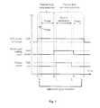
- FIG. 7shows the operation of the deposition reactor of FIG. 6 by means of a timing diagram in accordance with an example embodiment.
- the MFC 431 of the carrier and purge gas line 101is set to a processing value, preferably in the range of 10-200 sccm, more preferably in the range of 20-100 sccm, e.g., 50 sccm.
- the time between t B and t Cis used for pulsing metal precursor vapor, e.g. trimethylaluminum (TMA), in thermal ALD mode to the reaction space 331 heated to a temperature selected from a range of approximately 50-500° C., e.g. 200° C. in case of TMA used as a metal precursor.
- TMAtrimethylaluminum
- the time between t C and t Dis used for purging the reaction space 331 with inert gas that consists of argon or helium gas from the plasma source line 102 and nitrogen gas from the in-feed lines 371 , 372 .
- the pulsing valve of a (non-metal) plasma source precursoris opened.
- Oxygen gasis selected from the available plasma source gases in FIG. 6 , so at time instant t D it is the pulsing valve 414 that is opened.
- the power of the plasma generator(plasma source 110 ) is increased to the radical generation level, to the RF power selected from a range of 100-3000 W, e.g., 2000 W in case of oxygen radical generation.
- Radicalsare generated during the time between t E and t F .
- a plasma ALD phaseis carried out between time instants t E and t F .
- the power of the plasma generator(plasma source 110 ) is lowered to a level where radicals are not generated, preferably to a power that is less than 100 W, e.g. 0 W.
- the pulsing valve(here: oxygen gas valve 414 ) of the plasma source precursor is closed.
- the time between t G and t His used for purging the system with inert gas.
- the deposition cycle from the time instant t B to the time instant t H consisting of the metal precursor pulse, purge, radical precursor pulse and purgeis repeated until a thin film of desired thickness is grown on the substrate 360 .
- the deposition cyclemay be implemented in the order shown in FIG. 5 , or for example, in the order shown in FIG. 7 .
- gasis guided to flow from the inactive gas source into the radical in-feed part (or expansion space 425 ) via the plasma generator (plasma source 110 ) during the plasma precursor pulse period of the plasma ALD period, the gas during that pulse period functioning as carrier gas for generated radicals, and in certain embodiments, gas is guided to flow from the inactive gas source into the expansion space 425 via the plasma generator during the purge period of the plasma ALD period, the gas during that purge period functioning as inert or purge gas. In certain embodiments, gas is guided in this way during both of these periods. During both of these periods, gas from the inactive gas source is additionally guided in certain embodiments into the expansion space 425 via the shield gas line 204 .
- gas from the inactive gas sourceis guided in certain embodiments into the expansion space 425 via both routes, or via the shield gas line 204 only (in the event, the route from the plasma generator to the expansion space 425 is, for example, closed). Also, whenever the route from the plasma generator to the expansion space 425 is otherwise closed, gas from the inactive gas source is guided in certain embodiments during these periods into the expansion space 425 via the shield gas line 204 causing a continuous inert gas flow into the expansion space 425 and preventing the backstreaming effect. If the route from the plasma generator to the expansion space 425 is closed, gas from the inactive gas source that flows via the plasma generator is guided in certain embodiments into an evacuation line during that period so as to maintain a constant pressure in the plasma generator.
- a 100-mm silicon waferwas loaded to the reaction chamber 335 with the dual elevator shown in FIG. 3 .
- the instrumentation of the deposition reactor according to FIG. 6 and the timing diagram of FIG. 7were used for growing aluminum oxide Al 2 O 3 from trimethyl aluminum TMA and water H 2 O on the silicon wafer at 200° C.
- the flow rate of argon gaswas 30 sccm through the carrier and purge gas line 101 .
- the TMA pulse lengthwas 0.1 s followed by the 6 s purge.
- Oxygen gas pulsing valve 414was opened and 50 sccm of oxygen gas was flowing through the pulsing valve 414 to the remote plasma generator 110 .
- the RF powerwas increased from 0 W to 2500 W to switch on the plasma and kept at the 2500 W level for 6 s. After that the RF power was lowered from 2500 W to 0 W to switch off the plasma. Next the oxygen gas valve was closed and the system was purged with inert gas for 10 s. The deposition cycle was repeated until a 36-nm Al 2 O 3 thin film was grown. As a result, the 1-sigma non-uniformity of the thin film thickness measured with an ellipsometer from 49 points was only 1.3%.
- the deposition reactor described hereinis a computer-controlled system.
- a computer program stored into a memory of the systemcomprises instructions, which upon execution by at least one processor of the system cause the deposition reactor to operate as instructed.
- the instructionsmay be in the form of computer-readable program code.
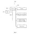
- FIG. 8shows a rough block diagram of a deposition reactor control system 800 .
- HMIhuman machine interface
- the control box 802comprises a general purpose programmable logic control (PLC) unit.
- the control box 802comprises at least one microprocessor for executing control box software comprising program code stored in a memory, dynamic and static memories, I/O modules, A/D and D/A converters and power relays.
- the control box 802sends electrical power to pneumatic controllers of the valves of the deposition reactor, and has two-way communication with mass flow controllers, and controls the operation of the plasma source and radical generation and the elevator, as well as otherwise controls the operation of the deposition reactor.
- the control box 802may measure and relay probe readings from the deposition reactor to the HMI terminal 806 .
- a dotted line 816indicates an interface line between the deposition reactor parts and the control box 802 .
Landscapes
- Chemical & Material Sciences (AREA)
- Engineering & Computer Science (AREA)
- Physics & Mathematics (AREA)
- Plasma & Fusion (AREA)
- Chemical Kinetics & Catalysis (AREA)
- Metallurgy (AREA)
- Organic Chemistry (AREA)
- Materials Engineering (AREA)
- General Chemical & Material Sciences (AREA)
- Mechanical Engineering (AREA)
- Analytical Chemistry (AREA)
- Electromagnetism (AREA)
- Inorganic Chemistry (AREA)
- Health & Medical Sciences (AREA)
- Epidemiology (AREA)
- Public Health (AREA)
- Condensed Matter Physics & Semiconductors (AREA)
- Computer Hardware Design (AREA)
- Microelectronics & Electronic Packaging (AREA)
- Power Engineering (AREA)
- Manufacturing & Machinery (AREA)
- General Physics & Mathematics (AREA)
- Chemical Vapour Deposition (AREA)
- Formation Of Insulating Films (AREA)
Abstract
Description
This patent application is a continuation application of copending U.S. patent application Ser. No. 14/009,647, filed on Oct. 3, 2013, which is a national stage entry of PCT/FI2011/050303, filed on Apr. 7, 2011, the disclosures of both applications being incorporated by reference herein in their entireties.
The present invention generally relates to deposition reactors with a plasma source. More particularly, but not exclusively, the invention relates to such deposition reactors in which material is deposited on surfaces by sequential self-saturating surface reactions.
Atomic Layer Epitaxy (ALE) method was invented by Dr. Tuomo Suntola in the early 1970's. Another generic name for the method is Atomic Layer Deposition (ALD) and it is nowadays used instead of ALE. ALD is a special chemical deposition method based on the sequential introduction of at least two reactive precursor species to a substrate. The substrate is located within a reaction space. The reaction space is typically heated. The basic growth mechanism of ALD relies on the bond strength differences between chemical adsorption (chemisorption) and physical adsorption (physisorption). ALD utilizes chemisorption and eliminates physisorption during the deposition process. During chemisorption a strong chemical bond is formed between atom(s) of a solid phase surface and a molecule that is arriving from the gas phase. Bonding by physisorption is much weaker because only van der Waals forces are involved. Physisorption bonds are easily broken by thermal energy when the local temperature is above the condensation temperature of the molecules.
The reaction space of an ALD reactor comprises all the heated surfaces that can be exposed alternately and sequentially to each of the ALD precursor used for the deposition of thin films. A basic ALD deposition cycle consists of four sequential steps: pulse A, purge A, pulse B and purge B. Pulse A typically consists of metal precursor vapor and pulse B of non-metal precursor vapor, especially nitrogen or oxygen precursor vapor. Inactive gas, such as nitrogen or argon, and a vacuum pump are used for purging gaseous reaction by-products and the residual reactant molecules from the reaction space during purge A and purge B. A deposition sequence comprises at least one deposition cycle. Deposition cycles are repeated until the deposition sequence has produced a thin film of desired thickness.
Precursor species form through chemisorption a chemical bond to reactive sites of the heated surfaces. Conditions are typically arranged in such a way that no more than a molecular monolayer of a solid material forms on the surfaces during one precursor pulse. The growth process is thus self-terminating or saturative. For example, the first precursor can include ligands that remain attached to the adsorbed species and saturate the surface, which prevents further chemisorption. Reaction space temperature is maintained above condensation temperatures and below thermal decomposition temperatures of the utilized precursors such that the precursor molecule species chemisorb on the substrate(s) essentially intact. Essentially intact means that volatile ligands may come off the precursor molecule when the precursor molecules species chemisorb on the surface. The surface becomes essentially saturated with the first type of reactive sites, i.e. adsorbed species of the first precursor molecules. This chemisorption step is typically followed by a first purge step (purge A) wherein the excess first precursor and possible reaction by-products are removed from the reaction space. Second precursor vapor is then introduced into the reaction space. Second precursor molecules typically react with the adsorbed species of the first precursor molecules, thereby forming the desired thin film material. This growth terminates once the entire amount of the adsorbed first precursor has been consumed and the surface has essentially been saturated with the second type of reactive sites. The excess of second precursor vapor and possible reaction by-product vapors are then removed by a second purge step (purge B). The cycle is then repeated until the film has grown to a desired thickness. Deposition cycles can also be more complex. For example, the cycles can include three or more reactant vapor pulses separated by purging steps. All these deposition cycles form a timed deposition sequence that is controlled by a logic unit or a microprocessor.
Thin films grown by ALD are dense, pinhole free and have uniform thickness. For example, aluminum oxide grown by thermal ALD from trimethylaluminum (CH3)3Al, also referred to as TMA, and water at 250-300° C. has usually about 1% non-uniformity over the 100-200 mm diameter wafer. Metal oxide thin films grown by ALD are suitable for gate dielectrics, electroluminescent display insulators, fill layers for magnetic read head gaps, capacitor dielectrics and passivation layers. Metal nitride thin films grown by ALD are suitable for diffusion barriers, e.g., in dual damascene structures.
Precursors suitable for ALD processes in various ALD reactors are disclosed, for example, in review article R. Puurunen, “Surface chemistry of atomic layer deposition: A case study for the trimethylaluminium/water process”, J. Appl. Phys.,97 (2005), p. 121301, which is incorporated herein by reference.
The use of radicals in ALD processes may achieve some advantages, such as the possibility to use thermally sensitive substrates at very low deposition temperatures. In a plasma ALD reactor, radicals are generated by a plasma source. The use of a plasma source, however, may cause certain requirements or specific problems for the deposition reactor.
According to a first example aspect of the invention there is provided a method comprising:
operating a plasma atomic layer deposition reactor configured to deposit material in a reaction chamber on at least one substrate by sequential self-saturating surface reactions; and
allowing gas from an inactive gas source to flow into a widening radical in-feed part opening towards the reaction chamber substantially during a whole deposition cycle.
The expression “allowing . . . to flow” may in practice mean “guiding”, “conducting” or “guiding to flow”.
In certain embodiments, the deposition reactor is a plasma enhanced atomic layer deposition reactor, a PEALD reactor. In certain embodiments, the deposition reactor comprises a plasma source on the top side of the reactor chamber. In certain embodiments, the plasma source is an inductively coupled plasma source. In certain embodiments, the plasma source produces radicals used as reactants in the deposition reactor. In certain embodiments, the activated species output of the plasma source consists of radicals. In these embodiments, the activated species output is radicals without substantially containing ions.
In certain embodiments, the plasma atomic layer deposition reactor (plasma ALD reactor) may be used for both plasma ALD and thermal ALD. The in-feed lines for thermal ALD may be separate from the plasma ALD source line via which radicals are guided into the reaction chamber.
A deposition process consists of one or more consecutive deposition cycles. Each deposition cycle may consist of a thermal ALD period followed by a plasma ALD period or a plasma ALD period followed by a thermal ALD period. Each plasma ALD period may substantially consist of a plasma ALD pulse period (radical generation period) and a subsequent plasma ALD purge period. Similarly, each thermal ALD period may substantially consist of a thermal ALD pulse period and a subsequent thermal ALD purge period. In certain embodiment, each ALD cycle may comprise more than two pulse periods (which may be followed by respective purge periods).
In certain embodiments, the method comprises:
allowing gas from the inactive gas source to flow into the radical in-feed part via a plasma source during a plasma precursor pulse period of a plasma atomic layer deposition period, the gas during that pulse period functioning as carrier gas for generated radicals.
In certain embodiments, the method comprises:
allowing gas from the inactive gas source to flow into the radical in-feed part via the plasma source during a purge period of a plasma atomic layer deposition period, the gas during that purge period functioning as purge and inert shield gas.
In certain embodiments, the method comprises:
allowing gas from the inactive gas source to flow into the radical in-feed part via the plasma source both during a plasma atomic layer deposition period and during a thermal atomic layer deposition period.
In certain embodiments, the method comprises:
allowing gas from an inactive gas source to flow into the radical in-feed part via a route that bypasses the plasma source.
In certain embodiments, the method comprises:
allowing gas from the inactive gas source to flow into the radical in-feed part via both a route travelling via the plasma source and via another route bypassing the plasma source during the plasma atomic layer deposition period.
In certain embodiments, the method comprises:
allowing gas from the inactive gas source to flow into the radical in-feed part only via the route bypassing the plasma source during the thermal atomic layer deposition period, and
guiding gas from the inactive gas source that flows via the plasma source into an evacuation line during that period.
In certain embodiments, the method comprises:
guiding inert gas towards the reaction chamber via thermal atomic layer deposition in-feed line(s) during the plasma atomic layer deposition period, the thermal atomic layer deposition in-feed line(s) being separate from plasma source line(s) via which radicals are guided into the reaction chamber during the plasma atomic layer deposition period.
Accordingly, in certain embodiments the deposition reactor may comprise two routes from an inactive gas source to the in-feed part, while in some other embodiments only a singly route is implemented. In certain embodiments, the plasma source may be separated from the reaction chamber by a gate valve or a comparable closing member closing the route via the plasma source when needed so that then the route does not continue via the in-feed part into the reaction chamber, but bypasses the reaction chamber altogether.
In certain embodiments, the method comprises using a deformable in-feed part which is deformable between a contracted shape and an extended shape by at least one mechanical actuator.
In certain embodiments, a substrate holder carrying at least one substrate is mechanically coupled to the deformable in-feed part, and the method comprises:
causing by deforming said deformable in-feed part said substrate holder carrying at least one substrate to lift into an upper position for loading or unloading.
According to a second example aspect of the invention there is provided a plasma atomic layer apparatus, comprising:
a gas line from an inactive gas source to a widening radical in-feed part opening towards a reaction chamber; and
a control system configured to allow gas from the inactive gas source to flow into in-feed part substantially during a whole deposition cycle, and
the plasma atomic layer deposition reactor being configured to deposit material in the reaction chamber on at least one substrate by sequential self-saturating surface reactions.
In certain embodiments, the apparatus or control system is configured to allow gas from the inactive gas source to flow into the radical in-feed part via a plasma source during a plasma precursor pulse period of a plasma atomic layer deposition period, the gas during that pulse period functioning as carrier gas for generated radicals.
In certain embodiments, the apparatus or control system is configured to allow gas from the inactive gas source to flow into the radical in-feed part via the plasma source during a purge period of a plasma atomic layer deposition period, the gas during that purge period functioning as purge and inert shield gas.
In certain embodiments, the apparatus or control system is configured to allow gas from the inactive gas source to flow into the radical in-feed part via the plasma source both during a plasma atomic layer deposition period and during a thermal atomic layer deposition period.
In certain embodiments, the apparatus or control system is configured to allow gas from an inactive gas source to flow into the radical in-feed part via a route that bypasses the plasma source.
In certain embodiments, the apparatus or control system is configured to allow gas from the inactive gas source to flow into the radical in-feed part via both a route travelling via the plasma source and via another route bypassing the plasma source during the plasma atomic layer deposition period.
In certain embodiments, the apparatus or control system is configured to:
allow gas from the inactive gas source to flow into the radical in-feed part only via the route bypassing the plasma source during the thermal atomic layer deposition period; and
guide gas from the inactive gas source that flows via the plasma source into an evacuation line during that period.
In certain embodiments, the apparatus or control system is configured to guide inert gas towards the reaction chamber via thermal atomic layer deposition in-feed line(s) during the plasma atomic layer deposition period, the thermal atomic layer deposition in-feed line(s) being separate from plasma source line(s) via which radicals are guided into the reaction chamber during the plasma atomic layer deposition period.
In certain embodiments, said in-feed part defining or forming the expansion space is variable in its dimensions or its shape or size. In certain embodiments, said lifting mechanism is configured to change the dimensions of said in-feed part.
In certain embodiments, said in-feed part is a part via which radicals enter the reaction chamber. In certain embodiments, said in-feed part has a contracted shape and an extended shape, the transition between these shapes being operated by a lifting mechanism (an elevator or similar). The elevator may be configured to push or pull said in-feed part from said extended shape to said contracted shape allowing said loading of said at least one substrate when said in-feed part is in its contracted shape. In certain embodiments, said in-feed part is configured to deform vertically.
In certain embodiments, said in-feed part comprises a set of nested sub-parts or ring-like members movable to fit within each other. The sub-parts may be hollow from inside. The number of nested sub-parts may be two or more to form a telescopic structure. The form of the nested sub-parts may be a truncated cone. In an embodiment, where said in-feed part practically consists of two or more sub-parts, at least the sub-part that is closest to the reaction space may be a truncated cone. In certain embodiments, said in-feed part consists of two nested sub-parts.
In certain embodiments, the in-feed part is deformable, and the apparatus comprises at least one mechanical actuator to deform the in-feed part between a contracted shape and an extended shape.
In certain embodiments, a substrate holder carrying at least one substrate is mechanically coupled to the deformable in-feed part, and wherein deforming said deformable in-feed part causes said substrate holder carrying at least one substrate to lift into an upper position for loading or unloading.
According to a third example aspect of the invention there is provided a plasma atomic layer apparatus, comprising:
means for operating a plasma atomic layer deposition reactor configured to deposit material in a reaction chamber on at least one substrate by sequential self-saturating surface reactions; and
means for allowing gas from an inactive gas source to flow into a widening radical in-feed part opening towards the reaction chamber substantially during a whole deposition cycle.
Different non-binding example aspects and embodiments of the present invention have been illustrated in the foregoing. The above embodiments are used merely to explain selected aspects or steps that may be utilized in implementations of the present invention. Some embodiments may be presented only with reference to certain example aspects of the invention. It should be appreciated that corresponding embodiments may apply to other example aspects as well. Any appropriate combinations of the embodiments may be formed.
The invention will now be described, by way of example only, with reference to the accompanying drawings, in which:
In the following description, Atomic Layer Deposition (ALD) technology is used as an example. The purpose, however, is not to strictly limit to that technology but it has to be recognized that certain embodiments may be applicable also in methods and apparatus utilizing other comparable atomic-scale deposition technologies.
The basics of an ALD growth mechanism are known to a skilled person. Details of ALD methods have also been described in the introductory portion of this patent application. These details are not repeated here but a reference is made to the introductory portion with that respect.
Theplasma source line 102 from the plasma source may be closed prior to thetransfer chamber 120 by a closing member orvalve 115, such as a gate valve or similar (hereinafter referred to the gate valve115), attached to theplasma source line 102. When thevalve 115 is open, radicals generated by theplasma source 110 from the source gas flow via theplasma source line 102 towards the reaction chamber. The radicals flow through the transfer chamberupper flange 121 into an expansion space (not shown inFIG. 1 ) that widens towards the reaction chamber. This, and other additional details, is shown in more detail inFIG. 2 . In an embodiment as shown in more detail inFIG. 6 and related description, the closing member orvalve 115 may be omitted from the construction and there is a protective inert gas (such as argon) flow from thesource gas line 101 through theplasma generator 110 towards the reaction space (331,FIG. 3 ) during the deposition process.
The expansion space is defined or formed by an in-feed part or an assembly comprising a set of nested sub-parts or ring-like members which are movable to fit within each other. In the embodiment shown inFIG. 2 , the number of sub-parts is two. The sub-parts241 and242 form a telescopic structure. In the example embodiment shown inFIG. 2 theupper sub-part 241 is attached to the transfer chamberupper flange 121. Theflange 121 may also be denoted as a vacuum chamber flange, since a vacuum or almost a vacuum can typically be generated into the portion of the transfer chamber that surrounds the in-feed part. In the example embodiment shown inFIG. 2 thelower sub-part 242 is attached to anexpansion space flange 224 which, during deposition, is substantially leak-tightly fitted against areaction chamber flange 234 preventing gas leaks between the reaction space (331,FIG. 3 ) and the gas space surrounding the reaction chamber (335,FIG. 3 ).
In the embodiment shown inFIG. 2 , a retractable shaft of anelevator 250 is attached to theexpansion space flange 224, or directly to the in-feed part. The body of theelevator 250 may also be attached to the transfer chamberupper flange 121 or to another suitable counterpart in the deposition reactor. Theelevator 250 may be for example an elevator which operates by means of a rigid retractable shaft at least partially covered withbellows 251 or similar. In an embodiment, this arrangement forms a leak-tight vertically flexible cover between a pneumatic or a linear actuator and theexpansion space flange 224 or the in-feed part. In an embodiment, a linear feedthrough for moving the in-feed part and expansion space flange together with the substrate holder in vacuum and controlled from atmosphere side is used.
The deposition reactor shown inFIG. 2 has anoptional evacuation line 207 in fluid communication with theplasma source line 102. Theevacuation line 207 is joined to theplasma source line 102 on the portion of theplasma source line 102 between theplasma source 110 and thegate valve 115.
Further, the deposition reactor shown inFIG. 2 has an optionalshield gas line 204 in fluid communication with theplasma source line 102. Inactive shield gas flowing in the shield gas line prevents particle or gas flow in the upstream direction. Theshield gas line 204 is joined to theplasma source line 102 on the portion of theplasma source line 102 after thegate valve 115, in an embodiment immediately next to thegate valve 115 in the downstream direction.
In an alternative embodiment, theexpansion space flange 224 is not separate from the in-feed part but forms part of the in-feed part thus forming a bottom part of the in-feed part. The bottom part in that embodiment functions as a rim seal against the reaction chamber. On the other hand, it functions as a fixing point for the elevator250 (elevator shaft).
In areaction space 331 ofreaction chamber 335, as shown byFIG. 3 , at least one horizontally placedsubstrate 360 is supported by or lies on asubstrate holder 361. In an embodiment, the substrate holder comprises two separate sections with an open gap wide enough for allowing free movement of a substrate fork between the sections. Thesubstrate holder 361 is attached to theexpansion space flange 224 by holder supports362. In an example embodiment, thesubstrate holder 361 is configured to move together with theexpansion space flange 224. In an embodiment, the bottom end of the elevator bellows251 is leak-tightly coupled up with the shaft. Pulling the shaft within the elevator bellows251 with the actuator contracts the elevator bellows251, and the at least onesubstrate 360 or thesubstrate holder 361 can be pulled up for loading or unloading while keeping the substrate handling area and its surroundings in vacuum. The in-feed part comprising the sub-parts241 and242 contracts vertically when the sub-part242 slides onto thesmaller sub-part 241 leaving a space for loading and unloading via the transfer chamber120 (FIG. 1 ). There can be more than one elevator, such as two elevators. The elevator bellows351 of a second elevator has been shown inFIG. 3 with dotted lines.
In an embodiment, thesubstrate holder 361 is detachably attachable to theexpansion space flange 224. In that way thesubstrate holder 361 together with the at least onesubstrate 360 can be loaded or unloaded when pulled up. Similarly, a batch of substrates vertically placed in a substrate holder can be loaded into and unloaded from the deposition reactor.
Deposition of material on the at least onesubstrate 360 occurs by alternating sequential self-saturating surface reactions in thereaction space 331 of thereaction chamber 335. Alternately, radicals from the plasma source110 (FIGS. 1 and 2 ) and other precursor vapor flow to thereaction space 331 of thereaction chamber 335. Radicals from theplasma source 110 flow as a top tobottom flow 301 via the expansion space to thereaction space 331. The other precursor vapor flow either via in-feed line 371 via an example tube fitting381 andchannel 373 within thereaction chamber flange 234 or via in-feed line 372 an example tube fitting382 andchannel 374 within thereaction chamber flange 234. In a typical reactor construction the number of in-feed lines is for example 4 or 6. Alternatively, the other precursor may also flow into thereaction chamber 335 via theplasma source line 102 with the plasma generation shut off. Exhaust gases are removed via an exhaust guide on the bottom to an exhaust line as indicated with theflow direction arrow 305.
In an embodiment, the gas space between the plasma generator (plasma source110) and thesubstrate holder 361 substantially consists of an open gas space so that the majority of radicals generated by the plasma generator is capable of arriving essentially intact to thesubstrate 360 without hitting any surfaces before the substrate.
Downstream the carrier and purgevalve 410 before entering theplasma source 110, the carrier and purge gas flows through plasma source precursor pulsing valves411-414. In an embodiment, the valves are three-way valves. The carrier and purge gas flows into a first input of a pulsing valve and outputs via an output. In this context a precursor that can flow via a pulsing valve411-414 into the carrier and purgegas line 101 and can subsequently be used to generate radicals in theplasma source 110 is denoted as plasma source precursor. The desired plasma source precursor, depending on the applied deposition cycle, is guided via an MFM (Mass Flow Meter) and through a capillary or a needle valve into a second input of a corresponding pulsing valve. During operation, the default position of valves411-414 is that the first input and output are ‘open’, the second input is ‘closed’ and will be opened only during plasma precursor pulse periods of a selected plasma source precursor.
In the embodiment shown inFIG. 4 , nitrogen gas, hydrogen gas, ammonia gas and oxygen gas serve as examples of plasma source precursors. The massflow meter MFM 441 measures the flow rate of nitrogen gas from a nitrogen gas source through a capillary orneedle valve 451 to thenitrogen pulsing valve 411. Similarly, theMFM 442 measures the flow rate of hydrogen gas from a hydrogen gas source through a capillary orneedle valve 452 to thehydrogen pulsing valve 412, theMFM 443 measures the flow rate of ammonia gas from an ammonia gas source through a capillary orneedle valve 453 to the ammonia pulsing valve413, and theMFM 444 measures the flow rate of oxygen gas from an oxygen gas source through a capillary orneedle valve 454 to theoxygen pulsing valve 414. MFMs441-444 are used for verifying that the mass flow rate of the plasma source precursor settles to a desired value controlled with the pressure of the plasma source precursor to the upstream of the capillary or needle valve451-454 and with the orifice size of the capillary or with the adjustment of needle valve451-454. When the second input of a pulsing valve is open, the corresponding plasma source precursor is mixed with the carrier gas flow and flows further towards theplasma source 110 for radical generation.
Theevacuation line 207 joined to theplasma source line 101 downstream of theplasma source 110 and upstream of thegate valve 115 is not used during normal operation. Accordingly, the default position of an evacuation valve417 (by which theevacuation line 207 can be opened and closed) is ‘closed’.
InFIG. 4 there are also shown the other in-feed lines FIG. 3 via which other precursor vapor may flow into thereaction chamber 335 during, for example, a thermal ALD period.
An alternative embodiment concerns, for example, situations in which for a certain reason theplasma source line 102 is desired to be closed by thegate valve 115 during a deposition process. This can occur, for example, during the thermal ALD phase, or if the reactor is desired to carry out a deposition process with thermal ALD phases only. In these embodiments, the route via the pulsing valves411-414 and theplasma source 110 to thereaction space 331 is closed. Since a constant pressure should preferably be maintained in theplasma source 110, theevacuation line valve 417 is opened and a gas flow through theplasma source 110 is guided via theevacuation line 207 directly to the exhaust line to maintain a constant pressure. Shield gas flowing from theshield gas line 204 forms a shielding buffer preventing particle and gas flow from rising from the direction of thereaction chamber 335 into the direction of thegate valve 115.
In certain embodiments, oxygen radicals generated from oxygen gas are used for growing metal oxides, such as oxides ofgroup 3 metals (e.g. yttrium oxide), oxides of group 4 metals (e.g. hafnium dioxide), oxides of group 5 metals (e.g. tantalum pentoxide) and oxides of group 13 metals (e.g. aluminum oxide). Ammonia radicals generated from ammonia gas and nitrogen radicals generated from nitrogen gas are used for growing metal nitrides, such as nitrides of group 4 metals (e.g. titanium nitride), nitrides of group 5 metals (e.g. tantalum nitride and superconducting niobium nitride) and nitrides of group 14 elements (e.g. silicon nitride). Hydrogen radicals generated from hydrogen gas are used as a reducing agent for growing elemental thin films, such as group 4 metals (e.g. titanium), group 5 metals (e.g. tantalum), group 6 metals (e.g. tungsten) and group 11 metals (e.g. silver). Volatile hydrocarbons are utilized for generating hydrocarbon radicals for growing metal carbides, such as carbides of group 4 metals (e.g. titanium carbide).
It is to be noted that several variants of the embodiments presented herein may be implemented. In a construction shown inFIG. 4 the deposition cycle may be implemented in the order shown inFIG. 5 , or for example, in the order shown inFIG. 7 .
In certain embodiments, gas is guided to flow from the inactive gas source into the radical in-feed part (or expansion space425) via the plasma generator (plasma source110) during the plasma precursor pulse period of the plasma ALD period, the gas during that pulse period functioning as carrier gas for generated radicals, and in certain embodiments, gas is guided to flow from the inactive gas source into theexpansion space 425 via the plasma generator during the purge period of the plasma ALD period, the gas during that purge period functioning as inert or purge gas. In certain embodiments, gas is guided in this way during both of these periods. During both of these periods, gas from the inactive gas source is additionally guided in certain embodiments into theexpansion space 425 via theshield gas line 204. During, for example, a thermal ALD period, gas from the inactive gas source is guided in certain embodiments into theexpansion space 425 via both routes, or via theshield gas line 204 only (in the event, the route from the plasma generator to theexpansion space 425 is, for example, closed). Also, whenever the route from the plasma generator to theexpansion space 425 is otherwise closed, gas from the inactive gas source is guided in certain embodiments during these periods into theexpansion space 425 via theshield gas line 204 causing a continuous inert gas flow into theexpansion space 425 and preventing the backstreaming effect. If the route from the plasma generator to theexpansion space 425 is closed, gas from the inactive gas source that flows via the plasma generator is guided in certain embodiments into an evacuation line during that period so as to maintain a constant pressure in the plasma generator.
The following experimental example further demonstrates the operation of selected example embodiments.
A 100-mm silicon wafer was loaded to thereaction chamber 335 with the dual elevator shown inFIG. 3 . The instrumentation of the deposition reactor according toFIG. 6 and the timing diagram ofFIG. 7 were used for growing aluminum oxide Al2O3from trimethyl aluminum TMA and water H2O on the silicon wafer at 200° C. The flow rate of argon gas was 30 sccm through the carrier and purgegas line 101. The TMA pulse length was 0.1 s followed by the 6 s purge. Oxygengas pulsing valve 414 was opened and 50 sccm of oxygen gas was flowing through the pulsingvalve 414 to theremote plasma generator 110. The RF power was increased from 0 W to 2500 W to switch on the plasma and kept at the 2500 W level for 6 s. After that the RF power was lowered from 2500 W to 0 W to switch off the plasma. Next the oxygen gas valve was closed and the system was purged with inert gas for 10 s. The deposition cycle was repeated until a 36-nm Al2O3thin film was grown. As a result, the 1-sigma non-uniformity of the thin film thickness measured with an ellipsometer from 49 points was only 1.3%.
In an example embodiment, the deposition reactor described herein is a computer-controlled system. A computer program stored into a memory of the system comprises instructions, which upon execution by at least one processor of the system cause the deposition reactor to operate as instructed. The instructions may be in the form of computer-readable program code.FIG. 8 shows a rough block diagram of a depositionreactor control system 800. In a basic system setup process parameters are programmed with the aid of software and instructions are executed with a human machine interface (HMI)terminal 806 and downloaded viaEthernet bus 804 to acontrol box 802. In an embodiment, thecontrol box 802 comprises a general purpose programmable logic control (PLC) unit. Thecontrol box 802 comprises at least one microprocessor for executing control box software comprising program code stored in a memory, dynamic and static memories, I/O modules, A/D and D/A converters and power relays. Thecontrol box 802 sends electrical power to pneumatic controllers of the valves of the deposition reactor, and has two-way communication with mass flow controllers, and controls the operation of the plasma source and radical generation and the elevator, as well as otherwise controls the operation of the deposition reactor. Thecontrol box 802 may measure and relay probe readings from the deposition reactor to theHMI terminal 806. A dottedline 816 indicates an interface line between the deposition reactor parts and thecontrol box 802.
The foregoing description has provided by way of non-limiting examples of particular implementations and embodiments of the invention a full and informative description of the best mode presently contemplated by the inventors for carrying out the invention. It is however clear to a person skilled in the art that the invention is not restricted to details of the embodiments presented above, but that it can be implemented in other embodiments using equivalent means without deviating from the characteristics of the invention.
Furthermore, some of the features of the above-disclosed embodiments of this invention may be used to advantage without the corresponding use of other features. As such, the foregoing description should be considered as merely illustrative of the principles of the present invention, and not in limitation thereof. Hence, the scope of the invention is only restricted by the appended patent claims.
Claims (11)
1. A method comprising:
operating a plasma atomic layer deposition reactor configured to deposit material in a reaction chamber on at least one substrate by sequential self-saturating surface reactions; and
allowing gas from an inactive gas source to flow into a widening radical in-feed part opening towards the reaction chamber substantially during a whole deposition cycle, the widening radical in-feed part being a deformable in-feed part; and
using the deformable in-feed part which is deformable between a contracted shape and an extended shape by at least one mechanical actuator.
2. The method ofclaim 1 , comprising:
allowing gas from the inactive gas source to flow into the radical in-feed part via a plasma source during a plasma precursor pulse period of a plasma atomic layer deposition period, the gas during that pulse period functioning as carrier gas for generated radicals.
3. The method ofclaim 1 , comprising:
allowing gas from the inactive gas source to flow into the radical in-feed part via the plasma source during a purge period of a plasma atomic layer deposition period, the gas during that purge period functioning as purge and inert shield gas.
4. The method ofclaim 1 , comprising:
allowing gas from an inactive gas source to flow into the radical in-feed part via a route that bypasses the plasma source.
5. The method ofclaim 1 , wherein a substrate holder carrying at least one substrate is mechanically coupled to the deformable in-feed part, the method comprising:
causing by deforming said deformable in-feed part said substrate holder carrying at least one substrate to lift into an upper position for loading or unloading.
6. A plasma atomic layer apparatus, comprising:
a gas line from an inactive gas source to a widening radical in-feed part opening towards a reaction chamber; and
a control system configured to allow gas from the inactive gas source to flow into in-feed part substantially during a whole deposition cycle, and
the plasma atomic layer deposition reactor being configured to deposit material in the reaction chamber on at least one substrate by sequential self-saturating surface reactions;
wherein said widening radical in-feed part is deformable, and the apparatus comprises at least one mechanical actuator to deform the in-feed part between a contracted shape and an extended shape.
7. The apparatus ofclaim 6 , wherein the control system is configured to allow gas from the inactive gas source to flow into the radical in-feed part via a plasma source during a plasma precursor pulse period of a plasma atomic layer deposition period, the gas during that pulse period functioning as carrier gas for generated radicals.
8. The apparatus ofclaim 6 , wherein the control system is configured to allow gas from the inactive gas source to flow into the radical in-feed part via the plasma source during a purge period of a plasma atomic layer deposition period, the gas during that purge period functioning as purge and inert shield gas.
9. The apparatus ofclaim 6 , wherein the control system is configured to allow gas from an inactive gas source to flow into the radical in-feed part via a route that bypasses the plasma source.
10. The apparatus ofclaim 6 , wherein a substrate holder carrying at least one substrate is mechanically coupled to the deformable in-feed part, and wherein deforming said deformable in-feed part causes said substrate holder carrying at least one substrate to lift into an upper position for loading or unloading.
11. A method, comprising:
operating a plasma atomic layer deposition reactor configured to deposit material in a reaction chamber on at least one substrate by sequential self-saturating surface reactions;
allowing gas from an inactive gas source to flow into a widening radical in-feed part opening towards the reaction chamber substantially during a whole deposition cycle;
providing the deposition reactor with an elevator coupled to the in-feed part; and
deforming the in-feed part by the elevator so as to allow loading of the at least one substrate into the reaction chamber.
Priority Applications (2)
| Application Number | Priority Date | Filing Date | Title |
|---|---|---|---|
| US14/794,159US9868131B2 (en) | 2011-04-07 | 2015-07-08 | Atomic layer deposition with plasma source |
| US15/840,007US12383923B2 (en) | 2011-04-07 | 2017-12-13 | Atomic layer deposition with plasma source |
Applications Claiming Priority (3)
| Application Number | Priority Date | Filing Date | Title |
|---|---|---|---|
| PCT/FI2011/050303WO2012136876A1 (en) | 2011-04-07 | 2011-04-07 | Atomic layer deposition with plasma source |
| US201314009647A | 2013-10-03 | 2013-10-03 | |
| US14/794,159US9868131B2 (en) | 2011-04-07 | 2015-07-08 | Atomic layer deposition with plasma source |
Related Parent Applications (2)
| Application Number | Title | Priority Date | Filing Date |
|---|---|---|---|
| US14/009,647ContinuationUS9095869B2 (en) | 2011-04-07 | 2011-04-07 | Atomic layer deposition with plasma source |
| PCT/FI2011/050303ContinuationWO2012136876A1 (en) | 2011-04-07 | 2011-04-07 | Atomic layer deposition with plasma source |
Related Child Applications (1)
| Application Number | Title | Priority Date | Filing Date |
|---|---|---|---|
| US15/840,007ContinuationUS12383923B2 (en) | 2011-04-07 | 2017-12-13 | Atomic layer deposition with plasma source |
Publications (2)
| Publication Number | Publication Date |
|---|---|
| US20150322569A1 US20150322569A1 (en) | 2015-11-12 |
| US9868131B2true US9868131B2 (en) | 2018-01-16 |
Family
ID=46968647
Family Applications (3)
| Application Number | Title | Priority Date | Filing Date |
|---|---|---|---|
| US14/009,647Active2031-05-15US9095869B2 (en) | 2011-04-07 | 2011-04-07 | Atomic layer deposition with plasma source |
| US14/794,159Active2031-08-08US9868131B2 (en) | 2011-04-07 | 2015-07-08 | Atomic layer deposition with plasma source |
| US15/840,007Active2032-12-23US12383923B2 (en) | 2011-04-07 | 2017-12-13 | Atomic layer deposition with plasma source |
Family Applications Before (1)
| Application Number | Title | Priority Date | Filing Date |
|---|---|---|---|
| US14/009,647Active2031-05-15US9095869B2 (en) | 2011-04-07 | 2011-04-07 | Atomic layer deposition with plasma source |
Family Applications After (1)
| Application Number | Title | Priority Date | Filing Date |
|---|---|---|---|
| US15/840,007Active2032-12-23US12383923B2 (en) | 2011-04-07 | 2017-12-13 | Atomic layer deposition with plasma source |
Country Status (9)
| Country | Link |
|---|---|
| US (3) | US9095869B2 (en) |
| EP (1) | EP2694700B1 (en) |
| JP (1) | JP5919371B2 (en) |
| KR (3) | KR102111702B1 (en) |
| CN (1) | CN103635605B (en) |
| RU (1) | RU2584841C2 (en) |
| SG (1) | SG11201405416UA (en) |
| TW (1) | TWI565824B (en) |
| WO (1) | WO2012136876A1 (en) |
Cited By (320)
| Publication number | Priority date | Publication date | Assignee | Title |
|---|---|---|---|---|
| US20180099304A1 (en)* | 2011-04-07 | 2018-04-12 | Picosun Oy | Atomic Layer Deposition with Plasma Source |
| US10559458B1 (en) | 2018-11-26 | 2020-02-11 | Asm Ip Holding B.V. | Method of forming oxynitride film |
| US10561975B2 (en) | 2014-10-07 | 2020-02-18 | Asm Ip Holdings B.V. | Variable conductance gas distribution apparatus and method |
| USD876504S1 (en) | 2017-04-03 | 2020-02-25 | Asm Ip Holding B.V. | Exhaust flow control ring for semiconductor deposition apparatus |
| US10590535B2 (en) | 2017-07-26 | 2020-03-17 | Asm Ip Holdings B.V. | Chemical treatment, deposition and/or infiltration apparatus and method for using the same |
| US10600673B2 (en) | 2015-07-07 | 2020-03-24 | Asm Ip Holding B.V. | Magnetic susceptor to baseplate seal |
| US10604847B2 (en) | 2014-03-18 | 2020-03-31 | Asm Ip Holding B.V. | Gas distribution system, reactor including the system, and methods of using the same |
| US10612136B2 (en) | 2018-06-29 | 2020-04-07 | ASM IP Holding, B.V. | Temperature-controlled flange and reactor system including same |
| US10622375B2 (en) | 2016-11-07 | 2020-04-14 | Asm Ip Holding B.V. | Method of processing a substrate and a device manufactured by using the method |
| US10643904B2 (en) | 2016-11-01 | 2020-05-05 | Asm Ip Holdings B.V. | Methods for forming a semiconductor device and related semiconductor device structures |
| US10643826B2 (en) | 2016-10-26 | 2020-05-05 | Asm Ip Holdings B.V. | Methods for thermally calibrating reaction chambers |
| US10658181B2 (en) | 2018-02-20 | 2020-05-19 | Asm Ip Holding B.V. | Method of spacer-defined direct patterning in semiconductor fabrication |
| US10655221B2 (en)* | 2017-02-09 | 2020-05-19 | Asm Ip Holding B.V. | Method for depositing oxide film by thermal ALD and PEALD |
| US10658205B2 (en) | 2017-09-28 | 2020-05-19 | Asm Ip Holdings B.V. | Chemical dispensing apparatus and methods for dispensing a chemical to a reaction chamber |
| US10665452B2 (en) | 2016-05-02 | 2020-05-26 | Asm Ip Holdings B.V. | Source/drain performance through conformal solid state doping |
| US10672636B2 (en) | 2017-08-09 | 2020-06-02 | Asm Ip Holding B.V. | Cassette holder assembly for a substrate cassette and holding member for use in such assembly |
| US10685834B2 (en) | 2017-07-05 | 2020-06-16 | Asm Ip Holdings B.V. | Methods for forming a silicon germanium tin layer and related semiconductor device structures |
| US10683571B2 (en) | 2014-02-25 | 2020-06-16 | Asm Ip Holding B.V. | Gas supply manifold and method of supplying gases to chamber using same |
| US10692741B2 (en) | 2017-08-08 | 2020-06-23 | Asm Ip Holdings B.V. | Radiation shield |
| US10707106B2 (en) | 2011-06-06 | 2020-07-07 | Asm Ip Holding B.V. | High-throughput semiconductor-processing apparatus equipped with multiple dual-chamber modules |
| US10714315B2 (en) | 2012-10-12 | 2020-07-14 | Asm Ip Holdings B.V. | Semiconductor reaction chamber showerhead |
| US10714335B2 (en) | 2017-04-25 | 2020-07-14 | Asm Ip Holding B.V. | Method of depositing thin film and method of manufacturing semiconductor device |
| US10714385B2 (en) | 2016-07-19 | 2020-07-14 | Asm Ip Holding B.V. | Selective deposition of tungsten |
| US10714350B2 (en) | 2016-11-01 | 2020-07-14 | ASM IP Holdings, B.V. | Methods for forming a transition metal niobium nitride film on a substrate by atomic layer deposition and related semiconductor device structures |
| US10720322B2 (en) | 2016-02-19 | 2020-07-21 | Asm Ip Holding B.V. | Method for forming silicon nitride film selectively on top surface |
| US10720331B2 (en) | 2016-11-01 | 2020-07-21 | ASM IP Holdings, B.V. | Methods for forming a transition metal nitride film on a substrate by atomic layer deposition and related semiconductor device structures |
| US10734244B2 (en) | 2017-11-16 | 2020-08-04 | Asm Ip Holding B.V. | Method of processing a substrate and a device manufactured by the same |
| US10734497B2 (en) | 2017-07-18 | 2020-08-04 | Asm Ip Holding B.V. | Methods for forming a semiconductor device structure and related semiconductor device structures |
| US10731249B2 (en) | 2018-02-15 | 2020-08-04 | Asm Ip Holding B.V. | Method of forming a transition metal containing film on a substrate by a cyclical deposition process, a method for supplying a transition metal halide compound to a reaction chamber, and related vapor deposition apparatus |
| US10734223B2 (en) | 2017-10-10 | 2020-08-04 | Asm Ip Holding B.V. | Method for depositing a metal chalcogenide on a substrate by cyclical deposition |
| US10741385B2 (en) | 2016-07-28 | 2020-08-11 | Asm Ip Holding B.V. | Method and apparatus for filling a gap |
| US10755922B2 (en) | 2018-07-03 | 2020-08-25 | Asm Ip Holding B.V. | Method for depositing silicon-free carbon-containing film as gap-fill layer by pulse plasma-assisted deposition |
| US10755923B2 (en) | 2018-07-03 | 2020-08-25 | Asm Ip Holding B.V. | Method for depositing silicon-free carbon-containing film as gap-fill layer by pulse plasma-assisted deposition |
| US10770336B2 (en) | 2017-08-08 | 2020-09-08 | Asm Ip Holding B.V. | Substrate lift mechanism and reactor including same |
| US10770286B2 (en) | 2017-05-08 | 2020-09-08 | Asm Ip Holdings B.V. | Methods for selectively forming a silicon nitride film on a substrate and related semiconductor device structures |
| US10767789B2 (en) | 2018-07-16 | 2020-09-08 | Asm Ip Holding B.V. | Diaphragm valves, valve components, and methods for forming valve components |
| US10784102B2 (en) | 2016-12-22 | 2020-09-22 | Asm Ip Holding B.V. | Method of forming a structure on a substrate |
| US10787741B2 (en) | 2014-08-21 | 2020-09-29 | Asm Ip Holding B.V. | Method and system for in situ formation of gas-phase compounds |
| US10797133B2 (en) | 2018-06-21 | 2020-10-06 | Asm Ip Holding B.V. | Method for depositing a phosphorus doped silicon arsenide film and related semiconductor device structures |
| US10804098B2 (en) | 2009-08-14 | 2020-10-13 | Asm Ip Holding B.V. | Systems and methods for thin-film deposition of metal oxides using excited nitrogen-oxygen species |
| US10811256B2 (en) | 2018-10-16 | 2020-10-20 | Asm Ip Holding B.V. | Method for etching a carbon-containing feature |
| USD900036S1 (en) | 2017-08-24 | 2020-10-27 | Asm Ip Holding B.V. | Heater electrical connector and adapter |
| US10818758B2 (en) | 2018-11-16 | 2020-10-27 | Asm Ip Holding B.V. | Methods for forming a metal silicate film on a substrate in a reaction chamber and related semiconductor device structures |
| US10829852B2 (en) | 2018-08-16 | 2020-11-10 | Asm Ip Holding B.V. | Gas distribution device for a wafer processing apparatus |
| US10832903B2 (en) | 2011-10-28 | 2020-11-10 | Asm Ip Holding B.V. | Process feed management for semiconductor substrate processing |
| US10847365B2 (en) | 2018-10-11 | 2020-11-24 | Asm Ip Holding B.V. | Method of forming conformal silicon carbide film by cyclic CVD |
| US10844486B2 (en) | 2009-04-06 | 2020-11-24 | Asm Ip Holding B.V. | Semiconductor processing reactor and components thereof |
| US10847366B2 (en) | 2018-11-16 | 2020-11-24 | Asm Ip Holding B.V. | Methods for depositing a transition metal chalcogenide film on a substrate by a cyclical deposition process |
| US10847371B2 (en) | 2018-03-27 | 2020-11-24 | Asm Ip Holding B.V. | Method of forming an electrode on a substrate and a semiconductor device structure including an electrode |
| US10844484B2 (en) | 2017-09-22 | 2020-11-24 | Asm Ip Holding B.V. | Apparatus for dispensing a vapor phase reactant to a reaction chamber and related methods |
| US10854498B2 (en) | 2011-07-15 | 2020-12-01 | Asm Ip Holding B.V. | Wafer-supporting device and method for producing same |
| US10851456B2 (en) | 2016-04-21 | 2020-12-01 | Asm Ip Holding B.V. | Deposition of metal borides |
| USD903477S1 (en) | 2018-01-24 | 2020-12-01 | Asm Ip Holdings B.V. | Metal clamp |
| US10858737B2 (en) | 2014-07-28 | 2020-12-08 | Asm Ip Holding B.V. | Showerhead assembly and components thereof |
| US10865475B2 (en) | 2016-04-21 | 2020-12-15 | Asm Ip Holding B.V. | Deposition of metal borides and silicides |
| US10867788B2 (en) | 2016-12-28 | 2020-12-15 | Asm Ip Holding B.V. | Method of forming a structure on a substrate |
| US10867786B2 (en) | 2018-03-30 | 2020-12-15 | Asm Ip Holding B.V. | Substrate processing method |
| US10872771B2 (en) | 2018-01-16 | 2020-12-22 | Asm Ip Holding B. V. | Method for depositing a material film on a substrate within a reaction chamber by a cyclical deposition process and related device structures |
| US10883175B2 (en) | 2018-08-09 | 2021-01-05 | Asm Ip Holding B.V. | Vertical furnace for processing substrates and a liner for use therein |
| US10892156B2 (en) | 2017-05-08 | 2021-01-12 | Asm Ip Holding B.V. | Methods for forming a silicon nitride film on a substrate and related semiconductor device structures |
| US10896820B2 (en) | 2018-02-14 | 2021-01-19 | Asm Ip Holding B.V. | Method for depositing a ruthenium-containing film on a substrate by a cyclical deposition process |
| US10910262B2 (en) | 2017-11-16 | 2021-02-02 | Asm Ip Holding B.V. | Method of selectively depositing a capping layer structure on a semiconductor device structure |
| US10914004B2 (en) | 2018-06-29 | 2021-02-09 | Asm Ip Holding B.V. | Thin-film deposition method and manufacturing method of semiconductor device |
| US10923344B2 (en) | 2017-10-30 | 2021-02-16 | Asm Ip Holding B.V. | Methods for forming a semiconductor structure and related semiconductor structures |
| US10928731B2 (en) | 2017-09-21 | 2021-02-23 | Asm Ip Holding B.V. | Method of sequential infiltration synthesis treatment of infiltrateable material and structures and devices formed using same |
| US10934619B2 (en) | 2016-11-15 | 2021-03-02 | Asm Ip Holding B.V. | Gas supply unit and substrate processing apparatus including the gas supply unit |
| US10941490B2 (en) | 2014-10-07 | 2021-03-09 | Asm Ip Holding B.V. | Multiple temperature range susceptor, assembly, reactor and system including the susceptor, and methods of using the same |
| USD913980S1 (en) | 2018-02-01 | 2021-03-23 | Asm Ip Holding B.V. | Gas supply plate for semiconductor manufacturing apparatus |
| US10975470B2 (en) | 2018-02-23 | 2021-04-13 | Asm Ip Holding B.V. | Apparatus for detecting or monitoring for a chemical precursor in a high temperature environment |
| US11004977B2 (en) | 2017-07-19 | 2021-05-11 | Asm Ip Holding B.V. | Method for depositing a group IV semiconductor and related semiconductor device structures |
| US11001925B2 (en) | 2016-12-19 | 2021-05-11 | Asm Ip Holding B.V. | Substrate processing apparatus |
| US11018002B2 (en) | 2017-07-19 | 2021-05-25 | Asm Ip Holding B.V. | Method for selectively depositing a Group IV semiconductor and related semiconductor device structures |
| US11015245B2 (en) | 2014-03-19 | 2021-05-25 | Asm Ip Holding B.V. | Gas-phase reactor and system having exhaust plenum and components thereof |
| US11018047B2 (en) | 2018-01-25 | 2021-05-25 | Asm Ip Holding B.V. | Hybrid lift pin |
| US11022879B2 (en) | 2017-11-24 | 2021-06-01 | Asm Ip Holding B.V. | Method of forming an enhanced unexposed photoresist layer |
| US11024523B2 (en) | 2018-09-11 | 2021-06-01 | Asm Ip Holding B.V. | Substrate processing apparatus and method |
| US11031242B2 (en) | 2018-11-07 | 2021-06-08 | Asm Ip Holding B.V. | Methods for depositing a boron doped silicon germanium film |
| USD922229S1 (en) | 2019-06-05 | 2021-06-15 | Asm Ip Holding B.V. | Device for controlling a temperature of a gas supply unit |
| US11049751B2 (en) | 2018-09-14 | 2021-06-29 | Asm Ip Holding B.V. | Cassette supply system to store and handle cassettes and processing apparatus equipped therewith |
| US11056567B2 (en) | 2018-05-11 | 2021-07-06 | Asm Ip Holding B.V. | Method of forming a doped metal carbide film on a substrate and related semiconductor device structures |
| US11056344B2 (en) | 2017-08-30 | 2021-07-06 | Asm Ip Holding B.V. | Layer forming method |
| US11053591B2 (en) | 2018-08-06 | 2021-07-06 | Asm Ip Holding B.V. | Multi-port gas injection system and reactor system including same |
| US11069510B2 (en) | 2017-08-30 | 2021-07-20 | Asm Ip Holding B.V. | Substrate processing apparatus |
| US11081345B2 (en) | 2018-02-06 | 2021-08-03 | Asm Ip Holding B.V. | Method of post-deposition treatment for silicon oxide film |
| US11087997B2 (en) | 2018-10-31 | 2021-08-10 | Asm Ip Holding B.V. | Substrate processing apparatus for processing substrates |
| US11088002B2 (en) | 2018-03-29 | 2021-08-10 | Asm Ip Holding B.V. | Substrate rack and a substrate processing system and method |
| US11094546B2 (en) | 2017-10-05 | 2021-08-17 | Asm Ip Holding B.V. | Method for selectively depositing a metallic film on a substrate |
| US11094582B2 (en) | 2016-07-08 | 2021-08-17 | Asm Ip Holding B.V. | Selective deposition method to form air gaps |
| US11101370B2 (en) | 2016-05-02 | 2021-08-24 | Asm Ip Holding B.V. | Method of forming a germanium oxynitride film |
| US11114294B2 (en) | 2019-03-08 | 2021-09-07 | Asm Ip Holding B.V. | Structure including SiOC layer and method of forming same |
| US11114283B2 (en) | 2018-03-16 | 2021-09-07 | Asm Ip Holding B.V. | Reactor, system including the reactor, and methods of manufacturing and using same |
| USD930782S1 (en) | 2019-08-22 | 2021-09-14 | Asm Ip Holding B.V. | Gas distributor |
| US11127589B2 (en) | 2019-02-01 | 2021-09-21 | Asm Ip Holding B.V. | Method of topology-selective film formation of silicon oxide |
| US11127617B2 (en) | 2017-11-27 | 2021-09-21 | Asm Ip Holding B.V. | Storage device for storing wafer cassettes for use with a batch furnace |
| USD931978S1 (en) | 2019-06-27 | 2021-09-28 | Asm Ip Holding B.V. | Showerhead vacuum transport |
| US11139308B2 (en) | 2015-12-29 | 2021-10-05 | Asm Ip Holding B.V. | Atomic layer deposition of III-V compounds to form V-NAND devices |
| US11139191B2 (en) | 2017-08-09 | 2021-10-05 | Asm Ip Holding B.V. | Storage apparatus for storing cassettes for substrates and processing apparatus equipped therewith |
| US11158513B2 (en) | 2018-12-13 | 2021-10-26 | Asm Ip Holding B.V. | Methods for forming a rhenium-containing film on a substrate by a cyclical deposition process and related semiconductor device structures |
| USD935572S1 (en) | 2019-05-24 | 2021-11-09 | Asm Ip Holding B.V. | Gas channel plate |
| US11171025B2 (en) | 2019-01-22 | 2021-11-09 | Asm Ip Holding B.V. | Substrate processing device |
| US11205585B2 (en) | 2016-07-28 | 2021-12-21 | Asm Ip Holding B.V. | Substrate processing apparatus and method of operating the same |
| US11217444B2 (en) | 2018-11-30 | 2022-01-04 | Asm Ip Holding B.V. | Method for forming an ultraviolet radiation responsive metal oxide-containing film |
| USD940837S1 (en) | 2019-08-22 | 2022-01-11 | Asm Ip Holding B.V. | Electrode |
| US11222772B2 (en) | 2016-12-14 | 2022-01-11 | Asm Ip Holding B.V. | Substrate processing apparatus |
| US11227789B2 (en) | 2019-02-20 | 2022-01-18 | Asm Ip Holding B.V. | Method and apparatus for filling a recess formed within a substrate surface |
| US11227782B2 (en) | 2019-07-31 | 2022-01-18 | Asm Ip Holding B.V. | Vertical batch furnace assembly |
| US11232963B2 (en) | 2018-10-03 | 2022-01-25 | Asm Ip Holding B.V. | Substrate processing apparatus and method |
| US11230766B2 (en) | 2018-03-29 | 2022-01-25 | Asm Ip Holding B.V. | Substrate processing apparatus and method |
| US11233133B2 (en) | 2015-10-21 | 2022-01-25 | Asm Ip Holding B.V. | NbMC layers |
| US11242598B2 (en) | 2015-06-26 | 2022-02-08 | Asm Ip Holding B.V. | Structures including metal carbide material, devices including the structures, and methods of forming same |
| US11251068B2 (en) | 2018-10-19 | 2022-02-15 | Asm Ip Holding B.V. | Substrate processing apparatus and substrate processing method |
| US11251040B2 (en) | 2019-02-20 | 2022-02-15 | Asm Ip Holding B.V. | Cyclical deposition method including treatment step and apparatus for same |
| USD944946S1 (en) | 2019-06-14 | 2022-03-01 | Asm Ip Holding B.V. | Shower plate |
| US11270899B2 (en) | 2018-06-04 | 2022-03-08 | Asm Ip Holding B.V. | Wafer handling chamber with moisture reduction |
| US11274369B2 (en) | 2018-09-11 | 2022-03-15 | Asm Ip Holding B.V. | Thin film deposition method |
| US11282698B2 (en) | 2019-07-19 | 2022-03-22 | Asm Ip Holding B.V. | Method of forming topology-controlled amorphous carbon polymer film |
| US11289326B2 (en) | 2019-05-07 | 2022-03-29 | Asm Ip Holding B.V. | Method for reforming amorphous carbon polymer film |
| US11286562B2 (en) | 2018-06-08 | 2022-03-29 | Asm Ip Holding B.V. | Gas-phase chemical reactor and method of using same |
| US11286558B2 (en) | 2019-08-23 | 2022-03-29 | Asm Ip Holding B.V. | Methods for depositing a molybdenum nitride film on a surface of a substrate by a cyclical deposition process and related semiconductor device structures including a molybdenum nitride film |
| USD947913S1 (en) | 2019-05-17 | 2022-04-05 | Asm Ip Holding B.V. | Susceptor shaft |
| US11295980B2 (en) | 2017-08-30 | 2022-04-05 | Asm Ip Holding B.V. | Methods for depositing a molybdenum metal film over a dielectric surface of a substrate by a cyclical deposition process and related semiconductor device structures |
| USD948463S1 (en) | 2018-10-24 | 2022-04-12 | Asm Ip Holding B.V. | Susceptor for semiconductor substrate supporting apparatus |
| USD949319S1 (en) | 2019-08-22 | 2022-04-19 | Asm Ip Holding B.V. | Exhaust duct |
| US11306395B2 (en) | 2017-06-28 | 2022-04-19 | Asm Ip Holding B.V. | Methods for depositing a transition metal nitride film on a substrate by atomic layer deposition and related deposition apparatus |
| US11315794B2 (en) | 2019-10-21 | 2022-04-26 | Asm Ip Holding B.V. | Apparatus and methods for selectively etching films |
| US11339476B2 (en) | 2019-10-08 | 2022-05-24 | Asm Ip Holding B.V. | Substrate processing device having connection plates, substrate processing method |
| US11342216B2 (en) | 2019-02-20 | 2022-05-24 | Asm Ip Holding B.V. | Cyclical deposition method and apparatus for filling a recess formed within a substrate surface |
| US11345999B2 (en) | 2019-06-06 | 2022-05-31 | Asm Ip Holding B.V. | Method of using a gas-phase reactor system including analyzing exhausted gas |
| US11355338B2 (en) | 2019-05-10 | 2022-06-07 | Asm Ip Holding B.V. | Method of depositing material onto a surface and structure formed according to the method |
| US11361990B2 (en) | 2018-05-28 | 2022-06-14 | Asm Ip Holding B.V. | Substrate processing method and device manufactured by using the same |
| US11374112B2 (en) | 2017-07-19 | 2022-06-28 | Asm Ip Holding B.V. | Method for depositing a group IV semiconductor and related semiconductor device structures |
| US11378337B2 (en) | 2019-03-28 | 2022-07-05 | Asm Ip Holding B.V. | Door opener and substrate processing apparatus provided therewith |
| US11390945B2 (en) | 2019-07-03 | 2022-07-19 | Asm Ip Holding B.V. | Temperature control assembly for substrate processing apparatus and method of using same |
| US11390946B2 (en) | 2019-01-17 | 2022-07-19 | Asm Ip Holding B.V. | Methods of forming a transition metal containing film on a substrate by a cyclical deposition process |
| US11390950B2 (en) | 2017-01-10 | 2022-07-19 | Asm Ip Holding B.V. | Reactor system and method to reduce residue buildup during a film deposition process |
| US11393690B2 (en) | 2018-01-19 | 2022-07-19 | Asm Ip Holding B.V. | Deposition method |
| US11401605B2 (en) | 2019-11-26 | 2022-08-02 | Asm Ip Holding B.V. | Substrate processing apparatus |
| US11410851B2 (en) | 2017-02-15 | 2022-08-09 | Asm Ip Holding B.V. | Methods for forming a metallic film on a substrate by cyclical deposition and related semiconductor device structures |
| US11414760B2 (en) | 2018-10-08 | 2022-08-16 | Asm Ip Holding B.V. | Substrate support unit, thin film deposition apparatus including the same, and substrate processing apparatus including the same |
| US11424119B2 (en) | 2019-03-08 | 2022-08-23 | Asm Ip Holding B.V. | Method for selective deposition of silicon nitride layer and structure including selectively-deposited silicon nitride layer |
| US11430674B2 (en) | 2018-08-22 | 2022-08-30 | Asm Ip Holding B.V. | Sensor array, apparatus for dispensing a vapor phase reactant to a reaction chamber and related methods |
| US11430640B2 (en) | 2019-07-30 | 2022-08-30 | Asm Ip Holding B.V. | Substrate processing apparatus |
| US11437241B2 (en) | 2020-04-08 | 2022-09-06 | Asm Ip Holding B.V. | Apparatus and methods for selectively etching silicon oxide films |
| US11443926B2 (en) | 2019-07-30 | 2022-09-13 | Asm Ip Holding B.V. | Substrate processing apparatus |
| US11447861B2 (en) | 2016-12-15 | 2022-09-20 | Asm Ip Holding B.V. | Sequential infiltration synthesis apparatus and a method of forming a patterned structure |
| US11447864B2 (en) | 2019-04-19 | 2022-09-20 | Asm Ip Holding B.V. | Layer forming method and apparatus |
| USD965044S1 (en) | 2019-08-19 | 2022-09-27 | Asm Ip Holding B.V. | Susceptor shaft |
| US11453943B2 (en) | 2016-05-25 | 2022-09-27 | Asm Ip Holding B.V. | Method for forming carbon-containing silicon/metal oxide or nitride film by ALD using silicon precursor and hydrocarbon precursor |
| USD965524S1 (en) | 2019-08-19 | 2022-10-04 | Asm Ip Holding B.V. | Susceptor support |
| US11469098B2 (en) | 2018-05-08 | 2022-10-11 | Asm Ip Holding B.V. | Methods for depositing an oxide film on a substrate by a cyclical deposition process and related device structures |
| US11473195B2 (en) | 2018-03-01 | 2022-10-18 | Asm Ip Holding B.V. | Semiconductor processing apparatus and a method for processing a substrate |
| US11476109B2 (en) | 2019-06-11 | 2022-10-18 | Asm Ip Holding B.V. | Method of forming an electronic structure using reforming gas, system for performing the method, and structure formed using the method |
| US11482533B2 (en) | 2019-02-20 | 2022-10-25 | Asm Ip Holding B.V. | Apparatus and methods for plug fill deposition in 3-D NAND applications |
| US11482412B2 (en) | 2018-01-19 | 2022-10-25 | Asm Ip Holding B.V. | Method for depositing a gap-fill layer by plasma-assisted deposition |
| US11482418B2 (en) | 2018-02-20 | 2022-10-25 | Asm Ip Holding B.V. | Substrate processing method and apparatus |
| US11488854B2 (en) | 2020-03-11 | 2022-11-01 | Asm Ip Holding B.V. | Substrate handling device with adjustable joints |
| US11488819B2 (en) | 2018-12-04 | 2022-11-01 | Asm Ip Holding B.V. | Method of cleaning substrate processing apparatus |
| US11492703B2 (en) | 2018-06-27 | 2022-11-08 | Asm Ip Holding B.V. | Cyclic deposition methods for forming metal-containing material and films and structures including the metal-containing material |
| US11495459B2 (en) | 2019-09-04 | 2022-11-08 | Asm Ip Holding B.V. | Methods for selective deposition using a sacrificial capping layer |
| US11499222B2 (en) | 2018-06-27 | 2022-11-15 | Asm Ip Holding B.V. | Cyclic deposition methods for forming metal-containing material and films and structures including the metal-containing material |
| US11501968B2 (en) | 2019-11-15 | 2022-11-15 | Asm Ip Holding B.V. | Method for providing a semiconductor device with silicon filled gaps |
| US11499226B2 (en) | 2018-11-02 | 2022-11-15 | Asm Ip Holding B.V. | Substrate supporting unit and a substrate processing device including the same |
| US11515187B2 (en) | 2020-05-01 | 2022-11-29 | Asm Ip Holding B.V. | Fast FOUP swapping with a FOUP handler |
| US11515188B2 (en) | 2019-05-16 | 2022-11-29 | Asm Ip Holding B.V. | Wafer boat handling device, vertical batch furnace and method |
| US11521851B2 (en) | 2020-02-03 | 2022-12-06 | Asm Ip Holding B.V. | Method of forming structures including a vanadium or indium layer |
| US11527403B2 (en) | 2019-12-19 | 2022-12-13 | Asm Ip Holding B.V. | Methods for filling a gap feature on a substrate surface and related semiconductor structures |
| US11527400B2 (en) | 2019-08-23 | 2022-12-13 | Asm Ip Holding B.V. | Method for depositing silicon oxide film having improved quality by peald using bis(diethylamino)silane |
| US11532757B2 (en) | 2016-10-27 | 2022-12-20 | Asm Ip Holding B.V. | Deposition of charge trapping layers |
| US11530876B2 (en) | 2020-04-24 | 2022-12-20 | Asm Ip Holding B.V. | Vertical batch furnace assembly comprising a cooling gas supply |
| US11530483B2 (en) | 2018-06-21 | 2022-12-20 | Asm Ip Holding B.V. | Substrate processing system |
| US11551912B2 (en) | 2020-01-20 | 2023-01-10 | Asm Ip Holding B.V. | Method of forming thin film and method of modifying surface of thin film |
| US11551925B2 (en) | 2019-04-01 | 2023-01-10 | Asm Ip Holding B.V. | Method for manufacturing a semiconductor device |
| USD975665S1 (en) | 2019-05-17 | 2023-01-17 | Asm Ip Holding B.V. | Susceptor shaft |
| US11557474B2 (en) | 2019-07-29 | 2023-01-17 | Asm Ip Holding B.V. | Methods for selective deposition utilizing n-type dopants and/or alternative dopants to achieve high dopant incorporation |
| US11562901B2 (en) | 2019-09-25 | 2023-01-24 | Asm Ip Holding B.V. | Substrate processing method |
| US11572620B2 (en) | 2018-11-06 | 2023-02-07 | Asm Ip Holding B.V. | Methods for selectively depositing an amorphous silicon film on a substrate |
| US11581186B2 (en) | 2016-12-15 | 2023-02-14 | Asm Ip Holding B.V. | Sequential infiltration synthesis apparatus |
| US11587815B2 (en) | 2019-07-31 | 2023-02-21 | Asm Ip Holding B.V. | Vertical batch furnace assembly |
| US11587814B2 (en) | 2019-07-31 | 2023-02-21 | Asm Ip Holding B.V. | Vertical batch furnace assembly |
| US11594600B2 (en) | 2019-11-05 | 2023-02-28 | Asm Ip Holding B.V. | Structures with doped semiconductor layers and methods and systems for forming same |
| US11594450B2 (en) | 2019-08-22 | 2023-02-28 | Asm Ip Holding B.V. | Method for forming a structure with a hole |
| USD979506S1 (en) | 2019-08-22 | 2023-02-28 | Asm Ip Holding B.V. | Insulator |
| USD980813S1 (en) | 2021-05-11 | 2023-03-14 | Asm Ip Holding B.V. | Gas flow control plate for substrate processing apparatus |
| USD980814S1 (en) | 2021-05-11 | 2023-03-14 | Asm Ip Holding B.V. | Gas distributor for substrate processing apparatus |
| US11605528B2 (en) | 2019-07-09 | 2023-03-14 | Asm Ip Holding B.V. | Plasma device using coaxial waveguide, and substrate treatment method |
| US11610774B2 (en) | 2019-10-02 | 2023-03-21 | Asm Ip Holding B.V. | Methods for forming a topographically selective silicon oxide film by a cyclical plasma-enhanced deposition process |
| US11610775B2 (en) | 2016-07-28 | 2023-03-21 | Asm Ip Holding B.V. | Method and apparatus for filling a gap |
| USD981973S1 (en) | 2021-05-11 | 2023-03-28 | Asm Ip Holding B.V. | Reactor wall for substrate processing apparatus |
| US11615970B2 (en) | 2019-07-17 | 2023-03-28 | Asm Ip Holding B.V. | Radical assist ignition plasma system and method |
| US11626308B2 (en) | 2020-05-13 | 2023-04-11 | Asm Ip Holding B.V. | Laser alignment fixture for a reactor system |
| US11626316B2 (en) | 2019-11-20 | 2023-04-11 | Asm Ip Holding B.V. | Method of depositing carbon-containing material on a surface of a substrate, structure formed using the method, and system for forming the structure |
| US11629407B2 (en) | 2019-02-22 | 2023-04-18 | Asm Ip Holding B.V. | Substrate processing apparatus and method for processing substrates |
| US11629406B2 (en) | 2018-03-09 | 2023-04-18 | Asm Ip Holding B.V. | Semiconductor processing apparatus comprising one or more pyrometers for measuring a temperature of a substrate during transfer of the substrate |
| US11637014B2 (en) | 2019-10-17 | 2023-04-25 | Asm Ip Holding B.V. | Methods for selective deposition of doped semiconductor material |
| US11637011B2 (en) | 2019-10-16 | 2023-04-25 | Asm Ip Holding B.V. | Method of topology-selective film formation of silicon oxide |
| US11639548B2 (en) | 2019-08-21 | 2023-05-02 | Asm Ip Holding B.V. | Film-forming material mixed-gas forming device and film forming device |
| US11639811B2 (en) | 2017-11-27 | 2023-05-02 | Asm Ip Holding B.V. | Apparatus including a clean mini environment |
| US11646205B2 (en) | 2019-10-29 | 2023-05-09 | Asm Ip Holding B.V. | Methods of selectively forming n-type doped material on a surface, systems for selectively forming n-type doped material, and structures formed using same |
| US11646184B2 (en) | 2019-11-29 | 2023-05-09 | Asm Ip Holding B.V. | Substrate processing apparatus |
| US11643724B2 (en) | 2019-07-18 | 2023-05-09 | Asm Ip Holding B.V. | Method of forming structures using a neutral beam |
| US11646204B2 (en) | 2020-06-24 | 2023-05-09 | Asm Ip Holding B.V. | Method for forming a layer provided with silicon |
| US11644758B2 (en) | 2020-07-17 | 2023-05-09 | Asm Ip Holding B.V. | Structures and methods for use in photolithography |
| US11649546B2 (en) | 2016-07-08 | 2023-05-16 | Asm Ip Holding B.V. | Organic reactants for atomic layer deposition |
| US11658035B2 (en) | 2020-06-30 | 2023-05-23 | Asm Ip Holding B.V. | Substrate processing method |
| US11658029B2 (en) | 2018-12-14 | 2023-05-23 | Asm Ip Holding B.V. | Method of forming a device structure using selective deposition of gallium nitride and system for same |
| US11658030B2 (en) | 2017-03-29 | 2023-05-23 | Asm Ip Holding B.V. | Method for forming doped metal oxide films on a substrate by cyclical deposition and related semiconductor device structures |
| US11664267B2 (en) | 2019-07-10 | 2023-05-30 | Asm Ip Holding B.V. | Substrate support assembly and substrate processing device including the same |
| US11664199B2 (en) | 2018-10-19 | 2023-05-30 | Asm Ip Holding B.V. | Substrate processing apparatus and substrate processing method |
| US11664245B2 (en) | 2019-07-16 | 2023-05-30 | Asm Ip Holding B.V. | Substrate processing device |
| US11674220B2 (en) | 2020-07-20 | 2023-06-13 | Asm Ip Holding B.V. | Method for depositing molybdenum layers using an underlayer |
| US11680839B2 (en) | 2019-08-05 | 2023-06-20 | Asm Ip Holding B.V. | Liquid level sensor for a chemical source vessel |
| USD990441S1 (en) | 2021-09-07 | 2023-06-27 | Asm Ip Holding B.V. | Gas flow control plate |
| USD990534S1 (en) | 2020-09-11 | 2023-06-27 | Asm Ip Holding B.V. | Weighted lift pin |
| US11688603B2 (en) | 2019-07-17 | 2023-06-27 | Asm Ip Holding B.V. | Methods of forming silicon germanium structures |
| US11685991B2 (en) | 2018-02-14 | 2023-06-27 | Asm Ip Holding B.V. | Method for depositing a ruthenium-containing film on a substrate by a cyclical deposition process |
| US11705333B2 (en) | 2020-05-21 | 2023-07-18 | Asm Ip Holding B.V. | Structures including multiple carbon layers and methods of forming and using same |
| US11718913B2 (en) | 2018-06-04 | 2023-08-08 | Asm Ip Holding B.V. | Gas distribution system and reactor system including same |
| US11725280B2 (en) | 2020-08-26 | 2023-08-15 | Asm Ip Holding B.V. | Method for forming metal silicon oxide and metal silicon oxynitride layers |
| US11725277B2 (en) | 2011-07-20 | 2023-08-15 | Asm Ip Holding B.V. | Pressure transmitter for a semiconductor processing environment |
| US11735422B2 (en) | 2019-10-10 | 2023-08-22 | Asm Ip Holding B.V. | Method of forming a photoresist underlayer and structure including same |
| US11742189B2 (en) | 2015-03-12 | 2023-08-29 | Asm Ip Holding B.V. | Multi-zone reactor, system including the reactor, and method of using the same |
| US11742198B2 (en) | 2019-03-08 | 2023-08-29 | Asm Ip Holding B.V. | Structure including SiOCN layer and method of forming same |
| US11769682B2 (en) | 2017-08-09 | 2023-09-26 | Asm Ip Holding B.V. | Storage apparatus for storing cassettes for substrates and processing apparatus equipped therewith |
| US11767589B2 (en) | 2020-05-29 | 2023-09-26 | Asm Ip Holding B.V. | Substrate processing device |
| US11776846B2 (en) | 2020-02-07 | 2023-10-03 | Asm Ip Holding B.V. | Methods for depositing gap filling fluids and related systems and devices |
| US11781243B2 (en) | 2020-02-17 | 2023-10-10 | Asm Ip Holding B.V. | Method for depositing low temperature phosphorous-doped silicon |
| US11781221B2 (en) | 2019-05-07 | 2023-10-10 | Asm Ip Holding B.V. | Chemical source vessel with dip tube |
| US11804364B2 (en) | 2020-05-19 | 2023-10-31 | Asm Ip Holding B.V. | Substrate processing apparatus |
| US11814747B2 (en) | 2019-04-24 | 2023-11-14 | Asm Ip Holding B.V. | Gas-phase reactor system-with a reaction chamber, a solid precursor source vessel, a gas distribution system, and a flange assembly |
| US11821078B2 (en) | 2020-04-15 | 2023-11-21 | Asm Ip Holding B.V. | Method for forming precoat film and method for forming silicon-containing film |
| US11823866B2 (en) | 2020-04-02 | 2023-11-21 | Asm Ip Holding B.V. | Thin film forming method |
| US11823876B2 (en) | 2019-09-05 | 2023-11-21 | Asm Ip Holding B.V. | Substrate processing apparatus |
| US11830738B2 (en) | 2020-04-03 | 2023-11-28 | Asm Ip Holding B.V. | Method for forming barrier layer and method for manufacturing semiconductor device |
| US11830730B2 (en) | 2017-08-29 | 2023-11-28 | Asm Ip Holding B.V. | Layer forming method and apparatus |
| US11827981B2 (en) | 2020-10-14 | 2023-11-28 | Asm Ip Holding B.V. | Method of depositing material on stepped structure |
| US11828707B2 (en) | 2020-02-04 | 2023-11-28 | Asm Ip Holding B.V. | Method and apparatus for transmittance measurements of large articles |
| US11840761B2 (en) | 2019-12-04 | 2023-12-12 | Asm Ip Holding B.V. | Substrate processing apparatus |
| US11873557B2 (en) | 2020-10-22 | 2024-01-16 | Asm Ip Holding B.V. | Method of depositing vanadium metal |
| US11876356B2 (en) | 2020-03-11 | 2024-01-16 | Asm Ip Holding B.V. | Lockout tagout assembly and system and method of using same |
| US11887857B2 (en) | 2020-04-24 | 2024-01-30 | Asm Ip Holding B.V. | Methods and systems for depositing a layer comprising vanadium, nitrogen, and a further element |
| US11885023B2 (en) | 2018-10-01 | 2024-01-30 | Asm Ip Holding B.V. | Substrate retaining apparatus, system including the apparatus, and method of using same |
| US11885020B2 (en) | 2020-12-22 | 2024-01-30 | Asm Ip Holding B.V. | Transition metal deposition method |
| USD1012873S1 (en) | 2020-09-24 | 2024-01-30 | Asm Ip Holding B.V. | Electrode for semiconductor processing apparatus |
| US11885013B2 (en) | 2019-12-17 | 2024-01-30 | Asm Ip Holding B.V. | Method of forming vanadium nitride layer and structure including the vanadium nitride layer |
| US11891696B2 (en) | 2020-11-30 | 2024-02-06 | Asm Ip Holding B.V. | Injector configured for arrangement within a reaction chamber of a substrate processing apparatus |
| US11901179B2 (en) | 2020-10-28 | 2024-02-13 | Asm Ip Holding B.V. | Method and device for depositing silicon onto substrates |
| US11898243B2 (en) | 2020-04-24 | 2024-02-13 | Asm Ip Holding B.V. | Method of forming vanadium nitride-containing layer |
| US11915929B2 (en) | 2019-11-26 | 2024-02-27 | Asm Ip Holding B.V. | Methods for selectively forming a target film on a substrate comprising a first dielectric surface and a second metallic surface |
| US11923181B2 (en) | 2019-11-29 | 2024-03-05 | Asm Ip Holding B.V. | Substrate processing apparatus for minimizing the effect of a filling gas during substrate processing |
| US11929251B2 (en) | 2019-12-02 | 2024-03-12 | Asm Ip Holding B.V. | Substrate processing apparatus having electrostatic chuck and substrate processing method |
| US11946137B2 (en) | 2020-12-16 | 2024-04-02 | Asm Ip Holding B.V. | Runout and wobble measurement fixtures |
| US11959168B2 (en) | 2020-04-29 | 2024-04-16 | Asm Ip Holding B.V. | Solid source precursor vessel |
| US11961741B2 (en) | 2020-03-12 | 2024-04-16 | Asm Ip Holding B.V. | Method for fabricating layer structure having target topological profile |
| USD1023959S1 (en) | 2021-05-11 | 2024-04-23 | Asm Ip Holding B.V. | Electrode for substrate processing apparatus |
| US11967488B2 (en) | 2013-02-01 | 2024-04-23 | Asm Ip Holding B.V. | Method for treatment of deposition reactor |
| US11976359B2 (en) | 2020-01-06 | 2024-05-07 | Asm Ip Holding B.V. | Gas supply assembly, components thereof, and reactor system including same |
| US11987881B2 (en) | 2020-05-22 | 2024-05-21 | Asm Ip Holding B.V. | Apparatus for depositing thin films using hydrogen peroxide |
| US11986868B2 (en) | 2020-02-28 | 2024-05-21 | Asm Ip Holding B.V. | System dedicated for parts cleaning |
| US11993843B2 (en) | 2017-08-31 | 2024-05-28 | Asm Ip Holding B.V. | Substrate processing apparatus |
| US11996289B2 (en) | 2020-04-16 | 2024-05-28 | Asm Ip Holding B.V. | Methods of forming structures including silicon germanium and silicon layers, devices formed using the methods, and systems for performing the methods |
| US11993847B2 (en) | 2020-01-08 | 2024-05-28 | Asm Ip Holding B.V. | Injector |
| US11996309B2 (en) | 2019-05-16 | 2024-05-28 | Asm Ip Holding B.V. | Wafer boat handling device, vertical batch furnace and method |
| US11996292B2 (en) | 2019-10-25 | 2024-05-28 | Asm Ip Holding B.V. | Methods for filling a gap feature on a substrate surface and related semiconductor structures |
| US12009241B2 (en) | 2019-10-14 | 2024-06-11 | Asm Ip Holding B.V. | Vertical batch furnace assembly with detector to detect cassette |
| US12009224B2 (en) | 2020-09-29 | 2024-06-11 | Asm Ip Holding B.V. | Apparatus and method for etching metal nitrides |
| US12006572B2 (en) | 2019-10-08 | 2024-06-11 | Asm Ip Holding B.V. | Reactor system including a gas distribution assembly for use with activated species and method of using same |
| US12020934B2 (en) | 2020-07-08 | 2024-06-25 | Asm Ip Holding B.V. | Substrate processing method |
| US12025484B2 (en) | 2018-05-08 | 2024-07-02 | Asm Ip Holding B.V. | Thin film forming method |
| US12027365B2 (en) | 2020-11-24 | 2024-07-02 | Asm Ip Holding B.V. | Methods for filling a gap and related systems and devices |
| US12033885B2 (en) | 2020-01-06 | 2024-07-09 | Asm Ip Holding B.V. | Channeled lift pin |
| US12040199B2 (en) | 2018-11-28 | 2024-07-16 | Asm Ip Holding B.V. | Substrate processing apparatus for processing substrates |
| US12040177B2 (en) | 2020-08-18 | 2024-07-16 | Asm Ip Holding B.V. | Methods for forming a laminate film by cyclical plasma-enhanced deposition processes |
| US12040200B2 (en) | 2017-06-20 | 2024-07-16 | Asm Ip Holding B.V. | Semiconductor processing apparatus and methods for calibrating a semiconductor processing apparatus |
| US12051602B2 (en) | 2020-05-04 | 2024-07-30 | Asm Ip Holding B.V. | Substrate processing system for processing substrates with an electronics module located behind a door in a front wall of the substrate processing system |
| US12051567B2 (en) | 2020-10-07 | 2024-07-30 | Asm Ip Holding B.V. | Gas supply unit and substrate processing apparatus including gas supply unit |
| US12057314B2 (en) | 2020-05-15 | 2024-08-06 | Asm Ip Holding B.V. | Methods for silicon germanium uniformity control using multiple precursors |
| US12074022B2 (en) | 2020-08-27 | 2024-08-27 | Asm Ip Holding B.V. | Method and system for forming patterned structures using multiple patterning process |
| US12087586B2 (en) | 2020-04-15 | 2024-09-10 | Asm Ip Holding B.V. | Method of forming chromium nitride layer and structure including the chromium nitride layer |
| US12106944B2 (en) | 2020-06-02 | 2024-10-01 | Asm Ip Holding B.V. | Rotating substrate support |
| US12107005B2 (en) | 2020-10-06 | 2024-10-01 | Asm Ip Holding B.V. | Deposition method and an apparatus for depositing a silicon-containing material |
| US12112940B2 (en) | 2019-07-19 | 2024-10-08 | Asm Ip Holding B.V. | Method of forming topology-controlled amorphous carbon polymer film |
| US12125700B2 (en) | 2020-01-16 | 2024-10-22 | Asm Ip Holding B.V. | Method of forming high aspect ratio features |
| US12129545B2 (en) | 2020-12-22 | 2024-10-29 | Asm Ip Holding B.V. | Precursor capsule, a vessel and a method |
| US12131885B2 (en) | 2020-12-22 | 2024-10-29 | Asm Ip Holding B.V. | Plasma treatment device having matching box |
| US12148609B2 (en) | 2020-09-16 | 2024-11-19 | Asm Ip Holding B.V. | Silicon oxide deposition method |
| US12154824B2 (en) | 2020-08-14 | 2024-11-26 | Asm Ip Holding B.V. | Substrate processing method |
| US12159788B2 (en) | 2020-12-14 | 2024-12-03 | Asm Ip Holding B.V. | Method of forming structures for threshold voltage control |
| US12169361B2 (en) | 2019-07-30 | 2024-12-17 | Asm Ip Holding B.V. | Substrate processing apparatus and method |
| US12173404B2 (en) | 2020-03-17 | 2024-12-24 | Asm Ip Holding B.V. | Method of depositing epitaxial material, structure formed using the method, and system for performing the method |
| US12195852B2 (en) | 2020-11-23 | 2025-01-14 | Asm Ip Holding B.V. | Substrate processing apparatus with an injector |
| US12209308B2 (en) | 2020-11-12 | 2025-01-28 | Asm Ip Holding B.V. | Reactor and related methods |
| US12211742B2 (en) | 2020-09-10 | 2025-01-28 | Asm Ip Holding B.V. | Methods for depositing gap filling fluid |
| US12217946B2 (en) | 2020-10-15 | 2025-02-04 | Asm Ip Holding B.V. | Method of manufacturing semiconductor device, and substrate treatment apparatus using ether-CAT |
| USD1060598S1 (en) | 2021-12-03 | 2025-02-04 | Asm Ip Holding B.V. | Split showerhead cover |
| US12217954B2 (en) | 2020-08-25 | 2025-02-04 | Asm Ip Holding B.V. | Method of cleaning a surface |
| US12218000B2 (en) | 2020-09-25 | 2025-02-04 | Asm Ip Holding B.V. | Semiconductor processing method |
| US12218269B2 (en) | 2020-02-13 | 2025-02-04 | Asm Ip Holding B.V. | Substrate processing apparatus including light receiving device and calibration method of light receiving device |
| US12221357B2 (en) | 2020-04-24 | 2025-02-11 | Asm Ip Holding B.V. | Methods and apparatus for stabilizing vanadium compounds |
| US12230531B2 (en) | 2018-04-09 | 2025-02-18 | Asm Ip Holding B.V. | Substrate supporting apparatus, substrate processing apparatus including the same, and substrate processing method |
| US12240760B2 (en) | 2016-03-18 | 2025-03-04 | Asm Ip Holding B.V. | Aligned carbon nanotubes |
| US12243747B2 (en) | 2020-04-24 | 2025-03-04 | Asm Ip Holding B.V. | Methods of forming structures including vanadium boride and vanadium phosphide layers |
| US12243742B2 (en) | 2020-04-21 | 2025-03-04 | Asm Ip Holding B.V. | Method for processing a substrate |
| US12243757B2 (en) | 2020-05-21 | 2025-03-04 | Asm Ip Holding B.V. | Flange and apparatus for processing substrates |
| US12241158B2 (en) | 2020-07-20 | 2025-03-04 | Asm Ip Holding B.V. | Method for forming structures including transition metal layers |
| US12247286B2 (en) | 2019-08-09 | 2025-03-11 | Asm Ip Holding B.V. | Heater assembly including cooling apparatus and method of using same |
| US12252785B2 (en) | 2019-06-10 | 2025-03-18 | Asm Ip Holding B.V. | Method for cleaning quartz epitaxial chambers |
| US12255053B2 (en) | 2020-12-10 | 2025-03-18 | Asm Ip Holding B.V. | Methods and systems for depositing a layer |
| US12266524B2 (en) | 2020-06-16 | 2025-04-01 | Asm Ip Holding B.V. | Method for depositing boron containing silicon germanium layers |
| US12272527B2 (en) | 2018-05-09 | 2025-04-08 | Asm Ip Holding B.V. | Apparatus for use with hydrogen radicals and method of using same |
| US12276023B2 (en) | 2017-08-04 | 2025-04-15 | Asm Ip Holding B.V. | Showerhead assembly for distributing a gas within a reaction chamber |
| US12278129B2 (en) | 2020-03-04 | 2025-04-15 | Asm Ip Holding B.V. | Alignment fixture for a reactor system |
| US12288710B2 (en) | 2020-12-18 | 2025-04-29 | Asm Ip Holding B.V. | Wafer processing apparatus with a rotatable table |
| US12322591B2 (en) | 2020-07-27 | 2025-06-03 | Asm Ip Holding B.V. | Thin film deposition process |
| US12378665B2 (en) | 2018-10-26 | 2025-08-05 | Asm Ip Holding B.V. | High temperature coatings for a preclean and etch apparatus and related methods |
| US12406846B2 (en) | 2020-05-26 | 2025-09-02 | Asm Ip Holding B.V. | Method for depositing boron and gallium containing silicon germanium layers |
| US12410515B2 (en) | 2020-01-29 | 2025-09-09 | Asm Ip Holding B.V. | Contaminant trap system for a reactor system |
| US12431354B2 (en) | 2020-07-01 | 2025-09-30 | Asm Ip Holding B.V. | Silicon nitride and silicon oxide deposition methods using fluorine inhibitor |
| US12428726B2 (en) | 2019-10-08 | 2025-09-30 | Asm Ip Holding B.V. | Gas injection system and reactor system including same |
| US12431334B2 (en) | 2020-02-13 | 2025-09-30 | Asm Ip Holding B.V. | Gas distribution assembly |
| US12444599B2 (en) | 2021-12-08 | 2025-10-14 | Asm Ip Holding B.V. | Method for forming an ultraviolet radiation responsive metal oxide-containing film |
Families Citing this family (46)
| Publication number | Priority date | Publication date | Assignee | Title |
|---|---|---|---|---|
| HK1212724A1 (en)* | 2013-03-14 | 2016-06-17 | Nanoco Technologies Ltd | Multi-layer-coated quantum dot beads |
| JP6107327B2 (en)* | 2013-03-29 | 2017-04-05 | 東京エレクトロン株式会社 | Film forming apparatus, gas supply apparatus, and film forming method |
| CN103882409B (en)* | 2014-03-13 | 2016-04-20 | 中国科学院半导体研究所 | The adjustable gas path device of source conveying ratio of mixture |
| US9617637B2 (en)* | 2014-07-15 | 2017-04-11 | Lam Research Corporation | Systems and methods for improving deposition rate uniformity and reducing defects in substrate processing systems |
| US9318319B2 (en)* | 2014-08-27 | 2016-04-19 | Ultratech, Inc. | Radical-enhanced atomic layer deposition using CF4 to enhance oxygen radical generation |
| US9564312B2 (en) | 2014-11-24 | 2017-02-07 | Lam Research Corporation | Selective inhibition in atomic layer deposition of silicon-containing films |
| WO2016146881A1 (en)* | 2015-03-17 | 2016-09-22 | Picosun Oy | Heat conductive ald-coating in an electrical device |
| WO2016156659A1 (en)* | 2015-04-01 | 2016-10-06 | Picosun Oy | Ald-deposited graphene on a conformal seed layer |
| JP5990626B1 (en)* | 2015-05-26 | 2016-09-14 | 株式会社日本製鋼所 | Atomic layer growth equipment |
| US9601693B1 (en) | 2015-09-24 | 2017-03-21 | Lam Research Corporation | Method for encapsulating a chalcogenide material |
| RU2633894C1 (en)* | 2016-06-24 | 2017-10-19 | Акционерное общество "Научно-производственное предприятие "Пульсар" | Method of plasma-stimulated atomic-layer deposition of insulating dielectric coatings on heterostructures of nitrid-gallium semiconductor devices |
| US10629435B2 (en) | 2016-07-29 | 2020-04-21 | Lam Research Corporation | Doped ALD films for semiconductor patterning applications |
| US10074543B2 (en) | 2016-08-31 | 2018-09-11 | Lam Research Corporation | High dry etch rate materials for semiconductor patterning applications |
| US9865455B1 (en)* | 2016-09-07 | 2018-01-09 | Lam Research Corporation | Nitride film formed by plasma-enhanced and thermal atomic layer deposition process |
| US10832908B2 (en) | 2016-11-11 | 2020-11-10 | Lam Research Corporation | Self-aligned multi-patterning process flow with ALD gapfill spacer mask |
| US10454029B2 (en) | 2016-11-11 | 2019-10-22 | Lam Research Corporation | Method for reducing the wet etch rate of a sin film without damaging the underlying substrate |
| US10134579B2 (en) | 2016-11-14 | 2018-11-20 | Lam Research Corporation | Method for high modulus ALD SiO2 spacer |
| WO2018146370A1 (en)* | 2017-02-08 | 2018-08-16 | Picosun Oy | Deposition or cleaning apparatus with movable structure and method of operation |
| JP2018152457A (en)* | 2017-03-13 | 2018-09-27 | 株式会社デンソー | Semiconductor substrate and method for manufacturing the same |
| WO2018202935A1 (en)* | 2017-05-02 | 2018-11-08 | Picosun Oy | Ald apparatus, method and valve |
| TWI794238B (en)* | 2017-07-13 | 2023-03-01 | 荷蘭商Asm智慧財產控股公司 | Apparatus and method for removal of oxide and carbon from semiconductor films in a single processing chamber |
| US10269559B2 (en) | 2017-09-13 | 2019-04-23 | Lam Research Corporation | Dielectric gapfill of high aspect ratio features utilizing a sacrificial etch cap layer |
| TWI650837B (en)* | 2017-09-25 | 2019-02-11 | 台灣積體電路製造股份有限公司 | Process equipment and assembly method thereof |
| CN109559965B (en)* | 2017-09-25 | 2021-05-14 | 台湾积体电路制造股份有限公司 | Process equipment and method of assembling the same |
| US10927459B2 (en) | 2017-10-16 | 2021-02-23 | Asm Ip Holding B.V. | Systems and methods for atomic layer deposition |
| KR102014887B1 (en)* | 2017-10-27 | 2019-08-28 | 주식회사 뉴파워 프라즈마 | Radical generator for suppling radical optionally |
| KR101960073B1 (en)* | 2017-10-27 | 2019-03-20 | 주식회사 뉴파워 프라즈마 | Substrate processing system for semiconductor process |
| US10734238B2 (en) | 2017-11-21 | 2020-08-04 | Lam Research Corporation | Atomic layer deposition and etch in a single plasma chamber for critical dimension control |
| US10658174B2 (en) | 2017-11-21 | 2020-05-19 | Lam Research Corporation | Atomic layer deposition and etch for reducing roughness |
| US10515815B2 (en)* | 2017-11-21 | 2019-12-24 | Lam Research Corporation | Atomic layer deposition and etch in a single plasma chamber for fin field effect transistor formation |
| US10446394B2 (en) | 2018-01-26 | 2019-10-15 | Lam Research Corporation | Spacer profile control using atomic layer deposition in a multiple patterning process |
| CN112005343B (en) | 2018-03-02 | 2025-05-06 | 朗姆研究公司 | Selective deposition using hydrolysis |
| CN111074235B (en)* | 2018-10-19 | 2024-01-05 | 北京北方华创微电子装备有限公司 | Air inlet device, air inlet method and semiconductor processing equipment |
| KR102837863B1 (en) | 2019-06-04 | 2025-07-23 | 램 리써치 코포레이션 | Polymeric protective liner for reactive ion etching during patterning |
| FI129719B (en)* | 2019-06-25 | 2022-07-29 | Picosun Oy | Plasma in a substrate processing apparatus |
| WO2020260743A1 (en) | 2019-06-25 | 2020-12-30 | Picosun Oy | Plasma in a substrate processing apparatus |
| CN114207184A (en)* | 2019-08-06 | 2022-03-18 | 朗姆研究公司 | Thermal Atomic Layer Deposition of Silicon-Containing Films |
| WO2021090793A1 (en)* | 2019-11-06 | 2021-05-14 | 株式会社クリエイティブコーティングス | Film forming apparatus and film forming method for dlc film |
| KR20210100535A (en)* | 2020-02-05 | 2021-08-17 | 에이에스엠 아이피 홀딩 비.브이. | Method of forming a structure including carbon material, structure formed using the method, and system for forming the structure |
| KR20210127620A (en) | 2020-04-13 | 2021-10-22 | 에이에스엠 아이피 홀딩 비.브이. | method of forming a nitrogen-containing carbon film and system for performing the method |
| KR20210137395A (en) | 2020-05-07 | 2021-11-17 | 에이에스엠 아이피 홀딩 비.브이. | Apparatus and methods for performing an in-situ etch of reaction chambers with fluorine-based radicals |
| CN115735261A (en) | 2020-07-28 | 2023-03-03 | 朗姆研究公司 | Impurity reduction in silicon-containing films |
| CN113363405B (en)* | 2021-06-29 | 2022-06-03 | 昆山梦显电子科技有限公司 | Preparation method of display panel, display panel and display device |
| JP7039085B1 (en)* | 2021-08-30 | 2022-03-22 | 株式会社クリエイティブコーティングス | Film forming equipment |
| FI130545B (en)* | 2021-09-14 | 2023-11-08 | Picosun Oy | SUBSTRATE PROCESSING EQUIPMENT AND METHOD |
| CN114807905B (en)* | 2022-06-27 | 2022-10-28 | 江苏邑文微电子科技有限公司 | Atomic layer deposition device |
Citations (14)
| Publication number | Priority date | Publication date | Assignee | Title |
|---|---|---|---|---|
| WO2002083979A2 (en) | 2001-04-16 | 2002-10-24 | Technische Universiteit Eindhoven | Process and device for the deposition of an at least partially crystalline silicium layer on a substrate |
| US20040144311A1 (en)* | 2002-11-14 | 2004-07-29 | Ling Chen | Apparatus and method for hybrid chemical processing |
| US20050019494A1 (en) | 2003-07-25 | 2005-01-27 | Applied Materials, Inc., A Delaware Corporation | Sequential gas flow oxide deposition technique |
| US20050271812A1 (en) | 2004-05-12 | 2005-12-08 | Myo Nyi O | Apparatuses and methods for atomic layer deposition of hafnium-containing high-k dielectric materials |
| US20070116872A1 (en) | 2005-11-18 | 2007-05-24 | Tokyo Electron Limited | Apparatus for thermal and plasma enhanced vapor deposition and method of operating |
| WO2007066472A1 (en) | 2005-12-06 | 2007-06-14 | Ulvac, Inc. | Gas head and thin-film production apparatus |
| US20080081104A1 (en) | 2006-09-28 | 2008-04-03 | Kazuhide Hasebe | Film formation method and apparatus for forming silicon oxide film |
| JP2008109091A (en) | 2006-09-28 | 2008-05-08 | Tokyo Electron Ltd | Silicon oxide film forming method, silicon oxide film forming apparatus, and program |
| US20080264337A1 (en) | 2007-04-02 | 2008-10-30 | Hitachi Kokusai Electric Inc. | Substrate processing apparatus and method for manufacturing semiconductor device |
| JP2008277762A (en) | 2007-04-02 | 2008-11-13 | Hitachi Kokusai Electric Inc | Substrate processing apparatus and semiconductor device manufacturing method |
| US20090263578A1 (en) | 2008-04-22 | 2009-10-22 | Picosun Oy | Apparatus and methods for deposition reactors |
| US20090315093A1 (en) | 2008-04-16 | 2009-12-24 | Asm America, Inc. | Atomic layer deposition of metal carbide films using aluminum hydrocarbon compounds |
| US20100183825A1 (en) | 2008-12-31 | 2010-07-22 | Cambridge Nanotech Inc. | Plasma atomic layer deposition system and method |
| US9095869B2 (en)* | 2011-04-07 | 2015-08-04 | Picosun Oy | Atomic layer deposition with plasma source |
Family Cites Families (24)
| Publication number | Priority date | Publication date | Assignee | Title |
|---|---|---|---|---|
| US4980204A (en)* | 1987-11-27 | 1990-12-25 | Fujitsu Limited | Metal organic chemical vapor deposition method with controlled gas flow rate |
| US4996077A (en)* | 1988-10-07 | 1991-02-26 | Texas Instruments Incorporated | Distributed ECR remote plasma processing and apparatus |
| JPH07110991B2 (en)* | 1989-10-02 | 1995-11-29 | 株式会社日立製作所 | Plasma processing apparatus and plasma processing method |
| US6511539B1 (en)* | 1999-09-08 | 2003-01-28 | Asm America, Inc. | Apparatus and method for growth of a thin film |
| US6387207B1 (en) | 2000-04-28 | 2002-05-14 | Applied Materials, Inc. | Integration of remote plasma generator with semiconductor processing chamber |
| AU2002211730A1 (en)* | 2000-10-16 | 2002-04-29 | Tokyo Electron Limited | Plasma reactor with reduced reaction chamber |
| US6631334B2 (en)* | 2000-12-26 | 2003-10-07 | Mks Instruments, Inc. | Pressure-based mass flow controller system |
| KR100439948B1 (en) | 2002-04-19 | 2004-07-12 | 주식회사 아이피에스 | Apparatus and method for depositing thin film on wafer using remote plasma |
| US6825126B2 (en) | 2002-04-25 | 2004-11-30 | Hitachi Kokusai Electric Inc. | Manufacturing method of semiconductor device and substrate processing apparatus |
| US20040086434A1 (en)* | 2002-11-04 | 2004-05-06 | Gadgil Pradad N. | Apparatus and method for treating objects with radicals generated from plasma |
| JP4579157B2 (en)* | 2003-03-25 | 2010-11-10 | 東京エレクトロン株式会社 | Processing device and switching mechanism |
| US20050221004A1 (en)* | 2004-01-20 | 2005-10-06 | Kilpela Olli V | Vapor reactant source system with choked-flow elements |
| JP2005322668A (en)* | 2004-05-06 | 2005-11-17 | Renesas Technology Corp | Film deposition equipment and film deposition method |
| US8211235B2 (en)* | 2005-03-04 | 2012-07-03 | Picosun Oy | Apparatuses and methods for deposition of material on surfaces |
| JP2008540840A (en)* | 2005-05-09 | 2008-11-20 | エイエスエム・ジェニテック・コリア・リミテッド | Reactor of atomic layer deposition apparatus with multiple gas inlets |
| US7811411B2 (en) | 2005-08-09 | 2010-10-12 | Applied Materials, Inc. | Thermal management of inductively coupled plasma reactors |
| JP2007211326A (en)* | 2006-02-13 | 2007-08-23 | Nec Electronics Corp | Film deposition apparatus and film deposition method |
| KR101379015B1 (en)* | 2006-02-15 | 2014-03-28 | 한국에이에스엠지니텍 주식회사 | METHOD OF DEPOSITING Ru FILM USING PEALD AND DENSE Ru FILM |
| US7595270B2 (en)* | 2007-01-26 | 2009-09-29 | Asm America, Inc. | Passivated stoichiometric metal nitride films |
| US20080241387A1 (en)* | 2007-03-29 | 2008-10-02 | Asm International N.V. | Atomic layer deposition reactor |
| US20090025004A1 (en)* | 2007-07-16 | 2009-01-22 | Microsoft Corporation | Scheduling by Growing and Shrinking Resource Allocation |
| US8039052B2 (en)* | 2007-09-06 | 2011-10-18 | Intermolecular, Inc. | Multi-region processing system and heads |
| EP2159304A1 (en)* | 2008-08-27 | 2010-03-03 | Nederlandse Organisatie voor toegepast- natuurwetenschappelijk onderzoek TNO | Apparatus and method for atomic layer deposition |
| KR101497413B1 (en)* | 2008-08-28 | 2015-03-02 | 주식회사 뉴파워 프라즈마 | Capacitively coupled plasma reactor, plasma processing method using the same, and semiconductor device manufactured by the method |
- 2011
- 2011-04-07KRKR1020187033912Apatent/KR102111702B1/enactiveActive
- 2011-04-07SGSG11201405416UApatent/SG11201405416UA/enunknown
- 2011-04-07EPEP11862862.7Apatent/EP2694700B1/enactiveActive
- 2011-04-07KRKR1020137028931Apatent/KR101819721B1/enactiveActive
- 2011-04-07JPJP2014503181Apatent/JP5919371B2/enactiveActive
- 2011-04-07USUS14/009,647patent/US9095869B2/enactiveActive
- 2011-04-07CNCN201180069858.8Apatent/CN103635605B/enactiveActive
- 2011-04-07KRKR1020187000786Apatent/KR101923167B1/enactiveActive
- 2011-04-07RURU2013148923/02Apatent/RU2584841C2/enactive
- 2011-04-07WOPCT/FI2011/050303patent/WO2012136876A1/enactiveApplication Filing
- 2012
- 2012-03-19TWTW101109341Apatent/TWI565824B/enactive
- 2015
- 2015-07-08USUS14/794,159patent/US9868131B2/enactiveActive
- 2017
- 2017-12-13USUS15/840,007patent/US12383923B2/enactiveActive
Patent Citations (16)
| Publication number | Priority date | Publication date | Assignee | Title |
|---|---|---|---|---|
| WO2002083979A2 (en) | 2001-04-16 | 2002-10-24 | Technische Universiteit Eindhoven | Process and device for the deposition of an at least partially crystalline silicium layer on a substrate |
| US20040144311A1 (en)* | 2002-11-14 | 2004-07-29 | Ling Chen | Apparatus and method for hybrid chemical processing |
| US20050019494A1 (en) | 2003-07-25 | 2005-01-27 | Applied Materials, Inc., A Delaware Corporation | Sequential gas flow oxide deposition technique |
| US20050271812A1 (en) | 2004-05-12 | 2005-12-08 | Myo Nyi O | Apparatuses and methods for atomic layer deposition of hafnium-containing high-k dielectric materials |
| US20070116872A1 (en) | 2005-11-18 | 2007-05-24 | Tokyo Electron Limited | Apparatus for thermal and plasma enhanced vapor deposition and method of operating |
| JP2007162131A (en) | 2005-11-18 | 2007-06-28 | Tokyo Electron Ltd | Apparatus and method of operation for thermal and plasma enhanced deposition |
| WO2007066472A1 (en) | 2005-12-06 | 2007-06-14 | Ulvac, Inc. | Gas head and thin-film production apparatus |
| US20090250004A1 (en) | 2005-12-06 | 2009-10-08 | Ulvac, Inc. | Gas Head and Thin-Film Manufacturing Apparatus |
| JP2008109091A (en) | 2006-09-28 | 2008-05-08 | Tokyo Electron Ltd | Silicon oxide film forming method, silicon oxide film forming apparatus, and program |
| US20080081104A1 (en) | 2006-09-28 | 2008-04-03 | Kazuhide Hasebe | Film formation method and apparatus for forming silicon oxide film |
| US20080264337A1 (en) | 2007-04-02 | 2008-10-30 | Hitachi Kokusai Electric Inc. | Substrate processing apparatus and method for manufacturing semiconductor device |
| JP2008277762A (en) | 2007-04-02 | 2008-11-13 | Hitachi Kokusai Electric Inc | Substrate processing apparatus and semiconductor device manufacturing method |
| US20090315093A1 (en) | 2008-04-16 | 2009-12-24 | Asm America, Inc. | Atomic layer deposition of metal carbide films using aluminum hydrocarbon compounds |
| US20090263578A1 (en) | 2008-04-22 | 2009-10-22 | Picosun Oy | Apparatus and methods for deposition reactors |
| US20100183825A1 (en) | 2008-12-31 | 2010-07-22 | Cambridge Nanotech Inc. | Plasma atomic layer deposition system and method |
| US9095869B2 (en)* | 2011-04-07 | 2015-08-04 | Picosun Oy | Atomic layer deposition with plasma source |
Non-Patent Citations (1)
| Title |
|---|
| Puurunen, R.L., "Surface chemistry of atomic layer deposition: A case study for the trimethylaluminum/water process", © 2005 American Institute of Physics, 52 pgs. |
Cited By (402)
| Publication number | Priority date | Publication date | Assignee | Title |
|---|---|---|---|---|
| US10844486B2 (en) | 2009-04-06 | 2020-11-24 | Asm Ip Holding B.V. | Semiconductor processing reactor and components thereof |
| US10804098B2 (en) | 2009-08-14 | 2020-10-13 | Asm Ip Holding B.V. | Systems and methods for thin-film deposition of metal oxides using excited nitrogen-oxygen species |
| US20180099304A1 (en)* | 2011-04-07 | 2018-04-12 | Picosun Oy | Atomic Layer Deposition with Plasma Source |
| US12383923B2 (en)* | 2011-04-07 | 2025-08-12 | Picosun Oy | Atomic layer deposition with plasma source |
| US10707106B2 (en) | 2011-06-06 | 2020-07-07 | Asm Ip Holding B.V. | High-throughput semiconductor-processing apparatus equipped with multiple dual-chamber modules |
| US10854498B2 (en) | 2011-07-15 | 2020-12-01 | Asm Ip Holding B.V. | Wafer-supporting device and method for producing same |
| US11725277B2 (en) | 2011-07-20 | 2023-08-15 | Asm Ip Holding B.V. | Pressure transmitter for a semiconductor processing environment |
| US10832903B2 (en) | 2011-10-28 | 2020-11-10 | Asm Ip Holding B.V. | Process feed management for semiconductor substrate processing |
| US11501956B2 (en) | 2012-10-12 | 2022-11-15 | Asm Ip Holding B.V. | Semiconductor reaction chamber showerhead |
| US10714315B2 (en) | 2012-10-12 | 2020-07-14 | Asm Ip Holdings B.V. | Semiconductor reaction chamber showerhead |
| US11967488B2 (en) | 2013-02-01 | 2024-04-23 | Asm Ip Holding B.V. | Method for treatment of deposition reactor |
| US10683571B2 (en) | 2014-02-25 | 2020-06-16 | Asm Ip Holding B.V. | Gas supply manifold and method of supplying gases to chamber using same |
| US10604847B2 (en) | 2014-03-18 | 2020-03-31 | Asm Ip Holding B.V. | Gas distribution system, reactor including the system, and methods of using the same |
| US11015245B2 (en) | 2014-03-19 | 2021-05-25 | Asm Ip Holding B.V. | Gas-phase reactor and system having exhaust plenum and components thereof |
| US10858737B2 (en) | 2014-07-28 | 2020-12-08 | Asm Ip Holding B.V. | Showerhead assembly and components thereof |
| US10787741B2 (en) | 2014-08-21 | 2020-09-29 | Asm Ip Holding B.V. | Method and system for in situ formation of gas-phase compounds |
| US11795545B2 (en) | 2014-10-07 | 2023-10-24 | Asm Ip Holding B.V. | Multiple temperature range susceptor, assembly, reactor and system including the susceptor, and methods of using the same |
| US10941490B2 (en) | 2014-10-07 | 2021-03-09 | Asm Ip Holding B.V. | Multiple temperature range susceptor, assembly, reactor and system including the susceptor, and methods of using the same |
| US10561975B2 (en) | 2014-10-07 | 2020-02-18 | Asm Ip Holdings B.V. | Variable conductance gas distribution apparatus and method |
| US11742189B2 (en) | 2015-03-12 | 2023-08-29 | Asm Ip Holding B.V. | Multi-zone reactor, system including the reactor, and method of using the same |
| US11242598B2 (en) | 2015-06-26 | 2022-02-08 | Asm Ip Holding B.V. | Structures including metal carbide material, devices including the structures, and methods of forming same |
| US10600673B2 (en) | 2015-07-07 | 2020-03-24 | Asm Ip Holding B.V. | Magnetic susceptor to baseplate seal |
| US11233133B2 (en) | 2015-10-21 | 2022-01-25 | Asm Ip Holding B.V. | NbMC layers |
| US11956977B2 (en) | 2015-12-29 | 2024-04-09 | Asm Ip Holding B.V. | Atomic layer deposition of III-V compounds to form V-NAND devices |
| US11139308B2 (en) | 2015-12-29 | 2021-10-05 | Asm Ip Holding B.V. | Atomic layer deposition of III-V compounds to form V-NAND devices |
| US10720322B2 (en) | 2016-02-19 | 2020-07-21 | Asm Ip Holding B.V. | Method for forming silicon nitride film selectively on top surface |
| US11676812B2 (en) | 2016-02-19 | 2023-06-13 | Asm Ip Holding B.V. | Method for forming silicon nitride film selectively on top/bottom portions |
| US12240760B2 (en) | 2016-03-18 | 2025-03-04 | Asm Ip Holding B.V. | Aligned carbon nanotubes |
| US10865475B2 (en) | 2016-04-21 | 2020-12-15 | Asm Ip Holding B.V. | Deposition of metal borides and silicides |
| US10851456B2 (en) | 2016-04-21 | 2020-12-01 | Asm Ip Holding B.V. | Deposition of metal borides |
| US10665452B2 (en) | 2016-05-02 | 2020-05-26 | Asm Ip Holdings B.V. | Source/drain performance through conformal solid state doping |
| US11101370B2 (en) | 2016-05-02 | 2021-08-24 | Asm Ip Holding B.V. | Method of forming a germanium oxynitride film |
| US11453943B2 (en) | 2016-05-25 | 2022-09-27 | Asm Ip Holding B.V. | Method for forming carbon-containing silicon/metal oxide or nitride film by ALD using silicon precursor and hydrocarbon precursor |
| US11649546B2 (en) | 2016-07-08 | 2023-05-16 | Asm Ip Holding B.V. | Organic reactants for atomic layer deposition |
| US11094582B2 (en) | 2016-07-08 | 2021-08-17 | Asm Ip Holding B.V. | Selective deposition method to form air gaps |
| US11749562B2 (en) | 2016-07-08 | 2023-09-05 | Asm Ip Holding B.V. | Selective deposition method to form air gaps |
| US10714385B2 (en) | 2016-07-19 | 2020-07-14 | Asm Ip Holding B.V. | Selective deposition of tungsten |
| US10741385B2 (en) | 2016-07-28 | 2020-08-11 | Asm Ip Holding B.V. | Method and apparatus for filling a gap |
| US11610775B2 (en) | 2016-07-28 | 2023-03-21 | Asm Ip Holding B.V. | Method and apparatus for filling a gap |
| US11107676B2 (en) | 2016-07-28 | 2021-08-31 | Asm Ip Holding B.V. | Method and apparatus for filling a gap |
| US11694892B2 (en) | 2016-07-28 | 2023-07-04 | Asm Ip Holding B.V. | Method and apparatus for filling a gap |
| US11205585B2 (en) | 2016-07-28 | 2021-12-21 | Asm Ip Holding B.V. | Substrate processing apparatus and method of operating the same |
| US10943771B2 (en) | 2016-10-26 | 2021-03-09 | Asm Ip Holding B.V. | Methods for thermally calibrating reaction chambers |
| US10643826B2 (en) | 2016-10-26 | 2020-05-05 | Asm Ip Holdings B.V. | Methods for thermally calibrating reaction chambers |
| US11532757B2 (en) | 2016-10-27 | 2022-12-20 | Asm Ip Holding B.V. | Deposition of charge trapping layers |
| US11810788B2 (en) | 2016-11-01 | 2023-11-07 | Asm Ip Holding B.V. | Methods for forming a transition metal niobium nitride film on a substrate by atomic layer deposition and related semiconductor device structures |
| US10643904B2 (en) | 2016-11-01 | 2020-05-05 | Asm Ip Holdings B.V. | Methods for forming a semiconductor device and related semiconductor device structures |
| US10714350B2 (en) | 2016-11-01 | 2020-07-14 | ASM IP Holdings, B.V. | Methods for forming a transition metal niobium nitride film on a substrate by atomic layer deposition and related semiconductor device structures |
| US10720331B2 (en) | 2016-11-01 | 2020-07-21 | ASM IP Holdings, B.V. | Methods for forming a transition metal nitride film on a substrate by atomic layer deposition and related semiconductor device structures |
| US10644025B2 (en) | 2016-11-07 | 2020-05-05 | Asm Ip Holding B.V. | Method of processing a substrate and a device manufactured by using the method |
| US10622375B2 (en) | 2016-11-07 | 2020-04-14 | Asm Ip Holding B.V. | Method of processing a substrate and a device manufactured by using the method |
| US10934619B2 (en) | 2016-11-15 | 2021-03-02 | Asm Ip Holding B.V. | Gas supply unit and substrate processing apparatus including the gas supply unit |
| US11396702B2 (en) | 2016-11-15 | 2022-07-26 | Asm Ip Holding B.V. | Gas supply unit and substrate processing apparatus including the gas supply unit |
| US11222772B2 (en) | 2016-12-14 | 2022-01-11 | Asm Ip Holding B.V. | Substrate processing apparatus |
| US12000042B2 (en) | 2016-12-15 | 2024-06-04 | Asm Ip Holding B.V. | Sequential infiltration synthesis apparatus and a method of forming a patterned structure |
| US11851755B2 (en) | 2016-12-15 | 2023-12-26 | Asm Ip Holding B.V. | Sequential infiltration synthesis apparatus and a method of forming a patterned structure |
| US11447861B2 (en) | 2016-12-15 | 2022-09-20 | Asm Ip Holding B.V. | Sequential infiltration synthesis apparatus and a method of forming a patterned structure |
| US11581186B2 (en) | 2016-12-15 | 2023-02-14 | Asm Ip Holding B.V. | Sequential infiltration synthesis apparatus |
| US11970766B2 (en) | 2016-12-15 | 2024-04-30 | Asm Ip Holding B.V. | Sequential infiltration synthesis apparatus |
| US11001925B2 (en) | 2016-12-19 | 2021-05-11 | Asm Ip Holding B.V. | Substrate processing apparatus |
| US11251035B2 (en) | 2016-12-22 | 2022-02-15 | Asm Ip Holding B.V. | Method of forming a structure on a substrate |
| US10784102B2 (en) | 2016-12-22 | 2020-09-22 | Asm Ip Holding B.V. | Method of forming a structure on a substrate |
| US10867788B2 (en) | 2016-12-28 | 2020-12-15 | Asm Ip Holding B.V. | Method of forming a structure on a substrate |
| US11390950B2 (en) | 2017-01-10 | 2022-07-19 | Asm Ip Holding B.V. | Reactor system and method to reduce residue buildup during a film deposition process |
| US12043899B2 (en) | 2017-01-10 | 2024-07-23 | Asm Ip Holding B.V. | Reactor system and method to reduce residue buildup during a film deposition process |
| US10655221B2 (en)* | 2017-02-09 | 2020-05-19 | Asm Ip Holding B.V. | Method for depositing oxide film by thermal ALD and PEALD |
| US12106965B2 (en) | 2017-02-15 | 2024-10-01 | Asm Ip Holding B.V. | Methods for forming a metallic film on a substrate by cyclical deposition and related semiconductor device structures |
| US11410851B2 (en) | 2017-02-15 | 2022-08-09 | Asm Ip Holding B.V. | Methods for forming a metallic film on a substrate by cyclical deposition and related semiconductor device structures |
| US11658030B2 (en) | 2017-03-29 | 2023-05-23 | Asm Ip Holding B.V. | Method for forming doped metal oxide films on a substrate by cyclical deposition and related semiconductor device structures |
| USD876504S1 (en) | 2017-04-03 | 2020-02-25 | Asm Ip Holding B.V. | Exhaust flow control ring for semiconductor deposition apparatus |
| US10950432B2 (en) | 2017-04-25 | 2021-03-16 | Asm Ip Holding B.V. | Method of depositing thin film and method of manufacturing semiconductor device |
| US10714335B2 (en) | 2017-04-25 | 2020-07-14 | Asm Ip Holding B.V. | Method of depositing thin film and method of manufacturing semiconductor device |
| US10892156B2 (en) | 2017-05-08 | 2021-01-12 | Asm Ip Holding B.V. | Methods for forming a silicon nitride film on a substrate and related semiconductor device structures |
| US11848200B2 (en) | 2017-05-08 | 2023-12-19 | Asm Ip Holding B.V. | Methods for selectively forming a silicon nitride film on a substrate and related semiconductor device structures |
| US10770286B2 (en) | 2017-05-08 | 2020-09-08 | Asm Ip Holdings B.V. | Methods for selectively forming a silicon nitride film on a substrate and related semiconductor device structures |
| US12040200B2 (en) | 2017-06-20 | 2024-07-16 | Asm Ip Holding B.V. | Semiconductor processing apparatus and methods for calibrating a semiconductor processing apparatus |
| US11976361B2 (en) | 2017-06-28 | 2024-05-07 | Asm Ip Holding B.V. | Methods for depositing a transition metal nitride film on a substrate by atomic layer deposition and related deposition apparatus |
| US11306395B2 (en) | 2017-06-28 | 2022-04-19 | Asm Ip Holding B.V. | Methods for depositing a transition metal nitride film on a substrate by atomic layer deposition and related deposition apparatus |
| US10685834B2 (en) | 2017-07-05 | 2020-06-16 | Asm Ip Holdings B.V. | Methods for forming a silicon germanium tin layer and related semiconductor device structures |
| US10734497B2 (en) | 2017-07-18 | 2020-08-04 | Asm Ip Holding B.V. | Methods for forming a semiconductor device structure and related semiconductor device structures |
| US11164955B2 (en) | 2017-07-18 | 2021-11-02 | Asm Ip Holding B.V. | Methods for forming a semiconductor device structure and related semiconductor device structures |
| US11695054B2 (en) | 2017-07-18 | 2023-07-04 | Asm Ip Holding B.V. | Methods for forming a semiconductor device structure and related semiconductor device structures |
| US11374112B2 (en) | 2017-07-19 | 2022-06-28 | Asm Ip Holding B.V. | Method for depositing a group IV semiconductor and related semiconductor device structures |
| US11018002B2 (en) | 2017-07-19 | 2021-05-25 | Asm Ip Holding B.V. | Method for selectively depositing a Group IV semiconductor and related semiconductor device structures |
| US12363960B2 (en) | 2017-07-19 | 2025-07-15 | Asm Ip Holding B.V. | Method for depositing a Group IV semiconductor and related semiconductor device structures |
| US11004977B2 (en) | 2017-07-19 | 2021-05-11 | Asm Ip Holding B.V. | Method for depositing a group IV semiconductor and related semiconductor device structures |
| US10590535B2 (en) | 2017-07-26 | 2020-03-17 | Asm Ip Holdings B.V. | Chemical treatment, deposition and/or infiltration apparatus and method for using the same |
| US11802338B2 (en) | 2017-07-26 | 2023-10-31 | Asm Ip Holding B.V. | Chemical treatment, deposition and/or infiltration apparatus and method for using the same |
| US12276023B2 (en) | 2017-08-04 | 2025-04-15 | Asm Ip Holding B.V. | Showerhead assembly for distributing a gas within a reaction chamber |
| US11587821B2 (en) | 2017-08-08 | 2023-02-21 | Asm Ip Holding B.V. | Substrate lift mechanism and reactor including same |
| US10770336B2 (en) | 2017-08-08 | 2020-09-08 | Asm Ip Holding B.V. | Substrate lift mechanism and reactor including same |
| US10692741B2 (en) | 2017-08-08 | 2020-06-23 | Asm Ip Holdings B.V. | Radiation shield |
| US11417545B2 (en) | 2017-08-08 | 2022-08-16 | Asm Ip Holding B.V. | Radiation shield |
| US10672636B2 (en) | 2017-08-09 | 2020-06-02 | Asm Ip Holding B.V. | Cassette holder assembly for a substrate cassette and holding member for use in such assembly |
| US11769682B2 (en) | 2017-08-09 | 2023-09-26 | Asm Ip Holding B.V. | Storage apparatus for storing cassettes for substrates and processing apparatus equipped therewith |
| US11139191B2 (en) | 2017-08-09 | 2021-10-05 | Asm Ip Holding B.V. | Storage apparatus for storing cassettes for substrates and processing apparatus equipped therewith |
| USD900036S1 (en) | 2017-08-24 | 2020-10-27 | Asm Ip Holding B.V. | Heater electrical connector and adapter |
| US11830730B2 (en) | 2017-08-29 | 2023-11-28 | Asm Ip Holding B.V. | Layer forming method and apparatus |
| US11069510B2 (en) | 2017-08-30 | 2021-07-20 | Asm Ip Holding B.V. | Substrate processing apparatus |
| US11295980B2 (en) | 2017-08-30 | 2022-04-05 | Asm Ip Holding B.V. | Methods for depositing a molybdenum metal film over a dielectric surface of a substrate by a cyclical deposition process and related semiconductor device structures |
| US11581220B2 (en) | 2017-08-30 | 2023-02-14 | Asm Ip Holding B.V. | Methods for depositing a molybdenum metal film over a dielectric surface of a substrate by a cyclical deposition process and related semiconductor device structures |
| US11056344B2 (en) | 2017-08-30 | 2021-07-06 | Asm Ip Holding B.V. | Layer forming method |
| US11993843B2 (en) | 2017-08-31 | 2024-05-28 | Asm Ip Holding B.V. | Substrate processing apparatus |
| US10928731B2 (en) | 2017-09-21 | 2021-02-23 | Asm Ip Holding B.V. | Method of sequential infiltration synthesis treatment of infiltrateable material and structures and devices formed using same |
| US10844484B2 (en) | 2017-09-22 | 2020-11-24 | Asm Ip Holding B.V. | Apparatus for dispensing a vapor phase reactant to a reaction chamber and related methods |
| US10658205B2 (en) | 2017-09-28 | 2020-05-19 | Asm Ip Holdings B.V. | Chemical dispensing apparatus and methods for dispensing a chemical to a reaction chamber |
| US11387120B2 (en) | 2017-09-28 | 2022-07-12 | Asm Ip Holding B.V. | Chemical dispensing apparatus and methods for dispensing a chemical to a reaction chamber |
| US11094546B2 (en) | 2017-10-05 | 2021-08-17 | Asm Ip Holding B.V. | Method for selectively depositing a metallic film on a substrate |
| US12033861B2 (en) | 2017-10-05 | 2024-07-09 | Asm Ip Holding B.V. | Method for selectively depositing a metallic film on a substrate |
| US10734223B2 (en) | 2017-10-10 | 2020-08-04 | Asm Ip Holding B.V. | Method for depositing a metal chalcogenide on a substrate by cyclical deposition |
| US10923344B2 (en) | 2017-10-30 | 2021-02-16 | Asm Ip Holding B.V. | Methods for forming a semiconductor structure and related semiconductor structures |
| US12040184B2 (en) | 2017-10-30 | 2024-07-16 | Asm Ip Holding B.V. | Methods for forming a semiconductor structure and related semiconductor structures |
| US10734244B2 (en) | 2017-11-16 | 2020-08-04 | Asm Ip Holding B.V. | Method of processing a substrate and a device manufactured by the same |
| US10910262B2 (en) | 2017-11-16 | 2021-02-02 | Asm Ip Holding B.V. | Method of selectively depositing a capping layer structure on a semiconductor device structure |
| US11022879B2 (en) | 2017-11-24 | 2021-06-01 | Asm Ip Holding B.V. | Method of forming an enhanced unexposed photoresist layer |
| US11639811B2 (en) | 2017-11-27 | 2023-05-02 | Asm Ip Holding B.V. | Apparatus including a clean mini environment |
| US11127617B2 (en) | 2017-11-27 | 2021-09-21 | Asm Ip Holding B.V. | Storage device for storing wafer cassettes for use with a batch furnace |
| US11682572B2 (en) | 2017-11-27 | 2023-06-20 | Asm Ip Holdings B.V. | Storage device for storing wafer cassettes for use with a batch furnace |
| US11501973B2 (en) | 2018-01-16 | 2022-11-15 | Asm Ip Holding B.V. | Method for depositing a material film on a substrate within a reaction chamber by a cyclical deposition process and related device structures |
| US10872771B2 (en) | 2018-01-16 | 2020-12-22 | Asm Ip Holding B. V. | Method for depositing a material film on a substrate within a reaction chamber by a cyclical deposition process and related device structures |
| US11972944B2 (en) | 2018-01-19 | 2024-04-30 | Asm Ip Holding B.V. | Method for depositing a gap-fill layer by plasma-assisted deposition |
| US12119228B2 (en) | 2018-01-19 | 2024-10-15 | Asm Ip Holding B.V. | Deposition method |
| US11482412B2 (en) | 2018-01-19 | 2022-10-25 | Asm Ip Holding B.V. | Method for depositing a gap-fill layer by plasma-assisted deposition |
| US11393690B2 (en) | 2018-01-19 | 2022-07-19 | Asm Ip Holding B.V. | Deposition method |
| USD903477S1 (en) | 2018-01-24 | 2020-12-01 | Asm Ip Holdings B.V. | Metal clamp |
| US11018047B2 (en) | 2018-01-25 | 2021-05-25 | Asm Ip Holding B.V. | Hybrid lift pin |
| USD913980S1 (en) | 2018-02-01 | 2021-03-23 | Asm Ip Holding B.V. | Gas supply plate for semiconductor manufacturing apparatus |
| US11081345B2 (en) | 2018-02-06 | 2021-08-03 | Asm Ip Holding B.V. | Method of post-deposition treatment for silicon oxide film |
| US11735414B2 (en) | 2018-02-06 | 2023-08-22 | Asm Ip Holding B.V. | Method of post-deposition treatment for silicon oxide film |
| US11685991B2 (en) | 2018-02-14 | 2023-06-27 | Asm Ip Holding B.V. | Method for depositing a ruthenium-containing film on a substrate by a cyclical deposition process |
| US11387106B2 (en) | 2018-02-14 | 2022-07-12 | Asm Ip Holding B.V. | Method for depositing a ruthenium-containing film on a substrate by a cyclical deposition process |
| US10896820B2 (en) | 2018-02-14 | 2021-01-19 | Asm Ip Holding B.V. | Method for depositing a ruthenium-containing film on a substrate by a cyclical deposition process |
| US12173402B2 (en) | 2018-02-15 | 2024-12-24 | Asm Ip Holding B.V. | Method of forming a transition metal containing film on a substrate by a cyclical deposition process, a method for supplying a transition metal halide compound to a reaction chamber, and related vapor deposition apparatus |
| US10731249B2 (en) | 2018-02-15 | 2020-08-04 | Asm Ip Holding B.V. | Method of forming a transition metal containing film on a substrate by a cyclical deposition process, a method for supplying a transition metal halide compound to a reaction chamber, and related vapor deposition apparatus |
| US10658181B2 (en) | 2018-02-20 | 2020-05-19 | Asm Ip Holding B.V. | Method of spacer-defined direct patterning in semiconductor fabrication |
| US11482418B2 (en) | 2018-02-20 | 2022-10-25 | Asm Ip Holding B.V. | Substrate processing method and apparatus |
| US11939673B2 (en) | 2018-02-23 | 2024-03-26 | Asm Ip Holding B.V. | Apparatus for detecting or monitoring for a chemical precursor in a high temperature environment |
| US10975470B2 (en) | 2018-02-23 | 2021-04-13 | Asm Ip Holding B.V. | Apparatus for detecting or monitoring for a chemical precursor in a high temperature environment |
| US11473195B2 (en) | 2018-03-01 | 2022-10-18 | Asm Ip Holding B.V. | Semiconductor processing apparatus and a method for processing a substrate |
| US11629406B2 (en) | 2018-03-09 | 2023-04-18 | Asm Ip Holding B.V. | Semiconductor processing apparatus comprising one or more pyrometers for measuring a temperature of a substrate during transfer of the substrate |
| US11114283B2 (en) | 2018-03-16 | 2021-09-07 | Asm Ip Holding B.V. | Reactor, system including the reactor, and methods of manufacturing and using same |
| US11398382B2 (en) | 2018-03-27 | 2022-07-26 | Asm Ip Holding B.V. | Method of forming an electrode on a substrate and a semiconductor device structure including an electrode |
| US10847371B2 (en) | 2018-03-27 | 2020-11-24 | Asm Ip Holding B.V. | Method of forming an electrode on a substrate and a semiconductor device structure including an electrode |
| US12020938B2 (en) | 2018-03-27 | 2024-06-25 | Asm Ip Holding B.V. | Method of forming an electrode on a substrate and a semiconductor device structure including an electrode |
| US11088002B2 (en) | 2018-03-29 | 2021-08-10 | Asm Ip Holding B.V. | Substrate rack and a substrate processing system and method |
| US11230766B2 (en) | 2018-03-29 | 2022-01-25 | Asm Ip Holding B.V. | Substrate processing apparatus and method |
| US10867786B2 (en) | 2018-03-30 | 2020-12-15 | Asm Ip Holding B.V. | Substrate processing method |
| US12230531B2 (en) | 2018-04-09 | 2025-02-18 | Asm Ip Holding B.V. | Substrate supporting apparatus, substrate processing apparatus including the same, and substrate processing method |
| US11469098B2 (en) | 2018-05-08 | 2022-10-11 | Asm Ip Holding B.V. | Methods for depositing an oxide film on a substrate by a cyclical deposition process and related device structures |
| US12025484B2 (en) | 2018-05-08 | 2024-07-02 | Asm Ip Holding B.V. | Thin film forming method |
| US12272527B2 (en) | 2018-05-09 | 2025-04-08 | Asm Ip Holding B.V. | Apparatus for use with hydrogen radicals and method of using same |
| US11056567B2 (en) | 2018-05-11 | 2021-07-06 | Asm Ip Holding B.V. | Method of forming a doped metal carbide film on a substrate and related semiconductor device structures |
| US11908733B2 (en) | 2018-05-28 | 2024-02-20 | Asm Ip Holding B.V. | Substrate processing method and device manufactured by using the same |
| US11361990B2 (en) | 2018-05-28 | 2022-06-14 | Asm Ip Holding B.V. | Substrate processing method and device manufactured by using the same |
| US11837483B2 (en) | 2018-06-04 | 2023-12-05 | Asm Ip Holding B.V. | Wafer handling chamber with moisture reduction |
| US11718913B2 (en) | 2018-06-04 | 2023-08-08 | Asm Ip Holding B.V. | Gas distribution system and reactor system including same |
| US11270899B2 (en) | 2018-06-04 | 2022-03-08 | Asm Ip Holding B.V. | Wafer handling chamber with moisture reduction |
| US11286562B2 (en) | 2018-06-08 | 2022-03-29 | Asm Ip Holding B.V. | Gas-phase chemical reactor and method of using same |
| US10797133B2 (en) | 2018-06-21 | 2020-10-06 | Asm Ip Holding B.V. | Method for depositing a phosphorus doped silicon arsenide film and related semiconductor device structures |
| US11530483B2 (en) | 2018-06-21 | 2022-12-20 | Asm Ip Holding B.V. | Substrate processing system |
| US11296189B2 (en) | 2018-06-21 | 2022-04-05 | Asm Ip Holding B.V. | Method for depositing a phosphorus doped silicon arsenide film and related semiconductor device structures |
| US11492703B2 (en) | 2018-06-27 | 2022-11-08 | Asm Ip Holding B.V. | Cyclic deposition methods for forming metal-containing material and films and structures including the metal-containing material |
| US11499222B2 (en) | 2018-06-27 | 2022-11-15 | Asm Ip Holding B.V. | Cyclic deposition methods for forming metal-containing material and films and structures including the metal-containing material |
| US11952658B2 (en) | 2018-06-27 | 2024-04-09 | Asm Ip Holding B.V. | Cyclic deposition methods for forming metal-containing material and films and structures including the metal-containing material |
| US11814715B2 (en) | 2018-06-27 | 2023-11-14 | Asm Ip Holding B.V. | Cyclic deposition methods for forming metal-containing material and films and structures including the metal-containing material |
| US10612136B2 (en) | 2018-06-29 | 2020-04-07 | ASM IP Holding, B.V. | Temperature-controlled flange and reactor system including same |
| US11168395B2 (en) | 2018-06-29 | 2021-11-09 | Asm Ip Holding B.V. | Temperature-controlled flange and reactor system including same |
| US10914004B2 (en) | 2018-06-29 | 2021-02-09 | Asm Ip Holding B.V. | Thin-film deposition method and manufacturing method of semiconductor device |
| US11923190B2 (en) | 2018-07-03 | 2024-03-05 | Asm Ip Holding B.V. | Method for depositing silicon-free carbon-containing film as gap-fill layer by pulse plasma-assisted deposition |
| US11646197B2 (en) | 2018-07-03 | 2023-05-09 | Asm Ip Holding B.V. | Method for depositing silicon-free carbon-containing film as gap-fill layer by pulse plasma-assisted deposition |
| US10755922B2 (en) | 2018-07-03 | 2020-08-25 | Asm Ip Holding B.V. | Method for depositing silicon-free carbon-containing film as gap-fill layer by pulse plasma-assisted deposition |
| US10755923B2 (en) | 2018-07-03 | 2020-08-25 | Asm Ip Holding B.V. | Method for depositing silicon-free carbon-containing film as gap-fill layer by pulse plasma-assisted deposition |
| US10767789B2 (en) | 2018-07-16 | 2020-09-08 | Asm Ip Holding B.V. | Diaphragm valves, valve components, and methods for forming valve components |
| US11053591B2 (en) | 2018-08-06 | 2021-07-06 | Asm Ip Holding B.V. | Multi-port gas injection system and reactor system including same |
| US10883175B2 (en) | 2018-08-09 | 2021-01-05 | Asm Ip Holding B.V. | Vertical furnace for processing substrates and a liner for use therein |
| US10829852B2 (en) | 2018-08-16 | 2020-11-10 | Asm Ip Holding B.V. | Gas distribution device for a wafer processing apparatus |
| US11430674B2 (en) | 2018-08-22 | 2022-08-30 | Asm Ip Holding B.V. | Sensor array, apparatus for dispensing a vapor phase reactant to a reaction chamber and related methods |
| US11804388B2 (en) | 2018-09-11 | 2023-10-31 | Asm Ip Holding B.V. | Substrate processing apparatus and method |
| US11024523B2 (en) | 2018-09-11 | 2021-06-01 | Asm Ip Holding B.V. | Substrate processing apparatus and method |
| US11274369B2 (en) | 2018-09-11 | 2022-03-15 | Asm Ip Holding B.V. | Thin film deposition method |
| US11049751B2 (en) | 2018-09-14 | 2021-06-29 | Asm Ip Holding B.V. | Cassette supply system to store and handle cassettes and processing apparatus equipped therewith |
| US11885023B2 (en) | 2018-10-01 | 2024-01-30 | Asm Ip Holding B.V. | Substrate retaining apparatus, system including the apparatus, and method of using same |
| US11232963B2 (en) | 2018-10-03 | 2022-01-25 | Asm Ip Holding B.V. | Substrate processing apparatus and method |
| US11414760B2 (en) | 2018-10-08 | 2022-08-16 | Asm Ip Holding B.V. | Substrate support unit, thin film deposition apparatus including the same, and substrate processing apparatus including the same |
| US10847365B2 (en) | 2018-10-11 | 2020-11-24 | Asm Ip Holding B.V. | Method of forming conformal silicon carbide film by cyclic CVD |
| US10811256B2 (en) | 2018-10-16 | 2020-10-20 | Asm Ip Holding B.V. | Method for etching a carbon-containing feature |
| US11251068B2 (en) | 2018-10-19 | 2022-02-15 | Asm Ip Holding B.V. | Substrate processing apparatus and substrate processing method |
| US11664199B2 (en) | 2018-10-19 | 2023-05-30 | Asm Ip Holding B.V. | Substrate processing apparatus and substrate processing method |
| USD948463S1 (en) | 2018-10-24 | 2022-04-12 | Asm Ip Holding B.V. | Susceptor for semiconductor substrate supporting apparatus |
| US12378665B2 (en) | 2018-10-26 | 2025-08-05 | Asm Ip Holding B.V. | High temperature coatings for a preclean and etch apparatus and related methods |
| US11087997B2 (en) | 2018-10-31 | 2021-08-10 | Asm Ip Holding B.V. | Substrate processing apparatus for processing substrates |
| US11735445B2 (en) | 2018-10-31 | 2023-08-22 | Asm Ip Holding B.V. | Substrate processing apparatus for processing substrates |
| US11866823B2 (en) | 2018-11-02 | 2024-01-09 | Asm Ip Holding B.V. | Substrate supporting unit and a substrate processing device including the same |
| US11499226B2 (en) | 2018-11-02 | 2022-11-15 | Asm Ip Holding B.V. | Substrate supporting unit and a substrate processing device including the same |
| US11572620B2 (en) | 2018-11-06 | 2023-02-07 | Asm Ip Holding B.V. | Methods for selectively depositing an amorphous silicon film on a substrate |
| US11031242B2 (en) | 2018-11-07 | 2021-06-08 | Asm Ip Holding B.V. | Methods for depositing a boron doped silicon germanium film |
| US10818758B2 (en) | 2018-11-16 | 2020-10-27 | Asm Ip Holding B.V. | Methods for forming a metal silicate film on a substrate in a reaction chamber and related semiconductor device structures |
| US11244825B2 (en) | 2018-11-16 | 2022-02-08 | Asm Ip Holding B.V. | Methods for depositing a transition metal chalcogenide film on a substrate by a cyclical deposition process |
| US10847366B2 (en) | 2018-11-16 | 2020-11-24 | Asm Ip Holding B.V. | Methods for depositing a transition metal chalcogenide film on a substrate by a cyclical deposition process |
| US11798999B2 (en) | 2018-11-16 | 2023-10-24 | Asm Ip Holding B.V. | Methods for forming a metal silicate film on a substrate in a reaction chamber and related semiconductor device structures |
| US11411088B2 (en) | 2018-11-16 | 2022-08-09 | Asm Ip Holding B.V. | Methods for forming a metal silicate film on a substrate in a reaction chamber and related semiconductor device structures |
| US10559458B1 (en) | 2018-11-26 | 2020-02-11 | Asm Ip Holding B.V. | Method of forming oxynitride film |
| US12040199B2 (en) | 2018-11-28 | 2024-07-16 | Asm Ip Holding B.V. | Substrate processing apparatus for processing substrates |
| US11217444B2 (en) | 2018-11-30 | 2022-01-04 | Asm Ip Holding B.V. | Method for forming an ultraviolet radiation responsive metal oxide-containing film |
| US11488819B2 (en) | 2018-12-04 | 2022-11-01 | Asm Ip Holding B.V. | Method of cleaning substrate processing apparatus |
| US11769670B2 (en) | 2018-12-13 | 2023-09-26 | Asm Ip Holding B.V. | Methods for forming a rhenium-containing film on a substrate by a cyclical deposition process and related semiconductor device structures |
| US11158513B2 (en) | 2018-12-13 | 2021-10-26 | Asm Ip Holding B.V. | Methods for forming a rhenium-containing film on a substrate by a cyclical deposition process and related semiconductor device structures |
| US11658029B2 (en) | 2018-12-14 | 2023-05-23 | Asm Ip Holding B.V. | Method of forming a device structure using selective deposition of gallium nitride and system for same |
| US11959171B2 (en) | 2019-01-17 | 2024-04-16 | Asm Ip Holding B.V. | Methods of forming a transition metal containing film on a substrate by a cyclical deposition process |
| US11390946B2 (en) | 2019-01-17 | 2022-07-19 | Asm Ip Holding B.V. | Methods of forming a transition metal containing film on a substrate by a cyclical deposition process |
| US11171025B2 (en) | 2019-01-22 | 2021-11-09 | Asm Ip Holding B.V. | Substrate processing device |
| US11127589B2 (en) | 2019-02-01 | 2021-09-21 | Asm Ip Holding B.V. | Method of topology-selective film formation of silicon oxide |
| US11798834B2 (en) | 2019-02-20 | 2023-10-24 | Asm Ip Holding B.V. | Cyclical deposition method and apparatus for filling a recess formed within a substrate surface |
| US11482533B2 (en) | 2019-02-20 | 2022-10-25 | Asm Ip Holding B.V. | Apparatus and methods for plug fill deposition in 3-D NAND applications |
| US11342216B2 (en) | 2019-02-20 | 2022-05-24 | Asm Ip Holding B.V. | Cyclical deposition method and apparatus for filling a recess formed within a substrate surface |
| US11251040B2 (en) | 2019-02-20 | 2022-02-15 | Asm Ip Holding B.V. | Cyclical deposition method including treatment step and apparatus for same |
| US12176243B2 (en) | 2019-02-20 | 2024-12-24 | Asm Ip Holding B.V. | Method and apparatus for filling a recess formed within a substrate surface |
| US11227789B2 (en) | 2019-02-20 | 2022-01-18 | Asm Ip Holding B.V. | Method and apparatus for filling a recess formed within a substrate surface |
| US11615980B2 (en) | 2019-02-20 | 2023-03-28 | Asm Ip Holding B.V. | Method and apparatus for filling a recess formed within a substrate surface |
| US11629407B2 (en) | 2019-02-22 | 2023-04-18 | Asm Ip Holding B.V. | Substrate processing apparatus and method for processing substrates |
| US12410522B2 (en) | 2019-02-22 | 2025-09-09 | Asm Ip Holding B.V. | Substrate processing apparatus and method for processing substrates |
| US11114294B2 (en) | 2019-03-08 | 2021-09-07 | Asm Ip Holding B.V. | Structure including SiOC layer and method of forming same |
| US11424119B2 (en) | 2019-03-08 | 2022-08-23 | Asm Ip Holding B.V. | Method for selective deposition of silicon nitride layer and structure including selectively-deposited silicon nitride layer |
| US11742198B2 (en) | 2019-03-08 | 2023-08-29 | Asm Ip Holding B.V. | Structure including SiOCN layer and method of forming same |
| US11901175B2 (en) | 2019-03-08 | 2024-02-13 | Asm Ip Holding B.V. | Method for selective deposition of silicon nitride layer and structure including selectively-deposited silicon nitride layer |
| US11378337B2 (en) | 2019-03-28 | 2022-07-05 | Asm Ip Holding B.V. | Door opener and substrate processing apparatus provided therewith |
| US11551925B2 (en) | 2019-04-01 | 2023-01-10 | Asm Ip Holding B.V. | Method for manufacturing a semiconductor device |
| US11447864B2 (en) | 2019-04-19 | 2022-09-20 | Asm Ip Holding B.V. | Layer forming method and apparatus |
| US11814747B2 (en) | 2019-04-24 | 2023-11-14 | Asm Ip Holding B.V. | Gas-phase reactor system-with a reaction chamber, a solid precursor source vessel, a gas distribution system, and a flange assembly |
| US11289326B2 (en) | 2019-05-07 | 2022-03-29 | Asm Ip Holding B.V. | Method for reforming amorphous carbon polymer film |
| US11781221B2 (en) | 2019-05-07 | 2023-10-10 | Asm Ip Holding B.V. | Chemical source vessel with dip tube |
| US11355338B2 (en) | 2019-05-10 | 2022-06-07 | Asm Ip Holding B.V. | Method of depositing material onto a surface and structure formed according to the method |
| US11515188B2 (en) | 2019-05-16 | 2022-11-29 | Asm Ip Holding B.V. | Wafer boat handling device, vertical batch furnace and method |
| US11996309B2 (en) | 2019-05-16 | 2024-05-28 | Asm Ip Holding B.V. | Wafer boat handling device, vertical batch furnace and method |
| USD947913S1 (en) | 2019-05-17 | 2022-04-05 | Asm Ip Holding B.V. | Susceptor shaft |
| USD975665S1 (en) | 2019-05-17 | 2023-01-17 | Asm Ip Holding B.V. | Susceptor shaft |
| USD935572S1 (en) | 2019-05-24 | 2021-11-09 | Asm Ip Holding B.V. | Gas channel plate |
| USD922229S1 (en) | 2019-06-05 | 2021-06-15 | Asm Ip Holding B.V. | Device for controlling a temperature of a gas supply unit |
| US11345999B2 (en) | 2019-06-06 | 2022-05-31 | Asm Ip Holding B.V. | Method of using a gas-phase reactor system including analyzing exhausted gas |
| US11453946B2 (en) | 2019-06-06 | 2022-09-27 | Asm Ip Holding B.V. | Gas-phase reactor system including a gas detector |
| US12195855B2 (en) | 2019-06-06 | 2025-01-14 | Asm Ip Holding B.V. | Gas-phase reactor system including a gas detector |
| US12252785B2 (en) | 2019-06-10 | 2025-03-18 | Asm Ip Holding B.V. | Method for cleaning quartz epitaxial chambers |
| US11476109B2 (en) | 2019-06-11 | 2022-10-18 | Asm Ip Holding B.V. | Method of forming an electronic structure using reforming gas, system for performing the method, and structure formed using the method |
| US11908684B2 (en) | 2019-06-11 | 2024-02-20 | Asm Ip Holding B.V. | Method of forming an electronic structure using reforming gas, system for performing the method, and structure formed using the method |
| USD944946S1 (en) | 2019-06-14 | 2022-03-01 | Asm Ip Holding B.V. | Shower plate |
| USD931978S1 (en) | 2019-06-27 | 2021-09-28 | Asm Ip Holding B.V. | Showerhead vacuum transport |
| US11746414B2 (en) | 2019-07-03 | 2023-09-05 | Asm Ip Holding B.V. | Temperature control assembly for substrate processing apparatus and method of using same |
| US11390945B2 (en) | 2019-07-03 | 2022-07-19 | Asm Ip Holding B.V. | Temperature control assembly for substrate processing apparatus and method of using same |
| US11605528B2 (en) | 2019-07-09 | 2023-03-14 | Asm Ip Holding B.V. | Plasma device using coaxial waveguide, and substrate treatment method |
| US12107000B2 (en) | 2019-07-10 | 2024-10-01 | Asm Ip Holding B.V. | Substrate support assembly and substrate processing device including the same |
| US11664267B2 (en) | 2019-07-10 | 2023-05-30 | Asm Ip Holding B.V. | Substrate support assembly and substrate processing device including the same |
| US11996304B2 (en) | 2019-07-16 | 2024-05-28 | Asm Ip Holding B.V. | Substrate processing device |
| US11664245B2 (en) | 2019-07-16 | 2023-05-30 | Asm Ip Holding B.V. | Substrate processing device |
| US11615970B2 (en) | 2019-07-17 | 2023-03-28 | Asm Ip Holding B.V. | Radical assist ignition plasma system and method |
| US11688603B2 (en) | 2019-07-17 | 2023-06-27 | Asm Ip Holding B.V. | Methods of forming silicon germanium structures |
| US11643724B2 (en) | 2019-07-18 | 2023-05-09 | Asm Ip Holding B.V. | Method of forming structures using a neutral beam |
| US12129548B2 (en) | 2019-07-18 | 2024-10-29 | Asm Ip Holding B.V. | Method of forming structures using a neutral beam |
| US11282698B2 (en) | 2019-07-19 | 2022-03-22 | Asm Ip Holding B.V. | Method of forming topology-controlled amorphous carbon polymer film |
| US12112940B2 (en) | 2019-07-19 | 2024-10-08 | Asm Ip Holding B.V. | Method of forming topology-controlled amorphous carbon polymer film |
| US11557474B2 (en) | 2019-07-29 | 2023-01-17 | Asm Ip Holding B.V. | Methods for selective deposition utilizing n-type dopants and/or alternative dopants to achieve high dopant incorporation |
| US11443926B2 (en) | 2019-07-30 | 2022-09-13 | Asm Ip Holding B.V. | Substrate processing apparatus |
| US12169361B2 (en) | 2019-07-30 | 2024-12-17 | Asm Ip Holding B.V. | Substrate processing apparatus and method |
| US11430640B2 (en) | 2019-07-30 | 2022-08-30 | Asm Ip Holding B.V. | Substrate processing apparatus |
| US11876008B2 (en) | 2019-07-31 | 2024-01-16 | Asm Ip Holding B.V. | Vertical batch furnace assembly |
| US11587814B2 (en) | 2019-07-31 | 2023-02-21 | Asm Ip Holding B.V. | Vertical batch furnace assembly |
| US11227782B2 (en) | 2019-07-31 | 2022-01-18 | Asm Ip Holding B.V. | Vertical batch furnace assembly |
| US11587815B2 (en) | 2019-07-31 | 2023-02-21 | Asm Ip Holding B.V. | Vertical batch furnace assembly |
| US11680839B2 (en) | 2019-08-05 | 2023-06-20 | Asm Ip Holding B.V. | Liquid level sensor for a chemical source vessel |
| US12247286B2 (en) | 2019-08-09 | 2025-03-11 | Asm Ip Holding B.V. | Heater assembly including cooling apparatus and method of using same |
| USD965524S1 (en) | 2019-08-19 | 2022-10-04 | Asm Ip Holding B.V. | Susceptor support |
| USD965044S1 (en) | 2019-08-19 | 2022-09-27 | Asm Ip Holding B.V. | Susceptor shaft |
| US11639548B2 (en) | 2019-08-21 | 2023-05-02 | Asm Ip Holding B.V. | Film-forming material mixed-gas forming device and film forming device |
| USD930782S1 (en) | 2019-08-22 | 2021-09-14 | Asm Ip Holding B.V. | Gas distributor |
| USD940837S1 (en) | 2019-08-22 | 2022-01-11 | Asm Ip Holding B.V. | Electrode |
| US12040229B2 (en) | 2019-08-22 | 2024-07-16 | Asm Ip Holding B.V. | Method for forming a structure with a hole |
| USD979506S1 (en) | 2019-08-22 | 2023-02-28 | Asm Ip Holding B.V. | Insulator |
| US11594450B2 (en) | 2019-08-22 | 2023-02-28 | Asm Ip Holding B.V. | Method for forming a structure with a hole |
| USD949319S1 (en) | 2019-08-22 | 2022-04-19 | Asm Ip Holding B.V. | Exhaust duct |
| US11286558B2 (en) | 2019-08-23 | 2022-03-29 | Asm Ip Holding B.V. | Methods for depositing a molybdenum nitride film on a surface of a substrate by a cyclical deposition process and related semiconductor device structures including a molybdenum nitride film |
| US11898242B2 (en) | 2019-08-23 | 2024-02-13 | Asm Ip Holding B.V. | Methods for forming a polycrystalline molybdenum film over a surface of a substrate and related structures including a polycrystalline molybdenum film |
| US11827978B2 (en) | 2019-08-23 | 2023-11-28 | Asm Ip Holding B.V. | Methods for depositing a molybdenum nitride film on a surface of a substrate by a cyclical deposition process and related semiconductor device structures including a molybdenum nitride film |
| US12033849B2 (en) | 2019-08-23 | 2024-07-09 | Asm Ip Holding B.V. | Method for depositing silicon oxide film having improved quality by PEALD using bis(diethylamino)silane |
| US11527400B2 (en) | 2019-08-23 | 2022-12-13 | Asm Ip Holding B.V. | Method for depositing silicon oxide film having improved quality by peald using bis(diethylamino)silane |
| US11495459B2 (en) | 2019-09-04 | 2022-11-08 | Asm Ip Holding B.V. | Methods for selective deposition using a sacrificial capping layer |
| US11823876B2 (en) | 2019-09-05 | 2023-11-21 | Asm Ip Holding B.V. | Substrate processing apparatus |
| US11562901B2 (en) | 2019-09-25 | 2023-01-24 | Asm Ip Holding B.V. | Substrate processing method |
| US12230497B2 (en) | 2019-10-02 | 2025-02-18 | Asm Ip Holding B.V. | Methods for forming a topographically selective silicon oxide film by a cyclical plasma-enhanced deposition process |
| US11610774B2 (en) | 2019-10-02 | 2023-03-21 | Asm Ip Holding B.V. | Methods for forming a topographically selective silicon oxide film by a cyclical plasma-enhanced deposition process |
| US11339476B2 (en) | 2019-10-08 | 2022-05-24 | Asm Ip Holding B.V. | Substrate processing device having connection plates, substrate processing method |
| US12428726B2 (en) | 2019-10-08 | 2025-09-30 | Asm Ip Holding B.V. | Gas injection system and reactor system including same |
| US12006572B2 (en) | 2019-10-08 | 2024-06-11 | Asm Ip Holding B.V. | Reactor system including a gas distribution assembly for use with activated species and method of using same |
| US11735422B2 (en) | 2019-10-10 | 2023-08-22 | Asm Ip Holding B.V. | Method of forming a photoresist underlayer and structure including same |
| US12009241B2 (en) | 2019-10-14 | 2024-06-11 | Asm Ip Holding B.V. | Vertical batch furnace assembly with detector to detect cassette |
| US11637011B2 (en) | 2019-10-16 | 2023-04-25 | Asm Ip Holding B.V. | Method of topology-selective film formation of silicon oxide |
| US11637014B2 (en) | 2019-10-17 | 2023-04-25 | Asm Ip Holding B.V. | Methods for selective deposition of doped semiconductor material |
| US11315794B2 (en) | 2019-10-21 | 2022-04-26 | Asm Ip Holding B.V. | Apparatus and methods for selectively etching films |
| US11996292B2 (en) | 2019-10-25 | 2024-05-28 | Asm Ip Holding B.V. | Methods for filling a gap feature on a substrate surface and related semiconductor structures |
| US11646205B2 (en) | 2019-10-29 | 2023-05-09 | Asm Ip Holding B.V. | Methods of selectively forming n-type doped material on a surface, systems for selectively forming n-type doped material, and structures formed using same |
| US11594600B2 (en) | 2019-11-05 | 2023-02-28 | Asm Ip Holding B.V. | Structures with doped semiconductor layers and methods and systems for forming same |
| US12266695B2 (en) | 2019-11-05 | 2025-04-01 | Asm Ip Holding B.V. | Structures with doped semiconductor layers and methods and systems for forming same |
| US11501968B2 (en) | 2019-11-15 | 2022-11-15 | Asm Ip Holding B.V. | Method for providing a semiconductor device with silicon filled gaps |
| US11626316B2 (en) | 2019-11-20 | 2023-04-11 | Asm Ip Holding B.V. | Method of depositing carbon-containing material on a surface of a substrate, structure formed using the method, and system for forming the structure |
| US11915929B2 (en) | 2019-11-26 | 2024-02-27 | Asm Ip Holding B.V. | Methods for selectively forming a target film on a substrate comprising a first dielectric surface and a second metallic surface |
| US11401605B2 (en) | 2019-11-26 | 2022-08-02 | Asm Ip Holding B.V. | Substrate processing apparatus |
| US11646184B2 (en) | 2019-11-29 | 2023-05-09 | Asm Ip Holding B.V. | Substrate processing apparatus |
| US11923181B2 (en) | 2019-11-29 | 2024-03-05 | Asm Ip Holding B.V. | Substrate processing apparatus for minimizing the effect of a filling gas during substrate processing |
| US11929251B2 (en) | 2019-12-02 | 2024-03-12 | Asm Ip Holding B.V. | Substrate processing apparatus having electrostatic chuck and substrate processing method |
| US11840761B2 (en) | 2019-12-04 | 2023-12-12 | Asm Ip Holding B.V. | Substrate processing apparatus |
| US11885013B2 (en) | 2019-12-17 | 2024-01-30 | Asm Ip Holding B.V. | Method of forming vanadium nitride layer and structure including the vanadium nitride layer |
| US11527403B2 (en) | 2019-12-19 | 2022-12-13 | Asm Ip Holding B.V. | Methods for filling a gap feature on a substrate surface and related semiconductor structures |
| US12119220B2 (en) | 2019-12-19 | 2024-10-15 | Asm Ip Holding B.V. | Methods for filling a gap feature on a substrate surface and related semiconductor structures |
| US11976359B2 (en) | 2020-01-06 | 2024-05-07 | Asm Ip Holding B.V. | Gas supply assembly, components thereof, and reactor system including same |
| US12033885B2 (en) | 2020-01-06 | 2024-07-09 | Asm Ip Holding B.V. | Channeled lift pin |
| US11993847B2 (en) | 2020-01-08 | 2024-05-28 | Asm Ip Holding B.V. | Injector |
| US12125700B2 (en) | 2020-01-16 | 2024-10-22 | Asm Ip Holding B.V. | Method of forming high aspect ratio features |
| US11551912B2 (en) | 2020-01-20 | 2023-01-10 | Asm Ip Holding B.V. | Method of forming thin film and method of modifying surface of thin film |
| US12410515B2 (en) | 2020-01-29 | 2025-09-09 | Asm Ip Holding B.V. | Contaminant trap system for a reactor system |
| US11521851B2 (en) | 2020-02-03 | 2022-12-06 | Asm Ip Holding B.V. | Method of forming structures including a vanadium or indium layer |
| US11828707B2 (en) | 2020-02-04 | 2023-11-28 | Asm Ip Holding B.V. | Method and apparatus for transmittance measurements of large articles |
| US11776846B2 (en) | 2020-02-07 | 2023-10-03 | Asm Ip Holding B.V. | Methods for depositing gap filling fluids and related systems and devices |
| US12431334B2 (en) | 2020-02-13 | 2025-09-30 | Asm Ip Holding B.V. | Gas distribution assembly |
| US12218269B2 (en) | 2020-02-13 | 2025-02-04 | Asm Ip Holding B.V. | Substrate processing apparatus including light receiving device and calibration method of light receiving device |
| US11781243B2 (en) | 2020-02-17 | 2023-10-10 | Asm Ip Holding B.V. | Method for depositing low temperature phosphorous-doped silicon |
| US11986868B2 (en) | 2020-02-28 | 2024-05-21 | Asm Ip Holding B.V. | System dedicated for parts cleaning |
| US12278129B2 (en) | 2020-03-04 | 2025-04-15 | Asm Ip Holding B.V. | Alignment fixture for a reactor system |
| US11837494B2 (en) | 2020-03-11 | 2023-12-05 | Asm Ip Holding B.V. | Substrate handling device with adjustable joints |
| US11876356B2 (en) | 2020-03-11 | 2024-01-16 | Asm Ip Holding B.V. | Lockout tagout assembly and system and method of using same |
| US11488854B2 (en) | 2020-03-11 | 2022-11-01 | Asm Ip Holding B.V. | Substrate handling device with adjustable joints |
| US11961741B2 (en) | 2020-03-12 | 2024-04-16 | Asm Ip Holding B.V. | Method for fabricating layer structure having target topological profile |
| US12173404B2 (en) | 2020-03-17 | 2024-12-24 | Asm Ip Holding B.V. | Method of depositing epitaxial material, structure formed using the method, and system for performing the method |
| US11823866B2 (en) | 2020-04-02 | 2023-11-21 | Asm Ip Holding B.V. | Thin film forming method |
| US11830738B2 (en) | 2020-04-03 | 2023-11-28 | Asm Ip Holding B.V. | Method for forming barrier layer and method for manufacturing semiconductor device |
| US11437241B2 (en) | 2020-04-08 | 2022-09-06 | Asm Ip Holding B.V. | Apparatus and methods for selectively etching silicon oxide films |
| US12087586B2 (en) | 2020-04-15 | 2024-09-10 | Asm Ip Holding B.V. | Method of forming chromium nitride layer and structure including the chromium nitride layer |
| US11821078B2 (en) | 2020-04-15 | 2023-11-21 | Asm Ip Holding B.V. | Method for forming precoat film and method for forming silicon-containing film |
| US11996289B2 (en) | 2020-04-16 | 2024-05-28 | Asm Ip Holding B.V. | Methods of forming structures including silicon germanium and silicon layers, devices formed using the methods, and systems for performing the methods |
| US12243742B2 (en) | 2020-04-21 | 2025-03-04 | Asm Ip Holding B.V. | Method for processing a substrate |
| US12243747B2 (en) | 2020-04-24 | 2025-03-04 | Asm Ip Holding B.V. | Methods of forming structures including vanadium boride and vanadium phosphide layers |
| US11898243B2 (en) | 2020-04-24 | 2024-02-13 | Asm Ip Holding B.V. | Method of forming vanadium nitride-containing layer |
| US12221357B2 (en) | 2020-04-24 | 2025-02-11 | Asm Ip Holding B.V. | Methods and apparatus for stabilizing vanadium compounds |
| US12130084B2 (en) | 2020-04-24 | 2024-10-29 | Asm Ip Holding B.V. | Vertical batch furnace assembly comprising a cooling gas supply |
| US11887857B2 (en) | 2020-04-24 | 2024-01-30 | Asm Ip Holding B.V. | Methods and systems for depositing a layer comprising vanadium, nitrogen, and a further element |
| US11530876B2 (en) | 2020-04-24 | 2022-12-20 | Asm Ip Holding B.V. | Vertical batch furnace assembly comprising a cooling gas supply |
| US11959168B2 (en) | 2020-04-29 | 2024-04-16 | Asm Ip Holding B.V. | Solid source precursor vessel |
| US11798830B2 (en) | 2020-05-01 | 2023-10-24 | Asm Ip Holding B.V. | Fast FOUP swapping with a FOUP handler |
| US11515187B2 (en) | 2020-05-01 | 2022-11-29 | Asm Ip Holding B.V. | Fast FOUP swapping with a FOUP handler |
| US12051602B2 (en) | 2020-05-04 | 2024-07-30 | Asm Ip Holding B.V. | Substrate processing system for processing substrates with an electronics module located behind a door in a front wall of the substrate processing system |
| US11626308B2 (en) | 2020-05-13 | 2023-04-11 | Asm Ip Holding B.V. | Laser alignment fixture for a reactor system |
| US12057314B2 (en) | 2020-05-15 | 2024-08-06 | Asm Ip Holding B.V. | Methods for silicon germanium uniformity control using multiple precursors |
| US11804364B2 (en) | 2020-05-19 | 2023-10-31 | Asm Ip Holding B.V. | Substrate processing apparatus |
| US11705333B2 (en) | 2020-05-21 | 2023-07-18 | Asm Ip Holding B.V. | Structures including multiple carbon layers and methods of forming and using same |
| US12243757B2 (en) | 2020-05-21 | 2025-03-04 | Asm Ip Holding B.V. | Flange and apparatus for processing substrates |
| US11987881B2 (en) | 2020-05-22 | 2024-05-21 | Asm Ip Holding B.V. | Apparatus for depositing thin films using hydrogen peroxide |
| US12406846B2 (en) | 2020-05-26 | 2025-09-02 | Asm Ip Holding B.V. | Method for depositing boron and gallium containing silicon germanium layers |
| US11767589B2 (en) | 2020-05-29 | 2023-09-26 | Asm Ip Holding B.V. | Substrate processing device |
| US12106944B2 (en) | 2020-06-02 | 2024-10-01 | Asm Ip Holding B.V. | Rotating substrate support |
| US12266524B2 (en) | 2020-06-16 | 2025-04-01 | Asm Ip Holding B.V. | Method for depositing boron containing silicon germanium layers |
| US11646204B2 (en) | 2020-06-24 | 2023-05-09 | Asm Ip Holding B.V. | Method for forming a layer provided with silicon |
| US11658035B2 (en) | 2020-06-30 | 2023-05-23 | Asm Ip Holding B.V. | Substrate processing method |
| US12431354B2 (en) | 2020-07-01 | 2025-09-30 | Asm Ip Holding B.V. | Silicon nitride and silicon oxide deposition methods using fluorine inhibitor |
| US12020934B2 (en) | 2020-07-08 | 2024-06-25 | Asm Ip Holding B.V. | Substrate processing method |
| US12055863B2 (en) | 2020-07-17 | 2024-08-06 | Asm Ip Holding B.V. | Structures and methods for use in photolithography |
| US11644758B2 (en) | 2020-07-17 | 2023-05-09 | Asm Ip Holding B.V. | Structures and methods for use in photolithography |
| US12241158B2 (en) | 2020-07-20 | 2025-03-04 | Asm Ip Holding B.V. | Method for forming structures including transition metal layers |
| US11674220B2 (en) | 2020-07-20 | 2023-06-13 | Asm Ip Holding B.V. | Method for depositing molybdenum layers using an underlayer |
| US12322591B2 (en) | 2020-07-27 | 2025-06-03 | Asm Ip Holding B.V. | Thin film deposition process |
| US12154824B2 (en) | 2020-08-14 | 2024-11-26 | Asm Ip Holding B.V. | Substrate processing method |
| US12040177B2 (en) | 2020-08-18 | 2024-07-16 | Asm Ip Holding B.V. | Methods for forming a laminate film by cyclical plasma-enhanced deposition processes |
| US12217954B2 (en) | 2020-08-25 | 2025-02-04 | Asm Ip Holding B.V. | Method of cleaning a surface |
| US11725280B2 (en) | 2020-08-26 | 2023-08-15 | Asm Ip Holding B.V. | Method for forming metal silicon oxide and metal silicon oxynitride layers |
| US12074022B2 (en) | 2020-08-27 | 2024-08-27 | Asm Ip Holding B.V. | Method and system for forming patterned structures using multiple patterning process |
| US12211742B2 (en) | 2020-09-10 | 2025-01-28 | Asm Ip Holding B.V. | Methods for depositing gap filling fluid |
| USD990534S1 (en) | 2020-09-11 | 2023-06-27 | Asm Ip Holding B.V. | Weighted lift pin |
| US12148609B2 (en) | 2020-09-16 | 2024-11-19 | Asm Ip Holding B.V. | Silicon oxide deposition method |
| USD1012873S1 (en) | 2020-09-24 | 2024-01-30 | Asm Ip Holding B.V. | Electrode for semiconductor processing apparatus |
| US12218000B2 (en) | 2020-09-25 | 2025-02-04 | Asm Ip Holding B.V. | Semiconductor processing method |
| US12009224B2 (en) | 2020-09-29 | 2024-06-11 | Asm Ip Holding B.V. | Apparatus and method for etching metal nitrides |
| US12107005B2 (en) | 2020-10-06 | 2024-10-01 | Asm Ip Holding B.V. | Deposition method and an apparatus for depositing a silicon-containing material |
| US12051567B2 (en) | 2020-10-07 | 2024-07-30 | Asm Ip Holding B.V. | Gas supply unit and substrate processing apparatus including gas supply unit |
| US11827981B2 (en) | 2020-10-14 | 2023-11-28 | Asm Ip Holding B.V. | Method of depositing material on stepped structure |
| US12217946B2 (en) | 2020-10-15 | 2025-02-04 | Asm Ip Holding B.V. | Method of manufacturing semiconductor device, and substrate treatment apparatus using ether-CAT |
| US11873557B2 (en) | 2020-10-22 | 2024-01-16 | Asm Ip Holding B.V. | Method of depositing vanadium metal |
| US11901179B2 (en) | 2020-10-28 | 2024-02-13 | Asm Ip Holding B.V. | Method and device for depositing silicon onto substrates |
| US12209308B2 (en) | 2020-11-12 | 2025-01-28 | Asm Ip Holding B.V. | Reactor and related methods |
| US12195852B2 (en) | 2020-11-23 | 2025-01-14 | Asm Ip Holding B.V. | Substrate processing apparatus with an injector |
| US12027365B2 (en) | 2020-11-24 | 2024-07-02 | Asm Ip Holding B.V. | Methods for filling a gap and related systems and devices |
| US11891696B2 (en) | 2020-11-30 | 2024-02-06 | Asm Ip Holding B.V. | Injector configured for arrangement within a reaction chamber of a substrate processing apparatus |
| US12255053B2 (en) | 2020-12-10 | 2025-03-18 | Asm Ip Holding B.V. | Methods and systems for depositing a layer |
| US12159788B2 (en) | 2020-12-14 | 2024-12-03 | Asm Ip Holding B.V. | Method of forming structures for threshold voltage control |
| US11946137B2 (en) | 2020-12-16 | 2024-04-02 | Asm Ip Holding B.V. | Runout and wobble measurement fixtures |
| US12288710B2 (en) | 2020-12-18 | 2025-04-29 | Asm Ip Holding B.V. | Wafer processing apparatus with a rotatable table |
| US11885020B2 (en) | 2020-12-22 | 2024-01-30 | Asm Ip Holding B.V. | Transition metal deposition method |
| US12129545B2 (en) | 2020-12-22 | 2024-10-29 | Asm Ip Holding B.V. | Precursor capsule, a vessel and a method |
| US12131885B2 (en) | 2020-12-22 | 2024-10-29 | Asm Ip Holding B.V. | Plasma treatment device having matching box |
| US12442082B2 (en) | 2021-05-04 | 2025-10-14 | Asm Ip Holding B.V. | Reactor system comprising a tuning circuit |
| USD981973S1 (en) | 2021-05-11 | 2023-03-28 | Asm Ip Holding B.V. | Reactor wall for substrate processing apparatus |
| USD1023959S1 (en) | 2021-05-11 | 2024-04-23 | Asm Ip Holding B.V. | Electrode for substrate processing apparatus |
| USD980813S1 (en) | 2021-05-11 | 2023-03-14 | Asm Ip Holding B.V. | Gas flow control plate for substrate processing apparatus |
| USD980814S1 (en) | 2021-05-11 | 2023-03-14 | Asm Ip Holding B.V. | Gas distributor for substrate processing apparatus |
| USD990441S1 (en) | 2021-09-07 | 2023-06-27 | Asm Ip Holding B.V. | Gas flow control plate |
| USD1060598S1 (en) | 2021-12-03 | 2025-02-04 | Asm Ip Holding B.V. | Split showerhead cover |
| US12444599B2 (en) | 2021-12-08 | 2025-10-14 | Asm Ip Holding B.V. | Method for forming an ultraviolet radiation responsive metal oxide-containing film |
Also Published As
| Publication number | Publication date |
|---|---|
| SG11201405416UA (en) | 2014-11-27 |
| KR101923167B1 (en) | 2018-11-29 |
| CN103635605B (en) | 2017-03-08 |
| RU2013148923A (en) | 2015-05-20 |
| EP2694700A4 (en) | 2014-08-27 |
| KR101819721B1 (en) | 2018-02-28 |
| JP5919371B2 (en) | 2016-05-18 |
| US20150322569A1 (en) | 2015-11-12 |
| US9095869B2 (en) | 2015-08-04 |
| US20140024223A1 (en) | 2014-01-23 |
| RU2584841C2 (en) | 2016-05-20 |
| KR20180128982A (en) | 2018-12-04 |
| WO2012136876A1 (en) | 2012-10-11 |
| WO2012136876A8 (en) | 2012-12-06 |
| KR20140029424A (en) | 2014-03-10 |
| JP2014517499A (en) | 2014-07-17 |
| KR20180008875A (en) | 2018-01-24 |
| TWI565824B (en) | 2017-01-11 |
| KR102111702B1 (en) | 2020-05-15 |
| EP2694700B1 (en) | 2016-11-16 |
| TW201243095A (en) | 2012-11-01 |
| US20180099304A1 (en) | 2018-04-12 |
| CN103635605A (en) | 2014-03-12 |
| US12383923B2 (en) | 2025-08-12 |
| EP2694700A1 (en) | 2014-02-12 |
Similar Documents
| Publication | Publication Date | Title |
|---|---|---|
| US12383923B2 (en) | Atomic layer deposition with plasma source | |
| EP2694701B1 (en) | Deposition reactor with plasma source | |
| US11970774B2 (en) | Method of operating a deposition or cleaning apparatus | |
| US8211235B2 (en) | Apparatuses and methods for deposition of material on surfaces | |
| EP4056731A1 (en) | Film formation method and film formation device | |
| KR20220124223A (en) | Film-forming method, film-forming apparatus, and manufacturing method of a semiconductor device |
Legal Events
| Date | Code | Title | Description |
|---|---|---|---|
| STCF | Information on status: patent grant | Free format text:PATENTED CASE | |
| MAFP | Maintenance fee payment | Free format text:PAYMENT OF MAINTENANCE FEE, 4TH YR, SMALL ENTITY (ORIGINAL EVENT CODE: M2551); ENTITY STATUS OF PATENT OWNER: SMALL ENTITY Year of fee payment:4 | |
| FEPP | Fee payment procedure | Free format text:ENTITY STATUS SET TO UNDISCOUNTED (ORIGINAL EVENT CODE: BIG.); ENTITY STATUS OF PATENT OWNER: LARGE ENTITY | |
| MAFP | Maintenance fee payment | Free format text:PAYMENT OF MAINTENANCE FEE, 8TH YEAR, LARGE ENTITY (ORIGINAL EVENT CODE: M1552); ENTITY STATUS OF PATENT OWNER: LARGE ENTITY Year of fee payment:8 |