US9865814B2 - Resistive memory cell having a single bottom electrode and two top electrodes - Google Patents
Resistive memory cell having a single bottom electrode and two top electrodesDownload PDFInfo
- Publication number
- US9865814B2 US9865814B2US15/200,322US201615200322AUS9865814B2US 9865814 B2US9865814 B2US 9865814B2US 201615200322 AUS201615200322 AUS 201615200322AUS 9865814 B2US9865814 B2US 9865814B2
- Authority
- US
- United States
- Prior art keywords
- bottom electrode
- region
- pointed tip
- electrolyte
- memory
- Prior art date
- Legal status (The legal status is an assumption and is not a legal conclusion. Google has not performed a legal analysis and makes no representation as to the accuracy of the status listed.)
- Expired - Fee Related
Links
- 239000003792electrolyteSubstances0.000claimsabstractdescription61
- 239000000758substrateSubstances0.000claimsdescription12
- 238000000034methodMethods0.000abstractdescription15
- 210000004027cellAnatomy0.000description46
- 230000015572biosynthetic processEffects0.000description20
- VYPSYNLAJGMNEJ-UHFFFAOYSA-NSilicium dioxideChemical compoundO=[Si]=OVYPSYNLAJGMNEJ-UHFFFAOYSA-N0.000description9
- 239000000463materialSubstances0.000description7
- 238000005530etchingMethods0.000description6
- 230000008569processEffects0.000description6
- 239000010949copperSubstances0.000description5
- 239000004020conductorSubstances0.000description4
- 239000010408filmSubstances0.000description4
- 229920002120photoresistant polymerPolymers0.000description4
- 229910052721tungstenInorganic materials0.000description4
- 230000008901benefitEffects0.000description3
- 229910052681coesiteInorganic materials0.000description3
- 229910052802copperInorganic materials0.000description3
- 229910052906cristobaliteInorganic materials0.000description3
- 239000012212insulatorSubstances0.000description3
- 230000014759maintenance of locationEffects0.000description3
- 238000000059patterningMethods0.000description3
- 239000000377silicon dioxideSubstances0.000description3
- 229910052814silicon oxideInorganic materials0.000description3
- 229910052682stishoviteInorganic materials0.000description3
- 229910052905tridymiteInorganic materials0.000description3
- WFKWXMTUELFFGS-UHFFFAOYSA-NtungstenChemical compound[W]WFKWXMTUELFFGS-UHFFFAOYSA-N0.000description3
- 239000010937tungstenSubstances0.000description3
- RYGMFSIKBFXOCR-UHFFFAOYSA-NCopperChemical compound[Cu]RYGMFSIKBFXOCR-UHFFFAOYSA-N0.000description2
- -1SiO2)Chemical compound0.000description2
- GWEVSGVZZGPLCZ-UHFFFAOYSA-NTitan oxideChemical compoundO=[Ti]=OGWEVSGVZZGPLCZ-UHFFFAOYSA-N0.000description2
- 229910052782aluminiumInorganic materials0.000description2
- 229910021417amorphous siliconInorganic materials0.000description2
- 230000005684electric fieldEffects0.000description2
- 239000002001electrolyte materialSubstances0.000description2
- 150000002500ionsChemical class0.000description2
- 238000001000micrographMethods0.000description2
- 230000003647oxidationEffects0.000description2
- 238000007254oxidation reactionMethods0.000description2
- 230000001590oxidative effectEffects0.000description2
- 238000000206photolithographyMethods0.000description2
- 229910021420polycrystalline siliconInorganic materials0.000description2
- 229920005591polysiliconPolymers0.000description2
- 229910052709silverInorganic materials0.000description2
- 229910005829GeSInorganic materials0.000description1
- 229910052581Si3N4Inorganic materials0.000description1
- XUIMIQQOPSSXEZ-UHFFFAOYSA-NSiliconChemical group[Si]XUIMIQQOPSSXEZ-UHFFFAOYSA-N0.000description1
- 229910004166TaNInorganic materials0.000description1
- 229910003070TaOxInorganic materials0.000description1
- ATJFFYVFTNAWJD-UHFFFAOYSA-NTinChemical compound[Sn]ATJFFYVFTNAWJD-UHFFFAOYSA-N0.000description1
- 230000004075alterationEffects0.000description1
- PNEYBMLMFCGWSK-UHFFFAOYSA-Naluminium oxideInorganic materials[O-2].[O-2].[O-2].[Al+3].[Al+3]PNEYBMLMFCGWSK-UHFFFAOYSA-N0.000description1
- QVGXLLKOCUKJST-UHFFFAOYSA-Natomic oxygenChemical compound[O]QVGXLLKOCUKJST-UHFFFAOYSA-N0.000description1
- 210000003850cellular structureAnatomy0.000description1
- 230000008859changeEffects0.000description1
- 229910052593corundumInorganic materials0.000description1
- 229910052955covelliteInorganic materials0.000description1
- 230000007547defectEffects0.000description1
- 238000000151depositionMethods0.000description1
- 238000009792diffusion processMethods0.000description1
- 238000004090dissolutionMethods0.000description1
- 239000007772electrode materialSubstances0.000description1
- 238000005516engineering processMethods0.000description1
- 238000010438heat treatmentMethods0.000description1
- 229910052751metalInorganic materials0.000description1
- 239000002184metalSubstances0.000description1
- 229910052760oxygenInorganic materials0.000description1
- 239000001301oxygenSubstances0.000description1
- 238000011946reduction processMethods0.000description1
- 229910052710siliconInorganic materials0.000description1
- 239000010703siliconSubstances0.000description1
- HQVNEWCFYHHQES-UHFFFAOYSA-Nsilicon nitrideChemical compoundN12[Si]34N5[Si]62N3[Si]51N64HQVNEWCFYHHQES-UHFFFAOYSA-N0.000description1
- 239000004332silverSubstances0.000description1
- 239000007787solidSubstances0.000description1
- 239000007784solid electrolyteSubstances0.000description1
- 238000006467substitution reactionMethods0.000description1
- 229910052715tantalumInorganic materials0.000description1
- 239000010409thin filmSubstances0.000description1
- 229910001845yogo sapphireInorganic materials0.000description1
Images


Classifications
- H—ELECTRICITY
- H10—SEMICONDUCTOR DEVICES; ELECTRIC SOLID-STATE DEVICES NOT OTHERWISE PROVIDED FOR
- H10N—ELECTRIC SOLID-STATE DEVICES NOT OTHERWISE PROVIDED FOR
- H10N70/00—Solid-state devices having no potential barriers, and specially adapted for rectifying, amplifying, oscillating or switching
- H10N70/801—Constructional details of multistable switching devices
- H10N70/821—Device geometry
- H01L45/1273—
- H01L27/2463—
- H01L45/08—
- H01L45/085—
- H01L45/122—
- H01L45/1233—
- H01L45/142—
- H01L45/144—
- H01L45/146—
- H01L45/16—
- H01L45/1608—
- H01L45/1675—
- H—ELECTRICITY
- H10—SEMICONDUCTOR DEVICES; ELECTRIC SOLID-STATE DEVICES NOT OTHERWISE PROVIDED FOR
- H10B—ELECTRONIC MEMORY DEVICES
- H10B63/00—Resistance change memory devices, e.g. resistive RAM [ReRAM] devices
- H10B63/80—Arrangements comprising multiple bistable or multi-stable switching components of the same type on a plane parallel to the substrate, e.g. cross-point arrays
- H—ELECTRICITY
- H10—SEMICONDUCTOR DEVICES; ELECTRIC SOLID-STATE DEVICES NOT OTHERWISE PROVIDED FOR
- H10N—ELECTRIC SOLID-STATE DEVICES NOT OTHERWISE PROVIDED FOR
- H10N70/00—Solid-state devices having no potential barriers, and specially adapted for rectifying, amplifying, oscillating or switching
- H10N70/011—Manufacture or treatment of multistable switching devices
- H10N70/021—Formation of switching materials, e.g. deposition of layers
- H—ELECTRICITY
- H10—SEMICONDUCTOR DEVICES; ELECTRIC SOLID-STATE DEVICES NOT OTHERWISE PROVIDED FOR
- H10N—ELECTRIC SOLID-STATE DEVICES NOT OTHERWISE PROVIDED FOR
- H10N70/00—Solid-state devices having no potential barriers, and specially adapted for rectifying, amplifying, oscillating or switching
- H10N70/011—Manufacture or treatment of multistable switching devices
- H10N70/061—Shaping switching materials
- H10N70/063—Shaping switching materials by etching of pre-deposited switching material layers, e.g. lithography
- H—ELECTRICITY
- H10—SEMICONDUCTOR DEVICES; ELECTRIC SOLID-STATE DEVICES NOT OTHERWISE PROVIDED FOR
- H10N—ELECTRIC SOLID-STATE DEVICES NOT OTHERWISE PROVIDED FOR
- H10N70/00—Solid-state devices having no potential barriers, and specially adapted for rectifying, amplifying, oscillating or switching
- H10N70/20—Multistable switching devices, e.g. memristors
- H10N70/24—Multistable switching devices, e.g. memristors based on migration or redistribution of ionic species, e.g. anions, vacancies
- H10N70/245—Multistable switching devices, e.g. memristors based on migration or redistribution of ionic species, e.g. anions, vacancies the species being metal cations, e.g. programmable metallization cells
- H—ELECTRICITY
- H10—SEMICONDUCTOR DEVICES; ELECTRIC SOLID-STATE DEVICES NOT OTHERWISE PROVIDED FOR
- H10N—ELECTRIC SOLID-STATE DEVICES NOT OTHERWISE PROVIDED FOR
- H10N70/00—Solid-state devices having no potential barriers, and specially adapted for rectifying, amplifying, oscillating or switching
- H10N70/801—Constructional details of multistable switching devices
- H10N70/821—Device geometry
- H10N70/826—Device geometry adapted for essentially vertical current flow, e.g. sandwich or pillar type devices
- H—ELECTRICITY
- H10—SEMICONDUCTOR DEVICES; ELECTRIC SOLID-STATE DEVICES NOT OTHERWISE PROVIDED FOR
- H10N—ELECTRIC SOLID-STATE DEVICES NOT OTHERWISE PROVIDED FOR
- H10N70/00—Solid-state devices having no potential barriers, and specially adapted for rectifying, amplifying, oscillating or switching
- H10N70/801—Constructional details of multistable switching devices
- H10N70/841—Electrodes
- H10N70/8418—Electrodes adapted for focusing electric field or current, e.g. tip-shaped
- H—ELECTRICITY
- H10—SEMICONDUCTOR DEVICES; ELECTRIC SOLID-STATE DEVICES NOT OTHERWISE PROVIDED FOR
- H10N—ELECTRIC SOLID-STATE DEVICES NOT OTHERWISE PROVIDED FOR
- H10N70/00—Solid-state devices having no potential barriers, and specially adapted for rectifying, amplifying, oscillating or switching
- H10N70/801—Constructional details of multistable switching devices
- H10N70/881—Switching materials
- H10N70/882—Compounds of sulfur, selenium or tellurium, e.g. chalcogenides
- H10N70/8822—Sulfides, e.g. CuS
- H—ELECTRICITY
- H10—SEMICONDUCTOR DEVICES; ELECTRIC SOLID-STATE DEVICES NOT OTHERWISE PROVIDED FOR
- H10N—ELECTRIC SOLID-STATE DEVICES NOT OTHERWISE PROVIDED FOR
- H10N70/00—Solid-state devices having no potential barriers, and specially adapted for rectifying, amplifying, oscillating or switching
- H10N70/801—Constructional details of multistable switching devices
- H10N70/881—Switching materials
- H10N70/883—Oxides or nitrides
- H10N70/8833—Binary metal oxides, e.g. TaOx
- H01L45/145—
- H—ELECTRICITY
- H10—SEMICONDUCTOR DEVICES; ELECTRIC SOLID-STATE DEVICES NOT OTHERWISE PROVIDED FOR
- H10N—ELECTRIC SOLID-STATE DEVICES NOT OTHERWISE PROVIDED FOR
- H10N70/00—Solid-state devices having no potential barriers, and specially adapted for rectifying, amplifying, oscillating or switching
- H10N70/801—Constructional details of multistable switching devices
- H10N70/881—Switching materials
- H10N70/882—Compounds of sulfur, selenium or tellurium, e.g. chalcogenides
- H10N70/8828—Tellurides, e.g. GeSbTe
Definitions
- the present disclosurerelates to resistive memory cells, e.g., conductive bridging random access memory (CBRAM) or resistive random-access memory (ReRAM) cells, having a reduced area for the formation of conductive paths (e.g., conductive filaments or vacancy chains).
- CBRAMconductive bridging random access memory
- ReRAMresistive random-access memory
- Resistive memory cellssuch as conductive bridging memory (CBRAM) and resistive RAM (ReRAM) cells are a new type of non-volatile memory cells that provide scaling and cost advantages over conventional Flash memory cells.
- CBRAMis based on the physical re-location of ions within a solid electrolyte.
- a CBRAM memory callcan be made of two solid metal electrodes, one relatively inert (e.g., tungsten) the other electrochemically active (e.g., silver or copper), with a thin film of the electrolyte between them.
- CBRAM cellThe fundamental idea of a CBRAM cell is to create programmable conducting filaments, formed by either single or very few nanometer-scale ions across a normally non-conducting film through the application of a bias voltage across the non-conducting film.
- the non-conducting filmis referred to as the electrolyte since it creates the filament through an oxidation/reduction process much like in a battery.
- ReRAM cellthe conduction is through creation of a vacancy chain in an insulator.
- the creation of the filament/vacancy-chaincreates an on-state (high conduction between the electrodes), while the dissolution of the filament/vacancy-chain is by applying a similar polarity with Joule heating current or an opposite polarity but at smaller currents to revert the electrolyte/insulator back to its nonconductive off-state.
- a wide range of materialshave been demonstrated for possible use in resistive memory cells, both for the electrolyte and the electrodes.
- One exampleis the Cu/SiOx based cell in which the Cu is the active metal-source electrode and the SiOx is the electrolyte.
- resistive memory cellsOne common problem facing resistive memory cells is the on-state retention, i.e., the ability of the conductive path (filament or vacancy chain) to be stable, especially at the elevated temperatures that the memory parts would typically be qualified to (85 C/125 C).
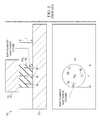
- FIG. 1shows a conventional CBRAM cell 1 A, having a top electrode 10 (e.g., copper) arranged over a bottom electrode 12 (e.g., tungsten), with the electrolyte or middle electrode 14 (e.g., SiO 2 ) arranged between the top and bottom electrodes.
- Conductive filaments 18propagate from the bottom electrode 12 to the top electrode 10 through the electrolyte 14 when a bias voltage is applied to the cell 1 A.
- This structurehas various potential limitations or drawbacks.
- the effective cross-sectional area for filament formationreferred to herein as the effective filament formation area indicated as A FF , or alternatively the “confinement zone,” is relatively large and unconfined, making the filament formation area susceptible to extrinsic defects.
- multi-filament root formationmay be likely, due to a relatively large area, which may lead to weaker (less robust) filaments.
- a large electrolyte volumesurrounds the filament, which provides diffusion paths for the filament and thus may provide poor retention.
- restricting the volume of the electrolyte material in which the conductive path formsmay provide a more robust filament due to spatial confinement.
- the volume of the electrolyte material in which the conductive path formsmay be restricted by reducing the area in contact between the bottom electrode 12 and the electrolyte 14 .
- conductive pathrefers a conductive filament (e.g., in a CBRAM cell), vacancy chain (e.g., in an oxygen vacancy based ReRAM cell), or any other type of conductive path for connecting the bottom and top electrodes of a non-volatile memory cell (typically through an electrolyte layer or region arranged between the bottom and top electrodes).
- electrolyte layeror “electrolyte region” refers to an electrolyte/insulator/memory layer or region between the bottom and top electrodes through which the conductive path propagates.
- FIG. 2shows certain principles of a CBRAM cell formation.
- Conductive paths 18may form and grow laterally, or branch into multiple parallel paths. Further, locations of the conductive paths may change with each program/erase cycle. This may contribute to a marginal switching performance, variability, high-temp retention issues, and/or switching endurance. Restricting switching volume has been shown to benefit the operation. These principles apply to ReRAM and CBRAM cells. A key obstacle for adoption of these technologies is switching uniformity.
- FIGS. 3A and 3Bshow a schematic view and an electron microscope image of an example known bottom electrode configuration 1 B for a CBRAM cell (e.g., having a one-transistor, one-resistive memory element (1T1R) architecture).
- the bottom electrode 12is a cylindrical via, e.g., a tungsten-filled via with a Ti/TiN liner.
- the bottom electrode 12may provide a relatively large effective filament formation area A FF , or confinement zone, of about 30,000 nm 2 , for example, which may lead to one or more of the problems or disadvantages discussed above.
- Some embodimentsprovide resistive memory cells, e.g., CBRAM or ReRAM cells, that focus the electric field more precisely than in known cells, which may provide more consistent filament formation, thus improving the consistency of programming voltage and cell predictability.
- some embodimentsprovide a memory cell structure in which two separate edge regions of a bottom electrode are used to define two separate memory elements from a single cell structure, wherein each of the two edge regions of the bottom electrode provides a highly focused electric field emanating from the bottom electrode.
- the effective cross-sectional area, or “confinement zone,” of such memory elementsmay be reduced in comparison to known resistive memory cells.
- the confinement zone of each memory elementmay be reduced to less than 1,000 nm 2 , less than 100 nm 2 , less than 10 nm 2 , or even less than 1 nm 2 .
- a method of forming a resistive memory cellmay include forming a bottom electrode layer on a substrate; oxidizing an exposed region of the bottom electrode layer to form an oxide region; removing a region of the bottom electrode layer proximate the oxide region, thereby forming a bottom electrode having a pointed tip region adjacent the oxide region, and forming (a) a first electrolyte region and first top electrode over a first portion of the pointed tip region of the bottom electrode, such that the first electrolyte region is arranged between the first top electrode and the first portion of the pointed tip region of the bottom electrode to define a first memory element, and (b) a second electrolyte region and second top electrode over a second portion of the pointed tip region of the bottom electrode, such that the second electrolyte region is arranged between the second top electrode and the second portion of the pointed tip region of the bottom electrode to define a second memory element, wherein the second electrolyte region and second top electrode are
- the first memory elementdefines a first path for conductive filament or vacancy chain formation from the first portion of the pointed tip region of the bottom electrode to the first top electrode via the first electrolyte region when a voltage bias is applied to the first memory element
- the second memory elementlikewise provides a second path for conductive filament or vacancy chain formation from the second portion of the pointed tip region of the bottom electrode to the second top electrode via the second electrolyte region when a voltage bias is applied to the second memory element.
- a method of forming an array of memory elementsmay include forming a bottom electrode layer on a substrate; oxidizing a plurality of exposed regions of the bottom electrode layer to form a plurality of oxide regions spaced apart from each other; removing regions of the bottom electrode layer between adjacent oxide regions, thereby forming a plurality of bottom electrodes, each bottom electrode having a respective oxide region at an upper side of the bottom electrode and a pointed tip adjacent the respective oxide region; and for each bottom electrode, forming a pair of memory elements, each memory element defined by a respective region of the bottom electrode pointed tip, a respective top electrode, and an electrolyte region arranged therebetween.
- each memory structuremay include a bottom electrode formed on a substrate; an oxide region adjacent the bottom electrode; wherein the bottom electrode has a pointed tip region proximate the oxide region; a first electrolyte region and first top electrode formed over a first portion of the pointed tip region of the bottom electrode, with the first electrolyte region arranged between the first top electrode and the first portion of the pointed tip region of the bottom electrode to define a first memory element; and a second electrolyte region and second top electrode over a second portion of the pointed tip region of the bottom electrode, with the second electrolyte region is arranged between the second top electrode and the second portion of the pointed tip region of the bottom electrode to define a second memory element.
- FIG. 1shows an example conventional CBRAM cell
- FIG. 2shows certain principles of CBRAM cell formation
- FIGS. 3A and 3Bshow a schematic view and an electron microscope image of an example known CBRAM cell configuration
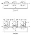
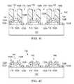
- FIGS. 4A-4Millustrate an example method for forming an array of resistive memory cells, e.g., CBRAM or ReRAM cells, according to one embodiment of the present invention.
- FIGS. 4A-4Millustrate an example method for forming an array of resistive memory cells, e.g., an array of conductive bridging memory (CBRAM) and resistive RAM (ReRAM) cells, according to one embodiment.
- a dielectric substrate 100e.g., SiO 2
- a bottom electrode layer 102 and a hard mask layer 104are deposited or formed over the dielectric substrate 100 .
- Bottom electrode layer 102may comprise any suitable conductive material or materials, e.g., polysilicon, doped polysilicon, amorphous silicon, doped amorphous silicon, or any other suitable material, and may be deposited or formed in any suitable manner.
- Hard mask layer 104may be formed from any suitable materials (e.g., silicon nitride) and may be deposited or formed in any suitable manner as known in the art.
- the hard mask layer 104is patterned, e.g., by forming and patterning a photoresist layer 106 over the hard mask layer 104 , using any suitable photolithography techniques. As shown, certain areas of the hard mask layer 104 are exposed through the patterned photoresist layer 106 .
- an etching processis performed to remove the photoresist layer 106 and portions of the hard mask layer 104 corresponding to the exposed areas shown in FIG. 4C , thereby forming a patterned hard mask 104 A having an array of openings 105 .
- openings 105may have any desired size and shape.
- openings 105may have a circular or oval shaped cross-section (in a plane parallel to the bottom electrode layer 102 ), thus providing cylindrical or elongated cylindrical openings 105 .
- openings 105may have a rectangular or otherwise elongated cross-section (in a plane parallel to the bottom electrode layer 102 ), thus providing elongated trench-style openings 105 .
- Openings 105may have any other suitable shapes and sizes.
- each oxide region 110may have a generally oval, rounded, curved, or otherwise non-orthogonal shape in a cross-section extending perpendicular to the bottom electrode layer 102 (i.e., the cross-section shown in FIG. 4E ).
- the hard mask 104 Ais removed and the remaining bottom electrode layer 102 and oxide regions 110 are etched to form an array of spaced-apart bottom electrodes 102 A and corresponding oxide regions 110 .
- the hard mask 104 Amay be removed during the etching of the bottom electrodes 102 A.
- the bottom electrode layer 102 and oxide regions 110may be etched in any suitable manner, e.g., by applying and utilizing a patterned mask or photoresist above the stack, or by using the oxide regions 110 themselves as a mask (e.g., using an etch selective to the non-oxidized bottom electrode material). The etch may or may not be patterned to follow the pattern defined by openings 105 (and thus the pattern of oxide regions 110 ).
- bottom electrodes 102 Amay have any shape and size, which may or may not correspond with the shapes and sizes of the openings 105 and oxide regions 110 prior to the etch process.
- bottom electrodes 102 Amay have a cylindrical or elongated cylindrical shape having a circular or oval shaped perimeter, or an rectangular prism shape have an elongated rectangular perimeter.
- the lateral edges of the etchmay be selected with respect to the lateral or outer perimeter edge or extent of each oxide region 110 .
- the lateral edges of the etchmay align with the outer perimeter edge of each oxide region 110 , as indicated by dashed lines E 1 .
- the lateral edges of the etchmay be aligned outside the outer perimeter edge of each oxide region 110 , as indicated by dashed lines E 2 , such that the post-etch bottom electrode 102 A has a region laterally outside the outer perimeter edge of the oxide region 110 .
- the lateral edges of the etchmay be aligned inside the outer perimeter edge of each oxide region 110 , as indicated by dashed lines E 3 , such that the etch extends removes an outer portion of the oxide region 110 .
- each bottom electrode 102 Ahas a pointed tip region 114 adjacent the respective oxide region.
- the shape of the pointed tip region 114may be at least partially defined by the oxide region 110 .
- the curved area toward the lateral perimeter of the oxide region 110helps define the shape of the pointed tip region 114 of the bottom electrode 102 A.
- the pointed tip region 114may define an angle ⁇ of less than 90 degrees, as shown in FIG. 4F .
- the pointed tip region 114may extend partially or fully around the lateral perimeter of the bottom electrode 102 A (e.g., a circular, oval, or rectangular perimeter).
- the lateral perimeter of the bottom electrode 102 Adefines a plurality of sides (e.g., a rectangular perimeter defining four sides), and the pointed tip region 114 extends along one, two, three, or more of the perimeter sides.
- Electrolyte layer 120may comprise any suitable dielectric or memristive type material or materials, for example, SiOx (e.g., SiO 2 ), GeS, CuS, TaO x , TiO 2 , Ge 2 Sb 2 Te 5 , GdO, HfO, CuO, Al 2 O 3 , or any other suitable material.
- Top electrode layer 122may comprise any suitable conductive material or materials, e.g., Ag, Al, Cu, Ta, TaN, Ti, TiN, Al, W or any other suitable material, and may be deposited or formed in any suitable manner.
- the stackis patterned, e.g., by forming and patterning a photomask 130 over the top electrode layer 122 , using any suitable photolithography techniques.
- photomask 130may be patterned in a manner that defines a pair of photomask regions 130 A and 130 B separated by a gap 132 over each cell structure, with a central area of each cell structure being exposed through each gap 132 . Further, the pair of photomask regions 130 A and 130 B over each cell structure is separated from the adjacent pair of photomask regions 130 A and 130 B by a gap 133 .
- an etching processis performed through gaps 132 and 133 to remove exposed portions of the top electrode layer 122 and underlying portions of electrolyte layer 120 .
- the etchmay be selective with respect to the oxide region 110 such that the oxide region 110 and underlying bottom electrode 102 A are not removed, while exposing surfaces of the oxide region 110 and bottom electrode 102 A.
- etching through gaps 133removes portions of top electrode layer 122 and electrolyte layer 120 between adjacent bottom electrodes 102 A to separate adjacent cell structures from each other.
- etching through gaps 132removes portions of top electrode layer 122 and electrolyte layer 120 over a central area of each oxide region 110 /bottom electrode 102 A, thereby defining, over each oxide region 110 /bottom electrode 102 A, a first top electrode 122 A and first electrolyte region 120 A physically separated from a second top electrode 122 B and second electrolyte region 120 B.
- the first top electrode 122 Ais arranged to interact with a first region of the bottom electrode 102 A (via the first electrolyte region 120 A) to define a first memory element 140 A (indicated in FIGS.
- the etch processforms two distinct memory elements 140 A and 140 B for each bottom electrode 102 A. This may therefore double the density of memory cells as compared to a design in which a single memory element is formed per bottom electrode.
- any remaining portions of the photomask 130may be removed, leaving an array 138 of resistive memory cell structures 140 , in which each memory cell structure 140 defines a pair of memory elements 140 A and 140 B, as discussed above.
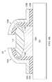
- FIG. 4KA close-up of one memory cell structure 140 is shown in FIG. 4K .
- the memory cell structure 140defines a pair of memory elements 140 A and 140 B.
- the first memory element 140 Ais defined by a first top electrode 122 A, a first portion 114 A of the pointed tip region 114 of bottom electrode 102 A, and a first electrolyte region 120 A arranged therebetween.
- the second memory element 140 Bis defined by a second top electrode 122 B, a second portion 114 B of the pointed tip region 114 of bottom electrode 102 A, and a second electrolyte region 120 B arranged therebetween.
- memory element 140 Ais a mirror image of corresponding memory element 140 B.
- memory element 140 Amay have a different shape or structure than its corresponding memory element 140 B, e.g., by shifting the etch opening 132 (see FIG. 4I for reference) from the center of the respective underlying bottom electrode 102 A, or by forming an irregular-shaped etch opening 132 , for example.
- the first memory element 140 Aprovides a first conductive path CP 1 for the formation of conductive filament(s) or vacancy chain(s) from the first pointed tip region 114 A of the bottom electrode 102 A to the top electrode 122 A through the electrolyte region 120 A.
- the second memory element 140 Bprovides a second conductive path CP 2 for the formation of conductive filament(s) or vacancy chain(s) from the second pointed tip region 114 B of the bottom electrode 102 A to the top electrode 122 B through the electrolyte region 120 B.
- each memory element 140 A and 140 Bmay provide a relatively small, or confined, effective filament formation area A FF , or confinement zone.
- the effective filament formation area A FF for each memory element 140 A/ 140 Bmeasured in a plane generally perpendicular to the direction of filament propagation, may be less than 1,000 nm 2 .
- each effective filament formation area A FFis less than 100 nm 2 .
- each effective filament formation area A FFis less than 10 nm 2 , or even less than 1 nm 2 .
- These reduced confinement zonesmay provide resistive memory cells (e.g., CBRAM or ReRAM cells) with more predictable and reliable filament formation, as compared with cells having a larger confinement zone.
- Thismay provide one or more of the following benefits: lower erase current, narrower distribution of low-resistance state (LRS), higher on/off ratio (HRS/LRS), and improved failure rates.
- Top electrodes 122 A and 122 Bmay be connected in or to any suitable circuitry using any suitable contact scheme.
- top contactsmay be formed in contact with top electrodes 122 A and 122 B as shown in FIGS. 4L and 4M .
- a dielectric layer 144may be deposited over the array of memory elements 140 A and 140 B.
- top contacts 150 A and 150 Bmay be formed in dielectric layer 144 , using any suitable techniques.
- each top contact 150 Acontacts an upper portion of a top electrode 122 A
- each top contact 150 Bcontacts an upper portion of a top electrode 122 B.
- Top contacts 150may be arranged in any other suitable manner with respect to top electrodes 122 A and 122 B and other cell components.
- each bottom electrode 102 Amay be contacted (e.g., for connection to a wordline or bitline) in any suitable or conventional manner.
- each bottom electrode 102 Amay be contacted from above by dropping down a contact that is recessed or offset from the memory films.
- each bottom electrode 102 Amay be contacted from below by depositing the bottom electrode layer 102 directly on a salicided active silicon region and then making contact to the active region at the end of a line of bits.
Landscapes
- Engineering & Computer Science (AREA)
- Manufacturing & Machinery (AREA)
- Semiconductor Memories (AREA)
Abstract
Description
Claims (24)
Priority Applications (1)
| Application Number | Priority Date | Filing Date | Title |
|---|---|---|---|
| US15/200,322US9865814B2 (en) | 2014-02-19 | 2016-07-01 | Resistive memory cell having a single bottom electrode and two top electrodes |
Applications Claiming Priority (2)
| Application Number | Priority Date | Filing Date | Title |
|---|---|---|---|
| US14/184,331US9385313B2 (en) | 2014-02-19 | 2014-02-19 | Resistive memory cell having a reduced conductive path area |
| US15/200,322US9865814B2 (en) | 2014-02-19 | 2016-07-01 | Resistive memory cell having a single bottom electrode and two top electrodes |
Related Parent Applications (1)
| Application Number | Title | Priority Date | Filing Date |
|---|---|---|---|
| US14/184,331DivisionUS9385313B2 (en) | 2014-02-19 | 2014-02-19 | Resistive memory cell having a reduced conductive path area |
Publications (2)
| Publication Number | Publication Date |
|---|---|
| US20160315257A1 US20160315257A1 (en) | 2016-10-27 |
| US9865814B2true US9865814B2 (en) | 2018-01-09 |
Family
ID=52595484
Family Applications (2)
| Application Number | Title | Priority Date | Filing Date |
|---|---|---|---|
| US14/184,331Expired - Fee RelatedUS9385313B2 (en) | 2014-02-19 | 2014-02-19 | Resistive memory cell having a reduced conductive path area |
| US15/200,322Expired - Fee RelatedUS9865814B2 (en) | 2014-02-19 | 2016-07-01 | Resistive memory cell having a single bottom electrode and two top electrodes |
Family Applications Before (1)
| Application Number | Title | Priority Date | Filing Date |
|---|---|---|---|
| US14/184,331Expired - Fee RelatedUS9385313B2 (en) | 2014-02-19 | 2014-02-19 | Resistive memory cell having a reduced conductive path area |
Country Status (6)
| Country | Link |
|---|---|
| US (2) | US9385313B2 (en) |
| EP (1) | EP3108512A1 (en) |
| KR (1) | KR20160122131A (en) |
| CN (1) | CN105940516A (en) |
| TW (1) | TW201539732A (en) |
| WO (1) | WO2015126870A1 (en) |
Cited By (3)
| Publication number | Priority date | Publication date | Assignee | Title |
|---|---|---|---|---|
| US11316106B2 (en) | 2019-12-24 | 2022-04-26 | Winbond Electronics Corp. | Resistive random access memory and manufacturing method thereof |
| US11502250B2 (en) | 2020-05-26 | 2022-11-15 | Globalfoundries Singapore Pte. Ltd. | Memory devices and methods of forming memory devices |
| US11600664B2 (en)* | 2020-01-16 | 2023-03-07 | Globalfoundries Singapore Pte. Ltd. | Memory devices and methods of forming memory devices |
Families Citing this family (10)
| Publication number | Priority date | Publication date | Assignee | Title |
|---|---|---|---|---|
| US9362496B2 (en) | 2013-03-13 | 2016-06-07 | Microchip Technology Incorporated | Resistive memory cell with trench-shaped bottom electrode |
| US9444040B2 (en) | 2013-03-13 | 2016-09-13 | Microchip Technology Incorporated | Sidewall type memory cell |
| US9385313B2 (en) | 2014-02-19 | 2016-07-05 | Microchip Technology Incorporated | Resistive memory cell having a reduced conductive path area |
| US9412942B2 (en) | 2014-02-19 | 2016-08-09 | Microchip Technology Incorporated | Resistive memory cell with bottom electrode having a sloped side wall |
| US9318702B2 (en) | 2014-02-19 | 2016-04-19 | Microchip Technology Incorporated | Resistive memory cell having a reduced conductive path area |
| US10003021B2 (en) | 2014-02-19 | 2018-06-19 | Microchip Technology Incorporated | Resistive memory cell with sloped bottom electrode |
| JP2018500754A (en) | 2014-11-26 | 2018-01-11 | マイクロチップ テクノロジー インコーポレイテッドMicrochip Technology Incorporated | Resistive memory cell with spacer region for reduced conductive path area / increased electric field |
| CN111584711B (en)* | 2020-04-29 | 2023-08-22 | 厦门半导体工业技术研发有限公司 | RRAM device and method for forming RRAM device |
| CN111640863B (en)* | 2020-05-19 | 2023-12-19 | 厦门半导体工业技术研发有限公司 | Semiconductor integrated circuit device and method for manufacturing the same |
| US12310267B2 (en) | 2021-06-14 | 2025-05-20 | International Business Machines Corporation | ReRAM module with intermediate electrode |
Citations (60)
| Publication number | Priority date | Publication date | Assignee | Title |
|---|---|---|---|---|
| US5687112A (en) | 1996-04-19 | 1997-11-11 | Energy Conversion Devices, Inc. | Multibit single cell memory element having tapered contact |
| US5790455A (en) | 1997-01-02 | 1998-08-04 | John Caywood | Low voltage single supply CMOS electrically erasable read-only memory |
| US5962872A (en) | 1993-10-01 | 1999-10-05 | Semiconductor Energy Laboratory Co., Ltd. | Semiconductor device and method for fabricating the same |
| US5986931A (en) | 1997-01-02 | 1999-11-16 | Caywood; John M. | Low voltage single CMOS electrically erasable read-only memory |
| US6031287A (en) | 1997-06-18 | 2000-02-29 | Micron Technology, Inc. | Contact structure and memory element incorporating the same |
| US6147395A (en) | 1996-10-02 | 2000-11-14 | Micron Technology, Inc. | Method for fabricating a small area of contact between electrodes |
| US20020036931A1 (en) | 1999-03-25 | 2002-03-28 | Tyler Lowrey | Electrically programmable memory element with reduced area of contact and method for making same |
| US20020039306A1 (en) | 2000-09-29 | 2002-04-04 | Lowrey Tyler A. | Single level metal memory cell using chalcogenide cladding |
| US6436611B1 (en) | 1999-07-07 | 2002-08-20 | Samsung Electronics Co., Ltd. | Trench isolation method for semiconductor integrated circuit |
| EP1355365A2 (en) | 2002-04-04 | 2003-10-22 | Hewlett-Packard Company | Electrode for phase change memory device |
| US20040085833A1 (en) | 2002-11-01 | 2004-05-06 | Young-Nam Hwang | Phase changeable memory devices and methods of forming the same in which an upper electrode includes a tip that extends toward a lower electrode |
| US20040192009A1 (en) | 2003-03-26 | 2004-09-30 | Infineon Technologies North America Corp. | Trench isolation employing a doped oxide trench fill |
| US20050029505A1 (en) | 2003-08-04 | 2005-02-10 | Lowrey Tyler A. | Phase change access device for memories |
| US20060097238A1 (en) | 2002-07-26 | 2006-05-11 | Laurent Breuil | Non-volatile memory element and production method thereof and storage memory arrangement |
| US20060131618A1 (en) | 2004-12-16 | 2006-06-22 | Ming-Hsiang Hsueh | Chalcogenide random access memory and method of fabricating the same |
| US20070097738A1 (en) | 2005-11-03 | 2007-05-03 | Elpida Memory, Inc. | Electrically rewritable non-volatile memory element and method of manufacturing the same |
| US20070267618A1 (en) | 2006-05-17 | 2007-11-22 | Shoaib Zaidi | Memory device |
| US20080012079A1 (en) | 2006-07-17 | 2008-01-17 | Shoaib Zaidi | Memory cell having active region sized for low reset current and method of fabricating such memory cells |
| US20090017591A1 (en) | 2007-07-11 | 2009-01-15 | Andrew Cervin-Lawry | Local Oxidation of Silicon Planarization for Polysilicon Layers Under Thin Film Structures |
| US20090026438A1 (en) | 2007-07-26 | 2009-01-29 | Industrial Technology Research Institute | Solid state electrolyte memory device and method of fabricating the same |
| US20090096568A1 (en) | 2006-04-28 | 2009-04-16 | Yasunari Hosoi | Variable resistance element, and its manufacturing method |
| DE102007049786A1 (en) | 2007-10-17 | 2009-04-23 | Qimonda Ag | Integrated circuit has multiple resistance change memory cells, where each memory cell has top electrode, bottom electrode and resistance changing material provided between top electrode and bottom electrode |
| US20090200640A1 (en) | 2006-04-28 | 2009-08-13 | Yasunari Hosoi | Variable resistive element, and its manufacturing method |
| US20100019218A1 (en) | 2008-07-24 | 2010-01-28 | Hynix Semiconductor Inc. | Resistive memory device and method of fabricating the same |
| US20100038614A1 (en) | 2008-08-14 | 2010-02-18 | Micron Technology, Inc. | Methods of forming a phase change material, a phase change material, a phase change random access memory device including the phase change material, and a semiconductor structure including the phase change material |
| US20100055687A1 (en) | 2001-06-14 | 2010-03-04 | Sawyers Charles L | Mutations in the BCR-ABL tyrosine kinase associated with resistance to ST1-571 |
| US20100084741A1 (en) | 2008-10-08 | 2010-04-08 | Dieter Andres | Integrated Circuit |
| EP2202816A1 (en) | 2008-12-24 | 2010-06-30 | Imec | Method for manufacturing a resistive switching memory device and devices obtained thereof |
| US20100163829A1 (en) | 2008-12-30 | 2010-07-01 | Industrial Technology Research Institute | Conductive bridging random access memory device and method of manufacturing the same |
| CN101794860A (en) | 2009-02-04 | 2010-08-04 | 财团法人工业技术研究院 | Conducting microchannel memory element and manufacturing method thereof |
| US20100193762A1 (en) | 2009-02-03 | 2010-08-05 | Nanya Technology Corp. | Non-volatile memory cell and fabrication method thereof |
| US20100252798A1 (en) | 2009-04-02 | 2010-10-07 | Sony Corporation | Storage element, method of manufacturing same, and semiconductor storage device |
| US20100264396A1 (en) | 2009-04-20 | 2010-10-21 | Macronix International Co., Ltd. | Ring-shaped electrode and manufacturing method for same |
| EP2267775A2 (en) | 1999-03-19 | 2010-12-29 | Microchip Technology Incorporated | Independently programmable memory segments in isolated N-wells within a PMOS EEPROM array |
| US20110147694A1 (en) | 2009-12-18 | 2011-06-23 | Seok-Pyo Song | Resistive memory device and method for fabricating the same |
| EP2339585A1 (en) | 2006-06-01 | 2011-06-29 | Microchip Technology Incorporated | EEPROM memory |
| CN102130145A (en) | 2010-01-12 | 2011-07-20 | 中芯国际集成电路制造(上海)有限公司 | Phase change storage and manufacturing method thereof |
| US20110175048A1 (en) | 2010-01-18 | 2011-07-21 | Kabushiki Kaisha Toshiba | Nonvolatile memory device and method for manufacturing same |
| US20110180775A1 (en) | 2010-01-25 | 2011-07-28 | Macronix International Co., Ltd. | Programmable metallization cell with ion buffer layer |
| US20110291064A1 (en) | 2010-05-25 | 2011-12-01 | Micron Technology, Inc. | Resistance variable memory cell structures and methods |
| WO2012057772A1 (en) | 2010-10-29 | 2012-05-03 | Hewlett-Packard Development Company, L.P. | Memristive devices and memristors with ribbon-like junctions and methods for fabricating the same |
| CN102738386A (en) | 2011-03-31 | 2012-10-17 | 中国科学院微电子研究所 | Resistive random access memory and manufacturing method thereof |
| US20120294065A1 (en) | 2011-05-17 | 2012-11-22 | Sanghyun Hong | Variable resistance memory device and method of fabricating the same |
| WO2012167286A1 (en) | 2011-05-13 | 2012-12-06 | Adesto Technologies Corporation | Contact structure and method for variable impedance memory element |
| US20120319072A1 (en) | 2010-02-23 | 2012-12-20 | Zhiqiang Wei | Method for manufacturing non-volatile memory device, non-volatile memory element, and non-volatile memory device |
| US20130001503A1 (en) | 2011-05-05 | 2013-01-03 | Gallo Antonio R | Conductive filament based memory elements and methods with improved data retention and/or endurance |
| US20130001501A1 (en) | 2011-07-01 | 2013-01-03 | Micron Technology, Inc. | Memory cell structures |
| US20130082231A1 (en) | 2010-06-16 | 2013-04-04 | Nec Corporation | Semiconductor device and manufacturing method for semiconductor device |
| US20130112936A1 (en) | 2011-01-20 | 2013-05-09 | Panasonic Corporation | Resistance change element and manufacturing method therefor |
| US20130214234A1 (en) | 2012-02-22 | 2013-08-22 | Adesto Technologies Corporation | Resistive Switching Devices and Methods of Formation Thereof |
| US20130252431A1 (en) | 2012-03-22 | 2013-09-26 | Tong-Yu Chen | Method of Forming Trench in Semiconductor Substrate |
| US20130336046A1 (en) | 2012-06-18 | 2013-12-19 | Gyu-Hwan OH | Non-volatile memory device having multi-level cells and method of forming the same |
| US20140264245A1 (en) | 2013-03-13 | 2014-09-18 | Microchip Technology Incorporated | Resistive Memory Cell with Trench-Shaped Bottom Electrode |
| WO2014164015A1 (en) | 2013-03-13 | 2014-10-09 | Microchip Technology Incorporated | Sidewall-type memory cell |
| US20150236258A1 (en) | 2014-02-19 | 2015-08-20 | Microchip Technology Incorporated | Resistive memory cell having a reduced conductive path area |
| US20150236255A1 (en) | 2014-02-19 | 2015-08-20 | Microchip Technology Incorporated | Resistive Memory Cell having a Reduced Conductive Path Area |
| US20150236257A1 (en)* | 2014-02-19 | 2015-08-20 | Microchip Technology Incorporated | Resistive Memory Cell with Sloped Bottom Electrode |
| US9269606B2 (en) | 2014-02-19 | 2016-02-23 | Microchip Technology Incorporated | Spacer enabled active isolation for an integrated circuit device |
| US9281476B2 (en) | 2012-12-19 | 2016-03-08 | Peking University | Resistive memory and method for fabricating the same |
| US20160190441A1 (en)* | 2014-02-19 | 2016-06-30 | Microchip Technology Incorporated | Resistive Memory Cell With Sloped Bottom Electrode |
Family Cites Families (2)
| Publication number | Priority date | Publication date | Assignee | Title |
|---|---|---|---|---|
| KR100612867B1 (en)* | 2004-11-02 | 2006-08-14 | 삼성전자주식회사 | Resistive memory device having probe array and manufacturing method thereof |
| US8701887B2 (en) | 2008-07-31 | 2014-04-22 | Silgan Containers Llc | Stackable container |
- 2014
- 2014-02-19USUS14/184,331patent/US9385313B2/ennot_activeExpired - Fee Related
- 2015
- 2015-02-18KRKR1020167020646Apatent/KR20160122131A/ennot_activeWithdrawn
- 2015-02-18EPEP15707029.3Apatent/EP3108512A1/ennot_activeWithdrawn
- 2015-02-18CNCN201580005856.0Apatent/CN105940516A/enactivePending
- 2015-02-18WOPCT/US2015/016259patent/WO2015126870A1/enactiveApplication Filing
- 2015-02-24TWTW104105897Apatent/TW201539732A/enunknown
- 2016
- 2016-07-01USUS15/200,322patent/US9865814B2/ennot_activeExpired - Fee Related
Patent Citations (70)
| Publication number | Priority date | Publication date | Assignee | Title |
|---|---|---|---|---|
| US5962872A (en) | 1993-10-01 | 1999-10-05 | Semiconductor Energy Laboratory Co., Ltd. | Semiconductor device and method for fabricating the same |
| US5687112A (en) | 1996-04-19 | 1997-11-11 | Energy Conversion Devices, Inc. | Multibit single cell memory element having tapered contact |
| US6147395A (en) | 1996-10-02 | 2000-11-14 | Micron Technology, Inc. | Method for fabricating a small area of contact between electrodes |
| US5790455A (en) | 1997-01-02 | 1998-08-04 | John Caywood | Low voltage single supply CMOS electrically erasable read-only memory |
| US5986931A (en) | 1997-01-02 | 1999-11-16 | Caywood; John M. | Low voltage single CMOS electrically erasable read-only memory |
| US6031287A (en) | 1997-06-18 | 2000-02-29 | Micron Technology, Inc. | Contact structure and memory element incorporating the same |
| EP2267775A2 (en) | 1999-03-19 | 2010-12-29 | Microchip Technology Incorporated | Independently programmable memory segments in isolated N-wells within a PMOS EEPROM array |
| US20060006443A1 (en) | 1999-03-25 | 2006-01-12 | Tyler Lowrey | Electrically programmable memory element with reduced area of contact |
| US20020036931A1 (en) | 1999-03-25 | 2002-03-28 | Tyler Lowrey | Electrically programmable memory element with reduced area of contact and method for making same |
| US6436611B1 (en) | 1999-07-07 | 2002-08-20 | Samsung Electronics Co., Ltd. | Trench isolation method for semiconductor integrated circuit |
| US20020039306A1 (en) | 2000-09-29 | 2002-04-04 | Lowrey Tyler A. | Single level metal memory cell using chalcogenide cladding |
| US20100055687A1 (en) | 2001-06-14 | 2010-03-04 | Sawyers Charles L | Mutations in the BCR-ABL tyrosine kinase associated with resistance to ST1-571 |
| EP1355365A2 (en) | 2002-04-04 | 2003-10-22 | Hewlett-Packard Company | Electrode for phase change memory device |
| US20060097238A1 (en) | 2002-07-26 | 2006-05-11 | Laurent Breuil | Non-volatile memory element and production method thereof and storage memory arrangement |
| US20040085833A1 (en) | 2002-11-01 | 2004-05-06 | Young-Nam Hwang | Phase changeable memory devices and methods of forming the same in which an upper electrode includes a tip that extends toward a lower electrode |
| US20040192009A1 (en) | 2003-03-26 | 2004-09-30 | Infineon Technologies North America Corp. | Trench isolation employing a doped oxide trench fill |
| US20050029505A1 (en) | 2003-08-04 | 2005-02-10 | Lowrey Tyler A. | Phase change access device for memories |
| US20060131618A1 (en) | 2004-12-16 | 2006-06-22 | Ming-Hsiang Hsueh | Chalcogenide random access memory and method of fabricating the same |
| US20070097738A1 (en) | 2005-11-03 | 2007-05-03 | Elpida Memory, Inc. | Electrically rewritable non-volatile memory element and method of manufacturing the same |
| US20090096568A1 (en) | 2006-04-28 | 2009-04-16 | Yasunari Hosoi | Variable resistance element, and its manufacturing method |
| US20090200640A1 (en) | 2006-04-28 | 2009-08-13 | Yasunari Hosoi | Variable resistive element, and its manufacturing method |
| US20070267618A1 (en) | 2006-05-17 | 2007-11-22 | Shoaib Zaidi | Memory device |
| EP2339585A1 (en) | 2006-06-01 | 2011-06-29 | Microchip Technology Incorporated | EEPROM memory |
| US20080012079A1 (en) | 2006-07-17 | 2008-01-17 | Shoaib Zaidi | Memory cell having active region sized for low reset current and method of fabricating such memory cells |
| US20090017591A1 (en) | 2007-07-11 | 2009-01-15 | Andrew Cervin-Lawry | Local Oxidation of Silicon Planarization for Polysilicon Layers Under Thin Film Structures |
| US20090026438A1 (en) | 2007-07-26 | 2009-01-29 | Industrial Technology Research Institute | Solid state electrolyte memory device and method of fabricating the same |
| DE102007049786A1 (en) | 2007-10-17 | 2009-04-23 | Qimonda Ag | Integrated circuit has multiple resistance change memory cells, where each memory cell has top electrode, bottom electrode and resistance changing material provided between top electrode and bottom electrode |
| US20100019218A1 (en) | 2008-07-24 | 2010-01-28 | Hynix Semiconductor Inc. | Resistive memory device and method of fabricating the same |
| US20100038614A1 (en) | 2008-08-14 | 2010-02-18 | Micron Technology, Inc. | Methods of forming a phase change material, a phase change material, a phase change random access memory device including the phase change material, and a semiconductor structure including the phase change material |
| US20100084741A1 (en) | 2008-10-08 | 2010-04-08 | Dieter Andres | Integrated Circuit |
| EP2202816A1 (en) | 2008-12-24 | 2010-06-30 | Imec | Method for manufacturing a resistive switching memory device and devices obtained thereof |
| US20100163829A1 (en) | 2008-12-30 | 2010-07-01 | Industrial Technology Research Institute | Conductive bridging random access memory device and method of manufacturing the same |
| US20100193762A1 (en) | 2009-02-03 | 2010-08-05 | Nanya Technology Corp. | Non-volatile memory cell and fabrication method thereof |
| CN101794860A (en) | 2009-02-04 | 2010-08-04 | 财团法人工业技术研究院 | Conducting microchannel memory element and manufacturing method thereof |
| US20100252798A1 (en) | 2009-04-02 | 2010-10-07 | Sony Corporation | Storage element, method of manufacturing same, and semiconductor storage device |
| US20100264396A1 (en) | 2009-04-20 | 2010-10-21 | Macronix International Co., Ltd. | Ring-shaped electrode and manufacturing method for same |
| US20110147694A1 (en) | 2009-12-18 | 2011-06-23 | Seok-Pyo Song | Resistive memory device and method for fabricating the same |
| CN102130145A (en) | 2010-01-12 | 2011-07-20 | 中芯国际集成电路制造(上海)有限公司 | Phase change storage and manufacturing method thereof |
| US20110175048A1 (en) | 2010-01-18 | 2011-07-21 | Kabushiki Kaisha Toshiba | Nonvolatile memory device and method for manufacturing same |
| US20110180775A1 (en) | 2010-01-25 | 2011-07-28 | Macronix International Co., Ltd. | Programmable metallization cell with ion buffer layer |
| US20120319072A1 (en) | 2010-02-23 | 2012-12-20 | Zhiqiang Wei | Method for manufacturing non-volatile memory device, non-volatile memory element, and non-volatile memory device |
| US20110291064A1 (en) | 2010-05-25 | 2011-12-01 | Micron Technology, Inc. | Resistance variable memory cell structures and methods |
| US20130082231A1 (en) | 2010-06-16 | 2013-04-04 | Nec Corporation | Semiconductor device and manufacturing method for semiconductor device |
| WO2012057772A1 (en) | 2010-10-29 | 2012-05-03 | Hewlett-Packard Development Company, L.P. | Memristive devices and memristors with ribbon-like junctions and methods for fabricating the same |
| US20130112936A1 (en) | 2011-01-20 | 2013-05-09 | Panasonic Corporation | Resistance change element and manufacturing method therefor |
| CN102738386A (en) | 2011-03-31 | 2012-10-17 | 中国科学院微电子研究所 | Resistive random access memory and manufacturing method thereof |
| US20130001503A1 (en) | 2011-05-05 | 2013-01-03 | Gallo Antonio R | Conductive filament based memory elements and methods with improved data retention and/or endurance |
| WO2012167286A1 (en) | 2011-05-13 | 2012-12-06 | Adesto Technologies Corporation | Contact structure and method for variable impedance memory element |
| US20120313071A1 (en) | 2011-05-13 | 2012-12-13 | Chakravarthy Gopalan | Contact structure and method for variable impedance memory element |
| US20120294065A1 (en) | 2011-05-17 | 2012-11-22 | Sanghyun Hong | Variable resistance memory device and method of fabricating the same |
| US20130001501A1 (en) | 2011-07-01 | 2013-01-03 | Micron Technology, Inc. | Memory cell structures |
| US20130214234A1 (en) | 2012-02-22 | 2013-08-22 | Adesto Technologies Corporation | Resistive Switching Devices and Methods of Formation Thereof |
| US20130252431A1 (en) | 2012-03-22 | 2013-09-26 | Tong-Yu Chen | Method of Forming Trench in Semiconductor Substrate |
| US20130336046A1 (en) | 2012-06-18 | 2013-12-19 | Gyu-Hwan OH | Non-volatile memory device having multi-level cells and method of forming the same |
| US9281476B2 (en) | 2012-12-19 | 2016-03-08 | Peking University | Resistive memory and method for fabricating the same |
| US20140264245A1 (en) | 2013-03-13 | 2014-09-18 | Microchip Technology Incorporated | Resistive Memory Cell with Trench-Shaped Bottom Electrode |
| WO2014164015A1 (en) | 2013-03-13 | 2014-10-09 | Microchip Technology Incorporated | Sidewall-type memory cell |
| US20160380192A1 (en)* | 2013-03-13 | 2016-12-29 | Microchip Technology Incorporated | Sidewall-Type Memory Cell |
| US9444040B2 (en) | 2013-03-13 | 2016-09-13 | Microchip Technology Incorporated | Sidewall type memory cell |
| US9362496B2 (en) | 2013-03-13 | 2016-06-07 | Microchip Technology Incorporated | Resistive memory cell with trench-shaped bottom electrode |
| US9349950B2 (en) | 2013-03-13 | 2016-05-24 | Microchip Technology Incorporated | Resistive memory cell with trench-shaped bottom electrode |
| US9318702B2 (en)* | 2014-02-19 | 2016-04-19 | Microchip Technology Incorporated | Resistive memory cell having a reduced conductive path area |
| US9269606B2 (en) | 2014-02-19 | 2016-02-23 | Microchip Technology Incorporated | Spacer enabled active isolation for an integrated circuit device |
| US20150236257A1 (en)* | 2014-02-19 | 2015-08-20 | Microchip Technology Incorporated | Resistive Memory Cell with Sloped Bottom Electrode |
| US20160190442A1 (en)* | 2014-02-19 | 2016-06-30 | Microchip Technology Incorporated | Resistive Memory Cell Having A Reduced Conductive Path Area |
| US20160190441A1 (en)* | 2014-02-19 | 2016-06-30 | Microchip Technology Incorporated | Resistive Memory Cell With Sloped Bottom Electrode |
| US9385313B2 (en) | 2014-02-19 | 2016-07-05 | Microchip Technology Incorporated | Resistive memory cell having a reduced conductive path area |
| US9412942B2 (en)* | 2014-02-19 | 2016-08-09 | Microchip Technology Incorporated | Resistive memory cell with bottom electrode having a sloped side wall |
| US20150236255A1 (en) | 2014-02-19 | 2015-08-20 | Microchip Technology Incorporated | Resistive Memory Cell having a Reduced Conductive Path Area |
| US20150236258A1 (en) | 2014-02-19 | 2015-08-20 | Microchip Technology Incorporated | Resistive memory cell having a reduced conductive path area |
Non-Patent Citations (39)
| Title |
|---|
| Balakrishnan, M. et al., "A Low Power Non-Volatile Memory Element Based on Copper in Deposited Silicon Oxide," Non-Volatile Memory Technology Symposium, 7 pages, 2006. |
| Chen, A., "Ionic Memories: Status and Challenges," Non-Volatile Memory Technology Symposium, 5 pages, 2008. |
| Chen, A., "Non-Volatile Resistive Switching for Advanced Memory Applications," IEDM Technical Digest, 4 pages, 2005. |
| International Search Report and Written Opinion, Application No. PCT/US2014/019868, 10 pages, dated Jun. 5, 2014. |
| International Search Report and Written Opinion, Application No. PCT/US2014/019906, 12 pages, dated Jul. 2, 2014. |
| International Search Report and Written Opinion, Application No. PCT/US2014/020188, 10 pages, dated May 13, 2014. |
| International Search Report and Written Opinion, Application No. PCT/US2014/022194, 11 pages, dated May 16, 2014. |
| International Search Report and Written Opinion, Application No. PCT/US2015/016244, 11 pages, dated May 7, 2015. |
| International Search Report and Written Opinion, Application No. PCT/US2015/016259, 16 pages, dated May 6, 2015. |
| International Search Report and Written Opinion, Application No. PCT/US2015/016268, 9 pages, dated May 4, 2015. |
| International Search Report and Written Opinion, Application No. PCT/US2015/016321, 11 pages, dated Jul. 14, 2015. |
| International Search Report and Written Opinion, Application No. PCT/US2015/016334, 11 pages, dated Dec. 7, 2015. |
| International Search Report and Written Opinion, Application No. PCT/US2015/062758, 12 pages, dated Mar. 2, 2016. |
| Jou, S. et al., "Resistance Switching Properties in Cu/Cu-SiO2/TaN Device," Proceeding World Congress on Engineering, vol. 2, 4 pages, Jul. 6, 2011. |
| Jou, S. et al., "Resistance Switching Properties in Cu/Cu—SiO2/TaN Device," Proceeding World Congress on Engineering, vol. 2, 4 pages, Jul. 6, 2011. |
| Kozicki, M., "Nanoscale Memory Elements Based on Solid-State Electrolytes," IEEE Transactions on Nano Technology, vol. 4, No. 3, 8 pages, May 2005. |
| Schindler, C. et al., "Bipolar and Unipolar Resistive Switching in CU-Doped SiO2," IEEE Transactions on Electron Devices, vol. 54, No. 10, 7 pages, 2007. |
| Taiwan Office Action, Application No. 103108883, 5 pages, dated Jul. 31, 2017. |
| Taiwan Office Action, Application No. 103108885, 15 pages, dated Jun. 6, 2017. |
| U.S. Final Office Action, U.S. Appl. No. 14/183,831, 13 pages, dated Feb. 2, 2016. |
| U.S. Final Office Action, U.S. Appl. No. 14/184,034, 16 pages, dated Feb. 10, 2017. |
| U.S. Final Office Action, U.S. Appl. No. 14/184,034, 29 pages, dated Dec. 16, 2015. |
| U.S. Final Office Action, U.S. Appl. No. 14/184,331, 10 pages, dated Nov. 12, 2015. |
| U.S. Final Office Action, U.S. Appl. No. 15/065,354, 21 pages, dated Aug. 28, 2017. |
| U.S. Non-Final Office Action, U.S. Appl. No. 14/183,674, 26 pages, dated Jul. 8, 2015. |
| U.S. Non-Final Office Action, U.S. Appl. No. 14/183,738, 26 pages, dated Jul. 16, 2015. |
| U.S. Non-Final Office Action, U.S. Appl. No. 14/183,792, 23 pages, dated Jul. 8, 2015. |
| U.S. Non-Final Office Action, U.S. Appl. No. 14/183,831, 18 pages, dated Jul. 9, 2015. |
| U.S. Non-Final Office Action, U.S. Appl. No. 14/183,953, 27 pages, dated Jul. 31, 2015. |
| U.S. Non-Final Office Action, U.S. Appl. No. 14/184,034, 20 pages, dated Jul. 5, 2016. |
| U.S. Non-Final Office Action, U.S. Appl. No. 14/184,034, 23 pages, dated Jun. 16, 2017. |
| U.S. Non-Final Office Action, U.S. Appl. No. 14/184,177, 12 pages, dated Jun. 19, 2015. |
| U.S. Non-Final Office Action, U.S. Appl. No. 14/952,559, 30 pages, dated Mar. 1, 2017. |
| U.S. Non-Final Office Action, U.S. Appl. No. 15/065,193, 33 pages, dated Jul. 14, 2017. |
| U.S. Non-Final Office Action, U.S. Appl. No. 15/065,354, 22 pages, dated Feb. 24, 2017. |
| U.S. Non-Final Office Action, U.S. Appl. No. 15/262,923, 33 pages, dated Aug. 10, 2017. |
| Valov, I. et al., "Electrochemical Metallization Memories-Fundamentals, Applications, Prospects," Nanotechnology, vol. 22, No. 25, 22 pages, Jun. 24, 2011. |
| Valov, I. et al., "Electrochemical Metallization Memories—Fundamentals, Applications, Prospects," Nanotechnology, vol. 22, No. 25, 22 pages, Jun. 24, 2011. |
| Yang, L. et al., "Linear Scaling of Reset Current Down to 22-nm Node for a Novel CuxSiyO RRAM," IEEE Electron Device Letters, vol. 33, No. 1, 3 pages, 2012. |
Cited By (3)
| Publication number | Priority date | Publication date | Assignee | Title |
|---|---|---|---|---|
| US11316106B2 (en) | 2019-12-24 | 2022-04-26 | Winbond Electronics Corp. | Resistive random access memory and manufacturing method thereof |
| US11600664B2 (en)* | 2020-01-16 | 2023-03-07 | Globalfoundries Singapore Pte. Ltd. | Memory devices and methods of forming memory devices |
| US11502250B2 (en) | 2020-05-26 | 2022-11-15 | Globalfoundries Singapore Pte. Ltd. | Memory devices and methods of forming memory devices |
Also Published As
| Publication number | Publication date |
|---|---|
| US20160315257A1 (en) | 2016-10-27 |
| EP3108512A1 (en) | 2016-12-28 |
| TW201539732A (en) | 2015-10-16 |
| US20150236255A1 (en) | 2015-08-20 |
| WO2015126870A1 (en) | 2015-08-27 |
| KR20160122131A (en) | 2016-10-21 |
| US9385313B2 (en) | 2016-07-05 |
| CN105940516A (en) | 2016-09-14 |
Similar Documents
| Publication | Publication Date | Title |
|---|---|---|
| US9865814B2 (en) | Resistive memory cell having a single bottom electrode and two top electrodes | |
| US9917251B2 (en) | Resistive memory cell having a reduced conductive path area | |
| US9865813B2 (en) | Method for forming resistive memory cell having a spacer region under an electrolyte region and a top electrode | |
| EP2973772B1 (en) | Resistive memory cell with trench-shaped bottom electrode | |
| US10056545B2 (en) | Sidewall-type memory cell | |
| US20180287057A1 (en) | Resistive Memory Cell With Sloped Bottom Electrode | |
| US9412942B2 (en) | Resistive memory cell with bottom electrode having a sloped side wall |
Legal Events
| Date | Code | Title | Description |
|---|---|---|---|
| AS | Assignment | Owner name:MICROCHIP TECHNOLOGY INCORPORATED, ARIZONA Free format text:ASSIGNMENT OF ASSIGNORS INTEREST;ASSIGNORS:FEST, PAUL;WALLS, JAMES;SIGNING DATES FROM 20160626 TO 20160630;REEL/FRAME:039884/0092 | |
| AS | Assignment | Owner name:JPMORGAN CHASE BANK, N.A., AS ADMINISTRATIVE AGENT, ILLINOIS Free format text:SECURITY INTEREST;ASSIGNOR:MICROCHIP TECHNOLOGY INCORPORATED;REEL/FRAME:041675/0617 Effective date:20170208 Owner name:JPMORGAN CHASE BANK, N.A., AS ADMINISTRATIVE AGENT Free format text:SECURITY INTEREST;ASSIGNOR:MICROCHIP TECHNOLOGY INCORPORATED;REEL/FRAME:041675/0617 Effective date:20170208 | |
| STCF | Information on status: patent grant | Free format text:PATENTED CASE | |
| AS | Assignment | Owner name:JPMORGAN CHASE BANK, N.A., AS ADMINISTRATIVE AGENT, ILLINOIS Free format text:SECURITY INTEREST;ASSIGNORS:MICROCHIP TECHNOLOGY INCORPORATED;SILICON STORAGE TECHNOLOGY, INC.;ATMEL CORPORATION;AND OTHERS;REEL/FRAME:046426/0001 Effective date:20180529 Owner name:JPMORGAN CHASE BANK, N.A., AS ADMINISTRATIVE AGENT Free format text:SECURITY INTEREST;ASSIGNORS:MICROCHIP TECHNOLOGY INCORPORATED;SILICON STORAGE TECHNOLOGY, INC.;ATMEL CORPORATION;AND OTHERS;REEL/FRAME:046426/0001 Effective date:20180529 | |
| AS | Assignment | Owner name:WELLS FARGO BANK, NATIONAL ASSOCIATION, AS NOTES COLLATERAL AGENT, CALIFORNIA Free format text:SECURITY INTEREST;ASSIGNORS:MICROCHIP TECHNOLOGY INCORPORATED;SILICON STORAGE TECHNOLOGY, INC.;ATMEL CORPORATION;AND OTHERS;REEL/FRAME:047103/0206 Effective date:20180914 Owner name:WELLS FARGO BANK, NATIONAL ASSOCIATION, AS NOTES C Free format text:SECURITY INTEREST;ASSIGNORS:MICROCHIP TECHNOLOGY INCORPORATED;SILICON STORAGE TECHNOLOGY, INC.;ATMEL CORPORATION;AND OTHERS;REEL/FRAME:047103/0206 Effective date:20180914 | |
| FEPP | Fee payment procedure | Free format text:MAINTENANCE FEE REMINDER MAILED (ORIGINAL EVENT CODE: REM.); ENTITY STATUS OF PATENT OWNER: LARGE ENTITY | |
| LAPS | Lapse for failure to pay maintenance fees | Free format text:PATENT EXPIRED FOR FAILURE TO PAY MAINTENANCE FEES (ORIGINAL EVENT CODE: EXP.); ENTITY STATUS OF PATENT OWNER: LARGE ENTITY | |
| STCH | Information on status: patent discontinuation | Free format text:PATENT EXPIRED DUE TO NONPAYMENT OF MAINTENANCE FEES UNDER 37 CFR 1.362 | |
| AS | Assignment | Owner name:MICROSEMI STORAGE SOLUTIONS, INC., ARIZONA Free format text:RELEASE BY SECURED PARTY;ASSIGNOR:JPMORGAN CHASE BANK, N.A., AS ADMINISTRATIVE AGENT;REEL/FRAME:059333/0222 Effective date:20220218 Owner name:MICROSEMI CORPORATION, ARIZONA Free format text:RELEASE BY SECURED PARTY;ASSIGNOR:JPMORGAN CHASE BANK, N.A., AS ADMINISTRATIVE AGENT;REEL/FRAME:059333/0222 Effective date:20220218 Owner name:ATMEL CORPORATION, ARIZONA Free format text:RELEASE BY SECURED PARTY;ASSIGNOR:JPMORGAN CHASE BANK, N.A., AS ADMINISTRATIVE AGENT;REEL/FRAME:059333/0222 Effective date:20220218 Owner name:SILICON STORAGE TECHNOLOGY, INC., ARIZONA Free format text:RELEASE BY SECURED PARTY;ASSIGNOR:JPMORGAN CHASE BANK, N.A., AS ADMINISTRATIVE AGENT;REEL/FRAME:059333/0222 Effective date:20220218 Owner name:MICROCHIP TECHNOLOGY INCORPORATED, ARIZONA Free format text:RELEASE BY SECURED PARTY;ASSIGNOR:JPMORGAN CHASE BANK, N.A., AS ADMINISTRATIVE AGENT;REEL/FRAME:059333/0222 Effective date:20220218 | |
| AS | Assignment | Owner name:MICROCHIP TECHNOLOGY INCORPORATED, ARIZONA Free format text:RELEASE BY SECURED PARTY;ASSIGNOR:JPMORGAN CHASE BANK, N.A., AS ADMINISTRATIVE AGENT;REEL/FRAME:059666/0545 Effective date:20220218 | |
| FP | Lapsed due to failure to pay maintenance fee | Effective date:20220109 | |
| AS | Assignment | Owner name:MICROSEMI STORAGE SOLUTIONS, INC., ARIZONA Free format text:RELEASE BY SECURED PARTY;ASSIGNOR:WELLS FARGO BANK, NATIONAL ASSOCIATION, AS NOTES COLLATERAL AGENT;REEL/FRAME:059358/0001 Effective date:20220228 Owner name:MICROSEMI CORPORATION, ARIZONA Free format text:RELEASE BY SECURED PARTY;ASSIGNOR:WELLS FARGO BANK, NATIONAL ASSOCIATION, AS NOTES COLLATERAL AGENT;REEL/FRAME:059358/0001 Effective date:20220228 Owner name:ATMEL CORPORATION, ARIZONA Free format text:RELEASE BY SECURED PARTY;ASSIGNOR:WELLS FARGO BANK, NATIONAL ASSOCIATION, AS NOTES COLLATERAL AGENT;REEL/FRAME:059358/0001 Effective date:20220228 Owner name:SILICON STORAGE TECHNOLOGY, INC., ARIZONA Free format text:RELEASE BY SECURED PARTY;ASSIGNOR:WELLS FARGO BANK, NATIONAL ASSOCIATION, AS NOTES COLLATERAL AGENT;REEL/FRAME:059358/0001 Effective date:20220228 Owner name:MICROCHIP TECHNOLOGY INCORPORATED, ARIZONA Free format text:RELEASE BY SECURED PARTY;ASSIGNOR:WELLS FARGO BANK, NATIONAL ASSOCIATION, AS NOTES COLLATERAL AGENT;REEL/FRAME:059358/0001 Effective date:20220228 |