US9865432B1 - RF impedance matching network - Google Patents
RF impedance matching networkDownload PDFInfo
- Publication number
- US9865432B1 US9865432B1US14/616,884US201514616884AUS9865432B1US 9865432 B1US9865432 B1US 9865432B1US 201514616884 AUS201514616884 AUS 201514616884AUS 9865432 B1US9865432 B1US 9865432B1
- Authority
- US
- United States
- Prior art keywords
- input
- impedance
- output
- capacitance
- source
- Prior art date
- Legal status (The legal status is an assumption and is not a legal conclusion. Google has not performed a legal analysis and makes no representation as to the accuracy of the status listed.)
- Active, expires
Links
Images


Classifications
- H—ELECTRICITY
- H01—ELECTRIC ELEMENTS
- H01J—ELECTRIC DISCHARGE TUBES OR DISCHARGE LAMPS
- H01J37/00—Discharge tubes with provision for introducing objects or material to be exposed to the discharge, e.g. for the purpose of examination or processing thereof
- H01J37/32—Gas-filled discharge tubes
- H01J37/32009—Arrangements for generation of plasma specially adapted for examination or treatment of objects, e.g. plasma sources
- H01J37/32082—Radio frequency generated discharge
- H01J37/32174—Circuits specially adapted for controlling the RF discharge
- H01J37/32183—Matching circuits
- H—ELECTRICITY
- H01—ELECTRIC ELEMENTS
- H01J—ELECTRIC DISCHARGE TUBES OR DISCHARGE LAMPS
- H01J37/00—Discharge tubes with provision for introducing objects or material to be exposed to the discharge, e.g. for the purpose of examination or processing thereof
- H01J37/32—Gas-filled discharge tubes
- H01J37/32009—Arrangements for generation of plasma specially adapted for examination or treatment of objects, e.g. plasma sources
- H01J37/32082—Radio frequency generated discharge
- H—ELECTRICITY
- H01—ELECTRIC ELEMENTS
- H01L—SEMICONDUCTOR DEVICES NOT COVERED BY CLASS H10
- H01L21/00—Processes or apparatus adapted for the manufacture or treatment of semiconductor or solid state devices or of parts thereof
- H01L21/02—Manufacture or treatment of semiconductor devices or of parts thereof
- H01L21/02104—Forming layers
- H01L21/02107—Forming insulating materials on a substrate
- H01L21/02225—Forming insulating materials on a substrate characterised by the process for the formation of the insulating layer
- H01L21/02227—Forming insulating materials on a substrate characterised by the process for the formation of the insulating layer formation by a process other than a deposition process
- H01L21/02252—Forming insulating materials on a substrate characterised by the process for the formation of the insulating layer formation by a process other than a deposition process formation by plasma treatment, e.g. plasma oxidation of the substrate
- H—ELECTRICITY
- H01—ELECTRIC ELEMENTS
- H01L—SEMICONDUCTOR DEVICES NOT COVERED BY CLASS H10
- H01L21/00—Processes or apparatus adapted for the manufacture or treatment of semiconductor or solid state devices or of parts thereof
- H01L21/02—Manufacture or treatment of semiconductor devices or of parts thereof
- H01L21/02104—Forming layers
- H01L21/02107—Forming insulating materials on a substrate
- H01L21/02225—Forming insulating materials on a substrate characterised by the process for the formation of the insulating layer
- H01L21/0226—Forming insulating materials on a substrate characterised by the process for the formation of the insulating layer formation by a deposition process
- H01L21/02263—Forming insulating materials on a substrate characterised by the process for the formation of the insulating layer formation by a deposition process deposition from the gas or vapour phase
- H—ELECTRICITY
- H01—ELECTRIC ELEMENTS
- H01L—SEMICONDUCTOR DEVICES NOT COVERED BY CLASS H10
- H01L21/00—Processes or apparatus adapted for the manufacture or treatment of semiconductor or solid state devices or of parts thereof
- H01L21/02—Manufacture or treatment of semiconductor devices or of parts thereof
- H01L21/02104—Forming layers
- H01L21/02365—Forming inorganic semiconducting materials on a substrate
- H01L21/02612—Formation types
- H01L21/02617—Deposition types
- H01L21/0262—Reduction or decomposition of gaseous compounds, e.g. CVD
- H—ELECTRICITY
- H01—ELECTRIC ELEMENTS
- H01L—SEMICONDUCTOR DEVICES NOT COVERED BY CLASS H10
- H01L21/00—Processes or apparatus adapted for the manufacture or treatment of semiconductor or solid state devices or of parts thereof
- H01L21/02—Manufacture or treatment of semiconductor devices or of parts thereof
- H01L21/04—Manufacture or treatment of semiconductor devices or of parts thereof the devices having potential barriers, e.g. a PN junction, depletion layer or carrier concentration layer
- H01L21/18—Manufacture or treatment of semiconductor devices or of parts thereof the devices having potential barriers, e.g. a PN junction, depletion layer or carrier concentration layer the devices having semiconductor bodies comprising elements of Group IV of the Periodic Table or AIIIBV compounds with or without impurities, e.g. doping materials
- H01L21/28—Manufacture of electrodes on semiconductor bodies using processes or apparatus not provided for in groups H01L21/20 - H01L21/268
- H01L21/283—Deposition of conductive or insulating materials for electrodes conducting electric current
- H01L21/285—Deposition of conductive or insulating materials for electrodes conducting electric current from a gas or vapour, e.g. condensation
- H01L21/28506—Deposition of conductive or insulating materials for electrodes conducting electric current from a gas or vapour, e.g. condensation of conductive layers
- H—ELECTRICITY
- H01—ELECTRIC ELEMENTS
- H01L—SEMICONDUCTOR DEVICES NOT COVERED BY CLASS H10
- H01L21/00—Processes or apparatus adapted for the manufacture or treatment of semiconductor or solid state devices or of parts thereof
- H01L21/02—Manufacture or treatment of semiconductor devices or of parts thereof
- H01L21/04—Manufacture or treatment of semiconductor devices or of parts thereof the devices having potential barriers, e.g. a PN junction, depletion layer or carrier concentration layer
- H01L21/18—Manufacture or treatment of semiconductor devices or of parts thereof the devices having potential barriers, e.g. a PN junction, depletion layer or carrier concentration layer the devices having semiconductor bodies comprising elements of Group IV of the Periodic Table or AIIIBV compounds with or without impurities, e.g. doping materials
- H01L21/30—Treatment of semiconductor bodies using processes or apparatus not provided for in groups H01L21/20 - H01L21/26
- H01L21/302—Treatment of semiconductor bodies using processes or apparatus not provided for in groups H01L21/20 - H01L21/26 to change their surface-physical characteristics or shape, e.g. etching, polishing, cutting
- H01L21/306—Chemical or electrical treatment, e.g. electrolytic etching
- H01L21/3065—Plasma etching; Reactive-ion etching
- H—ELECTRICITY
- H01—ELECTRIC ELEMENTS
- H01L—SEMICONDUCTOR DEVICES NOT COVERED BY CLASS H10
- H01L21/00—Processes or apparatus adapted for the manufacture or treatment of semiconductor or solid state devices or of parts thereof
- H01L21/02—Manufacture or treatment of semiconductor devices or of parts thereof
- H01L21/04—Manufacture or treatment of semiconductor devices or of parts thereof the devices having potential barriers, e.g. a PN junction, depletion layer or carrier concentration layer
- H01L21/18—Manufacture or treatment of semiconductor devices or of parts thereof the devices having potential barriers, e.g. a PN junction, depletion layer or carrier concentration layer the devices having semiconductor bodies comprising elements of Group IV of the Periodic Table or AIIIBV compounds with or without impurities, e.g. doping materials
- H01L21/30—Treatment of semiconductor bodies using processes or apparatus not provided for in groups H01L21/20 - H01L21/26
- H01L21/31—Treatment of semiconductor bodies using processes or apparatus not provided for in groups H01L21/20 - H01L21/26 to form insulating layers thereon, e.g. for masking or by using photolithographic techniques; After treatment of these layers; Selection of materials for these layers
- H01L21/3105—After-treatment
- H01L21/311—Etching the insulating layers by chemical or physical means
- H01L21/31105—Etching inorganic layers
- H01L21/31111—Etching inorganic layers by chemical means
- H01L21/31116—Etching inorganic layers by chemical means by dry-etching
- H—ELECTRICITY
- H01—ELECTRIC ELEMENTS
- H01L—SEMICONDUCTOR DEVICES NOT COVERED BY CLASS H10
- H01L21/00—Processes or apparatus adapted for the manufacture or treatment of semiconductor or solid state devices or of parts thereof
- H01L21/02—Manufacture or treatment of semiconductor devices or of parts thereof
- H01L21/04—Manufacture or treatment of semiconductor devices or of parts thereof the devices having potential barriers, e.g. a PN junction, depletion layer or carrier concentration layer
- H01L21/18—Manufacture or treatment of semiconductor devices or of parts thereof the devices having potential barriers, e.g. a PN junction, depletion layer or carrier concentration layer the devices having semiconductor bodies comprising elements of Group IV of the Periodic Table or AIIIBV compounds with or without impurities, e.g. doping materials
- H01L21/30—Treatment of semiconductor bodies using processes or apparatus not provided for in groups H01L21/20 - H01L21/26
- H01L21/31—Treatment of semiconductor bodies using processes or apparatus not provided for in groups H01L21/20 - H01L21/26 to form insulating layers thereon, e.g. for masking or by using photolithographic techniques; After treatment of these layers; Selection of materials for these layers
- H01L21/3105—After-treatment
- H01L21/311—Etching the insulating layers by chemical or physical means
- H01L21/31127—Etching organic layers
- H01L21/31133—Etching organic layers by chemical means
- H01L21/31138—Etching organic layers by chemical means by dry-etching
- H—ELECTRICITY
- H01—ELECTRIC ELEMENTS
- H01L—SEMICONDUCTOR DEVICES NOT COVERED BY CLASS H10
- H01L21/00—Processes or apparatus adapted for the manufacture or treatment of semiconductor or solid state devices or of parts thereof
- H01L21/02—Manufacture or treatment of semiconductor devices or of parts thereof
- H01L21/04—Manufacture or treatment of semiconductor devices or of parts thereof the devices having potential barriers, e.g. a PN junction, depletion layer or carrier concentration layer
- H01L21/18—Manufacture or treatment of semiconductor devices or of parts thereof the devices having potential barriers, e.g. a PN junction, depletion layer or carrier concentration layer the devices having semiconductor bodies comprising elements of Group IV of the Periodic Table or AIIIBV compounds with or without impurities, e.g. doping materials
- H01L21/30—Treatment of semiconductor bodies using processes or apparatus not provided for in groups H01L21/20 - H01L21/26
- H01L21/31—Treatment of semiconductor bodies using processes or apparatus not provided for in groups H01L21/20 - H01L21/26 to form insulating layers thereon, e.g. for masking or by using photolithographic techniques; After treatment of these layers; Selection of materials for these layers
- H01L21/3205—Deposition of non-insulating-, e.g. conductive- or resistive-, layers on insulating layers; After-treatment of these layers
- H01L21/321—After treatment
- H01L21/3213—Physical or chemical etching of the layers, e.g. to produce a patterned layer from a pre-deposited extensive layer
- H01L21/32133—Physical or chemical etching of the layers, e.g. to produce a patterned layer from a pre-deposited extensive layer by chemical means only
- H01L21/32135—Physical or chemical etching of the layers, e.g. to produce a patterned layer from a pre-deposited extensive layer by chemical means only by vapour etching only
- H01L21/32136—Physical or chemical etching of the layers, e.g. to produce a patterned layer from a pre-deposited extensive layer by chemical means only by vapour etching only using plasmas
- H—ELECTRICITY
- H01—ELECTRIC ELEMENTS
- H01L—SEMICONDUCTOR DEVICES NOT COVERED BY CLASS H10
- H01L21/00—Processes or apparatus adapted for the manufacture or treatment of semiconductor or solid state devices or of parts thereof
- H01L21/67—Apparatus specially adapted for handling semiconductor or electric solid state devices during manufacture or treatment thereof; Apparatus specially adapted for handling wafers during manufacture or treatment of semiconductor or electric solid state devices or components ; Apparatus not specifically provided for elsewhere
- H01L21/67005—Apparatus not specifically provided for elsewhere
- H01L21/67011—Apparatus for manufacture or treatment
- H01L21/67017—Apparatus for fluid treatment
- H01L21/67063—Apparatus for fluid treatment for etching
- H01L21/67069—Apparatus for fluid treatment for etching for drying etching
- H—ELECTRICITY
- H01—ELECTRIC ELEMENTS
- H01L—SEMICONDUCTOR DEVICES NOT COVERED BY CLASS H10
- H01L22/00—Testing or measuring during manufacture or treatment; Reliability measurements, i.e. testing of parts without further processing to modify the parts as such; Structural arrangements therefor
- H01L22/10—Measuring as part of the manufacturing process
- H—ELECTRICITY
- H01—ELECTRIC ELEMENTS
- H01L—SEMICONDUCTOR DEVICES NOT COVERED BY CLASS H10
- H01L22/00—Testing or measuring during manufacture or treatment; Reliability measurements, i.e. testing of parts without further processing to modify the parts as such; Structural arrangements therefor
- H01L22/20—Sequence of activities consisting of a plurality of measurements, corrections, marking or sorting steps
- H01L22/26—Acting in response to an ongoing measurement without interruption of processing, e.g. endpoint detection, in-situ thickness measurement
- H—ELECTRICITY
- H03—ELECTRONIC CIRCUITRY
- H03H—IMPEDANCE NETWORKS, e.g. RESONANT CIRCUITS; RESONATORS
- H03H7/00—Multiple-port networks comprising only passive electrical elements as network components
- H03H7/38—Impedance-matching networks
- H03H7/40—Automatic matching of load impedance to source impedance
Definitions
- the field of the present inventionrelates to RF impedance matching networks, and particularly to RF impedance matching networks that may be used with plasma chambers used in the fabrication of semiconductor devices.
- the semiconductor device fabrication processuses plasma processing at different stages to make semiconductor devices, which may include a microprocessor, a memory chip, and other types integrated circuits and devices.
- Plasma processinginvolves energizing a gas mixture by imparting energy to the gas molecules by introducing RF (radio frequency) energy into the gas mixture.
- This gas mixtureis typically contained in a vacuum chamber, referred to as a plasma chamber, and the RF energy is typically introduced into the plasma chamber through electrodes.
- the RF generatorIn a typical plasma process, the RF generator generates power at a radio frequency—which is broadly understood as being within the range of 3 kHz and 300 GHz—and this power is transmitted through RF cables and networks to the plasma chamber.
- a radio frequencywhich is broadly understood as being within the range of 3 kHz and 300 GHz—and this power is transmitted through RF cables and networks to the plasma chamber.
- an intermediary circuitis used to match the fixed impedance of the RF generator with the variable impedance of the plasma chamber.
- Such an intermediary circuitis commonly referred to as an RF impedance matching network, or more simply as an RF matching network.
- the purpose of the RF matching networkis to transform the variable plasma impedance to a value that more closely matches the fixed impedance of the RF generator.
- the system impedance of the RF generatoris fixed at 50 Ohms, and RF power is transmitted through coaxial cables which also have a fixed impedance of 50 Ohms.
- the impedance of the plasmawhich is driven by the RF power, varies.
- the impedance of the plasma chamberIn order to effectively transmit RF power from the RF generator and the coaxial cables to the plasma chamber, the impedance of the plasma chamber must be transformed to non-reactive 50 Ohms (i.e., 50+j0). Doing so will help maximize the amount of RF power transmitted into the plasma chamber.
- the typical RF matching networkincludes variable capacitors and a control circuit with a microprocessor to control the capacitance values of the variable capacitors.
- variable capacitors within the RF matching networkare determined by the power handling capability, frequency of operation, and impedance range of the plasma chamber.
- the predominant type of variable capacitor used in RF matching network applicationsis a Vacuum Variable Capacitor (VVC).
- VVCVacuum Variable Capacitor
- the VVCis an electromechanical device, having two concentric metallic rings that are moved in relation to each other to change capacitance.
- the impedance changesare often frequent
- the frequent adjustments needing to be made to a VVCleads to mechanical failures, often within less than a year of use for individual VVCs. Failure of a VVC leads to downtime for fabrication equipment so that the failed VVC can be replaced. Due to a desire to eliminate points of mechanical failure in the semiconductor fabrication process, it is unsurprising that the VVCs in RF matching networks are one of the last electromechanical components that remain in wide use in the semiconductor fabrication process.
- RF matching networkswhich use VVCs generally take in the range of 1 ⁇ 2 s to match the plasma chamber impedance to the RF generator impedance.
- the fabrication process parametersare unstable, and these unstable process parameters must be accounted for as part of the overall fabrication process. Because the matching process time is becoming a more and more significant part of the time for each fabrication process step, the period in which process parameters are unstable becomes more of a factor in the overall fabrication process.
- EVCElectronically Variable Capacitor
- a typical RF matching network based on VVCsuses information gathered from a power sensor to determine whether it has matched the input impedance to the desired impedance (e.g., 50 Ohms) or not.
- the power sensorcan be a phase/magnitude detector, a directional coupler, or a voltage/current sensor.
- the detectorIn the case of a phase/magnitude detector, the detector is set such that when the input impedance is tuned to the desired impedance (e.g., 50 Ohms) the error signal out of the phase/magnitude detector goes to a minimum.
- the control circuitry of the RF matching networkis designed such that it moves the VVC capacitors to bring the error signals out of the phase/magnitude detector to minimum. Once that state is reached, the RF matching network is considered tuned.
- the coupleris set such that when the reflected power is minimum, its reflected port shows a minimum signal.
- the control circuitry of the RF matching networkis designed such that it moves the VVC capacitors to bring the reflected port signal to a minimum. Once that state is reached, the RF matching network is considered tuned.
- the case of a voltage/current sensoris similar to a directional coupler.
- the voltage and current signals along with the phase angle information between the voltage and current signalsis used by the control circuitry to first calculate the impedances and then the reflected power or reflection coefficient or simply the reflected power and/or the reflection coefficient.
- the control circuitry of the RF matching networkis designed such that it moves the VVC capacitors to bring the calculated reflected power or the calculated reflection coefficient to a minimum. Once that state is reached, the RF matching network is considered tuned.
- the present inventionis directed toward an RF impedance matching network which utilizes electronically variable capacitors (EVCs) to reduce the time it takes to create an impedance match.
- EMCselectronically variable capacitors
- an RF impedance matching networkincludes an RF input configured to operably couple to an RF source, the RF source having a fixed RF source impedance; an RF output configured to operably couple to a plasma chamber, the plasma chamber having a variable plasma impedance; a series EVC having a series variable capacitance, the series EVC electrically coupled in series between the RF input and the RF output; a shunt EVC having a shunt variable capacitance, the shunt EVC electrically coupled in parallel between a ground and one of the RF input and the RF output; an RF input sensor operably coupled to the RF input, the RF input sensor configured to detect an RF input parameter at the RF input; and a control circuit operatively coupled to the series EVC and to the shunt EVC to control the series variable capacitance and the shunt variable capacitance, wherein the control circuit is configured to: determine an input impedance at the RF input, the input imped
- a method of matching an impedanceincludes operably coupling an RF input to an RF source, the RF source having a fixed RF source impedance; operably coupling an RF output to a plasma chamber, the plasma chamber having a variable plasma impedance; operably coupling a series EVC between the RF input and the RF output, the series EVC having a series variable capacitance; operably coupling a shunt EVC in parallel between a ground and one of the RF input and the RF output, the shunt EVC having a shunt variable capacitance; operably coupling an RF input sensor to the RF input, the RF input sensor configured to detect a RF input parameter at the RF input; and determining an input impedance at the RF input, the input impedance determination based on the RF input parameter; determining the plasma impedance presented by the plasma chamber; determining a first capacitance value for the series variable capacitance and a second capacit
- a method of manufacturing a semiconductorincludes: placing a substrate in a plasma chamber configured to deposit a material layer onto the substrate or etch a material layer from the substrate; and energizing plasma within the plasma chamber by coupling RF power from an RF source into the plasma chamber to perform a deposition or etching, and while energizing the plasma: providing an RF matching network between the plasma chamber and the RF source, the RF matching network comprising: an RF input; an RF output; a series EVC having a series variable capacitance, the series EVC electrically coupled in series between the RF input and the RF output; and a shunt EVC having a shunt variable capacitance, the shunt EVC electrically coupled in parallel between a ground and one of the RF input and the RF output; operably coupling the RF input to the RF source, the RF source having a fixed RF source impedance; operably coupling the RF output to a plasma chamber
- the RF impedance matching networkincludes an RF input configured to operably couple to an RF source, the RF source having a fixed RF source impedance; an RF output configured to operably couple to a plasma chamber, the plasma chamber having a variable plasma impedance; a series variable capacitor having a series variable capacitance, the series variable capacitor electrically coupled in series between the RF input and the RF output; a shunt variable capacitor having a shunt variable capacitance, the shunt variable capacitor electrically coupled in parallel between a ground and one of the RF input and the RF output; a control circuit operatively coupled to the series variable capacitor and to the shunt variable capacitor to control the series variable capacitance and the shunt variable capacitance, wherein the control circuit is configured to: determine an input impedance at the RF input; determine the plasma impedance presented by the plasma chamber; determine a first capacitance value for the series variable capacitance and a second capacitance value for the
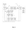
- FIG. 1is a schematic representation of an embodiment of an RF impedance matching network using EVCs incorporated into a semiconductor wafer fabrication system
- FIG. 2illustrates an EVC for use in an RF impedance matching network
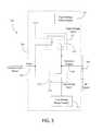
- FIG. 3illustrates a first switching circuit for use with an EVC
- FIG. 4is a graphical representation showing the timing capabilities of a driver circuit to switch to high voltage on the common output
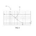
- FIG. 5is a graphical representation showing the timing capabilities of a driver circuit to switch to low voltage on the common output
- FIG. 6illustrates a second switching circuit for use with an EVC
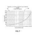
- FIG. 7is a graph showing the capacitance range of an EVC
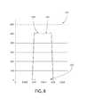
- FIG. 8is a graph showing the stable delivered power and the low reflected power that an impedance matching network including EVCs may provide during tuning;
- FIG. 9is a graphical representation showing the reflected RF power profile through an RF impedance matching network using EVCs and showing the voltage supplied to the driver circuit for the EVCs;
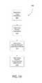
- FIG. 10is a flow chart showing an embodiment of a process for matching an impedance.
- FIG. 1illustrates an RF impedance matching network 11 having an RF input 13 connected to an RF source 15 and an RF output 17 connected to a plasma chamber 19 .
- An RF input sensor 21is connected between the RF impedance matching network 11 and the RF source 15 so that the RF signal output from the RF source 15 may be monitored.
- An RF output sensor 49is connected between the RF impedance matching network 11 and the plasma chamber 19 so that the RF output from the impedance matching network, and the plasma impedance presented by the plasma chamber 19 , may be monitored.
- Certain embodimentsmay include only one of the input sensor 21 and the output sensor 49 . The functioning of these sensors 21 , 49 are described in greater detail below.
- the RF impedance matching network 11serves to help maximize the amount of RF power transferred from the RF source 15 to the plasma chamber 19 by matching the impedance at the RF input 13 to the fixed impedance of the RF source 15 .
- the matching network 11can consist of a single module within a single housing designed for electrical connection to the RF source 15 and plasma chamber 19 .
- the components of the matching network 11can be located in different housings, some components can be outside of the housing, and/or some components can share a housing with a component outside the matching network.
- the plasma within a plasma chamber 19typically undergoes certain fluctuations outside of operational control so that the impedance presented by the plasma chamber 19 is a variable impedance. Since the variable impedance of the plasma chamber 19 cannot be fully controlled, and an impedance matching network may be used to create an impedance match between the plasma chamber 19 and the RF source 15 . Moreover, the impedance of the RF source 15 may be fixed at a set value by the design of the particular RF source 15 .
- the impedance of an RF source 15may undergo minor fluctuations during use, due to, for example, temperature or other environmental variations, the impedance of the RF source 15 is still considered a fixed impedance for purposes of impedance matching because the fluctuations do not significantly vary the fixed impedance from the originally set impedance value.
- Other types of RF source 15may be designed so that the impedance of the RF source 15 may be set at the time of, or during, use.
- the impedance of such types of RF sources 15is still considered fixed because it may be controlled by a user (or at least controlled by a programmable controller) and the set value of the impedance may be known at any time during operation, thus making the set value effectively a fixed impedance.
- the RF source 15may be an RF generator of a type that is well-known in the art, and generates an RF signal at an appropriate frequency and power for the process performed within the plasma chamber 19 .
- the RF source 15may be electrically connected to the RF input 13 of the RF impedance matching network 11 using a coaxial cable, which for impedance matching purposes would have the same fixed impedance as the RF source 15 .
- the plasma chamber 19includes a first electrode 23 and a second electrode 25 , and in processes that are well known in the art, the first and second electrodes 23 , 25 , in conjunction with appropriate control systems (not shown) and the plasma in the plasma chamber, enable one or both of deposition of materials onto a substrate 27 and etching of materials from the substrate 27 .
- the RF impedance matching network 11includes a series variable capacitor 31 , a shunt variable capacitor 33 , and a series inductor 35 configured as one form an ‘L’ type matching network.
- the shunt variable capacitor 33is shown shunting to ground 40 between the series variable capacitor 31 and the series inductor 35 , and one of skill in the art will recognize that the RF impedance matching network 11 may be configured with the shunt variable capacitor 33 shunting to ground 40 at the RF input 13 or at the RF output 17 .
- the RF impedance matching network 11may be configured in other matching network configurations, such as a ‘T’ type configuration or a ‘ ⁇ ’ type configuration.
- the variable capacitors and the switching circuit described belowmay be included in any configuration appropriate for an RF impedance matching network.
- Each of the series variable capacitor 31 and the shunt variable capacitor 33may be an electronic variable capacitor (EVC), as described in U.S. Pat. No. 7,251,121.
- the series variable capacitor 31is coupled in series between the RF input 13 and the RF output 17 (which is also in parallel between the RF source 15 and the plasma chamber 19 ).
- the shunt variable capacitor 33is coupled in parallel between the RF input 13 and ground 40 .
- the shunt variable capacitor 33may be coupled in parallel between the RF output 19 and ground 40 .
- Other configurationsmay also be implemented without departing from the functionality of an RF matching network.
- the series variable capacitor 31is connected to a series RF choke and filter circuit 37 and to a series driver circuit 39 .
- the shunt variable capacitor 33is connected to a shunt RF choke and filter circuit 41 and to a shunt driver circuit 43 .
- Each of the series and shunt driver circuits 39 , 43are connected to a control circuit 45 , which is configured with an appropriate processor and/or signal generating circuitry to provide an input signal for controlling the series and shunt driver circuits 39 , 43 .
- a power supply 47is connected to each of the RF input sensor 21 , the series driver circuit 39 , the shunt driver circuit 43 , and the control circuit 45 to provide operational power, at the designed currents and voltages, to each of these components.
- the voltage levels provided by the power supply 47and thus the voltage levels employed by each of the RF input sensor 21 , the series driver circuit 39 , the shunt driver circuit 43 , and the control circuit 45 to perform the respective designated tasks, is a matter of design choice.
- a variety of electronic componentscan be used to enable the control circuit 45 to send instructions to the variable capacitors.
- the driver circuit and RF choke and filterare shown as separate from the control circuit 45 , these components can also be considered as forming part of the control circuit 45 .
- the control circuit 45includes a processor.
- the processormay be any type of properly programmed processing device, such as a computer or microprocessor, configured for executing computer program instructions (e.g. code).
- the processormay be embodied in computer and/or server hardware of any suitable type (e.g. desktop, laptop, notebook, tablets, cellular phones, etc.) and may include all the usual ancillary components necessary to form a functional data processing device including without limitation a bus, software and data storage such as volatile and non-volatile memory, input/output devices, graphical user interfaces (GUIs), removable data storage, and wired and/or wireless communication interface devices including Wi-Fi, Bluetooth, LAN, etc.
- the processor of the exemplified embodimentis configured with specific algorithms to enable matching network to perform the functions described herein.
- the combined impedances of the RF impedance matching network 11 and the plasma chamber 19may be controlled, using the control circuit 45 , the series driver circuit 39 , the shunt driver circuit 43 , to match, or at least to substantially match, the fixed impedance of the RF source 15 .
- the control circuit 45is the brains of the RF impedance matching network 11 , as it receives multiple inputs, from sources such as the RF input sensor 21 and the series and shunt variable capacitors 31 , 33 , makes the calculations necessary to determine changes to the series and shunt variable capacitors 31 , 33 , and delivers commands to the series and shunt variable capacitors 31 , 33 to create the impedance match.
- the control circuit 45is of the type of control circuit that is commonly used in semiconductor fabrication processes, and therefore known to those of skill in the art. Any differences in the control circuit 45 , as compared to control circuits of the prior art, arise in programming differences to account for the speeds at which the RF impedance matching network 11 is able to perform switching of the variable capacitors 31 , 33 and impedance matching.
- Each of the series and shunt RF choke and filter circuits 37 , 41are configured so that DC signals may pass between the series and shunt driver circuits 39 , 43 and the respective series and shunt variable capacitors 31 , 33 , while at the same time the RF signal from the RF source 15 is blocked to prevent the RF signal from leaking into the outputs of the series and shunt driver circuits 39 , 43 and the output of the control circuit 45 .
- the series and shunt RF choke and filter circuits 37 , 41are of a type known to those of skill in the art.
- the series and shunt variable capacitors 31 , 33may each be an electronically variable capacitor 51 such as is depicted in FIG. 2 .
- the electronically variable capacitor 51includes a plurality of discrete capacitors 53 , each of which has an electrode on opposite sides thereof, such as is typical of discrete capacitors that are available on the market.
- Each discrete capacitor 53has its individual bottom electrode 55 electrically connected to a common bottom electrode 57 .
- the individual top electrode 59 of each discrete capacitor 53is electrically connected to the individual top electrode 59 of adjacent discrete capacitors 53 through an electronic switch 61 that may be activated to electrically connect the adjacent top electrodes 59 .
- the individual top electrodes 59 of each discrete capacitor 53may be electrically connected to the top electrodes 59 of one or more adjacent discrete capacitors 53 .
- the electronic switch 61is selected and/or designed to be capable of switching the voltage and current of the RF signal.
- the electronic switch 61may be a PiN/NiP diode, or a circuit based on a PiN/NiP diode.
- the electronic switch 61may be any other type of appropriate switch, such as a micro electro mechanical (MEM) switch, a solid state relay, a field effect transistor, and the like.
- MEMmicro electro mechanical
- the electronic switch 61in combination with a driver circuit, is discussed in greater detail below.
- each individual top electrode 59may be electrically connected to between two to four adjacent top electrodes 59 , with each connection being independently regulated by a separate electronic switch 61 .
- the RF signal input 63is electrically connected to one of the individual top electrodes 59
- the RF signal output 65is electrically connected to the common bottom electrode 57 .
- the electronic circuit through which the RF signal passesmay include one, some, or all of the discrete capacitors 53 by a process of independently activating one or more of the electronic switches 61 coupled to adjacent ones of the individual top electrodes 59 .
- the electronically variable capacitor 51may be configured to have any layout for the individual top electrodes 59 , to thereby increase or decrease the number of possible electrical connections between adjacent top electrodes 59 .
- the electronically variable capacitor 51may have an integrated dielectric disposed between the bottom electrode 57 and a plurality of top electrodes 59 .
- the electronic switch 61 that is used to connect pairs of adjacent top electrodes 59may be a PiN/NiP diode-based switch, although other types of electronic switches may be used, such as a Micro Electro Mechanical (MEM) switch, a solid state relay, a field effect transistor, and the like.
- MEMMicro Electro Mechanical
- Each electronic switch 61is switched by appropriate driver circuitry.
- each of the series and shunt driver circuits 39 , 43 of FIG. 1may include several discrete driving circuits, with each discrete driving circuit configured to switch one of the electronic switches 61 .
- FIG. 3shows an embodiment of a high voltage switching circuit 101 , which is shown including a driver circuit 102 and a PiN/NiP diode 103 as an electronic switch.
- this switching circuitis shown with the driver circuit 102 integrated with the PiN/NiP diode 103 , one of skill in the art will understand that in practice, the PiN/NiP diode 103 , or any other type of electronic switch, may be integrated with the discrete capacitors in an EVC that is part of an RF impedance matching network, with the RF choke and filter circuit connected between the output of the driver circuit 102 and the PiN/NiP diode 103 .
- the switching circuit 101may be used for switching one of the discrete capacitors in an EVC between an ‘ON’ state and an ‘OFF’ state.
- the use of the PiN/NiP diode 103 in this embodimentis exemplary, and that the switching circuit 101 may include other types of circuitry that does not include the PiN/NiP diode 103 , yet still provides some of the same fast switching advantages of the PiN/NiP diode 103 for switching one of the discrete capacitors in an EVC.
- certain components of the driver circuit 102may be replaced with other components that perform the same essential function while also greater allowing variability in other circuit parameters (e.g. voltage range, current range, and the like).
- This driver circuit 102has an input 105 which receives a common input signal for controlling the voltage on the common output 107 that is connected to and drives the PiN/NiP diode 103 .
- the voltage on the common output 107switches the PiN/NiP diode 103 between the ‘ON’ state and the ‘OFF’ state, thus also switching ‘ON’ and ‘OFF’ the discrete capacitor to which the PiN/NiP diode 103 is connected.
- the state of the discrete capacitorfollows the state of the state of the PiN/NiP diode 103 , such that when the PiN/NiP diode 103 is ‘ON’, the discrete capacitor is also ‘ON’, and likewise, when the PiN/NiP diode 103 is ‘OFF’, the discrete capacitor is also ‘OFF’.
- statements herein about the state of the PiN/NiP diode 103inherently describe the concomitant state of the connected discrete capacitor of the EVC.
- the input 105is connected to both a first power switch 111 and into a second power switch 113 .
- the first power switch 111is an optocoupler phototransistor 111 ′
- the second power switch 113is a MOSFET 113 ′.
- a high voltage power supply 115is connected to the first power switch 111 , providing a high voltage input which is to be switchably connected to the common output 107 .
- a low voltage power supply 117is connected to the second power switch 113 , providing a low voltage input which is also to be switchably connected to the common output 107 . In the configuration of the driver circuit 102 shown, the low voltage power supply 117 may supply a low voltage input which is about ⁇ 5 V.
- Such a low voltage, with a negative polarity,is sufficient to provide a forward bias for switching the PiN/NiP diode 103 .
- a higher or lower voltage inputmay be used, and the low voltage input may have a positive polarity, depending upon the configuration and the type of electronic switch being controlled.
- the common input signalasynchronously controls the ‘on’ and ‘off’ states of the first power switch 111 and the second power switch 113 , such that when the first power switch 111 is in the ‘on’ state, the second power switch 113 is in the ‘off’ state, and similarly, when the first power switch is in the ‘off’ state, the second power switch 113 is in the ‘on’ state.
- the common input signalcontrols the first power switch 111 and the second power switch 113 to asynchronously connect the high voltage input and the low voltage input to the common output for purposes of switching the PiN/NiP diode 103 between the ‘ON’ state and the ‘OFF’ state.
- the input 105may be configured to receive any type of appropriate control signal for the types of switches selected for the first power switch 111 and the second power switch 113 , which may be, for example, a +5 V control signal.
- the first and second power switches 111 , 113are preferably selected so that they may directly receive the common input signal without requiring additional circuitry to filter or otherwise transform the common input signal.
- the switching circuit 101has design features which make it particularly useful for switching between a high voltage input and a low voltage input on the common output quickly and without the need to float the drive circuit, with respect to the high voltage input, or require use of special gate charging circuits due to isolation of the input signal from the high voltage input.
- Another advantage of the switching circuit 101is that it provides the ability to switch the common output between voltage modes quickly, within the time frame of about 15 ⁇ sec or less.
- the simplicity of the switching circuit 101should considerably reduce manufacturing costs, especially when compared to other circuits performing similar functionality, and it should also significantly reduce space requirements for the circuit, and again, especially as compared to other circuits performing similar functionality.
- the first power switch 111being a monolithic circuit element, such as the optocoupler phototransistor 111 ′.
- a monolithic elementreduces both cost and space requirements.
- an optocoupler phototransistor 111 ′is used as the monolithic element, it can perform the necessary high voltage switching quickly, and it serves to isolate the high voltage input from the common input signal.
- Other, as yet unrealized advantagesmay also be present through the use of an optocoupler phototransistor 111 ′.
- An optocoupler phototransistor 111 ′serves well as the first power switch 111 for use in conjunction with the PiN/NiP diode 103 because of the low current requirements for the PiN/NiP diode 103 when in the ‘OFF’ state.
- the PiN/NiP diode 103is reverse biased, and thus non-conducting, and as such the ‘OFF’ state current requirement falls within the current handling capability of most optocoupler phototransistors.
- additional optocoupler phototransistorsmay be added into the circuit in series or in parallel to increase the voltage and/or current handling capabilities of the switching circuit.
- the common input signalmay be a 5 V control signal which is alternated between a first voltage level and a second voltage level that serve to switch both the optocoupler phototransistor 111 ′ and the MOSFET 113 ′ between ‘on’ and ‘off’ states.
- the manner of implementing a 5 V control signalis well known to those of skill in the art.
- the optocoupler phototransistor 111 ′When the PiN/NiP diode 103 is to be turned to the ‘OFF’ state, the optocoupler phototransistor 111 ′ is turned to the ‘on’ state by applying the first voltage level from the common input signal across the photodiode inputs of the optocoupler phototransistor 111 ′. Turning the optocoupler phototransistor 111 ′ to the ‘on’ state connects high voltage input to the common output 107 , thereby reverse biasing the PiN/NiP diode 103 .
- the optocoupler phototransistor 111 ′When the PiN/NiP diode 103 is to be turned to the ‘ON’ state, the optocoupler phototransistor 111 ′ is turned to the ‘off’ state by applying the second voltage level from the common input signal across the photodiode inputs of the optocoupler phototransistor 111 ′. Turning the optocoupler phototransistor 111 ′ to the ‘off’ state disconnects high voltage input from the common output 107 . At the same time, application of the second voltage level from the common input signal to the MOSFET 113 ′ places the MOSFET 113 ′ in the ‘on’ state, thereby connecting the low voltage input to the common output 107 .
- the optocoupler phototransistor 111 ′provides the advantage that the common input signal is electrically isolated, through the internal optical switch (not shown) of the optocoupler phototransistor 111 ′, from the switched high voltage, thus alleviating the need to float the drive circuit (such as when a MOSFET is used to switch the high voltage).
- Use of the optocoupler phototransistor 111 ′provides the additional advantage that the driver circuit 102 can quickly switch the common output 107 between the high voltage input and the low voltage input, with the switching occurring within the time frame of about 15 ⁇ sec or less.
- This fast switching timehelps reduce switching loss, thereby reducing stress on the PiN/NiP diode itself, and introduces improvements in the semiconductor fabrication process by reducing the amount of time it takes for the RF impedance matching network to create an impedance match between the RF source and the plasma chamber.
- optocoupler phototransistors in the driver circuit 102also provides advantages for switching a high voltage input in the range of 500 V-1000 V. Higher or lower voltages may also be switched with this driver circuit 102 .
- the high voltage inputmay therefore differ from the low voltage input by at least two or three orders of magnitude, or more.
- the switching circuit 101incorporates the PiN/NiP diode 103 , the high voltage input and the low voltage input may have opposite polarities.
- the ability of the driver circuit 102 to provide quick switching capabilitiesis exemplified by the graphs 151 , 161 of FIGS. 4 and 5 .
- the voltage curve 153 of FIG. 4shows the voltage on the common output 107 of the driver circuit 102 in order to switch the connected PiN/NiP diode 103 to the ‘OFF’ state.
- the driver circuit 102is capable of switching to connect the high voltage input, which in this example is approximately 1,000 V, to the common output 107 within about 11 ⁇ sec.
- the voltage curve 163 of FIG. 5shows the voltage on the common output 107 of the driver circuit 102 in order to switch the connected PiN/NiP diode 103 to the ‘ON’ state.
- the driver circuit 102is capable of switching to connect the low voltage input, which in this example is approximately ⁇ 12 V, to the common output 107 within about 9 ⁇ sec.
- an RF impedance matching networkwhich includes EVCs and switching circuits, as described above, shows significant improvements as compared to an RF impedance matching network which includes VVCs.
- a switching circuit 201which includes a driver circuit 202 having multiple optocoupler phototransistors 203 to increase the high voltage capabilities is shown in FIG. 6 .
- this driver circuit 202includes an input 205 which receives a common input signal for controlling the voltage on the common output 207 .
- the switching circuit 201includes a PiN/NiP diode 209 connected to the common output 207 , and the voltage on the common output 207 may be used to switch the PiN/NiP diode 209 between ‘ON’ state and ‘OFF’ states.
- the input 205is connected to both a first power switch 211 , which includes the optocoupler phototransistors 203 , and to a second power switch 213 , which includes another optocoupler phototransistor 215 and a MOSFET 217 .
- a high voltage power supply 219is connected to the first power switch 211 , providing a high voltage input which is to be switchably connected to the common output 207 .
- a low voltage power supply 221is connected to the second power switch 213 , providing a low voltage input which is also to be switchably connected to the common output 207 .
- the optocoupler phototransistors 203 of the first power switch 211are connected in series to each other in order to enable the first power switch 211 to switch higher voltages onto the common output 207 in the same manner as discussed above with a single optocoupler phototransistor.
- the first power switch 211With appropriate selection of the optocoupler phototransistors 203 , the first power switch 211 , as shown, is capable of switching about 1000 V or more from the high voltage power supply 219 to the common output 207 .
- Additional optocoupler phototransistorsmay be added in series for the first power switch 211 to increase the high voltage switching capabilities.
- one or more optocoupler phototransistorsmay be connected in parallel to each other to increase the current load capabilities of the first power switch 211 .
- One optocoupler phototransistormay be used to switch low voltages through the design rating of the optocoupler phototransistor, with more optocoupler phototransistors being added to switch higher voltages.
- the optocoupler phototransistor 215 of the second power switch 213receives the common input signal, like the optocoupler phototransistors 203 of the first power switch 211 .
- This optocoupler phototransistor 215is connected to the MOSFET 217 and places the MOSFET 217 in the ‘off’ state by connecting the source to the gate when the common input signal places the first power switch 211 in the ‘on’ state.
- the second power switch 213is also in the ‘on’ state, connecting the low power input to the common output 207 .
- the second power switch 213is also in the ‘off’ state, so that the low power input is disconnected from the common output 207 .
- optocoupler phototransistor 215disconnects the gate from the source, so that the MOSFET 217 placed in the ‘on’ state by the gate being connected to the voltage V 2 , which is an appropriate voltage for controlling the gate of the MOSFET 217 .
- the non-linear capacitance range of a single EVC switched by a switching circuitis shown in the graph 301 of FIG. 7 .
- the single EVC used to generate the capacitance curve 303has 24 discrete capacitors in the manner described above, with the top electrodes of the discrete capacitors being selectively connected to arrive at the capacitance curve 303 shown.
- the single EVCmay provide a capacitance ranging from only one active discrete capacitor (i.e., none of the top electrodes of any of the discrete capacitors are connected, so that the RF signal only flows through a single discrete capacitor) to all 24 discrete capacitors being active (i.e., all the top electrodes of all the discrete capacitors are connected).
- any number of the 24 discrete capacitorsmay be connected, so that the capacitance of the single EVC may range from a low capacitance, with one active discrete capacitor, to a high capacitance, with all 24 discrete capacitors active.
- the low capacitance and the high capacitanceare a matter of design choice for the EVC. In the capacitance curve shown, the low capacitance is about 25 pF, while the high capacitance is over 1,600 pF.
- the number of discrete capacitance values that is achievable between the low capacitance and the high capacitanceis also a matter of design choice for the EVC, as more or fewer discrete capacitors may be included as part of the EVC.
- the stable delivered power of an RF impedance matching network incorporating EVCsis shown in the graph 331 of FIG. 8 , which does not show or take into account switching capabilities of an EVC controlled by a switching circuit.
- the output power 333is a little over 500 V, while the reflected power 337 is in the range of about 10 V, so that the delivered power 335 to the plasma chamber is about 500 V.
- the delivered power 335is substantially stable, without significant fluctuations. Both the percentage of delivered power 335 and the stability of the delivered power 335 represent significant improvements over an RF impedance matching network that is based on VVCs.
- FIG. 9is a graph 401 having voltage along the two y-axes and time along the x-axis to show the speed at which an RF impedance matching network using EVCs performs impedance matching (also referred to as the “match tune process”).
- a representation of an RF power profile 403is shown, taken at the RF input of an RF impedance matching network, and the y-axis for the RF power profile has 50 mV divisions.
- a representation of the voltage of the common input signal 405 for driver circuitsis also shown in the lower portion of the graph 401 , the common input signal 405 originating from the control circuit of the RF impedance matching network, and the y-axis for the common input signal 405 has 5 V divisions.
- reflected power 407is shown in the left portion of the RF power profile 403 (i.e., before the 56 ⁇ sec mark). This reflected power represents inefficiencies in the RF power being transferred between the RF source and the plasma chamber as a result of an impedance mismatch.
- the match tune processbegins. The first approximately 50 ⁇ sec of the match tune process is consumed by measurements and calculations performed by the control circuit in order to determine new values for the variable capacitances of one or both of the series and shunt EVCs.
- FIG. 10is a flow chart showing a process 500 for matching an impedance according to one embodiment.
- the matching network 11 of the exemplified processincludes the following (shown in FIG. 1 ): an RF input 13 configured to operably couple to an RF source 15 , the RF source 15 having a fixed RF source impedance (e.g., 50 Ohms); an RF output 17 configured to operably couple to a plasma chamber 19 , the plasma chamber 19 having a variable plasma impedance; a series electronically variable capacitor (“series EVC”) 31 having a series variable capacitance, the series EVC 31 electrically coupled in series between the RF input 13 and the RF output 17 ; a shunt electronically variable capacitor (“shunt EVC”) 33 having a shunt variable capacitance, the shunt EVC 33 electrically coupled in parallel between a ground 40 and one of the RF input 13 and the RF output 17 ; an RF input sensor 21 operably coupled to the RF input 13 , the
- the steps of the exemplified process 500can be carried out as part of the manufacture of a semiconductor, where a substrate 27 is placed in a plasma chamber 19 configured to deposit a material layer onto the substrate 27 or etch a material layer from the substrate 27 , and plasma is energized within the plasma chamber 19 by coupling RF power from the RF source 15 into the plasma chamber 19 to perform a deposition or etching.
- the variable capacitors 31 , 33can be VVCs or other types of variable capacitors.
- an input impedance at the RF input 13is determined (step 501 ).
- the input impedanceis based on the RF input parameter detected by the RF input sensor 21 at the RF input 13 .
- the RF input sensor 21can be any sensor configured to detect an RF input parameter at the RF input 13 .
- the input parametercan be any parameter measurable at the RF input 13 , including a voltage, a current, or a phase at the RF input 13 .
- the RF input sensor 21detects the voltage, current, and phase at the RF input 13 of the matching network 11 .
- the control circuit 45determines the input impedance.
- the input impedancecan be determined by other means that do not use sensor 21 , or place sensor 21 at a different location in the matching network 11 .
- an alternative parametercould be determined to calculate the input impedance.
- the control circuit 45determines the plasma impedance presented by the plasma chamber 19 (step 502 ).
- the plasma impedance determinationis based on the input impedance (determined in step 501 ), the capacitance of the series EVC 31 , and the capacitance of the shunt EVC 33 .
- the plasma impedance determinationcan be made using the output sensor 49 operably coupled to the RF output, the RF output sensor 49 configured to detect an RF output parameter.
- the RF output parametercan be any parameter measurable at the RF output 17 , including a voltage, a current, or a phase at the RF output 17 .
- the RF output sensor 49may detect the output parameter at the RF output 17 of the matching network 11 .
- the control circuit 45may determine the plasma impedance.
- the plasma impedance determinationcan be based on both the RF output parameter and the RF input parameter.
- the control circuit 45can determine the changes to make to the variable capacitances of one or both of the series and shunt EVCs 31 , 33 for purposes of achieving an impedance match. Specifically, the control circuit 45 determines a first capacitance value for the series variable capacitance and a second capacitance value for the shunt variable capacitance (step 503 ). These values represent the new capacitance values for the series EVC 31 and shunt EVC 33 to enable an impedance match, or at least a substantial impedance match. In the exemplified embodiment, the determination of the first and second capacitance values is based on the variable plasma impedance (determined in step 502 ) and the fixed RF source impedance.
- the control signalinstructs the switching circuit 101 ( FIG. 3 ) to alter the variable capacitance of one or both of the series and shunt EVCs 31 , 33 .
- This alteration of the EVCs 31 , 33takes about 9-11 ⁇ sec total, as compared to about 1-2 sec of time for an RF matching network using VVCs.
- the switch to the different variable capacitancesis complete, there is a period of latency as the additional discrete capacitors that make up the EVCs join the circuit and charge.
- This part of the match tune processtakes about 55 ⁇ sec.
- the altering of the series variable capacitance and the shunt variable capacitancecan comprise sending a control signal to the series driver circuit 39 and the shunt driver circuit 43 to control the series variable capacitance and the shunt variable capacitance, respectively, where the series driver circuit 39 is operatively coupled to the series EVC 31 , and the shunt driver circuit 43 is operatively coupled to the shunt EVC 43 .
- the input impedancemay match the fixed RF source impedance (e.g., 50 Ohms), thus resulting in an impedance match. If, due to fluctuations in the plasma impedance, a sufficient impedance match does not result, the process of 500 may be repeated one or more times to achieve an impedance match, or at least a substantial impedance match.
- the input impedancecan be represented as follows:
- Z in( Z P + Z L + Z series ) ⁇ Z shunt Z P + Z L + Z series + Z shunt
- Z inis the input impedance
- Z Pis the plasma impedance
- Z Lis the series inductor impedance
- Z seriesis the series EVC impedance
- Z shuntis the shunt EVC impedance.
- the input impedance (Z in )is determined using the RF input sensor 21 .
- the EVC impedances (Z series and Z shunt )are known at any given time by the control circuitry, since the control circuitry is used to command the various discrete capacitors of each of the series and shunt EVCs to turn ON or OFF.
- the series inductor impedance (Z L )is a fixed value. Thus, the system can use these values to solve for the plasma impedance (Z P ).
- the systemcan determine a new series EVC impedance (Z series ′) and shunt EVC impedance (Z shunt ′).
- the systemcan then determine the new capacitance value (first capacitance value) for the series variable capacitance and a new capacitance value (second capacitance value) for the shunt variable capacitance.
- first capacitance valuethe new capacitance value for the series variable capacitance
- second capacitance valuethe new capacitance value for the shunt variable capacitance.
- This exemplified method of computing the desired first and second capacitance values and reaching those values in one stepis significantly faster than moving the two EVCs step-by-step to bring either the error signals to zero, or to bring the reflected power/reflection coefficient to a minimum.
- this approachprovides a significant improvement in matching network tune speed.
- the entire match tune process of the RF impedance matching network using EVCshas an elapsed time of approximately 110 ⁇ sec, or on the order of about 150 ⁇ sec or less. This short elapsed time period for a single iteration of the match tune process represents a significant increase over a VVC matching network.
- the RF impedance matching network using EVCsmay iteratively perform the match tune process, repeating the two determining steps and the generating another control signal for further alterations to the variable capacitances of one or both of the electronically variable capacitors.
- iteratively repeating the match tune processit is anticipated that a better impedance match may be created within about 2-4 iterations of the match tune process.
- 3-4 iterationsmay be performed in 500 ⁇ sec or less.
- the entire match tune process for an RF impedance matching network having EVCsshould take no more than about 500 ⁇ sec to complete from the beginning of the process (i.e., measuring by the control circuit and calculating adjustments needed to create the impedance match) to the end of the process (the point in time when the efficiency of RF power coupled into the plasma chamber is increased due to an impedance match and a reduction of the reflected power). Even at a match tune process on the order of 500 ⁇ sec, this process time still represents a significant improvement over RF impedance matching networks using VVCs.
- Table 1presents data showing a comparison between operational parameters of one example of an EVC versus one example of a VVC.
- EVCspresent several advantages, in addition to enabling fast switching for an RF impedance matching network:
- EVCsalso introduce a reliability advantage, a current handling advantage, and a size advantage. Additional advantages of the RF impedance matching network using EVCs and/or the switching circuit itself for the EVCs include:
Landscapes
- Engineering & Computer Science (AREA)
- Physics & Mathematics (AREA)
- Manufacturing & Machinery (AREA)
- Computer Hardware Design (AREA)
- Microelectronics & Electronic Packaging (AREA)
- Power Engineering (AREA)
- Condensed Matter Physics & Semiconductors (AREA)
- General Physics & Mathematics (AREA)
- Chemical & Material Sciences (AREA)
- Plasma & Fusion (AREA)
- Chemical Kinetics & Catalysis (AREA)
- General Chemical & Material Sciences (AREA)
- Analytical Chemistry (AREA)
- Inorganic Chemistry (AREA)
- Plasma Technology (AREA)
Abstract
Description
where Zinis the input impedance, ZPis the plasma impedance, ZLis the series inductor impedance, Zseriesis the series EVC impedance, and Zshuntis the shunt EVC impedance. In the exemplified embodiment, the input impedance (Zin) is determined using the
| TABLE 1 | ||
| Typical 1000 pF | ||
| Parameter | EVC | Vacuum Capacitors |
| Capacitance | 20 pF~1400 | 15 pF~1000 pF |
| Reliability | High | Low |
| Response Time | ~500 μsec | 1 s~2 s |
| ESR | ~13 mW | ~20 |
| Voltage | ||
| 7 | 5 kV | |
| Current Handling | 216 A rms | 80 A rms |
| Capability | ||
| Volume | 4.5 in3 | 75 in3 |
- The disclosed RF impedance matching network does not include any moving parts, so the likelihood of a mechanical failure reduced to that of other entirely electrical circuits which may be used as part of the semiconductor fabrication process. For example, the typical EVC may be formed from a rugged ceramic substrate with copper metallization to form the discrete capacitors. The elimination of moving parts also increases the resistance to breakdown due to thermal fluctuations during use.
- The EVC has a compact size as compared to a VVC, so that the reduced weight and volume may save valuable space within a fabrication facility.
- The design of the EVC introduces an increased ability to customize the RF matching network for specific design needs of a particular application. EVCs may be configured with custom capacitance ranges, one example of which is a non-linear capacitance range. Such custom capacitance ranges can provide better impedance matching for a wider range of processes. As another example, a custom capacitance range may provide more resolution in certain areas of impedance matching. A custom capacitance range may also enable generation of higher ignition voltages for easier plasma strikes.
- The short match tune process (˜500 μsec or less) allows the RF impedance matching network to better keep up with plasma changes within the fabrication process, thereby increasing plasma stability and resulting in more controlled power to the fabrication process.
- The use of EVCs, which are digitally controlled, non-mechanical devices, in an RF impedance matching network provides greater opportunity to fine tune control algorithms through programming.
- EVCs exhibit superior low frequency (kHz) performance as compared to VVCs.
Claims (20)
Priority Applications (14)
| Application Number | Priority Date | Filing Date | Title |
|---|---|---|---|
| US14/616,884US9865432B1 (en) | 2014-01-10 | 2015-02-09 | RF impedance matching network |
| US14/669,568US9196459B2 (en) | 2014-01-10 | 2015-03-26 | RF impedance matching network |
| US14/788,888US9697991B2 (en) | 2014-01-10 | 2015-07-01 | RF impedance matching network |
| US14/935,859US20160065207A1 (en) | 2014-01-10 | 2015-11-09 | High voltage control circuit for an electronic switch |
| US14/936,978US9844127B2 (en) | 2014-01-10 | 2015-11-10 | High voltage switching circuit |
| US14/982,244US10454453B2 (en) | 2014-01-10 | 2015-12-29 | RF impedance matching network |
| US15/467,667US10455729B2 (en) | 2014-01-10 | 2017-03-23 | Enclosure cooling system |
| US15/637,271US10431428B2 (en) | 2014-01-10 | 2017-06-29 | System for providing variable capacitance |
| US16/111,776US10460912B2 (en) | 2014-01-10 | 2018-08-24 | RF impedance matching circuit and systems and methods incorporating same |
| US16/665,778US10707057B2 (en) | 2014-01-10 | 2019-10-28 | RF impedance matching circuit and systems and methods incorporating same |
| US16/922,228US11195698B2 (en) | 2014-01-10 | 2020-07-07 | RF impedance matching circuit and systems and methods incorporating same |
| US17/182,902US11189466B2 (en) | 2014-01-10 | 2021-02-23 | High voltage switching circuit |
| US17/534,924US12334306B2 (en) | 2014-01-10 | 2021-11-24 | RF impedance matching network |
| US19/208,485US20250273434A1 (en) | 2014-01-10 | 2025-05-14 | Rf impedance matching network |
Applications Claiming Priority (4)
| Application Number | Priority Date | Filing Date | Title |
|---|---|---|---|
| US201461925974P | 2014-01-10 | 2014-01-10 | |
| US201461940139P | 2014-02-14 | 2014-02-14 | |
| US14/594,262US9496122B1 (en) | 2014-01-10 | 2015-01-12 | Electronically variable capacitor and RF matching network incorporating same |
| US14/616,884US9865432B1 (en) | 2014-01-10 | 2015-02-09 | RF impedance matching network |
Related Parent Applications (2)
| Application Number | Title | Priority Date | Filing Date |
|---|---|---|---|
| US14/594,262Continuation-In-PartUS9496122B1 (en) | 2014-01-10 | 2015-01-12 | Electronically variable capacitor and RF matching network incorporating same |
| US15/637,271Continuation-In-PartUS10431428B2 (en) | 2014-01-10 | 2017-06-29 | System for providing variable capacitance |
Related Child Applications (1)
| Application Number | Title | Priority Date | Filing Date |
|---|---|---|---|
| US201514622879AContinuation-In-Part | 2014-01-10 | 2015-02-15 |
Publications (1)
| Publication Number | Publication Date |
|---|---|
| US9865432B1true US9865432B1 (en) | 2018-01-09 |
Family
ID=60812738
Family Applications (1)
| Application Number | Title | Priority Date | Filing Date |
|---|---|---|---|
| US14/616,884Active2035-11-19US9865432B1 (en) | 2014-01-10 | 2015-02-09 | RF impedance matching network |
Country Status (1)
| Country | Link |
|---|---|
| US (1) | US9865432B1 (en) |
Cited By (42)
| Publication number | Priority date | Publication date | Assignee | Title |
|---|---|---|---|---|
| US20190288683A1 (en)* | 2016-11-17 | 2019-09-19 | Daihen Corporation | Drive Circuit and Impedance Matching Device |
| WO2020180848A1 (en)* | 2019-03-04 | 2020-09-10 | Advanced Energy Industries, Inc. | Detection of damage in matching networks |
| US10971335B2 (en)* | 2019-04-29 | 2021-04-06 | Samsung Electronics Co., Ltd. | Radio frequency (RF) power monitoring device and plasma enhanced (PE) system including the same |
| US10985735B2 (en) | 2018-12-27 | 2021-04-20 | Daihen Corporation | Impedance matching device and impedance matching method |
| US11050400B2 (en) | 2018-12-26 | 2021-06-29 | Daihen Corporation | Impedance matching device and impedance matching method |
| US11101109B2 (en) | 2018-12-27 | 2021-08-24 | Daihen Corporation | Impedance matching device and impedance matching method |
| US11107661B2 (en) | 2019-07-09 | 2021-08-31 | COMET Technologies USA, Inc. | Hybrid matching network topology |
| US11114279B2 (en) | 2019-06-28 | 2021-09-07 | COMET Technologies USA, Inc. | Arc suppression device for plasma processing equipment |
| US11218129B2 (en) | 2018-12-26 | 2022-01-04 | Daihen Corporation | Impedance matching device and impedance matching method |
| US11218135B2 (en) | 2018-12-28 | 2022-01-04 | Daihen Corporation | Impedance matching device and impedance matching method |
| US20220084791A1 (en)* | 2014-01-10 | 2022-03-17 | Reno Technologies, Inc. | Rf impedance matching network |
| US11290080B2 (en) | 2017-11-29 | 2022-03-29 | COMET Technologies USA, Inc. | Retuning for impedance matching network control |
| US11309164B2 (en) | 2019-11-25 | 2022-04-19 | Daihen Corporation | High-frequency power supply system |
| US11329614B2 (en) | 2019-10-11 | 2022-05-10 | Daihen Corporation | High-frequency power supply circuit and determining method of constants of amplifier circuit |
| US11348762B2 (en) | 2019-12-27 | 2022-05-31 | Daihen Corporation | High-frequency power supply system |
| US11373844B2 (en) | 2020-09-28 | 2022-06-28 | COMET Technologies USA, Inc. | Systems and methods for repetitive tuning of matching networks |
| US11387078B2 (en) | 2019-03-22 | 2022-07-12 | Daihen Corporation | Impedance matching device and impedance matching method |
| US11521832B2 (en) | 2020-01-10 | 2022-12-06 | COMET Technologies USA, Inc. | Uniformity control for radio frequency plasma processing systems |
| US11527385B2 (en) | 2021-04-29 | 2022-12-13 | COMET Technologies USA, Inc. | Systems and methods for calibrating capacitors of matching networks |
| EP4105962A1 (en)* | 2021-06-17 | 2022-12-21 | Impedans Ltd | A controller for a matching unit of a plasma processing system |
| EP4105963A1 (en)* | 2021-06-17 | 2022-12-21 | Impedans Ltd | A controller for a matching unit of a plasma processing system |
| US11545954B2 (en) | 2019-12-27 | 2023-01-03 | Daihen Corporation | Impedance adjustment device |
| US11552612B2 (en) | 2019-12-27 | 2023-01-10 | Daihen Corporation | Impedance adjustment device and impedance adjustment method |
| US11596309B2 (en) | 2019-07-09 | 2023-03-07 | COMET Technologies USA, Inc. | Hybrid matching network topology |
| US11605527B2 (en) | 2020-01-20 | 2023-03-14 | COMET Technologies USA, Inc. | Pulsing control match network |
| US11657980B1 (en) | 2022-05-09 | 2023-05-23 | COMET Technologies USA, Inc. | Dielectric fluid variable capacitor |
| US11670488B2 (en) | 2020-01-10 | 2023-06-06 | COMET Technologies USA, Inc. | Fast arc detecting match network |
| US11769651B2 (en) | 2019-09-26 | 2023-09-26 | Daihen Corporation | High-frequency power supply device and output method of high-frequency power |
| US11791134B2 (en) | 2019-12-27 | 2023-10-17 | Daihen Corporation | Impedance adjustment device |
| US11830708B2 (en) | 2020-01-10 | 2023-11-28 | COMET Technologies USA, Inc. | Inductive broad-band sensors for electromagnetic waves |
| US20240006156A1 (en)* | 2021-03-01 | 2024-01-04 | Trumpf Huettinger Gmbh + Co. Kg | Method for impedance matching, impedance matching arrangement and plasma system |
| US11887820B2 (en) | 2020-01-10 | 2024-01-30 | COMET Technologies USA, Inc. | Sector shunts for plasma-based wafer processing systems |
| US11923175B2 (en) | 2021-07-28 | 2024-03-05 | COMET Technologies USA, Inc. | Systems and methods for variable gain tuning of matching networks |
| US11961711B2 (en) | 2020-01-20 | 2024-04-16 | COMET Technologies USA, Inc. | Radio frequency match network and generator |
| US12002611B2 (en) | 2019-08-28 | 2024-06-04 | COMET Technologies USA, Inc. | High power low frequency coils |
| US12027351B2 (en) | 2020-01-10 | 2024-07-02 | COMET Technologies USA, Inc. | Plasma non-uniformity detection |
| US12040139B2 (en) | 2022-05-09 | 2024-07-16 | COMET Technologies USA, Inc. | Variable capacitor with linear impedance and high voltage breakdown |
| US12051549B2 (en) | 2022-08-02 | 2024-07-30 | COMET Technologies USA, Inc. | Coaxial variable capacitor |
| US12057296B2 (en) | 2021-02-22 | 2024-08-06 | COMET Technologies USA, Inc. | Electromagnetic field sensing device |
| US12132435B2 (en) | 2022-10-27 | 2024-10-29 | COMET Technologies USA, Inc. | Method for repeatable stepper motor homing |
| US12243717B2 (en) | 2022-04-04 | 2025-03-04 | COMET Technologies USA, Inc. | Variable reactance device having isolated gate drive power supplies |
| US12288673B2 (en) | 2017-11-29 | 2025-04-29 | COMET Technologies USA, Inc. | Retuning for impedance matching network control |
Citations (137)
| Publication number | Priority date | Publication date | Assignee | Title |
|---|---|---|---|---|
| US4110700A (en) | 1977-10-25 | 1978-08-29 | Rca Corporation | Electronically tunable microwave frequency FET discriminator |
| US4679007A (en) | 1985-05-20 | 1987-07-07 | Advanced Energy, Inc. | Matching circuit for delivering radio frequency electromagnetic energy to a variable impedance load |
| US4692643A (en) | 1983-10-28 | 1987-09-08 | Hitachi, Ltd. | Semiconductor switching device having plural MOSFET's, GTO's or the like connected in series |
| US4751408A (en) | 1985-09-06 | 1988-06-14 | Thomson-Csf | Voltage-switching device |
| US4929855A (en) | 1988-12-09 | 1990-05-29 | Grumman Corporation | High frequency switching device |
| US5012123A (en) | 1989-03-29 | 1991-04-30 | Hittite Microwave, Inc. | High-power rf switching system |
| US5079507A (en) | 1989-01-30 | 1992-01-07 | Daihen Corporation | Automatic impedance adjusting apparatus for microwave load and automatic impedance adjusting method therefor |
| US5654679A (en) | 1996-06-13 | 1997-08-05 | Rf Power Products, Inc. | Apparatus for matching a variable load impedance with an RF power generator impedance |
| EP0840349A2 (en) | 1996-11-04 | 1998-05-06 | Applied Materials, Inc. | RF tuning method for an RF plasma reactor using frequency servoing power, voltage, current or dI/dt control |
| EP0840350A2 (en) | 1996-11-04 | 1998-05-06 | Applied Materials, Inc. | Plasma apparatus and process with filtering of plasma sheath-generated harmonics |
| US5815047A (en) | 1993-10-29 | 1998-09-29 | Applied Materials, Inc. | Fast transition RF impedance matching network for plasma reactor ignition |
| US5849136A (en) | 1991-10-11 | 1998-12-15 | Applied Materials, Inc. | High frequency semiconductor wafer processing apparatus and method |
| US5880921A (en) | 1997-04-28 | 1999-03-09 | Rockwell Science Center, Llc | Monolithically integrated switched capacitor bank using micro electro mechanical system (MEMS) technology |
| US5889252A (en) | 1996-12-19 | 1999-03-30 | Lam Research Corporation | Method of and apparatus for independently controlling electric parameters of an impedance matching network |
| US5971591A (en) | 1997-10-20 | 1999-10-26 | Eni Technologies, Inc. | Process detection system for plasma process |
| US6027601A (en)* | 1997-07-01 | 2000-02-22 | Applied Materials, Inc | Automatic frequency tuning of an RF plasma source of an inductively coupled plasma reactor |
| US6046641A (en) | 1998-07-22 | 2000-04-04 | Eni Technologies, Inc. | Parallel HV MOSFET high power stable amplifier |
| US6137367A (en) | 1998-03-24 | 2000-10-24 | Amcom Communications, Inc. | High power high impedance microwave devices for power applications |
| US20020060914A1 (en) | 1999-03-23 | 2002-05-23 | Advanced Energy Industries, P.C. | High frequency power generator and related methods |
| US6400012B1 (en) | 1997-09-17 | 2002-06-04 | Advanced Energy Voorhees, Inc. | Heat sink for use in cooling an integrated circuit |
| US6424232B1 (en) | 1999-11-30 | 2002-07-23 | Advanced Energy's Voorhees Operations | Method and apparatus for matching a variable load impedance with an RF power generator impedance |
| US20030046013A1 (en) | 1998-02-27 | 2003-03-06 | Gerrish Kevin S. | Voltage current sensor with high matching directivity |
| US6583572B2 (en) | 2001-03-30 | 2003-06-24 | Lam Research Corporation | Inductive plasma processor including current sensor for plasma excitation coil |
| US6621372B2 (en) | 2001-03-01 | 2003-09-16 | Daihen Corporation | Impedance matching device |
| US6657395B2 (en) | 2000-08-17 | 2003-12-02 | Tokyo Electron Limited | Close coupled match structure for RF drive electrode |
| US6677828B1 (en) | 2000-08-17 | 2004-01-13 | Eni Technology, Inc. | Method of hot switching a plasma tuner |
| US6703080B2 (en) | 2002-05-20 | 2004-03-09 | Eni Technology, Inc. | Method and apparatus for VHF plasma processing with load mismatch reliability and stability |
| US6791274B1 (en) | 2003-07-15 | 2004-09-14 | Advanced Energy Industries, Inc. | RF power control device for RF plasma applications |
| US6794951B2 (en) | 2002-08-05 | 2004-09-21 | Veeco Instruments, Inc. | Solid state RF power switching network |
| US6818562B2 (en) | 2002-04-19 | 2004-11-16 | Applied Materials Inc | Method and apparatus for tuning an RF matching network in a plasma enhanced semiconductor wafer processing system |
| US6888396B2 (en) | 2002-03-11 | 2005-05-03 | California Inst Of Techn | Multi-cascode transistors |
| US6888313B2 (en) | 2003-07-16 | 2005-05-03 | Advanced Energy Industries, Inc. | Impedance matching network with termination of secondary RF frequencies |
| US6946847B2 (en) | 2002-02-08 | 2005-09-20 | Daihen Corporation | Impedance matching device provided with reactance-impedance table |
| US6967547B2 (en) | 2002-06-24 | 2005-11-22 | Signal Technology Corporation | RF switch including diodes with intrinsic regions |
| US7004107B1 (en) | 1997-12-01 | 2006-02-28 | Applied Materials Inc. | Method and apparatus for monitoring and adjusting chamber impedance |
| USRE39051E1 (en) | 1997-09-15 | 2006-03-28 | Eni Technology, Inc. | Fuzzy logic tuning of RF matching network |
| US7071786B2 (en) | 2003-07-09 | 2006-07-04 | Mitsubishi Denki Kabushiki Kaisha | Cascode circuit and integrated circuit having it |
| US20060170367A1 (en) | 2005-01-11 | 2006-08-03 | Bhutta Imran A | Method of detecting RF power delivered to a load and complex impedance of the load |
| US7095178B2 (en)* | 2001-11-27 | 2006-08-22 | Alps Electric Co., Ltd. | Plasma processing apparatus, method for operating the same, designing system of matching circuit, and plasma processing method |
| US20060198077A1 (en) | 2005-03-05 | 2006-09-07 | Innovation Engineering Llc | Electronically variable capacitor array |
| US7113761B2 (en) | 2003-10-07 | 2006-09-26 | Motorola, Inc. | RF power device with on-chip digital control and optical interface |
| US7122965B2 (en) | 2003-02-24 | 2006-10-17 | Mks Instruments, Inc. | Methods and apparatus for calibration and metrology for an integrated RF generator system |
| US20060232471A1 (en) | 2005-04-18 | 2006-10-19 | Mks Instruments, Inc. | Phase and frequency control of a radio frequency generator from an external source |
| US7164236B2 (en) | 2000-08-08 | 2007-01-16 | Tokyo Electron Limited | Method and apparatus for improved plasma processing uniformity |
| US7199678B2 (en) | 2004-11-09 | 2007-04-03 | Daihen Corporation | Impedance matching apparatus for a plasma chamber comprising two separate storage units and calculators |
| US20070075784A1 (en) | 2004-02-05 | 2007-04-05 | Ola Pettersson | Radio frequency power amplifier |
| US20070139122A1 (en) | 2005-10-31 | 2007-06-21 | Mks Instruments, Inc. | Radio Frequency Power Delivery System |
| US7298091B2 (en) | 2002-02-01 | 2007-11-20 | The Regents Of The University Of California | Matching network for RF plasma source |
| US7304438B2 (en) | 2003-09-22 | 2007-12-04 | Mks Instruments, Inc. | Method and apparatus for preventing instabilities in radio-frequency plasma processing |
| US20080179948A1 (en) | 2005-10-31 | 2008-07-31 | Mks Instruments, Inc. | Radio frequency power delivery system |
| US20080180179A1 (en) | 2007-01-25 | 2008-07-31 | Mks Instruments, Inc. | RF Power Amplifier Stability Network |
| US20080197854A1 (en) | 2007-02-16 | 2008-08-21 | Mks Instruments, Inc. | Harmonic Derived Arc Detector |
| US7439610B2 (en) | 2006-06-16 | 2008-10-21 | M/A-Com, Inc. | High power shunt switch with high isolation and ease of assembly |
| US7480571B2 (en) | 2002-03-08 | 2009-01-20 | Lam Research Corporation | Apparatus and methods for improving the stability of RF power delivery to a plasma load |
| US7495524B2 (en) | 2006-03-31 | 2009-02-24 | Daihen Corporation | Impedance matching apparatus |
| US7498908B2 (en) | 2006-08-04 | 2009-03-03 | Advanced Energy Industries, Inc | High-power PIN diode switch |
| US7514935B2 (en) | 2006-09-13 | 2009-04-07 | Advanced Energy Industries, Inc. | System and method for managing power supplied to a plasma chamber |
| US7518466B2 (en) | 2005-08-29 | 2009-04-14 | Applied Materials, Inc. | Methods and apparatus for symmetrical and/or concentric radio frequency matching networks |
| US7535312B2 (en) | 2006-11-08 | 2009-05-19 | Paratek Microwave, Inc. | Adaptive impedance matching apparatus, system and method with improved dynamic range |
| US20090207537A1 (en) | 2008-02-14 | 2009-08-20 | Mks Instruments, Inc. | Application Of Wideband Sampling For Arc Detection With A Probabilistic Model For Quantitatively Measuring Arc Events |
| US20100001796A1 (en) | 2008-07-01 | 2010-01-07 | Mks Instruments, Inc. | Radio Frequency (RF) Envelope Pulsing Using Phase Switching of Switch-Mode Power Amplifiers |
| US7666464B2 (en) | 2004-10-23 | 2010-02-23 | Applied Materials, Inc. | RF measurement feedback control and diagnostics for a plasma immersion ion implantation reactor |
| US20100073104A1 (en) | 2008-09-24 | 2010-03-25 | Mks Instruments, Inc. | Tune Range Limiter |
| US7714676B2 (en) | 2006-11-08 | 2010-05-11 | Paratek Microwave, Inc. | Adaptive impedance matching apparatus, system and method |
| US20100123502A1 (en) | 2008-07-09 | 2010-05-20 | Bhutta Imran A | System for providing a substantially uniform potential profile |
| US7745955B2 (en) | 2005-10-17 | 2010-06-29 | Huettinger Elektronik Gmbh + Co. Kg | RF plasma supply device |
| US7755300B2 (en) | 2003-09-22 | 2010-07-13 | Mks Instruments, Inc. | Method and apparatus for preventing instabilities in radio-frequency plasma processing |
| US20100194195A1 (en) | 2009-02-05 | 2010-08-05 | Mks Instruments, Inc. | Radio Frequency Power Control System |
| US20100201370A1 (en) | 2008-02-14 | 2010-08-12 | Mks Instruments, Inc. | Arc Detection |
| US7868556B2 (en) | 2005-08-05 | 2011-01-11 | Advanced Micro-Fabrication Equipment, Inc. Asia | RF matching network of a vacuum processing chamber and corresponding configuration methods |
| US7917104B2 (en) | 2007-04-23 | 2011-03-29 | Paratek Microwave, Inc. | Techniques for improved adaptive impedance matching |
| US7969096B2 (en) | 2006-12-15 | 2011-06-28 | Mks Instruments, Inc. | Inductively-coupled plasma source |
| US20110241781A1 (en) | 2010-04-02 | 2011-10-06 | Mks Instruments, Inc. | Variable Class Characteristic Amplifier |
| US20110247696A1 (en) | 2010-04-09 | 2011-10-13 | Advanced Energy Industries, Inc. | Mass flow controller with enhanced operating range |
| US8089026B2 (en) | 2003-08-18 | 2012-01-03 | Mks Instruments, Inc. | Methods for control of plasma transitions in sputter processing systems using a resonant circuit |
| US8102954B2 (en) | 2005-04-26 | 2012-01-24 | Mks Instruments, Inc. | Frequency interference detection and correction |
| US20120062322A1 (en) | 2010-09-09 | 2012-03-15 | Mks Instruments, Inc. | Power Amplifier With Transistor Input Mismatching |
| US8203859B2 (en) | 2006-12-29 | 2012-06-19 | Daihen Corporation | High frequency device with variable frequency and variable load impedance matching |
| US8228112B2 (en) | 2007-07-13 | 2012-07-24 | International Business Machines Corporation | Switch with reduced insertion loss |
| US20120188007A1 (en) | 2011-01-20 | 2012-07-26 | Advanced Energy Industries, Inc. | Impedance-Matching Network Using BJT Switches in Variable-Reactance Circuits |
| US8264154B2 (en) | 2008-05-14 | 2012-09-11 | Applied Materials, Inc. | Method and apparatus for pulsed plasma processing using a time resolved tuning scheme for RF power delivery |
| US8278909B2 (en) | 2009-07-16 | 2012-10-02 | Mks Instruments, Inc. | Wide-dynamic range electrometer with a fast response |
| US8299867B2 (en) | 2006-11-08 | 2012-10-30 | Research In Motion Rf, Inc. | Adaptive impedance matching module |
| US8314561B2 (en) | 2010-04-02 | 2012-11-20 | Mks Instruments, Inc. | Multi-channel radio frequency generator |
| US8330432B2 (en) | 2009-12-22 | 2012-12-11 | Advanced Energy Industries, Inc | Efficient active source impedance modification of a power amplifier |
| US8335479B2 (en) | 2006-11-09 | 2012-12-18 | Renesas Electronics Corporation | Semiconductor integrated circuit, RF module using the same, and radio communication terminal device using the same |
| US8344559B2 (en) | 2009-05-05 | 2013-01-01 | Advanced Energy Industries, Inc. | Multi-feed RF distribution systems and methods |
| US8368469B2 (en) | 2010-03-10 | 2013-02-05 | Purdue Research Foundation | Silicon-on-insulator high power amplifiers |
| US8368308B2 (en) | 2009-03-05 | 2013-02-05 | Applied Materials, Inc. | Inductively coupled plasma reactor having RF phase control and methods of use thereof |
| US20130043854A1 (en) | 2011-08-17 | 2013-02-21 | Mks Instruments, Inc. | Adjustable resonant buck converter |
| US8436643B2 (en) | 2010-11-04 | 2013-05-07 | Advanced Energy Industries, Inc. | High frequency solid state switching for impedance matching |
| US8461842B2 (en) | 2003-07-18 | 2013-06-11 | Mks Instruments, Inc. | Methods and systems for stabilizing an amplifier |
| US20130169359A1 (en) | 2011-12-29 | 2013-07-04 | Mks Instruments, Inc. | Power Distortion-Based Servo Control Systems For Frequency Tuning RF Power Sources |
| US8487706B2 (en) | 2010-01-25 | 2013-07-16 | Peregrine Semiconductor Corporation | Stacked linear power amplifier with capacitor feedback and resistor isolation |
| US8502689B2 (en) | 2010-09-23 | 2013-08-06 | Applied Materials, Inc. | System and method for voltage-based plasma excursion detection |
| US20130207738A1 (en) | 2011-11-03 | 2013-08-15 | Advanced Energy Industries, Inc. | High frequency solid state switching for impedance matching |
| US8513889B2 (en) | 2009-10-21 | 2013-08-20 | Applied Materials, Inc. | Methods and apparatus for tuning matching networks |
| US20130222055A1 (en) | 2012-02-23 | 2013-08-29 | Mks Instruments, Inc. | Feedback Control And Coherency Of Multiple Power Supplies In Radio Frequency Power Delivery Systems For Pulsed Mode Schemes in Thin Film Processing |
| US8536636B2 (en) | 2007-04-26 | 2013-09-17 | Peregrine Semiconductor Corporation | Tuning capacitance to enhance FET stack voltage withstand |
| US20130257311A1 (en) | 2012-03-27 | 2013-10-03 | Mks Instruments, Inc. | Versatile zero-voltage switch resonant inverter for industrial dielectric barrier discharge generator applications |
| US8552665B2 (en) | 2010-08-20 | 2013-10-08 | Advanced Energy Industries, Inc. | Proactive arc management of a plasma load |
| US8559907B2 (en) | 2004-06-23 | 2013-10-15 | Peregrine Semiconductor Corporation | Integrated RF front end with stacked transistor switch |
| US8569842B2 (en) | 2011-01-07 | 2013-10-29 | Infineon Technologies Austria Ag | Semiconductor device arrangement with a first semiconductor device and with a plurality of second semiconductor devices |
| US8576010B2 (en) | 2010-10-19 | 2013-11-05 | Samsung Electronics Co., Ltd. | Apparatus and method for a switched capacitor architecture for multi-band doherty power amplifiers |
| US8587321B2 (en) | 2010-09-24 | 2013-11-19 | Applied Materials, Inc. | System and method for current-based plasma excursion detection |
| US20130314163A1 (en) | 2012-05-22 | 2013-11-28 | Rf Micro Devices, Inc. | Integrated stacked power amplifier and rf switch architecture |
| US20130320853A1 (en) | 2009-02-02 | 2013-12-05 | Advanced Energy Industries, Inc. | Passive power distribution for multiple electrode inductive plasma source |
| US8624501B2 (en) | 2010-12-08 | 2014-01-07 | Mks Instruments, Inc. | Measuring and controlling parameters of a plasma generator |
| US20140009248A1 (en) | 2012-07-05 | 2014-01-09 | Rf Micro Devices, Inc. | Spac series programmable array of capacitors |
| US8638159B2 (en) | 2008-02-28 | 2014-01-28 | Peregrine Semiconductor Corporation | Devices and methods for improving voltage handling and/or bi-directionality of stacks of elements when connected between terminals |
| US20140028398A1 (en) | 2012-07-27 | 2014-01-30 | Mks Instruments, Inc. | Wideband AFT Power Amplifier Systems With Frequency-Based Output Transformer Impedance Balancing |
| US20140049250A1 (en) | 2012-08-16 | 2014-02-20 | Mks Instruments, Inc. | On The Enhancements of Planar Based RF Sensor Technology |
| US8659335B2 (en) | 2009-06-25 | 2014-02-25 | Mks Instruments, Inc. | Method and system for controlling radio frequency power |
| US20140061156A1 (en) | 2012-08-28 | 2014-03-06 | Advanced Energy Industries, Inc. | Wide dynamic range ion energy bias control; fast ion energy switching; ion energy control and a pulsed bias supply; and a virtual front panel |
| US20140062303A1 (en) | 2012-08-28 | 2014-03-06 | Advanced Energy Industries, Inc. | Systems and methods for calibrating a switched mode ion energy distribution system |
| US8674606B2 (en) | 2009-04-27 | 2014-03-18 | Advanced Energy Industries, Inc. | Detecting and preventing instabilities in plasma processes |
| US8680928B2 (en) | 2012-03-29 | 2014-03-25 | Avago Technologies General Ip (Singapore) Pte. Ltd. | Power amplifier including variable capacitor circuit |
| US8686796B2 (en) | 2011-04-19 | 2014-04-01 | Qualcomm Incorporated | RF power amplifiers with improved efficiency and output power |
| US8690537B2 (en) | 2009-11-24 | 2014-04-08 | Siemens Aktiengesellschaft | Arrangement with a nacelle and a radiator |
| US20140097908A1 (en) | 2012-03-23 | 2014-04-10 | Mks Instruments, Inc. | System and Methods of Bimodal Automatic Power and Frequency Tuning of RF Generators |
| US20140118031A1 (en) | 2012-10-30 | 2014-05-01 | Mks Instruments, Inc. | RF Pulse Edge Shaping |
| US20140117861A1 (en) | 2012-11-01 | 2014-05-01 | Advanced Energy Industries, Inc. | Differing boost voltages applied to two or more anodeless electrodes for plasma processing |
| US20140117872A1 (en) | 2012-11-01 | 2014-05-01 | Advanced Energy Industries, Inc. | Adjustable non-dissipative voltage boosting snubber network |
| US8716984B2 (en) | 2009-06-29 | 2014-05-06 | Advanced Energy Industries, Inc. | Method and apparatus for modifying the sensitivity of an electrical generator to a nonlinear load |
| US8723423B2 (en) | 2011-01-25 | 2014-05-13 | Advanced Energy Industries, Inc. | Electrostatic remote plasma source |
| US20140195033A1 (en)* | 2012-12-17 | 2014-07-10 | Lam Research Corporation | Control of Etch Rate Using Modeling, Feedback and Impedance Match |
| US8781415B1 (en) | 2013-02-07 | 2014-07-15 | Mks Instruments, Inc. | Distortion correction based feedforward control systems and methods for radio frequency power sources |
| US8779859B2 (en) | 2012-08-08 | 2014-07-15 | Qualcomm Incorporated | Multi-cascode amplifier bias techniques |
| US20140216076A1 (en) | 2012-01-24 | 2014-08-07 | Mitsubishi Electric Corporation | Refrigerant charging method for air-conditioning apparatus and air-conditioning apparatus |
| US20140231243A1 (en) | 2012-11-01 | 2014-08-21 | Advanced Energy Industries, Inc. | Charge removal from electrodes in unipolar sputtering system |
| US8815329B2 (en) | 2008-12-05 | 2014-08-26 | Advanced Energy Industries, Inc. | Delivered energy compensation during plasma processing |
| US20140266492A1 (en) | 2013-03-15 | 2014-09-18 | Mks Instruments, Inc. | Virtual RF Sensor |
| US8847561B2 (en) | 2008-05-07 | 2014-09-30 | Advanced Energy Industries, Inc. | Apparatus, system, and method for controlling a matching network based on information characterizing a cable |
| US20140320013A1 (en) | 2013-04-26 | 2014-10-30 | Mks Instruments, Inc. | Multiple Radio Frequency Power Supply Control of Frequency and Phase |
| US8884525B2 (en) | 2011-03-22 | 2014-11-11 | Advanced Energy Industries, Inc. | Remote plasma source generating a disc-shaped plasma |
| US8884180B2 (en) | 2008-12-05 | 2014-11-11 | Advanced Energy Industries, Inc. | Over-voltage protection during arc recovery for plasma-chamber power supplies |
| US8928329B2 (en) | 2011-07-26 | 2015-01-06 | Mks Instruments, Inc. | Cold cathode gauge fast response signal circuit |
- 2015
- 2015-02-09USUS14/616,884patent/US9865432B1/enactiveActive
Patent Citations (187)
| Publication number | Priority date | Publication date | Assignee | Title |
|---|---|---|---|---|
| US4110700A (en) | 1977-10-25 | 1978-08-29 | Rca Corporation | Electronically tunable microwave frequency FET discriminator |
| US4692643A (en) | 1983-10-28 | 1987-09-08 | Hitachi, Ltd. | Semiconductor switching device having plural MOSFET's, GTO's or the like connected in series |
| US4679007A (en) | 1985-05-20 | 1987-07-07 | Advanced Energy, Inc. | Matching circuit for delivering radio frequency electromagnetic energy to a variable impedance load |
| US4751408A (en) | 1985-09-06 | 1988-06-14 | Thomson-Csf | Voltage-switching device |
| US4929855A (en) | 1988-12-09 | 1990-05-29 | Grumman Corporation | High frequency switching device |
| US5079507A (en) | 1989-01-30 | 1992-01-07 | Daihen Corporation | Automatic impedance adjusting apparatus for microwave load and automatic impedance adjusting method therefor |
| US5012123A (en) | 1989-03-29 | 1991-04-30 | Hittite Microwave, Inc. | High-power rf switching system |
| US5849136A (en) | 1991-10-11 | 1998-12-15 | Applied Materials, Inc. | High frequency semiconductor wafer processing apparatus and method |
| US5815047A (en) | 1993-10-29 | 1998-09-29 | Applied Materials, Inc. | Fast transition RF impedance matching network for plasma reactor ignition |
| US5654679A (en) | 1996-06-13 | 1997-08-05 | Rf Power Products, Inc. | Apparatus for matching a variable load impedance with an RF power generator impedance |
| US6252354B1 (en) | 1996-11-04 | 2001-06-26 | Applied Materials, Inc. | RF tuning method for an RF plasma reactor using frequency servoing and power, voltage, current or DI/DT control |
| EP0840349A2 (en) | 1996-11-04 | 1998-05-06 | Applied Materials, Inc. | RF tuning method for an RF plasma reactor using frequency servoing power, voltage, current or dI/dt control |
| EP0840350A2 (en) | 1996-11-04 | 1998-05-06 | Applied Materials, Inc. | Plasma apparatus and process with filtering of plasma sheath-generated harmonics |
| US5889252A (en) | 1996-12-19 | 1999-03-30 | Lam Research Corporation | Method of and apparatus for independently controlling electric parameters of an impedance matching network |
| US5880921A (en) | 1997-04-28 | 1999-03-09 | Rockwell Science Center, Llc | Monolithically integrated switched capacitor bank using micro electro mechanical system (MEMS) technology |
| US6027601A (en)* | 1997-07-01 | 2000-02-22 | Applied Materials, Inc | Automatic frequency tuning of an RF plasma source of an inductively coupled plasma reactor |
| USRE39051E1 (en) | 1997-09-15 | 2006-03-28 | Eni Technology, Inc. | Fuzzy logic tuning of RF matching network |
| US6400012B1 (en) | 1997-09-17 | 2002-06-04 | Advanced Energy Voorhees, Inc. | Heat sink for use in cooling an integrated circuit |
| US5971591A (en) | 1997-10-20 | 1999-10-26 | Eni Technologies, Inc. | Process detection system for plasma process |
| US7004107B1 (en) | 1997-12-01 | 2006-02-28 | Applied Materials Inc. | Method and apparatus for monitoring and adjusting chamber impedance |
| US20030046013A1 (en) | 1998-02-27 | 2003-03-06 | Gerrish Kevin S. | Voltage current sensor with high matching directivity |
| US6137367A (en) | 1998-03-24 | 2000-10-24 | Amcom Communications, Inc. | High power high impedance microwave devices for power applications |
| US6046641A (en) | 1998-07-22 | 2000-04-04 | Eni Technologies, Inc. | Parallel HV MOSFET high power stable amplifier |
| US20030007372A1 (en) | 1999-03-23 | 2003-01-09 | Advanced Energy Industries, Inc. | High frequency power system and related methods |
| US20020060914A1 (en) | 1999-03-23 | 2002-05-23 | Advanced Energy Industries, P.C. | High frequency power generator and related methods |
| US6424232B1 (en) | 1999-11-30 | 2002-07-23 | Advanced Energy's Voorhees Operations | Method and apparatus for matching a variable load impedance with an RF power generator impedance |
| US7164236B2 (en) | 2000-08-08 | 2007-01-16 | Tokyo Electron Limited | Method and apparatus for improved plasma processing uniformity |
| US6677828B1 (en) | 2000-08-17 | 2004-01-13 | Eni Technology, Inc. | Method of hot switching a plasma tuner |
| US6657395B2 (en) | 2000-08-17 | 2003-12-02 | Tokyo Electron Limited | Close coupled match structure for RF drive electrode |
| US6621372B2 (en) | 2001-03-01 | 2003-09-16 | Daihen Corporation | Impedance matching device |
| US6583572B2 (en) | 2001-03-30 | 2003-06-24 | Lam Research Corporation | Inductive plasma processor including current sensor for plasma excitation coil |
| US7095178B2 (en)* | 2001-11-27 | 2006-08-22 | Alps Electric Co., Ltd. | Plasma processing apparatus, method for operating the same, designing system of matching circuit, and plasma processing method |
| US7298091B2 (en) | 2002-02-01 | 2007-11-20 | The Regents Of The University Of California | Matching network for RF plasma source |
| US6946847B2 (en) | 2002-02-08 | 2005-09-20 | Daihen Corporation | Impedance matching device provided with reactance-impedance table |
| US7480571B2 (en) | 2002-03-08 | 2009-01-20 | Lam Research Corporation | Apparatus and methods for improving the stability of RF power delivery to a plasma load |
| US6888396B2 (en) | 2002-03-11 | 2005-05-03 | California Inst Of Techn | Multi-cascode transistors |
| US6818562B2 (en) | 2002-04-19 | 2004-11-16 | Applied Materials Inc | Method and apparatus for tuning an RF matching network in a plasma enhanced semiconductor wafer processing system |
| US6703080B2 (en) | 2002-05-20 | 2004-03-09 | Eni Technology, Inc. | Method and apparatus for VHF plasma processing with load mismatch reliability and stability |
| US6967547B2 (en) | 2002-06-24 | 2005-11-22 | Signal Technology Corporation | RF switch including diodes with intrinsic regions |
| US6794951B2 (en) | 2002-08-05 | 2004-09-21 | Veeco Instruments, Inc. | Solid state RF power switching network |
| US7122965B2 (en) | 2003-02-24 | 2006-10-17 | Mks Instruments, Inc. | Methods and apparatus for calibration and metrology for an integrated RF generator system |
| US7071786B2 (en) | 2003-07-09 | 2006-07-04 | Mitsubishi Denki Kabushiki Kaisha | Cascode circuit and integrated circuit having it |
| US6791274B1 (en) | 2003-07-15 | 2004-09-14 | Advanced Energy Industries, Inc. | RF power control device for RF plasma applications |
| USRE42917E1 (en) | 2003-07-15 | 2011-11-15 | Advanced Energy Industries, Inc. | RF power control device for RF plasma applications |
| US6888313B2 (en) | 2003-07-16 | 2005-05-03 | Advanced Energy Industries, Inc. | Impedance matching network with termination of secondary RF frequencies |
| US8461842B2 (en) | 2003-07-18 | 2013-06-11 | Mks Instruments, Inc. | Methods and systems for stabilizing an amplifier |
| US8089026B2 (en) | 2003-08-18 | 2012-01-03 | Mks Instruments, Inc. | Methods for control of plasma transitions in sputter processing systems using a resonant circuit |
| US7755300B2 (en) | 2003-09-22 | 2010-07-13 | Mks Instruments, Inc. | Method and apparatus for preventing instabilities in radio-frequency plasma processing |
| US7304438B2 (en) | 2003-09-22 | 2007-12-04 | Mks Instruments, Inc. | Method and apparatus for preventing instabilities in radio-frequency plasma processing |
| US7113761B2 (en) | 2003-10-07 | 2006-09-26 | Motorola, Inc. | RF power device with on-chip digital control and optical interface |
| US20070075784A1 (en) | 2004-02-05 | 2007-04-05 | Ola Pettersson | Radio frequency power amplifier |
| US8559907B2 (en) | 2004-06-23 | 2013-10-15 | Peregrine Semiconductor Corporation | Integrated RF front end with stacked transistor switch |
| US8649754B2 (en) | 2004-06-23 | 2014-02-11 | Peregrine Semiconductor Corporation | Integrated RF front end with stacked transistor switch |
| US7666464B2 (en) | 2004-10-23 | 2010-02-23 | Applied Materials, Inc. | RF measurement feedback control and diagnostics for a plasma immersion ion implantation reactor |
| US7199678B2 (en) | 2004-11-09 | 2007-04-03 | Daihen Corporation | Impedance matching apparatus for a plasma chamber comprising two separate storage units and calculators |
| US7642879B2 (en) | 2004-11-09 | 2010-01-05 | Daihen Corporation | Impedance matching apparatus |
| US7332981B2 (en) | 2004-11-09 | 2008-02-19 | Daihen Corporation | Impedance matching apparatus for a plasma chamber comprising two separate storage units and three separate calculators |
| US20060170367A1 (en) | 2005-01-11 | 2006-08-03 | Bhutta Imran A | Method of detecting RF power delivered to a load and complex impedance of the load |
| US7298128B2 (en) | 2005-01-11 | 2007-11-20 | Innovation Engineering Llc | Method of detecting RF powder delivered to a load and complex impedance of the load |
| US20060198077A1 (en) | 2005-03-05 | 2006-09-07 | Innovation Engineering Llc | Electronically variable capacitor array |
| WO2006096589A2 (en) | 2005-03-05 | 2006-09-14 | Innovation Engineering Llc | Electronically variable capacitor array |
| US7251121B2 (en) | 2005-03-05 | 2007-07-31 | Innovation Engineering Llc | Electronically variable capacitor array |
| US7602127B2 (en) | 2005-04-18 | 2009-10-13 | Mks Instruments, Inc. | Phase and frequency control of a radio frequency generator from an external source |
| US8110991B2 (en) | 2005-04-18 | 2012-02-07 | Mks Instruments, Inc. | Phase and frequency control of a radio frequency generator from an external source |
| US8395322B2 (en) | 2005-04-18 | 2013-03-12 | Mks Instruments, Inc. | Phase and frequency control of a radio frequency generator from an external source |
| US20120013253A1 (en) | 2005-04-18 | 2012-01-19 | Mks Instruments, Inc. | Phase And Frequency Control Of A Radio Frequency Generator From An External Source |
| US20140055034A1 (en) | 2005-04-18 | 2014-02-27 | Mks Instruments, Inc. | Phase And Frequency Control Of A Radio Frequency Generator From An External Source |
| US20060232471A1 (en) | 2005-04-18 | 2006-10-19 | Mks Instruments, Inc. | Phase and frequency control of a radio frequency generator from an external source |
| US8102954B2 (en) | 2005-04-26 | 2012-01-24 | Mks Instruments, Inc. | Frequency interference detection and correction |
| US8334657B2 (en) | 2005-08-05 | 2012-12-18 | Applied Materials, Inc. | RF matching network of a vacuum processing chamber and corresponding configuration methods |
| US7868556B2 (en) | 2005-08-05 | 2011-01-11 | Advanced Micro-Fabrication Equipment, Inc. Asia | RF matching network of a vacuum processing chamber and corresponding configuration methods |
| US7518466B2 (en) | 2005-08-29 | 2009-04-14 | Applied Materials, Inc. | Methods and apparatus for symmetrical and/or concentric radio frequency matching networks |
| US7745955B2 (en) | 2005-10-17 | 2010-06-29 | Huettinger Elektronik Gmbh + Co. Kg | RF plasma supply device |
| US20080179948A1 (en) | 2005-10-31 | 2008-07-31 | Mks Instruments, Inc. | Radio frequency power delivery system |
| US8633782B2 (en) | 2005-10-31 | 2014-01-21 | Mks Instruments, Inc. | Radio frequency power delivery system |
| US7764140B2 (en) | 2005-10-31 | 2010-07-27 | Mks Instruments, Inc. | Radio frequency power delivery system |
| US8710926B2 (en) | 2005-10-31 | 2014-04-29 | Mks Instruments, Inc. | Radio frequency power delivery system |
| US20100231296A1 (en) | 2005-10-31 | 2010-09-16 | Mks Instruments, Inc. | Radio Frequency Power Delivery System |
| US20120262064A1 (en) | 2005-10-31 | 2012-10-18 | Mks Instruments, Inc. | Radio Frequency Power Delivery System |
| US20070139122A1 (en) | 2005-10-31 | 2007-06-21 | Mks Instruments, Inc. | Radio Frequency Power Delivery System |
| US7495524B2 (en) | 2006-03-31 | 2009-02-24 | Daihen Corporation | Impedance matching apparatus |
| US7439610B2 (en) | 2006-06-16 | 2008-10-21 | M/A-Com, Inc. | High power shunt switch with high isolation and ease of assembly |
| US7498908B2 (en) | 2006-08-04 | 2009-03-03 | Advanced Energy Industries, Inc | High-power PIN diode switch |
| US7514935B2 (en) | 2006-09-13 | 2009-04-07 | Advanced Energy Industries, Inc. | System and method for managing power supplied to a plasma chamber |
| US8008982B2 (en) | 2006-11-08 | 2011-08-30 | Paratek Microwave, Inc. | Method and apparatus for adaptive impedance matching |
| US7852170B2 (en) | 2006-11-08 | 2010-12-14 | Paratek Microwave, Inc. | Adaptive impedance matching apparatus, system and method with improved dynamic range |
| US8299867B2 (en) | 2006-11-08 | 2012-10-30 | Research In Motion Rf, Inc. | Adaptive impedance matching module |
| US8564381B2 (en) | 2006-11-08 | 2013-10-22 | Blackberry Limited | Method and apparatus for adaptive impedance matching |
| US8217732B2 (en) | 2006-11-08 | 2012-07-10 | Paratek Microwave, Inc. | Method and apparatus for adaptive impedance matching |
| US8217731B2 (en) | 2006-11-08 | 2012-07-10 | Paratek Microwave, Inc. | Method and apparatus for adaptive impedance matching |
| US8558633B2 (en) | 2006-11-08 | 2013-10-15 | Blackberry Limited | Method and apparatus for adaptive impedance matching |
| US7714676B2 (en) | 2006-11-08 | 2010-05-11 | Paratek Microwave, Inc. | Adaptive impedance matching apparatus, system and method |
| US7535312B2 (en) | 2006-11-08 | 2009-05-19 | Paratek Microwave, Inc. | Adaptive impedance matching apparatus, system and method with improved dynamic range |
| US8335479B2 (en) | 2006-11-09 | 2012-12-18 | Renesas Electronics Corporation | Semiconductor integrated circuit, RF module using the same, and radio communication terminal device using the same |
| US7969096B2 (en) | 2006-12-15 | 2011-06-28 | Mks Instruments, Inc. | Inductively-coupled plasma source |
| US8203859B2 (en) | 2006-12-29 | 2012-06-19 | Daihen Corporation | High frequency device with variable frequency and variable load impedance matching |
| US7777567B2 (en) | 2007-01-25 | 2010-08-17 | Mks Instruments, Inc. | RF power amplifier stability network |
| US20080180179A1 (en) | 2007-01-25 | 2008-07-31 | Mks Instruments, Inc. | RF Power Amplifier Stability Network |
| US7728602B2 (en) | 2007-02-16 | 2010-06-01 | Mks Instruments, Inc. | Harmonic derived arc detector |
| US20080197854A1 (en) | 2007-02-16 | 2008-08-21 | Mks Instruments, Inc. | Harmonic Derived Arc Detector |
| US7917104B2 (en) | 2007-04-23 | 2011-03-29 | Paratek Microwave, Inc. | Techniques for improved adaptive impedance matching |
| US8620236B2 (en) | 2007-04-23 | 2013-12-31 | Blackberry Limited | Techniques for improved adaptive impedance matching |
| US8536636B2 (en) | 2007-04-26 | 2013-09-17 | Peregrine Semiconductor Corporation | Tuning capacitance to enhance FET stack voltage withstand |
| US8228112B2 (en) | 2007-07-13 | 2012-07-24 | International Business Machines Corporation | Switch with reduced insertion loss |
| US8466736B1 (en) | 2007-07-13 | 2013-06-18 | International Business Machines Corporation | Switch with reduced insertion loss |
| US8334700B2 (en) | 2008-02-14 | 2012-12-18 | Mks Instruments, Inc. | Arc detection |
| US8289029B2 (en) | 2008-02-14 | 2012-10-16 | Mks Instruments, Inc. | Application of wideband sampling for arc detection with a probabilistic model for quantitatively measuring arc events |
| US20100201370A1 (en) | 2008-02-14 | 2010-08-12 | Mks Instruments, Inc. | Arc Detection |
| US20090207537A1 (en) | 2008-02-14 | 2009-08-20 | Mks Instruments, Inc. | Application Of Wideband Sampling For Arc Detection With A Probabilistic Model For Quantitatively Measuring Arc Events |
| US8638159B2 (en) | 2008-02-28 | 2014-01-28 | Peregrine Semiconductor Corporation | Devices and methods for improving voltage handling and/or bi-directionality of stacks of elements when connected between terminals |
| US8847561B2 (en) | 2008-05-07 | 2014-09-30 | Advanced Energy Industries, Inc. | Apparatus, system, and method for controlling a matching network based on information characterizing a cable |
| US8264154B2 (en) | 2008-05-14 | 2012-09-11 | Applied Materials, Inc. | Method and apparatus for pulsed plasma processing using a time resolved tuning scheme for RF power delivery |
| US20100001796A1 (en) | 2008-07-01 | 2010-01-07 | Mks Instruments, Inc. | Radio Frequency (RF) Envelope Pulsing Using Phase Switching of Switch-Mode Power Amplifiers |
| US7872523B2 (en) | 2008-07-01 | 2011-01-18 | Mks Instruments, Inc. | Radio frequency (RF) envelope pulsing using phase switching of switch-mode power amplifiers |
| US20100123502A1 (en) | 2008-07-09 | 2010-05-20 | Bhutta Imran A | System for providing a substantially uniform potential profile |
| US7863996B2 (en) | 2008-09-24 | 2011-01-04 | Mks Instruments, Inc. | Tune range limiter |
| US20100073104A1 (en) | 2008-09-24 | 2010-03-25 | Mks Instruments, Inc. | Tune Range Limiter |
| US8815329B2 (en) | 2008-12-05 | 2014-08-26 | Advanced Energy Industries, Inc. | Delivered energy compensation during plasma processing |
| US8884180B2 (en) | 2008-12-05 | 2014-11-11 | Advanced Energy Industries, Inc. | Over-voltage protection during arc recovery for plasma-chamber power supplies |
| US20130320853A1 (en) | 2009-02-02 | 2013-12-05 | Advanced Energy Industries, Inc. | Passive power distribution for multiple electrode inductive plasma source |
| US8742669B2 (en) | 2009-02-02 | 2014-06-03 | Advanced Energy Industries, Inc. | Passive power distribution for multiple electrode inductive plasma source |
| US20100194195A1 (en) | 2009-02-05 | 2010-08-05 | Mks Instruments, Inc. | Radio Frequency Power Control System |
| US8040068B2 (en) | 2009-02-05 | 2011-10-18 | Mks Instruments, Inc. | Radio frequency power control system |
| US8368308B2 (en) | 2009-03-05 | 2013-02-05 | Applied Materials, Inc. | Inductively coupled plasma reactor having RF phase control and methods of use thereof |
| US8674606B2 (en) | 2009-04-27 | 2014-03-18 | Advanced Energy Industries, Inc. | Detecting and preventing instabilities in plasma processes |
| US8344559B2 (en) | 2009-05-05 | 2013-01-01 | Advanced Energy Industries, Inc. | Multi-feed RF distribution systems and methods |
| US8912835B2 (en) | 2009-06-25 | 2014-12-16 | Mks Instruments Inc. | Method and system for controlling radio frequency power |
| US8659335B2 (en) | 2009-06-25 | 2014-02-25 | Mks Instruments, Inc. | Method and system for controlling radio frequency power |
| US20140306742A1 (en) | 2009-06-25 | 2014-10-16 | Mks Instruments, Inc. | Method and System for Controlling Radio Frequency Power |
| US8716984B2 (en) | 2009-06-29 | 2014-05-06 | Advanced Energy Industries, Inc. | Method and apparatus for modifying the sensitivity of an electrical generator to a nonlinear load |
| US8278909B2 (en) | 2009-07-16 | 2012-10-02 | Mks Instruments, Inc. | Wide-dynamic range electrometer with a fast response |
| US8513889B2 (en) | 2009-10-21 | 2013-08-20 | Applied Materials, Inc. | Methods and apparatus for tuning matching networks |
| US8690537B2 (en) | 2009-11-24 | 2014-04-08 | Siemens Aktiengesellschaft | Arrangement with a nacelle and a radiator |
| US8330432B2 (en) | 2009-12-22 | 2012-12-11 | Advanced Energy Industries, Inc | Efficient active source impedance modification of a power amplifier |
| US8487706B2 (en) | 2010-01-25 | 2013-07-16 | Peregrine Semiconductor Corporation | Stacked linear power amplifier with capacitor feedback and resistor isolation |
| US8368469B2 (en) | 2010-03-10 | 2013-02-05 | Purdue Research Foundation | Silicon-on-insulator high power amplifiers |
| US20110241781A1 (en) | 2010-04-02 | 2011-10-06 | Mks Instruments, Inc. | Variable Class Characteristic Amplifier |
| US8344801B2 (en) | 2010-04-02 | 2013-01-01 | Mks Instruments, Inc. | Variable class characteristic amplifier |
| US8314561B2 (en) | 2010-04-02 | 2012-11-20 | Mks Instruments, Inc. | Multi-channel radio frequency generator |
| US20110247696A1 (en) | 2010-04-09 | 2011-10-13 | Advanced Energy Industries, Inc. | Mass flow controller with enhanced operating range |
| US8552665B2 (en) | 2010-08-20 | 2013-10-08 | Advanced Energy Industries, Inc. | Proactive arc management of a plasma load |
| US8237501B2 (en) | 2010-09-09 | 2012-08-07 | Mks Instruments, Inc. | Power amplifier with transistor input mismatching |
| US20120062322A1 (en) | 2010-09-09 | 2012-03-15 | Mks Instruments, Inc. | Power Amplifier With Transistor Input Mismatching |
| US8502689B2 (en) | 2010-09-23 | 2013-08-06 | Applied Materials, Inc. | System and method for voltage-based plasma excursion detection |
| US8587321B2 (en) | 2010-09-24 | 2013-11-19 | Applied Materials, Inc. | System and method for current-based plasma excursion detection |
| US8576010B2 (en) | 2010-10-19 | 2013-11-05 | Samsung Electronics Co., Ltd. | Apparatus and method for a switched capacitor architecture for multi-band doherty power amplifiers |
| US8436643B2 (en) | 2010-11-04 | 2013-05-07 | Advanced Energy Industries, Inc. | High frequency solid state switching for impedance matching |
| US8624501B2 (en) | 2010-12-08 | 2014-01-07 | Mks Instruments, Inc. | Measuring and controlling parameters of a plasma generator |
| US8569842B2 (en) | 2011-01-07 | 2013-10-29 | Infineon Technologies Austria Ag | Semiconductor device arrangement with a first semiconductor device and with a plurality of second semiconductor devices |
| US8416008B2 (en) | 2011-01-20 | 2013-04-09 | Advanced Energy Industries, Inc. | Impedance-matching network using BJT switches in variable-reactance circuits |
| US20120188007A1 (en) | 2011-01-20 | 2012-07-26 | Advanced Energy Industries, Inc. | Impedance-Matching Network Using BJT Switches in Variable-Reactance Circuits |
| US20130193867A1 (en) | 2011-01-20 | 2013-08-01 | Advanced Energy Industries, Inc. | Impedance-Matching Network Using BJT Switches in Variable-Reactance Circuits |
| US20140210345A1 (en) | 2011-01-25 | 2014-07-31 | Advanced Energy Industries, Inc | Capacitively coupled remote plasma source |
| US8723423B2 (en) | 2011-01-25 | 2014-05-13 | Advanced Energy Industries, Inc. | Electrostatic remote plasma source |
| US8884525B2 (en) | 2011-03-22 | 2014-11-11 | Advanced Energy Industries, Inc. | Remote plasma source generating a disc-shaped plasma |
| US20140210551A1 (en) | 2011-04-18 | 2014-07-31 | Advanced Energy Industries, Inc. | Variable-class amplifier, system, and method |
| US8686796B2 (en) | 2011-04-19 | 2014-04-01 | Qualcomm Incorporated | RF power amplifiers with improved efficiency and output power |
| US8928329B2 (en) | 2011-07-26 | 2015-01-06 | Mks Instruments, Inc. | Cold cathode gauge fast response signal circuit |
| US8520413B2 (en) | 2011-08-17 | 2013-08-27 | Mks Instruments, Inc. | Adjustable resonant buck converter |
| US20130043854A1 (en) | 2011-08-17 | 2013-02-21 | Mks Instruments, Inc. | Adjustable resonant buck converter |
| US20130207738A1 (en) | 2011-11-03 | 2013-08-15 | Advanced Energy Industries, Inc. | High frequency solid state switching for impedance matching |
| US20140028389A1 (en) | 2011-12-29 | 2014-01-30 | Mks Instruments, Inc. | Power Distortion-Based Servo Control Systems for Frequency Tuning RF Power Sources |
| US8576013B2 (en) | 2011-12-29 | 2013-11-05 | Mks Instruments, Inc. | Power distortion-based servo control systems for frequency tuning RF power sources |
| US20130169359A1 (en) | 2011-12-29 | 2013-07-04 | Mks Instruments, Inc. | Power Distortion-Based Servo Control Systems For Frequency Tuning RF Power Sources |
| US20140216076A1 (en) | 2012-01-24 | 2014-08-07 | Mitsubishi Electric Corporation | Refrigerant charging method for air-conditioning apparatus and air-conditioning apparatus |
| US8773019B2 (en) | 2012-02-23 | 2014-07-08 | Mks Instruments, Inc. | Feedback control and coherency of multiple power supplies in radio frequency power delivery systems for pulsed mode schemes in thin film processing |
| US20130222055A1 (en) | 2012-02-23 | 2013-08-29 | Mks Instruments, Inc. | Feedback Control And Coherency Of Multiple Power Supplies In Radio Frequency Power Delivery Systems For Pulsed Mode Schemes in Thin Film Processing |
| US20140097908A1 (en) | 2012-03-23 | 2014-04-10 | Mks Instruments, Inc. | System and Methods of Bimodal Automatic Power and Frequency Tuning of RF Generators |
| US20130257311A1 (en) | 2012-03-27 | 2013-10-03 | Mks Instruments, Inc. | Versatile zero-voltage switch resonant inverter for industrial dielectric barrier discharge generator applications |
| US8680928B2 (en) | 2012-03-29 | 2014-03-25 | Avago Technologies General Ip (Singapore) Pte. Ltd. | Power amplifier including variable capacitor circuit |
| US20130314163A1 (en) | 2012-05-22 | 2013-11-28 | Rf Micro Devices, Inc. | Integrated stacked power amplifier and rf switch architecture |
| US20140009248A1 (en) | 2012-07-05 | 2014-01-09 | Rf Micro Devices, Inc. | Spac series programmable array of capacitors |
| US20140028398A1 (en) | 2012-07-27 | 2014-01-30 | Mks Instruments, Inc. | Wideband AFT Power Amplifier Systems With Frequency-Based Output Transformer Impedance Balancing |
| US8779859B2 (en) | 2012-08-08 | 2014-07-15 | Qualcomm Incorporated | Multi-cascode amplifier bias techniques |
| US20140049250A1 (en) | 2012-08-16 | 2014-02-20 | Mks Instruments, Inc. | On The Enhancements of Planar Based RF Sensor Technology |
| US20140062303A1 (en) | 2012-08-28 | 2014-03-06 | Advanced Energy Industries, Inc. | Systems and methods for calibrating a switched mode ion energy distribution system |
| US20140061156A1 (en) | 2012-08-28 | 2014-03-06 | Advanced Energy Industries, Inc. | Wide dynamic range ion energy bias control; fast ion energy switching; ion energy control and a pulsed bias supply; and a virtual front panel |
| US20140118031A1 (en) | 2012-10-30 | 2014-05-01 | Mks Instruments, Inc. | RF Pulse Edge Shaping |
| US20140117872A1 (en) | 2012-11-01 | 2014-05-01 | Advanced Energy Industries, Inc. | Adjustable non-dissipative voltage boosting snubber network |
| US20140231243A1 (en) | 2012-11-01 | 2014-08-21 | Advanced Energy Industries, Inc. | Charge removal from electrodes in unipolar sputtering system |
| US20140232266A1 (en) | 2012-11-01 | 2014-08-21 | Advanced Energy Industries, Inc. | Adjustable non-dissipative voltage boosting snubber network for achieving large boost voltages |
| US20140117861A1 (en) | 2012-11-01 | 2014-05-01 | Advanced Energy Industries, Inc. | Differing boost voltages applied to two or more anodeless electrodes for plasma processing |
| US20140195033A1 (en)* | 2012-12-17 | 2014-07-10 | Lam Research Corporation | Control of Etch Rate Using Modeling, Feedback and Impedance Match |
| US20140220913A1 (en) | 2013-02-07 | 2014-08-07 | Mks Instruments, Inc. | Distortion Correction Based Feedforward Control Systems and Methods For Radio Frequency Power Sources |
| US8781415B1 (en) | 2013-02-07 | 2014-07-15 | Mks Instruments, Inc. | Distortion correction based feedforward control systems and methods for radio frequency power sources |
| US20140266492A1 (en) | 2013-03-15 | 2014-09-18 | Mks Instruments, Inc. | Virtual RF Sensor |
| US20140320013A1 (en) | 2013-04-26 | 2014-10-30 | Mks Instruments, Inc. | Multiple Radio Frequency Power Supply Control of Frequency and Phase |
Non-Patent Citations (1)
| Title |
|---|
| Scott Gregory Bushman, "Process Monitoring, Modeling and Control of Plasma Etch Systems," Dissertation, The University of Texas at Austin, Dec. 1995. US. |
Cited By (53)
| Publication number | Priority date | Publication date | Assignee | Title |
|---|---|---|---|---|
| US12334306B2 (en)* | 2014-01-10 | 2025-06-17 | Asm America, Inc. | RF impedance matching network |
| US20220084791A1 (en)* | 2014-01-10 | 2022-03-17 | Reno Technologies, Inc. | Rf impedance matching network |
| US11211930B2 (en) | 2016-11-17 | 2021-12-28 | Daihen Corporation | Drive circuit and impedance matching device |
| US20190288683A1 (en)* | 2016-11-17 | 2019-09-19 | Daihen Corporation | Drive Circuit and Impedance Matching Device |
| US10812071B2 (en)* | 2016-11-17 | 2020-10-20 | Daihen Corporation | Drive circuit and impedance matching device |
| US12288673B2 (en) | 2017-11-29 | 2025-04-29 | COMET Technologies USA, Inc. | Retuning for impedance matching network control |
| US11290080B2 (en) | 2017-11-29 | 2022-03-29 | COMET Technologies USA, Inc. | Retuning for impedance matching network control |
| US11356074B2 (en) | 2018-12-26 | 2022-06-07 | Daihen Corporation | Impedance matching device and impedance matching method |
| US11050400B2 (en) | 2018-12-26 | 2021-06-29 | Daihen Corporation | Impedance matching device and impedance matching method |
| US11218129B2 (en) | 2018-12-26 | 2022-01-04 | Daihen Corporation | Impedance matching device and impedance matching method |
| US11101109B2 (en) | 2018-12-27 | 2021-08-24 | Daihen Corporation | Impedance matching device and impedance matching method |
| US11251778B2 (en) | 2018-12-27 | 2022-02-15 | Daihen Corporation | Impedance matching device and impedance matching method |
| US10985735B2 (en) | 2018-12-27 | 2021-04-20 | Daihen Corporation | Impedance matching device and impedance matching method |
| US11218135B2 (en) | 2018-12-28 | 2022-01-04 | Daihen Corporation | Impedance matching device and impedance matching method |
| WO2020180848A1 (en)* | 2019-03-04 | 2020-09-10 | Advanced Energy Industries, Inc. | Detection of damage in matching networks |
| US12272533B2 (en) | 2019-03-04 | 2025-04-08 | Advanced Energy Industries, Inc. | Assessment of matching networks |
| US10943770B2 (en) | 2019-03-04 | 2021-03-09 | Advanced Energy Industries, Inc. | Detection of damage in matching networks |
| US11387078B2 (en) | 2019-03-22 | 2022-07-12 | Daihen Corporation | Impedance matching device and impedance matching method |
| US10971335B2 (en)* | 2019-04-29 | 2021-04-06 | Samsung Electronics Co., Ltd. | Radio frequency (RF) power monitoring device and plasma enhanced (PE) system including the same |
| US11574799B2 (en) | 2019-06-28 | 2023-02-07 | COMET Technologies USA, Inc. | Arc suppression device for plasma processing equipment |
| US11114279B2 (en) | 2019-06-28 | 2021-09-07 | COMET Technologies USA, Inc. | Arc suppression device for plasma processing equipment |
| US11972928B2 (en) | 2019-06-28 | 2024-04-30 | COMET Technologies USA, Inc. | Method and system for plasma processing arc suppression |
| US11596309B2 (en) | 2019-07-09 | 2023-03-07 | COMET Technologies USA, Inc. | Hybrid matching network topology |
| US11107661B2 (en) | 2019-07-09 | 2021-08-31 | COMET Technologies USA, Inc. | Hybrid matching network topology |
| US12002611B2 (en) | 2019-08-28 | 2024-06-04 | COMET Technologies USA, Inc. | High power low frequency coils |
| US11769651B2 (en) | 2019-09-26 | 2023-09-26 | Daihen Corporation | High-frequency power supply device and output method of high-frequency power |
| US11329614B2 (en) | 2019-10-11 | 2022-05-10 | Daihen Corporation | High-frequency power supply circuit and determining method of constants of amplifier circuit |
| US11309164B2 (en) | 2019-11-25 | 2022-04-19 | Daihen Corporation | High-frequency power supply system |
| US11552612B2 (en) | 2019-12-27 | 2023-01-10 | Daihen Corporation | Impedance adjustment device and impedance adjustment method |
| US11791134B2 (en) | 2019-12-27 | 2023-10-17 | Daihen Corporation | Impedance adjustment device |
| US11545954B2 (en) | 2019-12-27 | 2023-01-03 | Daihen Corporation | Impedance adjustment device |
| US11348762B2 (en) | 2019-12-27 | 2022-05-31 | Daihen Corporation | High-frequency power supply system |
| US11811384B2 (en) | 2019-12-27 | 2023-11-07 | Daihen Corporation | Impedance adjustment device and impedance adjustment method |
| US11670488B2 (en) | 2020-01-10 | 2023-06-06 | COMET Technologies USA, Inc. | Fast arc detecting match network |
| US11830708B2 (en) | 2020-01-10 | 2023-11-28 | COMET Technologies USA, Inc. | Inductive broad-band sensors for electromagnetic waves |
| US11887820B2 (en) | 2020-01-10 | 2024-01-30 | COMET Technologies USA, Inc. | Sector shunts for plasma-based wafer processing systems |
| US11521832B2 (en) | 2020-01-10 | 2022-12-06 | COMET Technologies USA, Inc. | Uniformity control for radio frequency plasma processing systems |
| US12027351B2 (en) | 2020-01-10 | 2024-07-02 | COMET Technologies USA, Inc. | Plasma non-uniformity detection |
| US11961711B2 (en) | 2020-01-20 | 2024-04-16 | COMET Technologies USA, Inc. | Radio frequency match network and generator |
| US11605527B2 (en) | 2020-01-20 | 2023-03-14 | COMET Technologies USA, Inc. | Pulsing control match network |
| US11373844B2 (en) | 2020-09-28 | 2022-06-28 | COMET Technologies USA, Inc. | Systems and methods for repetitive tuning of matching networks |
| US12057296B2 (en) | 2021-02-22 | 2024-08-06 | COMET Technologies USA, Inc. | Electromagnetic field sensing device |
| US20240006156A1 (en)* | 2021-03-01 | 2024-01-04 | Trumpf Huettinger Gmbh + Co. Kg | Method for impedance matching, impedance matching arrangement and plasma system |
| US11527385B2 (en) | 2021-04-29 | 2022-12-13 | COMET Technologies USA, Inc. | Systems and methods for calibrating capacitors of matching networks |
| EP4105962A1 (en)* | 2021-06-17 | 2022-12-21 | Impedans Ltd | A controller for a matching unit of a plasma processing system |
| EP4105963A1 (en)* | 2021-06-17 | 2022-12-21 | Impedans Ltd | A controller for a matching unit of a plasma processing system |
| US12399474B2 (en) | 2021-06-17 | 2025-08-26 | Impedans Ltd | Controller for a matching unit of a plasma processing system |
| US11923175B2 (en) | 2021-07-28 | 2024-03-05 | COMET Technologies USA, Inc. | Systems and methods for variable gain tuning of matching networks |
| US12243717B2 (en) | 2022-04-04 | 2025-03-04 | COMET Technologies USA, Inc. | Variable reactance device having isolated gate drive power supplies |
| US12040139B2 (en) | 2022-05-09 | 2024-07-16 | COMET Technologies USA, Inc. | Variable capacitor with linear impedance and high voltage breakdown |
| US11657980B1 (en) | 2022-05-09 | 2023-05-23 | COMET Technologies USA, Inc. | Dielectric fluid variable capacitor |
| US12051549B2 (en) | 2022-08-02 | 2024-07-30 | COMET Technologies USA, Inc. | Coaxial variable capacitor |
| US12132435B2 (en) | 2022-10-27 | 2024-10-29 | COMET Technologies USA, Inc. | Method for repeatable stepper motor homing |
Similar Documents
| Publication | Publication Date | Title |
|---|---|---|
| US9865432B1 (en) | RF impedance matching network | |
| US9196459B2 (en) | RF impedance matching network | |
| US9697991B2 (en) | RF impedance matching network | |
| US10454453B2 (en) | RF impedance matching network | |
| US10026594B2 (en) | RF impedance matching network | |
| US9844127B2 (en) | High voltage switching circuit | |
| US20160065207A1 (en) | High voltage control circuit for an electronic switch | |
| US11315758B2 (en) | Impedance matching using electronically variable capacitance and frequency considerations | |
| US10483090B2 (en) | Restricted capacitor switching | |
| US11195698B2 (en) | RF impedance matching circuit and systems and methods incorporating same | |
| US10727029B2 (en) | Impedance matching using independent capacitance and frequency control | |
| US11114280B2 (en) | Impedance matching with multi-level power setpoint | |
| US11120971B2 (en) | Diagnostics for impedance matching network | |
| US9306533B1 (en) | RF impedance matching network | |
| US20240194449A1 (en) | Rf impedance matching network | |
| US11521831B2 (en) | Impedance matching network and method with reduced memory requirements | |
| US20240145216A1 (en) | Rf impedance matching with continuous wave and pulsing sources | |
| US20240234095A1 (en) | Rf impedance matching network with series-connected diode switches | |
| US20240235517A1 (en) | Rf impedance matching network with clamping circuit | |
| CN117955449A (en) | RF impedance matching for continuous wave and pulse sources |
Legal Events
| Date | Code | Title | Description |
|---|---|---|---|
| AS | Assignment | Owner name:RENO TECHNOLOGIES, INC., DELAWARE Free format text:ASSIGNMENT OF ASSIGNORS INTEREST;ASSIGNOR:BHUTTA, IMRAN AHMED;REEL/FRAME:034916/0506 Effective date:20150130 | |
| STCF | Information on status: patent grant | Free format text:PATENTED CASE | |
| MAFP | Maintenance fee payment | Free format text:PAYMENT OF MAINTENANCE FEE, 4TH YR, SMALL ENTITY (ORIGINAL EVENT CODE: M2551); ENTITY STATUS OF PATENT OWNER: SMALL ENTITY Year of fee payment:4 | |
| FEPP | Fee payment procedure | Free format text:ENTITY STATUS SET TO UNDISCOUNTED (ORIGINAL EVENT CODE: BIG.); ENTITY STATUS OF PATENT OWNER: LARGE ENTITY | |
| AS | Assignment | Owner name:RENO SUB-SYSTEMS, INC., DELAWARE Free format text:ASSIGNMENT OF ASSIGNORS INTEREST;ASSIGNOR:RENO TECHNOLOGIES, INC.;REEL/FRAME:065091/0846 Effective date:20230629 | |
| AS | Assignment | Owner name:ASM AMERICA, INC., ARIZONA Free format text:ASSIGNMENT OF ASSIGNORS INTEREST;ASSIGNOR:RENO SUB-SYSTEMS, INC.;REEL/FRAME:065217/0896 Effective date:20230629 | |
| MAFP | Maintenance fee payment | Free format text:PAYMENT OF MAINTENANCE FEE, 8TH YEAR, LARGE ENTITY (ORIGINAL EVENT CODE: M1552); ENTITY STATUS OF PATENT OWNER: LARGE ENTITY Year of fee payment:8 |