US9859489B2 - Integrated circuit having first and second magnetic field sensing elements - Google Patents
Integrated circuit having first and second magnetic field sensing elementsDownload PDFInfo
- Publication number
- US9859489B2 US9859489B2US14/707,319US201514707319AUS9859489B2US 9859489 B2US9859489 B2US 9859489B2US 201514707319 AUS201514707319 AUS 201514707319AUS 9859489 B2US9859489 B2US 9859489B2
- Authority
- US
- United States
- Prior art keywords
- magnetic field
- field sensing
- integrated circuit
- substrate
- sensing element
- Prior art date
- Legal status (The legal status is an assumption and is not a legal conclusion. Google has not performed a legal analysis and makes no representation as to the accuracy of the status listed.)
- Active
Links
Images


Classifications
- G—PHYSICS
- G01—MEASURING; TESTING
- G01R—MEASURING ELECTRIC VARIABLES; MEASURING MAGNETIC VARIABLES
- G01R33/00—Arrangements or instruments for measuring magnetic variables
- H01L43/04—
- H—ELECTRICITY
- H10—SEMICONDUCTOR DEVICES; ELECTRIC SOLID-STATE DEVICES NOT OTHERWISE PROVIDED FOR
- H10N—ELECTRIC SOLID-STATE DEVICES NOT OTHERWISE PROVIDED FOR
- H10N50/00—Galvanomagnetic devices
- H10N50/80—Constructional details
- B—PERFORMING OPERATIONS; TRANSPORTING
- B82—NANOTECHNOLOGY
- B82Y—SPECIFIC USES OR APPLICATIONS OF NANOSTRUCTURES; MEASUREMENT OR ANALYSIS OF NANOSTRUCTURES; MANUFACTURE OR TREATMENT OF NANOSTRUCTURES
- B82Y25/00—Nanomagnetism, e.g. magnetoimpedance, anisotropic magnetoresistance, giant magnetoresistance or tunneling magnetoresistance
- G—PHYSICS
- G01—MEASURING; TESTING
- G01R—MEASURING ELECTRIC VARIABLES; MEASURING MAGNETIC VARIABLES
- G01R15/00—Details of measuring arrangements of the types provided for in groups G01R17/00 - G01R29/00, G01R33/00 - G01R33/26 or G01R35/00
- G01R15/14—Adaptations providing voltage or current isolation, e.g. for high-voltage or high-current networks
- G01R15/20—Adaptations providing voltage or current isolation, e.g. for high-voltage or high-current networks using galvano-magnetic devices, e.g. Hall-effect devices, i.e. measuring a magnetic field via the interaction between a current and a magnetic field, e.g. magneto resistive or Hall effect devices
- G01R15/207—Constructional details independent of the type of device used
- G—PHYSICS
- G01—MEASURING; TESTING
- G01R—MEASURING ELECTRIC VARIABLES; MEASURING MAGNETIC VARIABLES
- G01R33/00—Arrangements or instruments for measuring magnetic variables
- G01R33/02—Measuring direction or magnitude of magnetic fields or magnetic flux
- G—PHYSICS
- G01—MEASURING; TESTING
- G01R—MEASURING ELECTRIC VARIABLES; MEASURING MAGNETIC VARIABLES
- G01R33/00—Arrangements or instruments for measuring magnetic variables
- G01R33/02—Measuring direction or magnitude of magnetic fields or magnetic flux
- G01R33/06—Measuring direction or magnitude of magnetic fields or magnetic flux using galvano-magnetic devices
- G01R33/07—Hall effect devices
- G—PHYSICS
- G01—MEASURING; TESTING
- G01R—MEASURING ELECTRIC VARIABLES; MEASURING MAGNETIC VARIABLES
- G01R33/00—Arrangements or instruments for measuring magnetic variables
- G01R33/02—Measuring direction or magnitude of magnetic fields or magnetic flux
- G01R33/06—Measuring direction or magnitude of magnetic fields or magnetic flux using galvano-magnetic devices
- G01R33/09—Magnetoresistive devices
- G01R33/093—Magnetoresistive devices using multilayer structures, e.g. giant magnetoresistance sensors
- H—ELECTRICITY
- H01—ELECTRIC ELEMENTS
- H01L—SEMICONDUCTOR DEVICES NOT COVERED BY CLASS H10
- H01L23/00—Details of semiconductor or other solid state devices
- H01L23/48—Arrangements for conducting electric current to or from the solid state body in operation, e.g. leads, terminal arrangements ; Selection of materials therefor
- H01L23/488—Arrangements for conducting electric current to or from the solid state body in operation, e.g. leads, terminal arrangements ; Selection of materials therefor consisting of soldered or bonded constructions
- H01L23/495—Lead-frames or other flat leads
- H01L23/49541—Geometry of the lead-frame
- H—ELECTRICITY
- H01—ELECTRIC ELEMENTS
- H01L—SEMICONDUCTOR DEVICES NOT COVERED BY CLASS H10
- H01L25/00—Assemblies consisting of a plurality of semiconductor or other solid state devices
- H01L25/16—Assemblies consisting of a plurality of semiconductor or other solid state devices the devices being of types provided for in two or more different subclasses of H10B, H10D, H10F, H10H, H10K or H10N, e.g. forming hybrid circuits
- H01L25/162—Assemblies consisting of a plurality of semiconductor or other solid state devices the devices being of types provided for in two or more different subclasses of H10B, H10D, H10F, H10H, H10K or H10N, e.g. forming hybrid circuits the devices being mounted on two or more different substrates
- H01L43/065—
- H01L43/08—
- H—ELECTRICITY
- H10—SEMICONDUCTOR DEVICES; ELECTRIC SOLID-STATE DEVICES NOT OTHERWISE PROVIDED FOR
- H10D—INORGANIC ELECTRIC SEMICONDUCTOR DEVICES
- H10D48/00—Individual devices not covered by groups H10D1/00 - H10D44/00
- H10D48/40—Devices controlled by magnetic fields
- H—ELECTRICITY
- H10—SEMICONDUCTOR DEVICES; ELECTRIC SOLID-STATE DEVICES NOT OTHERWISE PROVIDED FOR
- H10N—ELECTRIC SOLID-STATE DEVICES NOT OTHERWISE PROVIDED FOR
- H10N50/00—Galvanomagnetic devices
- H10N50/10—Magnetoresistive devices
- H—ELECTRICITY
- H10—SEMICONDUCTOR DEVICES; ELECTRIC SOLID-STATE DEVICES NOT OTHERWISE PROVIDED FOR
- H10N—ELECTRIC SOLID-STATE DEVICES NOT OTHERWISE PROVIDED FOR
- H10N52/00—Hall-effect devices
- H10N52/101—Semiconductor Hall-effect devices
- H—ELECTRICITY
- H10—SEMICONDUCTOR DEVICES; ELECTRIC SOLID-STATE DEVICES NOT OTHERWISE PROVIDED FOR
- H10N—ELECTRIC SOLID-STATE DEVICES NOT OTHERWISE PROVIDED FOR
- H10N52/00—Hall-effect devices
- H10N52/80—Constructional details
- G—PHYSICS
- G01—MEASURING; TESTING
- G01R—MEASURING ELECTRIC VARIABLES; MEASURING MAGNETIC VARIABLES
- G01R15/00—Details of measuring arrangements of the types provided for in groups G01R17/00 - G01R29/00, G01R33/00 - G01R33/26 or G01R35/00
- G01R15/08—Circuits for altering the measuring range
- H—ELECTRICITY
- H01—ELECTRIC ELEMENTS
- H01L—SEMICONDUCTOR DEVICES NOT COVERED BY CLASS H10
- H01L2224/00—Indexing scheme for arrangements for connecting or disconnecting semiconductor or solid-state bodies and methods related thereto as covered by H01L24/00
- H01L2224/01—Means for bonding being attached to, or being formed on, the surface to be connected, e.g. chip-to-package, die-attach, "first-level" interconnects; Manufacturing methods related thereto
- H01L2224/42—Wire connectors; Manufacturing methods related thereto
- H01L2224/47—Structure, shape, material or disposition of the wire connectors after the connecting process
- H01L2224/48—Structure, shape, material or disposition of the wire connectors after the connecting process of an individual wire connector
- H01L2224/4805—Shape
- H01L2224/4809—Loop shape
- H01L2224/48091—Arched
- H—ELECTRICITY
- H01—ELECTRIC ELEMENTS
- H01L—SEMICONDUCTOR DEVICES NOT COVERED BY CLASS H10
- H01L2224/00—Indexing scheme for arrangements for connecting or disconnecting semiconductor or solid-state bodies and methods related thereto as covered by H01L24/00
- H01L2224/01—Means for bonding being attached to, or being formed on, the surface to be connected, e.g. chip-to-package, die-attach, "first-level" interconnects; Manufacturing methods related thereto
- H01L2224/42—Wire connectors; Manufacturing methods related thereto
- H01L2224/47—Structure, shape, material or disposition of the wire connectors after the connecting process
- H01L2224/48—Structure, shape, material or disposition of the wire connectors after the connecting process of an individual wire connector
- H01L2224/481—Disposition
- H01L2224/48135—Connecting between different semiconductor or solid-state bodies, i.e. chip-to-chip
- H01L2224/48137—Connecting between different semiconductor or solid-state bodies, i.e. chip-to-chip the bodies being arranged next to each other, e.g. on a common substrate
- H—ELECTRICITY
- H01—ELECTRIC ELEMENTS
- H01L—SEMICONDUCTOR DEVICES NOT COVERED BY CLASS H10
- H01L2224/00—Indexing scheme for arrangements for connecting or disconnecting semiconductor or solid-state bodies and methods related thereto as covered by H01L24/00
- H01L2224/01—Means for bonding being attached to, or being formed on, the surface to be connected, e.g. chip-to-package, die-attach, "first-level" interconnects; Manufacturing methods related thereto
- H01L2224/42—Wire connectors; Manufacturing methods related thereto
- H01L2224/47—Structure, shape, material or disposition of the wire connectors after the connecting process
- H01L2224/48—Structure, shape, material or disposition of the wire connectors after the connecting process of an individual wire connector
- H01L2224/481—Disposition
- H01L2224/48151—Connecting between a semiconductor or solid-state body and an item not being a semiconductor or solid-state body, e.g. chip-to-substrate, chip-to-passive
- H01L2224/48221—Connecting between a semiconductor or solid-state body and an item not being a semiconductor or solid-state body, e.g. chip-to-substrate, chip-to-passive the body and the item being stacked
- H01L2224/48245—Connecting between a semiconductor or solid-state body and an item not being a semiconductor or solid-state body, e.g. chip-to-substrate, chip-to-passive the body and the item being stacked the item being metallic
- H01L2224/48247—Connecting between a semiconductor or solid-state body and an item not being a semiconductor or solid-state body, e.g. chip-to-substrate, chip-to-passive the body and the item being stacked the item being metallic connecting the wire to a bond pad of the item
- H—ELECTRICITY
- H01—ELECTRIC ELEMENTS
- H01L—SEMICONDUCTOR DEVICES NOT COVERED BY CLASS H10
- H01L2924/00—Indexing scheme for arrangements or methods for connecting or disconnecting semiconductor or solid-state bodies as covered by H01L24/00
- H—ELECTRICITY
- H01—ELECTRIC ELEMENTS
- H01L—SEMICONDUCTOR DEVICES NOT COVERED BY CLASS H10
- H01L2924/00—Indexing scheme for arrangements or methods for connecting or disconnecting semiconductor or solid-state bodies as covered by H01L24/00
- H01L2924/0001—Technical content checked by a classifier
- H01L2924/00014—Technical content checked by a classifier the subject-matter covered by the group, the symbol of which is combined with the symbol of this group, being disclosed without further technical details
- H—ELECTRICITY
- H01—ELECTRIC ELEMENTS
- H01L—SEMICONDUCTOR DEVICES NOT COVERED BY CLASS H10
- H01L2924/00—Indexing scheme for arrangements or methods for connecting or disconnecting semiconductor or solid-state bodies as covered by H01L24/00
- H01L2924/30—Technical effects
- H01L2924/301—Electrical effects
- H01L2924/3025—Electromagnetic shielding
Definitions
- This inventionrelates generally to integrated circuits and, more particularly, to integrated circuits having magnetic sensing elements.
- one type of conventional current sensoruses a Hall effect element, which generates a voltage in response to a magnetic field associated with a current passing through a conductor.
- Typical current sensors of this typeinclude a Hall effect elements mounted on a dielectric material, for example a circuit board.
- a ferrous coreflux concentrator
- AMRanisotropic magnetoresistance
- Sensitivityis related to a change in the resistance of the magnetoresistance element or a change in output voltage from the Hall effect element in response to a change in magnetic field.
- Linearityis related to the degree to which the resistance of the magnetoresistance element or the output voltage from the Hall effect element varies in direct linear proportion to the magnetic field.
- Various types of magnetic field sensing elementsare known to have different characteristics, including, but not limited to, different sensitivities, different linearities, and also different hysteresis characteristics in response to a magnetic field. It is also known that a particular type of magnetic field sensing element, for example, a Hall effect element, can have a substantially different sensitivity when fabricated on substrates comprised of different materials, for example, Silicon (Si) and Gallium Arsenide (GaAs).
- Typical current sensorstend to be undesirably large, both in terms of height and circuit board area. Typical current sensors also tend to be restricted in dynamic range, i.e., they tend to saturate at large currents, which generate large magnetic fields, and/or they tend to be inaccurate at small sensed currents, which generate small magnetic fields. It would, therefore, be desirable to provide a current sensor having a reduced size, improved accuracy, and/or improved dynamic range.
- an integrated circuitin accordance with the present invention, includes a lead frame and a first substrate having first and second opposing surfaces.
- the first substrateis coupled to the lead frame.
- the integrated circuitalso includes a second substrate having first and second opposing surfaces. The first substrate and the second substrate are coupled such that the first surface of the second substrate is proximate to the first surface of the first substrate and the second surface of the second substrate is distal from the second surface of the second substrate.
- the integrated circuitalso includes an electronic component disposed on the first surface of the first substrate and a magnetic field sensing element disposed on the first surface of the second substrate.
- an integrated circuitin accordance with another aspect of the present invention, includes a lead frame and a first substrate having first and second opposing surfaces.
- the first substrateis coupled to the lead frame such that the second surface of the first substrate is above the lead frame and the first surface of the first substrate is above the second surface of the first substrate.
- the integrated circuitalso includes a second substrate having first and second opposing surfaces. The first substrate and the second substrate are coupled such that the second surface of the second surface is above the first surface of the first substrate and the first surface of the second substrate is above the second surface of the second substrate.
- the integrated circuitalso includes an electronic component disposed on the first surface of the first substrate and a magnetic field sensing element disposed on the first surface of the second substrate.
- an integrated circuitin accordance with another aspect of the present invention, includes a lead frame and a first substrate having first and second opposing surfaces.
- the first substrateis coupled to the lead frame such that the second surface of the first substrate is above the lead frame and the first surface of the first substrate is above the second surface of the first substrate.
- the integrated circuitalso includes a second substrate having first and second opposing surfaces.
- the second substrateis coupled to the lead frame such that the second surface of the second substrate is above the lead frame and the first surface of the second substrate is above the second surface of the second substrate.
- the integrated circuitalso includes an electronic component disposed on the first surface of the first substrate.
- the integrated circuitalso includes a first magnetic field sensing element disposed on the first surface of the second substrate and a second magnetic field sensing element disposed on the first surface of the first substrate.
- an integrated circuitin accordance with another aspect of the present invention, includes a lead frame and a base substrate having first and second opposing surfaces.
- the base substrateis coupled to the lead frame such that the second surface of the base substrate is above the lead frame and the first surface of the base substrate is above the second surface of the base substrate.
- the integrated circuitalso includes a first substrate having first and second opposing surfaces.
- the first substrateis coupled to the base substrate such that the first surface of the first substrate is above the first surface of the base substrate and the second surface of the first substrate is above the first surface of the first substrate.
- the integrated circuitalso includes a second substrate having first and second opposing surfaces.
- the second substrateis coupled to the base substrate such that the first surface of the second substrate is above the first surface of the base substrate and the second surface of the second substrate is above the first surface of the second substrate.
- the integrated circuitalso includes an electronic component disposed on the first surface of the first substrate and a magnetic field sensing element disposed on the first surface of the second substrate.
- an integrated circuitin accordance with another aspect of the present invention, includes a lead frame and a base substrate having first and second opposing surfaces.
- the base substrateis coupled to the lead frame such that the second surface of the base substrate is above the lead frame and the first surface of the base substrate is above the second surface of the base substrate.
- the integrated circuitalso includes a first substrate having first and second opposing surfaces.
- the first substrateis coupled to the base substrate such that the second surface of the first substrate is above the first surface of the base substrate and the first surface of the first substrate is above the second surface of the first substrate.
- the integrated circuitalso includes a second substrate having a first and second opposing surface.
- the second substrateis coupled to the base substrate such that the second surface of the second substrate is above the first surface of the base substrate and the first surface of the second substrate is above the second surface of the second substrate.
- the integrated circuitalso includes an electronic component disposed on the first surface of the first substrate and a magnetic field sensing element disposed on the first surface of the second substrate.
- an integrated circuitin accordance with another aspect of the present invention, includes a first magnetic field sensing element having a first sensitivity to a magnetic field and a second magnetic field sensing element having a second different sensitivity to the magnetic field.
- the integrated circuitalso includes a circuit coupled to the first and second magnetic field sensing elements. The circuit is operable to provide the integrated circuit with a first sensitivity range and a second different sensitivity range in response to the magnetic field.
- an integrated circuitin accordance with another aspect of the present invention, includes a first substrate and a circuit element disposed on a surface of the first substrate.
- the integrated circuitfurther includes a second substrate coupled to the first substrate and a Hall effect element disposed on a surface of the second substrate.
- an integrated circuitin accordance with another aspect of the present invention, includes a first substrate and a circuit element disposed on a surface of the first substrate. A Hall effect element is disposed on a surface of the first substrate. The integrated circuit also includes a second substrate coupled to the first substrate and a magnetoresistance element disposed on a surface of the second substrate.
- an integrated circuitincludes a substrate, a first magnetic field sensing element disposed on a surface of the substrate, and a second different type of magnetic field sensing element disposed on a surface of the substrate.
- FIG. 1is a pictorial showing an integrated circuit having first and second substrates, wherein the second substrate is a flip-chip;
- FIG. 1Ais a cross-sectional view of the integrated circuit of FIG. 1 ;
- FIG. 2is a pictorial showing another integrated circuit having first and second substrates
- FIG. 2Ais a cross-sectional view of the integrated circuit of FIG. 1 ;
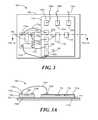
- FIG. 3is a pictorial showing another integrated circuit having first and second substrates
- FIG. 3Ais a cross-sectional view of the integrated circuit of FIG. 3 ;
- FIG. 4is a pictorial showing an integrated circuit having first and second substrates and a base substrate;
- FIG. 4Ais a cross-sectional view of the integrated circuit of FIG. 4 ;
- FIG. 5is a pictorial showing another integrated circuit having first and second substrates and a base substrate;
- FIG. 5Ais a cross-sectional view of the integrated circuit of FIG. 5 ;
- FIG. 6is an exploded view showing an exemplary integrated current sensor having first and second substrates and having an integrated current-carrying conductor;
- FIG. 7is a pictorial showing another exemplary integrated current sensor having first and second substrates and having an integrated current-carrying conductor formed by coupling lead frame leads;
- FIG. 7Ais a cross-sectional view of the integrated circuit of FIG. 7 ;
- FIG. 8is a pictorial showing another exemplary integrated current sensor having first and second substrates, three magnetic field sensors, and having an integrated current-carrying conductor formed by coupling lead frame leads;
- FIG. 8Ais a cross-sectional view of the integrated circuit of FIG. 8 .
- the term “magnetic field sensing element”is used to describe an electronic component that is responsive to and can be used to measure magnetic fields.
- the magnetic field sensing elementcan be of a type including, but not limited to, a Hall effect element and a magnetoresistance element.
- the Hall effect elementcan be a horizontal type or a vertical type.
- the magnetoresistance elementcan be of a type including, but not limited to, a giant magnetoresistance (GMR) element, an anisotropic magnetoresistance (AMR) element, and a tunneling magnetoresistance (TMR) element.
- GMRgiant magnetoresistance
- AMRanisotropic magnetoresistance
- TMRtunneling magnetoresistance
- magnetic field sensoris used to describe an electronic circuit, which includes a magnetic field sensing element, and which is responsive to and can be used to measure a magnetic field.
- current sensoris used to describe an electronic circuit, which includes a magnetic field sensing element, and which is responsive to and can be used to measure a current in a conductor.
- a current in a conductorgenerates a magnetic field circularly disposed about the direction of current. Therefore, the magnetic field sensing element as used in a current sensor can be used to measure the current flowing in a conductor. However, a magnetic field sensing element as used in a magnetic field sensor can be used to measure other magnetic fields, for example a magnetic field associated with the earth.
- an exemplary integrated circuit 10includes a lead frame 12 , here shown as only a portion of a lead frame. It will be understood that a lead frame can have a base plate and associated leads. The leads are not shown in FIGS. 1 and 1A .
- the integrated circuit 10also includes a first substrate 14 having first and second opposing surfaces 14 a , 14 b , respectively.
- the first substrate 14is coupled to the lead frame 12 such that the second surface 14 b of the first substrate 14 is above the lead frame 12 and the first surface 14 a of the first substrate 14 is above the second surface 14 b of the first substrate 14 .
- the integrated circuit 10also includes a second substrate 26 having first and second opposing surfaces 26 a , 26 b , respectively.
- the first substrate 14 and the second substrate 26are coupled such that the first surface 26 a of the second substrate 26 is above the first surface 14 a of the first substrate 14 and the second surface 26 l of the second substrate 26 is above the first surface 26 a of the second substrate 26 .
- the first and second substrates 14 , 26can be comprised of a variety of materials including, but not limited to, Si, GaAs, InP, InSb, InGaAs, InGaAsP, SiGe, ceramic, or glass.
- the first and second substrates 14 , 26can be comprised of the same material or of different materials.
- the first substrate 14is comprised of Silicon (Si) and the second substrate 26 is comprised of Gallium Arsenide (GaAs).
- the first surface 26 a of the second substrate 26can be coupled to the first surface 14 a of the first substrate 14 with a selected one of a solder ball, a gold bump, a eutectic or high lead solder bump, a no-lead solder bump, a gold stud bump, a polymeric conductive bump, an anisotropic conductive paste, or a conductive film.
- a solder balla gold bump, a eutectic or high lead solder bump, a no-lead solder bump, a gold stud bump, a polymeric conductive bump, an anisotropic conductive paste, or a conductive film.
- the integrated circuit 10also includes at least one electronic component 18 disposed on the first surface 14 a of the first substrate 14 .
- the electronic component 18can include, but is not limited to, a passive electronic component, for example, a resistor, capacitor, or inductor, and an active electronic component, for example, a transistor, an amplifier, or another integrated circuit.
- the integrated circuit 10also includes a first magnetic field sensing element 30 disposed on the first surface 26 a of the second substrate 26 . It will be recognized that this arrangement provides a so-called “flip-chip” arrangement of the second substrate 26 relative to the first substrate 14 .
- the integrated circuit 10further includes a second magnetic field sensing element 20 disposed on the first surface 14 a of the first substrate 14 .
- the first and second magnetic field sensing elements 30 , 20can be selected ones of a Hall effect element and a magnetoresistance element as described above.
- the first and second magnetic field sensing elements 30 , 20are the same type of magnetic field sensing element, and in other embodiments, the first and second magnetic field sensing elements 30 , 20 , respectively, are different types of magnetic field sensing elements.
- the first magnetic field sensing element 30is a Hall effect element and the second magnetic field sensing element 20 is a magnetoresistance element, for example, a giant magnetoresistance (GMR) element.
- the first and second magnetic field sensing elements 30 , 20are both Hall effect elements, the first substrate is comprised of Silicon and the second substrate 26 is comprised of GaAs. In some embodiments, the second magnetic field sensing element 20 is not present.
- the integrated circuit 10can also include one or more of a first or a second flux concentrator 32 , 22 , respectively each disposed proximate to an associated one of the first and second magnetic field sensing elements 30 , 20 , respectively.
- a first or a second flux concentrator 32 , 22respectively each disposed proximate to an associated one of the first and second magnetic field sensing elements 30 , 20 , respectively.
- the flux concentrators 32 , 22can provide an increased magnetic field proximate to the first and second magnetic field sensing elements 30 , 20 , respectively, resulting in an increased sensitivity of the first and second magnetic field sensing elements 30 , 20 to a magnetic field, for example, a magnetic field resulting from a current in a conductor.
- the integrated circuit 10also includes one or more of a first resistor 28 formed on the second substrate 26 or a second resistor 24 formed on the first substrate 14 .
- the first and second resistors 28 , 24can be used by the integrated circuit 10 to measure resistivity changes in the first and second substrates 14 , 26 , respectively, for example, over time or over temperature.
- One of ordinary skill in the artwill understand how to construct circuits in conjunction with one or more of the resistors 24 , 28 , to accomplish this end.
- one of the first and second resistors 28 , 24is not present, and the remaining one of the first and second resistors 28 , 24 is used to detect a resistivity change in one of the first and second substrates 14 , 26 , respectively.
- the integrated circuitcan also include a plurality of bonding pads, of which bonding pads 16 a - 16 c are representative. Bond wires 40 a - 40 c can couple the first and/or second substrates 14 , 26 , respectively, to leads (not shown) of the lead frame 12 .
- the integrated circuit 10can include an underfill material 42 disposed between the first surface 14 a of the first substrate 14 and the first surface 26 a of the second substrate 26 .
- the underfill materialtends to keep the packaging material, e.g., plastic, from contact with the magnetic field sensing element 30 , resulting in a further reduction of stresses and strains upon the magnetic field sensing element 30 and upon the second substrate 26 .
- the underfill material 42can be comprised of a, for example StaychipTM NUF-31071 E underfill material (Cookson Electronics Equipment, New Jersey).
- an insulating layercan be used to electrically isolate portions of the integrated circuit 10 from other portions of the integrated circuit 10 .
- an insulating layer(not shown) can be disposed between the first surface 14 a of the first substrate 14 and the flux concentrator 22 .
- an insulating layer(not shown) can be disposed between the second surface 26 b of the second substrate 26 and the flux concentrator 32 .
- the flux concentrator 32is instead disposed proximate to the first surface 26 a of the second substrate 26 .
- flux concentratorsmay be disposed on both the first and second surfaces 26 a , 26 b , respectively, of the second substrate 26 .
- the second magnetic field sensing element 20can have a different sensitivity to magnetic fields (i.e., currents) than the first magnetic field sensing element 30 . Therefore, with these arrangements, the integrated circuit 10 can have more than one “range,” or an extended range. With these arrangements, the integrated circuit 10 can operate over a greater span of sensed currents, i.e., magnetic field strengths.
- the sensitivity of the magnetic field sensing element 30is higher than the sensitivity of the second magnetic field sensing element 20 . Therefore, an extended range of operation can be obtained while using only Hall effect elements.
- the second substrate 26is comprised of GaAs and the magnetic field sensing element 30 is a Hall effect element
- the first substrate 14is comprised of Silicon and the second magnetic field sensing element 20 is not present
- a higher sensitivitycan be achieved than for an arrangement having only a Silicon based Hall effect element.
- known cost advantages of having the circuitry 18 disposed on the silicon substrate 14can be achieved.
- the first substrate 14is shown to be conventionally mounted to the lead frame 12 , i.e., with the first surface 14 a of the first substrate 14 facing away from the lead frame 12 , in other arrangements, the first substrate 14 can be flipped relative to the substrate 12 .
- the first surface 14 a of the first substrate 14is proximate to the lead frame 12 and coupled to the lead frame with a selected one of a solder ball, a gold bump, a eutectic or high lead solder bump, a no-lead solder bump, a gold stud bump, a polymeric conductive bump, an anisotropic conductive paste, or a conductive film.
- the first surface 26 a of the second substrate 26remains coupled as shown to the first surface 14 a of the first substrate 14 , wherein the first surfaces 14 a , 26 a of the substrates 14 , 26 , respectively are proximate to each other.
- the integrated circuit 10can adapted to be responsive to a current 46 passing through a wire 44 .
- wire 44is not shown in other figures herein, it will be understood that the other integrated circuits shown herein can be adapted to be responsive to a wire like the wire 44 .
- an integrated circuit 50includes aspects similar to the integrated circuit 10 of FIGS. 1 and 1A , but without the flip-chip arrangement of FIGS. 1 and 1A .
- the integrated circuit 50includes a lead frame 52 .
- the integrated circuit 50also includes a first substrate 54 having first and second opposing surfaces 54 a , 54 b , respectively.
- the first substrate 54is coupled to the lead frame 52 such that the second surface 54 b of the first substrate 54 is above the lead frame 52 and the first surface 54 a of the first substrate 54 is above the second surface 54 b of the first substrate 54 .
- the integrated circuit 50also includes a second substrate 66 having first and second opposing surfaces 66 a , 66 b , respectively.
- the first substrate 54 and the second substrate 66are coupled such that the second surface 66 b of the second substrate 66 is above the first surface 54 a of the first substrate 54 and the first surface 66 a of the second substrate 66 is above the second surface 66 b of the second substrate 66 .
- the first and second substrates 54 , 66can be comprised of a variety of materials including, but not limited to, Si, GaAs, InP, InSb, InGaAs, InGaAsP, SiGe, ceramic, or glass.
- the first and second substrates 54 , 66can be comprised of the same material or of different materials.
- the first substrate 54is comprised of Silicon (Si) and the second substrate 66 is comprised of Gallium Arsenide (GaAs).
- the first surface 66 a of the second substrate 66can be coupled to the first surface 54 a of the first substrate 54 with wire bonds 74 a - 74 d .
- Four such couplings 74 a - 74 dare shown.
- the integrated circuit 50can have more than four or fewer than four such couplings.
- the integrated circuit 50also includes at least one electronic component 56 disposed on the first surface 54 a of the first substrate 54 .
- the electronic component 56can include, but is not limited to, a passive electronic component, for example, a resistor, capacitor, or inductor, and an active electronic component, for example, a transistor, an amplifier, or another integrated circuit.
- the integrated circuit 50also includes a first magnetic field sensing element 70 disposed on the first surface 66 a of the second substrate 66 .
- the integrated circuit 50further includes a second magnetic field sensing element 58 disposed on the first surface 54 a of the first substrate 54 .
- the first and second magnetic field sensing elements 70 , 58can be selected ones of a Hall effect element and a magnetoresistance element as described above.
- the first and second magnetic field sensing elements 70 , 58are the same type of magnetic field sensing element, and in other embodiments, the first and second magnetic field sensing elements 70 , 58 , respectively, are different types of magnetic field sensing elements.
- the first magnetic field sensing element 70is a Hall effect element and the second magnetic field sensing element 58 is a magnetoresistance element, for example, a giant magnetoresistance (GMR) element.
- the first and second magnetic field sensing elements 70 , 58are both Hall effect elements, the first substrate 54 is comprised of Silicon and the second substrate 66 is comprised of GaAs. In some embodiments, the second magnetic field sensing element 58 is not present.
- the integrated circuit 50can also include one or more of a first or a second flux concentrator 71 , 59 , respectively, each disposed proximate to an associated one of the first and second magnetic field sensing elements 70 , 58 , respectively.
- the flux concentrators 71 , 59can provide an increased magnetic field proximate to the first and second magnetic field sensing elements 70 , 58 and a corresponding increased sensitivity of the first and second magnetic field sensing elements 70 , 58 to a magnetic field, for example, a magnetic field resulting from a current in a conductor.
- the integrated circuit 50also includes one or more of a first resistor 68 formed on the second substrate 66 or a second resistor 60 formed on the first substrate 54 .
- the first and second resistors 68 , 60can be used by the integrated circuit 50 to measure resistivity changes in the first and second substrates 54 , 66 , respectively, for example, over time or over temperature.
- FIGS. 1 and 1Aone of ordinary skill in the art will understand how to construct circuits in conjunction with one or more of the resistors 68 , 60 , to accomplish this end.
- one of the first and second resistors 68 , 60is not present, and the remaining one of the first and second resistors 68 , 60 is used to detect a resistivity change in one of the first and second substrates 54 , 66 , respectively.
- the integrated circuit 50can also include a plurality of bonding pads, of which bonding pads 76 a - 76 c are representative. Bond wires 78 a - 78 c can couple the first and/or second substrates 54 , 66 , respectively, to leads (not shown) of the lead frame 52 .
- an insulating layer 64can be disposed between the first surface 14 a of the first substrate 14 and the second surface 66 b of the second substrate 66 .
- the second magnetic field sensing element 58can have a different sensitivity to magnetic fields (i.e., currents) than the first magnetic field sensing element 70 . Therefore, with these arrangements, the integrated circuit 10 can have more than one “range,” or an extended range. With these arrangements, the integrated circuit 50 can operate over a greater span of sensed currents, magnetic field strengths.
- Exemplary combinations of types of magnetic field sensing elements and substrate materialsare further described above in conjunction with FIGS. 1 and 1A . At least the same combinations apply to the integrated circuit 50 .
- an integrated circuit 100includes aspects similar to the integrated circuit 10 of FIGS. 1 and 1A .
- the integrated circuit 100includes a lead frame 102 .
- the integrated circuit 100also includes a first substrate 114 having first and second opposing surfaces 114 a , 114 b , respectively.
- the integrated circuit 100also includes a second substrate 104 having first and second opposing surfaces 104 a , 104 b , respectively.
- the first substrate 114is coupled to the lead frame 102 such that the second surface 114 b of the first substrate 114 is above the lead frame 102 and the first surface 114 a of the first substrate 114 is above the second surface 114 b of the first substrate 114 .
- the second substrate 104is coupled to the lead frame 102 such that the second surface 104 b of the second substrate 104 is above the lead frame 102 and the first surface 104 a of the second substrate 104 is above the second surface 104 b of the second substrate 104 .
- the first and second substrates 114 , 104can be comprised of a variety of materials including, but not limited to, Si, GaAs, InP, InSb, InGaAs, InGaAsP, SiGe, ceramic, or glass.
- the first and second substrates 114 , 104can be comprised of the same material or of different materials.
- the first substrate 114is comprised of Silicon (Si) and the second substrate 104 is comprised of Gallium Arsenide (GaAs).
- the first surface 104 a of the second substrate 104can be coupled to the first surface 114 a of the first substrate 114 with wire bonds 112 a - 112 d .
- Four such couplings 112 a - 112 dare shown.
- the integrated circuit 100can have more than four or fewer than four such couplings.
- the integrated circuit 100also includes at least one electronic component 118 disposed on the first surface 114 a of the first substrate 114 .
- the electronic component 118can include, but is not limited to, a passive electronic component, for example, a resistor, capacitor, or inductor, and an active electronic component, for example, a transistor, an amplifier, or another integrated circuit.
- the integrated circuit 100also includes a first magnetic field sensing element 106 disposed on the first surface 104 a of the second substrate 104 .
- the integrated circuit 100further includes a second magnetic field sensing element 116 disposed on the first surface 114 a of the first substrate 114 .
- the first and second magnetic field sensing elements 106 , 116can be selected ones of a Hall effect element and a magnetoresistance element as described above.
- the first and second magnetic field sensing elements 106 , 116are the same type of magnetic field sensing element, and in other embodiments, the first and second magnetic field sensing elements 106 , 116 , respectively, are different types of magnetic field sensing elements.
- the first magnetic field sensing element 106is a Hall effect element and the second magnetic field sensing element 116 is a magnetoresistance element, for example, a giant magnetoresistance (GMR) element.
- the first and second magnetic field sensing elements 106 , 116are both Hall effect elements, the first substrate 114 is comprised of Silicon and the second substrate 104 is comprised of GaAs. In some embodiments, the second magnetic field sensing element 116 is not present.
- the integrated circuit 100can also include one or more of a first or a second flux concentrator (not shown) each disposed proximate to an associated one of the first and second magnetic field sensing elements 106 , 116 , respectively.
- the flux concentratorscan provide an increased magnetic field proximate to the first and second magnetic field sensing elements 106 , 116 and a corresponding increased sensitivity of the first and second magnetic field sensing elements 106 , 116 to a magnetic field, for example, a magnetic field resulting from a current in a conductor.
- the integrated circuit 100also includes one or more of a first resistor 108 formed on the second substrate 104 or a second resistor 120 formed on the first substrate 114 .
- the first and second resistors 108 , 120can be used by the integrated circuit 100 to measure resistivity changes in the first and second substrates 114 , 104 , respectively, for example, over time or over temperature.
- FIG. 1one of ordinary skill in the art will understand how to construct circuits in conjunction with one or more of the resistors 108 , 120 , to accomplish this end.
- one of the first and second resistors 108 , 120is not present, and the remaining one of the first and second resistors 108 , 120 is used to detect a resistivity change in one of the first and second substrates 114 , 104 , respectively.
- the integrated circuit 100can also include a plurality of bonding pads, of which bonding pads 124 a - 124 c are representative. Bond wires 126 a - 126 e can couple the first substrates 114 to leads (not shown) of the lead frame 102 .
- insulating layerscan be used to electrically isolate portions of the integrated circuit 100 from other portions of the integrated circuit 100 .
- insulating layers(not shown) can be disposed between the second surface 114 b of the first substrate 114 and the lead frame 102 and also between the second surface 104 b of the first substrate 104 and the lead frame 102 .
- the second magnetic field sensing element 116can have a different sensitivity to magnetic fields (i.e., currents) than the first magnetic field sensing element 106 . Therefore, with these arrangements, the integrated circuit 100 can have more than one “range,” or an extended range. With these arrangements, the integrated circuit 100 can operate over a greater span of sensed currents, i.e., magnetic field strengths.
- Exemplary combinations of types of magnetic field sensing elements and substrate materialsare further described above in conjunction with FIGS. 1 and 1A . At least the same combinations apply to the integrated circuit 100 .
- an integrated circuit 150includes aspects similar to the integrated circuit 10 of FIGS. 1 and 1A , including a flip-chip arrangement as shown in FIGS. 1 and 1A .
- the integrated circuit 150includes a lead frame 152 and a base substrate 154 having first and second opposing surfaces 154 a , 154 b , respectively.
- the base substratecan be comprised of a variety of materials, for example, ceramic, glass, polymer, i.e. FR-4, or a semiconductor.
- the integrated circuit 150also includes a first substrate 156 having first and second opposing surfaces 156 a , 156 b , respectively, and a second substrate 166 having first and second opposing surfaces 166 a , 166 b , respectively.
- the base substrate 154is coupled to the lead frame 152 such that the second surface 154 b of the base substrate 154 is above the lead frame 152 and the first surface 154 a of the base substrate 154 is above the second surface 154 b of the base substrate 154 .
- the first substrate 156is coupled to the base substrate 154 such that the first surface 156 a of the first substrate 156 is above the first surface 154 a of the base substrate 154 and the second surface 156 b of the first substrate 156 is above the first surface 156 a of the first substrate 156 .
- the second substrate 166is coupled to the base substrate 154 such that the first surface 166 a of the second substrate 166 is above the first surface 154 a of the base substrate 154 and the second surface 166 b of the second substrate 166 is above the first surface 166 a of the second substrate 166 .
- the first and second substrates 156 , 166can be comprised of a variety of materials including, but not limited to, Si, GaAs, InP, InSb, InGaAs, InGaAsP, Site, ceramic, or glass.
- the first and second substrates 156 , 166can be comprised of the same material or of different materials.
- the first substrate 156is comprised of Silicon (Si) and the second substrate 166 is comprised of Gallium Arsenide (GaAs).
- the first surface 166 a of the second substrate 166can be coupled to the first surface 154 a of the base substrate 154 with a conductive element, for example, of a solder ball, a gold bump, a eutectic or high lead solder bump, a no-lead solder bump, a gold stud bump, a polymeric conductive bump, an anisotropic conductive paste, or a conductive film.
- a conductive elementfor example, of a solder ball, a gold bump, a eutectic or high lead solder bump, a no-lead solder bump, a gold stud bump, a polymeric conductive bump, an anisotropic conductive paste, or a conductive film.
- Four such couplings 172 a - 172 care shown. However, it will be appreciated that the integrated circuit 150 can have more than four or fewer than four such couplings.
- the first surface 156 a of the second substrate 156can also be coupled to the first surface 154 a of the base substrate 154 with a selected one of a solder ball, a gold bump, a eutectic or high lead solder bump, a no-lead solder bump, a gold stud bump, a polymeric conductive bump, an anisotropic conductive paste, or a conductive film.
- a solder balla gold bump
- a eutectic or high lead solder bumpa no-lead solder bump
- a gold stud bumpa polymeric conductive bump
- an anisotropic conductive pasteor a conductive film.
- the base substrate 154can have conductive traces or the like (not shown) to couple the first substrate 156 to the second substrate 166 , and to the pads 174 a - c.
- the integrated circuit 150also includes at least one electronic component 158 disposed on the first surface 156 a of the first substrate 156 .
- the electronic component 158can include, but is not limited to, a passive electronic component, for example, a resistor, capacitor, or inductor, and an active electronic component, for example, a transistor, an amplifier, or another integrated circuit.
- the integrated circuit 150also includes a first magnetic field sensing element 168 disposed on the first surface 166 a of the second substrate 166 .
- the integrated circuit 150further includes a second magnetic field sensing element 160 disposed on the first surface 156 a of the first substrate 156 .
- the first and second magnetic field sensing elements 168 , 160can be selected ones of a Hall effect element and a magnetoresistance element as described above.
- the first and second magnetic field sensing elements 168 , 160are the same type of magnetic field sensing element, and in other embodiments, the first and second magnetic field sensing elements 168 , 160 , respectively, are different types of magnetic field sensing elements.
- the first magnetic field sensing element 168is a Hall effect element and the second magnetic field sensing element 160 is a magnetoresistance element, for example, a giant magnetoresistance (GMR) element.
- the first and second magnetic field sensing elements 168 , 160are both Hall effect elements, the first substrate 156 is comprised of Silicon and the second substrate 166 is comprised of GaAs. In some embodiments, the second magnetic field sensing element 160 is not present.
- the integrated circuit 150can also include one or more of a first or a second flux concentrator (not shown) each disposed proximate to an associated one of the first and second magnetic field sensing elements 168 , 160 , respectively.
- the flux concentratorscan provide an increased magnetic field proximate to the first and second magnetic field sensing elements 168 , 160 and a corresponding increased sensitivity of the first and second magnetic field sensing elements 168 , 160 to a magnetic field, for example, a magnetic field resulting from a current in a conductor.
- the integrated circuit 150also includes one or more of a first resistor 170 formed on the second substrate 166 or a second resistor 162 formed on the first substrate 156 .
- the first and second resistors 170 , 162can be used by the integrated circuit 150 to measure resistivity changes in the first and second substrates 156 , 166 , respectively, for example, over time or over temperature.
- FIGS. 1 and 1Aone of ordinary skill in the art will understand how to construct circuits in conjunction with one or more of the resistors 170 , 162 , to accomplish this end.
- one of the first and second resistors 170 , 162is not present, and the remaining one of the first and second resistors 170 , 162 is used to detect a resistivity change in one of the first and second substrates 156 , 166 , respectively.
- the integrated circuit 150can also include a plurality of bonding pads, of which bonding pads 174 a - 174 e are representative. Bond wires 176 a - 176 c can couple the first and/or second substrates 156 , 166 , respectively, to leads (not shown) of the lead frame 152 .
- insulating layerscan be used to electrically isolate portions of the integrated circuit 150 from other portions of the integrated circuit 150 .
- the second magnetic field sensing element 160can have a different sensitivity to magnetic fields (i.e., currents) than the first magnetic field sensing element 168 . Therefore, with these arrangements, the integrated circuit 150 can have more than one “range,” or an extended range. With these arrangements, the integrated circuit 150 can operate over a greater span of sensed currents, i.e., magnetic field strengths.
- Exemplary combinations of types of magnetic field sensing elements and substrate materialsare further described above in conjunction with FIGS. 1 and 1A . At least the same combinations apply to the integrated circuit 150 .
- first and second substrates 156 , 166are shown to be coupled to the base substrate 154 , it will be appreciated that in other arrangements there can be more than two or fewer than two substrates coupled to the base substrate 154 .
- an integrated circuit 200includes aspects similar to the integrated circuit 10 of FIGS. 1 and 1A .
- the integrated circuit 200includes a lead frame 202 and a base substrate 204 having first and second opposing surfaces 204 a , 204 b , respectively.
- the base substratecan be comprised of a variety of materials, for example, ceramic, glass, polymer, i.e. FR-4, or a semiconductor.
- the integrated circuit 200also includes a first substrate 216 having first and second opposing surfaces 216 a , 216 b , respectively, and a second substrate 206 having first and second opposing surfaces 206 a , 206 b , respectively.
- the base substrate 204is coupled to the lead frame 202 such that the second surface 204 b of the base substrate 204 is above the lead frame 202 and the first surface 204 a of the base substrate 204 is above the second surface 204 b of the base substrate 204 .
- the first substrate 216is coupled to the base substrate 204 such that the second surface 216 b of the first substrate 216 is above the first surface 204 a of the base substrate 204 and the first surface 216 a of the first substrate 216 is above the second surface 216 b of the first substrate 216 .
- the second substrate 206is coupled to the base substrate 204 such that the second surface 206 b of the second substrate 206 is above the first surface 204 a of the base substrate 204 and the first surface 206 a of the second substrate 206 is above the second surface 206 b of the second substrate 206 .
- the first and second substrates 216 , 206can be comprised of a variety of materials including, but not limited to, Si, GaAs, InP InSb, InGaAs, InGaAsP, SiGe, ceramic, or glass.
- the first and second substrates 216 , 206can be comprised of the same material or of different materials.
- the first substrate 216is comprised of Silicon (Si) and the second substrate 206 is comprised of Gallium Arsenide (GaAs).
- the first surface 206 a of the second substrate 206can be coupled to the first surface 216 a of the first substrate 216 with wire bonds 214 a - 214 d .
- Four such couplings 214 a - 214 dare shown. However, it will be appreciated that the integrated circuit 200 can have more than four or fewer than four such couplings.
- the integrated circuit 200also includes at least one electronic component 220 disposed on the first surface 216 a of the first substrate 216 .
- the electronic component 220can include, but is not limited to, a passive electronic component, for example, a resistor, capacitor, or inductor, and an active electronic component, for example, a transistor, an amplifier, or another integrated circuit.
- the integrated circuit 200also includes a first magnetic field sensing element 208 disposed on the first surface 206 a of the second substrate 206 .
- the integrated circuit 200further includes a second magnetic field sensing element 218 disposed on the first surface 216 a of the first substrate 216 .
- the first and second magnetic field sensing elements 208 , 218can be selected ones of a Hall effect element and a magnetoresistance element as described above.
- the first and second magnetic field sensing elements 208 , 218are the same type of magnetic field sensing element, and in other embodiments, the first and second magnetic field sensing elements 208 , 218 , respectively, are different types of magnetic field sensing elements.
- the first magnetic field sensing element 208is a Hall effect element and the second magnetic field sensing element 218 is a magnetoresistance element, for example, a giant magnetoresistance (GMR) element.
- the first and second magnetic field sensing elements 208 , 218are both Hall effect elements, the first substrate 216 is comprised of Silicon and the second substrate 206 is comprised of GaAs. In some embodiments, the second magnetic field sensing element 218 is not present.
- the integrated circuit 200can also include one or more of a first or a second flux concentrator (not shown) each disposed proximate to an associated one of the first and second magnetic field sensing elements 208 , 218 , respectively.
- the flux concentratorscan provide an increased magnetic field proximate to the first and second magnetic field sensing elements 208 , 218 and a corresponding increased sensitivity of the first and second magnetic field sensing elements 208 , 218 to a magnetic field, for example, a magnetic field resulting from a current in a conductor.
- the integrated circuit 200also includes one or more of a first resistor 210 formed on the second substrate 206 or a second resistor 222 formed on the first substrate 216 .
- the first and second resistors 210 , 222can be used by the integrated circuit 200 to measure resistivity changes in the first and second substrates 216 , 206 , respectively, for example, over time or over temperature.
- FIGS. 1 and 1Aone of ordinary skill in the art will understand how to construct circuits in conjunction with one or more of the resistors 210 , 222 , to accomplish this end.
- one of the first and second resistors 210 , 222is not present, and the remaining one of the first and second resistors 210 , 222 is used to detect a resistivity change in one of the first and second substrates 216 , 206 , respectively.
- the integrated circuit 200can also include a plurality of bonding pads, of which bonding pads 232 a - 232 c are representative. Bond wires 234 a - 234 c can couple the first and/or second substrates 216 , 206 , respectively, to leads (not shown) of the lead frame 202 .
- insulating layerscan be used to electrically isolate portions of the integrated circuit 200 from other portions of the integrated circuit 200 .
- the second magnetic field sensing element 218can have a different sensitivity to magnetic fields (i.e., currents) than the first magnetic field sensing element 208 . Therefore, with these arrangements, the integrated circuit 200 can have more than one “range,” or an extended range. With these arrangements, the integrated circuit 200 can operate over a greater span of sensed currents, i.e., magnetic field strengths.
- Exemplary combinations of types of magnetic field sensing elements and substrate materialsare further described above in conjunction with FIGS. 1 and 1A . At least the same combinations apply to the integrated circuit 200 .
- an integrated circuit 250shown in an exploded view, includes a first substrate 252 , a second substrate 254 , and a lead frame 257 .
- the first substrate 252 , second substrate 254 , and the lead frame 257can be the same as or similar to similar elements of any of the integrated circuit 10 , 50 , 100 , 150 , and 200 of FIGS. 1-1A, 2-2A, 3-3A, 4-4A, and 5-5A , respectively.
- the second substrate 254includes a magnetic field sensing element 256 , which can be a selected one of a Hall effect element or a magnetoresistance element. It will be appreciated that a position of the magnetic field sensing element 256 can be selected in accordance with an axis of sensitivity of the magnetic field sensing element 256 relative to a magnetic field that is being sensed.
- the integrated circuit 250also includes a current-carrying conductor 258 and a magnetic core 260 (also referred to herein as a flux concentrator).
- the magnetic core 260is substantially C-shaped and has a central region 260 a and a pair of substantially parallel legs 260 b , 260 c extending from the central region 260 a . When assembled, the flux concentrator 260 is shaped so that the leg 260 b is disposed under the lead frame 257 and the other leg 260 c is disposed above the second substrate 254 .
- the lead frame 275has leads 259 adapted for mounting to a printed circuit board (not shown).
- the leads 259can include, for example, a power, or Vcc, connection, a ground connection, and an output connection adapted to carry an output signal proportional to the current through the conductor 258 .
- the output signalmay be a current or a voltage.
- the first substrate 252includes circuitry (not shown) for processing the output signal of the Hall effect element 256
- the conductor 258can be comprised of various conductive materials, such as copper, and is adapted for mounting to a printed circuit board through which the measured current is provided to the conductor 258 .
- bent leads or tabs 258 a , 258 b( 258 b not shown) suitable for soldering into circuit board vias are provided at end portions of the conductor 258 .
- Mechanisms other than bent tabs 258 a , 258 bmay be used to mount the integrated circuit 250 to a circuit board, such as screw terminals and associated.
- the same or other mounting mechanismscan be used to allow the integrated circuit 250 to be mounted to other than a circuit board.
- the integrated circuit 250can have wire couplings (not shown) that allow the integrated circuit 250 to be coupled in series with a wire.
- the conductor 258(excluding the bent tabs 258 a , 258 b ) can be substantially planar as shown, without features extending in a z-axis 266 which would tend to increase the height of the integrated circuit 250 off of a printed circuit board. In use, the plane of the conductor 258 is positioned close to the printed circuit board plane, thereby providing a low profile integrated circuit.
- the flux concentrator 260tends to tailor the magnetic field across the Hall effect element 256 .
- the flux concentrator 260may be comprised of various materials including, but not limited to ferrite, steel, iron compounds, Permalloy, or other soft magnetic materials.
- the material of the flux concentrator 260is selected based on factors such as maximum measured current and the desired amount of magnetic shielding provided by the flux concentrator 260 . Other factors include stability of the relative permeability over temperature and hysteresis (magnetic remanence). For example, a low hysteresis ensures greater accuracy for small currents through the conductor 258 .
- the material and size of the flux concentrator 260are also selected in accordance with the desired full scale current through the conductor 258 , wherein a magnetic core material with a higher saturation flux density (Bsat) allows the use of a smaller core for a given current flowing through the conductor 258 . It will be appreciated that use of the flux concentrator 260 significantly reduces the susceptibility of the integrated circuit to stray magnetic fields.
- an integrated circuit 300includes a lead frame 302 having a plurality of leads 302 a - 302 h , a first substrate 306 , and a second substrate 307 .
- the leads 302 a and 302 bare coupled to the leads 302 c and 302 d to form a current path, or current conductor with a narrow portion 304 having a width w1.
- the first substrate 306has a first surface 306 a and a second, opposing surface 306 b and the second substrate 307 has a first surface 307 a and a second, opposing surface 307 b .
- the first substrate 306can have a magnetic field sensing element 308 , which, in some embodiments, can be a Hall effect element 308 , diffused into the first surface 306 a , or otherwise disposed on the first surface 306 a of the first substrate 306 .
- the second substrate 307can have a magnetic field sensing element 309 , which, in some embodiments, can be a Hall effect element 309 , diffused into the first surface 307 a , or otherwise disposed on the first surface 307 a of the second substrate 307 .
- a magnetic field sensing element 309which, in some embodiments, can be a Hall effect element 309 , diffused into the first surface 307 a , or otherwise disposed on the first surface 307 a of the second substrate 307 .
- the first and second substrates 306 , 307are shown to be coupled together in a flip-chip arrangement similar to the integrated circuit 10 of FIG. 1 .
- the first substrate 14 of FIGS. 1 and 1Acan be mounted in a flip-chip arrangement to the substrate 12 , which arrangement is shown in FIG. 7 .
- an integrated circuit similar to the integrated circuit 300can be formed from any of the arrangements of FIGS. 2-2A, 3-3A, 4-4A, and 5-5A .
- the substrate 306is disposed above the lead frame 302 so that the first surface 306 a is proximate to the current conductor portion 304 and the second surface 306 b is distal from the current conductor portion 304 and more specifically, so that the Hall effect element 308 is in close proximity to the current conductor portion 304 .
- the magnetic field sensing element 309 of the second substrate 307is in close proximity to the current conductor portion 304 .
- the substrate 306has an orientation that is upside down (i.e., the first surface 306 a is directed downward) relative to a conventional orientation with which a substrate is mounted in an integrated circuit package.
- the first substrate 306has bonding pads 310 a - 310 c on the first surface 306 a , to which bond wires 312 a - 312 c are coupled.
- the bond wiresare further coupled to the leads 302 e , 302 f , 302 h of the lead frame 302 .
- An insulator 314separates and electrically isolates the substrate 306 from the lead frame 302 .
- the insulator 314can be provided in a variety of ways.
- a first portion of the insulator 314includes a four ⁇ m thick layer of a BCB resin material deposited directly on the first surface 306 a of the substrate 306 .
- a second portion of the insulator 314includes a layer of StaychipTM NUF-31071 E underfill material (Cookson Electronics Equipment, New Jersey) deposited on the lead frame 302 .
- Such an arrangementprovides more than one thousand volts of isolation between the substrate 306 and the lead frame 302 .
- the current conductor portion 304is but a part of the total path through which an electrical current flows.
- a current having a direction depicted by arrows 316flows into the leads 302 c , 302 d , which are here shown to be electrically coupled in parallel, through the current conductor portion 304 , and out of the leads 302 a , 302 b , which are also shown here to be electrically coupled in parallel.
- the Hall effect elements 308 , 309are disposed in close proximity to the current conductor portion 304 and at a predetermined position relative to the current conductor portion 304 , such that a magnetic field generated by an electrical current passing though the current conductor portion 304 , in a direction shown by arrows 316 , is in a direction substantially aligned with a maximum response axis of the Hall effect elements 308 , 309 .
- the Hall effect elements 308 , 309generate respective voltage outputs proportional to the magnetic field and therefore proportional to the current flowing through the current conductor portion 304 .
- the illustrated Hall effect elements 308 , 309have a maximum response axis substantially aligned with a z-axis 324 .
- the Hall effect elements 308 , 309are disposed just to the side (i.e., slightly offset along a y-axis 322 ) of the current conductor portion 304 , as shown, where the magnetic field is pointed substantially along the z-axis 324 . This position results in a greater voltage output from the Hall effect elements 308 , 309 and therefore, improved sensitivity.
- a vertical Hall effect elementor another type of magnetic field sensor, for example a magnetoresistance element, having a maximum response axis aligned in another direction, can be disposed at another position relative to the current conductor portion 304 , for example, on top of the current conductor portion 304 (in a direction along z-axis 324 ).
- the close proximity between the Hall effect elements 308 , 309 and the current conductor 304is achieved by providing the Hall effect element 308 on the first surface 306 a of the first substrate 306 , and by providing the Hall effect element 309 on the first surface 307 a of the second substrate 307 .
- another exemplary integrated circuit 350includes a lead frame 352 having a plurality of leads 352 a - 352 h and a current conductor portion 354 provided as a combination of a first current conductor portion 354 a and a second current conductor portion 354 b .
- the integrated circuit 350also includes a substrate 356 having a first surface 356 a and a second, opposing, surface 356 b .
- the substrate 356has a Hall effect element 358 diffused into the first surface 356 a , or otherwise disposed on or supported by the first surface 356 a .
- the substrate 356also has two magnetoresistance elements 360 a , 360 b disposed on or otherwise supported by the first surface 356 a of the substrate 356 .
- the substrate 356is disposed on the lead frame 352 so that the Hall effect element 358 and the magnetoresistance elements 360 a , 360 b are in close proximity to the current conductor portion 354 .
- the substrate 356has an orientation that is upside down (i.e., the first surface 356 a is directed downward) in relation to the conventional orientation of a substrate mounted in an integrated circuit package.
- the substrate 356is a flip-chip having solder balls 362 a - 362 e on the first surface 356 a of the substrate 356 .
- the solder balls 362 a - 362 ecouple directly to the leads 352 e - 352 h .
- An insulator(not shown) can separate and electrically isolate the substrate 356 from the lead frame 352 .
- the second current conductor portion 354 bis deposited on the first surface 356 a of the substrate 356 , while avoiding, or being otherwise insulated from, the two magnetoresistance elements 360 a , 360 b .
- the second current conductor portion 354 bcan be deposited by any conventional integrated circuit deposition technique, including, but not limited to, sputtering and electroplating.
- the second current conductor portion 354 bis a conductive structure separate from, but proximate to, the first surface 356 a of the substrate 356 .
- the Hall effect element 358 and the magnetoresistance elements 360 a , 360 bare disposed in close proximity to the current conductor portion 354 and at a predetermined position relative to the current conductor portion 354 such that a magnetic field generated by an electrical current passing though the current conductor portion 354 is in a direction substantially aligned with a maximum response axis of the Hall effect element 358 and with the maximum response axes of the magnetoresistance elements 360 a , 360 b .
- the Hall effect element 358has a maximum response axis aligned with a z-axis 368 and the two magnetoresistance elements have maximum response axes substantially aligned with an x-axis 364 .
- the Hall effect element 358is disposed to a side (i.e., slightly offset along a y-axis 324 ) of the current conductor portion 354 , as shown, where the magnetic field is pointed along the z-axis 328 .
- the magnetoresistance elements 360 a , 360 bare disposed in a z-axis alignment with respect to the current conductor portion 354 .
- the current 316flows into the leads 352 c , 352 d , which are coupled in parallel, through the current conductor portion 354 , and out of the leads 352 a , 352 b , which are also coupled in parallel.
- the current 316 flowing though the current conductor portion 354generates a magnetic field, which is sensed by the Hall effect element 358 and by the two magnetoresistance elements 360 a , 360 b , providing a dual-level current sensor or an extended range current sensor in much the same fashion as described above for embodiments having two substrates.
- the magnetoresistance elements 360 a , 360 bcan be replaced with vertical Hall effect elements.
- the Hall effect element 358 and the magnetoresistance elements 360 a , 360 bare in very close proximity to the current conductor portion 354 and at a predetermined position relative to the current conductor portion 354 at which the magnetic field generated by the current is substantially aligned with the maximum response axis of the elements. This placement results in a greater voltage output from the Hall effect element 358 and from the magnetoresistance elements 360 a , 360 b , and therefore, greater sensitivity.
- lead frame 352is shown to have the bent leads 352 a - 352 h suitable for surface mounting to a circuit board, it will be appreciated that a lead frame having leads with other shapes can also be used, including but not limited to, through hole leads having a straight shape.
- Hall effect element 353is shown on the first surface 356 a of the substrate 356 , it will be appreciated that more than one Hall effect element can be used.
- two magnetoresistance elements 360 a , 360 bare shown, it will be appreciated that more than two or fewer than two magnetoresistance elements can be used.
- Other circuitryfor example an amplifier, can also be diffused on or otherwise coupled to or supported by the first and/or second surfaces 356 a , 356 b of the substrate 356 .
- solder balls 320 a - 320 eany number of solder balls can be provided, including dummy solder balls for stabilizing the substrate 356 .
- solder balls 320 a - 320 eother connection methods can also be used, including, but not limited to gold bumps, eutectic or high lead solder bumps, no-lead solder bumps, gold stud bumps, polymeric conductive bumps, anisotropic conductive paste, conductive film, and wire bonds.
- the substrate 356can be conventionally mounted such that the first surface 356 a is above the second surface 356 b When the integrated circuit 350 is normally mounted to an uppermost surface of a circuit board. With these arrangements, the first and second current conductor portions 354 a , 354 b , respectively, are each above the first surface 356 a of the substrate 356 .
- the integrated circuits described above in conjunction with FIGS. 1, 1A, 2, 2A, 3, 3A, 4, 5A, 5 and 5Aare discussed as used in current sensors, wherein the various magnetic field sensing elements disposed thereon are responsive to a magnetic field generated by a current passing through a conductor.
- the integrated circuitsare used in magnetic field sensors, responsive to a magnetic field external to the integrated circuits.
- the integrated circuitsare used in proximity sensors, responsive to a magnetic field associated with a moving ferrous object, or other soft magnetic material, for example, a rotating gear.
- the integrated circuitsare used in proximity sensors, responsive to a magnetic field generated by a moving permanent magnet, or hard magnetic object.
- the integrated circuitsare used in isolators, responsive to a pulse signal in a conductor or coil.
- an integrated circuitinstead of having two substrates, an integrated circuit can have but one substrate, wherein the doping, and/or material of the two magnetic field sensing elements are different.
- a region of a single Si substratecan be implanted with Ge to create a SiGe Hall effect element, while a separate Si Hall effect element can be formed elsewhere on the same substrate.
- the two magnetic field sensing elementscan have different sensitivities or can have the same sensitivity.
- electronic components 18 , 56 , 118 , 158 , and 220can be disposed on surfaces of respective substrates.
- the electronic componentscan be comprised of circuits described in U.S. patent application Ser. No. 11/336,602, filed on Jan. 20, 2006, entitled “Current Sensor,” having inventors Michael C. Doogue, Vijay Mangtani, and William P. Taylor, which application is incorporated by reference in its entirety.
Landscapes
- Physics & Mathematics (AREA)
- General Physics & Mathematics (AREA)
- Condensed Matter Physics & Semiconductors (AREA)
- Engineering & Computer Science (AREA)
- Nanotechnology (AREA)
- Chemical & Material Sciences (AREA)
- Microelectronics & Electronic Packaging (AREA)
- Computer Hardware Design (AREA)
- Power Engineering (AREA)
- Crystallography & Structural Chemistry (AREA)
- Measuring Magnetic Variables (AREA)
- Hall/Mr Elements (AREA)
- Measuring Instrument Details And Bridges, And Automatic Balancing Devices (AREA)
- Lead Frames For Integrated Circuits (AREA)
Abstract
Description
Claims (25)
Priority Applications (2)
| Application Number | Priority Date | Filing Date | Title |
|---|---|---|---|
| US14/707,319US9859489B2 (en) | 2006-01-20 | 2015-05-08 | Integrated circuit having first and second magnetic field sensing elements |
| US15/395,083US10069063B2 (en) | 2006-01-20 | 2016-12-30 | Integrated circuit having first and second magnetic field sensing elements |
Applications Claiming Priority (4)
| Application Number | Priority Date | Filing Date | Title |
|---|---|---|---|
| US11/335,944US7768083B2 (en) | 2006-01-20 | 2006-01-20 | Arrangements for an integrated sensor |
| US12/792,245US8629520B2 (en) | 2006-01-20 | 2010-06-02 | Arrangements for an integrated sensor |
| US13/918,075US9082957B2 (en) | 2006-01-20 | 2013-06-14 | Arrangements for an integrated sensor |
| US14/707,319US9859489B2 (en) | 2006-01-20 | 2015-05-08 | Integrated circuit having first and second magnetic field sensing elements |
Related Parent Applications (1)
| Application Number | Title | Priority Date | Filing Date |
|---|---|---|---|
| US13/918,075ContinuationUS9082957B2 (en) | 2006-01-20 | 2013-06-14 | Arrangements for an integrated sensor |
Related Child Applications (1)
| Application Number | Title | Priority Date | Filing Date |
|---|---|---|---|
| US15/395,083ContinuationUS10069063B2 (en) | 2006-01-20 | 2016-12-30 | Integrated circuit having first and second magnetic field sensing elements |
Publications (2)
| Publication Number | Publication Date |
|---|---|
| US20150243882A1 US20150243882A1 (en) | 2015-08-27 |
| US9859489B2true US9859489B2 (en) | 2018-01-02 |
Family
ID=38194995
Family Applications (6)
| Application Number | Title | Priority Date | Filing Date |
|---|---|---|---|
| US11/335,944Active2027-04-07US7768083B2 (en) | 2006-01-20 | 2006-01-20 | Arrangements for an integrated sensor |
| US12/792,245ActiveUS8629520B2 (en) | 2006-01-20 | 2010-06-02 | Arrangements for an integrated sensor |
| US13/918,075ActiveUS9082957B2 (en) | 2006-01-20 | 2013-06-14 | Arrangements for an integrated sensor |
| US13/918,064ActiveUS8952471B2 (en) | 2006-01-20 | 2013-06-14 | Arrangements for an integrated sensor |
| US14/707,319ActiveUS9859489B2 (en) | 2006-01-20 | 2015-05-08 | Integrated circuit having first and second magnetic field sensing elements |
| US15/395,083ActiveUS10069063B2 (en) | 2006-01-20 | 2016-12-30 | Integrated circuit having first and second magnetic field sensing elements |
Family Applications Before (4)
| Application Number | Title | Priority Date | Filing Date |
|---|---|---|---|
| US11/335,944Active2027-04-07US7768083B2 (en) | 2006-01-20 | 2006-01-20 | Arrangements for an integrated sensor |
| US12/792,245ActiveUS8629520B2 (en) | 2006-01-20 | 2010-06-02 | Arrangements for an integrated sensor |
| US13/918,075ActiveUS9082957B2 (en) | 2006-01-20 | 2013-06-14 | Arrangements for an integrated sensor |
| US13/918,064ActiveUS8952471B2 (en) | 2006-01-20 | 2013-06-14 | Arrangements for an integrated sensor |
Family Applications After (1)
| Application Number | Title | Priority Date | Filing Date |
|---|---|---|---|
| US15/395,083ActiveUS10069063B2 (en) | 2006-01-20 | 2016-12-30 | Integrated circuit having first and second magnetic field sensing elements |
Country Status (6)
| Country | Link |
|---|---|
| US (6) | US7768083B2 (en) |
| EP (4) | EP2290381B1 (en) |
| JP (8) | JP5748393B2 (en) |
| KR (1) | KR101366007B1 (en) |
| AT (4) | ATE551609T1 (en) |
| WO (1) | WO2007087121A2 (en) |
Cited By (8)
| Publication number | Priority date | Publication date | Assignee | Title |
|---|---|---|---|---|
| US10753968B2 (en) | 2018-02-27 | 2020-08-25 | Allegro Microsystems, Llc | Integrated circuit having insulation breakdown detection |
| US11112465B2 (en) | 2019-02-05 | 2021-09-07 | Allegro Microsystems, Llc | Integrated circuit having insulation monitoring with frequency discrimination |
| US11366141B1 (en) | 2021-01-28 | 2022-06-21 | Allegro Microsystems, Llc | Multipath wide bandwidth current sensor |
| US11408945B2 (en) | 2020-11-18 | 2022-08-09 | Allegro Microsystems, Llc | Magnetic field sensor with stacked transducers and capacitive summing amplifier |
| US11567108B2 (en) | 2021-03-31 | 2023-01-31 | Allegro Microsystems, Llc | Multi-gain channels for multi-range sensor |
| US11604058B2 (en) | 2020-02-25 | 2023-03-14 | Allegro Microsystems, Llc | Reducing stray magnetic field effect on an angle sensor |
| US12123926B2 (en) | 2021-08-02 | 2024-10-22 | Infineon Technologies Ag | Redundant current sensor |
| US12265103B2 (en) | 2022-08-05 | 2025-04-01 | Allegro Microsystems, Llc | Leadless current sensor package with high isolation |
Families Citing this family (146)
| Publication number | Priority date | Publication date | Assignee | Title |
|---|---|---|---|---|
| US7259545B2 (en)* | 2003-02-11 | 2007-08-21 | Allegro Microsystems, Inc. | Integrated sensor |
| US7768083B2 (en)* | 2006-01-20 | 2010-08-03 | Allegro Microsystems, Inc. | Arrangements for an integrated sensor |
| US7687882B2 (en)* | 2006-04-14 | 2010-03-30 | Allegro Microsystems, Inc. | Methods and apparatus for integrated circuit having multiple dies with at least one on chip capacitor |
| US7573112B2 (en)* | 2006-04-14 | 2009-08-11 | Allegro Microsystems, Inc. | Methods and apparatus for sensor having capacitor on chip |
| US20070279053A1 (en)* | 2006-05-12 | 2007-12-06 | Taylor William P | Integrated current sensor |
| US20080013298A1 (en) | 2006-07-14 | 2008-01-17 | Nirmal Sharma | Methods and apparatus for passive attachment of components for integrated circuits |
| US7816772B2 (en)* | 2007-03-29 | 2010-10-19 | Allegro Microsystems, Inc. | Methods and apparatus for multi-stage molding of integrated circuit package |
| US7564237B2 (en)* | 2007-10-23 | 2009-07-21 | Honeywell International Inc. | Integrated 3-axis field sensor and fabrication methods |
| US8009442B2 (en)* | 2007-12-28 | 2011-08-30 | Intel Corporation | Directing the flow of underfill materials using magnetic particles |
| US9823090B2 (en) | 2014-10-31 | 2017-11-21 | Allegro Microsystems, Llc | Magnetic field sensor for sensing a movement of a target object |
| US7816905B2 (en)* | 2008-06-02 | 2010-10-19 | Allegro Microsystems, Inc. | Arrangements for a current sensing circuit and integrated current sensor |
| US8093670B2 (en) | 2008-07-24 | 2012-01-10 | Allegro Microsystems, Inc. | Methods and apparatus for integrated circuit having on chip capacitor with eddy current reductions |
| US20100052424A1 (en)* | 2008-08-26 | 2010-03-04 | Taylor William P | Methods and apparatus for integrated circuit having integrated energy storage device |
| US8486755B2 (en) | 2008-12-05 | 2013-07-16 | Allegro Microsystems, Llc | Magnetic field sensors and methods for fabricating the magnetic field sensors |
| US9222992B2 (en)* | 2008-12-18 | 2015-12-29 | Infineon Technologies Ag | Magnetic field current sensors |
| US20100188078A1 (en)* | 2009-01-28 | 2010-07-29 | Andrea Foletto | Magnetic sensor with concentrator for increased sensing range |
| US20100193906A1 (en)* | 2009-02-05 | 2010-08-05 | Northern Lights Semiconductor Corp. | Integrated Circuit Package for Magnetic Capacitor |
| US20110133732A1 (en)* | 2009-12-03 | 2011-06-09 | Allegro Microsystems, Inc. | Methods and apparatus for enhanced frequency response of magnetic sensors |
| US20110210956A1 (en)* | 2010-02-26 | 2011-09-01 | Dev Alok Girdhar | Current sensor for a semiconductor device and system |
| US8384183B2 (en)* | 2010-02-19 | 2013-02-26 | Allegro Microsystems, Inc. | Integrated hall effect element having a germanium hall plate |
| US20110210411A1 (en)* | 2010-02-26 | 2011-09-01 | Sound Design Technologies, Ltd. | Ultra thin flip-chip backside device sensor package |
| JP5067676B2 (en)* | 2010-03-12 | 2012-11-07 | 株式会社デンソー | Sensor unit and magnetism collecting module |
| US8760149B2 (en) | 2010-04-08 | 2014-06-24 | Infineon Technologies Ag | Magnetic field current sensors |
| US20120007597A1 (en)* | 2010-07-09 | 2012-01-12 | Invensense, Inc. | Micromachined offset reduction structures for magnetic field sensing |
| US8994370B2 (en)* | 2010-07-30 | 2015-03-31 | Peugeot Citroën Automobiles SA | Magnetoresistor integrated sensor for measuring voltage or current, and diagnostic system |
| DE102010047128A1 (en)* | 2010-09-30 | 2012-04-05 | Infineon Technologies Ag | Hall sensor arrangement for redundantly measuring a magnetic field |
| US8339134B2 (en)* | 2010-10-08 | 2012-12-25 | Allegro Microsystems, Inc. | Apparatus and method for reducing a transient signal in a magnetic field sensor |
| JP5794777B2 (en) | 2010-12-22 | 2015-10-14 | 三菱電機株式会社 | Semiconductor device |
| US8975889B2 (en) | 2011-01-24 | 2015-03-10 | Infineon Technologies Ag | Current difference sensors, systems and methods |
| US8963536B2 (en) | 2011-04-14 | 2015-02-24 | Infineon Technologies Ag | Current sensors, systems and methods for sensing current in a conductor |
| US8907437B2 (en) | 2011-07-22 | 2014-12-09 | Allegro Microsystems, Llc | Reinforced isolation for current sensor with magnetic field transducer |
| US8952686B2 (en) | 2011-10-25 | 2015-02-10 | Honeywell International Inc. | High current range magnetoresistive-based current sensor |
| US8629539B2 (en) | 2012-01-16 | 2014-01-14 | Allegro Microsystems, Llc | Methods and apparatus for magnetic sensor having non-conductive die paddle |
| US8791533B2 (en)* | 2012-01-30 | 2014-07-29 | Broadcom Corporation | Semiconductor package having an interposer configured for magnetic signaling |
| US10234513B2 (en) | 2012-03-20 | 2019-03-19 | Allegro Microsystems, Llc | Magnetic field sensor integrated circuit with integral ferromagnetic material |
| US9812588B2 (en) | 2012-03-20 | 2017-11-07 | Allegro Microsystems, Llc | Magnetic field sensor integrated circuit with integral ferromagnetic material |
| US9666788B2 (en) | 2012-03-20 | 2017-05-30 | Allegro Microsystems, Llc | Integrated circuit package having a split lead frame |
| US9494660B2 (en) | 2012-03-20 | 2016-11-15 | Allegro Microsystems, Llc | Integrated circuit package having a split lead frame |
| JP6243602B2 (en)* | 2012-03-22 | 2017-12-06 | 旭化成エレクトロニクス株式会社 | Magnetic field direction measuring device and rotation angle measuring device |
| US10215550B2 (en) | 2012-05-01 | 2019-02-26 | Allegro Microsystems, Llc | Methods and apparatus for magnetic sensors having highly uniform magnetic fields |
| US9588134B2 (en)* | 2012-05-10 | 2017-03-07 | Infineon Technologies Ag | Increased dynamic range sensor |
| US9817078B2 (en) | 2012-05-10 | 2017-11-14 | Allegro Microsystems Llc | Methods and apparatus for magnetic sensor having integrated coil |
| US9372242B2 (en)* | 2012-05-11 | 2016-06-21 | Memsic, Inc. | Magnetometer with angled set/reset coil |
| CN102809665B (en)* | 2012-06-04 | 2016-08-03 | 江苏多维科技有限公司 | A kind of magnetic resistance gear sensor |
| JP5911065B2 (en)* | 2012-06-12 | 2016-04-27 | 公立大学法人大阪市立大学 | Earth leakage detector |
| US20140005527A1 (en)* | 2012-06-29 | 2014-01-02 | General Electric Company | Method and system for dynamic referencing and registration used with surgical and interventional procedures |
| US9482700B2 (en)* | 2013-01-20 | 2016-11-01 | Lenovo Enterprise Solutions (Singapore) Pte. Ltd. | Current detector to sense current without being in series with conductor |
| US9164155B2 (en) | 2013-01-29 | 2015-10-20 | Infineon Technologies Ag | Systems and methods for offset reduction in sensor devices and systems |
| CH707687B1 (en)* | 2013-03-08 | 2016-09-15 | Melexis Technologies Nv | Current sensor. |
| US10345343B2 (en) | 2013-03-15 | 2019-07-09 | Allegro Microsystems, Llc | Current sensor isolation |
| US10725100B2 (en) | 2013-03-15 | 2020-07-28 | Allegro Microsystems, Llc | Methods and apparatus for magnetic sensor having an externally accessible coil |
| US9190606B2 (en) | 2013-03-15 | 2015-11-17 | Allegro Micosystems, LLC | Packaging for an electronic device |
| US9411025B2 (en) | 2013-04-26 | 2016-08-09 | Allegro Microsystems, Llc | Integrated circuit package having a split lead frame and a magnet |
| US9733106B2 (en) | 2013-05-24 | 2017-08-15 | Allegro Microsystems, Llc | Magnetic field sensor to detect a magnitude of a magnetic field in any direction |
| US9664752B2 (en) | 2013-05-24 | 2017-05-30 | Allegro Microsystems, Llc | Magnetic field sensor for detecting a magnetic field in any direction above thresholds |
| JP6116061B2 (en)* | 2013-07-16 | 2017-04-19 | 横河電機株式会社 | Current sensor |
| US10145908B2 (en) | 2013-07-19 | 2018-12-04 | Allegro Microsystems, Llc | Method and apparatus for magnetic sensor producing a changing magnetic field |
| US9810519B2 (en) | 2013-07-19 | 2017-11-07 | Allegro Microsystems, Llc | Arrangements for magnetic field sensors that act as tooth detectors |
| US10495699B2 (en) | 2013-07-19 | 2019-12-03 | Allegro Microsystems, Llc | Methods and apparatus for magnetic sensor having an integrated coil or magnet to detect a non-ferromagnetic target |
| JP5945976B2 (en)* | 2013-12-06 | 2016-07-05 | トヨタ自動車株式会社 | Bus bar module |
| JP6123687B2 (en)* | 2014-01-29 | 2017-05-10 | 株式会社デンソー | Magnetic sensor |
| US9605983B2 (en) | 2014-06-09 | 2017-03-28 | Infineon Technologies Ag | Sensor device and sensor arrangement |
| US9823168B2 (en) | 2014-06-27 | 2017-11-21 | Infineon Technologies Ag | Auto tire localization systems and methods utilizing a TPMS angular position index |
| US10091594B2 (en) | 2014-07-29 | 2018-10-02 | Cochlear Limited | Bone conduction magnetic retention system |
| US9823092B2 (en) | 2014-10-31 | 2017-11-21 | Allegro Microsystems, Llc | Magnetic field sensor providing a movement detector |
| US9719806B2 (en) | 2014-10-31 | 2017-08-01 | Allegro Microsystems, Llc | Magnetic field sensor for sensing a movement of a ferromagnetic target object |
| US10712403B2 (en) | 2014-10-31 | 2020-07-14 | Allegro Microsystems, Llc | Magnetic field sensor and electronic circuit that pass amplifier current through a magnetoresistance element |
| US9720054B2 (en) | 2014-10-31 | 2017-08-01 | Allegro Microsystems, Llc | Magnetic field sensor and electronic circuit that pass amplifier current through a magnetoresistance element |
| US9857398B2 (en) | 2015-01-30 | 2018-01-02 | Lenovo Enterprise Solutions (Singapore) Pte. Ltd. | Inter-circuit board connector with current sensor |
| JP6934815B2 (en) | 2015-04-10 | 2021-09-15 | アレグロ・マイクロシステムズ・エルエルシー | Hall effect detection element |
| DE102015007190B4 (en)* | 2015-06-09 | 2017-03-02 | Micronas Gmbh | Magnetic field measuring device |
| US10130807B2 (en) | 2015-06-12 | 2018-11-20 | Cochlear Limited | Magnet management MRI compatibility |
| US20160381473A1 (en) | 2015-06-26 | 2016-12-29 | Johan Gustafsson | Magnetic retention device |
| US10917730B2 (en)* | 2015-09-14 | 2021-02-09 | Cochlear Limited | Retention magnet system for medical device |
| US10411498B2 (en) | 2015-10-21 | 2019-09-10 | Allegro Microsystems, Llc | Apparatus and methods for extending sensor integrated circuit operation through a power disturbance |
| US9976876B2 (en) | 2015-11-24 | 2018-05-22 | Allegro Microsystems, Llc | Methods and apparatus for phase selection in ring magnet sensing |
| US10145906B2 (en) | 2015-12-17 | 2018-12-04 | Analog Devices Global | Devices, systems and methods including magnetic structures |
| US10283699B2 (en) | 2016-01-29 | 2019-05-07 | Avago Technologies International Sales Pte. Limited | Hall-effect sensor isolator |
| US10114085B2 (en) | 2016-03-04 | 2018-10-30 | Allegro Microsystems, Llc | Magnetic field sensor with improved response immunity |
| US9910087B2 (en)* | 2016-03-14 | 2018-03-06 | Allegro Microsystems, Llc | Integrated circuit and method for detecting a stress condition in the integrated circuit |
| US10260905B2 (en) | 2016-06-08 | 2019-04-16 | Allegro Microsystems, Llc | Arrangements for magnetic field sensors to cancel offset variations |
| US10041810B2 (en) | 2016-06-08 | 2018-08-07 | Allegro Microsystems, Llc | Arrangements for magnetic field sensors that act as movement detectors |
| US10012518B2 (en) | 2016-06-08 | 2018-07-03 | Allegro Microsystems, Llc | Magnetic field sensor for sensing a proximity of an object |
| US10036785B2 (en)* | 2016-07-18 | 2018-07-31 | Allegro Microsystems, Llc | Temperature-compensated magneto-resistive sensor |
| US10114044B2 (en) | 2016-08-08 | 2018-10-30 | Allegro Microsystems, Llc | Current sensor |
| US10651147B2 (en) | 2016-09-13 | 2020-05-12 | Allegro Microsystems, Llc | Signal isolator having bidirectional communication between die |
| KR200483900Y1 (en) | 2016-11-10 | 2017-07-07 | 한윤식 | Natural Convection and a heated PREFABRICATED DOME HOUSE |
| US10760981B2 (en)* | 2016-11-18 | 2020-09-01 | Asahi Kasei Microdevices Corporation | Hall sensor |
| US10352969B2 (en) | 2016-11-29 | 2019-07-16 | Allegro Microsystems, Llc | Systems and methods for integrated shielding in a current sensor |
| US11595768B2 (en) | 2016-12-02 | 2023-02-28 | Cochlear Limited | Retention force increasing components |
| US9958482B1 (en)* | 2016-12-20 | 2018-05-01 | Allegro Microsystems, Llc | Systems and methods for a high isolation current sensor |
| US10324144B2 (en) | 2016-12-20 | 2019-06-18 | Infineon Technologies Austria Ag | Lateral transmission of signals across a galvanic isolation barrier |
| US9941999B1 (en)* | 2017-03-08 | 2018-04-10 | Allegro Microsystems, Llc | Methods and apparatus for communication over an isolation barrier with monitoring |
| US10481181B2 (en)* | 2017-04-25 | 2019-11-19 | Allegro Microsystems, Llc | Systems and methods for current sensing |
| US10641842B2 (en) | 2017-05-26 | 2020-05-05 | Allegro Microsystems, Llc | Targets for coil actuated position sensors |
| US11428755B2 (en) | 2017-05-26 | 2022-08-30 | Allegro Microsystems, Llc | Coil actuated sensor with sensitivity detection |
| US10996289B2 (en) | 2017-05-26 | 2021-05-04 | Allegro Microsystems, Llc | Coil actuated position sensor with reflected magnetic field |
| US10324141B2 (en) | 2017-05-26 | 2019-06-18 | Allegro Microsystems, Llc | Packages for coil actuated position sensors |
| US10837943B2 (en) | 2017-05-26 | 2020-11-17 | Allegro Microsystems, Llc | Magnetic field sensor with error calculation |
| US10310028B2 (en) | 2017-05-26 | 2019-06-04 | Allegro Microsystems, Llc | Coil actuated pressure sensor |
| US10380879B2 (en) | 2017-06-14 | 2019-08-13 | Allegro Microsystems, Llc | Sensor integrated circuits and methods for safety critical applications |
| US10692362B2 (en) | 2017-06-14 | 2020-06-23 | Allegro Microsystems, Llc | Systems and methods for comparing signal channels having different common mode transient immunity |
| US10636285B2 (en) | 2017-06-14 | 2020-04-28 | Allegro Microsystems, Llc | Sensor integrated circuits and methods for safety critical applications |
| US10622549B2 (en) | 2017-08-29 | 2020-04-14 | Allegro Microsystems, Llc | Signal isolator having interposer |
| US10718825B2 (en)* | 2017-09-13 | 2020-07-21 | Nxp B.V. | Stray magnetic field robust magnetic field sensor and system |
| US10257974B1 (en) | 2017-09-22 | 2019-04-16 | Cnh Industrial America Llc | Seed meter with multiple sensors for seed cell status monitoring |
| DE102017124542B4 (en) | 2017-10-20 | 2023-12-21 | Infineon Technologies Ag | MAGNETIC FIELD SENSOR ARRANGEMENT AND METHOD FOR MEASURING AN EXTERNAL MAGNETIC FIELD |
| US10236932B1 (en) | 2017-11-02 | 2019-03-19 | Allegro Microsystems, Llc | Signal isolator having magnetic signal latching |
| US10509058B2 (en)* | 2018-01-12 | 2019-12-17 | Allegro Microsystems, Llc | Current sensor using modulation of or change of sensitivity of magnetoresistance elements |
| US11112230B2 (en)* | 2018-02-23 | 2021-09-07 | Allegro Microsystems, Llc | Angle sensor using eddy currents |
| US10866117B2 (en) | 2018-03-01 | 2020-12-15 | Allegro Microsystems, Llc | Magnetic field influence during rotation movement of magnetic target |
| US10978897B2 (en) | 2018-04-02 | 2021-04-13 | Allegro Microsystems, Llc | Systems and methods for suppressing undesirable voltage supply artifacts |
| US10605874B2 (en) | 2018-08-06 | 2020-03-31 | Allegro Microsystems, Llc | Magnetic field sensor with magnetoresistance elements having varying sensitivity |
| US10921391B2 (en) | 2018-08-06 | 2021-02-16 | Allegro Microsystems, Llc | Magnetic field sensor with spacer |
| US11255700B2 (en) | 2018-08-06 | 2022-02-22 | Allegro Microsystems, Llc | Magnetic field sensor |
| US10935612B2 (en) | 2018-08-20 | 2021-03-02 | Allegro Microsystems, Llc | Current sensor having multiple sensitivity ranges |
| US10823586B2 (en) | 2018-12-26 | 2020-11-03 | Allegro Microsystems, Llc | Magnetic field sensor having unequally spaced magnetic field sensing elements |
| US10866122B2 (en)* | 2019-01-23 | 2020-12-15 | Allegro Microsystems, Llc | Magnetic field sensor for detecting an absolute position of a target object |
| US10816366B2 (en) | 2019-01-23 | 2020-10-27 | Allegro Microsystems, Llc | Magnetic field sensor for detecting an absolute position of a target object |
| US11061084B2 (en) | 2019-03-07 | 2021-07-13 | Allegro Microsystems, Llc | Coil actuated pressure sensor and deflectable substrate |
| US10955306B2 (en) | 2019-04-22 | 2021-03-23 | Allegro Microsystems, Llc | Coil actuated pressure sensor and deformable substrate |
| US11029373B2 (en) | 2019-07-16 | 2021-06-08 | Allegro Microsystems, Llc | Magnetic field sensors having a magnetic anti-aliasing filter |
| US10914765B1 (en) | 2019-07-31 | 2021-02-09 | Allegro Microsystems, Llc | Multi-die integrated current sensor |
| US10991644B2 (en) | 2019-08-22 | 2021-04-27 | Allegro Microsystems, Llc | Integrated circuit package having a low profile |
| US11115244B2 (en) | 2019-09-17 | 2021-09-07 | Allegro Microsystems, Llc | Signal isolator with three state data transmission |
| EP4034229B1 (en) | 2019-09-27 | 2025-04-09 | Cochlear Limited | Multipole magnet for medical implant system |
| JP2021064780A (en)* | 2019-10-11 | 2021-04-22 | メレキシス テクノロジーズ エス エーMelexis Technologies SA | Laminate die assembly |
| US11237020B2 (en) | 2019-11-14 | 2022-02-01 | Allegro Microsystems, Llc | Magnetic field sensor having two rows of magnetic field sensing elements for measuring an angle of rotation of a magnet |
| US11280637B2 (en) | 2019-11-14 | 2022-03-22 | Allegro Microsystems, Llc | High performance magnetic angle sensor |
| WO2021120060A1 (en)* | 2019-12-18 | 2021-06-24 | 上海麦歌恩微电子股份有限公司 | Sensor employing vertical hall element and anisotropic magnetic resistor and method of use therefor |
| US11600498B2 (en)* | 2019-12-31 | 2023-03-07 | Texas Instruments Incorporated | Semiconductor package with flip chip solder joint capsules |
| US11183436B2 (en) | 2020-01-17 | 2021-11-23 | Allegro Microsystems, Llc | Power module package and packaging techniques |
| US11150273B2 (en) | 2020-01-17 | 2021-10-19 | Allegro Microsystems, Llc | Current sensor integrated circuits |
| US12169214B2 (en)* | 2020-02-21 | 2024-12-17 | Elemental Machines, Inc. | Method and apparatus for noninvasive determination of utilization |
| US11262422B2 (en) | 2020-05-08 | 2022-03-01 | Allegro Microsystems, Llc | Stray-field-immune coil-activated position sensor |
| US11346688B2 (en) | 2020-07-06 | 2022-05-31 | Allegro Microsystems, Llc | Magnetic field sensors for detecting absolute position of multi-track targets |
| US11422167B2 (en)* | 2020-07-17 | 2022-08-23 | Texas Instruments Incorporated | Integrated current sensor with magnetic flux concentrators |
| US11493361B2 (en) | 2021-02-26 | 2022-11-08 | Allegro Microsystems, Llc | Stray field immune coil-activated sensor |
| US11578997B1 (en) | 2021-08-24 | 2023-02-14 | Allegro Microsystems, Llc | Angle sensor using eddy currents |
| US11644485B2 (en) | 2021-10-07 | 2023-05-09 | Allegro Microsystems, Llc | Current sensor integrated circuits |
| US11768230B1 (en) | 2022-03-30 | 2023-09-26 | Allegro Microsystems, Llc | Current sensor integrated circuit with a dual gauge lead frame |
| US12203822B2 (en) | 2022-04-14 | 2025-01-21 | Allegro Microsystems, Llc | Heterogeneous magnetic and inductive sensors |
| US11994541B2 (en) | 2022-04-15 | 2024-05-28 | Allegro Microsystems, Llc | Current sensor assemblies for low currents |
| US11719769B1 (en) | 2022-06-14 | 2023-08-08 | Allegro Microsystems, Llc | Method and apparatus for sensor signal path diagnostics |
| DE102022120256A1 (en)* | 2022-08-11 | 2024-02-22 | Dr. Ing. H.C. F. Porsche Aktiengesellschaft | Method and device for in-situ AC current measurement on busbars between pulse inverter and consumer |
| US20240295585A1 (en)* | 2023-03-03 | 2024-09-05 | Asahi Kasei Microdevices Corporation | Current sensor |
Citations (208)
| Publication number | Priority date | Publication date | Assignee | Title |
|---|---|---|---|---|
| US4283643A (en) | 1979-05-25 | 1981-08-11 | Electric Power Research Institute, Inc. | Hall sensing apparatus |
| JPS57105977A (en) | 1980-12-23 | 1982-07-01 | Toshiba Corp | Air cell |
| DE3133908A1 (en) | 1980-12-24 | 1982-07-08 | LGZ Landis & Gyr Zug AG, 6301 Zug | COMPENSATED MEASURING TRANSDUCER |
| US4343026A (en) | 1980-07-09 | 1982-08-03 | Spin Physics, Inc. | Magnetoresistive head employing field feedback |
| JPS57187671A (en) | 1981-05-15 | 1982-11-18 | Nec Corp | Magnetism sensor |
| US4385273A (en) | 1979-11-27 | 1983-05-24 | Lgz Landis & Gyr Zug Ag | Transducer for measuring a current-generated magnetic field |
| JPS58155761A (en) | 1982-03-10 | 1983-09-16 | Sharp Corp | Hall effect semiconductor integrated circuit |
| US4525668A (en) | 1980-12-24 | 1985-06-25 | Lgz Landis & Gyr Zug Ag | System for measuring electrical output or energy |
| JPS6243260A (en) | 1985-08-20 | 1987-02-25 | Canon Inc | Facsimile equipment |
| US4691259A (en) | 1984-08-27 | 1987-09-01 | Sony Corporation | Magnetic transducer head utilizing magnetoresistance effect |
| US4712064A (en) | 1984-07-20 | 1987-12-08 | Robert Bosch Gmbh | Magnetoresistive sensor for detecting position or speed of a ferromagnetic body |
| JPS63150384A (en) | 1986-12-15 | 1988-06-23 | Hitachi Ltd | lubricant |
| US4772929A (en) | 1987-01-09 | 1988-09-20 | Sprague Electric Company | Hall sensor with integrated pole pieces |
| JPS63263782A (en) | 1987-04-22 | 1988-10-31 | Hitachi Ltd | magnetoelectric conversion element |
| JPS6475969A (en) | 1987-09-17 | 1989-03-22 | Mitsubishi Electric Corp | Measuring device of current |
| US4823075A (en) | 1987-10-13 | 1989-04-18 | General Electric Company | Current sensor using hall-effect device with feedback |
| US4847584A (en) | 1988-10-14 | 1989-07-11 | Honeywell Inc. | Magnetoresistive magnetic sensor |
| JPH01251763A (en) | 1988-03-31 | 1989-10-06 | Res Dev Corp Of Japan | Vertical hall element and integrated magnetic sensor |
| US4893027A (en) | 1986-09-25 | 1990-01-09 | Gebhard Balluff Fabrik Feinmechanischer Erzeugnisse Gmbh & Co. | Proximity switch insensitive to interference fields |
| JPH0216475A (en) | 1988-07-04 | 1990-01-19 | Sharp Corp | Superconducting magnetic measurement device |
| US4922606A (en) | 1987-10-30 | 1990-05-08 | Honeywell Inc. | Method of making a current sensor |
| US4926116A (en) | 1988-10-31 | 1990-05-15 | Westinghouse Electric Corp. | Wide band large dynamic range current sensor and method of current detection using same |
| US4937521A (en) | 1987-07-07 | 1990-06-26 | Nippondenso Co., Ltd. | Current detecting device using ferromagnetic magnetoresistance element |
| JPH02170061A (en) | 1988-12-23 | 1990-06-29 | Fujitsu Ltd | power detection device |
| US4939459A (en) | 1987-12-21 | 1990-07-03 | Tdk Corporation | High sensitivity magnetic sensor |
| US4939449A (en) | 1986-12-12 | 1990-07-03 | Liaisons Electroniques-Mecaniques Lem Sa | Electric current sensing device of the magnetic field compensation type |
| US4939448A (en) | 1987-10-16 | 1990-07-03 | Liaisons Electroniques-Mecaniques Lem Sa | Electric current sensing device of the magnetic field compensationtype |
| JPH02212789A (en) | 1989-02-13 | 1990-08-23 | Nec Corp | Magnetic sensor |
| JPH02238372A (en) | 1989-03-13 | 1990-09-20 | Fujitsu Ltd | Current detector |
| US5041780A (en) | 1988-09-13 | 1991-08-20 | California Institute Of Technology | Integrable current sensors |
| US5049809A (en) | 1987-04-09 | 1991-09-17 | Fujitsu Limited | Sensing device utilizing magneto electric transducers |
| JPH03214783A (en) | 1990-01-19 | 1991-09-19 | Aichi Tokei Denki Co Ltd | Stacked sensor |
| JPH04302406A (en) | 1991-03-29 | 1992-10-26 | Res Dev Corp Of Japan | Magnetic sensor |
| JPH0510979A (en) | 1991-07-05 | 1993-01-19 | Murata Mfg Co Ltd | Micro current sensor |
| EP0539081A1 (en) | 1991-10-22 | 1993-04-28 | Hitachi, Ltd. | Current sensor system or a method for current detection |
| US5218279A (en) | 1990-01-08 | 1993-06-08 | Hitachi, Ltd. | Method and apparatus for detection of physical quantities, servomotor system utilizing the method and apparatus and power steering apparatus using the servomotor system |
| DE4212737C1 (en) | 1992-04-16 | 1993-07-08 | Leica Mikroskopie Und Systeme Gmbh | Compact bridge-connected sensor - has thin-film resistors on substrate |
| US5227721A (en) | 1987-12-25 | 1993-07-13 | Sharp Kabushiki Kaisha | Superconductive magnetic sensor having self induced magnetic biasing |
| US5247202A (en) | 1991-10-09 | 1993-09-21 | Landis & Gyr Betriebs Ag | Plurality of arrangements each including an ic magnetic field sensor and two ferromagnetic field concentrators, and a procedure for incorporating each arrangement into a package |
| JPH05264701A (en) | 1992-01-23 | 1993-10-12 | Fujitsu Ltd | Magnetic sensor |
| JPH0627150A (en) | 1992-07-07 | 1994-02-04 | Honda Motor Co Ltd | Hall element type current sensor |
| CH683469A5 (en) | 1992-07-03 | 1994-03-15 | Landis & Gyr Business Support | Semiconductor wafer contg. magnetic field sensor - is installed between pole shoes of laminated ferromagnetic magnetic flux concentrator to measure magnetic field in proximity |
| WO1994006030A1 (en) | 1992-09-02 | 1994-03-17 | Santa Barbara Research Center | Magnetoresistive integrated circuit sensor with high output voltage swing and temperature compensation |
| US5351027A (en) | 1991-03-20 | 1994-09-27 | Hitachi, Ltd. | Magnetic sensor |
| US5442283A (en) | 1993-09-03 | 1995-08-15 | Allegro Microsystems, Inc. | Hall-voltage slope-activated sensor |
| US5500590A (en) | 1994-07-20 | 1996-03-19 | Honeywell Inc. | Apparatus for sensing magnetic fields using a coupled film magnetoresistive transducer |
| EP0710850A2 (en) | 1994-11-04 | 1996-05-08 | International Business Machines Corporation | Magnetic field sensor and method for its manufacture |
| JPH08130338A (en) | 1994-10-31 | 1996-05-21 | Nec Corp | Thin film magnetic sensor |
| WO1996022542A1 (en) | 1995-01-18 | 1996-07-25 | Honeywell Inc. | Magnetic sensor with improved calibration capability |
| US5570034A (en) | 1994-12-29 | 1996-10-29 | Intel Corporation | Using hall effect to monitor current during IDDQ testing of CMOS integrated circuits |
| US5583725A (en) | 1994-06-15 | 1996-12-10 | International Business Machines Corporation | Spin valve magnetoresistive sensor with self-pinned laminated layer and magnetic recording system using the sensor |
| US5621377A (en) | 1993-01-13 | 1997-04-15 | Lust Electronic-Systeme Gmbh | Sensor assembly for measuring current as a function of magnetic field gradient |
| JPH09166612A (en) | 1995-12-18 | 1997-06-24 | Nissan Motor Co Ltd | Magnetic sensor |
| JPH09257835A (en) | 1996-03-22 | 1997-10-03 | Toshiba Corp | Current detector |
| US5686838A (en) | 1992-12-21 | 1997-11-11 | Siemens Aktiengesellschaft | Magnetoresistive sensor having at least a layer system and a plurality of measuring contacts disposed thereon, and a method of producing the sensor |
| US5686879A (en) | 1995-05-12 | 1997-11-11 | Thomson-Csf | Ammeter |
| FR2749664A1 (en) | 1996-06-05 | 1997-12-12 | Chauvin Arnoux | Low current measuring device using current lever effect |
| US5719494A (en) | 1994-10-15 | 1998-02-17 | Lust Antriebstechnik Gmbh | Sensor assembly |
| JPH10142303A (en) | 1996-10-09 | 1998-05-29 | Honeywell Inc | Magnetic sensor having component for performing laser trimming during calibration fixed to transparent plate |
| DE19650078A1 (en) | 1996-12-03 | 1998-06-04 | Inst Mikrostrukturtechnologie | Sensor element for determining magnetic field or current |
| US5831426A (en) | 1996-08-16 | 1998-11-03 | Nonvolatile Electronics, Incorporated | Magnetic current sensor |
| JPH10293141A (en) | 1997-04-18 | 1998-11-04 | Yasusuke Yamamoto | Current sensor |
| JPH10307156A (en) | 1997-04-19 | 1998-11-17 | Lust Antriebstechnik Gmbh | Method and device for measuring current in n conductors |
| US5877705A (en) | 1997-04-22 | 1999-03-02 | Nu-Metrics, Inc. | Method and apparatus for analyzing traffic and a sensor therefor |
| US5883567A (en) | 1997-10-10 | 1999-03-16 | Analog Devices, Inc. | Packaged integrated circuit with magnetic flux concentrator |
| US5945825A (en) | 1996-05-15 | 1999-08-31 | Siemens Aktiengesellschaft | Magnetic field-sensitive sensor device with a plurality of GMR sensor elements which have predetermined directions of magnetization |
| US5952825A (en) | 1997-08-14 | 1999-09-14 | Honeywell Inc. | Magnetic field sensing device having integral coils for producing magnetic fields |
| US6002553A (en) | 1994-02-28 | 1999-12-14 | The United States Of America As Represented By The United States Department Of Energy | Giant magnetoresistive sensor |
| US6031273A (en) | 1996-05-02 | 2000-02-29 | Integrated Magnetoelectronics | All-metal, giant magnetoresistive, solid-state component |
| JP2000193728A (en) | 1998-12-25 | 2000-07-14 | Toyota Central Res & Dev Lab Inc | Magnetic field detection element |
| US6094330A (en) | 1998-01-14 | 2000-07-25 | General Electric Company | Circuit interrupter having improved current sensing apparatus |
| US6100686A (en) | 1997-06-13 | 2000-08-08 | U.S. Philips Corporation | Magnetic field sensor with double wheatstone bridge having magneto-resistive elements |
| JP2000514920A (en) | 1996-07-05 | 2000-11-07 | トムソン―セーエスエフ | Thin layer magnetic field sensor |
| US6175296B1 (en) | 1998-07-17 | 2001-01-16 | Alps Electric Co., Ltd. | Potentiometer provided with giant magnetoresistive effect elements |
| GB2352522A (en) | 1999-05-28 | 2001-01-31 | Caithness Dev Ltd | Magnetic position and field sensors |
| US6184679B1 (en) | 1995-10-30 | 2001-02-06 | Sentron Ag | Magnetic field sensor comprising two hall elements |
| EP1111693A2 (en) | 1999-12-20 | 2001-06-27 | Sanken Electric Co., Ltd. | Large current detector having a Hall-effect device |
| JP2001227902A (en) | 2000-02-16 | 2001-08-24 | Mitsubishi Electric Corp | Semiconductor device |
| JP2001230598A (en) | 2000-02-14 | 2001-08-24 | Matsushita Electric Ind Co Ltd | Component distribution control device, component distribution method, component mounting equipment, and component distribution system. |
| US6300617B1 (en) | 1998-03-04 | 2001-10-09 | Nonvolatile Electronics, Incorporated | Magnetic digital signal coupler having selected/reversal directions of magnetization |
| US6315875B1 (en) | 1999-09-16 | 2001-11-13 | Tdk Corporation | Method of manufacturing thin-film magnetic head and method of manufacturing magnetoresistive device |
| US6316931B1 (en) | 1998-12-15 | 2001-11-13 | Tdk Corporation | Magnetic sensor apparatus and current sensor apparatus |
| US6323634B1 (en) | 1998-10-14 | 2001-11-27 | Tdk Corporation | Magnetic sensor apparatus, current sensor apparatus and magnetic sensor element |
| US6329818B1 (en) | 1998-07-17 | 2001-12-11 | Alps Electric Co., Ltd. | Magnetic field sensor having giant magnetoresistive effect elements, manufacturing method and apparatus therefor |
| US6331773B1 (en) | 1999-04-16 | 2001-12-18 | Storage Technology Corporation | Pinned synthetic anti-ferromagnet with oxidation protection layer |
| US6356068B1 (en) | 1997-09-15 | 2002-03-12 | Ams International Ag | Current monitor system and a method for manufacturing it |
| JP2002082136A (en) | 2000-06-23 | 2002-03-22 | Yazaki Corp | Current sensor |
| JP2002107382A (en) | 2000-09-27 | 2002-04-10 | Asahi Kasei Corp | Semiconductor device, method of manufacturing the same, and current sensor |
| US6392852B1 (en) | 1999-04-27 | 2002-05-21 | Tdk Corporation | Thin-film magnetic head and method of manufacturing same, and magnetoresistive device |
| US20020067162A1 (en) | 2000-10-27 | 2002-06-06 | Jorg Dammkohler | Sensor module |
| US20020067172A1 (en) | 2000-12-06 | 2002-06-06 | Pace Micro Technology Plc. | Voltage measuring apparatus |
| US6404191B2 (en) | 1997-08-08 | 2002-06-11 | Nve Corporation | Read heads in planar monolithic integrated circuit chips |
| US6411078B1 (en) | 1999-01-21 | 2002-06-25 | Tdk Corporation | Current sensor apparatus |
| US20020084105A1 (en) | 2000-12-29 | 2002-07-04 | Phil Geng | Via -in-pad with off-center geometry and methods of manufacture |
| US20020093332A1 (en) | 2001-01-18 | 2002-07-18 | Thaddeus Schroeder | Magnetic field sensor with tailored magnetic response |
| US6424018B1 (en) | 1998-10-02 | 2002-07-23 | Sanken Electric Co., Ltd. | Semiconductor device having a hall-effect element |
| US6426620B1 (en) | 1998-05-13 | 2002-07-30 | Mitsubishi Denki Kabushiki Kaisha | Magnetic field sensing element and device having magnetoresistance element and integrated circuit formed on the same substrate |
| US6429640B1 (en) | 2000-08-21 | 2002-08-06 | The United States Of America As Represented By The Secretary Of The Air Force | GMR high current, wide dynamic range sensor |
| US6433981B1 (en) | 1999-12-30 | 2002-08-13 | General Electric Company | Modular current sensor and power source |
| US6437558B2 (en) | 1998-07-31 | 2002-08-20 | Spinix Corporation | Passive solid-state magnetic field sensors and applications therefor |
| US6445171B2 (en) | 1999-10-29 | 2002-09-03 | Honeywell Inc. | Closed-loop magnetoresistive current sensor system having active offset nulling |
| WO2002069400A1 (en) | 2001-02-27 | 2002-09-06 | Chippac, Inc. | Plastic semiconductor package |
| DE10108640A1 (en) | 2001-02-22 | 2002-09-19 | Infineon Technologies Ag | Contact-free current measurement device has an array of two similar magnetic field sensors for measuring equal currents flowing in opposite directions in parallel conductors, such that measurements are insensitive to position |
| DE10159607A1 (en) | 2001-03-09 | 2002-09-19 | Siemens Ag | Analog/digital signal converter with electrical isolation in signal transfer path converts input signal to analog magnetic field signal, converts field signal to analog signal and digitizes this signal |
| US6459255B1 (en) | 1999-09-02 | 2002-10-01 | Yazaki Corporation | Current detector |
| US6462541B1 (en) | 1999-11-12 | 2002-10-08 | Nve Corporation | Uniform sense condition magnetic field sensor using differential magnetoresistance |
| US6462531B1 (en) | 1999-12-09 | 2002-10-08 | Sanken Electric Co., Ltd. | Current detector having a hall-effect device |
| DE10120408A1 (en) | 2001-04-25 | 2002-10-31 | Infineon Technologies Ag | Electronic component with semiconductor chips and electronic assembly made of stacked semiconductor chips |
| US20020180433A1 (en) | 2001-06-01 | 2002-12-05 | Koninklijke Philips Electronics N.V. | Method of orienting an axis of magnetization of a first magnetic element with respect to a second magnetic element, semimanufacture for obtaining a sensor, sensor for measuring a magnetic field |
| US6501678B1 (en) | 1999-06-18 | 2002-12-31 | Koninklijke Philips Electronics N.V. | Magnetic systems with irreversible characteristics and a method of manufacturing and repairing and operating such systems |
| EP1273921A1 (en) | 2001-07-06 | 2003-01-08 | Sanken Electric Co., Ltd. | Hall-effect current detector |
| DE10128150C1 (en) | 2001-06-11 | 2003-01-23 | Siemens Ag | Magnetoresistive sensor system used as angle sensor comprises soft magnetic measuring layer system and hard magnetic reference layer system |
| DE10142114C1 (en) | 2001-08-30 | 2003-02-13 | Infineon Technologies Ag | Electronic component with at least two semiconductor chips and method for its production |
| JP2003043074A (en) | 2001-07-26 | 2003-02-13 | Asahi Kasei Corp | Current detection device and method of manufacturing the same |
| WO2003019216A1 (en) | 2001-08-27 | 2003-03-06 | International Rectifier Corporation | Magnetoresistive magnetic field sensors and motor control devices using same |
| US20030043555A1 (en) | 2001-08-30 | 2003-03-06 | Bernd Goller | Electronic component with at least two stacked semiconductor chips and process for producing the electronic component |
| US20030047813A1 (en) | 2001-08-30 | 2003-03-13 | Bernd Goller | Electronic component with at least two stacked semiconductor chips and method for fabricating the electronic component |
| DE10143437A1 (en) | 2001-09-05 | 2003-03-27 | Hella Kg Hueck & Co | Device for determining the position of an electronic selection lever of a motor vehicle gearbox has an array of Hall sensors mounted using a lead frame in a curved selection housing so that production costs are reduced |
| US6542375B1 (en) | 2001-06-14 | 2003-04-01 | National Semiconductor Corporation | Hybrid PCB-IC directional coupler |
| US6545457B2 (en) | 2000-07-07 | 2003-04-08 | Sanken Electric Co., Ltd. | Current detector utilizing hall effect |
| US6583629B1 (en) | 1999-10-01 | 2003-06-24 | Nve Corporation | Magnetic digital signal coupler monitor |
| US6591481B2 (en) | 2001-04-25 | 2003-07-15 | Tdk Corporation | Method of manufacturing magnetoresistive device and method of manufacturing thin-film magnetic head |
| JP2003215171A (en) | 2002-12-13 | 2003-07-30 | Sanken Electric Co Ltd | Current detector provided with hall element |
| DE10202287C1 (en) | 2002-01-22 | 2003-08-07 | Siemens Ag | Monolithic bridge circuit manufacturing method, by heating of anti-ferromagnetic layers to above blocking temperature and cooled so that it follows magnetization of adjacent magnetic reference layers |
| US20030151406A1 (en) | 2002-02-11 | 2003-08-14 | Hong Wan | Magnetic field sensor |
| US6642705B2 (en) | 2000-10-19 | 2003-11-04 | Canon Denshi Kabushiki Kaisha | Electric current sensor |
| US6657826B2 (en) | 2001-04-25 | 2003-12-02 | Tdk Corporation | Magnetoresistive device and method of manufacturing same, thin-film magnetic head and method of manufacturing same, head gimbal assembly and hard disk drive |
| DE10222395A1 (en) | 2002-05-21 | 2003-12-11 | Siemens Ag | Tunneling magneto-resistance sensor element has voltage limiting protection circuit integrated in substrate provided with thin-film layer sequence for sensor element |
| US6667682B2 (en) | 2001-12-26 | 2003-12-23 | Honeywell International Inc. | System and method for using magneto-resistive sensors as dual purpose sensors |
| WO2003107018A1 (en) | 2002-06-18 | 2003-12-24 | 旭化成株式会社 | Current measuring method and current measuring device |
| DE10228764A1 (en) | 2002-06-27 | 2004-01-29 | Infineon Technologies Ag | Arrangement for testing semiconductor devices |
| US20040023064A1 (en) | 2000-06-09 | 2004-02-05 | Arno Ehresmann | Wheatstone bridge containing bridge elements, consisting of a spin-valve system and a method for producing the same |
| US6721140B2 (en) | 2000-11-22 | 2004-04-13 | Tdk Corporation | Magnetoresistive device and method of manufacturing same and thin-film magnetic head and method of manufacturing same |
| JP2004158668A (en) | 2002-11-07 | 2004-06-03 | Asahi Kasei Corp | Hybrid magnetic sensor and method of manufacturing the same |
| US6759841B2 (en) | 2001-06-15 | 2004-07-06 | Sanken Electric Co., Ltd. | Hall-effect current detector |
| US6769166B1 (en) | 1999-02-25 | 2004-08-03 | Liaisons Electroniques-Mecaniques Lem Sa | Method of making an electrical current sensor |
| EP1443332A1 (en) | 2001-11-01 | 2004-08-04 | Asahi Kasei EMD Corporation | Current sensor and current sensor manufacturing method |
| US20040155644A1 (en) | 2003-02-11 | 2004-08-12 | Jason Stauth | Integrated sensor |
| US6781359B2 (en) | 2002-09-20 | 2004-08-24 | Allegro Microsystems, Inc. | Integrated current sensor |
| WO2004071672A1 (en) | 2003-02-11 | 2004-08-26 | Liekki Oy | A method for feeding liquid to a flame spraying apparatus |
| US20040184196A1 (en) | 2003-03-18 | 2004-09-23 | Jayasekara Wipul P. | Magnetoresistive sensor having a high resistance soft magnetic layer between sensor stack and shield |
| DE10314602A1 (en) | 2003-03-31 | 2004-10-21 | Infineon Technologies Ag | Monolithically integrated differential magnetic field sensor device, has layer of permeable material covering two magnetic field sensor elements, parallel to substrate |
| US6812687B1 (en) | 1999-12-09 | 2004-11-02 | Sanken Electric Co., Ltd. | Semiconductor current detector of improved noise immunity |
| US6815944B2 (en) | 2002-01-31 | 2004-11-09 | Allegro Microsystems, Inc. | Method and apparatus for providing information from a speed and direction sensor |
| JP2004356338A (en) | 2003-05-28 | 2004-12-16 | Res Inst Electric Magnetic Alloys | Thin film magnetic sensor and method of manufacturing the same |
| WO2004109725A1 (en) | 2003-06-11 | 2004-12-16 | Koninklijke Philips Electronics N.V. | Method of manufacturing a device with a magnetic layer-structure |
| US6841989B2 (en) | 2001-06-15 | 2005-01-11 | Sanken Electric Co, Ltd. | Hall-effect current detector |
| US20050045359A1 (en) | 2003-08-26 | 2005-03-03 | Michael Doogue | Current sensor |
| FR2860592A1 (en) | 2003-10-06 | 2005-04-08 | Michel Remy Jean Combier | Current measurement device for e.g. truck, has calculating unit with correctors to correct errors of measurements of Hall Effect and magneto-resistive sensors respectively using measurements from magneto-resistive and Hall Effect sensors |
| WO2005059967A2 (en) | 2003-12-17 | 2005-06-30 | Chippac, Inc. | Multiple chip package module having inverted package stacked over die |
| JP2005195427A (en) | 2004-01-06 | 2005-07-21 | Asahi Kasei Electronics Co Ltd | Current measurement system, current measurement method, and current measurement program |
| DE102004003369A1 (en) | 2004-01-22 | 2005-08-18 | Siemens Ag | High-frequency magnetic component has a sequence of ferromagnetic components and anti-ferromagnetic layers |
| DE102004038847B3 (en) | 2004-08-10 | 2005-09-01 | Siemens Ag | Device for floating measurement of currents in conducting track has multilayer structure with sensor in opening in insulating ceramic layer with conducting track above or below at distance ensuring required breakdown resistance |
| WO2005081007A1 (en) | 2004-02-19 | 2005-09-01 | Mitsubishi Denki Kabushiki Kaisha | Magnetic field detector, current detector, position detector and rotation detector employing it |
| US20050194674A1 (en) | 2004-03-02 | 2005-09-08 | Jochen Thomas | Integrated circuit with re-route layer and stacked die assembly |
| JP2005253216A (en) | 2004-03-04 | 2005-09-15 | Sanyo Electric Co Ltd | Motor drive circuit |
| DE102004009267B3 (en) | 2004-02-26 | 2005-09-22 | Siemens Ag | Selection arrangement for magneto-resistive component, has regulated voltage source to generate offset voltage in output branch for adjusting signal hub of magneto-resistive component |
| DE102004017191A1 (en) | 2004-04-07 | 2005-10-27 | Infineon Technologies Ag | Device and method for determining a direction of an object |
| US20050246114A1 (en) | 2004-04-29 | 2005-11-03 | Rannow Randy K | In-line field sensor |
| US6970333B2 (en) | 2001-08-16 | 2005-11-29 | Siemens Aktiengesellschaft | Layer system having an increased magnetoresistive effect and use of the same, wherein a first layer of an artificial antiferromagnet has a relatively low cobalt content |
| DE102004021862A1 (en) | 2004-05-04 | 2005-12-01 | Infineon Technologies Ag | Current sensor has two lead frames each having a magnetic field sensor chip that are attached to the frame opposite one another |
| US20050280036A1 (en) | 2004-06-04 | 2005-12-22 | Stephan Schroeder | Semiconductor product having a first and at least one further semiconductor circuit and method |
| DE102004040079B3 (en) | 2004-08-18 | 2005-12-22 | Siemens Ag | Magnetic field sensor has two magnetoresistive bridge arms and third optionally invariant arm to measure field strength and gradient |
| US6989665B2 (en) | 2002-10-28 | 2006-01-24 | Sanken Electric Co., Ltd. | Electric current detector with hall effect sensor |
| WO2006017727A2 (en) | 2004-08-05 | 2006-02-16 | Ivax Corporation | Glycosides and salts thereof |
| DE10155423B4 (en) | 2001-11-12 | 2006-03-02 | Siemens Ag | Method for the homogeneous magnetization of an exchange-coupled layer system of a magneto-resistive component, in particular of a sensor or logic element |
| DE102005037905A1 (en) | 2004-08-18 | 2006-03-09 | Siemens Ag | Magnetic field sensor for measuring gradient of magnetic field, has series connected resistances, and connection leads for connecting resistances, where leads are arranged such that area surrounded by passive bridge circuit is reduced |
| US20060071655A1 (en) | 2004-10-01 | 2006-04-06 | Tdk Corporation | Current sensor |
| US20060077598A1 (en) | 2004-10-12 | 2006-04-13 | Taylor William P | Resistor having a predetermined temperature coefficient |
| US20060091993A1 (en) | 2004-10-28 | 2006-05-04 | Tdk Corporation | Current sensor |
| DE102004053551A1 (en) | 2004-11-05 | 2006-05-18 | Siemens Ag | Detector of mobile, or movable part, electrically and/or magnetically conductive, incorporates two electric circuits and control and/or regulating device, with specified components of both electric circuits |
| US20060114098A1 (en) | 2004-11-30 | 2006-06-01 | Tdk Corporation | Current sensor |
| US20060145690A1 (en) | 2004-12-06 | 2006-07-06 | Tdk Corporation | Current sensor |
| US7075287B1 (en) | 2003-08-26 | 2006-07-11 | Allegro Microsystems, Inc. | Current sensor |
| US20060170529A1 (en) | 2005-01-31 | 2006-08-03 | Tdk Corporation | Current sensor |
| WO2006083479A1 (en) | 2005-02-04 | 2006-08-10 | Allegro Microsystems, Inc. | Integrated sensor having a magnetic flux concentrator |
| EP1691204A1 (en) | 2005-02-15 | 2006-08-16 | C.R.F. Società Consortile per Azioni | A surface-mounted integrated current sensor |
| DE102006008257A1 (en) | 2005-03-22 | 2006-10-05 | Siemens Ag | Magnetoresistive multi-layer system of spin-valve type comprising magnetically softer electrode composed of several layers rotable in external magnetic field and able to be aligned to produce linear resistance |
| US20060255797A1 (en) | 2005-05-16 | 2006-11-16 | Allegro Microsystems, Inc. | Integrated magnetic flux concentrator |
| US20060284611A1 (en) | 2005-06-21 | 2006-12-21 | Denso Corporation | Current sensor having hall element |
| US20060291106A1 (en) | 2005-06-27 | 2006-12-28 | Tdk Corporation | Magnetic sensor and current sensor |
| WO2006136577A1 (en) | 2005-06-23 | 2006-12-28 | Siemens Aktiengesellschaft | Current sensor for the electrically isolated measurement of current |
| US7166807B2 (en) | 2003-08-26 | 2007-01-23 | Allegro Microsystems, Inc. | Current sensor |
| US20070025027A1 (en) | 2005-07-29 | 2007-02-01 | Chung Young S | Magnetic tunnel junction sensor |
| US20070044370A1 (en) | 2005-08-31 | 2007-03-01 | Tdk Corporation | Coil, coil module and method of manufacturing the same, current sensor and method of manufacturing the same |
| DE102005038655B3 (en) | 2005-08-16 | 2007-03-22 | Siemens Ag | Magnetic field-sensitive sensor device, has scanning coil, receiving response-magnetic field carrying field information, produced by resonance coil, where resonance circuit`s Q factor and square of field weakening factors take value of one |
| US20070076332A1 (en) | 2005-09-30 | 2007-04-05 | Tdk Corporation | Magnetic sensor and current sensor |
| US20070090825A1 (en) | 2005-09-30 | 2007-04-26 | Tdk Corporation | Current sensor |
| US20070096716A1 (en) | 2005-10-14 | 2007-05-03 | Tdk Corporation | Current sensor |
| DE10017374B4 (en) | 1999-05-25 | 2007-05-10 | Siemens Ag | Magnetic coupling device and its use |
| DE102005052688A1 (en) | 2005-11-04 | 2007-05-24 | Siemens Ag | Magnetic field sensor with a measuring bridge with MR sensor |
| DE102005040539B4 (en) | 2005-08-26 | 2007-07-05 | Siemens Ag | Magnetic field sensitive sensor device |
| US7248045B2 (en) | 2004-02-20 | 2007-07-24 | Tdk Corporation | Magnetic sensing device, method of forming the same, magnetic sensor, and ammeter |
| US20070170533A1 (en) | 2006-01-20 | 2007-07-26 | Allegro Microsystems, Inc. | Arrangements for an intergrated sensor |
| DE102006007770A1 (en) | 2006-02-20 | 2007-08-30 | Siemens Ag | Sensor unit for detection of magnetic field intensity, has transducer unit contains transducer bridge connection with two parallely switched bridge arms, and each bridge arm has magnetic field transducer and arm unit switched in sequence |
| EP1865331A2 (en) | 2006-06-06 | 2007-12-12 | INSTA ELEKTRO GmbH & Co. KG | Electric/electronic device |
| JP2007536689A (en) | 2004-05-04 | 2007-12-13 | イリノイ トゥール ワークス インコーポレイティド | Fibers without additives for metal texturing in hard disk drives |
| DE102006028698B3 (en) | 2006-06-22 | 2007-12-13 | Siemens Ag | OMR sensor and arrangement of such sensors |
| KR20080001938A (en) | 2006-06-30 | 2008-01-04 | 엘지.필립스 엘시디 주식회사 | Dual view display device and dual view liquid crystal display device |
| KR20080012938A (en) | 2005-05-27 | 2008-02-12 | 알레그로 마이크로시스템스 인코포레이티드 | Current sensor |
| US7336064B2 (en) | 2004-03-23 | 2008-02-26 | Siemens Aktiengesellschaft | Apparatus for current measurement |
| DE102006046736B4 (en) | 2006-09-29 | 2008-08-14 | Siemens Ag | Method for operating a magnetic field sensor and associated magnetic field sensor |
| DE102006046739B4 (en) | 2006-09-29 | 2008-08-14 | Siemens Ag | Method for operating a magnetic field sensor and associated magnetic field sensor |
| US7495624B2 (en) | 2004-09-09 | 2009-02-24 | Siemens Aktiengesellschaft | Apparatus for detection of the gradient of a magnetic field, and a method for production of the apparatus |
| US20090295368A1 (en) | 2008-06-02 | 2009-12-03 | Doogue Michael C | Arrangements for a current sensing circuit and integrated current sensor |
| US20090315543A1 (en) | 2008-06-24 | 2009-12-24 | Magic Technologies, Inc. | Gear tooth sensor (GTS) with magnetoresistive bridge |
| US8080994B2 (en) | 2006-05-12 | 2011-12-20 | Allegro Microsystems, Inc. | Integrated current sensor |
| US20150323568A1 (en) | 2012-06-27 | 2015-11-12 | Sensitec Gmbh | Arrangement for measuring current |
Family Cites Families (19)
| Publication number | Priority date | Publication date | Assignee | Title |
|---|---|---|---|---|
| JPS6311672Y2 (en)* | 1980-12-22 | 1988-04-05 | ||
| JPS629970Y2 (en) | 1981-05-25 | 1987-03-09 | ||
| JPS58155761U (en) | 1982-04-13 | 1983-10-18 | 三洋電機株式会社 | cylindrical battery |
| JPS58187004U (en) | 1982-06-04 | 1983-12-12 | 松下電器産業株式会社 | Slot-in type magnetic recording and reproducing device |
| JPS59132091U (en) | 1983-02-22 | 1984-09-04 | 京都機械株式会社 | Drying equipment for continuous dyeing of fabric |
| JPS63150384U (en)* | 1987-03-24 | 1988-10-04 | ||
| JPH03263383A (en)* | 1990-03-13 | 1991-11-22 | Fujitsu Ltd | Magnetoresistance element |
| JPH0627150Y2 (en) | 1990-12-28 | 1994-07-27 | 陽 小川 | Foot pedal |
| JPH06177454A (en)* | 1992-12-04 | 1994-06-24 | Fujitsu Ltd | Ferromagnetic thin film magnetoresistive element and magnetic sensor using the same |
| JP3234394B2 (en)* | 1994-02-04 | 2001-12-04 | 株式会社日本自動車部品総合研究所 | Current measuring device |
| JP3214783B2 (en) | 1994-07-25 | 2001-10-02 | 本田技研工業株式会社 | Fuel tank support structure |
| US5717327A (en)* | 1995-09-22 | 1998-02-10 | Bradford; Melvin J. | Current sensor |
| US6563629B2 (en) | 2001-05-18 | 2003-05-13 | Redc Optical Networks Ltd. | Method and apparatus for full C-band amplifier with high dynamic gain range |
| JP4180321B2 (en)* | 2002-07-30 | 2008-11-12 | 旭化成エレクトロニクス株式会社 | Magnetic sensor and method of manufacturing magnetic sensor |
| JP2005331437A (en)* | 2004-05-21 | 2005-12-02 | Nsk Ltd | Multipole magnet encoder output inspection method |
| JP2008541039A (en) | 2005-05-04 | 2008-11-20 | エヌエックスピー ビー ヴィ | Device comprising a sensor module |
| JP2007218700A (en) | 2006-02-15 | 2007-08-30 | Tdk Corp | Magnetometric sensor and current sensor |
| DE102006028250A1 (en) | 2006-06-20 | 2007-12-27 | Carl Zeiss Microimaging Gmbh | Monitoring laser welding processes with or without spontaneous plasma zone formation, images optical radiation from processing region, analyzes spectrally and evaluates |
| AT508554B1 (en) | 2009-08-26 | 2011-02-15 | Univ Wien Tech | Chalcone HYDROXYLASE |
- 2006
- 2006-01-20USUS11/335,944patent/US7768083B2/enactiveActive
- 2007
- 2007-01-04KRKR1020087018642Apatent/KR101366007B1/enactiveActive
- 2007-01-04EPEP10195147Apatent/EP2290381B1/ennot_activeRevoked
- 2007-01-04EPEP10195143Apatent/EP2290379B1/ennot_activeRevoked
- 2007-01-04ATAT10195145Tpatent/ATE551609T1/enactive
- 2007-01-04WOPCT/US2007/000093patent/WO2007087121A2/enactiveApplication Filing
- 2007-01-04EPEP07716253Apatent/EP1974223B1/ennot_activeRevoked
- 2007-01-04JPJP2008551281Apatent/JP5748393B2/enactiveActive
- 2007-01-04EPEP10195145Apatent/EP2290380B1/ennot_activeRevoked
- 2007-01-04ATAT07716253Tpatent/ATE550671T1/enactive
- 2007-01-04ATAT10195143Tpatent/ATE550672T1/enactive
- 2007-01-04ATAT10195147Tpatent/ATE550673T1/enactive
- 2010
- 2010-06-02USUS12/792,245patent/US8629520B2/enactiveActive
- 2011
- 2011-12-02JPJP2011264267Apatent/JP5635966B2/enactiveActive
- 2013
- 2013-04-16JPJP2013085409Apatent/JP2013178259A/ennot_activeWithdrawn
- 2013-06-14USUS13/918,075patent/US9082957B2/enactiveActive
- 2013-06-14USUS13/918,064patent/US8952471B2/enactiveActive
- 2013-09-12JPJP2013189638Apatent/JP5902657B2/enactiveActive
- 2014
- 2014-02-18JPJP2014028213Apatent/JP5848382B2/enactiveActive
- 2015
- 2015-03-09JPJP2015045607Apatent/JP6376995B2/enactiveActive
- 2015-05-08USUS14/707,319patent/US9859489B2/enactiveActive
- 2015-08-10JPJP2015157901Apatent/JP6150855B2/enactiveActive
- 2016
- 2016-12-30USUS15/395,083patent/US10069063B2/enactiveActive
- 2017
- 2017-09-11JPJP2017173831Apatent/JP2018036267A/enactivePending
Patent Citations (266)
| Publication number | Priority date | Publication date | Assignee | Title |
|---|---|---|---|---|
| US4283643A (en) | 1979-05-25 | 1981-08-11 | Electric Power Research Institute, Inc. | Hall sensing apparatus |
| US4385273A (en) | 1979-11-27 | 1983-05-24 | Lgz Landis & Gyr Zug Ag | Transducer for measuring a current-generated magnetic field |
| US4343026A (en) | 1980-07-09 | 1982-08-03 | Spin Physics, Inc. | Magnetoresistive head employing field feedback |
| JPS57105977A (en) | 1980-12-23 | 1982-07-01 | Toshiba Corp | Air cell |
| DE3133908A1 (en) | 1980-12-24 | 1982-07-08 | LGZ Landis & Gyr Zug AG, 6301 Zug | COMPENSATED MEASURING TRANSDUCER |
| US4525668A (en) | 1980-12-24 | 1985-06-25 | Lgz Landis & Gyr Zug Ag | System for measuring electrical output or energy |
| US4596950A (en) | 1980-12-24 | 1986-06-24 | Lgz Landis Gyr Zug Ag | Compensated transducer |
| JPS57187671A (en) | 1981-05-15 | 1982-11-18 | Nec Corp | Magnetism sensor |
| JPS58155761A (en) | 1982-03-10 | 1983-09-16 | Sharp Corp | Hall effect semiconductor integrated circuit |
| US4712064A (en) | 1984-07-20 | 1987-12-08 | Robert Bosch Gmbh | Magnetoresistive sensor for detecting position or speed of a ferromagnetic body |
| US4691259A (en) | 1984-08-27 | 1987-09-01 | Sony Corporation | Magnetic transducer head utilizing magnetoresistance effect |
| JPS6243260A (en) | 1985-08-20 | 1987-02-25 | Canon Inc | Facsimile equipment |
| US4893027A (en) | 1986-09-25 | 1990-01-09 | Gebhard Balluff Fabrik Feinmechanischer Erzeugnisse Gmbh & Co. | Proximity switch insensitive to interference fields |
| US4939449A (en) | 1986-12-12 | 1990-07-03 | Liaisons Electroniques-Mecaniques Lem Sa | Electric current sensing device of the magnetic field compensation type |
| JPS63150384A (en) | 1986-12-15 | 1988-06-23 | Hitachi Ltd | lubricant |
| US4772929A (en) | 1987-01-09 | 1988-09-20 | Sprague Electric Company | Hall sensor with integrated pole pieces |
| US5049809A (en) | 1987-04-09 | 1991-09-17 | Fujitsu Limited | Sensing device utilizing magneto electric transducers |
| JPS63263782A (en) | 1987-04-22 | 1988-10-31 | Hitachi Ltd | magnetoelectric conversion element |
| US4937521A (en) | 1987-07-07 | 1990-06-26 | Nippondenso Co., Ltd. | Current detecting device using ferromagnetic magnetoresistance element |
| JPS6475969A (en) | 1987-09-17 | 1989-03-22 | Mitsubishi Electric Corp | Measuring device of current |
| US4823075A (en) | 1987-10-13 | 1989-04-18 | General Electric Company | Current sensor using hall-effect device with feedback |
| US4939448A (en) | 1987-10-16 | 1990-07-03 | Liaisons Electroniques-Mecaniques Lem Sa | Electric current sensing device of the magnetic field compensationtype |
| US4922606A (en) | 1987-10-30 | 1990-05-08 | Honeywell Inc. | Method of making a current sensor |
| US4939459A (en) | 1987-12-21 | 1990-07-03 | Tdk Corporation | High sensitivity magnetic sensor |
| US5227721A (en) | 1987-12-25 | 1993-07-13 | Sharp Kabushiki Kaisha | Superconductive magnetic sensor having self induced magnetic biasing |
| JPH01251763A (en) | 1988-03-31 | 1989-10-06 | Res Dev Corp Of Japan | Vertical hall element and integrated magnetic sensor |
| JPH0216475A (en) | 1988-07-04 | 1990-01-19 | Sharp Corp | Superconducting magnetic measurement device |
| US5055785A (en) | 1988-07-04 | 1991-10-08 | Sharp Kabushiki Kaisha | Superconductive magneto resistive apparatus for measuring weak magnetic field using superconductive magneto-resistive element |
| US5041780A (en) | 1988-09-13 | 1991-08-20 | California Institute Of Technology | Integrable current sensors |
| US4847584A (en) | 1988-10-14 | 1989-07-11 | Honeywell Inc. | Magnetoresistive magnetic sensor |
| US4926116A (en) | 1988-10-31 | 1990-05-15 | Westinghouse Electric Corp. | Wide band large dynamic range current sensor and method of current detection using same |
| JPH02170061A (en) | 1988-12-23 | 1990-06-29 | Fujitsu Ltd | power detection device |
| JPH02212789A (en) | 1989-02-13 | 1990-08-23 | Nec Corp | Magnetic sensor |
| JPH02238372A (en) | 1989-03-13 | 1990-09-20 | Fujitsu Ltd | Current detector |
| US5218279A (en) | 1990-01-08 | 1993-06-08 | Hitachi, Ltd. | Method and apparatus for detection of physical quantities, servomotor system utilizing the method and apparatus and power steering apparatus using the servomotor system |
| JPH03214783A (en) | 1990-01-19 | 1991-09-19 | Aichi Tokei Denki Co Ltd | Stacked sensor |
| US5351027A (en) | 1991-03-20 | 1994-09-27 | Hitachi, Ltd. | Magnetic sensor |
| JPH04302406A (en) | 1991-03-29 | 1992-10-26 | Res Dev Corp Of Japan | Magnetic sensor |
| JPH0510979A (en) | 1991-07-05 | 1993-01-19 | Murata Mfg Co Ltd | Micro current sensor |
| US5247202A (en) | 1991-10-09 | 1993-09-21 | Landis & Gyr Betriebs Ag | Plurality of arrangements each including an ic magnetic field sensor and two ferromagnetic field concentrators, and a procedure for incorporating each arrangement into a package |
| EP0539081A1 (en) | 1991-10-22 | 1993-04-28 | Hitachi, Ltd. | Current sensor system or a method for current detection |
| US5561366A (en) | 1991-10-22 | 1996-10-01 | Hitachi, Ltd. | Current sensor system and detection method comprising magetoresistance element, biasing conductor and current measurement conductor on insulating substrate |
| JPH05264701A (en) | 1992-01-23 | 1993-10-12 | Fujitsu Ltd | Magnetic sensor |
| DE4212737C1 (en) | 1992-04-16 | 1993-07-08 | Leica Mikroskopie Und Systeme Gmbh | Compact bridge-connected sensor - has thin-film resistors on substrate |
| CH683469A5 (en) | 1992-07-03 | 1994-03-15 | Landis & Gyr Business Support | Semiconductor wafer contg. magnetic field sensor - is installed between pole shoes of laminated ferromagnetic magnetic flux concentrator to measure magnetic field in proximity |
| JPH0627150A (en) | 1992-07-07 | 1994-02-04 | Honda Motor Co Ltd | Hall element type current sensor |
| WO1994006030A1 (en) | 1992-09-02 | 1994-03-17 | Santa Barbara Research Center | Magnetoresistive integrated circuit sensor with high output voltage swing and temperature compensation |
| US5686838A (en) | 1992-12-21 | 1997-11-11 | Siemens Aktiengesellschaft | Magnetoresistive sensor having at least a layer system and a plurality of measuring contacts disposed thereon, and a method of producing the sensor |
| US5621377A (en) | 1993-01-13 | 1997-04-15 | Lust Electronic-Systeme Gmbh | Sensor assembly for measuring current as a function of magnetic field gradient |
| US5442283A (en) | 1993-09-03 | 1995-08-15 | Allegro Microsystems, Inc. | Hall-voltage slope-activated sensor |
| US6002553A (en) | 1994-02-28 | 1999-12-14 | The United States Of America As Represented By The United States Department Of Energy | Giant magnetoresistive sensor |
| US5583725A (en) | 1994-06-15 | 1996-12-10 | International Business Machines Corporation | Spin valve magnetoresistive sensor with self-pinned laminated layer and magnetic recording system using the sensor |
| US5500590A (en) | 1994-07-20 | 1996-03-19 | Honeywell Inc. | Apparatus for sensing magnetic fields using a coupled film magnetoresistive transducer |
| US5719494A (en) | 1994-10-15 | 1998-02-17 | Lust Antriebstechnik Gmbh | Sensor assembly |
| JPH08130338A (en) | 1994-10-31 | 1996-05-21 | Nec Corp | Thin film magnetic sensor |
| EP0710850A3 (en) | 1994-11-04 | 1997-07-30 | Ibm | Magnetic field sensor and method for its manufacture |
| US5561368A (en) | 1994-11-04 | 1996-10-01 | International Business Machines Corporation | Bridge circuit magnetic field sensor having spin valve magnetoresistive elements formed on common substrate |
| EP0710850A2 (en) | 1994-11-04 | 1996-05-08 | International Business Machines Corporation | Magnetic field sensor and method for its manufacture |
| US5570034A (en) | 1994-12-29 | 1996-10-29 | Intel Corporation | Using hall effect to monitor current during IDDQ testing of CMOS integrated circuits |
| DE19680089B4 (en) | 1995-01-18 | 2005-11-17 | Honeywell, Inc., Minneapolis | Magnetic sensor with improved calibration |
| WO1996022542A1 (en) | 1995-01-18 | 1996-07-25 | Honeywell Inc. | Magnetic sensor with improved calibration capability |
| US5686879A (en) | 1995-05-12 | 1997-11-11 | Thomson-Csf | Ammeter |
| US6184679B1 (en) | 1995-10-30 | 2001-02-06 | Sentron Ag | Magnetic field sensor comprising two hall elements |
| JPH09166612A (en) | 1995-12-18 | 1997-06-24 | Nissan Motor Co Ltd | Magnetic sensor |
| JPH09257835A (en) | 1996-03-22 | 1997-10-03 | Toshiba Corp | Current detector |
| US6031273A (en) | 1996-05-02 | 2000-02-29 | Integrated Magnetoelectronics | All-metal, giant magnetoresistive, solid-state component |
| US5945825A (en) | 1996-05-15 | 1999-08-31 | Siemens Aktiengesellschaft | Magnetic field-sensitive sensor device with a plurality of GMR sensor elements which have predetermined directions of magnetization |
| FR2749664A1 (en) | 1996-06-05 | 1997-12-12 | Chauvin Arnoux | Low current measuring device using current lever effect |
| US6191581B1 (en) | 1996-07-05 | 2001-02-20 | Thomson-Csf | Planar thin-film magnetic field sensor for determining directional magnetic fields |
| JP2000514920A (en) | 1996-07-05 | 2000-11-07 | トムソン―セーエスエフ | Thin layer magnetic field sensor |
| US5831426A (en) | 1996-08-16 | 1998-11-03 | Nonvolatile Electronics, Incorporated | Magnetic current sensor |
| US5896030A (en) | 1996-10-09 | 1999-04-20 | Honeywell Inc. | Magnetic sensor with components attached to transparent plate for laser trimming during calibration |
| JPH10142303A (en) | 1996-10-09 | 1998-05-29 | Honeywell Inc | Magnetic sensor having component for performing laser trimming during calibration fixed to transparent plate |
| DE19650078A1 (en) | 1996-12-03 | 1998-06-04 | Inst Mikrostrukturtechnologie | Sensor element for determining magnetic field or current |
| JPH10293141A (en) | 1997-04-18 | 1998-11-04 | Yasusuke Yamamoto | Current sensor |
| JPH10307156A (en) | 1997-04-19 | 1998-11-17 | Lust Antriebstechnik Gmbh | Method and device for measuring current in n conductors |
| US6310470B1 (en) | 1997-04-19 | 2001-10-30 | Lust Antriebstechnik Gmbh | Method and device for measuring the difference in magnetic field strength with magnetoresistive sensors |
| US5877705A (en) | 1997-04-22 | 1999-03-02 | Nu-Metrics, Inc. | Method and apparatus for analyzing traffic and a sensor therefor |
| US6100686A (en) | 1997-06-13 | 2000-08-08 | U.S. Philips Corporation | Magnetic field sensor with double wheatstone bridge having magneto-resistive elements |
| US6404191B2 (en) | 1997-08-08 | 2002-06-11 | Nve Corporation | Read heads in planar monolithic integrated circuit chips |
| US5952825A (en) | 1997-08-14 | 1999-09-14 | Honeywell Inc. | Magnetic field sensing device having integral coils for producing magnetic fields |
| US6356068B1 (en) | 1997-09-15 | 2002-03-12 | Ams International Ag | Current monitor system and a method for manufacturing it |
| US5883567A (en) | 1997-10-10 | 1999-03-16 | Analog Devices, Inc. | Packaged integrated circuit with magnetic flux concentrator |
| US6094330A (en) | 1998-01-14 | 2000-07-25 | General Electric Company | Circuit interrupter having improved current sensing apparatus |
| US6300617B1 (en) | 1998-03-04 | 2001-10-09 | Nonvolatile Electronics, Incorporated | Magnetic digital signal coupler having selected/reversal directions of magnetization |
| US6426620B1 (en) | 1998-05-13 | 2002-07-30 | Mitsubishi Denki Kabushiki Kaisha | Magnetic field sensing element and device having magnetoresistance element and integrated circuit formed on the same substrate |
| US6329818B1 (en) | 1998-07-17 | 2001-12-11 | Alps Electric Co., Ltd. | Magnetic field sensor having giant magnetoresistive effect elements, manufacturing method and apparatus therefor |
| US6175296B1 (en) | 1998-07-17 | 2001-01-16 | Alps Electric Co., Ltd. | Potentiometer provided with giant magnetoresistive effect elements |
| US6437558B2 (en) | 1998-07-31 | 2002-08-20 | Spinix Corporation | Passive solid-state magnetic field sensors and applications therefor |
| US6424018B1 (en) | 1998-10-02 | 2002-07-23 | Sanken Electric Co., Ltd. | Semiconductor device having a hall-effect element |
| US6323634B1 (en) | 1998-10-14 | 2001-11-27 | Tdk Corporation | Magnetic sensor apparatus, current sensor apparatus and magnetic sensor element |
| US6316931B1 (en) | 1998-12-15 | 2001-11-13 | Tdk Corporation | Magnetic sensor apparatus and current sensor apparatus |
| JP2000193728A (en) | 1998-12-25 | 2000-07-14 | Toyota Central Res & Dev Lab Inc | Magnetic field detection element |
| US6411078B1 (en) | 1999-01-21 | 2002-06-25 | Tdk Corporation | Current sensor apparatus |
| US6769166B1 (en) | 1999-02-25 | 2004-08-03 | Liaisons Electroniques-Mecaniques Lem Sa | Method of making an electrical current sensor |
| US6331773B1 (en) | 1999-04-16 | 2001-12-18 | Storage Technology Corporation | Pinned synthetic anti-ferromagnet with oxidation protection layer |
| US6392852B1 (en) | 1999-04-27 | 2002-05-21 | Tdk Corporation | Thin-film magnetic head and method of manufacturing same, and magnetoresistive device |
| DE10017374B4 (en) | 1999-05-25 | 2007-05-10 | Siemens Ag | Magnetic coupling device and its use |
| GB2352522A (en) | 1999-05-28 | 2001-01-31 | Caithness Dev Ltd | Magnetic position and field sensors |
| US6501678B1 (en) | 1999-06-18 | 2002-12-31 | Koninklijke Philips Electronics N.V. | Magnetic systems with irreversible characteristics and a method of manufacturing and repairing and operating such systems |
| US6459255B1 (en) | 1999-09-02 | 2002-10-01 | Yazaki Corporation | Current detector |
| US6315875B1 (en) | 1999-09-16 | 2001-11-13 | Tdk Corporation | Method of manufacturing thin-film magnetic head and method of manufacturing magnetoresistive device |
| US6583629B1 (en) | 1999-10-01 | 2003-06-24 | Nve Corporation | Magnetic digital signal coupler monitor |
| US6445171B2 (en) | 1999-10-29 | 2002-09-03 | Honeywell Inc. | Closed-loop magnetoresistive current sensor system having active offset nulling |
| US6566856B2 (en) | 1999-10-29 | 2003-05-20 | Honeywell International Inc. | Closed-loop magnetoresistive current sensor system having active offset nulling |
| US6462541B1 (en) | 1999-11-12 | 2002-10-08 | Nve Corporation | Uniform sense condition magnetic field sensor using differential magnetoresistance |
| US6812687B1 (en) | 1999-12-09 | 2004-11-02 | Sanken Electric Co., Ltd. | Semiconductor current detector of improved noise immunity |
| US6462531B1 (en) | 1999-12-09 | 2002-10-08 | Sanken Electric Co., Ltd. | Current detector having a hall-effect device |
| EP1111693A2 (en) | 1999-12-20 | 2001-06-27 | Sanken Electric Co., Ltd. | Large current detector having a Hall-effect device |
| US6683448B1 (en) | 1999-12-20 | 2004-01-27 | Sanken Electric Co., Ltd. | Large current detector having a hall-effect device |
| US6791313B2 (en) | 1999-12-20 | 2004-09-14 | Sanken Electric Co., Ltd. | Electrical current detector having a U-shaped current path and hall-effect device |
| EP1111693A3 (en) | 1999-12-20 | 2004-10-13 | Sanken Electric Co., Ltd. | Large current detector having a hall-effect device |
| US6433981B1 (en) | 1999-12-30 | 2002-08-13 | General Electric Company | Modular current sensor and power source |
| JP2001230598A (en) | 2000-02-14 | 2001-08-24 | Matsushita Electric Ind Co Ltd | Component distribution control device, component distribution method, component mounting equipment, and component distribution system. |
| JP2001227902A (en) | 2000-02-16 | 2001-08-24 | Mitsubishi Electric Corp | Semiconductor device |
| US20040023064A1 (en) | 2000-06-09 | 2004-02-05 | Arno Ehresmann | Wheatstone bridge containing bridge elements, consisting of a spin-valve system and a method for producing the same |
| JP2002082136A (en) | 2000-06-23 | 2002-03-22 | Yazaki Corp | Current sensor |
| US6545457B2 (en) | 2000-07-07 | 2003-04-08 | Sanken Electric Co., Ltd. | Current detector utilizing hall effect |
| US6429640B1 (en) | 2000-08-21 | 2002-08-06 | The United States Of America As Represented By The Secretary Of The Air Force | GMR high current, wide dynamic range sensor |
| JP2002107382A (en) | 2000-09-27 | 2002-04-10 | Asahi Kasei Corp | Semiconductor device, method of manufacturing the same, and current sensor |
| US6642705B2 (en) | 2000-10-19 | 2003-11-04 | Canon Denshi Kabushiki Kaisha | Electric current sensor |
| EP1202024B1 (en) | 2000-10-27 | 2005-03-23 | Siemens Aktiengesellschaft | Sensor module with stamped sheet metal part ( magneto resistive throttle valve sensor ) |
| US20020067162A1 (en) | 2000-10-27 | 2002-06-06 | Jorg Dammkohler | Sensor module |
| US6721140B2 (en) | 2000-11-22 | 2004-04-13 | Tdk Corporation | Magnetoresistive device and method of manufacturing same and thin-film magnetic head and method of manufacturing same |
| US20020067172A1 (en) | 2000-12-06 | 2002-06-06 | Pace Micro Technology Plc. | Voltage measuring apparatus |
| US20020084105A1 (en) | 2000-12-29 | 2002-07-04 | Phil Geng | Via -in-pad with off-center geometry and methods of manufacture |
| EP1225453A2 (en) | 2001-01-18 | 2002-07-24 | Delphi Technologies, Inc. | Magnetic field sensor with tailored magnetic response |
| US20020093332A1 (en) | 2001-01-18 | 2002-07-18 | Thaddeus Schroeder | Magnetic field sensor with tailored magnetic response |
| DE10108640A1 (en) | 2001-02-22 | 2002-09-19 | Infineon Technologies Ag | Contact-free current measurement device has an array of two similar magnetic field sensors for measuring equal currents flowing in opposite directions in parallel conductors, such that measurements are insensitive to position |
| WO2002069400A1 (en) | 2001-02-27 | 2002-09-06 | Chippac, Inc. | Plastic semiconductor package |
| DE10159607A1 (en) | 2001-03-09 | 2002-09-19 | Siemens Ag | Analog/digital signal converter with electrical isolation in signal transfer path converts input signal to analog magnetic field signal, converts field signal to analog signal and digitizes this signal |
| US6657826B2 (en) | 2001-04-25 | 2003-12-02 | Tdk Corporation | Magnetoresistive device and method of manufacturing same, thin-film magnetic head and method of manufacturing same, head gimbal assembly and hard disk drive |
| US20020158345A1 (en) | 2001-04-25 | 2002-10-31 | Harry Hedler | Electronic component with semiconductor chips, electronic assembly composed of stacked semiconductor chips, and methods for producing an electronic component and an electronic assembly |
| US6591481B2 (en) | 2001-04-25 | 2003-07-15 | Tdk Corporation | Method of manufacturing magnetoresistive device and method of manufacturing thin-film magnetic head |
| DE10120408A1 (en) | 2001-04-25 | 2002-10-31 | Infineon Technologies Ag | Electronic component with semiconductor chips and electronic assembly made of stacked semiconductor chips |
| US20020180433A1 (en) | 2001-06-01 | 2002-12-05 | Koninklijke Philips Electronics N.V. | Method of orienting an axis of magnetization of a first magnetic element with respect to a second magnetic element, semimanufacture for obtaining a sensor, sensor for measuring a magnetic field |
| DE10128150C1 (en) | 2001-06-11 | 2003-01-23 | Siemens Ag | Magnetoresistive sensor system used as angle sensor comprises soft magnetic measuring layer system and hard magnetic reference layer system |
| US6542375B1 (en) | 2001-06-14 | 2003-04-01 | National Semiconductor Corporation | Hybrid PCB-IC directional coupler |
| US6841989B2 (en) | 2001-06-15 | 2005-01-11 | Sanken Electric Co, Ltd. | Hall-effect current detector |
| US6759841B2 (en) | 2001-06-15 | 2004-07-06 | Sanken Electric Co., Ltd. | Hall-effect current detector |
| US6781358B2 (en) | 2001-07-06 | 2004-08-24 | Sanken Electric Co., Ltd. | Hall-effect current detector |
| EP1273921A1 (en) | 2001-07-06 | 2003-01-08 | Sanken Electric Co., Ltd. | Hall-effect current detector |
| JP2003043074A (en) | 2001-07-26 | 2003-02-13 | Asahi Kasei Corp | Current detection device and method of manufacturing the same |
| US6970333B2 (en) | 2001-08-16 | 2005-11-29 | Siemens Aktiengesellschaft | Layer system having an increased magnetoresistive effect and use of the same, wherein a first layer of an artificial antiferromagnet has a relatively low cobalt content |
| WO2003019216A1 (en) | 2001-08-27 | 2003-03-06 | International Rectifier Corporation | Magnetoresistive magnetic field sensors and motor control devices using same |
| US20030043555A1 (en) | 2001-08-30 | 2003-03-06 | Bernd Goller | Electronic component with at least two stacked semiconductor chips and process for producing the electronic component |
| DE10142118A1 (en) | 2001-08-30 | 2003-03-27 | Infineon Technologies Ag | Electronic component with at least two stacked semiconductor chips and method for its production |
| DE10142120A1 (en) | 2001-08-30 | 2003-03-27 | Infineon Technologies Ag | Electronic component has semiconductor chips whose passive back sides are fastened to top side of carrier substrate and active chip surface, respectively |
| DE10142114C1 (en) | 2001-08-30 | 2003-02-13 | Infineon Technologies Ag | Electronic component with at least two semiconductor chips and method for its production |
| US20030047813A1 (en) | 2001-08-30 | 2003-03-13 | Bernd Goller | Electronic component with at least two stacked semiconductor chips and method for fabricating the electronic component |
| US20030047760A1 (en) | 2001-08-30 | 2003-03-13 | Frank Daeche | Electronic component with at least two semiconductor chips, and process for its production |
| DE10143437A1 (en) | 2001-09-05 | 2003-03-27 | Hella Kg Hueck & Co | Device for determining the position of an electronic selection lever of a motor vehicle gearbox has an array of Hall sensors mounted using a lead frame in a curved selection housing so that production costs are reduced |
| EP1443332A1 (en) | 2001-11-01 | 2004-08-04 | Asahi Kasei EMD Corporation | Current sensor and current sensor manufacturing method |
| DE10155423B4 (en) | 2001-11-12 | 2006-03-02 | Siemens Ag | Method for the homogeneous magnetization of an exchange-coupled layer system of a magneto-resistive component, in particular of a sensor or logic element |
| US6667682B2 (en) | 2001-12-26 | 2003-12-23 | Honeywell International Inc. | System and method for using magneto-resistive sensors as dual purpose sensors |
| DE10202287C1 (en) | 2002-01-22 | 2003-08-07 | Siemens Ag | Monolithic bridge circuit manufacturing method, by heating of anti-ferromagnetic layers to above blocking temperature and cooled so that it follows magnetization of adjacent magnetic reference layers |
| US7026808B2 (en) | 2002-01-31 | 2006-04-11 | Allegro Microsystems, Inc. | Method and apparatus for providing information from a speed and direction sensor |
| US6815944B2 (en) | 2002-01-31 | 2004-11-09 | Allegro Microsystems, Inc. | Method and apparatus for providing information from a speed and direction sensor |
| US20030151406A1 (en) | 2002-02-11 | 2003-08-14 | Hong Wan | Magnetic field sensor |
| DE10222395A1 (en) | 2002-05-21 | 2003-12-11 | Siemens Ag | Tunneling magneto-resistance sensor element has voltage limiting protection circuit integrated in substrate provided with thin-film layer sequence for sensor element |
| US20060033487A1 (en) | 2002-06-18 | 2006-02-16 | Shuichi Nagano | Current measuring method and current measuring device |
| US7106046B2 (en) | 2002-06-18 | 2006-09-12 | Asahi Kasei Emd Corporation | Current measuring method and current measuring device |
| WO2003107018A1 (en) | 2002-06-18 | 2003-12-24 | 旭化成株式会社 | Current measuring method and current measuring device |
| DE10228764A1 (en) | 2002-06-27 | 2004-01-29 | Infineon Technologies Ag | Arrangement for testing semiconductor devices |
| US20040027891A1 (en) | 2002-06-27 | 2004-02-12 | Udo Hartmann | Configuration for testing semiconductor devices |
| US6781359B2 (en) | 2002-09-20 | 2004-08-24 | Allegro Microsystems, Inc. | Integrated current sensor |
| US6989665B2 (en) | 2002-10-28 | 2006-01-24 | Sanken Electric Co., Ltd. | Electric current detector with hall effect sensor |
| JP2004158668A (en) | 2002-11-07 | 2004-06-03 | Asahi Kasei Corp | Hybrid magnetic sensor and method of manufacturing the same |
| JP2003215171A (en) | 2002-12-13 | 2003-07-30 | Sanken Electric Co Ltd | Current detector provided with hall element |
| WO2004071672A1 (en) | 2003-02-11 | 2004-08-26 | Liekki Oy | A method for feeding liquid to a flame spraying apparatus |
| US20070247146A1 (en) | 2003-02-11 | 2007-10-25 | Jason Stauth | Integrated sensor |
| US7518354B2 (en) | 2003-02-11 | 2009-04-14 | Allegro Microsystems, Inc. | Multi-substrate integrated sensor |
| WO2004072672A1 (en) | 2003-02-11 | 2004-08-26 | Allegro Microsystems, Inc. | Integrated sensor |
| US7259545B2 (en) | 2003-02-11 | 2007-08-21 | Allegro Microsystems, Inc. | Integrated sensor |
| US7746056B2 (en) | 2003-02-11 | 2010-06-29 | Allegro Microsystems, Inc. | Integrated sensor |
| JP2006514283A (en) | 2003-02-11 | 2006-04-27 | アレグロ・マイクロシステムズ・インコーポレーテッド | Integrated sensor |
| US20040155644A1 (en) | 2003-02-11 | 2004-08-12 | Jason Stauth | Integrated sensor |
| US20040184196A1 (en) | 2003-03-18 | 2004-09-23 | Jayasekara Wipul P. | Magnetoresistive sensor having a high resistance soft magnetic layer between sensor stack and shield |
| US6995957B2 (en) | 2003-03-18 | 2006-02-07 | Hitachi Global Storage Technologies Netherland B.V. | Magnetoresistive sensor having a high resistance soft magnetic layer between sensor stack and shield |
| DE10314602A1 (en) | 2003-03-31 | 2004-10-21 | Infineon Technologies Ag | Monolithically integrated differential magnetic field sensor device, has layer of permeable material covering two magnetic field sensor elements, parallel to substrate |
| JP2004356338A (en) | 2003-05-28 | 2004-12-16 | Res Inst Electric Magnetic Alloys | Thin film magnetic sensor and method of manufacturing the same |
| WO2004109725A1 (en) | 2003-06-11 | 2004-12-16 | Koninklijke Philips Electronics N.V. | Method of manufacturing a device with a magnetic layer-structure |
| US7166807B2 (en) | 2003-08-26 | 2007-01-23 | Allegro Microsystems, Inc. | Current sensor |
| US7598601B2 (en) | 2003-08-26 | 2009-10-06 | Allegro Microsystems, Inc. | Current sensor |
| JP2007503584A (en) | 2003-08-26 | 2007-02-22 | アレグロ・マイクロシステムズ・インコーポレーテッド | Current sensor |
| US20050045359A1 (en) | 2003-08-26 | 2005-03-03 | Michael Doogue | Current sensor |
| US7075287B1 (en) | 2003-08-26 | 2006-07-11 | Allegro Microsystems, Inc. | Current sensor |
| FR2860592A1 (en) | 2003-10-06 | 2005-04-08 | Michel Remy Jean Combier | Current measurement device for e.g. truck, has calculating unit with correctors to correct errors of measurements of Hall Effect and magneto-resistive sensors respectively using measurements from magneto-resistive and Hall Effect sensors |
| WO2005059967A2 (en) | 2003-12-17 | 2005-06-30 | Chippac, Inc. | Multiple chip package module having inverted package stacked over die |
| JP2005195427A (en) | 2004-01-06 | 2005-07-21 | Asahi Kasei Electronics Co Ltd | Current measurement system, current measurement method, and current measurement program |
| DE102004003369A1 (en) | 2004-01-22 | 2005-08-18 | Siemens Ag | High-frequency magnetic component has a sequence of ferromagnetic components and anti-ferromagnetic layers |
| WO2005081007A1 (en) | 2004-02-19 | 2005-09-01 | Mitsubishi Denki Kabushiki Kaisha | Magnetic field detector, current detector, position detector and rotation detector employing it |
| EP1720027A1 (en) | 2004-02-19 | 2006-11-08 | Mitsubishi Denki Kabushiki Kaisha | Magnetic field detector, and current detection device, position detection device and rotation detection devices using the magnetic field detector |
| US7248045B2 (en) | 2004-02-20 | 2007-07-24 | Tdk Corporation | Magnetic sensing device, method of forming the same, magnetic sensor, and ammeter |
| DE102004009267B3 (en) | 2004-02-26 | 2005-09-22 | Siemens Ag | Selection arrangement for magneto-resistive component, has regulated voltage source to generate offset voltage in output branch for adjusting signal hub of magneto-resistive component |
| DE102005010156A1 (en) | 2004-03-02 | 2005-10-06 | Infineon Technologies Ag | Integrated circuit with deflection layer and arrangement of stacked individual circuits |
| US20050194674A1 (en) | 2004-03-02 | 2005-09-08 | Jochen Thomas | Integrated circuit with re-route layer and stacked die assembly |
| JP2005253216A (en) | 2004-03-04 | 2005-09-15 | Sanyo Electric Co Ltd | Motor drive circuit |
| US7336064B2 (en) | 2004-03-23 | 2008-02-26 | Siemens Aktiengesellschaft | Apparatus for current measurement |
| US20050258820A1 (en)* | 2004-04-07 | 2005-11-24 | Bernhard Forster | Apparatus and method for the determination of a direction of an object |
| DE102004017191A1 (en) | 2004-04-07 | 2005-10-27 | Infineon Technologies Ag | Device and method for determining a direction of an object |
| US20050246114A1 (en) | 2004-04-29 | 2005-11-03 | Rannow Randy K | In-line field sensor |
| DE102004021862A1 (en) | 2004-05-04 | 2005-12-01 | Infineon Technologies Ag | Current sensor has two lead frames each having a magnetic field sensor chip that are attached to the frame opposite one another |
| JP2007536689A (en) | 2004-05-04 | 2007-12-13 | イリノイ トゥール ワークス インコーポレイティド | Fibers without additives for metal texturing in hard disk drives |
| DE102004027273A1 (en) | 2004-06-04 | 2005-12-29 | Infineon Technologies Ag | Semiconductor device with a first and at least one further semiconductor circuit and method |
| US20050280036A1 (en) | 2004-06-04 | 2005-12-22 | Stephan Schroeder | Semiconductor product having a first and at least one further semiconductor circuit and method |
| WO2006017727A2 (en) | 2004-08-05 | 2006-02-16 | Ivax Corporation | Glycosides and salts thereof |
| DE102004038847B3 (en) | 2004-08-10 | 2005-09-01 | Siemens Ag | Device for floating measurement of currents in conducting track has multilayer structure with sensor in opening in insulating ceramic layer with conducting track above or below at distance ensuring required breakdown resistance |
| DE102004040079B3 (en) | 2004-08-18 | 2005-12-22 | Siemens Ag | Magnetic field sensor has two magnetoresistive bridge arms and third optionally invariant arm to measure field strength and gradient |
| DE102005037905A1 (en) | 2004-08-18 | 2006-03-09 | Siemens Ag | Magnetic field sensor for measuring gradient of magnetic field, has series connected resistances, and connection leads for connecting resistances, where leads are arranged such that area surrounded by passive bridge circuit is reduced |
| US7495624B2 (en) | 2004-09-09 | 2009-02-24 | Siemens Aktiengesellschaft | Apparatus for detection of the gradient of a magnetic field, and a method for production of the apparatus |
| US20060071655A1 (en) | 2004-10-01 | 2006-04-06 | Tdk Corporation | Current sensor |
| WO2006044031A1 (en) | 2004-10-12 | 2006-04-27 | Allegro Microsystems, Inc. | Resistor having a predetermined temperature coefficient |
| US20060077598A1 (en) | 2004-10-12 | 2006-04-13 | Taylor William P | Resistor having a predetermined temperature coefficient |
| US20060091993A1 (en) | 2004-10-28 | 2006-05-04 | Tdk Corporation | Current sensor |
| DE102004053551A1 (en) | 2004-11-05 | 2006-05-18 | Siemens Ag | Detector of mobile, or movable part, electrically and/or magnetically conductive, incorporates two electric circuits and control and/or regulating device, with specified components of both electric circuits |
| US20060114098A1 (en) | 2004-11-30 | 2006-06-01 | Tdk Corporation | Current sensor |
| US20060145690A1 (en) | 2004-12-06 | 2006-07-06 | Tdk Corporation | Current sensor |
| US20060170529A1 (en) | 2005-01-31 | 2006-08-03 | Tdk Corporation | Current sensor |
| US20060175674A1 (en) | 2005-02-04 | 2006-08-10 | Allegro Microsystems, Inc. | Integrated sensor having a magnetic flux concentrator |
| US7476953B2 (en) | 2005-02-04 | 2009-01-13 | Allegro Microsystems, Inc. | Integrated sensor having a magnetic flux concentrator |
| WO2006083479A1 (en) | 2005-02-04 | 2006-08-10 | Allegro Microsystems, Inc. | Integrated sensor having a magnetic flux concentrator |
| EP1691204A1 (en) | 2005-02-15 | 2006-08-16 | C.R.F. Società Consortile per Azioni | A surface-mounted integrated current sensor |
| DE102006008257A1 (en) | 2005-03-22 | 2006-10-05 | Siemens Ag | Magnetoresistive multi-layer system of spin-valve type comprising magnetically softer electrode composed of several layers rotable in external magnetic field and able to be aligned to produce linear resistance |
| US7358724B2 (en) | 2005-05-16 | 2008-04-15 | Allegro Microsystems, Inc. | Integrated magnetic flux concentrator |
| US20060255797A1 (en) | 2005-05-16 | 2006-11-16 | Allegro Microsystems, Inc. | Integrated magnetic flux concentrator |
| KR20080012938A (en) | 2005-05-27 | 2008-02-12 | 알레그로 마이크로시스템스 인코포레이티드 | Current sensor |
| DE102006028520A1 (en) | 2005-06-21 | 2007-01-04 | Denso Corp., Kariya | Current sensor with a Hall element |
| US20060284611A1 (en) | 2005-06-21 | 2006-12-21 | Denso Corporation | Current sensor having hall element |
| WO2006136577A1 (en) | 2005-06-23 | 2006-12-28 | Siemens Aktiengesellschaft | Current sensor for the electrically isolated measurement of current |
| DE102006021774A1 (en) | 2005-06-23 | 2007-01-04 | Siemens Ag | Current sensor for galvanically isolated current measurement |
| US7723983B2 (en) | 2005-06-27 | 2010-05-25 | Tdk Corporation | Magnetic sensor and current sensor |
| US20060291106A1 (en) | 2005-06-27 | 2006-12-28 | Tdk Corporation | Magnetic sensor and current sensor |
| US20070025027A1 (en) | 2005-07-29 | 2007-02-01 | Chung Young S | Magnetic tunnel junction sensor |
| KR20080033957A (en) | 2005-07-29 | 2008-04-17 | 프리스케일 세미컨덕터, 인크. | Magnetic tunnel junction sensor |
| DE102005038655B3 (en) | 2005-08-16 | 2007-03-22 | Siemens Ag | Magnetic field-sensitive sensor device, has scanning coil, receiving response-magnetic field carrying field information, produced by resonance coil, where resonance circuit`s Q factor and square of field weakening factors take value of one |
| DE102005040539B4 (en) | 2005-08-26 | 2007-07-05 | Siemens Ag | Magnetic field sensitive sensor device |
| US20070044370A1 (en) | 2005-08-31 | 2007-03-01 | Tdk Corporation | Coil, coil module and method of manufacturing the same, current sensor and method of manufacturing the same |
| US20070090825A1 (en) | 2005-09-30 | 2007-04-26 | Tdk Corporation | Current sensor |
| US20070076332A1 (en) | 2005-09-30 | 2007-04-05 | Tdk Corporation | Magnetic sensor and current sensor |
| US20070096716A1 (en) | 2005-10-14 | 2007-05-03 | Tdk Corporation | Current sensor |
| DE102005052688A1 (en) | 2005-11-04 | 2007-05-24 | Siemens Ag | Magnetic field sensor with a measuring bridge with MR sensor |
| US20130277783A1 (en) | 2006-01-20 | 2013-10-24 | Allegro Microsystems, Llc | Arrangements For An Integrated Sensor |
| WO2007087121A3 (en) | 2006-01-20 | 2008-04-03 | Allegro Microsystems Inc | Arrangements for an integrated sensor |
| US8629520B2 (en) | 2006-01-20 | 2014-01-14 | Allegro Microsystems, Llc | Arrangements for an integrated sensor |
| US20130277782A1 (en) | 2006-01-20 | 2013-10-24 | Allegro Microsystems, Llc | Arrangements For An Integrated Sensor |
| US9082957B2 (en)* | 2006-01-20 | 2015-07-14 | Allegro Microsystems, Llc | Arrangements for an integrated sensor |
| JP5902657B2 (en) | 2006-01-20 | 2016-04-13 | アレグロ・マイクロシステムズ・エルエルシー | Integrated sensor array |
| WO2007087121A2 (en) | 2006-01-20 | 2007-08-02 | Allegro Microsystems, Inc. | Arrangements for an integrated sensor |
| US20100237450A1 (en) | 2006-01-20 | 2010-09-23 | Allegro Microsystems, Inc. | Arrangements For An Integrated Sensor |
| US7768083B2 (en)* | 2006-01-20 | 2010-08-03 | Allegro Microsystems, Inc. | Arrangements for an integrated sensor |
| US20070170533A1 (en) | 2006-01-20 | 2007-07-26 | Allegro Microsystems, Inc. | Arrangements for an intergrated sensor |
| DE102006007770A1 (en) | 2006-02-20 | 2007-08-30 | Siemens Ag | Sensor unit for detection of magnetic field intensity, has transducer unit contains transducer bridge connection with two parallely switched bridge arms, and each bridge arm has magnetic field transducer and arm unit switched in sequence |
| US8080994B2 (en) | 2006-05-12 | 2011-12-20 | Allegro Microsystems, Inc. | Integrated current sensor |
| EP1865331A2 (en) | 2006-06-06 | 2007-12-12 | INSTA ELEKTRO GmbH & Co. KG | Electric/electronic device |
| WO2007147760A2 (en) | 2006-06-22 | 2007-12-27 | Siemens Aktiengesellschaft | Omr sensor and arrangement of said sensors |
| WO2007147760A3 (en) | 2006-06-22 | 2008-02-21 | Siemens Ag | Omr sensor and arrangement of said sensors |
| DE102006028698B3 (en) | 2006-06-22 | 2007-12-13 | Siemens Ag | OMR sensor and arrangement of such sensors |
| KR20080001938A (en) | 2006-06-30 | 2008-01-04 | 엘지.필립스 엘시디 주식회사 | Dual view display device and dual view liquid crystal display device |
| DE102006046739B4 (en) | 2006-09-29 | 2008-08-14 | Siemens Ag | Method for operating a magnetic field sensor and associated magnetic field sensor |
| DE102006046736B4 (en) | 2006-09-29 | 2008-08-14 | Siemens Ag | Method for operating a magnetic field sensor and associated magnetic field sensor |
| WO2009148823A1 (en) | 2008-06-02 | 2009-12-10 | Allegro Microsystems, Inc. | Arrangements for a current sensing circuit and integrated current sensor |
| US7816905B2 (en) | 2008-06-02 | 2010-10-19 | Allegro Microsystems, Inc. | Arrangements for a current sensing circuit and integrated current sensor |
| US20090295368A1 (en) | 2008-06-02 | 2009-12-03 | Doogue Michael C | Arrangements for a current sensing circuit and integrated current sensor |
| US20090315543A1 (en) | 2008-06-24 | 2009-12-24 | Magic Technologies, Inc. | Gear tooth sensor (GTS) with magnetoresistive bridge |
| US20150323568A1 (en) | 2012-06-27 | 2015-11-12 | Sensitec Gmbh | Arrangement for measuring current |
Non-Patent Citations (248)
| Title |
|---|
| "Flip-Chip-Montage;" Wikipedia (with English translation); Date Unknown; 8 pages. |
| "The Chip Scale Package (CSP);" Intel 2000 Packaging Databook; Jan. 2000; 16 pages. |
| "Utilization of GMR Materials. Analog Bridge Output Devices;" pp. 1-3; NVE Corporation on website: www.nve.com/technical/explinations//Bridge.html. |
| 21st Century Patent & Law Firm letter re: Trial Decision Rejection dated Oct. 27, 2017 for KR Pat. Appl. No. 10-2010-7029241; 1 page. |
| 312 Amendment filed May 20, 2010; for U.S. Appl. No. 11/335,944 7 pages. |
| Allowed Claims from Yuasa & Hara Allowance Report dated May 15, 2017 for JP Pat. Appl. No. 2015-157901; 2 pages. |
| Awad et al; "Stacked-Chip Packaging: Electrical, Mechanical, and Thermal Challenges;" IEEE 2004 Electronic Components and Technology Conference, vol. 2; Jun. 2004; pp. 1608-1613. |
| Carson et al; "Stack Die CSP Interconnect Challenges;" Slideshow Presentation, IEEE/CMPT Seminar; date unknown; 13 pages. |
| Chinese Notice of Completing Formalities for Patent Registration and Notice of Granting Patent Right for Invention; dated Aug. 1, 2013; for Chinese Pat. App. No. 200980115608.6; 2 pages. |
| Chinese Office Action dated Sep. 28, 2012; for Chinese Pat. App. No. 200980115608.6; 5 pages. |
| Chinese Office Action; dated May 2, 2013; for Chinese Pat. App. No. 200980115608.6; 9 pages. |
| Chinese Response to Office Action; received Jul. 22, 2013; to Chinese Office Action dated May 2, 2013; for Chinese Pat. App. No. 200980115608.6; 8 pages. |
| Claims (English Translation as filed with Japanese Argument and Amendment filed May 13, 2015; for Japanese Pat. App. No. 2014-028213; 7 pages. |
| Claims (English translation) filed in Japanese Argument and Amendment filed Feb. 18, 2014; for Japanese Pat. App. No. 2011-264267; 4 pages. |
| Claims as Allowed, English translation; For Japanese Pat. App. No. 2013-189638; 2 pages. |
| Corrected Notice of Allowability dated Sep. 2, 2014; for U.S. Appl. No. 13/918,064; 9 pages. |
| Data Sheet; "High-Speed Digital Isolators, AduM1100AR/AduM1100BR;" as published by Analog Devices Inc.; 2001; pp. 1-12. |
| Daughton "Spin-Dependent Sensors" IEEE, vol. 91, No. 5, May 2003, 6 pages. |
| Decision of Final Rejection dated May 12, 2017 for JP Pat. Application No. 2015-45607; 5 pages. |
| Email from 21st Century Patent & Law Firm dated Jan. 7, 2015; for Korean Pat. App. No. 10-2010-7029241; 2 pages. |
| Email from 21st Century Patent & Law Firm dated Jun. 18, 2015; for Korean Pat. App. No. 10-2010-7029241; 2 pages. |
| Email from 21st Century Patent and Law Firm dated Sep. 7, 2015; For Korean Pat. App. No. 10-2010-7029241; 2 pages. |
| Email from A. A. Thornton & Co. dated Feb. 12, 2016; For European Pat. No. 1974223; 2 pages. |
| Email from A. A. Thornton & Co. dated Feb. 12, 2016; For European Pat. No. 2290379; 2 pages. |
| Email from A. A. Thornton & Co. dated Feb. 12, 2016; For European Pat. No. 2290380; 2 pages. |
| Email from A. A. Thornton & Co. dated Feb. 12, 2016; For European Pat. No. 2290381; 2 pages. |
| English Abstract and Machine Full Translation of Reference No. 4; JP 2003-43074; dated Feb. 13, 2003; 21 pages. |
| English Abstract and Machine Full Translation of Reference No. 6; JP S58-155761; dated Sep. 16, 1983; 8 pages. |
| English Abstract and Machine Partial Translation of Reference No. 1, JP S63-150384; dated Oct. 4, 1988, 4 pages. |
| English Abstract and Machine Partial Translation of Reference No. 2; JP H02-212789; dated Aug. 23, 1990; 4 pages. |
| English Abstract and Machine Partial Translation of Reference No. 4; JP 2003-43074; dated Feb. 13, 2003; 21 pages. |
| English Translation of New Claims filed on Dec. 21, 2016; for JP App. No. 2015-157901; 2 pages. |
| EP Office Action dated Dec. 5, 2008 for EP Pat. App. No. 07716253.5filed on Jul. 10, 2008; 3 sheets. |
| EP Response to Official Communication dated Dec. 5, 2008 and filed on Jun. 8, 2009 for EP Pat. App. No. 07 716 253.5 fled on Jul. 10, 2008; 15 sheets. |
| European Decision Rejecting the Opposition dated Dec. 15, 2015; For European Pat. No. 2290380; 11 pages. |
| European Extended Search Report dated Oct. 17, 2017 for EP Pat. Appl. No. 11192131.8; 7 pages. |
| European Extended Search Report dated Oct. 19, 2017 for EP Pat. Appl. No. 11192127.6; 7 pages. |
| European Interlocutory Decision in Opposition Proceedings dated Dec. 15, 2015; For European Pat. No. 1974223; 39 pages. |
| European Interlocutory Decision in Opposition Proceedings dated Dec. 17, 2015; For European Pat. No. 2290379; 38 pages. |
| European Interlocutory Decision in Opposition Proceedings dated Dec. 17, 2015; For European Pat. No. 2290381; 38 pages. |
| European Notice of Allowance; dated Nov. 14, 2011; for EP Pat. App. No. 10 195 147.3; 7 pages. |
| European Notice of Allowance; dated Nov. 8, 2011; for EP Pat. App. No. 07 716 253.5; 7 pages. |
| European Notice of Allowance; dated Oct. 28, 2011; for EP Pat. App. No. 10 195 143.2; 7 pages. |
| European Notice of Allowance; dated Oct. 28, 2011; for EP Pat. App. No. 10 195 145.7; 7 pages. |
| European Notice of Opposition (in German) from the European Patent Office; dated Jan. 14, 2013; with regard to EP Pat. App. No. 07716253.5; 52 pages. |
| European Notice of Opposition (in German) from the European Patent Office; dated Jan. 15, 2013; with regard to EP Pat. App. No. 10195143.2; 52 pages. |
| European Notice of Opposition (in German) from the European Patent Office; dated Jan. 15, 2013; with regard to EP Pat. App. No. 10195145.7; 26 pages. |
| European Notice of Opposition (in German) from the European Patent Office; dated Jan. 15, 2013; with regard to EP Pat. App. No. 10195147.3; 45 pages. |
| European Office Action dated Apr. 19, 2011; for EP Pat. App. No. 07716253.5; 4 pages. |
| European Office Action dated Apr. 25, 2008 for European Appl. No. 05794713.7, 7 pages. |
| European Office Action dated Feb. 1, 2011 for EP Pat. App. No. 10195147.3 filed on Dec. 15, 2010. |
| European Office Action dated Jan. 2, 2011 for EP Pat. App. No. 10195143.2 filed on Dec. 15, 2010. |
| European Office Action dated Jan. 2, 2011 for EP Pat. App. No. 10195145.7 filed on Dec. 15, 2010. |
| European Patent Office Munich Response to Appeal dated Sep. 19, 2016; in opposition against Divisional European Patent No. 2290381, 24 pages. |
| European Provision of the Minutes in Accordance with Rule 124(4) EPC dated Dec. 15, 2015; For European Pat. No. 1974223; 14 pages. |
| European Provision of the Minutes in Accordance with Rule 124(4) EPC dated Dec. 15, 2015; For European Pat. No. 2290380; 8 pages. |
| European Provision of the Minutes in Accordance with Rule 124(4) EPC dated Dec. 17, 2015; For European Pat. No. 2290379; 16 pages. |
| European Provision of the Minutes in Accordance with Rule 124(4) EPC dated Dec. 17, 2015; For European Pat. No. 2290381; 14 pages. |
| European Response to Office; dated Mar. 7, 2011; and filed on Sep. 1, 2011 for EP Pat. App. No. 10195143.2; 30 pages. |
| European Response to Office; dated Mar. 7, 2011; and flied on Sep. 1, 2011 for EP Pat. App. No. 10195147.3; 27 pages. |
| European Response to Official Communication dated Apr. 19, 2011; for EP Pat. App. No. 07716253.5; 9 pages. |
| European Response to Official Communication; dated Mar. 7, 2011; for EP Pat. App. No. 10195143.2; filed on Sep. 1, 2011; 46 pages. |
| European Response to the Opposition by Micronas GmbH; received Aug. 12, 2013; for European Pat. App. No. 2290980; 10 pages. |
| European Response to the Opposition by Micronas GmbH; received Aug. 9, 2013; for European Pat. App. No. 194223; 14 pages. |
| European Response to the Opposition by Micronas GmbH; received Aug. 9, 2013; for European Pat. App. No. 2290379; 15 pages. |
| European Response to the Opposition by Micronas GmbH; received Aug. 9, 2013; for European Pat. App. No. 2290381; 9 pages. |
| European Summons to Attend Oral Proceedings and Summary of Facts and Submission dated Feb. 16, 2015; for European Pat. App. No. 10195143.2; 12 pages. |
| European Summons to Attend Oral Proceedings and Summary of Facts and Submission dated Feb. 17, 2015; for European Pat. App. No. 10195145.7; 11 pages. |
| European Summons to Attend Oral Proceedings and Summary of Facts and Submission dated Feb. 19, 2015; for European Pat. App. No. 07716253.5; 14 pages. |
| European Summons to Attend Oral Proceedings and Summary of Facts and Submission dated Feb. 23, 2015; for European Pat. App. No. 10195147.3; 12 pages. |
| Extended European Search Report dated Sep. 26, 2017 for EP Patent Application No. 11192118.5; 7 pages. |
| Extended European Search Report dated Sep. 26, 2017 for EP Patent Application No. 11192124.3; 6 pages. |
| Final Office Action dated Apr. 16, 2010 for U.S. Appl. No. 12/131,339. |
| Final Office action dated Jan. 14, 2014; for U.S. Appl. No. 13/918,064; 36 pages. |
| Final Office Action dated Oct. 28, 2011; for U.S. Appl. No. 12/792,245; 23 pages. |
| Hartmann; "Magnetfeldsensoren;" Institut fur Experimentalphysik, Universitat des Saarlandes, date unknown; 2 pages. |
| Hirota et al.; "Giant Magneto-Resistance Devices;" Springer Series in Surface Sciences, 40: ISBN-10: 3540418199; ISBN-13: 978354041819I pp. 10-77. |
| IEEE 100; "The Authoritative Dictionary of IEEE Standards Terms, Seventh Edition;" Feb. 27, 2007; 3 sheets. |
| Japanese Amendment dated Nov. 18, 2014; for Japanese Pat. App. No. 2013-189638 6 pages. |
| Japanese Appeal Brief and Amendment (in Japanese); dated Sep. 12, 2013; for JP Pat. App. No. 2008-551281; 11 pages. |
| Japanese Argument and Amendement filed Feb. 18, 2014; for Japanese Pat. App. No. 2011-264267; 5 pages. |
| Japanese Argument and Amendment filed Aug. 26, 2014; for Japanese Pat. App. No. 2013-085409; 7 pages. |
| Japanese Argument and Amendment filed Mar. 31, 2015; for Japanese Pat. App. No. 2008-551281; 4 pages. |
| Japanese Argument and Amendment filed May 13, 2015; for Japanese Pat. App. No. 2014-028213; 12 pages. |
| Japanese Argument and Amendment filed Oct. 23, 2013; for Japanese Pat. No. 2011-511715; 2 pages. |
| Japanese Claims (English translation) as filed with Response on Dec. 9, 2014; for Japanese Pat. App. No. 2008-551281; 2 pages. |
| Japanese Claims (in English) as filed with Appeal Brief and Amendment; dated Sep. 12, 2013; for JP Pat. App. No. 2008-551281; 2 pages. |
| Japanese Claims as filed with Argument and Amendment (English translation) filed Mar. 31, 2015; for Japanese Pat. App. No. 2008-551281; 2 pages. |
| Japanese Claims filed with Japanese Argument and Amendment filed on Oct. 23, 2013; for Japanese Pat. No. 2011-511715; 3 pages. |
| Japanese Decision for Declining of Amendment; dated Sep. 27, 2012; for Japanese Pat. App. No. 2008-551281; 2 page. |
| Japanese Decision for Rejection (English translation) dated Nov. 7, 2014; for Japanese Pat. App. No. 2013-085409; 2 pages. |
| Japanese Decision for Rejection; dated May 16, 2013; for Japanese Pat. App. No. 2008-551281; 1 page. |
| Japanese Decision of Final Rejection received May 8, 2015; for Japanese Pat. App. No. 2013-189638; 2 pages. |
| Japanese Demand of Appeal and Amendment (with English claims) filed on Sep. 2, 2014; for Japanese Pat. App. No. 2011-511715; 11 pages. |
| Japanese Final Decision of Rejection dated May 9, 2014 for Japanese Patent Application No. 2011-511715; 3 pages. |
| Japanese Judgment in Trial with English Translation dated Nov. 16, 2015; For Japanese Pat. App. No. 2011-511715; 15 pages. |
| Japanese Letter from Yuasa and Hara dated Jul. 22, 2015; for Japanese Pat. App. No. 2014-177801; 1 page. |
| Japanese Letter from Yuasa and Hara dated Sep. 19, 2014; for Japanese Pat. App. No. 2011-264267; 1 page. |
| Japanese Letter to Yuasa and Hara dated Jul. 6, 2015; for Japanese Pat. App. No. 2014-177801; 33 pages. |
| Japanese Notice of Reasons for Rejection (English translation) dated May 15, 2015; for Japanese Pat. App. No. 2011-511715; 7 pages. |
| Japanese Notice of Reasons for Rejection dated Apr. 16, 2015; for Japanese Pat. App. No. 2014-177801; 5 pages. |
| Japanese Notice of Reasons for Rejection; dated Jul. 25, 2013; for Japanese Pat. App. 2011-511715; 5 sheets. |
| Japanese Notification of Reason for Rejection (English Translation) dated Mar. 6, 2014; for Japanese Pat. App. No. 2013-85409; 3 pages. |
| Japanese Notification of Reason for Rejection dated Nov. 18, 2014; for Japanese Pat. App. No. 2014-028213; 3 pages. |
| Japanese Notification of Reason for Rejection dated Sep. 26, 2014; for Japanese Pat. App. No. 2008-551281; 2 pages. |
| Japanese Notification of Reason for Rejection; dated Aug. 19, 2013; for Japanese Pat. App. No. 2011-264267; 3 pages. |
| Japanese Notification of Rejection; dated Oct. 19, 2012; for JP Pat. App. No. 2011-264267; 3 sheets. |
| Japanese Office Action dated Jul. 2, 2012; for Japanese Pat. App. No. 2008-551281; 5 pages. |
| Japanese Office Action dated Mar. 23, 2009 for Japanese Appl. No. 2004-568309 filed Aug. 11, 2005. |
| Japanese Office Action dated May 15, 2014; Application No. 2013-189638. |
| Japanese Office Action dated May 26, 2008 for Japanese Appl. No. 2004-568309 filed Aug. 11, 2005. |
| Japanese Office Action with English Translation dated Feb. 24, 2016; For Japanese Pat. App. No. 2015-045607; 10 pages. |
| Japanese Pending Amended Claims filed Aug. 26, 2014; for Japanese Pat. App. No. 2013-085409; 5 pages. |
| Japanese Pending Claims filed Nov. 18, 2014; for Japanese Pat. App. No. 2013-189638 4 pages. |
| Japanese Reasons for Rejection dated Dec. 22, 2015; For Japanese Pat. App. No. 2014-177801; 10 pages. |
| Japanese Repsonse to Office Action dated Jun. 21, 2016; For Pat. App. No. JP 2015-045607; 9 pages. |
| Japanese Response (with claims in Englishs) filed Jul. 15, 2015; for Japanese Pat. App. No. 2014-177801; 12 pages. |
| Japanese Response to Notification of Rejection; filed on Apr. 16, 2013; for Japanese Pat. App. No. 2011-264267; 6 pages. |
| Japanese Response to Office Action dated May 26, 2008 for Japanese Appl. No. 2004-568309 filed Aug. 11, 2005. |
| Japanese Response to Office Action filed on Oct. 4, 2012; for Japanese Pat. App. No. 2008-551281; 12 pages. |
| JP Office Action; dated Aug. 3, 2011; for JP Pat. App. No. 2008-551281; 4 pages. |
| Korean Allowed Claims (English translation) dated Nov. 20, 2013; for Korean Pat. App. No. 10-2008-7018642; 17 pages. |
| Korean Final Notice to Submit a Response dated Jun. 17, 2015; for Korean Pat. App. No. 10-2010-7029241; 10 pages. |
| Korean Notice of Allowance (with English translation) dated Nov. 20, 2013: for Korean Pat. App. No. 10-2008-7018642; 3 pages. |
| Korean Notice of Decision of Refusal dated Dec. 1, 2015; For Korean Pat. App. No. 10-2010-7029241: 4 pages. |
| Korean Notice to Submit a Response (English translation) dated Jun. 17, 2015; for Korean Pat. App. No. 10-2010-7029241; 21 pages. |
| Korean Notice to Submit a Response dated Jan. 6, 2015; for Korean Pat. App. No. 10-2010-7029241; 10 pages. |
| Korean Office Action with a Summary of the Office Action in English; dated Nov. 13, 2012; for KR Pat. App. No. 10-2008-7148642; 13 pages. |
| Korean Response to Office Action; filed Jul. 17, 2013; for KR Pat. App. No. 10-2008-7148642; 19 pages. |
| Letter for Yuasa and Hara dated Jun. 28, 2016; For Pat. App. No. JP 2015-045607; 2 pages. |
| Letter from 21st Century Patent and Law Firm dated Dec. 15, 2015; For Korean Pat. App. No. 10-2010-7029241; 2 pages. |
| Letter from 21st Century Patent and Law Firm dated Feb. 11, 2016; For Korean Pat. App. No. 10-2010-7029241; 1 page. |
| Letter from A.A. Thornton & Co. to the European Patent Office; dated Aug. 12, 2013; for European Pat. App. No. 2290980; 1 page. |
| Letter from A.A. Thornton & Co. to the European Patent Office; dated Aug. 8, 2013; for European Pat. App. No. 194223; 4 pages. |
| Letter from A.A. Thornton & Co. to the European Patent Office; dated Aug. 8, 2013; for European Pat. App. No. 22093079; 4 pages. |
| Letter from A.A. Thornton & Co. to the European Patent Office; dated Aug. 8, 2013; for European Pat. App. No. 2290381; 1 page. |
| Letter from A.A. Thornton & Co.; dated Feb. 20, 2013; with regard to EP Pat. App. No. 07716253.5; 2 pages. |
| Letter from A.A. Thornton & Co.; dated Feb. 20, 2013; with regard to EP Pat. App. No. 10195143.2; 2 pages. |
| Letter from A.A. Thornton & Co.; dated Feb. 20, 2013; with regard to EP Pat. App. No. 10195145.7; 2 pages. |
| Letter from A.A. Thornton & Co.; dated Feb. 20, 2013; with regard to EP Pat. App. No. 10195147.3; 2 pages. |
| Letter from Koch Muller dated Sep. 13, 2015; For European Pat. App. No. EP 2 290 380 B1; 9 pages. |
| Letter from Koch Muller dated Sep. 14, 2015; For European Pat. App. No. EP 2 290 381 B1; 11 pages. |
| Letter from Koch Muller dated Sep. 7, 2015; For European Pat. App. No. EP 1 974 223 B1; 5 pages. |
| Letter from Koch Muller dated Sep. 8, 2015; For European Pat. App. No. 2 290 379 B1; 5 pages. |
| Letter from Koch Muller dated Sep. 8, 2015; For European Pat. App. No. EP 2 290 379 B1; 6 pages. |
| Letter from Kuhnen & Wacker dated Mar. 19, 2016; For German Pat. App. 112009001350.3; 2 pages. |
| Letter from NTD Patent and Trademark Agency Ltd.; dated Jul. 22, 2013; regarding Chinese Pat. App. No. 200980115608.6; 1 page. |
| Letter from Yuasa & Hara dated Sep. 16, 2011; for JP Pat. App. No. 2008-551281; 2pages. |
| Letter from Yuasa & Hara; dated Apr. 25, 2013; for Japanese Pat. App. No. 2011-264267; 4 pages. |
| Letter from Yuasa & Hara; dated Aug. 21, 2013; for Japanese Pat. App. No. 2011-264267; 2 pages. |
| Letter from Yuasa & Hara; dated May 29, 2013; for Japanese Pat. App. No. 2008-551281; 3 pages. |
| Letter from Yuasa and Hara dated Apr. 3, 2015; for Japanese Pat. App. No. 2008-551281; 2 pages. |
| Letter from Yuasa and Hara dated Aug. 11, 2015; For Japanese Pat. App. No. 2013-189638; 2 pages. |
| Letter from Yuasa and Hara dated Feb. 15, 2016; For Japanese Pat. App. No. 2013-189638; 2 pages. |
| Letter from Yuasa and Hara dated Feb. 17, 2017 for JP Appl. No. 2015-045607; 2 pages. |
| Letter from Yuasa and Hara dated Feb. 24, 2016; For Japanese Pat. App. No. 2013-189638; 1 page. |
| Letter from Yuasa and Hara dated Feb. 25, 2014; for Japanese Pat. App. No. 2011-264267; 1 page. |
| Letter from Yuasa and Hara dated Jan. 11, 2017 for JP Pat. App. No. 2015-157901; 2 pages. |
| Letter from Yuasa and Hara dated Jan. 26, 2016; For Japanese Pat. App. No. 2014-177801; 3 pages. |
| Letter from Yuasa and Hara dated Nov. 12, 2013; for Japanese Pat. No. 2011-511715; 2 pages. |
| Letter from Yuasa and Hara dated Nov. 27, 2014; for Japanese Pat. App. No. 2013-189638 1 page. |
| Letter from Yuasa and Hara dated Nov. 9, 2015; For Japanese Pat. App. No. 2013-189638; 3 pages. |
| Letter from Yuasa and Hara dated Oct. 28, 2015; For Japanese Pat. App. No. 2014-028213; 1 page. |
| Letter from Yuasa and Hara dated Sep. 15, 2017 for JP Appl. No. 2017-013468; 2 pages. |
| Letter from Yuasa and Hara dated Sep. 15, 2017 for JP Appl. No. 2017-173831; 3 pages. |
| Letter from Yuasa and Hara dated Sep. 9, 2014; for Japanese Pat. App. No. 2013-085409; 1 page. |
| Letter from Yuasa and Hara with Patented Claims dated May 11, 2016; For Japanese Pat. No. 5902657; 3 pages. |
| Letter from Yuasa and Hara; dated Sep. 25, 2013; for JP Pat. App. No. 2008-551281; 1 page. |
| Letter to 21st Century Patent & Law Firm; dated Dec. 14, 2012; including "DCMD Proposed Amended Claims Beginning From PCT Claims;" for Korean Patent Application No. 10-2008-7018642; 21 pages. |
| Letter to 21st Century Patent & Law Firm; dated Jun. 25, 2013; for KR Pat. App. No. 10-2008-7148642; 4 pages. |
| Letter to 21st Century Patent and Law Firm, including claims, dated Jul. 31, 2015; For Korean Pat. App. No. 10-2010-7029241; 12 pages. |
| Letter to Kuhnen & Wacker dated Mar. 16, 2016; For German Pat. App. 112009001350.3; 2 pages. |
| Letter to NTD Patent and Trademark Agency Ltd.; dated Jun. 24, 2013; regarding Chinese Pat. App. No. 200980115608.6; 8 pages. |
| Letter to Yuasa and Hara dated Aug. 8, 2014; for Japanese Pat. App. No. 2013-085409; 9 pages. |
| Letter to Yuasa and Hara dated Dec. 4, 2014; for Japanese Pat. App. No. 2008-551281; 1 page. |
| Letter to Yuasa and Hara dated Feb. 10, 2017 for JP Pat. Appl. No. 2015-045607; 6 pages. |
| Letter to Yuasa and Hara dated Jan. 30, 2017 for JP Pat. Appl. No. 2015-045607; 8 pages. |
| Letter to Yuasa and Hara dated Jul. 15, 2015; for Japanese Pat. App. No. 2011-511715; 3 pages. |
| Letter to Yuasa and Hara dated Mar. 23, 2015; for Japanese Pat. App. No. 2008-551281; 3 pages. |
| Letter to Yuasa and Hara dated Nov. 11, 2014; for Japanese Pat. App. No. 2013-189638 4 pages. |
| Mexelis Integrated Systems; "CSA-1V Current Sensor;" www.melexis.com/ProdMain.aspx?nID=614; Aug. 2008; 2 sheets. |
| Mitsui High Tec; "IC Leadframes;" downloaded on Sep. 23, 2011; http://mitsui-high-tec.com/en/prd/lf/index.html; 2 sheets. |
| New Claims on file dated Jun. 28, 2016; For Pat. App. No. JP 2015-045607; 10 pages. |
| New Japanese Claims filed on Feb. 10, 2017 for JP Appl. No. 2015-045607; 11 pages. |
| New Japanese Claims filed on Sep. 13, 2017 for JP Appl. No. 2017-173831; 10 pages. |
| Notice of Allowance dated Feb. 17, 2015; for U.S. Appl. No. 13/918,075/; 17 pages. |
| Notice of Allowance dated Jul. 29, 2010 for U.S. Appl. No. 12/131,339. |
| Notice of Allowance dated Mar. 23, 2010; for U.S. Appl. No. 11/335,944 6 pages. |
| Notice of Allowance dated May 27, 2014 from U.S. Appl. No. 13/918,064, filed Jun. 14, 2013. |
| Notice of Allowance dated May 31, 2013; for U.S. Appl. No. 12/792,245; 10 pages. |
| Notice of Allowance dated Sep. 15, 2014; from U.S. Appl. No. 13/918,064; 9 pages. |
| Notice of Allowance with English Allowed Claims dated Oct. 27, 2015. For Japanese Pat. App. No. 2014-028213; 9 pages. |
| Notice of Allowance; dated Sep. 16, 2013; for U.S. Appl. No. 12/792,245; 11 pages. |
| Office Action dated Apr. 16, 2010 from U.S. Appl. No. 12/131,399 17 pages. |
| Office Action dated Apr. 6, 2009 for U.S. Appl. No. 11/335,944, filed Jan. 20, 2006; 19 pages. |
| Office Action dated Jan. 25, 2010 for U.S. Appl. No. 12/131,339. |
| Office Action dated Jul. 1, 2016, Application No. 2015-157901, 6 pages. |
| Office Action dated Mar. 28, 2013; for U.S. Appl. No. 12/792,245; 18 pages. |
| Office Action dated May 19, 2011; for U.S. Appl. No. 12/792,245; 21 pages. |
| Office Action dated Sep. 25, 2014; for U.S. Appl. No. 13/918,075/; 47 pages. |
| Office Action/Restriction Requirement dated May 15, 2008 for U.S. Appl. No. 11/335,944. |
| Partin et al.; "Temperature Stable Hall Effect Sensors;" IEEESensors Journal, vol. 6, No. 1; Feb. 2006; pp. 106-110. |
| PC Magazine Encyclopedia; "Definition of lead frame;" data sheet downloaded Sep. 23, 2011; http://www.pcmag.com/encyclopedia—term/0.2542.t=lead+frame&i=45990.00.asp; 2 sheets. |
| PCT International Preliminary Examination Report of the ISA for PCT/US2007/000093 dated Jul. 31, 2008. |
| PCT International Preliminary Report on Patentability and Written Opinion dated Dec. 6, 2010 for PCT/US2009/044614. |
| PCT Invitation to Pay Additional Fees; PCT Application No. PCT/US03/34141 dated Apr. 23, 2004; 7 pages. |
| PCT Preliminary Report on Patentability of the ISA for PCT/US2007/000093 dated Jan. 4, 2007; 14 pages. |
| PCT Search Report and Written Opinion of the ISA dated May 11, 2009; for PCT Pat. App. No. PCT/US2009/044614; 11 pages. |
| PCT Search Report and Written Opinion of the ISA for PCT/US2005/029982 dated Jan. 18, 2006; 13 pages. |
| PCT Search Report and Written Opinion of the ISA for PCT/US2007/000093 dated Feb. 5, 2008; 14 pages. |
| PCT Search Report; PCT Application No. PCT/US03/34141 dated Jun. 17, 2004; 10 pages. |
| Pernia et al.; "Characteristics and Design of a Current Sensor Using Multilayer Co/Ni Structures;" IEEE, 1998 pp. 414-419. |
| Request for Continued Examination; filed on Feb. 16, 2012; for U.S. Appl. No. 12/792,245; 3 pages. |
| Request for Examination dated Mar. 19, 2016; For German Pat. App. 112009001350.3; 13 pages. |
| Response (with English Claims) received Aug. 12, 2015; for Japanese Pat. App. No. 2011-511715; 8 pages. |
| Response (with First, Second and Third Auxiliary Request Claims) to European Appeal Statement from the Opponent dated Dec. 15, 2015 for European Application No. 07716253.5; Response filed on Sep. 14, 2016; 4 Pages. |
| Response (with First, Second and Third Auxiliary Request Claims) to European Appeal Statement from the Opponent dated Dec. 17, 2015 for European Application No. 10195143.2; Response filed on Sep. 14, 2016; 4 Pages. |
| Response (with First, Second, Third, Fourth and Fifth Auxiliary Request Claims) to European Appeal Statement from the Opponent dated Dec. 15, 2015 for European Application No. 10195145.7; Response filed on Sep. 14, 2016; 6 Pages. |
| Response and Amendment (with English claims), dated Aug. 10, 2015, to Japanese Office Action; For Japanese Pat. App. No. 2013-189638; 13 pages. |
| Response and Amendment dated Sep. 7, 2015; For Korean Pat. App. No. 10-2010-7029241; 28 pages. |
| Response dated Jun. 1, 2010; to 312 Amendment; for U.S. Appl. No. 11/335,944 2 pages. |
| Response filed Apr. 25, 2013; to Office Action dated Mar. 28, 2013; for U.S. Appl. No. 12/792,245; 21 pages. |
| Response filed Aug. 16, 2011; to Office Action dated May 19, 2011; for U.S. Appl. No. 12/792,245; 14 pages. |
| Response filed Dec. 29, 2011; to Final Office Action dated Oct. 28, 2011; for U.S. Appl. No. 12/792,245; 14 pages. |
| Response filed Jan. 19, 2015; to Office Action dated Sep. 25, 2014; for U.S. Appl. No. 13/918,075/; 43 pages. |
| Response to Final Office Action dated Apr. 16, 2010 and filed on Jul. 16, 2010 for U.S. Appl. No. 12/131,339. |
| Response to JP Official Communication; dated Aug. 3, 3011; for JP Pat. App. No. 2008-551281; 11 pages. |
| Response to Office Action dated Apr. 6, 2009 for U.S. Appl. No. 11/335,944, filed Jan. 20, 2006; 17 pages. |
| Response to Office Action dated Jan. 25, 2010 and filed on Feb. 16, 2010 for U.S. Appl. No. 12/131,339. |
| Response to Restriction Requirement dated May 15, 2008 for U.S. Appl. No. 11/335,944. |
| Response with English translation of Claim Amendments dated Feb. 4, 2016 to Japanese Office Action; For Japanese Pat. App. No. 2013-189638; 7 pages. |
| Second 312 Amendment filed Oct. 22, 2014; for U.S. Appl. No. 13/918,064; 6 pages. |
| Sentron A Melexis Company; "Operation and Application of the Sentron CAS-1V-SO Surface Mount Current Sensor;" Current Sensing with the CSA-1V Hall IC, AN—102; Aug. 2004; pp. 1-14. |
| Siliconfareast.com; "Lead Frames;" data sheet downloaded on Sep. 23, 2011; http://www.siliconfareast.com/leadframes.htm; 2 sheets. |
| Statement of Grounds of Appeal (following opposition); English Translation; European Patent No. EP 1974223 B1; Apr. 25, 2016, 21 pages. |
| Statement of Grounds of Appeal (following opposition); English Translation; European Patent No. EP 2290379 B1; Apr. 25, 2016, 23 pages. |
| Statement of Grounds of Appeal (following opposition); English Translation; European Patent No. EP 2290380 B1; Apr. 25, 2016, 10 pages. |
| Statement of Grounds of Appeal (following opposition); English Translation; European Patent No. EP 2290381 B1; Apr. 27, 2016, 18 pages. |
| Takenaga et al.; "High-Temperture Operations of Rotation Angle Sensors with Spin-Valve-Type Magnetic Tunnel Junctions;" IEEE Transactions on Magnetics; vol. 41, No. 10; Oct. 2005; pp. 3628-3630. |
| Taylor et al.; "A Spin-Valve Based SOIC8 Current Sensor;" Allegro Microsystems, Inc. internal document; Aug. 17, 2006; pp. 1-5. |
| Translation of Chinese Office Action; dated May 2, 2013; for Chinese Pat. App. No. 200980115608.6; 8 pages. |
| Translation of Office Action dated Nov. 4, 2015; For Japanese Pat. App. No. 2013-189638; 1 page. |
| Translation of Second Japanese Office Action with Reasons for Rejection dated Dec. 27, 2016; for Japanese Pat. Appl. No. 2015-045607; 5 pages. |
| U.S. Appl. No. 10/962,889, filed Oct. 12, 2004. |
| U.S. Appl. No. 11/335,944, filed Jan. 20, 2006. |
| Wikipedia; "Electronic Compnent;" downloaded Sep. 23, 2011; http://en.wikipedia.org/wiki/Electronic—component; 10 sheets. |
| Xiao et al.: "An Overview of Integratable Current Sensor Technologies;" IEEE Mar. 2003; 0-7803-7883; pp. 1251-1258. |
| Yuasa and Hara letter dated Feb. 10, 2017 regarding response for JP Appl. No. 2015-045607; 5 pages. |
Cited By (8)
| Publication number | Priority date | Publication date | Assignee | Title |
|---|---|---|---|---|
| US10753968B2 (en) | 2018-02-27 | 2020-08-25 | Allegro Microsystems, Llc | Integrated circuit having insulation breakdown detection |
| US11112465B2 (en) | 2019-02-05 | 2021-09-07 | Allegro Microsystems, Llc | Integrated circuit having insulation monitoring with frequency discrimination |
| US11604058B2 (en) | 2020-02-25 | 2023-03-14 | Allegro Microsystems, Llc | Reducing stray magnetic field effect on an angle sensor |
| US11408945B2 (en) | 2020-11-18 | 2022-08-09 | Allegro Microsystems, Llc | Magnetic field sensor with stacked transducers and capacitive summing amplifier |
| US11366141B1 (en) | 2021-01-28 | 2022-06-21 | Allegro Microsystems, Llc | Multipath wide bandwidth current sensor |
| US11567108B2 (en) | 2021-03-31 | 2023-01-31 | Allegro Microsystems, Llc | Multi-gain channels for multi-range sensor |
| US12123926B2 (en) | 2021-08-02 | 2024-10-22 | Infineon Technologies Ag | Redundant current sensor |
| US12265103B2 (en) | 2022-08-05 | 2025-04-01 | Allegro Microsystems, Llc | Leadless current sensor package with high isolation |
Also Published As
Similar Documents
| Publication | Publication Date | Title |
|---|---|---|
| US10069063B2 (en) | Integrated circuit having first and second magnetic field sensing elements | |
| US7816905B2 (en) | Arrangements for a current sensing circuit and integrated current sensor | |
| US8542011B2 (en) | Apparatus and method for reducing a transient signal in a magnetic field sensor | |
| US20050248336A1 (en) | Current sensor | |
| US20140028290A1 (en) | Circuits and Techniques for Adjusting a Sensitivity of a Closed-Loop Current Sensor |
Legal Events
| Date | Code | Title | Description |
|---|---|---|---|
| AS | Assignment | Owner name:ALLEGRO MICROSYSTEMS, INC, MASSACHUSETTS Free format text:ASSIGNMENT OF ASSIGNORS INTEREST;ASSIGNORS:DOOGUE, MICHAEL C.;TAYLOR, WILLIAM P.;MANGTANI, VIJAY;REEL/FRAME:035635/0839 Effective date:20060119 | |
| AS | Assignment | Owner name:ALLEGRO MICROSYSTEMS, LLC, MASSACHUSETTS Free format text:CHANGE OF NAME;ASSIGNOR:ALLEGRO MICROSYSTEMS, INC.;REEL/FRAME:035759/0744 Effective date:20130326 | |
| STCF | Information on status: patent grant | Free format text:PATENTED CASE | |
| CC | Certificate of correction | ||
| AS | Assignment | Owner name:MIZUHO BANK LTD., AS COLLATERAL AGENT, NEW YORK Free format text:PATENT SECURITY AGREEMENT;ASSIGNOR:ALLEGRO MICROSYSTEMS, LLC;REEL/FRAME:053957/0620 Effective date:20200930 Owner name:CREDIT SUISSE AG, CAYMAN ISLANDS BRANCH, AS COLLATERAL AGENT, NEW YORK Free format text:PATENT SECURITY AGREEMENT;ASSIGNOR:ALLEGRO MICROSYSTEMS, LLC;REEL/FRAME:053957/0874 Effective date:20200930 | |
| MAFP | Maintenance fee payment | Free format text:PAYMENT OF MAINTENANCE FEE, 4TH YEAR, LARGE ENTITY (ORIGINAL EVENT CODE: M1551); ENTITY STATUS OF PATENT OWNER: LARGE ENTITY Year of fee payment:4 | |
| AS | Assignment | Owner name:MORGAN STANLEY SENIOR FUNDING, INC., AS THE COLLATERAL AGENT, MARYLAND Free format text:PATENT SECURITY AGREEMENT;ASSIGNOR:ALLEGRO MICROSYSTEMS, LLC;REEL/FRAME:064068/0459 Effective date:20230621 Owner name:ALLEGRO MICROSYSTEMS, LLC, NEW HAMPSHIRE Free format text:RELEASE OF SECURITY INTEREST IN PATENTS (R/F 053957/0620);ASSIGNOR:MIZUHO BANK, LTD., AS COLLATERAL AGENT;REEL/FRAME:064068/0360 Effective date:20230621 | |
| AS | Assignment | Owner name:ALLEGRO MICROSYSTEMS, LLC, NEW HAMPSHIRE Free format text:RELEASE OF SECURITY INTEREST IN PATENTS AT REEL 053957/FRAME 0874;ASSIGNOR:CREDIT SUISSE AG, CAYMAN ISLANDS BRANCH, AS COLLATERAL AGENT;REEL/FRAME:065420/0572 Effective date:20231031 | |
| MAFP | Maintenance fee payment | Free format text:PAYMENT OF MAINTENANCE FEE, 8TH YEAR, LARGE ENTITY (ORIGINAL EVENT CODE: M1552); ENTITY STATUS OF PATENT OWNER: LARGE ENTITY Year of fee payment:8 |