US9857394B2 - Multiple channel capacitive voltage divider scanning method and apparatus - Google Patents
Multiple channel capacitive voltage divider scanning method and apparatusDownload PDFInfo
- Publication number
- US9857394B2 US9857394B2US14/503,702US201414503702AUS9857394B2US 9857394 B2US9857394 B2US 9857394B2US 201414503702 AUS201414503702 AUS 201414503702AUS 9857394 B2US9857394 B2US 9857394B2
- Authority
- US
- United States
- Prior art keywords
- sample
- voltage
- capacitive sensors
- hold capacitor
- capacitive
- Prior art date
- Legal status (The legal status is an assumption and is not a legal conclusion. Google has not performed a legal analysis and makes no representation as to the accuracy of the status listed.)
- Active, expires
Links
Images


Classifications
- G—PHYSICS
- G01—MEASURING; TESTING
- G01R—MEASURING ELECTRIC VARIABLES; MEASURING MAGNETIC VARIABLES
- G01R15/00—Details of measuring arrangements of the types provided for in groups G01R17/00 - G01R29/00, G01R33/00 - G01R33/26 or G01R35/00
- G01R15/002—Switches for altering the measuring range or for multitesters
- G—PHYSICS
- G01—MEASURING; TESTING
- G01D—MEASURING NOT SPECIALLY ADAPTED FOR A SPECIFIC VARIABLE; ARRANGEMENTS FOR MEASURING TWO OR MORE VARIABLES NOT COVERED IN A SINGLE OTHER SUBCLASS; TARIFF METERING APPARATUS; MEASURING OR TESTING NOT OTHERWISE PROVIDED FOR
- G01D5/00—Mechanical means for transferring the output of a sensing member; Means for converting the output of a sensing member to another variable where the form or nature of the sensing member does not constrain the means for converting; Transducers not specially adapted for a specific variable
- G01D5/12—Mechanical means for transferring the output of a sensing member; Means for converting the output of a sensing member to another variable where the form or nature of the sensing member does not constrain the means for converting; Transducers not specially adapted for a specific variable using electric or magnetic means
- G01D5/14—Mechanical means for transferring the output of a sensing member; Means for converting the output of a sensing member to another variable where the form or nature of the sensing member does not constrain the means for converting; Transducers not specially adapted for a specific variable using electric or magnetic means influencing the magnitude of a current or voltage
- G01D5/24—Mechanical means for transferring the output of a sensing member; Means for converting the output of a sensing member to another variable where the form or nature of the sensing member does not constrain the means for converting; Transducers not specially adapted for a specific variable using electric or magnetic means influencing the magnitude of a current or voltage by varying capacitance
- G—PHYSICS
- G01—MEASURING; TESTING
- G01R—MEASURING ELECTRIC VARIABLES; MEASURING MAGNETIC VARIABLES
- G01R1/00—Details of instruments or arrangements of the types included in groups G01R5/00 - G01R13/00 and G01R31/00
- G01R1/30—Structural combination of electric measuring instruments with basic electronic circuits, e.g. with amplifier
- G—PHYSICS
- G01—MEASURING; TESTING
- G01R—MEASURING ELECTRIC VARIABLES; MEASURING MAGNETIC VARIABLES
- G01R19/00—Arrangements for measuring currents or voltages or for indicating presence or sign thereof
- G01R19/165—Indicating that current or voltage is either above or below a predetermined value or within or outside a predetermined range of values
- G01R19/16566—Circuits and arrangements for comparing voltage or current with one or several thresholds and for indicating the result not covered by subgroups G01R19/16504, G01R19/16528, G01R19/16533
- G01R19/16576—Circuits and arrangements for comparing voltage or current with one or several thresholds and for indicating the result not covered by subgroups G01R19/16504, G01R19/16528, G01R19/16533 comparing DC or AC voltage with one threshold
- G—PHYSICS
- G01—MEASURING; TESTING
- G01R—MEASURING ELECTRIC VARIABLES; MEASURING MAGNETIC VARIABLES
- G01R19/00—Arrangements for measuring currents or voltages or for indicating presence or sign thereof
- G01R19/25—Arrangements for measuring currents or voltages or for indicating presence or sign thereof using digital measurement techniques
- G—PHYSICS
- G01—MEASURING; TESTING
- G01R—MEASURING ELECTRIC VARIABLES; MEASURING MAGNETIC VARIABLES
- G01R27/00—Arrangements for measuring resistance, reactance, impedance, or electric characteristics derived therefrom
- G01R27/02—Measuring real or complex resistance, reactance, impedance, or other two-pole characteristics derived therefrom, e.g. time constant
- G01R27/26—Measuring inductance or capacitance; Measuring quality factor, e.g. by using the resonance method; Measuring loss factor; Measuring dielectric constants ; Measuring impedance or related variables
- G01R27/2605—Measuring capacitance
- H—ELECTRICITY
- H03—ELECTRONIC CIRCUITRY
- H03M—CODING; DECODING; CODE CONVERSION IN GENERAL
- H03M1/00—Analogue/digital conversion; Digital/analogue conversion
- H03M1/12—Analogue/digital converters
- H03M1/124—Sampling or signal conditioning arrangements specially adapted for A/D converters
- H03M1/1245—Details of sampling arrangements or methods
Definitions
- the present disclosurerelates to a method and apparatus for scanning a plurality of capacitive sensors connected to analog-to-digital converter (ADC) input channels using the capacitive voltage division method for determining the change in capacitance thereof.
- ADCanalog-to-digital converter
- microcontrollers used in these low power systemsneed to be in a sleep mode when a user is not actively using the system, however, the capacitive sensing only operates in an active mode, so in order to achieve low power consumption for a system involving capacitive measurement, the system must wake up from its sleep mode for a certain time interval, perform a burst scan of all capacitive sensors, do an evaluation of whether a capacitance change from a previous scan has occurred, and then return to its sleep mode if no capacitance change is detected. The system will continue this sleep/wakeup alternation until a touch/proximity on any capacitive sensors is detected.
- the average power consumption of the systemcan be reduced by minimizing the wakeup time that is spent on scanning of all the capacitive sensors.
- microcontrollersTherefore a need exists for microcontrollers to have the capability of scanning multiple capacitive sensors while spending as little time as possible in order to save power consumption.
- a method for determining change in capacitance of at least one capacitive sensor of a plurality of capacitive sensorsmay comprise the steps of: charging a plurality of capacitive sensors to a first voltage; charging a sample and hold capacitor to a second voltage; individually coupling each one of the plurality of capacitive sensors to the sample and hold capacitor, wherein electron charge from each of the individually coupled ones of the plurality of capacitive sensors may be transferred to the sample and hold capacitor; measuring a resulting voltage on the sample and hold capacitor after all of the plurality of capacitive sensors have been individually coupled to the sample and hold capacitor; and comparing the measured resulting voltage to a previously measured resulting voltage, wherein if the measured resulting voltage may be different than the previously measured resulting voltage then at least one capacitive sensor of the plurality of capacitive sensors may have changed capacitance value.
- the methodmay comprise the steps of: (a) charging a first one of the plurality of capacitive sensors to the first voltage; (b) charging the sample and hold capacitor to the second voltage; (c) coupling the first one of the plurality of capacitive sensors to the sample and hold capacitor, wherein electron charge from the first one of the plurality of capacitive sensors may be transferred to the sample and hold capacitor; (d) measuring a resulting voltage on the sample and hold capacitor; and (e) comparing the measured resulting voltage to a previously measured resulting voltage of the first one of the plurality of capacitive sensors, wherein if the measured resulting voltage may be different than the previously measured resulting voltage then the first one of the plurality of capacitive sensors may have changed capacitance value, if not then repeat steps (a) through (e) with another one of the plurality of capacitive sensors.
- the methodmay comprise the steps of: charging a portion of the plurality of capacitive sensors to the first voltage; charging the sample and hold capacitor to the second voltage; individually coupling each one of the portion of the plurality of capacitive sensors to the sample and hold capacitor, wherein electron charge from each of the individually coupled ones of the portion of the plurality of capacitive sensors may be transferred to the sample and hold capacitor; measuring a resulting voltage on the sample and hold capacitor after all of the portion of the plurality of capacitive sensors have been individually coupled to the sample and hold capacitor; and comparing the measured resulting voltage to a previously measured resulting voltage of the portion of the plurality of capacitive sensors, wherein if the measured resulting voltage may be different than the previously measured resulting voltage then at least one capacitive sensor of the portion of the plurality of capacitive sensors may have changed capacitance value.
- the first voltagemay be more positive than the second voltage.
- the second voltagemay be more positive than the first voltage.
- the step of measuring the resulting voltagemay comprise the step of converting the resulting voltage on the sample and hold capacitor to a digital value with an analog-to-digital converter (ADC).
- ADCanalog-to-digital converter
- the step of comparing the measured resulting voltage to a previously measured resulting voltagemay comprise the steps of comparing the digital value go a previous digital value with a digital processor.
- a method for determining change in capacitance of at least one capacitive sensor of a plurality of capacitive sensorsmay comprise the steps of: charging a plurality of capacitive sensors to a first voltage; charging a sample and hold capacitor to a second voltage; coupling the plurality of capacitive sensors to the sample and hold capacitor, wherein electron charge from the plurality of capacitive sensors may be transferred to the sample and hold capacitor; measuring a resulting voltage on the sample and hold capacitor; and comparing the resulting voltage to a previously measured resulting voltage, wherein if the resulting voltage may be different than the previously measured resulting voltage then at least one capacitive sensor of the plurality of capacitive sensors may have changed capacitance value.
- the methodmay comprise the steps of: charging a portion of the plurality of capacitive sensors to the first voltage; charging the sample and hold capacitor to the second voltage; coupling the portion of the plurality of capacitive sensors to the sample and hold capacitor, wherein electron charge from the portion of the plurality of capacitive sensors may be transferred to the sample and hold capacitor; measuring a resulting voltage on the sample and hold capacitor; and comparing the measured resulting voltage to a previously measured resulting voltage of the portion of the plurality of capacitive sensors, wherein if the measured resulting voltage may be different than the previously measured resulting voltage then at least one capacitive sensor of the portion of the plurality of capacitive sensors may have changed capacitance value.
- the methodmay comprise if the measured resulting voltage may be not substantially different than the previously measured resulting voltage then may perform the steps of: charging another portion of the plurality of capacitive sensors to the first voltage; charging the sample and hold capacitor to the second voltage; coupling the another portion of the plurality of capacitive sensors to the sample and hold capacitor, wherein electron charge from the another portion of the plurality of capacitive sensors may be transferred to the sample and hold capacitor; measuring another resulting voltage on the sample and hold capacitor; and comparing the another resulting voltage to a previously measured another resulting voltage of the another portion of the plurality of capacitive sensors, wherein if the resulting another voltage may be different than the previously measured another resulting voltage then at least one capacitive sensor of the another portion of the plurality of capacitive sensors may have changed capacitance value.
- the methodmay comprise the steps of: (a) charging a first one of the portion of the plurality of capacitive sensors to the first voltage; (b) charging the sample and hold capacitor to the second voltage; (c) coupling the first one of the portion of the plurality of capacitive sensors to the sample and hold capacitor, wherein electron charge from the first one of the portion of the plurality of capacitive sensors may be transferred to the sample and hold capacitor; (d) measuring a resulting voltage on the sample and hold capacitor; and (e) comparing the measured resulting voltage to a previously measured resulting voltage of the first one of the portion of the plurality of capacitive sensors, wherein if the measured resulting voltage may be different than the previously measured resulting voltage then the first one of the portion of the plurality of capacitive sensors may have changed capacitance value, if not repeat steps (a) through (e) with another one of the portion of the plurality of capacitive sensors.
- the first voltagemay be more positive than the second voltage.
- the second voltagemay be more positive than the first voltage.
- the step of measuring the resulting voltagecomprises the step of converting the resulting voltage on the sample and hold capacitor to a digital value with an analog-to-digital converter (ADC).
- ADCanalog-to-digital converter
- the step of comparing the measured resulting voltage to a previously measured resulting voltagemay comprise the steps of comparing the digital value to a previous digital value with a digital processor.
- an apparatusoperating in accordance with the methods disclosed and claimed herein, for determining change in capacitance of at least one capacitive sensor of a plurality of capacitive sensors, may comprise: a plurality of capacitive sensors; a sample and hold capacitor; a multiplexer having a plurality of inputs and an output; a plurality of capacitive sensor switches coupled to the plurality of capacitive sensors, and adapted to selectively couple each of the plurality of capacitive sensors to the first voltage, the second voltage or a respective input of the multiplexer; a sample and hold capacitor; a sample and hold switch coupled between the output of the multiplexer and the sampler and hold capacitor; an analog-to-digital converter (ADC) having an analog input coupled to the sample and hold capacitor; and a digital processor coupled to an output of the ADC and adapted to control the plurality of capacitive sensor switches, multiplexer, and sample and hold switch.
- ADCanalog-to-digital converter
- the plurality of capacitive sensor switches, the multiplexer, the sample and hold capacitor, the ADC and the digital processormay be provided in a microcontroller.
- a capacitive sensor scan controllermay be provided to perform the methods disclosed and claimed herein while the digital processor may be in a low power sleep mode.
- the capacitive sensor scan controllermay wake up the digital processor from the low power sleep mode when the at least one capacitive sensor of the plurality of capacitive sensors may have changed capacitance value.
- ADCanalog-to-digital converter
- the plurality of capacitive sensor switches, the multiplexer, the sample and hold capacitor, the ADC and the digital processormay be provided in a microcontroller.
- a capacitive sensor scan controllermay be provided for performing the methods disclosed and claimed herein while the digital processor may be in a low power sleep mode.
- the capacitive sensor scan controllermay wake up the digital processor from the low power sleep mode when the at least one capacitive sensor of the plurality of capacitive sensors may have changed capacitance value.
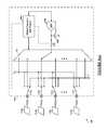
- FIGS. 1( a )-1( f )illustrate schematic diagrams of sequential switching configurations for measuring a plurality of capacitive sensors, according to a specific example embodiment of this disclosure
- FIG. 1( g )illustrates a schematic diagram of sequential switching configurations for measuring a plurality of capacitive sensors, according to another specific example embodiment of this disclosure
- FIG. 1( h )illustrates a schematic diagram of switching configurations for measuring a plurality of capacitive sensors, according to yet another specific example embodiment of this disclosure
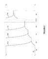
- FIG. 2illustrates schematic voltage-time graphs resulting from the sequential switching configurations shown in FIGS. 1( a )-1( e ) , according to a specific example embodiment of this disclosure
- FIG. 3illustrates a schematic diagram of a typical voltage charging/discharging driver and a voltage input receiver, according to a specific example embodiment of this disclosure
- FIGS. 4-7illustrate schematic process diagrams for operation of the multiple channel capacitive voltage divider scanning method, according to a specific example embodiment of this disclosure.
- FIGS. 8-11illustrate schematic process diagrams for operation of the multiple channel capacitive voltage divider scanning method, according to another specific example embodiment of this disclosure.
- Touching of a capacitive sensor or approaching a capacitive proximity sensor by an objectchanges certain parameters thereof, in particular the capacitance value of a capacitor that is built into the touch sensor used, for example, in human-machine interface devices, e.g., keypad or keyboard.
- Microcontrollersmay utilize algorithms or built-in peripherals for the detection and evaluation of such capacitive touch sensors.
- One such applicationutilizes capacitive voltage division (CVD) to evaluate whether a capacitive touch element has been touched or not.
- CVDcapacitive voltage division
- the CVD conversion processrequires that the sensor capacitor be charged and ADC sample-and-hold capacitor be discharged by different voltages, or vice versa, before being connected together for conversion of the resulting voltage.
- the touch sensor capacitancecan be charged/discharged by a driver connected to an external node (integrated circuit package pin), but the ADC sample-and-hold capacitor may be connected to an external pin or internal ADC channel, e.g., DAC output, fixed voltage reference output to be discharged/charged.
- a touch to that capacitive sensor platemay be determined based upon the change in capacitance thereof.
- CVDtwo capacitors are charged/discharged to opposite voltage values. Then the two oppositely charged capacitors are coupled together and a resulting voltage is measured after the two capacitors have been connected together a sufficient time for a quiescent (steady) voltage to be reached.
- the relative capacitance of a plurality of capacitive sensorsmay be monitored using only one ADC conversion.
- the systemmay generally include a plurality of capacitive sensors into a single measurement. According to some embodiments, all available capacitive sensors may be included in a measurement. According to other embodiments, only a selected sub-group of n capacitive sensors may be included, wherein n is greater than one (1).
- an entire panel of capacitive sensorsmay be quickly monitored for a change in the “group” capacitance thereof, or portions of the capacitive sensors may be monitored for a change in the “subgroup” capacitance thereof.
- a more focused and selective capacitive sensor measurementcan be made. Also the system average power consumption is reduced because of less time spent doing capacitive sensor scans.
- FIGS. 1( a )-1( f )depicted are schematic diagrams of sequential switching configurations for measuring a plurality of capacitive sensors, according to a specific example embodiment of this disclosure.
- the circuit shown in FIGS. 1( a )-( f )may “collect” the charges on a plurality of capacitive sensors 114 in a sample and hold capacitor 108 before doing an analog-to-digital conversion of these collect charges.
- a capacitive sensor touch/proximity systemmay comprise a plurality of capacitive sensors 114 , capacitive sensor channel switches 112 , a multiplexer 102 , a sample and hold switch 110 , a sample and hold capacitor 108 , an analog-to-digital converter (ADC) 106 , and a digital processor and memory 104 .
- the aforementioned capacitive sensor channel switches 112 , multiplexer 102 , sample and hold switch 110 , sample and hold capacitor 108 , ADC 106 , and digital processor and memory 104may be provided in a microcontroller integrated circuit 101 .
- the capacitive sensor channel switches 112may connect respective ones of the plurality of capacitive sensors 114 to either a first voltage, e.g., V DD , a second voltage, e.g., V SS , or respective inputs of the multiplexer 102 . Connecting a capacitive sensor 114 to a positive voltage puts a positive charge thereon, and connecting the capacitive sensor 114 to a common or ground removes substantially any charge thereon.
- the multiplexer 102is adapted to couple the sample and hold switch 110 to any one of the capacitive sensor channel switches 112 , the first voltage, e.g., V DD , or the second voltage, e.g., V SS .
- the sample and hold switch 110couplers the output of the multiplexer 102 to the sample and hold capacitor 108 and also may be used to isolate the sample and hold capacitor 108 during an analog-to-digital conversion by the ADC 106 .
- the resulting analog-to-digital conversion from the ADC 106may be read by the digital processor 104 for further processing in determining whether at least one of the plurality of capacitive sensors 114 has changed its capacitance value.
- all of the capacitive sensor channel switches 112may connect their respective capacitive sensors 114 to the first voltage, e.g., V DD .
- the sample and hold capacitor 108may be connected to the second voltage, e.g., V SS , through the sample and hold switch 110 and the multiplexer 102 .
- Portion (a) of FIG. 2shows the capacitive sensors 114 charged to the first voltage and the sample and hold capacitor 108 discharged to the second voltage.
- FIG. 1( b )shows one of the capacitive sensors 114 a connected to the sample and hold capacitor 108 through switch 112 a , the multiplexer 102 and the sample and hold switch 110 .
- FIG. 2shows a graphical representation of electron charge equalization (voltage equilibrium) between the capacitive sensor 114 a and the sample and hold capacitor 108 . Since the capacitive sensor 114 a has a capacitance value less than the sample and hold capacitor 108 , its charge does not much affect the initial charge (none) on the sample and hold capacitor 108 .
- switch 112 bmay connect the fully charged capacitive sensor 114 b to the partially charged sample and hold capacitor 108 through switches 112 b and 110 , and the multiplexer 102 .
- Portion (c) of FIG. 2shows a shows a graphical representation of the fully charged capacitive sensor 114 b discharging into the partially charged sample and hold capacitor 108 .
- the sample and hold capacitor 108is slightly more charged and comprises a more positive voltage thereon.
- Switch 112 amay also connect the capacitive sensor 114 a to the second voltage, e.g., substantially discharging the sensor 114 a in anticipation of the next capacitive sensor scan, but using reversed charge/discharge voltages on the capacitive sensors 114 and the sample and hold capacitor 108 .
- switch 112 cmay connect the fully charged capacitive sensor 114 c to the partially charged sample and hold capacitor 108 through switches 112 c and 110 , and the multiplexer 102 .
- Portion (d) of FIG. 2shows a graphical representation of the fully charged capacitive sensor 114 c discharging into the partially charged sample and hold capacitor 108 . Now the sample and hold capacitor 108 is slightly more charged and comprises an even more positive voltage thereon.
- Switches 112 a and 112 bmay also connect the capacitive sensors 114 a and 114 b to the second voltage, e.g., substantially discharging the sensors 114 a and 114 b in anticipation of the next capacitive sensor scan, but using reversed charge/discharge voltages on the capacitive sensors 114 and the sample and hold capacitor 108 .
- switch 112 nmay connect the fully charged capacitive sensor 114 n to the more partially charged sample and hold capacitor 108 through switches 112 n and 110 , and the multiplexer 102 .
- Portion (n) of FIG. 2shows a graphical representation of the fully charged capacitive sensor 114 n discharging into the even more partially charged sample and hold capacitor 108 .
- the sample and hold capacitor 108may be substantially charged and comprises a greater positive voltage thereon.
- Switches 112 a , 112 b and 122 cmay also connect the capacitive sensors 114 a , 114 b and 114 c to the second voltage, e.g., substantially discharging the sensors 114 a , 114 b and 114 c in anticipation of the next capacitive sensor scan, but using reversed charge/discharge voltages on the capacitive sensors 114 and the sample and hold capacitor 108 .
- sample and hold switch 110may briefly open while the multiplexer 102 and the switches 112 are changing configurations so that the switching thereof does not affect the existing charge on the sample and hold capacitor 108 .
- the sample and hold switch 110may open, effectively isolating the sample and hold capacitor 108 for further processing.
- the voltage on the sample and hold capacitor 108representing the sum of the charges from the plurality of capacitive sensors 114 , may be converted to a digital value with the ADC 106 .
- This digital valuerepresenting the sum of the charges from the capacitive sensors 114 , may then be read by the digital processor 104 for further evaluation thereof.
- the multiplexermay be switched to the first voltage, e.g., V DD , and all of the capacitive sensor channel switches 112 may be switched to the second voltage, e.g., V SS , in anticipation of the next capacitive sensor scan cycle using the reverse polarities of the previous scan.
- a capacitive sensor scan controller peripheral 116may be used to control the aforementioned switching operations while the digital processor and memory 104 a are in a low power sleep mode. This enables scanning of the capacitive sensors 114 using a minimum of power, and the more power hungry digital processor and memory 104 a only waking up after a scan has completed.
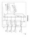
- FIG. 1( h )depicted is a schematic diagram of switching configurations for measuring a plurality of capacitive sensors, according to yet another specific example embodiment of this disclosure.
- the circuit shown in FIG. 1( h )may “collect” the charges on a plurality of capacitive sensors 114 in a sample and hold capacitor 108 before doing an analog-to-digital conversion of these collect charges.
- a capacitive sensor touch/proximity systemmay comprise a plurality of capacitive sensors 114 , capacitive sensor channel switches 112 , a multiplexer 102 a , a sample and hold switch 110 , a sample and hold capacitor 108 , an analog-to-digital converter (ADC) 106 , a digital processor and memory 104 , and optionally a capacitive sensor scan controller peripheral 116 .
- ADCanalog-to-digital converter
- capacitive sensor channel switches 112 , multiplexer 102 a , sample and hold switch 110 , sample and hold capacitor 108 , ADC 106 , digital processor and memory 104 a , and capacitive sensor scan controller peripheral 116may be provided in a microcontroller integrated circuit 101 b.
- the capacitive sensor channel switches 112may connect respective ones of the plurality of capacitive sensors 114 to either a first voltage, e.g., V DD , a second voltage, e.g., V SS , or an input of the multiplexer 102 . Connecting a capacitive sensor 114 to a positive voltage puts a positive charge thereon, and connecting the capacitive sensor 114 to a common or ground removes substantially any charge thereon.
- the multiplexer 102is adapted to couple the sample and hold switch 110 to a common node of the capacitive sensor channel switches 112 , the first voltage, e.g., V DD , or the second voltage, e.g., V SS .
- the sample and hold switch 110couplers the output of the multiplexer 102 to the sample and hold capacitor 108 and also may be used to isolate the sample and hold capacitor 108 during an analog-to-digital conversion by the ADC 106 .
- the resulting analog-to-digital conversion from the ADC 106may be read by the digital processor 104 for further processing in determining whether at least one of the plurality of capacitive sensors 114 has changed its capacitance value.
- the capacitive sensor scan controller peripheral 116may be used to control the aforementioned switching operations while the digital processor and memory 104 a are in a low power sleep mode. This enables scanning of the capacitive sensors 114 using a minimum of power, and the more power hungry digital processor and memory 104 a only waking up after a scan has completed.
- Each of the capacitive sensor channel switches 112may comprise a tri-state driver 320 having a high output state at substantially V DD , a low output state at substantially, V SS , and an open or high impedance state; and an analog receiver/buffer 322 for coupling the voltage on the respective capacitive sensor 114 to an input of the multiplexer 102 .
- the tri-state driver 320may be controller by the digital processor 104 .
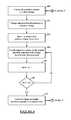
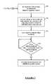
- step 430all capacitive sensors 114 may be charged (discharged) to a first voltage, e.g., V DD or V SS .
- step 432the sample and hold capacitor 108 may be discharged (charged) to a second voltage, e.g., V SS or V DD .
- step 434initiates the beginning of a capacitive sensor scan by setting an indexing value, k, to one (1), according to specific example embodiments of this disclosure.
- step 436the k th capacitive sensor 114 may be coupled to the sample and hold capacitor 108 .
- Step 438increments the k value by 1. Then step 440 checks the k value to see if all capacitive sensors 114 have been coupled to the sample and hold capacitor 108 . If not, then the next k th capacitive sensor 114 may be coupled to the sample and hold capacitor 108 . Once all of the capacitive sensors 114 have been individually coupled to the sample and hold capacitor 108 , the voltage on the sample and hold capacitor 108 is converted to a digital value in step 442 . It is contemplated and within the scope of this disclosure that the capacitive sensors 114 may be randomly and/or selectively coupled in any order to the sample and hold capacitor 108 depending upon the application and situation that may have been previously determined from a recognizable pattern of proximity and/or touch detections.
- this digital valuemay be stored in the digital processor memory 104 .
- the digital processor 104 or capacitive sensor scan controller 116may compare this stored digital value with a previously stored digital value of the same configuration capacitive sensor 114 scan. If there is substantially no difference in this comparison then the capacitive sensor 114 scan may start again from step 430 . If there is a difference in this comparison, e.g., the most recent scan has a digital value greater than the previously scanned digital value, then a proximity/touch condition has changed since the previous scan. For this situation either a more refined grouping(s) of capacitive sensors 114 may be scanned, or a standard CVD evaluation of each individual capacitive sensor 114 may be performed, depending on the application thereof.
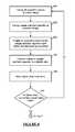
- step 548may charge a subgroup of the capacitive sensors 114 to a first voltage.
- step 550the sample and hold capacitor 108 may be charged to a second voltage.
- a subgroup range of capacitive sensors 114 to be scannedmay be selected in step 552 .
- step 554a capacitive sensor 114 may be coupled to the sample and hold capacitor 108 until voltage is equalized therebetween.
- step 656the sensor pointer k is advanced, and in step 658 the k value is checked to see if all of the selected subgroup of sensors 114 have be scanned. If not, then return to step 554 for the next capacitive sensor 114 to be coupled to the sample and hold capacitor 108 .
- step 660convert the voltage on the sample and hold capacitor 108 , representing the charges from all of the subgroup of capacitive sensors 114 , to a subgroup digital value.
- this subgroup digital valuemay be stored in the digital processor memory 104 .
- the digital processor 104may compare this stored digital subgroup value with a previously stored digital subgroup value of the same configuration capacitive sensor 114 scan. If there is substantially no difference in this comparison then the capacitive sensor 114 scan may start again from step 666 by charging another subgroup of capacitive sensors 114 to the first voltage. If the is a difference in this comparison, e.g., the most recent scan has a digital value greater than the previously scanned digital value, then a proximity/touch condition in this subgroup has changed since the previous scan. For this situation either a more refined grouping(s) of capacitive sensors 114 may be scanned, or a standard CVD evaluation of each individual capacitive sensor 114 may be performed, depending on the application thereof.
- step 768standard CVD detections for each of the subgroup capacitive sensors 114 may be performed.
- step 770convert the voltages on the sample and hold capacitor 108 for each one of the subgroup capacitive sensors to individual digital values thereof.
- step 772store each of these individual digital values in the digital processor memory 104 .
- step 774check each one of the stored individual digital values to see is there is a change in any one of them from previously stored digital values. If there is at least one difference then in step 776 that is the at least one capacitive sensor 114 that had a proximity/touch event occur to it.
- step 830all capacitive sensors 114 may be charged (discharged) to a first voltage, e.g., V DD or V SS .
- step 832the sample and hold capacitor 108 may be discharged (charged) to a second voltage, e.g., V SS or V DD .
- step 836all of the capacitive sensors 114 may be coupled to the sample and hold capacitor 108 . Once the capacitive sensors 114 have been coupled to the sample and hold capacitor 108 , the voltage on the sample and hold capacitor 108 is converted to a digital value in step 842 .
- this digital valuemay be stored in the digital processor memory 104 .
- the digital processor 104 a or capacitive sensor scan controller 116may compare this stored digital value with a previously stored digital value of the same configuration capacitive sensor 114 scan. If there is substantially no difference in this comparison then the capacitive sensor 114 scan may start again from step 830 . If there is a difference in this comparison, e.g., the most recent scan has a digital value greater than the previously scanned digital value, then a proximity/touch condition has changed since the previous scan. For this situation either a more refined grouping(s) of capacitive sensors 114 may be scanned, or a standard CVD evaluation of each individual capacitive sensor 114 may be performed, depending on the application thereof.
- step 948may charge a subgroup of the capacitive sensors 114 to a first voltage.
- step 950the sample and hold capacitor 108 may be charged to a second voltage.
- step 954the subgroup of capacitive sensors 114 may be coupled to the sample and hold capacitor 108 until voltage is equalized therebetween.
- step 960the voltage on the sample and hold capacitor 108 is converted to a subgroup digital value representing the charges from all of the subgroup of capacitive sensors 114 .
- this subgroup digital valuemay be stored in the digital processor memory 104 .
- the digital processor 104may compare this stored digital subgroup value with a previously stored digital subgroup value of the same configuration capacitive sensor 114 scan. If there is substantially no difference in this comparison then the capacitive sensor 114 scan may start again from step 1066 by charging another subgroup of capacitive sensors 114 to the first voltage. If the is a difference in this comparison, e.g., the most recent scan has a digital value greater than the previously scanned digital value, then a proximity/touch condition in this subgroup has changed since the previous scan. For this situation either a more refined grouping(s) of capacitive sensors 114 may be scanned, or a standard CVD evaluation of each individual capacitive sensor 114 may be performed, depending on the application thereof.
- step 1068standard CVD detections for each of the subgroup capacitive sensors 114 may be performed.
- step 1070convert the voltages on the sample and hold capacitor 108 for each one of the subgroup capacitive sensors to individual digital values thereof.
- step 1172store each of these individual digital values in the digital processor memory 104 .
- step 1174check each one of the stored individual digital values to see is there is a change in any one of them from previously stored digital values. If there is at least one difference then in step 1176 that is the at least one capacitive sensor 114 that had a proximity/touch event occur to it.
- the capacitive sensors 114may be randomly and/or selectively coupled in any order to the sample and hold capacitor 108 depending upon the application and situation that may have been previously determined from a recognizable pattern of proximity and/or touch detections.
Landscapes
- Physics & Mathematics (AREA)
- General Physics & Mathematics (AREA)
- Engineering & Computer Science (AREA)
- Theoretical Computer Science (AREA)
- Power Engineering (AREA)
- Electronic Switches (AREA)
- Measurement Of Resistance Or Impedance (AREA)
- Analogue/Digital Conversion (AREA)
- Position Input By Displaying (AREA)
Abstract
Description
Claims (13)
Priority Applications (8)
| Application Number | Priority Date | Filing Date | Title |
|---|---|---|---|
| US14/503,702US9857394B2 (en) | 2013-10-04 | 2014-10-01 | Multiple channel capacitive voltage divider scanning method and apparatus |
| CN201480050927.4ACN105580279B (en) | 2013-10-04 | 2014-10-02 | Multi-channel capacitive voltage divider scanning method and device |
| EP14790876.8AEP3053273B1 (en) | 2013-10-04 | 2014-10-02 | Multiple channel capacitive voltage divider scanning method and apparatus |
| JP2016518451AJP6418701B2 (en) | 2013-10-04 | 2014-10-02 | Multi-channel capacitive voltage divider scanning method and apparatus |
| PCT/US2014/058788WO2015051096A1 (en) | 2013-10-04 | 2014-10-02 | Multiple channel capacitive voltage divider scanning method and apparatus |
| KR1020167006839AKR102211085B1 (en) | 2013-10-04 | 2014-10-02 | Multiple channel capacitive voltage divider scanning method and apparatus |
| TW103134656ATWI628579B (en) | 2013-10-04 | 2014-10-03 | Multiple channel capacitive voltage divider scanning method and apparatus |
| US15/853,737US10408862B2 (en) | 2013-10-04 | 2017-12-23 | Multiple channel capacitive voltage divider scanning method and apparatus |
Applications Claiming Priority (2)
| Application Number | Priority Date | Filing Date | Title |
|---|---|---|---|
| US201361886993P | 2013-10-04 | 2013-10-04 | |
| US14/503,702US9857394B2 (en) | 2013-10-04 | 2014-10-01 | Multiple channel capacitive voltage divider scanning method and apparatus |
Related Child Applications (1)
| Application Number | Title | Priority Date | Filing Date |
|---|---|---|---|
| US15/853,737DivisionUS10408862B2 (en) | 2013-10-04 | 2017-12-23 | Multiple channel capacitive voltage divider scanning method and apparatus |
Publications (2)
| Publication Number | Publication Date |
|---|---|
| US20150097583A1 US20150097583A1 (en) | 2015-04-09 |
| US9857394B2true US9857394B2 (en) | 2018-01-02 |
Family
ID=52776454
Family Applications (2)
| Application Number | Title | Priority Date | Filing Date |
|---|---|---|---|
| US14/503,702Active2035-04-22US9857394B2 (en) | 2013-10-04 | 2014-10-01 | Multiple channel capacitive voltage divider scanning method and apparatus |
| US15/853,737ActiveUS10408862B2 (en) | 2013-10-04 | 2017-12-23 | Multiple channel capacitive voltage divider scanning method and apparatus |
Family Applications After (1)
| Application Number | Title | Priority Date | Filing Date |
|---|---|---|---|
| US15/853,737ActiveUS10408862B2 (en) | 2013-10-04 | 2017-12-23 | Multiple channel capacitive voltage divider scanning method and apparatus |
Country Status (7)
| Country | Link |
|---|---|
| US (2) | US9857394B2 (en) |
| EP (1) | EP3053273B1 (en) |
| JP (1) | JP6418701B2 (en) |
| KR (1) | KR102211085B1 (en) |
| CN (1) | CN105580279B (en) |
| TW (1) | TWI628579B (en) |
| WO (1) | WO2015051096A1 (en) |
Cited By (3)
| Publication number | Priority date | Publication date | Assignee | Title |
|---|---|---|---|---|
| US10408862B2 (en) | 2013-10-04 | 2019-09-10 | Microchip Technology Incorporated | Multiple channel capacitive voltage divider scanning method and apparatus |
| US20220155355A1 (en)* | 2019-04-10 | 2022-05-19 | Iee International Electronics & Engineering S.A. | Multi-channel capacitance sensing measurement circuit |
| US11511440B2 (en) | 2018-11-16 | 2022-11-29 | Hewlett-Packard Development Company, L.P. | Object detection to activiate pressure sensors |
Families Citing this family (8)
| Publication number | Priority date | Publication date | Assignee | Title |
|---|---|---|---|---|
| TWI540514B (en)* | 2015-05-05 | 2016-07-01 | 晨星半導體股份有限公司 | Sensing apparatus for detecting user touch |
| KR102349419B1 (en) | 2017-09-25 | 2022-01-10 | 삼성전자 주식회사 | Touch screen controller, Touch screen system and Operating method of touch screen controller |
| CN108259044B (en)* | 2018-02-26 | 2021-09-07 | 上海东软载波微电子有限公司 | Touch key scanning method and device and computer readable storage medium |
| CN109374932B (en)* | 2018-10-25 | 2020-11-06 | 安徽省临泉县康悦电子科技有限公司 | Pin clamping device of capacitance detection system |
| US11093078B1 (en)* | 2020-03-20 | 2021-08-17 | Cypress Semiconductor Corporation | Always on low power capacitive matrix autonomous scan |
| KR102819293B1 (en) | 2020-08-13 | 2025-06-11 | 삼성전자주식회사 | Apparatus and method for sensing touch based on multi-channel |
| DE102022106457A1 (en)* | 2021-03-30 | 2022-10-06 | Wika Alexander Wiegand Se & Co. Kg | level gauge |
| CN117595882B (en)* | 2024-01-19 | 2024-07-02 | 景昱医疗科技(苏州)股份有限公司 | Signal acquisition circuit, contact combination method, stimulator and implantable medical system |
Citations (12)
| Publication number | Priority date | Publication date | Assignee | Title |
|---|---|---|---|---|
| US6452514B1 (en)* | 1999-01-26 | 2002-09-17 | Harald Philipp | Capacitive sensor and array |
| US20070075710A1 (en)* | 2005-06-03 | 2007-04-05 | Kirk Hargreaves | Methods and systems for detecting a capacitance using sigma-delta measurement techniques |
| CN101213461A (en) | 2005-06-03 | 2008-07-02 | 辛纳普蒂克斯公司 | Method and system for detecting capacitance using SIGMA-DELTA measurement technique |
| US20080246723A1 (en) | 2007-04-05 | 2008-10-09 | Baumbach Jason G | Integrated button activation sensing and proximity sensing |
| US20100148806A1 (en)* | 2005-06-03 | 2010-06-17 | Synaptics Incorporated | Methods and systems for detecting a capacitance using sigma-delta measurement techniques |
| US20100181180A1 (en)* | 2009-01-16 | 2010-07-22 | Microchip Technology Incorporated | Capacitive touch sensing using an internal capacitor of an analog-to-digital converter (adc) and a voltage reference |
| US20120054379A1 (en)* | 2010-08-30 | 2012-03-01 | Kafai Leung | Low power multi-touch scan control system |
| US20140002406A1 (en)* | 2012-06-28 | 2014-01-02 | Texas Instruments Incorporated | Low-Power Capacitive Sensor Monitoring and Method |
| US20140111225A1 (en)* | 2011-07-29 | 2014-04-24 | Luben H. Hristov | Measuring Voltage |
| US20140368223A1 (en)* | 2010-05-07 | 2014-12-18 | Novatek Microelectronics Corp. | Capacitance measurement device and electronic device thereof |
| US9312831B2 (en)* | 2010-08-18 | 2016-04-12 | Analog Devices, Inc. | Charge sharing analog computation circuitry and applications |
| US9372582B2 (en)* | 2012-04-19 | 2016-06-21 | Atmel Corporation | Self-capacitance measurement |
Family Cites Families (13)
| Publication number | Priority date | Publication date | Assignee | Title |
|---|---|---|---|---|
| US7271758B2 (en)* | 2005-06-29 | 2007-09-18 | Silicon Laboratories Inc. | Gain adjust for SAR ADC |
| US7312616B2 (en)* | 2006-01-20 | 2007-12-25 | Cypress Semiconductor Corporation | Successive approximate capacitance measurement circuit |
| WO2007089937A2 (en)* | 2006-01-27 | 2007-08-09 | Rudolph Technologies, Inc. | High-speed capacitor leakage measurement systems and methods |
| JP5252427B2 (en) | 2008-10-01 | 2013-07-31 | 株式会社ジャパンディスプレイウェスト | Input device and display device |
| US8018238B2 (en)* | 2009-03-27 | 2011-09-13 | Texas Instruments Incorporated | Embedded sar based active gain capacitance measurement system and method |
| US8115499B2 (en) | 2009-05-22 | 2012-02-14 | Freescale Semiconductor, Inc. | Device with proximity detection capability |
| US20120169659A1 (en)* | 2010-08-29 | 2012-07-05 | Welland David R | Apparatus for capacitance sensor with interference rejection and associated methods |
| JP5429207B2 (en)* | 2010-09-08 | 2014-02-26 | 株式会社デンソー | Capacitive physical quantity detector |
| US8786295B2 (en)* | 2011-04-20 | 2014-07-22 | Cypress Semiconductor Corporation | Current sensing apparatus and method for a capacitance-sensing device |
| JP5791400B2 (en)* | 2011-07-08 | 2015-10-07 | コスモテック株式会社 | Absorbent packaging bag |
| EP2562627B1 (en) | 2011-08-26 | 2016-11-09 | LG Display Co., Ltd. | Touch sensing device |
| US9071264B2 (en)* | 2011-10-06 | 2015-06-30 | Microchip Technology Incorporated | Microcontroller with sequencer driven analog-to-digital converter |
| US9857394B2 (en) | 2013-10-04 | 2018-01-02 | Microchip Technology Incorporated | Multiple channel capacitive voltage divider scanning method and apparatus |
- 2014
- 2014-10-01USUS14/503,702patent/US9857394B2/enactiveActive
- 2014-10-02EPEP14790876.8Apatent/EP3053273B1/enactiveActive
- 2014-10-02CNCN201480050927.4Apatent/CN105580279B/enactiveActive
- 2014-10-02KRKR1020167006839Apatent/KR102211085B1/enactiveActive
- 2014-10-02JPJP2016518451Apatent/JP6418701B2/enactiveActive
- 2014-10-02WOPCT/US2014/058788patent/WO2015051096A1/enactiveApplication Filing
- 2014-10-03TWTW103134656Apatent/TWI628579B/enactive
- 2017
- 2017-12-23USUS15/853,737patent/US10408862B2/enactiveActive
Patent Citations (12)
| Publication number | Priority date | Publication date | Assignee | Title |
|---|---|---|---|---|
| US6452514B1 (en)* | 1999-01-26 | 2002-09-17 | Harald Philipp | Capacitive sensor and array |
| US20070075710A1 (en)* | 2005-06-03 | 2007-04-05 | Kirk Hargreaves | Methods and systems for detecting a capacitance using sigma-delta measurement techniques |
| CN101213461A (en) | 2005-06-03 | 2008-07-02 | 辛纳普蒂克斯公司 | Method and system for detecting capacitance using SIGMA-DELTA measurement technique |
| US20100148806A1 (en)* | 2005-06-03 | 2010-06-17 | Synaptics Incorporated | Methods and systems for detecting a capacitance using sigma-delta measurement techniques |
| US20080246723A1 (en) | 2007-04-05 | 2008-10-09 | Baumbach Jason G | Integrated button activation sensing and proximity sensing |
| US20100181180A1 (en)* | 2009-01-16 | 2010-07-22 | Microchip Technology Incorporated | Capacitive touch sensing using an internal capacitor of an analog-to-digital converter (adc) and a voltage reference |
| US20140368223A1 (en)* | 2010-05-07 | 2014-12-18 | Novatek Microelectronics Corp. | Capacitance measurement device and electronic device thereof |
| US9312831B2 (en)* | 2010-08-18 | 2016-04-12 | Analog Devices, Inc. | Charge sharing analog computation circuitry and applications |
| US20120054379A1 (en)* | 2010-08-30 | 2012-03-01 | Kafai Leung | Low power multi-touch scan control system |
| US20140111225A1 (en)* | 2011-07-29 | 2014-04-24 | Luben H. Hristov | Measuring Voltage |
| US9372582B2 (en)* | 2012-04-19 | 2016-06-21 | Atmel Corporation | Self-capacitance measurement |
| US20140002406A1 (en)* | 2012-06-28 | 2014-01-02 | Texas Instruments Incorporated | Low-Power Capacitive Sensor Monitoring and Method |
Non-Patent Citations (2)
| Title |
|---|
| International Search Report and Written Opinion, Application No. PCT/US2014/058788, 12 pages, dated Feb. 27, 2015. |
| Taiwan Office Action, Application No. 103134656, 6 pages, dated Nov. 3, 2017. |
Cited By (4)
| Publication number | Priority date | Publication date | Assignee | Title |
|---|---|---|---|---|
| US10408862B2 (en) | 2013-10-04 | 2019-09-10 | Microchip Technology Incorporated | Multiple channel capacitive voltage divider scanning method and apparatus |
| US11511440B2 (en) | 2018-11-16 | 2022-11-29 | Hewlett-Packard Development Company, L.P. | Object detection to activiate pressure sensors |
| US20220155355A1 (en)* | 2019-04-10 | 2022-05-19 | Iee International Electronics & Engineering S.A. | Multi-channel capacitance sensing measurement circuit |
| US12078666B2 (en)* | 2019-04-10 | 2024-09-03 | Iee International Electronics & Engineering S.A. | Multi-channel capacitance sensing measurement circuit |
Also Published As
| Publication number | Publication date |
|---|---|
| CN105580279B (en) | 2019-08-16 |
| EP3053273A1 (en) | 2016-08-10 |
| TWI628579B (en) | 2018-07-01 |
| WO2015051096A1 (en) | 2015-04-09 |
| US20180120355A1 (en) | 2018-05-03 |
| JP6418701B2 (en) | 2018-11-07 |
| TW201523408A (en) | 2015-06-16 |
| CN105580279A (en) | 2016-05-11 |
| EP3053273B1 (en) | 2020-02-26 |
| US10408862B2 (en) | 2019-09-10 |
| KR102211085B1 (en) | 2021-02-03 |
| KR20160067094A (en) | 2016-06-13 |
| US20150097583A1 (en) | 2015-04-09 |
| JP2017501462A (en) | 2017-01-12 |
Similar Documents
| Publication | Publication Date | Title |
|---|---|---|
| US10408862B2 (en) | Multiple channel capacitive voltage divider scanning method and apparatus | |
| US7375535B1 (en) | Scan method and topology for capacitive sensing | |
| US20110068810A1 (en) | Sensing method and driving circuit of capacitive touch screen | |
| US10296771B2 (en) | Fingerprint recognition system and method | |
| US9086439B2 (en) | Circuits, devices and methods having pipelined capacitance sensing | |
| CN105278776B (en) | Capacitance voltage information sensing circuit and related anti-noise touch control circuit thereof | |
| TWI493416B (en) | Touch sensing system, capacitance sensing apparatus and capacitance sensing method thereof | |
| CN109313518B (en) | Piezoelectric sensor element detection | |
| US9063622B2 (en) | Touch module having a dynamic capacitance matching mechanism | |
| CN101866231B (en) | Control method for detecting touch event in touch panel and related device thereof | |
| JP2013058045A (en) | Capacity detection circuit and capacity detection method for touch panel and touch panel input device and electronic equipment using the same | |
| CN110084082B (en) | Electronic equipment, fingerprint identification device and finger touch detection circuit thereof | |
| JP5723619B2 (en) | Touch panel capacitance detection circuit, touch panel input device using the same, and electronic device | |
| US11983060B2 (en) | Systems and method for always-on sensing user interface | |
| Rovere et al. | A 2.1 μW event-driven wake-up circuit based on a level-crossing ADC for pattern recognition in healthcare | |
| CN212872665U (en) | Capacitance change detection circuit | |
| US10439625B2 (en) | Comparator and analog-to-digital converter applied with dynamic current correlating circuit | |
| TWI825761B (en) | Capacitive touch sensor | |
| CN117389426A (en) | capacitive touch sensor | |
| CN112838853A (en) | High sensitivity touch key circuit |
Legal Events
| Date | Code | Title | Description |
|---|---|---|---|
| AS | Assignment | Owner name:MICROCHIP TECHNOLOGY INCORPORATED, ARIZONA Free format text:ASSIGNMENT OF ASSIGNORS INTEREST;ASSIGNOR:GAO, XIANG;REEL/FRAME:034477/0701 Effective date:20140930 | |
| AS | Assignment | Owner name:JPMORGAN CHASE BANK, N.A., AS ADMINISTRATIVE AGENT, ILLINOIS Free format text:SECURITY INTEREST;ASSIGNOR:MICROCHIP TECHNOLOGY INCORPORATED;REEL/FRAME:041675/0617 Effective date:20170208 Owner name:JPMORGAN CHASE BANK, N.A., AS ADMINISTRATIVE AGENT Free format text:SECURITY INTEREST;ASSIGNOR:MICROCHIP TECHNOLOGY INCORPORATED;REEL/FRAME:041675/0617 Effective date:20170208 | |
| STCF | Information on status: patent grant | Free format text:PATENTED CASE | |
| AS | Assignment | Owner name:JPMORGAN CHASE BANK, N.A., AS ADMINISTRATIVE AGENT, ILLINOIS Free format text:SECURITY INTEREST;ASSIGNORS:MICROCHIP TECHNOLOGY INCORPORATED;SILICON STORAGE TECHNOLOGY, INC.;ATMEL CORPORATION;AND OTHERS;REEL/FRAME:046426/0001 Effective date:20180529 Owner name:JPMORGAN CHASE BANK, N.A., AS ADMINISTRATIVE AGENT Free format text:SECURITY INTEREST;ASSIGNORS:MICROCHIP TECHNOLOGY INCORPORATED;SILICON STORAGE TECHNOLOGY, INC.;ATMEL CORPORATION;AND OTHERS;REEL/FRAME:046426/0001 Effective date:20180529 | |
| AS | Assignment | Owner name:WELLS FARGO BANK, NATIONAL ASSOCIATION, AS NOTES COLLATERAL AGENT, CALIFORNIA Free format text:SECURITY INTEREST;ASSIGNORS:MICROCHIP TECHNOLOGY INCORPORATED;SILICON STORAGE TECHNOLOGY, INC.;ATMEL CORPORATION;AND OTHERS;REEL/FRAME:047103/0206 Effective date:20180914 Owner name:WELLS FARGO BANK, NATIONAL ASSOCIATION, AS NOTES C Free format text:SECURITY INTEREST;ASSIGNORS:MICROCHIP TECHNOLOGY INCORPORATED;SILICON STORAGE TECHNOLOGY, INC.;ATMEL CORPORATION;AND OTHERS;REEL/FRAME:047103/0206 Effective date:20180914 | |
| AS | Assignment | Owner name:JPMORGAN CHASE BANK, N.A., AS ADMINISTRATIVE AGENT, DELAWARE Free format text:SECURITY INTEREST;ASSIGNORS:MICROCHIP TECHNOLOGY INC.;SILICON STORAGE TECHNOLOGY, INC.;ATMEL CORPORATION;AND OTHERS;REEL/FRAME:053311/0305 Effective date:20200327 | |
| AS | Assignment | Owner name:MICROCHIP TECHNOLOGY INC., ARIZONA Free format text:RELEASE BY SECURED PARTY;ASSIGNOR:JPMORGAN CHASE BANK, N.A, AS ADMINISTRATIVE AGENT;REEL/FRAME:053466/0011 Effective date:20200529 Owner name:MICROSEMI CORPORATION, CALIFORNIA Free format text:RELEASE BY SECURED PARTY;ASSIGNOR:JPMORGAN CHASE BANK, N.A, AS ADMINISTRATIVE AGENT;REEL/FRAME:053466/0011 Effective date:20200529 Owner name:SILICON STORAGE TECHNOLOGY, INC., ARIZONA Free format text:RELEASE BY SECURED PARTY;ASSIGNOR:JPMORGAN CHASE BANK, N.A, AS ADMINISTRATIVE AGENT;REEL/FRAME:053466/0011 Effective date:20200529 Owner name:ATMEL CORPORATION, ARIZONA Free format text:RELEASE BY SECURED PARTY;ASSIGNOR:JPMORGAN CHASE BANK, N.A, AS ADMINISTRATIVE AGENT;REEL/FRAME:053466/0011 Effective date:20200529 Owner name:MICROSEMI STORAGE SOLUTIONS, INC., ARIZONA Free format text:RELEASE BY SECURED PARTY;ASSIGNOR:JPMORGAN CHASE BANK, N.A, AS ADMINISTRATIVE AGENT;REEL/FRAME:053466/0011 Effective date:20200529 | |
| AS | Assignment | Owner name:WELLS FARGO BANK, NATIONAL ASSOCIATION, MINNESOTA Free format text:SECURITY INTEREST;ASSIGNORS:MICROCHIP TECHNOLOGY INC.;SILICON STORAGE TECHNOLOGY, INC.;ATMEL CORPORATION;AND OTHERS;REEL/FRAME:053468/0705 Effective date:20200529 | |
| AS | Assignment | Owner name:WELLS FARGO BANK, NATIONAL ASSOCIATION, AS COLLATERAL AGENT, MINNESOTA Free format text:SECURITY INTEREST;ASSIGNORS:MICROCHIP TECHNOLOGY INCORPORATED;SILICON STORAGE TECHNOLOGY, INC.;ATMEL CORPORATION;AND OTHERS;REEL/FRAME:055671/0612 Effective date:20201217 | |
| AS | Assignment | Owner name:WELLS FARGO BANK, NATIONAL ASSOCIATION, AS NOTES COLLATERAL AGENT, MINNESOTA Free format text:SECURITY INTEREST;ASSIGNORS:MICROCHIP TECHNOLOGY INCORPORATED;SILICON STORAGE TECHNOLOGY, INC.;ATMEL CORPORATION;AND OTHERS;REEL/FRAME:057935/0474 Effective date:20210528 | |
| MAFP | Maintenance fee payment | Free format text:PAYMENT OF MAINTENANCE FEE, 4TH YEAR, LARGE ENTITY (ORIGINAL EVENT CODE: M1551); ENTITY STATUS OF PATENT OWNER: LARGE ENTITY Year of fee payment:4 | |
| AS | Assignment | Owner name:MICROSEMI STORAGE SOLUTIONS, INC., ARIZONA Free format text:RELEASE BY SECURED PARTY;ASSIGNOR:JPMORGAN CHASE BANK, N.A., AS ADMINISTRATIVE AGENT;REEL/FRAME:059333/0222 Effective date:20220218 Owner name:MICROSEMI CORPORATION, ARIZONA Free format text:RELEASE BY SECURED PARTY;ASSIGNOR:JPMORGAN CHASE BANK, N.A., AS ADMINISTRATIVE AGENT;REEL/FRAME:059333/0222 Effective date:20220218 Owner name:ATMEL CORPORATION, ARIZONA Free format text:RELEASE BY SECURED PARTY;ASSIGNOR:JPMORGAN CHASE BANK, N.A., AS ADMINISTRATIVE AGENT;REEL/FRAME:059333/0222 Effective date:20220218 Owner name:SILICON STORAGE TECHNOLOGY, INC., ARIZONA Free format text:RELEASE BY SECURED PARTY;ASSIGNOR:JPMORGAN CHASE BANK, N.A., AS ADMINISTRATIVE AGENT;REEL/FRAME:059333/0222 Effective date:20220218 Owner name:MICROCHIP TECHNOLOGY INCORPORATED, ARIZONA Free format text:RELEASE BY SECURED PARTY;ASSIGNOR:JPMORGAN CHASE BANK, N.A., AS ADMINISTRATIVE AGENT;REEL/FRAME:059333/0222 Effective date:20220218 | |
| AS | Assignment | Owner name:MICROCHIP TECHNOLOGY INCORPORATED, ARIZONA Free format text:RELEASE BY SECURED PARTY;ASSIGNOR:JPMORGAN CHASE BANK, N.A., AS ADMINISTRATIVE AGENT;REEL/FRAME:059666/0545 Effective date:20220218 | |
| AS | Assignment | Owner name:MICROSEMI STORAGE SOLUTIONS, INC., ARIZONA Free format text:RELEASE BY SECURED PARTY;ASSIGNOR:WELLS FARGO BANK, NATIONAL ASSOCIATION, AS NOTES COLLATERAL AGENT;REEL/FRAME:059358/0001 Effective date:20220228 Owner name:MICROSEMI CORPORATION, ARIZONA Free format text:RELEASE BY SECURED PARTY;ASSIGNOR:WELLS FARGO BANK, NATIONAL ASSOCIATION, AS NOTES COLLATERAL AGENT;REEL/FRAME:059358/0001 Effective date:20220228 Owner name:ATMEL CORPORATION, ARIZONA Free format text:RELEASE BY SECURED PARTY;ASSIGNOR:WELLS FARGO BANK, NATIONAL ASSOCIATION, AS NOTES COLLATERAL AGENT;REEL/FRAME:059358/0001 Effective date:20220228 Owner name:SILICON STORAGE TECHNOLOGY, INC., ARIZONA Free format text:RELEASE BY SECURED PARTY;ASSIGNOR:WELLS FARGO BANK, NATIONAL ASSOCIATION, AS NOTES COLLATERAL AGENT;REEL/FRAME:059358/0001 Effective date:20220228 Owner name:MICROCHIP TECHNOLOGY INCORPORATED, ARIZONA Free format text:RELEASE BY SECURED PARTY;ASSIGNOR:WELLS FARGO BANK, NATIONAL ASSOCIATION, AS NOTES COLLATERAL AGENT;REEL/FRAME:059358/0001 Effective date:20220228 | |
| AS | Assignment | Owner name:MICROSEMI STORAGE SOLUTIONS, INC., ARIZONA Free format text:RELEASE BY SECURED PARTY;ASSIGNOR:WELLS FARGO BANK, NATIONAL ASSOCIATION, AS NOTES COLLATERAL AGENT;REEL/FRAME:059863/0400 Effective date:20220228 Owner name:MICROSEMI CORPORATION, ARIZONA Free format text:RELEASE BY SECURED PARTY;ASSIGNOR:WELLS FARGO BANK, NATIONAL ASSOCIATION, AS NOTES COLLATERAL AGENT;REEL/FRAME:059863/0400 Effective date:20220228 Owner name:ATMEL CORPORATION, ARIZONA Free format text:RELEASE BY SECURED PARTY;ASSIGNOR:WELLS FARGO BANK, NATIONAL ASSOCIATION, AS NOTES COLLATERAL AGENT;REEL/FRAME:059863/0400 Effective date:20220228 Owner name:SILICON STORAGE TECHNOLOGY, INC., ARIZONA Free format text:RELEASE BY SECURED PARTY;ASSIGNOR:WELLS FARGO BANK, NATIONAL ASSOCIATION, AS NOTES COLLATERAL AGENT;REEL/FRAME:059863/0400 Effective date:20220228 Owner name:MICROCHIP TECHNOLOGY INCORPORATED, ARIZONA Free format text:RELEASE BY SECURED PARTY;ASSIGNOR:WELLS FARGO BANK, NATIONAL ASSOCIATION, AS NOTES COLLATERAL AGENT;REEL/FRAME:059863/0400 Effective date:20220228 | |
| AS | Assignment | Owner name:MICROSEMI STORAGE SOLUTIONS, INC., ARIZONA Free format text:RELEASE BY SECURED PARTY;ASSIGNOR:WELLS FARGO BANK, NATIONAL ASSOCIATION, AS NOTES COLLATERAL AGENT;REEL/FRAME:059363/0001 Effective date:20220228 Owner name:MICROSEMI CORPORATION, ARIZONA Free format text:RELEASE BY SECURED PARTY;ASSIGNOR:WELLS FARGO BANK, NATIONAL ASSOCIATION, AS NOTES COLLATERAL AGENT;REEL/FRAME:059363/0001 Effective date:20220228 Owner name:ATMEL CORPORATION, ARIZONA Free format text:RELEASE BY SECURED PARTY;ASSIGNOR:WELLS FARGO BANK, NATIONAL ASSOCIATION, AS NOTES COLLATERAL AGENT;REEL/FRAME:059363/0001 Effective date:20220228 Owner name:SILICON STORAGE TECHNOLOGY, INC., ARIZONA Free format text:RELEASE BY SECURED PARTY;ASSIGNOR:WELLS FARGO BANK, NATIONAL ASSOCIATION, AS NOTES COLLATERAL AGENT;REEL/FRAME:059363/0001 Effective date:20220228 Owner name:MICROCHIP TECHNOLOGY INCORPORATED, ARIZONA Free format text:RELEASE BY SECURED PARTY;ASSIGNOR:WELLS FARGO BANK, NATIONAL ASSOCIATION, AS NOTES COLLATERAL AGENT;REEL/FRAME:059363/0001 Effective date:20220228 | |
| AS | Assignment | Owner name:MICROSEMI STORAGE SOLUTIONS, INC., ARIZONA Free format text:RELEASE BY SECURED PARTY;ASSIGNOR:WELLS FARGO BANK, NATIONAL ASSOCIATION, AS NOTES COLLATERAL AGENT;REEL/FRAME:060894/0437 Effective date:20220228 Owner name:MICROSEMI CORPORATION, ARIZONA Free format text:RELEASE BY SECURED PARTY;ASSIGNOR:WELLS FARGO BANK, NATIONAL ASSOCIATION, AS NOTES COLLATERAL AGENT;REEL/FRAME:060894/0437 Effective date:20220228 Owner name:ATMEL CORPORATION, ARIZONA Free format text:RELEASE BY SECURED PARTY;ASSIGNOR:WELLS FARGO BANK, NATIONAL ASSOCIATION, AS NOTES COLLATERAL AGENT;REEL/FRAME:060894/0437 Effective date:20220228 Owner name:SILICON STORAGE TECHNOLOGY, INC., ARIZONA Free format text:RELEASE BY SECURED PARTY;ASSIGNOR:WELLS FARGO BANK, NATIONAL ASSOCIATION, AS NOTES COLLATERAL AGENT;REEL/FRAME:060894/0437 Effective date:20220228 Owner name:MICROCHIP TECHNOLOGY INCORPORATED, ARIZONA Free format text:RELEASE BY SECURED PARTY;ASSIGNOR:WELLS FARGO BANK, NATIONAL ASSOCIATION, AS NOTES COLLATERAL AGENT;REEL/FRAME:060894/0437 Effective date:20220228 | |
| MAFP | Maintenance fee payment | Free format text:PAYMENT OF MAINTENANCE FEE, 8TH YEAR, LARGE ENTITY (ORIGINAL EVENT CODE: M1552); ENTITY STATUS OF PATENT OWNER: LARGE ENTITY Year of fee payment:8 |