US9853837B2 - High bit-rate magnetic communication - Google Patents
High bit-rate magnetic communicationDownload PDFInfo
- Publication number
- US9853837B2 US9853837B2US14/676,740US201514676740AUS9853837B2US 9853837 B2US9853837 B2US 9853837B2US 201514676740 AUS201514676740 AUS 201514676740AUS 9853837 B2US9853837 B2US 9853837B2
- Authority
- US
- United States
- Prior art keywords
- magnetic field
- receiver
- magnetic
- symbols
- transmitter
- Prior art date
- Legal status (The legal status is an assumption and is not a legal conclusion. Google has not performed a legal analysis and makes no representation as to the accuracy of the status listed.)
- Active
Links
Images


Classifications
- H—ELECTRICITY
- H04—ELECTRIC COMMUNICATION TECHNIQUE
- H04B—TRANSMISSION
- H04B5/00—Near-field transmission systems, e.g. inductive or capacitive transmission systems
- H04B5/70—Near-field transmission systems, e.g. inductive or capacitive transmission systems specially adapted for specific purposes
- H04B5/72—Near-field transmission systems, e.g. inductive or capacitive transmission systems specially adapted for specific purposes for local intradevice communication
- H—ELECTRICITY
- H04—ELECTRIC COMMUNICATION TECHNIQUE
- H04B—TRANSMISSION
- H04B5/00—Near-field transmission systems, e.g. inductive or capacitive transmission systems
- H04B5/20—Near-field transmission systems, e.g. inductive or capacitive transmission systems characterised by the transmission technique; characterised by the transmission medium
- H04B5/24—Inductive coupling
- H—ELECTRICITY
- H04—ELECTRIC COMMUNICATION TECHNIQUE
- H04L—TRANSMISSION OF DIGITAL INFORMATION, e.g. TELEGRAPHIC COMMUNICATION
- H04L25/00—Baseband systems
- H04L25/02—Details ; arrangements for supplying electrical power along data transmission lines
- H04L25/0264—Arrangements for coupling to transmission lines
- H04L25/0266—Arrangements for providing Galvanic isolation, e.g. by means of magnetic or capacitive coupling
- H—ELECTRICITY
- H04—ELECTRIC COMMUNICATION TECHNIQUE
- H04B—TRANSMISSION
- H04B5/00—Near-field transmission systems, e.g. inductive or capacitive transmission systems
- H04B5/0075—
- H—ELECTRICITY
- H04—ELECTRIC COMMUNICATION TECHNIQUE
- H04B—TRANSMISSION
- H04B5/00—Near-field transmission systems, e.g. inductive or capacitive transmission systems
- H04B5/40—Near-field transmission systems, e.g. inductive or capacitive transmission systems characterised by components specially adapted for near-field transmission
- H04B5/48—Transceivers
- H—ELECTRICITY
- H04—ELECTRIC COMMUNICATION TECHNIQUE
- H04L—TRANSMISSION OF DIGITAL INFORMATION, e.g. TELEGRAPHIC COMMUNICATION
- H04L25/00—Baseband systems
- H04L25/02—Details ; arrangements for supplying electrical power along data transmission lines
- H04L25/05—Electric or magnetic storage of signals before transmitting or retransmitting for changing the transmission rate
Definitions
- the present inventiongenerally relates to communications and, more particularly, to high bit-rate magnetic communication.
- radio-frequency (RF) and optical electromagnetic signalsdo not propagate well under the ocean surface or through land
- alternative communication methodsare to be used for these environments.
- RFradio-frequency
- some applicationsmay use a tether to communicate by wire or optical fiber, which can impose maneuvering limits or hazards involving physical contact with vehicles or structures.
- acoustic communicationsare often used, but are affected by multipath and shallow-water resonances, with the consequence that robust acoustic communications have a very low bit rate.
- another candidatecan be near-field magnetic communications, which works with low-frequency signals, to be measurable at longer ranges thereby limiting bit rate, and signals which have a rapid drop off in signal strength at longer ranges.
- UUVunmanned underwater vehicles
- One motivating applicationis the use of unmanned underwater vehicles (UUV) for sensing tasks underwater, such as oil rig inspection or sea-floor pipeline, or well-head inspection.
- UUVunmanned underwater vehicles
- Another motivating exampleis a stationary sensor on the ocean floor, which needs to send data to the surface or to a passing underwater vehicle when the opportunity arises.
- a magnetic communications transmitterincludes a magnetic field generator and a controller.
- the magnetic field generatoris configured to generate a magnetic field.
- the controlleris configured to control the magnetic field generator by controlling an electrical current supplied to the magnetic field generator, and causing the magnetic field generator to generate an optimized variable amplitude triangular waveform.
- a magnetic communications receiverin another aspect, includes a magnetic field sensor and a signal processor.
- the magnetic field sensoris configured to sense a modulated magnetic field.
- the signal processoris configured to demodulate the sensed modulated magnetic field.
- the modulated magnetic fieldcomprises an optimized variable amplitude triangular waveform.
- a method for facilitating magnetic communicationsincludes providing a magnetic field generator that is configured to generate a magnetic field.
- a controlleris provided that is configured to control the magnetic field generator by controlling an electrical current supplied to the magnetic field generator, and causing the magnetic field generator to generate an optimized variable amplitude triangular waveform.
- FIGS. 1A-1Bare diagrams illustrating examples of a high-level architecture of a magnetic communication transmitter and a schematic of a circuit of a controller, according to certain embodiments;
- FIGS. 2A-2Bare diagrams illustrating examples of a high-level architecture of a magnetic communication receiver and a set of amplitude modulated waveforms, according to certain embodiments;
- FIG. 3is a diagram illustrating an example of a method for providing a magnetic communication transmitter, according to certain embodiments
- FIG. 4is a diagram illustrating an example of a data frame of a magnetic communication transmitter, according to certain embodiments.
- FIG. 5is a diagram illustrating an example of motion compensation scheme, according to certain embodiments.
- FIGS. 6A-6Bare diagrams illustrating examples of throughput results with turning, rolling and tow-frequency compensation, according to certain embodiments.
- FIG. 7is a diagram illustrating an example adaptive modulation scheme, according to certain embodiments.
- FIGS. 8A through 8Care diagrams illustrating components for implementing an example technique for multiple channel resolution, according to certain embodiments.
- FIGS. 9A-9Bare diagrams illustrating single channel throughput variations versus transmitter-receiver distance, according to certain embodiments.
- FIGS. 10A-10Bare diagrams illustrating simulated performance results, according to certain embodiments.
- FIG. 11is a diagram illustrating an example of a system 1100 for implementing some aspects of the subject technology.
- the present disclosureis directed, in part, to a high bit-rate magnetic communications transmitter that is capable of transmitting magnetic field waves with an optimized waveform.
- the optimized waveformincludes an amplitude modulated triangular waveform.
- the disclosureis also directed to a high bit-rate magnetic communications receiver including a magnetic sensor, such as diamond nitrogen-vacancy (DNV) sensor, and a signal processor that can demodulate the amplitude modulated triangular waveform.
- the receiver of the subject technologyis enabled to perform motion compensation, for example, compensation for rotations in Earth's magnetic field.
- the subject technologyachieves a significantly higher bit-rate than other magnetic communications approaches by leveraging the high sensitivity and small form factor of the DNV sensors and utilizing modern signal processing that has made amplitude-dependent coherent modulation a practical reality for high bit rates.
- Other advantageous features of the disclosed solutioninclude optimized waveform for the magnetic scenario, magnetic-specific error removal, and an optional adaptation scheme and polarity scheme.
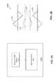
- FIGS. 1A-1Bare diagrams illustrating examples of a high-level architecture of a magnetic communication transmitter 100 A and a schematic of a circuit 100 B of a controller, according to certain embodiments. It is understood that he nearly-universal method of creating a variable magnetic field is by passing current through a coil of wire.
- the magnetic communication transmitter (hereinafter “transmitter”) 100 Aincludes a magnetic field generator 110 and a controller 120 .
- the magnetic field generator 100includes a magnetic coil and generates a magnetic field, which is proportional to an electrical current (hereinafter “current”) passing through the coil.
- the controller 120controls the current provided to the magnetic field generator and can cause the magnetic field generator to generate an optimized waveform.
- the coilis an inductor with some loss that can be modeled as a series resistance.
- the series resistancemay place the following constraints on the design.
- the rate of change of the magnetic fieldhas an upper bound corresponding to the maximum voltage available in drive circuit of the coil, because the derivative of the current is proportional to the voltage across the inductor. This also implies that the magnetic field and current are continuous functions.
- the optimized waveformis considered to be a waveform that when received and processed by the receiver can result in a desirable signal-to-noise ratio.
- the desirable signal-to-noise ratiocan be achieved when the modulation signal has the largest L 2 norm (e.g., the differences between the signals for different symbol values have the largest L 2 norm), and with a rate limited signal.
- the rate limited signalhas a waveform that, in the maximum amplitude case, has a ramp-up derivative equal to a maximum positive derivative, and a ramp-down derivative equal to the maximum negative derivative. Therefore, the subject technology uses, as a basis function, a triangle wave with an optional sustain. The triangular waveform ramps up, can sustain at its peak value, then ramps down.
- triangular waveformis a ramp-up and ramp-down, and for a given fixed symbol interval and given the rate limit, that would be a desirable waveform. If, however, there is also some reason to impose an inductor current limit that would be exceeded by a maximum ramp-up of the current for half the duration of the symbol interval, then the ramp up would be stopped at the current level and the magnitude would be sustained, and then ramped down proceeds at the maximum rate to zero.
- each symbolmust start with the same magnetic field strength and must end with that same field strength (e.g., for the required continuity).
- the controller 120is responsible for providing the current to the magnetic coil of the magnetic field generator 110 such that the generated magnetic field has the optimized triangular waveform.
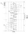
- the controllerincludes the circuit 100 B, the schematic of which is shown in FIG. 1B .
- the circuit 100 Bincludes switches (e.g., transistors such as bipolar or other transistor type or other switches) T 1 and T 2 , diodes D 1 and D 2 , an inductor L, capacitors C 1 and C 2 .
- the inductor Lis the magnetic coil of the magnetic field generator 110 .
- a current i of the inductor L of the magnetic coilis controlled by the transistors T 1 and T 2 .
- the capacitor C 1is precharged to +Vp voltage, as shown in FIG. 1B .
- the circuit 100 Bcan be operated in four phases.
- a first phasewhen the transistor T 1 is on and transistor T 2 is off, the capacitor C 1 is discharged through the transistor T 1 (e.g., an NPN transistor) and the inductor L, which provides an increasing positive current i through the inductor L.
- the transistors T 1 and T 2are off, the capacitor C 2 is charged through the diode D 2 and the inductor L, which provides a decreasing positive current i through the inductor L.
- the transistor T 1is off and the transistor T 2 is on, the capacitor C 2 is discharged through the transistor T 2 and the inductor L, which provides a decreasing negative current i through the inductor L.
- both transistors T 1 and T 2are off and the capacitor C 1 is charged through the diode D 1 and the inductor L, which provides an increasing negative current i through the inductor L.
- circuit 100 B and other implementations of the controller 120can be found in a separate patent application entitled “Energy Efficient Magnetic Field Generator Circuits,” by the applicants of the present patent application, filed on the same date with the present patent application.
- FIGS. 2A-2Bare diagrams illustrating examples of a high-level architecture of a magnetic communication receiver 200 A and a set of amplitude modulated waveforms 200 B, according to certain embodiments.
- the magnetic communication receiver (hereinafter “receiver”) 200 Aincludes a magnetic field sensor 210 and a signal processor 220 .
- the magnetic field sensor 210is configured to sense a magnetic field and generate a signal (e.g., an optical signal or an electrical signal such as a current or voltage signal) proportional to the sensed magnetic field.
- the magnetic field sensor 210may include a DNV sensor.
- Atomic-sized nitrogen-vacancy (NV) centers in diamond latticeshave been shown to have excellent sensitivity for magnetic field measurement and enable fabrication of small (e.g., micro-level) magnetic sensors that can readily replace existing-technology (e.g., Hall-effect) systems and devices.
- the DNV sensorsare maintained in room temperature and atmospheric pressure and can be even used in liquid environments.
- a green optical sourcee.g., a micro-LED
- the distance between the two spin resonance frequenciesis a measure of the strength of the external magnetic field.
- a photo detectorcan measure the fluorescence (red light) emitted by the optically excited NV centers and generate an electrical signal.
- the signal processor 220may include a general processor or a dedicated processor (e.g., a microcontroller).
- the signal processor 220includes logic circuits or other circuitry and codes configured to implement coherent demodulation of a high-bit rate amplitude modulated signals, such as a high-bit rate amplitude modulated triangular waveform.
- An example of an amplitude modulated triangular waveformis shown in FIG. 2B .
- the waveforms 232 , 234 , 236 , and 238can be used to represent 11, 10, 01, and 00 symbols of the 2-bit representation of data.
- the waveforms 232 , 234 , 236 , and 238can provide an optimized signal-to-noise ratio (SNR), and due to their continuity, can be readily generated by using a practical voltage supply, as shown for example, by the circuit 100 B of FIG. 1B .
- the amplitude of the waveforms 232 , 234 , 236 , and 238are selected to make the spacing between the subsequent symbols as large as possible by the L 2 metric.
- a partial amplitude waveforme.g., 234 or 236
- FIG. 3is a diagram illustrating an example of a method 300 for providing a magnetic communication transmitter, according to certain embodiments.
- the method 300includes providing a magnetic field generator (e.g. 110 of FIG. 1A ) configured to generate a magnetic field ( 310 ).
- a controllere.g. 120 of FIG. 1A ) is provided that is configured to control the magnetic field generator by controlling an electrical current (e.g. i of FIG. 1B ) supplied to the magnetic field generator and causing the magnetic field generator to generate an optimized variable amplitude triangular waveform (e.g. 200 B of FIG. 2B ) ( 320 ).
- an electrical currente.g. i of FIG. 1B
- FIG. 4is a diagram illustrating an example of a data frame 400 of a magnetic communication transmitter, according to certain embodiments.
- the data frame 400includes data portions 402 and 404 and one or more auxiliary portions.
- the data portions 402 and 404include data symbols, for example, 11, 00, 10, and 01 symbols.
- the auxiliary portionsinclude MAX and OFF symbols 410 and 420 .
- the MAX symbol 410can be a 11 symbol
- the OFF symbol 420may represent a no symbol interval, which provides an opportunity for synchronization and background field measurement and removal, as explained in more details herein.
- the calibration and background field removalare critical aspects of the subject technology.
- the MAX symbol 410is used to enable the receiver to perform synchronization and calibration of the received signal.
- the calibrationfor example, can correct for the rotation of the sensor relative to the Earth's magnetic dipole, which results in some change in the background signal.
- FIG. 5is a diagram illustrating an example of motion compensation scheme 500 , according to certain embodiments.
- Motion compensationis an important aspect of the subject disclosure, as the Earth's magnetic field is a significant part of the background noise in any magnetic field sensing. If the sensor is moving (e.g., rotating) relative to the Earth's magnetic field vector, the measured signal (e.g., 510 corresponding to a rotation rate of 0.1 rad/s) can significantly deviate from the measured magnetic signal without rotation (e.g., 520 ).
- the subject technologyallows for measurement and subtraction of this time varying background while the magnetic signal is analyzed.
- the OFF symbol intervals 420 , 422 , and 424can be used for measurement of the background noise. As seen from FIG.
- the value of the measured signal 510 at OFF symbol intervals 420 , 422 , and 424are substantially different from the respective values of the measured signal 520 (e.g., without rotation). These differences at different OFF symbol intervals can be fitted to linear or spline curves and be used to calibrate the signal for motion compensation, for example, by subtraction of the measured background noise from the actual measured signal.
- FIGS. 6A-6Bare diagrams illustrating examples of throughput results with turning, rolling and tow-frequency compensation, according to certain embodiments.
- plot 610corresponds to no rotation compensation that results is undesirably low throughput values (in kbits/sec), which rapidly turn to zero as the transmitter-to-receiver distance is increased to nearly 200 meters.
- Plots 620 and 630correspond to turning of the sensor at 0.1 rad/sec, where measure data are compensated for the motion (e.g., as described above) using linear and spline compensations, respectively. The spline compensation is seen to completely remove rotation effects on bit rate.
- the 60 cycle hum and its 120 Hz harmoniccan be removed by using notch filters.
- plots 612 , 622 , and 632are for similar circumstances as plots 610 , 620 , and 630 of FIG. 6A , except that the sensor motion is rolling at a higher rate (e.g., 0.3 rad/sec).
- the spline compensationis seen to be more effective in removing the effects of rolling on bit rate than the linear compensation.
- FIG. 7is a diagram illustrating an example adaptive modulation scheme 700 , according to certain embodiments.
- the adaptive modulation scheme 700uses an adaptive modulation technique, which is different form the commonly used techniques in other communication media such as RF communication.
- the subject technologyuses period extension to perform adaptive modulation. It is understood that as the performance is degraded due to noise (e.g., SNR is decreased), discriminating various levels 720 denoted by symbols 00, 01, 10, and 11 can be difficult. In other words, the correlation of the measured points 715 with the basis function 710 (e.g., a triangular waveform) may not match one of the expected values (e.g., denoted by symbols 00, 01, 10, and 11).
- the basis function 710e.g., a triangular waveform
- the receivercan signal for either fewer amplitude levels (e.g., lower performance such as two-level resolution) or longer symbol intervals (e.g., lower bit rate). Conversely, when the mismatches are small, the amplitude levels can be increased (e.g., better resolution performance) or the symbol intervals can be decreased (e.g., higher bit rate).
- the adaptive modulationmay, for example, be implemented by extending the symbol period as shown by the symbol (e.g., basis function) 730 , which has an extended period as compared to the basis function 710 .
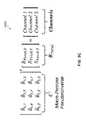
- FIGS. 8A through 8Care diagrams illustrating components for implementing an example technique for multiple channel resolution, according to certain embodiments.
- the use of DNV sensors for the receivers of the subject technologyallows simultaneous receiving of multiple channel (e.g., up to three) channels transmitted by three different transmitters that are synchronous and cooperative in time, but transmit with different magnetic field (B) orientations. This enables up to three times higher performance of a single channel alone.
- the magnetic fields of the three transmitters in the coordinate system 800 A of FIG. 8Awhere magnetic vectors 810 , 820 , and 830 correspond to the fields transmitted by the three transmitters, which form the resultant combined vector 850 .
- the subject technologyuses frame formatting to support the multiple channels scheme.
- MAX symbolse.g., 812 , 814 , and 816
- a data frame 800 B of FIG. 8Bare used to indicate which of the three transmitters is transmitting.
- the MAX symbol 812indicates that first transmitter is transmitting and the all other transmitters are off.
- MAX symbols 814 and 816indicate that one of the second or the third transmitters is transmitting, respectively. This information assists the receiver to estimate the corresponding magnetic field (e.g., B i ) vector of the transmitting transmitter (e.g. the i th transmitter).
- the basis matrix C+transforms the measurements from the ⁇ X,Y,Z ⁇ basis into the ⁇ B 1 ,B 2 , B 3 ⁇ basis.
- the full performancecan be achieved when the matrix C+ has full rank, which happens when all transmitter B fields are mutually orthogonal.
- C+ matrixmay become singular and magnify any noise present, thereby degrading the performance.
- the elements of the C+ matrixare projections of the measured magnetic field of each transmitter B i fields over the X, Y, and Y axes.
- B i,yis the projection of the measured B i fields over the Y axis
- B i,x , B i,y , and B i,zdefine the angle of arrival of the i th transmitter.
- the angle of arrival of each transmitteris a vector that is in the direction of the polarization of the B-field vector for that transmitter.
- the elements of the channels vectorgive the channel data that each transmitter has actually transmitted.
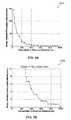
- FIGS. 9A-9Bare diagrams illustrating single channel throughput variations 900 A and 900 B versus transmitter-receiver distance, according to certain embodiments.
- the plots 900 A and 900 B shown in FIGS. 9A and 9Bare single channel (e.g., with no orthogonal frequency division multiplexing (OFDM) and no 3D-vector multiplexing) simulation results in open air for bit-error rates less than approximately one percent, using existing DNV detectors. The period of the triangular waveform is allowed to vary from 60 to 500 microseconds.
- the plot 900 B shown in FIG. 9Bis a zoom-in of the plot 900 A in FIG. 9A for closer look.
- FIGS. 10A-10Bare diagrams illustrating simulated performance results 1001 A and 1000 B, according to certain embodiments.
- the simulated performance results 1000 A and 1000 Bare 2-dimensional plots showing single channel throughput results (in Kbps) as the DNV sensor quantization level and transmitter magnetic field B (in Tesla at 1 meter) are varied.
- the results 1000 A and 1000 Bare, respectively, for 100 m and 500 meter distance between the receiver and the transmitter.
- the quantization levelsdefine the resolution of the DNV sensors.
- FIG. 11is a diagram illustrating an example of a system 1100 for implementing some aspects of the subject technology.
- the system 1100includes a processing system 1102 , which may include one or more processors or one or more processing systems.
- a processorcan be one or more processors.
- the processing system 1102may include a general-purpose processor or a specific-purpose processor for executing instructions and may further include a machine-readable medium 1119 , such as a volatile or non-volatile memory, for storing data and/or instructions for software programs.
- the instructionswhich may be stored in a machine-readable medium 1110 and/or 1119 , may be executed by the processing system 1102 to control and manage access to the various networks, as well as provide other communication and processing functions.
- the instructionsmay also include instructions executed by the processing system 1102 for various user interface devices, such as a display 1112 and a keypad 1114 .
- the processing system 1102may include an input port 1122 and an output port 1124 .
- Each of the input port 1122 and the output port 1124may include one or more ports.
- the input port 1122 and the output port 1124may be the same port (e.g., a bi-directional port) or may be different ports.
- the processing system 1102may be implemented using software, hardware, or a combination of both.
- the processing system 1102may be implemented with one or more processors.
- a processormay be a general-purpose microprocessor, a microcontroller, a Digital Signal Processor (DSP), an Application Specific Integrated Circuit (ASIC), a Field Programmable Gate Array (FPGA), a Programmable Logic Device (PLD), a controller, a state machine, gated logic, discrete hardware components, or any other suitable device that can perform calculations or other manipulations of information.
- DSPDigital Signal Processor
- ASICApplication Specific Integrated Circuit
- FPGAField Programmable Gate Array
- PLDProgrammable Logic Device
- controllera state machine, gated logic, discrete hardware components, or any other suitable device that can perform calculations or other manipulations of information.
- the transformation meanse.g., algorithms
- the signal processing of the subject technologymay be performed by the processing system 1102 .
- the processing system 1102may perform the functionality of the signal processor 220 of FIG. 2A or perform the matrix operation 800 C of FIG. 8C , or other or computational functions and simulations described above.
- a machine-readable mediumcan be one or more machine-readable media.
- Softwareshall be construed broadly to mean instructions, data, or any combination thereof, whether referred to as software, firmware, middleware, microcode, hardware description language, or otherwise. Instructions may include code (e.g., in source code format, binary code format, executable code format, or any other suitable format of code).
- Machine-readable mediamay include storage integrated into a processing system such as might be the case with an ASIC.
- Machine-readable mediae.g., 1110
- RAMRandom Access Memory
- ROMRead Only Memory
- PROMErasable PROM
- registersa hard disk, a removable disk, a CD-ROM, a DVD, or any other suitable storage device.
- a machine-readable mediumis a computer-readable medium encoded or stored with instructions and is a computing element, which defines structural and functional interrelationships between the instructions and the rest of the system, which permit the instructions' functionality to be realized.
- Instructionsmay be executable, for example, by the processing system 1102 or one or more processors. Instructions can be, for example, a computer program including code for performing methods of the subject technology.
- a network interface 1116may be any type of interface to a network (e.g., an Internet network interface), and may reside between any of the components shown in FIG. 11 and coupled to the processor via the bus 1104 .
- a networke.g., an Internet network interface
- a device interface 1118may be any type of interface to a device and may reside between any of the components shown in FIG. 11 .
- a device interface 1118may, for example, be an interface to an external device that plugs into a port (e.g., USB port) of the system 1100 .
- One or more of the above-described features and applicationsmay be implemented as software processes that are specified as a set of instructions recorded on a computer readable storage medium (alternatively referred to as computer-readable media, machine-readable media, or machine-readable storage media).
- these instructionsare executed by one or more processing unit(s) (e.g., one or more processors, cores of processors, or other processing units), they cause the processing unit(s) to perform the actions indicated in the instructions.
- the computer readable mediadoes not include carrier waves and electronic signals passing wirelessly or over wired connections, or any other ephemeral signals.
- the computer readable mediamay be entirely restricted to tangible, physical objects that store information in a form that is readable by a computer.
- the computer readable mediais non-transitory computer readable media, computer readable storage media, or non-transitory computer readable storage media.
- a computer program product(also known as a program, software, software application, script, or code) can be written in any form of programming language, including compiled or interpreted languages, declarative or procedural languages, and it can be deployed in any form, including as a stand-alone program or as a module, component, subroutine, object, or other unit suitable for use in a computing environment.
- a computer programmay, but need not, correspond to a file in a file system.
- a programcan be stored in a portion of a file that holds other programs or data (e.g., one or more scripts stored in a markup language document), in a single file dedicated to the program in question, or in multiple coordinated files (e.g., files that store one or more modules, sub programs, or portions of code).
- a computer programcan be deployed to be executed on one computer or on multiple computers that are located at one site or distributed across multiple sites and interconnected by a communication network.
- ASICsapplication specific integrated circuits
- FPGAsfield programmable gate arrays
- integrated circuitsexecute instructions that are stored on the circuit itself.
- compositions and methodsare described in terms of “comprising,” “containing,” or “including” various components or steps, the compositions and methods can also “consist essentially of” or “consist of” the various components and operations. All numbers and ranges disclosed above can vary by some amount Whenever a numerical range with a lower limit and an upper limit is disclosed, any number and any subrange falling within the broader range is specifically disclosed. Also, the terms in the claims have their plain, ordinary meaning unless otherwise explicitly and clearly defined by the patentee. If there is any conflict in the usages of a word or term in this specification and one or more patent or other documents that may be incorporated herein by reference, the definitions that are consistent with this specification should be adopted.
Landscapes
- Engineering & Computer Science (AREA)
- Computer Networks & Wireless Communication (AREA)
- Signal Processing (AREA)
- Power Engineering (AREA)
- Near-Field Transmission Systems (AREA)
- Arrangements For Transmission Of Measured Signals (AREA)
Abstract
Description
This application claims the benefit of priority under 35 U.S.C. §119 from U.S. Provisional Patent Application 61/976,009, filed Apr. 7, 2014, which is incorporated herein by reference in its entirety.
The present invention generally relates to communications and, more particularly, to high bit-rate magnetic communication.
As radio-frequency (RF) and optical electromagnetic signals do not propagate well under the ocean surface or through land, alternative communication methods are to be used for these environments. There are multiple alternative options, each having advantages and disadvantages. Therefore, different approaches may be taken depending on applications. For example, some applications may use a tether to communicate by wire or optical fiber, which can impose maneuvering limits or hazards involving physical contact with vehicles or structures. As another example, acoustic communications are often used, but are affected by multipath and shallow-water resonances, with the consequence that robust acoustic communications have a very low bit rate. Yet, another candidate can be near-field magnetic communications, which works with low-frequency signals, to be measurable at longer ranges thereby limiting bit rate, and signals which have a rapid drop off in signal strength at longer ranges.
Traditional modulation schemes used in magnetic communications have a low bit-rate for a given range. If the bit rate could be increased substantially, a variety of applications could benefit from these traditional modulation schemes. For example, one motivating application is the use of unmanned underwater vehicles (UUV) for sensing tasks underwater, such as oil rig inspection or sea-floor pipeline, or well-head inspection. Currently, most data is stored until the vehicle surfaces, meaning that operators have little awareness of how the mission is proceeding and little ability to influence its course, such as re-inspecting an area of interest, or recognizing that the UUV has incorrectly identified a rock as a well head. Another motivating example is a stationary sensor on the ocean floor, which needs to send data to the surface or to a passing underwater vehicle when the opportunity arises.
In some aspects, a magnetic communications transmitter includes a magnetic field generator and a controller. The magnetic field generator is configured to generate a magnetic field. The controller is configured to control the magnetic field generator by controlling an electrical current supplied to the magnetic field generator, and causing the magnetic field generator to generate an optimized variable amplitude triangular waveform.
In another aspect, a magnetic communications receiver includes a magnetic field sensor and a signal processor. The magnetic field sensor is configured to sense a modulated magnetic field. The signal processor is configured to demodulate the sensed modulated magnetic field. The modulated magnetic field comprises an optimized variable amplitude triangular waveform.
In yet another aspect, a method for facilitating magnetic communications includes providing a magnetic field generator that is configured to generate a magnetic field. A controller is provided that is configured to control the magnetic field generator by controlling an electrical current supplied to the magnetic field generator, and causing the magnetic field generator to generate an optimized variable amplitude triangular waveform.
The foregoing has outlined rather broadly the features of the present disclosure in order that the detailed description that follows can be better understood. Additional features and advantages of the disclosure will be described hereinafter, which form the subject of the claims.
For a more complete understanding of the present disclosure, and the advantages thereof, reference is now made to the following descriptions to be taken in conjunction with the accompanying drawings describing specific embodiments of the disclosure, wherein:
The detailed description set forth below is intended as a description of various configurations of the subject technology and is not intended to represent the only configurations in which the subject technology may be practiced. The appended drawings are incorporated herein and constitute a part of the detailed description. The detailed description includes specific details for the purpose of providing a thorough understanding of the subject technology. However, it will be clear and apparent to those skilled in the art that the subject technology is not limited to the specific details set forth herein and may be practiced without these specific details. In some instances, well-known structures and components are shown in block diagram form in order to avoid obscuring the concepts of the subject technology.
The present disclosure is directed, in part, to a high bit-rate magnetic communications transmitter that is capable of transmitting magnetic field waves with an optimized waveform. The optimized waveform includes an amplitude modulated triangular waveform. The disclosure is also directed to a high bit-rate magnetic communications receiver including a magnetic sensor, such as diamond nitrogen-vacancy (DNV) sensor, and a signal processor that can demodulate the amplitude modulated triangular waveform. In some implementations, the receiver of the subject technology is enabled to perform motion compensation, for example, compensation for rotations in Earth's magnetic field. The subject technology achieves a significantly higher bit-rate than other magnetic communications approaches by leveraging the high sensitivity and small form factor of the DNV sensors and utilizing modern signal processing that has made amplitude-dependent coherent modulation a practical reality for high bit rates. Other advantageous features of the disclosed solution include optimized waveform for the magnetic scenario, magnetic-specific error removal, and an optional adaptation scheme and polarity scheme.
Electrically, the coil is an inductor with some loss that can be modeled as a series resistance. The series resistance may place the following constraints on the design. First, the rate of change of the magnetic field has an upper bound corresponding to the maximum voltage available in drive circuit of the coil, because the derivative of the current is proportional to the voltage across the inductor. This also implies that the magnetic field and current are continuous functions. The optimized waveform is considered to be a waveform that when received and processed by the receiver can result in a desirable signal-to-noise ratio.
It is understood that the desirable signal-to-noise ratio can be achieved when the modulation signal has the largest L2 norm (e.g., the differences between the signals for different symbol values have the largest L2 norm), and with a rate limited signal. The rate limited signal has a waveform that, in the maximum amplitude case, has a ramp-up derivative equal to a maximum positive derivative, and a ramp-down derivative equal to the maximum negative derivative. Therefore, the subject technology uses, as a basis function, a triangle wave with an optional sustain. The triangular waveform ramps up, can sustain at its peak value, then ramps down. With no sustain, triangular waveform is a ramp-up and ramp-down, and for a given fixed symbol interval and given the rate limit, that would be a desirable waveform. If, however, there is also some reason to impose an inductor current limit that would be exceeded by a maximum ramp-up of the current for half the duration of the symbol interval, then the ramp up would be stopped at the current level and the magnitude would be sustained, and then ramped down proceeds at the maximum rate to zero. To be able to start each successive symbol transmission at the same starting point regardless of the value of the successive symbols, each symbol must start with the same magnetic field strength and must end with that same field strength (e.g., for the required continuity).
Thecontroller 120 is responsible for providing the current to the magnetic coil of themagnetic field generator 110 such that the generated magnetic field has the optimized triangular waveform. In some embodiments, the controller includes thecircuit 100B, the schematic of which is shown inFIG. 1B . Thecircuit 100B includes switches (e.g., transistors such as bipolar or other transistor type or other switches) T1 and T2, diodes D1 and D2, an inductor L, capacitors C1 and C2. The inductor L is the magnetic coil of themagnetic field generator 110. A current i of the inductor L of the magnetic coil is controlled by the transistors T1 and T2. The capacitor C1 is precharged to +Vp voltage, as shown inFIG. 1B . Thecircuit 100B can be operated in four phases.
In a first phase, when the transistor T1 is on and transistor T2 is off, the capacitor C1 is discharged through the transistor T1 (e.g., an NPN transistor) and the inductor L, which provides an increasing positive current i through the inductor L. In a second phase, the transistors T1 and T2 are off, the capacitor C2 is charged through the diode D2 and the inductor L, which provides a decreasing positive current i through the inductor L In a third phase, the transistor T1 is off and the transistor T2 is on, the capacitor C2 is discharged through the transistor T2 and the inductor L, which provides a decreasing negative current i through the inductor L. Finally, in a fourth phase, both transistors T1 and T2 are off and the capacitor C1 is charged through the diode D1 and the inductor L, which provides an increasing negative current i through the inductor L.
More detailed discussion ofcircuit 100B and other implementations of thecontroller 120 can be found in a separate patent application entitled “Energy Efficient Magnetic Field Generator Circuits,” by the applicants of the present patent application, filed on the same date with the present patent application.
Atomic-sized nitrogen-vacancy (NV) centers in diamond lattices have been shown to have excellent sensitivity for magnetic field measurement and enable fabrication of small (e.g., micro-level) magnetic sensors that can readily replace existing-technology (e.g., Hall-effect) systems and devices. The DNV sensors are maintained in room temperature and atmospheric pressure and can be even used in liquid environments. A green optical source (e.g., a micro-LED) can optically excite NV centers of the DNV sensor and cause emission of fluorescence radiation (e.g., red light) under off-resonant optical excitation. A magnetic field generated, for example, by a microwave coil can probe degenerate triplet spin states (e.g., with ms=−1, 0, +1) of the NV centers to split proportional to an external magnetic field projected along the NV axis, resulting in two spin resonance frequencies. The distance between the two spin resonance frequencies is a measure of the strength of the external magnetic field. A photo detector can measure the fluorescence (red light) emitted by the optically excited NV centers and generate an electrical signal.
Thesignal processor 220 may include a general processor or a dedicated processor (e.g., a microcontroller). Thesignal processor 220 includes logic circuits or other circuitry and codes configured to implement coherent demodulation of a high-bit rate amplitude modulated signals, such as a high-bit rate amplitude modulated triangular waveform. An example of an amplitude modulated triangular waveform is shown inFIG. 2B . The amplitude modulatedtriangular waveform 200B ofFIG. 2B includes a high-amplitude (e.g., full-amplitude) positivetriangular waveform 232, a low-amplitude positivetriangular waveform 234, a tow-amplitude negativetriangular waveform 236, and high-amplitude negativetriangular waveform 238. These waveforms are desirable for representing various symbols of a 2-bit representation of data. For example, thewaveforms waveforms circuit 100B ofFIG. 1B . The amplitude of thewaveforms
In the diagram600B ofFIG. 6B , plots612,622, and632 are for similar circumstances asplots FIG. 6A , except that the sensor motion is rolling at a higher rate (e.g., 0.3 rad/sec). The spline compensation is seen to be more effective in removing the effects of rolling on bit rate than the linear compensation.
The subject technology uses frame formatting to support the multiple channels scheme. For example, MAX symbols (e.g.,812,814, and816) of adata frame 800B ofFIG. 8B are used to indicate which of the three transmitters is transmitting. For instance, theMAX symbol 812 indicates that first transmitter is transmitting and the all other transmitters are off. Similarly,MAX symbols
Theprocessing system 1102 may be implemented using software, hardware, or a combination of both. By way of example, theprocessing system 1102 may be implemented with one or more processors. A processor may be a general-purpose microprocessor, a microcontroller, a Digital Signal Processor (DSP), an Application Specific Integrated Circuit (ASIC), a Field Programmable Gate Array (FPGA), a Programmable Logic Device (PLD), a controller, a state machine, gated logic, discrete hardware components, or any other suitable device that can perform calculations or other manipulations of information.
In one or more implementations, the transformation means (e.g., algorithms) and the signal processing of the subject technology may be performed by theprocessing system 1102. For example, theprocessing system 1102 may perform the functionality of thesignal processor 220 ofFIG. 2A or perform thematrix operation 800C ofFIG. 8C , or other or computational functions and simulations described above.
A machine-readable medium can be one or more machine-readable media. Software shall be construed broadly to mean instructions, data, or any combination thereof, whether referred to as software, firmware, middleware, microcode, hardware description language, or otherwise. Instructions may include code (e.g., in source code format, binary code format, executable code format, or any other suitable format of code).
Machine-readable media (e.g.,1119) may include storage integrated into a processing system such as might be the case with an ASIC. Machine-readable media (e.g.,1110) may also include storage external to a processing system, such as a Random Access Memory (RAM), a flash memory, a Read Only Memory (ROM), a Programmable Read-Only Memory (PROM), an Erasable PROM (EPROM), registers, a hard disk, a removable disk, a CD-ROM, a DVD, or any other suitable storage device. Those skilled in the art recognizes how best to implement the described functionality for theprocessing system 1102. According to one aspect of the disclosure, a machine-readable medium is a computer-readable medium encoded or stored with instructions and is a computing element, which defines structural and functional interrelationships between the instructions and the rest of the system, which permit the instructions' functionality to be realized. Instructions may be executable, for example, by theprocessing system 1102 or one or more processors. Instructions can be, for example, a computer program including code for performing methods of the subject technology.
Anetwork interface 1116 may be any type of interface to a network (e.g., an Internet network interface), and may reside between any of the components shown inFIG. 11 and coupled to the processor via thebus 1104.
Adevice interface 1118 may be any type of interface to a device and may reside between any of the components shown inFIG. 11 . Adevice interface 1118 may, for example, be an interface to an external device that plugs into a port (e.g., USB port) of thesystem 1100.
The foregoing description is provided to enable a person skilled in the art to practice the various configurations described herein. While the subject technology has been particularly described with reference to the various figures and configurations, it should be understood that these are for illustration purposes only and should not be taken as limiting the scope of the subject technology.
One or more of the above-described features and applications may be implemented as software processes that are specified as a set of instructions recorded on a computer readable storage medium (alternatively referred to as computer-readable media, machine-readable media, or machine-readable storage media). When these instructions are executed by one or more processing unit(s) (e.g., one or more processors, cores of processors, or other processing units), they cause the processing unit(s) to perform the actions indicated in the instructions. In one or more implementations, the computer readable media does not include carrier waves and electronic signals passing wirelessly or over wired connections, or any other ephemeral signals. For example, the computer readable media may be entirely restricted to tangible, physical objects that store information in a form that is readable by a computer. In one or more implementations, the computer readable media is non-transitory computer readable media, computer readable storage media, or non-transitory computer readable storage media.
In one or more implementations, a computer program product (also known as a program, software, software application, script, or code) can be written in any form of programming language, including compiled or interpreted languages, declarative or procedural languages, and it can be deployed in any form, including as a stand-alone program or as a module, component, subroutine, object, or other unit suitable for use in a computing environment. A computer program may, but need not, correspond to a file in a file system. A program can be stored in a portion of a file that holds other programs or data (e.g., one or more scripts stored in a markup language document), in a single file dedicated to the program in question, or in multiple coordinated files (e.g., files that store one or more modules, sub programs, or portions of code). A computer program can be deployed to be executed on one computer or on multiple computers that are located at one site or distributed across multiple sites and interconnected by a communication network.
While the above discussion primarily refers to microprocessor or multi-core processors that execute software, one or more implementations are performed by one or more integrated circuits, such as application specific integrated circuits (ASICs) or field programmable gate arrays (FPGAs). In one or more implementations, such integrated circuits execute instructions that are stored on the circuit itself.
Although the invention has been described with reference to the disclosed embodiments, one having ordinary skill in the art will readily appreciate that these embodiments are only illustrative of the invention. It should be understood that various modifications can be made without departing from the spirit of the invention. The particular embodiments disclosed above are illustrative only, as the present invention may be modified and practiced in different but equivalent manners apparent to those skilled in the art having the benefit of the teachings herein. Furthermore, no limitations are intended to the details of construction or design herein shown, other than as described in the claims below. It is therefore evident that the particular illustrative embodiments disclosed above may be altered, combined, or modified and all such variations are considered within the scope and spirit of the present invention. While compositions and methods are described in terms of “comprising,” “containing,” or “including” various components or steps, the compositions and methods can also “consist essentially of” or “consist of” the various components and operations. All numbers and ranges disclosed above can vary by some amount Whenever a numerical range with a lower limit and an upper limit is disclosed, any number and any subrange falling within the broader range is specifically disclosed. Also, the terms in the claims have their plain, ordinary meaning unless otherwise explicitly and clearly defined by the patentee. If there is any conflict in the usages of a word or term in this specification and one or more patent or other documents that may be incorporated herein by reference, the definitions that are consistent with this specification should be adopted.
Claims (20)
1. A magnetic communications transmitter, the transmitter comprising:
a magnetic field generator configured to generate a vector magnetic field; and
a controller configured to control the magnetic field generator,
wherein:
controlling the magnetic field generator comprises:
controlling an electrical current supplied to the magnetic field generator, and
causing the magnetic field generator to generate an optimized variable amplitude triangular waveform,
wherein the controller is configured to encode active channel information in a portion of the generated vector magnetic field by modulating an amplitude of the optimized variable amplitude triangular waveform to form a MAX and an OFF symbol, the active channel information utilized by a receiver to determine an angle of arrival for the generated vector magnetic field and to demodulate the vector magnetic field by using a vector indicated by the MAX and OFF symbol of the active channel information of the optimized variable amplitude triangular waveform.
2. The transmitter ofclaim 1 , wherein the optimized triangular waveform comprises a coherent amplitude modulated triangular waveform.
3. The transmitter ofclaim 1 , wherein the transmitter is configured to transmit magnetic data packets, wherein each magnetic data packet comprises data portions and auxiliary portions.
4. The transmitter ofclaim 3 , wherein the data potions comprises data symbols comprising amplitude modulated triangular waveforms, wherein the auxiliary portions comprise MAX and OFF symbols.
5. The transmitter ofclaim 4 , wherein the transmitter is configured to transmit, during MAX symbols, a highest magnetic data symbol, to enable synchronization and calibration of a received signal at a receiver.
6. The transmitter ofclaim 4 , wherein the transmitter is configured to transmit, during the OFF symbols, no data symbol to allow synchronization and background measurement at a receiver, wherein the background measurement enables the receiver to perform motion compensation, and wherein the motion compensation includes compensation for rotations in Earth's magnetic field.
7. The transmitter ofclaim 1 , wherein the transmitter is configured to enable simultaneous multiple channel communication.
8. The transmitter ofclaim 7 , wherein the simultaneous multiple channel communication is enabled by the encoding of active transmitting channel information in MAX symbols of transmitted magnetic data packets.
9. A magnetic communications receiver, the receiver comprising:
a magnetic field sensor configured to sense a modulated magnetic field comprising multiple channels; and
a signal processor configured to demodulate each channel of the multiple channels of the sensed modulated magnetic field,
wherein:
each channel of the modulated magnetic field comprises an optimized variable amplitude triangular waveform, the magnetic field sensor detecting a direction of a polarization of a B-field vector corresponding to a channel for a transmitter using a transmitted MAX and OFF symbol of the modulated magnetic signal, the signal processor configured to demodulate the channel of the sensed modulated magnetic field using the detected direction.
10. The receiver ofclaim 9 , wherein the magnetic field sensor comprises a diamond nitrogen-vacancy (DNV) sensor.
11. The receiver ofclaim 9 , wherein the receiver is configured to decode magnetic data packets including magnetic data symbols, OFF symbols, and MAX symbols, and wherein the signal processor is configured to demodulate the magnetic data symbol including coherent amplitude modulated triangular waveform.
12. The receiver ofclaim 11 , wherein the receiver is configured to measure background during OFF symbols, wherein the receiver is configured to leverage the background measurement to compensate for rotations in Earth's magnetic field.
13. The receiver ofclaim 9 , wherein the receiver is configured to perform synchronization and calibration during MAX symbols.
14. The receiver ofclaim 9 , wherein the receiver is configured to retrieve data from simultaneous multiple channel communication.
15. The receiver ofclaim 14 , wherein the receiver is configured to decode active transmitting channel information of multiple channel communication using information in MAX symbols of transmitted magnetic data packets.
16. A method for facilitating magnetic communications, the method comprising:
providing a magnetic field generator configured to generate a magnetic field; and
providing a controller configured to control the magnetic field generator,
wherein:
the controller is configured to:
control an electrical current supplied to the magnetic field generator, and
cause the magnetic field generator to generate an optimized variable amplitude triangular waveform,
wherein the controller is configured to encode active channel information in a portion of the generated vector magnetic field by modulating an amplitude of the optimized variable amplitude triangular waveform to form a MAX and an OFF symbol, the active channel information utilized by a receiver to determine an angle of arrival for the generated vector magnetic field and to demodulate the vector magnetic field by using a vector indicated by the MAX and OFF symbol of the active channel information of the optimized variable amplitude triangular waveform.
17. The method ofclaim 16 , wherein the optimized variable amplitude triangular waveform comprise magnetic data symbols, wherein the magnetic data symbols are included in magnetic data packets further including MAX and OFF symbols.
18. The method ofclaim 17 , further comprising transmitting, during the MAX symbols, a highest magnetic data symbol, to enable synchronization and calibration of a received signal at a receiver.
19. The method ofclaim 17 , further comprising:
during the MAX symbols, transmitting a highest magnetic data symbol, to enable synchronization and calibration of a received signal at a receiver; and
during the OFF symbols, transmitting no data symbol to allow synchronization and background measurement at a receiver, wherein the background measurement enables the receiver to perform motion compensation, and wherein the motion compensation includes compensation for rotations in Earth's magnetic field.
20. The method ofclaim 16 , further comprising enabling simultaneous multiple channel communication, wherein the simultaneous multiple channel communication is enabled by the encoding of active transmitting channel information in MAX symbols of transmitted magnetic data packets.
Priority Applications (8)
| Application Number | Priority Date | Filing Date | Title |
|---|---|---|---|
| US14/676,740US9853837B2 (en) | 2014-04-07 | 2015-04-01 | High bit-rate magnetic communication |
| BR112016023508ABR112016023508A2 (en) | 2014-04-07 | 2015-04-03 | high bit rate magnetic communication |
| CA2945125ACA2945125A1 (en) | 2014-04-07 | 2015-04-03 | High bit-rate magnetic communcation |
| PCT/US2015/024265WO2015157110A1 (en) | 2014-04-07 | 2015-04-03 | High bit-rate magnetic communcation |
| GB1618203.2AGB2539856A (en) | 2014-04-07 | 2015-04-03 | High bit-rate magnetic communication |
| US15/003,797US9910104B2 (en) | 2015-01-23 | 2016-01-21 | DNV magnetic field detector |
| US15/179,957US9910105B2 (en) | 2014-03-20 | 2016-06-10 | DNV magnetic field detector |
| US15/912,461US10725124B2 (en) | 2014-03-20 | 2018-03-05 | DNV magnetic field detector |
Applications Claiming Priority (2)
| Application Number | Priority Date | Filing Date | Title |
|---|---|---|---|
| US201461976009P | 2014-04-07 | 2014-04-07 | |
| US14/676,740US9853837B2 (en) | 2014-04-07 | 2015-04-01 | High bit-rate magnetic communication |
Related Parent Applications (2)
| Application Number | Title | Priority Date | Filing Date |
|---|---|---|---|
| US14/659,498Continuation-In-PartUS9638821B2 (en) | 2014-03-20 | 2015-03-16 | Mapping and monitoring of hydraulic fractures using vector magnetometers |
| US15/003,558Continuation-In-PartUS9829545B2 (en) | 2014-03-20 | 2016-01-21 | Apparatus and method for hypersensitivity detection of magnetic field |
Related Child Applications (3)
| Application Number | Title | Priority Date | Filing Date |
|---|---|---|---|
| US14/659,498Continuation-In-PartUS9638821B2 (en) | 2014-03-20 | 2015-03-16 | Mapping and monitoring of hydraulic fractures using vector magnetometers |
| US14/680,877Continuation-In-PartUS9590601B2 (en) | 2014-03-20 | 2015-04-07 | Energy efficient controlled magnetic field generator circuit |
| US15/179,957Continuation-In-PartUS9910105B2 (en) | 2014-03-20 | 2016-06-10 | DNV magnetic field detector |
Publications (2)
| Publication Number | Publication Date |
|---|---|
| US20150326410A1 US20150326410A1 (en) | 2015-11-12 |
| US9853837B2true US9853837B2 (en) | 2017-12-26 |
Family
ID=54288285
Family Applications (1)
| Application Number | Title | Priority Date | Filing Date |
|---|---|---|---|
| US14/676,740ActiveUS9853837B2 (en) | 2014-03-20 | 2015-04-01 | High bit-rate magnetic communication |
Country Status (5)
| Country | Link |
|---|---|
| US (1) | US9853837B2 (en) |
| BR (1) | BR112016023508A2 (en) |
| CA (1) | CA2945125A1 (en) |
| GB (1) | GB2539856A (en) |
| WO (1) | WO2015157110A1 (en) |
Cited By (2)
| Publication number | Priority date | Publication date | Assignee | Title |
|---|---|---|---|---|
| US20190004125A1 (en)* | 2017-06-28 | 2019-01-03 | Sichuan Energy Internet Research Institute, Tsinghua University | Method and system for evaluating magnetic field uniformity of magnetic coil |
| US12317757B2 (en) | 2018-10-11 | 2025-05-27 | SeeQC, Inc. | System and method for superconducting multi-chip module |
Families Citing this family (43)
| Publication number | Priority date | Publication date | Assignee | Title |
|---|---|---|---|---|
| US10241158B2 (en) | 2015-02-04 | 2019-03-26 | Lockheed Martin Corporation | Apparatus and method for estimating absolute axes' orientations for a magnetic detection system |
| US9910104B2 (en) | 2015-01-23 | 2018-03-06 | Lockheed Martin Corporation | DNV magnetic field detector |
| US9638821B2 (en) | 2014-03-20 | 2017-05-02 | Lockheed Martin Corporation | Mapping and monitoring of hydraulic fractures using vector magnetometers |
| US10168393B2 (en) | 2014-09-25 | 2019-01-01 | Lockheed Martin Corporation | Micro-vacancy center device |
| US9853837B2 (en) | 2014-04-07 | 2017-12-26 | Lockheed Martin Corporation | High bit-rate magnetic communication |
| US9910105B2 (en) | 2014-03-20 | 2018-03-06 | Lockheed Martin Corporation | DNV magnetic field detector |
| US10012704B2 (en) | 2015-11-04 | 2018-07-03 | Lockheed Martin Corporation | Magnetic low-pass filter |
| US9845153B2 (en) | 2015-01-28 | 2017-12-19 | Lockheed Martin Corporation | In-situ power charging |
| US9551763B1 (en) | 2016-01-21 | 2017-01-24 | Lockheed Martin Corporation | Diamond nitrogen vacancy sensor with common RF and magnetic fields generator |
| WO2015157290A1 (en) | 2014-04-07 | 2015-10-15 | Lockheed Martin Corporation | Energy efficient controlled magnetic field generator circuit |
| WO2016118756A1 (en) | 2015-01-23 | 2016-07-28 | Lockheed Martin Corporation | Apparatus and method for high sensitivity magnetometry measurement and signal processing in a magnetic detection system |
| WO2016190909A2 (en) | 2015-01-28 | 2016-12-01 | Lockheed Martin Corporation | Magnetic navigation methods and systems utilizing power grid and communication network |
| GB2551090A (en) | 2015-02-04 | 2017-12-06 | Lockheed Corp | Apparatus and method for recovery of three dimensional magnetic field from a magnetic detection system |
| WO2017087013A1 (en) | 2015-11-20 | 2017-05-26 | Lockheed Martin Corporation | Apparatus and method for closed loop processing for a magnetic detection system |
| WO2017095454A1 (en) | 2015-12-01 | 2017-06-08 | Lockheed Martin Corporation | Communication via a magnio |
| WO2017123261A1 (en) | 2016-01-12 | 2017-07-20 | Lockheed Martin Corporation | Defect detector for conductive materials |
| WO2017127098A1 (en) | 2016-01-21 | 2017-07-27 | Lockheed Martin Corporation | Diamond nitrogen vacancy sensed ferro-fluid hydrophone |
| GB2562958A (en) | 2016-01-21 | 2018-11-28 | Lockheed Corp | Magnetometer with a light emitting diode |
| WO2017127090A1 (en) | 2016-01-21 | 2017-07-27 | Lockheed Martin Corporation | Higher magnetic sensitivity through fluorescence manipulation by phonon spectrum control |
| WO2017127096A1 (en) | 2016-01-21 | 2017-07-27 | Lockheed Martin Corporation | Diamond nitrogen vacancy sensor with dual rf sources |
| WO2017127079A1 (en) | 2016-01-21 | 2017-07-27 | Lockheed Martin Corporation | Ac vector magnetic anomaly detection with diamond nitrogen vacancies |
| WO2017127094A1 (en) | 2016-01-21 | 2017-07-27 | Lockheed Martin Corporation | Magnetometer with light pipe |
| US10571530B2 (en) | 2016-05-31 | 2020-02-25 | Lockheed Martin Corporation | Buoy array of magnetometers |
| US10330744B2 (en) | 2017-03-24 | 2019-06-25 | Lockheed Martin Corporation | Magnetometer with a waveguide |
| US10359479B2 (en) | 2017-02-20 | 2019-07-23 | Lockheed Martin Corporation | Efficient thermal drift compensation in DNV vector magnetometry |
| US10527746B2 (en) | 2016-05-31 | 2020-01-07 | Lockheed Martin Corporation | Array of UAVS with magnetometers |
| US10274550B2 (en) | 2017-03-24 | 2019-04-30 | Lockheed Martin Corporation | High speed sequential cancellation for pulsed mode |
| US20170343621A1 (en) | 2016-05-31 | 2017-11-30 | Lockheed Martin Corporation | Magneto-optical defect center magnetometer |
| US10228429B2 (en) | 2017-03-24 | 2019-03-12 | Lockheed Martin Corporation | Apparatus and method for resonance magneto-optical defect center material pulsed mode referencing |
| US10371765B2 (en) | 2016-07-11 | 2019-08-06 | Lockheed Martin Corporation | Geolocation of magnetic sources using vector magnetometer sensors |
| US10281550B2 (en) | 2016-11-14 | 2019-05-07 | Lockheed Martin Corporation | Spin relaxometry based molecular sequencing |
| US10317279B2 (en) | 2016-05-31 | 2019-06-11 | Lockheed Martin Corporation | Optical filtration system for diamond material with nitrogen vacancy centers |
| US10345396B2 (en) | 2016-05-31 | 2019-07-09 | Lockheed Martin Corporation | Selected volume continuous illumination magnetometer |
| US10345395B2 (en) | 2016-12-12 | 2019-07-09 | Lockheed Martin Corporation | Vector magnetometry localization of subsurface liquids |
| US10677953B2 (en) | 2016-05-31 | 2020-06-09 | Lockheed Martin Corporation | Magneto-optical detecting apparatus and methods |
| US10145910B2 (en) | 2017-03-24 | 2018-12-04 | Lockheed Martin Corporation | Photodetector circuit saturation mitigation for magneto-optical high intensity pulses |
| US10338163B2 (en) | 2016-07-11 | 2019-07-02 | Lockheed Martin Corporation | Multi-frequency excitation schemes for high sensitivity magnetometry measurement with drift error compensation |
| US10408890B2 (en) | 2017-03-24 | 2019-09-10 | Lockheed Martin Corporation | Pulsed RF methods for optimization of CW measurements |
| US10367265B2 (en)* | 2016-08-05 | 2019-07-30 | Qualcomm Incorporated | Magnetic communication method |
| US10338164B2 (en) | 2017-03-24 | 2019-07-02 | Lockheed Martin Corporation | Vacancy center material with highly efficient RF excitation |
| US10371760B2 (en) | 2017-03-24 | 2019-08-06 | Lockheed Martin Corporation | Standing-wave radio frequency exciter |
| US10459041B2 (en) | 2017-03-24 | 2019-10-29 | Lockheed Martin Corporation | Magnetic detection system with highly integrated diamond nitrogen vacancy sensor |
| US10379174B2 (en) | 2017-03-24 | 2019-08-13 | Lockheed Martin Corporation | Bias magnet array for magnetometer |
Citations (368)
| Publication number | Priority date | Publication date | Assignee | Title |
|---|---|---|---|---|
| US2746027A (en) | 1951-11-16 | 1956-05-15 | James J Murray | Flux-gap variation transducer for hydrophones, microphones, and accelerometers |
| US3359812A (en) | 1964-03-13 | 1967-12-26 | Spectra Physics | Angle adjusting mechanism for optical elements |
| US3389333A (en) | 1964-02-10 | 1968-06-18 | Sperry Rand Corp | Control system for maintaining a desired magnetic field in a given space |
| US3490032A (en) | 1966-12-08 | 1970-01-13 | Gulf Research Development Co | Method and apparatus utilizing a pair of spaced magnetometers for making magnetic surveys |
| US3514723A (en) | 1966-06-23 | 1970-05-26 | Warwick Electronics Inc | Tone control circuit comprising a single potentiometer |
| US3518531A (en) | 1968-02-23 | 1970-06-30 | Varian Associates | Transient suppressor for use in magnetometer readout circuits |
| US3745452A (en) | 1971-02-23 | 1973-07-10 | J Osburn | Magnetic field gradient apparatus and method for detecting pipe line corrosion |
| US3899758A (en) | 1974-05-01 | 1975-08-12 | Gte International Inc | Variable inductive resonant circuit arrangement having a diamagnetic core for the UHF range |
| US4025873A (en) | 1976-08-17 | 1977-05-24 | The United States Of America As Represented By The Secretary Of The Navy | Broadband, microwave, two-stage, stagger-tuned, field effect transistor amplifier |
| US4078247A (en) | 1975-02-05 | 1978-03-07 | Rca Corporation | Inverter circuit control circuit for precluding simultaneous conduction of thyristors |
| US4084215A (en) | 1977-02-25 | 1978-04-11 | The United States Of America As Represented By The Secretary Of The Navy | Strobe light having reduced electromagnetic radiation |
| US4322769A (en) | 1980-12-22 | 1982-03-30 | International Business Machines Corporation | Electric switch operation monitoring circuitry |
| US4329173A (en) | 1980-03-31 | 1982-05-11 | Carondelet Foundry Company | Alloy resistant to corrosion |
| US4359673A (en) | 1980-08-21 | 1982-11-16 | Bross Jr Augustus T | Electromagnetically actuated linear reciprocating self-timed motor |
| US4368430A (en) | 1980-08-18 | 1983-01-11 | Sanders Associates, Inc. | Fiber optic magnetic sensors |
| US4410926A (en) | 1980-10-02 | 1983-10-18 | Flowtec Ag | Arrangement for generating DC magnetic fields of alternating polarity for the magnetic-inductive flow measurement |
| US4437533A (en) | 1981-03-18 | 1984-03-20 | Firma Jungheinrich Unternehmensuerwaltung KG | System for monitoring the course and for controlling the braking of a freely movable vehicle, particularly an inductively steered vehicle, and vehicle with such a system |
| US4514083A (en) | 1981-02-03 | 1985-04-30 | Olympus Optical Company Ltd. | Distance measuring apparatus |
| US4588993A (en) | 1980-11-26 | 1986-05-13 | The United States Of America As Represented By The Secretary Of The Department Of Health And Human Services | Broadband isotropic probe system for simultaneous measurement of complex E- and H-fields |
| US4636612A (en) | 1983-04-19 | 1987-01-13 | Cyclomatic Industries, Inc. | Optical tracking device |
| US4638324A (en) | 1984-12-10 | 1987-01-20 | Hazeltine Corporation | Resistive loop angular filter |
| US4675522A (en) | 1985-10-09 | 1987-06-23 | Spectron Development Laboratories, Inc. | Fiber optic magnetic field sensor |
| WO1987004028A1 (en) | 1985-12-20 | 1987-07-02 | Pierre Misson | Magnetic transmission |
| WO1988004032A1 (en) | 1986-11-27 | 1988-06-02 | Plessey Overseas Limited | Acoustic sensor |
| US4768962A (en) | 1986-05-17 | 1988-09-06 | U.S. Philips Corporation | Feed-through connector for RF signals |
| US4818990A (en) | 1987-09-11 | 1989-04-04 | Fernandes Roosevelt A | Monitoring system for power lines and right-of-way using remotely piloted drone |
| US4820986A (en) | 1985-12-16 | 1989-04-11 | National Research Development Corporation | Inductive circuit arrangements |
| US4945305A (en)* | 1986-10-09 | 1990-07-31 | Ascension Technology Corporation | Device for quantitatively measuring the relative position and orientation of two bodies in the presence of metals utilizing direct current magnetic fields |
| US4958328A (en) | 1989-07-24 | 1990-09-18 | Texaco Inc. | Marine walkaway vertical seismic profiling |
| EP0161940B1 (en) | 1984-05-17 | 1990-12-27 | Electricity Association Services Limited | Radio direction finding for locating lightening ground strikes |
| US5019721A (en)* | 1989-08-18 | 1991-05-28 | Wisconsin Alumni Research Foundation | Active superconducting devices formed of thin films |
| US5038103A (en) | 1985-04-22 | 1991-08-06 | The United States Of America As Represented By The Secretary Of The Navy | Optical fiber magnetometer |
| US5113136A (en)* | 1989-01-20 | 1992-05-12 | Fujitsu Limited | Gradiometer apparatus with compensation coils for measuring magnetic fields |
| US5134369A (en) | 1991-03-12 | 1992-07-28 | Hughes Aircraft Company | Three axis magnetometer sensor field alignment and registration |
| US5189368A (en) | 1976-09-24 | 1993-02-23 | Lockheed Sanders, Inc. | Magnetometer |
| US5200855A (en) | 1991-07-12 | 1993-04-06 | Optical Coating Laboratory, Inc. | Absorbing dichroic filters |
| US5245347A (en) | 1980-12-29 | 1993-09-14 | Raytheon Company | All weather tactical strike system (AWTSS) and method of operation |
| US5252912A (en) | 1989-06-28 | 1993-10-12 | William E. Merritt | System for warning aircraft pilot of potential impact with a power line and generating time-to-time impact signal |
| US5301096A (en) | 1991-09-27 | 1994-04-05 | Electric Power Research Institute | Submersible contactless power delivery system |
| US5384109A (en) | 1990-04-02 | 1995-01-24 | Nycomed Imaging As | Diagnostic magnetometry using superparamagnetic particles |
| US5396802A (en) | 1993-08-26 | 1995-03-14 | Viatran Corporation | Differential pressure transducer utilizing a variable ferrofluid keeper as an active magnetic circuit element |
| US5420549A (en) | 1994-05-13 | 1995-05-30 | The United States Of America As Represented By The Administrator Of The National Aeronautics And Space Administration | Extended linear ion trap frequency standard apparatus |
| US5425179A (en) | 1993-10-22 | 1995-06-20 | The Charles Machine Works, Inc. | Optical sensor for measuring inclination angles |
| US5427915A (en) | 1989-06-15 | 1995-06-27 | Biocircuits Corporation | Multi-optical detection system |
| WO1995033972A1 (en) | 1994-06-02 | 1995-12-14 | Spectra-Physics Laserplane, Inc. | Laser alignment device and method using green light |
| EP0718642A1 (en) | 1994-12-20 | 1996-06-26 | De Beers Industrial Diamond Division (Proprietary) Limited | Diffractive optics |
| EP0726458A2 (en) | 1995-01-13 | 1996-08-14 | Bruker Analytische Messtechnik GmbH | Method and apparatus for measuring samples and for localizing a first substance within a surrounding second substance by means of nuclear magnetic resonance |
| US5548279A (en) | 1994-07-22 | 1996-08-20 | Mcdonnell Douglas Corporation | Method and apparatus for detecting a power line |
| US5568516A (en)* | 1993-07-02 | 1996-10-22 | Phonic Ear Incorporated | Very low power cordless headset system |
| US5586069A (en) | 1994-09-30 | 1996-12-17 | Vlsi Technology, Inc. | Arithmetic logic unit with zero sum prediction |
| US5597762A (en) | 1994-09-27 | 1997-01-28 | Nonophase Diamond Technologies, Inc. | Field-enhanced diffusion using optical activation |
| US5638472A (en) | 1993-04-01 | 1997-06-10 | Optics For Research | Optical fiber and lens assembly having a movable lens and a fixed optical fiber |
| US5694375A (en) | 1996-03-22 | 1997-12-02 | The United States Of America As Represented By The Secretary Of The Navy | Ultra-broadband hydrophone |
| US5719497A (en) | 1996-05-09 | 1998-02-17 | The Regents Of The University Of California | Lensless Magneto-optic speed sensor |
| US5731996A (en) | 1996-03-05 | 1998-03-24 | Hughes Electronics | Dipole moment detector and localizer |
| US5764061A (en) | 1995-10-26 | 1998-06-09 | Kokusai Denshin Denwa Kabushiki Kaisha | Maritime apparatus for locating a buried submarine cable |
| US5818352A (en) | 1994-09-03 | 1998-10-06 | Integrated Drilling Services Limited | Well data telemetry system |
| US5846708A (en) | 1991-11-19 | 1998-12-08 | Massachusetts Institiute Of Technology | Optical and electrical methods and apparatus for molecule detection |
| US5888925A (en) | 1995-09-28 | 1999-03-30 | Alliedsignal Inc. | Hydrogen and moisture getter and absorber for sealed devices |
| US5907420A (en) | 1996-09-13 | 1999-05-25 | Lucent Technologies, Inc. | System and method for mitigating cross-saturation in optically amplified networks |
| US5907907A (en) | 1996-01-31 | 1999-06-01 | Kabushiki Kaisha Topcon | Laser leveling system |
| US6042249A (en) | 1996-07-30 | 2000-03-28 | Bayer Corporation | Illuminator optical assembly for an analytical instrument and methods of alignment and manufacture |
| US6057684A (en) | 1995-10-31 | 2000-05-02 | Yoshihiro Murakami | Magnetic flaw detection apparatus using an E-shaped magnetic sensor and high-pass filter |
| US6124862A (en) | 1997-06-13 | 2000-09-26 | Anivision, Inc. | Method and apparatus for generating virtual views of sporting events |
| US6130753A (en) | 1999-02-01 | 2000-10-10 | The United States Of America As Represented By The Secretary Of The Air Force | Laser optical density measurement system |
| US6144204A (en) | 1997-11-28 | 2000-11-07 | Picker Nordstar Oy | Gradient coils for magnetic resonance meeting |
| US6195231B1 (en) | 1994-05-06 | 2001-02-27 | Steven R. Sedlmayr | Thin film magnetic data transfer transducer |
| US6360173B1 (en) | 1999-02-22 | 2002-03-19 | Terrescan Technologies, Inc. | Geophysical exploration system and method |
| US6398155B1 (en) | 2001-01-02 | 2002-06-04 | The United States Of America As Represented By The Secretary Of The Army | Method and system for determining the pointing direction of a body in flight |
| US6433944B1 (en) | 1998-09-25 | 2002-08-13 | Fuji Photo Film Co., Ltd. | Master carrier for magnetic transfer and method for transfer |
| US20020144093A1 (en) | 2001-03-28 | 2002-10-03 | Ryo Inoue | Method and apparatus for restoring registers after cancelling a multi-cycle instruction |
| US6472869B1 (en) | 2001-06-18 | 2002-10-29 | United States Of America As Represented By The Secretary Of The Air Force | Diode laser-pumped magnetometer |
| US6472651B1 (en) | 1999-06-18 | 2002-10-29 | Fujitsu Limited | Optical information storage device having phase compensating mechanism and polarization plane rotating mechanism |
| US20020167306A1 (en) | 2001-03-23 | 2002-11-14 | Ivano Zalunardo | Device with a magnetic position encoder |
| US6504365B2 (en) | 2000-09-29 | 2003-01-07 | Jeol Ltd. | Magnetic force microscope |
| DE10228536A1 (en) | 2001-06-26 | 2003-01-30 | Fuji Photo Film Co Ltd | Magnetic recording medium used in magnetic disks in mini computers, personal computers, and work stations comprises a support with a non-magnetic lower layer, and a magnetic layer |
| US20030058346A1 (en) | 1997-04-02 | 2003-03-27 | Bechtel Jon H. | Control circuit for image array sensors |
| US6542242B1 (en) | 1999-05-10 | 2003-04-01 | University Of Washington | Mapping air contaminants using path-integrated optical remote sensing with a non-overlapping variable path length beam geometry |
| US20030076229A1 (en) | 2000-03-14 | 2003-04-24 | Roland Blanpain | Microsystem using magnetometer and inclinometer for anti-theft protection of valuables |
| US20030098455A1 (en) | 2001-03-31 | 2003-05-29 | D-Wave Systems, Inc. | High sensitivity, directional dc-SQUID magnetometer |
| US6621578B1 (en) | 1999-11-26 | 2003-09-16 | Olympus Optical Co, Ltd. | Elliposometer, sample positioning mechanism, and polarization angular adjusting mechanism, used in the elliposometer |
| US6636146B1 (en) | 1996-12-10 | 2003-10-21 | Régie Autonome des Transports Parisiens | Contactless communication system for exchanging data |
| US20030235136A1 (en) | 2001-12-04 | 2003-12-25 | Mark Akselrod | Optical single-bit recording and fluorescent readout utilizing aluminum oxide single crystals |
| US20040013180A1 (en) | 2002-04-22 | 2004-01-22 | Giannakis Georgios B. | Space-time multipath coding schemes for wireless communication systems |
| US6686696B2 (en) | 2001-03-08 | 2004-02-03 | Genvac Aerospace Corporation | Magnetron with diamond coated cathode |
| US20040022179A1 (en) | 2002-04-22 | 2004-02-05 | Giannakis Georgios B. | Wireless communication system having error-control coder and linear precoder |
| US6690162B1 (en) | 1999-10-04 | 2004-02-10 | Qest Quantenelektronische Systeme | Device for high-resolution measurement of magnetic fields |
| US20040042150A1 (en) | 2000-01-27 | 2004-03-04 | Swinbanks Malcolm A. | Dynamic degaussing system |
| US20040081033A1 (en) | 2001-02-06 | 2004-04-29 | Yoel Arieli | Multiple layer optical storage device |
| US20040109328A1 (en) | 2002-12-06 | 2004-06-10 | Chevron U.S.A. Inc. | Optical uses of diamondoid-containing materials |
| US6765487B1 (en) | 2002-10-17 | 2004-07-20 | The United States Of America As Represented By The Secretary Of The Navy | Underwater detection and deterrent system |
| US6788722B1 (en) | 2000-07-10 | 2004-09-07 | Coherent, Inc. | High power waveguide laser |
| US6809829B1 (en) | 1999-05-19 | 2004-10-26 | Matsushita Electric Industrial Co., Ltd. | Method and apparatus for evaluating aberrations of optical element and method and apparatus for adjusting optical unit and lens |
| US20040247145A1 (en) | 2003-06-03 | 2004-12-09 | Unitron Hearing Ltd. | Automatic magnetic detection in hearing aids |
| EP1505627A2 (en) | 2003-08-07 | 2005-02-09 | Matsushita Electric Industrial Co., Ltd. | Magnetron |
| US20050031840A1 (en) | 2003-08-05 | 2005-02-10 | Xerox Corporation | RF connector |
| US20050068249A1 (en) | 2003-09-27 | 2005-03-31 | Frederick Du Toit Cornelis | High gain, steerable multiple beam antenna system |
| US20050099177A1 (en) | 2003-11-06 | 2005-05-12 | Greelish Stephen J. | Dynamic magnetic anomaly compensation |
| US20050112594A1 (en) | 1999-03-15 | 2005-05-26 | Applera Corporation | Probe/mobility modifier complexes for multiplex nucleic acid detection |
| US20050130601A1 (en) | 2001-03-16 | 2005-06-16 | Vincent Palermo | Methods and apparatus for tuning in an inductive system |
| US20050126905A1 (en) | 1999-06-22 | 2005-06-16 | President And Fellows Of Harvard College | High-precision feedback control for ion sculpting of solid state features |
| US20050134257A1 (en) | 2003-12-22 | 2005-06-23 | Kurt Etherington | Combination hall effect position sensor and switch |
| US20050138330A1 (en) | 2003-12-23 | 2005-06-23 | Maxim Integrated Products, Inc. | MAXQ microcontroller |
| US20050146327A1 (en) | 1998-12-23 | 2005-07-07 | Jakab Peter D. | Magnetic resonance scanner with electromagnetic position and orientation tracking device |
| US20060012385A1 (en) | 2004-07-13 | 2006-01-19 | Credence Systems Corporation | Integration of photon emission microscope and focused ion beam |
| US20060055584A1 (en) | 2003-11-25 | 2006-03-16 | Waite James W | Sensor fusion for model-based detection in pipe and cable locator systems |
| US20060054789A1 (en) | 2004-09-13 | 2006-03-16 | Matsushita Electric Industrial Co., Ltd | Photodetector-amplifier circuit and optical pickup device |
| US20060062084A1 (en) | 2004-09-17 | 2006-03-23 | Julian Drew | Microseismic event detection and location by continuous map migration |
| US20060071709A1 (en) | 2003-12-31 | 2006-04-06 | Franco Maloberti | Switched-capacitor circuits with reduced finite-gain effect |
| EP1685597A2 (en) | 2003-11-18 | 2006-08-02 | Halliburton Energy Services, Inc. | High-temperature devices on insulator substrates |
| GB2423366A (en) | 2005-02-16 | 2006-08-23 | Cintex Ltd | Metal detector |
| US7118657B2 (en) | 1999-06-22 | 2006-10-10 | President And Fellows Of Harvard College | Pulsed ion beam control of solid state features |
| US20060247847A1 (en) | 2005-03-18 | 2006-11-02 | Carter Scott J | Navigation systems and methods for wheeled objects |
| US20060255801A1 (en) | 2005-05-10 | 2006-11-16 | Ge Medical Systems Global Technology Company, Llc | Magnetic resonance imaging apparatus and magnetic resonance imaging method |
| US20060291771A1 (en) | 2005-06-24 | 2006-12-28 | Henning Braunisch | Methods and apparatus to mount a waveguide to a substrate |
| US20070004371A1 (en) | 2001-06-08 | 2007-01-04 | Sony Corporation | IC receiver to minimize tracking error |
| US7221164B1 (en) | 2006-04-25 | 2007-05-22 | Barringer Anthony R | Airborne remote sensing electric field exploration system |
| GB2433737A (en) | 2002-11-21 | 2007-07-04 | Element Six Ltd | A CVD single crystal diamond material |
| US7277161B2 (en) | 2004-11-10 | 2007-10-02 | Wetenschappelijk En Technisch Onderzoekscentrum Voor Diamant | Method for discerning colorless and near colorless diamonds and arrangement for carrying out this method |
| US20070247147A1 (en) | 2001-10-25 | 2007-10-25 | Intermatix Corporation | Detection with evanescent wave probe |
| US20070273877A1 (en) | 2004-03-31 | 2007-11-29 | Yoshihiro Kawano | Examination Apparatus, Fluoroscopy Apparatus, Examination Method, And Experimental Method |
| US7305869B1 (en) | 2004-04-12 | 2007-12-11 | U. S. Department Of Energy | Spin microscope based on optically detected magnetic resonance |
| US7307416B2 (en) | 2004-10-22 | 2007-12-11 | Delphi Technologies, Inc. | Position sensor and assembly |
| US20080016677A1 (en) | 2002-01-23 | 2008-01-24 | Stereotaxis, Inc. | Rotating and pivoting magnet for magnetic navigation |
| US20080048640A1 (en) | 2006-08-18 | 2008-02-28 | Hull David M | Methods for detecting and classifying loads on AC lines |
| US20080078233A1 (en) | 2006-09-25 | 2008-04-03 | Larson John D | Apparatus and method for measuring an environmental condition |
| US20080089367A1 (en) | 2006-10-03 | 2008-04-17 | Kartik Srinivasan | Fiber-Coupled Solid State Microcavity Light Emitters |
| USRE40343E1 (en) | 1997-01-09 | 2008-05-27 | Cymer, Inc. | Control circuit with automatic DC offset |
| US7413011B1 (en) | 2007-12-26 | 2008-08-19 | Schlumberger Technology Corporation | Optical fiber system and method for wellhole sensing of magnetic permeability using diffraction effect of faraday rotator |
| US20080204004A1 (en) | 2007-02-23 | 2008-08-28 | General Electric Company | Coil arrangement for electromagnetic tracking method and system |
| US20080217516A1 (en) | 2004-07-22 | 2008-09-11 | Hamamatsu Photonics K.K. | Photodetector |
| US7427525B2 (en) | 2006-10-13 | 2008-09-23 | Hewlett-Packard Development Company, L.P. | Methods for coupling diamond structures to photonic devices |
| US20080239265A1 (en) | 2007-03-30 | 2008-10-02 | Asml Netherlands B.V. | Angularly resolved scatterometer, inspection method, lithographic apparatus, lithographic processing cell device manufacturing method and alignment sensor |
| US20080253264A1 (en) | 2007-04-12 | 2008-10-16 | Sanyo Electric Co., Ltd. | Optical pickup device and optical disk apparatus |
| US20080256050A1 (en) | 2007-04-10 | 2008-10-16 | Ruofei Zhang | System and method for modeling user selection feedback in a search result page |
| US7448548B1 (en) | 2006-01-13 | 2008-11-11 | Point Six Wireless, Llc | Pulsed wireless directional object counter |
| EP1990313A1 (en) | 2007-05-10 | 2008-11-12 | INSERM (Institut National de la Santé et de la Recherche Médicale) | Method to produce light-emitting nano-particles of diamond |
| US20080299904A1 (en) | 2007-06-04 | 2008-12-04 | Seagate Technology Llc | Wireless communication system |
| US7471805B2 (en) | 2004-12-20 | 2008-12-30 | Central Coast Patent Agency, Inc. | Hearing aid mechanism |
| US20090042592A1 (en) | 2007-07-06 | 2009-02-12 | Lg Electronics Inc. | Broadcast receiver and method of processing data |
| US20090058697A1 (en) | 2005-01-25 | 2009-03-05 | Atmel Corporation | Method and system for minimizing the accumulated offset error for an analog to digital converter |
| US20090060790A1 (en) | 2006-06-16 | 2009-03-05 | Murata Manufacturing Co., Ltd. | Sensor for detecting substance in liquid |
| US20090079426A1 (en) | 2007-09-25 | 2009-03-26 | General Electric Company, A New York Corporation | Electromagnetic tracking employing scalar-magnetometer |
| US20090079417A1 (en) | 2007-09-21 | 2009-03-26 | Mort Deborah K | Inductively powered power bus apparatus |
| US20090132100A1 (en) | 2005-03-18 | 2009-05-21 | Hideki Shibata | Flight Control System |
| US7543780B1 (en) | 2004-10-04 | 2009-06-09 | The United States Of America As Represented By The Secretary Of The Air Force | Unmanned air vehicle transmission line docking surveillance |
| US7546000B2 (en) | 2006-09-07 | 2009-06-09 | Hewlett-Packard Development Company, L.P. | Scalable and defect-tolerant color-center-based quantum computer architectures and methods for fabricating color-center-based quantum computer architectures |
| US20090157331A1 (en) | 2006-02-10 | 2009-06-18 | Rijksuniversiteit Groningen | System and a method for determining one or more parameters of a source of a potential-energy field |
| US7570050B2 (en) | 2006-01-11 | 2009-08-04 | Kabushiki Kaisha Toshiba | Magnetic resonance imaging apparatus and method |
| US20090195244A1 (en) | 2005-12-09 | 2009-08-06 | Schlumberger Technology Corporation | Electromagnetic imaging method and device |
| US20090222208A1 (en) | 2005-12-29 | 2009-09-03 | Neil Speck | Magnetic Beacon Guidance System |
| US7608820B1 (en) | 2007-08-28 | 2009-10-27 | The United States Of America As Represented By The United States Department Of Energy | Spin microscope based on optically detected magnetic resonance |
| US20090277702A1 (en) | 2005-10-07 | 2009-11-12 | Toyota Jidosha Kabushiki Kaisha | Hybrid vehicle and method of controlling the same |
| US20090310650A1 (en) | 2008-06-12 | 2009-12-17 | Harris Corporation | Featureless coherent chaotic amplitude modulation |
| US20100004802A1 (en) | 2005-01-25 | 2010-01-07 | William Kress Bodin | Navigating UAVS with an on-board digital camera |
| US20100015438A1 (en) | 2005-06-22 | 2010-01-21 | Stephen David Williams | High colour diamond layer |
| US20100015918A1 (en) | 2008-07-18 | 2010-01-21 | Ferro Solutions, Inc. | Wireless transfer of information using magneto-electric devices |
| US20100045269A1 (en) | 2001-03-16 | 2010-02-25 | Lafranchise Jeffrey R | Methods and apparatus to detect location and orientation in an inductive system |
| EP2163392A1 (en) | 2008-09-10 | 2010-03-17 | OOO "Novye Energeticheskie Tehnologii" | Document security, securities and article protection method using nanodiamonds with active NV centers |
| US20100071904A1 (en) | 2008-04-18 | 2010-03-25 | Shell Oil Company | Hydrocarbon production from mines and tunnels used in treating subsurface hydrocarbon containing formations |
| US7705599B2 (en) | 2007-07-09 | 2010-04-27 | Kjt Enterprises, Inc. | Buoy-based marine electromagnetic signal acquisition system |
| US20100102809A1 (en) | 2008-08-05 | 2010-04-29 | May Wayne A | Differential gradiometric magnetometer, system and method of use |
| US20100134922A1 (en)* | 2008-11-28 | 2010-06-03 | Kabushiki Kaisha Toshiba | Magnetic recording head, magnetic head assembly, magnetic recording apparatus, and magnetic recording method |
| US20100157305A1 (en) | 2008-12-18 | 2010-06-24 | Henderson Thomas A | In-line self spacing optical sensor assembly for a printer |
| US20100188081A1 (en) | 2007-06-15 | 2010-07-29 | Technische Universitat Graz | Method and Device for Measuring Magnetic Fields |
| US20100237149A1 (en) | 2009-03-17 | 2010-09-23 | Datalogic Scanning, Inc. | Systems and methods for compensating for fixed pattern noise |
| US7805030B2 (en) | 2007-03-08 | 2010-09-28 | Hewlett-Packard Development Company, L.P. | Optical structures including selectively positioned color centers, photonic chips including same, and methods of fabricating optical structures |
| US20100271016A1 (en) | 2009-04-24 | 2010-10-28 | Hewlett-Packard Development Company, L.P. | Microfiber Magnetometer |
| US20100277121A1 (en) | 2008-09-27 | 2010-11-04 | Hall Katherine L | Wireless energy transfer between a source and a vehicle |
| US20100308813A1 (en) | 2007-12-03 | 2010-12-09 | President And Fellows Of Harvard College | High sensitivity solid state magnetometer |
| US20100326042A1 (en) | 2008-11-25 | 2010-12-30 | Mclean John P | Efficient RF Electromagnetic Propulsion System With Communications Capability |
| US20110034393A1 (en) | 2007-09-25 | 2011-02-10 | Lesaffre Et Compagnie | Use of a novel natural agent in cosmetic compositions |
| US20110059704A1 (en) | 2009-09-10 | 2011-03-10 | Renesas Electronics Corporation | Transmitter and semiconductor integrated circuit available for it |
| US20110063957A1 (en) | 2009-09-16 | 2011-03-17 | Hitachi Media Electronics Co., Ltd. | Optical disk apparatus |
| US20110066379A1 (en) | 2008-05-26 | 2011-03-17 | Mes Marius J | survey system for locating geophysical anomalies |
| US20110062957A1 (en) | 2009-09-11 | 2011-03-17 | Hewlett-Packard Development Company, L.P. | Optically integrated biosensor based on optically detected magnetic resonance |
| US7916489B2 (en) | 2006-11-08 | 2011-03-29 | Aisin Seiki Kabushiki Kaisha | Mounting structure |
| WO2011046403A2 (en) | 2009-10-16 | 2011-04-21 | Korea Advanced Institute Of Science And Technology | Autonomous driving apparatus and method of on-line electric vehicle |
| US20110120890A1 (en) | 2008-05-15 | 2011-05-26 | Julie Macpherson | Conductivity sensor device comprising diamond film with at least one nanopore or micorpore |
| US20110127999A1 (en) | 2009-08-14 | 2011-06-02 | Paul Lott | Pipeline inspection apparatus and method |
| US20110165862A1 (en)* | 2008-11-26 | 2011-07-07 | Nationz Technologies Inc. | Rf sim card, card reader, and communication method |
| US7983812B2 (en) | 2008-08-04 | 2011-07-19 | Scott Potter & Associates, Llc | Method and apparatus for managing battery power in emergency vehicles |
| US20110176563A1 (en) | 2010-01-18 | 2011-07-21 | Ian Friel | Cvd single crystal diamond material |
| US8022693B2 (en) | 2007-10-12 | 2011-09-20 | Woelke Magnetbandtechnik Gmbh & Co. Kg | Magnetic field sensitive sensor |
| US20110243267A1 (en) | 2010-03-31 | 2011-10-06 | Korea Electronics Technology Institute | Magnetic field communication method for managing node with low power consumption |
| JP4800896B2 (en) | 2006-10-16 | 2011-10-26 | シャープ株式会社 | Magnetic sensor element and manufacturing method thereof, magnetic head, magnetic reproducing apparatus, and magnetic reproducing method |
| US20110270078A1 (en) | 2010-04-30 | 2011-11-03 | Wagenaar Douglas J | Methods and systems of combining magnetic resonance and nuclear imaging |
| WO2011153339A1 (en) | 2010-06-02 | 2011-12-08 | William Marsh Rice University | Magnetic particles for determining reservoir parameters |
| US20120016538A1 (en) | 2010-06-21 | 2012-01-19 | Waite James W | Uav power line position and load parameter estimation |
| US20120019242A1 (en) | 2008-11-04 | 2012-01-26 | The University Of Melbourne | Method and apparatus for monitoring a property of a sample |
| GB2482596A (en) | 2010-08-04 | 2012-02-08 | Uni T Stuttgart | A diamond optical element |
| US20120037803A1 (en) | 2010-08-12 | 2012-02-16 | Flir Systems, Inc. | Electromagnetic interference shield |
| US8120355B1 (en) | 2009-05-27 | 2012-02-21 | Lockheed Martin Corporation | Magnetic anomaly detector |
| US8120351B2 (en) | 2004-03-11 | 2012-02-21 | Robert Bosch Gmbh | Magnet sensor arrangement for sensing the movement of element moving in linear or rotary fashion |
| US20120044014A1 (en) | 2010-08-18 | 2012-02-23 | Volterra Semiconductor Corporation | Switching Circuits For Extracting Power From An Electric Power Source And Associated Methods |
| US20120051996A1 (en) | 2008-07-23 | 2012-03-01 | Geoffrey Alan Scarsbrook | Diamond material |
| US20120063505A1 (en) | 2010-09-10 | 2012-03-15 | Panasonic Corporation | Power transmitter and wireless power transmission system |
| GB2483767A (en) | 2010-09-14 | 2012-03-21 | Element Six Ltd | A microfluidic cell with a diamond sensor comprising a quantum spin defect |
| US20120087449A1 (en) | 2009-12-27 | 2012-04-12 | Curtis Ling | Methods and apparatus for synchronization in multiple-channel communication systems |
| US20120089299A1 (en) | 1999-12-15 | 2012-04-12 | Automotive Technologies International, Inc. | Wireless transmission system for vehicular component control and monitoring |
| JP2012103171A (en) | 2010-11-11 | 2012-05-31 | Jeol Resonance Inc | Magnetic field measuring device |
| US20120140219A1 (en) | 2010-12-07 | 2012-06-07 | Cleary Joseph A | Monolithic Geared Optical Reflector |
| JP2012110489A (en) | 2010-11-24 | 2012-06-14 | Sumitomo Electric Ind Ltd | Magnetism measuring instrument, and method for manufacturing magnetism sensor element |
| GB2486794A (en) | 2010-12-24 | 2012-06-27 | Element Six Ltd | Dislocation engineering in single crystal synthetic diamond material |
| JP2012121748A (en) | 2010-12-07 | 2012-06-28 | Sumitomo Electric Ind Ltd | Diamond and magnetic sensor using the same |
| US20120181020A1 (en) | 2008-05-20 | 2012-07-19 | Oxane Materials, Inc. | Method Of Manufacture And The Use Of A Functional Proppant For Determination Of Subterranean Fracture Geometries |
| US20120194068A1 (en) | 2011-01-31 | 2012-08-02 | Lite-On Technology Corp. | Lamp having light sensor |
| US20120203086A1 (en) | 2010-11-05 | 2012-08-09 | Freedom Meditech, Inc. | Apparatus and method for non-invasively detecting diseases that affect structural properties in biological tissues |
| EP2495166A1 (en) | 2011-03-03 | 2012-09-05 | Asociacion de la Industria Navarra (AIN) | Aerial robotic system for the inspection of overhead power lines |
| US20120232838A1 (en) | 2009-11-24 | 2012-09-13 | Nokia Corporation | Installation of Magnetic Signal Sources for Positioning |
| US20120235633A1 (en) | 2008-09-27 | 2012-09-20 | Kesler Morris P | Wireless energy transfer with variable size resonators for implanted medical devices |
| US20120235634A1 (en) | 2008-09-27 | 2012-09-20 | Hall Katherine L | Wireless energy transfer with variable size resonators for medical applications |
| US20120245885A1 (en) | 2011-03-25 | 2012-09-27 | Sony Corporation | Positioning device, positioning method, program, and recording medium |
| US20120257683A1 (en) | 2009-12-30 | 2012-10-11 | Sony Corporation | Communications system using beamforming |
| US8294306B2 (en) | 2010-03-16 | 2012-10-23 | Indian Institute Of Technology Madras | DC capacitor balancing |
| GB2490589A (en) | 2011-05-06 | 2012-11-07 | Element Six Ltd | Diamond sensors, detectors and quantum devices |
| US20120281843A1 (en) | 2011-05-06 | 2012-11-08 | Oticon A/S | Receiver and method for retrieving an information signal from a magnetic induction signal |
| US8311767B1 (en) | 2009-07-13 | 2012-11-13 | Lockheed Martin Corporation | Magnetic navigation system |
| US8334690B2 (en) | 2009-08-07 | 2012-12-18 | The United States of America as represented by the Secretary of Commerce, the National Institute of Standards and Technology | Atomic magnetometer and method of sensing magnetic fields |
| GB2491936A (en) | 2011-05-24 | 2012-12-19 | Element Six Ltd | Diamond sensors and spintronic quantum devices |
| US20120326793A1 (en) | 2008-02-07 | 2012-12-27 | Lahav Gan | Device, system, and method of frequency generation using an atomic resonator |
| GB2493236A (en) | 2011-05-10 | 2013-01-30 | Element Six Ltd | Diamond sensors, detectors and quantum devices |
| JP2013028497A (en) | 2011-07-28 | 2013-02-07 | Sumitomo Electric Ind Ltd | Polycrystalline diamond and method for producing the same |
| US20130043863A1 (en) | 2011-08-19 | 2013-02-21 | Udo Ausserlechner | Magnetic position sensors, systems and methods |
| US8415640B2 (en) | 2010-04-19 | 2013-04-09 | President And Fellows Of Harvard College | Diamond nanowires |
| GB2495632A (en) | 2011-10-14 | 2013-04-17 | Element Six Ltd | A solid state component device for achieving multi-photon interference between quantum registers with nuclear and electron spin state coupling |
| US20130093424A1 (en) | 2011-10-18 | 2013-04-18 | Aharon Blank | System and method for electron spin resonance |
| WO2013059404A1 (en) | 2011-10-19 | 2013-04-25 | The Trustees Of Columbia University In The City Of New York | Systems and methods for deterministic emitter switch microscopy |
| EP2587232A1 (en) | 2011-10-27 | 2013-05-01 | Universität des Saarlandes | System and method for detecting mechanical vibrations |
| WO2013066448A2 (en) | 2011-08-08 | 2013-05-10 | Battelle Memorial Institute | Polymer-sulfur composite materials for electrodes in li-s energy storage devices |
| WO2013066446A1 (en) | 2011-08-01 | 2013-05-10 | The Trustees Of Columbia University In The City Of New York | Conjugates of nano-diamond and magnetic or metallic particles |
| US20130127518A1 (en) | 2011-11-18 | 2013-05-23 | Fujitsu Limited | Control circuit and electronic device |
| GB2497660A (en) | 2011-12-16 | 2013-06-19 | Element Six Ltd | Single crystal CVD synthetic diamond material |
| US8471137B2 (en) | 2011-02-22 | 2013-06-25 | Kenneth Michael ADAIR | Pickup system with a cartridge |
| WO2013093136A1 (en) | 2011-12-23 | 2013-06-27 | Universidad De Zaragoza | Device and method for sensing magnetic materials |
| US8480653B2 (en) | 2007-05-23 | 2013-07-09 | Biosense Webster, Inc. | Magnetically guided catheter with concentric needle port |
| US20130179074A1 (en) | 2012-01-11 | 2013-07-11 | Indooratlas Oy | Utilizing magnetic field based navigation |
| US20130215712A1 (en) | 2011-03-23 | 2013-08-22 | Global Geophysical Services, Inc. | Method for Assessing the Effectiveness of Modifying Transmissive Networks of Natural Reservoirs |
| US20130223805A1 (en) | 2010-11-12 | 2013-08-29 | Zhengbiao OUYANG | Photonic Crystal Magneto-Optical Circulator and Manufacturing Method Thereof |
| US8525516B2 (en) | 2007-12-11 | 2013-09-03 | Commissariat à l'énergie atomique et aux énergies alternatives | Apparatus with ambient magnetic field correction |
| US20130265782A1 (en) | 2010-12-15 | 2013-10-10 | Illinois Tool Works Inc. | Heat-sink/connector system for light emitting diode |
| US20130279319A1 (en) | 2011-01-21 | 2013-10-24 | Mitsubishi Electric Corporation | Optical pickup device and optical disc device |
| US8575929B1 (en) | 2011-06-20 | 2013-11-05 | The United States Of America As Represented By The Secretary Of The Navy | Magnetic anomaly surveillance system using spherical trilateration |
| WO2013188732A1 (en) | 2012-06-14 | 2013-12-19 | The Trustees Of Columbia University In The City Of New York | Systems and methods for precision optical imaging of electrical currents and temperature in integrated circuits |
| WO2013190329A1 (en) | 2012-06-22 | 2013-12-27 | Ucl Business Plc | Analytical method on the basis of electron spin resonance (esr) and probe|molecule |
| US20140012505A1 (en) | 2011-03-31 | 2014-01-09 | Laurentian University Of Sudbury | Multi-component electromagnetic prospecting apparatus and method of use thereof |
| WO2014011286A2 (en) | 2012-04-13 | 2014-01-16 | The Regents Of The University Of California | Gyroscopes based on nitrogen-vacancy centers in diamond |
| US20140044208A1 (en) | 2008-02-20 | 2014-02-13 | Hobbit Wave | Beamforming devices and methods |
| US20140072008A1 (en) | 2012-09-13 | 2014-03-13 | Andrei Faraon | Color centers affected by magnetic fields to produce light based on lasing |
| US20140070622A1 (en) | 2012-09-11 | 2014-03-13 | Qualcomm Incorporated | Wireless power transfer system coil arrangements and method of operation |
| US20140081592A1 (en) | 2012-09-17 | 2014-03-20 | Xsens Holding B.V. | System and Method for Magnetic Field Data Compression |
| JP5476206B2 (en) | 2010-02-02 | 2014-04-23 | 日本電子株式会社 | Fluorescence microscope device |
| US20140126334A1 (en) | 2009-12-16 | 2014-05-08 | Shb Instruments, Inc. | Underwater acoustic navigation systems and methods |
| US20140139322A1 (en)* | 2011-05-03 | 2014-05-22 | Nationz Technologies Inc. | Communication method, device, and system |
| US20140154792A1 (en) | 2011-07-22 | 2014-06-05 | Biosensia Patents Limited | Reader device for luminescent immunoassays |
| US20140159652A1 (en) | 2008-09-27 | 2014-06-12 | Witricity Corporation | Wireless energy transfer converters |
| JP5522606B2 (en) | 2007-03-08 | 2014-06-18 | エレメント シックス リミテッド | diamond |
| US20140166904A1 (en) | 2011-06-13 | 2014-06-19 | President And Fellows Of Harvard College | Efficient Fluorescence Detection In Solid State Spin Systems |
| US20140167759A1 (en)* | 2012-12-18 | 2014-06-19 | The Regents Of The University Of California | Nmr borehole logging device and method of use |
| US20140168174A1 (en) | 2012-12-13 | 2014-06-19 | Research In Motion Limited | Stylus location utilizing multiple magnetometers |
| US20140180627A1 (en) | 2012-12-20 | 2014-06-26 | Qualcomm Incorporated | System, method and/or devices for applying magnetic signatures for positioning |
| WO2014099110A2 (en) | 2012-10-09 | 2014-06-26 | Purdue Research Foundation | Titanium nitride based metamaterial |
| US20140191752A1 (en) | 2011-06-13 | 2014-07-10 | President And Fellows Of Harvard College | Spectral Decomposition Of Composite Solid State Spin Environments Through Quantum Control of Spin Impurities |
| US20140198463A1 (en) | 2011-09-07 | 2014-07-17 | Commissariat A L'energie Atomique Et Aux Energies Alternatives | Printed circuit board and magnetic field or current sensor |
| GB2510053A (en) | 2012-12-13 | 2014-07-23 | Element Six Ltd | Synthetic diamond materials for quantum and optical applications |
| US20140210473A1 (en) | 2013-07-31 | 2014-07-31 | National Institute Of Standards And Technology | Electron spin resonance spectrometer and method for using same |
| US20140215985A1 (en) | 2013-02-07 | 2014-08-07 | Claas Selbstfahrende Erntemaschinen Gmbh | Agricultural harvesting machine |
| US8803513B2 (en) | 2007-06-27 | 2014-08-12 | Brooks Automation, Inc. | Multiple dimension position sensor |
| US20140247094A1 (en) | 2011-09-16 | 2014-09-04 | The Trustees Of Columbia University In The City Of New York | High-precision ghz clock generation using spin states in diamond |
| WO2014135544A1 (en) | 2013-03-06 | 2014-09-12 | Element Six Technologies Limited | Synthetic diamond optical elements |
| WO2014135547A1 (en) | 2013-03-06 | 2014-09-12 | Element Six N.V | Synthetic diamond optical elements |
| US20140265555A1 (en) | 2013-03-15 | 2014-09-18 | Witricity Corporation | Series relayed wireless power transfer in a vehicle |
| US20140273826A1 (en) | 2013-03-15 | 2014-09-18 | Google Inc. | System and Method for Code Communication |
| US20140272119A1 (en) | 2013-03-14 | 2014-09-18 | Sabic Innovative Plastics Ip B.V. | Functionally graded polymer articles and methods of making same |
| US20140297067A1 (en) | 2012-08-02 | 2014-10-02 | Benjamin Malay | Vehicle control system |
| JP5601183B2 (en) | 2010-12-07 | 2014-10-08 | 住友電気工業株式会社 | Diamond substrate and manufacturing method thereof |
| EP2790031A1 (en) | 2013-04-08 | 2014-10-15 | Universität Ulm | Method for the hyperpolarisation of nuclear spin in a diamond |
| US20140306707A1 (en) | 2011-11-30 | 2014-10-16 | President And Fellows Of Harvard College | Use of Nuclear Spin Impurities to Suppress Electronic Spin Fluctuations and Decoherence in Composite Solid-State Spin Systems |
| US20140327439A1 (en) | 2013-05-01 | 2014-11-06 | Massachusetts Institute Of Technology | Stable three-axis nuclear spin gyroscope |
| US8885301B1 (en) | 2014-02-19 | 2014-11-11 | Infinitum Solutions, Inc. | Magnetic write head characterization with nano-meter resolution using nitrogen vacancy color centers |
| JP2014216596A (en) | 2013-04-30 | 2014-11-17 | 日本電信電話株式会社 | Construction method of quantum bit |
| JP2014215985A (en) | 2013-04-30 | 2014-11-17 | 日本電信電話株式会社 | Quantum computing device |
| US20140340085A1 (en) | 2013-05-17 | 2014-11-20 | Massachusetts Institute Of Technology | Time-resolved magnetic sensing with electronic spins in diamond |
| US8913900B2 (en) | 2005-10-11 | 2014-12-16 | President And Fellows Of Harvard College | Method and apparatus for fault-tolerant quantum communication based on solid-state photon emitters |
| US20140368191A1 (en) | 2012-11-12 | 2014-12-18 | Valerian Goroshevskiy | Apparatus and method for metallic constructions assessment |
| WO2014210486A1 (en) | 2013-06-28 | 2014-12-31 | Dirk Robert Englund | Wide-field sensing using nitrogen vacancies |
| US20150009746A1 (en) | 2011-12-23 | 2015-01-08 | President And Fellows Of Harvard College | Solid-State Quantum Memory Based on a Nuclear Spin Coupled to an Electronic Spin |
| US8933594B2 (en) | 2008-09-27 | 2015-01-13 | Witricity Corporation | Wireless energy transfer for vehicles |
| US20150018018A1 (en) | 2013-07-12 | 2015-01-15 | Microsoft Corporation | Indoor Location-Finding using Magnetic Field Anomalies |
| US20150022404A1 (en) | 2011-03-07 | 2015-01-22 | Htc Corporation | Handheld device |
| WO2015015172A1 (en) | 2013-07-30 | 2015-02-05 | The University Of Warwick | Sensitive detector |
| EP2837930A1 (en) | 2013-08-15 | 2015-02-18 | Latvijas Universitate | Method for detecting the magnitude of a magnetic field gradient |
| US20150048822A1 (en) | 2011-06-13 | 2015-02-19 | President And Fellows Of Harvard College | Dynamic Decoupling In Solid State Spin Ensembles |
| US8963488B2 (en) | 2008-09-27 | 2015-02-24 | Witricity Corporation | Position insensitive wireless charging |
| US20150054355A1 (en) | 2012-05-03 | 2015-02-26 | Powermat Technologies Ltd. | System and method for triggering power transfer across an inductive power coupling and non resonant transmission |
| US20150061590A1 (en) | 2010-05-19 | 2015-03-05 | Qualcomm Incorporated | Adaptive wireless energy transfer system |
| US20150128431A1 (en) | 2013-11-14 | 2015-05-14 | Voltafield Technology Corporation | Magnetic-Field Sensing Method |
| US20150153151A1 (en) | 2013-12-04 | 2015-06-04 | Google Inc. | Determining Location Using Magnetic Fields From AC Power Lines |
| JP2015518562A (en) | 2012-03-27 | 2015-07-02 | ビーイー・エアロスペース・インコーポレーテッド | Magnetic encoder system for aircraft seat actuators |
| US20150192596A1 (en) | 2012-06-14 | 2015-07-09 | The Trustees Of Columbia University In The City Of New York | Systems and methods for detection of electric fields, ion exchange, and ph using spectral shift in diamond color centers |
| US20150192532A1 (en) | 2014-01-08 | 2015-07-09 | Massachusetts Institute Of Technology | Methods and apparatus for optically detecting magnetic resonance |
| GB2522309A (en) | 2013-11-18 | 2015-07-22 | Element Six Technologies Ltd | Diamond components for quantum imaging, sensing and information processing devices |
| US9103873B1 (en) | 2013-03-01 | 2015-08-11 | Anritsu Company | Systems and methods for improved power control in millimeter wave transceivers |
| JP5764059B2 (en) | 2008-07-23 | 2015-08-12 | エレメント シックス リミテッド | Solid state material |
| US20150225052A1 (en) | 2012-07-17 | 2015-08-13 | Steve Cordell | Method and Apparatus for Precision Tracking of Approaching Magnetic-Detonated and Traditional Impact Torpedoes |
| EP2907792A1 (en) | 2012-10-12 | 2015-08-19 | Japan Science and Technology Agency | Nano-diamond particle and method for producing same, and fluorescent molecular probe and method for analyzing structure of protein |
| US20150235661A1 (en) | 2014-02-19 | 2015-08-20 | Infinitum Solutions, Inc. | Magnetic write head characterization with nano-meter resolution using nitrogen vacancy color centers |
| US20150253355A1 (en) | 2012-08-22 | 2015-09-10 | President And Fellows Of Harvard College | Nanoscale scanning sensors |
| US20150268373A1 (en) | 2014-03-20 | 2015-09-24 | Lockheed Martin Corporation | Mapping and monitoring of hydraulic fractures using vector magnetometers |
| JP2015167176A (en) | 2014-03-04 | 2015-09-24 | 日本電信電話株式会社 | Control method of quantum memory |
| US20150269957A1 (en) | 2014-03-18 | 2015-09-24 | Seagate Technology Llc | Nitrogen-vacancy nanocrystal magnetic source sensor |
| US20150276897A1 (en) | 2012-10-25 | 2015-10-01 | Koninklijke Philips N.V. | Radio frequency (rf) birdcage coil with separately controlled ring members and rungs for use in a magnetic resonance (mr) imaging system |
| WO2015158383A1 (en) | 2014-04-16 | 2015-10-22 | Universitaet Ulm | Sensor comprising a piezomagnetic or piezoelectric element on a diamond substrate with a colour centre |
| US20150303333A1 (en) | 2008-09-04 | 2015-10-22 | Zena Technologies, Inc. | Passivated upstanding nanostructures and methods of making the same |
| US20150314870A1 (en) | 2012-10-22 | 2015-11-05 | Bcb International Ltd. | Micro unmanned aerial vehicle and method of control therefor |
| US20150326410A1 (en) | 2014-04-07 | 2015-11-12 | Lockheed Martin Corporation | High bit-rate magnetic communication |
| US20150326030A1 (en) | 2004-09-16 | 2015-11-12 | Auckland Uniservices Limited | Inductively powered mobile sensor system |
| JP5828036B2 (en) | 2011-06-13 | 2015-12-02 | プレジデント アンド フェローズ オブ ハーバード カレッジ | Absorption-based detection of spin impurities in solid-state spin systems |
| GB2526639A (en) | 2013-11-18 | 2015-12-02 | Element Six Technologies Ltd | Methods of fabricating synthetic diamond materials using microwave plasma activated chemical vapour deposition techniques and products obtained using said |
| JP5831947B2 (en) | 2013-01-09 | 2015-12-09 | 日本電信電話株式会社 | Magnetic field detection apparatus and magnetic field detection method |
| WO2015193156A1 (en) | 2014-06-16 | 2015-12-23 | Element Six Technologies Limited | Synthetic diamond optical elements |
| US20150377865A1 (en) | 2014-06-27 | 2015-12-31 | Google Inc. | Method for using nanodiamonds to detect nearby magnetic nanoparticles |
| US20150374250A1 (en) | 2014-06-26 | 2015-12-31 | Renesas Electronics Corporation | Magnetic measurement apparatus |
| US20150377987A1 (en) | 2006-01-19 | 2015-12-31 | Menon Biosensors, Inc. | Magnetic resonance system and method to detect and confirm analytes |
| US20160031339A1 (en) | 2013-04-08 | 2016-02-04 | Geo-Line Co., Ltd. | Location-based electric power mediation module, electric vehicle, mediation server, and user certification socket or connector |
| US20160036529A1 (en) | 2013-03-15 | 2016-02-04 | Bae Systems Plc | Directional multiband antenna |
| US20160077167A1 (en) | 2014-02-19 | 2016-03-17 | Infinitum Solutions, Inc. | Integrated optical nanoscale probe |
| US9291508B1 (en) | 2013-03-13 | 2016-03-22 | Sandia Corporation | Light-pulse atom interferometric device |
| US20160097702A1 (en) | 2014-10-06 | 2016-04-07 | CNPC USA Corp. | Method of testing a polycrystalline diamond compact cutter |
| US20160139048A1 (en) | 2014-11-14 | 2016-05-19 | Infinitum Solutions, Inc. | Photon emitter characterization using photoluminescence quenching in nitrogen vacancy color centers |
| WO2016075226A1 (en) | 2014-11-12 | 2016-05-19 | Technische Universiteit Eindhoven | Plasmonic biosensor based on molecular conformation |
| US20160146904A1 (en) | 2014-09-25 | 2016-05-26 | Lockheed Martin Corporation | Micro-dnv device |
| US20160161429A1 (en) | 2011-10-19 | 2016-06-09 | The Trustees Of Columbia University In The City Of New York | Systems and methods for deterministic emitter switch microscopy |
| US9369182B2 (en) | 2008-09-27 | 2016-06-14 | Witricity Corporation | Wireless energy transfer using variable size resonators and system monitoring |
| CN105738845A (en) | 2016-02-25 | 2016-07-06 | 哈尔滨医科大学 | Nanometer level three-dimension magnetic resonance molecule imaging device based on diamond NV-color center |
| US20160216304A1 (en) | 2015-01-28 | 2016-07-28 | Lockheed Martin Corporation | Rapid high-resolution magnetic field measurements for power line inspection |
| US20160216341A1 (en) | 2015-01-23 | 2016-07-28 | Lockheed Martin Corporation | Dnv magnetic field detector |
| US20160216340A1 (en) | 2015-01-23 | 2016-07-28 | Lockheed Martin Corporation | Apparatus and method for high sensitivity magnetometry measurement and signal processing in a magnetic detection system |
| US20160221441A1 (en) | 2008-09-27 | 2016-08-04 | Witricity Corporation | System for wireless energy distribution in a vehicle |
| US20160223621A1 (en) | 2015-02-04 | 2016-08-04 | Lockheed Martin Corporation | Apparatus and method for recovery of three dimensional magnetic field from a magnetic detection system |
| US20160231394A1 (en) | 2015-02-04 | 2016-08-11 | Lockheed Martin Corporation | Apparatus and method for estimating absolute axes' orientations for a magnetic detection system |
| US20160266220A1 (en) | 2015-03-13 | 2016-09-15 | President And Fellows Of Harvard College | Magnetic sensing and imaging using interactions between surface electron spins and solid state spins |
| US20160291191A1 (en) | 2013-12-04 | 2016-10-06 | Eiichi Fukushima | Method and System for Detection of a Material within a Region of the Earth |
| US20160313408A1 (en) | 2015-04-21 | 2016-10-27 | Renesas Electronics Corporation | Magnetic measuring device |
| US20160356863A1 (en) | 2014-03-20 | 2016-12-08 | Lockheed Martin Corporation | Dnv magnetic field detector |
| US20170010594A1 (en) | 2015-07-08 | 2017-01-12 | Lockheed Martin Corporation | Precision position encoder/sensor using nitrogen vacancy diamond |
| US20170010214A1 (en) | 2015-07-07 | 2017-01-12 | Otsuka Electronics Co., Ltd. | Optical characteristic measurement system and calibration method for optical characteristic measurement system |
| US20170010334A1 (en) | 2015-07-08 | 2017-01-12 | Lockheed Martin Corporation | General purpose removal of geomagnetic noise |
| US20170010338A1 (en) | 2014-02-13 | 2017-01-12 | President And Fellows Of Harvard College | Optically detected magnetic resonance imaging with an electromagnetic field resonator |
| US9551763B1 (en) | 2016-01-21 | 2017-01-24 | Lockheed Martin Corporation | Diamond nitrogen vacancy sensor with common RF and magnetic fields generator |
| US20170023487A1 (en) | 2015-07-23 | 2017-01-26 | Lockheed Martin Corporation | Light collection from dnv sensors |
| US9570793B2 (en) | 2014-04-15 | 2017-02-14 | Gatesair, Inc. | Directional coupler system |
| US9590601B2 (en) | 2014-04-07 | 2017-03-07 | Lockheed Martin Corporation | Energy efficient controlled magnetic field generator circuit |
| US20170068012A1 (en) | 2015-09-04 | 2017-03-09 | Lockheed Martin Corporation | Magnetic wake detector |
| US9614589B1 (en) | 2015-12-01 | 2017-04-04 | Lockheed Martin Corporation | Communication via a magnio |
| US20170104426A1 (en) | 2003-09-05 | 2017-04-13 | Brilliant Light Power, Inc | Electrical power generation systems and methods regarding same |
| US20170199156A1 (en) | 2016-01-12 | 2017-07-13 | Lockheed Martin Corporation | Defect detector for conductive materials |
| US20170212046A1 (en) | 2016-01-21 | 2017-07-27 | Lockheed Martin Corporation | Measurement parameters for qc metrology of synthetically generated diamond with nv centers |
| WO2017127093A1 (en) | 2016-01-21 | 2017-07-27 | Lockheed Martin Corporation | Hydrophone |
| WO2017127098A1 (en) | 2016-01-21 | 2017-07-27 | Lockheed Martin Corporation | Diamond nitrogen vacancy sensed ferro-fluid hydrophone |
| US20170212177A1 (en) | 2016-01-21 | 2017-07-27 | Lockheed Martin Corporation | Higher magnetic sensitivity through fluorescence manipulation by phonon spectrum control |
| WO2017127096A1 (en) | 2016-01-21 | 2017-07-27 | Lockheed Martin Corporation | Diamond nitrogen vacancy sensor with dual rf sources |
| US20170212179A1 (en) | 2016-01-21 | 2017-07-27 | Lockheed Martin Corporation | Magnetometer with a light emitting diode |
| US20170212183A1 (en) | 2016-01-21 | 2017-07-27 | Lockheed Martin Corporation | Method for resolving natural sensor ambiguity for dnv direction finding applications |
| US20170212181A1 (en) | 2016-01-21 | 2017-07-27 | Lockheed Martin Corporation | Reduced instruction set controller for diamond nitrogen vacancy sensor |
| US20170212182A1 (en) | 2016-01-21 | 2017-07-27 | Lockheed Martin Corporation | Diamond nitrogen vacancy sensor with circuitry on diamond |
| WO2017127094A1 (en) | 2016-01-21 | 2017-07-27 | Lockheed Martin Corporation | Magnetometer with light pipe |
| US20170212190A1 (en) | 2016-01-21 | 2017-07-27 | Lockheed Martin Corporation | Ac vector magnetic anomaly detection with diamond nitrogen vacancies |
- 2015
- 2015-04-01USUS14/676,740patent/US9853837B2/enactiveActive
- 2015-04-03CACA2945125Apatent/CA2945125A1/ennot_activeAbandoned
- 2015-04-03GBGB1618203.2Apatent/GB2539856A/ennot_activeWithdrawn
- 2015-04-03WOPCT/US2015/024265patent/WO2015157110A1/enactiveApplication Filing
- 2015-04-03BRBR112016023508Apatent/BR112016023508A2/ennot_activeApplication Discontinuation
Patent Citations (432)
| Publication number | Priority date | Publication date | Assignee | Title |
|---|---|---|---|---|
| US2746027A (en) | 1951-11-16 | 1956-05-15 | James J Murray | Flux-gap variation transducer for hydrophones, microphones, and accelerometers |
| US3389333A (en) | 1964-02-10 | 1968-06-18 | Sperry Rand Corp | Control system for maintaining a desired magnetic field in a given space |
| US3359812A (en) | 1964-03-13 | 1967-12-26 | Spectra Physics | Angle adjusting mechanism for optical elements |
| US3514723A (en) | 1966-06-23 | 1970-05-26 | Warwick Electronics Inc | Tone control circuit comprising a single potentiometer |
| US3490032A (en) | 1966-12-08 | 1970-01-13 | Gulf Research Development Co | Method and apparatus utilizing a pair of spaced magnetometers for making magnetic surveys |
| US3518531A (en) | 1968-02-23 | 1970-06-30 | Varian Associates | Transient suppressor for use in magnetometer readout circuits |
| US3745452A (en) | 1971-02-23 | 1973-07-10 | J Osburn | Magnetic field gradient apparatus and method for detecting pipe line corrosion |
| US3899758A (en) | 1974-05-01 | 1975-08-12 | Gte International Inc | Variable inductive resonant circuit arrangement having a diamagnetic core for the UHF range |
| US4078247A (en) | 1975-02-05 | 1978-03-07 | Rca Corporation | Inverter circuit control circuit for precluding simultaneous conduction of thyristors |
| US4025873A (en) | 1976-08-17 | 1977-05-24 | The United States Of America As Represented By The Secretary Of The Navy | Broadband, microwave, two-stage, stagger-tuned, field effect transistor amplifier |
| US5189368A (en) | 1976-09-24 | 1993-02-23 | Lockheed Sanders, Inc. | Magnetometer |
| US4084215A (en) | 1977-02-25 | 1978-04-11 | The United States Of America As Represented By The Secretary Of The Navy | Strobe light having reduced electromagnetic radiation |
| US4329173A (en) | 1980-03-31 | 1982-05-11 | Carondelet Foundry Company | Alloy resistant to corrosion |
| US4368430A (en) | 1980-08-18 | 1983-01-11 | Sanders Associates, Inc. | Fiber optic magnetic sensors |
| US4359673A (en) | 1980-08-21 | 1982-11-16 | Bross Jr Augustus T | Electromagnetically actuated linear reciprocating self-timed motor |
| US4410926A (en) | 1980-10-02 | 1983-10-18 | Flowtec Ag | Arrangement for generating DC magnetic fields of alternating polarity for the magnetic-inductive flow measurement |
| US4588993A (en) | 1980-11-26 | 1986-05-13 | The United States Of America As Represented By The Secretary Of The Department Of Health And Human Services | Broadband isotropic probe system for simultaneous measurement of complex E- and H-fields |
| US4322769A (en) | 1980-12-22 | 1982-03-30 | International Business Machines Corporation | Electric switch operation monitoring circuitry |
| US5245347A (en) | 1980-12-29 | 1993-09-14 | Raytheon Company | All weather tactical strike system (AWTSS) and method of operation |
| US4514083A (en) | 1981-02-03 | 1985-04-30 | Olympus Optical Company Ltd. | Distance measuring apparatus |
| US4437533A (en) | 1981-03-18 | 1984-03-20 | Firma Jungheinrich Unternehmensuerwaltung KG | System for monitoring the course and for controlling the braking of a freely movable vehicle, particularly an inductively steered vehicle, and vehicle with such a system |
| US4636612A (en) | 1983-04-19 | 1987-01-13 | Cyclomatic Industries, Inc. | Optical tracking device |
| EP0161940B1 (en) | 1984-05-17 | 1990-12-27 | Electricity Association Services Limited | Radio direction finding for locating lightening ground strikes |
| US4638324A (en) | 1984-12-10 | 1987-01-20 | Hazeltine Corporation | Resistive loop angular filter |
| US5038103A (en) | 1985-04-22 | 1991-08-06 | The United States Of America As Represented By The Secretary Of The Navy | Optical fiber magnetometer |
| US4675522A (en) | 1985-10-09 | 1987-06-23 | Spectron Development Laboratories, Inc. | Fiber optic magnetic field sensor |
| US4820986A (en) | 1985-12-16 | 1989-04-11 | National Research Development Corporation | Inductive circuit arrangements |
| WO1987004028A1 (en) | 1985-12-20 | 1987-07-02 | Pierre Misson | Magnetic transmission |
| US4768962A (en) | 1986-05-17 | 1988-09-06 | U.S. Philips Corporation | Feed-through connector for RF signals |
| US4945305A (en)* | 1986-10-09 | 1990-07-31 | Ascension Technology Corporation | Device for quantitatively measuring the relative position and orientation of two bodies in the presence of metals utilizing direct current magnetic fields |
| WO1988004032A1 (en) | 1986-11-27 | 1988-06-02 | Plessey Overseas Limited | Acoustic sensor |
| US4818990A (en) | 1987-09-11 | 1989-04-04 | Fernandes Roosevelt A | Monitoring system for power lines and right-of-way using remotely piloted drone |
| US5113136A (en)* | 1989-01-20 | 1992-05-12 | Fujitsu Limited | Gradiometer apparatus with compensation coils for measuring magnetic fields |
| US5427915A (en) | 1989-06-15 | 1995-06-27 | Biocircuits Corporation | Multi-optical detection system |
| US5252912A (en) | 1989-06-28 | 1993-10-12 | William E. Merritt | System for warning aircraft pilot of potential impact with a power line and generating time-to-time impact signal |
| US4958328A (en) | 1989-07-24 | 1990-09-18 | Texaco Inc. | Marine walkaway vertical seismic profiling |
| US5019721A (en)* | 1989-08-18 | 1991-05-28 | Wisconsin Alumni Research Foundation | Active superconducting devices formed of thin films |
| US5384109A (en) | 1990-04-02 | 1995-01-24 | Nycomed Imaging As | Diagnostic magnetometry using superparamagnetic particles |
| US5134369A (en) | 1991-03-12 | 1992-07-28 | Hughes Aircraft Company | Three axis magnetometer sensor field alignment and registration |
| US5200855A (en) | 1991-07-12 | 1993-04-06 | Optical Coating Laboratory, Inc. | Absorbing dichroic filters |
| US5301096A (en) | 1991-09-27 | 1994-04-05 | Electric Power Research Institute | Submersible contactless power delivery system |
| US5846708A (en) | 1991-11-19 | 1998-12-08 | Massachusetts Institiute Of Technology | Optical and electrical methods and apparatus for molecule detection |
| US5638472A (en) | 1993-04-01 | 1997-06-10 | Optics For Research | Optical fiber and lens assembly having a movable lens and a fixed optical fiber |
| US5568516A (en)* | 1993-07-02 | 1996-10-22 | Phonic Ear Incorporated | Very low power cordless headset system |
| US5396802A (en) | 1993-08-26 | 1995-03-14 | Viatran Corporation | Differential pressure transducer utilizing a variable ferrofluid keeper as an active magnetic circuit element |
| US5425179A (en) | 1993-10-22 | 1995-06-20 | The Charles Machine Works, Inc. | Optical sensor for measuring inclination angles |
| US6195231B1 (en) | 1994-05-06 | 2001-02-27 | Steven R. Sedlmayr | Thin film magnetic data transfer transducer |
| US5420549A (en) | 1994-05-13 | 1995-05-30 | The United States Of America As Represented By The Administrator Of The National Aeronautics And Space Administration | Extended linear ion trap frequency standard apparatus |
| WO1995033972A1 (en) | 1994-06-02 | 1995-12-14 | Spectra-Physics Laserplane, Inc. | Laser alignment device and method using green light |
| US5548279A (en) | 1994-07-22 | 1996-08-20 | Mcdonnell Douglas Corporation | Method and apparatus for detecting a power line |
| US5818352A (en) | 1994-09-03 | 1998-10-06 | Integrated Drilling Services Limited | Well data telemetry system |
| US5597762A (en) | 1994-09-27 | 1997-01-28 | Nonophase Diamond Technologies, Inc. | Field-enhanced diffusion using optical activation |
| US5586069A (en) | 1994-09-30 | 1996-12-17 | Vlsi Technology, Inc. | Arithmetic logic unit with zero sum prediction |
| EP0718642A1 (en) | 1994-12-20 | 1996-06-26 | De Beers Industrial Diamond Division (Proprietary) Limited | Diffractive optics |
| EP0726458A2 (en) | 1995-01-13 | 1996-08-14 | Bruker Analytische Messtechnik GmbH | Method and apparatus for measuring samples and for localizing a first substance within a surrounding second substance by means of nuclear magnetic resonance |
| DE19600241C2 (en) | 1995-01-13 | 2002-08-01 | Bruker Biospin Gmbh | Method and device for finding gemstones in a surrounding substance by means of magnetic resonance |
| DE69608006T2 (en) | 1995-01-13 | 2001-02-15 | Bruker Analytik Gmbh | Method and device for detecting gemstones in a surrounding substance using magnetic resonance |
| JP3782147B2 (en) | 1995-01-13 | 2006-06-07 | ブルーカー アナリチシェ メステヒニック ゲーエムベーハー | Method and apparatus for measuring gems in surrounding materials by nuclear magnetic resonance |
| US5888925A (en) | 1995-09-28 | 1999-03-30 | Alliedsignal Inc. | Hydrogen and moisture getter and absorber for sealed devices |
| US5764061A (en) | 1995-10-26 | 1998-06-09 | Kokusai Denshin Denwa Kabushiki Kaisha | Maritime apparatus for locating a buried submarine cable |
| US6057684A (en) | 1995-10-31 | 2000-05-02 | Yoshihiro Murakami | Magnetic flaw detection apparatus using an E-shaped magnetic sensor and high-pass filter |
| US5907907A (en) | 1996-01-31 | 1999-06-01 | Kabushiki Kaisha Topcon | Laser leveling system |
| US5731996A (en) | 1996-03-05 | 1998-03-24 | Hughes Electronics | Dipole moment detector and localizer |
| US5694375A (en) | 1996-03-22 | 1997-12-02 | The United States Of America As Represented By The Secretary Of The Navy | Ultra-broadband hydrophone |
| US5719497A (en) | 1996-05-09 | 1998-02-17 | The Regents Of The University Of California | Lensless Magneto-optic speed sensor |
| US6042249A (en) | 1996-07-30 | 2000-03-28 | Bayer Corporation | Illuminator optical assembly for an analytical instrument and methods of alignment and manufacture |
| US5907420A (en) | 1996-09-13 | 1999-05-25 | Lucent Technologies, Inc. | System and method for mitigating cross-saturation in optically amplified networks |
| US6636146B1 (en) | 1996-12-10 | 2003-10-21 | Régie Autonome des Transports Parisiens | Contactless communication system for exchanging data |
| USRE40343E1 (en) | 1997-01-09 | 2008-05-27 | Cymer, Inc. | Control circuit with automatic DC offset |
| US20030058346A1 (en) | 1997-04-02 | 2003-03-27 | Bechtel Jon H. | Control circuit for image array sensors |
| US6124862A (en) | 1997-06-13 | 2000-09-26 | Anivision, Inc. | Method and apparatus for generating virtual views of sporting events |
| US6144204A (en) | 1997-11-28 | 2000-11-07 | Picker Nordstar Oy | Gradient coils for magnetic resonance meeting |
| US6433944B1 (en) | 1998-09-25 | 2002-08-13 | Fuji Photo Film Co., Ltd. | Master carrier for magnetic transfer and method for transfer |
| US20050146327A1 (en) | 1998-12-23 | 2005-07-07 | Jakab Peter D. | Magnetic resonance scanner with electromagnetic position and orientation tracking device |
| US6130753A (en) | 1999-02-01 | 2000-10-10 | The United States Of America As Represented By The Secretary Of The Air Force | Laser optical density measurement system |
| US6360173B1 (en) | 1999-02-22 | 2002-03-19 | Terrescan Technologies, Inc. | Geophysical exploration system and method |
| US20050112594A1 (en) | 1999-03-15 | 2005-05-26 | Applera Corporation | Probe/mobility modifier complexes for multiplex nucleic acid detection |
| US6542242B1 (en) | 1999-05-10 | 2003-04-01 | University Of Washington | Mapping air contaminants using path-integrated optical remote sensing with a non-overlapping variable path length beam geometry |
| US6809829B1 (en) | 1999-05-19 | 2004-10-26 | Matsushita Electric Industrial Co., Ltd. | Method and apparatus for evaluating aberrations of optical element and method and apparatus for adjusting optical unit and lens |
| US6472651B1 (en) | 1999-06-18 | 2002-10-29 | Fujitsu Limited | Optical information storage device having phase compensating mechanism and polarization plane rotating mechanism |
| US7118657B2 (en) | 1999-06-22 | 2006-10-10 | President And Fellows Of Harvard College | Pulsed ion beam control of solid state features |
| US20050126905A1 (en) | 1999-06-22 | 2005-06-16 | President And Fellows Of Harvard College | High-precision feedback control for ion sculpting of solid state features |
| US6690162B1 (en) | 1999-10-04 | 2004-02-10 | Qest Quantenelektronische Systeme | Device for high-resolution measurement of magnetic fields |
| US6621578B1 (en) | 1999-11-26 | 2003-09-16 | Olympus Optical Co, Ltd. | Elliposometer, sample positioning mechanism, and polarization angular adjusting mechanism, used in the elliposometer |
| US20120089299A1 (en) | 1999-12-15 | 2012-04-12 | Automotive Technologies International, Inc. | Wireless transmission system for vehicular component control and monitoring |
| US20040042150A1 (en) | 2000-01-27 | 2004-03-04 | Swinbanks Malcolm A. | Dynamic degaussing system |
| US20030076229A1 (en) | 2000-03-14 | 2003-04-24 | Roland Blanpain | Microsystem using magnetometer and inclinometer for anti-theft protection of valuables |
| US6788722B1 (en) | 2000-07-10 | 2004-09-07 | Coherent, Inc. | High power waveguide laser |
| US6504365B2 (en) | 2000-09-29 | 2003-01-07 | Jeol Ltd. | Magnetic force microscope |
| US6398155B1 (en) | 2001-01-02 | 2002-06-04 | The United States Of America As Represented By The Secretary Of The Army | Method and system for determining the pointing direction of a body in flight |
| US20040081033A1 (en) | 2001-02-06 | 2004-04-29 | Yoel Arieli | Multiple layer optical storage device |
| US6686696B2 (en) | 2001-03-08 | 2004-02-03 | Genvac Aerospace Corporation | Magnetron with diamond coated cathode |
| US20050130601A1 (en) | 2001-03-16 | 2005-06-16 | Vincent Palermo | Methods and apparatus for tuning in an inductive system |
| US20100045269A1 (en) | 2001-03-16 | 2010-02-25 | Lafranchise Jeffrey R | Methods and apparatus to detect location and orientation in an inductive system |
| US20020167306A1 (en) | 2001-03-23 | 2002-11-14 | Ivano Zalunardo | Device with a magnetic position encoder |
| US20020144093A1 (en) | 2001-03-28 | 2002-10-03 | Ryo Inoue | Method and apparatus for restoring registers after cancelling a multi-cycle instruction |
| US20030098455A1 (en) | 2001-03-31 | 2003-05-29 | D-Wave Systems, Inc. | High sensitivity, directional dc-SQUID magnetometer |
| US20070004371A1 (en) | 2001-06-08 | 2007-01-04 | Sony Corporation | IC receiver to minimize tracking error |
| US6472869B1 (en) | 2001-06-18 | 2002-10-29 | United States Of America As Represented By The Secretary Of The Air Force | Diode laser-pumped magnetometer |
| DE10228536A1 (en) | 2001-06-26 | 2003-01-30 | Fuji Photo Film Co Ltd | Magnetic recording medium used in magnetic disks in mini computers, personal computers, and work stations comprises a support with a non-magnetic lower layer, and a magnetic layer |
| US20070247147A1 (en) | 2001-10-25 | 2007-10-25 | Intermatix Corporation | Detection with evanescent wave probe |
| US20030235136A1 (en) | 2001-12-04 | 2003-12-25 | Mark Akselrod | Optical single-bit recording and fluorescent readout utilizing aluminum oxide single crystals |
| US20080016677A1 (en) | 2002-01-23 | 2008-01-24 | Stereotaxis, Inc. | Rotating and pivoting magnet for magnetic navigation |
| US20040022179A1 (en) | 2002-04-22 | 2004-02-05 | Giannakis Georgios B. | Wireless communication system having error-control coder and linear precoder |
| US20040013180A1 (en) | 2002-04-22 | 2004-01-22 | Giannakis Georgios B. | Space-time multipath coding schemes for wireless communication systems |
| US6765487B1 (en) | 2002-10-17 | 2004-07-20 | The United States Of America As Represented By The Secretary Of The Navy | Underwater detection and deterrent system |
| GB2433737A (en) | 2002-11-21 | 2007-07-04 | Element Six Ltd | A CVD single crystal diamond material |
| US20040109328A1 (en) | 2002-12-06 | 2004-06-10 | Chevron U.S.A. Inc. | Optical uses of diamondoid-containing materials |
| US20040247145A1 (en) | 2003-06-03 | 2004-12-09 | Unitron Hearing Ltd. | Automatic magnetic detection in hearing aids |
| US20050031840A1 (en) | 2003-08-05 | 2005-02-10 | Xerox Corporation | RF connector |
| EP1505627A2 (en) | 2003-08-07 | 2005-02-09 | Matsushita Electric Industrial Co., Ltd. | Magnetron |
| US20170104426A1 (en) | 2003-09-05 | 2017-04-13 | Brilliant Light Power, Inc | Electrical power generation systems and methods regarding same |
| US20050068249A1 (en) | 2003-09-27 | 2005-03-31 | Frederick Du Toit Cornelis | High gain, steerable multiple beam antenna system |
| US20050099177A1 (en) | 2003-11-06 | 2005-05-12 | Greelish Stephen J. | Dynamic magnetic anomaly compensation |
| EP1685597A2 (en) | 2003-11-18 | 2006-08-02 | Halliburton Energy Services, Inc. | High-temperature devices on insulator substrates |
| US20060055584A1 (en) | 2003-11-25 | 2006-03-16 | Waite James W | Sensor fusion for model-based detection in pipe and cable locator systems |
| US20050134257A1 (en) | 2003-12-22 | 2005-06-23 | Kurt Etherington | Combination hall effect position sensor and switch |
| US20050138330A1 (en) | 2003-12-23 | 2005-06-23 | Maxim Integrated Products, Inc. | MAXQ microcontroller |
| US20060071709A1 (en) | 2003-12-31 | 2006-04-06 | Franco Maloberti | Switched-capacitor circuits with reduced finite-gain effect |
| US8120351B2 (en) | 2004-03-11 | 2012-02-21 | Robert Bosch Gmbh | Magnet sensor arrangement for sensing the movement of element moving in linear or rotary fashion |
| US20070273877A1 (en) | 2004-03-31 | 2007-11-29 | Yoshihiro Kawano | Examination Apparatus, Fluoroscopy Apparatus, Examination Method, And Experimental Method |
| US7305869B1 (en) | 2004-04-12 | 2007-12-11 | U. S. Department Of Energy | Spin microscope based on optically detected magnetic resonance |
| US20060012385A1 (en) | 2004-07-13 | 2006-01-19 | Credence Systems Corporation | Integration of photon emission microscope and focused ion beam |
| US20080217516A1 (en) | 2004-07-22 | 2008-09-11 | Hamamatsu Photonics K.K. | Photodetector |
| US20060054789A1 (en) | 2004-09-13 | 2006-03-16 | Matsushita Electric Industrial Co., Ltd | Photodetector-amplifier circuit and optical pickup device |
| US20150326030A1 (en) | 2004-09-16 | 2015-11-12 | Auckland Uniservices Limited | Inductively powered mobile sensor system |
| US9680338B2 (en) | 2004-09-16 | 2017-06-13 | Auckland Uniservices Limited | Inductively powered mobile sensor system |
| US20060062084A1 (en) | 2004-09-17 | 2006-03-23 | Julian Drew | Microseismic event detection and location by continuous map migration |
| US7543780B1 (en) | 2004-10-04 | 2009-06-09 | The United States Of America As Represented By The Secretary Of The Air Force | Unmanned air vehicle transmission line docking surveillance |
| US7307416B2 (en) | 2004-10-22 | 2007-12-11 | Delphi Technologies, Inc. | Position sensor and assembly |
| US7474090B2 (en) | 2004-10-22 | 2009-01-06 | Delphi Technologies, Inc. | Position sensor and assembly |
| US7277161B2 (en) | 2004-11-10 | 2007-10-02 | Wetenschappelijk En Technisch Onderzoekscentrum Voor Diamant | Method for discerning colorless and near colorless diamonds and arrangement for carrying out this method |
| US7471805B2 (en) | 2004-12-20 | 2008-12-30 | Central Coast Patent Agency, Inc. | Hearing aid mechanism |
| US20100004802A1 (en) | 2005-01-25 | 2010-01-07 | William Kress Bodin | Navigating UAVS with an on-board digital camera |
| US20090058697A1 (en) | 2005-01-25 | 2009-03-05 | Atmel Corporation | Method and system for minimizing the accumulated offset error for an analog to digital converter |
| GB2423366A (en) | 2005-02-16 | 2006-08-23 | Cintex Ltd | Metal detector |
| US20060247847A1 (en) | 2005-03-18 | 2006-11-02 | Carter Scott J | Navigation systems and methods for wheeled objects |
| US20090132100A1 (en) | 2005-03-18 | 2009-05-21 | Hideki Shibata | Flight Control System |
| US20060255801A1 (en) | 2005-05-10 | 2006-11-16 | Ge Medical Systems Global Technology Company, Llc | Magnetic resonance imaging apparatus and magnetic resonance imaging method |
| US20100015438A1 (en) | 2005-06-22 | 2010-01-21 | Stephen David Williams | High colour diamond layer |
| US20060291771A1 (en) | 2005-06-24 | 2006-12-28 | Henning Braunisch | Methods and apparatus to mount a waveguide to a substrate |
| US20090277702A1 (en) | 2005-10-07 | 2009-11-12 | Toyota Jidosha Kabushiki Kaisha | Hybrid vehicle and method of controlling the same |
| US8913900B2 (en) | 2005-10-11 | 2014-12-16 | President And Fellows Of Harvard College | Method and apparatus for fault-tolerant quantum communication based on solid-state photon emitters |
| US20090195244A1 (en) | 2005-12-09 | 2009-08-06 | Schlumberger Technology Corporation | Electromagnetic imaging method and device |
| US20090222208A1 (en) | 2005-12-29 | 2009-09-03 | Neil Speck | Magnetic Beacon Guidance System |
| US7570050B2 (en) | 2006-01-11 | 2009-08-04 | Kabushiki Kaisha Toshiba | Magnetic resonance imaging apparatus and method |
| US7448548B1 (en) | 2006-01-13 | 2008-11-11 | Point Six Wireless, Llc | Pulsed wireless directional object counter |
| US20150377987A1 (en) | 2006-01-19 | 2015-12-31 | Menon Biosensors, Inc. | Magnetic resonance system and method to detect and confirm analytes |
| US20090157331A1 (en) | 2006-02-10 | 2009-06-18 | Rijksuniversiteit Groningen | System and a method for determining one or more parameters of a source of a potential-energy field |
| US7221164B1 (en) | 2006-04-25 | 2007-05-22 | Barringer Anthony R | Airborne remote sensing electric field exploration system |
| US20090060790A1 (en) | 2006-06-16 | 2009-03-05 | Murata Manufacturing Co., Ltd. | Sensor for detecting substance in liquid |
| US20080048640A1 (en) | 2006-08-18 | 2008-02-28 | Hull David M | Methods for detecting and classifying loads on AC lines |
| US7546000B2 (en) | 2006-09-07 | 2009-06-09 | Hewlett-Packard Development Company, L.P. | Scalable and defect-tolerant color-center-based quantum computer architectures and methods for fabricating color-center-based quantum computer architectures |
| US20080078233A1 (en) | 2006-09-25 | 2008-04-03 | Larson John D | Apparatus and method for measuring an environmental condition |
| US20080089367A1 (en) | 2006-10-03 | 2008-04-17 | Kartik Srinivasan | Fiber-Coupled Solid State Microcavity Light Emitters |
| US7427525B2 (en) | 2006-10-13 | 2008-09-23 | Hewlett-Packard Development Company, L.P. | Methods for coupling diamond structures to photonic devices |
| JP4800896B2 (en) | 2006-10-16 | 2011-10-26 | シャープ株式会社 | Magnetic sensor element and manufacturing method thereof, magnetic head, magnetic reproducing apparatus, and magnetic reproducing method |
| US7916489B2 (en) | 2006-11-08 | 2011-03-29 | Aisin Seiki Kabushiki Kaisha | Mounting structure |
| US20080204004A1 (en) | 2007-02-23 | 2008-08-28 | General Electric Company | Coil arrangement for electromagnetic tracking method and system |
| JP5522606B2 (en) | 2007-03-08 | 2014-06-18 | エレメント シックス リミテッド | diamond |
| US7805030B2 (en) | 2007-03-08 | 2010-09-28 | Hewlett-Packard Development Company, L.P. | Optical structures including selectively positioned color centers, photonic chips including same, and methods of fabricating optical structures |
| US20080239265A1 (en) | 2007-03-30 | 2008-10-02 | Asml Netherlands B.V. | Angularly resolved scatterometer, inspection method, lithographic apparatus, lithographic processing cell device manufacturing method and alignment sensor |
| US20080256050A1 (en) | 2007-04-10 | 2008-10-16 | Ruofei Zhang | System and method for modeling user selection feedback in a search result page |
| US20080253264A1 (en) | 2007-04-12 | 2008-10-16 | Sanyo Electric Co., Ltd. | Optical pickup device and optical disk apparatus |
| US8574536B2 (en) | 2007-05-10 | 2013-11-05 | Inserm (Institut National De La Sante Et De La Recherche Medicale) | Method to produce light-emitting nano-particles of diamond |
| EP1990313A1 (en) | 2007-05-10 | 2008-11-12 | INSERM (Institut National de la Santé et de la Recherche Médicale) | Method to produce light-emitting nano-particles of diamond |
| US8480653B2 (en) | 2007-05-23 | 2013-07-09 | Biosense Webster, Inc. | Magnetically guided catheter with concentric needle port |
| US20080299904A1 (en) | 2007-06-04 | 2008-12-04 | Seagate Technology Llc | Wireless communication system |
| US20100188081A1 (en) | 2007-06-15 | 2010-07-29 | Technische Universitat Graz | Method and Device for Measuring Magnetic Fields |
| US8803513B2 (en) | 2007-06-27 | 2014-08-12 | Brooks Automation, Inc. | Multiple dimension position sensor |
| US20090042592A1 (en) | 2007-07-06 | 2009-02-12 | Lg Electronics Inc. | Broadcast receiver and method of processing data |
| US7705599B2 (en) | 2007-07-09 | 2010-04-27 | Kjt Enterprises, Inc. | Buoy-based marine electromagnetic signal acquisition system |
| US7608820B1 (en) | 2007-08-28 | 2009-10-27 | The United States Of America As Represented By The United States Department Of Energy | Spin microscope based on optically detected magnetic resonance |
| US20090079417A1 (en) | 2007-09-21 | 2009-03-26 | Mort Deborah K | Inductively powered power bus apparatus |
| US20090079426A1 (en) | 2007-09-25 | 2009-03-26 | General Electric Company, A New York Corporation | Electromagnetic tracking employing scalar-magnetometer |
| US20110034393A1 (en) | 2007-09-25 | 2011-02-10 | Lesaffre Et Compagnie | Use of a novel natural agent in cosmetic compositions |
| US8022693B2 (en) | 2007-10-12 | 2011-09-20 | Woelke Magnetbandtechnik Gmbh & Co. Kg | Magnetic field sensitive sensor |
| US20100308813A1 (en) | 2007-12-03 | 2010-12-09 | President And Fellows Of Harvard College | High sensitivity solid state magnetometer |
| US8547090B2 (en) | 2007-12-03 | 2013-10-01 | President And Fellows Of Harvard College | Electronic spin based enhancement of magnetometer sensitivity |
| US20100315079A1 (en) | 2007-12-03 | 2010-12-16 | President And Fellows Of Harvard College | Electronic spin based enhancement of magnetometer sensitivity |
| US8947080B2 (en) | 2007-12-03 | 2015-02-03 | President And Fellows Of Harvard College | High sensitivity solid state magnetometer |
| US8525516B2 (en) | 2007-12-11 | 2013-09-03 | Commissariat à l'énergie atomique et aux énergies alternatives | Apparatus with ambient magnetic field correction |
| US7413011B1 (en) | 2007-12-26 | 2008-08-19 | Schlumberger Technology Corporation | Optical fiber system and method for wellhole sensing of magnetic permeability using diffraction effect of faraday rotator |
| US20140104008A1 (en) | 2008-02-07 | 2014-04-17 | Lahav Gan | Device, system, and method of frequency generation using an atomic resonator |
| US20120326793A1 (en) | 2008-02-07 | 2012-12-27 | Lahav Gan | Device, system, and method of frequency generation using an atomic resonator |
| US20140044208A1 (en) | 2008-02-20 | 2014-02-13 | Hobbit Wave | Beamforming devices and methods |
| US20100071904A1 (en) | 2008-04-18 | 2010-03-25 | Shell Oil Company | Hydrocarbon production from mines and tunnels used in treating subsurface hydrocarbon containing formations |
| US20110120890A1 (en) | 2008-05-15 | 2011-05-26 | Julie Macpherson | Conductivity sensor device comprising diamond film with at least one nanopore or micorpore |
| US20120181020A1 (en) | 2008-05-20 | 2012-07-19 | Oxane Materials, Inc. | Method Of Manufacture And The Use Of A Functional Proppant For Determination Of Subterranean Fracture Geometries |
| US20110066379A1 (en) | 2008-05-26 | 2011-03-17 | Mes Marius J | survey system for locating geophysical anomalies |
| US20090310650A1 (en) | 2008-06-12 | 2009-12-17 | Harris Corporation | Featureless coherent chaotic amplitude modulation |
| US20100015918A1 (en) | 2008-07-18 | 2010-01-21 | Ferro Solutions, Inc. | Wireless transfer of information using magneto-electric devices |
| JP5536056B2 (en) | 2008-07-23 | 2014-07-02 | エレメント シックス リミテッド | Diamond material |
| JP5764059B2 (en) | 2008-07-23 | 2015-08-12 | エレメント シックス リミテッド | Solid state material |
| US20120051996A1 (en) | 2008-07-23 | 2012-03-01 | Geoffrey Alan Scarsbrook | Diamond material |
| US7983812B2 (en) | 2008-08-04 | 2011-07-19 | Scott Potter & Associates, Llc | Method and apparatus for managing battery power in emergency vehicles |
| US20100102809A1 (en) | 2008-08-05 | 2010-04-29 | May Wayne A | Differential gradiometric magnetometer, system and method of use |
| US20150303333A1 (en) | 2008-09-04 | 2015-10-22 | Zena Technologies, Inc. | Passivated upstanding nanostructures and methods of making the same |
| EP2163392A1 (en) | 2008-09-10 | 2010-03-17 | OOO "Novye Energeticheskie Tehnologii" | Document security, securities and article protection method using nanodiamonds with active NV centers |
| US8963488B2 (en) | 2008-09-27 | 2015-02-24 | Witricity Corporation | Position insensitive wireless charging |
| US9369182B2 (en) | 2008-09-27 | 2016-06-14 | Witricity Corporation | Wireless energy transfer using variable size resonators and system monitoring |
| US20160221441A1 (en) | 2008-09-27 | 2016-08-04 | Witricity Corporation | System for wireless energy distribution in a vehicle |
| US20120235633A1 (en) | 2008-09-27 | 2012-09-20 | Kesler Morris P | Wireless energy transfer with variable size resonators for implanted medical devices |
| US20120235634A1 (en) | 2008-09-27 | 2012-09-20 | Hall Katherine L | Wireless energy transfer with variable size resonators for medical applications |
| US20140159652A1 (en) | 2008-09-27 | 2014-06-12 | Witricity Corporation | Wireless energy transfer converters |
| US20100277121A1 (en) | 2008-09-27 | 2010-11-04 | Hall Katherine L | Wireless energy transfer between a source and a vehicle |
| US8933594B2 (en) | 2008-09-27 | 2015-01-13 | Witricity Corporation | Wireless energy transfer for vehicles |
| US20120019242A1 (en) | 2008-11-04 | 2012-01-26 | The University Of Melbourne | Method and apparatus for monitoring a property of a sample |
| US20100326042A1 (en) | 2008-11-25 | 2010-12-30 | Mclean John P | Efficient RF Electromagnetic Propulsion System With Communications Capability |
| US20110165862A1 (en)* | 2008-11-26 | 2011-07-07 | Nationz Technologies Inc. | Rf sim card, card reader, and communication method |
| US20100134922A1 (en)* | 2008-11-28 | 2010-06-03 | Kabushiki Kaisha Toshiba | Magnetic recording head, magnetic head assembly, magnetic recording apparatus, and magnetic recording method |
| US20100157305A1 (en) | 2008-12-18 | 2010-06-24 | Henderson Thomas A | In-line self spacing optical sensor assembly for a printer |
| US20100237149A1 (en) | 2009-03-17 | 2010-09-23 | Datalogic Scanning, Inc. | Systems and methods for compensating for fixed pattern noise |
| US20100271016A1 (en) | 2009-04-24 | 2010-10-28 | Hewlett-Packard Development Company, L.P. | Microfiber Magnetometer |
| US8138756B2 (en) | 2009-04-24 | 2012-03-20 | Hewlett-Packard Development Company, L.P. | Microfiber magnetometer |
| US8120355B1 (en) | 2009-05-27 | 2012-02-21 | Lockheed Martin Corporation | Magnetic anomaly detector |
| US8311767B1 (en) | 2009-07-13 | 2012-11-13 | Lockheed Martin Corporation | Magnetic navigation system |
| US8334690B2 (en) | 2009-08-07 | 2012-12-18 | The United States of America as represented by the Secretary of Commerce, the National Institute of Standards and Technology | Atomic magnetometer and method of sensing magnetic fields |
| US20110127999A1 (en) | 2009-08-14 | 2011-06-02 | Paul Lott | Pipeline inspection apparatus and method |
| US20110059704A1 (en) | 2009-09-10 | 2011-03-10 | Renesas Electronics Corporation | Transmitter and semiconductor integrated circuit available for it |
| US8193808B2 (en) | 2009-09-11 | 2012-06-05 | Hewlett-Packard Development Company, L.P. | Optically integrated biosensor based on optically detected magnetic resonance |
| US20110062957A1 (en) | 2009-09-11 | 2011-03-17 | Hewlett-Packard Development Company, L.P. | Optically integrated biosensor based on optically detected magnetic resonance |
| US20110063957A1 (en) | 2009-09-16 | 2011-03-17 | Hitachi Media Electronics Co., Ltd. | Optical disk apparatus |
| WO2011046403A2 (en) | 2009-10-16 | 2011-04-21 | Korea Advanced Institute Of Science And Technology | Autonomous driving apparatus and method of on-line electric vehicle |
| US20120232838A1 (en) | 2009-11-24 | 2012-09-13 | Nokia Corporation | Installation of Magnetic Signal Sources for Positioning |
| US20140126334A1 (en) | 2009-12-16 | 2014-05-08 | Shb Instruments, Inc. | Underwater acoustic navigation systems and methods |
| US20120087449A1 (en) | 2009-12-27 | 2012-04-12 | Curtis Ling | Methods and apparatus for synchronization in multiple-channel communication systems |
| US20120257683A1 (en) | 2009-12-30 | 2012-10-11 | Sony Corporation | Communications system using beamforming |
| US20110176563A1 (en) | 2010-01-18 | 2011-07-21 | Ian Friel | Cvd single crystal diamond material |
| JP5476206B2 (en) | 2010-02-02 | 2014-04-23 | 日本電子株式会社 | Fluorescence microscope device |
| US8294306B2 (en) | 2010-03-16 | 2012-10-23 | Indian Institute Of Technology Madras | DC capacitor balancing |
| US20110243267A1 (en) | 2010-03-31 | 2011-10-06 | Korea Electronics Technology Institute | Magnetic field communication method for managing node with low power consumption |
| US8415640B2 (en) | 2010-04-19 | 2013-04-09 | President And Fellows Of Harvard College | Diamond nanowires |
| US20110270078A1 (en) | 2010-04-30 | 2011-11-03 | Wagenaar Douglas J | Methods and systems of combining magnetic resonance and nuclear imaging |
| US20150061590A1 (en) | 2010-05-19 | 2015-03-05 | Qualcomm Incorporated | Adaptive wireless energy transfer system |
| WO2011153339A1 (en) | 2010-06-02 | 2011-12-08 | William Marsh Rice University | Magnetic particles for determining reservoir parameters |
| US20120016538A1 (en) | 2010-06-21 | 2012-01-19 | Waite James W | Uav power line position and load parameter estimation |
| GB2482596A (en) | 2010-08-04 | 2012-02-08 | Uni T Stuttgart | A diamond optical element |
| US20130270991A1 (en) | 2010-08-04 | 2013-10-17 | Element Six Limited | Diamond optical element |
| WO2012016977A2 (en) | 2010-08-04 | 2012-02-09 | Element Six Limited | A diamond optical element |
| US20120037803A1 (en) | 2010-08-12 | 2012-02-16 | Flir Systems, Inc. | Electromagnetic interference shield |
| US20120044014A1 (en) | 2010-08-18 | 2012-02-23 | Volterra Semiconductor Corporation | Switching Circuits For Extracting Power From An Electric Power Source And Associated Methods |
| US20120063505A1 (en) | 2010-09-10 | 2012-03-15 | Panasonic Corporation | Power transmitter and wireless power transmission system |
| GB2483767A (en) | 2010-09-14 | 2012-03-21 | Element Six Ltd | A microfluidic cell with a diamond sensor comprising a quantum spin defect |
| US20120203086A1 (en) | 2010-11-05 | 2012-08-09 | Freedom Meditech, Inc. | Apparatus and method for non-invasively detecting diseases that affect structural properties in biological tissues |
| JP2012103171A (en) | 2010-11-11 | 2012-05-31 | Jeol Resonance Inc | Magnetic field measuring device |
| US20130223805A1 (en) | 2010-11-12 | 2013-08-29 | Zhengbiao OUYANG | Photonic Crystal Magneto-Optical Circulator and Manufacturing Method Thereof |
| JP2012110489A (en) | 2010-11-24 | 2012-06-14 | Sumitomo Electric Ind Ltd | Magnetism measuring instrument, and method for manufacturing magnetism sensor element |
| JP2012121748A (en) | 2010-12-07 | 2012-06-28 | Sumitomo Electric Ind Ltd | Diamond and magnetic sensor using the same |
| JP5601183B2 (en) | 2010-12-07 | 2014-10-08 | 住友電気工業株式会社 | Diamond substrate and manufacturing method thereof |
| US20120140219A1 (en) | 2010-12-07 | 2012-06-07 | Cleary Joseph A | Monolithic Geared Optical Reflector |
| US20130265782A1 (en) | 2010-12-15 | 2013-10-10 | Illinois Tool Works Inc. | Heat-sink/connector system for light emitting diode |
| WO2012084750A1 (en) | 2010-12-24 | 2012-06-28 | Element Six Limited | Dislocation engineering in single crystal synthetic diamond material |
| GB2486794A (en) | 2010-12-24 | 2012-06-27 | Element Six Ltd | Dislocation engineering in single crystal synthetic diamond material |
| US20130279319A1 (en) | 2011-01-21 | 2013-10-24 | Mitsubishi Electric Corporation | Optical pickup device and optical disc device |
| US20120194068A1 (en) | 2011-01-31 | 2012-08-02 | Lite-On Technology Corp. | Lamp having light sensor |
| US8471137B2 (en) | 2011-02-22 | 2013-06-25 | Kenneth Michael ADAIR | Pickup system with a cartridge |
| EP2495166A1 (en) | 2011-03-03 | 2012-09-05 | Asociacion de la Industria Navarra (AIN) | Aerial robotic system for the inspection of overhead power lines |
| US20150022404A1 (en) | 2011-03-07 | 2015-01-22 | Htc Corporation | Handheld device |
| US20130215712A1 (en) | 2011-03-23 | 2013-08-22 | Global Geophysical Services, Inc. | Method for Assessing the Effectiveness of Modifying Transmissive Networks of Natural Reservoirs |
| US20120245885A1 (en) | 2011-03-25 | 2012-09-27 | Sony Corporation | Positioning device, positioning method, program, and recording medium |
| US20140012505A1 (en) | 2011-03-31 | 2014-01-09 | Laurentian University Of Sudbury | Multi-component electromagnetic prospecting apparatus and method of use thereof |
| US20140139322A1 (en)* | 2011-05-03 | 2014-05-22 | Nationz Technologies Inc. | Communication method, device, and system |
| EP2705179A1 (en) | 2011-05-06 | 2014-03-12 | Element Six Limited | Diamond sensors, detectors, and quantum devices |
| US20120281843A1 (en) | 2011-05-06 | 2012-11-08 | Oticon A/S | Receiver and method for retrieving an information signal from a magnetic induction signal |
| US9249526B2 (en) | 2011-05-06 | 2016-02-02 | Element Six Limited | Diamond sensors, detectors, and quantum devices |
| US20140037932A1 (en) | 2011-05-06 | 2014-02-06 | Element Six Limited | Diamond sensors, detectors, and quantum devices |
| GB2490589A (en) | 2011-05-06 | 2012-11-07 | Element Six Ltd | Diamond sensors, detectors and quantum devices |
| US20140061510A1 (en) | 2011-05-10 | 2014-03-06 | Element Six Limited | Diamond sensors, detectors, and quantum devices |
| GB2493236A (en) | 2011-05-10 | 2013-01-30 | Element Six Ltd | Diamond sensors, detectors and quantum devices |
| EP2707523A1 (en) | 2011-05-10 | 2014-03-19 | Element Six Limited | Diamond sensors, detectors, and quantum devices |
| US8686377B2 (en) | 2011-05-10 | 2014-04-01 | Element Six Limited | Diamond sensors, detectors, and quantum devices |
| US20140077231A1 (en) | 2011-05-24 | 2014-03-20 | Element Six Limited | Diamond sensors, detectors, and quantum devices |
| GB2491936A (en) | 2011-05-24 | 2012-12-19 | Element Six Ltd | Diamond sensors and spintronic quantum devices |
| US8758509B2 (en) | 2011-05-24 | 2014-06-24 | Element Six Limited | Diamond sensors, detectors, and quantum devices |
| US20140191752A1 (en) | 2011-06-13 | 2014-07-10 | President And Fellows Of Harvard College | Spectral Decomposition Of Composite Solid State Spin Environments Through Quantum Control of Spin Impurities |
| US20150048822A1 (en) | 2011-06-13 | 2015-02-19 | President And Fellows Of Harvard College | Dynamic Decoupling In Solid State Spin Ensembles |
| US9157859B2 (en) | 2011-06-13 | 2015-10-13 | President And Fellows Of Harvard College | Efficient fluorescence detection in solid state spin systems |
| JP5828036B2 (en) | 2011-06-13 | 2015-12-02 | プレジデント アンド フェローズ オブ ハーバード カレッジ | Absorption-based detection of spin impurities in solid-state spin systems |
| US20140166904A1 (en) | 2011-06-13 | 2014-06-19 | President And Fellows Of Harvard College | Efficient Fluorescence Detection In Solid State Spin Systems |
| US8575929B1 (en) | 2011-06-20 | 2013-11-05 | The United States Of America As Represented By The Secretary Of The Navy | Magnetic anomaly surveillance system using spherical trilateration |
| US20140154792A1 (en) | 2011-07-22 | 2014-06-05 | Biosensia Patents Limited | Reader device for luminescent immunoassays |
| JP2013028497A (en) | 2011-07-28 | 2013-02-07 | Sumitomo Electric Ind Ltd | Polycrystalline diamond and method for producing the same |
| US20140191139A1 (en) | 2011-08-01 | 2014-07-10 | The Trustees Of Columbia University In The City Of New York | Conjugates of nano-diamond and magnetic or metallic particles |
| EP2745360A1 (en) | 2011-08-01 | 2014-06-25 | The Trustees of Columbia University in the City of New York | Conjugates of nano-diamond and magnetic or metallic particles |
| WO2013066446A1 (en) | 2011-08-01 | 2013-05-10 | The Trustees Of Columbia University In The City Of New York | Conjugates of nano-diamond and magnetic or metallic particles |
| WO2013066448A2 (en) | 2011-08-08 | 2013-05-10 | Battelle Memorial Institute | Polymer-sulfur composite materials for electrodes in li-s energy storage devices |
| US20130043863A1 (en) | 2011-08-19 | 2013-02-21 | Udo Ausserlechner | Magnetic position sensors, systems and methods |
| US20140198463A1 (en) | 2011-09-07 | 2014-07-17 | Commissariat A L'energie Atomique Et Aux Energies Alternatives | Printed circuit board and magnetic field or current sensor |
| US20140247094A1 (en) | 2011-09-16 | 2014-09-04 | The Trustees Of Columbia University In The City Of New York | High-precision ghz clock generation using spin states in diamond |
| US20140291490A1 (en) | 2011-10-14 | 2014-10-02 | Element Six Technologies Limited | Quantum processing device |
| GB2495632A (en) | 2011-10-14 | 2013-04-17 | Element Six Ltd | A solid state component device for achieving multi-photon interference between quantum registers with nuclear and electron spin state coupling |
| US20130093424A1 (en) | 2011-10-18 | 2013-04-18 | Aharon Blank | System and method for electron spin resonance |
| EP2769417A1 (en) | 2011-10-19 | 2014-08-27 | The Trustees of Columbia University in the City of New York | Systems and methods for deterministic emitter switch microscopy |
| WO2013059404A1 (en) | 2011-10-19 | 2013-04-25 | The Trustees Of Columbia University In The City Of New York | Systems and methods for deterministic emitter switch microscopy |
| US20160161429A1 (en) | 2011-10-19 | 2016-06-09 | The Trustees Of Columbia University In The City Of New York | Systems and methods for deterministic emitter switch microscopy |
| EP2587232A1 (en) | 2011-10-27 | 2013-05-01 | Universität des Saarlandes | System and method for detecting mechanical vibrations |
| US20130127518A1 (en) | 2011-11-18 | 2013-05-23 | Fujitsu Limited | Control circuit and electronic device |
| US20140306707A1 (en) | 2011-11-30 | 2014-10-16 | President And Fellows Of Harvard College | Use of Nuclear Spin Impurities to Suppress Electronic Spin Fluctuations and Decoherence in Composite Solid-State Spin Systems |
| GB2497660A (en) | 2011-12-16 | 2013-06-19 | Element Six Ltd | Single crystal CVD synthetic diamond material |
| US20140335339A1 (en) | 2011-12-16 | 2014-11-13 | Element Six Technologies Limited | Single crystal cvd synthetic diamond material |
| US20150009746A1 (en) | 2011-12-23 | 2015-01-08 | President And Fellows Of Harvard College | Solid-State Quantum Memory Based on a Nuclear Spin Coupled to an Electronic Spin |
| WO2013093136A1 (en) | 2011-12-23 | 2013-06-27 | Universidad De Zaragoza | Device and method for sensing magnetic materials |
| US20130179074A1 (en) | 2012-01-11 | 2013-07-11 | Indooratlas Oy | Utilizing magnetic field based navigation |
| JP2015518562A (en) | 2012-03-27 | 2015-07-02 | ビーイー・エアロスペース・インコーポレーテッド | Magnetic encoder system for aircraft seat actuators |
| US9689679B2 (en) | 2012-04-13 | 2017-06-27 | The Regents Of The University Of California | Gyroscopes based on nitrogen-vacancy centers in diamond |
| US20150090033A1 (en) | 2012-04-13 | 2015-04-02 | The Regents Of The University Of California | Gyroscopes based on nitrogen-vacancy centers in diamond |
| GB2515226A (en) | 2012-04-13 | 2014-12-17 | Univ California | Gyroscopes based on nitrogen-vacancy centers in diamond |
| WO2014011286A2 (en) | 2012-04-13 | 2014-01-16 | The Regents Of The University Of California | Gyroscopes based on nitrogen-vacancy centers in diamond |
| US20150054355A1 (en) | 2012-05-03 | 2015-02-26 | Powermat Technologies Ltd. | System and method for triggering power transfer across an inductive power coupling and non resonant transmission |
| WO2013188732A1 (en) | 2012-06-14 | 2013-12-19 | The Trustees Of Columbia University In The City Of New York | Systems and methods for precision optical imaging of electrical currents and temperature in integrated circuits |
| US20150137793A1 (en) | 2012-06-14 | 2015-05-21 | The Trustees Of Columbia University In The City Of New York | Systems and methods for precision optical imaging of electrical currents and temperature in integrated circuits |
| US20150192596A1 (en) | 2012-06-14 | 2015-07-09 | The Trustees Of Columbia University In The City Of New York | Systems and methods for detection of electric fields, ion exchange, and ph using spectral shift in diamond color centers |
| WO2013190329A1 (en) | 2012-06-22 | 2013-12-27 | Ucl Business Plc | Analytical method on the basis of electron spin resonance (esr) and probe|molecule |
| US20150225052A1 (en) | 2012-07-17 | 2015-08-13 | Steve Cordell | Method and Apparatus for Precision Tracking of Approaching Magnetic-Detonated and Traditional Impact Torpedoes |
| US20140297067A1 (en) | 2012-08-02 | 2014-10-02 | Benjamin Malay | Vehicle control system |
| JP2015529328A (en) | 2012-08-22 | 2015-10-05 | プレジデント アンド フェローズ オブ ハーバード カレッジ | Nanoscale scanning sensor |
| US20150253355A1 (en) | 2012-08-22 | 2015-09-10 | President And Fellows Of Harvard College | Nanoscale scanning sensors |
| US20140070622A1 (en) | 2012-09-11 | 2014-03-13 | Qualcomm Incorporated | Wireless power transfer system coil arrangements and method of operation |
| US20140072008A1 (en) | 2012-09-13 | 2014-03-13 | Andrei Faraon | Color centers affected by magnetic fields to produce light based on lasing |
| US20140081592A1 (en) | 2012-09-17 | 2014-03-20 | Xsens Holding B.V. | System and Method for Magnetic Field Data Compression |
| WO2014099110A2 (en) | 2012-10-09 | 2014-06-26 | Purdue Research Foundation | Titanium nitride based metamaterial |
| EP2907792A1 (en) | 2012-10-12 | 2015-08-19 | Japan Science and Technology Agency | Nano-diamond particle and method for producing same, and fluorescent molecular probe and method for analyzing structure of protein |
| US20150314870A1 (en) | 2012-10-22 | 2015-11-05 | Bcb International Ltd. | Micro unmanned aerial vehicle and method of control therefor |
| US20150276897A1 (en) | 2012-10-25 | 2015-10-01 | Koninklijke Philips N.V. | Radio frequency (rf) birdcage coil with separately controlled ring members and rungs for use in a magnetic resonance (mr) imaging system |
| US20140368191A1 (en) | 2012-11-12 | 2014-12-18 | Valerian Goroshevskiy | Apparatus and method for metallic constructions assessment |
| GB2510053A (en) | 2012-12-13 | 2014-07-23 | Element Six Ltd | Synthetic diamond materials for quantum and optical applications |
| US20140168174A1 (en) | 2012-12-13 | 2014-06-19 | Research In Motion Limited | Stylus location utilizing multiple magnetometers |
| US20150299894A1 (en) | 2012-12-13 | 2015-10-22 | Element Six Limited | Synthetic diamond materials for quantum and optical applications and methods of making the same |
| US20140167759A1 (en)* | 2012-12-18 | 2014-06-19 | The Regents Of The University Of California | Nmr borehole logging device and method of use |
| US20140180627A1 (en) | 2012-12-20 | 2014-06-26 | Qualcomm Incorporated | System, method and/or devices for applying magnetic signatures for positioning |
| JP5831947B2 (en) | 2013-01-09 | 2015-12-09 | 日本電信電話株式会社 | Magnetic field detection apparatus and magnetic field detection method |
| US20140215985A1 (en) | 2013-02-07 | 2014-08-07 | Claas Selbstfahrende Erntemaschinen Gmbh | Agricultural harvesting machine |
| US9103873B1 (en) | 2013-03-01 | 2015-08-11 | Anritsu Company | Systems and methods for improved power control in millimeter wave transceivers |
| WO2014135544A1 (en) | 2013-03-06 | 2014-09-12 | Element Six Technologies Limited | Synthetic diamond optical elements |
| WO2014135547A1 (en) | 2013-03-06 | 2014-09-12 | Element Six N.V | Synthetic diamond optical elements |
| US9291508B1 (en) | 2013-03-13 | 2016-03-22 | Sandia Corporation | Light-pulse atom interferometric device |
| US20140272119A1 (en) | 2013-03-14 | 2014-09-18 | Sabic Innovative Plastics Ip B.V. | Functionally graded polymer articles and methods of making same |
| US20160036529A1 (en) | 2013-03-15 | 2016-02-04 | Bae Systems Plc | Directional multiband antenna |
| US20140265555A1 (en) | 2013-03-15 | 2014-09-18 | Witricity Corporation | Series relayed wireless power transfer in a vehicle |
| US20140273826A1 (en) | 2013-03-15 | 2014-09-18 | Google Inc. | System and Method for Code Communication |
| EP2790031A1 (en) | 2013-04-08 | 2014-10-15 | Universität Ulm | Method for the hyperpolarisation of nuclear spin in a diamond |
| WO2014166883A1 (en) | 2013-04-08 | 2014-10-16 | Universitaet Ulm | Method for the hyperpolarisation of nuclear spin in a diamond via a long-range interaction |
| US20160031339A1 (en) | 2013-04-08 | 2016-02-04 | Geo-Line Co., Ltd. | Location-based electric power mediation module, electric vehicle, mediation server, and user certification socket or connector |
| JP2014215985A (en) | 2013-04-30 | 2014-11-17 | 日本電信電話株式会社 | Quantum computing device |
| JP2014216596A (en) | 2013-04-30 | 2014-11-17 | 日本電信電話株式会社 | Construction method of quantum bit |
| US20140327439A1 (en) | 2013-05-01 | 2014-11-06 | Massachusetts Institute Of Technology | Stable three-axis nuclear spin gyroscope |
| US20140340085A1 (en) | 2013-05-17 | 2014-11-20 | Massachusetts Institute Of Technology | Time-resolved magnetic sensing with electronic spins in diamond |
| WO2014210486A1 (en) | 2013-06-28 | 2014-12-31 | Dirk Robert Englund | Wide-field sensing using nitrogen vacancies |
| US20150001422A1 (en) | 2013-06-28 | 2015-01-01 | Massachusetts Institute Of Technology | Wide-field imaging using nitrogen vacancies |
| US20150018018A1 (en) | 2013-07-12 | 2015-01-15 | Microsoft Corporation | Indoor Location-Finding using Magnetic Field Anomalies |
| WO2015015172A1 (en) | 2013-07-30 | 2015-02-05 | The University Of Warwick | Sensitive detector |
| US20140210473A1 (en) | 2013-07-31 | 2014-07-31 | National Institute Of Standards And Technology | Electron spin resonance spectrometer and method for using same |
| EP2837930A1 (en) | 2013-08-15 | 2015-02-18 | Latvijas Universitate | Method for detecting the magnitude of a magnetic field gradient |
| US20150128431A1 (en) | 2013-11-14 | 2015-05-14 | Voltafield Technology Corporation | Magnetic-Field Sensing Method |
| GB2522309A (en) | 2013-11-18 | 2015-07-22 | Element Six Technologies Ltd | Diamond components for quantum imaging, sensing and information processing devices |
| US20160348277A1 (en) | 2013-11-18 | 2016-12-01 | Element Six Technologies Limited | Diamond components for quantum imaging, sensing and information processing devices |
| GB2526639A (en) | 2013-11-18 | 2015-12-02 | Element Six Technologies Ltd | Methods of fabricating synthetic diamond materials using microwave plasma activated chemical vapour deposition techniques and products obtained using said |
| US20150153151A1 (en) | 2013-12-04 | 2015-06-04 | Google Inc. | Determining Location Using Magnetic Fields From AC Power Lines |
| US20160291191A1 (en) | 2013-12-04 | 2016-10-06 | Eiichi Fukushima | Method and System for Detection of a Material within a Region of the Earth |
| US20150192532A1 (en) | 2014-01-08 | 2015-07-09 | Massachusetts Institute Of Technology | Methods and apparatus for optically detecting magnetic resonance |
| US20170010338A1 (en) | 2014-02-13 | 2017-01-12 | President And Fellows Of Harvard College | Optically detected magnetic resonance imaging with an electromagnetic field resonator |
| US20160077167A1 (en) | 2014-02-19 | 2016-03-17 | Infinitum Solutions, Inc. | Integrated optical nanoscale probe |
| US20160071532A9 (en) | 2014-02-19 | 2016-03-10 | Infinitum Solutions, Inc. | Magnetic write head characterization with nano-meter resolution using nitrogen vacancy color centers |
| US20150235661A1 (en) | 2014-02-19 | 2015-08-20 | Infinitum Solutions, Inc. | Magnetic write head characterization with nano-meter resolution using nitrogen vacancy color centers |
| US8885301B1 (en) | 2014-02-19 | 2014-11-11 | Infinitum Solutions, Inc. | Magnetic write head characterization with nano-meter resolution using nitrogen vacancy color centers |
| JP2015167176A (en) | 2014-03-04 | 2015-09-24 | 日本電信電話株式会社 | Control method of quantum memory |
| US20150269957A1 (en) | 2014-03-18 | 2015-09-24 | Seagate Technology Llc | Nitrogen-vacancy nanocrystal magnetic source sensor |
| US9245551B2 (en) | 2014-03-18 | 2016-01-26 | Seagate Technology Llc | Nitrogen-vacancy nanocrystal magnetic source sensor |
| US20150268373A1 (en) | 2014-03-20 | 2015-09-24 | Lockheed Martin Corporation | Mapping and monitoring of hydraulic fractures using vector magnetometers |
| US20170205526A1 (en) | 2014-03-20 | 2017-07-20 | Lockheed Martin Corporation | Mapping and monitoring of hydraulic fractures using vector magnetometers |
| US20160356863A1 (en) | 2014-03-20 | 2016-12-08 | Lockheed Martin Corporation | Dnv magnetic field detector |
| US20150326410A1 (en) | 2014-04-07 | 2015-11-12 | Lockheed Martin Corporation | High bit-rate magnetic communication |
| US9590601B2 (en) | 2014-04-07 | 2017-03-07 | Lockheed Martin Corporation | Energy efficient controlled magnetic field generator circuit |
| US9570793B2 (en) | 2014-04-15 | 2017-02-14 | Gatesair, Inc. | Directional coupler system |
| WO2015158383A1 (en) | 2014-04-16 | 2015-10-22 | Universitaet Ulm | Sensor comprising a piezomagnetic or piezoelectric element on a diamond substrate with a colour centre |
| WO2015193156A1 (en) | 2014-06-16 | 2015-12-23 | Element Six Technologies Limited | Synthetic diamond optical elements |
| US20150374250A1 (en) | 2014-06-26 | 2015-12-31 | Renesas Electronics Corporation | Magnetic measurement apparatus |
| US20150377865A1 (en) | 2014-06-27 | 2015-12-31 | Google Inc. | Method for using nanodiamonds to detect nearby magnetic nanoparticles |
| US20160146904A1 (en) | 2014-09-25 | 2016-05-26 | Lockheed Martin Corporation | Micro-dnv device |
| US20160097702A1 (en) | 2014-10-06 | 2016-04-07 | CNPC USA Corp. | Method of testing a polycrystalline diamond compact cutter |
| WO2016075226A1 (en) | 2014-11-12 | 2016-05-19 | Technische Universiteit Eindhoven | Plasmonic biosensor based on molecular conformation |
| US20160139048A1 (en) | 2014-11-14 | 2016-05-19 | Infinitum Solutions, Inc. | Photon emitter characterization using photoluminescence quenching in nitrogen vacancy color centers |
| US20160216340A1 (en) | 2015-01-23 | 2016-07-28 | Lockheed Martin Corporation | Apparatus and method for high sensitivity magnetometry measurement and signal processing in a magnetic detection system |
| US20160216341A1 (en) | 2015-01-23 | 2016-07-28 | Lockheed Martin Corporation | Dnv magnetic field detector |
| US9557391B2 (en) | 2015-01-23 | 2017-01-31 | Lockheed Martin Corporation | Apparatus and method for high sensitivity magnetometry measurement and signal processing in a magnetic detection system |
| US20160216304A1 (en) | 2015-01-28 | 2016-07-28 | Lockheed Martin Corporation | Rapid high-resolution magnetic field measurements for power line inspection |
| US20160214714A1 (en) | 2015-01-28 | 2016-07-28 | Lockheed Martin Corporation | In-situ power charging |
| US20160223621A1 (en) | 2015-02-04 | 2016-08-04 | Lockheed Martin Corporation | Apparatus and method for recovery of three dimensional magnetic field from a magnetic detection system |
| US9541610B2 (en) | 2015-02-04 | 2017-01-10 | Lockheed Martin Corporation | Apparatus and method for recovery of three dimensional magnetic field from a magnetic detection system |
| US20160231394A1 (en) | 2015-02-04 | 2016-08-11 | Lockheed Martin Corporation | Apparatus and method for estimating absolute axes' orientations for a magnetic detection system |
| US20160266220A1 (en) | 2015-03-13 | 2016-09-15 | President And Fellows Of Harvard College | Magnetic sensing and imaging using interactions between surface electron spins and solid state spins |
| US20160313408A1 (en) | 2015-04-21 | 2016-10-27 | Renesas Electronics Corporation | Magnetic measuring device |
| US20170010214A1 (en) | 2015-07-07 | 2017-01-12 | Otsuka Electronics Co., Ltd. | Optical characteristic measurement system and calibration method for optical characteristic measurement system |
| US20170010334A1 (en) | 2015-07-08 | 2017-01-12 | Lockheed Martin Corporation | General purpose removal of geomagnetic noise |
| US20170010594A1 (en) | 2015-07-08 | 2017-01-12 | Lockheed Martin Corporation | Precision position encoder/sensor using nitrogen vacancy diamond |
| US20170023487A1 (en) | 2015-07-23 | 2017-01-26 | Lockheed Martin Corporation | Light collection from dnv sensors |
| US20170068012A1 (en) | 2015-09-04 | 2017-03-09 | Lockheed Martin Corporation | Magnetic wake detector |
| US9614589B1 (en) | 2015-12-01 | 2017-04-04 | Lockheed Martin Corporation | Communication via a magnio |
| WO2017095454A1 (en) | 2015-12-01 | 2017-06-08 | Lockheed Martin Corporation | Communication via a magnio |
| US20170207823A1 (en) | 2015-12-01 | 2017-07-20 | Lockheed Martin Corporation | Communication via a magnio |
| US20170199156A1 (en) | 2016-01-12 | 2017-07-13 | Lockheed Martin Corporation | Defect detector for conductive materials |
| US20170212177A1 (en) | 2016-01-21 | 2017-07-27 | Lockheed Martin Corporation | Higher magnetic sensitivity through fluorescence manipulation by phonon spectrum control |
| US20170212178A1 (en) | 2016-01-21 | 2017-07-27 | Lockheed Martin Corporation | Magnetometer with light pipe |
| US20170212046A1 (en) | 2016-01-21 | 2017-07-27 | Lockheed Martin Corporation | Measurement parameters for qc metrology of synthetically generated diamond with nv centers |
| WO2017127093A1 (en) | 2016-01-21 | 2017-07-27 | Lockheed Martin Corporation | Hydrophone |
| WO2017127098A1 (en) | 2016-01-21 | 2017-07-27 | Lockheed Martin Corporation | Diamond nitrogen vacancy sensed ferro-fluid hydrophone |
| WO2017127080A1 (en) | 2016-01-21 | 2017-07-27 | Lockheed Martin Corporation | Measurement parameters for qc metrology of synthetically generated diamond with nv centers |
| US9551763B1 (en) | 2016-01-21 | 2017-01-24 | Lockheed Martin Corporation | Diamond nitrogen vacancy sensor with common RF and magnetic fields generator |
| WO2017127096A1 (en) | 2016-01-21 | 2017-07-27 | Lockheed Martin Corporation | Diamond nitrogen vacancy sensor with dual rf sources |
| US20170212258A1 (en) | 2016-01-21 | 2017-07-27 | Lockheed Martin Corporation | Hydrophone |
| US20170212179A1 (en) | 2016-01-21 | 2017-07-27 | Lockheed Martin Corporation | Magnetometer with a light emitting diode |
| US20170212183A1 (en) | 2016-01-21 | 2017-07-27 | Lockheed Martin Corporation | Method for resolving natural sensor ambiguity for dnv direction finding applications |
| WO2017127085A1 (en) | 2016-01-21 | 2017-07-27 | Lockheed Martin Corporation | Method for resolving natural sensor ambiguity for dnv direction finding applications |
| US20170212181A1 (en) | 2016-01-21 | 2017-07-27 | Lockheed Martin Corporation | Reduced instruction set controller for diamond nitrogen vacancy sensor |
| US20170212182A1 (en) | 2016-01-21 | 2017-07-27 | Lockheed Martin Corporation | Diamond nitrogen vacancy sensor with circuitry on diamond |
| WO2017127094A1 (en) | 2016-01-21 | 2017-07-27 | Lockheed Martin Corporation | Magnetometer with light pipe |
| US9720055B1 (en) | 2016-01-21 | 2017-08-01 | Lockheed Martin Corporation | Magnetometer with light pipe |
| US20170212180A1 (en) | 2016-01-21 | 2017-07-27 | Lockheed Martin Corporation | Diamond nitrogen vacancy sensor with dual rf sources |
| WO2017127081A1 (en) | 2016-01-21 | 2017-07-27 | Lockheed Martin Corporation | Diamond nitrogen vacancy sensor with circuitry on diamond |
| US20170212187A1 (en) | 2016-01-21 | 2017-07-27 | Lockheed Martin Corporation | Magneto-optical defect sensor with common rf and magnetic fields generator |
| WO2017127097A1 (en) | 2016-01-21 | 2017-07-27 | Lockheed Martin Corporation | Magnetometer with a light emitting diode |
| US20170212186A1 (en) | 2016-01-21 | 2017-07-27 | Lockheed Martin Corporation | Magnetometer with light pipe |
| US20170212190A1 (en) | 2016-01-21 | 2017-07-27 | Lockheed Martin Corporation | Ac vector magnetic anomaly detection with diamond nitrogen vacancies |
| WO2017127091A1 (en) | 2016-01-21 | 2017-07-27 | Lockheed Martin Corporation | Reduced instruction set controller for diamond nitrogen vacancy sensor |
| US20170212184A1 (en) | 2016-01-21 | 2017-07-27 | Lockheed Martin Corporation | Higher magnetic sensitivity through fluorescence manipulation by phonon spectrum control |
| WO2017127095A1 (en) | 2016-01-21 | 2017-07-27 | Lockheed Martin Corporation | Diamond nitrogen vacancy sensor with common rf and magnetic fields generator |
| WO2017127090A1 (en) | 2016-01-21 | 2017-07-27 | Lockheed Martin Corporation | Higher magnetic sensitivity through fluorescence manipulation by phonon spectrum control |
| US20170212185A1 (en) | 2016-01-21 | 2017-07-27 | Lockheed Martin Corporation | Magnetometer with a light emitting diode |
| WO2017127079A1 (en) | 2016-01-21 | 2017-07-27 | Lockheed Martin Corporation | Ac vector magnetic anomaly detection with diamond nitrogen vacancies |
| US20170211947A1 (en) | 2016-01-21 | 2017-07-27 | Lockheed Martin Corporation | Diamond nitrogen vacancy sensed ferro-fluid hydrophone |
| CN105738845A (en) | 2016-02-25 | 2016-07-06 | 哈尔滨医科大学 | Nanometer level three-dimension magnetic resonance molecule imaging device based on diamond NV-color center |
Non-Patent Citations (377)
| Title |
|---|
| "‘Diamond Sensors, Detectors, and Quantum Devices’ in Patent Application Approval Process," Chemicals & Chemistry (Feb. 28, 2014). |
| "Findings from University of Stuttgart in physics reported," Physics Week (Jul. 7, 2009). |
| "New Findings on Nitrogen from Ecole Normale Superieure Summarized (Magnetic imaging with an ensemble of nitrogen vacancy-centers in diamond)," Physics Week (Jul. 21, 2015). |
| "Patent Issued for Diamond Sensors, Detectors, and Quantum Devices (USPTO 9249526)," Journal of Engineering (Feb. 15, 2016). |
| "Researchers Submit Patent Application, ‘Diamond Sensors, Detectors, and Quantum Devices’, for Approval," Chemicals & Chemistry (Apr. 11, 2014). |
| Acosta et al., "Broadband magnetometry by infrared-absorption detection of nitrogen-vacancy ensembles in diamond," Appl. Phys. Letters 97: 174104 (Oct. 29, 2010), 4 pages. |
| Acosta, "Optical Magnetometry with Nitrogen-Vacancy Centers in Diamond," University of California Berkeley, 2011. |
| Acosta, et al., "Diamonds with a high density of nitrogen—vacancy centers for magnetometry applications," Physical Review B, Sep. 2009. |
| Acosta, et al., "Nitrogen-vacancy centers: physics and applications," MRS Bulletin, 2013. |
| Aiello, et al., "Composite-pulse magnetometry with a solid-state quantum sensor," Nature Communications, Jan. 2013. |
| Alam, "Solid-state C-13 magic angle spinning NMR spectroscopy characterization of particle size structural variations in synthetic nanodiamonds," Materials Chemistry and Physics, Jun. 2004. |
| Albrecht, et al., "Coupling of nitrogen vacancy centres in nanodiamonds by means of phonons," New Journal of Physics, Aug. 2013. |
| Anthony, et al., "Jahn-Teller Splitting and Zeeman Effect of Acceptors in Diamond," 20th International Conference on Defects in Semiconductors, Jul. 1999. |
| Appel, et al., "Nanoscale microwave imaging with a single electron spin in diamond," New Journal of Physics, Nov. 2015. |
| Arai, et al., "Fourier magnetic imaging with nanoscale resolution and compressed sensing speed-up using electronic spins in diamond," Nature Nanotechnology, Oct. 2015. |
| Aslam, et al., "Single spin optically detected magnetic resonance with 60-90 GHz (E-band) microwave resonators," Review of Scientific Instruments, Jun. 2015. |
| Awschalom, et al., "Diamond age of spintronics," Scientific American, Oct. 2007. |
| Babamoradi, et al., "Correlation between entanglement and spin density in nitrogen-vacancy center of diamond," European Physical Journal D, Dec. 2011. |
| Babunts, et al., "Diagnostics of NV defect structure orientation in diamond using optically detected magnetic resonance with a modulated magnetic field," Technical Physics Letters, Jun. 2015. |
| Babunts, et al., "Temperature-scanned magnetic resonance and the evidence of two-way transfer of a nitrogen nuclear spin hyperfine interaction in coupled NV-N pairs in diamond," JETP Letters, Jun. 2012. |
| Bagguley, et al., "Zeeman effect of acceptor states in semiconducting diamond," Journal of the Physical Society of Japan, 1966. |
| Balasubramanian, et al., "Nanoscale imaging magnetometry with diamond spins under ambient conditions," Nature, Oct. 2008. |
| Balmer, et al., "Chemical Vapour deposition synthetic diamond: materials technology and applications," J. of Physics, 2009. |
| Baranov, et al., "Enormously High Concentrations of Fluorescent Nitrogen-Vacancy Centers Fabricated by Sintering of Detonation Nanodiamonds," Small, Jun. 2011. |
| Barfuss, et al., "Strong mechanical driving of a single electron spin," Nature Physics, Oct. 2015. |
| Barry et al., "Optical magnetic detection of single-neuron action potentials using quantum defects in diamond," as submitted to Quantum Physics on Feb. 2, 2016, 23 pages. |
| Bennett, et al., "CVD Diamond for High Power Laser Applications," Proceedings of SPIE, Jan. 2013. |
| Berman & Chernobrod, "Single-spin microscope with sub-nanoscale resolution based on optically detected magnetic resonance," Proceedings of SPIE, May 2010. |
| Berman, et al. "Measurement of single electron and nuclear spin states based on optically detected magnetic resonance," J. Physics: Conf. Series 38: 167-170 (2006). |
| Blakley, et al., "Room-temperature magnetic gradiometry with fiber-coupled nitrogen—vacancy centers in diamond," Optics Letters, Aug. 2015. |
| Bourgeois, et al., "Photoelectric detection of electron spin resonance of nitrogen-vacancy centres in diamond," Nature Communications, Oct. 2015. |
| Brenneis, et al. "Ultrafast electronic readout of diamond nitrogen-vacancy centres coupled to graphene." Nature nanotechnology 10.2 (2015): 135-139. |
| Bucher et al, "High Resolution Magnetic Resonance Spectroscopy Using Solid-State Spins", May 25, 2017, downloaded from https://arxiv.org/ (arXiv.org > quant-ph > arXiv:1705.08887) on May 25, 2017, pp. 1-24. |
| Budker & Kimball, "Optical Magnetometry," Cambridge Press, 2013. |
| Budker & Romalis, "Optical Magnetometry," Nature Physics, 2007. |
| Casanova, et al., "Effect of magnetic field on phosphorus centre in diamond," Physica Status Solidi A, Jul. 2001. |
| Castelletto, et al., "Frontiers in diffraction unlimited optical methods for spin manipulation, magnetic field sensing and imaging using diamond nitrogen vacancy defects," Nanophotonics, 2012. |
| Chapman, et al., "Anomalous saturation effects due to optical spin depolarization in nitrogen-vacancy centers in diamond nanocrystals," Physical Review B, Jul. 2012. |
| Chavez, et al. "Detecting Arctic oil spills with NMR: a feasibility study." Near Surface Geophysics 13.4 (Feb. 2015): 409-416. |
| Chen, et al., "Vector magnetic field sensing by a single nitrogen vacancy center in diamond," EPL, Mar. 2013. |
| Chernobrod, et al., "Improving the sensitivity of frequency modulation spectroscopy using nanomechanical cantilevers," Applied Physics Letters, 2004. |
| Chernobrod, et al., "Spin Microscope Based on Optically Detected Magnetic Resoncance," Journal of Applied Physics, 2005. |
| Childress, et al., "Coherent dynamics of coupled electron and nuclear spin qubits in diamond," Science, 2006. |
| Chipaux, et al., "Magnetic imaging with an ensemble of nitrogen vacancy -centers in diamond," European Physical Journal D, Jul. 2015. |
| Chipaux, et al., "Nitrogen vacancies (NV) centers in diamond for magnetic sensors and quantum sensing," Proceedings of SPIE, Jan. 2015. |
| Chipaux, et al., "Wide bandwidth instantaneous radio frequency spectrum analyzer based on nitrogen vacancy centers in diamond," Applied Physics Letters, Dec. 2015. |
| Clevenson, et al., "Broadband magnetometry and temperature sensing with a light-trapping diamond waveguide," Nature Physics, May 2015. |
| Constable, "Geomagnetic Spectrum, Temporal." In Encyclopedia of Geomagnetism and Paleomagnetism, pp. 353-355, Springer: Dordrecht, Netherlands (2007). |
| Cooper, et al., "Time-resolved magnetic sensing with electronic spins in diamond," Nature Communications, Jan. 2014. |
| Creedon, et al., "Strong coupling between P1 diamond impurity centers and a three-dimensional lumped photonic microwave cavity," Physical Review B, Apr. 2015. |
| Dale, et al. "Medical applications of diamond magnetometry: commercial viability." arXiv preprint arXiv:1705.01994 (May 8, 2017), pp. 1-7. |
| Davies, "Current problems in diamond: towards a quantitative understanding," Physica B—Condensed Matter, Dec. 1999. |
| De Lange, et al., "Single-Spin Magnetometry with Multipulse Sensing Sequences," Physical Review Letters, Feb. 2011. |
| Degen, "Scanning magnetic field microscope with a diamond single-spin sensor ," Applied Physics Letters, 2008. |
| Delacroix, et al., "Design, manufacturing, and performance analysis of mid-infrared achromatic half-wave plates with diamond subwavelength gratings," Applied Optics, 2012. |
| Denatale, et al., "Fabrication and characterization of diamond moth eye antireflective surfaces on Ge," J. of Applied Physics, 1982. |
| Dobrovitski, et al., "Quantum Control over Single Spins in Diamond," Annual Review of Condensed Matter Physics vol. 4, 2013. |
| Doherty, et al., "The nitrogen-vacancy colour centre in diamond," Physics Reports, Jul. 2013. |
| Doherty, et al., "Theory of the ground-state spin of the NV- center in diamond," Physical Review B, May 2012. |
| Doi, et al., "Pure negatively charged state of the NV center in n-type diamond," Physical Review B, Feb. 2016. |
| Drake, et al., "Influence of magnetic field alignment and defect concentration on nitrogen-vacancy polarization in diamond," New Journal of Physics, Jan. 2016. |
| Dreau, et al., "Avoiding power broadening in optically detected magnetic resonance of single NV defects for enhanced dc magnetic field sensitivity," Physical Review B, Nov. 2011. |
| Dreau, et al., "High-resolution spectroscopy of single NV defects coupled with nearby C-13 nuclear spins in diamond," Physical Review B, Apr. 2012. |
| Dumeige, et al., "Magnetometry with nitrogen—vacancy ensembles in diamond based on infrared absorption in a doubly resonant optical cavity," Physical Review B, Apr. 2013. |
| Epstein, et al., "Anisotropic interactions of a single spin and dark-spin spectroscopy in diamond," Center for Spintronics and Quantum Computation, 2005. |
| Fallah et al., "Multi-sensor approach in vessel magnetic wake imaging," Wave Motion 51(1): 60-76 (Jan. 2014), retrieved from http://www.sciencedirect.com/science/article/pii/S0165200113 (Aug. 21, 2016), 17 pages. |
| Fedotov, et al., "High-resolution magnetic field imaging with a nitrogen—vacancy diamond sensor integrated with a photonic-crystal fiber," Optics Letters, Feb. 2016. |
| Fedotov, et al., "Photonic-crystal-fiber-coupled photoluminescence interrogation of nitrogen vacancies in diamond nanoparticles," Laser Physics Letters, Feb. 2012. |
| Feng & Wei, "A steady-state spectral method to fit microwave absorptions of Nv centers in diamonds: application to sensitive magnetic field sensing," Measurement Science & Technology, Oct. 2014. |
| Fologea, et al. "Detecting single stranded DNA with a solid state nanopore." Nano Letters 5.10 (Aug. 15, 2005): 1905-1909. |
| Freitas, et al., "Solid-State Nuclear Magnetic Resonance (NMR) Methods Applied to the Study of Carbon Materials," Chemistry and Physics of Carbon, vol. 31, 2012. |
| Gaebel, et al. "Room-temperature coherent coupling of single spins in diamond." Nature Physics 2.6 (May 28, 2006): 408-413. |
| GB Office Action dated Jan. 10, 2017, in related national stage application GB1618202.4. |
| Geiselmann, et al., "Fast optical modulation of the fluorescence from a single nitrogen-vacancy centre," Nature Physics, Dec. 2013. |
| Gombert & Blasi, "The Moth-Eye Effect-From Fundamentals to Commercial Exploitation," Functional Properties of Bio-Inspired Surfaces, Nov. 2009. |
| Gong, et al., "Generation of Nitrogen-Vacancy Center Pairs in Bulk Diamond by Molecular Nitrogen Implantation," Chinese Physics Letters, Feb. 2016. |
| Gould, et al., "An imaging magnetometer for bio-sensing based on nitrogen—vacancy centers in diamond," Proceedings of the SPIE—Progress in Biomedical Optics and Imaging, 2014. |
| Gould, et al., "Room-temperature detection of a single 19 nm super-paramagnetic nanoparticle with an imaging magnetometer," Applied Physics Letters, Aug. 2014. |
| Gruber, et al., "Scanning confocal optical microscopy and magnetic resonance on single defect centers," Science, Jun. 1997. |
| Haeberle, et al., "Nanoscale nuclear magnetic imaging with chemical contrast," Nature Nanotechnology, Feb. 2015. |
| Haihua, et al., "Design of wideband anti-reflective sub wavelength nanostructures," Infrared and Laser Engineering, 2011. |
| Hall, et al., "Sensing of Fluctuating Nanoscale Magnetic Fields Using Nitrogen—Vacancy Centers in Diamond," Physical Review Letters, Nov. 2009. |
| Hanson, et al., "Coherent Dynamics of a single spin interacting with an adjustable spin bath," Sci. Am. Ass'n for the Advancement of Science, 2008. |
| Hanson, et al., "Polarization and Readout of Coupled Single Spins in Diamond," Physical Review Letters, 2006. |
| Hanson, et al., "Room-temperature manipulation and decoherence of a single spin in diamond," Physical Review, 2006. |
| Hanzawa, et al., "Zeeman effect on the zero-phonon line of the NV center in synthetic diamond," Physica B, Feb. 1993. |
| Heerema, et al. "Graphene nanodevices for DNA sequencing." Nature nanotechnology 11.2 (Feb. 3, 2016): 127-136. |
| Hegyi & Yablonovitch, "Molecular imaging by optically detected electron spin resonance of nitrogen-vacancies in nanodiamonds," Nano Letters, Mar. 2013. |
| Hegyi & Yablonovitch, "Nanodiamond molecular imaging with enhanced contrast and expanded field of view," Journal of Biomedical Optics, Jan. 2014. |
| Hilser, et al., "All-optical control of the spin state in the NV—center in diamond," Physical Review B, Sep. 2012. |
| Hobbs, "Study of the Environmental and Optical Durability of AR Microstructures in Sapphire, ALON, and Diamond," Proceedings of SPIE, 2009. |
| Huebener, et al., "ODMR of NV centers in nano-diamonds covered with N@C60," Physica Status Solidi B, Oct. 2008. |
| Huxter, et al., "Vibrational and electronic dynamics of nitrogen-vacancy centres in diamond revealed by two-dimensional ultrafast spectroscopy," Nature Physics, Nov. 2013. |
| International Preliminary Report on Patentability dated Oct. 20, 2016 from related PCT application PCT/US2015/024723, 7 pages. |
| International Search Report and Written Opinion from related PCT application PCT/US2017/035315 dated Aug. 24, 2017, 7 pages. |
| International Search Report and Written Opinion of the International Searching Authority dated Apr. 1, 2016 from related PCT application PCT/US2016/014384, 12 pages. |
| International Search Report and Written Opinion of the International Searching Authority dated Apr. 11, 2016 from related PCT application PCT/US2016/014376, 12 pages. |
| International Search Report and Written Opinion of the International Searching Authority dated Apr. 11, 2016 from related PCT application PCT/US2016/014388, 14 pages. |
| International Search Report and Written Opinion of the International Searching Authority dated Apr. 11, 2016 from related PCT application PCT/US2016/014395, 15 pages. |
| International Search Report and Written Opinion of the International Searching Authority dated Apr. 4, 2017 from related PCT application PCT/US16/68366, 9 pages. |
| International Search Report and Written Opinion of the International Searching Authority dated Jul. 12, 2016, from related PCT application PCT/US2016/014287, 14 pages. |
| International Search Report and Written Opinion of the International Searching Authority dated Jul. 14, 2017, from related PCT application PCT/US2017/022118, 13 pages. |
| International Search Report and Written Opinion of the International Searching Authority dated Jul. 16, 2015, from related PCT application PCT/US2015/24723, 8 pages. |
| International Search Report and Written Opinion of the International Searching Authority dated Jul. 17, 2017, from related PCT application PCT/US2017/024177, 11 pages. |
| International Search Report and Written Opinion of the International Searching Authority dated Jul. 18, 2017, from related PCT application PCT/US2017/024167, 11 pages. |
| International Search Report and Written Opinion of the International Searching Authority dated Jul. 18, 2017, from related PCT application PCT/US2017/024173, 13 pages. |
| International Search Report and Written Opinion of the International Searching Authority dated Jul. 19, 2017, from related PCT application PCT/US2017/024171, 12 pages. |
| International Search Report and Written Opinion of the International Searching Authority dated Jul. 6, 2015, from related PCT application PCT/US2015/021093, 9 pages. |
| International Search Report and Written Opinion of the International Searching Authority dated Jul. 8, 2015, from related PCT application PCT/US2015/024265, 11 pages. |
| International Search Report and Written Opinion of the International Searching Authority dated Jun. 1, 2017, from related PCT application PCT/US17/21811, 9 pages. |
| International Search Report and Written Opinion of the International Searching Authority dated Jun. 1, 2017, in related PCT application PCT/US17/22279, 20 pages. |
| International Search Report and Written Opinion of the International Searching Authority dated Jun. 10, 2016 from related PCT application PCT/US2016/014290, 11 pages. |
| International Search Report and Written Opinion of the International Searching Authority dated Jun. 15, 2017, from related PCT application PCT/US2017/024175, 10 pages. |
| International Search Report and Written Opinion of the International Searching Authority dated Jun. 15, 2017, from related PCT application PCT/US2017/024182, 21 pages. |
| International Search Report and Written Opinion of the International Searching Authority dated Jun. 2, 2016, from related PCT application PCT/US2016/014386, 14 pages. |
| International Search Report and Written Opinion of the International Searching Authority dated Jun. 2, 2016, from related PCT application PCT/US2016/014387, 13 pages. |
| International Search Report and Written Opinion of the International Searching Authority dated Jun. 22, 2017, in related PCT application PCT/US2017/024180, 10 pages. |
| International Search Report and Written Opinion of the International Searching Authority dated Jun. 5, 2017, from related PCT application PCT/US2017/024169, 11 pages. |
| International Search Report and Written Opinion of the International Searching Authority dated Jun. 5, 2017, from related PCT application PCT/US2017/024174, 8 pages. |
| International Search Report and Written Opinion of the International Searching Authority dated Jun. 5, 2017, in related PCT application PCT/US2017/024168, 7 pages. |
| International Search Report and Written Opinion of the International Searching Authority dated Jun. 6, 2016, from related PCT application PCT/US2016/014291, 13 pages. |
| International Search Report and Written Opinion of the International Searching Authority dated Jun. 6, 2017, from related PCT application PCT/2017/024165, 9 pages. |
| International Search Report and Written Opinion of the International Searching Authority dated Jun. 6, 2017, from related PCT application PCT/US2017/024172, 9 pages. |
| International Search Report and Written Opinion of the International Searching Authority dated Jun. 9, 2016 from related PCT application PCT/US2016/014333, 16 pages. |
| International Search Report and Written Opinion of the International Searching Authority dated Jun. 9, 2017, from related patent application PCT/US2017/024181, 13 pages. |
| International Search Report and Written Opinion of the International Searching Authority dated Jun. 9, 2017, from related PCT application PCT/US2017/024179, 9 pages. |
| International Search Report and Written Opinion of the International Searching Authority dated Mar. 13, 2017 from related PCT application PCT/US2016/68320, 10 pages. |
| International Search Report and Written Opinion of the International Searching Authority dated Mar. 24, 2016 from related PCT application PCT/US2016/014297, 15 pages. |
| International Search Report and Written Opinion of the International Searching Authority dated Mar. 24, 2016 from related PCT application PCT/US2016/014336, 17 pages. |
| International Search Report and Written Opinion of the International Searching Authority dated Mar. 24, 2016 from related PCT application PCT/US2016/014392, 8 pages. |
| International Search Report and Written Opinion of the International Searching Authority dated Mar. 24, 2016 from related PCT application PCT/US2016/014403, 10 pages. |
| International Search Report and Written Opinion of the International Searching Authority dated Mar. 25, 2016, from related PCT application PCT/US2016/014363, 8 pages. |
| International Search Report and Written Opinion of the International Searching Authority dated Mar. 25, 2016, from related PCT application PCT/US2016/014389, 19 pages. |
| International Search Report and Written Opinion of the International Searching Authority dated Mar. 27, 2017 from related PCT application PCT/US16/68344, 6 pages. |
| International Search Report and Written Opinion of the International Searching Authority dated Mar. 28, 2016, from related PCT application PCT/US2016/014380, 9 pages. |
| International Search Report and Written Opinion of the International Searching Authority dated Mar. 28, 2016, from related PCT application PCT/US2016/014394, 17 pages. |
| International Search Report and Written Opinion of the International Searching Authority dated Mar. 29, 2016 from related PCT application PCT/US2016/014325, 11 pages. |
| International Search Report and Written Opinion of the International Searching Authority dated Mar. 29, 2016 from related PCT application PCT/US2016/014330, 8 pages. |
| International Search Report and Written Opinion of the International Searching Authority dated Mar. 29, 2016, from related PCT application PCT/US2016/014328, 7 pages. |
| International Search Report and Written Opinion of the International Searching Authority dated Mar. 29, 2016, from related PCT application PCT/US2016/014385, 11 pages. |
| International Search Report and Written Opinion of the International Searching Authority dated Mar. 30, 2016 from related PCT application PCT/US2016/014298, 14 pages. |
| International Search Report and Written Opinion of the International Searching Authority dated Mar. 31, 2016 from related PCT application PCT/US2016/014375, 11 pages. |
| International Search Report and Written Opinion of the International Searching Authority dated Mar. 31, 2016 from related PCT application PCT/US2016/014396, 11 pages. |
| International Search Report and Written Opinion of the International Searching Authority dated Mar. 31, 2017 from related PCT application PCT/US2016/066566, 11 pages. |
| International Search Report and Written Opinion of the International Searching Authority dated May 10, 2017 from related PCT application PCT/US17/19411, 8 pages. |
| International Search Report and Written Opinion of the International Searching Authority dated May 18, 2017, from related PCT application PCT/US2017/021593, 10 pages. |
| International Search Report and Written Opinion of the International Searching Authority dated May 19, 2017, from related PCT application PCT/US17/18099, 16 pages. |
| International Search Report and Written Opinion of the International Searching Authority dated May 26, 2016, 2016 from related PCT application PCT/US2016/014331, 15 pages. |
| International Search Report and Written Opinion of the International Searching Authority dated May 3, 2017 from related PCT application PCT/US2017/018701, 8 pages. |
| International Search Report and Written Opinion of the International Searching Authority dated May 4, 2017 from related PCT application PCT/US2017/018709, 8 pages. |
| International Search Report and Written Opinion of the International Searching Authority dated May 8, 2017 from related PCT application PCT/US2017/17321, 17 pages. |
| International Search Report and Written Opinion of the International Searching Authority dated Sep. 13, 2016 from related PCT application PCT/US16/14377, 11 pages. |
| International Search Report and Written Opinion of the International Searching Authority in PCT/US2016/014390 dated Feb. 15, 2017. |
| Ivady, et al., "Pressure and temperature dependence of the zero-field splitting in the ground state of NV centers in diamond: A first-principles study," Physical Review B, Dec. 2014. |
| Jarmola, et al., "Temperature- and Magnetic-Field-Dependent Longitudinal Spin Relaxation in Nitrogen-Vacancy Ensembles in Diamond," Physical Review Letters, May 2012. |
| Jensen, et al., "Light narrowing of magnetic resonances in ensembles of nitrogen—vacancy centers in diamond," Physical Review, Jan. 2013. |
| Kailath, "Linear Systems," Prentice Hall, 1979. |
| Karlsson, et al., "Diamond micro-optics: microlenses and antireflection structures surfaces for the infrared spectral region," Optics Express, 2003. |
| Keyser "Enhancing nanopore sensing with DNA nanotechnology." Nature nanotechnology 11.2 (Feb. 2016): 106-108. |
| Khan & Hemmer, "Noise limitation in nano-scale imaging," Proceedings of SPIE, Dec. 2005. |
| Kim, et al., "Electron spin resonance shift and linewidth broadening of nitrogen-vacancy centers in diamond as a function of electron irradiation dose," Applied Physics Letters, Aug. 2012. |
| Kim, et al., "Magnetospectroscopy of acceptors in ‘blue’ diamonds," Physica B, Aug. 2001. |
| Kim, et al., "Zeeman effect of electronic Raman lines of accepters in elemental semiconductors: Boron in blue diamond," Physical Review B, Sep. 2000. |
| King, et al., "Optical polarization of 13C nuclei in diamond through nitrogen vacancy centers," Physical Review B, Feb. 2010. |
| Kok, et al., "Materials Science: Qubits in the pink," Nature, 2006. |
| Konenko, et al., "Formation of antireflective surface structures on diamond films by laser patterning," Applied Physics a, 1999. |
| Kraus, et al., "Magnetic field and temperature sensing with atomic-scale spin defects in silicon carbide," Scientific Reports, Jul. 2014. |
| Lai, et al., "Influence of a static magnetic field on the photoluminescence of an ensemble of nitrogen - vacancy color centers in a diamond single-crystal," Applied Physics Letters, Sep. 2009. |
| Lai, et al., "Optically detected magnetic resonance of a single Nitrogen - Vacancy electronic spin in diamond nanocrystals," Cleo/Eqec, 2009. |
| Laraoui, et al., "Nitrogen - vacancy -assisted magnetometry of paramagnetic centers in an individual diamond nanocrystal," Nano Letters, Jul. 2012. |
| Lazariev, et al., "A nitrogen-vacancy spin based molecular structure microscope using multiplexed projection reconstruction," Scientific Reports, Sep. 2015. |
| Le Sage et al., "Efficient photon detection from color centers in a diamond optical waveguide," Phys. Rev. B 85: 121202(R), pp. 121202-1-121202-4, (Mar. 23, 2012). |
| Lee, et al., "Vector magnetometry based on S=3/2 electronic spins," Physical Review B, Sep. 2015. |
| Lesik, et al., "Preferential orientation of Nv defects in Cvd diamond films grown on (113)-oriented substrates," Diamond and Related Materials, Jun. 2015. |
| Levchenko, et al., "Inhomogeneous broadening of optically detected magnetic resonance of the ensembles of nitrogen - vacancy centers in diamond by interstitial carbon atoms," Applied Physics Letters, Mar. 2015. |
| Lindsay "The promises and challenges of solid-state sequencing." Nature nanotechnology 11.2 (Feb. 2016): 109-111. |
| Liu, et al., "Electron spin studies of nitrogen vacancy centers in nanodiamonds," Acta Physica Sinica, Aug. 2013. |
| Liu, et al., "Fiber-integrated diamond-based magnetometer," Applied Physics Letters, Sep. 2013. |
| Maclaurin, et al., "Nanoscale magnetometry through quantum control of nitrogen-vacancy centres in rotationally diffusing nanodiamonds," New Journal of Physics, Jan. 2013. |
| Macquarie et al., "Mechanical spin control of nitrogen-vacancy centers in diamond," Retrieved from http://www.arxiv.org/pdf/1306.6356.pdf, pp. 1-8, (Jun. 2013). |
| Macs, et al., "Diamond as a magnetic field calibration probe," Journal of Physics D: Applied Physics, Apr. 2004. |
| Maletinsky, et al., "A robust scanning diamond sensor for nanoscale imaging with single nitrogen-vacancy centres," Nature Nanotechnology, May 2012. |
| Mamin, et al., "Multipulse Double-Quantum Magnetometry with Near-Surface Nitrogen-Vacancy Centers," Physical Review Letters, Jul. 2014. |
| Mamin, et al., "Nanoscale Nuclear Magnetic Resonance with a Nitrogen-Vacancy Spin Sensor," Science, Feb. 2013. |
| Manson, et al., "GR transitions in diamond: magnetic field measurements," Journal of Physics C, Nov. 1980. |
| Massachusetts Institute of Technology; "Wide-Field Imaging Using Nitrogen Vacancies" in Patent Application Approval Process, Physics Week (2015). |
| Matlashov, et al. "SQUIDs for magnetic resonance imaging at ultra-low magnetic field." PIERS online 5.5 (2009): 466-470. |
| Matlashov, et al. "SQUIDs vs. induction coils for ultra-low field nuclear magnetic resonance: experimental and simulation comparison." IEEE Transactions on Applied Superconductivity 21.3 (Jan. 1, 2012): 465-468. |
| Matsuda, et al., "Development of a plastic diamond anvil cell for high pressure magneto-photoluminescence in pulsed high magnetic fields," International Journal of Modern Physics B, Nov. 2004. |
| Maze et al., "Nanoscale magnetic sensing with an individual electronic spin in diamond," Nature Physics (2008). |
| Maze, et al., "Nanoscale magnetic sensing using spin qubits in diamond," Nature Physics, 2009. |
| Meijer, et al., "Generation of single color centers by focused nitrogen implantation," Applied Physics Letters, Dec. 2005. |
| Michaelovich et al., "Polarization Dependencies of the Nitrogen-Vacancy Center." Undergraduate Project Report, Ben-Gurion University, Aug. 2015, pp. 1-9. |
| Millot, et al., "High-field Zeeman and paschen-back effects at high pressure in oriented ruby," Physical Review B, Oct. 2008. |
| Moessle, et al. "SQUID-detected magnetic resonance imaging in microtesla fields." Annu. Rev. Biomed. Eng. 9 (May 23, 2008): 389-413. |
| Moriyama, et al., "Importance of electron-electron interactions and Zeeman splitting in single-wall carbon nanotube quantum dots," Physica E, Feb. 2005. |
| Mrozek, et al., "Circularly polarized microwaves for magnetic resonance study in the GHz range: Application to nitrogen—vacancy in diamonds," Applied Physics Letters, Jul. 2015. |
| Nagl, et al., "Improving surface and defect center chemistry of fluorescent nanodiamonds for imaging purposes-a review," Analytical and Bioanalaytical Chemistry, Oct. 2015. |
| Neumann, et al., "Excited-state spectroscopy of single NV defects in diamond using optically detected magnetic resonance," New Journal of Physics, Jan. 2009. |
| Nizovtsev & Kilin, "Optically Detected Magnetic Resonance Spectra of the 14NV-13C Spin Systems in Diamond: Analytical Theory and Experiment," Doklady of the National Academy of Sciences of Belarus, 2013. |
| Nizovtsev, et al., "Modeling fluorescence of single nitrogen-vacancy defect centers in diamond," Physica B—Condensed Matter, Dec. 2001. |
| Nizovtsev, et al., "Theoretical study of hyperfine interactions and optically detected magnetic resonance spectra by simulation of the C-291(NV)H—(172) diamond cluster hosting nitrogen vacancy center," New Journal of Physics, Aug. 2014. |
| Nobauer et al., "Smooth optimal quantum control for robust solid state spin magnetometry," Retrieved from http://www.arxiv.org/abs/1412.5051, pp. 1-12, (Dec. 2014). |
| Notice of Allowance dated Aug. 17, 2016, from related U.S. Appl. No. 15/003,718, 8 pages. |
| Notice of Allowance dated Dec. 13, 2016, from related U.S. Appl. No. 14/680,877. |
| Notice of Allowance dated Dec. 22, 2016, from related U.S. Appl. No. 14/659,498. |
| Notice of Allowance dated Jun. 8, 2017, from related U.S. Appl. No. 15/351,862, 7 pages. |
| Notice of Allowance dated Sep. 8, 2016, from related U.S. Appl. No. 15/003,298, 10 pages. |
| Nowodzinski, et al., "Nitrogen-Vacancy centers in diamond for current imaging at the redistributive layer level of Integrated Circuits," Microelectronics Reliability, Aug. 2015. |
| Nusran, et al., "Optimizing phase-estimation algorithms for diamond spin magnetometry," Physical Review B, Jul. 2014. |
| Ohashi, et al., "Negatively Charged Nitrogen-Vacancy Centers in a 5 nm Thin C-12 Diamond Film," Nano Letters, Oct. 2013. |
| Pelliccione, et al., Two-dimensional nanoscale imaging of gadolinium spins via scanning probe relaxometry with a single spin in diamond, Phys. Rev. Applied 2.5, (Sep. 8, 2014): 054014 pp. 1-17. |
| Plakhotnik, et al., "Super-Paramagnetic Particles Chemically Bound to Luminescent Diamond : Single Nanocrystals Probed with Optically Detected Magnetic Resonance," Journal of Physical Chemistry C, Aug. 2015. |
| Polatomic. "AN/ASQ-233A Digital Magnetic Anomaly Detecting Set." Retrieved May 9, 2016, from http://polatomic.com/images/DMAD—Data—Sheet—09-2009.pdf (2009), 1 page. |
| Poole, "What is GMSK Modulation—Gaussian Minimum Shift Keying." Radio-Electronics, retrieved from https://web.archive.org/web/20150403045840/http://www.radio-electronics.com/info/rf-technology-design/pm-phase-modulation/what-is-gmsk-gaussian-minimum-shift-keyingtutorial.php (Apr. 3, 2015), 4 pages. |
| Qiu et al., "Low-field NMR Measurement Procedure when SQUID Detection is Used," IEEE/CSC & ESAS European Superconductivity News Forum, No. 5, Jul. 2008. |
| Qiu, et al. "SQUID-detected NMR in Earth's magnetic field." Journal of Physics: Conference Series. vol. 97. No. 1.IOP Publishing, Mar. 2008, pp. 1-7. |
| Rabeau, et al., "Implantation of labelled single nitrogen vacancy centers in diamond using N-15," Applied Physics Letters, Jan. 2006. |
| Ramsey, et al., "Phase Shifts in the Molecular Beam Method of Separated Oscillating Fields", Physical Review, vol. 84, No. 3, Nov. 1, 1951, pp. 506-507. |
| Ranjbar, et al., "Many-electron states of nitrogen-vacancy centers in diamond and spin density calculations," Physical Review B, Oct. 2011. |
| Reynhardt, "Spin-lattice relaxation of spin-1/2 nuclei in solids containing diluted paramagnetic impurity centers. I. Zeeman polarization of nuclear spin system," Concepts in Magnetic Resonance Part A, Sep. 2003. |
| Rogers, et al., "Singlet levels of the NV(-)centre in diamond," New Journal of Physics, Jan. 2015. |
| Rondin, et al., "Magnetometry with nitrogen—vacancy defects in diamond," Reports on Progress in Physics, May 2014. |
| Rondin, et al., "Nanoscale magnetic field mapping with a single spin scanning probe magnetometer," Applied Physics Letters, Apr. 2012. |
| Sarkar, et al., "Magnetic properties of graphite oxide and reduced graphene oxide," Physica E, 2014. |
| Scheuer, et al., "Accelerated 2D magnetic resonance spectroscopy of single spins using matrix completion," Scientific Reports, Dec. 2015. |
| Schirhagl, et al., "Nitrogen-vacancy centers in diamond: Nanoscale sensors for physics and biology," Annual Review of Physical Chemistry, Jan. 2014. |
| Schoenfeld & Harneit, "Real time magnetic field sensing and imaging using a single spin in diamond," Physical Review Letters, Jan. 2011. |
| Sedov, et al., "Si-doped nano- and microcrystalline diamond films with controlled bright photoluminescence of silicon-vacancy color centers," Diamond and Related Materials, Jun. 2015. |
| Shames, et al., "Magnetic resonance tracking of fluorescent nanodiamond fabrication," Journal of Physics D: Applied Physics, Apr. 2015. |
| Shao et al., "Diamond Color Center Based FM Microwave Demodulator," in Conference on Lasers and Electro-Optics, OSA Technical Digest (online) (Optical Society of America), paper JTh2A.136, 2 pages. (Jun. 5-10, 2016). |
| Sheinker et al., "Localization in 3-D Using Beacons of Low Frequency Magnetic Field." IEEE Transactions on Instrumentation and Measurement 62(12): 3194-3201 (Dec. 2013), 8 pages. |
| Simanovskaia, et al., "Sidebands in optically detected magnetic resonance signals of nitrogen vacancy centers in diamond," Physical Review B, Jun. 2013. |
| Sotoma, et al., "Effective production of fluorescent nanodiamonds containing negatively-charged nitrogen-vacancy centers by ion irradiation," Diamond and Related Materials, Oct. 2014. |
| Soykal et al., "Quantum metrology with a single spin-3/2 defect in silicon carbide," Mesoscale and Nanoscale Physics (May 24, 2016), retrieved from https://arxiv.org/abs/1605.07628 (Sep. 22, 2016), 9 pages. |
| Steiner, et al., "Universal enhancement of the optical readout fidelity of single electron spins at nitrogen-vacancy centers in diamond," Physical Review B, Jan. 2010. |
| Steinert et al., "High-sensitivity magnetic imaging using an array of spins in diamond," Rev. Sci. Inst. (2010). |
| Steinert et al., "Magnetic spin imaging under ambient conditions with sub-cellular resolution." Nature Comms 4:1607 (Mar. 19, 2013). |
| Steinert, et al., "High sensitivity magnetic imaging using an array of spins in diamond," Review of Scientific Instruments, Apr. 2010. |
| Stepanov, et al., "High-frequency and high-field optically detected magnetic resonance of nitrogen—vacancy centers in diamond," Applied Physics Letters, Feb. 2015. |
| Sternschulte, et al., "Uniaxial stress and Zeeman splitting of the 1.681 eV optical center in a homoepitaxial CVD diamond film," Diamond and Related Materials, Sep. 1995. |
| Storteboom, et al., "Lifetime investigation of single nitrogen vacancy centres in nanodiamonds," Optics Express, May 2015. |
| Sushkov, et al. "All-optical sensing of a single-molecule electron spin." Nano letters 14.11 (Nov. 7, 2013): 6443-6448. |
| Tahara, et al., "Quantifying selective alignment of ensemble nitrogen-vacancy centers in (111) diamond," Applied Physics Letters, Nov. 2015. |
| Taylor, et al., "High-sensitivity diamond magnetometer with nanoscale resolution," Nature Physics, Oct. 2008. |
| Teale, "Magnetometry with Ensembles of Nitrogen Vacancy Centers in Bulk Diamond," Master's Thesis, Massachusetts Institute of Technology Department of Electrical Engineering and Computer Science (Sep. 2015), 57 pages. |
| Terblanche, et al., "13C spin-lattice relaxation in natural diamond: Zeeman relaxation at 4.7 T and 300 K due to fixed paramagnetic nitrogen defects," Solid State Nuclear Magnetic Resonance, Aug. 2001. |
| Terblanche, et al., "13C spin-lattice relaxation in natural diamond: Zeeman relaxation in fields of 500 to 5000 G at 300 K due to fixed paramagnetic nitrogen defects," Solid State Nuclear Magnetic Resonance, May 2001. |
| Tetienne, et al. "Spin relaxometry of single nitrogen-vacancy defects in diamond nanocrystals for magnetic noise sensing." Physical Review B 87.23 (Apr. 3, 2013): 235436-1-235436-5. |
| Tetienne, et al., "Magnetic-field-dependent photodynamics of single NV defects in diamond: an application to qualitative all-optical magnetic imaging," New Journal of Physics, Oct. 2012. |
| Tong, et al., "A hybrid-system approach for W state and cluster state generation," Optics Communication 310: 166-172 (2014). |
| U.S. Appl. No. 14/659,498, filed Mar. 16, 2015. |
| U.S. Appl. No. 14/676,740, filed Apr. 1, 2015. |
| U.S. Appl. No. 14/680,877, filed Apr. 7, 2015. |
| U.S. Appl. No. 14/866,730, filed Sep. 25, 2015. |
| U.S. Appl. No. 15/003,062, filed Jan. 21, 2016. |
| U.S. Appl. No. 15/003,088, filed Jan. 21, 2016. |
| U.S. Appl. No. 15/003,145, filed Jan. 21, 2016. |
| U.S. Appl. No. 15/003,176, filed Jan. 21, 2016. |
| U.S. Appl. No. 15/003,177, filed Jan. 21, 2016. |
| U.S. Appl. No. 15/003,193, filed Jan. 21, 2016. |
| U.S. Appl. No. 15/003,206, filed Jan. 21, 2016. |
| U.S. Appl. No. 15/003,209, filed Jan. 21, 2016. |
| U.S. Appl. No. 15/003,256, filed Jan. 21, 2016. |
| U.S. Appl. No. 15/003,281, filed Jan. 21, 2016. |
| U.S. Appl. No. 15/003,292, filed Jan. 21, 2016. |
| U.S. Appl. No. 15/003,298, filed Jan. 21, 2016. |
| U.S. Appl. No. 15/003,309, filed Jan. 21, 2016. |
| U.S. Appl. No. 15/003,336, filed Jan. 21, 2016. |
| U.S. Appl. No. 15/003,396, filed Jan. 21, 2016. |
| U.S. Appl. No. 15/003,519, filed Jan. 21, 2016. |
| U.S. Appl. No. 15/003,558, filed Jan. 21, 2016. |
| U.S. Appl. No. 15/003,577, filed Jan. 21, 2016. |
| U.S. Appl. No. 15/003,590, filed Jan. 21, 2016. |
| U.S. Appl. No. 15/003,617, filed Jan. 21, 2016. |
| U.S. Appl. No. 15/003,634, filed Jan. 21, 2016. |
| U.S. Appl. No. 15/003,652, filed Jan. 21, 2016. |
| U.S. Appl. No. 15/003,670, filed Jan. 21, 2016. |
| U.S. Appl. No. 15/003,677, filed Jan. 21, 2016. |
| U.S. Appl. No. 15/003,678, filed Jan. 21, 2016. |
| U.S. Appl. No. 15/003,704, filed Jan. 21, 2016. |
| U.S. Appl. No. 15/003,718, filed Jan. 21, 2016. |
| U.S. Appl. No. 15/003,797, filed Jan. 21, 2016. |
| U.S. Appl. No. 15/179,957, filed Jun. 10, 2016. |
| U.S. Appl. No. 15/204,675, filed Jul. 7, 2016. |
| U.S. Appl. No. 15/207,457, filed Jul. 11, 2016. |
| U.S. Appl. No. 15/218,821, filed Jul. 25, 2016. |
| U.S. Appl. No. 15/350,303, filed Nov. 14, 2016. |
| U.S. Appl. No. 15/351,862, filed Jul. 7, 2016. |
| U.S. Appl. No. 15/372,201, filed Dec. 7, 2016. |
| U.S. Appl. No. 15/376,244, filed Dec. 12, 2016. |
| U.S. Appl. No. 15/380,419, filed Dec. 15, 2016. |
| U.S. Appl. No. 15/380,691, filed Dec. 15, 2016. |
| U.S. Appl. No. 15/382,045, filed Dec. 16, 2016. |
| U.S. Appl. No. 15/400,794, filed Jan. 6, 2017. |
| U.S. Appl. No. 15/419,832, filed Jan. 30, 2017. |
| U.S. Appl. No. 15/437,038, filed Feb. 20, 2017. |
| U.S. Appl. No. 15/437,222, filed Feb. 20, 2017. |
| U.S. Appl. No. 15/440,194, filed Feb. 23, 2017. |
| U.S. Appl. No. 15/443,422, filed Jan. 27, 2017. |
| U.S. Appl. No. 15/446,373, filed Mar. 1, 2017. |
| U.S. Appl. No. 15/450,504, filed Mar. 6, 2017. |
| U.S. Appl. No. 15/454,162, filed Mar. 9, 2017. |
| U.S. Appl. No. 15/456,913, filed Mar. 13, 2017. |
| U.S. Appl. No. 15/468,274, filed Mar. 24, 2017. |
| U.S. Appl. No. 15/468,282, filed Mar. 24, 2017. |
| U.S. Appl. No. 15/468,289, filed Mar. 24, 2017. |
| U.S. Appl. No. 15/468,303, filed Mar. 24, 2017. |
| U.S. Appl. No. 15/468,314, filed Mar. 24, 2017. |
| U.S. Appl. No. 15/468,356, filed Mar. 24, 2017. |
| U.S. Appl. No. 15/468,386, filed Mar. 24, 2017. |
| U.S. Appl. No. 15/468,397, filed Mar. 24, 2017. |
| U.S. Appl. No. 15/468,410, filed Mar. 24, 2017. |
| U.S. Appl. No. 15/468,559, filed Mar. 24, 2017. |
| U.S. Appl. No. 15/468,582, filed Mar. 24, 2017. |
| U.S. Appl. No. 15/468,641, filed Mar. 24, 2017. |
| U.S. Appl. No. 15/468,951, filed Mar. 24, 2017. |
| U.S. Appl. No. 15/469,374, filed Mar. 24, 2017. |
| U.S. Appl. No. 15/476,636, filed Mar. 31, 2017. |
| U.S. Appl. No. 15/479,256, filed Apr. 4, 2017. |
| U.S. Notice of Allowance dated Apr. 20, 2016, from related U.S. Appl. No. 15/003,718, 9 pages. |
| U.S. Notice of Allowance dated Aug. 11, 2017 from related U.S. Appl. No. 15/003,558, 5 pages. |
| U.S. Notice of Allowance dated Feb. 14, 2017, from related U.S. Appl. No. 15/003,677, 8 pages. |
| U.S. Notice of Allowance dated Jul. 18, 2017 from related U.S. Appl. No. 15/003,634, 6 pages. |
| U.S. Notice of Allowance dated Jul. 24, 2017 from related U.S. Appl. No. 15/003,088, 12 pages. |
| U.S. Notice of Allowance dated Jun. 20, 2017, from related U.S. Appl. No. 15/204,675, 9 pages. |
| U.S. Notice of Allowance dated Jun. 28, 2017 from related U.S. Appl. No. 15/003,256, 10 pages. |
| U.S. Notice of Allowance dated Mar. 15, 2017, from related U.S. Appl. No. 15/351,862, 6 pages. |
| U.S. Notice of Allowance dated Mar. 29, 2016, from related U.S. Appl. No. 15/003,590, 11 pages. |
| U.S. Notice of Allowance dated May 26, 2017 from related U.S. Appl. No. 15/218,821, 7 pages. |
| U.S. Notice of Allowance on U.S. Appl. No. 15/003,206 dated Sep. 18, 2017, 11 pages. |
| U.S. Notice of Allowance on U.S. Appl. No. 15/003,281 dated Sep. 26, 2017, 7 pages. |
| U.S. Notice of Allowance on U.S. Appl. No. 15/476,636 dated Sep. 14, 2017, 10 pages. |
| U.S. Office Action dated Apr. 17, 2017, from related U.S. Appl. No. 15/003,558, 12 pages. |
| U.S. Office Action dated Aug. 15, 2017 from related U.S. Appl. No. 15/003,281, 12 pages. |
| U.S. Office Action dated Feb. 10, 2017, from related U.S. Appl. No. 14/676,740, 38 pages. |
| U.S. Office Action dated Feb. 10, 2017, from related U.S. Appl. No. 15/003,088, 32 pages. |
| U.S. Office Action dated Feb. 16, 2017, from related U.S. Appl. No. 15/204,675, 15 pages. |
| U.S. Office Action dated Jul. 27, 2017 from related U.S. Appl. No. 15/003,577, 15 pages. |
| U.S. Office Action dated Jul. 29, 2016 from related U.S. Appl. No. 14/680,877, 8 pages. |
| U.S. Office Action dated Jun. 1, 2017, from related U.S. Appl. No. 15/003,797, 29 pages. |
| U.S. Office Action dated Jun. 1, 2017, from related U.S. Appl. No. 15/179,957, 29 pages. |
| U.S. Office Action dated Jun. 12, 2017, from related U.S. Appl. No. 15/003,256, 9 pages. |
| U.S. Office Action dated Jun. 12, 2017, from related U.S. Appl. No. 15/003,336, 14 pages. |
| U.S. Office Action dated Jun. 16, 2017, from related U.S. Appl. No. 15/003,678, 15 pages. |
| U.S. Office Action dated Jun. 2, 2017, from related U.S. Appl. No. 15/476,636, 10 pages. |
| U.S. Office Action dated Mar. 1, 2017, from related U.S. Appl. No. 15/003,634, 7 pages. |
| U.S. Office Action dated Mar. 16, 2017, from related U.S. Appl. No. 15/218,821, 7 pages. |
| U.S. Office Action dated May 13, 2016, from related U.S. Appl. No. 14/676,740, 15 pages. |
| U.S. Office Action dated May 22, 2017, from related U.S. Appl. No. 15/003,206, 12 pages. |
| U.S. Office Action dated May 6, 2016, from related U.S. Appl. No. 14/659,498, 20 pages. |
| U.S. Office Action dated Nov. 2, 2016 from related U.S. Appl. No. 15/003,256, 19 pages. |
| U.S. Office Action dated Nov. 3, 2016 from related U.S. Appl. No. 15/204,675, 9 pages. |
| U.S. Office Action dated Oct. 14, 2016 from related U.S. Appl. No. 15/003,677, 13 pages. |
| U.S. Office Action dated Oct. 19, 2016 from related U.S. Appl. No. 15/218,821, 6 pages. |
| U.S. Office Action on U.S. Appl. No. 15/003,176 dated Sep. 27, 2017, 8 pages. |
| U.S. Office Action on U.S. Appl. No. 15/003,292 dated Sep. 8, 2017, 8 pages. |
| Uhlen, et al., "New Diamond Nanofabrication process for hard x-ray zone plates," J. of Vacuum Science & Tech. B, 2011. |
| Vershovskii & Dmitriev, "Combined excitation of an optically detected magnetic resonance in nitrogen—vacancy centers in diamond for precision measurement of the components of a magnetic field vector," Technical Physics Letters, Nov. 2015. |
| Vershovskii & Dmitriev, "Micro-scale three-component quantum magnetometer based on nitrogen—vacancy color centers in diamond crystal," Technical Physics Letters, Apr. 2015. |
| Wahlstrom et al., "Modeling Magnetic Fields Using Gaussian Processes," 2013 IEEE International Conference on Acoustics, Speech, and Signal Processing, pp. 3522-3526 (May 26-31, 2013). |
| Wang, et al., "Optimizing ultrasensitive single electron magnetometer based on nitrogen—vacancy center in diamond," Chinese Science Bulletin, Aug. 2013. |
| Webber, et al., "Ab initio thermodynamics calculation of the relative concentration of NV- and NV0 defects in diamond," Physical Review B, Jan. 2012. |
| Wells, et al. "Assessing graphene nanopores for sequencing DNA." Nano letters 12.8 (Jul. 10, 2012): 4117-4123. |
| Widmann et al., "Coherent control of single spins in silicon carbide at room temperature," Nature Materials, 14: 164-168 (Feb. 2015) (available online Dec. 1, 2014), 5 pages. |
| Wolf, et al., "Subpicotesla Diamond Magnetometry," Physical Review X, Oct. 2015. |
| Wolfe, et al., "Off-resonant manipulation of spins in diamond via precessing magnetization of a proximal ferromagnet," Physical Review B, May 2014. |
| Wroble, "Performance Analysis of Magnetic Indoor Local Positioning System." Western Michigan University Master's Theses, Paper 609 (Jun. 2015), 42 pages. |
| Wysocki et al., "Modified Walsh-Hadamard sequences for DS CDMA wireless systems." Int. J. Adaptive Control and Signal Processing 16(8): 589-602 (Oct. 2002; first published online Sep. 23, 2002), 25 pages. |
| Xue & Liu, "Producing GHZ state of nitrogen-vacancy centers in cavity QED," Journal of Modern Optics, Mar. 2013. |
| Yang & Gu, "Novel calibration techniques for high pulsed-magnetic fields using luminescence caused by photo," Journal of Huazhong University of Science and Technology, Jun. 2007. |
| Yavkin, et al., "Defects in Nanodiamonds: Application of High-Frequency cw and Pulse EPR, ODMR," Applied Magnetic Resonance, Oct. 2014. |
| Yu, et al., "Bright fluorescent nanodiamonds: no photobleaching and low cytotoxicity," J. Am. Chem. Soc., 2005. |
| Zhang, et al., "Laser-polarization-dependent and magnetically controlled optical bistability in diamond nitrogen—vacancy centers," Physics Letters A, Nov. 2013. |
| Zhang, et al., "Laser-polarization-dependent spontaneous emission of the zero phonon line from single nitrogen-vacancy center in diamond," Chinese Physics B, Apr. 2014. |
| Zhang, et al., "Scalable quantum information transfer between nitrogen-vacancy-center ensembles," Annals of Physics, Apr. 2015. |
| Zhao, et al., "Atomic-scale magnetometry of distant nuclear spin clusters via nitrogen—vacancy spin in diamond," Nature Nanotechnology, Apr. 2011. |
Cited By (3)
| Publication number | Priority date | Publication date | Assignee | Title |
|---|---|---|---|---|
| US20190004125A1 (en)* | 2017-06-28 | 2019-01-03 | Sichuan Energy Internet Research Institute, Tsinghua University | Method and system for evaluating magnetic field uniformity of magnetic coil |
| US10488472B2 (en)* | 2017-06-28 | 2019-11-26 | Sichuan Energy Internet Research Institute, Tsinghua University | Method and system for evaluating magnetic field uniformity of magnetic coil |
| US12317757B2 (en) | 2018-10-11 | 2025-05-27 | SeeQC, Inc. | System and method for superconducting multi-chip module |
Also Published As
| Publication number | Publication date |
|---|---|
| GB201618203D0 (en) | 2016-12-14 |
| CA2945125A1 (en) | 2015-10-15 |
| WO2015157110A1 (en) | 2015-10-15 |
| GB2539856A (en) | 2016-12-28 |
| BR112016023508A2 (en) | 2017-08-15 |
| US20150326410A1 (en) | 2015-11-12 |
Similar Documents
| Publication | Publication Date | Title |
|---|---|---|
| US9853837B2 (en) | High bit-rate magnetic communication | |
| EP3418948B1 (en) | Data transmission network configuration | |
| CN109416410B (en) | Seabed resource detection system, transmitting device, receiving device, signal processing device, signal processing method, electrical detection method, electromagnetic detection method and program | |
| US9618366B2 (en) | Absolute encoder scale configuration with unique coded impedance modulations | |
| CN104115405B (en) | Geophysical data obtains system | |
| CN104583808A (en) | Electronics for a thin bed array induction logging system | |
| US20130300420A1 (en) | Acquisition System and Method for Towed Electromagnetic Sensor Cable and Source | |
| CN103782559A (en) | Bi-phase communication demodulation methods and apparatus | |
| RU2015128780A (en) | IDENTIFICATION OF A NONLINEAR SYSTEM FOR OPTIMIZATION OF WIRELESS ENERGY TRANSFER | |
| CY1119832T1 (en) | EQUIPMENT FOR READING AND TRANSFERING TEMPERATURE MEASURES | |
| KR102105322B1 (en) | Transmitter and receiver, wireless communication method | |
| CA2882903A1 (en) | Reducing conductive casing effect in transient cased-hole resistivity logging | |
| MX394491B (en) | Receiver for high-spectral-efficiency data communications system using encoded sinusoidal waveforms | |
| NO349012B1 (en) | Power transmission and communication between processors and energy industry devices | |
| WO2013093468A3 (en) | Full waveform inversion quality control method | |
| WO2014195155A3 (en) | Method of constraining seismic inversion | |
| WO2011115784A3 (en) | Multiple depths of investigation using two pairs of toroid transmitters | |
| EA201790581A1 (en) | REMOTE SENSING SURFACE WITH THE USE OF MODES OF DIRECTED SURFACE WAVES ON ENVIRONMENTS WITH LOSSES | |
| CN104954020A (en) | Multi-channel transducer device and method of operation thereof | |
| CN107144885A (en) | A kind of nuclear magnetic resonance detection system and method based on ground well pattern | |
| KR101815942B1 (en) | A method and an apparatus for envelope detection | |
| KR101922907B1 (en) | Method and apparatus for envelope detection using a difference of sampling signals | |
| EP3186663B1 (en) | Joint estimation of electromagnetic earth responses and ambient noise | |
| WO2007120269A3 (en) | Lorentz acoustic transmitter for underwater communications | |
| JP2016178635A5 (en) |
Legal Events
| Date | Code | Title | Description |
|---|---|---|---|
| AS | Assignment | Owner name:LOCKHEED MARTIN CORPORATION, MARYLAND Free format text:ASSIGNMENT OF ASSIGNORS INTEREST;ASSIGNORS:KRAUSE, JAMES MICHAEL;MANICKAM, ARUL;SIGNING DATES FROM 20150324 TO 20150325;REEL/FRAME:035674/0694 | |
| STCF | Information on status: patent grant | Free format text:PATENTED CASE | |
| MAFP | Maintenance fee payment | Free format text:PAYMENT OF MAINTENANCE FEE, 4TH YEAR, LARGE ENTITY (ORIGINAL EVENT CODE: M1551); ENTITY STATUS OF PATENT OWNER: LARGE ENTITY Year of fee payment:4 | |
| MAFP | Maintenance fee payment | Free format text:PAYMENT OF MAINTENANCE FEE, 8TH YEAR, LARGE ENTITY (ORIGINAL EVENT CODE: M1552); ENTITY STATUS OF PATENT OWNER: LARGE ENTITY Year of fee payment:8 |