US9853043B2 - Method of making a multilevel memory stack structure using a cavity containing a sacrificial fill material - Google Patents
Method of making a multilevel memory stack structure using a cavity containing a sacrificial fill materialDownload PDFInfo
- Publication number
- US9853043B2 US9853043B2US14/834,830US201514834830AUS9853043B2US 9853043 B2US9853043 B2US 9853043B2US 201514834830 AUS201514834830 AUS 201514834830AUS 9853043 B2US9853043 B2US 9853043B2
- Authority
- US
- United States
- Prior art keywords
- memory
- layer
- stack
- monolithic
- stack structure
- Prior art date
- Legal status (The legal status is an assumption and is not a legal conclusion. Google has not performed a legal analysis and makes no representation as to the accuracy of the status listed.)
- Active
Links
Images


Classifications
- H01L27/11582—
- H—ELECTRICITY
- H01—ELECTRIC ELEMENTS
- H01L—SEMICONDUCTOR DEVICES NOT COVERED BY CLASS H10
- H01L23/00—Details of semiconductor or other solid state devices
- H01L23/52—Arrangements for conducting electric current within the device in operation from one component to another, i.e. interconnections, e.g. wires, lead frames
- H01L23/522—Arrangements for conducting electric current within the device in operation from one component to another, i.e. interconnections, e.g. wires, lead frames including external interconnections consisting of a multilayer structure of conductive and insulating layers inseparably formed on the semiconductor body
- H01L23/5226—Via connections in a multilevel interconnection structure
- H—ELECTRICITY
- H01—ELECTRIC ELEMENTS
- H01L—SEMICONDUCTOR DEVICES NOT COVERED BY CLASS H10
- H01L21/00—Processes or apparatus adapted for the manufacture or treatment of semiconductor or solid state devices or of parts thereof
- H01L21/02—Manufacture or treatment of semiconductor devices or of parts thereof
- H01L21/04—Manufacture or treatment of semiconductor devices or of parts thereof the devices having potential barriers, e.g. a PN junction, depletion layer or carrier concentration layer
- H01L21/18—Manufacture or treatment of semiconductor devices or of parts thereof the devices having potential barriers, e.g. a PN junction, depletion layer or carrier concentration layer the devices having semiconductor bodies comprising elements of Group IV of the Periodic Table or AIIIBV compounds with or without impurities, e.g. doping materials
- H01L21/30—Treatment of semiconductor bodies using processes or apparatus not provided for in groups H01L21/20 - H01L21/26
- H01L21/31—Treatment of semiconductor bodies using processes or apparatus not provided for in groups H01L21/20 - H01L21/26 to form insulating layers thereon, e.g. for masking or by using photolithographic techniques; After treatment of these layers; Selection of materials for these layers
- H01L21/3205—Deposition of non-insulating-, e.g. conductive- or resistive-, layers on insulating layers; After-treatment of these layers
- H01L21/32055—Deposition of semiconductive layers, e.g. poly - or amorphous silicon layers
- H—ELECTRICITY
- H01—ELECTRIC ELEMENTS
- H01L—SEMICONDUCTOR DEVICES NOT COVERED BY CLASS H10
- H01L21/00—Processes or apparatus adapted for the manufacture or treatment of semiconductor or solid state devices or of parts thereof
- H01L21/02—Manufacture or treatment of semiconductor devices or of parts thereof
- H01L21/04—Manufacture or treatment of semiconductor devices or of parts thereof the devices having potential barriers, e.g. a PN junction, depletion layer or carrier concentration layer
- H01L21/18—Manufacture or treatment of semiconductor devices or of parts thereof the devices having potential barriers, e.g. a PN junction, depletion layer or carrier concentration layer the devices having semiconductor bodies comprising elements of Group IV of the Periodic Table or AIIIBV compounds with or without impurities, e.g. doping materials
- H01L21/30—Treatment of semiconductor bodies using processes or apparatus not provided for in groups H01L21/20 - H01L21/26
- H01L21/31—Treatment of semiconductor bodies using processes or apparatus not provided for in groups H01L21/20 - H01L21/26 to form insulating layers thereon, e.g. for masking or by using photolithographic techniques; After treatment of these layers; Selection of materials for these layers
- H01L21/3205—Deposition of non-insulating-, e.g. conductive- or resistive-, layers on insulating layers; After-treatment of these layers
- H01L21/321—After treatment
- H01L21/3213—Physical or chemical etching of the layers, e.g. to produce a patterned layer from a pre-deposited extensive layer
- H01L21/32133—Physical or chemical etching of the layers, e.g. to produce a patterned layer from a pre-deposited extensive layer by chemical means only
- H—ELECTRICITY
- H01—ELECTRIC ELEMENTS
- H01L—SEMICONDUCTOR DEVICES NOT COVERED BY CLASS H10
- H01L21/00—Processes or apparatus adapted for the manufacture or treatment of semiconductor or solid state devices or of parts thereof
- H01L21/70—Manufacture or treatment of devices consisting of a plurality of solid state components formed in or on a common substrate or of parts thereof; Manufacture of integrated circuit devices or of parts thereof
- H01L21/71—Manufacture of specific parts of devices defined in group H01L21/70
- H01L21/768—Applying interconnections to be used for carrying current between separate components within a device comprising conductors and dielectrics
- H01L21/76801—Applying interconnections to be used for carrying current between separate components within a device comprising conductors and dielectrics characterised by the formation and the after-treatment of the dielectrics, e.g. smoothing
- H01L21/76802—Applying interconnections to be used for carrying current between separate components within a device comprising conductors and dielectrics characterised by the formation and the after-treatment of the dielectrics, e.g. smoothing by forming openings in dielectrics
- H—ELECTRICITY
- H01—ELECTRIC ELEMENTS
- H01L—SEMICONDUCTOR DEVICES NOT COVERED BY CLASS H10
- H01L21/00—Processes or apparatus adapted for the manufacture or treatment of semiconductor or solid state devices or of parts thereof
- H01L21/70—Manufacture or treatment of devices consisting of a plurality of solid state components formed in or on a common substrate or of parts thereof; Manufacture of integrated circuit devices or of parts thereof
- H01L21/71—Manufacture of specific parts of devices defined in group H01L21/70
- H01L21/768—Applying interconnections to be used for carrying current between separate components within a device comprising conductors and dielectrics
- H01L21/76838—Applying interconnections to be used for carrying current between separate components within a device comprising conductors and dielectrics characterised by the formation and the after-treatment of the conductors
- H01L21/76877—Filling of holes, grooves or trenches, e.g. vias, with conductive material
- H—ELECTRICITY
- H01—ELECTRIC ELEMENTS
- H01L—SEMICONDUCTOR DEVICES NOT COVERED BY CLASS H10
- H01L23/00—Details of semiconductor or other solid state devices
- H01L23/52—Arrangements for conducting electric current within the device in operation from one component to another, i.e. interconnections, e.g. wires, lead frames
- H01L23/522—Arrangements for conducting electric current within the device in operation from one component to another, i.e. interconnections, e.g. wires, lead frames including external interconnections consisting of a multilayer structure of conductive and insulating layers inseparably formed on the semiconductor body
- H01L23/528—Layout of the interconnection structure
- H01L27/11575—
- H01L29/7926—
- H—ELECTRICITY
- H10—SEMICONDUCTOR DEVICES; ELECTRIC SOLID-STATE DEVICES NOT OTHERWISE PROVIDED FOR
- H10B—ELECTRONIC MEMORY DEVICES
- H10B43/00—EEPROM devices comprising charge-trapping gate insulators
- H10B43/20—EEPROM devices comprising charge-trapping gate insulators characterised by three-dimensional arrangements, e.g. with cells on different height levels
- H10B43/23—EEPROM devices comprising charge-trapping gate insulators characterised by three-dimensional arrangements, e.g. with cells on different height levels with source and drain on different levels, e.g. with sloping channels
- H10B43/27—EEPROM devices comprising charge-trapping gate insulators characterised by three-dimensional arrangements, e.g. with cells on different height levels with source and drain on different levels, e.g. with sloping channels the channels comprising vertical portions, e.g. U-shaped channels
- H—ELECTRICITY
- H10—SEMICONDUCTOR DEVICES; ELECTRIC SOLID-STATE DEVICES NOT OTHERWISE PROVIDED FOR
- H10B—ELECTRONIC MEMORY DEVICES
- H10B43/00—EEPROM devices comprising charge-trapping gate insulators
- H10B43/50—EEPROM devices comprising charge-trapping gate insulators characterised by the boundary region between the core and peripheral circuit regions
- H—ELECTRICITY
- H10—SEMICONDUCTOR DEVICES; ELECTRIC SOLID-STATE DEVICES NOT OTHERWISE PROVIDED FOR
- H10D—INORGANIC ELECTRIC SEMICONDUCTOR DEVICES
- H10D30/00—Field-effect transistors [FET]
- H10D30/60—Insulated-gate field-effect transistors [IGFET]
- H10D30/69—IGFETs having charge trapping gate insulators, e.g. MNOS transistors
- H10D30/693—Vertical IGFETs having charge trapping gate insulators
- H—ELECTRICITY
- H01—ELECTRIC ELEMENTS
- H01L—SEMICONDUCTOR DEVICES NOT COVERED BY CLASS H10
- H01L21/00—Processes or apparatus adapted for the manufacture or treatment of semiconductor or solid state devices or of parts thereof
- H01L21/02—Manufacture or treatment of semiconductor devices or of parts thereof
- H01L21/04—Manufacture or treatment of semiconductor devices or of parts thereof the devices having potential barriers, e.g. a PN junction, depletion layer or carrier concentration layer
- H01L21/18—Manufacture or treatment of semiconductor devices or of parts thereof the devices having potential barriers, e.g. a PN junction, depletion layer or carrier concentration layer the devices having semiconductor bodies comprising elements of Group IV of the Periodic Table or AIIIBV compounds with or without impurities, e.g. doping materials
- H01L21/30—Treatment of semiconductor bodies using processes or apparatus not provided for in groups H01L21/20 - H01L21/26
- H01L21/31—Treatment of semiconductor bodies using processes or apparatus not provided for in groups H01L21/20 - H01L21/26 to form insulating layers thereon, e.g. for masking or by using photolithographic techniques; After treatment of these layers; Selection of materials for these layers
- H01L21/3105—After-treatment
- H01L21/311—Etching the insulating layers by chemical or physical means
- H01L21/31144—Etching the insulating layers by chemical or physical means using masks
- H01L27/11548—
- H01L27/11556—
- H01L29/7889—
- H—ELECTRICITY
- H10—SEMICONDUCTOR DEVICES; ELECTRIC SOLID-STATE DEVICES NOT OTHERWISE PROVIDED FOR
- H10B—ELECTRONIC MEMORY DEVICES
- H10B41/00—Electrically erasable-and-programmable ROM [EEPROM] devices comprising floating gates
- H10B41/20—Electrically erasable-and-programmable ROM [EEPROM] devices comprising floating gates characterised by three-dimensional arrangements, e.g. with cells on different height levels
- H10B41/23—Electrically erasable-and-programmable ROM [EEPROM] devices comprising floating gates characterised by three-dimensional arrangements, e.g. with cells on different height levels with source and drain on different levels, e.g. with sloping channels
- H10B41/27—Electrically erasable-and-programmable ROM [EEPROM] devices comprising floating gates characterised by three-dimensional arrangements, e.g. with cells on different height levels with source and drain on different levels, e.g. with sloping channels the channels comprising vertical portions, e.g. U-shaped channels
- H—ELECTRICITY
- H10—SEMICONDUCTOR DEVICES; ELECTRIC SOLID-STATE DEVICES NOT OTHERWISE PROVIDED FOR
- H10B—ELECTRONIC MEMORY DEVICES
- H10B41/00—Electrically erasable-and-programmable ROM [EEPROM] devices comprising floating gates
- H10B41/50—Electrically erasable-and-programmable ROM [EEPROM] devices comprising floating gates characterised by the boundary region between the core region and the peripheral circuit region
- H—ELECTRICITY
- H10—SEMICONDUCTOR DEVICES; ELECTRIC SOLID-STATE DEVICES NOT OTHERWISE PROVIDED FOR
- H10D—INORGANIC ELECTRIC SEMICONDUCTOR DEVICES
- H10D30/00—Field-effect transistors [FET]
- H10D30/60—Insulated-gate field-effect transistors [IGFET]
- H10D30/68—Floating-gate IGFETs
- H10D30/689—Vertical floating-gate IGFETs
Definitions
- the present disclosurerelates generally to the field of three-dimensional memory devices and specifically to three-dimensional memory devices including a vertical stack of multilevel memory arrays and methods of making the same.
- Three-dimensional vertical NAND strings having one bit per cellare disclosed in an article by T. Endoh, et. al., titled “Novel Ultra High Density Memory With A Stacked-Surrounding Gate Transistor (S-SGT) Structured Cell”, IEDM Proc. (2001) 33-36.
- S-SGTStacked-Surrounding Gate Transistor
- a monolithic three-dimensional memory devicecomprises a lower stack structure comprising a first alternating stack including first insulating layers and first electrically conductive layers and located over a substrate, an upper stack structure comprising a second alternating stack including second insulating layers and second electrically conductive layers and located over the lower stack structure, and a plurality of memory stack structures extending through the lower stack structure and the upper stack structure.
- Each of the memory stack structuresis located in a memory opening and comprises a lower blocking dielectric contacting a sidewall of a lower portion of the memory opening, and an upper blocking dielectric contacting a sidewall of an upper portion of the memory opening and not in physical contact with the lower blocking dielectric.
- Each of the plurality of memory stack structurescomprises a memory film including a memory material layer and a tunneling dielectric layer, and each memory material layer contacts the horizontal bottom surface of the upper stack structure.
- a method of forming a three-dimensional memory deviceincludes forming a lower stack structure of insulating and first sacrificial material layers over a substrate, forming first memory openings through the lower stack structure and filling the first memory openings with a sacrificial fill material, replacing the first sacrificial material layers with first electrically conductive layers, forming an upper stack structure of insulating and second sacrificial material layers over the lower stack structure after replacing the first sacrificial material layers, forming second memory openings through the upper stack structure in areas overlying the first memory openings, replacing the second sacrificial material layers with second electrically conductive layers, removing the sacrificial fill material from the first memory openings underneath the second memory openings to form inter-stack memory openings after replacing the second sacrificial material layers, and forming memory stack structures within the inter-stack memory openings.
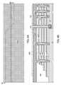
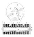
- FIG. 1is a vertical cross-sectional view of an exemplary structure after formation of a first alternating stack of first insulating layers and first sacrificial material layers according to an embodiment of the present disclosure.
- FIG. 2is a vertical cross-sectional view of the exemplary structure after formation of first stepped surfaces and a first retro-stepped dielectric material portion according to an embodiment of the present disclosure.
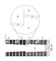
- FIG. 3Ais a top-down view of the exemplary structure after formation of first memory openings in a device region and first support openings in a contact region according to an embodiment of the present disclosure.
- FIG. 3Bis a vertical cross-sectional view of the exemplary structure of FIG. 3A along the vertical plane B-B′.
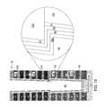
- FIG. 4Ais a top-down view of the exemplary structure after formation of epitaxial channel portions at a bottom of each first memory opening and each first support opening according to an embodiment of the present disclosure.
- FIG. 4Bis a vertical cross-sectional view of the exemplary structure of FIG. 4A along the vertical plane B-B′.
- FIG. 5Ais a top-down view of the exemplary structure after formation of a lower blocking dielectric layer according to an embodiment of the present disclosure.
- FIG. 5Bis a vertical cross-sectional view of the exemplary structure of FIG. 5A along the vertical plane B-B′.
- FIG. 6Ais a top-down view of the exemplary structure after deposition of a first sacrificial fill material layer according to an embodiment of the present disclosure.
- FIG. 6Bis a vertical cross-sectional view of the exemplary structure of FIG. 6A along the vertical plane B-B′.
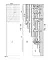
- FIG. 7Ais a top-down view of the exemplary structure after formation of a lower level contact trench according to an embodiment of the present disclosure.
- FIG. 7Bis a vertical cross-sectional view of the exemplary structure of FIG. 7A along the vertical plane B-B′.
- FIG. 8Ais a top-down view of the exemplary structure after formation of first lateral recesses by removal of the first sacrificial material layers according to an embodiment of the present disclosure.
- FIG. 8Bis a vertical cross-sectional view of the exemplary structure of FIG. 8A along the vertical plane B-B′.
- FIG. 9Ais a top-down view of the exemplary structure after deposition of a conductive material to form first electrically conductive layers according to an embodiment of the present disclosure.
- FIG. 9Bis a vertical cross-sectional view of the exemplary structure of FIG. 9A along the vertical plane B-B′.
- FIG. 10Ais a top-down view of the exemplary structure after a recess etch that removes portions of the conductive material from the lower level contact trench and from above the first alternating stack according to an embodiment of the present disclosure.
- FIG. 10Bis a vertical cross-sectional view of the exemplary structure of FIG. 10A along the vertical plane B-B′.
- FIG. 11Ais a top-down view of the exemplary structure after deposition of a second sacrificial fill material layer according to an embodiment of the present disclosure.
- FIG. 11Bis a vertical cross-sectional view of the exemplary structure of FIG. 11A along the vertical plane B-B′.
- FIG. 12Ais a top-down view of the exemplary structure after planarizing the first and second sacrificial fill material layers according to an embodiment of the present disclosure.
- FIG. 12Bis a vertical cross-sectional view of the exemplary structure of FIG. 12A along the vertical plane B-B′.
- FIG. 13Ais a top-down view of the exemplary structure after formation of a second alternating stack of second insulating layers and second sacrificial material layers according to an embodiment of the present disclosure.
- FIG. 13Bis a vertical cross-sectional view of the exemplary structure of FIG. 13A along the vertical plane B-B′.
- FIG. 14Ais a top-down view of the exemplary structure after formation of second stepped surfaces and a second retro-stepped dielectric material portion according to an embodiment of the present disclosure.
- FIG. 14Bis a vertical cross-sectional view of the exemplary structure of FIG. 14A along the vertical plane B-B′.
- FIG. 15Ais a top-down view of the exemplary structure after formation of second memory openings in the device region and second support openings in the contact region according to an embodiment of the present disclosure.
- FIG. 15Bis a vertical cross-sectional view of the exemplary structure of FIG. 15A along the vertical plane B-B′.
- FIG. 16is a vertical cross-sectional view of a stack of a first memory opening and a second memory opening after deposition of a second blocking dielectric layer and a sacrificial liner according to an embodiment of the present disclosure.
- FIG. 17is a vertical cross-sectional view of the stack of the first and second memory openings after an anisotropic etch that removes an upper cap portion of an encapsulated cavity according to an embodiment of the present disclosure.
- FIG. 18is a vertical cross-sectional view of the stack of the first and second memory openings after removal of the first sacrificial fill material and the sacrificial liner according to an embodiment of the present disclosure.
- FIG. 19is a vertical cross-sectional view of the stack of the first and second memory openings after formation of a memory material layer, a tunneling dielectric layer, and a first semiconductor channel layer according to an embodiment of the present disclosure.
- FIG. 20is a vertical cross-sectional view of the stack of the first and second memory openings after formation of a second semiconductor channel layer, a dielectric core, and a drain region according to an embodiment of the present disclosure.
- FIG. 21Ais a top-down view of the exemplary structure after formation of memory stack structures, dummy memory stack structures, dielectric cores, and drain regions according to an embodiment of the present disclosure.
- FIG. 21Bis a vertical cross-sectional view of the exemplary structure of FIG. 21A along the vertical plane B-B′.
- FIG. 22Ais a top-down view of the exemplary structure after formation of an upper level contact trench according to an embodiment of the present disclosure.
- FIG. 22Bis a vertical cross-sectional view of the exemplary structure of FIG. 22A along the vertical plane B-B′.
- FIG. 23Ais a top-down view of the exemplary structure after formation of second lateral recesses by removal of the second sacrificial material layers according to an embodiment of the present disclosure.
- FIG. 23Bis a vertical cross-sectional view of the exemplary structure of FIG. 23A along the vertical plane B-B′.
- FIG. 24Ais a top-down view of the exemplary structure after formation of second electrically conducive layers according to an embodiment of the present disclosure.
- FIG. 24Bis a vertical cross-sectional view of the exemplary structure of FIG. 24A along the vertical plane B-B′.
- FIG. 25Ais a top-down view of the exemplary structure after removal of a second sacrificial fill material portion according to an embodiment of the present disclosure.
- FIG. 25Bis a vertical cross-sectional view of the exemplary structure of FIG. 25A along the vertical plane B-B′.
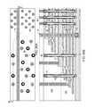
- FIG. 26Ais a top-down view of the exemplary structure after formation of an insulating spacer and a backside contact via structure according to an embodiment of the present disclosure.
- FIG. 26Bis a vertical cross-sectional view of the exemplary structure of FIG. 26A along the vertical plane B-B′.
- the present disclosureis directed to three-dimensional memory devices including a vertical stack of multilevel memory arrays and methods of making the same, the various aspects of which are described below.
- An embodiment of the disclosurecan be employed to form semiconductor devices such as three-dimensional monolithic memory array devices comprising a plurality of NAND memory strings.
- the drawingsare not drawn to scale. Multiple instances of an element may be duplicated where a single instance of the element is illustrated, unless absence of duplication of elements is expressly described or clearly indicated otherwise. Ordinals such as “first,” “second,” and “third” are employed merely to identify similar elements, and different ordinals may be employed across the specification and the claims of the instant disclosure.
- a first element located “on” a second elementcan be located on the exterior side of a surface of the second element or on the interior side of the second element.
- a first elementis located “directly on” a second element if there exist a physical contact between a surface of the first element and a surface of the second element.
- a “layer”refers to a material portion including a region having a substantially uniform thickness.
- a layermay extend over the entirety of an underlying or overlying structure, or may have an extent less than the extent of an underlying or overlying structure. Further, a layer may be a region of a homogeneous or inhomogeneous contiguous structure that has a thickness less than the thickness of the contiguous structure. For example, a layer may be located between any pair of horizontal planes between, or at, a top surface and a bottom surface of the contiguous structure. A layer may extend horizontally, vertically, and/or along a tapered surface.
- a substratemay be a layer, may include one or more layers therein, and/or may have one or more layer thereupon, thereabove, and/or therebelow.
- a monolithic three dimensional memory arrayis one in which multiple memory levels are formed above a single substrate, such as a semiconductor wafer, with no intervening substrates.
- the term “monolithic”means that layers of each level of the array are directly deposited on the layers of each underlying level of the array.
- two-dimensional arraysmay be formed separately and then packaged together to form a non-monolithic memory device.
- non-monolithic stacked memorieshave been constructed by forming memory levels on separate substrates and vertically stacking the memory levels, as described in U.S. Pat. No.
- the substratesmay be thinned or removed from the memory levels before bonding, but as the memory levels are initially formed over separate substrates, such memories are not true monolithic three dimensional memory arrays.
- the various three-dimensional memory devices of the present disclosureinclude a monolithic three-dimensional NAND string memory device, and can be fabricated employing the various embodiments described herein.
- the exemplary structureincludes a substrate, which can be a semiconductor substrate.
- the substratecan include a substrate semiconductor layer 9 .
- the substrate semiconductor layer 9is a semiconductor material layer, and can include at least one elemental semiconductor material, at least one III-V compound semiconductor material, at least one II-VI compound semiconductor material, at least one organic semiconductor material, or other semiconductor materials known in the art.
- the substrate semiconductor layer 9can comprise a single crystalline semiconductor material, such as a single crystal silicon wafer.
- a “semiconductor material”refers to a material having electrical conductivity in the range from 1.0 ⁇ 10 ⁇ 6 S/cm to 1.0 ⁇ 10 5 S/cm, and is capable of producing a doped material having electrical conductivity in a range from 1.0 S/cm to 1.0 ⁇ 10 5 S/cm upon suitable doping with an electrical dopant.
- an “electrical dopant”refers to a p-type dopant that adds a hole to a valance band within a band structure, or an n-type dopant that adds an electron to a conduction band within a band structure.
- a “conductive material”refers to a material having electrical conductivity greater than 1.0 ⁇ 10 5 S/cm.
- an “insulator material” or a “dielectric material”refers to a material having electrical conductivity less than 1.0 ⁇ 10 ⁇ 6 S/cm. All measurements for electrical conductivities are made at the standard condition.
- at least one doped wellcan be formed within the substrate semiconductor layer 9 .
- the exemplary structureincludes a device region 100 , in which memory devices can be subsequently formed, and a contact region 200 , in which stepped surfaces are subsequently formed.
- a “contact region”refers to a region in which contact via structures are to be formed.
- At least one semiconductor device for a peripheral circuitrycan be formed in a peripheral device region 300 , of which the general location is illustrated by a dotted rectangle (detailed structures not shown for clarity).
- the at least one semiconductor devicecan include, for example, one or more field effect transistors.
- the least one semiconductor device for the peripheral circuitrycan contain a driver circuit for memory devices to be subsequently formed, which can include at least one NAND device.
- a semiconductor material layer 10can be provided in an upper portion of the substrate.
- the semiconductor material layer 10can be formed, for example, by implantation of electrical dopants (p-type dopants or n-type dopants) into an upper portion of the substrate semiconductor layer 9 , or by deposition of a single crystalline semiconductor material, for example, by selective epitaxy.
- the semiconductor material layer 10can include a single crystalline semiconductor material (e.g., p-well) that is in epitaxial alignment with the single crystalline structure of the substrate semiconductor layer 9 .
- Each first material layercan include a first material
- each second material layercan include a second material that is different from the first material.
- the first material layers and the second material layerscan be first insulating layers 132 and first sacrificial material layers 142 , respectively.
- each first insulating layer 132can include a first insulating material
- each first sacrificial material layer 142can include a first sacrificial material.
- the alternating stack formed by the first insulating layers 132 and the first sacrificial material layers 142is herein referred to as a first alternating stack ( 132 , 142 ), or a lower alternating stack ( 132 , 142 ).
- the stackcan include an alternating plurality of first insulating layers 132 and first sacrificial material layers 142 .
- a “sacrificial material”refers to a material that is removed during a subsequent processing step.
- an alternating stack of first elements and second elementsrefers to a structure in which instances of the first elements and instances of the second elements alternate. Each instance of the first elements that is not an end element of the alternating plurality is adjoined by two instances of the second elements on both sides, and each instance of the second elements that is not an end element of the alternating plurality is adjoined by two instances of the first elements on both ends.
- the first elementsmay have the same thickness thereamongst, or may have different thicknesses.
- the second elementsmay have the same thickness thereamongst, or may have different thicknesses.
- the alternating plurality of first material layers and second material layersmay begin with an instance of the first material layers or with an instance of the second material layers, and may end with an instance of the first material layers or with an instance of the second material layers.
- an instance of the first elements and an instance of the second elementsmay form a unit that is repeated with periodicity within the alternating plurality.
- the first alternating stack ( 132 , 142 )can include first insulating layers 132 composed of the first material, and first sacrificial material layers 142 composed of the second material, which is different from the first material.
- the first material of the first insulating layers 132can be at least one insulating material.
- Insulating materials that can be employed for the first insulating layers 132include, but are not limited to silicon oxide (including doped or undoped silicate glass), silicon nitride, silicon oxynitride, organosilicate glass (OSG), spin-on dielectric materials, dielectric metal oxides that are commonly known as high dielectric constant (high-k) dielectric oxides (e.g., aluminum oxide, hafnium oxide, etc.) and silicates thereof, dielectric metal oxynitrides and silicates thereof, and organic insulating materials.
- the first material of the first insulating layers 132can be silicon oxide.
- the second material of the first sacrificial material layers 142is a sacrificial material that can be removed selective to the first material of the first insulating layers 132 .
- a removal of a first materialis “selective to” a second material if the removal process removes the first material at a rate that is at least twice the rate of removal of the second material.
- the ratio of the rate of removal of the first material to the rate of removal of the second materialis herein referred to as a “selectivity” of the removal process for the first material with respect to the second material.
- the first sacrificial material layers 142may comprise an insulating material, a semiconductor material, or a conductive material.
- the second material of the first sacrificial material layers 142can be subsequently replaced with electrically conductive electrodes which can function, for example, as control gate electrodes of a vertical NAND device.
- Non-limiting examples of the second materialinclude silicon nitride, an amorphous semiconductor material (such as amorphous silicon), and a polycrystalline semiconductor material (such as polysilicon).
- the first sacrificial material layers 142can be material layers that comprise silicon nitride or a semiconductor material including at least one of silicon and germanium.
- the first insulating layers 132can include silicon oxide, and sacrificial material layers can include silicon nitride sacrificial material layers.
- the first material of the first insulating layers 132can be deposited, for example, by chemical vapor deposition (CVD).
- CVDchemical vapor deposition
- TEOStetraethylorthosilicate
- the second material of the first sacrificial material layers 142can be formed, for example, CVD or atomic layer deposition (ALD).
- the thicknesses of the first insulating layers 132 and the first sacrificial material layers 142can be in a range from 20 nm to 50 nm, although lesser and greater thicknesses can be employed for each first insulating layer 132 and for each first sacrificial material layer 142 .
- the number of repetitions of the pairs of a first insulating layer 132 and a first sacrificial material layer 142can be in a range from 2 to 1,024, and typically from 8 to 256, although a greater number of repetitions can also be employed.
- each first sacrificial material layer 142 in the first alternating stack ( 132 , 142 )can have a uniform thickness that is substantially invariant within each respective first sacrificial material layer 142 .
- the lower stack structure( 132 , 142 ) can be patterned to form first stepped surfaces.
- the first stepped surfacesare formed in the contact region 200 .
- the contact region 200includes a first stepped area in which the first stepped surfaces are formed, and a second stepped area in which additional stepped surfaces are to be subsequently formed in an upper stack structure (to be subsequently formed over the lower stack structure).
- the device region 100is provided adjacent to the contact region 200 .
- Memory devices including memory stack structurescan be subsequently formed in the device region 100 .
- the first stepped surfacescan be formed, for example, by forming a mask layer with an opening therein, etching a cavity within the levels of the topmost first sacrificial material layer 142 and the topmost first insulating layer 132 , and iteratively expanding the etched area and vertically recessing the cavity by etching each pair of a first insulating layer 132 and a first sacrificial material layer 142 located directly underneath the bottom surface of the etched cavity within the etched area.
- the first alternating stack ( 132 , 142 )is patterned such that each underlying first sacrificial material layer 142 laterally protrudes farther than any overlying first sacrificial material layer 142 in the etched region, and each underlying first insulating layer 132 laterally protrudes farther than any overlying first insulating layer 132 in the etched region.
- the contact regioncan be a contact region of the first alternating stack ( 132 , 142 ).
- the cavityis herein referred to as a first stepped cavity.
- a dielectric materialis deposited to fill the first stepped cavity. Excess portions of the dielectric material overlying the topmost surface of the first alternating stack ( 132 , 142 ), are removed for example, by chemical mechanical planarization. The remaining portion of the deposited dielectric material forms a first retro-stepped dielectric material portion 165 , which is formed on the first stepped surfaces.
- the first dielectric material portion 165is retro-stepped.
- a “retro-stepped” elementrefers to an element that has stepped surfaces and a horizontal cross-sectional area that increases monotonically as a function of a vertical distance from a top surface of a substrate on which the element is present.
- the lower stack structurewhich is also referred to as a first stack structure, comprises the first alternating stack ( 132 , 142 ) and the first retro-stepped dielectric material portion 165 .
- first openings ( 121 , 321 ) extending to a top surface of the substrate ( 9 , 10 )are formed through the lower stack structure ( 132 , 142 , 165 ).
- the first openings ( 121 , 321 )include first memory openings 121 that are formed in the device region 100 and first support openings 321 that are formed in the contact region 200 .
- a lithographic material stack(not shown) including at least a photoresist layer can be formed over the lower stack structure ( 132 , 142 , 165 ), and can be lithographically patterned to form openings within the lithographic material stack.
- the pattern in the lithographic material stackcan be transferred through the entirety of the lower stack structure ( 132 , 142 , 165 ) by at least one anisotropic etch that employs the patterned lithographic material stack as an etch mask. Portions of the lower stack structure ( 132 , 142 , 165 ) underlying the openings in the patterned lithographic material stack are etched to form the first openings ( 121 , 321 ). In other words, the transfer of the pattern in the patterned lithographic material stack through the lower stack structure ( 132 , 142 , 165 ) forms the first openings ( 121 , 321 ).
- the chemistry of the anisotropic etch process employed to etch through the materials of the first alternating stack ( 132 , 142 )can alternate to optimize etching of the first and second materials in the first alternating stack ( 132 , 142 ) while providing a comparable average etch rate for the first dielectric material portion 165 .
- the anisotropic etchcan be, for example, a series of reactive ion etches.
- the sidewalls of the first openings ( 121 , 321 )can be substantially vertical, or can be tapered.
- the patterned lithographic material stackcan be subsequently removed, for example, by ashing.
- the top layer 132 in the stackmay function as an etch stop dielectric layer during subsequent steps.
- the top layer 132 in the stackmay comprise a different material (e.g., metal oxide dielectric) from the remaining layers 132 (e.g., silicon oxide) in the stack.
- the first support opening 321are formed through the first stack of alternating layers ( 132 , 142 ) and through one of the first dielectric material portion 165 and the optional etch stop dielectric layer concurrently with formation of the first memory openings 121 , which are formed through the etch stop dielectric layer and the first stack of alternating layers ( 132 , 142 ).
- the substrate ( 9 , 10 )can be employed as a stopping layer for the anisotropic etch process.
- the first openings ( 121 , 321 )may extend below the top surface of the substrate ( 9 , 10 ) by an overetch.
- the lateral dimensions (e.g., a diameter) of the first openings ( 121 , 321 )can be from about 20 nm to 200 nm at an upper portion of each first opening ( 121 , 321 ), and can be about 10 nm to 150 nm at a lower portion of each first opening ( 121 , 321 ).
- the first memory openings 121can be formed as an array of openings, which can be a periodic two-dimensional array of openings.
- the first support openings 321can be formed as discrete openings that are mutually separated from one another, and may not form a periodic two-dimensional array pattern.
- the nearest neighbor lateral separation distance among the first support openings 321may be greater than twice (e.g., three times or more) than the nearest neighbor distance among the first memory openings 121 .
- an optional epitaxial channel portions 11can be formed by a selective epitaxy process.
- the epitaxial channel portions 11comprise a single crystalline semiconductor material in epitaxial alignment with the single crystalline substrate semiconductor material of the semiconductor material layer 10 .
- the epitaxial channel portions 11can be doped with electrical dopants of a suitable conductivity type.
- the semiconductor material layer 10 and the epitaxial channel portions 11can have a doping of the first conductivity type (e.g., p-type).
- the selective epitaxy process that forms the epitaxial channel portions 11can be performed, for example, by sequentially or simultaneously flowing a reactant gas (such as SiH 4 , SiH 2 Cl 2 , SiHCl 3 , SiCl 4 , Si 2 H 6 , GeH 4 , Ge 2 H 6 , other semiconductor precursor gases, or combinations there) with an etchant gas (such as HCl).
- a reactant gassuch as SiH 4 , SiH 2 Cl 2 , SiHCl 3 , SiCl 4 , Si 2 H 6 , GeH 4 , Ge 2 H 6 , other semiconductor precursor gases, or combinations there
- an etchant gassuch as HCl
- the semiconductor materialis deposited only on the semiconductor surface, which is the physically exposed portion of the top surface of the semiconductor material layer 10 .
- the process conditions(such as the deposition temperature, the partial pressure of the various gases in a process chamber, etc.) can be selected such that the deposited semiconductor material is epitaxial, i.e., single crystalline silicon or another semiconductor material with atomic alignment with the single crystalline structure of the semiconductor material layer 10 (e.g., p-well).
- a lower blocking dielectric layer 21 Lcan be formed on the physically exposed surface of the first memory openings 121 and the first support openings 321 and over the first alternating stack ( 132 , 142 ).
- the lower blocking dielectric layer 21 Lcan include a single dielectric material layer or a plurality of dielectric material layers.
- the lower blocking dielectric layer 21 Lcan be deposited on the sidewalls of each memory opening 121 by a conformal deposition method.
- the lower blocking dielectric layer 21 Lcan include a dielectric metal oxide.
- a dielectric metal oxiderefers to a dielectric material that includes at least one metallic element and at least oxygen.
- the dielectric metal oxidemay consist essentially of the at least one metallic element and oxygen, or may consist essentially of the at least one metallic element, oxygen, and at least one non-metallic element such as nitrogen.
- the lower blocking dielectric layer 21 Lcan include a dielectric metal oxide having a dielectric constant greater than 7.9, i.e., having a dielectric constant greater than the dielectric constant of silicon nitride.
- Non-limiting examples of dielectric metal oxidesinclude aluminum oxide (Al 2 O 3 ), hafnium oxide (HfO 2 ), lanthanum oxide (LaO 2 ), yttrium oxide (Y 2 O 3 ), tantalum oxide (Ta 2 O 5 ), silicates thereof, nitrogen-doped compounds thereof, alloys thereof, and stacks thereof.
- the lower blocking dielectric layer 21 Lcan be deposited, for example, by chemical vapor deposition (CVD), atomic layer deposition (ALD), pulsed laser deposition (PLD), liquid source misted chemical deposition, or a combination thereof.
- the thickness of the lower blocking dielectric layer 21 Lcan be in a range from 1 nm to 20 nm, although lesser and greater thicknesses can also be employed.
- the lower blocking dielectric layer 21 Lcan subsequently function as a dielectric material portion that blocks leakage of stored electrical charges to control gate electrodes.
- the lower blocking dielectric layer 21 Lincludes aluminum oxide.
- the lower blocking dielectric layer 21 Lcan include a silicon-based dielectric material such as silicon oxide, silicon oxynitride, silicon nitride, or a combination thereof.
- the lower blocking dielectric layer 21 Lcan include silicon oxide.
- the silicon-based dielectric materialcan be formed by a conformal deposition method such as low pressure chemical vapor deposition, atomic layer deposition, or a combination thereof.
- the thickness of the silicon-based dielectric material, if present,can be in a range from 1 nm to 20 nm, although lesser and greater thicknesses can also be employed.
- the lower blocking dielectric layer 21 Lcan be omitted, and a blocking dielectric layer can be formed after formation of backside recesses by a conformal deposition process on surfaces of memory films to be subsequently formed.
- a first sacrificial fill material layer 22 Lis deposited in the cavities of the first memory openings 121 and the first support openings 321 , and over the alternating stack ( 132 , 142 ) and the lower blocking dielectric layer 21 L.
- the first sacrificial fill material layer 22 Lincludes a first sacrificial fill material, which is a material that can be removed selective to the material of the lower blocking dielectric layer 21 L.
- the first sacrificial fill materialcan include a semiconductor material such as silicon (e.g., amorphous silicon or polysilicon), germanium, a silicon-germanium alloy.
- the first sacrificial fill materialcan include amorphous carbon, diamond-like carbon, or a porous organosilicate glass.
- the first sacrificial fill material layer 22 Lcan be deposited employing a non-conformal deposition method.
- a first encapsulated cavity 29can be formed within each first memory opening 121 and within each first support opening 321 .
- a “cavity”refers to a volume that does not include a solid or a liquid material.
- a cavitymay be under vacuum or may include a gas phase material.
- an “encapsulated cavity”refers to a cavity that is encapsulated, i.e., a cavity that is inside a contiguous set of surfaces that do not have any opening therein.
- a first encapsulated cavity 29is formed within each first memory opening 121 and within each support opening 321 upon filling the first memory openings 121 and the first support openings 321 with the first sacrificial fill material.
- Each first encapsulated cavity 29is encapsulated by a portion of the first sacrificial fill material within a respective first memory opening 121 or within a respective first support opening 321 .
- At least one first contact trench 179can be formed through the first alternating stack ( 132 , 142 ), for example, by applying a photoresist layer (not shown), lithographically patterning the photoresist layer, and transferring the pattern in the photoresist layer through the first alternating stack ( 132 , 142 ) employing an anisotropic etch.
- Each first contact trench 179can extend from the top surface of the first sacrificial fill material layer 22 L at least to the top surface of the semiconductor material layer 10 .
- Dopants of a second conductivity typewhich is the opposite of the first conductivity type of the semiconductor material layer 10 , can be implanted into a surface portion of the semiconductor material layer 10 to form a source region 61 .
- Each first contact trench 179extends through the lower stack structure ( 132 , 142 , 165 ), and thus, is herein referred to as a lower level contact trench.
- an etchant that selectively etches the material of the first sacrificial material layers 142 with respect to the material of the first insulating layers 132can be introduced into the first contact trench 179 , for example, employing an isotropic etch process.
- First backside recesses 143are formed in volumes from which the first sacrificial material layers 142 are removed. The removal of the material of the first sacrificial material layers 142 can be selective to the material of the first insulating layers 132 , the material of the first retro-stepped dielectric material portion 165 , the semiconductor material of the semiconductor material layer 10 , and the material of the lower blocking dielectric layer 21 L.
- the first sacrificial material layers 142can include silicon nitride, and the materials of the first insulating layers 132 , and the first retro-stepped dielectric material portion 165 can be selected from silicon oxide and dielectric metal oxides.
- the first sacrificial material layers 142can include a semiconductor material such as germanium or a silicon-germanium alloy, and the materials of the first insulating layers 132 and the first retro-stepped dielectric material portion 165 can be selected from silicon oxide, silicon nitride, and dielectric metal oxides.
- the isotropic etch processcan be a wet etch process employing a wet etch solution, or can be a gas phase (dry) etch process in which the etchant is introduced in a vapor phase into the first contact trench 179 .
- the etch processcan be a wet etch process in which the exemplary structure is immersed within a wet etch tank including phosphoric acid, which etches silicon nitride selective to silicon oxide, silicon, and various other materials employed in the art.
- Each first backside recess 143can be a laterally extending cavity having a lateral dimension that is greater than the vertical extent of the cavity. In other words, the lateral dimension of each first backside recess 143 can be greater than the height of the first backside recess 143 .
- a plurality of first backside recesses 143can be formed in the volumes from which the material of the first sacrificial material layers 142 is removed. Each of the plurality of first backside recesses 143 can extend substantially parallel to the top surface of the substrate ( 9 , 10 ).
- a first backside recess 143can be vertically bounded by a top surface of an underlying first insulating layer 132 and a bottom surface of an overlying first insulating layer 132 . In one embodiment, each first backside recess 143 can have a uniform height throughout.
- a backside blocking dielectric layercan be formed in the backside recesses.
- At least one conductive materialcan be deposited in the plurality of first backside recesses 143 , on the sidewalls of the first contact trench 179 , and over the first sacrificial fill material layer 22 L.
- the at least one conductive materialcan include at least one metallic material, i.e., an electrically conductive material that includes at least one metallic element.
- a plurality of first electrically conductive layers 146can be formed in the plurality of first backside recesses 143 , and a contiguous metallic material layer 46 L can be formed on the sidewalls of each first contact trench 179 and over the first sacrificial fill material layer 22 L.
- each first sacrificial material layer 142can be replaced with a first electrically conductive layer 146 .
- a backside cavityis present in the portion of each first contact trench 179 that is not filled with the contiguous metallic material layer 46 L.
- the metallic materialcan be deposited by a conformal deposition method, which can be, for example, chemical vapor deposition (CVD), atomic layer deposition (ALD), electroless plating, electroplating, or a combination thereof.
- the metallic materialcan be an elemental metal, an intermetallic alloy of at least two elemental metals, a conductive nitride of at least one elemental metal, a conductive metal oxide, a conductive doped semiconductor material, a conductive metal-semiconductor alloy such as a metal silicide, alloys thereof, and combinations or stacks thereof.
- Non-limiting exemplary metallic materials that can be deposited in the plurality of first backside recesses 143include tungsten, tungsten nitride, titanium, titanium nitride, tantalum, tantalum nitride, cobalt, and ruthenium.
- the metallic materialcan comprise a metal such as tungsten and/or metal nitride.
- the metallic material for filling the plurality of first backside recesses 143can be a combination of titanium nitride layer and a tungsten fill material.
- the metallic materialcan be deposited by chemical vapor deposition or atomic layer deposition.
- the deposited metallic material of the contiguous metallic material layer 46 Lis etched back from the sidewalls of each first contact trench 179 and from above the first sacrificial fill material layer 22 L, for example, by an isotropic etch.
- Each remaining portion of the deposited metallic material in the first backside recesses 143constitutes a first electrically conductive layer 146 .
- Each first electrically conductive layer 146can be a conductive line structure.
- each first sacrificial material layer 142can be replaced with a first electrically conductive layer 146 .
- Each first electrically conductive layer 146can function as a combination of a plurality of control gate electrodes located at a same level and a word line electrically interconnecting, i.e., electrically shorting, the plurality of control gate electrodes located at the same level.
- the control gate electrodes within each first electrically conductive layer 146are the control gate electrodes for the vertical memory devices to be subsequently formed.
- a second sacrificial fill material layer 24 Lis deposited in each first contact trench 179 and over the first sacrificial fill material layer 22 L.
- the second sacrificial fill material layer 24 Lincludes a second sacrificial fill material, which is a material that can be removed selective to the materials of the first insulating layers 132 and the first electrically conductive layers 146 .
- the second sacrificial fill materialcan include a semiconductor material such as polysilicon, germanium, and/or a silicon-germanium alloy.
- the second sacrificial fill materialcan include amorphous carbon, diamond-like carbon, or a porous organosilicate glass.
- the second sacrificial fill materialcan be the same as, or can be different from, the first sacrificial fill material.
- the second sacrificial fill material layer 24 Lcan be deposited employing a non-conformal deposition method.
- a second encapsulated cavity 27can be formed within each first contact trench 179 .
- a second encapsulated cavity 27is formed within each first contact trench 179 upon filling the first contact trenches 179 with the second sacrificial fill material.
- Each second encapsulated cavity 27is encapsulated by a portion of the second sacrificial fill material within a respective first contact trench 179 .
- a planarization processis performed to remove portions of the first and second sacrificial fill material layers ( 21 L, 22 L) from above an alternating stack ( 132 , 146 ) of the first insulating layers 132 and the first electrically conductive layers 146 .
- a chemical mechanical planarization (CMP) processcan be employed to remove the first and second sacrificial fill material layers ( 21 L, 22 L) from above the alternating stack ( 132 , 146 ).
- the horizontal portion of the lower blocking dielectric layer 21 Lcan be employed as a stopping layer for the CMP process.
- the horizontal portion of the lower blocking dielectric layer 21 Lcan be subsequently removed, for example, by an isotropic etch process or by a touch-up polish process.
- Each remaining portion of the first sacrificial fill material in a first memory opening or a first support openingconstitutes a first sacrificial fill material portion 22 including a first encapsulated cavity 27 .
- Each remaining portion of the second sacrificial fill material in a first contact trenchconstitutes a second sacrificial fill material portion 24 including a second encapsulated cavity 27 .
- the first sacrificial fill material portions 22can form a two-dimensional array, which may have a periodicity along two different horizontal directions.
- each second sacrificial fill material portion 24can extend along a horizontal direction, which is herein referred to as a lengthwise direction of a second sacrificial fill material portion 24 .
- Each remaining portion of the lower blocking dielectric layer 21 L within a first memory opening or within a first support openingis herein referred to as a lower blocking dielectric 21 .
- Each lower blocking dielectric 21is formed directly on a sidewall of a first memory opening or a first support opening.
- a second alternating stack ( 232 , 242 ) of material layersis subsequently formed on the top surface of the lower stack structure ( 132 , 142 , 165 ).
- the second stack ( 232 , 242 )includes an alternating plurality of third material layers and fourth material layers.
- Each third material layercan include a third material
- each fourth material layercan include a fourth material that is different from the third material.
- the third materialcan be the same as the first material of the first insulating layer 132
- the fourth materialcan be the same as the second material of the first sacrificial material layers 142 .
- the third material layers and the fourth material layerscan be second insulating layers 232 and second sacrificial material layers 242 , respectively.
- the third material of the second insulating layers 232can be at least one insulating material.
- the fourth material of the second sacrificial material layers 242is a sacrificial material that can be removed selective to the third material of the second insulating layers 232 .
- the second sacrificial material layers 242may comprise an insulating material, a semiconductor material, or a conductive material.
- the fourth material of the second sacrificial material layers 242can be subsequently replaced with electrically conductive electrodes which can function, for example, as control gate electrodes of a vertical NAND device.
- each second insulating layer 232can include a second insulating material
- each second sacrificial material layer 242can include a second sacrificial material.
- the second stack ( 232 , 242 )can include an alternating plurality of second insulating layers 232 and second sacrificial material layers 242 .
- the third material of the second insulating layers 232can be deposited, for example, by chemical vapor deposition (CVD).
- the fourth material of the second sacrificial material layers 242can be formed, for example, CVD or atomic layer deposition (ALD).
- the third material of the second insulating layers 232can be at least one insulating material. Insulating materials that can be employed for the second insulating layers 232 can be any material that can be employed for the first insulating layers 132 .
- the fourth material of the second sacrificial material layers 242is a sacrificial material that can be removed selective to the third material of the second insulating layers 232 . Sacrificial materials that can be employed for the second sacrificial material layers 242 can be any material that can be employed for the first sacrificial material layers 142 .
- the second insulating materialcan be the same as the first insulating material, and the second sacrificial material can be the same as the first sacrificial material.
- the thicknesses of the second insulating layers 232 and the second sacrificial material layers 242can be in a range from 20 nm to 50 nm, although lesser and greater thicknesses can be employed for each second insulating layer 232 and for each second sacrificial material layer 242 .
- the number of repetitions of the pairs of a second insulating layer 232 and a second sacrificial material layer 242can be in a range from 2 to 1,024, and typically from 8 to 256, although a greater number of repetitions can also be employed.
- each second sacrificial material layer 242 in the second stack ( 232 , 242 )can have a uniform thickness that is substantially invariant within each respective second sacrificial material layer 242 .
- a dielectric cap layer 70 and a planarization stopping layer 72can be subsequently formed over the second stack ( 232 , 242 ).
- the dielectric cap layer 70includes a dielectric material that is different from the material of the second sacrificial material layers 242 .
- the dielectric cap layer 70can include silicon oxide.
- the planarization stopping layer 72is an optional layer, and includes a dielectric material that is different from the material of the second sacrificial material layer 242 and can be employed as a planarization stopping material in a planarization process (which may be a chemical mechanical planarization process).
- the planarization stopping layer 72can include silicon nitride and/or a dielectric metal oxide.
- additional stepped surfacesare formed in the second stack ( 232 , 242 ) in the contact region 200 .
- the additional stepped surfacesare herein referred to as second stepped surfaces.
- the second stepped surfacesare formed in a second stepped area, which is adjacent to, and does not overlie, the first stepped area of the first stepped surfaces within the lower stack structure ( 132 , 142 , 165 ).
- the second stepped surfacescan be adjacent to, and do not overlie, the stepped interface between the first alternating stack ( 132 , 146 ) and the first retro-stepped dielectric material portion 165 .
- the second stepped surfacescan be formed, for example, by forming a mask layer with an opening therein, etching a cavity within the levels of the topmost second sacrificial material layer 242 and the topmost second insulating layer 232 , and iteratively expanding the etched area and vertically recessing the cavity by etching a pair of a second insulating layer 232 and a second sacrificial material layer 242 located directly underneath the bottom surface of the etched cavity within the etched area.
- the second stack ( 232 , 242 )is patterned such that each underlying second sacrificial material layer 242 laterally protrudes farther than any overlying second sacrificial material layer 242 in the etched region, and each underlying second insulating layer 232 laterally protrudes farther than any overlying second insulating layer 232 in the etched region.
- the etched areaincludes the area of the contact region 200 , which includes the contact area for the second stack ( 232 , 242 ) and a contact area for the first alternating stack ( 132 , 142 ).
- the second stack ( 232 , 242 )is patterned to form the second stepped surfaces thereupon.
- the cavity formed by removal of portions of the second stack ( 232 , 242 )is herein referred to as a second stepped cavity.
- the area of the second stepped cavityincludes the area of the first retro-stepped first dielectric material portion 165 , from which all layers of the second stack ( 232 , 242 ) are removed.
- the area of the second stepped cavityfurther includes the area of the second stepped surfaces of the second stack ( 232 , 242 ).
- Dielectric materialis deposited to fill the second stepped cavity. Excess portions of the dielectric material overlying the topmost surface of the second stack ( 232 , 242 ) are removed, for example, by chemical mechanical planarization. The remaining portion of the deposited dielectric material is retro-stepped, and thus, forms a second retro-stepped dielectric material portion 265 .
- the second retro-stepped dielectric material portion 265is located on, and over, the second stepped surfaces of the second stack ( 232 , 242 ).
- the second retro-stepped dielectric material portion 265is formed on the second stepped surfaces.
- the contact region 200comprises a region of the first stepped surfaces and a region of the second stepped surfaces.
- second openings ( 221 , 421 )are formed through the upper stack structure ( 232 , 242 , 265 , 70 , 72 ) to the top surface of the lower stack structure ( 132 , 142 , 165 ).
- the second openings ( 221 , 421 )include second memory openings 221 that are formed in the device region 100 and second support openings 421 that are formed in the contact region 200 .
- Each second memory opening 221can be formed in an area that substantially coincides with the area of a respective first memory opening 121 .
- Each second support opening 421can be formed in an area that substantially coincides with the area of a respective first support opening 321 .
- a lithographic material stackincluding at least a photoresist layer can be formed over the upper stack structure ( 232 , 242 , 265 , 70 , 72 ), and can be lithographically patterned to form openings within the lithographic material stack.
- the pattern in the lithographic material stackcan be transferred through the entirety of the upper stack structure ( 232 , 242 , 265 , 70 , 72 ) by at least one anisotropic etch that employs the patterned lithographic material stack as an etch mask.
- Portions of the upper stack structure ( 232 , 242 , 265 , 70 , 72 ) underlying the openings in the patterned lithographic material stackare etched to form the second openings ( 221 , 421 ).
- the transfer of the pattern in the patterned lithographic material stack through the upper stack structure ( 232 , 242 , 265 , 70 , 72 )forms the second openings ( 221 , 421 ).
- the chemistry of the anisotropic etch process employed to etch through the materials of the second stack ( 232 , 242 )can alternate to optimize etching of the third and fourth materials in the second stack ( 232 , 242 ) while providing a comparable average etch rate for the second dielectric material portion 265 .
- the anisotropic etchcan be, for example, a series of reactive ion etches.
- the sidewalls of the second openings ( 221 , 421 )can be substantially vertical, or can be tapered.
- the second memory openings ( 221 , 421 )are formed through the upper stack structure ( 232 , 242 , 265 , 70 , 72 ) in areas overlying the first memory openings ( 121 , 321 ), which are filled with the sacrificial opening fill structures ( 22 , 24 ).
- the second support opening 421can be formed through the second stack of alternating layers ( 232 , 242 ) and through the second dielectric material portion 265 concurrently with formation of the second memory openings 221 , which are formed through the second stack of alternating layers ( 232 , 242 ).
- the sacrificial opening fill structures ( 22 , 24 )can be employed as an endpoint detection layer to control the termination time of the anisotropic etch process.
- the lateral dimensions (e.g., a diameter) of the second openings ( 221 , 421 )can be comparable to the lateral dimensions of the first openings ( 121 , 321 ).
- the lateral dimensions of the second openings ( 221 , 421 )can be from about 20 nm to 200 nm at an upper portion of each second opening ( 221 , 421 ), and can be about 10 nm to 150 nm at a lower portion of each second opening ( 221 , 421 ).
- the second memory openings 221 and the first memory openings 121can be formed as an array of openings, which can be a periodic two-dimensional array of openings.
- the second support openings 421 and the first support openings 321can be formed as discrete openings that are mutually separated from one another, and may not form a periodic two-dimensional array pattern.
- the lateral separation distance among the second support openings 421may be greater than twice (e.g., three time or more) than the nearest neighbor distance among the second memory openings 221 .
- Each bottom surface of the second memory openings 221can be entirely within the area of a top surface of an underlying first sacrificial fill material portion 22 .
- Each bottom surface of the second support openings 421can be entirely within the area of a top surface of an underlying sacrificial fill material portion 24 .
- the patterned lithographic material stackcan be subsequently removed, for example, by ashing.
- a vertical stack of a first memory opening and a second memory openingis shown for a configuration in which a dielectric spacer 116 is provided at a sidewall of each epitaxial channel portion 11 , and in which a gate dielectric layer 31 is employed in lieu of a bottommost first insulating layer 132 .
- Such a configurationcan be provided by oxidizing physically exposed sidewalls of the epitaxial channel portions 11 after formation of the first backside recesses 143 and prior to deposition of at least one conductive material to form the first electrically conductive layers 146 , e.g., between the processing steps of FIGS. 8A and 8B and the processing steps of FIGS. 9A and 9B .
- An upper blocking dielectric layer 41 Lcan be deposited directly on the sidewalls of the second openings ( 221 , 421 ) and physically exposed surfaces of the first sacrificial fill material portions 22 , and over the second alternating stack ( 232 , 242 ).
- the upper blocking dielectric layer 41 Lcan include one or more of any of the materials that can be employed for the lower blocking dielectric layer 21 L.
- the upper blocking dielectric layer 41 Lcan be deposited employing the same processes that can be employed to deposit the lower blocking dielectric layer 21 L.
- the composition of the upper blocking dielectric layer 41 Lcan be the same as, or can be different from, the composition of the lower blocking dielectric layer 21 L.
- the thickness of the upper blocking dielectric layer 41 Lcan be the same as, or can be different from, the thickness of the lower blocking dielectric layer 21 L. In one embodiment, the upper blocking dielectric layer 41 L does not physically contact any portion of the underlying lower blocking dielectric 21 .
- a sacrificial liner 42 Lcan be optionally formed over the upper blocking dielectric layer 41 L.
- the sacrificial liner 42 Lincludes a material that can be removed selective to the material of the upper blocking dielectric layer 41 L and can provide protection for vertical portions of the upper blocking dielectric layer 41 L during a subsequent anisotropic etch process that removes the horizontal portions of the upper blocking dielectric layer 41 L.
- the sacrificial liner 42 Lcan include a material such as silicon, germanium, a silicon-germanium alloy, amorphous carbon, diamond-like carbon, or organosilicate glass.
- the sacrificial liner 42 Lcan include the same material as the material of the first sacrificial fill material portions 22 .
- the sacrificial liner 42 Lcan be an amorphous silicon layer or a polysilicon layer.
- the thickness of the sacrificial liner 42 Lcan be in a range from 1 nm to 20 nm, although lesser and greater thicknesses can also be employed.
- an anisotropic etchis performed to remove horizontal portions of the sacrificial liner 42 L and the upper blocking dielectric layer 41 L.
- An upper portion of each first sacrificial fill material portion 22is anisotropically etched within each first memory opening located underneath a second memory opening.
- the anisotropic etchremoves an upper cap portion of each first sacrificial material fill portion 22 such that the encapsulated cavities 29 are connected to an overlying cavity volume and become open cavities 29 ′.
- a volume of each encapsulated cavity 29is contiguously adjoined to a volume of an overlying second memory opening so that the encapsulated cavity 29 becomes an open cavity 29 ′.
- an “open cavity”refers to a cavity that is contiguously connected to another volume that is not filled with a solid or a liquid.
- Each remaining portion of the upper blocking dielectric layer 41 L within a second memory opening or within a second support openingconstitutes an upper blocking dielectric 41 .
- the materials of the sacrificial liner 42 L and the first sacrificial fill material portions 22are removed by an isotropic etch selective to the materials of the lower blocking dielectrics 21 and the upper blocking dielectrics 41 .
- the etchant of the isotropic etch processcan simultaneously access the sidewall portions and the bottom portions of the sacrificial fill material portions 22 through the open cavities 29 ′. Bottommost horizontal portions of each upper blocking dielectric 41 may be removed or reduced in size during the isotropic etch that removes the materials of the sacrificial liner 42 L and the first sacrificial fill material portions 22 .
- the isotropic etch that removes the materials of the materials of the sacrificial liner 42 L and the first sacrificial fill material portions 22can have high selectivity to the materials of the lower blocking dielectrics 21 and the upper blocking dielectrics 41 so as to minimize collateral damage of the lower blocking dielectrics 21 and the upper blocking dielectrics 41 .
- an upper blocking dielectric 41can be physically disjoined from, i.e., not in physical contact with, an underlying blocking dielectric 21 , as shown in the inset in FIG. 18 .
- a stack of a first memory opening in the lower stack structure ( 132 , 146 , 165 ) and a second memory opening in the upper stack structure ( 232 , 246 , 265 , 70 , 72 )collectively constitutes an inter-stack memory opening.
- Each inter-stack memory openingcan include a volume of a vertically adjoining pair of a first memory opening and a second memory opening, and can extend through the lower stack structure ( 132 , 146 , 165 ) and the upper stack structure ( 232 , 246 , 265 , 70 , 72 ).
- a memory material layer 54 , a tunneling dielectric layer 56 , and a first semiconductor channel layer 601can be sequentially deposited as conformal material layers in the inter-stack memory openings and over the upper stack structure ( 232 , 246 , 265 , 70 , 72 ).
- the memory material layer 54can be a charge trapping material including a dielectric charge trapping material, which can be, for example, silicon nitride.
- the memory material layer 54can be formed as a single memory material layer of homogeneous composition, or can include a stack of multiple memory material layers.
- the multiple memory material layerscan comprise a plurality of spaced-apart floating gate material layers that contain conductive materials (e.g., metal such as tungsten, molybdenum, tantalum, titanium, platinum, ruthenium, and alloys thereof, or a metal silicide such as tungsten silicide, molybdenum silicide, tantalum silicide, titanium silicide, nickel silicide, cobalt silicide, or a combination thereof) and/or semiconductor materials (e.g., polycrystalline or amorphous semiconductor material including at least one elemental semiconductor element or at least one compound semiconductor material).
- conductive materialse.g., metal such as tungsten, molybdenum, tantalum, titanium, platinum, ruthenium, and alloys thereof, or a metal silicide such as tungsten silicide, molybdenum silicide, tantalum silicide, titanium silicide, nickel silicide, cobalt silicide, or a combination thereof
- semiconductor materials
- the memory material layer 54may comprise an insulating charge trapping material, such as one or more silicon nitride segments.
- the memory material layer 54may comprise conductive nanoparticles such as metal nanoparticles, which can be, for example, ruthenium nanoparticles.
- the memory material layer 54can be formed, for example, by chemical vapor deposition (CVD), atomic layer deposition (ALD), physical vapor deposition (PVD), or any suitable deposition technique for storing electrical charges therein.
- the thickness of the memory material layer 54can be in a range from 2 nm to 20 nm, although lesser and greater thicknesses can also be employed.
- the tunneling dielectric layer 56includes a dielectric material through which charge tunneling can be performed under suitable electrical bias conditions.
- the charge tunnelingmay be performed through hot-carrier injection or by Fowler-Nordheim tunneling induced charge transfer depending on the mode of operation of the monolithic three-dimensional NAND string memory device to be formed.
- the tunneling dielectric layer 56can include silicon oxide, silicon nitride, silicon oxynitride, dielectric metal oxides (such as aluminum oxide and hafnium oxide), dielectric metal oxynitride, dielectric metal silicates, alloys thereof, and/or combinations thereof.
- the tunneling dielectric layer 56can include a stack of a first silicon oxide layer, a silicon oxynitride layer, and a second silicon oxide layer, which is commonly known as an ONO stack.
- the ONO stackcan be formed by deposition of a silicon oxide layer, nitridation of a surface portion of the silicon oxide layer into a silicon oxynitride layer, and oxidation of a surface portion of the silicon oxynitride layer into the second silicon oxide layer.
- the portion of the silicon oxide layer that is not converted into the silicon oxynitride layeris the first silicon oxide layer within the ONO stack, and the portion of the silicon oxynitride layer that is not converted into the second silicon oxide layer is the silicon oxynitride layer within the ONO stack.
- the second silicon oxide layercan be formed by deposition of silicon oxide on the inner sidewalls of the silicon oxynitride layer that is formed by nitridation.
- the tunneling dielectric layer 56can include a silicon oxide layer that is substantially free of carbon and/or a silicon oxynitride layer that is substantially free of carbon.
- the thickness of the tunneling dielectric layer 56can be in a range from 2 nm to 20 nm, although lesser and greater thicknesses can also be employed.
- the first semiconductor channel layer 601can be formed over the tunneling dielectric layer 56 .
- the first semiconductor channel layer 601can be deposited directly on the tunneling dielectric layer 56 .
- the first semiconductor channel layer 601includes a semiconductor material such as at least one elemental semiconductor material, at least one III-V compound semiconductor material, at least one II-VI compound semiconductor material, at least one organic semiconductor material, or other semiconductor materials known in the art.
- the first semiconductor channel layer 601includes amorphous silicon or polysilicon.
- the first semiconductor channel layer 601can be formed by a conformal deposition method such as low pressure chemical vapor deposition (LPCVD).
- LPCVDlow pressure chemical vapor deposition
- the thickness of the first semiconductor channel layer 601can be in a range from 2 nm to 10 nm, although lesser and greater thicknesses can also be employed.
- a cavity 49 ′is present in each inter-stack memory opening after formation of the first semiconductor channel layer 601 .
- an anisotropic etchis performed to remove horizontal portions of the first semiconductor channel layer 601 , the tunneling dielectric layer 56 , the memory material layer 54 , and the lower blocking dielectrics 21 and to physically expose a surface of each epitaxial channel portion 11 (or layer 10 is portion 11 is omitted).
- Each contiguous set of a lower blocking dielectric 21 , an upper blocking dielectric 41 , a remaining portion the tunneling dielectric layer 56 , an a remaining portion of the memory material layer 54 within a same inter-stack memory openingconstitutes a memory film 50 .
- a second semiconductor channel layer 602can be deposited on remaining vertical portions of the first semiconductor channel layer 601 and on top surface of the epitaxial channel portions 11 .
- the second semiconductor channel layer 602includes a semiconductor material, which can be any semiconductor material that can be employed for the first semiconductor channel layer 601 .
- the first and second semiconductor channel layers ( 601 , 602 )can have a doping of the first conductivity type (i.e., the same conductivity type as the semiconductor material layer 10 ) or can be substantially intrinsic.
- a semiconductor materialis substantially intrinsic if the dopant concentration does not exceed 1.0 ⁇ 10 16 /cm 3 .
- the second semiconductor channel layer 602can include amorphous silicon or polysilicon.
- the thickness of the second semiconductor channel layer 602can be in a range from 2 nm to 10 nm, although lesser and greater thicknesses can also be employed.
- a dielectric core layercan be deposited in the cavity 49 ′ to fill any remaining portion of the cavity 49 ′ within each inter-stack memory opening.
- the dielectric core layerincludes a dielectric material such as silicon oxide or organosilicate glass.
- the dielectric core layercan be deposited by a conformal deposition method such as low pressure chemical vapor deposition (LPCVD), or by a self-planarizing deposition process such as spin coating.
- the horizontal portion of the dielectric core layercan be removed, for example, by a recess etch from above the top surface of the insulating cap layer 70 and the optional planarization stopping layer 72 .
- the horizontal portion of the second semiconductor channel layer 602 located above the top surface of the planarization stopping layer 72can be removed by a planarization process, which can employ a recess etch or chemical mechanical planarization (CMP).
- Each remaining portion of the first and second semiconductor channel layers ( 601 , 602 ) within an inter-stack memory openingconstitutes a semiconductor channel 60 , which is a vertical portion of a composite semiconductor channel that further includes a horizontal semiconductor channel that is present between the epitaxial channel portions 11 and the source regions 61 in an upper portion of the semiconductor material layer 10 .
- Each memory film 50can store electrical charges with a macroscopic retention time.
- a macroscopic retention timerefers to a retention time suitable for operation of a memory device as a permanent memory device such as a retention time in excess of 24 hours.
- the top surface of the remaining portion of the dielectric core layercan be further recessed within each memory opening, for example, by a recess etch to a depth that is located between the top surface of the insulating cap layer 70 and the bottom surface of the insulating cap layer 70 .
- Each remaining portion of the dielectric core layerconstitutes a dielectric core 62 .
- a drain region 63can be formed by depositing a doped semiconductor material within each recessed region above the dielectric cores 62 .
- the doped semiconductor materialcan be, for example, doped polysilicon. Excess portions of the deposited semiconductor material can be removed from above the top surface of the planarization stopping layer 72 , for example, by chemical mechanical planarization (CMP) or a recess etch to form the drain region 63 .
- CMPchemical mechanical planarization
- FIGS. 21A and 22Billustrate the exemplary structure after the processing steps of FIG. 20 , which form memory stack structures 55 , dummy memory stack structures 55 ′, the dielectric cores 62 , and the drain regions.
- Each memory stack structure 55includes a combination of a memory film 50 and a semiconductor channel 60 within a vertical stack of a first memory opening and a second memory opening (i.e., an inter-stack memory opening).
- Each dummy memory stack structure 55 ′includes a combination of a memory film 50 and a semiconductor channel 60 within a vertical stack of a first support opening and a second support opening (i.e., an inter-stack support opening).
- a contact level dielectric layer 80can be optionally deposited over the upper stack structure ( 232 , 242 , 265 , 70 , 72 ).
- the contact level dielectric layer 80includes a dielectric material that is different from the material of the second sacrificial fill material layers 242 .
- the contact level dielectric layer 80can include silicon oxide.
- the thickness of the contact level dielectric layer 80can be in a range from 20 nm to 500 nm, although lesser and greater thicknesses can also be employed.
- At least one second contact trench 279can be formed through the second alternating stack ( 232 , 242 ), for example, by applying a photoresist layer (not shown), lithographically patterning the photoresist layer, and transferring the pattern in the photoresist layer through the second alternating stack ( 232 , 242 ) employing an anisotropic etch.
- Each second contact trench 279is formed in an area overlying a first contact trench 179 that is filled with a second sacrificial fill material portion 24 .
- Each second contact trench 279can extend through the upper stack structure ( 232 , 242 , 265 , 70 , 72 ), and thus, is herein referred to as an upper level contact trench.
- the anisotropic etch that forms the at least one second contact trench 279can stop on the second sacrificial fill material portions 24 .
- an etchant that selectively etches the material of the second sacrificial material layers 242 with respect to the material of the second insulating layers 232can be introduced into the second contact trench 279 , for example, employing an isotropic etch process.
- Second backside recesses 243are formed in volumes from which the second sacrificial material layers 242 are removed. The removal of the material of the second sacrificial material layers 242 can be selective to the material of the second insulating layers 232 , the material of the second retro-stepped dielectric material portion 165 , the material of the second sacrificial fill material portions 24 , and the material of the upper blocking dielectrics 41 .
- the second sacrificial material layers 242can include silicon nitride, and the materials of the second insulating layers 232 , and the second retro-stepped dielectric material portion 265 can be selected from silicon oxide and dielectric metal oxides.
- the second sacrificial material layers 242can include a semiconductor material such as germanium or a silicon-germanium alloy, and the materials of the second insulating layers 232 and the second retro-stepped dielectric material portion 265 can be selected from silicon oxide, silicon nitride, and dielectric metal oxides.
- the isotropic etch processcan be a wet etch process employing a wet etch solution, or can be a gas phase (dry) etch process in which the etchant is introduced in a vapor phase into the second contact trench 279 .
- the etch processcan be a wet etch process in which the exemplary structure is immersed within a wet etch tank including phosphoric acid, which etches silicon nitride selective to silicon oxide, silicon, and various other materials employed in the art.
- Each second backside recess 243can be a laterally extending cavity having a lateral dimension that is greater than the vertical extent of the cavity. In other words, the lateral dimension of each second backside recess 243 can be greater than the height of the second backside recess 243 .
- a plurality of second backside recesses 243can be formed in the volumes from which the material of the second sacrificial material layers 242 is removed. Each of the plurality of second backside recesses 243 can extend substantially parallel to the top surface of the substrate ( 9 , 10 ).
- a second backside recess 243can be vertically bounded by a top surface of an underlying second insulating layer 232 and a bottom surface of an overlying second insulating layer 232 . In one embodiment, each second backside recess 243 can have a uniform height throughout.
- a backside blocking dielectric layercan be formed in the backside recesses.
- the processing steps of FIGS. 9A, 9B, 10A, and 10Bcan be performed to deposit at least one conductive material in the plurality of second backside recesses 243 , and to etch back the at least one conductive material from the sidewalls of each second contact trench 279 and from above the contact level dielectric layer 80 , for example, by an isotropic etch.
- Each remaining portion of the deposited metallic material in the second backside recesses 243constitutes a second electrically conductive layer 246 .
- Each second electrically conductive layer 246can be a conductive line structure.
- each second sacrificial material layer 242can be replaced with a second electrically conductive layer 246 .
- replacement of the first sacrificial material layers 142 with the first electrically conductive layers 146can be performed by supplying a first etchant and at least one conductive material through the first contact trench 179 prior to formation of the upper stack structure ( 232 , 242 , 265 , 70 , 72 ).
- Replacement of the second sacrificial material layers 242 with the second electrically conductive layers 246can be performed by supplying a second etchant and at least another conductive material through the second contact trench 279 while the second sacrificial fill material is present within the first contact trench 179 .
- Each second electrically conductive layer 246can function as a combination of a plurality of control gate electrodes located at a same level and a word line electrically interconnecting, i.e., electrically shorting, the plurality of control gate electrodes located at the same level.
- the control gate electrodes within each second electrically conductive layer 246are the control gate electrodes for the vertical memory devices to be subsequently formed.
- each second sacrificial fill material portion 24can be removed from a first contact trench 179 after replacement of the second sacrificial material layers 242 with the second electrically conductive layers 246 .
- An anisotropic etch, an isotropic etch, or a combination thereofcan be employed to remove the second sacrificial fill material portions 24 selective to the first and second insulating layers ( 132 , 232 ), the first and second electrically conductive layers ( 146 , 246 ), and the source regions 61 .
- an anisotropic etchcan be employed to etch the cap portion of each second sacrificial fill material portion 24 to convert each second encapsulated cavity 27 into an open cavity, and an isotropic etch can be employed to etch the remaining portion of the second sacrificial fill material portion 24 from within the open cavity.
- a top surface of each source region 61is physically exposed within a backside contact trench 79 , which includes the volumes of a first contact trench 179 and a second contact trench 279 .
- an insulating spacer 74is formed within each backside contact trench 79 by a conformal deposition of a dielectric material layer and an anisotropic etch that removes the horizontal portions of the dielectric material layer. At least one conductive material is deposited within the cavity enclosed by the insulating spacer 74 , and excess portion of the at least one conductive material is removed from above a horizontal plane including a top surface of the contact level dielectric layer 80 . A remaining portion of the at least one conductive material within the insulating spacer 74 constitutes a backside contact via structure 76 .
- Control gate contact via structures 66can be formed through the contact level dielectric layer 80 and the second and/or first retro-stepped dielectric material portions ( 165 , 265 ) to provide electrical contact to the first and second electrically conductive layers ( 146 , 246 ).
- Array contact via structures 88can be formed through the contact level dielectric layer 80 to provide electrical contact to the drain regions 63 .
- stacks132 , 146 ) and ( 232 , 246 ) are illustrated and described above, it should be understood that more than two stacks, such as three to ten stacks, such as four to six stacks, may be formed using the above described method.
- the steps, the memory openings and the support openings (if needed)are formed in a first stack, and the memory and support openings are then filled with a sacrificial material.
- Backside contact trenches(s)are then formed in the first stack, the sacrificial material layers are replaced with electrically conductive layers, and the backside contact via trenches are then filled with another sacrificial material.
- a second stackis then formed on the first stack. If only two stacks are used in the memory device, then the method is completed as described above.
- the above process steps for the first stackare repeated for each subsequent stack that is not the top stack in the device.
- the steps, the memory openings and the support openingsare formed in each deposited stack, and the memory and support openings are then filled with a sacrificial material.
- Backside contact via trenche(s)are then formed in the each deposited stack, the sacrificial material layers are replaced with electrically conductive layers, and the backside contact via trenches are then filled with another sacrificial material.
- the next stackis then formed over the underlying stack.
- the steps shown in FIGS. 14A-26Bare performed, and the memory stack structures 55 , backside contact via structures 76 and control gate contact via structures 66 are formed through respective openings and trenches extending through all stacks (i.e., through three or more stacks).
- the electrically conductive control gate/word line materialsare formed in each stack before the next stack is formed.
- the steps, the memory openings, the support openings (if needed) and the backside contact trenches formed in each stack and filled with a sacrificial material before the net stackis formed.
- the memory stack structures 55 , backside contact via structures 76 (i.e., source electrode or local interconnect) and control gate contact via structures 66 (i.e., word line contact structures)are formed through respective openings and trenches extending through all stacks in a respective single step all of the stacks are formed and the sacrificial material layers are replaced with electrically conductive layers (i.e., control gate electrodes/word lines) in each stack.
- the replacement of sacrificial material layers with electrically conductive layers in each stackallows many stacks to be formed in the device and to achieve a large number of device levels, since it is relatively difficult to obtain a high metal fill ratio when the horizontal sacrificial material layers are replaced with horizontal electrically conductive layers in a device with a large number of device levels.
- the steps and memory and support openingsare formed in each stack before the next overlying stack is formed.
- the vertical memory stack structures 55 , backside contact via structures 76 and control gate contact via structures 66can be formed in a single step in respective openings and trenches extending through all stacks to reduce the process cost.
- the exemplary structurecan include a monolithic three-dimensional memory device, which includes a lower stack structure ( 132 , 146 , 165 ) comprising a first alternating stack including first insulating layers 132 and first electrically conductive layers 146 and located over a substrate ( 9 , 10 ), an upper stack structure ( 232 , 246 , 265 , 70 , 72 ) comprising a second alternating stack including second insulating layers 232 and second electrically conductive layers 246 and located over the lower stack structure ( 132 , 146 , 165 ), and a plurality of memory stack structures 55 extending through the lower stack structure ( 132 , 146 , 165 ) and the upper stack structure ( 232 , 246 , 265 , 70 , 72 ).
- a monolithic three-dimensional memory devicewhich includes a lower stack structure ( 132 , 146 , 165 ) comprising a first alternating stack including first insulating layers 132 and first electrically conductive layers 146
- Each of the memory stack structures 55is located in a memory opening and comprises a lower blocking dielectric 21 contacting a sidewall of a lower portion of the memory opening, and an upper blocking dielectric 41 contacting a sidewall of an upper portion of the memory opening (i.e., an inter-stack memory opening) and as shown in the inset of FIG. 18 , in one embodiment, the upper blocking dielectric 21 is not in physical contact with the lower blocking dielectric 21 .
- a bottom surface of the upper blocking dielectric 41can be entirely within an area defined by an inner periphery of a top surface of the lower blocking dielectric 21 .
- the sidewall of the lower portion of the memory openingis adjoined to the sidewall of the upper portion of the memory opening by a horizontal bottom surface of the second alternating stack ( 232 , 246 ), which can be, for example, a bottom surface of a bottommost second insulator layer 232 , as shown in the inset in FIG. 18 .
- the lower blocking dielectric 21 and the upper blocking dielectric 41are formed employing different processes.
- the upper blocking dielectric 41 and the lower blocking dielectric 21can differ from each other by at least one of composition and thickness.
- the sidewall of the lower portion of the memory opening and the sidewall of the upper portion of the memory openingcan be tapered.
- each of the plurality of memory stack structures 55can comprise a memory film 50 including a memory material layer 54 and a tunneling dielectric layer 56 .
- each memory material layer 54can contact a horizontal surface of the upper stack structure ( 232 , 246 , 265 , 70 , 72 ), which can be, for example, a bottom surface of a bottommost second insulator layer 232 .
- the contact area between one of the memory material layers 54 and the horizontal surface of the upper stack structure ( 232 , 246 , 265 , 70 , 72 )can have an annular shape, i.e., a substantially circular shape with a hole therein, as shown in the inset in FIG. 19 .
- the monolithic three-dimensional memory devicecan further include semiconductor channels including vertical portions 60 located within the memory stack structures 55 and a horizontal portion (i.e., a surface portion of the semiconductor material layer 10 ) adjoining a source region 61 located below the lower stack. An upper portion of each vertical portion of the semiconductor channels contacts a drain region 63 .
- at least one support pillar structure 55 ′can extend through stepped surfaces of the lower and upper stack structures, and can comprise the same set of materials as the plurality of memory stack structures 55 ′.
- each of the at least one support pillar structure 55 ′can comprises a dummy semiconductor channel 60 having a same composition as, and a same thickness as, the semiconductor channels 60 . The dummy semiconductor channel is not electrically connected to a driver circuit of the monolithic three-dimensional memory device.
- each second electrically conductive layer 246 that underlies at least another second electrically conductive layer 246can laterally extend farther than any overlying layer among the second electrically conductive layers 246 .
- each first electrically conductive layer 146 that underlies at least another first electrically conductive layer 146can laterally extend farther than any overlying layer among the first electrically conductive layers 146 .
- the control gate contact via structures 66can be located within the contact region.
- the control gate contact via structures 66can vertically extend at least through a dielectric material portion within the upper stack structure, i.e., the second retro-stepped dielectric material portion 265 ), and can contact a respective electrically conductive layer selected from the first and second electrically conductive layers ( 146 , 246 ).
- the lower stack structurecan further comprises a first dielectric material portion, e.g., the first retro-stepped dielectric material portion 165 , located on, and over, first stepped surfaces of the first alternating stack ( 132 , 146 ), and the upper stack structure can further comprises a second dielectric material portion, e.g., the second retro-stepped dielectric material portion 265 , located on, and over, second stepped surfaces of the second alternating stack ( 232 , 246 ).
- the first stepped surfaces and the second stepped surfacescan be located within a contact region, and a subset of control gate contact via structures 66 extends through the first dielectric material portion and the second dielectric material portion.
- the monolithic three-dimensional memory structurecomprises a monolithic three-dimensional NAND memory device.
- the first and second electrically conductive layerscan comprise, or can be electrically connected to, a respective word line of the monolithic three-dimensional NAND memory device.
- the substrate ( 9 , 10 )can comprise a silicon substrate.
- the monolithic three-dimensional NAND memory devicecan comprise an array of monolithic three-dimensional NAND strings over the silicon substrate. At least one memory cell in a first device level of the array of monolithic three-dimensional NAND strings can be located over another memory cell in a second device level of the array of monolithic three-dimensional NAND strings.
- the silicon substratecan contain an integrated circuit comprising a driver circuit for the memory device located thereon.
- the array of monolithic three-dimensional NAND stringscan comprises a plurality of semiconductor channels. At least one end portion of each of the plurality of semiconductor channels extends substantially perpendicular to a top surface of the substrate.
- the array of monolithic three-dimensional NAND stringscan comprises a plurality of charge storage elements. Each charge storage element can be located adjacent to a respective one of the plurality of semiconductor channels.
- the array of monolithic three-dimensional NAND stringscan comprise a plurality of control gate electrodes having a strip shape extending substantially parallel to the top surface of the substrate.
- the plurality of control gate electrodescan comprise at least a first control gate electrode located in the first device level and a second control gate electrode located in the second device level.
Landscapes
- Engineering & Computer Science (AREA)
- Physics & Mathematics (AREA)
- General Physics & Mathematics (AREA)
- Condensed Matter Physics & Semiconductors (AREA)
- Computer Hardware Design (AREA)
- Microelectronics & Electronic Packaging (AREA)
- Power Engineering (AREA)
- Manufacturing & Machinery (AREA)
- General Chemical & Material Sciences (AREA)
- Chemical Kinetics & Catalysis (AREA)
- Chemical & Material Sciences (AREA)
- Geometry (AREA)
- Semiconductor Memories (AREA)
- Non-Volatile Memory (AREA)
Abstract
Description
Claims (17)
Priority Applications (4)
| Application Number | Priority Date | Filing Date | Title |
|---|---|---|---|
| US14/834,830US9853043B2 (en) | 2015-08-25 | 2015-08-25 | Method of making a multilevel memory stack structure using a cavity containing a sacrificial fill material |
| PCT/US2016/036837WO2017034649A1 (en) | 2015-08-25 | 2016-06-10 | Method of making a multilevel memory stack structure using a cavity containing a sacrificial fill material |
| CN201680036417.0ACN107810552B (en) | 2015-08-25 | 2016-06-10 | Use the multi-level store stacked body structure containing the chamber manufacture for sacrificing packing material |
| EP16730988.9AEP3286784B1 (en) | 2015-08-25 | 2016-06-10 | Method of making a multilevel memory stack structure using a cavity containing a sacrificial fill material |
Applications Claiming Priority (1)
| Application Number | Priority Date | Filing Date | Title |
|---|---|---|---|
| US14/834,830US9853043B2 (en) | 2015-08-25 | 2015-08-25 | Method of making a multilevel memory stack structure using a cavity containing a sacrificial fill material |
Publications (2)
| Publication Number | Publication Date |
|---|---|
| US20170062454A1 US20170062454A1 (en) | 2017-03-02 |
| US9853043B2true US9853043B2 (en) | 2017-12-26 |
Family
ID=56148746
Family Applications (1)
| Application Number | Title | Priority Date | Filing Date |
|---|---|---|---|
| US14/834,830ActiveUS9853043B2 (en) | 2015-08-25 | 2015-08-25 | Method of making a multilevel memory stack structure using a cavity containing a sacrificial fill material |
Country Status (4)
| Country | Link |
|---|---|
| US (1) | US9853043B2 (en) |
| EP (1) | EP3286784B1 (en) |
| CN (1) | CN107810552B (en) |
| WO (1) | WO2017034649A1 (en) |
Cited By (25)
| Publication number | Priority date | Publication date | Assignee | Title |
|---|---|---|---|---|
| US10283493B1 (en) | 2018-01-17 | 2019-05-07 | Sandisk Technologies Llc | Three-dimensional memory device containing bonded memory die and peripheral logic die and method of making thereof |
| US10361216B2 (en)* | 2017-09-20 | 2019-07-23 | Micron Technology, Inc. | Methods used in forming an array of elevationally-extending transistors |
| US10381322B1 (en) | 2018-04-23 | 2019-08-13 | Sandisk Technologies Llc | Three-dimensional memory device containing self-aligned interlocking bonded structure and method of making the same |
| US10510738B2 (en) | 2018-01-17 | 2019-12-17 | Sandisk Technologies Llc | Three-dimensional memory device having support-die-assisted source power distribution and method of making thereof |
| US10559592B1 (en) | 2018-08-08 | 2020-02-11 | Yangtze Memory Technologies Co., Ltd. | Memory device and forming method thereof |
| US10748919B2 (en) | 2016-02-17 | 2020-08-18 | Sandisk Technology Llc | Multi-tier three-dimensional memory devices containing annular dielectric spacers within memory openings and methods of making the same |
| US10756107B2 (en) | 2018-07-12 | 2020-08-25 | Samsung Electronics Co., Ltd. | Semiconductor device including partially enlarged channel hole |
| TWI703678B (en)* | 2018-09-19 | 2020-09-01 | 日商東芝記憶體股份有限公司 | Semiconductor memory device |
| US10777577B2 (en) | 2018-12-19 | 2020-09-15 | Samsung Electronics Co., Ltd. | 3-dimensional semiconductor memory device |
| US10797060B2 (en) | 2018-12-17 | 2020-10-06 | Sandisk Technologies Llc | Three-dimensional memory device having stressed vertical semiconductor channels and method of making the same |
| US10797074B2 (en) | 2018-09-19 | 2020-10-06 | Samsung Electronics Co., Ltd. | Three-dimensional semiconductor memory devices |
| US10797061B2 (en) | 2018-12-17 | 2020-10-06 | Sandisk Technologies Llc | Three-dimensional memory device having stressed vertical semiconductor channels and method of making the same |
| US10868031B2 (en) | 2018-07-27 | 2020-12-15 | Yangtze Memory Technologies Co., Ltd. | Multiple-stack three-dimensional memory device and fabrication method thereof |
| US10879260B2 (en) | 2019-02-28 | 2020-12-29 | Sandisk Technologies Llc | Bonded assembly of a support die and plural memory dies containing laterally shifted vertical interconnections and methods for making the same |
| US10910390B2 (en) | 2018-04-19 | 2021-02-02 | Yangtze Memory Technologies Co., Ltd. | Memory device and forming method thereof |
| US10950624B2 (en) | 2018-12-10 | 2021-03-16 | Samsung Electronics Co., Ltd. | Vertical memory devices |
| US10985172B2 (en) | 2019-01-18 | 2021-04-20 | Sandisk Technologies Llc | Three-dimensional memory device with mobility-enhanced vertical channels and methods of forming the same |
| US11018152B2 (en) | 2019-07-05 | 2021-05-25 | Sandisk Technologies Llc | Method for etching bottom punch-through opening in a memory film of a multi-tier three-dimensional memory device |
| US11114461B2 (en) | 2019-04-30 | 2021-09-07 | Samsung Electronics Co., Ltd. | Three-dimensional semiconductor memory devices having source structure overlaps buried insulating layer |
| US11121146B2 (en)* | 2018-10-15 | 2021-09-14 | Micron Technology, Inc. | Forming terminations in stacked memory arrays |
| US20210327896A1 (en)* | 2020-04-20 | 2021-10-21 | Samsung Electronics Co., Ltd. | Vertical memory devices |
| US11322509B2 (en) | 2018-12-17 | 2022-05-03 | Sandisk Technologies Llc | Three-dimensional memory device including a silicon-germanium source contact layer and method of making the same |
| TWI776337B (en)* | 2020-01-29 | 2022-09-01 | 日商鎧俠股份有限公司 | Semiconductor memory device and method of manufacturing the same |
| US11450681B2 (en) | 2019-07-30 | 2022-09-20 | Samsung Electronics Co., Ltd. | Semiconductor device |
| US11721727B2 (en) | 2018-12-17 | 2023-08-08 | Sandisk Technologies Llc | Three-dimensional memory device including a silicon-germanium source contact layer and method of making the same |
Families Citing this family (85)
| Publication number | Priority date | Publication date | Assignee | Title |
|---|---|---|---|---|
| KR101993070B1 (en)* | 2015-02-02 | 2019-06-25 | 가부시키가이샤 코쿠사이 엘렉트릭 | Method for manufacturing semiconductor device and recording medium |
| US9502471B1 (en) | 2015-08-25 | 2016-11-22 | Sandisk Technologies Llc | Multi tier three-dimensional memory devices including vertically shared bit lines |
| US10242994B2 (en) | 2016-03-16 | 2019-03-26 | Sandisk Technologies Llc | Three-dimensional memory device containing annular etch-stop spacer and method of making thereof |
| US9865612B2 (en)* | 2016-03-22 | 2018-01-09 | Toshiba Memory Corporation | Semiconductor memory device and method of manufacturing the same |
| US9947721B2 (en)* | 2016-04-01 | 2018-04-17 | Micron Technology, Inc. | Thermal insulation for three-dimensional memory arrays |
| US10446571B2 (en)* | 2016-06-01 | 2019-10-15 | Micron Technology, Inc. | Memory circuitry comprising a vertical string of memory cells and a conductive via and method used in forming a vertical string of memory cells and a conductive via |
| US9881929B1 (en)* | 2016-10-27 | 2018-01-30 | Sandisk Technologies Llc | Multi-tier memory stack structure containing non-overlapping support pillar structures and method of making thereof |
| KR102650995B1 (en)* | 2016-11-03 | 2024-03-25 | 삼성전자주식회사 | Vertical type memory device |
| US10056399B2 (en) | 2016-12-22 | 2018-08-21 | Sandisk Technologies Llc | Three-dimensional memory devices containing inter-tier dummy memory cells and methods of making the same |
| US10256245B2 (en)* | 2017-03-10 | 2019-04-09 | Sandisk Technologies Llc | Three-dimensional memory device with short-free source select gate contact via structure and method of making the same |
| US9960181B1 (en) | 2017-04-17 | 2018-05-01 | Sandisk Technologies Llc | Three-dimensional memory device having contact via structures in overlapped terrace region and method of making thereof |
| US20180331117A1 (en) | 2017-05-12 | 2018-11-15 | Sandisk Technologies Llc | Multilevel memory stack structure with tapered inter-tier joint region and methods of making thereof |
| KR102344862B1 (en)* | 2017-05-17 | 2021-12-29 | 삼성전자주식회사 | Vertical semiconductor devices |
| US10355012B2 (en) | 2017-06-26 | 2019-07-16 | Sandisk Technologies Llc | Multi-tier three-dimensional memory device with stress compensation structures and method of making thereof |
| US10224240B1 (en) | 2017-06-27 | 2019-03-05 | Sandisk Technologies Llc | Distortion reduction of memory openings in a multi-tier memory device through thermal cycle control |
| KR102427324B1 (en)* | 2017-07-25 | 2022-07-29 | 삼성전자주식회사 | Three dimensional semiconductor device |
| US10103169B1 (en) | 2017-08-21 | 2018-10-16 | Sandisk Technologies Llc | Method of making a three-dimensional memory device using a multi-step hot phosphoric acid wet etch process |
| KR102385566B1 (en)* | 2017-08-30 | 2022-04-12 | 삼성전자주식회사 | Vertical-type memory device |
| CN107658317B (en)* | 2017-09-15 | 2019-01-01 | 长江存储科技有限责任公司 | A kind of semiconductor device and preparation method thereof |
| US10283452B2 (en) | 2017-09-15 | 2019-05-07 | Yangtze Memory Technology Co., Ltd. | Three-dimensional memory devices having a plurality of NAND strings |
| JP2019079853A (en)* | 2017-10-20 | 2019-05-23 | 東芝メモリ株式会社 | Semiconductor storage device and method of manufacturing the same |
| KR102534838B1 (en) | 2017-12-20 | 2023-05-22 | 삼성전자주식회사 | Memory device with three dimentional structure |
| US11823888B2 (en) | 2017-12-20 | 2023-11-21 | Samsung Electronics Co., Ltd. | Memory stack with pads connecting peripheral and memory circuits |
| US10269625B1 (en)* | 2017-12-28 | 2019-04-23 | Micron Technology, Inc. | Methods of forming semiconductor structures having stair step structures |
| US10622369B2 (en) | 2018-01-22 | 2020-04-14 | Sandisk Technologies Llc | Three-dimensional memory device including contact via structures that extend through word lines and method of making the same |
| US10600802B2 (en) | 2018-03-07 | 2020-03-24 | Sandisk Technologies Llc | Multi-tier memory device with rounded top part of joint structure and methods of making the same |
| KR102699603B1 (en)* | 2018-04-20 | 2024-08-29 | 삼성전자주식회사 | Semiconductor memory device |
| US10490564B2 (en)* | 2018-04-24 | 2019-11-26 | Sandisk Technologies Llc | Three-dimensional memory device and methods of making the same using replacement drain select gate electrodes |
| CN108520881B (en)* | 2018-04-25 | 2019-10-11 | 长江存储科技有限责任公司 | Three-dimensional memory and its data operation method |
| KR102620598B1 (en) | 2018-06-05 | 2024-01-04 | 삼성전자주식회사 | Three-dimensional semiconductor device |
| CN108682674B (en)* | 2018-06-20 | 2020-02-18 | 长江存储科技有限责任公司 | Preparation method of three-dimensional memory and preparation method of semiconductor structure |
| US10658377B2 (en) | 2018-06-27 | 2020-05-19 | Sandisk Technologies Llc | Three-dimensional memory device with reduced etch damage to memory films and methods of making the same |
| KR102519012B1 (en)* | 2018-07-09 | 2023-04-10 | 삼성전자주식회사 | Semiconductor device and method for fabricating the same |
| WO2020034084A1 (en)* | 2018-08-14 | 2020-02-20 | Yangtze Memory Technologies Co., Ltd. | Stacked connections in 3d memory and methods of making the same |
| WO2020037489A1 (en) | 2018-08-21 | 2020-02-27 | Yangtze Memory Technologies Co., Ltd. | Three-dimensional memory devices having through array contacts and methods for forming the same |
| US10446578B1 (en)* | 2018-08-24 | 2019-10-15 | Micron Technology, Inc. | Methods used in forming an array of elevationally-extending strings of memory cells, methods of forming an array of elevationally-extending strings of memory cells, and methods of forming an array of vertical strings of memory cells |
| US10553607B1 (en)* | 2018-08-24 | 2020-02-04 | Micron Technology, Inc. | Method of forming an array of elevationally-extending strings of programmable memory cells and method of forming an array of elevationally-extending strings of memory cells |
| CN109087916B (en)* | 2018-09-21 | 2019-12-13 | 长江存储科技有限责任公司 | Method for forming three-dimensional memory |
| EP3811406B1 (en)* | 2018-09-27 | 2024-05-01 | Yangtze Memory Technologies Co., Ltd. | Semiconductor plug protected by protective dielectric layer in three-dimensional memory device and method for forming the same |
| KR102633034B1 (en) | 2018-10-02 | 2024-02-05 | 에스케이하이닉스 주식회사 | Semiconductor device and manufacturing method thereof |
| US10825828B2 (en)* | 2018-10-11 | 2020-11-03 | Micron Technology, Inc. | Semiconductor devices and systems with channel openings or pillars extending through a tier stack, and methods of formation |
| JP7208374B2 (en)* | 2018-10-11 | 2023-01-18 | 長江存儲科技有限責任公司 | Methods for forming three-dimensional (3D) memory devices, methods for forming channel holes in three-dimensional (3D) memory devices |
| US10748921B2 (en)* | 2018-10-25 | 2020-08-18 | Micron Technology, Inc. | Integrated assemblies which include stacked memory decks, and methods of forming integrated assemblies |
| CN109712987A (en)* | 2018-11-29 | 2019-05-03 | 长江存储科技有限责任公司 | The manufacturing method and 3D memory device of 3D memory device |
| CN113169186B (en)* | 2019-01-07 | 2023-08-25 | 桑迪士克科技有限责任公司 | Three-dimensional memory device including a replacement buried source line and method of fabricating the same |
| TWI838458B (en)* | 2019-02-20 | 2024-04-11 | 荷蘭商Asm Ip私人控股有限公司 | Apparatus and methods for plug fill deposition in 3-d nand applications |
| US10672780B1 (en)* | 2019-02-25 | 2020-06-02 | Sandisk Technologies Llc | Three-dimensional memory device having dual configuration support pillar structures and methods for making the same |
| US10937801B2 (en)* | 2019-03-22 | 2021-03-02 | Sandisk Technologies Llc | Three-dimensional memory device containing a polygonal lattice of support pillar structures and contact via structures and methods of manufacturing the same |
| CN110021603B (en)* | 2019-04-11 | 2021-09-14 | 德淮半导体有限公司 | Semiconductor structure and forming method thereof |
| US10923498B2 (en)* | 2019-04-25 | 2021-02-16 | Sandisk Technologies Llc | Three-dimensional memory device containing direct source contact structure and methods for making the same |
| EP3891805B1 (en)* | 2019-04-30 | 2023-09-27 | Yangtze Memory Technologies Co., Ltd. | Methods for forming three-dimensional memory device having bent backside word lines |
| EP3891812B1 (en) | 2019-04-30 | 2023-12-13 | Yangtze Memory Technologies Co., Ltd. | Three-dimensional memory device having bent backside word lines |
| US11081493B2 (en)* | 2019-05-16 | 2021-08-03 | Taiwan Semiconductor Manufacturing Co., Ltd. | Method for forming semiconductor memory device with sacrificial via |
| US11121143B2 (en)* | 2019-05-24 | 2021-09-14 | Micron Technology, Inc. | Integrated assemblies having conductive posts extending through stacks of alternating materials |
| KR20240132393A (en) | 2019-07-16 | 2024-09-03 | 양쯔 메모리 테크놀로지스 씨오., 엘티디. | Self-aligned contacts in three-dimensional memory devices and methods for forming the same |
| KR102832612B1 (en)* | 2019-07-31 | 2025-07-10 | 삼성전자주식회사 | Vertical memory devices |
| KR20210024423A (en)* | 2019-08-22 | 2021-03-05 | 에이에스엠 아이피 홀딩 비.브이. | Method for forming a structure with a hole |
| CN110800109B (en)* | 2019-09-20 | 2021-08-17 | 长江存储科技有限责任公司 | Three-dimensional memory device with multi-stack structure and method of forming the same |
| JP2021048372A (en)* | 2019-09-20 | 2021-03-25 | キオクシア株式会社 | Semiconductor storage device and manufacturing method of semiconductor storage device |
| WO2021051381A1 (en) | 2019-09-20 | 2021-03-25 | Yangtze Memory Technologies Co., Ltd. | Three-dimensional memory device having multi-deck structure and methods for forming the same |
| US11527549B2 (en) | 2019-10-04 | 2022-12-13 | SK Hynix Inc. | Memory device and method of manufacturing the same |
| KR102709627B1 (en)* | 2019-10-11 | 2024-09-26 | 에스케이하이닉스 주식회사 | Semiconductor memory device and manufacturing method thereof |
| CN115224108A (en)* | 2019-10-12 | 2022-10-21 | 长江存储科技有限责任公司 | three-dimensional memory structure |
| JP2021086884A (en)* | 2019-11-26 | 2021-06-03 | キオクシア株式会社 | Semiconductor storage device |
| US11271006B2 (en) | 2019-12-05 | 2022-03-08 | Micron Technology, Inc. | Methods of forming charge-blocking material, and integrated assemblies having charge-blocking material |
| CN111162086A (en)* | 2020-01-03 | 2020-05-15 | 长江存储科技有限责任公司 | Three-dimensional memory and preparation method thereof |
| CN111244102A (en)* | 2020-01-16 | 2020-06-05 | 长江存储科技有限责任公司 | Three-dimensional memory and preparation method thereof |
| WO2021174381A1 (en)* | 2020-03-02 | 2021-09-10 | Yangtze Memory Technologies Co., Ltd. | Three-dimensional memory device with source structure and methods for forming the same |
| CN111557049B (en)* | 2020-03-31 | 2021-11-23 | 长江存储科技有限责任公司 | Three-dimensional memory device and method of forming the same |
| US11387245B2 (en) | 2020-04-17 | 2022-07-12 | Micron Technology, Inc. | Electronic devices including pillars in array regions and non-array regions, and related systems and methods |
| TWI729794B (en)* | 2020-05-04 | 2021-06-01 | 旺宏電子股份有限公司 | Semiconductor device and method for fabricating the same |
| US11515319B2 (en)* | 2020-05-05 | 2022-11-29 | Macronix International Co., Ltd. | Semiconductor memory structure and manufacturing method thereof |
| US11398498B2 (en) | 2020-05-28 | 2022-07-26 | Micron Technology, Inc. | Integrated assemblies and methods of forming integrated assemblies |
| US11264404B2 (en) | 2020-06-17 | 2022-03-01 | Micron Technology, Inc. | Microelectronic devices including a varying tier pitch, and related electronic systems and methods |
| US11398486B2 (en)* | 2020-06-17 | 2022-07-26 | Micron Technology, Inc. | Microelectronic devices with tier stacks with varied tier thicknesses, and related methods and systems |
| US11476274B2 (en) | 2020-07-14 | 2022-10-18 | Micron Technology, Inc. | Memory arrays comprising strings of memory cells and methods used in forming a memory array comprising strings of memory cells |
| US11792983B2 (en) | 2020-08-28 | 2023-10-17 | Micron Technology, Inc. | Integrated circuitry comprising a memory array comprising strings of memory cells and methods used in forming a memory array comprising strings of memory cells |
| US11552090B2 (en) | 2020-08-28 | 2023-01-10 | Micron Technology, Inc. | Integrated circuitry comprising a memory array comprising strings of memory cells and methods used in forming a memory array comprising strings of memory cells |
| CN112289804B (en)* | 2020-10-26 | 2021-11-16 | 长江存储科技有限责任公司 | Manufacturing method of 3D memory device |
| US11655537B2 (en)* | 2020-10-26 | 2023-05-23 | Applied Materials, Inc. | HDP sacrificial carbon gapfill |
| CN112563286B (en)* | 2020-12-09 | 2023-11-28 | 长江存储科技有限责任公司 | Semiconductor device manufacturing method |
| US11665894B2 (en)* | 2021-03-04 | 2023-05-30 | Micron Technology, Inc. | Microelectronic devices, memory devices, and electronic systems |
| US20230345722A1 (en)* | 2022-04-22 | 2023-10-26 | Micron Technology, Inc. | Memory apparatus and methods including merged process for memory cell pillar and source structure |
| US12324150B2 (en) | 2022-04-22 | 2025-06-03 | SanDisk Technologies, Inc. | Method of making a multi-tier memory device with rounded joint structures |
| US12289886B2 (en) | 2022-04-22 | 2025-04-29 | SanDisk Technologies, Inc. | Multi-tier memory device with rounded joint structures and methods of making the same |
Citations (76)
| Publication number | Priority date | Publication date | Assignee | Title |
|---|---|---|---|---|
| US5387530A (en) | 1993-06-29 | 1995-02-07 | Digital Equipment Corporation | Threshold optimization for soi transistors through use of negative charge in the gate oxide |
| US5915167A (en) | 1997-04-04 | 1999-06-22 | Elm Technology Corporation | Three dimensional structure memory |
| WO2002015277A2 (en) | 2000-08-14 | 2002-02-21 | Matrix Semiconductor, Inc. | Dense arrays and charge storage devices, and methods for making same |
| EP1398831A2 (en) | 2002-09-13 | 2004-03-17 | Shipley Co. L.L.C. | Air gaps formation |
| US20060003531A1 (en) | 2003-11-03 | 2006-01-05 | Ting-Chang Chang | Non-volatile memory and method of manufacturing floating gate |
| US20060258076A1 (en) | 2005-04-08 | 2006-11-16 | Kabushiki Kaisha Toshiba | Method of manufacturing non-volatile semiconductor memory |
| US7177191B2 (en) | 2004-12-30 | 2007-02-13 | Sandisk 3D Llc | Integrated circuit including memory array incorporating multiple types of NAND string structures |
| US7221588B2 (en) | 2003-12-05 | 2007-05-22 | Sandisk 3D Llc | Memory array incorporating memory cells arranged in NAND strings |
| US7233522B2 (en) | 2002-12-31 | 2007-06-19 | Sandisk 3D Llc | NAND memory array incorporating capacitance boosting of channel regions in unselected memory cells and method for operation of same |
| US20070210338A1 (en) | 2006-03-08 | 2007-09-13 | Orlowski Marius K | Charge storage structure formation in transistor with vertical channel region |
| US20070252201A1 (en) | 2006-03-27 | 2007-11-01 | Masaru Kito | Nonvolatile semiconductor memory device and manufacturing method thereof |
| US20080067583A1 (en) | 2006-09-15 | 2008-03-20 | Masaru Kidoh | Nonvolatile semiconductor memory device and manufacturing method thereof |
| US20080169496A1 (en) | 2007-01-12 | 2008-07-17 | Micron Technology, Inc. | Methods of forming NAND cell units |
| WO2008118433A1 (en) | 2007-03-27 | 2008-10-02 | Sandisk 3D Llc | Three dimensional nand memory and method of making thereof |
| US20090026561A1 (en) | 2005-02-03 | 2009-01-29 | Frank Reichenbach | Micromechanical component and corresponding method for its manufacture |
| US7514321B2 (en) | 2007-03-27 | 2009-04-07 | Sandisk 3D Llc | Method of making three dimensional NAND memory |
| US20090121271A1 (en) | 2007-11-08 | 2009-05-14 | Samsung Electronics Co., Ltd. | Vertical-type non-volatile memory devices |
| WO2009085078A1 (en) | 2007-12-27 | 2009-07-09 | Sandisk 3D Llc | Three-dimensional hexagonal matrix memory array and method of manufacturing the same |
| US7575973B2 (en) | 2007-03-27 | 2009-08-18 | Sandisk 3D Llc | Method of making three dimensional NAND memory |
| US20090242967A1 (en) | 2008-03-14 | 2009-10-01 | Kabushiki Kaisha Toshiba | Non-volatile semiconductor storage device and method of manufacturing the same |
| US20100044778A1 (en) | 2008-08-21 | 2010-02-25 | Kwang-Soo Seol | Non-volatile memory device and method of manufacturing same |
| US20100059811A1 (en) | 2008-09-10 | 2010-03-11 | Kabushiki Kaisha Toshiba | Nonvolatile semiconductor memory device and method for manufacturing same |
| US20100109065A1 (en) | 2008-11-06 | 2010-05-06 | Jin-Yong Oh | Three-dimensional nonvolatile memory devices having sub-divided active bars and methods of manufacturing such devices |
| US20100120214A1 (en) | 2008-11-12 | 2010-05-13 | Samsung Electronics Co., Ltd. | Method of manufacturing nonvolatile memory device and nonvolatile memory device manufactured by the method |
| US20100155818A1 (en) | 2008-12-24 | 2010-06-24 | Heung-Jae Cho | Vertical channel type nonvolatile memory device and method for fabricating the same |
| US20100155810A1 (en) | 2008-12-24 | 2010-06-24 | Samsung Electronics Co., Ltd. | Multi-layer nonvolatile memory devices having vertical charge storage regions |
| US7745265B2 (en) | 2007-03-27 | 2010-06-29 | Sandisk 3D, Llc | Method of making three dimensional NAND memory |
| US20100171162A1 (en) | 2009-01-07 | 2010-07-08 | Kabushiki Kaisha Toshiba | Non-volatile semiconductor storage device and method of manufacturing the same |
| US20100181610A1 (en) | 2009-01-19 | 2010-07-22 | Samsung Electronics Co., Ltd. | Non-volatile memory device and method for fabricating non-volatile memory device |
| US20100207195A1 (en) | 2007-12-11 | 2010-08-19 | Kabushiki Kaisha Toshiba | Non-volatile semiconductor storage device and method of manufacturing the same |
| US20100213458A1 (en) | 2009-02-23 | 2010-08-26 | Micron Technology, Inc. | Rigid semiconductor memory having amorphous metal oxide semiconductor channels |
| US7808038B2 (en) | 2007-03-27 | 2010-10-05 | Sandisk 3D Llc | Method of making three dimensional NAND memory |
| US7848145B2 (en) | 2007-03-27 | 2010-12-07 | Sandisk 3D Llc | Three dimensional NAND memory |
| US7851851B2 (en) | 2007-03-27 | 2010-12-14 | Sandisk 3D Llc | Three dimensional NAND memory |
| US20100320528A1 (en) | 2009-06-22 | 2010-12-23 | Samsung Electronics Co., Ltd. | Three-dimensional semiconductor memory device |
| US20110065270A1 (en) | 2009-09-15 | 2011-03-17 | Sunil Shim | Three-dimensional semiconductor memory device and a method of fabricating the same |
| US20110076819A1 (en) | 2009-09-29 | 2011-03-31 | Jinho Kim | Three-dimensional semiconductor memory device and method of fabricating the same |
| US20110090737A1 (en)* | 2009-10-19 | 2011-04-21 | Hyun-Seung Yoo | 3d non-volatile memory device and method for operating and fabricating the same |
| US20110133606A1 (en) | 2008-08-01 | 2011-06-09 | Nikko Company | Apparatus for holding piezoelectric vibrator |
| US20110151667A1 (en)* | 2009-12-18 | 2011-06-23 | Sung-Min Hwang | Methods of Manufacturing Three-Dimensional Semiconductor Devices and Related Devices |
| US8008710B2 (en) | 2008-08-12 | 2011-08-30 | Kabushiki Kaisha Toshiba | Non-volatile semiconductor storage device |
| US20110233646A1 (en) | 2010-03-23 | 2011-09-29 | Kabushiki Kaisha Toshiba | Nonvolatile semiconductor memory device and method of manufacturing the same |
| US8053829B2 (en) | 2008-12-10 | 2011-11-08 | Samsung Electronics Co., Ltd. | Methods of fabricating nonvolatile memory devices |
| US20110287612A1 (en) | 2010-05-24 | 2011-11-24 | Jae-Goo Lee | Nonvolatile Memory Device, Method of Manufacturing the Nonvolatile Memory Device, and Memory Module and System Including the Nonvolatile Memory Device |
| US20110312174A1 (en) | 2010-06-22 | 2011-12-22 | Samsung Electronics Co., Ltd. | Methods Of Manufacturing Three-Dimensional Semiconductor Devices |
| US20120001247A1 (en) | 2010-06-30 | 2012-01-05 | Sandisk Corporation | Ultrahigh density vertical nand memory device and method of making thereof |
| WO2012003301A2 (en) | 2010-06-30 | 2012-01-05 | Sandisk Technologies Inc. | Ultrahigh density vertical nand memory device and method of making thereof |
| US20120001249A1 (en) | 2010-06-30 | 2012-01-05 | Sandisk Corporation | Ultrahigh density vertical nand memory device & method of making thereof |
| US20120003800A1 (en) | 2010-07-02 | 2012-01-05 | Lee Changhyun | Methods of Forming Nonvolatile Memory Devices Having Vertically Integrated Nonvolatile Memory Cell Sub-Strings Therein and Nonvolatile Memory Devices Formed Thereby |
| US20120052674A1 (en) | 2010-08-30 | 2012-03-01 | Jaegoo Lee | Semiconductor devices and methods of fabricating the same |
| US20120068242A1 (en) | 2010-09-16 | 2012-03-22 | Seung-Mok Shin | Semiconductor devices and methods of fabricating the same |
| US20120074367A1 (en) | 2010-09-28 | 2012-03-29 | Xiying Costa | Counter doping compensation methods to improve diode performance |
| US8187936B2 (en) | 2010-06-30 | 2012-05-29 | SanDisk Technologies, Inc. | Ultrahigh density vertical NAND memory device and method of making thereof |
| US8193054B2 (en) | 2010-06-30 | 2012-06-05 | SanDisk Technologies, Inc. | Ultrahigh density vertical NAND memory device and method of making thereof |
| US20120140562A1 (en) | 2010-12-02 | 2012-06-07 | Samsung Electronics Co., Ltd. | Nonvolatile memory device and method of making the same |
| US20120153376A1 (en) | 2010-12-21 | 2012-06-21 | Sandisk Corporation | Stacked metal fin cell |
| US20120153372A1 (en)* | 2010-12-15 | 2012-06-21 | Samsung Electronics Co., Ltd. | Three dimensional semiconductor memory devices and methods of forming the same |
| US20120208347A1 (en) | 2011-02-11 | 2012-08-16 | Samsung Electronics Co., Ltd. | Three-dimensional semiconductor memory devices and methods of fabricating the same |
| US20120256247A1 (en) | 2011-04-11 | 2012-10-11 | Sandisk Corporation | 3D Vertical NAND and Method of Making Thereof by Front and Back Side Processing |
| US20120261638A1 (en) | 2011-04-13 | 2012-10-18 | Micron Technology, Inc. | Vertical memory cell for high-density memory |
| US20120276719A1 (en)* | 2011-04-29 | 2012-11-01 | Tae-Jong Han | Methods of forming semiconductor memory devices having vertically stacked memory cells therein |
| US8450181B2 (en) | 2010-01-08 | 2013-05-28 | Sandisk 3D Llc | In-situ passivation methods to improve performance of polysilicon diode |
| US20130248974A1 (en) | 2012-03-21 | 2013-09-26 | SanDisk Technologies, Inc. | Compact three dimensional vertical nand and method of making thereof |
| US20130264631A1 (en) | 2012-04-10 | 2013-10-10 | SanDisk Technologies, Inc. | Vertical nand device with low capacitance and silicided word lines |
| US20130313717A1 (en) | 2012-05-24 | 2013-11-28 | International Business Machines Corporation | Spacer for enhancing via pattern overlay tolerence |
| US20130313627A1 (en) | 2012-05-23 | 2013-11-28 | SanDisk Technologies, Inc. | Multi-Level Contact to a 3D Memory Array and Method of Making |
| US20130322174A1 (en) | 2012-05-30 | 2013-12-05 | Haibo Li | Threshold Voltage Adjustment For A Select Gate Transistor In A Stacked Non-Volatile Memory Device |
| US8614126B1 (en) | 2012-08-15 | 2013-12-24 | Sandisk Technologies Inc. | Method of making a three-dimensional memory array with etch stop |
| US8658499B2 (en) | 2012-07-09 | 2014-02-25 | Sandisk Technologies Inc. | Three dimensional NAND device and method of charge trap layer separation and floating gate formation in the NAND device |
| US20140264533A1 (en) | 2013-03-15 | 2014-09-18 | Micron Technology, Inc. | Cell pillar structures and integrated flows |
| US20140264542A1 (en) | 2013-03-15 | 2014-09-18 | Micron Technology, Inc. | Memory including blocking dielectric in etch stop tier |
| US20140273373A1 (en) | 2013-03-12 | 2014-09-18 | SanDisk Technologies, Inc. | Method of making a vertical nand device using sequential etching of multilayer stacks |
| US20140264525A1 (en) | 2013-03-12 | 2014-09-18 | SanDisk Technologies, Inc. | Vertical nand and method of making thereof using sequential stack etching and landing pad |
| WO2015126664A1 (en) | 2014-02-20 | 2015-08-27 | SanDisk Technologies, Inc. | A multilevel memory stack structure and methods of manufacturing the same |
| US20170117294A1 (en)* | 2014-12-29 | 2017-04-27 | SK Hynix Inc. | Electronic device and method for manufacturing the same |
| US20170148816A1 (en)* | 2014-06-25 | 2017-05-25 | Kabushiki Kaisha Toshiba | Semiconductor memory device and method for manufacturing same |
Family Cites Families (5)
| Publication number | Priority date | Publication date | Assignee | Title |
|---|---|---|---|---|
| KR101663566B1 (en)* | 2010-03-03 | 2016-10-07 | 삼성전자주식회사 | Three dimensional semiconductor memory devices and methods of forming the same |
| KR20130044711A (en)* | 2011-10-24 | 2013-05-03 | 에스케이하이닉스 주식회사 | Three dimension non-volatile memory device, memory system comprising the same and method of manufacturing the same |
| KR20130141876A (en)* | 2012-06-18 | 2013-12-27 | 에스케이하이닉스 주식회사 | Semiconductor device and method of manufacturing the same |
| US9202750B2 (en)* | 2013-10-31 | 2015-12-01 | Macronix International Co., Ltd. | Stacked 3D memory with isolation layer between memory blocks and access conductors coupled to decoding elements in memory blocks |
| CN104157654B (en)* | 2014-08-15 | 2017-06-06 | 中国科学院微电子研究所 | Three-dimensional memory and manufacturing method thereof |
- 2015
- 2015-08-25USUS14/834,830patent/US9853043B2/enactiveActive
- 2016
- 2016-06-10EPEP16730988.9Apatent/EP3286784B1/enactiveActive
- 2016-06-10CNCN201680036417.0Apatent/CN107810552B/enactiveActive
- 2016-06-10WOPCT/US2016/036837patent/WO2017034649A1/ennot_activeCeased
Patent Citations (87)
| Publication number | Priority date | Publication date | Assignee | Title |
|---|---|---|---|---|
| US5387530A (en) | 1993-06-29 | 1995-02-07 | Digital Equipment Corporation | Threshold optimization for soi transistors through use of negative charge in the gate oxide |
| US5915167A (en) | 1997-04-04 | 1999-06-22 | Elm Technology Corporation | Three dimensional structure memory |
| WO2002015277A2 (en) | 2000-08-14 | 2002-02-21 | Matrix Semiconductor, Inc. | Dense arrays and charge storage devices, and methods for making same |
| EP1398831A2 (en) | 2002-09-13 | 2004-03-17 | Shipley Co. L.L.C. | Air gaps formation |
| US7233522B2 (en) | 2002-12-31 | 2007-06-19 | Sandisk 3D Llc | NAND memory array incorporating capacitance boosting of channel regions in unselected memory cells and method for operation of same |
| US20060003531A1 (en) | 2003-11-03 | 2006-01-05 | Ting-Chang Chang | Non-volatile memory and method of manufacturing floating gate |
| US7221588B2 (en) | 2003-12-05 | 2007-05-22 | Sandisk 3D Llc | Memory array incorporating memory cells arranged in NAND strings |
| US7177191B2 (en) | 2004-12-30 | 2007-02-13 | Sandisk 3D Llc | Integrated circuit including memory array incorporating multiple types of NAND string structures |
| US20090026561A1 (en) | 2005-02-03 | 2009-01-29 | Frank Reichenbach | Micromechanical component and corresponding method for its manufacture |
| US20060258076A1 (en) | 2005-04-08 | 2006-11-16 | Kabushiki Kaisha Toshiba | Method of manufacturing non-volatile semiconductor memory |
| US20070210338A1 (en) | 2006-03-08 | 2007-09-13 | Orlowski Marius K | Charge storage structure formation in transistor with vertical channel region |
| US20070252201A1 (en) | 2006-03-27 | 2007-11-01 | Masaru Kito | Nonvolatile semiconductor memory device and manufacturing method thereof |
| US20080067583A1 (en) | 2006-09-15 | 2008-03-20 | Masaru Kidoh | Nonvolatile semiconductor memory device and manufacturing method thereof |
| US20080169496A1 (en) | 2007-01-12 | 2008-07-17 | Micron Technology, Inc. | Methods of forming NAND cell units |
| US7808038B2 (en) | 2007-03-27 | 2010-10-05 | Sandisk 3D Llc | Method of making three dimensional NAND memory |
| US7745265B2 (en) | 2007-03-27 | 2010-06-29 | Sandisk 3D, Llc | Method of making three dimensional NAND memory |
| US7575973B2 (en) | 2007-03-27 | 2009-08-18 | Sandisk 3D Llc | Method of making three dimensional NAND memory |
| US7514321B2 (en) | 2007-03-27 | 2009-04-07 | Sandisk 3D Llc | Method of making three dimensional NAND memory |
| US7848145B2 (en) | 2007-03-27 | 2010-12-07 | Sandisk 3D Llc | Three dimensional NAND memory |
| US7851851B2 (en) | 2007-03-27 | 2010-12-14 | Sandisk 3D Llc | Three dimensional NAND memory |
| WO2008118433A1 (en) | 2007-03-27 | 2008-10-02 | Sandisk 3D Llc | Three dimensional nand memory and method of making thereof |
| US20090121271A1 (en) | 2007-11-08 | 2009-05-14 | Samsung Electronics Co., Ltd. | Vertical-type non-volatile memory devices |
| US20100112769A1 (en) | 2007-11-08 | 2010-05-06 | Samsung Electronics Co., Ltd. | Vertical-type non-volatile memory devices and methods of manufacturing the same |
| US20100207195A1 (en) | 2007-12-11 | 2010-08-19 | Kabushiki Kaisha Toshiba | Non-volatile semiconductor storage device and method of manufacturing the same |
| WO2009085078A1 (en) | 2007-12-27 | 2009-07-09 | Sandisk 3D Llc | Three-dimensional hexagonal matrix memory array and method of manufacturing the same |
| US20090242967A1 (en) | 2008-03-14 | 2009-10-01 | Kabushiki Kaisha Toshiba | Non-volatile semiconductor storage device and method of manufacturing the same |
| US20110133606A1 (en) | 2008-08-01 | 2011-06-09 | Nikko Company | Apparatus for holding piezoelectric vibrator |
| US8008710B2 (en) | 2008-08-12 | 2011-08-30 | Kabushiki Kaisha Toshiba | Non-volatile semiconductor storage device |
| US20100044778A1 (en) | 2008-08-21 | 2010-02-25 | Kwang-Soo Seol | Non-volatile memory device and method of manufacturing same |
| US20100059811A1 (en) | 2008-09-10 | 2010-03-11 | Kabushiki Kaisha Toshiba | Nonvolatile semiconductor memory device and method for manufacturing same |
| US20100109065A1 (en) | 2008-11-06 | 2010-05-06 | Jin-Yong Oh | Three-dimensional nonvolatile memory devices having sub-divided active bars and methods of manufacturing such devices |
| US20110266606A1 (en) | 2008-11-12 | 2011-11-03 | Samsung Electronics Co., Ltd. | Method of manufacturing nonvolatile memory device and nonvolatile memory device manufactured by the method |
| US20100120214A1 (en) | 2008-11-12 | 2010-05-13 | Samsung Electronics Co., Ltd. | Method of manufacturing nonvolatile memory device and nonvolatile memory device manufactured by the method |
| US8053829B2 (en) | 2008-12-10 | 2011-11-08 | Samsung Electronics Co., Ltd. | Methods of fabricating nonvolatile memory devices |
| US20100155818A1 (en) | 2008-12-24 | 2010-06-24 | Heung-Jae Cho | Vertical channel type nonvolatile memory device and method for fabricating the same |
| US20100155810A1 (en) | 2008-12-24 | 2010-06-24 | Samsung Electronics Co., Ltd. | Multi-layer nonvolatile memory devices having vertical charge storage regions |
| US20100171162A1 (en) | 2009-01-07 | 2010-07-08 | Kabushiki Kaisha Toshiba | Non-volatile semiconductor storage device and method of manufacturing the same |
| US20100181610A1 (en) | 2009-01-19 | 2010-07-22 | Samsung Electronics Co., Ltd. | Non-volatile memory device and method for fabricating non-volatile memory device |
| US20100213458A1 (en) | 2009-02-23 | 2010-08-26 | Micron Technology, Inc. | Rigid semiconductor memory having amorphous metal oxide semiconductor channels |
| US20100320528A1 (en) | 2009-06-22 | 2010-12-23 | Samsung Electronics Co., Ltd. | Three-dimensional semiconductor memory device |
| US20110065270A1 (en) | 2009-09-15 | 2011-03-17 | Sunil Shim | Three-dimensional semiconductor memory device and a method of fabricating the same |
| US20110076819A1 (en) | 2009-09-29 | 2011-03-31 | Jinho Kim | Three-dimensional semiconductor memory device and method of fabricating the same |
| US20110090737A1 (en)* | 2009-10-19 | 2011-04-21 | Hyun-Seung Yoo | 3d non-volatile memory device and method for operating and fabricating the same |
| US20110151667A1 (en)* | 2009-12-18 | 2011-06-23 | Sung-Min Hwang | Methods of Manufacturing Three-Dimensional Semiconductor Devices and Related Devices |
| US8394716B2 (en) | 2009-12-18 | 2013-03-12 | Samsung Electronics Co., Ltd. | Methods of manufacturing three-dimensional semiconductor devices and related devices |
| US8450181B2 (en) | 2010-01-08 | 2013-05-28 | Sandisk 3D Llc | In-situ passivation methods to improve performance of polysilicon diode |
| US20110233646A1 (en) | 2010-03-23 | 2011-09-29 | Kabushiki Kaisha Toshiba | Nonvolatile semiconductor memory device and method of manufacturing the same |
| US20110287612A1 (en) | 2010-05-24 | 2011-11-24 | Jae-Goo Lee | Nonvolatile Memory Device, Method of Manufacturing the Nonvolatile Memory Device, and Memory Module and System Including the Nonvolatile Memory Device |
| US20110312174A1 (en) | 2010-06-22 | 2011-12-22 | Samsung Electronics Co., Ltd. | Methods Of Manufacturing Three-Dimensional Semiconductor Devices |
| US8741761B2 (en) | 2010-06-22 | 2014-06-03 | Samsung Electronics Co., Ltd. | Methods of manufacturing three-dimensional semiconductor devices |
| US8193054B2 (en) | 2010-06-30 | 2012-06-05 | SanDisk Technologies, Inc. | Ultrahigh density vertical NAND memory device and method of making thereof |
| US8187936B2 (en) | 2010-06-30 | 2012-05-29 | SanDisk Technologies, Inc. | Ultrahigh density vertical NAND memory device and method of making thereof |
| US20120001249A1 (en) | 2010-06-30 | 2012-01-05 | Sandisk Corporation | Ultrahigh density vertical nand memory device & method of making thereof |
| US8198672B2 (en) | 2010-06-30 | 2012-06-12 | SanDisk Technologies, Inc. | Ultrahigh density vertical NAND memory device |
| WO2012003301A2 (en) | 2010-06-30 | 2012-01-05 | Sandisk Technologies Inc. | Ultrahigh density vertical nand memory device and method of making thereof |
| US20120001247A1 (en) | 2010-06-30 | 2012-01-05 | Sandisk Corporation | Ultrahigh density vertical nand memory device and method of making thereof |
| US8349681B2 (en) | 2010-06-30 | 2013-01-08 | Sandisk Technologies Inc. | Ultrahigh density monolithic, three dimensional vertical NAND memory device |
| US20120003800A1 (en) | 2010-07-02 | 2012-01-05 | Lee Changhyun | Methods of Forming Nonvolatile Memory Devices Having Vertically Integrated Nonvolatile Memory Cell Sub-Strings Therein and Nonvolatile Memory Devices Formed Thereby |
| US20120052674A1 (en) | 2010-08-30 | 2012-03-01 | Jaegoo Lee | Semiconductor devices and methods of fabricating the same |
| US20120068242A1 (en) | 2010-09-16 | 2012-03-22 | Seung-Mok Shin | Semiconductor devices and methods of fabricating the same |
| US20120074367A1 (en) | 2010-09-28 | 2012-03-29 | Xiying Costa | Counter doping compensation methods to improve diode performance |
| US20120140562A1 (en) | 2010-12-02 | 2012-06-07 | Samsung Electronics Co., Ltd. | Nonvolatile memory device and method of making the same |
| US20120153372A1 (en)* | 2010-12-15 | 2012-06-21 | Samsung Electronics Co., Ltd. | Three dimensional semiconductor memory devices and methods of forming the same |
| US20120153376A1 (en) | 2010-12-21 | 2012-06-21 | Sandisk Corporation | Stacked metal fin cell |
| US20120208347A1 (en) | 2011-02-11 | 2012-08-16 | Samsung Electronics Co., Ltd. | Three-dimensional semiconductor memory devices and methods of fabricating the same |
| US20120256247A1 (en) | 2011-04-11 | 2012-10-11 | Sandisk Corporation | 3D Vertical NAND and Method of Making Thereof by Front and Back Side Processing |
| US8445347B2 (en) | 2011-04-11 | 2013-05-21 | Sandisk Technologies Inc. | 3D vertical NAND and method of making thereof by front and back side processing |
| US20120261638A1 (en) | 2011-04-13 | 2012-10-18 | Micron Technology, Inc. | Vertical memory cell for high-density memory |
| US20120276719A1 (en)* | 2011-04-29 | 2012-11-01 | Tae-Jong Han | Methods of forming semiconductor memory devices having vertically stacked memory cells therein |
| US8878278B2 (en) | 2012-03-21 | 2014-11-04 | Sandisk Technologies Inc. | Compact three dimensional vertical NAND and method of making thereof |
| US20130248974A1 (en) | 2012-03-21 | 2013-09-26 | SanDisk Technologies, Inc. | Compact three dimensional vertical nand and method of making thereof |
| US20130264631A1 (en) | 2012-04-10 | 2013-10-10 | SanDisk Technologies, Inc. | Vertical nand device with low capacitance and silicided word lines |
| US8847302B2 (en) | 2012-04-10 | 2014-09-30 | Sandisk Technologies Inc. | Vertical NAND device with low capacitance and silicided word lines |
| US20130313627A1 (en) | 2012-05-23 | 2013-11-28 | SanDisk Technologies, Inc. | Multi-Level Contact to a 3D Memory Array and Method of Making |
| US20130313717A1 (en) | 2012-05-24 | 2013-11-28 | International Business Machines Corporation | Spacer for enhancing via pattern overlay tolerence |
| US20130322174A1 (en) | 2012-05-30 | 2013-12-05 | Haibo Li | Threshold Voltage Adjustment For A Select Gate Transistor In A Stacked Non-Volatile Memory Device |
| US8658499B2 (en) | 2012-07-09 | 2014-02-25 | Sandisk Technologies Inc. | Three dimensional NAND device and method of charge trap layer separation and floating gate formation in the NAND device |
| US8614126B1 (en) | 2012-08-15 | 2013-12-24 | Sandisk Technologies Inc. | Method of making a three-dimensional memory array with etch stop |
| US20140273373A1 (en) | 2013-03-12 | 2014-09-18 | SanDisk Technologies, Inc. | Method of making a vertical nand device using sequential etching of multilayer stacks |
| US20140264525A1 (en) | 2013-03-12 | 2014-09-18 | SanDisk Technologies, Inc. | Vertical nand and method of making thereof using sequential stack etching and landing pad |
| US8884357B2 (en) | 2013-03-12 | 2014-11-11 | Sandisk Technologies Inc. | Vertical NAND and method of making thereof using sequential stack etching and landing pad |
| US8946023B2 (en) | 2013-03-12 | 2015-02-03 | Sandisk Technologies Inc. | Method of making a vertical NAND device using sequential etching of multilayer stacks |
| US20140264542A1 (en) | 2013-03-15 | 2014-09-18 | Micron Technology, Inc. | Memory including blocking dielectric in etch stop tier |
| US20140264533A1 (en) | 2013-03-15 | 2014-09-18 | Micron Technology, Inc. | Cell pillar structures and integrated flows |
| WO2015126664A1 (en) | 2014-02-20 | 2015-08-27 | SanDisk Technologies, Inc. | A multilevel memory stack structure and methods of manufacturing the same |
| US20170148816A1 (en)* | 2014-06-25 | 2017-05-25 | Kabushiki Kaisha Toshiba | Semiconductor memory device and method for manufacturing same |
| US20170117294A1 (en)* | 2014-12-29 | 2017-04-27 | SK Hynix Inc. | Electronic device and method for manufacturing the same |
Non-Patent Citations (30)
| Title |
|---|
| Chen et al., "Reliability Characteristics of NiSi Nanocrystals Embedded in Oxide and Nitride Layers for Nonvolatile Memory Application," Applied Physics Letters 92, 152114 (2008). |
| Endoh et al., "Novel Ultra High Density Memory with a Stacked-Surrounding Gate Transistor (S-SGT) Structured Cell," IEDM Proc. (2001) 33-36. |
| International Search Report & Written Opinion, PCT/US2011/042566, dated Jan. 17, 2012. |
| International Search Report and Written Opinion of the International Searching Authority for International Application No. PCT/US2016/036837, dated Dec. 1, 2016, 24 pages. |
| Invitation to Pay Additional Fees & Partial International Search Report, PCT/US2011/042566, dated Sep. 28, 2011. |
| Invitation to Pay Additional Fees and Annex Partial International Search Report for PCT/US2015/015155, dated May 25, 2015, 8 Sheets. |
| Invitation to Pay Additional Fees and Communication Relating to the Results of the Partial International Search from the International Searching Authority for International Application No. PCT/US2016/036837, dated Oct. 11, 2016, 11 pages. |
| Invitation to Pay Additional Search Fees, International Application No. PCT/US13/24638, dated Apr. 24, 2013. |
| J. Ooshita, Toshiba Announces 32Gb 3D-Stacked Multi-Level NAND Flash, 3 pages, http://techon.nikkeibp.co.jp/english/NEWS-EN/20090619/171977/ Nikkei Microdevices, Tech-On, Jun. 19, 2009. |
| J. Ooshita, Toshiba Announces 32Gb 3D-Stacked Multi-Level NAND Flash, 3 pages, http://techon.nikkeibp.co.jp/english/NEWS—EN/20090619/171977/ Nikkei Microdevices, Tech-On, Jun. 19, 2009. |
| Jang et al., "Memory Properties of Nickel Silicide Nanocrystal Layer for Possible Application to Nonvolatile Memory Devices," IEEE Transactions on Electron Devices, vol. 56, No. 12, Dec. 2009. |
| Jang et al., "Vertical Cell Array Using TCAT (Terabit Cell Array Transistor) Technology for Ultra High Density NAND Flash Memory," 2009 Symposium on VLSI Technology Digest of Technical Papers, pp. 192-193. |
| Katsumata et al., "Pipe-Shaped BiCS Flash Memory with 16 Stacked Layers and Multi-Level-Cell Operation for Ultra High Density Storage Devices," 2009 Symposium on VLSI Technology Digest of Technical Papers, pp. 136-137. |
| Kimura, M. "3D Cells Make Terabit NAND Flash Possible," Nikkei Electronics Asia, Sep. 17, 2009, 6pgs. |
| Li, W. et al., "Sacrificial Polymers for Nanofluidic Channels in Biological Applications", Nanotechnology 14 (2003) 578-583. |
| Maeda et al., "Multi-Stacked 1G Cell/Layer Pipe-Shaped BiCS Flash Memory," 2009 Symposium on VLSI Technology Digest of Technical Papers, pp. 22-23. |
| Non-Final Office for U.S. Appl. No. 13/933,743, Office Action dated Apr. 21, 2014, 29pgs. |
| Office Action dated Apr. 21, 2014, for U.S. Appl. No. 13/933,743, (29 pages). |
| Search Report and Written Opinion of PCT/US2014/023276, dated Jun. 30, 2014, 13 pages. |
| Search Report and Written Opinion PCT/US2014/020290, dated Jun. 25, 2014, 10 pages. |
| Tanaka et al., "Bit-Cost Scalable Technology for Low-Cost and Ultrahigh-Density Flash Memory," Toshiba Review, vol. 63, No. 2, 2008, pp. 28-31. |
| U.S. Appl. No. 14/133,979, filed Dec. 19, 2013, SanDisk Technologies Inc. |
| U.S. Appl. No. 14/225,116, filed Mar. 25, 2014, SanDisk Technologies Inc. |
| U.S. Appl. No. 14/225,176, filed Mar. 25, 2014, SanDisk Technologies Inc. |
| U.S. Appl. No. 14/317,274, filed Jun. 27, 2014, SanDisk Technologies Inc. |
| U.S. Appl. No. 14/517,134, filed Oct. 17, 2014, SanDisk Technologies Inc. |
| U.S. Appl. No. 14/611,785, filed Feb. 2, 2015, SanDisk Technologies Inc. |
| U.S. Appl. No. 14/748,808, filed Jun. 24, 2015, SanDisk Technologies Inc. |
| U.S. Appl. No. 14/834,943, filed Aug. 25, 2015, SanDisk Technologies Inc. |
| U.S. Appl. No. 62/154,916, filed Apr. 30, 2015, SanDisk Technologies Inc. |
Cited By (44)
| Publication number | Priority date | Publication date | Assignee | Title |
|---|---|---|---|---|
| US10777570B2 (en) | 2016-02-17 | 2020-09-15 | Sandisk Technologies Llc | Multi-tier three-dimensional memory devices containing annular dielectric spacers within memory openings and methods of making the same |
| US10748919B2 (en) | 2016-02-17 | 2020-08-18 | Sandisk Technology Llc | Multi-tier three-dimensional memory devices containing annular dielectric spacers within memory openings and methods of making the same |
| US10727250B2 (en) | 2017-09-20 | 2020-07-28 | Micron Technology, Inc. | Methods used in forming an array of elevationally-extending transistors |
| US10361216B2 (en)* | 2017-09-20 | 2019-07-23 | Micron Technology, Inc. | Methods used in forming an array of elevationally-extending transistors |
| US11031417B2 (en) | 2017-09-20 | 2021-06-08 | Micron Technology, Inc. | Methods used in forming an array of elevationally-extending transistors |
| US10283493B1 (en) | 2018-01-17 | 2019-05-07 | Sandisk Technologies Llc | Three-dimensional memory device containing bonded memory die and peripheral logic die and method of making thereof |
| US11133297B2 (en) | 2018-01-17 | 2021-09-28 | Sandisk Technologies Llc | Three-dimensional memory device having support-die-assisted source power distribution and method of making thereof |
| US10510738B2 (en) | 2018-01-17 | 2019-12-17 | Sandisk Technologies Llc | Three-dimensional memory device having support-die-assisted source power distribution and method of making thereof |
| US11791327B2 (en) | 2018-01-17 | 2023-10-17 | Sandisk Technologies Llc | Three-dimensional memory device having support-die-assisted source power distribution and method of making thereof |
| US11211393B2 (en) | 2018-04-19 | 2021-12-28 | Yangtze Memory Technologies Co., Ltd. | Memory device and forming method thereof |
| US11271004B2 (en) | 2018-04-19 | 2022-03-08 | Yangtze Memory Technologies Co., Ltd. | Memory device and forming method thereof |
| US11380701B2 (en) | 2018-04-19 | 2022-07-05 | Yangtze Memory Technologies Co., Ltd. | Memory device and forming method thereof |
| US10910390B2 (en) | 2018-04-19 | 2021-02-02 | Yangtze Memory Technologies Co., Ltd. | Memory device and forming method thereof |
| US10381322B1 (en) | 2018-04-23 | 2019-08-13 | Sandisk Technologies Llc | Three-dimensional memory device containing self-aligned interlocking bonded structure and method of making the same |
| US10756107B2 (en) | 2018-07-12 | 2020-08-25 | Samsung Electronics Co., Ltd. | Semiconductor device including partially enlarged channel hole |
| US10825833B1 (en) | 2018-07-12 | 2020-11-03 | Samsung Electronics Co., Ltd. | Semiconductor device including partially enlarged channel hole |
| US11968832B2 (en)* | 2018-07-27 | 2024-04-23 | Yangtze Memory Technologies Co., Ltd. | Multiple-stack three-dimensional memory device and fabrication method thereof |
| US10868031B2 (en) | 2018-07-27 | 2020-12-15 | Yangtze Memory Technologies Co., Ltd. | Multiple-stack three-dimensional memory device and fabrication method thereof |
| US20210043651A1 (en)* | 2018-07-27 | 2021-02-11 | Yangtze Memory Technologies Co., Ltd. | Multiple-stack three-dimensional memory device and fabrication method thereof |
| US20240179911A1 (en)* | 2018-07-27 | 2024-05-30 | Yangtze Memory Technologies Co., Ltd. | Multiple-stack three-dimensional memory device and fabrication method thereof |
| US10559592B1 (en) | 2018-08-08 | 2020-02-11 | Yangtze Memory Technologies Co., Ltd. | Memory device and forming method thereof |
| US11569261B2 (en) | 2018-09-19 | 2023-01-31 | Samsung Electronics Co., Ltd. | Three-dimensional semiconductor memory devices |
| US10797074B2 (en) | 2018-09-19 | 2020-10-06 | Samsung Electronics Co., Ltd. | Three-dimensional semiconductor memory devices |
| US12402314B2 (en) | 2018-09-19 | 2025-08-26 | Samsung Electronics Co., Ltd. | Three-dimensional semiconductor memory devices |
| TWI703678B (en)* | 2018-09-19 | 2020-09-01 | 日商東芝記憶體股份有限公司 | Semiconductor memory device |
| US11121146B2 (en)* | 2018-10-15 | 2021-09-14 | Micron Technology, Inc. | Forming terminations in stacked memory arrays |
| US11756826B2 (en) | 2018-10-15 | 2023-09-12 | Micron Technology, Inc. | Forming terminations in stacked memory arrays |
| US10950624B2 (en) | 2018-12-10 | 2021-03-16 | Samsung Electronics Co., Ltd. | Vertical memory devices |
| US11721727B2 (en) | 2018-12-17 | 2023-08-08 | Sandisk Technologies Llc | Three-dimensional memory device including a silicon-germanium source contact layer and method of making the same |
| US11322509B2 (en) | 2018-12-17 | 2022-05-03 | Sandisk Technologies Llc | Three-dimensional memory device including a silicon-germanium source contact layer and method of making the same |
| US10797061B2 (en) | 2018-12-17 | 2020-10-06 | Sandisk Technologies Llc | Three-dimensional memory device having stressed vertical semiconductor channels and method of making the same |
| US10797060B2 (en) | 2018-12-17 | 2020-10-06 | Sandisk Technologies Llc | Three-dimensional memory device having stressed vertical semiconductor channels and method of making the same |
| US10777577B2 (en) | 2018-12-19 | 2020-09-15 | Samsung Electronics Co., Ltd. | 3-dimensional semiconductor memory device |
| US10985172B2 (en) | 2019-01-18 | 2021-04-20 | Sandisk Technologies Llc | Three-dimensional memory device with mobility-enhanced vertical channels and methods of forming the same |
| US10879260B2 (en) | 2019-02-28 | 2020-12-29 | Sandisk Technologies Llc | Bonded assembly of a support die and plural memory dies containing laterally shifted vertical interconnections and methods for making the same |
| US11616078B2 (en) | 2019-04-30 | 2023-03-28 | Samsung Electronics Co., Ltd. | Three-dimensional semiconductor memory devices having a source structure that overlaps a buried insulating layer |
| US11114461B2 (en) | 2019-04-30 | 2021-09-07 | Samsung Electronics Co., Ltd. | Three-dimensional semiconductor memory devices having source structure overlaps buried insulating layer |
| US11018152B2 (en) | 2019-07-05 | 2021-05-25 | Sandisk Technologies Llc | Method for etching bottom punch-through opening in a memory film of a multi-tier three-dimensional memory device |
| US11450681B2 (en) | 2019-07-30 | 2022-09-20 | Samsung Electronics Co., Ltd. | Semiconductor device |
| US11974438B2 (en) | 2019-07-30 | 2024-04-30 | Samsung Electronics Co., Ltd. | Semiconductor device |
| TWI776337B (en)* | 2020-01-29 | 2022-09-01 | 日商鎧俠股份有限公司 | Semiconductor memory device and method of manufacturing the same |
| US11871577B2 (en) | 2020-01-29 | 2024-01-09 | Kioxia Corporation | Semiconductor storage device and manufacturing method thereof |
| US11672119B2 (en)* | 2020-04-20 | 2023-06-06 | Samsung Electronics Co., Ltd. | Vertical memory devices |
| US20210327896A1 (en)* | 2020-04-20 | 2021-10-21 | Samsung Electronics Co., Ltd. | Vertical memory devices |
Also Published As
| Publication number | Publication date |
|---|---|
| CN107810552A (en) | 2018-03-16 |
| CN107810552B (en) | 2019-04-16 |
| US20170062454A1 (en) | 2017-03-02 |
| EP3286784A1 (en) | 2018-02-28 |
| WO2017034649A1 (en) | 2017-03-02 |
| EP3286784B1 (en) | 2020-01-29 |
Similar Documents
| Publication | Publication Date | Title |
|---|---|---|
| US9853043B2 (en) | Method of making a multilevel memory stack structure using a cavity containing a sacrificial fill material | |
| US11621277B2 (en) | Multilevel memory stack structure with tapered inter-tier joint region and methods of making thereof | |
| EP3642877B1 (en) | Three-dimensional memory device having discrete direct source strap contacts and method of making thereof | |
| EP3651204B1 (en) | Three-dimensional memory device containing non-epitaxial support pillars in the support openings | |
| US10141331B1 (en) | Three-dimensional memory device containing support pillars underneath a retro-stepped dielectric material and method of making thereof | |
| US9786681B1 (en) | Multilevel memory stack structure employing stacks of a support pedestal structure and a support pillar structure | |
| US10014316B2 (en) | Three-dimensional memory device with leakage reducing support pillar structures and method of making thereof | |
| US10192877B2 (en) | Three-dimensional memory device with level-shifted staircase structures and method of making thereof | |
| US10438964B2 (en) | Three-dimensional memory device having direct source contact and metal oxide blocking dielectric and method of making thereof | |
| EP3494597B1 (en) | Method of making a three-dimensional memory device having drain select level isolation structure | |
| US9524981B2 (en) | Three dimensional memory device with hybrid source electrode for wafer warpage reduction | |
| US9570463B1 (en) | Multilevel memory stack structure with joint electrode having a collar portion and methods for manufacturing the same | |
| US9978768B2 (en) | Method of making three-dimensional semiconductor memory device having laterally undulating memory films | |
| US9646975B2 (en) | Lateral stack of cobalt and a cobalt-semiconductor alloy for control gate electrodes in a memory structure | |
| US10290647B2 (en) | Three-dimensional memory device containing structurally reinforced pedestal channel portions and method of making the same | |
| US9230979B1 (en) | High dielectric constant etch stop layer for a memory structure | |
| US9711524B2 (en) | Three-dimensional memory device containing plural select gate transistors having different characteristics and method of making thereof | |
| US9496419B2 (en) | Ruthenium nucleation layer for control gate electrodes in a memory structure | |
| US9754956B2 (en) | Uniform thickness blocking dielectric portions in a three-dimensional memory structure | |
| US20190096808A1 (en) | Three-dimensional memory device with gated contact via structures and method of making thereof | |
| US20150179662A1 (en) | Cobalt-containing conductive layers for control gate electrodes in a memory structure |
Legal Events
| Date | Code | Title | Description |
|---|---|---|---|
| AS | Assignment | Owner name:SANDISK TECHNOLOGIES, INC., TEXAS Free format text:ASSIGNMENT OF ASSIGNORS INTEREST;ASSIGNORS:LU, ZHENYU;MAO, DAXIN;ZHANG, TONG;AND OTHERS;SIGNING DATES FROM 20150902 TO 20150930;REEL/FRAME:036715/0689 | |
| AS | Assignment | Owner name:SANDISK TECHNOLOGIES LLC, TEXAS Free format text:CHANGE OF NAME;ASSIGNOR:SANDISK TECHNOLOGIES INC;REEL/FRAME:038812/0954 Effective date:20160516 | |
| STCF | Information on status: patent grant | Free format text:PATENTED CASE | |
| MAFP | Maintenance fee payment | Free format text:PAYMENT OF MAINTENANCE FEE, 4TH YEAR, LARGE ENTITY (ORIGINAL EVENT CODE: M1551); ENTITY STATUS OF PATENT OWNER: LARGE ENTITY Year of fee payment:4 | |
| AS | Assignment | Owner name:SANDISK TECHNOLOGIES, INC., CALIFORNIA Free format text:ASSIGNMENT OF ASSIGNORS INTEREST;ASSIGNOR:SANDISK TECHNOLOGIES LLC;REEL/FRAME:069796/0423 Effective date:20241227 | |
| AS | Assignment | Owner name:PALISADE TECHNOLOGIES, LLP, NEVADA Free format text:ASSIGNMENT OF ASSIGNORS INTEREST;ASSIGNOR:SANDISK TECHNOLOGIES INC.;REEL/FRAME:071435/0290 Effective date:20250425 | |
| MAFP | Maintenance fee payment | Free format text:PAYMENT OF MAINTENANCE FEE, 8TH YEAR, LARGE ENTITY (ORIGINAL EVENT CODE: M1552); ENTITY STATUS OF PATENT OWNER: LARGE ENTITY Year of fee payment:8 |