US9842835B1 - High density nanosheet diodes - Google Patents
High density nanosheet diodesDownload PDFInfo
- Publication number
- US9842835B1 US9842835B1US15/289,390US201615289390AUS9842835B1US 9842835 B1US9842835 B1US 9842835B1US 201615289390 AUS201615289390 AUS 201615289390AUS 9842835 B1US9842835 B1US 9842835B1
- Authority
- US
- United States
- Prior art keywords
- layers
- dopant
- doping
- stack
- region
- Prior art date
- Legal status (The legal status is an assumption and is not a legal conclusion. Google has not performed a legal analysis and makes no representation as to the accuracy of the status listed.)
- Active
Links
Images


Classifications
- H—ELECTRICITY
- H10—SEMICONDUCTOR DEVICES; ELECTRIC SOLID-STATE DEVICES NOT OTHERWISE PROVIDED FOR
- H10D—INORGANIC ELECTRIC SEMICONDUCTOR DEVICES
- H10D84/00—Integrated devices formed in or on semiconductor substrates that comprise only semiconducting layers, e.g. on Si wafers or on GaAs-on-Si wafers
- H10D84/80—Integrated devices formed in or on semiconductor substrates that comprise only semiconducting layers, e.g. on Si wafers or on GaAs-on-Si wafers characterised by the integration of at least one component covered by groups H10D12/00 or H10D30/00, e.g. integration of IGFETs
- H10D84/811—Combinations of field-effect devices and one or more diodes, capacitors or resistors
- H01L27/0629—
- H01L27/1203—
- H01L29/0673—
- H01L29/42392—
- H01L29/66136—
- H01L29/66545—
- H01L29/66742—
- H01L29/78618—
- H01L29/78654—
- H01L29/78696—
- H01L29/8613—
- H—ELECTRICITY
- H10—SEMICONDUCTOR DEVICES; ELECTRIC SOLID-STATE DEVICES NOT OTHERWISE PROVIDED FOR
- H10D—INORGANIC ELECTRIC SEMICONDUCTOR DEVICES
- H10D30/00—Field-effect transistors [FET]
- H10D30/01—Manufacture or treatment
- H10D30/014—Manufacture or treatment of FETs having zero-dimensional [0D] or one-dimensional [1D] channels, e.g. quantum wire FETs, single-electron transistors [SET] or Coulomb blockade transistors
- H—ELECTRICITY
- H10—SEMICONDUCTOR DEVICES; ELECTRIC SOLID-STATE DEVICES NOT OTHERWISE PROVIDED FOR
- H10D—INORGANIC ELECTRIC SEMICONDUCTOR DEVICES
- H10D30/00—Field-effect transistors [FET]
- H10D30/01—Manufacture or treatment
- H10D30/021—Manufacture or treatment of FETs having insulated gates [IGFET]
- H10D30/031—Manufacture or treatment of FETs having insulated gates [IGFET] of thin-film transistors [TFT]
- H10D30/0321—Manufacture or treatment of FETs having insulated gates [IGFET] of thin-film transistors [TFT] comprising silicon, e.g. amorphous silicon or polysilicon
- H10D30/0323—Manufacture or treatment of FETs having insulated gates [IGFET] of thin-film transistors [TFT] comprising silicon, e.g. amorphous silicon or polysilicon comprising monocrystalline silicon
- H—ELECTRICITY
- H10—SEMICONDUCTOR DEVICES; ELECTRIC SOLID-STATE DEVICES NOT OTHERWISE PROVIDED FOR
- H10D—INORGANIC ELECTRIC SEMICONDUCTOR DEVICES
- H10D30/00—Field-effect transistors [FET]
- H10D30/40—FETs having zero-dimensional [0D], one-dimensional [1D] or two-dimensional [2D] charge carrier gas channels
- H10D30/43—FETs having zero-dimensional [0D], one-dimensional [1D] or two-dimensional [2D] charge carrier gas channels having 1D charge carrier gas channels, e.g. quantum wire FETs or transistors having 1D quantum-confined channels
- H—ELECTRICITY
- H10—SEMICONDUCTOR DEVICES; ELECTRIC SOLID-STATE DEVICES NOT OTHERWISE PROVIDED FOR
- H10D—INORGANIC ELECTRIC SEMICONDUCTOR DEVICES
- H10D30/00—Field-effect transistors [FET]
- H10D30/60—Insulated-gate field-effect transistors [IGFET]
- H10D30/67—Thin-film transistors [TFT]
- H10D30/6704—Thin-film transistors [TFT] having supplementary regions or layers in the thin films or in the insulated bulk substrates for controlling properties of the device
- H10D30/6713—Thin-film transistors [TFT] having supplementary regions or layers in the thin films or in the insulated bulk substrates for controlling properties of the device characterised by the properties of the source or drain regions, e.g. compositions or sectional shapes
- H—ELECTRICITY
- H10—SEMICONDUCTOR DEVICES; ELECTRIC SOLID-STATE DEVICES NOT OTHERWISE PROVIDED FOR
- H10D—INORGANIC ELECTRIC SEMICONDUCTOR DEVICES
- H10D30/00—Field-effect transistors [FET]
- H10D30/60—Insulated-gate field-effect transistors [IGFET]
- H10D30/67—Thin-film transistors [TFT]
- H10D30/6729—Thin-film transistors [TFT] characterised by the electrodes
- H10D30/673—Thin-film transistors [TFT] characterised by the electrodes characterised by the shapes, relative sizes or dispositions of the gate electrodes
- H10D30/6735—Thin-film transistors [TFT] characterised by the electrodes characterised by the shapes, relative sizes or dispositions of the gate electrodes having gates fully surrounding the channels, e.g. gate-all-around
- H—ELECTRICITY
- H10—SEMICONDUCTOR DEVICES; ELECTRIC SOLID-STATE DEVICES NOT OTHERWISE PROVIDED FOR
- H10D—INORGANIC ELECTRIC SEMICONDUCTOR DEVICES
- H10D30/00—Field-effect transistors [FET]
- H10D30/60—Insulated-gate field-effect transistors [IGFET]
- H10D30/67—Thin-film transistors [TFT]
- H10D30/674—Thin-film transistors [TFT] characterised by the active materials
- H10D30/6741—Group IV materials, e.g. germanium or silicon carbide
- H10D30/6743—Silicon
- H10D30/6744—Monocrystalline silicon
- H—ELECTRICITY
- H10—SEMICONDUCTOR DEVICES; ELECTRIC SOLID-STATE DEVICES NOT OTHERWISE PROVIDED FOR
- H10D—INORGANIC ELECTRIC SEMICONDUCTOR DEVICES
- H10D30/00—Field-effect transistors [FET]
- H10D30/60—Insulated-gate field-effect transistors [IGFET]
- H10D30/67—Thin-film transistors [TFT]
- H10D30/6757—Thin-film transistors [TFT] characterised by the structure of the channel, e.g. transverse or longitudinal shape or doping profile
- H—ELECTRICITY
- H10—SEMICONDUCTOR DEVICES; ELECTRIC SOLID-STATE DEVICES NOT OTHERWISE PROVIDED FOR
- H10D—INORGANIC ELECTRIC SEMICONDUCTOR DEVICES
- H10D62/00—Semiconductor bodies, or regions thereof, of devices having potential barriers
- H10D62/10—Shapes, relative sizes or dispositions of the regions of the semiconductor bodies; Shapes of the semiconductor bodies
- H10D62/117—Shapes of semiconductor bodies
- H10D62/118—Nanostructure semiconductor bodies
- H10D62/119—Nanowire, nanosheet or nanotube semiconductor bodies
- H10D62/121—Nanowire, nanosheet or nanotube semiconductor bodies oriented parallel to substrates
- H—ELECTRICITY
- H10—SEMICONDUCTOR DEVICES; ELECTRIC SOLID-STATE DEVICES NOT OTHERWISE PROVIDED FOR
- H10D—INORGANIC ELECTRIC SEMICONDUCTOR DEVICES
- H10D62/00—Semiconductor bodies, or regions thereof, of devices having potential barriers
- H10D62/10—Shapes, relative sizes or dispositions of the regions of the semiconductor bodies; Shapes of the semiconductor bodies
- H10D62/128—Anode regions of diodes
- H—ELECTRICITY
- H10—SEMICONDUCTOR DEVICES; ELECTRIC SOLID-STATE DEVICES NOT OTHERWISE PROVIDED FOR
- H10D—INORGANIC ELECTRIC SEMICONDUCTOR DEVICES
- H10D62/00—Semiconductor bodies, or regions thereof, of devices having potential barriers
- H10D62/10—Shapes, relative sizes or dispositions of the regions of the semiconductor bodies; Shapes of the semiconductor bodies
- H10D62/129—Cathode regions of diodes
- H—ELECTRICITY
- H10—SEMICONDUCTOR DEVICES; ELECTRIC SOLID-STATE DEVICES NOT OTHERWISE PROVIDED FOR
- H10D—INORGANIC ELECTRIC SEMICONDUCTOR DEVICES
- H10D62/00—Semiconductor bodies, or regions thereof, of devices having potential barriers
- H10D62/80—Semiconductor bodies, or regions thereof, of devices having potential barriers characterised by the materials
- H10D62/81—Semiconductor bodies, or regions thereof, of devices having potential barriers characterised by the materials of structures exhibiting quantum-confinement effects, e.g. single quantum wells; of structures having periodic or quasi-periodic potential variation
- H10D62/815—Semiconductor bodies, or regions thereof, of devices having potential barriers characterised by the materials of structures exhibiting quantum-confinement effects, e.g. single quantum wells; of structures having periodic or quasi-periodic potential variation of structures having periodic or quasi-periodic potential variation, e.g. superlattices or multiple quantum wells [MQW]
- H10D62/8171—Doping structures, e.g. doping superlattices or nipi superlattices
- H—ELECTRICITY
- H10—SEMICONDUCTOR DEVICES; ELECTRIC SOLID-STATE DEVICES NOT OTHERWISE PROVIDED FOR
- H10D—INORGANIC ELECTRIC SEMICONDUCTOR DEVICES
- H10D8/00—Diodes
- H—ELECTRICITY
- H10—SEMICONDUCTOR DEVICES; ELECTRIC SOLID-STATE DEVICES NOT OTHERWISE PROVIDED FOR
- H10D—INORGANIC ELECTRIC SEMICONDUCTOR DEVICES
- H10D8/00—Diodes
- H10D8/01—Manufacture or treatment
- H10D8/045—Manufacture or treatment of PN junction diodes
- H—ELECTRICITY
- H10—SEMICONDUCTOR DEVICES; ELECTRIC SOLID-STATE DEVICES NOT OTHERWISE PROVIDED FOR
- H10D—INORGANIC ELECTRIC SEMICONDUCTOR DEVICES
- H10D8/00—Diodes
- H10D8/422—PN diodes having the PN junctions in mesas
- H—ELECTRICITY
- H10—SEMICONDUCTOR DEVICES; ELECTRIC SOLID-STATE DEVICES NOT OTHERWISE PROVIDED FOR
- H10D—INORGANIC ELECTRIC SEMICONDUCTOR DEVICES
- H10D84/00—Integrated devices formed in or on semiconductor substrates that comprise only semiconducting layers, e.g. on Si wafers or on GaAs-on-Si wafers
- H10D84/01—Manufacture or treatment
- H10D84/0107—Integrating at least one component covered by H10D12/00 or H10D30/00 with at least one component covered by H10D8/00, H10D10/00 or H10D18/00, e.g. integrating IGFETs with BJTs
- H10D84/0109—Integrating at least one component covered by H10D12/00 or H10D30/00 with at least one component covered by H10D8/00, H10D10/00 or H10D18/00, e.g. integrating IGFETs with BJTs the at least one component covered by H10D12/00 or H10D30/00 being a MOS device
- H—ELECTRICITY
- H10—SEMICONDUCTOR DEVICES; ELECTRIC SOLID-STATE DEVICES NOT OTHERWISE PROVIDED FOR
- H10D—INORGANIC ELECTRIC SEMICONDUCTOR DEVICES
- H10D84/00—Integrated devices formed in or on semiconductor substrates that comprise only semiconducting layers, e.g. on Si wafers or on GaAs-on-Si wafers
- H10D84/01—Manufacture or treatment
- H10D84/02—Manufacture or treatment characterised by using material-based technologies
- H10D84/03—Manufacture or treatment characterised by using material-based technologies using Group IV technology, e.g. silicon technology or silicon-carbide [SiC] technology
- H10D84/038—Manufacture or treatment characterised by using material-based technologies using Group IV technology, e.g. silicon technology or silicon-carbide [SiC] technology using silicon technology, e.g. SiGe
- H—ELECTRICITY
- H10—SEMICONDUCTOR DEVICES; ELECTRIC SOLID-STATE DEVICES NOT OTHERWISE PROVIDED FOR
- H10D—INORGANIC ELECTRIC SEMICONDUCTOR DEVICES
- H10D84/00—Integrated devices formed in or on semiconductor substrates that comprise only semiconducting layers, e.g. on Si wafers or on GaAs-on-Si wafers
- H10D84/80—Integrated devices formed in or on semiconductor substrates that comprise only semiconducting layers, e.g. on Si wafers or on GaAs-on-Si wafers characterised by the integration of at least one component covered by groups H10D12/00 or H10D30/00, e.g. integration of IGFETs
- H10D84/82—Integrated devices formed in or on semiconductor substrates that comprise only semiconducting layers, e.g. on Si wafers or on GaAs-on-Si wafers characterised by the integration of at least one component covered by groups H10D12/00 or H10D30/00, e.g. integration of IGFETs of only field-effect components
- H10D84/83—Integrated devices formed in or on semiconductor substrates that comprise only semiconducting layers, e.g. on Si wafers or on GaAs-on-Si wafers characterised by the integration of at least one component covered by groups H10D12/00 or H10D30/00, e.g. integration of IGFETs of only field-effect components of only insulated-gate FETs [IGFET]
- H10D84/8311—Integrated devices formed in or on semiconductor substrates that comprise only semiconducting layers, e.g. on Si wafers or on GaAs-on-Si wafers characterised by the integration of at least one component covered by groups H10D12/00 or H10D30/00, e.g. integration of IGFETs of only field-effect components of only insulated-gate FETs [IGFET] the IGFETs characterised by having different channel structures
- H—ELECTRICITY
- H10—SEMICONDUCTOR DEVICES; ELECTRIC SOLID-STATE DEVICES NOT OTHERWISE PROVIDED FOR
- H10D—INORGANIC ELECTRIC SEMICONDUCTOR DEVICES
- H10D86/00—Integrated devices formed in or on insulating or conducting substrates, e.g. formed in silicon-on-insulator [SOI] substrates or on stainless steel or glass substrates
- H10D86/201—Integrated devices formed in or on insulating or conducting substrates, e.g. formed in silicon-on-insulator [SOI] substrates or on stainless steel or glass substrates the substrates comprising an insulating layer on a semiconductor body, e.g. SOI
- H—ELECTRICITY
- H10—SEMICONDUCTOR DEVICES; ELECTRIC SOLID-STATE DEVICES NOT OTHERWISE PROVIDED FOR
- H10D—INORGANIC ELECTRIC SEMICONDUCTOR DEVICES
- H10D64/00—Electrodes of devices having potential barriers
- H10D64/01—Manufacture or treatment
- H10D64/017—Manufacture or treatment using dummy gates in processes wherein at least parts of the final gates are self-aligned to the dummy gates, i.e. replacement gate processes
- H—ELECTRICITY
- H10—SEMICONDUCTOR DEVICES; ELECTRIC SOLID-STATE DEVICES NOT OTHERWISE PROVIDED FOR
- H10D—INORGANIC ELECTRIC SEMICONDUCTOR DEVICES
- H10D86/00—Integrated devices formed in or on insulating or conducting substrates, e.g. formed in silicon-on-insulator [SOI] substrates or on stainless steel or glass substrates
- H10D86/01—Manufacture or treatment
Definitions
- the present inventiongenerally relates to complementary metal-oxide-semiconductor (CMOS) fabrication methods and related structures. More specifically, the present invention relates to methods and device architectures for fabricating diodes and transistors that can be integrated with nanosheet CMOS structures, thus allowing the formation of on-chip diodes with increased junction areas at the same time as forming nanosheet transistors.
- CMOScomplementary metal-oxide-semiconductor
- FETsfield effect transistors
- the gate stackwraps around the full perimeter of each nanosheet (or nanowire), enabling fuller depletion in the channel region, and reducing short-channel effects due to steeper sub-threshold swing (SS) and smaller drain-induced barrier lowering (DIBL).
- Diodes fabricated from nanosheet structuresalso increase the PN junction area per footprint.
- Embodimentsare directed to a method for forming a semiconductor structure, the method including forming a stack of alternating layers of first and second materials over a substrate, where a FET region and a diode region with a source, drain, and channel region are defined.
- the methodfurther includes depositing a mask over the structure, with the mask covering the FET region while leaving the diode region uncovered, and doping the second material in the diode region with a first dopant.
- the methodfurther includes implanting epitaxial material with a second dopant to form PN junctions in the diode region.
- the methodincludes forming a high-k/metal gate conductor over the FET region.
- the methodfurther includes forming a metalizing contact material over the substrate to create terminals for both the FET and diode regions.
- Embodimentsare also directed to a semiconductor device with a substrate and a stack of alternating layers of a first and second material over the device.
- the devicefurther includes a FET and diode region, gate, source, and drain regions, and a channel region.
- the deviceincludes a spacer that isolates the gate from the source and drain regions, a doped second material in the diode region, epitaxial material with a second dopant that forms a PN junction in the diode region, a high-k/metal gate conductor over the FET region, and a metalizing contact material that are formed into terminals.
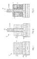
- FIG. 1depicts a cross-sectional view of a semiconductor structure formed with a stack of alternating materials onto the substrate according to embodiments of the present invention
- FIG. 2depicts a cross-sectional view of the semiconductor structure after forming a dummy gate and spacers according to one or more embodiments of the present invention
- FIG. 3depicts a cross-sectional view of the structure after forming source, drain, and channel regions on the substrate according to one or more embodiments of the present invention
- FIG. 4depicts a cross-sectional view of the structure after depositing an inter-layer dielectric (ILD) onto the substrate and removing the dummy gate according to one or more embodiments of the present invention
- ILDinter-layer dielectric
- FIG. 5depicts a cross-sectional view of the structure after removing selected SiGe layers of the structure, according to one or more embodiments of the present invention
- FIG. 6depicts a cross-sectional view of the structure after forming a mask and doping the nanosheets in the diode region according to one or more embodiments of the present invention
- FIG. 7depicts a cross-sectional view of the structure after epitaxially growing materials around the nanosheets to form PN diode junctions according to one or more embodiments of the present invention
- FIG. 8depicts a cross-sectional view of the structure after stripping the mask and forming a gate and channel according to one or more embodiments of the present invention.
- FIG. 9depicts a cross-sectional view of the structure after depositing a contact layer on the substrate according to one or more embodiments of the present invention.
- references in the present description to forming layer “A” over layer “B”include situations in which one or more intermediate layers (e.g., layer “C”) is between layer “A” and layer “B” as long as the relevant characteristics and functionalities of layer “A” and layer “B” are not substantially changed by the intermediate layer(s).
- layer “C”one or more intermediate layers
- compositionscomprising, “comprising,” “includes,” “including,” “has,” “having,” “contains,” or “containing,” or any other variation thereof, are intended to cover a non-exclusive inclusion.
- a composition, a mixture, process, method, article, or apparatus that comprises a list of elementsis not necessarily limited to only those elements but can include other elements not expressly listed or inherent to such composition, mixture, process, method, article, or apparatus.
- connectioncan include an indirect “connection” and a direct “connection”.
- references in the specification to “one embodiment,” “an embodiment,” “an example embodiment,” etc.,indicate that the embodiment described can include a particular feature, structure, or characteristic, but every embodiment can include the particular feature, structure, or characteristic. Moreover, such phrases are not necessarily referring to the same embodiment. Further, when a particular feature, structure, or characteristic is described in connection with an embodiment, it is submitted that it is within the knowledge of one skilled in the art to affect such feature, structure, or characteristic in connection with other embodiments whether or not explicitly described.
- the terms “upper,” “lower,” “right,” “left,” “vertical,” “horizontal,” “top,” “bottom,” and derivatives thereofshall relate to the described structures and methods, as oriented in the drawing figures.
- the terms “overlying,” “atop,” “on top,” “positioned on,” or “positioned atop”mean that a first element, such as a first structure, is present on a second element, such as a second structure, where intervening elements such as an interface structure can be present between the first element and the second element.
- the term “direct contact”means that a first element, such as a first structure, and a second element, such as a second structure, are connected without any intermediary conducting, insulating or semiconductor layers at the interface of the two elements.
- the term “selective to,” such as, for example, “a first element selective to a second element,”means that the first element can be etched and the second element can act as an etch stop.
- Depositionis any process that grows, coats, or otherwise transfers a material onto the wafer.
- Available technologiesinclude physical vapor deposition (PVD), chemical vapor deposition (CVD), electrochemical deposition (ECD), molecular beam epitaxy (MBE) and more recently, atomic layer deposition (ALD) among others.
- Removal/etchingis any process that removes material from the wafer. Examples include etch processes (either wet or dry), and chemical-mechanical planarization (CMP), and the like.
- Semiconductor dopingis the modification of electrical properties by doping, for example, transistor sources and drains, generally by diffusion and/or by ion implantation. These doping processes are followed by furnace annealing or by rapid thermal annealing (RTA). Annealing serves to activate the implanted dopants. Films of both conductors (e.g., poly-silicon, aluminum, copper, etc.) and insulators (e.g., various forms of silicon dioxide, silicon nitride, etc.) are used to connect and isolate transistors and their components. Selective doping of various regions of the semiconductor substrate allows the conductivity of the substrate to be changed with the application of voltage.
- RTArapid thermal annealing
- Semiconductor lithographyis the formation of three-dimensional relief images or patterns on the semiconductor substrate for subsequent transfer of the pattern to the substrate.
- the patternsare formed by a light sensitive polymer called a photo-resist.
- lithography and etch pattern transfer stepsare repeated multiple times. Each pattern being printed on the wafer is aligned to the previously formed patterns and slowly the conductors, insulators and selectively doped regions are built up to form the final device.
- the MOSFETmetal-oxide-semiconductor field effect transistor
- the MOSFEThas source, drain, and metal oxide gate junctions or electrodes.
- the metal gateis electrically insulated from the main semiconductor n-channel or p-channel by a thin layer of insulating material, for example, silicon dioxide or a high-k gate dielectric, which makes the input resistance of the MOSFET relatively high.
- the gate voltagecontrols whether the path from the drain to the source is an open circuit (“off”) or a resistive path (“on”).
- NFETn-type field effect transistors
- PFETp-type field effect transistors
- CMOScomplementary metal-oxide-semiconductor
- the NFETuses electrons as the current carriers and with n-type doped source and drain junctions.
- the PFETuses holes as the current carriers and with p-type doped source and drain junctions.
- a gate-all-around (GAA) nanosheet transistora specific form of a MOSFET device, is a three-dimensional transistor with a gate formed around all four sides of alternating layers of nanosheets, as well as the surface perpendicular to all four sides.
- a replacement-gate GAA nanosheet transistorgenerally involves the formation of a dummy gate used for source and drain formation, followed by removal of the dummy gate, and replacement with a gate dielectric and gate conductor.
- Semiconductor materialscan be doped with either n-type dopants or p-type dopants.
- the described methodsemploy the simultaneous fabrication of both FET and diode devices with nanosheet layers.
- Some embodimentsprovide methods of fabricating semiconductor devices, including nanosheet-based devices, FET transistors, and diodes.
- one or more embodiments of the present inventioncan apply to nanowire-based structures.
- NFET device junctions, including the source and drainare doped with n-type dopants and for PFET devices, the source and drain are doped with p-type dopants.
- Embodiments of the described methodsemploy a nanosheet-based PN diode that is integrated with nanosheet CMOS devices, including FET transistors, beyond the 7 nm range.
- the diodeincludes doped P and N junctions, including multiple layers in a nanosheet configuration.
- the FET transistoris formed using the same process flow, including identical epitaxy, as employed to form the diode device.
- the PN diode junction regionneed not be the same width as the FET gate region.
- diodes formed using this processcan possess a greater PN diode junction area than a planar diode.
- FIG. 1depicts a cross-sectional view of a semiconductor structure 100 formed with a stack of alternating materials onto the substrate according to one or more embodiments of the present invention.
- Structure 100includes a semiconductor substrate 102 , a buried oxide (BOX) layer 104 , and a first material 106 and a second material 108 , formed in alternating layers, to make up a stack 116 .
- the second material 108is also known as a nanosheet.
- the substrate 102 and BOX layer 104form a semiconductor-on-insulator (SOI) structure.
- SOIsemiconductor-on-insulator
- the substrate 102is a bulk substrate.
- the first material 106 of the stack 116can include silicon germanium (SiGe), while the second material 108 can include silicon (Si).
- the alternating layers of the stack 116are nanosheets formed from the first and second materials 106 , 108 respectfully.
- the stack 116can be formed by wafer bonding and/or epitaxy.
- the semiconductor substrate 102can also include an organic semiconductor or a layered semiconductor such as, for example, Si/SiGe, a silicon-on-insulator, or a SiGe-on-insulator. A portion or the entire semiconductor substrate 102 can be amorphous, polycrystalline, or monocrystalline.
- the semiconductor substrate 102 employed in embodiments of the present inventioncan also include a hybrid oriented (HOT) semiconductor substrate 102 in which the HOT substrate has surface regions of different crystallographic orientations.
- the semiconductor substrate 102can be doped or undoped, or contain doped regions and undoped regions therein.
- the semiconductor substrate 102can contain regions with strain and regions without strain therein, or contain regions of tensile strain and compressive strain.
- FIG. 2depicts a cross-sectional view of the semiconductor structure 100 after forming a dummy gate and spacers according to one or more embodiments of the present invention.
- FIG. 2is a continuation of FIG. 1 and depicts forming a dummy gate 110 surrounded by a spacer 112 .
- the spacer 112extends downward to the BOX layer 104 .
- the dummy gate 110can include a dummy gate dielectric (e.g., silicon oxide), amorphous dummy gate, and a gate cap on top of the amorphous silicon.
- the spacer 112can include single or multiple dielectric materials, including but not limited to silicon oxide, silicon oxynitride, silicon nitride, SiBCN, SiOCN, SiOC, and SiCN.
- FIG. 3depicts a cross-sectional view of the structure 100 after forming source, drain, and channel regions on the substrate according to one or more embodiments of the present invention.
- FIG. 3is a continuation of FIG. 2 and depicts the structure 100 after an epitaxial process is applied to portions of the stack 116 (of FIG. 1 ) to define source and drain regions 114 .
- the source and drain regions 114are formed from the stack areas not under the dummy gate 110 .
- the structure 100also includes a channel region 118 , formed between the source and drain regions 114 and within the spacers 112 .
- the channel 118includes alternating layers of the first material 106 and the second material 108 as described in FIG. 1 .
- the alternating layers that are not covered by the dummy gate and spacersare recessed before epitaxially growing the source/drain 114 .
- the SiGe layersare laterally etched and replaced with a dielectric (except SiGe) under the dummy gate 110 .
- the alternating layers of a first and second material 106 , 108 , respectfully of FIG. 1are preserved and epitaxial source/drain regions 114 are grown around the alternating layers in the source/drain regions. The source/drain regions 114 are then doped.
- Dopantscan be incorporated during epitaxy (e.g., by in-situ epitaxy) or by any other suitable doping techniques, including but not limited to, ion implantation, gas phase doping, plasma doping, plasma immersion ion implantation, cluster doping, infusion doping, liquid phase doping, solid phase doping, etc.
- the epitaxy source/draincan be silicon, silicon germanium, germanium, carbon doped silicon, carbon doped silicon germanium, or any other suitable semiconductor material.
- FIG. 4depicts a cross-sectional view of the structure 200 after depositing an inter-layer dielectric (ILD) onto the substrate and removing the dummy gate according to one or more embodiments of the present invention.
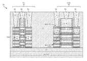
- FIG. 4is a continuation of FIG. 3 and depicts the structure 200 at a wider scale than the previous figures and depicts two structures that were formed simultaneously.
- Embodiments of the present inventioninclude a FET region 130 and a diode region 140 , and the regions need not be identical in width.
- the alternating Si/SiGe layers in the FET region 130are the same alternating Si/SiGe layers in the diode region 140 .
- an ILD layer 132is deposited over the structure 200 , covering both regions 130 and 140 .
- the ILD layer 132can include single or multiple dielectric materials, including but not limited to, silicon oxide, silicon oxynitride, silicon nitride, SiBCN, SiOCN, SiOC, and SiCN. Then, an etching process removes the dummy gate 110 (of FIG. 3 ) from both regions 130 , 140 . Now looking at the diode region 140 , the region includes spacer 112 , source and drain regions 114 , and alternating layers of a first material 106 and a second material 108 .
- the first material 106can include silicon germanium (SiGe), while the second material 108 can include silicon (Si).
- the diode region 140is electrically and physically isolated from the FET region 130 by the ILD layer 132 .
- isolation between regions 130 and 140can be used to further isolate the FET from the diode.
- the ILD material 132is used to electrically separate closely-spaced interconnect lines arranged in several levels (multilevel metallization) in an advanced integrated circuit. It is noteworthy that both regions 130 , 140 are formed at the same time and employing the same processes and do not require specialized steps to produce the different regions.
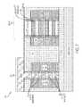
- FIG. 5depicts a cross-sectional view of the structure 200 after removing selected SiGe layers of the structure according to one or more embodiments of the present invention.
- FIG. 5is a continuation of FIG. 4 and includes removing selective layers of the first material (SiGe) 106 (of FIG. 4 ) from the stack 116 to create gaps 302 in the FET and diode regions 130 , 140 respectfully.
- Two methods to remove layers of the first material 106include gas phase hydrofluoric acid (HCl) and a wet etch process with an etchant containing ammonia and hydrogen peroxide.
- the second material 108Left behind during the etching process is the second material 108 (of FIG. 4 ), also referred to as nanosheet 354 . This process removes the first material 106 (of FIG. 4 ) while retaining the source and drain regions 114 (of FIG. 4 ) and the layers of the nanosheet 354 in both the FET and diode regions 130 , 140 .
- FIG. 6depicts a cross-sectional view of the structure 200 after forming a mask and doping the nanosheets 354 (of FIG. 5 ) in the diode region 140 according to one or more embodiments of the present invention.
- FIG. 6is a continuation of FIG. 5 and includes depositing and patterning a mask 352 over predetermined areas of the substrate, to include the FET region 130 but excluding the diode region 140 .
- the mask 352can include, but is not limited to, an amorphous carbon.
- the mask 352is also formed in the gaps 302 (of FIG. 5 ) found in the FET region 130 to form layers of the mask 352 inside the stack 116 (of FIG.
- a doping processis carried out where the nanosheets 354 in diode region 140 are doped with a dopant that has the same doping polarity as the source/drain 114 .
- the nanosheets 354are doped with n-type dopants.
- the nanosheets 354are doped with p-type dopants.
- Doping techniquesinclude, but are not limited to, ion implantation, gas phase doping, plasma doping, plasma immersion ion implantation, cluster doping, infusion doping, liquid phase doping, solid phase doping, etc.
- a thermal anneal processsuch as laser anneal, flash anneal, rapid thermal anneal (RTA), furnace anneal, or any suitable combination of those annealing techniques can be performed.
- FIG. 7is a continuation of FIG. 6 and depicts a cross-sectional view of the structure 200 after epitaxially depositing a material that has dopants with a doping polarity opposite to the doping polarity of the nanosheet and the source/drain to form PN diode junctions.
- a material that has dopants with a doping polarity opposite to the doping polarity of the nanosheet and the source/drain to form PN diode junctionsFor example, if the nanosheets 354 and source/drain 114 (of FIG. 4 ) have n-type dopants, epitaxial material 402 has p-type dopants. Conversely, if the nanosheet 354 and the source/drain 114 (of FIG. 4 ) contain p-type dopants, the epitaxial material 402 has n-type dopants.
- Doping concentrationscan be tuned to meet the diode fabrication and design requirements.
- Non-limiting doping concentrations in the source/drain 114include, but are not limited to 5E19 cm ⁇ 3 to 2E21 cm ⁇ 3 .
- Non-limiting doping concentrations in the nanosheets 354include, but are not limited to 2E18 cm ⁇ 3 to 2E21 cm ⁇ 3 .
- Non-limiting doping concentrations in the epitaxial material 402include, but are not limited to 2E18 cm ⁇ 3 to 2E21 cm ⁇ 3 .
- the doping concentrationscan be uniform or can possess a suitable gradient.
- the epitaxial material 402can include silicon, silicon germanium, germanium, carbon-doped silicon, carbon-doped silicon germanium, etc.
- the epitaxial material 402 and the nanosheets 354form a PN diode according to one or more embodiments of the present invention.
- the process of applying p-type and then n-type dopants to the nanosheets 354 and the gaps 302 (of FIG. 5 ) respectfullycan be reversed, thus n-type and p-type materials can be formed, with the resultant PN junctions formed as before, but with a reversed polarity as compared to embodiments of the present invention.
- N-type dopantsare selected from the group of phosphorus (P), arsenic (As), and antimony (Sb), and a p-type dopant is selected from the group of boron (B), boron fluoride (BF2), gallium (Ga), indium (In), and thallium (Tl).
- the three process steps of (1) selectively removing SiGe, (2) doping the Si nanosheet 354 , and (3) epitaxially growing material around the nanosheet 354can be performed with separate processes. In some embodiments of the present invention, some processes can be integrated together.
- steps (1) and (2)are performed in the same chamber while step (3) is performed separately. In other embodiments, steps (2) and (3) are combined while step (1) is performed separately.
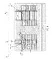
- FIG. 8which is a continuation of FIG. 7 , depicts a cross-sectional view of the structure 200 after stripping the mask 352 (of FIG. 6 ) off of the structure and forming a gate and channel in the FET region according to one or more embodiments of the present invention.
- the FET region 130layers of nanosheets 354 are located underneath the gate 110 .
- the channel region 118includes a metal gate conductor 454 and a high-k gate dielectric 456 , where the high-k gate dielectric 456 surrounds the metal gate conductor 454 and electrically isolates it from the surrounding structure. Due to the multiple layers of nanosheets 354 present, multiple metal gate conductors 454 are present in the structure.
- the high-k gate dielectric 456can include silicon oxide, silicon nitride, silicon oxynitride, boron nitride, high-k materials, or any combination of these materials.
- high-k materialsinclude, but are not limited to, metal oxides such as hafnium oxide, hafnium silicon oxide, hafnium silicon oxynitride, lanthanum oxide, lanthanum aluminum oxide, zirconium oxide, zirconium silicon oxide, zirconium silicon oxynitride, tantalum oxide, titanium oxide, barium strontium titanium oxide, barium titanium oxide, strontium titanium oxide, yttrium oxide, aluminum oxide, lead scandium tantalum oxide, and lead zinc niobate.
- the high-k materialcan further include dopants such as lanthanum and aluminum.
- the gate conductor materialcan include doped polycrystalline or amorphous silicon, germanium, silicon germanium, a metal (e.g., tungsten, titanium, tantalum, ruthenium, zirconium, cobalt, copper, aluminum, lead, platinum, tin, silver, or gold), a conducting metallic compound material (e.g., tantalum nitride, titanium nitride, tantalum carbide, titanium carbide, titanium aluminum carbide, tungsten silicide, tungsten nitride, ruthenium oxide, cobalt silicide, or nickel silicide), carbon nanotube, conductive carbon, graphene, or any suitable combination of these materials.
- a metale.g., tungsten, titanium, tantalum, ruthenium, zirconium, cobalt, copper, aluminum, lead, platinum, tin, silver, or gold
- a conducting metallic compound material
- the conductive materialcan further include dopants that are incorporated during or after deposition.
- the gatecan further include a work function setting layer.
- the work function layercan be a nitride, including but not limited to titanium nitride (TiN), hafnium nitride (HfN), hafnium silicon nitride (HfSiN), tantalum nitride (TaN), tantalum silicon nitride (TaSiN), tungsten nitride (WN), molybdenum nitride (MoN), niobium nitride (NbN); a carbide, including but not limited to titanium carbide (TiC) titanium aluminum carbide (TiAlC), tantalum carbide (TaC), hafnium carbide (HfC), and combinations thereof.
- FIG. 9depicts a cross-sectional view of the structure 200 after depositing a contact layer on the substrate according to one or more embodiments of the present invention.
- Non-limiting methods for forming contactsinclude depositing a dielectric material, patterning to form contact trenches, and filling the trenches with a conducting material.
- FIG. 9depicts forming FET region 130 source/drain contacts 502 and a gate contact 508 .
- the FET source/drain contacts 502extend downward from the surface of the structure 200 to the source and drain regions 114 (of FIG. 4 ).
- the FET gate contact 508extends downward from the surface of the structure 200 to the channel region 118 .
- the resultant structure 200also shows an on-chip diode region 140 with two n-contacts 504 and a single p-contact 506 .
- the n-contacts 504are present in multiple examples due to the aforementioned fabrication techniques, but are electrically identical to each other and either n-contact 504 are used to operate the diode 140 without ill effects.
- the diode 140has multiple PN junctions due to the multiple layers of n-type and p-type materials present due to nanosheets used in the fabrication process. In the present embodiment, four nanosheet layers are interleaved with the p-type epi material and create eight PN junction areas.
- the diode 140includes p-type and n-type layers that creates a PN junction with an area that is 2N times as large as compared to a planar diode device, with N being the number of nanosheets in the structure.
- the increased PN junction area of the diode 140aids in resisting electrostatic discharge events over planar diodes.
- the structure 200includes at least a FET transistor 130 and a nanosheet diode 140 made with nanosheet layers. Both the FET 130 and the diode 140 are formed at the same time and employ the same processes and do not require specialized steps to produce the different regions. Both devices 130 , 140 have identical epitaxy at the ends of the stacked nanosheets and spacers.
- the epitaxyserves as the source and drain of the transistor.
- the epitaxyserves as the contact to the nanosheet which is doped with the same polarity as the epitaxy.
- the nanosheets 354are wrapped around with a second epitaxy that has dopant polarity opposite to the dopant polarity of the nanosheets 354 .
- various functions or actscan take place at a given location and/or in connection with the operation of one or more apparatuses or systems.
- a portion of a given function or actcan be performed at a first device or location, and the remainder of the function or act can be performed at one or more additional devices or locations.
Landscapes
- Chemical & Material Sciences (AREA)
- Crystallography & Structural Chemistry (AREA)
- Metal-Oxide And Bipolar Metal-Oxide Semiconductor Integrated Circuits (AREA)
- Thin Film Transistor (AREA)
Abstract
Description
The present invention generally relates to complementary metal-oxide-semiconductor (CMOS) fabrication methods and related structures. More specifically, the present invention relates to methods and device architectures for fabricating diodes and transistors that can be integrated with nanosheet CMOS structures, thus allowing the formation of on-chip diodes with increased junction areas at the same time as forming nanosheet transistors.
In contemporary semiconductor device fabrication processes, a large number of devices, including field effect transistors (FETs), are fabricated on a single wafer. In addition to these devices, there is a need for other structures, such as diodes, that are formed from PN junctions. Being fabricated from similar materials, it is advantageous to be able to form both FETs and diodes onto a substrate by applying the same processes onto the same structure and on the same layer, including nanosheet layers. In nanosheet-based transistors (or nanowire-based transistors), in contrast to conventional FETs, the gate stack wraps around the full perimeter of each nanosheet (or nanowire), enabling fuller depletion in the channel region, and reducing short-channel effects due to steeper sub-threshold swing (SS) and smaller drain-induced barrier lowering (DIBL). Diodes fabricated from nanosheet structures also increase the PN junction area per footprint.
Embodiments are directed to a method for forming a semiconductor structure, the method including forming a stack of alternating layers of first and second materials over a substrate, where a FET region and a diode region with a source, drain, and channel region are defined. The method further includes depositing a mask over the structure, with the mask covering the FET region while leaving the diode region uncovered, and doping the second material in the diode region with a first dopant. The method further includes implanting epitaxial material with a second dopant to form PN junctions in the diode region. Next, the method includes forming a high-k/metal gate conductor over the FET region. The method further includes forming a metalizing contact material over the substrate to create terminals for both the FET and diode regions.
Embodiments are also directed to a semiconductor device with a substrate and a stack of alternating layers of a first and second material over the device. The device further includes a FET and diode region, gate, source, and drain regions, and a channel region. The device includes a spacer that isolates the gate from the source and drain regions, a doped second material in the diode region, epitaxial material with a second dopant that forms a PN junction in the diode region, a high-k/metal gate conductor over the FET region, and a metalizing contact material that are formed into terminals.
The subject matter of embodiments of the present invention are particularly pointed out and distinctly defined in the claims at the conclusion of the specification. The foregoing and other features and advantages are apparent from the following detailed description taken in conjunction with the accompanying drawings in which:
Various embodiments of the present invention are described herein with reference to the related drawings. Alternative embodiments can be devised without departing from the scope of this invention. It is noted that various connections and positional relationships (e.g., over, below, adjacent, etc.) are set forth between elements in the following description and in the drawings. These connections and/or positional relationships, unless specified otherwise, can be direct or indirect, and embodiments of the present invention are not intended to be limiting in this respect. Accordingly, a coupling of entities can refer to either a direct or an indirect coupling, and a positional relationship between entities can be a direct or indirect positional relationship. As an example of an indirect positional relationship, references in the present description to forming layer “A” over layer “B” include situations in which one or more intermediate layers (e.g., layer “C”) is between layer “A” and layer “B” as long as the relevant characteristics and functionalities of layer “A” and layer “B” are not substantially changed by the intermediate layer(s).
The following definitions and abbreviations are to be used for the interpretation of the claims and the specification. As used herein, the terms “comprises,” “comprising,” “includes,” “including,” “has,” “having,” “contains,” or “containing,” or any other variation thereof, are intended to cover a non-exclusive inclusion. For example, a composition, a mixture, process, method, article, or apparatus that comprises a list of elements is not necessarily limited to only those elements but can include other elements not expressly listed or inherent to such composition, mixture, process, method, article, or apparatus.
Additionally, the term “exemplary” is used herein to mean “serving as an example, instance, or illustration.” Any embodiment or design described herein as “exemplary” is not necessarily to be construed as preferred or advantageous over other embodiments or designs. The terms “one or more” and “one or more” are understood to include any integer number greater than or equal to one, i.e. one, two, three, four, etc. The terms “a plurality” are understood to include any integer number greater than or equal to two, i.e. two, three, four, five, etc. The term “connection” can include an indirect “connection” and a direct “connection”.
References in the specification to “one embodiment,” “an embodiment,” “an example embodiment,” etc., indicate that the embodiment described can include a particular feature, structure, or characteristic, but every embodiment can include the particular feature, structure, or characteristic. Moreover, such phrases are not necessarily referring to the same embodiment. Further, when a particular feature, structure, or characteristic is described in connection with an embodiment, it is submitted that it is within the knowledge of one skilled in the art to affect such feature, structure, or characteristic in connection with other embodiments whether or not explicitly described.
For purposes of the description hereinafter, the terms “upper,” “lower,” “right,” “left,” “vertical,” “horizontal,” “top,” “bottom,” and derivatives thereof shall relate to the described structures and methods, as oriented in the drawing figures. The terms “overlying,” “atop,” “on top,” “positioned on,” or “positioned atop” mean that a first element, such as a first structure, is present on a second element, such as a second structure, where intervening elements such as an interface structure can be present between the first element and the second element. The term “direct contact” means that a first element, such as a first structure, and a second element, such as a second structure, are connected without any intermediary conducting, insulating or semiconductor layers at the interface of the two elements. It should be noted that the term “selective to,” such as, for example, “a first element selective to a second element,” means that the first element can be etched and the second element can act as an etch stop.
For the sake of brevity, conventional techniques related to semiconductor device and integrated circuit (IC) fabrication can be described in detail herein. Moreover, the various tasks and process steps described herein can be incorporated into a more comprehensive procedure or process having additional steps or functionality not described in detail herein. In particular, various steps in the manufacture of semiconductor devices and semiconductor-based ICs are well known and so, in the interest of brevity, many conventional steps will only be mentioned briefly herein or will be omitted entirely without providing the well-known process details.
By way of background, however, a more general description of the semiconductor device fabrication processes that can be utilized in implementing one or more embodiments of the present invention will now be provided. Although specific fabrication operations used in implementing one or more embodiments of the present invention can be individually known, the described combination of operations and/or resulting structures of the present invention are unique. Thus, the unique combination of the operations described in connection with the present invention utilize a variety of individually known physical and chemical processes performed on a semiconductor (e.g., silicon) substrate, some of which are described in the immediately following paragraphs.
In general, the various processes used to form a micro-chip that will be packaged into an IC fall into four general categories, namely, film deposition, removal/etching, semiconductor doping, and patterning/lithography. Deposition is any process that grows, coats, or otherwise transfers a material onto the wafer. Available technologies include physical vapor deposition (PVD), chemical vapor deposition (CVD), electrochemical deposition (ECD), molecular beam epitaxy (MBE) and more recently, atomic layer deposition (ALD) among others. Removal/etching is any process that removes material from the wafer. Examples include etch processes (either wet or dry), and chemical-mechanical planarization (CMP), and the like. Semiconductor doping is the modification of electrical properties by doping, for example, transistor sources and drains, generally by diffusion and/or by ion implantation. These doping processes are followed by furnace annealing or by rapid thermal annealing (RTA). Annealing serves to activate the implanted dopants. Films of both conductors (e.g., poly-silicon, aluminum, copper, etc.) and insulators (e.g., various forms of silicon dioxide, silicon nitride, etc.) are used to connect and isolate transistors and their components. Selective doping of various regions of the semiconductor substrate allows the conductivity of the substrate to be changed with the application of voltage. By creating structures of these various components, millions of transistors can be built and wired together to form the complex circuitry of a modern microelectronic device. Semiconductor lithography is the formation of three-dimensional relief images or patterns on the semiconductor substrate for subsequent transfer of the pattern to the substrate. In semiconductor lithography, the patterns are formed by a light sensitive polymer called a photo-resist. To build the complex structures that make up a transistor and the many wires that connect the millions of transistors of a circuit, lithography and etch pattern transfer steps are repeated multiple times. Each pattern being printed on the wafer is aligned to the previously formed patterns and slowly the conductors, insulators and selectively doped regions are built up to form the final device.
The MOSFET (metal-oxide-semiconductor field effect transistor) is a transistor used for amplifying or switching electronic signals. The MOSFET has source, drain, and metal oxide gate junctions or electrodes. The metal gate is electrically insulated from the main semiconductor n-channel or p-channel by a thin layer of insulating material, for example, silicon dioxide or a high-k gate dielectric, which makes the input resistance of the MOSFET relatively high. The gate voltage controls whether the path from the drain to the source is an open circuit (“off”) or a resistive path (“on”). n-type field effect transistors (NFET) and p-type field effect transistors (PFET) are two types of CMOS (complementary metal-oxide-semiconductor) devices. The NFET uses electrons as the current carriers and with n-type doped source and drain junctions. The PFET uses holes as the current carriers and with p-type doped source and drain junctions. A gate-all-around (GAA) nanosheet transistor, a specific form of a MOSFET device, is a three-dimensional transistor with a gate formed around all four sides of alternating layers of nanosheets, as well as the surface perpendicular to all four sides. The formation of a replacement-gate GAA nanosheet transistor generally involves the formation of a dummy gate used for source and drain formation, followed by removal of the dummy gate, and replacement with a gate dielectric and gate conductor. Semiconductor materials can be doped with either n-type dopants or p-type dopants.
Turning now to an overview of aspects of the present invention, the described methods employ the simultaneous fabrication of both FET and diode devices with nanosheet layers. Some embodiments provide methods of fabricating semiconductor devices, including nanosheet-based devices, FET transistors, and diodes. In addition, one or more embodiments of the present invention can apply to nanowire-based structures. NFET device junctions, including the source and drain, are doped with n-type dopants and for PFET devices, the source and drain are doped with p-type dopants. Embodiments of the described methods employ a nanosheet-based PN diode that is integrated with nanosheet CMOS devices, including FET transistors, beyond the 7 nm range. The diode includes doped P and N junctions, including multiple layers in a nanosheet configuration. The FET transistor is formed using the same process flow, including identical epitaxy, as employed to form the diode device. The PN diode junction region need not be the same width as the FET gate region. In addition, diodes formed using this process can possess a greater PN diode junction area than a planar diode. The fabrication methodologies and resulting structures according to embodiments of the present invention are described in detail below by referring to the accompanying drawings inFIGS. 1-9 .
Turning now to a more detailed description of embodiments of the present invention,FIG. 1 depicts a cross-sectional view of asemiconductor structure 100 formed with a stack of alternating materials onto the substrate according to one or more embodiments of the present invention.Structure 100 includes asemiconductor substrate 102, a buried oxide (BOX)layer 104, and afirst material 106 and asecond material 108, formed in alternating layers, to make up astack 116. Thesecond material 108 is also known as a nanosheet. Thesubstrate 102 andBOX layer 104 form a semiconductor-on-insulator (SOI) structure. Alternatively, thesubstrate 102 is a bulk substrate. Thefirst material 106 of thestack 116 can include silicon germanium (SiGe), while thesecond material 108 can include silicon (Si). The alternating layers of thestack 116 are nanosheets formed from the first andsecond materials stack 116 can be formed by wafer bonding and/or epitaxy.Structure 100 can include silicon, germanium, silicon germanium, silicon carbide, or III-V compound semiconductors having a composition defined by the formula AlX1GaX2InX3AsY1PY2NY3SbY4, where X1, X2, X3, Y1, Y2, Y3, and Y4 represent relative proportions, each greater than or equal to zero and X1+X2+X3+Y1+Y2+Y3+Y4=1 (1 being the total relative mole quantity). Other suitable substrates include II-VI compound semiconductors having a composition ZnA1CdA2SeB1TeB2, where A1, A2, B1, and B2 are relative proportions, each greater than or equal to zero, and A1+A2+B1+B2=1 (1 being a total mole quantity). Thesemiconductor substrate 102 can also include an organic semiconductor or a layered semiconductor such as, for example, Si/SiGe, a silicon-on-insulator, or a SiGe-on-insulator. A portion or theentire semiconductor substrate 102 can be amorphous, polycrystalline, or monocrystalline. In addition to the aforementioned types of semiconductor substrates, thesemiconductor substrate 102 employed in embodiments of the present invention can also include a hybrid oriented (HOT)semiconductor substrate 102 in which the HOT substrate has surface regions of different crystallographic orientations. Thesemiconductor substrate 102 can be doped or undoped, or contain doped regions and undoped regions therein. Thesemiconductor substrate 102 can contain regions with strain and regions without strain therein, or contain regions of tensile strain and compressive strain.
Continuing with the process of forming a semiconductor structure,FIG. 6 depicts a cross-sectional view of thestructure 200 after forming a mask and doping the nanosheets354 (ofFIG. 5 ) in thediode region 140 according to one or more embodiments of the present invention.FIG. 6 is a continuation ofFIG. 5 and includes depositing and patterning amask 352 over predetermined areas of the substrate, to include theFET region 130 but excluding thediode region 140. Themask 352 can include, but is not limited to, an amorphous carbon. Themask 352 is also formed in the gaps302 (ofFIG. 5 ) found in theFET region 130 to form layers of themask 352 inside the stack116 (ofFIG. 5 ) in theFET region 130. Then, a doping process is carried out where thenanosheets 354 indiode region 140 are doped with a dopant that has the same doping polarity as the source/drain 114. For example, if the source/drain 114 has n-type dopants, thenanosheets 354 are doped with n-type dopants. If the source/drain 114 has p-type dopants, thenanosheets 354 are doped with p-type dopants. Doping techniques include, but are not limited to, ion implantation, gas phase doping, plasma doping, plasma immersion ion implantation, cluster doping, infusion doping, liquid phase doping, solid phase doping, etc. A thermal anneal process such as laser anneal, flash anneal, rapid thermal anneal (RTA), furnace anneal, or any suitable combination of those annealing techniques can be performed.
In some embodiments, various functions or acts can take place at a given location and/or in connection with the operation of one or more apparatuses or systems. In some embodiments, a portion of a given function or act can be performed at a first device or location, and the remainder of the function or act can be performed at one or more additional devices or locations.
The corresponding structures, materials, acts, and equivalents of all means or step plus function elements in the claims below are intended to include any structure, material, or act for performing the function in combination with other claimed elements as specifically claimed. Embodiment of the present invention have been presented for purposes of illustration and description, but is not intended to be exhaustive or limited to the form described. Many modifications and variations will be apparent to those of ordinary skill in the art without departing from the scope and spirit of the invention. The embodiments were chosen and described in order to best explain the principles of the invention and the practical application, and to enable others of ordinary skill in the art to understand the invention for various embodiments with various modifications as are suited to the particular use contemplated.
The flowchart and block diagrams in the figures illustrate the functionality and operation of possible implementations of systems and methods according to various embodiments of the present invention. In some alternative implementations, the functions noted in the block can occur out of the order noted in the figures. For example, two blocks shown in succession can, in fact, be executed substantially concurrently, or the blocks can sometimes be executed in the reverse order, depending upon the functionality involved. The actions can be performed in a differing order or actions can be added, deleted or modified. Also, the term “coupled” describes having a signal path between two elements and does not imply a direct connection between the elements with no intervening elements/connections therebetween. All of these variations are considered a part of the invention.
The terms “about,” “substantially,” “approximately,” and variations thereof, are intended to include the degree of error associated with measurement of the particular quantity based upon the equipment available at the time of filing the application. For example, “about” can include a range of ±8% or 5%, or 2% of a given value.
The terminology used herein is for describing particular embodiments only and is not intended to be limiting of embodiments of the present invention. As used herein, the singular forms “a”, “an” and “the” are intended to include the plural forms as well, unless the context clearly indicates otherwise. It will be further understood that the terms “comprises” and/or “comprising,” when used in this specification, specify the presence of stated features, integers, steps, operations, elements, and/or components, but do not preclude the presence or addition of one or more other features, integers, steps, operations, element components, and/or groups thereof.
While embodiments of the present invention have been described in detail in connection with only a limited number of embodiments, it should be readily understood that embodiments of the present invention are not limited to such described embodiments. Rather, embodiments of the present invention can be modified to incorporate any number of variations, alterations, substitutions or equivalent arrangements not heretofore described, but which are commensurate with the spirit and scope of the present invention. Additionally, while various embodiments of the present invention have been described, it is to be understood that aspects of the present invention can include only some of the described embodiments. Accordingly, the present invention is not to be seen as limited by the foregoing description, but is only limited by the scope of the appended claims.
Claims (9)
1. A method for forming a semiconductor structure, the method comprising:
providing a substrate having a field-effect transistor region and a diode region;
forming a first stack of layers of a first material alternating with layers of a second material at the field-effect transistor region;
forming a second stack of the layers of the first material alternating with the layers of the second material at the diode region;
epitaxially growing a third material having a first dopant at opposing sidewalls of the second stack;
removing the first material;
depositing a mask over the first stack, wherein the mask covers the field-effect transistor region while leaving the diode region uncovered;
doping the second material at the diode region with a second dopant,
wherein a conductivity type of the second material having the second dopant is the same as a conductivity type of the third material having the first dopant;
epitaxially growing a fourth material with a third dopant, wherein the fourth material wraps around each of the layers of the second material at the diode region to make a third stack comprising the layers of the second material alternating with layers of the fourth material, wherein a conductivity type of the fourth material having the third dopant is opposite to the conductivity type of the second material having the second dopant and the conductivity type of the third material having the first dopant; and
depositing a metalizing contact material over the substrate, wherein both the field-effect transistor region and the diode region include terminals.
2. The method ofclaim 1 , further comprising forming a dielectric layer over the substrate and patterning the dielectric layer to form trenches, wherein depositing the metalizing contact material includes filling the trenches with the metalizing contact material.
3. The method ofclaim 1 , wherein each of the layers of the first material and each of the layers of the second material comprises nanosheets.
4. The method ofclaim 1 , wherein each of the layers of the first material and each of the layers of the second material comprises nanowires.
5. The method ofclaim 1 , wherein the first material comprises silicon germanium (SiGe) and the second material comprises silicon (Si).
6. The method ofclaim 1 , wherein the substrate comprises a semiconductor-on-insulator (SOI) substrate.
7. The method ofclaim 1 , wherein the first stack at said field-effect transistor region and the second stack at said diode region are formed simultaneously.
8. The method ofclaim 1 , wherein the conductivity type of the fourth material having the third dopant comprises p-type and wherein each of the conductivity type of the second material having the second dopant and the conductivity type of the third material having the first dopant comprises n-type.
9. The method ofclaim 1 , wherein doping the second material at the diode region includes one or more of gas phase doping, plasma doping, plasma immersion ion implantation, cluster doping, infusion doping, liquid phase doping, and solid phase doping.
Priority Applications (2)
| Application Number | Priority Date | Filing Date | Title |
|---|---|---|---|
| US15/289,390US9842835B1 (en) | 2016-10-10 | 2016-10-10 | High density nanosheet diodes |
| US15/805,670US10504890B2 (en) | 2016-10-10 | 2017-11-07 | High density nanosheet diodes |
Applications Claiming Priority (1)
| Application Number | Priority Date | Filing Date | Title |
|---|---|---|---|
| US15/289,390US9842835B1 (en) | 2016-10-10 | 2016-10-10 | High density nanosheet diodes |
Related Child Applications (1)
| Application Number | Title | Priority Date | Filing Date |
|---|---|---|---|
| US15/805,670DivisionUS10504890B2 (en) | 2016-10-10 | 2017-11-07 | High density nanosheet diodes |
Publications (1)
| Publication Number | Publication Date |
|---|---|
| US9842835B1true US9842835B1 (en) | 2017-12-12 |
Family
ID=60516382
Family Applications (2)
| Application Number | Title | Priority Date | Filing Date |
|---|---|---|---|
| US15/289,390ActiveUS9842835B1 (en) | 2016-10-10 | 2016-10-10 | High density nanosheet diodes |
| US15/805,670ActiveUS10504890B2 (en) | 2016-10-10 | 2017-11-07 | High density nanosheet diodes |
Family Applications After (1)
| Application Number | Title | Priority Date | Filing Date |
|---|---|---|---|
| US15/805,670ActiveUS10504890B2 (en) | 2016-10-10 | 2017-11-07 | High density nanosheet diodes |
Country Status (1)
| Country | Link |
|---|---|
| US (2) | US9842835B1 (en) |
Cited By (245)
| Publication number | Priority date | Publication date | Assignee | Title |
|---|---|---|---|---|
| US20170271514A1 (en)* | 2016-03-21 | 2017-09-21 | Samsung Electronics Co., Ltd. | Nanosheet and nanowire devices having source/drain stressors and methods of manufacturing the same |
| US20180175036A1 (en)* | 2015-11-16 | 2018-06-21 | Taiwan Semiconductor Manufacturing Company, Ltd. | Multi-Gate Device and Method of Fabrication Thereof |
| US10043748B1 (en)* | 2017-02-02 | 2018-08-07 | International Business Machines Corporation | Vertically integrated nanosheet fuse |
| US20180331179A1 (en)* | 2017-02-13 | 2018-11-15 | International Business Machines Corporation | Nanosheet transistors on bulk material |
| US10269790B2 (en)* | 2017-03-09 | 2019-04-23 | International Business Machines Corporation | Forming horizontal bipolar junction transistor compatible with nanosheets |
| US10332809B1 (en)* | 2018-06-21 | 2019-06-25 | International Business Machines Corporation | Method and structure to introduce strain in stack nanosheet field effect transistor |
| WO2020049969A1 (en)* | 2018-09-05 | 2020-03-12 | ソニーセミコンダクタソリューションズ株式会社 | Diode |
| US11037926B2 (en)* | 2016-06-21 | 2021-06-15 | Samsung Electronics Co., Ltd. | Semiconductor device |
| US11101374B1 (en) | 2020-06-13 | 2021-08-24 | International Business Machines Corporation | Nanosheet gated diode |
| CN113903810A (en)* | 2020-07-06 | 2022-01-07 | 中芯国际集成电路制造(上海)有限公司 | Semiconductor structure and method of forming the same |
| CN113903788A (en)* | 2021-09-24 | 2022-01-07 | 上海华虹宏力半导体制造有限公司 | Doping methods for three-dimensional semiconductor devices |
| US11274369B2 (en) | 2018-09-11 | 2022-03-15 | Asm Ip Holding B.V. | Thin film deposition method |
| US20220085202A1 (en)* | 2019-05-27 | 2022-03-17 | Samsung Electronics Co., Ltd. | Semiconductor devices and methods of manufacturing the same |
| US11286558B2 (en)* | 2019-08-23 | 2022-03-29 | Asm Ip Holding B.V. | Methods for depositing a molybdenum nitride film on a surface of a substrate by a cyclical deposition process and related semiconductor device structures including a molybdenum nitride film |
| US11296189B2 (en) | 2018-06-21 | 2022-04-05 | Asm Ip Holding B.V. | Method for depositing a phosphorus doped silicon arsenide film and related semiconductor device structures |
| US11295980B2 (en) | 2017-08-30 | 2022-04-05 | Asm Ip Holding B.V. | Methods for depositing a molybdenum metal film over a dielectric surface of a substrate by a cyclical deposition process and related semiconductor device structures |
| USD947913S1 (en) | 2019-05-17 | 2022-04-05 | Asm Ip Holding B.V. | Susceptor shaft |
| US11306395B2 (en) | 2017-06-28 | 2022-04-19 | Asm Ip Holding B.V. | Methods for depositing a transition metal nitride film on a substrate by atomic layer deposition and related deposition apparatus |
| US11315794B2 (en) | 2019-10-21 | 2022-04-26 | Asm Ip Holding B.V. | Apparatus and methods for selectively etching films |
| US11342216B2 (en) | 2019-02-20 | 2022-05-24 | Asm Ip Holding B.V. | Cyclical deposition method and apparatus for filling a recess formed within a substrate surface |
| US11339476B2 (en) | 2019-10-08 | 2022-05-24 | Asm Ip Holding B.V. | Substrate processing device having connection plates, substrate processing method |
| US11345999B2 (en) | 2019-06-06 | 2022-05-31 | Asm Ip Holding B.V. | Method of using a gas-phase reactor system including analyzing exhausted gas |
| US11355338B2 (en) | 2019-05-10 | 2022-06-07 | Asm Ip Holding B.V. | Method of depositing material onto a surface and structure formed according to the method |
| US11361990B2 (en) | 2018-05-28 | 2022-06-14 | Asm Ip Holding B.V. | Substrate processing method and device manufactured by using the same |
| US11368016B2 (en) | 2020-03-18 | 2022-06-21 | Mavagail Technology, LLC | ESD protection for integrated circuit devices |
| US11378337B2 (en) | 2019-03-28 | 2022-07-05 | Asm Ip Holding B.V. | Door opener and substrate processing apparatus provided therewith |
| US11387120B2 (en) | 2017-09-28 | 2022-07-12 | Asm Ip Holding B.V. | Chemical dispensing apparatus and methods for dispensing a chemical to a reaction chamber |
| US11387106B2 (en) | 2018-02-14 | 2022-07-12 | Asm Ip Holding B.V. | Method for depositing a ruthenium-containing film on a substrate by a cyclical deposition process |
| US11390946B2 (en) | 2019-01-17 | 2022-07-19 | Asm Ip Holding B.V. | Methods of forming a transition metal containing film on a substrate by a cyclical deposition process |
| US11390950B2 (en) | 2017-01-10 | 2022-07-19 | Asm Ip Holding B.V. | Reactor system and method to reduce residue buildup during a film deposition process |
| US11393690B2 (en) | 2018-01-19 | 2022-07-19 | Asm Ip Holding B.V. | Deposition method |
| US11390945B2 (en) | 2019-07-03 | 2022-07-19 | Asm Ip Holding B.V. | Temperature control assembly for substrate processing apparatus and method of using same |
| US11398382B2 (en) | 2018-03-27 | 2022-07-26 | Asm Ip Holding B.V. | Method of forming an electrode on a substrate and a semiconductor device structure including an electrode |
| US11396702B2 (en) | 2016-11-15 | 2022-07-26 | Asm Ip Holding B.V. | Gas supply unit and substrate processing apparatus including the gas supply unit |
| US11401605B2 (en) | 2019-11-26 | 2022-08-02 | Asm Ip Holding B.V. | Substrate processing apparatus |
| US11411088B2 (en) | 2018-11-16 | 2022-08-09 | Asm Ip Holding B.V. | Methods for forming a metal silicate film on a substrate in a reaction chamber and related semiconductor device structures |
| US11410851B2 (en) | 2017-02-15 | 2022-08-09 | Asm Ip Holding B.V. | Methods for forming a metallic film on a substrate by cyclical deposition and related semiconductor device structures |
| US11417545B2 (en) | 2017-08-08 | 2022-08-16 | Asm Ip Holding B.V. | Radiation shield |
| US11414760B2 (en) | 2018-10-08 | 2022-08-16 | Asm Ip Holding B.V. | Substrate support unit, thin film deposition apparatus including the same, and substrate processing apparatus including the same |
| US11424119B2 (en) | 2019-03-08 | 2022-08-23 | Asm Ip Holding B.V. | Method for selective deposition of silicon nitride layer and structure including selectively-deposited silicon nitride layer |
| US11430674B2 (en) | 2018-08-22 | 2022-08-30 | Asm Ip Holding B.V. | Sensor array, apparatus for dispensing a vapor phase reactant to a reaction chamber and related methods |
| US11430640B2 (en) | 2019-07-30 | 2022-08-30 | Asm Ip Holding B.V. | Substrate processing apparatus |
| US11437241B2 (en) | 2020-04-08 | 2022-09-06 | Asm Ip Holding B.V. | Apparatus and methods for selectively etching silicon oxide films |
| US11443926B2 (en) | 2019-07-30 | 2022-09-13 | Asm Ip Holding B.V. | Substrate processing apparatus |
| US11450529B2 (en) | 2019-11-26 | 2022-09-20 | Asm Ip Holding B.V. | Methods for selectively forming a target film on a substrate comprising a first dielectric surface and a second metallic surface |
| US11447864B2 (en) | 2019-04-19 | 2022-09-20 | Asm Ip Holding B.V. | Layer forming method and apparatus |
| US11447861B2 (en) | 2016-12-15 | 2022-09-20 | Asm Ip Holding B.V. | Sequential infiltration synthesis apparatus and a method of forming a patterned structure |
| USD965044S1 (en) | 2019-08-19 | 2022-09-27 | Asm Ip Holding B.V. | Susceptor shaft |
| US11453943B2 (en) | 2016-05-25 | 2022-09-27 | Asm Ip Holding B.V. | Method for forming carbon-containing silicon/metal oxide or nitride film by ALD using silicon precursor and hydrocarbon precursor |
| USD965524S1 (en) | 2019-08-19 | 2022-10-04 | Asm Ip Holding B.V. | Susceptor support |
| US11476109B2 (en) | 2019-06-11 | 2022-10-18 | Asm Ip Holding B.V. | Method of forming an electronic structure using reforming gas, system for performing the method, and structure formed using the method |
| US11473195B2 (en) | 2018-03-01 | 2022-10-18 | Asm Ip Holding B.V. | Semiconductor processing apparatus and a method for processing a substrate |
| US11482418B2 (en) | 2018-02-20 | 2022-10-25 | Asm Ip Holding B.V. | Substrate processing method and apparatus |
| US11482533B2 (en) | 2019-02-20 | 2022-10-25 | Asm Ip Holding B.V. | Apparatus and methods for plug fill deposition in 3-D NAND applications |
| US11482412B2 (en) | 2018-01-19 | 2022-10-25 | Asm Ip Holding B.V. | Method for depositing a gap-fill layer by plasma-assisted deposition |
| US11488819B2 (en) | 2018-12-04 | 2022-11-01 | Asm Ip Holding B.V. | Method of cleaning substrate processing apparatus |
| US11488854B2 (en) | 2020-03-11 | 2022-11-01 | Asm Ip Holding B.V. | Substrate handling device with adjustable joints |
| US11492703B2 (en) | 2018-06-27 | 2022-11-08 | Asm Ip Holding B.V. | Cyclic deposition methods for forming metal-containing material and films and structures including the metal-containing material |
| US11495459B2 (en) | 2019-09-04 | 2022-11-08 | Asm Ip Holding B.V. | Methods for selective deposition using a sacrificial capping layer |
| US11499226B2 (en) | 2018-11-02 | 2022-11-15 | Asm Ip Holding B.V. | Substrate supporting unit and a substrate processing device including the same |
| US11501968B2 (en) | 2019-11-15 | 2022-11-15 | Asm Ip Holding B.V. | Method for providing a semiconductor device with silicon filled gaps |
| US11501973B2 (en) | 2018-01-16 | 2022-11-15 | Asm Ip Holding B.V. | Method for depositing a material film on a substrate within a reaction chamber by a cyclical deposition process and related device structures |
| US11499222B2 (en) | 2018-06-27 | 2022-11-15 | Asm Ip Holding B.V. | Cyclic deposition methods for forming metal-containing material and films and structures including the metal-containing material |
| US11515188B2 (en) | 2019-05-16 | 2022-11-29 | Asm Ip Holding B.V. | Wafer boat handling device, vertical batch furnace and method |
| US11515187B2 (en) | 2020-05-01 | 2022-11-29 | Asm Ip Holding B.V. | Fast FOUP swapping with a FOUP handler |
| US11521851B2 (en) | 2020-02-03 | 2022-12-06 | Asm Ip Holding B.V. | Method of forming structures including a vanadium or indium layer |
| US11527403B2 (en) | 2019-12-19 | 2022-12-13 | Asm Ip Holding B.V. | Methods for filling a gap feature on a substrate surface and related semiconductor structures |
| US11530483B2 (en) | 2018-06-21 | 2022-12-20 | Asm Ip Holding B.V. | Substrate processing system |
| US11532757B2 (en) | 2016-10-27 | 2022-12-20 | Asm Ip Holding B.V. | Deposition of charge trapping layers |
| US11530876B2 (en) | 2020-04-24 | 2022-12-20 | Asm Ip Holding B.V. | Vertical batch furnace assembly comprising a cooling gas supply |
| EP4109561A1 (en)* | 2021-06-24 | 2022-12-28 | INTEL Corporation | Substrate-less nanowire-based lateral diode integrated circuit structures |
| US11551925B2 (en) | 2019-04-01 | 2023-01-10 | Asm Ip Holding B.V. | Method for manufacturing a semiconductor device |
| US11551912B2 (en) | 2020-01-20 | 2023-01-10 | Asm Ip Holding B.V. | Method of forming thin film and method of modifying surface of thin film |
| USD975665S1 (en) | 2019-05-17 | 2023-01-17 | Asm Ip Holding B.V. | Susceptor shaft |
| US11557474B2 (en) | 2019-07-29 | 2023-01-17 | Asm Ip Holding B.V. | Methods for selective deposition utilizing n-type dopants and/or alternative dopants to achieve high dopant incorporation |
| US11562901B2 (en) | 2019-09-25 | 2023-01-24 | Asm Ip Holding B.V. | Substrate processing method |
| US11572620B2 (en) | 2018-11-06 | 2023-02-07 | Asm Ip Holding B.V. | Methods for selectively depositing an amorphous silicon film on a substrate |
| US11581186B2 (en) | 2016-12-15 | 2023-02-14 | Asm Ip Holding B.V. | Sequential infiltration synthesis apparatus |
| US11587821B2 (en) | 2017-08-08 | 2023-02-21 | Asm Ip Holding B.V. | Substrate lift mechanism and reactor including same |
| US11587815B2 (en) | 2019-07-31 | 2023-02-21 | Asm Ip Holding B.V. | Vertical batch furnace assembly |
| US11587814B2 (en) | 2019-07-31 | 2023-02-21 | Asm Ip Holding B.V. | Vertical batch furnace assembly |
| USD979506S1 (en) | 2019-08-22 | 2023-02-28 | Asm Ip Holding B.V. | Insulator |
| US11594600B2 (en) | 2019-11-05 | 2023-02-28 | Asm Ip Holding B.V. | Structures with doped semiconductor layers and methods and systems for forming same |
| US11594450B2 (en) | 2019-08-22 | 2023-02-28 | Asm Ip Holding B.V. | Method for forming a structure with a hole |
| US11605528B2 (en) | 2019-07-09 | 2023-03-14 | Asm Ip Holding B.V. | Plasma device using coaxial waveguide, and substrate treatment method |
| USD980813S1 (en) | 2021-05-11 | 2023-03-14 | Asm Ip Holding B.V. | Gas flow control plate for substrate processing apparatus |
| USD980814S1 (en) | 2021-05-11 | 2023-03-14 | Asm Ip Holding B.V. | Gas distributor for substrate processing apparatus |
| US11610775B2 (en) | 2016-07-28 | 2023-03-21 | Asm Ip Holding B.V. | Method and apparatus for filling a gap |
| US11610774B2 (en) | 2019-10-02 | 2023-03-21 | Asm Ip Holding B.V. | Methods for forming a topographically selective silicon oxide film by a cyclical plasma-enhanced deposition process |
| USD981973S1 (en) | 2021-05-11 | 2023-03-28 | Asm Ip Holding B.V. | Reactor wall for substrate processing apparatus |
| US11615970B2 (en) | 2019-07-17 | 2023-03-28 | Asm Ip Holding B.V. | Radical assist ignition plasma system and method |
| US11615980B2 (en) | 2019-02-20 | 2023-03-28 | Asm Ip Holding B.V. | Method and apparatus for filling a recess formed within a substrate surface |
| US11626316B2 (en) | 2019-11-20 | 2023-04-11 | Asm Ip Holding B.V. | Method of depositing carbon-containing material on a surface of a substrate, structure formed using the method, and system for forming the structure |
| US11626308B2 (en) | 2020-05-13 | 2023-04-11 | Asm Ip Holding B.V. | Laser alignment fixture for a reactor system |
| US20230114216A1 (en)* | 2021-10-12 | 2023-04-13 | Taiwan Semiconductor Manufacturing Co., Ltd. | Nanostructure fet and method of forming same |
| US11629407B2 (en) | 2019-02-22 | 2023-04-18 | Asm Ip Holding B.V. | Substrate processing apparatus and method for processing substrates |
| US11637014B2 (en) | 2019-10-17 | 2023-04-25 | Asm Ip Holding B.V. | Methods for selective deposition of doped semiconductor material |
| US11637011B2 (en) | 2019-10-16 | 2023-04-25 | Asm Ip Holding B.V. | Method of topology-selective film formation of silicon oxide |
| US11639548B2 (en) | 2019-08-21 | 2023-05-02 | Asm Ip Holding B.V. | Film-forming material mixed-gas forming device and film forming device |
| US11639811B2 (en) | 2017-11-27 | 2023-05-02 | Asm Ip Holding B.V. | Apparatus including a clean mini environment |
| US11646184B2 (en) | 2019-11-29 | 2023-05-09 | Asm Ip Holding B.V. | Substrate processing apparatus |
| US11646205B2 (en) | 2019-10-29 | 2023-05-09 | Asm Ip Holding B.V. | Methods of selectively forming n-type doped material on a surface, systems for selectively forming n-type doped material, and structures formed using same |
| US11644758B2 (en) | 2020-07-17 | 2023-05-09 | Asm Ip Holding B.V. | Structures and methods for use in photolithography |
| US11643724B2 (en) | 2019-07-18 | 2023-05-09 | Asm Ip Holding B.V. | Method of forming structures using a neutral beam |
| US11646197B2 (en) | 2018-07-03 | 2023-05-09 | Asm Ip Holding B.V. | Method for depositing silicon-free carbon-containing film as gap-fill layer by pulse plasma-assisted deposition |
| US11646204B2 (en) | 2020-06-24 | 2023-05-09 | Asm Ip Holding B.V. | Method for forming a layer provided with silicon |
| US11649546B2 (en) | 2016-07-08 | 2023-05-16 | Asm Ip Holding B.V. | Organic reactants for atomic layer deposition |
| US11658029B2 (en) | 2018-12-14 | 2023-05-23 | Asm Ip Holding B.V. | Method of forming a device structure using selective deposition of gallium nitride and system for same |
| US11658035B2 (en) | 2020-06-30 | 2023-05-23 | Asm Ip Holding B.V. | Substrate processing method |
| US11664245B2 (en) | 2019-07-16 | 2023-05-30 | Asm Ip Holding B.V. | Substrate processing device |
| US11664267B2 (en) | 2019-07-10 | 2023-05-30 | Asm Ip Holding B.V. | Substrate support assembly and substrate processing device including the same |
| US11664199B2 (en) | 2018-10-19 | 2023-05-30 | Asm Ip Holding B.V. | Substrate processing apparatus and substrate processing method |
| US11674220B2 (en) | 2020-07-20 | 2023-06-13 | Asm Ip Holding B.V. | Method for depositing molybdenum layers using an underlayer |
| US11676812B2 (en) | 2016-02-19 | 2023-06-13 | Asm Ip Holding B.V. | Method for forming silicon nitride film selectively on top/bottom portions |
| US11680839B2 (en) | 2019-08-05 | 2023-06-20 | Asm Ip Holding B.V. | Liquid level sensor for a chemical source vessel |
| US11682572B2 (en) | 2017-11-27 | 2023-06-20 | Asm Ip Holdings B.V. | Storage device for storing wafer cassettes for use with a batch furnace |
| US11685991B2 (en) | 2018-02-14 | 2023-06-27 | Asm Ip Holding B.V. | Method for depositing a ruthenium-containing film on a substrate by a cyclical deposition process |
| USD990534S1 (en) | 2020-09-11 | 2023-06-27 | Asm Ip Holding B.V. | Weighted lift pin |
| USD990441S1 (en) | 2021-09-07 | 2023-06-27 | Asm Ip Holding B.V. | Gas flow control plate |
| US11688603B2 (en) | 2019-07-17 | 2023-06-27 | Asm Ip Holding B.V. | Methods of forming silicon germanium structures |
| US11695054B2 (en) | 2017-07-18 | 2023-07-04 | Asm Ip Holding B.V. | Methods for forming a semiconductor device structure and related semiconductor device structures |
| US11694892B2 (en) | 2016-07-28 | 2023-07-04 | Asm Ip Holding B.V. | Method and apparatus for filling a gap |
| US11705333B2 (en) | 2020-05-21 | 2023-07-18 | Asm Ip Holding B.V. | Structures including multiple carbon layers and methods of forming and using same |
| US11718913B2 (en) | 2018-06-04 | 2023-08-08 | Asm Ip Holding B.V. | Gas distribution system and reactor system including same |
| US11725277B2 (en) | 2011-07-20 | 2023-08-15 | Asm Ip Holding B.V. | Pressure transmitter for a semiconductor processing environment |
| US11725280B2 (en) | 2020-08-26 | 2023-08-15 | Asm Ip Holding B.V. | Method for forming metal silicon oxide and metal silicon oxynitride layers |
| US20230260851A1 (en)* | 2022-02-15 | 2023-08-17 | Tokyo Electron Limited | 3d single crystal silicon nano sheets integrated with 2d material channel and s/d diode enhancement |
| US11735422B2 (en) | 2019-10-10 | 2023-08-22 | Asm Ip Holding B.V. | Method of forming a photoresist underlayer and structure including same |
| US11735445B2 (en) | 2018-10-31 | 2023-08-22 | Asm Ip Holding B.V. | Substrate processing apparatus for processing substrates |
| US11735414B2 (en) | 2018-02-06 | 2023-08-22 | Asm Ip Holding B.V. | Method of post-deposition treatment for silicon oxide film |
| US11742189B2 (en) | 2015-03-12 | 2023-08-29 | Asm Ip Holding B.V. | Multi-zone reactor, system including the reactor, and method of using the same |
| US11742198B2 (en) | 2019-03-08 | 2023-08-29 | Asm Ip Holding B.V. | Structure including SiOCN layer and method of forming same |
| US11749562B2 (en) | 2016-07-08 | 2023-09-05 | Asm Ip Holding B.V. | Selective deposition method to form air gaps |
| US11756996B2 (en) | 2018-04-20 | 2023-09-12 | International Business Machines Corporation | Formation of wrap-around-contact for gate-all-around nanosheet FET |
| US11769670B2 (en) | 2018-12-13 | 2023-09-26 | Asm Ip Holding B.V. | Methods for forming a rhenium-containing film on a substrate by a cyclical deposition process and related semiconductor device structures |
| US11767589B2 (en) | 2020-05-29 | 2023-09-26 | Asm Ip Holding B.V. | Substrate processing device |
| US11769682B2 (en) | 2017-08-09 | 2023-09-26 | Asm Ip Holding B.V. | Storage apparatus for storing cassettes for substrates and processing apparatus equipped therewith |
| US11776846B2 (en) | 2020-02-07 | 2023-10-03 | Asm Ip Holding B.V. | Methods for depositing gap filling fluids and related systems and devices |
| US11781221B2 (en) | 2019-05-07 | 2023-10-10 | Asm Ip Holding B.V. | Chemical source vessel with dip tube |
| US11781243B2 (en) | 2020-02-17 | 2023-10-10 | Asm Ip Holding B.V. | Method for depositing low temperature phosphorous-doped silicon |
| US11795545B2 (en) | 2014-10-07 | 2023-10-24 | Asm Ip Holding B.V. | Multiple temperature range susceptor, assembly, reactor and system including the susceptor, and methods of using the same |
| US11802338B2 (en) | 2017-07-26 | 2023-10-31 | Asm Ip Holding B.V. | Chemical treatment, deposition and/or infiltration apparatus and method for using the same |
| US11804364B2 (en) | 2020-05-19 | 2023-10-31 | Asm Ip Holding B.V. | Substrate processing apparatus |
| US11804388B2 (en) | 2018-09-11 | 2023-10-31 | Asm Ip Holding B.V. | Substrate processing apparatus and method |
| US11810788B2 (en) | 2016-11-01 | 2023-11-07 | Asm Ip Holding B.V. | Methods for forming a transition metal niobium nitride film on a substrate by atomic layer deposition and related semiconductor device structures |
| US11814747B2 (en) | 2019-04-24 | 2023-11-14 | Asm Ip Holding B.V. | Gas-phase reactor system-with a reaction chamber, a solid precursor source vessel, a gas distribution system, and a flange assembly |
| US11823876B2 (en) | 2019-09-05 | 2023-11-21 | Asm Ip Holding B.V. | Substrate processing apparatus |
| US11821078B2 (en) | 2020-04-15 | 2023-11-21 | Asm Ip Holding B.V. | Method for forming precoat film and method for forming silicon-containing film |
| US11823866B2 (en) | 2020-04-02 | 2023-11-21 | Asm Ip Holding B.V. | Thin film forming method |
| US11830738B2 (en) | 2020-04-03 | 2023-11-28 | Asm Ip Holding B.V. | Method for forming barrier layer and method for manufacturing semiconductor device |
| US11830730B2 (en) | 2017-08-29 | 2023-11-28 | Asm Ip Holding B.V. | Layer forming method and apparatus |
| US11827981B2 (en) | 2020-10-14 | 2023-11-28 | Asm Ip Holding B.V. | Method of depositing material on stepped structure |
| US11828707B2 (en) | 2020-02-04 | 2023-11-28 | Asm Ip Holding B.V. | Method and apparatus for transmittance measurements of large articles |
| US11840761B2 (en) | 2019-12-04 | 2023-12-12 | Asm Ip Holding B.V. | Substrate processing apparatus |
| US11848200B2 (en) | 2017-05-08 | 2023-12-19 | Asm Ip Holding B.V. | Methods for selectively forming a silicon nitride film on a substrate and related semiconductor device structures |
| US11876356B2 (en) | 2020-03-11 | 2024-01-16 | Asm Ip Holding B.V. | Lockout tagout assembly and system and method of using same |
| US11873557B2 (en) | 2020-10-22 | 2024-01-16 | Asm Ip Holding B.V. | Method of depositing vanadium metal |
| US11876008B2 (en) | 2019-07-31 | 2024-01-16 | Asm Ip Holding B.V. | Vertical batch furnace assembly |
| US11887857B2 (en) | 2020-04-24 | 2024-01-30 | Asm Ip Holding B.V. | Methods and systems for depositing a layer comprising vanadium, nitrogen, and a further element |
| US11885020B2 (en) | 2020-12-22 | 2024-01-30 | Asm Ip Holding B.V. | Transition metal deposition method |
| US11885023B2 (en) | 2018-10-01 | 2024-01-30 | Asm Ip Holding B.V. | Substrate retaining apparatus, system including the apparatus, and method of using same |
| USD1012873S1 (en) | 2020-09-24 | 2024-01-30 | Asm Ip Holding B.V. | Electrode for semiconductor processing apparatus |
| US11885013B2 (en) | 2019-12-17 | 2024-01-30 | Asm Ip Holding B.V. | Method of forming vanadium nitride layer and structure including the vanadium nitride layer |
| US11891696B2 (en) | 2020-11-30 | 2024-02-06 | Asm Ip Holding B.V. | Injector configured for arrangement within a reaction chamber of a substrate processing apparatus |
| US11898243B2 (en) | 2020-04-24 | 2024-02-13 | Asm Ip Holding B.V. | Method of forming vanadium nitride-containing layer |
| US11901179B2 (en) | 2020-10-28 | 2024-02-13 | Asm Ip Holding B.V. | Method and device for depositing silicon onto substrates |
| US11923190B2 (en) | 2018-07-03 | 2024-03-05 | Asm Ip Holding B.V. | Method for depositing silicon-free carbon-containing film as gap-fill layer by pulse plasma-assisted deposition |
| US11923181B2 (en) | 2019-11-29 | 2024-03-05 | Asm Ip Holding B.V. | Substrate processing apparatus for minimizing the effect of a filling gas during substrate processing |
| US11929251B2 (en) | 2019-12-02 | 2024-03-12 | Asm Ip Holding B.V. | Substrate processing apparatus having electrostatic chuck and substrate processing method |
| US11939673B2 (en) | 2018-02-23 | 2024-03-26 | Asm Ip Holding B.V. | Apparatus for detecting or monitoring for a chemical precursor in a high temperature environment |
| US11946137B2 (en) | 2020-12-16 | 2024-04-02 | Asm Ip Holding B.V. | Runout and wobble measurement fixtures |
| US11956977B2 (en) | 2015-12-29 | 2024-04-09 | Asm Ip Holding B.V. | Atomic layer deposition of III-V compounds to form V-NAND devices |
| US11959168B2 (en) | 2020-04-29 | 2024-04-16 | Asm Ip Holding B.V. | Solid source precursor vessel |
| US11961741B2 (en) | 2020-03-12 | 2024-04-16 | Asm Ip Holding B.V. | Method for fabricating layer structure having target topological profile |
| USD1023959S1 (en) | 2021-05-11 | 2024-04-23 | Asm Ip Holding B.V. | Electrode for substrate processing apparatus |
| US11967488B2 (en) | 2013-02-01 | 2024-04-23 | Asm Ip Holding B.V. | Method for treatment of deposition reactor |
| US11976359B2 (en) | 2020-01-06 | 2024-05-07 | Asm Ip Holding B.V. | Gas supply assembly, components thereof, and reactor system including same |
| US11987881B2 (en) | 2020-05-22 | 2024-05-21 | Asm Ip Holding B.V. | Apparatus for depositing thin films using hydrogen peroxide |
| US11986868B2 (en) | 2020-02-28 | 2024-05-21 | Asm Ip Holding B.V. | System dedicated for parts cleaning |
| US11993847B2 (en) | 2020-01-08 | 2024-05-28 | Asm Ip Holding B.V. | Injector |
| US11996309B2 (en) | 2019-05-16 | 2024-05-28 | Asm Ip Holding B.V. | Wafer boat handling device, vertical batch furnace and method |
| US11996292B2 (en) | 2019-10-25 | 2024-05-28 | Asm Ip Holding B.V. | Methods for filling a gap feature on a substrate surface and related semiconductor structures |
| US11996289B2 (en) | 2020-04-16 | 2024-05-28 | Asm Ip Holding B.V. | Methods of forming structures including silicon germanium and silicon layers, devices formed using the methods, and systems for performing the methods |
| US12009224B2 (en) | 2020-09-29 | 2024-06-11 | Asm Ip Holding B.V. | Apparatus and method for etching metal nitrides |
| US12009241B2 (en) | 2019-10-14 | 2024-06-11 | Asm Ip Holding B.V. | Vertical batch furnace assembly with detector to detect cassette |
| US12006572B2 (en) | 2019-10-08 | 2024-06-11 | Asm Ip Holding B.V. | Reactor system including a gas distribution assembly for use with activated species and method of using same |
| US12020934B2 (en) | 2020-07-08 | 2024-06-25 | Asm Ip Holding B.V. | Substrate processing method |
| US12025484B2 (en) | 2018-05-08 | 2024-07-02 | Asm Ip Holding B.V. | Thin film forming method |
| US12027365B2 (en) | 2020-11-24 | 2024-07-02 | Asm Ip Holding B.V. | Methods for filling a gap and related systems and devices |
| US12033861B2 (en) | 2017-10-05 | 2024-07-09 | Asm Ip Holding B.V. | Method for selectively depositing a metallic film on a substrate |
| US12033885B2 (en) | 2020-01-06 | 2024-07-09 | Asm Ip Holding B.V. | Channeled lift pin |
| US12033849B2 (en) | 2019-08-23 | 2024-07-09 | Asm Ip Holding B.V. | Method for depositing silicon oxide film having improved quality by PEALD using bis(diethylamino)silane |
| US12040177B2 (en) | 2020-08-18 | 2024-07-16 | Asm Ip Holding B.V. | Methods for forming a laminate film by cyclical plasma-enhanced deposition processes |
| US12040199B2 (en) | 2018-11-28 | 2024-07-16 | Asm Ip Holding B.V. | Substrate processing apparatus for processing substrates |
| US12040200B2 (en) | 2017-06-20 | 2024-07-16 | Asm Ip Holding B.V. | Semiconductor processing apparatus and methods for calibrating a semiconductor processing apparatus |
| US12040184B2 (en) | 2017-10-30 | 2024-07-16 | Asm Ip Holding B.V. | Methods for forming a semiconductor structure and related semiconductor structures |
| US12051602B2 (en) | 2020-05-04 | 2024-07-30 | Asm Ip Holding B.V. | Substrate processing system for processing substrates with an electronics module located behind a door in a front wall of the substrate processing system |
| US12051567B2 (en) | 2020-10-07 | 2024-07-30 | Asm Ip Holding B.V. | Gas supply unit and substrate processing apparatus including gas supply unit |
| US12057314B2 (en) | 2020-05-15 | 2024-08-06 | Asm Ip Holding B.V. | Methods for silicon germanium uniformity control using multiple precursors |
| US12068154B2 (en) | 2020-04-13 | 2024-08-20 | Asm Ip Holding B.V. | Method of forming a nitrogen-containing carbon film and system for performing the method |
| US12074022B2 (en) | 2020-08-27 | 2024-08-27 | Asm Ip Holding B.V. | Method and system for forming patterned structures using multiple patterning process |
| US12087586B2 (en) | 2020-04-15 | 2024-09-10 | Asm Ip Holding B.V. | Method of forming chromium nitride layer and structure including the chromium nitride layer |
| US12107005B2 (en) | 2020-10-06 | 2024-10-01 | Asm Ip Holding B.V. | Deposition method and an apparatus for depositing a silicon-containing material |
| US12106944B2 (en) | 2020-06-02 | 2024-10-01 | Asm Ip Holding B.V. | Rotating substrate support |
| US12112940B2 (en) | 2019-07-19 | 2024-10-08 | Asm Ip Holding B.V. | Method of forming topology-controlled amorphous carbon polymer film |
| US12125700B2 (en) | 2020-01-16 | 2024-10-22 | Asm Ip Holding B.V. | Method of forming high aspect ratio features |
| US12131885B2 (en) | 2020-12-22 | 2024-10-29 | Asm Ip Holding B.V. | Plasma treatment device having matching box |
| US12129545B2 (en) | 2020-12-22 | 2024-10-29 | Asm Ip Holding B.V. | Precursor capsule, a vessel and a method |
| US12148609B2 (en) | 2020-09-16 | 2024-11-19 | Asm Ip Holding B.V. | Silicon oxide deposition method |
| US12154824B2 (en) | 2020-08-14 | 2024-11-26 | Asm Ip Holding B.V. | Substrate processing method |
| US12159788B2 (en) | 2020-12-14 | 2024-12-03 | Asm Ip Holding B.V. | Method of forming structures for threshold voltage control |
| US12169361B2 (en) | 2019-07-30 | 2024-12-17 | Asm Ip Holding B.V. | Substrate processing apparatus and method |
| US12173404B2 (en) | 2020-03-17 | 2024-12-24 | Asm Ip Holding B.V. | Method of depositing epitaxial material, structure formed using the method, and system for performing the method |
| US12173402B2 (en) | 2018-02-15 | 2024-12-24 | Asm Ip Holding B.V. | Method of forming a transition metal containing film on a substrate by a cyclical deposition process, a method for supplying a transition metal halide compound to a reaction chamber, and related vapor deposition apparatus |
| US12195852B2 (en) | 2020-11-23 | 2025-01-14 | Asm Ip Holding B.V. | Substrate processing apparatus with an injector |
| US12203166B2 (en) | 2020-05-07 | 2025-01-21 | Asm Ip Holding B.V. | Apparatus and methods for performing an in-situ etch of reaction chambers with fluorine-based radicals |
| US12209308B2 (en) | 2020-11-12 | 2025-01-28 | Asm Ip Holding B.V. | Reactor and related methods |
| US12217954B2 (en) | 2020-08-25 | 2025-02-04 | Asm Ip Holding B.V. | Method of cleaning a surface |
| US12217946B2 (en) | 2020-10-15 | 2025-02-04 | Asm Ip Holding B.V. | Method of manufacturing semiconductor device, and substrate treatment apparatus using ether-CAT |
| US12218000B2 (en) | 2020-09-25 | 2025-02-04 | Asm Ip Holding B.V. | Semiconductor processing method |
| US12218269B2 (en) | 2020-02-13 | 2025-02-04 | Asm Ip Holding B.V. | Substrate processing apparatus including light receiving device and calibration method of light receiving device |
| USD1060598S1 (en) | 2021-12-03 | 2025-02-04 | Asm Ip Holding B.V. | Split showerhead cover |
| US12221357B2 (en) | 2020-04-24 | 2025-02-11 | Asm Ip Holding B.V. | Methods and apparatus for stabilizing vanadium compounds |
| US12230531B2 (en) | 2018-04-09 | 2025-02-18 | Asm Ip Holding B.V. | Substrate supporting apparatus, substrate processing apparatus including the same, and substrate processing method |
| US12240760B2 (en) | 2016-03-18 | 2025-03-04 | Asm Ip Holding B.V. | Aligned carbon nanotubes |
| US12243747B2 (en) | 2020-04-24 | 2025-03-04 | Asm Ip Holding B.V. | Methods of forming structures including vanadium boride and vanadium phosphide layers |
| US12241158B2 (en) | 2020-07-20 | 2025-03-04 | Asm Ip Holding B.V. | Method for forming structures including transition metal layers |
| US12243742B2 (en) | 2020-04-21 | 2025-03-04 | Asm Ip Holding B.V. | Method for processing a substrate |
| US12243757B2 (en) | 2020-05-21 | 2025-03-04 | Asm Ip Holding B.V. | Flange and apparatus for processing substrates |
| US12247286B2 (en) | 2019-08-09 | 2025-03-11 | Asm Ip Holding B.V. | Heater assembly including cooling apparatus and method of using same |
| US12252785B2 (en) | 2019-06-10 | 2025-03-18 | Asm Ip Holding B.V. | Method for cleaning quartz epitaxial chambers |
| US12255053B2 (en) | 2020-12-10 | 2025-03-18 | Asm Ip Holding B.V. | Methods and systems for depositing a layer |
| US12266524B2 (en) | 2020-06-16 | 2025-04-01 | Asm Ip Holding B.V. | Method for depositing boron containing silicon germanium layers |
| US12272527B2 (en) | 2018-05-09 | 2025-04-08 | Asm Ip Holding B.V. | Apparatus for use with hydrogen radicals and method of using same |
| US12276023B2 (en) | 2017-08-04 | 2025-04-15 | Asm Ip Holding B.V. | Showerhead assembly for distributing a gas within a reaction chamber |
| US12278129B2 (en) | 2020-03-04 | 2025-04-15 | Asm Ip Holding B.V. | Alignment fixture for a reactor system |
| US12288710B2 (en) | 2020-12-18 | 2025-04-29 | Asm Ip Holding B.V. | Wafer processing apparatus with a rotatable table |
| US12322591B2 (en) | 2020-07-27 | 2025-06-03 | Asm Ip Holding B.V. | Thin film deposition process |
| US12363960B2 (en) | 2017-07-19 | 2025-07-15 | Asm Ip Holding B.V. | Method for depositing a Group IV semiconductor and related semiconductor device structures |
| US12378665B2 (en) | 2018-10-26 | 2025-08-05 | Asm Ip Holding B.V. | High temperature coatings for a preclean and etch apparatus and related methods |
| US12406846B2 (en) | 2020-05-26 | 2025-09-02 | Asm Ip Holding B.V. | Method for depositing boron and gallium containing silicon germanium layers |
| US12410515B2 (en) | 2020-01-29 | 2025-09-09 | Asm Ip Holding B.V. | Contaminant trap system for a reactor system |
| US12428726B2 (en) | 2019-10-08 | 2025-09-30 | Asm Ip Holding B.V. | Gas injection system and reactor system including same |
| US12431334B2 (en) | 2020-02-13 | 2025-09-30 | Asm Ip Holding B.V. | Gas distribution assembly |
| US12442082B2 (en) | 2021-05-04 | 2025-10-14 | Asm Ip Holding B.V. | Reactor system comprising a tuning circuit |
Families Citing this family (12)
| Publication number | Priority date | Publication date | Assignee | Title |
|---|---|---|---|---|
| US10879394B2 (en)* | 2018-07-31 | 2020-12-29 | Taiwan Semiconductor Manufacturing Co., Ltd. | Semiconductor device and method of forming the same |
| US11031298B2 (en) | 2018-11-30 | 2021-06-08 | Taiwan Semiconductor Manufacturing Company, Ltd. | Semiconductor device and method |
| US10971630B2 (en) | 2019-04-24 | 2021-04-06 | Taiwan Semiconductor Manufacturing Co., Ltd. | Semiconductor structure having both gate-all-around devices and planar devices |
| CN112420831B (en)* | 2019-08-23 | 2024-05-14 | 中芯国际集成电路制造(上海)有限公司 | Semiconductor structure and method of forming the same |
| US11165032B2 (en)* | 2019-09-05 | 2021-11-02 | Taiwan Semiconductor Manufacturing Co., Ltd. | Field effect transistor using carbon nanotubes |
| TWI838260B (en)* | 2019-10-21 | 2024-04-01 | 美商應用材料股份有限公司 | Horizontal gaa nano-wire and nano-slab transistors |
| US11075273B1 (en) | 2020-03-04 | 2021-07-27 | International Business Machines Corporation | Nanosheet electrostatic discharge structure |
| US11637099B2 (en) | 2020-06-15 | 2023-04-25 | Taiwan Semiconductor Manufacturing Co., Ltd. | Forming ESD devices using multi-gate compatible processes |
| US11837459B2 (en) | 2021-08-31 | 2023-12-05 | Taiwan Semiconductor Manufacturing Company, Ltd. | Method and structure for diodes with backside contacts |
| US12119341B2 (en)* | 2021-09-27 | 2024-10-15 | International Business Machines Corporation | Electrostatic discharge diode having dielectric isolation layer |
| US20240072041A1 (en)* | 2022-08-24 | 2024-02-29 | International Business Machines Corporation | Integration of Nanosheets with Bottom Dielectric Isolation and Ideal Diode |
| US20240096949A1 (en)* | 2022-09-15 | 2024-03-21 | International Business Machines Corporation | Diodes in nanosheet technology |
Citations (20)
| Publication number | Priority date | Publication date | Assignee | Title |
|---|---|---|---|---|
| US5111253A (en) | 1989-05-09 | 1992-05-05 | General Electric Company | Multicellular FET having a Schottky diode merged therewith |
| US6097046A (en) | 1993-04-30 | 2000-08-01 | Texas Instruments Incorporated | Vertical field effect transistor and diode |
| US20050266645A1 (en)* | 2004-05-25 | 2005-12-01 | Jin-Jun Park | Phosphorous doping methods of manufacturing field effect transistors having multiple stacked channels |
| US20060284218A1 (en) | 2003-09-03 | 2006-12-21 | The Regents Of The University Of California | Nanoelectonic devices based on nanowire networks |
| US20080050573A1 (en) | 2004-07-16 | 2008-02-28 | Kabushiki Kaisha Toyota Chuo Kenkyusho | Silicon Nanosheet , Nanosheet Solution and Process for Producing the Same, Nanosheet -Containing Composite, and Nanosheet Aggregate |
| US7504673B2 (en) | 2005-08-25 | 2009-03-17 | Flextronics International Usa, Inc. | Semiconductor device including a lateral field-effect transistor and Schottky diode |
| US7564074B2 (en) | 2005-08-25 | 2009-07-21 | Flextronics International Usa, Inc. | Semiconductor device including a lateral field-effect transistor and Schottky diode |
| US20120305893A1 (en)* | 2010-02-19 | 2012-12-06 | University College Cork-National University of Ireland ,Cork | Transistor device |
| US8482078B2 (en) | 2011-05-10 | 2013-07-09 | International Business Machines Corporation | Integrated circuit diode |
| US20130285208A1 (en)* | 2012-04-26 | 2013-10-31 | International Business Machines Corporation | Finfet diode with increased junction area |
| US8592904B2 (en) | 2004-07-30 | 2013-11-26 | Renesas Electronics Corporation | Semiconductor device including Schottky barrier diode |
| US20130336033A1 (en) | 2012-06-14 | 2013-12-19 | Infineon Technologies Austria Ag | Integrated Power Semiconductor Component, Production Method and Chopper Circuit Comprising Integrated Semiconductor Component |
| US20140217507A1 (en)* | 2013-02-07 | 2014-08-07 | International Business Machines Corporation | Diode Structure and Method for Gate All Around Silicon Nanowire Technologies |
| US20140217502A1 (en)* | 2013-02-07 | 2014-08-07 | International Business Machines Corporation | Diode Structure and Method for Wire-Last Nanomesh Technologies |
| US20150123215A1 (en) | 2013-11-01 | 2015-05-07 | Samsung Electronics Co., Ltd. | Crystalline multiple-nanosheet iii-v channel fets |
| US20150295084A1 (en) | 2013-11-01 | 2015-10-15 | Borna J. Obradovic | Crystalline multiple-nanosheet strained channel fets and methods of fabricating the same |
| US9257547B2 (en) | 2011-09-13 | 2016-02-09 | Transphorm Inc. | III-N device structures having a non-insulating substrate |
| US9281388B2 (en) | 2011-07-15 | 2016-03-08 | Infineon Technologies Americas Corp. | Composite semiconductor device with a SOI substrate having an integrated diode |
| US20160071970A1 (en) | 2014-09-08 | 2016-03-10 | Samsung Electronics Co., Ltd. | Confined semi-metal field effect transistor |
| US9362355B1 (en)* | 2015-11-13 | 2016-06-07 | International Business Machines Corporation | Nanosheet MOSFET with full-height air-gap spacer |
Family Cites Families (3)
| Publication number | Priority date | Publication date | Assignee | Title |
|---|---|---|---|---|
| US9012997B2 (en)* | 2012-10-26 | 2015-04-21 | International Business Machines Corporation | Semiconductor device including ESD protection device |
| US9490323B2 (en)* | 2014-06-13 | 2016-11-08 | Samsung Electronics Co., Ltd. | Nanosheet FETs with stacked nanosheets having smaller horizontal spacing than vertical spacing for large effective width |
| CN107887425B (en)* | 2016-09-30 | 2020-05-12 | 中芯国际集成电路制造(北京)有限公司 | Manufacturing method of semiconductor device |
- 2016
- 2016-10-10USUS15/289,390patent/US9842835B1/enactiveActive
- 2017
- 2017-11-07USUS15/805,670patent/US10504890B2/enactiveActive
Patent Citations (24)
| Publication number | Priority date | Publication date | Assignee | Title |
|---|---|---|---|---|
| US5111253A (en) | 1989-05-09 | 1992-05-05 | General Electric Company | Multicellular FET having a Schottky diode merged therewith |
| US6097046A (en) | 1993-04-30 | 2000-08-01 | Texas Instruments Incorporated | Vertical field effect transistor and diode |
| US20060284218A1 (en) | 2003-09-03 | 2006-12-21 | The Regents Of The University Of California | Nanoelectonic devices based on nanowire networks |
| US20050266645A1 (en)* | 2004-05-25 | 2005-12-01 | Jin-Jun Park | Phosphorous doping methods of manufacturing field effect transistors having multiple stacked channels |
| US20080050573A1 (en) | 2004-07-16 | 2008-02-28 | Kabushiki Kaisha Toyota Chuo Kenkyusho | Silicon Nanosheet , Nanosheet Solution and Process for Producing the Same, Nanosheet -Containing Composite, and Nanosheet Aggregate |
| US8592904B2 (en) | 2004-07-30 | 2013-11-26 | Renesas Electronics Corporation | Semiconductor device including Schottky barrier diode |
| US7564074B2 (en) | 2005-08-25 | 2009-07-21 | Flextronics International Usa, Inc. | Semiconductor device including a lateral field-effect transistor and Schottky diode |
| US7655963B2 (en) | 2005-08-25 | 2010-02-02 | Flextronics International Usa, Inc. | Semiconductor device including a lateral field-effect transistor and Schottky diode |
| US7504673B2 (en) | 2005-08-25 | 2009-03-17 | Flextronics International Usa, Inc. | Semiconductor device including a lateral field-effect transistor and Schottky diode |
| US7642568B2 (en) | 2005-08-25 | 2010-01-05 | Flextronics International Usa, Inc. | Semiconductor device having substrate-driven field-effect transistor and Schottky diode and method of forming the same |
| US20120305893A1 (en)* | 2010-02-19 | 2012-12-06 | University College Cork-National University of Ireland ,Cork | Transistor device |
| US9059014B2 (en) | 2011-05-10 | 2015-06-16 | International Business Machines Corporation | Integrated circuit diode |
| US8482078B2 (en) | 2011-05-10 | 2013-07-09 | International Business Machines Corporation | Integrated circuit diode |
| US9281388B2 (en) | 2011-07-15 | 2016-03-08 | Infineon Technologies Americas Corp. | Composite semiconductor device with a SOI substrate having an integrated diode |
| US9257547B2 (en) | 2011-09-13 | 2016-02-09 | Transphorm Inc. | III-N device structures having a non-insulating substrate |
| US20130285208A1 (en)* | 2012-04-26 | 2013-10-31 | International Business Machines Corporation | Finfet diode with increased junction area |
| US9246410B2 (en) | 2012-06-14 | 2016-01-26 | Infineon Technologies Austria Ag | Integrated power semiconductor component, production method and chopper circuit comprising integrated semiconductor component |
| US20130336033A1 (en) | 2012-06-14 | 2013-12-19 | Infineon Technologies Austria Ag | Integrated Power Semiconductor Component, Production Method and Chopper Circuit Comprising Integrated Semiconductor Component |
| US20140217502A1 (en)* | 2013-02-07 | 2014-08-07 | International Business Machines Corporation | Diode Structure and Method for Wire-Last Nanomesh Technologies |
| US20140217507A1 (en)* | 2013-02-07 | 2014-08-07 | International Business Machines Corporation | Diode Structure and Method for Gate All Around Silicon Nanowire Technologies |
| US20150123215A1 (en) | 2013-11-01 | 2015-05-07 | Samsung Electronics Co., Ltd. | Crystalline multiple-nanosheet iii-v channel fets |
| US20150295084A1 (en) | 2013-11-01 | 2015-10-15 | Borna J. Obradovic | Crystalline multiple-nanosheet strained channel fets and methods of fabricating the same |
| US20160071970A1 (en) | 2014-09-08 | 2016-03-10 | Samsung Electronics Co., Ltd. | Confined semi-metal field effect transistor |
| US9362355B1 (en)* | 2015-11-13 | 2016-06-07 | International Business Machines Corporation | Nanosheet MOSFET with full-height air-gap spacer |
Cited By (302)
| Publication number | Priority date | Publication date | Assignee | Title |
|---|---|---|---|---|
| US11725277B2 (en) | 2011-07-20 | 2023-08-15 | Asm Ip Holding B.V. | Pressure transmitter for a semiconductor processing environment |
| US11967488B2 (en) | 2013-02-01 | 2024-04-23 | Asm Ip Holding B.V. | Method for treatment of deposition reactor |
| US11795545B2 (en) | 2014-10-07 | 2023-10-24 | Asm Ip Holding B.V. | Multiple temperature range susceptor, assembly, reactor and system including the susceptor, and methods of using the same |
| US11742189B2 (en) | 2015-03-12 | 2023-08-29 | Asm Ip Holding B.V. | Multi-zone reactor, system including the reactor, and method of using the same |
| US20180175036A1 (en)* | 2015-11-16 | 2018-06-21 | Taiwan Semiconductor Manufacturing Company, Ltd. | Multi-Gate Device and Method of Fabrication Thereof |
| US10790280B2 (en)* | 2015-11-16 | 2020-09-29 | Taiwan Semiconductor Manufacturing Company, Ltd. | Multi-gate device and method of fabrication thereof |
| US11956977B2 (en) | 2015-12-29 | 2024-04-09 | Asm Ip Holding B.V. | Atomic layer deposition of III-V compounds to form V-NAND devices |
| US11676812B2 (en) | 2016-02-19 | 2023-06-13 | Asm Ip Holding B.V. | Method for forming silicon nitride film selectively on top/bottom portions |
| US12240760B2 (en) | 2016-03-18 | 2025-03-04 | Asm Ip Holding B.V. | Aligned carbon nanotubes |
| US9941405B2 (en)* | 2016-03-21 | 2018-04-10 | Samsung Electronics Co., Ltd. | Nanosheet and nanowire devices having source/drain stressors and methods of manufacturing the same |
| US20170271514A1 (en)* | 2016-03-21 | 2017-09-21 | Samsung Electronics Co., Ltd. | Nanosheet and nanowire devices having source/drain stressors and methods of manufacturing the same |
| US11453943B2 (en) | 2016-05-25 | 2022-09-27 | Asm Ip Holding B.V. | Method for forming carbon-containing silicon/metal oxide or nitride film by ALD using silicon precursor and hydrocarbon precursor |
| US11728345B2 (en) | 2016-06-21 | 2023-08-15 | Samsung Electronics Co., Ltd. | Multi-gate metal-oxide-semiconductor field effect transistor |
| US12225741B2 (en) | 2016-06-21 | 2025-02-11 | Samsung Electronics Co., Ltd. | Semiconductor device including source/drain having sidewalls with convex and concave portions |
| US11037926B2 (en)* | 2016-06-21 | 2021-06-15 | Samsung Electronics Co., Ltd. | Semiconductor device |
| US11749562B2 (en) | 2016-07-08 | 2023-09-05 | Asm Ip Holding B.V. | Selective deposition method to form air gaps |
| US11649546B2 (en) | 2016-07-08 | 2023-05-16 | Asm Ip Holding B.V. | Organic reactants for atomic layer deposition |
| US11694892B2 (en) | 2016-07-28 | 2023-07-04 | Asm Ip Holding B.V. | Method and apparatus for filling a gap |
| US11610775B2 (en) | 2016-07-28 | 2023-03-21 | Asm Ip Holding B.V. | Method and apparatus for filling a gap |
| US11532757B2 (en) | 2016-10-27 | 2022-12-20 | Asm Ip Holding B.V. | Deposition of charge trapping layers |
| US11810788B2 (en) | 2016-11-01 | 2023-11-07 | Asm Ip Holding B.V. | Methods for forming a transition metal niobium nitride film on a substrate by atomic layer deposition and related semiconductor device structures |
| US11396702B2 (en) | 2016-11-15 | 2022-07-26 | Asm Ip Holding B.V. | Gas supply unit and substrate processing apparatus including the gas supply unit |
| US11581186B2 (en) | 2016-12-15 | 2023-02-14 | Asm Ip Holding B.V. | Sequential infiltration synthesis apparatus |
| US11447861B2 (en) | 2016-12-15 | 2022-09-20 | Asm Ip Holding B.V. | Sequential infiltration synthesis apparatus and a method of forming a patterned structure |
| US12000042B2 (en) | 2016-12-15 | 2024-06-04 | Asm Ip Holding B.V. | Sequential infiltration synthesis apparatus and a method of forming a patterned structure |
| US11851755B2 (en) | 2016-12-15 | 2023-12-26 | Asm Ip Holding B.V. | Sequential infiltration synthesis apparatus and a method of forming a patterned structure |
| US11970766B2 (en) | 2016-12-15 | 2024-04-30 | Asm Ip Holding B.V. | Sequential infiltration synthesis apparatus |
| US12043899B2 (en) | 2017-01-10 | 2024-07-23 | Asm Ip Holding B.V. | Reactor system and method to reduce residue buildup during a film deposition process |
| US11390950B2 (en) | 2017-01-10 | 2022-07-19 | Asm Ip Holding B.V. | Reactor system and method to reduce residue buildup during a film deposition process |
| US10043748B1 (en)* | 2017-02-02 | 2018-08-07 | International Business Machines Corporation | Vertically integrated nanosheet fuse |
| US10347719B2 (en)* | 2017-02-13 | 2019-07-09 | International Business Machines Corporation | Nanosheet transistors on bulk material |
| US20180331179A1 (en)* | 2017-02-13 | 2018-11-15 | International Business Machines Corporation | Nanosheet transistors on bulk material |
| US12106965B2 (en) | 2017-02-15 | 2024-10-01 | Asm Ip Holding B.V. | Methods for forming a metallic film on a substrate by cyclical deposition and related semiconductor device structures |
| US11410851B2 (en) | 2017-02-15 | 2022-08-09 | Asm Ip Holding B.V. | Methods for forming a metallic film on a substrate by cyclical deposition and related semiconductor device structures |
| US10269790B2 (en)* | 2017-03-09 | 2019-04-23 | International Business Machines Corporation | Forming horizontal bipolar junction transistor compatible with nanosheets |
| US11848200B2 (en) | 2017-05-08 | 2023-12-19 | Asm Ip Holding B.V. | Methods for selectively forming a silicon nitride film on a substrate and related semiconductor device structures |
| US12040200B2 (en) | 2017-06-20 | 2024-07-16 | Asm Ip Holding B.V. | Semiconductor processing apparatus and methods for calibrating a semiconductor processing apparatus |
| US11976361B2 (en) | 2017-06-28 | 2024-05-07 | Asm Ip Holding B.V. | Methods for depositing a transition metal nitride film on a substrate by atomic layer deposition and related deposition apparatus |
| US11306395B2 (en) | 2017-06-28 | 2022-04-19 | Asm Ip Holding B.V. | Methods for depositing a transition metal nitride film on a substrate by atomic layer deposition and related deposition apparatus |
| US11695054B2 (en) | 2017-07-18 | 2023-07-04 | Asm Ip Holding B.V. | Methods for forming a semiconductor device structure and related semiconductor device structures |
| US12363960B2 (en) | 2017-07-19 | 2025-07-15 | Asm Ip Holding B.V. | Method for depositing a Group IV semiconductor and related semiconductor device structures |
| US11802338B2 (en) | 2017-07-26 | 2023-10-31 | Asm Ip Holding B.V. | Chemical treatment, deposition and/or infiltration apparatus and method for using the same |
| US12276023B2 (en) | 2017-08-04 | 2025-04-15 | Asm Ip Holding B.V. | Showerhead assembly for distributing a gas within a reaction chamber |
| US11417545B2 (en) | 2017-08-08 | 2022-08-16 | Asm Ip Holding B.V. | Radiation shield |
| US11587821B2 (en) | 2017-08-08 | 2023-02-21 | Asm Ip Holding B.V. | Substrate lift mechanism and reactor including same |
| US11769682B2 (en) | 2017-08-09 | 2023-09-26 | Asm Ip Holding B.V. | Storage apparatus for storing cassettes for substrates and processing apparatus equipped therewith |
| US11830730B2 (en) | 2017-08-29 | 2023-11-28 | Asm Ip Holding B.V. | Layer forming method and apparatus |
| US11295980B2 (en) | 2017-08-30 | 2022-04-05 | Asm Ip Holding B.V. | Methods for depositing a molybdenum metal film over a dielectric surface of a substrate by a cyclical deposition process and related semiconductor device structures |
| US11581220B2 (en) | 2017-08-30 | 2023-02-14 | Asm Ip Holding B.V. | Methods for depositing a molybdenum metal film over a dielectric surface of a substrate by a cyclical deposition process and related semiconductor device structures |
| US11387120B2 (en) | 2017-09-28 | 2022-07-12 | Asm Ip Holding B.V. | Chemical dispensing apparatus and methods for dispensing a chemical to a reaction chamber |
| US12033861B2 (en) | 2017-10-05 | 2024-07-09 | Asm Ip Holding B.V. | Method for selectively depositing a metallic film on a substrate |
| US12040184B2 (en) | 2017-10-30 | 2024-07-16 | Asm Ip Holding B.V. | Methods for forming a semiconductor structure and related semiconductor structures |
| US11639811B2 (en) | 2017-11-27 | 2023-05-02 | Asm Ip Holding B.V. | Apparatus including a clean mini environment |
| US11682572B2 (en) | 2017-11-27 | 2023-06-20 | Asm Ip Holdings B.V. | Storage device for storing wafer cassettes for use with a batch furnace |
| US11501973B2 (en) | 2018-01-16 | 2022-11-15 | Asm Ip Holding B.V. | Method for depositing a material film on a substrate within a reaction chamber by a cyclical deposition process and related device structures |
| US11393690B2 (en) | 2018-01-19 | 2022-07-19 | Asm Ip Holding B.V. | Deposition method |
| US11972944B2 (en) | 2018-01-19 | 2024-04-30 | Asm Ip Holding B.V. | Method for depositing a gap-fill layer by plasma-assisted deposition |
| US11482412B2 (en) | 2018-01-19 | 2022-10-25 | Asm Ip Holding B.V. | Method for depositing a gap-fill layer by plasma-assisted deposition |
| US12119228B2 (en) | 2018-01-19 | 2024-10-15 | Asm Ip Holding B.V. | Deposition method |
| US11735414B2 (en) | 2018-02-06 | 2023-08-22 | Asm Ip Holding B.V. | Method of post-deposition treatment for silicon oxide film |
| US11685991B2 (en) | 2018-02-14 | 2023-06-27 | Asm Ip Holding B.V. | Method for depositing a ruthenium-containing film on a substrate by a cyclical deposition process |
| US11387106B2 (en) | 2018-02-14 | 2022-07-12 | Asm Ip Holding B.V. | Method for depositing a ruthenium-containing film on a substrate by a cyclical deposition process |
| US12173402B2 (en) | 2018-02-15 | 2024-12-24 | Asm Ip Holding B.V. | Method of forming a transition metal containing film on a substrate by a cyclical deposition process, a method for supplying a transition metal halide compound to a reaction chamber, and related vapor deposition apparatus |
| US11482418B2 (en) | 2018-02-20 | 2022-10-25 | Asm Ip Holding B.V. | Substrate processing method and apparatus |
| US11939673B2 (en) | 2018-02-23 | 2024-03-26 | Asm Ip Holding B.V. | Apparatus for detecting or monitoring for a chemical precursor in a high temperature environment |
| US11473195B2 (en) | 2018-03-01 | 2022-10-18 | Asm Ip Holding B.V. | Semiconductor processing apparatus and a method for processing a substrate |
| US12020938B2 (en) | 2018-03-27 | 2024-06-25 | Asm Ip Holding B.V. | Method of forming an electrode on a substrate and a semiconductor device structure including an electrode |
| US11398382B2 (en) | 2018-03-27 | 2022-07-26 | Asm Ip Holding B.V. | Method of forming an electrode on a substrate and a semiconductor device structure including an electrode |
| US12230531B2 (en) | 2018-04-09 | 2025-02-18 | Asm Ip Holding B.V. | Substrate supporting apparatus, substrate processing apparatus including the same, and substrate processing method |
| US11756996B2 (en) | 2018-04-20 | 2023-09-12 | International Business Machines Corporation | Formation of wrap-around-contact for gate-all-around nanosheet FET |
| US12025484B2 (en) | 2018-05-08 | 2024-07-02 | Asm Ip Holding B.V. | Thin film forming method |
| US12272527B2 (en) | 2018-05-09 | 2025-04-08 | Asm Ip Holding B.V. | Apparatus for use with hydrogen radicals and method of using same |
| US11908733B2 (en) | 2018-05-28 | 2024-02-20 | Asm Ip Holding B.V. | Substrate processing method and device manufactured by using the same |
| US11361990B2 (en) | 2018-05-28 | 2022-06-14 | Asm Ip Holding B.V. | Substrate processing method and device manufactured by using the same |
| US11718913B2 (en) | 2018-06-04 | 2023-08-08 | Asm Ip Holding B.V. | Gas distribution system and reactor system including same |
| US11530483B2 (en) | 2018-06-21 | 2022-12-20 | Asm Ip Holding B.V. | Substrate processing system |
| US10332809B1 (en)* | 2018-06-21 | 2019-06-25 | International Business Machines Corporation | Method and structure to introduce strain in stack nanosheet field effect transistor |
| US11296189B2 (en) | 2018-06-21 | 2022-04-05 | Asm Ip Holding B.V. | Method for depositing a phosphorus doped silicon arsenide film and related semiconductor device structures |
| US11492703B2 (en) | 2018-06-27 | 2022-11-08 | Asm Ip Holding B.V. | Cyclic deposition methods for forming metal-containing material and films and structures including the metal-containing material |
| US11952658B2 (en) | 2018-06-27 | 2024-04-09 | Asm Ip Holding B.V. | Cyclic deposition methods for forming metal-containing material and films and structures including the metal-containing material |
| US11814715B2 (en) | 2018-06-27 | 2023-11-14 | Asm Ip Holding B.V. | Cyclic deposition methods for forming metal-containing material and films and structures including the metal-containing material |
| US11499222B2 (en) | 2018-06-27 | 2022-11-15 | Asm Ip Holding B.V. | Cyclic deposition methods for forming metal-containing material and films and structures including the metal-containing material |
| US11923190B2 (en) | 2018-07-03 | 2024-03-05 | Asm Ip Holding B.V. | Method for depositing silicon-free carbon-containing film as gap-fill layer by pulse plasma-assisted deposition |
| US11646197B2 (en) | 2018-07-03 | 2023-05-09 | Asm Ip Holding B.V. | Method for depositing silicon-free carbon-containing film as gap-fill layer by pulse plasma-assisted deposition |
| US11430674B2 (en) | 2018-08-22 | 2022-08-30 | Asm Ip Holding B.V. | Sensor array, apparatus for dispensing a vapor phase reactant to a reaction chamber and related methods |
| WO2020049969A1 (en)* | 2018-09-05 | 2020-03-12 | ソニーセミコンダクタソリューションズ株式会社 | Diode |
| JPWO2020049969A1 (en)* | 2018-09-05 | 2021-08-26 | ソニーセミコンダクタソリューションズ株式会社 | diode |
| US11804554B2 (en) | 2018-09-05 | 2023-10-31 | Sony Semiconductor Solutions Corporation | Diode |
| US12176441B2 (en) | 2018-09-05 | 2024-12-24 | Sony Semiconductor Solutions Corporation | Diode |
| TWI826501B (en)* | 2018-09-05 | 2023-12-21 | 日商索尼半導體解決方案公司 | diode |
| KR102724744B1 (en) | 2018-09-05 | 2024-11-04 | 소니 세미컨덕터 솔루션즈 가부시키가이샤 | diode |
| KR20210049791A (en)* | 2018-09-05 | 2021-05-06 | 소니 세미컨덕터 솔루션즈 가부시키가이샤 | diode |
| US11393931B2 (en) | 2018-09-05 | 2022-07-19 | Sony Semiconductor Solutions Corporation | Diode |
| US11274369B2 (en) | 2018-09-11 | 2022-03-15 | Asm Ip Holding B.V. | Thin film deposition method |
| US11804388B2 (en) | 2018-09-11 | 2023-10-31 | Asm Ip Holding B.V. | Substrate processing apparatus and method |
| US11885023B2 (en) | 2018-10-01 | 2024-01-30 | Asm Ip Holding B.V. | Substrate retaining apparatus, system including the apparatus, and method of using same |
| US11414760B2 (en) | 2018-10-08 | 2022-08-16 | Asm Ip Holding B.V. | Substrate support unit, thin film deposition apparatus including the same, and substrate processing apparatus including the same |
| US11664199B2 (en) | 2018-10-19 | 2023-05-30 | Asm Ip Holding B.V. | Substrate processing apparatus and substrate processing method |
| US12378665B2 (en) | 2018-10-26 | 2025-08-05 | Asm Ip Holding B.V. | High temperature coatings for a preclean and etch apparatus and related methods |
| US11735445B2 (en) | 2018-10-31 | 2023-08-22 | Asm Ip Holding B.V. | Substrate processing apparatus for processing substrates |
| US11866823B2 (en) | 2018-11-02 | 2024-01-09 | Asm Ip Holding B.V. | Substrate supporting unit and a substrate processing device including the same |
| US11499226B2 (en) | 2018-11-02 | 2022-11-15 | Asm Ip Holding B.V. | Substrate supporting unit and a substrate processing device including the same |
| US11572620B2 (en) | 2018-11-06 | 2023-02-07 | Asm Ip Holding B.V. | Methods for selectively depositing an amorphous silicon film on a substrate |
| US11411088B2 (en) | 2018-11-16 | 2022-08-09 | Asm Ip Holding B.V. | Methods for forming a metal silicate film on a substrate in a reaction chamber and related semiconductor device structures |
| US11798999B2 (en) | 2018-11-16 | 2023-10-24 | Asm Ip Holding B.V. | Methods for forming a metal silicate film on a substrate in a reaction chamber and related semiconductor device structures |
| US12040199B2 (en) | 2018-11-28 | 2024-07-16 | Asm Ip Holding B.V. | Substrate processing apparatus for processing substrates |
| US11488819B2 (en) | 2018-12-04 | 2022-11-01 | Asm Ip Holding B.V. | Method of cleaning substrate processing apparatus |
| US11769670B2 (en) | 2018-12-13 | 2023-09-26 | Asm Ip Holding B.V. | Methods for forming a rhenium-containing film on a substrate by a cyclical deposition process and related semiconductor device structures |
| US11658029B2 (en) | 2018-12-14 | 2023-05-23 | Asm Ip Holding B.V. | Method of forming a device structure using selective deposition of gallium nitride and system for same |
| US11959171B2 (en) | 2019-01-17 | 2024-04-16 | Asm Ip Holding B.V. | Methods of forming a transition metal containing film on a substrate by a cyclical deposition process |
| US11390946B2 (en) | 2019-01-17 | 2022-07-19 | Asm Ip Holding B.V. | Methods of forming a transition metal containing film on a substrate by a cyclical deposition process |
| US11615980B2 (en) | 2019-02-20 | 2023-03-28 | Asm Ip Holding B.V. | Method and apparatus for filling a recess formed within a substrate surface |
| US11342216B2 (en) | 2019-02-20 | 2022-05-24 | Asm Ip Holding B.V. | Cyclical deposition method and apparatus for filling a recess formed within a substrate surface |
| US11798834B2 (en) | 2019-02-20 | 2023-10-24 | Asm Ip Holding B.V. | Cyclical deposition method and apparatus for filling a recess formed within a substrate surface |
| US12176243B2 (en) | 2019-02-20 | 2024-12-24 | Asm Ip Holding B.V. | Method and apparatus for filling a recess formed within a substrate surface |
| US11482533B2 (en) | 2019-02-20 | 2022-10-25 | Asm Ip Holding B.V. | Apparatus and methods for plug fill deposition in 3-D NAND applications |
| US11629407B2 (en) | 2019-02-22 | 2023-04-18 | Asm Ip Holding B.V. | Substrate processing apparatus and method for processing substrates |
| US12410522B2 (en) | 2019-02-22 | 2025-09-09 | Asm Ip Holding B.V. | Substrate processing apparatus and method for processing substrates |
| US11424119B2 (en) | 2019-03-08 | 2022-08-23 | Asm Ip Holding B.V. | Method for selective deposition of silicon nitride layer and structure including selectively-deposited silicon nitride layer |
| US11901175B2 (en) | 2019-03-08 | 2024-02-13 | Asm Ip Holding B.V. | Method for selective deposition of silicon nitride layer and structure including selectively-deposited silicon nitride layer |
| US11742198B2 (en) | 2019-03-08 | 2023-08-29 | Asm Ip Holding B.V. | Structure including SiOCN layer and method of forming same |
| US11378337B2 (en) | 2019-03-28 | 2022-07-05 | Asm Ip Holding B.V. | Door opener and substrate processing apparatus provided therewith |
| US11551925B2 (en) | 2019-04-01 | 2023-01-10 | Asm Ip Holding B.V. | Method for manufacturing a semiconductor device |
| US11447864B2 (en) | 2019-04-19 | 2022-09-20 | Asm Ip Holding B.V. | Layer forming method and apparatus |
| US11814747B2 (en) | 2019-04-24 | 2023-11-14 | Asm Ip Holding B.V. | Gas-phase reactor system-with a reaction chamber, a solid precursor source vessel, a gas distribution system, and a flange assembly |
| US11781221B2 (en) | 2019-05-07 | 2023-10-10 | Asm Ip Holding B.V. | Chemical source vessel with dip tube |
| US11355338B2 (en) | 2019-05-10 | 2022-06-07 | Asm Ip Holding B.V. | Method of depositing material onto a surface and structure formed according to the method |
| US11515188B2 (en) | 2019-05-16 | 2022-11-29 | Asm Ip Holding B.V. | Wafer boat handling device, vertical batch furnace and method |
| US11996309B2 (en) | 2019-05-16 | 2024-05-28 | Asm Ip Holding B.V. | Wafer boat handling device, vertical batch furnace and method |
| USD975665S1 (en) | 2019-05-17 | 2023-01-17 | Asm Ip Holding B.V. | Susceptor shaft |
| USD947913S1 (en) | 2019-05-17 | 2022-04-05 | Asm Ip Holding B.V. | Susceptor shaft |
| US11777032B2 (en)* | 2019-05-27 | 2023-10-03 | Samsung Electronics Co., Ltd. | Semiconductor devices and methods of manufacturing the same |
| US20220085202A1 (en)* | 2019-05-27 | 2022-03-17 | Samsung Electronics Co., Ltd. | Semiconductor devices and methods of manufacturing the same |
| US11453946B2 (en) | 2019-06-06 | 2022-09-27 | Asm Ip Holding B.V. | Gas-phase reactor system including a gas detector |
| US12195855B2 (en) | 2019-06-06 | 2025-01-14 | Asm Ip Holding B.V. | Gas-phase reactor system including a gas detector |
| US11345999B2 (en) | 2019-06-06 | 2022-05-31 | Asm Ip Holding B.V. | Method of using a gas-phase reactor system including analyzing exhausted gas |
| US12252785B2 (en) | 2019-06-10 | 2025-03-18 | Asm Ip Holding B.V. | Method for cleaning quartz epitaxial chambers |
| US11476109B2 (en) | 2019-06-11 | 2022-10-18 | Asm Ip Holding B.V. | Method of forming an electronic structure using reforming gas, system for performing the method, and structure formed using the method |
| US11908684B2 (en) | 2019-06-11 | 2024-02-20 | Asm Ip Holding B.V. | Method of forming an electronic structure using reforming gas, system for performing the method, and structure formed using the method |
| US11390945B2 (en) | 2019-07-03 | 2022-07-19 | Asm Ip Holding B.V. | Temperature control assembly for substrate processing apparatus and method of using same |
| US11746414B2 (en) | 2019-07-03 | 2023-09-05 | Asm Ip Holding B.V. | Temperature control assembly for substrate processing apparatus and method of using same |
| US11605528B2 (en) | 2019-07-09 | 2023-03-14 | Asm Ip Holding B.V. | Plasma device using coaxial waveguide, and substrate treatment method |
| US12107000B2 (en) | 2019-07-10 | 2024-10-01 | Asm Ip Holding B.V. | Substrate support assembly and substrate processing device including the same |
| US11664267B2 (en) | 2019-07-10 | 2023-05-30 | Asm Ip Holding B.V. | Substrate support assembly and substrate processing device including the same |
| US11664245B2 (en) | 2019-07-16 | 2023-05-30 | Asm Ip Holding B.V. | Substrate processing device |
| US11996304B2 (en) | 2019-07-16 | 2024-05-28 | Asm Ip Holding B.V. | Substrate processing device |
| US11688603B2 (en) | 2019-07-17 | 2023-06-27 | Asm Ip Holding B.V. | Methods of forming silicon germanium structures |
| US11615970B2 (en) | 2019-07-17 | 2023-03-28 | Asm Ip Holding B.V. | Radical assist ignition plasma system and method |
| US12129548B2 (en) | 2019-07-18 | 2024-10-29 | Asm Ip Holding B.V. | Method of forming structures using a neutral beam |
| US11643724B2 (en) | 2019-07-18 | 2023-05-09 | Asm Ip Holding B.V. | Method of forming structures using a neutral beam |
| US12112940B2 (en) | 2019-07-19 | 2024-10-08 | Asm Ip Holding B.V. | Method of forming topology-controlled amorphous carbon polymer film |
| US11557474B2 (en) | 2019-07-29 | 2023-01-17 | Asm Ip Holding B.V. | Methods for selective deposition utilizing n-type dopants and/or alternative dopants to achieve high dopant incorporation |
| US12169361B2 (en) | 2019-07-30 | 2024-12-17 | Asm Ip Holding B.V. | Substrate processing apparatus and method |
| US11443926B2 (en) | 2019-07-30 | 2022-09-13 | Asm Ip Holding B.V. | Substrate processing apparatus |
| US11430640B2 (en) | 2019-07-30 | 2022-08-30 | Asm Ip Holding B.V. | Substrate processing apparatus |
| US11587814B2 (en) | 2019-07-31 | 2023-02-21 | Asm Ip Holding B.V. | Vertical batch furnace assembly |
| US11876008B2 (en) | 2019-07-31 | 2024-01-16 | Asm Ip Holding B.V. | Vertical batch furnace assembly |
| US11587815B2 (en) | 2019-07-31 | 2023-02-21 | Asm Ip Holding B.V. | Vertical batch furnace assembly |
| US11680839B2 (en) | 2019-08-05 | 2023-06-20 | Asm Ip Holding B.V. | Liquid level sensor for a chemical source vessel |
| US12247286B2 (en) | 2019-08-09 | 2025-03-11 | Asm Ip Holding B.V. | Heater assembly including cooling apparatus and method of using same |
| USD965524S1 (en) | 2019-08-19 | 2022-10-04 | Asm Ip Holding B.V. | Susceptor support |
| USD965044S1 (en) | 2019-08-19 | 2022-09-27 | Asm Ip Holding B.V. | Susceptor shaft |
| US11639548B2 (en) | 2019-08-21 | 2023-05-02 | Asm Ip Holding B.V. | Film-forming material mixed-gas forming device and film forming device |
| US11594450B2 (en) | 2019-08-22 | 2023-02-28 | Asm Ip Holding B.V. | Method for forming a structure with a hole |
| USD979506S1 (en) | 2019-08-22 | 2023-02-28 | Asm Ip Holding B.V. | Insulator |
| US12040229B2 (en) | 2019-08-22 | 2024-07-16 | Asm Ip Holding B.V. | Method for forming a structure with a hole |
| US12215416B2 (en) | 2019-08-23 | 2025-02-04 | Asm Ip Holding B.V. | Methods for depositing a molybdenum nitride film on a surface of a substrate by a cyclical deposition process and related semiconductor device structures including a molybdenum nitride film |
| US11898242B2 (en) | 2019-08-23 | 2024-02-13 | Asm Ip Holding B.V. | Methods for forming a polycrystalline molybdenum film over a surface of a substrate and related structures including a polycrystalline molybdenum film |
| US11827978B2 (en) | 2019-08-23 | 2023-11-28 | Asm Ip Holding B.V. | Methods for depositing a molybdenum nitride film on a surface of a substrate by a cyclical deposition process and related semiconductor device structures including a molybdenum nitride film |
| US12033849B2 (en) | 2019-08-23 | 2024-07-09 | Asm Ip Holding B.V. | Method for depositing silicon oxide film having improved quality by PEALD using bis(diethylamino)silane |
| US11286558B2 (en)* | 2019-08-23 | 2022-03-29 | Asm Ip Holding B.V. | Methods for depositing a molybdenum nitride film on a surface of a substrate by a cyclical deposition process and related semiconductor device structures including a molybdenum nitride film |
| US11495459B2 (en) | 2019-09-04 | 2022-11-08 | Asm Ip Holding B.V. | Methods for selective deposition using a sacrificial capping layer |
| US11823876B2 (en) | 2019-09-05 | 2023-11-21 | Asm Ip Holding B.V. | Substrate processing apparatus |
| US11562901B2 (en) | 2019-09-25 | 2023-01-24 | Asm Ip Holding B.V. | Substrate processing method |
| US11610774B2 (en) | 2019-10-02 | 2023-03-21 | Asm Ip Holding B.V. | Methods for forming a topographically selective silicon oxide film by a cyclical plasma-enhanced deposition process |
| US12230497B2 (en) | 2019-10-02 | 2025-02-18 | Asm Ip Holding B.V. | Methods for forming a topographically selective silicon oxide film by a cyclical plasma-enhanced deposition process |
| US11339476B2 (en) | 2019-10-08 | 2022-05-24 | Asm Ip Holding B.V. | Substrate processing device having connection plates, substrate processing method |
| US12006572B2 (en) | 2019-10-08 | 2024-06-11 | Asm Ip Holding B.V. | Reactor system including a gas distribution assembly for use with activated species and method of using same |
| US12428726B2 (en) | 2019-10-08 | 2025-09-30 | Asm Ip Holding B.V. | Gas injection system and reactor system including same |
| US11735422B2 (en) | 2019-10-10 | 2023-08-22 | Asm Ip Holding B.V. | Method of forming a photoresist underlayer and structure including same |
| US12009241B2 (en) | 2019-10-14 | 2024-06-11 | Asm Ip Holding B.V. | Vertical batch furnace assembly with detector to detect cassette |
| US11637011B2 (en) | 2019-10-16 | 2023-04-25 | Asm Ip Holding B.V. | Method of topology-selective film formation of silicon oxide |
| US11637014B2 (en) | 2019-10-17 | 2023-04-25 | Asm Ip Holding B.V. | Methods for selective deposition of doped semiconductor material |
| US11315794B2 (en) | 2019-10-21 | 2022-04-26 | Asm Ip Holding B.V. | Apparatus and methods for selectively etching films |
| US11996292B2 (en) | 2019-10-25 | 2024-05-28 | Asm Ip Holding B.V. | Methods for filling a gap feature on a substrate surface and related semiconductor structures |
| US11646205B2 (en) | 2019-10-29 | 2023-05-09 | Asm Ip Holding B.V. | Methods of selectively forming n-type doped material on a surface, systems for selectively forming n-type doped material, and structures formed using same |
| US12266695B2 (en) | 2019-11-05 | 2025-04-01 | Asm Ip Holding B.V. | Structures with doped semiconductor layers and methods and systems for forming same |
| US11594600B2 (en) | 2019-11-05 | 2023-02-28 | Asm Ip Holding B.V. | Structures with doped semiconductor layers and methods and systems for forming same |
| US11501968B2 (en) | 2019-11-15 | 2022-11-15 | Asm Ip Holding B.V. | Method for providing a semiconductor device with silicon filled gaps |
| US11626316B2 (en) | 2019-11-20 | 2023-04-11 | Asm Ip Holding B.V. | Method of depositing carbon-containing material on a surface of a substrate, structure formed using the method, and system for forming the structure |
| US11401605B2 (en) | 2019-11-26 | 2022-08-02 | Asm Ip Holding B.V. | Substrate processing apparatus |
| US11450529B2 (en) | 2019-11-26 | 2022-09-20 | Asm Ip Holding B.V. | Methods for selectively forming a target film on a substrate comprising a first dielectric surface and a second metallic surface |
| US11915929B2 (en) | 2019-11-26 | 2024-02-27 | Asm Ip Holding B.V. | Methods for selectively forming a target film on a substrate comprising a first dielectric surface and a second metallic surface |
| US11646184B2 (en) | 2019-11-29 | 2023-05-09 | Asm Ip Holding B.V. | Substrate processing apparatus |
| US11923181B2 (en) | 2019-11-29 | 2024-03-05 | Asm Ip Holding B.V. | Substrate processing apparatus for minimizing the effect of a filling gas during substrate processing |
| US11929251B2 (en) | 2019-12-02 | 2024-03-12 | Asm Ip Holding B.V. | Substrate processing apparatus having electrostatic chuck and substrate processing method |
| US11840761B2 (en) | 2019-12-04 | 2023-12-12 | Asm Ip Holding B.V. | Substrate processing apparatus |
| US11885013B2 (en) | 2019-12-17 | 2024-01-30 | Asm Ip Holding B.V. | Method of forming vanadium nitride layer and structure including the vanadium nitride layer |
| US11527403B2 (en) | 2019-12-19 | 2022-12-13 | Asm Ip Holding B.V. | Methods for filling a gap feature on a substrate surface and related semiconductor structures |
| US12119220B2 (en) | 2019-12-19 | 2024-10-15 | Asm Ip Holding B.V. | Methods for filling a gap feature on a substrate surface and related semiconductor structures |
| US11976359B2 (en) | 2020-01-06 | 2024-05-07 | Asm Ip Holding B.V. | Gas supply assembly, components thereof, and reactor system including same |
| US12033885B2 (en) | 2020-01-06 | 2024-07-09 | Asm Ip Holding B.V. | Channeled lift pin |
| US11993847B2 (en) | 2020-01-08 | 2024-05-28 | Asm Ip Holding B.V. | Injector |
| US12125700B2 (en) | 2020-01-16 | 2024-10-22 | Asm Ip Holding B.V. | Method of forming high aspect ratio features |
| US11551912B2 (en) | 2020-01-20 | 2023-01-10 | Asm Ip Holding B.V. | Method of forming thin film and method of modifying surface of thin film |
| US12410515B2 (en) | 2020-01-29 | 2025-09-09 | Asm Ip Holding B.V. | Contaminant trap system for a reactor system |
| US11521851B2 (en) | 2020-02-03 | 2022-12-06 | Asm Ip Holding B.V. | Method of forming structures including a vanadium or indium layer |
| US11828707B2 (en) | 2020-02-04 | 2023-11-28 | Asm Ip Holding B.V. | Method and apparatus for transmittance measurements of large articles |
| US11776846B2 (en) | 2020-02-07 | 2023-10-03 | Asm Ip Holding B.V. | Methods for depositing gap filling fluids and related systems and devices |
| US12218269B2 (en) | 2020-02-13 | 2025-02-04 | Asm Ip Holding B.V. | Substrate processing apparatus including light receiving device and calibration method of light receiving device |
| US12431334B2 (en) | 2020-02-13 | 2025-09-30 | Asm Ip Holding B.V. | Gas distribution assembly |
| US11781243B2 (en) | 2020-02-17 | 2023-10-10 | Asm Ip Holding B.V. | Method for depositing low temperature phosphorous-doped silicon |
| US11986868B2 (en) | 2020-02-28 | 2024-05-21 | Asm Ip Holding B.V. | System dedicated for parts cleaning |
| US12278129B2 (en) | 2020-03-04 | 2025-04-15 | Asm Ip Holding B.V. | Alignment fixture for a reactor system |
| US11488854B2 (en) | 2020-03-11 | 2022-11-01 | Asm Ip Holding B.V. | Substrate handling device with adjustable joints |
| US11876356B2 (en) | 2020-03-11 | 2024-01-16 | Asm Ip Holding B.V. | Lockout tagout assembly and system and method of using same |
| US11837494B2 (en) | 2020-03-11 | 2023-12-05 | Asm Ip Holding B.V. | Substrate handling device with adjustable joints |
| US11961741B2 (en) | 2020-03-12 | 2024-04-16 | Asm Ip Holding B.V. | Method for fabricating layer structure having target topological profile |
| US12173404B2 (en) | 2020-03-17 | 2024-12-24 | Asm Ip Holding B.V. | Method of depositing epitaxial material, structure formed using the method, and system for performing the method |
| US11664656B2 (en) | 2020-03-18 | 2023-05-30 | Mavagail Technology, LLC | ESD protection for integrated circuit devices |
| US11368016B2 (en) | 2020-03-18 | 2022-06-21 | Mavagail Technology, LLC | ESD protection for integrated circuit devices |
| US11823866B2 (en) | 2020-04-02 | 2023-11-21 | Asm Ip Holding B.V. | Thin film forming method |
| US11830738B2 (en) | 2020-04-03 | 2023-11-28 | Asm Ip Holding B.V. | Method for forming barrier layer and method for manufacturing semiconductor device |
| US11437241B2 (en) | 2020-04-08 | 2022-09-06 | Asm Ip Holding B.V. | Apparatus and methods for selectively etching silicon oxide films |
| US12068154B2 (en) | 2020-04-13 | 2024-08-20 | Asm Ip Holding B.V. | Method of forming a nitrogen-containing carbon film and system for performing the method |
| US11821078B2 (en) | 2020-04-15 | 2023-11-21 | Asm Ip Holding B.V. | Method for forming precoat film and method for forming silicon-containing film |
| US12087586B2 (en) | 2020-04-15 | 2024-09-10 | Asm Ip Holding B.V. | Method of forming chromium nitride layer and structure including the chromium nitride layer |
| US11996289B2 (en) | 2020-04-16 | 2024-05-28 | Asm Ip Holding B.V. | Methods of forming structures including silicon germanium and silicon layers, devices formed using the methods, and systems for performing the methods |
| US12243742B2 (en) | 2020-04-21 | 2025-03-04 | Asm Ip Holding B.V. | Method for processing a substrate |
| US12221357B2 (en) | 2020-04-24 | 2025-02-11 | Asm Ip Holding B.V. | Methods and apparatus for stabilizing vanadium compounds |
| US12243747B2 (en) | 2020-04-24 | 2025-03-04 | Asm Ip Holding B.V. | Methods of forming structures including vanadium boride and vanadium phosphide layers |
| US11887857B2 (en) | 2020-04-24 | 2024-01-30 | Asm Ip Holding B.V. | Methods and systems for depositing a layer comprising vanadium, nitrogen, and a further element |
| US12130084B2 (en) | 2020-04-24 | 2024-10-29 | Asm Ip Holding B.V. | Vertical batch furnace assembly comprising a cooling gas supply |
| US11898243B2 (en) | 2020-04-24 | 2024-02-13 | Asm Ip Holding B.V. | Method of forming vanadium nitride-containing layer |
| US11530876B2 (en) | 2020-04-24 | 2022-12-20 | Asm Ip Holding B.V. | Vertical batch furnace assembly comprising a cooling gas supply |
| US11959168B2 (en) | 2020-04-29 | 2024-04-16 | Asm Ip Holding B.V. | Solid source precursor vessel |
| US11515187B2 (en) | 2020-05-01 | 2022-11-29 | Asm Ip Holding B.V. | Fast FOUP swapping with a FOUP handler |
| US11798830B2 (en) | 2020-05-01 | 2023-10-24 | Asm Ip Holding B.V. | Fast FOUP swapping with a FOUP handler |
| US12051602B2 (en) | 2020-05-04 | 2024-07-30 | Asm Ip Holding B.V. | Substrate processing system for processing substrates with an electronics module located behind a door in a front wall of the substrate processing system |
| US12203166B2 (en) | 2020-05-07 | 2025-01-21 | Asm Ip Holding B.V. | Apparatus and methods for performing an in-situ etch of reaction chambers with fluorine-based radicals |
| US11626308B2 (en) | 2020-05-13 | 2023-04-11 | Asm Ip Holding B.V. | Laser alignment fixture for a reactor system |
| US12057314B2 (en) | 2020-05-15 | 2024-08-06 | Asm Ip Holding B.V. | Methods for silicon germanium uniformity control using multiple precursors |
| US11804364B2 (en) | 2020-05-19 | 2023-10-31 | Asm Ip Holding B.V. | Substrate processing apparatus |
| US11705333B2 (en) | 2020-05-21 | 2023-07-18 | Asm Ip Holding B.V. | Structures including multiple carbon layers and methods of forming and using same |
| US12243757B2 (en) | 2020-05-21 | 2025-03-04 | Asm Ip Holding B.V. | Flange and apparatus for processing substrates |
| US11987881B2 (en) | 2020-05-22 | 2024-05-21 | Asm Ip Holding B.V. | Apparatus for depositing thin films using hydrogen peroxide |
| US12406846B2 (en) | 2020-05-26 | 2025-09-02 | Asm Ip Holding B.V. | Method for depositing boron and gallium containing silicon germanium layers |
| US11767589B2 (en) | 2020-05-29 | 2023-09-26 | Asm Ip Holding B.V. | Substrate processing device |
| US12106944B2 (en) | 2020-06-02 | 2024-10-01 | Asm Ip Holding B.V. | Rotating substrate support |
| US11101374B1 (en) | 2020-06-13 | 2021-08-24 | International Business Machines Corporation | Nanosheet gated diode |
| US12266524B2 (en) | 2020-06-16 | 2025-04-01 | Asm Ip Holding B.V. | Method for depositing boron containing silicon germanium layers |
| US11646204B2 (en) | 2020-06-24 | 2023-05-09 | Asm Ip Holding B.V. | Method for forming a layer provided with silicon |
| US11658035B2 (en) | 2020-06-30 | 2023-05-23 | Asm Ip Holding B.V. | Substrate processing method |
| CN113903810B (en)* | 2020-07-06 | 2023-12-22 | 中芯国际集成电路制造(上海)有限公司 | Semiconductor structure and forming method thereof |
| CN113903810A (en)* | 2020-07-06 | 2022-01-07 | 中芯国际集成电路制造(上海)有限公司 | Semiconductor structure and method of forming the same |
| US12020934B2 (en) | 2020-07-08 | 2024-06-25 | Asm Ip Holding B.V. | Substrate processing method |
| US12055863B2 (en) | 2020-07-17 | 2024-08-06 | Asm Ip Holding B.V. | Structures and methods for use in photolithography |
| US11644758B2 (en) | 2020-07-17 | 2023-05-09 | Asm Ip Holding B.V. | Structures and methods for use in photolithography |
| US12241158B2 (en) | 2020-07-20 | 2025-03-04 | Asm Ip Holding B.V. | Method for forming structures including transition metal layers |
| US11674220B2 (en) | 2020-07-20 | 2023-06-13 | Asm Ip Holding B.V. | Method for depositing molybdenum layers using an underlayer |
| US12322591B2 (en) | 2020-07-27 | 2025-06-03 | Asm Ip Holding B.V. | Thin film deposition process |
| US12154824B2 (en) | 2020-08-14 | 2024-11-26 | Asm Ip Holding B.V. | Substrate processing method |
| US12040177B2 (en) | 2020-08-18 | 2024-07-16 | Asm Ip Holding B.V. | Methods for forming a laminate film by cyclical plasma-enhanced deposition processes |
| US12217954B2 (en) | 2020-08-25 | 2025-02-04 | Asm Ip Holding B.V. | Method of cleaning a surface |
| US11725280B2 (en) | 2020-08-26 | 2023-08-15 | Asm Ip Holding B.V. | Method for forming metal silicon oxide and metal silicon oxynitride layers |
| US12074022B2 (en) | 2020-08-27 | 2024-08-27 | Asm Ip Holding B.V. | Method and system for forming patterned structures using multiple patterning process |
| USD990534S1 (en) | 2020-09-11 | 2023-06-27 | Asm Ip Holding B.V. | Weighted lift pin |
| US12148609B2 (en) | 2020-09-16 | 2024-11-19 | Asm Ip Holding B.V. | Silicon oxide deposition method |
| USD1012873S1 (en) | 2020-09-24 | 2024-01-30 | Asm Ip Holding B.V. | Electrode for semiconductor processing apparatus |
| US12218000B2 (en) | 2020-09-25 | 2025-02-04 | Asm Ip Holding B.V. | Semiconductor processing method |
| US12009224B2 (en) | 2020-09-29 | 2024-06-11 | Asm Ip Holding B.V. | Apparatus and method for etching metal nitrides |
| US12107005B2 (en) | 2020-10-06 | 2024-10-01 | Asm Ip Holding B.V. | Deposition method and an apparatus for depositing a silicon-containing material |
| US12051567B2 (en) | 2020-10-07 | 2024-07-30 | Asm Ip Holding B.V. | Gas supply unit and substrate processing apparatus including gas supply unit |
| US11827981B2 (en) | 2020-10-14 | 2023-11-28 | Asm Ip Holding B.V. | Method of depositing material on stepped structure |
| US12217946B2 (en) | 2020-10-15 | 2025-02-04 | Asm Ip Holding B.V. | Method of manufacturing semiconductor device, and substrate treatment apparatus using ether-CAT |
| US11873557B2 (en) | 2020-10-22 | 2024-01-16 | Asm Ip Holding B.V. | Method of depositing vanadium metal |
| US11901179B2 (en) | 2020-10-28 | 2024-02-13 | Asm Ip Holding B.V. | Method and device for depositing silicon onto substrates |
| US12209308B2 (en) | 2020-11-12 | 2025-01-28 | Asm Ip Holding B.V. | Reactor and related methods |
| US12195852B2 (en) | 2020-11-23 | 2025-01-14 | Asm Ip Holding B.V. | Substrate processing apparatus with an injector |
| US12027365B2 (en) | 2020-11-24 | 2024-07-02 | Asm Ip Holding B.V. | Methods for filling a gap and related systems and devices |
| US11891696B2 (en) | 2020-11-30 | 2024-02-06 | Asm Ip Holding B.V. | Injector configured for arrangement within a reaction chamber of a substrate processing apparatus |
| US12255053B2 (en) | 2020-12-10 | 2025-03-18 | Asm Ip Holding B.V. | Methods and systems for depositing a layer |
| US12159788B2 (en) | 2020-12-14 | 2024-12-03 | Asm Ip Holding B.V. | Method of forming structures for threshold voltage control |
| US11946137B2 (en) | 2020-12-16 | 2024-04-02 | Asm Ip Holding B.V. | Runout and wobble measurement fixtures |
| US12288710B2 (en) | 2020-12-18 | 2025-04-29 | Asm Ip Holding B.V. | Wafer processing apparatus with a rotatable table |
| US12131885B2 (en) | 2020-12-22 | 2024-10-29 | Asm Ip Holding B.V. | Plasma treatment device having matching box |
| US12129545B2 (en) | 2020-12-22 | 2024-10-29 | Asm Ip Holding B.V. | Precursor capsule, a vessel and a method |
| US11885020B2 (en) | 2020-12-22 | 2024-01-30 | Asm Ip Holding B.V. | Transition metal deposition method |
| US12442082B2 (en) | 2021-05-04 | 2025-10-14 | Asm Ip Holding B.V. | Reactor system comprising a tuning circuit |
| USD1023959S1 (en) | 2021-05-11 | 2024-04-23 | Asm Ip Holding B.V. | Electrode for substrate processing apparatus |
| USD980814S1 (en) | 2021-05-11 | 2023-03-14 | Asm Ip Holding B.V. | Gas distributor for substrate processing apparatus |
| USD980813S1 (en) | 2021-05-11 | 2023-03-14 | Asm Ip Holding B.V. | Gas flow control plate for substrate processing apparatus |
| USD981973S1 (en) | 2021-05-11 | 2023-03-28 | Asm Ip Holding B.V. | Reactor wall for substrate processing apparatus |
| EP4109561A1 (en)* | 2021-06-24 | 2022-12-28 | INTEL Corporation | Substrate-less nanowire-based lateral diode integrated circuit structures |
| USD990441S1 (en) | 2021-09-07 | 2023-06-27 | Asm Ip Holding B.V. | Gas flow control plate |
| CN113903788B (en)* | 2021-09-24 | 2024-01-19 | 上海华虹宏力半导体制造有限公司 | Doping method of three-dimensional semiconductor device |
| CN113903788A (en)* | 2021-09-24 | 2022-01-07 | 上海华虹宏力半导体制造有限公司 | Doping methods for three-dimensional semiconductor devices |
| US20230114216A1 (en)* | 2021-10-12 | 2023-04-13 | Taiwan Semiconductor Manufacturing Co., Ltd. | Nanostructure fet and method of forming same |
| US12414338B2 (en)* | 2021-10-12 | 2025-09-09 | Taiwan Semiconductor Manufacturing Co., Ltd. | Nanostructure FET and method of forming same |
| USD1060598S1 (en) | 2021-12-03 | 2025-02-04 | Asm Ip Holding B.V. | Split showerhead cover |
| US12444599B2 (en) | 2021-12-08 | 2025-10-14 | Asm Ip Holding B.V. | Method for forming an ultraviolet radiation responsive metal oxide-containing film |
| US20230260851A1 (en)* | 2022-02-15 | 2023-08-17 | Tokyo Electron Limited | 3d single crystal silicon nano sheets integrated with 2d material channel and s/d diode enhancement |
Also Published As
| Publication number | Publication date |
|---|---|
| US10504890B2 (en) | 2019-12-10 |
| US20180102359A1 (en) | 2018-04-12 |
Similar Documents
| Publication | Publication Date | Title |
|---|---|---|
| US10504890B2 (en) | High density nanosheet diodes | |
| US10833204B2 (en) | Multiple width nanosheet devices | |
| US10679906B2 (en) | Method of forming nanosheet transistor structures with reduced parasitic capacitance and improved junction sharpness | |
| US10804410B2 (en) | Bottom channel isolation in nanosheet transistors | |
| US11062937B2 (en) | Dielectric isolation for nanosheet devices | |
| US10236381B2 (en) | IFinFET | |
| US9653480B1 (en) | Nanosheet capacitor | |
| CN113491014B (en) | Transistor channel with vertically stacked nanosheets coupled by a fin-like bridge region | |
| US10896972B2 (en) | Self-aligned contact for vertical field effect transistor | |
| US10249540B2 (en) | Dual channel CMOS having common gate stacks | |
| US10840147B1 (en) | Fin cut forming single and double diffusion breaks | |
| US10957799B2 (en) | Transistor channel having vertically stacked nanosheets coupled by fin-shaped bridge regions | |
| US11710666B2 (en) | Dummy fin template to form a self-aligned metal contact for output of vertical transport field effect transistor | |
| WO2018211340A1 (en) | Embedded bottom metal contact formed by a self-aligned contact process for vertical transistors | |
| US10622264B2 (en) | Nanosheet devices with different types of work function metals | |
| US10950506B2 (en) | Forming single and double diffusion breaks | |
| US20200066711A1 (en) | Integrating a junction field effect transistor into a vertical field effect transistor | |
| US10032679B1 (en) | Self-aligned doping in source/drain regions for low contact resistance | |
| US10833158B2 (en) | III-V segmented finFET free of wafer bonding | |
| US11575003B2 (en) | Creation of stress in the channel of a nanosheet transistor | |
| US10978571B2 (en) | Self-aligned contact with metal-insulator transition materials | |
| US20200152756A1 (en) | Source and drain contact cut last process to enable wrap-around-contact |
Legal Events
| Date | Code | Title | Description |
|---|---|---|---|
| AS | Assignment | Owner name:INTERNATIONAL BUSINESS MACHINES CORPORATION, NEW Y Free format text:ASSIGNMENT OF ASSIGNORS INTEREST;ASSIGNORS:CHENG, KANGGUO;LI, JUNTAO;WANG, GENG;AND OTHERS;SIGNING DATES FROM 20161005 TO 20161007;REEL/FRAME:039977/0494 | |
| STCF | Information on status: patent grant | Free format text:PATENTED CASE | |
| MAFP | Maintenance fee payment | Free format text:PAYMENT OF MAINTENANCE FEE, 4TH YEAR, LARGE ENTITY (ORIGINAL EVENT CODE: M1551); ENTITY STATUS OF PATENT OWNER: LARGE ENTITY Year of fee payment:4 | |
| MAFP | Maintenance fee payment | Free format text:PAYMENT OF MAINTENANCE FEE, 8TH YEAR, LARGE ENTITY (ORIGINAL EVENT CODE: M1552); ENTITY STATUS OF PATENT OWNER: LARGE ENTITY Year of fee payment:8 |