US9837249B2 - Radial waveguide systems and methods for post-match control of microwaves - Google Patents
Radial waveguide systems and methods for post-match control of microwavesDownload PDFInfo
- Publication number
- US9837249B2 US9837249B2US15/394,583US201615394583AUS9837249B2US 9837249 B2US9837249 B2US 9837249B2US 201615394583 AUS201615394583 AUS 201615394583AUS 9837249 B2US9837249 B2US 9837249B2
- Authority
- US
- United States
- Prior art keywords
- signal
- microwave
- phase
- signals
- digital
- Prior art date
- Legal status (The legal status is an assumption and is not a legal conclusion. Google has not performed a legal analysis and makes no representation as to the accuracy of the status listed.)
- Active
Links
Images


Classifications
- H—ELECTRICITY
- H01—ELECTRIC ELEMENTS
- H01J—ELECTRIC DISCHARGE TUBES OR DISCHARGE LAMPS
- H01J37/00—Discharge tubes with provision for introducing objects or material to be exposed to the discharge, e.g. for the purpose of examination or processing thereof
- H01J37/32—Gas-filled discharge tubes
- H01J37/32009—Arrangements for generation of plasma specially adapted for examination or treatment of objects, e.g. plasma sources
- H01J37/32192—Microwave generated discharge
- H01J37/32211—Means for coupling power to the plasma
- H01J37/32229—Waveguides
- H—ELECTRICITY
- H01—ELECTRIC ELEMENTS
- H01J—ELECTRIC DISCHARGE TUBES OR DISCHARGE LAMPS
- H01J19/00—Details of vacuum tubes of the types covered by group H01J21/00
- H01J19/78—One or more circuit elements structurally associated with the tube
- H01J19/80—Structurally associated resonator having distributed inductance and capacitance
- H—ELECTRICITY
- H01—ELECTRIC ELEMENTS
- H01J—ELECTRIC DISCHARGE TUBES OR DISCHARGE LAMPS
- H01J37/00—Discharge tubes with provision for introducing objects or material to be exposed to the discharge, e.g. for the purpose of examination or processing thereof
- H01J37/02—Details
- H01J37/244—Detectors; Associated components or circuits therefor
- H—ELECTRICITY
- H01—ELECTRIC ELEMENTS
- H01J—ELECTRIC DISCHARGE TUBES OR DISCHARGE LAMPS
- H01J37/00—Discharge tubes with provision for introducing objects or material to be exposed to the discharge, e.g. for the purpose of examination or processing thereof
- H01J37/32—Gas-filled discharge tubes
- H01J37/32009—Arrangements for generation of plasma specially adapted for examination or treatment of objects, e.g. plasma sources
- H01J37/32192—Microwave generated discharge
- H01J37/32201—Generating means
- H—ELECTRICITY
- H01—ELECTRIC ELEMENTS
- H01J—ELECTRIC DISCHARGE TUBES OR DISCHARGE LAMPS
- H01J37/00—Discharge tubes with provision for introducing objects or material to be exposed to the discharge, e.g. for the purpose of examination or processing thereof
- H01J37/32—Gas-filled discharge tubes
- H01J37/32009—Arrangements for generation of plasma specially adapted for examination or treatment of objects, e.g. plasma sources
- H01J37/32192—Microwave generated discharge
- H01J37/32302—Plural frequencies
- H—ELECTRICITY
- H01—ELECTRIC ELEMENTS
- H01J—ELECTRIC DISCHARGE TUBES OR DISCHARGE LAMPS
- H01J37/00—Discharge tubes with provision for introducing objects or material to be exposed to the discharge, e.g. for the purpose of examination or processing thereof
- H01J37/32—Gas-filled discharge tubes
- H01J37/32009—Arrangements for generation of plasma specially adapted for examination or treatment of objects, e.g. plasma sources
- H01J37/32192—Microwave generated discharge
- H01J37/32311—Circuits specially adapted for controlling the microwave discharge
- H—ELECTRICITY
- H01—ELECTRIC ELEMENTS
- H01J—ELECTRIC DISCHARGE TUBES OR DISCHARGE LAMPS
- H01J37/00—Discharge tubes with provision for introducing objects or material to be exposed to the discharge, e.g. for the purpose of examination or processing thereof
- H01J37/32—Gas-filled discharge tubes
- H01J37/32917—Plasma diagnostics
- H01J37/32935—Monitoring and controlling tubes by information coming from the object and/or discharge
- H—ELECTRICITY
- H01—ELECTRIC ELEMENTS
- H01J—ELECTRIC DISCHARGE TUBES OR DISCHARGE LAMPS
- H01J37/00—Discharge tubes with provision for introducing objects or material to be exposed to the discharge, e.g. for the purpose of examination or processing thereof
- H01J37/32—Gas-filled discharge tubes
- H01J37/32917—Plasma diagnostics
- H01J37/3299—Feedback systems
- H—ELECTRICITY
- H01—ELECTRIC ELEMENTS
- H01J—ELECTRIC DISCHARGE TUBES OR DISCHARGE LAMPS
- H01J7/00—Details not provided for in the preceding groups and common to two or more basic types of discharge tubes or lamps
- H01J7/24—Cooling arrangements; Heating arrangements; Means for circulating gas or vapour within the discharge space
- H—ELECTRICITY
- H05—ELECTRIC TECHNIQUES NOT OTHERWISE PROVIDED FOR
- H05B—ELECTRIC HEATING; ELECTRIC LIGHT SOURCES NOT OTHERWISE PROVIDED FOR; CIRCUIT ARRANGEMENTS FOR ELECTRIC LIGHT SOURCES, IN GENERAL
- H05B41/00—Circuit arrangements or apparatus for igniting or operating discharge lamps
- H05B41/14—Circuit arrangements
- H05B41/16—Circuit arrangements in which the lamp is fed by DC or by low-frequency AC, e.g. by 50 cycles/sec AC, or with network frequencies
Definitions
- the present disclosureis in the field of microwaves. More specifically, embodiments that utilize radial waveguides and associated control systems to provide control of microwaves in a plasma process chamber are disclosed.
- RFradio frequency
- microwave generatorsare typically utilized to generate oscillating electric and/or magnetic fields.
- the same fields, and/or DC fields,may also be utilized to direct the ionized and/or energetically excited species to the semiconductor wafer(s) being processed.
- Various known methodsare often utilized to match an impedance of a power source (the RF generator) to a load (the plasma) so that power from the RF generator is delivered to the plasma without significant reflection of power back to the RF generator.
- reflected poweris usually directed to a dummy load where it is dissipated as heat, which must then be removed.
- reflected powerresults in a two-fold waste of energy: the energy utilized to generate the power, and the energy utilized to remove the waste heat.
- a systemprovides post-match control of microwaves in a radial waveguide.
- the systemincludes the radial waveguide and a signal generator that provides a first microwave signal and a second microwave signal.
- the first and second microwave signalshave a common frequency.
- the signal generatoradjusts a phase offset between the first and second microwave signals in response to a digital correction signal.
- the systemalso includes a first electronics set and a second electronics set. Each of the first and second electronics sets amplifies a respective one of the first and second microwave signals to provide a respective first or second amplified microwave signal, transmits the respective first or second amplified microwave signal into the radial waveguide, and matches an impedance of the respective first or second amplified microwave signal to an impedance presented by the radial waveguide.
- the systemalso includes at least two monitoring antennas disposed at least 30 degrees about a circumference of the radial waveguide from locations at which the first and second electronics sets transmit the respective first and second amplified microwave signals into the radial waveguide.
- a signal controllerreceives analog signals from the at least two monitoring antennas, determines the digital correction signal based at least on the analog signals from the at least two monitoring antennas, and transmits the digital correction signal to the signal generator.
- a system for plasma processing of a workpieceincludes a process chamber configured to create a plasma for the plasma processing, and a radial waveguide, adjacent to the process chamber, configured to generate microwaves for transmission to the process chamber to supply energy for the plasma.
- the systemalso includes a signal generator that provides a first microwave signal and a second microwave signal, the first and second microwave signals having a common frequency. The signal generator adjusts a phase offset between the first and second microwave signals in response to a digital correction signal.
- the systemalso includes a first electronics set and a second electronics set.
- Each of the first and second electronics setsamplifies a respective one of the first and second microwave signals to provide an amplified microwave signal, transmits the amplified microwave signal into the radial waveguide, and matches an impedance of the amplified microwave signal to an impedance presented by the radial waveguide.
- the systemalso includes at least two monitoring antennas disposed at least 30 degrees about a circumference of the radial waveguide from locations at which the first and second electronics sets transmit the respective first and second amplified microwave signals into the radial waveguide.
- a signal controllerreceives analog signals from the at least two monitoring antennas, determines the digital correction signal based at least on the analog signals from the at least two monitoring antennas, and transmits the digital correction signal to the signal generator.
- the first electronics setincludes a tuner that matches the impedance of the first amplified microwave signal to the impedance presented by the radial waveguide, a dummy load, and a circulator that shunts power reflected back from the radial waveguide toward the first electronics set, into the dummy load.
- the signal generatoradjusts the phase offset, and the tuner matches the impedance, concurrently with one another.
- a method for controlling a plasma within a process chamberincludes generating, with a signal generator, a first microwave signal and a second microwave signal, the first and second microwave signals having a common frequency and a phase offset therebetween that is determined at least in part by the signal generator responding to a digital correction signal.
- the methodalso includes amplifying the first and second microwave signals to provide respective first and second amplified microwave signals, and transmitting the first and second amplified microwave signals into a radial waveguide proximate the process chamber such that microwaves propagate from the radial waveguide into the process chamber to provide energy for the plasma.
- the methodalso includes generating analog signals with at least two monitoring antennas disposed at least 30 degrees about a circumference of the radial waveguide from locations at which the first and second electronics sets transmit the respective first and second amplified microwave signals into the radial waveguide, determining the digital correction signal based at least on the analog signals from the at least two monitoring antennas, and transmitting the digital correction signal to the signal generator.
- FIG. 1schematically illustrates major elements of a single wafer, semiconductor wafer processing system, according to an embodiment.
- FIGS. 2A and 2Bare schematic cross-sections illustrating selected structure of a radial waveguide and a process chamber of the single wafer, semiconductor wafer processing system of FIG. 1 .
- FIG. 3is a schematic diagram of major components of a system for providing microwaves to a plasma chamber utilizing a radial waveguide, in an embodiment.
- FIG. 4is a schematic diagram of major components of a system that provides post-match control of microwaves in a radial waveguide, in an embodiment.
- FIG. 5is a schematic diagram of major components of a system that provides post-match control of microwaves in a radial waveguide, in an embodiment.
- FIG. 6is a schematic diagram of major components of a system that provides post-match control of microwaves in a radial waveguide, in an embodiment.
- FIG. 7is a schematic diagram of a region within the system that provides post-match control of microwaves in a radial waveguide of FIG. 6 .
- FIG. 8schematically illustrates a radial waveguide that is powered by four electronics sets and is monitored by four monitoring antennas, in an embodiment.
- FIG. 9is a schematic diagram illustrating implementations of the signal controller and dual phase signal generator shown in FIG. 4 , in an embodiment.
- FIG. 10illustrates exemplary operation of a first portion of an in-phase and quadrature-phase (IQ) demodulator shown in FIG. 9 .
- FIG. 11is a schematic diagram of major components of a system that provides post-match control of microwaves in a radial waveguide, in an embodiment.
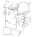
- FIG. 1schematically illustrates major elements of a plasma processing system 100 , according to an embodiment.
- System 100is depicted as a single wafer, semiconductor wafer processing system, but it will be apparent to one skilled in the art that the techniques and principles herein are applicable to a plasma processing system for any type of workpiece (e.g., items that are not necessarily wafers or semiconductors).
- Processing system 100includes a housing 110 for a wafer interface 115 , a user interface 120 , a process chamber 130 , a controller 140 and one or more power supplies 150 .
- Process chamber 130includes one or more wafer pedestals 135 , upon which wafer interface 115 can place a workpiece 50 (e.g., a wafer, but could be a different type of workpiece) for processing.
- workpiece 50e.g., a wafer, but could be a different type of workpiece
- a radio frequency generator (RF Gen) 165supplies power to create a plasma within process chamber 130 .
- RF Gen 165powers a radial waveguide 167 that may be disposed above or below process chamber 130 , and is shown in FIG. 2 as above chamber 130 .
- Process chamber 130is proximate radial waveguide 167 , and is bounded adjacent to radial waveguide 167 by a plate 169 that is formed of a material that is permeable to electromagnetic fields but not to air or process gases utilized in chamber 130 .
- plate 169can support a pressure difference between radial waveguide 167 and chamber 130 , while allowing microwaves within radial waveguide 167 to propagate into chamber 130 .
- Plate 169may be formed, for example, of ceramic.
- system 100The elements shown as part of system 100 are listed by way of example and are not exhaustive. Many other possible elements, such as: pressure and/or flow controllers; electrodes, magnetic cores and/or other electromagnetic apparatus; mechanical, pressure, temperature, chemical, optical and/or electronic sensors; viewing and/or other access ports; and the like may also be included, but are not shown for clarity of illustration. Internal connections and cooperation of the elements shown within system 100 are also not shown for clarity of illustration.
- RF generator 165other representative utilities such as gases 155 , vacuum pumps 160 , and/or general purpose electrical power 170 may connect with system 100 .
- the utilities shown as connected with system 100are intended as illustrative rather than exhaustive; other types of utilities such as heating or cooling fluids, pressurized air, network capabilities, waste disposal systems and the like may also be connected with system 100 , but are not shown for clarity of illustration.
- FIGS. 2A and 2Bare schematic cross-sections illustrating selected structure of radial waveguide 167 and process chamber 130 , FIG. 1 .
- FIG. 2Ais a vertical cross-section of radial waveguide 167 , process chamber 130 and a workpiece 50 therein.
- a broken line 2 B- 2 B′indicates a further cross-sectional view illustrated in FIG. 2B .
- Radial waveguide 167is a substantially cylindrical and closed shape, except for slots 168 formed in an undersurface thereof that allow microwaves to propagate into process chamber 130 , ports for providing and/or measuring microwaves, and other minor penetrations (such ports and penetrations are not shown in FIGS. 2A / 2 B).
- Slots 168may for example form a radial line slot antenna.
- Process chamber 130is substantially radially symmetric along a common axis with radial waveguide 129 . Microwaves propagate from radial waveguide 167 into process chamber 130 through slots 168 and through plate 169 to provide energy for igniting and/or maintaining plasma 60 .
- Pedestal 135is configured to present a workpiece 50 to plasma 60 for processing.
- Process chamber 130may include ports and/or mechanical openings (not shown) for insertion and/or withdrawal of workpiece 50 , introduction of gases to form plasma 60 , removal of plasma and gaseous reaction products, sensors, viewing and the like.
- FIG. 3is a schematic diagram of major components of a system 200 for providing microwaves to a plasma chamber utilizing a radial waveguide, in an embodiment.
- a radial waveguide 210 of system 200may be utilized for example as radial waveguide 167 , FIG. 1 .
- system 200powers radial waveguide 210 at two locations noted as P and Q in FIG. 3 , with locations P and Q being driven roughly ⁇ /2 out of phase with one another by electronics sets 225 ( 1 ), 225 ( 2 ) described below.
- Radial waveguide 210is thus considered a “dual driven” radial waveguide; the dual driven mode of operation provides high microwave energy density derived from two sets of driving electronics rather than a single set operating at double the power.
- An electronics set operating at higher powermay require components having higher voltage, current, or heat dissipation ratings that may be much more expensive or difficult to obtain than components for lower power sets.
- microwave field effect transistorsFETs
- high voltage, current, and/or power dissipation versions of such FETsmay remain costly or difficult to obtain.
- System 200Operation of system 200 is best understood as starting with a dual phase signal generator 215 that provides two microwave signals 220 ( 1 ), 220 ( 2 ) that are at the same frequency, but are ⁇ /2 out of phase with one another.
- Microwave signals 220 ( 1 ), 220 ( 2 )drive circuits that are referred to as a first set 225 ( 1 ) and a second set 225 ( 2 ).
- Each set 225 ( 1 ), 225 ( 2 )begins with a solid state amplifier 230 that boosts the power of respective microwave signals 220 ( 1 ), 220 ( 2 ) to create amplified microwave signals 235 ( 1 ), 235 ( 2 ).
- Solid state amplifiers 230may include one or more microwave FETs, as discussed above.
- Each amplified microwave signal 235 ( 1 ), 235 ( 2 )passes into and through a circulator 240 that serves to protect the respective solid state amplifiers 230 from power reflections from radial waveguide 210 .
- Circulators 240thus pass input power from solid state amplifiers 230 into respective tuners 250 , while shunting any power that is reflected back into dummy loads 245 .
- Tuners 250adjust impedance seen by the amplified microwave signals 235 ( 1 ), 235 ( 2 ) so as to match an impedance presented by components such as converters 255 , radial waveguide 260 and an adjacent process chamber (e.g., process chamber 130 , FIG. 1 , not shown in FIG. 3 ).
- Tuners 250may be, for example, three-pole stub tuners.
- the amplified, tuned signalsthen pass through respective coaxial-to-waveguide converters 265 and into radial waveguide 210 at respective waveguides with radiating apertures 270 .
- tuners 250can change the phase of signals passed toward radial waveguide 210 , such that although the signals are supplied at positions that are exactly ⁇ /2 out of phase around the circumference of radial waveguide 210 , the signals themselves may no longer be exactly ⁇ /2 out of phase. That is, instead of exciting a symmetric, circular polarization mode in radial waveguide 210 , an asymmetric, ellipsoidally polarized mode may be excited.
- This asymmetry in the microwave configurationcan lead, in turn, to process aberrations in an adjacent process chamber. For example, an asymmetric microwave configuration can lead to a correspondingly asymmetric plasma and consequently to local skews in depth of plasma etching.
- Embodiments hereinrecognize that as wafer sizes grow larger and the geometries produced in semiconductor fabrication grow smaller, the need for uniformity control of all aspects of the processing environment around the wafer increases. Therefore, embodiments herein adjust the microwave configuration that generates the plasma, not only to match impedance, but also to adjust phase and/or amplitude after impedance is matched, for improved symmetry of the plasma generated around the wafer.
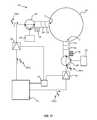
- FIG. 4is a schematic diagram of major components of a system 300 that provides post-match control of microwaves in a radial waveguide, in an embodiment.
- System 300may be utilized to excite a plasma in an adjacent plasma chamber.
- system 300has many of the same components as, and works similarly to, system 200 ( FIG. 3 ).
- system 300independently adjusts amplitude of, and/or a phase offset between, microwave signals 320 ( 1 ) and 320 ( 2 ) to control phase at points P and Q, for example to be utilized as a degree of freedom for optimizing process uniformity.
- a radial waveguide 210may be utilized for example as radial waveguide 167 , FIG. 1 .
- System 300powers radial waveguide at two locations noted as P and Q in FIG. 1 , with locations P and Q being driven roughly ⁇ /2 out of phase with one another.
- operation of system 300can be understood starting with a dual phase signal generator 315 that provides microwave signals 320 ( 1 ), 320 ( 2 ) that are at the same frequency.
- dual phase signal generator 315receives a correction signal 313 from a signal controller 312 that provides information for adjustment of signals 320 ( 1 ), 320 ( 2 ).
- correction signal 313may direct dual phase signal generator 315 to provide a corrected or targeted phase offset between microwave signals 320 ( 1 ), 320 ( 2 ).
- microwave signals 320 ( 1 ), 320 ( 2 )may be out of phase with one another by ⁇ /2, or by ⁇ /2 plus or minus the target phase difference, such that a measured phase difference at points P and Q is as intended, as discussed below.
- correction signal 313may direct dual phase signal generator 315 to boost and/or attenuate one or both of microwave signals 320 ( 1 ), 320 ( 2 ).
- signal generator 315is termed a “dual phase signal generator” herein, but considering that other embodiments may be driven at more than two points by a signal generator that generates more than two signals of identical frequency and differing phase (see, e.g., FIG. 8 ) it is understood that the “dual phase” aspect is for convenient reference. Furthermore, in embodiments, signal generator 315 may control amplitude of signals 320 , as well as phase thereof. Thus, dual phase signal generator 315 is simply a specific case of a “signal generator” as discussed elsewhere herein.
- microwave signals 320 ( 1 ), 320 ( 2 )drive respective solid state amplifiers 230 that boost power to create amplified microwave signals 335 ( 1 ), 335 ( 2 ), which in turn pass into and through circulators 240 .
- Circulators 240pass amplified microwave signals 335 ( 1 ), 335 ( 2 ) into respective tuners 250 while shunting any power reflected back into dummy loads 245 .
- Tuners 250adjust impedance seen by the amplified microwave signals 335 ( 1 ), 335 ( 2 ) so as to match an impedance presented by components such as converters 255 , radial waveguide 260 and an adjacent process chamber (e.g., process chamber 130 , FIG. 1 , not shown in FIG. 4 ).
- the amplified, tuned signalsthen pass through respective coaxial-to-waveguide converters 265 and into radial waveguide 210 at respective waveguides with radiating apertures 270 .
- Monitoring antennas 311may monitor either an electrical field or a magnetic field component of microwaves in radial waveguide 210 . When electrical fields are monitored, it is appreciated that metal of radial waveguide 210 may reduce electrical fields in close proximity thereto, such that care should be taken to locate monitoring antennas 311 far enough from radial waveguide 210 to provide sufficient sensitivity.
- Signal controller 312receives signals from monitoring antennas 311 ( 1 ) and 311 ( 2 ) through their respective connections 318 ( 1 ) and 318 ( 2 ) and determines amplitude of, and a phase offset between, signals at points P and Q. For example, signal controller 312 may perform in-phase and quadrature-phase demodulation (IQ demodulation) to measure amplitude and phase offset of the signals from monitoring antennas 311 ( 1 ) and 311 ( 2 ) (see also FIG. 9 ). Signal controller 312 then utilizes the measured phase offset and/or amplitudes to calculate and provide a corresponding digital correction signal 313 to dual phase signal generator 315 .
- IQ demodulationin-phase and quadrature-phase demodulation
- Digital correction signal 313may be chosen to be a desired phase offset (e.g., a value of ⁇ /2) or an offset from an assumed, desired phase difference (e.g., a correction factor that is zero when the desired phase difference is attained).
- digital correction signalmay be chosen to adjust amplitude of one or both of microwave signals 320 ( 1 ), 320 ( 2 ).
- Dual phase signal generator 315then provides microwave signals 320 ( 1 ) and 320 ( 2 ) with a phase offset and/or amplitudes such that when the microwave signals propagate through the system, the phase offset between points P and Q is driven to the desired phase difference, and/or the amplitudes measured at points P and Q are as desired.
- a target input device 314may provide one or more target parameters 316 to signal controller 312 .
- Target input device 314may be implemented in a variety of ways, such as by physical switches providing an output that is received directly by signal controller 312 , or as a part of system management hardware and software that acquires the target parameters from a user interface (e.g., a keyboard, other buttons, or a graphical user interface (GUI)).
- Target parameters 316may include, for example, a desired phase difference as measured at monitoring antennas 311 ( 1 ) and 311 ( 2 ), or amplitude adjustments to either or both of microwaves driven into radial waveguide 210 .
- Target parameters 316can be utilized by signal controller 312 along with the analog signals from monitoring antennas 311 ( 1 ) and 311 ( 2 ), to generate digital correction signal 313 .
- digital correction signal 313may be generated first based on the signals from monitoring antennas 311 ( 1 ) and 312 ( 1 ), after which digital correction signal 313 may be adjusted by adding or subtracting target parameter 316 .
- dual phase signal generator 315provides signals 320 ( 1 ) and 320 ( 2 ) with a corresponding offset until the phase offset between points P and Q is driven according to the target parameter, and digital correction signal 313 is driven to its target value, or zero.
- dual phase signal generator 315can adjust amplitude of either or both of signals 320 ( 1 ), 320 ( 2 ) in response thereto.
- Optional target input device 314provides a useful, independent degree of freedom for optimizing a semiconductor processing system that includes system 300 or other systems with a similar capability, as disclosed herein.
- the corresponding semiconductor processing systemmay be optimized by processing (e.g., etching) wafers, which may have test patterns printed thereon. Each wafer could be processed with identical processing parameters except for a different target parameter entered into target input device 314 .
- the performance of the systemcould be evaluated by measurements of the wafers that are indicative of performance of the etch system (e.g., etch rate, selectivity, linewidth change due to etch, and the like) as well as system monitors (e.g., system stabilization times, endpoint detection parameters, etc.) An optimized value of the target parameter could then be selected, based on the wafer measurements, the system monitors and/or a combination thereof.
- etch rateetch rate, selectivity, linewidth change due to etch, and the like
- system monitorse.g., system stabilization times, endpoint detection parameters, etc.
- tuners 250also continue to adjust impedance matching to minimize reflected power.
- system 300does not sacrifice impedance matching, but rather provides the additional capability of phase and/or amplitude adjustment for the dual driven radial waveguide, to optimize plasma symmetry in an adjacent process chamber. That is, in embodiments, signal generator 315 adjusts the phase offset, and tuners 250 provide the impedance matching, concurrently with one another during the operation of system 300 . In other embodiments, signal generator 315 adjusts the amplitude, and tuners 250 provide the impedance matching, concurrently with one another during the operation of system 300 .
- FIG. 5is a schematic diagram of major components of a system 400 that provides post-match control of microwaves in a radial waveguide, in an embodiment.
- System 400may be utilized to excite a plasma in an adjacent plasma chamber.
- system 400has many of the same components as, and works similarly to, systems 200 ( FIG. 3 ) and 300 ( FIG. 4 ). However, system 400 places monitoring antennas 411 ( 1 ) and 411 ( 2 ) at locations that are 180 degrees across radial waveguide 210 from points P and Q.
- monitoring antennas 411 ( 1 ) and 411 ( 2 )may enable the signals returned to signal controller 312 to include effects of radial waveguide 210 that are not readily monitored by monitoring antennas located at points P and Q (e.g., like monitoring antennas 311 , FIG. 4 ). That is, in system 300 , monitoring antennas 311 ( 1 ) and 311 ( 2 ) will receive very strong signals directly from waveguides with radiating apertures 270 such that effects introduced by other features (e.g., minor asymmetries) of radial waveguide 210 , and/or feedback effects from an adjacent plasma chamber, may not have much effect on the received signals.
- other featurese.g., minor asymmetries
- monitoring antennas 411 ( 1 ) and 411 ( 2 ) at points within radial waveguide 210 that are distant from points P and Qincreases the usefulness of the phase match capabilities of system 400 by including such effects.
- monitoring antennas 411 ( 1 ) and 411 ( 2 ) 180 degrees across radial waveguide 210 from points P and Q respectivelymay simplify calculation of digital correction signal 313 (e.g., signals expected when monitoring antennas 411 ( 1 ) and 411 ( 2 ) are 180 degrees across radial waveguide 210 from points P and Q leads to the expectation that phase of signals detected thereby will be ⁇ out of phase with the respective signals at points P and Q).
- digital correction signal 313e.g., signals expected when monitoring antennas 411 ( 1 ) and 411 ( 2 ) are 180 degrees across radial waveguide 210 from points P and Q leads to the expectation that phase of signals detected thereby will be ⁇ out of phase with the respective signals at points P and Q).
- FIG. 6is a schematic diagram of major components of a system 500 that provides post-match control of microwaves in a radial waveguide, in an embodiment.
- System 500may be utilized to excite a plasma in an adjacent plasma chamber.
- system 500has many of the same components as, and works similarly to, systems 200 , 300 and 400 ( FIGS. 3-5 ).
- system 500includes monitoring antennas 511 ( 1 ) and 511 ( 2 ) that measure independent components of magnetic fields, H z and H ⁇ respectively.
- Monitoring antennas 511 ( 1 ) and 511 ( 2 )are shown at a region A that is across radial waveguide 210 from point P, as shown in FIG.
- antennas 511 ( 1 ) and 511 ( 2 )provide signals that relate to magnetic field components H z and H ⁇ that are independent of one another, they may be located at other locations and still provide phase offset information that is useful for providing post-match control.
- FIG. 7is a schematic diagram of region A, FIG. 6 .
- a radial direction r, azimuthal direction ⁇ and axial direction z of a cylindrical coordinate system useful for describing the positions of antennas 511 and the directions of magnetic fields detected thereby,are shown.
- Monitoring antenna 511 ( 1 )includes a loop that is horizontally oriented and is thus responsive to magnetic field H z .
- Monitoring antenna 511 ( 2 )includes a loop that is vertically oriented and is thus responsive to magnetic field H ⁇ .
- Each of monitoring antennas 511 ( 1 ), 511 ( 2 )connects with a respective coaxial cable 518 ( 1 ) or 518 ( 2 ), as shown.
- Cables 518 ( 1 ) and 518 ( 2 )transmit signals from antennas 511 ( 1 ) and 511 ( 2 ) to signal controller 312 , as shown in FIG. 6 .
- Monitoring antennas 511 ( 1 ) and 511 ( 2 )may be disposed relatively close to one another in order to simplify calculations of phase offsets therebetween.
- FIG. 7monitoring antennas 511 ( 1 ) and 511 ( 2 ) may be disposed atop one another in the z direction, and/or within about 3 degrees of one another in the azimuthal direction ⁇ .
- Embodiments that provide post-match control of microwaves in a radial waveguideare not limited to the cases of two microwave generating electronics sets and two antennas that are illustrated in FIGS. 4-6 .
- FIG. 8schematically illustrates a radial waveguide 510 that is powered by four electronics sets, 525 ( 1 ) through 525 ( 4 ) and is monitored by four monitoring antennas, 555 ( 1 ) through 555 ( 4 ).
- electronics sets 525are disposed at 90 degree intervals about a periphery of radial waveguide 510 , with monitoring antennas 555 disposed at midpoints therebetween.
- Electronics sets 525are driven by a signal generator that provides four microwave signals of the same frequency but different phases (e.g., analogous to operation of dual phase signal generator 315 ) that receives correction factors from a quad signal controller (e.g., analogous to signal controller 312 ).
- An optional target input device(analogous to target input device 314 ) may provide target parameters applicable to any of the signals driven by the signal generator and/or the signals detected by any of the monitoring antennas 555 .
- the locations of electronics sets 525 and monitoring antennas 555 shown in FIG. 8may simplify calculation of expected phase of microwaves monitored at the monitoring antennas, and corresponding digital correction factors to be applied to the microwave signals that are input to the electronics sets, but other arrangements will be apparent to those skilled in the art. Also, similar embodiments may utilize more or fewer electronics sets 525 and/or monitoring antennas 555 , with appropriate adjustments to input of target parameters and/or calculation of signals driven by a corresponding signal generator.
- a semiconductor processing system that includes radial waveguide 510 , electronics sets 525 and monitoring antennas 555may be optimized in a manner analogous to the procedure described above in connection with FIG. 4 , except that multiple target parameters may be implemented and evaluated, alone and/or in combination with one another.
- FIG. 9is a schematic diagram illustrating implementations of signal controller 312 and dual phase signal generator 315 , in an embodiment.
- the embodiment illustrated in FIG. 9could support any of the systems shown in FIGS. 4, 5 and 6 directly, and the principles now explained can be duplicated modified in ways that will be readily apparent to support the system illustrated in FIG. 8 .
- signal controller 312includes a control clock (CLK) 602 that generates a 40 MHz waveform and a high frequency clock (HCLK) 604 that generates a 2.449 GHz waveform.
- Clock 602serves to provide a gating time signal for successive demodulations.
- Clock 604provides a reference frequency for dual phase signal generator 315 (e.g., a frequency at which radial waveguide 167 , FIGS. 2A and 2B , radial waveguide 210 , FIGS. 3-7 or radial waveguide 510 , FIG. 8 , is driven to support a plasma powered thereby) and can therefore provide the same reference frequency for IQ demodulation purposes.
- clocks 602 and 604are not critical and may be different in other embodiments.
- a higher speed of clock 602will force more frequent repetition of the calculations discussed below, leading to faster plasma adjustment and settling times for an entire system, but will increase system power requirements and may lead to a need for higher performance versions of components 606 and 608 discussed below.
- a lower speed of clock 602may increase plasma adjustment and settling time achievable by the system but may reduce system power requirements and may allow use of lower performance versions of components 606 and 608 .
- Signal controller 312also includes an IQ demodulator 606 and a microcontroller 608 executing software 609 .
- an IQ demodulator 606performs IQ demodulation of each of the signals provided through connections 318 ( 1 ) and 318 ( 2 ), and generates therefrom a digital in-phase signal Xni and a digital quadrature phase signal Xnq, where n is 1 or 2 corresponding to connections 318 ( 1 ) and 318 ( 2 ) respectively.
- Digital in-phase and quadrature-phase signals Xni and Xnqcharacterize the corresponding received signal in that Xni is the real part of signal n, and Xnq is the imaginary part of signal n.
- the IQ demodulation of each of the signalsproceeds in parallel such that for each interval, IQ demodulator 606 provides corresponding digital signals X 1 i , X 1 q , X 2 i , X 2 q , as shown.
- FIG. 10illustrates exemplary operation of a first portion 606 ( a ) of IQ demodulator 606 that processes a signal received from connection 318 ( 1 ) to yield X 1 i and X 1 q ; it is understood that IQ demodulator 606 also has a second portion that performs similar processing with respect to a signal received from connection 318 ( 2 ) to yield X 2 i and X 2 q .
- An optional bandpass filter 620may be utilized to clean up the signal from connection 318 , especially to eliminate harmonics of the main received frequency, which in this example is around 2.450 GHz.
- An exemplary passband of filter 620might be, for example, 2.45 GHz ⁇ 0.05 GHz; in embodiments, the width of the passband could be considerably higher, up to perhaps 20% of the received frequency and not necessarily centered about the received frequency.
- Demodulationproceeds by mixing the signal from connection 318 ( 1 ) with the signal from clock 604 to generate an intermediate frequency (IF) signal.
- IFintermediate frequency
- the clock 604 frequencywill be related to the frequency produced by signal generator 315 and propagated into radial waveguide 210 to produce a usable IF signal.
- clock 604operates at 2.449 GHz while dual phase signal generator 315 produces a 2.450 GHz signal, thus yielding a 1 MHz IF signal.
- FIG. 10labels parts of portion 606 ( a ) of demodulator 606 as “HF” (high frequency), “IF” and “DIGITAL” for easy understanding of the signals being processed in each part.
- a bandpass or lowpass filter 624cleans up the signal from mixer 622 .
- An exemplary passband of filter 620might be, for example, 0 Hz (if lowpass) or 0.5 MHz (if bandpass) to around 2 MHz.
- An analog to digital converter 626converts the IF signal to a digital sample on intervals determined from clock 602 ; further processing takes place in the digital part of portion 606 ( a ).
- Copies 628 ( a ). 628 ( b ) of the digital sampleare mixed with values corresponding to cos( ⁇ n) and ⁇ sin( ⁇ n), where ⁇ is defined as 2 ⁇ f IF /f s , where f s is a sampling frequency of clock 602 (40 MHz in this example), f IF is the microwave signal frequency projected to the IF band (1 MHz in this example).
- the cos( ⁇ n) and ⁇ sin( ⁇ n) valuesare generated from a read-only-memory (ROM) 630 at the clock 602 sampling frequency, and are multiplied with copies 628 ( a ), 628 ( b ) at digital mixers 632 ( a ), 632 ( b ) to form the resulting digital outputs X 1 i and X 1 q.
- ROMread-only-memory
- digital low pass filters 634 ( a ) and 634 ( b )can be utilized to eliminate high frequency digital noise from X 1 i and X 1 q .
- Typical cutoff values of digital low pass filters 634 ( a ) and 634 ( b )are for example 1 kHz.
- microcontroller 608executes software 609 (which may be stored in nontransitory, computer-readable media that forms part of microcontroller 608 , or may be external to microcontroller 608 ) to generate correction signal 313 .
- Software 609is implemented to generate correction signal 313 in cooperation with operation of dual phase signal generator 315 .
- dual phase signal generator 315may expect correction signal 313 to completely specify a phase offset between signals 320 ( 1 ) and 320 ( 2 ), in which case the default value of correction signal 313 may be ⁇ /2.
- microcontroller 608receives target parameter 316 therefrom, and software 609 implements adjustments to correction signal 313 based on target parameter 316 .
- Dual phase signal generator 315receives correction signal 313 from signal controller 312 (specifically, from microcontroller 608 ) and provides signals 320 ( 1 ) and 320 ( 2 ) with a phase offset indicated by correction signal 313 , at two outputs Vout 1 and Vout 2 .
- Dual phase signal generator 315may include, for example, a direct digital synthesizer that generates two analog outputs, each at the nominal IF frequency discussed in connection with IQ demodulator 606 , that are subsequently mixed with the signal from clock 604 to form the frequencies of signals 320 .
- the direct digital synthesizerwould create analog outputs at 1 MHz frequency that, when mixed with the 2.449 GHz frequency of clock 604 , would provide signals 320 at 2.450 GHz. Signals 320 then transmit to their respective electronics sets, as shown in each of FIGS. 4, 5 and 6 , radiated into respective radial waveguides 210 and received back into connections 318 ( 1 ), 318 ( 2 ).
- clock 604may not be part of signal controller 312 , but may instead be part of a signal generator (e.g., dual phase signal generator 315 ) which may originate the clock 604 signal and provide an output thereof to IQ demodulator 606 for use as a reference clock.
- clock 602may also be generated by a signal controller or some other part of a system that includes signal controller 312 .
- FIG. 11is a schematic diagram of major components of a system 700 that provides post-match control of microwaves in a radial waveguide, in an embodiment.
- System 700may be utilized, for example, to excite a plasma in an adjacent plasma chamber.
- system 700has many of the same components as, and works similarly to, systems 200 , 300 , 400 and 500 ( FIGS. 3-6 ).
- system 700does not include monitoring antennas or a corresponding signal controller providing feedback to signal generator 315 .
- a target input device 714provides an ability to provide one or more target parameters such as phase offset, amplitude adjustments, or both to signal generator 315 and/or to solid state amplifiers 230 .
- target input device 714specifies a phase offset as the target parameter
- the phase offsetis provided by signal generator 315 in the form of a corresponding phase offset between signals 320 ( 1 ) and 320 ( 2 ).
- the corresponding effectmay be provided by signal generator 315 (e.g., in the form of amplitude(s) of signals 320 ( 1 ) and/or 320 ( 2 )) or by one or both of solid state amplifiers 230 (e.g., in the form of adjusting gain of one or both of solid state amplifiers 230 , so that the resulting amplitude is provided to radial waveguide 210 ).
- target input device 714allows an operator of system 700 to optimize the selected target parameter independently of actions of tuners 250 , which continue to match impedance.
- an ability to set and/or adjust gain of solid state amplifiers 230 as shown in FIG. 11may also be utilized in embodiments wherein antennas provide feedback and a signal controller adjusts phase and/or amplitude based on the feedback, (e.g., systems 300 , 400 and 500 ( FIGS. 4-6 )).
Landscapes
- Chemical & Material Sciences (AREA)
- Analytical Chemistry (AREA)
- Physics & Mathematics (AREA)
- Engineering & Computer Science (AREA)
- Plasma & Fusion (AREA)
- Plasma Technology (AREA)
- Drying Of Semiconductors (AREA)
Abstract
Description
This patent application is a continuation of U.S. patent application Ser. No. 15/063,849, filed on Mar. 8, 2016, which is a continuation of, and claims the benefit of priority to, pending U.S. patent application Ser. No. 14/221,132, filed on Mar. 20, 2014. Both of the above-identified patent applications are hereby incorporated by reference for all purposes.
The present disclosure is in the field of microwaves. More specifically, embodiments that utilize radial waveguides and associated control systems to provide control of microwaves in a plasma process chamber are disclosed.
Semiconductor processing often generates plasmas to create ionized and/or energetically excited species for interaction with semiconductor wafers themselves, or other processing related materials (e.g., photoresist). To create and/or maintain a plasma, one or more radio frequency (RF) and/or microwave generators are typically utilized to generate oscillating electric and/or magnetic fields. The same fields, and/or DC fields, may also be utilized to direct the ionized and/or energetically excited species to the semiconductor wafer(s) being processed. Various known methods are often utilized to match an impedance of a power source (the RF generator) to a load (the plasma) so that power from the RF generator is delivered to the plasma without significant reflection of power back to the RF generator. This is for reasons of energy efficiency as well as to protect electrical components of the RF generator from damage. Particularly when microwave energy is utilized, reflected power is usually directed to a dummy load where it is dissipated as heat, which must then be removed. Thus, reflected power results in a two-fold waste of energy: the energy utilized to generate the power, and the energy utilized to remove the waste heat.
In an embodiment, a system provides post-match control of microwaves in a radial waveguide. The system includes the radial waveguide and a signal generator that provides a first microwave signal and a second microwave signal. The first and second microwave signals have a common frequency. The signal generator adjusts a phase offset between the first and second microwave signals in response to a digital correction signal. The system also includes a first electronics set and a second electronics set. Each of the first and second electronics sets amplifies a respective one of the first and second microwave signals to provide a respective first or second amplified microwave signal, transmits the respective first or second amplified microwave signal into the radial waveguide, and matches an impedance of the respective first or second amplified microwave signal to an impedance presented by the radial waveguide. The system also includes at least two monitoring antennas disposed at least 30 degrees about a circumference of the radial waveguide from locations at which the first and second electronics sets transmit the respective first and second amplified microwave signals into the radial waveguide. A signal controller receives analog signals from the at least two monitoring antennas, determines the digital correction signal based at least on the analog signals from the at least two monitoring antennas, and transmits the digital correction signal to the signal generator.
In an embodiment, a system for plasma processing of a workpiece includes a process chamber configured to create a plasma for the plasma processing, and a radial waveguide, adjacent to the process chamber, configured to generate microwaves for transmission to the process chamber to supply energy for the plasma. The system also includes a signal generator that provides a first microwave signal and a second microwave signal, the first and second microwave signals having a common frequency. The signal generator adjusts a phase offset between the first and second microwave signals in response to a digital correction signal. The system also includes a first electronics set and a second electronics set. Each of the first and second electronics sets amplifies a respective one of the first and second microwave signals to provide an amplified microwave signal, transmits the amplified microwave signal into the radial waveguide, and matches an impedance of the amplified microwave signal to an impedance presented by the radial waveguide. The system also includes at least two monitoring antennas disposed at least 30 degrees about a circumference of the radial waveguide from locations at which the first and second electronics sets transmit the respective first and second amplified microwave signals into the radial waveguide. A signal controller receives analog signals from the at least two monitoring antennas, determines the digital correction signal based at least on the analog signals from the at least two monitoring antennas, and transmits the digital correction signal to the signal generator. The first electronics set includes a tuner that matches the impedance of the first amplified microwave signal to the impedance presented by the radial waveguide, a dummy load, and a circulator that shunts power reflected back from the radial waveguide toward the first electronics set, into the dummy load. The signal generator adjusts the phase offset, and the tuner matches the impedance, concurrently with one another.
In an embodiment, a method for controlling a plasma within a process chamber includes generating, with a signal generator, a first microwave signal and a second microwave signal, the first and second microwave signals having a common frequency and a phase offset therebetween that is determined at least in part by the signal generator responding to a digital correction signal. The method also includes amplifying the first and second microwave signals to provide respective first and second amplified microwave signals, and transmitting the first and second amplified microwave signals into a radial waveguide proximate the process chamber such that microwaves propagate from the radial waveguide into the process chamber to provide energy for the plasma. The method also includes generating analog signals with at least two monitoring antennas disposed at least 30 degrees about a circumference of the radial waveguide from locations at which the first and second electronics sets transmit the respective first and second amplified microwave signals into the radial waveguide, determining the digital correction signal based at least on the analog signals from the at least two monitoring antennas, and transmitting the digital correction signal to the signal generator.
Additional embodiments and features are set forth in part in the description that follows, and in part will become apparent to those skilled in the art upon examination of the specification or may be learned by the practice of the invention. The features and advantages of the invention may be realized and attained by means of the instrumentalities, combinations, and methods described in the specification.
The present disclosure may be understood by reference to the following detailed description taken in conjunction with the drawings briefly described below, wherein like reference numerals are used throughout the several drawings to refer to similar components. It is noted that, for purposes of illustrative clarity, certain elements in the drawings may not be drawn to scale. Specific instances of an item may be referred to by use of a numeral in parentheses (e.g., monitoring antennas311(1),311(2)) while numerals without parentheses refer to any such item (e.g., monitoring antennas311). In instances where multiple instances of an item are shown, only some of the instances may be labeled, for clarity of illustration.
Operation ofsystem 200 is best understood as starting with a dualphase signal generator 215 that provides two microwave signals220(1),220(2) that are at the same frequency, but are π/2 out of phase with one another. Microwave signals220(1),220(2) drive circuits that are referred to as a first set225(1) and a second set225(2). Each set225(1),225(2) begins with asolid state amplifier 230 that boosts the power of respective microwave signals220(1),220(2) to create amplified microwave signals235(1),235(2).Solid state amplifiers 230 may include one or more microwave FETs, as discussed above. Each amplified microwave signal235(1),235(2) passes into and through acirculator 240 that serves to protect the respectivesolid state amplifiers 230 from power reflections fromradial waveguide 210.Circulators 240 thus pass input power fromsolid state amplifiers 230 intorespective tuners 250, while shunting any power that is reflected back into dummy loads245.
As part of the tuning required to achieve acceptable impedance matching,tuners 250 can change the phase of signals passed towardradial waveguide 210, such that although the signals are supplied at positions that are exactly π/2 out of phase around the circumference ofradial waveguide 210, the signals themselves may no longer be exactly π/2 out of phase. That is, instead of exciting a symmetric, circular polarization mode inradial waveguide 210, an asymmetric, ellipsoidally polarized mode may be excited. This asymmetry in the microwave configuration can lead, in turn, to process aberrations in an adjacent process chamber. For example, an asymmetric microwave configuration can lead to a correspondingly asymmetric plasma and consequently to local skews in depth of plasma etching.
Embodiments herein recognize that as wafer sizes grow larger and the geometries produced in semiconductor fabrication grow smaller, the need for uniformity control of all aspects of the processing environment around the wafer increases. Therefore, embodiments herein adjust the microwave configuration that generates the plasma, not only to match impedance, but also to adjust phase and/or amplitude after impedance is matched, for improved symmetry of the plasma generated around the wafer. Even when careful attention is paid to symmetry of a process chamber, placement of a wafer in the process chamber, and the like, asymmetries in a plasma can arise from many causes (e.g., mechanically asymmetric ports, sensors, wafer placement, wafer flats, cabling length and the like) such that control of phase and/or amplitude, in addition to impedance matching, may provide an extra and useful degree of freedom for improving uniformity in plasma processing.
Insystem 300, aradial waveguide 210 may be utilized for example asradial waveguide 167,FIG. 1 .System 300 powers radial waveguide at two locations noted as P and Q inFIG. 1 , with locations P and Q being driven roughly π/2 out of phase with one another. Likesystem 200, operation ofsystem 300 can be understood starting with a dualphase signal generator 315 that provides microwave signals320(1),320(2) that are at the same frequency. However, dualphase signal generator 315 receives acorrection signal 313 from asignal controller 312 that provides information for adjustment of signals320(1),320(2). For example,correction signal 313 may direct dualphase signal generator 315 to provide a corrected or targeted phase offset between microwave signals320(1),320(2). Thus, insystem 300, microwave signals320(1),320(2) may be out of phase with one another by π/2, or by π/2 plus or minus the target phase difference, such that a measured phase difference at points P and Q is as intended, as discussed below. In another example,correction signal 313 may direct dualphase signal generator 315 to boost and/or attenuate one or both of microwave signals320(1),320(2).
At this point, it should be noted thatsignal generator 315 is termed a “dual phase signal generator” herein, but considering that other embodiments may be driven at more than two points by a signal generator that generates more than two signals of identical frequency and differing phase (see, e.g.,FIG. 8 ) it is understood that the “dual phase” aspect is for convenient reference. Furthermore, in embodiments,signal generator 315 may control amplitude ofsignals 320, as well as phase thereof. Thus, dualphase signal generator 315 is simply a specific case of a “signal generator” as discussed elsewhere herein.
Likesystem 200, microwave signals320(1),320(2) drive respectivesolid state amplifiers 230 that boost power to create amplified microwave signals335(1),335(2), which in turn pass into and throughcirculators 240.Circulators 240 pass amplified microwave signals335(1),335(2) intorespective tuners 250 while shunting any power reflected back into dummy loads245.Tuners 250 adjust impedance seen by the amplified microwave signals335(1),335(2) so as to match an impedance presented by components such as converters255, radial waveguide260 and an adjacent process chamber (e.g.,process chamber 130,FIG. 1 , not shown inFIG. 4 ). The amplified, tuned signals then pass through respective coaxial-to-waveguide converters 265 and intoradial waveguide 210 at respective waveguides with radiatingapertures 270.
Monitoring antennas311(1) and311(2), disposed proximate to points P and Q respectively, provide analog signals to signalcontroller 312 through their respective connections318(1) and318(2), capturing any phase offset introduced bytuners 250.Monitoring antennas 311 may monitor either an electrical field or a magnetic field component of microwaves inradial waveguide 210. When electrical fields are monitored, it is appreciated that metal ofradial waveguide 210 may reduce electrical fields in close proximity thereto, such that care should be taken to locatemonitoring antennas 311 far enough fromradial waveguide 210 to provide sufficient sensitivity.Signal controller 312 receives signals from monitoring antennas311(1) and311(2) through their respective connections318(1) and318(2) and determines amplitude of, and a phase offset between, signals at points P and Q. For example,signal controller 312 may perform in-phase and quadrature-phase demodulation (IQ demodulation) to measure amplitude and phase offset of the signals from monitoring antennas311(1) and311(2) (see alsoFIG. 9 ).Signal controller 312 then utilizes the measured phase offset and/or amplitudes to calculate and provide a correspondingdigital correction signal 313 to dualphase signal generator 315.Digital correction signal 313 may be chosen to be a desired phase offset (e.g., a value of π/2) or an offset from an assumed, desired phase difference (e.g., a correction factor that is zero when the desired phase difference is attained). Alternatively, digital correction signal may be chosen to adjust amplitude of one or both of microwave signals320(1),320(2). Dualphase signal generator 315 then provides microwave signals320(1) and320(2) with a phase offset and/or amplitudes such that when the microwave signals propagate through the system, the phase offset between points P and Q is driven to the desired phase difference, and/or the amplitudes measured at points P and Q are as desired.
Optionally, atarget input device 314 may provide one ormore target parameters 316 to signalcontroller 312.Target input device 314 may be implemented in a variety of ways, such as by physical switches providing an output that is received directly bysignal controller 312, or as a part of system management hardware and software that acquires the target parameters from a user interface (e.g., a keyboard, other buttons, or a graphical user interface (GUI)).Target parameters 316 may include, for example, a desired phase difference as measured at monitoring antennas311(1) and311(2), or amplitude adjustments to either or both of microwaves driven intoradial waveguide 210.Target parameters 316 can be utilized bysignal controller 312 along with the analog signals from monitoring antennas311(1) and311(2), to generatedigital correction signal 313. For example, when a target phase difference is utilized,digital correction signal 313 may be generated first based on the signals from monitoring antennas311(1) and312(1), after whichdigital correction signal 313 may be adjusted by adding or subtractingtarget parameter 316. Oncedigital correction signal 313 is transmitted, dualphase signal generator 315 provides signals320(1) and320(2) with a corresponding offset until the phase offset between points P and Q is driven according to the target parameter, anddigital correction signal 313 is driven to its target value, or zero. In another example, when a target amplitude adjustment is utilized, dualphase signal generator 315 can adjust amplitude of either or both of signals320(1),320(2) in response thereto.
Optionaltarget input device 314 provides a useful, independent degree of freedom for optimizing a semiconductor processing system that includessystem 300 or other systems with a similar capability, as disclosed herein. For example, the corresponding semiconductor processing system may be optimized by processing (e.g., etching) wafers, which may have test patterns printed thereon. Each wafer could be processed with identical processing parameters except for a different target parameter entered intotarget input device 314. The performance of the system could be evaluated by measurements of the wafers that are indicative of performance of the etch system (e.g., etch rate, selectivity, linewidth change due to etch, and the like) as well as system monitors (e.g., system stabilization times, endpoint detection parameters, etc.) An optimized value of the target parameter could then be selected, based on the wafer measurements, the system monitors and/or a combination thereof.
It will be understood by one skilled in the art that whilesignal controller 312 cooperates with dualphase signal generator 315 to adjust phase of microwave signals320(1) and320(2),tuners 250 also continue to adjust impedance matching to minimize reflected power. Thus,system 300 does not sacrifice impedance matching, but rather provides the additional capability of phase and/or amplitude adjustment for the dual driven radial waveguide, to optimize plasma symmetry in an adjacent process chamber. That is, in embodiments,signal generator 315 adjusts the phase offset, andtuners 250 provide the impedance matching, concurrently with one another during the operation ofsystem 300. In other embodiments,signal generator 315 adjusts the amplitude, andtuners 250 provide the impedance matching, concurrently with one another during the operation ofsystem 300.
Embodiments that provide post-match control of microwaves in a radial waveguide are not limited to the cases of two microwave generating electronics sets and two antennas that are illustrated inFIGS. 4-6 . For example,FIG. 8 schematically illustrates aradial waveguide 510 that is powered by four electronics sets,525(1) through525(4) and is monitored by four monitoring antennas,555(1) through555(4). As shown inFIG. 8 , electronics sets525 are disposed at 90 degree intervals about a periphery ofradial waveguide 510, withmonitoring antennas 555 disposed at midpoints therebetween. While twomonitoring antennas 555 disposed orthogonally to one another are theoretically sufficient to evaluate whether a microwave distribution withinradial waveguide 510 is symmetrical, fourantennas 555 and corresponding correction factors for four electronics sets525 may be utilized to provide further degrees of freedom in process control. Electronics sets525 are driven by a signal generator that provides four microwave signals of the same frequency but different phases (e.g., analogous to operation of dual phase signal generator315) that receives correction factors from a quad signal controller (e.g., analogous to signal controller312). An optional target input device (analogous to target input device314) may provide target parameters applicable to any of the signals driven by the signal generator and/or the signals detected by any of themonitoring antennas 555. The locations of electronics sets525 andmonitoring antennas 555 shown inFIG. 8 may simplify calculation of expected phase of microwaves monitored at the monitoring antennas, and corresponding digital correction factors to be applied to the microwave signals that are input to the electronics sets, but other arrangements will be apparent to those skilled in the art. Also, similar embodiments may utilize more or fewer electronics sets525 and/ormonitoring antennas 555, with appropriate adjustments to input of target parameters and/or calculation of signals driven by a corresponding signal generator. A semiconductor processing system that includesradial waveguide 510, electronics sets525 andmonitoring antennas 555 may be optimized in a manner analogous to the procedure described above in connection withFIG. 4 , except that multiple target parameters may be implemented and evaluated, alone and/or in combination with one another.
In the embodiment illustrated inFIG. 9 ,signal controller 312 includes a control clock (CLK)602 that generates a 40 MHz waveform and a high frequency clock (HCLK)604 that generates a 2.449 GHz waveform.Clock 602 serves to provide a gating time signal for successive demodulations.Clock 604 provides a reference frequency for dual phase signal generator315 (e.g., a frequency at whichradial waveguide 167,FIGS. 2A and 2B ,radial waveguide 210,FIGS. 3-7 orradial waveguide 510,FIG. 8 , is driven to support a plasma powered thereby) and can therefore provide the same reference frequency for IQ demodulation purposes. Given these understandings of howclocks clocks clock 602 will force more frequent repetition of the calculations discussed below, leading to faster plasma adjustment and settling times for an entire system, but will increase system power requirements and may lead to a need for higher performance versions ofcomponents clock 602 may increase plasma adjustment and settling time achievable by the system but may reduce system power requirements and may allow use of lower performance versions ofcomponents
In certain embodiments, in the IF part of portion606(a) a bandpass orlowpass filter 624 cleans up the signal frommixer 622. An exemplary passband offilter 620 might be, for example, 0 Hz (if lowpass) or 0.5 MHz (if bandpass) to around 2 MHz. An analog todigital converter 626 converts the IF signal to a digital sample on intervals determined fromclock 602; further processing takes place in the digital part of portion606(a).
Copies628(a).628(b) of the digital sample are mixed with values corresponding to cos(ωn) and −sin(ωn), where ω is defined as 2πfIF/fs, where fsis a sampling frequency of clock602 (40 MHz in this example), fIFis the microwave signal frequency projected to the IF band (1 MHz in this example). The cos(ωn) and −sin(ωn) values are generated from a read-only-memory (ROM)630 at theclock 602 sampling frequency, and are multiplied with copies628(a),628(b) at digital mixers632(a),632(b) to form the resulting digital outputs X1iand X1q.
In certain embodiments, digital low pass filters634(a) and634(b) can be utilized to eliminate high frequency digital noise from X1iand X1q. Typical cutoff values of digital low pass filters634(a) and634(b) are for example 1 kHz.
Returning toFIG. 9 , fromIQ demodulator 606, digital outputs X1i, X1q, X2iand X2qpass tomicrocontroller 608, that generates correction signal313 therefrom.Microcontroller 608 executes software609 (which may be stored in nontransitory, computer-readable media that forms part ofmicrocontroller 608, or may be external to microcontroller608) to generatecorrection signal 313.Software 609 is implemented to generatecorrection signal 313 in cooperation with operation of dualphase signal generator 315. For example, if default operation of dualphase signal generator 315 is to generate signals320(1) and320(2) with a phase offset of π/2, the default value ofcorrection signal 313 may be zero; alternatively, dualphase signal generator 315 may expect correction signal313 to completely specify a phase offset between signals320(1) and320(2), in which case the default value ofcorrection signal 313 may be π/2. Also, when optionaltarget input device 314 is implemented,microcontroller 608 receivestarget parameter 316 therefrom, andsoftware 609 implements adjustments to correction signal313 based ontarget parameter 316.
Dualphase signal generator 315 receivescorrection signal 313 from signal controller312 (specifically, from microcontroller608) and provides signals320(1) and320(2) with a phase offset indicated bycorrection signal 313, at two outputs Vout1 and Vout2. Dualphase signal generator 315 may include, for example, a direct digital synthesizer that generates two analog outputs, each at the nominal IF frequency discussed in connection withIQ demodulator 606, that are subsequently mixed with the signal fromclock 604 to form the frequencies ofsignals 320. For example, in consistency with the examples above, the direct digital synthesizer would create analog outputs at 1 MHz frequency that, when mixed with the 2.449 GHz frequency ofclock 604, would providesignals 320 at 2.450 GHz.Signals 320 then transmit to their respective electronics sets, as shown in each ofFIGS. 4, 5 and 6 , radiated into respectiveradial waveguides 210 and received back into connections318(1),318(2).
In embodiments,clock 604 may not be part ofsignal controller 312, but may instead be part of a signal generator (e.g., dual phase signal generator315) which may originate theclock 604 signal and provide an output thereof toIQ demodulator 606 for use as a reference clock. Similarly,clock 602 may also be generated by a signal controller or some other part of a system that includessignal controller 312.
It should be understood that an ability to set and/or adjust gain ofsolid state amplifiers 230 as shown inFIG. 11 may also be utilized in embodiments wherein antennas provide feedback and a signal controller adjusts phase and/or amplitude based on the feedback, (e.g.,systems FIGS. 4-6 )).
Having described several embodiments, it will be recognized by those of skill in the art that various modifications, alternative constructions, and equivalents may be used without departing from the spirit of the invention. Additionally, a number of well-known processes and elements have not been described in order to avoid unnecessarily obscuring the present invention. Accordingly, the above description should not be taken as limiting the scope of the invention.
Where a range of values is provided, it is understood that each intervening value, to the tenth of the unit of the lower limit unless the context clearly dictates otherwise, between the upper and lower limits of that range is also specifically disclosed. Each smaller range between any stated value or intervening value in a stated range and any other stated or intervening value in that stated range is encompassed. The upper and lower limits of these smaller ranges may independently be included or excluded in the range, and each range where either, neither or both limits are included in the smaller ranges is also encompassed within the invention, subject to any specifically excluded limit in the stated range. Where the stated range includes one or both of the limits, ranges excluding either or both of those included limits are also included.
As used herein and in the appended claims, the singular forms “a”, “an”, and “the” include plural referents unless the context clearly dictates otherwise. Thus, for example, reference to “a process” includes a plurality of such processes and reference to “the electrode” includes reference to one or more electrodes and equivalents thereof known to those skilled in the art, and so forth. Also, the words “comprise,” “comprising,” “include,” “including,” and “includes” when used in this specification and in the following claims are intended to specify the presence of stated features, integers, components, or steps, but they do not preclude the presence or addition of one or more other features, integers, components, steps, acts, or groups.
Claims (20)
1. A system that generates microwaves in a waveguide, comprising:
the waveguide;
one or more transmitters that transmit:
a first microwave signal into the waveguide at a first location, and
a second microwave signal into the waveguide at a second location,
at least one monitoring antenna within the waveguide that provides an analog signal responsive to microwaves at a location of the monitoring antenna; and
a controller that receives the analog signal, and in response to the analog signal, adjusts at least one of a phase and an amplitude of the first microwave signal or the second microwave signal, until the analog signal meets a predetermined condition.
2. The system as recited inclaim 1 , wherein in response to the analog signal, the controller that receives the analog signal adjusts both the phase and the amplitude of the first microwave signal or the second microwave signal, to achieve the predetermined condition.
3. The system as recited inclaim 1 , further comprising:
a target input device configured to provide a target parameter to the controller;
and wherein:
the controller adjusts the at least one of the phase and the amplitude of the first microwave signal or the second microwave signal, based on the analog signal and the target parameter.
4. The system as recited inclaim 1 , wherein at least one of the one or more transmitters includes an electronics set that receives and amplifies an input microwave signal to form one of the first and second microwave signals, and wherein the electronics set includes:
a tuner that matches an impedance of the electronics set to an impedance presented by the waveguide;
a dummy load; and
a circulator that shunts power reflected by the waveguide back to the electronics set, into the dummy load.
5. The system as recited inclaim 4 , wherein:
the controller adjusts the at least one of the phase and the amplitude of the first microwave signal by adjusting a corresponding one of the phase and the amplitude of the input microwave signal, and
the tuner matches the impedance, concurrently with the controller adjusting the at least one of the phase and the amplitude.
6. The system as recited inclaim 1 , wherein the monitoring antenna is disposed proximate to the first location or the second location.
7. The system as recited inclaim 1 ,
comprising at least two of the monitoring antennas that provide respective analog signals responsive to microwaves at respective locations of each of the monitoring antennas; and wherein
the controller receives the respective analog signals and adjusts at least the at least one of the phase and the amplitude of the first microwave signal or the second microwave signal, to achieve the predetermined condition at the respective locations of each of the monitoring antennas.
8. The system as recited inclaim 7 , wherein the waveguide is characterized by a circumference, and:
a first one of the monitoring antennas is disposed 90 degrees about the circumference from the first location; and
a second one of the monitoring antennas is disposed 90 degrees about the circumference from the second location.
9. The system as recited inclaim 1 , wherein the monitoring antenna comprises a loop antenna that measures a magnetic field to provide the analog signal.
10. The system as recited inclaim 1 , further comprising a signal generator that provides one or more input microwave signals to the controller and to the one or more transmitters, wherein:
the controller adjusts at least the at least one of the phase and the amplitude of the one or more input microwave signals to achieve the predetermined condition by providing a digital correction signal to the signal generator, and
the signal generator adjusts the at least one of the phase and the amplitude of one of the input microwave signals provided to one of the transmitters, relative to at least one of the phase and the amplitude of one of the input microwave signals provided to another one of the transmitters, in response to the digital correction signal.
11. The system as recited inclaim 1 , wherein the controller comprises:
a high frequency clock generator that produces a high frequency reference signal;
a control clock generator that produces a low frequency control signal;
an in-phase and quadrature-phase demodulator that produces a first digital in-phase signal and a first digital quadrature phase signal from the analog signal; and
a microcontroller that generates a correction signal based at least in part on the first digital in-phase signal and the first digital quadrature phase signal, the correction signal specifying adjustment information that, when utilized by the system to adjust the at least one of the phase and the amplitude of an input microwave signal provided to one or more of the plurality of transmitters, produces one or more changes in the analog signal toward the predetermined condition.
12. A signal corrector that provides a correction signal for a microwave generator that transmits microwaves, at a microwave frequency, into a microwave chamber from at least two locations, the signal corrector comprising:
a first clock generator that produces the microwave frequency;
a second clock generator that produces a control signal;
a decoder that produces one or more digital signals in response to at least one analog signal from a location within the microwave chamber, at each cycle of the control signal; and
a microcontroller that generates the correction signal based at least in part on the one or more digital signals, wherein the correction signal specifies an adjustment, by the microwave generator, for at least one of a phase and an amplitude of the microwaves transmitted into the microwave chamber.
13. The signal corrector ofclaim 12 , wherein the decoder produces a first one of the one or more digital signals by:
mixing the at least one analog signal with the microwave frequency to produce an intermediate frequency signal;
converting the intermediate frequency signal to a digital sample at intervals determined from the control signal; and
multiplying the digital sample with a first value obtained from a read-only memory to produce the first one of the one or more digital signals.
14. The signal corrector ofclaim 13 , wherein:
the first value obtained from the read-only memory corresponds to cos(ωn), where ω is defined as 2πfIF/fs, where fsis a sampling frequency of the control signal and fIFis a frequency of the intermediate frequency signal,
such that the first one of the digital signals corresponds to a digital in-phase signal.
15. The signal corrector ofclaim 13 , wherein the decoder produces a second one of the one or more digital signals by:
multiplying the digital sample with a second value obtained from the read-only memory to produce the second one of the one or more digital signals.
16. The signal corrector ofclaim 15 , wherein:
the second value obtained from the read-only memory corresponds to −sin(ωn), where ω is defined as 2πfIF/fs, where fsis a sampling frequency of the control signal and fIFis a frequency of the intermediate frequency signal,
such that the second one of the digital signals corresponds to a digital quadrature phase signal.
17. The signal corrector ofclaim 12 , further comprising a low pass filter that is used to eliminate high frequency digital noise from at least one of the one or more digital signals.
18. The signal corrector ofclaim 12 , wherein the microcontroller provides phase adjustment information for the microwaves based at least in part on the one or more digital signals.
19. The signal corrector ofclaim 12 , wherein the microcontroller provides amplitude adjustment information for the microwaves based at least in part on the one or more digital signals.
20. The signal corrector ofclaim 12 , wherein:
the decoder produces the one or more digital signals in response to the at least one analog signal, and
the microcontroller generates the correction signal based at least in part on the one or more digital signals,
concurrently with one or more tuners of the microwave generator matching an impedance of the microwave generator to an impedance presented by the microwave chamber, as the microwaves are transmitted into the microwave chamber.
Priority Applications (1)
| Application Number | Priority Date | Filing Date | Title |
|---|---|---|---|
| US15/394,583US9837249B2 (en) | 2014-03-20 | 2016-12-29 | Radial waveguide systems and methods for post-match control of microwaves |
Applications Claiming Priority (3)
| Application Number | Priority Date | Filing Date | Title |
|---|---|---|---|
| US14/221,132US9299537B2 (en) | 2014-03-20 | 2014-03-20 | Radial waveguide systems and methods for post-match control of microwaves |
| US15/063,849US9564296B2 (en) | 2014-03-20 | 2016-03-08 | Radial waveguide systems and methods for post-match control of microwaves |
| US15/394,583US9837249B2 (en) | 2014-03-20 | 2016-12-29 | Radial waveguide systems and methods for post-match control of microwaves |
Related Parent Applications (1)
| Application Number | Title | Priority Date | Filing Date |
|---|---|---|---|
| US15/063,849ContinuationUS9564296B2 (en) | 2014-03-20 | 2016-03-08 | Radial waveguide systems and methods for post-match control of microwaves |
Publications (2)
| Publication Number | Publication Date |
|---|---|
| US20170110290A1 US20170110290A1 (en) | 2017-04-20 |
| US9837249B2true US9837249B2 (en) | 2017-12-05 |
Family
ID=54142787
Family Applications (3)
| Application Number | Title | Priority Date | Filing Date |
|---|---|---|---|
| US14/221,132Active2034-04-18US9299537B2 (en) | 2014-03-20 | 2014-03-20 | Radial waveguide systems and methods for post-match control of microwaves |
| US15/063,849ActiveUS9564296B2 (en) | 2014-03-20 | 2016-03-08 | Radial waveguide systems and methods for post-match control of microwaves |
| US15/394,583ActiveUS9837249B2 (en) | 2014-03-20 | 2016-12-29 | Radial waveguide systems and methods for post-match control of microwaves |
Family Applications Before (2)
| Application Number | Title | Priority Date | Filing Date |
|---|---|---|---|
| US14/221,132Active2034-04-18US9299537B2 (en) | 2014-03-20 | 2014-03-20 | Radial waveguide systems and methods for post-match control of microwaves |
| US15/063,849ActiveUS9564296B2 (en) | 2014-03-20 | 2016-03-08 | Radial waveguide systems and methods for post-match control of microwaves |
Country Status (1)
| Country | Link |
|---|---|
| US (3) | US9299537B2 (en) |
Cited By (82)
| Publication number | Priority date | Publication date | Assignee | Title |
|---|---|---|---|---|
| US9947549B1 (en) | 2016-10-10 | 2018-04-17 | Applied Materials, Inc. | Cobalt-containing material removal |
| US9966240B2 (en) | 2014-10-14 | 2018-05-08 | Applied Materials, Inc. | Systems and methods for internal surface conditioning assessment in plasma processing equipment |
| US9978564B2 (en) | 2012-09-21 | 2018-05-22 | Applied Materials, Inc. | Chemical control features in wafer process equipment |
| US10026621B2 (en) | 2016-11-14 | 2018-07-17 | Applied Materials, Inc. | SiN spacer profile patterning |
| US10032606B2 (en) | 2012-08-02 | 2018-07-24 | Applied Materials, Inc. | Semiconductor processing with DC assisted RF power for improved control |
| US10043674B1 (en) | 2017-08-04 | 2018-08-07 | Applied Materials, Inc. | Germanium etching systems and methods |
| US10043684B1 (en) | 2017-02-06 | 2018-08-07 | Applied Materials, Inc. | Self-limiting atomic thermal etching systems and methods |
| US10049891B1 (en) | 2017-05-31 | 2018-08-14 | Applied Materials, Inc. | Selective in situ cobalt residue removal |
| US10062585B2 (en) | 2016-10-04 | 2018-08-28 | Applied Materials, Inc. | Oxygen compatible plasma source |
| US10062575B2 (en) | 2016-09-09 | 2018-08-28 | Applied Materials, Inc. | Poly directional etch by oxidation |
| US10128086B1 (en) | 2017-10-24 | 2018-11-13 | Applied Materials, Inc. | Silicon pretreatment for nitride removal |
| US10147620B2 (en) | 2015-08-06 | 2018-12-04 | Applied Materials, Inc. | Bolted wafer chuck thermal management systems and methods for wafer processing systems |
| US10163696B2 (en) | 2016-11-11 | 2018-12-25 | Applied Materials, Inc. | Selective cobalt removal for bottom up gapfill |
| US10170336B1 (en) | 2017-08-04 | 2019-01-01 | Applied Materials, Inc. | Methods for anisotropic control of selective silicon removal |
| US10186428B2 (en) | 2016-11-11 | 2019-01-22 | Applied Materials, Inc. | Removal methods for high aspect ratio structures |
| US10224180B2 (en) | 2016-10-04 | 2019-03-05 | Applied Materials, Inc. | Chamber with flow-through source |
| US10224210B2 (en) | 2014-12-09 | 2019-03-05 | Applied Materials, Inc. | Plasma processing system with direct outlet toroidal plasma source |
| US10242908B2 (en) | 2016-11-14 | 2019-03-26 | Applied Materials, Inc. | Airgap formation with damage-free copper |
| US10256112B1 (en) | 2017-12-08 | 2019-04-09 | Applied Materials, Inc. | Selective tungsten removal |
| US10256079B2 (en) | 2013-02-08 | 2019-04-09 | Applied Materials, Inc. | Semiconductor processing systems having multiple plasma configurations |
| US10283321B2 (en) | 2011-01-18 | 2019-05-07 | Applied Materials, Inc. | Semiconductor processing system and methods using capacitively coupled plasma |
| US10283324B1 (en) | 2017-10-24 | 2019-05-07 | Applied Materials, Inc. | Oxygen treatment for nitride etching |
| US10297458B2 (en) | 2017-08-07 | 2019-05-21 | Applied Materials, Inc. | Process window widening using coated parts in plasma etch processes |
| US10319603B2 (en) | 2016-10-07 | 2019-06-11 | Applied Materials, Inc. | Selective SiN lateral recess |
| US10319649B2 (en) | 2017-04-11 | 2019-06-11 | Applied Materials, Inc. | Optical emission spectroscopy (OES) for remote plasma monitoring |
| US10319739B2 (en) | 2017-02-08 | 2019-06-11 | Applied Materials, Inc. | Accommodating imperfectly aligned memory holes |
| US10319600B1 (en) | 2018-03-12 | 2019-06-11 | Applied Materials, Inc. | Thermal silicon etch |
| US10354889B2 (en) | 2017-07-17 | 2019-07-16 | Applied Materials, Inc. | Non-halogen etching of silicon-containing materials |
| US10403507B2 (en) | 2017-02-03 | 2019-09-03 | Applied Materials, Inc. | Shaped etch profile with oxidation |
| US10424487B2 (en) | 2017-10-24 | 2019-09-24 | Applied Materials, Inc. | Atomic layer etching processes |
| US10424463B2 (en) | 2015-08-07 | 2019-09-24 | Applied Materials, Inc. | Oxide etch selectivity systems and methods |
| US10424485B2 (en) | 2013-03-01 | 2019-09-24 | Applied Materials, Inc. | Enhanced etching processes using remote plasma sources |
| US10431429B2 (en) | 2017-02-03 | 2019-10-01 | Applied Materials, Inc. | Systems and methods for radial and azimuthal control of plasma uniformity |
| US10468267B2 (en) | 2017-05-31 | 2019-11-05 | Applied Materials, Inc. | Water-free etching methods |
| US10465294B2 (en) | 2014-05-28 | 2019-11-05 | Applied Materials, Inc. | Oxide and metal removal |
| US10468285B2 (en) | 2015-02-03 | 2019-11-05 | Applied Materials, Inc. | High temperature chuck for plasma processing systems |
| US10468276B2 (en) | 2015-08-06 | 2019-11-05 | Applied Materials, Inc. | Thermal management systems and methods for wafer processing systems |
| US10490406B2 (en) | 2018-04-10 | 2019-11-26 | Appled Materials, Inc. | Systems and methods for material breakthrough |
| US10497573B2 (en) | 2018-03-13 | 2019-12-03 | Applied Materials, Inc. | Selective atomic layer etching of semiconductor materials |
| US10504754B2 (en) | 2016-05-19 | 2019-12-10 | Applied Materials, Inc. | Systems and methods for improved semiconductor etching and component protection |
| US10504700B2 (en) | 2015-08-27 | 2019-12-10 | Applied Materials, Inc. | Plasma etching systems and methods with secondary plasma injection |
| US10522371B2 (en) | 2016-05-19 | 2019-12-31 | Applied Materials, Inc. | Systems and methods for improved semiconductor etching and component protection |
| US10541246B2 (en) | 2017-06-26 | 2020-01-21 | Applied Materials, Inc. | 3D flash memory cells which discourage cross-cell electrical tunneling |
| US10541184B2 (en) | 2017-07-11 | 2020-01-21 | Applied Materials, Inc. | Optical emission spectroscopic techniques for monitoring etching |
| US10546729B2 (en) | 2016-10-04 | 2020-01-28 | Applied Materials, Inc. | Dual-channel showerhead with improved profile |
| US10566206B2 (en) | 2016-12-27 | 2020-02-18 | Applied Materials, Inc. | Systems and methods for anisotropic material breakthrough |
| US10573527B2 (en) | 2018-04-06 | 2020-02-25 | Applied Materials, Inc. | Gas-phase selective etching systems and methods |
| US10573496B2 (en) | 2014-12-09 | 2020-02-25 | Applied Materials, Inc. | Direct outlet toroidal plasma source |
| US10593523B2 (en) | 2014-10-14 | 2020-03-17 | Applied Materials, Inc. | Systems and methods for internal surface conditioning in plasma processing equipment |
| US10593560B2 (en) | 2018-03-01 | 2020-03-17 | Applied Materials, Inc. | Magnetic induction plasma source for semiconductor processes and equipment |
| US10615047B2 (en) | 2018-02-28 | 2020-04-07 | Applied Materials, Inc. | Systems and methods to form airgaps |
| US10629473B2 (en) | 2016-09-09 | 2020-04-21 | Applied Materials, Inc. | Footing removal for nitride spacer |
| US10672642B2 (en) | 2018-07-24 | 2020-06-02 | Applied Materials, Inc. | Systems and methods for pedestal configuration |
| US10679870B2 (en) | 2018-02-15 | 2020-06-09 | Applied Materials, Inc. | Semiconductor processing chamber multistage mixing apparatus |
| US10699879B2 (en) | 2018-04-17 | 2020-06-30 | Applied Materials, Inc. | Two piece electrode assembly with gap for plasma control |
| US10727080B2 (en) | 2017-07-07 | 2020-07-28 | Applied Materials, Inc. | Tantalum-containing material removal |
| US10755941B2 (en) | 2018-07-06 | 2020-08-25 | Applied Materials, Inc. | Self-limiting selective etching systems and methods |
| US10854426B2 (en) | 2018-01-08 | 2020-12-01 | Applied Materials, Inc. | Metal recess for semiconductor structures |
| US10872778B2 (en) | 2018-07-06 | 2020-12-22 | Applied Materials, Inc. | Systems and methods utilizing solid-phase etchants |
| US10886137B2 (en) | 2018-04-30 | 2021-01-05 | Applied Materials, Inc. | Selective nitride removal |
| US10892198B2 (en) | 2018-09-14 | 2021-01-12 | Applied Materials, Inc. | Systems and methods for improved performance in semiconductor processing |
| US10903054B2 (en) | 2017-12-19 | 2021-01-26 | Applied Materials, Inc. | Multi-zone gas distribution systems and methods |
| US10920320B2 (en) | 2017-06-16 | 2021-02-16 | Applied Materials, Inc. | Plasma health determination in semiconductor substrate processing reactors |
| US10920319B2 (en) | 2019-01-11 | 2021-02-16 | Applied Materials, Inc. | Ceramic showerheads with conductive electrodes |
| US10943834B2 (en) | 2017-03-13 | 2021-03-09 | Applied Materials, Inc. | Replacement contact process |
| US10964512B2 (en) | 2018-02-15 | 2021-03-30 | Applied Materials, Inc. | Semiconductor processing chamber multistage mixing apparatus and methods |
| US11049755B2 (en) | 2018-09-14 | 2021-06-29 | Applied Materials, Inc. | Semiconductor substrate supports with embedded RF shield |
| US11062887B2 (en) | 2018-09-17 | 2021-07-13 | Applied Materials, Inc. | High temperature RF heater pedestals |
| US11121002B2 (en) | 2018-10-24 | 2021-09-14 | Applied Materials, Inc. | Systems and methods for etching metals and metal derivatives |
| US11239061B2 (en) | 2014-11-26 | 2022-02-01 | Applied Materials, Inc. | Methods and systems to enhance process uniformity |
| US11257693B2 (en) | 2015-01-09 | 2022-02-22 | Applied Materials, Inc. | Methods and systems to improve pedestal temperature control |
| US11276559B2 (en) | 2017-05-17 | 2022-03-15 | Applied Materials, Inc. | Semiconductor processing chamber for multiple precursor flow |
| US11276590B2 (en) | 2017-05-17 | 2022-03-15 | Applied Materials, Inc. | Multi-zone semiconductor substrate supports |
| US11328909B2 (en) | 2017-12-22 | 2022-05-10 | Applied Materials, Inc. | Chamber conditioning and removal processes |
| US11348783B2 (en) | 2019-09-05 | 2022-05-31 | Applied Materials, Inc. | Methods and apparatus for dynamical control of radial uniformity with two-story microwave cavities |
| US11417534B2 (en) | 2018-09-21 | 2022-08-16 | Applied Materials, Inc. | Selective material removal |
| US11437242B2 (en) | 2018-11-27 | 2022-09-06 | Applied Materials, Inc. | Selective removal of silicon-containing materials |
| US11594428B2 (en) | 2015-02-03 | 2023-02-28 | Applied Materials, Inc. | Low temperature chuck for plasma processing systems |
| US11682560B2 (en) | 2018-10-11 | 2023-06-20 | Applied Materials, Inc. | Systems and methods for hafnium-containing film removal |
| US11721527B2 (en) | 2019-01-07 | 2023-08-08 | Applied Materials, Inc. | Processing chamber mixing systems |
| US12057329B2 (en) | 2016-06-29 | 2024-08-06 | Applied Materials, Inc. | Selective etch using material modification and RF pulsing |
| US12340979B2 (en) | 2017-05-17 | 2025-06-24 | Applied Materials, Inc. | Semiconductor processing chamber for improved precursor flow |
Families Citing this family (45)
| Publication number | Priority date | Publication date | Assignee | Title |
|---|---|---|---|---|
| US9324576B2 (en) | 2010-05-27 | 2016-04-26 | Applied Materials, Inc. | Selective etch for silicon films |
| US8999856B2 (en) | 2011-03-14 | 2015-04-07 | Applied Materials, Inc. | Methods for etch of sin films |
| US9064815B2 (en) | 2011-03-14 | 2015-06-23 | Applied Materials, Inc. | Methods for etch of metal and metal-oxide films |
| US9267739B2 (en) | 2012-07-18 | 2016-02-23 | Applied Materials, Inc. | Pedestal with multi-zone temperature control and multiple purge capabilities |
| US9023734B2 (en) | 2012-09-18 | 2015-05-05 | Applied Materials, Inc. | Radical-component oxide etch |
| US8921234B2 (en) | 2012-12-21 | 2014-12-30 | Applied Materials, Inc. | Selective titanium nitride etching |
| US9040422B2 (en) | 2013-03-05 | 2015-05-26 | Applied Materials, Inc. | Selective titanium nitride removal |
| US20140271097A1 (en) | 2013-03-15 | 2014-09-18 | Applied Materials, Inc. | Processing systems and methods for halide scavenging |
| US9493879B2 (en) | 2013-07-12 | 2016-11-15 | Applied Materials, Inc. | Selective sputtering for pattern transfer |
| US9773648B2 (en) | 2013-08-30 | 2017-09-26 | Applied Materials, Inc. | Dual discharge modes operation for remote plasma |
| US9576809B2 (en) | 2013-11-04 | 2017-02-21 | Applied Materials, Inc. | Etch suppression with germanium |
| US9520303B2 (en) | 2013-11-12 | 2016-12-13 | Applied Materials, Inc. | Aluminum selective etch |
| US9245762B2 (en) | 2013-12-02 | 2016-01-26 | Applied Materials, Inc. | Procedure for etch rate consistency |
| US9499898B2 (en) | 2014-03-03 | 2016-11-22 | Applied Materials, Inc. | Layered thin film heater and method of fabrication |
| US9299537B2 (en) | 2014-03-20 | 2016-03-29 | Applied Materials, Inc. | Radial waveguide systems and methods for post-match control of microwaves |
| US9903020B2 (en) | 2014-03-31 | 2018-02-27 | Applied Materials, Inc. | Generation of compact alumina passivation layers on aluminum plasma equipment components |
| US9425058B2 (en) | 2014-07-24 | 2016-08-23 | Applied Materials, Inc. | Simplified litho-etch-litho-etch process |
| US9496167B2 (en) | 2014-07-31 | 2016-11-15 | Applied Materials, Inc. | Integrated bit-line airgap formation and gate stack post clean |
| US9659753B2 (en) | 2014-08-07 | 2017-05-23 | Applied Materials, Inc. | Grooved insulator to reduce leakage current |
| US9553102B2 (en) | 2014-08-19 | 2017-01-24 | Applied Materials, Inc. | Tungsten separation |
| US9355862B2 (en) | 2014-09-24 | 2016-05-31 | Applied Materials, Inc. | Fluorine-based hardmask removal |
| US9613822B2 (en) | 2014-09-25 | 2017-04-04 | Applied Materials, Inc. | Oxide etch selectivity enhancement |
| US9502258B2 (en) | 2014-12-23 | 2016-11-22 | Applied Materials, Inc. | Anisotropic gap etch |
| US9449846B2 (en) | 2015-01-28 | 2016-09-20 | Applied Materials, Inc. | Vertical gate separation |
| US9881805B2 (en) | 2015-03-02 | 2018-01-30 | Applied Materials, Inc. | Silicon selective removal |
| US10153133B2 (en) | 2015-03-23 | 2018-12-11 | Applied Materials, Inc. | Plasma reactor having digital control over rotation frequency of a microwave field with direct up-conversion |
| JP6482390B2 (en)* | 2015-06-05 | 2019-03-13 | 東京エレクトロン株式会社 | Power combiner and microwave introduction mechanism |
| US10340124B2 (en)* | 2015-10-29 | 2019-07-02 | Applied Materials, Inc. | Generalized cylindrical cavity system for microwave rotation and impedance shifting by irises in a power-supplying waveguide |
| JP6704275B2 (en)* | 2016-03-28 | 2020-06-03 | 株式会社ディスコ | Device wafer evaluation method |
| US9721789B1 (en) | 2016-10-04 | 2017-08-01 | Applied Materials, Inc. | Saving ion-damaged spacers |
| US10790118B2 (en) | 2017-03-16 | 2020-09-29 | Mks Instruments, Inc. | Microwave applicator with solid-state generator power source |
| US10950500B2 (en) | 2017-05-05 | 2021-03-16 | Applied Materials, Inc. | Methods and apparatus for filling a feature disposed in a substrate |
| US11355317B2 (en)* | 2017-12-14 | 2022-06-07 | Applied Materials, Inc. | Methods and apparatus for dynamical control of radial uniformity in microwave chambers |
| US11476092B2 (en)* | 2019-05-31 | 2022-10-18 | Mks Instruments, Inc. | System and method of power generation with phase linked solid-state generator modules |
| US11107661B2 (en)* | 2019-07-09 | 2021-08-31 | COMET Technologies USA, Inc. | Hybrid matching network topology |
| EP4173060A1 (en) | 2020-06-25 | 2023-05-03 | 6K Inc. | Microcomposite alloy structure |
| WO2022067303A1 (en) | 2020-09-24 | 2022-03-31 | 6K Inc. | Systems, devices, and methods for starting plasma |
| EP4237174A1 (en) | 2020-10-30 | 2023-09-06 | 6K Inc. | Systems and methods for synthesis of spheroidized metal powders |
| CA3197544A1 (en) | 2021-01-11 | 2022-07-14 | 6K Inc. | Methods and systems for reclamation of li-ion cathode materials using microwave plasma processing |
| US12042861B2 (en) | 2021-03-31 | 2024-07-23 | 6K Inc. | Systems and methods for additive manufacturing of metal nitride ceramics |
| US12106938B2 (en)* | 2021-09-14 | 2024-10-01 | Applied Materials, Inc. | Distortion current mitigation in a radio frequency plasma processing chamber |
| WO2023229928A1 (en) | 2022-05-23 | 2023-11-30 | 6K Inc. | Microwave plasma apparatus and methods for processing materials using an interior liner |
| US12040162B2 (en)* | 2022-06-09 | 2024-07-16 | 6K Inc. | Plasma apparatus and methods for processing feed material utilizing an upstream swirl module and composite gas flows |
| US12094688B2 (en) | 2022-08-25 | 2024-09-17 | 6K Inc. | Plasma apparatus and methods for processing feed material utilizing a powder ingress preventor (PIP) |
| US12195338B2 (en) | 2022-12-15 | 2025-01-14 | 6K Inc. | Systems, methods, and device for pyrolysis of methane in a microwave plasma for hydrogen and structured carbon powder production |
Citations (1302)
| Publication number | Priority date | Publication date | Assignee | Title |
|---|---|---|---|---|
| US2369620A (en) | 1941-03-07 | 1945-02-13 | Battelle Development Corp | Method of coating cupreous metal with tin |
| US3451840A (en) | 1965-10-06 | 1969-06-24 | Us Air Force | Wire coated with boron nitride and boron |
| US3537474A (en) | 1968-02-19 | 1970-11-03 | Varian Associates | Push button vacuum control valve and vacuum system using same |
| US3756511A (en) | 1971-02-02 | 1973-09-04 | Kogyo Kaihatsu Kenyusho | Nozzle and torch for plasma jet |
| US3937857A (en) | 1974-07-22 | 1976-02-10 | Amp Incorporated | Catalyst for electroless deposition of metals |
| US3969077A (en) | 1971-12-16 | 1976-07-13 | Varian Associates | Alkali metal leak detection method and apparatus |
| US4006047A (en) | 1974-07-22 | 1977-02-01 | Amp Incorporated | Catalysts for electroless deposition of metals on comparatively low-temperature polyolefin and polyester substrates |
| US4209357A (en) | 1979-05-18 | 1980-06-24 | Tegal Corporation | Plasma reactor apparatus |
| US4214946A (en) | 1979-02-21 | 1980-07-29 | International Business Machines Corporation | Selective reactive ion etching of polysilicon against SiO2 utilizing SF6 -Cl2 -inert gas etchant |
| US4232060A (en) | 1979-01-22 | 1980-11-04 | Richardson Chemical Company | Method of preparing substrate surface for electroless plating and products produced thereby |
| US4234628A (en) | 1978-11-28 | 1980-11-18 | The Harshaw Chemical Company | Two-step preplate system for polymeric surfaces |
| US4265943A (en) | 1978-11-27 | 1981-05-05 | Macdermid Incorporated | Method and composition for continuous electroless copper deposition using a hypophosphite reducing agent in the presence of cobalt or nickel ions |
| US4340462A (en) | 1981-02-13 | 1982-07-20 | Lam Research Corporation | Adjustable electrode plasma processing chamber |
| US4341592A (en) | 1975-08-04 | 1982-07-27 | Texas Instruments Incorporated | Method for removing photoresist layer from substrate by ozone treatment |
| US4361418A (en) | 1980-05-06 | 1982-11-30 | Risdon Corporation | High vacuum processing system having improved recycle draw-down capability under high humidity ambient atmospheric conditions |
| US4361441A (en) | 1979-04-17 | 1982-11-30 | Plasma Holdings N.V. | Treatment of matter in low temperature plasmas |
| US4364803A (en) | 1980-03-11 | 1982-12-21 | Oronzio De Nora Impianti Elettrochimici S.P.A. | Deposition of catalytic electrodes on ion-exchange membranes |
| US4368223A (en) | 1981-06-01 | 1983-01-11 | Asahi Glass Company, Ltd. | Process for preparing nickel layer |
| US4374698A (en) | 1980-07-11 | 1983-02-22 | U.S. Philips Corporation | Method of manufacturing a semiconductor device |
| US4397812A (en) | 1974-05-24 | 1983-08-09 | Richardson Chemical Company | Electroless nickel polyalloys |
| JPS59126778A (en) | 1983-01-11 | 1984-07-21 | Tokyo Denshi Kagaku Kabushiki | Method and device for plasma etching |
| US4468413A (en) | 1982-02-15 | 1984-08-28 | U.S. Philips Corporation | Method of manufacturing fluorine-doped optical fibers |
| US4565601A (en) | 1983-09-12 | 1986-01-21 | Hitachi, Ltd. | Method and apparatus for controlling sample temperature |
| US4579618A (en) | 1984-01-06 | 1986-04-01 | Tegal Corporation | Plasma reactor apparatus |
| US4585920A (en) | 1982-05-21 | 1986-04-29 | Tegal Corporation | Plasma reactor removable insert |
| US4610775A (en) | 1985-07-26 | 1986-09-09 | Westinghouse Electric Corp. | Method and apparatus for clearing short-circuited, high-voltage cathodes in a sputtering chamber |
| US4625678A (en) | 1982-05-28 | 1986-12-02 | Fujitsu Limited | Apparatus for plasma chemical vapor deposition |
| US4632857A (en) | 1974-05-24 | 1986-12-30 | Richardson Chemical Company | Electrolessly plated product having a polymetallic catalytic film underlayer |
| US4656052A (en) | 1984-02-13 | 1987-04-07 | Kyocera Corporation | Process for production of high-hardness boron nitride film |
| US4656076A (en) | 1985-04-26 | 1987-04-07 | Triquint Semiconductors, Inc. | Self-aligned recessed gate process |
| US4668335A (en) | 1985-08-30 | 1987-05-26 | Advanced Micro Devices, Inc. | Anti-corrosion treatment for patterning of metallic layers |
| US4690746A (en) | 1986-02-24 | 1987-09-01 | Genus, Inc. | Interlayer dielectric process |
| US4715937A (en) | 1986-05-05 | 1987-12-29 | The Board Of Trustees Of The Leland Stanford Junior University | Low-temperature direct nitridation of silicon in nitrogen plasma generated by microwave discharge |
| US4749440A (en) | 1985-08-28 | 1988-06-07 | Fsi Corporation | Gaseous process and apparatus for removing films from substrates |
| US4753898A (en) | 1987-07-09 | 1988-06-28 | Motorola, Inc. | LDD CMOS process |
| US4786360A (en) | 1987-03-30 | 1988-11-22 | International Business Machines Corporation | Anisotropic etch process for tungsten metallurgy |
| US4793897A (en) | 1987-03-20 | 1988-12-27 | Applied Materials, Inc. | Selective thin film etch process |
| US4807016A (en) | 1985-07-15 | 1989-02-21 | Texas Instruments Incorporated | Dry etch of phosphosilicate glass with selectivity to undoped oxide |
| US4810520A (en) | 1987-09-23 | 1989-03-07 | Magnetic Peripherals Inc. | Method for controlling electroless magnetic plating |
| US4816638A (en) | 1987-02-20 | 1989-03-28 | Anelva Corporation | Vacuum processing apparatus |
| US4820377A (en) | 1987-07-16 | 1989-04-11 | Texas Instruments Incorporated | Method for cleanup processing chamber and vacuum process module |
| US4828649A (en) | 1987-07-16 | 1989-05-09 | Texas Instruments Incorporated | Method for etching an aluminum film doped with silicon |
| JPH01200627A (en) | 1988-02-05 | 1989-08-11 | Toshiba Corp | Apparatus and method of dry etching |
| US4857140A (en) | 1987-07-16 | 1989-08-15 | Texas Instruments Incorporated | Method for etching silicon nitride |
| US4904621A (en) | 1987-07-16 | 1990-02-27 | Texas Instruments Incorporated | Remote plasma generation process using a two-stage showerhead |
| US4913929A (en) | 1987-04-21 | 1990-04-03 | The Board Of Trustees Of The Leland Stanford Junior University | Thermal/microwave remote plasma multiprocessing reactor and method of use |
| JPH02114525A (en) | 1988-10-24 | 1990-04-26 | Toshiba Corp | Organic compound film removal method and removal device |
| US4946903A (en) | 1989-03-27 | 1990-08-07 | The Research Foundation Of State University Of Ny | Oxyfluoropolymers having chemically reactive surface functionality and increased surface energies |
| US4951601A (en) | 1986-12-19 | 1990-08-28 | Applied Materials, Inc. | Multi-chamber integrated process system |
| US4960488A (en) | 1986-12-19 | 1990-10-02 | Applied Materials, Inc. | Reactor chamber self-cleaning process |
| US4980018A (en) | 1989-11-14 | 1990-12-25 | Intel Corporation | Plasma etching process for refractory metal vias |
| US4981551A (en) | 1987-11-03 | 1991-01-01 | North Carolina State University | Dry etching of silicon carbide |
| US4985372A (en) | 1989-02-17 | 1991-01-15 | Tokyo Electron Limited | Method of forming conductive layer including removal of native oxide |
| US4992136A (en) | 1987-07-29 | 1991-02-12 | Hitachi, Ltd. | Dry etching method |
| US4991542A (en) | 1987-10-14 | 1991-02-12 | The Furukawa Electric Co., Ltd. | Method of forming a thin film by plasma CVD and apapratus for forming a thin film |
| US4994404A (en) | 1989-08-28 | 1991-02-19 | Motorola, Inc. | Method for forming a lightly-doped drain (LDD) structure in a semiconductor device |
| US5000113A (en) | 1986-12-19 | 1991-03-19 | Applied Materials, Inc. | Thermal CVD/PECVD reactor and use for thermal chemical vapor deposition of silicon dioxide and in-situ multi-step planarized process |
| US5006192A (en) | 1988-06-28 | 1991-04-09 | Mitsubishi Denki Kabushiki Kaisha | Apparatus for producing semiconductor devices |
| US5013691A (en) | 1989-07-31 | 1991-05-07 | At&T Bell Laboratories | Anisotropic deposition of silicon dioxide |
| US5028565A (en) | 1989-08-25 | 1991-07-02 | Applied Materials, Inc. | Process for CVD deposition of tungsten layer on semiconductor wafer |
| US5030319A (en) | 1988-12-27 | 1991-07-09 | Kabushiki Kaisha Toshiba | Method of oxide etching with condensed plasma reaction product |
| US5038713A (en) | 1988-05-25 | 1991-08-13 | Canon Kabushiki Kaisha | Microwave plasma treating apparatus |
| US5045244A (en) | 1988-05-26 | 1991-09-03 | Ethyl Corporation | Preparation of metal halide-amine complexes |
| US5061838A (en) | 1989-06-23 | 1991-10-29 | Massachusetts Institute Of Technology | Toroidal electron cyclotron resonance reactor |
| US5083030A (en) | 1990-07-18 | 1992-01-21 | Applied Photonics Research | Double-sided radiation-assisted processing apparatus |
| US5089442A (en) | 1990-09-20 | 1992-02-18 | At&T Bell Laboratories | Silicon dioxide deposition method using a magnetic field and both sputter deposition and plasma-enhanced cvd |
| US5089441A (en) | 1990-04-16 | 1992-02-18 | Texas Instruments Incorporated | Low-temperature in-situ dry cleaning process for semiconductor wafers |
| US5147692A (en) | 1990-05-08 | 1992-09-15 | Macdermid, Incorporated | Electroless plating of nickel onto surfaces such as copper or fused tungston |
| US5156881A (en) | 1987-03-18 | 1992-10-20 | Kabushiki Kaisha Toshiba | Method for forming a film on a substrate by activating a reactive gas |
| US5180435A (en) | 1987-09-24 | 1993-01-19 | Research Triangle Institute, Inc. | Remote plasma enhanced CVD method and apparatus for growing an epitaxial semiconductor layer |
| US5186718A (en) | 1989-05-19 | 1993-02-16 | Applied Materials, Inc. | Staged-vacuum wafer processing system and method |
| US5188706A (en) | 1989-03-18 | 1993-02-23 | Kabushiki Kaisha Toshiba | Method of manufacturing an x-ray exposure mask and device for controlling the internal stress of thin films |
| US5198034A (en) | 1987-03-31 | 1993-03-30 | Epsilon Technology, Inc. | Rotatable substrate supporting mechanism with temperature sensing device for use in chemical vapor deposition equipment |
| US5203911A (en) | 1991-06-24 | 1993-04-20 | Shipley Company Inc. | Controlled electroless plating |
| US5215787A (en) | 1991-01-23 | 1993-06-01 | Nec Corporation | Method of forming silicon oxide film containing fluorine |
| US5228501A (en) | 1986-12-19 | 1993-07-20 | Applied Materials, Inc. | Physical vapor deposition clamping mechanism and heater/cooler |
| US5231690A (en) | 1990-03-12 | 1993-07-27 | Ngk Insulators, Ltd. | Wafer heaters for use in semiconductor-producing apparatus and heating units using such wafer heaters |
| US5235139A (en) | 1990-09-12 | 1993-08-10 | Macdermid, Incorprated | Method for fabricating printed circuits |
| US5238499A (en) | 1990-07-16 | 1993-08-24 | Novellus Systems, Inc. | Gas-based substrate protection during processing |
| US5240497A (en) | 1991-10-08 | 1993-08-31 | Cornell Research Foundation, Inc. | Alkaline free electroless deposition |
| US5248371A (en) | 1992-08-13 | 1993-09-28 | General Signal Corporation | Hollow-anode glow discharge apparatus |
| US5248527A (en) | 1991-03-01 | 1993-09-28 | C. Uyemura And Company, Limited | Process for electroless plating tin, lead or tin-lead alloy |
| US5252178A (en) | 1992-06-24 | 1993-10-12 | Texas Instruments Incorporated | Multi-zone plasma processing method and apparatus |
| US5266157A (en) | 1990-10-04 | 1993-11-30 | Sony Corporation | Dry etching method |
| US5270125A (en) | 1989-07-11 | 1993-12-14 | Redwood Microsystems, Inc. | Boron nutride membrane in wafer structure |
| US5269881A (en) | 1991-09-03 | 1993-12-14 | Mitsubishi Denki Kabushiki Kaisha | Plasma processing apparatus and plasma cleaning method |
| US5271972A (en) | 1992-08-17 | 1993-12-21 | Applied Materials, Inc. | Method for depositing ozone/TEOS silicon oxide films of reduced surface sensitivity |
| US5275977A (en) | 1990-03-19 | 1994-01-04 | Hitachi, Ltd. | Insulating film forming method for semiconductor device interconnection |
| US5277750A (en) | 1991-03-05 | 1994-01-11 | Siemens Aktiengesellschaft | Method for anisotropic dry etching of metallization layers, containing aluminum or aluminum alloys, in integrated semiconductor circuits |
| US5279669A (en) | 1991-12-13 | 1994-01-18 | International Business Machines Corporation | Plasma reactor for processing substrates comprising means for inducing electron cyclotron resonance (ECR) and ion cyclotron resonance (ICR) conditions |
| US5279865A (en) | 1991-06-28 | 1994-01-18 | Digital Equipment Corporation | High throughput interlevel dielectric gap filling process |
| US5288518A (en) | 1991-06-07 | 1994-02-22 | Nec Corproation | Chemical vapor deposition method for forming fluorine containing silicon oxide film |
| US5290382A (en) | 1991-12-13 | 1994-03-01 | Hughes Aircraft Company | Methods and apparatus for generating a plasma for "downstream" rapid shaping of surfaces of substrates and films |
| US5292370A (en) | 1992-08-14 | 1994-03-08 | Martin Marietta Energy Systems, Inc. | Coupled microwave ECR and radio-frequency plasma source for plasma processing |
| US5292682A (en) | 1993-07-06 | 1994-03-08 | Eastman Kodak Company | Method of making two-phase charge coupled device |
| US5300463A (en) | 1992-03-06 | 1994-04-05 | Micron Technology, Inc. | Method of selectively etching silicon dioxide dielectric layers on semiconductor wafers |
| US5302233A (en) | 1993-03-19 | 1994-04-12 | Micron Semiconductor, Inc. | Method for shaping features of a semiconductor structure using chemical mechanical planarization (CMP) |
| US5304250A (en) | 1991-07-11 | 1994-04-19 | Sony Corporation | Plasma system comprising hollow mesh plate electrode |
| US5306530A (en) | 1992-11-23 | 1994-04-26 | Associated Universities, Inc. | Method for producing high quality thin layer films on substrates |
| US5314724A (en) | 1991-01-08 | 1994-05-24 | Fujitsu Limited | Process for forming silicon oxide film |
| US5319247A (en) | 1990-10-30 | 1994-06-07 | Mitsubishi Denki Kabushiki Kaisha | Semiconductor device having an interlayer insulating film of high crack resistance |
| US5326427A (en) | 1992-09-11 | 1994-07-05 | Lsi Logic Corporation | Method of selectively etching titanium-containing materials on a semiconductor wafer using remote plasma generation |
| US5328558A (en) | 1992-03-25 | 1994-07-12 | Tokyo Electron Limited | Method for etching an SiO2 film |
| US5328810A (en) | 1990-05-07 | 1994-07-12 | Micron Technology, Inc. | Method for reducing, by a factor or 2-N, the minimum masking pitch of a photolithographic process |
| US5330578A (en) | 1991-03-12 | 1994-07-19 | Semiconductor Energy Laboratory Co., Ltd. | Plasma treatment apparatus |
| US5334552A (en) | 1991-12-04 | 1994-08-02 | Nec Corporation | Method for fabricating a semiconductor device having a multi-layered interconnection structure |
| US5345999A (en) | 1993-03-17 | 1994-09-13 | Applied Materials, Inc. | Method and apparatus for cooling semiconductor wafers |
| US5352636A (en) | 1992-01-16 | 1994-10-04 | Applied Materials, Inc. | In situ method for cleaning silicon surface and forming layer thereon in same chamber |
| US5356478A (en) | 1992-06-22 | 1994-10-18 | Lam Research Corporation | Plasma cleaning method for removing residues in a plasma treatment chamber |
| US5368897A (en) | 1987-04-03 | 1994-11-29 | Fujitsu Limited | Method for arc discharge plasma vapor deposition of diamond |
| US5378316A (en) | 1991-04-03 | 1995-01-03 | Eastman Kodak Company | High durability mask for dry etch processing of GaAs |
| US5380560A (en) | 1992-07-28 | 1995-01-10 | International Business Machines Corporation | Palladium sulfate solution for the selective seeding of the metal interconnections on polyimide dielectrics for electroless metal deposition |
| US5382311A (en) | 1992-12-17 | 1995-01-17 | Tokyo Electron Limited | Stage having electrostatic chuck and plasma processing apparatus using same |
| US5384284A (en) | 1993-10-01 | 1995-01-24 | Micron Semiconductor, Inc. | Method to form a low resistant bond pad interconnect |
| US5399529A (en) | 1992-05-27 | 1995-03-21 | Nec Corporation | Process for producing semiconductor devices |
| US5399237A (en) | 1994-01-27 | 1995-03-21 | Applied Materials, Inc. | Etching titanium nitride using carbon-fluoride and carbon-oxide gas |
| US5403434A (en) | 1994-01-06 | 1995-04-04 | Texas Instruments Incorporated | Low-temperature in-situ dry cleaning process for semiconductor wafer |
| US5413967A (en) | 1991-05-16 | 1995-05-09 | Kabushiki Kaisha Toshiba | Method of manufacturing semiconductor devices |
| US5413670A (en) | 1993-07-08 | 1995-05-09 | Air Products And Chemicals, Inc. | Method for plasma etching or cleaning with diluted NF3 |
| US5415890A (en) | 1994-01-03 | 1995-05-16 | Eaton Corporation | Modular apparatus and method for surface treatment of parts with liquid baths |
| US5416048A (en) | 1993-04-16 | 1995-05-16 | Micron Semiconductor, Inc. | Method to slope conductor profile prior to dielectric deposition to improve dielectric step-coverage |
| US5420075A (en) | 1992-04-15 | 1995-05-30 | Nec Corporation | Forming multi-layered interconnections with fluorine compound treatment permitting selective deposition of insulator |
| US5429995A (en) | 1992-07-17 | 1995-07-04 | Kabushiki Kaisha Toshiba | Method of manufacturing silicon oxide film containing fluorine |
| US5439553A (en) | 1994-03-30 | 1995-08-08 | Penn State Research Foundation | Controlled etching of oxides via gas phase reactions |
| US5451259A (en) | 1994-02-17 | 1995-09-19 | Krogh; Ole D. | ECR plasma source for remote processing |
| US5464499A (en) | 1992-06-24 | 1995-11-07 | Texas Instruments Incorporated | Multi-electrode plasma processing apparatus |
| US5468342A (en) | 1994-04-28 | 1995-11-21 | Cypress Semiconductor Corp. | Method of etching an oxide layer |
| US5474589A (en) | 1990-11-28 | 1995-12-12 | Sumitomo Electric Industries, Ltd. | UV light-permeable glass and article comprising the same |
| US5478403A (en) | 1988-10-31 | 1995-12-26 | Fujitsu Limited | Process and apparatus for ashing treatment |
| US5478462A (en) | 1987-02-24 | 1995-12-26 | Polyonics Corporation, Inc. | Process for forming polyimide-metal laminates |
| US5483920A (en) | 1993-08-05 | 1996-01-16 | Board Of Governors Of Wayne State University | Method of forming cubic boron nitride films |
| JPH0810701A (en) | 1994-06-29 | 1996-01-16 | Nisshin Steel Co Ltd | Black silicone resin-precoated steel sheet |
| JPH0831755A (en) | 1994-07-08 | 1996-02-02 | Tokyo Electron Ltd | Processing equipment |
| US5500249A (en) | 1992-12-22 | 1996-03-19 | Applied Materials, Inc. | Uniform tungsten silicide films produced by chemical vapor deposition |
| US5505816A (en) | 1993-12-16 | 1996-04-09 | International Business Machines Corporation | Etching of silicon dioxide selectively to silicon nitride and polysilicon |
| US5510216A (en) | 1993-08-25 | 1996-04-23 | Shipley Company Inc. | Selective metallization process |
| US5516367A (en) | 1993-04-05 | 1996-05-14 | Applied Materials, Inc. | Chemical vapor deposition chamber with a purge guide |
| US5518962A (en) | 1992-11-26 | 1996-05-21 | Nec Corporation | Planarized interlayer insulating film formed of stacked BPSG film and ozone-teos NSG film in semiconductor device and method for forming the same |
| US5531835A (en) | 1994-05-18 | 1996-07-02 | Applied Materials, Inc. | Patterned susceptor to reduce electrostatic force in a CVD chamber |
| US5534070A (en) | 1993-03-31 | 1996-07-09 | Canon Kabushiki Kaisha | Plasma CVD process using a very-high-frequency and plasma CVD apparatus |
| US5536360A (en) | 1993-04-09 | 1996-07-16 | International Business Machines Corporation | Method for etching boron nitride |
| US5549780A (en) | 1990-10-23 | 1996-08-27 | Semiconductor Energy Laboratory Co., Ltd. | Method for plasma processing and apparatus for plasma processing |
| US5558717A (en) | 1994-11-30 | 1996-09-24 | Applied Materials | CVD Processing chamber |
| US5560779A (en) | 1993-07-12 | 1996-10-01 | Olin Corporation | Apparatus for synthesizing diamond films utilizing an arc plasma |
| US5563105A (en) | 1994-09-30 | 1996-10-08 | International Business Machines Corporation | PECVD method of depositing fluorine doped oxide using a fluorine precursor containing a glass-forming element |
| JPH08264510A (en) | 1995-03-27 | 1996-10-11 | Toshiba Corp | Silicon nitride film etching method and etching apparatus |
| US5567243A (en) | 1994-06-03 | 1996-10-22 | Sony Corporation | Apparatus for producing thin films by low temperature plasma-enhanced chemical vapor deposition using a rotating susceptor reactor |
| US5571576A (en) | 1995-02-10 | 1996-11-05 | Watkins-Johnson | Method of forming a fluorinated silicon oxide layer using plasma chemical vapor deposition |
| US5575853A (en) | 1994-07-01 | 1996-11-19 | Tokyo Electron Limited | Vacuum exhaust system for processing apparatus |
| US5578161A (en) | 1991-04-30 | 1996-11-26 | International Business Machines Corporation | Method and apparatus for in-situ and on-line monitoring of trench formation process |
| US5578130A (en) | 1990-12-12 | 1996-11-26 | Semiconductor Energy Laboratory Co., Ltd. | Apparatus and method for depositing a film |
| US5580421A (en) | 1994-06-14 | 1996-12-03 | Fsi International | Apparatus for surface conditioning |
| US5592358A (en) | 1994-07-18 | 1997-01-07 | Applied Materials, Inc. | Electrostatic chuck for magnetic flux processing |
| US5591269A (en) | 1993-06-24 | 1997-01-07 | Tokyo Electron Limited | Vacuum processing apparatus |
| US5599740A (en) | 1995-11-16 | 1997-02-04 | Taiwan Semiconductor Manufacturing Company, Ltd. | Deposit-etch-deposit ozone/teos insulator layer method |
| US5614055A (en) | 1993-08-27 | 1997-03-25 | Applied Materials, Inc. | High density plasma CVD and etching reactor |
| US5616518A (en) | 1990-09-27 | 1997-04-01 | Lucent Technologies Inc. | Process for fabricating integrating circuits |
| US5624582A (en) | 1993-01-21 | 1997-04-29 | Vlsi Technology, Inc. | Optimization of dry etching through the control of helium backside pressure |
| US5626922A (en) | 1990-09-25 | 1997-05-06 | Semiconductor Energy Laboratory Co., Ltd. | Plasma processing method |
| US5628829A (en) | 1994-06-03 | 1997-05-13 | Materials Research Corporation | Method and apparatus for low temperature deposition of CVD and PECVD films |
| US5635086A (en) | 1995-10-10 | 1997-06-03 | The Esab Group, Inc. | Laser-plasma arc metal cutting apparatus |
| US5645645A (en) | 1995-04-07 | 1997-07-08 | Board Of Trustees Operating Michigan State University | Method and apparatus for plasma treatment of a surface |
| US5648175A (en) | 1996-02-14 | 1997-07-15 | Applied Materials, Inc. | Chemical vapor deposition reactor system and integrated circuit |
| US5648125A (en) | 1995-11-16 | 1997-07-15 | Cane; Frank N. | Electroless plating process for the manufacture of printed circuit boards |
| US5656093A (en) | 1996-03-08 | 1997-08-12 | Applied Materials, Inc. | Wafer spacing mask for a substrate support chuck and method of fabricating same |
| US5661093A (en) | 1996-09-12 | 1997-08-26 | Applied Materials, Inc. | Method for the stabilization of halogen-doped films through the use of multiple sealing layers |
| US5660957A (en) | 1996-05-16 | 1997-08-26 | Fujitsu Limited | Electron-beam treatment procedure for patterned mask layers |
| US5670066A (en) | 1995-03-17 | 1997-09-23 | Lam Research Corporation | Vacuum plasma processing wherein workpiece position is detected prior to chuck being activated |
| US5674787A (en) | 1996-01-16 | 1997-10-07 | Sematech, Inc. | Selective electroless copper deposited interconnect plugs for ULSI applications |
| US5676758A (en) | 1995-06-08 | 1997-10-14 | Anelva Corporation | CVD apparatus |
| US5679606A (en) | 1995-12-27 | 1997-10-21 | Taiwan Semiconductor Manufacturing Company, Ltd. | method of forming inter-metal-dielectric structure |
| US5685946A (en) | 1993-08-11 | 1997-11-11 | The United States Of America As Represented By The Administrator Of The National Aeronautics And Space Administration | Method of producing buried porous silicon-geramanium layers in monocrystalline silicon lattices |
| US5688331A (en) | 1993-05-27 | 1997-11-18 | Applied Materisls, Inc. | Resistance heated stem mounted aluminum susceptor assembly |
| US5695810A (en) | 1996-11-20 | 1997-12-09 | Cornell Research Foundation, Inc. | Use of cobalt tungsten phosphide as a barrier material for copper metallization |
| US5712185A (en) | 1996-04-23 | 1998-01-27 | United Microelectronics | Method for forming shallow trench isolation |
| US5716500A (en) | 1993-10-18 | 1998-02-10 | Surfcoat Oy | Method and an apparatus for generation of a discharge in own vapors of a radio frequency electrode for sustained self-sputtering and evaporation of the electrode |
| US5716506A (en) | 1995-10-06 | 1998-02-10 | Board Of Trustees Of The University Of Illinois | Electrochemical sensors for gas detection |
| US5719085A (en) | 1995-09-29 | 1998-02-17 | Intel Corporation | Shallow trench isolation technique |
| US5733816A (en) | 1995-12-13 | 1998-03-31 | Micron Technology, Inc. | Method for depositing a tungsten layer on silicon |
| US5747373A (en) | 1996-09-24 | 1998-05-05 | Taiwan Semiconductor Manufacturing Company Ltd. | Nitride-oxide sidewall spacer for salicide formation |
| US5753886A (en) | 1995-02-07 | 1998-05-19 | Seiko Epson Corporation | Plasma treatment apparatus and method |
| US5756400A (en) | 1995-12-08 | 1998-05-26 | Applied Materials, Inc. | Method and apparatus for cleaning by-products from plasma chamber surfaces |
| US5756402A (en) | 1992-12-28 | 1998-05-26 | Kabushiki Kaisha Toshiba | Method of etching silicon nitride film |
| US5755859A (en) | 1995-08-24 | 1998-05-26 | International Business Machines Corporation | Cobalt-tin alloys and their applications for devices, chip interconnections and packaging |
| US5772770A (en) | 1995-01-27 | 1998-06-30 | Kokusai Electric Co, Ltd. | Substrate processing apparatus |
| US5781693A (en) | 1996-07-24 | 1998-07-14 | Applied Materials, Inc. | Gas introduction showerhead for an RTP chamber with upper and lower transparent plates and gas flow therebetween |
| US5786276A (en) | 1997-03-31 | 1998-07-28 | Applied Materials, Inc. | Selective plasma etching of silicon nitride in presence of silicon or silicon oxides using mixture of CH3F or CH2F2 and CF4 and O2 |
| US5788825A (en) | 1996-12-30 | 1998-08-04 | Samsung Electronics Co., Ltd. | Vacuum pumping system for a sputtering device |
| US5789300A (en) | 1997-02-25 | 1998-08-04 | Advanced Micro Devices, Inc. | Method of making IGFETs in densely and sparsely populated areas of a substrate |
| US5792376A (en) | 1995-01-06 | 1998-08-11 | Kabushiki Kaisha Toshiba | Plasma processing apparatus and plasma processing method |
| US5804259A (en) | 1996-11-07 | 1998-09-08 | Applied Materials, Inc. | Method and apparatus for depositing a multilayered low dielectric constant film |
| US5812403A (en) | 1996-11-13 | 1998-09-22 | Applied Materials, Inc. | Methods and apparatus for cleaning surfaces in a substrate processing system |
| US5814238A (en) | 1995-10-12 | 1998-09-29 | Sandia Corporation | Method for dry etching of transition metals |
| US5814365A (en) | 1997-08-15 | 1998-09-29 | Micro C Technologies, Inc. | Reactor and method of processing a semiconductor substate |
| US5820723A (en) | 1996-06-05 | 1998-10-13 | Lam Research Corporation | Universal vacuum chamber including equipment modules such as a plasma generating source, vacuum pumping arrangement and/or cantilevered substrate support |
| US5824599A (en) | 1996-01-16 | 1998-10-20 | Cornell Research Foundation, Inc. | Protected encapsulation of catalytic layer for electroless copper interconnect |
| US5830805A (en) | 1996-11-18 | 1998-11-03 | Cornell Research Foundation | Electroless deposition equipment or apparatus and method of performing electroless deposition |
| US5835334A (en) | 1996-09-30 | 1998-11-10 | Lam Research | Variable high temperature chuck for high density plasma chemical vapor deposition |
| US5843847A (en) | 1996-04-29 | 1998-12-01 | Applied Materials, Inc. | Method for etching dielectric layers with high selectivity and low microloading |
| US5843538A (en) | 1996-12-09 | 1998-12-01 | John L. Raymond | Method for electroless nickel plating of metal substrates |
| US5844195A (en) | 1996-11-18 | 1998-12-01 | Applied Materials, Inc. | Remote plasma source |
| US5846375A (en) | 1996-09-26 | 1998-12-08 | Micron Technology, Inc. | Area specific temperature control for electrode plates and chucks used in semiconductor processing equipment |
| US5846373A (en) | 1996-06-28 | 1998-12-08 | Lam Research Corporation | Method for monitoring process endpoints in a plasma chamber and a process monitoring arrangement in a plasma chamber |
| US5846332A (en) | 1996-07-12 | 1998-12-08 | Applied Materials, Inc. | Thermally floating pedestal collar in a chemical vapor deposition chamber |
| US5846598A (en) | 1995-11-30 | 1998-12-08 | International Business Machines Corporation | Electroless plating of metallic features on nonmetallic or semiconductor layer without extraneous plating |
| US5850105A (en) | 1997-03-21 | 1998-12-15 | Advanced Micro Devices, Inc. | Substantially planar semiconductor topography using dielectrics and chemical mechanical polish |
| US5849639A (en) | 1997-11-26 | 1998-12-15 | Lucent Technologies Inc. | Method for removing etching residues and contaminants |
| US5855681A (en) | 1996-11-18 | 1999-01-05 | Applied Materials, Inc. | Ultra high throughput wafer vacuum processing system |
| US5855685A (en) | 1995-10-09 | 1999-01-05 | Anelva Corporation | Plasma enhanced CVD apparatus, plasma enhanced processing apparatus and plasma enhanced CVD method |
| US5858876A (en) | 1996-04-01 | 1999-01-12 | Chartered Semiconductor Manufacturing, Ltd. | Simultaneous deposit and etch method for forming a void-free and gap-filling insulator layer upon a patterned substrate layer |
| US5866483A (en) | 1997-04-04 | 1999-02-02 | Applied Materials, Inc. | Method for anisotropically etching tungsten using SF6, CHF3, and N2 |
| US5865896A (en) | 1993-08-27 | 1999-02-02 | Applied Materials, Inc. | High density plasma CVD reactor with combined inductive and capacitive coupling |
| US5872058A (en) | 1997-06-17 | 1999-02-16 | Novellus Systems, Inc. | High aspect ratio gapfill process by using HDP |
| US5872052A (en) | 1996-02-12 | 1999-02-16 | Micron Technology, Inc. | Planarization using plasma oxidized amorphous silicon |
| US5882424A (en) | 1997-01-21 | 1999-03-16 | Applied Materials, Inc. | Plasma cleaning of a CVD or etch reactor using a low or mixed frequency excitation field |
| US5883012A (en) | 1995-12-21 | 1999-03-16 | Motorola, Inc. | Method of etching a trench into a semiconductor substrate |
| US5882786A (en) | 1996-11-15 | 1999-03-16 | C3, Inc. | Gemstones formed of silicon carbide with diamond coating |
| US5885404A (en) | 1996-11-05 | 1999-03-23 | Samsung Electronics Co., Ltd. | Pedestal with self retaining sealing ring for semiconductor device etching system |
| US5885749A (en) | 1997-06-20 | 1999-03-23 | Clear Logic, Inc. | Method of customizing integrated circuits by selective secondary deposition of layer interconnect material |
| US5888906A (en) | 1996-09-16 | 1999-03-30 | Micron Technology, Inc. | Plasmaless dry contact cleaning method using interhalogen compounds |
| US5891513A (en) | 1996-01-16 | 1999-04-06 | Cornell Research Foundation | Electroless CU deposition on a barrier layer by CU contact displacement for ULSI applications |
| US5891349A (en) | 1995-10-11 | 1999-04-06 | Anelva Corporation | Plasma enhanced CVD apparatus and process, and dry etching apparatus and process |
| US5897751A (en) | 1991-03-11 | 1999-04-27 | Regents Of The University Of California | Method of fabricating boron containing coatings |
| US5899752A (en) | 1993-07-30 | 1999-05-04 | Applied Materials, Inc. | Method for in-situ cleaning of native oxide from silicon surfaces |
| US5900163A (en) | 1996-05-08 | 1999-05-04 | Samsung Electronics Co., Ltd. | Methods for performing plasma etching operations on microelectronic structures |
| US5904827A (en) | 1996-10-15 | 1999-05-18 | Reynolds Tech Fabricators, Inc. | Plating cell with rotary wiper and megasonic transducer |
| US5907790A (en) | 1993-07-15 | 1999-05-25 | Astarix Inc. | Aluminum-palladium alloy for initiation of electroless plating |
| US5910340A (en) | 1995-10-23 | 1999-06-08 | C. Uyemura & Co., Ltd. | Electroless nickel plating solution and method |
| US5913147A (en) | 1997-01-21 | 1999-06-15 | Advanced Micro Devices, Inc. | Method for fabricating copper-aluminum metallization |
| US5915190A (en) | 1995-12-27 | 1999-06-22 | Lam Research Corporation | Methods for filling trenches in a semiconductor wafer |
| US5913978A (en) | 1995-04-20 | 1999-06-22 | Tokyo Electron Ltd. | Apparatus and method for regulating pressure in two chambers |
| US5918116A (en) | 1994-11-30 | 1999-06-29 | Lucent Technologies Inc. | Process for forming gate oxides possessing different thicknesses on a semiconductor substrate |
| US5920792A (en) | 1998-03-19 | 1999-07-06 | Winbond Electronics Corp | High density plasma enhanced chemical vapor deposition process in combination with chemical mechanical polishing process for preparation and planarization of intemetal dielectric layers |
| US5926737A (en) | 1997-08-19 | 1999-07-20 | Tokyo Electron Limited | Use of TiCl4 etchback process during integrated CVD-Ti/TiN wafer processing |
| US5932077A (en) | 1998-02-09 | 1999-08-03 | Reynolds Tech Fabricators, Inc. | Plating cell with horizontal product load mechanism |
| US5933757A (en) | 1997-06-23 | 1999-08-03 | Lsi Logic Corporation | Etch process selective to cobalt silicide for formation of integrated circuit structures |
| US5935334A (en) | 1996-11-13 | 1999-08-10 | Applied Materials, Inc. | Substrate processing apparatus with bottom-mounted remote plasma system |
| US5937323A (en) | 1997-06-03 | 1999-08-10 | Applied Materials, Inc. | Sequencing of the recipe steps for the optimal low-k HDP-CVD processing |
| US5939831A (en) | 1996-11-13 | 1999-08-17 | Applied Materials, Inc. | Methods and apparatus for pre-stabilized plasma generation for microwave clean applications |
| US5942075A (en) | 1995-06-18 | 1999-08-24 | Tokyo Electron Limited | Plasma processing apparatus |
| US5944902A (en) | 1997-02-10 | 1999-08-31 | Applied Materials, Inc. | Plasma source for HDP-CVD chamber |
| US5944049A (en) | 1997-07-15 | 1999-08-31 | Applied Materials, Inc. | Apparatus and method for regulating a pressure in a chamber |
| US5948702A (en) | 1996-12-19 | 1999-09-07 | Texas Instruments Incorporated | Selective removal of TixNy |
| US5953635A (en) | 1996-12-19 | 1999-09-14 | Intel Corporation | Interlayer dielectric with a composite dielectric stack |
| US5951601A (en) | 1996-03-25 | 1999-09-14 | Lesinski; S. George | Attaching an implantable hearing aid microactuator |
| US5953591A (en) | 1995-12-28 | 1999-09-14 | Nippon Sanso Corporation | Process for laser detection of gas and contaminants in a wafer transport gas tunnel |
| US5951896A (en) | 1996-12-04 | 1999-09-14 | Micro C Technologies, Inc. | Rapid thermal processing heater technology and method of use |
| US5951776A (en) | 1996-10-25 | 1999-09-14 | Applied Materials, Inc. | Self aligning lift mechanism |
| US5969422A (en) | 1997-05-15 | 1999-10-19 | Advanced Micro Devices, Inc. | Plated copper interconnect structure |
| US5968610A (en) | 1997-04-02 | 1999-10-19 | United Microelectronics Corp. | Multi-step high density plasma chemical vapor deposition process |
| US5976327A (en) | 1997-12-12 | 1999-11-02 | Applied Materials, Inc. | Step coverage and overhang improvement by pedestal bias voltage modulation |
| US5990000A (en) | 1997-02-20 | 1999-11-23 | Applied Materials, Inc. | Method and apparatus for improving gap-fill capability using chemical and physical etchbacks |
| US5990013A (en) | 1996-12-04 | 1999-11-23 | France Telecom | Process for treating a semiconductor substrate comprising a surface-treatment step |
| US5993916A (en) | 1996-07-12 | 1999-11-30 | Applied Materials, Inc. | Method for substrate processing with improved throughput and yield |
| US5997962A (en) | 1995-06-30 | 1999-12-07 | Tokyo Electron Limited | Plasma process utilizing an electrostatic chuck |
| US6004884A (en) | 1996-02-15 | 1999-12-21 | Lam Research Corporation | Methods and apparatus for etching semiconductor wafers |
| US6007635A (en) | 1997-11-26 | 1999-12-28 | Micro C Technologies, Inc. | Platform for supporting a semiconductor substrate and method of supporting a substrate during rapid high temperature processing |
| US6007785A (en) | 1998-05-20 | 1999-12-28 | Academia Sinica | Apparatus for efficient ozone generation |
| US6010962A (en) | 1999-02-12 | 2000-01-04 | Taiwan Semiconductor Manufacturing Company | Copper chemical-mechanical-polishing (CMP) dishing |
| US6013584A (en) | 1997-02-19 | 2000-01-11 | Applied Materials, Inc. | Methods and apparatus for forming HDP-CVD PSG film used for advanced pre-metal dielectric layer applications |
| US6013191A (en) | 1997-10-27 | 2000-01-11 | Advanced Refractory Technologies, Inc. | Method of polishing CVD diamond films by oxygen plasma |
| US6015747A (en) | 1998-12-07 | 2000-01-18 | Advanced Micro Device | Method of metal/polysilicon gate formation in a field effect transistor |
| US6015724A (en) | 1995-11-02 | 2000-01-18 | Semiconductor Energy Laboratory Co. | Manufacturing method of a semiconductor device |
| US6017414A (en) | 1997-03-31 | 2000-01-25 | Lam Research Corporation | Method of and apparatus for detecting and controlling in situ cleaning time of vacuum processing chambers |
| US6020271A (en) | 1997-02-04 | 2000-02-01 | Sony Corporation | Manufacturing method of semiconductor device |
| KR20000008278A (en) | 1998-07-11 | 2000-02-07 | 황철주 | Apparatus for fabricating semiconductor |
| US6030666A (en) | 1997-03-31 | 2000-02-29 | Lam Research Corporation | Method for microwave plasma substrate heating |
| US6030881A (en) | 1998-05-05 | 2000-02-29 | Novellus Systems, Inc. | High throughput chemical vapor deposition process capable of filling high aspect ratio structures |
| US6035101A (en) | 1997-02-12 | 2000-03-07 | Applied Materials, Inc. | High temperature multi-layered alloy heater assembly and related methods |
| US6037266A (en) | 1998-09-28 | 2000-03-14 | Taiwan Semiconductor Manufacturing Company | Method for patterning a polysilicon gate with a thin gate oxide in a polysilicon etcher |
| US6037018A (en) | 1998-07-01 | 2000-03-14 | Taiwan Semiconductor Maufacturing Company | Shallow trench isolation filled by high density plasma chemical vapor deposition |
| US6039851A (en) | 1995-03-22 | 2000-03-21 | Micron Technology, Inc. | Reactive sputter faceting of silicon dioxide to enhance gap fill of spaces between metal lines |
| US6053982A (en) | 1995-09-01 | 2000-04-25 | Asm America, Inc. | Wafer support system |
| US6059643A (en) | 1997-02-21 | 2000-05-09 | Aplex, Inc. | Apparatus and method for polishing a flat surface using a belted polishing pad |
| US6063683A (en) | 1998-07-27 | 2000-05-16 | Acer Semiconductor Manufacturing, Inc. | Method of fabricating a self-aligned crown-shaped capacitor for high density DRAM cells |
| US6063712A (en) | 1997-11-25 | 2000-05-16 | Micron Technology, Inc. | Oxide etch and method of etching |
| US6065424A (en) | 1995-12-19 | 2000-05-23 | Cornell Research Foundation, Inc. | Electroless deposition of metal films with spray processor |
| US6072147A (en) | 1996-12-05 | 2000-06-06 | Tokyo Electron Limited | Plasma processing system |
| US6072227A (en) | 1998-02-11 | 2000-06-06 | Applied Materials, Inc. | Low power method of depositing a low k dielectric with organo silane |
| US6074512A (en) | 1991-06-27 | 2000-06-13 | Applied Materials, Inc. | Inductively coupled RF plasma reactor having an overhead solenoidal antenna and modular confinement magnet liners |
| US6077780A (en) | 1997-12-03 | 2000-06-20 | Advanced Micro Devices, Inc. | Method for filling high aspect ratio openings of an integrated circuit to minimize electromigration failure |
| US6081414A (en) | 1998-05-01 | 2000-06-27 | Applied Materials, Inc. | Apparatus for improved biasing and retaining of a workpiece in a workpiece processing system |
| US6080529A (en) | 1997-12-12 | 2000-06-27 | Applied Materials, Inc. | Method of etching patterned layers useful as masking during subsequent etching or for damascene structures |
| US6083344A (en) | 1997-05-29 | 2000-07-04 | Applied Materials, Inc. | Multi-zone RF inductively coupled source configuration |
| US6083844A (en) | 1997-12-22 | 2000-07-04 | Lam Research Corporation | Techniques for etching an oxide layer |
| US6086677A (en) | 1998-06-16 | 2000-07-11 | Applied Materials, Inc. | Dual gas faceplate for a showerhead in a semiconductor wafer processing system |
| US6087278A (en) | 1998-06-16 | 2000-07-11 | Hyundai Electronics Industries Co., Ltd. | Method for fabricating semiconductor devices having an HDP-CVD oxide layer as a passivation layer |
| US6090212A (en) | 1997-08-15 | 2000-07-18 | Micro C Technologies, Inc. | Substrate platform for a semiconductor substrate during rapid high temperature processing and method of supporting a substrate |
| US6093594A (en) | 1998-04-29 | 2000-07-25 | Advanced Micro Devices, Inc. | CMOS optimization method utilizing sacrificial sidewall spacer |
| US6093457A (en) | 1997-03-27 | 2000-07-25 | Matsushita Electric Industrial Co., Ltd. | Method for plasma processing |
| US6099697A (en) | 1999-04-13 | 2000-08-08 | Applied Materials, Inc. | Method of and apparatus for restoring a support surface in a semiconductor wafer processing system |
| US6100838A (en) | 1975-06-16 | 2000-08-08 | Lockheed Martin Corporation | Multiple source jamming signal cancellation system |
| US6107199A (en) | 1998-10-24 | 2000-08-22 | International Business Machines Corporation | Method for improving the morphology of refractory metal thin films |
| US6110530A (en) | 1999-06-25 | 2000-08-29 | Applied Materials, Inc. | CVD method of depositing copper films by using improved organocopper precursor blend |
| US6110836A (en) | 1999-04-22 | 2000-08-29 | Applied Materials, Inc. | Reactive plasma etch cleaning of high aspect ratio openings |
| US6110832A (en) | 1999-04-28 | 2000-08-29 | International Business Machines Corporation | Method and apparatus for slurry polishing |
| US6113771A (en) | 1998-04-21 | 2000-09-05 | Applied Materials, Inc. | Electro deposition chemistry |
| US6117245A (en) | 1998-04-08 | 2000-09-12 | Applied Materials, Inc. | Method and apparatus for controlling cooling and heating fluids for a gas distribution plate |
| US6120640A (en) | 1996-12-19 | 2000-09-19 | Applied Materials, Inc. | Boron carbide parts and coatings in a plasma reactor |
| US6136163A (en) | 1999-03-05 | 2000-10-24 | Applied Materials, Inc. | Apparatus for electro-chemical deposition with thermal anneal chamber |
| US6136693A (en) | 1997-10-27 | 2000-10-24 | Chartered Semiconductor Manufacturing Ltd. | Method for planarized interconnect vias using electroless plating and CMP |
| US6136685A (en) | 1997-06-03 | 2000-10-24 | Applied Materials, Inc. | High deposition rate recipe for low dielectric constant films |
| US6140234A (en) | 1998-01-20 | 2000-10-31 | International Business Machines Corporation | Method to selectively fill recesses with conductive metal |
| US6144099A (en) | 1999-03-30 | 2000-11-07 | Advanced Micro Devices, Inc. | Semiconductor metalization barrier |
| US6147009A (en) | 1998-06-29 | 2000-11-14 | International Business Machines Corporation | Hydrogenated oxidized silicon carbon material |
| US6150628A (en) | 1997-06-26 | 2000-11-21 | Applied Science And Technology, Inc. | Toroidal low-field reactive gas source |
| US6149828A (en) | 1997-05-05 | 2000-11-21 | Micron Technology, Inc. | Supercritical etching compositions and method of using same |
| US6153935A (en) | 1999-09-30 | 2000-11-28 | International Business Machines Corporation | Dual etch stop/diffusion barrier for damascene interconnects |
| US6162302A (en) | 1999-11-16 | 2000-12-19 | Agilent Technologies | Method of cleaning quartz substrates using conductive solutions |
| US6161576A (en) | 1999-06-23 | 2000-12-19 | Mks Instruments, Inc. | Integrated turbo pump and control valve system |
| US6165912A (en) | 1998-09-17 | 2000-12-26 | Cfmt, Inc. | Electroless metal deposition of electronic components in an enclosable vessel |
| US6169021B1 (en) | 1998-07-06 | 2001-01-02 | Micron Technology, Inc. | Method of making a metallized recess in a substrate |
| US6170428B1 (en) | 1996-07-15 | 2001-01-09 | Applied Materials, Inc. | Symmetric tunable inductively coupled HDP-CVD reactor |
| US6171661B1 (en) | 1998-02-25 | 2001-01-09 | Applied Materials, Inc. | Deposition of copper with increased adhesion |
| US6174812B1 (en) | 1999-06-08 | 2001-01-16 | United Microelectronics Corp. | Copper damascene technology for ultra large scale integration circuits |
| US6174450B1 (en) | 1997-04-16 | 2001-01-16 | Lam Research Corporation | Methods and apparatus for controlling ion energy and plasma density in a plasma processing system |
| US6176667B1 (en) | 1996-04-30 | 2001-01-23 | Applied Materials, Inc. | Multideck wafer processing system |
| US6176198B1 (en) | 1998-11-02 | 2001-01-23 | Applied Materials, Inc. | Apparatus and method for depositing low K dielectric materials |
| US6177245B1 (en) | 1994-06-16 | 2001-01-23 | Novartis Finance Corporation | Manipulation of protoporphyrinogen oxidase enzyme activity in eukaryotic organisms |
| US6180523B1 (en) | 1998-10-13 | 2001-01-30 | Industrial Technology Research Institute | Copper metallization of USLI by electroless process |
| US6179924B1 (en) | 1998-04-28 | 2001-01-30 | Applied Materials, Inc. | Heater for use in substrate processing apparatus to deposit tungsten |
| US6184121B1 (en) | 1997-07-10 | 2001-02-06 | International Business Machines Corporation | Chip interconnect wiring structure with low dielectric constant insulator and methods for fabricating the same |
| US6186091B1 (en) | 1998-02-11 | 2001-02-13 | Silicon Genesis Corporation | Shielded platen design for plasma immersion ion implantation |
| US6189483B1 (en) | 1997-05-29 | 2001-02-20 | Applied Materials, Inc. | Process kit |
| US6190233B1 (en) | 1997-02-20 | 2001-02-20 | Applied Materials, Inc. | Method and apparatus for improving gap-fill capability using chemical and physical etchbacks |
| US6194038B1 (en) | 1998-03-20 | 2001-02-27 | Applied Materials, Inc. | Method for deposition of a conformal layer on a substrate |
| US6197680B1 (en) | 1999-01-25 | 2001-03-06 | United Semiconductor Corp. | Method for forming conductive line |
| US6197364B1 (en) | 1995-08-22 | 2001-03-06 | International Business Machines Corporation | Production of electroless Co(P) with designed coercivity |
| US6197181B1 (en) | 1998-03-20 | 2001-03-06 | Semitool, Inc. | Apparatus and method for electrolytically depositing a metal on a microelectronic workpiece |
| US6197705B1 (en) | 1999-03-18 | 2001-03-06 | Chartered Semiconductor Manufacturing Ltd. | Method of silicon oxide and silicon glass films deposition |
| US6197688B1 (en) | 1998-02-12 | 2001-03-06 | Motorola Inc. | Interconnect structure in a semiconductor device and method of formation |
| US6204200B1 (en) | 1997-05-05 | 2001-03-20 | Texas Instruments Incorporated | Process scheme to form controlled airgaps between interconnect lines to reduce capacitance |
| US6203863B1 (en) | 1998-11-27 | 2001-03-20 | United Microelectronics Corp. | Method of gap filling |
| US6210486B1 (en) | 1997-07-16 | 2001-04-03 | Tokyo Electron Limited | CVD film forming method in which a film formation preventing gas is supplied in a direction from a rear surface of an object to be processed |
| US6228233B1 (en) | 1998-11-30 | 2001-05-08 | Applied Materials, Inc. | Inflatable compliant bladder assembly |
| US6228751B1 (en) | 1995-09-08 | 2001-05-08 | Semiconductor Energy Laboratory Co., Ltd. | Method of manufacturing a semiconductor device |
| US6228758B1 (en) | 1998-10-14 | 2001-05-08 | Advanced Micro Devices, Inc. | Method of making dual damascene conductive interconnections and integrated circuit device comprising same |
| US6235643B1 (en) | 1999-08-10 | 2001-05-22 | Applied Materials, Inc. | Method for etching a trench having rounded top and bottom corners in a silicon substrate |
| US6238513B1 (en) | 1999-12-28 | 2001-05-29 | International Business Machines Corporation | Wafer lift assembly |
| US6238582B1 (en) | 1999-03-30 | 2001-05-29 | Veeco Instruments, Inc. | Reactive ion beam etching method and a thin film head fabricated using the method |
| US6237527B1 (en) | 1999-08-06 | 2001-05-29 | Axcelis Technologies, Inc. | System for improving energy purity and implant consistency, and for minimizing charge accumulation of an implanted substrate |
| US6241845B1 (en) | 1996-06-05 | 2001-06-05 | Lam Research Corporation | Apparatus for reducing process drift in inductive coupled plasma etching such as oxide layer |
| US6242349B1 (en) | 1998-12-09 | 2001-06-05 | Advanced Micro Devices, Inc. | Method of forming copper/copper alloy interconnection with reduced electromigration |
| US6245670B1 (en) | 1999-02-19 | 2001-06-12 | Advanced Micro Devices, Inc. | Method for filling a dual damascene opening having high aspect ratio to minimize electromigration failure |
| US6244211B1 (en) | 1999-05-19 | 2001-06-12 | Mitsubishi Denki Kabushiki Kaisha | Plasma processing apparatus |
| US6245396B1 (en) | 1998-02-26 | 2001-06-12 | Anelva Corporation | CVD apparatus and method of using same |
| US6251236B1 (en) | 1998-11-30 | 2001-06-26 | Applied Materials, Inc. | Cathode contact ring for electrochemical deposition |
| US6251802B1 (en) | 1998-10-19 | 2001-06-26 | Micron Technology, Inc. | Methods of forming carbon-containing layers |
| US20010006093A1 (en) | 1999-12-07 | 2001-07-05 | Toshihiro Tabuchi | Surface treatment apparatus |
| US6258220B1 (en) | 1998-11-30 | 2001-07-10 | Applied Materials, Inc. | Electro-chemical deposition system |
| US6258170B1 (en) | 1997-09-11 | 2001-07-10 | Applied Materials, Inc. | Vaporization and deposition apparatus |
| US6258223B1 (en) | 1999-07-09 | 2001-07-10 | Applied Materials, Inc. | In-situ electroless copper seed layer enhancement in an electroplating system |
| US6258270B1 (en) | 1997-01-07 | 2001-07-10 | Gkss-Forschungszentrum Geesthacht Gmbh | Filtration apparatus having channeled flow guide elements |
| US6261637B1 (en) | 1995-12-15 | 2001-07-17 | Enthone-Omi, Inc. | Use of palladium immersion deposition to selectively initiate electroless plating on Ti and W alloys for wafer fabrication |
| US20010008803A1 (en) | 1998-03-17 | 2001-07-19 | Toshi Takamatsu | Plasma surface treatment method and resulting device |
| US6277752B1 (en) | 1999-06-28 | 2001-08-21 | Taiwan Semiconductor Manufacturing Company | Multiple etch method for forming residue free patterned hard mask layer |
| US6277733B1 (en) | 1998-10-05 | 2001-08-21 | Texas Instruments Incorporated | Oxygen-free, dry plasma process for polymer removal |
| US6277763B1 (en) | 1999-12-16 | 2001-08-21 | Applied Materials, Inc. | Plasma processing of tungsten using a gas mixture comprising a fluorinated gas and oxygen |
| US20010015261A1 (en) | 1997-06-04 | 2001-08-23 | Tokyo Electro Limited | Processing method and apparatus for removing oxide film |
| US6281072B1 (en) | 1998-05-11 | 2001-08-28 | Micron Technology, Inc. | Multiple step methods for forming conformal layers |
| US6281135B1 (en) | 1999-08-05 | 2001-08-28 | Axcelis Technologies, Inc. | Oxygen free plasma stripping process |
| US6284146B1 (en) | 1996-06-13 | 2001-09-04 | Samsung Electronics Co., Ltd. | Etching gas mixture for transition metal thin film and method for etching transition metal thin film using the same |
| US6291282B1 (en) | 1999-02-26 | 2001-09-18 | Texas Instruments Incorporated | Method of forming dual metal gate structures or CMOS devices |
| US6291348B1 (en) | 2000-11-30 | 2001-09-18 | Advanced Micro Devices, Inc. | Method of forming Cu-Ca-O thin films on Cu surfaces in a chemical solution and semiconductor device thereby formed |
| US20010028093A1 (en) | 2000-03-30 | 2001-10-11 | Kazuo Yamazaki | Fabrication method for semiconductor integrated circuit devices and semiconductor integrated circuit device |
| US20010028922A1 (en) | 1995-06-07 | 2001-10-11 | Sandhu Gurtej S. | High throughput ILD fill process for high aspect ratio gap fill |
| US6303418B1 (en) | 2000-06-30 | 2001-10-16 | Chartered Semiconductor Manufacturing Ltd. | Method of fabricating CMOS devices featuring dual gate structures and a high dielectric constant gate insulator layer |
| US20010030366A1 (en) | 2000-03-08 | 2001-10-18 | Hiroshi Nakano | Semiconducting system and production method |
| US6306772B1 (en) | 2000-03-31 | 2001-10-23 | Promos Technology, Inc | Deep trench bottle-shaped etching using Cl2 gas |
| US20010034106A1 (en) | 1999-12-22 | 2001-10-25 | Theodore Moise | Hardmask designs for dry etching FeRAM capacitor stacks |
| US20010034121A1 (en) | 1999-02-05 | 2001-10-25 | Taiwan Semiconductor Manufacturing Company | High selectivity Si-rich SiON etch-stop layer |
| US6308776B1 (en) | 1994-01-21 | 2001-10-30 | Fsi International, Inc. | Temperature control apparatus with recirculated coolant |
| US20010035124A1 (en) | 2000-03-02 | 2001-11-01 | Satohiro Okayama | Substrate processing apparatus and semiconductor manufacturing method |
| US20010036706A1 (en) | 2000-04-21 | 2001-11-01 | Masayuki Kitamura | Thermal processing apparatus for introducing gas between a target object and a cooling unit for cooling the target object |
| US6312554B1 (en) | 1996-12-05 | 2001-11-06 | Applied Materials, Inc. | Apparatus and method for controlling the ratio of reactive to non-reactive ions in a semiconductor wafer processing chamber |
| US6312995B1 (en) | 1999-03-08 | 2001-11-06 | Advanced Micro Devices, Inc. | MOS transistor with assisted-gates and ultra-shallow “Psuedo” source and drain extensions for ultra-large-scale integration |
| US20010037856A1 (en) | 1996-12-24 | 2001-11-08 | Choul-Gue Park | Etching apparatus for manufacturing semiconductor devices |
| US20010037941A1 (en) | 1999-05-14 | 2001-11-08 | Thompson Donald E. | Electrostatic filter for dielectric fluid |
| US20010039921A1 (en) | 1997-02-21 | 2001-11-15 | J. Brett Rolfson | Method and apparatus for controlling rate of pressure change in a vacuum process chamber |
| US6319387B1 (en) | 1998-06-30 | 2001-11-20 | Semitool, Inc. | Copper alloy electroplating bath for microelectronic applications |
| US20010042512A1 (en) | 1998-02-26 | 2001-11-22 | Ge Xu | CVD apparatus |
| US6322716B1 (en) | 1999-08-30 | 2001-11-27 | Cypress Semiconductor Corp. | Method for conditioning a plasma etch chamber |
| US6321587B1 (en) | 1999-10-15 | 2001-11-27 | Radian International Llc | Solid state fluorine sensor system and method |
| US6323128B1 (en) | 1999-05-26 | 2001-11-27 | International Business Machines Corporation | Method for forming Co-W-P-Au films |
| US20010053585A1 (en) | 2000-05-09 | 2001-12-20 | M-Fsi Ltd. | Cleaning process for substrate surface |
| US20010053610A1 (en) | 1999-09-14 | 2001-12-20 | Satish D. Athavale | Method of plasma etching thin films of difficult to dry etch materials |
| US6335288B1 (en) | 2000-08-24 | 2002-01-01 | Applied Materials, Inc. | Gas chemistry cycling to achieve high aspect ratio gapfill with HDP-CVD |
| US20020001778A1 (en) | 2000-06-08 | 2002-01-03 | Applied Materials, Inc. | Photolithography scheme using a silicon containing resist |
| US20020000202A1 (en) | 2000-06-29 | 2002-01-03 | Katsuhisa Yuda | Remote plasma apparatus for processing sustrate with two types of gases |
| US6340435B1 (en) | 1998-02-11 | 2002-01-22 | Applied Materials, Inc. | Integrated low K dielectrics and etch stops |
| US6342733B1 (en) | 1999-07-27 | 2002-01-29 | International Business Machines Corporation | Reduced electromigration and stressed induced migration of Cu wires by surface coating |
| US20020011214A1 (en) | 1999-04-12 | 2002-01-31 | Mohammad Kamarehi | Remote plasma mixer |
| US20020011210A1 (en) | 2000-01-18 | 2002-01-31 | Kiyoshi Satoh | Semiconductor-processing device provided with a remote plasma source for self-cleaning |
| US20020016080A1 (en) | 2000-02-25 | 2002-02-07 | Anisul Khan | Two etchant etch method |
| US20020016085A1 (en) | 2000-07-14 | 2002-02-07 | Kegang Huang | Method and apparatus for treating low k dielectric layers to reduce diffusion |
| US6348407B1 (en) | 2001-03-15 | 2002-02-19 | Chartered Semiconductor Manufacturing Inc. | Method to improve adhesion of organic dielectrics in dual damascene interconnects |
| US6350320B1 (en) | 2000-02-22 | 2002-02-26 | Applied Materials, Inc. | Heater for processing chamber |
| US6350697B1 (en) | 1999-12-22 | 2002-02-26 | Lam Research Corporation | Method of cleaning and conditioning plasma reaction chamber |
| US6351013B1 (en) | 1999-07-13 | 2002-02-26 | Advanced Micro Devices, Inc. | Low-K sub spacer pocket formation for gate capacitance reduction |
| US20020023899A1 (en) | 2000-08-25 | 2002-02-28 | Khater Marwan H. | Transmission line based inductively coupled plasma source with stable impedance |
| US6352081B1 (en) | 1999-07-09 | 2002-03-05 | Applied Materials, Inc. | Method of cleaning a semiconductor device processing chamber after a copper etch process |
| US20020028582A1 (en) | 2000-07-12 | 2002-03-07 | Applied Materials, Inc. | Method of etching tungsten or tungsten nitride electrode gates in semiconductor structures |
| US20020028585A1 (en) | 2000-07-18 | 2002-03-07 | Samsung Electronics Co., Ltd. | Method of removing contaminants from integrated circuit substrates using cleaning solutions |
| US6355573B1 (en) | 1999-05-10 | 2002-03-12 | Matsushita Electric Industrial Co., Ltd. | Plasma processing method and apparatus |
| US20020029747A1 (en) | 1999-09-30 | 2002-03-14 | Novellus Systems, Inc. | Apparatus and method for injecting and modifying gas concentration of a meta-stable or atomic species in a downstream plasma reactor |
| US20020033233A1 (en) | 1999-06-08 | 2002-03-21 | Stephen E. Savas | Icp reactor having a conically-shaped plasma-generating section |
| US20020036143A1 (en) | 2000-04-10 | 2002-03-28 | Yuji Segawa | Method of electroless plating and electroless plating apparatus |
| US6364957B1 (en) | 1997-10-09 | 2002-04-02 | Applied Materials, Inc. | Support assembly with thermal expansion compensation |
| US6364949B1 (en) | 1999-10-19 | 2002-04-02 | Applied Materials, Inc. | 300 mm CVD chamber design for metal-organic thin film deposition |
| US6364954B2 (en) | 1998-12-14 | 2002-04-02 | Applied Materials, Inc. | High temperature chemical vapor deposition chamber |
| US20020040766A1 (en) | 1998-10-12 | 2002-04-11 | Kazue Takahashi | Plasma processing apparatus and a plasma processing method |
| US20020043690A1 (en) | 1997-09-29 | 2002-04-18 | Doyle Brian S. | Fabrication of deep submicron structures and quantum wire transistors using hard-mask transistor width definition |
| US20020045966A1 (en) | 2000-10-18 | 2002-04-18 | Hee-Tae Lee | Chemical vapor deposition process and apparatus for performing the same |
| US6376386B1 (en) | 1997-02-25 | 2002-04-23 | Fujitsu Limited | Method of etching silicon nitride by a mixture of CH2 F2, CH3F or CHF3 and an inert gas |
| US6375748B1 (en) | 1999-09-01 | 2002-04-23 | Applied Materials, Inc. | Method and apparatus for preventing edge deposition |
| US6379575B1 (en) | 1997-10-21 | 2002-04-30 | Applied Materials, Inc. | Treatment of etching chambers using activated cleaning gas |
| US6383951B1 (en) | 1998-09-03 | 2002-05-07 | Micron Technology, Inc. | Low dielectric constant material for integrated circuit fabrication |
| US6383896B1 (en) | 1999-09-16 | 2002-05-07 | Nissan Electric Co., Ltd. | Thin film forming method and thin film forming apparatus |
| US20020054962A1 (en) | 1999-06-18 | 2002-05-09 | Judy Huang | Plasma treatment to enhance adhesion and to minimize oxidation of carbon-containing layers |
| US6387207B1 (en) | 2000-04-28 | 2002-05-14 | Applied Materials, Inc. | Integration of remote plasma generator with semiconductor processing chamber |
| US6391753B1 (en) | 2000-06-20 | 2002-05-21 | Advanced Micro Devices, Inc. | Process for forming gate conductors |
| US6395150B1 (en) | 1998-04-01 | 2002-05-28 | Novellus Systems, Inc. | Very high aspect ratio gapfill using HDP |
| US6403491B1 (en) | 2000-11-01 | 2002-06-11 | Applied Materials, Inc. | Etch method using a dielectric etch chamber with expanded process window |
| US20020069820A1 (en) | 2000-12-08 | 2002-06-13 | Applied Materials, Inc. | Heater with detachable ceramic top plate |
| US20020070414A1 (en) | 1999-01-14 | 2002-06-13 | Dirk Drescher | Semiconductor component and process for its fabrication |
| US20020074573A1 (en) | 1998-09-29 | 2002-06-20 | Yuji Takeuchi | Semiconductor device and semiconductor integrated circuit having a conductive film on element region |
| US6416647B1 (en) | 1998-04-21 | 2002-07-09 | Applied Materials, Inc. | Electro-chemical deposition cell for face-up processing of single semiconductor substrates |
| US6415736B1 (en) | 1999-06-30 | 2002-07-09 | Lam Research Corporation | Gas distribution apparatus for semiconductor processing |
| US20020090781A1 (en) | 2001-01-11 | 2002-07-11 | Stmicroelectronics S.A. | DRAM cell with high integration density, and associated method |
| US20020090835A1 (en) | 2001-01-08 | 2002-07-11 | Chakravarti Ashima B. | Methods and materials for depositing films on semiconductor substrates |
| US6418874B1 (en) | 2000-05-25 | 2002-07-16 | Applied Materials, Inc. | Toroidal plasma source for plasma processing |
| US20020094378A1 (en) | 2000-12-29 | 2002-07-18 | O'donnell Robert J. | Carbonitride coated component of semiconductor processing equipment and method of manufacturing thereof |
| US20020094591A1 (en) | 1999-06-15 | 2002-07-18 | Tokyo Electron Limited Of Tbs Broadcast Center | Apparatus and method for monitoring substrate biasing during plasma processing of a substrate |
| US6423284B1 (en) | 1999-10-18 | 2002-07-23 | Advanced Technology Materials, Inc. | Fluorine abatement using steam injection in oxidation treatment of semiconductor manufacturing effluent gases |
| US20020096493A1 (en) | 2000-03-28 | 2002-07-25 | Kazuhiro Hattori | Dry etching method, microfabrication process and dry etching mask |
| US6427623B2 (en) | 2000-06-23 | 2002-08-06 | Anelva Corporation | Chemical vapor deposition system |
| US20020106845A1 (en) | 1999-11-29 | 2002-08-08 | John Chao | Method for rounding corners and removing damaged outer surfaces of a trench |
| US6432831B2 (en) | 1999-06-30 | 2002-08-13 | Lam Research Corporation | Gas distribution apparatus for semiconductor processing |
| US6432819B1 (en) | 1999-09-27 | 2002-08-13 | Applied Materials, Inc. | Method and apparatus of forming a sputtered doped seed layer |
| US6436193B1 (en) | 1999-04-07 | 2002-08-20 | Tokyo Electron Limited | Gas processing apparatus baffle member, and gas processing method |
| US6436816B1 (en) | 1998-07-31 | 2002-08-20 | Industrial Technology Research Institute | Method of electroless plating copper on nitride barrier |
| US6440863B1 (en) | 1998-09-04 | 2002-08-27 | Taiwan Semiconductor Manufacturing Company | Plasma etch method for forming patterned oxygen containing plasma etchable layer |
| US6441492B1 (en) | 1999-09-10 | 2002-08-27 | James A. Cunningham | Diffusion barriers for copper interconnect systems |
| US6448537B1 (en) | 2000-12-11 | 2002-09-10 | Eric Anton Nering | Single-wafer process chamber thermal convection processes |
| US6446572B1 (en) | 2000-08-18 | 2002-09-10 | Tokyo Electron Limited | Embedded plasma source for plasma density improvement |
| US20020124867A1 (en) | 2001-01-08 | 2002-09-12 | Apl Co., Ltd. | Apparatus and method for surface cleaning using plasma |
| US20020129769A1 (en) | 2001-03-19 | 2002-09-19 | Apex Co. Ltd. | Chemical vapor deposition apparatus |
| US20020129902A1 (en) | 1999-05-14 | 2002-09-19 | Babayan Steven E. | Low-temperature compatible wide-pressure-range plasma flow device |
| US6458718B1 (en) | 2000-04-28 | 2002-10-01 | Asm Japan K.K. | Fluorine-containing materials and processes |
| US6461974B1 (en) | 2000-10-06 | 2002-10-08 | Lam Research Corporation | High temperature tungsten etching process |
| US6462371B1 (en) | 1998-11-24 | 2002-10-08 | Micron Technology Inc. | Films doped with carbon for use in integrated circuit technology |
| US20020144657A1 (en) | 2001-04-05 | 2002-10-10 | Chiang Tony P. | ALD reactor employing electrostatic chuck |
| US6465051B1 (en) | 1994-04-28 | 2002-10-15 | Applied Materials, Inc. | Method of operating high density plasma CVD reactor with combined inductive and capacitive coupling |
| US6465366B1 (en) | 2000-09-12 | 2002-10-15 | Applied Materials, Inc. | Dual frequency plasma enhanced chemical vapor deposition of silicon carbide layers |
| US20020153808A1 (en) | 2001-04-03 | 2002-10-24 | Thomas Skotnicki | Vibratory beam electromechanical resonator |
| US20020164885A1 (en) | 2001-05-07 | 2002-11-07 | Lill Thorsten B. | Method of making small transistor lengths |
| US6477980B1 (en) | 2000-01-20 | 2002-11-12 | Applied Materials, Inc. | Flexibly suspended gas distribution manifold for plasma chamber |
| US6479373B2 (en) | 1997-02-20 | 2002-11-12 | Infineon Technologies Ag | Method of structuring layers with a polysilicon layer and an overlying metal or metal silicide layer using a three step etching process with fluorine, chlorine, bromine containing gases |
| US20020177322A1 (en) | 2001-03-30 | 2002-11-28 | Li Si Yi | Method of plasma etching of silicon carbide |
| US6488984B1 (en) | 1998-10-29 | 2002-12-03 | Applied Materials Inc. | Film deposition method and apparatus |
| US20020182878A1 (en) | 1999-12-14 | 2002-12-05 | Eiji Hirose | Pressure control method |
| US20020179248A1 (en) | 2000-12-22 | 2002-12-05 | Alex Kabansky | Integrated circuit fabrication dual plasma process with separate introduction of different gases into gas flow |
| US20020187655A1 (en) | 2001-05-11 | 2002-12-12 | Applied Materials, Inc. | HDP-CVD deposition process for filling high aspect ratio gaps |
| US20020187280A1 (en) | 1999-12-22 | 2002-12-12 | Tokyo Electron Limited | Method and system for reducing damage to substrates during plasma processing with a resonator source |
| US6494959B1 (en) | 2000-01-28 | 2002-12-17 | Applied Materials, Inc. | Process and apparatus for cleaning a silicon surface |
| US6500728B1 (en) | 2002-05-24 | 2002-12-31 | Taiwan Semiconductor Manufacturing Company | Shallow trench isolation (STI) module to improve contact etch process window |
| US6499425B1 (en) | 1999-01-22 | 2002-12-31 | Micron Technology, Inc. | Quasi-remote plasma processing method and apparatus |
| US6503843B1 (en) | 1999-09-21 | 2003-01-07 | Applied Materials, Inc. | Multistep chamber cleaning and film deposition process using a remote plasma that also enhances film gap fill |
| US20030007910A1 (en) | 2001-06-22 | 2003-01-09 | Stela Diamant Lazarovich | Plasma treatment of processing gases |
| US6506291B2 (en) | 2001-06-14 | 2003-01-14 | Applied Materials, Inc. | Substrate support with multilevel heat transfer mechanism |
| US20030010645A1 (en) | 2001-06-14 | 2003-01-16 | Mattson Technology, Inc. | Barrier enhancement process for copper interconnects |
| US6509623B2 (en) | 2000-06-15 | 2003-01-21 | Newport Fab, Llc | Microelectronic air-gap structures and methods of forming the same |
| US20030019428A1 (en) | 2001-04-28 | 2003-01-30 | Applied Materials, Inc. | Chemical vapor deposition chamber |
| US20030019580A1 (en) | 2000-03-30 | 2003-01-30 | Strang Eric J. | Method of and apparatus for tunable gas injection in a plasma processing system |
| US20030026060A1 (en) | 2000-05-10 | 2003-02-06 | Yasuji Hiramatsu | Electrostatic chuck |
| US6516815B1 (en) | 1999-07-09 | 2003-02-11 | Applied Materials, Inc. | Edge bead removal/spin rinse dry (EBR/SRD) module |
| US6518548B2 (en) | 1997-04-02 | 2003-02-11 | Hitachi, Ltd. | Substrate temperature control system and method for controlling temperature of substrate |
| US20030029567A1 (en) | 2001-08-08 | 2003-02-13 | Rajinder Dhindsa | Dual frequency plasma processor |
| US20030032284A1 (en) | 2001-08-07 | 2003-02-13 | Hiroyuki Enomoto | Fabrication method of semiconductor integrated circuit device |
| US20030029715A1 (en) | 2001-07-25 | 2003-02-13 | Applied Materials, Inc. | An Apparatus For Annealing Substrates In Physical Vapor Deposition Systems |
| US20030029566A1 (en) | 1998-01-08 | 2003-02-13 | The University Of Tennessee Research Corporation | Remote exposure of workpieces using a plasma |
| US20030038305A1 (en) | 2001-08-21 | 2003-02-27 | Wasshuber Christoph A. | Method for manufacturing and structure of transistor with low-k spacer |
| US20030038127A1 (en) | 2001-08-23 | 2003-02-27 | Yong Liu | System and method of fast ambient switching for rapid thermal processing |
| US6528409B1 (en) | 2002-04-29 | 2003-03-04 | Advanced Micro Devices, Inc. | Interconnect structure formed in porous dielectric material with minimized degradation and electromigration |
| US6528751B1 (en) | 2000-03-17 | 2003-03-04 | Applied Materials, Inc. | Plasma reactor with overhead RF electrode tuned to the plasma |
| US6527968B1 (en) | 2000-03-27 | 2003-03-04 | Applied Materials Inc. | Two-stage self-cleaning silicon etch process |
| US20030054608A1 (en) | 2001-09-17 | 2003-03-20 | Vanguard International Semiconductor Corporation | Method for forming shallow trench isolation in semiconductor device |
| US6537707B1 (en) | 2000-03-15 | 2003-03-25 | Agilent Technologies, Inc. | Two-stage roughing and controlled deposition rates for fabricating laser ablation masks |
| US6537733B2 (en) | 2001-02-23 | 2003-03-25 | Applied Materials, Inc. | Method of depositing low dielectric constant silicon carbide layers |
| KR20030023964A (en) | 2001-09-14 | 2003-03-26 | 주성엔지니어링(주) | Remote plasma-Assisted CCP type PECVD apparatus |
| US6541397B1 (en) | 2002-03-29 | 2003-04-01 | Applied Materials, Inc. | Removable amorphous carbon CMP stop |
| US6541671B1 (en) | 2002-02-13 | 2003-04-01 | The Regents Of The University Of California | Synthesis of 2H- and 13C-substituted dithanes |
| US6547977B1 (en) | 1998-04-02 | 2003-04-15 | Applied Materials Inc. | Method for etching low k dielectrics |
| US20030071035A1 (en) | 2001-10-16 | 2003-04-17 | Brailove Adam Alexander | Induction plasma reactor |
| US20030072639A1 (en) | 2001-10-17 | 2003-04-17 | Applied Materials, Inc. | Substrate support |
| US6551924B1 (en) | 1999-11-02 | 2003-04-22 | International Business Machines Corporation | Post metalization chem-mech polishing dielectric etch |
| US20030075808A1 (en) | 2001-08-13 | 2003-04-24 | Hiroaki Inoue | Semiconductor device, method for manufacturing the same, and plating solution |
| US20030077909A1 (en) | 2001-10-24 | 2003-04-24 | Nobuhiro Jiwari | Etching method |
| US20030079686A1 (en) | 2001-10-26 | 2003-05-01 | Ling Chen | Gas delivery apparatus and method for atomic layer deposition |
| US6558564B1 (en) | 2000-04-05 | 2003-05-06 | Applied Materials Inc. | Plasma energy control by inducing plasma instability |
| US20030087531A1 (en) | 2001-03-30 | 2003-05-08 | Lam Research Corporation | Method for etching silicon carbide |
| US20030091938A1 (en) | 2000-02-17 | 2003-05-15 | Applied Materials, Inc. | Method of depositing an amorphous carbon layer |
| US6565729B2 (en) | 1998-03-20 | 2003-05-20 | Semitool, Inc. | Method for electrochemically depositing metal on a semiconductor workpiece |
| US20030094134A1 (en) | 2001-11-22 | 2003-05-22 | Mitsubishi Denki Kabushiki Kaisha | Semiconductor manufacturing system with exhaust pipe, deposit elimination method for use with semiconductor manufacturing system, and method of manufacturing semiconductor device |
| US6569773B1 (en) | 1998-12-24 | 2003-05-27 | Temic Semiconductor Gmbh | Method for anisotropic plasma-chemical dry etching of silicon nitride layers using a gas mixture containing fluorine |
| US20030098125A1 (en) | 2001-11-29 | 2003-05-29 | Jae-Hyuck An | Method of and apparatus for performing sequential processes requiring different amounts of time in the manufacturing of semiconductor devices |
| US6572937B2 (en) | 1999-11-30 | 2003-06-03 | The Regents Of The University Of California | Method for producing fluorinated diamond-like carbon films |
| US6573606B2 (en) | 2001-06-14 | 2003-06-03 | International Business Machines Corporation | Chip to wiring interface with single metal alloy layer applied to surface of copper interconnect |
| US20030109143A1 (en) | 2001-12-12 | 2003-06-12 | Applied Materials, Inc. | Process for selectively etching dielectric layers |
| JP2003174020A (en) | 2001-12-07 | 2003-06-20 | Tokyo Electron Ltd | Exhaust ring mechanism used for plasma treatment device and plasma treatment device |
| US20030116439A1 (en) | 2001-12-21 | 2003-06-26 | International Business Machines Corporation | Method for forming encapsulated metal interconnect structures in semiconductor integrated circuit devices |
| US20030116087A1 (en) | 2001-12-21 | 2003-06-26 | Nguyen Anh N. | Chamber hardware design for titanium nitride atomic layer deposition |
| US6586163B1 (en) | 1999-06-02 | 2003-07-01 | Semiconductor Leading Edge Technologies Inc. | Method of forming fine pattern |
| US6585851B1 (en) | 1997-03-07 | 2003-07-01 | Tadahiro Ohmi | Plasma etching device |
| KR20030054726A (en) | 2001-12-26 | 2003-07-02 | 주성엔지니어링(주) | Method of removing native oxide film |
| US20030124842A1 (en) | 2001-12-27 | 2003-07-03 | Applied Materials, Inc. | Dual-gas delivery system for chemical vapor deposition processes |
| US20030121609A1 (en) | 1999-11-26 | 2003-07-03 | Tadahiro Ohmi | Plasma etching device |
| US20030121608A1 (en) | 2001-10-26 | 2003-07-03 | Applied Materials, Inc. | Gas delivery apparatus for atomic layer deposition |
| US20030124465A1 (en) | 2001-12-27 | 2003-07-03 | Sung-Kwon Lee | Method for fabricating semiconductor device capable of covering facet on plug |
| US20030129827A1 (en) | 2001-12-14 | 2003-07-10 | Applied Materials, Inc. | Method of depositing dielectric materials in damascene applications |
| US20030129106A1 (en) | 2001-08-29 | 2003-07-10 | Applied Materials, Inc. | Semiconductor processing using an efficiently coupled gas source |
| US20030127740A1 (en) | 2001-09-28 | 2003-07-10 | Sharp Laboratories Of America, Inc. | Air gaps copper interconnect structure |
| US20030132319A1 (en) | 2002-01-15 | 2003-07-17 | Hytros Mark M. | Showerhead assembly for a processing chamber |
| US6596599B1 (en) | 2001-07-16 | 2003-07-22 | Taiwan Semiconductor Manufacturing Company | Gate stack for high performance sub-micron CMOS devices |
| US6596654B1 (en) | 2001-08-24 | 2003-07-22 | Novellus Systems, Inc. | Gap fill for high aspect ratio structures |
| US20030140844A1 (en) | 2002-01-31 | 2003-07-31 | Maa Jer-Shen | Method to form thick relaxed SiGe Layer with trench structure |
| US20030143328A1 (en) | 2002-01-26 | 2003-07-31 | Applied Materials, Inc. | Apparatus and method for plasma assisted deposition |
| US6603269B1 (en) | 2000-06-13 | 2003-08-05 | Applied Materials, Inc. | Resonant chamber applicator for remote plasma source |
| US6602434B1 (en) | 1998-03-27 | 2003-08-05 | Applied Materials, Inc. | Process for etching oxide using hexafluorobutadiene or related fluorocarbons and manifesting a wide process window |
| US20030148035A1 (en) | 2002-02-07 | 2003-08-07 | Applied Materials, Inc. | Article for use in a semiconductor processing chamber and method of fabricating same |
| US6605874B2 (en) | 2001-12-19 | 2003-08-12 | Intel Corporation | Method of making semiconductor device using an interconnect |
| US20030152691A1 (en) | 2002-02-14 | 2003-08-14 | 3M Innovative Properties Company | In-line deposition processes for circuit fabrication |
| US20030159307A1 (en) | 2002-02-28 | 2003-08-28 | Anelva Corporation | Substrate processing apparatus |
| US6616967B1 (en) | 2002-04-15 | 2003-09-09 | Texas Instruments Incorporated | Method to achieve continuous hydrogen saturation in sparingly used electroless nickel plating process |
| US20030170945A1 (en) | 2001-12-07 | 2003-09-11 | Tokyo Electron Limited | Radical processing of a sub-nanometer insulation film |
| US20030168439A1 (en) | 2002-03-05 | 2003-09-11 | Seiichiro Kanno | Wafer stage for wafer processing apparatus and wafer processing method |
| US20030173675A1 (en) | 2002-03-15 | 2003-09-18 | Fujitsu Limited | Semiconductor device, method of manufacturing the same, and phase shift mask |
| US20030173347A1 (en) | 2002-03-15 | 2003-09-18 | Guiver Harold Chris | Vacuum thermal annealer |
| US20030181040A1 (en) | 2002-03-22 | 2003-09-25 | Igor Ivanov | Apparatus and method for electroless deposition of materials on semiconductor substrates |
| US6627532B1 (en) | 1998-02-11 | 2003-09-30 | Applied Materials, Inc. | Method of decreasing the K value in SiOC layer deposited by chemical vapor deposition |
| US20030183244A1 (en) | 2002-04-02 | 2003-10-02 | Applied Materials, Inc. | Method of cleaning a semiconductor processing chamber |
| US20030190426A1 (en) | 2002-04-03 | 2003-10-09 | Deenesh Padhi | Electroless deposition method |
| US6635578B1 (en) | 1998-02-09 | 2003-10-21 | Applied Materials, Inc | Method of operating a dual chamber reactor with neutral density decoupled from ion density |
| US6638810B2 (en) | 2000-02-22 | 2003-10-28 | Applied Materials, Inc. | Tantalum nitride CVD deposition by tantalum oxide densification |
| US20030200929A1 (en) | 1999-12-10 | 2003-10-30 | Hayashi Otsuki | Processing apparatus with a chamber having therein a high-corrosion-resistant sprayed film |
| US20030205329A1 (en) | 2000-02-28 | 2003-11-06 | Rudolf Gujer | Semiconductor wafer support lift-pin assembly |
| US6645550B1 (en) | 2000-06-22 | 2003-11-11 | Applied Materials, Inc. | Method of treating a substrate |
| US6645301B2 (en) | 2000-11-30 | 2003-11-11 | Saintech Pty Limited | Ion source |
| US20030216044A1 (en) | 2002-05-16 | 2003-11-20 | Nanya Technology Corporation | Method for forming bottle trenches |
| US20030215963A1 (en) | 2002-05-17 | 2003-11-20 | Amrhein Fred | Plasma etch resistant coating and process |
| US6656831B1 (en) | 2000-01-26 | 2003-12-02 | Applied Materials, Inc. | Plasma-enhanced chemical vapor deposition of a metal nitride layer |
| US6656848B1 (en) | 2002-02-22 | 2003-12-02 | Scientific Systems Research Limited | Plasma chamber conditioning |
| US6656837B2 (en) | 2001-10-11 | 2003-12-02 | Applied Materials, Inc. | Method of eliminating photoresist poisoning in damascene applications |
| US20030224217A1 (en) | 2002-05-31 | 2003-12-04 | Applied Materials, Inc. | Metal nitride formation |
| US20030221780A1 (en) | 2002-01-26 | 2003-12-04 | Lei Lawrence C. | Clamshell and small volume chamber with fixed substrate support |
| US20030224617A1 (en) | 2002-06-04 | 2003-12-04 | Eun-Kyung Baek | Method of manufacturing a semiconductor device |
| US6663715B1 (en) | 1999-11-10 | 2003-12-16 | Nec Corporation | Plasma CVD apparatus for large area CVD film |
| US20030230385A1 (en) | 2002-06-13 | 2003-12-18 | Applied Materials, Inc. | Electro-magnetic configuration for uniformity enhancement in a dual chamber plasma processing system |
| US20040005726A1 (en) | 2002-07-03 | 2004-01-08 | Taiwan Semiconductor Manufacturing Co., Ltd. | Plasma chamber equipped with temperature-controlled focus ring and method of operating |
| US6677242B1 (en) | 2000-08-12 | 2004-01-13 | Applied Materials Inc. | Integrated shallow trench isolation approach |
| US6679981B1 (en) | 2000-05-11 | 2004-01-20 | Applied Materials, Inc. | Inductive plasma loop enhancing magnetron sputtering |
| US20040018304A1 (en) | 2002-07-10 | 2004-01-29 | Applied Materials, Inc. | Method of film deposition using activated precursor gases |
| US20040020801A1 (en) | 2000-10-08 | 2004-02-05 | Tino Solling | Storage device for a data carrier |
| US6688375B1 (en) | 1997-10-14 | 2004-02-10 | Applied Materials, Inc. | Vacuum processing system having improved substrate heating and cooling |
| US20040026371A1 (en) | 2002-08-06 | 2004-02-12 | Tue Nguyen | Two-compartment chamber for sequential processing method |
| US20040033684A1 (en) | 2002-08-13 | 2004-02-19 | Li Li | Methods for forming openings in doped silicon dioxide |
| US20040033678A1 (en) | 2002-08-14 | 2004-02-19 | Reza Arghavani | Method and apparatus to prevent lateral oxidation in a transistor utilizing an ultra thin oxygen-diffusion barrier |
| JP2004508709A (en) | 2000-08-31 | 2004-03-18 | マイクロン テクノロジー インコーポレイテッド | Oxide selective etching method |
| US20040050328A1 (en) | 2002-09-17 | 2004-03-18 | Akira Kumagai | Film-forming system and film-forming method |
| US20040058293A1 (en) | 2002-08-06 | 2004-03-25 | Tue Nguyen | Assembly line processing system |
| US6713356B1 (en) | 1999-06-28 | 2004-03-30 | FRANCE TéLéCOM | Method for making a semiconductor device comprising a stack alternately consisting of silicon layers and dielectric material layers |
| US6713835B1 (en) | 2003-05-22 | 2004-03-30 | International Business Machines Corporation | Method for manufacturing a multi-level interconnect structure |
| US6717189B2 (en) | 2001-06-01 | 2004-04-06 | Ebara Corporation | Electroless plating liquid and semiconductor device |
| US6720213B1 (en) | 2003-01-15 | 2004-04-13 | International Business Machines Corporation | Low-K gate spacers by fluorine implantation |
| US20040069225A1 (en) | 1996-11-18 | 2004-04-15 | Applied Materials, Inc. | Tandem process chamber |
| US20040070346A1 (en) | 2002-10-10 | 2004-04-15 | Dae-Kyu Choi | Remote plasma generator |
| US20040072446A1 (en) | 2002-07-02 | 2004-04-15 | Applied Materials, Inc. | Method for fabricating an ultra shallow junction of a field effect transistor |
| US20040076529A1 (en) | 2000-07-07 | 2004-04-22 | Peter Gnauck | Particle beam device with a particle source to be operated in high vacuum and cascade-type pump arrangement for such a particle beam device |
| US20040087139A1 (en) | 2002-11-04 | 2004-05-06 | Applied Materials, Inc. | Nitrogen-free antireflective coating for use with photolithographic patterning |
| US20040092063A1 (en) | 2002-11-12 | 2004-05-13 | Renesas Technology Corp. | Semiconductor device and manufacturing method thereof |
| US6740977B2 (en) | 2002-04-24 | 2004-05-25 | Samsung Electronics Co., Ltd. | Insulating layers in semiconductor devices having a multi-layer nanolaminate structure of SiNx thin film and BN thin film and methods for forming the same |
| US20040101667A1 (en) | 2002-11-27 | 2004-05-27 | O'loughlin Jennifer | Adhesion between dielectric materials |
| US20040099378A1 (en) | 2002-11-15 | 2004-05-27 | Tae-Wan Kim | Gas injection apparatus for semiconductor processing system |
| US6743473B1 (en) | 2000-02-16 | 2004-06-01 | Applied Materials, Inc. | Chemical vapor deposition of barriers from novel precursors |
| US6743732B1 (en) | 2001-01-26 | 2004-06-01 | Taiwan Semiconductor Manufacturing Company | Organic low K dielectric etch with NH3 chemistry |
| US20040107908A1 (en) | 2002-06-05 | 2004-06-10 | Applied Materials, Inc. | Plasma immersion ion implantation apparatus including an inductively coupled plasma source having low dissociation and low minimum plasma voltage |
| US20040108067A1 (en) | 2002-08-02 | 2004-06-10 | Fischione Paul E. | Method and apparatus for preparing specimens for microscopy |
| US20040108068A1 (en) | 2000-05-17 | 2004-06-10 | Shigeru Senzaki | Processing device and method of maintaining the device, mechanism and method for assembling processing device part, and lock mechanism and method for locking the lock mechanism |
| US20040115876A1 (en) | 2002-10-10 | 2004-06-17 | Asm Japan K.K. | Method of manufacturing silicon carbide film |
| US6756235B1 (en) | 1999-08-20 | 2004-06-29 | Tokyo Electron Limited | Metal oxide film formation method and apparatus |
| US6759261B2 (en) | 1999-05-07 | 2004-07-06 | Tokyo Institute Of Technology | Thin film-structure and a method for producing the same |
| US20040129671A1 (en) | 2002-07-18 | 2004-07-08 | Bing Ji | Method for etching high dielectric constant materials and for cleaning deposition chambers for high dielectric constant materials |
| US6762127B2 (en) | 2001-08-23 | 2004-07-13 | Yves Pierre Boiteux | Etch process for dielectric materials comprising oxidized organo silane materials |
| US6762435B2 (en) | 2000-11-20 | 2004-07-13 | Intel Corporation | Semiconductor device with boron containing carbon doped silicon oxide layer |
| US20040137161A1 (en) | 2001-04-06 | 2004-07-15 | Yuji Segawa | Device and method for electroless plating |
| US6764958B1 (en) | 2000-07-28 | 2004-07-20 | Applied Materials Inc. | Method of depositing dielectric films |
| US6765273B1 (en) | 1997-06-30 | 2004-07-20 | Intel Corporation | Device structure and method for reducing silicide encroachment |
| US6768079B2 (en) | 2001-11-08 | 2004-07-27 | Sumitomo Osaka Cement Co. Ltd. | Susceptor with built-in plasma generation electrode and manufacturing method therefor |
| US6767834B2 (en) | 2000-11-24 | 2004-07-27 | Samsung Electronics Co., Ltd. | Method of manufacturing a contact of a semiconductor device using cluster apparatus having at least one plasma pretreatment module |
| US20040144490A1 (en) | 2003-01-27 | 2004-07-29 | Applied Materials, Inc. | Method and apparatus for cleaning a CVD chamber |
| US20040147126A1 (en) | 2000-04-19 | 2004-07-29 | Matsushita Electric Industrial Co., Ltd. | Dry etching method, fabrication method for semiconductor device, and dry etching apparatus |
| US6770166B1 (en) | 2001-06-29 | 2004-08-03 | Lam Research Corp. | Apparatus and method for radio frequency de-coupling and bias voltage control in a plasma reactor |
| US20040149394A1 (en) | 2003-02-03 | 2004-08-05 | Applied Materials, Inc. | Apparatus for uniformly etching a dielectric layer |
| US20040152342A1 (en) | 2003-02-04 | 2004-08-05 | Micron Technology, Inc. | Method of eliminating residual carbon from flowable oxide fill |
| US6772827B2 (en) | 2000-01-20 | 2004-08-10 | Applied Materials, Inc. | Suspended gas distribution manifold for plasma chamber |
| US20040154535A1 (en) | 2002-10-18 | 2004-08-12 | Applied Materials, Inc. | Modular electrochemical processing system |
| US20040157444A1 (en) | 2003-02-10 | 2004-08-12 | Taiwan Semiconductor Manufacturing Company | Photoresist intensive patterning and processing |
| US20040161921A1 (en) | 2001-10-23 | 2004-08-19 | Hynix Semiconductor Inc. | Method for forming conductive wires of semiconductor device |
| US20040175929A1 (en) | 2003-03-07 | 2004-09-09 | Applied Materials, Inc. | Method of improving interlayer adhesion |
| US20040175913A1 (en) | 2003-02-14 | 2004-09-09 | David Johnson | End point detection in time division multiplexed etch processes |
| US6794290B1 (en) | 2001-12-03 | 2004-09-21 | Novellus Systems, Inc. | Method of chemical modification of structure topography |
| US6792889B2 (en) | 2002-01-30 | 2004-09-21 | Alps Electric Co., Ltd. | Plasma processing apparatus and method capable of performing uniform plasma treatment by control of excitation power |
| US20040182315A1 (en) | 2003-03-17 | 2004-09-23 | Tokyo Electron Limited | Reduced maintenance chemical oxide removal (COR) processing system |
| US6797189B2 (en) | 1999-03-25 | 2004-09-28 | Hoiman (Raymond) Hung | Enhancement of silicon oxide etch rate and nitride selectivity using hexafluorobutadiene or other heavy perfluorocarbon |
| US6796314B1 (en) | 2001-09-07 | 2004-09-28 | Novellus Systems, Inc. | Using hydrogen gas in a post-etch radio frequency-plasma contact cleaning process |
| US20040192032A1 (en) | 2002-10-17 | 2004-09-30 | Renesas Technology Corp. | Semiconductor device and manufacturing method thereof |
| US6800830B2 (en) | 2000-08-18 | 2004-10-05 | Hitachi Kokusai Electric, Inc. | Chemistry for boron diffusion barrier layer and method of application in semiconductor device fabrication |
| US6800336B1 (en) | 1999-10-30 | 2004-10-05 | Foernsel Peter | Method and device for plasma coating surfaces |
| US6802944B2 (en) | 2002-10-23 | 2004-10-12 | Applied Materials, Inc. | High density plasma CVD process for gapfill into high aspect ratio features |
| US20040200499A1 (en) | 2003-04-11 | 2004-10-14 | Applied Materials, Inc. | Backflush chamber clean |
| JP2004296467A (en) | 2003-03-25 | 2004-10-21 | Hitachi Kokusai Electric Inc | Substrate processing equipment |
| US6808748B2 (en) | 2003-01-23 | 2004-10-26 | Applied Materials, Inc. | Hydrogen assisted HDP-CVD deposition process for aggressive gap-fill technology |
| US6808564B2 (en) | 1998-06-30 | 2004-10-26 | Seh America, Inc. | In-situ post epitaxial treatment process |
| US20040211357A1 (en) | 2003-04-24 | 2004-10-28 | Gadgil Pradad N. | Method of manufacturing a gap-filled structure of a semiconductor device |
| US20040219737A1 (en) | 2001-12-20 | 2004-11-04 | Tokyo Electron Limited | Method and apparatus for processing a workpiece with a plasma |
| US20040219789A1 (en) | 2003-02-14 | 2004-11-04 | Applied Materials, Inc. | Cleaning of native oxide with hydrogen-containing radicals |
| US20040231706A1 (en) | 2003-05-22 | 2004-11-25 | Applied Materials, Inc. | Cleaning a component of a process chamber |
| US6828241B2 (en) | 2002-01-07 | 2004-12-07 | Applied Materials, Inc. | Efficient cleaning by secondary in-situ activation of etch precursor from remote plasma source |
| US6830624B2 (en) | 2003-05-02 | 2004-12-14 | Applied Materials, Inc. | Blocker plate by-pass for remote plasma clean |
| US20040263827A1 (en) | 2003-06-26 | 2004-12-30 | Applied Materials, Inc. | Novel methodology for in-situ and real-time chamber condition monitoring and process recovery during plasma processing |
| US20050003676A1 (en) | 2001-02-12 | 2005-01-06 | Ho Chok W. | Use of ammonia for etching organic low-k dielectrics |
| US20050001276A1 (en) | 2003-07-03 | 2005-01-06 | The Regents Of The University Of California | Selective etching of silicon carbide films |
| US20050009358A1 (en) | 2003-07-10 | 2005-01-13 | Applied Materials, Inc. | Method of fabricating a gate structure of a field effect transistor having a metal-containing gate electrode |
| US20050009340A1 (en) | 2003-07-07 | 2005-01-13 | Yasuhiko Saijo | Method and apparatus for forming capping film |
| US6846745B1 (en) | 2001-08-03 | 2005-01-25 | Novellus Systems, Inc. | High-density plasma process for filling high aspect ratio structures |
| US6849854B2 (en) | 2001-01-18 | 2005-02-01 | Saintech Pty Ltd. | Ion source |
| US20050026431A1 (en) | 2003-07-30 | 2005-02-03 | Hitachi High-Technologies Corporation | LSI device etching method and apparatus thereof |
| US20050026430A1 (en) | 2003-08-01 | 2005-02-03 | Applied Materials, Inc. | Selective etching of carbon-doped low-k dielectrics |
| US6852550B2 (en) | 2002-08-29 | 2005-02-08 | Micron Technology, Inc. | MRAM sense layer area control |
| US20050035455A1 (en) | 2003-08-14 | 2005-02-17 | Chenming Hu | Device with low-k dielectric in close proximity thereto and its method of fabrication |
| US6861097B1 (en) | 1997-10-17 | 2005-03-01 | Shipley Company, L.L.C. | Electroless plating processes |
| US6861332B2 (en) | 2002-11-21 | 2005-03-01 | Intel Corporation | Air gap interconnect method |
| US20050051094A1 (en) | 2003-09-05 | 2005-03-10 | Mark Schaepkens | Replaceable plate expanded thermal plasma apparatus and method |
| US6869880B2 (en) | 2002-01-24 | 2005-03-22 | Applied Materials, Inc. | In situ application of etch back for improved deposition into high-aspect-ratio features |
| US6875280B2 (en) | 2000-02-10 | 2005-04-05 | Hitachi Kokusai Electric Inc | Substrate processing apparatus and substrate processing method |
| US20050073051A1 (en) | 2003-09-24 | 2005-04-07 | Naoki Yamamoto | Semiconductor integrated circuit device and manufacturing method thereof |
| US6879981B2 (en) | 2001-01-16 | 2005-04-12 | Corigin Ltd. | Sharing live data with a non cooperative DBMS |
| US6878206B2 (en) | 2001-07-16 | 2005-04-12 | Applied Materials, Inc. | Lid assembly for a processing system to facilitate sequential deposition techniques |
| US20050079706A1 (en) | 2003-10-14 | 2005-04-14 | Kaushik Kumar | Dual damascene structure and method |
| US20050090120A1 (en) | 2003-10-23 | 2005-04-28 | Norio Hasegawa | Manufacturing method of semiconductor integrated circuit device |
| US20050090078A1 (en) | 2003-10-22 | 2005-04-28 | Canon Kabushiki Kaisha | Processing apparatus and method |
| KR20050042701A (en) | 2003-11-04 | 2005-05-10 | 삼성전자주식회사 | Helical resonator type plasma processing apparatus |
| US20050098111A1 (en) | 2002-04-12 | 2005-05-12 | Asm Japan K.K. | Apparatus for single-wafer-processing type CVD |
| US6893967B1 (en) | 2004-01-13 | 2005-05-17 | Advanced Micro Devices, Inc. | L-shaped spacer incorporating or patterned using amorphous carbon or CVD organic materials |
| US20050105991A1 (en) | 2002-07-22 | 2005-05-19 | Christopher Hofmeister | Substrate processing apparatus |
| US6897532B1 (en) | 2002-04-15 | 2005-05-24 | Cypress Semiconductor Corp. | Magnetic tunneling junction configuration and a method for making the same |
| US20050112901A1 (en) | 2003-09-30 | 2005-05-26 | Bing Ji | Removal of transition metal ternary and/or quaternary barrier materials from a substrate |
| US20050112876A1 (en) | 2003-11-26 | 2005-05-26 | Chih-Ta Wu | Method to form a robust TiCI4 based CVD TiN film |
| KR20050049903A (en) | 2003-11-24 | 2005-05-27 | 세메스 주식회사 | Wafer edge etcher |
| US6900596B2 (en) | 2002-07-09 | 2005-05-31 | Applied Materials, Inc. | Capacitively coupled plasma reactor with uniform radial distribution of plasma |
| US6903511B2 (en) | 2003-05-06 | 2005-06-07 | Zond, Inc. | Generation of uniformly-distributed plasma |
| US6908862B2 (en) | 2002-05-03 | 2005-06-21 | Applied Materials, Inc. | HDP-CVD dep/etch/dep process for improved deposition into high aspect ratio features |
| US6911401B2 (en) | 1999-12-03 | 2005-06-28 | Applied Materials, Inc. | Method for CVD process control for enhancing device performance |
| US20050164479A1 (en) | 2004-01-27 | 2005-07-28 | Taiwan Semiconductor Manufacturing Co. | Zirconium oxide and hafnium oxide etching using halogen containing chemicals |
| US6924191B2 (en) | 2002-06-20 | 2005-08-02 | Applied Materials, Inc. | Method for fabricating a gate structure of a field effect transistor |
| US20050167394A1 (en) | 2004-01-30 | 2005-08-04 | Wei Liu | Techniques for the use of amorphous carbon (APF) for various etch and litho integration scheme |
| US6930047B2 (en) | 2000-10-04 | 2005-08-16 | Semiconductor Energy Laboratory Co., Ltd. | Dry etching apparatus, etching method, and method of forming a wiring |
| US20050181588A1 (en) | 2004-02-13 | 2005-08-18 | Kim Jeong-Ho | Method to form a contact hole |
| US20050183666A1 (en) | 2004-02-20 | 2005-08-25 | Asm Japan K.K. | Shower plate having projections and plasma CVD apparatus using same |
| US6935269B2 (en) | 2000-05-02 | 2005-08-30 | Sem Technology Co., Ltd. | Apparatus for treating the surface with neutral particle beams |
| US20050196967A1 (en) | 2004-01-20 | 2005-09-08 | Savas Stephen E. | System and method for removal of photoresist and residues following contact etch with a stop layer present |
| US6942753B2 (en) | 2003-04-16 | 2005-09-13 | Applied Materials, Inc. | Gas distribution plate assembly for large area plasma enhanced chemical vapor deposition |
| US20050199489A1 (en) | 2002-01-28 | 2005-09-15 | Applied Materials, Inc. | Electroless deposition apparatus |
| US6946033B2 (en) | 2002-09-16 | 2005-09-20 | Applied Materials Inc. | Heated gas distribution plate for a processing chamber |
| US20050205862A1 (en) | 2004-03-17 | 2005-09-22 | Lam Research Corporation | Dual doped polysilicon and silicon germanium etch |
| US20050208215A1 (en) | 2002-06-14 | 2005-09-22 | Yuji Eguchi | Oxide film forming method and oxide film forming apparatus |
| US20050205110A1 (en) | 2004-02-26 | 2005-09-22 | Applied Materials, Inc. | Method for front end of line fabrication |
| US20050214477A1 (en) | 2004-03-26 | 2005-09-29 | Applied Materials, Inc. | Chemical vapor deposition plasma process using an ion shower grid |
| US6951821B2 (en) | 2003-03-17 | 2005-10-04 | Tokyo Electron Limited | Processing system and method for chemically treating a substrate |
| US20050219786A1 (en) | 2004-03-31 | 2005-10-06 | Applied Materials, Inc. | Detachable electrostatic chuck |
| US6958286B2 (en) | 2004-01-02 | 2005-10-25 | International Business Machines Corporation | Method of preventing surface roughening during hydrogen prebake of SiGe substrates |
| US6958175B2 (en) | 2001-03-28 | 2005-10-25 | Kabushiki Kaisha Watanabe Shoko | Film forming method and film forming device |
| US20050239282A1 (en) | 2004-04-23 | 2005-10-27 | Meng-Hung Chen | Method for forming self-aligned contact in semiconductor device |
| US20050236694A1 (en) | 2004-04-27 | 2005-10-27 | Zhen-Cheng Wu | Silicon oxycarbide and silicon carbonitride based materials for MOS devices |
| US20050251990A1 (en) | 2004-05-12 | 2005-11-17 | Applied Materials, Inc. | Plasma uniformity control by gas diffuser hole design |
| US20050266622A1 (en) | 2004-05-25 | 2005-12-01 | Applied Materials, Inc., A Delaware Corporation | Method for forming a low thermal budget spacer |
| US20050266691A1 (en) | 2004-05-11 | 2005-12-01 | Applied Materials Inc. | Carbon-doped-Si oxide etch using H2 additive in fluorocarbon etch chemistry |
| US20050266650A1 (en) | 2004-05-31 | 2005-12-01 | Hynix Semiconductor Inc. | Semiconductor device with flowable insulation layer formed on capacitor and method for fabricating the same |
| US20050269030A1 (en) | 2004-06-04 | 2005-12-08 | Tokyo Electron Limited | Processing system and method for treating a substrate |
| US20050274324A1 (en) | 2004-06-04 | 2005-12-15 | Tokyo Electron Limited | Plasma processing apparatus and mounting unit thereof |
| US20050279454A1 (en) | 2004-06-17 | 2005-12-22 | Snijders Gert J | Pressure control system |
| US20050287755A1 (en) | 2002-12-20 | 2005-12-29 | Jens Bachmann | Capacitor assemblies |
| US20050287771A1 (en) | 2004-03-05 | 2005-12-29 | Applied Materials, Inc. | Liquid precursors for the CVD deposition of amorphous carbon films |
| US20060000805A1 (en) | 2004-06-30 | 2006-01-05 | Applied Materials, Inc. | Method and apparatus for stable plasma processing |
| US20060000802A1 (en) | 2004-06-30 | 2006-01-05 | Ajay Kumar | Method and apparatus for photomask plasma etching |
| US20060005930A1 (en) | 2003-03-12 | 2006-01-12 | Tokyo Electron Limited | Substrate supporting structure for semiconductor processing, and plasma processing device |
| US20060006057A1 (en) | 2002-06-28 | 2006-01-12 | Robert Bosch Gmbh | Device and method for the production of chlorotriflouride and system for etching semiconductor substrates using said device |
| US20060005856A1 (en) | 2004-06-29 | 2006-01-12 | Applied Materials, Inc. | Reduction of reactive gas attack on substrate heater |
| US20060011299A1 (en) | 2004-07-13 | 2006-01-19 | Condrashoff Robert S | Ultra high speed uniform plasma processing system |
| US20060011298A1 (en) | 2004-07-15 | 2006-01-19 | Ji-Eun Lim | Showerhead with branched gas receiving channel and apparatus including the same for use in manufacturing semiconductor substrates |
| US20060016783A1 (en) | 2004-07-22 | 2006-01-26 | Dingjun Wu | Process for titanium nitride removal |
| US20060019456A1 (en) | 2004-07-26 | 2006-01-26 | Haowen Bu | Transistor fabrication methods using dual sidewall spacers |
| US20060019486A1 (en) | 2003-09-24 | 2006-01-26 | Novellus Systems, Inc. | Novel film for copper diffusion barrier |
| US20060021574A1 (en) | 2004-08-02 | 2006-02-02 | Veeco Instruments Inc. | Multi-gas distribution injector for chemical vapor deposition reactors |
| US20060024956A1 (en) | 2004-07-30 | 2006-02-02 | Lu Zhijian | Method of eliminating etch ridges in a dual damascene process |
| US20060024954A1 (en) | 2004-08-02 | 2006-02-02 | Zhen-Cheng Wu | Copper damascene barrier and capping layer |
| US6995073B2 (en) | 2003-07-16 | 2006-02-07 | Intel Corporation | Air gap integration |
| US20060033678A1 (en) | 2004-01-26 | 2006-02-16 | Applied Materials, Inc. | Integrated electroless deposition system |
| US20060040055A1 (en) | 2002-08-06 | 2006-02-23 | Tegal Corporation | Method and system for sequential processing in a two-compartment chamber |
| US20060046470A1 (en) | 2004-09-01 | 2006-03-02 | Becknell Alan F | Apparatus and plasma ashing process for increasing photoresist removal rate |
| US20060046412A1 (en) | 2002-08-06 | 2006-03-02 | Tegal Corporation | Method and system for sequential processing in a two-compartment chamber |
| US20060046419A1 (en) | 2004-09-02 | 2006-03-02 | Sandhu Gurtej S | Double-sided container capacitors using a sacrificial layer |
| US20060043066A1 (en) | 2004-08-26 | 2006-03-02 | Kamp Thomas A | Processes for pre-tapering silicon or silicon-germanium prior to etching shallow trenches |
| US20060051966A1 (en) | 2004-02-26 | 2006-03-09 | Applied Materials, Inc. | In-situ chamber clean process to remove by-product deposits from chemical vapor etch chamber |
| US20060051968A1 (en) | 2001-12-13 | 2006-03-09 | Joshi Ajey M | Self-aligned contact etch with high sensitivity to nitride shoulder |
| US20060054184A1 (en) | 2003-05-08 | 2006-03-16 | Miran Mozetic | Plasma treatment for purifying copper or nickel |
| US20060060942A1 (en) | 2003-02-28 | 2006-03-23 | Austriamicrosystems Ag | Bipolar transistor with an improved base emitter junction and method for the production thereof |
| US7018941B2 (en) | 2004-04-21 | 2006-03-28 | Applied Materials, Inc. | Post treatment of low k dielectric films |
| US7030034B2 (en) | 2003-09-18 | 2006-04-18 | Micron Technology, Inc. | Methods of etching silicon nitride substantially selectively relative to an oxide of aluminum |
| US20060087644A1 (en) | 2003-10-28 | 2006-04-27 | Lam Research Corporation | Method and apparatus for etch endpoint detection |
| US20060093756A1 (en) | 2004-11-03 | 2006-05-04 | Nagarajan Rajagopalan | High-power dielectric seasoning for stable wafer-to-wafer thickness uniformity of dielectric CVD films |
| US20060097397A1 (en) | 2004-11-10 | 2006-05-11 | Russell Stephen W | Method for forming a dual layer, low resistance metallization during the formation of a semiconductor device |
| US20060102587A1 (en) | 2003-04-11 | 2006-05-18 | Yasuki Kimura | Method for etching chromium thin film and method for producing photomask |
| US20060102076A1 (en) | 2003-11-25 | 2006-05-18 | Applied Materials, Inc. | Apparatus and method for the deposition of silicon nitride films |
| US7052553B1 (en) | 2004-12-01 | 2006-05-30 | Lam Research Corporation | Wet cleaning of electrostatic chucks |
| US20060121724A1 (en) | 2004-12-02 | 2006-06-08 | Texas Instruments, Inc. | Contact resistance reduction by new barrier stack process |
| US20060118178A1 (en) | 2004-12-03 | 2006-06-08 | Alcatel | Controlling gas partial pressures for process optimization |
| US20060124242A1 (en) | 2004-10-27 | 2006-06-15 | Kanarik Keren J | Photoresist conditioning with hydrogen ramping |
| US20060130971A1 (en) | 2004-12-21 | 2006-06-22 | Applied Materials, Inc. | Apparatus for generating plasma by RF power |
| EP1675160A1 (en) | 2004-12-22 | 2006-06-28 | Shin-Etsu Chemical Co., Ltd. | Electrostatic chuck with built-in heater |
| US7071532B2 (en) | 2003-09-30 | 2006-07-04 | International Business Machines Corporation | Adjustable self-aligned air gap dielectric for low capacitance wiring |
| US20060162661A1 (en) | 2005-01-22 | 2006-07-27 | Applied Materials, Inc. | Mixing energized and non-energized gases for silicon nitride deposition |
| US20060166515A1 (en) | 2003-09-03 | 2006-07-27 | Applied Materials, Inc. | In-situ-etch-assisted HDP deposition |
| US20060166107A1 (en) | 2005-01-27 | 2006-07-27 | Applied Materials, Inc. | Method for plasma etching a chromium layer suitable for photomask fabrication |
| US7084070B1 (en) | 2001-03-30 | 2006-08-01 | Lam Research Corporation | Treatment for corrosion in substrate processing |
| US20060169327A1 (en) | 2004-03-09 | 2006-08-03 | Mks Instruments, Inc. | Pressure regulation in remote zones |
| US20060178008A1 (en) | 2005-02-08 | 2006-08-10 | Taiwan Semiconductor Manufacturing Company, Ltd. | Post etch copper cleaning using dry plasma |
| US20060185592A1 (en) | 2005-02-18 | 2006-08-24 | Hiroyuki Matsuura | Vertical batch processing apparatus |
| US20060191637A1 (en) | 2001-06-21 | 2006-08-31 | John Zajac | Etching Apparatus and Process with Thickness and Uniformity Control |
| US20060191479A1 (en) | 1998-07-09 | 2006-08-31 | Hiroyuki Mizukami | Surface treatment apparatus |
| US20060207504A1 (en) | 2005-03-11 | 2006-09-21 | Kazuhide Hasebe | Film formation method and apparatus for semiconductor process |
| US20060210723A1 (en) | 2005-03-21 | 2006-09-21 | Tokyo Electron Limited | Plasma enhanced atomic layer deposition system and method |
| US20060207971A1 (en) | 2005-03-17 | 2006-09-21 | Tokyo Electron Limited | Atmospheric transfer chamber, processed object transfer method, program for performing the transfer method, and storage medium storing the program |
| US20060207595A1 (en) | 2003-10-06 | 2006-09-21 | Tadahiro Ohmi | Internal pressure controller of chamber and internal pressure subject -to- control type chamber |
| US20060215347A1 (en) | 2005-03-28 | 2006-09-28 | Tokyo Electron Limited | Processing apparatus and recording medium |
| US20060216878A1 (en) | 2005-03-25 | 2006-09-28 | Hynix Semiconductor Inc. | Method for fabricating semiconductor device |
| US7115525B2 (en) | 2004-09-02 | 2006-10-03 | Micron Technology, Inc. | Method for integrated circuit fabrication using pitch multiplication |
| US20060219360A1 (en) | 2005-03-31 | 2006-10-05 | Tokyo Electron Limited | Device and method for controlling temperature of a mounting table, a program therefor, and a processing apparatus including same |
| US20060222481A1 (en) | 2002-03-08 | 2006-10-05 | Foree Michael T | Method of supporting a substrate in a gas cushion susceptor system |
| US20060228889A1 (en) | 2005-03-31 | 2006-10-12 | Edelberg Erik A | Methods of removing resist from substrates in resist stripping chambers |
| US20060226121A1 (en) | 1999-01-27 | 2006-10-12 | Matsushita Electric Industrial Co., Ltd. | Etching method |
| US7122949B2 (en) | 2004-06-21 | 2006-10-17 | Neocera, Inc. | Cylindrical electron beam generating/triggering device and method for generation of electrons |
| CN1847450A (en) | 2001-03-19 | 2006-10-18 | 株式会社Ips | Chemical vapor deposition method |
| US20060240661A1 (en) | 2003-12-16 | 2006-10-26 | Rao Annapragada | Method of preventing damage to porous low-K materials during resist stripping |
| US20060246217A1 (en) | 2005-03-18 | 2006-11-02 | Weidman Timothy W | Electroless deposition process on a silicide contact |
| US20060244107A1 (en) | 2003-06-20 | 2006-11-02 | Toshinori Sugihara | Semiconductor device, manufacturing method, and electronic device |
| US20060251801A1 (en) | 2005-03-18 | 2006-11-09 | Weidman Timothy W | In-situ silicidation metallization process |
| US20060252265A1 (en) | 2002-03-06 | 2006-11-09 | Guangxiang Jin | Etching high-kappa dielectric materials with good high-kappa foot control and silicon recess control |
| US20060254716A1 (en) | 2004-07-06 | 2006-11-16 | Tokyo Electron Limited | Processing system and method for chemically treating a tera layer |
| US7138767B2 (en)* | 2004-09-30 | 2006-11-21 | Tokyo Electron Limited | Surface wave plasma processing system and method of using |
| US20060260750A1 (en) | 2004-08-30 | 2006-11-23 | Rueger Neal R | Plasma processing apparatuses and methods |
| US20060261490A1 (en) | 2003-04-15 | 2006-11-23 | Chao-Yuan Su | Apparatus and method for manufacturing a semiconductor wafer with reduced delamination and peeling |
| US20060266288A1 (en) | 2005-05-27 | 2006-11-30 | Applied Materials, Inc. | High plasma utilization for remote plasma clean |
| US7145725B2 (en) | 2003-08-13 | 2006-12-05 | Seiko Epson Corporation | Micro lens and fabrication method of micro lens, optical device, optical transmitter, laser printer head, and laser printer |
| US7148155B1 (en) | 2004-10-26 | 2006-12-12 | Novellus Systems, Inc. | Sequential deposition/anneal film densification method |
| US20060292846A1 (en) | 2004-09-17 | 2006-12-28 | Pinto Gustavo A | Material management in substrate processing |
| US7166233B2 (en) | 1999-08-17 | 2007-01-23 | Tokyo Electron Limited | Pulsed plasma processing method and apparatus |
| US20070025907A1 (en) | 2005-05-18 | 2007-02-01 | National Research Council Of Canada And University Of Alberta | Nano-tip fabrication by spatially controlled etching |
| US7183214B2 (en) | 2005-03-29 | 2007-02-27 | Samsung Electronics Co., Lgd. | High-density plasma (HDP) chemical vapor deposition (CVD) methods and methods of fabricating semiconductor devices employing the same |
| US20070048977A1 (en) | 2005-08-24 | 2007-03-01 | Jung-Wook Lee | Method of depositing Ge-Sb-Te thin film |
| US20070056925A1 (en) | 2005-09-09 | 2007-03-15 | Lam Research Corporation | Selective etch of films with high dielectric constant with H2 addition |
| US20070062453A1 (en) | 2005-06-15 | 2007-03-22 | Tokyo Electron Limited | Substrate processing method, computer readable recording medium and substrate processing apparatus |
| US7196342B2 (en) | 2004-03-10 | 2007-03-27 | Cymer, Inc. | Systems and methods for reducing the influence of plasma-generated debris on the internal components of an EUV light source |
| US20070071888A1 (en) | 2005-09-21 | 2007-03-29 | Arulkumar Shanmugasundram | Method and apparatus for forming device features in an integrated electroless deposition system |
| US20070090325A1 (en) | 2005-10-26 | 2007-04-26 | Hwang Dong-Won | Etching solution for silicon oxide and method of manufacturing a semiconductor device using the same |
| US20070099428A1 (en) | 2005-10-28 | 2007-05-03 | Denis Shamiryan | Plasma for patterning advanced gate stacks |
| US20070099431A1 (en) | 2005-11-01 | 2007-05-03 | Micron Technology, Inc. | Process for increasing feature density during the manufacture of a semiconductor device |
| US20070099438A1 (en) | 2005-10-28 | 2007-05-03 | Applied Materials, Inc. | Thin film deposition |
| KR100712727B1 (en) | 2006-01-26 | 2007-05-04 | 주식회사 아토 | Shower head with insulator |
| US20070108404A1 (en) | 2005-10-28 | 2007-05-17 | Stewart Michael P | Method of selectively depositing a thin film material at a semiconductor interface |
| US20070107750A1 (en) | 2005-11-14 | 2007-05-17 | Sawin Herbert H | Method of using NF3 for removing surface deposits from the interior of chemical vapor deposition chambers |
| US20070111519A1 (en) | 2003-10-15 | 2007-05-17 | Applied Materials, Inc. | Integrated electroless deposition system |
| US20070117396A1 (en) | 2005-11-22 | 2007-05-24 | Dingjun Wu | Selective etching of titanium nitride with xenon difluoride |
| US20070123051A1 (en) | 2004-02-26 | 2007-05-31 | Reza Arghavani | Oxide etch with nh4-nf3 chemistry |
| US20070119371A1 (en) | 2005-11-04 | 2007-05-31 | Paul Ma | Apparatus and process for plasma-enhanced atomic layer deposition |
| US7226805B2 (en) | 2004-03-18 | 2007-06-05 | Cree, Inc. | Sequential lithographic methods to reduce stacking fault nucleation sites |
| US20070131274A1 (en) | 2001-10-12 | 2007-06-14 | Gunther Stollwerck | Photovoltaic modules with a thermoplastic hot-melt adhesive layer and a process for their production |
| US7235137B2 (en) | 2001-01-23 | 2007-06-26 | Tokyo Electron Limited | Conductor treating single-wafer type treating device and method for semi-conductor treating |
| US20070145023A1 (en) | 2003-04-16 | 2007-06-28 | Mks Instruments, Inc. | Toroidal Low-Field Reactive Gas and Plasma Source Having a Dielectric Vacuum Vessel |
| US20070154838A1 (en) | 2005-12-30 | 2007-07-05 | Hynix Semiconductor Inc. | Hard Mask Composition and Method for Manufacturing Semiconductor Device |
| US20070163440A1 (en) | 2006-01-19 | 2007-07-19 | Atto Co., Ltd. | Gas separation type showerhead |
| US20070175861A1 (en) | 2005-12-13 | 2007-08-02 | Guang-Yaw Hwang | Methods and apparatus for in-situ substrate processing |
| US7253123B2 (en) | 2005-01-10 | 2007-08-07 | Applied Materials, Inc. | Method for producing gate stack sidewall spacers |
| US7252011B2 (en) | 2002-03-11 | 2007-08-07 | Mks Instruments, Inc. | Surface area deposition trap |
| KR20070079870A (en) | 2006-02-04 | 2007-08-08 | 위순임 | Multiple output remote plasma generator and substrate processing system having same |
| US20070181057A1 (en) | 2006-02-03 | 2007-08-09 | Applied Materials, Inc. | Epitaxial deposition process and apparatus |
| US20070197028A1 (en) | 2000-06-27 | 2007-08-23 | Byun Jeong S | Formation of boride barrier layers using chemisorption techniques |
| US20070193515A1 (en) | 2006-02-17 | 2007-08-23 | Industry-University Cooperation Foundation Hanyang University | Apparatus for generating remote plasma |
| US20070207275A1 (en) | 2006-02-21 | 2007-09-06 | Applied Materials, Inc. | Enhancement of remote plasma source clean for dielectric films |
| US20070212288A1 (en) | 1996-12-31 | 2007-09-13 | Mark Holst | Effluent gas stream treatment system having utility for oxidation treatment of semiconductor manufacturing effluent gases |
| US20070231109A1 (en) | 2006-03-28 | 2007-10-04 | Pak Samuel S | Apparatus and method for processing substrates using one or more vacuum transfer chamber units |
| US20070238199A1 (en) | 2006-03-31 | 2007-10-11 | Tokyo Electron Limited | Method for conditioning a process chamber |
| US20070235134A1 (en) | 2006-03-28 | 2007-10-11 | Shunichi Iimuro | Multi-zone substrate temperature control system and method of operating |
| US20070238321A1 (en) | 2006-04-10 | 2007-10-11 | Takuya Futase | Method of manufacturing semiconductor device |
| US20070243714A1 (en) | 2006-04-18 | 2007-10-18 | Applied Materials, Inc. | Method of controlling silicon-containing polymer build up during etching by using a periodic cleaning step |
| US20070243685A1 (en) | 2006-04-12 | 2007-10-18 | Semiconductor Manufacturing International (Shanghai) Corporation | Method and structure for self aligned formation of a gate polysilicon layer |
| US7288482B2 (en) | 2005-05-04 | 2007-10-30 | International Business Machines Corporation | Silicon nitride etching methods |
| US20070254169A1 (en) | 2006-04-28 | 2007-11-01 | Kamins Theodore I | Structures including organic self-assembled monolayers and methods of making the structures |
| US7291360B2 (en) | 2004-03-26 | 2007-11-06 | Applied Materials, Inc. | Chemical vapor deposition plasma process using plural ion shower grids |
| US20070259467A1 (en) | 2006-05-02 | 2007-11-08 | Sharp Laboratories Of America, Inc. | Fabrication of vertical sidewalls on (110) silicon substrates for use in si/sige photodetectors |
| US20070264820A1 (en) | 2006-05-15 | 2007-11-15 | Chartered Semiconductor Manufacturing Ltd | Protruded contact and insertion of inter-layer-dielectric material to match damascene hardmask to improve undercut for low-k interconnects |
| US20070266946A1 (en) | 2006-05-22 | 2007-11-22 | Byung-Chul Choi | Semiconductor device manufacturing apparatus and method of using the same |
| US20070280816A1 (en) | 2006-06-02 | 2007-12-06 | Shinichi Kurita | Multiple slot load lock chamber and method of operation |
| US20070281106A1 (en) | 2006-05-30 | 2007-12-06 | Applied Materials, Inc. | Process chamber for dielectric gapfill |
| US20070277734A1 (en) | 2006-05-30 | 2007-12-06 | Applied Materials, Inc. | Process chamber for dielectric gapfill |
| US20070287292A1 (en) | 2004-06-10 | 2007-12-13 | Lam Research Corporation | Preventing damage to low-k materials during resist stripping |
| US20070296967A1 (en) | 2006-06-27 | 2007-12-27 | Bhupendra Kumra Gupta | Analysis of component for presence, composition and/or thickness of coating |
| US20080020570A1 (en) | 2006-07-18 | 2008-01-24 | Applied Materials, Inc. | Dual damascene fabrication with low k materials |
| US20080017104A1 (en) | 2006-07-20 | 2008-01-24 | Applied Materials, Inc. | Substrate processing with rapid temperature gradient control |
| US7329608B2 (en) | 1999-05-14 | 2008-02-12 | The Regents Of The University Of California | Method of processing a substrate |
| US20080044990A1 (en) | 2006-08-18 | 2008-02-21 | Hynix Semiconductor Inc. | Method for Fabricating A Semiconductor Device Comprising Surface Cleaning |
| US7341633B2 (en) | 2003-10-15 | 2008-03-11 | Applied Materials, Inc. | Apparatus for electroless deposition |
| US20080063810A1 (en) | 2006-08-23 | 2008-03-13 | Applied Materials, Inc. | In-situ process state monitoring of chamber |
| US7344912B1 (en) | 2005-03-01 | 2008-03-18 | Spansion Llc | Method for patterning electrically conducting poly(phenyl acetylene) and poly(diphenyl acetylene) |
| US20080075668A1 (en) | 2006-09-27 | 2008-03-27 | Goldstein Alan H | Security Device Using Reversibly Self-Assembling Systems |
| US20080081483A1 (en) | 2006-09-30 | 2008-04-03 | Semiconductor Manufacturing International (Shanghai) Corporation | Pulsed plasma etching method and apparatus |
| US20080085604A1 (en) | 2004-07-07 | 2008-04-10 | Showa Denko K.K. | Plasma Treatment Method and Plasma Etching Method |
| US7358192B2 (en) | 2004-04-08 | 2008-04-15 | Applied Materials, Inc. | Method and apparatus for in-situ film stack processing |
| US7361865B2 (en) | 2003-08-27 | 2008-04-22 | Kyocera Corporation | Heater for heating a wafer and method for fabricating the same |
| US7364956B2 (en) | 2005-07-26 | 2008-04-29 | Hitachi High-Technologies Corporation | Method for manufacturing semiconductor devices |
| US7365016B2 (en) | 2004-12-27 | 2008-04-29 | Dalsa Semiconductor Inc. | Anhydrous HF release of process for MEMS devices |
| US20080099147A1 (en) | 2006-10-26 | 2008-05-01 | Nyi Oo Myo | Temperature controlled multi-gas distribution assembly |
| US20080099876A1 (en) | 2006-10-27 | 2008-05-01 | Oki Electric Industry Co., Ltd. | Manufacturing method of semiconductor device and semiconductor device |
| US20080100222A1 (en) | 2006-10-30 | 2008-05-01 | Applied Materials, Inc. | Mask etch plasma reactor with cathode providing a uniform distribution of etch rate |
| US20080099431A1 (en) | 2006-10-30 | 2008-05-01 | Applied Materials, Inc. | Method and apparatus for photomask plasma etching |
| US20080102640A1 (en) | 2006-10-30 | 2008-05-01 | Applied Materials, Inc. | Etching oxide with high selectivity to titanium nitride |
| US20080102570A1 (en) | 2006-11-01 | 2008-05-01 | Micron Technology, Inc. | Fin field emission transistor apparatus and processes |
| US20080104782A1 (en) | 2006-11-02 | 2008-05-08 | Hughes Randall L | Shoe and foot cleaning and disinfecting system |
| US20080115726A1 (en) | 2004-08-27 | 2008-05-22 | Applied Materials, Inc. | gap-fill depositions introducing hydroxyl-containing precursors in the formation of silicon containing dielectric materials |
| US20080121970A1 (en) | 2006-08-31 | 2008-05-29 | Micron Technology, Inc. | Finned memory cells and the fabrication thereof |
| US20080124937A1 (en) | 2006-08-16 | 2008-05-29 | Songlin Xu | Selective etching method and apparatus |
| US20080142831A1 (en) | 2006-12-18 | 2008-06-19 | Lighthouse Technology Co., Ltd | Package structure |
| US20080153306A1 (en) | 2006-12-11 | 2008-06-26 | Applied Materials, Inc. | Dry photoresist stripping process and apparatus |
| US20080157225A1 (en) | 2006-12-29 | 2008-07-03 | Suman Datta | SRAM and logic transistors with variable height multi-gate transistor architecture |
| US20080156771A1 (en) | 2007-01-03 | 2008-07-03 | Samsung Electronics Co., Ltd. | Etching apparatus using neutral beam and method thereof |
| US20080160210A1 (en) | 2004-02-26 | 2008-07-03 | Haichun Yang | Passivation layer formation by plasma clean process to reduce native oxide growth |
| US7396773B1 (en) | 2002-12-06 | 2008-07-08 | Cypress Semiconductor Company | Method for cleaning a gate stack |
| US20080171407A1 (en) | 2007-01-17 | 2008-07-17 | Tokyo Electron Limited | Manufacturing method of fin-type field effect transistor |
| US20080176412A1 (en) | 2007-01-22 | 2008-07-24 | Elpida Memory, Inc. | Atomic layer deposition system including a plurality of exhaust tubes |
| US20080173906A1 (en) | 2007-01-19 | 2008-07-24 | International Business Machines Corporation | Enhanced mobility cmos transistors with a v-shaped channel with self-alignment to shallow trench isolation |
| US20080182383A1 (en) | 2007-01-31 | 2008-07-31 | Seung-Heon Lee | Method of removing an oxide and method of filling a trench using the same |
| US20080182381A1 (en) | 2006-10-20 | 2008-07-31 | Masahiro Kiyotoshi | Manufacturing method of semiconductor device using sti technique |
| US7416989B1 (en) | 2006-06-30 | 2008-08-26 | Novellus Systems, Inc. | Adsorption based material removal process |
| US20080202892A1 (en) | 2007-02-27 | 2008-08-28 | Smith John M | Stacked process chambers for substrate vacuum processing tool |
| WO2008112673A2 (en) | 2007-03-12 | 2008-09-18 | Tokyo Electron Limited | Dynamic temperature backside gas control for improved within-substrate processing uniformity |
| US20080233709A1 (en) | 2007-03-22 | 2008-09-25 | Infineon Technologies North America Corp. | Method for removing material from a semiconductor |
| US20080230519A1 (en) | 2007-03-23 | 2008-09-25 | Tokyo Electron Limited | Method and system for dry etching a metal nitride |
| US20080236751A1 (en) | 2007-03-30 | 2008-10-02 | Tooru Aramaki | Plasma Processing Apparatus |
| US20080254635A1 (en) | 2005-09-30 | 2008-10-16 | Hubert Benzel | Method for Accelerated Etching of Silicon |
| US20080261404A1 (en) | 2005-12-13 | 2008-10-23 | Tokyo Electron Limited | Method of making semiconductor device |
| US20080264337A1 (en) | 2007-04-02 | 2008-10-30 | Hitachi Kokusai Electric Inc. | Substrate processing apparatus and method for manufacturing semiconductor device |
| JP2008288560A (en) | 2007-04-18 | 2008-11-27 | Sony Corp | Semiconductor device and manufacturing method thereof |
| US20080292798A1 (en) | 2007-05-23 | 2008-11-27 | Jeong-Uk Huh | Boron nitride and boron nitride-derived materials deposition method |
| US20080293248A1 (en) | 2007-05-22 | 2008-11-27 | Tes Co., Ltd. | Method of forming amorphous carbon film and method of manufacturing semiconductor device using the same |
| US7465953B1 (en) | 2005-01-07 | 2008-12-16 | Board Of Regents, The University Of Texas System | Positioning of nanoparticles and fabrication of single election devices |
| US7468319B2 (en) | 2004-07-20 | 2008-12-23 | Dongbu Electronics Co., Ltd. | Method for preventing a metal corrosion in a semiconductor device |
| US20090004849A1 (en) | 2007-06-28 | 2009-01-01 | Hynix Semiconductor Inc. | Method for fabricating an inter dielectric layer in semiconductor device |
| US20090001480A1 (en) | 2007-06-27 | 2009-01-01 | International Business Machines Corporation | HIGH-k/METAL GATE MOSFET WITH REDUCED PARASITIC CAPACITANCE |
| US20090014324A1 (en) | 2006-10-26 | 2009-01-15 | Mark Naoshi Kawaguchi | Integrated apparatus for efficient removal of halogen residues from etched substrates |
| US20090014323A1 (en) | 2007-07-13 | 2009-01-15 | Boris Yendler | High temperature cathode for plasma etching |
| US20090014127A1 (en) | 2007-07-12 | 2009-01-15 | Applied Materials, Inc. | Systems for plasma enhanced chemical vapor deposition and bevel edge etching |
| US20090017227A1 (en) | 2007-07-11 | 2009-01-15 | Applied Materials, Inc. | Remote Plasma Source for Pre-Treatment of Substrates Prior to Deposition |
| US7488688B2 (en) | 1999-10-25 | 2009-02-10 | Samsung Electronics Co., Ltd. | Method of removing oxide layer and semiconductor manufacturing apparatus for removing oxide layer |
| US20090045167A1 (en) | 2005-03-28 | 2009-02-19 | Tokyo Electron Limited | Plasma etching method and apparatus therefor |
| CN101378850A (en) | 2006-02-21 | 2009-03-04 | 应用材料股份有限公司 | Enhanced Remote Plasma Source Cleaning for Dielectric Coatings |
| US20090072401A1 (en) | 2007-09-19 | 2009-03-19 | International Business Machines Corporation | Methods to mitigate plasma damage in organosilicate dielectrics using a protective sidewall spacer |
| US20090081878A1 (en) | 2007-09-25 | 2009-03-26 | Lam Research Corporation | Temperature control modules for showerhead electrode assemblies for plasma processing apparatuses |
| US20090084317A1 (en) | 2007-09-28 | 2009-04-02 | Applied Materials, Inc. | Atomic layer deposition chamber and components |
| US20090087979A1 (en) | 2007-09-28 | 2009-04-02 | Usha Raghuram | Dual damascene with amorphous carbon for 3d deep via/trench application |
| US20090087960A1 (en) | 2007-09-28 | 2009-04-02 | Hynix Semiconductor Inc. | Method for fabricating recess gate in semiconductor device |
| US7513214B2 (en) | 1999-02-23 | 2009-04-07 | Matsushita Electric Industrial Co., Ltd. | Plasma processing method and apparatus |
| US20090098706A1 (en) | 2007-10-12 | 2009-04-16 | Samsung Electronics Co., Ltd. | Methods of Forming Integrated Circuit Devices Having Ion-Cured Electrically Insulating Layers Therein |
| US20090104738A1 (en) | 2000-04-11 | 2009-04-23 | Cree, Inc. | Method of Forming Vias in Silicon Carbide and Resulting Devices and Circuits |
| US20090104782A1 (en) | 2007-10-22 | 2009-04-23 | Applied Materials, Inc. | Selective etching of silicon nitride |
| KR20090040869A (en) | 2007-10-22 | 2009-04-27 | 어플라이드 머티어리얼스, 인코포레이티드 | Methods and systems for forming at least one dielectric layer |
| US20090120464A1 (en) | 2007-11-08 | 2009-05-14 | Applied Materials, Inc. | Multi-port pumping system for substrate processing chambers |
| US7553756B2 (en) | 2005-11-16 | 2009-06-30 | Hitachi, Ltd. | Process for producing semiconductor integrated circuit device |
| US20090170221A1 (en) | 2007-12-28 | 2009-07-02 | Texas Instruments Incorporated | Etch residue reduction by ash methodology |
| US20090170331A1 (en) | 2007-12-27 | 2009-07-02 | International Business Machines Corporation | Method of forming a bottle-shaped trench by ion implantation |
| WO2009084194A1 (en) | 2007-12-28 | 2009-07-09 | Tokyo Electron Limited | Etching method for metal film and metal oxide film, and manufacturing method for semiconductor device |
| US20090179300A1 (en) | 2008-01-14 | 2009-07-16 | Toshiba America Electronic Components, Inc. | Trench Sidewall Protection by a Carbon-Rich Layer in a Semiconductor Device |
| US20090189246A1 (en) | 2008-01-30 | 2009-07-30 | Hsiao-Che Wu | Method of forming trench isolation structures and semiconductor device produced thereby |
| US20090194810A1 (en) | 2008-01-31 | 2009-08-06 | Masahiro Kiyotoshi | Semiconductor device using element isolation region of trench isolation structure and manufacturing method thereof |
| US20090202721A1 (en) | 2005-03-15 | 2009-08-13 | Hiroshi Nogami | Method for Thin Film Formation |
| US7575007B2 (en) | 2006-08-23 | 2009-08-18 | Applied Materials, Inc. | Chamber recovery after opening barrier over copper |
| US7581511B2 (en) | 2003-10-10 | 2009-09-01 | Micron Technology, Inc. | Apparatus and methods for manufacturing microfeatures on workpieces using plasma vapor processes |
| US20090258162A1 (en) | 2008-04-12 | 2009-10-15 | Applied Materials, Inc. | Plasma processing apparatus and method |
| US20090255902A1 (en) | 2004-11-15 | 2009-10-15 | Tokyo Electron Limited | Focus ring, plasma etching apparatus and plasma etching method |
| US20090269934A1 (en) | 2008-04-25 | 2009-10-29 | Applied Materials, Inc. | Plasma treatment method for preventing defects in doped silicon oxide surfaces during exposure to atmosphere |
| US7611980B2 (en) | 2006-08-30 | 2009-11-03 | Micron Technology, Inc. | Single spacer process for multiplying pitch by a factor greater than two and related intermediate IC structures |
| US20090275146A1 (en) | 2008-04-23 | 2009-11-05 | Ulvac, Inc. | Method and apparatus for manufacturing device |
| US20090275205A1 (en) | 2008-05-02 | 2009-11-05 | Micron Technology, Inc. | Methods of removing silicon oxide and gaseous mixtures for achieving same |
| US20090274590A1 (en) | 2008-05-05 | 2009-11-05 | Applied Materials, Inc. | Plasma reactor electrostatic chuck having a coaxial rf feed and multizone ac heater power transmission through the coaxial feed |
| US20090275206A1 (en) | 2008-05-05 | 2009-11-05 | Applied Materials, Inc. | Plasma process employing multiple zone gas distribution for improved uniformity of critical dimension bias |
| US20090277874A1 (en) | 2008-05-09 | 2009-11-12 | Applied Materials, Inc. | Method and apparatus for removing polymer from a substrate |
| US20090280650A1 (en) | 2008-05-09 | 2009-11-12 | Applied Materials, Inc. | Flowable dielectric equipment and processes |
| US20090277587A1 (en) | 2008-05-09 | 2009-11-12 | Applied Materials, Inc. | Flowable dielectric equipment and processes |
| US20090286400A1 (en) | 2008-05-13 | 2009-11-19 | Lam Research Corporation | Plasma process with photoresist mask pretreatment |
| US20090294898A1 (en) | 2008-05-30 | 2009-12-03 | Frank Feustel | Microstructure device including a metallization structure with self-aligned air gaps between closely spaced metal lines |
| US7628897B2 (en) | 2002-10-23 | 2009-12-08 | Applied Materials, Inc. | Reactive ion etching for semiconductor device feature topography modification |
| KR20090128913A (en) | 2008-06-11 | 2009-12-16 | 성균관대학교산학협력단 | Texturing device and method of silicon substrate for solar cell |
| US20090317978A1 (en) | 2008-06-19 | 2009-12-24 | Kabushiki Kaisha Toshiba | Manufacturing method of semiconductor device |
| US20090320756A1 (en) | 2008-06-25 | 2009-12-31 | Tokyo Electron Limited | Microwave plasma processing apparatus |
| US20100003824A1 (en) | 2008-07-07 | 2010-01-07 | Lam Research Corporation | Clamped showerhead electrode assembly |
| WO2010010706A1 (en) | 2008-07-24 | 2010-01-28 | キヤノンアネルバ株式会社 | Resist trimming method and trimming apparatus |
| US20100022030A1 (en) | 2006-03-16 | 2010-01-28 | Tegal Corporation | Dry etch stop process for eliminating electrical shorting in mram device structures |
| US7658799B2 (en) | 2003-11-19 | 2010-02-09 | Tokyo Electron Limited | Plasma film-forming apparatus and plasma film-forming method |
| US20100048027A1 (en) | 2008-08-21 | 2010-02-25 | International Business Machines Corporation | Smooth and vertical semiconductor fin structure |
| US20100047080A1 (en) | 2005-02-02 | 2010-02-25 | The Boc Group Plc | Method of operating a pumping system |
| US20100055408A1 (en) | 2008-08-26 | 2010-03-04 | Korea Kumho Petrochemical Co., Ltd. | Organic anti-reflective layer composition containing ring-opened phthalic anhydride and method for preparation thereof |
| US20100055917A1 (en) | 2008-09-02 | 2010-03-04 | Myung-Ok Kim | Method for forming active pillar of vertical channel transistor |
| US20100059889A1 (en) | 2006-12-20 | 2010-03-11 | Nxp, B.V. | Adhesion of diffusion barrier on copper-containing interconnect element |
| US20100062603A1 (en) | 2008-09-11 | 2010-03-11 | Udayan Ganguly | Semiconductor devices suitable for narrow pitch applications and methods of fabrication thereof |
| US7682518B2 (en) | 2003-08-28 | 2010-03-23 | Applied Materials, Inc. | Process for etching a metal layer suitable for use in photomask fabrication |
| US20100075503A1 (en) | 2008-09-19 | 2010-03-25 | Applied Materials, Inc. | Integral patterning of large features along with array using spacer mask patterning process flow |
| US20100081285A1 (en) | 2008-09-30 | 2010-04-01 | Tokyo Electron Limited | Apparatus and Method for Improving Photoresist Properties |
| US7695590B2 (en) | 2004-03-26 | 2010-04-13 | Applied Materials, Inc. | Chemical vapor deposition plasma reactor having plural ion shower grids |
| US20100093168A1 (en) | 2008-10-10 | 2010-04-15 | Mehul Naik | Air gap interconnects using carbon-based films |
| US20100099263A1 (en) | 2008-10-20 | 2010-04-22 | Applied Materials, Inc. | Nf3/h2 remote plasma process with high etch selectivity of psg/bpsg over thermal oxide and low density surface defects |
| US20100096367A1 (en) | 2008-10-20 | 2010-04-22 | Industry-University Cooperation Foundation Hanyang University | Apparatus for generating remote plasma |
| US20100099236A1 (en) | 2008-10-16 | 2010-04-22 | Applied Materials, Inc. | Gapfill improvement with low etch rate dielectric liners |
| US20100105209A1 (en) | 2008-10-23 | 2010-04-29 | Lam Research Corporation | Silicon etch with passivation using plasma enhanced oxidation |
| US20100101727A1 (en) | 2008-10-27 | 2010-04-29 | Helin Ji | Capacitively coupled remote plasma source with large operating pressure range |
| US7708859B2 (en) | 2004-04-30 | 2010-05-04 | Lam Research Corporation | Gas distribution system having fast gas switching capabilities |
| US20100116788A1 (en) | 2008-11-12 | 2010-05-13 | Lam Research Corporation | Substrate temperature control by using liquid controlled multizone substrate support |
| US7722925B2 (en) | 2004-02-24 | 2010-05-25 | Applied Materials, Inc. | Showerhead mounting to accommodate thermal expansion |
| US7723221B2 (en) | 2006-05-16 | 2010-05-25 | Nec Corporation | Stacked film patterning method and gate electrode forming method |
| US20100129974A1 (en) | 2008-11-26 | 2010-05-27 | Renesas Technology Corp. | Method for manufacturing a semiconductor integrated circuit devicecircuit device |
| US20100130001A1 (en) | 2008-10-28 | 2010-05-27 | Hitachi, Ltd. | Semiconductor device and manufacturing method thereof |
| US20100144140A1 (en) | 2008-12-10 | 2010-06-10 | Novellus Systems, Inc. | Methods for depositing tungsten films having low resistivity for gapfill applications |
| US20100147219A1 (en) | 2008-12-12 | 2010-06-17 | Jui Hai Hsieh | High temperature and high voltage electrode assembly design |
| US20100164422A1 (en) | 2008-12-26 | 2010-07-01 | Hitachi, Ltd. | Variable magnetic flux electric rotary machine |
| US7749326B2 (en) | 2008-05-22 | 2010-07-06 | Samsung Led Co., Ltd. | Chemical vapor deposition apparatus |
| US20100173499A1 (en) | 2003-11-05 | 2010-07-08 | Taiwan Semiconductor Manufacturing Co., Ltd. | Low k dielectric surface damage control |
| US20100178755A1 (en) | 2009-01-14 | 2010-07-15 | Samsung Electronics Co., Ltd. | Method of fabricating nonvolatile memory device |
| US20100178748A1 (en) | 2007-12-03 | 2010-07-15 | Micron Technology, Inc. | Methods of Etching Trenches Into Silicon of a Semiconductor Substrate, Methods of Forming Trench Isolation in Silicon of a Semiconductor Substrate, and Methods of Forming a Plurality of Diodes |
| US20100183825A1 (en) | 2008-12-31 | 2010-07-22 | Cambridge Nanotech Inc. | Plasma atomic layer deposition system and method |
| US20100180819A1 (en) | 2007-04-17 | 2010-07-22 | Ulvac, Inc. | Film-forming apparatus |
| US20100187588A1 (en) | 2009-01-29 | 2010-07-29 | Kim Gil-Sub | Semiconductor memory device including a cylinder type storage node and a method of fabricating the same |
| US20100187534A1 (en) | 2004-05-21 | 2010-07-29 | Semiconductor Energy Laboratory Co., Ltd. | Semiconductor device and manufacturing method thereof |
| US20100190352A1 (en) | 2009-01-29 | 2010-07-29 | Rajneesh Jaiswal | Use of a biased precoat for reduced first wafer defects in high-density plasma process |
| US20100187694A1 (en) | 2009-01-28 | 2010-07-29 | Chen-Hua Yu | Through-Silicon Via Sidewall Isolation Structure |
| US20100197143A1 (en) | 2009-02-03 | 2010-08-05 | Tokyo Electron Limited | Dry etching method for silicon nitride film |
| US20100203739A1 (en) | 2007-07-19 | 2010-08-12 | Volker Becker | Method for etching a layer on a silicon semiconductor substrate |
| JP2010180458A (en) | 2009-02-06 | 2010-08-19 | Kit:Kk | Method for forming oxide layer on aluminum surface and method for manufacturing semiconductor device |
| US20100207205A1 (en) | 2009-02-19 | 2010-08-19 | Grebs Thomas E | Structures and Methods for Improving Trench-Shielded Semiconductor Devices and Schottky Barrier Rectifier Devices |
| US7785672B2 (en) | 2004-04-20 | 2010-08-31 | Applied Materials, Inc. | Method of controlling the film properties of PECVD-deposited thin films |
| US7790634B2 (en) | 2006-05-30 | 2010-09-07 | Applied Materials, Inc | Method for depositing and curing low-k films for gapfill and conformal film applications |
| US20100240205A1 (en) | 2009-03-19 | 2010-09-23 | Samsung Electronics Co., Ltd. | Methods of fabricating three-dimensional nonvolatile memory devices using expansions |
| US7806078B2 (en) | 2002-08-09 | 2010-10-05 | Mitsubishi Heavy Industries, Ltd. | Plasma treatment apparatus |
| US7807578B2 (en) | 2007-06-01 | 2010-10-05 | Applied Materials, Inc. | Frequency doubling using spacer mask |
| US7806077B2 (en) | 2004-07-30 | 2010-10-05 | Amarante Technologies, Inc. | Plasma nozzle array for providing uniform scalable microwave plasma generation |
| US20100258913A1 (en) | 2009-04-09 | 2010-10-14 | Macronix International Co., Ltd. | Patterning method and integrated circuit structure |
| US7825038B2 (en) | 2006-05-30 | 2010-11-02 | Applied Materials, Inc. | Chemical vapor deposition of high quality flow-like silicon dioxide using a silicon containing precursor and atomic oxygen |
| US20100288369A1 (en) | 2009-05-18 | 2010-11-18 | Taiwan Semiconductor Manufacturing Co., Ltd. | Piping System And Control For Semiconductor Processing |
| US20100294199A1 (en) | 2009-04-21 | 2010-11-25 | Applied Materials, Inc. | Cvd apparatus for improved film thickness non-uniformity and particle performance |
| US20100330814A1 (en) | 2009-06-29 | 2010-12-30 | Applied Materials, Inc. | Methods of forming oxide layers on substrates |
| US7867926B2 (en) | 2007-06-29 | 2011-01-11 | Tokyo Electron Limited | Substrate processing apparatus and method |
| US20110008950A1 (en) | 2009-04-20 | 2011-01-13 | Applied Materials, Inc. | Remote Hydrogen Plasma With Ion Filter for Terminating Silicon Dangling Bonds |
| US20110011338A1 (en) | 2009-07-15 | 2011-01-20 | Applied Materials, Inc. | Flow control features of cvd chambers |
| US20110034035A1 (en) | 2009-08-06 | 2011-02-10 | Applied Materials, Inc. | Stress management for tensile films |
| US20110039407A1 (en) | 2007-08-31 | 2011-02-17 | Tokyo Electron Limited | Semiconductor device manufacturing method |
| US20110045676A1 (en) | 2009-08-18 | 2011-02-24 | Applied Materials, Inc. | Remote plasma source seasoning |
| US20110053380A1 (en) | 2009-08-31 | 2011-03-03 | Applied Materials, Inc. | Silicon-selective dry etch for carbon-containing films |
| US20110058303A1 (en) | 2008-02-26 | 2011-03-10 | Kyocera Corporation | Wafer Support Member, Method for Manufacturing the Same and Electrostatic Chuck Using the Same |
| US20110061812A1 (en) | 2009-09-11 | 2011-03-17 | Applied Materials, Inc. | Apparatus and Methods for Cyclical Oxidation and Etching |
| US20110065276A1 (en) | 2009-09-11 | 2011-03-17 | Applied Materials, Inc. | Apparatus and Methods for Cyclical Oxidation and Etching |
| US20110061810A1 (en) | 2009-09-11 | 2011-03-17 | Applied Materials, Inc. | Apparatus and Methods for Cyclical Oxidation and Etching |
| US7915139B1 (en) | 2005-12-29 | 2011-03-29 | Novellus Systems, Inc. | CVD flowable gap fill |
| US20110081782A1 (en) | 2009-10-05 | 2011-04-07 | Applied Materials, Inc. | Post-planarization densification |
| US7932181B2 (en) | 2006-06-20 | 2011-04-26 | Lam Research Corporation | Edge gas injection for critical dimension uniformity improvement |
| US20110100489A1 (en) | 2009-11-04 | 2011-05-05 | Tokyo Electron Limited | Substrate process apparatus, substrate process method, and computer readable storage medium |
| US7939422B2 (en) | 2006-12-07 | 2011-05-10 | Applied Materials, Inc. | Methods of thin film process |
| US20110111596A1 (en) | 2009-11-06 | 2011-05-12 | International Business Machine Corporation | Sidewall Image Transfer Using the Lithographic Stack as the Mandrel |
| US20110115378A1 (en) | 2009-11-18 | 2011-05-19 | Applied Materials, Inc. | Plasma source design |
| US20110114601A1 (en) | 2009-11-18 | 2011-05-19 | Applied Materials, Inc. | Plasma source design |
| US20110124144A1 (en) | 2009-03-17 | 2011-05-26 | Roth & Rau Ag | Substrate processing system and substrate processing method |
| US20110127156A1 (en) | 2009-11-30 | 2011-06-02 | Applied Materials, Inc. | Chamber for processing hard disk drive substrates |
| US20110143542A1 (en) | 2009-12-11 | 2011-06-16 | Tokyo Electron Limited | Method to remove capping layer of insulation dielectric in interconnect structures |
| US20110140229A1 (en) | 2009-12-16 | 2011-06-16 | Willy Rachmady | Techniques for forming shallow trench isolation |
| US20110151674A1 (en) | 2009-12-23 | 2011-06-23 | Applied Materials, Inc. | Smooth siconi etch for silicon-containing films |
| US20110151677A1 (en) | 2009-12-21 | 2011-06-23 | Applied Materials, Inc. | Wet oxidation process performed on a dielectric material formed from a flowable cvd process |
| JP2011518408A (en) | 2008-03-21 | 2011-06-23 | 東京エレクトロン株式会社 | Chemical process system activated by monochromatic neutral beam and method of using the system |
| US20110151678A1 (en) | 2009-12-09 | 2011-06-23 | Kaihan Ashtiani | Novel gap fill integration |
| US7968441B2 (en) | 2008-10-08 | 2011-06-28 | Applied Materials, Inc. | Dopant activation anneal to achieve less dopant diffusion (better USJ profile) and higher activation percentage |
| US20110155181A1 (en) | 2009-12-25 | 2011-06-30 | Tokyo Electron Limited | Substrate processing method, storage medium storing program for executing substrate processing method and substrate processing apparatus |
| US20110159690A1 (en) | 2009-08-04 | 2011-06-30 | Anand Chandrashekar | Depositing tungsten into high aspect ratio features |
| US20110165057A1 (en) | 2008-07-01 | 2011-07-07 | Yuuji Honda | Plasma cvd device, dlc film, and method for depositing thin film |
| US7976631B2 (en) | 2007-10-16 | 2011-07-12 | Applied Materials, Inc. | Multi-gas straight channel showerhead |
| US7981806B2 (en) | 2007-03-19 | 2011-07-19 | Hynix Semiconductor Inc. | Method for forming trench and method for fabricating semiconductor device using the same |
| US20110174778A1 (en)* | 2008-07-11 | 2011-07-21 | Tokyo Electron Limited | Plasma processing apparatus and method |
| KR20110086540A (en) | 2011-07-12 | 2011-07-28 | 조인숙 | Selective Etching Method of Film Using Fluorine Compound |
| US20110180847A1 (en) | 2010-01-22 | 2011-07-28 | Keiji Ikeda | Semiconductor device and fabrication method thereof |
| US20110195575A1 (en) | 2010-02-11 | 2011-08-11 | Taiwan Semiconductor Manufacturing Company, Ltd. | novel hard mask removal method |
| TW201127983A (en) | 2010-01-05 | 2011-08-16 | Applied Materials Inc | Dielectric film formation using inert gas excitation |
| US8008166B2 (en) | 2007-07-26 | 2011-08-30 | Applied Materials, Inc. | Method and apparatus for cleaning a substrate surface |
| JP4763293B2 (en) | 2002-12-31 | 2011-08-31 | 東京エレクトロン株式会社 | Monitoring material adhesion to system components by light radiation |
| US20110217851A1 (en) | 2010-03-05 | 2011-09-08 | Applied Materials, Inc. | Conformal layers by radical-component cvd |
| US20110230008A1 (en) | 2010-03-17 | 2011-09-22 | Applied Materials, Inc. | Method and Apparatus for Silicon Film Deposition |
| US20110230052A1 (en) | 2010-03-17 | 2011-09-22 | Applied Materials, Inc. | Invertable pattern loading with dry etch |
| US20110227028A1 (en) | 2010-03-16 | 2011-09-22 | Deepak Chandra Sekar | Bottom electrodes for use with metal oxide resistivity switching layers |
| US20110226734A1 (en) | 2010-03-16 | 2011-09-22 | Masahiro Sumiya | Plasma processing apparatus and plasma processing method |
| US20110232737A1 (en) | 2007-12-04 | 2011-09-29 | Parabel Ag | Multilayer solar element |
| US8048811B2 (en) | 2008-03-31 | 2011-11-01 | Advanced Micro Devices, Inc. | Method for patterning a metallization layer by reducing resist strip induced damage of the dielectric material |
| US20110265884A1 (en) | 2010-04-30 | 2011-11-03 | Applied Materials, Inc. | Twin chamber processing system with shared vacuum pump |
| US20110266682A1 (en) | 2010-04-29 | 2011-11-03 | International Business Machines Corporation | Microelectronic structure including air gap |
| US20110266256A1 (en) | 2010-04-30 | 2011-11-03 | Applied Materials, Inc. | Methods for processing substrates in process systems having shared resources |
| US20110266252A1 (en) | 2010-04-30 | 2011-11-03 | Applied Materials, Inc. | High-temperature selective dry etch having reduced post-etch solid residue |
| US20110265951A1 (en) | 2010-04-30 | 2011-11-03 | Applied Materials, Inc. | Twin chamber processing system |
| US8058179B1 (en) | 2008-12-23 | 2011-11-15 | Novellus Systems, Inc. | Atomic layer removal process with higher etch amount |
| KR20110126675A (en) | 2009-02-13 | 2011-11-23 | 어플라이드 머티어리얼스, 인코포레이티드 | RF bus and RF return bus for plasma chamber electrodes |
| US20110287633A1 (en) | 2010-05-20 | 2011-11-24 | Applied Materials, Inc. | Ultra high selectivity ashable hard mask film |
| US20110294300A1 (en) | 2010-05-27 | 2011-12-01 | Applied Materials, Inc. | Selective etch for silicon films |
| US8071482B2 (en) | 2007-05-21 | 2011-12-06 | Fuji Electric Co., Ltd. | Manufacturing method of a silicon carbide semiconductor device |
| US20110298061A1 (en) | 2010-06-08 | 2011-12-08 | International Business Machines Corporation | Structure and method for replacement gate mosfet with self-aligned contact using sacrificial mandrel dielectric |
| US8074599B2 (en) | 2004-05-12 | 2011-12-13 | Applied Materials, Inc. | Plasma uniformity control by gas diffuser curvature |
| US20110304078A1 (en) | 2010-06-14 | 2011-12-15 | Applied Materials, Inc. | Methods for removing byproducts from load lock chambers |
| US20120003782A1 (en) | 2006-08-23 | 2012-01-05 | Jeong Soo Byun | Method for forming image sensor with shield structures |
| US20120009796A1 (en) | 2010-07-09 | 2012-01-12 | Applied Materials, Inc. | Post-ash sidewall healing |
| JP2012019164A (en) | 2010-07-09 | 2012-01-26 | Nhk Spring Co Ltd | Manufacturing method of plate with passage, plate with passage, temperature adjustment plate, cold plate, and shower plate |
| US20120025289A1 (en) | 2010-07-28 | 2012-02-02 | Jarrett Jun Liang | Metal control gate formation in non-volatile storage |
| US20120034786A1 (en) | 2010-08-04 | 2012-02-09 | Lam Research Corporation | Plasma Processing Chamber with Dual Axial Gas Injection and Exhaust |
| US20120031559A1 (en) | 2010-08-04 | 2012-02-09 | Lam Research Corporation | Dual Plasma Volume Processing Apparatus for Neutral/Ion Flux Control |
| US20120035766A1 (en) | 2010-08-06 | 2012-02-09 | Ali Shajii | Systems, methods and apparatus for choked flow element extraction |
| TW201207919A (en) | 2007-12-21 | 2012-02-16 | Applied Materials Inc | Removal of surface dopants from a substrate |
| US8119530B2 (en) | 2006-12-25 | 2012-02-21 | National University Corporation Nagoya University | Pattern forming method and semiconductor device manufacturing method |
| US20120052683A1 (en) | 2007-11-08 | 2012-03-01 | Lam Research Corporation | Pitch reduction using oxide spacer |
| US8133349B1 (en) | 2010-11-03 | 2012-03-13 | Lam Research Corporation | Rapid and uniform gas switching for a plasma etch process |
| US20120068242A1 (en) | 2010-09-16 | 2012-03-22 | Seung-Mok Shin | Semiconductor devices and methods of fabricating the same |
| TW201213594A (en) | 2010-08-16 | 2012-04-01 | Air Liquide | Etching of oxide materials |
| US20120091108A1 (en) | 2010-10-14 | 2012-04-19 | Applied Materials, Inc. | Methods and apparatus for controlling substrate temperature in a process chamber |
| US20120104564A1 (en) | 2010-11-01 | 2012-05-03 | Magnachip Semiconductor, Ltd. | Semiconductor device and method of fabricating the same |
| US20120103518A1 (en) | 2010-10-29 | 2012-05-03 | Tokyo Electron Limited | Film formation apparatus |
| US8183134B2 (en) | 2010-10-19 | 2012-05-22 | Taiwan Semiconductor Manufacturing Company, Ltd. | Semiconductor device and manufacturing method with improved epitaxial quality of III-V compound on silicon surfaces |
| US20120129354A1 (en) | 2010-11-22 | 2012-05-24 | Tokyo Electron Limited | Process for etching silicon with selectivity to silicon-germanium |
| US8187486B1 (en) | 2007-12-13 | 2012-05-29 | Novellus Systems, Inc. | Modulating etch selectivity and etch rate of silicon nitride thin films |
| US20120135576A1 (en) | 2010-11-30 | 2012-05-31 | Hyun-Jung Lee | Method of fabricating semiconductor device |
| JP2012512531A (en) | 2008-12-12 | 2012-05-31 | オブシンスキー イノベーション,エルエルシー | Thin film deposition through spatially coordinated and time-synchronized processes |
| US20120148369A1 (en) | 2010-12-09 | 2012-06-14 | Hamilton Sundstrand Corporation | Sealing washer assembly for large diameter holes on flat surfaces |
| US20120149200A1 (en) | 2010-12-13 | 2012-06-14 | International Business Machines Corporation | Nitride etch for improved spacer uniformity |
| US20120161405A1 (en) | 2010-12-20 | 2012-06-28 | Mohn Jonathan D | System and apparatus for flowable deposition in semiconductor fabrication |
| US20120164839A1 (en) | 2010-12-24 | 2012-06-28 | Tokyo Electron Limited | Substrate processing method |
| US20120182808A1 (en) | 2011-01-19 | 2012-07-19 | Macronix International Co., Ltd. | Memory Device, Manufacturing Method and Operating Method of the Same |
| US20120181599A1 (en) | 2011-01-19 | 2012-07-19 | Macronix International Co., Ltd. | Low cost scalable 3d memory |
| US20120180954A1 (en) | 2011-01-18 | 2012-07-19 | Applied Materials, Inc. | Semiconductor processing system and methods using capacitively coupled plasma |
| KR20120082640A (en) | 2011-01-14 | 2012-07-24 | 성균관대학교산학협력단 | Apparatus and method for treating substrate using plasma |
| US20120196447A1 (en) | 2010-12-14 | 2012-08-02 | Applied Materials, Inc. | Uniform dry etch in two stages |
| US20120208361A1 (en) | 2011-02-14 | 2012-08-16 | Samsung Electronics Co., Ltd. | Method for forming fine patterns of a semiconductor device |
| TW201233842A (en) | 2011-01-07 | 2012-08-16 | Applied Materials Inc | Radical steam CVD |
| US20120211462A1 (en) | 2011-02-22 | 2012-08-23 | Applied Materials, Inc. | Remotely-excited fluorine and water vapor etch |
| US20120223048A1 (en) | 2009-08-26 | 2012-09-06 | Veeco Process Equipment Inc. | System for Fabricating a Pattern on Magnetic Recording Media |
| US20120225557A1 (en) | 2011-03-01 | 2012-09-06 | The American University In Cairo | Silicon germanium mask for deep silicon etching |
| US20120223418A1 (en) | 2011-02-28 | 2012-09-06 | Stowers Jason K | Solution processible hardmasks for high resolution lithography |
| WO2012118987A1 (en) | 2011-03-02 | 2012-09-07 | Game Changers, Llc | Air cushion transport |
| US20120228642A1 (en) | 2011-03-07 | 2012-09-13 | Michel Aube | Method of treating an oxidized layer of metal nitride |
| US20120238103A1 (en) | 2011-03-14 | 2012-09-20 | Applied Materials, Inc. | Methods for etch of metal and metal-oxide films |
| WO2012125656A2 (en) | 2011-03-14 | 2012-09-20 | Applied Materials, Inc. | Methods for etch of sin films |
| US8272346B2 (en) | 2009-04-10 | 2012-09-25 | Lam Research Corporation | Gasket with positioning feature for clamped monolithic showerhead electrode |
| US20120241411A1 (en) | 2011-03-24 | 2012-09-27 | Uchicago Argonne Llc | Sequential infiltration synthesis for advanced lithography |
| US20120247670A1 (en) | 2011-03-31 | 2012-10-04 | Iwatani Corporation | Substrate cleaning apparatus and vacuum processing system |
| US20120247671A1 (en) | 2011-03-31 | 2012-10-04 | Tokyo Electron Limited | Substrate processing apparatus |
| US20120247390A1 (en) | 2009-09-17 | 2012-10-04 | Tokyo Electron Limited | Film formation apparatus |
| US20120258600A1 (en) | 2011-04-07 | 2012-10-11 | Varian Semiconductor Equipment Associates, Inc. | Method and system for post-etch treatment of patterned substrate features |
| US8295089B2 (en) | 2009-02-02 | 2012-10-23 | Samsung Electronics Co., Ltd. | Non-volatile memory device having vertical structure and method of operating the same |
| US8298627B2 (en) | 2008-07-15 | 2012-10-30 | Canon Anelva Corporation | Method and apparatus of plasma treatment |
| US20120282779A1 (en) | 2011-05-06 | 2012-11-08 | International Business Machines Corporation | Sidewall image transfer process employing a cap material layer for a metal nitride layer |
| US20120285619A1 (en) | 2006-04-27 | 2012-11-15 | Alexander Matyushkin | Electrostatic chuck having a plurality of heater coils |
| US20120285621A1 (en) | 2011-05-10 | 2012-11-15 | Applied Materials, Inc. | Semiconductor chamber apparatus for dielectric processing |
| US8312839B2 (en) | 2009-03-24 | 2012-11-20 | Applied Materials, Inc. | Mixing frequency at multiple feeding points |
| US20120292664A1 (en) | 2011-05-16 | 2012-11-22 | International Business Machines Corporation | Integrated Circuit (IC) Chip Having Both Metal and Silicon Gate Field Effect Transistors (FETs) and Method of Manufacture |
| US20120309204A1 (en) | 2011-05-31 | 2012-12-06 | Lam Research Corporation | Gas distribution showerhead for inductively coupled plasma etch reactor |
| US8328939B2 (en) | 2004-05-12 | 2012-12-11 | Applied Materials, Inc. | Diffuser plate with slit valve compensation |
| US8336188B2 (en) | 2008-07-17 | 2012-12-25 | Formfactor, Inc. | Thin wafer chuck |
| US20130001899A1 (en) | 2011-07-01 | 2013-01-03 | Applied Materials, Inc. | Electrostatic chuck assembly |
| US20130005103A1 (en) | 2011-06-29 | 2013-01-03 | Globalfoundries Inc. | Methods for fabricating a finfet integrated circuit on a bulk silicon substrate |
| US20130005140A1 (en) | 2011-06-30 | 2013-01-03 | Novellus Systems, Inc. | Systems and methods for controlling etch selectivity of various materials |
| US20130012032A1 (en) | 2011-07-05 | 2013-01-10 | Applied Materials, Inc. | Nh3 containing plasma nitridation of a layer on a substrate |
| US20130026135A1 (en) | 2011-07-29 | 2013-01-31 | Semes Co., Ltd. | Apparatuses, systems and methods for treating substrate |
| US8368308B2 (en) | 2009-03-05 | 2013-02-05 | Applied Materials, Inc. | Inductively coupled plasma reactor having RF phase control and methods of use thereof |
| US20130032574A1 (en) | 2011-08-02 | 2013-02-07 | Zhongdu Liu | Capacitive-coupled plasma processing apparatus and method for processing substrate |
| US20130034666A1 (en) | 2011-08-01 | 2013-02-07 | Applied Materials, Inc. | Inductive plasma sources for wafer processing and chamber cleaning |
| US20130034968A1 (en) | 2011-08-01 | 2013-02-07 | Applied Materials, Inc. | Dry-etch for silicon-and-carbon-containing films |
| US20130045605A1 (en) | 2011-08-18 | 2013-02-21 | Applied Materials, Inc. | Dry-etch for silicon-and-nitrogen-containing films |
| US20130052833A1 (en) | 2011-08-25 | 2013-02-28 | Tokyo Electron Limited | Method for etching high-k dielectric using pulsed bias power |
| US20130052827A1 (en) | 2011-08-26 | 2013-02-28 | Applied Materials, Inc. | Selective suppression of dry-etch rate of materials containing both silicon and oxygen |
| US8390980B2 (en) | 2008-08-12 | 2013-03-05 | Applied Materials, Inc. | Electrostatic chuck assembly |
| US20130059440A1 (en) | 2011-09-01 | 2013-03-07 | Applied Materials, Inc. | Selective suppression of dry-etch rate of materials containing both silicon and nitrogen |
| US20130062675A1 (en) | 2004-08-19 | 2013-03-14 | Micron Technology, Inc. | Pillars for vertical transistors |
| US20130065398A1 (en) | 2011-09-12 | 2013-03-14 | Tokyo Electron Limited | Dry metal etching method |
| US20130082197A1 (en) | 2011-01-18 | 2013-04-04 | Applied Materials, Inc. | Semiconductor processing system and methods using capacitively coupled plasma |
| US20130084654A1 (en) | 2011-09-30 | 2013-04-04 | Tokyo Electron Limited | Combined silicon oxide etch and contamination removal process |
| US20130089988A1 (en) | 2011-10-07 | 2013-04-11 | Applied Materials, Inc. | Selective etch of silicon by way of metastable hydrogen termination |
| US8427067B2 (en) | 2005-10-04 | 2013-04-23 | Topanga Technologies, Inc. | External resonator electrode-less plasma lamp and method of exciting with radio-frequency energy |
| US20130098868A1 (en) | 2011-10-20 | 2013-04-25 | Tokyo Electron Limited | Dry etching method for metal film |
| US20130105948A1 (en) | 2006-04-25 | 2013-05-02 | Micron Technology, Inc. | Process for improving critical dimension uniformity of integrated circuit arrays |
| US8440523B1 (en) | 2011-12-07 | 2013-05-14 | International Business Machines Corporation | Micromechanical device and methods to fabricate same using hard mask resistant to structure release etch |
| US20130119016A1 (en) | 2011-11-15 | 2013-05-16 | Hitachi High-Technologies Corporation | Plasma processing apparatus and plasma processing method |
| US20130119483A1 (en) | 2011-04-29 | 2013-05-16 | International Business Machines Corporation | Silicide contacts having different shapes on regions of a semiconductor device |
| US20130150303A1 (en) | 2007-07-31 | 2013-06-13 | Protaffin Biotechnologie Ag | Glycosaminoglycan-antagonising mcp-1 mutants and methods of using same |
| US20130161726A1 (en) | 2011-12-22 | 2013-06-27 | Min-Soo Kim | Non-volatile memory device and method for fabricating the same |
| US20130171810A1 (en) | 2011-12-30 | 2013-07-04 | Snu R&Db Foundation | Methods of fabricating semiconductor device using high-k layer for spacer etch stop and related devices |
| US8480850B2 (en) | 2002-04-19 | 2013-07-09 | Nordson Corporation | Plasma treatment system |
| US20130175654A1 (en) | 2012-02-10 | 2013-07-11 | Sylvain Muckenhirn | Bulk nanohole structures for thermoelectric devices and methods for making the same |
| US8491805B2 (en) | 2010-02-05 | 2013-07-23 | Tokyo Electron Limited | Semiconductor device manufacturing method and plasma etching apparatus |
| US20130187220A1 (en) | 2012-01-20 | 2013-07-25 | Micron Technology, Inc. | Vertical memory devices, apparatuses including vertical memory devices, and methods for forming such vertical memory devices and apparatuses |
| US20130193108A1 (en) | 2012-01-27 | 2013-08-01 | Applied Materials, Inc. | Methods of end point detection for substrate fabrication processes |
| US8506713B2 (en) | 2007-09-12 | 2013-08-13 | Tokyo Electron Limited | Film deposition apparatus and film deposition method |
| US8512509B2 (en) | 2007-12-19 | 2013-08-20 | Applied Materials, Inc. | Plasma reactor gas distribution plate with radially distributed path splitting manifold |
| US20130217243A1 (en) | 2011-09-09 | 2013-08-22 | Applied Materials, Inc. | Doping of dielectric layers |
| US20130224960A1 (en) | 2010-10-29 | 2013-08-29 | Applied Materials, Inc. | Methods for etching oxide layers using process gas pulsing |
| US8528889B2 (en) | 2009-03-31 | 2013-09-10 | Tokyo Electron Limited | Device and method for supporting a substrate |
| US8540844B2 (en) | 2008-12-19 | 2013-09-24 | Lam Research Corporation | Plasma confinement structures in plasma processing systems |
| US20130260533A1 (en) | 2011-09-26 | 2013-10-03 | Applied Materials, Inc. | Intrench profile |
| US20130260564A1 (en) | 2011-09-26 | 2013-10-03 | Applied Materials, Inc. | Insensitive dry removal process for semiconductor integration |
| US8551391B2 (en) | 2004-02-17 | 2013-10-08 | Avery Dennison Corporation | Method of making microneedles |
| US20130279066A1 (en) | 2012-04-24 | 2013-10-24 | Dmitry Lubomirsky | Electrostatic chuck with advanced rf and temperature uniformity |
| US20130284373A1 (en) | 2012-04-27 | 2013-10-31 | Applied Materials, Inc. | Plasma resistant ceramic coated conductive article |
| US20130284374A1 (en) | 2012-04-26 | 2013-10-31 | Dmitry Lubomirsky | High temperature electrostatic chuck with real-time heat zone regulating capability |
| US20130284370A1 (en) | 2012-04-26 | 2013-10-31 | Applied Materials, Inc. | Independent control of rf phases of separate coils of an inductively coupled plasma reactor |
| US20130286530A1 (en) | 2012-04-26 | 2013-10-31 | Xing Lin | Methods and apparatus toward preventing esc bonding adhesive erosion |
| US20130284369A1 (en) | 2012-04-26 | 2013-10-31 | Applied Materials, Inc. | Two-phase operation of plasma chamber by phase locked loop |
| US8573152B2 (en) | 2010-09-03 | 2013-11-05 | Lam Research Corporation | Showerhead electrode |
| US20130295297A1 (en) | 2012-05-01 | 2013-11-07 | Taiwan Semiconductor Manufacturing Co., Ltd. | Semiconductor film formation apparatus and process |
| US20130302980A1 (en) | 2009-08-04 | 2013-11-14 | Anand Chandrashekar | Tungsten feature fill |
| US20130298942A1 (en) | 2012-05-14 | 2013-11-14 | Applied Materials, Inc. | Etch remnant removal |
| JP2013243418A (en) | 2013-09-12 | 2013-12-05 | Lapis Semiconductor Co Ltd | Monitoring method, plasma monitoring method, monitoring system, and plasma monitoring system |
| US20130337655A1 (en) | 2011-03-01 | 2013-12-19 | Applied Materials, Inc. | Abatement and strip process chamber in a dual loadlock configuration |
| US20130343829A1 (en) | 2012-06-26 | 2013-12-26 | Steven M. Benedetti | Plastic High Heat Fastener |
| US20140004708A1 (en) | 2012-07-02 | 2014-01-02 | Novellus Systems, Inc. | Removal of native oxide with high selectivity |
| US20140004707A1 (en) | 2012-07-02 | 2014-01-02 | Novellus Systems, Inc. | Polysilicon etch with high selectivity |
| US8622021B2 (en) | 2007-10-31 | 2014-01-07 | Lam Research Corporation | High lifetime consumable silicon nitride-silicon dioxide plasma processing components |
| US20140008880A1 (en) | 2011-03-23 | 2014-01-09 | Sumitomo Osaka Cement Co., Ltd. | Electrostatic chuck device |
| US20140021673A1 (en) | 2012-07-18 | 2014-01-23 | Applied Materials, Inc. | Pedestal with multi-zone temperature control and multiple purge capabilities |
| US20140020708A1 (en) | 2012-07-19 | 2014-01-23 | Lam Research Corporation | Edge exclusion control with adjustable plasma exclusion zone ring |
| US20140026813A1 (en) | 2012-07-25 | 2014-01-30 | Taiwan Semiconductor Manufacturing Company, Ltd. | Apparatus for Dielectric Deposition Process |
| US8652298B2 (en) | 2011-11-21 | 2014-02-18 | Lam Research Corporation | Triode reactor design with multiple radiofrequency powers |
| US20140057447A1 (en) | 2012-08-02 | 2014-02-27 | Applied Materials, Inc. | Semiconductor processing with dc assisted rf power for improved control |
| US20140065842A1 (en) | 2012-08-28 | 2014-03-06 | Jeffrey W. Anthis | Methods And Apparatus For Forming Tantalum Silicate Layers On Germanium Or III-V Semiconductor Devices |
| US20140062285A1 (en) | 2012-08-29 | 2014-03-06 | Mks Instruments, Inc. | Method and Apparatus for a Large Area Inductive Plasma Source |
| US20140080310A1 (en) | 2012-09-20 | 2014-03-20 | Applied Materials Inc. | Silicon-carbon-nitride selective etch |
| US20140080309A1 (en) | 2012-09-17 | 2014-03-20 | Applied Materials, Inc. | Differential silicon oxide etch |
| US20140080308A1 (en) | 2012-09-18 | 2014-03-20 | Applied Materials, Inc. | Radical-component oxide etch |
| US20140087488A1 (en) | 2012-09-24 | 2014-03-27 | Lam Research Corporation | Showerhead electrode assembly in a capacitively coupled plasma processing apparatus |
| US20140097270A1 (en) | 2012-09-21 | 2014-04-10 | Applied Materials, Inc. | Chemical control features in wafer process equipment |
| US20140099794A1 (en) | 2012-09-21 | 2014-04-10 | Applied Materials, Inc. | Radical chemistry modulation and control using multiple flow pathways |
| US8702902B2 (en) | 2008-08-20 | 2014-04-22 | Vision Dynamics Holding B.V. | Device for generating a plasma discharge for patterning the surface of a substrate |
| US20140124364A1 (en) | 2011-06-09 | 2014-05-08 | Suk Jae Yoo | Plasma generation source including belt-type magnet and thin film deposition system using this |
| US20140134847A1 (en) | 2012-11-09 | 2014-05-15 | Tokyo Electron Limited | Plasma etching method and plasma etching apparatus |
| US20140141621A1 (en) | 2012-11-20 | 2014-05-22 | Applied Materials, Inc. | Dry-etch selectivity |
| US20140147126A1 (en) | 2007-07-19 | 2014-05-29 | Koninklijke Philips N.V. | Method, system and device for transmitting lighting device data |
| US20140152312A1 (en) | 2012-12-03 | 2014-06-05 | Pyrophase, Inc. | Stimulating production from oil wells using an rf dipole antenna |
| US20140154668A1 (en) | 2010-05-21 | 2014-06-05 | The Trustees Of Princeton University | Structures for Enhancement of Local Electric Field, Light Absorption, Light Radiation, Material Detection and Methods for Making and Using of the Same. |
| US8747680B1 (en) | 2012-08-14 | 2014-06-10 | Everspin Technologies, Inc. | Method of manufacturing a magnetoresistive-based device |
| US20140166618A1 (en) | 2012-12-14 | 2014-06-19 | The Penn State Research Foundation | Ultra-high speed anisotropic reactive ion etching |
| US20140165912A1 (en) | 2012-12-14 | 2014-06-19 | Applied Materials, Inc. | Apparatus for providing plasma to a process chamber |
| US20140166617A1 (en) | 2012-12-18 | 2014-06-19 | Applied Materials, Inc. | Non-local plasma oxide etch |
| US8765574B2 (en) | 2012-11-09 | 2014-07-01 | Applied Materials, Inc. | Dry etch process |
| US20140186772A1 (en) | 2012-12-31 | 2014-07-03 | Rohm And Haas Electronic Materials Llc | Photoresist pattern trimming methods |
| US8772888B2 (en) | 2012-08-10 | 2014-07-08 | Avalanche Technology Inc. | MTJ MRAM with stud patterning |
| US20140191388A1 (en) | 2013-01-08 | 2014-07-10 | Macronix International Co., Ltd. | 3d stacking semiconductor device and manufacturing method thereof |
| US20140190410A1 (en) | 2011-08-02 | 2014-07-10 | Eugene Technology Co., Ltd. | Equipment for manufacturing semiconductor |
| US8778079B2 (en) | 2007-10-11 | 2014-07-15 | Valence Process Equipment, Inc. | Chemical vapor deposition reactor |
| US20140199851A1 (en) | 2013-01-16 | 2014-07-17 | Applied Materials, Inc. | Method of patterning a silicon nitride dielectric film |
| US20140209245A1 (en) | 2013-01-31 | 2014-07-31 | Tokyo Electron Limited | Mounting table and plasma processing apparatus |
| US8801952B1 (en) | 2013-03-07 | 2014-08-12 | Applied Materials, Inc. | Conformal oxide dry etch |
| US20140227881A1 (en) | 2013-02-08 | 2014-08-14 | Applied Materials, Inc. | Semiconductor processing systems having multiple plasma configurations |
| US20140225504A1 (en) | 2013-02-12 | 2014-08-14 | Tokyo Electron Limited | Plasma processing apparatus, plasma processing method and high frequency generator |
| US20140234466A1 (en) | 2013-02-21 | 2014-08-21 | HGST Netherlands B.V. | Imprint mold and method for making using sidewall spacer line doubling |
| US20140248780A1 (en) | 2013-03-01 | 2014-09-04 | Applied Materials, Inc. | Enhanced etching processes using remote plasma sources |
| US20140248773A1 (en) | 2013-03-01 | 2014-09-04 | Winbond Electronics Corp. | Patterning method and method of forming memory device |
| US20140256131A1 (en) | 2013-03-05 | 2014-09-11 | Applied Materials, Inc. | Selective titanium nitride removal |
| US20140256145A1 (en) | 2013-03-11 | 2014-09-11 | International Business Machines Corporation | Dsa grapho-epitaxy process with etch stop material |
| US20140271097A1 (en) | 2013-03-15 | 2014-09-18 | Applied Materials, Inc. | Processing systems and methods for halide scavenging |
| US20140273492A1 (en) | 2013-03-13 | 2014-09-18 | Jeffrey W. Anthis | Methods Of Etching Films Comprising Transition Metals |
| US20140262031A1 (en) | 2013-03-12 | 2014-09-18 | Sergey G. BELOSTOTSKIY | Multi-mode etch chamber source assembly |
| US20140273451A1 (en) | 2013-03-13 | 2014-09-18 | Applied Materials, Inc. | Tungsten deposition sequence |
| US20140273462A1 (en) | 2013-03-15 | 2014-09-18 | Micron Technology, Inc. | Methods of Fabricating Integrated Structures, and Methods of Forming Vertically-Stacked Memory Cells |
| US20140264533A1 (en) | 2013-03-15 | 2014-09-18 | Micron Technology, Inc. | Cell pillar structures and integrated flows |
| US20140263172A1 (en) | 2013-03-14 | 2014-09-18 | Applied Materials, Inc. | Resist hardening and development processes for semiconductor device manufacturing |
| US20140263272A1 (en) | 2013-03-14 | 2014-09-18 | Applied Materials, Inc. | Yttria-based material coated chemical vapor deposition chamber heater |
| US20140273373A1 (en) | 2013-03-12 | 2014-09-18 | SanDisk Technologies, Inc. | Method of making a vertical nand device using sequential etching of multilayer stacks |
| US20140273496A1 (en) | 2013-03-14 | 2014-09-18 | Chia-Ling Kao | Method of removing a metal hardmask |
| US20140288528A1 (en) | 2013-03-15 | 2014-09-25 | Dr. Py Institute, Llc | Single-use needle assembly and method |
| US20140302680A1 (en) | 2013-04-05 | 2014-10-09 | Lam Research Corporation | Internal plasma grid for semiconductor fabrication |
| US20140302678A1 (en) | 2013-04-05 | 2014-10-09 | Lam Research Corporation | Internal plasma grid applications for semiconductor fabrication |
| US20140308758A1 (en) | 2013-04-10 | 2014-10-16 | Applied Materials, Inc. | Patterning magnetic memory |
| US20140311581A1 (en) | 2013-04-19 | 2014-10-23 | Applied Materials, Inc. | Pressure controller configuration for semiconductor processing applications |
| US8871651B1 (en) | 2013-07-12 | 2014-10-28 | Globalfoundries Inc. | Mask formation processing |
| US8888087B2 (en) | 2013-03-27 | 2014-11-18 | Applied Materials, Inc. | Susceptor support portion and epitaxial growth apparatus including susceptor support portion |
| US20140342569A1 (en) | 2013-05-16 | 2014-11-20 | Applied Materials, Inc. | Near surface etch selectivity enhancement |
| US20140342532A1 (en) | 2013-05-16 | 2014-11-20 | Applied Materials, Inc. | Delicate dry clean |
| US20140349477A1 (en) | 2013-05-24 | 2014-11-27 | Lam Research Corporation | Methods and apparatuses for void-free tungsten fill in three-dimensional semiconductor features |
| US8900364B2 (en) | 2011-11-29 | 2014-12-02 | Intermolecular, Inc. | High productivity vapor processing system |
| US20140357083A1 (en) | 2013-05-31 | 2014-12-04 | Applied Materials, Inc. | Directed block copolymer self-assembly patterns for advanced photolithography applications |
| US20140361684A1 (en)* | 2012-01-27 | 2014-12-11 | Tokyo Electron Limited | Microwave emission mechanism, microwave plasma source and surface wave plasma processing apparatus |
| US8921234B2 (en) | 2012-12-21 | 2014-12-30 | Applied Materials, Inc. | Selective titanium nitride etching |
| US20150011096A1 (en) | 2013-07-03 | 2015-01-08 | Lam Research Corporation | Deposition apparatus including an isothermal processing zone |
| US20150014152A1 (en) | 2013-07-12 | 2015-01-15 | International Business Machines Corporation | Selective sputtering for pattern transfer |
| US20150037980A1 (en) | 2013-08-01 | 2015-02-05 | Sangho Rha | Semiconductor devices including a capping layer and methods of forming semiconductor devices including a capping layer |
| US8951429B1 (en) | 2013-10-29 | 2015-02-10 | Applied Materials, Inc. | Tungsten oxide processing |
| US8956980B1 (en) | 2013-09-16 | 2015-02-17 | Applied Materials, Inc. | Selective etch of silicon nitride |
| US20150060265A1 (en) | 2013-08-30 | 2015-03-05 | Applied Materials, Inc. | Dual discharge modes operation for remote plasma |
| US20150072508A1 (en) | 2012-10-02 | 2015-03-12 | Applied Materials, Inc. | Directional sio2 etch using plasma pre-treatment and high-temperature etchant deposition |
| US8980005B2 (en) | 2011-03-22 | 2015-03-17 | Applied Materials, Inc. | Liner assembly for chemical vapor deposition chamber |
| US8980758B1 (en) | 2013-09-17 | 2015-03-17 | Applied Materials, Inc. | Methods for etching an etching stop layer utilizing a cyclical etching process |
| US8980763B2 (en) | 2012-11-30 | 2015-03-17 | Applied Materials, Inc. | Dry-etch for selective tungsten removal |
| US20150076110A1 (en) | 2013-09-16 | 2015-03-19 | Applied Materials, Inc. | Boron ionization for aluminum oxide etch enhancement |
| US20150076586A1 (en) | 2013-09-15 | 2015-03-19 | SanDisk Technologies, Inc. | Single-semiconductor-layer channel in a memory opening for a three-dimensional non-volatile memory device |
| US8999839B2 (en) | 2010-02-18 | 2015-04-07 | Taiwan Semiconductor Manufacturing Company, Ltd. | Semiconductor structure having an air-gap region and a method of manufacturing the same |
| US8999656B2 (en) | 2009-10-26 | 2015-04-07 | Atlas Antibodies Ab | PODXL protein in colorectal cancer |
| US9017481B1 (en) | 2011-10-28 | 2015-04-28 | Asm America, Inc. | Process feed management for semiconductor substrate processing |
| US20150118858A1 (en) | 2012-05-08 | 2015-04-30 | Tokyo Electron Limited | Etching method for substrate to be processed and plasma-etching device |
| US20150126040A1 (en) | 2013-11-04 | 2015-05-07 | Applied Materials, Inc. | Silicon germanium processing |
| US20150126035A1 (en) | 2013-11-06 | 2015-05-07 | Mattson Technology, Inc. | Novel Mask Removal Process Strategy for Vertical NAND Device |
| US20150126039A1 (en) | 2013-11-04 | 2015-05-07 | Applied Materials, Inc. | Etch suppression with germanium |
| US20150129541A1 (en) | 2013-11-12 | 2015-05-14 | Applied Materials, Inc. | Aluminum selective etch |
| US20150132953A1 (en) | 2013-11-13 | 2015-05-14 | Intermolecular Inc. | Etching of semiconductor structures that include titanium-based layers |
| US20150152072A1 (en) | 2012-06-05 | 2015-06-04 | Commissariat A L'energie Atomique Et Aux Energies Alternatives | Method For Preparing Methylated Amines |
| US20150155177A1 (en) | 2013-12-02 | 2015-06-04 | Applied Materials, Inc. | Procedure for etch rate consistency |
| US20150170879A1 (en) | 2013-12-17 | 2015-06-18 | Applied Materials, Inc. | Semiconductor system assemblies and methods of operation |
| US20150170943A1 (en) | 2013-12-17 | 2015-06-18 | Applied Materials, Inc. | Semiconductor system assemblies and methods of operation |
| US20150170924A1 (en) | 2013-12-17 | 2015-06-18 | Applied Materials, Inc. | Semiconductor system assemblies and methods of operation |
| US20150170935A1 (en) | 2013-12-18 | 2015-06-18 | Applied Materials, Inc. | Even tungsten etch for high aspect ratio trenches |
| US20150170926A1 (en) | 2013-12-16 | 2015-06-18 | David J. Michalak | Dielectric layers having ordered elongate pores |
| US20150170920A1 (en) | 2013-12-17 | 2015-06-18 | Applied Materials, Inc. | Dopant etch selectivity control |
| US20150171008A1 (en) | 2013-12-17 | 2015-06-18 | GLOBAL FOUNDRIES Singapore Ptd. Ltd. | Integrated circuits with dummy contacts and methods for producing such integrated circuits |
| US9064816B2 (en) | 2012-11-30 | 2015-06-23 | Applied Materials, Inc. | Dry-etch for selective oxidation removal |
| US9072158B2 (en) | 2010-01-18 | 2015-06-30 | Tokyo Electron Limited | Electromagnetic-radiation power-supply mechanism for exciting a coaxial waveguide by using first and second poles and a ring-shaped reflection portion |
| US20150187625A1 (en) | 2013-12-31 | 2015-07-02 | Matthew J. Busche | Electrostatic chuck with external flow adjustments for improved temperature distribution |
| US20150206764A1 (en) | 2014-01-17 | 2015-07-23 | Applied Materials, Inc. | Titanium oxide etch |
| US20150214066A1 (en) | 2014-01-27 | 2015-07-30 | Applied Materials, Inc. | Method for material removal in dry etch reactor |
| US20150214337A1 (en) | 2014-01-27 | 2015-07-30 | Applied Materials, Inc. | Method of fin patterning |
| US20150214092A1 (en) | 2014-01-27 | 2015-07-30 | Applied Materials, Inc. | Air gaps between copper lines |
| US20150221541A1 (en) | 2014-02-03 | 2015-08-06 | Applied Materials, Inc. | Air gap process |
| US9111907B2 (en) | 2014-01-02 | 2015-08-18 | Globalfoundries Inc. | Silicide protection during contact metallization and resulting semiconductor structures |
| US20150235860A1 (en) | 2014-02-19 | 2015-08-20 | Tokyo Electron Limited | Etching method and plasma processing apparatus |
| US20150235809A1 (en) | 2012-09-12 | 2015-08-20 | Tokyo Electron Limited | Plasma processing apparatus and filter unit |
| US9117855B2 (en) | 2013-12-04 | 2015-08-25 | Applied Materials, Inc. | Polarity control for remote plasma |
| US9114438B2 (en) | 2013-05-21 | 2015-08-25 | Applied Materials, Inc. | Copper residue chamber clean |
| US20150247231A1 (en) | 2014-03-03 | 2015-09-03 | Applied Materials, Inc. | Layered thin film heater and method of fabrication |
| US9136273B1 (en) | 2014-03-21 | 2015-09-15 | Applied Materials, Inc. | Flash gate air gap |
| US20150270140A1 (en) | 2014-06-09 | 2015-09-24 | American Air Liquide, Inc. | Atomic layer or cyclic plasma etching chemistries and processes |
| US20150275375A1 (en) | 2014-03-31 | 2015-10-01 | Applied Materials, Inc. | Generation of compact alumina passivation layers on aluminum plasma equipment components |
| US9159606B1 (en) | 2014-07-31 | 2015-10-13 | Applied Materials, Inc. | Metal air gap |
| US20150294980A1 (en) | 2014-04-09 | 2015-10-15 | Jaegoo Lee | Semiconductor Memory Devices Including Fine Patterns and Methods of Fabricatring the Same |
| US9165786B1 (en) | 2014-08-05 | 2015-10-20 | Applied Materials, Inc. | Integrated oxide and nitride recess for better channel contact in 3D architectures |
| US9190302B2 (en) | 2002-12-20 | 2015-11-17 | Lam Research Corporation | System and method for controlling plasma with an adjustable coupling to ground circuit |
| US20150340225A1 (en) | 2014-05-22 | 2015-11-26 | Lam Research Corporation | Back side deposition apparatus and applications |
| US20150345029A1 (en) | 2014-05-28 | 2015-12-03 | Applied Materials, Inc. | Metal removal |
| US20150371861A1 (en) | 2014-06-23 | 2015-12-24 | Applied Materials, Inc. | Protective silicon oxide patterning |
| US20150371864A1 (en) | 2014-06-19 | 2015-12-24 | Applied Materials, Inc. | Low temperature gas-phase carbon removal |
| US20150371866A1 (en) | 2014-06-19 | 2015-12-24 | Applied Materials, Inc. | Highly selective doped oxide removal method |
| US20150371865A1 (en) | 2014-06-19 | 2015-12-24 | Applied Materials, Inc. | High selectivity gas phase silicon nitride removal |
| US20150380431A1 (en) | 2014-06-25 | 2015-12-31 | Kohji Kanamori | Semiconductor device having vertical channel and air gap, and method of manufacturing thereof |
| US20160005833A1 (en) | 2014-07-03 | 2016-01-07 | Applied Materials, Inc. | Feol low-k spacers |
| US20160027654A1 (en) | 2014-07-24 | 2016-01-28 | Applied Materials, Inc. | Simplified litho-etch-litho-etch process |
| US20160035586A1 (en) | 2014-07-31 | 2016-02-04 | Applied Materials, Inc. | Integrated oxide recess and floating gate fin trimming |
| US20160035614A1 (en) | 2014-07-31 | 2016-02-04 | Applied Materials, Inc. | Integrated bit-line airgap formation and gate stack post clean |
| US20160042968A1 (en) | 2014-08-05 | 2016-02-11 | Applied Materials, Inc. | Integrated oxide and si etch for 3d cell channel mobility improvements |
| US9269590B2 (en) | 2014-04-07 | 2016-02-23 | Applied Materials, Inc. | Spacer formation |
| US20160056167A1 (en) | 2014-08-19 | 2016-02-25 | Applied Materials, Inc. | Tungsten separation |
| US9275834B1 (en) | 2015-02-20 | 2016-03-01 | Applied Materials, Inc. | Selective titanium nitride etch |
| US20160079072A1 (en) | 2014-09-12 | 2016-03-17 | Applied Materials, Inc. | V trench dry etch |
| US20160086807A1 (en) | 2014-09-24 | 2016-03-24 | Applied Materials, Inc. | SILICON ETCH PROCESS WITH TUNABLE SELECTIVITY TO SiO2 AND OTHER MATERIALS |
| US20160086816A1 (en) | 2014-09-24 | 2016-03-24 | Applied Materials, Inc. | Chlorine-based hardmask removal |
| US9299537B2 (en) | 2014-03-20 | 2016-03-29 | Applied Materials, Inc. | Radial waveguide systems and methods for post-match control of microwaves |
| US9299538B2 (en) | 2014-03-20 | 2016-03-29 | Applied Materials, Inc. | Radial waveguide systems and methods for post-match control of microwaves |
| US9299575B2 (en) | 2014-03-17 | 2016-03-29 | Applied Materials, Inc. | Gas-phase tungsten etch |
| US9299583B1 (en) | 2014-12-05 | 2016-03-29 | Applied Materials, Inc. | Aluminum oxide selective etch |
| US20160093505A1 (en) | 2014-09-25 | 2016-03-31 | Applied Materials, Inc. | Oxide etch selectivity enhancement |
| US9309598B2 (en) | 2014-05-28 | 2016-04-12 | Applied Materials, Inc. | Oxide and metal removal |
| US20160104606A1 (en) | 2014-10-14 | 2016-04-14 | Applied Materials, Inc. | Systems and methods for internal surface conditioning assessment in plasma processing equipment |
| US9343272B1 (en) | 2015-01-08 | 2016-05-17 | Applied Materials, Inc. | Self-aligned process |
| US9349605B1 (en) | 2015-08-07 | 2016-05-24 | Applied Materials, Inc. | Oxide etch selectivity systems and methods |
| US20160148821A1 (en) | 2014-11-26 | 2016-05-26 | Applied Materials, Inc. | Methods and systems to enhance process uniformity |
| US9355922B2 (en) | 2014-10-14 | 2016-05-31 | Applied Materials, Inc. | Systems and methods for internal surface conditioning in plasma processing equipment |
| US20160163512A1 (en) | 2014-12-09 | 2016-06-09 | Applied Materials, Inc. | Direct outlet toroidal plasma source |
| US20160163513A1 (en) | 2014-12-09 | 2016-06-09 | Applied Materials, Inc. | Plasma processing system with direct outlet toroidal plasma source |
| US9373522B1 (en) | 2015-01-22 | 2016-06-21 | Applied Mateials, Inc. | Titanium nitride removal |
| US20160181112A1 (en) | 2014-12-23 | 2016-06-23 | Applied Materials, Inc. | Anisotropic gap etch |
| US20160204009A1 (en) | 2015-01-09 | 2016-07-14 | Applied Materials, Inc. | Methods and systems to improve pedestal temperature control |
| US20160218018A1 (en) | 2015-01-28 | 2016-07-28 | Applied Materials, Inc. | Vertical gate separation |
| US20160225652A1 (en) | 2015-02-03 | 2016-08-04 | Applied Materials, Inc. | Low temperature chuck for plasma processing systems |
| US20160225651A1 (en) | 2015-02-03 | 2016-08-04 | Applied Materials, Inc. | High temperature chuck for plasma processing systems |
| US20160237570A1 (en) | 2015-02-13 | 2016-08-18 | Applied Materials, Inc. | Gas delivery apparatus for process equipment |
| US20160260616A1 (en) | 2015-03-02 | 2016-09-08 | Applied Materials, Inc. | Silicon selective removal |
| US9443749B2 (en) | 2011-01-20 | 2016-09-13 | Tokyo Electron Limited | Vacuum processing apparatus |
| US9564338B1 (en) | 2015-09-08 | 2017-02-07 | Applied Materials, Inc. | Silicon-selective removal |
| US20170040191A1 (en) | 2015-08-06 | 2017-02-09 | Applied Materials, Inc. | Bolted wafer chuck thermal management systems and methods for wafer processing systems |
| US20170040190A1 (en) | 2015-08-06 | 2017-02-09 | Applied Materials, Inc. | Thermal management systems and methods for wafer processing systems |
| US20170062184A1 (en) | 2015-08-27 | 2017-03-02 | Applied Materials, Inc. | Plasma etching systems and methods with secondary plasma injection |
| US9659753B2 (en) | 2014-08-07 | 2017-05-23 | Applied Materials, Inc. | Grooved insulator to reduce leakage current |
Family Cites Families (100)
| Publication number | Priority date | Publication date | Assignee | Title |
|---|---|---|---|---|
| US4571819A (en) | 1984-11-01 | 1986-02-25 | Ncr Corporation | Method for forming trench isolation structures |
| JPS61276977A (en) | 1985-05-30 | 1986-12-06 | Canon Inc | Deposited film formation method |
| US4714520A (en) | 1985-07-25 | 1987-12-22 | Advanced Micro Devices, Inc. | Method for filling a trench in an integrated circuit structure without producing voids |
| US4872947A (en) | 1986-12-19 | 1989-10-10 | Applied Materials, Inc. | CVD of silicon oxide using TEOS decomposition and in-situ planarization process |
| US4892753A (en) | 1986-12-19 | 1990-01-09 | Applied Materials, Inc. | Process for PECVD of silicon oxide using TEOS decomposition |
| US4868071A (en) | 1987-02-24 | 1989-09-19 | Polyonics Corporation | Thermally stable dual metal coated laminate products made from textured polyimide film |
| US4878994A (en) | 1987-07-16 | 1989-11-07 | Texas Instruments Incorporated | Method for etching titanium nitride local interconnects |
| US4838990A (en) | 1987-07-16 | 1989-06-13 | Texas Instruments Incorporated | Method for plasma etching tungsten |
| US4886570A (en) | 1987-07-16 | 1989-12-12 | Texas Instruments Incorporated | Processing apparatus and method |
| US4865685A (en) | 1987-11-03 | 1989-09-12 | North Carolina State University | Dry etching of silicon carbide |
| US4851370A (en) | 1987-12-28 | 1989-07-25 | American Telephone And Telegraph Company, At&T Bell Laboratories | Fabricating a semiconductor device with low defect density oxide |
| US4904341A (en) | 1988-08-22 | 1990-02-27 | Westinghouse Electric Corp. | Selective silicon dioxide etchant for superconductor integrated circuits |
| US4894352A (en) | 1988-10-26 | 1990-01-16 | Texas Instruments Inc. | Deposition of silicon-containing films using organosilicon compounds and nitrogen trifluoride |
| JPH02121330A (en) | 1988-10-31 | 1990-05-09 | Hitachi Ltd | Plasma treatment method and device |
| JP2981243B2 (en) | 1988-12-27 | 1999-11-22 | 株式会社東芝 | Surface treatment method |
| IT216961Z2 (en) | 1989-03-07 | 1991-10-21 | Roltra Spa | ELECTRIC LOCK ACTUATOR DEVICE |
| JPH04228572A (en) | 1990-08-10 | 1992-08-18 | Sumitomo Electric Ind Ltd | Hard boron nitride synthesis method |
| JPH04239723A (en) | 1991-01-23 | 1992-08-27 | Nec Corp | Manufacture of semiconductor device |
| DE69224640T2 (en) | 1991-05-17 | 1998-10-01 | Lam Res Corp | METHOD FOR COATING A SIOx FILM WITH REDUCED INTRINSIC TENSION AND / OR REDUCED HYDROGEN CONTENT |
| JPH07130713A (en) | 1993-11-04 | 1995-05-19 | Fujitsu Ltd | Downflow etching equipment |
| JPH07161703A (en) | 1993-12-03 | 1995-06-23 | Ricoh Co Ltd | Method for manufacturing semiconductor device |
| JPH07193214A (en) | 1993-12-27 | 1995-07-28 | Mitsubishi Electric Corp | Via hole and method of forming the same |
| US6110838A (en) | 1994-04-29 | 2000-08-29 | Texas Instruments Incorporated | Isotropic polysilicon plus nitride stripping |
| EP0697467A1 (en) | 1994-07-21 | 1996-02-21 | Applied Materials, Inc. | Method and apparatus for cleaning a deposition chamber |
| JPH08148470A (en) | 1994-11-21 | 1996-06-07 | Sanyo Electric Co Ltd | Manufacture of semiconductor device |
| JP3386287B2 (en) | 1995-05-08 | 2003-03-17 | 堀池 靖浩 | Plasma etching equipment |
| JP4420986B2 (en) | 1995-11-21 | 2010-02-24 | 株式会社東芝 | Shallow trench isolated semiconductor substrate and method of manufacturing the same |
| JPH09153481A (en) | 1995-11-30 | 1997-06-10 | Sumitomo Metal Ind Ltd | Plasma processing equipment |
| US6191026B1 (en) | 1996-01-09 | 2001-02-20 | Applied Materials, Inc. | Method for submicron gap filling on a semiconductor substrate |
| US6313035B1 (en) | 1996-05-31 | 2001-11-06 | Micron Technology, Inc. | Chemical vapor deposition using organometallic precursors |
| US5846883A (en) | 1996-07-10 | 1998-12-08 | Cvc, Inc. | Method for multi-zone high-density inductively-coupled plasma generation |
| US20010012700A1 (en) | 1998-12-15 | 2001-08-09 | Klaus F. Schuegraf | Semiconductor processing methods of chemical vapor depositing sio2 on a substrate |
| US5913140A (en) | 1996-12-23 | 1999-06-15 | Lam Research Corporation | Method for reduction of plasma charging damage during chemical vapor deposition |
| US5838055A (en) | 1997-05-29 | 1998-11-17 | International Business Machines Corporation | Trench sidewall patterned by vapor phase etching |
| JP3874911B2 (en) | 1997-10-15 | 2007-01-31 | 株式会社Neomaxマテリアル | Plating method for micro plastic balls |
| WO1999026277A1 (en) | 1997-11-17 | 1999-05-27 | Mattson Technology, Inc. | Systems and methods for plasma enhanced processing of semiconductor wafers |
| JPH11204442A (en) | 1998-01-12 | 1999-07-30 | Tokyo Electron Ltd | Single wafer heat treatment device |
| US6177222B1 (en) | 1998-03-12 | 2001-01-23 | Xerox Corporation | Coated photographic papers |
| DE69835276T2 (en) | 1998-05-22 | 2007-07-12 | Applied Materials, Inc., Santa Clara | A method of making a self-planarized dielectric layer for shallow trench isolation |
| JP2000012514A (en) | 1998-06-19 | 2000-01-14 | Hitachi Ltd | Post-treating method |
| US6074954A (en) | 1998-08-31 | 2000-06-13 | Applied Materials, Inc | Process for control of the shape of the etch front in the etching of polysilicon |
| KR20000044928A (en) | 1998-12-30 | 2000-07-15 | 김영환 | Method for forming trench of semiconductor device |
| US20010041444A1 (en) | 1999-10-29 | 2001-11-15 | Jeffrey A. Shields | Tin contact barc for tungsten polished contacts |
| KR20010051575A (en) | 1999-11-09 | 2001-06-25 | 조셉 제이. 스위니 | Chemical plasma cleaning for salicide process |
| TW484170B (en) | 1999-11-30 | 2002-04-21 | Applied Materials Inc | Integrated modular processing platform |
| KR20010058774A (en) | 1999-12-30 | 2001-07-06 | 박종섭 | Method for manufacturing semiconductor device |
| KR100350056B1 (en) | 2000-03-09 | 2002-08-24 | 삼성전자 주식회사 | Method of forming a self-aligned contact pad in a damascene gate process |
| US6335261B1 (en) | 2000-05-31 | 2002-01-01 | International Business Machines Corporation | Directional CVD process with optimized etchback |
| US6729081B2 (en) | 2000-06-09 | 2004-05-04 | United Solar Systems Corporation | Self-adhesive photovoltaic module |
| JP2002100578A (en) | 2000-09-25 | 2002-04-05 | Crystage Co Ltd | Thin film forming system |
| JP2002222934A (en) | 2001-01-29 | 2002-08-09 | Nec Corp | Semiconductor device and method of manufacturing the same |
| JP2002256235A (en) | 2001-03-01 | 2002-09-11 | Hitachi Chem Co Ltd | Adhesive sheet, method for producing semiconductor device and semiconductor device |
| JP4720019B2 (en) | 2001-05-18 | 2011-07-13 | 東京エレクトロン株式会社 | Cooling mechanism and processing device |
| US20020197823A1 (en) | 2001-05-18 | 2002-12-26 | Yoo Jae-Yoon | Isolation method for semiconductor device |
| JP2003019433A (en) | 2001-07-06 | 2003-01-21 | Sekisui Chem Co Ltd | Discharge plasma treating apparatus and treating method using the same |
| KR100403630B1 (en) | 2001-07-07 | 2003-10-30 | 삼성전자주식회사 | Method for forming inter-layer dielectric film of semiconductor device by HDP CVD |
| US6531377B2 (en) | 2001-07-13 | 2003-03-11 | Infineon Technologies Ag | Method for high aspect ratio gap fill using sequential HDP-CVD |
| TW554069B (en) | 2001-08-10 | 2003-09-21 | Ebara Corp | Plating device and method |
| JP2003059914A (en) | 2001-08-21 | 2003-02-28 | Hitachi Kokusai Electric Inc | Plasma processing equipment |
| US6677247B2 (en) | 2002-01-07 | 2004-01-13 | Applied Materials Inc. | Method of increasing the etch selectivity of a contact sidewall to a preclean etchant |
| JP2003217898A (en) | 2002-01-16 | 2003-07-31 | Sekisui Chem Co Ltd | Discharge plasma processing device |
| JP2003347278A (en) | 2002-05-23 | 2003-12-05 | Hitachi Kokusai Electric Inc | Substrate treatment apparatus and method for manufacturing semiconductor device |
| US7223701B2 (en) | 2002-09-06 | 2007-05-29 | Intel Corporation | In-situ sequential high density plasma deposition and etch processing for gap fill |
| KR100898580B1 (en) | 2002-12-07 | 2009-05-20 | 주식회사 하이닉스반도체 | Device Separating Method of Semiconductor Device |
| US6858532B2 (en) | 2002-12-10 | 2005-02-22 | International Business Machines Corporation | Low defect pre-emitter and pre-base oxide etch for bipolar transistors and related tooling |
| JP3838969B2 (en) | 2002-12-17 | 2006-10-25 | 沖電気工業株式会社 | Dry etching method |
| KR20040096365A (en) | 2003-05-09 | 2004-11-16 | 주식회사 하이닉스반도체 | Manufacturing method for semiconductor device |
| US7081414B2 (en) | 2003-05-23 | 2006-07-25 | Applied Materials, Inc. | Deposition-selective etch-deposition process for dielectric film gapfill |
| US7205240B2 (en) | 2003-06-04 | 2007-04-17 | Applied Materials, Inc. | HDP-CVD multistep gapfill process |
| JP2005033023A (en) | 2003-07-07 | 2005-02-03 | Sony Corp | Semiconductor device and manufacturing method thereof |
| US7078312B1 (en) | 2003-09-02 | 2006-07-18 | Novellus Systems, Inc. | Method for controlling etch process repeatability |
| EP1676295A2 (en) | 2003-10-06 | 2006-07-05 | Applied Materials, Inc. | Apparatus to improve wafer temperature uniformity for face-up wet processing |
| KR100550808B1 (en) | 2003-11-17 | 2006-02-09 | 주식회사 에스테크 | Multi-layered sheet with excellent electromagnetic shielding performance and its manufacturing method |
| US7202172B2 (en) | 2003-12-05 | 2007-04-10 | Taiwan Semiconductor Manufacturing Company, Ltd. | Microelectronic device having disposable spacer |
| US7390710B2 (en) | 2004-09-02 | 2008-06-24 | Micron Technology, Inc. | Protection of tunnel dielectric using epitaxial silicon |
| KR20070087196A (en) | 2004-12-21 | 2007-08-27 | 어플라이드 머티어리얼스, 인코포레이티드 | In-situ chamber cleaning method to remove byproduct deposition from chemical vapor etching chamber |
| US7253118B2 (en) | 2005-03-15 | 2007-08-07 | Micron Technology, Inc. | Pitch reduced patterns relative to photolithography features |
| KR100681390B1 (en) | 2005-03-18 | 2007-02-09 | (주)한빛레이저 | Laser dicing and scribing method of a semiconductor wafer using an optical focusing device and an optical deflecting device capable of moving the focus position of the laser beam in any three-dimensional high speed |
| US7611944B2 (en) | 2005-03-28 | 2009-11-03 | Micron Technology, Inc. | Integrated circuit fabrication |
| KR100745067B1 (en) | 2005-05-18 | 2007-08-01 | 주식회사 하이닉스반도체 | Trench isolation layer and formation method of semiconductor device |
| JP2007173383A (en) | 2005-12-20 | 2007-07-05 | Sharp Corp | Method for forming trench element isolation region, method for forming silicon nitride film liner, and method for manufacturing semiconductor device |
| US7780865B2 (en) | 2006-03-31 | 2010-08-24 | Applied Materials, Inc. | Method to improve the step coverage and pattern loading for dielectric films |
| JP2007311540A (en) | 2006-05-18 | 2007-11-29 | Renesas Technology Corp | Method of manufacturing semiconductor device |
| KR20080013174A (en) | 2006-08-07 | 2008-02-13 | 주식회사 하이닉스반도체 | How to remove a storage node from a capacitor |
| US7700479B2 (en) | 2006-11-06 | 2010-04-20 | Taiwan Semiconductor Manufacturing Company, Ltd. | Cleaning processes in the formation of integrated circuit interconnect structures |
| US20080142483A1 (en) | 2006-12-07 | 2008-06-19 | Applied Materials, Inc. | Multi-step dep-etch-dep high density plasma chemical vapor deposition processes for dielectric gapfills |
| US7808053B2 (en) | 2006-12-29 | 2010-10-05 | Intel Corporation | Method, apparatus, and system for flash memory |
| KR101050454B1 (en) | 2007-07-02 | 2011-07-19 | 주식회사 하이닉스반도체 | Device Separation Film of Semiconductor Device and Formation Method Thereof |
| JP5047881B2 (en) | 2007-07-13 | 2012-10-10 | 東京応化工業株式会社 | Titanium nitride stripping solution and method for stripping titanium nitride coating |
| EP2205674B1 (en) | 2007-10-22 | 2019-04-17 | Trinseo Europe GmbH | Polymeric compositions and processes for molding articles |
| JP2009170890A (en) | 2007-12-18 | 2009-07-30 | Takashima & Co Ltd | Flexible membrane solar cell multilayer |
| US20100015357A1 (en) | 2008-07-18 | 2010-01-21 | Hiroji Hanawa | Capacitively coupled plasma etch chamber with multiple rf feeds |
| KR20100013980A (en) | 2008-08-01 | 2010-02-10 | 주식회사 하이닉스반도체 | Method of fabricating the trench isolation layer for semiconductor device |
| US8563090B2 (en) | 2008-10-16 | 2013-10-22 | Applied Materials, Inc. | Boron film interface engineering |
| KR20100074508A (en) | 2008-12-24 | 2010-07-02 | 주식회사 동부하이텍 | Method of manufacturing semiconductor device |
| US20110009999A1 (en) | 2009-07-13 | 2011-01-13 | Applied Materials, Inc. | Plasma reactor with rf generator and automatic impedance match with minimum reflected power-seeking control |
| US20110073136A1 (en) | 2009-09-10 | 2011-03-31 | Matheson Tri-Gas, Inc. | Removal of gallium and gallium containing materials |
| US8992733B2 (en) | 2010-02-15 | 2015-03-31 | Daikin Industries, Ltd. | Water and oil resistant agent for paper and paper treatment process |
| US8551891B2 (en) | 2011-10-04 | 2013-10-08 | Applied Materials, Inc. | Remote plasma burn-in |
| US10580623B2 (en) | 2013-11-19 | 2020-03-03 | Applied Materials, Inc. | Plasma processing using multiple radio frequency power feeds for improved uniformity |
- 2014
- 2014-03-20USUS14/221,132patent/US9299537B2/enactiveActive
- 2016
- 2016-03-08USUS15/063,849patent/US9564296B2/enactiveActive
- 2016-12-29USUS15/394,583patent/US9837249B2/enactiveActive
Patent Citations (1502)
| Publication number | Priority date | Publication date | Assignee | Title |
|---|---|---|---|---|
| US2369620A (en) | 1941-03-07 | 1945-02-13 | Battelle Development Corp | Method of coating cupreous metal with tin |
| US3451840A (en) | 1965-10-06 | 1969-06-24 | Us Air Force | Wire coated with boron nitride and boron |
| US3537474A (en) | 1968-02-19 | 1970-11-03 | Varian Associates | Push button vacuum control valve and vacuum system using same |
| US3756511A (en) | 1971-02-02 | 1973-09-04 | Kogyo Kaihatsu Kenyusho | Nozzle and torch for plasma jet |
| US3969077A (en) | 1971-12-16 | 1976-07-13 | Varian Associates | Alkali metal leak detection method and apparatus |
| US4632857A (en) | 1974-05-24 | 1986-12-30 | Richardson Chemical Company | Electrolessly plated product having a polymetallic catalytic film underlayer |
| US4397812A (en) | 1974-05-24 | 1983-08-09 | Richardson Chemical Company | Electroless nickel polyalloys |
| US3937857A (en) | 1974-07-22 | 1976-02-10 | Amp Incorporated | Catalyst for electroless deposition of metals |
| US4006047A (en) | 1974-07-22 | 1977-02-01 | Amp Incorporated | Catalysts for electroless deposition of metals on comparatively low-temperature polyolefin and polyester substrates |
| US6100838A (en) | 1975-06-16 | 2000-08-08 | Lockheed Martin Corporation | Multiple source jamming signal cancellation system |
| US4341592A (en) | 1975-08-04 | 1982-07-27 | Texas Instruments Incorporated | Method for removing photoresist layer from substrate by ozone treatment |
| US4265943A (en) | 1978-11-27 | 1981-05-05 | Macdermid Incorporated | Method and composition for continuous electroless copper deposition using a hypophosphite reducing agent in the presence of cobalt or nickel ions |
| US4234628A (en) | 1978-11-28 | 1980-11-18 | The Harshaw Chemical Company | Two-step preplate system for polymeric surfaces |
| US4232060A (en) | 1979-01-22 | 1980-11-04 | Richardson Chemical Company | Method of preparing substrate surface for electroless plating and products produced thereby |
| US4214946A (en) | 1979-02-21 | 1980-07-29 | International Business Machines Corporation | Selective reactive ion etching of polysilicon against SiO2 utilizing SF6 -Cl2 -inert gas etchant |
| US4361441A (en) | 1979-04-17 | 1982-11-30 | Plasma Holdings N.V. | Treatment of matter in low temperature plasmas |
| US4209357A (en) | 1979-05-18 | 1980-06-24 | Tegal Corporation | Plasma reactor apparatus |
| US4364803A (en) | 1980-03-11 | 1982-12-21 | Oronzio De Nora Impianti Elettrochimici S.P.A. | Deposition of catalytic electrodes on ion-exchange membranes |
| US4361418A (en) | 1980-05-06 | 1982-11-30 | Risdon Corporation | High vacuum processing system having improved recycle draw-down capability under high humidity ambient atmospheric conditions |
| US4374698A (en) | 1980-07-11 | 1983-02-22 | U.S. Philips Corporation | Method of manufacturing a semiconductor device |
| US4340462A (en) | 1981-02-13 | 1982-07-20 | Lam Research Corporation | Adjustable electrode plasma processing chamber |
| US4368223A (en) | 1981-06-01 | 1983-01-11 | Asahi Glass Company, Ltd. | Process for preparing nickel layer |
| US4468413A (en) | 1982-02-15 | 1984-08-28 | U.S. Philips Corporation | Method of manufacturing fluorine-doped optical fibers |
| US4585920A (en) | 1982-05-21 | 1986-04-29 | Tegal Corporation | Plasma reactor removable insert |
| US4625678A (en) | 1982-05-28 | 1986-12-02 | Fujitsu Limited | Apparatus for plasma chemical vapor deposition |
| JPS59126778A (en) | 1983-01-11 | 1984-07-21 | Tokyo Denshi Kagaku Kabushiki | Method and device for plasma etching |
| US4565601A (en) | 1983-09-12 | 1986-01-21 | Hitachi, Ltd. | Method and apparatus for controlling sample temperature |
| US4579618A (en) | 1984-01-06 | 1986-04-01 | Tegal Corporation | Plasma reactor apparatus |
| US4656052A (en) | 1984-02-13 | 1987-04-07 | Kyocera Corporation | Process for production of high-hardness boron nitride film |
| US4656076A (en) | 1985-04-26 | 1987-04-07 | Triquint Semiconductors, Inc. | Self-aligned recessed gate process |
| US4807016A (en) | 1985-07-15 | 1989-02-21 | Texas Instruments Incorporated | Dry etch of phosphosilicate glass with selectivity to undoped oxide |
| US4610775A (en) | 1985-07-26 | 1986-09-09 | Westinghouse Electric Corp. | Method and apparatus for clearing short-circuited, high-voltage cathodes in a sputtering chamber |
| US4749440A (en) | 1985-08-28 | 1988-06-07 | Fsi Corporation | Gaseous process and apparatus for removing films from substrates |
| US4668335A (en) | 1985-08-30 | 1987-05-26 | Advanced Micro Devices, Inc. | Anti-corrosion treatment for patterning of metallic layers |
| US4690746A (en) | 1986-02-24 | 1987-09-01 | Genus, Inc. | Interlayer dielectric process |
| US4715937A (en) | 1986-05-05 | 1987-12-29 | The Board Of Trustees Of The Leland Stanford Junior University | Low-temperature direct nitridation of silicon in nitrogen plasma generated by microwave discharge |
| US5228501A (en) | 1986-12-19 | 1993-07-20 | Applied Materials, Inc. | Physical vapor deposition clamping mechanism and heater/cooler |
| US5362526A (en) | 1986-12-19 | 1994-11-08 | Applied Materials, Inc. | Plasma-enhanced CVD process using TEOS for depositing silicon oxide |
| US5000113A (en) | 1986-12-19 | 1991-03-19 | Applied Materials, Inc. | Thermal CVD/PECVD reactor and use for thermal chemical vapor deposition of silicon dioxide and in-situ multi-step planarized process |
| US6167834B1 (en) | 1986-12-19 | 2001-01-02 | Applied Materials, Inc. | Thermal CVD/PECVD reactor and use for thermal chemical vapor deposition of silicon dioxide and in-situ multi-step planarized process |
| US4960488A (en) | 1986-12-19 | 1990-10-02 | Applied Materials, Inc. | Reactor chamber self-cleaning process |
| US4951601A (en) | 1986-12-19 | 1990-08-28 | Applied Materials, Inc. | Multi-chamber integrated process system |
| US4816638A (en) | 1987-02-20 | 1989-03-28 | Anelva Corporation | Vacuum processing apparatus |
| US5478462A (en) | 1987-02-24 | 1995-12-26 | Polyonics Corporation, Inc. | Process for forming polyimide-metal laminates |
| US5385763A (en) | 1987-03-18 | 1995-01-31 | Kabushiki Kaisha Toshiba | Method for forming a film on a substrate by activating a reactive gas |
| US5156881A (en) | 1987-03-18 | 1992-10-20 | Kabushiki Kaisha Toshiba | Method for forming a film on a substrate by activating a reactive gas |
| US4793897A (en) | 1987-03-20 | 1988-12-27 | Applied Materials, Inc. | Selective thin film etch process |
| US4786360A (en) | 1987-03-30 | 1988-11-22 | International Business Machines Corporation | Anisotropic etch process for tungsten metallurgy |
| US5198034A (en) | 1987-03-31 | 1993-03-30 | Epsilon Technology, Inc. | Rotatable substrate supporting mechanism with temperature sensing device for use in chemical vapor deposition equipment |
| US5368897A (en) | 1987-04-03 | 1994-11-29 | Fujitsu Limited | Method for arc discharge plasma vapor deposition of diamond |
| US4913929A (en) | 1987-04-21 | 1990-04-03 | The Board Of Trustees Of The Leland Stanford Junior University | Thermal/microwave remote plasma multiprocessing reactor and method of use |
| US4753898A (en) | 1987-07-09 | 1988-06-28 | Motorola, Inc. | LDD CMOS process |
| US4857140A (en) | 1987-07-16 | 1989-08-15 | Texas Instruments Incorporated | Method for etching silicon nitride |
| US4820377A (en) | 1987-07-16 | 1989-04-11 | Texas Instruments Incorporated | Method for cleanup processing chamber and vacuum process module |
| US4828649A (en) | 1987-07-16 | 1989-05-09 | Texas Instruments Incorporated | Method for etching an aluminum film doped with silicon |
| US4904621A (en) | 1987-07-16 | 1990-02-27 | Texas Instruments Incorporated | Remote plasma generation process using a two-stage showerhead |
| US4992136A (en) | 1987-07-29 | 1991-02-12 | Hitachi, Ltd. | Dry etching method |
| US4810520A (en) | 1987-09-23 | 1989-03-07 | Magnetic Peripherals Inc. | Method for controlling electroless magnetic plating |
| US5180435A (en) | 1987-09-24 | 1993-01-19 | Research Triangle Institute, Inc. | Remote plasma enhanced CVD method and apparatus for growing an epitaxial semiconductor layer |
| US4991542A (en) | 1987-10-14 | 1991-02-12 | The Furukawa Electric Co., Ltd. | Method of forming a thin film by plasma CVD and apapratus for forming a thin film |
| US4981551A (en) | 1987-11-03 | 1991-01-01 | North Carolina State University | Dry etching of silicon carbide |
| JPH01200627A (en) | 1988-02-05 | 1989-08-11 | Toshiba Corp | Apparatus and method of dry etching |
| US5038713A (en) | 1988-05-25 | 1991-08-13 | Canon Kabushiki Kaisha | Microwave plasma treating apparatus |
| US5045244A (en) | 1988-05-26 | 1991-09-03 | Ethyl Corporation | Preparation of metal halide-amine complexes |
| US5006192A (en) | 1988-06-28 | 1991-04-09 | Mitsubishi Denki Kabushiki Kaisha | Apparatus for producing semiconductor devices |
| JPH02114525A (en) | 1988-10-24 | 1990-04-26 | Toshiba Corp | Organic compound film removal method and removal device |
| US5478403A (en) | 1988-10-31 | 1995-12-26 | Fujitsu Limited | Process and apparatus for ashing treatment |
| US5030319A (en) | 1988-12-27 | 1991-07-09 | Kabushiki Kaisha Toshiba | Method of oxide etching with condensed plasma reaction product |
| US4985372A (en) | 1989-02-17 | 1991-01-15 | Tokyo Electron Limited | Method of forming conductive layer including removal of native oxide |
| US5188706A (en) | 1989-03-18 | 1993-02-23 | Kabushiki Kaisha Toshiba | Method of manufacturing an x-ray exposure mask and device for controlling the internal stress of thin films |
| US4946903A (en) | 1989-03-27 | 1990-08-07 | The Research Foundation Of State University Of Ny | Oxyfluoropolymers having chemically reactive surface functionality and increased surface energies |
| US5186718A (en) | 1989-05-19 | 1993-02-16 | Applied Materials, Inc. | Staged-vacuum wafer processing system and method |
| US5061838A (en) | 1989-06-23 | 1991-10-29 | Massachusetts Institute Of Technology | Toroidal electron cyclotron resonance reactor |
| US5270125A (en) | 1989-07-11 | 1993-12-14 | Redwood Microsystems, Inc. | Boron nutride membrane in wafer structure |
| US5013691A (en) | 1989-07-31 | 1991-05-07 | At&T Bell Laboratories | Anisotropic deposition of silicon dioxide |
| US5028565A (en) | 1989-08-25 | 1991-07-02 | Applied Materials, Inc. | Process for CVD deposition of tungsten layer on semiconductor wafer |
| US4994404A (en) | 1989-08-28 | 1991-02-19 | Motorola, Inc. | Method for forming a lightly-doped drain (LDD) structure in a semiconductor device |
| US4980018A (en) | 1989-11-14 | 1990-12-25 | Intel Corporation | Plasma etching process for refractory metal vias |
| US5231690A (en) | 1990-03-12 | 1993-07-27 | Ngk Insulators, Ltd. | Wafer heaters for use in semiconductor-producing apparatus and heating units using such wafer heaters |
| US5275977A (en) | 1990-03-19 | 1994-01-04 | Hitachi, Ltd. | Insulating film forming method for semiconductor device interconnection |
| US5089441A (en) | 1990-04-16 | 1992-02-18 | Texas Instruments Incorporated | Low-temperature in-situ dry cleaning process for semiconductor wafers |
| US5328810A (en) | 1990-05-07 | 1994-07-12 | Micron Technology, Inc. | Method for reducing, by a factor or 2-N, the minimum masking pitch of a photolithographic process |
| US5147692A (en) | 1990-05-08 | 1992-09-15 | Macdermid, Incorporated | Electroless plating of nickel onto surfaces such as copper or fused tungston |
| US5238499A (en) | 1990-07-16 | 1993-08-24 | Novellus Systems, Inc. | Gas-based substrate protection during processing |
| US5083030A (en) | 1990-07-18 | 1992-01-21 | Applied Photonics Research | Double-sided radiation-assisted processing apparatus |
| US5235139A (en) | 1990-09-12 | 1993-08-10 | Macdermid, Incorprated | Method for fabricating printed circuits |
| US5089442A (en) | 1990-09-20 | 1992-02-18 | At&T Bell Laboratories | Silicon dioxide deposition method using a magnetic field and both sputter deposition and plasma-enhanced cvd |
| US5626922A (en) | 1990-09-25 | 1997-05-06 | Semiconductor Energy Laboratory Co., Ltd. | Plasma processing method |
| US5616518A (en) | 1990-09-27 | 1997-04-01 | Lucent Technologies Inc. | Process for fabricating integrating circuits |
| US5266157A (en) | 1990-10-04 | 1993-11-30 | Sony Corporation | Dry etching method |
| US5549780A (en) | 1990-10-23 | 1996-08-27 | Semiconductor Energy Laboratory Co., Ltd. | Method for plasma processing and apparatus for plasma processing |
| US5319247A (en) | 1990-10-30 | 1994-06-07 | Mitsubishi Denki Kabushiki Kaisha | Semiconductor device having an interlayer insulating film of high crack resistance |
| US5474589A (en) | 1990-11-28 | 1995-12-12 | Sumitomo Electric Industries, Ltd. | UV light-permeable glass and article comprising the same |
| US5578130A (en) | 1990-12-12 | 1996-11-26 | Semiconductor Energy Laboratory Co., Ltd. | Apparatus and method for depositing a film |
| US5314724A (en) | 1991-01-08 | 1994-05-24 | Fujitsu Limited | Process for forming silicon oxide film |
| US5215787A (en) | 1991-01-23 | 1993-06-01 | Nec Corporation | Method of forming silicon oxide film containing fluorine |
| US5248527A (en) | 1991-03-01 | 1993-09-28 | C. Uyemura And Company, Limited | Process for electroless plating tin, lead or tin-lead alloy |
| US5277750A (en) | 1991-03-05 | 1994-01-11 | Siemens Aktiengesellschaft | Method for anisotropic dry etching of metallization layers, containing aluminum or aluminum alloys, in integrated semiconductor circuits |
| US5897751A (en) | 1991-03-11 | 1999-04-27 | Regents Of The University Of California | Method of fabricating boron containing coatings |
| US5330578A (en) | 1991-03-12 | 1994-07-19 | Semiconductor Energy Laboratory Co., Ltd. | Plasma treatment apparatus |
| US5378316A (en) | 1991-04-03 | 1995-01-03 | Eastman Kodak Company | High durability mask for dry etch processing of GaAs |
| US5578161A (en) | 1991-04-30 | 1996-11-26 | International Business Machines Corporation | Method and apparatus for in-situ and on-line monitoring of trench formation process |
| US5413967A (en) | 1991-05-16 | 1995-05-09 | Kabushiki Kaisha Toshiba | Method of manufacturing semiconductor devices |
| US5288518A (en) | 1991-06-07 | 1994-02-22 | Nec Corproation | Chemical vapor deposition method for forming fluorine containing silicon oxide film |
| US5203911A (en) | 1991-06-24 | 1993-04-20 | Shipley Company Inc. | Controlled electroless plating |
| US6074512A (en) | 1991-06-27 | 2000-06-13 | Applied Materials, Inc. | Inductively coupled RF plasma reactor having an overhead solenoidal antenna and modular confinement magnet liners |
| US5279865A (en) | 1991-06-28 | 1994-01-18 | Digital Equipment Corporation | High throughput interlevel dielectric gap filling process |
| US5304250A (en) | 1991-07-11 | 1994-04-19 | Sony Corporation | Plasma system comprising hollow mesh plate electrode |
| US5269881A (en) | 1991-09-03 | 1993-12-14 | Mitsubishi Denki Kabushiki Kaisha | Plasma processing apparatus and plasma cleaning method |
| US5240497A (en) | 1991-10-08 | 1993-08-31 | Cornell Research Foundation, Inc. | Alkaline free electroless deposition |
| US5334552A (en) | 1991-12-04 | 1994-08-02 | Nec Corporation | Method for fabricating a semiconductor device having a multi-layered interconnection structure |
| US5279669A (en) | 1991-12-13 | 1994-01-18 | International Business Machines Corporation | Plasma reactor for processing substrates comprising means for inducing electron cyclotron resonance (ECR) and ion cyclotron resonance (ICR) conditions |
| US5290382A (en) | 1991-12-13 | 1994-03-01 | Hughes Aircraft Company | Methods and apparatus for generating a plasma for "downstream" rapid shaping of surfaces of substrates and films |
| US5352636A (en) | 1992-01-16 | 1994-10-04 | Applied Materials, Inc. | In situ method for cleaning silicon surface and forming layer thereon in same chamber |
| US5300463A (en) | 1992-03-06 | 1994-04-05 | Micron Technology, Inc. | Method of selectively etching silicon dioxide dielectric layers on semiconductor wafers |
| US5328558A (en) | 1992-03-25 | 1994-07-12 | Tokyo Electron Limited | Method for etching an SiO2 film |
| US5420075A (en) | 1992-04-15 | 1995-05-30 | Nec Corporation | Forming multi-layered interconnections with fluorine compound treatment permitting selective deposition of insulator |
| US5399529A (en) | 1992-05-27 | 1995-03-21 | Nec Corporation | Process for producing semiconductor devices |
| US5356478A (en) | 1992-06-22 | 1994-10-18 | Lam Research Corporation | Plasma cleaning method for removing residues in a plasma treatment chamber |
| US5252178A (en) | 1992-06-24 | 1993-10-12 | Texas Instruments Incorporated | Multi-zone plasma processing method and apparatus |
| US5464499A (en) | 1992-06-24 | 1995-11-07 | Texas Instruments Incorporated | Multi-electrode plasma processing apparatus |
| US5429995A (en) | 1992-07-17 | 1995-07-04 | Kabushiki Kaisha Toshiba | Method of manufacturing silicon oxide film containing fluorine |
| US5380560A (en) | 1992-07-28 | 1995-01-10 | International Business Machines Corporation | Palladium sulfate solution for the selective seeding of the metal interconnections on polyimide dielectrics for electroless metal deposition |
| US5248371A (en) | 1992-08-13 | 1993-09-28 | General Signal Corporation | Hollow-anode glow discharge apparatus |
| US5292370A (en) | 1992-08-14 | 1994-03-08 | Martin Marietta Energy Systems, Inc. | Coupled microwave ECR and radio-frequency plasma source for plasma processing |
| US5271972A (en) | 1992-08-17 | 1993-12-21 | Applied Materials, Inc. | Method for depositing ozone/TEOS silicon oxide films of reduced surface sensitivity |
| US5326427A (en) | 1992-09-11 | 1994-07-05 | Lsi Logic Corporation | Method of selectively etching titanium-containing materials on a semiconductor wafer using remote plasma generation |
| US5306530A (en) | 1992-11-23 | 1994-04-26 | Associated Universities, Inc. | Method for producing high quality thin layer films on substrates |
| US5518962A (en) | 1992-11-26 | 1996-05-21 | Nec Corporation | Planarized interlayer insulating film formed of stacked BPSG film and ozone-teos NSG film in semiconductor device and method for forming the same |
| US5382311A (en) | 1992-12-17 | 1995-01-17 | Tokyo Electron Limited | Stage having electrostatic chuck and plasma processing apparatus using same |
| US5500249A (en) | 1992-12-22 | 1996-03-19 | Applied Materials, Inc. | Uniform tungsten silicide films produced by chemical vapor deposition |
| US5756402A (en) | 1992-12-28 | 1998-05-26 | Kabushiki Kaisha Toshiba | Method of etching silicon nitride film |
| US5624582A (en) | 1993-01-21 | 1997-04-29 | Vlsi Technology, Inc. | Optimization of dry etching through the control of helium backside pressure |
| US5345999A (en) | 1993-03-17 | 1994-09-13 | Applied Materials, Inc. | Method and apparatus for cooling semiconductor wafers |
| US5302233A (en) | 1993-03-19 | 1994-04-12 | Micron Semiconductor, Inc. | Method for shaping features of a semiconductor structure using chemical mechanical planarization (CMP) |
| US5534070A (en) | 1993-03-31 | 1996-07-09 | Canon Kabushiki Kaisha | Plasma CVD process using a very-high-frequency and plasma CVD apparatus |
| US5800686A (en) | 1993-04-05 | 1998-09-01 | Applied Materials, Inc. | Chemical vapor deposition chamber with substrate edge protection |
| US5856240A (en) | 1993-04-05 | 1999-01-05 | Applied Materials, Inc. | Chemical vapor deposition of a thin film onto a substrate |
| US5516367A (en) | 1993-04-05 | 1996-05-14 | Applied Materials, Inc. | Chemical vapor deposition chamber with a purge guide |
| US5536360A (en) | 1993-04-09 | 1996-07-16 | International Business Machines Corporation | Method for etching boron nitride |
| US5416048A (en) | 1993-04-16 | 1995-05-16 | Micron Semiconductor, Inc. | Method to slope conductor profile prior to dielectric deposition to improve dielectric step-coverage |
| US5688331A (en) | 1993-05-27 | 1997-11-18 | Applied Materisls, Inc. | Resistance heated stem mounted aluminum susceptor assembly |
| US5591269A (en) | 1993-06-24 | 1997-01-07 | Tokyo Electron Limited | Vacuum processing apparatus |
| US5292682A (en) | 1993-07-06 | 1994-03-08 | Eastman Kodak Company | Method of making two-phase charge coupled device |
| JPH07153739A (en) | 1993-07-08 | 1995-06-16 | Air Prod And Chem Inc | Plasma removal of semiconductor material |
| US5413670A (en) | 1993-07-08 | 1995-05-09 | Air Products And Chemicals, Inc. | Method for plasma etching or cleaning with diluted NF3 |
| US5560779A (en) | 1993-07-12 | 1996-10-01 | Olin Corporation | Apparatus for synthesizing diamond films utilizing an arc plasma |
| US5907790A (en) | 1993-07-15 | 1999-05-25 | Astarix Inc. | Aluminum-palladium alloy for initiation of electroless plating |
| US5899752A (en) | 1993-07-30 | 1999-05-04 | Applied Materials, Inc. | Method for in-situ cleaning of native oxide from silicon surfaces |
| US5483920A (en) | 1993-08-05 | 1996-01-16 | Board Of Governors Of Wayne State University | Method of forming cubic boron nitride films |
| US5685946A (en) | 1993-08-11 | 1997-11-11 | The United States Of America As Represented By The Administrator Of The National Aeronautics And Space Administration | Method of producing buried porous silicon-geramanium layers in monocrystalline silicon lattices |
| US5510216A (en) | 1993-08-25 | 1996-04-23 | Shipley Company Inc. | Selective metallization process |
| US6220201B1 (en) | 1993-08-27 | 2001-04-24 | Applied Materials, Inc. | High density plasma CVD reactor with combined inductive and capacitive coupling |
| US5614055A (en) | 1993-08-27 | 1997-03-25 | Applied Materials, Inc. | High density plasma CVD and etching reactor |
| US5865896A (en) | 1993-08-27 | 1999-02-02 | Applied Materials, Inc. | High density plasma CVD reactor with combined inductive and capacitive coupling |
| US5384284A (en) | 1993-10-01 | 1995-01-24 | Micron Semiconductor, Inc. | Method to form a low resistant bond pad interconnect |
| US5716500A (en) | 1993-10-18 | 1998-02-10 | Surfcoat Oy | Method and an apparatus for generation of a discharge in own vapors of a radio frequency electrode for sustained self-sputtering and evaporation of the electrode |
| US5505816A (en) | 1993-12-16 | 1996-04-09 | International Business Machines Corporation | Etching of silicon dioxide selectively to silicon nitride and polysilicon |
| US5415890A (en) | 1994-01-03 | 1995-05-16 | Eaton Corporation | Modular apparatus and method for surface treatment of parts with liquid baths |
| US5403434A (en) | 1994-01-06 | 1995-04-04 | Texas Instruments Incorporated | Low-temperature in-situ dry cleaning process for semiconductor wafer |
| US6308776B1 (en) | 1994-01-21 | 2001-10-30 | Fsi International, Inc. | Temperature control apparatus with recirculated coolant |
| US5399237A (en) | 1994-01-27 | 1995-03-21 | Applied Materials, Inc. | Etching titanium nitride using carbon-fluoride and carbon-oxide gas |
| US5451259A (en) | 1994-02-17 | 1995-09-19 | Krogh; Ole D. | ECR plasma source for remote processing |
| US5439553A (en) | 1994-03-30 | 1995-08-08 | Penn State Research Foundation | Controlled etching of oxides via gas phase reactions |
| US5468342A (en) | 1994-04-28 | 1995-11-21 | Cypress Semiconductor Corp. | Method of etching an oxide layer |
| US6465051B1 (en) | 1994-04-28 | 2002-10-15 | Applied Materials, Inc. | Method of operating high density plasma CVD reactor with combined inductive and capacitive coupling |
| US5531835A (en) | 1994-05-18 | 1996-07-02 | Applied Materials, Inc. | Patterned susceptor to reduce electrostatic force in a CVD chamber |
| US5628829A (en) | 1994-06-03 | 1997-05-13 | Materials Research Corporation | Method and apparatus for low temperature deposition of CVD and PECVD films |
| US5567243A (en) | 1994-06-03 | 1996-10-22 | Sony Corporation | Apparatus for producing thin films by low temperature plasma-enhanced chemical vapor deposition using a rotating susceptor reactor |
| US5580421A (en) | 1994-06-14 | 1996-12-03 | Fsi International | Apparatus for surface conditioning |
| US6177245B1 (en) | 1994-06-16 | 2001-01-23 | Novartis Finance Corporation | Manipulation of protoporphyrinogen oxidase enzyme activity in eukaryotic organisms |
| JPH0810701A (en) | 1994-06-29 | 1996-01-16 | Nisshin Steel Co Ltd | Black silicone resin-precoated steel sheet |
| US5575853A (en) | 1994-07-01 | 1996-11-19 | Tokyo Electron Limited | Vacuum exhaust system for processing apparatus |
| JPH0831755A (en) | 1994-07-08 | 1996-02-02 | Tokyo Electron Ltd | Processing equipment |
| US5592358A (en) | 1994-07-18 | 1997-01-07 | Applied Materials, Inc. | Electrostatic chuck for magnetic flux processing |
| US5563105A (en) | 1994-09-30 | 1996-10-08 | International Business Machines Corporation | PECVD method of depositing fluorine doped oxide using a fluorine precursor containing a glass-forming element |
| US5918116A (en) | 1994-11-30 | 1999-06-29 | Lucent Technologies Inc. | Process for forming gate oxides possessing different thicknesses on a semiconductor substrate |
| US5558717A (en) | 1994-11-30 | 1996-09-24 | Applied Materials | CVD Processing chamber |
| US5792376A (en) | 1995-01-06 | 1998-08-11 | Kabushiki Kaisha Toshiba | Plasma processing apparatus and plasma processing method |
| US5772770A (en) | 1995-01-27 | 1998-06-30 | Kokusai Electric Co, Ltd. | Substrate processing apparatus |
| US5753886A (en) | 1995-02-07 | 1998-05-19 | Seiko Epson Corporation | Plasma treatment apparatus and method |
| US5571576A (en) | 1995-02-10 | 1996-11-05 | Watkins-Johnson | Method of forming a fluorinated silicon oxide layer using plasma chemical vapor deposition |
| US5670066A (en) | 1995-03-17 | 1997-09-23 | Lam Research Corporation | Vacuum plasma processing wherein workpiece position is detected prior to chuck being activated |
| US6039851A (en) | 1995-03-22 | 2000-03-21 | Micron Technology, Inc. | Reactive sputter faceting of silicon dioxide to enhance gap fill of spaces between metal lines |
| JPH08264510A (en) | 1995-03-27 | 1996-10-11 | Toshiba Corp | Silicon nitride film etching method and etching apparatus |
| US5645645A (en) | 1995-04-07 | 1997-07-08 | Board Of Trustees Operating Michigan State University | Method and apparatus for plasma treatment of a surface |
| US5913978A (en) | 1995-04-20 | 1999-06-22 | Tokyo Electron Ltd. | Apparatus and method for regulating pressure in two chambers |
| US20010028922A1 (en) | 1995-06-07 | 2001-10-11 | Sandhu Gurtej S. | High throughput ILD fill process for high aspect ratio gap fill |
| US5676758A (en) | 1995-06-08 | 1997-10-14 | Anelva Corporation | CVD apparatus |
| US5942075A (en) | 1995-06-18 | 1999-08-24 | Tokyo Electron Limited | Plasma processing apparatus |
| US5997962A (en) | 1995-06-30 | 1999-12-07 | Tokyo Electron Limited | Plasma process utilizing an electrostatic chuck |
| US6197364B1 (en) | 1995-08-22 | 2001-03-06 | International Business Machines Corporation | Production of electroless Co(P) with designed coercivity |
| US5755859A (en) | 1995-08-24 | 1998-05-26 | International Business Machines Corporation | Cobalt-tin alloys and their applications for devices, chip interconnections and packaging |
| US6053982A (en) | 1995-09-01 | 2000-04-25 | Asm America, Inc. | Wafer support system |
| US6228751B1 (en) | 1995-09-08 | 2001-05-08 | Semiconductor Energy Laboratory Co., Ltd. | Method of manufacturing a semiconductor device |
| US5719085A (en) | 1995-09-29 | 1998-02-17 | Intel Corporation | Shallow trench isolation technique |
| US5716506A (en) | 1995-10-06 | 1998-02-10 | Board Of Trustees Of The University Of Illinois | Electrochemical sensors for gas detection |
| US5855685A (en) | 1995-10-09 | 1999-01-05 | Anelva Corporation | Plasma enhanced CVD apparatus, plasma enhanced processing apparatus and plasma enhanced CVD method |
| US5635086A (en) | 1995-10-10 | 1997-06-03 | The Esab Group, Inc. | Laser-plasma arc metal cutting apparatus |
| US5891349A (en) | 1995-10-11 | 1999-04-06 | Anelva Corporation | Plasma enhanced CVD apparatus and process, and dry etching apparatus and process |
| US5814238A (en) | 1995-10-12 | 1998-09-29 | Sandia Corporation | Method for dry etching of transition metals |
| US5910340A (en) | 1995-10-23 | 1999-06-08 | C. Uyemura & Co., Ltd. | Electroless nickel plating solution and method |
| US6015724A (en) | 1995-11-02 | 2000-01-18 | Semiconductor Energy Laboratory Co. | Manufacturing method of a semiconductor device |
| US5599740A (en) | 1995-11-16 | 1997-02-04 | Taiwan Semiconductor Manufacturing Company, Ltd. | Deposit-etch-deposit ozone/teos insulator layer method |
| US5648125A (en) | 1995-11-16 | 1997-07-15 | Cane; Frank N. | Electroless plating process for the manufacture of printed circuit boards |
| US5846598A (en) | 1995-11-30 | 1998-12-08 | International Business Machines Corporation | Electroless plating of metallic features on nonmetallic or semiconductor layer without extraneous plating |
| US5756400A (en) | 1995-12-08 | 1998-05-26 | Applied Materials, Inc. | Method and apparatus for cleaning by-products from plasma chamber surfaces |
| US5733816A (en) | 1995-12-13 | 1998-03-31 | Micron Technology, Inc. | Method for depositing a tungsten layer on silicon |
| US6261637B1 (en) | 1995-12-15 | 2001-07-17 | Enthone-Omi, Inc. | Use of palladium immersion deposition to selectively initiate electroless plating on Ti and W alloys for wafer fabrication |
| US6065424A (en) | 1995-12-19 | 2000-05-23 | Cornell Research Foundation, Inc. | Electroless deposition of metal films with spray processor |
| US5883012A (en) | 1995-12-21 | 1999-03-16 | Motorola, Inc. | Method of etching a trench into a semiconductor substrate |
| US5679606A (en) | 1995-12-27 | 1997-10-21 | Taiwan Semiconductor Manufacturing Company, Ltd. | method of forming inter-metal-dielectric structure |
| US5915190A (en) | 1995-12-27 | 1999-06-22 | Lam Research Corporation | Methods for filling trenches in a semiconductor wafer |
| US5953591A (en) | 1995-12-28 | 1999-09-14 | Nippon Sanso Corporation | Process for laser detection of gas and contaminants in a wafer transport gas tunnel |
| US5824599A (en) | 1996-01-16 | 1998-10-20 | Cornell Research Foundation, Inc. | Protected encapsulation of catalytic layer for electroless copper interconnect |
| US5674787A (en) | 1996-01-16 | 1997-10-07 | Sematech, Inc. | Selective electroless copper deposited interconnect plugs for ULSI applications |
| US5891513A (en) | 1996-01-16 | 1999-04-06 | Cornell Research Foundation | Electroless CU deposition on a barrier layer by CU contact displacement for ULSI applications |
| US5872052A (en) | 1996-02-12 | 1999-02-16 | Micron Technology, Inc. | Planarization using plasma oxidized amorphous silicon |
| US5648175A (en) | 1996-02-14 | 1997-07-15 | Applied Materials, Inc. | Chemical vapor deposition reactor system and integrated circuit |
| US6004884A (en) | 1996-02-15 | 1999-12-21 | Lam Research Corporation | Methods and apparatus for etching semiconductor wafers |
| US5656093A (en) | 1996-03-08 | 1997-08-12 | Applied Materials, Inc. | Wafer spacing mask for a substrate support chuck and method of fabricating same |
| US5951601A (en) | 1996-03-25 | 1999-09-14 | Lesinski; S. George | Attaching an implantable hearing aid microactuator |
| US5858876A (en) | 1996-04-01 | 1999-01-12 | Chartered Semiconductor Manufacturing, Ltd. | Simultaneous deposit and etch method for forming a void-free and gap-filling insulator layer upon a patterned substrate layer |
| US5712185A (en) | 1996-04-23 | 1998-01-27 | United Microelectronics | Method for forming shallow trench isolation |
| US5843847A (en) | 1996-04-29 | 1998-12-01 | Applied Materials, Inc. | Method for etching dielectric layers with high selectivity and low microloading |
| US6176667B1 (en) | 1996-04-30 | 2001-01-23 | Applied Materials, Inc. | Multideck wafer processing system |
| US5900163A (en) | 1996-05-08 | 1999-05-04 | Samsung Electronics Co., Ltd. | Methods for performing plasma etching operations on microelectronic structures |
| US5660957A (en) | 1996-05-16 | 1997-08-26 | Fujitsu Limited | Electron-beam treatment procedure for patterned mask layers |
| US6241845B1 (en) | 1996-06-05 | 2001-06-05 | Lam Research Corporation | Apparatus for reducing process drift in inductive coupled plasma etching such as oxide layer |
| US5820723A (en) | 1996-06-05 | 1998-10-13 | Lam Research Corporation | Universal vacuum chamber including equipment modules such as a plasma generating source, vacuum pumping arrangement and/or cantilevered substrate support |
| US6284146B1 (en) | 1996-06-13 | 2001-09-04 | Samsung Electronics Co., Ltd. | Etching gas mixture for transition metal thin film and method for etching transition metal thin film using the same |
| US5846373A (en) | 1996-06-28 | 1998-12-08 | Lam Research Corporation | Method for monitoring process endpoints in a plasma chamber and a process monitoring arrangement in a plasma chamber |
| US5846332A (en) | 1996-07-12 | 1998-12-08 | Applied Materials, Inc. | Thermally floating pedestal collar in a chemical vapor deposition chamber |
| US5993916A (en) | 1996-07-12 | 1999-11-30 | Applied Materials, Inc. | Method for substrate processing with improved throughput and yield |
| US6170428B1 (en) | 1996-07-15 | 2001-01-09 | Applied Materials, Inc. | Symmetric tunable inductively coupled HDP-CVD reactor |
| US6182602B1 (en) | 1996-07-15 | 2001-02-06 | Applied Materials, Inc. | Inductively coupled HDP-CVD reactor |
| US5781693A (en) | 1996-07-24 | 1998-07-14 | Applied Materials, Inc. | Gas introduction showerhead for an RTP chamber with upper and lower transparent plates and gas flow therebetween |
| US5661093A (en) | 1996-09-12 | 1997-08-26 | Applied Materials, Inc. | Method for the stabilization of halogen-doped films through the use of multiple sealing layers |
| US5888906A (en) | 1996-09-16 | 1999-03-30 | Micron Technology, Inc. | Plasmaless dry contact cleaning method using interhalogen compounds |
| US5747373A (en) | 1996-09-24 | 1998-05-05 | Taiwan Semiconductor Manufacturing Company Ltd. | Nitride-oxide sidewall spacer for salicide formation |
| US5846375A (en) | 1996-09-26 | 1998-12-08 | Micron Technology, Inc. | Area specific temperature control for electrode plates and chucks used in semiconductor processing equipment |
| US5835334A (en) | 1996-09-30 | 1998-11-10 | Lam Research | Variable high temperature chuck for high density plasma chemical vapor deposition |
| US5904827A (en) | 1996-10-15 | 1999-05-18 | Reynolds Tech Fabricators, Inc. | Plating cell with rotary wiper and megasonic transducer |
| US5951776A (en) | 1996-10-25 | 1999-09-14 | Applied Materials, Inc. | Self aligning lift mechanism |
| US5885404A (en) | 1996-11-05 | 1999-03-23 | Samsung Electronics Co., Ltd. | Pedestal with self retaining sealing ring for semiconductor device etching system |
| US5804259A (en) | 1996-11-07 | 1998-09-08 | Applied Materials, Inc. | Method and apparatus for depositing a multilayered low dielectric constant film |
| US5939831A (en) | 1996-11-13 | 1999-08-17 | Applied Materials, Inc. | Methods and apparatus for pre-stabilized plasma generation for microwave clean applications |
| US5812403A (en) | 1996-11-13 | 1998-09-22 | Applied Materials, Inc. | Methods and apparatus for cleaning surfaces in a substrate processing system |
| US5935334A (en) | 1996-11-13 | 1999-08-10 | Applied Materials, Inc. | Substrate processing apparatus with bottom-mounted remote plasma system |
| US5882786A (en) | 1996-11-15 | 1999-03-16 | C3, Inc. | Gemstones formed of silicon carbide with diamond coating |
| US5830805A (en) | 1996-11-18 | 1998-11-03 | Cornell Research Foundation | Electroless deposition equipment or apparatus and method of performing electroless deposition |
| US5844195A (en) | 1996-11-18 | 1998-12-01 | Applied Materials, Inc. | Remote plasma source |
| US20040069225A1 (en) | 1996-11-18 | 2004-04-15 | Applied Materials, Inc. | Tandem process chamber |
| US5855681A (en) | 1996-11-18 | 1999-01-05 | Applied Materials, Inc. | Ultra high throughput wafer vacuum processing system |
| US5695810A (en) | 1996-11-20 | 1997-12-09 | Cornell Research Foundation, Inc. | Use of cobalt tungsten phosphide as a barrier material for copper metallization |
| US5951896A (en) | 1996-12-04 | 1999-09-14 | Micro C Technologies, Inc. | Rapid thermal processing heater technology and method of use |
| US5990013A (en) | 1996-12-04 | 1999-11-23 | France Telecom | Process for treating a semiconductor substrate comprising a surface-treatment step |
| US6072147A (en) | 1996-12-05 | 2000-06-06 | Tokyo Electron Limited | Plasma processing system |
| US6312554B1 (en) | 1996-12-05 | 2001-11-06 | Applied Materials, Inc. | Apparatus and method for controlling the ratio of reactive to non-reactive ions in a semiconductor wafer processing chamber |
| US5843538A (en) | 1996-12-09 | 1998-12-01 | John L. Raymond | Method for electroless nickel plating of metal substrates |
| US5953635A (en) | 1996-12-19 | 1999-09-14 | Intel Corporation | Interlayer dielectric with a composite dielectric stack |
| US5948702A (en) | 1996-12-19 | 1999-09-07 | Texas Instruments Incorporated | Selective removal of TixNy |
| US6120640A (en) | 1996-12-19 | 2000-09-19 | Applied Materials, Inc. | Boron carbide parts and coatings in a plasma reactor |
| US20010037856A1 (en) | 1996-12-24 | 2001-11-08 | Choul-Gue Park | Etching apparatus for manufacturing semiconductor devices |
| US5788825A (en) | 1996-12-30 | 1998-08-04 | Samsung Electronics Co., Ltd. | Vacuum pumping system for a sputtering device |
| US20070212288A1 (en) | 1996-12-31 | 2007-09-13 | Mark Holst | Effluent gas stream treatment system having utility for oxidation treatment of semiconductor manufacturing effluent gases |
| US6258270B1 (en) | 1997-01-07 | 2001-07-10 | Gkss-Forschungszentrum Geesthacht Gmbh | Filtration apparatus having channeled flow guide elements |
| US5913147A (en) | 1997-01-21 | 1999-06-15 | Advanced Micro Devices, Inc. | Method for fabricating copper-aluminum metallization |
| US5882424A (en) | 1997-01-21 | 1999-03-16 | Applied Materials, Inc. | Plasma cleaning of a CVD or etch reactor using a low or mixed frequency excitation field |
| US6020271A (en) | 1997-02-04 | 2000-02-01 | Sony Corporation | Manufacturing method of semiconductor device |
| US5944902A (en) | 1997-02-10 | 1999-08-31 | Applied Materials, Inc. | Plasma source for HDP-CVD chamber |
| US6035101A (en) | 1997-02-12 | 2000-03-07 | Applied Materials, Inc. | High temperature multi-layered alloy heater assembly and related methods |
| US6013584A (en) | 1997-02-19 | 2000-01-11 | Applied Materials, Inc. | Methods and apparatus for forming HDP-CVD PSG film used for advanced pre-metal dielectric layer applications |
| US6479373B2 (en) | 1997-02-20 | 2002-11-12 | Infineon Technologies Ag | Method of structuring layers with a polysilicon layer and an overlying metal or metal silicide layer using a three step etching process with fluorine, chlorine, bromine containing gases |
| US5990000A (en) | 1997-02-20 | 1999-11-23 | Applied Materials, Inc. | Method and apparatus for improving gap-fill capability using chemical and physical etchbacks |
| US6190233B1 (en) | 1997-02-20 | 2001-02-20 | Applied Materials, Inc. | Method and apparatus for improving gap-fill capability using chemical and physical etchbacks |
| US20010039921A1 (en) | 1997-02-21 | 2001-11-15 | J. Brett Rolfson | Method and apparatus for controlling rate of pressure change in a vacuum process chamber |
| US6059643A (en) | 1997-02-21 | 2000-05-09 | Aplex, Inc. | Apparatus and method for polishing a flat surface using a belted polishing pad |
| US5789300A (en) | 1997-02-25 | 1998-08-04 | Advanced Micro Devices, Inc. | Method of making IGFETs in densely and sparsely populated areas of a substrate |
| US6376386B1 (en) | 1997-02-25 | 2002-04-23 | Fujitsu Limited | Method of etching silicon nitride by a mixture of CH2 F2, CH3F or CHF3 and an inert gas |
| US6585851B1 (en) | 1997-03-07 | 2003-07-01 | Tadahiro Ohmi | Plasma etching device |
| US5850105A (en) | 1997-03-21 | 1998-12-15 | Advanced Micro Devices, Inc. | Substantially planar semiconductor topography using dielectrics and chemical mechanical polish |
| US6093457A (en) | 1997-03-27 | 2000-07-25 | Matsushita Electric Industrial Co., Ltd. | Method for plasma processing |
| US5786276A (en) | 1997-03-31 | 1998-07-28 | Applied Materials, Inc. | Selective plasma etching of silicon nitride in presence of silicon or silicon oxides using mixture of CH3F or CH2F2 and CF4 and O2 |
| US6303044B1 (en) | 1997-03-31 | 2001-10-16 | Lam Research Corporation | Method of and apparatus for detecting and controlling in situ cleaning time of vacuum processing chambers |
| US6017414A (en) | 1997-03-31 | 2000-01-25 | Lam Research Corporation | Method of and apparatus for detecting and controlling in situ cleaning time of vacuum processing chambers |
| US6030666A (en) | 1997-03-31 | 2000-02-29 | Lam Research Corporation | Method for microwave plasma substrate heating |
| US6518548B2 (en) | 1997-04-02 | 2003-02-11 | Hitachi, Ltd. | Substrate temperature control system and method for controlling temperature of substrate |
| US5968610A (en) | 1997-04-02 | 1999-10-19 | United Microelectronics Corp. | Multi-step high density plasma chemical vapor deposition process |
| US5866483A (en) | 1997-04-04 | 1999-02-02 | Applied Materials, Inc. | Method for anisotropically etching tungsten using SF6, CHF3, and N2 |
| US6174450B1 (en) | 1997-04-16 | 2001-01-16 | Lam Research Corporation | Methods and apparatus for controlling ion energy and plasma density in a plasma processing system |
| US6204200B1 (en) | 1997-05-05 | 2001-03-20 | Texas Instruments Incorporated | Process scheme to form controlled airgaps between interconnect lines to reduce capacitance |
| US6149828A (en) | 1997-05-05 | 2000-11-21 | Micron Technology, Inc. | Supercritical etching compositions and method of using same |
| US5969422A (en) | 1997-05-15 | 1999-10-19 | Advanced Micro Devices, Inc. | Plated copper interconnect structure |
| US6083344A (en) | 1997-05-29 | 2000-07-04 | Applied Materials, Inc. | Multi-zone RF inductively coupled source configuration |
| US6189483B1 (en) | 1997-05-29 | 2001-02-20 | Applied Materials, Inc. | Process kit |
| US6217658B1 (en) | 1997-06-03 | 2001-04-17 | Applied Materials, Inc. | Sequencing of the recipe steps for the optimal low-dielectric constant HDP-CVD Processing |
| US5937323A (en) | 1997-06-03 | 1999-08-10 | Applied Materials, Inc. | Sequencing of the recipe steps for the optimal low-k HDP-CVD processing |
| US6136685A (en) | 1997-06-03 | 2000-10-24 | Applied Materials, Inc. | High deposition rate recipe for low dielectric constant films |
| US20010015261A1 (en) | 1997-06-04 | 2001-08-23 | Tokyo Electro Limited | Processing method and apparatus for removing oxide film |
| US5872058A (en) | 1997-06-17 | 1999-02-16 | Novellus Systems, Inc. | High aspect ratio gapfill process by using HDP |
| US5885749A (en) | 1997-06-20 | 1999-03-23 | Clear Logic, Inc. | Method of customizing integrated circuits by selective secondary deposition of layer interconnect material |
| US5933757A (en) | 1997-06-23 | 1999-08-03 | Lsi Logic Corporation | Etch process selective to cobalt silicide for formation of integrated circuit structures |
| US6150628A (en) | 1997-06-26 | 2000-11-21 | Applied Science And Technology, Inc. | Toroidal low-field reactive gas source |
| US6765273B1 (en) | 1997-06-30 | 2004-07-20 | Intel Corporation | Device structure and method for reducing silicide encroachment |
| US6184121B1 (en) | 1997-07-10 | 2001-02-06 | International Business Machines Corporation | Chip interconnect wiring structure with low dielectric constant insulator and methods for fabricating the same |
| US5944049A (en) | 1997-07-15 | 1999-08-31 | Applied Materials, Inc. | Apparatus and method for regulating a pressure in a chamber |
| US6210486B1 (en) | 1997-07-16 | 2001-04-03 | Tokyo Electron Limited | CVD film forming method in which a film formation preventing gas is supplied in a direction from a rear surface of an object to be processed |
| US5814365A (en) | 1997-08-15 | 1998-09-29 | Micro C Technologies, Inc. | Reactor and method of processing a semiconductor substate |
| US6090212A (en) | 1997-08-15 | 2000-07-18 | Micro C Technologies, Inc. | Substrate platform for a semiconductor substrate during rapid high temperature processing and method of supporting a substrate |
| USRE37546E1 (en) | 1997-08-15 | 2002-02-12 | Micro C Technologies, Inc. | Reactor and method of processing a semiconductor substrate |
| US5926737A (en) | 1997-08-19 | 1999-07-20 | Tokyo Electron Limited | Use of TiCl4 etchback process during integrated CVD-Ti/TiN wafer processing |
| US6258170B1 (en) | 1997-09-11 | 2001-07-10 | Applied Materials, Inc. | Vaporization and deposition apparatus |
| US20020043690A1 (en) | 1997-09-29 | 2002-04-18 | Doyle Brian S. | Fabrication of deep submicron structures and quantum wire transistors using hard-mask transistor width definition |
| US6364957B1 (en) | 1997-10-09 | 2002-04-02 | Applied Materials, Inc. | Support assembly with thermal expansion compensation |
| US6688375B1 (en) | 1997-10-14 | 2004-02-10 | Applied Materials, Inc. | Vacuum processing system having improved substrate heating and cooling |
| US6861097B1 (en) | 1997-10-17 | 2005-03-01 | Shipley Company, L.L.C. | Electroless plating processes |
| US6379575B1 (en) | 1997-10-21 | 2002-04-30 | Applied Materials, Inc. | Treatment of etching chambers using activated cleaning gas |
| US6013191A (en) | 1997-10-27 | 2000-01-11 | Advanced Refractory Technologies, Inc. | Method of polishing CVD diamond films by oxygen plasma |
| US6136693A (en) | 1997-10-27 | 2000-10-24 | Chartered Semiconductor Manufacturing Ltd. | Method for planarized interconnect vias using electroless plating and CMP |
| US6063712A (en) | 1997-11-25 | 2000-05-16 | Micron Technology, Inc. | Oxide etch and method of etching |
| US5849639A (en) | 1997-11-26 | 1998-12-15 | Lucent Technologies Inc. | Method for removing etching residues and contaminants |
| US6007635A (en) | 1997-11-26 | 1999-12-28 | Micro C Technologies, Inc. | Platform for supporting a semiconductor substrate and method of supporting a substrate during rapid high temperature processing |
| US6077780A (en) | 1997-12-03 | 2000-06-20 | Advanced Micro Devices, Inc. | Method for filling high aspect ratio openings of an integrated circuit to minimize electromigration failure |
| US5976327A (en) | 1997-12-12 | 1999-11-02 | Applied Materials, Inc. | Step coverage and overhang improvement by pedestal bias voltage modulation |
| US6080529A (en) | 1997-12-12 | 2000-06-27 | Applied Materials, Inc. | Method of etching patterned layers useful as masking during subsequent etching or for damascene structures |
| US6083844A (en) | 1997-12-22 | 2000-07-04 | Lam Research Corporation | Techniques for etching an oxide layer |
| US20030029566A1 (en) | 1998-01-08 | 2003-02-13 | The University Of Tennessee Research Corporation | Remote exposure of workpieces using a plasma |
| US6140234A (en) | 1998-01-20 | 2000-10-31 | International Business Machines Corporation | Method to selectively fill recesses with conductive metal |
| US5932077A (en) | 1998-02-09 | 1999-08-03 | Reynolds Tech Fabricators, Inc. | Plating cell with horizontal product load mechanism |
| US6635578B1 (en) | 1998-02-09 | 2003-10-21 | Applied Materials, Inc | Method of operating a dual chamber reactor with neutral density decoupled from ion density |
| US6072227A (en) | 1998-02-11 | 2000-06-06 | Applied Materials, Inc. | Low power method of depositing a low k dielectric with organo silane |
| US6186091B1 (en) | 1998-02-11 | 2001-02-13 | Silicon Genesis Corporation | Shielded platen design for plasma immersion ion implantation |
| US6858153B2 (en) | 1998-02-11 | 2005-02-22 | Applied Materials Inc. | Integrated low K dielectrics and etch stops |
| US6340435B1 (en) | 1998-02-11 | 2002-01-22 | Applied Materials, Inc. | Integrated low K dielectrics and etch stops |
| US6627532B1 (en) | 1998-02-11 | 2003-09-30 | Applied Materials, Inc. | Method of decreasing the K value in SiOC layer deposited by chemical vapor deposition |
| US6197688B1 (en) | 1998-02-12 | 2001-03-06 | Motorola Inc. | Interconnect structure in a semiconductor device and method of formation |
| US6171661B1 (en) | 1998-02-25 | 2001-01-09 | Applied Materials, Inc. | Deposition of copper with increased adhesion |
| US20010042512A1 (en) | 1998-02-26 | 2001-11-22 | Ge Xu | CVD apparatus |
| US6245396B1 (en) | 1998-02-26 | 2001-06-12 | Anelva Corporation | CVD apparatus and method of using same |
| US6892669B2 (en) | 1998-02-26 | 2005-05-17 | Anelva Corporation | CVD apparatus |
| US20010008803A1 (en) | 1998-03-17 | 2001-07-19 | Toshi Takamatsu | Plasma surface treatment method and resulting device |
| US5920792A (en) | 1998-03-19 | 1999-07-06 | Winbond Electronics Corp | High density plasma enhanced chemical vapor deposition process in combination with chemical mechanical polishing process for preparation and planarization of intemetal dielectric layers |
| US6197181B1 (en) | 1998-03-20 | 2001-03-06 | Semitool, Inc. | Apparatus and method for electrolytically depositing a metal on a microelectronic workpiece |
| US6565729B2 (en) | 1998-03-20 | 2003-05-20 | Semitool, Inc. | Method for electrochemically depositing metal on a semiconductor workpiece |
| US6194038B1 (en) | 1998-03-20 | 2001-02-27 | Applied Materials, Inc. | Method for deposition of a conformal layer on a substrate |
| US6602434B1 (en) | 1998-03-27 | 2003-08-05 | Applied Materials, Inc. | Process for etching oxide using hexafluorobutadiene or related fluorocarbons and manifesting a wide process window |
| US6395150B1 (en) | 1998-04-01 | 2002-05-28 | Novellus Systems, Inc. | Very high aspect ratio gapfill using HDP |
| US6547977B1 (en) | 1998-04-02 | 2003-04-15 | Applied Materials Inc. | Method for etching low k dielectrics |
| US6117245A (en) | 1998-04-08 | 2000-09-12 | Applied Materials, Inc. | Method and apparatus for controlling cooling and heating fluids for a gas distribution plate |
| US6113771A (en) | 1998-04-21 | 2000-09-05 | Applied Materials, Inc. | Electro deposition chemistry |
| US6416647B1 (en) | 1998-04-21 | 2002-07-09 | Applied Materials, Inc. | Electro-chemical deposition cell for face-up processing of single semiconductor substrates |
| US6179924B1 (en) | 1998-04-28 | 2001-01-30 | Applied Materials, Inc. | Heater for use in substrate processing apparatus to deposit tungsten |
| US6093594A (en) | 1998-04-29 | 2000-07-25 | Advanced Micro Devices, Inc. | CMOS optimization method utilizing sacrificial sidewall spacer |
| US6081414A (en) | 1998-05-01 | 2000-06-27 | Applied Materials, Inc. | Apparatus for improved biasing and retaining of a workpiece in a workpiece processing system |
| US6030881A (en) | 1998-05-05 | 2000-02-29 | Novellus Systems, Inc. | High throughput chemical vapor deposition process capable of filling high aspect ratio structures |
| US6281072B1 (en) | 1998-05-11 | 2001-08-28 | Micron Technology, Inc. | Multiple step methods for forming conformal layers |
| US6007785A (en) | 1998-05-20 | 1999-12-28 | Academia Sinica | Apparatus for efficient ozone generation |
| US6087278A (en) | 1998-06-16 | 2000-07-11 | Hyundai Electronics Industries Co., Ltd. | Method for fabricating semiconductor devices having an HDP-CVD oxide layer as a passivation layer |
| US6086677A (en) | 1998-06-16 | 2000-07-11 | Applied Materials, Inc. | Dual gas faceplate for a showerhead in a semiconductor wafer processing system |
| US6147009A (en) | 1998-06-29 | 2000-11-14 | International Business Machines Corporation | Hydrogenated oxidized silicon carbon material |
| US6808564B2 (en) | 1998-06-30 | 2004-10-26 | Seh America, Inc. | In-situ post epitaxial treatment process |
| US6319387B1 (en) | 1998-06-30 | 2001-11-20 | Semitool, Inc. | Copper alloy electroplating bath for microelectronic applications |
| US6037018A (en) | 1998-07-01 | 2000-03-14 | Taiwan Semiconductor Maufacturing Company | Shallow trench isolation filled by high density plasma chemical vapor deposition |
| US6169021B1 (en) | 1998-07-06 | 2001-01-02 | Micron Technology, Inc. | Method of making a metallized recess in a substrate |
| US20060191479A1 (en) | 1998-07-09 | 2006-08-31 | Hiroyuki Mizukami | Surface treatment apparatus |
| KR20000008278A (en) | 1998-07-11 | 2000-02-07 | 황철주 | Apparatus for fabricating semiconductor |
| US6063683A (en) | 1998-07-27 | 2000-05-16 | Acer Semiconductor Manufacturing, Inc. | Method of fabricating a self-aligned crown-shaped capacitor for high density DRAM cells |
| US6436816B1 (en) | 1998-07-31 | 2002-08-20 | Industrial Technology Research Institute | Method of electroless plating copper on nitride barrier |
| US6835995B2 (en) | 1998-09-03 | 2004-12-28 | Micron Technology, Inc. | Low dielectric constant material for integrated circuit fabrication |
| US6383951B1 (en) | 1998-09-03 | 2002-05-07 | Micron Technology, Inc. | Low dielectric constant material for integrated circuit fabrication |
| US6440863B1 (en) | 1998-09-04 | 2002-08-27 | Taiwan Semiconductor Manufacturing Company | Plasma etch method for forming patterned oxygen containing plasma etchable layer |
| US6165912A (en) | 1998-09-17 | 2000-12-26 | Cfmt, Inc. | Electroless metal deposition of electronic components in an enclosable vessel |
| US6037266A (en) | 1998-09-28 | 2000-03-14 | Taiwan Semiconductor Manufacturing Company | Method for patterning a polysilicon gate with a thin gate oxide in a polysilicon etcher |
| US20020074573A1 (en) | 1998-09-29 | 2002-06-20 | Yuji Takeuchi | Semiconductor device and semiconductor integrated circuit having a conductive film on element region |
| US6277733B1 (en) | 1998-10-05 | 2001-08-21 | Texas Instruments Incorporated | Oxygen-free, dry plasma process for polymer removal |
| US20020040766A1 (en) | 1998-10-12 | 2002-04-11 | Kazue Takahashi | Plasma processing apparatus and a plasma processing method |
| US20060157449A1 (en) | 1998-10-12 | 2006-07-20 | Kazue Takahashi | Plasma processing apparatus and a plasma processing method |
| US6180523B1 (en) | 1998-10-13 | 2001-01-30 | Industrial Technology Research Institute | Copper metallization of USLI by electroless process |
| US6228758B1 (en) | 1998-10-14 | 2001-05-08 | Advanced Micro Devices, Inc. | Method of making dual damascene conductive interconnections and integrated circuit device comprising same |
| US6251802B1 (en) | 1998-10-19 | 2001-06-26 | Micron Technology, Inc. | Methods of forming carbon-containing layers |
| US6107199A (en) | 1998-10-24 | 2000-08-22 | International Business Machines Corporation | Method for improving the morphology of refractory metal thin films |
| US6488984B1 (en) | 1998-10-29 | 2002-12-03 | Applied Materials Inc. | Film deposition method and apparatus |
| US6176198B1 (en) | 1998-11-02 | 2001-01-23 | Applied Materials, Inc. | Apparatus and method for depositing low K dielectric materials |
| US6462371B1 (en) | 1998-11-24 | 2002-10-08 | Micron Technology Inc. | Films doped with carbon for use in integrated circuit technology |
| US6203863B1 (en) | 1998-11-27 | 2001-03-20 | United Microelectronics Corp. | Method of gap filling |
| US6228233B1 (en) | 1998-11-30 | 2001-05-08 | Applied Materials, Inc. | Inflatable compliant bladder assembly |
| US6251236B1 (en) | 1998-11-30 | 2001-06-26 | Applied Materials, Inc. | Cathode contact ring for electrochemical deposition |
| US6258220B1 (en) | 1998-11-30 | 2001-07-10 | Applied Materials, Inc. | Electro-chemical deposition system |
| US6015747A (en) | 1998-12-07 | 2000-01-18 | Advanced Micro Device | Method of metal/polysilicon gate formation in a field effect transistor |
| US6242349B1 (en) | 1998-12-09 | 2001-06-05 | Advanced Micro Devices, Inc. | Method of forming copper/copper alloy interconnection with reduced electromigration |
| US6364954B2 (en) | 1998-12-14 | 2002-04-02 | Applied Materials, Inc. | High temperature chemical vapor deposition chamber |
| US6569773B1 (en) | 1998-12-24 | 2003-05-27 | Temic Semiconductor Gmbh | Method for anisotropic plasma-chemical dry etching of silicon nitride layers using a gas mixture containing fluorine |
| US20020070414A1 (en) | 1999-01-14 | 2002-06-13 | Dirk Drescher | Semiconductor component and process for its fabrication |
| US6499425B1 (en) | 1999-01-22 | 2002-12-31 | Micron Technology, Inc. | Quasi-remote plasma processing method and apparatus |
| US6197680B1 (en) | 1999-01-25 | 2001-03-06 | United Semiconductor Corp. | Method for forming conductive line |
| US20060226121A1 (en) | 1999-01-27 | 2006-10-12 | Matsushita Electric Industrial Co., Ltd. | Etching method |
| US20010034121A1 (en) | 1999-02-05 | 2001-10-25 | Taiwan Semiconductor Manufacturing Company | High selectivity Si-rich SiON etch-stop layer |
| US6010962A (en) | 1999-02-12 | 2000-01-04 | Taiwan Semiconductor Manufacturing Company | Copper chemical-mechanical-polishing (CMP) dishing |
| US6245670B1 (en) | 1999-02-19 | 2001-06-12 | Advanced Micro Devices, Inc. | Method for filling a dual damascene opening having high aspect ratio to minimize electromigration failure |
| US7513214B2 (en) | 1999-02-23 | 2009-04-07 | Matsushita Electric Industrial Co., Ltd. | Plasma processing method and apparatus |
| US6291282B1 (en) | 1999-02-26 | 2001-09-18 | Texas Instruments Incorporated | Method of forming dual metal gate structures or CMOS devices |
| US6136163A (en) | 1999-03-05 | 2000-10-24 | Applied Materials, Inc. | Apparatus for electro-chemical deposition with thermal anneal chamber |
| US6312995B1 (en) | 1999-03-08 | 2001-11-06 | Advanced Micro Devices, Inc. | MOS transistor with assisted-gates and ultra-shallow “Psuedo” source and drain extensions for ultra-large-scale integration |
| US6197705B1 (en) | 1999-03-18 | 2001-03-06 | Chartered Semiconductor Manufacturing Ltd. | Method of silicon oxide and silicon glass films deposition |
| US6797189B2 (en) | 1999-03-25 | 2004-09-28 | Hoiman (Raymond) Hung | Enhancement of silicon oxide etch rate and nitride selectivity using hexafluorobutadiene or other heavy perfluorocarbon |
| US6144099A (en) | 1999-03-30 | 2000-11-07 | Advanced Micro Devices, Inc. | Semiconductor metalization barrier |
| US6344410B1 (en) | 1999-03-30 | 2002-02-05 | Advanced Micro Devices, Inc. | Manufacturing method for semiconductor metalization barrier |
| US6238582B1 (en) | 1999-03-30 | 2001-05-29 | Veeco Instruments, Inc. | Reactive ion beam etching method and a thin film head fabricated using the method |
| US6436193B1 (en) | 1999-04-07 | 2002-08-20 | Tokyo Electron Limited | Gas processing apparatus baffle member, and gas processing method |
| US20020011214A1 (en) | 1999-04-12 | 2002-01-31 | Mohammad Kamarehi | Remote plasma mixer |
| US20020112819A1 (en) | 1999-04-12 | 2002-08-22 | Mohammad Kamarehi | Remote plasma generator with sliding short tuner |
| US6099697A (en) | 1999-04-13 | 2000-08-08 | Applied Materials, Inc. | Method of and apparatus for restoring a support surface in a semiconductor wafer processing system |
| US6110836A (en) | 1999-04-22 | 2000-08-29 | Applied Materials, Inc. | Reactive plasma etch cleaning of high aspect ratio openings |
| US6110832A (en) | 1999-04-28 | 2000-08-29 | International Business Machines Corporation | Method and apparatus for slurry polishing |
| US6759261B2 (en) | 1999-05-07 | 2004-07-06 | Tokyo Institute Of Technology | Thin film-structure and a method for producing the same |
| US6355573B1 (en) | 1999-05-10 | 2002-03-12 | Matsushita Electric Industrial Co., Ltd. | Plasma processing method and apparatus |
| US20010037941A1 (en) | 1999-05-14 | 2001-11-08 | Thompson Donald E. | Electrostatic filter for dielectric fluid |
| US20020129902A1 (en) | 1999-05-14 | 2002-09-19 | Babayan Steven E. | Low-temperature compatible wide-pressure-range plasma flow device |
| US7329608B2 (en) | 1999-05-14 | 2008-02-12 | The Regents Of The University Of California | Method of processing a substrate |
| US6244211B1 (en) | 1999-05-19 | 2001-06-12 | Mitsubishi Denki Kabushiki Kaisha | Plasma processing apparatus |
| US6323128B1 (en) | 1999-05-26 | 2001-11-27 | International Business Machines Corporation | Method for forming Co-W-P-Au films |
| US6586163B1 (en) | 1999-06-02 | 2003-07-01 | Semiconductor Leading Edge Technologies Inc. | Method of forming fine pattern |
| US20020033233A1 (en) | 1999-06-08 | 2002-03-21 | Stephen E. Savas | Icp reactor having a conically-shaped plasma-generating section |
| US6174812B1 (en) | 1999-06-08 | 2001-01-16 | United Microelectronics Corp. | Copper damascene technology for ultra large scale integration circuits |
| US20020094591A1 (en) | 1999-06-15 | 2002-07-18 | Tokyo Electron Limited Of Tbs Broadcast Center | Apparatus and method for monitoring substrate biasing during plasma processing of a substrate |
| US6821571B2 (en) | 1999-06-18 | 2004-11-23 | Applied Materials Inc. | Plasma treatment to enhance adhesion and to minimize oxidation of carbon-containing layers |
| US20020054962A1 (en) | 1999-06-18 | 2002-05-09 | Judy Huang | Plasma treatment to enhance adhesion and to minimize oxidation of carbon-containing layers |
| US6161576A (en) | 1999-06-23 | 2000-12-19 | Mks Instruments, Inc. | Integrated turbo pump and control valve system |
| US6110530A (en) | 1999-06-25 | 2000-08-29 | Applied Materials, Inc. | CVD method of depositing copper films by using improved organocopper precursor blend |
| US6713356B1 (en) | 1999-06-28 | 2004-03-30 | FRANCE TéLéCOM | Method for making a semiconductor device comprising a stack alternately consisting of silicon layers and dielectric material layers |
| US6277752B1 (en) | 1999-06-28 | 2001-08-21 | Taiwan Semiconductor Manufacturing Company | Multiple etch method for forming residue free patterned hard mask layer |
| US6432831B2 (en) | 1999-06-30 | 2002-08-13 | Lam Research Corporation | Gas distribution apparatus for semiconductor processing |
| US6415736B1 (en) | 1999-06-30 | 2002-07-09 | Lam Research Corporation | Gas distribution apparatus for semiconductor processing |
| US6258223B1 (en) | 1999-07-09 | 2001-07-10 | Applied Materials, Inc. | In-situ electroless copper seed layer enhancement in an electroplating system |
| US6516815B1 (en) | 1999-07-09 | 2003-02-11 | Applied Materials, Inc. | Edge bead removal/spin rinse dry (EBR/SRD) module |
| US6352081B1 (en) | 1999-07-09 | 2002-03-05 | Applied Materials, Inc. | Method of cleaning a semiconductor device processing chamber after a copper etch process |
| US6351013B1 (en) | 1999-07-13 | 2002-02-26 | Advanced Micro Devices, Inc. | Low-K sub spacer pocket formation for gate capacitance reduction |
| US20020098681A1 (en) | 1999-07-27 | 2002-07-25 | Chao-Kun Hu | Reduced electromigration and stressed induced migration of Cu wires by surface coating |
| US6342733B1 (en) | 1999-07-27 | 2002-01-29 | International Business Machines Corporation | Reduced electromigration and stressed induced migration of Cu wires by surface coating |
| US6281135B1 (en) | 1999-08-05 | 2001-08-28 | Axcelis Technologies, Inc. | Oxygen free plasma stripping process |
| US6237527B1 (en) | 1999-08-06 | 2001-05-29 | Axcelis Technologies, Inc. | System for improving energy purity and implant consistency, and for minimizing charge accumulation of an implanted substrate |
| US6235643B1 (en) | 1999-08-10 | 2001-05-22 | Applied Materials, Inc. | Method for etching a trench having rounded top and bottom corners in a silicon substrate |
| US7166233B2 (en) | 1999-08-17 | 2007-01-23 | Tokyo Electron Limited | Pulsed plasma processing method and apparatus |
| US6756235B1 (en) | 1999-08-20 | 2004-06-29 | Tokyo Electron Limited | Metal oxide film formation method and apparatus |
| US6322716B1 (en) | 1999-08-30 | 2001-11-27 | Cypress Semiconductor Corp. | Method for conditioning a plasma etch chamber |
| US6375748B1 (en) | 1999-09-01 | 2002-04-23 | Applied Materials, Inc. | Method and apparatus for preventing edge deposition |
| US6441492B1 (en) | 1999-09-10 | 2002-08-27 | James A. Cunningham | Diffusion barriers for copper interconnect systems |
| US20010053610A1 (en) | 1999-09-14 | 2001-12-20 | Satish D. Athavale | Method of plasma etching thin films of difficult to dry etch materials |
| US6383896B1 (en) | 1999-09-16 | 2002-05-07 | Nissan Electric Co., Ltd. | Thin film forming method and thin film forming apparatus |
| US6503843B1 (en) | 1999-09-21 | 2003-01-07 | Applied Materials, Inc. | Multistep chamber cleaning and film deposition process using a remote plasma that also enhances film gap fill |
| US6432819B1 (en) | 1999-09-27 | 2002-08-13 | Applied Materials, Inc. | Method and apparatus of forming a sputtered doped seed layer |
| US20020029747A1 (en) | 1999-09-30 | 2002-03-14 | Novellus Systems, Inc. | Apparatus and method for injecting and modifying gas concentration of a meta-stable or atomic species in a downstream plasma reactor |
| US6153935A (en) | 1999-09-30 | 2000-11-28 | International Business Machines Corporation | Dual etch stop/diffusion barrier for damascene interconnects |
| US6321587B1 (en) | 1999-10-15 | 2001-11-27 | Radian International Llc | Solid state fluorine sensor system and method |
| US6423284B1 (en) | 1999-10-18 | 2002-07-23 | Advanced Technology Materials, Inc. | Fluorine abatement using steam injection in oxidation treatment of semiconductor manufacturing effluent gases |
| US6364949B1 (en) | 1999-10-19 | 2002-04-02 | Applied Materials, Inc. | 300 mm CVD chamber design for metal-organic thin film deposition |
| US7488688B2 (en) | 1999-10-25 | 2009-02-10 | Samsung Electronics Co., Ltd. | Method of removing oxide layer and semiconductor manufacturing apparatus for removing oxide layer |
| US6800336B1 (en) | 1999-10-30 | 2004-10-05 | Foernsel Peter | Method and device for plasma coating surfaces |
| US6551924B1 (en) | 1999-11-02 | 2003-04-22 | International Business Machines Corporation | Post metalization chem-mech polishing dielectric etch |
| US20040083967A1 (en) | 1999-11-10 | 2004-05-06 | Nec Corporation | Plasma CVD apparatus for large area CVD film |
| US6663715B1 (en) | 1999-11-10 | 2003-12-16 | Nec Corporation | Plasma CVD apparatus for large area CVD film |
| US6162302A (en) | 1999-11-16 | 2000-12-19 | Agilent Technologies | Method of cleaning quartz substrates using conductive solutions |
| US8114245B2 (en) | 1999-11-26 | 2012-02-14 | Tadahiro Ohmi | Plasma etching device |
| US20030121609A1 (en) | 1999-11-26 | 2003-07-03 | Tadahiro Ohmi | Plasma etching device |
| US20020106845A1 (en) | 1999-11-29 | 2002-08-08 | John Chao | Method for rounding corners and removing damaged outer surfaces of a trench |
| US6572937B2 (en) | 1999-11-30 | 2003-06-03 | The Regents Of The University Of California | Method for producing fluorinated diamond-like carbon films |
| US6911401B2 (en) | 1999-12-03 | 2005-06-28 | Applied Materials, Inc. | Method for CVD process control for enhancing device performance |
| US20010006093A1 (en) | 1999-12-07 | 2001-07-05 | Toshihiro Tabuchi | Surface treatment apparatus |
| US20030200929A1 (en) | 1999-12-10 | 2003-10-30 | Hayashi Otsuki | Processing apparatus with a chamber having therein a high-corrosion-resistant sprayed film |
| US20050176258A1 (en) | 1999-12-14 | 2005-08-11 | Tokyo Electron Limited | Pressure control method and processing device |
| US20020182878A1 (en) | 1999-12-14 | 2002-12-05 | Eiji Hirose | Pressure control method |
| US6277763B1 (en) | 1999-12-16 | 2001-08-21 | Applied Materials, Inc. | Plasma processing of tungsten using a gas mixture comprising a fluorinated gas and oxygen |
| US6350697B1 (en) | 1999-12-22 | 2002-02-26 | Lam Research Corporation | Method of cleaning and conditioning plasma reaction chamber |
| US20010034106A1 (en) | 1999-12-22 | 2001-10-25 | Theodore Moise | Hardmask designs for dry etching FeRAM capacitor stacks |
| US20020187280A1 (en) | 1999-12-22 | 2002-12-12 | Tokyo Electron Limited | Method and system for reducing damage to substrates during plasma processing with a resonator source |
| US6238513B1 (en) | 1999-12-28 | 2001-05-29 | International Business Machines Corporation | Wafer lift assembly |
| US20070227554A1 (en) | 2000-01-18 | 2007-10-04 | Asm Japan K.K. | Semiconductor processing with a remote plasma source for self-cleaning |
| US20020011210A1 (en) | 2000-01-18 | 2002-01-31 | Kiyoshi Satoh | Semiconductor-processing device provided with a remote plasma source for self-cleaning |
| US7484473B2 (en) | 2000-01-20 | 2009-02-03 | Applied Materials, Inc. | Suspended gas distribution manifold for plasma chamber |
| US6772827B2 (en) | 2000-01-20 | 2004-08-10 | Applied Materials, Inc. | Suspended gas distribution manifold for plasma chamber |
| US6477980B1 (en) | 2000-01-20 | 2002-11-12 | Applied Materials, Inc. | Flexibly suspended gas distribution manifold for plasma chamber |
| US7017269B2 (en) | 2000-01-20 | 2006-03-28 | Applied Materials, Inc. | Suspended gas distribution plate |
| US6823589B2 (en) | 2000-01-20 | 2004-11-30 | Applied Materials, Inc. | Flexibly suspended gas distribution manifold for plasma chamber |
| US6656831B1 (en) | 2000-01-26 | 2003-12-02 | Applied Materials, Inc. | Plasma-enhanced chemical vapor deposition of a metal nitride layer |
| US6494959B1 (en) | 2000-01-28 | 2002-12-17 | Applied Materials, Inc. | Process and apparatus for cleaning a silicon surface |
| US6875280B2 (en) | 2000-02-10 | 2005-04-05 | Hitachi Kokusai Electric Inc | Substrate processing apparatus and substrate processing method |
| US6743473B1 (en) | 2000-02-16 | 2004-06-01 | Applied Materials, Inc. | Chemical vapor deposition of barriers from novel precursors |
| US20030091938A1 (en) | 2000-02-17 | 2003-05-15 | Applied Materials, Inc. | Method of depositing an amorphous carbon layer |
| US6573030B1 (en) | 2000-02-17 | 2003-06-03 | Applied Materials, Inc. | Method for depositing an amorphous carbon layer |
| US6350320B1 (en) | 2000-02-22 | 2002-02-26 | Applied Materials, Inc. | Heater for processing chamber |
| US6638810B2 (en) | 2000-02-22 | 2003-10-28 | Applied Materials, Inc. | Tantalum nitride CVD deposition by tantalum oxide densification |
| US20020016080A1 (en) | 2000-02-25 | 2002-02-07 | Anisul Khan | Two etchant etch method |
| US20030205329A1 (en) | 2000-02-28 | 2003-11-06 | Rudolf Gujer | Semiconductor wafer support lift-pin assembly |
| US20010035124A1 (en) | 2000-03-02 | 2001-11-01 | Satohiro Okayama | Substrate processing apparatus and semiconductor manufacturing method |
| US20010030366A1 (en) | 2000-03-08 | 2001-10-18 | Hiroshi Nakano | Semiconducting system and production method |
| US6537707B1 (en) | 2000-03-15 | 2003-03-25 | Agilent Technologies, Inc. | Two-stage roughing and controlled deposition rates for fabricating laser ablation masks |
| US6528751B1 (en) | 2000-03-17 | 2003-03-04 | Applied Materials, Inc. | Plasma reactor with overhead RF electrode tuned to the plasma |
| US6527968B1 (en) | 2000-03-27 | 2003-03-04 | Applied Materials Inc. | Two-stage self-cleaning silicon etch process |
| US20030173333A1 (en) | 2000-03-27 | 2003-09-18 | Applied Materials, Inc. | Two-stage etching process |
| US20020096493A1 (en) | 2000-03-28 | 2002-07-25 | Kazuhiro Hattori | Dry etching method, microfabrication process and dry etching mask |
| US20010028093A1 (en) | 2000-03-30 | 2001-10-11 | Kazuo Yamazaki | Fabrication method for semiconductor integrated circuit devices and semiconductor integrated circuit device |
| US20030019580A1 (en) | 2000-03-30 | 2003-01-30 | Strang Eric J. | Method of and apparatus for tunable gas injection in a plasma processing system |
| US6306772B1 (en) | 2000-03-31 | 2001-10-23 | Promos Technology, Inc | Deep trench bottle-shaped etching using Cl2 gas |
| US6558564B1 (en) | 2000-04-05 | 2003-05-06 | Applied Materials Inc. | Plasma energy control by inducing plasma instability |
| US20020036143A1 (en) | 2000-04-10 | 2002-03-28 | Yuji Segawa | Method of electroless plating and electroless plating apparatus |
| US20090104738A1 (en) | 2000-04-11 | 2009-04-23 | Cree, Inc. | Method of Forming Vias in Silicon Carbide and Resulting Devices and Circuits |
| US20110165771A1 (en) | 2000-04-11 | 2011-07-07 | Cree, Inc. | Method of forming vias in silicon carbide and resulting devices and circuits |
| US20040147126A1 (en) | 2000-04-19 | 2004-07-29 | Matsushita Electric Industrial Co., Ltd. | Dry etching method, fabrication method for semiconductor device, and dry etching apparatus |
| US20010036706A1 (en) | 2000-04-21 | 2001-11-01 | Masayuki Kitamura | Thermal processing apparatus for introducing gas between a target object and a cooling unit for cooling the target object |
| US6387207B1 (en) | 2000-04-28 | 2002-05-14 | Applied Materials, Inc. | Integration of remote plasma generator with semiconductor processing chamber |
| US6458718B1 (en) | 2000-04-28 | 2002-10-01 | Asm Japan K.K. | Fluorine-containing materials and processes |
| US6935269B2 (en) | 2000-05-02 | 2005-08-30 | Sem Technology Co., Ltd. | Apparatus for treating the surface with neutral particle beams |
| US20010053585A1 (en) | 2000-05-09 | 2001-12-20 | M-Fsi Ltd. | Cleaning process for substrate surface |
| US20030026060A1 (en) | 2000-05-10 | 2003-02-06 | Yasuji Hiramatsu | Electrostatic chuck |
| US6679981B1 (en) | 2000-05-11 | 2004-01-20 | Applied Materials, Inc. | Inductive plasma loop enhancing magnetron sputtering |
| US20040108068A1 (en) | 2000-05-17 | 2004-06-10 | Shigeru Senzaki | Processing device and method of maintaining the device, mechanism and method for assembling processing device part, and lock mechanism and method for locking the lock mechanism |
| US6418874B1 (en) | 2000-05-25 | 2002-07-16 | Applied Materials, Inc. | Toroidal plasma source for plasma processing |
| US20020001778A1 (en) | 2000-06-08 | 2002-01-03 | Applied Materials, Inc. | Photolithography scheme using a silicon containing resist |
| US6603269B1 (en) | 2000-06-13 | 2003-08-05 | Applied Materials, Inc. | Resonant chamber applicator for remote plasma source |
| US6509623B2 (en) | 2000-06-15 | 2003-01-21 | Newport Fab, Llc | Microelectronic air-gap structures and methods of forming the same |
| US6391753B1 (en) | 2000-06-20 | 2002-05-21 | Advanced Micro Devices, Inc. | Process for forming gate conductors |
| US6645550B1 (en) | 2000-06-22 | 2003-11-11 | Applied Materials, Inc. | Method of treating a substrate |
| US6427623B2 (en) | 2000-06-23 | 2002-08-06 | Anelva Corporation | Chemical vapor deposition system |
| US20070197028A1 (en) | 2000-06-27 | 2007-08-23 | Byun Jeong S | Formation of boride barrier layers using chemisorption techniques |
| US20020000202A1 (en) | 2000-06-29 | 2002-01-03 | Katsuhisa Yuda | Remote plasma apparatus for processing sustrate with two types of gases |
| US6303418B1 (en) | 2000-06-30 | 2001-10-16 | Chartered Semiconductor Manufacturing Ltd. | Method of fabricating CMOS devices featuring dual gate structures and a high dielectric constant gate insulator layer |
| US20040076529A1 (en) | 2000-07-07 | 2004-04-22 | Peter Gnauck | Particle beam device with a particle source to be operated in high vacuum and cascade-type pump arrangement for such a particle beam device |
| US20030003757A1 (en) | 2000-07-12 | 2003-01-02 | Padmapani Nallan | Method of etching tungsten or tungsten nitride in semiconductor structures |
| US20020028582A1 (en) | 2000-07-12 | 2002-03-07 | Applied Materials, Inc. | Method of etching tungsten or tungsten nitride electrode gates in semiconductor structures |
| US6794311B2 (en) | 2000-07-14 | 2004-09-21 | Applied Materials Inc. | Method and apparatus for treating low k dielectric layers to reduce diffusion |
| US20020016085A1 (en) | 2000-07-14 | 2002-02-07 | Kegang Huang | Method and apparatus for treating low k dielectric layers to reduce diffusion |
| US20020028585A1 (en) | 2000-07-18 | 2002-03-07 | Samsung Electronics Co., Ltd. | Method of removing contaminants from integrated circuit substrates using cleaning solutions |
| US6764958B1 (en) | 2000-07-28 | 2004-07-20 | Applied Materials Inc. | Method of depositing dielectric films |
| US6677242B1 (en) | 2000-08-12 | 2004-01-13 | Applied Materials Inc. | Integrated shallow trench isolation approach |
| US6446572B1 (en) | 2000-08-18 | 2002-09-10 | Tokyo Electron Limited | Embedded plasma source for plasma density improvement |
| US6800830B2 (en) | 2000-08-18 | 2004-10-05 | Hitachi Kokusai Electric, Inc. | Chemistry for boron diffusion barrier layer and method of application in semiconductor device fabrication |
| US20020040764A1 (en) | 2000-08-24 | 2002-04-11 | Applied Materials, Inc. | Gas chemistry cycling to achieve high aspect ratio gapfill with HDP-CVD |
| US6335288B1 (en) | 2000-08-24 | 2002-01-01 | Applied Materials, Inc. | Gas chemistry cycling to achieve high aspect ratio gapfill with HDP-CVD |
| US20020023899A1 (en) | 2000-08-25 | 2002-02-28 | Khater Marwan H. | Transmission line based inductively coupled plasma source with stable impedance |
| JP2004508709A (en) | 2000-08-31 | 2004-03-18 | マイクロン テクノロジー インコーポレイテッド | Oxide selective etching method |
| US6465366B1 (en) | 2000-09-12 | 2002-10-15 | Applied Materials, Inc. | Dual frequency plasma enhanced chemical vapor deposition of silicon carbide layers |
| US6930047B2 (en) | 2000-10-04 | 2005-08-16 | Semiconductor Energy Laboratory Co., Ltd. | Dry etching apparatus, etching method, and method of forming a wiring |
| US6461974B1 (en) | 2000-10-06 | 2002-10-08 | Lam Research Corporation | High temperature tungsten etching process |
| US20040020801A1 (en) | 2000-10-08 | 2004-02-05 | Tino Solling | Storage device for a data carrier |
| US20020045966A1 (en) | 2000-10-18 | 2002-04-18 | Hee-Tae Lee | Chemical vapor deposition process and apparatus for performing the same |
| US6403491B1 (en) | 2000-11-01 | 2002-06-11 | Applied Materials, Inc. | Etch method using a dielectric etch chamber with expanded process window |
| US6762435B2 (en) | 2000-11-20 | 2004-07-13 | Intel Corporation | Semiconductor device with boron containing carbon doped silicon oxide layer |
| US6767834B2 (en) | 2000-11-24 | 2004-07-27 | Samsung Electronics Co., Ltd. | Method of manufacturing a contact of a semiconductor device using cluster apparatus having at least one plasma pretreatment module |
| US6645301B2 (en) | 2000-11-30 | 2003-11-11 | Saintech Pty Limited | Ion source |
| US6291348B1 (en) | 2000-11-30 | 2001-09-18 | Advanced Micro Devices, Inc. | Method of forming Cu-Ca-O thin films on Cu surfaces in a chemical solution and semiconductor device thereby formed |
| US6544340B2 (en) | 2000-12-08 | 2003-04-08 | Applied Materials, Inc. | Heater with detachable ceramic top plate |
| US20020069820A1 (en) | 2000-12-08 | 2002-06-13 | Applied Materials, Inc. | Heater with detachable ceramic top plate |
| US6448537B1 (en) | 2000-12-11 | 2002-09-10 | Eric Anton Nering | Single-wafer process chamber thermal convection processes |
| US20020179248A1 (en) | 2000-12-22 | 2002-12-05 | Alex Kabansky | Integrated circuit fabrication dual plasma process with separate introduction of different gases into gas flow |
| US20020094378A1 (en) | 2000-12-29 | 2002-07-18 | O'donnell Robert J. | Carbonitride coated component of semiconductor processing equipment and method of manufacturing thereof |
| US20020124867A1 (en) | 2001-01-08 | 2002-09-12 | Apl Co., Ltd. | Apparatus and method for surface cleaning using plasma |
| US20040194799A1 (en) | 2001-01-08 | 2004-10-07 | Kim Jeong-Ho | Apparatus and method for surface cleaning using plasma |
| US20020090835A1 (en) | 2001-01-08 | 2002-07-11 | Chakravarti Ashima B. | Methods and materials for depositing films on semiconductor substrates |
| US20020090781A1 (en) | 2001-01-11 | 2002-07-11 | Stmicroelectronics S.A. | DRAM cell with high integration density, and associated method |
| US6879981B2 (en) | 2001-01-16 | 2005-04-12 | Corigin Ltd. | Sharing live data with a non cooperative DBMS |
| US6849854B2 (en) | 2001-01-18 | 2005-02-01 | Saintech Pty Ltd. | Ion source |
| US7235137B2 (en) | 2001-01-23 | 2007-06-26 | Tokyo Electron Limited | Conductor treating single-wafer type treating device and method for semi-conductor treating |
| US6743732B1 (en) | 2001-01-26 | 2004-06-01 | Taiwan Semiconductor Manufacturing Company | Organic low K dielectric etch with NH3 chemistry |
| US20050003676A1 (en) | 2001-02-12 | 2005-01-06 | Ho Chok W. | Use of ammonia for etching organic low-k dielectrics |
| US6537733B2 (en) | 2001-02-23 | 2003-03-25 | Applied Materials, Inc. | Method of depositing low dielectric constant silicon carbide layers |
| US6348407B1 (en) | 2001-03-15 | 2002-02-19 | Chartered Semiconductor Manufacturing Inc. | Method to improve adhesion of organic dielectrics in dual damascene interconnects |
| US6886491B2 (en) | 2001-03-19 | 2005-05-03 | Apex Co. Ltd. | Plasma chemical vapor deposition apparatus |
| CN1847450A (en) | 2001-03-19 | 2006-10-18 | 株式会社Ips | Chemical vapor deposition method |
| US20020129769A1 (en) | 2001-03-19 | 2002-09-19 | Apex Co. Ltd. | Chemical vapor deposition apparatus |
| US6958175B2 (en) | 2001-03-28 | 2005-10-25 | Kabushiki Kaisha Watanabe Shoko | Film forming method and film forming device |
| US20020177322A1 (en) | 2001-03-30 | 2002-11-28 | Li Si Yi | Method of plasma etching of silicon carbide |
| US20030199170A1 (en) | 2001-03-30 | 2003-10-23 | Li Si Yi | Plasma etching of silicon carbide |
| US7084070B1 (en) | 2001-03-30 | 2006-08-01 | Lam Research Corporation | Treatment for corrosion in substrate processing |
| US20030087531A1 (en) | 2001-03-30 | 2003-05-08 | Lam Research Corporation | Method for etching silicon carbide |
| US20020153808A1 (en) | 2001-04-03 | 2002-10-24 | Thomas Skotnicki | Vibratory beam electromechanical resonator |
| US20020144657A1 (en) | 2001-04-05 | 2002-10-10 | Chiang Tony P. | ALD reactor employing electrostatic chuck |
| US20040137161A1 (en) | 2001-04-06 | 2004-07-15 | Yuji Segawa | Device and method for electroless plating |
| US20030019428A1 (en) | 2001-04-28 | 2003-01-30 | Applied Materials, Inc. | Chemical vapor deposition chamber |
| US20020164885A1 (en) | 2001-05-07 | 2002-11-07 | Lill Thorsten B. | Method of making small transistor lengths |
| US20020187655A1 (en) | 2001-05-11 | 2002-12-12 | Applied Materials, Inc. | HDP-CVD deposition process for filling high aspect ratio gaps |
| US6717189B2 (en) | 2001-06-01 | 2004-04-06 | Ebara Corporation | Electroless plating liquid and semiconductor device |
| US6573606B2 (en) | 2001-06-14 | 2003-06-03 | International Business Machines Corporation | Chip to wiring interface with single metal alloy layer applied to surface of copper interconnect |
| US6506291B2 (en) | 2001-06-14 | 2003-01-14 | Applied Materials, Inc. | Substrate support with multilevel heat transfer mechanism |
| US20030010645A1 (en) | 2001-06-14 | 2003-01-16 | Mattson Technology, Inc. | Barrier enhancement process for copper interconnects |
| US20060191637A1 (en) | 2001-06-21 | 2006-08-31 | John Zajac | Etching Apparatus and Process with Thickness and Uniformity Control |
| US20030007910A1 (en) | 2001-06-22 | 2003-01-09 | Stela Diamant Lazarovich | Plasma treatment of processing gases |
| US6770166B1 (en) | 2001-06-29 | 2004-08-03 | Lam Research Corp. | Apparatus and method for radio frequency de-coupling and bias voltage control in a plasma reactor |
| US6596599B1 (en) | 2001-07-16 | 2003-07-22 | Taiwan Semiconductor Manufacturing Company | Gate stack for high performance sub-micron CMOS devices |
| US6878206B2 (en) | 2001-07-16 | 2005-04-12 | Applied Materials, Inc. | Lid assembly for a processing system to facilitate sequential deposition techniques |
| US6740585B2 (en) | 2001-07-25 | 2004-05-25 | Applied Materials, Inc. | Barrier formation using novel sputter deposition method with PVD, CVD, or ALD |
| US20030029715A1 (en) | 2001-07-25 | 2003-02-13 | Applied Materials, Inc. | An Apparatus For Annealing Substrates In Physical Vapor Deposition Systems |
| US6846745B1 (en) | 2001-08-03 | 2005-01-25 | Novellus Systems, Inc. | High-density plasma process for filling high aspect ratio structures |
| US20030032284A1 (en) | 2001-08-07 | 2003-02-13 | Hiroyuki Enomoto | Fabrication method of semiconductor integrated circuit device |
| US20070072408A1 (en) | 2001-08-07 | 2007-03-29 | Hiroyuki Enomoto | Fabrication Method of Semiconductor Integrated Circuit Device |
| US20030029567A1 (en) | 2001-08-08 | 2003-02-13 | Rajinder Dhindsa | Dual frequency plasma processor |
| US20030075808A1 (en) | 2001-08-13 | 2003-04-24 | Hiroaki Inoue | Semiconductor device, method for manufacturing the same, and plating solution |
| US20030038305A1 (en) | 2001-08-21 | 2003-02-27 | Wasshuber Christoph A. | Method for manufacturing and structure of transistor with low-k spacer |
| US6762127B2 (en) | 2001-08-23 | 2004-07-13 | Yves Pierre Boiteux | Etch process for dielectric materials comprising oxidized organo silane materials |
| US20030038127A1 (en) | 2001-08-23 | 2003-02-27 | Yong Liu | System and method of fast ambient switching for rapid thermal processing |
| US6596654B1 (en) | 2001-08-24 | 2003-07-22 | Novellus Systems, Inc. | Gap fill for high aspect ratio structures |
| US20030129106A1 (en) | 2001-08-29 | 2003-07-10 | Applied Materials, Inc. | Semiconductor processing using an efficiently coupled gas source |
| US6796314B1 (en) | 2001-09-07 | 2004-09-28 | Novellus Systems, Inc. | Using hydrogen gas in a post-etch radio frequency-plasma contact cleaning process |
| KR20030023964A (en) | 2001-09-14 | 2003-03-26 | 주성엔지니어링(주) | Remote plasma-Assisted CCP type PECVD apparatus |
| KR100441297B1 (en) | 2001-09-14 | 2004-07-23 | 주성엔지니어링(주) | Remote plasma-Assisted CCP type PECVD apparatus |
| US20030054608A1 (en) | 2001-09-17 | 2003-03-20 | Vanguard International Semiconductor Corporation | Method for forming shallow trench isolation in semiconductor device |
| US20030127740A1 (en) | 2001-09-28 | 2003-07-10 | Sharp Laboratories Of America, Inc. | Air gaps copper interconnect structure |
| US6656837B2 (en) | 2001-10-11 | 2003-12-02 | Applied Materials, Inc. | Method of eliminating photoresist poisoning in damascene applications |
| US20070131274A1 (en) | 2001-10-12 | 2007-06-14 | Gunther Stollwerck | Photovoltaic modules with a thermoplastic hot-melt adhesive layer and a process for their production |
| US20030071035A1 (en) | 2001-10-16 | 2003-04-17 | Brailove Adam Alexander | Induction plasma reactor |
| US20030072639A1 (en) | 2001-10-17 | 2003-04-17 | Applied Materials, Inc. | Substrate support |
| US20040161921A1 (en) | 2001-10-23 | 2004-08-19 | Hynix Semiconductor Inc. | Method for forming conductive wires of semiconductor device |
| US20030077909A1 (en) | 2001-10-24 | 2003-04-24 | Nobuhiro Jiwari | Etching method |
| US20030121608A1 (en) | 2001-10-26 | 2003-07-03 | Applied Materials, Inc. | Gas delivery apparatus for atomic layer deposition |
| US20030079686A1 (en) | 2001-10-26 | 2003-05-01 | Ling Chen | Gas delivery apparatus and method for atomic layer deposition |
| US6768079B2 (en) | 2001-11-08 | 2004-07-27 | Sumitomo Osaka Cement Co. Ltd. | Susceptor with built-in plasma generation electrode and manufacturing method therefor |
| US20030094134A1 (en) | 2001-11-22 | 2003-05-22 | Mitsubishi Denki Kabushiki Kaisha | Semiconductor manufacturing system with exhaust pipe, deposit elimination method for use with semiconductor manufacturing system, and method of manufacturing semiconductor device |
| US6911112B2 (en) | 2001-11-29 | 2005-06-28 | Samsung Electronics Co., Ltd. | Method of and apparatus for performing sequential processes requiring different amounts of time in the manufacturing of semiconductor devices |
| US20030098125A1 (en) | 2001-11-29 | 2003-05-29 | Jae-Hyuck An | Method of and apparatus for performing sequential processes requiring different amounts of time in the manufacturing of semiconductor devices |
| US6794290B1 (en) | 2001-12-03 | 2004-09-21 | Novellus Systems, Inc. | Method of chemical modification of structure topography |
| KR100641762B1 (en) | 2001-12-07 | 2006-11-06 | 동경 엘렉트론 주식회사 | Nitriding method of insulating film, semiconductor device and manufacturing method of semiconductor device, substrate processing apparatus and substrate processing method |
| US20030170945A1 (en) | 2001-12-07 | 2003-09-11 | Tokyo Electron Limited | Radical processing of a sub-nanometer insulation film |
| JP2003174020A (en) | 2001-12-07 | 2003-06-20 | Tokyo Electron Ltd | Exhaust ring mechanism used for plasma treatment device and plasma treatment device |
| US20030109143A1 (en) | 2001-12-12 | 2003-06-12 | Applied Materials, Inc. | Process for selectively etching dielectric layers |
| US20060051968A1 (en) | 2001-12-13 | 2006-03-09 | Joshi Ajey M | Self-aligned contact etch with high sensitivity to nitride shoulder |
| US20030129827A1 (en) | 2001-12-14 | 2003-07-10 | Applied Materials, Inc. | Method of depositing dielectric materials in damascene applications |
| US6605874B2 (en) | 2001-12-19 | 2003-08-12 | Intel Corporation | Method of making semiconductor device using an interconnect |
| US20040219737A1 (en) | 2001-12-20 | 2004-11-04 | Tokyo Electron Limited | Method and apparatus for processing a workpiece with a plasma |
| US20030116087A1 (en) | 2001-12-21 | 2003-06-26 | Nguyen Anh N. | Chamber hardware design for titanium nitride atomic layer deposition |
| US20030116439A1 (en) | 2001-12-21 | 2003-06-26 | International Business Machines Corporation | Method for forming encapsulated metal interconnect structures in semiconductor integrated circuit devices |
| KR20030054726A (en) | 2001-12-26 | 2003-07-02 | 주성엔지니어링(주) | Method of removing native oxide film |
| US20030124465A1 (en) | 2001-12-27 | 2003-07-03 | Sung-Kwon Lee | Method for fabricating semiconductor device capable of covering facet on plug |
| US20030124842A1 (en) | 2001-12-27 | 2003-07-03 | Applied Materials, Inc. | Dual-gas delivery system for chemical vapor deposition processes |
| US6828241B2 (en) | 2002-01-07 | 2004-12-07 | Applied Materials, Inc. | Efficient cleaning by secondary in-situ activation of etch precursor from remote plasma source |
| US20030132319A1 (en) | 2002-01-15 | 2003-07-17 | Hytros Mark M. | Showerhead assembly for a processing chamber |
| US6869880B2 (en) | 2002-01-24 | 2005-03-22 | Applied Materials, Inc. | In situ application of etch back for improved deposition into high-aspect-ratio features |
| US20030221780A1 (en) | 2002-01-26 | 2003-12-04 | Lei Lawrence C. | Clamshell and small volume chamber with fixed substrate support |
| US20030143328A1 (en) | 2002-01-26 | 2003-07-31 | Applied Materials, Inc. | Apparatus and method for plasma assisted deposition |
| US20050199489A1 (en) | 2002-01-28 | 2005-09-15 | Applied Materials, Inc. | Electroless deposition apparatus |
| US6792889B2 (en) | 2002-01-30 | 2004-09-21 | Alps Electric Co., Ltd. | Plasma processing apparatus and method capable of performing uniform plasma treatment by control of excitation power |
| US20030140844A1 (en) | 2002-01-31 | 2003-07-31 | Maa Jer-Shen | Method to form thick relaxed SiGe Layer with trench structure |
| US20030148035A1 (en) | 2002-02-07 | 2003-08-07 | Applied Materials, Inc. | Article for use in a semiconductor processing chamber and method of fabricating same |
| US6541671B1 (en) | 2002-02-13 | 2003-04-01 | The Regents Of The University Of California | Synthesis of 2H- and 13C-substituted dithanes |
| US20030152691A1 (en) | 2002-02-14 | 2003-08-14 | 3M Innovative Properties Company | In-line deposition processes for circuit fabrication |
| US6656848B1 (en) | 2002-02-22 | 2003-12-02 | Scientific Systems Research Limited | Plasma chamber conditioning |
| US20030159307A1 (en) | 2002-02-28 | 2003-08-28 | Anelva Corporation | Substrate processing apparatus |
| US20090197418A1 (en) | 2002-02-28 | 2009-08-06 | Canon Anelva Corporation | Substrate processing apparatus |
| US20030168439A1 (en) | 2002-03-05 | 2003-09-11 | Seiichiro Kanno | Wafer stage for wafer processing apparatus and wafer processing method |
| US20060252265A1 (en) | 2002-03-06 | 2006-11-09 | Guangxiang Jin | Etching high-kappa dielectric materials with good high-kappa foot control and silicon recess control |
| US20060222481A1 (en) | 2002-03-08 | 2006-10-05 | Foree Michael T | Method of supporting a substrate in a gas cushion susceptor system |
| US7252011B2 (en) | 2002-03-11 | 2007-08-07 | Mks Instruments, Inc. | Surface area deposition trap |
| US20030173347A1 (en) | 2002-03-15 | 2003-09-18 | Guiver Harold Chris | Vacuum thermal annealer |
| US7256370B2 (en) | 2002-03-15 | 2007-08-14 | Steed Technology, Inc. | Vacuum thermal annealer |
| US20030173675A1 (en) | 2002-03-15 | 2003-09-18 | Fujitsu Limited | Semiconductor device, method of manufacturing the same, and phase shift mask |
| US20030181040A1 (en) | 2002-03-22 | 2003-09-25 | Igor Ivanov | Apparatus and method for electroless deposition of materials on semiconductor substrates |
| US6541397B1 (en) | 2002-03-29 | 2003-04-01 | Applied Materials, Inc. | Removable amorphous carbon CMP stop |
| US20030183244A1 (en) | 2002-04-02 | 2003-10-02 | Applied Materials, Inc. | Method of cleaning a semiconductor processing chamber |
| US20030190426A1 (en) | 2002-04-03 | 2003-10-09 | Deenesh Padhi | Electroless deposition method |
| US20050098111A1 (en) | 2002-04-12 | 2005-05-12 | Asm Japan K.K. | Apparatus for single-wafer-processing type CVD |
| US6921556B2 (en) | 2002-04-12 | 2005-07-26 | Asm Japan K.K. | Method of film deposition using single-wafer-processing type CVD |
| US6897532B1 (en) | 2002-04-15 | 2005-05-24 | Cypress Semiconductor Corp. | Magnetic tunneling junction configuration and a method for making the same |
| US6616967B1 (en) | 2002-04-15 | 2003-09-09 | Texas Instruments Incorporated | Method to achieve continuous hydrogen saturation in sparingly used electroless nickel plating process |
| US8480850B2 (en) | 2002-04-19 | 2013-07-09 | Nordson Corporation | Plasma treatment system |
| US8623471B2 (en) | 2002-04-19 | 2014-01-07 | Nordson Corporation | Plasma treatment system |
| US6740977B2 (en) | 2002-04-24 | 2004-05-25 | Samsung Electronics Co., Ltd. | Insulating layers in semiconductor devices having a multi-layer nanolaminate structure of SiNx thin film and BN thin film and methods for forming the same |
| US6528409B1 (en) | 2002-04-29 | 2003-03-04 | Advanced Micro Devices, Inc. | Interconnect structure formed in porous dielectric material with minimized degradation and electromigration |
| US6908862B2 (en) | 2002-05-03 | 2005-06-21 | Applied Materials, Inc. | HDP-CVD dep/etch/dep process for improved deposition into high aspect ratio features |
| US20030216044A1 (en) | 2002-05-16 | 2003-11-20 | Nanya Technology Corporation | Method for forming bottle trenches |
| US20030215963A1 (en) | 2002-05-17 | 2003-11-20 | Amrhein Fred | Plasma etch resistant coating and process |
| US6500728B1 (en) | 2002-05-24 | 2002-12-31 | Taiwan Semiconductor Manufacturing Company | Shallow trench isolation (STI) module to improve contact etch process window |
| US20030224217A1 (en) | 2002-05-31 | 2003-12-04 | Applied Materials, Inc. | Metal nitride formation |
| US20030224617A1 (en) | 2002-06-04 | 2003-12-04 | Eun-Kyung Baek | Method of manufacturing a semiconductor device |
| US20040107908A1 (en) | 2002-06-05 | 2004-06-10 | Applied Materials, Inc. | Plasma immersion ion implantation apparatus including an inductively coupled plasma source having low dissociation and low minimum plasma voltage |
| US20030230385A1 (en) | 2002-06-13 | 2003-12-18 | Applied Materials, Inc. | Electro-magnetic configuration for uniformity enhancement in a dual chamber plasma processing system |
| US20050208215A1 (en) | 2002-06-14 | 2005-09-22 | Yuji Eguchi | Oxide film forming method and oxide film forming apparatus |
| US6924191B2 (en) | 2002-06-20 | 2005-08-02 | Applied Materials, Inc. | Method for fabricating a gate structure of a field effect transistor |
| US20060006057A1 (en) | 2002-06-28 | 2006-01-12 | Robert Bosch Gmbh | Device and method for the production of chlorotriflouride and system for etching semiconductor substrates using said device |
| US20040072446A1 (en) | 2002-07-02 | 2004-04-15 | Applied Materials, Inc. | Method for fabricating an ultra shallow junction of a field effect transistor |
| US20040005726A1 (en) | 2002-07-03 | 2004-01-08 | Taiwan Semiconductor Manufacturing Co., Ltd. | Plasma chamber equipped with temperature-controlled focus ring and method of operating |
| US6900596B2 (en) | 2002-07-09 | 2005-05-31 | Applied Materials, Inc. | Capacitively coupled plasma reactor with uniform radial distribution of plasma |
| US20040018304A1 (en) | 2002-07-10 | 2004-01-29 | Applied Materials, Inc. | Method of film deposition using activated precursor gases |
| US20040129671A1 (en) | 2002-07-18 | 2004-07-08 | Bing Ji | Method for etching high dielectric constant materials and for cleaning deposition chambers for high dielectric constant materials |
| US20050105991A1 (en) | 2002-07-22 | 2005-05-19 | Christopher Hofmeister | Substrate processing apparatus |
| US20040108067A1 (en) | 2002-08-02 | 2004-06-10 | Fischione Paul E. | Method and apparatus for preparing specimens for microscopy |
| US20060040055A1 (en) | 2002-08-06 | 2006-02-23 | Tegal Corporation | Method and system for sequential processing in a two-compartment chamber |
| US20040058293A1 (en) | 2002-08-06 | 2004-03-25 | Tue Nguyen | Assembly line processing system |
| US20060046412A1 (en) | 2002-08-06 | 2006-03-02 | Tegal Corporation | Method and system for sequential processing in a two-compartment chamber |
| US20040026371A1 (en) | 2002-08-06 | 2004-02-12 | Tue Nguyen | Two-compartment chamber for sequential processing method |
| US7806078B2 (en) | 2002-08-09 | 2010-10-05 | Mitsubishi Heavy Industries, Ltd. | Plasma treatment apparatus |
| US20040033684A1 (en) | 2002-08-13 | 2004-02-19 | Li Li | Methods for forming openings in doped silicon dioxide |
| US20040033678A1 (en) | 2002-08-14 | 2004-02-19 | Reza Arghavani | Method and apparatus to prevent lateral oxidation in a transistor utilizing an ultra thin oxygen-diffusion barrier |
| US6852550B2 (en) | 2002-08-29 | 2005-02-08 | Micron Technology, Inc. | MRAM sense layer area control |
| US6946033B2 (en) | 2002-09-16 | 2005-09-20 | Applied Materials Inc. | Heated gas distribution plate for a processing chamber |
| US20040050328A1 (en) | 2002-09-17 | 2004-03-18 | Akira Kumagai | Film-forming system and film-forming method |
| US20040070346A1 (en) | 2002-10-10 | 2004-04-15 | Dae-Kyu Choi | Remote plasma generator |
| US20040115876A1 (en) | 2002-10-10 | 2004-06-17 | Asm Japan K.K. | Method of manufacturing silicon carbide film |
| US20040192032A1 (en) | 2002-10-17 | 2004-09-30 | Renesas Technology Corp. | Semiconductor device and manufacturing method thereof |
| US20040154535A1 (en) | 2002-10-18 | 2004-08-12 | Applied Materials, Inc. | Modular electrochemical processing system |
| US6802944B2 (en) | 2002-10-23 | 2004-10-12 | Applied Materials, Inc. | High density plasma CVD process for gapfill into high aspect ratio features |
| US7628897B2 (en) | 2002-10-23 | 2009-12-08 | Applied Materials, Inc. | Reactive ion etching for semiconductor device feature topography modification |
| US20040087139A1 (en) | 2002-11-04 | 2004-05-06 | Applied Materials, Inc. | Nitrogen-free antireflective coating for use with photolithographic patterning |
| US20040092063A1 (en) | 2002-11-12 | 2004-05-13 | Renesas Technology Corp. | Semiconductor device and manufacturing method thereof |
| US7252716B2 (en) | 2002-11-15 | 2007-08-07 | Samsung Electronics Co., Ltd. | Gas injection apparatus for semiconductor processing system |
| US20040099378A1 (en) | 2002-11-15 | 2004-05-27 | Tae-Wan Kim | Gas injection apparatus for semiconductor processing system |
| US6861332B2 (en) | 2002-11-21 | 2005-03-01 | Intel Corporation | Air gap interconnect method |
| US20040101667A1 (en) | 2002-11-27 | 2004-05-27 | O'loughlin Jennifer | Adhesion between dielectric materials |
| US7396773B1 (en) | 2002-12-06 | 2008-07-08 | Cypress Semiconductor Company | Method for cleaning a gate stack |
| US9190302B2 (en) | 2002-12-20 | 2015-11-17 | Lam Research Corporation | System and method for controlling plasma with an adjustable coupling to ground circuit |
| US20050287755A1 (en) | 2002-12-20 | 2005-12-29 | Jens Bachmann | Capacitor assemblies |
| JP4763293B2 (en) | 2002-12-31 | 2011-08-31 | 東京エレクトロン株式会社 | Monitoring material adhesion to system components by light radiation |
| US6720213B1 (en) | 2003-01-15 | 2004-04-13 | International Business Machines Corporation | Low-K gate spacers by fluorine implantation |
| US6808748B2 (en) | 2003-01-23 | 2004-10-26 | Applied Materials, Inc. | Hydrogen assisted HDP-CVD deposition process for aggressive gap-fill technology |
| US20040144490A1 (en) | 2003-01-27 | 2004-07-29 | Applied Materials, Inc. | Method and apparatus for cleaning a CVD chamber |
| US7500445B2 (en) | 2003-01-27 | 2009-03-10 | Applied Materials, Inc. | Method and apparatus for cleaning a CVD chamber |
| US7316761B2 (en) | 2003-02-03 | 2008-01-08 | Applied Materials, Inc. | Apparatus for uniformly etching a dielectric layer |
| US20040149394A1 (en) | 2003-02-03 | 2004-08-05 | Applied Materials, Inc. | Apparatus for uniformly etching a dielectric layer |
| US20040152342A1 (en) | 2003-02-04 | 2004-08-05 | Micron Technology, Inc. | Method of eliminating residual carbon from flowable oxide fill |
| US20040157444A1 (en) | 2003-02-10 | 2004-08-12 | Taiwan Semiconductor Manufacturing Company | Photoresist intensive patterning and processing |
| US20040175913A1 (en) | 2003-02-14 | 2004-09-09 | David Johnson | End point detection in time division multiplexed etch processes |
| US20040219789A1 (en) | 2003-02-14 | 2004-11-04 | Applied Materials, Inc. | Cleaning of native oxide with hydrogen-containing radicals |
| US7604708B2 (en) | 2003-02-14 | 2009-10-20 | Applied Materials, Inc. | Cleaning of native oxide with hydrogen-containing radicals |
| US20060060942A1 (en) | 2003-02-28 | 2006-03-23 | Austriamicrosystems Ag | Bipolar transistor with an improved base emitter junction and method for the production thereof |
| US20040175929A1 (en) | 2003-03-07 | 2004-09-09 | Applied Materials, Inc. | Method of improving interlayer adhesion |
| US7837828B2 (en) | 2003-03-12 | 2010-11-23 | Tokyo Electron Limited | Substrate supporting structure for semiconductor processing, and plasma processing device |
| US20060005930A1 (en) | 2003-03-12 | 2006-01-12 | Tokyo Electron Limited | Substrate supporting structure for semiconductor processing, and plasma processing device |
| US6951821B2 (en) | 2003-03-17 | 2005-10-04 | Tokyo Electron Limited | Processing system and method for chemically treating a substrate |
| US20040182315A1 (en) | 2003-03-17 | 2004-09-23 | Tokyo Electron Limited | Reduced maintenance chemical oxide removal (COR) processing system |
| JP2004296467A (en) | 2003-03-25 | 2004-10-21 | Hitachi Kokusai Electric Inc | Substrate processing equipment |
| US20060102587A1 (en) | 2003-04-11 | 2006-05-18 | Yasuki Kimura | Method for etching chromium thin film and method for producing photomask |
| US20040200499A1 (en) | 2003-04-11 | 2004-10-14 | Applied Materials, Inc. | Backflush chamber clean |
| US20060261490A1 (en) | 2003-04-15 | 2006-11-23 | Chao-Yuan Su | Apparatus and method for manufacturing a semiconductor wafer with reduced delamination and peeling |
| US20070145023A1 (en) | 2003-04-16 | 2007-06-28 | Mks Instruments, Inc. | Toroidal Low-Field Reactive Gas and Plasma Source Having a Dielectric Vacuum Vessel |
| US6942753B2 (en) | 2003-04-16 | 2005-09-13 | Applied Materials, Inc. | Gas distribution plate assembly for large area plasma enhanced chemical vapor deposition |
| US20040211357A1 (en) | 2003-04-24 | 2004-10-28 | Gadgil Pradad N. | Method of manufacturing a gap-filled structure of a semiconductor device |
| US6830624B2 (en) | 2003-05-02 | 2004-12-14 | Applied Materials, Inc. | Blocker plate by-pass for remote plasma clean |
| US6903511B2 (en) | 2003-05-06 | 2005-06-07 | Zond, Inc. | Generation of uniformly-distributed plasma |
| US20060054184A1 (en) | 2003-05-08 | 2006-03-16 | Miran Mozetic | Plasma treatment for purifying copper or nickel |
| US6713835B1 (en) | 2003-05-22 | 2004-03-30 | International Business Machines Corporation | Method for manufacturing a multi-level interconnect structure |
| US20040231706A1 (en) | 2003-05-22 | 2004-11-25 | Applied Materials, Inc. | Cleaning a component of a process chamber |
| US20060244107A1 (en) | 2003-06-20 | 2006-11-02 | Toshinori Sugihara | Semiconductor device, manufacturing method, and electronic device |
| US20040263827A1 (en) | 2003-06-26 | 2004-12-30 | Applied Materials, Inc. | Novel methodology for in-situ and real-time chamber condition monitoring and process recovery during plasma processing |
| US20050001276A1 (en) | 2003-07-03 | 2005-01-06 | The Regents Of The University Of California | Selective etching of silicon carbide films |
| US20050009340A1 (en) | 2003-07-07 | 2005-01-13 | Yasuhiko Saijo | Method and apparatus for forming capping film |
| US20050009358A1 (en) | 2003-07-10 | 2005-01-13 | Applied Materials, Inc. | Method of fabricating a gate structure of a field effect transistor having a metal-containing gate electrode |
| KR20050007143A (en) | 2003-07-10 | 2005-01-17 | 어플라이드 머티어리얼스, 인코포레이티드 | Method of fabricating a gate structure of a field effect transistor having a metal-containing gate electrode |
| US6995073B2 (en) | 2003-07-16 | 2006-02-07 | Intel Corporation | Air gap integration |
| JP2005050908A (en) | 2003-07-30 | 2005-02-24 | Hitachi High-Technologies Corp | LSI device etching method and apparatus |
| US20050026431A1 (en) | 2003-07-30 | 2005-02-03 | Hitachi High-Technologies Corporation | LSI device etching method and apparatus thereof |
| US20050026430A1 (en) | 2003-08-01 | 2005-02-03 | Applied Materials, Inc. | Selective etching of carbon-doped low-k dielectrics |
| US7145725B2 (en) | 2003-08-13 | 2006-12-05 | Seiko Epson Corporation | Micro lens and fabrication method of micro lens, optical device, optical transmitter, laser printer head, and laser printer |
| US20050035455A1 (en) | 2003-08-14 | 2005-02-17 | Chenming Hu | Device with low-k dielectric in close proximity thereto and its method of fabrication |
| US7361865B2 (en) | 2003-08-27 | 2008-04-22 | Kyocera Corporation | Heater for heating a wafer and method for fabricating the same |
| US7682518B2 (en) | 2003-08-28 | 2010-03-23 | Applied Materials, Inc. | Process for etching a metal layer suitable for use in photomask fabrication |
| US20060166515A1 (en) | 2003-09-03 | 2006-07-27 | Applied Materials, Inc. | In-situ-etch-assisted HDP deposition |
| US20050051094A1 (en) | 2003-09-05 | 2005-03-10 | Mark Schaepkens | Replaceable plate expanded thermal plasma apparatus and method |
| US7030034B2 (en) | 2003-09-18 | 2006-04-18 | Micron Technology, Inc. | Methods of etching silicon nitride substantially selectively relative to an oxide of aluminum |
| US20050073051A1 (en) | 2003-09-24 | 2005-04-07 | Naoki Yamamoto | Semiconductor integrated circuit device and manufacturing method thereof |
| US20060019486A1 (en) | 2003-09-24 | 2006-01-26 | Novellus Systems, Inc. | Novel film for copper diffusion barrier |
| US7071532B2 (en) | 2003-09-30 | 2006-07-04 | International Business Machines Corporation | Adjustable self-aligned air gap dielectric for low capacitance wiring |
| US20050112901A1 (en) | 2003-09-30 | 2005-05-26 | Bing Ji | Removal of transition metal ternary and/or quaternary barrier materials from a substrate |
| US20060207595A1 (en) | 2003-10-06 | 2006-09-21 | Tadahiro Ohmi | Internal pressure controller of chamber and internal pressure subject -to- control type chamber |
| US7581511B2 (en) | 2003-10-10 | 2009-09-01 | Micron Technology, Inc. | Apparatus and methods for manufacturing microfeatures on workpieces using plasma vapor processes |
| US20050079706A1 (en) | 2003-10-14 | 2005-04-14 | Kaushik Kumar | Dual damascene structure and method |
| US20070111519A1 (en) | 2003-10-15 | 2007-05-17 | Applied Materials, Inc. | Integrated electroless deposition system |
| US7465358B2 (en) | 2003-10-15 | 2008-12-16 | Applied Materials, Inc. | Measurement techniques for controlling aspects of a electroless deposition process |
| US7341633B2 (en) | 2003-10-15 | 2008-03-11 | Applied Materials, Inc. | Apparatus for electroless deposition |
| US20050090078A1 (en) | 2003-10-22 | 2005-04-28 | Canon Kabushiki Kaisha | Processing apparatus and method |
| US20050090120A1 (en) | 2003-10-23 | 2005-04-28 | Norio Hasegawa | Manufacturing method of semiconductor integrated circuit device |
| US20060087644A1 (en) | 2003-10-28 | 2006-04-27 | Lam Research Corporation | Method and apparatus for etch endpoint detection |
| KR20050042701A (en) | 2003-11-04 | 2005-05-10 | 삼성전자주식회사 | Helical resonator type plasma processing apparatus |
| US20100173499A1 (en) | 2003-11-05 | 2010-07-08 | Taiwan Semiconductor Manufacturing Co., Ltd. | Low k dielectric surface damage control |
| US7658799B2 (en) | 2003-11-19 | 2010-02-09 | Tokyo Electron Limited | Plasma film-forming apparatus and plasma film-forming method |
| KR20050049903A (en) | 2003-11-24 | 2005-05-27 | 세메스 주식회사 | Wafer edge etcher |
| US20060102076A1 (en) | 2003-11-25 | 2006-05-18 | Applied Materials, Inc. | Apparatus and method for the deposition of silicon nitride films |
| US20050112876A1 (en) | 2003-11-26 | 2005-05-26 | Chih-Ta Wu | Method to form a robust TiCI4 based CVD TiN film |
| US20060240661A1 (en) | 2003-12-16 | 2006-10-26 | Rao Annapragada | Method of preventing damage to porous low-K materials during resist stripping |
| US6958286B2 (en) | 2004-01-02 | 2005-10-25 | International Business Machines Corporation | Method of preventing surface roughening during hydrogen prebake of SiGe substrates |
| US6893967B1 (en) | 2004-01-13 | 2005-05-17 | Advanced Micro Devices, Inc. | L-shaped spacer incorporating or patterned using amorphous carbon or CVD organic materials |
| US20050196967A1 (en) | 2004-01-20 | 2005-09-08 | Savas Stephen E. | System and method for removal of photoresist and residues following contact etch with a stop layer present |
| US20060033678A1 (en) | 2004-01-26 | 2006-02-16 | Applied Materials, Inc. | Integrated electroless deposition system |
| US20050164479A1 (en) | 2004-01-27 | 2005-07-28 | Taiwan Semiconductor Manufacturing Co. | Zirconium oxide and hafnium oxide etching using halogen containing chemicals |
| US20050167394A1 (en) | 2004-01-30 | 2005-08-04 | Wei Liu | Techniques for the use of amorphous carbon (APF) for various etch and litho integration scheme |
| US20050181588A1 (en) | 2004-02-13 | 2005-08-18 | Kim Jeong-Ho | Method to form a contact hole |
| US8551391B2 (en) | 2004-02-17 | 2013-10-08 | Avery Dennison Corporation | Method of making microneedles |
| US20050183666A1 (en) | 2004-02-20 | 2005-08-25 | Asm Japan K.K. | Shower plate having projections and plasma CVD apparatus using same |
| US7722925B2 (en) | 2004-02-24 | 2010-05-25 | Applied Materials, Inc. | Showerhead mounting to accommodate thermal expansion |
| US8846163B2 (en) | 2004-02-26 | 2014-09-30 | Applied Materials, Inc. | Method for removing oxides |
| US20070123051A1 (en) | 2004-02-26 | 2007-05-31 | Reza Arghavani | Oxide etch with nh4-nf3 chemistry |
| US20050230350A1 (en) | 2004-02-26 | 2005-10-20 | Applied Materials, Inc. | In-situ dry clean chamber for front end of line fabrication |
| US20050221552A1 (en) | 2004-02-26 | 2005-10-06 | Applied Materials, Inc. | Substrate support for in-situ dry clean chamber for front end of line fabrication |
| US7520957B2 (en) | 2004-02-26 | 2009-04-21 | Applied Materials, Inc. | Lid assembly for front end of line fabrication |
| US20080268645A1 (en) | 2004-02-26 | 2008-10-30 | Chien-Teh Kao | Method for front end of line fabrication |
| US20080160210A1 (en) | 2004-02-26 | 2008-07-03 | Haichun Yang | Passivation layer formation by plasma clean process to reduce native oxide growth |
| US20090111280A1 (en) | 2004-02-26 | 2009-04-30 | Applied Materials, Inc. | Method for removing oxides |
| US20090095621A1 (en) | 2004-02-26 | 2009-04-16 | Chien-Teh Kao | Support assembly |
| US20050218507A1 (en) | 2004-02-26 | 2005-10-06 | Applied Materials, Inc. | Lid assembly for front end of line fabrication |
| US20060051966A1 (en) | 2004-02-26 | 2006-03-09 | Applied Materials, Inc. | In-situ chamber clean process to remove by-product deposits from chemical vapor etch chamber |
| US20050205110A1 (en) | 2004-02-26 | 2005-09-22 | Applied Materials, Inc. | Method for front end of line fabrication |
| US20120267346A1 (en) | 2004-02-26 | 2012-10-25 | Chien-Teh Kao | Support assembly |
| US7396480B2 (en) | 2004-02-26 | 2008-07-08 | Applied Materials, Inc. | Method for front end of line fabrication |
| US20050287771A1 (en) | 2004-03-05 | 2005-12-29 | Applied Materials, Inc. | Liquid precursors for the CVD deposition of amorphous carbon films |
| US20060169327A1 (en) | 2004-03-09 | 2006-08-03 | Mks Instruments, Inc. | Pressure regulation in remote zones |
| US20120202408A1 (en) | 2004-03-09 | 2012-08-09 | Mks Instruments, Inc. | Pressure regulation in remote zones |
| US7196342B2 (en) | 2004-03-10 | 2007-03-27 | Cymer, Inc. | Systems and methods for reducing the influence of plasma-generated debris on the internal components of an EUV light source |
| US20050205862A1 (en) | 2004-03-17 | 2005-09-22 | Lam Research Corporation | Dual doped polysilicon and silicon germanium etch |
| US7226805B2 (en) | 2004-03-18 | 2007-06-05 | Cree, Inc. | Sequential lithographic methods to reduce stacking fault nucleation sites |
| US20050214477A1 (en) | 2004-03-26 | 2005-09-29 | Applied Materials, Inc. | Chemical vapor deposition plasma process using an ion shower grid |
| US7244474B2 (en) | 2004-03-26 | 2007-07-17 | Applied Materials, Inc. | Chemical vapor deposition plasma process using an ion shower grid |
| US7695590B2 (en) | 2004-03-26 | 2010-04-13 | Applied Materials, Inc. | Chemical vapor deposition plasma reactor having plural ion shower grids |
| US7291360B2 (en) | 2004-03-26 | 2007-11-06 | Applied Materials, Inc. | Chemical vapor deposition plasma process using plural ion shower grids |
| US20050219786A1 (en) | 2004-03-31 | 2005-10-06 | Applied Materials, Inc. | Detachable electrostatic chuck |
| US7358192B2 (en) | 2004-04-08 | 2008-04-15 | Applied Materials, Inc. | Method and apparatus for in-situ film stack processing |
| US7785672B2 (en) | 2004-04-20 | 2010-08-31 | Applied Materials, Inc. | Method of controlling the film properties of PECVD-deposited thin films |
| US7018941B2 (en) | 2004-04-21 | 2006-03-28 | Applied Materials, Inc. | Post treatment of low k dielectric films |
| US20050239282A1 (en) | 2004-04-23 | 2005-10-27 | Meng-Hung Chen | Method for forming self-aligned contact in semiconductor device |
| US20050236694A1 (en) | 2004-04-27 | 2005-10-27 | Zhen-Cheng Wu | Silicon oxycarbide and silicon carbonitride based materials for MOS devices |
| US7708859B2 (en) | 2004-04-30 | 2010-05-04 | Lam Research Corporation | Gas distribution system having fast gas switching capabilities |
| US20050266691A1 (en) | 2004-05-11 | 2005-12-01 | Applied Materials Inc. | Carbon-doped-Si oxide etch using H2 additive in fluorocarbon etch chemistry |
| US8074599B2 (en) | 2004-05-12 | 2011-12-13 | Applied Materials, Inc. | Plasma uniformity control by gas diffuser curvature |
| US8083853B2 (en) | 2004-05-12 | 2011-12-27 | Applied Materials, Inc. | Plasma uniformity control by gas diffuser hole design |
| US20050251990A1 (en) | 2004-05-12 | 2005-11-17 | Applied Materials, Inc. | Plasma uniformity control by gas diffuser hole design |
| US8328939B2 (en) | 2004-05-12 | 2012-12-11 | Applied Materials, Inc. | Diffuser plate with slit valve compensation |
| US20100187534A1 (en) | 2004-05-21 | 2010-07-29 | Semiconductor Energy Laboratory Co., Ltd. | Semiconductor device and manufacturing method thereof |
| US20050266622A1 (en) | 2004-05-25 | 2005-12-01 | Applied Materials, Inc., A Delaware Corporation | Method for forming a low thermal budget spacer |
| US7049200B2 (en) | 2004-05-25 | 2006-05-23 | Applied Materials Inc. | Method for forming a low thermal budget spacer |
| US20050266650A1 (en) | 2004-05-31 | 2005-12-01 | Hynix Semiconductor Inc. | Semiconductor device with flowable insulation layer formed on capacitor and method for fabricating the same |
| US20050269030A1 (en) | 2004-06-04 | 2005-12-08 | Tokyo Electron Limited | Processing system and method for treating a substrate |
| US20050274324A1 (en) | 2004-06-04 | 2005-12-15 | Tokyo Electron Limited | Plasma processing apparatus and mounting unit thereof |
| US20070287292A1 (en) | 2004-06-10 | 2007-12-13 | Lam Research Corporation | Preventing damage to low-k materials during resist stripping |
| US20050279454A1 (en) | 2004-06-17 | 2005-12-22 | Snijders Gert J | Pressure control system |
| US7122949B2 (en) | 2004-06-21 | 2006-10-17 | Neocera, Inc. | Cylindrical electron beam generating/triggering device and method for generation of electrons |
| US20060005856A1 (en) | 2004-06-29 | 2006-01-12 | Applied Materials, Inc. | Reduction of reactive gas attack on substrate heater |
| US20060000805A1 (en) | 2004-06-30 | 2006-01-05 | Applied Materials, Inc. | Method and apparatus for stable plasma processing |
| US20060000802A1 (en) | 2004-06-30 | 2006-01-05 | Ajay Kumar | Method and apparatus for photomask plasma etching |
| US20060254716A1 (en) | 2004-07-06 | 2006-11-16 | Tokyo Electron Limited | Processing system and method for chemically treating a tera layer |
| US20080085604A1 (en) | 2004-07-07 | 2008-04-10 | Showa Denko K.K. | Plasma Treatment Method and Plasma Etching Method |
| US20060011299A1 (en) | 2004-07-13 | 2006-01-19 | Condrashoff Robert S | Ultra high speed uniform plasma processing system |
| US7845309B2 (en) | 2004-07-13 | 2010-12-07 | Nordson Corporation | Ultra high speed uniform plasma processing system |
| US20060011298A1 (en) | 2004-07-15 | 2006-01-19 | Ji-Eun Lim | Showerhead with branched gas receiving channel and apparatus including the same for use in manufacturing semiconductor substrates |
| US7468319B2 (en) | 2004-07-20 | 2008-12-23 | Dongbu Electronics Co., Ltd. | Method for preventing a metal corrosion in a semiconductor device |
| US20060016783A1 (en) | 2004-07-22 | 2006-01-26 | Dingjun Wu | Process for titanium nitride removal |
| US20060019456A1 (en) | 2004-07-26 | 2006-01-26 | Haowen Bu | Transistor fabrication methods using dual sidewall spacers |
| US20060024956A1 (en) | 2004-07-30 | 2006-02-02 | Lu Zhijian | Method of eliminating etch ridges in a dual damascene process |
| US7806077B2 (en) | 2004-07-30 | 2010-10-05 | Amarante Technologies, Inc. | Plasma nozzle array for providing uniform scalable microwave plasma generation |
| US20060021574A1 (en) | 2004-08-02 | 2006-02-02 | Veeco Instruments Inc. | Multi-gas distribution injector for chemical vapor deposition reactors |
| US20060024954A1 (en) | 2004-08-02 | 2006-02-02 | Zhen-Cheng Wu | Copper damascene barrier and capping layer |
| US20130062675A1 (en) | 2004-08-19 | 2013-03-14 | Micron Technology, Inc. | Pillars for vertical transistors |
| US20060043066A1 (en) | 2004-08-26 | 2006-03-02 | Kamp Thomas A | Processes for pre-tapering silicon or silicon-germanium prior to etching shallow trenches |
| US20080115726A1 (en) | 2004-08-27 | 2008-05-22 | Applied Materials, Inc. | gap-fill depositions introducing hydroxyl-containing precursors in the formation of silicon containing dielectric materials |
| US20060260750A1 (en) | 2004-08-30 | 2006-11-23 | Rueger Neal R | Plasma processing apparatuses and methods |
| US20060046470A1 (en) | 2004-09-01 | 2006-03-02 | Becknell Alan F | Apparatus and plasma ashing process for increasing photoresist removal rate |
| US7115525B2 (en) | 2004-09-02 | 2006-10-03 | Micron Technology, Inc. | Method for integrated circuit fabrication using pitch multiplication |
| US20060046419A1 (en) | 2004-09-02 | 2006-03-02 | Sandhu Gurtej S | Double-sided container capacitors using a sacrificial layer |
| US20060292846A1 (en) | 2004-09-17 | 2006-12-28 | Pinto Gustavo A | Material management in substrate processing |
| US7138767B2 (en)* | 2004-09-30 | 2006-11-21 | Tokyo Electron Limited | Surface wave plasma processing system and method of using |
| US7148155B1 (en) | 2004-10-26 | 2006-12-12 | Novellus Systems, Inc. | Sequential deposition/anneal film densification method |
| US20060124242A1 (en) | 2004-10-27 | 2006-06-15 | Kanarik Keren J | Photoresist conditioning with hydrogen ramping |
| US20060093756A1 (en) | 2004-11-03 | 2006-05-04 | Nagarajan Rajagopalan | High-power dielectric seasoning for stable wafer-to-wafer thickness uniformity of dielectric CVD films |
| US20060097397A1 (en) | 2004-11-10 | 2006-05-11 | Russell Stephen W | Method for forming a dual layer, low resistance metallization during the formation of a semiconductor device |
| US20090255902A1 (en) | 2004-11-15 | 2009-10-15 | Tokyo Electron Limited | Focus ring, plasma etching apparatus and plasma etching method |
| US7052553B1 (en) | 2004-12-01 | 2006-05-30 | Lam Research Corporation | Wet cleaning of electrostatic chucks |
| US20060121724A1 (en) | 2004-12-02 | 2006-06-08 | Texas Instruments, Inc. | Contact resistance reduction by new barrier stack process |
| US20110005607A1 (en) | 2004-12-03 | 2011-01-13 | Jean-Pierre Desbiolles | Controlling gas partial pressures for process optimization |
| US20060118178A1 (en) | 2004-12-03 | 2006-06-08 | Alcatel | Controlling gas partial pressures for process optimization |
| US20060130971A1 (en) | 2004-12-21 | 2006-06-22 | Applied Materials, Inc. | Apparatus for generating plasma by RF power |
| EP1675160A1 (en) | 2004-12-22 | 2006-06-28 | Shin-Etsu Chemical Co., Ltd. | Electrostatic chuck with built-in heater |
| US7365016B2 (en) | 2004-12-27 | 2008-04-29 | Dalsa Semiconductor Inc. | Anhydrous HF release of process for MEMS devices |
| US7465953B1 (en) | 2005-01-07 | 2008-12-16 | Board Of Regents, The University Of Texas System | Positioning of nanoparticles and fabrication of single election devices |
| US7253123B2 (en) | 2005-01-10 | 2007-08-07 | Applied Materials, Inc. | Method for producing gate stack sidewall spacers |
| US20060162661A1 (en) | 2005-01-22 | 2006-07-27 | Applied Materials, Inc. | Mixing energized and non-energized gases for silicon nitride deposition |
| US20060166107A1 (en) | 2005-01-27 | 2006-07-27 | Applied Materials, Inc. | Method for plasma etching a chromium layer suitable for photomask fabrication |
| US20100047080A1 (en) | 2005-02-02 | 2010-02-25 | The Boc Group Plc | Method of operating a pumping system |
| US20060178008A1 (en) | 2005-02-08 | 2006-08-10 | Taiwan Semiconductor Manufacturing Company, Ltd. | Post etch copper cleaning using dry plasma |
| US20060185592A1 (en) | 2005-02-18 | 2006-08-24 | Hiroyuki Matsuura | Vertical batch processing apparatus |
| US7344912B1 (en) | 2005-03-01 | 2008-03-18 | Spansion Llc | Method for patterning electrically conducting poly(phenyl acetylene) and poly(diphenyl acetylene) |
| US20060207504A1 (en) | 2005-03-11 | 2006-09-21 | Kazuhide Hasebe | Film formation method and apparatus for semiconductor process |
| US20090202721A1 (en) | 2005-03-15 | 2009-08-13 | Hiroshi Nogami | Method for Thin Film Formation |
| US20060207971A1 (en) | 2005-03-17 | 2006-09-21 | Tokyo Electron Limited | Atmospheric transfer chamber, processed object transfer method, program for performing the transfer method, and storage medium storing the program |
| US20060264043A1 (en) | 2005-03-18 | 2006-11-23 | Stewart Michael P | Electroless deposition process on a silicon contact |
| US20060252252A1 (en) | 2005-03-18 | 2006-11-09 | Zhize Zhu | Electroless deposition processes and compositions for forming interconnects |
| US20060251801A1 (en) | 2005-03-18 | 2006-11-09 | Weidman Timothy W | In-situ silicidation metallization process |
| US20060251800A1 (en) | 2005-03-18 | 2006-11-09 | Weidman Timothy W | Contact metallization scheme using a barrier layer over a silicide layer |
| US20060246217A1 (en) | 2005-03-18 | 2006-11-02 | Weidman Timothy W | Electroless deposition process on a silicide contact |
| US20060210723A1 (en) | 2005-03-21 | 2006-09-21 | Tokyo Electron Limited | Plasma enhanced atomic layer deposition system and method |
| US20060216878A1 (en) | 2005-03-25 | 2006-09-28 | Hynix Semiconductor Inc. | Method for fabricating semiconductor device |
| US20090045167A1 (en) | 2005-03-28 | 2009-02-19 | Tokyo Electron Limited | Plasma etching method and apparatus therefor |
| US20060215347A1 (en) | 2005-03-28 | 2006-09-28 | Tokyo Electron Limited | Processing apparatus and recording medium |
| US7183214B2 (en) | 2005-03-29 | 2007-02-27 | Samsung Electronics Co., Lgd. | High-density plasma (HDP) chemical vapor deposition (CVD) methods and methods of fabricating semiconductor devices employing the same |
| US20060219360A1 (en) | 2005-03-31 | 2006-10-05 | Tokyo Electron Limited | Device and method for controlling temperature of a mounting table, a program therefor, and a processing apparatus including same |
| US20060228889A1 (en) | 2005-03-31 | 2006-10-12 | Edelberg Erik A | Methods of removing resist from substrates in resist stripping chambers |
| US7288482B2 (en) | 2005-05-04 | 2007-10-30 | International Business Machines Corporation | Silicon nitride etching methods |
| US20070025907A1 (en) | 2005-05-18 | 2007-02-01 | National Research Council Of Canada And University Of Alberta | Nano-tip fabrication by spatially controlled etching |
| US20060266288A1 (en) | 2005-05-27 | 2006-11-30 | Applied Materials, Inc. | High plasma utilization for remote plasma clean |
| US20070062453A1 (en) | 2005-06-15 | 2007-03-22 | Tokyo Electron Limited | Substrate processing method, computer readable recording medium and substrate processing apparatus |
| US7364956B2 (en) | 2005-07-26 | 2008-04-29 | Hitachi High-Technologies Corporation | Method for manufacturing semiconductor devices |
| US20070048977A1 (en) | 2005-08-24 | 2007-03-01 | Jung-Wook Lee | Method of depositing Ge-Sb-Te thin film |
| US20070056925A1 (en) | 2005-09-09 | 2007-03-15 | Lam Research Corporation | Selective etch of films with high dielectric constant with H2 addition |
| US20070071888A1 (en) | 2005-09-21 | 2007-03-29 | Arulkumar Shanmugasundram | Method and apparatus for forming device features in an integrated electroless deposition system |
| US20080254635A1 (en) | 2005-09-30 | 2008-10-16 | Hubert Benzel | Method for Accelerated Etching of Silicon |
| US8427067B2 (en) | 2005-10-04 | 2013-04-23 | Topanga Technologies, Inc. | External resonator electrode-less plasma lamp and method of exciting with radio-frequency energy |
| US20070090325A1 (en) | 2005-10-26 | 2007-04-26 | Hwang Dong-Won | Etching solution for silicon oxide and method of manufacturing a semiconductor device using the same |
| US20070108404A1 (en) | 2005-10-28 | 2007-05-17 | Stewart Michael P | Method of selectively depositing a thin film material at a semiconductor interface |
| US20070099428A1 (en) | 2005-10-28 | 2007-05-03 | Denis Shamiryan | Plasma for patterning advanced gate stacks |
| US20070099438A1 (en) | 2005-10-28 | 2007-05-03 | Applied Materials, Inc. | Thin film deposition |
| US20070099431A1 (en) | 2005-11-01 | 2007-05-03 | Micron Technology, Inc. | Process for increasing feature density during the manufacture of a semiconductor device |
| US20070119370A1 (en) | 2005-11-04 | 2007-05-31 | Paul Ma | Apparatus and process for plasma-enhanced atomic layer deposition |
| US20070119371A1 (en) | 2005-11-04 | 2007-05-31 | Paul Ma | Apparatus and process for plasma-enhanced atomic layer deposition |
| US20070107750A1 (en) | 2005-11-14 | 2007-05-17 | Sawin Herbert H | Method of using NF3 for removing surface deposits from the interior of chemical vapor deposition chambers |
| US7553756B2 (en) | 2005-11-16 | 2009-06-30 | Hitachi, Ltd. | Process for producing semiconductor integrated circuit device |
| US20070117396A1 (en) | 2005-11-22 | 2007-05-24 | Dingjun Wu | Selective etching of titanium nitride with xenon difluoride |
| US20070175861A1 (en) | 2005-12-13 | 2007-08-02 | Guang-Yaw Hwang | Methods and apparatus for in-situ substrate processing |
| US20080261404A1 (en) | 2005-12-13 | 2008-10-23 | Tokyo Electron Limited | Method of making semiconductor device |
| US7915139B1 (en) | 2005-12-29 | 2011-03-29 | Novellus Systems, Inc. | CVD flowable gap fill |
| US20070154838A1 (en) | 2005-12-30 | 2007-07-05 | Hynix Semiconductor Inc. | Hard Mask Composition and Method for Manufacturing Semiconductor Device |
| US20070163440A1 (en) | 2006-01-19 | 2007-07-19 | Atto Co., Ltd. | Gas separation type showerhead |
| KR100712727B1 (en) | 2006-01-26 | 2007-05-04 | 주식회사 아토 | Shower head with insulator |
| US7494545B2 (en) | 2006-02-03 | 2009-02-24 | Applied Materials, Inc. | Epitaxial deposition process and apparatus |
| US20070181057A1 (en) | 2006-02-03 | 2007-08-09 | Applied Materials, Inc. | Epitaxial deposition process and apparatus |
| KR20070079870A (en) | 2006-02-04 | 2007-08-08 | 위순임 | Multiple output remote plasma generator and substrate processing system having same |
| US20070193515A1 (en) | 2006-02-17 | 2007-08-23 | Industry-University Cooperation Foundation Hanyang University | Apparatus for generating remote plasma |
| CN101378850A (en) | 2006-02-21 | 2009-03-04 | 应用材料股份有限公司 | Enhanced Remote Plasma Source Cleaning for Dielectric Coatings |
| US20070207275A1 (en) | 2006-02-21 | 2007-09-06 | Applied Materials, Inc. | Enhancement of remote plasma source clean for dielectric films |
| US20100022030A1 (en) | 2006-03-16 | 2010-01-28 | Tegal Corporation | Dry etch stop process for eliminating electrical shorting in mram device structures |
| US20070231109A1 (en) | 2006-03-28 | 2007-10-04 | Pak Samuel S | Apparatus and method for processing substrates using one or more vacuum transfer chamber units |
| US20070235134A1 (en) | 2006-03-28 | 2007-10-11 | Shunichi Iimuro | Multi-zone substrate temperature control system and method of operating |
| US20070238199A1 (en) | 2006-03-31 | 2007-10-11 | Tokyo Electron Limited | Method for conditioning a process chamber |
| US20070238321A1 (en) | 2006-04-10 | 2007-10-11 | Takuya Futase | Method of manufacturing semiconductor device |
| US20070243685A1 (en) | 2006-04-12 | 2007-10-18 | Semiconductor Manufacturing International (Shanghai) Corporation | Method and structure for self aligned formation of a gate polysilicon layer |
| US20070243714A1 (en) | 2006-04-18 | 2007-10-18 | Applied Materials, Inc. | Method of controlling silicon-containing polymer build up during etching by using a periodic cleaning step |
| US20130105948A1 (en) | 2006-04-25 | 2013-05-02 | Micron Technology, Inc. | Process for improving critical dimension uniformity of integrated circuit arrays |
| US20120285619A1 (en) | 2006-04-27 | 2012-11-15 | Alexander Matyushkin | Electrostatic chuck having a plurality of heater coils |
| US20070254169A1 (en) | 2006-04-28 | 2007-11-01 | Kamins Theodore I | Structures including organic self-assembled monolayers and methods of making the structures |
| US20070259467A1 (en) | 2006-05-02 | 2007-11-08 | Sharp Laboratories Of America, Inc. | Fabrication of vertical sidewalls on (110) silicon substrates for use in si/sige photodetectors |
| US20070264820A1 (en) | 2006-05-15 | 2007-11-15 | Chartered Semiconductor Manufacturing Ltd | Protruded contact and insertion of inter-layer-dielectric material to match damascene hardmask to improve undercut for low-k interconnects |
| US7723221B2 (en) | 2006-05-16 | 2010-05-25 | Nec Corporation | Stacked film patterning method and gate electrode forming method |
| US20070266946A1 (en) | 2006-05-22 | 2007-11-22 | Byung-Chul Choi | Semiconductor device manufacturing apparatus and method of using the same |
| US20070277734A1 (en) | 2006-05-30 | 2007-12-06 | Applied Materials, Inc. | Process chamber for dielectric gapfill |
| US7825038B2 (en) | 2006-05-30 | 2010-11-02 | Applied Materials, Inc. | Chemical vapor deposition of high quality flow-like silicon dioxide using a silicon containing precursor and atomic oxygen |
| US20140083362A1 (en) | 2006-05-30 | 2014-03-27 | Applied Materials, Inc. | Process chamber for dielectric gapfill |
| US7790634B2 (en) | 2006-05-30 | 2010-09-07 | Applied Materials, Inc | Method for depositing and curing low-k films for gapfill and conformal film applications |
| US20070281106A1 (en) | 2006-05-30 | 2007-12-06 | Applied Materials, Inc. | Process chamber for dielectric gapfill |
| US20070280816A1 (en) | 2006-06-02 | 2007-12-06 | Shinichi Kurita | Multiple slot load lock chamber and method of operation |
| US20100139889A1 (en) | 2006-06-02 | 2010-06-10 | Applied Materials, Inc. | Multiple Slot Load Lock Chamber and Method of Operation |
| US7932181B2 (en) | 2006-06-20 | 2011-04-26 | Lam Research Corporation | Edge gas injection for critical dimension uniformity improvement |
| US20070296967A1 (en) | 2006-06-27 | 2007-12-27 | Bhupendra Kumra Gupta | Analysis of component for presence, composition and/or thickness of coating |
| US7416989B1 (en) | 2006-06-30 | 2008-08-26 | Novellus Systems, Inc. | Adsorption based material removal process |
| US20080020570A1 (en) | 2006-07-18 | 2008-01-24 | Applied Materials, Inc. | Dual damascene fabrication with low k materials |
| US20080017104A1 (en) | 2006-07-20 | 2008-01-24 | Applied Materials, Inc. | Substrate processing with rapid temperature gradient control |
| US20080124937A1 (en) | 2006-08-16 | 2008-05-29 | Songlin Xu | Selective etching method and apparatus |
| US20080044990A1 (en) | 2006-08-18 | 2008-02-21 | Hynix Semiconductor Inc. | Method for Fabricating A Semiconductor Device Comprising Surface Cleaning |
| US20120003782A1 (en) | 2006-08-23 | 2012-01-05 | Jeong Soo Byun | Method for forming image sensor with shield structures |
| US7575007B2 (en) | 2006-08-23 | 2009-08-18 | Applied Materials, Inc. | Chamber recovery after opening barrier over copper |
| US20080063810A1 (en) | 2006-08-23 | 2008-03-13 | Applied Materials, Inc. | In-situ process state monitoring of chamber |
| US7611980B2 (en) | 2006-08-30 | 2009-11-03 | Micron Technology, Inc. | Single spacer process for multiplying pitch by a factor greater than two and related intermediate IC structures |
| US20080121970A1 (en) | 2006-08-31 | 2008-05-29 | Micron Technology, Inc. | Finned memory cells and the fabrication thereof |
| US20080075668A1 (en) | 2006-09-27 | 2008-03-27 | Goldstein Alan H | Security Device Using Reversibly Self-Assembling Systems |
| US20080081483A1 (en) | 2006-09-30 | 2008-04-03 | Semiconductor Manufacturing International (Shanghai) Corporation | Pulsed plasma etching method and apparatus |
| US20080182381A1 (en) | 2006-10-20 | 2008-07-31 | Masahiro Kiyotoshi | Manufacturing method of semiconductor device using sti technique |
| US20090014324A1 (en) | 2006-10-26 | 2009-01-15 | Mark Naoshi Kawaguchi | Integrated apparatus for efficient removal of halogen residues from etched substrates |
| US20080099147A1 (en) | 2006-10-26 | 2008-05-01 | Nyi Oo Myo | Temperature controlled multi-gas distribution assembly |
| US20080099876A1 (en) | 2006-10-27 | 2008-05-01 | Oki Electric Industry Co., Ltd. | Manufacturing method of semiconductor device and semiconductor device |
| US20080099431A1 (en) | 2006-10-30 | 2008-05-01 | Applied Materials, Inc. | Method and apparatus for photomask plasma etching |
| US20080102640A1 (en) | 2006-10-30 | 2008-05-01 | Applied Materials, Inc. | Etching oxide with high selectivity to titanium nitride |
| US20080100222A1 (en) | 2006-10-30 | 2008-05-01 | Applied Materials, Inc. | Mask etch plasma reactor with cathode providing a uniform distribution of etch rate |
| US20080102570A1 (en) | 2006-11-01 | 2008-05-01 | Micron Technology, Inc. | Fin field emission transistor apparatus and processes |
| US20080104782A1 (en) | 2006-11-02 | 2008-05-08 | Hughes Randall L | Shoe and foot cleaning and disinfecting system |
| US7939422B2 (en) | 2006-12-07 | 2011-05-10 | Applied Materials, Inc. | Methods of thin film process |
| US20080153306A1 (en) | 2006-12-11 | 2008-06-26 | Applied Materials, Inc. | Dry photoresist stripping process and apparatus |
| US20080142831A1 (en) | 2006-12-18 | 2008-06-19 | Lighthouse Technology Co., Ltd | Package structure |
| US20100059889A1 (en) | 2006-12-20 | 2010-03-11 | Nxp, B.V. | Adhesion of diffusion barrier on copper-containing interconnect element |
| US8119530B2 (en) | 2006-12-25 | 2012-02-21 | National University Corporation Nagoya University | Pattern forming method and semiconductor device manufacturing method |
| US20080157225A1 (en) | 2006-12-29 | 2008-07-03 | Suman Datta | SRAM and logic transistors with variable height multi-gate transistor architecture |
| KR20080063988A (en) | 2007-01-03 | 2008-07-08 | 삼성전자주식회사 | Etching Device Using Neutral Beam |
| US20080156771A1 (en) | 2007-01-03 | 2008-07-03 | Samsung Electronics Co., Ltd. | Etching apparatus using neutral beam and method thereof |
| US20100093151A1 (en) | 2007-01-11 | 2010-04-15 | Reza Arghavani | Oxide etch with nh4-nf3 chemistry |
| US20080171407A1 (en) | 2007-01-17 | 2008-07-17 | Tokyo Electron Limited | Manufacturing method of fin-type field effect transistor |
| US20080173906A1 (en) | 2007-01-19 | 2008-07-24 | International Business Machines Corporation | Enhanced mobility cmos transistors with a v-shaped channel with self-alignment to shallow trench isolation |
| US20080176412A1 (en) | 2007-01-22 | 2008-07-24 | Elpida Memory, Inc. | Atomic layer deposition system including a plurality of exhaust tubes |
| US20080182383A1 (en) | 2007-01-31 | 2008-07-31 | Seung-Heon Lee | Method of removing an oxide and method of filling a trench using the same |
| US20080202892A1 (en) | 2007-02-27 | 2008-08-28 | Smith John M | Stacked process chambers for substrate vacuum processing tool |
| WO2008112673A2 (en) | 2007-03-12 | 2008-09-18 | Tokyo Electron Limited | Dynamic temperature backside gas control for improved within-substrate processing uniformity |
| US7981806B2 (en) | 2007-03-19 | 2011-07-19 | Hynix Semiconductor Inc. | Method for forming trench and method for fabricating semiconductor device using the same |
| US20080233709A1 (en) | 2007-03-22 | 2008-09-25 | Infineon Technologies North America Corp. | Method for removing material from a semiconductor |
| US20080230519A1 (en) | 2007-03-23 | 2008-09-25 | Tokyo Electron Limited | Method and system for dry etching a metal nitride |
| US20080236751A1 (en) | 2007-03-30 | 2008-10-02 | Tooru Aramaki | Plasma Processing Apparatus |
| US20080264337A1 (en) | 2007-04-02 | 2008-10-30 | Hitachi Kokusai Electric Inc. | Substrate processing apparatus and method for manufacturing semiconductor device |
| US20100180819A1 (en) | 2007-04-17 | 2010-07-22 | Ulvac, Inc. | Film-forming apparatus |
| JP2008288560A (en) | 2007-04-18 | 2008-11-27 | Sony Corp | Semiconductor device and manufacturing method thereof |
| US8071482B2 (en) | 2007-05-21 | 2011-12-06 | Fuji Electric Co., Ltd. | Manufacturing method of a silicon carbide semiconductor device |
| US20080293248A1 (en) | 2007-05-22 | 2008-11-27 | Tes Co., Ltd. | Method of forming amorphous carbon film and method of manufacturing semiconductor device using the same |
| US20080292798A1 (en) | 2007-05-23 | 2008-11-27 | Jeong-Uk Huh | Boron nitride and boron nitride-derived materials deposition method |
| US7807578B2 (en) | 2007-06-01 | 2010-10-05 | Applied Materials, Inc. | Frequency doubling using spacer mask |
| US20090001480A1 (en) | 2007-06-27 | 2009-01-01 | International Business Machines Corporation | HIGH-k/METAL GATE MOSFET WITH REDUCED PARASITIC CAPACITANCE |
| US20090004849A1 (en) | 2007-06-28 | 2009-01-01 | Hynix Semiconductor Inc. | Method for fabricating an inter dielectric layer in semiconductor device |
| US7867926B2 (en) | 2007-06-29 | 2011-01-11 | Tokyo Electron Limited | Substrate processing apparatus and method |
| US20090017227A1 (en) | 2007-07-11 | 2009-01-15 | Applied Materials, Inc. | Remote Plasma Source for Pre-Treatment of Substrates Prior to Deposition |
| US20090014127A1 (en) | 2007-07-12 | 2009-01-15 | Applied Materials, Inc. | Systems for plasma enhanced chemical vapor deposition and bevel edge etching |
| US20090014323A1 (en) | 2007-07-13 | 2009-01-15 | Boris Yendler | High temperature cathode for plasma etching |
| US20140147126A1 (en) | 2007-07-19 | 2014-05-29 | Koninklijke Philips N.V. | Method, system and device for transmitting lighting device data |
| US20100203739A1 (en) | 2007-07-19 | 2010-08-12 | Volker Becker | Method for etching a layer on a silicon semiconductor substrate |
| US8309440B2 (en) | 2007-07-26 | 2012-11-13 | Applied Materials, Inc. | Method and apparatus for cleaning a substrate surface |
| US8008166B2 (en) | 2007-07-26 | 2011-08-30 | Applied Materials, Inc. | Method and apparatus for cleaning a substrate surface |
| US20130150303A1 (en) | 2007-07-31 | 2013-06-13 | Protaffin Biotechnologie Ag | Glycosaminoglycan-antagonising mcp-1 mutants and methods of using same |
| US20150235867A1 (en) | 2007-08-31 | 2015-08-20 | Tokyo Electron Limited | Semiconductor device manufacturing method |
| US20110039407A1 (en) | 2007-08-31 | 2011-02-17 | Tokyo Electron Limited | Semiconductor device manufacturing method |
| US8506713B2 (en) | 2007-09-12 | 2013-08-13 | Tokyo Electron Limited | Film deposition apparatus and film deposition method |
| US20090072401A1 (en) | 2007-09-19 | 2009-03-19 | International Business Machines Corporation | Methods to mitigate plasma damage in organosilicate dielectrics using a protective sidewall spacer |
| US8313610B2 (en) | 2007-09-25 | 2012-11-20 | Lam Research Corporation | Temperature control modules for showerhead electrode assemblies for plasma processing apparatuses |
| US20090081878A1 (en) | 2007-09-25 | 2009-03-26 | Lam Research Corporation | Temperature control modules for showerhead electrode assemblies for plasma processing apparatuses |
| US20090084317A1 (en) | 2007-09-28 | 2009-04-02 | Applied Materials, Inc. | Atomic layer deposition chamber and components |
| US20090087960A1 (en) | 2007-09-28 | 2009-04-02 | Hynix Semiconductor Inc. | Method for fabricating recess gate in semiconductor device |
| US20090087979A1 (en) | 2007-09-28 | 2009-04-02 | Usha Raghuram | Dual damascene with amorphous carbon for 3d deep via/trench application |
| US8778079B2 (en) | 2007-10-11 | 2014-07-15 | Valence Process Equipment, Inc. | Chemical vapor deposition reactor |
| US20090098706A1 (en) | 2007-10-12 | 2009-04-16 | Samsung Electronics Co., Ltd. | Methods of Forming Integrated Circuit Devices Having Ion-Cured Electrically Insulating Layers Therein |
| US7976631B2 (en) | 2007-10-16 | 2011-07-12 | Applied Materials, Inc. | Multi-gas straight channel showerhead |
| KR20090040869A (en) | 2007-10-22 | 2009-04-27 | 어플라이드 머티어리얼스, 인코포레이티드 | Methods and systems for forming at least one dielectric layer |
| US20090104782A1 (en) | 2007-10-22 | 2009-04-23 | Applied Materials, Inc. | Selective etching of silicon nitride |
| US8622021B2 (en) | 2007-10-31 | 2014-01-07 | Lam Research Corporation | High lifetime consumable silicon nitride-silicon dioxide plasma processing components |
| US20090120464A1 (en) | 2007-11-08 | 2009-05-14 | Applied Materials, Inc. | Multi-port pumping system for substrate processing chambers |
| US20120052683A1 (en) | 2007-11-08 | 2012-03-01 | Lam Research Corporation | Pitch reduction using oxide spacer |
| US20100178748A1 (en) | 2007-12-03 | 2010-07-15 | Micron Technology, Inc. | Methods of Etching Trenches Into Silicon of a Semiconductor Substrate, Methods of Forming Trench Isolation in Silicon of a Semiconductor Substrate, and Methods of Forming a Plurality of Diodes |
| US20110232737A1 (en) | 2007-12-04 | 2011-09-29 | Parabel Ag | Multilayer solar element |
| US8187486B1 (en) | 2007-12-13 | 2012-05-29 | Novellus Systems, Inc. | Modulating etch selectivity and etch rate of silicon nitride thin films |
| US8512509B2 (en) | 2007-12-19 | 2013-08-20 | Applied Materials, Inc. | Plasma reactor gas distribution plate with radially distributed path splitting manifold |
| TW201207919A (en) | 2007-12-21 | 2012-02-16 | Applied Materials Inc | Removal of surface dopants from a substrate |
| US20090170331A1 (en) | 2007-12-27 | 2009-07-02 | International Business Machines Corporation | Method of forming a bottle-shaped trench by ion implantation |
| WO2009084194A1 (en) | 2007-12-28 | 2009-07-09 | Tokyo Electron Limited | Etching method for metal film and metal oxide film, and manufacturing method for semiconductor device |
| US20090170221A1 (en) | 2007-12-28 | 2009-07-02 | Texas Instruments Incorporated | Etch residue reduction by ash methodology |
| US20090179300A1 (en) | 2008-01-14 | 2009-07-16 | Toshiba America Electronic Components, Inc. | Trench Sidewall Protection by a Carbon-Rich Layer in a Semiconductor Device |
| US20090189246A1 (en) | 2008-01-30 | 2009-07-30 | Hsiao-Che Wu | Method of forming trench isolation structures and semiconductor device produced thereby |
| US20090194810A1 (en) | 2008-01-31 | 2009-08-06 | Masahiro Kiyotoshi | Semiconductor device using element isolation region of trench isolation structure and manufacturing method thereof |
| US20110058303A1 (en) | 2008-02-26 | 2011-03-10 | Kyocera Corporation | Wafer Support Member, Method for Manufacturing the Same and Electrostatic Chuck Using the Same |
| JP2011518408A (en) | 2008-03-21 | 2011-06-23 | 東京エレクトロン株式会社 | Chemical process system activated by monochromatic neutral beam and method of using the system |
| US8048811B2 (en) | 2008-03-31 | 2011-11-01 | Advanced Micro Devices, Inc. | Method for patterning a metallization layer by reducing resist strip induced damage of the dielectric material |
| US20090258162A1 (en) | 2008-04-12 | 2009-10-15 | Applied Materials, Inc. | Plasma processing apparatus and method |
| US20090275146A1 (en) | 2008-04-23 | 2009-11-05 | Ulvac, Inc. | Method and apparatus for manufacturing device |
| US20090269934A1 (en) | 2008-04-25 | 2009-10-29 | Applied Materials, Inc. | Plasma treatment method for preventing defects in doped silicon oxide surfaces during exposure to atmosphere |
| US20090275205A1 (en) | 2008-05-02 | 2009-11-05 | Micron Technology, Inc. | Methods of removing silicon oxide and gaseous mixtures for achieving same |
| US20090275206A1 (en) | 2008-05-05 | 2009-11-05 | Applied Materials, Inc. | Plasma process employing multiple zone gas distribution for improved uniformity of critical dimension bias |
| US20090274590A1 (en) | 2008-05-05 | 2009-11-05 | Applied Materials, Inc. | Plasma reactor electrostatic chuck having a coaxial rf feed and multizone ac heater power transmission through the coaxial feed |
| US20090280650A1 (en) | 2008-05-09 | 2009-11-12 | Applied Materials, Inc. | Flowable dielectric equipment and processes |
| US8357435B2 (en) | 2008-05-09 | 2013-01-22 | Applied Materials, Inc. | Flowable dielectric equipment and processes |
| US20090277587A1 (en) | 2008-05-09 | 2009-11-12 | Applied Materials, Inc. | Flowable dielectric equipment and processes |
| US20090277874A1 (en) | 2008-05-09 | 2009-11-12 | Applied Materials, Inc. | Method and apparatus for removing polymer from a substrate |
| US20090286400A1 (en) | 2008-05-13 | 2009-11-19 | Lam Research Corporation | Plasma process with photoresist mask pretreatment |
| US7749326B2 (en) | 2008-05-22 | 2010-07-06 | Samsung Led Co., Ltd. | Chemical vapor deposition apparatus |
| US20090294898A1 (en) | 2008-05-30 | 2009-12-03 | Frank Feustel | Microstructure device including a metallization structure with self-aligned air gaps between closely spaced metal lines |
| KR20090128913A (en) | 2008-06-11 | 2009-12-16 | 성균관대학교산학협력단 | Texturing device and method of silicon substrate for solar cell |
| US20090317978A1 (en) | 2008-06-19 | 2009-12-24 | Kabushiki Kaisha Toshiba | Manufacturing method of semiconductor device |
| US20090320756A1 (en) | 2008-06-25 | 2009-12-31 | Tokyo Electron Limited | Microwave plasma processing apparatus |
| US20110165057A1 (en) | 2008-07-01 | 2011-07-07 | Yuuji Honda | Plasma cvd device, dlc film, and method for depositing thin film |
| US20100003824A1 (en) | 2008-07-07 | 2010-01-07 | Lam Research Corporation | Clamped showerhead electrode assembly |
| US20110174778A1 (en)* | 2008-07-11 | 2011-07-21 | Tokyo Electron Limited | Plasma processing apparatus and method |
| US8298627B2 (en) | 2008-07-15 | 2012-10-30 | Canon Anelva Corporation | Method and apparatus of plasma treatment |
| US8336188B2 (en) | 2008-07-17 | 2012-12-25 | Formfactor, Inc. | Thin wafer chuck |
| WO2010010706A1 (en) | 2008-07-24 | 2010-01-28 | キヤノンアネルバ株式会社 | Resist trimming method and trimming apparatus |
| US8390980B2 (en) | 2008-08-12 | 2013-03-05 | Applied Materials, Inc. | Electrostatic chuck assembly |
| US8702902B2 (en) | 2008-08-20 | 2014-04-22 | Vision Dynamics Holding B.V. | Device for generating a plasma discharge for patterning the surface of a substrate |
| US20100048027A1 (en) | 2008-08-21 | 2010-02-25 | International Business Machines Corporation | Smooth and vertical semiconductor fin structure |
| US20100055408A1 (en) | 2008-08-26 | 2010-03-04 | Korea Kumho Petrochemical Co., Ltd. | Organic anti-reflective layer composition containing ring-opened phthalic anhydride and method for preparation thereof |
| US20100055917A1 (en) | 2008-09-02 | 2010-03-04 | Myung-Ok Kim | Method for forming active pillar of vertical channel transistor |
| US20100062603A1 (en) | 2008-09-11 | 2010-03-11 | Udayan Ganguly | Semiconductor devices suitable for narrow pitch applications and methods of fabrication thereof |
| US20100075503A1 (en) | 2008-09-19 | 2010-03-25 | Applied Materials, Inc. | Integral patterning of large features along with array using spacer mask patterning process flow |
| US20100081285A1 (en) | 2008-09-30 | 2010-04-01 | Tokyo Electron Limited | Apparatus and Method for Improving Photoresist Properties |
| US7968441B2 (en) | 2008-10-08 | 2011-06-28 | Applied Materials, Inc. | Dopant activation anneal to achieve less dopant diffusion (better USJ profile) and higher activation percentage |
| US20100093168A1 (en) | 2008-10-10 | 2010-04-15 | Mehul Naik | Air gap interconnects using carbon-based films |
| US20100099236A1 (en) | 2008-10-16 | 2010-04-22 | Applied Materials, Inc. | Gapfill improvement with low etch rate dielectric liners |
| US20100099263A1 (en) | 2008-10-20 | 2010-04-22 | Applied Materials, Inc. | Nf3/h2 remote plasma process with high etch selectivity of psg/bpsg over thermal oxide and low density surface defects |
| US20100096367A1 (en) | 2008-10-20 | 2010-04-22 | Industry-University Cooperation Foundation Hanyang University | Apparatus for generating remote plasma |
| US20100105209A1 (en) | 2008-10-23 | 2010-04-29 | Lam Research Corporation | Silicon etch with passivation using plasma enhanced oxidation |
| US20100101727A1 (en) | 2008-10-27 | 2010-04-29 | Helin Ji | Capacitively coupled remote plasma source with large operating pressure range |
| US20100130001A1 (en) | 2008-10-28 | 2010-05-27 | Hitachi, Ltd. | Semiconductor device and manufacturing method thereof |
| US20100116788A1 (en) | 2008-11-12 | 2010-05-13 | Lam Research Corporation | Substrate temperature control by using liquid controlled multizone substrate support |
| US20100129974A1 (en) | 2008-11-26 | 2010-05-27 | Renesas Technology Corp. | Method for manufacturing a semiconductor integrated circuit devicecircuit device |
| US20100144140A1 (en) | 2008-12-10 | 2010-06-10 | Novellus Systems, Inc. | Methods for depositing tungsten films having low resistivity for gapfill applications |
| JP2012512531A (en) | 2008-12-12 | 2012-05-31 | オブシンスキー イノベーション,エルエルシー | Thin film deposition through spatially coordinated and time-synchronized processes |
| US20100147219A1 (en) | 2008-12-12 | 2010-06-17 | Jui Hai Hsieh | High temperature and high voltage electrode assembly design |
| US8540844B2 (en) | 2008-12-19 | 2013-09-24 | Lam Research Corporation | Plasma confinement structures in plasma processing systems |
| US8058179B1 (en) | 2008-12-23 | 2011-11-15 | Novellus Systems, Inc. | Atomic layer removal process with higher etch amount |
| US20100164422A1 (en) | 2008-12-26 | 2010-07-01 | Hitachi, Ltd. | Variable magnetic flux electric rotary machine |
| US20100183825A1 (en) | 2008-12-31 | 2010-07-22 | Cambridge Nanotech Inc. | Plasma atomic layer deposition system and method |
| US20100178755A1 (en) | 2009-01-14 | 2010-07-15 | Samsung Electronics Co., Ltd. | Method of fabricating nonvolatile memory device |
| US8076198B2 (en) | 2009-01-14 | 2011-12-13 | Samsung Electronics Co., Ltd. | Method of fabricating nonvolatile memory device |
| US20100187694A1 (en) | 2009-01-28 | 2010-07-29 | Chen-Hua Yu | Through-Silicon Via Sidewall Isolation Structure |
| US20100187588A1 (en) | 2009-01-29 | 2010-07-29 | Kim Gil-Sub | Semiconductor memory device including a cylinder type storage node and a method of fabricating the same |
| US20100190352A1 (en) | 2009-01-29 | 2010-07-29 | Rajneesh Jaiswal | Use of a biased precoat for reduced first wafer defects in high-density plasma process |
| US8295089B2 (en) | 2009-02-02 | 2012-10-23 | Samsung Electronics Co., Ltd. | Non-volatile memory device having vertical structure and method of operating the same |
| US20100197143A1 (en) | 2009-02-03 | 2010-08-05 | Tokyo Electron Limited | Dry etching method for silicon nitride film |
| JP2010180458A (en) | 2009-02-06 | 2010-08-19 | Kit:Kk | Method for forming oxide layer on aluminum surface and method for manufacturing semiconductor device |
| US8992723B2 (en) | 2009-02-13 | 2015-03-31 | Applied Material, Inc. | RF bus and RF return bus for plasma chamber electrode |
| KR20110126675A (en) | 2009-02-13 | 2011-11-23 | 어플라이드 머티어리얼스, 인코포레이티드 | RF bus and RF return bus for plasma chamber electrodes |
| US20100207205A1 (en) | 2009-02-19 | 2010-08-19 | Grebs Thomas E | Structures and Methods for Improving Trench-Shielded Semiconductor Devices and Schottky Barrier Rectifier Devices |
| US8368308B2 (en) | 2009-03-05 | 2013-02-05 | Applied Materials, Inc. | Inductively coupled plasma reactor having RF phase control and methods of use thereof |
| US20110124144A1 (en) | 2009-03-17 | 2011-05-26 | Roth & Rau Ag | Substrate processing system and substrate processing method |
| US20100240205A1 (en) | 2009-03-19 | 2010-09-23 | Samsung Electronics Co., Ltd. | Methods of fabricating three-dimensional nonvolatile memory devices using expansions |
| US8312839B2 (en) | 2009-03-24 | 2012-11-20 | Applied Materials, Inc. | Mixing frequency at multiple feeding points |
| US8528889B2 (en) | 2009-03-31 | 2013-09-10 | Tokyo Electron Limited | Device and method for supporting a substrate |
| US20100258913A1 (en) | 2009-04-09 | 2010-10-14 | Macronix International Co., Ltd. | Patterning method and integrated circuit structure |
| US8272346B2 (en) | 2009-04-10 | 2012-09-25 | Lam Research Corporation | Gasket with positioning feature for clamped monolithic showerhead electrode |
| US20110008950A1 (en) | 2009-04-20 | 2011-01-13 | Applied Materials, Inc. | Remote Hydrogen Plasma With Ion Filter for Terminating Silicon Dangling Bonds |
| US20100294199A1 (en) | 2009-04-21 | 2010-11-25 | Applied Materials, Inc. | Cvd apparatus for improved film thickness non-uniformity and particle performance |
| US20100288369A1 (en) | 2009-05-18 | 2010-11-18 | Taiwan Semiconductor Manufacturing Co., Ltd. | Piping System And Control For Semiconductor Processing |
| US20100330814A1 (en) | 2009-06-29 | 2010-12-30 | Applied Materials, Inc. | Methods of forming oxide layers on substrates |
| US20110011338A1 (en) | 2009-07-15 | 2011-01-20 | Applied Materials, Inc. | Flow control features of cvd chambers |
| US20130302980A1 (en) | 2009-08-04 | 2013-11-14 | Anand Chandrashekar | Tungsten feature fill |
| US20110159690A1 (en) | 2009-08-04 | 2011-06-30 | Anand Chandrashekar | Depositing tungsten into high aspect ratio features |
| US20110034035A1 (en) | 2009-08-06 | 2011-02-10 | Applied Materials, Inc. | Stress management for tensile films |
| US7989365B2 (en) | 2009-08-18 | 2011-08-02 | Applied Materials, Inc. | Remote plasma source seasoning |
| US20110045676A1 (en) | 2009-08-18 | 2011-02-24 | Applied Materials, Inc. | Remote plasma source seasoning |
| US20120223048A1 (en) | 2009-08-26 | 2012-09-06 | Veeco Process Equipment Inc. | System for Fabricating a Pattern on Magnetic Recording Media |
| US20110053380A1 (en) | 2009-08-31 | 2011-03-03 | Applied Materials, Inc. | Silicon-selective dry etch for carbon-containing films |
| US8211808B2 (en) | 2009-08-31 | 2012-07-03 | Applied Materials, Inc. | Silicon-selective dry etch for carbon-containing films |
| US20110061810A1 (en) | 2009-09-11 | 2011-03-17 | Applied Materials, Inc. | Apparatus and Methods for Cyclical Oxidation and Etching |
| US20110061812A1 (en) | 2009-09-11 | 2011-03-17 | Applied Materials, Inc. | Apparatus and Methods for Cyclical Oxidation and Etching |
| US20110065276A1 (en) | 2009-09-11 | 2011-03-17 | Applied Materials, Inc. | Apparatus and Methods for Cyclical Oxidation and Etching |
| US20120247390A1 (en) | 2009-09-17 | 2012-10-04 | Tokyo Electron Limited | Film formation apparatus |
| US20110081782A1 (en) | 2009-10-05 | 2011-04-07 | Applied Materials, Inc. | Post-planarization densification |
| US8999656B2 (en) | 2009-10-26 | 2015-04-07 | Atlas Antibodies Ab | PODXL protein in colorectal cancer |
| US20110100489A1 (en) | 2009-11-04 | 2011-05-05 | Tokyo Electron Limited | Substrate process apparatus, substrate process method, and computer readable storage medium |
| US20110111596A1 (en) | 2009-11-06 | 2011-05-12 | International Business Machine Corporation | Sidewall Image Transfer Using the Lithographic Stack as the Mandrel |
| US20110115378A1 (en) | 2009-11-18 | 2011-05-19 | Applied Materials, Inc. | Plasma source design |
| US20110114601A1 (en) | 2009-11-18 | 2011-05-19 | Applied Materials, Inc. | Plasma source design |
| US20110127156A1 (en) | 2009-11-30 | 2011-06-02 | Applied Materials, Inc. | Chamber for processing hard disk drive substrates |
| US20110151678A1 (en) | 2009-12-09 | 2011-06-23 | Kaihan Ashtiani | Novel gap fill integration |
| US20110143542A1 (en) | 2009-12-11 | 2011-06-16 | Tokyo Electron Limited | Method to remove capping layer of insulation dielectric in interconnect structures |
| US20110140229A1 (en) | 2009-12-16 | 2011-06-16 | Willy Rachmady | Techniques for forming shallow trench isolation |
| US20110151677A1 (en) | 2009-12-21 | 2011-06-23 | Applied Materials, Inc. | Wet oxidation process performed on a dielectric material formed from a flowable cvd process |
| US8501629B2 (en) | 2009-12-23 | 2013-08-06 | Applied Materials, Inc. | Smooth SiConi etch for silicon-containing films |
| US20110151674A1 (en) | 2009-12-23 | 2011-06-23 | Applied Materials, Inc. | Smooth siconi etch for silicon-containing films |
| US20110155181A1 (en) | 2009-12-25 | 2011-06-30 | Tokyo Electron Limited | Substrate processing method, storage medium storing program for executing substrate processing method and substrate processing apparatus |
| TW201127983A (en) | 2010-01-05 | 2011-08-16 | Applied Materials Inc | Dielectric film formation using inert gas excitation |
| US9072158B2 (en) | 2010-01-18 | 2015-06-30 | Tokyo Electron Limited | Electromagnetic-radiation power-supply mechanism for exciting a coaxial waveguide by using first and second poles and a ring-shaped reflection portion |
| US20110180847A1 (en) | 2010-01-22 | 2011-07-28 | Keiji Ikeda | Semiconductor device and fabrication method thereof |
| US8491805B2 (en) | 2010-02-05 | 2013-07-23 | Tokyo Electron Limited | Semiconductor device manufacturing method and plasma etching apparatus |
| US20110195575A1 (en) | 2010-02-11 | 2011-08-11 | Taiwan Semiconductor Manufacturing Company, Ltd. | novel hard mask removal method |
| US8999839B2 (en) | 2010-02-18 | 2015-04-07 | Taiwan Semiconductor Manufacturing Company, Ltd. | Semiconductor structure having an air-gap region and a method of manufacturing the same |
| US20110217851A1 (en) | 2010-03-05 | 2011-09-08 | Applied Materials, Inc. | Conformal layers by radical-component cvd |
| US20110227028A1 (en) | 2010-03-16 | 2011-09-22 | Deepak Chandra Sekar | Bottom electrodes for use with metal oxide resistivity switching layers |
| US20110226734A1 (en) | 2010-03-16 | 2011-09-22 | Masahiro Sumiya | Plasma processing apparatus and plasma processing method |
| US20110230052A1 (en) | 2010-03-17 | 2011-09-22 | Applied Materials, Inc. | Invertable pattern loading with dry etch |
| US8435902B2 (en) | 2010-03-17 | 2013-05-07 | Applied Materials, Inc. | Invertable pattern loading with dry etch |
| US20110230008A1 (en) | 2010-03-17 | 2011-09-22 | Applied Materials, Inc. | Method and Apparatus for Silicon Film Deposition |
| US20110266682A1 (en) | 2010-04-29 | 2011-11-03 | International Business Machines Corporation | Microelectronic structure including air gap |
| US20110266252A1 (en) | 2010-04-30 | 2011-11-03 | Applied Materials, Inc. | High-temperature selective dry etch having reduced post-etch solid residue |
| US8475674B2 (en) | 2010-04-30 | 2013-07-02 | Applied Materials, Inc. | High-temperature selective dry etch having reduced post-etch solid residue |
| US20110265951A1 (en) | 2010-04-30 | 2011-11-03 | Applied Materials, Inc. | Twin chamber processing system |
| US20110266256A1 (en) | 2010-04-30 | 2011-11-03 | Applied Materials, Inc. | Methods for processing substrates in process systems having shared resources |
| US20110265884A1 (en) | 2010-04-30 | 2011-11-03 | Applied Materials, Inc. | Twin chamber processing system with shared vacuum pump |
| US20110287633A1 (en) | 2010-05-20 | 2011-11-24 | Applied Materials, Inc. | Ultra high selectivity ashable hard mask film |
| US20140154668A1 (en) | 2010-05-21 | 2014-06-05 | The Trustees Of Princeton University | Structures for Enhancement of Local Electric Field, Light Absorption, Light Radiation, Material Detection and Methods for Making and Using of the Same. |
| US20110294300A1 (en) | 2010-05-27 | 2011-12-01 | Applied Materials, Inc. | Selective etch for silicon films |
| US20160240389A1 (en) | 2010-05-27 | 2016-08-18 | Applied Materials, Inc. | Selective etch for silicon films |
| US9324576B2 (en) | 2010-05-27 | 2016-04-26 | Applied Materials, Inc. | Selective etch for silicon films |
| US20110298061A1 (en) | 2010-06-08 | 2011-12-08 | International Business Machines Corporation | Structure and method for replacement gate mosfet with self-aligned contact using sacrificial mandrel dielectric |
| US20110304078A1 (en) | 2010-06-14 | 2011-12-15 | Applied Materials, Inc. | Methods for removing byproducts from load lock chambers |
| US20120009796A1 (en) | 2010-07-09 | 2012-01-12 | Applied Materials, Inc. | Post-ash sidewall healing |
| JP2012019164A (en) | 2010-07-09 | 2012-01-26 | Nhk Spring Co Ltd | Manufacturing method of plate with passage, plate with passage, temperature adjustment plate, cold plate, and shower plate |
| US20120025289A1 (en) | 2010-07-28 | 2012-02-02 | Jarrett Jun Liang | Metal control gate formation in non-volatile storage |
| US8869742B2 (en) | 2010-08-04 | 2014-10-28 | Lam Research Corporation | Plasma processing chamber with dual axial gas injection and exhaust |
| US20120034786A1 (en) | 2010-08-04 | 2012-02-09 | Lam Research Corporation | Plasma Processing Chamber with Dual Axial Gas Injection and Exhaust |
| US20120031559A1 (en) | 2010-08-04 | 2012-02-09 | Lam Research Corporation | Dual Plasma Volume Processing Apparatus for Neutral/Ion Flux Control |
| US20120035766A1 (en) | 2010-08-06 | 2012-02-09 | Ali Shajii | Systems, methods and apparatus for choked flow element extraction |
| TW201213594A (en) | 2010-08-16 | 2012-04-01 | Air Liquide | Etching of oxide materials |
| US8573152B2 (en) | 2010-09-03 | 2013-11-05 | Lam Research Corporation | Showerhead electrode |
| US20120068242A1 (en) | 2010-09-16 | 2012-03-22 | Seung-Mok Shin | Semiconductor devices and methods of fabricating the same |
| US20120091108A1 (en) | 2010-10-14 | 2012-04-19 | Applied Materials, Inc. | Methods and apparatus for controlling substrate temperature in a process chamber |
| US8183134B2 (en) | 2010-10-19 | 2012-05-22 | Taiwan Semiconductor Manufacturing Company, Ltd. | Semiconductor device and manufacturing method with improved epitaxial quality of III-V compound on silicon surfaces |
| US20130224960A1 (en) | 2010-10-29 | 2013-08-29 | Applied Materials, Inc. | Methods for etching oxide layers using process gas pulsing |
| US20120103518A1 (en) | 2010-10-29 | 2012-05-03 | Tokyo Electron Limited | Film formation apparatus |
| US20120104564A1 (en) | 2010-11-01 | 2012-05-03 | Magnachip Semiconductor, Ltd. | Semiconductor device and method of fabricating the same |
| US8133349B1 (en) | 2010-11-03 | 2012-03-13 | Lam Research Corporation | Rapid and uniform gas switching for a plasma etch process |
| US20120129354A1 (en) | 2010-11-22 | 2012-05-24 | Tokyo Electron Limited | Process for etching silicon with selectivity to silicon-germanium |
| US20120135576A1 (en) | 2010-11-30 | 2012-05-31 | Hyun-Jung Lee | Method of fabricating semiconductor device |
| US20120148369A1 (en) | 2010-12-09 | 2012-06-14 | Hamilton Sundstrand Corporation | Sealing washer assembly for large diameter holes on flat surfaces |
| US20120149200A1 (en) | 2010-12-13 | 2012-06-14 | International Business Machines Corporation | Nitride etch for improved spacer uniformity |
| US20120196447A1 (en) | 2010-12-14 | 2012-08-02 | Applied Materials, Inc. | Uniform dry etch in two stages |
| US8741778B2 (en) | 2010-12-14 | 2014-06-03 | Applied Materials, Inc. | Uniform dry etch in two stages |
| US20120161405A1 (en) | 2010-12-20 | 2012-06-28 | Mohn Jonathan D | System and apparatus for flowable deposition in semiconductor fabrication |
| US20120164839A1 (en) | 2010-12-24 | 2012-06-28 | Tokyo Electron Limited | Substrate processing method |
| TW201233842A (en) | 2011-01-07 | 2012-08-16 | Applied Materials Inc | Radical steam CVD |
| KR20120082640A (en) | 2011-01-14 | 2012-07-24 | 성균관대학교산학협력단 | Apparatus and method for treating substrate using plasma |
| US20130082197A1 (en) | 2011-01-18 | 2013-04-04 | Applied Materials, Inc. | Semiconductor processing system and methods using capacitively coupled plasma |
| US20120180954A1 (en) | 2011-01-18 | 2012-07-19 | Applied Materials, Inc. | Semiconductor processing system and methods using capacitively coupled plasma |
| US9144147B2 (en) | 2011-01-18 | 2015-09-22 | Applied Materials, Inc. | Semiconductor processing system and methods using capacitively coupled plasma |
| US20120181599A1 (en) | 2011-01-19 | 2012-07-19 | Macronix International Co., Ltd. | Low cost scalable 3d memory |
| US20120182808A1 (en) | 2011-01-19 | 2012-07-19 | Macronix International Co., Ltd. | Memory Device, Manufacturing Method and Operating Method of the Same |
| US20130119457A1 (en) | 2011-01-19 | 2013-05-16 | Macronix International Co., Ltd. | Memory device, manufacturing method and operating method of the same |
| US9443749B2 (en) | 2011-01-20 | 2016-09-13 | Tokyo Electron Limited | Vacuum processing apparatus |
| US20120208361A1 (en) | 2011-02-14 | 2012-08-16 | Samsung Electronics Co., Ltd. | Method for forming fine patterns of a semiconductor device |
| US20120211462A1 (en) | 2011-02-22 | 2012-08-23 | Applied Materials, Inc. | Remotely-excited fluorine and water vapor etch |
| US8771539B2 (en) | 2011-02-22 | 2014-07-08 | Applied Materials, Inc. | Remotely-excited fluorine and water vapor etch |
| US20120223418A1 (en) | 2011-02-28 | 2012-09-06 | Stowers Jason K | Solution processible hardmasks for high resolution lithography |
| US20130337655A1 (en) | 2011-03-01 | 2013-12-19 | Applied Materials, Inc. | Abatement and strip process chamber in a dual loadlock configuration |
| US20120225557A1 (en) | 2011-03-01 | 2012-09-06 | The American University In Cairo | Silicon germanium mask for deep silicon etching |
| WO2012118987A1 (en) | 2011-03-02 | 2012-09-07 | Game Changers, Llc | Air cushion transport |
| US20120228642A1 (en) | 2011-03-07 | 2012-09-13 | Michel Aube | Method of treating an oxidized layer of metal nitride |
| US20150214067A1 (en) | 2011-03-14 | 2015-07-30 | Applied Materials, Inc. | Methods for etch of sin films |
| US20120238103A1 (en) | 2011-03-14 | 2012-09-20 | Applied Materials, Inc. | Methods for etch of metal and metal-oxide films |
| US20160260619A1 (en) | 2011-03-14 | 2016-09-08 | Applied Materials, Inc. | Methods for etch of sin films |
| US9343327B2 (en) | 2011-03-14 | 2016-05-17 | Applied Materials, Inc. | Methods for etch of sin films |
| US8999856B2 (en) | 2011-03-14 | 2015-04-07 | Applied Materials, Inc. | Methods for etch of sin films |
| US9064815B2 (en) | 2011-03-14 | 2015-06-23 | Applied Materials, Inc. | Methods for etch of metal and metal-oxide films |
| WO2012125656A2 (en) | 2011-03-14 | 2012-09-20 | Applied Materials, Inc. | Methods for etch of sin films |
| US20120238102A1 (en) | 2011-03-14 | 2012-09-20 | Applied Materials, Inc. | Methods for etch of sin films |
| US8980005B2 (en) | 2011-03-22 | 2015-03-17 | Applied Materials, Inc. | Liner assembly for chemical vapor deposition chamber |
| US20140008880A1 (en) | 2011-03-23 | 2014-01-09 | Sumitomo Osaka Cement Co., Ltd. | Electrostatic chuck device |
| US20120241411A1 (en) | 2011-03-24 | 2012-09-27 | Uchicago Argonne Llc | Sequential infiltration synthesis for advanced lithography |
| US20120247670A1 (en) | 2011-03-31 | 2012-10-04 | Iwatani Corporation | Substrate cleaning apparatus and vacuum processing system |
| US20120247671A1 (en) | 2011-03-31 | 2012-10-04 | Tokyo Electron Limited | Substrate processing apparatus |
| US20120258600A1 (en) | 2011-04-07 | 2012-10-11 | Varian Semiconductor Equipment Associates, Inc. | Method and system for post-etch treatment of patterned substrate features |
| US20130119483A1 (en) | 2011-04-29 | 2013-05-16 | International Business Machines Corporation | Silicide contacts having different shapes on regions of a semiconductor device |
| US20120282779A1 (en) | 2011-05-06 | 2012-11-08 | International Business Machines Corporation | Sidewall image transfer process employing a cap material layer for a metal nitride layer |
| US20120285621A1 (en) | 2011-05-10 | 2012-11-15 | Applied Materials, Inc. | Semiconductor chamber apparatus for dielectric processing |
| US20120292664A1 (en) | 2011-05-16 | 2012-11-22 | International Business Machines Corporation | Integrated Circuit (IC) Chip Having Both Metal and Silicon Gate Field Effect Transistors (FETs) and Method of Manufacture |
| US20120309204A1 (en) | 2011-05-31 | 2012-12-06 | Lam Research Corporation | Gas distribution showerhead for inductively coupled plasma etch reactor |
| US20140124364A1 (en) | 2011-06-09 | 2014-05-08 | Suk Jae Yoo | Plasma generation source including belt-type magnet and thin film deposition system using this |
| US20130005103A1 (en) | 2011-06-29 | 2013-01-03 | Globalfoundries Inc. | Methods for fabricating a finfet integrated circuit on a bulk silicon substrate |
| US20130005140A1 (en) | 2011-06-30 | 2013-01-03 | Novellus Systems, Inc. | Systems and methods for controlling etch selectivity of various materials |
| US20130001899A1 (en) | 2011-07-01 | 2013-01-03 | Applied Materials, Inc. | Electrostatic chuck assembly |
| US20130012032A1 (en) | 2011-07-05 | 2013-01-10 | Applied Materials, Inc. | Nh3 containing plasma nitridation of a layer on a substrate |
| KR20110086540A (en) | 2011-07-12 | 2011-07-28 | 조인숙 | Selective Etching Method of Film Using Fluorine Compound |
| US20130026135A1 (en) | 2011-07-29 | 2013-01-31 | Semes Co., Ltd. | Apparatuses, systems and methods for treating substrate |
| US8771536B2 (en) | 2011-08-01 | 2014-07-08 | Applied Materials, Inc. | Dry-etch for silicon-and-carbon-containing films |
| US20140273491A1 (en) | 2011-08-01 | 2014-09-18 | Applied Materials, Inc. | Dry-etch for silicon-and-carbon-containing films |
| US9236266B2 (en) | 2011-08-01 | 2016-01-12 | Applied Materials, Inc. | Dry-etch for silicon-and-carbon-containing films |
| US20130034666A1 (en) | 2011-08-01 | 2013-02-07 | Applied Materials, Inc. | Inductive plasma sources for wafer processing and chamber cleaning |
| US20130034968A1 (en) | 2011-08-01 | 2013-02-07 | Applied Materials, Inc. | Dry-etch for silicon-and-carbon-containing films |
| US20140190410A1 (en) | 2011-08-02 | 2014-07-10 | Eugene Technology Co., Ltd. | Equipment for manufacturing semiconductor |
| US20130032574A1 (en) | 2011-08-02 | 2013-02-07 | Zhongdu Liu | Capacitive-coupled plasma processing apparatus and method for processing substrate |
| US20130045605A1 (en) | 2011-08-18 | 2013-02-21 | Applied Materials, Inc. | Dry-etch for silicon-and-nitrogen-containing films |
| US20130130507A1 (en) | 2011-08-18 | 2013-05-23 | Applied Materials, Inc. | Dry-etch for silicon-and-nitrogen-containing films |
| US20130052833A1 (en) | 2011-08-25 | 2013-02-28 | Tokyo Electron Limited | Method for etching high-k dielectric using pulsed bias power |
| US8679982B2 (en) | 2011-08-26 | 2014-03-25 | Applied Materials, Inc. | Selective suppression of dry-etch rate of materials containing both silicon and oxygen |
| US20130052827A1 (en) | 2011-08-26 | 2013-02-28 | Applied Materials, Inc. | Selective suppression of dry-etch rate of materials containing both silicon and oxygen |
| US20130059440A1 (en) | 2011-09-01 | 2013-03-07 | Applied Materials, Inc. | Selective suppression of dry-etch rate of materials containing both silicon and nitrogen |
| US8679983B2 (en) | 2011-09-01 | 2014-03-25 | Applied Materials, Inc. | Selective suppression of dry-etch rate of materials containing both silicon and nitrogen |
| US20130217243A1 (en) | 2011-09-09 | 2013-08-22 | Applied Materials, Inc. | Doping of dielectric layers |
| US20130065398A1 (en) | 2011-09-12 | 2013-03-14 | Tokyo Electron Limited | Dry metal etching method |
| US9012302B2 (en) | 2011-09-26 | 2015-04-21 | Applied Materials, Inc. | Intrench profile |
| US8927390B2 (en) | 2011-09-26 | 2015-01-06 | Applied Materials, Inc. | Intrench profile |
| US20130260564A1 (en) | 2011-09-26 | 2013-10-03 | Applied Materials, Inc. | Insensitive dry removal process for semiconductor integration |
| US20150031211A1 (en) | 2011-09-26 | 2015-01-29 | Applied Materials, Inc. | Intrench profile |
| US20130260533A1 (en) | 2011-09-26 | 2013-10-03 | Applied Materials, Inc. | Intrench profile |
| US20130084654A1 (en) | 2011-09-30 | 2013-04-04 | Tokyo Electron Limited | Combined silicon oxide etch and contamination removal process |
| US8808563B2 (en) | 2011-10-07 | 2014-08-19 | Applied Materials, Inc. | Selective etch of silicon by way of metastable hydrogen termination |
| US20140308816A1 (en) | 2011-10-07 | 2014-10-16 | Applied Materials, Inc. | Selective etch of silicon by way of metastable hydrogen termination |
| US20130089988A1 (en) | 2011-10-07 | 2013-04-11 | Applied Materials, Inc. | Selective etch of silicon by way of metastable hydrogen termination |
| US9418858B2 (en) | 2011-10-07 | 2016-08-16 | Applied Materials, Inc. | Selective etch of silicon by way of metastable hydrogen termination |
| US20130098868A1 (en) | 2011-10-20 | 2013-04-25 | Tokyo Electron Limited | Dry etching method for metal film |
| US9017481B1 (en) | 2011-10-28 | 2015-04-28 | Asm America, Inc. | Process feed management for semiconductor substrate processing |
| US20130119016A1 (en) | 2011-11-15 | 2013-05-16 | Hitachi High-Technologies Corporation | Plasma processing apparatus and plasma processing method |
| US8652298B2 (en) | 2011-11-21 | 2014-02-18 | Lam Research Corporation | Triode reactor design with multiple radiofrequency powers |
| US8900364B2 (en) | 2011-11-29 | 2014-12-02 | Intermolecular, Inc. | High productivity vapor processing system |
| US8440523B1 (en) | 2011-12-07 | 2013-05-14 | International Business Machines Corporation | Micromechanical device and methods to fabricate same using hard mask resistant to structure release etch |
| US20130161726A1 (en) | 2011-12-22 | 2013-06-27 | Min-Soo Kim | Non-volatile memory device and method for fabricating the same |
| US20130171810A1 (en) | 2011-12-30 | 2013-07-04 | Snu R&Db Foundation | Methods of fabricating semiconductor device using high-k layer for spacer etch stop and related devices |
| US20130187220A1 (en) | 2012-01-20 | 2013-07-25 | Micron Technology, Inc. | Vertical memory devices, apparatuses including vertical memory devices, and methods for forming such vertical memory devices and apparatuses |
| US20130193108A1 (en) | 2012-01-27 | 2013-08-01 | Applied Materials, Inc. | Methods of end point detection for substrate fabrication processes |
| US20140361684A1 (en)* | 2012-01-27 | 2014-12-11 | Tokyo Electron Limited | Microwave emission mechanism, microwave plasma source and surface wave plasma processing apparatus |
| US20130175654A1 (en) | 2012-02-10 | 2013-07-11 | Sylvain Muckenhirn | Bulk nanohole structures for thermoelectric devices and methods for making the same |
| US20130279066A1 (en) | 2012-04-24 | 2013-10-24 | Dmitry Lubomirsky | Electrostatic chuck with advanced rf and temperature uniformity |
| US20130284370A1 (en) | 2012-04-26 | 2013-10-31 | Applied Materials, Inc. | Independent control of rf phases of separate coils of an inductively coupled plasma reactor |
| US20130284369A1 (en) | 2012-04-26 | 2013-10-31 | Applied Materials, Inc. | Two-phase operation of plasma chamber by phase locked loop |
| US20130284374A1 (en) | 2012-04-26 | 2013-10-31 | Dmitry Lubomirsky | High temperature electrostatic chuck with real-time heat zone regulating capability |
| US20130286530A1 (en) | 2012-04-26 | 2013-10-31 | Xing Lin | Methods and apparatus toward preventing esc bonding adhesive erosion |
| US20130284373A1 (en) | 2012-04-27 | 2013-10-31 | Applied Materials, Inc. | Plasma resistant ceramic coated conductive article |
| US20130295297A1 (en) | 2012-05-01 | 2013-11-07 | Taiwan Semiconductor Manufacturing Co., Ltd. | Semiconductor film formation apparatus and process |
| US20150118858A1 (en) | 2012-05-08 | 2015-04-30 | Tokyo Electron Limited | Etching method for substrate to be processed and plasma-etching device |
| US20130298942A1 (en) | 2012-05-14 | 2013-11-14 | Applied Materials, Inc. | Etch remnant removal |
| US20150152072A1 (en) | 2012-06-05 | 2015-06-04 | Commissariat A L'energie Atomique Et Aux Energies Alternatives | Method For Preparing Methylated Amines |
| US20130343829A1 (en) | 2012-06-26 | 2013-12-26 | Steven M. Benedetti | Plastic High Heat Fastener |
| US20140004708A1 (en) | 2012-07-02 | 2014-01-02 | Novellus Systems, Inc. | Removal of native oxide with high selectivity |
| US20140004707A1 (en) | 2012-07-02 | 2014-01-02 | Novellus Systems, Inc. | Polysilicon etch with high selectivity |
| US20140021673A1 (en) | 2012-07-18 | 2014-01-23 | Applied Materials, Inc. | Pedestal with multi-zone temperature control and multiple purge capabilities |
| US20160126118A1 (en) | 2012-07-18 | 2016-05-05 | Applied Materials, Inc. | Pedestal with multi-zone temperature control and multiple purge capabilities |
| US20140020708A1 (en) | 2012-07-19 | 2014-01-23 | Lam Research Corporation | Edge exclusion control with adjustable plasma exclusion zone ring |
| US20140026813A1 (en) | 2012-07-25 | 2014-01-30 | Taiwan Semiconductor Manufacturing Company, Ltd. | Apparatus for Dielectric Deposition Process |
| US9373517B2 (en) | 2012-08-02 | 2016-06-21 | Applied Materials, Inc. | Semiconductor processing with DC assisted RF power for improved control |
| US20140057447A1 (en) | 2012-08-02 | 2014-02-27 | Applied Materials, Inc. | Semiconductor processing with dc assisted rf power for improved control |
| US20160300694A1 (en) | 2012-08-02 | 2016-10-13 | Applied Materials, Inc. | Semiconductor processing with dc assisted rf power for improved control |
| US8772888B2 (en) | 2012-08-10 | 2014-07-08 | Avalanche Technology Inc. | MTJ MRAM with stud patterning |
| US8747680B1 (en) | 2012-08-14 | 2014-06-10 | Everspin Technologies, Inc. | Method of manufacturing a magnetoresistive-based device |
| US20140065842A1 (en) | 2012-08-28 | 2014-03-06 | Jeffrey W. Anthis | Methods And Apparatus For Forming Tantalum Silicate Layers On Germanium Or III-V Semiconductor Devices |
| US20140062285A1 (en) | 2012-08-29 | 2014-03-06 | Mks Instruments, Inc. | Method and Apparatus for a Large Area Inductive Plasma Source |
| US20150235809A1 (en) | 2012-09-12 | 2015-08-20 | Tokyo Electron Limited | Plasma processing apparatus and filter unit |
| US9034770B2 (en) | 2012-09-17 | 2015-05-19 | Applied Materials, Inc. | Differential silicon oxide etch |
| US20140080309A1 (en) | 2012-09-17 | 2014-03-20 | Applied Materials, Inc. | Differential silicon oxide etch |
| US20150249018A1 (en) | 2012-09-17 | 2015-09-03 | Applied Materials, Inc. | Differential silicon oxide etch |
| US9023734B2 (en) | 2012-09-18 | 2015-05-05 | Applied Materials, Inc. | Radical-component oxide etch |
| US9437451B2 (en) | 2012-09-18 | 2016-09-06 | Applied Materials, Inc. | Radical-component oxide etch |
| US20140080308A1 (en) | 2012-09-18 | 2014-03-20 | Applied Materials, Inc. | Radical-component oxide etch |
| US20150235863A1 (en) | 2012-09-18 | 2015-08-20 | Applied Materials, Inc. | Radical-component oxide etch |
| US20140080310A1 (en) | 2012-09-20 | 2014-03-20 | Applied Materials Inc. | Silicon-carbon-nitride selective etch |
| US9390937B2 (en) | 2012-09-20 | 2016-07-12 | Applied Materials, Inc. | Silicon-carbon-nitride selective etch |
| US9132436B2 (en) | 2012-09-21 | 2015-09-15 | Applied Materials, Inc. | Chemical control features in wafer process equipment |
| US20160005572A1 (en) | 2012-09-21 | 2016-01-07 | Applied Materials, Inc. | Chemical control features in wafer process equipment |
| US20140099794A1 (en) | 2012-09-21 | 2014-04-10 | Applied Materials, Inc. | Radical chemistry modulation and control using multiple flow pathways |
| US20140097270A1 (en) | 2012-09-21 | 2014-04-10 | Applied Materials, Inc. | Chemical control features in wafer process equipment |
| US20140087488A1 (en) | 2012-09-24 | 2014-03-27 | Lam Research Corporation | Showerhead electrode assembly in a capacitively coupled plasma processing apparatus |
| US20150072508A1 (en) | 2012-10-02 | 2015-03-12 | Applied Materials, Inc. | Directional sio2 etch using plasma pre-treatment and high-temperature etchant deposition |
| US8765574B2 (en) | 2012-11-09 | 2014-07-01 | Applied Materials, Inc. | Dry etch process |
| US20140134847A1 (en) | 2012-11-09 | 2014-05-15 | Tokyo Electron Limited | Plasma etching method and plasma etching apparatus |
| US20150132968A1 (en) | 2012-11-20 | 2015-05-14 | Applied Materials, Inc. | Dry-etch selectivity |
| US9384997B2 (en) | 2012-11-20 | 2016-07-05 | Applied Materials, Inc. | Dry-etch selectivity |
| US20140141621A1 (en) | 2012-11-20 | 2014-05-22 | Applied Materials, Inc. | Dry-etch selectivity |
| US8969212B2 (en) | 2012-11-20 | 2015-03-03 | Applied Materials, Inc. | Dry-etch selectivity |
| US8980763B2 (en) | 2012-11-30 | 2015-03-17 | Applied Materials, Inc. | Dry-etch for selective tungsten removal |
| US9412608B2 (en) | 2012-11-30 | 2016-08-09 | Applied Materials, Inc. | Dry-etch for selective tungsten removal |
| US20150179464A1 (en) | 2012-11-30 | 2015-06-25 | Applied Materials, Inc. | Dry-etch for selective tungsten removal |
| US9064816B2 (en) | 2012-11-30 | 2015-06-23 | Applied Materials, Inc. | Dry-etch for selective oxidation removal |
| US20140152312A1 (en) | 2012-12-03 | 2014-06-05 | Pyrophase, Inc. | Stimulating production from oil wells using an rf dipole antenna |
| US20140166618A1 (en) | 2012-12-14 | 2014-06-19 | The Penn State Research Foundation | Ultra-high speed anisotropic reactive ion etching |
| US20140165912A1 (en) | 2012-12-14 | 2014-06-19 | Applied Materials, Inc. | Apparatus for providing plasma to a process chamber |
| US9111877B2 (en) | 2012-12-18 | 2015-08-18 | Applied Materials, Inc. | Non-local plasma oxide etch |
| US20150357201A1 (en) | 2012-12-18 | 2015-12-10 | Applied Materials, Inc. | Non-local plasma oxide etch |
| US9355863B2 (en) | 2012-12-18 | 2016-05-31 | Applied Materials, Inc. | Non-local plasma oxide etch |
| US20140166617A1 (en) | 2012-12-18 | 2014-06-19 | Applied Materials, Inc. | Non-local plasma oxide etch |
| US9449845B2 (en) | 2012-12-21 | 2016-09-20 | Applied Materials, Inc. | Selective titanium nitride etching |
| US8921234B2 (en) | 2012-12-21 | 2014-12-30 | Applied Materials, Inc. | Selective titanium nitride etching |
| US20140186772A1 (en) | 2012-12-31 | 2014-07-03 | Rohm And Haas Electronic Materials Llc | Photoresist pattern trimming methods |
| US20140191388A1 (en) | 2013-01-08 | 2014-07-10 | Macronix International Co., Ltd. | 3d stacking semiconductor device and manufacturing method thereof |
| US20140199851A1 (en) | 2013-01-16 | 2014-07-17 | Applied Materials, Inc. | Method of patterning a silicon nitride dielectric film |
| US20140209245A1 (en) | 2013-01-31 | 2014-07-31 | Tokyo Electron Limited | Mounting table and plasma processing apparatus |
| US20140227881A1 (en) | 2013-02-08 | 2014-08-14 | Applied Materials, Inc. | Semiconductor processing systems having multiple plasma configurations |
| US20140225504A1 (en) | 2013-02-12 | 2014-08-14 | Tokyo Electron Limited | Plasma processing apparatus, plasma processing method and high frequency generator |
| US20140234466A1 (en) | 2013-02-21 | 2014-08-21 | HGST Netherlands B.V. | Imprint mold and method for making using sidewall spacer line doubling |
| US9362130B2 (en) | 2013-03-01 | 2016-06-07 | Applied Materials, Inc. | Enhanced etching processes using remote plasma sources |
| US20160284556A1 (en) | 2013-03-01 | 2016-09-29 | Applied Materials, Inc. | Enhanced etching processes using remote plasma sources |
| US20140248773A1 (en) | 2013-03-01 | 2014-09-04 | Winbond Electronics Corp. | Patterning method and method of forming memory device |
| US20140248780A1 (en) | 2013-03-01 | 2014-09-04 | Applied Materials, Inc. | Enhanced etching processes using remote plasma sources |
| US20140256131A1 (en) | 2013-03-05 | 2014-09-11 | Applied Materials, Inc. | Selective titanium nitride removal |
| US20150357205A1 (en) | 2013-03-05 | 2015-12-10 | Applied Materials, Inc. | Selective titanium nitride removal |
| US9607856B2 (en) | 2013-03-05 | 2017-03-28 | Applied Materials, Inc. | Selective titanium nitride removal |
| US9040422B2 (en) | 2013-03-05 | 2015-05-26 | Applied Materials, Inc. | Selective titanium nitride removal |
| US8801952B1 (en) | 2013-03-07 | 2014-08-12 | Applied Materials, Inc. | Conformal oxide dry etch |
| US9093390B2 (en) | 2013-03-07 | 2015-07-28 | Applied Materials, Inc. | Conformal oxide dry etch |
| US20140256145A1 (en) | 2013-03-11 | 2014-09-11 | International Business Machines Corporation | Dsa grapho-epitaxy process with etch stop material |
| US20140262031A1 (en) | 2013-03-12 | 2014-09-18 | Sergey G. BELOSTOTSKIY | Multi-mode etch chamber source assembly |
| US20140273373A1 (en) | 2013-03-12 | 2014-09-18 | SanDisk Technologies, Inc. | Method of making a vertical nand device using sequential etching of multilayer stacks |
| US20140273492A1 (en) | 2013-03-13 | 2014-09-18 | Jeffrey W. Anthis | Methods Of Etching Films Comprising Transition Metals |
| US20140273451A1 (en) | 2013-03-13 | 2014-09-18 | Applied Materials, Inc. | Tungsten deposition sequence |
| US20140263172A1 (en) | 2013-03-14 | 2014-09-18 | Applied Materials, Inc. | Resist hardening and development processes for semiconductor device manufacturing |
| US20140273496A1 (en) | 2013-03-14 | 2014-09-18 | Chia-Ling Kao | Method of removing a metal hardmask |
| US20140263272A1 (en) | 2013-03-14 | 2014-09-18 | Applied Materials, Inc. | Yttria-based material coated chemical vapor deposition chamber heater |
| US20140264533A1 (en) | 2013-03-15 | 2014-09-18 | Micron Technology, Inc. | Cell pillar structures and integrated flows |
| US20140273489A1 (en) | 2013-03-15 | 2014-09-18 | Applied Materials, Inc. | Processing systems and methods for halide scavenging |
| US20160027673A1 (en) | 2013-03-15 | 2016-01-28 | Applied Materials, Inc. | Processing systems and methods for halide scavenging |
| US20150332930A1 (en) | 2013-03-15 | 2015-11-19 | Applied Materials, Inc. | Processing systems and methods for halide scavenging |
| US20160064233A1 (en) | 2013-03-15 | 2016-03-03 | Applied Materials, Inc. | Processing systems and methods for halide scavenging |
| US9184055B2 (en) | 2013-03-15 | 2015-11-10 | Applied Materials, Inc. | Processing systems and methods for halide scavenging |
| US9153442B2 (en) | 2013-03-15 | 2015-10-06 | Applied Materials, Inc. | Processing systems and methods for halide scavenging |
| US20140273406A1 (en) | 2013-03-15 | 2014-09-18 | Applied Materials, Inc. | Processing systems and methods for halide scavenging |
| US20140273462A1 (en) | 2013-03-15 | 2014-09-18 | Micron Technology, Inc. | Methods of Fabricating Integrated Structures, and Methods of Forming Vertically-Stacked Memory Cells |
| US9023732B2 (en) | 2013-03-15 | 2015-05-05 | Applied Materials, Inc. | Processing systems and methods for halide scavenging |
| US20140262038A1 (en) | 2013-03-15 | 2014-09-18 | Applied Materials, Inc. | Processing systems and methods for halide scavenging |
| US20140271097A1 (en) | 2013-03-15 | 2014-09-18 | Applied Materials, Inc. | Processing systems and methods for halide scavenging |
| US20140288528A1 (en) | 2013-03-15 | 2014-09-25 | Dr. Py Institute, Llc | Single-use needle assembly and method |
| US9449850B2 (en) | 2013-03-15 | 2016-09-20 | Applied Materials, Inc. | Processing systems and methods for halide scavenging |
| US20150235865A1 (en) | 2013-03-15 | 2015-08-20 | Applied Materials, Inc. | Processing systems and methods for halide scavenging |
| US9093371B2 (en) | 2013-03-15 | 2015-07-28 | Applied Materials, Inc. | Processing systems and methods for halide scavenging |
| US9659792B2 (en) | 2013-03-15 | 2017-05-23 | Applied Materials, Inc. | Processing systems and methods for halide scavenging |
| US8888087B2 (en) | 2013-03-27 | 2014-11-18 | Applied Materials, Inc. | Susceptor support portion and epitaxial growth apparatus including susceptor support portion |
| US20140302678A1 (en) | 2013-04-05 | 2014-10-09 | Lam Research Corporation | Internal plasma grid applications for semiconductor fabrication |
| US20140302680A1 (en) | 2013-04-05 | 2014-10-09 | Lam Research Corporation | Internal plasma grid for semiconductor fabrication |
| US20140308758A1 (en) | 2013-04-10 | 2014-10-16 | Applied Materials, Inc. | Patterning magnetic memory |
| US20140311581A1 (en) | 2013-04-19 | 2014-10-23 | Applied Materials, Inc. | Pressure controller configuration for semiconductor processing applications |
| US20140342569A1 (en) | 2013-05-16 | 2014-11-20 | Applied Materials, Inc. | Near surface etch selectivity enhancement |
| US20140342532A1 (en) | 2013-05-16 | 2014-11-20 | Applied Materials, Inc. | Delicate dry clean |
| US8895449B1 (en) | 2013-05-16 | 2014-11-25 | Applied Materials, Inc. | Delicate dry clean |
| US9114438B2 (en) | 2013-05-21 | 2015-08-25 | Applied Materials, Inc. | Copper residue chamber clean |
| US20140349477A1 (en) | 2013-05-24 | 2014-11-27 | Lam Research Corporation | Methods and apparatuses for void-free tungsten fill in three-dimensional semiconductor features |
| US20140357083A1 (en) | 2013-05-31 | 2014-12-04 | Applied Materials, Inc. | Directed block copolymer self-assembly patterns for advanced photolithography applications |
| US20150011096A1 (en) | 2013-07-03 | 2015-01-08 | Lam Research Corporation | Deposition apparatus including an isothermal processing zone |
| US9493879B2 (en) | 2013-07-12 | 2016-11-15 | Applied Materials, Inc. | Selective sputtering for pattern transfer |
| US8871651B1 (en) | 2013-07-12 | 2014-10-28 | Globalfoundries Inc. | Mask formation processing |
| US20150014152A1 (en) | 2013-07-12 | 2015-01-15 | International Business Machines Corporation | Selective sputtering for pattern transfer |
| US20150037980A1 (en) | 2013-08-01 | 2015-02-05 | Sangho Rha | Semiconductor devices including a capping layer and methods of forming semiconductor devices including a capping layer |
| US20150060265A1 (en) | 2013-08-30 | 2015-03-05 | Applied Materials, Inc. | Dual discharge modes operation for remote plasma |
| JP2013243418A (en) | 2013-09-12 | 2013-12-05 | Lapis Semiconductor Co Ltd | Monitoring method, plasma monitoring method, monitoring system, and plasma monitoring system |
| US20150076586A1 (en) | 2013-09-15 | 2015-03-19 | SanDisk Technologies, Inc. | Single-semiconductor-layer channel in a memory opening for a three-dimensional non-volatile memory device |
| US20150079797A1 (en) | 2013-09-16 | 2015-03-19 | Applied Materials, Inc. | Selective etch of silicon nitride |
| US8956980B1 (en) | 2013-09-16 | 2015-02-17 | Applied Materials, Inc. | Selective etch of silicon nitride |
| US20150076110A1 (en) | 2013-09-16 | 2015-03-19 | Applied Materials, Inc. | Boron ionization for aluminum oxide etch enhancement |
| US9209012B2 (en) | 2013-09-16 | 2015-12-08 | Applied Materials, Inc. | Selective etch of silicon nitride |
| US8980758B1 (en) | 2013-09-17 | 2015-03-17 | Applied Materials, Inc. | Methods for etching an etching stop layer utilizing a cyclical etching process |
| US8951429B1 (en) | 2013-10-29 | 2015-02-10 | Applied Materials, Inc. | Tungsten oxide processing |
| US20150126039A1 (en) | 2013-11-04 | 2015-05-07 | Applied Materials, Inc. | Etch suppression with germanium |
| US9576809B2 (en) | 2013-11-04 | 2017-02-21 | Applied Materials, Inc. | Etch suppression with germanium |
| US9236265B2 (en) | 2013-11-04 | 2016-01-12 | Applied Materials, Inc. | Silicon germanium processing |
| US20150126040A1 (en) | 2013-11-04 | 2015-05-07 | Applied Materials, Inc. | Silicon germanium processing |
| US20150126035A1 (en) | 2013-11-06 | 2015-05-07 | Mattson Technology, Inc. | Novel Mask Removal Process Strategy for Vertical NAND Device |
| US20150129546A1 (en) | 2013-11-12 | 2015-05-14 | Applied Materials, Inc. | Plasma-free metal etch |
| US20150129541A1 (en) | 2013-11-12 | 2015-05-14 | Applied Materials, Inc. | Aluminum selective etch |
| US9520303B2 (en) | 2013-11-12 | 2016-12-13 | Applied Materials, Inc. | Aluminum selective etch |
| US9299582B2 (en) | 2013-11-12 | 2016-03-29 | Applied Materials, Inc. | Selective etch for metal-containing materials |
| US20150129545A1 (en) | 2013-11-12 | 2015-05-14 | Applied Materials, Inc. | Selective etch for metal-containing materials |
| US20160118268A1 (en) | 2013-11-12 | 2016-04-28 | Applied Materials, Inc. | Selective etch for metal-containing materials |
| US9472417B2 (en) | 2013-11-12 | 2016-10-18 | Applied Materials, Inc. | Plasma-free metal etch |
| US20150132953A1 (en) | 2013-11-13 | 2015-05-14 | Intermolecular Inc. | Etching of semiconductor structures that include titanium-based layers |
| US9245762B2 (en) | 2013-12-02 | 2016-01-26 | Applied Materials, Inc. | Procedure for etch rate consistency |
| US9472412B2 (en) | 2013-12-02 | 2016-10-18 | Applied Materials, Inc. | Procedure for etch rate consistency |
| US20150155177A1 (en) | 2013-12-02 | 2015-06-04 | Applied Materials, Inc. | Procedure for etch rate consistency |
| US20160086808A1 (en) | 2013-12-02 | 2016-03-24 | Applied Materials, Inc. | Procedure for etch rate consistency |
| US9117855B2 (en) | 2013-12-04 | 2015-08-25 | Applied Materials, Inc. | Polarity control for remote plasma |
| US20150170926A1 (en) | 2013-12-16 | 2015-06-18 | David J. Michalak | Dielectric layers having ordered elongate pores |
| US20150170920A1 (en) | 2013-12-17 | 2015-06-18 | Applied Materials, Inc. | Dopant etch selectivity control |
| US20150170924A1 (en) | 2013-12-17 | 2015-06-18 | Applied Materials, Inc. | Semiconductor system assemblies and methods of operation |
| US20150170879A1 (en) | 2013-12-17 | 2015-06-18 | Applied Materials, Inc. | Semiconductor system assemblies and methods of operation |
| US20150170943A1 (en) | 2013-12-17 | 2015-06-18 | Applied Materials, Inc. | Semiconductor system assemblies and methods of operation |
| US20150171008A1 (en) | 2013-12-17 | 2015-06-18 | GLOBAL FOUNDRIES Singapore Ptd. Ltd. | Integrated circuits with dummy contacts and methods for producing such integrated circuits |
| US9287095B2 (en) | 2013-12-17 | 2016-03-15 | Applied Materials, Inc. | Semiconductor system assemblies and methods of operation |
| US9263278B2 (en) | 2013-12-17 | 2016-02-16 | Applied Materials, Inc. | Dopant etch selectivity control |
| US20150170935A1 (en) | 2013-12-18 | 2015-06-18 | Applied Materials, Inc. | Even tungsten etch for high aspect ratio trenches |
| US9190293B2 (en) | 2013-12-18 | 2015-11-17 | Applied Materials, Inc. | Even tungsten etch for high aspect ratio trenches |
| US20150187625A1 (en) | 2013-12-31 | 2015-07-02 | Matthew J. Busche | Electrostatic chuck with external flow adjustments for improved temperature distribution |
| US9111907B2 (en) | 2014-01-02 | 2015-08-18 | Globalfoundries Inc. | Silicide protection during contact metallization and resulting semiconductor structures |
| US20150206764A1 (en) | 2014-01-17 | 2015-07-23 | Applied Materials, Inc. | Titanium oxide etch |
| US9287134B2 (en) | 2014-01-17 | 2016-03-15 | Applied Materials, Inc. | Titanium oxide etch |
| US20150214066A1 (en) | 2014-01-27 | 2015-07-30 | Applied Materials, Inc. | Method for material removal in dry etch reactor |
| US9293568B2 (en) | 2014-01-27 | 2016-03-22 | Applied Materials, Inc. | Method of fin patterning |
| US20150214092A1 (en) | 2014-01-27 | 2015-07-30 | Applied Materials, Inc. | Air gaps between copper lines |
| US20150214337A1 (en) | 2014-01-27 | 2015-07-30 | Applied Materials, Inc. | Method of fin patterning |
| US9396989B2 (en) | 2014-01-27 | 2016-07-19 | Applied Materials, Inc. | Air gaps between copper lines |
| US9385028B2 (en) | 2014-02-03 | 2016-07-05 | Applied Materials, Inc. | Air gap process |
| US20150221541A1 (en) | 2014-02-03 | 2015-08-06 | Applied Materials, Inc. | Air gap process |
| US20150235860A1 (en) | 2014-02-19 | 2015-08-20 | Tokyo Electron Limited | Etching method and plasma processing apparatus |
| US20150247231A1 (en) | 2014-03-03 | 2015-09-03 | Applied Materials, Inc. | Layered thin film heater and method of fabrication |
| US9499898B2 (en) | 2014-03-03 | 2016-11-22 | Applied Materials, Inc. | Layered thin film heater and method of fabrication |
| US9299575B2 (en) | 2014-03-17 | 2016-03-29 | Applied Materials, Inc. | Gas-phase tungsten etch |
| US9299537B2 (en) | 2014-03-20 | 2016-03-29 | Applied Materials, Inc. | Radial waveguide systems and methods for post-match control of microwaves |
| US9299538B2 (en) | 2014-03-20 | 2016-03-29 | Applied Materials, Inc. | Radial waveguide systems and methods for post-match control of microwaves |
| US20160189933A1 (en) | 2014-03-20 | 2016-06-30 | Applied Materials, Inc. | Radial waveguide systems and methods for post-match control of microwaves |
| US9564296B2 (en) | 2014-03-20 | 2017-02-07 | Applied Materials, Inc. | Radial waveguide systems and methods for post-match control of microwaves |
| US9136273B1 (en) | 2014-03-21 | 2015-09-15 | Applied Materials, Inc. | Flash gate air gap |
| US20150275361A1 (en) | 2014-03-31 | 2015-10-01 | Applied Materials, Inc. | Conditioned semiconductor system parts |
| US20150275375A1 (en) | 2014-03-31 | 2015-10-01 | Applied Materials, Inc. | Generation of compact alumina passivation layers on aluminum plasma equipment components |
| US9269590B2 (en) | 2014-04-07 | 2016-02-23 | Applied Materials, Inc. | Spacer formation |
| US20150294980A1 (en) | 2014-04-09 | 2015-10-15 | Jaegoo Lee | Semiconductor Memory Devices Including Fine Patterns and Methods of Fabricatring the Same |
| US20150340225A1 (en) | 2014-05-22 | 2015-11-26 | Lam Research Corporation | Back side deposition apparatus and applications |
| US9309598B2 (en) | 2014-05-28 | 2016-04-12 | Applied Materials, Inc. | Oxide and metal removal |
| US20160222522A1 (en) | 2014-05-28 | 2016-08-04 | Applied Materials, Inc. | Oxide and metal removal |
| US20150345029A1 (en) | 2014-05-28 | 2015-12-03 | Applied Materials, Inc. | Metal removal |
| US20150270140A1 (en) | 2014-06-09 | 2015-09-24 | American Air Liquide, Inc. | Atomic layer or cyclic plasma etching chemistries and processes |
| US9406523B2 (en) | 2014-06-19 | 2016-08-02 | Applied Materials, Inc. | Highly selective doped oxide removal method |
| US9378969B2 (en) | 2014-06-19 | 2016-06-28 | Applied Materials, Inc. | Low temperature gas-phase carbon removal |
| US20150371864A1 (en) | 2014-06-19 | 2015-12-24 | Applied Materials, Inc. | Low temperature gas-phase carbon removal |
| US20150371866A1 (en) | 2014-06-19 | 2015-12-24 | Applied Materials, Inc. | Highly selective doped oxide removal method |
| US20150371865A1 (en) | 2014-06-19 | 2015-12-24 | Applied Materials, Inc. | High selectivity gas phase silicon nitride removal |
| US20150371861A1 (en) | 2014-06-23 | 2015-12-24 | Applied Materials, Inc. | Protective silicon oxide patterning |
| US20150380431A1 (en) | 2014-06-25 | 2015-12-31 | Kohji Kanamori | Semiconductor device having vertical channel and air gap, and method of manufacturing thereof |
| US20160005833A1 (en) | 2014-07-03 | 2016-01-07 | Applied Materials, Inc. | Feol low-k spacers |
| US9425058B2 (en) | 2014-07-24 | 2016-08-23 | Applied Materials, Inc. | Simplified litho-etch-litho-etch process |
| US20160027654A1 (en) | 2014-07-24 | 2016-01-28 | Applied Materials, Inc. | Simplified litho-etch-litho-etch process |
| US9378978B2 (en) | 2014-07-31 | 2016-06-28 | Applied Materials, Inc. | Integrated oxide recess and floating gate fin trimming |
| US9159606B1 (en) | 2014-07-31 | 2015-10-13 | Applied Materials, Inc. | Metal air gap |
| US20170040207A1 (en) | 2014-07-31 | 2017-02-09 | Applied Materials, Inc. | Integrated bit-line airgap formation and gate stack post clean |
| US9496167B2 (en) | 2014-07-31 | 2016-11-15 | Applied Materials, Inc. | Integrated bit-line airgap formation and gate stack post clean |
| US20160035586A1 (en) | 2014-07-31 | 2016-02-04 | Applied Materials, Inc. | Integrated oxide recess and floating gate fin trimming |
| US20160035614A1 (en) | 2014-07-31 | 2016-02-04 | Applied Materials, Inc. | Integrated bit-line airgap formation and gate stack post clean |
| US20160042968A1 (en) | 2014-08-05 | 2016-02-11 | Applied Materials, Inc. | Integrated oxide and si etch for 3d cell channel mobility improvements |
| US9165786B1 (en) | 2014-08-05 | 2015-10-20 | Applied Materials, Inc. | Integrated oxide and nitride recess for better channel contact in 3D architectures |
| US9659753B2 (en) | 2014-08-07 | 2017-05-23 | Applied Materials, Inc. | Grooved insulator to reduce leakage current |
| US20170110475A1 (en) | 2014-08-19 | 2017-04-20 | Applied Materials, Inc. | High aspect ratio 3-d flash memory device |
| US20160056167A1 (en) | 2014-08-19 | 2016-02-25 | Applied Materials, Inc. | Tungsten separation |
| US9355856B2 (en) | 2014-09-12 | 2016-05-31 | Applied Materials, Inc. | V trench dry etch |
| US20160079072A1 (en) | 2014-09-12 | 2016-03-17 | Applied Materials, Inc. | V trench dry etch |
| US20160086816A1 (en) | 2014-09-24 | 2016-03-24 | Applied Materials, Inc. | Chlorine-based hardmask removal |
| US9478434B2 (en) | 2014-09-24 | 2016-10-25 | Applied Materials, Inc. | Chlorine-based hardmask removal |
| US9368364B2 (en) | 2014-09-24 | 2016-06-14 | Applied Materials, Inc. | Silicon etch process with tunable selectivity to SiO2 and other materials |
| US9355862B2 (en) | 2014-09-24 | 2016-05-31 | Applied Materials, Inc. | Fluorine-based hardmask removal |
| US20160086807A1 (en) | 2014-09-24 | 2016-03-24 | Applied Materials, Inc. | SILICON ETCH PROCESS WITH TUNABLE SELECTIVITY TO SiO2 AND OTHER MATERIALS |
| US20160086815A1 (en) | 2014-09-24 | 2016-03-24 | Applied Materials, Inc. | Fluorine-based hardmask removal |
| US20160260588A1 (en) | 2014-09-24 | 2016-09-08 | Applied Materials, Inc. | SILICON ETCH PROCESS WITH TUNABLE SELECTIVITY TO SiO2 AND OTHER MATERIALS |
| US20160093506A1 (en) | 2014-09-25 | 2016-03-31 | Applied Materials, Inc. | Silicon oxide selective removal |
| US9613822B2 (en) | 2014-09-25 | 2017-04-04 | Applied Materials, Inc. | Oxide etch selectivity enhancement |
| US9478432B2 (en) | 2014-09-25 | 2016-10-25 | Applied Materials, Inc. | Silicon oxide selective removal |
| US20160093505A1 (en) | 2014-09-25 | 2016-03-31 | Applied Materials, Inc. | Oxide etch selectivity enhancement |
| US20160104606A1 (en) | 2014-10-14 | 2016-04-14 | Applied Materials, Inc. | Systems and methods for internal surface conditioning assessment in plasma processing equipment |
| US20160240402A1 (en) | 2014-10-14 | 2016-08-18 | Applied Materials, Inc. | Systems and methods for internal surface conditioning in plasma processing equipment |
| US9355922B2 (en) | 2014-10-14 | 2016-05-31 | Applied Materials, Inc. | Systems and methods for internal surface conditioning in plasma processing equipment |
| US20160148821A1 (en) | 2014-11-26 | 2016-05-26 | Applied Materials, Inc. | Methods and systems to enhance process uniformity |
| US9299583B1 (en) | 2014-12-05 | 2016-03-29 | Applied Materials, Inc. | Aluminum oxide selective etch |
| US20160163512A1 (en) | 2014-12-09 | 2016-06-09 | Applied Materials, Inc. | Direct outlet toroidal plasma source |
| US20160163513A1 (en) | 2014-12-09 | 2016-06-09 | Applied Materials, Inc. | Plasma processing system with direct outlet toroidal plasma source |
| US9502258B2 (en) | 2014-12-23 | 2016-11-22 | Applied Materials, Inc. | Anisotropic gap etch |
| US20160181112A1 (en) | 2014-12-23 | 2016-06-23 | Applied Materials, Inc. | Anisotropic gap etch |
| US9343272B1 (en) | 2015-01-08 | 2016-05-17 | Applied Materials, Inc. | Self-aligned process |
| US20160204009A1 (en) | 2015-01-09 | 2016-07-14 | Applied Materials, Inc. | Methods and systems to improve pedestal temperature control |
| US9373522B1 (en) | 2015-01-22 | 2016-06-21 | Applied Mateials, Inc. | Titanium nitride removal |
| US20160218018A1 (en) | 2015-01-28 | 2016-07-28 | Applied Materials, Inc. | Vertical gate separation |
| US9449846B2 (en) | 2015-01-28 | 2016-09-20 | Applied Materials, Inc. | Vertical gate separation |
| US20160225651A1 (en) | 2015-02-03 | 2016-08-04 | Applied Materials, Inc. | High temperature chuck for plasma processing systems |
| US20160225652A1 (en) | 2015-02-03 | 2016-08-04 | Applied Materials, Inc. | Low temperature chuck for plasma processing systems |
| US20160237570A1 (en) | 2015-02-13 | 2016-08-18 | Applied Materials, Inc. | Gas delivery apparatus for process equipment |
| US9275834B1 (en) | 2015-02-20 | 2016-03-01 | Applied Materials, Inc. | Selective titanium nitride etch |
| US20160260616A1 (en) | 2015-03-02 | 2016-09-08 | Applied Materials, Inc. | Silicon selective removal |
| US20170040190A1 (en) | 2015-08-06 | 2017-02-09 | Applied Materials, Inc. | Thermal management systems and methods for wafer processing systems |
| US20170040191A1 (en) | 2015-08-06 | 2017-02-09 | Applied Materials, Inc. | Bolted wafer chuck thermal management systems and methods for wafer processing systems |
| US20170040175A1 (en) | 2015-08-07 | 2017-02-09 | Applied Materials, Inc. | Oxide etch selectivity systems and methods |
| US9349605B1 (en) | 2015-08-07 | 2016-05-24 | Applied Materials, Inc. | Oxide etch selectivity systems and methods |
| US20170062184A1 (en) | 2015-08-27 | 2017-03-02 | Applied Materials, Inc. | Plasma etching systems and methods with secondary plasma injection |
| US9564338B1 (en) | 2015-09-08 | 2017-02-07 | Applied Materials, Inc. | Silicon-selective removal |
Non-Patent Citations (7)
| Title |
|---|
| H. Xiao, Introduction to Semiconductor Manufacturing Technology, published by Prentice Hall, 2001, ISBN 0-13-022404-9, pp. 354-356. |
| Instrument Manual: Vacuum Gauge Model MM200, Rev D. Televac (website: www.televac.com), A Division of the Fredericks Company, Huntingdon Valley, PA, US. 2008. pp. 162. |
| International Search Report and Written Opinion of PCT/US2016/045543 dated Nov. 17, 2016, all pages. |
| International Search Report and Written Opinion of PCT/US2016/045551 dated Nov. 17, 2016, all pages. |
| J.J. Wang and et al., "Inductively coupled plasma etching of bulk 1-20 6H-SiC and thin-film SiCN in NF3 chemistries," Journal of Vacuum Science & Technology A: Vacuum, Surfaces, and Films 16, 2204 (1998). |
| Liang et al. Industrial Application of Plasma Process vol. 3, pp. 61-74. 2010. |
| Manual No. TQMA72E1. "Bayard-Alpert Pirani Gauge FRG-730: Short Operating Instructions" Mar. 2012. Agilent Technologies, Lexington, MA 02421, USA. pp. 1-45. |
Cited By (111)
| Publication number | Priority date | Publication date | Assignee | Title |
|---|---|---|---|---|
| US10283321B2 (en) | 2011-01-18 | 2019-05-07 | Applied Materials, Inc. | Semiconductor processing system and methods using capacitively coupled plasma |
| US10032606B2 (en) | 2012-08-02 | 2018-07-24 | Applied Materials, Inc. | Semiconductor processing with DC assisted RF power for improved control |
| US11264213B2 (en) | 2012-09-21 | 2022-03-01 | Applied Materials, Inc. | Chemical control features in wafer process equipment |
| US9978564B2 (en) | 2012-09-21 | 2018-05-22 | Applied Materials, Inc. | Chemical control features in wafer process equipment |
| US10354843B2 (en) | 2012-09-21 | 2019-07-16 | Applied Materials, Inc. | Chemical control features in wafer process equipment |
| US10256079B2 (en) | 2013-02-08 | 2019-04-09 | Applied Materials, Inc. | Semiconductor processing systems having multiple plasma configurations |
| US11024486B2 (en) | 2013-02-08 | 2021-06-01 | Applied Materials, Inc. | Semiconductor processing systems having multiple plasma configurations |
| US10424485B2 (en) | 2013-03-01 | 2019-09-24 | Applied Materials, Inc. | Enhanced etching processes using remote plasma sources |
| US10465294B2 (en) | 2014-05-28 | 2019-11-05 | Applied Materials, Inc. | Oxide and metal removal |
| US10707061B2 (en) | 2014-10-14 | 2020-07-07 | Applied Materials, Inc. | Systems and methods for internal surface conditioning in plasma processing equipment |
| US10593523B2 (en) | 2014-10-14 | 2020-03-17 | Applied Materials, Inc. | Systems and methods for internal surface conditioning in plasma processing equipment |
| US10490418B2 (en) | 2014-10-14 | 2019-11-26 | Applied Materials, Inc. | Systems and methods for internal surface conditioning assessment in plasma processing equipment |
| US9966240B2 (en) | 2014-10-14 | 2018-05-08 | Applied Materials, Inc. | Systems and methods for internal surface conditioning assessment in plasma processing equipment |
| US10796922B2 (en) | 2014-10-14 | 2020-10-06 | Applied Materials, Inc. | Systems and methods for internal surface conditioning assessment in plasma processing equipment |
| US11239061B2 (en) | 2014-11-26 | 2022-02-01 | Applied Materials, Inc. | Methods and systems to enhance process uniformity |
| US11637002B2 (en) | 2014-11-26 | 2023-04-25 | Applied Materials, Inc. | Methods and systems to enhance process uniformity |
| US10573496B2 (en) | 2014-12-09 | 2020-02-25 | Applied Materials, Inc. | Direct outlet toroidal plasma source |
| US10224210B2 (en) | 2014-12-09 | 2019-03-05 | Applied Materials, Inc. | Plasma processing system with direct outlet toroidal plasma source |
| US11257693B2 (en) | 2015-01-09 | 2022-02-22 | Applied Materials, Inc. | Methods and systems to improve pedestal temperature control |
| US11594428B2 (en) | 2015-02-03 | 2023-02-28 | Applied Materials, Inc. | Low temperature chuck for plasma processing systems |
| US12009228B2 (en) | 2015-02-03 | 2024-06-11 | Applied Materials, Inc. | Low temperature chuck for plasma processing systems |
| US10468285B2 (en) | 2015-02-03 | 2019-11-05 | Applied Materials, Inc. | High temperature chuck for plasma processing systems |
| US10147620B2 (en) | 2015-08-06 | 2018-12-04 | Applied Materials, Inc. | Bolted wafer chuck thermal management systems and methods for wafer processing systems |
| US11158527B2 (en) | 2015-08-06 | 2021-10-26 | Applied Materials, Inc. | Thermal management systems and methods for wafer processing systems |
| US10607867B2 (en) | 2015-08-06 | 2020-03-31 | Applied Materials, Inc. | Bolted wafer chuck thermal management systems and methods for wafer processing systems |
| US10468276B2 (en) | 2015-08-06 | 2019-11-05 | Applied Materials, Inc. | Thermal management systems and methods for wafer processing systems |
| US10424463B2 (en) | 2015-08-07 | 2019-09-24 | Applied Materials, Inc. | Oxide etch selectivity systems and methods |
| US10424464B2 (en) | 2015-08-07 | 2019-09-24 | Applied Materials, Inc. | Oxide etch selectivity systems and methods |
| US10504700B2 (en) | 2015-08-27 | 2019-12-10 | Applied Materials, Inc. | Plasma etching systems and methods with secondary plasma injection |
| US11476093B2 (en) | 2015-08-27 | 2022-10-18 | Applied Materials, Inc. | Plasma etching systems and methods with secondary plasma injection |
| US10522371B2 (en) | 2016-05-19 | 2019-12-31 | Applied Materials, Inc. | Systems and methods for improved semiconductor etching and component protection |
| US11735441B2 (en) | 2016-05-19 | 2023-08-22 | Applied Materials, Inc. | Systems and methods for improved semiconductor etching and component protection |
| US10504754B2 (en) | 2016-05-19 | 2019-12-10 | Applied Materials, Inc. | Systems and methods for improved semiconductor etching and component protection |
| US12057329B2 (en) | 2016-06-29 | 2024-08-06 | Applied Materials, Inc. | Selective etch using material modification and RF pulsing |
| US10062575B2 (en) | 2016-09-09 | 2018-08-28 | Applied Materials, Inc. | Poly directional etch by oxidation |
| US10629473B2 (en) | 2016-09-09 | 2020-04-21 | Applied Materials, Inc. | Footing removal for nitride spacer |
| US10224180B2 (en) | 2016-10-04 | 2019-03-05 | Applied Materials, Inc. | Chamber with flow-through source |
| US11049698B2 (en) | 2016-10-04 | 2021-06-29 | Applied Materials, Inc. | Dual-channel showerhead with improved profile |
| US10062585B2 (en) | 2016-10-04 | 2018-08-28 | Applied Materials, Inc. | Oxygen compatible plasma source |
| US10546729B2 (en) | 2016-10-04 | 2020-01-28 | Applied Materials, Inc. | Dual-channel showerhead with improved profile |
| US10541113B2 (en) | 2016-10-04 | 2020-01-21 | Applied Materials, Inc. | Chamber with flow-through source |
| US10319603B2 (en) | 2016-10-07 | 2019-06-11 | Applied Materials, Inc. | Selective SiN lateral recess |
| US9947549B1 (en) | 2016-10-10 | 2018-04-17 | Applied Materials, Inc. | Cobalt-containing material removal |
| US10163696B2 (en) | 2016-11-11 | 2018-12-25 | Applied Materials, Inc. | Selective cobalt removal for bottom up gapfill |
| US10186428B2 (en) | 2016-11-11 | 2019-01-22 | Applied Materials, Inc. | Removal methods for high aspect ratio structures |
| US10770346B2 (en) | 2016-11-11 | 2020-09-08 | Applied Materials, Inc. | Selective cobalt removal for bottom up gapfill |
| US10242908B2 (en) | 2016-11-14 | 2019-03-26 | Applied Materials, Inc. | Airgap formation with damage-free copper |
| US10026621B2 (en) | 2016-11-14 | 2018-07-17 | Applied Materials, Inc. | SiN spacer profile patterning |
| US10600639B2 (en) | 2016-11-14 | 2020-03-24 | Applied Materials, Inc. | SiN spacer profile patterning |
| US10566206B2 (en) | 2016-12-27 | 2020-02-18 | Applied Materials, Inc. | Systems and methods for anisotropic material breakthrough |
| US10403507B2 (en) | 2017-02-03 | 2019-09-03 | Applied Materials, Inc. | Shaped etch profile with oxidation |
| US10903052B2 (en) | 2017-02-03 | 2021-01-26 | Applied Materials, Inc. | Systems and methods for radial and azimuthal control of plasma uniformity |
| US10431429B2 (en) | 2017-02-03 | 2019-10-01 | Applied Materials, Inc. | Systems and methods for radial and azimuthal control of plasma uniformity |
| US10043684B1 (en) | 2017-02-06 | 2018-08-07 | Applied Materials, Inc. | Self-limiting atomic thermal etching systems and methods |
| US10529737B2 (en) | 2017-02-08 | 2020-01-07 | Applied Materials, Inc. | Accommodating imperfectly aligned memory holes |
| US10319739B2 (en) | 2017-02-08 | 2019-06-11 | Applied Materials, Inc. | Accommodating imperfectly aligned memory holes |
| US10325923B2 (en) | 2017-02-08 | 2019-06-18 | Applied Materials, Inc. | Accommodating imperfectly aligned memory holes |
| US10943834B2 (en) | 2017-03-13 | 2021-03-09 | Applied Materials, Inc. | Replacement contact process |
| US10319649B2 (en) | 2017-04-11 | 2019-06-11 | Applied Materials, Inc. | Optical emission spectroscopy (OES) for remote plasma monitoring |
| US12340979B2 (en) | 2017-05-17 | 2025-06-24 | Applied Materials, Inc. | Semiconductor processing chamber for improved precursor flow |
| US11361939B2 (en) | 2017-05-17 | 2022-06-14 | Applied Materials, Inc. | Semiconductor processing chamber for multiple precursor flow |
| US11276559B2 (en) | 2017-05-17 | 2022-03-15 | Applied Materials, Inc. | Semiconductor processing chamber for multiple precursor flow |
| US11915950B2 (en) | 2017-05-17 | 2024-02-27 | Applied Materials, Inc. | Multi-zone semiconductor substrate supports |
| US11276590B2 (en) | 2017-05-17 | 2022-03-15 | Applied Materials, Inc. | Multi-zone semiconductor substrate supports |
| US10049891B1 (en) | 2017-05-31 | 2018-08-14 | Applied Materials, Inc. | Selective in situ cobalt residue removal |
| US10497579B2 (en) | 2017-05-31 | 2019-12-03 | Applied Materials, Inc. | Water-free etching methods |
| US10468267B2 (en) | 2017-05-31 | 2019-11-05 | Applied Materials, Inc. | Water-free etching methods |
| US10920320B2 (en) | 2017-06-16 | 2021-02-16 | Applied Materials, Inc. | Plasma health determination in semiconductor substrate processing reactors |
| US10541246B2 (en) | 2017-06-26 | 2020-01-21 | Applied Materials, Inc. | 3D flash memory cells which discourage cross-cell electrical tunneling |
| US10727080B2 (en) | 2017-07-07 | 2020-07-28 | Applied Materials, Inc. | Tantalum-containing material removal |
| US10541184B2 (en) | 2017-07-11 | 2020-01-21 | Applied Materials, Inc. | Optical emission spectroscopic techniques for monitoring etching |
| US10354889B2 (en) | 2017-07-17 | 2019-07-16 | Applied Materials, Inc. | Non-halogen etching of silicon-containing materials |
| US10593553B2 (en) | 2017-08-04 | 2020-03-17 | Applied Materials, Inc. | Germanium etching systems and methods |
| US10170336B1 (en) | 2017-08-04 | 2019-01-01 | Applied Materials, Inc. | Methods for anisotropic control of selective silicon removal |
| US10043674B1 (en) | 2017-08-04 | 2018-08-07 | Applied Materials, Inc. | Germanium etching systems and methods |
| US11101136B2 (en) | 2017-08-07 | 2021-08-24 | Applied Materials, Inc. | Process window widening using coated parts in plasma etch processes |
| US10297458B2 (en) | 2017-08-07 | 2019-05-21 | Applied Materials, Inc. | Process window widening using coated parts in plasma etch processes |
| US10283324B1 (en) | 2017-10-24 | 2019-05-07 | Applied Materials, Inc. | Oxygen treatment for nitride etching |
| US10128086B1 (en) | 2017-10-24 | 2018-11-13 | Applied Materials, Inc. | Silicon pretreatment for nitride removal |
| US10424487B2 (en) | 2017-10-24 | 2019-09-24 | Applied Materials, Inc. | Atomic layer etching processes |
| US10256112B1 (en) | 2017-12-08 | 2019-04-09 | Applied Materials, Inc. | Selective tungsten removal |
| US10903054B2 (en) | 2017-12-19 | 2021-01-26 | Applied Materials, Inc. | Multi-zone gas distribution systems and methods |
| US12148597B2 (en) | 2017-12-19 | 2024-11-19 | Applied Materials, Inc. | Multi-zone gas distribution systems and methods |
| US11328909B2 (en) | 2017-12-22 | 2022-05-10 | Applied Materials, Inc. | Chamber conditioning and removal processes |
| US10861676B2 (en) | 2018-01-08 | 2020-12-08 | Applied Materials, Inc. | Metal recess for semiconductor structures |
| US10854426B2 (en) | 2018-01-08 | 2020-12-01 | Applied Materials, Inc. | Metal recess for semiconductor structures |
| US10699921B2 (en) | 2018-02-15 | 2020-06-30 | Applied Materials, Inc. | Semiconductor processing chamber multistage mixing apparatus |
| US10679870B2 (en) | 2018-02-15 | 2020-06-09 | Applied Materials, Inc. | Semiconductor processing chamber multistage mixing apparatus |
| US10964512B2 (en) | 2018-02-15 | 2021-03-30 | Applied Materials, Inc. | Semiconductor processing chamber multistage mixing apparatus and methods |
| US10615047B2 (en) | 2018-02-28 | 2020-04-07 | Applied Materials, Inc. | Systems and methods to form airgaps |
| US10593560B2 (en) | 2018-03-01 | 2020-03-17 | Applied Materials, Inc. | Magnetic induction plasma source for semiconductor processes and equipment |
| US10319600B1 (en) | 2018-03-12 | 2019-06-11 | Applied Materials, Inc. | Thermal silicon etch |
| US11004689B2 (en) | 2018-03-12 | 2021-05-11 | Applied Materials, Inc. | Thermal silicon etch |
| US10497573B2 (en) | 2018-03-13 | 2019-12-03 | Applied Materials, Inc. | Selective atomic layer etching of semiconductor materials |
| US10573527B2 (en) | 2018-04-06 | 2020-02-25 | Applied Materials, Inc. | Gas-phase selective etching systems and methods |
| US10490406B2 (en) | 2018-04-10 | 2019-11-26 | Appled Materials, Inc. | Systems and methods for material breakthrough |
| US10699879B2 (en) | 2018-04-17 | 2020-06-30 | Applied Materials, Inc. | Two piece electrode assembly with gap for plasma control |
| US10886137B2 (en) | 2018-04-30 | 2021-01-05 | Applied Materials, Inc. | Selective nitride removal |
| US10872778B2 (en) | 2018-07-06 | 2020-12-22 | Applied Materials, Inc. | Systems and methods utilizing solid-phase etchants |
| US10755941B2 (en) | 2018-07-06 | 2020-08-25 | Applied Materials, Inc. | Self-limiting selective etching systems and methods |
| US10672642B2 (en) | 2018-07-24 | 2020-06-02 | Applied Materials, Inc. | Systems and methods for pedestal configuration |
| US11049755B2 (en) | 2018-09-14 | 2021-06-29 | Applied Materials, Inc. | Semiconductor substrate supports with embedded RF shield |
| US10892198B2 (en) | 2018-09-14 | 2021-01-12 | Applied Materials, Inc. | Systems and methods for improved performance in semiconductor processing |
| US11062887B2 (en) | 2018-09-17 | 2021-07-13 | Applied Materials, Inc. | High temperature RF heater pedestals |
| US11417534B2 (en) | 2018-09-21 | 2022-08-16 | Applied Materials, Inc. | Selective material removal |
| US11682560B2 (en) | 2018-10-11 | 2023-06-20 | Applied Materials, Inc. | Systems and methods for hafnium-containing film removal |
| US11121002B2 (en) | 2018-10-24 | 2021-09-14 | Applied Materials, Inc. | Systems and methods for etching metals and metal derivatives |
| US11437242B2 (en) | 2018-11-27 | 2022-09-06 | Applied Materials, Inc. | Selective removal of silicon-containing materials |
| US11721527B2 (en) | 2019-01-07 | 2023-08-08 | Applied Materials, Inc. | Processing chamber mixing systems |
| US10920319B2 (en) | 2019-01-11 | 2021-02-16 | Applied Materials, Inc. | Ceramic showerheads with conductive electrodes |
| US11348783B2 (en) | 2019-09-05 | 2022-05-31 | Applied Materials, Inc. | Methods and apparatus for dynamical control of radial uniformity with two-story microwave cavities |
Also Published As
| Publication number | Publication date |
|---|---|
| US9564296B2 (en) | 2017-02-07 |
| US20160189933A1 (en) | 2016-06-30 |
| US20150270105A1 (en) | 2015-09-24 |
| US20170110290A1 (en) | 2017-04-20 |
| US9299537B2 (en) | 2016-03-29 |
Similar Documents
| Publication | Publication Date | Title |
|---|---|---|
| US9837249B2 (en) | Radial waveguide systems and methods for post-match control of microwaves | |
| US9299538B2 (en) | Radial waveguide systems and methods for post-match control of microwaves | |
| JP6698033B2 (en) | Plasma processing apparatus and plasma processing method | |
| KR102469576B1 (en) | Plasma processing apparatus | |
| US10510513B2 (en) | Plasma processing device and high-frequency generator | |
| US10074524B2 (en) | Plasma processing apparatus and high frequency generator | |
| KR102659673B1 (en) | Pulse monitor device and plasma processing apparatus | |
| US10879045B2 (en) | Plasma processing apparatus | |
| US10622197B2 (en) | Plasma processing apparatus and plasma processing method | |
| TWI739335B (en) | Plasma processing device and plasma processing method | |
| US20190244789A1 (en) | Microwave output device and plasma processing apparatus | |
| KR20150010610A (en) | Plasma processing apparatus, abnormal oscillation determination method and high-frequency generator | |
| JP2019036483A (en) | Plasma processing equipment | |
| US10662531B2 (en) | Plasma processing apparatus, abnormality determination method, and microwave generator | |
| US20190267216A1 (en) | Microwave output device and plasma processing apparatus | |
| US20220115208A1 (en) | Plasma processing apparatus and plasma processing method | |
| US11646178B2 (en) | Apparatus for plasma processing | |
| JP2021141010A (en) | Inspection method and plasma processing device | |
| KR102358938B1 (en) | Method for presetting tuner of plasma processing apparatus and plasma processing apparatus | |
| JP2016100312A (en) | Plasma processing device and plasma processing method |
Legal Events
| Date | Code | Title | Description |
|---|---|---|---|
| AS | Assignment | Owner name:APPLIED MATERIALS, INC., CALIFORNIA Free format text:ASSIGNMENT OF ASSIGNORS INTEREST;ASSIGNORS:KOBAYASHI, SATORU;PARK, SOONAM;LUBOMIRSKY, DMITRY;AND OTHERS;SIGNING DATES FROM 20140326 TO 20140327;REEL/FRAME:040807/0114 | |
| STCF | Information on status: patent grant | Free format text:PATENTED CASE | |
| MAFP | Maintenance fee payment | Free format text:PAYMENT OF MAINTENANCE FEE, 4TH YEAR, LARGE ENTITY (ORIGINAL EVENT CODE: M1551); ENTITY STATUS OF PATENT OWNER: LARGE ENTITY Year of fee payment:4 | |
| MAFP | Maintenance fee payment | Free format text:PAYMENT OF MAINTENANCE FEE, 8TH YEAR, LARGE ENTITY (ORIGINAL EVENT CODE: M1552); ENTITY STATUS OF PATENT OWNER: LARGE ENTITY Year of fee payment:8 |